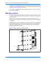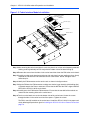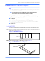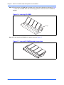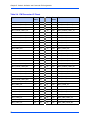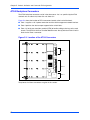
1
REVIEW COPY
ATCA-C110/1G
AMC Carrier Blade
Installation and Use
225254 420 000 AA
September 2005 Edition
REVIEW COPY
© Copyright 2005 Motorola, Inc.
All rights reserved.
Printed in the United States of America.
Trademarks
Motorola and the stylized M logo are trademarks registered in the U.S. Patent and Trademark Office.
PICMG, AdvancedTCA, and the AdvancedTCA logo are registered trademarks of PCI Industrial Computer
Manufacturers Group.
PowerPC™ and the PowerPC logo are trademarks of International Business Machines Corporation.
All other product or service names mentioned in this document are the property of their respective owners.
REVIEW COPY
Safety Summary
The following general safety precautions must be observed during all phases of operation, service, and repair
of this equipment. Failure to comply with these precautions or with specific warnings elsewhere in this manual
could result in personal injury or damage to the equipment.
The safety precautions listed below represent warnings of certain dangers of which Motorola is aware. You,
as the user of the product, should follow these warnings and all other safety precautions necessary for the
safe operation of the equipment in your operating environment.
Ground the Instrument.
To minimize shock hazard, the equipment chassis and enclosure must be connected to an electrical ground.
If the equipment is supplied with a three-conductor AC power cable, the power cable must be plugged into
an approved three-contact electrical outlet, with the grounding wire (green/yellow) reliably connected to an
electrical ground (safety ground) at the power outlet. The power jack and mating plug of the power cable meet
International Electrotechnical Commission (IEC) safety standards and local electrical regulatory codes.
Do Not Operate in an Explosive Atmosphere.
Do not operate the equipment in any explosive atmosphere such as in the presence of flammable gases or
fumes. Operation of any electrical equipment in such an environment could result in an explosion and cause
injury or damage.
Keep Away From Live Circuits Inside the Equipment.
Operating personnel must not remove equipment covers. Only Factory Authorized Service Personnel or other
qualified service personnel may remove equipment covers for internal subassembly or component
replacement or any internal adjustment. Service personnel should not replace components with power cable
connected. Under certain conditions, dangerous voltages may exist even with the power cable removed. To
avoid injuries, such personnel should always disconnect power and discharge circuits before touching
components.
Use Caution When Exposing or Handling a CRT.
Breakage of a Cathode-Ray Tube (CRT) causes a high-velocity scattering of glass fragments (implosion). To
prevent CRT implosion, do not handle the CRT and avoid rough handling or jarring of the equipment.
Handling of a CRT should be done only by qualified service personnel using approved safety mask and
gloves.
Do Not Substitute Parts or Modify Equipment.
Do not install substitute parts or perform any unauthorized modification of the equipment. Contact your local
Motorola representative for service and repair to ensure that all safety features are maintained.
Observe Warnings in Manual.
Warnings, such as the example below, precede potentially dangerous procedures throughout this manual.
Instructions contained in the warnings must be followed. You should also employ all other safety precautions
which you deem necessary for the operation of the equipment in your operating environment.
Warning
Warning
To prevent serious injury or death from dangerous voltages, use
extreme caution when handling, testing, and adjusting this
equipment and its components.
REVIEW COPY
Flammability
All Motorola PWBs (printed wiring boards) are manufactured with a flammability rating of 94V-0 by ULrecognized manufacturers.
EMI Caution
Caution
!
Caution
This equipment generates, uses and can radiate electromagnetic energy. It may cause
or be susceptible to electromagnetic interference (EMI) if not installed and used with
adequate EMI protection.
Lithium Battery Caution
This product contains a lithium battery to power the clock and calendar circuitry.
Caution
!
Caution
Caution
!
Attention
Caution
!
Vorsicht
Danger of explosion if battery is replaced incorrectly. Replace battery only with the
same or equivalent type recommended by the equipment manufacturer. Dispose of
used batteries according to the manufacturer’s instructions.
Il y a danger d’explosion s’il y a remplacement incorrect de la batterie. Remplacer
uniquement avec une batterie du même type ou d’un type équivalent recommandé par
le constructeur. Mettre au rebut les batteries usagées conformément aux instructions
du fabricant.
Explosionsgefahr bei unsachgemäßem Austausch der Batterie. Ersatz nur durch
denselben oder einen vom Hersteller empfohlenen Typ. Entsorgung gebrauchter
Batterien nach Angaben des Herstellers.
CE Notice (European Community)
Warning
!
Warning
This is a Class A product. In a domestic environment, this product may cause radio
interference, in which case the user may be required to take adequate measures.
REVIEW COPY
Motorola products with the CE marking comply with the EMC Directive (89/336/EEC). Compliance with this
directive implies conformity to the following European Norms:
EN55022 “Limits and Methods of Measurement of Radio Interference Characteristics of Information
Technology Equipment”; this product tested to Equipment Class A
EN50082-1:1997 “Electromagnetic Compatibility—Generic Immunity Standard, Part 1. Residential,
Commercial and Light Industry”
System products also fulfill EN60950 (product safety) which is essentially the requirement for the Low
Voltage Directive (73/23/EEC).
Board products are tested in a representative system to show compliance with the above mentioned
requirements. A proper installation in a CE-marked system will maintain the required EMC/safety
performance.
In accordance with European Community directives, a “Declaration of Conformity” has been made and is
on file within the European Union. The “Declaration of Conformity” is available on request. Please contact
your sales representative.
FCC Class A
This equipment has been tested and found to comply with the limits for a Class A digital device, pursuant to
Part 15 of the FCC Rules. These limits are designed to provide reasonable protection against harmful
interference when the equipment is operated in a commercial environment. This equipment generates,
uses, and can radiate radio frequency energy and, if not installed and used in accordance with the
instruction manual, may cause harmful interference to radio communications. Operation of this equipment
in a residential area is likely to cause harmful interference in which case the user will be required to correct
the interference at his own expense.
Changes or modifications not expressly approved by Motorola could void the user’s authority to operate the
equipment.
Use only shielded cables when connecting peripherals to assure that appropriate radio frequency emissions
compliance is maintained.
Industrie Canada
This product meets the requirements of the Canadian Interference-Causing Equipment Standard ICES-003.
Cet appareil numérique est conforme à la norme NMB-003 du Canada.
REVIEW COPY
Notice
While reasonable efforts have been made to assure the accuracy of this document, Motorola, Inc. assumes
no liability resulting from any omissions in this document, or from the use of the information obtained therein.
Motorola reserves the right to revise this document and to make changes from time to time in the content
hereof without obligation of Motorola to notify any person of such revision or changes.
Electronic versions of this material may be read online, downloaded for personal use, or referenced in
another document as a URL to the Motorola Computer Group website. The text itself may not be published
commercially in print or electronic form, edited, translated, or otherwise altered without the permission of
Motorola, Inc.
It is possible that this publication may contain reference to or information about Motorola products (machines
and programs), programming, or services that are not available in your country. Such references or
information must not be construed to mean that Motorola intends to announce such Motorola products,
programming, or services in your country.
Limited and Restricted Rights Legend
If the documentation contained herein is supplied, directly or indirectly, to the U.S. Government, the following
notice shall apply unless otherwise agreed to in writing by Motorola, Inc.
Use, duplication, or disclosure by the Government is subject to restrictions as set forth in subparagraph
(b)(3) of the Rights in Technical Data clause at DFARS 252.227-7013 (Nov. 1995) and of the Rights in
Noncommercial Computer Software and Documentation clause at DFARS 252.227-7014 (Jun. 1995).
Motorola, Inc.
Embedded Communications Computing
2900 South Diablo Way
Tempe, Arizona 85282
REVIEW COPY
Contents
About This Manual . . . . . . . . . . . . . . . . . . . . . . . . . . . . . . . . . . . . . . . . . . . . . . . . . . . . . . . . . . . . . . . . xvii
Audience . . . . . . . . . . . . . . . . . . . . . . . . . . . . . . . . . . . . . . . . . . . . . . . . . . . . . . . . . . . . . . . . . . . . . .xvii
Summary of Changes . . . . . . . . . . . . . . . . . . . . . . . . . . . . . . . . . . . . . . . . . . . . . . . . . . . . . . . . . . . . .xvii
Ordering Information . . . . . . . . . . . . . . . . . . . . . . . . . . . . . . . . . . . . . . . . . . . . . . . . . . . . . . . . . . . . . .xvii
Product Nomenclature . . . . . . . . . . . . . . . . . . . . . . . . . . . . . . . . . . . . . . . . . . . . . . . . . . . . . . . . .xvii
Order Numbers . . . . . . . . . . . . . . . . . . . . . . . . . . . . . . . . . . . . . . . . . . . . . . . . . . . . . . . . . . . . . . xviii
Overview of Contents . . . . . . . . . . . . . . . . . . . . . . . . . . . . . . . . . . . . . . . . . . . . . . . . . . . . . . . . . . . . xviii
Comments and Suggestions . . . . . . . . . . . . . . . . . . . . . . . . . . . . . . . . . . . . . . . . . . . . . . . . . . . . . . . . xix
Conventions Used in This Manual. . . . . . . . . . . . . . . . . . . . . . . . . . . . . . . . . . . . . . . . . . . . . . . . . . . . xix
Signal Names . . . . . . . . . . . . . . . . . . . . . . . . . . . . . . . . . . . . . . . . . . . . . . . . . . . . . . . . . . . . . . . . xix
Numeric notation: . . . . . . . . . . . . . . . . . . . . . . . . . . . . . . . . . . . . . . . . . . . . . . . . . . . . . . . . . . . . . xix
Miscellaneous notations . . . . . . . . . . . . . . . . . . . . . . . . . . . . . . . . . . . . . . . . . . . . . . . . . . . . . . . . xx
Typographical Conventions . . . . . . . . . . . . . . . . . . . . . . . . . . . . . . . . . . . . . . . . . . . . . . . . . . . . . xx
Terms and Abbreviations . . . . . . . . . . . . . . . . . . . . . . . . . . . . . . . . . . . . . . . . . . . . . . . . . . . . . . . xxi
1
ATCA-C110/1G Baseboard Preparation and Installation. . . . . . . . . . . . . . . . . . . . . . . . . . . . . . . . . 1
Introduction . . . . . . . . . . . . . . . . . . . . . . . . . . . . . . . . . . . . . . . . . . . . . . . . . . . . . . . . . . . . . . . . . . . . . 1
Product Description . . . . . . . . . . . . . . . . . . . . . . . . . . . . . . . . . . . . . . . . . . . . . . . . . . . . . . . . . . . . . . . 1
Baseboard Layout . . . . . . . . . . . . . . . . . . . . . . . . . . . . . . . . . . . . . . . . . . . . . . . . . . . . . . . . . . . . . . . . 3
Equipment Required . . . . . . . . . . . . . . . . . . . . . . . . . . . . . . . . . . . . . . . . . . . . . . . . . . . . . . . . . . . . . . 3
AMC Bay Locations . . . . . . . . . . . . . . . . . . . . . . . . . . . . . . . . . . . . . . . . . . . . . . . . . . . . . . . . . . . . . . . 4
Getting Started . . . . . . . . . . . . . . . . . . . . . . . . . . . . . . . . . . . . . . . . . . . . . . . . . . . . . . . . . . . . . . . . . . . 5
Overview of Startup Procedures . . . . . . . . . . . . . . . . . . . . . . . . . . . . . . . . . . . . . . . . . . . . . . . . . . 5
Unpacking Guidelines . . . . . . . . . . . . . . . . . . . . . . . . . . . . . . . . . . . . . . . . . . . . . . . . . . . . . . . . . . 5
Hardware Configuration . . . . . . . . . . . . . . . . . . . . . . . . . . . . . . . . . . . . . . . . . . . . . . . . . . . . . . . . . . . . 6
Software Support . . . . . . . . . . . . . . . . . . . . . . . . . . . . . . . . . . . . . . . . . . . . . . . . . . . . . . . . . . . . . . . . . 6
Hardware Upgrades and Accessories . . . . . . . . . . . . . . . . . . . . . . . . . . . . . . . . . . . . . . . . . . . . . . . . . 7
Installing the FIM on ATCA-C110/1G Board . . . . . . . . . . . . . . . . . . . . . . . . . . . . . . . . . . . . . . . . . 7
SO-DIMM Installation in a Non-Powered System . . . . . . . . . . . . . . . . . . . . . . . . . . . . . . . . . . . . . 9
Installing SO-DIMM . . . . . . . . . . . . . . . . . . . . . . . . . . . . . . . . . . . . . . . . . . . . . . . . . . . . . . . . . 9
Removing SO-DIMM . . . . . . . . . . . . . . . . . . . . . . . . . . . . . . . . . . . . . . . . . . . . . . . . . . . . . . . 11
Installing an AMC Module in a Powered System . . . . . . . . . . . . . . . . . . . . . . . . . . . . . . . . . . . . . 12
Removing an AMC Module from a Powered System . . . . . . . . . . . . . . . . . . . . . . . . . . . . . . . . . 14
Rear Transition Modules . . . . . . . . . . . . . . . . . . . . . . . . . . . . . . . . . . . . . . . . . . . . . . . . . . . . . . . . . . 15
Switch Settings . . . . . . . . . . . . . . . . . . . . . . . . . . . . . . . . . . . . . . . . . . . . . . . . . . . . . . . . . . . . . . . . . . 16
Before You Install or Remove an AdvancedTCA Blade . . . . . . . . . . . . . . . . . . . . . . . . . . . . . . . . . . . 16
Observe ESD Precautions . . . . . . . . . . . . . . . . . . . . . . . . . . . . . . . . . . . . . . . . . . . . . . . . . . . . . . 17
Watch for Bent Pins or Other Damage . . . . . . . . . . . . . . . . . . . . . . . . . . . . . . . . . . . . . . . . . . . . 17
Use Caution When Installing or Removing Blades . . . . . . . . . . . . . . . . . . . . . . . . . . . . . . . . . . . 17
Preserve EMI Compliance . . . . . . . . . . . . . . . . . . . . . . . . . . . . . . . . . . . . . . . . . . . . . . . . . . . . . . 17
Understand Hot Swap . . . . . . . . . . . . . . . . . . . . . . . . . . . . . . . . . . . . . . . . . . . . . . . . . . . . . . . . . 18
ATCA-C110/1G Installation and Use Manual
vii
REVIEW COPY
Contents
Control Elements . . . . . . . . . . . . . . . . . . . . . . . . . . . . . . . . . . . . . . . . . . . . . . . . . . . . . . . . . .
Injector/Ejector Lever and Hot Swap Switch Mechanism . . . . . . . . . . . . . . . . . . . . . . . . . . .
Verify Slot Usage . . . . . . . . . . . . . . . . . . . . . . . . . . . . . . . . . . . . . . . . . . . . . . . . . . . . . . . . . . . . .
Installing the ATCA-C110/1G in a Powered Chassis . . . . . . . . . . . . . . . . . . . . . . . . . . . . . . . . . . . . .
Removing the ATCA-C110/1G from a Powered Chassis . . . . . . . . . . . . . . . . . . . . . . . . . . . . . . . . . .
Connecting to Peripherals . . . . . . . . . . . . . . . . . . . . . . . . . . . . . . . . . . . . . . . . . . . . . . . . . . . . . . . . .
2
Operating Instructions . . . . . . . . . . . . . . . . . . . . . . . . . . . . . . . . . . . . . . . . . . . . . . . . . . . . . . . . . . . 25
System Initialization . . . . . . . . . . . . . . . . . . . . . . . . . . . . . . . . . . . . . . . . . . . . . . . . . . . . . . . . . . . . . .
Hot Swap Support . . . . . . . . . . . . . . . . . . . . . . . . . . . . . . . . . . . . . . . . . . . . . . . . . . . . . . . . . . . . . . .
Ejector Handles . . . . . . . . . . . . . . . . . . . . . . . . . . . . . . . . . . . . . . . . . . . . . . . . . . . . . . . . . . . . . .
Indicator LEDs . . . . . . . . . . . . . . . . . . . . . . . . . . . . . . . . . . . . . . . . . . . . . . . . . . . . . . . . . . . . . . . . . .
Booting with Firmware . . . . . . . . . . . . . . . . . . . . . . . . . . . . . . . . . . . . . . . . . . . . . . . . . . . . . . . . . . . .
Reset Sources . . . . . . . . . . . . . . . . . . . . . . . . . . . . . . . . . . . . . . . . . . . . . . . . . . . . . . . . . . . . . . . . . .
Debug Support . . . . . . . . . . . . . . . . . . . . . . . . . . . . . . . . . . . . . . . . . . . . . . . . . . . . . . . . . . . . . . . . . .
3
29
29
29
30
31
31
32
Functional Description . . . . . . . . . . . . . . . . . . . . . . . . . . . . . . . . . . . . . . . . . . . . . . . . . . . . . . . . . . . 35
ATCA-C110/1G Overview . . . . . . . . . . . . . . . . . . . . . . . . . . . . . . . . . . . . . . . . . . . . . . . . . . . . . . . . .
ATCA Compliant features . . . . . . . . . . . . . . . . . . . . . . . . . . . . . . . . . . . . . . . . . . . . . . . . . . . . . . . . .
Block Diagram – ATCA-C110/1G . . . . . . . . . . . . . . . . . . . . . . . . . . . . . . . . . . . . . . . . . . . . . . . . . . . .
Processor and Processor interfaces . . . . . . . . . . . . . . . . . . . . . . . . . . . . . . . . . . . . . . . . . . . . . . . . .
CPU . . . . . . . . . . . . . . . . . . . . . . . . . . . . . . . . . . . . . . . . . . . . . . . . . . . . . . . . . . . . . . . . . . . . . . .
CPU Interfaces . . . . . . . . . . . . . . . . . . . . . . . . . . . . . . . . . . . . . . . . . . . . . . . . . . . . . . . . . . . . . .
Integrated Memory Controller . . . . . . . . . . . . . . . . . . . . . . . . . . . . . . . . . . . . . . . . . . . . . . . .
Programmable Interrupt Controller . . . . . . . . . . . . . . . . . . . . . . . . . . . . . . . . . . . . . . . . . . . .
I2C Interface . . . . . . . . . . . . . . . . . . . . . . . . . . . . . . . . . . . . . . . . . . . . . . . . . . . . . . . . . . . . .
DUART Controller . . . . . . . . . . . . . . . . . . . . . . . . . . . . . . . . . . . . . . . . . . . . . . . . . . . . . . . . .
Local Bus Controller (LBC) . . . . . . . . . . . . . . . . . . . . . . . . . . . . . . . . . . . . . . . . . . . . . . . . . .
Three Speed Ethernet Controllers (TSEC) . . . . . . . . . . . . . . . . . . . . . . . . . . . . . . . . . . . . . .
Fast Ethernet Controller . . . . . . . . . . . . . . . . . . . . . . . . . . . . . . . . . . . . . . . . . . . . . . . . . . . .
DMA Controller . . . . . . . . . . . . . . . . . . . . . . . . . . . . . . . . . . . . . . . . . . . . . . . . . . . . . . . . . . .
PCI/PCI-X Interface . . . . . . . . . . . . . . . . . . . . . . . . . . . . . . . . . . . . . . . . . . . . . . . . . . . . . . . .
Main Memory . . . . . . . . . . . . . . . . . . . . . . . . . . . . . . . . . . . . . . . . . . . . . . . . . . . . . . . . . . . . . . . . . . .
Onboard Memory . . . . . . . . . . . . . . . . . . . . . . . . . . . . . . . . . . . . . . . . . . . . . . . . . . . . . . . . . . . . .
SODIMM . . . . . . . . . . . . . . . . . . . . . . . . . . . . . . . . . . . . . . . . . . . . . . . . . . . . . . . . . . . . . . . . . . .
viii
25
26
26
26
26
26
27
U-Boot Firmware Overview . . . . . . . . . . . . . . . . . . . . . . . . . . . . . . . . . . . . . . . . . . . . . . . . . . . . . . . 29
System Setup . . . . . . . . . . . . . . . . . . . . . . . . . . . . . . . . . . . . . . . . . . . . . . . . . . . . . . . . . . . . . . . . . . .
Serial Console Access . . . . . . . . . . . . . . . . . . . . . . . . . . . . . . . . . . . . . . . . . . . . . . . . . . . . . . . . . . . .
Configuring the TFTP Server . . . . . . . . . . . . . . . . . . . . . . . . . . . . . . . . . . . . . . . . . . . . . . . . . . . . . . .
Configuring the BOOTP/DHCP Server . . . . . . . . . . . . . . . . . . . . . . . . . . . . . . . . . . . . . . . . . . . . . . .
Configuring an NFS Server . . . . . . . . . . . . . . . . . . . . . . . . . . . . . . . . . . . . . . . . . . . . . . . . . . . . . . . .
Initialization of the ATCA-C110/1G Board . . . . . . . . . . . . . . . . . . . . . . . . . . . . . . . . . . . . . . . . . . . . .
Initial Steps . . . . . . . . . . . . . . . . . . . . . . . . . . . . . . . . . . . . . . . . . . . . . . . . . . . . . . . . . . . . . . . . . . . . .
4
18
18
19
19
21
22
ATCA-C110/1G Installation and Use Manual
35
36
37
38
38
38
38
38
39
39
39
39
39
39
40
40
40
40
REVIEW COPY
Contents
Boot Device . . . . . . . . . . . . . . . . . . . . . . . . . . . . . . . . . . . . . . . . . . . . . . . . . . . . . . . . . . . . . . . . . . . .
System Management . . . . . . . . . . . . . . . . . . . . . . . . . . . . . . . . . . . . . . . . . . . . . . . . . . . . . . . . . . . . .
IPMI . . . . . . . . . . . . . . . . . . . . . . . . . . . . . . . . . . . . . . . . . . . . . . . . . . . . . . . . . . . . . . . . . . . . . . .
IPMB Interfaces . . . . . . . . . . . . . . . . . . . . . . . . . . . . . . . . . . . . . . . . . . . . . . . . . . . . . . . . . . .
Private I2C Bus . . . . . . . . . . . . . . . . . . . . . . . . . . . . . . . . . . . . . . . . . . . . . . . . . . . . . . . . . . .
Payload Interface . . . . . . . . . . . . . . . . . . . . . . . . . . . . . . . . . . . . . . . . . . . . . . . . . . . . . . . . .
8-bit Analog-to-Digital Converters (ADC) . . . . . . . . . . . . . . . . . . . . . . . . . . . . . . . . . . . . . . .
AMC Power Limiting Control . . . . . . . . . . . . . . . . . . . . . . . . . . . . . . . . . . . . . . . . . . . . . . . . .
Telecom Clock Interface Control . . . . . . . . . . . . . . . . . . . . . . . . . . . . . . . . . . . . . . . . . . . . . .
Digital IO . . . . . . . . . . . . . . . . . . . . . . . . . . . . . . . . . . . . . . . . . . . . . . . . . . . . . . . . . . . . . . . .
Fabric Interface Module . . . . . . . . . . . . . . . . . . . . . . . . . . . . . . . . . . . . . . . . . . . . . . . . . . . . . . . . . . .
Block Diagram – FIM . . . . . . . . . . . . . . . . . . . . . . . . . . . . . . . . . . . . . . . . . . . . . . . . . . . . . . . . . .
PCI-Express Switch . . . . . . . . . . . . . . . . . . . . . . . . . . . . . . . . . . . . . . . . . . . . . . . . . . . . . . .
PCI-Express to PCI Bridge . . . . . . . . . . . . . . . . . . . . . . . . . . . . . . . . . . . . . . . . . . . . . . . . . .
Ethernet Switching Fabric . . . . . . . . . . . . . . . . . . . . . . . . . . . . . . . . . . . . . . . . . . . . . . . . . . .
SATA Multiplexer . . . . . . . . . . . . . . . . . . . . . . . . . . . . . . . . . . . . . . . . . . . . . . . . . . . . . . . . .
I2C Bus Interface . . . . . . . . . . . . . . . . . . . . . . . . . . . . . . . . . . . . . . . . . . . . . . . . . . . . . . . . .
I/O Subsystems . . . . . . . . . . . . . . . . . . . . . . . . . . . . . . . . . . . . . . . . . . . . . . . . . . . . . . . . . . . . . . . . .
Onboard Devices . . . . . . . . . . . . . . . . . . . . . . . . . . . . . . . . . . . . . . . . . . . . . . . . . . . . . . . . . . . . .
User Flash . . . . . . . . . . . . . . . . . . . . . . . . . . . . . . . . . . . . . . . . . . . . . . . . . . . . . . . . . . . . . . .
AMC Bays . . . . . . . . . . . . . . . . . . . . . . . . . . . . . . . . . . . . . . . . . . . . . . . . . . . . . . . . . . . . . . .
Programmable Logic Devices – CPLD . . . . . . . . . . . . . . . . . . . . . . . . . . . . . . . . . . . . . . . . .
PCI Interface . . . . . . . . . . . . . . . . . . . . . . . . . . . . . . . . . . . . . . . . . . . . . . . . . . . . . . . . . . . . . . . .
PCI-to-PCI-Express Bridge . . . . . . . . . . . . . . . . . . . . . . . . . . . . . . . . . . . . . . . . . . . . . . . . . . . . .
PCI-Express Interface . . . . . . . . . . . . . . . . . . . . . . . . . . . . . . . . . . . . . . . . . . . . . . . . . . . . . . . . .
Serial ATA interface . . . . . . . . . . . . . . . . . . . . . . . . . . . . . . . . . . . . . . . . . . . . . . . . . . . . . . . . . . .
Gigabit Ethernet - SerDes Interface . . . . . . . . . . . . . . . . . . . . . . . . . . . . . . . . . . . . . . . . . . . . . .
10/100 Ethernet . . . . . . . . . . . . . . . . . . . . . . . . . . . . . . . . . . . . . . . . . . . . . . . . . . . . . . . . . . . . . .
Serial interface . . . . . . . . . . . . . . . . . . . . . . . . . . . . . . . . . . . . . . . . . . . . . . . . . . . . . . . . . . . . . . .
I2C Bus . . . . . . . . . . . . . . . . . . . . . . . . . . . . . . . . . . . . . . . . . . . . . . . . . . . . . . . . . . . . . . . . . . . .
RTC interface . . . . . . . . . . . . . . . . . . . . . . . . . . . . . . . . . . . . . . . . . . . . . . . . . . . . . . . . . . . . . . .
Power Supplies . . . . . . . . . . . . . . . . . . . . . . . . . . . . . . . . . . . . . . . . . . . . . . . . . . . . . . . . . . . . . . . . .
5
40
41
41
42
43
43
43
43
43
44
44
44
45
46
46
46
46
47
47
47
47
47
48
48
48
49
49
49
49
50
50
50
Controls, Indicators and Connector Pin Assignments . . . . . . . . . . . . . . . . . . . . . . . . . . . . . . . . . 51
Face plate and LEDs . . . . . . . . . . . . . . . . . . . . . . . . . . . . . . . . . . . . . . . . . . . . . . . . . . . . . . . . . . . . .
Baseboard Connectors . . . . . . . . . . . . . . . . . . . . . . . . . . . . . . . . . . . . . . . . . . . . . . . . . . . . . . . . . . .
FIM Connectors . . . . . . . . . . . . . . . . . . . . . . . . . . . . . . . . . . . . . . . . . . . . . . . . . . . . . . . . . . . . . .
AMC Connectors . . . . . . . . . . . . . . . . . . . . . . . . . . . . . . . . . . . . . . . . . . . . . . . . . . . . . . . . . . . . .
Clocks . . . . . . . . . . . . . . . . . . . . . . . . . . . . . . . . . . . . . . . . . . . . . . . . . . . . . . . . . . . . . . . . . .
Common Options Region . . . . . . . . . . . . . . . . . . . . . . . . . . . . . . . . . . . . . . . . . . . . . . . . . . .
Fat Pipes Region . . . . . . . . . . . . . . . . . . . . . . . . . . . . . . . . . . . . . . . . . . . . . . . . . . . . . . . . . .
Extended Options Region . . . . . . . . . . . . . . . . . . . . . . . . . . . . . . . . . . . . . . . . . . . . . . . . . . .
ATCA Backplane Connectors . . . . . . . . . . . . . . . . . . . . . . . . . . . . . . . . . . . . . . . . . . . . . . . . . . .
Zone 1 Connectors . . . . . . . . . . . . . . . . . . . . . . . . . . . . . . . . . . . . . . . . . . . . . . . . . . . . . . . .
Zone 2 Connectors . . . . . . . . . . . . . . . . . . . . . . . . . . . . . . . . . . . . . . . . . . . . . . . . . . . . . . . .
ATCA-C110/1G Installation and Use Manual
51
52
53
59
60
60
61
61
62
63
64
ix
REVIEW COPY
Contents
Zone 3 Connectors . . . . . . . . . . . . . . . . . . . . . . . . . . . . . . . . . . . . . . . . . . . . . . . . . . . . . . . . 67
6
Memory Map and Registers . . . . . . . . . . . . . . . . . . . . . . . . . . . . . . . . . . . . . . . . . . . . . . . . . . . . . . . 71
Memory Maps . . . . . . . . . . . . . . . . . . . . . . . . . . . . . . . . . . . . . . . . . . . . . . . . . . . . . . . . . . . . . . . . . .
Interrupt Mapping . . . . . . . . . . . . . . . . . . . . . . . . . . . . . . . . . . . . . . . . . . . . . . . . . . . . . . . . . . . . . . . .
Shelf Management Registers (IPMI interface) . . . . . . . . . . . . . . . . . . . . . . . . . . . . . . . . . . . . . . . . . .
Digital IO . . . . . . . . . . . . . . . . . . . . . . . . . . . . . . . . . . . . . . . . . . . . . . . . . . . . . . . . . . . . . . . . . . .
Payload Reset . . . . . . . . . . . . . . . . . . . . . . . . . . . . . . . . . . . . . . . . . . . . . . . . . . . . . . . . . . . .
Boot ROM Selection . . . . . . . . . . . . . . . . . . . . . . . . . . . . . . . . . . . . . . . . . . . . . . . . . . . . . . .
Payload Power Enable . . . . . . . . . . . . . . . . . . . . . . . . . . . . . . . . . . . . . . . . . . . . . . . . . . . . .
I2C Address Map for MPC8540 . . . . . . . . . . . . . . . . . . . . . . . . . . . . . . . . . . . . . . . . . . . . . . . . . . . . .
I2C Resources . . . . . . . . . . . . . . . . . . . . . . . . . . . . . . . . . . . . . . . . . . . . . . . . . . . . . . . . . . . . . . . . . .
I2C to GPIO’s Device Mappings - ATMega64-AMC Private I2C Bus . . . . . . . . . . . . . . . . . . . . .
GPIO . . . . . . . . . . . . . . . . . . . . . . . . . . . . . . . . . . . . . . . . . . . . . . . . . . . . . . . . . . . . . . . . . . . . . . . . .
Geographical addressing of AMC Bays on ATCA-C110/1G . . . . . . . . . . . . . . . . . . . . . . . . . . . .
Ethernet Phy Address Map . . . . . . . . . . . . . . . . . . . . . . . . . . . . . . . . . . . . . . . . . . . . . . . . . . . . . . . .
A
Troubleshooting . . . . . . . . . . . . . . . . . . . . . . . . . . . . . . . . . . . . . . . . . . . . . . . . . . . . . . . . . . . . . . . . 83
Error List . . . . . . . . . . . . . . . . . . . . . . . . . . . . . . . . . . . . . . . . . . . . . . . . . . . . . . . . . . . . . . . . . . . . . . .
Mechanical . . . . . . . . . . . . . . . . . . . . . . . . . . . . . . . . . . . . . . . . . . . . . . . . . . . . . . . . . . . . . . . . .
During or After System Initialization . . . . . . . . . . . . . . . . . . . . . . . . . . . . . . . . . . . . . . . . . . . . . .
During Boot-up Procedure . . . . . . . . . . . . . . . . . . . . . . . . . . . . . . . . . . . . . . . . . . . . . . . . . . . . . .
During Board Operation . . . . . . . . . . . . . . . . . . . . . . . . . . . . . . . . . . . . . . . . . . . . . . . . . . . . . . . .
B
89
89
91
92
93
Thermal Validation . . . . . . . . . . . . . . . . . . . . . . . . . . . . . . . . . . . . . . . . . . . . . . . . . . . . . . . . . . . . . . 95
Thermal Requirements . . . . . . . . . . . . . . . . . . . . . . . . . . . . . . . . . . . . . . . . . . . . . . . . . . . . . . . . . . . .
Thermally Significant Components . . . . . . . . . . . . . . . . . . . . . . . . . . . . . . . . . . . . . . . . . . . . . . .
Component Temperature Measurement . . . . . . . . . . . . . . . . . . . . . . . . . . . . . . . . . . . . . . . . . . . . . .
Preparation . . . . . . . . . . . . . . . . . . . . . . . . . . . . . . . . . . . . . . . . . . . . . . . . . . . . . . . . . . . . . . . . .
Measuring Junction Temperature . . . . . . . . . . . . . . . . . . . . . . . . . . . . . . . . . . . . . . . . . . . . . . . .
Measuring Case Temperature . . . . . . . . . . . . . . . . . . . . . . . . . . . . . . . . . . . . . . . . . . . . . . . . . . .
Measuring Local Air Temperature . . . . . . . . . . . . . . . . . . . . . . . . . . . . . . . . . . . . . . . . . . . . . . . .
D
83
83
84
85
86
Specifications . . . . . . . . . . . . . . . . . . . . . . . . . . . . . . . . . . . . . . . . . . . . . . . . . . . . . . . . . . . . . . . . . . 89
Specifications . . . . . . . . . . . . . . . . . . . . . . . . . . . . . . . . . . . . . . . . . . . . . . . . . . . . . . . . . . . . . . . . . . .
Environmental and Physical Specifications . . . . . . . . . . . . . . . . . . . . . . . . . . . . . . . . . . . . . . . . .
Power Requirements . . . . . . . . . . . . . . . . . . . . . . . . . . . . . . . . . . . . . . . . . . . . . . . . . . . . . . . . . . . . .
Standard Compliance . . . . . . . . . . . . . . . . . . . . . . . . . . . . . . . . . . . . . . . . . . . . . . . . . . . . . . . . . . . . .
EMC Compliance . . . . . . . . . . . . . . . . . . . . . . . . . . . . . . . . . . . . . . . . . . . . . . . . . . . . . . . . . . . . . . . .
C
71
72
73
73
73
73
73
74
74
80
82
82
82
95
95
96
96
96
96
98
Related Documentation . . . . . . . . . . . . . . . . . . . . . . . . . . . . . . . . . . . . . . . . . . . . . . . . . . . . . . . . . . 99
Embedded Communications Computing Documents . . . . . . . . . . . . . . . . . . . . . . . . . . . . . . . . . . . . . 99
x
ATCA-C110/1G Installation and Use Manual
REVIEW COPY
Contents
Manufacturers’ Documents . . . . . . . . . . . . . . . . . . . . . . . . . . . . . . . . . . . . . . . . . . . . . . . . . . . . . . . . 100
Related Specifications . . . . . . . . . . . . . . . . . . . . . . . . . . . . . . . . . . . . . . . . . . . . . . . . . . . . . . . . . . . 101
ATCA-C110/1G Installation and Use Manual
xi
REVIEW COPY
REVIEW COPY
List of Figures
Figure 1-1. Board Layout Diagram . . . . . . . . . . . . . . . . . . . . . . . . . . . . . . . . . . . . . . . . . . . . . . . . . . . 3
Figure 1-2. Bay Locations on ATCA-C110/1G . . . . . . . . . . . . . . . . . . . . . . . . . . . . . . . . . . . . . . . . . . . 4
Figure 1-3. Fabric Interface Module Installation . . . . . . . . . . . . . . . . . . . . . . . . . . . . . . . . . . . . . . . . . 8
Figure 1-4. SO-DIMM with Notch . . . . . . . . . . . . . . . . . . . . . . . . . . . . . . . . . . . . . . . . . . . . . . . . . . . . 9
Figure 1-5. SO-DIMM Socket and Projection . . . . . . . . . . . . . . . . . . . . . . . . . . . . . . . . . . . . . . . . . . . 9
Figure 1-6. Inserting SO-DIMM . . . . . . . . . . . . . . . . . . . . . . . . . . . . . . . . . . . . . . . . . . . . . . . . . . . . . 10
Figure 1-7. Inserted SO-DIMM locked into position . . . . . . . . . . . . . . . . . . . . . . . . . . . . . . . . . . . . . 10
Figure 1-8. Removing the SO-DIMM - pull retaining clips outward . . . . . . . . . . . . . . . . . . . . . . . . . . 11
Figure 1-9. Removing the SO-DIMM - slide module out . . . . . . . . . . . . . . . . . . . . . . . . . . . . . . . . . . 11
Figure 1-10. Installing AMC Module in ATCA-C110/1G . . . . . . . . . . . . . . . . . . . . . . . . . . . . . . . . . . 13
Figure 1-11. Switch Settings . . . . . . . . . . . . . . . . . . . . . . . . . . . . . . . . . . . . . . . . . . . . . . . . . . . . . . . 16
Figure 1-12. Injector/Ejector Lever Types for ATCA-C110/1G . . . . . . . . . . . . . . . . . . . . . . . . . . . . . . 19
Figure 1-13. ATCA-C110/1G Installation . . . . . . . . . . . . . . . . . . . . . . . . . . . . . . . . . . . . . . . . . . . . . . 20
Figure 1-14. ATCA-C110/1G Removal . . . . . . . . . . . . . . . . . . . . . . . . . . . . . . . . . . . . . . . . . . . . . . . 22
Figure 4-1. ATCA-C110/1G Block Diagram . . . . . . . . . . . . . . . . . . . . . . . . . . . . . . . . . . . . . . . . . . . . 37
Figure 4-2. Primary and Secondary Boot Flash Connections . . . . . . . . . . . . . . . . . . . . . . . . . . . . . . 41
Figure 4-3. IPMI Implementation on ATCA-C110/1G . . . . . . . . . . . . . . . . . . . . . . . . . . . . . . . . . . . . 42
Figure 4-4. Fabric Interface Module - Block Diagram . . . . . . . . . . . . . . . . . . . . . . . . . . . . . . . . . . . . 45
Figure 5-1. Face plate LEDs . . . . . . . . . . . . . . . . . . . . . . . . . . . . . . . . . . . . . . . . . . . . . . . . . . . . . . . 51
Figure 5-2. Location of Baseboard Connectors . . . . . . . . . . . . . . . . . . . . . . . . . . . . . . . . . . . . . . . . . 52
Figure 5-3. Location of the ATCA Connectors . . . . . . . . . . . . . . . . . . . . . . . . . . . . . . . . . . . . . . . . . . 62
Figure 6-1. Interrupt Routing Block Diagram . . . . . . . . . . . . . . . . . . . . . . . . . . . . . . . . . . . . . . . . . . . 72
Figure C-1. Mounting a Thermocouple Under a Heatsink . . . . . . . . . . . . . . . . . . . . . . . . . . . . . . . . . 97
Figure C-2. Measuring Local Air Temperature . . . . . . . . . . . . . . . . . . . . . . . . . . . . . . . . . . . . . . . . . 98
REVIEW COPY
REVIEW COPY
List of Tables
Table 1. Ordering Information . . . . . . . . . . . . . . . . . . . . . . . . . . . . . . . . . . . . . . . . . . . . . . . . . . . . . xviii
Table 2. Accessories Ordering Information . . . . . . . . . . . . . . . . . . . . . . . . . . . . . . . . . . . . . . . . . . . xviii
Table 1-1. Startup Overview . . . . . . . . . . . . . . . . . . . . . . . . . . . . . . . . . . . . . . . . . . . . . . . . . . . . . . . . 5
Table 1-2. Default Switch Settings for SW1 . . . . . . . . . . . . . . . . . . . . . . . . . . . . . . . . . . . . . . . . . . . . 16
Table 1-3. Slot Usage Indicators . . . . . . . . . . . . . . . . . . . . . . . . . . . . . . . . . . . . . . . . . . . . . . . . . . . . 19
Table 1-4. ATCA-C110/1G Onboard Connectors . . . . . . . . . . . . . . . . . . . . . . . . . . . . . . . . . . . . . . . . 23
Table 1-5. Serial Port Configuration Parameters for MPC8540 . . . . . . . . . . . . . . . . . . . . . . . . . . . . . 23
Table 2-1. Reset Sources . . . . . . . . . . . . . . . . . . . . . . . . . . . . . . . . . . . . . . . . . . . . . . . . . . . . . . . . . 26
Table 4-1. ATCA-C110/1G Overview . . . . . . . . . . . . . . . . . . . . . . . . . . . . . . . . . . . . . . . . . . . . . . . . . 35
Table 4-2. Port Configuration on PCI-Express Switch . . . . . . . . . . . . . . . . . . . . . . . . . . . . . . . . . . . . 45
Table 5-1. Face Plate LEDs . . . . . . . . . . . . . . . . . . . . . . . . . . . . . . . . . . . . . . . . . . . . . . . . . . . . . . . . 52
Table 5-2. Differential Signals between FIM and Baseboard . . . . . . . . . . . . . . . . . . . . . . . . . . . . . . . 53
Table 5-3. FIM Connector J1 Pinout . . . . . . . . . . . . . . . . . . . . . . . . . . . . . . . . . . . . . . . . . . . . . . . . . 54
Table 5-4. FIM Connector J2 Pinout . . . . . . . . . . . . . . . . . . . . . . . . . . . . . . . . . . . . . . . . . . . . . . . . . 56
Table 5-5. FIM Connector J3 Pinout . . . . . . . . . . . . . . . . . . . . . . . . . . . . . . . . . . . . . . . . . . . . . . . . . 57
Table 5-6. FIM Connector J4 Pinout . . . . . . . . . . . . . . . . . . . . . . . . . . . . . . . . . . . . . . . . . . . . . . . . . 58
Table 5-7. AMC Connector Port Map . . . . . . . . . . . . . . . . . . . . . . . . . . . . . . . . . . . . . . . . . . . . . . . . 60
Table 5-8. AMC Connector Port Mapping on ATCA-C110/1G . . . . . . . . . . . . . . . . . . . . . . . . . . . . . . 61
Table 5-9. Zone 1 Connector Pinouts . . . . . . . . . . . . . . . . . . . . . . . . . . . . . . . . . . . . . . . . . . . . . . . . 63
Table 5-10. Zone 2 Backplane Connector J20 Pinout - Rows A to D . . . . . . . . . . . . . . . . . . . . . . . . 64
Table 5-11. Zone 2 Backplane Connector J20 Pinout - Rows E to H . . . . . . . . . . . . . . . . . . . . . . . . 64
Table 5-12. Zone 2 Backplane Connector J21 Pinout - Rows A to D . . . . . . . . . . . . . . . . . . . . . . . . 65
Table 5-13. Zone 2 Backplane Connector J22 Pinout - Rows A to D . . . . . . . . . . . . . . . . . . . . . . . . 65
Table 5-14. Zone 2 Backplane Connector J21 Pinout - Rows E to H . . . . . . . . . . . . . . . . . . . . . . . . 65
Table 5-15. Zone 2 Backplane Connector J22 Pinout - Rows E to H . . . . . . . . . . . . . . . . . . . . . . . . 66
Table 5-16. Zone 2 Backplane Connector J23 Pinout - Rows A to D . . . . . . . . . . . . . . . . . . . . . . . . 66
Table 5-17. Zone 2 Backplane Connector J23 Pinout - Rows E to H . . . . . . . . . . . . . . . . . . . . . . . . 67
Table 5-18. Zone 3 Backplane Connector J30 Pinout - Rows A to D . . . . . . . . . . . . . . . . . . . . . . . . 67
Table 5-19. Zone 3 Backplane Connector J30 Pinout - Rows E to H . . . . . . . . . . . . . . . . . . . . . . . . 68
Table 5-20. Zone 3 Backplane Connector J31 Pinout - Rows A to D . . . . . . . . . . . . . . . . . . . . . . . . 68
Table 5-21. Zone 3 Backplane Connector J31 Pinout - Rows E to H . . . . . . . . . . . . . . . . . . . . . . . . 68
Table 5-22. Zone 3 Backplane Connector J32 Pinout - Rows A to D . . . . . . . . . . . . . . . . . . . . . . . . 69
Table 5-23. Zone 3 Backplane Connector J32 Pinout - Rows E to H . . . . . . . . . . . . . . . . . . . . . . . . 69
Table 6-1. Memory Address Map . . . . . . . . . . . . . . . . . . . . . . . . . . . . . . . . . . . . . . . . . . . . . . . . . . . 71
Table 6-2. CS# Mapping of Main Memory on ATCA-C110/1G . . . . . . . . . . . . . . . . . . . . . . . . . . . . . 71
Table 6-3. MPC8540 Interrupt Mapping . . . . . . . . . . . . . . . . . . . . . . . . . . . . . . . . . . . . . . . . . . . . . . 72
Table 6-4. Private I2C Address Map - MPC8540 . . . . . . . . . . . . . . . . . . . . . . . . . . . . . . . . . . . . . . . 74
Table 6-5. Private I2C Address Map - ATmega8L . . . . . . . . . . . . . . . . . . . . . . . . . . . . . . . . . . . . . . . 74
Table 6-6. I2C to GPIO’s Device Mappings - ATMega8 Private I2C Bus . . . . . . . . . . . . . . . . . . . . . . 75
Table 6-7. Private I2C Address Map - ATmega64-AMC micro-controller . . . . . . . . . . . . . . . . . . . . . 79
ATCA-C110/1G Installation and Use Manual
xv
REVIEW COPY
List of Tables
Table 6-8. I2C to GPIO’s Device Mappings - ATMega64-AMC Private I2C Bus . . . . . . . . . . . . . . . . 80
Table 6-9. Geographical addressing of AMC Bays on ATCA-C110/1G . . . . . . . . . . . . . . . . . . . . . . 82
Table 6-10. Ethernet Phy Address Map . . . . . . . . . . . . . . . . . . . . . . . . . . . . . . . . . . . . . . . . . . . . . . . 82
Table B-1. ATCA-C110/1G Environmental Specifications . . . . . . . . . . . . . . . . . . . . . . . . . . . . . . . . . 90
Table B-2. Power Requirements . . . . . . . . . . . . . . . . . . . . . . . . . . . . . . . . . . . . . . . . . . . . . . . . . . . . 91
Table B-3. Standard Compliance . . . . . . . . . . . . . . . . . . . . . . . . . . . . . . . . . . . . . . . . . . . . . . . . . . . . 92
Table C-1. Thermally Significant Components . . . . . . . . . . . . . . . . . . . . . . . . . . . . . . . . . . . . . . . . . 95
Table D-1. Embedded Communications Computing Documents . . . . . . . . . . . . . . . . . . . . . . . . . . . 99
Table D-2. Manufacturers’ Documents . . . . . . . . . . . . . . . . . . . . . . . . . . . . . . . . . . . . . . . . . . . . . . 100
Table D-3. Related Specifications . . . . . . . . . . . . . . . . . . . . . . . . . . . . . . . . . . . . . . . . . . . . . . . . . . 101
xvi
ATCA-C110/1G Installation and Use Manual
REVIEW COPY
About This Manual
This manual provides both general and functional descriptions of the product along with
installation and removal instructions, firmware details, connector pin assignments, memory
maps, troubleshooting information, specifications, thermal validation and related
documentation details for the ATCA-C110/1G board.
The ATCA-C110/1G is a multi-function conventional AMC Carrier intended to be used in control
and management applications on AdvancedTCA™ systems. The board uses the MPC8540 as
its Service Processor and has Gigabit Ethernet, UART, SATA and PCI Express as its
I/O interfaces.
Audience
This document is written for anyone who designs OEM systems, supplies additional capability
to existing compatible systems, or works in a lab environment for experimental purposes. It is
important to note that a basic knowledge of computers and digital logic is assumed; users must
have a working understanding of AdvancedTCA and telecommunications. To use this document
successfully, you should be familiar with the documents listed in Appendix D, Related
Documentation, in particular documents related to the AMC.x and PICMG 3.x.
Summary of Changes
This is the first release of ATCA-C110/1G Installation and Use Guide.
Ordering Information
When ordering the board variants, upgrades and accessories, use the order numbers
given below.
Product Nomenclature
The following table lists the key for the product name extensions.
ATCA-C110/1G-xx-yyy
1G
Ethernet Fabric speed
xx
RAM size in GBytes
yyy
CPU frequency in MHz
ATCA-C110/1G Installation and Use Manual
xvii
REVIEW COPY
About This Manual
Order Numbers
The table below is an excerpt from the blade’s ordering information. Ask your local Motorola
representative for the current ordering information.
Table 1. Ordering Information
Order Number
Variant Name
Description
121871
ATCA-C110/1G-1GB-833
AMC carrier board along with 1G FIM
The table below is an excerpt from the blade’s accessories ordering information. Ask your local
Motorola representative for the current ordering information.
Table 2. Accessories Ordering Information
Order Number
Accessory
Description
122375
ACC/ARTM-C110/1G
Rear transition module for ATCA-C110/1G.
Overview of Contents
This manual is divided into the following chapters and appendices.
Chapter 1, ATCA-C110/1G Baseboard Preparation and Installation, includes instructions
and diagrams for hardware preparation and installation and removal procedures.
Chapter 2, Operating Instructions, provides a description of basic operational
characteristics of the ATCA-C110/1G including system initialization sequence, hot swap
support, sources of reset, and the debug support.
Chapter 3, U-Boot Firmware Overview, gives a brief overview of U-Boot boot loader and
host system set up.
Chapter 4, Functional Description, describes the ATCA-C110/1G on a block diagram level.
It provides an explanation of the various components and the functional characteristics of
the board.
Chapter 5, Controls, Indicators and Connector Pin Assignments, summarizes the LEDs
and pin assignments provided on the ATCA-C110/1G baseboard.
Chapter 6, Memory Map and Registers, provides a description of memory maps and
programming information including register reference, and memory structure.
Appendix A, Troubleshooting, provides a hint list for detecting possible errors which could
be mechanical in nature or which could occur after power on, during boot-up or during
board operation.
Appendix B, Specifications, lists the general specifications and compliance for
ATCA-C110/1G boards.
xviii ATCA-C110/1G Installation and Use Manual
REVIEW COPY
About This Manual
Appendix C, Thermal Validation, provides information about thermally significant
components and an overview of how to measure various junction and case temperatures.
Appendix D, Related Documentation, lists other Motorola Computer Group documents,
industry specifications, and additional sources of related information.
Comments and Suggestions
Motorola welcomes and appreciates your comments on its documentation. We want to know
what you think about our manuals and how we can make them better. Mail comments to:
Motorola, Inc.
Embedded Communications Computing Group
Reader Comments DW164
2900 S. Diablo Way
Tempe, Arizona 85282
You can also submit comments to the following e-mail address:
[email protected]
In all your correspondence, please list your name, position, and company. Be sure to include
the title and part number of the manual and tell how you used it. Then tell us your feelings about
its strengths and weaknesses and any recommendations for improvements.
Conventions Used in This Manual
Signal Names
Differential signals are denoted by a trailing positive (+) or negative (-) symbol. For instance,
TX+/TX- denotes a differential transmit signal pair.
A pound sign (#) following the signal name for signals which are level significant denotes that
the signal is true or valid when the signal is low. For instance, RESET#.
A pound sign (#) following the signal name for signals which are edge significant denotes that
the actions initiated by that signal occur on high to low transition.
Bussed signal groups are represented as BUSNAME [0:N-1] where N is the bus-width. For
instance, an 8-bit address bus could be ADDR [0:7].
Numeric notation:
Binary numbers are suffixed with 'b' (e.g. 01b), whereas hexadecimal numbers are prefixed with
'0x' (e.g. 0x5F). Other numbers (e.g. 35) are decimal.
ATCA-C110/1G Installation and Use Manual
xix
REVIEW COPY
About This Manual
Miscellaneous notations
The term AMC Carrier refers to the ATCA-C110/1G board/blade, and is used interchangeably.
The phrases Service Processor and MPC8540 are used interchangeably.
The term xY in reference to a serial link refers to a link with a width of Y Lanes. For example,
an x4 PCI-Express link refers to that the PCI-Express link with a width of 4 lanes.
The term Yx indicates plurality in general. For example, a 2x SerDes interface refers to two
SerDes interfaces each with one TX and RX pair for communication.
Typographical Conventions
bold
is used for user input that you type just as it appears; it is also used for commands, options
and arguments to commands, and names of programs, directories and files.
italic
is used for names of variables to which you assign values. Italic is also used for comments
in screen displays and examples, and to introduce new terms.
courier
is used for system output (for example, screen displays, reports), examples, and system
prompts.
<Enter>, <Return> or <CR>
represents the carriage return or Enter key.
Ctrl
represents the Control key. Execute control characters by pressing the Ctrl key and the
letter simultaneously, for example, Ctrl-d.
Note Contains information that is not critical to the procedure, task, or information you are
describing. Notes are usually used to give the reader a tip or additional information.
!
Caution
Identifies any risk of system failure, service interruption, or damage to equipment and
should explicitly state the nature of the risk and specify how to reduce or avoid the
risk.
Avoid touching areas of integrated circuitry; static discharge can damage circuits.
Caution
xx
ATCA-C110/1G Installation and Use Manual
REVIEW COPY
About This Manual
Before you install or remove a board Motorola strongly recommends that you use an
antistatic wrist strap and a conductive foam pad.
Use ESD
Wrist Strap
Identifies any risk of personal injury or loss of life and should explicitly state the nature
of the risk and specify how to reduce or avoid the risk.
!
Warning
Terms and Abbreviations
This document uses the following terms and abbreviations:
Term
Definition
ADC
Analog to Digital Converter
AMC
Advanced Mezzanine Card
ARTM
AdvancedTCA Rear Transition Module
ATCA
Advanced Telecom Computing Architecture
BIB
Board Information Block
CL
CAS Latency (for SDRAM)
CLI
Command Line Interface
COP
Control and Observation Port (PowerPC JTAG debug port)
CPLD
Complex Programmable Logic Device
CPU
Central Processing Unit
DMA
Direct Memory Access
DRAM
Dynamic Random Access Memory
E2PROM
Electrically Erasable Programmable Read Only Memory
FEC
Fast Ethernet Controller
FIM
Fabric Interface Module
GbE
Gigabit Ethernet
GPCM
General Purpose Chipselect Machine
I/O
Input/Output
I
2C
Inter-Integrated Circuit Bus
IPMB
Intelligent Platform Management Bus
IPMC
Intelligent Peripheral Management Controller (also referred to as the IPMI Controller)
IPMI
Intelligent Platform Management Interface
JTAG
Joint Test Action Group; test interface for digital logic circuits
LED
Light-Emitting Diode
ATCA-C110/1G Installation and Use Manual
xxi
REVIEW COPY
About This Manual
xxii
Term
Definition
MAC
Medium Access Controller (for Ethernet)
MII
Media Independent Interface (for Ethernet)
MIIM
Media Independent Interface Management
NMI
Non-maskable interrupts
NPTH
Non-Plated Through-hole
PCA
Printed Circuit Assembly
PCB
Printed Circuit Board
PCI
Peripheral Component Interconnect
PHY
Physical transceiver device for Ethernet
PICMG
PCI Industrial Computer Manufacturers Group.
QoS
Quality of Service
R/W
Read/write
RS-232
Recommended Standard -232C: interface standard for serial communication
RTC
Real Time Clock
RTOS
Real Time Operating System
SDRAM
Synchronous Dynamic Random Access Memory
SerDes
Serializer De-Serializer
ShMC
Shelf Management Controller
SoC
System on Chip
SPD
Serial Presence Detect
SRAM
Static Random Access Memory
TBD
To be decided
TC
Traffic Class
UART
Universal Asynchronous Receiver-Transmitter
UBOOT
Universal Boot Code for PowerPC's
UPM
User-Programmable Machine
VC
Virtual Channel
VPD
Vital Product Data
XAUI
10G Attachment Unit Interface
ATCA-C110/1G Installation and Use Manual
REVIEW COPY
1
ATCA-C110/1G Baseboard
Preparation and Installation
1
Introduction
This chapter outlines startup and safety instructions, hardware accessories details, switch
settings, hardware preparation, installation and removal instructions.
Product Description
The ATCA-C110/1G is an AdvancedTCA form factor blade acting as a multi-functional
conventional AMC carrier and supporting a centralized fabric switching architecture. The board
is built according to the AdvancedTCA and AMC Specifications. The board is designed for use
in the AXP Application-Enabling Platform, but may also be installed into any ATCA shelf. The
Operating Environment consists of Basic Blade Services (BBS) and Carrier Grade Linux (CGL).
The following are some of the features of the ATCA-C110/1G board:
■
MPC8540 Service Processor
■
DDR memory of capacity 1 GB with an operating frequency of 333 MHz
■
2 MB Boot Flash (with failure recovery capability) on the GPCM interface of the MPC8540
Processor
■
PICMG 3.x features:
■
–
ATCA Base Interface
–
ATCA Fabric Interface
–
ATCA compliant LEDs
–
IPMI Interface
–
Synchronization Clock Interface
–
Update Ports
AMC.x features
–
Four B+ type AMC bays that support the following AMC Bay Interfaces:
•
PCI-Express Interface link of 4 lanes (x4 PCI-Express link)
•
2x Gigabit Ethernet Interface
•
2x Serial ATA Link
–
Three unique Geographical Address (GA) lines for each AMC module’s IPMB address.
The module’s Management Controller communicates with the ATCA-C110/1G carrier
board using IPMB.
–
Support for AMC Interface Ports (refer to AMC Connectors on page 59 for more details)
ATCA-C110/1G Installation and Use Manual
1
REVIEW COPY
Chapter 1 ATCA-C110/1G Baseboard Preparation and Installation
■
Onboard Devices such as:
–
PCI to PCI-Express Bridge
–
GigE PHYs
–
BCM56502 GigE Switch (device on FIM)
–
PEX8532 PCI-Express Switch (device on FIM)
–
SATA Multiplexer (device on FIM)
The details of major onboard components are described in Chapter 4, Functional Description.
The fully assembled ATCA-C110/1G consists of:
2
■
ATCA-C110/1G carrier board
■
1G Fabric Interface Module
■
Rear Transition Module
■
Four single-width, full height, B+ Connector type AMC modules
ATCA-C110/1G Installation and Use Manual
REVIEW COPY
Chapter 1 ATCA-C110/1G Baseboard Preparation and Installation
Baseboard Layout
The figure below shows the placement of the components on the ATCA-C110/1G board.
Figure 1-1. Board Layout Diagram
SO-DIMM Connector
AMC Connectors
Payload Power Brick
Management Power Brick
Onboard DDR SDRAM
devices (bottom side)
J41
J30
PowerQUICC III™
Microprocessor
J31
ATCA Zone 3
Connectors
J32
Gigabit Ethernet
PHY devices
J2
J4
J40
FIM
Connectors
J20
Flash Devices
J21
PCI to PCI-Express
Bridge
J39
J1
ATCA Zone 2
Connectors
J3
J22
CPLD
J23
Hot Swap Control
and Holdup Cap
IPMI Controllers
J38
ATCA Zone 1
Connector
Equipment Required
To install the ATCA-C110/1G board you need the following equipment:
■
PICMG 3.0 Compliant AdvancedTCA Modular Communications Platform AXP or any ATCA
complaint chassis
■
PICMG 3.1 Compliant Fabric Switch Blades supporting the Base and Fabric Interface
■
PICMG 3.0 Compliant Shelf Manager with IPMI interoperability
■
AMC B+ single-width, full-height modules
■
ARTM-C110 Rear Transition Module and connecting cables
ATCA-C110/1G Installation and Use Manual
3
REVIEW COPY
Chapter 1 ATCA-C110/1G Baseboard Preparation and Installation
The ATCA-C110/1G has two face plates: top and bottom, which are mounted on the top strut
and bottom strut, respectively. No front panel I/O is present on the ATCA-C110/1G board. See
Face plate and LEDs on page 51 for more details.
The rear panel I/O is provided via a Rear Transition Module. Refer Rear Transition Modules on
page 15 for more information.
AMC Bay Locations
The ATCA-C110/1G is a conventional AMC carrier board with four B+ type AMC bays. Figure
1-2 shows AMC Bay locations on the ATCA-C110/1G board. An AMC Bay is a single AMC site
on an AMC carrier.
Bays on a carrier are identified by an alphanumeric value representing the Bay layer and
position. Bay layers are designated as A and B, while positions within each layer are designated
as 1 through 4.
Bays are identified by a capital letter followed by a numeral. The letter shall be A for the lower
Bay and B for the upper Bay, and also B for the Single Layer Bay. The number identifies the
Bay's position. The Bay positions, Single Layer and Stacked, shall be numbered together,
contiguously, starting with 1 at the top.
‘
Figure 1-2. Bay Locations on ATCA-C110/1G
B1
B2
B3
B4
4
ATCA-C110/1G Installation and Use Manual
REVIEW COPY
Chapter 1 ATCA-C110/1G Baseboard Preparation and Installation
Getting Started
This section provides an overview of the steps necessary to install the ATCA-C110/1G and a
brief section on unpacking and ESD precautions.
Overview of Startup Procedures
Table 1-1 lists the things you will need to do before you can use this board and tells where to
find the information you need to perform each step. Be sure to read this entire chapter, including
all Caution and Warning notes, before you begin.
Table 1-1. Startup Overview
What you need to do...
Refer to...
Unpack the hardware.
Unpacking Guidelines on page 5
Make sure specifications and requirements are
met.
Appendix B, Specifications
Setting up hardware
Hardware Configuration on page 6
Install the onboard accessories, if applicable.
Hardware Upgrades and Accessories on page 7
Ensure Fabric Interface Module is installed.
Installing the FIM on ATCA-C110/1G Board on
page 7
Installing the ATCA-C110/1G on a chassis or
shelf.
Installing the ATCA-C110/1G in a Powered
Chassis on page 19
Install RTM, if required.
The ARTM-C110 Rear Transition Module
Installation and Use Manual
Install the B+ single-width, full-height, Advanced
Mezzanine Cards on the ATCA-C110/1G.
Installing an AMC Module in a Powered System on
page 12
Install ATCA-C110/1G on chassis.
Installing the ATCA-C110/1G in a Powered
Chassis on page 19
Connect any other equipment you will be using.
Connecting to Peripherals on page 22 and
Chapter 5, Controls, Indicators and Connector Pin
Assignments
Initialize the System
Chapter 2, Operating Instructions
Familiarize yourself with U-Boot Firmware
Chapter 3, U-Boot Firmware Overview
Program your ATCA-C110/1G as needed by your
application.
Chapter 6, Memory Map and Registers
Unpacking Guidelines
Unpack the equipment from the shipping carton. Refer to the packing list and verify that all items
are present. Save the packing material for storing and reshipping of equipment.
Note If the shipping carton is damaged upon receipt, request that the carrier’s agent be present
during the unpacking and inspection of the equipment.
ATCA-C110/1G Installation and Use Manual
5
REVIEW COPY
Chapter 1 ATCA-C110/1G Baseboard Preparation and Installation
Avoid touching areas of integrated circuitry; static discharge can damage circuits.
Caution
Caution
ESD
Use ESD
Wrist Strap
Motorola strongly recommends that you use an antistatic wrist strap and a conductive
foam pad when installing or upgrading a system. Electronic components, such as disk
drives, computer boards, and memory modules, can be extremely sensitive to
electrostatic discharge (ESD). After removing the component from its protective
wrapper or from the system, place the component flat on a grounded, static-free
surface (and, in the case of a board, component side up). Do not slide the component
over any surface.
If an ESD station is not available, you can avoid damage resulting from ESD by wearing
an antistatic wrist strap (available at electronics stores) that is attached to an active
electrical ground. Note that a system chassis may not be grounded if it is unplugged.
Dangerous voltages, capable of causing death, are present in this equipment. Use
extreme caution when handling, testing, and adjusting.
Warning
Warning
Hardware Configuration
This section discusses certain hardware and software tasks that may need to be performed
prior to installing the blade in a shelf.
The ATCA-C110/1G board has been factory tested and is shipped with the configurations. It
contains a factory installed start-up firmware, U-Boot, which operates with those factory
settings. See Chapter 3, U-Boot Firmware Overview for more details. You can configure most
options on the ATCA-C110/1G via the U-Boot. Configuration changes are made by setting bits
in control registers after the board is installed in a system.
The user control configuration details are described in Chapter 6, Memory Map and Registers.
For more details refer to the datasheets of the devices as listed in Manufacturers’ Documents
on page 100.
Software Support
Refer to the current ATCA-C110/1G Software Release Notes, as listed in Appendix B,
Specifications, for a complete list of supported features and known limitations. All features
described in this guide may not be supported in early released (proto) versions.
6
ATCA-C110/1G Installation and Use Manual
REVIEW COPY
Chapter 1 ATCA-C110/1G Baseboard Preparation and Installation
Hardware Upgrades and Accessories
Hardware upgrades and accessories allow an easy and cost-efficient way to adapt the system
board to your application needs.
The following hardware upgrades and accessories are available:
■
Fabric Interface Module - refer Installing the FIM on ATCA-C110/1G Board on page 7
■
SO-DIMM Memory Modules - refer Installing SO-DIMM on page 9
■
AMC Modules - refer Installing an AMC Module in a Powered System on page 12
The installation procedure for each hardware upgrade and accessory is described in the
sections below.
Installing the FIM on ATCA-C110/1G Board
To install the FIM on the ATCA-C110/1G board, refer to Figure 1-3 on page 8, read all cautions
and warnings and perform the following steps.
Note Since the FIM is not hot-swappable always install the ATCA-C110/1G when power is
turned off. The FIM is assembled on the delivered board. The following steps detail the
procedures to replace the FIM onboard the ATCA-C110/1G, in case of any FIM failure.
Dangerous voltages, capable of causing death, are present in this equipment. Use
extreme caution when handling, testing and adjusting.
Warning
Caution
!
Caution
Caution
!
Caution
Damage of Circuits
Electrostatic discharge and incorrect board installation and removal can damage
circuits or shorten their life.
Therefore, before touching boards or electronic components, make sure that you are
working in an ESD-safe environment.
Damage to Board or electronic components
Avoid touching areas of integrated circuitry; static discharge can damage the circuits.
Therefore, before touching boards or electronic components, make sure that you are
working in an ESD-safe environment.
Step 1:Attach an ESD strap to your wrist. Attach the other end of the ESD strap to the chassis as a
ground. The ESD strap must be secured to your wrist and to ground throughout the procedure
Step 2:Remove the ATCA-C110/1G board from the chassis - refer to Removing the ATCA-C110/1G
from a Powered Chassis on page 21.
ATCA-C110/1G Installation and Use Manual
7
REVIEW COPY
Chapter 1 ATCA-C110/1G Baseboard Preparation and Installation
Figure 1-3. Fabric Interface Module Installation
Copper Plated Heatsink
(with holding clips)
FIM Module
NPTH for keying
Zone 3 Connector
FIM Connectors
Screws
Step 3:After removing the carrier board from its card slot, place it on a clean and adequately protected
working surface (preferably an ESD mat) with the bottom side of the board facing up.
Step 4:Remove the screws from the holes in the carrier board that fasten the FIM to the carrier board.
Step 5:Carefully turn the carrier board over to the top side and place it on your working surface. Gently
separate the FIM from the FIM connectors on the carrier board. Do not damage or bend
connector pins.
Step 6:Identify the FIM connectors on the carrier card as shown in the figure above.
Step 7:Align the FIM over the FIM connectors making sure that the larger heatsink (with holding clips)
is oriented towards the Zone 3 connector. Ensure that the NPTH of the FIM is aligned with the
NPTH of the ATCA-C110/1G carrier board.
Step 8:Carefully press the FIM into the FIM connectors. Ensure that the standoffs of the module are
seated into the mounting holes of the carrier board.
Step 9:Turn the carrier board over and on the bottom side of the carrier board, fasten the screws
through the holes in the carrier board and the spacers. Tighten the screws.
The FIM is now fully installed on the carrier board. Install the ATCA-C110/1G in its proper card
slot by following the procedures given in Installing the ATCA-C110/1G in a Powered Chassis on
page 19.
8
ATCA-C110/1G Installation and Use Manual
REVIEW COPY
Chapter 1 ATCA-C110/1G Baseboard Preparation and Installation
SO-DIMM Installation in a Non-Powered System
Note
■
The SO-DIMM onboard the ATCA-C110/1G can be installed only when the module is
removed from the carrier board.
■ It is recommended to use the SODIMM that is factory-shipped along with the
ATCA-C110/1G, since it has already been verified and validated.
If using SO-DIMM other than the standard supplied SO-DIMM, ensure that the following
requirements are met when power is turned off.
■
Is unbuffered
■
Is 2.5V, PC166 SDRAM module compliant to the JEDEC Specification
■
Has size of either 128 MB, 256 MB or 512 MB or 1 GB. (The MPC8540 will configure
memory maps automatically on boot)
■
Supports ECC
Installing SO-DIMM
To install the SO-DIMM into the SO-DIMM socket on the ATCA-C110/1G follow these steps:
Step 1:Identify the SO-DIMM socket located onboard the ATCA-C110/1G. Locate the notch on the SODIMM socket as shown in Figure 1-4.
Figure 1-4. SO-DIMM with Notch
Notch
Step 2:Locate the projection on the SO-DIMM socket as shown in Figure 1-5.
Figure 1-5. SO-DIMM Socket and Projection
Projection
SO-DIMM Socket
ATCA-C110/1G Installation and Use Manual
9
REVIEW COPY
Chapter 1 ATCA-C110/1G Baseboard Preparation and Installation
Step 3:Firmly insert the SO-DIMM into the socket at a 45° angle in the direction as indicated in Figure
1-6. Push the SO-DIMM down until the retaining clip of the socket locks the SO-DIMM into
position.
Figure 1-6. Inserting SO-DIMM
0
45 Angle
Step 4:The fully installed SO-DIMM in its socket is shown in Figure 1-7.
Figure 1-7. Inserted SO-DIMM locked into position
10
ATCA-C110/1G Installation and Use Manual
REVIEW COPY
Chapter 1 ATCA-C110/1G Baseboard Preparation and Installation
Removing SO-DIMM
To remove the SO-DIMM from the SO-DIMM socket on the ATCA-C110/1G follow these steps:
Step 1:Pull the two retaining clips of the SO-DIMM socket in an outward direction, parallel to the surface
of the board, as shown by arrows in Figure 1-8.
Figure 1-8. Removing the SO-DIMM - pull retaining clips outward
Step 2:The SO-DIMM will no longer be locked in position, but will be at an angle of 45°, shown in
Removing the SO-DIMM - slide module out on page 11. Pull the SO-DIMM outwards in the
direction of the arrow as shown below.
Figure 1-9. Removing the SO-DIMM - slide module out
0
45 Angle
Step 3:The SO-DIMM is now removed from ATCA-C110/1G.
ATCA-C110/1G Installation and Use Manual
11
REVIEW COPY
Chapter 1 ATCA-C110/1G Baseboard Preparation and Installation
Installing an AMC Module in a Powered System
To install an AMC Module on a AdvancedTCA host board, refer to the Figure 1-10 on page 13,
read all cautions and warnings and perform the following steps. This figure is for reference only
and may not represent the exact host board you are using.
Note
■
ATCA-C110/1G can accommodate up to four single-width, full-height, B+ Connector
Type, Advanced Mezzanine Cards. Refer to AMC Bay Locations on page 4 for the
locations of the AMC Bays onboard the ATCA-C110/1G.
■
The AMC installation procedure assumes that the ATCA-C110/1G is already installed
in its host chassis - see Installing the ATCA-C110/1G in a Powered Chassis on page 19.
■
The installation procedure assumes that the AMC module is being hot-inserted into a
live carrier. The procedure for a cold insertion (when the carrier is not powered) is the
same, except that you need not wait for the blue LED indications to proceed. For more
details about hot swap, refer to Understand Hot Swap on page 18.
■
Figure 1-10 on page 13 is for reference only and may not represent the exact carrier
board you are using.
■ Refer to the PrAMC-7201 Installation and Use manual as mentioned in Appendix D,
Related Documentation for more details.
Dangerous voltages, capable of causing death, are present in this equipment. Use
extreme caution when handling, testing and adjusting.
Warning
Warning
Caution
!
Caution
Caution
!
Caution
Damage of Circuits
Electrostatic discharge and incorrect board installation and removal can damage
circuits or shorten their life.
Therefore, before touching boards or electronic components, make sure that you are
working in an ESD-safe environment.
Module damage
Only mount permitted combinations of AMC variants. Otherwise, damage to AMC
module, carrier card and equipment attached to the rear transition board may occur.
Therefore, only install and use the AMC module together with the Embedded
Communications Computing’s carrier card.
Step 1:Attach an ESD strap to your wrist. Attach the other end of the ESD strap to the chassis as a
ground. The ESD strap must be secured to your wrist and to ground throughout the procedure.
12
ATCA-C110/1G Installation and Use Manual
REVIEW COPY
Chapter 1 ATCA-C110/1G Baseboard Preparation and Installation
Figure 1-10. Installing AMC Module in ATCA-C110/1G
AMC Bay
Position of AMC Guide Rail
Anchoring Points
SIngle-Width, Full Height
AMC Module
AMC Module Handle
Step 2:Identify the AMC bay to be used for installation. Please note the following possibilities:
–
If the required AMC bay is occupied by the AMC filler panel, you will need to remove the
filler panel before proceeding with the installation procedure. The handles’ latch
mechanisms for the filler panel and the AMC module are similar, follow the steps listed in
Removing an AMC Module from a Powered System on page 14 to remove the filler panel.
The blue LED on the filler panel is irrelevant.
–
If the identified bay is already filled by another AMC module, remove this module from the
bay (follow the steps listed in Removing an AMC Module from a Powered System on page
14).
Step 3:Ensure that board handles are in the extracted position: pulled outward, away from the
faceplate.
Step 4:Using your thumb, apply equal and steady pressure on the faceplate as necessary to carefully
slide the AMC module into the guides rails.
Step 5:Continue to gently push the module along the guide rails till the module is fully engaged with the
connector. Avoid using excessive force during this operation.
Step 6:Wait for the blue LED to glow. The blue LED glows when the AMC module is completely
engaged with the connector.
Step 7:Press board handles inwards towards the faceplate to lock the AMC module on AMC bay.
Step 8:Wait for the blue LED to perform a series of long blinks. The blue LED blinks when the handles
are locked in position indicating module detection and activation by the carrier board.
Step 9:Observe blue LED status/activity. The module is fully installed when the blue LED stops blinking.
ATCA-C110/1G Installation and Use Manual
13
REVIEW COPY
Chapter 1 ATCA-C110/1G Baseboard Preparation and Installation
Removing an AMC Module from a Powered System
To remove an AMC Module from the ATCA-C110/1G, read all cautions and warnings and
perform the following steps.
Dangerous voltages, capable of causing death, are present in this equipment. Use
extreme caution when handling, testing and adjusting.
Warning
Warning
Caution
!
Caution
Caution
!
Caution
Damage to module components
Inserting or removing modules with power applied may result in damage to module
components.
Therefore, ensure that you power down before inserting or removing the AMC-7201
module.
Unpredictable System behavior
Avoid sudden module extractions from the carrier, without waiting for the blue LED
status change as indicated in the steps below. A surprise hot extraction, which does
not allow the MMC (Module Management Controller) time to react and initiate a graceful
extraction sequence, is liable to cause a system software crash, especially if there are
no recovery mechanisms built into the system software.
Step 1:Attach an ESD strap to your wrist. Attach the other end of the ESD strap to the chassis as a
ground. The ESD strap must be secured to your wrist and to ground throughout the procedure.
Step 2:If multiple AMC modules are installed on the carrier, identify the AMC module to be extracted.
Step 3:Remove any cables that are fastened to front panel connectors, if any.
Step 4:Gently pull the module latch outwards approximately 3 mm from its locked position.
Step 5:Wait for the blue LED to first perform short blinks, and then glow persistently.
Note Please wait for the blue LED to glow persistently before proceeding to the next step.
Step 6:Once the blue LED glows, gently pull handles outwards to disconnect the module from the AMC
connectors. Continue to gently slide the module outwards along the guide rails.
Step 7:After module removal is complete, place the module on a clean and adequately protected
working surface (preferably an ESD mat) with the top side of the board facing up.
Note Empty or unused AMC Bays need to be covered with a filler panel, in order to satisfy
environmental and EMC compliance.
14
ATCA-C110/1G Installation and Use Manual
REVIEW COPY
Chapter 1 ATCA-C110/1G Baseboard Preparation and Installation
Rear Transition Modules
At the time of writing this manual the ACC/ARTM-C110 Rear Transition Module was available
for the blade. For further information, refer to the ACC/ARTM-C110 Installation and Use
manual.
The RTM provides the following interfaces:
■
Debug Serial port for the IPMI Controllers onboard the ATCA-C110/1G
■
Debug Serial port from the Control Processor
■
Ethernet port for the 10/100 port from the Control Processor
■
Four Gigabit Ethernet ports from the FIM
■
CX4 connector for XAUI interface from Ethernet Switch on the FIM
■
Debug USB connector for the interface from AMC Bay 4
■
RJ45 connector for Telecom clock interface
■
JTAG header for programming
■
SPI Programming Interface for IPMI Programming
■
IPMI Interface
Note
■
You must install the ARTM-C110 before the ATCA-C110/1G carrier board is installed.
■
Refer to the ARTM-C110 Installation and Use manual for the RTM installation
procedure.
■
Check the documentation of the system where you operate the blade and the RTM for
any restrictions that may apply to the blade or the RTM.
■ No hot-swap is supported for the RTMs.
ATCA-C110/1G Installation and Use Manual
15
REVIEW COPY
Chapter 1 ATCA-C110/1G Baseboard Preparation and Installation
Switch Settings
The blade provides the configuration switch SW1. The switch provides AMC bay selection in the
JTAG chain. The board is delivered with the white switch set to the default OFF position. Refer
to Table 1-2 on page 16 for default switch settings of SW1.
Figure 1-11. Switch Settings
O
N
1
SW1
Table 1-2. Default Switch Settings for SW1
SW0
SW1
Description
On
On
AMC Bay 1 on the JTAG chain
Off
On
AMC Bay 2 on the JTAG chain
On
Off
AMC Bay 3 on the JTAG chain
Off
Off
AMC Bay 4 on the JTAG chain
Before You Install or Remove an AdvancedTCA Blade
Blades may be damaged if improperly installed or handled. Please read and follow the
guidelines in this section to protect your equipment.
16
ATCA-C110/1G Installation and Use Manual
REVIEW COPY
Chapter 1 ATCA-C110/1G Baseboard Preparation and Installation
Observe ESD Precautions
ESD
Use ESD
Wrist Strap
Motorola strongly recommends that you use an antistatic wrist strap and a conductive
foam pad when installing or upgrading a system. Electronic components, such as disk
drives, computer boards, and memory modules, can be extremely sensitive to
electrostatic discharge (ESD). After removing the component from its protective
wrapper or from the system, place the component flat on a grounded, static-free
surface (and, in the case of a board, component side up). Do not slide the component
over any surface.
If an ESD station is not available, you can avoid damage resulting from ESD by wearing
an antistatic wrist strap (available at electronics stores) that is attached to an active
electrical ground. Note that a system chassis may not be grounded if it is unplugged.
Watch for Bent Pins or Other Damage
Caution
!
Caution
Bent pins or loose components can cause damage to the blade, the backplane, or
other system components. Carefully inspect your blade and the backplane for both pin
and component integrity before installation.
Motorola and our suppliers take significant steps to ensure there are no bent pins on the
backplane or connector damage to the boards prior to leaving our factory. Bent pins caused by
improper installation or by boards with damaged connectors could void the Motorola warranty
for the backplane or blades.
If a system contains one or more crushed pins, power off the system and contact your local
sales representative to schedule delivery of a replacement chassis assembly.
Use Caution When Installing or Removing Blades
When first installing blades in an empty shelf, we recommend that you start at the left of the
card cage and work to the right when cards are vertically aligned; in horizontally aligned cages,
work from bottom to top.
When inserting or removing a board in a slot adjacent to other boards, use extra caution to avoid
damage to the pins and components located on the top or bottom sides of the blades.
Preserve EMI Compliance
Caution
!
Caution
To preserve compliance with applicable standards and regulations for electromagnetic
interference (EMI), during operation all front and rear openings on the shelf or blade
face plates must be filled with an appropriate card or covered with a filler panel. If the
EMI barrier is open, devices may cause or be susceptible to excessive interference.
ATCA-C110/1G Installation and Use Manual
17
REVIEW COPY
Chapter 1 ATCA-C110/1G Baseboard Preparation and Installation
Understand Hot Swap
Board/Component Damage
Inserting or removing non-hot swap cards or transition modules with power applied
may result in damage to module components. Make sure that your blade manufacturer
identifies your module as hot swap ready.
Caution
!
Caution
The PICMG 3.0 Specification defines varying levels of hot swap. A blade that is compliant with
the specification can be inserted and removed safely with system power on without damage to
onboard circuitry. If a module is not hot swap compliant, you should remove power to the slot or
system before inserting or removing the module.
To facilitate hot swap, PICMG 3.0 specifies a blue LED on the face plate and board handles’
latch mechanism. This LED is under the control of System Management Firmware (IPMI).
The IPMI firmware will illuminate the blue hot-swap LED on the face plate, when it has powered
down the board, thus indicating that it is safe to remove the board.
Corruption of Data or File System
Powering down or removing a blade before the operating system or other software
running on the blade has been properly shut down may cause corruption of data or file
systems.
Therefore, ensure that the board has been properly shut down. You should ensure that
the blue hot swap LED on the faceplate is illuminated before extracting the module.
ESD
!
Caution
Refer to the Management chapter of the PICMG 3.0 Specification for more information about
hot swap
Control Elements
The ATCA-C110/1G provides the following elements as man-machine interface:
■
Injector/Ejector Lever and Hot Swap Switch Mechanism on page 18
■
Blue hot-swap LED (see Face plate and LEDs on page 51)
Injector/Ejector Lever and Hot Swap Switch Mechanism
The Hot Swap micro-switch is activated by the ATCA-C110/1G board ejector handles’
mechanism during the board insertion and extraction. This switch is used to confirm insertion
or to indicate a request for extraction to the IPMC.
The following illustrations show the typical blade ejector handles used with the ATCA-C110/1G
payload cards. All handles are compliant with the AdvancedTCA specification and are designed
to meet the IEEE1101.10 standards. The handles facilitate insertion, locking and extraction of
the board. It includes the hot-swap micro-switch mounted on the board PCB. The board handles
are used to activate the micro-switch, which is the Hot Swap Switch, and to extract the board
by pulling it out of the ATCA slot from the chassis.
18
ATCA-C110/1G Installation and Use Manual
REVIEW COPY
Chapter 1 ATCA-C110/1G Baseboard Preparation and Installation
Note The hot-swap switch contacts should be in the OFF position (high-resistance) when the
board handles are fully inserted.
Figure 1-12. Injector/Ejector Lever Types for ATCA-C110/1G
Board Handle
Verify Slot Usage
ESD
!
Prevent possible damage to module components by verifying the proper slot usage for
your configuration.
Caution
In most cases, connector keying will prevent insertion of a board into an incompatible slot.
However, as an extra precaution, you should be familiar with colored card rails used to indicate
slot purpose.
Table 1-3 lists the colors and glyphs common to the Embedded Communications Computing
chassis.
Table 1-3. Slot Usage Indicators
Card Rail Color
Usage
Black
AXP: Shelf Manager slot (slot 0)
Black
AXP: Payload Card slot
Red
AXP: Controller Switch Card slot
Installing the ATCA-C110/1G in a Powered Chassis
This section describes a recommended procedure for installing the ATCA-C110/1G blade into
the platform. Before you install your board, please read all cautions, warnings, and instructions
presented in this section and the guidelines explained in Before You Install or Remove an
AdvancedTCA Blade on page 16. Refer to Figure 1-13 on page 20 and perform these steps
when installing the board. Note that this illustration is for general reference only and may not
accurately depict the connectors and handles on the board you are installing.
ATCA-C110/1G Installation and Use Manual
19
REVIEW COPY
Chapter 1 ATCA-C110/1G Baseboard Preparation and Installation
Note The ATCA-C110/1G is designed to operate as an AdvancedTCA node board. Refer to
Verify Slot Usage on page 19 for more details. The installation procedure assumes that the
board is being hot-inserted into a live chassis. The procedure for a cold insertion (when the
chassis is not powered) is the same, except that you need not wait for the blue LED indications
to proceed.
ESD
Use ESD
Handling modules and peripherals can result in static damage. Use a grounded wrist
strap, static-dissipating work surface, and antistatic containers when handling and
storing components.
Wrist Strap
Insert the blade by holding the injector levers—do not exert unnecessary pressure on
the face plate.
Caution
!
Caution
Figure 1-13. ATCA-C110/1G Installation
Stage 1
Stage 2
Stage 3
Step 1:Open the injector levers of your board (Stage 1 in Figure 1-13).
Step 2:Verify the proper slot for the carrier board you are inserting (see Verify Slot Usage on page 19).
Align the edges of the carrier board with the card cage rail guides in the appropriate slot.
Step 3:Using your thumbs, apply equal and steady pressure as necessary to carefully slide the carrier
board into the card cage rail guides (Stage 2 in Figure 1-13). Continue to gently push until the
blade connectors engage with the backplane connector. DO NOT FORCE THE BOARD INTO
THE BACKPLANE SLOT.
20
ATCA-C110/1G Installation and Use Manual
REVIEW COPY
Chapter 1 ATCA-C110/1G Baseboard Preparation and Installation
Note If a Rear Transition Module (RTM) is already installed in the same slot, be careful not to
bend any pins of the RTM connectors.
Step 4:Wait until the blue LED is illuminated. The blue LED indicates that the blade announces its
presence to the Shelf Management Controller.
Step 5:If the levers do not completely latch, remove the carrier board from the shelf and visually inspect
the slot to ensure there are no bent pins.
Step 6:When the carrier board you are installing is completely seated, release the handles to activate
the switch (Stage 3 in Figure 1-13). Wait for the blue LED to switch off. This indicates the board
is active. Secure it by tightening the captive screws at both ends of the face plate.
Note If a (RTM) is connected to the front blade, make sure that the handles of both the RTM
and the front blade are closed in order to power up the blade‘s payload.
Step 7:Connect cables to face plate, if applicable.
Removing the ATCA-C110/1G from a Powered Chassis
Before you remove your carrier board, please read all cautions, warnings, and instructions
presented in this section and the guidelines explained in Before You Install or Remove an
AdvancedTCA Blade on page 16. Refer to the following illustration and perform these steps
when removing the carrier board.
Hot swap compliant boards may be installed while the system is powered on. If a board is not
hot swap compliant, you should remove power to the slot or system before installing the board.
See Understand Hot Swap on page 18 for more information.
Note The removal procedure assumes that the board is being removed from a live chassis. The
procedure for removing the board when the chassis is not powered is the same, except that you
need not wait for the blue LED indications to proceed.
!
Caution
Data loss
Removing the blade with the blue LED still blinking causes data loss. Wait until the
blue LED is permanently illuminated, before removing the blade.
ATCA-C110/1G Installation and Use Manual
21
REVIEW COPY
Chapter 1 ATCA-C110/1G Baseboard Preparation and Installation
Figure 1-14. ATCA-C110/1G Removal
Stage 3
Stage 2
Stage 1
Step 1:Remove face plate cables and cables from the AMC, if applicable.
Step 2:Loosen the board's captive screws.
Step 3:Gently pull the top and bottom ejector handles outward from its locked position (Stage 2 of
Figure 1-14).
Step 4:Do not remove the board immediately. Wait for the blue LED first perform short blinks, and then
glow persistently. If the blue LED fails to respond refer to Appendix A, Troubleshooting.
Note Please wait for the blue LED to glow persistently before proceeding to the next step.
Unlatching this ejector lever will start the shutdown process on the blade. Software will
illuminate the blue hot swap LED on the faceplate when it is safe to remove the blade.
Step 5:Once the blue LED glows, gently pull handles outwards to disconnect the board from the
baokplane connectors. Continue to gently slide the board outwards along the guide rails.
Step 6:After board removal is complete, place the board on a clean and adequately protected working
surface (preferably an ESD mat) with the top side of the board facing up.
Connecting to Peripherals
When the ATCA-C110/1G is installed in a shelf, you are ready to connect peripherals.
Figure 1-1 on page 3 depicts the location of the different connectors onboard the
ATCA-C110/1G and Table 1-4 on page 23 lists the different connectors onboard the
ATCA-C110/1G. Refer to Chapter 5, Controls, Indicators and Connector Pin Assignments, for
the pin assignments of the connectors.
22
ATCA-C110/1G Installation and Use Manual
REVIEW COPY
Chapter 1 ATCA-C110/1G Baseboard Preparation and Installation
Table 1-4. ATCA-C110/1G Onboard Connectors
Connector
Function
J1
Zone 1 Connectors
J20, J21, J22 and J23
Zone 2 Connectors
J30, J31 and J32
Zone 3 Connectors
J1, J2, J3, J4
FIM Connectors
J38, J39, J40, J41
AMC Connectors
You may access the standard serial console port via the ARTM-C110. This serial port serves
as the U-Boot and operating system (OS) console port. Refer to Chapter 3, U-Boot Firmware
Overview, for information on configuring the U-Boot. The console should be set up as follows:
Table 1-5. Serial Port Configuration Parameters for MPC8540
Parameter
Setting
Baud rate
115200
Data bits
8
Parity
No parity
Stop bits
1
Flow control
None
ATCA-C110/1G Installation and Use Manual
23
REVIEW COPY
REVIEW COPY
2
Operating Instructions
2
This chapter contains the following information:
■
System Initialization
■
Hot Swap Support on page 26
■
Booting with Firmware on page 26
System Initialization
After you verify that all necessary hardware preparation is complete and all connections are
made correctly, the system will be initialized.
The firmware is shipped from the factory with the appropriate set of defaults. In most cases
there is no need to modify the firmware configuration before you boot the operating system.
The CPU and hardware initialization process is performed by the U-Boot firmware at power-up
or system reset. The firmware initializes the devices on the ATCA-C110/1G in preparation for
booting the operating system. The following list shows the basic initialization process that takes
place during the ATCA-C110/1G system start-ups.
STARTUP
PROCESSOR
INITIALIZATION
CONSOLE
INITIALIZATION
SDRAM DETECTION
AND
SDRAM CONTROLLER
INITIALIZATION
FIRMWARE
RELOCATION
PCI ENUMERATION
FLASH, ETHERNET
INITIALIZATION
AUTOBOOT (IF
ENABLED)
OPERATING SYSTEM RUNNING
Verify the following during system Initialization:
ATCA-C110/1G Installation and Use Manual
25
REVIEW COPY
Chapter 2 Operating Instructions
■
Before the system is powered up ensure that chassis power supply voltage settings
matches the voltage present in country of use (if the power supply in your system is not
auto-sensing).
■
The initial U-Boot boot-up prompt (ATCA-C110>) is displayed on the console.
Hot Swap Support
The ATCA-C110/1G provides hardware to support the physical connection process and the
hardware connection process of the full hot swap system model defined in the PICMG 3.0
Specification.
The ATCA-C110/1G may be inserted and extracted from the system chassis while power is
applied. Hot swap circuitry protect the board from electrical damage.
Ejector Handles
The ejection handles’ switch is activated when the ejector handles are opened. The state of the
switch is monitored by the IPMC.
Indicator LEDs
The light-emitting diodes (LEDs) on the front panel are explained in Table 5-1 on page 52.
Booting with Firmware
Refer to Chapter 3, U-Boot Firmware Overview for details about U-Boot.
Reset Sources
The ATCA-C110/1G provides reset control from various sources. Hard or soft resets may be
generated. A hard reset is defined as a reset of all onboard circuitry and reset of all onboard
peripheral devices. A soft reset is defined as a reset of the Processor. Table 2-1 describes each
reset source.
Table 2-1. Reset Sources
Reset Sources
Description
Power-On Reset
Reset during power-up
Power-bad reset generated onboard
Reset signal generated when one of the voltage rails goes bad
IPMI
Reset from IPMI
Rear Panel Reset (for debug
purposes only)
Manual Reset from ARTM-C110
Each source of reset will result in a reset of the Processor, and all other onboard logic.
26
ATCA-C110/1G Installation and Use Manual
REVIEW COPY
Chapter 2 Operating Instructions
Debug Support
The debug mechanisms supported on ATCA-C110/1G include:
■
Debug connectors for IPMC
A serial interface for debug will be provided for each ATMega controller. The debug
connectors are located on the ARTM-C110 serial ports COM 1 to COM 4. Refer to the
ARTM-C110 Installation and Use manual as listed in Appendix D, Related Documentation
for details.
■
JTAG Interfaces
There would be two separate JTAG Interfaces on ATCA-C110/1G.
The JTAG chain from the main board is extended to the FIM board through the FIM
connector and is connected to the main devices on the FIM. The JTAG chain is also
extended to the ARTM-C110 through the Zone 3 interface and is connected to the main
devices on the ARTM-C110.
ATCA-C110/1G Installation and Use Manual
27
REVIEW COPY
REVIEW COPY
3
U-Boot Firmware Overview
3
U-Boot is a software package based on an open-source boot loader for embedded systems
utilizing PowerPC, MIPS, or ARM Processors. U-Boot can be installed in a boot ROM and used
as a boot loader to download and activate application code.
For more detail on using U-Boot and a listing of all commands, refer to the ATCA-C110/1G
U-Boot Installation and Use Manual, listed in Appendix D, Related Documentation.
System Setup
Some tools are needed to install and configure U-Boot and Linux on the target system. Also,
especially during development, you require interaction with the target system. This section
describes how to configure your host system for this purpose.
Serial Console Access
To use U-Boot and Linux as a development system and fully utilize all their capabilities, you
need access to a serial console port on your target system. Later, U-Boot and Linux can be
configured to allow automatic execution without any user interaction.
To access the serial console port on your target system, connect one end of the serial cable to
serial port (COM5 on the ARTM-C110) and the other end of the serial cable to the host COM
port.
Configuring the TFTP Server
The quickest manner for U-Boot to load a Linux kernel or an application image is through file
transfer over Ethernet. For this purpose, U-Boot implements the TFTP protocol (see DENX
U-Boot and Linux Guide which may be obtained online from the
http://www.denx.de/twiki/bin/view/DULG/Manual site).
To enable TFTP support on your host system you must make sure that the TFTP daemon
program /usr/sbin/in.tftpd is installed. On RedHat systems you can verify this by running:
$ rpm -q tftp-server
If necessary, install the TFTP daemon program from your distribution media.
Most Linux distributions disable the TFTP service by default. To enable the TFTP service, for
example on RedHat systems, edit the file /etc/xinetd.d/tftp and remove the line
disable = yes
or, comment the line by prefixing a hash character. For example:
ATCA-C110/1G Installation and Use Manual
29
REVIEW COPY
Chapter 3 U-Boot Firmware Overview
# default: off
# description: The tftp server serves files using the trivial file
transfer
#
protocol. The tftp protocol is often used to boot diskless
#
workstations, download configuration files to network-aware
printers,
#
and to start the installation process for some operating systems.
service tftp
{
socket_type
= dgram
protocol
= udp
wait
= yes
user
= root
server
= /usr/sbin/in.tftpd
server_args
= -s /tftpboot
#
disable
= yes
per_source
= 11
cps
= 100 2
}
Also, make sure that the /tftpboot directory exists and is world-readable (permissions at least
“dr-xr-xr-x”).
Configuring the BOOTP/DHCP Server
The BOOTP or DHCP Server can be used to automatically pass configuration information to
the target.
The target must "know" its own Ethernet hardware (MAC) address. The following command
checks the availability of DHCP on your host system:
$ rpm -q dhcp
If necessary, install the DHCP package from your distribution media.
You then have to create the DHCP configuration file /etc/dhcpd.conf that matches your
network setup, for example:
subnet 10.0.0.0 netmask 255.0.0.0 {
option routers
10.0.0.2;
option subnet-mask
255.0.0.0;
option domain-name
"local.net";
option domain-name-servers ns.local.net;
host trgt {
hardware ethernet
00:30:BF:01:02:D0;
fixed-address
10.0.0.99;
option root-path
"/opt/eldk/ppc_82xx";
option host-name
"atca";
next-server
10.0.0.2;
filename
"/tftpboot/ATCAC110/uImage";
}
}
30
ATCA-C110/1G Installation and Use Manual
REVIEW COPY
Chapter 3 U-Boot Firmware Overview
Using this configuration, the DHCP server will reply to a request from the target with the
Ethernet address 00:30:BF:01:02:D0, provided the following conditions are satisfied:
■
The target is located in the subnet 10.0.0.0 which uses the netmask 255.0.0.0
■
The target has the hostname as atca and the IP address 10.0.0.99
■
The host with the IP address 10.0.0.2 provides the boot image for the target and provides
NFS server function when the target mounts its root filesystem over NFS.
The host provides the file /tftpboot/ATCAC110/uImage as boot image for the target.
The target can mount the directory /opt/eldk/ppc_82xx on the NFS server as the root
filesystem.
Note The host listed with the next-server option can be different from the host that is running
the DHCP server.
Configuring an NFS Server
File sharing over the network, between the host and the target, is a convenient feature in a
development environment.
The easiest manner to setup sharing is when the host provides NFS server functionality and
exports a directory that can be mounted from the target as the root filesystem.
Assuming NFS server functionality is already provided by your host, the only configuration
required to be added, is an entry for your target root directory to your /etc/exports file, for
example:
/opt/eldk/ppc_82xx
10.0.0.0/255.0.0.0(rw,no_root_squash,sync)
The above command exports the /opt/eldk/ppc_82xx directory with read and write
permissions to all hosts on the 10.0.0.0 subnet.
After modifying the /etc/exports file ensure that the NFS system is notified about the change,
for example, by using the following command:
# /sbin/service nfs restart
Initialization of the ATCA-C110/1G Board
To initialize the U-Boot firmware running on the ATCA-C110/1G board, connect the Host COM
port to the board's serial console port. (COM5 port on the ARTM-C110).
The default configuration of the console port on the ATCA-C110/1G board uses a baudrate of
115200/8N1 (115200 bps, 8 Bit per character, no parity, 1 stop bit, no handshake).
Note Make sure that both hardware and software flow controls are disabled.
ATCA-C110/1G Installation and Use Manual
31
REVIEW COPY
Chapter 3 U-Boot Firmware Overview
Initial Steps
In the default configuration, U-Boot operates in an interactive mode providing a simple
command line-oriented user interface using the serial console on port
In this CLI mode, U-Boot shows a prompt (ATCA-C110>) when it is ready to receive the user
input. You can type a command from the command line prompt, and press enter. U-Boot tries
to run the required action(s), and then prompt for another command.
To see a list of the available U-Boot commands, type help, or type "?". This command prints a
list of all commands that are available in the current configuration. For example:
=> help
askenv autoscr base
bdinfo bootm
bootp
bootd
cmp
coninfo cp
crc32
date
dhcp
diskbootecho
erase
flinfo go
help
ide
iminfo loadb
loads
loop
md
mm
mtest
mw
nm
printenvprotect rarpbootreset
run
saveenv setenv -
32
get environment variables from stdin
run script from memory
print or set address offset
print Board Info structure
boot application image from memory
boot image via network using BootP/TFTP protocol
boot default, i.e., run 'bootcmd'
memory compare
print console devices and informations
memory copy
checksum calculation
get/set/reset date & time
invoke DHCP client to obtain IP/boot params
boot from IDE device
echo args to console
erase FLASH memory
print FLASH memory information
start application at address 'addr'
print online help
IDE sub-system
print header information for application image
load binary file over serial line (kermit mode)
load S-Record file over serial line
infinite loop on address range
memory display
memory modify (auto-incrementing)
simple RAM test
memory write (fill)
memory modify (constant address)
print environment variables
enable or disable FLASH write protection
boot image via network using RARP/TFTP protocol
Perform RESET of the CPU
run commands in an environment variable
save environment variables to persistent storage
set environment variables
ATCA-C110/1G Installation and Use Manual
REVIEW COPY
Chapter 3 U-Boot Firmware Overview
sleep
- delay execution for some time
tftpboot- boot image via network using TFTP protocol
and env variables ipaddr and serverip
version - print monitor version
?
- alias for 'help'
=>
To obtain additional information about most commands, use help <command>. For example:
=> help tftpboot
tftpboot [loadAddress] [bootfilename]
=> help setenv printenv
setenv name value ...
- set environment variable 'name' to 'value ...'
setenv name
- delete environment variable 'name'
printenv
- print values of all environment variables
printenv name ...
- print value of environment variable 'name'
=>
Most commands can be abbreviated as long as the string remains unambiguous.
ATCA-C110/1G Installation and Use Manual
33
REVIEW COPY
REVIEW COPY
4
Functional Description
4
This chapter describes the functional concepts of the ATCA-C110/1G as well as the main
physical and electrical structure of the board.
ATCA-C110/1G Overview
The following table lists the features of the ATCA-C110/1G.
Table 4-1. ATCA-C110/1G Overview
Feature
Description
Service Processor and Interfaces
Processor
MPC8540 at 833 MHz core frequency utilizing a SoC platform
Memory Devices
Main Memory
Default memory capacity:
Onboard - 512 MB
SODIMM - 512 MB
Boot Flash
Boot Flash Memory (with the Recover Image) of size 2 MB for Firmware Image
User Flash
User Flash Memory of size 128 MB
Modules
FIM
Fabric Interface Module (FIM), which performs switching functions for fabric links
Features a 24-port GbE switch, a PCI-Express switch and a SATA Multiplexer
AMC Bays
Upto four AMC Bays, B+ single width type
ARTM
Rear Transition Module to route the I/O interface from the carrier and the FIM
board out of the system
I/O interfaces
PCI-Express
One x4 PCI-Express link routed to each AMC Bay
One x4 link through a PCI-to-PCI-Express bridge routed to the Service Processor
Ethernet
Support for Base and Fabric Interface of PICMG 3.0 and PICMG 3.1
Two SerDes interfaces routed from FIM to each AMC Bay
Two GbE interfaces of the Processor routed to the FIM
Four SerDes interfaces routed from FIM to the RTM (Zone 3)
One XAUI interface routed from FIM to the RTM (Zone 3)
One 10/100 interface routed from the Processor to the RTM (ATCA Zone 3)
Serial
One UART Port from the Processor to the RTM
One UART Port from the Processor to the IPMC as the Payload interface
SATA
Two SATA links from each AMC Bay to FIM
ATCA-C110/1G Installation and Use Manual
35
REVIEW COPY
Chapter 4 Functional Description
Table 4-1. ATCA-C110/1G Overview (continued)
Feature
Description
System Management and IPMI
IPMI
IPMI conforming to ATCA and AMC Specifications.
Others
Update Port
One XAUI interface from FIM
Form Factor
AdvancedTCA form factor (322.25 mm x 280 mm) as defined by PICMG 3.0
ATCA Compliant features
The ATCA-C110/1G complies with the following features as per the PICMG 3.0 Specification.
■
ATCA Base Interface
The Base Interface of the ATCA-C110/1G is a Gigabit Ethernet interface in a dual star
topology on the backplane as per the PICMG 3.0 Specification.
■
ATCA Fabric Interface
The Fabric Interface of the ATCA-C110/1G is a Gigabit Ethernet Interface supporting a
Full-Mesh or a Dual-Star topology.
The Fabric Interface consists of eight Gigabit Ethernet lines from the backplane. These
lines are routed directly to the switching fabric on the FIM. Port Mapping is as per the
PICMG 3.1 Specification for Ethernet and Fiber channel for ATCA systems.
■
IPMI Interface
IPMI support on ATCA-C110/1G is implemented using an IPMC block built around the
Atmel AVR micro-controller family (ATMegaxx). Refer to System Management on page 41
for more details.
■
Synchronization Clock Interface
The clock synchronization interface on ATCA-C110/1G is compliant to the in-house JETIS
Telecom Clock Specification.
■
Update Ports
The Update Ports are defined by the ATCA Specification as the interface between adjacent
boards. The XAUI channel from the FIM onboard the ATCA-C110/1G is routed to the
Update Channel.
■
Front Panel LEDs
The front panels LEDs of the ATCA-C110/1G are controlled by the IPMI Master Controller
and are placed as per the mechanical recommendations of the AMC.0 Specification. Refer
to Face plate and LEDs on page 51 for more details.
■
E-Keying Support
The E-Keying feature for base and fabric channel is under the control of the IPMI firmware.
The IPMC and the MPC8540 communicate with each other through the Payload interface.
Refer to System Management on page 41 for more details.
36
ATCA-C110/1G Installation and Use Manual
REVIEW COPY
Chapter 4 Functional Description
Block Diagram – ATCA-C110/1G
The ATCA-C110/1G server blade is divided into several functional blocks, see Figure 4-1. Each
of these functional blocks are described in the following sections:
■
Processor and Processor interfaces on page 38
■
Main Memory on page 40
■
Boot Device on page 40
■
I/O Subsystems on page 47
■
System Management on page 41
■
Fabric Interface Module on page 44
Figure 4-1. ATCA-C110/1G Block Diagram
Clock
Synthesizers
Clock Signals
Glue
Logic
(CPLD)
DDR
SDRAM
BOOT
Flash
DDR333 Interface
GPCM Interface
1X Serial
64/128MB
User
Flash
Power QUICC III TM
MPC8540
Processor
PCI 64bit, 66MHz
PCI-PCI-e
Bridge
PEX8114
1x Serial
PHY
AMC
Slot 1
1x 10/100 Ethernet
10/100
PHY
2x SerDes
2x SATA
Recovery
Flash
2x SerDes
2x SerDes
2x SerDes
JTAG Interface
Z
O
N
E
3
2x SerDes
4x SerDes
A
T
C
A
x4 PCI-Express
2x SATA
AMC
Slot 2
1x XAUI
x4 PCI-Express
x4 PCI-Express
x4 PCI-Express
Fabric Interface
Module
AMC
Slot 3
1x XAUI
Telecom Clocks
2x SATA
AMC
Slot 4
PHY
8x SerDes -Fabric interface
x4 PCI-Express
2x SATA
2x SerDes - Base
interface
IPMC
Block
Update
Port
Z
O
N
E
2
Telecom
Clocks Block
HARDWARE ADDRESS
Power
conversion
block
Z
O
N
E
1
ATCA-C110/1G Installation and Use Manual
C
O
N
N
E
C
T
O
R
37
REVIEW COPY
Chapter 4 Functional Description
Processor and Processor interfaces
CPU
ATCA-C110/1G has MPC8540 as a Service Processor working with the following features:
■
e500 high performance PowerPC core
■
Core operating frequency upto 833 Mhz
■
32 KB L1 data and 32 KB L1 instruction cache with line locking support
■
256 KB on-chip L2 cache with direct mapped capability
■
Memory Management Unit
CPU Interfaces
■
Universal 64-bit and 66 MHz PCI interface
■
Local bus speed of approximately 82 MHz
■
Two triple-speed Ethernet controllers (TSECs) supporting 10/100/1000 Mbps Ethernet
(IEEE 802.3, 802.3u, 802.3x, 802.3z, and 802.3ac compliant) with two GMII/TBI/RGMII
interfaces
■
166 MHz, 64-bit, 2.5V I/O, DDR SDRAM memory controller with full ECC support
■
133 MHz, 64-bit, 3.3V I/O, PCI-X 1.0a/PCI 2.2 bus controller
■
166 MHz, 32-bit, 3.3V I/O, local bus with memory controller
■
10/100 Ethernet controller (802.3)
■
Integrated four-channel DMA controller
■
Interrupt controller
■
IEEE 1149.1 JTAG test access port
Listed below are some of the processor interfaces. The following sections define the CPU
interfaces of the MPC8540 Processor, and briefly describe how these blocks interact with one
another and with other blocks on the device.
Integrated Memory Controller
The fully programmable DDR SDRAM controller integrated in the MPC8540 Processor,
supports first-generation JEDEC standard x8 or x16 DDR memories available, including
buffered and unbuffered DIMMs. The Integrated Memory Controller does not provide direct
support for x4 DDR memories.
Programmable Interrupt Controller
The interrupt controller provides interrupt management and is responsible for the following:
38
■
Receiving hardware-generated interrupts from internal and external sources
■
Prioritizing interrupts
ATCA-C110/1G Installation and Use Manual
REVIEW COPY
Chapter 4 Functional Description
■
Delivering interrupts to the CPU for servicing
All the interrupts generated on the ATCA-C110 are wired to the interrupt controller of the
MPC8540 Processor. Refer to the Interrupt Mapping on page 72 for the Interrupt Architecture.
I2C Interface
The I2C Interface on the ATCA-C110/1G is a bi-directional serial bus that provides a simple
efficient, out-band signaling method of data exchange between this device and other devices.
It supports multiple-master operation, and a software-programmable clock frequency.
The I2C Controller operates in four different modes:
■
Master mode
■
Slave mode
■
Interrupt driven byte-to-byte transfer
■
Boot sequencer mode
DUART Controller
The DUART of the MPC8540 consists of two Universal Asynchronous Receiver Transmitters
(UARTs). Refer to Serial interface on page 49 for details about the serial devices attached to
the DUART controller.
Local Bus Controller (LBC)
The LBC of the MPC8540 supports the GPCM (General Purpose Chipselect Machine)
interface. The GPCM provides interfacing for simpler, lower-performance memories and
memory-mapped devices. A 2 MB Boot Flash, a Recovery Flash and 64/128 MB User Flash
are mounted on the GPCM interface.
Three Speed Ethernet Controllers (TSEC)
The MPC8540 integrates two three-speed Ethernet Controllers (TSEC1 and TSEC2)
supporting 10/100/1000 Mbps MII/GMII interface operation. The TSECs on the ATCA-C110/1G
implement a Gigabit Ethernet protocol, which builds on top of the Ethernet protocol, but
increases speed tenfold over 10/100 Ethernet to 1000 Mbps or one Gbps.
Fast Ethernet Controller
The MPC8540 Processor provides a Fast Ethernet Controller (FEC) apart from the TSECs
used for the Gigabit Ethernet. The FEC is designed to support 10/100 Mbps, supporting both
half and full duplex operations.
DMA Controller
The DMA Controller of the MPC8540 allows DMA transfers between PCI, the local bus
controller (LBC) interface, and the local address space, independent of the e500 core or
external hosts.
ATCA-C110/1G Installation and Use Manual
39
REVIEW COPY
Chapter 4 Functional Description
PCI/PCI-X Interface
The MPC8540 provides PCI/PCI-X interface that complies with the PCI Local Bus Specification,
Rev. 2.2 and the PCI-X Addendum to the PCI Local Bus Specification, Rev. 1.0a.
The PCI interface is 64-bit wide and runs at 66 MHz and is the interface between the MPC8540
and the PEX8114 PCI/PCI-X to PCI-Express Bridge.
Main Memory
The main memory on ATCA-C110/1G has two physical banks: Onboard Memory and SODIMM.
The onboard memory has a capacity of 512 MB and uses 512 Mbit devices. The SODIMM slot
can use either single-rank or dual-rank modules. The chip select mappings of main memory is
shown in Table 6-2 on page 71.
ATCA-C110/1G supports single channel unbuffered, onboard, first generation DDR memory of
capacity 1 GB. The base operating frequency of the DDR memory is 166 MHz, with peak data
rate of 333 MHz. The data bus width of the memory controller is 64-bit (8 bytes) with 8-bit ECC.
Onboard Memory
The onboard memory bank of the ATCA-C110/1G consists of nine 512 Mb devices, eight for
data storage and one for ECC. It supports a CAS Latency of 2.5 Clock cycles.
The onboard memory is unbuffered. An I2C compatible SPD EEPROM chip contains
information of the onboard memory on the I2C interface of the MPC8540. Stacking on onboard
memory is supported.
SODIMM
The ATCA-C110/1G supports ECC-enabled unbuffered SODIMM memory on the second
Physical bank of the main memory. The SODIMMs may be single or dual ranked.
Boot Device
The boot device on the ATCA-C110/1G is a 2 MB Primary Boot Flash located on the GPCM
interface of the MPC8540. The ATCA-C110/1G also provides one redundant (Secondary) 2 MB
Boot Flash device.
Note If the Primary Boot Flash fails, the IPMC enables the Secondary Boot Flash device.
Figure 4-2 on page 41 shows the connections made to the Primary and Secondary Boot Flash.
40
ATCA-C110/1G Installation and Use Manual
REVIEW COPY
Chapter 4 Functional Description
Figure 4-2. Primary and Secondary Boot Flash Connections
BOOT_CS#
IPMI
Block
BOOT_SEL
CS0#
Boot Flash
Select Signal
RECO V_CS#
MPC8540
Programmable
Logic CPLD
Default
Primary
Boot Flash
Force boot
from Recovery Flash
Strapping
Option
Backup
Secondary
Boot Flash
System Management
The ATCA-C110 carries an Intelligent Platform Management Controller (IPMC) entity. The
IPMC is a chassis management entity on individual cards that monitor voltages, temperature,
and chassis characteristics. The IPMC communicates with the shelf manager over the IPMB
I2C bus. The IPMI interface is described in the following section.
For details about accessing the IPMC via IPMI commands as well as Sensor Data Records
(SDRs) and Field Replaceable Unit (FRU) information provided by the blade, refer to the
ATCA-C110/1G Preliminary IPMI Reference Manual as listed in Appendix D, Related
Documentation.
IPMI
IPMI support on ATCA-C110/1G is implemented using an IPMC block built around the Atmel
AVR micro-controller family. The IPMC block implementation provides:
■
IPMB Interfaces
Two IPMB interfaces to the back-plane
One local IPMB interface for interfacing the MMCs of the AMC modules and the RTM
■
Private I2C Bus for non-intelligent I2C devices
■
Payload Interface on page 43
Serial Port 0, routed to the ARTM-C110, is used as general purpose/debug serial port
Serial Port 1 is used for communication between the Processor and IPMI
■
8-bit Analog-to-Digital Converters (ADC) - Analog voltage sensor inputs
■
AMC Power Limiting Control
ATCA-C110/1G Installation and Use Manual
41
REVIEW COPY
Chapter 4 Functional Description
■
Telecom Clock Interface Control
■
Digital IO
The IPMI module consists of three micro-controllers from Atmel. The interface of each of the
controllers is illustrated below in Figure 4-3 on page 42.
Figure 4-3. IPMI Implementation on ATCA-C110/1G
UART debug
console
8MHz
oscillator
From debug port
UART1 - payload
(service
processor)
communication
UART0 debug
console
EEPROM
Clock
buffer
Temp.
sensors
Telecom Clock
Control
Master-only I2C
E_PWR_EN
RESET#
HANDLE_SW
HA[7:0]
ATMega64-Master
I2C
buffer
Slave_RST#
RESET#
ADC
Slave1_DATA_IRQ
On-board voltages
ATMega8
IPMB-B
Slave1_RDY_IRQ
IPMB-A
I2C
buffer
SPI (SCK, MISO, MOSI, SS#)
FRU_PWR_EN
RESET#
ADC
Slave2_DATA_IRQ
Carrier
LEDs
Slave2_RDY_IRQ
Payload_Reset
(to Reset logic)
Payload current sense
ATMega64-AMC
AMC_PS1#
AMC_ENABLE#
IPMB-L
Interrupts to
Payload
4 x I2C
buffer
UART1 debug
console
MP_PWRGD
(from mgmt pwr controller)
PP_PWRGD
(from payload pwr controller)
MP_EN
(to mgmt pwr controller)
PP_EN
(to payload pwr controller)
A brief description of the interfaces and the functions of the IPMI block are given below.
IPMB Interfaces
The IPMC Module provides three IPMB interfaces, two interfaces to the backplane (IPMB-A and
IPMB-B) and one interface to the AMC modules and the RTM (IPMB-L).
The IPMB interfaces are split between the micro-controllers in the following manner:
42
■
The Master has the IPMB-A connection,
■
The ATmega8 has the IPMB-B connection, and
■
The ATmega64-AMC has the IPMB-L connection that goes to the RTM and the AMC bays.
ATCA-C110/1G Installation and Use Manual
REVIEW COPY
Chapter 4 Functional Description
Private I2C Bus
There are two private I2C busses implemented on the IPMI Module of ATCA-C110/1G. The
busses are Master-only I2C busses implemented on the Slave micro-controllers.
The private I2C Bus from the ATMega8 micro-controller has the following devices:
■
Board Information Block (BIB) EEPROM
Note The 64 kb Serial EEPROM contains the BIB (board Information block) data structure,
consisting of information such as the serial number of the board, MAC addresses of network
interfaces, variant information and some additional information. The EEPROM has an I2C
interface and is connected to the private I2C interface of the IPMC.
■
Two temperature sensors, which monitors the inlet and outlet air temperature of the board
and the onboard temperature sensor
■
The Telecom clock buffer-enable and the Telecom clock selection signals.
Payload Interface
The ATCA-C110/1G provides a UART interface intended for use as an interface to the host
(payload). The payload interface is implemented using the built-in USART1 controller of the
Master Controller of the IPMI Block. The ATCA-C110/1G boards are equipped with 8 MHz
clocks and provide reliable support for baud rates of up to 9600 on the payload interface. The
payload interface implements data lines (RXD1, TXD1) only.
8-bit Analog-to-Digital Converters (ADC)
The ADCs of the IPMI monitor the voltages on the ATCA-C110/1G. In addition to the voltages,
the current drawn by the payload from the Power module on the 12V rail and the temperature
of the Power module are also monitored. The current drawn by the AMC on the 12V and the
Management Power rail are measured by the IPMC using the ADCs of the micro-controller.
AMC Power Limiting Control
The IPMI management on the ATCA-C110/1G controls the power to the AMC module. The
power control block of the IPMI continuously monitors the payload power delivered to the AMC
module.
Telecom Clock Interface Control
The IPMI controls the telecom clock selection on ATCA-C110/1G, to provide the E-keying
support. The selected clock from the backplane is processed for jitter and then is fed to the AMC
bays and the RTM.
The clock selection logic also provides the option for AMC Bay 3 or AMC Bay 4 to drive a
reference clock signal to the backplane.
ATCA-C110/1G Installation and Use Manual
43
REVIEW COPY
Chapter 4 Functional Description
Digital IO
The IPMI interface of the ATCA-C110/1G helps in the configuration and operations of the board
through its GPIO pins.
Refer to Digital IO on page 73 for more details about the GPIO pin signals.
Fabric Interface Module
The FIM is used for high-speed differential signaling and performs switching functions for fabric
links. There are four FIM connectors onboard the ATCA-C110, each supporting 36 differential
pairs. The location of the FIM onboard the ATCA-C110/1G is shown in Figure 4-1 on page 37
The following interfaces are provided through the FIM connectors:
■
Fabric signals
–
PCI-Express
–
Gigabit Ethernet
–
XAUI
–
SATA Multiplexer
■
Power (3.3V, 12V, 5V, 3.3V Management)
■
Reset signals
■
Interrupt signals (from FIM devices to the base-board Service Processor)
■
I2C signals
■
Other control signals
Block Diagram – FIM
The functional blocks of the FIM are illustrated in Figure 4-4 on page 45 and are described in
the following sections:
44
■
PCI-Express Switch
■
PCI-Express to PCI Bridge
■
Ethernet Switching Fabric
■
SATA Multiplexer
■
I2C Bus Interface
ATCA-C110/1G Installation and Use Manual
REVIEW COPY
Chapter 4 Functional Description
Figure 4-4. Fabric Interface Module - Block Diagram
Power
conversion
block
Clock Signals
Clock
Synthesizers
x4 PCI-Express
x4 PCI-Express
PEX8532
PCI-Express
Switch
x4 PCI-Express
x4 PCI-Express
x4 PCI-Express
F
I
M
Processor 2x SerDes
AMC1 2x SerDes
BCM56502
24-port GbE +
2 port XAUI
Switch
AMC2 2x SerDes
AMC3 2x SerDes
C
O
N
N
E
C
T
O
R
PEX8111
PCI-Express to
PCI Bridge
x1 PCI-Express
AMC4 2x SerDes
Base interface 2x SerDes
PCI Bus
33MHz
Fabric interface 8x SerDes
RTM 4x SerDes
RTM 1x XAUI
Update Channel 1x XAUI
2x SATA
2x SATA
PM8380
SATA MUX
2x SATA
2x SATA
Control Signals
Control Logic
PCI-Express Switch
The 16-lane PCI-Express switch is used as the PCI-Express switching element on the Fabric
Interface Module of ATCA-C110. The multipurpose PCI-Express switch can be used as a fanout, aggression, peer-to-peer switch as well as in backplane and in intelligent I/O module
applications.
The port configuration of PCI-Express switch is tabulated below.
Table 4-2. Port Configuration on PCI-Express Switch
Link
Link Width
Station
Lanes
AMC Bay1 Link
x4
Station 0
Lane [0:3]
AMC Bay2 Link
x4
Station 0
Lane [8:11]
ATCA-C110/1G Installation and Use Manual
45
REVIEW COPY
Chapter 4 Functional Description
Table 4-2. Port Configuration on PCI-Express Switch (continued)
Link
Link Width
Station
Lanes
AMC Bay3 Link
x4
Station 0
Lane [12:15]
AMC Bay4 Link
x4
Station 1
Lane [28:31]
PEX8114 Link
x4
Station 1
Lane [16:19]
PEX8111 Link
x1
Station 1
Lane [20]
PCI-Express to PCI Bridge
The PCI-to-PCI-Express Bridge acts as the interface between the FIM (through its PCI-Express
interface) and the Processor of the ATCA-C110. The PCI-Express to PCI Bridge supports full
forward and reverse transparent bridging applications.
The FIM of the ATCA-C110 uses PCI-Express to PCI Bridge in the forward bridging mode to
allow the PCI configuration register access through PCI-Express interface. The Internal Arbiter
of the bridge is also utilized for arbitration on the PCI bus. The PCI bus operates in 32-bit
66 MHz mode.
Ethernet Switching Fabric
The Ethernet switching fabric on the FIM of the ATCA-C110 is a 24 port GbE switch from
Broadcom used for multilayer switching applications. This switching fabric is a complete IPv6enabled Layer 2 and Layer 3 switch-on-chip solution.
SATA Multiplexer
The SATA Multiplexer on the FIM of the ATCA-C110 is a four channel bi-directional 2:1
SATA/SAS Mux/Demux supporting both 1.5 and 3.0 Gbps standard rates, transparently passing
through Out-of-Band signaling. Each of the four channels operates independently.
The SATA Multiplexer is used to route the SATA interfaces from the host AMC Bays to the
storage Bays and also to the RTM. This functionality is under software control and is
programmable, allowing flexible AMC interfacing between two AMC bays.
I2C Bus Interface
The I2C bus devices have been listed in Table 6-4 on page 74 along with the main carrier board
I2C devices.
46
ATCA-C110/1G Installation and Use Manual
REVIEW COPY
Chapter 4 Functional Description
I/O Subsystems
Onboard Devices
The following onboard devices are present on ATCA-C110/1G
■
User Flash
■
AMC Bays
■
Programmable Logic Devices – CPLD
User Flash
The ATCA-C110/1G supports upto 128 MB User Flash. The User Flash is located on the GPCM
on the Local Bus Interface of the MPC8540. The User Flash is implemented in two physical
banks of 64 MB each. The device used is a 32 MB flash with a data bus width of 16 bits. There
are two devices per bank with two separated write-enables for each device.
Note Only word-aligned transfers are allowed on the User Flash interface.
AMC Bays
The ATCA-C110/1G supports up to four B+ type AMC bays. The ATCA-C110/1G supports a
centralized switching for the Fabric Interface on the AMC bays. The interface signals are routed
to the FIM through the FIM Connector. The following interfaces on the AMC bays are supported
by ATCA-C110/1G:
■
PCI-Express interface link of 4 lanes
■
2x Gigabit Ethernet interface
■
2x Serial ATA Link
Refer to Geographical addressing of AMC Bays on ATCA-C110/1G on page 82 for the
geographical address of the AMC bay on the ATCA-C110/1G.
Programmable Logic Devices – CPLD
The ATCA-C110/1G has one programmable logic device used to implement dedicated boardspecific functions and registers. The Programmable Logic onboard the ATCA-C110/1G is used
to implement the following functions:
■
Power-on Sequence
■
Reset Architecture
■
Boot ROM Selection
ATCA-C110/1G Installation and Use Manual
47
REVIEW COPY
Chapter 4 Functional Description
Power-on Sequence
The power-on sequence is controlled by the CPLD onboard the ATCA-C110/1G. The Enable
signals from the CPLD enables the corresponding regulator and the Power Good signals from
the regulator indicates the stabilization of the corresponding power supply. Refer to Power
Supplies on page 50 for more details.
Reset Architecture
The reset sources are explained in Reset Sources on page 26. The CPLD is the heart of the
Reset architecture, which implements the logic required for the same.
Boot ROM Selection
The redirection of the Boot Flash access to the Recovery Flash is through the CPLD. This
redirection of boot access is controlled by the IPMI. The CPU must, by default, boot from the
Primary Boot Flash. If the boot from Primary Boot Flash fails, the IPMC with the CPLD redirects
the access to the Secondary Boot Flash. See Figure 4-2 on page 41 for representation of the
Primary and Secondary Boot Flash connections.
PCI Interface
The PCI interface is used for communication between the CPU and the PCI express devices.
The PCI interface uses a 64-bit multiplexed data/address bus with a frequency of 66 MHz, plus
various control and error signals. The devices on the PCI interface are the MPC8540 and the
PCI-to-PCI-Express Bridge. Refer to PCI/PCI-X Interface on page 40 for details about the
Processor PCI interface.
PCI-to-PCI-Express Bridge
The PCI-to-PCI-Express Bridge acts as the interface between the FIM (through its PCI-Express
interface) and the Processor.
There are several specific data transfer modes which the PCI-to-PCI-Express Bridge supports
as it transfers data between PCI and PCI-Express: forward and reverse bridging (via pin
strapping option) as well as transparent and non-transparent bridging.
Note The ATCA-C110/1G uses the PCI-to-PCI-Express Bridge in the transparent mode as a
reverse bridge.
PCI-Express Interface
PCI-Express is a serial point-to-point high-speed interface with a LVDS interconnects. It
supports full duplex configuration with independent TX and RX lines. The PCI-Express interface
of the Processor functions both as a master (initiator) and a target device.
ATCA-C110/1G uses x4 links with an effective bandwidth of 8 Gbps or 1 GBps in each direction;
the effective data bandwidth of the PCI-Express links on ATCA-C110/1G is 2 GBps.
48
ATCA-C110/1G Installation and Use Manual
REVIEW COPY
Chapter 4 Functional Description
Serial ATA interface
The Serial ATA (SATA) interface is a high-speed serialized storage interface. The 2x SATA
interface from the AMC Connectors are routed through the AMC interconnect to the
ATCA-C110/1G’s SATA Multiplexer on the Fabric Interface Module.
Gigabit Ethernet - SerDes Interface
The ATCA-C110/1G incorporates an onboard Gigabit Ethernet Switch on the Fabric Interface
Module. The Gigabit Ethernet Switch provides node connections to the Base Interface, Fabric
Interface, Ethernet connections to the AMC bays, Processor and the ARTM-C110. The Base
Interface (10/100/1000 BASE-T Ethernet) from the ATCA backplane is converted to the SerDes
interface by the GbE transceiver.
The Fabric Interface is above the Physical layer of the Ethernet and is a SerDes interface. The
following interfaces and signals are routed to the FIM:
■
Gigabit Ethernet interface connections on the ATCA-C110/1G board
■
SerDes signals from each of the AMC Bays
10/100 Ethernet
The MPC8540 integrates a Fast Ethernet Controller. This interface is used on the
ATCA-C110/1G as a general purpose Fast Ethernet interface.The Fast Ethernet Transceiver
from Intel is used as the transceiver.
The output of the transceiver is routed to the RJ45 connector on the rear panel of the
ARTM-C110 through the Zone 3 interface.
The Management Interfaces of the Three Speed Ethernet Controllers (TSEC) and the Fast
Ethernet Controller are connected to the Ethernet Controller of the MPC8540, sharing a
common Management Controller. The Phy addresses of the respective devices are listed in
Table 6-10 on page 82.
Serial interface
The MPC8540 integrates two RS-232 serial port interfaces.
■
Serial Port 1 of the Processor is used for the communication between the Processor and
the IPMC.
■
Serial Port 0 is used as a general purpose/debug serial port and is routed to the RTM of
ATCA-C110/1G using the DB9 connector.
Serial Port 2 is equipped with RS-232 line drivers and are used in a 3-wire null-modem
configuration, without any modem control/status signals.
ATCA-C110/1G Installation and Use Manual
49
REVIEW COPY
Chapter 4 Functional Description
I2C Bus
There are two I2C interfaces on the ATCA-C110/1G.
■
The Private I2C buses from the IPMI Controllers
■
The I2C interface from the MPC8540
The private I2C Address Map for MPC8540 is shown in Table 6-4 on page 74.
RTC interface
The ATCA-C110/1G supports an RTC device on the I2C bus of the MPC8540. The RTC
functions on normal 3.3V when the board is powered on and is backed-up by a super capacitor
to store the parameters in the absence of backplane power to the board. The default I2C
address for the RTC is 0xD0h. The RTC is fully compliant to the following:
■
TBD
Power Supplies
The ATCA-C110/1G has power input from the Zone 1 connector of the ATCA backplane.
A power brick, of 200W output power, is used on the board to derive the Payload power. A 5W
power brick is used to derive the Management power from the -48V input from the backplane.
The Payload power is used to drive the onboard regulators, which are used to generate the
required voltages for the onboard devices.
50
ATCA-C110/1G Installation and Use Manual
REVIEW COPY
5
Controls, Indicators and Connector Pin
Assignments
5
This chapter provides details of controls, indicators as well as connector pin assignments for all
connectors on the ATCA-C110/1G board.
Face plate and LEDs
The ATCA-C110/1G has two face plates, top face plate and bottom face plate, which are
mounted to the top strut and bottom strut respectively. Top and bottom struts are mounted on
the main board using the corresponding mounting holes. Handles to extract the board, are
mounted to the main board using the mounting holes near the PCB edge. The following figure
shows the LEDs available on the ATCA-C110/1G face plate.
Figure 5-1. Face plate LEDs
USR2
USR1
OOS
H/S
The LEDs are described on table Face Plate LEDs on page 52:
ATCA-C110/1G Installation and Use Manual
51
REVIEW COPY
Chapter 5 Controls, Indicators and Connector Pin Assignments
Table 5-1. Face Plate LEDs
LED Label
Description
USR1
User LED 1
USR2
User LED 2
OOS
Out Of Service
Red: Blade out of service
OFF: Blade working properly
HS
FRU State Machine
During blade installation
Non-blinking blue: Powering up of on-board IPMC
Blinking blue: Blade communication with shelf manager
OFF: Blade is active
During blade removal
Blinking blue: Blade notification to shelf manager for deactivation
Non-blinking blue: Blade is ready to be extracted
Baseboard Connectors
The following sections describe the onboard connectors on ATCA-C110/1G base board. Figure
5-2 shows the location of the connectors.
■
FIM Connectors
■
AMC Connectors
■
ATCA Backplane Connectors
Figure 5-2. Location of Baseboard Connectors
Zone 3 Connectors
Zone 3 Connectors
Zone 1 Connector
FIM Connectors
AMC Connectors
52
ATCA-C110/1G Installation and Use Manual
REVIEW COPY
Chapter 5 Controls, Indicators and Connector Pin Assignments
FIM Connectors
The FIM connectors used on the baseboard are specially designed for high-speed differential
signaling. Table 5-2 shows the fabric signals routed between the baseboard and FIM through
the connector.
Table 5-2. Differential Signals between FIM and Baseboard
Pin #
Group
Link
No. of
differential
pairs
Device on FIM
AMC Bay B1
x4 PCI Express
8
PEX8532
2
Gig SerDes Port 0
2
BCM56502
3
Gig SerDes Port 1
2
BCM56502
4
SATA port 0
2
PM8380
5
SATA port 1
2
PM8380
x4 PCI Express
8
PEX8532
7
Gig SerDes Port 0
2
BCM56502
8
Gig SerDes Port 1
2
BCM56502
9
SATA port 0
2
PM8380
10
SATA port 1
2
PM8380
x4 PCI Express
8
PEX8532
12
Gig SerDes Port 0
2
BCM56502
13
Gig SerDes Port 1
2
BCM56502
14
SATA port 0
2
PM8380
15
SATA port 1
2
PM8380
x4 PCI Express
8
PEX8532
17
Gig SerDes Port 0
2
BCM56502
18
Gig SerDes Port 1
2
BCM56502
19
SATA port 0
2
PM8380
20
SATA port 1
2
PM8380
Gig SerDes Port 0
2
BCM56502
22
Gig SerDes Port 1
2
BCM56502
23
x4 PCI Express
8
PEX8532
Gig SerDes Port 0
2
BCM56502
Gig SerDes Port 1
2
BCM56502
1
6
11
16
21
24
25
AMC Bay B2
AMC Bay B3
AMC Bay B4
PowerQuiccIII™
PICMG3.0, Base
Interface
The four FIM connectors provide a total of 144 differential pairs. The unused pins are
used for Power, JTAG, Reset and Control signals.
ATCA-C110/1G Installation and Use Manual
53
REVIEW COPY
Chapter 5 Controls, Indicators and Connector Pin Assignments
Table 5-2. Differential Signals between FIM and Baseboard (continued)
Pin #
Group
Link
No. of
differential
pairs
Device on FIM
PICMG3.1, Fabric
Interface
Gig SerDes Port 0
2
BCM56502
Gig SerDes Port 1
2
BCM56502
28
Gig SerDes Port 2
2
BCM56502
29
Gig SerDes Port 3
2
BCM56502
30
Gig SerDes Port 4
2
BCM56502
31
Gig SerDes Port 5
2
BCM56502
32
Gig SerDes Port 6
2
BCM56502
33
Gig SerDes Port 7
2
BCM56502
Gig SerDes
Port 0
2
BCM56502
35
Gig SerDes
Port 1
2
BCM56502
36
Gig SerDes
Port 2
2
BCM56502
37
Gig SerDes
Port 3
2
BCM56502
38
XAUI Link
8
BCM56502
26
27
34
RTM
39
Update port
XAUI Link
8
BCM56502
40
Reference Clock
PCI-Express
2
ICS9DB102
TOTAL
122 differential pairs
The four FIM connectors provide a total of 144 differential pairs. The unused pins are
used for Power, JTAG, Reset and Control signals.
The four FIM connectors: J1, J2, J3 and J4, onboard the ATCA-C110/1G are described below.
See Figure 5-2 on page 52 for location of FIM connectors.
Table 5-3. FIM Connector J1 Pinout
Signal
Pin
Name
Pin #
Pin #
Pin
Name
Signal
PEX8532_PCI_EXP_CLK+
S1+
1
37
S19+
AMC3_SATA0_TX+
PEX8532_PCI_EXP_CLK-
S1-
2
38
S19-
AMC3_SATA0_TX-
AMC4_GBE0_TX+
S2+
3
39
S20+
AMC3_SATA1_TX+
AMC4_GBE0_TX-
S2-
4
40
S20-
AMC3_SATA1_TX-
AMC4_GBE1_TX+
S3+
5
41
S21+
AMC4_PCIEXP_LANE0_TX+
AMC4_GBE1_TX-
S3-
6
42
S21-
AMC4_PCIEXP_LANE0_TX-
54
ATCA-C110/1G Installation and Use Manual
REVIEW COPY
Chapter 5 Controls, Indicators and Connector Pin Assignments
Table 5-3. FIM Connector J1 Pinout (continued)
Signal
Pin
Name
Pin #
Pin #
Pin
Name
Signal
AMC4_SATA0_TX+
S4+
7
43
S22+
AMC4_PCIEXP_LANE1_TX+
AMC4_SATA0_TX-
S4-
8
44
S22-
AMC4_PCIEXP_LANE1_TX-
AMC4_SATA1_TX+
S5+
9
45
S23+
AMC4_PCIEXP_LANE2_TX+
AMC4_SATA1_TX-
S5-
10
46
S23-
AMC4_PCIEXP_LANE2_TX-
AMC3_PCIEXP_LANE0_TX+
S6+
11
47
S24+
AMC4_PCIEXP_LANE3_TX+
AMC3_PCIEXP_LANE0_TX-
S6-
12
48
S24-
AMC4_PCIEXP_LANE3_TX-
AMC3_PCIEXP_LANE1_TX+
S7+
13
49
S25+
AMC3_GBE0_RX+
AMC3_PCIEXP_LANE1_TX-
S7-
14
50
S25-
AMC3_GBE0_RX-
AMC3_PCIEXP_LANE2_TX+
S8+
15
51
S26+
AMC3_GBE1_RX+
AMC3_PCIEXP_LANE2_TX-
S8-
16
52
S26-
AMC3_GBE1_RX-
AMC3_PCIEXP_LANE3_TX+
S9+
17
53
S27+
AMC3_SATA0_RX+
AMC3_PCIEXP_LANE3_TX-
S9-
18
54
S27-
AMC3_SATA0_RX-
AMC4_GBE0_RX+
S10+
19
55
S28+
AMC3_SATA1_RX+
AMC4_GBE0_RX-
S10-
20
56
S28-
AMC3_SATA1_RX-
AMC4_GBE1_RX+
S11+
21
57
S29+
AMC4_PCIEXP_LANE0_RX+
AMC4_GBE1_RX-
S11-
22
58
S29-
AMC4_PCIEXP_LANE0_RX-
AMC4_SATA0_RX+
S12+
23
59
S30+
AMC4_PCIEXP_LANE1_RX+
AMC4_SATA0_RX-
S12-
24
60
S30-
AMC4_PCIEXP_LANE1_RX-
AMC4_SATA1_RX+
S13+
25
61
S31+
AMC4_PCIEXP_LANE2_RX+
AMC4_SATA1_RX-
S13-
26
62
S31-
AMC4_PCIEXP_LANE2_RX-
AMC3_PCIEXP_LANE0_RX+
S14+
27
63
S32+
AMC4_PCIEXP_LANE3_RX+
AMC3_PCIEXP_LANE0_RX-
S14-
28
64
S32-
AMC4_PCIEXP_LANE3_RX-
AMC3_PCIEXP_LANE1_RX+
S15+
29
65
S33+
MPC_I2C_SCL
AMC3_PCIEXP_LANE1_RX-
S15-
30
66
S33-
MPC_I2C_SDA
AMC3_PCIEXP_LANE2_RX+
S16+
31
67
S34+
PVT_I2C_SCL
AMC3_PCIEXP_LANE2_RX-
S16-
32
68
S34-
PVT_I2C_SDA
AMC3_PCIEXP_LANE3_RX+
S17+
33
69
S35+
BCM_GBE_MDIO
AMC3_PCIEXP_LANE3_RX-
S17-
34
70
S35-
BCM_GBE_MDC
AMC3_GBE0_TX+
S18+
35
71
S36+
AMC3_GBE1_TX+
AMC3_GBE0_TX-
S18-
36
72
S36-
AMC3_GBE1_TX-
ATCA-C110/1G Installation and Use Manual
55
REVIEW COPY
Chapter 5 Controls, Indicators and Connector Pin Assignments
Table 5-4. FIM Connector J2 Pinout
Signal
Pin
Name
Pin #
Pin #
Pin
Name
Signal
AMC1_PCIEXP_LANE0_TX+
S1+
1
37
S19+
AMC2_PCIEXP_LANE2_TX+
AMC1_PCIEXP_LANE0_TX-
S1-
2
38
S19-
AMC2_PCIEXP_LANE2_TX-
AMC1_PCIEXP_LANE1_TX+
S2+
3
39
S20+
AMC2_PCIEXP_LANE3_TX+
AMC1_PCIEXP_LANE1_TX-
S2-
4
40
S20-
AMC2_PCIEXP_LANE3_TX-
AMC1_PCIEXP_LANE2_TX+
S3+
5
41
S21+
AMC1_GBE0_RX+
AMC1_PCIEXP_LANE2_TX-
S3-
6
42
S21-
AMC1_GBE0_RX-
AMC1_PCIEXP_LANE3_TX+
S4+
7
43
S22+
AMC1_GBE1_RX+
AMC1_PCIEXP_LANE3_TX-
S4-
8
44
S22-
AMC1_GBE1_RX-
AMC2_GBE0_RX+
S5+
9
45
S23+
AMC1_SATA0_RX+
AMC2_GBE0_RX-
S5-
10
46
S23-
AMC1_SATA0_RX-
AMC2_GBE1_RX+
S6+
11
47
S24+
AMC1_SATA1_RX+
AMC2_GBE1_RX-
S6-
12
48
S24-
AMC1_SATA1_RX-
AMC2_SATA0_RX+
S7+
13
49
S25+
AMC2_PCIEXP_LANE0_RX+
AMC2_SATA0_RX-
S7-
14
50
S25-
AMC2_PCIEXP_LANE0_RX-
AMC2_SATA1_RX+
S8+
15
51
S26+
AMC2_PCIEXP_LANE1_RX+
AMC2_SATA1_RX-
S8-
16
52
S26-
AMC2_PCIEXP_LANE1_RX-
AMC1_PCIEXP_LANE0_RX+
S9+
17
53
S27+
AMC2_PCIEXP_LANE2_RX+
AMC1_PCIEXP_LANE0_RX-
S9-
18
54
S27-
AMC2_PCIEXP_LANE2_RX-
AMC1_PCIEXP_LANE1_RX+
S10+
19
55
S28+
AMC2_PCIEXP_LANE3_RX+
AMC1_PCIEXP_LANE1_RX-
S10-
20
56
S28-
AMC2_PCIEXP_LANE3_RX-
AMC1_PCIEXP_LANE2_RX+
S11+
21
57
S29+
AMC2_GBE0_TX+
AMC1_PCIEXP_LANE2_RX-
S11-
22
58
S29-
AMC2_GBE0_TX-
AMC1_PCIEXP_LANE3_RX+
S12+
23
59
S30+
AMC2_GBE1_TX+
AMC1_PCIEXP_LANE3_RX-
S12-
24
60
S30-
AMC2_GBE1_TX-
AMC1_GBE0_TX+
S13+
25
61
S31+
AMC2_SATA0_TX+
AMC1_GBE0_TX-
S13-
26
62
S31-
AMC2_SATA0_TX-
AMC1_GBE1_TX+
S14+
27
63
S32+
AMC2_SATA1_TX+
AMC1_GBE1_TX-
S14-
28
64
S32-
AMC2_SATA1_TX-
AMC1_SATA0_TX+
S15+
29
65
S33+
PROC_GBE_PORT0_TX+
AMC1_SATA0_TX-
S15-
30
66
S33-
PROC_GBE_PORT0_TX-
AMC1_SATA1_TX+
S16+
31
67
S34+
PROC_GBE_PORT0_RX+
AMC1_SATA1_TX-
S16-
32
68
S34-
PROC_GBE_PORT0_RX-
56
ATCA-C110/1G Installation and Use Manual
REVIEW COPY
Chapter 5 Controls, Indicators and Connector Pin Assignments
Table 5-4. FIM Connector J2 Pinout (continued)
Signal
Pin
Name
Pin #
Pin #
Pin
Name
Signal
AMC2_PCIEXP_LANE0_TX+
S17+
33
69
S35+
PROC_GBE_PORT1_TX+
AMC2_PCIEXP_LANE0_TX-
S17-
34
70
S35-
PROC_GBE_PORT1_TX-
AMC2_PCIEXP_LANE1_TX+
S18+
35
71
S36+
PROC_GBE_PORT1_RX+
AMC2_PCIEXP_LANE1_TX-
S18-
36
72
S36-
PROC_GBE_PORT1_RX-
Table 5-5. FIM Connector J3 Pinout
Signal
Pin
Name
Pin #
Pin #
Pin
Name
Signal
JTAG_TCK
S1+
1
37
S19+
FABRIC_LINK2_RX+
JTAG_DPLL_TDO_FIM_TDI
S1-
2
38
S19-
FABRIC_LINK2_RX-
JTAG_FIM_TDO
S2+
3
39
S20+
FABRIC_LINK2_TX+
JTAG_TMS
S2-
4
40
S20-
FABRIC_LINK2_TX-
JTAG_TRST
S3+
5
41
S21+
FABRIC_LINK1_RX+
PE_NT_RST#
S3-
6
42
S21-
FABRIC_LINK1_RX-
FIM_PWR_EN
S4+
7
43
S22+
FABRIC_LINK1_TX+
MOD_RST#
S4-
8
44
S22-
FABRIC_LINK1_TX-
ATCA_BASE0_GBE_TX+
S5+
9
45
S23+
FABRIC_LINK0_RX+
ATCA_BASE0_GBE_TX-
S5-
10
46
S23-
FABRIC_LINK0_RX-
ATCA_BASE0_GBE_RX+
S6+
11
47
S24+
FABRIC_LINK0_TX+
ATCA_BASE0_GBE_RX-
S6-
12
48
S24-
FABRIC_LINK0_TX-
ATCA_BASE1_GBE_TX+
S7+
13
49
S25+
NC
ATCA_BASE1_GBE_TX-
S7-
14
50
S25-
NC
ATCA_BASE1_GBE_RX+
S8+
15
51
S26+
PEX_8114_PCIe_LANE0_RX+
ATCA_BASE1_GBE_RX-
S8-
16
52
S26-
PEX_8114_PCIe_LANE0_RX-
FABRIC_LINK7_RX+
S9+
17
53
S27+
PEX_8114_PCIe_LANE1_RX+
FABRIC_LINK7_RX-
S9-
18
54
S27-
PEX_8114_PCIe_LANE1_RX-
FABRIC_LINK7_TX+
S10+
19
55
S28+
PEX_8114_PCIe_LANE2_RX+
FABRIC_LINK7_TX-
S10-
20
56
S28-
PEX_8114_PCIe_LANE2_RX-
FABRIC_LINK6_RX+
S11+
21
57
S29+
PEX_8114_PCIe_LANE3_RX+
FABRIC_LINK6_RX-
S11-
22
58
S29-
PEX_8114_PCIe_LANE3_RX-
FABRIC_LINK6_TX+
S12+
23
59
S30+
PEX_8114_PCIe_LANE0_TX+
FABRIC_LINK6_TX-
S12-
24
60
S30-
PEX_8114_PCIe_LANE0_TX-
FABRIC_LINK5_RX+
S13+
25
61
S31+
PEX_8114_PCIe_LANE1_TX+
ATCA-C110/1G Installation and Use Manual
57
REVIEW COPY
Chapter 5 Controls, Indicators and Connector Pin Assignments
Table 5-5. FIM Connector J3 Pinout (continued)
Signal
Pin
Name
Pin #
Pin #
Pin
Name
Signal
FABRIC_LINK5_RX-
S13-
26
62
S31-
PEX_8114_PCIe_LANE1_TX-
FABRIC_LINK5_TX+
S14+
27
63
S32+
PEX_8114_PCIe_LANE2_TX+
FABRIC_LINK5_TX-
S14-
28
64
S32-
PEX_8114_PCIe_LANE2_TX-
FABRIC_LINK4_RX+
S15+
29
65
S33+
PEX_8114_PCIe_LANE3_TX+
FABRIC_LINK4_RX-
S15-
30
66
S33-
PEX_8114_PCIe_LANE3_TX-
FABRIC_LINK4_TX+
S16+
31
67
S34+
NC
FABRIC_LINK4_TX-
S16-
32
68
S34-
NC
FABRIC_LINK3_RX+
S17+
33
69
S35+
FIM_CLKEN
FABRIC_LINK3_RX-
S17-
34
70
S35-
FIM_PWRGD
FABRIC_LINK3_TX+
S18+
35
71
S36+
XAUI_MDC
FABRIC_LINK3_TX-
S18-
36
72
S36-
XAUI_MDIO
Table 5-6. FIM Connector J4 Pinout
Signal
Pin
Name
Pin #
Pin #
Pin
Name
Signal
V3_3
S1+
1
37
S19+
RTM_XAUI_LANE3_TX+
V3_3
S1-
2
38
S19-
RTM_XAUI_LANE3_TX-
V3_3
S2+
3
39
S20+
RTM_XAUI_LANE3_RX+
V3_3
S2-
4
40
S20-
RTM_XAUI_LANE3_RX-
V3_3
S3+
5
41
S21+
XAUI_UP_TX0+
V3_3
S3-
6
42
S21-
XAUI_UP_TX0-
V3_3
S4+
7
43
S22+
XAUI_UP_RX0+
V3_3
S4-
8
44
S22-
XAUI_UP_RX0-
V3_3
S5+
9
45
S23+
XAUI_UP_TX1+
V3_3
S5-
10
46
S23-
XAUI_UP_TX1-
V3_3
S6+
11
47
S24+
XAUI_UP_RX1+
V3_3
S6-
12
48
S24-
XAUI_UP_RX1-
V3_3
S7+
13
49
S25+
XAUI_UP_TX2+
V3_3
S7-
14
50
S25-
XAUI_UP_TX2-
V3_3
S8+
15
51
S26+
XAUI_UP_RX2+
V3_3
S8-
16
52
S26-
XAUI_UP_RX2-
V12
S9+
17
53
S27+
XAUI_UP_TX3+
V12
S9-
18
54
S27-
XAUI_UP_TX3-
58
ATCA-C110/1G Installation and Use Manual
REVIEW COPY
Chapter 5 Controls, Indicators and Connector Pin Assignments
Table 5-6. FIM Connector J4 Pinout (continued)
Signal
Pin
Name
Pin #
Pin #
Pin
Name
Signal
V12
S10+
19
55
S28+
XAUI_UP_RX3+
V12
S10-
20
56
S28-
XAUI_UP_RX3-
V12
S11+
21
57
S29+
RTM_GBE_PORT0_TX+
VCC
S11-
22
58
S29-
RTM_GBE_PORT0_TX-
VCC
S12+
23
59
S30+
RTM_GBE_PORT0_RX+
V3_3_MGMT
S12-
24
60
S30-
RTM_GBE_PORT0_RX-
RTM_XAUI_LANE0_TX+
S13+
25
61
S31+
RTM_GBE_PORT1_TX+
RTM_XAUI_LANE0_TX-
S13-
26
62
S31-
RTM_GBE_PORT1_TX-
RTM_XAUI_LANE0_RX+
S14+
27
63
S32+
RTM_GBE_PORT1_RX+
RTM_XAUI_LANE0_RX-
S14-
28
64
S32-
RTM_GBE_PORT1_RX-
RTM_XAUI_LANE1_TX+
S15+
29
65
S33+
RTM_GBE_PORT2_TX+
RTM_XAUI_LANE1_TX-
S15-
30
66
S33-
RTM_GBE_PORT2_TX-
RTM_XAUI_LANE1_RX+
S16+
31
67
S34+
RTM_GBE_PORT2_RX+
RTM_XAUI_LANE1_RX-
S16-
32
68
S34-
RTM_GBE_PORT2_RX-
RTM_XAUI_LANE2_TX+
S17+
33
69
S35+
RTM_GBE_PORT3_TX+
RTM_XAUI_LANE2_TX-
S17-
34
70
S35-
RTM_GBE_PORT3_TX-
RTM_XAUI_LANE2_RX+
S18+
35
71
S36+
RTM_GBE_PORT3_RX+
RTM_XAUI_LANE2_RX-
S18-
36
72
S36-
RTM_GBE_PORT3_RX-
AMC Connectors
The AMC modules are connected to the carrier board via the AMC connectors. See Figure 5-2
on page 52 for AMC connector locations.
The AMC Connector has distinct regions for interfacing various interfaces on the AMC Card.
The port mapping of the AMC on the ATCA-C110/1G is shown in Table 5-7, followed by a brief
description of each mapped region. Table 5-8 on page 61 describes each port mapping of the
AMC Card on ATCA-C110/1G.
ATCA-C110/1G Installation and Use Manual
59
REVIEW COPY
Chapter 5 Controls, Indicators and Connector Pin Assignments
Table 5-7. AMC Connector Port Map
Port number
AMC Port Mapping Strategy
CLKA
Clocks
CLKB
Basic Connector
CLKC
0
Common Options Region
1
2
3
4
5
6
7
Fat Pipes Region
Extended Connector
8
9
10
11
12
Extended options Region
13
14
15
16
17
18
19
20
Clocks
The telecom synchronization clocks from LCCB interface are routed to the AMC boards. The
option for the AMC Module to drive the CLK3 to the ATCA backplane is provided for the AMC
Bay3 and AMC Bay4.
Common Options Region
The ATCA-C110/1G has two Gigabit Ethernet SerDes ports and two SATA ports on the
Common Options Region interface.
The Gigabit Ethernet SerDes ports from each AMC Bay are routed to the Fabric Interface
Module through the carrier board.
60
ATCA-C110/1G Installation and Use Manual
REVIEW COPY
Chapter 5 Controls, Indicators and Connector Pin Assignments
The SATA ports are mapped to the Port 2 and Port 3 of the AMC connector as per the AMC.3
Specification. The ports from each of the AMC Bays are routed to the Fabric Interface Module.
Fat Pipes Region
The Fat Pipes Region in the ATCA-C110/1G is used for the x4 PCI-Express link from the AMC
cards to the PCI-Switch on the FIM.
Note The AMC.1 Specification defines a Control and Management x1 PCI-Express interface
for the Type-P AMC Modules. This interface is not supported on the ATCA-C110/1G board.
Extended Options Region
Note The Extended Options Region of the AMC Bay is not used on ATCA-C110/1G. and is
meant for debug purposes only.
This option is used to define Non-LVDS signals to or from the AMC. The AMC POST code
information is serialized and is given to the AMC carrier, which is decoded by the Programmable
Logic and this drives the LEDs on the ATCA carrier.
Table 5-8. AMC Connector Port Mapping on ATCA-C110/1G
Port number
AMC Port Mapping on ATCA-C110/1G
CLKA
CLK1
CLKB
CLK2
CLKC
CLK3/PCIe CLK
0
GbE SerDes PORT 1
1
GbE SerDes PORT 2
2
SATA PORT 1
3
SATA PORT 2
4
PCIe LINK 0 LANE 1
5
PCIe LINK 0 LANE 2
6
PCIe LINK 0 LANE 3
7
PCIe LINK 0 LANE 4
8-17
NC
18
Serial port interface (debug only)
19
Serial port and USB interface (debug only)
20
Postcode signals (for debug - Bay 4 only)
ATCA-C110/1G Installation and Use Manual
61
REVIEW COPY
Chapter 5 Controls, Indicators and Connector Pin Assignments
ATCA Backplane Connectors
The ATCA backplane connectors reside in the three zones 1 to 3 as specified by the ATCA
standard and are called J10, J20 to J23 and J30 to J31.
Figure 5-3 shows the location of ATCA connectors located at the back of the board.
■
Zone 1 supplies a -48-V power connection and the shelf-management network interface.
■
Zone 2 provides the data transport support for the switch fabric.
■
Zone 3 is for the rear transition modules (RTM) to handle cabling to devices on the main
boards. The ARTM-C110 Rear Transition Module mates directly with the ATCA-C110/1G
blade via the Zone 3 connector.
Figure 5-3. Location of the ATCA Connectors
J30
J31
Zone 3
J32
J21
J22
J22
Zone 2
J23
J24
J 10
The pinouts of all these connectors are given in this section.
62
ATCA-C110/1G Installation and Use Manual
Zone 1
REVIEW COPY
Chapter 5 Controls, Indicators and Connector Pin Assignments
Zone 1 Connectors
The connector residing in Zone 1 is called J10 (see Figure 5-3 on page 62) and carries the
following signals:
■
Power feed for the blade (ABP_VM48_x_CON and ABP_RTN_A_CON)
■
Power enable (ABP_ENABLE_x)
■
IPMB bus signals (APMB_P10_IPMB0_x_yyy)
■
Geographic address signals (ABP_P10_HAx)
■
Ground signals (ABP_P10_SHELF_GND and GND)
■
Reserved signals
Table 5-9 shows the ATCA Zone 1 connector pinouts.
Table 5-9. Zone 1 Connector Pinouts
Pin #
Signal
Signal
Pin #
1
Reserved
Reserved
18
2
Reserved
Reserved
19
3
Reserved
Reserved
20
4
Reserved
Reserved
21
5
HA0
Reserved
22
6
HA1
Reserved
23
7
HA2
Reserved
24
8
HA3
SHELF GND
25
9
HA4
LOGIC GND
26
10
HA5
ENABLE B
27
11
HA6
VRTN A
28
12
HA7
VRTN B
29
13
IPMB A SCL
Reserved
30
14
IPMB A SDA
Reserved
31
15
IPMB B SCL
ENABLE B
32
16
IPMB B SDA
-48V A
33
17
Reserved
-48V B
34
ATCA-C110/1G Installation and Use Manual
63
REVIEW COPY
Chapter 5 Controls, Indicators and Connector Pin Assignments
Zone 2 Connectors
Zone 2 contains four connectors: J20, J21, J22 and J23 (see Figure 5-3 on page 62) carrying
the following types of signals:
■
Telecom clock signals (CLKx_)
■
Base interface signals (BASE_)
■
Fabric channel interfaces (FAB_)
Some of the pins provided by J20, J21 and J23 are defined as optional in the ATCA specification
and are unused.on the blade. If the ATCA specification defines these signals as input signals,
they are terminated on the blade and marked as “TERM_” in the following pinouts.
The pinouts for J20, J21, J22 and J23 are given below:
Table 5-10. Zone 2 Backplane Connector J20 Pinout - Rows A to D
Pin #
A
B
C
D
1
ATCA_CLK1A+
ATCA_CLK1A-
ATCA_CLK1B+
ATCA_CLK1B-
2
XAUI_UP_TX3+
XAUI_UP_TX3-
XAUI_UP_RX3+
XAUI_UP_RX3-
3
XAUI_UP_TX1+
XAUI_UP_TX1-
XAUI_UP_RX1+
XAUI_UP_RX1-
4
FEC_UP_TX0+
FEC_UP_TX0-
FEC_UP_RX0+
FEC_UP_RX0-
5
Reserved
Reserved
Terminated
Terminated
6
Reserved
Reserved
Terminated
Terminated
7
Reserved
Reserved
Terminated
Terminated
8
Reserved
Reserved
Terminated
Terminated
9
Reserved
Reserved
Terminated
Terminated
10
Reserved
Reserved
Terminated
Terminated
Table 5-11. Zone 2 Backplane Connector J20 Pinout - Rows E to H
64
Pin #
E
F
G
H
1
ATCA_CLK2A+
ATCA_CLK2A-
ATCA_CLK2B+
ATCA_CLK2B-
2
ATCA_CLK3A+
ATCA_CLK3A-
ATCA_CLK3B+
ATCA_CLK3B-
3
XAUI_UP_TX2+
XAUI_UP_TX2-
XAUI_UP_RX2+
XAUI_UP_RX2-
4
XAUI_UP_TX4+
XAUI_UP_TX4-
XAUI_UP_RX4+
XAUI_UP_RX4-
5
Reserved
Reserved
Terminated
Terminated
6
Reserved
Reserved
Terminated
Terminated
7
Reserved
Reserved
Terminated
Terminated
8
Reserved
Reserved
Terminated
Terminated
9
Reserved
Reserved
Terminated
Terminated
10
Reserved
Reserved
Terminated
Terminated
ATCA-C110/1G Installation and Use Manual
REVIEW COPY
Chapter 5 Controls, Indicators and Connector Pin Assignments
Table 5-12. Zone 2 Backplane Connector J21 Pinout - Rows A to D
Pin #
A
B
C
D
1
Reserved
Reserved
Terminated
Terminated
2
Reserved
Reserved
Terminated
Terminated
3
Reserved
Reserved
Terminated
Terminated
4
Reserved
Reserved
Terminated
Terminated
5
Reserved
Reserved
Terminated
Terminated
6
Reserved
Reserved
Terminated
Terminated
7
Reserved
Reserved
Terminated
Terminated
8
Reserved
Reserved
Terminated
Terminated
9
Reserved
Reserved
Terminated
Terminated
10
FAB_CH8_TX0+
FAB_CH8_TX0-
FAB_CH8_RX0+
FAB_CH8_RX0-
Table 5-13. Zone 2 Backplane Connector J22 Pinout - Rows A to D
Pin #
A
B
C
D
1
Reserved
Reserved
Terminated
Terminated
2
FAB_CH7_TX0+
FAB_CH7_TX0-
FAB_CH7_RX0+
FAB_CH7_RX0-
3
Reserved
Reserved
Terminated
Terminated
4
FAB_CH6_TX0+
FAB_CH6_TX0-
FAB_CH6_RX0+
FAB_CH6_RX0-
5
Reserved
Reserved
Terminated
Terminated
6
FAB_CH5_TX0+
FAB_CH5_TX0-
FAB_CH5_RX0+
FAB_CH5_RX0-
7
Reserved
Reserved
Terminated
Terminated
8
FAB_CH4_TX0+
FAB_CH4_TX0-
FAB_CH4_RX0+
FAB_CH4_RX0-
9
Reserved
Reserved
Terminated
Terminated
10
FAB_CH3_TX0+
FAB_CH3_TX0-
FAB_CH3_RX0+
FAB_CH3_RX0-
Table 5-14. Zone 2 Backplane Connector J21 Pinout - Rows E to H
Pin #
E
F
G
H
1
Reserved
Reserved
Terminated
Terminated
2
Reserved
Reserved
Terminated
Terminated
3
Reserved
Reserved
Terminated
Terminated
4
Reserved
Reserved
Terminated
Terminated
5
Reserved
Reserved
Terminated
Terminated
6
Reserved
Reserved
Terminated
Terminated
ATCA-C110/1G Installation and Use Manual
65
REVIEW COPY
Chapter 5 Controls, Indicators and Connector Pin Assignments
Table 5-14. Zone 2 Backplane Connector J21 Pinout - Rows E to H
Pin #
E
F
G
H
7
Reserved
Reserved
Terminated
Terminated
8
Reserved
Reserved
Terminated
Terminated
9
Reserved
Reserved
Terminated
Terminated
10
Reserved
Reserved
Terminated
Terminated
Table 5-15. Zone 2 Backplane Connector J22 Pinout - Rows E to H
Pin #
E
F
G
H
1
Reserved
Reserved
Terminated
Terminated
2
Reserved
Reserved
Terminated
Terminated
3
Reserved
Reserved
Terminated
Terminated
4
Reserved
Reserved
Terminated
Terminated
5
Reserved
Reserved
Terminated
Terminated
6
Reserved
Reserved
Terminated
Terminated
7
Reserved
Reserved
Terminated
Terminated
8
Reserved
Reserved
Terminated
Terminated
9
Reserved
Reserved
Terminated
Terminated
10
Reserved
Reserved
Terminated
Terminated
Table 5-16. Zone 2 Backplane Connector J23 Pinout - Rows A to D
66
Pin #
A
B
C
D
1
FAB_CH2_TX2+
FAB_CH2_TX2-
FAB_CH2_RX2+
FAB_CH2_RX2-
2
FAB_CH2_TX0+
FAB_CH2_TX0-
FAB_CH2_RX0+
FAB_CH2_RX0-
3
FAB_CH1_TX2+
FAB_CH1_TX2-
FAB_CH1_RX2+
FAB_CH1_RX2-
4
FAB_CH1_TX0+
FAB_CH1_TX0-
FAB_CH1_RX0+
FAB_CH1_RX0-
5
BASE_CH1_DA+
BASE_CH1_DA-
BASE_CH1_DB+
BASE_CH1_DB-
6
BASE_CH2_DA+
BASE_CH2_DA-
BASE_CH2_DB+
BASE_CH2_DB-
7
Reserved
Reserved
Reserved
Reserved
8
Reserved
Reserved
Reserved
Reserved
9
Reserved
Reserved
Reserved
Reserved
10
Reserved
Reserved
Reserved
Reserved
ATCA-C110/1G Installation and Use Manual
REVIEW COPY
Chapter 5 Controls, Indicators and Connector Pin Assignments
Table 5-17. Zone 2 Backplane Connector J23 Pinout - Rows E to H
Pin #
E
F
G
H
1
FAB_CH2_TX3+
FAB_CH2_TX3-
FAB_CH2_RX3+
FAB_CH2_RX3-
2
FAB_CH2_TX1+
FAB_CH2_TX1-
FAB_CH2_RX1+
FAB_CH2_RX1-
3
FAB_CH1_TX3+
FAB_CH1_TX3-
FAB_CH1_RX3+
FAB_CH1_RX3-
4
FAB_CH1_TX1+
FAB_CH1_TX1-
FAB_CH1_RX1+
FAB_CH1_RX1-
5
BASE_CH1_DC+
BASE_CH1_DC-
BASE_CH1_DD+
BASE_CH1_DD-
6
BASE_CH2_DC+
BASE_CH2_DC-
BASE_CH2_DD+
BASE_CH2_DD-
7
Reserved
Reserved
Reserved
Reserved
8
Reserved
Reserved
Reserved
Reserved
9
Reserved
Reserved
Reserved
Reserved
10
Reserved
Reserved
Reserved
Reserved
Zone 3 Connectors
Zone 3 contains three connectors: J30, J31, and J32 (see Figure 5-3 on page 62). The
connectors are used to connect the RTM to the blade and carry the following signals:
■
Serial : debug only
■
USB : debug only
■
IPMI (IPMB1_xxx, ISMB_xxx)
■
Power (VP12_RTM, V3P3_RTM)
■
General control signals (BD_PRESENTx, RTM_PRSNT_N, RTM_RST_KEY, RTM_RST)
The pinouts of J30, J31, and J32 are as follows.
Table 5-18. Zone 3 Backplane Connector J30 Pinout - Rows A to D
Pin #
A
B
C
D
1
MPC_RTM_RXD
MPC_RTM_TXD
IPMC_SLAVE_RXD
IPMC_SLAVE_TXD
2
JTAG_TCK
JTAG_RTM_TDO
JTAG_TMS
JTAG_RTM_TDI
3
JTAG_TRST
Reserved
Reserved
Reserved
4
RTM_USB+
RTM_USB-
Reserved
Reserved
5
Reserved
Reserved
Reserved
Reserved
6
Reserved
Reserved
Reserved
Reserved
7
Reserved
Reserved
Reserved
Reserved
8
Reserved
Reserved
Reserved
Reserved
9
RTM_IPMBL_SCL
RTM_IPMBL_SDA
V3_3_MGMT
RTM_I2C_INT#
10
Reserved
Reserved
V3_3_RTM
V3_3_RTM
ATCA-C110/1G Installation and Use Manual
67
REVIEW COPY
Chapter 5 Controls, Indicators and Connector Pin Assignments
Table 5-19. Zone 3 Backplane Connector J30 Pinout - Rows E to H
Pin #
E
F
G
H
1
IPMC_ATCA_RXD
IPMC_ATCA_TXD
IPMC_AMC_RXD
IPMC_AMC_TXD
2
Reserved
Reserved
Reserved
Reserved
3
Reserved
Reserved
Reserved
Reserved
4
Reserved
Reserved
Reserved
Reserved
5
Reserved
Reserved
Reserved
Reserved
6
Reserved
Reserved
Reserved
Reserved
7
Reserved
Reserved
Reserved
Reserved
8
Reserved
Reserved
Reserved
Reserved
9
ATCA_BRD_PRST#
RTM_PRST#
REAR_PANEL_RST#
MOD_RST#
10
VCC_RTM
Reserved
RTM_I2C_SCL
RTM_I2C_SDA
Table 5-20. Zone 3 Backplane Connector J31 Pinout - Rows A to D
Pin #
A
B
C
D
1
Reserved
Reserved
Reserved
Reserved
2
Reserved
Reserved
Reserved
Reserved
3
Reserved
Reserved
Reserved
Reserved
4
Reserved
Reserved
Reserved
Reserved
5
Reserved
Reserved
Reserved
Reserved
6
XAUI_LANE0_TX+
XAUI_LANE0_TX-
XAUI_LANE1_TX+
XAUI_LANE1_TX-
7
XAUI_LANE0_RX+
XAUI_LANE0_RX-
XAUI_LANE1_RX+
XAUI_LANE1_RX-
8
Reserved
Reserved
Reserved
Reserved
9
V3_3_RTM
V3_3_RTM
V3_3_RTM
V3_3_RTM
10
Reserved
VCC_RTM
VCC_RTM
Reserved
Table 5-21. Zone 3 Backplane Connector J31 Pinout - Rows E to H
Pin #
E
F
G
H
1
Reserved
Reserved
Reserved
Reserved
2
FEC_PHY_TX+
FEC_PHY_TX-
FEC_PHY_RX+
FEC_PHY_RX-
3
FEC_LED_CFG1
FEC_LED_CFG2
Reserved
Reserved
4
Reserved
Reserved
Reserved
Reserved
5
Reserved
Reserved
Reserved
Reserved
6
XAUI_LANE2_TX+
XAUI_LANE2_TX-
XAUI_LANE3_TX+
XAUI_LANE3_TX-
68
ATCA-C110/1G Installation and Use Manual
REVIEW COPY
Chapter 5 Controls, Indicators and Connector Pin Assignments
Table 5-21. Zone 3 Backplane Connector J31 Pinout - Rows E to H (continued)
Pin #
E
F
G
H
7
XAUI_LANE2_RX+
XAUI_LANE2_RX-
XAUI_LANE3_RX+
XAUI_LANE3_RX-
8
Reserved
Reserved
Reserved
Reserved
9
Reserved
Reserved
Reserved
Reserved
10
Reserved
Reserved
XAUI_MDC
XAUI_MDIO
Table 5-22. Zone 3 Backplane Connector J32 Pinout - Rows A to D
Pin #
A
B
C
D
1
RTM_CLK1A+
RTM_CLK1A-
RTM_CLK1B+
RTM_CLK1B-
2
RTM_CLK2A+
RTM_CLK2A-
RTM_CLK2B+
RTM_CLK2B-
3
RTM_CLK3A+
RTM_CLK3A-
RTM_CLK3B+
RTM_CLK3B-
4
Reserved
Reserved
Reserved
Reserved
5
Reserved
Reserved
Reserved
Reserved
6
Reserved
Reserved
Reserved
Reserved
7
Reserved
Reserved
Reserved
Reserved
8
GBE_PORT2_TX+
GBE_PORT2_TX-
GBE_PORT2_RX+
GBE_PORT2_RX-
9
GBE_PORT0_TX+
GBE_PORT0_TX-
GBE_PORT0_RX+
GBE_PORT0_RX-
10
Reserved
Reserved
Reserved
Reserved
Table 5-23. Zone 3 Backplane Connector J32 Pinout - Rows E to H
Pin #
E
F
G
H
1
Reserved
Reserved
Reserved
Reserved
2
Reserved
Reserved
Reserved
Reserved
3
Reserved
Reserved
Reserved
Reserved
4
Reserved
Reserved
Reserved
Reserved
5
Reserved
Reserved
Reserved
Reserved
6
Reserved
Reserved
Reserved
Reserved
7
Reserved
Reserved
Reserved
Reserved
8
GBE_PORT3_TX+
GBE_PORT3_TX-
GBE_PORT3_RX+
GBE_PORT3_RX-
9
GBE_PORT1_TX+
GBE_PORT1_TX-
GBE_PORT1_RX+
GBE_PORT1_RX-
10
Reserved
Reserved
Reserved
Reserved
ATCA-C110/1G Installation and Use Manual
69
REVIEW COPY
REVIEW COPY
6
Memory Map and Registers
6
This chapter describes the following mapping information for the ATCA-C110/1G board:
■
Memory Maps on page 71
■
Interrupt Mapping on page 72
■
Shelf Management Registers (IPMI interface) on page 73
■
I2C Address Map for MPC8540 on page 74
■
I2C Resources on page 74
■
GPIO on page 82
■
Ethernet Phy Address Map on page 82
Memory Maps
The following table shows the ATCA-C110/1G’s main address map.
Table 6-1. Memory Address Map
Memory
Base Address
Device
Configuration
Data
bus
width
Chip Select
2 MB Primary Boot Flash
FFE00000
16 Mbit Device
8
CS0
2 MB Secondary Boot Flash
FFE00000
16 Mbit Device
8
CS0
SDRAM base address
00000000
512 Mbit Device
64
CS0 to CS3
MPC8540 control, configuration,
status registers base address
C0000000
NA
NA
NA
The CS# mapping is listed in the table below.
Table 6-2. CS# Mapping of Main Memory on ATCA-C110/1G
PowerQUICC III Signal
Physical Bank
Rank
Signal on DIMM/Device
MCS0#
Bank 1
Rank 0
CS0#
MCS1#
Bank 1
Rank 1
CS1#
MCS2#
Bank 2
Rank 0
CS2#
MCS3#
Bank 2
Rank 1
CS3#
Bank1 refers to the onboard memory and Bank 2 to the SODIMM memory. The Rank 1 refers
to the stacked memory on each physical bank.
The I/O addresses of all onboard functional units are listed below.
ATCA-C110/1G Installation and Use Manual
71
REVIEW COPY
Chapter 6 Memory Map and Registers
Interrupt Mapping
All the interrupts generated on the ATCA-C110/1G are wired to the interrupt controller of the
MPC8540 Processor. The PCI interrupts from the PCI/PCI-X to PCI-Express Bridge, the GbE
Phy interrupts and the interrupt from the DPLL of the LCCB interface are wired to the MPC8540
Processor. Given below is an illustration of the interrupt architecture.
Figure 6-1. Interrupt Routing Block Diagram
INT11#
INT10#
INT9#
INT8#
INT7#
INT6#
INT5#
INT4#
INT3#
INT2#
INT1#
INT0#
Payload
Interface
RTM
Telcom Clock
DPLL
PS1#
PS1#
PS1#
PS1#
Table 6-3. MPC8540 Interrupt Mapping
72
Pin #
NAME
DESCRIPTION
1
MPC_IRQ0
8114 PCI IRQ0
2
MPC_IRQ1
8114 PCI IRQ1
3
MPC_IRQ2
8114 PCI IRQ2
4
MPC_IRQ3
8114 PCI IRQ3
5
MPC_IRQ4
Fast Ethernet PHY interrupt (BCM5461S)
ATCA-C110/1G Installation and Use Manual
REVIEW COPY
Chapter 6 Memory Map and Registers
Table 6-3. MPC8540 Interrupt Mapping (continued)
Pin #
NAME
DESCRIPTION
6
MPC_IRQ5
Base Interface PHY0 Interrupt (BCM5461S)
7
MPC_IRQ6
Base Interface PHY1 Interrupt (BCM5461S)
8
MPC_IRQ7
Processor TSEC PHY 1 (BCM5461S)
9
MPC_IRQ8
Processor TSEC PHY 2 (BCM5461S)
10
MPC_IRQ9
RTM PHY Interrupt (88E1145)
11
MPC_IRQ10
IPMI MPC interrupt 0 (ATMega64L-AMC)
12
MPC_IRQ11
IPMI MPC interrupt 1 (ATMega64L-AMC)
Shelf Management Registers (IPMI interface)
For details about accessing the IPMC via IPMI commands as well as Sensor Data Records
(SDRs) and Field Replaceable Unit (FRU) information provided by the blade, refer to the
ATCA-C110/1G Preliminary IPMI Reference Manual as listed in Appendix D, Related
Documentation.
Digital IO
The IPMI interface of the ATCA-C110/1G helps in the configuration and operations of the board
through its GPIO pins. They are listed as follows:
Payload Reset
The Payload Reset signal, PAYLOAD_RST#, is the signal from the IPMI to the CPLD through
which the IPMI can reset the board.
Boot ROM Selection
The IPMI determines the selection of the Boot ROM from which the CPU boots. The CPU boots
from the Primary Boot Flash, by default. However, if the boot from Primary Boot Flash fails, the
IPMC with the CPLD redirects the access to the Secondary Boot Flash.
Payload Power Enable
The Payload power of ATCA-C110/1G is controlled by the IPMI block, which enables or disables
the Payload power through the FRU_EN signal. This signal enables the power brick so as to
enable onboard conversion from -48V to 12V.
ATCA-C110/1G Installation and Use Manual
73
REVIEW COPY
Chapter 6 Memory Map and Registers
I2C Address Map for MPC8540
The devices supported by the Processor MPC8540 I2C interface along with their I2C addresses
are shown in Table 6-4.
Table 6-4. Private I2C Address Map - MPC8540
Device
Device description
Address
Carrier Board Devices
Boot Sequencer
Boot parameters for the MPC8540
0xA0
Onboard SPD
SPD details for onboard devices
0xA2
SODIMM SPD
SPD details for SODIMM devices
0xA4
PM8380
MUX for Fabric Interface
0XB2
PM8380
MUX for Fabric Interface
0XB4
RTC
Real Time Clock
0xD0
PCI-Express Clock Buffer
ICS9DB108
0xDC
FIM Devices
BCM56502/4 EEprom
Default parameters for BCM Switch
0xA8
PM8380
SATA MUX
0xB0
I2C Resources
The Address Map for the I2C devices on the Private I2C interface for the Slave micro-controller
is shown in Table 6-5.
Table 6-5. Private I2C Address Map - ATmega8L
Device
Device description
Address
Carrier Board Devices
74
BIB - EEPROM for Carrier Board
Board Information Block EEPROM
0xA0
I2C
to GPIO Device
CLK2 Buffer enable control,
PCA9557PW.
0x3A
I2C to GPIO Device
CLK1 Buffer enable control,
PCA9557PW.
0x38
I2C to GPIO Device
CLK3 Buffer enable control,
PCA9557PW.
0x3C
I2C to GPIO Device
Telecom Clock selection control,
PCA9557PW.
0x3E
Temperature Sensor
Inlet Air Temperature Sensor,
TMP100
0x92
Temperature Sensor
Outlet Air Temperature Sensor,
TMP100
0x96
ATCA-C110/1G Installation and Use Manual
REVIEW COPY
Chapter 6 Memory Map and Registers
Table 6-5. Private I2C Address Map - ATmega8L (continued)
Device
Device description
Address
Temperature Sensor
Board Temperature Sensor,
LM75CIM
0x9E
FIM Devices
BIB - EEPROM for Fabric Interface
Module
Board Information Block EEPROM
0xAE
I2C to GPIO Device
HotPlug control
0x32
PCA9557PW
2
I C ADC
Onboard ADC, AD7997
0x41
Table 6-6. I2C to GPIO’s Device Mappings - ATMega8 Private I2C Bus
Device Address
GPIO
Number
Description
Telecom Clock
Selection Device
0:2
CLKSEL[0:2]
Selects the Clock source to the DPLL, the clock source can be
from the AMC Bay3 or Bay4 or the Backplane or the RTM.
(Address: 0x38)
3
SYNC_RTM_OR_BPLANE
Selection of the SYNC Signal from the backplane or the RTM
0 - From the Backplane
1 - From the RTM
4
CLK1_SEC_OR_SYNC
Selects the CLK1 buffer input selection signal either it is 8 kHz
Frame Alignment Clock or 19.44 MHz Byte Alignment Clock
0 - Frame Alignment Clock, 8 kHz
1 - Byte Alignment Clock, 19.44 MHz
5
BPLANE_CLK3_SEL
Selection of the ATCA Backplane Clock, primary or secondary
source
0 - Primary Source, CLK3A
1 - Secondary Source, CLK3B
6:7
CLK3_SEL[0:1]
Netref Clock (CLK3) buffer input selection signals
ATCA-C110/1G Installation and Use Manual
75
REVIEW COPY
Chapter 6 Memory Map and Registers
Table 6-6. I2C to GPIO’s Device Mappings - ATMega8 Private I2C Bus
Device Address
GPIO
Number
Telecom CLK1 Buffer
Enable Signals
0
Description
ATCA_CLK1A_EN
Enables the Clock to be sourced to the Backplane on the CLK1A
lines
(Address: 0x38)
0 - Disable
1 - Enable
1
ATCA_CLK1B_EN
Enables the Clock to be sourced to the Backplane on the CLK1B
lines
0 - Disable
1 - Enable
2
AMC1_CLK1_EN
Enables the Clock to be sourced to AMC Bay1
0 - Disable
1 - Enable
3
AMC2_CLK1_EN
Enables the Clock to be sourced to AMC Bay1
0 - Disable
1 - Enable
4
AMC3_CLK1_EN
Enables the Clock to be sourced to AMC Bay1
0 - Disable
1 - Enable
5
AMC4_CLK1_EN
Enables the Clock to be sourced to AMC Bay1
0 - Disable
1- Enable
6:7
76
Unused
ATCA-C110/1G Installation and Use Manual
REVIEW COPY
Chapter 6 Memory Map and Registers
Table 6-6. I2C to GPIO’s Device Mappings - ATMega8 Private I2C Bus
Device Address
GPIO
Number
Telecom CLK2 Buffer
Enable Signals
0
Description
ATCA_CLK2A_EN
Enables the Clock to be sourced to the Backplane on the CLK2A
lines
(Address: 0x3A)
0 - Disable
1 - Enable
1
ATCA_CLK2B_EN
Enables the Clock to be sourced to the Backplane on the CLK2B
lines
0 - Disable
1 - Enable
2
AMC1_CLK2_EN
Enables the Clock to be sourced to AMC Bay1
0 - Disable
1 - Enable
3
AMC2_CLK2_EN
Enables the Clock to be sourced to AMC Bay1
0 - Disable
1 - Enable
4
AMC3_CLK2_EN
Enables the Clock to be sourced to AMC Bay1
0 - Disable
1 - Enable
5
AMC4_CLK2_EN
Enables the Clock to be sourced to AMC Bay1
0- Disable
1 - Enable
6:7
Unused
ATCA-C110/1G Installation and Use Manual
77
REVIEW COPY
Chapter 6 Memory Map and Registers
Table 6-6. I2C to GPIO’s Device Mappings - ATMega8 Private I2C Bus
Device Address
GPIO
Number
Telecom CLK3 Buffer
Enable Signals
0
Description
ATCA_CLK3A_EN
Enables the Clock to be sourced to the Backplane on the CLK3A
lines
(Address: 0x3C)
0 - Disable
1 - Enable
1
ATCA_CLK3B_EN
Enables the Clock to be sourced to the Backplane on the CLK3B
lines
0 - Disable
1 - Enable
2
AMC1_CLK3_EN
Enables the Clock to be sourced to AMC Bay1
0 - Disable
1- Enable
3
AMC2_CLK3_EN
Enables the Clock to be sourced to AMC Bay1
0 - Disable
1 - Enable
4
AMC3_CLK3_EN
Enables the Clock to be sourced to AMC Bay1
0 - Disable
1 - Enable
5
AMC4_CLK3_EN
Enables the Clock to be sourced to AMC Bay1
0 - Disable
1 - Enable
6:7
Unused
The ATmega64-AMC micro-controller Private I2C interface is used for the control of the AMC
Bays and the RTM. The Address Map for the I2C devices on the Private I2C interface for the
ATmega64-AMC micro-controller is shown below:
78
ATCA-C110/1G Installation and Use Manual
REVIEW COPY
Chapter 6 Memory Map and Registers
Table 6-7. Private I2C Address Map - ATmega64-AMC micro-controller
Device
Device description
Address
I2C to GPIO Device
AMC1 Control signals interface
0x30
2
I C to GPIO Device
AMC2 Control signals interface
0x32
I2
C to GPIO Device
AMC3 Control signals interface
0x34
I2C to GPIO Device
AMC4 Control signals interface
0x36
RTM Control signals interface
0x38
2
I C to GPIO Device
ATCA-C110/1G Installation and Use Manual
79
REVIEW COPY
Chapter 6 Memory Map and Registers
I2C to GPIO’s Device Mappings - ATMega64-AMC Private I2C Bus
Table 6-8. I2C to GPIO’s Device Mappings - ATMega64-AMC Private I2C
Bus
Device Address
GPIO
Number
Description
AMC Bay x Control
Interface
0
AMCx_PAYLOAD_PWR_EN#
Payload Power to the AMC Bay1 enable signal
0 - Enabled
1 - Disabled
1
AMCx_IMPB_EN
The IPMB Connection to AMC Bay x is enabled at the Isolator
0 - Disable
1 - Enable
2
AMCx_MGMT_PWR_EN#
Management Power to the AMC Bay x enable signal
0 - Enabled
1 - Disabled
3
AMCx_EN#
Enable signal to the AMC Bay x, as defined by the AMC.0
Specification
0 - Enabled
1 - Disabled
4
AMCx_PAYLOAD_FLT#
Fault signal from the Payload Power Controller of the AMC Bay x
to the IPMC
0 - Fault asserted by the Controller
1 - Not Asserted
5
AMCx_IMPB_RDY
The IPMB isolator has completed the start-up after enabling the
device
0 - Start-up Completed
1 - Start-up Completed
6
AMCx_MGMT_PWRGD
The Management voltage to the AMC Bay x is within tolerance
levels
0 - Not within Tolerance Levels
1 - Within tolerance levels
7
AMCx_MGMT_FLT#
Fault signal from the Management Power Controller of the AMC
Bay x to the IPMC
0 - Fault asserted by the Controller
1 - Not asserted
80
ATCA-C110/1G Installation and Use Manual
REVIEW COPY
Chapter 6 Memory Map and Registers
Table 6-8. I2C to GPIO’s Device Mappings - ATMega64-AMC Private I2C
Bus (continued)
Device Address
GPIO
Number
Description
RTM Control
Signals
0
RTM_IMPB_RDY
The IPMB isolator has completed the start-up after enabling the
device
0 - Start-up Completed
1 - Start-up Completed
1
RTM_IMPB_EN
The IPMB Connection to RTM is enabled at the Isolator
0 - Disable
1 - Enable
2
RTM_PRST#
Indicates the Presence of the RTM
0 - RTM Present
1 - RTM Not Present
3
REAR_PANEL_RST#
Reset input from the Rear panel Reset Switch to the Main board
0 - Asserted
1 - Not asserted
4
MOD_RST#
Reset input from the Main board logic to the RTM
0 - Asserted
1 - Not asserted
5
RTM_I2C_INT#
I2C bus interrupt from the RTM to the Main board
0 - Asserted
1 - Not Asserted
6:7
Unused
ATCA-C110/1G Installation and Use Manual
81
REVIEW COPY
Chapter 6 Memory Map and Registers
GPIO
Geographical addressing of AMC Bays on ATCA-C110/1G
Geographical Addressing for AMC Bays
Table 6-9. Geographical addressing of AMC Bays on ATCA-C110/1G
GA [2:0]
IPMB-L Address
AMC Bay ID
AMC Bay on
ATCA-C110/1G
UGU
7Ah
B1
Bay 1
UUG
7Ch
B2
Bay 2
UUP
7Eh
B3
Bay 3
UPU
80h
B4
Bay 4
U: Unconnected
P: Pulled up to Management Power
G: Grounded
Ethernet Phy Address Map
The Management Interfaces of the Ethernet Phys are connected to the corresponding
Management Controllers as shown in Table 6-10.
Table 6-10. Ethernet Phy Address Map
82
Sl. No.
Device
Ethernet Interface
PHY
Address
Management
Controller
1
BCM5461S
ATCA Base Interface 0
00001b
BCM56502/4
2
BCM5461S
ATCA Base Interface 1
00010b
BCM56502/4
3
88E1145
RTM GbE interfaces
10000b,
10001b,
10010b,
10011b
BCM56502/4
4
BCM5461S
Processor GbE interface 0
00100b
MPC8540
5
BCM5461S
Processor GbE interface 1
01000b
MPC8540
6
LXT971A
Processor Fast Ethernet
10000b
MPC8540
ATCA-C110/1G Installation and Use Manual
REVIEW COPY
A
Troubleshooting
A
Error List
This appendix provides a hint list for detecting erroneous system configurations and any
untoward or unusual behavior of the ATCA-C110/1G. It cannot replace a serious and
sophisticated pre- and post-sales support during application development.
If it is not possible to fix a problem using the Error List provided, contact your local sales
representative or FAE for further support.
Note To troubleshoot the AMC modules or the ARTM-C110 board , refer to the Troubleshooting
section of the relevant Installation and Use Manuals as listed in the Appendix D, Related
Documentation.
Mechanical
Problem
Possible Reason
Solution
Unable to insert board
into backplane.
Damaged plugs, bent or broken pins:
backplane defect
1: Ensure that there is no mechanical
damage on the ATCA-C110/1G. Check
for obstructions on guide rails.
2: Make sure that the ATCA-C110/1G
board is being inserted into the node
slot on the backplane.
3: Try inserting the board into a different
slot, to check if it is a problem with the
target slot alone.
Board defect
Replace board
Allignment keys of RTM or backplane do
not fit snugly with carrier board
1: Check if you are using the correct board
variant and replace board, if necessary.
2: Check if you are using the correct RTM
variant and replace RTM, if necessary.
3: Mount the board on compatible chassis
only.
Unable to push board handles inward.
Remove the board and open and close the
board handles several times. If handle
motion is hampered or is not smooth, the
handle may be damaged.
ATCA-C110/1G Installation and Use Manual
83
REVIEW COPY
Appendix A Troubleshooting
During or After System Initialization
Problem
Possible Reason
Solution
The blue hot-swap LED
does not glow after inserting
the board.
The board has not mated completely
with the backplane connectors.
1: Ensure that the board is fully inserted and
seated properly.
2: Remove the board and check the board’s
backplane connectors for any damage.
The carrier has not enabled
Management Power.
1: Check if the Shelf Manager/Carrier IPMC
has detected the board.
2: Check if the Shelf Manager/Carrier IPMC
has detected a short circuit or overload on
the Management power rail.
Board fails to power up.
No management support for blue LED
exists (on prototype boards).
If you are using a prototype carrier, the IPMC
may not support the blue LED functionality,
yet. Check with your vendor to confirm.
Backplane voltages not within the
specified range.
1: Check if all backplane voltages are within
their specific ranges.
2: Check if power supply is capable to drive
the respective loads.
Board defect
Replace board
Damaged plugs, bent or broken pins:
backplane defect
1: Check for bent or broken pins in the ATCA
slot used.
2: Replace backplane.
The carrier IPMC has not enabled
Payload power.
1: Check if the Shelf Manager/Carrier IPMC
has detected the newly inserted board.
2: Check if the Shelf Manager/Carrier IPMC
has determined that the onboard devices’
power requirement is more than what can
be supplied. If so, analyze if the carrier can
really support the onboard devices’ power
requirements.
3: Check if there is a short circuit on the
Payload power (12V) rail.
An onboard power supply regulator
has failed.
84
ATCA-C110/1G Installation and Use Manual
Check if the IPMC has reported a local power
failure.
REVIEW COPY
Appendix A Troubleshooting
During Boot-up Procedure
Problem
Possible Reason
Solution
The board seems to have
powered up, but there are
no boot-up prints on the
console OR the boot-up
prints halt midway.
Board is under reset or, is being
reset periodically.
1: Check if the carrier IPMC has issued a Cold
Reset IPMI command some reason, thereby
preventing the board from booting up.
2: Check if the IPMC has reported a watchdog
expiry event on the module.
The carrier IPMC has disabled
payload power to the module.
Check if the Shelf manager/Carrier IPMC has
detected an overload/short circuit on the payload
power rail and has hence decided to disable
payload power to the module.
The Processor has hung during
boot-up.
The IPMC monitors the POST codes of the
Processor. System Management Firmware can
use the IPMC to trace the stage at which
Processor got stuck.
Note Check if the version of the IPMC firmware
you are using supports this feature.
Serial port is not OK.
1: Check if the connection of the serial port cable
to the console connector and to the terminal
PC is secure.
2: Ensure that a null modem cable is used.
3: Check the settings (baud rate, flow-control,
etc.) of the terminal program.
4: Check the baud rate setting in ATCA-C110/1G
U-Boot setup. This should match the baud
rate setting of the terminal program.
ATCA-C110/1G Installation and Use Manual
85
REVIEW COPY
Appendix A Troubleshooting
During Board Operation
Problem
Possible Reason
Solution
Board runs unstable or
hangs after some duration
of operation.
Disregard of environmental
requirements
1: Check that internal system temperature
remains within specified ranges for all system
devices. Ensure that the system configuration
you are using is validated for safe thermal
performance.
2: Check for hot-spots within system Improve
cooling system if necessary.
3: Check that other environmental values like
moisture or altitude are kept within specified
ranges.
Drivers are missing, faulty or do
not match hardware.
1: Check that all used hardware parts have a
driver matching the hardware.
2: Reinstall hardware drivers.
Board defect.
Replace board.
Low system performance.
Caches are disabled.
Enable caches.
Memory/AMC module does
not work
Module defect.
Replace module.
Module not defined for the used
board.
1: Check if module specification match with
interface specification of board.
2: Replace module if specifications do not
match.
RTM does not work.
Board boots firmware but
cannot load the Operating
System.
Ethernet inoperable
86
Module not installed correctly.
Check if module is seated snugly in socket.
Wrong board configuration, faulty
switch setting.
Configure the board correctly for the respective
module.
RTM defect.
Replace RTM.
RTM installed on wrong slot
position
Install RTM on adjacent slot position of the used
board.
RTM not defined for the used
peripheral or system board.
Install RTM defined for the used peripheral or
system board.
Ethernet cable not connected.
Check if the connection of the Ethernet cable to
the Fast Ethernet Port (Port 4) on the RTM and to
the board and network is secure.
E-keying problems
If the module is to load the OS over Ethernet or
SATA, it needs the appropriate interface to be
enabled during E-keying. This means that the
carrier IPMC should have completed E-keying
and enabled the interface before the module
starts loading the OS.
Ethernet port configuration (MAC
address or IP address) is not
proper.
Check if the board has a valid, unique MAC
address that can be read by the IPMC from the
board information EEPROM. Also ensure that
the IP address assigned to the port is
appropriate.
ATCA-C110/1G Installation and Use Manual
REVIEW COPY
Appendix A Troubleshooting
Problem
Possible Reason
Solution
RTM gets reset.
Super capacitor is drained if the
board has not been powered on
for a sufficient duration (more
than 8 hours).
Power on the board and reconfigure the RTM.
Wait for at least ten minutes for the super
capacitor to charge.
Board hangs or becomes
unstable
Inadequate airflow
Check if the airflow is adequate see Appendix C,
Thermal Validation.
Application software does
not work
Memory ranges of system and
peripheral boards do not match.
Change application software so that memory
ranges match I/O cards and host.
Not enough disk capacity on
mass storage device.
Add disk capacity.
Used I/O ranges do not match.
Change application software so that I/O ranges
match I/O cards and host.
Device defect
Replace device
Device not connected to power
supply.
Connect device to power supply.
Wrong board configuration, faulty
switch setting.
Configure the board correctly for the respective
device.
Devices are disabled.
Configure board correctly.
Connected devices do not
work
ATCA-C110/1G Installation and Use Manual
87
REVIEW COPY
REVIEW COPY
B
Specifications
B
Specifications
This appendix provides general mechanical, environmental and electrical specifications for the
ATCA-C110/1G.
Environmental and Physical Specifications
The ATCA-C110/1G features the industry-standard ATCA form factor.
The conditions listed below refer to the surroundings of the board within the user environment.
In order to meet the environmental requirements, the ATCA-C110/1G has to be tested in the
system where it is to be installed. Before powering up the board, calculate the power needed
according to the combination of board upgrades and accessories.
Note Operating temperatures refer to the temperature of the air circulating around the board
and not to the component temperature. The Fabric Interface Module is designed to work in
conjunction with the ATCA-C110/1G carrier board and will comply with the specifications of the
carrier board.
!
Caution
!
Caution
Board Damage
Do not operate the product outside the specified environmental limits. High humidity,
temperature and condensation may cause short circuits.
Therefore, ensure that the product is completely dry and there is no moisture on any
surface before applying power.
Board Damage
Do not operate the product outside the specified environmental limits. High humidity,
temperature and condensation may cause short circuits.
Therefore, ensure that the product is completely dry and there is no moisture on any
surface before applying power.
ATCA-C110/1G Installation and Use Manual
89
REVIEW COPY
Appendix B Specifications
Table B-1. ATCA-C110/1G Environmental Specifications
Characteristics
Specifications
Environmental Parameters
A minimum of 300 LFM (linear feet per minute) of forced air cooling is recommended for operation
in the higher temperature ranges.
Temperature range
Temperature change
Relative humidity
0 to 55°C
Operating
–40°C to 85°C
Non-Operating
+/-5°C per minute
Operating
+/-1°C per minute
Non-Operating
5% to 95% at 40°C
Operating
(non-condensing)
5% to 95% at 40°C
Non-Operating
(non-condensing)
Altitude
Shock
Vibration
–300 m to 3000 m
Operating
–300 m to 12000 m
Non-Operating
5g/11 ms half sine
Operating
15g/11 ms half sine
Non-Operating
10 Hz to 15 Hz: 2 mm amplitude
Operating
15 Hz to 150 Hz: 2 g
10 Hz to 15 Hz: 5 mm amplitude
Non-Operating
15 Hz to 150 Hz: 5g
Packaging free fall
MTBF (Mean Time Between
Failures)a
100 mm/3 axis
Operating
1200 mm/all edges and corners
Non-Operating
347,826 hours
Physical Dimensions
8U Board
Height
322.25 (12.68”)
Length
280 mm (11.02”)
Front panel height
351.00 mm (13.82”)
Front panel width
30.48 mm (1.2”)
a. The following are the standard conditions for MTBF calculation:
• Non-mobile operation
• Ground benign (Gb)
• 40°C mean ambient temperature
• No fans used
• Continuous operation at 8,760 hours per year
90
ATCA-C110/1G Installation and Use Manual
REVIEW COPY
Appendix B Specifications
Power Requirements
The blade’s power requirements depend on the installed hardware accessories. If you want to
install accessories on the board, the load of the respective accessory has to be added to that
of the blade.
In the following table you will find typical examples of power requirements with and without
accessories installed. For information on the accessories’ power requirements, refer to the
documentation delivered together with the respective accessory or consult your local Motorola
representative for further details.
The blade must be connected to a TNV-2 or a safety-extra-low-voltage (SELV) circuit.
Note A TNV-2 circuit is a circuit whose normal operating voltages exceed the limits for a SELV
circuit under normal operating conditions, and which is not subject to over voltages from
telecommunication networks.
The power to the FIM is supplied via the pins of the FIM Connector. Three main voltages are
fed through the FIM Connector to the FIM board: 12V, 5V, 3.3V and 3.3V Management Power.
Other voltages required are derived on the FIM board.
Table B-2. Power Requirements
Characteristic
Value
Rated Voltage
TBD
Operating Voltage
TBD
Max. current
TBD
Max. total power consumption of all four AMC sites
TBD
Max. total power consumption of all installed blade accessories (AMCs)
TBD
The blade provides two independent power inputs according to the AdvancedTCA
Specification. Each input has to be equipped with an additional fuse of max. 90A located either
in the shelf where the blade is installed or the power entry module (PEM).
ATCA-C110/1G Installation and Use Manual
91
REVIEW COPY
Appendix B Specifications
Standard Compliance
The ATCA-C110/1G is CE approved and meets the following standard requirements:
Note The ATCA-C110/1G is yet to be qualified in the following standards.
Table B-3. Standard Compliance
Standard
SN29500/8
Description
Reliability requirements
MIL-HDBK-217F
GR-332
TR-NWT-000357
IEC 60068-2-1/2/3/13/14
Climatic environmental requirements
IEC 60068-2-27/32/35
Mechanical environmental requirements
UL 60950-1
Legal safety requirements
EN 60950-1
IEC 60950-1
CAN/CSA C22.2 No 60950-1
UL 94V-0/1
Flammability
Oxygen index for PCBs below 28%
EN 55022
EN 55024
EMC requirements on system level (predefined
Motorola system)
EN 300386
FCC Part 15a
ANSI/IPC-A610 Rev.C Class 2
Manufacturing Requirements
ANSI/IPC-7711
ANSI/IPC-7721
ANSI-J-001...003
92
ISO 8601
Y2K compliance
NEBS Standard GR-63-CORE,
NEBS level three
NEBS Standard GR?1089 CORE
Project is designed to support NEBS level three.
The compliance tests must be done with the
customer target system.
RoHS
TBD
ATCA-C110/1G Installation and Use Manual
REVIEW COPY
Appendix B Specifications
EMC Compliance
The ATCA-C110/1G was tested in an EMC-compliant chassis and meets the requirements for
EN55022 Class A equipment. Compliance was achieved under the following conditions:
■
Shielded cables on all external I/O ports
■
Cable shields connected to earth ground via metal shell connectors bonded to a conductive
module front panel
■
Conductive chassis rails connected to earth ground. This provides the path for connecting
shields to earth ground
■
Front panel screws properly tightened
For minimum RF emissions, it is essential that the conditions above be implemented. Failure to
do so could compromise the EMC compliance of the equipment containing the board.
ATCA-C110/1G Installation and Use Manual
93
REVIEW COPY
REVIEW COPY
C
Thermal Validation
C
Thermal Requirements
Board component temperatures are affected by ambient temperature, airflow, board electrical
operation and software operation. In order to evaluate the thermal performance of a circuit
board assembly, it is necessary to test the board under actual operating conditions. The
operating conditions vary depending on system design.
While Embedded Communications Computing performs thermal analysis in a representative
system to verify operation within specified ranges (see Appendix B, Specifications), you should
evaluate the thermal performance of the board in your application. Contact Motorola for current
information on the thermal validation of the ATCA-C110/1G.
Thermally Significant Components
The following table summarizes components that exhibit significant temperature rises. These
components should be monitored in order to assess thermal performance. The table also
supplies the component reference designator and the maximum allowable operating
temperature.
Versions of the board that are not fully populated may not contain some of these components.
The preferred measurement location for a component may be junction, case, or air as
specified in the table. Junction temperature refers to the temperature measured by an on-chip
thermal device. Case temperature refers to the temperature at the top, center surface of the
component. Air temperature refers to the ambient temperature near the component.
Table C-1. Thermally Significant Components
Component identifier
Reference designator
Thermal dissipation
power (TDP)
Maximum allowable
temperature
CPU-PowerQUICC III™
(MPC8540)
U45
10.1W
Die-Junction
temperature = 105ºC
Memory (9 devices)
U142, U143, U144, U145,
U146, U151, U152, U153,
U154, S3
0.5W per Memory device
Max. Case
Temperature = 70ºC
Ethernet Switch (on FIM)
U14
16W
Junction Temperature = 125ºC
Power Brick
U103
20W
Max. Junction
temperature = 110ºC
PCI-Express Switch (on
FIM)
U17
8.37W
Case Temperature = 75ºC
Hold-up Capacitor
CE9902
NA
Case Temperature = 105ºC
SODIMM (9 devices)
4.5W for SODIMM
Min. Case Temperature = 0ºC
ATCA-C110/1G Installation and Use Manual
95
REVIEW COPY
Appendix C Thermal Validation
Table C-1. Thermally Significant Components
Component identifier
Reference designator
Thermal dissipation
power (TDP)
Maximum allowable
temperature
PCI-PCI-Express Bridge
U17
2.5W
Case Temperature = 0ºC
BCM Phys
U1, U2
0.5W for devices near
front panel
Junction Temperature = 125ºC
U121, U122
0.85W for devices near
backplane connectors
SATA Mux (on FIM)
U124
and Fabric MUX (1+2
devices on main board)
U125
Management Power
Brick
U129
2.1W
Junction Temperature = 105ºC
0.75W
Junction Temperature = 120ºC
Component Temperature Measurement
The following sections outline general temperature measurement methods. For the specific
types of measurements required for thermal evaluation of this board, see Table C-1 on page 95.
Preparation
We recommend 40 AWG (American Wire Gauge) thermocouples for all thermal measurements.
Larger gauge thermocouples can wick heat away from the components and disturb air flowing
past the board.
Allow the board to reach thermal equilibrium before taking measurements. Most circuit boards
will reach thermal equilibrium within 30 minutes. After the warm up period, monitor a small
number of components over time to assure that equilibrium has been reached.
Measuring Junction Temperature
There is an independent temperature sensor to measure inlet air temperature. Both sensors are
monitored by the IPMC and temperature can be read over IPMI. In addition the IPMC can also
monitor the temperature of the power brick.
For instructions on measuring temperatures using the onboard device, refer to the
ATCA-C110/1G IPMI Preliminary Reference Manual and to the component manufacturer’s
documentation listed in Appendix D, Related Documentation.
Measuring Case Temperature
Measure the case temperature at the center of the top of the component. Make sure there is
good thermal contact between the thermocouple junction and the component. We recommend
you use a thermally conductive adhesive such as Loctite 384.
96
ATCA-C110/1G Installation and Use Manual
REVIEW COPY
Appendix C Thermal Validation
If components are covered by mechanical parts such as heatsinks, you will need to machine
these parts to route the thermocouple wire. Make sure that the thermocouple junction contacts
only the electrical component. Also make sure that heatsinks lay flat on electrical components.
Figure C-1 on page 97 shows one method of machining a heatsink base to provide a
thermocouple routing path.
Note Machining a heatsink base reduces the contact area between the heatsink and the
electrical component. You can partially compensate for this effect by filling the machined areas
with thermal grease. The grease should not come in contact with the thermocouple junction.
Figure C-1. Mounting a Thermocouple Under a Heatsink
Machined groove for
thermocouple wire
routing
Thermocouple
junction bonded
to component
ISOMETRIC VIEW
Machined groove for
thermocouple wire
routing
Through hole for thermocouple
junction clearance (may require
removal of fin material)
Also use for alignment guidance
during heatsink installation
Thermal pad
Heatsink base
HEATSINK BOTTOM VIEW
ATCA-C110/1G Installation and Use Manual
97
REVIEW COPY
Appendix C Thermal Validation
Measuring Local Air Temperature
Measure local component ambient temperature by placing the thermocouple downstream of
the component. This method is conservative since it includes heating of the air by the
component. Figure C-2 illustrates one method of mounting the thermocouple.
Figure C-2. Measuring Local Air Temperature
Tape thermocouple wire to
top of component
Thermocouple
junction
Air flow
PWB
98
ATCA-C110/1G Installation and Use Manual
REVIEW COPY
D
Related Documentation
D
Embedded Communications Computing Documents
The Motorola publications listed below are referenced in this manual. You can obtain electronic
copies of Motorola publications by contacting your local Motorola sales office or by visiting
ECC’s World Wide Web literature site: http://www.motorola.com/computer/literature. This site
provides the most up-to-date copies of ECC product documentation.
D
Table D-1. Embedded Communications Computing Documents
Document Title
Motorola Publication Number
ARTM-C110 Installation and Use Manual
226768 420 000
PrAMC-7201 Installation and Use Manual
224622 420 000
ATCA-C110/1G MontaVista Linux CGE Preliminary Installation
and Use Manual
226959 410 000
ATCA-C110/1G U-Boot Installation and Use Manual
226957 410 000
ATCA-C110/1G Preliminary IPMI Reference Manual
226990 410 000
Note Each release of hardware/software has a Release Note. Refer to the Release Notes
relevant to the release you are using. If you do not have this information, contact Motorola.
ATCA-C110/1G Installation and Use Manual
99
REVIEW COPY
Appendix D Related Documentation
Manufacturers’ Documents
For additional information, refer to the following table for manufacturers’ data sheets or user’s
manuals. As an additional help, a source for the listed document is provided. Please note that,
while these sources have been verified, the information is subject to change without notice.
Table D-2. Manufacturers’ Documents
Document Title and Source
Publication Number
MPC8540 PowerQUICC III™ Integrated Host Processor Reference
Manual
MPC8540RM
MPC8560/MPC8540 Power QUICC III™ Integrated Communications
Processor ADS Board Specification Rev 0.5.1, June, 2004
MPC8560/ADS8540/D
www.freescale.com
PEX 8114 PCI Express™ - to - PCI/PCI-X Bridge Data Book
PEX 8532 and PEX 8516 Versatile PCI Express™ Switches Data Book
Contact vendor for latest
document
PEX 8111 PCI Express to PCI Bridge Data Book
www.plxtech.com
XILINX® XC95144XL High Performance CPLD Preliminary Product
Specification
DS056 (v1.7)
www.xilinx.com
Intel® LXT972A Dual-Speed Fast Ethernet Transceiver Datasheet
249186-003
www.intel.com
BCM5461S 10/100/1000 Base-T Gigabit Ethernet Transceiver Datasheet
5416S-DS05-R
BCM5650X 24-Port GbE Multilayer Switch with Four 10-GbE/HiGig+
Uplink Ports Advance Datasheet
5650X-DS01-R
www.broadcom.com
ATmega64L Microcontroller Datasheet
2490G–AVR–03/04
www.atmel.com
PM8380 QuadSMX 3G Quad SATA/SAS Mux/Demux for 3G Data Sheet
http://www.pmc-sierra.com/
100
ATCA-C110/1G Installation and Use Manual
PMC-2031101
REVIEW COPY
Appendix D Related Documentation
Related Specifications
For additional information, refer to the following table for related specifications. As an additional
help, a source for the listed document is provided. Please note that, while these sources have
been verified, the information is subject to change without notice
D
Table D-3. Related Specifications
Document Title
Publication Number
IEEE
http://standards.ieee.org/catalog/
IEEE Gigabit Ethernet 802.3 Specification
IEEE 802.3
IPMI Specifications
http://www.intel.com/design/servers/ipmi
Intelligent Platform Management Interface Specification Version
1.5, February 2004
IPMI2010-1510E1
PCI Industrial Computer Manufacturers Group (PICMG) Specifications
http://www.picmg.org
Advanced TCA Base Specification
PICMG 3.0 Revision 1.0
PCI Local Bus Specification
PCI Local Bus Specification
PICMG 3.1 (Ethernet fabric interface)
PICMG 3.1 R 1.0
AMC.0, AMC.1
PICMG AMC.0 RC1.1
PICMG AMC.1 RC1.0
PCI Special Interest Group (PCI SIG)
http://www.pcisig.com/
Peripheral Component Interconnect (PCI) Local Bus Specification
PCI Local Bus Specification
PCI-Express Base Specification 1.0
PCI Express Base Specification
R1.0a
Serial ATA specification 1.0
Serial ATA: High Speed
Serialized AT Attachment
R 1.0a
I2C Specification
The I2C-Bus Specification
Version 2.1
Philips Semiconductors
www.philips.com
ATCA-C110/1G Installation and Use Manual
101
REVIEW COPY
REVIEW COPY
Index
A
O
AMC bay locations . . . . . . . . . . . . . . . . . . . . . . . . . . . 4
ATCA-C110/1G
block diagram . . . . . . . . . . . . . . . . . . . . . . . . . . 37
main functional blocks . . . . . . . . . . . . . . . . . . . . 37
overview . . . . . . . . . . . . . . . . . . . . . . . . . . . . . . 35
ordering information
accessories . . . . . . . . . . . . . . . . . . . . . . . . . . .xviii
baseboard varianats . . . . . . . . . . . . . . . . . . . . . xvii
B
baseboard
connectors . . . . . . . . . . . . . . . . . . . . . . . . . . . . . 52
face plate . . . . . . . . . . . . . . . . . . . . . . . . . . . . . . 51
LEDs . . . . . . . . . . . . . . . . . . . . . . . . . . . . . . . . . 51
C
comments, sending . . . . . . . . . . . . . . . . . . . . . . . . . xix
connectors
AMC . . . . . . . . . . . . . . . . . . . . . . . . . . . . . . . . . 59
ATCA backplane . . . . . . . . . . . . . . . . . . . . . . . . 62
FIM onnectors . . . . . . . . . . . . . . . . . . . . . . . . . . 54
conventions used in the manual . . . . . . . . . . . . . . . . xix
CPU . . . . . . . . . . . . . . . . . . . . . . . . . . . . . . . . . . . . . 35
E
environmental and physical specifications . . . . . . . . 89
H
hot swap . . . . . . . . . . . . . . . . . . . . . . . . . . . . . . . . . . 18
I
injector/ejector lever types . . . . . . . . . . . . . . . . . . . . 18
IPMI controller . . . . . . . . . . . . . . . . . . . . . . . . . . . . . 41
M
manual conventions . . . . . . . . . . . . . . . . . . . . . . . . . xix
manufacturers’ documents . . . . . . . . . . . . . . . . . . . 100
memory . . . . . . . . . . . . . . . . . . . . . . . . . . . . . . . . . . . 40
memory modules
SO-DIMM installation . . . . . . . . . . . . . . . . . . . . . 9
SO-DIMM removal . . . . . . . . . . . . . . . . . . . . . . . 11
P
procedure
AMC module installation . . . . . . . . . . . . . . . . . .12
AMC module removal . . . . . . . . . . . . . . . . . . . . .14
ATCA-C110 board installation - powered chassis .
19
ATCA-C110 board removal - powered chassis .21
FIM installation . . . . . . . . . . . . . . . . . . . . . . . . . . .7
SO-DIMM installation . . . . . . . . . . . . . . . . . . . . . .9
SO-DIMM removal . . . . . . . . . . . . . . . . . . . . . . .11
startup . . . . . . . . . . . . . . . . . . . . . . . . . . . . . . . . .5
product nomenclature . . . . . . . . . . . . . . . . . . . . . . . xvii
R
Rear Transition Modules . . . . . . . . . . . . . . . . . . . . . . 15
removing SO-DIMM . . . . . . . . . . . . . . . . . . . . . . . . . . 11
requirements
environmental and physical . . . . . . . . . . . . . . . .89
power . . . . . . . . . . . . . . . . . . . . . . . . . . . . . . . . .91
thermal . . . . . . . . . . . . . . . . . . . . . . . . . . . . . . . .95
S
specifications, related . . . . . . . . . . . . . . . . . . . . . . . 101
standard compliance . . . . . . . . . . . . . . . . . . . . . . . . . 92
suggestions, submitting . . . . . . . . . . . . . . . . . . . . . . . xix
switch settings . . . . . . . . . . . . . . . . . . . . . . . . . . . . . . 16
system management . . . . . . . . . . . . . . . . . . . . . . . . . 41
T
terms and abbreviations . . . . . . . . . . . . . . . . . . . . . . xxi
troubleshooting . . . . . . . . . . . . . . . . . . . . . . . . . . . . . 83
typeface, meaning of . . . . . . . . . . . . . . . . . . . . . . . . . xix
U
upgrades and accessories
.....................7
ATCA-C110/1G Installation and Use Manual
103
REVIEW COPY