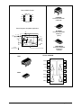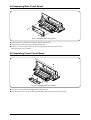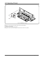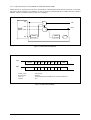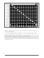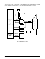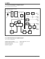
1
SF4300C
SERVICE
Manual
INKJET PRINTER COMPOUND
CONTENTS
1. Precaution
2. Referential Information
3. Specifications
4. Disassembly & Assembly
5. Circuit
6. Repair
7. Exploded View
8. Packing
9. Circuit Diagram & Parts List
10. Block Diagram
11. PCB Layout
12. Wiring Diagram
ELECTRONICS
1. Precautions
1-1 Safeguards
Please read these instructions carefully and completely.
1. Do not use this product in a humid place nor outdoor.
2. Do not place this product on an unstable stand or
table. The product may fall, causing serious damage to the product.
3. Use this product in a well-ventilated place.
4. Slots are provided for ventilation. Never push
objects of any kind into this product through
these slots as they may result in a fire or electric
shock. Never spill liquid of any kind on the product.
5. Power-supply cords should be routed so that
they are not likely to be walked.
6. Use this product in a place big enough to support
printers.
7. Install this product within 180cm from the computer and 150cm from the power outlet.
8. This product should be operated only from the
type of power source indicated on the marking
label.
9. If you use extension cords, be sure they have
three-wire grounding-type power outlets. Do not
overload wall outlets and extension cords. Never
load one wall outlet with over 15 ampere.
10. Unplug this product from the wall outlet before
cleaning. Do not use liquid cleaners or aerosol
cleaners. Use a dry cloth for cleaning.
11. Use only standard paper, OHP film, andapproved envelopes.
1-2 Servicing Precautions
Please read these instructions carefully and completely.
1. Unplug this product from the wall outlet before
you disassemble it.
2. Replace defective parts with the same parts as
them.
3. Check the insulation of electricity-conducting
parts (metal plate or input terminal) that can easily contact AC plug blades.
4. How to check insulation: Pull the AC plug out of
the outlet and measure insulation resistance of
each blade.
Samsung Electronics
5. Insulation resistance of AC plug blades against
electricity-conducting parts should be 1 megaohm
or over.
6. Always use it after connecting the ground of measuring instruments to the ground of chassis. And
after you use it, separate the ground of the
measuring instruments lastly.
1-1
1-3 Static Electricity Precautions
Semi-conductors are easily damaged by static electricity. They are usually called electrostatically
sensitive devices (ESD). For example, there are IC,
FET, and semi-conductor chips.
1) Before you handle semi-conductor parts, be sure
to discharge electricity by touching earth connection or putting on a wristband. (Before you turn
on the product, put off the wristband to prevent
electric shock.)
2) Remove the static electricity protective device
and then place the assembly on the surface of
electric conductors such as aluminum foil to
prevent static electricity from accumulating.
3) Do not use chemicals like Freon. These chemicals
produce static electricity that may damage parts.
4) Solder ESD parts with a grounded soldering iron.
5) Use static electricity protective solder. Solder not
marked Ôstatic electricity protectiveÕ may accumulate static electricity that damages ESD parts.
1-2
6) Do not get rid of the static electricity protective
cover of ESD parts until you are ready to replace
them. Most of ESD parts are packed, with electricity conducting materials in contact with ESD
parts leads.
7) Make static electricity protective materials contact the chassis or the circuit where parts will be
mounted, before you remove the materials from
ESD parts to be replaced.
8) Minimize your motion when you handle the ESD
parts from which static electricity protective
materials have been removed. Static electricity is
generated when your clothes are frictionized or
you walk on the carpet.
9) Be careful not to bend pins when you handle IC.
10) Pay attention to directions when you mount
parts on PCB.
11) Overheat during soldering may damage the
parts completely. Heat affects all the parts.
Samsung Electronics
2. Referential Information
2-1 Abbreviations & Acronyms
Abbreviations
Definition
MFP
Multi Function Peripheral
I/F
INTERFACE
UART
Universal Asynchronous Receiver/Transmitter
ECP
Expended Capasilities port : 8bits Data
CR
Carriage Return
LF
LINE FEED
CIP
COLOR IMAGE PROCESSOR
CCD
Charge Coupled Device
A/D
ANALOG TO DIGITAL
D/A
DIGITAL TO ANALOG
LIU
Line Interface Unit
TIT
Transformer Input from Transformer
ROT
Receive Output Transformer
LI
Line Input
Samsung Electronics
2-1
2-2 Location & Outline of Pins of Electrical Parts
LOGIC AND CONNECTION
DIAGRAMS DIP (TOP VIEW)
J SUFFIX
CERAMIC
CASE 732-03
Vcc E B1 B2 B3 B4 B5 B6 B7 B8
20 19 18 17 16 15 14 13 12 11
20
1
1
2
3
DIR A1
4
5
6
7
8
A2 A3 A4 A5 A6
9
N SUFFIX
PLASTIC
CASE 738-03
10
A7 A8 GND
20
1
DW SUFFIX
SOIC
CASE 751D-03
20
1
TO-220
C
B
.
R1=10KΩ
.
.
R2=0.6KΩ
.
1
2
3
R1
1. Gate
2. Drain
R2
E
3. Source
SOT-89
SOT-23
3
1
1
2
2
1. Base
2-2
2. Emitter
3. Collector
3
1. Base 2. Collector 3. Emitter
Samsung Electronics
BLOCK DIAGRAM
OUT 1
1
IN1(- )
2
IN1(+ )
3
GND
4
8
Vcc
7
OUT 2
6
IN2 (- )
5
IN2 (+)
8 DIP
_
+
8 SOP
_
+
Vcc
Q6
Q6
Q12
Q17
Q19
Q2 Q3
IN(-)
Q1
Q20
C1
Q18
Q4
R1
R2
IN(+)
Q15
Q11
Q10
Q8
OUT
Q21
Q14
Q9
Q13
Samsung Electronics
2-3
PIN CONNECTIONS
8
CD
FC2
FC1
Vin
1
8 Vo2
2
7 Gnd
3
4
6 Vcc
5 Vo1
1
P SUFFIX
PLASTIC PACKAGE
CASE 626
(Top View)
8
Block Diagram Simplified Application
1
D SUFFIX
PLASTIC PACKAGE
CASE 751
(SO-8)
Rf
75k
Audio
Input
Cj
0.1
Ri
3.0k
6
Vin
4
_
FC1
3
+
Vcc
5
#1
Vo1
Speaker
C1
1.0uF
C2*
5.0uF
FC2
2
_
50k
125k
+
#2
Bias
Circuit
50k
MC34119
8
Vo2
1
CD
8
Chip
Disable
1
7
DTB SUFFIX
PLASTIC PACKAGE
CASE 948J
(TSSOP)
GND
*=Optional
Differential Gian=2 x Rf
Rj
This device contains 45 active transistors.
BLOCK DIAGRAM
14DIP
1
OUT2
1
14
OUT1
2
13
Vcc
3
12
_ +
_ +
IN1(-)
4
11
IN1(+)
5
10
IN2(-)
6
9
IN2(+)
7
14SOP
1
2-4
_ +
_ +
8
Samsung Electronics
PIN CONFIGURATION (Top Views)
KM416C/V10(2)00BJ
VCC
DQ0
DQ1
DQ2
DQ3
VCC
DQ4
DQ5
DQ6
DQ7
N.C
N.C
W
RAS
*A11(N.C)
*A10(N.C)
A0
A1
A2
A3
VCC
1
2
3
4
5
6
7
8
9
10
11
12
13
14
15
16
17
18
19
20
21
42
41
40
39
38
37
36
35
34
33
32
31
30
29
28
27
26
25
24
23
22
TO-92
1
2
3
1.Emitter
2.Base
Samsung Electronics
3.Collector
KM416C/V10(2)00BT
Vss
DQ15
DQ14
DQ13
DQ12
Vss
DQ11
DQ10
DQ9
DQ8
N.C
UCAS
UCAS
OE
A9
A8
A7
A6
A5
A4
Vss
Vcc
DQ0
DQ1
DQ2
DQ3
Vcc
DQ4
DQ5
DQ6
DQ7
N.C
1
2
3
4
5
6
7
8
9
10
11
44
43
42
41
40
39
38
37
36
35
34
Vss
DQ15
DQ14
DQ13
DQ12
Vss
DQ11
DQ10
DQ9
DQ8
N.C
N.C
N.C
W
RAS
*A11(N.C)
*A10(N.C)
A0
A1
A2
A3
Vcc
12
13
14
15
16
17
18
19
20
21
22
33
32
31
30
29
28
27
26
25
24
23
N.C
UCAS
UCAS
OE
A9
A8
A7
A6
A5
A4
Vss
A15
A14
A13
A12
A11
A10
A9
A8
NC
NC
WE
RESET
NC
NC
RY/BY
NC
A17
A7
A6
A5
A4
A3
A2
A1
1
2
3
4
5
6
7
8
9
10
11
12
13
14
15
16
17
18
19
20
21
22
23
24
48
47
46
45
44
43
42
41
40
39
38
37
36
35
34
33
32
31
30
29
28
27
26
25
A16
BYTE
Vss
DQ15/A-1
DQ7
DQ14
DQ6
DQ13
DQ5
DQ12
DQ4
Vcc
DQ11
DQ3
DQ10
DQ2
DQ9
DQ1
DQ8
DQ0
OE
Vss
CE
A0
A16
BYTE
Vss
DQ15/A-1
DQ7
DQ14
DQ6
DQ13
DQ5
DQ12
DQ4
Vcc
DQ11
DQ3
DQ10
DQ2
DQ9
DQ1
DQ8
DQ0
OE
Vss
CE
A0
1
2
3
4
5
6
7
8
9
10
11
12
13
14
15
16
17
18
19
20
21
22
23
24
48
47
46
45
44
43
42
41
40
39
38
37
36
35
34
33
32
31
30
29
28
27
26
25
A15
A14
A13
A12
A11
A10
A9
A8
NC
NC
WE
RESET
NC
NC
RY/BY
NC
A17
A7
A6
A5
A4
A3
A2
A1
2-5
S
OUTPUT B
1
16
SENSE RESISTOR
PULSE TIME
2
15
OUTPUT A
Vs(B)
3
14
Vs(A)
GND
4
13
GND
GND
5
12
GND
Vss
6
11
REFERENCE
INPUT 1
7
10
COMPARATOR INPUT
PHASE
8
9
Powerdip 12+2+2
(Plastic Package)
ORDER CODE:PBL3717A
Powerdip
12+2+2
SO-20
ORDERING NUMBERS:
TEA3718SDP
TEA3718DP
15
14
13
12
11
10
9
8
7
6
5
4
3
2
1
MULTIWATT-15
ORDERING NUMBERS:
TEA3718SFP
TEA3718SP
(Multiwatt-15)
ORDERING NUMBER : TEA3718SP
TEA3718DP
TEA3718SDP
(Powerdip 12+2+2)
TEA3718SFP
(SO-20)
Us
DUT B
SENSE
OUT B
DUT A
PULSE TIME
PULSE TIME
Us
Us
N.C.
N.C.
GND
GND
GND
ALARM OUTPUT
N.C.
REFERENCE
COMPARATOR INPUT Uss
IN1
IN0
PHASE
PHASE
IN1
Uss
INPUT
1
20
SENSE
2
3
4
19
18
17
OUT A
Us
N.C.
OUT B
1
16
SENSE
5
6
7
8
9
10
16
15
14
13
12
11
GND
PULSE TIME
GND
Us
PRE-ALARM OUT
GND
GND
REFERENCE
COMPARATOR INPUT Uss
IN1
IN0
2
3
4
15
14
13
5
6
7
8
12
11
10
9
OUT A
Us
GND
GND
PHASE
REFERENCE
COMPARATOR INPUT
IN0
Note:HEATSINK SURFACE CONNECTED TO PIN B
2-6
Samsung Electronics
nECS2
nECS1
nECS0
VCC6
nWBE1
nWBE0
nWE
nOE
nCAS1
nCAS0
nRAS1
nRAS0
nRCS2
nRCS1
nRCS0
GND6
ADDR21
ADDR20
ADDR19
ADDR18
ADDR17
ADDR16
ADDR15
ADDR14
VCC5
ADDR13
ADDR12
ADDR11
ADDR10
ADDR9
ADDR8
ADDR7
ADDR6
GND5
ADDR5
ADDR4
ADDR3
ADDR2
ADDR1
ADDR0
1
2
3
4
5
6
7
8
9
10
11
12
13
14
15
16
17
18
19
20
D11
D10
D9
D8
VSS
D7
D6
D5
D4
VDD
D3
D2
D1
D0
VSS
ADDR4
ADDR3
ADDR2
ADDR1
ADDR0
GNDD
DCLK
SEPWCLK
DAOUT
GNDD
SEPYO
GP21
GNDD
GP20
GP19
RXDO
RLSD
GNDD
RCVO
SWGAINO
VCC4
DATA15
DATA14
DATA13
DATA12
DATA11
DATA10
DATA9
DATA8
GND4
DATA7
DATA6
DATA5
DATA4
DATA3
DATA2
DATA1
DATA0
VCC3
245CLK
PPD0
PPD1
PPD2
PPD3
PPD4
PPD5
PPD6
PPD7
GND3
nSTROBE
nAUTOFD
nSLCTIN
nINIT
SELECT
nACK
BUSY
PERROR
nFAULT
VCC2
GPIO4/TDO
SEPCLKX
80
79
78
77
76
75
74
73
72
71
70
69
68
67
66
65
64
63
62
61
60
59
58
57
56
55
54
53
52
51
50
49
48
47
46
45
44
43
42
41
GP02
60
59
58
57
56
55
54
53
52
CIP1
51
V2.1
50
49
48
47
46
45
44
43
42
41
21 22 23 24 25 26 27 28 29 30 31 32 33 34 35 36 37 38 39 40
SEPCLK
(Top View)
VDD
GPO0
GPO1
GPO2
GPO3
VSS
GPO4
GPO5
GPO6
GPO7
VDD
GPI0
GPI1
GPI2
GPI3
VSS
GPI4
GPI5
GPI6
GPI7
GPIO0
GPIO1
GPIO2
GPIO3
GPIO4
GPIO5
GPIO6
GPIO7
VSS
Xin
Xout
VSS
VDD
nXDREQ
TEST
nXDACK
nRESET
nCIPCS
nRD
nWR
KS32C6200
160 TQFP
80 79 78 77 76 75 74 73 72 71 70 69 68 67 66 65 64 63 62 61
SEPXO
120
119
118
117
116
115
114
113
112
111
110
109
108
107
106
105
104
103
102
101
100
99
98
97
96
95
94
93
92
91
90
89
88
87
86
85
84
83
82
81
ADIN
121
122
123
124
125
126
127
128
129
130
131
132
133
134
135
136
137
138
139
140
141
142
143
144
145
146
147
148
149
150
151
152
153
154
155
156
157
158
159
160
1
2
3
4
5
6
7
8
9
10
11
12
13
14
15
16
17
18
19
20
21
22
23
24
25
26
27
28
29
30
31
32
33
34
35
36
37
38
39
40
ADCDG
ADCDP
pVref
Vin
nVref
ADCAP
ADCAG
VSS
CLR-SCAN
SH
CLK1
CLK2
CLK-M
VSS
VDD
VSS
D15
D14
D13
D12
nECS3
GOP0/TXD1
GIP0/RXD1
GOP1/TXD2
GIP1/RXD2
TEST1
TEST2
GIP5/UCLK
CLKSEL
nRESET
GND7
MCLK
GND8
GOP5/nIOWR1
VCC7
GIP2/nEINT1
GIP3/nEINT2
GIP4/nXDREQ
GOP2/nXDACK
NC
NC
NC
NC
NC
NC
EEDATA
EECLK
GND9
GOP3/TONE
GOP4/nRSTO
GOP8/nIORD2
GOP9/CLKOUT
GOP10/FIREPULSE
GOP11
GOP6/nIOWR2
GOP7/nIORD1
VCC8
NC
NC
NC
NC
NC
NC
NC
NC
NC
NC
NC
NC
NC
GND1
NC
NC
NC
NC
NC
NC
NC
NC
VCC1
NC
NC
NC
NC
NC
NC
NC
NC
GND2
GOP12
NC
NC
NC
NC
NC
NC
GPIO0/TCK
GPIO1/TMS
GPIO2/TDI
GPIO3/nTRST
100 99 98 97 96 95 94 93 92 91 90 89 88 87 86 85 84 83 82 81
GP03 1
80 GNDD
GP04 2
79 TXDI
GP05 3
78 CTS
GP06 4
77 DGND
GP07 5
76 GP17
GNDD 6
75 GP16
GNDD 7
74 SYNCIN2
D7 8
73 DCLK
D6 9
72 DVDD
D5 10
71 YCLKO
D4 11
70 XCLKO
D3 12
69 XTALO
D2 13
68 XTALI
D1 14
67 PORI
D0 15
66 DGND
KS16116/7
GNDD 16
65 EN85
GNDA 17
64 RTS
63 GP11
RXAMPI 18
NC 19
62 NC
NC 20
61 GP13
GNDA 21
60 RS0
VDD 22
59 RS1
GNDD 23
58 RS2
SWGAINI 24
57 RS3
ECLKIN1 25
56 RS4
SYNCIN1 26
55 READ-ø2
NC 27
54 CS
NC 28
53 WRITE-R/W
NC 29
52 IRQ
GNDA 30
51 NC
Samsung Electronics
GNDD
AOUT
VC
Vcc
GNDA
RXAI
TXAO
VSSG
VREFN
NC
TXATT1
TXATT2
TXATT3
RCVI
BYPASS
ADOUT
NC
DAIN
NC
NC
31 32 33 34 35 36 37 38 39 40 41 42 43 44 45 46 47 48 49 50
2-7
2-3 Chip Replacement (SMD parts)
2-2-1. Precautions for Chip Replacement
1. See to it that the soldering iron does not touch
parts directly. In particular, TSOP may be easily
damaged by heat.
2. Handle the soldering iron with care and avoid
using the same many times. Some parts can be
damaged by sudden heat. Preheat parts for minutes at about 100¡c before soldering them.
3. The temperature of the soldering iron should
remain at about 240¡c Use a 280¡c iron for
bigger parts.
4. Thin (0.3mm) solder used for chip parts does not
contain enough flux. Use additional flux.
2-2-2. Tools to Replace Chips
The following tools are used to replace chip parts.
¥ iron with thin tip
¥ iron with small and flat tip
¥ solder remover
¥ ventilation device
¥ tools to lift flat parts
¥ flux that can be cleaned with water
¥ 0.3mm thin solder that can be cleaned with water
¥ wire to remove solder
¥ tweezers
2-2-3. Chip Resistance & Chip Condenser
* For computers and OA systems, water-soluble flux
is used. Water-soluble flux and solder are also
good for replacing parts and repairing this product. Improper flux may corrode the soldered part
and cause serious defects to the system.
5. Be careful not to damage the circuit pattern when
you disjoin soldering. The pattern should be clean
because there are a lot of pins close together on IC.
6. Be careful not to cause a short circuit between
close pins.
7. Locate parts in place. It has a great influence on
soldering.
8. Do not use repaired parts again.
9. Check the soldered part.
10. Defective variable resistors are not adjustable. Be
sure to replace them.
11. After finishing the job, check if there are cold soldered parts.
2-8
2-2-3 (a) Type
There are the following types of chip resistance and
chip condensers.
¥ There are the following types of thin film and chip
condensers.
¥ Carbon Film chip resistance
¥ Metal Film chip resistance
¥ Chip ceramic condenser
¥ Chip variable resistance
2-2-3 (b) Removal
Use 2 soldering irons.
a. Use a thin-tip iron.
b. Keep about 280¡c
c. Apply heat to both ends of a part at the same time.
d. Remove it with the tip of the iron while heating.
e. Remove the remaining solder on PCB completely
with solder removing wire. It should be done to
install a new part.
Samsung Electronics
2-2-3 (c) Installation
a. Clean the place where a new part will be located.
b. Apply water-soluble flux.
c. Set a part correctly in place. Prevent it from shifting.
d. Stick the part fast without contacting it directly
with the soldering iron. Put 0.3mm solder between
the iron and the part so that it can melt into the
part.
e. Check the soldered part with a magnifier.
2-2-4. Chip Tantalum Condenser and Chip Filter
2-2-4 (a) Type
There are the following types of chip tantalum condenser and chip filter.
¥ Chip coil
¥ Chip tantalum condenser
¥ Chip tantalum electrolysis condenser
¥ Chip aluminum electrolysis condenser
¥ Chip transformer
¥ Chip filter
2-2-4 (b) Remoral
1. Use a special solder-removing iron.
a. Choose an iron tip that suits the size of the part.
b. Put the iron tip to the part to be soldered.
c. Remove the part when solder melts.
d. Remove the remaining solder completely with
solder-removing wire.
2. Use two irons.
a. Use an iron with small flat tip.
b. Apply heat to both ends of the part at the same
time.
c. Remove the part with the tip of the iron while
melting.
d. Remove the remaining solder completely with
solder removing wire.
Samsung Electronics
2-2-4 (c) Installation
1. Clean the place where new parts will be installed.
2. Apply water-soluble flux.
3. Locate a part exactly in place. Be careful not to shift
it.
4. Stick the part fast with a soldering iron not contacting it directly. Put 0.3mm solder between the
iron and the part so that it can melt into the part.
5. Check the soldered part with a magnifier.
2-2-5. Chip Variable Resistance, Chip
Variable Condenser, Diode &
Transistor
Chip Variable Resistance, Chip Variable Condenser,
Diode & Transistor
2-2-5 (a) Type
There are the following types.
¥ Chip Variable Resistance
¥ Chip Variable Condenser
¥ Diode
¥ Transistor
2-2-5 (b) Removal
Use two soldering irons.
a. Use an iron with small flat tip.
b. Apply heat to both ends of a part at the same time.
c. Remove the part with the tip of the iron while solder melts.
d. Remove the remaining solder completely with solder removing wire.
2-9
2-2-5 (c) Installation
1. Clean the place where new parts will be installed.
2. Apply water-soluble flux.
3. Locate a part exactly in place. Be careful not to shift
it.
4. Stick the part fast with a soldering iron not contacting it directly. Put 0.3mm solder between the
iron and the part so that it can melt into the part.
2. Use a ventilation device.
a. Choose an injector that suits IC.
b. Choose the temperature and the ventilation
speed. (normal: temperature - 7, speed - 4)
c. Use IC-removing tools.
d. Preheat it for about 5 seconds with the ventilation device. And apply heat with the injector
until IC can be removed from the board with IC
removing tools.
2-2-6. Chip IC
2-2-6 (a) Type
There are the following types of chip IC.
1. SOP (Small Outline Package) IC
2. SSOP (Shrink Small Outline Package) IC
3. VSOP (Very Small Outline Package) IC
4. QFP (Quad Flat Package) IC
5. VQFP (Very Quad Flat Package) IC
6. PLCC (Plastic Leaded Chip Carrier) IC
7. TSOP (Thin Small Outline Package) IC
2-2-6 (b) Removal
1. Use a special solder-removing iron.
a. Choose an iron tip that suits the shape and the
size of IC.
b. Use ÔthinÕ tip to contact legs of IC.
c. Put the tip right in front of the legs of IC.
d. Twist the iron carefully when solder melts.
e. Raise and remove IC.
2-10
2-2-6 (c) Installation
1. Remove the remaining solder completely with solder-removing wire.
2. Clean the place to be soldered.
3. Apply water-soluble flux.
4. Put IC in place and solder the legs of opposite
direction.
5. Solder each leg carefully with thin tip.
6. Remove solder with solder-removing wire if there
is a short circuit.
7. Check the soldered part with a magnifier.
IC
Samsung Electronics
3. Specifications
3-1 Specifications
Specification & Features
1. Printer
1-A. Set
Thermal Inkjet
Technology
Speed
Resolution
1-pen & print head swapping type
Color
3PPM at draft mode (6005300 DPI)
Mono
7PPM at draft mode (6005300 DPI)
Color
600 5 600DPI (120051200 DPI addressable)
Mono
600 5 600DPI (120051200 DPI addressable)
Printing Width
8 Inch
Automatic
100 sheets for normal cut sheets, coating paper
Manual
Recommended for thick media, fashion paper, envolope,
Feeding
Method
postcard, Banner paper
Emulation
Host Based Printing (GDI)
Printer Driver
Window 3.1/3.11 and Windows 95 drivers
Interface
IEEE 1284 Compatible Parallel Interface (ECP)
1-B. Ink Cartridge Supply
Mono Ink
Color Ink
Print Head
208 nozzles
192 nozzles
Ink Type
Pigment
Dye
Ink Color
Black
Color
Ink Yield
About 600 sheets
About 200 sheets
Samsung Electronics
3-1
2. Scanner
Technology
CCD
Scanner Type
Color/Mono
TWAIN Compatible
Yes
Pre-Scan
Using Carrier Sheet
Speed
Resolution
Color
about 1 PPM
Mono
about 2 PPM
Color
300 X 300 DPI (for SmartJet-C only)
Mono
300 X 300 DPI
Gray Scale
256 Level
Printing Width
8 lnch
Feeding
Interface
3-2
Manual
Yes
IEEE 1284 Compatible Parallel Interface (ECP)
Samsung Electronics
3-1. Facsimile
Compatibility
ITU-G3
Scan Method
CCD Shuttle Scanning Method
Scan Width
Max. 8.5 Inch, Effective : 8 Inch
Document Feeding Method
Manual Feeding Method
Guide
Document In-put Guide
Stacker
None
Handset
None
Keys on OPE
4EA (Ready, Cartridge, FF/STOP, START/COPY))
LEDs on OPE
3EA (Ready, Busy, Scan/Fax)
Real Time Clock
None
Fax Monitoring Speaker
Yes
Ring Volume Control Switch
None
Paper Tray
BIN Type, up to 100 sheets
Modem Speed
Max 9600 bps
Coding Method
MH, MR, MMR, Error Correction Mode
LCD
None
Answering Machine I/F
None
Extension Phone I/F
1-Jack, Extension Phone Transfer
PC Interface
IEEE 1284 Parallel Interface (ECP)
Fax Send Resolution
- Standard : 200 x 100 dpi
- Fine : 200 x 200 dpi
- Superfine : 300 x 300 dpi
Samsung Electronics
3-3
3-2. Facsimile
Feature
Gray Scale
Use Ext. Telephone
- Auto Contrast
Use PC
- Auto Contrast
- 256 level with
Error diffusion
Memory Transmission
None
Yes
Memory Rx
Yes
Yes
Receive Mode
- Tel, Fax
- Fax
- PC Rx
Telephone
Others
One Touch Dial
*No
70 Numbers
Speed Dial
*No
Chain Dial
*No
No
On Hook Dial
*No
No
Last Number Redial
*No
No
Auto Busy Redial
*No
No
No Power Operation
*No
No
Hold & Mute
*No
No
Pause
*No
Yes
Ring Volume Control
*No
No
Flash
*No
No
Tone/Pulse Switch
*No
Yes
Sensors
No paper sensor, Paper jam sensor
Error Indicator
Yes (On LED)
Yes (On PC Screen)
Voice Request
No
No
TTI
Yes
Rx Terminal ID
No
No
Polling
No
No
DRPD
U.S.A : Yes, Other countries : No
Mercury
No
No
* The marked “No” can be provided by telephone’s feature.
3-4
Samsung Electronics
Feature
Use Ext. Telephone
Use PC
Tx/Rx Journal
No
Yes
Delayed Dial List
No
No
System Data
No
Yes
Tel Number List
No
Yes
Help List
No
No
Copy
Yes (1-Page)
Yes (99-Page)
Gray Scale
No
Yes
Reduction Copy
No
Yes
Enlargement Copy
No
No
Report & List
Print out
Copy
4. Electrical & Environment
Power Source
AC 220~240V, 0.3A, 50~60Hz
Dimension (W5D5H)
422(mm) 5 237(mm) 5 180(mm)
Weight
3.7kg
5. Accessories
Tel
Handset
No
Curl Cord
No
Tel Line
Yes
Power Cord
Yes
Software
1 CD-ROM
(Manual, Printer Driver, PC-Fax)
Manual
1EA
Ink
Mono Ink
Yes
Cartridge
Color Ink
Yes
* Xerox’s OCR S/W and scanner editor are recommended for its own use.
Samsung Electronics
3-5
4. Disassembly & Assembly
4-1 Taking Off Front Cover
This section explains with illustrations how to disassemble the printer.
It does not explain how to assemble it, because it is the very reverse of disassembly.
Fig.4-1. Taking Off Front Cover -1
▲
▲
▲
▲
Samsung Electronics
▲
▲
Disconnect power cords and printer cable from
the printer.
Unscrew 1 screws on rear cover to separate ink
cartridge storage.
Push Guide Extension in the direction of the
arrow symbol.
Remove 2 screws between front cover and bottom cover.
Fig.4-1. Taking Off Front Cover -2
Hold the upper part of front cover with both
hands and lift the front cover, holding
down rear cover.
Separate front cover from rear cover in the
direction of the arrow symbol.
4-1
4-2 Taking off Rear Cover
▲
▲ ▲
▲
▲
Fig.4-2. Taking Off Rear Cover
Push in the paper guide (ÒCÓ) of automatic
sheet feeder and place it inside of A4 line.
Push the guide manual(L) (ÒDÓ) left.
Unhook right and left hooks(ÒAÓ) on the upper
part of rear cover.
Unhook right and the left hooks of bottom
cover by pushing them in.
Separate rear cover in the same direction that
the automatic sheet feeder is mounted.
4-3 Separating Automatic Sheet Feeder
“A”
Fig.4-3. Separating Automatic Sheet Feeder
▲ ▲▲▲
Remove various wires fixed on the side of automatic sheet feeder.
Unscrew 2 screws on automatic sheet feeder.
Push slightly and disconnect the hook (ÒAÓ) fixed to the main frame.
Separate automatic sheet feeder by pulling it in the direction of the arrow symbol.
4-2
Samsung Electronics
4-4 Separating Main Circuit Board
Fig.4-4. Separating Main Circuit Board
▲ ▲▲
Separate various connectors connected with the main board.
Separate head cable connected with the main board.
Unscrew 3 screws fixed to the main board and separate the main board in the
direction of the arrow symbol.
4-5 Separating Power Circuit Board
Fig.4-5. Separating Power Circuit Board
▲ ▲
Unscrew 2 screws that fix the right and left ground wire.
Press the hook (ÒAÓ) on the middle of the housing and separate power circuit board.
Samsung Electronics
4-3
4-6. Separating Printer Engine
▲
▲
Fig.4-6. Separating Printer Engine
Remove 2 screws fixed to printer engine unless
you unscrewed them at the previous
stage.
Push outside right and left hooks on the side of
the engine, unhook them, and
separate the engine in the direction of the arrow
symbol.
4-7. Separating Home Assembly
▲
▲
Fig.4-7. Separating Home Assembly
4-4
Unscrew 1 screw fixed to the back of the engine
and separate home assembly from the
engine.
Pull out the wiper and the cap in the direction
of the arrow symbol to separate them.
Samsung Electronics
4-8. Separating Carrier Assembly
Idle Pulley
Carrier Shaft
▲
▲
▲
Holder
Cable
▲
Head Cable
▲
Fig.4-8. Separating Carrier Assembly
Separate FPC cable connected with the main
board.
Separate the holder cable fixed to the main
frame.
Remove 1 screw on the right of the engine and
spring on the left of the engine.
Push the left idle pulley in and separate the
right part of the timing belt from motor
pulley.
Pull out carrier shaft and separate carrier
Assembly.
4-9. Separating Frame Base Assembly
Actuator Feed
Roller Friction Assembly
Samsung Electronics
▲
Fig. 4-9. Separating Frame Base Assembly
▲▲
Frame Base Assembly
Refer to 4-8 to separate carrier Assembly first.
Separate 4 roller friction Assembly on the back
of the engine and then actuator feed.
Separate frame base Assembly by lifting the
back.
4-5
4-10 Separating Feed Roller Assembly
▲
1
2
▲
Feed Roller
▲
Frame Support
Bearing Feed (R)
▲
Fig.4-10. Separating Feed Roller Assembly
Refer to 4-9 to separate frame base Assembly
first.
Unscrew 1 screw fixed to the back of the engine
and separate frame support from the
engine.
Turn the bearing feed (R) in the direction of the
arrow symbol to separate it from
the main frame.
Push feed roller on the right to separate it from
the main frame.
4-11 Separating Bracket Line Feed Assembly
Bracket Line Feed
▲▲
Fig.4-11. Separating Bracket Line Feed Assembly
4-6
Refer to 4-10 to separate feed roller Assembly.
Unscrew 2 screws and separate bracket line
feed Assembly.
Samsung Electronics
4-12 Separating Automatic Sheet Feeder
,,,,
,,,,
,,,,
,,,,
,,,,
,,,,
,,,,
,,,,
Fig.4-12. Separating Automatic Sheet Feeder
▲▲
▲ ▲▲▲
Separate the manual plate from frame ASF.
Separate the cam pickup on the right and then unscrew the right screw to separate
the finger part.
Pull out the clutch and then unscrew 1 left screw to separate the clutch part.
Separate the guide finger from shaft pickup.
Push shaft pickup to the right to separate.
Bend plate-knockup slightly and then separate it from the frame ASF.
Samsung Electronics
4-7
4-13. Separating LIU board
Fig.4-13. Separating LIU board
▲▲ ▲▲
Refer to 4-12 to separate automatic sheet feeder from the engine.
Separate the connector.
Unscrew 2 screws fixed to LIU board.
Separate LIU board from the engine in the direction of the arrow symbol.
4-8
Samsung Electronics
4-14. Separating Scan Assembly
Fig.4-14. Separating Scan Assembly
▲▲
Unscrew 1 screw.
Push up scan Assembly in the direction of the arrow symbol to separate it from the carriage.
4-15. Separating White Reference Sheet
White Reference Sheet
Frame Base
Fig.4-15. Separating White Reference Sheet
▲▲
Remove contaminated white reference sheet completely from the frame base.
Ask for new white reference sheet.
Samsung Electronics
4-9
5. CIRCUIT
5-1 MAIN PBA
5-1-1 SUMMARY
The main circuit that consists of CPU, MFP controller (built-in RISC processor core:
ARM7TDMI) including various I/O device drivers, system memory, scanner, printer,
motor driver, PC I/F, and FAX transceiver controls the whole system. The entire
structure of the main circuit is as follows:
LIU-TXD
LIU-RXD
LIU (STI9510)
MCLK(30MHz)
/POR
/RST-OUT
/ROMCS
IP-CLK
/XDACK
/RD, /WR
D0~D15
/XDREQ
COKOR IMAGE
PROCESSOR
/IP-CS
A0~A17
/RD, /WR
/UCAS,
/LCAS
D0~D15
A0~A4
/WR
A0~A9
LFIA0
LFIB0
LFIB1
MFP CONTROLLER
(KS32C6200)
/MCS
/MIRQ
/RD, /WR
CR-REF
CRPHA
DRAM
D0~D15
LFPHB
LFIA1
FLASH
MEMORY
/RASO, 1
LFPHA
LF MOTOR
DRIVER
/F-POR
MODEM
D0~D7
A0~A4
CRPHB
CR MOTOR
DRIVER
CRIA0
/RST-OUT
CRIA1
PD0~PD7
CRIB0
/P-ERROR
CRIB1
/P-PE
/P-BUSY
/RST-OUT
/HEAD-EN
HEAD-DATA
PRINT HEAD’
DRIVER &
PRINT
CONTROL
CIRCUIT
/HGA1~/HGA13
HOE1~HOE16
OK2PRINT
/FAULT-TEST
BIASOFF
/P-ACK
/P-SLCT
/P-INIT
PARALLEL
INTERFACE
(IEEE1284)
/P-SLCTIN
/P-AUTOFD
/P-STB
245DIR
Fig.5-1-1. Entire Structure of Main Circuit for Each Key Signal
Samsung Electronics
5-1
5-1-2 MFP CONTRLLER (KS32C6200 : U15)
MFP Controller consists of CPU(ARM7TDMI RISC processor), 2K-byte cache, data and address buses, serial
communication part with LIU(Line Interface Unit), print head controller, parallel port interface, external
DMA part to receive data from external color image processor (CIPIA:U17), LF/CR motor diver controller and
I/O controller.
5-1-2-1. SYSTEM CLOCK
The internal clock frequency is 30MHz. 30MHz system clock (MCLK) supplied from the outside is used without being divided inside.
5-1-2-2. DATA & ADDRESS BUS CONTROL
¥ /RD & /WR
/RD & /WR signals are synchronized with MCLK(30MHz) and become LOW ACTIVE.
These signals are strobe signals used to read and write data when each CHIP SELECT is connected with
/RD and /WR pin of RAM, ROM, MODEM and the outside devices and becomes active.
¥ CHIP SELECT (/CSO, /ROMCS, /MCS)
- /IP-CS : CIP1A(U17) CHIP SELECT (LOW ACTIVE)
- /ROMCS : ROM/FLASH MEMORY(U10) CHIP SELECT (LOW ACTIVE)
- /MCS : MODEM(U21) CHIP SELECT (LOW ACTIVE)
When each CHIP SELECT is low, data can be read or written.
¥ D0 - D15
- 16bit data bus
¥ A0 - A17
- ADDRESS BUS (A18 - A21 are reserved.)
5-2
Samsung Electronics
5-1-2-3, LIU(Line Interface Unit) SERIAL COMMUNICATION PART
UART (Universal Asynchronous Receiver/Transmitter) at KS32C6200 enables the main and LIU to transmit
serial data. The block diagram of UART is as follows: (Fig.5-1-2) KS32C6200 has 2 UART channels. Channel
0(RXD0, TXD0) is used here and the baud rate is 9600bps.
TxD
0
TxD
1
IRS
UART
Block RxD
RE
0
RxD
1
IR Tx
Encoder
IR Rx
Decoder
Fig.5-1-2. UART BLOCK DIAGRAM
TXD :
START
D0
D1
D2
D3
D4
D5
D6
D7
STOP
START
D0
D1
D2
D3
D4
D5
D6
D7
STOP
RXD :
START, STOP
BAUD RATE
CPU I/F
PARITY
: 1BIT EACH
: 9600bps
: SUPPORTS BOTH INTERRUPT & POLLING DRIVEN
: NO
Fig.5-1-3 UART DATA FORMAT
Samsung Electronics
5-3
5-1-2-4 External DMA
It brings data from an external device (CIP1A:U17) using DMA channel 0. DMA REQUEST sent from an
external device to KS32C6200 activates DMA ACKNOWLEDGE signal and drives DMA channel 0 to produce
CHIP SELECT and READ STROBE (/RD) at the external device and bring data from it. It generates address
of destination memory, CHIP SELECT and WRITE STROBE (/WR) in order to move this data into
destination memory, and then stores the data.
MCLK
/XDREQ
/XDACK
D[15:0]
/RD
/WR
Fig.5-1-4 EXTERNAL DMA TIMING DIAGRAM
5-4
Samsung Electronics
5-1-2-5. DRAM CONTROLLER
As KS32C6200 has DRAM controller in it, DRAM can be connected with external memory. The control mode
of DRAM controller enabling EARLY WRITE, NORMAL READ, PAGE MODE, and BYTE/HALF WORD
ACCESS supports EDO DRAM as well as normal DRAM. DRAM READ/WRITE signals are /RD and /WR
signals used to control system buses. It supports CAS BEFORE RAS for DRAM REFRESH and self-refresh
mode for DRAM backup. Connected with common /LCAS, /UCAS and RAS[1:0], it consists of 2 banks.
Though each may be connected with up to 1M - 4M halfword, 512 Kbytes or 2 Mbytes are connected according to the model for this product.
5-1-2-6. PARALLEL PORT INTERFACE
This part connected with the computer through the centronics connector makes possible parallel interface
with the computer. Data is transmitted according to the standard of IEEE P1284. This MFP controller supports
compatibility mode the traditional way to transmit print data, nibble mode (4bit data) to upload data to the
computer, and duplex high-speed transmission with the computer ECP(Extended Capabilities Port: 8bit data
transmission) all together.
It enables PC data to be printed and scanned data to be uploaded quickly to the computer. Besides, various
data transmission and reception with the computer such as uploading received fax data, downloading fax
data to be sent, and monitoring system control signals and system conditions are carried out here.
PPD(7 : 0)
DATA
BUSY
nSTROBE
nACK
Fig.5-1-5 Compatibility Hardware handshaking Timing
Samsung Electronics
5-5
nSTROBE
BUSY
PPD(7 : 0)
BYTE0
nAUTOFD
DATA BYTE
BYTE1
COMMAND BYTE
Fig.5-1-6 ECP Hardware Handshaking Timing (forward)
nACK
nAUTOFD
PPD(7 : 0)
BUSY
BYTE0
DATA BYTE
BYTE1
COMMAND BYTE
nINIT
PE
Fig.5-1-7 ECP Hardware Handshaking Timing (reverse)
5-6
Samsung Electronics
5-1-2-7. INKJET HEAD CONTROLLER
This part produces major control signals used to drive INKJET head. It consists of signals to drive head nozzles, /PHGA[13:1], PHOE[16:1], /FAULT-TEST, /HEAD-EN, and BIASOFF, and consists of signals to check
the status of the head, OK 2PRINT and HEAD-DATA.
It has double height print head system, 208 nozzles for mono and 192 nozzles for color, and uses
/PHGA[13:1], /PHOE[16:1] signals and /HEAD-EN to drive these nozzles. Fig.5-1-8 is timing diagram of
each signal.
Fire Enable Timer
/PHGA
Signal
tp (PD)
Pre-Heat Pulse Width
Fire Pulse Width
PHOE
Signal
Front End Delay
Pr-Heat Delay Width
Back End Delay
Fig.5-1-8 Timing Diagram to Drive Head
Samsung Electronics
5-7
/HEAD-EN
/PHGA1
/PHGA2
/PHGA3
/PHGA4
/PHGA5
/PHGA6
/PHGA7
/PHGA8
/PHGA9
/PHGA10
/PHGA11
/PHGA12
/PHGA13
PHOE1PHOE16
(Tp)
Fig.5-1-9. Timing Diagram for Each Nozzle
The above control signals are sent to head driver and the head driver converts these signals to the level
(+11.75V) to drive head nozzles.
5-1-2-8. MOTOR CONTROLLER (CRPHA, CRPHB, CRIA0, 1, CRIB0, 1, LFPHA, LFPHB, LFIA0, 1, LFIB0, 1)
MFP Controller (KS32C6200:U15) supports 2 stepper motors. It controls CR(Carriage Return) motor used to
read and print documents and LF (Line Feed) motor used to feed and eject paper.
CR motor controller can support 75, 150, 200, 300, 600, or 1200dpi according to resolution, while LF motor
controller supports uni-polar and bi-polar according to the kind of motors. Though full step, half step and software control are possible for both, bi-polar CR motor is controlled half step and LF motor is controlled half
step and quarter step here.
5-8
Samsung Electronics
5-1-2-9. I/O PORT OF KS32C6200
PIN NAME
CIRCUIT NAME
I/O
STATE
TXD 0 /GOP 0
LIU-TXD
0
-
UART DATA TO I-LIU CHIP IN LIU
TXD 1 /GOP 1
-
0
-
UNUSED
/EDACK /GOP 2
/XDACK
0
H
DEFAULT STATE
L
DMA ACKNOWLEDGE
-
BEEP TONE
H
WATCHDOG RESET OUT IS INACTIVE
L
WATCHDOG RESET OUT IS ACTIVE
H
DEFAULT STATE
L
CHECK FAULT IN PRINTHEAD
H
MODEM RX PATH CONNECTION
L
REMOTE START DETECTION PATH CONNECTION
H
PRINTHEAD IS DISABLE
L
PRINTHEAD IS ENABLE
H
MONITORING TX/RX SOUND
L
BEEP SOUND
-
CIP CLOCK
H
EXT. CHIP IS ACTIVE
L
EXT. CHIP IS RESET
H
PRINTHEAD BIAS OFF
L
PRINTHEAD BIAS ON
H
PRINT MODE IS LQ
L
PRINT MODE IS DRAFT
TONE / GOP 3
KEYCLICK
0
/RSTO / GOP 4
/RESET
0
/IOWR 1 / GOP 5
/IOWR 2 / GOP 6
/IORD 1 / GOP 7
/IORD 2 / GOP 8
/FAULT-TEST
RX-CTL
/HEAD-EN
TONE-CTL
0
0
0
0
CLKOUT / GOP 9
IP-CLK
0
FIREPS / GOP 10
/RST-OUT
0
/HSC / GOP 11
/HSM / GOP 12
Samsung Electronics
BIASOFF
CR-REF
0
0
DESCRIPTION
5-9
PIN NAME
CIRCUIT NAME
I/O
STATE
RXD 0 / GIP 0
LIU-RXD
I
-
UART DATA FROM I-LIU CHIP IN LIU
RXD 1 / GIP 1
/P-EXIT
I
H
PAPER IS NOT DETECTED
L
PAPER IS DETECTED
/EINT 1 / GIP 2
/MIRQ
I
H
NO INTERRUPT FROM MODEM
L
INTERRUPT FROM MODEM
/EINT 2 / GIP 3
OK2PRINT
I
H
NO FAULT IN PRINTHEAD
L
FAULT IN PRINTHEAD
/EDREQ / GIP 4
/XDREQ
I
H
NO DMA REQUEST FROM CIP
L
DMA REQUEST FROM CIP
UCLK / GIP 5
HEAD-DATA
I
-
CODE DATA FROM PRINTHEAD
TCK / GIOP 0
TCK
I/O
-
TEST PIN FOR EMULATOR (CLOCK)
TMS / GIOP 1
TMS
I/O
-
TEST PIN FOR EMULATOR (DATA MODE)
TDI / GIOP 2
TDI
I/O
-
TEST PIN FOR EMULATOR (DATA FROM EMULATOR)
/TRST / GIOP 3
/TRST
I/O
-
TEST PIN FOR EMULATOR (RESET TO TAP CON.)
TDO / GIOP 4
TDO
I/O
-
TEST PIN FOR EMULATOR (DATA TO EMULATOR)
5-10
DESCRIPTION
Samsung Electronics
5-1-2-10. RESET CIRCUIT
As for SMARTJET there are 2 power resets of primary reset(/F-POR) and secondary reset(/POR) and also
reset by watchdog timer (/RSTO). Primary reset is used to initialize flash memory when the system is turned
on, while secondary reset is used to initialize the whole system by initializing MFP controller (KS32C6200)
after primary reset. Primary reset makes flash memory wait in READ mode to fetch program codes, and secondary reset makes the main controller (KS53C6200) wake up and initialize external peripherals to operate
the system. Fig.5-1-10 is Power Reset Timing Diagram.
supply
Voltage
/F-POR
/POR
Reset filter
65 MCLK
PnRST
Internal Reset
256 MCLK
(internal)
Reset
ROM Access
Fig.5-1-10 POWER RESET TIMING DIAGRAM
Samsung Electronics
5-11
¥ POWER MONITOR (U16: KIA7045F)
If +5V supplied to KIA7045F is so unstable as to reach +4.65V - +4.35V (typically 4.5V), it will recognize it
as power failure. Then KIA7045F output terminal becomes low (0V) and the voltage is impressed to flash
memory and KS32C6200, running RESET (LOW ACTIVE). Flash memory and KS32C6200 are reset first.
Thereafter modem, print control parts and CIP(Color Image Processor) linked to /RST-OUT terminal of
KS32C6200 are reset as well. KIA7045F output terminal of open drain structure is pulled up 5.1k½ and put
out.
5-1-3 SYSTEM MEMORY
System memory consists of 512KB flash memory and 2MB DRAM. Flash memory and DRAM are selected by
each CHIP SELECT (/ROMCS, /RASO, /RAS1, /LCAS, /UCAS), and data is accessed half word (16bits) by
half word.
5-12
Samsung Electronics
5-1-4 SCANNER
5-1-4-1. SUMMARY
This product has CCD(Charge Coupled Device) as an image sensor to receive image input signals and has
embodied a shuttle scanner, realizing various scanner control signals and image processing with color image
processor CIP1A(U17), which is ASIC for shuttle scan. We are going to look into the principles by explaining
the whole data flow in the scanner, block diagram of CIP1A, allocated I/O port and peripheral circuits.
5-1-4-2. CIP1A(U17)
The inside of ASIC is roughly divided into A/D Converter to convert image signals to digital signals, Scanner
Controller to provide various CCD driving signals and signals to interface with host controller, and Image
Processor for shading compensation, gamma compensation and reasoning of image signals.
CIP-1A
CCD
Control
CCD
Module
Analog
Data
Pixel
Data
A/D
Converter
A/D
Sample
Clock
Digitized
Data
Scanner
Controller
IP
Control
Image
Processor
Processed
Data
Data
Timing
System
Data BUS
CIP-I Control Data
+
Formatted Data for DMA
DMA
Control
Formatted Data for DMA
CIP-I Control Data
MFP
Controller
Data
Memory
fig.5-1-11 CIP1A Block Diagram
Samsung Electronics
5-13
5-1-4-3 CIP1A I/O Port
PIN
NAME
PIN
NO.
I/O
GIP 0
12
I
/START-KEY
-
GIP 1
13
I
/CART-KEY
-
GIP 2
14
I
/POW-KEY
-
GIP 3
15
I
/STOP-KEY
-
GIP 4
17
I
THMST
GIP 5
18
I
/RINGDET
GIP 6
19
I
/HOOK-OFF
EXTERNAL PHONE HOOK ON
EXTERNAL PHONE HOOK OFF
GIP 7
20
I
HOME-SEN
PRINT HEAD PARKING
PRINT HEAD MOVING
GOP 0
2
O
SHAD-ON
SHADING ENABLE
-
GOP 1
3
O
/SHAD-RST
SHADING REFERENCE CLEAR
-
GOP 2
4
O
POW-LED
POWER (READY) LED ON
POWER(READY) LED OFF
GOP 3
5
O
BUSY-LED
BUSY LED ON
BUSY LED OFF
GOP 4
7
O
SCAN-LED
FAX LED ON
FAX LED OFF
GOP 5
8
O
CML-CTL
FAX OR TEL LINE CONNECTED
EXT. PHONE CONNECTED
GOP 6
9
O
LAMP-5V
CCD MODULE RETURN (+5V)
-
GOP 7
10
O
LAMP-12V
CCD LAMP ON (+11.75V)
-
5-14
CIRCUIT
NAME
DESCRIPTION
H
CCD LAMP OVER HEAT
-
L
FAX START / COPY KEY
PRESSED
CARTRIDGE CHANGE KEY
PRESSED
POWER(READY) KEY
PRESSED
FORM FEED / STOP KEY
PRESSED
CCD LAMP NORMAL
RING DETECTION FROM
TEL LINE
Samsung Electronics
PIN
NAME
PIN
NO.
I/O
CIRCUIT
NAME
GIOP 0
21
O
GIOP 1
22
I/O
GIOP 2
23
O
PRE-HEAT
PRINT HEAD PREHEATING
GIOP 3
24
I
P-EMPTY
NO PAPER
PAPER READY
GIOP 4
25
O
/SPK-CTL
AUDIO AMP. OFF
AUDIO AMP. ON
GIOP 5
26
O
FAX-LED
FAX LED ON
FAX LED OFF
GIOP 6
TUS
27
I
FM-STAT
FLASH MEMORY STATUS
FLASH MEMORY STA
GIOP 7
28
O
CLK-SEL
THM-CLK
DESCRIPTION
H
L
CLOCK SIGNAL TO DIGITAL THERMISTER : 100~140kHz
THM-DATA DATA FROM/TO DIGITAL THERMISTER
-
READY BUSY
MCLK/2
MCLK
5-1-4-4. PERIPHERAL CIRCUIT
As to the power of lamp, light source of the scanner module, +11.75V(while scanning) supply and +5V(while
waiting) supply are switched by transistor Q7,8,9, and 11.
-Vref is supplied with 1.5V by resistance division through OP-Amp, while +Vref detects the peak by control
of analog Mux U2 during white reference label shading. It detects the peak level of image signals by dividing
shad-on signal and /Shad-rst signal of U2 into High, setting it as top standard voltage. When you scan some
image actually, it will drive shad-on signals into Low to keep the peak level of the capacitor. When you finish
scanning, it will drive /Shad-rst into Low and discharge electricity.
Image signals from CCD mounted on scan PBA in the shuttle scanner are delivered through FPC cable, shifting the level as much as 0.75V at Emitter terminal of Tr which is turned on by Level SH signal. These image
signals will double by an non-inverting amplifier and finally 1.5V level-shifted image signals will be put in
CIP1A.
Samsung Electronics
5-15
5-1-5 PRINTER
5-1-5-1. GENERAL
It drives inkjet head to print printing data received from the computer or fax data coming through the line. It
roughly consists of head driver, head controller, and the ambient temperature sensor. Fig.6-1-11. Block
Diagram of Printer shows the entire structure.
5-1-5-2. HEAD DRIVER (U19, U20, U23, U24)
This part drives and inks inkjet head. Color inkjet head drives 192 nozzles, while mono inkjet head drives 208
nozzles. Mono inkjet head is composed of 16 groups of 13 nozzles. As to the driver that composes each nozzle, 13 row 7-bit driver (U23, U24) selects head address and 16 column 8-bit driver (U19, U20) sends head data.
Head driver converts control signals from MFP controller to +11.75V, the level to be able to drive the head,
and provides them for the inkjet head.
¥ Row Driver Circuit (HD7:U23:U24)
This is a 13-line signal impressed to row drive IC through the output port of MFP controller(/PHGA1 - /PHGA13),
used as an address to drive the head in ink cartridge. Pulse period differs according to head driving frequency. In
1200dpi (in case of Head: 12KHz) mode, timing period is 2.6usec (1/1200Ö16 groups). The signal put in each driver(window time) is active ÒLÓ, with the biggest driver current max 100mA and output voltage +11.75V.
¥ Column Driver Circuit (HD8:U19,U20)
It is the fire enable pulse of real head. 16 lines are put out as head driving data lines through the output port of MFP
controller (PHOE1 - PHOE16). Enable pulse impressed to the head is put out within window time (Low). It has the
function to move it forward or backward by the register in MFP controller. Besides the output signal may differ in
accordance with the type of head (mono or color). If there is data, printing image is put out at ÒHÓ. If not, it is put
out at ÒLÓ. In case of Babbage head, pulse width is always 1.3use regardless of the type of the head, with the maximum driving current 400mA and output voltage +11.75V.
5-16
Samsung Electronics
5-1-5-3. HEAD CONTROLLER
This part consists of +22V Power Controller to control head driver, Fault Test, Head Detection, Substrate
Heating and ambient Temperature Sensor. It checks and controls head driver and ink cartridge.
/FAULT-TEST
/HGA1
BA1
/HGA13
BA13
KS32C6200
(U15)
HOE1
HOE16
BP1
HEAD-DATA
Ink
Cartridge
BP16
(Mono)
or
(Color)
MFP
CONTROLLER
/FAULT-TEST
OK2PRINT
/FAULT
BIASOFF
BS1
HEAD-DATA
HSM
/HEAD-EN
CIP 1A(U17)
IMAGE
PROCESSOR
PRE-HEAT
BH1,BH2
THM-DATA
THM-CLK
Fig.5-1-12 Block Diagram of Printer
Samsung Electronics
5-17
¥ +22V Power Controller
If you insert power cords, the main board will be supplied with power. /POR signal put out through reset
circuit activates MFP controller (K32C6200:U15) and MFP controller puts out external circuit reset signal
/RST-OUT. This /RST-OUT signal and Vrefx (+2.5V) divided through +30V are impressed to the input terminal of the comparator, putting out +22V if the output of the comparator is ÒhighÓ or getting turned off if
ÒlowÓ.(in case of /FAULT-TEST signal: HIGH) While +22V is being impressed after /RST-OUT is ÒHighÓ,
comparator output gets ÒlowÓ and turns off +22V driving TR(TIP112) if /FAULT-TEST signal is put out at
ÒlowÓ when you check a short of the head driver and the ink cartridge (head).
¥ FAULT TEST CIRCUIT
This is a signal to detect whether the head receiving the output of head column driver is in a short. After
/FAULT-TEST signal is put out at ÒlowÓ and +22V is turned ÒoffÓ, ÒOK2PRINTÓ signal is entered. The port
of KS32C6200(U15) shows normal condition if ÒHÓ and a short if ÒLÓ. If you make FAULT-TEST output ÒLÓ
to detect fault of the head, +22V gets off. If the head is in a short (LOW), when the level of Ò/FAULT-TESTÓ
signal goes ÒLÓ and final ÒOK2PRINTÓ output goes ÒLÓ. KS32C6200(U15) reads this signal and checks
whether the head input receiving the driver output is in a short. Diode cathode is attached to each output
transistor collector in the column driver. 8 anode terminals of diode become common as one and put out
/FAULT signal, which is pulled up by bias circuit controlled by /FAULT-TEST and shows the condition by
OK2PRINT through the comparator.
¥ SUBSTRATE HEAT CIRCUIT
Mono ink cartridge of Babbage head is 600dpi head that uses pigment ink. It is very sensitive to the temperature in and around the cartridge. In particular, the viscosity of ink affects print quality as it is inversely
proportional to temperature by an exponential function. This signal used to compensate it helps you get
equal inking quality by warming the ink chamber in the cartridge with aluminum pattern heater before
starting to print if the surrounding temperature is lower than standard (below 35¡É).(Refer to Timing
Chart.) It sends PRE-HEAT signal through I/O port of CIP1A(Color Image Processor:U17) and supplies
+11.75V.
Mono Head
70°C
35°C
Pre-Heat if below 35¡c
Fig.5-1-13. Temperature around Mono Head
5-18
Samsung Electronics
Color Head
70°C
No Pre-Heating
t
Fig.5-1-14. Temperature around Color Head
¥ HEAD DETECTION CIRCUIT
Babbage ink cartridge has 8-bit mask ROM I.D. to check the type of cartridge. In order to detect the head,
HSM signal is used as ENABLE signal and BA3 signal as START & STOP BIT, and BA1 and BA2 as clock
signal of each bit, and ID signal in the cartridge is put in HEAD-DATA port of KS32C6200 through BS1 line.
With each bit controlled, 8bit I.D data is read and STOP bit is put out of BA3(LOAD) port. Then it finishes.
If data is mono, it is 07H. If color, 08H.
HSM
(Pwr)
BA3
(Load)
BA1
(Clock1)
BA2
(Clock2)
Min 500ns
Clock Delay
HEAD-DATA
bit7
bit6
bit5
bit4
bit3
bit2
bit1
bit0
Head I.D read : HEAD-DATA
Mono : 07H
Color : 08H
Fig.5-1-15. HEAD DETECTION TIMING DIAGRAM
Samsung Electronics
5-19
¥ SURROUNDING TEMPERATURE SENSOR
DS1621S(DALLAS SEMI.) is applied to read the temperature around ink cartridge. It is used to get optimum
inking quality by keeping the viscosity of ink in the cartridge in the specified lerel. The way to read temperature is similar to EEPROM, controlled by THM-CLK, THM-DATA LINE. Digital thermometer to check
the surrounding temperature is assembled along with home sensor in the frame of assembly CR. After each
line is printed, it reads the surrounding temperature and heats substrate heater in the ink cartridge during
the accelerating time of CR to keep the viscosity of ink in the specified lerel.
5-1-5-4. HEAD DRIVING TIMING
Control signal from MFP controller (KS32C6200:U15) enters the head driver and it becomes the level to be able
to drive the head nozzles (+11.75V). It is depicted in the following diagram.
Fire Enable Timer
BA
Signal
t p(PD)
Pre-Heat Pulse Width
Fire Pulse Width
BP
Signal
Front End Delay
Pre-Heat Delay Width
Back End Delay
Fig.5-1-16. HEAD DRIVING TIMING DIAGRAM
5-20
Samsung Electronics
HSM
BA1
BA2
BA3
BA4
BA5
BA6
BA7
BA8
BA9
BA10
BA11
BA12
BA13
BP1BP16
(Tp)
Fig.5-1-17. TIMING DIAGRAM FOR EACH NOZZLE
Samsung Electronics
5-21
5-1-5-5. INK CARTRIDGE
¥ PIN ARRAY OF MONO INK CARTRIDGE
There are 208 heater chips in mono ink cartridge.
Address (BA1_ ~ BA13_)
Column
Data(BPx)
1
2
3
4
5
6
7
8
9
10
11
12
13
1
1
21
15
9
3
23
17
11
5
25
19
13
7
2
20
14
8
2
22
16
10
4
24
18
12
6
26
3
27
47
41
35
29
49
43
37
31
52
45
39
33
4
46
40
34
28
49
42
36
30
50
44
38
32
52
5
53
73
67
61
55
75
69
63
57
77
71
65
59
6
72
66
60
54
74
68
62
56
76
70
64
58
78
7
79
99
93
87
81
101
95
89
83
103
97
91
85
8
98
92
86
80
100
94
88
82
102
96
90
84
104
9
105
125
119
113
107
127
121
115
109
129
123
117
111
10
124
118
112
106
126
120
114
108
128
122
116
110
130
11
131
151
145
139
133
153
147
141
135
155
149
143
137
12
150
144
138
132
152
146
140
134
154
148
142
136
156
13
157
177
171
165
159
179
173
167
161
181
175
169
163
14
176
170
164
158
178
172
166
160
180
174
168
162
182
15
183
203
197
191
185
205
199
193
187
207
201
195
189
16
202
196
190
184
204
198
192
186
206
200
194
188
208
5-22
Samsung Electronics
¥ PIN ARRAY OF COLOR INK CARTRIDGE
There are 192 heater chips in mono ink cartridge. One cartridge has 64 Cyan, 64 Magenta, 64 Yellow heaters
and (64 x 3 colors) 192 nozzles.
Address (BA1_ ~ BA13_)
Column
Data(BPx)
1
2
3
4
5
6
7
8
9
10
11
12
13
1
-
19
13
7
11
21
15
9
3
23
17
11
5
2
15
12
6
-
20
14
8
2
22
16
10
4
24
3
25
45
39
33
27
47
41
35
29
49
43
37
31
4
44
38
32
26
46
40
34
28
48
42
36
30
50
5
51
71
65
59
53
73
67
61
55
75
69
63
57
6
70
64
58
52
72
66
60
54
74
68
62
56
76
7
77
97
91
85
79
99
93
87
81
101
95
89
83
8
96
90
84
78
98
92
86
80
100
94
88
82
102
9
103
123
117
111
105
125
119
113
107
127
121
115
109
10
122
166
110
104
124
118
112
106
126
120
114
108
128
11
129
149
143
137
131
151
145
139
133
153
147
141
135
12
148
142
136
130
150
144
138
132
152
146
140
134
154
13
155
175
169
163
157
177
171
165
159
179
173
167
161
14
174
168
162
156
176
170
164
158
178
172
166
160
180
15
181
-
-
189
183
-
-
191
185
-
-
-
187
16
-
-
188
182
-
-
190
184
-
-
192
186
-
Samsung Electronics
5-23
5-1-6 MOTOR DRIVER
5-1-6-1. GENERAL
SMARTJET use 2 stepper motors, i.e. CR(Cartridge Return) motor and LF(Line Feed) motor.
CR motor moves left and right all-in-one carriage of inkjet head and shuttle scanner. It helps the printer print
accurately on the paper and the scanner read image data accurately. LF motor is driven to feed and eject
paper for printing and to feed and eject documents to read for scanning. Bi-polar CR motor is controlled half
step with maximum 24ips(inch/sec), while LF motor half step and quarter step at maximum 6ips.
5-1-6-2. CR(CARRIAGE RETURN) MOTOR DRIVING CIRCUIT
CR motor moves the carriage left and right when ink cartridge prints something on paper or shuttle scanner
reads image data.
- Motor Type : Stepper motor, bi-polar
- Driving Voltage : +30V
- Winding Resistance : 6½ ± 10%
- Driving IC : TEA3718DP X 2
CR_REF
CRIA1
(CRIB1)
CRIA0
(CRIB0)
CURRENT(mA)
OPERATION
H
L
L
490
Mono LQ is being driven
L
L
L
670
Color draft is being driven
L
L
L
670
Mono draft is being driven
X
H
H
0
No current
REMARK
As shown in the above table, current in each mode is adjusted by voltage of driver(U25, U26) CRVREF input.
If the output of CR_REF signal controlled by MFP controller(U15) is ÒlowÓ, TR(Q12) will be turned off and the
voltage put in to CRVREF of driver (U25, U26) with +5V divided will go up (+4.5V). It becomes the standard
of the driver, resulting in high current. If CR_REF output is ÒhighÓ, TR(Q12) will be turned on and the voltage put in to CRVREF will go down (+3.0V), resulting in low current in the motor.
5-24
Samsung Electronics
5-1-6-3. LF(Line Feed) Motor Driving Circuit
LF motor is driven to feed and eject documents and paper.
- Motor Type: stepper motor, bi-polar
- Driving Voltage : +30V
- Winding Resistance : 12½ ± 10%
- Driving IC : PBL3717A X 2
LFIA1
LFIA0
CURRENT(mA)
OPERATION
L
L
670
When feeding document/paper
L
H
400
When ejecting document/paper
X
H
0
No current
Samsung Electronics
REMARK
5-25
5-1-7 FAX TRANSCEIVER
5-1-7-1. GENERAL
This circuit processes transmission signals of modem and between LIU and modem.
This circuit is added only to SMARTJET.
5-1-7-2. MODEM (U21)
KS16116 is a single chip fax modem. It has functions of DTMF detection and DTMF signal production as well
as functions of modem. TX OUT is transmission output port and RX IN is received data input port. /POR
signal controlled by MFP controller (U15:KS32C6200) can initialize modem(/RST_OUT) without turning off
the system.
D0 - D7 are 8-bit data buses. RS0 - RS4 signals to select the register in modem decide the mode. /CS is a signal to select modem chips. /RD and /WR signals control READ and WRITE respectively. /IRQ is a signal for
modem interrupt.
Transmission speed of KS16116 is up to 9600bps.
5-1-7-3. TRANSMITTER
This circuit processes transmission output, analog signal of modem(KS16116).
Output signal in each mode goes out of modem (TXOUT:U21-44). After D/A signals are smoothed and filtered through active filter (U5-6,7:R270,R277,C130), they are buffered under OP AMP(U5-2, 1:R291, C139,
R298, C150) and put out to LINE through LIU board.
5-1-7-4. RECEIVER
In the receiving mode, analog signals coming in through LIU board are amplified at OP AMP(U6-2, R293,
C141), and then transmitted to input terminal of modem (RXIN:U21-45) through smoothing filter (U6-6,
7:R273, R274, C126).
FAX TRANSMISSION
LIU
MODEM
KS16116
(U21)
FAX RECEPTION
Fig.5-1-18. FAX TRANSCEIVER
5-26
Samsung Electronics
5-1-8 OTHERS
OPERATOR PANEL DESCRIPTION
KEY & LED
DESCRIPTION
Ready
- When power cord is inserted, the system is turned on and initialized. It does not operate but
waits for Ready key to be pressed.
- If you press the Ready key, the nearby Ready LED will be turned on and the device will be
initialized with the system in standby mode.
- If the Ready LED is off, the system does not operate though it is on.
- Running Print Out Test Pattern
Step 1. While Ready LED is off, press ÔReadyÕ key for 0.5 - 1 second with ÔFF/Stop key pressed
in advance.
Step 2. Pattern is printed so that you can check the nozzles of the head.
Cartridge
- This key is used to exchange print head cartridge in the toggle mode or to insert it for the first
time.
- If color head is mounted when fax documents are to be printed,it does not print but Ready
LED and operating LED blink.
- Press this key for about 3 sec or more to put in a new ink cartridge.
- When Ôno paperÕ is displayed while printing, place paper, and it is automatically fed.
- After you finish printing, press this key to eject paper already fed.
- Press this key to stop fax communication.
- Press this key to stop scanning.
FF/Stop
- If you press this key when hook-on and documents will be fed, scanned and stored in
memory.
- If you press this key when hook-on but there is no document, LED meaning ÔFeed documentÕ
will blink for about 3 sec. (Refer to LED status.)
- If you press this key when hook-off, it will operate to receive or transmit the document you
fed.
Start/Copy
● ➞ green LED ON
■ ➞ red LED ON
LED status
Ready
●
●
●
●
●
●
●
●
Busy Scan/Fax
●
●
●
●
■
■
➞ OFF
➞ green LED blinks
➞ red LED blinks
System Standby Mode. You can start new operation only in this mode. (TEL mode)
System Standby Mode. You can start new operation only in this mode. (FAX mode)
Data is being received from host.(Printing) other operation
Data is being uploaded to host. (Scanning) Fax transmitting/reception. (Faxing)
Transmitting/receiving error
Paper jam, no paper
No document, next document, document jam
Cartridge is being exchanged. No cartridge
Ink low
Ready
Cartridge
Busy
Samsung Electronics
FF/Stop
Start/Copy
Scan/Fax
5-27
5-2 LIU PBA
5-2-1 SUMMARY
LIU(Line Interface Unit) circuit added only to SMARTJET is controlled by the main circuit.
It monitors telephone line and helps interface between the system and the telephone line. It uses 1LIU(STI9510) to control the whole LIU, MODEM/LINE INTERFACE, RING SIGNAL DETECTOR, DIALER,
LINE CURRENT DETECTOR, and SERIAL INTERFACE.
5-2-2 MODEM/LINE INTERFACE
This is the path through which transmitted and received data of modem is put in and out.
¥ CML1 Relay: It divides telephone line into external telephone and fax.
¥ U3-3 TIT(Transformer Input from Transformer): This single ended input receives image signals from
modem through transformer T2 and transmits them on telephone line.
¥ U3-40 ROT(Receive Output Transformer): This output transformer receives signals on telephone line and
delivers them to modem through transformer T1. It has AC impedance of 10Kohm or over.
¥ AC impedance: Normal operation range of U3(STI9510) is from 15mA to 100mA. DC characteristics depend
on the voltage of U3-37 LI(Line Input) terminal and the voltage of resistance R48 between U3-37 LI(Line
Input) terminal and U3-39 LS terminal.
5-2-3 RING SIGNAL DETECTOR
¥ U3-28(MO) terminals are ring signal output terminals. Q4 and Q5 put out ring signals and drive Piezzo, but
SmartJet2000, SMARTJET does not use Piezzo. It has only the functions related to ring detection such as driving the photocoupler of U4 and delivering ring signals to MFP controller (U15:KS32C6200) of the main.
5-2-4 DIALER
5-2-4-1. MF DIAL
¥ Default mode it is set in DP. You can change it to MF mode by control of MFP controller.
¥ MF signal can be measured at (tone level of low group: typical - 14dBm) U3-4 MFO(DTMF Generator
Output). The signal is adjustable by R40, R41 and C29. The adjusted signal enters U3-9 MFI (DTMF
Amplifier Input) and is amplified to be transmitted on telephone line.
¥ U3-39 LS(Line Current Sense Input) terminals show the final signals transmitted to telephone line.
5-2-4-2. DP DIAL
¥ If U3-2(DMS) is made Vcc by R42, it is set at 33:67 DP signal. If it is made Vss by R43, it is set at DP signal.
This product is set at DP signal.
¥ DP signal is made by U3-27(DPn) terminals. This signal turns on/off Q1. The signal made at that time turns
on/off Q2, which interrupts DC current on telephone line and puts out pulse signal on telephone line.
¥ U3-35 CS terminals : It makes Make Resistance by shorting telephone line with Vss during Make period of
DP dial.
5-28
Samsung Electronics
5-2-5 Line Current Detector
¥ When CML1 relay connects telephone line, U3(STI9510) of LIU board and MFP controller of the main board
(U15:KS32C6200) start communication through UART. U3 of LIU board sends signal that includes information of line current value, whenever it receives orders or data from U15 of the main board.
5-2-6 Serial Interface
¥ This part does serial communication with MFP controller of the main board (MAIN PBA:U15) that controls
the whole system. It controls LIU by giving and taking all control orders and line status.
¥ U3-11 RXD : Schmitt Trigger input, Receiving terminal..
¥ U3-29 TXD : Open Drain output terminal
¥ Standard UART communication
- Baud Rate : 9600bps
- Start, Stop bit : 1bit each
- Data bits : 8 bit
- Parity bit : none
5-2-7 MAJOR FUNCTIONS OF PARTS
1) U3 : STI9510
- Key part of LIU board. Speech Network, Dialer, Ringer and UART are built in one IC package.
2) U5 : PC817
- Photo coupler. It enables UART of U3(STI9510) to receive control signal or dialing information from
MFP controller of the main board (U15).
- Insulation between prinary and secondany circuit part.
3) U6 : PC817
- Photo coupler. It enables UART(U3-29:TXD) of U3(STI9510) to deliver telephone line status or
response signal about control signal or dialing information from LIU to MFP controller of the main
board (U15).
- Insulation between prinary and secondany circuit part.
4) U4 : PC817
- It senses and delivers ring signal to the main board.
- Insulation between prinary and secondany circuit part.
5) U2 : PC814
- It senses hook-off (Line connection) of the external telephone and delivers it to the main board.
- Insulation between prinary and secondany circuit part.
6) BD1 : BRIDGE DIODE
- Regardless of the polarity of DC power from telephone line, the voltage put out on Pin.1 has always
+ polarity against pin Pin.2. So DC loop forms always in the same direction regardless of the polarity of the telephone line.
7) T2,T3 : TRANSFORMER
- It delivers signals from the telephone line to modem or signals from modem to the telephone
line.
- Insulation between prinary and secondany circuit part.
Samsung Electronics
5-29
5-3 SMPS
5-3-1 BLOCK DIAGRAM OF POWER CIRCUIT
Refer to the following block diagram.
AMUNDSEN & SMARTJET POWER
SUPPLY (220-240Vac)
INLET
AC250V2A
INPUT
FILTER
HALF WAVE
RECTIFIER
FULL WAVE
RECTIFIER
SNUBBER Nb1
CIRCUIT
3-TERMINAL
REGULATOR
Ns1
N
CH1
+5V
RED
#1
GND
BLACK
#2
HALF WAVE
RECTIFIER
START-UP
CIRCUIT
SWITCHING
DEVICE
PWM
CONTROL
CIRCUIT
CH3
+30V
GREEN
#6
Ns2
HALF WAVE
RECTIFIER
Nb1
Ns2
VOLTAGE
DETECTION
CH2
+11.75V
YELLOW
#3
OVER
VOLTAGE
PROTECTION
GND
BLACK
#4,#5
OVER
CURRENT
DETECTION
PHOTO
COUPLER
ERROR
AMPLIFIER
5-3-2. SPECIFICATIONS OF POWER CIRCUIT
5-3-2-1. INPUT CONDITIONS
1) INPUT RATED VOLTAGE
2) INPUT VOLTAGE TURNING RANGE
3) RATED FREQUENCY
4) FREQUENCY RANGE
5) INPUT CURRENT
5-30
: AC220 - 240V FREE VOLTAGE
: AC 85 - 270V
: 50 - 60 Hz
: 47 - 63 Hz
: 0.5Arms
Samsung Electronics
5-3-2-2. OUTPUT CONDITIONS
NO
ITEM
CH1
CH2
CH3
1
RATED OUTPUT VOLTAGE
+5.0V
+11.75V
+30V
2
RATED OUTPUT CURRENT
0.5A
0.8A
0.5A
3
MAXIMUM LOAD CURRENT
0.8A
1.3A
0.76A
4
LOAD CHANGE RANGE
0.1 ~ 0.8A
0.03 ~ 1.3A
0.05 ~ 0.76A
5-3-3. POWER CIRCUIT
5-3-3-1 INPUT
This product is equipped with a three-wire grounding-type power inlet. Insulation is class 1. When a power
device part breaks down or some trouble in this circuit causes a short, excess current runs through a fuse and
blows it to protect power devices and the system from excess current and prevent a fire.
Input filter of power input terminal removes line noise flown in from outside and reduces noise which is
made in power circuit and logic part and conducted or radiated through power cords.
AC input voltage is rectified by bridge diode of full wave rectifier, is converted to DC voltage by smoothing
circuit, and switches the power device of this voltage.
As switching is in RCC(Ringing Choke Converter) mode, switching frequency changes from about 50KHz to
100KHz.
PWM(Pulse Width Modulation) Control Circuit adjusts the duty of the switching device by sensing the
change of output voltage, and protects this product from excess current by receiving signals from excess current detecting circuit.
5-3-3-2 DRIVING CIRCUIT (START-UP CIRCUIT)
If you insert a power plug into AC outlet, full-wave rectified DC output voltage is generated at input electrolysis condenser and supplied to the gate of a switching device through driving resistance. This voltage drives the switching device. Once it is driven, it continues to switch via PWM control circuit with power supplied by auxiliary coil Nb.
5-3-3-3 SWITCHING CIRCUIT (VOLTAGE STABILIZATION)
11.75V of 2nd voltage is detected by voltage detector and feeds back through photo coupler to 1st PWM
Control Circuit signals compared by error amplifier.
PWM Control Circuit controls the gate of power transistor according to the feedback voltage so as to supply
load with stable output voltage.
Samsung Electronics
5-31
5-3-3-4 OCP CIRCUIT (OVER CURRENT PROTECTIVE CIRCUIT)
If a short in secondary load terminal or a short inside power device causes excess current, power consumption increases. Then it increases current of power transistor.
The current of power transistor increases linearly when it is on. This current is detected by sensing resistance
and is impressed to excess voltage protective circuit of PWM control circuit through RC integration circuit
where over current protection is built in.
If this voltage becomes bigger than Vbe of excess current control transistor, the potential of power transistor
gate falls immediately and it stops driving power transistor to protect it from excess current.
5-3-3-5 OVP CIRCUIT (OVER VOLTAGE PROTECTIVE CIRCUIT)
If the main power of power device 11.75V increases abnormally, this excess voltage is detected by OVP detecting circuit and 11.75V output terminal shifts to a state similar to
a short.
If 11.75V output terminal shorts, over current runs on over current detecting terminal and OCP circuit operates to prevent a fire in power device.
5-3-3-6 +5V OUTPUT TERMINAL
Square wave voltage generated by Ns1 produces DC voltage rectified and smoothed by half-wave rectifier.
This voltage put in to a three-wire regulator generates stable DC power of +5V.
5-3-3-7 +30V OUTPUT TERMINAL
Square wave voltage generated by Ns2 is rectified and smoothed by half-wave rectifier and supplies load with
output voltage without separate regulation.
5-3-3-8 +11.75V OUTPUT TERMINAL
Square wave voltage generated by Ns3 is rectified and smoothed by half-wave rectifier, and then detected by
voltage detector. Signals compared by error amplifier are fed back to primary PWM control circuit through
photo coupler.
PWM control circuit controls the voltage of power transistor gate driver according to the voltage to supply
load with stable output voltage.
5-32
Samsung Electronics
5-4. OTHERS
5-4-1. PAPER SENSING CIRCUIT
This circuit senses whether there is paper or not, using photo interrupter. If there is no paper, the lever will
cover its sensor and output Ò/P_EXITÓ will become ÒHighÓ. If there is paper, the lever will be lifted and output Ò/P_EXITÓ will become ÒLowÓ.
+5V
+5V
Lever
/P_EXIT
Photo
Interrupter
5-4-2. HOME SENSING CIRCUIT
This circuit senses whether carriage is at home or not. This function is carried out when the system is turned
on or when the head is capped. Photo interrupter is used as a home detecting sensor, attached to the back of
the carriage. When the carriage moves left and right, output is ÒhighÓ if the frame rib covers the center of the
sensor and ÒlowÓ if it is out of home.
+5V
Photo
Interrupter
Sensor PCB
Frame
Rib
HOME_SEN
Samsung Electronics
5-33
5-4-3 TEMP IC DRIVING CIRCUIT
TEMP IC(DC1621S, Thermometer) mounted on the sensor card on the back of the carriage is used to read the
temperature around ink cartridge.
This IC converts the temperature around IC package into digital and sends the temperature data to serial to
make it sense the temperature around the head. It senses temperature so that the temperature of the head can
be the optimum when you print something. The above IC sends data serially using signal lines(THM_DATA,
THM_CLK).
5-34
Samsung Electronics
6. REPAIR
6-1. SCANNER
PROBLEM
ITEMS TO BE CHECKED
HOW TO SOLVE
Does the lamp operate normally while
shuttle module operates?
- Check module lamp.
- Check FPC of the main board & module.
(J1-1<=> CON2-1: LAMP ON)
- Check the path of the main board.
(U17[#10]->R185[1K]-Q8->R262->Q7> CON2[#1])
- Replace module.
- Replace the main board.
Check if white ref. panel is too dirty.
- Clean white ref. panel.
- Replace white ref. panel.
1. Is the lamp supplied with appropriate power when the scanner operates?
2. Does the output of module satisfy
specifications?
3. Does (-)Vref value satisfy specifications?
1. Check the lamp-on level of module
and the main board.(+11.75V/ + 5V)
(J1-1<=> CON2-1: LAMP ON)
2. Check video signal output of module
and main board.
3. Check (-) Vref value.
Lamp blinks
Check power of the lamp. (12V serial
connection)
Replace FPC-SCAN connecting power
of the lamp.
Replace the scanner.
Cannot turn on the
lamp
Check the power of the lamp. (12V
serial connection)
Check scan connector on circuit board.
Check the power of the lamp.
Replace the scanner. Connect the
connector.
Black data when
you scan or copy
Bright image
Dark image
Overlapped or omit- Check if screws of CR fixing part are
ted image when you loose.
scan or copy
Check if LF connector is properly
connected.
Screw down
Black in whole
when you scan or
copy
Check the scanner of the main board.
Check scanner cable.
Check the scanner.
Replace the main board.
Replace FPC-SCAN.
Replace the scanner.
White lines when
you scan/copy.
Check if there is foreign substances on
LABEL(P)-REFERENCE.
Wipe LABEL(P)-REFERENCE.
Samsung Electronics
Connect LF connector.
1-1
6-2. SENSOR
PROBLEM
ITEMS TO BE CHECKED
Does the carriage operate normally and
go to the initial place, when you turn it
on with the carriage placed in the
middle?
- Check connection between the sensor
board of the carriage and the main
and check if FPC cable is damaged.
- Check if FPC is connected properly
with CN1 of the sensor board.
- Check if the signal of the sensor is
delivered well to CN1-#2 of the sensor
board.
- Replace FPC cable.
- Replace the sensor board.
- Is No Paper cleared when you press
No Paper sensor on ASF?
- Does the level of CON7-#2 turn from
H to L when you press No Paper
sensor on ASF?
- Check connection with CON7 of the
main board.
- Replace No Paper sensor on ASF.
Black data when
you scan/copy
CanÕt print/copy
with No Paper displayed
HOW TO SOLVE
6-3. PAPER FEED
PROBLEM
ITEMS TO BE CHECKED
Automatic sheet
- Check if actuator feed operates perfeeder feeds paper
fectly.
but paper is not sup- - Check if paper sensing optical sensor
plied to the engine.
is normal.
Automatic sheet
feeder cannot feed
paper.
- Check if stopper clutch operates
perfectly.
- Check if too much paper has been
supplied.
- Check if pickup roller rubber of the
automatic sheet feeder is worn out.
HOW TO SOLVE
- Replace actuator feed, spring, or other
defective parts.
- Replace the paper sensing optical
sensor.
- Replace stopper clutch assembly.
- Supply appropriate amount of
paper(100 sheets of normal copying
paper).
- Replace pickup roller rubber.
CanÕt feed envelopes - Check the location of the envelope
guide of automatic sheet feeder.
- Open the envelope guide when you
feed envelopes.
Tilted Printing
- Adjust paper guide to the size of
paper.
1-2
- Check if paper guide of the automatic
sheet feeder is adjusted to the size of
paper.
Samsung Electronics
6-4. PRINTING QUALITY
6-4-1 White lines on letters or graphics.
■
Cause
If nozzles in print head has a probkem, white lines are marked on the print.
ÔSelf-diagnostic printingÕ will let you know if nozzles have problems.
If this line is broken, it confirms that
nozzles have problems.
■
Solution
1) Run Ôprint control panelÕ to Òclean cartridgeÓ and check if nozzles have been blocked.
2) Wipe with soft cloth the contact surfaces of ink cartridge and carriage, and check if nozzles have been
cleaned properly.
3) Separate ink cartridge from carriage and combine them. Repeat it about 5 to 6 times and check if connection is proper.
4) Replace ink cartridge and check whether thereÕs a problem with thehead.
5) Check if head cable is inserted well into the main circuit board and then check if nozzles have problems.
6) Check if head cable is broken or torn and then check if nozzles have problems.
7) Replace the main circuit board with a new one and check if nozzles have problems.
Samsung Electronics
1-3
6-4-2 When perpendicular lines are printed crookedly
■
■
Cause : Perpendicular lines are printed crookedly if you do not Òalign perpendicular linesÓ on the
printer.
Solution
1) Run print control panel to Òalign perpendicular linesÓ, and
2) Select the best one of the above samples and enter the number.
3) This function to align perpendicular lines is available both for mono and color cartridges.
1
2
3
4
5
6-4-3 When ink spreads on transparent film
■
■
Cause : You selected a wrong medium on the driver or you did not use transparent film designated for
inkjet.
Solution
1) Use only transparent film designated for inkjet when you print on transparent film by an inkjet
printer.
2) Run ÒWindows driverÓ and select Òtransparent filmÓ as the kind of paper if you print on Windows.
6-5. Setting a PC BIOS to invoke ECP Mode
SMARTJET use ECP mode of Nibble mode when SMARTJET are transferring scanned data to a PC through
a centronics cable. Depending upon a parallel port connection (P1284) mode, scan speed of our unit can vary
in great deal, and sometimes unexpected problems like SIO chip detection problem might come up due to a
mode difference between a host PC and our unit.
When a PC is booting, a PC BIOS initializes the SIO chip of PC in parallel port and sets the mode of parallel
port. But when parallel port is set in a nibble mode, a SIO chip in some certain PCs prohibit PC software(the
twain driver) from changing the mode of parallel port. In order to enhance the speed of parallel port and to
solve some parallel port connection problems it is strongly recommended that the service man who has
encounterde these problems must set the parallel port connection(P1284) mode to a ECP mode in a PC BIOS.
1-4
Samsung Electronics
6-6. Defective Operation
PROBLEM
ITEMS TO BE CHECKED
HOW TO SOLVE
1. No Power?
2. VCC(+5V) ³ +4.5V?
3. U15-130(/POR) is HIGH? (+4.5V or
over)
4. U15-153(/RST_OUT) is HIGH? (+4V
or over)
1. Check power(SMPS).
1) Cord connection
2) Check each power channel.
(+5V, +11.75V, +30V)
2. Check power.
3. Check the circuit around U16.
4. Check data bus of U15. Exchange the
main PBA.
1. Check control signal of U15-141 - 145.
2. Check driving output and input signal of U27 and U28.
1. Replace the main PBA if control signal is not generated though the other
functions of the system are normal.
2. Replace U27 and U28 if driving output is defective though input signal is
normal.
1. Check control signal of U15-31 - 36.
2. Check driving output and input signal of U25 and U26.
1. Replace the main PBA if control signal is not generated though the other
functions of the system are normal.
2. Replace U25 and U26 if driving output is defective though input signal is
normal.
Check sheet feeder and ejector.
Get rid of jammed paper.
Check manual document feeder.
Remove jammed documents and insert
it again.
No Paper
1. No paper?
2. U17-24 is HIGH? (+4V or over)
1. Feed paper.
2. If high, replace the paper empty
sensor. If low, replace the main PBA.
No Document
1. No document?
2. U15-125 is HIGH? (+4V or over)
1. Insert documents.
2. If high, check SEN1 and the surrounding circuit. If low, replace the
main PBA.
1. Check if ink cartridge is mounted.
2. Check contacted part of the head.
3. Check head checking circuit and driver.: Check U15-8,9,10,128,154,156,
U17-23 control signals and head data.
1. Mount ink cartridge.
2. Clean it.
3. Replace the main PBA.
Check the amount of ink.
Replace ink cartridge.
After replacing it, press Ôink replacementÕ key for over 3sec to inform the
system of new ink.
ÒReadyÓ LED wonÕt
light up.
LF motor does not
operate.
CR motor does not
operate.
Paper Jam
Document Jam
No Cartridge
Ink low
Samsung Electronics
1-5
PROBLEM
CanÕt copy
CanÕt PRINT
In case
Defective
PC
Transmission
controls
/ Reception
1-6
ITEMS TO BE CHECKED
HOW TO SOLVE
1. Refer to Ôproblems of scanner.Õ
2. Poor quality of printed image : Print
test pattern and check if nozzles have
fallen out.
3. CanÕt print.: Check U17-34, 36 signals.(LOW ACTIVE)
1. Refer to Ôproblems of scanner.Õ
2. 1) Check contact between ink cartridge and the head.: Clean it.
2) Check print control signals of U151~10, U15-158 - 160, U15-12~19,
and U15-21~28. Check input and
output signals of U19,20,23, and
24. Replace the main PBA.
3. Replace the main PBA.
1. Check centronics cable connection.
2. Is ÔStandbyÕ LED of the system on?
3. Check how print driver has been
installed.
4. Check I/F part of parallel port.
1) Check the initial state of print control signal of CON8.: No.1, 10 ~14,
31, 32, 36
2) Check input and output signal of
U14.
3) Check input and output signals of
U15-43~51 and U15-53~61.
5. Refer to 2 and 3 of 6-4 ÔPRINGTING
QUALITYÕ.
1. Connect it correctly.
2. Press ÔstandbyÕ key to keep the standby mode.
3. Install the print driver again and
reboot the system.
4. Replace the main PBA.
5. Refer to 2 and 3 of 6-4 ÔPRINGTING
QUALITYÕ.
1. Check CON3(main PBA), main LIU
harness, and P1(LIU PBA).
2. 1) Is external telephone hooked off?
2) Output of U2-4(LIU PBA) is LOW?
3. Check HOOK-OFF. (Line connection):
U17-8(/CML1) is HIGH?
4. Check the signals of U15-122, 123.
5. Check transmission path: Check output of U21-44(main PBA) and input of
U3-3(LIU PBA).
6. Check reception path: Check output
of U3-40(LIU PBA) and input of
U21-45(main PBA).
1. Replace defective parts.
2. 1) Hook on external telephone
correctly.
2) If low, replace LIU PBA.
3. If low, replace main PBA. If it is
not hooked off though it is normal,
replace LIU PBA.
4. If the signals of U15-122(LIU_TXD)
are abnormal, replace main PBA. If
the signals of U15-123(LIU_RXD) are
abnormal, replace LIU PBA.
5. If it is abnormal, replace main PBA.
6. If the output of U3-40(LIU PBA) is
not confirmed, replace LIU PBA. If
the output of U3-40(LIU PBA) is confirmed but the input of U21-45(main
PBA) is not confirmed, check the
circuit around U6(main PBA).
Samsung Electronics
PROBLEM
ITEMS TO BE CHECKED
HOW TO SOLVE
1. Check CON3(main PBA), main LIU
harness, and P1(LIU PBA).
2. Output of U2-4(LIU PBA) is HIGH?
(+4V or over)
3. Refer to 3,4,5 and 6 of ÔDefective
Transmission/ReceptionÕ in ÔIn case
PC controlsÕ.
1. Replace defective parts.
2. If high, check the surrounding circuit
and replace LIU PBA.
3. Refer to 3,4,5 and 6 of ÔDefective
Transmission/ReceptionÕ in ÔIn case
PC controlsÕ.
Automatic
Reception Failure
1. Can you check ring? Check ring pattern of U17-18(main PBA).
2. Refer to ÔDefective Transmission/
ReceptionÕ.
1. If not, replace LIU PBA.
2. Refer to ÔDefective Transmission/
ReceptionÕ.
MF dial is possible
but not DP dial.
1. Check the part around R2 and Q6 of
LIU PBA.
2. Check connection of R43 of LIU PBA.
1. Replace LIU PBA.
2. Replace LIU PBA.
In case
you use
external
telephones
Note) 1) Refer to 5. ÔCIRCUITÕ for the details about the signals mentioned above.
2) Unplug power cord and insert it again to cancel all operations (all operations being performed,
error, etc.) and initialize the system.
6-7. Other Problems
PROBLEM
ITEMS TO BE CHECKED
HOW TO SOLVE
ÔInk LowÕ continues
to be displayed or
warning voice
sounds though ink
has been
replaced.
- Check if you reset ÔInk Low CounterÕ
when you replaced ink.
- Reset Ink Low Counter by pressing
Ôink replacementÕ button for more than
3 seconds when you replace ink using
the button.
- Reset Ink Low Counter by pressing
Ônew cartridge replacementÕ button
when you replace ink using PC.
Printed color is
extremely different
from the color on
the screen of PC.
- Check by self diagnostic printing if
specific color ink is used up.
- Replace color ink cartridge.
PC cannot check the
status of the printer.
- Check if device driver has not been
installed or incorrectly installed.
- Add Device=C: \ Myjet \ Mjtsr.exe to
Config.sys file and reboot the computer.
- Optimize PC memory by running
ÒMemmakerÓ.
Windows goes in
error and the computer gets down
after a diskette is
installed.
- Check Ôvirtual memoryÕ of control
panel in the basic program group.
- Press the 386 expansion icon of control
panel to change Ôvirtual memoryÕ from
temporary to permanent.
Samsung Electronics
1-7
7. Exploded View
7-1. Exploded View
Location
Code
100
101
102
103
104
105
106
107
108
200
201
202
203
204
205
206
207
208
209
210
211
212
300
301
302
303
304
305
306
307
308
309
310
311
312
313
314
315
400
401
402
403
404
405
406
407
408
409
500
501
502
503
504
550
JB97-00979C
JB75-10940B
JB72-40952C
JB72-40956A
JB72-40970A
JB72-40971A
JB75-10943C
JB72-40953G
JB72-40957A
JB96-00912A
JB72-40972A
JB73-10901A
JB72-40243A
JB72-40244A
6107-000015
JB70-10907A
JB72-60114A
JB39-40501A
6602-001036
JB41-10504A
JB72-40935A
JB96-00915A
JB97-00937A
JB75-10932A
JB72-40930A
JB72-40934A
JB73-40902A
JB61-70906A
JB73-20901A
JB72-40932A
JB75-10933A
JB75-10958A
JB70-10101A
JB72-40237A
JB72-40933A
JB61-70907A
JB72-40278C
JB68-10914A
JB97-00944A
JB72-40937A
JB72-40938A
JB73-10902A
JB72-40939A
JB61-70908A
JB72-40940A
JB72-40248A
JB73-10903A
6107-000014
JB97-00242D
JB66-40203A
JB72-40283A
JB70-40100A
6107-001004
JB72-41121A
Samsung Electronics
Part Name & Specifications
MEA HOU-COVER FRONT
MEC-COVER FRONT
PMO-COVER FRONT : HIPS VE-1870U C7425
PMO-BUTTON KEY : ABS HF-0660I C7425
PMO-CAP BUTTON : ABS HF-0660I 75064
PMO-LENS LED : PMMA IF855 CLEAR
MEC-COVER-DOOR : MJ-850S
PMO-COVER DOOR : HIPS VE-1870U C7425
PMO-WINDOW DOOR : ABS 558C 88682
MLA-UNIT CARRIAGE : MJ-850S
FRAME-CR : PC+GF20% VO BLK
RUBBER-CONTACT : SILICON RUBBER
PMO-CRADDLE HEAD A : ABS HB BLUE
PMO-LATCH HEAD : ABS HB BLK
SPRING-CS ; PI 0.74, D2.48, L1
IPR-DEFLECTOR GUIDE ; SUS304 0.2T
PMO-DAMPER CR : NYLON 66
CBF-HARNESS FPC : POLYMIDE
BELT-TIMING GEAR : RUBBER (CR+GLASS)
PCB-SUB : PHOTO SENSOR
PMO-HOLDER FPC : PMO NAT
ELA UNIT-SCANNER : MJ-850S
MEA-FRAME BASE ; MJ-850S
MEC-FRAME BASE : MJ-850S/MJ-860X
PMO-FRAME BASE : ABS HB BLK
PMO-PULLEY EXIT : POM
PMO-RUBBER PULLEY : EPDM
SPRING-RING : SUS 304 WPB(0.5DIA)
REX-FEED EXIT ; CR RUBBER BLK
PMO-ROLLER EXIT : ABS HB BLK
MEC-HOLDE EXIT : MJ-850S
MEC-LEVER WHEEL : MJ-850S
IPR-WHEEL STAR : SUS 304 T0.15 DIA7.0
PMO-HOLDER WHEEL : POM
PMO-LEVER EXIT : ABS HB BLK
SPRING-CS(EXIT) : SUS 304 WPB(0.2DIA)
PMO-HOLDER EXIT : ABS+GF20% HB BLK
LABEL(P)-REFERENCE
MEA-FRAME HOME : MJ-705G/705A
PMO-FRAME HOME : ABS V0 BLK
PMO-GUIDE WIPER : ABS HB BLK
RPR-RUBBER WIPE HEAD : TEXIN480A
PMO-LEVER WIPER : ABS HB BLK
SPRING-EX(WIPER) : SUS 304 WPB(0.2DIA)
PMO-GUIDE CAP : POM BLK
PMO-HOLDER CAP :POM BLK
RPR-RUBBER CAP HEAD : SANTOPRENE -45
SPRING-CS(CAP) : SUS 304 WPB(0.55DIA)
MEA-PULLEY IDELE : MJ-705G/MJ-705A
GEAR-IDLE : POM BLK
PMO-HOLDER PULLEY : ABS HB BLK
ICT-SHAFT PULLEY : SUM 24L(NI) DIA3.0
SPRING-CS(PULLEY) : SUS 304 WPB (0.8DIA)
STOPPER-PULLEY:ABS HB BLK
Availability
of Materials
Minimum
Q’ty
O
O
O
O
O
O
O
✕
✕
O
✕
✕
O
✕
✕
✕
✕
O
O
✕
✕
O
O
✕
✕
✕
✕
✕
O
✕
✕
O
✕
✕
✕
O
✕
O
O
✕
✕
✕
✕
✕
✕
✕
✕
✕
O
✕
✕
✕
✕
O
1
1
1
1
1
1
1
1
1
1
1
1
1
1
1
1
1
1
1
1
1
1
1
1
1
1
1
1
1
1
1
1
1
1
1
1
1
1
1
1
1
1
1
1
1
1
1
1
1
1
1
1
1
1
7-1
Availability
of Materials
Minimum
Q’ty
MEA-BRKT LF1 : MJ-705G/MJ-705A
MEC-BRKT LF : MJ-705G/MJ-705A
BRKT-LF MOTOR : SECC T1.2
GEAR-LF IDLE1 : POM
GEAR-LF IDLE2 : POM
GEAR-LF IDLE3 : POM
GEAR-LF IDLE4 : POM
BEARING-FEED L : POM
MOTOR-STEP(LF) : NMB MOTOR
O
O
✕
✕
✕
✕
✕
✕
O
1
1
1
1
1
1
1
1
1
JB75-10938A
JB70-10908A
JB70-10909A
JB70-10910A
MEC-FRAME MAIN : MJ-850S/MJ-860X
IPR-FRAME MAIN : SECC T1.2
IPR-RAIL CR 2 : SECC T0.8
IPR-SUPPORT BASE : SECC T1.2
O
✕
✕
✕
1
1
1
1
800
801
802
JB97-00939A
JB75-10926A
JB66-40001A
MEA-ROLLER FEED : MJ-705G/MJ-705A
MEC-ROLLER FEED : SUM 24L+EPDM 70deg
GEAR-FEED : POM
O
✕
✕
1
1
1
900
901
902
903
JB97-00938A
JB72-40914A
JB70-40902A
JB61-70902A
MEA-FRICTION ROLLER : MJ-705G/MJ-705A
PMO-HOLDER FRICTION : PBT BLK
ICT-ROLLER FRICTION : SUS 24L(NI) (DIA4.0)
SPRING-FRICTION : SUS 304 WPB(0.4DIA)
O
✕
✕
✕
1
1
1
1
1000
1001
1002
1003
JB97-00240A
JB72-40232A
JB72-40236A
JB61-70004A
MEA-ROLLER SUB : COLUMBUS
PMO-HOLDER ROLLER : ABS V0 BLK
PMO-ACTUATOR FEED : ABS HB BLK
SPRING-ACTUATOR : SUS 304 WPB(0.2DIA)
O
✕
✕
✕
1
1
1
1
1101
1102
1103
1104
1105
1106
JB70-40903A
JB72-40959A
JB61-70007A
6107-000003
JB66-10002A
3101-001096
ICT-SHAFT CR 2 : SUM 24L NI
PMO-FRAME SUPPORT : ABS HB BLK
SPRING-CR SHAFT : SUS 304 WPB (0.7DIA)
SPRING-ES(DAMP) : SUS 304 WPB (0.3DIA)
BEARING-FEED, R : POM BLK
MOTOR STEP(CR) : NMB MOTOR
O
O
O
O
O
O
1
1
1
1
1
1
1200
JB92-00914A
PBA MAIN-MAIN : MJ-850S
O
1
1300
1301
1302
1303
JB75-10939A
JB72-40955A
JB74-10901A
JB61-40001A
MEC-COVER BOTTOM : MJ-850S/MJ-860X
PMO-COVER BOTTOM : HIPS VE-187OU C7425
MPR-FELT INK : PULP
FOOT-PRINTER : CR RUBBER
O
✕
✕
✕
1
1
1
1
Location
Code
600
601
602
603
604
605
606
607
608
JB97-00945A
JB75-10934A
JB70-10902A
JB66-40002A
JB66-40003A
JB66-40902A
JB66-40903A
JB66-10001A
3101-001079
700
701
702
703
1400
JB44-10502A
1500
955 001407AAAA
1600
1601
1602
1603
1604
1605
1606
1607
1608
1609
1610
1611
JB96-00913A
JB72-40915A
JB72-40917A
JB72-41027A
JB72-40950A
829 492001AA
JB61-70923A
JB70-10918A
JB72-41026A
JB70-10906A
JB72-40218A
JB72-40923A
7-2
Part Name & Specifications
SMPS-FV : FREE VOLT
O
1
CBF-POWER CORD, 2000MM
O
1
ELA UNIT-ASF : MJ-850S/MJ-860X
PMO-FRAME ASF : HIPS V0
PMO-PLATE KNOCK UP : ABS HB
PMO-GUIDE ENVELOPE : HIPS HB
PMO-LEVER DAMPER : POM+MINARAL 5%
MMP-PAD : CORK
SPRING-KNOCK UP : SUS 304 WPB(135g)
IPR-PLATE TENSION :
PMO-GUIDE PAPER SIDE : ABS HB 75064
IPR-GUIDE LATCH : SUS 0.3T
PMO-GUIDE EXTENSION A : HIPS HB
PMO-FINGER ASF : ACETAL(NA)
O
✕
✕
✕
✕
✕
✕
✕
O
✕
O
✕
1
1
1
1
1
1
1
1
1
1
1
1
Samsung Electronics
Availability
of Materials
Minimum
Q’ty
PMO-LEVER FINGER : ACETAL (NA)
SPRING-FINGER LEVER : SUS 304 WPB
IPR-BRACKET FINGER : SECC T0.8
PMO-PLATE MANUAL : PC GE 1415109
PMO-GUIDE MANUAL (R) : PC GE 1415109
PMO-GUIDE MANUAL (L) : PC GE 1415109
PMO-GUIDE FILM :
PMO-SHAFT PICK UP : PC
PMO-GUIDE FINGER : ACETAL (NA)
RUBBER-PICK UP : EPDM
PMO-ROLLER IDLE : ACETAL (NA)
PMO-CAM PICK UP : ACETAL (NA)
PMO-ACTUATOR PE : POM BLK
CBF HARNESS-PES : MJ-850S
PHOTO-INTERUPTER : TR
MEA-CLUCH : MJ-705G/MJ-705A
GEAR-CLUCH : ACETAL (NA)
HUB-CLUCH : ACETAL (NA)
PMO-RATCHET-CLUCH : ACETAL (NA)
SPRING-CLUCH : SUS 304 WPB(DIA0.8)
SPRING-RATCHET : SUS 304 WPB(0.5DIA)
PMO-STOPER CLUTCH : ACETAL (NA)
LEVER-RETURN : ABS+GF20
BUSHING-LEVER : POM
SPRING-RETURN LEVER : STS304 WPB §j0.6
✕
✕
✕
O
O
O
✕
✕
✕
✕
✕
✕
✕
✕
✕
O
✕
✕
✕
✕
✕
O
✕
✕
✕
1
1
1
1
1
1
1
1
1
1
1
1
1
1
1
1
1
1
1
1
1
1
1
1
1
JB72-40954A
PMO-COVER REAR : HIPS VE-1870U C7425
O
1
1800
1801
1802
1803
1804
JB97-00925A
JB72-40947A
JB72-40248A
JB73-10903A
6107-000014
MEA-GARAGE : MJ-705G/MJ-705A
PMO-CASE GARAGE : HIPS VE-1870U C7425
PMO-HOLDER CAP : ACETAL BLK
RUBBER-CAP HEAD ; SANTOPRENE -45
SPRING-CAP : SUS 304 WBP (0.5DIA)
O
✕
✕
✕
✕
1
1
1
1
1
1900
1901
1902
JB75-10944B
JB72-60125A
JB72-40984A
MEC-GUIDE BANNER : MJ-705G/MJ-705A
EXIT-TRAY A : HIPS HR-1360 C7425
PMO-GUIDE BANNER : HIPS HR-1360 C7425
O
✕
✕
1
1
1
2000
2101
2102
2103
2104
2105
2106
2107
2108
2109
2110
2111
2112
JB75-10986B
JB46-10524
JB46-10525
JB46-10526
JB46-10527
JB46-10528
JB46-10529
JB68-60917A
JB68-60920A
JB68-60921A
JB59-10504A
JB59-10507A
JB39-40301H
MEC-CARRIER SHEET
S/W-DOS UTILITY : MJ-850S/MJ-860X
S/W-WIN DRIVE 1 : MJ-850S/MJ-860X
S/W-WIN DRIVE 2 : MJ-805S/MJ-860X
S/W-SCAN DRIVE 1 : MJ-850S/MJ-860X
S/W-SCAN DRIVE 2 : MJ-850S/MJ-860X
UTILITY-CD ROM TITLE : MJ-850S/MJ-860X
MANUAL-USERS DRIVE : MJ-850S/MJ-860X
MANUAL-USERS SCAN : MJ-850S/MJ-860X
MANUAL-USER PRINTER : MJ-850S/MJ-860X
UNIT-CARTRIDGE (C) : BABBAGE
UNIT-CARTRIDGE (M) : BABBAGE
CBF-HARNESS
O
O
O
O
O
O
O
O
O
O
O
O
O
1
1
1
1
1
1
1
1
1
1
1
1
1
S1
S2
S3
S4
S5
S6
S7
S8
S9
6003-000179
6002-000101
6003-001016
6003-000126
6002-000175
6003-000193
6003-000190
6002-000143
6003-001062
SCREW-TAPTITE : PWH, +S, M3, L6
SCREW-TAPPING : BH +, S, M3, L10(BLK)
SCREW-TAPTITE : BH +, S, M3, L5.5
SCREW-TAPTITE : BH +, S, M3, L6
SCREW-TAPPING : PWH, +, 2, M3, L8
SCREW-TAPTITE : PWH, +, B, M2.5, L6
SCREW-TAPTITE : PWH, +, S, M3, L6
SCREW-TAPPING : PH, +, 2, M2.5, L6
SCREW-TAPTITE : PH +, S, M3, L12, WHT
O
O
O
O
O
O
O
O
O
1
1
1
1
1
1
1
1
1
Location
Code
1613
1614
1615
1616
1617
1618
1619
1620
1621
1622
1623
1624
1625
1626
1627
1628
1629
1630
1631
1632
1633
1634
1635
1636
1637
JB72-40924A
JB61-70903A
JB70-10903A
JB72-41029A
JB72-41025A
JB72-41028A
JB72-30901A
JB72-40921A
JB72-41024A
JB73-40901A
JB72-40925A
JB72-40926A
JB72-40958A
JB39-40504A
0604-001050
JB75-10931A
JB66-40901A
JB72-40927A
JB72-40928A
JB61-70904A
JB61-70905A
JB39-40929A
JB72-41155A
JB72-41156A
JB61-70935A
1700
Samsung Electronics
Part Name & Specifications
7-3
Location
Code
G1
G2
G3
0205-001002
0205-001007
961 171005AB
7-4
Part Name & Specifications
GREASE : NYOGEL 744
GREASE : NYOGEL 759G
GREASE : CRS841
Availability
of Materials
Minimum
Q’ty
O
O
O
1
1
1
Samsung Electronics
Samsung Electronics
S8
212
205
204
107
106
206
202
201
108
207
203
G2
208
210
104
211
209
1103
105
103
200
608
S1
607
601
101
1101
102
G1
S4
100
603
503
604
605
606
602
600
501
S4
502
315
311
305
307
312
1104
306
314
313
308
504
550
301
500
1902
1901
310
800
305
303
304
309
G3
1700
1900
1803
1802
305
302
701
1200
1804
1801
G4
405
404
302
S9
1804
S7
406
S5
1102
401
402
409
407
408
702
2200
S3
700
S1
902
901
1106
903
S4
,,,,
,,,,
,,,,
,,,,
1301
1003
1605
1602
1001
1608
1607
S2
1302
2301
1002
1000
900
,,,,
,,,,
,,,,
,,,,
,,,,
,,,,
,,,,
,,,,
,,,,
,,,,
1609
2302
1500
1604
1400
1618
S6
1616
1637
1300
1634
1606
1636
1617
1622
1620
1628
1623
1633
1629
1632
1631
1630
1603
1635
1617
1636
1500
1600
1624
1610
S3
1612
1611
1601
1614
S5
1613
1615
7-1. Exploded View
7-5
4
7
Samsung Electronics
IEW
TV
ON
FR
5
3
2
4
4
6
5
6
7
CODE NO
JB69-20904A
JB69-10930A
JB69-10932A
JB69- 30901A
JB98-00918A
JB98-00922A
MEC-CARRIER SHEET JB75-10986A
JB68-10208A
LABEL(P)-BARCODE
MEC-GUIDER BANNER JB75-10944A
BOX-MAIN(MJ-850S)
BOX-MAIN(MJ-860X)
BAG-SET
4 INA-ACCESSORY
3
2
1 CUSHION-L/R
NO
HDPE T0.015X700X600
MJ-850S
MJ-860X
PE+SC400
ART PAPER
HIPS
DESCRIPTION
EPS 60M
SW-3 WHITE(OFFSET UV)
SW-3 WHITE(OFFSET UV)
1
1
1
1
1
1
1
1
Q'TY
8. Packing
How to pack SMARTJET
8-1
9. Electrical Parts Lists
MAIN B’D P/L
No.
SEC CODE
DESCRIPTION
PART NAME
VENDOR
Q’TY
Location
1
0401-001003 DIODE-REC,MMBD6050LT1,0.2A,70V
MMBD6050LT1
MOT
2
D3,D4
2
0402-000199 DIODE-REC,100V,1A,DO-213AB
EGL41B
GI
1
D2
3
0403-000284 DIODE-ZENER,MMBZ5237B,8.2V,225mW
MMBZ5237BLT1
MOT
1
D14
4
0403-000287 DIODE-ZENER,MMBZ5251BL,22
MMBZ5251
MOT,MATSU
1
D1
5
0404-000112
DIODE-REC,RB420D,25V,100mA
RB420DDT147
ROHM
5
D7,D9,D10,D15,D16
6
0404-000112
DIODE-REC,RB420D,25V,100mA
RB420DDT147
ROHM
1
D8
7
0501-000279 TR-SMALL,KSA1182-Y,PNP,150mW
KSA1182-Y
SEC
1
Q11
8
0501-000342 TR-CHIP,NPN,200mW,SOT-23
KSC1623-Y
SEC
3
Q-8-Q10
9
0501-000415 TR-SMALL,KSP56,DIP,PNP,625mW,TO-92
KSP56
SEC,MOT
1
Q3
10
0501-000457 TR-CHIP,MMBT2222ALT1,NPN,225mW
KST2222A-TF
SEC,MOT
3
Q4,Q5,Q12
11
0501-000462 TR-CHIP,PNP,225mW,SOT-23
MMBT2907A
SEC,MOT
1
Q6
12
0501-000545 TR-SMALL SIGNAL,PNP,500mW,SOT-89
KSA1203-YTF
SEC
1
Q7
13
0503-000129 TR-POWER,TIP112
TIP112
SEC,MOT
1
Q2
14
0601-000012 LED-CHIP,CHIP,Y/GRN,1.5x0.9MM
SM2331-H
KOC
2
LED2-3
15
0601-001064 LED-CHIP,RED/GRN,DUAL COLOR, 3x2.5mm
SLS-YGUR302TM
SEM
1
LED1
16
0604-001033 PHOTO-INTERRUPTER
GP1S523
SHARP
1
SEN1
17
0803-000916 IC-TTL,74LS245,TRANS-VER
SN74LS245DW
MOT,NSC
1
U14
18
1001-000171 IC-LIN,VUFFER,MC14053BD,SOP,16,150MIL
MC14053BD
MOT
1
U2
19
1003-000243 IC-MOTOR DRV,PBL3717A,DIP,16P
PBL3717A
SGS
2
U27,U28
20
1003-001102
IC-MOTOR DRV,TEA3718,DIP
TEA3718DP
SGS
2
U25,U26
21
1003-001137
IC-SOURCE DRIVER,HD8,CD1603,SOP,24P
CD1603(R)
PHI
2
U19,U20
22
1003-001138
IC-SOURCE DRIVER,HD7,CD1602,SOP,20P
CD1602(R)
PHI
2
U23,U24
23
1105-001030
IC-MEM,DRAM,16M, 1M*16BIT,SOJ,42P
KM416C1200BLJ-6
SEC
1
U35
24
1107-001055
IC-FLASH MEMORY,4M,16BIT,TSOP,48P
AM29F400AB-120EC
AMD,FUJIT
1
U10
25
1201-000167 IC-LIN,OP-AMP,SOP,8P,KA358
KA358D-T/F
SEC
1
U3
26
1201-001052 IC-LIN,OP-AMP.SOP.8P.150MIL
MC14577CFR2
MOT
1
U1
27
1202-000164 IC-VOLTAGE COMP,393,SOP,8P,150MIL
KA393D
SEC,MOT
1
U8
28
1203-000623 IC-LIN,DETECTOR,3,SINGLE
KIA7045F
KEC
1
U16
29
2001-000202 R-CARBON,0.5ohm,5%,1/2W
CR1/2W,0.5.J
ABCO
4
R318,R322,R324,R329
30
2007-000023 R-CHIP,120ohm,5%,1/10W
RC2012J121CS
SEM,ROHMK
1
R54
31
2007-000026 R-CHIP,20Oohm,5%,1/10W
RC2012J201CS
SEM,ROHMK
5
R43,R44,R70,R193,R195
Samsung Electronics
9-1
No.
SEC CODE
VENDOR
Q’TY
32
2007-000026
R-CHIP,
200ohm,5%,1/10W
RC2012J201CS
SEM,ROHMK
5
33
2007-000028
R-CHIP,
39ohm,5%,1/10W
RC2012J390CS
SEM,ROHMK 19
R215,R63-R66,
R69,R301-R313
34
2007-000029
R-CHIP,
0ohm,5%,1/10W
RC2012J000CS
SEM,ROHMK
1
R29
35
2007-000221
R-CHIP,
0ohm,5%,1/10W
RC2012JOOOCS
SEM,ROHMK
3
R362,R363,R353
36
2007-000223
R-CHIP,
1.2Kohm,5%,1/10W
RC2012J122CS
SEM,ROHMK
1
R368
37
2007-000238
R-CHIP,
1.2Kohm,5%,1/8W,3216
RC3216J122CS
SEM,ROHMK
1
R224
38
2007-000240
R-CHIP,
1.5Kohm,1%,1/10w
RC2012F1501CS
SEM,ROHMK
1
R315
39
2007-000285
R-CHIP,
1.5Kohm,1%,1/8W,3216
RC3216F1501CS
SEM,ROHMK
1
R221
40
2007-000286
R-CHIP,
100Kohm,5%,1/8w,3216
RC3216J104CS
SEM,ROHMK
2
R223,R225
41
2007-000288
R-CHIP,
100ohm,1%,1/10w
RC2012F1000CS
SEM,ROHMK
1
R257
42
2007-000290
R-CHIP,
100ohm,1%,1/8w,3216
RC3216F1000CS
SEM,ROHMK
1
L4
43
2007-000290
R-CHIP,
100ohm,5%,1/10W
RC2012J101CS
SEM,ROHMK 55
44
2007-000297
R-CHIP,
100ohm,5%,1/10W
RC2012J101CS
SEM,ROHMK 11
45
2007-000300
R-CHIP,
10Kohm,1%,1/10W
RC2012F1002CS
SEM,ROHMK
2
R328,R317
46
2007-000300
R-CHIP,
10Kohm,5%,1/10W
RC2012J103CS
SEM,ROHMK
3
R328,R317
47
2007-000300
R-CHIP,
10Kohm,5%,1/10W
RC2012J103CS
SEM,ROHMK
4
R1,R2,R73
48
2007-000300
R-CHIP,
10Kohm,5%,1/10W
RC2012J103CS
SEM,ROHMK
4
R175,R200,R216,R242
49
2007-000300
R-CHIP,
10Kohm,5%,1/10W
RC2012J103CS
SEM,ROHMK
3
R252-R254
50
2007-000409
R-CHIP,
10Kohm,5%,1/10W
RC2012J103CS
SEM,ROHMK
1
R332
51
2007-000451
R-CHIP,
15Kohm,5%,1/10W
RC2012J103CS
SEM,ROHMK
1
R188
52
2007-000465
R-CHIP,
180ohm,5%,1/8W,3216
RC3216J181CS
SEM,ROHMK
2
R334,R369
53
2007-000468
R-CHIP,
1Kohm1%,1/10W
RC2012F1001CS
SEM,ROHMK
3
R256,R259,R260
54
2007-000468
R-CHIP,
1Kohm,5%,1/10W
RC2012J102CS
SEM,ROHMK 13
R35,R45-R53,R185,R186
55
2007-000468
R-CHIP,
1Kohm,5%,1/10W
RC2012J102CS
SEM,ROHMK
6
RR207,R209,R210
R214,R245,R246
56
2007-000468
R-CHIP,
1Kohm,5%,1/10W
RC2012J102CS
SEM,ROHMK
3
R262,R314,R319
57
2007-000508
R-CHIP,
1Kohm,5%,1/10W
RC2012J102CS
SEM,ROHMK
5
R321,R325,R330
R336,R339
58
2007-002842
R-CHIP,
14.3Kohm,1%,1/10W
RMC1/10-1432F-Tp KAMAY
1
R249
59
2007-000565
R-CHIP,
200ohm,5%,1/8W,3216
RC3216J201CS
SEM,ROHMK
2
R205,R247
60
2007-000586
R-CHIP,
220Kohm,5%,1/10W
RC2012J224CS
SEM,ROHMK
1
R264
61
2007-000671
R-CHIP,
22Kohm,5%,1/10W
RC2012J223CS
SEM,ROHMK
1
R205,R247
62
2007-000703
R-CHIP,
2Kohm,5%,1/10W
RC2012J202CS
SEM,ROHMK
2
R262,R340
63
2007-000705
R-CHIP,
3.6Kohm,5%,1/10W
RC2012J334CS
SEM,ROHMK
1
R208
64
2007-000705
R-CHIP, 3.6Kohm,5%,1/8W,3216
RC3216J362CS
SEM,ROHMK
1
R187
9-2
DESCRIPTION
PART NAME
Location
R197,R199,R202-R204
R74-R118,R120,R121,
R123,R158-R165
R189,R356-R361,R364
R365,R367,c344
Samsung Electronics
No.
SEC CODE
DESCRIPTION
65
2007-000710
R-CHIP, 6.8Kohm,5%,1/10W
66
2007-000757
67
VENDOR
Q’TY
RC2012J682CS
SEM,ROHMK
1
R265
R-CHIP, 330Kohm,5%,1/10W
RC2012J334CS
SEM,ROHMK
1
R251
2007-000766
R-CHIP, 300ohm,5%,1/10W
RC2012J331CS
SEM,ROHMK-
2
R211,R212
68
2007-000814
R-CHIP, 39.2Kohm,1%,1/8W,3216
RC3216F3922CS
SEM,ROHMK
1
R222
69
2007-000844
R-CHIP, 3Kohm,5%,1/10W
RC2012J302CS
SEM,MURATA
2
R218,R255
70
2007-000941
R-CHIP, 47Kohm,5%,1/10W
RC2012J473CS
SEM,MURATA
3
R243,R244,R338
71
2007-000964
R-CHIP, 5.1Kohm,5%,1/10W
RC2012J512CS
SEM,MURATA
11
72
2007-000964
R-CHIP, 5.1Kohm,5%,1/10W
RC2012J512CS
SEM,MURATA
6
73
2007-000784
R-CHIP, 34.8Kohm,1%,110W
RC2012F3482CS
SEM,MURATA
1
R250
74
2007-001001
R-CHIP, 510ohm,5%,1/10W
RC2012J511CS
SEM,MURATA
3
R219,R316,R327
75
2007-001013
R-CHIP, 51ohm,5%,1/10W
RC2012J510CS
SEM,MURATA
1
R258
76
2007-001039
R-CHIP, 56Kohm,5%,1/10W
RC2012J563CS
SEM,MURATA
5
R190,R320,R323
R326,R331
77
2007-001055
R-CHIP, 750ohm,5%,1/10w
RC2012J6222CS
SEM,MURATA
1
R217
78
2007-001155
R-CHIP, 39ohm,+-5%,1/16W,L,PLCC,8P
RC2012J751CS
SEM,MURATA
1
R36
79
2011-001094
R-NETWORK, 39ohm,+-5%,1/16W,L,PLCC,8P
RP164PJ390CS
SEM,MURATA
2
RA1,RA2
80
2203-000009
C-CHIP, 820pF,5%,50V,NPO,2012
CL21C821JBNC
SEM,MURATA
6
C54,C177,C178,C182
C183,C187
81
2203-000009
C-CHIP, 820pF,5%,50V,NPO,2012
CL21C821JBNC
SEM,MURATA
3
C188,C192,C193
82
2203-000192
C-CHIP, 100nF,5%,50V,NPO,2012
CL21F104ZBNC
SEM,MURATA
1
C1
83
2203-000192
C-CHIP, 100nF,5%,50V,NPO,2012
CL21F104ZBNC
SEM,MURATA
2
C9,C27
84
2203-000192
C-CHIP, 100nF,5%,50V,NPO,2012
CL21F104ZBNC
SEM,MURATA
15
C30-C37,C39,C41-C46
85
2203-000192
C-CHIP, 100nF,5%,50V,NPO,2012
CL21F104ZBNC
SEM,MURATA
13
86
2203-000192
C-CHIP, 100PF, 5%,50V,NP0,2012
CL21F104ZBNC
SEM,MURATA
7
87
2203-000192
C-CHIP, 10nF,10%,50V,X7R,2012
CL21F104ZBNC
SEM,MURATA
1
C110
88
2203-000192
C-CHIP, 10pF,5%,50V,NPO,2012
CL21F104ZBNC
SEM,MURATA
1
C113
89
2203-000192
C-CHIP, 150pF,5%,50V,NPO,2012
CL21F104ZBNC
SEM,MURATA
1
C136
90
2203-000192
C-CHIP, 150pF,5%,50V,NPO,2012
CL21F104ZBNC
SEM,MURATA
9
91
2203-000192
C-CHIP, 150pF,5%,50V,NPO,2012
CL21F104ZBNC
SEM,MURATA
6
92
2203-000192
C-CHIP, 150pF,5%,50V,NPO,2012
CL21F104ZBNC
SEM,MURATA
3
C199,C202,C339
93
2203-000192
C-CHIP, 150pF,5%,50V,NPO,2012
CL21F104ZBNC
SEM,MURATA
3
C300,C352,C353
94
2203-000239
C-CHIP, 150pF,5%,50V,NPO,2012
CL21C101JBNC
SEM,MURATA
7
C26,C203,C307-C311
95
2203-000260
C-CHIP, 150pF,5%,50V,NPO,2012
CL21B103KBNC
SEM,MURATA
2
C40,C53
96
2203-000295
C-CHIP, 150pF,5%,50V,NPO,2012
GRM40COG100J50PT
SEM,MURATA
1
C108
97
2203-000361
C-CHIP, 150pF,5%,50V,NPO,2012
CL21C151JBNC
SEM,MURATA
1
C107
Samsung Electronics
PART NAME
Location
R37-R42,R67,R68,R176
R191,192
R194,R196,R198,R213
R220,R337
C48-C52,C55-C58
C75-C77,C94
C96,C99C101C103,C104,C109
C154-C156,C170-C172
C174,C176,C179
C180,C184,C185,C189
C190,C195
9-3
No.
SEC CODE
VENDOR
Q’TY
98
2203-000429
C-CHIP, 18pF,5%,50V,NPO,2012
CL21C180BNC
SEM,MURATA
1
99
2203-000455
C-CHIP, 1nF,5%,50V,NPO,2012
CL21C102JBNC
SEM,MURATA 12
C10-C17,C23-C25,C111
100
2203-000455
C-CHIP, 1nF,5%,50V,NPO,2012
CL21C102JBNC
SEM,MURATA
1
C112
101
2203-000595
C-CHIP,220pF,5%,50V,NPO,2012
CL21C221JBNC
SEM,MURATA
5
C18-C20,C314,C315
102
2203-000634
C-CHIP,22pF,5%,50V,NPO,2012
CL21C220JBNC
SEM,MURATA
3
C21,C22,C175
103
2203-000634
C-CHIP,22pF,5%,50V,NPO,2012
CL21C220JBNC
SEM,MURATA
4
C181,C186,C191,C337
104
2203-000683
C-CHIP,27pF,5%,50V,NPO,2012
CL21C270JBNC
SEM,MURATA
2
C345,C346
105
2203-000818
C-CHIP,33pF,5%,50V,NPO,2012
08055A330JATMA
AVX,MURATA
1
C338
106
2203-001132
C-CHIP,680pF,5%,50V,NPO,2012
CL21C681JBNC
SEM,MURATA
1
C106
107
2401-000032
C-AL.DIP,100U,50V,20%,100U/50V
SMS1HVB101MTP
SEM,SAMY
1
C102
108
2401-000172
C-AL.ELEC,1000U,20%,35V
SHL1VVB108MTP
SAMY,SAMHE
1
C95
109
2402-000110
C-AL.SMD,106M,10U/16V,GP,4X7mm,5mm
ECEV1CA100SR
MATSU,SAMY
3
C98,C105,C194
110
2402-000135
C-AL.SMD,226M,IC,22U/16V
ECEV1CA220SR
MATSU,SAMY
2
C115,C137
111
2402-000168
C-AL.SMD,100U,16V,20%,100U/16V
ECEV1CA101P
MATSU,SAMY
2
C97,C114
112
2703-000204
INDUCTOR-SMD,390uH,10%
LQH4N391K04
MURAT
1
BD6
113
2801-000252
CRYSTAL-UNIT,30MHz,50ppm,28-AAM,20pF
HC-49/U,30MHZ,20PF SUNNY
1
Y2
114
3301-000325
BEAD-CHIP,FERRITE CORE
HF50ACB322513-T
TDK
6
BD1,BD3,BD5,BD7,
BD10,BD11
115
3301-000362
BEAD-CHIP,FERRITE CORE
HF50ACC322513
TDK
4
BD12-BD15
116
3404-001001
SWITCH-TACT,RIGHT ANGLE
SKHH17910C
LGE
4
SW5-8
117
3702-001025
CONN-RIBBON,36P,STRAIGHT,AU,FEMALE,P-BRON
57GE-40360-853B(D58)
DDK
1
CON8
118
3708-001187
CONN-HEADER,FPC,23P,1mm
08-6232-023-007-800
ELCO
2
CON9,CON10
119
3708-001224
CONN-HEADER,14P,1mm
08-6232-014-007-800
ELCO
1
CON2
120
3711-000225
CONN-HEADER,4P,1R,2.5mm,STRAIGHT
5045-04A,ST
MOLEX
2
CON4.CON5
121
3711-000280
CONN-HEADER,6P,1R,2.5mm,STRAIGHT
5045-06A,ST
MOLEX
1
CON1
122
3711-003409
CONN-HEADER,3P,1R,2mm,STRAIGHT
35303-0350
MOLEX
1
CON7
123
4701-001020
FREQ-ATTENUATOR,5-80MHz,15dB,0.03W
FS741AZB
IMI
1
U297
124 8710700006XA IC-TTL,7406,BUFFER,SOP
SN7406D
TI,PHI
1
U18
125 8810200339XA IC-LIN,LM339,COMP.SOP,14P
KA339D
SEC,PHI
1
U4
126 JB13-10503A IC-ASIC,MICRO PROCESSOR,160R,SMD
KS32C6200
SEC
1
U15
127 JB13-10504A IC-ASIC,IMAGE PROCESSOR,80P,SMD
CIP1A
SEC
1
U17
128 JB41-10507A PCB-MAIN,FR-4,4L,215x87x1.6T
MAIN PCB
KIJU
1
PCB
9-4
DESCRIPTION
PART NAME
Location
C348
Samsung Electronics
No.
SEC CODE
DESCRIPTION
129
0401-000116
DIODE-WITCHING,MMSD914T1,100V,200mA
MMBD914T1
MOT
3
D11-13
130
0407-000101
DIODE-ARRAY,DA204K,20V,100mA,C2-3
DA204KT147
ROHM
2
D5,D6
131
0501-000342
TR-CHIP,NPN,200mW,SOT-23
KSC1623-Y
SEC
1
Q1
132
1001-000171
IC-LIN,BUFFER,MC14053BD,SOP,16,150MIL
MC14053BD
MOT
1
U7
133
1201-000105
IC-LIN,SOP,8,SINGLE
MC34119DR2
MOT
1
U22
134
1201-000167
IC-LIN,OP-AMP,SOP,8P,KA358
KA358D-T/F
SEC
2
U5,U6
135
1205-001285
IC-LIN,MODERM,KS16116,QFP,100P,9600BPS
KS16116-02
SEC
1
U21
136
2007-000029
R-CHIP,0ohm,5%,1/10W
RC2012J000CS
SEM,ROHMK
2
R279,R282
137
2007-000282
R-CHIP,100Kohm,5%,1/10W
RC2012J004CS
SEM,ROHMK
1
R283
138
2007-000290
R-CHIP,100ohm,5%,1/10W
RC2012J001CS
SEM,ROHMK
1
R122
139
2007-000300
R-CHIP,10Kohm,5%,1/10W
RC2012J003CS
SEM,ROHMK
3
R268,R269,R275
140
2007-000300
R-CHIP,10Kohm,5%,1/10W
RC2012J003CS
SEM,ROHMK
2
R285,R300
141
2007-000325
R-CHIP,118Kohm,5%,1/10W
RC2012J1183CS
SEM,ROHMK
1
R273
142
2007-000395
R-CHIP,150Kohm,5%,1/10W
RC2012J154CS
SEM,ROHMK
3
R290,R293,R294
143
2007-000401
R-CHIP,150ohm,5%,1/10W
RC2012J151CS
SEM,ROHMK
1
R278
144
2007-000477
R-CHIP,1Mohm,5%,1/10W
RC2012J105CS
SEM,ROHMK
2
R289,R297
145
2007-000551
R-CHIP,20ohm,5%,1/10W
RC2012J200CS
SEM,ROHMK
1
R276
146
2007-000565
R-CHIP,220Kohm,5%,1/10W
RC2012J224CS
SEM,ROHMK
3
R286,R291,R298
147
2007-000671
R-CHIP,2Kohm,5%,1/10W
RC2012J202CS
SEM,ROHMK
1
R183
148
2007-000703
R-CHIP,3.6Kohm,5%,1/10W
RC2012J362CS
SEM,ROHMK
1
R182
149
2007-000738
R-CHIP,30Kohm,5%,1/10W
RC2012J303CS
SEM,ROHMK
1
R296, R270
150
2007-000791
R-CHIP,36.5Kohm,1%,1/10W
RC2012F3652CS
SEM,ROHMK
1
R284
151
2007-000844
R-CHIP,3Kohm,5%,1/10W
RC2012J302CS
SEM,ROHMK
1
R272
152
2007-000872
R-CHIP,4.7Kohm,5%,1/10W
RC2012J1472CS
SEM,ROHMK
2
R292,R295
153
2007-000920
R-CHIP,47.5Kohm,1%,1/10W
RC2012J4752CS
SEM,ROHMK
1
R271
154
2007-001078
R-CHIP,600ohm,5%,1/10W
RC2012J601CS
SEM,ROHMK
2
R287,R288
155
2007-001220
R-CHIP,86.6Kohm,1%,1/10W
RC2012F8662CS
SEM,ROHMK
2
R274,R277
156
2203-000192
C-CHIP,100nF,5%,50V,NPO,2012
CL21F104ZBNC
SEM,MURATA
6
C121,C123,C125,
C127-C129
157
2203-000192
C-CHIP,100nF,5%,50V,NPO,2012
CL21F104ZBNC
SEM,MURA
7
C135,C138,C140
C143-C145,C147
Samsung Electronics
PART NAME
VENDOR
Q’TY
Location
9-5
No.
SEC CODE
VENDOR
Q’TY
158
0401-000116
C-CHIP,100nF,5%,50V,NPO,2012
CL21F104ZBNC
SEM,MURATA
4
C151-C153,C343
159
0407-000101
C-CHIP,120pF,5%,50V,NPO,2012
CL21C121JBNC
SEM,MURATA
1
C141
160
0501-000342
C-CHIP,18pF,5%,50V,NPO,2012
CL21C180JBNC
SEM,MURATA
1
C132
161
1001-000171
C-CHIP,1nF,5%,50V,NPO,2012
CL21C102JBNC
SEM,MURATA
3
C122,C126,C130
162
1201-000105
C-CHIP,1UF,5%,16V,Y5V,2012
0805YG105ZATNA AVX,ROHM
2
C133,C148
163
1201-000167
C-CHIP,270pF,5%,50V,NPO,2012
CL21C271JBNC
SEM,MURATA
1
C134
164
1205-001285
C-CHIP,39pF,5%,50V,NPO,2012
CL21C390JBNC
SEM,MURATA
1
C131
165
2007-000029
C-CHIP,68nF,10%,25V,X7R,2012
CL21B683KANG
SEM,MURATA
2
C139,C142
166
2007-000282
C-CHIP,75pF,5%,50V,NPO,2012
CL21C750JBNC
SEM,MURATA
1
C150
167
2007-000290
C-AL.SMD,106M,10U/16V,GP,4x7mm,5mm
ECEV1CA100SR
MATSU,SAMY
1
C149
168
2007-000300
C-AL.SMD,106M,1V,10U/35V
ECEV1VA100SR
MATSU,SAMY
1
C124
169
2007-000300
C-AL.SMD,226M,1V,22U/16V
ECEV1CA220SR
MATSU,SAMY
1
C118
170
2007-000325
C-TANTAL,1uF,20%,16V,3216
TAJA105M016R
SEM,AVX
1
C120
171
2007-000395
CRYSTAL,24.00014M,HC-49/S,18PF
HC-49/S,24.00014M ITC,SUNNY
1
Y1
172
2007-000401
CONN-WALL HEADER,12P,2mm,STRAIGHT
35303-1250
MOLEX
1
CON3
173
2007-000477
CONN-WALL HEADER,2P,2mm,STRAIGHT
35303-0250
MOLEX
1
CON6
9-6
DESCRIPTION
PART NAME
Location
Samsung Electronics
LIU B’D P/L
No.
SEC CODE
DESCRIPTION
1
0401-000140
DIODE-SWITCHING, 1N4148, 100V, 200mA, 500mW, 4nS, DO
2
0402-000339
3
VENDOR
Q’TY
IN4148T/R
DSMS, NSC, TERRY
2
D1,D8
DIODE-BRIDGE, W06F, 600V, 1.5A
W06G
GI
1
BD1
0403-000139
DIODE-ZENER, 1N4734A, 5.6V, 5%, 1W, DO-41, TP
1N4734AT/R
ITT, MOT
1
ZD8
4
0403-000155
DIODE-ZENER, 1N4748A, 22V, 5%, 1W, DO-41, TP
1N4748A
ITT, MOT
1
ZD5
5
0403-000532
DIODE-ZENER, 1N4740A, 10V, 5%, 1W, DO-41, TP
1N4740A
ITT, MOT
1
ZD7
6
0403-000537
DIODE-ZENER, 1N4749A, 24V, 5%, 1W, DO-41, TP
1N4749A
ITT, MOT
1
ZD9
7
0501-000242
TR-SMALL SIGNAL, BC547B, NPN, 500mW, TO-92, TP, 200
BC547B
ITT, NSC
1
Q5
8
0501-000500
TR-SMALL SIGNAL, KSP45, NPN, 625mW, TO-92, TP, 50-20
MPSA45
SEC, MOT
1
Q1
9
0501-000550
TR-SMALL SIGNAL, BC327-16, PNP, 625mW, TO-92, TP
BC327-16
SEC, ITT
2
Q6-7
10
0502-000133
TR-POWER, 2SA1156, PNP, 1W, TO-126, -, 40-80
2SA1156-R
SEC, NEC
1
Q2
11
0505-000123
FET-SILICON, BS170, N, 60V, 500mA, 5ohm, 350mW
BS170-RLRA
ITT, MOT
1
Q4
12
0604-000118
PHOTO-COUPLER, TR, 20-300%, 200mW, DIP-4, ST
PC814
SHARP, TSB
1
U2
13
0604-000119
PHOTO-COUPLER, PC817C, 200-400%
PC817C
SHARP, KOC, TSB
1
U6
14
0604-000237
PHOTO-COUPLER, PC817, NO-MARKING
PC817
SHARP, KOC, TSB
2
U4-5
15
1405-000170
VARI, 82V, DISC, 9MM
V82ZA2
HARRIS, MATSU
1
VAR1
16
2001-000044
REF-CARBON, 1.2Kohm, 5%, 1/4W
CR1/4W, 1.2K, J
ABCO
1
R6
17
2001-000294
REF-CARBON, 10M, 5%, 1/4W
CR1/4W, 10M, J
ABCO
1
R7
18
2001-000626
REF-CARBON, 300, 300ohm, 5%, 1/4W
MR1/4W, 300, F
ABCO
1
R49
19
2001-000637
REF-CARBON, 30, 2%, 1/2W
CR1/2W, 30, G
ABCO
1
R48
20
2001-000643
REF-CARBON, 330K, 5%, 1/4W
CR1/4W, 330K, J
ABCO
1
R9
21
2001-001004
REF-CARBON, 82ohm, 5%, 1/4W
CR1/4W, 82, J
ABCO
1
R4
22
2007-000029
REF-CHIP, 0, 5%, 1/10W, 2012
RC2012J000BS
SEM,
4
R26-27, R42, R57
23
2007-000033
REF-CHIP. 0, 5%, 1/8W, 3216
RC3216J000BS
ROHMK
27
J3-J4, J8, J10-J32
24
2007-000033
REF-CHIP. 0, 5%, 1/8W, 3216
RC3216J000BS
SEM,
2
R31, R50
25
2007-000282
REF-CHIP, 100K, 5%, 1/10W, 150V
RC2012J104BS
ROHMK
3
R3, R33, R101
26
2007-000300
REF-CHIP, 10K, 5%, 1/10W, 150V
RC2012J103BS
SEM,
1
R38
27
2007-000355
REF-CHIP, 12K, 5%, 1/10W, 150V
RC3216J123CS
ROHMK
1
R47
28
2007-000376
CAP-CERAMIC, 15NF, 50V, 3216
CL21B153ZBNC
SEM,
1
C30
29
2007-000409
REF-CHIP, 15Kohm, 5%, 1/10W, 150V
RC2012J153CS
ROHMK
2
R30, R40
30
2007-000449
REF-CHIP, 180ohm, 5%, 1/10W, 150V
RC2012J181CS
SEM,
1
R52
31
2007-000468
REF-CHIP, 1K, 5%, 1/10W, 150V
RC2012J102BS
ROHMK
1
R13
32
2007-000498
REF-CHIP, 2.2M, 5%, 1/10W, 150V
RC2012J225BS
SEM,
2
R22,24
33
2007-000572
REF-CHIP, 220ohm, 5%, 1/10W, 2012
RC2012J221CS
ROHMK
1
R45
Samsung Electronics
PART NAME
Part Number
9-7
No.
SEC CODE
DESCRIPTION
34
2007-000757
REF-CHIP, 330K, 5%, 1/10W, 150V
35
2007-000774
36
VENDOR
Q’TY
RC2012J334BS
SEM, ROHMK
1
R10, 21, 23, 32
REF-CHIP, 33Kohm, 5%, 1/10W, 2012
RC2012J333CS
SEM, ROHMK
1
R41
2007-000931
REF-CHIP, 470, 5%, 1/10W
RC2012J471CS
SEM, ROHMK
1
R44
37
2007-001001
REF-CHIP, 510, 5%, 1/10W
RC2012J511BS
SEM, ROHMK
1
R39
38
2007-001071
REF-CHIP, 6.8K, 5%, 1/10W, 150V
RC3216J682CS
SEM, ROHMK
1
R2
39
2007-001141
REF-CHIP, 7.5K, 5%, 1/10W
RC2012J752BS
SEM, ROHMK
1
R51
40
2203-000192
CAP-CERAMIC, 100NF, 50V, 5%
CL21F104ZBNC
SEM, MURATA
1
C37
41
2203-000260
CAP-CERAMIC, 10NF, 50V, 5%, 2012
CL21B103KBNC
SEM, MURATA
3
C6, 11, 40
42
2203-000429
CAP-CERAMIC, 18NF, 5%, 50V, 2012
CL21C180JBNC
SEM, MURATA
1
C27
43
2203-000455
CAP-CERAMIC, 1NF, 50V, 5%, 5M, NPO
CL21C102JBNC
SEM, MURATA
2
C12, 22
44
2203-000595
CAP-CERAMIC, 220PF, 50V, 5%, 2012
CL31C221JBNC
SEM, MURATA
7
C13-17, 20, 21
45
2203-001142
CAP-CERAMIC, 68NF, 50V, 5%, 2012
CL21B683KANC
SEM, MURATA
2
C4, 18
46
2305-000218
CAP-FILM, MPEF, 1UF, 250V, 10%
MMT.2E, 105K
SHIN
1
C3
47
2401-000217
CAP-AL .ELEC, 100NF, 50V, 20%
1SS1HAB104MAN04007
SEM, SAMH
1
C45
48
2401-000486
CAP-AL .ELEC, 10UF, 50V
CESSM1H100MAAT
SEM, SAMY, SAMH
3
C25, 28, 38
49
2401-000597
CAP-AL .ELEC, 1UF, 50V
CESSM1H010MAAB
SEM, SAMY, SAMH
2
C34, 42
50
2401-001368
CAP-AL .ELEC, 470UF, 16V
CESSL1C471MAAT
SEM, SAMY, SAMH
1
C32
51
2401-001509
CAP-AL .ELEC, 47UF, 16V
CESSM1C470MAAT SEM, SAMY, SAMH
1
C39
52
2401-001775
CAP-AL .ELEC, 0.47UF/50V
CESSM1HR47MAAB
SEM, SAMY, SAMH
1
C31
53
2403-000124
CAP-TA, DIPPED, 10uF, 20%, 16V(50v)
TBG1C-100MSS
DAEWO, SPRAG
1
C36
54
2404-000151
CAP-TA. ELEC, 1UF, 20%
T491A105M016AS
SEM, AVX, KEMET
1
C10
55
2802-001029
C-RESO, 3.58M, 0.5%:CSA3.58MHz
CSA3.58MG312AM
MURATA
1
X1
56
3501-001025
RELAY-MINIATURE, 12V:2FORM
G6A-234P-BS
OMRON
1
CML1
57
3711-002807
CONN-HEADER, 6P, 2MM, STRAIGHT
35303-0650
MOLEX
1
P3
58
3711-002813
CONN-HEADER, 12P, 2mm, STRAIGHT
35303-1250
MOLEX
1
P1
59
4715-000127
SURGE ABSORBER, MEP, ARRESTER, 2P, 5X11, 330V
DSS-301L-A22R
MITSUBISHI
3
ARS1, 2, 3
60
BH39-40305U WIRE-NO SHEATH, JUMPER WIRE, AWG22(0.6PI)
JUMPER-WIRE
KJEW, LGC
10
JP2-JP5, JP10-JP11, JP13-JP16, ARS4
61
JB41-10508A
MJ-715S, FR-4, 1L, T1.6mm, 110X90, LIU PCB
LIU PCB
CJE
1
PCB
62
JF13-10073A
I-LIU Chip, STI9510, DIP, 40P
STI9510
AMS
1
U3
63
JF27-60051A
COIL-FILTER, IND-RF, 60UH
SBT-0260T
TOKIN
2
FLT1-2
64
JG26-50001A 600:600 Transformer, 100-1016
100-1016
SUNGMOON
2
T2, T3
9-8
PART NAME
Part Number
Samsung Electronics
SCAN B’D P/L
No.
SEC CODE
DESCRIPTION
1
2007-000703
R-CHIP,3.6Kohm,5%,1/10W
RC2012J362CS
SEM,ROHMK
1
R1
2
2007-000868
R-CHIP,4.7Kohm,1%,1/10W
RC2012F4701CS
SEM,ROHMK
2
R3,R4
3
2007-001013
R-CHIP,51ohm,5%,1/10W
RC2012J510CS
SEM,ROHMK
1
R5
4
2007-000518
R-CHIP,2.7Kohm,5%,1/10W
RC2012J272CS
SEM,ROHMK
1
R2
5
2203-000192
C-CHIP,100nF,5%,50V,NPO,2012
CL21F104ZBNC
SEM,MURATA
4
C1,C4,C6,C8
6
2203-000295
C-CHIP,10pF,5%,50V,NPO,2012
GRM40COG100J50PT
AVX,MURATA
1
C5
7
2402-000110
C-AL,SMD,10uF,20%,16V
ECEV1CA100SR
MATSU,SAMY
3
C2,C3,C7
8
3708-001224
CONN-HEADER,14P,1mm,DIP
08-6232-014-007-800
ELCO
1
CON1
9
1201-001052
IC-LIN,OP-AMP,SOP,8P,150MIL
MC14577CFR2
MOT
1
U1
10
0605-001014
CCD-MONO,TCD1001P
TCD1001P
TOSHI
1
U2(MONO ONLY)
11
0605-001015
CCD-COLOR,UPD3700CS
UPD3700CS
NEC
1
U2(COLOR ONLY)
12
JB41-10509A
SMARTJET CCD PCB,2-LAYER
OCD PCB
1
PCB
Samsung Electronics
PART NAME
VENDOR
Q’TY
Location
9-9
LAMP B’D P/L
No.
SEC CODE
1
4713-001047
LAMP-MONO,6V,BQ051-26704A-ST
2
4713-001048
3
4
9-10
DESCRIPTION
PART NAME
VENDOR
Q’TY
Location
BQ051-26704A-ST
STANLEY
2
LAMP1,2
LAMP-COLOR,6V,BQ405-12020A-ST
BQ405-12020A-ST
STANLEY
2
LAMP1,2
1404-001081
THERMISTOR,100Kohm
NTH5G2M42B104J04TE
MURATA
1
T1
JB41-1051A
SMARTJET LAMP PCB,1-LAYER
LAMP PCB
1
PCB
Samsung Electronics
SENSOR B’D P/L
No.
SEC CODE
DESCRIPTION
1
0604-001045
PHOTO-INTERRUPTER,TR,0.8%-,100mW,DIP
GP1S94
SHARP
1
S1
2
1209-001016
IC-THERMOMETER,DS1621,SOP,8P
DS1621S
DALLA
1
U1
3
2007-000941
R-CHIP,47Kohm,5%,1/10W
RC2012J473CS
SEM,ROHMK
3
R1,R2,R3
4
2007-000542
R-CHIP,200ohm,5%,1/8W
RC3216J201CS
SEM,ROHMK
1
R3
5
2203-000192
C-CHIP,100nF,5%,50V,NPO,2012
CL21F104ZBNC
SEM,MURATA
1
C1
6
3708-001198
CONN-FPC,6P,1mm,SMD
04-6232-106-103-800
ELCO
1
CN1
7
Jb41-10504A
SENSOR PCB
PCB
ZERO
1
PCB
Samsung Electronics
PART NAME
VENDOR
Q’TY
Location
9-11
SMPS B’D P/L
No.
1001
ITEM
IC-SHUNT REG
1001-A
1002
IC-REGULATOR
DIODE-SWITCHING
DIODE-SCHOTTKY
DIODE-F.R
1005-A
1006
DIODE-ZENER
5V
1A
1N4148
DIODE-ZENER
75V
0.15A
1008-A
SAMSUNG
ROHM KOREA
1N5822
40V
2.5A
MICRO SEMI
D3S6M
60V
2.5A
SHINDENGEN
SF34
200V
3A
MICRO SEMI
MTZ20C
MTZ6.2C
TZP15B
1
U1
1
U2
1
D1
1
D2
2
D3, 4
1
ZD1
1
ZD2
1
ZD3
UNIZON
SHINDENGEN
0.5W
20V
ROHM KOREA
UNIZON
0.5W
6.2V
UZ6.2BSC
DIODE-ZENER
SAMSUNG
Q’TY LOCATION
KEC
UZ20BSC
1007-A
1008
KA7805P
VENDOR
KEC
S3L20U
1006-A
1007
0.1A
1N4148
1004-A
1005
40V
KIA7805P
1003-A
1004
KA431AZ
DESCRIPTION
KIA431Z
1002-A
1003
PART No.
ROHM KOREA
UNIZON
1.0W
15V
UZP15B
ROHM KOREA
UNIZON
1009
FET
SSP5N80A
800V
5A
SAMSUNG
1
Q1
1010
TR
KSC5020-0
500V
3A
SAMSUNG
1
Q2
1011
TR-SWITCHING
KSC1008-Y
80V
0.7A
SAMSUNG
2
Q3, 4
1012
PHOTO-COUPLER
PC123FY2
5KVac 50mA
SHARP
1
PC1
1013
DIODE-BRIDGE
D2SB(A)60
600V
SHINDENGEN
1
BD1
2001
CAP-X
KNB1530-154
AC275V 154M MINI TYPE
ISKRA
2
C1, 4
PCX2 335M 154
AC275V 154M MINI TYPE
PHILKOR
HCYE2G222MAA
AC400V 222M VDE (2600V)
SAMSUNG
2
C2, 3
2001-A
2002
2002-A
9-12
CAP-Y
SCE2G222M08BS7
2A
SAMHWA
Samsung Electronics
No.
2003
ITEM
CAP-Y
2003-A
2004
CAP-ELEC
CAP-ELEC
CAP-ELEC
CAP-ELEC
CAP-ELEC
CAP-ELEC
CAP-ELEC
CAP-CERAMIC
CAP-CERAMIC
CAP-CERAMIC
CAP-MYLAR
CAP-MYLAR
2015-A
2016
25V 560uF 10*25
SRE50V1uF
SMS50V22uF
CKR3A471KO6BS
CKR3A101K06BS
CCYV1H104ZF
CAP-M.F
50V 1uF 3.5*5
Samsung Electronics
SAMYOUNG
SAMYOUNG
SAMYOUNG
SAMYOUNG
50V 22uF 5*11
SAMYOUNG
1
C14
2
C16, 23
2
C17, 18
2
C20, 21
1
C22
1
C19
1
C9
1
C12
1
C15
1
C10
1
C11
1
C8
1
VR1
SAMHWA
1KV 471K BL
SAMHWA
SEMCO
1KV 101K BL
SAMHWA
SEMCO
50V 104Z
SEMCO
SAMHWA
100V 223J
SAMHWA
TS1H223J
50V 223J
SAMHWA
TY2A683J
100V 683J
SAMHWA
EVNDJAA03B52
C7
SAMHWA
DONGSUNG
630V 683K
MMW630V683K
R-VARIABLE
SAMYOUNG
TY2A223J
TM2J683K
1
SAMHWA
CQ92MST2A683J
2016-A
3001
SXE25V560uF
SAMYOUNG
SAMHWA
CGF1H104ZFK
2014-A
2015
50V 330uF 10*30
HCYB3A101KDS
2013-A
2014
SXE50V330uF
C6
SAMHWA
HCYB3A471KDS
2012-A
2013
25V 47uF 5*11
SG50V22uF
2011-A
2012
SMS25V47uF
1
SAMHWA
SE50V1uF
2010-A
2011
16V 820uF 10*25
RX25V560uF
2009-A
2010
SXE16V820uF
SAMSUNG
Q’TY LOCATION
SAMHWA
RX50V330uF
2008-A
2009
400V 100uF 22*30
SG25V47UF
2007-A
2008
SMH400V100uF
VENDOR
SAMHWA
RX16V820uF
2006-A
2007
AC400V 222M (4000V)
HC400V100uF
2005-A
2006
HCYE2G222MAD
DESCRIPTION
SDE2G222M10BS1
2004-A
2005
PART No.
SAMHWA
DONGSUNG
1/2W 500½ TOP ADJ
MATSUSHITA
9-13
No.
ITEM
PART No.
DESCRIPTION
VENDOR
3002
R-METAL
1/2W 560K-J
NORMAL TYPE L:9mm
ABCO
3002-A
R-M.O
1W 560K-J
MINI
PILKOR ABCO
3003
R-METAL OXIDE
1W 330K-J MINI
PHILKOR
3003-A
3004
R-METAL OXIDE
1W 47-J MINI
PHILKOR
R-METAL OXIDE
1W 470-J MINI
PHILKOR
R-METAL
PHILKOR
1/8W 100-J
R-METAL
PHILKOR
1/8W 47K-J
R-METAL OXIDE
1W 1.0-J MINI
PHILKOR
R-METAL
PHILKOR
1/8W 330-J
R-METAL
PHILKOR
1/4W 390-J
R-METAL OXIDE
1W 110-J MINI
PHILKOR
R-METAL
1/8W 4.7K-J
PHILKOR
R-METAL
1/8W 68-J
PHILKOR
R-METAL
1/8W 10K-J
PHILKOR
4001-A
9-14
R7
2
R8, 9
1
R10
1
R11
1
R12
1
R13
1
R14
1
R15
1
R16
1
NT1
ABCO
R-METAL
1/8W 2.4K-J
PHILKOR
3015-A
4001
1
ABCO
3014-A
3015
R6
ABCO
3013-A
3014
1
ABCO
3012-A
3013
R5
ABCO
3011-A
3012
1
ABCO
3010-A
3011
R4
ABCO
3009-A
3010
1
ABCO
3008-A
3009
R2, 3
ABCO
3007-A
3008
2
ABCO
3006-A
3007
R1
ABCO
3005-A
3006
1
ABCO
3004-A
3005
Q’TY LOCATION
ABCO
THERMISTOR
DSC 10D-9
NTC 10D-9
10ohm 9pi
SHINHO
SAMKYUNG
Samsung Electronics
No.
4002
ITEM
SURGE ABSORBER
4002-A
4003
BEAD CORE
4003-A
4004
BEAD CORE
4004-A
PART No.
DESCRIPTION
VENDOR
JVR14N471K UL
JOYIN
SVC471D-14A
SAMHWA
BFD3550R2F
SAMHWA
RTD3550S(R2)
NAMYANG
BFS3550R2F
SAMHWA
RTS3550S(R1)
NAMYANG
Q’TY LOCATION
1
TNR1
1
B1
2
B2, B4
4005
BEAD CORE
F-FB35T
3.5*6*1
NAMYANG
1
B3
4006
OUTPUT HAR-
IFPS HARNESS
6PIN 320mm
SHIN GIN
1
CON1
1
LUG2
1
LUG3
1
INLET
2
LF1, 2
1
L1
1
PT1
TRLAD
2
FOR F1
F1
NESS
4007
SEOIL
IFPS G/W-1
150mm GREEN
GND WITE ASSÕY
4008
SEOIL
IFPS G/W-2
215mm GREEN/YELLOW SHIN GIN
GND WIRE ASSÕY
4009
4009-A
INLET
4010
4010-A
4011-A
BCP-03A
BAE EUN
0714-FR7
INALWAYS
UU1116 0.35*60T
LINE FILTER
BUJEON
YOUNHWA
BAR5*20(15.5TS)
5.5uH
CHOKE-COIL
NAMYANG
DONGHEUNG
IFPS-V2
4012
4012-A
SEOIL
US35060
4011
SHIN GIN
IPT-2
TRANSFORMER
DONGHEUNG
SUNGWON
4012-B
ASEA
FC51F
4013
CLIP FUSE
4014
50T 020H
250V 2.0A
TRIAD
1
IFPS
SECC T=1.0
SUN WOO
1
FUSE-GLASS
4015
4015-1
SHIELD PLATE
Samsung Electronics
YOO CHANG
9-15
No.
4016
ITEM
PCB
PART No.
IFPS-V2
DESCRIPTION
FR-1 1.6T
VENDOR
CHUNG JU
Q’TY LOCATION
1
GANA
4016-A
4017
LABEL
IFPS-V2
SAMSUNG PRINTEC
1
4018
SCREW-FG
MSBH 4*6
SCREW+WASHER
DAEKYUNG
1
4019
SCREW
MSBH 3*6
TAPTITE GLD
DAEKYUNG
4
4020
SCREW
MSBH 3*10
GLD
DAEKYUNG
2
J1~J4, J6~J9
4021
WIRE JUMPER
0.6mm
SAMEUN
8
Q1, 2
4022
SILICON RUBBER
TUBE 9.5*27
0.45T
MUNG SUNG
2
CAP TO-220
0.45T
APEX
4022-A
4023
CLAMP-TR4
DONG IL
SPCC 1.6T
2
YOO CHANG
4023-A
4023-B
CLAMP-TR
4024
SOLDER WIRE
SN63% 1.0
SEOUL
4025
SOLDER BAR
SN60%
SEOUL
4026
AUTO(POST)FLUX
JS-90TVS
SANKEI KOREA
4027
THINNER
4662SM
KESTER
4028
LUG GROUND
4¯ 0.5T
DONG IL
1
LUG1
4029
LUG GROUND
3¯ 0.5T
DONG IL
2
LUG2, LUG3
9-16
IFPS
YOO CHANG
Samsung Electronics
Samsung Electronics
3000PI CCD
(COLOR or MONO)
CCD
MODULE
DOUBLE HEIGHT
6000PI
PRINT HEAD
KEYS
&
LEDS
CCD MODULE
INTERFACE
PART
CHECK 7 PREHEAT
PRINT HEAD
(8BIT*2,7BIT*2)
PRINT HEAD
DRIVER
LINE FEED
MOTOR DRIVER
LINE FEED
MOTOR
PAPER EXIT
SENSOR
CARRIER
MOTOR DRIVE
CENTRONICS
CABLE
CARRIER
MOTOR
PERSONAL
COMPUTER
PARALLEL
PORT
INTERFACE
PART
MAIN
9600bps
MODEM*
DMA
I/O PORT
SCAN CNTR
I P
8BIT ADC
CIP 1
(30MHz CLK)
DMA 3
INT. CNTR
I/O PORT
TIMERS
IEEE 1284
UART 2
DERASTERIZER
MOTOR CNTR
HEAD CNTR
MEM. CNTR
ARM7DMI
JUPITER
24MHz Crystal*
AFE*
AUDIO*
PART
(M,MF:4Mb)
(C, CF:4Mb)
DRAM
(M,MF:4Mb)
(C, CF:4Mb)
FLASH
MEMORY
CLOCK
GENERATION
30MHz
RESET
CONTROL
PART
+22V
GENERATION
PART
SMPS
*
UART
RINGER
DIALER
MODEM Tx:Rx
SPEECH PART
I-LIU
TRANSFORMER
600/600
Tx:Rx
LIU
PAPER EMPTY
SENSOR
SPEAKER*
EXTENSION
PHONE
DETECTION
PART
MODEM &
EXT-PHONE
SEPERATION
PART
AC
(220~
240V)
EXTENSION *
PHONE
LINE*
* : MJ-860X
MODEL ONLY
HOME SENSOR
*
PAPER EMPTY
DIGITAL
THEMOMETER
SENSOR PBA
(30V,11.75V,5V)
POWER
10. Block Diagram
10-1
Samsung Electronics
CR MOTOR
PRINT HEAD
Modular Jack
SCANNER
Ext.Tel
Line
Liu B'D
SMPS
Main B'D
ASF Paper Empty Sensor
SPEAKER
LF MOTOR
11. Wiring Diagram
11-1