1
16
HIGHLIGHTS
This section of the manual contains the following major topics:
16.1 Introduction .................................................................................................................. 16-2
16.2 Control Registers ......................................................................................................... 16-4
16.3 A/D Terminology and Conversion Sequence ............................................................. 16-14
16.4 ADC Module Configuration ........................................................................................ 16-16
16.5 Selecting the Voltage Reference Source ................................................................... 16-16
16.6 Selecting the A/D Conversion Clock .......................................................................... 16-17
16.7 Selecting Analog Inputs for Sampling ........................................................................ 16-18
16.8 Enabling the Module .................................................................................................. 16-20
16.9 Specifying Sample/Conversion Control ..................................................................... 16-20
16.10 How to Start Sampling ............................................................................................... 16-21
16.11 How to Stop Sampling and Start Conversions ........................................................... 16-22
16.12 Controlling Sample/Conversion Operation................................................................. 16-32
16.13 Specifying Conversion Results Buffering ................................................................... 16-33
16.14 Conversion Sequence Examples............................................................................... 16-37
16.15 A/D Sampling Requirements...................................................................................... 16-49
16.16 Reading the ADC Result Buffer ................................................................................. 16-50
16.17 Transfer Function (10-bit Mode)................................................................................. 16-52
16.18 Transfer Function (12-bit Mode)................................................................................. 16-53
16.19 ADC Accuracy/Error................................................................................................... 16-54
16.20 Connection Considerations........................................................................................ 16-54
16.21 Code Examples.......................................................................................................... 16-54
16.22 Operation During Sleep and Idle Modes.................................................................... 16-61
16.23 Effects of a Reset....................................................................................................... 16-62
16.24 Special Function Registers Associated with the ADC................................................ 16-62
16.25 Design Tips ................................................................................................................ 16-64
16.26 Related Application Notes.......................................................................................... 16-65
16.27 Revision History ......................................................................................................... 16-66
© 2006 Microchip Technology Inc.
DS70183A-page 16-1
ADC
Section 16. Analog-to-Digital Converter (ADC)
dsPIC33F Family Reference Manual
16.1
INTRODUCTION
The dsPIC33F family devices have up to 32 A/D input channels. These devices also have up to
two ADC modules (ADCx, where x = 1 or 2), each with its own set of Special Function Registers
(SFRs).
The 10-bit or 12-bit Operation Mode (AD12B) bit in the ADCx Control 1(ADxCON1) register
allows each of the ADC modules to be configured by the user application as either a 10-bit, 4
Sample/Hold (S/H) ADC (default configuration) or a 12-bit, 1 Sample/Hold ADC.
Note:
The ADC module needs to be disabled before the AD12B bit is modified.
The 10-bit ADC configuration (AD12B = 0) has the following key features:
•
•
•
•
•
•
•
•
•
•
•
Successive Approximation (SAR) conversion
Conversion speeds of up to 1.1 Msps
Up to 32 analog input pins
External voltage reference input pins
Simultaneous sampling of up to four analog input pins
Automatic Channel Scan mode
Selectable conversion trigger source
Selectable Buffer Fill modes
DMA support, including Peripheral Indirect Addressing
Four result alignment options (signed/unsigned, fractional/integer)
Operation during CPU Sleep and Idle modes
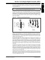
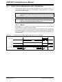
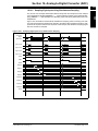
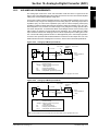
Depending on the particular device pinout, the ADC can have up to 32 analog input pins, designated AN0 through AN31. In addition, there are two analog input pins for external voltage reference connections. These voltage reference inputs can be shared with other analog input pins.
The actual number of analog input pins and external voltage reference input configuration will
depend on the specific device. Refer to the device data sheet for further details.
The analog inputs are multiplexed to four Sample/Hold amplifiers, designated CH0-CH3. One,
two, or four of the Sample/Hold amplifiers can be enabled for acquiring input data. The analog
input multiplexers can be switched between two sets of analog inputs during conversions. Unipolar differential conversions are possible on all channels using certain input pins (see
Figure 16-1).
An Analog Input Scan mode can be enabled for the CH0 Sample/Hold Amplifier. A Control
register specifies which analog input channels are included in the scanning sequence.
The ADC is connected to a single-word result buffer. However, multiple conversion results can
be stored in a DMA RAM buffer with no CPU overhead. Each conversion result is converted to
one of four 16-bit output formats when it is read from the buffer.
The 12-bit ADC configuration (AD12B = 1) supports all the above features, except:
• In the 12-bit configuration, conversion speeds of up to 500 ksps are supported
• There is only one Sample/Hold amplifier in the 12-bit configuration, so simultaneous
sampling of multiple channels is not supported.
DS70183A-page 16-2
© 2006 Microchip Technology Inc.
Section 16. Analog-to-Digital Converter (ADC)
16
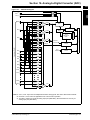
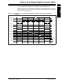
Figure 16-1:
ADC Block Diagram
AVDD
VREF+(1)
ADC
AVSS
VREF-(1)
AN6
AN9
VREFAN1
AN1
AN4
AN7
AN10
VREF-
AN2
AN2
AN5
Analog Input Pins(3)
AN8
AN11
VREF-
AN3
+
CH1(2)
ADC
S/H
-
+
-
CH2(2)
00100
AN5
00101
AN6
00110
AN7
00111
AN8
01000
AN9
01001
AN10
01010
AN11
01011
AN30
11110
AN31
11111
VREFAN1
Conversion Logic
S/H
16-bit
ADC Result
Buffer
+
-
CH3(2)
S/H
CH0,CH1,
CH2,CH3
Sample
00000
00001
00010
00011
AN4
Conversion
Result
Input
Switches
+
Sample/Sequence
Control
Bus Interface
AN0
AN3
Data Format
AN0
Input MUX
Control
CH0
S/H
-
Note 1: VREF+, VREF- inputs can be multiplexed with other analog inputs. See device data sheet for details.
2: Channels 1, 2 and 3 are not applicable for the 12-bit mode of operation.
3: The ADC1 module can use all 32 analog input pins (AN0-AN31), whereas ADC2 can use only 16
analog input pins (AN0-AN15).
© 2006 Microchip Technology Inc.
DS70183A-page 16-3
dsPIC33F Family Reference Manual
16.2
CONTROL REGISTERS
The ADC module has ten Control and Status registers. These registers are:
•
•
•
•
•
•
•
•
•
•
ADxCON1: ADCx Control Register 1(1)
ADxCON2: ADCx Control Register 2(1)
ADxCON3: ADCx Control Register 3(1)
ADxCON4: ADCx Control Register 4(1)
ADxCHS123: ADCx Input Channel 1, 2, 3 Select Register(1)
ADxCHS0: ADCx Input Channel 0 Select Register
AD1CSSH: ADC1 Input Scan Select Register High
ADxCSSL: ADCx Input Scan Select Register Low
AD1PCFGH: ADC1 Port Configuration Register High
ADxPCFGL: ADCx Port Configuration Register Low
The ADxCON1, ADxCON2 and ADxCON3 registers control the operation of the ADC module.
The ADxCON4 register sets up the number of conversion results stored in a DMA buffer for each
analog input in the Scatter/Gather mode. The ADxCHS123 and ADxCHS0 registers select the
input pins to be connected to the Sample/Hold amplifiers. The ADxPCFGH/L registers configure
the analog input pins as analog inputs or as digital I/O. The ADCSSH/L registers select inputs to
be sequentially scanned.
DS70183A-page 16-4
© 2006 Microchip Technology Inc.
Section 16. Analog-to-Digital Converter (ADC)
16
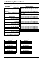
Register 16-1:
(1)
ADxCON1: ADCx Control Register 1
R/W-0
U-0
—
R/W-0
ADSIDL
R/W-0
ADDMABM
U-0
—
R/W-0
AD12B
R/W-0
R/W-0
FORM<1:0>
bit 8
R/W-0
R/W-0
U-0
R/W-0
R/W-0
—
SIMSAM
ASAM
R/W-0
HC,HS
SAMP
SSRC<2:0>
bit 7
Legend:
R = Readable bit
-n = Value at POR
HC = Cleared by hardware
W = Writable bit
‘1’ = Bit is set
R/C-0
HC, HS
DONE
bit 0
HS = Set by hardware
U = Unimplemented bit, read as ‘0’
‘0’ = Bit is cleared
x = Bit is unknown
bit 15
ADON: ADC Operating Mode bit
1 = ADC module is operating
0 = ADC is off
bit 14
Unimplemented: Read as ‘0’
bit 13
ADSIDL: Stop in Idle Mode bit
1 = Discontinue module operation when device enters Idle mode
0 = Continue module operation in Idle mode
bit 12
ADDMABM: DMA Buffer Build Mode bit
1 = DMA buffers are written in the order of conversion. The module provides an address to the DMA
channel that is the same as the address used for the non-DMA stand-alone buffer.
0 = DMA buffers are written in Scatter/Gather mode. The module provides a Scatter/Gather address
to the DMA channel, based on the index of the analog input and the size of the DMA buffer.
bit 11
Unimplemented: Read as ‘0’
bit 10
AD12B: 10-bit or 12-bit Operation Mode bit
1 = 12-bit, 1-channel ADC operation
0 = 10-bit, 4-channel ADC operation
bit 9-8
FORM<1:0>: Data Output Format bits
For 10-bit operation:
11 = Signed fractional (DOUT = sddd dddd dd00 0000, where s = .NOT.d<9>)
10 = Fractional (DOUT = dddd dddd dd00 0000)
01 = Signed integer (DOUT = ssss sssd dddd dddd, where s = .NOT.d<9>)
00 = Integer (DOUT = 0000 00dd dddd dddd)
For 12-bit operation:
11 = Signed fractional (DOUT = sddd dddd dddd 0000, where s = .NOT.d<11>)
10 = Fractional (DOUT = dddd dddd dddd 0000)
01 = Signed Integer (DOUT = ssss sddd dddd dddd, where s = .NOT.d<11>)
00 = Integer (DOUT = 0000 dddd dddd dddd)
bit 7-5
SSRC<2:0>: Sample Clock Source Select bits
111 = Internal counter ends sampling and starts conversion (auto-convert)
110 = Reserved
101 = Reserved
100 = Reserved
011 = MPWM interval ends sampling and starts conversion
010 = GP timer (Timer3 for ADC1, Timer5 for ADC2) compare ends sampling and starts conversion
001 = Active transition on INTx pin ends sampling and starts conversion
000 = Clearing sample bit ends sampling and starts conversion
bit 4
Unimplemented: Read as ‘0’
Note 1: The ‘x’ in ADxCON1 and ADCx refers to ADC 1 or ADC 2.
© 2006 Microchip Technology Inc.
DS70183A-page 16-5
ADC
R/W-0
ADON
bit 15
dsPIC33F Family Reference Manual
Register 16-1:
ADxCON1: ADCx Control Register 1(1) (Continued)
bit 3
SIMSAM: Simultaneous Sample Select bit (only applicable when CHPS<1:0> = 01 or 1x)
When AD12B = 1, SIMSAM is: U-0, Unimplemented, Read as ‘0’
1 = Samples CH0, CH1, CH2, CH3 simultaneously (when CHPS<1:0> = 1x); or
Samples CH0 and CH1 simultaneously (when CHPS<1:0> = 01)
0 = Samples multiple channels individually in sequence
bit 2
ASAM: ADC Sample Auto-Start bit
1 = Sampling begins immediately after last conversion. SAMP bit is auto-set.
0 = Sampling begins when SAMP bit is set
bit 1
SAMP: ADC Sample Enable bit
1 = ADC Sample/Hold amplifiers are sampling
0 = ADC Sample/Hold amplifiers are holding
If ASAM = 0, software can write ‘1’ to begin sampling. Automatically set by hardware if ASAM = 1.
If SSRC = 000, software can write ‘0’ to end sampling and start conversion. If SSRC ≠ 000,
automatically cleared by hardware to end sampling and start conversion.
bit 0
DONE: ADC Conversion Status bit
1 = ADC conversion cycle is completed.
0 = ADC conversion not started or in progress
Automatically set by hardware when A/D conversion is complete. Software can write ‘0’ to clear DONE
status (software not allowed to write ‘1’). Clearing this bit does NOT affect any operation in
progress. Automatically cleared by hardware at start of a new conversion.
Note 1: The ‘x’ in ADxCON1 and ADCx refers to ADC 1 or ADC 2.
DS70183A-page 16-6
© 2006 Microchip Technology Inc.
Section 16. Analog-to-Digital Converter (ADC)
16
Register 16-2:
R/W-0
(1)
ADxCON2: ADCx Control Register 2
R/W-0
U-0
—
R/W-0
U-0
—
U-0
—
R/W-0
CSCNA
bit 15
R-0
BUFS
bit 7
Legend:
R = Readable bit
-n = Value at POR
bit 15-13
W = Writable bit
‘1’ = Bit is set
R/W-0
R/W-0
SMPI<3:0>
R/W-0
R/W-0
R/W-0
CHPS<1:0>
bit 8
R/W-0
BUFM
R/W-0
ALTS
bit 0
U = Unimplemented bit, read as ‘0’
‘0’ = Bit is cleared
x = Bit is unknown
VCFG<2:0>: Converter Voltage Reference Configuration bits
000
001
010
011
1xx
VREFH
AVDD
External VREF+
AVDD
External VREF+
AVDD
VREFL
Avss
Avss
External VREFExternal VREFAvss
bit 12-11
bit 10
Unimplemented: Read as ‘0’
CSCNA: Input Scan Select bit
1 = Scan inputs for CH0+ during Sample A bit
0 = Do not scan inputs
bit 9-8
CHPS<1:0>: Channel Select bits
When AD12B = 1, CHPS<1:0> is: U-0, Unimplemented, Read as ‘0’
1x = Converts CH0, CH1, CH2 and CH3
01 = Converts CH0 and CH1
00 = Converts CH0
bit 7
BUFS: Buffer Fill Status bit (only valid when BUFM = 1)
1 = ADC is currently filling the second half of the buffer. The user application should access data in
the first half of the buffer
0 = ADC is currently filling the first half of the buffer. The user application should access data in the
second half of the buffer.
bit 6
Unimplemented: Read as ‘0’
bit 5-2
SMPI<3:0>: Increment Rate for DMA Addresses bits
1111 = Increments the DMA address or generates interrupt after completion of every 16th
sample/conversion operation
1110 = Increments the DMA address or generates interrupt after completion of every 15th
sample/conversion operation
•••
0001 = Increments the DMA address or generates interrupt after completion of every 2nd
sample/conversion operation
0000 = Increments the DMA address or generates interrupt after completion of every
sample/conversion operation
bit 1
BUFM: Buffer Fill Mode Select bit
1 = Starts buffer filling the first half of the buffer on the first interrupt and the second half of the buffer
on next interrupt
0 = Always starts filling the buffer from the start address.
bit 0
ALTS: Alternate Input Sample Mode Select bit
1 = Uses channel input selects for Sample A on first sample and Sample B on next sample
0 = Always uses channel input selects for Sample A
Note 1: The ‘x’ in ADxCON2 and ADCx refers to ADC 1 or ADC 2.
© 2006 Microchip Technology Inc.
DS70183A-page 16-7
ADC
R/W-0
VCFG<2:0>
dsPIC33F Family Reference Manual
Register 16-3:
ADxCON3: ADCx Control Register 3(1)
R/W-0
ADRC
bit 15
R/W-0
U-0
—
U-0
—
R/W-0
R/W-0
R/W-0
SAMC<4:0>
R/W-0
R/W-0
bit 8
R/W-0
R/W-0
R/W-0
R/W-0
ADCS<7:0>
R/W-0
R/W-0
R/W-0
bit 7
Legend:
R = Readable bit
-n = Value at POR
bit 0
W = Writable bit
‘1’ = Bit is set
U = Unimplemented bit, read as ‘0’
‘0’ = Bit is cleared
x = Bit is unknown
bit 15
ADRC: ADC Conversion Clock Source bit
1 = ADC Internal RC Clock
0 = Clock Derived From System Clock
bit 14-13
Unimplemented: Read as ‘0’
bit 12-8
SAMC<4:0>: Auto Sample Time bits
11111 = 31 TAD
•••
00001 = 1 TAD
00000 = 0 TAD
bit 7-0
ADCS<7:0>: ADC Conversion Clock Select bits
11111111 = TCY · (ADCS<7:0> + 1) = 256 · TCY = TAD
•••
00000010 = TCY · (ADCS<7:0> + 1) = 3 · TCY = TAD
00000001 = TCY · (ADCS<7:0> + 1) = 2 · TCY = TAD
00000000 = TCY · (ADCS<7:0> + 1) = 1 · TCY = TAD
Note 1: The ‘x’ in ADxCON3 and ADCx refers to ADC 1 or ADC 2.
DS70183A-page 16-8
© 2006 Microchip Technology Inc.
Section 16. Analog-to-Digital Converter (ADC)
16
Register 16-4:
(1)
ADxCON4: ADCx Control Register 4
U-0
—
U-0
—
U-0
—
U-0
—
U-0
—
U-0
—
U-0
—
U-0
—
U-0
—
bit 8
U-0
—
U-0
—
U-0
—
R/W-0
R/W-0
DMABL<2:0>
R/W-0
bit 7
Legend:
R = Readable bit
-n = Value at POR
bit 0
W = Writable bit
‘1’ = Bit is set
U = Unimplemented bit, read as ‘0’
‘0’ = Bit is cleared
x = Bit is unknown
bit 15-3
bit 2-0
Unimplemented: Read as ‘0’
DMABL<2:0>: Selects Number of DMA Buffer Locations per Analog Input bits
111 =Allocates 128 words of buffer to each analog input
110 =Allocates 64 words of buffer to each analog input
101 =Allocates 32 words of buffer to each analog input
100 =Allocates 16 words of buffer to each analog input
011 =Allocates 8 words of buffer to each analog input
010 =Allocates 4 words of buffer to each analog input
001 =Allocates 2 words of buffer to each analog input
000 =Allocates 1 word of buffer to each analog input
Note 1: The ‘x’ in ADxCON4 and ADCx refers to ADC 1 or ADC 2.
© 2006 Microchip Technology Inc.
DS70183A-page 16-9
ADC
U-0
—
bit 15
dsPIC33F Family Reference Manual
Register 16-5:
ADxCHS123: ADCx Input Channel 1, 2, 3 Select Register(1)
U-0
—
bit 15
U-0
—
U-0
—
U-0
—
U-0
—
R/W-0
R/W-0
CH123NB<1:0>
R/W-0
CH123SB
bit 8
U-0
—
U-0
—
U-0
—
U-0
—
U-0
—
R/W-0
R/W-0
CH123NA<1:0>
R/W-0
CH123SA
bit 0
bit 7
Legend:
R = Readable bit
-n = Value at POR
W = Writable bit
‘1’ = Bit is set
U = Unimplemented bit, read as ‘0’
‘0’ = Bit is cleared
x = Bit is unknown
bit 15-11
bit 10-9
Unimplemented: Read as ‘0’
CH123NB<1:0>: Channel 1, 2, 3 Negative Input Select for Sample B bits
When AD12B = 1, CHxNB is: U-0, Unimplemented, Read as ‘0’
11 = CH1 negative input is AN9, CH2 negative input is AN10, CH3 negative input is AN11
10 = CH1 negative input is AN6, CH2 negative input is AN7, CH3 negative input is AN8
0x = CH1, CH2, CH3 negative input is VREFL
bit 8
CH123SB: Channel 1, 2, 3 Positive Input Select for Sample B bit
When AD12B = 1, CHxSA is: U-0, Unimplemented, Read as ‘0’
1 = CH1 positive input is AN3, CH2 positive input is AN4, CH3 positive input is AN5
0 = CH1 positive input is AN0, CH2 positive input is AN1, CH3 positive input is AN2
bit 7-3
Unimplemented: Read as ‘0’
bit 2-1
CH123NA<1:0>: Channel 1, 2, 3 Negative Input Select for Sample A bits
When AD12B = 1, CHxNA is: U-0, Unimplemented, Read as ‘0’
11 = CH1 negative input is AN9, CH2 negative input is AN10, CH3 negative input is AN11
10 = CH1 negative input is AN6, CH2 negative input is AN7, CH3 negative input is AN8
0x = CH1, CH2, CH3 negative input is VREFL
bit 0
CH123SA: Channel 1, 2, 3 Positive Input Select for Sample A bit
When AD12B = 1, CHxSA is: U-0, Unimplemented, Read as ‘0’
1 = CH1 positive input is AN3, CH2 positive input is AN4, CH3 positive input is AN5
0 = CH1 positive input is AN0, CH2 positive input is AN1, CH3 positive input is AN2
Note 1: The ‘x’ in ADxCHS123 and ADCx refers to ADC 1 or ADC 2.
DS70183A-page 16-10
© 2006 Microchip Technology Inc.
Section 16. Analog-to-Digital Converter (ADC)
16
Register 16-6:
ADxCHS0: ADCx Input Channel 0 Select Register
U-0
—
R/W-0
CH0NA
bit 7
U-0
—
U-0
—
R/W-0
R/W-0
R/W-0
CH0SB<4:0>
R/W-0
R/W-0
bit 8
Legend:
R = Readable bit
-n = Value at POR
U-0
—
R/W-0
R/W-0
R/W-0
CH0SA<4:0>
R/W-0
R/W-0
bit 0
W = Writable bit
‘1’ = Bit is set
U = Unimplemented bit, read as ‘0’
‘0’ = Bit is cleared
x = Bit is unknown
bit 15
CH0NB: Channel 0 Negative Input Select for Sample B bit
Same definition as bit 7.
bit 14-13
Unimplemented: Read as ‘0’
bit 12-8
CH0SB<4:0>: Channel 0 Positive Input Select for Sample B bits(1, 2)
Same definition as bit<4:0>.
bit 7
CH0NA: Channel 0 Negative Input Select for Sample A bit
1 = Channel 0 negative input is AN1
0 = Channel 0 negative input is VREFL
bit 6-5
Unimplemented: Read as ‘0’
bit 4-0
CH0SA<4:0>: Channel 0 Positive Input Select for Sample A bits(1, 2)
11111 = Channel 0 positive input is AN31
11110 = Channel 0 positive input is AN30
•••
00010 = Channel 0 positive input is AN2
00001 = Channel 0 positive input is AN1
00000 = Channel 0 positive input is AN0
Note 1: The AN16 – AN31 pins are not available for ADC 2.
2: The ‘x’ in ADxCHS0 and ADCx refers to ADC 1 or ADC 2
© 2006 Microchip Technology Inc.
DS70183A-page 16-11
ADC
R/W-0
CH0NB
bit 15
dsPIC33F Family Reference Manual
Register 16-7:
AD1CSSH: ADC1 Input Scan Select Register High
R/W-0
CSS31
bit 15
R/W-0
CSS30
R/W-0
CSS29
R/W-0
CSS28
R/W-0
CSS27
R/W-0
CSS26
R/W-0
CSS25
R/W-0
CSS24
bit 8
R/W-0
CSS23
bit 7
R/W-0
CSS22
R/W-0
CSS21
R/W-0
CSS20
R/W-0
CSS19
R/W-0
CSS18
R/W-0
CSS17
R/W-0
CSS16
bit 0
Legend:
R = Readable bit
-n = Value at POR
W = Writable bit
‘1’ = Bit is set
U = Unimplemented bit, read as ‘0’
‘0’ = Bit is cleared
x = Bit is unknown
CSS<31:16>: ADC Input Scan Selection bits(1, 2)
1 = Select ANx for input scan
0 = Skip ANx for input scan
Note 1: On devices with less than 32 analog inputs, all ADxCSSL bits can be selected by user. However, inputs
selected for scan without a corresponding input on device convert VREF-.
2: ADC 2 only supports analog inputs AN0-AN15; therefore, no ADC 2 Input Scan Select register exists.
bit 15-0
Register 16-8:
ADxCSSL: ADCx Input Scan Select Register Low
R/W-0
CSS15
bit 15
R/W-0
CSS14
R/W-0
CSS13
R/W-0
CSS12
R/W-0
CSS11
R/W-0
CSS10
R/W-0
CSS9
R/W-0
CSS8
bit 8
R/W-0
CSS7
bit 7
R/W-0
CSS6
R/W-0
CSS5
R/W-0
CSS4
R/W-0
CSS3
R/W-0
CSS2
R/W-0
CSS1
R/W-0
CSS0
bit 0
Legend:
R = Readable bit
-n = Value at POR
W = Writable bit
‘1’ = Bit is set
U = Unimplemented bit, read as ‘0’
‘0’ = Bit is cleared
x = Bit is unknown
CSS<15:0>: ADC Input Scan Selection bits(1, 2)
1 = Select ANx for input scan
0 = Skip ANx for input scan
Note 1: On devices with less than 16 analog inputs, all ADxCSSL bits can be selected by the user. However, inputs
selected for scan without a corresponding input on device convert VREF-.
2: The ‘x’ in ADxCSSL and ADCx refers to ADC 1 or ADC 2.
bit 15-0
DS70183A-page 16-12
© 2006 Microchip Technology Inc.
Section 16. Analog-to-Digital Converter (ADC)
16
Register 16-9:
R/W-0
PCFG30
R/W-0
PCFG29
R/W-0
PCFG28
R/W-0
PCFG27
R/W-0
PCFG26
R/W-0
PCFG25
R/W-0
PCFG24
bit 8
R/W-0
PCFG22
R/W-0
PCFG21
R/W-0
PCFG20
R/W-0
PCFG19
R/W-0
PCFG18
R/W-0
PCFG17
R/W-0
PCFG16
bit 0
bit 15
R/W-0
PCFG23
bit 7
Legend:
R = Readable bit
-n = Value at POR
W = Writable bit
‘1’ = Bit is set
U = Unimplemented bit, read as ‘0’
‘0’ = Bit is cleared
x = Bit is unknown
PCFG<31:16>: ADC Port Configuration Control bits(1, 2)
1 = Port pin in Digital mode, port read input enabled, ADC input multiplexor connected to AVSS
0 = Port pin in Analog mode, port read input disabled, ADC samples pin voltage
Note 1: On devices with less than 32 analog inputs, all PCFG bits are R/W by user. However, PCFG bits are ignored
on ports without a corresponding input on device.
2: ADC2 only supports analog inputs AN0-AN15; therefore, no ADC2 Port Configuration register exists.
bit 15-0
Register 16-10: ADxPCFGL: ADCx Port Configuration Register Low
R/W-0
PCFG15
R/W-0
PCFG14
R/W-0
PCFG13
R/W-0
PCFG12
R/W-0
PCFG11
R/W-0
PCFG10
R/W-0
PCFG9
R/W-0
PCFG8
bit 8
R/W-0
PCFG6
R/W-0
PCFG5
R/W-0
PCFG4
R/W-0
PCFG3
R/W-0
PCFG2
R/W-0
PCFG1
R/W-0
PCFG0
bit 0
bit 15
R/W-0
PCFG7
bit 7
Legend:
R = Readable bit
-n = Value at POR
W = Writable bit
‘1’ = Bit is set
U = Unimplemented bit, read as ‘0’
‘0’ = Bit is cleared
x = Bit is unknown
PCFG<15:0>: ADC Port Configuration Control bits(1, 2, 3)
1 = Port pin in Digital mode, port read input enabled, ADC input multiplexor connected to AVSS
0 = Port pin in Analog mode, port read input disabled, ADC samples pin voltage
Note 1: On devices with less than 16 analog inputs, all PCFG bits are R/W by user. However, PCFG bits are ignored
on ports without a corresponding input on device.
2: On devices with two analog-to-digital modules, both AD1PCFGL and AD2PCFGL affect the configuration of
port pins multiplexed with AN0-AN15.
3: The ‘x’ in ADxPCFGL and ADx refers to ADC 1 or ADC 2
bit 15-0
© 2006 Microchip Technology Inc.
DS70183A-page 16-13
ADC
R/W-0
PCFG31
AD1PCFGH: ADC1 Port Configuration Register High
dsPIC33F Family Reference Manual
16.3
A/D TERMINOLOGY AND CONVERSION SEQUENCE
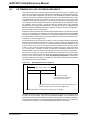
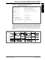
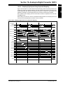
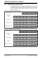
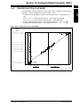
Figure 16-2 shows a basic conversion sequence and the terms that are used. A sampling of the
analog input pin voltage is performed by Sample/Hold amplifiers (also called Sample/Hold channels). The 10-bit ADC configuration can use up to four Sample/Hold channels, designated
CH0-CH3, whereas the 12-bit ADC configuration can use only one Sample/Hold channel, CH0.
The Sample/Hold channels are connected to the analog input pins via the analog input
multiplexer. The analog input multiplexer is controlled by the ADxCHS123 and ADxCHS0 registers. There are two sets of multiplexer control bits in the ADC channel select registers that function identically. These two sets of control bits allow two different analog input multiplexer
configurations to be programmed (called MUX A and MUX B). The ADC can optionally switch
between the MUX A and MUX B configurations between conversions. The ADC can also optionally scan through a series of analog inputs.
Sample time is the time that the ADC module’s Sample/Hold Amplifier is connected to the analog
input pin. The sample time can be started manually by setting the ADC Sample Enable (SAMP)
bit in ADCx Control Register 1 (ADxCON1<1>) or started automatically by the ADC hardware.
The sample time is ended manually by clearing the SAMP control bit in the user software or automatically by a conversion trigger source.
Conversion time is the time required for the ADC to convert the voltage held by the Sample/Hold
Amplifier. The ADC is disconnected from the analog input pin at the end of the sample time. The
ADC requires one A/D clock cycle (TAD) to convert each bit of the result plus two additional clock
cycles. A total of 12 TAD cycles are required to perform the complete conversion in 10-bit mode.
A total of 14 TAD cycles are required to perform the complete conversion in 12-bit mode. When
the conversion time is complete, the result is loaded into the ADCxBUF0 register, the Sample/Hold Amplifier can be reconnected to the input pin and a CPU interrupt can be generated.
The sum of the sample time and the A/D conversion time provides the total conversion time.
There is a minimum sample time to ensure that the Sample/Hold Amplifier provides the desired
accuracy for the A/D conversion (see 16.15 “A/D Sampling Requirements”). Furthermore,
there are multiple input clock options for the ADC. You must select an input clock option that does
not violate the minimum TAD specification.
Figure 16-2:
ADC Sample/Conversion Sequence
ADC Total Conversion Time
Sample Time
ADC Conversion Time
A/D conversion complete,
result is loaded into result buffer.
Optionally generate interrupt.
Sample/Hold Amplifier is disconnected from input and holds signal level.
A/D conversion is started by the conversion trigger source.
Sample/Hold Amplifier is connected to the analog input pin for sampling.
The ADC allows many options for specifying the sample/convert sequence. The sample/convert
sequence can be very simple, using only one Sample/Hold amplifier. A more elaborate sample/convert sequence performs multiple conversions using more than one Sample/Hold amplifier.
The 10-bit ADC configuration can use two Sample/Hold amplifiers to perform two conversions in
a sample/convert sequence or four Sample/Hold amplifiers with four conversions.
DS70183A-page 16-14
© 2006 Microchip Technology Inc.
Section 16. Analog-to-Digital Converter (ADC)
16
The number of Sample/Hold amplifiers, or channels per sample, used in the sample/convert
sequence is determined by the Channel Select (CHPS<1:0>) control bits in ADCx Control Register 2 (ADxCON2<9:8>).
The 12-bit ADC configuration can only perform one conversion in a single sample/convert sequence. The CHPS bits are irrelevant in this case.
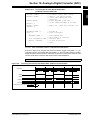
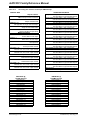
A sample/convert sequence that uses multiple Sample/Hold channels can be simultaneously
sampled or sequentially sampled, as controlled by the Simultaneous Sample Select (SIMSAM)
bit (ADxCON1<3>). Simultaneously sampling multiple signals ensures that the snapshot of the
analog inputs occurs at precisely the same time for all inputs. Sequential sampling takes a snapshot of each analog input just before conversion starts on that input. The sampling of multiple
inputs is not correlated.
Figure 16-3:
Simultaneous and Sequential Sampling
AN0
AN1
AN2
AN3
Simultaneous
Sampling
Sequential
Sampling
The start time for sampling can be controlled in software by setting the ADC Sample Enable
(SAMP) control bit (ADxCON1<1>). The start of the sampling time can also be controlled automatically by the hardware. When the ADC module operates in the Auto-Sample mode, the Sample/Hold amplifier(s) is reconnected to the analog input pin at the end of the conversion in the
sample/convert sequence. The auto-sample function is controlled by the ADC Sample Auto-Start
(ASAM) control bit (ADxCON1<2>).
The conversion trigger source ends the sampling time and begins an A/D conversion or a
sample/convert sequence. The conversion trigger source is selected by the Sample Clock
Source Select (SSRC<2:0>) control bits (ADxCON1<7:5>. The conversion trigger can be taken
from a variety of hardware sources, or can be controlled manually in software by clearing the
SAMP control bit. One of the conversion trigger sources is an auto-conversion. The time between
auto-conversions is set by a counter and the ADC clock. The Auto-Sample mode and auto-conversion trigger can be used together to provide endless automatic conversions without software
intervention.
An interrupt can be generated at the end of each sample/convert sequence or after multiple
sample/convert sequences, as determined by the value of the Samples Per Interrupt
(SMPI<3:0>) control bits (ADxCON2<5:2>). The number of sample/convert sequences between
interrupts can vary between 1 and 16. The total number of conversion results between interrupts
is the product of the channels per sample and the SMPI<3:0> value. However, since only one
conversion result is stored in ADCxBUF0, each execution of the interrupt service routine can be
used to read only one conversion result.
If multiple conversion results need to be buffered, a DMA buffer should be used to store the conversion results. In this case, the SMPI<3:0> bits are used to select how often the DMA RAM
buffer pointer is incremented. The frequency of incrementing the DMA RAM buffer pointer should
not exceed the DMA RAM buffer length.
© 2006 Microchip Technology Inc.
DS70183A-page 16-15
ADC
Note:
dsPIC33F Family Reference Manual
16.4
ADC MODULE CONFIGURATION
The following steps should be followed for performing an A/D conversion:
1.
2.
3.
4.
5.
6.
7.
8.
9.
10.
11.
12.
13.
14.
15.
16.
Select 10-bit or 12-bit mode (ADxCON1<10>)
Select voltage reference source to match expected range on analog inputs
(ADxCON2<15:13>)
Select the analog conversion clock to match desired data rate with processor clock
(ADxCON3<7:0>)
Select port pins as analog inputs (ADxPCFGH<15:0> and ADxPCFGL<15:0>)
Determine how inputs will be allocated to Sample/Hold channels (ADxCHS0<15:0> and
ADxCHS123<15:0>)
Determine how many Sample/Hold channels will be used (ADxCON2<9:8>, ADxPCFGH<15:0> and ADxPCFGL<15:0>)
Determine how sampling will occur (ADxCON1<3>, ADxCSSH<15:0> and ADxCSSL<15:0>)
Select Manual or Auto Sampling
Select conversion trigger and sampling time.
Select how conversion results are stored in the buffer (ADxCON1<9:8>)
Select interrupt rate or DMA buffer pointer increment rate (ADxCON2<9:5>)
Select the number of samples in DMA buffer for each ADC module input
(ADxCON4<2:0>)
Select the data format
Configure ADC interrupt (if required)
• Clear ADxIF bit
• Select interrupt priority (ADxIP<2:0)
• Set ADxIE bit
Configure DMA channel (if needed)
Turn on ADC module (ADxCON1<15>)
The options for these configuration steps are described in the subsequent sections.
16.5
SELECTING THE VOLTAGE REFERENCE SOURCE
The voltage references for A/D conversions are selected using the VCFG<2:0> control bits
(ADxCON2<15:13>). The upper voltage reference (VREFH) and the lower voltage reference
(VREFL) can be the internal AVDD and AVSS voltage rails or the VREF+ and VREF- input pins.
The external voltage reference pins can be shared with the AN0 and AN1 inputs on low pin count
devices. The ADC module can still perform conversions on these pins when they are shared with
the Vref+ and Vref- input pins.
The voltages applied to the external reference pins must meet certain specifications. Refer to the
“Electrical Specifications” section of the device data sheet for details
DS70183A-page 16-16
© 2006 Microchip Technology Inc.
Section 16. Analog-to-Digital Converter (ADC)
16
16.6
SELECTING THE A/D CONVERSION CLOCK
The period of the A/D conversion clock is software selected using a 6-bit counter. There are 256
possible options for TAD, specified by the ADC Conversion Clock Select (ADCS<7:0>) bits
(ADxCON3<7:0>). Equation 16-1 gives the TAD value as a function of the ADCS control bits and
the device instruction cycle clock period, TCY.
Equation 16-1:
A/D Conversion Clock Period
TAD = TCY (ADCS + 1)
TAD
ADCS =
–1
TCY
For correct A/D conversions, the A/D conversion clock (TAD) must be selected to ensure a
minimum TAD time of 75 nsec.
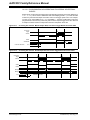
The ADC module has a dedicated internal RC clock source that can be used to perform
conversions. The internal RC clock source should be used when A/D conversions are performed
while the device is in Sleep mode. The internal RC oscillator is selected by setting the ADC Conversion Clock Source (ADRC) bit (ADxCON3<15>). When the ADRC bit is set, the ADCS<7:0>
bits have no effect on the A/D operation.
Figure 16-4:
A/D Conversion Clock Period Block Diagram
ADxCON3<15>
ADC Internal
RC Clock
0
TAD
ADxCON3<7:0>
1
8
TCY
A/D Conversion
Clock Multiplier
1, 2, 3, 4, 5,..., 256
© 2006 Microchip Technology Inc.
DS70183A-page 16-17
ADC
The ADC module has a maximum rate at which conversions can be completed. An analog
module clock, TAD, controls the conversion timing. The A/D conversion requires 12 clock periods
(12 TAD) in the 10-bit mode and 14 clock periods (14 TAD) in the 12-bit mode. The A/D conversion
clock is derived from either the device instruction clock or an internal RC clock source.
dsPIC33F Family Reference Manual
16.7
SELECTING ANALOG INPUTS FOR SAMPLING
All Sample/Hold Amplifiers have analog multiplexers (see Figure 16-1) on both their non-inverting and inverting inputs to select which analog input(s) are sampled. Once the sample/convert
sequence is specified, the ADxCHS0 and ADxCHS123 registers determine which analog inputs
are selected for each sample.
Additionally, the selected inputs can vary on an alternating sample basis or on a repeated
sequence of samples.
The same analog input can be connected to two or more Sample/Hold channels to improve conversion rates.
Note:
Different devices will have different numbers of analog inputs. Verify the analog
input availability against the device data sheet.
16.7.1
Configuring Analog Port Pins
The ADPCFGH and ADPCFGL registers specify the input condition of device pins used as analog inputs. Along with the Data Direction (TRISx) register in the Parallel I/O Port module, these
registers control the operation of the ADC pins.
A pin is configured as analog input when the corresponding PCFGn bit (ADPCFGH<n> or
ADPCFGL<n>) is clear. The ADPCFGH and ADPCFGL registers are clear at Reset, causing the
ADC input pins to be configured for analog input by default at Reset.
When configured for analog input, the associated port I/O digital input buffer is disabled so it does
not consume current.
The port pins that are desired as analog inputs must have their corresponding TRIS bit set, specifying port input. If the I/O pin associated with an A/D input is configured as an output, the TRIS
bit is cleared and the port’s digital output level (VOH or VOL) is converted. After a device Reset,
all TRIS bits are set.
A pin is configured as digital I/O when the corresponding PCFGn bit is set. In this configuration,
the input to the analog multiplexer is connected to AVss.
Note 1: When the ADC Port register is read, any pin configured as an analog input reads
as a ‘0’.
2: Analog levels on any pin that is defined as a digital input (including the AN15:AN0
pins) may cause the input buffer to consume current that is out of the device’s
specification.
16.7.2
Channel 0 Input Selection
Channel 0 is the most flexible of the four Sample/Hold channels in terms of selecting analog
inputs. It allows you to select any of the up to 16 analog inputs as the input to the positive input
of the channel. The Channel 0 Positive Input Select for Sample A (CH0SA<4:0>) bits
(ADxCHS0<4:0>) normally select the analog input for the positive input of channel 0.
You can select either VREF- or AN1 as the negative input of the channel. The CH0NA bit
(ADxCHS0<7>) normally selects the analog input for the negative input of channel 0.
16.7.2.1
SPECIFYING ALTERNATING CHANNEL 0 INPUT SELECTIONS
The Alternate Input Sample Mode Select (ALTS) bit (ADxCON2<0>) causes the ADC module to
alternate between two sets of inputs that are selected during successive samples.
The inputs specified by CH0SA<4:0> (ADxCHS0<4:0>), CH0NA (ADxCHS0<7>), CH123SA
(ADxCHS123<0>) and CH123NA<1:0> (ADxCHS123<2:1>) are collectively called the MUX A
inputs. The inputs specified by CH0SB<4:0> (ADxCHS0<12:8>), CH0NB (ADxCHS0<15>),
CH123SB (ADxCHS0<8>) and CH123NB<1:0> (ADxCHS0<10:9>) are collectively called the
MUX B inputs. When the ALTS bit is ‘1’, the ADC module alternates between the MUX A inputs
on one group of samples and the MUX B inputs on the subsequent group of samples.
DS70183A-page 16-18
© 2006 Microchip Technology Inc.
Section 16. Analog-to-Digital Converter (ADC)
16
For channel 0, if the ALTS bit is ‘0’, only the inputs specified by CH0SA<4:0> and CH0NA are
selected for sampling.
Note that if multiple channels (CHPS = 01 or 1x) and simultaneous sampling (SIMSAM = 1) are
specified, alternating inputs change every sample because all channels are sampled on every
sample time. If multiple channels (CHPS = 01 or 1x) and sequential sampling (SIMSAM = 0) are
specified, alternating inputs change only on each sample of a particular channel.
16.7.2.2
SCANNING THROUGH SEVERAL INPUTS WITH CHANNEL 0
Channel 0 can scan through a selected vector of inputs. The CSCNA bit (ADxCON2<10>)
enables the CH0 channel inputs to be scanned across a selected number of analog inputs. When
CSCNA is set, the CH0SA<4:0> bits are ignored.
The ADCx Input Scan Select Register High (ADxCSSH) and ADCx Input Scan Select Register
Low (ADxCSSL) registers specify the inputs to be scanned. Each bit in these registers
corresponds to an analog input. Bit 0 corresponds to AN0, bit 1 corresponds to AN1 and so on.
If a particular bit is ‘1’, the corresponding input is part of the scan sequence. The inputs are
always scanned from lower to higher numbered inputs, starting at the first selected channel after
each interrupt occurs.
Note:
If the number of scanned inputs selected is greater than the number of samples
taken per interrupt, the higher numbered inputs will not be sampled.
The ADxCSSH and ADxCSSL bits only specify the input of the positive input of the channel. The
CH0NA bit still selects the input of the negative input of the channel during scanning.
If the ALTS bit is ‘1’, the scanning only applies to the MUX A input selection. The MUX B input
selection, as specified by the CH0SB<4:0>, still selects the alternating channel 0 input. When the
input selections are programmed in this manner, the channel 0 input alternates between a set of
scanning inputs specified by the ADxCSSL register and a fixed input specified by the CH0SB
bits.
16.7.3
Channel 1, 2 and 3 Input Selection
Channel 1, 2 and 3 can sample a subset of the analog input pins. Channel 1, 2 and 3 can select
one of two groups of three inputs.
The CH123SA bit (ADxCHS123<0>) selects the source for the positive inputs of channel 1, 2 and
3. Clearing CH123SA selects AN0, AN1 and AN2 as the analog source to the positive inputs of
channel 1, 2 and 3, respectively. Setting CH123SA selects AN3, AN4 and AN5 as the analog
source.
The CH123NA<1:0> bits (ADxCHS<2:1>) select the source for the negative inputs of channel 1,
2 and 3. Programming CH123NA = 0x selects VREF- as the analog source for the negative inputs
of channels 1, 2 and 3. Programming CH123NA = 10 selects AN6, AN7 and AN8 as the analog
source to the negative inputs of channels 1, 2 and 3 respectively. Programming CH123NA = 11
selects AN9, AN10 and AN11 as the analog source.
© 2006 Microchip Technology Inc.
DS70183A-page 16-19
ADC
If the ALTS bit is ‘1’, on the first sample/convert sequence for channel 0, the inputs specified by
CH0SA<4:0> and CH0NA are selected for sampling. On the next sample convert sequence for
channel 0, the inputs specified by CH0SB<4:0> and CH0NB are selected for sampling. This
pattern repeats for subsequent sample conversion sequences.
dsPIC33F Family Reference Manual
16.7.3.1
SELECTING MULTIPLE CHANNELS FOR A SINGLE ANALOG INPUT
The analog input multiplexer can be configured so that the same input pin is connected to two or
more Sample/Hold channels. The ADC converts the value held on one Sample/Hold channel,
while the second Sample/Hold channel acquires a new input sample.
16.7.3.2
SPECIFYING ALTERNATING CHANNEL 1, 2 AND 3 INPUT
SELECTIONS
As with the channel 0 inputs, the ALTS bit (ADxCON2<0>) causes the ADC module to alternate
between two sets of inputs that are selected during successive samples for channel 1,2 and 3.
The MUX A inputs specified by CH123SA and CH123NA<1:0> always select the input when
ALTS = 0.
The MUX A inputs alternate with the MUX B inputs specified by CH123SB and CH123NB<1:0>
when ALTS = 1.
16.8
ENABLING THE MODULE
When the ADC Operating Mode (ADON) bit (ADxCON1<15>) is ‘1’, the ADC module is in Active
mode and is fully powered and functional.
When ADON is ‘0’, the ADC module is disabled. The digital and analog portions of the circuit are
turned off for maximum current savings.
In order to return to the Active mode from the Off mode, the user must wait for the analog stages
to stabilize. For the stabilization time, refer to the Electrical Characteristics section of the device
data sheet.
Note:
16.9
The SSRC<2:0>, SIMSAM, ASAM, CHPS<1:0>, SMPI<3:0>, BUFM and ALTS bits,
as well as the ADxCON3, ADxCSSH and ADxCSSL registers, should not be written
to while ADON = 1. This would lead to indeterminate results.
SPECIFYING SAMPLE/CONVERSION CONTROL
The ADC module uses four Sample/Hold amplifiers and one A/D Converter in the 10-bit mode.
The module can perform 1, 2 or 4 input samples and A/D conversions per sample/convert
sequence.
16.9.1
Number of Sample/Hold Channels
The CHPS<1:0> control bits (ADxCON2<9:8>) are used to select how many Sample/Hold amplifiers are used by the ADC module during sample/conversion sequences. The following three
options can be selected:
• CH0 only
• CH0 and CH1
• CH0, CH1, CH2, CH3
The CHPS control bits work in conjunction with the SIMSAM (simultaneous sample) control bit
(ADxCON1<3>). The CHPS and SIMSAM bits are not relevant in 12-bit mode as there is only
one Sample/Hold amplifier.
16.9.2
Simultaneous Sampling Enable
Some applications can require that multiple signals be sampled simultaneously. The SIMSAM
control bit (ADxCON1<3>) works in conjunction with the CHPS control bits and controls the sample/convert sequence for multiple channels as shown in Table 16-1. The SIMSAM control bit has
no effect on the ADC module operation if CHPS<1:0> = 00. If more than one Sample/Hold amplifier is enabled by the CHPS control bits and the SIMSAM bit is ‘0’, the two or four selected channels are sampled and converted sequentially with two or four sampling periods. If the SIMSAM
bit is ‘1’, two or four selected channels are sampled simultaneously with one sampling period.
The channels are then converted sequentially. The SIMSAM bit is not relevant in 12-bit mode as
there is only one S/H.
DS70183A-page 16-20
© 2006 Microchip Technology Inc.
Section 16. Analog-to-Digital Converter (ADC)
16
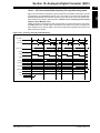
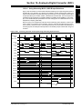
Table 16-1:
Sample/Conversion Control Options
CHPS<1:0> SIMSAM
# of Sample/
Convert Cycles
to Complete
Example
00
x
Sample CH0, Convert CH0
1
Figure 16-5,
Figure 16-6,
Figure 16-7,
Figure 16-8,
Figure 16-11,
Figure 16-12,
Figure 16-17,
Figure 16-18
01
0
Sample CH0, Convert CH0
Sample CH1, Convert CH1
2
1x
0
Sample CH0, Convert CH0
Sample CH1, Convert CH1
Sample CH2, Convert CH2
Sample CH3, Convert CH3
4
Figure 16-10,
Figure 16-14,
Figure 16-22
01
1
Sample CH0, CH1 simultaneously
Convert CH0
Convert CH1
1
Figure 16-20
1x
1
Sample CH0, CH1, CH2, CH3
simultaneously
Convert CH0
Convert CH1
Convert CH2
Convert CH3
1
Figure 16-9,
Figure 16-13,
Figure 16-19,
Figure 16-21
HOW TO START SAMPLING
16.10.1 Manual
Setting the SAMP bit (ADxCON1<1>) causes the ADC to begin sampling. One of several options
can be used to end sampling and complete the conversions. Sampling does not resume until the
SAMP bit is once again set. For an example, see Figure 16-5.
16.10.2 Automatic
Setting the ASAM bit (ADxCON1<2>) causes the ADC to automatically begin sampling a channel
whenever a conversion is not active on that channel. One of several options can be used to end
sampling and complete the conversions. If the SIMSAM bit specifies sequential sampling,
sampling on a channel resumes after the conversion of that channel completes. If the SIMSAM
bit specifies simultaneous sampling, sampling on a channel resumes after the conversion of all
channels completes. For an example, see Figure 16-6.
© 2006 Microchip Technology Inc.
DS70183A-page 16-21
ADC
16.10
Sample/Conversion Sequence
dsPIC33F Family Reference Manual
16.11
HOW TO STOP SAMPLING AND START CONVERSIONS
The conversion trigger source terminates sampling and starts a selected sequence of
conversions. The Sample Clock Source Select (SSRC<2:0>) bits (ADxCON1<7:5>) select the
source of the conversion trigger.
Note:
The available conversion trigger sources can vary depending on the device variant.
Please refer to the specific device data sheet for the available conversion trigger
sources.
Note:
The SSRC<2:0> selection bits should not be changed when the ADC module is
enabled. If you change the conversion trigger source, be sure the ADC module is
disabled first by clearing the ADON bit (ADxCON1<15>).
16.11.1
Manual
When SSRC<2:0> = 000, the conversion trigger is under software control. Clearing the SAMP
bit (ADxCON1<1>) starts the conversion sequence.
Figure 16-5 is an example where setting the SAMP bit initiates sampling and clearing the SAMP
bit terminates sampling and starts conversion. The user software must time the setting and
clearing of the SAMP bit to ensure adequate sampling time of the input signal. See Example 16-1
for code example.
Figure 16-5:
Converting 1 Channel, Manual Sample Start, Manual Conversion Start
ADC Clock
TCONV
TSAMP
SAMP
DONE
ADC1BUF0
Instruction Execution
BSET AD1CON1,SAMP
DS70183A-page 16-22
BCLR AD1CON1,SAMP
© 2006 Microchip Technology Inc.
Section 16. Analog-to-Digital Converter (ADC)
16
Example 16-1:
Converting 1 Channel, Manual Sample Start,
Manual Conversion Start Code
//
//
//
//
//
AD1CHS0 = 0x0002;
AD1CSSL = 0;
AD1CON3 = 0x0002;
AD1CON2 = 0;
all PORTB = Digital; RB2 = analog
SAMP bit = 0 ends sampling ...
and starts converting
Connect RB2/AN2 as CH0 input ..
in this example RB2/AN2 is the input
// Manual Sample, Tad = internal 2 Tcy
AD1CON1bits.ADON = 1;
//
while (1)
//
{
AD1CON1bits.SAMP = 1;
//
DelayNmSec(100);
//
AD1CON1bits.SAMP = 0;
//
while (!AD1CON1bits.DONE);//
ADCValue = ADC1BUF0;
//
}
//
turn ADC ON
repeat continuously
start sampling ...
for 100 mS
start Converting
conversion done?
yes then get ADC value
repeat
Figure 16-6 is an example where setting the ASAM bit initiates automatic sampling and clearing
the SAMP bit terminates sampling and starts conversion. After the conversion completes, the
ADC module automatically returns to a sampling state. The SAMP bit is automatically set at the
start of the sample interval. The user software must time the clearing of the SAMP bit to ensure
adequate sampling time of the input signal, understanding that the time between clearing of the
SAMP bit includes the conversion time as well as the sampling time. See Example 16-2 for code
example.
Figure 16-6:
Converting 1 Channel, Automatic Sample Start, Manual Conversion Start
ADC Clock
TAD0
TSAMP
TCONV
TAD0
TSAMP
TCONV
SAMP
DONE
ADC1BUF0
BSET AD1CON1,ASAM BCLR AD1CON1,SAMP
© 2006 Microchip Technology Inc.
BCLR AD1CON1,SAMP
Instruction Execution
DS70183A-page 16-23
ADC
AD1PCFGL = 0xFFFB;
AD1CON1 = 0x0000;
dsPIC33F Family Reference Manual
Example 16-2:
Converting 1 Channel, Automatic Sample Start,
Manual Conversion Start Code
AD1PCFGL = 0xFF7F;
AD1CON1 = 0x0004;
AD1CHS0= 0x0007;
AD1CSSL = 0;
AD1CON3 = 0x0002;
AD1CON2 = 0;
//
//
//
//
//
//
all PORTB = Digital but RB7 = analog
ASAM bit = 1 implies sampling ..
starts immediately after last
conversion is done
Connect RB7/AN7 as CH0 input ..
in this example RB7/AN7 is the input
// Sample time manual, Tad = internal 2 Tcy
AD1CON1bits.ADON = 1;
//
while (1)
//
{
DelayNmSec(100);
//
AD1CON1bits.SAMP = 0;
//
while (!AD1CON1bits.DONE);//
ADCValue = ADC1BUF0;
//
}
//
turn ADC ON
repeat continuously
sample for 100 mS
start Converting
conversion done?
yes then get ADC value
repeat
16.11.2 Clocked Conversion Trigger
When SSRC<2:0> = 111, the conversion trigger is under A/D clock control. The Auto Sample Time
(SAMC<4:0>) bits (AD1CON3<12:8>) select the number of TAD clock cycles between the start of sampling and the start of conversion. This trigger option provides the fastest conversion rates on multiple
channels. After the start of sampling, the ADC module counts a number of TAD clocks specified by the
SAMC bits.
Equation 16-2:
Clocked Conversion Trigger Time
TSMP = SAMC<4:0>*TAD
When using only one Sample/Hold channel or simultaneous sampling, SAMC must always be programmed for at least one clock cycle. When using multiple Sample/Hold channels with sequential
sampling, programming SAMC for zero clock cycles results in the fastest possible conversion rate.
See Example 16-3 for code example.
Figure 16-7:
Converting 1 Channel, Manual Sample Start, TAD Based Conversion Start
ADC Clock
TSAMP
= 16 TAD
TCONV
SAMP
DONE
ADC1BUF0
Instruction ExecutionBSET
DS70183A-page 16-24
AD1CON1,SAMP
© 2006 Microchip Technology Inc.
Section 16. Analog-to-Digital Converter (ADC)
16
Example 16-3:
Converting One Channel, Manual Sample Start,
TAD Based Conversion Start Code
AD1CHS0= 0x000C;
AD1CSSL = 0;
AD1CON3 = 0x1F02;
AD1CON2 = 0;
AD1CON1bits.ADON = 1;
while (1)
{
AD1CON1bits.SAMP = 1;
//
//
//
//
//
//
all PORTB = Digital; RB12 = analog
SSRC bit = 111 implies internal
counter ends sampling and starts
converting.
Connect RB12/AN12 as CH0 input ..
in this example RB12/AN12 is the input
// Sample time = 31Tad, Tad = internal 2 Tcy
// turn ADC ON
// repeat continuously
//
//
while (!AD1CON1bits.DONE);//
ADCValue = ADC1BUF0;
//
}
//
start sampling then ...
after 31Tad go to conversion
conversion done?
yes then get ADC value
repeat
16.11.2.1 FREE RUNNING SAMPLE CONVERSION SEQUENCE
As shown in Figure 16-8, using the Auto-Convert Conversion Trigger mode (SSRC = 111) in
combination with the Auto-Sample Start mode (ASAM = 1), allows the ADC module to schedule
sample/conversion sequences with no intervention by the user or other device resources. This
“Clocked” mode allows continuous data collection after module initialization.
Note:
Figure 16-8:
This A/D configuration must be enabled for the conversion rate of 750 ksps.
Converting One Channel, Auto-Sample Start, TAD Based Conversion Start
ADC Clock
TSAMP
= 16 TAD
TCONV
TSAMP
= 16 TAD
TCONV
SAMP
DONE
Buffer[0]
Buffer[1]
Instruction Execution
BSET AD1CON1,ASAM
© 2006 Microchip Technology Inc.
DS70183A-page 16-25
ADC
AD1PCFGL = 0xEFFF;
AD1CON1 = 0x00E0;
dsPIC33F Family Reference Manual
16.11.2.2 MULTIPLE CHANNELS WITH SIMULTANEOUS SAMPLING
As shown in Figure 16-9 when using simultaneous sampling, the SAMC value specifies the sampling time. In the example, SAMC specifies a sample time of 3 TAD. Because automatic sample
start is active, sampling starts on all channels after the last conversion ends and continues for
three A/D clocks.
Figure 16-9:
Converting Four Channels, Auto-Sample Start, TAD Conversion Start, Simultaneous Sampling
ADCLK
TCONV
TSAMP
TCONV
TCONV
TCONV
TCONV
TCONV
ch0_samp
ch1_samp
ch2_samp
ch3_samp
Buffer[0]
Buffer[1]
Buffer[2]
Buffer[3]
DONE
SAMP
16.11.2.3 MULTIPLE CHANNELS WITH SEQUENTIAL SAMPLING
As shown in Figure 16-10 when using sequential sampling, the sample time precedes each
conversion time. In the example, 3 TAD clocks are added for sample time for each channel.
Figure 16-10: Converting Four Channels, Auto-Sample Start, TAD Conversion Start, Sequential Sampling
ADCLK
TCONV
TSAMP
TCONV
TCONV
TCONV
TCONV
TSAMP
ch0_samp
ch1_samp
ch2_samp
ch3_samp
Buffer[0]
Buffer[1]
Buffer[2]
Buffer[3]
DONE
=0
SAMP
DS70183A-page 16-26
© 2006 Microchip Technology Inc.
Section 16. Analog-to-Digital Converter (ADC)
16
16.11.2.4 SAMPLE TIME CONSIDERATIONS USING CLOCKED CONVERSION
TRIGGER AND AUTOMATIC SAMPLING
Assuming that the ADC module is set for automatic sampling and using a clocked conversion
trigger, the sampling interval is determined by the sample interval specified by the SAMC bits.
If the SIMSAM bit specifies simultaneous sampling or only one channel is active, the sampling
time is the period specified by the SAMC bit.
Equation 16-3:
Available Sampling Time, Simultaneous Sampling
TSMP = SAMC<4:0> * TAD
If the SIMSAM bit specifies sequential sampling, the total interval used to convert all channels is
the number of channels times the sampling time and conversion time. The sampling time for an
individual channel is the total interval minus the conversion time for that channel.
Equation 16-4:
TSEQ
=
Available Sampling Time, Simultaneous Sampling
Channels per Sample (CH/S) *
((SAMC<4:0> * TAD) + Conversion Time (TCONV))
TSMP =
(TSEQ – TCONV)
Note 1: CH/S specified by CHPS<1:0> bits.
2: TSEQ is the total time for the sample/convert sequence.
16.11.3 Event Trigger Conversion Start
It is often desirable to synchronize the end of sampling and the start of conversion with some
other time event. The ADC module can use one of three sources as a conversion trigger:
• External INT trigger
• GP Timer Compare trigger
• Motor Control PWM trigger
16.11.3.1 EXTERNAL INT TRIGGER
When SSRC<2:0> = 001, the A/D conversion is triggered by an active transition on the INT0 pin.
The INT0 pin can be programmed for either a rising edge input or a falling edge input.
16.11.3.2 GP TIMER COMPARE TRIGGER
The ADC is configured in this Trigger mode by setting SSRC<2:0> = 010. When a match occurs
between the 32-bit timer TMR3/TMR2 and the 32-bit Combined Period register PR3/PR2, a
special ADC trigger event signal is generated by Timer3. This feature does not exist for the
TMR5/TMR4 timer pair. Refer to Section 11. “Timers” for more details. Check for the most
recent documentation on the Microchip website at www.microchip.com.
16.11.3.3 MOTOR CONTROL PWM TRIGGER
The PWM Module has an event trigger that allows A/D conversions to be synchronized to the
PWM time base. When SSRC<2:0> = 011, the A/D sampling and conversion times occur at any
user programmable point within the PWM period. The special event trigger allows the user to
minimize the delay between the time when A/D conversion results are acquired and the time
when the duty cycle value is updated. Refer to Section 14. “Motor Control PWM” for more
details. Check for the most recent documentation on the Microchip website at
www.microchip.com.
© 2006 Microchip Technology Inc.
DS70183A-page 16-27
ADC
Different sample/conversion sequences provide different available sampling times for the Sample/Hold channel to acquire the analog signal. The user must ensure the sampling time exceeds
the sampling requirements, as outlined in Section 16.15 “A/D Sampling Requirements”.
dsPIC33F Family Reference Manual
16.11.3.4 SYNCHRONIZING A/D OPERATIONS TO INTERNAL OR EXTERNAL
EVENTS
Modes where an external event trigger pulse ends sampling and starts conversion (SSRC<2:0>
= 001, 10, 011) can be used in combination with auto-sampling (ASAM = 1) to cause the ADC
module to synchronize the sample conversion events to the trigger pulse source. For example,
in Figure 16-12, where SSRC<2:0> = 010 and ASAM = 1, the ADC module always ends sampling and starts conversions synchronously with the timer compare trigger event. The ADC has
a sample conversion rate that corresponds to the timer comparison event rate.
Figure 16-11:
Converting One Channel, Manual Sample Start, Conversion Trigger Based Conversion Start
Conversion
Trigger
ADCLK
TCONV
TSAMP
SAMP
ADC1BUF0
Instruction Execution
BSET AD1CON1,SAMP
Figure 16-12: Converting One Channel, Auto-Sample Start, Conversion Trigger Based Conversion Start
Conversion
Trigger
ADCLK
TSAMP
TCONV
TSAMP
TCONV
SAMP
DONE
Buffer[0]
Buffer[1]
BSET AD1CON1,ASAM
DS70183A-page 16-28
Instruction Execution
© 2006 Microchip Technology Inc.
Section 16. Analog-to-Digital Converter (ADC)
16
16.11.3.5 MULTIPLE CHANNELS WITH SIMULTANEOUS SAMPLING
Figure 16-13: Converting Four Channels, Auto-Sample Start, Trigger Conversion Start, Simultaneous
Sampling
TSEQ
Conversion
Trigger
ADCLK
TCONV
TSAMP
TCONV
TCONV
TCONV
TSAMP
ch0_samp
ch1_samp
ch2_samp
ch3_samp
Buffer[0]
Buffer[1]
Buffer[2]
Buffer[3]
DONE
Cleared
in software
SAMP
© 2006 Microchip Technology Inc.
DS70183A-page 16-29
ADC
As shown in Figure 16-13, when simultaneous sampling is used, sampling starts on all channels
after the ASAM bit is set or when the last conversion ends. Sampling stops and conversions start
when the conversion trigger occurs.
dsPIC33F Family Reference Manual
16.11.3.6 MULTIPLE CHANNELS WITH SEQUENTIAL SAMPLING
As shown in Figure 16-14 when sequential sampling is used, sampling for a particular channel
stops just prior to converting that channel and resumes after the conversion has stopped.
Figure 16-14: Converting Four Channels, Auto-Sample Start, Trigger Conversion Start, Sequential Sampling
TSEQ
Conversion
Trigger
ADCLK
TCONV
TCONV
TCONV
ch0_samp
TCONV
TSAMP
TSAMP
ch1_samp
TSAMP
ch2_samp
TSAMP
ch3_samp
TSAMP
Buffer[0]
Buffer[1]
Buffer[2]
Buffer[3]
DONE
Cleared
in software
SAMP
DS70183A-page 16-30
© 2006 Microchip Technology Inc.
Section 16. Analog-to-Digital Converter (ADC)
16
16.11.3.7 SAMPLE TIME CONSIDERATIONS FOR AUTOMATIC
SAMPLING/CONVERSION SEQUENCES
Assuming that the ADC module is set for automatic sampling and an external trigger pulse is
used as the conversion trigger, the sampling interval is a portion of the trigger pulse interval.
If the SIMSAM bit specifies simultaneous sampling, the sampling time is the trigger pulse period
less the time required to complete the specified conversions.
Equation 16-5:
Available Sampling Time, Simultaneous Sampling
TSMP = Trigger Pulse Interval (TSEQ) - Channels per Sample (CH/S) * Conversion Time (TCONV)
TSMP = TSEQ - (CH/S * TCONV)
Note 1: CH/S is specified by CHPS<1:0> bits
2: TSEQ is the trigger pulse interval time
If the SIMSAM bit specifies sequential sampling, the sampling time is the trigger pulse period less
the time required to complete only one conversion.
Equation 16-6:
Available Sampling Time, Sequential Sampling
TSMP = Trigger Pulse Interval (TSEQ) - Conversion Time (TCONV)
TSMP = TSEQ - TCONV
Note:
© 2006 Microchip Technology Inc.
TSEQ is the trigger pulse interval time
DS70183A-page 16-31
ADC
Different sample/conversion sequences provide different available sampling times for the Sample/Hold channel to acquire the analog signal. You must ensure that the sampling time exceeds
the sampling requirements, as outlined in Section 16.15 “A/D Sampling Requirements”.
dsPIC33F Family Reference Manual
16.12
CONTROLLING SAMPLE/CONVERSION OPERATION
The application software can poll the SAMP (AD1CON1<1>) and DONE (AD1CON1<0>) bits to
keep track of A/D operations or the ADC module can interrupt the CPU when conversions are
complete. The application software can also abort A/D operations, if necessary.
16.12.1 Monitoring Sample/Conversion Status
The SAMP and DONE bits indicate the sampling state and the conversion state of the ADC,
respectively. Generally, when the SAMP bit clears, indicating end of sampling, the DONE bit is
automatically set, indicating end of conversion. If both SAMP and DONE are ‘0’, the ADC is in
an inactive state. In some operational modes, the SAMP bit can also invoke and terminate sampling.
16.12.2 Generating an ADC Interrupt
The SMPI<3:0> bits (ADxCON2<5:2>) control the generation of interrupts. The interrupt occurs
some number of sample/conversion sequences after starting sampling and re-occurs on each
equivalent number of samples. Note that the interrupts are specified in terms of samples and not
in terms of conversions or data samples in the buffer memory.
If DMA transfers are not enabled, having a non-zero SMPI<3:0> value results in overwriting the
data in the ADCxBUF0 register. For example, if SMPI<3:0> = 0011, then every 4th conversion
result can be read in the ADC Interrupt Service Routine. However, if channel scanning is
enabled, the SMPI<3:0> bits must be set to one less than the number of channels to be scanned.
Similarly, if alternate sampling is enabled, the SMPI<3:0> bits must be set to ‘0001’.
If DMA transfers are enabled, the SMPI<3:0> bit must be cleared, except when channel scanning
or alternate sampling is used. Please refer to Section 16.13 “Specifying Conversion Results
Buffering” for more details on SMPI<3:0> setup requirements.
When the SIMSAM bit (ADxCON1<3>) specifies sequential sampling, regardless of the number
of channels specified by the CHPS<1:0> bits (ADxCON2<9:8>), the ADC module samples once
for each conversion and data sample in the buffer. The value specified by the DMAxCNT register
for the DMA channel being used corresponds to the number of data samples in the buffer.
When the SIMSAM bit specifies simultaneous sampling, the number of data samples in the buffer
is related to the CHPS<1:0> bits. Algorithmically, the channels per sample (CH/S) times the number of samples results in the number of data sample entries in the buffer. To avoid loss of data in
the buffer due to overruns, the DMAxCNT register must be set to the desired buffer size.
Disabling the ADC interrupt is not done with the SMPI<3:0> bits. To disable the interrupt, clear
the ADxIE analog module interrupt enable bit.
16.12.3 Aborting Sampling
Clearing the SAMP bit while in Manual Sampling mode terminates sampling but can also start a
conversion if SSRC<2:0> = 000.
Clearing the ASAM bit while in Automatic Sampling mode does not terminate an on going
sample/convert sequence, however, sampling does not automatically resume after subsequent
conversions.
16.12.4 Aborting a Conversion
Clearing the ADON (ADxCON1<15>) bit during a conversion aborts the current conversion. The
ADC Result register pair is NOT updated with the partially completed A/D conversion sample.
That is, the corresponding ADC1BUF0 buffer location continues to contain the value of the last
completed conversion (or the last value written to the buffer).
DS70183A-page 16-32
© 2006 Microchip Technology Inc.
Section 16. Analog-to-Digital Converter (ADC)
16
16.13
SPECIFYING CONVERSION RESULTS BUFFERING
The result of every A/D conversion is stored in the ADCxBUF0 register. If a DMA channel is not
enabled for the ADC module, each result should be read by the user application before it gets
overwritten by the next conversion result. However, if DMA is enabled, multiple conversion
results can be automatically transferred from ADCxBUF0 to a user-defined buffer in the DMA
RAM area. Thus, the application can process several conversion results with minimal software
overhead.
Note:
For information about how to configure a DMA channel to transfer data from the
ADC buffer and define a corresponding DMA buffer area from where the data can
be accessed by the application, please refer to Section 22. “Direct Memory
Access (DMA)”. For specific information about the Interrupt registers, please refer
to Section 6. “Interrupts”.
The DMA Buffer Build Mode (ADDMABM) bit in ADCx Control Register 1 (ADxCON1<12>) determines how the conversion results are filled in the DMA RAM buffer area being used for the ADC.
If this bit is set (ADDMABM = 1), DMA buffers are written in the order of conversion. The ADC
module provides an address to the DMA channel that is the same as the address used for the
non-DMA stand-alone buffer. If the ADDMABM bit is cleared, then DMA buffers are written in
Scatter/Gather mode. The ADC module provides a Scatter/Gather address to the DMA channel,
based on the index of the analog input and the size of the DMA buffer.
16.13.1 USING DMA IN THE SCATTER/GATHER MODE
When the ADDMABM bit is ‘0’, the Scatter/Gather mode is enabled. In this mode, the DMA channel must be configured for Peripheral Indirect Addressing. The DMA buffer is divided into consecutive memory blocks corresponding to all available analog inputs (out of AN0 - AN31). Each
conversion result for a particular analog input is automatically transferred by the ADC module to
the corresponding block within the user-defined DMA buffer area. Successive samples for the
same analog input are stored in sequence within the block assigned to that input.
The number of samples that need to be stored in the DMA buffer for each analog input is specified by the DMABL<2:0> bits (ADxCON4<2:0>).
The buffer locations within each block are accessed by the ADC module using an internal pointer,
which is initialized to ‘0’ when the ADC module is enabled. When this internal pointer reaches
the value defined by the DMABL<2:0> bits, it gets reset to ‘0’. This ensures that conversion
results of one analog input do not corrupt the conversion results of other analog inputs. The rate
at which this internal pointer is incremented when data is written to the DMA buffer is specified
by the SMPI<3:0> bits.
When no channel scanning or alternate sampling is required, SMPI <3:0> should be cleared,
implying that the pointer will increment on every sample. Thus, it is theoretically possible to use
every location in the DMA buffer for the blocks assigned to the analog inputs being sampled.
In the example illustrated in Figure 16-15, it can be observed that the conversion results for the
AN0, AN1 and AN2 inputs are stored in sequence, leaving no unused locations in their corresponding memory blocks. However, for the four analog inputs (AN4, AN5, AN6 and AN7) that are
scanned by CH0, the first location in the AN5 block, the first two locations in the AN6 block and
the first three locations in the AN7 block are unused, resulting in a relatively inefficient arrangement of data in the DMA buffer.
© 2006 Microchip Technology Inc.
DS70183A-page 16-33
ADC
The ADC module contains a single-word, read-only, dual-port register (ADCxBUF0), which
stores the A/D conversion result. If more than one conversion result needs to be buffered before
triggering an interrupt, DMA data transfers can be used. Both ADC channels (ADC1 and ADC2)
can trigger a DMA data transfer. Depending on which ADC channel is selected as the DMA IRQ
source, a DMA transfer occurs when the ADC Conversion Complete Interrupt Flag Status (AD1IF
or AD2IF) bit in the Interrupt Flag Status Register (IFS0 or IFS1, respectively) in the Interrupt
Module gets set as a result of a sample conversion sequence.
dsPIC33F Family Reference Manual
When scanning is used, and no simultaneous sampling is performed (SIMSAM = 0), SMPI<3:0>
should be set to one less than the number of inputs being scanned. For example, if CHPS<1:0>
= 00 (only one Sample/Hold channel is used), and AD1CSSL = 0xFFFF, indicating that
AN0-AN15 are being scanned, then set SMPI<3:0> = 1111 so that the internal pointer is incremented only after every 16th sample/conversion sequence. This avoids unused locations in the
blocks corresponding to the analog inputs being scanned.
Similarly, if ALTS=1, indicating that alternating analog input selections are used, then SMPI<3:0>
is set to ‘0001’, thereby incrementing the internal pointer after every 2nd sample.
Note:
DS70183A-page 16-34
The module does not perform limit checks on the generated buffer addresses. For
example, you must ensure that the LS bits of the DMAxSTA or DMAxSTB register
used are indeed ‘0’. Also, the number of potential analog inputs multiplied by the
buffer size specified by DMABL<2:0> must not exceed the total length of the DMA
buffer.
© 2006 Microchip Technology Inc.
Section 16. Analog-to-Digital Converter (ADC)
16
Figure 16-15: DMA Buffer in Scatter/Gather Mode
Unused Buffer Locations
{
Unused Buffer Locations
{
Unused Buffer Locations
{
Unused Buffer Locations
{
Unused Buffer Locations
{
Unused Buffer Locations
{
—
—
—
—
—
—
—
© 2006 Microchip Technology Inc.
AN0 BLOCK
AN1 BLOCK
AN2 BLOCK
AN3 BLOCK
AN4 BLOCK
AN5 BLOCK
AN6 BLOCK
AN7 BLOCK
|
|
|
{
{
ADC
Unused Buffer Locations
AN0 – SAMPLE 1
AN0 – SAMPLE 2
AN0 – SAMPLE 3
AN0 – SAMPLE 4
AN0 – SAMPLE 5
AN0 – SAMPLE 6
AN0 – SAMPLE 7
AN0 – SAMPLE 8
AN1 – SAMPLE 1
AN1 – SAMPLE 2
AN1 – SAMPLE 3
AN1 – SAMPLE 4
AN1 – SAMPLE 5
AN1 – SAMPLE 6
AN1 – SAMPLE 7
AN1 – SAMPLE 8
AN2 – SAMPLE 1
AN2 – SAMPLE 2
AN2 – SAMPLE 3
AN2 – SAMPLE 4
AN2 – SAMPLE 5
AN2 – SAMPLE 6
AN2 – SAMPLE 7
AN2 – SAMPLE 8
—
—
—
—
—
—
—
—
AN4 – SAMPLE 1
—
—
—
AN4 – SAMPLE 5
—
—
—
—
AN5 – SAMPLE 2
—
—
—
AN5 – SAMPLE 6
—
—
—
—
AN6 – SAMPLE 3
—
—
—
AN6 – SAMPLE 7
—
—
—
—
AN7 – SAMPLE 4
—
—
—
AN7 – SAMPLE 8
—
—
—
—
—
{
{
{
{
{
{
{
{
DMAxSTA
AN31 BLOCK
DS70183A-page 16-35
dsPIC33F Family Reference Manual
16.13.2 USING DMA IN THE CONVERSION ORDER MODE
When the AADMABM bit (ADCON1<12>) = 1, the Conversion Order mode is enabled. In this
mode, the DMA channel can be configured for Register Indirect or Peripheral Indirect Addressing. All conversion results are stored in the user-specified DMA buffer area in the same order in
which the conversions are performed by the ADC module. In this mode, the buffer is not divided
into blocks allocated to different analog inputs. Rather the conversion results from different inputs
are interleaved according to the specific buffer fill modes being used.
In this configuration, the buffer pointer is always incremented by one word. In this case, the
SMPI<3:0> bits (ADxCON2<5:2>) must be cleared and the DMABL<2:0> bits (ADxCON4<2:0>)
are ignored.
Figure 16-16 illustrates an example identical to the configuration in Figure 16-15, but using the
Conversion Order mode. In this example, the DMAxCNT register has been configured to generate the DMA interrupt after 16 conversion results have been obtained.
Figure 16-16: DMA Buffer in Conversion Order Mode
DMAxSTA
AN4 – SAMPLE 1
AN0 – SAMPLE 1
AN1 – SAMPLE 1
AN2 – SAMPLE 1
AN5 – SAMPLE 2
AN0 – SAMPLE 2
AN1 – SAMPLE 2
AN2 – SAMPLE 2
AN6 – SAMPLE 3
AN0 – SAMPLE 3
AN1 – SAMPLE 3
AN2 – SAMPLE 3
AN7 – SAMPLE 4
AN0 – SAMPLE 4
AN1 – SAMPLE 4
AN2 – SAMPLE 4
DS70183A-page 16-36
© 2006 Microchip Technology Inc.
Section 16. Analog-to-Digital Converter (ADC)
16
16.14
CONVERSION SEQUENCE EXAMPLES
16.14.1 Sampling and Converting a Single Channel Multiple Times
Figure 16-17 and Table 16-2 illustrate a basic configuration of the ADC. In this case, one ADC
input, AN0, is sampled by one Sample/Hold channel, CH0, and converted. The results are stored
in the user-configured DMA buffer, illustrated as Buffer(0) through Buffer(15). This process
repeats 16 times until the buffer is full and then the ADC module generates an interrupt. The
entire process then repeats.
The CHPS bits specify that only Sample/Hold CH0 is active. With ALTS clear, only the MUX A
inputs are active. The CH0SA bits and CH0NA bit are specified (AN0-VREF-) as the input to the
Sample/Hold channel. All other input selection bits are not used.
Figure 16-17: Converting One Channel 16 Times/Interrupt
Conversion
Trigger
TSAMP
TSAMP
TSAMP
TSAMP
ADC Clock
TCONV
Input to CH0
AN0
TCONV
AN0
TCONV
AN0
TCONV
AN0
ASAM
SAMP
DONE
Buffer[0]
Buffer[1]
Buffer[2]
Buffer[15]
AD1IF
BSET AD1CON1,ASAM
© 2006 Microchip Technology Inc.
Instruction Execution
DS70183A-page 16-37
ADC
The following configuration examples show the A/D operation in different sampling and buffering
configurations. In each example, setting the ASAM bit starts automatic sampling. A conversion
trigger ends sampling and starts conversion.
dsPIC33F Family Reference Manual
Table 16-2:
Converting One Channel 16 Times per DMA Interrupt
CONTROL BITS
Sequence Select
SMPI<3:0> = 0000, AMODE = 00, DMAxCNT = 15
DMA Interrupt on 16th conversion
CHPS<1:0> = 00
Sample Channel CH0
SIMSAM = n/a
Not applicable for single channel sample
BUFM = 0
Single 16-word result buffer
ALTS = 0
Always use MUX A input select
MUX A Input Select
CH0SA<4:0> = 00000
Select AN0 for CH0+ input
CH0NA = 0
Select VREF- for CH0- input
CSCNA = 0
No input scan
CSSL<15:0> = n/a
Scan input select unused
CH123SA = n/a
Channel CH1, CH2, CH3 + input unused
CH123NA<1:0> = n/a
Channel CH1, CH2, CH3 – input unused
MUX B Input Select
CH0SB<4:0> = n/a
Channel CH0+ input unused
CH0NB = n/a
Channel CH0- input unused
CH123SB = n/a
Channel CH1, CH2, CH3 + input unused
CH123NB<1:0> = n/a
Channel CH1, CH2, CH3 – input unused
DMA Buffer @
1st DMA Interrupt
AN0 Sample 1
AN0 Sample 2
AN0 Sample 3
AN0 Sample 4
AN0 Sample 5
AN0 Sample 6
AN0 Sample 7
AN0 Sample 8
AN0 Sample 9
AN0 Sample 10
AN0 Sample 11
AN0 Sample 12
AN0 Sample 13
AN0 Sample 14
AN0 Sample 15
AN0 Sample 16
DS70183A-page 16-38
OPERATION SEQUENCE
Sample MUX A Inputs: AN0 -> CH0, convert CH0,
write ADC1BUF0 and generate DMA Request
Sample MUX A Inputs: AN0 -> CH0, convert CH0,
write ADC1BUF0 and Generate DMA Request
Sample MUX A Inputs: AN0 -> CH0, convert CH0,
write ADC1BUF0 and generate DMA Request
Sample MUX A Inputs: AN0 -> CH0, convert CH0,
write ADC1BUF0 and generate DMA Request
Sample MUX A Inputs: AN0 -> CH0, convert CH0,
write ADC1BUF0 and generate DMA Request
Sample MUX A Inputs: AN0 -> CH0, convert CH0,
write ADC1BUF0 and generate DMA Request
Sample MUX A Inputs: AN0 -> CH0, convert CH0,
write ADC1BUF0 and generate DMA Request
Sample MUX A Inputs: AN0 -> CH0, convert CH0,
write ADC1BUF0 and generate DMA Request
Sample MUX A Inputs: AN0 -> CH0, convert CH0,
write ADC1BUF0 and generate DMA Request
Sample MUX A Inputs: AN0 -> CH0, convert CH0,
write ADC1BUF0 and generate DMA Request
Sample MUX A Inputs: AN0 -> CH0, convert CH0,
write ADC1BUF0 and generate DMA Request
Sample MUX A Inputs: AN0 -> CH0, convert CH0,
write ADC1BUF0 and generate DMA Request
Sample MUX A Inputs: AN0 -> CH0, convert CH0,
write ADC1BUF0 and generate DMA Request
Sample MUX A Inputs: AN0 -> CH0, convert CH0,
write ADC1BUF0 and generate DMA Request
Sample MUX A Inputs: AN0 -> CH0, convert CH0,
write ADC1BUF0 and generate DMA Request
Sample MUX A Inputs: AN0 -> CH0, Convert CH0,
write ADC1BUF0 and generate DMA Request
DMA Interrupt
Repeat
DMA Buffer @
2nd DMA Interrupt
AN0 Sample 17
AN0 Sample 18
AN0 Sample 19
AN0 Sample 20
AN0 Sample 21
AN0 Sample 22
AN0 Sample 23
AN0 Sample 24
AN0 Sample 25
AN0 Sample 26
AN0 Sample 27
AN0 Sample 28
AN0 Sample 29
AN0 Sample 30
AN0 Sample 31
AN0 Sample 32
© 2006 Microchip Technology Inc.
Section 16. Analog-to-Digital Converter (ADC)
16
16.14.2 A/D Conversions While Scanning Through All Analog Inputs
Initially, the AN0 input is sampled by CH0 and converted. The result is stored in the user-configured DMA buffer. Then the AN1 input is sampled and converted. This process of scanning the
inputs repeats 16 times until the buffer is full. Then the ADC module generates an interrupt. The
entire process then repeats.
Figure 16-18: Scanning Through 16 Inputs/Interrupt
Conversion
Trigger
TSAMP
TSAMP
TSAMP
TSAMP
ADC Clock
TCONV
Input to CH0
AN0
TCONV
AN1
TCONV
AN14
TCONV
AN15
ASAM
SAMP
DONE
Buffer[0]
Buffer[1]
Buffer[2]
Buffer[15]
AD1IF
BSET AD1CON1,#ASAM
© 2006 Microchip Technology Inc.
Instruction Execution
DS70183A-page 16-39
ADC
Figure 16-18 and Table 16-3 illustrate a typical setup where all available analog input channels
are sampled by one Sample/Hold channel, CH0, and converted. The set Scan Input Selection
(CSCNA) bit (ADxCON2<10>) specifies scanning of the ADC inputs to the CH0 positive input.
Other conditions are similar to those described in Section 16.14.1 “Sampling and Converting
a Single Channel Multiple Times”.
dsPIC33F Family Reference Manual
Table 16-3:
Scanning Through 16 Inputs per DMA Interrupt
CONTROL BITS
Sequence Select
SMPI<3:0> = 1111, AMODE = 00, DMAxCNT = 15
DMA Interrupt on 16th conversion
CHPS<1:0> = 00
Sample Channel CH0
SIMSAM = n/a
Not applicable for single channel sample
BUFM = 0
Single 16-word result buffer
ALTS = 0
Always use MUX A input select
MUX A Input Select
CH0SA<4:0> = n/a
Override by CSCNA
CH0NA = 0
Select VREF- for CH0- input
CSCNA = 1
Scan CH0+ Inputs
CSSL<15:0> = 1111 1111 1111 1111
16 inputs scanned
CH123SA = n/a
Channel CH1, CH2, CH3 + input unused
CH123NA<1:0> = n/a
Channel CH1, CH2, CH3 – input unused
MUX B Input Select
CH0SB<3:0> = n/a
Channel CH0+ input unused
CH0NB = n/a
Channel CH0- input unused
CH123SB = n/a
Channel CH1, CH2, CH3 + input unused
CH123NB<1:0> = n/a
Channel CH1, CH2, CH3 – input unused
DMA Buffer @
1st DMA Interrupt
AN0 Sample 1
AN1 Sample 2
AN2 Sample 3
AN3 Sample 4
AN4 Sample 5
AN5 Sample 6
AN6 Sample 7
AN7 Sample 8
AN8 Sample 9
AN9 Sample 10
AN10 Sample 11
AN11 Sample 12
AN12 Sample 13
AN13 Sample 14
AN14 Sample 15
AN15 Sample 16
DS70183A-page 16-40
OPERATION SEQUENCE
Sample MUX A Inputs: AN0 -> CH0, convert CH0,
write ADC1BUF0,and generate DMA Request
Sample MUX A Inputs: AN1 -> CH0, convert CH0,
write ADC1BUF0,and generate DMA Request
Sample MUX A Inputs: AN2 -> CH0, convert CH0,
write ADC1BUF0,and generate DMA Request
Sample MUX A Inputs: AN3 -> CH0, convert CH0,
write ADC1BUF0,and generate DMA Request
Sample MUX A Inputs: AN4 -> CH0, convert CH0,
write ADC1BUF0,and generate DMA Request
Sample MUX A Inputs: AN5 -> CH0, convert CH0,
write ADC1BUF0,and generate DMA Request
Sample MUX A Inputs: AN6 -> CH0, convert CH0,
write ADC1BUF0,and generate DMA Request
Sample MUX A Inputs: AN7 -> CH0, convert CH0,
write ADC1BUF0,and generate DMA Request
Sample MUX A Inputs: AN8 -> CH0, convert CH0,
write ADC1BUF0,and generate DMA Request
Sample MUX A Inputs: AN9 -> CH0, convert CH0,
write ADC1BUF0,and generate DMA Request
Sample MUX A Inputs: AN10 -> CH0, convert CH0,
write ADC1BUF0,and generate DMA Request
Sample MUX A Inputs: AN11 -> CH0, convert CH0,
write ADC1BUF0,and generate DMA Request
Sample MUX A Inputs: AN12 -> CH0, convert CH0,
write ADC1BUF0,and generate DMA Request
Sample MUX A Inputs: AN13 -> CH0, convert CH0,
write ADC1BUF0,and generate DMA Request
Sample MUX A Inputs: AN14 -> CH0, convert CH0,
write ADC1BUF0,and generate DMA Request
Sample MUX A Inputs: AN15 -> CH0, convert CH0,
write ADC1BUF0,and generate DMA Request
Interrupt
Repeat
DMA Buffer @
2nd DMA Interrupt
AN0 Sample 17
AN1 Sample 18
AN2 Sample 19
AN3 Sample 20
AN4 Sample 21
AN5 Sample 22
AN6 Sample 23
AN7 Sample 24
AN8 Sample 25
AN9 Sample 26
AN10 Sample 27
AN11 Sample 28
AN12 Sample 29
AN13 Sample 30
AN14 Sample 31
AN15 Sample 32
© 2006 Microchip Technology Inc.
Section 16. Analog-to-Digital Converter (ADC)
16
16.14.3 Sampling Three Inputs Frequently While Scanning Four Other
Inputs
Figure 16-19: Converting Three Inputs, Four Times and Four Inputs, One Time/Interrupt
Conversion
Trigger
TSAMP
TSAMP
TSAMP
ADC Clock
TCONVTCONVTCONVTCONV
TCONVTCONVTCONVTCONV
TCONVTCONVTCONVTCONV
Input to CH0
AN4
AN5
AN6
AN7
AN4
Input to CH1
AN0
AN0
AN0
AN0
AN0
Input to CH2
AN1
AN1
AN1
AN1
AN1
Input to CH3
AN2
AN2
AN2
AN2
AN2
ASAM
SAMP
DONE
Buffer[0]
Buffer[1]
Buffer[2]
Buffer[3]
Buffer[12]
Buffer[13]
Buffer[14]
Buffer[15]
AD1IF
© 2006 Microchip Technology Inc.
DS70183A-page 16-41
ADC
Figure 16-19 and Table 16-4 show how the ADC module could be configured to sample three
inputs frequently using Sample/Hold channels CH1, CH2 and CH3; while four other inputs are
sampled less frequently by scanning them using Sample/Hold channel CH0. In this case, only
MUX A inputs are used, and all four channels are sampled simultaneously. Four different inputs
(AN4, AN5, AN6, AN7) are scanned in CH0, whereas AN0, AN1 and AN2 are the fixed inputs for
CH1, CH2 and CH3, respectively. Thus, in every set of 16 samples, AN0, AN1 and AN2 are sampled four times, while AN4, AN5, AN6 and AN7 are sampled only once each.
dsPIC33F Family Reference Manual
Table 16-4:
Converting Three Inputs, Four Times and Four Inputs, One Time per DMA Interrupt
CONTROL BITS
Sequence Select
SMPI<3:0> = 0011, AMODE = 00, DMAxCNT = 15
Scan 4 inputs, Interrupt on 16th conversion
CHPS<1:0> = 1x
Sample Channels CH0, CH1, CH2, CH3
SIMSAM = 1
Sample all channels simultaneously
BUFM = 0
Single 16-word result buffer
ALTS = 0
Always use MUX A input select
MUX A Input Select
CH0SA<3:0> = n/a
Override by CSCNA
CH0NA = 0
Select VREF- for CH0- input
CSCNA = 1
Scan CH0+ Inputs
CSSL<15:0> = 0000 0000 1111 0000
Scan AN4, AN5, AN6, AN7
CH123SA = 0
CH1+ = AN0, CH2+ = AN1, CH3+ = AN2
CH123NA<1:0> = 0x
CH1-, CH2-, CH3- = VREFMUX B Input Select
CH0SB<3:0> = n/a
Channel CH0+ input unused
CH0NB = n/a
Channel CH0- input unused
CH123SB = n/a
Channel CH1, CH2, CH3 + input unused
CH123NB<1:0> = n/a
Channel CH1, CH2, CH3 – input unused
DMA Buffer @
1st DMA Interrupt
AN4 Sample 1
AN0 Sample 1
AN1 Sample 1
AN2 Sample 1
AN5 Sample 1
AN0 Sample 2
AN1 Sample 2
AN2 Sample 2
AN6 Sample 1
AN0 Sample 3
AN1 Sample 3
AN2 Sample 3
AN7 Sample 1
AN0 Sample 4
AN1 Sample 4
AN2 Sample 4
DS70183A-page 16-42
OPERATION SEQUENCE
Sample MUX A Inputs:
AN4 -> CH0, AN0 -> CH1, AN1 -> CH2, AN2 -> CH3
Convert CH0, write ADC1BUF0, and generate DMA Request
Convert CH1, write ADC1BUF0, and generate DMA Request
Convert CH2, write ADC1BUF0, and generate DMA Request
Convert CH3, write ADC1BUF0, and generate DMA Request
Sample MUX A Inputs:
AN5 -> CH0, AN0 -> CH1, AN1 -> CH2, AN2 -> CH3
Convert CH0, write ADC1BUF0, and generate DMA Request
Convert CH1, write ADC1BUF0, and generate DMA Request
Convert CH2, write ADC1BUF0, and generate DMA Request
Convert CH3, write ADC1BUF0, and generate DMA Request
Sample MUX A Inputs:
AN6 -> CH0, AN0 -> CH1, AN1 -> CH2, AN2 -> CH3
Convert CH0, write ADC1BUF0, and generate DMA Request
Convert CH1, write ADC1BUF0, and generate DMA Request
Convert CH2,write ADC1BUF0, and generate DMA Request
Convert CH3, write ADC1BUF0, and generate DMA Request
Sample MUX A Inputs:
AN7 -> CH0, AN0 -> CH1, AN1 -> CH2, AN2 -> CH3
Convert CH0, write ADC1BUF0, and generate DMA Request
Convert CH1, write ADC1BUF0, and generate DMA Request
Convert CH2, write ADC1BUF0, and generate DMA Request
Convert CH3, write ADC1BUF0, and generate DMA Request
Interrupt
Repeat
DMA Buffer @
2nd DMA Interrupt
AN4 Sample 2
AN0 Sample 5
AN1 Sample 5
AN2 Sample 5
AN5 Sample 2
AN0 Sample 6
AN1 Sample 6
AN2 Sample 6
AN6 Sample 2
AN0 Sample 7
AN1 Sample 7
AN2 Sample 7
AN7 Sample 2
AN0 Sample 8
AN1 Sample 8
AN2 Sample 8
© 2006 Microchip Technology Inc.
Section 16. Analog-to-Digital Converter (ADC)
16
16.14.4 Using Alternating MUX A, MUX B Input Selections
Note that using four Sample/Hold channels without alternating input selections results in the
same number of conversions as this example, using two channels with alternating input selections. However, because the CH1, CH2 and CH3 channels are more limited in the selectivity of
the analog inputs, this example method provides more flexibility of input selection than using four
channels.
Figure 16-20: Converting Two Sets of Two Inputs Using Alternating Input Selections
Conversion
Trigger
TSAMP
TSAMP
TSAMP
TSAMP
TSAMP
ADC Clock
TCONVTCONV
TCONVTCONV
TCONVTCONV
TCONVTCONV
TCONVTCONV
Input to
CH0
AN1
AN15
AN15
AN1
AN15
Input to
CH1
AN0
AN3-AN9
AN3-AN9
AN0
AN3-AN9
ASAM
SAMP
Cleared
in software
DONE
BUFS
Buffer[0]
Buffer[1]
Buffer[2]
Buffer[3]
Buffer[4]
Buffer[5]
Buffer[6]
Buffer[7]
Buffer[8]
ADxIF
Cleared by Software
© 2006 Microchip Technology Inc.
DS70183A-page 16-43
ADC
Figure 16-20 and Table 16-5 demonstrate alternate sampling of the inputs assigned to MUX A
and MUX B. In this example, two channels are enabled to sample simultaneously. Setting the
ALTS bit (ADCxCON2<0>) enables alternating input selections. The first sample uses the MUX
A inputs specified by the CH0SA, CH0NA, CH123SA and CH123NA bits. The next sample uses
the MUX B inputs specified by the CH0SB, CH0NB, CH123SB and CH123NB bits. In this example, one of the MUX B input specifications uses two analog inputs as a differential source to the
Sample/Hold, sampling (AN3-AN9).
dsPIC33F Family Reference Manual
Table 16-5:
Converting Two Sets of Two Inputs Using Alternating Input Selections
CONTROL BITS
Sequence Select
SMPI<3:0> = 0001, AMODE = 00, DMAxCNT = 7
Alt. Sampling, DMA Interrupt on 8th conversion
CHPS<1:0> = 01
Sample Channels CH0, CH1
SIMSAM = 1
Sample all channels simultaneously
BUFM = 1
Dual 8-word result buffers
ALTS = 1
Alternate MUX A/B input select
MUX A Input Select
CH0SA<3:0> = 0001
Select AN1 for CH0+ input
CH0NA = 0
Select VREF- for CH0- input
CSCNA = 0
No input scan
CSSL<15:0> = n/a
Scan input select unused
CH123SA = 0
CH1+ = AN0, CH2+ = AN1, CH3+ = AN2
CH123NA<1:0> = 0x
CH1-, CH2-, CH3- = VREFMUX B Input Select
CH0SB<3:0> = 1111
Select AN15 for CH0+ input
CH0NB = 0
Select VREF- for CH0- input
CH123SB = 1
CH1+ = AN3, CH2+ = AN4, CH3+ = AN5
CH123NB<1:0> = 11
CH1- = AN9, CH2- = AN10, CH3- = AN11
DMA Buffer @
1st DMA Interrupt
AN1 Sample 1
AN0 Sample 1
AN15 Sample 1
(AN3-AN9) Sample 1
AN1 Sample 2
AN0 Sample 2
AN15 Sample 2
(AN3-AN9) Sample 2
DS70183A-page 16-44
OPERATION SEQUENCE
Sample MUX A Inputs: AN1 -> CH0, AN0 -> CH1
Convert CH0, write ADC1BUF0, and generate DMA Request
Convert CH1, write ADC1BUF0, and generate DMA Request
Sample MUX B Inputs: AN15 -> CH0, (AN3-AN9) -> CH1
Convert CH0, write ADC1BUF0, and generate DMA Request
Convert CH1, write ADC1BUF0, and generate DMA Request
Interrupt
Repeat
DMA Buffer @
2nd DMA Interrupt
AN1 Sample 3
AN0 Sample 3
AN15 Sample 3
(AN3-AN9) Sample 3
AN1 Sample 4
AN0 Sample 4
AN15 Sample 4
(AN3-AN9) Sample 4
© 2006 Microchip Technology Inc.
Section 16. Analog-to-Digital Converter (ADC)
16
16.14.5 Sampling Eight Inputs Using Simultaneous Sampling
Figure 16-21 and Table 16-6 demonstrate simultaneous sampling. When converting more than
one channel and selecting simultaneous sampling, the ADC module samples all channels, then
performs the required conversions in sequence. In this example, with ASAM set, sampling begins
after the conversions complete.
Figure 16-21: Sampling Eight Inputs Using Simultaneous Sampling
Conversion
Trigger
TSAMP
TSAMP
TSAMP
ADC Clock
TCONVTCONVTCONVTCONV
TCONVTCONVTCONVTCONV
TCONVTCONVTCONVTCONV
Input to CH0
AN13-AN1
AN14
AN14
AN13-AN1
Input to CH1
AN0
AN3-AN6
AN3-AN6
AN0
Input to CH2
AN1
AN4-AN7
AN4-AN7
AN1
Input to CH3
AN2
AN5-AN8
AN5-AN8
AN2
ASAM
SAMP
DONE
Buffer[0]
Buffer[1]
Buffer[2]
Buffer[3]
Buffer[12]
Buffer[13]
Buffer[14]
Buffer[15]
AD1IF
© 2006 Microchip Technology Inc.
DS70183A-page 16-45
ADC
This and the next example demonstrate identical setups with the exception that this example
uses simultaneous sampling (SIMSAM = 1), and the following example uses sequential sampling (SIMSAM = 0). Both examples use alternating inputs and specify differential inputs to the
Sample/Hold.
dsPIC33F Family Reference Manual
Table 16-6:
Sampling Eight Inputs Using Simultaneous Sampling
CONTROL BITS
Sequence Select
SMPI<3:0> = 0001, AMODE = 00, DMAxCNT = 15
Alt. sampling, DMA interrupt on 16th conversion
CHPS<1:0> = 1x
Sample Channels CH0, CH1, CH2, CH3
SIMSAM = 1
Sample all channels simultaneously
BUFM = 0
Single 16-word result buffer
ALTS = 1
Alternate MUX A/MUX B input select
MUX A Input Select
CH0SA<3:0> = 1101
Select AN13 for CH0+ input
CH0NA = 1
Select AN1 for CH0- input
CSCNA = 0
No input scan
CSSL<15:0> = n/a
Scan input select unused
CH123SA = 0
CH1+ = AN0, CH2+ = AN1, CH3+ = AN2
CH123NA<1:0> = 0x
CH1-, CH2-, CH3- = VREFMUX B Input Select
CH0SB<3:0> = 1110
Select AN14 for CH0+ input
CH0NB = 0
Select VREF- for CH0- input
CH123SB = 1
CH1+ = AN3, CH2+ = AN4, CH3+ = AN5
CH123NB<1:0> = 10
CH1- = AN6, CH2- = AN7, CH3- = AN8
DMA Buffer @
1st DMA Interrupt
(AN13-AN1) Sample 1
AN0 Sample 1
AN1 Sample 1
AN2 Sample 1
AN14 Sample 1
(AN3-AN6) Sample 1
(AN4-AN7) Sample 1
(AN5-AN8) Sample 1
(AN13-AN1) Sample 1
AN0 Sample 2
AN1 Sample 2
AN2 Sample 2
AN14 Sample 2
(AN3-AN6) Sample 2
(AN4-AN7) Sample 2
(AN5-AN8) Sample 2
DS70183A-page 16-46
OPERATION SEQUENCE
Sample MUX A Inputs:
(AN13-AN1) -> CH0, AN0 -> CH1, AN1 -> CH2, AN2 -> CH3
Convert CH0, write ADC1BUF0, and generate DMA Request
Convert CH1,write ADC1BUF0, and generate DMA Request
Convert CH2, write ADC1BUF0, and generate DMA Request
Convert CH3, write ADC1BUF0, and generate DMA Request
Sample MUX B Inputs:
AN14 -> CH0,
(AN3-AN6) -> CH1, (AN4-AN7) -> CH2, (AN5-AN8) -> CH3
Convert CH0, write ADC1BUF0, and generate DMA Request
Convert CH1, write ADC1BUF0, and generate DMA Request
Convert CH2, write ADC1BUF0, and generate DMA Request
Convert CH3, write ADC1BUF0, and generate DMA Request
Sample MUX A Inputs:
(AN13-AN1) -> CH0, AN0 -> CH1, AN1 -> CH2, AN2 -> CH3
Convert CH0, write ADC1BUF0, and generate DMA Request
Convert CH1, write ADC1BUF0, and generate DMA Request
Convert CH2, write ADC1BUF0, and generate DMA Request
Convert CH3, write ADC1BUF0, and generate DMA Request
Sample MUX B Inputs:
AN14 -> CH0,
(AN3-AN6) -> CH1, (AN4-AN7) -> CH2, (AN5-AN8) -> CH3
Convert CH0, write ADC1BUF0, and generate DMA Request
Convert CH1, write ADC1BUF0, and generate DMA Request
Convert CH2, write ADC1BUF0, and generate DMA Request
Convert CH3, write ADC1BUF0, and generate DMA Request
Interrupt
Repeat
DMA Buffer @
2nd DMA Interrupt
(AN13-AN1) Sample 3
AN0 Sample 3
AN1 Sample 3
AN2 Sample 3
AN14 Sample 3
(AN3-AN6) Sample 3
(AN4-AN7) Sample 3
(AN5-AN8) Sample 3
(AN13-AN1) Sample 4
AN0 Sample 4
AN1 Sample 4
AN2 Sample 4
AN14 Sample 4
(AN3-AN6) Sample 4
(AN4-AN7) Sample 4
(AN5-AN8) Sample 4
© 2006 Microchip Technology Inc.
Section 16. Analog-to-Digital Converter (ADC)
16
16.14.6 Sampling Eight Inputs Using Sequential Sampling
When ASAM is clear, sampling does not resume after conversion completion but occurs when
the SAMP bit is set.
When utilizing more than one channel, sequential sampling provides more sampling time since
a channel can be sampled while conversion occurs on another.
Figure 16-22: Sampling Eight Inputs Using Sequential Sampling
Conversion
Trigger
TSAMP
TSAMP
TSAMP
ADC Clock
TCONVTCONVTCONVTCONV
Input to CH0
AN13-AN1
Input to CH1
AN0
Input to CH2
Input to CH3
TCONVTCONVTCONVTCONV
AN14
AN13-AN1
AN2
AN4-AN7
AN5-AN8
AN13-AN1
AN14
AN0
AN3-AN6
AN1
TCONVTCONVTCONVTCONV
AN3-AN6
AN1
AN2
AN4-AN7
AN5-AN8
AN0
AN1
AN2
ASAM
SAMP
DONE
Buffer[0]
Buffer[1]
Buffer[2]
Buffer[3]
Buffer[12]
Buffer[13]
Buffer[14]
Buffer[15]
AD1IF
© 2006 Microchip Technology Inc.
DS70183A-page 16-47
ADC
Figure 16-22 and Table 16-7 demonstrate sequential sampling. When converting more than one
channel and selecting sequential sampling, the ADC module starts sampling a channel at the
earliest opportunity, then performs the required conversions in sequence. In this example, with
ASAM set, sampling of a channel begins after the conversion of that channel completes.
dsPIC33F Family Reference Manual
Table 16-7:
Sampling Eight Inputs Using Sequential Sampling
CONTROL BITS
Sequence Select
SMPI<3:0> = 0001, AMODE = 00, DMAxCNT = 15
Alt. sampling, DMA interrupt on 16th sample
CHPS<1:0> = 1x
Sample Channels CH0, CH1, CH2, CH3
SIMSAM = 0
Sample all channels sequentially
BUFM = 0
Single 16-word result buffer
ALTS = 1
Alternate MUX A/B input select
MUX A Input Select
CH0SA<3:0> = 0110
Select AN6 for CH0+ input
CH0NA = 0
Select VREF- for CH0- input
CSCNA = 0
No input scan
CSSL<15:0> = n/a
Scan input select unused
CH123SA = 0
CH1+ = AN0, CH2+ = AN1, CH3+ = AN2
CH123NA<1:0> = 0x
CH1-, CH2-, CH3- = VREFMUX B Input Select
CH0SB<3:0> = 0111
Select AN7 for CH0+ input
CH0NB = 0
Select VREF- for CH0- input
CH123SB = 1
CH1+ = AN3, CH2+ = AN4, CH3+ = AN5
CH123NB<1:0> = 0x
CH1-, CH2-, CH3- = VREF-
DMA Buffer @
1st DMA Interrupt
(AN13-AN1) Sample 1
AN0 Sample 1
AN1 Sample 1
AN2 Sample 1
AN14 Sample 1
(AN3-AN6) Sample 1
(AN4-AN7) Sample 1
(AN5-AN8) Sample 1
(AN13-AN1) Sample 2
AN0 Sample 2
AN1 Sample 2
AN2 Sample 2
AN14 Sample 2
(AN3-AN6) Sample 2
(AN4-AN7) Sample 2
(AN5-AN8) Sample 2
DS70183A-page 16-48
OPERATION SEQUENCE
Sample: (AN13-AN1) -> CH0, convert CH0,
write ADC1BUF0, and generate DMA Request
Sample: AN0 -> CH1, convert CH0,
write ADC1BUF0, and generate DMA Request
Sample: AN1 -> CH2, convert CH0,
write ADC1BUF0, and generate DMA Request
Sample: AN2 -> CH3, convert CH0,
write ADC1BUF0, and generate DMA Request
Sample: AN14 -> CH0, convert CH0,
write ADC1BUF0, and generate DMA Request
Sample: (AN3-AN6) -> CH1, convert CH0,
write ADC1BUF0, and generate DMA Request
Sample: (AN4-AN7) -> CH2, convert CH0,
write ADC1BUF0, and generate DMA Request
Sample: (AN5-AN8) -> CH3, convert CH0,
write ADC1BUF0, and generate DMA Request
Interrupt
Repeat
DMA Buffer @
2nd DMA Interrupt
(AN13-AN1) Sample 3
AN0 Sample 3
AN1 Sample 3
AN2 Sample 3
AN14 Sample 3
(AN3-AN6) Sample 3
(AN4-AN7) Sample 3
(AN5-AN8) Sample 3
(AN13-AN1) Sample 4
AN0 Sample 4
AN1 Sample 4
AN2 Sample 28
AN14 Sample 4
(AN3-AN6) Sample 4
(AN4-AN7) Sample 4
(AN5-AN8) Sample 4
© 2006 Microchip Technology Inc.
Section 16. Analog-to-Digital Converter (ADC)
16
16.15
A/D SAMPLING REQUIREMENTS
For the ADC module to meet its specified accuracy, the charge holding capacitor (CHOLD) must
be allowed to fully charge to the voltage level on the analog input pin. The analog output source
impedance (RS), the interconnect impedance (RIC) and the internal sampling switch (RSS)
impedance combine to directly affect the time required to charge the capacitor CHOLD. The combined impedance must, therefore, be small enough to fully charge the holding capacitor within
the chosen sample time. To minimize the effects of pin leakage currents on the accuracy of the
ADC module, the maximum recommended source impedance, RS, is 200Ω. After the analog
input channel is selected, this sampling function must be completed prior to starting the conversion. The internal holding capacitor will be in a discharged state prior to each sample operation.
A minimum time period should be allowed between conversions for the sample time. For more
details about the minimum sampling time for a device, see the device electrical specifications.
Figure 16-23: Analog Input Model (10-bit Mode)
VDD
Rs
RIC ≤ 250Ω
VT = 0.6V
ANx
RSS ≤ 3 kΩ
RSS
CPIN
VA
Sampling
Switch
VT = 0.6V
CHOLD
= DAC capacitance
= 4.4 pF
I leakage
± 500 nA
VSS
Legend: CPIN
= input capacitance
= threshold voltage
VT
I leakage = leakage current at the pin due to
various junctions
= interconnect resistance
RIC
= sampling switch resistance
RSS
= Sample/Hold capacitance (from DAC)
CHOLD
Note: CPIN value depends on device package and is not tested. Effect of CPIN negligible if Rs ≤ 500Ω.
Figure 16-24: Analog Input Model (12-bit Mode)
VDD
Rs
VA
ANx
RIC ≤ 250Ω
VT = 0.6V
Sampling
Switch
RSS ≤ 3 kΩ
RSS
CPIN
VT = 0.6V
I leakage
± 500 nA
CHOLD
= DAC capacitance
= 18 pF
VSS
Legend: CPIN
= input capacitance
= threshold voltage
VT
I leakage = leakage current at the pin due to
various junctions
= interconnect resistance
RIC
= sampling switch resistance
RSS
= Sample/Hold capacitance (from DAC)
CHOLD
Note: CPIN value depends on device package and is not tested. Effect of CPIN negligible if Rs ≤ 5 kΩ.
© 2006 Microchip Technology Inc.
DS70183A-page 16-49
ADC
The analog input model of the 10-bit and 12-bit ADC modes are shown in Figure 16-23 and
Figure 16-24. The total sampling time for the A/D conversion is a function of the internal amplifier
settling time and the holding capacitor charge time.
dsPIC33F Family Reference Manual
16.16
READING THE ADC RESULT BUFFER
The RAM is 10-bits or 12-bits wide, but the data is automatically formatted to one of four selectable formats when the buffer is read. The FORM<1:0> bits (ADCON1<9:8>) select the format.
The formatting hardware provides a 16-bit result on the data bus for all of the data formats.
Figure 16-25 and Figure 16-26 show the data output formats that can be selected using the
FORM<1:0> control bits.
Figure 16-25: A/D Output Data Formats (10-bit Mode)
RAM Contents:
Read to Bus:
Integer
Signed Integer
d09 d08 d07 d06 d05 d04 d03 d02 d01 d00
0
0
0
0
0
0
d09 d08 d07 d06 d05 d04 d03 d02 d01 d00
d09 d09 d09 d09 d09 d09 d09 d08 d07 d06 d05 d04 d03 d02 d01 d00
Fractional (1.15)
d09 d08 d07 d06 d05 d04 d03 d02 d01 d00
0
0
0
0
0
0
Signed Fractional (1.15)
d09 d08 d07 d06 d05 d04 d03 d02 d01 d00
0
0
0
0
0
0
Figure 16-26: A/D Output Data Formats (12-bit Mode)
RAM Contents:
Read to Bus:
Integer
Signed Integer
d11 d10 d09 d08 d07 d06 d05 d04 d03 d02 d01 d00
0
0
0
0
d11 d10 d09 d08 d07 d06 d05 d04 d03 d02 d01 d00
d11 d11 d11 d11 d11 d10 d09 d08 d07 d06 d05 d04 d03 d02 d01 d00
Fractional
d11 d10 d09 d08 d07 d06 d05 d04 d03 d02 d01 d00
0
0
0
0
Signed Fractional (1.15)
d11 d10 d09 d08 d07 d04 d03 d02 d01 d00 d01 d00
0
0
0
0
DS70183A-page 16-50
© 2006 Microchip Technology Inc.
Section 16. Analog-to-Digital Converter (ADC)
16
Table 16-8:
Numerical Equivalents of Various Result Codes (10-bit Mode)
10-bit
Output Code
VIN/VREF
11 1111
1111
1022/1024
11 1111
1110
513/1024
10 0000
0001
512/1024
10 0000
0000
511/1024
01 1111
1111
1/1024
00 0000
0001
0/1024
00 0000
0000
16-bit Signed
Integer Format
16-bit Fractional Format
16-bit Signed
Fractional Format
0000 0011 1111
1111
= 1023
0000 0011 1111
1110
= 1022
0000 0001 1111
1111
= 511
0000 0001 1111
1110
= 5 10
1111 1111 1100
0000
= 0.999
1111 1111 1000
0000
= 0.998
0111 1111 1100
0000
= 0.499
0111 1111 1000
0000
= 0.498
0000 0010 0000
0001
= 513
0000 0010 0000
0000
= 512
0000 0001 1111
1111
= 511
0000 0000 0000
0001
= 1
0000 0000 0000
0000
= 0
1111 1111 1111
1111
= -1
1000 0000 0100
0000
= 0.501
1000 0000 0000
0000
= 0.500
0111 1111 1100
0000
= .499
0 000 0000 0100
0000
= 0.001
0000 0000 0000
0000
= 0.000
1111 1111 1100
0000
= -0.001
0000 0000 0000
0001
= 1
0000 0000 0000
0000
= 0
1111 1110 0000
0001
= -511
1111 1110 0000
0000
= -512
0000 0000 0100
0000
= 0.001
0000 0000 0000
0000
= 0.000
1000 0000 0100
0000
= -0.499
1000 0000 0000
0000
= -0.500
•••
•••
Table 16-9:
Numerical Equivalents of Various Result Codes (12-bit Mode)
12-bit
Output Code
16-bit Unsigned
Integer Format
16-bit Signed
Integer Format
16-bit Unsigned
Fractional Format
16-bit Signed
Fractional Format
4095/4096
1111 1111
1111
4094/4096
1111 1111
1110
0000 1111 1111
1111
= 4095
0000 1111 1111
1110
= 4094
0000 0111 1111
1111
= 2047
0000 0111 1111
1110
= 2046
1111 1111 1111
0000
= 0.9998
1111 1111 1110
0000
= 0.9995
0111 1111 1111
0000
= 0.9995
0111 1111 1110
0000
= 0.9990
2049/4096
1000 0000
0001
2048/4096
1000 0000
0000
2047/4096
0111 1111
1111
0000 1000 0000
0001
= 2049
0000 1000 0000
0000
= 2048
0000 0111 1111
1111
= 2047
0000 0000 0000
0001
= 1
0000 0000 0000
0000
= 0
1111 1111 1111
1111
= -1
1000 0000 0001
0000
= 0.5002
1000 0000 0000
0000
= 0.500
0111 1111 1111
0000
= 0.4998
0000 0000 0001
0000
= 0.0005
0000 0000 0000
0000
= 0.000
1111 1111 1111
0000
= -0.0005
1/4096
0000 0000
0001
0/4096
0000 0000
0000
0000 0000 0000
0001
= 1
0000 0000 0000
0000
= 0
1111 1000 0000
0001
= -2047
1111 1000 0000
0000
= -2048
0000 0000 0001
0000
= 0.0002
0000 0000 0000
0000
= 0.000
1000 0000 0001
0000
= -0.9995
1000 0000 0000
0000
= -1.000
VIN/VREF
•••
•••
© 2006 Microchip Technology Inc.
DS70183A-page 16-51
ADC
1023/1024
16-bit Integer Format
dsPIC33F Family Reference Manual
16.17
TRANSFER FUNCTION (10-BIT MODE)
The ideal transfer function of the ADC module is shown in Figure 16-27. The difference of the
input voltages, (VINH – VINL), is compared to the reference, (VREFH – VREFL).
• The first code transition (A) occurs when the input voltage is (VREFH – VREFL/2048) or 0.5
LSb.
• The 00 0000 0001 code is centered at (VREFH – VREFL/1024) or 1.0 LSb (B).
• The 10 0000 0000 code is centered at (512*(VREFH – VREFL)/1024) (C).
• An input voltage less than (1*(VREFH – VREFL)/2048) converts as 00 0000 0000 (D).
• An input greater than (2045*(VREFH – VREFL)/2048) converts as 11 1111 1111 (E).
Figure 16-27: ADC Module Transfer Function (10-bit Mode)
Output
Code
11 1111 1111 (= 1023)
11 1111 1110 (= 1022)
(E)
10 0000 0011 (= 515)
10 0000 0010 (= 514)
10 0000 0001 (= 513)
10 0000 0000 (= 512)
01 1111 1111 (= 511)
01 1111 1110 (= 510)
(C)
01 1111 1101 (= 509)
(B)
(A)
(D)
00 0000 0001 (= 1)
00 0000 0000 (= 0)
VREFL
VREFL +
VREFH – VREFL
1024
VREFL +
512*(VREFH – VREFL)
1024
VREFL +
1023*(VREFH – VREFL)
VREFH
1024
(VINH – VINL)
DS70183A-page 16-52
© 2006 Microchip Technology Inc.
Section 16. Analog-to-Digital Converter (ADC)
16
16.18
TRANSFER FUNCTION (12-BIT MODE)
• The first code transition (A) occurs when the input voltage is (VREFH – VREFL/8192) or 0.5
LSb.
• The 00 0000 0001 code is centered at (VREFH – VREFL/4096) or 1.0 LSb (B).
• The 10 0000 0000 code is centered at (2048*(VREFH – VREFL)/4096) (C).
• An input voltage less than (1*(VREFH – VREFL)/8192) converts as 00 0000 0000 (D).
• An input greater than (8192*(VREFH – VREFL)/8192) converts as 11 1111 1111 (E).
Figure 16-28: A/D Transfer Function (12-bit Mode)
Output
Code
1111 1111 1111 (= 4095)
1111 1111 1110 (= 4094)
(E)
1000 0000 0011 (= 2051)
1000 0000 0010 (= 2050)
1000 0000 0001 (= 2049)
1000 0000 0000 (= 2048)
0111 1111 1111 (= 2047)
(C)
0111 1111 1110 (= 2046)
0111 1111 1101 (= 2045)
(B)
(A)
0000 0000 0001 (= 1)
0000 0000 0000 (= 0)
(D)
VREFL
VREFH – VREFL
VREFL +
4096
VREFL +
2048*(VREFH – VREFL)
VREFH
4096
(VINH – VINL)
© 2006 Microchip Technology Inc.
DS70183A-page 16-53
ADC
The ideal transfer function of the ADC is shown in Figure 16-27. The difference of the input voltages (VINH – VINL) is compared to the reference (VREFH – VREFL).
dsPIC33F Family Reference Manual
16.19
ADC ACCURACY/ERROR
Refer to Section 16.26 “Related Application Notes” for a list of documents that discuss ADC
accuracy.
16.20
CONNECTION CONSIDERATIONS
Since the analog inputs employ ESD protection, they have diodes to VDD and VSS. As a result,
the analog input must be between VDD and VSS. If the input voltage exceeds this range by greater
than 0.3 V (either direction), one of the diodes becomes forward biased, and it may damage the
device if the input current specification is exceeded.
An external RC filter is sometimes added for anti-aliasing of the input signal. The R component
should be selected to ensure that the sampling time requirements are satisfied. Any external
components connected (via high-impedance) to an analog input pin (capacitor, zener diode, etc.)
should have very little leakage current at the pin.
16.21
CODE EXAMPLES
Two code examples that demonstrate typical ADC usage scenarios are described here:
16.21.1 Channel Scanning Using DMA
Example 16-4 configures a DMA channel for storing 32 ADC results in the Scatter/Gather mode.
The ADC is set up to scan four analog inputs (AN0, AN1, AN2, AN3), thereby providing eight
samples of each input in the DMA buffer.
16.21.2 Alternate Sampling Using DMA
Example 16-5 performs alternate sampling of two analog inputs (AN4, AN5) and stores the
results in a 32-word DMA buffer using the Scatter/Gather mode.
DS70183A-page 16-54
© 2006 Microchip Technology Inc.
Section 16. Analog-to-Digital Converter (ADC)
16
Example 16-4:
Code for Channel Scanning Using DMA
#if defined(__dsPIC33F__)
#include "p33fxxxx.h"
#elif defined(__PIC24H__)
#include "p24hxxxx.h"
#endif
void ProcessADCSamples(unsigned int * AdcBuffer);
/*==========================================================================================
ADC Initialization for Channel Scan
===========================================================================================*/
void initAdc1(void)
{
AD1CON1bits.FORM
= 3;
// Data Output Format: Signed Fraction (Q15 format)
AD1CON1bits.SSRC
= 2;
// Sample Clock Source: GP Timer starts conversion
AD1CON1bits.ASAM
= 1;
// ADC Sample Control: Sampling begins immediately after conversion
AD1CON1bits.AD12B = 0;
// 10-bit ADC operation
AD1CON1bits.SIMSAM = 0;
// Samples multiple channels individually in sequence
AD1CON2bits.BUFM = 0;
AD1CON2bits.CSCNA = 1;
AD1CON2bits.CHPS = 0;
// Scan Input Selections for CH0+ during Sample A bit
// Converts CH0
AD1CON3bits.ADRC = 0;
AD1CON3bits.ADCS = 63;
// ADC Clock is derived from Systems Clock
// ADC Conversion Clock
//AD1CHS0: A/D Input Select Register
AD1CHS0bits.CH0SA = 0;
// MUXA +ve input selection (AIN0) for CH0
AD1CHS0bits.CH0NA = 0;
// MUXA -ve input selection (Vref-) for CH0
© 2006 Microchip Technology Inc.
DS70183A-page 16-55
ADC
/**********************************************************************
* © 2005 Microchip Technology Inc.
*
* FileName:
adcDrv1.c
* Dependencies:
Header (.h) files if applicable, see below
* Processor:
dsPIC33Fxxxx
* Compiler:
MPLAB® C30 v2.01.00 or higher
*
* SOFTWARE LICENSE AGREEMENT:
* Microchip Technology Inc. (“Microchip”) licenses this software to you solely for use with
* Microchip dsPIC® digital signal controller products. The software is owned by Microchip
* and is protected under applicable copyright laws. All rights reserved.
*
* SOFTWARE IS PROVIDED “AS IS.” MICROCHIP EXPRESSLY DISCLAIMS ANY WARRANTY OF ANY KIND,
* WHETHER EXPRESS OR IMPLIED, INCLUDING BUT NOT LIMITED TO, THE IMPLIED WARRANTIES OF
* MERCHANTABILITY, FITNESS FOR A PARTICULAR PURPOSE, OR NON-INFRINGEMENT. IN NO EVENT SHALL
* MICROCHIP BE LIABLE FOR ANY INCIDENTAL, SPECIAL, INDIRECT OR CONSEQUENTIAL DAMAGES, LOST
* PROFITS OR LOST DATA, HARM TO YOUR EQUIPMENT, COST OF PROCUREMENT OF SUBSTITUTE GOODS,
* TECHNOLOGY OR SERVICES, ANY CLAIMS BY THIRD PARTIES (INCLUDING BUT NOT LIMITED TO ANY
* DEFENSE THEREOF), ANY CLAIMS FOR INDEMNITY OR CONTRIBUTION, OR OTHER SIMILAR COSTS.
*
********************************************************************************************/
dsPIC33F Family Reference Manual
Example 16-4:
Code for Channel Scanning Using DMA (Continued)
//AD1CHS123: A/D Input Select Register
AD1CHS123bits.CH123SA = 0;
// MUXA +ve input selection (AIN0) for CH1
AD1CHS123bits.CH123NA = 0;
// MUXA -ve input selection (Vref-) for CH1
//AD1CSSH/AD1CSSL: A/D Input Scan Selection Register
AD1CSSH = 0x0000;
AD1CSSL = 0x000F;
// Scan AIN0, AIN1, AIN2, AIN3 inputs
AD1CON1bits.ADDMABM = 0;
AD1CON2bits.SMPI
= 3;
AD1CON4bits.DMABL
= 3;
// DMA buffers are built in scatter/gather mode
// 4 ADC buffers
// Each buffer contains 8 words
IFS0bits.AD1IF
= 0;
IEC0bits.AD1IE
= 0;
AD1CON1bits.ADON = 1;
// Clear the A/D interrupt flag bit
// Do Not Enable A/D interrupt
// Turn on the A/D converter
}
/*======================================================================================
Timer 3 is setup to time-out every 125 microseconds (8Khz Rate). As a result, the module
will stop sampling and trigger a conversion on every Timer3 time-out, i.e., Ts=125us.
=======================================================================================*/
void initTmr3()
{
TMR3 = 0x0000;
PR3 = 4999;
// Trigger ADC1 every 125usec
IFS0bits.T3IF = 0;
// Clear Timer 3 interrupt
IEC0bits.T3IE = 0;
// Disable Timer 3 interrupt
T3CONbits.TON = 1;
//Start Timer 3
}
// Linker will allocate these buffers from the bottom of DMA RAM.
struct
{
unsigned int Adc1Ch0[8];
unsigned int Adc1Ch1[8];
unsigned int Adc1Ch2[8];
unsigned int Adc1Ch3[8];
} BufferA __attribute__((space(dma)));
struct
{
unsigned int Adc1Ch0[8];
unsigned int Adc1Ch1[8];
unsigned int Adc1Ch2[8];
unsigned int Adc1Ch3[8];
} BufferB __attribute__((space(dma)));;
//
//
//
//
//
DMA0 configuration
Direction: Read from peripheral address 0-x300 (ADC1BUF0) and write to DMA RAM
AMODE: Peripheral Indirect Addressing Mode
MODE: Continuous, Ping-Pong Mode
IRQ: ADC Interrupt
DS70183A-page 16-56
© 2006 Microchip Technology Inc.
Section 16. Analog-to-Digital Converter (ADC)
16
Example 16-4:
Code for Channel Scanning Using DMA (Continued)
//
//
//
//
//
Configure DMA for Peripheral indirect mode
Configure DMA for Continuous Ping-Pong mode
Point DMA to ADC1BUF0
32 DMA request (4 buffers, each with 8 words)
Select ADC1 as DMA Request source
DMA0STA = __builtin_dmaoffset(&BufferA);
DMA0STB = __builtin_dmaoffset(&BufferB);
IFS0bits.DMA0IF = 0;
IEC0bits.DMA0IE = 1;
//Clear the DMA interrupt flag bit
//Set the DMA interrupt enable bit
DMA0CONbits.CHEN=1;
// Enable DMA
}
/*========================================================================================
_DMA0Interrupt(): ISR name is chosen from the device linker script.
========================================================================================*/
unsigned int DmaBuffer = 0;
void __attribute__((__interrupt__)) _DMA0Interrupt(void)
{
if(DmaBuffer == 0)
{
ProcessADCSamples(BufferA.Adc1Ch0);
ProcessADCSamples(BufferA.Adc1Ch1);
ProcessADCSamples(BufferA.Adc1Ch2);
ProcessADCSamples(BufferA.Adc1Ch3);
}
else
{
ProcessADCSamples(BufferB.Adc1Ch0);
ProcessADCSamples(BufferB.Adc1Ch1);
ProcessADCSamples(BufferB.Adc1Ch2);
ProcessADCSamples(BufferB.Adc1Ch3);
}
DmaBuffer ^= 1;
IFS0bits.DMA0IF = 0;
//Clear the DMA0 Interrupt Flag
}
void ProcessADCSamples(unsigned int * AdcBuffer)
{
/* Do something with ADC Samples */
}
© 2006 Microchip Technology Inc.
DS70183A-page 16-57
ADC
void initDma0(void)
{
DMA0CONbits.AMODE = 2;
DMA0CONbits.MODE = 2;
DMA0PAD = 0x0300;
DMA0CNT = 31;
DMA0REQ = 13;
dsPIC33F Family Reference Manual
Example 16-5:
Code for Alternate Sampling Using DMA
/********************************************************************************************
* © 2005 Microchip Technology Inc.
*
* FileName:
adcDrv1.c
* Dependencies:
Header (.h) files if applicable, see below
* Processor:
dsPIC33Fxxxx
* Compiler:
MPLAB® C30 v2.01.00 or higher
*
* SOFTWARE LICENSE AGREEMENT:
* Microchip Technology Inc. (“Microchip”) licenses this software to you solely for use with
* Microchip dsPIC® digital signal controller products. The software is owned by Microchip
* and is protected under applicable copyright laws. All rights reserved.
* *
* SOFTWARE IS PROVIDED “AS IS.” MICROCHIP EXPRESSLY DISCLAIMS ANY WARRANTY OF ANY KIND,
* WHETHER EXPRESS OR IMPLIED, INCLUDING BUT NOT LIMITED TO, THE IMPLIED WARRANTIES OF
* MERCHANTABILITY, FITNESS FOR A PARTICULAR PURPOSE, OR NON-INFRINGEMENT. IN NO EVENT
* SHALL MICROCHIP BE LIABLE FOR ANY INCIDENTAL, SPECIAL, INDIRECT OR CONSEQUENTIAL DAMAGES,
* LOST PROFITS OR LOST DATA, HARM TO YOUR EQUIPMENT, COST OF PROCUREMENT OF SUBSTITUTE GOODS,
* TECHNOLOGY OR SERVICES, ANY CLAIMS BY THIRD PARTIES (INCLUDING BUT NOT LIMITED TO
* ANY DEFENSE THEREOF), ANY CLAIMS FOR INDEMNITY OR CONTRIBUTION, OR OTHER SIMILAR COSTS.
*
*********************************************************************************************/
#if defined(__dsPIC33F__)
#include "p33fxxxx.h"
#elif defined(__PIC24H__)
#include "p24hxxxx.h"
#endif
#include "adcDrv1.h"
#include "tglPin.h"
// Define Message Buffer Length for ECAN1/ECAN2
#define MAX_CHNUM 5
// Highest Analog input number enabled for alternate sampling
#define SAMP_BUFF_SIZE 16
// Size of the input buffer per analog input
// Number of locations for ADC buffer = 2 (AN4 and AN5) x 16 = 32 words
// Align the buffer to 32words or 64 bytes. This is needed for peripheral indirect mode
int BufferA[MAX_CHNUM+1][SAMP_BUFF_SIZE] __attribute__((space(dma),aligned(64)));
int BufferB[MAX_CHNUM+1][SAMP_BUFF_SIZE] __attribute__((space(dma),aligned(64)));
void ProcessADCSamples(int * AdcBuffer);
/*=============================================================================
ADC Initialisation for Channel Scan
=============================================================================*/
void initAdc1(void)
{
AD1CON1bits.FORM
= 3;
// Data Output Format: Signed Fraction (Q15 format)
AD1CON1bits.SSRC
= 2;
// Sample Clock Source: GP Timer starts conversion
AD1CON1bits.ASAM
= 1;
// ADC Sample Control: Sampling begins immediately after conversion
AD1CON1bits.AD12B = 0;
// 10-bit ADC operation
AD1CON2bits.ALTS=1;
AD1CON2bits.CHPS = 0;
DS70183A-page 16-58
// Alternate Input Sample Mode Select Bit
// Converts CH0
© 2006 Microchip Technology Inc.
Section 16. Analog-to-Digital Converter (ADC)
16
Example 16-5:
Code for Alternate Sampling Using DMA (Continued)
// ADC Clock is derived from Systems Clock
// ADC Conversion Clock Tad=Tcy*(ADCS+1)=(1/40M)*64 = 1.6us(625Khz)
// ADC Conversion Time for 10-bit Tc=12*Tab = 19.2us
AD1CON1bits.ADDMABM = 0;
AD1CON2bits.SMPI
= 1;
AD1CON4bits.DMABL
= 4;
// DMA buffers are built in scatter/gather mode
// SMPI Must be programmed to 1 for this case
// Each buffer contains 16 words
//AD1CHS0: A/D Input Select Register
AD1CHS0bits.CH0SA=4;
// MUXA +ve input selection (AIN4) for CH0
AD1CHS0bits.CH0NA=0;
// MUXA -ve input selection (Vref-) for CH0
AD1CHS0bits.CH0SB=5;
AD1CHS0bits.CH0NB=0;
// MUXB +ve input selection (AIN5) for CH0
// MUXB -ve input selection (Vref-) for CH0
//AD1PCFGH/AD1PCFGL: Port Configuration Register
AD1PCFGL=0xFFFF;
AD1PCFGH=0xFFFF;
AD1PCFGLbits.PCFG4 = 0;
// AN4 as Analog Input
AD1PCFGLbits.PCFG5 = 0;
// AN5 as Analog Input
IFS0bits.AD1IF = 0;
IEC0bits.AD1IE = 0;
AD1CON1bits.ADON = 1;
// Clear the A/D interrupt flag bit
// Do Not Enable A/D interrupt
// Turn on the A/D converter
tglPinInit();
}
/*========================================================================================
Timer 3 is set up to time-out every 125 microseconds (8Khz Rate). As a result, the module
will stop sampling and trigger a conversion on every Timer3 time-out, i.e., Ts=125us.
==========================================================================================*/
void initTmr3()
{
TMR3 = 0x0000;
PR3 = 4999;
IFS0bits.T3IF = 0;
IEC0bits.T3IE = 0;
//Start Timer 3
T3CONbits.TON = 1;
}
//
//
//
//
//
//
DMA0 configuration
Direction: Read from peripheral address 0-x300 (ADC1BUF0) and write to DMA RAM
AMODE: Peripheral Indirect Addressing Mode
MODE: Continuous, Ping-Pong Mode
IRQ: ADC Interrupt
ADC stores results stored alternatively between DMA_BASE[0]/DMA_BASE[16] on every 16th DMA request
void initDma0(void)
{
DMA0CONbits.AMODE = 2;
DMA0CONbits.MODE = 2;
// Configure DMA for Peripheral indirect mode
// Configure DMA for Continuous Ping-Pong mode
DMA0PAD=(int)&ADC1BUF0;
DMA0CNT = (SAMP_BUFF_SIZE*2)-1;
© 2006 Microchip Technology Inc.
DS70183A-page 16-59
ADC
AD1CON3bits.ADRC = 0;
AD1CON3bits.ADCS = 63;
dsPIC33F Family Reference Manual
Example 16-5:
Code for Alternate Sampling Using DMA (Continued)
DMA0REQ=13;
DMA0STA = __builtin_dmaoffset(&BufferA[0][0]);
DMA0STB = __builtin_dmaoffset(&BufferB[0][0]);
IFS0bits.DMA0IF = 0;
IEC0bits.DMA0IE = 1;
//Clear the DMA interrupt flag bit
//Set the DMA interrupt enable bit
DMA0CONbits.CHEN=1;
}
/*=======================================================================================
_DMA0Interrupt(): ISR name is chosen from the device linker script.
=======================================================================================*/
unsigned int DmaBuffer = 0;
void __attribute__((__interrupt__)) _DMA0Interrupt(void)
{
if(DmaBuffer==0) {
ProcessADCSamples(&BufferA[4][0]);
ProcessADCSamples(&BufferA[5][0]);
} else {
ProcessADCSamples(&BufferB[4][0]);
ProcessADCSamples(&BufferB[5][0]);
}
DmaBuffer ^= 1;
tglPin();
// Toggle PORTA, BIT0
IFS0bits.DMA0IF = 0;//Clear the DMA0 Interrupt Flag
}
void ProcessADCSamples(int * AdcBuffer)
{
/* Do something with ADC Samples */
}
DS70183A-page 16-60
© 2006 Microchip Technology Inc.
Section 16. Analog-to-Digital Converter (ADC)
16
16.22
OPERATION DURING SLEEP AND IDLE MODES
16.22.1 CPU Sleep Mode without RC A/D Clock
When the device enters Sleep mode, all clock sources to the ADC module are shut down and
stay at logic ‘0’.
If Sleep occurs in the middle of a conversion, the conversion is aborted unless the ADC is
clocked from its internal RC clock generator. The converter does not resume a partially completed conversion on exiting from Sleep mode.
Register contents are not affected by the device entering or leaving Sleep mode.
16.22.2 CPU Sleep Mode with RC A/D Clock
The ADC module can operate during Sleep mode if the A/D clock source is set to the internal A/D
RC oscillator (ADRC = 1). This eliminates digital switching noise from the conversion. When the
conversion is completed, the DONE bit is set and the result is loaded into the ADC Result buffer,
ADCBUF.
If the ADC interrupt is enabled (ADxIE = 1), the device wakes up from Sleep when the ADC
interrupt occurs. Program execution resumes at the ADC Interrupt Service Routine if the ADC
interrupt is greater than the current CPU priority. Otherwise, execution continues from the
instruction after the PWRSAV instruction that placed the device in Sleep mode.
If the ADC interrupt is not enabled, the ADC module is turned off, although the ADON bit remains
set.
To minimize the effects of digital noise on the ADC module operation, the user should select a
conversion trigger source that ensures the A/D conversion will take place in Sleep mode. The
automatic conversion trigger option can be used for sampling and conversion in Sleep
(SSRC<2:0> = 111). To use the automatic conversion option, the ADON bit should be set in the
instruction before the PWRSAV instruction.
Note:
For the ADC module to operate in Sleep, the ADC clock source must be set to RC
(ADRC = 1).
16.22.3 ADC Operation During CPU Idle Mode
For the A/D conversion, the ADSIDL bit (ADxCON1<13>) selects if the ADC module stops or continues on Idle. If ADSIDL = 0, the ADC module continues normal operation when the device
enters Idle mode. If the ADC interrupt is enabled (ADxIE = 1), the device wakes up from Idle
mode when the ADC interrupt occurs. Program execution resumes at the ADC Interrupt Service
Routine if the ADC interrupt is greater than the current CPU priority. Otherwise, execution continues from the instruction after the PWRSAV instruction that placed the device in Idle mode.
If ADSIDL = 1, the ADC module stops in Idle. If the device enters Idle mode in the middle of a
conversion, the conversion is aborted. The converter does not resume a partially completed
conversion on exiting from Idle mode.
© 2006 Microchip Technology Inc.
DS70183A-page 16-61
ADC
Sleep and Idle modes are useful for minimizing conversion noise because the digital activity of
the CPU, buses and other peripherals is minimized.
dsPIC33F Family Reference Manual
16.23
EFFECTS OF A RESET
A device Reset forces all registers to their Reset state. This forces the ADC module to be turned
off and any conversion in progress to be aborted. All pins that are multiplexed with analog inputs
are configured as analog inputs. The corresponding TRIS bits are set.
The value in the ADCxBUF0 register is not initialized during a Power-on Reset and contain
unknown data.
16.24
SPECIAL FUNCTION REGISTERS ASSOCIATED WITH THE ADC
The following table lists dsPIC33F ADC Special Function registers, including their addresses and
formats. All unimplemented registers and/or bits within a register are read as zeros.
DS70183A-page 16-62
© 2006 Microchip Technology Inc.
ADC Register Map
File Name
ADR
Bit 15
Bit 14
Bit 13
Bit 12
Bit 11
Bit 10
Bit 9
Bit 8
Bit 7
Bit 6
Bit 5
Bit 4
Bit 3
INTCON1
0080
NSTDIS
OVAERR
OVBERR
COVAERR
COVBERR
OVATE
OVBTE
COVTE
SFTACERR
DIV0ERR
DMACERR
MATHERR
ADDRERR
INTCON2
0082
ALTIVT
DISI
—
—
—
—
—
—
—
—
—
INT4EP
INT3EP
INT2EP
INT1EP
INT0EP
0000
IFS0
0084
—
DMA1IF
AD1IF
U1TXIF
U1RXIF
SPI1IF
SPI1EIF
T3IF
T2IF
OC2IF
IC2IF
DMA0IF
T1IF
OC1IF
IC1IF
INT0IF
0000
IFS1
0086
U2TXIF
U2RXIF
INT2IF
T5IF
T4IF
OC4IF
OC3IF
DMA2IF
IC8IF
IC7IF
AD2IF
INT1IF
CNIF
—
MI2C1IF
SI2C1IF
0000
IEC0
0094
—
DMA1IE
AD1IE
U1TXIE
U1RXIE
SPI1IE
SPI1EIE
T3IE
T2IE
OC2IE
IC2IE
DMA0IE
T1IE
OC1IE
IC1IE
INT0IE
0000
IEC1
0096
U2TXIE
U2RXIE
INT2IE
T5IE
T4IE
OC4IE
OC3IE
DMA2IE
IC8IE
IC7IE
AD2IE
INT1IE
CNIE
—
MI2C1IE
SI2C1IE
0000
IPC3
00AA
—
—
—
—
—
DMA1IP<2:0>
—
AD1IP<2:0>
—
U1TXIP<2:0>
4444
IPC5
00AE
—
—
IC7IP<2:0>
—
AD2IP<2:0>
—
INT1IP<2:0>
4444
ADC1BUF0
0300
AD1CON1
0320
AD1CON2
0322
AD1CON3
0324
AD1CHS123
AD1CHS0
IC8IP<2:0>
Bit 2
Bit 1
STKERR OSCFAIL
Bit 0
Reset
States
—
0000
ADC1 Data Buffer
ADON
—
ADSIDL
VCFG<2:0>
ADDMABM
—
AD12B
FORM<1:0>
—
—
CSCNA
CHPS<1:0>
ADRC
—
—
SAMC<4:0>
0326
—
—
—
0328
CH0NB
—
—
AD1PCFGH
032A
PCFG31
PCFG30
PCFG29
PCFG28
PCFG27
PCFG26
PCFG25
AD1PCFGL
032C
PCFG15
PCFG14
PCFG13
PCFG12
PCFG11
PCFG10
AD1CSSH
032E
CSS31
CSS30
CSS29
CSS28
CSS27
CSS26
AD1CSSL
0330
CSS15
CSS14
CSS13
CSS12
CSS11
AD1CON4
0332
—
—
—
—
ADC2BUF0
0340
AD2CON1
0360
ADON
—
ADSIDL
AD2CON2
0362
AD2CON3
0364
AD2CHS123
AD2CHS0
—
—
CH123NB<1:0>
CH123SB
uuuu
SSRC<2:0>
BUFS
—
—
—
—
SIMSAM
ASAM
SMPI<3:0>
SAMP
DONE
BUFM
ALTS
ADCS<5:0>
—
—
—
—
—
—
—
CH123NA<1:0>
PCFG24
PCFG23
PCFG22
PCFG21
PCFG20
PCFG19
PCFG18
PCFG9
PCFG8
PCFG7
PCFG6
PCFG5
PCFG4
PCFG3
CSS25
CSS24
CSS23
CSS22
CSS21
CSS20
CSS19
CSS10
CSS9
CSS8
CSS7
CSS6
CSS5
CSS4
CSS3
—
—
—
—
—
—
—
—
—
ADDMABM
—
AD12B
FORM<1:0>
—
SIMSAM
—
—
CSCNA
CHPS<1:0>
ADRC
—
—
SAMC<4:0>
0366
—
—
—
—
0368
CH0NB
—
—
—
AD2PCFGL
036C
PCFG15
PCFG14
PCFG13
PCFG12
PCFG11
PCFG10
PCFG9
AD2CSSL
0370
CSS15
CSS14
CSS13
CSS12
CSS11
CSS10
AD2CON4
0372
—
—
—
—
—
—
—
CH123NB<1:0>
CH123SB
0000
PCFG17
PCFG16
0000
PCFG2
PCFG1
PCFG0
0000
CSS18
CSS17
CSS16
0000
CSS2
CSS1
CSS0
0000
DMABL<2:0>
0000
0000
uuuu
SSRC<2:0>
BUFS
—
—
—
ASAM
SMPI<3:0>
SAMP
DONE
BUFM
ALTS
ADCS<5:0>
—
0000
0000
0000
—
—
—
—
CH0NA
—
—
—
PCFG8
PCFG7
PCFG6
PCFG5
PCFG4
PCFG3
PCFG2
CSS9
CSS8
CSS7
CSS6
CSS5
CSS4
CSS3
CSS2
—
—
—
—
—
—
—
CH0SB<3:0>
0000
CH123SA
CH0SA<4:0>
ADC2 Data Buffer
VCFG<2:0>
0000
0000
CH0NA
CH0SB<4:0>
Section 16. Analog-to-Digital Converter (ADC)
© 2006 Microchip Technology Inc.
Table 16-10:
CH123NA<1:0>
CH123SA
0000
PCFG1
PCFG0
0000
CSS1
CSS0
CH0SA<3:0>
0000
DMABL<2:0>
0000
0000
Legend: u = unknown
Note:
All interrupt sources and their associated control bits may not be available on a particular device. Refer to the device data sheet for details.
DS70183A-page 16-63
16
ADC
dsPIC33F Family Reference Manual
16.25
DESIGN TIPS
Question 1:
How can I optimize the system performance of the ADC module?
Answer:
1.
2.
3.
Make sure you are meeting all of the timing specifications. If you are turning the ADC module off and on, there is a minimum delay you must wait before taking a sample. If you are
changing input channels, there is a minimum delay you must wait for this as well. Finally,
there is TAD, which is the time selected for each bit conversion. TAD is selected in ADCON3
and should be within a range as specified in the Electrical Characteristics. If TAD is too
short, the result may not be fully converted before the conversion is terminated. If TAD is
too long, the voltage on the sampling capacitor can decay before the conversion is complete. These timing specifications are provided in the “Electrical Specifications” section of
the device data sheets.
Often the source impedance of the analog signal is high (greater than 10 kΩ), so the
current drawn from the source to charge the sample capacitor can affect accuracy. If the
input signal does not change too quickly, try putting a 0.1 μF capacitor on the analog input.
This capacitor charges to the analog voltage being sampled and supplies the
instantaneous current needed to charge the 4.4 pF internal holding capacitor.
Put the device into Sleep mode before the start of the A/D conversion. The RC clock
source selection is required for conversions in Sleep mode. This technique increases
accuracy because digital noise from the CPU and other peripherals is minimized.
Question 2:
Do you know of a good reference on ADCs?
Answer: A good reference for understanding A/D conversions is the “Analog-Digital Conversion
Handbook” third edition, published by Prentice Hall (ISBN 0-13-03-2848-0).
Question 3:
My combination of channels/sample and samples/interrupt is greater than
the size of the buffer. What will happen to the buffer?
Answer: This configuration is not recommended. The buffer will contain unknown results.
DS70183A-page 16-64
© 2006 Microchip Technology Inc.
Section 16. Analog-to-Digital Converter (ADC)
16
16.26
RELATED APPLICATION NOTES
Title
Application Note #
Using the Analog-to-Digital (A/D) Converter
AN546
Four Channel Digital Voltmeter with Display and Keyboard
AN557
Understanding A/D Converter Performance Specifications
AN693
Using the dsPIC30F for Sensorless BLDC Control
AN901
Using the dsPIC30F for Vector Control of an ACIM
AN908
Sensored BLDC Motor Control Using the dsPIC30F2010
AN957
An Introduction to AC Induction Motor Control Using the dsPIC30F MCU
AN984
Note:
© 2006 Microchip Technology Inc.
Please visit the Microchip web site (www.microchip.com) for additional Application
Notes and code examples for the dsPIC33F family of devices.
DS70183A-page 16-65
ADC
This section lists application notes that are related to this section of the manual. These
application notes may not be written specifically for the dsPIC33F Product Family, but the
concepts are pertinent and could be used with modification and possible limitations. The current
application notes related to the ADC module are:
dsPIC33F Family Reference Manual
16.27
REVISION HISTORY
Revision A (December 2006)
This is the initial release of this document.
DS70183A-page 16-66
© 2006 Microchip Technology Inc.