1
S1C33 Family In-Circuit Debugger
S5U1C33001H1400
MANUAL
Evaluation board/kit and Development tool important notice
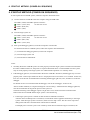
1. This evaluation board/kit or development tool is designed for use for engineering evaluation, demonstration,
or development purposes only. Do not use it for other purpose. It is not intended to meet the requirement of
design for finished product.
2. This evaluation board/kit or development tool is intended for use by an electronics engineer, and it is not the
product for consumer. The user should use this goods properly and safely. Seiko Epson dose not assume any
responsibility and liability of any kind of damage and/or fire coursed by usage of it. User should cease to use
it when any abnormal issue occurs even during proper and safe use.
3. The part used for this evaluation board/kit or development tool is changed without any notice.
NOTICE
No part of this material may be reproduced or duplicated in any form or by any means without the written
permission of Seiko Epson. Seiko Epson reserves the right to make changes to this material without notice.
Seiko Epson does not assume any liability of any kind arising out of any inaccuracies contained in this material
or due to its application or use in any product or circuit and, further, there is no representation that this material is
applicable to products requiring high level reliability, such as, medical products. Moreover, no license to any
intellectual property rights is granted by implication or otherwise, and there is no representation or warranty that
anything made in accordance with this material will be free from any patent or copyright infringement of a third
party. When exporting the products or technology described in this material, you should comply with the
applicable export control laws and regulations and follow the procedures required by such laws and regulations.
You are requested not to use, to resell, to export and/or to otherwise dispose of the products (and any technical
information furnished, if any) for the development and/or manufacture of weapon of mass destruction or for other
military purposes.
All brands or product names mentioned herein are trademarks and/or registered trademarks of their respective
companies.
©SEIKO EPSON CORPORATION 2012, All rights reserved.
Table of Contents
1. GLOSSARY........................................................................................................................................ 1
2. OVERVIEW......................................................................................................................................... 2
2.1
Features...................................................................................................................................... 3
2.2
Operating environment ............................................................................................................... 6
3. COMPONENTS INCLUDED WITH PACKAGE .................................................................................. 7
4. NAME AND FUNCTION OF EACH PART.......................................................................................... 9
4.1
Left-side panel ............................................................................................................................ 9
4.1.1
10-pin connector for connecting to target systems ............................................................ 9
4.1.2
30-pin connector (not provided) for connecting to target systems ..................................... 9
4.1.3
4-pin connector for flash programmer power supply ......................................................... 9
4.1.4
Regarding the monitor pins ............................................................................................. 10
4.2
Right-side panel ........................................................................................................................ 12
4.2.1
DIP switch ....................................................................................................................... 12
4.2.2
RESET/START switch ..................................................................................................... 14
4.2.3
USB connector ................................................................................................................ 14
4.3
Top panel .................................................................................................................................. 15
5. CONNECTION.................................................................................................................................. 18
5.1
Connecting the S5U1C33001H1400 and the host computer .................................................... 18
5.1.1
Connecting the USB Cable.............................................................................................. 18
5.1.2
USB Driver Installation Procedure ................................................................................... 18
5.2
Connecting the target system ................................................................................................... 20
5.3
Connector for flash programmer power supply ......................................................................... 22
5.3.1
Target system reset signal output (TARGET RST OUT).................................................. 22
5.3.2
Target voltage input (TARGET VCC IN)........................................................................... 22
5.3.3
Flash programming voltage output (FLASH VCC OUT) .................................................. 23
6. START-UP METHOD (POWER-ON SEQUENCE) ........................................................................... 24
7. ICD MODE........................................................................................................................................ 26
7.1
ICD mode setting ...................................................................................................................... 26
S1C33 Family In-Circuit Debugger
S5U1C33001H1400 Manual (Rev. 0.20)
EPSON
i
7.2
Invoking ICD mode ................................................................................................................... 26
7.3
Debugger start-up ..................................................................................................................... 27
7.4
Connection test......................................................................................................................... 27
8. FLASH PROGRAMMER MODE ...................................................................................................... 28
8.1
Preparing for flash programming .............................................................................................. 28
8.2
Flash programmer mode operating method.............................................................................. 29
9. FIRMWARE UPDATE PROCEDURE ............................................................................................... 31
10. PRECAUTIONS.............................................................................................................................. 32
10.1 Restrictions on debugging ........................................................................................................ 32
10.1.1
Operation of the internal peripheral circuits ..................................................................... 32
10.1.2
Interrupts when the target program is not running ........................................................... 32
10.1.3
Interrupts when the target program is executed in a single step ..................................... 32
10.1.4
Break functions................................................................................................................ 32
10.1.5
Trace function.................................................................................................................. 33
10.1.6
Counts of the execution counter...................................................................................... 33
10.1.7
Reserved areas in the internal peripheral circuits (C33 STD/Mini core) .......................... 34
10.1.8
Operating clock of the S5U1C33001H (C33 STD/Mini core) ........................................... 34
10.1.9
Area 2 of S1C33xxx (C33 STD/Mini/ADV core)............................................................... 34
10.1.10 Concurrent use of the S5U1C330M2S debug monitor .................................................... 34
10.1.11
Reset sequence .............................................................................................................. 35
10.1.12 Break functions when a reset request is accepted .......................................................... 35
10.1.13 I/O memory dump by the S5U1C33001H ........................................................................ 35
10.1.14 Parameter file .................................................................................................................. 35
10.1.15 Models with cache memory embedded ........................................................................... 36
10.1.16 Models with MMU embedded .......................................................................................... 36
10.2 Differences from the actual IC .................................................................................................. 37
10.2.1
Register initialization ....................................................................................................... 37
10.3 Usage precautions.................................................................................................................... 38
ii
10.3.1
Connecting and disconnecting equipment....................................................................... 38
10.3.2
Powering on/off ............................................................................................................... 38
10.3.3
Connecting the target system.......................................................................................... 38
EPSON
S1C33 Family In-Circuit Debugger
S5U1C33001H1400 Manual (Rev. 0.20)
10.3.4
Operation of the S5U1C33001H system ......................................................................... 38
10.3.5
Wiring between the S1C33xxx chip and target connector ............................................... 39
10.3.6
Reset request .................................................................................................................. 39
10.3.7
Notes on target system power supply.............................................................................. 39
10.3.8
Notes on S5U1C33001H power supply ........................................................................... 40
10.3.9
Core Sync Simple Logic Analyzer Function..................................................................... 40
10.4 Implementation of the PC trace function ................................................................................... 41
10.5 Implementation of the bus trace function .................................................................................. 41
11. TROUBLESHOOTING.................................................................................................................... 42
12. SPECIFICATIONS .......................................................................................................................... 43
S1C33 Family In-Circuit Debugger
S5U1C33001H1400 Manual (Rev. 0.20)
EPSON
iii
1. GLOSSARY
1. GLOSSARY
S5U1C33001H1400 (ICD33V6.0)
ICD mode
Flash programmer mode
This mode is used to debug the target system. Debugging
requires both a PC and the debugger (gdb. exe included in
the S5U1C33001C: C Compiler Package for S1C33
Family).
This mode is used to write programs to the target
system without a PC. Before writing a program to the
target system, you must load the program to the
S5U1C33001H1400 (ICD33V6.0) in ICD mode.
Debugger, gdb.exe (included in the S5U1C33001C: C Compiler Package for S1C33 Family)
Simulator (SIM) mode
ICD6 mode
This mode simulates the execution of the target program on
a PC memory. This mode does not require any other tool.
However, this mode cannot execute ICD-dependent
functions.
This mode performs debugging using the
S5U1C33001H1400 (ICD33V6.0) or ICD board. The
program is executed on the target board. To debug
these products, use this debugger in ICD6 mode.
Target (S1C33xxx)
Normal mode
Debug mode
Ordinary mode in which the target system executes a user
program.
The mode changes to debug mode under the following
conditions:
• When the break condition set by the debugger (gdb.exe)
is met
• When the user presses the Break button on the gdb
screen while the debugger (gdb.exe) is connected
• When a Low level is input to the target system DSIO pin
• When the CPU executes a brk command
In this mode, the target system accepts control by the
debugger (gdb.exe).
This mode permits various debugging operations,
including display and rewriting of data in registers and
memory.
This mode is activated when the S5U1C33001H1400
(ICD33V6.0) is connected and the power-on sequence
is executed.
S1C33 Family In-Circuit Debugger
S5U1C33001H1400 Manual (Rev. 0.20)
EPSON
1
2. OVERVIEW
2. OVERVIEW
The S5U1C33001H1400 (In-Circuit Debugger for the S1C33 Family) is a hardware tool (emulator) that
allows software to be efficiently developed for the S1C33 Family of 32-bit Single-Chip Microcomputers. It
provides a software development environment by communicating with the S1C33xxx chip.
This manual primarily explains how to use the S5U1C33001H1400. For details on the debugger (gdb.exe)
functions and commands, refer to the “Debugger” section in the “S5U1C33001C Manual (C Compiler
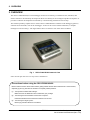
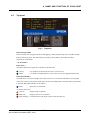
Package for S1C33 Family)”. The figure below shows an external view of the S5U1C33001H.
Fig. 1 S5U1C33001H1400 external view
Note: Do not open the case as it may cause a malfunction.
Precautions before using the S5U1C33001H1400
Please read the sections shown below before getting started with the S5U1C33001H1400. These sections,
especially (2) and (3), describe the answers to frequently asked questions.
(1) “Components Included with Package”
Make sure all of the listed items are included with your package.
(2) “Connecting the S5U1C33001H and the host computer”
Install the USB driver before the S5U1C33001H can be used.
(3) “Connecting the target system”
Please pay particular attention to the Notes.
2
EPSON
S1C33 Family In-Circuit Debugger
S5U1C33001H1400 Manual (Rev. 0.20)
2. OVERVIEW
2.1
Features
• C33 cores supported
C33 STD core
C33 Mini core
C33 PE core
C33 ADV core
• Interface with the host PC
USB 1.1
• Maximum data download speed
About 65KB/s (Approx. 50 KB/s at 20 MHz)*1
• Mode supported by debugger
ICD6 mode
• Program break function
PC break function
Data break function
Forced break function
External forced break function (BRK IN)
Area break function
Bus break function
(logical or physical address is selectable)
Elapsed-time break function
• Trace function
Normal PC trace function / normal bus trace
function
→ (1 Mclk after a go command or 1 Mclk before a
break command can be traced)
→ (Allows selection of logical or physical address
for bus trace)
Area PC trace function / area bus trace function
→ Trace of area between trace trigger 1 and trace
trigger 2 only
→ 1 Mclk can be traced
→ Allows selection of logical or physical address
for bus trace
Bus break trigger trace function
TRC IN pin input signal trace function
User logic signal trace function
• Measurement of the target program execution time
Measurement range of 3 us to 6515 hours
• Single-unit flash programmer function
Provided
• Firmware update function
Provided
• Clock frequency for communications with target system
4 kHz to 120 MHz
S1C33 Family In-Circuit Debugger
S5U1C33001H1400 Manual (Rev. 0.20)
EPSON
3
2. OVERVIEW
• Power supply for flash programmer
Provided (fixed at 7.0 V)
• Reset signal output to target system
Provided
• Supported system I/O voltage
3.3 V, 1.8 V, input voltage (1.0 to 5.0 V) from target
system
• Connector for target system connection
4-pin, 10-pin, 30-pin *2
• Connector for flash programmer power supply 4-pin
*1
Frequency when I/O voltage = 3.3 V. The upper-limit frequency may be lower than the
specification value in certain cases, depending on ambient noise, temperature conditions,
product variations, etc.
*2
The product package does not include a 30-pin cable connector. Please contact us if you need
this cable connector.
4
EPSON
S1C33 Family In-Circuit Debugger
S5U1C33001H1400 Manual (Rev. 0.20)
2. OVERVIEW
Table 1
Model
Function
ICD models and differences
S5U1C33001H
S5U1C33000H
Ver. 3.0
Ver. 4.0
Ver. 4.1
Ver. 6.0
C33 cores supported
C33 STD core
C33 Mini core
C33 STD core
C33 Mini core
C33 PE core *5
C33 STD core
C33 Mini core
C33 PE core
C33 ADV core
C33 STD core
C33 Mini core
C33 PE core
C33 ADV core
Interface with the host PC
Serial and
parallel I/F
USB 1.1
USB 1.1
USB 1.1
Data download speed
(maximum rate: DCLK = 40 MHz)
Serial I/F:
Approx. 8KB/s
Parallel I/F:
Approx. 30KB/s
About 65KB/s
(About 50KB/s
at 20 MHz)
About 65KB/s
(About 50KB/s at
20 MHz) *1
About 65KB/s
(About 50KB/s at
20 MHz) *1
Clock frequency to communicate with
the target
1 MHz to 40
MHz
1 MHz to 40
MHz
1 MHz to 40 MHz
*3
4 MHz to 40 MHz
Core clock frequency for using the
trace function
1 MHz to 60
MHz (3.3 V) *1
(10-pin cable)
1 MHz to 60
MHz (3.3 V)
(10-pin cable)
1 MHz to 120 MHz
(3.3 V)
*2, *3 (10-pin
cable, or 30-pin
coaxial cable)
4 MHz to 120 MHz
(3.3 V)
*2, *3, *6 (10-pin
cable, or 30-pin
coaxial cable)
Maximum trace capacity
128K clock
cycles
1M clock cycles
1M clock cycles
1M clock cycles
Single-unit flash programmer
function
-
Available
Available
Available
Firmware update function
-
-
Available
Available
Mode supported by debugger
ICD2 mode
ICD3 mode
ICD3 mode
ICD6 mode
Bus trace function
-
-
Available
Available *6
Bus break trigger trace function
-
-
Available
Available *6
TRC IN pin input signal trace
function
-
-
Available
Available
User logic signal trace function *4
-
-
Available
Available
Target reset signal output
-
-
Available
Available
Target system I/O interface voltage
3.3 V
3.3 V
3.3 V and 1.8 V
3.3 V and 1.8 V, or
input voltage (1.0 to
5.0 V) from target
system
RESET/START switch
-
Available
Available
Available
DIP switch
4 bits
8 bits
8 bits
10 bits
LEDs for flash programmer
-
Available
Available
Available
Target system interface connector
10 pins
10 pins
10 pins, 30 pins
10 pins, 30 pins *6
Target system interface method
4 pins, 10 pins
4 pins, 10 pins
4 pins, 10 pins,
30 pins
4 pins, 10 pins, 30
pins *6
Target power supply connector
-
-
6 pins
-
Connector for flash programmer
power supply
-
-
-
4 pins
*1
*2
Indicates the frequency range for 3.3-V I/O. The upper-limit frequency may be lowered by environment noise,
temperature condition, S1C33 model, unevenness in quality, etc.
Note: In the model with the C33 STD or Mini core embedded, the maximum CPU core clock frequency is 60 MHz but
the maximum BCU (bus) clock frequency is 40 MHz. When operating the CPU with a clock higher than 40 MHz, the
BCU clock must be setup to 1/2 CPU core clock (#X2SPD = 0).
The maximum frequency may be half or less of the described value when the I/O voltage is 1.8 V.
S1C33 Family In-Circuit Debugger
S5U1C33001H1400 Manual (Rev. 0.20)
EPSON
5
2. OVERVIEW
*3
*4
*5
*6
Supports 32 kHz by firmware update.
Available only when the S1C33 model that supports the user logic signal trace function is used.
Supports by firmware update.
The product does not include a 30-pin cable for connecting to target systems or a connector for this cable. Please
contact us if you need a 30-pin cable.
Table 2
Correspondence between C33 cores and debug functions
Core
C33 STDMini
Function
C33 PE
C33 ADV
DCLK while the program is halted
= Bus clock
= Core clock x set value
= Core clock x set value
DCLK while the program is being
executed
= Core clock
= Core clock
= Core clock
PC trace method
Level 1
Level 1
Level 2
Switching the DCLK-core clock
ratio
(DCLK while the program is
halted)
-
{
{
Address setup for the debug unit
-
{
-
Area break function
-
-
{
Bus break function
-
-
{
Bus break trigger trace function
-
-
{
TRC IN pin input signal trace
function
-
-
{
User logic signal trace function *7
-
-
{
Use of MMU in debug mode
-
-
{
*7
Available only in S1C33 models that support the user logic signal trace function.
Except for the PC trace, Level 2 is upwardly compatible with Level 1 and realizes higher analytical accuracy than Level 1.
Functions not listed in the above table can be used regardless of the core model.
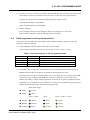
2.2
Operating environment
As the host computer, the S5U1C33001H1400 uses a PC with a USB port (USB 1.1) available.
Windows 2000 or Windows XP is recommended for the OS.
6
EPSON
S1C33 Family In-Circuit Debugger
S5U1C33001H1400 Manual (Rev. 0.20)
3. COMPONENTS INCLUDED WITH PACKAGE
3. COMPONENTS INCLUDED WITH PACKAGE
The following shows the components included with the package:
(1) S5U1C33001H1400 (main unit) .................................................................................................................1
(2) USB cable (mini B).....................................................................................................................................1
(3) Target system interface cable (10-4 pin).....................................................................................................1
(4) Target system interface cable (10-10 pin)...................................................................................................1
(5) Target system power supply cable (4-4 pin) ...............................................................................................1
(6) Target system interface connectors (10-pin)...............................................................................................1
(7) Target system interface connectors (4-pin).................................................................................................1
(8) Target system power supply connectors (4-pin) .........................................................................................1
(9) User registration card ............................................................................................ English/Japanese, 1 each
(10) Warranty card........................................................................................................ English/Japanese, 1 each
(11) Usage precautions ................................................................................................. English/Japanese, 1 each
(12) Manual download guide........................................................................................ English/Japanese, 1 each
The items specified below are not included with the package. These items must be prepared separately.
(13) S5U1C33001H1400 User Manual (ICD33V6.0)
(PDF is downloadable from this PDF document and the SEIKO EPSON HP)
(14) Debugger (gdb.exe) for the S1C33 Family (included in the S1C33 Family C Compiler Package)
(15) Debugger manual for the S1C33 Family (included in the S1C33 Family C Compiler Package)
S1C33 Family In-Circuit Debugger
S5U1C33001H1400 Manual (Rev. 0.20)
EPSON
7
3. COMPONENTS INCLUDED WITH PACKAGE
Fig. 2
8
Package components
EPSON
S1C33 Family In-Circuit Debugger
S5U1C33001H1400 Manual (Rev. 0.20)
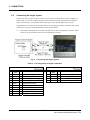
4. NAME AND FUNCTION OF EACH PART
4. NAME AND FUNCTION OF EACH PART
The following shows an external view of the S5U1C33001H1400’s operating section and the name of each part.
4.1
Left-side panel
Fig. 3
4.1.1
Left-side panel
10-pin connector for connecting to target systems
This connector is used to connect to the target system using a 10-pin cable or 10-pin-4-pin cable.
4.1.2
30-pin connector (not provided) for connecting to target systems
This connector is used to connect to the target system using a 30-pin cable.
Note: This connector is not provided with the debugger unit. Please contact us if you need
this cable.
Note: Only one of the 10-pin connector for connecting to target systems and 30-pin
connector for connecting to target systems may be used at any given time.
4.1.3
4-pin connector for flash programmer power supply
This connector is used to output a reset signal to the target system or to supply power
(note) for flash programming. When the interface for debug signals requires a voltage level
for the target system, this connector is used to input the operating voltage from the target
system. For information on the connector pin configuration and connection method, refer
to “Connector for flash programmer power supply.”
Note: The S5U1C1700H incorporates a 7-V, 200-mA power supply for flash programming.
However, use of this power supply may not be possible with certain S1C processors.
If the technical manual for the target S1C processor does not specifically mention
this power supply, damage may occur in the chip due to overvoltage. To prevent this
problem, avoid using this voltage (do not set the DIP SW8 to ON) if this voltage is
not supported by the target S1C processor. Keep this pin open when implementing a
connection terminal on the target board.
S1C33 Family In-Circuit Debugger
S5U1C33001H1400 Manual (Rev. 0.20)
EPSON
9
4. NAME AND FUNCTION OF EACH PART
4.1.4
Regarding the monitor pins
• GND pin (black (left side in the above diagram))
To monitor the signals output from the above pins, connect the GND of a measuring
instrument such as an oscilloscope to this pin. If the ground level between the
S5U1C33001H and the target system is unstable (particularly when the 4-pin cable is
used), this pin can be used to stabilize the ground level.
• BRK IN pin (red)
If a low-level signal is input to this pin when the target program is being executed, the
target program execution is suspended. After a low level is input to the BRK IN
terminal, a break will occur after a few instructions have been executed.
• TRC IN pin (white)
This pin inputs an external trace signal. The input signal can also be traced when the
bus trace is performed.
• TRG OUT pin (light blue)
The TRG OUT pin outputs trace trigger signals indicating the start and end of the trace.
To perform an area trace with the S5U1C33001H, set two trigger points: the start
address and end address of the trace area. When the execution address of the program
corresponds to the set trace trigger point, the TRG OUT pin outputs a High-level signal.
It also outputs a High-level signal when target program execution is suspended. For a
discussion of how to set the trace function, see the “Debugger” section in the
S5U1C33001C Manual (C Compiler Package for S1C33 Family). The output timing is
shown below. To generate trace trigger signals, you must run the program for trace
trigger point 1 and point 2, in that order. Shown below are states in which trace triggers
are and are not generated.
10
EPSON
S1C33 Family In-Circuit Debugger
S5U1C33001H1400 Manual (Rev. 0.20)
4. NAME AND FUNCTION OF EACH PART
Fig. 4
Examples of TRG OUT output timing
• EMUOUT pin (green)
This pin outputs a low level when the EMU/ERASE LED is lit (that is, when the
program is being executed) and outputs the 5 V level when that LCD is off (during a
break). This signal can be used as the protect signal for the S5U1C33xxxM emulation
memory.
• TRCFULL pin (blue (right side in the above diagram))
This is the trace full state output pin. This pin outputs a high level when the trace
memory becomes full.
S1C33 Family In-Circuit Debugger
S5U1C33001H1400 Manual (Rev. 0.20)
EPSON
11
4. NAME AND FUNCTION OF EACH PART
4.2
Right-side panel
Fig. 5
4.2.1
Right-side panel
DIP switch
Note: After operating the DIP switches, press the RESET/START switch to apply the
settings.
• Selecting target CPU core (SW1)
Table 3-1
DIP SW1 setting
SW1
Setting
OPEN
C33
ON
C17 (Not supported)
• Selecting ICD mode/flash programmer mode (SW2, SW3)
Table 3-2
SW2
OPEN
DIP SW2 and SW3 settings
SW3
Setting
OPEN
ICD mode
ON
OPEN
Flash programmer mode Erase → Write
OPEN
ON
Flash programmer mode Verify
ON
ON
Flash mode
Erase → Write → Verify
ICD mode:
Mode for executing the debug command from the debugger in a PC (see the relevant section)
Flash programmer mode: Mode for operating the S5U1C33001H independently as a flash programmer (see relevant section)
12
EPSON
S1C33 Family In-Circuit Debugger
S5U1C33001H1400 Manual (Rev. 0.20)
4. NAME AND FUNCTION OF EACH PART
• Selecting DSIO signal (SW4, SW5)
Table 3-3
SW4
DIP SW4 and SW5 settings
SW5
Setting
OPEN
OPEN
3.3 V (default)
OPEN
ON
1.8 V
ON
OPEN
Target system input voltage (1.0 to 5.0 V)
ON
ON
Target system input voltage (1.0 to 5.0 V)
Target system operating voltage applied to Pin No. 4 of the connector for flash programmer power supply.
• Selecting connection test (SW6)
Table 3-4
DIP SW6 setting
SW6
Setting
OPEN
Connection test disabled (default)
ON
Connection test enabled
Connection test: A communication check test is performed at the time of debugger invocation.
• Selecting firmware update mode (SW7)
Table 3-5
DIP SW7 setting
SW7
Setting
OPEN
Off (default)
ON
On
Turning this DIP switch ON enables connections between the S5U1C33001H and debugger without a target system. For
a discussion of how to update the firmware, refer to “Firmware Update.”
• Selecting flash programming voltage output (SW8)
Table 3-6
DIP SW8 setting
SW8
Setting
OPEN
Off
ON
On
Note:
The S5U1C1700H incorporates a 7-V, 200-mA power supply for flash programming. However, use of this power
supply may not be possible with certain S1C processors. If the technical manual for the target S1C processor
does not specifically mention this power supply, damage may occur in the chip due to overvoltage. To prevent this
problem, avoid using this voltage (do not set the DIP SW8 to ON) if this voltage is not supported by the target S1C
processor.
S1C33 Family In-Circuit Debugger
S5U1C33001H1400 Manual (Rev. 0.20)
EPSON
13
4. NAME AND FUNCTION OF EACH PART
• Selecting trace (SW9)
Table 3-7
DIP SW9 setting
SW9
Setting
OPEN
Trace disabled
ON
Trace enabled
• Option setting (SW10)
Table 3-8
DIP SW10 setting
SW10
Setting
OPEN
Unused
ON
Unused
4.2.2
RESET/START switch
< In ICD mode >
Pressing the RESET/START switch restarts the firmware and establishes an initial
connection with the target S1C processor. If the target board is not connected, the firmware
awaits the initial connection. If the TARGET RST OUTPUT signal from the
S5U1C33001H reaches the target board, a reset signal is also output.
< In flash programmer mode >
Pressing the RESET/START switch invokes the selected flash operation function (erase,
write, verify). If the LED indicates OK/ERR, the state immediately before the execution of
the function will be restored.
Note: After operating the DIP switches, press the RESET/START switch to apply the
settings (in ICD mode or flash programmer mode).
4.2.3
USB connector
This connector is used to connect a PC using the USB cable.
Note: A USB hub that runs solely on bus power may not provide adequate power in all
cases. To supply voltage for flash programming to the target system in flash
programmer mode, connect directly to the USB port of the PC or use an AC adaptor
(USB 5-V output) to supply power to the USB cable.
14
EPSON
S1C33 Family In-Circuit Debugger
S5U1C33001H1400 Manual (Rev. 0.20)
4. NAME AND FUNCTION OF EACH PART
4.3
Top panel
Fig. 6
Top panel
LED1 through LED4
The four LEDs on the top panel show the debugging or flash programming status of LED1 through
LED4 on the front panel. The information provided by these LEDs in ICD mode and flash
programmer mode differs.
< In ICD mode >
LED1 (CPU)
This LED indicates the target CPU selected by the DIP SW1.
(Green)
C33: Product incorporating S1C33xxx or S1C33 core
(Blue)
C17: Product incorporating S1C17xxx or S1C17 core (not supported at this time)
LED2 (ICD MODE)
This LED emits a constant red light if the target system is not connected and flashes red if a proper
connection cannot be achieved with the target system. The LED signals continuous blue if ICD mode
is selected (DIP SW2 and SW3 set to OPEN).
(Blue)
Operations in ICD mode
(In initial connection)
(Yellow)
USB is being recognized
(Red, ON)
Target system is not connected
(Red, flashing) Communication with target system cannot be achieved
S1C33 Family In-Circuit Debugger
S5U1C33001H1400 Manual (Rev. 0.20)
EPSON
15
4. NAME AND FUNCTION OF EACH PART
LED3 (EMU)
If ICD mode is selected (DIP SW2 and SW3 set to OPEN), this LED emits a constant red light when
the debugger issues a command to execute the target program, indicating that the target system is
executing the target program. It also lights up when power for the target system is turned off or no
target system is connected. In this case, turning on the power for the target system or properly
Connecting the target system and pressing the RESET/START switch will turn off the LED. If the
LED emits a constant green light, the target processor is in the debug mode.
(Red)
Power for the target system is turned off (except for initial connection)
Target system is not connected (except for initial connection)
Target system is running a user program
(Green)
Target S1C processor is in debug mode
(OFF)
Other
LED4 (TRC)
This LED will emit a constant light blue light when ICD mode is selected (DIP SW2 and SW3 set to
OPEN).
(OFF)
Trace OFF
(Light blue)
Trace ON
(Yellow)
Trace ON (memory full)
Note: With firmware Ver 1.0, this LED will emit a constant light blue light even when the trace
function is disabled. This issue is scheduled to be corrected in the next firmware update.
< In flash programmer mode >
LED1 (CPU)
This LED indicates the target CPU selected by the DIP SW1.
(Green)
C33: Product incorporating S1C33xxx or S1C33 core
(Blue)
C17: Product incorporating S1C17xxx or S1C17 core (not supported at this time)
LED2 (ERASE)
This LED indicates the flash memory erase condition.
(White)
Flash memory erase is selected
(White, flashing) Data in the flash memory is being erased
(Green)
Flash memory erase has been successfully completed (OK)
(Red)
Flash memory erase error (ERR)
(In initial connection)
16
(Red, ON)
Target system is not connected
(Red, flashing)
Communication with target system cannot be achieved
EPSON
S1C33 Family In-Circuit Debugger
S5U1C33001H1400 Manual (Rev. 0.20)
4. NAME AND FUNCTION OF EACH PART
LED3 (WRITE)
This LED indicates the flash memory write condition.
(Purple)
Flash memory write is selected
(Purple, flashing)
Flash memory is being written
(Green)
Flash memory write has been successfully completed (OK)
(Red)
Flash memory write error (ERR)
LED3 (VERIFY)
This LED indicates the flash memory verify condition.
(Yellow)
Flash memory verify is selected
(Yellow, flashing)
Flash memory is being verified
(Green)
Flash memory verify has been successfully completed (OK)
(Red)
Flash memory verify error (ERR)
S1C33 Family In-Circuit Debugger
S5U1C33001H1400 Manual (Rev. 0.20)
EPSON
17
5. CONNECTION
5. CONNECTION
5.1
Connecting the S5U1C33001H1400 and the host computer
5.1.1
Connecting the USB Cable
The connectors at each end of the USB cable are type A (for the host computer) and Mini
B type (for the S5U1C33001H). Turn on the S5U1C33001H power and connect the USB
cable to the host computer. The host computer will request that the USB driver be installed.
Use the procedure described in the next section to install the USB driver.
Note: The USB driver is located in the directory in which the S5U1C33001C (S1C33
Family C Compiler Package) is installed:
C:\EPSON\gnu33\utility\drv_usb\Icd33v60.
Fig. 7
5.1.2
Connecting the USB cable
USB Driver Installation Procedure
(1) When the USB cable is first connected to the host computer, the hardware wizard will
be displayed.
(2) Install the USB driver by following the directions displayed by the wizard.
Specify “C:\EPSON\gnu33\utility\drv_usb\Icd33v60” as the USB driver directory.
The device manager will be displayed as shown below when the USB driver has been
installed correctly.
Note: When using the S5U1C33001H1400 (ICD33V6.0), use the following C compiler
package: GNU33V3.1.1 (Product No. not assigned), GNU33V3.2.0
(S5U1C33001C1300) or a later C Compiler Package.
18
EPSON
S1C33 Family In-Circuit Debugger
S5U1C33001H1400 Manual (Rev. 0.20)
5. CONNECTION
The device manager will be displayed as shown below when the USB driver has been
installed correctly.
Note: If the window above is not displayed correctly, reinstall the USB driver.
S1C33 Family In-Circuit Debugger
S5U1C33001H1400 Manual (Rev. 0.20)
EPSON
19
5. CONNECTION
5.2
Connecting the target system
Connect the target system, using the 10-pin or 4-pin cable provided with the S5U1C33001H or a
30-pin cable.(*1) Use the 10-pin-type/4-pin-type connector provided with the S5U1C33001H, a
30-pin connector[*1], or equivalent on the target system side. See the tables below for pin
configurations for connectors on the target side. For each signal pin number of the S1C33xxx chip,
refer to the “S1C33xxx Technical Manual” of the specific model.
*1:
The product package does not include a 30-pin cable or the corresponding connector. Please
contact us if you need this cable or the corresponding connector.
Fig. 8
Table 4
Connecting the target system
Pin assignment of target connectors
10-pin connector
No.
Pin
name
4-pin connector
I/O
Pin function
No.
Pin
name
I/O
Pin function
1
DCLK
I
Clock for debugging
1
DCLK
I
Clock for debugging
2
GND
-
Power supply (GND)
2
GND
-
Power supply (GND)
3
DSIO
I/O
Serial I/O signal for debugging
3
DSIO
I/O
4
GND
-
Power supply (GND)
4
DST2
I
5
DST2
I
Debug status 2 signal
6
GND
-
Power supply (GND)
7
DST1
I
Debug status 1 signal
8
GND
-
Power supply (GND)
9
DST0
I
Debug status 0 signal
10
DPCO
I
PC signal
20
EPSON
Serial I/O signal for debugging
Debug status 2 signal
S1C33 Family In-Circuit Debugger
S5U1C33001H1400 Manual (Rev. 0.20)
5. CONNECTION
30-pin connector
No.
Pin
name
I/O
Pin function
No.
Pin
name
I/O
Pin function
1
GND
-
Power supply (GND)
16
DST2
I
Bus trace status 2 signal
2
DCLK
I
Clock for debugging
17
DTS1
I
Bus trace status 1 signal
3
GND
-
4
DSIO
I/O
5
GND
-
Power supply (GND)
18
DTS0
I
Bus trace status 0 signal
Serial I/O signal for debugging
19
GND
-
Power supply (GND)
Power supply (GND)
20
DTD7
I
Bus trace data 7 signal
6
DST2
I
Debug status 2 signal
21
DTD6
I
Bus trace data 6 signal
7
GND
-
Power supply (GND)
22
DTD5
I
Bus trace data 5 signal
8
DST1
I
Debug status 1 signal
23
DTD4
I
Bus trace data 4 signal
9
GND
-
Power supply (GND)
24
GND
-
Power supply (GND)
10
DST0
I
Debug status 0 signal
25
DTD3
I
Bus trace data 3 signal
11
GND
-
Power supply (GND)
26
DTD2
I
Bus trace data 2 signal
12
DPCO
I
PC signal
27
DTD1
I
Bus trace data 1 signal
13
GND
-
Power supply (GND)
28
DTD0
I
Bus trace data 0 signal
14
DTS4
I
Bus trace status 4 signal
29
GND
-
Power supply (GND)
15
DTS3
I
Bus trace status 3 signal
30
DBT
I
Bus break trigger signal
Notes:
• The signals connected to the S5U1C33001H are very high-speed signals, so the target connector must be mounted
within 5 cm from the S1C33xxx. If there is more distance between the connector and the S1C33xxx chip, the
S5U1C33001H may not work properly.
• A 33 Ω resistor must be connected in series to the DSIO signal line between the connector and the S1C33xxx chip.
The resistor should be placed as close to the S1C33xxx as possible.
• Be sure to use the supplied 10-pin or 4-pin, or 30-pin cable for Connecting the target system to the S5U1C33001H.
Using another cable may cause a malfunction. Furthermore, do not use the 30-pin cable and 10-pin or 4-pin cable
simultaneously.
• Disable the trace function of the S5U1C33001H using DIP switch 4 in the following cases:
- when using the 4-pin cable and connector.
- when the signals (DST0, DST1, DPCO) necessary for tracing are not connected even if the 30-pin or 10-pin cable
and connector is used.
- when the trace function is not used due to some reason even if the 30-pin or 10-pin cable and connector is used
and all the signals are connected.
• The 4-pin connector does not have a projection for preventing reverse insertion. Check the cable marker of pin 1 to be
sure the insertion of connector is proper when connecting it to the target system.
• The product package does not include a 30-pin cable or the corresponding connector. Please contact us if you need
this cable or the corresponding connector.
Fig. 9
Connecting with 4-pin connectors
S1C33 Family In-Circuit Debugger
S5U1C33001H1400 Manual (Rev. 0.20)
EPSON
21
5. CONNECTION
5.3
Connector for flash programmer power supply
This connector is used to output reset signals to the target system, to output voltage for flash
programming, and to input target interface voltage. Debugging is possible without connecting these
signals. If necessary, use the cable for flash programmer power supply provided with the
S5U1C33001H to connect the target system. The pin assignment of the 4-pin connector (white) of the
S5U1C33001H is shown in the table below.
Table 5
Pin assignment of the flash programmer power supply connector (white)
No.
Pin name
I/O
Pin function
1
FLASH VCC OUT
O
Flash programming voltage output
2
GND
-
Power supply (GND)
3
TARGET RST OUT
O
Target system reset signal output
4
TARGET VCC IN
I
Target system voltage input
* Note the sequence of Pin Nos. (This sequence is reversed in the connector for connecting to target
systems.)
5.3.1
Target system reset signal output (TARGET RST OUT)
Pressing the RESET/START switch outputs a reset signal from the TARGET RST OUT
pin to the target system.
The following circuit structure is recommended to use this reset output.
Fig. 10
Example of reset circuit
Note: High (voltage level set by DIP SW4, SW5) or Low (GND level) is output as a target
reset signal.
5.3.2
Target voltage input (TARGET VCC IN)
In addition to 3.3 V and 1.8 V, the voltage (1.0 to 5.0 V) input from the target system can
be used as an interface for the target system. To use this function, set the DIP SW4 to ON
and apply a voltage from the target system to the TARGET VCC IN pin.
22
EPSON
S1C33 Family In-Circuit Debugger
S5U1C33001H1400 Manual (Rev. 0.20)
5. CONNECTION
5.3.3
Flash programming voltage output (FLASH VCC OUT)
Some target S1C processors have internal flash memory that can supply the voltage (7 V)
necessary for flash programming from the S5U1C33001H. The maximum current that can
be provided in this way is 200 mA.
To use this output, set the DIP SW8 to ON and connect the power supply from the target
system to the FLASH VCC OUT pin. Note that setting the DIPS SW8 to ON results in a
constant output of 7 V from the FLASH VCC OUT pin regardless of the operation of the
RESET/START switch.
Note: Refer to the relevant technical manual to determine if the target S1C processor can
use this output. (To prevent overvoltage-induced damage to the S1C processor, avoid
using this output if no applicable instructions are provided in the technical manual.)
S1C33 Family In-Circuit Debugger
S5U1C33001H1400 Manual (Rev. 0.20)
EPSON
23
6. START-UP METHOD (POWER-ON SEQUENCE)
6. START-UP METHOD (POWER-ON SEQUENCE)
To start up the S5U1C33001H system, follow the sequence described below:
(1) Connect the S5U1C33001H to the host computer using the USB cable.
The LED1, LED2, and LED3 operate as follows:
LED1 (Green, ON)
* In the case of C33
LED2 (Red, ON)
LED3 (OFF)
(2) Turn the target system on.
The LED1, LED2, and LED3 operate as follows:
LED1 (Green, ON)
* In the case of C33
LED2 (Blue, ON)
LED3 (Green, ON)
(3) Start up the debugger (gdb.exe) on the host computer in ICD mode.
To terminate the S5U1C33001H system, follow the sequence described below:
(1’) Terminate the debugger (gdb.exe) on the host computer.
(2’) Turn the target system off.
(3’) Turn the S5U1C33001H off.
Notes:
• Normally the S5U1C33001H system can work properly when the target system is turned on first and then
the S5U1C33001H. However, the power-on sequence described above is recommended since the system
may not work properly if the target system is in indeterminate operation or in runaway status.
• If the debugger (gdb.exe) is terminated after the S5U1C33001H is turned off, the debugger may not work
properly with “Cannot open ICD33 usb driver.” displayed on the screen when it is re-invoked. In this case,
turn on or reset the S5U1C33001H after terminating the debugger (gdb.exe) once, and then re-invoke the
debugger.
For details on how to invoke/terminate the debugger, refer to the “Debugger” section in the
“S5U1C33001C Manual (C Compiler Package for S1C33 Family)”. Furthermore the debugger (gdb.exe)
must be invoked after turning all the power of the system on.
Check the following if the debugger reports a target down error, which means that communication
between the S5U1C33001H and the target system is not functioning.
• If the target system power is turned on after the S5U1C33001H is turned on:
After the S5U1C33001H power is turned on, a forced break will be applied continuously to the target
system. After the target system is turned on, the S1C33xxx chip is reset. The S1C33xxx chip enters
debug mode and starts communication with the S5U1C33001H.
If multiple power on/reset cycles occur caused by switch bounce when the target is turned on, the
24
EPSON
S1C33 Family In-Circuit Debugger
S5U1C33001H1400 Manual (Rev. 0.20)
6. START-UP METHOD (POWER-ON SEQUENCE)
communication between the S5U1C33001H and the target system may be disconnected after the
second reset.
Design the target system so that switch bounce does not occur and the system starts up only once.
Furthermore, if the reset is applied with either the power or the oscillator in an unstable state (for
example, if the reset is applied within the first few ms after the power is turned on), the S1C33xxx
chip operation will also be unstable. In this case the system will not enter debug mode and
communication between the S5U1C33001H and the target system will not be possible. Apply the reset
only after an adequate stabilization time has elapsed.
Refer to the “S1C33xxx Technical Manual” for more information on the reset operation.
• If the S5U1C33001H is turned on after the target system power is turned on:
When the S5U1C33001H is turned on, it issues a forcible break to the free-running target system. The
S1C33xxx chip enters debug mode and starts communication with the S5U1C33001H. If a boot
program was not loaded into ROM, the S1C33xxx chip cannot respond to the forced break since the
S1C33xxx chip is in the runaway state, so communication is impossible. Load a boot program that
operates correctly into boot ROM so that the target system will not be in the runaway state.
• If the initial connection operation fails
In this case, add a reset switch to the target system and start the system in the following sequence:
(1) Turn the target system on
(2) Hold down the reset switch on the target system and turn the S5U1C33001H on
(3) Release the reset switch to clear the reset state.
This will allow the system to operate reliably. This is because this sequence reliably reproduces the
conditions in the “If the S5U1C33001H is turned on after the target system power is turned on” item
above. If it is not possible to connect, install a reset switch on the target system.
We recommend adding the reset switch at the system design stage.
• RESET/WRITE switch on the S5U1C33001H
Besides turning power on and off, the S5U1C33001H can be reset using the on-board RESET/WRITE
switch.
Also the RESET/WRITE switch changes the signal output from the TARGET_RESET pin in the
target system power supply connector (see next section).
S1C33 Family In-Circuit Debugger
S5U1C33001H1400 Manual (Rev. 0.20)
EPSON
25
7. ICD MODE
7. ICD MODE
ICD mode is used to debug the target system by connecting the debugger (dbg.exe) on the PC to the target
system. Described below are the settings for launching the S5U1C33001H in ICD mode and corresponding
procedures.
7.1
ICD mode setting
To launch the S5U1C33001H in ICD mode, set the DIP switches as follows:
SW2 = OPEN
SW3 = OPEN
7.2
Invoking ICD mode
After Connecting the target system to the host computer, start the S5U1C33001H as described below.
Starting the S5U1C33001H by a different procedure may not result in a successful connection.
< When TARGET RST_OUT signal is not connected >
If the TARGET RST OUT signal is not connected to reset the target system, follow the start-up
procedure described below.
(1) Press the S5U1C33001H RESET/START switch.
LED1 (Green, ON)
* In the case of C33
LED2 (Red, flashing)
LED3 (OFF)
LED4 (OFF)
(2) Press the target system RESET switch.
LED1 (Green, ON)
* In the case of C33
LED2 (Blue, ON)
LED3 (Green, ON)
LED4 (OFF)
*1
If the LEDs do not light as described above, there may be a problem with the connection. Repeat the
procedure from step (1).
*1:
With firmware Ver 1.0, LED4 will emit a constant light blue light in step (2), even when the
trace function is disabled. This issue is scheduled to be corrected in the next firmware update.
26
EPSON
S1C33 Family In-Circuit Debugger
S5U1C33001H1400 Manual (Rev. 0.20)
7. ICD MODE
< When TARGET RST_OUT signal is connected >
If the TARGET RST OUT signal is connected to reset the target system, the S5U1C33001H
automatically generates signals according to the connection procedure. You need only to press the
S5U1C33001H RESET/START switch to start the S5U1C33001H.
(1) Press the S5U1C33001H RESET/START switch.
LED1 (Green, ON)
* In the case of C33
LED2 (Blue, ON)
LED3 (Green, ON)
LED4 (OFF)
*1
With the LEDs in the status described above, repeat the procedure from step (1).
*1:
With firmware Ver 1.0, LED4 will emit a constant light blue light in step (2), even when the
trace function is disabled. This issue is scheduled to be corrected in the next firmware update.
7.3
Debugger start-up
After the aforementioned operation results in a proper connection between the S5U1C33001H and
the target S1C processor, run the debugger (gdb.exe) on the PC.
To connect to the S5U1C33001H and start debugging, you must specify ICD mode using the target
command.
(gdb) target icd6 usb
For a discussion of the debug command and how to use the debugger, refer to the S5U1C33001C
Manual (C Compiler Package for S1C33 Family).
Note: Close the debugger before disconnecting the S5U1C33001H from the host computer.
7.4
Connection test
The S5U1C33001H can run diagnostics to confirm proper communication with the target system at
the time the debugger (gdb.exe) is launched. If proper start-up is not possible by this method,
perform a connection test. Use the DIP SW6 to enable or disable this function.
Skipping the connection test (default)
If the DIP SW6 is set to OPEN, the S5U1C33001H skips connection diagnostics when connecting to
the target system at the time the debugger is launched.
Execution of connection test
If the DIP SW6 is set to ON, the S5U1C33001H runs the connection diagnostics of the connection to
the target system at the time the debugger is launched.
S1C33 Family In-Circuit Debugger
S5U1C33001H1400 Manual (Rev. 0.20)
EPSON
27
8. FLASH PROGRAMMER MODE
8. FLASH PROGRAMMER MODE
Flash programmer mode lets the S5U1C33001H function as a flash programmer. Described below are
preparations for starting up the S5U1C33001H in flash programmer mode and associated procedures.
8.1
Preparing for flash programming
The S5U1C33001H can write data, such as a program downloaded to internal flash memory, directly
to the flash memory of the target system.
As described below, start by downloading to the S5U1C33001H the data you want to write to the
target system’s flash memory.
(1) Convert the file to be written to the target system flash memory to a Motorola S3 file.
Use objcopy.exe (included in the C Compiler Package for S1C33 Family) to perform this file
conversion.
Example:
1. Converting sample.elf to Motorola S3 file
>objcopy -O srec -R .gbss --srec-forceS3 sample.elf sample.sa
2. Fill the empty addresses in sample.sa with 0xff and produce sample.saf.
(When the fill start address is 0x600000 and the target block size is 0x1000)
>moto2ff 0x600000 1000 sample.sa
(2) Launch the S5U1C33001H in ICD mode.
(3) Launch the debugger.
1. Launching GDB
>gdb
2. Connecting the target system
(gdb) target icd6 usb
(4) Delete any unnecessary programs or data in the S5U1C33001H with the c33 fwe command.
(5) Use the c33 fwlp command to download the flash erase/write program to the S5U1C33001H.
Example: Downloading data erase/write program file, writer.sa
(when the erase routine start address is 0x14c and the write routine start address is 0x180)
(gdb) c33 fwlp writer.sa 0x14c 0x180
28
EPSON
S1C33 Family In-Circuit Debugger
S5U1C33001H1400 Manual (Rev. 0.20)
8. FLASH PROGRAMMER MODE
(6) Use the c33 fwld (or c33 fwdc) command to download the data to be written to the target system
flash memory to the S5U1C33001H. At the same time, set the erase area in flash memory.
Example: Erasing all sectors and downloading sample.saf to flash memory
(when flash start address is 0x600000)
(gdb) c33 fwld sample.saf 0 0 0x600000
(7) End the debugger.
For an in depth discussion of the debugger (dbg.exe) and objcopy.exe, refer to the
S5U1C33001C Manual (C Compiler Package for S1C33 Family).
8.2
Flash programmer mode operating method
Given below is the procedure for launching the S5U1C33001H in flash programmer mode and
performing flash programming.
(1) Set the DIP SW2 and SW3 based on the work to be performed.
You can select flash erase and write only, verify only, or erase → write → verify.
Table 6
SW2
DIP switch settings in flash programmer mode
SW3
Setting
OPEN (↑)
OPEN (↑)
ICD mode (default)
ON (↓)
OPEN (↑)
Flash programmer mode Erase → Write
OPEN (↑)
ON (↓)
Flash programmer mode Verify
ON (↓)
ON (↓)
Flash programmer mode Erase → Write → Verify
(2) If the DIP switch settings were changed while power was being supplied via USB, press the
RESET/START switch to set the S5U1C33001H to flash programmer mode.
If the DIP switch settings are changed when power is off, supply power by connecting the USB
cable for the S5U1C33001H to the USB port of the host computer or by connecting an AC
adaptor with USB 5-V output. (Flash programmer mode will run on power supplied through the
USB cable. No communication occurs with the PC.) If the S5U1C33001H starts up properly, the
LEDs will light up according to the selected operating mode.
With power supply
z LED1
(Green)
z LED2
(Red)
Erase → Write
Verify
Erase → Write → Verify
z ERASE
(White)
(OFF)
(White)
z WRITE
(Purple)
(OFF)
(Purple)
z VERIFY
(OFF)
(Yellow)
(Yellow)
S1C33 Family In-Circuit Debugger
S5U1C33001H1400 Manual (Rev. 0.20)
EPSON
29
8. FLASH PROGRAMMER MODE
(3) Connect the target system to the S5U1C33001H for flash programming.
(4) Press the RESET/START switch.
The S5U1C33001H executes the selected flash operation.
The operation currently underway is indicated by the flashing LED.
Erase
z ERASE
Write
Verify
−
−
(White, flashing)
z WRITE
−
z VERIFY
−
−
(Purple, flashing)
(Yellow, flashing)
-
(5) After the flash operation is completed, the following LED lights up to indicate successful
completion of the operation or the generation of an error.
Operation completed successfully
Erase completed
Write completed
Verify completed
(Green)
−
−
z ERASE
z WRITE
−
−
z VERIFY
−
(Green)
−
(Green)
Error generated
Erase error
z ERASE
z WRITE
z VERIFY
(Red)
−
Write error
Verify error
−
−
−
(Red)
−
−
(Red)
(6) Disconnect the target system.
(7) Return to step (3) to proceed with the same flash operation.
Return to step (1) to change the flash operation.
To end flash programming, disconnect the USB cable and set the DIP switches to ICD mode
settings.
30
EPSON
S1C33 Family In-Circuit Debugger
S5U1C33001H1400 Manual (Rev. 0.20)
9. FIRMWARE UPDATE PROCEDURE
9. FIRMWARE UPDATE PROCEDURE
The S5U1C33001H has a firmware update function using the debugger (gdb.exe). The following show the
procedure to update the S5U1C33001H firmware.
Note: Before the firmware can be updated, the USB driver must be installed.
(1) Connect the S5U1C33001H with the host computer using the USB cable.
(2) Set the S5U1C33001H DIP switches as shown below and press the RESET/START switch.
SW2 = OPEN
SW3 = OPEN
SW7 = ON
(3) Invoke the debugger (gdb.exe)
• To invoke at the command prompt:
>start /w gdb -nw --c33_no_ver
• To invoke from gwb33
Just click the [GDB] button with nothing selected.
(4) Enter the commands shown below after the debugger starts up.
(gdb) target icd6 usb
(gdb) c33 firmupdate icd33dmt.sa
(5) The ukpdate operation has completed when LEDs light up as follows:
LED1
(Blue)
LED2
(Blue)
LED3
(Blue)
LED4
(Blue)
(6) Set the DIP SW7 to OPEN and press the RESET/START switch to restart the S5U1C33001H.
Please contact us if a problem occurs during the firmware update that renders the S5U1C33001H
inoperable.
S1C33 Family In-Circuit Debugger
S5U1C33001H1400 Manual (Rev. 0.20)
EPSON
31
10. PRECAUTIONS
10. PRECAUTIONS
10.1 Restrictions on debugging
The debugging using the S5U1C33001H is subject to the restrictions specified below.
10.1.1
Operation of the internal peripheral circuits
The peripheral circuits of the S1C33xxx stop operating when the debugger (gdb.exe) on the
host computer is ready to accept commands, that is, unless the target program is running.
For this reason, the peripheral circuits do not operate in real time when the target program
is executed in the single-step mode. For details on single-step execution, refer to the
“Debugger” section in the “S5U1C33001C Manual (C Compiler Package for S1C33 Family)”.
10.1.2
Interrupts when the target program is not running
If an interrupt request to the C33 core is generated by the target system when the target
program is not running, interrupt processing is paused. The interrupt that has been paused
is serviced immediately before the target program is executed or immediately after one
instruction is executed after the debugger (gdb.exe) on the host computer has directed that
the target program be executed.
10.1.3
Interrupts when the target program is executed in a single step
If an interrupt request to the C33 core is generated by the target system during single-step
execution of the target program, including functions and subroutines (STEP), the interrupt
request is paused. During single-step execution of the target program, not including
functions and subroutines (NEXT), an interrupt request received within a function or
subroutine is serviced without being paused and an interrupt received in other parts of the
program is paused as with the STEP command. The interrupt that has been paused is
serviced immediately before the target program is executed or immediately after one
instruction is executed after the debugger (gdb.exe) on the host computer has directed that
the target program be executed. For details on single-step execution (STEP and NEXT),
refer to the “Debugger” section in the “S5U1C33001C Manual (C Compiler Package for
S1C33 Family)”.
10.1.4
Break functions
The S5U1C33001H and the debugger support multiple break functions.
The timing at which a break occurs is classified into the following two categories
depending on the break function.
(1) Break functions that suspend the target program before the instruction in which the
cause of the break occurred is executed
Software PC break, hardware PC break
32
EPSON
S1C33 Family In-Circuit Debugger
S5U1C33001H1400 Manual (Rev. 0.20)
10. PRECAUTIONS
(2) Break functions that suspend the target program after several instructions are executed
from the instruction in which the cause of the break occurred
Data break, area break, bus break
For details on break functions, refer to the “Debugger” section in the “S5U1C33001C
Manual (C Compiler Package for S1C33 Family)”.
10.1.5
Trace function
Note that the trace function in the S5U1C33001H has the following restrictions.
Furthermore, refer to the technical information of the trace function (“Implementation of
the PC Trace Function” and “Implementation of the Bus Trace Function”).
(1) The S5U1C33001H PC trace function can trace only instruction execution cycle
information. Note that data access (read/write) information cannot be traced. When the
target system uses the S1C33 model in which a C33 core that supports the bus trace
function is embedded, data read/write information can be traced.
(2) Be aware that the trace function cannot be used when it is disabled using the DIP
switch. For enabling/disabling the trace function using the DIP switch, refer to “Trace
function setting” in the “DIP Switches” section.
(3) There are certain functional limitations to the PC trace function that are due to the
analysis procedure being implemented in software. Refer to “Implementation of the
PC Trace Function” section and the “S5U1C33001C Manual (C Compiler Package for
S1C33 Family)” for more information.
(4) Be aware that the trace function cannot be used when using the 4-pin cable to connect
the target system to the S5U1C33001H.
(5) Be aware that the bus trace function cannot be used when using the 10-pin cable to
connect the target system to the S5U1C33001H.
10.1.6
Counts of the execution counter
The S5U1C33001H’s execution counter is normally subject to the errors shown in the table
below. These errors must be taken into account when calculating execution times.
Note that execution and break overhead adds the prefetch cycles for two additional
instructions, making the counters usable for only relatively long intervals. For short
intervals, use the clock cycle counts from the trace function.
Table 7
Execution counter error
Execution counter
Count error
Cycle counter
±4 bus clock cycles
μs-unit time counter
±50 ns
Second-unit time counter
±1 μs
S1C33 Family In-Circuit Debugger
S5U1C33001H1400 Manual (Rev. 0.20)
EPSON
33
10. PRECAUTIONS
10.1.7
Reserved areas in the internal peripheral circuits (C33 STD/Mini core)
When reserved areas in the internal peripheral circuits are displayed using the
S5U1C33001H’s data display function, note that, depending on the type of microcomputer,
the last value read by the C33 core that is held in the bus latch circuit inside the chip may
be displayed.
10.1.8
Operating clock of the S5U1C33001H (C33 STD/Mini core)
When execution of the target program is suspended, the operating clock of S1C33xxx chip
on the target system is forcibly switched to the high-speed clock even if the C33 core may
have been operated with the low-speed clock while the target program was executed. For
this reason, if the high-speed clock is turned off by the target program when the target
system is being operated with the low-speed clock, the S5U1C33001H will be unable to
operate normally after execution of the target program is suspended.
10.1.9
Area 2 of S1C33xxx (C33 STD/Mini/ADV core)
Area 2 of the S1C33xxx (0x0060000 to 0x007FFFF) is reserved as a dedicated area for the
programs that operate the S5U1C33001H. Therefore, no device can be mapped to this area
using a parameter file, and data cannot be written to this area when the target program is
suspended or being executed. If the contents of area 2 are rewritten, the S5U1C33001H
will be unable to operate normally. For details on the parameter file, refer to the
“Debugger” section in the “S5U1C33001C Manual (C Compiler Package for S1C33
Family)”.
10.1.10 Concurrent use of the S5U1C330M2S debug monitor
The S5U1C330M2S cannot be used with the S5U1C33001H simultaneously for debugging
the target program.
The S5U1C33001H can be used for debugging the S5U1C330M2S. In this case, the
S5U1C330M2S must be implemented using “mon33ice.lib” (library supplied with the
S5U1C330M2S package). However, only the following parts in the S5U1C330M2S can be
debugged:
34
-
Part for initial connection to the debugger (gdb.exe)
-
Confirming the command functions except for execution commands
-
Part for communication to the debugger (gdb.exe)
EPSON
S1C33 Family In-Circuit Debugger
S5U1C33001H1400 Manual (Rev. 0.20)
10. PRECAUTIONS
10.1.11 Reset sequence
The sequence from when the S5U1C33001H is powered on until the execution of the target
program is executed is entirely different from that of the actual S1C33xxx chip.
However, a sequence for the reset requests input from the target system while the target
program is being executed is the same as that for the actual S1C33xxx chip.
Regarding the reset sequence in the actual S1C33xxx chip, refer to the “S1C33xxx
Technical Manual”.
10.1.12 Break functions when a reset request is accepted
If a cold reset request from the target system is accepted when the target system is being
executed, the hardware PC break and data break functions are disabled until execution of
the target program is suspended.
In the case of a hot reset request, there is no such restriction.
10.1.13 I/O memory dump by the S5U1C33001H
Note that some S1C33xxx peripheral circuits may change the control register status due to
their specifications when the I/O memory is read using the memory dump function of the
S5U1C33001H or when the target program execution is suspended.
For details on the memory dump function, refer to the “Debugger” section in the
“S5U1C33001C Manual (C Compiler Package for S1C33 Family)”.
10.1.14 Parameter file
Make sure the parameter file for the S5U1C33001H is set correctly according to the
specifications of the target system.
For details on the parameter file, refer to the “Debugger” section in the “S5U1C33001C
Manual (C Compiler Package for S1C33 Family)”.
S1C33 Family In-Circuit Debugger
S5U1C33001H1400 Manual (Rev. 0.20)
EPSON
35
10. PRECAUTIONS
10.1.15 Models with cache memory embedded
The debugging operations performed while program execution is suspended rewrite the
contents of the cache memory. Furthermore, the software PC break function cannot be used
when the cache is used under conditions other than that listed in the table below. Use the
hardware break function in such cases.
Table 8
1
Cache usage conditions to use software PC break
Instruction cache
Data cache
OFF
OFF
2
ON
ON
3
OFF
ON (write through mode only)
10.1.16 Models with MMU embedded
The debugging operations performed while program execution is suspended access
physical addresses in the default setting.
Although there are some restrictions, it can be changed so that logical addresses will be
accessed. For more information, refer to the “Debugger” section in the “S5U1C33001C
Manual (C Compiler Package for S1C33 Family)”.
36
EPSON
S1C33 Family In-Circuit Debugger
S5U1C33001H1400 Manual (Rev. 0.20)
10. PRECAUTIONS
10.2 Differences from the actual IC
The S5U1C33001H is different from the actual IC in the way specified below. If this difference is not
taken into consideration in an application, the program may not operate normally in the actual IC.
10.2.1
Register initialization
When the actual IC is powered on, the contents of all registers except the PC (program
counter) and PSR (processor status register) are indeterminate and retain the immediately
preceding values after a reset, whereas in the S5U1C33001H all registers are initialized
when the debugger on the host computer is invoked.
At this time, the registers are initialized with the following data:
(For all cores)
PSR (processor status register):
0x00000000
AHR, ALR (arithmetic operation high/low registers):
0xAAAAAAAA
R0 through R15 (general-purpose registers):
0xAAAAAAAA
(For C33 STD, Mini and PE cores)
PC (program counter):
0x00C00000 (Note)
SP (stack pointer):
0x0AAAAAA8
(For C33 ADV core)
PC (program counter):
0x20000000 (Note)
LCO (loop count register):
0x00000000
LSA (loop start address register):
0x00000000
LEA (loop end address register):
0x00000000
SOR (shift out register):
0x00000000
TTBR (trap table base register):
0x20000000
DP (data pointer):
0x00000000
USP (user stack pointer):
0x00000000
SSP (supervisor stack pointer):
0x00000000
For this reason, never create a program that depends on the initialized value. However, for
reset input from the target system when the target program is being executed, the
S5U1C33001H retains the immediately preceding values, as with the actual IC. For details
on each register, refer to the C33 Core Manual.
Note: The PC initial value is decided according to the setting value of the trap table base
register (boot address). Refer to the “S1C33xxx Technical Manual” for details on the
trap table base register (TTBR).
S1C33 Family In-Circuit Debugger
S5U1C33001H1400 Manual (Rev. 0.20)
EPSON
37
10. PRECAUTIONS
10.3 Usage precautions
10.3.1
Connecting and disconnecting equipment
Before attaching or removing the target system and cables, and setting the DIP switch and
jumper, be sure to turn off the power to the host computer, S5U1C33001H, and target
system. Failure to take this precaution may result in equipment malfunction.
10.3.2
Powering on/off
After turning off the power to the S5U1C33001H, wait at least 10 seconds before turning
the power on again. If the power is turned on immediately after it is turned off, the
S5U1C33001H may not be initialized correctly in a power-on reset, and may cause a
malfunction.
10.3.3
Connecting the target system
The signals connected to the S5U1C33001H are very high-speed signals, so the target
connector must be mounted within 5 cm from the S1C33xxx. If there is more distance
between the connector and the S1C33xxx chip, the S5U1C33001H may not work properly.
Furthermore, be sure to use one of the supplied 10-pin and 4-pin cables, or 30-pin cables
for connecting the target system to the S5U1C33001H. Using two cables (30-pin and
10-pin or 4-pin cables) simultaneously or using another cable may cause a malfunction.
*1: The product package does not include a 30-pin cable or the corresponding connector.
Please contact us if you need this cable or the corresponding connector.
10.3.4
Operation of the S5U1C33001H system
The S5U1C33001H can work by connecting a target system in which the actual S1C33xxx
chip is mounted.
Since the S5U1C33001H package does not include any board equivalent to a target system,
please prepare separately.
38
EPSON
S1C33 Family In-Circuit Debugger
S5U1C33001H1400 Manual (Rev. 0.20)
10. PRECAUTIONS
10.3.5
Wiring between the S1C33xxx chip and target connector
When wiring the S1C33xxx chip to the target connector for connecting the S5U1C33001H,
insert a 33 Ω resistor in series between the S1C33xxx chip DSIO pin and the connector.
This resistor must be placed as close to the S1C33xxx chip as possible. If the reset line is
not connected, the system can be operated without this 33 Ω resistor. However, we
recommend inserting this resistor to prevent malfunctions. The other pins are connected
directly. The total length of the line must be under 5 cm.
Forcible breaks are applied by inputting a low-level to the DSIO pin. Although this signal
is pulled up through an about 100 kΩ internally, when not debugging, we recommend
either removing the 33 Ω resistor to reduce noise and other problems or pulling this line up
to the VDD level (the core voltage).
Fig. 11
10.3.6
Wiring between S1C33xxx and target connector
Reset request
Do not reset the target system while the target program execution is suspended as the
S5U1C33001H will be unable to operate normally.
10.3.7
Notes on target system power supply
The allowable voltage range for the signals input from the target system is 0 to 3.6 V. The
S5U1C33001H may fail if voltages that exceed this range are input. Therefore, target
systems to be connected to the S5U1C33001H must be designed so that voltages outside
this range are not applied. Take special care in designing the target system power supply,
and design the target system so that overvoltages are not applied to the S5U1C33001H
when the target system power supply is turned on or off.
S1C33 Family In-Circuit Debugger
S5U1C33001H1400 Manual (Rev. 0.20)
EPSON
39
10. PRECAUTIONS
10.3.8
Notes on S5U1C33001H power supply
When using the S5U1C33001H, install circuit breakers that automatically disconnect both
conductors in the local power mains, and connect the S5U1C33001H power supply line to
a power line protected in that manner.
10.3.9
Core Sync Simple Logic Analyzer Function
This function allows tracing of up to 14 arbitrary signals in the same cycles as the core
clock. The traced information can be displayed with the core status. When using an
evaluation board for development, any signals on the board may be traced. Before internal
signals can be traced, when using an FPGA for development, they should be output from
the unused pins.
A 30-pin cable(*1) is used for tracing. The signals to be traced must be output from DTD7
through DTD0, DTS4 through DTS0, or DBT of the provided 30-pin connector. (Use a
connector conversion board, such as the CK-4 manufactured by Sunhayato Corp., to attach
the 0.5 mm pitch 30-pin connector on the 2.54 mm pitch board.)
For operations of the debugger and the debug commands, refer to the “Debugger” section
in the “S5U1C33001C Manual (C Compiler Package for S1C33 Family)”.
*1: The product package does not include a 30-pin cable or the corresponding connector.
Please contact us if you need this cable or the corresponding connector.
Fig. 12
40
Connection example for tracing user logic signals
EPSON
S1C33 Family In-Circuit Debugger
S5U1C33001H1400 Manual (Rev. 0.20)
10. PRECAUTIONS
10.4 Implementation of the PC trace function
The PC trace function is implemented by a method that allows the debugger (gdb.exe) to analyze the
target program flow using the information delivered on the DST0, DST1, DST2 and DPCO signals
output from the S1C33xxx chip, and the target program information loaded into the debugger. The
debugger obtains the absolute addresses information required for analyzing the target program flow
from the following status.
(1) The PC (program counter) value when the target program restarts executing from suspended
status
(2) Trace trigger set-up address when a trace trigger is generated
(3) The PC (program counter) value that is output on the 27- or 31-cycle DPCO signal (PC signal
for debugging)
Furthermore, target program execution information is output on the DST0–DST2 signals (status
signals for debugging). The debugger analyzes execution and branches successively using this
absolute address and execution information, and displays the trace information. Therefore, there are
some restrictions in the PC trace function. For details on the PC trace function and operating
procedures, see the “Debugger” section in the “S5U1C33001C Manual (C Compiler Package for
S1C33 Family)”.
10.5 Implementation of the bus trace function
The S1C33xxx bus trace function monitors the internal bus to obtain the bus address, data, bus
master, read/write, access size and access type (instruction fetch cycle or data access cycle)
information when a read or write access is generated. The sampled information is divided and output
from the DST4-0 and DTD7-0 pins to the S5U1C33001H in maximum 8 cycles. If a new bus access
is generated while the current bus information is being output from the target system, the S1C33xxx
will suspend outputting the current trace information and will start outputting the new trace
information. Therefore, frequent bus accesses reduce bus trace information to be obtained. In this
case, select a bus trace option for compressing the trace data. The information compress circuit in the
S1C33xxx compresses the bus trace data before outputting, thus the amount of bus trace information
that can be obtained will be increased.
Furthermore, the items to be traced can be narrowed by specifying a command parameter so that the
desired bus trace information to be obtained will be increased.
The bus trace function does not affect the real-time program execution.
S1C33 Family In-Circuit Debugger
S5U1C33001H1400 Manual (Rev. 0.20)
EPSON
41
11. TROUBLESHOOTING
11. TROUBLESHOOTING
The following shows the problems attributable to the hardware:
Table 9
Troubleshooting
Symptom
Cause/remedy
After power is supplied to the S5U1C33001H via USB, the
LED2 (EMU) does not change to ICD mode (blue).
(1) Does the LED2 (EMU) remain lit in yellow?
→ See the “Connecting the S5U1C33001H and the
host computer” section in this manual. Install the USB
driver.
(2) Does the LED2 (EMU) remain lit in red?
→ See the “Connecting the target system” section in
this manual. Connect the S5U1C33001H to the target
system, then press the RESET/START button.
(3) Is the LED2 (EMU) flashing in red?
→ Recheck the connection procedure.
The following message appears when the debugger
(gdb.exe) in the host computer is invoked:
(1) Are the host computer and the S5U1C33001H
connected correctly?
→ See the “Connecting the S5U1C33001H and the
host computer” section in this manual and check the
connection.
(2) Was the debugger (gdb.exe) restarted after resetting
the S5U1C33001H while the debugger is running?
→ See the “Method of invoking ICD mode” section in
this manual and restart according to the procedure
specified.
Cannot open ICD33 usb driver
The following message will appear suddenly when the
target program is executed using the debugger (gdb.exe)
in the host computer:
Break by external break.
Program received signal SIGINT, Interrupt.
This problem can be generated when low noise enters the
DSIO signal of the target system or the BRK IN pin
changes to GND level.
(1) Is the target system connected with the provided
cable? Is the provided cable connected without using
an extension cable?
→ Use only the provided cable. If this cable cannot be
used for some reason, connect the target system
directly to the S5U1C33001H using the shortest cable
possible.
(2) Are there any electrically conductive items located
near the BRK IN pin?
→ Keep electrically conductive items away from the
BRK IN pin.
The bus trace function is enabled, but trace information
cannot be obtained at all.
(1) Is the 30-pin coaxial cable connected to the target
system?
→ Use the 30-pin coaxial cable. The product package
does not include a 30-pin cable. Please contact us if
you need a 30-pin cable.
The operation is unstable.
(1) Is the DSIO signal level (SW4 and 5) set correctly?
→ See the “Right-side panel” section in this manual
and check the setting.
(2) Is the target system connected with the provided
cable? Is the provided cable connected without using
an extension cable?
→ Use only the provided cable. If this cable cannot be
used for some reason, connect the target system
directly to the S5U1C33001H using the shortest cable
possible.
42
EPSON
S1C33 Family In-Circuit Debugger
S5U1C33001H1400 Manual (Rev. 0.20)
12. SPECIFICATIONS
12. SPECIFICATIONS
Table 10
Components
Specifications
Items
S5U1C33001H
USB cable
Specifications
Dimensions
114 mm (W) x 120 mm (L) x 33 mm (H)
Input voltage
5 V DC
Power
consumption
2.5 W, max.
Length
1.6 m
Connectors
S5U1C33001H side: Mini-B type
Host PC side: Standard-A type
Target system interface
cable (4-pin)
Length
Approx. 15 cm
Target system interface
cable (10-pin)
Length
Approx. 15 cm
Flash programmer power
supply cable (4-pin)
Length
Approx. 15 cm
Table 11
Remarks
Rubber feet included
Connectors recommended for target system
Components
Items
Specifications
Target system interface
cable (4-pin)
Connectors
4-pin (straight): HKP04M5S (manufactured by Honda
Tsushin)
4-pin (low angle): HKP04M5LS (manufactured by Honda
Tsushin)
Target system interface
cable (10-pin)
Connectors
10-pin (straight): J3654-6002SC (manufactured by 3M)
10-pin (low angle): J3654-5002SC (manufactured by 3M)
Flash programmer
power supply cable
(4-pin)
Connectors
4-pin (straight): HKP04M5S (manufactured by Honda
Tsushin)
4-pin (low angle): HKP04M5LS (manufactured by Honda
Tsushin)
S1C33 Family In-Circuit Debugger
S5U1C33001H1400 Manual (Rev. 0.20)
EPSON
Remarks
43
International Sales Operations
AMERICA
ASIA
214 Devcon Drive,
San Jose, CA 95112, USA
Phone: +1-800-228-3964
7F, Jinbao Bldg., No.89 Jinbao St.,
Dongcheng District,
Beijing 100005, CHINA
Phone: +86-10-8522-1199
FAX: +86-10-8522-1125
EPSON ELECTRONICS AMERICA, INC.
FAX: +1-408-922-0238
EPSON (CHINA) CO., LTD.
SHANGHAI BRANCH
EUROPE
EPSON EUROPE ELECTRONICS GmbH
Riesstrasse 15, 80992 Munich,
GERMANY
Phone: +49-89-14005-0
FAX: +49-89-14005-110
7F, Block B, Hi-Tech Bldg., 900 Yishan Road,
Shanghai 200233, CHINA
Phone: +86-21-5423-5577
FAX: +86-21-5423-4677
SHENZHEN BRANCH
12F, Dawning Mansion, Keji South 12th Road,
Hi-Tech Park, Shenzhen 518057, CHINA
Phone: +86-755-2699-3828
FAX: +86-755-2699-3838
EPSON HONG KONG LTD.
Unit 715-723, 7/F Trade Square, 681 Cheung Sha Wan Road,
Kowloon, Hong Kong.
Phone: +852-2585-4600
FAX: +852-2827-4346
EPSON TAIWAN TECHNOLOGY & TRADING LTD.
14F, No. 7, Song Ren Road,
Taipei 110, TAIWAN
Phone: +886-2-8786-6688
FAX: +886-2-8786-6660
EPSON SINGAPORE PTE., LTD.
1 HarbourFront Place,
#03-02 HarbourFront Tower One, Singapore 098633
Phone: +65-6586-5500
FAX: +65-6271-3182
SEIKO EPSON CORP.
KOREA OFFICE
5F, KLI 63 Bldg., 60 Yoido-dong,
Youngdeungpo-Ku, Seoul 150-763, KOREA
Phone: +82-2-784-6027
FAX: +82-2-767-3677
SEIKO EPSON CORP.
MICRODEVICES OPERATIONS DIVISION
IC Sales & Marketing Department
421-8, Hino, Hino-shi, Tokyo 191-8501, JAPAN
Phone: +81-42-587-5814
FAX: +81-42-587-5117
S5U1C33001H1400
MANUAL
Document code: 411437800a
First Issue: May, 2008 C
Reviced: December, 2012 in JAPAN
Mouser Electronics
Authorized Distributor
Click to View Pricing, Inventory, Delivery & Lifecycle Information:
Epson:
S5U1C33001H1400