1
MF1200-02
CMOS 32-BIT SINGLE CHIP MICROCOMPUTER
S1C33 Family
Debug Monitor Operation Manual
NOTICE
No part of this material may be reproduced or duplicated in any form or by any means without the written permission of Seiko
Epson. Seiko Epson reserves the right to make changes to this material without notice. Seiko Epson does not assume any
liability of any kind arising out of any inaccuracies contained in this material or due to its application or use in any product or
circuit and, further, there is no representation that this material is applicable to products requiring high level reliability, such
as medical products. Moreover, no license to any intellectual property rights is granted by implication or otherwise, and there
is no representation or warranty that anything made in accordance with this material will be free from any patent or copyright
infringement of a third party. This material or portions thereof may contain technology or the subject relating to strategic
products under the control of the Foreign Exchange and Foreign Trade Law of Japan and may require an export license from
the Ministry of International Trade and Industry or other approval from another government agency.
Windows 95, Windows 98 and Windows NT are registered trademarks of Microsoft Corporation, U.S.A.
PC/AT and IBM are registered trademarks of International Business Machines Corporation, U.S.A.
All other product names mentioned herein are trademarks and/or registered trademarks of their respective owners.
© SEIKO EPSON CORPORATION 2001 All rights reserved.
The information of the product number change
Starting April 1, 2001, the product number will be changed as listed below. To order from April 1,
2001 please use the new product number. For further information, please contact Epson sales
representative.
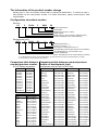
Configuration of product number
Devices
S1
C
33104
F
0A01
00
Packing specification
Specification
Package (D: die form; F: QFP)
Model number
Model name (C: microcomputer, digital products)
Product classification (S1: semiconductor)
Development tools
C
33L01
S5U1
D1
1
00
Packing specification
Version (1: Version 1 ∗2)
Tool type (D1: Development Tool ∗1)
Corresponding model number (33L01: for S1C33L01)
Tool classification (C: microcomputer use)
Product classification
(S5U1: development tool for semiconductor products)
∗1: For details about tool types, see the tables below. (In some manuals, tool types are represented by one digit.)
∗2: Actual versions are not written in the manuals.
Comparison table between Comparison table between new and previous
new and previous number number of development tools
S1C33 Family processors
Previous No.
E0C33A104
E0C33202
E0C33204
E0C33208
E0C33209
E0C332T01
E0C332L01
E0C332L02
E0C332S08
E0C332129
E0C33264
E0C332F128
Previous No.
CC33
CF33
COSIM33
GRAPHIC33
HMM33
JPEG33
MON33
MELODY33
PEN33
ROS33
SOUND33
SMT33
TS33
USB33
VOX33
VRE33
New No.
S1C33104
S1C33202
S1C33204
S1C33208
S1C33209
S1C33T01
S1C33L01
S1C33L02
S1C33S01
S1C33221
S1C33222
S1C33240
New No.
S5U1C33000C
S5U1C330C1S
S5U1C330C2S
S5U1C330G1S
S5U1C330H1S
S5U1C330J1S
S5U1C330M2S
S5U1C330M1S
S5U1C330P1S
S5U1C330R1S
S5U1C330S1S
S5U1C330S2S
S5U1C330T1S
S5U1C330U1S
S5U1C330V1S
S5U1C330V2S
Development tools for the S1C33 Family
Previous No.
New No.
Previous No.
New No.
ICE33
S5U1C33104H
DMT33LIF
S5U1C330L1D1
EM33-4M
S5U1C33104E
DMT33SMT
S5U1C330S1D1
PRC33001
S5U1C33104P1
DMT33LCD26
S5U1C330L2D1
POD33001
S5U1C33104P2
DMT33LCD37
S5U1C330L3D1
ICD33
S5U1C33000H
EPOD33001
S5U1C33208E1
DMT33004
S5U1C33104D1
EPOD33001LV
S5U1C33208E2
DMT33004PD
S5U1C33104D2
EPOD33208
S5U1C33208E3
DMT33005
S5U1C33208D1
EPOD33208LV
S5U1C33208E4
DMT33005PD
S5U1C33208D2
EPOD332L01LV
S5U1C33L01E1
DMT33006LV
S5U1C33L01D1
EPOD332T01
S5U1C33T01E1
DMT33006PDLV
S5U1C33L01D2
EPOD332T01LV
S5U1C33T01E2
DMT33007
S5U1C33208D3
EPOD33209
S5U1C33209E1
DMT33007PD
S5U1C33208D4
EPOD33209LV
S5U1C33209E2
DMT33008LV
S5U1C33T01D1
EPOD332128
S5U1C33220E1
DMT33008PDLV
S5U1C33T01D2
EPOD332128LV
S5U1C33220E2
DMT332S08LV
S5U1C33S01D1
EPOD332S08LV
S5U1C33S01E1
DMT332S08PDLV
S5U1C33S01D2
MEM33201
S5U1C33001M1
DMT33209LV
S5U1C33209D1
MEM33201LV
S5U1C33001M2
DMT33209PDLV
S5U1C33209D2
MEM33202
S5U1C33002M1
DMT332F128LV
S5U1C33240D1
MEM33202LV
S5U1C33002M2
DMT33MON
S5U1C330M1D1
MEM33203
S5U1C33003M1
DMT33MONLV
S5U1C330M2D1
MEM33203LV
S5U1C33003M2
DMT33AMP
S5U1C330A1D1
MEM33DIP42
S5U1C330D1M1
DMT33AMP2
S5U1C330A2D1
MEM33TSOP48
S5U1C330T1M1
DMT33AMP3
S5U1C330A3D1
EPOD176CABLE
S5U1C33T00E31
DMT33AMP4
S5U1C330A4D1
EPOD100CABLE
S5U1C33S00E31
DMT33CF
S5U1C330C1D1
EPOD33SRAM5V
S5U1C33000S
DMT33CPLD400KLV S5U1C330C2D1
EPOD33SRAM3V
S5U1C33001S
TABLE OF CONTENTS
Preface
Written for those who develop applications using the S1C33 Family of microcomputers, this manual describes how to
implement the S1C33 Family debug monitor library S5U1C330M2S and how to debug the target program.
Table of Contents
1 S5U1C330M2S Package ................................................................................................1
1.1 Features ......................................................................................................................................................................1
1.2 Components of S5U1C330M2S Package ......................................................................................................2
1.3 Installation...................................................................................................................................................................2
2 Implementing the Debug ..............................................................................................4
2.1 Resources Required for the Debug Monitor ..................................................................................................4
2.2 Starting Up the Debug Monitor ...........................................................................................................................5
2.3 Building an Application Program........................................................................................................................6
2.4 Creating Communication Control Routines ...................................................................................................7
3 Target Program and Debugging.................................................................................. 10
3.1 Notes for Creating Target Programs .............................................................................................................10
3.2 Parameter File for Debugging..........................................................................................................................10
3.3 Starting Up and Terminating Procedure of Debugging ..........................................................................11
3.4 Debugging Method ...............................................................................................................................................12
3.5 Precautions for Debugging................................................................................................................................14
3.5.1 Restriction on Debugging Command..........................................................................................14
3.5.2 Other Precautions ..............................................................................................................................14
Appendix
S5U1C330MxD1 Board ................................................................................ 15
A.1 Outline of S5U1C330MxD1 Board .................................................................................................................15
A.2 Names and Functions of Each Part ..............................................................................................................15
A.3 Connecting the System ......................................................................................................................................16
A.4 S5U1C330MxD1 Block Diagram ....................................................................................................................17
A.5 Program Debugging with a S5U1C33xxxDx Board and S5U1C330M2S .......................................18
A.6 Indispensable Signal Pins of S5U1C330MxD1.........................................................................................21
S1C33 FAMILY DEBUG MONITOR
OPERATION MANUAL
EPSON
i
1 S5U1C330M2S PACKAGE
1 S5U1C330M2S Package
The Debug Monitor S5U1C330M2S is a middleware designed for S1C33 Family single-chip
microcomputers.
It provides program-debugging functions on the user target board or for the actual product.
1.1 Features
The following lists the features of S5U1C330M2S:
• It is provided as a library file that can be linked to the user program.
This package also contains source codes of all the modules.
• S5 U1 C33 0M2 S u ses app rox . 1 0KB RO M, app rox . 2 .5K B RA M and a chan nel o f s eri al i nt erface o n t he S1 C33
chip. It allows direct program debugging via the S5U1C330MxD1 board using the debugger db33 on the personal
computer.
• Allows debugging of the target program in the RAM, ROM or Flash memory on the target board.
• Supports the following debugging functions:
- Successive execution and step execution of the program
- PC break and data break
- Memory/register operation
- Flash memory writing
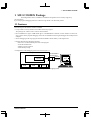
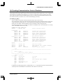
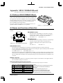
A configuration of the debugging system is shown in Figure 1.1.1.
Target board
S5U1C330MxD1
interface board
S1C33xxx
RS232C
Serial
interface
Debugger
db33
115,200 bps
EPSON
External
RAM
External
ROM
FLASH
memory
Figure 1.1.1 Configuration of debugging system
S1C33 FAMILY DEBUG MONITOR
OPERATION MANUAL
EPSON
1
1 S5U1C330M2S PACKAGE
1.2 Components of S5U1C330M2S Package
The following lists the contents of S5U1C330M2S Package:
When unpacking, make sure that all of the following components are included.
(1) Tool disk (3.5' FD for PC/AT, 1.44MB)
1
(2) S1C33 Family Debug Monitor Operation Manual (this manual)
2 (1 English/1 Japanese)
(3) Warranty
2 (1 English/1 Japanese)
1.3 Installation
S5U1C330M2S needs to be linked with the user program as it is implemented. Therefore, make sure all tools of the
"S1C33 Family C Compiler Package" have been installed in the personal computer and are ready to run before
installing the S5U1C330M2S files. The basic system configuration is described below.
• Personal computer:
IBM PC/AT or compatible
(PC with Pentium 90 MHz or higher and 32MB or more memory recommended)
One channel of the serial port is used to communicate with the debug monitor.
• OS:
Windows95, Windows NT 4.0 or higher version (English version or Japanese version)
All the S5U1C330M2S files are supplied on one floppy disk. Execute the self-extract file "mon33vXX.exe" on the
FD to install the files. ("XX" in the file name represents the version number, for example, "mon33v10.exe" is the
file name of S5U1C330M2S ver. 1.0.)
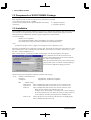
When "mon33vXX.exe" is started up by double-clicking the file icon, the following dialog box appears.
Enter a path/folder name in the text box then click
[Unzip]. The specified folder will be created and all the
files will be copied to the folder.
When the specified folder already exists on the specified
path, the folder will be overwritten without prompting if
[Overwrite Files Without Prompting] is checked.
The following lists the configuration of directories and files after copying.
(root)\
(default: C:\E0C33\MON33\)
readme.txt
readmeja.txt
lib\
..... MON33 library
mon33ch0.lib
S5U1C330M2S library that uses the serial I/F Ch.0 on the S1C33xxx
mon33ch1.lib
S5U1C330M2S library that uses the serial I/F Ch.1 on the S1C33xxx
mon33.lib
S5U1C330M2S library that does not use a serial I/F on the S1C33xxx
... These libraries cannot be used with the ICE or ICD.
Normally, either "mon33ch0.lib" or "mon33ch1.lib" is used according to
the serial I/F channel used. Use "mon33.lib" when providing a serial I/O
circuit separately and when not using the S5U1C330MxD1 board.
mon33ice.lib
2
Supplementary explanation (in English)
Supplementary explanation (in Japanese)
Library that does not use a serial I/F on the S1C33xxx for debugging the
S5U1C330M2S using the ICE or ICD
EPSON
S1C33 FAMILY DEBUG MONITOR
OPERATION MANUAL
1 S5U1C330M2S PACKAGE
mon33ch0.mak
mon33ch1.mak
mon33.mak
mon33ice.mak
src\
Make file for building mon33ch0.lib
Make file for building mon33ch1.lib
Make file for building mon33.lib
Make file for building mon33ice.lib
..... MON33 source files
m33_def.h
S5U1C330M2S definition file
m3c_brk.c
C source file for break functions
m3c_exe.c
C source file for program execution
m3c_flsh.c
C source file for Flash memory operation
m3c_main.c
S5U1C330M2S main C source file
m3c_mem.c
C source file for memory operation
m3c_othe.c
C source file for other functions
m3c_sci.c
C source file for sending/receiving messages
m3s_exe.s
Assembly source file for program execution
m3s_flsh.s
Assembly source file for Flash memory operation
m3s_init.s
Assembly source file for S5U1C330M2S initial set-up
m3s_mem.s
Assembly source file for memory operation
m3s_sci.s
Assembly source file for sending/receiving messages
dmt33xxx\
..... Sample source files for the S5U1C33xxxDx, MON33 build files and related files
A sample program for blinking the LED on the S5U1C33xxxDx, a source for the onboard Flash memory write/erase routines and the make files are included in each
dmt33xxx folder. The source files can be modified to use in the application program if
necessary. Refer to "readme.txt" or "readmeja.txt" for the contents of the dmt33xxx
folder.
S1C33 FAMILY DEBUG MONITOR
OPERATION MANUAL
EPSON
3
2 IMPLEMENTING THE DEBUG MONITOR
2 Implementing the Debug Monitor
This chapter describes how to implement the debug monitor and how to start it from the application
program.
2.1 Resources Required for the Debug Monitor
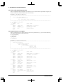
The debug monitor uses the following resources:
• Approximately 10KB of ROM area for the program code of the debug monitor.
• Approximately 2.5KB of RAM area for the work and stack area.
• Since the debug monitor uses the debugging exception of the CPU, addresses 0x0 to 0xF of the built-in RAM area
are used as the vector and stack for processing debugging exceptions. Furthermore, addresses 0x10 to 0x2F are
reserved for extending functions.
• One channel (Ch.0 or Ch.1) of the serial interface (8-bit asynchronous mode) is used for communicating with the
debugger db33 on the personal computer.
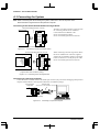
Figure 2.1.1 shows a connection diagram.
S1C33xxx
S5U1C330MxD1
VSS
Connected to the personal computer
using the RS232C cable
(Baud rate: 115,200 bps)
SOUT0/1
SIN0/1
SCLK0/1
Target board
Figure 2.1.1 RS232C connector diagram
• Communication via RS232C is performed by a software polling method without any interrupt related resource.
• A serial I/O device outside the S1C33 chip can be used by customizing the serial I/O routine (see Section 2.4).
• S5U1C330M2S uses the TXD, RXD and status registers of the corresponding serial interface channel exclusively.
Therefore, do not access these control registers.
Furthermore, fix the I/O pins for the channel at the serial interface pins using the port function select register. For
example, the sample program "m3s_sci.s" writes 0x07 to the P0 function select register (0x402D0) when Ch.0 is
used or 0x70 when Ch.1 is used to set the serial interface pins.
4
EPSON
S1C33 FAMILY DEBUG MONITOR
OPERATION MANUAL
2 IMPLEMENTING THE DEBUG MONITOR
2.2 Starting Up the Debug Monitor
The debug monitor starts by jumping to m_mon_start( ).
Normally, provide a select switch outside the S1C33 chip for selecting either starting up the debug monitor or a
normal execution and create the program that can jump to m_mon_start( ) from the boot routine after an initial reset.
Furthermore, start the debug monitor after initializing the BCU if necessary. In case the debug monitor is started
before the BCU is initialized, downloaded data cannot be written to a 8-bit device or in DRAM. However, when the
S5U1C330M2S itself is placed on the 16-bit ROM and the 16-bit SRAM is used as a work area, it can be operated
even in the default setting (7-wait state) when operating in 20 MHz. In the following example, the initial set-up
statements are described as comments so that the BCU operates by default. By decreasing the wait cycle number
(2-wait setting in the example below), the file loading and other operations may improve the response time
(approximately 5 to 10%).
Example: boot routine of "dmt33004\m3s_boot.s"
;******************************************************************************
;
;
BOOT program
;
;******************************************************************************
BOOT:
xld.w
%r0,0x800
ld.w
%sp,%r0
;
xld.w
%r5,BCU_A10_ADDR
;area9-10 (0x800000-0xffffff)
;
xld.w
%r4,0b0000000000010010
;Device 16 bits,delay 1.5, wait 2
;
ld.h
[%r5]+,%r4
;
xld.w
%r5,BCU_A8_ADDR
;area8 (0x600000-0x7fffff)
;
xld.w
%r4,0b0000000000010010
;Device 16 bits,delay 1.5, wait 2
;
ld.h
[%r5]+,%r4
;
xld.w
%r5,BCU_A5_A6_ADDR
;area5-6 (0x200000-0x3fffff)
;
xld.w
%r4,0b0001001000010010
;Device 16 bits,delay 1.5, wait 2
;
ld.h
[%r5]+,%r4
xbtst
[K6XD],0x3
;K63 (debug SW check) 0:MON33 1:USER
xjreq
m_mon_start
;MON33 start
jp
USER
USER:
xld.w
%r4,TBRP
xld.w
%r6,0x59
xld.b
[%r4],%r6
;TTBR writable 0x59
xld.w
%r4,TTBR
xld.w
%r6,0x200000
ld.w
[%r4],%r6
;TTBR set 0x200000
ld.w
%r4,[%r6]
jp
%r4
;user application(flash) start
S1C33 FAMILY DEBUG MONITOR
OPERATION MANUAL
EPSON
5
2 IMPLEMENTING THE DEBUG MONITOR
2.3 Building an Application Program
The S5U1C330M2S modules are provided as a library file "mon33*.lib" in the directory "lib\". Link this library to
the user modules.
When using the serial interface on the S1C33 chip and the S5U1C330MxD1 board, link "mon33ch0.lib" (Ch.0 is
used) or "mon33ch1.lib" (Ch.1 is used) accordingly. When not using the serial interface on the S1C33 chip and the
S5U1C330MxD1 board, create serial I/O routines separately and link "mon33.lib".
Specify the "lib\" directory of the S5U1C330M2S as a library path in the linker command file when linking.
Example: "dmt33004\dmt33004.cm"
;Map set
-code 0x0c00000
-bss 0x06ff640
;Library path
-l c:\CC33\lib
-l ..\lib
; set relative code section start address
; set relative bss section start address
.... CC33 standard library path
.... S5U1C330M2S library path (c:\E0C33\mon33\lib)
;Executable file
-o dmt33004.srf
;Object files
m3s_boot.o
;Library files
string.lib
ctype.lib
idiv.lib
mon33ch1.lib
.... S5U1C330M2S library to be linked
Since all the source codes of the debug monitor are provided in the directory "src\", it is possible to customize the
debug monitor if necessary. In this case, rebuild the library using "mon33*.mak" (make file for creating
"mon33*.lib") in the directory "lib\".
S5U1C330M2S allows the debugger db33 to write the target program to be debugged in the RAM or Flash memory
on the target board. In this case, it is not necessary to create a target object linked to the debug monitor. When the
S5U1C33xxxDx board (S5U1C33104D1, S5U1C33209D1, etc.) is used, the target program can be downloaded to
the RAM or Flash memory and can be debugged by writing S5U1C330M2S and a simple boot program to the ROM.
When executing the target program in the external ROM on the target board, link the debug monitor to the target
program and create an object that is mapped to the external ROM.
6
EPSON
S1C33 FAMILY DEBUG MONITOR
OPERATION MANUAL
2 IMPLEMENTING THE DEBUG MONITOR
2.4 Creating Communication Control Routines
For communicating with the debugger, the debug monitor calls the following four RS232C routines (1 to 4).
"mon33chX.lib" that contains these routines can be used when using the serial interface Ch.0 or Ch.1 on the S1C33
chip and the S5U1C330MxD1 board. Otherwise, it is necessary to create these routines according to the system
since "mon33.lib" must be used. The sample program "m3s_sci.s" that uses the serial interface Ch.0/Ch.1 of the
S1C33104/S1C33209 is provided in "src\", so use it after modifying if necessary.
(1) void m_io_init( )
This is an initial set-up routine of the serial interface. Return value is not necessary.
Set up I/O terminals, input clock, baud rate and a data format. Select 8-bit asynchronous mode, no parity and 1
stop bit. The baud rate should be set to a value supported by the debugger db33 and the personal computer.
Refer to the "S1C33XXX Technical Manual" for the serial interface and for setting the clock.
The sample program "m3s_sci.s" assumes use of the S5U1C330MxD1 board. It sets the baud rate to 115.2 kbps
when a 1.843 MHz external clock is used.
Example: "m_io_init( ) of "m3s_sci.s"
#define
#ifdef SIO0
#define
#define
#define
#define
#define
#define
#else
#define
#define
#define
#define
#define
#define
#endif
#define
#define
#define
#define
MON_VER
0x11
;monitor firm-ware version
STDR
SRDR
SSR
SCR
SIR
PIO_SET
0x000401e0
0x000401e1
0x000401e2
0x000401e3
0x000401e4
0x07
;transmit data register(ch0)
;receive data register(ch0)
;serial status register(ch0)
;serial control register(ch0)
;IrDA control register(ch0)
;port function register
STDR
SRDR
SSR
SCR
SIR
PIO_SET
0x000401e5
0x000401e6
0x000401e7
0x000401e8
0x000401e9
0x70
;transmit data register(ch1)
;receive data register(ch1)
;serial status register(ch1)
;serial control register(ch1)
;IrDA control register(ch1)
;port function register
SIR_SET
SCR_SET
SCR_EN
PIO
0x0
0x7
0xc0
0x000402d0
;SIR set(1/16 mode)
;SCR set(#SCLK input 1.843MHz 115200bps)
;SCR enable
;IO port (P port) register
.code
;******************************************************************************
;
;
void m_io_init()
;
serial port initial function
;
;******************************************************************************
.global m_io_init
m_io_init:
ld.w
%r0,SIR_SET
;1/16 mode
xld.b
[SIR],%r0
;SIR set
ld.w
%r0,SCR_SET
xld.b
[SCR],%r0
;SCR set(#SCLK input 1.843MHz)
xld.w
%r0,PIO_SET
xld.b
[PIO],%r0
;IO port set
xld.w
%r0,SCR_EN|SCR_SET
xld.b
[SCR],%r0
;SCR set
ret
In addition to the sample program above, "dmt33001\m3s_sci.s " is provided. This program sets the baud rate to
38,400 bps based on the 20 MHz S1C33104 internal clock. Refer to it if necessary.
S1C33 FAMILY DEBUG MONITOR
OPERATION MANUAL
EPSON
7
2 IMPLEMENTING THE DEBUG MONITOR
(2) void m_snd_1byte(unsigned char)
This is a routine that sends 1-byte data. This routine receives 1-byte data as the argument (R12 register) and
sends it via the serial interface. Return value is not necessary.
Example: m_snd_1byte( ) of "m3s_sci.s"
;******************************************************************************
;
;
void m_snd_1byte( sdata )
;
1 byte send function
;
IN : uchar sdata (R12) send data
;
;******************************************************************************
.global m_snd_1byte
m_snd_1byte:
pushn
%r3
;save r3-r0
snd000:
xbtst
[SSR1],0x1
;TDBE1(bit1) == 0(full) ?
jreq
snd000
;if full, jp snd000
xld.b
[STDR1],%r12
;write data
popn
%r3
;restore r3-r0
ret
(3) unsigned char m_rcv_1byte( )
This is a routine that receives 1-byte data. Store received 1-byte data into m_rcv_data. It returns following
error codes (unsigned char) as the return value:
0: received normally
1: framing error
2: parity error
3: overrun error
Example: m_rcv_1byte( ) of "m3c_sci.s"
;******************************************************************************
;
;
uchar m_rcv_1byte()
;
1 byte receive function
;
OUT : 0 receive OK
;
1 receive ERROR (framing err)
;
2
(parity
err)
;
3
(over run err)
;
;******************************************************************************
.global m_rcv_1byte
m_rcv_1byte:
pushn
%r3
;save r3-r0
rcv000:
xbtst
[SSR1],0x0
;RDBF1(bit0) == 0(empty) ?
jreq
rcv000
;if empty, jp rcv000
ld.w
%r10,0x0
xbtst
[SSR1],0x4
;FER1(bit4) == 0 ?
jreq
rcv010
xbclr
[SSR1],0x4
;FER1(bit4) 0 clear
ld.w
%r10,0x1
;return 1
rcv010:
xbtst
[SSR1],0x3
;PER1(bit3) == 0 ?
jreq
rcv020
xbclr
[SSR1],0x3
;PER1(bit3) 0 clear
ld.w
%r10,0x2
;return 2
rcv020:
xbtst
[SSR1],0x2
;OER1(bit2) == 0 ?
jreq
rcv030
xbclr
[SSR1],0x2
;OER1(bit2) 0 clear
ld.w
%r10,0x3
;return 3
rcv030:
xld.b
%r0,[SRDR1]
;read data
xld.b
[m_rcv_data],%r0 ;read data set
popn
%r3
;restore r3-r0
ret
8
EPSON
S1C33 FAMILY DEBUG MONITOR
OPERATION MANUAL
2 IMPLEMENTING THE DEBUG MONITOR
(4) void m_dummy_rd( )
This is a dummy read routine. It reads data from the receive buffer and clears the buffer. Return value is not
necessary.
Example: m_dummy_rd( ) of "m3s_sci.s"
;******************************************************************************
;
;
void m_dummy_rd()
;
dummy read function
;
;******************************************************************************
.global m_dummy_rd
m_dummy_rd:
xld.b
%r4,[SRDR]
;read data
ret
(5) void m_ver_rd( )
This is a version read routine. Modifying the constant MON_VER can change the S5U1C330M2S version
number. It returns MON_VER as the return value.
Example: m_ver_rd( ) of "m3s_sci.s"
;******************************************************************************
;
;
void m_ver_rd()
;
mon firmware version read function
;
;******************************************************************************
.global m_ver_rd
m_ver_rd:
xld.w
%r10,MON_VER
;mon firmware version
ret
(6) Sample command file for building
When the above routines are newly created, create a linker command file as the following example and link
"mon33.lib" to the user modules.
Example: dmt33001\dmt33001.cm
;Map set
-code 0x0c00000
-bss 0x081f640
; set relative code section start address
; set relative bss section start address
;Library path
-l c:\CC33\lib
-l ..\lib
;Executable file
-o dmt33001.srf
;Object files
m3s_boot.o
m3s_bcu.o
m3s_sci.o
.... Originally created SIO routine
;Library files
string.lib
ctype.lib
fp.lib
idiv.lib
mon33.lib
.... Link "mon33.lib" that does not include SIO routine
S1C33 FAMILY DEBUG MONITOR
OPERATION MANUAL
EPSON
9
3 TARGET PROGRAM AND DEBUGGING
3 Target Program and Debugging
This chapter describes precautions for debugging using the debug monitor.
3.1 Notes for Creating Target Programs
Follow the instructions below when creating the target program to be debugged:
• Since the debug monitor uses the debugging exception of the CPU, addresses 0x0 to 0xF of the built-in RAM area
are used as the vector and stack for processing debugging exceptions. Therefore, the target program cannot use this
area. Furthermore, do not use addresses 0x10 to 0x2F.
• Wh en d eb ug gi ng t he t arg et p ro gram b y wri ti ng i n t he RA M o r Fl as h memory o n t he t arg et b oard, map t he
program to that address.
• Th e d eb ug mo ni to r d oes n ot all ow forced b reak fun cti on s s uch as k ey b reak s. Fo rced b reak fun cti on s s ho ul d b e
made i n t he t arg et p ro gram u si ng a k ey i np ut i nt erru pt o r an NMI i np ut . Sett in g a h ard ware PC b reak i n t he
interrupt processing routine makes it possible to execute a forced break.
3.2 Parameter File for Debugging
A debug-parameter file is required to start the debugger. Create the file according to the memory configuration of
the target system. When using the debug monitor, the debugger ignores all the settings for the ICE emulation
memory.
When using a Flash memory, specify it as a RAM.
Example: "dmt33004\sample\33104_m.par"
CHIP
IROM
FOPT
PRC VER
PRC STATUS
MPU
VER
33104
1000
0000
00 ff
****************
1
;
;
;
;
;
;
;
chip name (33XXX)
internal ROM is 80000 to 80FFF
f option size
allow any PRC board
allow any PRC board status
0xC00000 external boot address
this file version
; Emulation memory allocation (max 8 areas, 1MB/area, 1MB boundary)
EMROM
c00000
cfffff
; external ROM 1MB
; Map allocation (max 31 areas, 256bytes boundary)
RAM
0
7FF
;
IO
40000
4ffff
;
RAM
200000
2fffff
;
RAM
600000
6fffff
;
EROM
c00000
cfffff
;
; Stack area except internal RAM area
STACK
600000
6fffff
internal RAM area 2KB
internal IO area 64KB
external FLASH 1MB
external SRAM 1MB
external ROM 1MB
(max 8 areas, 256bytes boundary)
; external stack area 1MB
END
10
EPSON
S1C33 FAMILY DEBUG MONITOR
OPERATION MANUAL
3 TARGET PROGRAM AND DEBUGGING
3.3 Starting Up and Terminating Procedure of Debugging
Follow the procedure below to start debugging.
1. Make sure the power of the target board and personal computer are off.
2. Connect the S5U1C330MxD1 board to the target board in which the debug monitor is implemented and connect
the S5U1C330MxD1 board to the personal computer with the RS232 cable.
3. Turn the target board on and then start the debug monitor.
4. Turn the personal computer on and start the debugger db33 in debug monitor mode from the work bench wb33 or
DOS prompt.
Example: db33 -mon -b 115200 -p 33104_m.par
Follow the procedure in order from Step 4 to Step 1 to terminate debugging and for power off.
Note: When connecting and disconnecting the RS232C cable, make sure the target board and the
personal computer are off.
S1C33 FAMILY DEBUG MONITOR
OPERATION MANUAL
EPSON
11
3 TARGET PROGRAM AND DEBUGGING
3.4 Debugging Method
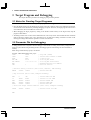
The following three methods are available for debugging the target program.
1. Debugging in the ROM
Map the target program in the ROM after linking to the debug monitor. The target program can be executed and
debugged in the ROM.
Since the [Source] window of the debugger displays the disassembled content of the ROM on the target system,
it is not necessary to load the target program with the lf command. To display the source, load the same
absolute object file as the one written to the ROM. In this case, by using the ld command instead of the lf
command, the db33, except for the object code, loads only the debugging information.
After starting the debugger, follow the process below before starting to debug:
1. Load the debugging information (when displaying the source or using symbols).
2. Set up a hardware PC break point for the forced break function.
Example: command file example of the above description
ld sample.srf
bh ESC
; Load the debugging information of the target program
; Set up a hardware PC break point at the label ESC (for forced break)*
* For example, an NMI input switch can be used for the forced break function.
Example: NMI processing routine example for forced break function
NMI:
; nmi
nop
.global
ESC
; Label set as a hardware PC break point for the forced break function
ESC:
reti
Note: When debugging the target program in the ROM, the software PC break function (bs command)
cannot be used.
2. Debugging in the RAM
Load the target program into the RAM of the target system with the lf command to debug the program in the
RAM.
After starting the debugger, follow the process below before starting to debug:
1. Set the trap table base address (only when placing the trap table in the RAM).
2. Load the target program.
3. Reset the CPU.
4. Set up a hardware PC break point for the forced break function.
The following shows a debug-command file example in which the above process is described.
Example: "dmt33004\sample\led.cmd"
eb 4812d
59
q
ew 48134
600000
q
lf led.srf
rsth
bh ESC
12
; Set up TBRP (TTBR write protection register)
; Remove TTBR write protection
; Set up TTBR (trap table base register)
; Set up the base address to 0x600000 (external RAM)
; Load the target program (0x600000~)
; Reset the CPU (reset vector at 0x600000 is set to the PC)
; Set up a hardware PC break at the label ESC (for forced break)
EPSON
S1C33 FAMILY DEBUG MONITOR
OPERATION MANUAL
3 TARGET PROGRAM AND DEBUGGING
3. Debugging in the Flash memory
In the target system in which a Flash memory has mounted, the target program can be debugged by writing it
into the Flash memory using the debugger.
Notes: • When debugging the target program in the Flash memory, the software break function (bs
command) cannot be used.
• The debugger db33 ver. 1.72 or later version supports data writing to the Flash memory on the
target board. To debug using the Flash memory, create Flash erase and Flash write routines in
the user program and write the program following the instructions below:
After starting the debugger, follow the process below before starting to debug:
1. Load and initialize the Flash erase/write routines.
2. Erase the Flash memory.
3. Set up the trap table base address.
4. Load the target program.
5. Reset the CPU.
6. Set up a hardware PC break point for the forced break function.
The following shows a debug-command file example in which the above process is described.
Example: "dmt33004\sample\led2.cmd"
lf ..\sample\flsh\am29f800.srf
fls
1
200000
2fffff
FLASH_ERASE
FLASH_LOAD
fle
0x200000
0
0
eb 4812d
59
q
ew 48134
200000
q
lf led2.srf
rsth
bh ESC
; Load the Flash erase/write routines to the built-in RAM
; Flash set up command
; 1: Set up 2: Clear
; Flash memory start address = 0x200000 (∗2)
; Flash memory end address = 0x2fffff (∗2)
; Flash erase routine start address (∗1)
; Flash load routine start address (∗1)
; Flash memory erase command
; Flash control register = 0x200000
; Erase start block, 0 = All area, 1–19 = Start section
; Erase end block, 1–19 = End section, 0 = Ignored
; Set up TBRP (TTBR write protection register)
; Remove TTBR write protection
; Set up TTBR (trap table base register)
; Set up base address to 0x200000 (Flash memory start address)
; Load the target program (0x200000~)
; Reset the CPU (reset vector at 0x200000 is set to PC)
; Set up a hardware PC break at the label ESC (for forced break)
*1: "am29f800.srf" is created so as to operate by loading into the built-in RAM (2KB).
When using this source for the S1C33104 after modifying, use the patch tool "cc33\utility\filter".
* 2 : Th i s s amp l e (" d mt 3 3 0 0 4 \ s amp l e\ l ed 2 .s rf " ) as s u me s t h at a Fl as h memo ry o f 1 MB i s l o cat e d at
0 x 2 0 0 0 0 0 – 0 x 2 fff ff.
S1C33 FAMILY DEBUG MONITOR
OPERATION MANUAL
EPSON
13
3 TARGET PROGRAM AND DEBUGGING
3.5 Precautions for Debugging
3.5.1 Restriction on Debugging Command
When the debug monitor is used for debugging, the following debugging functions/commands are not available or
allowed to be used.
When the following commands/functions are used, an error message will be displayed.
Error: Command is not supported at present mode.
• Trace function (tm, td, ts and tf commands)
• Sequential break function (bsq command)
• ICE Flash memory function (lfl, sfl and efl commands)
• Option related function (lo and od commands)
• ICE emulation memory
The following commands/ functions are not available even though no error message will be displayed.
• File loading via a parallel port (lf and lh commands)
• Map break function
• On-the-fly function
• Execution time measurement function
• Key break function
In addition to the functions above, the following functions cannot be used when the program in the ROM or Flash
memory is debugged.
• Software PC break functions (bp, bs and bc commands)
• Commands that use the software PC break function internally (stdin and stdout commands)
• Memory edit functions (eb, eh and ew commands)
• Memory fill functions (fb, fh and fw commands)
• Memory move functions (mv, mvh and mvw commands)
3.5.2 Other Precautions
• Th e d eb ug mo ni to r u ses add ress es 0 x0 t o 0 x2 F i n t he b ui lt -i n RA M and app rox imat ely 2 .5K B (des crib ed l at er)
p art o f t he ext ernal RA M. Do n ot rewri te t hi s area wi th a memory o perati on comman d. Wh en t hi s area i s
modified, the debug monitor cannot be executed normally.
• The cold reset sequence is the same as the hot reset sequence.
1) The vector value indicated by TTBR is set to the PC.
2) Initial setting: general purpose/special registers = 0xAAAAAAAA, PSR = 0x0, SP = 0xAAAAAA8
In the debug monitor, cold reset is simulated as hot reset.
• The S5U1C33104H and S5U1C33000H halt all the peripheral functions after a break occurs except for the DRAM
refresh o perati on . In t he d eb ug mo ni to r, t he p eri ph eral fun cti on s h al t i ns tant aneo us ly wh en a b reak o ccu rs o r
s uccess iv e/s tep execu ti on s tarts , h owev er t hey rest art i mmed iat ely . Int errup ts wh il e t he t arg et p ro gram i s
suspended are disabled according to the IE-bit status of the PSR.
14
EPSON
S1C33 FAMILY DEBUG MONITOR
OPERATION MANUAL
APPENDIX
S5U1C330MXD1 BOARD
Appendix S5U1C330MxD1 Board
This chapter describes how to use the S5U1C330MxD1 board.
A.1 Outline of S5U1C330MxD1 Board
The S5U1C330MxD1 board provides the interface for the debug
monitor to the demonstration tools such as the S5U1C33104Dx or the
user target board. The S5U1C330MxD1 allows on-board debugging
using the debugger (db33.exe) on a personal computer by connecting
it to the target board in which the S1C33 Family debug monitor
(S5U1C330M2S) has been implemented.
Two types of boards are available: S5U1C330M1D1 board for 5 V
operation and S5U1C330M2D1 for 3.3 V operation.
Figure A.1.1
S5U1C330MxD1 board
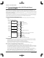
A.2 Names and Functions of Each Part
The following describes the parts layout on the S5U1C330MxD1 board as well as the functions of the connectors and
switches:
RS232 connector
OFF
SW1
(RESET)
SW2
(NMI)
ON
SW1 (RESET switch)
OFF
ON
SW3
(DEBUG)
Sets up the status of the RESET pin at the S5U1C33xxxDx/
target board I/F connector. When a S5U1C33xxxDx board is
connected, this switch can reset the CPU on the board.
ON: RESET = "0"
OFF: RESET = "1"
SW2 (NMI switch)
1
12
S5U1C33xxxDx/target board I/F connector
Figure A.2.1
S5U1C330MxD1 board layout
Sets up the status of the NMI pin at the S5U1C33xxxDx/target
board I/F connector. When a S5U1C33xxxDx board is
connected, a NMI request can be input to the CPU on the
board.
ON: NMI = "0"
OFF: NMI = "1"
SW3 (DEBUG switch)
Sets up the status of the DEBUG pin at the S5U1C33xxxDx/target board I/F connector. When the
S5U1C33104Dx/S5U1C33209Dx board is connected, the switch signal is input to the K63 port and can be used
to start up the debug monitor from the boot routine.
ON: DEBUG (K63) = "0"
OFF: DEBUG (K63) = "1"
When the switch is ON, the S5U1C33104Dx/S5U1C33209Dx will start the debug monitor. When the switch is
OFF, the S5U1C33104Dx/S5U1C33209Dx will start executing the program stored in the Flash memory. The
S5U1C33104Dx/S5U1C33209Dx works assuming the debug switch is OFF when the S5U1C330MxD1 is not
connected.
RS232C connector
This is a Dsub 9-pin connector for connecting a personal computer. Use the RS232C cable supplied with the
S5U1C330MxD1 package for connection.
S5U1C33xxxDx/target board I/F connector
This connector is used for connecting the S5U1C33xxxDx board. The pin layout is as follows:
Table A.2.1
No.
1
2
3
4
5
6
S5U1C33xxxDx/target board connector pin layout
No.
Signal name
( ) indicates the CPU pin corresponding to the signal
VCC [+5 V, +3.3 V]
7
N.C.
when the S5U1C33104Dx/S5U1C33209Dx is
VCC [+5 V, +3.3 V]
8
DEBUG (K63)
connected.
RESET (#RESET)
9
VCC [+5 V, +3.3 V]
Since the corresponding signals on the
TxD (P05)
10
SCLK (P06)
S5U1C33xxxDx may differ depending on the
RxD (P04)
11
GND
board, refer to the pin layout table provided in
NMI (#NMI)
12
GND
the specifications of each S5U1C33xxxDx board.
Signal name
S1C33 FAMILY DEBUG MONITOR
OPERATION MANUAL
EPSON
15
APPENDIX
S5U1C330MXD1 BOARD
A.3 Connecting the System
Note: When connecting and disconnecting the system, make sure to turn off the power of the
S5U1C33xxxDx/ target board and the personal computer.
Connecting to the S5U1C33xxxDx board/user target board
S5U1C33xxxDx/target board I/F connector
The S5U1C33xxxDx board has a connector used
for connecting with the S5U1C330MxD1.
Connect the S5U1C330MxD1 to the
S5U1C33xxxDx board with the
S5U1C33xxxDx/target board I/F connector.
S5U1C33xxxDx
S5U1C330MxD1 I/F connector
Figure A.3.1
Connecting to the S5U1C33xxxDx board
S5U1C33xxxDx/target board I/F connector
User target board
SINx
SOUTx
SCLKx
#RESET
#NMI
(K63)
VSS
VCC
When connecting to the user target board, attach
the S5U1C330MxD1 I/F connector (supplied
with the S5U1C330MxD1 package) to the target
board. See Table A.2.1 for the pin layout of the
S5U1C33xxxDx/target board I/F connector.
S1C33xxx
S5U1C330MxD1 I/F connector
(supplied with the S5U1C330MxD1 package)
Figure A.3.2
Connecting to the user target board
Connecting to a personal computer
Connect the S5U1C330MxD1 board to the COMx port connector (the port used for debugging) of the personal
computer with the RS232C cable supplied with the S5U1C330MxD1 package.
S5U1C33xxxDx/
target board
RS232C cable
(supplied with the S5U1C330MxD1 package)
COMx
(male)
(female)
EPSON
RS232C connector (female)
Figure A.3.3
16
Connecting to a personal computer
EPSON
S1C33 FAMILY DEBUG MONITOR
OPERATION MANUAL
APPENDIX
S5U1C330MXD1 BOARD
A.4 S5U1C330MxD1 Block Diagram
RS232C connector
(Dsub 9 pins)
RXD
TXD
RTS
CTS
DTR
DSR
SG
S5U1C33xxxD1/target board I/F connector (12 pins)
1, 2, 9
VCC
5
3
2
7
8
4
6
UPD4724
VCC
1.843MHz
crystal
oscillator
4
10
VCC
3
6
8
11, 12
5
VCC
RxD (SINx)
TxD (SOUTx)
SCLK (SCLKx)
RESET (SW1: ON = L, OFF = H)
NMI (SW2: ON = L, OFF = H)
DEBUG (SW3: ON = L, OFF = H)
GND
SW1 SW2 SW3
(RESET) (NMI) (DEBUG)
Figure A.4.1
S1C33 FAMILY DEBUG MONITOR
OPERATION MANUAL
S5U1C330MxD1 block diagram
EPSON
17
APPENDIX
S5U1C330MXD1 BOARD
A.5 Program Debugging with a S5U1C33xxxDx Board
and S5U1C330M2S
This section describes the debugging procedure of the program on the target system configured with the
S5U1C330MxD1 board and the S5U1C33104Dx/S5U1C33209Dx board using the S5U1C330M2S. The sample
program for the S5U1C33104Dx/S5U1C33209Dx is used for the explanation. Further, the development tools in the
"S1C33 Family C Compiler Package" including the debugger (db33 ver. 1.72 or later) that supports S5U1C330M2S
should be installed for debugging.
The debugging function of the debug monitor can be tested using the sample file even when using a user target board
as well as the S5U1C33xxxDx board. Use the sample file after modifying the necessary parts such as the mapping
condition and the communication routines (refer to Section 2.4) according to the target system.
S5U1C33104Dx/S5U1C33209Dx address map
Figure A.5.1 shows the S5U1C33104Dx/S5U1C33209Dx memory map and the area used by the debug
monitor.
CPU: S1C33104/S1C33209
0xC1FFFF
External ROM
128KB
0xC00000
0x6FFFFF
External RAM
1MB
0x600000
0x2FFFFF
Flash memory
1MB
0x200000
0xC021FF
0xC00000
Boot routine
S5U1C330M2S library
0x6FFFFF
0x6FF640
0x6FF63F
0x600000
S5U1C330M2S work area
Free area
0x2FFFFF
Free area
0x200000
0x04FFFF
Built-in I/O
0x04FFFF
Control registers of built-in I/O
0x040000
∗
0x000000
0x040000
Built-in RAM
∗
S5U1C33104Dx: 6KB 0x000030
S5U1C33209Dx: 8KB 0x00002F
0x000010
0x00000C
0x000008
0x000000
Figure A.5.1
Free area
∗: 0x17FF(S5U1C33104Dx), 0x1FFF (S5U1C33209Dx)
Reserved area for S5U1C330M2S
R0 stack area
PC stack area
Debugging vector
S5U1C33104Dx/S5U1C33209Dx memory map
Sample program
"\dmt33004\sample\led.srf" and "dmt33004\sample\led2.srf" are sample programs for the S5U1C33104Dx
that blinks the LED on the S5U1C33104Dx board. "led.srf" and "led2.srf" are created to be able to debug in
the RAM (0x600000~) and in the Flash memory (0x200000~), respectively.
For the contents of the program, refer to the source file (\dmt33004\sample\led.s).
Sample programs for the S5U1C33209Dx are also provided in the "\dmt33005\sample\" directory.
Boot routine and implementing the debug monitor
A boot routine and the debug monitor are written in the external ROM (0xC00000~) on the
S5U1C33104Dx/S5U1C33209Dx in advance. Therefore, a sample program/target program can be debugged
by loading from the debugger db33 to the RAM or the Flash memory on the S5U1C33104Dx/S5U1C33209Dx.
It is not necessary to link the S5U1C330M2S library to the program to be debugged.
The S5U1C330M2S library implemented in the S5U1C33104Dx is "mon33ch1.lib" that uses the built-in
serial interface Ch.1. The S5U1C33209Dx uses "mon33ch0.lib" that supports the built-in serial interface Ch.0.
Refer to "\dmt33004\m3s_boot.s" and "\dmt33005\m3s_boot.s" for the boot routine, "\dmt33004\
dmt33004.cm" and "dmt33005\dmt33005.cm" for the linker commands to implement the debug monitor.
18
EPSON
S1C33 FAMILY DEBUG MONITOR
OPERATION MANUAL
APPENDIX
S5U1C330MXD1 BOARD
Building the sample program
It is not necessary to execute Make when modification of the source is not needed since the executable object
files ("led.srf," "led2.srf") are provided in the "sample\" folder.
When the source is modified, execute Make using the make file provided.
Make execution procedure
1) Set "\dmt33004\sample\" (or "\dmt33005\sample\") as the current directory.
2) Enter the following command at the DOS prompt.
C:\...\SAMPLE\>make -f led.mak
... when creating "led.srf"
C:\...\SAMPLE\>make -f led2.mak
... when creating "led2.srf"
Make can also be executed from the work bench wb33 (refer to the "S1C33 Family C Compiler Package
Manual").
Starting up the debug monitor
The boot routine mapped from address 0xC00000 on the S5U1C33104Dx/S5U1C33209Dx starts the debug
monitor when the K63 input port is set to "0".
Start up the debug monitor following the procedure below after connecting the target system and a personal
computer.
1) Turn SW3[DEBUG] of the S5U1C330MxD1 on.
2) Turn the power of the S5U1C33104Dx/S5U1C33209Dx on.
3) Reset the S5U1C33104Dx/S5U1C33209Dx (S5U1C330MxD1 SW1 [RESET] ON→OFF).
4) Turn the personal computer on and start up Windows.
5) Start up the debugger db33 (start-up method is described later).
Note: When the power of the S5U1C33104Dx/S5U1C33209Dx is turned on while the SW3 [DEBUG] of
the S5U1C330MxD1 is off, the debug monitor does not start up.
The S5U1C33104Dx/S5U1C33209Dx sets TTBR at the beginning of the Flash memory
(0x200000~), so the program sequence branches to the boot address. In this case, turn the SW3
[DEBUG] on and reset the S5U1C33104Dx/S5U1C33209Dx with the SW1 [RESET] to start up the
debug monitor.
Debugging in the RAM
The sample program for debugging in the RAM (0x600000~) of the S5U1C33104Dx/S5U1C33209Dx is
"led.srf". When starting up the debugger, specify the debug command file "led.cmd" with the -c option.
"led.cmd" sets the trap table address to the start address of the RAM and loads "led.srf" to the RAM.
Operating procedure is as follows:
1) Start up the debug monitor as described above.
2) Set "\dmt33004\sample\" (or "\dmt33005\sample\") as the current directory.
3) Set a path to db33.exe.
4) Start up the debugger with the following command at the DOS prompt.
C:\...\SAMPLE\>db33 -mon -b 115200 -p 33104_m.par -c led.cmd
The debugger starts in debug monitor mode and is ready to debug "led.srf". For example, the LED on the
S5U1C33104Dx/S5U1C33209Dx board will start blinking by executing the g command.
Refer to "2. Debugging in the RAM" in Section 3.4, "Debugging Method", for the contents of the command
file.
Note: The debugger db33 ver. 1.0 does not support the debug monitor. Use ver. 1.72 or a later version.
S1C33 FAMILY DEBUG MONITOR
OPERATION MANUAL
EPSON
19
APPENDIX
S5U1C330MXD1 BOARD
Debugging in the Flash memory
The sample program for debugging in the Flash memory (0x200000~) of the S5U1C33104Dx/S5U1C33209Dx
is "led2.srf".
The debugger db33 ver. 1.72 or later version supports debugging in the Flash memory. Refer to the
"Debugger" section of the "S1C33 Family C Compiler Package Manual" for details of operations.
To write the sample program to the Flash memory, first load the Flash erase/write routine "am29f800.srf". Then
initialize the Flash memory functions using the fls and fle commands and load the sample program into the
Flash memory using the lf command. Refer to the sample debug command file "led2.cmd" for executing
procedure.
When starting up the debugger, specify the debug command file "led2.cmd" with the -c option. "led2.cmd"
contains debug commands for loading the Flash erase/write routine, setting the trap table address and loading
"led2.srf" to the Flash memory.
Operating procedure is as follows:
1) Start up the debug monitor as described above.
2) Set "\dmt33004\sample\" (or "\dmt33005\sample\") as the current directory.
3) Set a path to db33.exe.
4) Start up the debugger with the following command at the DOS prompt.
C:\...\SAMPLE\>db33 -mon -b 115200 -p 33104_m.par -c led2.cmd
The debugger starts in debug monitor mode and is ready to debug "led2.srf". For example, the LED on the
S5U1C33104Dx/S5U1C33209Dx board will start blinking by executing the g command.
Refer to "3. Debugging in the Flash memory" in Section 3.4, "Debugging Method", for the contents of the
command file.
When debugging in the Flash memory, be aware that the software PC break function (bs command), memory
edit/fill/move commands and commands not supported by the debug monitor cannot be used.
Forced break
The debug monitor does not support forced break functions such as key break.
In the sample program, the label ESC is described in the NMI processing routine of the source ("led.s"). When
the debug command file ("led.cmd", "led2.cmd") is executed, a hardware PC break point is set at the ESC
location after the program has been loaded.
When the SW2 of the S5U1C330MxD1 is turned on, a NMI is generated and it suspends the program
execution forcibly.
Notes on debugging the user program on the S5U1C33104Dx/S5U1C33209Dx board
• Wh en d eb ug gi ng t he u ser p ro gram o n t he S5 U1 C33 10 4D x/ S5U 1C3 32 09 Dx b oard, create t he p ro gram s o
t hat i t can b e l oaded and execu ted i n t he free area o f t he RA M o r t he Fl as h memory i n t he s ame way as t he
sample file. (See Figure A.5.1)
• Th e d eb ug mo ni to r o n t he S5 U1 C33 10 4D x h as b een i mpl emen ted b y l in ki ng wi th t he " mon 33 ch1 .li b" .
Therefore, the built-in serial interface Ch.1 cannot be used from the user program.
• Th e d eb ug mo ni to r o n t he S5 U1 C33 20 9D x h as b een i mpl emen ted b y l in ki ng wi th t he " mon 33 ch0 .li b" .
Therefore, the built-in serial interface Ch.0 cannot be used from the user program.
20
EPSON
S1C33 FAMILY DEBUG MONITOR
OPERATION MANUAL
APPENDIX
S5U1C330MXD1 BOARD
A.6 Indispensable Signal Pins of S5U1C330MxD1
When using the S5U1C330M2S it is not absolutely necessary to connect the NMI, RESET and DEBUG
switches/signals on the S5U1C330MxD1 board. If these switches are not used, the target board can be connected to
the S5U1C330MxD1 using only the five signals as shown below.
Example: Connecting the target board to S5U1C330MxD1 with five wires
User target board
12
10
GND
SCLK
5
4
SIN
SOUT
1
VCC
The wire length must be within 10 cm.
Figure A.6.1
Connection example using indispensable pins
The NMI, RESET and/or DEBUG signals should be connected if necessary.
S1C33 FAMILY DEBUG MONITOR
OPERATION MANUAL
EPSON
21
International Sales Operations
AMERICA
ASIA
EPSON ELECTRONICS AMERICA, INC.
EPSON (CHINA) CO., LTD.
- HEADQUARTERS -
28F, Beijing Silver Tower 2# North RD DongSanHuan
ChaoYang District, Beijing, CHINA
Phone: 64106655
Fax: 64107319
1960 E. Grand Avenue
EI Segundo, CA 90245, U.S.A.
Phone: +1-310-955-5300
Fax: +1-310-955-5400
SHANGHAI BRANCH
4F, Bldg., 27, No. 69, Gui Jing Road
Caohejing, Shanghai, CHINA
Phone: 21-6485-5552
Fax: 21-6485-0775
- SALES OFFICES West
150 River Oaks Parkway
San Jose, CA 95134, U.S.A.
Phone: +1-408-922-0200
Fax: +1-408-922-0238
Central
101 Virginia Street, Suite 290
Crystal Lake, IL 60014, U.S.A.
Phone: +1-815-455-7630
Fax: +1-815-455-7633
Northeast
301 Edgewater Place, Suite 120
Wakefield, MA 01880, U.S.A.
Phone: +1-781-246-3600
Fax: +1-781-246-5443
EPSON HONG KONG LTD.
20/F., Harbour Centre, 25 Harbour Road
Wanchai, Hong Kong
Phone: +852-2585-4600 Fax: +852-2827-4346
Telex: 65542 EPSCO HX
EPSON TAIWAN TECHNOLOGY & TRADING LTD.
10F, No. 287, Nanking East Road, Sec. 3
Taipei
Phone: 02-2717-7360
Fax: 02-2712-9164
Telex: 24444 EPSONTB
HSINCHU OFFICE
Southeast
3010 Royal Blvd. South, Suite 170
Alpharetta, GA 30005, U.S.A.
Phone: +1-877-EEA-0020 Fax: +1-770-777-2637
13F-3, No. 295, Kuang-Fu Road, Sec. 2
HsinChu 300
Phone: 03-573-9900
Fax: 03-573-9169
EPSON SINGAPORE PTE., LTD.
No. 1 Temasek Avenue, #36-00
Millenia Tower, SINGAPORE 039192
Phone: +65-337-7911
Fax: +65-334-2716
EUROPE
EPSON EUROPE ELECTRONICS GmbH
SEIKO EPSON CORPORATION KOREA OFFICE
- HEADQUARTERS Riesstrasse 15
80992 Munich, GERMANY
Phone: +49-(0)89-14005-0
Fax: +49-(0)89-14005-110
SALES OFFICE
Altstadtstrasse 176
51379 Leverkusen, GERMANY
Phone: +49-(0)2171-5045-0
Fax: +49-(0)2171-5045-10
UK BRANCH OFFICE
Unit 2.4, Doncastle House, Doncastle Road
Bracknell, Berkshire RG12 8PE, ENGLAND
Phone: +44-(0)1344-381700
Fax: +44-(0)1344-381701
50F, KLI 63 Bldg., 60 Yoido-dong
Youngdeungpo-Ku, Seoul, 150-763, KOREA
Phone: 02-784-6027
Fax: 02-767-3677
SEIKO EPSON CORPORATION
ELECTRONIC DEVICES MARKETING DIVISION
Electronic Device Marketing Department
IC Marketing & Engineering Group
421-8, Hino, Hino-shi, Tokyo 191-8501, JAPAN
Phone: +81-(0)42-587-5816
Fax: +81-(0)42-587-5624
ED International Marketing Department Europe & U.S.A.
FRENCH BRANCH OFFICE
1 Avenue de l' Atlantique, LP 915 Les Conquerants
Z.A. de Courtaboeuf 2, F-91976 Les Ulis Cedex, FRANCE
Phone: +33-(0)1-64862350
Fax: +33-(0)1-64862355
BARCELONA BRANCH OFFICE
Barcelona Design Center
Edificio Prima Sant Cugat
Avda. Alcalde Barrils num. 64-68
E-08190 Sant Cugat del Vallès, SPAIN
Phone: +34-93-544-2490
Fax: +34-93-544-2491
421-8, Hino, Hino-shi, Tokyo 191-8501, JAPAN
Phone: +81-(0)42-587-5812
Fax: +81-(0)42-587-5564
ED International Marketing Department Asia
421-8, Hino, Hino-shi, Tokyo 191-8501, JAPAN
Phone: +81-(0)42-587-5814
Fax: +81-(0)42-587-5110
In pursuit of “Saving” Technology, Epson electronic devices.
Our lineup of semiconductors, liquid crystal displays and quartz devices
assists in creating the products of our customers’ dreams.
Epson IS energy savings.
S1C33 Family
Debug Monitor Operation Manual
ELECTRONIC DEVICES MARKETING DIVISION
EPSON Electronic Devices Website
http://www.epson.co.jp/device/
First issue April, 1999
Printed February, 2001 in Japan M A