1
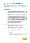
LPC1769/68/67/66/65/64/63
32-bit ARM Cortex-M3 microcontroller; up to 512 kB flash and
64 kB SRAM with Ethernet, USB 2.0 Host/Device/OTG, CAN
Rev. 9.5 — 24 June 2014
Product data sheet
1. General description
The LPC1769/68/67/66/65/64/63 are ARM Cortex-M3 based microcontrollers for
embedded applications featuring a high level of integration and low power consumption.
The ARM Cortex-M3 is a next generation core that offers system enhancements such as
enhanced debug features and a higher level of support block integration.
The LPC1768/67/66/65/64/63 operate at CPU frequencies of up to 100 MHz. The
LPC1769 operates at CPU frequencies of up to 120 MHz. The ARM Cortex-M3 CPU
incorporates a 3-stage pipeline and uses a Harvard architecture with separate local
instruction and data buses as well as a third bus for peripherals. The ARM Cortex-M3
CPU also includes an internal prefetch unit that supports speculative branching.
The peripheral complement of the LPC1769/68/67/66/65/64/63 includes up to 512 kB of
flash memory, up to 64 kB of data memory, Ethernet MAC, USB Device/Host/OTG
interface, 8-channel general purpose DMA controller, 4 UARTs, 2 CAN channels, 2 SSP
controllers, SPI interface, 3 I2C-bus interfaces, 2-input plus 2-output I2S-bus interface,
8-channel 12-bit ADC, 10-bit DAC, motor control PWM, Quadrature Encoder interface,
four general purpose timers, 6-output general purpose PWM, ultra-low power Real-Time
Clock (RTC) with separate battery supply, and up to 70 general purpose I/O pins.
The LPC1769/68/67/66/65/64/63 are pin-compatible to the 100-pin LPC236x
ARM7-based microcontroller series.
For additional documentation, see Section 19 “References”.
2. Features and benefits
ARM Cortex-M3 processor, running at frequencies of up to 100 MHz
(LPC1768/67/66/65/64/63) or of up to 120 MHz (LPC1769). A Memory Protection Unit
(MPU) supporting eight regions is included.
ARM Cortex-M3 built-in Nested Vectored Interrupt Controller (NVIC).
Up to 512 kB on-chip flash programming memory. Enhanced flash memory accelerator
enables high-speed 120 MHz operation with zero wait states.
In-System Programming (ISP) and In-Application Programming (IAP) via on-chip
bootloader software.
On-chip SRAM includes:
32/16 kB of SRAM on the CPU with local code/data bus for high-performance CPU
access.
NXP Semiconductors
LPC1769/68/67/66/65/64/63
32-bit ARM Cortex-M3 microcontroller
Two/one 16 kB SRAM blocks with separate access paths for higher throughput.
These SRAM blocks may be used for Ethernet, USB, and DMA memory, as well as
for general purpose CPU instruction and data storage.
Eight channel General Purpose DMA controller (GPDMA) on the AHB multilayer
matrix that can be used with SSP, I2S-bus, UART, Analog-to-Digital and
Digital-to-Analog converter peripherals, timer match signals, and for
memory-to-memory transfers.
Multilayer AHB matrix interconnect provides a separate bus for each AHB master.
AHB masters include the CPU, General Purpose DMA controller, Ethernet MAC, and
the USB interface. This interconnect provides communication with no arbitration
delays.
Split APB bus allows high throughput with few stalls between the CPU and DMA.
Serial interfaces:
Ethernet MAC with RMII interface and dedicated DMA controller. (Not available on
all parts, see Table 2.)
USB 2.0 full-speed device/Host/OTG controller with dedicated DMA controller and
on-chip PHY for device, Host, and OTG functions. (Not available on all parts, see
Table 2.)
Four UARTs with fractional baud rate generation, internal FIFO, and DMA support.
One UART has modem control I/O and RS-485/EIA-485 support, and one UART
has IrDA support.
CAN 2.0B controller with two channels. (Not available on all parts, see Table 2.)
SPI controller with synchronous, serial, full duplex communication and
programmable data length.
Two SSP controllers with FIFO and multi-protocol capabilities. The SSP interfaces
can be used with the GPDMA controller.
Three enhanced I2C bus interfaces, one with an open-drain output supporting full
I2C specification and Fast mode plus with data rates of 1 Mbit/s, two with standard
port pins. Enhancements include multiple address recognition and monitor mode.
I2S (Inter-IC Sound) interface for digital audio input or output, with fractional rate
control. The I2S-bus interface can be used with the GPDMA. The I2S-bus interface
supports 3-wire and 4-wire data transmit and receive as well as master clock
input/output. (Not available on all parts, see Table 2.)
Other peripherals:
70 (100 pin package) General Purpose I/O (GPIO) pins with configurable
pull-up/down resistors. All GPIOs support a new, configurable open-drain operating
mode. The GPIO block is accessed through the AHB multilayer bus for fast access
and located in memory such that it supports Cortex-M3 bit banding and use by the
General Purpose DMA Controller.
12-bit Analog-to-Digital Converter (ADC) with input multiplexing among eight pins,
conversion rates up to 200 kHz, and multiple result registers. The 12-bit ADC can
be used with the GPDMA controller.
10-bit Digital-to-Analog Converter (DAC) with dedicated conversion timer and DMA
support. (Not available on all parts, see Table 2)
Four general purpose timers/counters, with a total of eight capture inputs and ten
compare outputs. Each timer block has an external count input. Specific timer
events can be selected to generate DMA requests.
One motor control PWM with support for three-phase motor control.
LPC1769_68_67_66_65_64_63
All information provided in this document is subject to legal disclaimers.
Product data sheet
Rev. 9.5 — 24 June 2014
© NXP Semiconductors N.V. 2014. All rights reserved.
2 of 89
NXP Semiconductors
LPC1769/68/67/66/65/64/63
32-bit ARM Cortex-M3 microcontroller
1.
Quadrature encoder interface that can monitor one external quadrature encoder.
One standard PWM/timer block with external count input.
RTC with a separate power domain and dedicated RTC oscillator. The RTC block
includes 20 bytes of battery-powered backup registers.
WatchDog Timer (WDT). The WDT can be clocked from the internal RC oscillator,
the RTC oscillator, or the APB clock.
ARM Cortex-M3 system tick timer, including an external clock input option.
Repetitive interrupt timer provides programmable and repeating timed interrupts.
Each peripheral has its own clock divider for further power savings.
Standard JTAG test/debug interface for compatibility with existing tools. Serial Wire
Debug and Serial Wire Trace Port options.
Emulation trace module enables non-intrusive, high-speed real-time tracing of
instruction execution.
Integrated PMU (Power Management Unit) automatically adjusts internal regulators to
minimize power consumption during Sleep, Deep sleep, Power-down, and Deep
power-down modes.
Four reduced power modes: Sleep, Deep-sleep, Power-down, and Deep power-down.
Single 3.3 V power supply (2.4 V to 3.6 V).
Four external interrupt inputs configurable as edge/level sensitive. All pins on Port 0
and Port 2 can be used as edge sensitive interrupt sources.
Non-maskable Interrupt (NMI) input.
Clock output function that can reflect the main oscillator clock, IRC clock, RTC clock,
CPU clock, and the USB clock.
The Wake-up Interrupt Controller (WIC) allows the CPU to automatically wake up from
any priority interrupt that can occur while the clocks are stopped in deep sleep,
Power-down, and Deep power-down modes.
Processor wake-up from Power-down mode via any interrupt able to operate during
Power-down mode (includes external interrupts, RTC interrupt, USB activity, Ethernet
wake-up interrupt, CAN bus activity, Port 0/2 pin interrupt, and NMI).
Brownout detect with separate threshold for interrupt and forced reset.
Power-On Reset (POR).
Crystal oscillator with an operating range of 1 MHz to 25 MHz.
4 MHz internal RC oscillator trimmed to 1 % accuracy that can optionally be used as a
system clock.
PLL allows CPU operation up to the maximum CPU rate without the need for a
high-frequency crystal. May be run from the main oscillator, the internal RC oscillator,
or the RTC oscillator.
USB PLL for added flexibility.
Code Read Protection (CRP) with different security levels.
Unique device serial number for identification purposes.
Available as LQFP100 (14 mm 14 mm 1.4 mm), TFBGA1001 (9 mm 9 mm 0.7
mm), and WLCSP100 (5.074 5.074 0.6 mm) package.
LPC1768/65 only.
LPC1769_68_67_66_65_64_63
All information provided in this document is subject to legal disclaimers.
Product data sheet
Rev. 9.5 — 24 June 2014
© NXP Semiconductors N.V. 2014. All rights reserved.
3 of 89
LPC1769/68/67/66/65/64/63
NXP Semiconductors
32-bit ARM Cortex-M3 microcontroller
3. Applications
eMetering
Lighting
Industrial networking
Alarm systems
White goods
Motor control
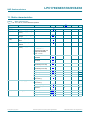
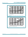
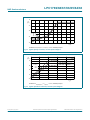
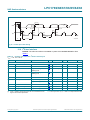
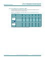
4. Ordering information
Table 1.
Ordering information
Type number
Package
Name
Description
Version
LPC1769FBD100
LQFP100
plastic low profile quad flat package; 100 leads; body 14 14 1.4 mm
SOT407-1
LPC1768FBD100
LQFP100
plastic low profile quad flat package; 100 leads; body 14 14 1.4 mm
SOT407-1
LPC1768FET100
TFBGA100
plastic thin fine-pitch ball grid array package; 100 balls; body 9 9 0.7 mm SOT926-1
LPC1768UK
WLCSP100 wafer level chip-scale package; 100 balls; 5.074 5.074 0.6 mm
LPC1767FBD100
LQFP100
plastic low profile quad flat package; 100 leads; body 14 14 1.4 mm
SOT407-1
LPC1766FBD100
LQFP100
plastic low profile quad flat package; 100 leads; body 14 14 1.4 mm
SOT407-1
LPC1765FBD100
LQFP100
plastic low profile quad flat package; 100 leads; body 14 14 1.4 mm
SOT407-1
LPC1765FET100
TFBGA100
plastic thin fine-pitch ball grid array package; 100 balls; body 9 9 0.7 mm SOT926-1
LPC1764FBD100
LQFP100
plastic low profile quad flat package; 100 leads; body 14 14 1.4 mm
SOT407-1
LPC1763FBD100
LQFP100
plastic low profile quad flat package; 100 leads; body 14 14 1.4 mm
SOT407-1
-
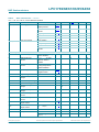
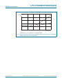
4.1 Ordering options
Table 2.
Ordering options
Type number
Flash
SRAM in kB
Ethernet USB
CAN
I2S
DAC Maximum
CPU
operating
frequency
CPU AHB
AHB
Total
SRAM0 SRAM1
LPC1769FBD100 512 kB 32
16
16
64
yes
Device/Host/OTG 2
yes
yes
120 MHz
LPC1768FBD100 512 kB 32
16
16
64
yes
Device/Host/OTG 2
yes
yes
100 MHz
LPC1768FET100 512 kB 32
16
16
64
yes
Device/Host/OTG 2
yes
yes
100 MHz
LPC1768UK
512 kB 32
16
16
64
yes
Device/Host/OTG 2
yes
yes
100 MHz
LPC1767FBD100 512 kB 32
16
16
64
yes
no
yes
yes
100 MHz
LPC1766FBD100 256 kB 32
16
16
64
yes
Device/Host/OTG 2
yes
yes
100 MHz
LPC1765FBD100 256 kB 32
16
16
64
no
Device/Host/OTG 2
yes
yes
100 MHz
no
LPC1765FET100 256 kB 32
16
16
64
no
Device/Host/OTG 2
yes
yes
100 MHz
LPC1764FBD100 128 kB 16
16
-
32
yes
Device only
2
no
no
100 MHz
LPC1763FBD100 256 kB 32
16
16
64
no
no
no
yes
yes
100 MHz
LPC1769_68_67_66_65_64_63
All information provided in this document is subject to legal disclaimers.
Product data sheet
Rev. 9.5 — 24 June 2014
© NXP Semiconductors N.V. 2014. All rights reserved.
4 of 89
LPC1769/68/67/66/65/64/63
NXP Semiconductors
32-bit ARM Cortex-M3 microcontroller
5. Marking
The LPC176x devices typically have the following top-side marking:
LPC176xxxx
xxxxxxx
xxYYWWR[x]
The last/second to last letter in the third line (field ‘R’) will identify the device revision. This
data sheet covers the following revisions of the LPC176x:
Table 3.
Device revision table
Revision identifier (R)
Revision description
‘-’
Initial device revision
‘A’
Second device revision
‘B’
Third device revision
Field ‘YY’ states the year the device was manufactured. Field ‘WW’ states the week the
device was manufactured during that year.
LPC1769_68_67_66_65_64_63
All information provided in this document is subject to legal disclaimers.
Product data sheet
Rev. 9.5 — 24 June 2014
© NXP Semiconductors N.V. 2014. All rights reserved.
5 of 89
LPC1769/68/67/66/65/64/63
NXP Semiconductors
32-bit ARM Cortex-M3 microcontroller
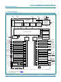
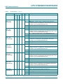
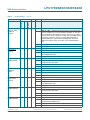
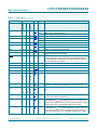
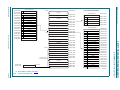
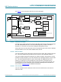
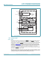
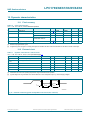
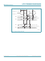
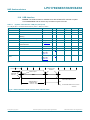
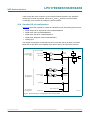
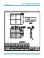
6. Block diagram
JTAG
interface
EMULATION
TRACE MODULE
debug
port
RMII pins
LPC1769/68/67/
66/65/64/63
TEST/DEBUG
INTERFACE
I-code
bus
MPU
ARM
CORTEX-M3
D-code
bus
DMA
CONTROLLER
system
bus
USB PHY
CLOCK
GENERATION,
POWER CONTROL,
SYSTEM
FUNCTIONS
USB HOST/
DEVICE/OTG
CONTROLLER
WITH DMA(1)
ETHERNET
CONTROLLER
WITH DMA(1)
master
XTAL1
XTAL2
RESET
USB pins
master
CLKOUT
clocks and
controls
master
slave
ROM
slave
MULTILAYER AHB MATRIX
SRAM 32/64 kB
P0 to
P4
slave
HIGH-SPEED
GPIO
SCK1
SSEL1
MISO1
MOSI1
RXD0/TXD0
8 × UART1
FLASH
ACCELERATOR
FLASH
512/256/128 kB
APB slave group 1
SCK0
SSEL0
MISO0
MOSI0
SSP0
RXD2/3
TXD2/3
UART2/3
I2S(1)
3 × I2SRX
3 × I2STX
TX_MCLK
RX_MCLK
SPI0
I2C2
SCL2
SDA2
TIMER 0/1
RI TIMER
WDT
TIMER2/3
PWM1
EXTERNAL INTERRUPTS
12-bit ADC
SYSTEM CONTROL
PIN CONNECT
MOTOR CONTROL PWM
CAN1/2(1)
I2C0/1
PWM1[7:0]
PCAP1[1:0]
AD0[7:0]
VBAT
AHB TO
APB
BRIDGE 1
UART0/1
2 × CAP0/1
RTCX2
slave
slave
SSP1
SCK/SSEL
MOSI/MISO
2 × MAT0/1
RTCX1
AHB TO
APB
BRIDGE 0
APB slave group 0
RD1/2
TD1/2
SCL0/1
SDA0/1
P0, P2
slave
GPIO INTERRUPT CONTROL
32 kHz
OSCILLATOR
4 × MAT2
2 × MAT3
2 × CAP2
2 × CAP3
DAC(1)
RTC
EINT[3:0]
MCOA[2:0]
MCOB[2:0]
MCI[2:0]
MCABORT
AOUT
QUADRATURE ENCODER
PHA, PHB
INDEX
BACKUP REGISTERS
= connected to DMA
RTC POWER DOMAIN
002aad944
(1) Not available on all parts. See Table 2.
Fig 1.
Block diagram
LPC1769_68_67_66_65_64_63
All information provided in this document is subject to legal disclaimers.
Product data sheet
Rev. 9.5 — 24 June 2014
© NXP Semiconductors N.V. 2014. All rights reserved.
6 of 89
LPC1769/68/67/66/65/64/63
NXP Semiconductors
32-bit ARM Cortex-M3 microcontroller
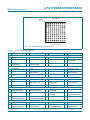
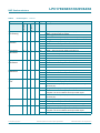
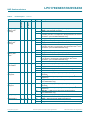
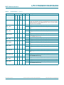
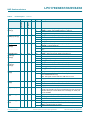
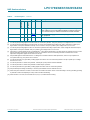
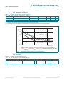
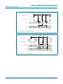
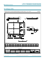
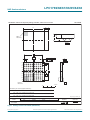
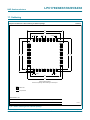
7. Pinning information
51
75
7.1 Pinning
76
50
LPC176xFBD100
26
1
25
100
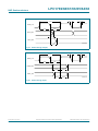
Fig 2.
002aad945
Pin configuration LQFP100 package
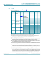
ball A1
index area
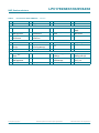
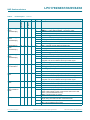
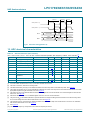
LPC1768/65FET100
1
2
3
4
5
6
7
8
9 10
A
B
C
D
E
F
G
H
J
K
002aaf723
Transparent top view
Fig 3.
Pin configuration TFBGA100 package
LPC1769_68_67_66_65_64_63
All information provided in this document is subject to legal disclaimers.
Product data sheet
Rev. 9.5 — 24 June 2014
© NXP Semiconductors N.V. 2014. All rights reserved.
7 of 89
LPC1769/68/67/66/65/64/63
NXP Semiconductors
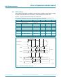
32-bit ARM Cortex-M3 microcontroller
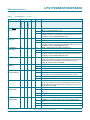
LPC1768UK
bump A1
index area
1
2
3
4
5
6
7
8
9
10
A
B
C
D
E
F
G
H
J
K
aaa-009522
Transparent top view
Fig 4.
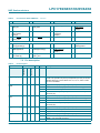
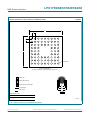
Table 4.
Pin configuration WLCSP100 package
Pin allocation table TFBGA100
Pin Symbol
Pin Symbol
Pin Symbol
Pin Symbol
Row A
1
TDO/SWO
2
P0[3]/RXD0/AD0[6]
3
VDD(3V3)
4
P1[4]/ENET_TX_EN
5
P1[10]/ENET_RXD1
6
P1[16]/ENET_MDC
7
VDD(REG)(3V3)
8
P0[4]/I2SRX_CLK/
RD2/CAP2[0]
9
P0[7]/I2STX_CLK/
SCK1/MAT2[1]
10
P0[9]/I2STX_SDA/
MOSI1/MAT2[3]
11
-
12
-
Row B
1
TMS/SWDIO
2
RTCK
3
VSS
4
P1[1]/ENET_TXD1
5
P1[9]/ENET_RXD0
6
P1[17]/
ENET_MDIO
7
VSS
8
P0[6]/I2SRX_SDA/
SSEL1/MAT2[0]
9
P2[0]/PWM1[1]/TXD1
10
P2[1]/PWM1[2]/RXD1
11
-
12
-
Row C
1
TCK/SWDCLK
2
TRST
3
TDI
4
P0[2]/TXD0/AD0[7]
5
P1[8]/ENET_CRS
6
P1[15]/
ENET_REF_CLK
7
P4[28]/RX_MCLK/
MAT2[0]/TXD3
8
P0[8]/I2STX_WS/
MISO1/MAT2[2]
9
VSS
10
VDD(3V3)
11
-
12
-
Row D
1
P0[24]/AD0[1]/
I2SRX_WS/CAP3[1]
2
P0[25]/AD0[2]/
I2SRX_SDA/TXD3
3
P0[26]/AD0[3]/
AOUT/RXD3
4
n.c.
5
P1[0]/ENET_TXD0
6
P1[14]/ENET_RX_ER
7
P0[5]/I2SRX_WS/
TD2/CAP2[1]
8
P2[2]/PWM1[3]/
CTS1/TRACEDATA[3]
9
P2[4]/PWM1[5]/
DSR1/TRACEDATA[1]
10
P2[5]/PWM1[6]/
DTR1/TRACEDATA[0]
11
-
12
-
Row E
1
VSSA
2
VDDA
3
VREFP
4
n.c.
5
P0[23]/AD0[0]/
I2SRX_CLK/CAP3[0]
6
P4[29]/TX_MCLK/
MAT2[1]/RXD3
7
P2[3]/PWM1[4]/
DCD1/TRACEDATA[2]
8
P2[6]/PCAP1[0]/
RI1/TRACECLK
LPC1769_68_67_66_65_64_63
All information provided in this document is subject to legal disclaimers.
Product data sheet
Rev. 9.5 — 24 June 2014
© NXP Semiconductors N.V. 2014. All rights reserved.
8 of 89
LPC1769/68/67/66/65/64/63
NXP Semiconductors
32-bit ARM Cortex-M3 microcontroller
Table 4.
Pin allocation table TFBGA100 …continued
Pin Symbol
Pin Symbol
Pin Symbol
Pin Symbol
9
10
P2[8]/TD2/TXD2
11
-
12
-
P2[7]/RD2/RTS1
Row F
1
VREFN
2
RTCX1
3
RESET
4
P1[31]/SCK1/
AD0[5]
5
P1[21]/MCABORT/
PWM1[3]/SSEL0
6
P0[18]/DCD1/
MOSI0/MOSI
7
P2[9]/USB_CONNECT/
RXD2
8
P0[16]/RXD1/
SSEL0/SSEL
9
P0[17]/CTS1/
MISO0/MISO
10
P0[15]/TXD1/
SCK0/SCK
11
-
12
-
Row G
1
RTCX2
2
VBAT
3
XTAL2
4
P0[30]/USB_D
5
P1[25]/MCOA1/
MAT1[1]
6
P1[29]/MCOB2/
PCAP1[1]/MAT0[1]
7
VSS
8
P0[21]/RI1/RD1
9
P0[20]/DTR1/SCL1
10
P0[19]/DSR1/SDA1
11
-
12
-
Row H
1
P1[30]/VBUS/
AD0[4]
2
XTAL1
3
P3[25]/MAT0[0]/
PWM1[2]
4
P1[18]/USB_UP_LED/
PWM1[1]/CAP1[0]
5
P1[24]/MCI2/
PWM1[5]/MOSI0
6
VDD(REG)(3V3)
7
P0[10]/TXD2/
SDA2/MAT3[0]
8
P2[11]/EINT1/
I2STX_CLK
9
VDD(3V3)
10
P0[22]/RTS1/TD1
11
-
12
-
LPC1769_68_67_66_65_64_63
All information provided in this document is subject to legal disclaimers.
Product data sheet
Rev. 9.5 — 24 June 2014
© NXP Semiconductors N.V. 2014. All rights reserved.
9 of 89
LPC1769/68/67/66/65/64/63
NXP Semiconductors
32-bit ARM Cortex-M3 microcontroller
Table 4.
Pin allocation table TFBGA100 …continued
Pin Symbol
Pin Symbol
Pin Symbol
Pin Symbol
Row J
1
P0[28]/SCL0/
USB_SCL
2
P0[27]/SDA0/
USB_SDA
3
P0[29]/USB_D+
4
P1[19]/MCOA0/
USB_PPWR/
CAP1[1]
5
P1[22]/MCOB0/
USB_PWRD/
MAT1[0]
6
VSS
7
P1[28]/MCOA2/
PCAP1[0]/
MAT0[0]
8
P0[1]/TD1/RXD3/SCL1
9
P2[13]/EINT3/
I2STX_SDA
10
P2[10]/EINT0/NMI
11
-
12
-
Row K
1
P3[26]/STCLK/
MAT0[1]/PWM1[3]
2
VDD(3V3)
3
VSS
4
P1[20]/MCI0/
PWM1[2]/SCK0
5
P1[23]/MCI1/
PWM1[4]/MISO0
6
P1[26]/MCOB1/
PWM1[6]/CAP0[0]
7
P1[27]/CLKOUT
/USB_OVRCR/
CAP0[1]
8
P0[0]/RD1/TXD3/SDA1
9
P0[11]/RXD2/
SCL2/MAT3[1]
10
P2[12]/EINT2/
I2STX_WS
11
-
12
-
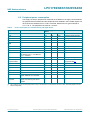
7.2 Pin description
Pin description
P0[0] to P0[31]
P0[0]/RD1/TXD3/
SDA1
P0[1]/TD1/RXD3/
SCL1
46
47
P0[2]/TXD0/AD0[7] 98
P0[3]/RXD0/AD0[6] 99
K8
J8
C4
A2
Type
Description
I/O
Port 0: Port 0 is a 32-bit I/O port with individual direction controls for
each bit. The operation of port 0 pins depends upon the pin function
selected via the pin connect block. Pins 12, 13, 14, and 31 of this
port are not available.
WLCSP100
Pin/ball
LQFP100
Symbol
TFBGA100
Table 5.
H10
H9
B1
C3
[1]
[1]
[2]
[2]
I/O
P0[0] — General purpose digital input/output pin.
I
RD1 — CAN1 receiver input. (LPC1769/68/66/65/64 only).
O
TXD3 — Transmitter output for UART3.
I/O
SDA1 — I2C1 data input/output. (This is not an I2C-bus compliant
open-drain pin).
I/O
P0[1] — General purpose digital input/output pin.
O
TD1 — CAN1 transmitter output. (LPC1769/68/66/65/64 only).
I
RXD3 — Receiver input for UART3.
I/O
SCL1 — I2C1 clock input/output. (This is not an I2C-bus compliant
open-drain pin).
I/O
P0[2] — General purpose digital input/output pin.
O
TXD0 — Transmitter output for UART0.
I
AD0[7] — A/D converter 0, input 7.
I/O
P0[3] — General purpose digital input/output pin.
I
RXD0 — Receiver input for UART0.
I
AD0[6] — A/D converter 0, input 6.
LPC1769_68_67_66_65_64_63
All information provided in this document is subject to legal disclaimers.
Product data sheet
Rev. 9.5 — 24 June 2014
© NXP Semiconductors N.V. 2014. All rights reserved.
10 of 89
LPC1769/68/67/66/65/64/63
NXP Semiconductors
Table 5.
Pin description …continued
Symbol
Pin/ball
LQFP100
TFBGA100
WLCSP100
32-bit ARM Cortex-M3 microcontroller
P0[4]/
I2SRX_CLK/
RD2/CAP2[0]
81
A8
G2
P0[5]/
I2SRX_WS/
TD2/CAP2[1]
P0[6]/
I2SRX_SDA/
SSEL1/MAT2[0]
P0[7]/
I2STX_CLK/
SCK1/MAT2[1]
P0[8]/
I2STX_WS/
MISO1/MAT2[2]
P0[9]/
I2STX_SDA/
MOSI1/MAT2[3]
P0[10]/TXD2/
SDA2/MAT3[0]
80
79
78
77
76
48
D7
B8
A9
C8
H1
G3
J1
H2
A10 H3
H7
H8
[1]
[1]
[1]
[1]
[1]
[1]
[1]
Type
Description
I/O
P0[4] — General purpose digital input/output pin.
I/O
I2SRX_CLK — Receive Clock. It is driven by the master and
received by the slave. Corresponds to the signal SCK in the I2S-bus
specification. (LPC1769/68/67/66/65/63 only).
I
RD2 — CAN2 receiver input. (LPC1769/68/66/65/64 only).
I
CAP2[0] — Capture input for Timer 2, channel 0.
I/O
P0[5] — General purpose digital input/output pin.
I/O
I2SRX_WS — Receive Word Select. It is driven by the master and
received by the slave. Corresponds to the signal WS in the I2S-bus
specification. (LPC1769/68/67/66/65/63 only).
O
TD2 — CAN2 transmitter output. (LPC1769/68/66/65/64 only).
I
CAP2[1] — Capture input for Timer 2, channel 1.
I/O
P0[6] — General purpose digital input/output pin.
I/O
I2SRX_SDA — Receive data. It is driven by the transmitter and read
by the receiver. Corresponds to the signal SD in the I2S-bus
specification. (LPC1769/68/67/66/65/63 only).
I/O
SSEL1 — Slave Select for SSP1.
O
MAT2[0] — Match output for Timer 2, channel 0.
I/O
P0[7] — General purpose digital input/output pin.
I/O
I2STX_CLK — Transmit Clock. It is driven by the master and
received by the slave. Corresponds to the signal SCK in the I2S-bus
specification. (LPC1769/68/67/66/65/63 only).
I/O
SCK1 — Serial Clock for SSP1.
O
MAT2[1] — Match output for Timer 2, channel 1.
I/O
P0[8] — General purpose digital input/output pin.
I/O
I2STX_WS — Transmit Word Select. It is driven by the master and
received by the slave. Corresponds to the signal WS in the I2S-bus
specification. (LPC1769/68/67/66/65/63 only).
I/O
MISO1 — Master In Slave Out for SSP1.
O
MAT2[2] — Match output for Timer 2, channel 2.
I/O
P0[9] — General purpose digital input/output pin.
I/O
I2STX_SDA — Transmit data. It is driven by the transmitter and
read by the receiver. Corresponds to the signal SD in the I2S-bus
specification. (LPC1769/68/67/66/65/63 only).
I/O
MOSI1 — Master Out Slave In for SSP1.
O
MAT2[3] — Match output for Timer 2, channel 3.
I/O
P0[10] — General purpose digital input/output pin.
O
TXD2 — Transmitter output for UART2.
I/O
SDA2 — I2C2 data input/output (this is not an open-drain pin).
O
MAT3[0] — Match output for Timer 3, channel 0.
LPC1769_68_67_66_65_64_63
All information provided in this document is subject to legal disclaimers.
Product data sheet
Rev. 9.5 — 24 June 2014
© NXP Semiconductors N.V. 2014. All rights reserved.
11 of 89
LPC1769/68/67/66/65/64/63
NXP Semiconductors
Table 5.
Pin description …continued
Symbol
Pin/ball
LQFP100
TFBGA100
WLCSP100
32-bit ARM Cortex-M3 microcontroller
P0[11]/RXD2/
SCL2/MAT3[1]
49
K9
J10
P0[15]/TXD1/
SCK0/SCK
P0[16]/RXD1/
SSEL0/SSEL
P0[17]/CTS1/
MISO0/MISO
P0[18]/DCD1/
MOSI0/MOSI
P0[19]/DSR1/
SDA1
62
63
61
60
59
P0[20]/DTR1/SCL1 58
P0[21]/RI1/RD1
P0[22]/RTS1/TD1
57
56
F10 H6
F8
F9
F6
J5
K6
J6
G10 K7
G9
G8
J7
H7
H10 K8
[1]
[1]
[1]
[1]
[1]
[1]
[1]
[1]
[1]
Type
Description
I/O
P0[11] — General purpose digital input/output pin.
I
RXD2 — Receiver input for UART2.
I/O
SCL2 — I2C2 clock input/output (this is not an open-drain pin).
O
MAT3[1] — Match output for Timer 3, channel 1.
I/O
P0[15] — General purpose digital input/output pin.
O
TXD1 — Transmitter output for UART1.
I/O
SCK0 — Serial clock for SSP0.
I/O
SCK — Serial clock for SPI.
I/O
P0[16] — General purpose digital input/output pin.
I
RXD1 — Receiver input for UART1.
I/O
SSEL0 — Slave Select for SSP0.
I/O
SSEL — Slave Select for SPI.
I/O
P0[17] — General purpose digital input/output pin.
I
CTS1 — Clear to Send input for UART1.
I/O
MISO0 — Master In Slave Out for SSP0.
I/O
MISO — Master In Slave Out for SPI.
I/O
P0[18] — General purpose digital input/output pin.
I
DCD1 — Data Carrier Detect input for UART1.
I/O
MOSI0 — Master Out Slave In for SSP0.
I/O
MOSI — Master Out Slave In for SPI.
I/O
P0[19] — General purpose digital input/output pin.
I
DSR1 — Data Set Ready input for UART1.
I/O
SDA1 — I2C1 data input/output (this is not an I2C-bus compliant
open-drain pin).
I/O
P0[20] — General purpose digital input/output pin.
O
DTR1 — Data Terminal Ready output for UART1. Can also be
configured to be an RS-485/EIA-485 output enable signal.
I/O
SCL1 — I2C1 clock input/output (this is not an I2C-bus compliant
open-drain pin).
I/O
P0[21] — General purpose digital input/output pin.
I
RI1 — Ring Indicator input for UART1.
I
RD1 — CAN1 receiver input. (LPC1769/68/66/65/64 only).
I/O
P0[22] — General purpose digital input/output pin.
O
RTS1 — Request to Send output for UART1. Can also be
configured to be an RS-485/EIA-485 output enable signal.
O
TD1 — CAN1 transmitter output. (LPC1769/68/66/65/64 only).
LPC1769_68_67_66_65_64_63
All information provided in this document is subject to legal disclaimers.
Product data sheet
Rev. 9.5 — 24 June 2014
© NXP Semiconductors N.V. 2014. All rights reserved.
12 of 89
LPC1769/68/67/66/65/64/63
NXP Semiconductors
Table 5.
Pin description …continued
Symbol
Pin/ball
LQFP100
TFBGA100
WLCSP100
32-bit ARM Cortex-M3 microcontroller
P0[23]/AD0[0]/
I2SRX_CLK/
CAP3[0]
9
E5
D5
P0[24]/AD0[1]/
I2SRX_WS/
CAP3[1]
8
P0[25]/AD0[2]/
I2SRX_SDA/
TXD3
7
P0[26]/AD0[3]/
AOUT/RXD3
6
P0[27]/SDA0/
USB_SDA
P0[28]/SCL0/
USB_SCL
P0[29]/USB_D+
P0[30]/USB_D
25
24
29
30
D1
D2
D3
J2
J1
J3
G4
B4
A3
C5
C8
B9
[2]
[2]
[2]
[3]
[4]
[4]
B10
[5]
C9
[5]
Type
Description
I/O
P0[23] — General purpose digital input/output pin.
I
AD0[0] — A/D converter 0, input 0.
I/O
I2SRX_CLK — Receive Clock. It is driven by the master and
received by the slave. Corresponds to the signal SCK in the I2S-bus
specification. (LPC1769/68/67/66/65/63 only).
I
CAP3[0] — Capture input for Timer 3, channel 0.
I/O
P0[24] — General purpose digital input/output pin.
I
AD0[1] — A/D converter 0, input 1.
I/O
I2SRX_WS — Receive Word Select. It is driven by the master and
received by the slave. Corresponds to the signal WS in the I2S-bus
specification. (LPC1769/68/67/66/65/63 only).
I
CAP3[1] — Capture input for Timer 3, channel 1.
I/O
P0[25] — General purpose digital input/output pin.
I
AD0[2] — A/D converter 0, input 2.
I/O
I2SRX_SDA — Receive data. It is driven by the transmitter and read
by the receiver. Corresponds to the signal SD in the I2S-bus
specification. (LPC1769/68/67/66/65/63 only).
O
TXD3 — Transmitter output for UART3.
I/O
P0[26] — General purpose digital input/output pin.
I
AD0[3] — A/D converter 0, input 3.
O
AOUT — DAC output (LPC1769/68/67/66/65/63 only).
I
RXD3 — Receiver input for UART3.
I/O
P0[27] — General purpose digital input/output pin. Output is
open-drain.
I/O
SDA0 — I2C0 data input/output. Open-drain output (for I2C-bus
compliance).
I/O
USB_SDA — USB port I2C serial data (OTG transceiver,
LPC1769/68/66/65 only).
I/O
P0[28] — General purpose digital input/output pin. Output is
open-drain.
I/O
SCL0 — I2C0 clock input/output. Open-drain output (for I2C-bus
compliance).
I/O
USB_SCL — USB port I2C serial clock (OTG transceiver,
LPC1769/68/66/65 only).
I/O
P0[29] — General purpose digital input/output pin.
I/O
USB_D+ — USB bidirectional D+ line. (LPC1769/68/66/65/64 only).
I/O
P0[30] — General purpose digital input/output pin.
I/O
USB_D — USB bidirectional D line. (LPC1769/68/66/65/64 only).
LPC1769_68_67_66_65_64_63
All information provided in this document is subject to legal disclaimers.
Product data sheet
Rev. 9.5 — 24 June 2014
© NXP Semiconductors N.V. 2014. All rights reserved.
13 of 89
LPC1769/68/67/66/65/64/63
NXP Semiconductors
32-bit ARM Cortex-M3 microcontroller
Pin/ball
P1[0] to P1[31]
P1[0]/
ENET_TXD0
95
P1[1]/
ENET_TXD1
94
P1[4]/
ENET_TX_EN
93
P1[8]/
ENET_CRS
92
P1[9]/
ENET_RXD0
91
P1[10]/
ENET_RXD1
90
P1[14]/
ENET_RX_ER
89
P1[15]/
ENET_REF_CLK
88
P1[16]/
ENET_MDC
87
P1[17]/
ENET_MDIO
86
D5
B4
A4
C5
B5
A5
D6
C6
A6
B6
Type
Description
I/O
Port 1: Port 1 is a 32-bit I/O port with individual direction controls for
each bit. The operation of port 1 pins depends upon the pin function
selected via the pin connect block. Pins 2, 3, 5, 6, 7, 11, 12, and 13
of this port are not available.
I/O
P1[0] — General purpose digital input/output pin.
O
ENET_TXD0 — Ethernet transmit data 0. (LPC1769/68/67/66/64
only).
I/O
P1[1] — General purpose digital input/output pin.
O
ENET_TXD1 — Ethernet transmit data 1. (LPC1769/68/67/66/64
only).
I/O
P1[4] — General purpose digital input/output pin.
O
ENET_TX_EN — Ethernet transmit data enable.
(LPC1769/68/67/66/64 only).
WLCSP100
Symbol
TFBGA100
Pin description …continued
LQFP100
Table 5.
C1
C2
D2
D1
D3
E3
E2
E1
[1]
[1]
[1]
[1]
[1]
[1]
[1]
[1]
F3
[1]
F2
[1]
I/O
P1[8] — General purpose digital input/output pin.
I
ENET_CRS — Ethernet carrier sense. (LPC1769/68/67/66/64 only).
I/O
P1[9] — General purpose digital input/output pin.
I
ENET_RXD0 — Ethernet receive data. (LPC1769/68/67/66/64
only).
I/O
P1[10] — General purpose digital input/output pin.
I
ENET_RXD1 — Ethernet receive data. (LPC1769/68/67/66/64
only).
I/O
P1[14] — General purpose digital input/output pin.
I
ENET_RX_ER — Ethernet receive error. (LPC1769/68/67/66/64
only).
I/O
P1[15] — General purpose digital input/output pin.
I
ENET_REF_CLK — Ethernet reference clock.
(LPC1769/68/67/66/64 only).
I/O
P1[16] — General purpose digital input/output pin.
O
ENET_MDC — Ethernet MIIM clock (LPC1769/68/67/66/64 only).
I/O
P1[17] — General purpose digital input/output pin.
I/O
ENET_MDIO — Ethernet MIIM data input and output.
(LPC1769/68/67/66/64 only).
LPC1769_68_67_66_65_64_63
All information provided in this document is subject to legal disclaimers.
Product data sheet
Rev. 9.5 — 24 June 2014
© NXP Semiconductors N.V. 2014. All rights reserved.
14 of 89
LPC1769/68/67/66/65/64/63
NXP Semiconductors
Table 5.
Pin description …continued
Symbol
Pin/ball
LQFP100
TFBGA100
WLCSP100
32-bit ARM Cortex-M3 microcontroller
P1[18]/
USB_UP_LED/
PWM1[1]/
CAP1[0]
32
H4
D9
P1[19]/MCOA0/
USB_PPWR/
CAP1[1]
P1[20]/MCI0/
PWM1[2]/SCK0
33
34
P1[21]/MCABORT/ 35
PWM1[3]/
SSEL0
P1[22]/MCOB0/
USB_PWRD/
MAT1[0]
36
P1[23]/MCI1/
PWM1[4]/MISO0
37
P1[24]/MCI2/
PWM1[5]/MOSI0
38
J4
K4
F5
J5
K5
H5
C10
E8
E9
D10
E7
F8
[1]
[1]
[1]
[1]
[1]
[1]
[1]
Type
Description
I/O
P1[18] — General purpose digital input/output pin.
O
USB_UP_LED — USB GoodLink LED indicator. It is LOW when the
device is configured (non-control endpoints enabled), or when the
host is enabled and has detected a device on the bus. It is HIGH
when the device is not configured, or when host is enabled and has
not detected a device on the bus, or during global suspend. It
transitions between LOW and HIGH (flashes) when the host is
enabled and detects activity on the bus. (LPC1769/68/66/65/64
only).
O
PWM1[1] — Pulse Width Modulator 1, channel 1 output.
I
CAP1[0] — Capture input for Timer 1, channel 0.
I/O
P1[19] — General purpose digital input/output pin.
O
MCOA0 — Motor control PWM channel 0, output A.
O
USB_PPWR — Port Power enable signal for USB port.
(LPC1769/68/66/65 only).
I
CAP1[1] — Capture input for Timer 1, channel 1.
I/O
P1[20] — General purpose digital input/output pin.
I
MCI0 — Motor control PWM channel 0, input. Also Quadrature
Encoder Interface PHA input.
O
PWM1[2] — Pulse Width Modulator 1, channel 2 output.
I/O
SCK0 — Serial clock for SSP0.
I/O
P1[21] — General purpose digital input/output pin.
O
MCABORT — Motor control PWM, LOW-active fast abort.
O
PWM1[3] — Pulse Width Modulator 1, channel 3 output.
I/O
SSEL0 — Slave Select for SSP0.
I/O
P1[22] — General purpose digital input/output pin.
O
MCOB0 — Motor control PWM channel 0, output B.
I
USB_PWRD — Power Status for USB port (host power switch,
LPC1769/68/66/65 only).
O
MAT1[0] — Match output for Timer 1, channel 0.
I/O
P1[23] — General purpose digital input/output pin.
I
MCI1 — Motor control PWM channel 1, input. Also Quadrature
Encoder Interface PHB input.
O
PWM1[4] — Pulse Width Modulator 1, channel 4 output.
I/O
MISO0 — Master In Slave Out for SSP0.
I/O
P1[24] — General purpose digital input/output pin.
I
MCI2 — Motor control PWM channel 2, input. Also Quadrature
Encoder Interface INDEX input.
O
PWM1[5] — Pulse Width Modulator 1, channel 5 output.
I/O
MOSI0 — Master Out Slave in for SSP0.
LPC1769_68_67_66_65_64_63
All information provided in this document is subject to legal disclaimers.
Product data sheet
Rev. 9.5 — 24 June 2014
© NXP Semiconductors N.V. 2014. All rights reserved.
15 of 89
LPC1769/68/67/66/65/64/63
NXP Semiconductors
Table 5.
Pin description …continued
Symbol
Pin/ball
LQFP100
TFBGA100
WLCSP100
32-bit ARM Cortex-M3 microcontroller
P1[25]/MCOA1/
MAT1[1]
39
G5
F9
P1[26]/MCOB1/
PWM1[6]/CAP0[0]
P1[27]/CLKOUT
/USB_OVRCR/
CAP0[1]
P1[28]/MCOA2/
PCAP1[0]/
MAT0[0]
P1[29]/MCOB2/
PCAP1[1]/
MAT0[1]
P1[30]/VBUS/
AD0[4]
40
43
44
45
21
K6
K7
J7
G6
H1
E10
G9
G10
G8
B8
[1]
[1]
[1]
[1]
[1]
[2]
Type
Description
I/O
P1[25] — General purpose digital input/output pin.
O
MCOA1 — Motor control PWM channel 1, output A.
O
MAT1[1] — Match output for Timer 1, channel 1.
I/O
P1[26] — General purpose digital input/output pin.
O
MCOB1 — Motor control PWM channel 1, output B.
O
PWM1[6] — Pulse Width Modulator 1, channel 6 output.
I
CAP0[0] — Capture input for Timer 0, channel 0.
I/O
P1[27] — General purpose digital input/output pin.
O
CLKOUT — Clock output pin.
I
USB_OVRCR — USB port Over-Current status. (LPC1769/68/66/65
only).
I
CAP0[1] — Capture input for Timer 0, channel 1.
I/O
P1[28] — General purpose digital input/output pin.
O
MCOA2 — Motor control PWM channel 2, output A.
I
PCAP1[0] — Capture input for PWM1, channel 0.
O
MAT0[0] — Match output for Timer 0, channel 0.
I/O
P1[29] — General purpose digital input/output pin.
O
MCOB2 — Motor control PWM channel 2, output B.
I
PCAP1[1] — Capture input for PWM1, channel 1.
O
MAT0[1] — Match output for Timer 0, channel 1.
I/O
P1[30] — General purpose digital input/output pin.
I
VBUS — Monitors the presence of USB bus power.
(LPC1769/68/66/65/64 only).
Note: This signal must be HIGH for USB reset to occur.
P1[31]/SCK1/
AD0[5]
20
F4
C7
[2]
P2[0] to P2[31]
P2[0]/PWM1[1]/
TXD1
P2[1]/PWM1[2]/
RXD1
75
74
B9
K1
B10 J2
[1]
[1]
I
AD0[4] — A/D converter 0, input 4.
I/O
P1[31] — General purpose digital input/output pin.
I/O
SCK1 — Serial Clock for SSP1.
I
AD0[5] — A/D converter 0, input 5.
I/O
Port 2: Port 2 is a 32-bit I/O port with individual direction controls for
each bit. The operation of port 2 pins depends upon the pin function
selected via the pin connect block. Pins 14 through 31 of this port
are not available.
I/O
P2[0] — General purpose digital input/output pin.
O
PWM1[1] — Pulse Width Modulator 1, channel 1 output.
O
TXD1 — Transmitter output for UART1.
I/O
P2[1] — General purpose digital input/output pin.
O
PWM1[2] — Pulse Width Modulator 1, channel 2 output.
I
RXD1 — Receiver input for UART1.
LPC1769_68_67_66_65_64_63
All information provided in this document is subject to legal disclaimers.
Product data sheet
Rev. 9.5 — 24 June 2014
© NXP Semiconductors N.V. 2014. All rights reserved.
16 of 89
LPC1769/68/67/66/65/64/63
NXP Semiconductors
Table 5.
Pin description …continued
Symbol
Pin/ball
LQFP100
TFBGA100
WLCSP100
32-bit ARM Cortex-M3 microcontroller
P2[2]/PWM1[3]/
CTS1/
TRACEDATA[3]
73
D8
K2
P2[3]/PWM1[4]/
DCD1/
TRACEDATA[2]
P2[4]/PWM1[5]/
DSR1/
TRACEDATA[1]
P2[5]/PWM1[6]/
DTR1/
TRACEDATA[0]
P2[6]/PCAP1[0]/
RI1/TRACECLK
P2[7]/RD2/
RTS1
P2[8]/TD2/
TXD2
P2[9]/
USB_CONNECT/
RXD2
P2[10]/EINT0/NMI
70
69
68
67
66
65
64
53
E7
D9
K3
J3
D10 H4
E8
E9
K4
J4
E10 H5
F7
K5
J10 K9
[1]
[1]
[1]
[1]
[1]
[1]
[1]
[1]
[6]
Type
Description
I/O
P2[2] — General purpose digital input/output pin.
O
PWM1[3] — Pulse Width Modulator 1, channel 3 output.
I
CTS1 — Clear to Send input for UART1.
O
TRACEDATA[3] — Trace data, bit 3.
I/O
P2[3] — General purpose digital input/output pin.
O
PWM1[4] — Pulse Width Modulator 1, channel 4 output.
I
DCD1 — Data Carrier Detect input for UART1.
O
TRACEDATA[2] — Trace data, bit 2.
I/O
P2[4] — General purpose digital input/output pin.
O
PWM1[5] — Pulse Width Modulator 1, channel 5 output.
I
DSR1 — Data Set Ready input for UART1.
O
TRACEDATA[1] — Trace data, bit 1.
I/O
P2[5] — General purpose digital input/output pin.
O
PWM1[6] — Pulse Width Modulator 1, channel 6 output.
O
DTR1 — Data Terminal Ready output for UART1. Can also be
configured to be an RS-485/EIA-485 output enable signal.
O
TRACEDATA[0] — Trace data, bit 0.
I/O
P2[6] — General purpose digital input/output pin.
I
PCAP1[0] — Capture input for PWM1, channel 0.
I
RI1 — Ring Indicator input for UART1.
O
TRACECLK — Trace Clock.
I/O
P2[7] — General purpose digital input/output pin.
I
RD2 — CAN2 receiver input. (LPC1769/68/66/65/64 only).
O
RTS1 — Request to Send output for UART1. Can also be
configured to be an RS-485/EIA-485 output enable signal.
I/O
P2[8] — General purpose digital input/output pin.
O
TD2 — CAN2 transmitter output. (LPC1769/68/66/65/64 only).
O
TXD2 — Transmitter output for UART2.
I/O
P2[9] — General purpose digital input/output pin.
O
USB_CONNECT — Signal used to switch an external 1.5 k
resistor under software control. Used with the SoftConnect USB
feature. (LPC1769/68/66/65/64 only).
I
RXD2 — Receiver input for UART2.
I/O
P2[10] — General purpose digital input/output pin. A LOW level on
this pin during reset starts the ISP command handler.
I
EINT0 — External interrupt 0 input.
I
NMI — Non-maskable interrupt input.
LPC1769_68_67_66_65_64_63
All information provided in this document is subject to legal disclaimers.
Product data sheet
Rev. 9.5 — 24 June 2014
© NXP Semiconductors N.V. 2014. All rights reserved.
17 of 89
LPC1769/68/67/66/65/64/63
NXP Semiconductors
Table 5.
Pin description …continued
Symbol
Pin/ball
LQFP100
TFBGA100
WLCSP100
32-bit ARM Cortex-M3 microcontroller
P2[11]/EINT1/
I2STX_CLK
52
H8
J8
P2[12]/EINT2/
I2STX_WS
P2[13]/EINT3/
I2STX_SDA
51
50
K10 K10
J9
J9
[6]
[6]
[6]
P3[0] to P3[31]
P3[25]/MAT0[0]/
PWM1[2]
27
P3[26]/STCLK/
MAT0[1]/PWM1[3]
26
H3
K1
D8
A10
[1]
[1]
P4[0] to P4[31]
P4[28]/RX_MCLK/
MAT2[0]/TXD3
P4[29]/TX_MCLK/
MAT2[1]/RXD3
82
85
C7
E6
G1
F1
[1]
[1]
Type
Description
I/O
P2[11] — General purpose digital input/output pin.
I
EINT1 — External interrupt 1 input.
I/O
I2STX_CLK — Transmit Clock. It is driven by the master and
received by the slave. Corresponds to the signal SCK in the I2S-bus
specification. (LPC1769/68/67/66/65/63 only).
I/O
P2[12] — General purpose digital input/output pin.
I
EINT2 — External interrupt 2 input.
I/O
I2STX_WS — Transmit Word Select. It is driven by the master and
received by the slave. Corresponds to the signal WS in the I2S-bus
specification. (LPC1769/68/67/66/65/63 only).
I/O
P2[13] — General purpose digital input/output pin.
I
EINT3 — External interrupt 3 input.
I/O
I2STX_SDA — Transmit data. It is driven by the transmitter and
read by the receiver. Corresponds to the signal SD in the I2S-bus
specification. (LPC1769/68/67/66/65/63 only).
I/O
Port 3: Port 3 is a 32-bit I/O port with individual direction controls for
each bit. The operation of port 3 pins depends upon the pin function
selected via the pin connect block. Pins 0 through 24, and 27
through 31 of this port are not available.
I/O
P3[25] — General purpose digital input/output pin.
O
MAT0[0] — Match output for Timer 0, channel 0.
O
PWM1[2] — Pulse Width Modulator 1, output 2.
I/O
P3[26] — General purpose digital input/output pin.
I
STCLK — System tick timer clock input. The maximum STCLK
frequency is 1/4 of the ARM processor clock frequency CCLK.
O
MAT0[1] — Match output for Timer 0, channel 1.
O
PWM1[3] — Pulse Width Modulator 1, output 3.
I/O
Port 4: Port 4 is a 32-bit I/O port with individual direction controls for
each bit. The operation of port 4 pins depends upon the pin function
selected via the pin connect block. Pins 0 through 27, 30, and 31 of
this port are not available.
I/O
P4[28] — General purpose digital input/output pin.
O
RX_MCLK — I2S receive master clock. (LPC1769/68/67/66/65
only).
O
MAT2[0] — Match output for Timer 2, channel 0.
O
TXD3 — Transmitter output for UART3.
I/O
P4[29] — General purpose digital input/output pin.
O
TX_MCLK — I2S transmit master clock. (LPC1769/68/67/66/65
only).
O
MAT2[1] — Match output for Timer 2, channel 1.
I
RXD3 — Receiver input for UART3.
LPC1769_68_67_66_65_64_63
All information provided in this document is subject to legal disclaimers.
Product data sheet
Rev. 9.5 — 24 June 2014
© NXP Semiconductors N.V. 2014. All rights reserved.
18 of 89
LPC1769/68/67/66/65/64/63
NXP Semiconductors
Table 5.
Pin description …continued
Symbol
Pin/ball
LQFP100
TFBGA100
WLCSP100
32-bit ARM Cortex-M3 microcontroller
TDO/SWO
1
A1
A1
[1][7]
TDI
2
C3
C4
[1][8]
B3
[1][8]
TMS/SWDIO
3
B1
Type
Description
O
TDO — Test Data out for JTAG interface.
O
SWO — Serial wire trace output.
I
TDI — Test Data in for JTAG interface.
I
TMS — Test Mode Select for JTAG interface.
I/O
SWDIO — Serial wire debug data input/output.
I
TRST — Test Reset for JTAG interface.
I
TCK — Test Clock for JTAG interface.
TRST
4
C2
A2
[1][8]
TCK/SWDCLK
5
C1
D4
[1][7]
I
SWDCLK — Serial wire clock.
O
RTCK — JTAG interface control signal.
RTCK
100 B2
B2
[1][7]
RSTOUT
14
-
-
-
O
RSTOUT — This is a 3.3 V pin. LOW on this pin indicates the
microcontroller being in Reset state.
RESET
17
F3
C6
[9]
I
External reset input: A LOW-going pulse as short as 50 ns on this
pin resets the device, causing I/O ports and peripherals to take on
their default states, and processor execution to begin at address 0.
TTL with hysteresis, 5 V tolerant.
XTAL1
22
H2
D7
[10][11]
I
Input to the oscillator circuit and internal clock generator circuits.
A9
[10][11]
O
Output from the oscillator amplifier.
XTAL2
23
G3
RTCX1
16
F2
A7
[10][11]
I
Input to the RTC oscillator circuit.
RTCX2
18
G1
B7
[10]
O
Output from the RTC oscillator circuit.
I
ground: 0 V reference.
VSS
31,
41,
55,
72,
83,
97
B3,
B7,
C9,
G7,
J6,
K3
E5,
F5,
F6,
G5,
G6,
G7
[10]
VSSA
11
E1
B5
[10]
I
analog ground: 0 V reference. This should nominally be the same
voltage as VSS, but should be isolated to minimize noise and error.
VDD(3V3)
28,
54,
71,
96
K2,
H9,
C10
, A3
E4,
E6,
F7,
G4
[10]
I
3.3 V supply voltage: This is the power supply voltage for the I/O
ports.
VDD(REG)(3V3)
42, H6,
84 A7
F4,
F0
[10]
I
3.3 V voltage regulator supply voltage: This is the supply voltage
for the on-chip voltage regulator only.
VDDA
10
E2
A4
[10]
I
analog 3.3 V pad supply voltage: This should be nominally the
same voltage as VDD(3V3) but should be isolated to minimize noise
and error. This voltage is used to power the ADC and DAC. This pin
should be tied to 3.3 V if the ADC and DAC are not used.
VREFP
12
E3
A5
[10]
I
ADC positive reference voltage: This should be nominally the
same voltage as VDDA but should be isolated to minimize noise and
error. Level on this pin is used as a reference for ADC and DAC.
This pin should be tied to 3.3 V if the ADC and DAC are not used.
LPC1769_68_67_66_65_64_63
All information provided in this document is subject to legal disclaimers.
Product data sheet
Rev. 9.5 — 24 June 2014
© NXP Semiconductors N.V. 2014. All rights reserved.
19 of 89
LPC1769/68/67/66/65/64/63
NXP Semiconductors
Table 5.
Pin description …continued
Symbol
Pin/ball
LQFP100
TFBGA100
WLCSP100
32-bit ARM Cortex-M3 microcontroller
VREFN
15
F1
A6
VBAT
19
G2
A8
n.c.
13
D4,
E4
B6,
D6
[10][12]
Type
Description
I
ADC negative reference voltage: This should be nominally the
same voltage as VSS but should be isolated to minimize noise and
error. Level on this pin is used as a reference for ADC and DAC.
I
RTC pin power supply: 3.3 V on this pin supplies the power to the
RTC peripheral.
-
not connected.
[1]
5 V tolerant pad providing digital I/O functions with TTL levels and hysteresis. This pin is pulled up to a voltage level of 2.3 V to 2.6 V.
[2]
5 V tolerant pad providing digital I/O functions (with TTL levels and hysteresis) and analog input. When configured as a ADC input,
digital section of the pad is disabled and the pin is not 5 V tolerant. This pin is pulled up to a voltage level of 2.3 V to 2.6 V.
[3]
5 V tolerant pad providing digital I/O with TTL levels and hysteresis and analog output function. When configured as the DAC output,
digital section of the pad is disabled. This pin is pulled up to a voltage level of 2.3 V to 2.6 V.
[4]
Open-drain 5 V tolerant digital I/O pad, compatible with I2C-bus 400 kHz specification. This pad requires an external pull-up to provide
output functionality. When power is switched off, this pin connected to the I2C-bus is floating and does not disturb the I2C lines.
Open-drain configuration applies to all functions on this pin.
[5]
Pad provides digital I/O and USB functions. It is designed in accordance with the USB specification, revision 2.0 (Full-speed and
Low-speed mode only). This pad is not 5 V tolerant.
[6]
5 V tolerant pad with 10 ns glitch filter providing digital I/O functions with TTL levels and hysteresis. This pin is pulled up to a voltage
level of 2.3 V to 2.6 V.
[7]
5 V tolerant pad with TTL levels and hysteresis. Internal pull-up and pull-down resistors disabled.
[8]
5 V tolerant pad with TTL levels and hysteresis and internal pull-up resistor.
[9]
5 V tolerant pad with 20 ns glitch filter providing digital I/O function with TTL levels and hysteresis.
[10] Pad provides special analog functionality. A 32 kHz crystal oscillator must be used with the RTC.
[11] When the system oscillator is not used, connect XTAL1 and XTAL2 as follows: XTAL1 can be left floating or can be grounded (grounding
is preferred to reduce susceptibility to noise). XTAL2 should be left floating.
[12] When the RTC is not used, connect VBAT to VDD(REG)(3V3) and leave RTCX1 floating.
LPC1769_68_67_66_65_64_63
All information provided in this document is subject to legal disclaimers.
Product data sheet
Rev. 9.5 — 24 June 2014
© NXP Semiconductors N.V. 2014. All rights reserved.
20 of 89
LPC1769/68/67/66/65/64/63
NXP Semiconductors
32-bit ARM Cortex-M3 microcontroller
8. Functional description
8.1 Architectural overview
Remark: In the following, the notation LPC17xx refers to all parts:
LPC1769/68/67/66/65/64/63.
The ARM Cortex-M3 includes three AHB-Lite buses: the system bus, the I-code bus, and
the D-code bus (see Figure 1). The I-code and D-code core buses are faster than the
system bus and are used similarly to TCM interfaces: one bus dedicated for instruction
fetch (I-code) and one bus for data access (D-code). The use of two core buses allows for
simultaneous operations if concurrent operations target different devices.
The LPC17xx use a multi-layer AHB matrix to connect the ARM Cortex-M3 buses and
other bus masters to peripherals in a flexible manner that optimizes performance by
allowing peripherals that are on different slaves ports of the matrix to be accessed
simultaneously by different bus masters.
8.2 ARM Cortex-M3 processor
The ARM Cortex-M3 is a general purpose, 32-bit microprocessor, which offers high
performance and very low power consumption. The ARM Cortex-M3 offers many new
features, including a Thumb-2 instruction set, low interrupt latency, hardware divide,
interruptible/continuable multiple load and store instructions, automatic state save and
restore for interrupts, tightly integrated interrupt controller with wake-up interrupt
controller, and multiple core buses capable of simultaneous accesses.
Pipeline techniques are employed so that all parts of the processing and memory systems
can operate continuously. Typically, while one instruction is being executed, its successor
is being decoded, and a third instruction is being fetched from memory.
The ARM Cortex-M3 processor is described in detail in the Cortex-M3 Technical
Reference Manual that can be found on official ARM website.
8.3 On-chip flash program memory
The LPC17xx contain up to 512 kB of on-chip flash memory. A new two-port flash
accelerator maximizes performance for use with the two fast AHB-Lite buses.
8.4 On-chip SRAM
The LPC17xx contain a total of 64 kB on-chip static RAM memory. This includes the main
32 kB SRAM, accessible by the CPU and DMA controller on a higher-speed bus, and two
additional 16 kB each SRAM blocks situated on a separate slave port on the AHB
multilayer matrix.
This architecture allows CPU and DMA accesses to be spread over three separate RAMs
that can be accessed simultaneously.
8.5 Memory Protection Unit (MPU)
The LPC17xx have a Memory Protection Unit (MPU) which can be used to improve the
reliability of an embedded system by protecting critical data within the user application.
LPC1769_68_67_66_65_64_63
All information provided in this document is subject to legal disclaimers.
Product data sheet
Rev. 9.5 — 24 June 2014
© NXP Semiconductors N.V. 2014. All rights reserved.
21 of 89
LPC1769/68/67/66/65/64/63
NXP Semiconductors
32-bit ARM Cortex-M3 microcontroller
The MPU allows separating processing tasks by disallowing access to each other's data,
disabling access to memory regions, allowing memory regions to be defined as read-only
and detecting unexpected memory accesses that could potentially break the system.
The MPU separates the memory into distinct regions and implements protection by
preventing disallowed accesses. The MPU supports up to 8 regions each of which can be
divided into 8 subregions. Accesses to memory locations that are not defined in the MPU
regions, or not permitted by the region setting, will cause the Memory Management Fault
exception to take place.
8.6 Memory map
The LPC17xx incorporates several distinct memory regions, shown in the following
figures. Figure 5 shows the overall map of the entire address space from the user
program viewpoint following reset. The interrupt vector area supports address remapping.
The AHB peripheral area is 2 MB in size and is divided to allow for up to 128 peripherals.
The APB peripheral area is 1 MB in size and is divided to allow for up to 64 peripherals.
Each peripheral of either type is allocated 16 kB of space. This allows simplifying the
address decoding for each peripheral.
LPC1769_68_67_66_65_64_63
All information provided in this document is subject to legal disclaimers.
Product data sheet
Rev. 9.5 — 24 June 2014
© NXP Semiconductors N.V. 2014. All rights reserved.
22 of 89
xxxxxxxxxxxxxxxxxxxxx xxxxxxxxxxxxxxxxxxxxxxxxxx xxxxxxx x x x xxxxxxxxxxxxxxxxxxxxxxxxxxxxxx xxxxxxxxxxxxxxxxxxx xx xx xxxxx
xxxxxxxxxxxxxxxxxxxxxxxxxxx xxxxxxxxxxxxxxxxxxx xxxxxx xxxxxxxxxxxxxxxxxxxxxxxxxxxxxxxxxxx xxxxxxxxxxxx x x
xxxxxxxxxxxxxxxxxxxxx xxxxxxxxxxxxxxxxxxxxxxxxxxxxxx xxxxx xxxxxxxxxxxxxxxxxxxxxxxxxxxxxxxxxxxxxxxxxxxxxxxxxx xxxxxxxx
xxxxxxxxxxxxxxxxxxxxxxxxx xxxxxxxxxxxxxxxxxxxx xxx
0x400F C000
31
4 GB
QEI
0x400B 8000
14
motor control PWM
0x400B 4000
13
reserved
0x400B 0000
12 repetitive interrupt timer
0x400A C000
11
reserved
AHB peripherals
0x400A 8000
10
I2S(1)
reserved
0x400A 4000
9
0x400A 0000
8
I2C2
0x4009 C000
7
UART3
0x4009 8000
6
UART2
0x4009 4000
5
timer 3
0x4009 0000
4
timer 2
0x4008 C000
3
DAC(1)
0x4008 8000
2
SSP0
private peripheral bus
127- 4 reserved
0xE000 0000
reserved
0x5020 0000
0x5000 0000
USB controller(1)
2
reserved
1
GPDMA controller
0
Ethernet controller(1)
0x4400 0000
reserved
peripheral bit-band alias addressing
reserved
APB1 peripherals
1 GB
APB0 peripherals
0x4200 0000
0x4008 0000
reserved
reserved
32 kB local SRAM (LPC1769/8/7/6/5/3)
I-code/D-code
memory space
16 kB local SRAM (LPC1764)
23 of 89
© NXP Semiconductors N.V. 2014. All rights reserved.
+ 256 words
256 kB on-chip flash (LPC1766/65/63)
active interrupt vectors
0 GB
128 kB on-chip flash (LPC1764)
0x4008 0000
0x4006 0000
0x4005 C000
0x4004 C000
0x4004 8000
0x4004 4000
16
CAN common(1)
0x4004 0000
0x200A 0000
15
CAN AF registers(1)
0x4003 C000
0x2009 C000
14
CAN AF RAM(1)
0x4003 8000
0x2008 4000
13
ADC
0x4003 4000
0x2008 0000
12
SSP1
0x4003 0000
0x2007 C000
11
pin connect
0x4002 C000
10
GPIO interrupts
0x4002 8000
9
RTC + backup registers
0x4002 4000
8
SPI
0x4002 0000
0x1000 8000
7
reserved
0x4001 C000
0x1000 4000
6
PWM1
0x4001 8000
0x1000 0000
5
reserved
0x4001 4000
4
UART1
0x4001 0000
0x0008 0000
3
UART0
0x4000 C000
0x0004 0000
2
timer 1
0x4000 8000
0x0002 0000
1
0
timer 0
0x4000 4000
WDT
0x4000 0000
0x1FFF 2000
0x1FFF 0000
reserved
512 kB on-chip flash (LPC1769/8/7)
0x5000 0000
0x0000 0000
002aad946
(1) Not available on all parts. See Table 2.
Fig 5.
LPC17xx memory map
32-bit ARM Cortex-M3 microcontroller
8 kB boot ROM
0x5000 4000
CAN1(1)
reserved
0.5 GB
22 - 19 reserved
0x5000 8000
17
0x2200 0000
16 kB AHB SRAM0
I2C1
0x5000 C000
CAN2(1)
AHB SRAM bit-band alias addressing
16 kB AHB SRAM1 (LPC1769/8/7/6/5)
23
0x5001 0000
18
0x2400 0000
reserved
31 - 24 reserved
0x4000 0000
reserved
1 - 0 reserved
APB0 peripherals
0x4010 0000
GPIO
0x0000 0000
3
0x5020 0000
LPC1769/68/67/66/65/64/63
Rev. 9.5 — 24 June 2014
All information provided in this document is subject to legal disclaimers.
15
0x0000 0400
AHB peripherals
0xE010 0000
0x400B C000
0x4008 0000
LPC1769/68/67/66/65/64/63
reserved
30 - 16 reserved
0x400C 0000
0xFFFF FFFF
system control
NXP Semiconductors
LPC1769_68_67_66_65_64_63
Product data sheet
APB1 peripherals
0x4010 0000
LPC1769/68/67/66/65/64/63
NXP Semiconductors
32-bit ARM Cortex-M3 microcontroller
8.7 Nested Vectored Interrupt Controller (NVIC)
The NVIC is an integral part of the Cortex-M3. The tight coupling to the CPU allows for low
interrupt latency and efficient processing of late arriving interrupts.
8.7.1 Features
•
•
•
•
•
•
Controls system exceptions and peripheral interrupts
In the LPC17xx, the NVIC supports 33 vectored interrupts
32 programmable interrupt priority levels, with hardware priority level masking
Relocatable vector table
Non-Maskable Interrupt (NMI)
Software interrupt generation
8.7.2 Interrupt sources
Each peripheral device has one interrupt line connected to the NVIC but may have several
interrupt flags. Individual interrupt flags may also represent more than one interrupt
source.
Any pin on Port 0 and Port 2 (total of 42 pins) regardless of the selected function, can be
programmed to generate an interrupt on a rising edge, a falling edge, or both.
8.8 Pin connect block
The pin connect block allows selected pins of the microcontroller to have more than one
function. Configuration registers control the multiplexers to allow connection between the
pin and the on-chip peripherals.
Peripherals should be connected to the appropriate pins prior to being activated and prior
to any related interrupt(s) being enabled. Activity of any enabled peripheral function that is
not mapped to a related pin should be considered undefined.
Most pins can also be configured as open-drain outputs or to have a pull-up, pull-down, or
no resistor enabled.
8.9 General purpose DMA controller
The GPDMA is an AMBA AHB compliant peripheral allowing selected peripherals to have
DMA support.
The GPDMA enables peripheral-to-memory, memory-to-peripheral,
peripheral-to-peripheral, and memory-to-memory transactions. The source and
destination areas can each be either a memory region or a peripheral, and can be
accessed through the AHB master. The GPDMA controller allows data transfers between
the USB and Ethernet controllers and the various on-chip SRAM areas. The supported
APB peripherals are SSP0/1, all UARTs, the I2S-bus interface, the ADC, and the DAC.
Two match signals for each timer can be used to trigger DMA transfers.
Remark: The Ethernet controller is available on parts LPC1769/68/67/66/64. The USB
controller is available on parts LPC1769/68/66/65/64. The I2S-bus interface is available on
parts LPC1769/68/67/66/65. The DAC is available on parts LPC1769/68/67/66/65/63.
LPC1769_68_67_66_65_64_63
All information provided in this document is subject to legal disclaimers.
Product data sheet
Rev. 9.5 — 24 June 2014
© NXP Semiconductors N.V. 2014. All rights reserved.
24 of 89
LPC1769/68/67/66/65/64/63
NXP Semiconductors
32-bit ARM Cortex-M3 microcontroller
8.9.1 Features
• Eight DMA channels. Each channel can support an unidirectional transfer.
• 16 DMA request lines.
• Single DMA and burst DMA request signals. Each peripheral connected to the DMA
Controller can assert either a burst DMA request or a single DMA request. The DMA
burst size is set by programming the DMA Controller.
• Memory-to-memory, memory-to-peripheral, peripheral-to-memory, and
peripheral-to-peripheral transfers are supported.
• Scatter or gather DMA is supported through the use of linked lists. This means that
the source and destination areas do not have to occupy contiguous areas of memory.
• Hardware DMA channel priority.
• AHB slave DMA programming interface. The DMA Controller is programmed by
writing to the DMA control registers over the AHB slave interface.
• One AHB bus master for transferring data. The interface transfers data when a DMA
request goes active.
• 32-bit AHB master bus width.
• Incrementing or non-incrementing addressing for source and destination.
• Programmable DMA burst size. The DMA burst size can be programmed to more
efficiently transfer data.
• Internal four-word FIFO per channel.
• Supports 8, 16, and 32-bit wide transactions.
• Big-endian and little-endian support. The DMA Controller defaults to little-endian
mode on reset.
• An interrupt to the processor can be generated on a DMA completion or when a DMA
error has occurred.
• Raw interrupt status. The DMA error and DMA count raw interrupt status can be read
prior to masking.
8.10 Fast general purpose parallel I/O
Device pins that are not connected to a specific peripheral function are controlled by the
GPIO registers. Pins may be dynamically configured as inputs or outputs. Separate
registers allow setting or clearing any number of outputs simultaneously. The value of the
output register may be read back as well as the current state of the port pins.
LPC17xx use accelerated GPIO functions:
• GPIO registers are accessed through the AHB multilayer bus so that the fastest
possible I/O timing can be achieved.
• Mask registers allow treating sets of port bits as a group, leaving other bits
unchanged.
•
•
•
•
All GPIO registers are byte and half-word addressable.
Entire port value can be written in one instruction.
Support for Cortex-M3 bit banding.
Support for use with the GPDMA controller.
LPC1769_68_67_66_65_64_63
All information provided in this document is subject to legal disclaimers.
Product data sheet
Rev. 9.5 — 24 June 2014
© NXP Semiconductors N.V. 2014. All rights reserved.
25 of 89
LPC1769/68/67/66/65/64/63
NXP Semiconductors
32-bit ARM Cortex-M3 microcontroller
Additionally, any pin on Port 0 and Port 2 (total of 42 pins) providing a digital function can
be programmed to generate an interrupt on a rising edge, a falling edge, or both. The
edge detection is asynchronous, so it may operate when clocks are not present such as
during Power-down mode. Each enabled interrupt can be used to wake up the chip from
Power-down mode.
8.10.1 Features
• Bit level set and clear registers allow a single instruction to set or clear any number of
bits in one port.
• Direction control of individual bits.
• All I/O default to inputs after reset.
• Pull-up/pull-down resistor configuration and open-drain configuration can be
programmed through the pin connect block for each GPIO pin.
8.11 Ethernet
Remark: The Ethernet controller is available on parts LPC1769/68/67/66/64. The
Ethernet block supports bus clock rates of up to 100 MHz (LPC1768/67/66/64) or 120
MHz (LPC1769). See Table 2.
The Ethernet block contains a full featured 10 Mbit/s or 100 Mbit/s Ethernet MAC
designed to provide optimized performance through the use of DMA hardware
acceleration. Features include a generous suite of control registers, half or full duplex
operation, flow control, control frames, hardware acceleration for transmit retry, receive
packet filtering and wake-up on LAN activity. Automatic frame transmission and reception
with scatter-gather DMA off-loads many operations from the CPU.
The Ethernet block and the CPU share the ARM Cortex-M3 D-code and system bus
through the AHB-multilayer matrix to access the various on-chip SRAM blocks for
Ethernet data, control, and status information.
The Ethernet block interfaces between an off-chip Ethernet PHY using the Reduced MII
(RMII) protocol and the on-chip Media Independent Interface Management (MIIM) serial
bus.
8.11.1 Features
• Ethernet standards support:
– Supports 10 Mbit/s or 100 Mbit/s PHY devices including 10 Base-T, 100 Base-TX,
100 Base-FX, and 100 Base-T4.
– Fully compliant with IEEE standard 802.3.
– Fully compliant with 802.3x full duplex flow control and half duplex back pressure.
– Flexible transmit and receive frame options.
– Virtual Local Area Network (VLAN) frame support.
• Memory management:
– Independent transmit and receive buffers memory mapped to shared SRAM.
– DMA managers with scatter/gather DMA and arrays of frame descriptors.
– Memory traffic optimized by buffering and pre-fetching.
LPC1769_68_67_66_65_64_63
All information provided in this document is subject to legal disclaimers.
Product data sheet
Rev. 9.5 — 24 June 2014
© NXP Semiconductors N.V. 2014. All rights reserved.
26 of 89
LPC1769/68/67/66/65/64/63
NXP Semiconductors
32-bit ARM Cortex-M3 microcontroller
• Enhanced Ethernet features:
– Receive filtering.
– Multicast and broadcast frame support for both transmit and receive.
– Optional automatic Frame Check Sequence (FCS) insertion with Cyclic
Redundancy Check (CRC) for transmit.
– Selectable automatic transmit frame padding.
– Over-length frame support for both transmit and receive allows any length frames.
– Promiscuous receive mode.
– Automatic collision back-off and frame retransmission.
– Includes power management by clock switching.
– Wake-on-LAN power management support allows system wake-up: using the
receive filters or a magic frame detection filter.
• Physical interface:
– Attachment of external PHY chip through standard RMII interface.
– PHY register access is available via the MIIM interface.
8.12 USB interface
Remark: The USB controller is available as device/Host/OTG controller on parts
LPC1769/68/66/65 and as device-only controller on part LPC1764.
The Universal Serial Bus (USB) is a 4-wire bus that supports communication between a
host and one or more (up to 127) peripherals. The host controller allocates the USB
bandwidth to attached devices through a token-based protocol. The bus supports hot
plugging and dynamic configuration of the devices. All transactions are initiated by the
host controller.
The USB interface includes a device, Host, and OTG controller with on-chip PHY for
device and Host functions. The OTG switching protocol is supported through the use of an
external controller. Details on typical USB interfacing solutions can be found in
Section 15.1.
8.12.1 USB device controller
The device controller enables 12 Mbit/s data exchange with a USB Host controller. It
consists of a register interface, serial interface engine, endpoint buffer memory, and a
DMA controller. The serial interface engine decodes the USB data stream and writes data
to the appropriate endpoint buffer. The status of a completed USB transfer or error
condition is indicated via status registers. An interrupt is also generated if enabled. When
enabled, the DMA controller transfers data between the endpoint buffer and the on-chip
SRAM.
8.12.1.1
Features
•
•
•
•
Fully compliant with USB 2.0 specification (full speed).
Supports 32 physical (16 logical) endpoints with a 4 kB endpoint buffer RAM.
Supports Control, Bulk, Interrupt and Isochronous endpoints.
Scalable realization of endpoints at run time.
LPC1769_68_67_66_65_64_63
All information provided in this document is subject to legal disclaimers.
Product data sheet
Rev. 9.5 — 24 June 2014
© NXP Semiconductors N.V. 2014. All rights reserved.
27 of 89
LPC1769/68/67/66/65/64/63
NXP Semiconductors
32-bit ARM Cortex-M3 microcontroller
• Endpoint Maximum packet size selection (up to USB maximum specification) by
software at run time.
• Supports SoftConnect and GoodLink features.
• While USB is in the Suspend mode, the part can enter one of the reduced power
modes and wake up on USB activity.
• Supports DMA transfers with all on-chip SRAM blocks on all non-control endpoints.
• Allows dynamic switching between CPU-controlled slave and DMA modes.
• Double buffer implementation for Bulk and Isochronous endpoints.
8.12.2 USB host controller
The host controller enables full- and low-speed data exchange with USB devices attached
to the bus. It consists of a register interface, a serial interface engine, and a DMA
controller. The register interface complies with the OHCI specification.
8.12.2.1
Features
• OHCI compliant.
• One downstream port.
• Supports port power switching.
8.12.3 USB OTG controller
USB OTG is a supplement to the USB 2.0 specification that augments the capability of
existing mobile devices and USB peripherals by adding host functionality for connection to
USB peripherals.
The OTG Controller integrates the host controller, device controller, and a master-only
I2C-bus interface to implement OTG dual-role device functionality. The dedicated I2C-bus
interface controls an external OTG transceiver.
8.12.3.1
Features
• Fully compliant with On-The-Go supplement to the USB 2.0 Specification, Revision
1.0a.
• Hardware support for Host Negotiation Protocol (HNP).
• Includes a programmable timer required for HNP and Session Request Protocol
(SRP).
• Supports any OTG transceiver compliant with the OTG Transceiver Specification
(CEA-2011), Rev. 1.0.
8.13 CAN controller and acceptance filters
Remark: The CAN controllers are available on parts LPC1769/68/66/65/64. See Table 2.
The Controller Area Network (CAN) is a serial communications protocol which efficiently
supports distributed real-time control with a very high level of security. Its domain of
application ranges from high-speed networks to low cost multiplex wiring.
The CAN block is intended to support multiple CAN buses simultaneously, allowing the
device to be used as a gateway, switch, or router among a number of CAN buses in
industrial or automotive applications.
LPC1769_68_67_66_65_64_63
All information provided in this document is subject to legal disclaimers.
Product data sheet
Rev. 9.5 — 24 June 2014
© NXP Semiconductors N.V. 2014. All rights reserved.
28 of 89
LPC1769/68/67/66/65/64/63
NXP Semiconductors
32-bit ARM Cortex-M3 microcontroller
8.13.1 Features
•
•
•
•
•
Two CAN controllers and buses.
Data rates to 1 Mbit/s on each bus.
32-bit register and RAM access.
Compatible with CAN specification 2.0B, ISO 11898-1.
Global Acceptance Filter recognizes standard (11-bit) and extended-frame (29-bit)
receive identifiers for all CAN buses.
• Acceptance Filter can provide FullCAN-style automatic reception for selected
Standard Identifiers.
• FullCAN messages can generate interrupts.
8.14 12-bit ADC
The LPC17xx contain a single 12-bit successive approximation ADC with eight channels
and DMA support.
8.14.1 Features
•
•
•
•
•
•
•
•
•
•
12-bit successive approximation ADC.
Input multiplexing among 8 pins.
Power-down mode.
Measurement range VREFN to VREFP.
12-bit conversion rate: 200 kHz.
Individual channels can be selected for conversion.
Burst conversion mode for single or multiple inputs.
Optional conversion on transition of input pin or Timer Match signal.
Individual result registers for each ADC channel to reduce interrupt overhead.
DMA support.
8.15 10-bit DAC
The DAC allows to generate a variable analog output. The maximum output value of the
DAC is VREFP.
Remark: The DAC is available on parts LPC1769/68/67/66/65/63. See Table 2.
8.15.1 Features
•
•
•
•
•
•
•
10-bit DAC
Resistor string architecture
Buffered output
Power-down mode
Selectable output drive
Dedicated conversion timer
DMA support
LPC1769_68_67_66_65_64_63
All information provided in this document is subject to legal disclaimers.
Product data sheet
Rev. 9.5 — 24 June 2014
© NXP Semiconductors N.V. 2014. All rights reserved.
29 of 89
LPC1769/68/67/66/65/64/63
NXP Semiconductors
32-bit ARM Cortex-M3 microcontroller
8.16 UARTs
The LPC17xx each contain four UARTs. In addition to standard transmit and receive data
lines, UART1 also provides a full modem control handshake interface and support for
RS-485/9-bit mode allowing both software address detection and automatic address
detection using 9-bit mode.
The UARTs include a fractional baud rate generator. Standard baud rates such as
115200 Bd can be achieved with any crystal frequency above 2 MHz.
8.16.1 Features
•
•
•
•
•
Maximum UART data bit rate of 6.25 Mbit/s.
16 B Receive and Transmit FIFOs.
Register locations conform to 16C550 industry standard.
Receiver FIFO trigger points at 1 B, 4 B, 8 B, and 14 B.
Built-in fractional baud rate generator covering wide range of baud rates without a
need for external crystals of particular values.
• Auto baud capabilities and FIFO control mechanism that enables software flow
control implementation.
• UART1 equipped with standard modem interface signals. This module also provides
full support for hardware flow control (auto-CTS/RTS).
• Support for RS-485/9-bit/EIA-485 mode (UART1).
• UART3 includes an IrDA mode to support infrared communication.
• All UARTs have DMA support.
8.17 SPI serial I/O controller
The LPC17xx contain one SPI controller. SPI is a full duplex serial interface designed to
handle multiple masters and slaves connected to a given bus. Only a single master and a
single slave can communicate on the interface during a given data transfer. During a data
transfer the master always sends 8 bits to 16 bits of data to the slave, and the slave
always sends 8 bits to 16 bits of data to the master.
8.17.1 Features
•
•
•
•
•
•
Maximum SPI data bit rate of 12.5 Mbit/s
Compliant with SPI specification
Synchronous, serial, full duplex communication
Combined SPI master and slave
Maximum data bit rate of one eighth of the input clock rate
8 bits to 16 bits per transfer
8.18 SSP serial I/O controller
The LPC17xx contain two SSP controllers. The SSP controller is capable of operation on
a SPI, 4-wire SSI, or Microwire bus. It can interact with multiple masters and slaves on the
bus. Only a single master and a single slave can communicate on the bus during a given
LPC1769_68_67_66_65_64_63
All information provided in this document is subject to legal disclaimers.
Product data sheet
Rev. 9.5 — 24 June 2014
© NXP Semiconductors N.V. 2014. All rights reserved.
30 of 89
LPC1769/68/67/66/65/64/63
NXP Semiconductors
32-bit ARM Cortex-M3 microcontroller
data transfer. The SSP supports full duplex transfers, with frames of 4 bits to 16 bits of
data flowing from the master to the slave and from the slave to the master. In practice,
often only one of these data flows carries meaningful data.
8.18.1 Features
• Maximum SSP speed of 33 Mbit/s (master) or 8 Mbit/s (slave)
• Compatible with Motorola SPI, 4-wire Texas Instruments SSI, and National
Semiconductor Microwire buses
•
•
•
•
•
Synchronous serial communication
Master or slave operation
8-frame FIFOs for both transmit and receive
4-bit to 16-bit frame
DMA transfers supported by GPDMA
8.19 I2C-bus serial I/O controllers
The LPC17xx each contain three I2C-bus controllers.
The I2C-bus is bidirectional for inter-IC control using only two wires: a Serial Clock line
(SCL) and a Serial DAta line (SDA). Each device is recognized by a unique address and
can operate as either a receiver-only device (e.g., an LCD driver) or a transmitter with the
capability to both receive and send information (such as memory). Transmitters and/or
receivers can operate in either master or slave mode, depending on whether the chip has
to initiate a data transfer or is only addressed. The I2C is a multi-master bus and can be
controlled by more than one bus master connected to it.
8.19.1 Features
• I2C0 is a standard I2C compliant bus interface with open-drain pins. I2C0 also
supports Fast mode plus with bit rates up to 1 Mbit/s.
•
•
•
•
•
•
I2C1 and I2C2 use standard I/O pins with bit rates of up to 400 kbit/s (Fast I2C-bus).
Easy to configure as master, slave, or master/slave.
Programmable clocks allow versatile rate control.
Bidirectional data transfer between masters and slaves.
Multi-master bus (no central master).
Arbitration between simultaneously transmitting masters without corruption of serial
data on the bus.
• Serial clock synchronization allows devices with different bit rates to communicate via
one serial bus.
• Serial clock synchronization can be used as a handshake mechanism to suspend and
resume serial transfer.
• The I2C-bus can be used for test and diagnostic purposes.
• All I2C-bus controllers support multiple address recognition and a bus monitor mode.
LPC1769_68_67_66_65_64_63
All information provided in this document is subject to legal disclaimers.
Product data sheet
Rev. 9.5 — 24 June 2014
© NXP Semiconductors N.V. 2014. All rights reserved.
31 of 89
LPC1769/68/67/66/65/64/63
NXP Semiconductors
32-bit ARM Cortex-M3 microcontroller
8.20 I2S-bus serial I/O controllers
Remark: The I2S-bus interface is available on parts LPC1769/68/67/66/65/63. See
Table 2.
The I2S-bus provides a standard communication interface for digital audio applications.
The I2S-bus specification defines a 3-wire serial bus using one data line, one clock line,
and one word select signal. The basic I2S-bus connection has one master, which is
always the master, and one slave. The I2S-bus interface provides a separate transmit and
receive channel, each of which can operate as either a master or a slave.
8.20.1 Features
• The interface has separate input/output channels each of which can operate in master
or slave mode.
• Capable of handling 8-bit, 16-bit, and 32-bit word sizes.
• Mono and stereo audio data supported.
• The sampling frequency can range from 16 kHz to 96 kHz (16, 22.05, 32, 44.1, 48,
96) kHz.
• Support for an audio master clock.
• Configurable word select period in master mode (separately for I2S-bus input and
output).
• Two 8-word FIFO data buffers are provided, one for transmit and one for receive.
• Generates interrupt requests when buffer levels cross a programmable boundary.
• Two DMA requests, controlled by programmable buffer levels. These are connected
to the GPDMA block.
• Controls include reset, stop and mute options separately for I2S-bus input and I2S-bus
output.
8.21 General purpose 32-bit timers/external event counters
The LPC17xx include four 32-bit timer/counters. The timer/counter is designed to count
cycles of the system derived clock or an externally-supplied clock. It can optionally
generate interrupts, generate timed DMA requests, or perform other actions at specified
timer values, based on four match registers. Each timer/counter also includes two capture
inputs to trap the timer value when an input signal transitions, optionally generating an
interrupt.
8.21.1 Features
• A 32-bit timer/counter with a programmable 32-bit prescaler.
• Counter or timer operation.
• Two 32-bit capture channels per timer, that can take a snapshot of the timer value
when an input signal transitions. A capture event may also generate an interrupt.
• Four 32-bit match registers that allow:
– Continuous operation with optional interrupt generation on match.
– Stop timer on match with optional interrupt generation.
– Reset timer on match with optional interrupt generation.
LPC1769_68_67_66_65_64_63
All information provided in this document is subject to legal disclaimers.
Product data sheet
Rev. 9.5 — 24 June 2014
© NXP Semiconductors N.V. 2014. All rights reserved.
32 of 89
LPC1769/68/67/66/65/64/63
NXP Semiconductors
32-bit ARM Cortex-M3 microcontroller
• Up to four external outputs corresponding to match registers, with the following
capabilities:
– Set LOW on match.
– Set HIGH on match.
– Toggle on match.
– Do nothing on match.
• Up to two match registers can be used to generate timed DMA requests.
8.22 Pulse width modulator
The PWM is based on the standard Timer block and inherits all of its features, although
only the PWM function is pinned out on the LPC17xx. The Timer is designed to count
cycles of the system derived clock and optionally switch pins, generate interrupts or
perform other actions when specified timer values occur, based on seven match registers.
The PWM function is in addition to these features, and is based on match register events.
The ability to separately control rising and falling edge locations allows the PWM to be
used for more applications. For instance, multi-phase motor control typically requires
three non-overlapping PWM outputs with individual control of all three pulse widths and
positions.
Two match registers can be used to provide a single edge controlled PWM output. One
match register (PWMMR0) controls the PWM cycle rate, by resetting the count upon
match. The other match register controls the PWM edge position. Additional single edge
controlled PWM outputs require only one match register each, since the repetition rate is
the same for all PWM outputs. Multiple single edge controlled PWM outputs will all have a
rising edge at the beginning of each PWM cycle, when an PWMMR0 match occurs.
Three match registers can be used to provide a PWM output with both edges controlled.
Again, the PWMMR0 match register controls the PWM cycle rate. The other match
registers control the two PWM edge positions. Additional double edge controlled PWM
outputs require only two match registers each, since the repetition rate is the same for all
PWM outputs.
With double edge controlled PWM outputs, specific match registers control the rising and
falling edge of the output. This allows both positive going PWM pulses (when the rising
edge occurs prior to the falling edge), and negative going PWM pulses (when the falling
edge occurs prior to the rising edge).
8.22.1 Features
• One PWM block with Counter or Timer operation (may use the peripheral clock or one
of the capture inputs as the clock source).
• Seven match registers allow up to 6 single edge controlled or 3 double edge
controlled PWM outputs, or a mix of both types. The match registers also allow:
– Continuous operation with optional interrupt generation on match.
– Stop timer on match with optional interrupt generation.
– Reset timer on match with optional interrupt generation.
LPC1769_68_67_66_65_64_63
All information provided in this document is subject to legal disclaimers.
Product data sheet
Rev. 9.5 — 24 June 2014
© NXP Semiconductors N.V. 2014. All rights reserved.
33 of 89
LPC1769/68/67/66/65/64/63
NXP Semiconductors
32-bit ARM Cortex-M3 microcontroller
• Supports single edge controlled and/or double edge controlled PWM outputs. Single
edge controlled PWM outputs all go high at the beginning of each cycle unless the
output is a constant low. Double edge controlled PWM outputs can have either edge
occur at any position within a cycle. This allows for both positive going and negative
going pulses.
• Pulse period and width can be any number of timer counts. This allows complete
flexibility in the trade-off between resolution and repetition rate. All PWM outputs will
occur at the same repetition rate.
• Double edge controlled PWM outputs can be programmed to be either positive going
or negative going pulses.
• Match register updates are synchronized with pulse outputs to prevent generation of
erroneous pulses. Software must ‘release’ new match values before they can become
effective.
• May be used as a standard 32-bit timer/counter with a programmable 32-bit prescaler
if the PWM mode is not enabled.
8.23 Motor control PWM
The motor control PWM is a specialized PWM supporting 3-phase motors and other
combinations. Feedback inputs are provided to automatically sense rotor position and use
that information to ramp speed up or down. An abort input is also provided that causes the
PWM to immediately release all motor drive outputs. At the same time, the motor control
PWM is highly configurable for other generalized timing, counting, capture, and compare
applications.
8.24 Quadrature Encoder Interface (QEI)
A quadrature encoder, also known as a 2-channel incremental encoder, converts angular
displacement into two pulse signals. By monitoring both the number of pulses and the
relative phase of the two signals, the user can track the position, direction of rotation, and
velocity. In addition, a third channel, or index signal, can be used to reset the position
counter. The quadrature encoder interface decodes the digital pulses from a quadrature
encoder wheel to integrate position over time and determine direction of rotation. In
addition, the QEI can capture the velocity of the encoder wheel.
8.24.1 Features
•
•
•
•
•
•
•
•
•
•
Tracks encoder position.
Increments/decrements depending on direction.
Programmable for 2 or 4 position counting.
Velocity capture using built-in timer.
Velocity compare function with “less than” interrupt.
Uses 32-bit registers for position and velocity.
Three position compare registers with interrupts.
Index counter for revolution counting.
Index compare register with interrupts.
Can combine index and position interrupts to produce an interrupt for whole and
partial revolution displacement.
LPC1769_68_67_66_65_64_63
All information provided in this document is subject to legal disclaimers.
Product data sheet
Rev. 9.5 — 24 June 2014
© NXP Semiconductors N.V. 2014. All rights reserved.
34 of 89
LPC1769/68/67/66/65/64/63
NXP Semiconductors
32-bit ARM Cortex-M3 microcontroller
• Digital filter with programmable delays for encoder input signals.
• Can accept decoded signal inputs (clk and direction).
• Connected to APB.
8.25 Repetitive Interrupt (RI) timer
The repetitive interrupt timer provides a free-running 32-bit counter which is compared to
a selectable value, generating an interrupt when a match occurs. Any bits of the
timer/compare can be masked such that they do not contribute to the match detection.
The repetitive interrupt timer can be used to create an interrupt that repeats at
predetermined intervals.
8.25.1 Features
• 32-bit counter running from PCLK. Counter can be free-running or be reset by a
generated interrupt.
• 32-bit compare value.
• 32-bit compare mask. An interrupt is generated when the counter value equals the
compare value, after masking. This allows for combinations not possible with a simple
compare.
8.26 ARM Cortex-M3 system tick timer
The ARM Cortex-M3 includes a system tick timer (SYSTICK) that is intended to generate
a dedicated SYSTICK exception at a 10 ms interval. In the LPC17xx, this timer can be
clocked from the internal AHB clock or from a device pin.
8.27 Watchdog timer
The purpose of the watchdog is to reset the microcontroller within a reasonable amount of
time if it enters an erroneous state. When enabled, the watchdog will generate a system
reset if the user program fails to ‘feed’ (or reload) the watchdog within a predetermined
amount of time.
8.27.1 Features
• Internally resets chip if not periodically reloaded.
• Debug mode.
• Enabled by software but requires a hardware reset or a watchdog reset/interrupt to be
disabled.
•
•
•
•
Incorrect/Incomplete feed sequence causes reset/interrupt if enabled.
Flag to indicate watchdog reset.
Programmable 32-bit timer with internal prescaler.
Selectable time period from (Tcy(WDCLK) 256 4) to (Tcy(WDCLK) 232 4) in
multiples of Tcy(WDCLK) 4.
• The Watchdog Clock (WDCLK) source can be selected from the Internal RC (IRC)
oscillator, the RTC oscillator, or the APB peripheral clock. This gives a wide range of
potential timing choices of Watchdog operation under different power reduction
LPC1769_68_67_66_65_64_63
All information provided in this document is subject to legal disclaimers.
Product data sheet
Rev. 9.5 — 24 June 2014
© NXP Semiconductors N.V. 2014. All rights reserved.
35 of 89
LPC1769/68/67/66/65/64/63
NXP Semiconductors
32-bit ARM Cortex-M3 microcontroller
conditions. It also provides the ability to run the WDT from an entirely internal source
that is not dependent on an external crystal and its associated components and wiring
for increased reliability.
• Includes lock/safe feature.
8.28 RTC and backup registers
The RTC is a set of counters for measuring time when system power is on, and optionally
when it is off. The RTC on the LPC17xx is designed to have extremely low power
consumption, i.e. less than 1 A. The RTC will typically run from the main chip power
supply, conserving battery power while the rest of the device is powered up. When
operating from a battery, the RTC will continue working down to 2.1 V. Battery power can
be provided from a standard 3 V Lithium button cell.
An ultra-low power 32 kHz oscillator will provide a 1 Hz clock to the time counting portion
of the RTC, moving most of the power consumption out of the time counting function.
The RTC includes a calibration mechanism to allow fine-tuning the count rate in a way
that will provide less than 1 second per day error when operated at a constant voltage and
temperature. A clock output function (see Section 8.29.4) makes measuring the oscillator
rate easy and accurate.
The RTC contains a small set of backup registers (20 bytes) for holding data while the
main part of the LPC17xx is powered off.
The RTC includes an alarm function that can wake up the LPC17xx from all reduced
power modes with a time resolution of 1 s.
8.28.1 Features
• Measures the passage of time to maintain a calendar and clock.
• Ultra low power design to support battery powered systems.
• Provides Seconds, Minutes, Hours, Day of Month, Month, Year, Day of Week, and
Day of Year.
•
•
•
•
Dedicated power supply pin can be connected to a battery or to the main 3.3 V.
Periodic interrupts can be generated from increments of any field of the time registers.
Backup registers (20 bytes) powered by VBAT.
RTC power supply is isolated from the rest of the chip.
8.29 Clocking and power control
8.29.1 Crystal oscillators
The LPC17xx include three independent oscillators. These are the main oscillator, the IRC
oscillator, and the RTC oscillator. Each oscillator can be used for more than one purpose
as required in a particular application. Any of the three clock sources can be chosen by
software to drive the main PLL and ultimately the CPU.
Following reset, the LPC17xx will operate from the Internal RC oscillator until switched by
software. This allows systems to operate without any external crystal and the bootloader
code to operate at a known frequency.
LPC1769_68_67_66_65_64_63
All information provided in this document is subject to legal disclaimers.
Product data sheet
Rev. 9.5 — 24 June 2014
© NXP Semiconductors N.V. 2014. All rights reserved.
36 of 89
LPC1769/68/67/66/65/64/63
NXP Semiconductors
32-bit ARM Cortex-M3 microcontroller
See Figure 6 for an overview of the LPC17xx clock generation.
LPC17xx
usbclk
(48 MHz)
USB PLL
MAIN
OSCILLATOR
USB
CLOCK
DIVIDER
MAIN PLL
pllclk
system
clock
select
(CLKSRCSEL)
INTERNAL
RC
OSCILLATOR
USB BLOCK
USB clock config USB PLL enable
(USBCLKCFG)
cclk
CPU
CLOCK
DIVIDER
main PLL enable
CPU clock config
(CCLKCFG)
ARM
CORTEX-M3
ETHERNET
BLOCK
DMA
GPIO
NVIC
WATCHDOG
TIMER
CCLK/8
32 kHz
RTC
OSCILLATOR
PERIPHERAL
CLOCK
GENERATOR
pclkWDT
rtclk = 1Hz
REAL-TIME
CLOCK
CCLK/6
CCLK/4
CCLK/2
APB peripherals
CCLK
002aad947
Fig 6.
LPC17xx clocking generation block diagram
8.29.1.1
Internal RC oscillator
The IRC may be used as the clock source for the WDT, and/or as the clock that drives the
PLL and subsequently the CPU. The nominal IRC frequency is 4 MHz. The IRC is
trimmed to 1 % accuracy over the entire voltage and temperature range.
Upon power-up or any chip reset, the LPC17xx use the IRC as the clock source. Software
may later switch to one of the other available clock sources.
8.29.1.2
Main oscillator
The main oscillator can be used as the clock source for the CPU, with or without using the
PLL. The main oscillator also provides the clock source for the dedicated USB PLL.
The main oscillator operates at frequencies of 1 MHz to 25 MHz. This frequency can be
boosted to a higher frequency, up to the maximum CPU operating frequency, by the main
PLL. The clock selected as the PLL input is PLLCLKIN. The ARM processor clock
frequency is referred to as CCLK elsewhere in this document. The frequencies of
PLLCLKIN and CCLK are the same value unless the PLL is active and connected. The
clock frequency for each peripheral can be selected individually and is referred to as
PCLK. Refer to Section 8.29.2 for additional information.
8.29.1.3
RTC oscillator
The RTC oscillator can be used as the clock source for the RTC block, the main PLL,
and/or the CPU.
LPC1769_68_67_66_65_64_63
All information provided in this document is subject to legal disclaimers.
Product data sheet
Rev. 9.5 — 24 June 2014
© NXP Semiconductors N.V. 2014. All rights reserved.
37 of 89
LPC1769/68/67/66/65/64/63
NXP Semiconductors
32-bit ARM Cortex-M3 microcontroller
8.29.2 Main PLL (PLL0)
The PLL0 accepts an input clock frequency in the range of 32 kHz to 25 MHz. The input
frequency is multiplied up to a high frequency, then divided down to provide the actual
clock used by the CPU and/or the USB block.
The PLL0 input, in the range of 32 kHz to 25 MHz, may initially be divided down by a
value ‘N’, which may be in the range of 1 to 256. This input division provides a wide range
of output frequencies from the same input frequency.
Following the PLL0 input divider is the PLL0 multiplier. This can multiply the input divider
output through the use of a Current Controlled Oscillator (CCO) by a value ‘M’, in the
range of 1 through 32768. The resulting frequency must be in the range of 275 MHz to
550 MHz. The multiplier works by dividing the CCO output by the value of M, then using a
phase-frequency detector to compare the divided CCO output to the multiplier input. The
error value is used to adjust the CCO frequency.
The PLL0 is turned off and bypassed following a chip Reset and by entering Power-down
mode. PLL0 is enabled by software only. The program must configure and activate the
PLL0, wait for the PLL0 to lock, and then connect to the PLL0 as a clock source.
8.29.3 USB PLL (PLL1)
The LPC17xx contain a second, dedicated USB PLL1 to provide clocking for the USB
interface.
The PLL1 receives its clock input from the main oscillator only and provides a fixed
48 MHz clock to the USB block only. The PLL1 is disabled and powered off on reset. If the
PLL1 is left disabled, the USB clock will be supplied by the 48 MHz clock from the main
PLL0.
The PLL1 accepts an input clock frequency in the range of 10 MHz to 25 MHz only. The
input frequency is multiplied up the range of 48 MHz for the USB clock using a Current
Controlled Oscillators (CCO). It is insured that the PLL1 output has a 50 % duty cycle.
8.29.4 RTC clock output
The LPC17xx feature a clock output function intended for synchronizing with external
devices and for use during system development to allow checking the internal clocks
CCLK, IRC clock, main crystal, RTC clock, and USB clock in the outside world. The RTC
clock output allows tuning the RTC frequency without probing the pin, which would distort
the results.
8.29.5 Wake-up timer
The LPC17xx begin operation at power-up and when awakened from Power-down mode
by using the 4 MHz IRC oscillator as the clock source. This allows chip operation to
resume quickly. If the main oscillator or the PLL is needed by the application, software will
need to enable these features and wait for them to stabilize before they are used as a
clock source.
When the main oscillator is initially activated, the wake-up timer allows software to ensure
that the main oscillator is fully functional before the processor uses it as a clock source
and starts to execute instructions. This is important at power on, all types of Reset, and
LPC1769_68_67_66_65_64_63
All information provided in this document is subject to legal disclaimers.
Product data sheet
Rev. 9.5 — 24 June 2014
© NXP Semiconductors N.V. 2014. All rights reserved.
38 of 89
LPC1769/68/67/66/65/64/63
NXP Semiconductors
32-bit ARM Cortex-M3 microcontroller
whenever any of the aforementioned functions are turned off for any reason. Since the
oscillator and other functions are turned off during Power-down mode, any wake-up of the
processor from Power-down mode makes use of the wake-up timer.
The Wake-up Timer monitors the crystal oscillator to check whether it is safe to begin
code execution. When power is applied to the chip, or when some event caused the chip
to exit Power-down mode, some time is required for the oscillator to produce a signal of
sufficient amplitude to drive the clock logic. The amount of time depends on many factors,
including the rate of VDD(3V3) ramp (in the case of power on), the type of crystal and its
electrical characteristics (if a quartz crystal is used), as well as any other external circuitry
(e.g., capacitors), and the characteristics of the oscillator itself under the existing ambient
conditions.
8.29.6 Power control
The LPC17xx support a variety of power control features. There are four special modes of
processor power reduction: Sleep mode, Deep-sleep mode, Power-down mode, and
Deep power-down mode. The CPU clock rate may also be controlled as needed by
changing clock sources, reconfiguring PLL values, and/or altering the CPU clock divider
value. This allows a trade-off of power versus processing speed based on application
requirements. In addition, Peripheral Power Control allows shutting down the clocks to
individual on-chip peripherals, allowing fine tuning of power consumption by eliminating all
dynamic power use in any peripherals that are not required for the application. Each of the
peripherals has its own clock divider which provides even better power control.
Integrated PMU (Power Management Unit) automatically adjust internal regulators to
minimize power consumption during Sleep, Deep sleep, Power-down, and Deep
power-down modes.
The LPC17xx also implement a separate power domain to allow turning off power to the
bulk of the device while maintaining operation of the RTC and a small set of registers for
storing data during any of the power-down modes.
8.29.6.1
Sleep mode
When Sleep mode is entered, the clock to the core is stopped. Resumption from the Sleep
mode does not need any special sequence but re-enabling the clock to the ARM core.
In Sleep mode, execution of instructions is suspended until either a Reset or interrupt
occurs. Peripheral functions continue operation during Sleep mode and may generate
interrupts to cause the processor to resume execution. Sleep mode eliminates dynamic
power used by the processor itself, memory systems and related controllers, and internal
buses.
8.29.6.2
Deep-sleep mode
In Deep-sleep mode, the oscillator is shut down and the chip receives no internal clocks.
The processor state and registers, peripheral registers, and internal SRAM values are
preserved throughout Deep-sleep mode and the logic levels of chip pins remain static.
The output of the IRC is disabled but the IRC is not powered down for a fast wake-up later.
The RTC oscillator is not stopped because the RTC interrupts may be used as the
wake-up source. The PLL is automatically turned off and disconnected. The CCLK and
USB clock dividers automatically get reset to zero.
LPC1769_68_67_66_65_64_63
All information provided in this document is subject to legal disclaimers.
Product data sheet
Rev. 9.5 — 24 June 2014
© NXP Semiconductors N.V. 2014. All rights reserved.
39 of 89
LPC1769/68/67/66/65/64/63
NXP Semiconductors
32-bit ARM Cortex-M3 microcontroller
The Deep-sleep mode can be terminated and normal operation resumed by either a
Reset or certain specific interrupts that are able to function without clocks. Since all
dynamic operation of the chip is suspended, Deep-sleep mode reduces chip power
consumption to a very low value. Power to the flash memory is left on in Deep-sleep
mode, allowing a very quick wake-up.
On wake-up from Deep-sleep mode, the code execution and peripherals activities will
resume after 4 cycles expire if the IRC was used before entering Deep-sleep mode. If the
main external oscillator was used, the code execution will resume when 4096 cycles
expire. PLL and clock dividers need to be reconfigured accordingly.
8.29.6.3
Power-down mode
Power-down mode does everything that Deep-sleep mode does, but also turns off the
power to the IRC oscillator and the flash memory. This saves more power but requires
waiting for resumption of flash operation before execution of code or data access in the
flash memory can be accomplished.
On the wake-up of Power-down mode, if the IRC was used before entering Power-down
mode, it will take IRC 60 s to start-up. After this 4 IRC cycles will expire before the code
execution can then be resumed if the code was running from SRAM. In the meantime, the
flash wake-up timer then counts 4 MHz IRC clock cycles to make the 100 s flash start-up
time. When it times out, access to the flash will be allowed. Users need to reconfigure the
PLL and clock dividers accordingly.
8.29.6.4
Deep power-down mode
The Deep power-down mode can only be entered from the RTC block. In Deep
power-down mode, power is shut off to the entire chip with the exception of the RTC
module and the RESET pin.
The LPC17xx can wake up from Deep power-down mode via the RESET pin or an alarm
match event of the RTC.
8.29.6.5
Wake-up interrupt controller
The Wake-up Interrupt Controller (WIC) allows the CPU to automatically wake up from
any enabled priority interrupt that can occur while the clocks are stopped in Deep sleep,
Power-down, and Deep power-down modes.
The WIC works in connection with the Nested Vectored Interrupt Controller (NVIC). When
the CPU enters Deep sleep, Power-down, or Deep power-down mode, the NVIC sends a
mask of the current interrupt situation to the WIC.This mask includes all of the interrupts
that are both enabled and of sufficient priority to be serviced immediately. With this
information, the WIC simply notices when one of the interrupts has occurred and then it
wakes up the CPU.
The WIC eliminates the need to periodically wake up the CPU and poll the interrupts
resulting in additional power savings.
8.29.7 Peripheral power control
A Power Control for Peripherals feature allows individual peripherals to be turned off if
they are not needed in the application, resulting in additional power savings.
LPC1769_68_67_66_65_64_63
All information provided in this document is subject to legal disclaimers.
Product data sheet
Rev. 9.5 — 24 June 2014
© NXP Semiconductors N.V. 2014. All rights reserved.
40 of 89
LPC1769/68/67/66/65/64/63
NXP Semiconductors
32-bit ARM Cortex-M3 microcontroller
8.29.8 Power domains
The LPC17xx provide two independent power domains that allow the bulk of the device to
have power removed while maintaining operation of the RTC and the backup Registers.
On the LPC17xx, I/O pads are powered by the 3.3 V (VDD(3V3)) pins, while the
VDD(REG)(3V3) pin powers the on-chip voltage regulator which in turn provides power to the
CPU and most of the peripherals.
Depending on the LPC17xx application, a design can use two power options to manage
power consumption.
The first option assumes that power consumption is not a concern and the design ties the
VDD(3V3) and VDD(REG)(3V3) pins together. This approach requires only one 3.3 V power
supply for both pads, the CPU, and peripherals. While this solution is simple, it does not
support powering down the I/O pad ring “on the fly” while keeping the CPU and
peripherals alive.
The second option uses two power supplies; a 3.3 V supply for the I/O pads (VDD(3V3)) and
a dedicated 3.3 V supply for the CPU (VDD(REG)(3V3)). Having the on-chip voltage regulator
powered independently from the I/O pad ring enables shutting down of the I/O pad power
supply “on the fly”, while the CPU and peripherals stay active.
The VBAT pin supplies power only to the RTC domain. The RTC requires a minimum of
power to operate, which can be supplied by an external battery. The device core power
(VDD(REG)(3V3)) is used to operate the RTC whenever VDD(REG)(3V3) is present. Therefore,
there is no power drain from the RTC battery when VDD(REG)(3V3) is available.
LPC1769_68_67_66_65_64_63
All information provided in this document is subject to legal disclaimers.
Product data sheet
Rev. 9.5 — 24 June 2014
© NXP Semiconductors N.V. 2014. All rights reserved.
41 of 89
LPC1769/68/67/66/65/64/63
NXP Semiconductors
32-bit ARM Cortex-M3 microcontroller
LPC17xx
to I/O pads
VDD(3V3)
to core
VSS
REGULATOR
to memories,
peripherals,
oscillators,
PLLs
VDD(REG)(3V3)
MAIN POWER DOMAIN
POWER
SELECTOR
VBAT
ULTRA LOW-POWER
REGULATOR
BACKUP REGISTERS
RTCX1
32 kHz
OSCILLATOR
RTCX2
REAL-TIME CLOCK
RTC POWER DOMAIN
DAC
VDDA
VREFP
ADC
VREFN
VSSA
ADC POWER DOMAIN
002aad978
Fig 7.
Power distribution
8.30 System control
8.30.1 Reset
Reset has four sources on the LPC17xx: the RESET pin, the Watchdog reset, power-on
reset (POR), and the BrownOut Detection (BOD) circuit. The RESET pin is a Schmitt
trigger input pin. Assertion of chip Reset by any source, once the operating voltage attains
a usable level, causes the RSTOUT pin to go LOW and starts the wake-up timer (see
description in Section 8.29.5). The wake-up timer ensures that reset remains asserted
until the external Reset is de-asserted, the oscillator is running, a fixed number of clocks
have passed, and the flash controller has completed its initialization. Once reset is
de-asserted, or, in case of a BOD-triggered reset, once the voltage rises above the BOD
threshold, the RSTOUT pin goes HIGH.
When the internal Reset is removed, the processor begins executing at address 0, which
is initially the Reset vector mapped from the Boot Block. At that point, all of the processor
and peripheral registers have been initialized to predetermined values.
LPC1769_68_67_66_65_64_63
All information provided in this document is subject to legal disclaimers.
Product data sheet
Rev. 9.5 — 24 June 2014
© NXP Semiconductors N.V. 2014. All rights reserved.
42 of 89
LPC1769/68/67/66/65/64/63
NXP Semiconductors
32-bit ARM Cortex-M3 microcontroller
8.30.2 Brownout detection
The LPC17xx include 2-stage monitoring of the voltage on the VDD(REG)(3V3) pins. If this
voltage falls below 2.2 V, the BOD asserts an interrupt signal to the Vectored Interrupt
Controller. This signal can be enabled for interrupt in the Interrupt Enable Register in the
NVIC in order to cause a CPU interrupt; if not, software can monitor the signal by reading
a dedicated status register.
The second stage of low-voltage detection asserts reset to inactivate the LPC17xx when
the voltage on the VDD(REG)(3V3) pins falls below 1.85 V. This reset prevents alteration of
the flash as operation of the various elements of the chip would otherwise become
unreliable due to low voltage. The BOD circuit maintains this reset down below 1 V, at
which point the power-on reset circuitry maintains the overall reset.
Both the 2.2 V and 1.85 V thresholds include some hysteresis. In normal operation, this
hysteresis allows the 2.2 V detection to reliably interrupt, or a regularly executed event
loop to sense the condition.
8.30.3 Code security (Code Read Protection - CRP)
This feature of the LPC17xx allows user to enable different levels of security in the system
so that access to the on-chip flash and use of the JTAG and ISP can be restricted. When
needed, CRP is invoked by programming a specific pattern into a dedicated flash location.
IAP commands are not affected by the CRP.
There are three levels of the Code Read Protection.
CRP1 disables access to chip via the JTAG and allows partial flash update (excluding
flash sector 0) using a limited set of the ISP commands. This mode is useful when CRP is
required and flash field updates are needed but all sectors can not be erased.
CRP2 disables access to chip via the JTAG and only allows full flash erase and update
using a reduced set of the ISP commands.
Running an application with level CRP3 selected fully disables any access to chip via the
JTAG pins and the ISP. This mode effectively disables ISP override using P2[10] pin, too.
It is up to the user’s application to provide (if needed) flash update mechanism using IAP
calls or call reinvoke ISP command to enable flash update via UART0.
CAUTION
If level three Code Read Protection (CRP3) is selected, no future factory testing can be
performed on the device.
8.30.4 APB interface
The APB peripherals are split into two separate APB buses in order to distribute the bus
bandwidth and thereby reducing stalls caused by contention between the CPU and the
GPDMA controller.
LPC1769_68_67_66_65_64_63
All information provided in this document is subject to legal disclaimers.
Product data sheet
Rev. 9.5 — 24 June 2014
© NXP Semiconductors N.V. 2014. All rights reserved.
43 of 89
LPC1769/68/67/66/65/64/63
NXP Semiconductors
32-bit ARM Cortex-M3 microcontroller
8.30.5 AHB multilayer matrix
The LPC17xx use an AHB multilayer matrix. This matrix connects the instruction (I-code)
and data (D-code) CPU buses of the ARM Cortex-M3 to the flash memory, the main
(32 kB) static RAM, and the Boot ROM. The GPDMA can also access all of these
memories. The peripheral DMA controllers, Ethernet, and USB can access all SRAM
blocks. Additionally, the matrix connects the CPU system bus and all of the DMA
controllers to the various peripheral functions.
8.30.6 External interrupt inputs
The LPC17xx include up to 46 edge sensitive interrupt inputs combined with up to four
level sensitive external interrupt inputs as selectable pin functions. The external interrupt
inputs can optionally be used to wake up the processor from Power-down mode.
8.30.7 Memory mapping control
The Cortex-M3 incorporates a mechanism that allows remapping the interrupt vector table
to alternate locations in the memory map. This is controlled via the Vector Table Offset
Register contained in the NVIC.
The vector table may be located anywhere within the bottom 1 GB of Cortex-M3 address
space. The vector table must be located on a 128 word (512 byte) boundary because the
NVIC on the LPC17xx is configured for 128 total interrupts.
8.31 Emulation and debugging
Debug and trace functions are integrated into the ARM Cortex-M3. Serial wire debug and
trace functions are supported in addition to a standard JTAG debug and parallel trace
functions. The ARM Cortex-M3 is configured to support up to eight breakpoints and four
watch points.
LPC1769_68_67_66_65_64_63
All information provided in this document is subject to legal disclaimers.
Product data sheet
Rev. 9.5 — 24 June 2014
© NXP Semiconductors N.V. 2014. All rights reserved.
44 of 89
LPC1769/68/67/66/65/64/63
NXP Semiconductors
32-bit ARM Cortex-M3 microcontroller
9. Limiting values
Table 6.
Limiting values
In accordance with the Absolute Maximum Rating System (IEC 60134).[1]
Symbol
VDD(3V3)
Parameter
Conditions
supply voltage (3.3 V)
external rail
Min
Max
Unit
[2]
0.5
+4.6
V
VDD(REG)(3V3)
regulator supply voltage (3.3 V)
[2]
0.5
+4.6
V
VDDA
analog 3.3 V pad supply
voltage
[2]
0.5
+4.6
V
Vi(VBAT)
input voltage on pin VBAT
[2]
0.5
+4.6
V
[2]
0.5
+4.6
V
on ADC related pins
[2][3]
0.5
+5.1
V
5 V tolerant digital I/O pins;
VDD 2.4 V
[2][4]
0.5
+5.5
VI
0.5
+3.6
[2][5]
0.5
+5.5
Vi(VREFP)
input voltage on pin VREFP
VIA
analog input voltage
input voltage
VI
for the RTC
VDD = 0 V
5 V tolerant open-drain pins
PIO0_27 and PIO0_28
IDD
supply current
per supply pin
-
100
mA
ISS
ground current
per ground pin
-
100
mA
Ilatch
I/O latch-up current
(0.5VDD(3V3)) < VI <
(1.5VDD(3V3)); Tj < 125 C
-
100
mA
Tstg
storage temperature
65
+150
C
[6]
Tj(max)
maximum junction temperature
Ptot(pack)
total power dissipation (per
package)
based on package heat
transfer, not device power
consumption
VESD
electrostatic discharge voltage
human body model; all pins
[1]
[7]
150
C
-
1.5
W
4000
+4000
V
The following applies to the limiting values:
a) This product includes circuitry specifically designed for the protection of its internal devices from the damaging effects of excessive
static charge. Nonetheless, it is suggested that conventional precautions be taken to avoid applying greater than the rated
maximum.
b) Parameters are valid over operating temperature range unless otherwise specified. All voltages are with respect to VSS unless
otherwise noted.
c) The limiting values are stress ratings only. Operating the part at these values is not recommended, and proper operation is not
guaranteed. The conditions for functional operation are specified in Table 8.
[2]
Maximum/minimum voltage above the maximum operating voltage (see Table 8) and below ground that can be applied for a short time
(< 10 ms) to a device without leading to irrecoverable failure. Failure includes the loss of reliability and shorter lifetime of the device.
[3]
See Table 19 for maximum operating voltage.
[4]
Including voltage on outputs in 3-state mode.
[5]
VDD present or not present. Compliant with the I2C-bus standard. 5.5 V can be applied to this pin when VDD is powered down.
[6]
The maximum non-operating storage temperature is different than the temperature for required shelf life which should be determined
based on required shelf lifetime. Please refer to the JEDEC spec (J-STD-033B.1) for further details.
[7]
Human body model: equivalent to discharging a 100 pF capacitor through a 1.5 k series resistor.
LPC1769_68_67_66_65_64_63
All information provided in this document is subject to legal disclaimers.
Product data sheet
Rev. 9.5 — 24 June 2014
© NXP Semiconductors N.V. 2014. All rights reserved.
45 of 89
LPC1769/68/67/66/65/64/63
NXP Semiconductors
32-bit ARM Cortex-M3 microcontroller
10. Thermal characteristics
The average chip junction temperature, Tj (C), can be calculated using the following
equation:
T j = T amb + P D R th j – a
(1)
• Tamb = ambient temperature (C)
• Rth(j-a) = the package junction-to-ambient thermal resistance (C/W)
• PD = sum of internal and I/O power dissipation
The internal power dissipation is the product of IDD and VDD. The I/O power dissipation of
the I/O pins is often small and many times can be negligible. However it can be significant
in some applications.
Table 7.
Thermal resistance (15 %)
Symbol Parameter
Conditions
Max/Min
JEDEC (4.5 in 4 in); still air
Unit
LQFP100
Rth(j-a)
Rth(j-c)
thermal resistance from
junction to ambient
38.01
C/W
Single-layer (4.5 in 3 in); still air 55.09
C/W
9.065
C/W
55.2
C/W
Single-layer (4.5 in 3 in); still air 45.6
C/W
thermal resistance from
junction to case
TFBGA100
Rth(j-a)
Rth(j-c)
thermal resistance from
junction to ambient
JEDEC (4.5 in 4 in); still air
thermal resistance from
junction to case
LPC1769_68_67_66_65_64_63
All information provided in this document is subject to legal disclaimers.
Product data sheet
Rev. 9.5 — 24 June 2014
9.5
C/W
© NXP Semiconductors N.V. 2014. All rights reserved.
46 of 89
LPC1769/68/67/66/65/64/63
NXP Semiconductors
32-bit ARM Cortex-M3 microcontroller
11. Static characteristics
Table 8.
Static characteristics
Tamb = 40 C to +85 C, unless otherwise specified.
Min
Typ[1]
Max
Unit
2.4
3.3
3.6
V
2.4
3.3
3.6
V
[3][4]
2.5
3.3
3.6
V
input voltage on pin
VBAT
[5]
2.1
3.3
3.6
V
Vi(VREFP)
input voltage on pin
VREFP
[3]
2.5
3.3
VDDA
V
IDD(REG)(3V3)
regulator supply current active mode; code
(3.3 V)
while(1){}
Symbol
Parameter
Conditions
VDD(3V3)
supply voltage (3.3 V)
external rail
VDD(REG)(3V3)
regulator supply voltage
(3.3 V)
VDDA
analog 3.3 V pad supply
voltage
Vi(VBAT)
Supply pins
[2]
executed from flash; all
peripherals disabled;
PCLK = CCLK⁄8
CCLK = 12 MHz; PLL
disabled
[6][7]
-
7
-
mA
CCLK = 100 MHz; PLL
enabled
[6][7]
-
42
-
mA
CCLK = 100 MHz; PLL
enabled (LPC1769)
[6][8]
-
50
-
mA
CCLK = 120 MHz; PLL
enabled (LPC1769)
[6][8]
-
67
-
mA
[6][9]
-
2
-
mA
deep sleep mode
[6][10]
-
240
-
A
power-down mode
[6][10]
-
31
-
A
[11]
-
630
-
nA
VDD(REG)(3V3) present
[12]
-
530
-
nA
VDD(REG)(3V3) not
present
[13]
1.1
-
A
deep sleep mode
[14][15]
-
40
-
nA
power-down mode
[14][15]
-
40
-
nA
[14]
-
10
-
nA
sleep mode
deep power-down mode;
RTC running
IBAT
IDD(IO)
battery supply current
I/O supply current
deep power-down mode;
RTC running
deep power-down mode
LPC1769_68_67_66_65_64_63
All information provided in this document is subject to legal disclaimers.
Product data sheet
Rev. 9.5 — 24 June 2014
© NXP Semiconductors N.V. 2014. All rights reserved.
47 of 89
LPC1769/68/67/66/65/64/63
NXP Semiconductors
32-bit ARM Cortex-M3 microcontroller
Table 8.
Static characteristics …continued
Tamb = 40 C to +85 C, unless otherwise specified.
Symbol
IDD(ADC)
Parameter
ADC supply current
Min
Typ[1]
Max
Unit
[16][17]
-
1.95
-
mA
[16][18]
-
<0.2
-
A
deep sleep mode
[16]
-
38
-
nA
power-down mode
[16]
-
38
-
nA
deep power-down mode
[16]
-
24
-
nA
deep sleep mode
[19]
-
100
-
nA
power-down mode
[19]
-
100
-
nA
deep power-down
mode
[19]
-
100
-
nA
Conditions
active mode;
ADC powered
ADC in Power-down
mode
II(ADC)
ADC input current
on pin VREFP
Standard port pins, RESET, RTCK
IIL
LOW-level input current VI = 0 V; on-chip pull-up
resistor disabled
-
0.5
10
nA
IIH
HIGH-level input
current
VI = VDD(3V3); on-chip
pull-down resistor
disabled
-
0.5
10
nA
IOZ
OFF-state output
current
VO = 0 V; VO = VDD(3V3);
on-chip pull-up/down
resistors disabled
-
0.5
10
nA
VI
input voltage
pin configured to provide
a digital function
0
-
5.0
V
0
-
VDD(3V3)
V
V
[20][21]
[22]
VO
output voltage
output active
VIH
HIGH-level input
voltage
0.7VDD(3V3) -
-
VIL
LOW-level input voltage
-
-
0.3VDD(3V3) V
Vhys
hysteresis voltage
0.4
-
-
V
VOH
HIGH-level output
voltage
IOH = 4 mA
VDD(3V3)
0.4
-
-
V
VOL
LOW-level output
voltage
IOL = 4 mA
-
-
0.4
V
IOH
HIGH-level output
current
VOH = VDD(3V3) 0.4 V
4
-
-
mA
IOL
LOW-level output
current
VOL = 0.4 V
4
-
-
mA
IOHS
HIGH-level short-circuit VOH = 0 V
output current
[23]
-
-
45
mA
IOLS
LOW-level short-circuit
output current
VOL = VDD(3V3)
[23]
-
-
50
mA
Ipd
pull-down current
VI = 5 V
10
50
150
A
Ipu
pull-up current
VI = 0 V
15
50
85
A
VDD(3V3) < VI < 5 V
0
0
0
A
LPC1769_68_67_66_65_64_63
All information provided in this document is subject to legal disclaimers.
Product data sheet
Rev. 9.5 — 24 June 2014
© NXP Semiconductors N.V. 2014. All rights reserved.
48 of 89
LPC1769/68/67/66/65/64/63
NXP Semiconductors
32-bit ARM Cortex-M3 microcontroller
Table 8.
Static characteristics …continued
Tamb = 40 C to +85 C, unless otherwise specified.
Symbol
I2C-bus
Parameter
Conditions
Min
Typ[1]
Max
Unit
V
pins (P0[27] and P0[28])
VIH
HIGH-level input
voltage
0.7VDD(3V3) -
-
VIL
LOW-level input voltage
-
-
0.3VDD(3V3) V
Vhys
hysteresis voltage
-
0.05
VDD(3V3)
-
V
VOL
LOW-level output
voltage
IOLS = 3 mA
-
-
0.4
V
ILI
input leakage current
VI = VDD(3V3)
-
2
4
A
-
10
22
A
[24]
VI = 5 V
Oscillator pins
Vi(XTAL1)
input voltage on pin
XTAL1
0.5
1.8
1.95
V
Vo(XTAL2)
output voltage on pin
XTAL2
0.5
1.8
1.95
V
Vi(RTCX1)
input voltage on pin
RTCX1
0.5
-
3.6
V
Vo(RTCX2)
output voltage on pin
RTCX2
0.5
-
3.6
V
[2]
-
-
10
A
[2]
USB pins (LPC1769/68/66/65/64 only)
IOZ
OFF-state output
current
VBUS
bus supply voltage
-
-
5.25
V
VDI
differential input
sensitivity voltage
(D+) (D)
[2]
0.2
-
-
V
VCM
differential common
mode voltage range
includes VDI range
[2]
0.8
-
2.5
V
Vth(rs)se
single-ended receiver
switching threshold
voltage
[2]
0.8
-
2.0
V
VOL
LOW-level output
voltage for
low-/full-speed
RL of 1.5 k to 3.6 V
[2]
-
-
0.18
V
VOH
HIGH-level output
voltage (driven) for
low-/full-speed
RL of 15 k to GND
[2]
2.8
-
3.5
V
Ctrans
transceiver capacitance pin to GND
[2]
-
-
20
pF
ZDRV
driver output
with 33 series resistor;
impedance for driver
steady state drive
which is not high-speed
capable
36
-
44.1
[1]
0 V < VI < 3.3 V
[2][25]
Typical ratings are not guaranteed. The values listed are at room temperature (25 C), nominal supply voltages.
[2]
For USB operation 3.0 V VDD((3V3) 3.6 V. Guaranteed by design.
[3]
VDDA and VREFP should be tied to VDD(3V3) if the ADC and DAC are not used.
[4]
VDDA for DAC specs are from 2.7 V to 3.6 V.
LPC1769_68_67_66_65_64_63
All information provided in this document is subject to legal disclaimers.
Product data sheet
Rev. 9.5 — 24 June 2014
© NXP Semiconductors N.V. 2014. All rights reserved.
49 of 89
LPC1769/68/67/66/65/64/63
NXP Semiconductors
32-bit ARM Cortex-M3 microcontroller
[5]
The RTC typically fails when Vi(VBAT) drops below 1.6 V.
[6]
VDD(REG)(3V3) = 3.3 V; Tamb = 25 C for all power consumption measurements.
[7]
Applies to LPC1768/67/66/65/64/63.
[8]
Applies to LPC1769 only.
[9]
IRC running at 4 MHz; main oscillator and PLL disabled; PCLK = CCLK⁄8.
[10] BOD disabled.
[11] On pin VDD(REG)(3V3). IBAT = 530 nA. VDD(REG)(3V3) = 3.0 V; VBAT = 3.0 V; Tamb = 25 C.
[12] On pin VBAT; IDD(REG)(3V3) = 630 nA; VDD(REG)(3V3) = 3.0 V; VBAT = 3.0 V; Tamb = 25 C.
[13] On pin VBAT; VBAT = 3.0 V; Tamb = 25 C.
[14] All internal pull-ups disabled. All pins configured as output and driven LOW. VDD(3V3) = 3.3 V; Tamb = 25 C.
[15] TCK/SWDCLK pin needs to be externally pulled LOW.
[16] On pin VDDA; VDDA = 3.3 V; Tamb = 25 C. The ADC is powered if the PDN bit in the AD0CR register is set to 1 and in Power-down mode
of the PDN bit is set to 0.
[17] The ADC is powered if the PDN bit in the AD0CR register is set to 1. See LPC17xx user manual UM10360_1.
[18] The ADC is in Power-down mode if the PDN bit in the AD0CR register is set to 0. See LPC17xx user manual UM10360_1.
[19] Vi(VREFP) = 3.3 V; Tamb = 25 C.
[20] Including voltage on outputs in 3-state mode.
[21] VDD(3V3) supply voltages must be present.
[22] 3-state outputs go into 3-state mode in Deep power-down mode.
[23] Allowed as long as the current limit does not exceed the maximum current allowed by the device.
[24] To VSS.
[25] Includes external resistors of 33 1 % on D+ and D.
11.1 Power consumption
002aaf568
400
IDD(Reg)(3V3)
(μA)
350
3.6 V
3.3 V
2.4 V
300
250
200
−40
−15
10
35
60
85
temperature (°C)
Conditions: BOD disabled.
Fig 8.
Deep-sleep mode: typical regulator supply current IDD(Reg)(3V3) versus
temperature
LPC1769_68_67_66_65_64_63
All information provided in this document is subject to legal disclaimers.
Product data sheet
Rev. 9.5 — 24 June 2014
© NXP Semiconductors N.V. 2014. All rights reserved.
50 of 89
LPC1769/68/67/66/65/64/63
NXP Semiconductors
32-bit ARM Cortex-M3 microcontroller
002aaf569
120
IDD(Reg)(3V3)
(μA)
80
3.6 V
3.3 V
2.4 V
40
0
−40
−15
10
35
60
85
temperature (°C)
Conditions: BOD disabled.
Fig 9.
Power-down mode: Typical regulator supply current IDD(Reg)(3V3) versus
temperature
002aag119
1.8
Vi(VBAT) = 3.6 V
3.3 V
3.0 V
2.4 V
IBAT)
(μA)
1.4
1.0
0.6
-40
-15
10
35
60
85
temperature (°C)
Conditions: VDD(REG)(3V3) floating; RTC running.
Fig 10. Deep power-down mode: Typical battery supply current IBAT versus temperature
LPC1769_68_67_66_65_64_63
All information provided in this document is subject to legal disclaimers.
Product data sheet
Rev. 9.5 — 24 June 2014
© NXP Semiconductors N.V. 2014. All rights reserved.
51 of 89
LPC1769/68/67/66/65/64/63
NXP Semiconductors
32-bit ARM Cortex-M3 microcontroller
002aag120
2.0
IDD(REG)(3V3)/IBAT
(µA)
IDD(REG)(3V3)
1.6
1.2
IBAT
0.8
0.4
0
-40
-15
10
35
60
85
temperature (°C)
Conditions: VBAT = 3.0 V; VDD(REG)(3V3) = 3.0 V; RTC running.
Fig 11. Deep power-down mode: Typical regulator supply current IDD(REG)(3V3) and battery
supply current IBAT versus temperature
LPC1769_68_67_66_65_64_63
All information provided in this document is subject to legal disclaimers.
Product data sheet
Rev. 9.5 — 24 June 2014
© NXP Semiconductors N.V. 2014. All rights reserved.
52 of 89
LPC1769/68/67/66/65/64/63
NXP Semiconductors
32-bit ARM Cortex-M3 microcontroller
11.2 Peripheral power consumption
The supply current per peripheral is measured as the difference in supply current between
the peripheral block enabled and the peripheral block disabled in the PCONP register. All
other blocks are disabled and no code is executed. Measured on a typical sample at
Tamb = 25 C. The peripheral clock PCLK = CCLK/4.
Table 9.
Power consumption for individual analog and digital blocks
Peripheral
Conditions
Typical supply current in mA;
CCLK =
Notes
12 MHz
48 MHz
100 MHz
Timer
0.03
0.11
0.23
Average current per timer
UART
0.07
0.26
0.53
Average current per UART
PWM
0.05
0.20
0.41
Motor control
PWM
0.05
0.21
0.42
I2C
0.02
0.08
0.16
SPI
0.02
0.06
0.13
SSP1
0.04
0.16
0.32
ADC
PCLK = 12 MHz for CCLK = 12 MHz
and 48 MHz; PCLK = 12.5 MHz for
CCLK = 100 MHz
2.12
2.09
2.07
Average current per I2C
CAN
PCLK = CCLK/6
0.13
0.49
1.00
Average current per CAN
CAN0, CAN1,
acceptance filter
PCLK = CCLK/6
0.22
0.85
1.73
Both CAN blocks and
acceptance filter[1]
DMA
PCLK = CCLK
1.33
5.10
10.36
QEI
0.05
0.20
0.41
GPIO
0.33
1.27
2.58
I2S
0.09
0.34
0.70
USB and PLL1
0.94
1.32
1.94
Ethernet
Ethernet block enabled in the PCONP
register; Ethernet not connected.
0.49
1.87
3.79
Ethernet
connected
Ethernet initialized, connected to
network, and running web server
example.
-
-
5.19
[1]
The combined current of several peripherals running at the same time can be less than the sum of each individual peripheral current
measured separately.
LPC1769_68_67_66_65_64_63
All information provided in this document is subject to legal disclaimers.
Product data sheet
Rev. 9.5 — 24 June 2014
© NXP Semiconductors N.V. 2014. All rights reserved.
53 of 89
LPC1769/68/67/66/65/64/63
NXP Semiconductors
32-bit ARM Cortex-M3 microcontroller
11.3 Electrical pin characteristics
002aaf112
3.6
VOH
(V)
T = 85 °C
25 °C
−40 °C
3.2
2.8
2.4
2.0
0
8
16
24
IOH (mA)
Conditions: VDD(REG)(3V3) = VDD(3V3) = 3.3 V; standard port pins.
Fig 12. Typical HIGH-level output voltage VOH versus HIGH-level output source current
IOH
002aaf111
15
IOL
(mA)
T = 85 °C
25 °C
−40 °C
10
5
0
0
0.2
0.4
0.6
VOL (V)
Conditions: VDD(REG)(3V3) = VDD(3V3) = 3.3 V; standard port pins.
Fig 13. Typical LOW-level output current IOL versus LOW-level output voltage VOL
LPC1769_68_67_66_65_64_63
All information provided in this document is subject to legal disclaimers.
Product data sheet
Rev. 9.5 — 24 June 2014
© NXP Semiconductors N.V. 2014. All rights reserved.
54 of 89
LPC1769/68/67/66/65/64/63
NXP Semiconductors
32-bit ARM Cortex-M3 microcontroller
002aaf108
10
Ipu
(μA)
−10
−30
T = 85 °C
25 °C
−40 °C
−50
−70
0
1
2
3
4
5
VI (V)
Conditions: VDD(REG)(3V3) = VDD(3V3) = 3.3 V; standard port pins.
Fig 14. Typical pull-up current Ipu versus input voltage VI
002aaf109
90
Ipd
(μA)
70
T = 85 °C
25 °C
−40 °C
50
30
10
−10
0
1
2
3
4
5
VI (V)
Conditions: VDD(REG)(3V3) = VDD(3V3) = 3.3 V; standard port pins.
Fig 15. Typical pull-down current Ipd versus input voltage VI
LPC1769_68_67_66_65_64_63
All information provided in this document is subject to legal disclaimers.
Product data sheet
Rev. 9.5 — 24 June 2014
© NXP Semiconductors N.V. 2014. All rights reserved.
55 of 89
LPC1769/68/67/66/65/64/63
NXP Semiconductors
32-bit ARM Cortex-M3 microcontroller
12. Dynamic characteristics
12.1 Flash memory
Table 10. Flash characteristics
Tamb = 40 C to +85 C, unless otherwise specified.
Symbol
Parameter
Nendu
endurance
tret
retention time
ter
erase time
tprog
programming time
Conditions
[1]
Min
Typ
Max
Unit
10000
100000
-
cycles
powered
10
-
-
years
unpowered
20
-
-
years
sector or multiple
consecutive sectors
95
100
105
ms
0.95
1
1.05
ms
[2]
[1]
Number of program/erase cycles.
[2]
Programming times are given for writing 256 bytes from RAM to the flash. Data must be written to the flash in blocks of 256 bytes.
12.2 External clock
Table 11. Dynamic characteristic: external clock
Tamb = 40 C to +85 C; VDD(3V3) over specified ranges.[1]
Min
Typ[2]
Max
Unit
oscillator frequency
1
-
25
MHz
Tcy(clk)
clock cycle time
40
-
1000
ns
tCHCX
clock HIGH time
Tcy(clk) 0.4
-
-
ns
tCLCX
clock LOW time
Tcy(clk) 0.4
-
-
ns
tCLCH
clock rise time
-
-
5
ns
tCHCL
clock fall time
-
-
5
ns
Symbol
Parameter
fosc
Conditions
[1]
Parameters are valid over operating temperature range unless otherwise specified.
[2]
Typical ratings are not guaranteed. The values listed are at room temperature (25 C), nominal supply voltages.
tCHCL
tCHCX
tCLCH
tCLCX
Tcy(clk)
002aaa907
Fig 16. External clock timing (with an amplitude of at least Vi(RMS) = 200 mV)
LPC1769_68_67_66_65_64_63
All information provided in this document is subject to legal disclaimers.
Product data sheet
Rev. 9.5 — 24 June 2014
© NXP Semiconductors N.V. 2014. All rights reserved.
56 of 89
LPC1769/68/67/66/65/64/63
NXP Semiconductors
32-bit ARM Cortex-M3 microcontroller
12.3 Internal oscillators
Table 12. Dynamic characteristic: internal oscillators
Tamb = 40 C to +85 C; 2.7 V VDD(REG)(3V3) 3.6 V.[1]
Symbol
Parameter
Conditions
Min
Typ[2]
Max
Unit
fosc(RC)
internal RC oscillator frequency
-
3.96
4.02
4.04
MHz
fi(RTC)
RTC input frequency
-
-
32.768
-
kHz
[1]
Parameters are valid over operating temperature range unless otherwise specified.
[2]
Typical ratings are not guaranteed. The values listed are at room temperature (25 C), nominal supply voltages.
002aaf107
4.036
fosc(RC)
(MHz)
4.032
VDD(REG)(3V3) = 3.6 V
3.3 V
3.0 V
2.7 V
2.4 V
4.028
4.024
4.020
4.016
-40
-15
10
35
60
85
temperature (°C)
Conditions: Frequency values are typical values. 4 MHz 1 % accuracy is guaranteed for
2.7 V VDD(REG)(3V3) 3.6 V and Tamb = 40 C to +85 C. Variations between parts may cause
the IRC to fall outside the 4 MHz 1 % accuracy specification for voltages below 2.7 V.
Fig 17. Internal RC oscillator frequency versus temperature
12.4 I/O pins
Table 13. Dynamic characteristic: I/O pins[1]
Tamb = 40 C to +85 C; VDD(3V3) over specified ranges.
Symbol
Parameter
tr
rise time
pin configured as output
3.0
-
5.0
ns
tf
fall time
pin configured as output
2.5
-
5.0
ns
[1]
Conditions
Min
Typ
Max
Unit
Applies to standard I/O pins.
LPC1769_68_67_66_65_64_63
All information provided in this document is subject to legal disclaimers.
Product data sheet
Rev. 9.5 — 24 June 2014
© NXP Semiconductors N.V. 2014. All rights reserved.
57 of 89
LPC1769/68/67/66/65/64/63
NXP Semiconductors
32-bit ARM Cortex-M3 microcontroller
12.5 I2C-bus
Table 14. Dynamic characteristic: I2C-bus pins[1]
Tamb = 40 C to +85 C.[2]
Symbol
Parameter
Conditions
Min
Max
Unit
fSCL
SCL clock
frequency
Standard-mode
0
100
kHz
[3][4][5][6]
fall time
tf
Fast-mode
0
400
kHz
Fast-mode Plus
0
1
MHz
of both SDA and
SCL signals
-
300
ns
Fast-mode
20 + 0.1 Cb
300
ns
Fast-mode Plus
-
120
ns
Standard-mode
4.7
-
s
Fast-mode
1.3
-
s
Fast-mode Plus
0.5
-
s
Standard-mode
4.0
-
s
Standard-mode
tLOW
tHIGH
tHD;DAT
tSU;DAT
[1]
LOW period of
the SCL clock
HIGH period of
the SCL clock
data hold time
data set-up
time
[3][7][8]
[9][10]
Fast-mode
0.6
-
s
Fast-mode Plus
0.26
-
s
Standard-mode
0
-
s
Fast-mode
0
-
s
Fast-mode Plus
0
-
s
Standard-mode
250
-
ns
Fast-mode
100
-
ns
Fast-mode Plus
50
-
ns
See the I2C-bus specification UM10204 for details.
[2]
Parameters are valid over operating temperature range unless otherwise specified.
[3]
A device must internally provide a hold time of at least 300 ns for the SDA signal (with respect to the
VIH(min) of the SCL signal) to bridge the undefined region of the falling edge of SCL.
[4]
Cb = total capacitance of one bus line in pF.
[5]
The maximum tf for the SDA and SCL bus lines is specified at 300 ns. The maximum fall time for the SDA
output stage tf is specified at 250 ns. This allows series protection resistors to be connected in between the
SDA and the SCL pins and the SDA/SCL bus lines without exceeding the maximum specified tf.
[6]
In Fast-mode Plus, fall time is specified the same for both output stage and bus timing. If series resistors
are used, designers should allow for this when considering bus timing.
[7]
tHD;DAT is the data hold time that is measured from the falling edge of SCL; applies to data in transmission
and the acknowledge.
[8]
The maximum tHD;DAT could be 3.45 s and 0.9 s for Standard-mode and Fast-mode but must be less than
the maximum of tVD;DAT or tVD;ACK by a transition time (see the I2C-bus specification UM10204). This
maximum must only be met if the device does not stretch the LOW period (tLOW) of the SCL signal. If the
clock stretches the SCL, the data must be valid by the set-up time before it releases the clock.
[9]
tSU;DAT is the data set-up time that is measured with respect to the rising edge of SCL; applies to data in
transmission and the acknowledge.
[10] A Fast-mode I2C-bus device can be used in a Standard-mode I2C-bus system but the requirement tSU;DAT =
250 ns must then be met. This will automatically be the case if the device does not stretch the LOW period
of the SCL signal. If such a device does stretch the LOW period of the SCL signal, it must output the next
data bit to the SDA line tr(max) + tSU;DAT = 1000 + 250 = 1250 ns (according to the Standard-mode I2C-bus
specification) before the SCL line is released. Also the acknowledge timing must meet this set-up time.
LPC1769_68_67_66_65_64_63
All information provided in this document is subject to legal disclaimers.
Product data sheet
Rev. 9.5 — 24 June 2014
© NXP Semiconductors N.V. 2014. All rights reserved.
58 of 89
LPC1769/68/67/66/65/64/63
NXP Semiconductors
32-bit ARM Cortex-M3 microcontroller
tf
SDA
tSU;DAT
70 %
30 %
70 %
30 %
tHD;DAT
tf
70 %
30 %
SCL
tVD;DAT
tHIGH
70 %
30 %
70 %
30 %
70 %
30 %
tLOW
1 / fSCL
S
002aaf425
Fig 18. I2C-bus pins clock timing
12.6 I2S-bus interface
Remark: The I2S-bus interface is available on parts LPC1769/68/67/66/65/63. See
Table 2.
Table 15. Dynamic characteristics: I2S-bus interface pins
Tamb = 40 C to +85 C.
Symbol
Parameter
Conditions
Min
Typ
Max
Unit
common to input and output
rise time
[1]
-
-
35
ns
fall time
[1]
-
-
35
ns
tWH
pulse width HIGH
on pins I2STX_CLK and
I2SRX_CLK
[1]
0.495 Tcy(clk)
-
-
-
tWL
pulse width LOW
on pins I2STX_CLK and
I2SRX_CLK
[1]
-
-
0.505 Tcy(clk)
ns
data output valid time
on pin I2STX_SDA
[1]
-
-
30
ns
on pin I2STX_WS
[1]
-
-
30
ns
on pin I2SRX_SDA
[1]
3.5
-
-
ns
on pin I2SRX_SDA
[1]
4.0
-
-
ns
tr
tf
output
tv(Q)
input
tsu(D)
th(D)
[1]
data input set-up time
data input hold time
CCLK = 20 MHz; peripheral clock to the I2S-bus interface PCLK = CCLK⁄4; I2S clock cycle time Tcy(clk) = 1600 ns, corresponds to the SCK
signal in the I2S-bus specification.
LPC1769_68_67_66_65_64_63
All information provided in this document is subject to legal disclaimers.
Product data sheet
Rev. 9.5 — 24 June 2014
© NXP Semiconductors N.V. 2014. All rights reserved.
59 of 89
LPC1769/68/67/66/65/64/63
NXP Semiconductors
32-bit ARM Cortex-M3 microcontroller
Tcy(clk)
tf
tr
I2STX_CLK
tWH
tWL
I2STX_SDA
tv(Q)
I2STX_WS
002aad992
tv(Q)
Fig 19. I2S-bus timing (output)
Tcy(clk)
tf
tr
I2SRX_CLK
tWH
tWL
I2SRX_SDA
tsu(D)
th(D)
I2SRX_WS
tsu(D)
tsu(D)
002aae159
Fig 20. I2S-bus timing (input)
LPC1769_68_67_66_65_64_63
All information provided in this document is subject to legal disclaimers.
Product data sheet
Rev. 9.5 — 24 June 2014
© NXP Semiconductors N.V. 2014. All rights reserved.
60 of 89
LPC1769/68/67/66/65/64/63
NXP Semiconductors
32-bit ARM Cortex-M3 microcontroller
12.7 SSP interface
The maximum SSP speed is 33 Mbit/s in master mode or 8 Mbit/s in slave mode. In slave
mode, the maximum SSP clock rate must be 1/12 of the SSP PCLK clock rate.
Table 16. Dynamic characteristics: SSP pins in SPI mode
CL = 30 pF for all SSP pins; Tamb = 40 C to 85 C; VDD(3V3) = 3.3 V to 3.6 V; input slew = 1 ns;
sampled at 10 % and 90 % of the signal level. Values guaranteed by design.
Symbol
Parameter
Conditions
Min
Max
Unit
tDS
data set-up time
in SPI mode
16.1
-
ns
SSP master
tDH
data hold time
in SPI mode
0
-
ns
tv(Q)
data output valid time
in SPI mode
-
2.5
ns
th(Q)
data output hold time
in SPI mode
0
-
ns
SSP slave
tDS
data set-up time
in SPI mode
16.1
-
ns
tDH
data hold time
in SPI mode
0
-
ns
tv(Q)
data output valid time
in SPI mode
-
2.5
ns
th(Q)
data output hold time
in SPI mode
0
-
ns
Tcy(clk)
SCK (CPOL = 0)
SCK (CPOL = 1)
tv(Q)
th(Q)
DATA VALID
MOSI
DATA VALID
tDS
DATA VALID
MISO
tDH
DATA VALID
tv(Q)
MOSI
th(Q)
DATA VALID
DATA VALID
tDH
tDS
MISO
CPHA = 1
DATA VALID
CPHA = 0
DATA VALID
002aae829
Fig 21. SSP master timing in SPI mode
LPC1769_68_67_66_65_64_63
All information provided in this document is subject to legal disclaimers.
Product data sheet
Rev. 9.5 — 24 June 2014
© NXP Semiconductors N.V. 2014. All rights reserved.
61 of 89
LPC1769/68/67/66/65/64/63
NXP Semiconductors
32-bit ARM Cortex-M3 microcontroller
Tcy(clk)
SCK (CPOL = 0)
SCK (CPOL = 1)
tDS
MOSI
DATA VALID
tDH
DATA VALID
tv(Q)
MISO
th(Q)
DATA VALID
tDS
MOSI
DATA VALID
tDH
DATA VALID
tv(Q)
MISO
DATA VALID
CPHA = 1
DATA VALID
th(Q)
CPHA = 0
DATA VALID
002aae830
Fig 22. SSP slave timing in SPI mode
LPC1769_68_67_66_65_64_63
All information provided in this document is subject to legal disclaimers.
Product data sheet
Rev. 9.5 — 24 June 2014
© NXP Semiconductors N.V. 2014. All rights reserved.
62 of 89
LPC1769/68/67/66/65/64/63
NXP Semiconductors
32-bit ARM Cortex-M3 microcontroller
12.8 USB interface
Remark: The USB controller is available as a device/Host/OTG controller on parts
LPC1769/68/66/65 and as device-only controller on part LPC1764.
Table 17. Dynamic characteristics: USB pins (full-speed)
CL = 50 pF; Rpu = 1.5 k on D+ to VDD(3V3); 3.0 V VDD(3V3) 3.6 V.
Symbol
Parameter
Conditions
Min
Typ
Max
Unit
tr
rise time
10 % to 90 %
8.5
-
13.8
ns
tf
fall time
10 % to 90 %
7.7
-
13.7
ns
tFRFM
differential rise and fall time
matching
tr / tf
-
-
109
%
VCRS
output signal crossover voltage
1.3
-
2.0
V
tFEOPT
source SE0 interval of EOP
see Figure 23
160
-
175
ns
tFDEOP
source jitter for differential transition
to SE0 transition
see Figure 23
2
-
+5
ns
tJR1
receiver jitter to next transition
18.5
-
+18.5
ns
tJR2
receiver jitter for paired transitions
10 % to 90 %
tEOPR1
EOP width at receiver
must reject as
EOP; see
Figure 23
[1]
tEOPR2
EOP width at receiver
must accept as
EOP; see
Figure 23
[1]
[1]
9
-
+9
ns
40
-
-
ns
82
-
-
ns
Characterized but not implemented as production test. Guaranteed by design.
TPERIOD
crossover point
extended
crossover point
differential
data lines
source EOP width: tFEOPT
differential data to
SE0/EOP skew
n × TPERIOD + tFDEOP
receiver EOP width: tEOPR1, tEOPR2
002aab561
Fig 23. Differential data-to-EOP transition skew and EOP width
LPC1769_68_67_66_65_64_63
All information provided in this document is subject to legal disclaimers.
Product data sheet
Rev. 9.5 — 24 June 2014
© NXP Semiconductors N.V. 2014. All rights reserved.
63 of 89
LPC1769/68/67/66/65/64/63
NXP Semiconductors
32-bit ARM Cortex-M3 microcontroller
12.9 SPI
Table 18. Dynamic characteristics of SPI pins
Tamb = 40 C to +85 C.
Symbol
Parameter
Tcy(PCLK)
PCLK cycle time
TSPICYC
SPI cycle time
tSPICLKH
SPICLK HIGH time
tSPICLKL
SPICLK LOW time
[1]
Min
Typ
Max
Unit
10
-
-
ns
79.6
-
-
ns
0.485 TSPICYC
-
-
ns
-
0.515 TSPICYC
ns
SPI master
tSPIDSU
SPI data set-up time
[2]
0
-
-
ns
tSPIDH
SPI data hold time
[2]
2 Tcy(PCLK) 5
-
-
ns
tSPIQV
SPI data output valid time
[2]
2 Tcy(PCLK) + 30
-
-
ns
SPI output data hold time
[2]
2 Tcy(PCLK) + 5
-
-
ns
SPI data set-up time
[2]
0
-
-
ns
SPI data hold time
[2]
2 Tcy(PCLK) + 5
-
-
ns
SPI data output valid time
[2]
2 Tcy(PCLK) + 35
-
-
ns
SPI output data hold time
[2]
2 Tcy(PCLK) + 15
-
-
ns
tSPIOH
SPI slave
tSPIDSU
tSPIDH
tSPIQV
tSPIOH
[1]
TSPICYC = (Tcy(PCLK) n) 0.5 %, n is the SPI clock divider value (n 8); PCLK is derived from the
processor clock CCLK.
[2]
Timing parameters are measured with respect to the 50 % edge of the clock SCK and the 10 % (90 %)
edge of the data signal (MOSI or MISO).
TSPICYC
tSPICLKH
tSPICLKL
SCK (CPOL = 0)
SCK (CPOL = 1)
tSPIOH
tSPIQV
MOSI
DATA VALID
DATA VALID
tSPIDSU
MISO
DATA VALID
tSPIDH
DATA VALID
002aad986
Fig 24.
SPI master timing (CPHA = 1)
LPC1769_68_67_66_65_64_63
All information provided in this document is subject to legal disclaimers.
Product data sheet
Rev. 9.5 — 24 June 2014
© NXP Semiconductors N.V. 2014. All rights reserved.
64 of 89
LPC1769/68/67/66/65/64/63
NXP Semiconductors
32-bit ARM Cortex-M3 microcontroller
TSPICYC
tSPICLKH
tSPICLKL
SCK (CPOL = 0)
SCK (CPOL = 1)
tSPIOH
tSPIQV
MOSI
DATA VALID
DATA VALID
tSPIDSU
MISO
DATA VALID
tSPIDH
DATA VALID
002aad987
Fig 25.
SPI master timing (CPHA = 0)
TSPICYC
tSPICLKH
tSPICLKL
tSPIDSU
tSPIDH
SCK (CPOL = 0)
SCK (CPOL = 1)
MOSI
DATA VALID
DATA VALID
tSPIOH
tSPIQV
MISO
DATA VALID
DATA VALID
002aad988
Fig 26.
SPI slave timing (CPHA = 1)
LPC1769_68_67_66_65_64_63
All information provided in this document is subject to legal disclaimers.
Product data sheet
Rev. 9.5 — 24 June 2014
© NXP Semiconductors N.V. 2014. All rights reserved.
65 of 89
LPC1769/68/67/66/65/64/63
NXP Semiconductors
32-bit ARM Cortex-M3 microcontroller
TSPICYC
tSPICLKH
tSPICLKL
SCK (CPOL = 0)
SCK (CPOL = 1)
tSPIDSU
MOSI
DATA VALID
tSPIDH
DATA VALID
tSPIQV
MISO
tSPIOH
DATA VALID
DATA VALID
002aad989
Fig 27.
SPI slave timing (CPHA = 0)
13. ADC electrical characteristics
Table 19. ADC characteristics (full resolution)
VDDA = 2.5 V to 3.6 V; Tamb = 40 C to +85 C unless otherwise specified; ADC frequency 13 MHz; 12-bit resolution.[1]
Symbol
Parameter
VIA
analog input voltage
Cia
analog input capacitance
Conditions
Min
Typ
Max
Unit
0
-
VDDA
V
-
-
15
pF
[2][3]
-
-
1
LSB
[4]
-
-
3
LSB
[5][6]
-
-
2
LSB
gain error
[7]
-
-
0.5
%
absolute error
[8]
-
-
4
LSB
Rvsi
voltage source interface
resistance
[9]
-
-
7.5
k
fclk(ADC)
ADC clock frequency
-
-
13
MHz
-
-
200
kHz
differential linearity error
ED
EL(adj)
integral non-linearity
EO
offset error
EG
ET
fc(ADC)
[10]
ADC conversion frequency
[1]
VDDA and VREFP should be tied to VDD(3V3) if the ADC and DAC are not used.
[2]
The ADC is monotonic, there are no missing codes.
[3]
The differential linearity error (ED) is the difference between the actual step width and the ideal step width. See Figure 28.
[4]
The integral non-linearity (EL(adj)) is the peak difference between the center of the steps of the actual and the ideal transfer curve after
appropriate adjustment of gain and offset errors. See Figure 28.
[5]
The offset error (EO) is the absolute difference between the straight line which fits the actual curve and the straight line which fits the
ideal curve. See Figure 28.
[6]
ADCOFFS value (bits 7:4) = 2 in the ADTRM register. See LPC17xx user manual UM10360.
[7]
The gain error (EG) is the relative difference in percent between the straight line fitting the actual transfer curve after removing offset
error, and the straight line which fits the ideal transfer curve. See Figure 28.
[8]
The absolute error (ET) is the maximum difference between the center of the steps of the actual transfer curve of the non-calibrated
ADC and the ideal transfer curve. See Figure 28.
[9]
See Figure 29.
[10] The conversion frequency corresponds to the number of samples per second.
LPC1769_68_67_66_65_64_63
All information provided in this document is subject to legal disclaimers.
Product data sheet
Rev. 9.5 — 24 June 2014
© NXP Semiconductors N.V. 2014. All rights reserved.
66 of 89
LPC1769/68/67/66/65/64/63
NXP Semiconductors
32-bit ARM Cortex-M3 microcontroller
Table 20. ADC characteristics (lower resolution)
Tamb = 40 C to +85 C unless otherwise specified; 12-bit ADC used as 10-bit resolution ADC.[1]
Symbol Parameter
Conditions
Min
Typ
[2][3]
Max
Unit
ED
differential linearity error
-
1
-
LSB
EL(adj)
integral non-linearity
[4]
-
1.5
-
LSB
EO
offset error
[5]
-
2
-
LSB
EG
gain error
[6]
-
2
-
LSB
fclk(ADC)
ADC clock frequency
3.0 V VDDA 3.6 V
-
-
33
MHz
2.7 V VDDA < 3.0 V
-
-
25
MHz
fc(ADC)
ADC conversion frequency
3 V VDDA 3.6 V
[7]
-
-
500
kHz
2.7 V VDDA < 3.0 V
[7]
-
-
400
kHz
[1]
VDDA and VREFP should be tied to VDD(3V3) if the ADC and DAC are not used.
[2]
The ADC is monotonic, there are no missing codes.
[3]
The differential linearity error (ED) is the difference between the actual step width and the ideal step width. See Figure 28.
[4]
The integral non-linearity (EL(adj)) is the peak difference between the center of the steps of the actual and the ideal transfer curve after
appropriate adjustment of gain and offset errors. See Figure 28.
[5]
The offset error (EO) is the absolute difference between the straight line which fits the actual curve and the straight line which fits the
ideal curve. See Figure 28.
[6]
The gain error (EG) is the relative difference in percent between the straight line fitting the actual transfer curve after removing offset
error, and the straight line which fits the ideal transfer curve. See Figure 28.
[7]
The conversion frequency corresponds to the number of samples per second.
LPC1769_68_67_66_65_64_63
All information provided in this document is subject to legal disclaimers.
Product data sheet
Rev. 9.5 — 24 June 2014
© NXP Semiconductors N.V. 2014. All rights reserved.
67 of 89
LPC1769/68/67/66/65/64/63
NXP Semiconductors
32-bit ARM Cortex-M3 microcontroller
offset
error
EO
gain
error
EG
4095
4094
4093
4092
4091
4090
(2)
7
code
out
(1)
6
5
(5)
4
(4)
3
(3)
2
1 LSB
(ideal)
1
0
1
2
3
4
5
6
7
4090
4091
4092
4093
4094
4095
4096
VIA (LSBideal)
offset error
EO
1 LSB =
VREFP − VREFN
4096
002aad948
(1) Example of an actual transfer curve.
(2) The ideal transfer curve.
(3) Differential linearity error (ED).
(4) Integral non-linearity (EL(adj)).
(5) Center of a step of the actual transfer curve.
Fig 28. 12-bit ADC characteristics
LPC1769_68_67_66_65_64_63
All information provided in this document is subject to legal disclaimers.
Product data sheet
Rev. 9.5 — 24 June 2014
© NXP Semiconductors N.V. 2014. All rights reserved.
68 of 89
LPC1769/68/67/66/65/64/63
NXP Semiconductors
32-bit ARM Cortex-M3 microcontroller
LPC17xx
C3
2.2 pF
ADC
COMPARATOR
BLOCK
Ri2
100 Ω - 600 Ω
Ri1
2 kΩ - 5.2 kΩ
AD0[n]
C1
750 fF
C2
65 fF
Cia
Rvsi
VSS
VEXT
002aaf197
The values of resistor components Ri1 and Ri2 vary with temperature and input voltage and are
process-dependent (see Table 21).
Parasitic resistance and capacitance from the pad are not included in this figure.
Fig 29. ADC interface to pins AD0[n]
Table 21.
ADC interface components
Component
Range
Description
Ri1
2 k to 5.2 k
Switch-on resistance for channel selection switch. Varies with
temperature, input voltage, and process.
Ri2
100 to 600
Switch-on resistance for the comparator input switch. Varies
with temperature, input voltage, and process.
C1
750 fF
Parasitic capacitance from the ADC block level.
C2
65 fF
Parasitic capacitance from the ADC block level.
C3
2.2 pF
Sampling capacitor.
14. DAC electrical characteristics
Remark: The DAC is available on parts LPC1769/68/67/66/65/63. See Table 2.
Table 22. DAC electrical characteristics
VDDA = 2.7 V to 3.6 V; Tamb = 40 C to +85 C unless otherwise specified
Symbol
Parameter
Min
Typ
Max
Unit
ED
differential linearity error
Conditions
-
1
-
LSB
EL(adj)
integral non-linearity
-
1.5
-
LSB
EO
offset error
-
0.6
-
%
EG
gain error
-
0.6
-
%
CL
load capacitance
-
200
-
pF
RL
load resistance
1
-
-
k
LPC1769_68_67_66_65_64_63
All information provided in this document is subject to legal disclaimers.
Product data sheet
Rev. 9.5 — 24 June 2014
© NXP Semiconductors N.V. 2014. All rights reserved.
69 of 89
LPC1769/68/67/66/65/64/63
NXP Semiconductors
32-bit ARM Cortex-M3 microcontroller
15. Application information
15.1 Suggested USB interface solutions
Remark: The USB controller is available as a device/Host/OTG controller on parts
LPC1769/68/66/65 and as device-only controller on part LPC1764.
If the LPC1769/68/67/66/65/64/63 VDD is always greater than 0 V while VBUS = 5 V, the
VBUS pin can be connected directly to the VBUS pin on the USB connector.
This applies to bus powered devices where the USB cable supplies the system power. For
systems where VDD can be 0 V and VBUS is directly applied to the VBUS pin, precautions
must be taken to reduce the voltage to below 3.6 V.
VDD(3V3)
R2
LPC17xx
USB_UP_LED
R1
1.5 kΩ
VBUS
USB_D+ RS = 33 Ω
USB-B
connector
USB_D− RS = 33 Ω
VSS
002aad940
Fig 30. USB interface on a bus-powered device
The maximum allowable voltage on the VBUS pin is 3.6 V. One method is to use a voltage
divider to connect the VBUS pin to the VBUS on the USB connector.
The voltage divider ratio should be such that the VBUS pin will be greater than 0.7VDD to
indicate a logic HIGH while below the 3.6 V allowable maximum voltage.
Use the following operating conditions:
VBUSmax = 5.25 V
VDD = 3.6 V
The voltage divider would need to provide a reduction of 3.6 V/5.25 V or ~0.686 V.
LPC1769_68_67_66_65_64_63
All information provided in this document is subject to legal disclaimers.
Product data sheet
Rev. 9.5 — 24 June 2014
© NXP Semiconductors N.V. 2014. All rights reserved.
70 of 89
LPC1769/68/67/66/65/64/63
NXP Semiconductors
32-bit ARM Cortex-M3 microcontroller
VDD
R2
R2
LPC17xx
USB_UP_LED
R1
1.5 kΩ
R3
USB_VBUS
USB-B
connector
USB_D+ RS = 33 Ω
USB_D-
RS = 33 Ω
VSS
aaa-008962
Fig 31. USB interface on a bus-powered device where VBUS = 5 V, VDD not present
VDD(3V3)
USB_UP_LED
USB_CONNECT
LPC17xx
SoftConnect switch
R1
1.5 kΩ
VBUS
USB_D+ RS = 33 Ω
USB-B
connector
USB_D− RS = 33 Ω
VSS
002aad939
Fig 32. USB interface with soft-connect
LPC1769_68_67_66_65_64_63
All information provided in this document is subject to legal disclaimers.
Product data sheet
Rev. 9.5 — 24 June 2014
© NXP Semiconductors N.V. 2014. All rights reserved.
71 of 89
LPC1769/68/67/66/65/64/63
NXP Semiconductors
32-bit ARM Cortex-M3 microcontroller
VDD
RSTOUT
RESET_N
VBUS
ADR/PSW
ID
OE_N/INT_N
VDD
SPEED
SUSPEND
LPC17xx
DP
33 Ω
DM
33 Ω
ISP1302
VSS
SCL
USB_SCL
Mini-AB
connector
SDA
USB_SDA
INT_N
EINTn
USB_D+
USB_D−
USB_UP_LED
002aad941
VDD
Fig 33. USB OTG port configuration
VDD
USB_UP_LED
VSS
USB_D+
33 Ω
D+
USB_D−
33 Ω
D−
LPC17xx
15 kΩ
USB-A
connector
15 kΩ
VDD
VBUS
USB_PWRD
USB_OVRCR
USB_PPWR
FLAGA
ENA
5V
IN
LM3526-L
OUTA
002aad942
Fig 34. USB host port configuration
LPC1769_68_67_66_65_64_63
All information provided in this document is subject to legal disclaimers.
Product data sheet
Rev. 9.5 — 24 June 2014
© NXP Semiconductors N.V. 2014. All rights reserved.
72 of 89
LPC1769/68/67/66/65/64/63
NXP Semiconductors
32-bit ARM Cortex-M3 microcontroller
VDD
USB_UP_LED
VDD
USB_CONNECT
LPC17xx
VSS
USB_D+
33 Ω
D+
USB_D−
33 Ω
D−
VBUS
USB-B
connector
VBUS
002aad943
Fig 35. USB device port configuration
15.2 Crystal oscillator XTAL input and component selection
The input voltage to the on-chip oscillators is limited to 1.8 V. If the oscillator is driven by a
clock in slave mode, it is recommended that the input be coupled through a capacitor with
Ci = 100 pF. To limit the input voltage to the specified range, choose an additional
capacitor to ground Cg which attenuates the input voltage by a factor Ci/(Ci + Cg). In slave
mode, a minimum of 200 mV(RMS) is needed.
LPC1xxx
XTAL1
Ci
100 pF
Cg
002aae835
Fig 36. Slave mode operation of the on-chip oscillator
In slave mode the input clock signal should be coupled by means of a capacitor of 100 pF
(Figure 36), with an amplitude between 200 mV(RMS) and 1000 mV(RMS). This
corresponds to a square wave signal with a signal swing of between 280 mV and 1.4 V.
The XTALOUT pin in this configuration can be left unconnected.
External components and models used in oscillation mode are shown in Figure 37 and in
Table 23 and Table 24. Since the feedback resistance is integrated on chip, only a crystal
and the capacitances CX1 and CX2 need to be connected externally in case of
fundamental mode oscillation (the fundamental frequency is represented by L, CL and
RS). Capacitance CP in Figure 37 represents the parallel package capacitance and should
not be larger than 7 pF. Parameters FOSC, CL, RS and CP are supplied by the crystal
manufacturer.
LPC1769_68_67_66_65_64_63
All information provided in this document is subject to legal disclaimers.
Product data sheet
Rev. 9.5 — 24 June 2014
© NXP Semiconductors N.V. 2014. All rights reserved.
73 of 89
LPC1769/68/67/66/65/64/63
NXP Semiconductors
32-bit ARM Cortex-M3 microcontroller
LPC1xxx
L
XTALIN
XTALOUT
CL
=
CP
XTAL
RS
CX2
CX1
002aaf424
Fig 37. Oscillator modes and models: oscillation mode of operation and external crystal
model used for CX1/CX2 evaluation
Table 23.
Recommended values for CX1/CX2 in oscillation mode (crystal and external
components parameters): low frequency mode
Fundamental oscillation
frequency FOSC
Crystal load
capacitance CL
Maximum crystal
series resistance RS
External load
capacitors CX1/CX2
1 MHz to 5 MHz
10 pF
< 300
18 pF, 18 pF
20 pF
< 300
39 pF, 39 pF
5 MHz to 10 MHz
10 MHz to 15 MHz
15 MHz to 20 MHz
Table 24.
30 pF
< 300
57 pF, 57 pF
10 pF
< 300
18 pF, 18 pF
20 pF
< 200
39 pF, 39 pF
30 pF
< 100
57 pF, 57 pF
10 pF
< 160
18 pF, 18 pF
20 pF
< 60
39 pF, 39 pF
10 pF
< 80
18 pF, 18 pF
Recommended values for CX1/CX2 in oscillation mode (crystal and external
components parameters): high frequency mode
Fundamental oscillation
frequency FOSC
Crystal load
capacitance CL
Maximum crystal
series resistance RS
External load
capacitors CX1, CX2
15 MHz to 20 MHz
10 pF
< 180
18 pF, 18 pF
20 pF
< 100
39 pF, 39 pF
20 MHz to 25 MHz
10 pF
< 160
18 pF, 18 pF
20 pF
< 80
39 pF, 39 pF
15.3 XTAL and RTCX Printed Circuit Board (PCB) layout guidelines
The crystal should be connected on the PCB as close as possible to the oscillator input
and output pins of the chip. Take care that the load capacitors Cx1, Cx2, and Cx3 in case of
third overtone crystal usage have a common ground plane. The external components
must also be connected to the ground plain. Loops must be made as small as possible in
LPC1769_68_67_66_65_64_63
All information provided in this document is subject to legal disclaimers.
Product data sheet
Rev. 9.5 — 24 June 2014
© NXP Semiconductors N.V. 2014. All rights reserved.
74 of 89
LPC1769/68/67/66/65/64/63
NXP Semiconductors
32-bit ARM Cortex-M3 microcontroller
order to keep the noise coupled in via the PCB as small as possible. Also parasitics
should stay as small as possible. Values of Cx1 and Cx2 should be chosen smaller
accordingly to the increase in parasitics of the PCB layout.
15.4 Standard I/O pin configuration
Figure 38 shows the possible pin modes for standard I/O pins with analog input function:
•
•
•
•
•
Digital output driver: Open-drain mode enabled/disabled
Digital input: Pull-up enabled/disabled
Digital input: Pull-down enabled/disabled
Digital input: Repeater mode enabled/disabled
Analog input
The default configuration for standard I/O pins is input with pull-up enabled. The weak
MOS devices provide a drive capability equivalent to pull-up and pull-down resistors.
VDD
VDD
open-drain enable
pin configured
as digital output
driver
strong
pull-up
output enable
ESD
data output
PIN
strong
pull-down
ESD
VSS
VDD
weak
pull-up
pull-up enable
pin configured
as digital input
weak
pull-down
repeater mode
enable
pull-down enable
data input
select analog input
pin configured
as analog input
analog input
002aaf272
Fig 38. Standard I/O pin configuration with analog input
LPC1769_68_67_66_65_64_63
All information provided in this document is subject to legal disclaimers.
Product data sheet
Rev. 9.5 — 24 June 2014
© NXP Semiconductors N.V. 2014. All rights reserved.
75 of 89
LPC1769/68/67/66/65/64/63
NXP Semiconductors
32-bit ARM Cortex-M3 microcontroller
15.5 Reset pin configuration
VDD
VDD
VDD
Rpu
reset
ESD
20 ns RC
GLITCH FILTER
PIN
ESD
VSS
002aaf274
Fig 39. Reset pin configuration
LPC1769_68_67_66_65_64_63
All information provided in this document is subject to legal disclaimers.
Product data sheet
Rev. 9.5 — 24 June 2014
© NXP Semiconductors N.V. 2014. All rights reserved.
76 of 89
LPC1769/68/67/66/65/64/63
NXP Semiconductors
32-bit ARM Cortex-M3 microcontroller
15.6 ElectroMagnetic Compatibility (EMC)
Radiated emission measurements according to the IEC61967-2 standard using the
TEM-cell method are shown for part LPC1768.
Table 25. ElectroMagnetic Compatibility (EMC) for part LPC1768 (TEM-cell method)
VDD = 3.3 V; Tamb = 25 C.
Parameter
Frequency band
System clock =
Unit
12 MHz
24 MHz
48 MHz
72 MHz
100 MHz
7
6
4
7
7
Input clock: IRC (4 MHz)
maximum
peak level
IEC level[1]
150 kHz to 30 MHz
dBV
30 MHz to 150 MHz +1
+5
+11
+16
+9
dBV
150 MHz to 1 GHz
2
+4
+11
+12
+19
dBV
-
O
O
N
M
L
-
Input clock: crystal oscillator (12 MHz)
maximum
peak level
5
4
4
7
8
dBV
30 MHz to 150 MHz 1
+5
+10
+15
+7
dBV
150 MHz to 1 GHz
1
+6
+11
+10
+16
dBV
-
O
O
N
M
M
-
150 kHz to 30 MHz
IEC
level[1]
[1]
IEC levels refer to Appendix D in the IEC61967-2 Specification.
LPC1769_68_67_66_65_64_63
All information provided in this document is subject to legal disclaimers.
Product data sheet
Rev. 9.5 — 24 June 2014
© NXP Semiconductors N.V. 2014. All rights reserved.
77 of 89
LPC1769/68/67/66/65/64/63
NXP Semiconductors
32-bit ARM Cortex-M3 microcontroller
16. Package outline
LQFP100: plastic low profile quad flat package; 100 leads; body 14 x 14 x 1.4 mm
SOT407-1
c
y
X
A
51
75
50
76
ZE
e
E HE
A A2
(A 3)
A1
w M
θ
bp
Lp
pin 1 index
L
100
detail X
26
1
25
ZD
e
v M A
w M
bp
D
B
HD
v M B
0
5
10 mm
scale
DIMENSIONS (mm are the original dimensions)
UNIT
A
max.
A1
A2
A3
bp
c
D (1)
E (1)
e
mm
1.6
0.15
0.05
1.45
1.35
0.25
0.27
0.17
0.20
0.09
14.1
13.9
14.1
13.9
0.5
HD
HE
16.25 16.25
15.75 15.75
L
Lp
v
w
y
1
0.75
0.45
0.2
0.08
0.08
Z D (1) Z E (1)
1.15
0.85
1.15
0.85
θ
7o
o
0
Note
1. Plastic or metal protrusions of 0.25 mm maximum per side are not included.
REFERENCES
OUTLINE
VERSION
IEC
JEDEC
SOT407-1
136E20
MS-026
JEITA
EUROPEAN
PROJECTION
ISSUE DATE
00-02-01
03-02-20
Fig 40. Package outline SOT407-1 (LQFP100)
LPC1769_68_67_66_65_64_63
All information provided in this document is subject to legal disclaimers.
Product data sheet
Rev. 9.5 — 24 June 2014
© NXP Semiconductors N.V. 2014. All rights reserved.
78 of 89
LPC1769/68/67/66/65/64/63
NXP Semiconductors
32-bit ARM Cortex-M3 microcontroller
TFBGA100: plastic thin fine-pitch ball grid array package; 100 balls; body 9 x 9 x 0.7 mm
B
D
SOT926-1
A
ball A1
index area
A2
E
A
A1
detail X
e1
e
∅v
∅w
b
1/2 e
C
M
M
C A B
C
y
y1 C
K
J
e
H
G
F
e2
E
D
1/2 e
C
B
A
ball A1
index area
1
2
3
4
5
6
7
8
9
10
X
0
2.5
5 mm
scale
DIMENSIONS (mm are the original dimensions)
UNIT
A
max
A1
A2
b
D
E
e
e1
e2
v
w
y
y1
mm
1.2
0.4
0.3
0.8
0.65
0.5
0.4
9.1
8.9
9.1
8.9
0.8
7.2
7.2
0.15
0.05
0.08
0.1
REFERENCES
OUTLINE
VERSION
IEC
JEDEC
JEITA
SOT926-1
---
---
---
EUROPEAN
PROJECTION
ISSUE DATE
05-12-09
05-12-22
Fig 41. Package outline SOT926-1 (TFBGA100)
LPC1769_68_67_66_65_64_63
All information provided in this document is subject to legal disclaimers.
Product data sheet
Rev. 9.5 — 24 June 2014
© NXP Semiconductors N.V. 2014. All rights reserved.
79 of 89
LPC1769/68/67/66/65/64/63
NXP Semiconductors
32-bit ARM Cortex-M3 microcontroller
WLCSP100: wafer level chip-scale package; 100 balls; 5.074 x 5.074 x 0.6 mm
B
D
LPC1768UK
A
A2
ball A1
index area
A
A1
E
detail X
e1
1/2 e
Øv
Øw
b
e
C A B
C
C
y
K
e
J
H
G
F
e2
E
D
1/2 e
C
B
A
1
2
3
4
5
6
7
8
9
10
ball A1
index area
X
3 mm
0
scale
Dimensions (mm are the original dimensions)
Unit
mm
A
A1
A2
b
D
E
e
max 0.65 0.27 0.385 0.35 5.104 5.104
nom 0.60 0.24 0.360 0.32 5.074 5.074 0.5
min 0.55 0.21 0.335 0.29 5.044 5.044
e1
e2
4.5
4.5
v
w
y
0.15 0.05 0.05
wlcsp100_lpc1768uk_po
Outline
version
References
IEC
JEDEC
JEITA
European
projection
Issue date
11-10-19
13-11-04
LPC1768UK
Fig 42. Package outline LPC1768UK (WLCSP100)
LPC1769_68_67_66_65_64_63
All information provided in this document is subject to legal disclaimers.
Product data sheet
Rev. 9.5 — 24 June 2014
© NXP Semiconductors N.V. 2014. All rights reserved.
80 of 89
LPC1769/68/67/66/65/64/63
NXP Semiconductors
32-bit ARM Cortex-M3 microcontroller
17. Soldering
Footprint information for reflow soldering of LQFP100 package
SOT407-1
Hx
Gx
P2
Hy
(0.125)
P1
Gy
By
Ay
C
D2 (8×)
D1
Bx
Ax
Generic footprint pattern
Refer to the package outline drawing for actual layout
solder land
occupied area
DIMENSIONS in mm
P1
0.500
P2
Ax
Ay
Bx
By
0.560 17.300 17.300 14.300 14.300
C
D1
D2
1.500
0.280
0.400
Gx
Gy
Hx
Hy
14.500 14.500 17.550 17.550
sot407-1
Fig 43. Reflow soldering for the LQFP100 package
LPC1769_68_67_66_65_64_63
All information provided in this document is subject to legal disclaimers.
Product data sheet
Rev. 9.5 — 24 June 2014
© NXP Semiconductors N.V. 2014. All rights reserved.
81 of 89
LPC1769/68/67/66/65/64/63
NXP Semiconductors
32-bit ARM Cortex-M3 microcontroller
Footprint information for reflow soldering of TFBGA100 package
SOT926-1
Hx
P
P
Hy
see detail X
Generic footprint pattern
Refer to the package outline drawing for actual layout
solder land
solder paste deposit
solder land plus solder paste
SL
SP
occupied area
SR
solder resist
detail X
DIMENSIONS in mm
P
SL
SP
SR
Hx
Hy
0.80
0.330
0.400
0.480
9.400
9.400
sot926-1_fr
Fig 44. Reflow soldering of the TFBGA100 package
LPC1769_68_67_66_65_64_63
All information provided in this document is subject to legal disclaimers.
Product data sheet
Rev. 9.5 — 24 June 2014
© NXP Semiconductors N.V. 2014. All rights reserved.
82 of 89
LPC1769/68/67/66/65/64/63
NXP Semiconductors
32-bit ARM Cortex-M3 microcontroller
18. Abbreviations
Table 26.
Abbreviations
Acronym
Description
ADC
Analog-to-Digital Converter
AHB
Advanced High-performance Bus
AMBA
Advanced Microcontroller Bus Architecture
APB
Advanced Peripheral Bus
BOD
BrownOut Detection
CAN
Controller Area Network
DAC
Digital-to-Analog Converter
DMA
Direct Memory Access
EOP
End Of Packet
GPIO
General Purpose Input/Output
IRC
Internal RC
IrDA
Infrared Data Association
JTAG
Joint Test Action Group
MAC
Media Access Control
MIIM
Media Independent Interface Management
OHCI
Open Host Controller Interface
OTG
On-The-Go
PHY
Physical Layer
PLL
Phase-Locked Loop
PWM
Pulse Width Modulator
RIT
Repetitive Interrupt Timer
RMII
Reduced Media Independent Interface
SE0
Single Ended Zero
SPI
Serial Peripheral Interface
SSI
Serial Synchronous Interface
SSP
Synchronous Serial Port
TCM
Tightly Coupled Memory
TTL
Transistor-Transistor Logic
UART
Universal Asynchronous Receiver/Transmitter
USB
Universal Serial Bus
19. References
[1]
LPC176x/5x User manual UM10360:
http://www.nxp.com/documents/user_manual/UM10360.pdf
[2]
LPC176x Errata sheet:
http://www.nxp.com/documents/errata_sheet/ES_LPC176X.pdf
[3]
Technical note ADC design guidelines:
http://www.nxp.com/documents/technical_note/TN00009.pdf
LPC1769_68_67_66_65_64_63
All information provided in this document is subject to legal disclaimers.
Product data sheet
Rev. 9.5 — 24 June 2014
© NXP Semiconductors N.V. 2014. All rights reserved.
83 of 89
LPC1769/68/67/66/65/64/63
NXP Semiconductors
32-bit ARM Cortex-M3 microcontroller
20. Revision history
Table 27.
Revision history
Document ID
Release
date
Data sheet status
LPC1769_68_67_66_65_64_63 v.9.5 20140624 Product data sheet
Modifications:
-
LPC1769_68_67_66_65_64 v.9.4
SSP timing diagram updated. SSP timing parameters tv(Q), th(Q), tDS, and tDH
added. See Section 12.7 “SSP interface”.
•
•
Parameter Tj(max) added in Table 6 “Limiting values”.
SSP maximum bit rate in master mode corrected to 33 Mbit/s.
•
•
•
-
LPC1769_68_67_66_65_64 v.9.3
Added LPC1768UK.
Table 5 “Pin description”: Changed RX_MCLK and TX_MCLK type from INPUT
to OUTPUT.
LPC1769_68_67_66_65_64_63 v.9.3 20140108 Product data sheet
Modifications:
Supersedes
•
LPC1769_68_67_66_65_64_63 v.9.4 20140404 Product data sheet
Modifications:
Change
notice
-
LPC1769_68_67_66_65_64 v.9.2
Table 7 “Thermal resistance (±15 %)”:
– Added TFBGA100.
– Added 15 % to table title.
LPC1769_68_67_66_65_64_63 v.9.2 20131021 Product data sheet
Modifications:
•
-
LPC1769_68_67_66_65_64 v.9.1
Table 8 “Static characteristics”:
– Added Table note 3 “VDDA and VREFP should be tied to VDD(3V3) if the
ADC and DAC are not used.”
– Added Table note 4 “VDDA for DAC specs are from 2.7 V to 3.6 V.”
– VDDA/VREFP spec changed from 2.7 V to 2.5 V.
•
Table 19 “ADC characteristics (full resolution)”:
– Added Table note 1 “VDDA and VREFP should be tied to VDD(3V3) if the
ADC and DAC are not used.”
– VDDA changed from 2.7 V to 2.5 V.
•
Table 20 “ADC characteristics (lower resolution)”: Added Table note 1 “VDDA
and VREFP should be tied to VDD(3V3) if the ADC and DAC are not used.”
LPC1769_68_67_66_65_64_63 v.9.1 20130916 Product data sheet
Modifications:
•
•
-
LPC1769_68_67_66_65_64 v.9
Added Table 7 “Thermal resistance”.
Table 6 “Limiting values”:
– Updated min/max values for VDD(3V3) and VDD(REG)(3V3).
– Updated conditions for VI.
– Updated table notes.
•
Table 8 “Static characteristics”: Added Table note 15 “TCK/SWDCLK pin needs
to be externally pulled LOW.”
•
•
•
Updated Section 15.1 “Suggested USB interface solutions”.
Added Section 5 “Marking”.
Changed title of Figure 31 from “USB interface on a self-powered device” to
“USB interface with soft-connect”.
LPC1769_68_67_66_65_64_63
All information provided in this document is subject to legal disclaimers.
Product data sheet
Rev. 9.5 — 24 June 2014
© NXP Semiconductors N.V. 2014. All rights reserved.
84 of 89
LPC1769/68/67/66/65/64/63
NXP Semiconductors
32-bit ARM Cortex-M3 microcontroller
Table 27.
Revision history …continued
Document ID
Release
date
LPC1769_68_67_66_65_64_63 v.9
20120810 Product data sheet
Modifications:
LPC1769_68_67_66_65_64_63 v.8
Modifications:
LPC1769_68_67_66_65_64_63 v.7
Modifications:
Modifications:
Change
notice
Supersedes
-
LPC1769_68_67_66_65_64 v.8
•
Remove table note “The peak current is limited to 25 times the corresponding
maximum current.” from Table 5 “Limiting values”.
•
•
•
•
•
Change VDD(3V3) to VDD(REG)(3V3) in Section 11.3 “Internal oscillators”.
Glitch filter constant changed to 10 ns in Table note 6 in Table 4.
Description of RESET function updated in Table 4.
Pull-up value added for GPIO pins in Table 4.
Pin configuration diagram for LQFP100 package corrected (Figure 2).
20111114
•
•
•
•
•
•
•
•
Product data sheet
-
LPC1769_68_67_66_65_64 v.7
Pin description of USB_UP_LED pin updated in Table 4.
Ri1 and Ri2 labels in Figure 27 updated.
Part LPC1765FET100 added.
Table note 10 updated in Table 4.
Table note 1 updated in Table 12.
Pin description of STCLK pin updated in Table 4.
Electromagnetic compatibility data added in Section 14.6.
Section 16 added.
20110405 Product data sheet
-
LPC1769_68_67_66_65_64 v.6
•
Pin description of pins P0[29] and P0[30] updated in Table note 5 of Table 4.
Pins are not 5 V tolerant.
•
•
Typical value for Parameter Nendu added in Table 9.
•
•
Condition 3.0 V VDD(3V3) 3.6 V added in Table 16.
•
LPC1769_68_67_66_65_64_63 v.6
Data sheet status
Parameter Vhys for I2C bus pins: typical value corrected Vhys = 0.05VDD(3V3) in
Table 7.
Typical values for parameters IDD(REG)(3V3) and IBAT with condition Deep
power-down mode corrected in Table 7 and Table note 9, Table note 10, and
Table note 11 updated.
For Deep power-down mode, Figure 9 updated and Figure 10 added.
20100825 Product data sheet
•
•
•
-
LPC1769_68_67_66_65_64 v.5
Part LPC1768TFBGA added.
Section 7.30.2; BOD level corrected.
Added Section 10.2.
LPC1769_68_67_66_65_64_63 v.5
20100716 Product data sheet
-
LPC1769_68_67_66_65_64 v.4
LPC1769_68_67_66_65_64 v.4
20100201 Product data sheet
-
LPC1768_67_66_65_64 v.3
LPC1768_67_66_65_64 v.3
20091119 Product data sheet
-
LPC1768_66_65_64 v.2
LPC1768_66_65_64 v.2
20090211 Objective data sheet -
LPC1768_66_65_64 v.1
LPC1768_66_65_64 v.1
20090115 Objective data sheet -
-
LPC1769_68_67_66_65_64_63
All information provided in this document is subject to legal disclaimers.
Product data sheet
Rev. 9.5 — 24 June 2014
© NXP Semiconductors N.V. 2014. All rights reserved.
85 of 89
LPC1769/68/67/66/65/64/63
NXP Semiconductors
32-bit ARM Cortex-M3 microcontroller
21. Legal information
21.1 Data sheet status
Document status[1][2]
Product status[3]
Definition
Objective [short] data sheet
Development
This document contains data from the objective specification for product development.
Preliminary [short] data sheet
Qualification
This document contains data from the preliminary specification.
Product [short] data sheet
Production
This document contains the product specification.
[1]
Please consult the most recently issued document before initiating or completing a design.
[2]
The term ‘short data sheet’ is explained in section “Definitions”.
[3]
The product status of device(s) described in this document may have changed since this document was published and may differ in case of multiple devices. The latest product status
information is available on the Internet at URL http://www.nxp.com.
21.2 Definitions
Draft — The document is a draft version only. The content is still under
internal review and subject to formal approval, which may result in
modifications or additions. NXP Semiconductors does not give any
representations or warranties as to the accuracy or completeness of
information included herein and shall have no liability for the consequences of
use of such information.
Short data sheet — A short data sheet is an extract from a full data sheet
with the same product type number(s) and title. A short data sheet is intended
for quick reference only and should not be relied upon to contain detailed and
full information. For detailed and full information see the relevant full data
sheet, which is available on request via the local NXP Semiconductors sales
office. In case of any inconsistency or conflict with the short data sheet, the
full data sheet shall prevail.
Product specification — The information and data provided in a Product
data sheet shall define the specification of the product as agreed between
NXP Semiconductors and its customer, unless NXP Semiconductors and
customer have explicitly agreed otherwise in writing. In no event however,
shall an agreement be valid in which the NXP Semiconductors product is
deemed to offer functions and qualities beyond those described in the
Product data sheet.
21.3 Disclaimers
Limited warranty and liability — Information in this document is believed to
be accurate and reliable. However, NXP Semiconductors does not give any
representations or warranties, expressed or implied, as to the accuracy or
completeness of such information and shall have no liability for the
consequences of use of such information. NXP Semiconductors takes no
responsibility for the content in this document if provided by an information
source outside of NXP Semiconductors.
In no event shall NXP Semiconductors be liable for any indirect, incidental,
punitive, special or consequential damages (including - without limitation - lost
profits, lost savings, business interruption, costs related to the removal or
replacement of any products or rework charges) whether or not such
damages are based on tort (including negligence), warranty, breach of
contract or any other legal theory.
Notwithstanding any damages that customer might incur for any reason
whatsoever, NXP Semiconductors’ aggregate and cumulative liability towards
customer for the products described herein shall be limited in accordance
with the Terms and conditions of commercial sale of NXP Semiconductors.
Right to make changes — NXP Semiconductors reserves the right to make
changes to information published in this document, including without
limitation specifications and product descriptions, at any time and without
notice. This document supersedes and replaces all information supplied prior
to the publication hereof.
Suitability for use — NXP Semiconductors products are not designed,
authorized or warranted to be suitable for use in life support, life-critical or
safety-critical systems or equipment, nor in applications where failure or
malfunction of an NXP Semiconductors product can reasonably be expected
to result in personal injury, death or severe property or environmental
damage. NXP Semiconductors and its suppliers accept no liability for
inclusion and/or use of NXP Semiconductors products in such equipment or
applications and therefore such inclusion and/or use is at the customer’s own
risk.
Applications — Applications that are described herein for any of these
products are for illustrative purposes only. NXP Semiconductors makes no
representation or warranty that such applications will be suitable for the
specified use without further testing or modification.
Customers are responsible for the design and operation of their applications
and products using NXP Semiconductors products, and NXP Semiconductors
accepts no liability for any assistance with applications or customer product
design. It is customer’s sole responsibility to determine whether the NXP
Semiconductors product is suitable and fit for the customer’s applications and
products planned, as well as for the planned application and use of
customer’s third party customer(s). Customers should provide appropriate
design and operating safeguards to minimize the risks associated with their
applications and products.
NXP Semiconductors does not accept any liability related to any default,
damage, costs or problem which is based on any weakness or default in the
customer’s applications or products, or the application or use by customer’s
third party customer(s). Customer is responsible for doing all necessary
testing for the customer’s applications and products using NXP
Semiconductors products in order to avoid a default of the applications and
the products or of the application or use by customer’s third party
customer(s). NXP does not accept any liability in this respect.
Limiting values — Stress above one or more limiting values (as defined in
the Absolute Maximum Ratings System of IEC 60134) will cause permanent
damage to the device. Limiting values are stress ratings only and (proper)
operation of the device at these or any other conditions above those given in
the Recommended operating conditions section (if present) or the
Characteristics sections of this document is not warranted. Constant or
repeated exposure to limiting values will permanently and irreversibly affect
the quality and reliability of the device.
Terms and conditions of commercial sale — NXP Semiconductors
products are sold subject to the general terms and conditions of commercial
sale, as published at http://www.nxp.com/profile/terms, unless otherwise
agreed in a valid written individual agreement. In case an individual
agreement is concluded only the terms and conditions of the respective
agreement shall apply. NXP Semiconductors hereby expressly objects to
applying the customer’s general terms and conditions with regard to the
purchase of NXP Semiconductors products by customer.
No offer to sell or license — Nothing in this document may be interpreted or
construed as an offer to sell products that is open for acceptance or the grant,
conveyance or implication of any license under any copyrights, patents or
other industrial or intellectual property rights.
LPC1769_68_67_66_65_64_63
All information provided in this document is subject to legal disclaimers.
Product data sheet
Rev. 9.5 — 24 June 2014
© NXP Semiconductors N.V. 2014. All rights reserved.
86 of 89
LPC1769/68/67/66/65/64/63
NXP Semiconductors
32-bit ARM Cortex-M3 microcontroller
Export control — This document as well as the item(s) described herein
may be subject to export control regulations. Export might require a prior
authorization from competent authorities.
Non-automotive qualified products — Unless this data sheet expressly
states that this specific NXP Semiconductors product is automotive qualified,
the product is not suitable for automotive use. It is neither qualified nor tested
in accordance with automotive testing or application requirements. NXP
Semiconductors accepts no liability for inclusion and/or use of
non-automotive qualified products in automotive equipment or applications.
In the event that customer uses the product for design-in and use in
automotive applications to automotive specifications and standards, customer
(a) shall use the product without NXP Semiconductors’ warranty of the
product for such automotive applications, use and specifications, and (b)
whenever customer uses the product for automotive applications beyond
NXP Semiconductors’ specifications such use shall be solely at customer’s
own risk, and (c) customer fully indemnifies NXP Semiconductors for any
liability, damages or failed product claims resulting from customer design and
use of the product for automotive applications beyond NXP Semiconductors’
standard warranty and NXP Semiconductors’ product specifications.
21.4 Trademarks
Notice: All referenced brands, product names, service names and trademarks
are the property of their respective owners.
I2C-bus — logo is a trademark of NXP Semiconductors N.V.
22. Contact information
For more information, please visit: http://www.nxp.com
For sales office addresses, please send an email to: [email protected]
LPC1769_68_67_66_65_64_63
All information provided in this document is subject to legal disclaimers.
Product data sheet
Rev. 9.5 — 24 June 2014
© NXP Semiconductors N.V. 2014. All rights reserved.
87 of 89
LPC1769/68/67/66/65/64/63
NXP Semiconductors
32-bit ARM Cortex-M3 microcontroller
23. Contents
1
General description . . . . . . . . . . . . . . . . . . . . . . 1
2
Features and benefits . . . . . . . . . . . . . . . . . . . . 1
3
Applications . . . . . . . . . . . . . . . . . . . . . . . . . . . . 4
4
Ordering information . . . . . . . . . . . . . . . . . . . . . 4
4.1
Ordering options . . . . . . . . . . . . . . . . . . . . . . . . 4
5
Marking . . . . . . . . . . . . . . . . . . . . . . . . . . . . . . . . 5
6
Block diagram . . . . . . . . . . . . . . . . . . . . . . . . . . 6
7
Pinning information . . . . . . . . . . . . . . . . . . . . . . 7
7.1
Pinning . . . . . . . . . . . . . . . . . . . . . . . . . . . . . . . 7
7.2
Pin description . . . . . . . . . . . . . . . . . . . . . . . . 10
8
Functional description . . . . . . . . . . . . . . . . . . 21
8.1
Architectural overview . . . . . . . . . . . . . . . . . . 21
8.2
ARM Cortex-M3 processor . . . . . . . . . . . . . . . 21
8.3
On-chip flash program memory . . . . . . . . . . . 21
8.4
On-chip SRAM . . . . . . . . . . . . . . . . . . . . . . . . 21
8.5
Memory Protection Unit (MPU). . . . . . . . . . . . 21
8.6
Memory map. . . . . . . . . . . . . . . . . . . . . . . . . . 22
8.7
Nested Vectored Interrupt Controller (NVIC) . 24
8.7.1
Features . . . . . . . . . . . . . . . . . . . . . . . . . . . . . 24
8.7.2
Interrupt sources. . . . . . . . . . . . . . . . . . . . . . . 24
8.8
Pin connect block . . . . . . . . . . . . . . . . . . . . . . 24
8.9
General purpose DMA controller . . . . . . . . . . 24
8.9.1
Features . . . . . . . . . . . . . . . . . . . . . . . . . . . . . 25
8.10
Fast general purpose parallel I/O . . . . . . . . . . 25
8.10.1
Features . . . . . . . . . . . . . . . . . . . . . . . . . . . . . 26
8.11
Ethernet . . . . . . . . . . . . . . . . . . . . . . . . . . . . . 26
8.11.1
Features . . . . . . . . . . . . . . . . . . . . . . . . . . . . . 26
8.12
USB interface . . . . . . . . . . . . . . . . . . . . . . . . 27
8.12.1
USB device controller . . . . . . . . . . . . . . . . . . . 27
8.12.1.1 Features . . . . . . . . . . . . . . . . . . . . . . . . . . . . . 27
8.12.2
USB host controller . . . . . . . . . . . . . . . . . . . . 28
8.12.2.1 Features . . . . . . . . . . . . . . . . . . . . . . . . . . . . . 28
8.12.3
USB OTG controller . . . . . . . . . . . . . . . . . . . . 28
8.12.3.1 Features . . . . . . . . . . . . . . . . . . . . . . . . . . . . . 28
8.13
CAN controller and acceptance filters . . . . . . 28
8.13.1
Features . . . . . . . . . . . . . . . . . . . . . . . . . . . . . 29
8.14
12-bit ADC . . . . . . . . . . . . . . . . . . . . . . . . . . . 29
8.14.1
Features . . . . . . . . . . . . . . . . . . . . . . . . . . . . . 29
8.15
10-bit DAC . . . . . . . . . . . . . . . . . . . . . . . . . . . 29
8.15.1
Features . . . . . . . . . . . . . . . . . . . . . . . . . . . . . 29
8.16
UARTs. . . . . . . . . . . . . . . . . . . . . . . . . . . . . . . 30
8.16.1
Features . . . . . . . . . . . . . . . . . . . . . . . . . . . . . 30
8.17
SPI serial I/O controller. . . . . . . . . . . . . . . . . . 30
8.17.1
Features . . . . . . . . . . . . . . . . . . . . . . . . . . . . . 30
8.18
SSP serial I/O controller . . . . . . . . . . . . . . . . . 30
8.18.1
Features . . . . . . . . . . . . . . . . . . . . . . . . . . . . . 31
I2C-bus serial I/O controllers . . . . . . . . . . . . .
Features. . . . . . . . . . . . . . . . . . . . . . . . . . . . .
I2S-bus serial I/O controllers . . . . . . . . . . . . .
Features. . . . . . . . . . . . . . . . . . . . . . . . . . . . .
General purpose 32-bit timers/external event
counters . . . . . . . . . . . . . . . . . . . . . . . . . . . . .
8.21.1
Features. . . . . . . . . . . . . . . . . . . . . . . . . . . . .
8.22
Pulse width modulator . . . . . . . . . . . . . . . . . .
8.22.1
Features. . . . . . . . . . . . . . . . . . . . . . . . . . . . .
8.23
Motor control PWM . . . . . . . . . . . . . . . . . . . .
8.24
Quadrature Encoder Interface (QEI) . . . . . . .
8.24.1
Features. . . . . . . . . . . . . . . . . . . . . . . . . . . . .
8.25
Repetitive Interrupt (RI) timer. . . . . . . . . . . . .
8.25.1
Features. . . . . . . . . . . . . . . . . . . . . . . . . . . . .
8.26
ARM Cortex-M3 system tick timer . . . . . . . . .
8.27
Watchdog timer . . . . . . . . . . . . . . . . . . . . . . .
8.27.1
Features. . . . . . . . . . . . . . . . . . . . . . . . . . . . .
8.28
RTC and backup registers . . . . . . . . . . . . . . .
8.28.1
Features. . . . . . . . . . . . . . . . . . . . . . . . . . . . .
8.29
Clocking and power control . . . . . . . . . . . . . .
8.29.1
Crystal oscillators . . . . . . . . . . . . . . . . . . . . . .
8.29.1.1 Internal RC oscillator . . . . . . . . . . . . . . . . . . .
8.29.1.2 Main oscillator . . . . . . . . . . . . . . . . . . . . . . . .
8.29.1.3 RTC oscillator . . . . . . . . . . . . . . . . . . . . . . . .
8.29.2
Main PLL (PLL0) . . . . . . . . . . . . . . . . . . . . . .
8.29.3
USB PLL (PLL1) . . . . . . . . . . . . . . . . . . . . . .
8.29.4
RTC clock output . . . . . . . . . . . . . . . . . . . . . .
8.29.5
Wake-up timer . . . . . . . . . . . . . . . . . . . . . . . .
8.29.6
Power control . . . . . . . . . . . . . . . . . . . . . . . . .
8.29.6.1 Sleep mode . . . . . . . . . . . . . . . . . . . . . . . . . .
8.29.6.2 Deep-sleep mode. . . . . . . . . . . . . . . . . . . . . .
8.29.6.3 Power-down mode . . . . . . . . . . . . . . . . . . . . .
8.29.6.4 Deep power-down mode . . . . . . . . . . . . . . . .
8.29.6.5 Wake-up interrupt controller . . . . . . . . . . . . .
8.29.7
Peripheral power control . . . . . . . . . . . . . . . .
8.29.8
Power domains . . . . . . . . . . . . . . . . . . . . . . .
8.30
System control . . . . . . . . . . . . . . . . . . . . . . . .
8.30.1
Reset . . . . . . . . . . . . . . . . . . . . . . . . . . . . . . .
8.30.2
Brownout detection . . . . . . . . . . . . . . . . . . . .
8.30.3
Code security (Code Read Protection - CRP)
8.30.4
APB interface . . . . . . . . . . . . . . . . . . . . . . . . .
8.30.5
AHB multilayer matrix . . . . . . . . . . . . . . . . . .
8.30.6
External interrupt inputs . . . . . . . . . . . . . . . . .
8.30.7
Memory mapping control . . . . . . . . . . . . . . . .
8.31
Emulation and debugging . . . . . . . . . . . . . . .
9
Limiting values . . . . . . . . . . . . . . . . . . . . . . . .
10
Thermal characteristics . . . . . . . . . . . . . . . . .
8.19
8.19.1
8.20
8.20.1
8.21
31
31
32
32
32
32
33
33
34
34
34
35
35
35
35
35
36
36
36
36
37
37
37
38
38
38
38
39
39
39
40
40
40
40
41
42
42
43
43
43
44
44
44
44
45
46
continued >>
LPC1769_68_67_66_65_64_63
All information provided in this document is subject to legal disclaimers.
Product data sheet
Rev. 9.5 — 24 June 2014
© NXP Semiconductors N.V. 2014. All rights reserved.
88 of 89
LPC1769/68/67/66/65/64/63
NXP Semiconductors
32-bit ARM Cortex-M3 microcontroller
11
11.1
11.2
11.3
12
12.1
12.2
12.3
12.4
12.5
12.6
12.7
12.8
12.9
13
14
15
15.1
15.2
15.3
15.4
15.5
15.6
16
17
18
19
20
21
21.1
21.2
21.3
21.4
22
23
Static characteristics. . . . . . . . . . . . . . . . . . . .
Power consumption . . . . . . . . . . . . . . . . . . . .
Peripheral power consumption . . . . . . . . . . . .
Electrical pin characteristics . . . . . . . . . . . . . .
Dynamic characteristics . . . . . . . . . . . . . . . . .
Flash memory . . . . . . . . . . . . . . . . . . . . . . . . .
External clock . . . . . . . . . . . . . . . . . . . . . . . . .
Internal oscillators. . . . . . . . . . . . . . . . . . . . . .
I/O pins . . . . . . . . . . . . . . . . . . . . . . . . . . . . . .
I2C-bus . . . . . . . . . . . . . . . . . . . . . . . . . . . . . .
I2S-bus interface . . . . . . . . . . . . . . . . . . . . . .
SSP interface . . . . . . . . . . . . . . . . . . . . . . . . .
USB interface . . . . . . . . . . . . . . . . . . . . . . . .
SPI . . . . . . . . . . . . . . . . . . . . . . . . . . . . . . . . .
ADC electrical characteristics . . . . . . . . . . . .
DAC electrical characteristics . . . . . . . . . . . .
Application information. . . . . . . . . . . . . . . . . .
Suggested USB interface solutions . . . . . . . .
Crystal oscillator XTAL input and component
selection . . . . . . . . . . . . . . . . . . . . . . . . . . . . .
XTAL and RTCX Printed Circuit Board (PCB)
layout guidelines . . . . . . . . . . . . . . . . . . . . . . .
Standard I/O pin configuration . . . . . . . . . . . .
Reset pin configuration . . . . . . . . . . . . . . . . . .
ElectroMagnetic Compatibility (EMC) . . . . . . .
Package outline . . . . . . . . . . . . . . . . . . . . . . . .
Soldering . . . . . . . . . . . . . . . . . . . . . . . . . . . . .
Abbreviations . . . . . . . . . . . . . . . . . . . . . . . . . .
References . . . . . . . . . . . . . . . . . . . . . . . . . . . .
Revision history . . . . . . . . . . . . . . . . . . . . . . . .
Legal information. . . . . . . . . . . . . . . . . . . . . . .
Data sheet status . . . . . . . . . . . . . . . . . . . . . .
Definitions . . . . . . . . . . . . . . . . . . . . . . . . . . . .
Disclaimers . . . . . . . . . . . . . . . . . . . . . . . . . . .
Trademarks. . . . . . . . . . . . . . . . . . . . . . . . . . .
Contact information. . . . . . . . . . . . . . . . . . . . .
Contents . . . . . . . . . . . . . . . . . . . . . . . . . . . . . .
47
50
53
54
56
56
56
57
57
58
59
61
63
64
66
69
70
70
73
74
75
76
77
78
81
83
83
84
86
86
86
86
87
87
88
Please be aware that important notices concerning this document and the product(s)
described herein, have been included in section ‘Legal information’.
© NXP Semiconductors N.V. 2014.
All rights reserved.
For more information, please visit: http://www.nxp.com
For sales office addresses, please send an email to: [email protected]
Date of release: 24 June 2014
Document identifier: LPC1769_68_67_66_65_64_63