1
MVME172
VME Embedded Controller
Programmer’s
Reference Guide
VME172A/PG2
Edition of February 1999
Notice
While reasonable efforts have been made to assure the accuracy of this document,
Motorola, Inc. assumes no liability resulting from any omissions in this document, or from
the use of the information obtained therein. Motorola reserves the right to revise this
document and to make changes from time to time in the content hereof without obligation
of Motorola to notify any person of such revision or changes.
No part of this material may be reproduced or copied in any tangible medium, or stored in
a retrieval system, or transmitted in any form, or by any means, radio, electronic,
mechanical, photocopying, recording or facsimile, or otherwise, without the prior written
permission of Motorola, Inc.
It is possible that this publication may contain reference to, or information about Motorola
products (machines and programs), programming, or services that are not announced in
your country. Such references or information must not be construed to mean that Motorola
intends to announce such Motorola products, programming, or services in your country.
Restricted Rights Legend
If the documentation contained herein is supplied, directly or indirectly, to the U.S.
Government, the following notice shall apply unless otherwise agreed to in writing by
Motorola, Inc.
Use, duplication, or disclosure by the Government is subject to restrictions as set forth in
subparagraph (c)(1)(ii) of the Rights in Technical Data and Computer Software clause at
DFARS 252.227-7013.
Motorola, Inc.
Computer Group
2900 South Diablo Way
Tempe, Arizona 85282
Preface
This manual provides board level information and detailed ASIC chip information
including register bit descriptions for the MVME172 Embedded Controller. The
information contained in this manual applies to the following MVME172 models:
MVME172-303
MVME172-213
MVME172-313
MVME172-223
MVME172-323
MVME172-233
MVME172-333
MVME172-243
MVME172-343
MVME172-253
MVME172-353
MVME172-263
MVME172-363
MVME172-413
MVME172-513
MVME172-433
MVME172-453
MVME172-373
This manual is intended for anyone who wants to program these boards in order to design
OEM systems, supply additional capability to an existing compatible system, or work in a
lab environment for experimental purposes.
A basic knowledge of computers and digital logic is assumed.
To use this manual, you should be familiar with the publications listed in Related
Documentation below.
Manual Terminology
Throughout this manual, a convention is used which precedes data and address parameters
by a character identifying the numeric format as follows:
$
%
&
dollar
percent
ampersand
specifies a hexadecimal character
specifies a binary number
specifies a decimal number
For example, “12” is the decimal number twelve, and “$12” is the decimal number
eighteen.
Unless otherwise specified, all address references are in hexadecimal.
An asterisk (*) following the signal name for signals which are level significant denotes that
the signal is true or valid when the signal is low.
An asterisk (*) following the signal name for signals which are edge significant denotes that
the actions initiated by that signal occur on high to low transition.
In this manual, assertion and negation are used to specify forcing a signal to a particular
state. In particular, assertion and assert refer to a signal that is active or true; negation and
negate indicate a signal that is inactive or false. These terms are used independently of the
voltage level (high or low) that they represent.
Data and address sizes are defined as follows:
❏
A byte is eight bits, numbered 0 through 7, with bit 0 being the least significant.
❏
A word is 16 bits, numbered 0 through 15, with bit 0 being the least significant.
❏
A longword is 32 bits, numbered 0 through 31, with bit 0 being the least
significant.
The terms control bit, status bit, true, and false are used extensively in this document. The
term control bit is used to describe a bit in a register that can be set and cleared under
software control. The term true is used to indicate that a bit is in the state that enables the
function it controls. The term false is used to indicate that the bit is in the state that disables
the function it controls. In all tables, the terms 0 and 1 are used to describe the actual value
that should be written to the bit, or the value that it yields when read. The term status bit is
used to describe a bit in a register that reflects a specific condition. The status bit can be
read by software to determine operational or exception conditions.
Recent Updates
This edition of the MVME172 VME Embedded Controller Programmer’s Reference Guide
incorporates the following changes:
❏
The ‘‘MVME172 Version Register‘‘ section has an improved description of the
function of bit V6.
❏
The ‘‘PROM Access Time Control Register’’ and ‘‘Flash Access Time Control
Register’’ have clarification relating to bus speeds and access times with the
MVME172’s MC68060 processor.
❏
In accordance with recent MCG practice, the ‘‘Related Documentation’’ section
has been moved from the front of the document to a separate appendix.
The computer programs stored in the Read Only Memory of this device contain material
copyrighted by Motorola Inc., first published 1990, and may be used only under a license
such as the License for Computer Programs (Article 14) contained in Motorola’s Terms and
Conditions of Sale, Rev. 1/79.
!
WARNING
This equipment generates, uses, and can radiate electro- magnetic
energy. It may cause or be susceptible to electro-magnetic
interference (EMI) if not installed and used in a cabinet with
adequate EMI protection.
Motorola and the Motorola symbol are registered trademarks of Motorola, Inc.
All other products mentioned in this document are trademarks or registered trademarks of
their respective holders.
© Copyright Motorola, Inc. 1999
All Rights Reserved
Printed in the United States of America
February 1999
Place holder
Contents
CHAPTER 1
Board Description and Memory Maps
Introduction................................................................................................................1-1
Overview....................................................................................................................1-1
Requirements .............................................................................................................1-4
Block Diagrams .........................................................................................................1-5
Functional Description...............................................................................................1-5
No-VMEbus-Interface Option ............................................................................1-5
VMEbus Interface and VMEchip2 .....................................................................1-9
Memory Maps ............................................................................................................1-9
Local Bus Memory Map .....................................................................................1-9
Normal Address Range................................................................................1-9
Detailed I/O Memory Maps.......................................................................1-21
BBRAM/TOD Clock Memory Map..........................................................1-40
Interrupt Acknowledge Map......................................................................1-46
VMEbus Memory Map .....................................................................................1-46
VMEbus Accesses to the Local Bus..........................................................1-47
VMEbus Short I/O Memory Map..............................................................1-47
Software Support Considerations ............................................................................1-47
Interrupts...........................................................................................................1-47
Cache Coherency ..............................................................................................1-48
Sources of Local BERR*..................................................................................1-48
Local Bus Time-out ...................................................................................1-48
VMEbus Access Time-out.........................................................................1-49
VMEbus BERR* .......................................................................................1-49
Local DRAM Parity Error .........................................................................1-49
VMEchip2 .................................................................................................1-49
Bus Error Processing .................................................................................1-49
Description of Error Conditions on the MVME172 .........................................1-50
MPU Parity Error.......................................................................................1-50
MPU Off-board Error ................................................................................1-51
MPU TEA - Cause Unidentified ...............................................................1-51
MPU Local Bus Time-out .........................................................................1-51
DMAC VMEbus Error ..............................................................................1-52
DMAC Parity Error ...................................................................................1-52
DMAC Off-board Error.............................................................................1-53
DMAC LTO Error .....................................................................................1-53
vii
DMAC TEA - Cause Unidentified............................................................ 1-54
LAN Parity Error....................................................................................... 1-54
LAN Off-Board Error ............................................................................... 1-55
LAN LTO Error ........................................................................................ 1-55
SCSI Parity Error ...................................................................................... 1-56
SCSI Off-Board Error ............................................................................... 1-56
SCSI LTO Error ........................................................................................ 1-56
Example of the Proper Use of Bus Timers ....................................................... 1-57
MVME172 MC68060 Indivisible Cycles ........................................................ 1-58
Illegal Access to IP Modules from External VMEbus Masters ....................... 1-59
CHAPTER 2
VMEchip2
Introduction ............................................................................................................... 2-1
Summary of Major Features............................................................................... 2-1
Functional Blocks ...................................................................................................... 2-4
Local Bus to VMEbus Interface ......................................................................... 2-4
Local Bus to VMEbus Requester ................................................................ 2-7
VMEbus to Local Bus Interface ......................................................................... 2-9
Local Bus to VMEbus DMA Controller .......................................................... 2-10
No Address Increment DMA Transfers .................................................... 2-12
DMAC VMEbus Requester ...................................................................... 2-13
Tick and Watchdog Timers............................................................................... 2-14
Prescaler .................................................................................................... 2-14
Tick Timers ............................................................................................... 2-15
Watchdog Timer........................................................................................ 2-15
VMEbus Interrupter ......................................................................................... 2-16
VMEbus System Controller ............................................................................. 2-17
Arbiter ....................................................................................................... 2-17
IACK Daisy-Chain Driver ........................................................................ 2-17
Bus Timer.................................................................................................. 2-17
Reset Driver .............................................................................................. 2-18
Local Bus Interrupter and Interrupt Handler .................................................... 2-18
Global Control and Status Registers ................................................................ 2-20
LCSR Programming Model..................................................................................... 2-20
Programming the VMEbus Slave Map Decoders ............................................ 2-26
VMEbus Slave Ending Address Register 1 ............................................. 2-28
VMEbus Slave Starting Address Register 1 ............................................ 2-28
VMEbus Slave Ending Address Register 2 ............................................. 2-29
VMEbus Slave Starting Address Register 2 ............................................ 2-29
VMEbus Slave Address Translation Address Offset Register 1 .............. 2-29
viii
VMEbus Slave Address Translation Select Register 1 ............................2-30
VMEbus Slave Address Translation Address Offset Register 2 ...............2-31
VMEbus Slave Address Translation Select Register 2 ............................2-31
VMEbus Slave Write Post and Snoop Control Register 2 ........................2-32
VMEbus Slave Address Modifier Select Register 2 .................................2-33
VMEbus Slave Write Post and Snoop Control Register 1 ........................2-35
VMEbus Slave Address Modifier Select Register 1 .................................2-36
Programming the Local Bus to VMEbus Map Decoders .................................2-37
Local Bus Slave (VMEbus Master) Ending Address Register 1...............2-39
Local Bus Slave (VMEbus Master) Starting Address Register 1..............2-40
Local Bus Slave (VMEbus Master) Ending Address Register 2...............2-40
Local Bus Slave (VMEbus Master) Starting Address Register 2..............2-40
Local Bus Slave (VMEbus Master) Ending Address Register 3 ..............2-41
Local Bus Slave (VMEbus Master) Starting Address Register 3 .............2-41
Local Bus Slave (VMEbus Master) Ending Address Register 4 ..............2-41
Local Bus Slave (VMEbus Master) Starting Address Register 4 .............2-42
Local Bus Slave (VMEbus Master)
Address Translation Address Register 4 ..........................................2-42
Local Bus Slave (VMEbus Master)
Address Translation Select Register 4 ..............................................2-42
Local Bus Slave (VMEbus Master) Attribute Register 4 .........................2-43
Local Bus Slave (VMEbus Master) Attribute Register 3 .........................2-44
Local Bus Slave (VMEbus Master) Attribute Register 2 .........................2-45
Local Bus Slave (VMEbus Master) Attribute Register 1 .........................2-46
VMEbus Slave GCSR Group Address Register .......................................2-47
VMEbus Slave GCSR Board Address Register .......................................2-48
Local Bus to VMEbus Enable Control Register .......................................2-49
Local Bus to VMEbus I/O Control Register ............................................2-50
ROM Control Register ..............................................................................2-51
Programming the VMEchip2 DMA Controller ................................................2-52
DMAC Registers .......................................................................................2-53
PROM Decoder, SRAM and DMA Control Register ..............................2-54
Local Bus to VMEbus Requester Control Register ..................................2-55
DMAC Control Register 1 (bits 0-7) ........................................................2-56
DMAC Control Register 2 (bits 8-15) ......................................................2-57
DMAC Control Register 2 (bits 0-7) ........................................................2-59
DMAC Local Bus Address Counter ..........................................................2-60
DMAC VMEbus Address Counter ...........................................................2-60
DMAC Byte Counter ................................................................................2-61
Table Address Counter .............................................................................2-61
VMEbus Interrupter Control Register ......................................................2-61
VMEbus Interrupter Vector Register .......................................................2-63
ix
MPU Status and DMA Interrupt Count Register ..................................... 2-63
DMAC Status Register ............................................................................. 2-64
Programming the Tick and Watchdog Timers.................................................. 2-65
VMEbus Arbiter Time-out Control Register ........................................... 2-65
DMAC Ton/Toff Timers
and VMEbus Global Time-out Control Register .............................. 2-66
VME Access, Local Bus, and Watchdog Time-out Control Register ...... 2-67
Prescaler Control Register ........................................................................ 2-68
Tick Timer 1 Compare Register ............................................................... 2-69
Tick Timer 1 Counter ............................................................................... 2-69
Tick Timer 2 Compare Register ............................................................... 2-70
Tick Timer 2 Counter ............................................................................... 2-70
Board Control Register ............................................................................ 2-71
Watchdog Timer Control Register ........................................................... 2-72
Tick Timer 2 Control Register ................................................................. 2-73
Tick Timer 1 Control Register ................................................................. 2-74
Prescaler Counter ..................................................................................... 2-74
Programming the Local Bus Interrupter........................................................... 2-75
Local Bus Interrupter Status Register (bits 24-31) .................................. 2-78
Local Bus Interrupter Status Register (bits 16-23) .................................. 2-79
Local Bus Interrupter Status Register (bits 8-15) .................................... 2-80
Local Bus Interrupter Status Register (bits 0-7) ...................................... 2-81
Local Bus Interrupter Enable Register (bits 24-31) ................................. 2-82
Local Bus Interrupter Enable Register (bits 16-23) ................................. 2-83
Local Bus Interrupter Enable Register (bits 8-15) ................................... 2-84
Local Bus Interrupter Enable Register (bits 0-7) ..................................... 2-85
Software Interrupt Set Register (bits 8-15) .............................................. 2-86
Interrupt Clear Register (bits 24-31) ........................................................ 2-86
Interrupt Clear Register (bits 16-23) ........................................................ 2-87
Interrupt Clear Register (bits 8-15) .......................................................... 2-88
Interrupt Level Register 1 (bits 24-31) ..................................................... 2-88
Interrupt Level Register 1 (bits 16-23) ..................................................... 2-89
Interrupt Level Register 1 (bits 8-15) ....................................................... 2-89
Interrupt Level Register 1 (bits 0-7) ......................................................... 2-90
Interrupt Level Register 2 (bits 24-31) ..................................................... 2-90
Interrupt Level Register 2 (bits 16-23) ..................................................... 2-91
Interrupt Level Register 2 (bits 8-15) ....................................................... 2-91
Interrupt Level Register 2 (bits 0-7) ......................................................... 2-92
Interrupt Level Register 3 (bits 24-31) ..................................................... 2-92
Interrupt Level Register 3 (bits 16-23) ..................................................... 2-93
Interrupt Level Register 3 (bits 8-15) ....................................................... 2-93
Interrupt Level Register 3 (bits 0-7) ......................................................... 2-94
x
Interrupt Level Register 4 (bits 24-31) .....................................................2-94
Interrupt Level Register 4 (bits 16-23) .....................................................2-95
Interrupt Level Register 4 (bits 8-15) .......................................................2-95
Interrupt Level Register 4 (bits 0-7) .........................................................2-96
Vector Base Register ................................................................................2-96
I/O Control Register 1 ..............................................................................2-97
I/O Control Register 2 ..............................................................................2-98
I/O Control Register 3 ..............................................................................2-98
Miscellaneous Control Register ................................................................2-99
GCSR Programming Model...................................................................................2-101
Programming the GCSR .................................................................................2-103
VMEchip2 Revision Register .................................................................2-105
VMEchip2 ID Register ............................................................................2-105
VMEchip2 LM/SIG Register ..................................................................2-105
VMEchip2 Board Status/Control Register .............................................2-107
General Purpose Register 0 ....................................................................2-108
General Purpose Register 1 ....................................................................2-108
General Purpose Register 2 ....................................................................2-109
General Purpose Register 3 ....................................................................2-109
General Purpose Register 4 ....................................................................2-110
General Purpose Register 5 ....................................................................2-110
CHAPTER 3
MC2 Chip
Introduction................................................................................................................3-1
Summary of Major Features ...............................................................................3-1
Functional Description...............................................................................................3-2
MC2 Chip Initialization ......................................................................................3-2
Flash and PROM Interface .................................................................................3-2
BBRAM Interface...............................................................................................3-3
82596CA LAN Interface ....................................................................................3-3
MPU Port and MPU Channel Attention ......................................................3-3
MC68060-Bus Master Support for 82596CA .............................................3-4
LANC Bus Error..........................................................................................3-4
LANC Interrupt ...........................................................................................3-5
53C710 SCSI Controller Interface......................................................................3-5
SRAM Memory Controller.................................................................................3-5
NON-ECC DRAM Memory Controller .............................................................3-5
Z85230 SCC Interface ........................................................................................3-6
Tick Timers .........................................................................................................3-7
Watchdog Timer..................................................................................................3-8
xi
Local Bus Timer ................................................................................................. 3-8
Memory Map of the MC2 Chip Registers ................................................................. 3-8
Programming Model................................................................................................ 3-10
MC2 Chip ID Register ..................................................................................... 3-11
MC2 Chip Revision Register ........................................................................... 3-11
General Control Register ................................................................................. 3-12
Interrupt Vector Base Register ......................................................................... 3-13
Programming the Tick Timers.......................................................................... 3-15
Tick Timer 1 and 2 Compare and Counter Registers................................ 3-15
LSB Prescaler Count Register................................................................... 3-17
Prescaler Clock Adjust Register................................................................ 3-18
Tick Timer 1 and 2 Control Registers....................................................... 3-18
Tick Timer Interrupt Control Registers..................................................... 3-20
DRAM Parity Error Interrupt Control Register ............................................... 3-22
SCC Interrupt Control Register ........................................................................ 3-23
Tick Timer 3 and 4 Control Registers .............................................................. 3-24
DRAM and SRAM Memory Controller Registers........................................... 3-25
DRAM Space Base Address Register ....................................................... 3-25
SRAM Space Base Address Register........................................................ 3-26
DRAM Space Size Register ...................................................................... 3-26
DRAM/SRAM Options Register .............................................................. 3-27
SRAM Space Size Register....................................................................... 3-29
LANC Error Status Register............................................................................. 3-30
82596CA LANC Interrupt Control Register .................................................... 3-31
LANC Bus Error Interrupt Control Register .................................................... 3-32
SCSI Error Status Register ............................................................................... 3-33
General Purpose Inputs Register ...................................................................... 3-33
MVME172 Version Register ............................................................................ 3-35
SCSI Interrupt Control Register ....................................................................... 3-36
Tick Timer 3 and 4 Compare and Counter Registers ....................................... 3-37
Bus Clock Register ........................................................................................... 3-38
PROM Access Time Control Register ............................................................. 3-39
Flash Access Time Control Register ................................................................ 3-40
ABORT Switch Interrupt Control Register ...................................................... 3-41
RESET Switch Control Register ...................................................................... 3-42
Watchdog Timer Control Register.................................................................... 3-43
Access and Watchdog Time Base Select Register............................................ 3-44
DRAM Control Register .................................................................................. 3-45
MPU Status Register ........................................................................................ 3-46
32-bit Prescaler Count Register........................................................................ 3-48
xii
CHAPTER 4
IP2 Chip
Introduction................................................................................................................4-1
Summary of Major Features ...............................................................................4-1
Functional Description...............................................................................................4-2
General Description ............................................................................................4-2
Cache Coherency ................................................................................................4-2
Local Bus to IndustryPack DMA Controllers.....................................................4-3
Clocking Environments and Performance ..........................................................4-5
Programmable Clock ..........................................................................................4-7
Error Reporting ...................................................................................................4-7
Error Reporting as a Local Bus Slave .........................................................4-7
Error Reporting as a Local Bus Master .......................................................4-7
IndustryPack Error Reporting......................................................................4-8
Interrupts.............................................................................................................4-8
Overall Memory Map ................................................................................................4-9
Programming Model ................................................................................................4-10
Chip ID Register ...............................................................................................4-17
Chip Revision Register .....................................................................................4-17
Vector Base Register.........................................................................................4-18
IP_a, IP_b, IP_c, IP_d Memory Base Address Registers .................................4-19
IP_a or Double Size IP_ab Memory Base Address Registers ..................4-20
IP_b Memory Base Address Registers ......................................................4-20
IP_c or Double Size IP_cd Memory Base Address Registers ...................4-21
IP_d Memory Base Address Registers ......................................................4-21
IP_a, IP_b, IP_c, IP_d Memory Size Registers ................................................4-21
IP_a, IP_b, IP_c, and IP_d; IRQ0 and IRQ1 Interrupt Control Registers ........4-23
IP_a, IP_b, IP_c, and IP_d; General Control Registers ....................................4-24
IP Clock Register ..............................................................................................4-28
DMA Arbitration Control Register...................................................................4-29
IP RESET Register ..........................................................................................4-30
Programming the DMA Controllers .................................................................4-31
DMA Enable Function...............................................................................4-33
DMA Control and Status Register Set Definition .....................................4-33
Programming the Programmable Clock ....................................................4-43
Local Bus to IndustryPack Addressing ....................................................................4-46
8-Bit Memory Space.........................................................................................4-46
16-Bit Memory Space.......................................................................................4-47
32-Bit Memory Space.......................................................................................4-48
IP_a I/O Space ..................................................................................................4-49
IP_ab I/O Space ................................................................................................4-50
IP_a ID Space ...................................................................................................4-51
xiii
IP to Local Bus Data Routing.................................................................................. 4-52
Memory Space Accesses .................................................................................. 4-52
I/O and ID Space Accesses .............................................................................. 4-54
CHAPTER 5
MCECC
Introduction ............................................................................................................... 5-1
Features...................................................................................................................... 5-1
Functional Description .............................................................................................. 5-2
General Description............................................................................................ 5-2
Performance........................................................................................................ 5-2
Cache Coherency................................................................................................ 5-3
ECC .................................................................................................................... 5-4
Cycle Types................................................................................................. 5-4
Error Reporting ........................................................................................... 5-5
Single Bit Error (Cycle Type = Burst Read or Non-Burst Read) ............... 5-5
Double Bit Error (Cycle Type = Burst Read or Non-Burst Read) .............. 5-5
Triple (or Greater) Bit Error
(Cycle Type = Burst Read or Non-Burst Read) .................................. 5-6
Cycle Type = Burst Write ........................................................................... 5-6
Single Bit Error (Cycle Type = Non-Burst Write)...................................... 5-6
Double Bit Error (Cycle Type = Non-Burst Write) .................................... 5-6
Triple (or Greater) Bit Error (Cycle Type = Non-Burst Write) .................. 5-6
Single Bit Error (Cycle Type = Scrub) ....................................................... 5-6
Double Bit Error (Cycle Type = Scrub) ...................................................... 5-7
Triple (or Greater) Bit Error (Cycle Type = Scrub) .................................... 5-7
Error Logging ..................................................................................................... 5-7
Scrub................................................................................................................... 5-7
Refresh................................................................................................................ 5-8
Arbitration .......................................................................................................... 5-8
Chip Defaults...................................................................................................... 5-8
Programming Model.................................................................................................. 5-9
Chip ID Register............................................................................................... 5-14
Chip Revision Register..................................................................................... 5-14
Memory Configuration Register ...................................................................... 5-15
Dummy Register 0............................................................................................ 5-16
Dummy Register 1............................................................................................ 5-17
Base Address Register...................................................................................... 5-17
DRAM Control Register .................................................................................. 5-18
BCLK Frequency Register ............................................................................... 5-20
Data Control Register ....................................................................................... 5-21
xiv
Scrub Control Register......................................................................................5-23
Scrub Period Register Bits 15-8........................................................................5-24
Scrub Period Register Bits 7-0..........................................................................5-24
Chip Prescaler Counter .....................................................................................5-25
Scrub Time On/Time Off Register....................................................................5-25
Scrub Prescaler Counter (Bits 21-16) ...............................................................5-27
Scrub Prescaler Counter (Bits 15-8) .................................................................5-28
Scrub Prescaler Counter (Bits 7-0) ...................................................................5-28
Scrub Timer Counter (Bits 15-8) ......................................................................5-28
Scrub Timer Counter (Bits 7-0) ........................................................................5-29
Scrub Address Counter (Bits 26-24).................................................................5-29
Scrub Address Counter (Bits 23-16).................................................................5-30
Scrub Address Counter (Bits 15-8)...................................................................5-30
Scrub Address Counter (Bits 7-4).....................................................................5-31
Error Logger Register .......................................................................................5-31
Error Address (Bits 31-24) ...............................................................................5-32
Error Address (Bits 23-16) ...............................................................................5-33
Error Address Bits (15-8) .................................................................................5-33
Error Address Bits (7-4) ...................................................................................5-33
Error Syndrome Register ..................................................................................5-34
Defaults Register 1............................................................................................5-34
Defaults Register 2............................................................................................5-36
Initialization ......................................................................................................5-37
Syndrome Decode ....................................................................................................5-39
APPENDIX A
Related Documentation
Motorola Computer Group Documents ....................................................................A-1
Literature Updates..............................................................................................A-2
Manufacturers’ Documents.......................................................................................A-2
APPENDIX B
Using Interrupts on the MVME172
Introduction............................................................................................................... B-1
VMEchip2 Tick Timer 1 Periodic Interrupt Example .............................................. B-1
INDEX
xv
FIGURES
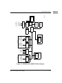
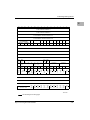
Figure 1-1. 200/300-Series MVME172 Block Diagram ........................................... 1-6
Figure 1-2. 400/500-Series MVME172 Block Diagram ........................................... 1-7
Figure 2-1. VMEchip2 Block Diagram ..................................................................... 2-5
TABLES
Table 1-1. MVME172 Features Summary................................................................. 1-3
Table 1-2. Redundant Functions in the VMEchip2 and MC2 Chip ......................... 1-8
Table 1-3. 200/300-Series MVME172 Local Bus Memory Map ............................ 1-10
Table 1-4. 400/500-Series MVME172 Local Bus Memory Map ............................ 1-12
Table 1-5. 200/300-Series MVME172 Local I/O Devices Memory Map ............... 1-14
Table 1-6. 400/500-Series MVME172 Local I/O Devices Memory Map ............... 1-18
Table 1-7. VMEchip2 Memory Map (Sheet 1 of 3) ................................................ 1-22
Table 1-8. MC2 Chip Register Map ........................................................................ 1-27
Table 1-9. IP2 Chip Overall Memory Map.............................................................. 1-28
Table 1-10. IP2 Chip Memory Map - Control and Status Registers ....................... 1-29
Table 1-11. MCECC Internal Register Memory Map ............................................ 1-35
Table 1-12. Z85230 SCC Register Addresses ......................................................... 1-37
Table 1-13. 82596CA Ethernet LAN Memory Map................................................ 1-38
Table 1-14. 53C710 SCSI Memory Map ............................................................... 1-39
Table 1-15. MK48T58 BBRAM/TOD Clock Memory Map ................................... 1-40
Table 1-16. BBRAM Configuration Area Memory Map ....................................... 1-41
Table 1-17. TOD Clock Memory Map .................................................................... 1-42
Table 2-1. VMEchip2 Memory Map - LCSR Summary (Sheet 1 of 2) .................. 2-22
Table 2-2. DMAC Command Table Format ............................................................ 2-53
Table 2-3. Local Bus Interrupter Summary ............................................................ 2-76
Table 2-4. VMEchip2 Memory Map (GCSR Summary) ...................................... 2-104
Table 3-1. DRAM Performance................................................................................. 3-6
Table 3-2. MC2 Chip Register Map ......................................................................... 3-9
Table 3-3. Interrupt Vector Base Register Encoding and Priority ........................... 3-14
Table 3-4. DRAM Size Control Bit Encoding......................................................... 3-27
Table 3-5. DRAM Size Control Bit Encoding......................................................... 3-28
Table 3-6. SRAM Size Control Bit Encoding ......................................................... 3-28
Table 3-7. SRAM Size Control Bit Encoding ......................................................... 3-29
Table 4-1. IP2 Chip Clock Cycles ............................................................................. 4-6
Table 4-2. IP2 Chip Overall Memory Map ............................................................... 4-9
Table 4-3. IP2 Chip Memory Map - Control and Status Registers ......................... 4-11
xvi
Table 5-1. MCECC Specifications.............................................................................5-3
Table 5-2. MCECC Internal Register Memory Map, Part 1 ....................................5-10
Table 5-3. MCECC Internal Register Memory Map, Part 2 ...................................5-12
Table A-1. Motorola Computer Group Documents ..................................................A-1
Table A-2. Manufacturers’ Documents ....................................................................A-2
xvii
xviii
1Board Description
and Memory Maps
1
Introduction
This manual provides programming information for the MVME172
Embedded Controller. Extensive programming information is provided for
the Application-Specific Integrated Circuit (ASIC) devices used on the
board. Reference information is included for the Large Scale Integration
(LSI) devices used on the board and sources for additional information are
provided.
This chapter briefly describes the board level hardware features of the
MVME172 Embedded Controller. The chapter begins with a board level
overview and features list. Memory maps are next, and the chapter closes
with some general software considerations such as cache coherency,
interrupts, and bus errors.
All programmable registers in the MVME172 that reside in ASICs are
covered in the chapters on those ASICs. Chapter 2 covers the VMEchip2,
Chapter 3 covers the MC2 chip, and Chapter 4 covers the IP2 chip. Chapter
5 covers the MCECC chip, used only on 200/300-Series MVME172.
Appendix A describes using interrupts. For those interested in
programmable register bit definitions and less interested in hardware
functionality, focus on Chapters 2, 3, 4, and 5. In some cases, however,
Chapter 1 gives related background information.
Overview
The MVME172 is based on the MC68060 or MC68LC060
microprocessor. The MVME172 is available in various versions with the
features listed in Table 1-1 on page 1-3. A “No VMEbus” option is also
available.
The I/O connection for the 200/300-Series MVME172 is provided through
four RJ-45 front panel connectors.
1-1
1
Board Description and Memory Maps
The I/O connection for the 400/500-Series serial ports is provided by two
DB-25 front panel I/O connectors. The I/O is connected to the VMEbus P2
connector. The main board is connected through a P2 transition board and
cables to transition boards. The Series 400/500 MVME172 supports the
transition boards MVME712-12, MVME712-13, MVME712M,
MVME712A, MVME712AM, and MVME712B (referred to in this
manual as MVME712x, unless separately specified). These transition
boards provide configuration headers, serial port drivers and industry
standard connectors for the I/O devices. The MVME712 series transition
boards were designed to support the MVME167 boards, but can be used
on the MVME172 by following some special precautions. (Refer to the
section on the Serial Communications Interface in the MVME172
installation and use manual furnished with your 400/500-Series
MVME172, for more information.)
The VMEbus interface is provided by an ASIC called the VMEchip2. The
VMEchip2 includes two tick timers, a watchdog timer, programmable map
decoders for the master and slave interfaces, and a VMEbus to/from local
bus DMA controller, a VMEbus to/from local bus non-DMA programmed
access interface, a VMEbus interrupter, a VMEbus system controller, a
VMEbus interrupt handler, and a VMEbus requester.
Processor-to-VMEbus transfers can be D8, D16, or D32. VMEchip2 DMA
transfers to the VMEbus, however, can be D16, D32, D16/BLT, D32/BLT,
or D64/MBLT.
The MC2 chip ASIC provides four tick timers, the interface to the LAN
chip, SCSI chip, serial port chip, BBRAM, the programmable interface for
the DRAM and/or SRAM mezzanine board, and Flash write enable.
The IndustryPack Interface Controller (IP2 chip) ASIC provides control
and status information, including DMA control, for up to four single size
IndustryPacks (IPs) or up to two double size IPs that can be plugged into
the MVME172 main module.
1-2
Computer Group Literature Center Web Site
Overview
The MCECC chip Memory Controller ASIC on the 200/300-Series
MVME172 provides the programmable interface for the ECC-protected
16 MB DRAM mezzanine board.
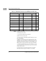
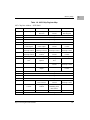
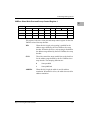
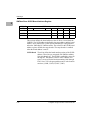
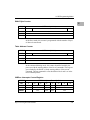
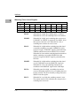
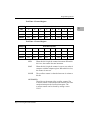
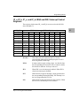
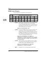
Table 1-1. MVME172 Features Summary
Feature
200/300-Series
400/500-Series
Processor
60 MHz 32-bit MC68060 microprocessor, or 64 MHz 32-bit
MC68LC060 microprocessor
DRAM
4MB, 8 MB, or 16 MB of shared
DRAM with parity protection on a
mezzanine module, or up to 64 MB of
ECC-protected DRAM
4MB, 8 MB, or 16 MB of shared
DRAM with no protection
SRAM
128 KB of SRAM with battery
512KB of SRAM with battery backup
backup
PROM/
EPROM
Sockets
Flash
One JEDEC standard 32-pin
PLCC EPROM socket (EPROMs
may be shipped separately)
One Intel 28F016SA 2M x 8 Flash memory device (2MB Flash memory
Two JEDEC standard 32-pin DIP
PROM sockets
total) with write protection (optional)
NVRAM and
TOD
8K by 8 Non-Volatile RAM (NVRAM) and Time-of-Day (TOD) clock with
battery backup
Timers
Four 32-bit Tick Timers and Watchdog Timer (in the MC2 Chip ASIC) for
periodic interrupts
Two 32-bit Tick Timers and Watchdog Timer in the VMEchip2 ASIC) for
periodic interrupts
Software
Interrupts
Eight software interrupts (for MVME172 versions that have the VMEchip2)
I/O
Four serial ports, both EIA-232-D RJ45
Two serial ports; one EIA-232-D
DCE, one EIA-232-D DCE/DTE or
EIA-530 DCE/DTE or EIA-42
DCE/DTE or EIA-485
Serial port controllers (Zilog Z85230)
Optional Small Computer Systems Interface (SCSI) bus interface with 32-bit
local bus burst Direct Memory Access (DMA) (NCR 53C710 controller)
Optional LAN Ethernet transceiver interface with 32-bit local bus DMA (Inter
82596CA controller)
http://www.mcg.mot.com/literature
1-3
1
1
Board Description and Memory Maps
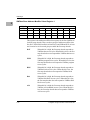
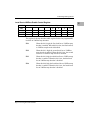
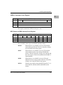
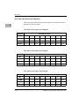
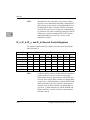
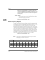
Table 1-1. MVME172 Features Summary
Feature
200/300-Series
400/500-Series
Two MVIP IndustryPack
interfaces with DMA
VMEbus
interface
(boards may be
special ordered
without the
VMEbus
interface)
Four MVIP IndustryPack
interfaces with DMA
VMEbus system controller functions
VMEbus interface to local bus (A24/A32,
D8/D16/D32 (D8/D16/D32/D64 BLT) (BLT = Block Transfer)
Local bus to VMEbus interface (A16/A24/A32, D8/D16/D32)
VMEbus interrupter
VMEbus interrupt handler
Global CSR for interprocessor communications
DMA for fast local memory - VMEbus transfers (A16/A24/A32, D16/D32
(D16/D32/D64 BLT)
Switches
Two pushbutton switches (ABORT and RESET)
Light-Emitting
Diodes (LEDs)
FUSES
Four LEDs: FAIL, RUN, SCON,
(LAN power)
Eight LEDs: FAIL, STAT, RUN,
SCON, LAN, FUSE
SCSI, and VME
(LAN power),
Requirements
These boards are designed to conform to the requirements of the following
documents:
1-4
❏
VMEbus Specification (IEEE 1014-87)
❏
EIA-232-D Serial Interface Specification, EIA
❏
SCSI Specification, ANSI
❏
IndustryPack Specification, GreenSpring
Computer Group Literature Center Web Site
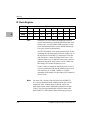
Block Diagrams
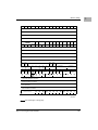
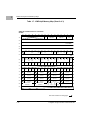
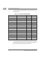
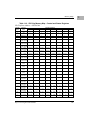
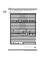
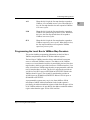
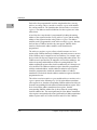
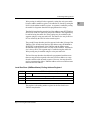
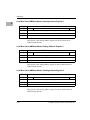
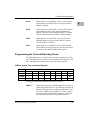
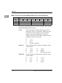
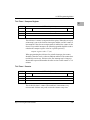
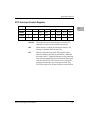
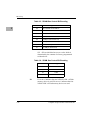
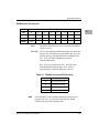
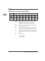
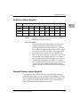
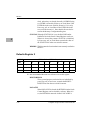
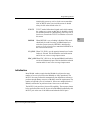
Block Diagrams
Figure 1-2 on page 1-7 is a general block diagram of the 200/300-Series
MVME172. Figure 1-2 on page 1-7 is a general block diagram of the
400/500-Series MVME172.
Functional Description
This section covers only a few specific features of the MVME172.
A complete functional description of the major blocks of the MVME172
Embedded Controller is provided in your MVME172 installation and use
manual.
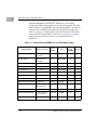
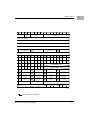
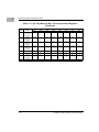
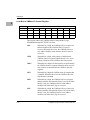
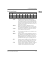
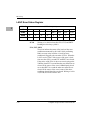
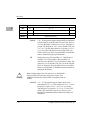
No-VMEbus-Interface Option
The MVME172 can be operated as an embedded controller without the
VMEbus interface. For this option, the VMEchip2 and the VMEbus
buffers are not populated. Also, the bus grant daisy chain and the interrupt
acknowledge daisy chain have zero-ohm bypass resistors installed.
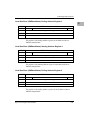
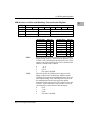
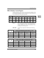
To support this feature, certain logic in the VMEchip2 has been duplicated
in the MC2 chip. Table 1-2 on page 1-8 defines the location of the
redundant logic. This logic is inhibited in the MC2 chip if the VMEchip2
is present. The enables for these functions are controlled by software and
MC2 chip hardware initialization.
Note that an MVME172 ordered without the VMEbus interface is shipped
with Flash memory blank (the factory uses the VMEbus to program the
Flash memory with debugger code). To use the 172Bug package,
MVME172Bug, in such models, be sure that the General Purpose
Readable Jumpers Header is configured for the EPROM memory map.
Refer to Chapters 3 and 4 of your MVME172 installation and use manual
for further details.
http://www.mcg.mot.com/literature
1-5
1
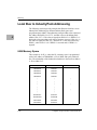
1-6
Optional
MC68060
MC68LC060
MPU
IP2
IndustryPack
Interface
VMEchip2
VMEbus
Interface
A32/D32
IndustryPack
I/O
2 Channels
VMEbus
A32/24:D64/32/16/08
Master/Slave
Optional
4,8,16,32,64MB
ECC DRAM
Memory Array
53C710
SCSI
Coprocessor
SCSI
Peripherals
68-pin Front
Panel SCSI
Connector
Configuration Dependent
4,8,16MB Parity
DRAM Memory
Array
i82596CA
Ethernet
Controller
Ethernet
Transceiver
DB-15 Front
Panel
Connector
Optional
MC2 chip
Two 32-pin
EPROM
Sockets
128KB SRAM
Memory Array
w/Battery
M48T58
Battery Backed
8KB RAM/Clock
Dual 85230
Serial
I/O Controllers
EIA-232
Transceivers
4 Serial Ports
RJ-45 Front
Panel
21009702
Flash
2MB
Optional
1
Board Description and Memory Maps
Figure 1-1. 200/300-Series MVME172 Block Diagram
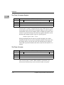
Computer Group Literature Center Web Site
http://www.mcg.mot.com/literature
Optional
MC68060
MC68LC060
MPU
A32/D32
IP2
IndustryPack
Interface
VMEchip2
VMEbus
Interface
Configuration Dependent
4,8,16MB Parity
DRAM Memory
Array
53C710
SCSI
Coprocessor
Ethernet
SCSI
Transceiver
Peripherals
connections are
connections are
Via P2 and
Via P2 and
Transition Modules Transition Modules
IndustryPack
I/O
4 Channels
VMEbus
A32/24:D64/32/16/08
Master/Slave
i82596CA
Ethernet
Controller
Optional
Optional
MC2 chip
1 PLCC
Socket
512KB SRAM
Memory Array
w/Battery
M48T58
Battery Backed
8KB RAM/Clock
Dual 85230
Serial
I/O Controllers
EIA-232
Transceivers
2 Serial Ports
DB-25 Front Panel
or
Via P2 and
Transition Module
2038 9706
Flash
2MB
Optional
Functional Description
Figure 1-2. 400/500-Series MVME172 Block Diagram
1-7
1
1
Board Description and Memory Maps
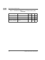
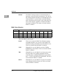
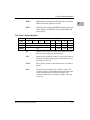
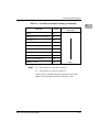
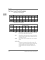
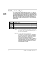
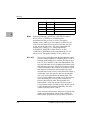
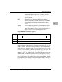
Table 1-2. Redundant Functions in the VMEchip2 and MC2 Chip
VMEchip2
MC2 Chip
Notes
Address
Bit #
Address
Bit #
$FFF40060
28 - 24
$FFF42044
28 - 24
1,5
$FFF40060
22 19,17,16
$FFF42044
22 19,17,16
2,5
$FFF4004C
13 - 8
$FFF42044
13 - 8
3,5
$FFF40048
7
$FFF42048
8
4
$FFF40048
9
$FFF42048
9
4,5
$FFF40048
10
$FFF42048
10
4,5
$FFF40048
11
$FFF42048
11
4,5
$FFF40064
31 - 0
$FFF4204C
31 - 0
8
$FFF42040
6-0
6
$FF800000-$FFBFFFFF
31 - 0
$FF800000$FFBFFFFF
31 - 0
7
$FFE00000-$FFEFFFFF
31 - 0
Programmable
31 - 0
7
Notes 1. RESET switch control.
2. Watchdog timer control.
3. Access and watchdog timer parameters.
4. MPU TEA (bus error) status
5. Bit numbering for VMEchip2 and MC2 chip has a one-toone correspondence.
6. ABORT switch interrupt control. Implemented also in the
VMEchip2, but with a different bit organization (refer to the
VMEchip2 description in Chapter 2). In the MVME172, the
ABORT switch is wired to the MC2 chip, not the VMEchip2.
7. The SRAM and PROM decoder in the VMEchip2 (version
2) must be disabled by software before any accesses are made
to these address spaces.
8. 32-bit prescaler. The prescaler can also be accessed at
$FFF40064 when the optional VMEbus is not enabled.
1-8
Computer Group Literature Center Web Site
Memory Maps
VMEbus Interface and VMEchip2
The local bus to VMEbus interface and the VMEbus to local bus interface
are provided by the VMEchip2. The VMEchip2 can also provide the
VMEbus system controller functions. Refer to the VMEchip2 in Chapter 2
for detailed programming information.
Note that the ABORT switch logic in the VMEchip2 is not used. The GPI
inputs to the VMEchip2 which are located at $FFF40088 bits 7-0 are not
used. The ABORT switch interrupt is integrated into the
MC2 chip ASIC at location $FFF42043. The GPI inputs are integrated into
the MC2 chip ASIC at location $FFF4202C bits 23-16.
Memory Maps
There are two points of view for memory maps: 1) the mapping of all
resources as viewed by local bus masters (local bus memory map), and 2)
the mapping of onboard resources as viewed by VMEbus masters
(VMEbus memory map).
The memory and I/O maps which are described in the following tables are
correct for all local bus masters. There is some address translation
capability in the VMEchip2. This allows multiple MVME172 modules on
the same VMEbus with different virtual local bus maps as viewed by
different VMEbus masters.
Local Bus Memory Map
The local bus memory map is split into different address spaces by the
transfer type (TT) signals. The local resources respond to the normal
access and interrupt acknowledge codes.
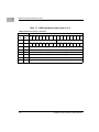
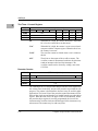
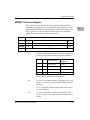
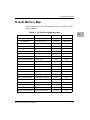
Normal Address Range
The memory map of devices that respond to the normal address range is
shown in the following tables. The normal address range is defined by the
Transfer Type (TT) signals on the local bus. On the MVME172, Transfer
Types 0, 1, and 2 define the normal address range. Table 1-2 is the entire
http://www.mcg.mot.com/literature
1-9
1
1
Board Description and Memory Maps
map from $00000000 to $FFFFFFFF. Many areas of the map are
user-programmable, and suggested uses are shown in the table. The cache
inhibit function is programmable in the MC68xx060 MMU. The onboard
I/O space must be marked cache inhibit and serialized in its page table.
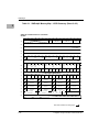
Table 1-3 on page 1-10 further defines the map for the local I/O devices
for the 200/300-Series MVME172, and Table 1-4 on page 1-12 further
defines the map for the local I/O devices for the 400/500-Series
MVME172.
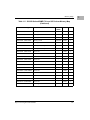
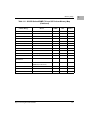
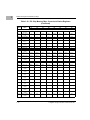
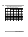
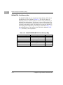
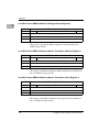
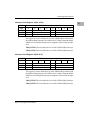
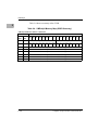
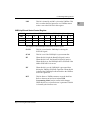
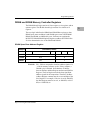
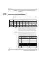
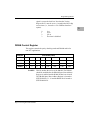
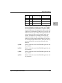
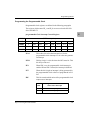
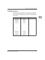
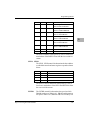
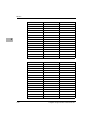
Table 1-3. 200/300-Series MVME172 Local Bus Memory Map
Address Range
Devices Accessed
Port
Width
Size
Software
Cache
Inhibit
Notes
Programmable
DRAM on parity
mezzanine
D32
4MB-16MB
N
2
Programmable
DRAM on ECC
mezzanine
D32
4MB-64MB
N
2
Programmable
Onboard SRAM
D32
128KB
N
2
Programmable
VMEbus A32/A24
D32-D16
--
?
4
Programmable
IP_a memory
D32-D8
64KB-8MB
?
2, 4
Programmable
IP_b memory
D32-D8
64KB-8MB
?
2, 4
$FF800000-$FF9FFFFF
Flash/EPROM
D32
2MB
N
1, 5
$FFA00000-$FFBFFFFF
EPROM/Flash
D32
2MB
N
5
$FFC00000-$FFDFFFFF
Not decoded
D32
2MB
N
$FFE00000-$FFE1FFFF
Onboard
SRAM default
D32
128KB
N
$FFE80000-$FFEFFFFF
Not decoded
--
512KB
N
6
$FFF00000-$FFFEFFFF
Local I/O devices
(see next table)
D32-D8
878KB
Y
3
$FFFF0000-$FFFFFFFF
VMEbus A16
D32/D16
64KB
?
2, 4
1-10
Computer Group Literature Center Web Site
Memory Maps
Notes 1. Devices mapped at $FFF80000-$FFF9FFFF also appear at
$00000000- $001FFFFF when the ROM0 bit in the MC2
chip EPROM control register is high (ROM0=1). ROM0 is
set to 1 after each reset. The ROM0 bit must be cleared before
other resources (DRAM or SRAM) can be mapped in this
range ($00000000 - $001FFFFF).
The EPROM/Flash memory map is also controlled by the
EPROM size and by control bit V11 in the MC2 chip ASIC.
Refer to the EPROM/Flash configuration tables in your
MVME172 installation manual for further details.
2. This area is user-programmable. The DRAM and SRAM
decoder is programmed in the MC2 chip, the local-toVMEbus decoders are programmed in the VMEchip2, and
the IP memory space is programmed in the IP2.
3. Size is approximate.
4. Cache inhibit depends on the devices in the area mapped.
5. The EPROM and Flash are dynamically sized by the MC2
chip ASIC from an 8-bit private bus to the 32-bit MPU local
bus.
6. These areas are not decoded unless one of the
programmable decoders is initialized to decode this space. If
they are not decoded and the local timer is enabled, an access
to this address range will generate a local bus time-out.
http://www.mcg.mot.com/literature
1-11
1
1
Board Description and Memory Maps
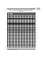
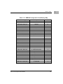
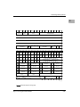
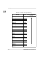
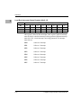
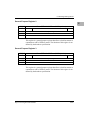
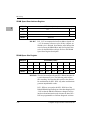
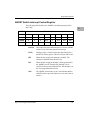
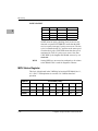
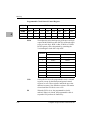
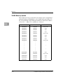
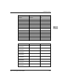
Table 1-4. 400/500-Series MVME172 Local Bus Memory Map
Devices
Accessed
Port
Width
Size
Software
Cache
Inhibit
Note(s)
Programmable
DRAM on board
D32
4MB-16 MB
N
2
Programmable
SRAM
D32
128KB-2MB
N
2
Programmable
VMEbus
A32/A24
D32/D16
--
?
4
Programmable
IP_a Memory
D32-D8
64KB-8MB
?
2, 4
Programmable
IP_b Memory
D32-D8
64KB-8MB
?
2, 4
Programmable
IP_c Memory
D32-D8
64KB-8MB
?
2, 4
Programmable
IP_d Memory
D32-D8
64KB-8MB
?
2, 4
$FF800000 - $FF9FFFFF
Flash/PROM
D32
2MB
N
1, 5
$FFA00000 - $FFBFFFFF
PROM/Flash
D32
2MB
N
6
$FFC00000 - $FFCFFFFF
Not decoded
--
1MB
N
7
$FFD00000 - $FFDFFFFF
Not decoded
--
1MB
N
7
$FFE00000 - $FFE7FFFF
SRAM default
D32
512KB
N
--
$FFE80000 - $FFEFFFFF
Not decoded
--
512KB
N
7
$FFF00000 - $FFFEFFFF
Local I/O
D32-D8
878KB
Y
3
$FFFF0000 - $FFFFFFFF
VMEbus A16
D32/D16
64KB
?
2, 4
Address Range
Notes 1. Reset enables the decoder for this space of the memory
map so that it will decode address spaces
$FF800000-$FF9FFFFF and $00000000-$003FFFFF. The
decode at 0 must be disabled in the MC2 chip before DRAM
is enabled. DRAM is enabled with the DRAM Control
1-12
Computer Group Literature Center Web Site
Memory Maps
Register at address $FFF42048, bit 24. PROM/Flash is
disabled at the low address space with PROM Control
Register at address $FFF42040, bit 20.
2. This area is user-programmable. The DRAM and SRAM
decoder is programmed in the MC2 chip, the
local-to-VMEbus decoders are programmed in the
VMEchip2, and the IP memory space is programmed in the
IP2 chip.
3. Size is approximate.
4. Cache inhibit depends on devices in area mapped.
5. The PROM and Flash are sized by the MC2 chip ASIC
from an 8-bit private bus to the 32-bit MPU local bus.
Because the device size is less than the allocated memory
map size for some entries, the device contents repeat for
those entries.
If jumper GPI3 is installed, the Flash device is accessed. If
GPI3 is not installed, the PROM is accessed.
6. The Flash and PROM are sized by the MC2 chip ASIC
from an 8-bit private bus to the 32-bit MPU local bus.
Because the device size is less than the allocated memory
map size for some entries, the device contents repeat for
those entries.
If jumper GPI3 is installed, the PROM is accessed. If GPI3 is
not installed, the Flash device is accessed.
7. These areas are not decoded unless one of the
programmable decoders are initialized to decode this space.
If they are not decoded, an access to this address range will
generate a local bus time-out. The local bus timer must be
enabled.
http://www.mcg.mot.com/literature
1-13
1
1
Board Description and Memory Maps
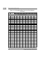
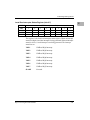
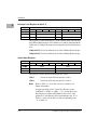
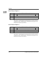
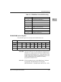
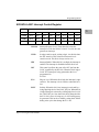
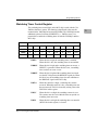
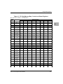
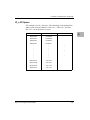
Table 1-5 below and Table 1-6 on page 1-18 describe the "Local I/O
Devices" portion of the local bus main memory map for the 200/300-Series
and 400/500-Series MVME172, respectively.
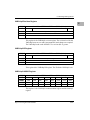
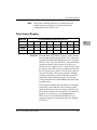
Table 1-5. 200/300-Series MVME172 Local I/O Devices Memory Map
Address Range
Devices Accessed
Port
Width
Size
Notes
--
256K
B
4
$FFF00000 - $FFF3FFFF
Reserved
$FFF40000 - $FFF400FF
VMEchip2 (LCSR)
D32
256B
1, 3
$FFF40100 - $FFF401FF
VMEchip2 (GCSR)
D32-D8
256B
1, 3
$FFF40200 - $FFF40FFF
Reserved
--
3.5KB
4, 5
$FFF41000 - $FFF41FFF
Reserved
--
4KB
4
$FFF42000 - $FFF42FFF
MC2 chip
D32-D8
4KB
1
$FFF43000 - $FFF430FF
MCECC #1
D8
256B
1, 8
$FFF43100 - $FFF431FF
MCECC #2
D8
256B
1, 8
$FFF43200 - $FFF43FFF
MCECCs (repeated)
--
3.5KB
1, 5, 8
$FFF44000 - $FFF44FFF
Reserved
--
8KB
4
$FFF45000 - $FFF45800
SCC #1 (Z85230)
D8
2KB
1, 2
$FFF45801 - $FFF45FFF
SCC #2 (Z85230)
D8
2KB
1, 2
$FFF46000 - $FFF46FFF
LAN (82596CA)
D32
4KB
1, 6
$FFF47000 - $FFF47FFF
SCSI (53C710)
D32-D8
4KB
1
$FFF48000 - $FFF57FFF
Reserved
--
64KB
4
$FFF58000 - $FFF5807F
IP2 IP_a I/O
D16
128B
1
$FFF58080 - $FFF580FF
IP2 IP_a ID
D16
128B
1
$FFF58100 - $FFF5817F
IP2 IP_b I/O
D16
128B
1
$FFF58180 - $FFF581FF
IP2 IP_b ID Read
D16
128B
1
$FFF58200 - $FFF5827F
IP2 IP_c I/O
D16
128B
7
1-14
Computer Group Literature Center Web Site
Memory Maps
Table 1-5. 200/300-Series MVME172 Local I/O Devices Memory Map
(Continued)
Address Range
Devices Accessed
Port
Width
Size
Notes
$FFF58280 - $FFF582FF
IP2 IP_c ID
D16
128B
7
$FFF58300 - $FFF5837F
IP2 IP_d I/O
D16
128B
7
$FFF58380 - $FFF583FF
IP2 IP_d ID Read
D16
128B
7
$FFF58400 - $FFF584FF
IP2 IP_ab I/O
D32-D16
256B
1
$FFF58500 - $FFF585FF
IP2 IP_cd I/O
D32-D16
256B
7
$FFF58600 - $FFF586FF
IP2 IP_ab I/O Repeated
D32-D16
256B
1
$FFF58700 - $FFF587FF
IP2 IP_cd I/O Repeated
D32-D16
256B
7
$FFF58800 - $FFF5887F
Reserved
--
128B
1
$FFF58880 - $FFF588FF
Reserved
--
128B
1
$FFF58900 - $FFF5897F
Reserved
--
128B
1
$FFF58980 - $FFF589FF
Reserved
--
128B
1
$FFF58A00 - $FFF58A7F
Reserved
--
128B
1
$FFF58A80 - $FFF58AFF
Reserved
--
128B
1
$FFF58B00 - $FFF58B7F
Reserved
--
128B
1
$FFF58B80 - $FFF58BFF
Reserved
--
128B
1
$FFF58C00 - $FFF58CFF
Reserved
--
256B
1
$FFF58D00 - $FFF58DFF
Reserved
--
256B
1
$FFF58E00 - $FFF58EFF
Reserved
--
256B
1
$FFF58F00 - $FFF58FFF
Reserved
--
256B
1
$FFFBC000 - $FFFBC01F
IP2 Registers
D32-D8
2KB
1
http://www.mcg.mot.com/literature
1-15
1
1
Board Description and Memory Maps
Table 1-5. 200/300-Series MVME172 Local I/O Devices Memory Map
(Continued)
Address Range
Devices Accessed
Port
Width
Size
Notes
$FFFBC800 - $FFFBC81F
Reserved
--
2KB
1
$FFFBD000 - $FFFBFFFF
Reserved
--
12KB
4
$FFFC0000 - $FFFCFFFF
M48T58 (BBRAM, TOD Clock)
D32-D8
64KB
1, 9
$FFFD0000 - $FFFEFFFF
Reserved
--
128K
B
4
1-16
Computer Group Literature Center Web Site
Memory Maps
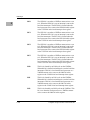
Notes 1. For a complete description of the register bits, refer to the
data sheet for the specific chip. For a more detailed memory
map, refer to the following detailed peripheral device
memory maps.
2. The SCC is an 8-bit device located on an MC2 chip private
data bus. Byte access is required.
3. Writes to the LCSR in the VMEchip2 must be 32 bits.
LCSR writes of 8 or 16 bits terminate with a TEA signal.
Writes to the GCSR may be 8, 16 or 32 bits. Reads to the
LCSR and GCSR may be 8, 16 or 32 bits. Byte reads should
be used to read the interrupt vector.
4. This area does not return an acknowledge signal. If the
local bus timer is enabled, the access times out and is
terminated by a TEA signal.
5. Size is approximate.
6. Port commands to the 82596CA must be written as two 16bit writes: upper word first and lower word second.
7. Not used.
8. To use this area, the ECC mezzanine board must be
installed. If it is not installed, no acknowledge signal is
returned; if the local bus timer is enabled, the access times
out and is terminated by a TEA signal.
9.Repeats on 8KB boundaries.
http://www.mcg.mot.com/literature
1-17
1
1
Board Description and Memory Maps
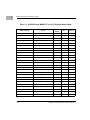
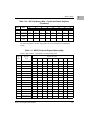
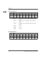
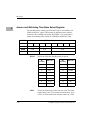
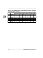
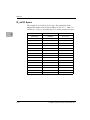
Table 1-6. 400/500-Series MVME172 Local I/O Devices Memory Map
Address Range
Device
Port
Width
Size
Note(s)
--
256KB
4
D32
256B
1, 3
D32-D8
256B
1, 3
$FFF00000 - $FFF3FFFF
Reserved
$FFF40000 - $FFF400FF
VMEchip2 (LCSR)
$FFF40100 - $FFF401FF
VMEchip2 (GCSR) registers
$FFF40200 - $FFF40FFF
Reserved
--
3.5KB
4, 5
$FFF41000 - $FFF41FFF
Reserved
--
4KB
4
$FFF42000 - $FFF42FFF
MC2 chip
D32-D8
4KB
1
$FFF43000 - $FFF44FFF
Reserved
--
8KB
4
$FFF45000 - $FFF45FFF
SCC (Z85230)
D8
4KB
1, 2
$FFF46000 - $FFF46FFF
LAN (82596CA)
D32
4KB
1, 6
$FFF47000 - $FFF47FFF
SCSI (53C710)
D32-D8
4KB
1
$FFF48000 - $FFF57FFF
Reserved
--
64KB
4
$FFF58000 - $FFF5807F
IP2 chip IP_a I/O
D16
128B
1
$FFF58080 - $FFF580FF
IP2 chip IP_a ID
D16
128B
1
$FFF58100 - $FFF5817F
IP2 chip IP_b I/O
D16
128B
1
$FFF58180 - $FFF581FF
IP2 chip IP_b ID Read
D16
128B
1
$FFF58200 - $FFF5827F
IP2 chip IP_c I/O
D16
128B
1
$FFF58280 - $FFF582FF
IP2 chip IP_c ID
D16
128B
1
$FFF58300 - $FFF5837F
IP2 chip IP_d I/O
D16
128B
1
$FFF58380 - $FFF583FF
IP2 chip IP_d ID Read
D16
128B
1
$FFF58400 - $FFF584FF
IP2 chip IP_ab I/O
D32-D16
256B
1
$FFF58500 - $FFF585FF
IP2 chip IP_cd I/O
D32-D16
256B
1
$FFF58600 - $FFF586FF
IP2 chip IP_ab I/O repeated
D32-D16
256B
1
$FFF58700 - $FFF587FF
IP2 chip IP_cd I/O repeated
D32-D16
256B
1
$FFF58800 - $FFF5887F
Reserved
--
128B
1
$FFF58880 - $FFF588FF
Reserved
--
128B
1
$FFF58900 - $FFF5897F
Reserved
--
128B
1
1-18
Computer Group Literature Center Web Site
Memory Maps
Table 1-6. 400/500-Series MVME172 Local I/O Devices Memory Map
(Continued)
Address Range
Device
Port
Width
Size
Note(s)
$FFF58980 - $FFF589FF
Reserved
--
128B
1
$FFF58A00 - $FFF58A7F
Reserved
--
128B
1
$FFF58A80 - $FFF58AFF
Reserved
--
128B
1
$FFF58B00 - $FFF58B7F
Reserved
--
128B
1
$FFF58B80 - $FFF58BFF
Reserved
--
128B
1
$FFF58C00 - $FFF58CFF
Reserved
--
256B
1
$FFF58D00 - $FFF58DFF
Reserved
--
256B
1
$FFF58E00 - $FFF58EFF
Reserved
--
256B
1
$FFF58F00 - $FFF58FFF
Reserved
--
256B
1
D32-D8
2KB
1
$FFFBC800 - $FFFBC81F Reserved
--
2KB
1
$FFFBD000 $FFFBFFFF
Reserved
--
12KB
4
$FFFC0000 - $FFFC7FFF
MK48T58
(BBRAM, TOD clock)
D32-D8
32KB
1
$FFFC8000 - $FFFCBFFF
MK48T58
D32-D8
16KB
1, 7
$FFFCC000 - $FFFCFFFF MK48T58
D32-D8
16KB
1, 7
--
128KB
4
$FFFBC000 - $FFFBC01F IP2 chip registers
$FFFD0000 - $FFFEFFFF
Reserved
http://www.mcg.mot.com/literature
1-19
1
1
Board Description and Memory Maps
Notes 1. For a complete description of the register bits, refer to the
data sheet for the specific chip. For a more detailed memory
map, refer to the following detailed peripheral device
memory maps.
2. The SCC is an 8-bit device located on an MC2 chip private
data bus. Byte access is required.
The data register of the Zilog Z85230 device which is
interfaced by the MC2 chip ASIC cannot be accessed. The
Zilog Z85230 has an indirect access mode to the data
registers which is functional and must be used.
3. Writes to the LCSR in the VMEchip2 must be 32 bits.
LCSR writes of 8 or 16 bits terminate with a TEA signal.
Writes to the GCSR may be 8, 16 or 32 bits. Reads to the
LCSR and GCSR may be 8, 16 or 32 bits. Byte reads should
be used to read the interrupt vector.
4. This area does not return an acknowledge signal. If the
local bus timer is enabled, the access times out and is
terminated by a TEA signal.
5. Size is approximate.
6. Port commands to the 82596CA must be written as two
16-bit writes: upper word first and lower word second.
7. Refer to the Flash and PROM Interface section in the MC2
chip description in Chapter 3.
1-20
Computer Group Literature Center Web Site
Memory Maps
Detailed I/O Memory Maps
Tables 1-7 through 1-17 give the detailed memory maps for:
Note
VMEchip2
Table 1-7
MC2 chip
Table 1-8
IP2 chip
Table 1-9
IP2 chip Control and Status Registers
Table 1-10
MCECC chip
Table 1-11
Z85230 SCC Register addresses
Table 1-12
82596CA Ethernet LAN chip
Table 1-13
53C710 SCSI chip
Table 1-14
MK48T58 BBRAM/TOD clock
Table 1-15
BBRAM configuration area
Table 1-16
TOD clock
Table 1-17
Manufacturers’ errata sheets for the various chips are
available by contacting your local Motorola sales
representative. A non-disclosure agreement may be required.
http://www.mcg.mot.com/literature
1-21
1
1
Board Description and Memory Maps
Table 1-7. VMEchip2 Memory Map (Sheet 1 of 3)
VMEchip2 LCSR Base Address = $FFF40000
OFFSET:
31
30
29
28
27
26
25
24
23
22
21
0
SLAVE ENDING ADDRESS 1
4
SLAVE ENDING ADDRESS 2
8
SLAVE ADDRESS TRANSLATION ADDRESS 1
C
SLAVE ADDRESS TRANSLATION ADDRESS 2
ADDER
2
10
31
30
29
28
27
SNP
2
26
25
19
18
17
16
WP
2
SUP
2
USR
2
A32
2
A24
2
BLK
D64
2
BLK
2
PRGM
2
DATA
2
24
23
22
21
20
19
18
17
16
14
MASTER ENDING ADDRESS 1
18
MASTER ENDING ADDRESS 2
1C
MASTER ENDING ADDRESS 3
20
MASTER ENDING ADDRESS 4
MASTER ADDRESS TRANSLATION ADDRESS 4
24
28
20
MAST
D16
EN
MAST
WP
EN
MAST
D16
EN
MASTER AM 4
31
30
29
28
27
26
MASTER AM 3
GCSR
BOARD SELECT
GCSR GROUP SELECT
2C
MAST
WP
EN
25
30
24
23
22
21
20
WAIT
RMW
ROM
ZERO
MAST
4
EN
MAST
3
EN
MAST
2
EN
MAST
1
EN
19
18
17
16
DMA TB
SNP MODE
SRAM
SPEED
34
38
DMA CONTROLLER
3C
DMA CONTROLLER
40
DMA CONTROLLER
44
DMA CONTROLLER
48
TICK
2/1
TICK
IRQ 1
EN
CLR
IRQ
IRQ
STAT
VMEBUS
INTERRUPT
LEVEL
VMEBUS INTERRUPT VECTOR
This sheet continues on facing page.
1-22
Computer Group Literature Center Web Site
Memory Maps
15
14
13
12
11
10
9
8
7
6
5
4
3
2
1
0
A24
1
BLK
D64
1
BLK
1
PRGM
1
DATA
1
4
3
2
1
0
SLAVE STARTING ADDRESS 1
SLAVE STARTING ADDRESS 2
SLAVE ADDRESS TRANSLATION SELECT 1
SLAVE ADDRESS TRANSLATION SELECT 2
ADDER
1
15
14
13
12
SNP
1
11
10
9
WP
1
SUP
1
USR
1
8
7
6
A32
1
5
MASTER STARTING ADDRESS 1
MASTER STARTING ADDRESS 2
MASTER STARTING ADDRESS 3
MASTER STARTING ADDRESS 4
MASTER ADDRESS TRANSLATION SELECT 4
MAST
D16
EN
MAST
WP
EN
IO2
EN
IO2
WP
EN
15
14
ARB
ROBN
MAST
DHB
DMA
TBL
INT
MAST
D16
EN
MASTER AM 2
IO2
S/U
13
MAST
DWB
DMA LB
SNP MODE
IO2
P/D
12
IO1
EN
IO1
D16
EN
IO1
WP
EN
IO1
S/U
9
8
11
10
MST
FAIR
MST
RWD
DMA
INC
VME
DMA
INC
LB
DMA
WRT
MPU
LBE
ERR
MPU
LPE
ERR
MAST
WP
EN
MASTER AM 1
ROM
SIZE
ROM BANK B
SPEED
ROM BANK A
SPEED
7
6
5
4
DMA
HALT
DMA
EN
DMA
TBL
DMA
FAIR
DMA
D16
DMA
D64
BLK
DMA
BLK
DMA
AM
5
DMA
AM
4
DMA
AM
3
DMA
AM
2
DMA
AM
1
DMA
AM
0
MPU
LOB
ERR
MPU
LTO
ERR
DMA
LBE
ERR
DMA
LPE
ERR
DMA
LOB
ERR
DMA
LTO
ERR
DMA
TBL
ERR
DMA
VME
ERR
DMA
DONE
MASTER
VMEBUS
3
2
DM
RELM
1
0
DMA
VMEBUS
LOCAL BUS ADDRESS COUNTER
VMEBUS ADDRESS COUNTER
BYTE COUNTER
TABLE ADDRESS COUNTER
DMA TABLE
INTERRUPT COUNT
MPU
CLR
STAT
1360 9403
This sheet begins on facing page.
http://www.mcg.mot.com/literature
1-23
1
1
Board Description and Memory Maps
Table 1-7. VMEchip2 Memory Map (Sheet 2 of 3)
VMEchip2 LCSR Base Address = $FFF40000
OFFSET:
31
30
29
28
27
26
25
24
23
22
ARB
BGTO
EN
4C
21
20
DMA
TIME OFF
19
18
17
16
VME
GLOBAL
TIMER
DMA
TIME ON
50
TICK TIMER 1
54
TICK TIMER 1
58
TICK TIMER 2
TICK TIMER 2
5C
SCON
60
SYS
FAIL
BRD
FAIL
STAT
PURS
STAT
CLR
PURS
STAT
BRD
FAIL
OUT
RST
SW
EN
SYS
RST
WD
CLR
TO
WD
CLR
CNT
WD
TO
STAT
TO
BF
EN
WD
SRST
LRST
WD
RST
EN
64
WD
EN
PRE
31
30
29
28
27
26
25
24
23
22
21
20
19
18
17
16
68
AC
FAIL
IRQ
AB
IRQ
SYS
FAIL
IRQ
MWP
BERR
IRQ
PE
IRQ
IRQ1E
IRQ
TIC2
IRQ
TIC1
IRQ
VME
IACK
IRQ
DMA
IRQ
SIG3
IRQ
SIG2
IRQ
SIG1
IRQ
SIG0
IRQ
LM1
IRQ
LM0
IRQ
6C
EN
IRQ
31
EN
IRQ
30
EN
IRQ
29
EN
IRQ
28
EN
IRQ
27
EN
IRQ
26
EN
IRQ
25
EN
IRQ
24
EN
IRQ
23
EN
IRQ
22
EN
IRQ
21
EN
IRQ
20
EN
IRQ
19
EN
IRQ
18
EN
IRQ
17
EN
IRQ
16
CLR
IRQ
31
CLR
IRQ
30
CLR
IRQ
29
CLR
IRQ
28
CLR
IRQ
27
CLR
IRQ
26
CLR
IRQ
25
CLR
IRQ
24
CLR
IRQ
23
CLR
IRQ
22
CLR
IRQ
21
CLR
IRQ
20
CLR
IRQ
19
CLR
IRQ
18
CLR
IRQ
17
CLR
IRQ
16
70
74
78
AC FAIL
IRQ LEVEL
ABORT
IRQ LEVEL
SYS FAIL
IRQ LEVEL
MST WP ERROR
IRQ LEVEL
7C
VME IACK
IRQ LEVEL
DMA
IRQ LEVEL
SIG 3
IRQ LEVEL
SIG 2
IRQ LEVEL
80
SW7
IRQ LEVEL
SW6
IRQ LEVEL
SW5
IRQ LEVEL
SW4
IRQ LEVEL
84
SPARE
IRQ LEVEL
VME IRQ 7
IRQ LEVEL
VME IRQ 6
IRQ LEVEL
VME IRQ 5
IRQ LEVEL
88
VECTOR BASE
REGISTER 0
VECTOR BASE
REGISTER 1
MST
IRQ
EN
SYS
FAIL
LEVEL
AC
FAIL
LEVEL
ABORT
GPIOEN
LEVEL
8C
This sheet continues on facing page.
1-24
Computer Group Literature Center Web Site
Memory Maps
15
14
13
VME
ACCESS
TIMER
12
11
LOCAL
BUS
TIMER
10
9
8
7
6
5
WD
TIME OUT
SELECT
4
3
2
1
0
CLR
OVF
1
COC
EN
1
TIC
EN
1
PRESCALER
CLOCK ADJUST
COMPARE REGISTER
COUNTER
COMPARE REGISTER
COUNTER
CLR
OVF
2
OVERFLOW
COUNTER 2
COC
EN
2
TIC
EN
2
OVERFLOW
COUNTER 1
SCALER
15
14
13
12
11
10
9
8
7
6
5
4
3
2
1
0
SW7
IRQ
SW6
IRQ
SW5
IRQ
SW4
IRQ
SW3
IRQ
SW2
IRQ
SW1
IRQ
SW0
IRQ
SPARE
VME
IRQ7
VME
IRQ6
VME
IRQ5
VME
IRQ4
VME
IRQ3
VME
IRQ2
VME
IRQ1
EN
IRQ
15
EN
IRQ
14
EN
IRQ
13
EN
IRQ
12
EN
IRQ
11
EN
IRQ
10
EN
IRQ
9
EN
IRQ
8
EN
IRQ
7
EN
IRQ
6
EN
IRQ
5
EN
IRQ
4
EN
IRQ
3
EN
IRQ
2
EN
IRQ
1
EN
IRQ
0
SET
IRQ
15
SET
IRQ
14
SET
IRQ
13
SET
IRQ
12
SET
IRQ
11
SET
IRQ
10
SET
IRQ
9
SET
IRQ
8
CLR
IRQ
15
CLR
IRQ
14
CLR
IRQ
13
CLR
IRQ
12
CLR
IRQ
11
CLR
IRQ
10
CLR
IRQ
9
CLR
IRQ
8
P ERROR
IRQ LEVEL
IRQ1E
IRQ LEVEL
TIC TIMER 2
IRQ LEVEL
TIC TIMER 1
IRQ LEVEL
SIG 1
IRQ LEVEL
SIG 0
IRQ LEVEL
LM 1
IRQ LEVEL
LM 0
IRQ LEVEL
SW3
IRQ LEVEL
SW2
IRQ LEVEL
SW1
IRQ LEVEL
SW0
IRQ LEVEL
VME IRQ 4
IRQ LEVEL
VMEB IRQ 3
IRQ LEVEL
VME IRQ 2
IRQ LEVEL
VME IRQ 1
IRQ LEVEL
GPIOO
GPIOI
GPI
MP
IRQ
EN
REV
EROM
DIS
SRAM
DIS
MST
NO
EL
BBSY
DIS
BSYT
EN
INT
DIS
BGN
1361 9403
This sheet begins on facing page.
http://www.mcg.mot.com/literature
1-25
1
1
Board Description and Memory Maps
Table 1-7. VMEchip2 Memory Map (Sheet 3 of 3)
VMEchip2 GCSR Base Address = $FFF40100
Offsets
Bit Numbers
VME
-bus
Local
Bus
0
0
2
4
4
8
General Purpose Control and Status Register 0
6
C
General Purpose Control and Status Register 1
8
10
General Purpose Control and Status Register 2
A
14
General Purpose Control and Status Register 3
C
18
General Purpose Control and Status Register 4
E
1C
General Purpose Control and Status Register 5
1-26
15
14
13
LM
3
LM
2
LM
1
12
11
10
9
8
7
6
5
SI
G1
SI
G0
RS
T
ISF
BF
Chip Revision
LM
0
SI
G3
SI
G2
4
3
2
1
0
X
X
X
Chip ID
SCO
N
SYS
FL
Computer Group Literature Center Web Site
1Board Description and Memory Maps
0Memory Maps
Memory Maps
Table 1-8. MC2 Chip Register Map
MC2 Chip Base Address = $FFF42000
Offset
D31-D24
D23-D16
D15-D8
D7-D0
$00
MC2 chip ID
MC2 chip
Revision
General
Control
Interrupt Vector
Base Register
$04
Tick Timer 1 Compare Register
$08
Tick Timer 1 Counter Register
$0C
Tick Timer 2 Compare Register
$10
Tick Timer 2 Counter Register
$14
LSB Prescaler
Count Register
Prescaler
Clock Adjust
Tick Timer 2
Control
Tick Timer 1
Control
$18
Tick Timer 4
Interrupt Control
Tick Timer 3
Interrupt Control
Tick Timer 2
Interrupt Control
Tick Timer 1
Interrupt Control
$1C
DRAM Parity Error
Interrupt Control
SCC Interrupt
Control
Tick Timer 4
Control
Tick Timer 3
Control
$20
DRAM Space Base Address Register
SRAM Space Base Address Register
$24
DRAM Space
Size
DRAM/SRAM
Options
SRAM Space
Size
Reserved
$28
LANC Error Status
Reserved
LANC Interrupt
Control
LANC Bus Error
Interrupt Control
$2C
SCSI Error Status
General Purpose
Inputs
MVME172 Version
SCSI Interrupt
Control
$30
Tick Timer 3 Compare Register
$34
Tick Timer 3 Counter Register
$38
Tick Timer 4 Compare Register
$3C
Tick Timer 4 Counter Register
$40
Bus Clock
EPROM Access
Time Control
Flash Parameter
Control
ABORT Switch
Interrupt Control
$44
RESET Switch
Watchdog Timer
Control
Access &
Watchdog Time
Base Select
Reserved
Control
DRAM Control
Reserved
MPU Status
Reserved
$48
$4C
http://www.mcg.mot.com/literature
32-bit Prescaler Count Register
1-27
1
1
Board Description and Memory Maps
The following memory map table includes all devices selected by the IP2
chip map decoder.
Table 1-9. IP2 Chip Overall Memory Map
Address Range
Selected Device
Port Width
Size
D32-D8
64KB-16MB
Programmable
IP_a/IP_ab Memory Space
Programmable
IP_b Memory Space
D16-D8
64KB-8MB
Programmable
IP_c/IP_cd Memory Space
D32-D8
64KB-16MB
Programmable
IP_d Memory Space
D16-D8
64KB-8MB
$FFF58000-$FFF5807F
IP_a I/O Space
D16
128B
$FFF58080-$FFF580BF
IP_a ID Space
D16
64B
$FFF580C0-$FFF580FF
IP_a ID Space Repeated
D16
64B
$FFF58100-$FFF5817F
IP_b I/O Space
D16
128B
$FFF58180-$FFF581BF
IP_b ID Space
D16
64B
$FFF581C0-$FFF581FF
IP_b ID Space Repeated
D16
64B
$FFF58200-$FFF5827F
IP_c I/O Space
D16
128B
$FFF58280-$FFF582BF
IP_c ID Space
D16
64B
$FFF582C0-$FFF582FF
IP_c ID Space Repeated
D16
64B
$FFF58300-$FFF5837F
IP_d I/O Space
D16
128B
$FFF58380-$FFF583BF
IP_d ID Space
D16
64B
$FFF583C0-$FFF583FF
IP_d ID Space Repeated
D16
64B
$FFF58400-$FFF584FF
IP_ab I/O Space
D32-D16
256B
$FFF58500-$FFF585FF
IP_cd I/O Space
D32-D16
256B
$FFF58600-$FFF586FF
IP_ab I/O Space Repeated
D32-D16
256B
$FFF58700-$FFF587FF
IP_cd I/O Space Repeated
D32-D16
256B
$FFFBC000-$FFFBC083
Control/Status Registers
D32-D8
32B
A summary of the IP2 chip CSR registers is shown in Table 1-10. The CSR
registers can be accessed as bytes, words, or longwords. They should not
be accessed as lines. They are shown in the table as bytes.
1-28
Computer Group Literature Center Web Site
Memory Maps
Table 1-10. IP2 Chip Memory Map - Control and Status Registers
IP2 Chip Base Address = $FFFBC000
Register Bit Names
Register
Offset
Register
Name
D7
D6
D5
D4
D3
D2
D1
$00
CHIP ID
0
0
1
0
0
0
1
1
$01
CHIP
REVISION
0
0
0
0
0
0
0
1
D0
$02
RESERVED
0
0
0
0
0
0
0
0
$03
VECTOR BASE
IV7
IV6
IV5
IV4
IV3
IV2
IV1
IV0
$04
IP_a MEM
BASE UPPER
a_BASE31
a_BASE30
a_BASE29
a_BASE28
a_BASE27
a_BASE26
a_BASE25
a_BASE24
$05
IP_a MEM
BASE LOWER
a_BASE23
a_BASE22
a_BASE21
a_BASE20
a_BASE19
a_BASE18
a_BASE17
a_BASE16
$06
IP_b MEM
BASE UPPER
b_BASE31
b_BASE30
b_BASE29
b_BASE28
b_BASE27
b_BASE26
b_BASE25
b_BASE24
$07
IP_b MEM
BASE LOWER
b_BASE23
b_BASE22
b_BASE21
b_BASE20
b_BASE19
b_BASE18
b_BASE17
b_BASE16
$08
IP_c MEM
BASE UPPER
c_BASE31
c_BASE30
c_BASE29
c_BASE28
c_BASE27
c_BASE26
c_BASE25
c_BASE24
$09
IP_c MEM
BASE LOWER
c_BASE23
c_BASE22
c_BASE21
c_BASE20
c_BASE19
c_BASE18
c_BASE17
c_BASE16
$0A
IP_d MEM
BASE UPPER
d_BASE31
d_BASE30
d_BASE29
d_BASE28
d_BASE27
d_BASE26
d_BASE25
d_BASE24
$0B
IP_d MEM
BASE LOWER
d_BASE23
d_BASE22
d_BASE21
d_BASE20
d_BASE19
d_BASE18
d_BASE17
d_BASE16
$0C
IP_a MEM
SIZE
a_SIZE23
a_SIZE22
a_SIZE21
a_SIZE20
a_SIZE19
a_SIZE18
a_SIZE17
a_SIZE16
$0D
IP_b MEM
SIZE
b_SIZE23
b_SIZE22
b_SIZE21
b_SIZE20
b_SIZE19
b_SIZE18
b_SIZE17
b_SIZE16
$0E
IP_c MEM
SIZE
c_cSIZE23
c_SIZE22
c_SIZE21
c_SIZE20
c_SIZE19
c_SIZE18
c_SIZE17
c_SIZE16
$0F
IP_d MEM
SIZE
d_SIZE23
d_SIZE22
d_SIZE21
d_SIZE20
d_SIZE19
d_SIZE18
d_SIZE17
d_SIZE16
$10
IP_a INT0
CONTROL
a0_PLTY
a0_E/L*
a0_INT
a0_IEN
a0_ICLR
a0_IL2
a0_IL1
a0_IL0
$11
IP_a INT1
CONTROL
a1_PLTY
a1_E/L*
a1_INT
a1_IEN
a1_ICLR
a1_IL2
a1_IL1
a1_IL0
$12
IP_b INT0
CONTROL
b0_PLTY
b0_E/L*
b0_INT
b0_IEN
b0_ICLR
b0_IL2
b0_IL1
b0_IL0
$13
IP_b INT1
CONTROL
b1_PLTY
b1_E/L*
b1_INT
b1_IEN
b1_ICLR
b1_IL2
b1_IL1
b1_IL0
$14
IP_c INT0
CONTROL
c0_PLTY
c0__E/L*
c0__INT
c0__IEN
c0__ICLR
c0__IL2
c0__IL1
c0__IL0
$15
IP_c INT1
CONTROL
c1_PLTY
c1__E/L*
c1__INT
c1__IEN
c1__ICLR
c1__IL2
c1__IL1
c1__IL0
$16
IP_d INT0
CONTROL
d0_PLTY
d0__E/L*
d0__INT
d0__IEN
d0__ICLR
d0__IL2
d0__IL1
d0__IL0
$17
IP_d INT1
CONTROL
d1_PLTY
d1__E/L*
d1__INT
d1__IEN
d1__ICLR
d1__IL2
d1__IL1
d1__IL0
http://www.mcg.mot.com/literature
1-29
1
1
Board Description and Memory Maps
Table 1-10. IP2 Chip Memory Map - Control and Status Registers
(Continued)
Register
Offset
Register
Name
$18
Register Bit Names
D7
D6
D5
D4
D3
D2
D1
D0
IP_a
GENERAL
CONTROL
a_ERR
0
a_RT1
a_RT0
a_WIDTH1
a_WIDTH0
a_BTD
a_MEN
$19
IP_b
GENERAL
CONTROL
b_ERR
0
b_RT1
b_RT0
b_WIDTH1
b_WIDTH0
b_BTD
b_MEN
$1A
IP_c
GENERAL
CONTROL
c_ERR
0
c_RT1
c_RT0
c_WIDTH1
c_WIDTH0
c_BTD
c_MEN
$1B
IP_d
GENERAL
CONTROL
d_ERR
0
d_RT1
d_RT0
d_WIDTH1
d_WIDTH0
d_BTD
d_MEN
$1C
RESERVED
0
0
0
0
0
0
0
0
$1D
IP CLOCK
0
0
0
0
0
0
0
IP32
$1E
DMA
ARBITRATION
CONTROL
0
0
0
0
0
ROTAT
PRI1
PRI0
$1F
IP RESET
0
0
0
0
0
0
0
RES
1-30
Computer Group Literature Center Web Site
Memory Maps
Table 1-10. IP2 Chip Memory Map - Control and Status Registers
(Continued)
Register
Offset
Register
Name
Register Bit Names
D7
D6
D5
D4
D3
D2
D1
D0
DMAC for IndustryPack a, request 0. This register set is referred to as DMACa in the text.
$20
DMA_a
STATUS
0
DLBE
0
IPEND
CHANI
TBL
IPTO
DONE
$21
DMA_a INT
CTRL
0
0
DINT
DIEN
DICLR
DIL2
DIL1
DIL0
$22
DMA ENABLE
0
0
0
0
0
0
0
DEN
$23
RESERVED
0
0
0
0
0
0
0
0
$24
DMA_a CONTROL 1
DHALT
0
DTBL
ADMA
WIDTH1
WIDTH0
0
XXX
$25
DMA_a
CONTROL 2
INTE
0
DMAEI
DMAEO
ENTO
TOIP
0
0
$26
RESERVED
0
0
0
0
0
0
0
0
$27
RESERVED
0
0
0
0
0
0
0
0
$28
DMA_a LB
ADDR
LBA31
LBA30
LBA29
LBA28
LBA27
LBA26
LBA25
LBA24
$29
DMA_a LB
ADDR
LBA23
LBA22
LBA21
LBA20
LBA19
LBA18
LBA17
LBA16
$2A
DMA_a LB
ADDR
LBA15
LBA14
LBA13
LBA12
LBA11
LBA10
LBA9
LBA8
$2B
DMA_a LB
ADDR
LBA7
LBA6
LBA5
LBA4
LBA3
LBA2
LBA1
LBA0
$2C
DMA_a IP
ADDR
0
0
0
0
0
0
0
0
$2D
DMA_a IP
ADDR
IPA23
IPA22
IPA21
IPA20
IPA19
IPA18
IPA17
IPA16
$2E
DMA_a IP
ADDR
IPA15
IPA14
IPA13
IPA12
IPA11
IPA10
IPA9
IPA8
$2F
DMA_a IP
ADDR
IPA7
IPA6
IPA5
IPA4
IPA3
IPA2
IPA1
IPA0
$30
DMA_a BYTE
CNT
0
0
0
0
0
0
0
0
$31
DMA_a BYTE
CNT
BCNT23
BCNT22
BCNT21
BCNT20
BCNT19
BCNT18
BCNT17
BCNT16
$32
DMA_a BYTE
CNT
BCNT15
BCNT14
BCNT13
BCNT12
BCNT11
BCNT10
BCNT9
BCN8
$33
DMA_a BYTE
CNT
BCNT7
BCNT6
BCNT5
BCNT4
BCNT3
BCNT2
BCNT1
BCNT0
$34
DMA_a TBL
ADDR
TA31
TA30
TA29
TA28
TA27
TA26
TA25
TA24
$35
DMA_a TBL
ADDR
TA23
TA22
TA21
TA20
TA19
TA18
TA17
TA16
$36
DMA_a TBL
ADDR
TA15
TA14
TA13
TA12
TA11
TA10
TA9
TA8
$37
DMA_a TBL
ADDR
TA7
TA6
TA5
TA4
TA3
TA2
TA1
TA0
http://www.mcg.mot.com/literature
1-31
1
1
Board Description and Memory Maps
Table 1-10. IP2 Chip Memory Map - Control and Status Registers
(Continued)
Register
Offset
Register
Name
Register Bit Names
D7
D6
D5
D4
D3
D2
D1
D0
DMAC for IndustryPack b, request 0 or for IndustryPack a, request 1. This register set is referred to as DMACb in the text.
$38
DMA_b
STATUS
0
DLBE
0
IPEND
CHANI
TBL
IPTO
DONE
$39
DMA_b INT
CTRL
0
0
DINT
DIEN
DICLR
DIL2
DIL1
DIL0
DEN
$3a
DMA ENABLE
0
0
0
0
0
0
0
$3b
RESERVED
0
0
0
0
0
0
0
0
$3c
DMA_b CONTROL 1
DHALT
0
DTBL
ADMA
WIDTH1
WIDTH0
A_CH1
XXX
$3d
DMA_b CONTROL 2
INTE
0
DMAEI
DMAEO
ENTO
TOIP
0
0
$3e
RESERVED
0
0
0
0
0
0
0
0
$3f
RESERVED
0
0
0
0
0
0
0
0
$40
DMA_b LB
ADDR
LBA31
LBA30
LBA29
LBA28
LBA27
LBA26
LBA25
LBA24
$41
DMA_b LB
ADDR
LBA23
LBA22
LBA21
LBA20
LBA19
LBA18
LBA17
LBA16
$42
DMA_b LB
ADDR
LBA15
LBA14
LBA13
LBA12
LBA11
LBA10
LBA9
LBA8
$43
DMA_b LB
ADDR
LBA7
LBA6
LBA5
LBA4
LBA3
LBA2
LBA1
LBA0
$44
DMA_b IP
ADDR
0
0
0
0
0
0
0
0
$45
DMA_b IP
ADDR
IPA23
IPA22
IPA21
IPA20
IPA19
IPA18
IPA17
IPA16
$46
DMA_b IP
ADDR
IPA15
IPA14
IPA13
IPA12
IPA11
IPA10
IPA9
IPA8
$47
DMA_b IP
ADDR
IPA7
IPA6
IPA5
IPA4
IPA3
IPA2
IPA1
IPA0
$48
DMA_b BYTE
CNT
0
0
0
0
0
0
0
0
$49
DMA_b BYTE
CNT
BCNT23
BCNT22
BCNT21
BCNT20
BCNT19
BCNT18
BCNT17
BCNT16
$4a
DMA_b BYTE
CNT
BCNT15
BCNT14
BCNT13
BCNT12
BCNT11
BCNT10
BCNT9
BCN8
$4b
DMA_b BYTE
CNT
BCNT7
BCNT6
BCNT5
BCNT4
BCNT3
BCNT2
BCNT1
BCNT0
$4c
DMA_b TBL
ADDR
TA31
TA30
TA29
TA28
TA27
TA26
TA25
TA24
$4d
DMA_b TBL
ADDR
TA23
TA22
TA21
TA20
TA19
TA18
TA17
TA16
$4e
DMA_b TBL
ADDR
TA15
TA14
TA13
TA12
TA11
TA10
TA9
TA8
$4f
DMA_b TBL
ADDR
TA7
TA6
TA5
TA4
TA3
TA2
TA1
TA0
1-32
Computer Group Literature Center Web Site
Memory Maps
Table 1-10. IP2 Chip Memory Map - Control and Status Registers
(Continued)
Register
Offset
Register
Name
Register Bit Names
D7
D6
D5
D4
D3
D2
D1
D0
DMAC for IndustryPack c, request 0. This register set is referred to as DMACc in the text.
$50
DMA_c
STATUS
0
DLBE
0
IPEND
CHANI
TBL
IPTO
DONE
$51
DMA_c INT
CTRL
0
0
DINT
DIEN
DICLR
DIL2
DIL1
DIL0
$52
DMA ENABLE
0
0
0
0
0
0
0
DEN
$53
RESERVED
0
0
0
0
0
0
0
0
$54
DMA_c CONTROL 1
DHALT
0
DTBL
ADMA
WIDTH1
WIDTH0
0
XXX
$55
DMA_c CONTROL 2
INTE
0
DMAEI
DMAEO
ENTO
TOIP
0
0
$56
RESERVED
0
0
0
0
0
0
0
0
$57
RESERVED
0
0
0
0
0
0
0
0
$58
DMA_c LB
ADDR
LBA31
LBA30
LBA29
LBA28
LBA27
LBA26
LBA25
LBA24
$59
DMA_c LB
ADDR
LBA23
LBA22
LBA21
LBA20
LBA19
LBA18
LBA17
LBA16
$5A
DMA_c LB
ADDR
LBA15
LBA14
LBA13
LBA12
LBA11
LBA10
LBA9
LBA8
$5B
DMA_c LB
ADDR
LBA7
LBA6
LBA5
LBA4
LBA3
LBA2
LBA1
LBA0
$5C
DMA_c IP
ADDR
0
0
0
0
0
0
0
0
$5D
DMA_c IP
ADDR
IPA23
IPA22
IPA21
IPA20
IPA19
IPA18
IPA17
IPA16
$5E
DMA_c IP
ADDR
IPA15
IPA14
IPA13
IPA12
IPA11
IPA10
IPA9
IPA8
$5F
DMA_c IP
ADDR
IPA7
IPA6
IPA5
IPA4
IPA3
IPA2
IPA1
IPA0
60
DMA_c BYTE
CNT
0
0
0
0
0
0
0
0
$61
DMA_c BYTE
CNT
BCNT23
BCNT22
BCNT21
BCNT20
BCNT19
BCNT18
BCNT17
BCNT16
$62
DMA_c BYTE
CNT
BCNT15
BCNT14
BCNT13
BCNT12
BCNT11
BCNT10
BCNT9
BCN8
$63
DMA_c BYTE
CNT
BCNT7
BCNT6
BCNT5
BCNT4
BCNT3
BCNT2
BCNT1
BCNT0
$64
DMA_c TBL
ADDR
TA31
TA30
TA29
TA28
TA27
TA26
TA25
TA24
$65
DMA_c TBL
ADDR
TA23
TA22
TA21
TA20
TA19
TA18
TA17
TA16
$66
DMA_c TBL
ADDR
TA15
TA14
TA13
TA12
TA11
TA10
TA9
TA8
$67
DMA_c TBL
ADDR
TA7
TA6
TA5
TA4
TA3
TA2
TA1
TA0
http://www.mcg.mot.com/literature
1-33
1
1
Board Description and Memory Maps
Table 1-10. IP2 Chip Memory Map - Control and Status Registers
(Continued)
Register
Offset
Register
Name
Register Bit Names
D7
D6
D5
D4
D3
D2
D1
D0
DMAC for IndustryPack d, request 0 or for IndustryPack c, request 1, and for PACER CLOCK. This register set, not including the Pacer
Clock, is referred to as DMACd in the text.
$68
DMA_d
STATUS
0
DLBE
0
IPEND
CHANI
TBL
IPTO
DONE
$69
DMA_d INT
CTRL
0
0
DINT
DIEN
DICLR
DIL2
DIL1
DIL0
$6a
DMA ENABLE
0
0
0
0
0
0
0
DEN
$6b
RESERVED
0
0
0
0
0
0
0
0
$6c
DMA_d CONTROL 1
DHALT
0
DTBL
ADMA
WIDTH1
WIDTH0
C_CH1
XXX
$6d
DMA_d CONTROL 2
INTE
0
DMAEI
DMAEO
ENTO
TOIP
0
0
$6e
RESERVED
0
0
0
0
0
0
0
0
$6f
RESERVED
0
0
0
0
0
0
0
0
$70
DMA_d LB
ADDR
LBA31
LBA30
LBA29
LBA28
LBA27
LBA26
LBA25
LBA24
$71
DMA_d LB
ADDR
LBA23
LBA22
LBA21
LBA20
LBA19
LBA18
LBA17
LBA16
$72
DMA_d LB
ADDR
LBA15
LBA14
LBA13
LBA12
LBA11
LBA10
LBA9
LBA8
$73
DMA_d LB
ADDR
LBA7
LBA6
LBA5
LBA4
LBA3
LBA2
LBA1
LBA0
$74
DMA_d IP
ADDR
0
0
0
0
0
0
0
0
$75
DMA_d IP
ADDR
IPA23
IPA22
IPA21
IPA20
IPA19
IPA18
IPA17
IPA16
$76
DMA_d IP
ADDR
IPA15
IPA14
IPA13
IPA12
IPA11
IPA10
IPA9
IPA8
$77
DMA_d IP
ADDR
IPA7
IPA6
IPA5
IPA4
IPA3
IPA2
IPA1
IPA0
$78
DMA_d BYTE
CNT
0
0
0
0
0
0
0
0
$79
DMA_d BYTE
CNT
BCNT23
BCNT22
BCNT21
BCNT20
BCNT19
BCNT18
BCNT17
BCNT16
$7a
DMA_d BYTE
CNT
BCNT15
BCNT14
BCNT13
BCNT12
BCNT11
BCNT10
BCNT9
BCN8
$7b
DMA_d BYTE
CNT
BCNT7
BCNT6
BCNT5
BCNT4
BCNT3
BCNT2
BCNT1
BCNT0
$7c
DMA_d TBL
ADDR
TA31
TA30
TA29
TA28
TA27
TA26
TA25
TA24
$7d
DMA_d TBL
ADDR
TA23
TA22
TA21
TA20
TA19
TA18
TA17
TA16
$7e
DMA_d TBL
ADDR
TA15
TA14
TA13
TA12
TA11
TA10
TA9
TA8
$7f
DMA_d TBL
ADDR
TA7
TA6
TA5
TA4
TA3
TA2
TA1
TA0
1-34
Computer Group Literature Center Web Site
Memory Maps
Table 1-10. IP2 Chip Memory Map - Control and Status Registers
(Continued)
Register
Offset
Register
Name
$80
Register Bit Names
D7
D6
D5
D4
D3
D2
D1
D0
PACER INT
CONTROL
0
IRE
INT
IEN
ICLR
IL2
IL1
IL0
$81
PACER GEN
CONTROL
PLTY
PLS
0
EN
CLR
PS2
PS1
PS0
$82
PACER
TIMER
T15
T14
T13
T12
T11
T10
T9
T8
$83
PACER
TIMER
T7
T6
T5
T4
T3
T2
T1
T0
The following MCECC memory map applies only to the 200/300-Series MVME172
boards.
Table 1-11. MCECC Internal Register Memory Map
MCECC Base Address = $FFF43000 (1st); $FFF43100 (2nd)
Register
Offset
Register Bit Names
Register
Name
D31
D30
D29
D28
D27
D26
D25
D24
$00
CHIP ID
CID7
CID6
CID5
CID4
CID3
CID2
CID1
CID0
$04
CHIP REVISION
REV7
REV6
REV5
REV4
REV3
REV2
REV1
REV0
$08
MEM CONFIG
MSIZ2
MSIZ1
MSIZ0
FSTRD
0
1
$0C
DUMMY 0
0
0
0
0
0
0
0
0
$10
DUMMY 1
0
0
0
0
0
0
0
0
$14
BASE ADDRESS
BAD31
BAD30
BAD29
BAD28
BAD27
BAD26
BAD25
BAD24
$18
DRAM CONTRL
BAD23
BAD22
RWB5
SWAIT
RWB3
NCEIEN
NCEBEN
RAMEN
$1C
BCLK FREQ
BCK7
BCK6
BCK5
BCK4
BCK3
BCK2
BCK1
BCK0
$20
DATA CONTRL
0
0
DERC
ZFILL
RWCKB
0
0
0
$24
SCRUB CNTRL
RACODE
RADATA
HITDIS
SCRB
SCRBEN
0
SBEIEN
IDIS
$28
SCRUB PERIOD
SBPD15
SBPD14
SBPD13
SBPD12
SBPD11
SBPD10
SBPD9
SBPD8
$2C
SCRUB PERIOD
SBPD7
SBPD6
SBPD5
SBPD4
SBPD3
SBPD2
SBPD1
SBPD0
$30
CHIP PRESCALE
CPS7
CPS6
CPS5
CPS4
CPS3
CPS2
CPS1
CPS0
$34
SCRUB TIME ON/OFF
SRDIS
0
STON2
STON1
STON0
STOFF2
STOFF1
STOFF0
$38
SCRUB PRESCALE
0
0
SPS21
SPS20
SPS19
SPS18
SPS17
SPS16
$3C
SCRUB PRESCALE
SPS15
SPS14
SPS13
SPS12
SPS11
SPS10
SPS9
SPS8
http://www.mcg.mot.com/literature
1-35
1
1
Board Description and Memory Maps
Table 1-11. MCECC Internal Register Memory Map (Continued)
MCECC Base Address = $FFF43000 (1st); $FFF43100 (2nd)
Register Bit Names
Register
Offset
Register
Name
$40
SCRUB PRESCALE
SPS7
SPS6
SPS5
SPS4
SPS3
SPS2
SPS1
SPS0
$44
SCRUB TIMER
ST15
ST14
ST13
ST12
ST11
ST10
ST9
ST8
$48
SCRUB TIMER
ST7
ST6
ST5
ST4
ST3
ST2
ST1
ST0
$4C
SCRUB ADDR CNTRL
0
0
0
0
0
SAC26
SAC25
SAC24
$50
SCRUB ADDR CNTRL
SAC23
SAC22
SAC21
SAC20
SAC19
SAC18
SAC17
SAC16
$54
SCRUB ADDR CNTRL
SAC15
SAC14
SAC13
SAC12
SAC11
SAC10
SAC9
SAC8
$58
SCRUB ADDR CNTRL
SAC7
SAC6
SAC5
SAC4
0
0
0
0
$5C
ERROR LOGGER
ERRLOG
ERD
ESCRB
ERA
EALT
0
MBE
SBE
$60
ERROR ADDRESS
EA31
EA30
EA29
EA28
EA27
EA26
EA25
EA24
$64
ERROR ADDRESS
EA23
EA22
EA21
EA20
EA19
EA18
EA17
EA16
$68
ERROR ADDRESS
EA15
EA14
EA13
EA12
EA11
EA10
EA9
EA8
$6C
ERROR ADDRESS
EA7
EA6
EA5
EA4
0
0
0
0
$70
ERROR SYNDROME
S7
S6
S5
S4
S3
S2
S1
S0
$74
DEFAULTS1
WRHDIS
STATCOL
FSTRD
SELI1
SELI0
RSIZ2
RSIZ1
RSIZ0
DEFAULTS2
FRC_OPN
XY_FLIP
REFDIS
TVECT
NOCACHE
RESST2
RESST1
RESST0
$78
1-36
D31
D30
D29
D28
D27
D26
D25
D24
Computer Group Literature Center Web Site
Memory Maps
Table 1-12. Z85230 SCC Register Addresses
SCC
Z85230 SCC Register
Address
SCC #1
(All MVME172
modules)
Port B Control
$FFF45001
SCC #2
(200/300-Series
MVME172
only)
Note
Port B Data
$FFF45003
Port A Control
$FFF45005
Port A Data
$FFF45007
Port B Control
$FFF45801
Port B Data
$FFF45803
Port A Control
$FFF45805
Port A Data
$FFF45807
A bug in MVME172s that have MC2 chip revision $01 does
not allow the data registers to be accessed directly. You must
access them indirectly via the SCC chip. The software must
send a command to the control register that tells it that the
next thing read or written to the control register will go to the
data register. The following two macros are examples:
dev_addr is a pointer to the base address of the SCC.
SCCR0 is the offset to the SCC control register #0.
#define READ_SCC(VAR_NAME)\
dev_addr[SCCR0] = 0x08;\
(VAR_NAME) = dev_addr[SCCR0]
#define WRITE_SCC(VAR_NAME)\
dev_addr[SCCR0] = 0x08;\
dev_addr[SCCR0] = (VAR_NAME)
http://www.mcg.mot.com/literature
1-37
1
1
Board Description and Memory Maps
Table 1-13. 82596CA Ethernet LAN Memory Map
82596CA Ethernet LAN
Directly Accessible Registers
Address
$FFF46000
$FFF46004
Data Bits
D31
...
D16
Upper Command Word
D15
...
D0
Lower Command Word
MPU Channel Attention (CA)
Notes 1. Refer to the MPU Port and MPU Channel Attention
registers in Chapter 3.
2. After reset you must write the System Configuration
Pointer to the command registers prior to writing to the MPU
Channel Attention register. Writes to the System
Configuration Pointer must be upper word first, lower word
second.
1-38
Computer Group Literature Center Web Site
Memory Maps
Table 1-14. 53C710 SCSI Memory Map
Base Address is $FFF47000
Big Endian
Mode
53C710 Register Address Map
SCRIPTs Mode and
Little Endian Mode
00
SIEN
SDID
SCNTL1
SCNTL0
00
04
SOCL
SODL
SXFER
SCID
04
08
SBCL
SBDL
SIDL
SFBR
08
0C
SSTAT2
SSTAT1
SSTAT0
DSTAT
0C
14
CTEST3
CTEST2
CTEST1
CTEST0
14
18
CTEST7
CTEST6
CTEST5
CTEST4
18
10
DSA
1C
10
TEMP
20
LCRC
24
DCMD
CTEST8
ISTAT
1C
DFIFO
DBC
20
24
28
DNAD
28
2C
DSP
2C
30
DSPS
30
34
SCRATCH
34
38
DCNTL
3C
Note
DWT
DIEN
DMODE
ADDER
38
3C
Accesses may be 8-bit or 32-bit, but not 16-bit.
http://www.mcg.mot.com/literature
1-39
1
1
Board Description and Memory Maps
BBRAM/TOD Clock Memory Map
The MK48T58 BBRAM (also called Non-Volatile RAM or NVRAM) is
divided into six areas as shown in Table 1-15. The first five areas are
defined by software, while the sixth area, the time-of-day (TOD) clock, is
defined by the chip hardware. The first area is reserved for user data. The
second area is used by Motorola networking software. The third area may
be used by an operating system. The fourth area is used by the MVME172
board debugger (MVME172Bug). The fifth area, detailed in Table 1-16, is
the configuration area. The sixth area, the TOD clock, detailed in Table
1-17, is defined by the chip hardware.
Table 1-15. MK48T58 BBRAM/TOD Clock Memory Map
1-40
Address Range
Description
Size (Bytes)
$FFFC0000 - $FFFC0FFF
User Area
4096
$FFFC1000 - $FFFC10FF
Networking Area
256
$FFFC1100 - $FFFC16F7
Operating System Area
1528
$FFFC16F8 - $FFFC1EF7
Debugger Area
2048
$FFFC1EF8 - $FFFC1FF7
Configuration Area
256
$FFFC1FF8 - $FFFC1FFF
TOD Clock
8
Computer Group Literature Center Web Site
1Board Description and Memory Maps
0Memory Maps
Memory Maps
Table 1-16. BBRAM Configuration Area Memory Map
Address Range
Description
Size (Bytes)
$FFFC1EF8 - $FFFC1EFB
Version
4
$FFFC1EFC - $FFFC1F07
Serial Number
12
$FFFC1F08 - $FFFC1F17
Board ID
16
$FFFC1F18 - $FFFC1F27
PWA
16
$FFFC1F28 - $FFFC1F2B
Speed
4
$FFFC1F2C - $FFFC1F31
Ethernet Address
6
$FFFC1F32 - $FFFC1F33
Reserved
2
$FFFC1F34 - $FFFC1F35
Local SCSI ID
2
$FFFC1F36 - $FFFC1F3D
Memory Mezz. PWB
8
$FFFC1F3E - $FFFC1F45
Memory Mezz. Serial Number
8
$FFFC1F46 - $FFFC1F4D
Static Mezz. PWB
8
$FFFC1F4E - $FFFC1F4D
Static Mezz. Serial
8
$FFFC1F56 - $FFFC1F5D
ECC1 Mezz. PWB
8
$FFFC1F5E - $FFFC1F5D
ECC1 Mezz Serial
8
$FFFC1F66 - $FFFC1F65
ECC2 Mezz. PWB
8
$FFFC1F6E - $FFFC1F75
ECC2 Mezz. Serial
8
$FFFC1F76 - $FFFC1F7D
Ser. Port 2 Pers. PWB
8
$FFFC1F7E - $FFFC1F85
Ser. Port 2 Pers. Serial No.
8
$FFFC1F86 - $FFFC1F8D
IP_a Board ID
8
$FFFC1F8E - $FFFC1F95
IP_a Board Serial Number
8
$FFFC1F96 - $FFFC1F9D
IP_a Board PWB
8
$FFFC1F9E - $FFFC1FA5
IP_b Board ID
8
$FFFC1FA6 - $FFFC1FAD
IP_b Board Serial Number
8
$FFFC1FAE - $FFFC1FB5
IP_b Board PWB
8
$FFFC1FB6 - $FFFC1FBD
IP_c Board ID
8
$FFFC1FBE - $FFFC1FC5
IP_c Board Serial Number
8
$FFFC1FC6 - $FFFC1FCD
IP_c Board PWB
8
4FFFC1FCE - $FFFC1FD5
IP_d Board ID
8
http://www.mcg.mot.com/literature
1-41
1
1
Board Description and Memory Maps
Table 1-16. BBRAM Configuration Area Memory Map (Continued)
Address Range
Description
Size (Bytes)
$FFFC1FD6 - $FFFC1FDD
IP_d Board Serial Number
8
4FFFC1FDE - $FFFC1FE5
IP_d Board PWB
8
$FFFC1FE6 - $FFFC1FF6
Reserved
65
$FFFC1FF7
Checksum
1
Note
IP_c and IP_d are not used on 200/300-Series MVME172
modules.
Table 1-17. TOD Clock Memory Map
Address
Data Bits
D7 D6 D5 D4 D3 D2 D1 D0
$FFFC1FF8
W
R
S
Calibration
Function
Control
$FFFC1FF9
ST
--
--
--
--
--
--
--
Seconds
00
$FFFC1FFA
x
--
--
--
--
--
--
--
Minutes
00
$FFFC1FFB
x
x
--
--
--
--
--
--
Hour
00
$FFFC1FFC
x
FT
x
x
x
--
--
--
Day
01
$FFFC1FFD
x
x
--
--
--
--
--
--
Date
01
$FFFC1FFE
x
x
x
--
--
--
--
--
Month
01
$FFFC1FFF
--
--
--
--
--
--
--
--
Year
00
Notes W = Write Bit
R = Read Bit
S = Signbit
ST = Stop Bit
FT = Frequency Test
x = Must be set to 0
1-42
Computer Group Literature Center Web Site
Memory Maps
The data structure of the configuration bytes starts at $FFFC1EF8 and is
as follows.
struct brdi_cnfg {
char
char
char
char
char
char
char
char
char
char
char
char
char
char
char
char
char
char
char
char
char
char
char
char
char
char
char
char
char
char
char
char
}
version[4];
serial[12];
id[16];
pwa[16];
speed[4];
ethernet[6];
fill[2];
lscsiid[2];
pmem_pwb[8];
pmem_serial[8];
smem_pwb [8] ;
smem_serial [8];
ecc1mem_pwb [8];
ecc1mem_serial [8];
ecc2mem_pwb [8] ;
ecc2mem_srial [8];
port2_pwb[8];
port2_serial[8];
ipa_brdid[8];
ipa_serial[8];
ipa_pwb[8];
ipb_brdid[8];
ipb_serial[8];
ipb_pwb[8];
ipc_brdid[8];
ipc_serial[8];
ipc_pwb[8];
ipd_brdid[8];
ipd_serial[8];
ipd_pwb[8];
reserved[17];
cksum[1];
The fields are defined as follows:
1. Four bytes are reserved for the revision or version of this structure.
This revision is stored in ASCII format, with the first two bytes
being the major version numbers and the last two bytes being the
http://www.mcg.mot.com/literature
1-43
1
1
Board Description and Memory Maps
minor version numbers. For example, if the version of this structure
is 1.0, this field contains:
0100
2. Twelve bytes are reserved for the serial number of the board in
ASCII format. For example, this field could contain:
000000470476
3. Sixteen bytes are reserved for the board ID in ASCII format. For
example, for an MVME172 board with MC68060, SCSI, Ethernet,
4MB DRAM, and 512KB SRAM, this field contains:
MVME172-xxx
(The 12 characters are followed by four blanks.)
4. Sixteen bytes are reserved for the printed wiring assembly (PWA)
number assigned to this board in ASCII format. This includes the
01-W prefix. This is for the main logic board if more than one board
is required for a set. Additional boards in a set are defined by a
structure for that set. For example, for an MVME172 board with
MC68060, SCSI, Ethernet, 4MB DRAM, and 512KB SRAM, at
revision A, the PWA field contains:
01-W318xB01A
(The 12 characters are followed by four blanks.)
5. Four bytes contain the speed of the board in MHz. The first two
bytes are the whole number of MHz and the second two bytes are
fractions of MHz. For example, for a 60.00 MHz board, this field
contains:
6000
6. Six bytes are reserved for the Ethernet address. The address is stored
in hexadecimal format. (Refer to the detailed description earlier in
this chapter.) If the board does not support Ethernet, this field is
filled with zeros.
7. These two bytes are reserved.
8. Two bytes are reserved for the local SCSI ID. The SCSI ID is stored
in ASCII format.
1-44
Computer Group Literature Center Web Site
Memory Maps
9. Eight bytes are reserved for the printed wiring board (PWB) number
assigned to the memory mezzanine board in ASCII format. This
does not include the 01-W prefix. For example, for a 4MB
mezzanine at revision A, the PWB field contains:
3992B03A
10. Eight bytes are reserved for the serial number assigned to the
memory mezzanine board in ASCII format.
11. Eight bytes are reserved for the printed wiring board (PWB) number
assigned to the serial port 2 personality board in ASCII format.
Static Memory Mezzanine pwb identifier in ascii
Static Memory Mezzanine serial number in ascii
ECC1 Memory Mezzanine pwb identifier in ascii
ECC1 Memory Mezzanine serial number in ascii
ECC2 Memory Mezzanine pwb identifier in ascii
ECC2 Memory Mezzanine serial number in ascii
12. Eight bytes are reserved for the serial number assigned to the serial
port 2 personality board in ASCII format.
13. Eight bytes are reserved for the board identifier, in ASCII, assigned
to the optional first IndustryPack a.
14. Eight bytes are reserved for the serial number, in ASCII, assigned to
the optional first IndustryPack a.
15. Eight bytes are reserved for the printed wiring board (PWB) number
assigned to the optional first IndustryPack a.
16. Eight bytes are reserved for the board identifier, in ASCII, assigned
to the optional second IndustryPack b.
17. Eight bytes are reserved for the serial number, in ASCII, assigned to
the optional second IndustryPack b.
18. Eight bytes are reserved for the printed wiring board (PWB) number
assigned to the optional second IndustryPack b.
19. Eight bytes are reserved for the board identifier, in ASCII, assigned
to the optional third IndustryPack c.
http://www.mcg.mot.com/literature
1-45
1
1
Board Description and Memory Maps
20. Eight bytes are reserved for the serial number, in ASCII, assigned to
the optional third IndustryPack c.
21. Eight bytes are reserved for the printed wiring board (PWB) number
assigned to the optional third IndustryPack c.
22. Eight bytes are reserved for the board identifier, in ASCII, assigned
to the optional fourth IndustryPack d.
23. Eight bytes are reserved for the serial number, in ASCII, assigned to
the optional fourth IndustryPack d.
24. Eight bytes are reserved for the printed wiring board (PWB) number
assigned to the optional fourth IndustryPack d.
25. Growth space (65 bytes) is reserved. This pads the structure to an
even 256 bytes.
26. The final one byte of the area is reserved for a checksum (as defined
in the Debugging Package for Motorola 68K CISC CPUs User’s
Manual) for security and data integrity of the configuration area of
the NVRAM. This data is stored in hexadecimal format.
Interrupt Acknowledge Map
The local bus distinguishes interrupt acknowledge cycles from other
cycles by placing the binary value %11 on TT1-TT0. It also specifies the
level that is being acknowledged using TM2-TM0. The interrupt handler
selects which device within that level is being acknowledged.
VMEbus Memory Map
This section describes the mapping of local resources as viewed by
VMEbus masters. Default addresses for the slave, master, and GCSR
address decoders are provided by the ENV command.
1-46
Computer Group Literature Center Web Site
Software Support Considerations
VMEbus Accesses to the Local Bus
The VMEchip2 includes a user-programmable map decoder for the
VMEbus to local bus interface. The map decoder allows you to program
the starting and ending address and the modifiers the MVME172 responds
to.
VMEbus Short I/O Memory Map
The VMEchip2 includes a user-programmable map decoder for the GCSR.
The GCSR map decoder allows you to program the starting address of the
GCSR in the VMEbus short I/O space.
Software Support Considerations
The MVME172 is a complex board that interfaces to the VMEbus and
SCSI bus. These multiple bus interfaces raise the issue of cache coherency
and support of indivisible cycles. There are also many sources of bus error.
First, let us consider how interrupts are handled.
Interrupts
The MC68060 uses hardware-vectored interrupts.
Most interrupt sources are level and base vector programmable. Interrupt
vectors from the MC2 chip and the VMEchip2 have two sections, a base
value which can be set by the processor, usually the upper four bits, and
the lower bits which are set according to the particular interrupt source.
There is an onboard daisy chain of interrupt sources, with interrupts from
the MC2 chip having the highest priority, those from the IP2 chip having
the next highest priority, and interrupt sources from the VMEchip2 having
the lowest priority. Refer to Appendix A for an example of interrupt usage.
The MC2 chip, IP2 chip, and VMEchip2 ASICs are used to implement the
multilevel MC680x0 interrupt architecture. A PLD is used to combine the
individual IPLx signals from each ASIC.
http://www.mcg.mot.com/literature
1-47
1
1
Board Description and Memory Maps
Cache Coherency
The MC68060 has the ability to watch local bus cycles executed by other
local bus masters such as the SCSI DMA controller, the LAN, the
VMEchip2 DMA controller, the VMEbus to local bus controller, and the
IP DMA controller.
When snooping is enabled, the MPU can invalidate cache entries as
required by the current cycle. The MPU cannot watch VMEbus cycles
which do not access the local bus on the MVME172. Software must ensure
that data shared by multiple processors is kept in memory that is not
cached. The software must also mark all onboard and off-board I/O areas
as cache inhibited and serialized.
Sources of Local BERR*
A TEA* signal (indicating a bus error) is returned to the local bus master
when a local bus time-out occurs, a DRAM parity error occurs and parity
checking is enabled, or a VME bus error occurs during a VMEbus access.
Note
The 400/500-Series MVME172 models do not contain parity
DRAM.
The devices on the MVME172 that are able to assert a local bus error are
described below.
Local Bus Time-out
A Local Bus Time-out occurs whenever a local bus cycle does not
complete within the programmed time (VMEbus bound cycles are not
timed by the local bus timer). If the system is configured properly, this
should only happen if software accesses a nonexistent location within the
onboard address range.
1-48
Computer Group Literature Center Web Site
Software Support Considerations
VMEbus Access Time-out
A VMEbus Access Time-out occurs whenever a VMEbus bound transfer
does not receive a VMEbus bus grant within the programmed time. This is
usually caused by another bus master holding the bus for an excessive
period of time.
VMEbus BERR*
A VMEbus BERR* occurs when the BERR* signal line is asserted on the
VMEbus while a local bus master is accessing the VMEbus. VMEbus
BERR* should occur only if: an initialization routine samples to see if a
device is present on the VMEbus and it is not, software accesses a
nonexistent device within the VMEbus range, incorrect configuration
information causes the VMEchip2 to incorrectly access a device on the
VMEbus (such as driving LWORD* low to a 16-bit board), a hardware
error occurs on the VMEbus, or a VMEbus slave reports an access error
(such as parity error).
Local DRAM Parity Error
Note
The 400/500-Series MVME172 models do not contain parity
DRAM.
When parity checking is enabled, the current bus master receives a bus
error if it is accessing the local DRAM and a parity error occurs.
VMEchip2
An 8- or 16-bit write to the LCSR in the VMEchip2 causes a local BERR*.
Bus Error Processing
Because different conditions can cause bus error exceptions, the software
must be able to distinguish the source. To aid in this, status registers are
provided for every local bus master. The next section describes the various
causes of bus error and the associated status registers.
http://www.mcg.mot.com/literature
1-49
1
1
Board Description and Memory Maps
Generally, the bus error handler can interrogate the status bits and proceed
with the result. However, an interrupt can happen during the execution of
the bus error handler (before an instruction can write to the status register
to raise the interrupt mask). If the interrupt service routine causes a second
bus error, the status that indicates the source of the first bus error may be
lost. The software must be written to deal with this.
Description of Error Conditions on the MVME172
This section list the various error conditions that are reported by the
MVME172 hardware. A subsection heading identifies each type of error
condition. A standard format gives a description of the error, indicates how
notification of the error condition is made, indicates which status
register(s) have information about the error, and concludes with some
comments pertaining to each particular error.
MPU Parity Error
Note
The 400/500_Series MVME172 models do not contain parity
DRAM.
Description:
A DRAM parity error.
MPU Notification:
TEA is asserted during an MPU DRAM access.
Status:
Bit 9 of the MPU Status and DMA Interrupt Count Register in the
VMEchip2 at address $FFF40048.
Comments:
After memory has been initialized, this error normally indicates a
hardware problem.
1-50
Computer Group Literature Center Web Site
Software Support Considerations
MPU Off-board Error
Description:
An error occurred while the MPU was attempting to access an off-board
resource.
MPU Notification:
TEA is asserted during off-board access.
Status:
Bit 8 of the MPU Status and DMA Interrupt Count Register. Address
$FFF40048.
Comments:
This can be caused by a VMEbus time-out, a VMEbus BERR, or an
MVME172 VMEbus access time-out. The latter is the time from when the
VMEbus has been requested to when it is granted.
MPU TEA - Cause Unidentified
Description:
An error occurred while the MPU was attempting an access.
MPU Notification:
TEA is asserted during an MPU access.
Status:
Bit 10 of the MPU Status and DMA Interrupt Count Register at address
$FFF40048 in the VMEchip2.
Comments:
No status was given as to the cause of the TEA assertion.
MPU Local Bus Time-out
Description:
An error occurred while the MPU was attempting to access a local
resource.
MPU Notification:
TEA is asserted during the MPU access.
http://www.mcg.mot.com/literature
1-51
1
1
Board Description and Memory Maps
Status:
Bit 7 of the MPU Status and DMA Interrupt Count Register, (actually in
the DMAC Status Register) at address $FFF40048.
Comments:
The local bus timer timed out. This usually indicates the MPU tried
to
read or write an address at which there was no resource. Otherwise, it
indicates a hardware problem.
DMAC VMEbus Error
Description:
The DMAC experienced a VMEbus error during an attempted transfer.
MPU Notification:
DMAC interrupt (when enabled).
Status:
The VME bit is set in the DMAC Status Register (address $FFF40048 bit
1).
Comments:
This indicates the DMAC attempted to access a VMEbus address at which
there was no resource or the VMEbus slave returned a BERR signal.
DMAC Parity Error
Note
The 400/500-Series MVME172 models do not contain parity
DRAM.
Description:
Parity error while the DMAC was reading DRAM.
MPU Notification:
DMAC interrupt (when enabled).
Status:
The DLPE bit is set in the DMAC Status Register (address $FFF40048 bit
5).
1-52
Computer Group Literature Center Web Site
Software Support Considerations
Comments:
If the TBL bit is set (address $FFF40048 bit 2) the error occurred during a
command table access, otherwise the error occurred during a data access.
DMAC Off-board Error
Description:
Error encountered while the local bus side of the DMAC was attempting
to go to the VMEbus.
MPU Notification:
DMAC interrupt (when enabled).
Status:
The DLOB bit is set in the DMAC Status Register (address $FFF40048 bit
4).
Comments:
This is normally caused by a programming error. The local bus address of
the DMAC should not be programmed with a local bus address that maps
to the VMEbus. If the TBL bit is set (address $FFF40048 bit 2) the error
occurred during a command table access, otherwise the error occurred
during a data access.
DMAC LTO Error
Description:
A local bus time-out (LTO) occurred while the DMAC was local bus
master.
MPU Notification:
DMAC interrupt (when enabled).
Status:
The DLTO bit is set in the DMAC Status Register (address $FFF40048
bit 3).
http://www.mcg.mot.com/literature
1-53
1
1
Board Description and Memory Maps
Comments:
This indicates the DMAC attempted to access a local bus address at which
there was no resource. If the TBL bit is set (address $FFF40048 bit 2) the
error occurred during a command table access, otherwise the error
occurred during a data access.
DMAC TEA - Cause Unidentified
Description:
An error occurred while the DMAC was local bus master and additional
status was not provided.
MPU Notification:
DMAC interrupt (when enabled).
Status:
The DLBE bit is set in the DMAC Status Register (address $FFF40048 bit
6).
Comments:
An 8- or 16-bit write to the LCSR in the VMEchip2 causes this error. If the
TBL bit is set (address $FFF40048 bit 2) the error occurred during a
command table access, otherwise the error occurred during a data access.
LAN Parity Error
Note
The 400/500-Series MVME172 models do not contain parity
DRAM.
Description:
Parity error while the LANCE was reading DRAM MPU.
Notification:
MC2 chip Interrupt (LAN ERROR IRQ).
Status:
MC2 chip LAN Error Status Register ($FFF42028).
1-54
Computer Group Literature Center Web Site
Software Support Considerations
Comments:
The LANCE has no ability to respond to TEA so the error interrupt and
status are provided in the MC2 chip. Control for the interrupt is in the MC2
chip LAN Error Interrupt Control Register ($FFF4202B).
LAN Off-Board Error
Description:
Error encountered while the LANCE was attempting to go to the VMEbus.
MPU Notification:
MC2 chip Interrupt (LAN ERROR IRQ).
Status:
MC2 chip LAN Error Status Register ($FFF42028).
Comments:
The LANCE has no ability to respond to TEA so the error interrupt and
status are provided in the MC2 chip. Control for the interrupt is in the MC2
chip LAN Error Interrupt Control Register ($FFF4202B).
LAN LTO Error
Description:
Local Bus Time-out occurred while the LANCE was local bus master.
MPU Notification:
MC2 chip Interrupt (LAN ERROR IRQ).
Status:
MC2 chip LAN Error Status Register ($FFF42028).
Comments:
The LANCE has no ability to respond to TEA so the error interrupt and
status are provided in the MC2 chip. Control for the interrupt is in the MC2
chip LAN Error Interrupt Control Register ($FFF4202B).
http://www.mcg.mot.com/literature
1-55
1
1
Board Description and Memory Maps
SCSI Parity Error
Note
The 400/500-Series MVME172 models do not contain parity
DRAM.
Description:
Parity error detected while the 53C710 was reading DRAM.
MPU Notification:
53C710 Interrupt.
Status:
53C710 DMA Status Register 53C710 DMA Interrupt Status Register
MC2 chip SCSI Error Status Register ($FFF4202C).
Comments:
53C710 interrupt enables are controlled in the 53C710 and in the MC2
chip SCSI Interrupt Control Register ($FFF4202F).
SCSI Off-Board Error
Description:
Error encountered while the 53C710 was attempting to go to the VMEbus.
MPU Notification:
53C710 Interrupt.
Status:
53C710 DMA Status Register 53C710 DMA Interrupt Status Register
MC2 chip SCSI Error Status Register ($FFF4202C).
Comments:
53C710 interrupt enables are controlled in the 53C710 and in the MC2
chip SCSI Interrupt Control Register ($FFF4202F).
SCSI LTO Error
Description:
Local Bus Time-out occurred while the 53C710 was local bus master.
1-56
Computer Group Literature Center Web Site
Software Support Considerations
MPU Notification:
53C710 Interrupt.
Status:
53C710 DMA Status Register 53C710 DMA Interrupt Status Register
MC2 chip SCSI Error Status Register ($FFF4202C).
Comments:
53C710 interrupt enables are controlled in the 53C710 and in the MC2
chip SCSI Interrupt Control Register ($FFF4202F).
Example of the Proper Use of Bus Timers
In this example, the use of the bus timers is illustrated by describing the
sequence of events when the MPU on one MVME172 accesses the local
bus memory on another MVME172 using the VMEbus. In this scenario
there are three bus timers involved. These are the local bus timer, the
VMEbus access timer, and the Global VMEbus timer. The local bus timer
measures the time an access to an onboard resource takes. The VMEbus
timer measures the time from when the VMEbus request has been initiated
to when a VMEbus grant has been obtained. The global bus timer
measures the time from when a VMEbus cycle begins to when it
completes. Normally these timers should be set to quite different values.
An example of one MVME172 accessing another MVME172 illustrates
the use of these timers.
When the processor or another local bus master initiates an access to the
VMEbus, it first waits until any other local bus masters get off the local
bus. Then it begins its cycle and the local bus timer starts counting. It
continues to count until an address decode of the VMEbus address space
is detected and then terminates. This is normally a very short period of
time. In fact all local bus non-error bus accesses are normally very short,
such as the time to access onboard memory. Therefore, it is recommended
this timer be set to a small value, such as 256 µsec.
The next timer to take over when one MVME172 accesses another is the
VMEbus access timer. This measures the time between when the VMEbus
has been address decoded and hence a VMEbus request has been made,
http://www.mcg.mot.com/literature
1-57
1
1
Board Description and Memory Maps
and when VMEbus mastership has been granted. Because we have found
in the past that some VME systems can become very busy, we recommend
this time-out be set at a large value, such as 32 msec.
Once the VMEbus has been granted, a third timer takes over. This is the
global VMEbus timer. This timer starts when a transfer actually begins
(DS0 or DS1 goes active) and ends when that transfer completes (DS0 or
DS1 goes inactive). This time should be longer than any expected
legitimate transfer time on the bus. We normally set it to 256 µsec. This
timer can also be disabled for debug purposes. Before an MVME172
access to another MVME172 can complete, however, the VMEchip2 on
the accessed MVME172 must decode a slave access and request the local
bus of the second MVME172. When the local bus is granted (any
in-process onboard transfers have completed) then the local bus timer of
the accessed MVME172 starts. Normally, this is also set to 256 µsec.
When the memory has the data available, a transfer acknowledge signal
(TA) is given. This translates into a DTACK signal on the VMEbus which
is then translated into a TA signal to the first requesting processor, and the
transfer is complete. If the VMEbus global timer expires on a legitimate
transfer, the VMEbus to local bus controller in the VMEchip2 may become
confused and the VMEchip2 may misbehave; therefore, the bus timers’
values must be set correctly. The correct settings depend on the system
configuration.
MVME172 MC68060 Indivisible Cycles
The MC68060 performs operations that require indivisible
read-modify-write (RMW) memory accesses. These RMW sequences
occur when the MMU modifies table entries or when the MPU executes a
TAS, CAS, or CAS2 instruction. TAS cycles are always single-address
RMW operations, while the CAS, CAS2, and MMU operations can be
multiple-address RMW cycles. The VMEbus does not support
multiple-address RMW cycles and there is no defined protocol for
supporting multiple-address RMW cycles which start onboard and then
access off-board resources. The MVME172 does not fully support all
RMW operations in all possible cases.
1-58
Computer Group Literature Center Web Site
Software Support Considerations
The MVME172 makes the following assumptions and supports a limited
subset of RMW instructions. The MVME172 supports single-address
RMW cycles caused by TAS and CAS instructions. Because it is not
possible to tell if the MC68060 is executing a single- or multiple-address
read-modify-write cycle, software should only execute single-address
RMW instructions. Multiple-address RMW cycles caused by CAS or
CAS2 instructions are not guaranteed indivisible and may cause illegal
VMEbus cycles. Lock cycles caused by MMU table walks do not cause
illegal VMEbus cycles, and they are not guaranteed indivisible.
Illegal Access to IP Modules from External VMEbus Masters
When a device other than the local MVME172 is operating as VMEbus
master, access by that device to the local IP modules is subject to
restrictions.
Access to the IndustryPack memory space is supported in all cases. As a
result of the difference in data width between the VMEbus and the IP
modules (D32 versus D16), however, access to the IndustryPack I/O, ID,
and Interrupt Acknowledge space is not supported for single IP modules.
This applies to IndustryPacks a, b, c, and d.
http://www.mcg.mot.com/literature
1-59
1
1
Board Description and Memory Maps
1-60
Computer Group Literature Center Web Site
2VMEchip2
2
Introduction
This chapter describes the VMEchip2 ASIC, local bus to VMEbus
interface chip.
The VMEchip2 interfaces the local bus to the VMEbus. In addition to the
VMEbus defined functions, the VMEchip2 includes a local bus to
VMEbus DMA controller, VME board support features, and Global
Control and Status Registers (GCSR) for interprocessor communications.
Summary of Major Features
❏
Local Bus to VMEbus Interface:
– Programmable local bus map decoder.
– Programmable short, standard, and extended VMEbus
addressing.
– Programmable AM codes.
– Programmable 16-bit and 32-bit VMEbus data width.
– Software-enabled write posting mode.
– Write post buffer (one cache line or one four-byte).
– Automatically performs dynamic bus sizing for VMEbus cycles.
– Software-configured VMEbus access timers.
– Local bus to VMEbus Requester:
Software-enabled fair request mode;
Software-configured release modes:
Release-When-Done (RWD), and
Release-On-Request (ROR); and
Software-configured BR0*-BR3* request levels.
2-1
VMEchip2
❏
2
VMEbus Bus to Local Bus Interface:
– Programmable VMEbus map decoder.
– Programmable AM decoder.
– Programmable local bus snoop enable.
– Simple VMEbus to local bus address translation.
– 8-bit, 16-bit and 32-bit VMEbus data width.
– 8-bit, 16-bit and 32-bit block transfer.
– Standard and extended VMEbus addressing.
– Software-enabled write posting mode.
– Write post buffer (17 four-bytes in BLT mode, two four-bytes in
non-BLT mode).
– An eight four-byte read ahead buffer (BLT mode only).
❏
32-bit Local to VMEbus DMA Controller:
– Programmable 16-bit, 32-bit, and 64-bit VMEbus data width.
– Programmable short, standard, and extended VMEbus
addressing.
– Programmable AM code.
– Programmable local bus snoop enable.
– A 16 four-byte FIFO data buffer.
– Supports up to 4 GB of data per DMA request.
– Automatically adjusts transfer size to optimize bus utilization.
– DMA complete interrupt.
– DMAC command chaining is supported by a singly-linked list of
DMA commands.
– VMEbus DMA controller requester:
Software-enabled fair request modes;
Software-configured release modes:
Release-On-Request (ROR), and
Release-On-End-Of-Data (ROEOD);
Software-configured BR0-BR3 request levels; and
Software enabled bus-tenure timer.
2-2
Computer Group Literature Center Web Site
Introduction
❏
VMEbus Interrupter:
2
– Software-configured IRQ1-IRQ7 interrupt request level.
– 8-bit software-programmed status/ID register.
❏
VMEbus System Controller:
– Arbiter with software-configured arbitration modes:
Priority (PRI),
Round-Robin-Select (RRS), and
Single-level (SGL).
– Programmable arbitration timer.
– IACK daisy-chain driver.
– Programmable bus timer.
– SYSRESET logic.
❏
Global Control Status Register Set:
– Four location monitors.
– Global control of locally detected failures.
– Global control of local reset.
– Four global attention interrupt bits.
– A chip ID and revision register.
– Four 16-bit dual-ported general purpose registers.
❏
Interrupt Handler:
– All interrupts are level-programmable.
– All interrupts are maskable.
– All interrupts provide a unique vector.
– Software and external interrupts.
❏
Watchdog timer.
❏
Two 32-bit tick timers.
http://www.mcg.mot.com/literature
2-3
VMEchip2
2
Functional Blocks
The following sections provide an overview of the functions provided by
the VMEchip2. See Figure 2-1 for a block diagram of the VMEchip2. A
detailed programming model for the local control and status registers
(LCSR) is provided in the following section. A detailed programming
model for the global control and status registers (GCSR) is provided in the
next section.
Local Bus to VMEbus Interface
The local bus to VMEbus interface allows local bus masters access to
global resources on the VMEbus. This interface includes a local bus slave,
a write post buffer, and a VMEbus master.
Using programmable map decoders with programmable attribute bits, the
local bus to VMEbus interface can be configured to provide the following
VMEbus capabilities:
Addressing capabilities:
Data transfer capabilities:
A16, A24, A32
D08, D16, D32
The local bus slave includes six local bus map decoders for accessing the
VMEbus. The first four map decoders are general purpose programmable
decoders, while the other two are fixed and are dedicated for I/O decoding.
The first four map decoders compare local bus address lines A31 through
A16 with a 16-bit start address and a 16-bit end address. When an address
in the selected range is detected, a VMEbus select is generated to the
VMEbus master. Each map decoder also has eight attribute bits and an
enable bit. The attribute bits are for VMEbus AM codes, D16 enable, and
write post (WP) enable.
The fourth map decoder also includes a 16-bit alternate address register
and a 16-bit alternate address select register. This allows any or all of the
upper 16 address bits from the local bus to be replaced by bits from the
alternate address register. The feature allows the local bus master to access
any VMEbus address.
2-4
Computer Group Literature Center Web Site
ADDRESS
CONTROL
ADDRESS
CONTROL
DATA
http://www.mcg.mot.com/literature
ADDRESS
ADDRESS
DATA
DATA
CONTROL
CONTROL
ADDRESS
CONTROL
ADDRESS
CONTROL
DATA
LOCAL BUS MASTER
CONTROL
CONTROL
DATA
CONTROL
DATA
LOCAL BUS MASTER
CONTROL
ADDRESS
DATA
LOCAL BUS SLAVE
CONTROL
DATA
LOCAL BUS
ADDRESS
CONTROL
DATA
GCSR
ADDRESS
CONTROL
DATA
DMA CONTROLLER
DMA CONTROL
16 ENTRY BY 4 BYTES
FIFO
CONTROL
CONTROL
DATA
CONTROL
DATA
GLOBAL CONTROL / STATUS REGISTER
CONTROL
CONTROL
DATA
CONTROL
ADDRESS
16 ENTRY BY 4 BYTES
FIFO
DATA
CONTROL
VMEBUS TO LOCAL BUS INTERFACE
CONTROL
DATA
CONTROL
ADDRESS
4 ENTRY BY 4 BYTES
LOCAL BUS TO VMEBUS INTERFACE
CONTROL
DATA
FIFO
ADDRESS
CONTROL
DATA
ADDRESS
DATA
DATA
ADDRESS
CONTROL
ADDRESS
CONTROL
CONTROL
CONTROL
DATA
VMEBUS MASTER
CONTROL
ADDRESS
DATA
CONTROL
VMEBUS SLAVE
CONTROL
DATA
CONTROL
ADDRESS
CONTROL
DATA
VMEBUS MASTER
1344 9403
ADDRESS
CONTROL
DATA
VMEBUS
Functional Blocks
2
Figure 2-1. VMEchip2 Block Diagram
2-5
VMEchip2
Using the four programmable map decoders, separate VMEbus maps can
be created, each with its own attributes. For example, one map can be
configured as A32, D32 with write posting enabled while a second map
can be A24, D16 with write posting disabled.
2
The first I/O map decoder decodes local bus addresses $FFFF0000 through
$FFFFFFFF as the short I/O A16/D16 or A16/D32 area, and the other
provides an A24/D16 space at $F0000000 to $F0FFFFFF and an A32/D16
space at $F1000000 to $FF7FFFFF.
Supervisor/non-privileged and program/data space is determined by
attribute bits. Write posting may be enabled or disabled for each decoder
I/O space and this map decoder may be enabled or disabled.
When write posting is enabled, the VMEchip2 stores the local bus address
and data and then acknowledges the local bus master. The local bus is then
free to perform other operations while the VMEbus master requests the
VMEbus and performs the requested operation.
The write post buffer stores one byte, two-byte, four-byte, or one cache
line (four four-bytes). Write posting should only be enabled when bus
errors are not expected. If a bus error is returned on a write posted cycle,
the local processor is interrupted, if the interrupt is enabled. The address of
the error is not saved. Normal memory never returns a bus error on a write
cycle. However, some VMEbus ECC memory cards perform a readmodify-write operation and therefore may return a bus error if there is an
error on the read portion of a read-modify-write. Write posting should not
be enabled when this type of memory card is used. Also, memory should
not be sized using write operations if write posting is enabled. I/O areas
that have holes should not be write posted if software may access nonexistent memory. Using the programmable map decoders, write posting
can be enabled for “safe” areas and disabled for areas which are not “safe”.
Block transfer is not supported because the MC68060 block transfer
capability is not compatible with the VMEbus.
The VMEbus master supports dynamic bus sizing. When a local device
initiates a quad-byte access to a VMEbus slave that only has the D16 data
transfer capability, the chip executes two double-byte cycles on the
VMEbus, acknowledging the local device after all requested four-bytes
2-6
Computer Group Literature Center Web Site
Functional Blocks
have been accessed. This enhances the portability of software because it
allows software to run on the system regardless of the physical
organization of global memory.
Using the local bus map decoder attribute register, the AM code that the
master places on the VMEbus can be programmed under software control.
The VMEchip2 includes a software-controlled VMEbus access timer, and
it starts ticking when the chip is requested to do a VMEbus data transfer or
an interrupt acknowledge cycle. The timer stops ticking once the chip has
started the data transfer on the VMEbus. If the data transfer does not begin
before the timer times out, the timer drives the local bus error signal, and
sets the appropriate status bit in the Local Control and Status Register
(LCSR). Using control bits in the LCSR, the timer can be disabled, or it
can be enabled to drive the local bus error signal after 64 µs, 1 ms, or 32
ms.
The VMEchip2 includes a software-controlled VMEbus write post timer,
and it starts ticking when a data transfer to the VMEbus is write posted.
The timer stops ticking once the chip has started the data transfer on the
VMEbus. If this does not happen before the timer times out, the chip aborts
the write posted cycle and send an interrupt to the local bus interrupter. If
the write post bus error interrupt is enabled in the local bus interrupter, the
local processor is interrupted to indicate a write post time-out has occurred.
The write post timer has the same timing as the VMEbus access timer.
Local Bus to VMEbus Requester
The requester provides all the signals necessary to allow the local bus to
VMEbus master to request and be granted use of the VMEbus. The chip
connects to all signals that a VMEbus requester is required to drive and
monitor.
Requiring no external jumpers, the chip provides the means for software to
program the requester to request the bus on any one of the four bus request
levels, automatically establishing the bus grant daisy-chains for the three
inactive levels.
http://www.mcg.mot.com/literature
2-7
2
VMEchip2
The requester requests the bus if any of the following conditions occur:
2
1. The local bus master initiates either a data transfer cycle or an
interrupt acknowledge cycle to the VMEbus.
2. The chip is requested to acquire control of the VMEbus as signaled
by the DWB input signal pin.
3. The chip is requested to acquire control of the VMEbus as signaled
by the DWB control bit in the LCSR.
The local bus to VMEbus requester in the VMEchip2 implements a fair
mode. By setting the LVFAIR bit, the requester refrains from requesting
the VMEbus until it detects its assigned request line in its negated state.
The local bus to VMEbus requester attempts to release the VMEbus when
the requested data transfer operation is complete, the DWB pin is negated,
the DWB bit in the LCSR is negated and the bus is not being held by a lock
cycle. The requester releases the bus as follows:
1. When the chip is configured in the release-when-done (RWD)
mode, the requester releases the bus when the above conditions are
satisfied.
2. When the chip is configured in the release-on-request (ROR) mode,
the requester releases the bus when the above conditions are
satisfied and there is a bus request pending on one of the VMEbus
request lines.
To minimize the timing overhead of the arbitration process, the local bus
to VMEbus requester in the VMEchip2 executes an early release of the
VMEbus. If it is about to release the bus and it is executing a VMEbus
cycle, the requester releases BBSY before its associated master completes
the cycle. This allows the arbiter to arbitrate any pending requests, and
grant the bus to the next requester, at the same time that the active master
completes its cycle.
2-8
Computer Group Literature Center Web Site
Functional Blocks
VMEbus to Local Bus Interface
2
The VMEbus to local bus interface allows an off-board VMEbus master
access to onboard resources. The VMEbus to local bus interface includes
the VMEbus slave, write post buffer, and local bus master.
Adhering to the IEEE 1014-87 VMEbus Standard, the slave can withstand
address-only cycles, as well as address pipelining, and respond to
unaligned transfers. Using programmable map decoders, it can be
configured to provide the following VMEbus capabilities:
Addressing capabilities:
A24, A32
Data transfer capabilities:
D08(EO), D16, D32, D8/BLT,
D16/BLT, D32/BLT, D64/BLT
(BLT = block transfer)
The slave can be programmed to perform write posting operations. When
in this mode, the chip latches incoming data and addressing information
into a staging FIFO and then acknowledges the VMEbus write transfer by
asserting DTACK. The chip then requests control of the local bus and
independently accesses the local resource after it has been granted the local
bus. The write-posting pipeline is two deep in the non-block transfer mode
and 16 deep in the block transfer mode.
To significantly improve the access time of the slave when it responds to
a VMEbus block read cycle, the VMEchip2 contains a 16 four-byte deep
read-ahead pipeline. When responding to a block read cycle, the chip
performs block read cycles on the local bus to keep the FIFO buffer full.
Data for subsequent transfers is then retrieved from the onchip buffer,
significantly improving the response time of the slave in the block transfer
mode.
The VMEchip2 includes an onchip map decoder that allows software to
configure the global addressing range of onboard resources. The decoder
allows the local address range to be partitioned into two separate banks,
each with its own start and end address (in increments of 64KB), as well
as set each bank’s address modifier codes and write post enable and snoop
enable.
http://www.mcg.mot.com/literature
2-9
VMEchip2
Each map decoder includes an alternate address register and an alternate
address select register. These registers allow any or all of the upper 16
VMEbus address lines to be replaced by signals from the alternate address
register. This allows the address of local resources to be different from
their VMEbus address.
2
The alternate address register also provides the upper eight bits of the local
address when the VMEbus slave cycle is A24.
The local bus master requests the local bus and executes cycles as
required. To reduce local bus loading and improve performance it always
attempts to transfer data using a burst transfer as defined by the MC68060.
When snooping is enabled, the local bus master requests the cache
controller in the MC68060 to monitor the local bus addresses.
Local Bus to VMEbus DMA Controller
The DMA Controller (DMAC) operates in conjunction with the local bus
master, the VMEbus master, and a 16 four-byte FIFO buffer. The DMA
controller has a 32-bit local address counter, 32-bit table address counter,
a 32-bit VMEbus address counter, a 32-bit byte counter, and control and
status registers. The Local Control and Status Register (LCSR) provides
software with the ability to control the operational modes of the DMAC.
Software can program the DMAC to transfer up to 4GB of data in the
course of a single DMA operation. The DMAC supports transfers from any
local bus address to any VMEbus address. The transfers may be from one
byte to 4GB in length.
To optimize local bus use, the DMAC automatically adjusts the size of
individual data transfers until 32-bit transfers can be executed. Based on
the address of the first byte, the DMAC transfers a single-byte, a
double-byte, or a mixture of both, and then continues to execute quad-byte
block transfer cycles. When the DMAC is set for 64-bit transfers, the
octal-byte transfers takes place. Based on the address of the last byte, the
DMAC transfers a single-byte, a double-byte, or a mixture of both to end
the transfer.
2-10
Computer Group Literature Center Web Site
Functional Blocks
Using control register bits in the LCSR, the DMAC can be configured to
provide the following VMEbus capabilities:
Addressing capabilities:
A16, A24, A32
Data transfer capabilities:
D16, D32, D16/BLT, D32/BLT,
D64/BLT (BLT = block transfer)
Using the DMA AM control register, the address modifier code that the
VMEbus DMA controller places on the VMEbus can be programmed
under software control. In addition, the DMAC can be programmed to
execute block-transfer cycles over the VMEbus.
Complying with the VMEbus specification, the DMAC automatically
terminates block-transfer cycles whenever a 256-byte (D32/BLT) or 2-KB
(D64/BLT) boundary is crossed. It does so by momentarily releasing AS
and then, in accordance with its bus release/bus request configuration,
initiating a new block-transfer cycle.
To optimize VMEbus use, the DMAC automatically adjusts the size of
individual data transfers until 64-bit transfers (D64/BLT mode), 32-bit
transfers (D32 mode) or 16-bit transfers (D16 mode) can be executed.
Based on the address of the first byte, the DMAC transfers single-byte,
double-byte, or a mixture of both, and then continues to execute transfer
cycles based on the programmed data width. Based on the address of the
last byte, the DMAC transfers single-byte, double-byte, or a mixture of
both to end the transfer.
To optimize local bus use when the VMEbus is operating in the D16 mode,
the data FIFO converts D16 VMEbus transfers to D32 local bus transfers.
The FIFO also aligns data if the source and destination addresses are not
aligned so the local bus and VMEbus can operate at their maximum data
transfer sizes.
To allow other boards access to the VMEbus, the DMAC has bus tenure
timers to limit the time the DMAC spends on the VMEbus and to ensure a
minimum time off the VMEbus. Since the local bus is generally faster than
the VMEbus, other local bus masters may use the local bus while the
DMAC is waiting for the VMEbus.
http://www.mcg.mot.com/literature
2-11
2
VMEchip2
The DMAC also supports command chaining through the use of a singlylinked list built in local memory. Each entry in the list includes a VMEbus
address, a local bus address, a byte count, a control word, and a pointer to
the next entry. When the command chaining mode is enabled, the DMAC
reads and executes commands from the list in local memory until all
commands are executed.
2
The DMAC can be programmed to send an interrupt request to the local
bus interrupter when any specific table entry has completed. In addition the
DMAC always sends an interrupt request at the normal completion of a
request or when an error is detected. If the DMAC interrupt is enabled in
the DMAC, the local bus is interrupted.
To allow increased flexibility in managing the bus tenure to optimize bus
usage as required by the system configuration, the chip contains control
bits that allow the DMAC time on and off the bus to be programmed. Using
these control bits, software can instruct the DMA Controller to acquire the
bus, maintain mastership for a specific amount of time, and then, after
relinquishing it, refrain from requesting it for another specific amount of
time.
No Address Increment DMA Transfers
During normal memory-to-memory DMA transfers, the DMA controller is
programmed to increment the local bus and VMEbus address. This allows
a block of data to be transferred between VMEbus memory and local bus
memory. In some applications, it may be desirable to transfer a block of
data from local bus memory to a single VMEbus address. This single
VMEbus address may be a FIFO or similar type device which can accept
a large amount of data but only appears at single VMEbus address. The
DMA controller provides support for these devices by allowing transfers
without incrementing the VMEbus address. The DMA controller also
allows DMA transfers without incrementing the local bus address,
however the MVME172 does not have any onboard devices that benefit
from not incrementing the local bus address.
The transfer mode on the VMEbus may be D16, D16/BLT, D32, D32/BLT
or D64/BLT. When the no increment address mode is selected, some of the
VMEbus address lines and local bus address lines continue to increment in
some modes. This is required to support the various port sizes and to allow
2-12
Computer Group Literature Center Web Site
Functional Blocks
transfers which are not an even byte count or start at an odd address, with
respect to the port size. A 16-bit device should respond with VA<1> high
or low. Devices on the local bus should respond to any combination of
LA<3..2>. This is required to support the burst mode on the MC68060 bus.
Normally when the non-increment mode is used, the starting address and
byte count would be aligned to the port size. For example, a DMA transfer
to a 16-bit FIFO would start on a 16-bit boundary and would have an even
number of 16-bit transfers. If the starting address is not aligned or the byte
count is odd, the DMA controller will increment the lower address lines.
This is required because the lower order address lines are used to define
the size of the transfer and the byte lanes.
The VMEbus uses VA<2..1>, LWORD*, and DS<1..0>* to define the
transfer size and byte lanes. If the VMEbus port size is D32, then VA<1>,
LWORD* and DS<1..0>* are used to define the transfer size and byte
lanes. During D16 transfers, the VMEbus address line VA<1> toggles. If
the VMEbus port size is D64, then VA<2..1>, LWORD* and DS<1..0>*
are used to define the transfer size and byte lanes. Local bus address
LA<3..0> and SIZ<1..0> are used to define the transfer size and byte lanes
on local bus. During local bus transfers, LA<3..2> count.
The DMA controller internally increments the VMEbus address counter
and if the transfer mode is BLT, the DMA controller generates a new
address strobe (AS*) when a block boundary is crossed.
DMAC VMEbus Requester
The chip contains an independent VMEbus requester associated with the
DMA Controller. This allows flexibility in instituting different bus tenure
policies for the single-transfer oriented master, and the block-transfer
oriented DMA controller. The DMAC requester provides all the signals
necessary to allow the onchip DMA Controller to request and be granted
use of the VMEbus.
Requiring no external jumpers, the chip provides the means for software to
program the DMAC requester to request the bus on any one of the four bus
request levels, automatically establishing the bus grant daisy-chains for the
three inactive levels.
http://www.mcg.mot.com/literature
2-13
2
VMEchip2
The DMAC requester requests the bus as required to transfer data to or
from the FIFO buffer.
2
The requester implements a fair mode. By setting the DFAIR bit, the
requester refrains from requesting the bus until it detects its assigned
request line in its negated state.
The requester releases the bus when requested to by the DMA controller.
The DMAC always releases the VMEbus when the FIFO is full (VMEbus
to local bus) or empty (local bus to VMEbus). The DMAC can also be
programmed to release the VMEbus when another VMEbus master
requests the bus, when the time on timer has expired, or when the time on
timer has expired and another VMEbus master is requesting the bus. To
minimize the timing overhead of the arbitration process, the DMAC
requester executes an early release of the bus. If it is about to release the
bus and it is executing a VMEbus cycle, the requester releases BBSY
before its associated VMEbus master completes the cycle. This allows the
arbiter to arbitrate any pending requests, and grant the bus to the next
requester, at the same time that the DMAC completes its cycle.
Tick and Watchdog Timers
The VMEchip2 has two 32-bit tick timers and a watchdog timer. The tick
timers run on a 1 MHz clock which is derived from the local bus clock by
the prescaler.
Prescaler
The prescaler is used to derive the various clocks required by the tick
timers, VME access timers, reset timer, bus arbitration timer, local bus
timer, and VMEbus timer. The prescaler divides the local bus clock to
produce the constant-frequency clocks required. Software is required to
load the appropriate constant, depending upon the local bus clock,
following reset to ensure proper operation of the prescaler.
2-14
Computer Group Literature Center Web Site
Functional Blocks
Tick Timers
2
The VMEchip2 includes two general purpose tick timers. These timers can
be used to generate interrupts at various rates or the counters can be read
at various times for interval timing. The timers have a resolution of 1 µs
and when free running, they roll over every 71.6 minutes.
Each tick timer has a 32-bit counter, a 32-bit compare register, a 4-bit
overflow register, an enable bit, an overflow clear bit, and a
clear-on-compare enable bit. The counter is readable and writable at any
time and when enabled in the free run mode, it increments every 1µs.
When the counter is enabled in the clear-on-compare mode, it increments
every 1µs until the counter value matches the value in the compare
register. When a match occurs, the counter is cleared. When a match
occurs, in either mode, an interrupt is sent to the local bus interrupter and
the overflow counter is incremented. An interrupt to the local bus is only
generated if the tick timer interrupt is enabled by the local bus interrupter.
The overflow counter can be cleared by writing a one to the overflow clear
bit.
Tick timer one or two can be programmed to generate a pulse on the
VMEbus IRQ1 interrupt line at the tick timer period. This provides a
broadcast interrupt function which allows several VME boards to receive
an interrupt at the same time. In certain applications, this interrupt can be
used to synchronize multiple processors. This interrupt is not
acknowledged on the VMEbus. This mode is intended for specific
applications and is not defined in the VMEbus specification.
Watchdog Timer
The watchdog timer has a 4-bit counter, four clock select bits, an enable
bit, a local reset enable bit, a SYSRESET enable bit, a board fail enable bit,
counter reset bit, WDTO status bit, and WDTO status reset bit.
When enabled, the counter increments at a rate determined by the clock
select bits. If the counter is not reset by software, the counter reaches its
terminal count. When this occurs, the WDTO status bit is set; and if the
local or SYSRESET function is enabled, the selected reset is generated; if
the board fail function is enabled, the board fail signal is generated.
http://www.mcg.mot.com/literature
2-15
VMEchip2
2
VMEbus Interrupter
The interrupter provides all the signals necessary to allow software to
request interrupt service from a VMEbus interrupt handler. The chip
connects to all signals that a VMEbus interrupter is required to drive and
monitor.
Requiring no external jumpers, the chip provides the means for software to
program the interrupter to request an interrupt on any one of the seven
interrupt request lines. In addition, the chip controls the propagation of the
acknowledge on the IACK daisy-chain.
The interrupter operates in the release-on-acknowledge (ROAK) mode.
An 8-bit control register provides software with the means to dynamically
program the status/ID information. Upon reset, this register is initialized to
a status/ID of $0F (the uninitialized vector in the 68K-based environment).
The VMEbus interrupter has an additional feature not defined in the
VMEbus specification. The VMEchip2 supports a broadcast mode on the
IRQ1 signal line. When this feature is used, the normal IRQ1 interrupt to
the local bus interrupter should be disabled and the edge-sensitive IRQ1
interrupt to the local bus interrupter should be enabled. All boards in the
system which are not participating in the broadcast interrupt function
should not drive or respond to any signals on the IRQ1 signal line.
There are two ways to broadcast an IRQ1 interrupt. The VMEbus
interrupter in the VMEchip2 may be programmed to generate a level one
interrupt. This interrupt must be cleared using the interrupt clear bit in the
control register because the interrupt is never acknowledged on the
VMEbus. The VMEchip2 allows the output of one of the tick timers to be
connected to the IRQ1 interrupt signal line on the VMEbus. When this
function is enabled, a pulse appears on the IRQ1 signal line at the
programmed interrupt rate of the tick timer.
2-16
Computer Group Literature Center Web Site
Functional Blocks
VMEbus System Controller
2
With the exception of the optional SERCLK Driver and the Power
Monitor, the chip includes all the functions that a VMEbus System
Controller must provide. The System Controller is enabled/disabled with
the aid of an external jumper (the only jumper required in a VMEchip2
based VMEbus interface).
Arbiter
The arbitration algorithm used by the chip arbiter is selected by software.
All three arbitration modes defined in the VMEbus Specification are
supported: Priority (PRI), Round-Robin-Select (RRS), as well as Single
(SGL). When operating in the PRI mode, the arbiter asserts the BCLR line
whenever it detects a request for the bus whose level is higher that the one
being serviced.
The chip includes an arbitration timer, preventing a bus lockup when no
requester assumes control of the bus after the arbiter has issued a grant.
Using a control bit, this timer can be enabled or disabled. When enabled,
it assumes control of the bus by driving the BBSY signal after 256 µsecs,
releasing it after satisfying the requirements of the VMEbus specification,
and then re-arbitrating any pending bus requests.
IACK Daisy-Chain Driver
Complying with the latest revision of the VMEbus specification, the
System Controller includes an IACK Daisy-Chain Driver, ensuring that
the timing requirements of the IACK daisy-chain are satisfied.
Bus Timer
The Bus Timer is enabled/disabled by software to terminate a VMEbus
cycle by asserting BERR if any of the VMEbus data strobes is maintained
in its asserted state for longer than the programmed time-out period. The
time-out period can be set to 8, 64, or 256 secs. The bus timer terminates
an unresponded VMEbus cycle only if both it and the system controller are
enabled.
http://www.mcg.mot.com/literature
2-17
VMEchip2
In addition to the VMEbus timer, the chip contains a local bus timer. This
timer asserts the local TEA when the local bus cycle maintained in its
asserted state for longer that the programmed time-out period. This timer
can be enabled or disabled under software control. The time-out period can
be programmed for 8, 64, or 256 secs.
2
Reset Driver
The chip includes both a global and a local reset driver. When the chip
operates as the VMEbus system controller, the reset driver provides a
global system reset by asserting the VMEbus signal SYSRESET. A
SYSRESET may be generated by the RESET switch, a power up reset, a
watch dog time-out, or by a control bit in the LCSR. SYSRESET remains
asserted for at least 200 msec, as required by the VMEbus specification.
Similarly, the chip provides an input signal and a control bit to initiate a
local reset operation.
The local reset driver is enabled even when the chip is not the system
controller. A local reset may be generated by the RESET switch, a power
up reset, a watch dog time-out, a VMEbus SYSRESET, or a control bit in
the GCSR.
Local Bus Interrupter and Interrupt Handler
There are 31 interrupt sources in the VMEchip2: VMEbus ACFAIL,
ABORT switch, VMEbus SYSFAIL, write post bus error, external input,
VMEbus IRQ1 edge-sensitive, VMEchip2 VMEbus interrupter
acknowledge, tick timer 2-1, DMAC done, GCSR SIG3-0, GCSR location
monitor 1-0, software interrupts 7-0, and VMEbus IRQ7-1. Each of the 31
interrupts can be enabled to generate a local bus interrupt at any level. For
example, VMEbus IRQ5 can be programmed to generate a level 2 local
bus interrupt.
The VMEbus AC fail interrupter is an edge-sensitive interrupter connected
to the VMEbus ACFAIL signal line. This interrupter is filtered to remove
the ACFAIL glitch which is related to the BBSY glitch.
The SYS fail interrupter is an edge-sensitive interrupter connected to the
VMEbus SYSFAIL signal line.
2-18
Computer Group Literature Center Web Site
Functional Blocks
The write post bus error interrupter is an edge-sensitive interrupter
connected to the local bus to VMEbus write post bus error signal line.
The VMEbus IRQ1 edge-sensitive interrupter is an edge-sensitive
interrupter connected to the VMEbus IRQ1 signal line. This interrupter is
used when one of the tick timers is connected to the IRQ1 signal line.
When this interrupt is acknowledged, the vector is provided by the
VMEchip2 and a VMEbus interrupt acknowledge is not generated. When
this interrupt is enabled, the VMEbus IRQ1 level-sensitive interrupter
should be disabled.
The VMEchip2 VMEbus interrupter acknowledge interrupter is an edgesensitive interrupter connected to the acknowledge output of the VMEbus
interrupter. An interrupt is generated when an interrupt on the VMEbus
from VMEchip2 is acknowledged by a VMEbus interrupt handler.
The tick timer interrupters are edge-sensitive interrupters connected to the
output of the tick timers.
The DMAC interrupter is an edge-sensitive interrupter connected to the
DMAC.
The GCSR SIG3-0 interrupters are edge-sensitive interrupters connected
to the output of the signal bits in the GCSR.
The location monitor interrupters are edge-sensitive interrupters connected
to the location monitor bits in the GCSR.
The software 7-0 interrupters can be set by software to generate interrupts.
The VMEbus IRQ7-1 interrupters are level-sensitive interrupters
connected to the VMEbus IRQ7-1 signal lines.
The interrupt handler provides all logic necessary to identify and handle all
local interrupts as well as VMEbus interrupts. When a local interrupt is
acknowledged, a unique vector is provided by the chip. Edge-sensitive
interrupters are not cleared during the interrupt acknowledge cycle and
must by reset by software as required. If the interrupt source is the
VMEbus, the interrupt handler instructs the VMEbus master to execute a
VMEbus IACK cycle to obtain the vector from the VMEbus interrupter.
The chip connects to all signals that a VMEbus handler is required to drive
http://www.mcg.mot.com/literature
2-19
2
VMEchip2
and monitor. On the local bus, the interrupt handler is designed to comply
with the interrupt handling signaling protocol of the MC68060
microprocessor.
2
Global Control and Status Registers
The VMEchip2 includes a set of registers that are accessible from both the
VMEbus and the local bus. These registers are provided to aid in
interprocessor communications over the VMEbus. These registers are
fully described in a later section.
LCSR Programming Model
This section defines the programming model for the Local Control and
Status Registers (LCSR) in the VMEchip2. The local bus map decoder for
the LCSR is included in the VMEchip2. The base address of the LCSR is
$FFF40000 and the registers are 32-bits wide. Byte, two-byte, and
four-byte read operations are permitted: however, byte and two-byte write
operations are not permitted. Byte and two-byte write operations return a
TEA signal to the local bus. Read-modify-write operations should be used
to modify a byte or a two-byte of a register.
Each register definition includes a table with 5 lines:
2-20
❏
Line 1 is the base address of the register and the number of bits
defined in the table.
❏
Line 2 shows the bits defined by this table.
❏
Line 3 defines the name of the register or the name of the bits in the
register.
Computer Group Literature Center Web Site
LCSR Programming Model
❏
Line 4 defines the operations possible on the register bits as follows:
R
This bit is a read-only status bit.
R/W
This bit is readable and writable.
W/AC This bit can be set and it is automatically cleared. This bit can
also be read.
❏
C
Writing a one to this bit clears this bit or another bit. This bit
reads zero.
S
Writing a one to this bit sets this bit or another bit. This bit reads
zero.
Line 5 defines the state of the bit following a reset as follows:
P
The bit is affected by powerup reset.
S
The bit is affected by SYSRESET.
L
The bit is affected by local reset.
X
The bit is not affected by reset.
A summary of the LCSR is shown in Table 2-1.
http://www.mcg.mot.com/literature
2-21
2
VMEchip2
Table 2-1. VMEchip2 Memory Map - LCSR Summary (Sheet 1 of 2)
2
VMEchip2 LCSR Base Address = $FFF40000
OFFSET:
31
30
29
28
27
26
25
24
23
22
21
0
SLAVE ENDING ADDRESS 1
4
SLAVE ENDING ADDRESS 2
8
SLAVE ADDRESS TRANSLATION ADDRESS 1
C
19
18
17
16
SLAVE ADDRESS TRANSLATION ADDRESS 2
ADDER
2
10
31
30
29
28
27
SNP
2
26
25
WP
2
SUP
2
USR
2
A32
2
A24
2
BLK
D64
2
BLK
2
PRGM
2
DATA
2
24
23
22
21
20
19
18
17
16
14
MASTER ENDING ADDRESS 1
18
MASTER ENDING ADDRESS 2
1C
MASTER ENDING ADDRESS 3
20
MASTER ENDING ADDRESS 4
MASTER ADDRESS TRANSLATION ADDRESS 4
24
28
20
MAST
D16
EN
MAST
WP
EN
MAST
D16
EN
MASTER AM 4
31
30
29
28
27
26
MASTER AM 3
GCSR
BOARD SELECT
GCSR GROUP SELECT
2C
MAST
WP
EN
25
30
24
23
22
21
20
WAIT
RMW
ROM
ZERO
MAST
4
EN
MAST
3
EN
MAST
2
EN
MAST
1
EN
19
18
17
16
DMA TB
SNP MODE
SRAM
SPEED
34
38
DMA CONTROLLER
3C
DMA CONTROLLER
40
DMA CONTROLLER
44
48
DMA CONTROLLER
TICK
2/1
TICK
IRQ 1
EN
CLR
IRQ
IRQ
STAT
VMEBUS
INTERRUPT
LEVEL
VMEBUS INTERRUPT VECTOR
This sheet continues on facing page.
2-22
Computer Group Literature Center Web Site
LCSR Programming Model
2
15
14
13
12
11
10
9
8
7
6
5
4
3
2
1
0
A24
1
BLK
D64
1
BLK
1
PRGM
1
DATA
1
4
3
2
1
0
SLAVE STARTING ADDRESS 1
SLAVE STARTING ADDRESS 2
SLAVE ADDRESS TRANSLATION SELECT 1
SLAVE ADDRESS TRANSLATION SELECT 2
ADDER
1
15
14
13
12
SNP
1
11
10
9
WP
1
SUP
1
USR
1
8
7
6
A32
1
5
MASTER STARTING ADDRESS 1
MASTER STARTING ADDRESS 2
MASTER STARTING ADDRESS 3
MASTER STARTING ADDRESS 4
MASTER ADDRESS TRANSLATION SELECT 4
MAST
D16
EN
MAST
WP
EN
IO2
EN
IO2
WP
EN
15
14
ARB
ROBN
MAST
DHB
DMA
TBL
INT
MAST
D16
EN
MASTER AM 2
IO2
S/U
13
MAST
DWB
DMA LB
SNP MODE
IO2
P/D
12
IO1
EN
IO1
D16
EN
IO1
WP
EN
IO1
S/U
9
8
11
10
MST
FAIR
MST
RWD
DMA
INC
VME
DMA
INC
LB
DMA
WRT
MPU
LBE
ERR
MPU
LPE
ERR
MAST
WP
EN
MASTER AM 1
ROM
SIZE
ROM BANK B
SPEED
7
6
DMA
HALT
DMA
EN
DMA
TBL
DMA
FAIR
DMA
D16
DMA
D64
BLK
DMA
BLK
DMA
AM
5
DMA
AM
4
DMA
AM
3
DMA
AM
2
DMA
AM
1
DMA
AM
0
MPU
LOB
ERR
MPU
LTO
ERR
DMA
LBE
ERR
DMA
LPE
ERR
DMA
LOB
ERR
DMA
LTO
ERR
DMA
TBL
ERR
DMA
VME
ERR
DMA
DONE
MASTER
VMEBUS
5
4
ROM BANK A
SPEED
3
2
DM
RELM
1
0
DMA
VMEBUS
LOCAL BUS ADDRESS COUNTER
VMEBUS ADDRESS COUNTER
BYTE COUNTER
TABLE ADDRESS COUNTER
DMA TABLE
INTERRUPT COUNT
MPU
CLR
STAT
1360 9403
This sheet begins on facing page.
http://www.mcg.mot.com/literature
2-23
VMEchip2
Table 2-1. VMEchip2 Memory Map - LCSR Summary (Sheet 2 of 2)
2
VMEchip2 LCSR Base Address = $FFF40000
OFFSET:
31
30
29
28
27
26
25
24
23
22
ARB
BGTO
EN
4C
21
20
DMA
TIME OFF
19
18
17
16
VME
GLOBAL
TIMER
DMA
TIME ON
50
TICK TIMER 1
54
TICK TIMER 1
58
TICK TIMER 2
TICK TIMER 2
5C
SCON
60
SYS
FAIL
BRD
FAIL
STAT
PURS
STAT
CLR
PURS
STAT
BRD
FAIL
OUT
RST
SW
EN
SYS
RST
WD
CLR
TO
WD
CLR
CNT
WD
TO
STAT
TO
BF
EN
WD
SRST
LRST
WD
RST
EN
64
WD
EN
PRE
31
30
29
28
27
26
25
24
23
22
21
20
19
18
17
16
68
AC
FAIL
IRQ
AB
IRQ
SYS
FAIL
IRQ
MWP
BERR
IRQ
PE
IRQ
IRQ1E
IRQ
TIC2
IRQ
TIC1
IRQ
VME
IACK
IRQ
DMA
IRQ
SIG3
IRQ
SIG2
IRQ
SIG1
IRQ
SIG0
IRQ
LM1
IRQ
LM0
IRQ
6C
EN
IRQ
31
EN
IRQ
30
EN
IRQ
29
EN
IRQ
28
EN
IRQ
27
EN
IRQ
26
EN
IRQ
25
EN
IRQ
24
EN
IRQ
23
EN
IRQ
22
EN
IRQ
21
EN
IRQ
20
EN
IRQ
19
EN
IRQ
18
EN
IRQ
17
EN
IRQ
16
CLR
IRQ
31
CLR
IRQ
30
CLR
IRQ
29
CLR
IRQ
28
CLR
IRQ
27
CLR
IRQ
26
CLR
IRQ
25
CLR
IRQ
24
CLR
IRQ
23
CLR
IRQ
22
CLR
IRQ
21
CLR
IRQ
20
CLR
IRQ
19
CLR
IRQ
18
CLR
IRQ
17
CLR
IRQ
16
70
74
78
AC FAIL
IRQ LEVEL
ABORT
IRQ LEVEL
SYS FAIL
IRQ LEVEL
MST WP ERROR
IRQ LEVEL
7C
VME IACK
IRQ LEVEL
DMA
IRQ LEVEL
SIG 3
IRQ LEVEL
SIG 2
IRQ LEVEL
80
SW7
IRQ LEVEL
SW6
IRQ LEVEL
SW5
IRQ LEVEL
SW4
IRQ LEVEL
84
SPARE
IRQ LEVEL
VME IRQ 7
IRQ LEVEL
VME IRQ 6
IRQ LEVEL
VME IRQ 5
IRQ LEVEL
88
VECTOR BASE
REGISTER 0
VECTOR BASE
REGISTER 1
MST
IRQ
EN
SYS
FAIL
LEVEL
AC
FAIL
LEVEL
ABORT
GPIOEN
LEVEL
8C
This sheet continues on facing page.
2-24
Computer Group Literature Center Web Site
LCSR Programming Model
2
15
14
13
VME
ACCESS
TIMER
12
11
LOCAL
BUS
TIMER
10
9
8
7
6
5
WD
TIME OUT
SELECT
4
3
2
1
0
CLR
OVF
1
COC
EN
1
TIC
EN
1
PRESCALER
CLOCK ADJUST
COMPARE REGISTER
COUNTER
COMPARE REGISTER
COUNTER
CLR
OVF
2
OVERFLOW
COUNTER 2
COC
EN
2
TIC
EN
2
OVERFLOW
COUNTER 1
SCALER
15
14
13
12
11
10
9
8
7
6
5
4
3
2
1
0
SW7
IRQ
SW6
IRQ
SW5
IRQ
SW4
IRQ
SW3
IRQ
SW2
IRQ
SW1
IRQ
SW0
IRQ
SPARE
VME
IRQ7
VME
IRQ6
VME
IRQ5
VME
IRQ4
VME
IRQ3
VME
IRQ2
VME
IRQ1
EN
IRQ
15
EN
IRQ
14
EN
IRQ
13
EN
IRQ
12
EN
IRQ
11
EN
IRQ
10
EN
IRQ
9
EN
IRQ
8
EN
IRQ
7
EN
IRQ
6
EN
IRQ
5
EN
IRQ
4
EN
IRQ
3
EN
IRQ
2
EN
IRQ
1
EN
IRQ
0
SET
IRQ
15
SET
IRQ
14
SET
IRQ
13
SET
IRQ
12
SET
IRQ
11
SET
IRQ
10
SET
IRQ
9
SET
IRQ
8
CLR
IRQ
15
CLR
IRQ
14
CLR
IRQ
13
CLR
IRQ
12
CLR
IRQ
11
CLR
IRQ
10
CLR
IRQ
9
CLR
IRQ
8
P ERROR
IRQ LEVEL
IRQ1E
IRQ LEVEL
TIC TIMER 2
IRQ LEVEL
TIC TIMER 1
IRQ LEVEL
SIG 1
IRQ LEVEL
SIG 0
IRQ LEVEL
LM 1
IRQ LEVEL
LM 0
IRQ LEVEL
SW3
IRQ LEVEL
SW2
IRQ LEVEL
SW1
IRQ LEVEL
SW0
IRQ LEVEL
VME IRQ 4
IRQ LEVEL
VMEB IRQ 3
IRQ LEVEL
VME IRQ 2
IRQ LEVEL
VME IRQ 1
IRQ LEVEL
GPIOO
GPIOI
GPI
MP
IRQ
EN
REV
EROM
DIS
SRAM
DIS
MST
NO
EL
BBSY
DIS
BSYT
EN
INT
DIS
BGN
1361 9403
This sheet begins on facing page.
http://www.mcg.mot.com/literature
2-25
VMEchip2
2
Programming the VMEbus Slave Map Decoders
This section includes programming information for the VMEbus to local
bus map decoders.
The VMEbus to local bus interface allows off-board VMEbus masters
access to local onboard resources. The address of the local resources as
viewed from the VMEbus is controlled by the VMEbus slave map
decoders, which are part of the VMEbus to local bus interface. Two
VMEbus slave map decoders in the VMEchip2 allow two segments of the
VMEbus to be mapped to the local bus. A segment may vary in size from
64KB to 4GB in increments of 64KB. Address translation is provided by
the address translation registers which allow the upper 16 bits of the local
bus address to be provided by the address translation address register
rather than the upper 16 bits of the VMEbus.
Each VMEbus slave map decoder has the following registers: address
translation address register, address translation select register, starting
address register, ending address register, address modifier select register,
and attribute register. The addresses and bit definitions of these registers
are shown in the following tables.
The VMEbus slave map decoders described in this section are disabled by
local reset, SYSRESET, or power-up reset. Caution must be used when
enabling the map decoders or when modifying their registers after they are
enabled. The safest time to enable or modify the map decoder registers is
when the VMEchip2 is VMEbus master. The following procedure should
be used to modify the map decoder registers: Set the DWB bit in the LCSR
and then wait for the DHB bit in the LCSR to be set, indicating that
VMEbus mastership has been acquired. The map decoder registers can
then be modified and the VMEbus released by clearing the DWB bit in the
LCSR. Because the VMEbus is held during this programming operation,
the registers should be programmed quickly with interrupts disabled.
The VMEbus slave map decoders can be programmed, without obtaining
VMEbus mastership, if they are disabled and the following procedure is
followed: The address translation registers and starting and ending address
registers should be programmed first, and then the map decoders should be
enabled by programming the address modifier select registers.
2-26
Computer Group Literature Center Web Site
LCSR Programming Model
A VMEbus slave map decoder is programmed by loading the starting
address of the segment into the starting address register and the ending
address of the segment into the ending address register. If the VMEbus
address modifier codes indicate an A24 VMEbus address cycle, then the
upper eight bits of the VMEbus address are forced to zero before the
compare. The address modifier select register should be programmed for
the required address modifier codes. A VMEbus slave map decoder is
disabled when the address modifier select register is cleared.
The address translation registers allow local resources to have different
VMEbus and local bus addresses. Only address bits A31 through A16 may
be modified.
The address translation registers also provide the upper eight local bus
address lines when an A24 VMEbus cycle is used to accesses a local
resource. The address translation register should be programmed with the
translated address and the address translation select register should be
programmed to enable the translated address. If address translation is not
desired, then the address translation registers should be programmed to
zero.
The address translation address register and the address translation select
register operate in the following way: If a bit in the address translation
select register is set, then the corresponding local bus address line is driven
from the corresponding bit in the address translation address register. If the
bit is cleared in the address translation select register, then the
corresponding local bus address line is driven from the corresponding
VMEbus address line. The most significant bit of the address translation
select register corresponds to the most significant bit of address translation
register and to A32 of the local bus and A32 of the VMEbus.
In addition to the address translation method previously described, the
VMEchip2 used on the MVME166/167/187 includes an adder which can
be used for address translation. When the adder is enabled, the local bus
address is generated by adding the offset value to the VMEbus address
lines VA<31..16>. The offset is the value in the address translation/offset
register. If the VMEbus transfer is A24, then the VMEbus address lines
VA<31..24> are forced to 0 before the add. The adders are enable by
setting bit 11 for map decoder 1 and bit 27 for map decoder 2 in register
http://www.mcg.mot.com/literature
2-27
2
VMEchip2
$FFF40010. The adders allow any size board to be mapped on any 64KB
boundary. The adders are disabled and the address replacement method is
used following reset.
2
Write posting is enabled for the segment by setting the write post enable
bit in the attribute register. Local bus snooping for the segment is enabled
by setting the snoop bits in the attribute register. The snoop bits in the
attribute register are driven on to the local bus when the VMEbus to local
bus interface is local bus master.
VMEbus Slave Ending Address Register 1
ADR/SIZ
BIT
$FFF40000 (16 bits of 32)
31
...
NAME
Ending Address Register 1
OPER
R/W
RESET
0 PS
16
This register is the ending address register for the first VMEbus to local
bus map decoder.
VMEbus Slave Starting Address Register 1
ADR/SIZ
BIT
$FFF40000 (16 bits of 32)
15
...
NAME
Starting Address Register 1
OPER
R/W
RESET
0 PS
0
This register is the starting address register for the first VMEbus to local
bus map decoder.
2-28
Computer Group Literature Center Web Site
LCSR Programming Model
VMEbus Slave Ending Address Register 2
ADR/SIZ
BIT
2
$FFF40004 (16 bits of 32)
31
...
NAME
Ending Address Register 2
OPER
R/W
RESET
0 PS
16
This register is the ending address register for the second VMEbus to local
bus map decoder.
VMEbus Slave Starting Address Register 2
ADR/SIZ
BIT
$FFF40004 (16 bits of 32)
15
...
NAME
Starting Address Register 2
OPER
R/W
RESET
0 PS
0
This register is the starting address register for the second VMEbus to local
bus map decoder.
VMEbus Slave Address Translation Address Offset Register 1
ADR/SIZ
BIT
$FFF40008 (16 bits of 32)
31
...
NAME
Address Translation Address Offset Register 1
OPER
R/W
RESET
0 PS
16
This register is the address translation address register for the first
VMEbus to local bus map decoder. It should be programmed to the local
bus starting address. When the adder is engaged, this register is the offset
value.
http://www.mcg.mot.com/literature
2-29
VMEchip2
2
VMEbus Slave Address Translation Select Register 1
ADR/SIZ
BIT
$FFF40008 (16 bits of 32)
15
...
0
NAME
Address Translation Select Register 1
OPER
R/W
RESET
0 PS
This register is the address translation select register for the first VMEbus
to local bus map decoder. The address translation select register value is
based on the segment size (the difference between the VMEbus starting
and ending addresses).
If the segment size is between the sizes shown in the table below, assume
the larger size.
Segment
Size
2-30
Address
Translation
Select Value
Segment
Size
Address
Translation
Select Value
64KB
FFFF
32MB
FE00
128KB
FFFE
64MB
FC00
256KB
FFFC
128MB
F800
512KB
FFF8
256MB
F000
1MB
FFF0
512MB
E000
2MB
FFE0
1GB
C000
4MB
FFC0
2GB
8000
8MB
FF80
4GB
0000
16MB
FF00
Computer Group Literature Center Web Site
LCSR Programming Model
VMEbus Slave Address Translation Address Offset Register 2
ADR/SIZ
BIT
2
$FFF4000C (16 bits of 32)
31
...
16
NAME
Address Translation Address Offset Register 2
OPER
R/W
RESET
0 PS
This register is the address translation address register for the second
VMEbus to local bus map decoder. It should be programmed to the local
bus starting address. When the adder is enabled, this register is the offset
value.
VMEbus Slave Address Translation Select Register 2
ADR/SIZ
BIT
$FFF4000C (16 bits of 32)
15
...
0
NAME
Address Translation Select Register 2
OPER
R/W
RESET
0 PS
This register is the address translation select register for the second
VMEbus to local bus map decoder. The address translation select register
value is based on the segment size (the difference between the VMEbus
starting and ending addresses). If the segment size is between the sizes
shown in the table below, assume the larger size.
Segment
Size
Address
Translation
Select Value
Segment
Size
Address
Translation
Select Value
64KB
FFFF
32MB
FE00
128KB
FFFE
64MB
FC00
256KB
FFFC
128MB
F800
512KB
FFF8
256MB
F000
1MB
FFF0
512MB
E000
2MB
FFE0
1GB
C000
4MB
FFC0
2GB
8000
8MB
FF80
4GB
0000
16MB
FF00
http://www.mcg.mot.com/literature
2-31
VMEchip2
2
VMEbus Slave Write Post and Snoop Control Register 2
ADR/SIZ
BIT
$FFF40010 (8 bits [4 used] of 32)
31
30
29
28
27
26
25
24
NAME
ADDER2
SNP2
WP2
OPER
R/W
R/W
R/W
RESET
0 PS
0 PS
0 PS
This register is the slave write post and snoop control register for the
second VMEbus to local bus map decoder.
WP2
When this bit is high, write posting is enabled for the
address range defined by the second VMEbus slave map
decoder. When this bit is low, write posting is disabled for
the address range defined by the second VMEbus slave
map decoder.
SNP2
These bits control the snoop enable lines to the local bus
for the address range defined by the second VMEbus
slave map decoder. The snooping functions are:
ADDER2
2-32
0
Snoop enabled
1
Snoop inhibited
When this bit is high, the adder is used for address
translation. When this bit is low, the adder is not used for
address translation.
Computer Group Literature Center Web Site
LCSR Programming Model
VMEbus Slave Address Modifier Select Register 2
ADR/SIZ
2
$FFF40010 (8 bits of 32)
BIT
23
22
21
20
19
18
17
16
NAME
SUP
USR
A32
A24
D64
BLK
PGM
DAT
OPER
R/W
R/W
R/W
R/W
R/W
R/W
R/W
R/W
RESET
0 PSL
0 PSL
0 PSL
0 PSL
0 PSL
0 PSL
0 PSL
0 PSL
This register is the address modifier select register for the second VMEbus
to local bus map decoder. There are three groups of address modifier select
bits: DAT, PGM, BLK and D64; A24 and A32; and USR and SUP. At least
one bit must be set from each group to enable the map decoder.
DAT
When this bit is high, the second map decoder responds to
VMEbus data access cycles. When this bit is low, the
second map decoder does not respond to VMEbus data
access cycles.
PGM
When this bit is high, the second map decoder responds to
VMEbus program access cycles. When this bit is low, the
second map decoder does not respond to VMEbus
program access cycles.
BLK
When this bit is high, the second map decoder responds to
VMEbus block access cycles. When this bit is low, the
second map decoder does not respond to VMEbus block
access cycles.
D64
When this bit is high, the second map decoder responds to
VMEbus D64 block access cycles. When this bit is low,
the second map decoder does not respond to VMEbus
D64 block access cycles.
A24
When this bit is high, the second map decoder responds to
VMEbus A24 (standard) access cycles. When this bit is
low, the second map decoder does not respond to
VMEbus A24 access cycles.
http://www.mcg.mot.com/literature
2-33
VMEchip2
2
2-34
A32
When this bit is high, the second map decoder responds to
VMEbus A32 (extended) access cycles. When this bit is
low, the second map decoder does not respond to
VMEbus A32 access cycles.
USR
When this bit is high, the second map decoder responds to
VMEbus user (non-privileged) access cycles. When this
bit is low, the second map decoder does not responded to
VMEbus user access cycles.
SUP
When this bit is high, the second map decoder responds to
VMEbus supervisory access cycles. When this bit is low,
the second map decoder does not respond to VMEbus
supervisory access cycles.
Computer Group Literature Center Web Site
LCSR Programming Model
VMEbus Slave Write Post and Snoop Control Register 1
ADR/SIZ
BIT
2
$FFF40010 (8 bits [4 used] of 32)
15
14
13
12
11
10
9
8
NAME
ADDER1
SNP1
WP1
OPER
R/W
R/W
R/W
RESET
0 PS
0 PS
0 PS
This register is the slave write post and snoop control register for the first
VMEbus to local bus map decoder.
WP1
When this bit is high, write posting is enabled for the
address range defined by the first VMEbus slave map
decoder. When this bit is low, write posting is disabled for
the address range defined by the first VMEbus slave map
decoder.
SNP1
These bits control the snoop enable lines to the local bus
for the address range defined by the first VMEbus slave
map decoder. The snooping functions are:
ADDER1
http://www.mcg.mot.com/literature
0
Snoop enabled
1
Snoop inhibited
When this bit is high, the adder is used for address
translation. When this bit is low, the adder is not used for
address translation.
2-35
VMEchip2
2
VMEbus Slave Address Modifier Select Register 1
ADR/SIZ
$FFF40010 (8 bits of 32)
BIT
7
6
5
4
3
2
1
0
NAME
SUP
USR
A32
A24
D64
BLK
PGM
DAT
OPER
R/W
R/W
R/W
R/W
R/W
R/W
R/W
R/W
RESET
0 PSL
0 PSL
0 PSL
0 PSL
0 PSL
0 PSL
0 PSL
0 PSL
This register is the address modifier select register for the first VMEbus to
local bus map decoder. There are three groups of address modifier select
bits: DAT, PGM, BLK and D64; A24 and A32; and USR and SUP. At least
one bit must be set from each group to enable the first map decoder.
2-36
DAT
When this bit is high, the first map decoder responds to
VMEbus data access cycles. When this bit is low, the first
map decoder does not responded to VMEbus data access
cycles.
PGM
When this bit is high, the first map decoder responds to
VMEbus program access cycles. When this bit is low, the
first map decoder does not respond to VMEbus program
access cycles.
BLK
When this bit is high, the first map decoder responds to
VMEbus block access cycles. When this bit is low, the
first map decoder does not respond to VMEbus block
access cycles.
D64
When this bit is high, the first map decoder responds to
VMEbus D64 block access cycles. When this bit is low,
the first map decoder does not respond to VMEbus D64
block access cycles.
A24
When this bit is high, the first map decoder responds to
VMEbus A24 (standard) access cycles. When this bit is
low, the first map decoder does not respond to VMEbus
A24 access cycles.
Computer Group Literature Center Web Site
LCSR Programming Model
A32
When this bit is high, the first map decoder responds to
VMEbus A32 (extended) access cycles. When this bit is
low, the first map decoder does not respond to VMEbus
A32 access cycles.
USR
When this bit is high, the first map decoder responds to
VMEbus user (non-privileged) access cycles. When this
bit is low, the first map decoder does not respond to
VMEbus user access cycles.
SUP
When this bit is high, the first map decoder responds to
VMEbus supervisory access cycles. When this bit is low,
the first map decoder does not respond to VMEbus
supervisory access cycles.
Programming the Local Bus to VMEbus Map Decoders
This section includes programming information on the local bus to
VMEbus map decoders and the GCSR base address registers.
The local bus to VMEbus interface allows onboard local bus masters
access to off-board VMEbus resources. The address of the VMEbus
resources as viewed from the local bus is controlled by the local bus slave
map decoders, which are part of the local bus to VMEbus interface. Four
of the six local bus to VMEbus map decoders are programmable, while the
two I/O map decoders are fixed. The first I/O map decoder provides an
A16/D16 or A16/D32 space at $FFFF0000 to $FFFFFFFF which is the
VMEbus short I/O space. The second I/O map decoder provides an
A24/D16 space at $F000000 to $F0FFFFFF and an A32/D16 space at
$F1000000 to $FF7FFFFF.
A programmable segment may vary in size from 64KB to 4GB in
increments of 64KB. Address translation for the fourth segment is
provided by the address translation registers which allow the upper 16 bits
of the VMEbus address to be provided by the address translation address
register rather than the upper 16 bits of the local bus.
http://www.mcg.mot.com/literature
2-37
2
VMEchip2
Each of the four programmable local bus map decoders has a starting
address, an ending address, an address modifier register with attribute
bits, and an enable bit. The fourth decoder also has address translation
registers. The addresses and bit definitions for these registers are in the
tables below.
2
A local bus slave map decoder is programmed by loading the starting
address of the segment into the starting address register and the ending
address of the segment into the ending address register. The address
modifier code is programmed in to the address modifier register. Because
the local bus to VMEbus interface does not support VMEbus block
transfers, block transfer address modifier codes should not be
programmed.
The address translation register allows a local bus master to view a
portion of the VMEbus that may be hidden by onboard resources or an area
of the VMEbus may be mapped to two local address. For example, some
devices in the I/O map may support write posting while others do not. The
VMEbus area in question may be mapped to two local bus addresses, one
with write posting enabled and one with write posting disabled. The
address translation registers allow local bus address bits A31 through A16
to be modified. The address translation register should be programmed
with the translated address, and the address translation select register
should be programmed to enable the translated address. If address
translation is not desired, then the address translation registers should be
programmed to zero.
The address translation address register and the address translation select
register operate in the following way. If a bit in the address translation
select register is set, then the corresponding VMEbus address line is driven
from the corresponding bit in the address translation address register. If the
bit is cleared in the address translation select register, then the
corresponding VMEbus address line is driven from the corresponding
local bus address line. The most significant bit of the address translation
select register corresponds to the most significant bit of address translation
address register and to A32 of the local bus and A32 of the VMEbus.
2-38
Computer Group Literature Center Web Site
LCSR Programming Model
Write posting is enabled for the segment by setting the write post enable
bit in the address modifier register. D16 transfers are forced by setting the
D16 bit in the address modifier register. A segment is enabled by setting
the enable bit. Segments should not be programmed to overlap.
The first I/O map decoder maps the local bus address range $FFFF0000 to
$FFFFFFFF to the A16 (short I/O) map of the VMEbus. This segment may
be enabled using the enable bit. Write posting may be enabled for this
segment using the write post enable bit. The transfer size may be D16 or
D32 as defined by the D16 bit in the control register.
The second I/O map decoder provides support for the other I/O map of the
VMEbus. This decoder maps the local bus address range $F0000000 to
$F0FFFFFF to the A24 map of the VMEbus and the address range
$F1000000 to $FF7FFFFF to the A32 map of the VMEbus. The transfer
size is always D16. This segment may be enabled using the enable bit.
Write posting may be enabled using the write post enable bit.
The local bus map decoders should not be programmed such that more
than one map decoder responds to the same local bus address or a map
decoder conflicts with on board resources. However, the map decoders
may be programmed to allow a VMEbus address to be accessed from more
than one local bus address.
Local Bus Slave (VMEbus Master) Ending Address Register 1
ADR/SIZ
BIT
$FFF40014 (16 bits of 32)
31
...
NAME
Ending Address Register 1
OPER
R/W
RESET
0 PS
16
This register is the ending address register for the first local bus to
VMEbus map decoder.
http://www.mcg.mot.com/literature
2-39
2
VMEchip2
2
Local Bus Slave (VMEbus Master) Starting Address Register 1
ADR/SIZ
BIT
$FFF40014 (16 bits of 32)
15
...
NAME
Starting Address Register 1
OPER
R/W
RESET
0 PS
0
This register is the starting address register for the first local bus to
VMEbus map decoder.
Local Bus Slave (VMEbus Master) Ending Address Register 2
ADR/SIZ
BIT
$FFF40018 (16 bits of 32)
31
...
NAME
Ending Address Register 2
OPER
R/W
RESET
0 PS
16
This register is the ending address register for the second local bus to
VMEbus map decoder.
Local Bus Slave (VMEbus Master) Starting Address Register 2
ADR/SIZ
BIT
$FFF40018 (16 bits of 32)
15
...
NAME
Starting Address Register 2
OPER
R/W
RESET
0 PS
0
This register is the starting address register for the second local bus to
VMEbus map decoder.
2-40
Computer Group Literature Center Web Site
LCSR Programming Model
Local Bus Slave (VMEbus Master) Ending Address Register 3
ADR/SIZ
BIT
2
$FFF4001C (16 bits of 32)
31
...
NAME
Ending Address Register 3
OPER
R/W
RESET
0 PS
16
This register is the ending address register for the third local bus to
VMEbus map decoder.
Local Bus Slave (VMEbus Master) Starting Address Register 3
ADR/SIZ
BIT
$FFF4001C (16 bits of 32)
15
...
NAME
Starting Address Register 3
OPER
R/W
RESET
0 PS
0
This register is the starting address register for the third local bus to
VMEbus map decoder.
Local Bus Slave (VMEbus Master) Ending Address Register 4
ADR/SIZ
BIT
$FFF40020 (16 bits of 32)
31
...
NAME
Ending Address Register 4
OPER
R/W
RESET
0 PS
16
This register is the ending address register for the fourth local bus to
VMEbus map decoder.
http://www.mcg.mot.com/literature
2-41
VMEchip2
2
Local Bus Slave (VMEbus Master) Starting Address Register 4
ADR/SIZ
BIT
$FFF40020 (16 bits of 32)
15
...
NAME
Starting Address Register 4
OPER
R/W
RESET
0 PS
0
This register is the starting address register for the fourth local bus to
VMEbus map decoder.
Local Bus Slave (VMEbus Master) Address Translation Address Register 4
ADR/SIZ
BIT
$FFF40024 (16 bits of 32)
31
...
NAME
Address Translation Address Register 4
OPER
R/W
RESET
0 PS
16
This register is the address translation address register for the fourth local
bus to VMEbus bus map decoder.
Local Bus Slave (VMEbus Master) Address Translation Select Register 4
ADR/SIZ
BIT
$FFF40024 (16 bits of 32)
15
...
NAME
Address Translation Select Register 4
OPER
R/W
RESET
0 PS
0
This register is the address translation select register for the fourth local
bus to VMEbus bus map decoder.
2-42
Computer Group Literature Center Web Site
LCSR Programming Model
Local Bus Slave (VMEbus Master) Attribute Register 4
ADR/SIZ
2
$FFF40028 (8 bits of 32)
BIT
31
30
NAME
D16
WP
AM
OPER
R/W
R/W
R/W
RESET
0 PS
0 PS
0 PS
29
28
27
26
25
24
This register is the attribute register for the fourth local bus to VMEbus bus
map decoder.
AM
These bits define the VMEbus address modifier codes the
VMEbus master uses for the segment defined by map
decoder 4. Because the local bus to VMEbus interface
does not support block transfers, the block transfer
address modifier codes should not be used.
WP
When this bit is high, write posting is enabled to the
segment defined by map decoder 4. When this bit is low,
write posting is disabled to the segment defined by map
decoder 4.
D16
When this bit is high, D16 data transfers are performed to
the segment defined by map decoder 4. When this bit is
low, D32 data transfers are per- formed to the segment
defined by map decoder 4.
http://www.mcg.mot.com/literature
2-43
VMEchip2
2
Local Bus Slave (VMEbus Master) Attribute Register 3
ADR/SIZ
$FFF40028 (8 bits of 32)
BIT
23
22
NAME
D16
WP
AM
OPER
R/W
R/W
R/W
RESET
0 PS
0 PS
O PS
21
20
19
18
17
16
This register is the attribute register for the third local bus to VMEbus bus
map decoder.
2-44
AM
These bits define the VMEbus address modifier codes the
VMEbus master uses for the segment defined by map
decoder 3. Because the local bus to VMEbus interface
does not support block transfers, the block transfer
address modifier codes should not be used.
WP
When this bit is high, write posting is enabled to the
segment defined by map decoder 3. When this bit is low,
write posting is disabled to the segment defined by map
decoder 3.
D16
When this bit is high, D16 data transfers are performed to
the segment defined by map decoder 3. When this bit is
low, D32 data transfers are per- formed to the segment
defined by map decoder 3.
Computer Group Literature Center Web Site
LCSR Programming Model
Local Bus Slave (VMEbus Master) Attribute Register 2
ADR/SIZ
2
$FFF40028 (8 bits of 32)
BIT
15
14
NAME
D16
WP
AM
OPER
R/W
R/W
R/W
RESET
0 PS
0 PS
O PS
13
12
11
10
9
8
This register is the attribute register for the second local bus to VMEbus
bus map decoder.
AM
These bits define the VMEbus address modifier codes the
VMEbus master uses for the segment defined by map
decoder 2. Since the local bus to VMEbus interface does
not support block transfers, the block transfer address
modifier codes should not be used.
WP
When this bit is high, write posting is enabled to the
segment defined by map decoder 2. When this bit is low,
write posting is disabled to the segment defined by map
decoder 2.
D16
When this bit is high, D16 data transfers are performed to
the segment defined by map decoder 2. When this bit is
low, D32 data transfers are per- formed to the segment
defined by map decoder 2.
http://www.mcg.mot.com/literature
2-45
VMEchip2
2
Local Bus Slave (VMEbus Master) Attribute Register 1
ADR/SIZ
$FFF40028 (8 bits of 32)
BIT
7
6
NAME
D16
WP
AM
OPER
R/W
R/W
R/W
RESET
0 PS
0 PS
O PS
5
4
3
2
1
0
This register is the attribute register for the first local bus to VMEbus bus
map decoder.
2-46
AM
These bits define the VMEbus address modifier codes the
VMEbus master uses for the segment defined by map
decoder 1. Because the local bus to VMEbus interface
does not support block transfers, the block transfer
address modifier codes should not be used.
WP
When this bit is high, write posting is enabled to the
segment defined by map decoder 1. When this bit is low,
write posting is disabled to the segment defined by map
decoder 1.
D16
When this bit is high, D16 data transfers are performed to
the segment defined by map decoder 1. When this bit is
low, D32 data transfers are per- formed to the segment
defined by map decoder 1.
Computer Group Literature Center Web Site
LCSR Programming Model
VMEbus Slave GCSR Group Address Register
ADR/SIZ
BIT
2
$FFF4002C (8 bits of 32)
31
...
NAME
GCSR Group Address Register 4
OPER
R/W
RESET
$00 PS
24
This register defines the group address of the GCSR as viewed from the
VMEbus. The GCSR address is defined by the group address and the board
address. Once enabled, the GCSR register should not be reprogrammed
unless the VMEchip2 is VMEbus master.
GCSR Group These bits define the group portion of the GCSR address.
These bits are compared with VMEbus address lines A8
through A15. The recommended group address for the
MVME172 is $D2.
http://www.mcg.mot.com/literature
2-47
VMEchip2
2
VMEbus Slave GCSR Board Address Register
ADR/SIZ
BIT
$FFF4002C (4 bits of 32)
23
...
NAME
GCSR Board Address
OPER
R/W
RESET
$F PS
20
This register defines the board address of the GCSR as viewed from the
VMEbus. The GCSR address is defined by the group address and the board
address. Once enabled, the GCSR register should not be reprogrammed
unless the VMEchip2 is VMEbus master. The value $F in the GCSR board
address register disables the map decoder. The map decoder is enabled
when the board address is not $F.
GCSR Board
2-48
These bits define the board number portion of the GCSR
address. These bits are compared with VMEbus address
lines A4 through A7. The GCSR is enabled by values $0
through $E. The address $XXFY in the VMEbus A16
space is reserved for the location monitors LM0 through
LM3. Note: XX is the group address and Y is the location
monitor (1,LM0; 3,LM1; 5,LM2; 7,LM3).
Computer Group Literature Center Web Site
LCSR Programming Model
Local Bus to VMEbus Enable Control Register
ADR/SIZ
2
$FFF4002C (4 bits of 32)
BIT
19
18
17
16
NAME
EN4
EN3
EN2
EN1
OPER
R/W
R/W
R/W
R/W
RESET
0 PSL
0 PSL
0 PSL
0 PSL
This register is the map decoder enable register for the four programmable
local bus to VMEbus map decoders.
EN1
When this bit is high, the first local bus to VMEbus map
decoder is enabled. When this bit is low, the first local bus
to VMEbus map decoder is disabled.
EN2
When this bit is high, the second local bus to VMEbus
map decoder is enabled. When this bit is low, the second
local bus to VMEbus map decoder is disabled.
EN3
When this bit is high, the third local bus to VMEbus map
decoder is enabled. When this bit is low, the third local
bus to VMEbus map decoder is disabled.
EN4
When this bit is high, the fourth local bus to VMEbus map
decoder is enabled. When this bit is low, the fourth local
bus to VMEbus map decoder is disabled.
http://www.mcg.mot.com/literature
2-49
VMEchip2
2
Local Bus to VMEbus I/O Control Register
ADR/SIZ
$FFF4002C (8 bits of 32)
BIT
15
14
13
12
11
10
9
8
NAME
I2EN
I2WP
I2SU
I2PD
I1EN
I1D16
I1WP
I1SU
OPER
R/W
R/W
R/W
R/W
R/W
R/W
R/W
R/W
RESET
0 PSL
0 PS
O PS
0 PS
0 PS
O PS
0 PS
O PS
This register controls the VMEbus short I/O map and the F page
($F0000000 through $FF7FFFFF) I/O map.
2-50
I1SU
When this bit is high, the VMEchip2 drives a supervisor
address modifier code when the short I/O space is
accessed. When this bit is low, the VMEchip2 drives a
user address modifier code when the short I/O space is
accessed.
I1WP
When this bit is high, write posting is enabled to the
VMEbus short I/O segment. When this bit is low, write
posting is disabled to the VMEbus short I/O segment.
I1D16
When this bit is high, D16 data transfers are performed to
the VMEbus short I/O segment. When this bit is low, D32
data transfers are performed to the VMEbus short I/O
segment.
I1EN
When this bit is high, the VMEbus short I/O map decoder
is enabled. When this bit is low, the VMEbus short I/O
map decoder is disabled.
I2PD
When this bit is high, the VMEchip2 drives a program
address modifier code when the F page is accessed. When
this bit is low, the VMEchip2 drives a data address
modifier code when the F page is accessed.
I2SU
When this bit is high, the VMEchip2 drives a supervisor
address modifier code when the F page is accessed. When
this bit is low, the VMEchip2 drives a user address
modifier code when the F page is accessed.
Computer Group Literature Center Web Site
2VMEchip2
2LCSR Programming Model
LCSR Programming Model
I2WP
When this bit is high, write posting is enabled to the local
bus F page. When this bit is low, write posting is disabled
to the local bus F page.
I2EN
When this bit is high, the F page ($F0000000 through
$FF7FFFFF) map decoder is enabled. The F0 page is
defined as A24/D16 on the VMEbus while the F1-FE
pages are defined as A32/D16. When this bit is low, the F
page is disabled.
ROM Control Register
ADR/SIZ
BIT
$FFF4002C
7
6
5
4
3
2
1
NAME
SIZE
BSSPD
ASPD
OPER
R/W
R/W
R/W
RESET
0 PS
0 PS
0 PS
0
This function is not used on the MVME172.
http://www.mcg.mot.com/literature
2-51
2
VMEchip2
2
Programming the VMEchip2 DMA Controller
This section includes programming information on the DMA controller,
VMEbus interrupter, MPU status register, and local bus to VMEbus
requester register.
The VMEchip2 features a local bus -VMEbus DMA controller (DMAC).
The DMAC has two modes of operation: command chaining, and direct.
In the direct mode, the local bus address, the VMEbus address, the byte
count, and the control register of the DMAC are programmed and the
DMAC is enabled. The DMAC transfers data, as programmed, until the
byte count is zero or an error is detected. When the DMAC stops, the status
bits in the DMAC status register are set and an interrupt is sent to the local
bus interrupter. If the DMAC interrupt is enabled in the local bus
interrupter, the local bus is interrupted. The time on and time off timers
should be programmed to control the VMEbus bandwidth used by the
DMAC.
A maximum of 4GB of data may be transferred with one DMAC
command. Larger transfers can be accomplished using the command
chaining mode. In the command chaining mode, a singly-linked list of
commands is built in local memory and the table address register in the
DMAC is programmed with the starting address of the list of commands.
The DMAC control register is programmed and the DMAC is enabled. The
DMAC executes commands from the list until all commands are executed
or an error is detected. When the DMAC stops, the status bits are set in the
DMAC status register and an interrupt is sent to the local bus interrupter.
If the DMAC interrupt is enabled in the local bus interrupter, the local bus
is interrupted. When the DMAC finishes processing a command in the list,
and interrupts are enabled for that command, the DMAC sends an interrupt
to the local bus interrupter. If the DMAC interrupt is enabled in the local
bus interrupter, the local bus is interrupted.
The DMAC control is divided into two registers. The first register is only
accessible by the processor. The second register can be loaded by the
processor in the direct mode and by the DMAC in the command chaining
mode.
2-52
Computer Group Literature Center Web Site
LCSR Programming Model
Once the DMAC is enabled, the counter and control registers should not
be modified by software. When the command chaining mode is used, the
list of commands must be in local 32-bit memory and the entries must be
four-byte aligned.
A DMAC command list includes one or more DMAC command packets.
A DMAC command packet includes a control word that defines the
VMEbus AM code, the VMEbus transfer size, the VMEbus transfer
method, the DMA transfer direction, the VMEbus and local bus address
counter operation, and the local bus snoop operation. The format of the
control word is the same as the lower 16 bits of the control register. The
command packet also includes a local bus address, a VMEbus address, a
byte count, and a pointer to the next command packet in the list. The end
of a command is indicated by setting bit 0 or 1 of next command address.
The command packet format is shown in Table 2-2.
Table 2-2. DMAC Command Table Format
Entry
0 (bits 0-15)
Function
--
Control Word
1 (bits 0-31)
Local Bus Address
2 (bits 0-31)
VMEbus Address
3 (bits 0-31)
Byte Count
4 (bits 0-31)
Address of Next Command Packet
DMAC Registers
This section provides addresses and bit level descriptions of the DMAC
counters, control registers, and status registers. Other control functions are
also included in this section.
http://www.mcg.mot.com/literature
2-53
2
VMEchip2
2
PROM Decoder, SRAM and DMA Control Register
ADR/SIZ
BIT
$FFF40030 (8 bits [6 used] of 32)
23
22
21
20
19
18
17
16
NAME
WAIT RMW
ROM0
TBLSC
SRAMS
OPER
R/W
R/W
R/W
R/W
RESET
0 PSL
1 PSL
0 PS
0 PS
This register controls the snoop control bits used by the DMAC when it is
accessing table entries.
SRAMS
These VMEchip2 bits are not used on the MVME172.
TBLSC
These bits control the snoop signal lines on the local bus
when the DMAC is table walking.
ROM0
0
Snoop inhibited
1
Snoop enabled
This VMEchip2 bit is not used on the MVME172. Its
function is performed by the ROM0 bit in the PROM
Access Time Control Register in the MC2 chip. Refer to
Chapter 3.
WAIT RMW This function is not used on the MVME172.
2-54
Computer Group Literature Center Web Site
LCSR Programming Model
Local Bus to VMEbus Requester Control Register
ADR/SIZ
2
$FFF40030 (8 bits [7 used] OF 32)
BIT
15
14
13
NAME
ROBN
DHB
DWB
11
LVFAIR
OPER
R/W
R
R/W
R/W
10
LVRW
D
R/W
RESET
0 PS
0 PS
0 PSL
0 PS
0 PS
12
9
8
LVREQL
R/W
0 PS
This register controls the VMEbus request level, the request mode, and
release mode for the local bus to VMEbus interface.
LVREQL
These bits define the VMEbus request level. The request
is only changed when the VMEchip2 is bus master. The
VMEchip2 always requests at the old level until it
becomes bus master and the new level takes effect. If the
VMEchip2 is bus master when the level is changed, the
new level does not take effect until the bus has been
released and re-requested at the old level. The requester
always requests the VMEbus at level 3 the first time
following a SYSRESET.
0
1
2
3
The request level is 0.
The request level is 1.
The request level is 2.
The request level is 3.
LVRWD
When this bit is high, the requester operates in the
release-when-done mode. When this bit is low, the
requester operates in the release-on-request mode.
LVFAIR
When this bit is high, the requester operates in the fair
mode. When this bit is low, the requester does not operate
in the fair mode. In the fair mode, the requester waits until
the request signal line for the selected level is inactive
before requesting the VMEbus.
DWB
When this bit is high, the VMEchip2 requests the
VMEbus and does not release it. When this bit is low, the
VMEchip2 releases the VMEbus according to the release
mode programmed in the LVRWD bit. When the
VMEbus has been acquired, the DHB bit is set.
http://www.mcg.mot.com/literature
2-55
VMEchip2
2
DHB
When this bit is high, the VMEbus has been acquired in
response to the DWB bit being set. When the DWB bit is
cleared, this bit is cleared.
ROBN
When this bit is high, the VMEbus arbiter operates in the
round robin mode. When this bit is low, the arbiter
operates in the priority mode.
DMAC Control Register 1 (bits 0-7)
ADR/SIZ
BIT
NAME
OPER
RESET
7
DHALT
S
0 PS
$FFF40030 (8 bits of 32)
5
4
3
2
DTBL DFAIR
DRELM
R/W
R/W
R/W
0 PS
0 PS
0 PS
6
DEN
S
0 PS
1
0
DREQL
R/W
0 PS
This control register is loaded by the processor; it is not modified when the
DMAC loads new values from the command packet.
DREQL
These bits define the VMEbus request level for the
DMAC requester. The request is only changed when the
VMEchip2 is bus master. The VMEchip2 always requests
at the old level until it becomes bus master and the new
level takes effect. If the VMEchip2 is bus master when the
level is changed, the new level does not take effect until
the bus has been released and re-requested at the old level.
The requester always requests the VMEbus at level 3 the
first time following a SYSRESET.
0
1
2
3
DRELM
These bits define the VMEbus release mode for the
DMAC requester. The DMAC always releases the bus
when the FIFO is full (VMEbus to local bus) or empty
(local bus to VMEbus).
0
1
2
2-56
VMEbus request level 0
VMEbus request level 1
VMEbus request level 2
VMEbus request level 3
Release when the time on timer has expired
and a BRx* signal is active on the VMEbus.
Release when the time on timer has expired.
Release when a BRx* signal is active on the
Computer Group Literature Center Web Site
LCSR Programming Model
VMEbus.
Release when a BRx* signal is active on the
VMEbus or the time on timer has expired.
3
2
DFAIR
When this bit is high, the DMAC requester operates in the
fair mode. It waits until its request level is inactive before
requesting the VMEbus. When this bit is low, the DMAC
requester does not operate in the fair mode.
DTBL
The DMAC operates in the direct mode when this bit is
low, and it operates in the command chaining mode when
this bit is high.
DEN
The DMAC is enabled when this bit is set high. This bit
always reads 0.
DHALT
When this bit is high, the DMAC halts at the end of a
command when the DMAC is operating in the command
chaining mode. When this bit is low, the DMAC executes
the next command in the list.
DMAC Control Register 2 (bits 8-15)
ADR/SIZ
$FFF40034 (8 bits [7 USED] of 32)
BIT
15
NAME
INTE
OPER
R/W
RESET
0 PS
0 PS
14
13
12
11
10
9
8
SNP
VINC
LINC
TVME
D16
R/W
R/W
R/W
R/W
R/W
0 PS
0 PS
0 PS
0 PS
This portion of the control register is loaded by the processor or by the
DMAC when it loads the command word from the command packet.
Because this register is loaded from the command packet in the command
chaining mode, the descriptions here also apply to the control word in the
command packet.
D16
http://www.mcg.mot.com/literature
When this bit is high, the DMAC executes D16 cycles on
the VMEbus. When this bit is low, the DMAC executes
D32/D64 cycles on the VMEbus.
2-57
VMEchip2
2
TVME
This bit defines the direction in which the DMAC
transfers data. When this bit is high, data is transferred to
the VMEbus. When it is low, data is transferred to the
local bus.
LINC
When this bit is high, the local bus address counter is
incremented during DMA transfers. When this bit is low,
the counter is not incremented. This bit should normally
be set high. In special situations such as transferring data
to or from a FIFO, it may be desirable to not increment the
counter.
VINC
When this bit is high, the VMEbus address counter is
incremented during DMA transfers. When this bit is low,
the counter is not incremented. This bit should normally
be set high. In special situations such as transferring data
to or from a FIFO, it may be desirable to not increment the
counter.
SNP
These bits control the snoop signal lines on the local bus
when the DMAC is local bus master and it is not accessing
the command table.
0
1
INTE
2-58
Snoop inhibited
Snoop enabled
This bit is used only in the command chaining mode and
it is only modified when the DMAC loads the control
register from the control word in the command packet.
When this bit in the command packet is set, an interrupt is
sent to the local bus interrupter when the command in the
packet has been executed. The local bus is interrupted if
the DMAC interrupt is enabled.
Computer Group Literature Center Web Site
LCSR Programming Model
DMAC Control Register 2 (bits 0-7)
ADR/SIZ
BIT
2
$FFF40034 (8 bits of 32)
7
6
5
4
3
2
NAME
BLK
VME AM
OPER
R/W
R/W
RESET
0 PS
0 PS
1
0
This portion of the control register is loaded by the processor or the DMAC
when it loads the command word from the command packet. Because this
byte is loaded from the command packet in the command chaining mode,
the descriptions here also apply to the control word in the command
packet.
VME AM
These bits define the address modifier codes the DMAC
drives on the VMEbus when it is bus master. During
non-block transfer cycles, bits 0-5 define the VMEbus
address modifiers. During block transfers, bits 2-5 define
VMEbus address modifier bits 2-5, and address modifier
bits 0 and 1 are provided by the DMAC to indicate a block
transfer. Block transfer mode should not be set in the
address modifier codes. The special block transfer bits
should be set to enable block transfers. If non-block cycles
are required to reach a 32- or 64-bit boundary, bits 0 and
1 are used during these cycles.
BLK
These bits control the block transfer modes of the DMAC:
http://www.mcg.mot.com/literature
0
Block transfers disabled
1
The DMAC executes D32 block transfer
cycles on the VMEbus. In the block transfer
mode, the DMAC may execute byte and twobyte cycles at the beginning and ending of a
transfer in non-block transfer mode. If the
D16 bit is set, the DMAC executes D16 block
transfers.
2
Block transfers disabled
2-59
VMEchip2
3
2
The DMAC executes D64 block transfer
cycles on the VMEbus. In the block transfer
mode, the DMAC may execute byte, twobyte and four-byte cycles at the beginning
and ending of a transfer in non-block transfer
mode. If the D16 bit is set, the DMAC
executes D16 block transfers.
DMAC Local Bus Address Counter
ADR/SIZ
BIT
$FFF40038 (32 bits)
31
...
NAME
DMAC Local Bus Address Counter
OPER
R/W
RESET
0 PS
0
In the direct mode, this counter is programmed with the starting address of
the data in local bus memory.
DMAC VMEbus Address Counter
ADR/SIZ
BIT
$FFF4003C (32 bits)
31
...
NAME
DMAC VMEbus Address Counter
OPER
R/W
RESET
0 PS
0
In the direct mode, this counter is programmed with the starting address of
the data in VMEbus memory.
2-60
Computer Group Literature Center Web Site
LCSR Programming Model
DMAC Byte Counter
2
ADR/SIZ
BIT
$FFF40040 (32 bits)
31
...
0
NAME
DMAC Byte Counter
OPER
R/W
RESET
0 PS
In the direct mode, this counter is programmed with the number of bytes
of data to be transferred.
Table Address Counter
ADR/SIZ
BIT
$FFF40044 (32 bits)
31
...
0
NAME
Table Address Counter
OPER
R/W
RESET
0 PS
In the command chaining mode, this counter should be loaded by the
processor with the starting address of the list of commands. This register
gets reloaded by the DMAC with the starting address of the current
command. The last command in a list should have bits 0 and 1 set in the
next command pointer.
VMEbus Interrupter Control Register
ADR/SIZ
BIT
$FFF40048 (8 bits [7 used] of 32)
31
30
29
28
27
26
25
NAME
IRQ1S
IRQC
IRQS
IRQL
OPER
R/W
S
R
S
RESET
0 PS
0 PS
0 PS
0 PS
http://www.mcg.mot.com/literature
24
2-61
VMEchip2
This register controls the VMEbus interrupter.
2
2-62
IRQL
These bits define the level of the VMEbus interrupt
generated by the VMEchip2. A VMEbus interrupt is
generated by writing the desired level to these bits. These
bits always read 0 and writing 0 to these bits has no effect.
IRQS
This bit is the IRQ status bit. When this bit is high, the
VMEbus interrupt has not been acknowledged. When this
bit is low, the VMEbus interrupt has been acknowledged.
This is a read-only status bit.
IRQC
This bit is VMEbus interrupt clear bit. When this bit is set
high, the VMEbus interrupt is removed. This feature is
only used when the IRQ1 broadcast mode is used. Normal
VMEbus interrupts should never be cleared. This bit
always reads 0 and writing a 0 to this bit has no effect.
IRQ1S
These bits control the function of the IRQ1 signal line on
the VMEbus:
0
The IRQ1 signal from the interrupter is
connected to the IRQ1 signal line on the
VMEbus.
1
The output from tick timer 1 is connected to
the IRQ1 signal line on the VMEbus.
2
The IRQ1 signal from the interrupter is
connected to the IRQ1 signal line on the
VMEbus.
3
The output from tick timer 2 is connected to
the IRQ1 signal line on the VMEbus.
Computer Group Literature Center Web Site
LCSR Programming Model
VMEbus Interrupter Vector Register
ADR/SIZ
BIT
2
$FFF40048 (8 bits of 32)
23
...
16
NAME
Interrupter Vector
OPER
R/W
RESET
$0F PS
This register controls the VMEbus interrupter vector.
MPU Status and DMA Interrupt Count Register
ADR/SIZ
BIT
$FFF40048 (8 bits of 32)
15
NAME
14
13
DMAIC
12
11
10
9
8
MCLR
MLBE
MLPE
MLOB
OPER
R
C
R
R
R
RESET
0 PS
0 PS
0 PS
0 PS
0 PS
This is the MPU status register and DMAC interrupt counter.
MLOB
When this bit is set, the MPU received a TEA and the
status indicated off-board. This bit is cleared by writing a
one to the MCLR bit in this register.
MLPE
When this bit is set, the MPU received a TEA and the
status indicated a parity error during a DRAM data
transfer. This bit is cleared by writing a one to the MCLR
bit in this register. This bit is not defined for MVME172
implementation.
MLBE
When this bit is set, the MPU received a TEA and
additional status was not provided. This bit is cleared by
writing a one to the MCLR bit in this register.
MCLR
Writing a one to this bit clears the MPU status bits 7, 8, 9
and 10 (MLTO, MLOB, MLPE, and MLBE) in this
register.
http://www.mcg.mot.com/literature
2-63
VMEchip2
DMAIC
2
The DMAC interrupt counter is incremented when an
interrupt is sent to the local bus interrupter. The value in
this counter indicates the number of commands processed
when the DMAC is operated in the command chaining
mode. If interrupt count exceeds 15, the counter rolls over.
This counter operates regardless of whether the DMAC
interrupts are enabled. This counter is cleared when the
DMAC is enabled.
DMAC Status Register
ADR/SIZ
$FFF40048 (8 bits of 32)
BIT
7
6
5
4
3
2
1
0
NAME
MLTO
DLBE
DLPE
DLOB
DLTO
TBL
VME
DONE
OPER
R
R
R
R
R
R
R
R
RESET
0 PS
0 PS
0 PS
0 PS
0 PS
0 PS
0 PS
0 PS
This is the DMAC status register.
2-64
DONE
This bit is set when the DMAC has finished executing
commands and there were no errors or the DMAC has
finished executing command because the halt bit was set.
This bit is cleared when the DMAC is enabled.
VME
When this bit is set, the DMAC received a VMEbus
BERR during a data transfer. This bit is cleared when the
DMAC is enabled.
TBL
When this bit is set, the DMAC received an error on the
local bus while it was reading commands from the
command packet. Additional information is provided in
bits 3 - 6 (DLTO, DLOB, DLPE, and DLBE). This bit is
cleared when the DMAC is enabled.
DLTO
When this bit is set, the DMAC received a TEA and the
status indicated a local bus time-out. This bit is cleared
when the DMAC is enabled.
Computer Group Literature Center Web Site
LCSR Programming Model
DLOB
When this bit is set, the DMAC received a TEA and the
status indicated off-board. This bit is cleared when the
DMAC is enabled.
DLPE
When this bit is set, the DMAC received a TEA and the
status indicated a parity error during a DRAM data
transfer. This bit is cleared when the DMAC is enabled.
This bit is not defined for MVME172 implementation.
DLBE
When this bit is set, the DMAC received a TEA and
additional status was not provided. This bit is cleared
when the DMAC is enabled.
MLTO
When this bit is set, the MPU received a TEA and the
status indicated a local bus time-out. This bit is cleared by
a writing a one to the MCLR bit in this register.
Programming the Tick and Watchdog Timers
The VMEchip2 has two 32-bit tick timers and one watchdog timer. This
section provides addresses and bit level descriptions of the prescaler, tick
timer, watchdog timer registers and various other timer registers.
VMEbus Arbiter Time-out Control Register
ADR/SIZ
BIT
$FFF4004C (8 bits [1 used] of 32)
31
30
29
28
27
26
25
24
NAME
ARBTO
OPER
R/W
RESET
0 PS
This register controls the VMEbus arbiter time-out timer.
ARBTO
http://www.mcg.mot.com/literature
When this bit is high, the VMEbus grant time-out timer is
enabled. When this bit is low, the VMEbus grant timer is
disabled. When the timer is enabled and the arbiter does
not receive a BBSY signal within 256 µs after a grant is
issued, the arbiter asserts BBSY and removes the grant.
The arbiter then rearbitrates any pending requests.
2-65
2
VMEchip2
2
DMAC Ton/Toff Timers and VMEbus Global Time-out Control Register
ADR/SIZ
BIT
$FFF4004C (8 bits of 32)
23
22
21
20
19
18
17
16
NAME
TIME OFF
TIME ON
VGTO
OPER
R/W
R/W
R/W
RESET
0 PS
0 PS
0 PS
This register controls the DMAC time off timer, the DMAC time on timer,
and the VMEbus global time-out timer.
VGTO
These bits define the VMEbus global time-out value.
When DS0 or DS1 is asserted on the VMEbus, the timer
begins timing. If the timer times out before the data
strobes are removed, a BERR signal is sent to the
VMEbus. The global time-out timer is disabled when the
VMEchip2 is not system controller.
0
1
2
3
TIME ON
These bits define the maximum time the DMAC spends
on the VMEbus:
0
1
2
3
TIME OFF
16 µs
32 µs
64 µs
128 µs
4
5
6
7
256 µs
512 µs
1024 µs
When done (or no data)
These bits define the minimum time the DMAC spends
off the VMEbus:
0
1
2
3
2-66
8 µs
64 µs
256 µs
The timer is disabled
0 µs
16 µs
32 µs
64 µs
4
5
6
7
128 µs
256 µs
512 µs
1024 µs
Computer Group Literature Center Web Site
LCSR Programming Model
VME Access, Local Bus, and Watchdog Time-out Control Register
ADR/SIZ
BIT
2
$FFF4004C (8 bits of 32)
15
14
13
12
11
10
9
NAME
VATO
LBTO
WDTO
OPER
R/W
R/W
R/W
RESET
0 PS
0 PS
0 PS
WDTO
8
These bits define the watchdog time-out period:
Bit Encoding
0
1
2
3
4
5
6
7
Time-out
512 µs
1 ms
2 ms
4 ms
8 ms
16 ms
32 ms
64 ms
Bit Encoding
8
9
10
11
12
13
14
15
Time-out
128 ms
256 ms
512 ms
1 s
4 s
16 s
32 s
64 s
LBTO
These bits define the local bus time-out value. The timer
begins timing when TS is asserted on the local bus. If TA
or TAE is not asserted before the timer times out, a TEA
signal is sent to the local bus. The timer is disabled if the
transfer is bound for the VMEbus.
0
8 µs
1
64 µs
2
256 µs
3
The timer is disabled
VATO
These bits define the VMEbus access time-out value.
When a transaction is headed to the VMEbus and the
VMEchip2 is not the current VMEbus master, the access
timer begins timing. If the VMEchip2 has not received
bus mastership before the timer times out and the
transaction is not write posted, a TEA signal is sent to the
local bus. If the transaction is write posted, a write post
error interrupt is sent to the local bus interrupter.
0
64 µs
1
1 ms
2
32 ms
3
The timer is disabled
http://www.mcg.mot.com/literature
2-67
VMEchip2
2
Prescaler Control Register
ADR/SIZ
BIT
$FFF4004C (8 bits of 32)
7
...
NAME
Prescaler Adjust
OPER
R/W
RESET
$DF P
0
The prescaler provides the various clocks required by the counters and
timers in the VMEchip2. In order to specify absolute times from these
counters and timers, the prescaler must be adjusted for different local bus
clocks. The prescaler register should be programmed based on the
following equation. This provides a one MHz clock to the Tick timers.
prescaler register = 256 - B clock (MHz)
For example, for operation at 25 MHz the prescaler value is $E7, and at 32
MHz it is $E0.
Non-integer local bus clocks introduce an error into the specified times for
the various counters and timers. This is most notable in the tick timers. The
tick timer clock can be derived by the following equation.
tick timer clock = B clock / (256 - prescaler value)
If the prescaler is not correctly programmed, the bus timers do not generate
their specified values and the VMEbus reset time may be violated. The
maximum clock frequency for the tick timers is the B clock divided by
two. The prescaler register control logic does not allow the value 255
($FF) to be programmed.
2-68
Computer Group Literature Center Web Site
LCSR Programming Model
Tick Timer 1 Compare Register
ADR/SIZ
BIT
2
$FFF40050 (32 bits)
31
...
NAME
Tick timer 1 Compare Register
OPER
R/W
RESET
0P
0
The tick timer 1 counter is compared to this register. When they are equal,
an interrupt is sent to the local bus interrupter and the overflow counter is
incremented. If the clear-on-compare mode is enabled, the counter is also
cleared. For periodic interrupts, the following equation should be used to
calculate the compare register value for a specific period (T).
compare register value = T (µs)
When programming the tick timer for periodic interrupts, the counter
should be cleared to zero by software and then enabled. If the counter does
not initially start at zero, the time to the first interrupt may be longer or
shorter than expected. Remember the rollover time for the counter is 71.6
minutes.
Tick Timer 1 Counter
ADR/SIZ
BIT
$FFF40054 (32 bits)
31
...
NAME
Tick timer 1 Counter
OPER
R/W
RESET
0P
0
This is the tick timer 1 counter. When enabled, it increments every
microsecond. Software may read or write the counter at any time.
http://www.mcg.mot.com/literature
2-69
VMEchip2
2
Tick Timer 2 Compare Register
ADR/SIZ
BIT
$FFF40058 (32 bits)
31
...
NAME
Tick timer 2 Compare Register
OPER
R/W
RESET
0P
0
The tick timer 2 counter is compared to this register. When they are equal,
an interrupt is sent to the local bus interrupter and the overflow counter is
incremented. If the clear-on-compare mode is enabled, the counter is also
cleared. For periodic interrupts, the following equation should be used to
determine the compare register value for a specific period.
compare register value = T (µs)
When programming the tick timer for periodic interrupts, the counter
should be cleared to zero by software and then enabled. If the counter does
not initially start at zero, the time to the first interrupt may be longer or
shorter than expected. Remember the rollover time for the counter is 71.6
minutes.
Tick Timer 2 Counter
ADR/SIZ
BIT
$FFF4005C (32 bits)
31
...
NAME
Tick timer 2 Counter
OPER
R/W
RESET
0P
0
This is the tick timer 2 counter. When enabled, it increments every
microsecond. Software may read or write the counter at any time.
2-70
Computer Group Literature Center Web Site
LCSR Programming Model
Board Control Register
2
ADR/SIZ
BIT
$FFF40060 (8 bits [7 used] of 32)
31
30
29
28
27
26
25
NAME
SCON
SFFL
BRFLI
PURS
OPER
R
R
R
R
C
R/W
R/W
RESET
X
X
1 PSL
1P
0 PS
1 PSL
1P
CPURS BDFLO
24
RSWE
RSWE
The RESET switch enable bit is used with the “no
VMEbus interface” option. This bit is duplicated at the
same bit position in the MC2 chip at location $FFF42044.
When this bit or the duplicate bit in the MC2 chip is high,
the RESET switch is enabled. When both bits are low, the
RESET switch is disabled.
BDFLO
When this bit is high, the VMEchip2 asserts the
BRDFAIL signal pin. When this bit is low, this bit does
not contribute to the BRDFAIL signal on the VMEchip2.
CPURS
When this bit is set high, the powerup reset status bit is
cleared. This bit is always read zero.
PURS
This bit is set by a powerup reset. It is cleared by a write
to the CPURS bit.
BRFLI
When this status bit is high, the BRDFAIL signal pin on
the VMEchip2 is asserted. When this status bit is low, the
BRDFAIL signal pin on the VMEchip2 is not asserted.
The BRDFAIL pin may be asserted by an external device,
the BDFLO bit in this register, or a watchdog time-out.
SFFL
When this status bit is high, the SYSFAIL signal line on
the VMEbus is asserted. When this status bit is low, the
SYSFAIL signal line on the VMEbus is not asserted.
SCON
When this status bit is high, the VMEchip2 is configured
as system controller. When this status bit is low, the
VMEchip2 is not configured as system controller.
http://www.mcg.mot.com/literature
2-71
VMEchip2
2
Watchdog Timer Control Register
ADR/SIZ
2-72
$FFF40060 (8 bits of 32)
BIT
23
22
21
NAME
SRST
WDCS
WDCC
OPER
S
C
C
R
R/W
R/W
R/W
R/W
RESET
0 PS
0
0
0P
0 PSL
0 PSL
1 PSL
0 PSL
20
19
18
17
16
WDTO WDBFE WDS/L WDRSE WDEN
WDEN
When this bit is high, the watchdog timer is enabled.
When this bit is low, the watchdog timer is not enabled.
WDRSE
When this bit is high, and a watchdog time-out occurs, a
SYSRESET or LRESET is generated. The WDS/L bit in
this register selects the reset. When this bit is low, a
watchdog time-out does not cause a reset.
WDS/L
When this bit is high and the watchdog timer has timed
out and the watchdog reset enable (WDRSE bit in this
register) is high, a SYSRESET signal is generated on the
VMEbus which in turn causes LRESET to be asserted.
When this bit is low and the watchdog timer has timed out
and the watchdog reset enable (WDRSE bit in this
register) is high, an LRESET signal is generated on the
local bus.
WDBFE
When this bit is high and the watchdog timer has timed
out, the VMEchip2 asserts the BRDFAIL signal pin.
When this bit is low, the watchdog timer does not
contribute to the BRDFAIL signal on the VMEchip2.
WDTO
When this status bit is high, a watchdog time-out has
occurred. When this status bit is low, a watchdog time-out
has not occurred. This bit is cleared by writing a one to the
WDCS bit in this register.
WDCC
When this bit is set high, the watchdog counter is reset.
The counter must be reset within the time-out period or a
watchdog time-out occurs.
Computer Group Literature Center Web Site
LCSR Programming Model
WDCS
When this bit is set high, the watchdog time-out status bit
(WDTO bit in this register) is cleared.
SRST
When this bit is set high, a SYSRESET signal is generated
on the VMEbus. SYSRESET resets the VMEchip2 and
clears this bit.
Tick Timer 2 Control Register
ADR/SIZ
BIT
$FFF40060 (8 bits [7 used] of 32)
15
14
NAME
13
OVF
12
11
10
9
8
COVF
COC
EN
OPER
R
C
R/W
R/W
RESET
0 PS
0 PS
0 PS
0 PS
EN
When this bit is high, the counter increments. When this
bit is low, the counter does not increment.
COC
When this bit is high, the counter is reset to zero when it
compares with the compare register. When this bit is low,
the counter is not reset.
COVF
The overflow counter is cleared when a one is written to
this bit.
OVF
These bits are the output of the overflow counter. The
overflow counter is incremented each time the tick timer
sends an interrupt to the local bus interrupter. The
overflow counter can be cleared by writing a one to the
COVF bit.
http://www.mcg.mot.com/literature
2-73
2
VMEchip2
2
Tick Timer 1 Control Register
ADR/SIZ
$FFF40060 (8 bits of 32)
BIT
7
6
5
4
3
2
1
0
NAME
OVF
COVF
COC
EN
OPER
R
C
R/W
R/W
RESET
0 PS
0 PS
0 PS
0 PS
EN
When this bit is high, the counter increments. When this
bit is low, the counter does not increment.
COC
When this bit is high, the counter is reset to zero when it
compares with the compare register. When this bit is low,
the counter is not reset.
COVF
The overflow counter is cleared when a one is written to
this bit.
OVF
These bits are the output of the overflow counter. The
overflow counter is incremented each time the tick timer
sends an interrupt to the local bus interrupter. The
overflow counter can be cleared by writing a one to the
COVF bit.
Prescaler Counter
ADR/SIZ
BIT
$FFF40064 (32 bits)
31
...
NAME
Prescaler Counter
OPER
R/W
RESET
0P
0
The VMEchip2 has a 32-bit prescaler that provides the clocks required by
the various timers in the chip. Access to the prescaler is provided for test
purposes. The counter is described here because it may be useful in other
applications. The lower 8 bits of the prescaler counter increment to $FF at
the local bus clock rate and then they are loaded from the prescaler adjust
register. When the load occurs, the upper 24 bits are incremented. When
the prescaler adjust register is correctly programmed, the lower 8 bits
increment at the local bus clock rate and the upper 24 bits increment every
microsecond. The counter may be read at any time.
2-74
Computer Group Literature Center Web Site
2VMEchip2
LCSR Programming Model
LCSR Programming Model
Programming the Local Bus Interrupter
2
The local bus interrupter is used by devices that wish to interrupt the local
bus. There are 31 devices that can interrupt the local bus through the
VMEchip2. In the general case, each interrupter has a level select register,
an enable bit, a status bit, a clear bit, and for the software interrupts, a set
bit. Each interrupter also provides a unique interrupt vector to the
processor. The upper four bits of the vector are programmable in the vector
base registers. The lower four bits are unique for each interrupter. There
are two base registers, one for the first 16 interrupters, and one for the next
8 interrupters. The VMEbus interrupters provide their own vectors. A
summary of the interrupts is shown in Table 2-3.
The status bit of an interrupter is affected by the enable bit. If the enable
bit is low, the status bit is also low. Interrupts may be polled by setting the
enable bit and programming the level to zero. This enables the status bit
and prevents the local bus from being interrupted. The enable bit does not
clear edge-sensitive interrupts. If necessary, edge-sensitive interrupts
should be cleared, in order to remove any old interrupts, and then enabled.
The master interrupt enable (MIEN) bit must be set before the VMEchip2
can generate any interrupts. The MIEN bit is in I/O Control Register 1.
http://www.mcg.mot.com/literature
2-75
VMEchip2
2
Table 2-3. Local Bus Interrupter Summary
Interrupt
2-76
Vector
VMEbus IRQ1
External
VMEbus IRQ2
External
VMEbus IRQ3
External
VMEbus IRQ4
External
VMEbus IRQ5
External
VMEbus IRQ6
External
VMEbus IRQ7
External
Spare
$Y7
Software 0
$Y8
Software 1
$Y9
Software 2
$YA
Software 3
$YB
Software 4
$YC
Software 5
$YD
Software 6
$YE
Software 7
$YF
GCSR LM0
$X0
GCSR LM1
$X1
GCSR SIG0
$X2
GCSR SIG1
$X3
GCSR SIG2
$X4
GCSR SIG3
$X5
Priority for Simultaneous
Interrupts
Lowest
:
:
Computer Group Literature Center Web Site
LCSR Programming Model
Table 2-3. Local Bus Interrupter Summary (Continued)
Interrupt
Vector
DMAC
$X6
VMEbus Interrupter Acknowledge
$X7
Tick Timer 1
$X8
Tick Timer 2
$X9
VMEbus IRQ1 Edge-Sensitive
$XA
(Not used on MVME172)
$XB
VMEbus Master Write Post Error
$XC
VMEbus SYSFAIL
$XD
(Not used on MVME172)
$XE
VMEbus ACFAIL
$XF
2
Priority for Simultaneous
Interrupts
:
:
Highest
Notes 1. X = The contents of vector base register 0.
2. Y = The contents of vector base register 1.
3. Refer to the Vector Base Register description later in this
chapter for recommended Vector Base Register values.
http://www.mcg.mot.com/literature
2-77
VMEchip2
2
Local Bus Interrupter Status Register (bits 24-31)
ADR/SIZ
$FFF40068 (8 bits of 32)
BIT
31
30
29
28
27
26
25
24
NAME
ACF
AB
SYSF
MWP
PE
VI1E
TIC2
TIC1
OPER
R
R
R
R
R
R
R
R
RESET
0 PSL
0 PSL
0 PSL
0 PSL
0 PSL
0 PSL
0 PSL
0 PSL
This register is the local bus interrupter status register. When an interrupt
status bit is high, a local bus interrupt is being generated. When an interrupt
status bit is low, a local interrupt is not being generated. The interrupt
status bits are:
2-78
TIC1
Tick timer 1 interrupt.
TIC2
Tick timer 2 interrupt
VI1E
VMEbus IRQ1 edge-sensitive interrupt.
PE
Not used on MVME172.
MWP
VMEbus master write post error interrupt.
SYSF
VMEbus SYSFAIL interrupt.
AB
Not used on MVME172.
ACF
VMEbus ACFAIL interrupt.
Computer Group Literature Center Web Site
LCSR Programming Model
Local Bus Interrupter Status Register (bits 16-23)
ADR/SIZ
2
$FFF40068 (8 bits of 32)
BIT
23
22
21
20
19
18
17
16
NAME
VIA
DMA
SIG3
SIG2
SIG1
SIG0
LM1
LM0
OPER
R
R
R
R
R
R
R
R
RESET
0 PSL
0 PSL
0 PSL
0 PSL
0 PSL
0 PSL
0 PSL
0 PSL
This register is the local bus interrupter status register. When an interrupt
status bit is high, a local bus interrupt is being generated. When an interrupt
status bit is low, a local interrupt is not being generated. The interrupt
status bits are:
LM0
GCSR LM0 interrupt.
LM1
GCSR LM1 interrupt.
SIG0
GCSR SIG0 interrupt.
SIG1
GCSR SIG1 interrupt.
SIG2
GCSR SIG2 interrupt.
SIG3
GCSR SIG3 interrupt.
DMA
DMAC interrupt.
VIA
VMEbus interrupter acknowledge interrupt.
http://www.mcg.mot.com/literature
2-79
VMEchip2
2
Local Bus Interrupter Status Register (bits 8-15)
ADR/SIZ
$FFF40068 (8 bits of 32)
BIT
15
14
13
12
11
10
9
8
NAME
SW7
SW6
SW5
SW4
SW3
SW2
SW1
SW0
OPER
R
R
R
R
R
R
R
R
RESET
0 PSL
0 PSL
0 PSL
0 PSL
0 PSL
0 PSL
0 PSL
0 PSL
This register is the local bus interrupter status register. When an interrupt
status bit is high, a local bus interrupt is being generated. When an interrupt
status bit is low, a local interrupt is not being generated. The interrupt
status bits are:
2-80
SW0
Software 0 interrupt.
SW1
Software 1 interrupt.
SW2
Software 2 interrupt.
SW3
Software 3 interrupt.
SW4
Software 4 interrupt.
SW5
Software 5 interrupt.
SW6
Software 6 interrupt.
SW7
Software 7 interrupt.
Computer Group Literature Center Web Site
LCSR Programming Model
Local Bus Interrupter Status Register (bits 0-7)
ADR/SIZ
2
$FFF40068 (8 bits of 32)
BIT
7
6
5
4
3
2
1
0
NAME
SPARE
VME7
VME6
VME5
VME4
VME3
VME2
VME1
OPER
R
R
R
R
R
R
R
R
RESET
0 PSL
0 PSL
0 PSL
0 PSL
0 PSL
0 PSL
0 PSL
0 PSL
This register is the local bus interrupter status register. When an interrupt
status bit is high, a local bus interrupt is being generated. When an interrupt
status bit is low, a local interrupt is not being generated. The interrupt
status bits are:
VME1
VMEbus IRQ1 Interrupt.
VME2
VMEbus IRQ2 Interrupt.
VME3
VMEbus IRQ3 Interrupt.
VME4
VMEbus IRQ4 Interrupt.
VME5
VMEbus IRQ5 Interrupt.
VME6
VMEbus IRQ6 Interrupt.
VME7
VMEbus IRQ7 Interrupt.
SPARE
Not used.
http://www.mcg.mot.com/literature
2-81
VMEchip2
2
Local Bus Interrupter Enable Register (bits 24-31)
ADR/SIZ
$FFF4006C (8 bits of 32)
BIT
31
30
29
28
27
26
25
24
NAME
EACF
EAB
ESYSF
EMWP
EPE
EVI1E
ETIC2
ETIC1
OPER
R/W
R/W
R/W
R/W
R/W
R/W
R/W
R/W
RESET
0 PSL
0 PSL
0 PSL
0 PSL
0 PSL
0 PSL
0 PSL
0 PSL
This register is the local bus interrupter enable register. When an enable bit
is high, the corresponding interrupt is enabled. When an enable bit is low,
the corresponding interrupt is disabled. The enable bit does not clear
edge-sensitive interrupts or prevent the flip flop from being set. If
necessary, edge-sensitive interrupters should be cleared to remove any old
interrupts and then enabled.
2-82
ETIC1
Enable tick timer 1 interrupt.
ETIC2
Enable tick timer 2 interrupt.
EVI1E
Enable VMEbus IRQ1 edge-sensitive interrupt.
EPE
Not used on MVME172.
EMWP
Enable VMEbus master write post error interrupt.
ESYSF
Enable VMEbus SYSFAIL interrupt.
EAB
Not used on MVME172.
EACF
Enable VMEbus ACFAIL interrupt.
Computer Group Literature Center Web Site
LCSR Programming Model
Local Bus Interrupter Enable Register (bits 16-23)
ADR/SIZ
2
$FFF4006C (8 bits of 32)
BIT
23
22
21
20
19
18
17
16
NAME
EVIA
EDMA
ESIG3
ESIG2
ESIG1
ESIG0
ELM1
ELM0
OPER
R/W
R/W
R/W
R/W
R/W
R/W
R/W
R/W
RESET
0 PSL
0 PSL
0 PSL
0 PSL
0 PSL
0 PSL
0 PSL
0 PSL
This register is the local bus interrupter enable register. When an enable bit
is high, the corresponding interrupt is enabled. When an enable bit is low,
the corresponding interrupt is disabled. The enable bit does not clear
edge-sensitive interrupts or prevent the flip flop from being set. If
necessary, edge-sensitive interrupters should be cleared to remove any old
interrupts and then enabled.
ELM0
Enable GCSR LM0 interrupt.
ELM1
Enable GCSR LM1 interrupt.
ESIG0
Enable GCSR SIG0 interrupt.
ESIG1
Enable GCSR SIG1 interrupt.
ESIG2
Enable GCSR SIG2 interrupt.
ESIG3
Enable GCSR SIG3 interrupt.
EDMA
Enable DMAC interrupt.
EVIA
VMEbus interrupter acknowledge interrupt.
http://www.mcg.mot.com/literature
2-83
VMEchip2
2
Local Bus Interrupter Enable Register (bits 8-15)
ADR/SIZ
$FFF4006C (8 bits of 32)
BIT
15
14
13
12
11
10
9
8
NAME
ESW7
ESW6
ESW5
ESW4
ESW3
ESW2
ESW1
ESW0
OPER
R/W
R/W
R/W
R/W
R/W
R/W
R/W
R/W
RESET
0 PSL
0 PSL
0 PSL
0 PSL
0 PSL
0 PSL
0 PSL
0 PSL
This is the local bus interrupter enable register. When an enable bit is high,
the corresponding interrupt is enabled. When an enable bit is low, the
corresponding interrupt is disabled. The enable bit does not clear
edge-sensitive interrupts or prevent the flip flop from being set. If
necessary, edge-sensitive interrupters should be cleared to remove any old
interrupts and then enabled.
2-84
ESW0
Enable software 0 interrupt.
ESW1
Enable software 1 interrupt.
ESW2
Enable software 2 interrupt.
ESW3
Enable software 3 interrupt.
ESW4
Enable software 4 interrupt.
ESW5
Enable software 5 interrupt.
ESW6
Enable software 6 interrupt.
ESW7
Enable software 7 interrupt.
Computer Group Literature Center Web Site
LCSR Programming Model
Local Bus Interrupter Enable Register (bits 0-7)
ADR/SIZ
2
$FFF4006C (8 bits of 32)
BIT
7
6
5
4
3
2
1
0
NAME
SPARE
EIRQ7
EIRQ6
EIRQ5
EIRIQ4
EIRQ3
EIRQ2
EIRQ1
OPER
R/W
R/W
R/W
R/W
R/W
R/W
R/W
R/W
RESET
0 PSL
0 PSL
0 PSL
0 PSL
0 PSL
0 PSL
0 PSL
0 PSL
This is the local bus interrupter enable register. When an enable bit is high,
the corresponding interrupt is enabled. When an enable bit is low, the
corresponding interrupt is disabled. The enable bit does not clear
edge-sensitive interrupts or prevent the flip flop from being set. If
necessary, edge-sensitive interrupters should be cleared to remove any old
interrupts and then enabled.
EIRQ1
Enable VMEbus IRQ1 interrupt.
EIRQ2
Enable VMEbus IRQ2 interrupt.
EIRQ3
Enable VMEbus IRQ3 interrupt.
EIRQ4
Enable VMEbus IRQ4 interrupt.
EIRQ5
Enable VMEbus IRQ5 interrupt.
EIRQ6
Enable VMEbus IRQ6 interrupt.
EIRQ7
Enable VMEbus IRQ7 interrupt.
SPARE
SPARE.
http://www.mcg.mot.com/literature
2-85
VMEchip2
2
Software Interrupt Set Register (bits 8-15)
ADR/SIZ
$FFF40070 (8 bits of 32)
BIT
15
14
13
12
11
10
9
8
NAME
SSW7
SSW6
SSW5
SSW4
SSW3
SSW2
SSW1
SSW0
OPER
S
S
S
S
S
S
S
S
RESET
0 PSL
0 PSL
0 PSL
0 PSL
0 PSL
0 PSL
0 PSL
0 PSL
This register is used to set the software interrupts. An interrupt is set by
writing a one to it. The software interrupt set bits are:
SSW0
Set software 0 interrupt.
SSW1
Set software 1 interrupt.
SSW2
Set software 2 interrupt.
SSW3
Set software 3 interrupt.
SSW4
Set software 4 interrupt.
SSW5
Set software 5 interrupt.
SSW6
Set software 6 interrupt.
SSW7
Set software 7 interrupt.
Interrupt Clear Register (bits 24-31)
ADR/SIZ
$FFF40074 (8 bits of 32)
BIT
31
30
29
28
27
26
25
24
NAME
CACF
CAB
CSYSF
CMWP
CPE
CVI1E
CTIC2
CTIC1
OPER
C
C
C
C
C
C
C
C
RESET
0 PSL
0 PSL
0 PSL
0 PSL
0 PSL
0 PSL
0 PSL
0 PSL
This register is used to clear the edge-sensitive interrupts. An interrupt is
cleared by writing a one to its clear bit. The clear bits are defined below.
2-86
CTIC1
Clear tick timer 1 interrupt.
CTIC2
Clear tick timer 2 interrupt.
Computer Group Literature Center Web Site
LCSR Programming Model
CVI1E
Clear VMEbus IRQ1 edge-sensitive interrupt.
CPE
Not used on MVME172.
CMWP
Clear VMEbus master write post error interrupt.
CSYSF
Clear VMEbus SYSFAIL interrupt.
CAB
Not used on MVME172.
CACF
Clear VMEbus ACFAIL interrupt.
2
Interrupt Clear Register (bits 16-23)
ADR/SIZ
$FFF40074 (8 bits of 32)
BIT
23
22
21
20
19
18
17
16
NAME
CVIA
CDMA
CSIG3
CSIG2
CSIG1
CSIG0
CLM1
CLM0
OPER
C
C
C
C
C
C
C
C
RESET
X
X
X
X
X
X
X
X
This register is used to clear the edge-sensitive interrupts. An interrupt is
cleared by writing a one to its clear bit. The clear bits are defined below.
CLM0
Clear GCSR LM0 interrupt.
CLM1
Clear GCSR LM1 interrupt.
CSIG0
Clear GCSR SIG0 interrupt.
CSIG1
Clear GCSR SIG1 interrupt.
CSIG2
Clear GCSR SIG2 interrupt.
CSIG3
Clear GCSR SIG3 interrupt.
CDMA
Clear DMA controller interrupt.
CVIA
Clear VMEbus interrupter acknowledge interrupt.
http://www.mcg.mot.com/literature
2-87
VMEchip2
2
Interrupt Clear Register (bits 8-15)
ADR/SIZ
$FFF40074 (8 bits of 32)
BIT
15
14
13
12
11
10
9
8
NAME
CSW7
CSW6
CSW5
CSW4
CSW3
CSW2
CSW1
CSW0
OPER
C
C
C
C
C
C
C
C
RESET
X
X
X
X
X
X
X
X
This register is used to clear the edge software interrupts. An interrupt is
cleared by writing a one to its clear bit. The clear bits are:
CSW0
Clear software 0 interrupt.
CSW1
Clear software 1 interrupt.
CSW2
Clear software 2 interrupt.
CSW3
Clear software 3 interrupt.
CSW4
Clear software 4 interrupt.
CSW5
Clear software 5 interrupt.
CSW6
Clear software 6 interrupt.
CSW7
Clear software 7 interrupt.
Interrupt Level Register 1 (bits 24-31)
ADR/SIZ
BIT
$FFF40078 (8 bits [6 used] of 32)
31
30
29
28
27
26
25
NAME
ACF LEVEL
AB LEVEL
OPER
R/W
R/W
RESET
0 PSL
0 PSL
24
This register is used to define the level of the abort interrupt and the
ACFAIL interrupt.
AB LEVEL
Not used on MVME172.
ACF LEVEL These bits define the level of the ACFAIL interrupt.
2-88
Computer Group Literature Center Web Site
LCSR Programming Model
Interrupt Level Register 1 (bits 16-23)
ADR/SIZ
BIT
2
$FFF40078 (8 bits [6 used] of 32)
23
22
21
20
19
18
17
NAME
SYSF LEVEL
WPE LEVEL
OPER
R/W
R/W
RESET
0 PSL
0 PSL
16
This register is used to define the level of the SYSFAIL interrupt and the
master write post bus error interrupt.
WPE LEVEL These bits define the level of the master write post bus
error interrupt.
SYSF LEVEL These bits define the level of the SYSFAIL interrupt.
Interrupt Level Register 1 (bits 8-15)
ADR/SIZ
BIT
$FFF40078 (8 bits [6 used] of 32)
15
14
13
12
11
10
9
NAME
PE LEVEL
IRQ1E LEVEL
OPER
R/W
R/W
RESET
0 PSL
0 PSL
8
This register is used to define the level of the VMEbus IRQ1
edge-sensitive interrupt and the level of the external (parity error)
interrupt.
IRQ1E LEVEL These bits define the level of the VMEbus IRQ1
edge-sensitive interrupt.
PE LEVEL
http://www.mcg.mot.com/literature
Not used on MVME172.
2-89
VMEchip2
2
Interrupt Level Register 1 (bits 0-7)
ADR/SIZ
BIT
$FFF40078 (8 bits [6 used] of 32)
7
6
5
4
3
2
1
NAME
TICK2 LEVEL
TICK1 LEVEL
OPER
R/W
R/W
RESET
0 PSL
0 PSL
0
This register is used to define the level of the tick timer 1 interrupt and the
tick timer 2 interrupt.
TICK1 LEVEL These bits define the level of the tick timer 1 interrupt.
TICK2 LEVEL These bits define the level of the tick timer 2 interrupt.
Interrupt Level Register 2 (bits 24-31)
ADR/SIZ
BIT
$FFF4007C (8 bits [6 used] of 32)
31
30
NAME
29
VIA LEVEL
28
27
26
25
24
DMA LEVEL
OPER
R/W
R/W
RESET
0 PSL
0 PSL
This register is used to define the level of the DMA controller interrupt and
the VMEbus acknowledge interrupt.
DMA LEVEL These bits define the level of the DMA controller
interrupt.
VIA LEVEL
2-90
These bits define the level of the VMEbus interrupter
acknowledge interrupt.
Computer Group Literature Center Web Site
LCSR Programming Model
Interrupt Level Register 2 (bits 16-23)
ADR/SIZ
BIT
2
$FFF4007C (8 bits [6 used] of 32)
23
22
21
20
19
18
17
NAME
SIG3 LEVEL
SIG2 LEVEL
OPER
R/W
R/W
RESET
0 PSL
0 PSL
16
This register is used to define the level of the GCSR SIG2 interrupt and the
GCSR SIG3 interrupt.
SIG2 LEVEL These bits define the level of the GCSR SIG2 interrupt.
SIG3 LEVEL These bits define the level of the GCSR SIG3 interrupt.
Interrupt Level Register 2 (bits 8-15)
ADR/SIZ
BIT
$FFF4007C (8 bits [6 used] of 32)
15
14
NAME
13
SIG1 LEVEL
12
11
10
9
8
SIG0 LEVEL
OPER
R/W
R/W
RESET
0 PSL
0 PSL
This register is used to define the level of the GCSR SIG0 interrupt and the
GCSR SIG1 interrupt.
SIG0 LEVEL These bits define the level of the GCSR SIG0 interrupt.
SIG1 LEVEL These bits define the level of the GCSR SIG1 interrupt.
http://www.mcg.mot.com/literature
2-91
VMEchip2
2
Interrupt Level Register 2 (bits 0-7)
ADR/SIZ
BIT
$FFF4007C (8 bits [6 used] of 32)
7
6
5
4
3
2
1
NAME
LM1 LEVEL
LM0 LEVEL
OPER
R/W
R/W
RESET
0 PSL
0 PSL
0
This register is used to define the level of the GCSR LM0 interrupt and the
GCSR LM1 interrupt.
LM0 LEVEL These bits define the level of the GCSR LM0 interrupt.
LM1 LEVEL These bits define the level of the GCSR LM1 interrupt.
Interrupt Level Register 3 (bits 24-31)
ADR/SIZ
BIT
NAME
$FFF40080 (8 bits [6 used] of 32)
31
30
29
SW7 LEVEL
28
27
26
25
24
SW6 LEVEL
OPER
R/W
R/W
RESET
0 PSL
0 PSL
This register is used to define the level of the software 6 interrupt and the
software 7 interrupt.
SW6 LEVEL These bits define the level of the software 6 interrupt.
SW7 LEVEL These bits define the level of the software 7 interrupt.
2-92
Computer Group Literature Center Web Site
LCSR Programming Model
Interrupt Level Register 3 (bits 16-23)
ADR/SIZ
BIT
2
$FFF40080 (8 bits [6 used] of 32)
23
22
21
20
19
18
17
NAME
SW5 LEVEL
SW4 LEVEL
OPER
R/W
R/W
RESET
0 PSL
0 PSL
16
This register is used to define the level of the software 4 interrupt and the
software 5 interrupt.
SW4 LEVEL These bits define the level of the software 4 interrupt.
SW5 LEVEL These bits define the level of the software 5 interrupt.
Interrupt Level Register 3 (bits 8-15)
ADR/SIZ
BIT
$FFF40080 (8 bits [6 used] of 32)
15
14
NAME
13
SW3 LEVEL
12
11
10
9
8
SW2 LEVEL
OPER
R/W
R/W
RESET
0 PSL
0 PSL
This register is used to define the level of the software 2 interrupt and the
software 3 interrupt.
SW2 LEVEL These bits define the level of the software 2 interrupt.
SW3 LEVEL These bits define the level of the software 3 interrupt.
http://www.mcg.mot.com/literature
2-93
VMEchip2
2
Interrupt Level Register 3 (bits 0-7)
ADR/SIZ
BIT
$FFF40080 (8 bits [6 used] of 32)
7
6
5
4
3
2
1
NAME
SW1 LEVEL
SW0 LEVEL
OPER
R/W
R/W
RESET
0 PSL
0 PSL
0
This register is used to define the level of the software 0 interrupt and the
software 1 interrupt.
SW0 LEVEL These bits define the level of the software 0 interrupt.
SW1 LEVEL These bits define the level of the software 1 interrupt.
Interrupt Level Register 4 (bits 24-31)
ADR/SIZ
BIT
NAME
$FFF40084 (8 bits [6 used] of 32)
31
30
29
28
27
SPARE LEVEL
26
25
24
VIRQ7 LEVEL
OPER
R/W
R/W
RESET
0 PSL
0 PSL
This register is used to define the level of the VMEbus IRQ7 interrupt and
the spare interrupt. The VMEbus level 7 (IRQ7) interrupt may be mapped
to any local bus interrupt level.
VIRQ7 LEVEL These bits define the level of the VMEbus IRQ7 interrupt.
SPARE LEVELNot used on the MVME172.
2-94
Computer Group Literature Center Web Site
LCSR Programming Model
Interrupt Level Register 4 (bits 16-23)
ADR/SIZ
BIT
2
$FFF40084 (8 bits [6 used] of 32)
23
22
21
20
19
18
17
NAME
VIRQ6
VIRQ5 LEVEL
OPER
R/W
R/W
RESET
0 PSL
0 PSL
16
This register is used to define the level of the VMEbus IRQ5 interrupt and
the VMEbus IRQ6 interrupt. The VMEbus level 5 (IRQ5) interrupt and the
VMEbus level 6 (IRQ6) interrupt may be mapped to any local bus interrupt
level.
VIRQ5 LEVEL These bits define the level of the VMEbus IRQ5 interrupt.
VIRQ6 LEVEL These bits define the level of the VMEbus IRQ6 interrupt.
Interrupt Level Register 4 (bits 8-15)
ADR/SIZ
BIT
$FFF40084 (8 bits [6 used] of 32)
15
14
13
12
11
10
9
NAME
VIRQ4
VIRQ3 LEVEL
OPER
R/W
R/W
RESET
0 PSL
0 PSL
8
This register is used to define the level of the VMEbus IRQ3 interrupt and
the VMEbus IRQ4 interrupt. The VMEbus level 3 (IRQ3) interrupt and the
VMEbus level 4 (IRQ4) interrupt may be mapped to any local bus interrupt
level.
VIRQ3 LEVEL These bits define the level of the VMEbus IRQ3 interrupt.
VIRQ4 LEVEL These bits define the level of the VMEbus IRQ4 interrupt.
http://www.mcg.mot.com/literature
2-95
VMEchip2
2
Interrupt Level Register 4 (bits 0-7)
ADR/SIZ
BIT
NAME
OPER
RESET
7
6
$FFF40084 (8 bits [6 used] of 32)
5
4
3
2
1
0
VIRQ2
VIRQ1 LEVEL
R/W
R/W
0 PSL
0 PSL
This register is used to define the level of the VMEbus IRQ1 interrupt and
the VMEbus IRQ2 interrupt. The VMEbus level 1 (IRQ1) interrupt and the
VMEbus level 2 (IRQ2) interrupt may be mapped to any local bus interrupt
level.
VIRQ1 LEVEL These bits define the level of the VMEbus IRQ1 interrupt.
VIRQ2 LEVEL These bits define the level of the VMEbus IRQ2 interrupt.
Vector Base Register
ADR/SIZ
BIT
NAME
OPER
RESET
31
$FFF40088 (8 bits of 32)
29
28
27
26
30
VBR 0
R/W
0 PSL
25
24
VBR 1
R/W
0 PSL
This register is used to define the interrupt base vectors.
VBR 1
VBR 0
Note
These bits define the interrupt base vector 1.
These bits define the interrupt base vector 0.
Refer to Table 2-3, Local Bus Interrupter Summary, for
further information.
A suggested setting for the Vector Base Register for the
VMEchip2 is: VBR0 = 6, VBR1 = 7 (i.e., setting the Vector
Base Register at address $FFF40088 to $67xxxxxx). This
produces a Vector Base0 of $60 corresponding to the “X” in
Table 2-3, and a Vector Base1 of $70 corresponding to the
“Y” in Table 2-3.
2-96
Computer Group Literature Center Web Site
LCSR Programming Model
I/O Control Register 1
2
ADR/SIZ
$FFF40088 (8 bits of 32)
BIT
23
22
21
NAME
MIEN
SYSFL
ACFL
OPER
R/W
R
R
R
R/W
R/W
R/W
R/W
RESET
0 PSL
X
X
X
0 PS
0 PS
0 PS
0 PS
20
19
18
17
16
ABRTL GPOEN3 GPOEN2 GPOEN1 GPOEN0
This register is a general purpose I/O control register. Bits 16-19 control
the direction of the four General Purpose I/O pins (GPIO0-3).
GPOEN0
When this bit is low, the GPIO0 pin is an input.
When this bit is high, the BPIO0 pin is an output.
GPOEN1
When this bit is low, the GPIO1 pin is an input.
When this bit is high, the BPIO1 pin is an output.
GPOEN2
When this bit is low, the GPIO2 pin is an input.
When this bit is high, the BPIO2 pin is an output.
GPOEN3
When this bit is low, the GPIO3 pin is an input.
When this bit is high, the BPIO3 pin is an output.
ABRTL
This bit indicates the status of the ABORT switch.
When this bit is high, the ABORT switch is depressed.
When this bit is low, the ABORT switch is not depressed.
ACFL
This bit indicates the status of the ACFAIL signal line on
the VMEbus. When this bit is high, the ACFAIL signal
line is active. When this bit is low, the ACFAIL signal line
is not active.
SYSFL
This bit indicates the status of the SYSFAIL signal line on
the VMEbus. When this bit is high, the SYSFAIL signal
line is active. When this bit is low, the SYSFAIL signal
line is not active.
MIEN
When this bit is low, all interrupts controlled by the
VMEchip2 are masked. When this bit is high, all
interrupts controlled by the VMEchip2 are not masked.
http://www.mcg.mot.com/literature
2-97
VMEchip2
2
I/O Control Register 2
ADR/SIZ
BIT
NAME
$FFF40088 (8 bits of 32)
15
14
13
12
GPIOO3 GPIOO2 GPIOO1 GPIOO0
11
10
9
8
GPIOI3 GPIOI2 GPIOI1 GPIOI0
OPER
R/W
R/W
R/W
R/W
R
R
R
R
RESET
0 PSL
0 PS
0 PS
0 PS
X
X
X
X
GPIOO1
Connects to pin 16 of the Remote Status and Control
Register.
GPIOO2
Connects to pin 17 of the Remote Status and Control
Register.
GPIOO3
Connects to pin 18 of the Remote Status and Control
Register.
GPIOI1
Not used.
GPIOI2
Not used.
GPIOI3
Not used.
I/O Control Register 3
ADR/SIZ
$FFF40088 (8 bits of 32)
BIT
7
6
5
4
3
2
1
0
NAME
GPI7
GPI6
GPI5
GPI40
GPI3
GPI2
GPI1
GPI0
OPER
R
R
R
R
R
R
R
R
RESET
X
X
X
X
X
X
X
X
This function is not used on the MVME172.
2-98
Computer Group Literature Center Web Site
LCSR Programming Model
Miscellaneous Control Register
2
ADR/SIZ
$FFF4008C (8 bits of 32)
BIT
7
6
5
4
3
2
1
0
NAME
MPIRQEN
REVEROM
DISSRAM
DISMST
NOELBBSY
DISBSYT
ENINT
DISBGN
OPER
R/W
R/W
R/W
R/W
R/W
R/W
R/W
R/W
RESET
0 PSL
0 PSL
0 PSL
0 PS
0 PS
0 PS
0 PS
0 PS
DISBGN
When this bit is high, the VMEbus BGIN filters are
disabled. When this bit is low, the VMEbus BGIN filters
are enabled. This bit should not be set.
ENINT
When this bit is high, the local bus interrupt filters are
enabled. When this bit is low, the local bus in- terrupt
filters are disabled. This bit should not be set.
DISBSYT
When this bit is low, the minimum VMEbus BBSY* time
when the local bus master has been retried off the local
bus is 32 local bus clocks. When this bit is high, the
minimum VMEbus BBSY* time when the local bus
master has been retried off the local bus is 3 local bus
clocks.
When a local bus master attempts to access the VMEbus
and a VMEbus master attempts to access the local bus, a
deadlock is created. The VMEchip2 detects this condition
and requests the local bus master to give up the local bus
and retry the cycle. This allows the VMEbus master to
complete the cycle to the local bus. If the VMEchip2
receives VMEbus mastership, the local master has not
returned from the retry, and this bit is high, VMEchip2
drives VMEbus BBSY* for the minimum time (about 90
ns) and then releases the VMEbus. If the local master does
not return from the retry within this 90 ns window, the
board loses its turn on the VMEbus. If the VMEchip2
receives VMEbus mastership, the local master has not
returned from the retry, and this bit is low, VMEchip2
drives VMEbus BBSY* for a minimum of 32 local bus
clocks, which allows the local bus master time to return
http://www.mcg.mot.com/literature
2-99
VMEchip2
from the retry and the board does not lose its turn on the
VMEbus. For this reason, it is recommended that this bit
remain low.
2
2-100
NOELBBSY
When this bit is high, the early release feature of bus busy
feature on the VMEbus is disabled. The VMEchip2 drives
BBSY* low whenever VMEbus AS* is low. When this bit
is low, the early release feature of bus busy feature on the
VMEbus is not disabled.
DISMST
When this bit is high, the VME LED on the MVME172 is
lit when local bus reset is asserted or the VMEchip2 is
driving local bus busy. When this bit is low, the VME LED
on the MVME172 is lit when local bus reset is asserted,
the VMEchip2 is driving local bus busy, or the VMEchip2
is driving the VMEbus address strobe.
DISSRAM
When this bit is high, the SRAM decoder in the
VMEchip2 is disabled. When this bit is low, the SRAM
decoder in the VMEchip2 is enabled. Because the SRAM
decoder in the VMEchip2 is not used on the MVME172,
this bit must be set.
REVEROM
This function is not used on the MVME172. This bit must
not be set.
MPIRQEN
This function is not used on the MVME172. This bit must
not be set.
Computer Group Literature Center Web Site
GCSR Programming Model
GCSR Programming Model
2
This section describes the programming model for the Global Control and
Status Registers (GCSR) in the VMEchip2. The local bus map decoder for
the GCSR registers is included in the VMEchip2. The local bus base
address for the GCSR is $FFF40100. The registers in the GCSR are 16 bits
wide and they are byte accessible from both the VMEbus and the local bus.
The GCSR is located in the 16-bit VMEbus short I/O space and it responds
to address modifier codes $29 or $2D. The address of the GCSR as viewed
from the VMEbus depends upon the GCSR group select value XX and
GCSR board select value Y programmed in the LCSR. The board value Y
may be $0 through $E, allowing 15 boards in one group. The value $F is
reserved for the location monitors.
The VMEchip2 includes four location monitors (LM0-LM3). The location
monitors provide a broadcast signaling capability on the VMEbus. When
a location monitor address is generated on the VMEbus, all location
monitors in the group are cleared. The signal interrupts SIG0-SIG3 should
be used to signal individual boards. The location monitors are located in
the VMEbus short I/O space and the specific address is determined by the
VMEchip2 group address. The location monitors LM0-LM3 are located at
addresses $XXF1, $XXF3, $XXF5, and $XXF7 respectively. A location
monitor cycle on the VMEbus is generated by a read or write to VMEbus
short I/O address $XXFN, where XX is the group address and N is the
specific location monitor address. When the VMEchip2 generates a
location monitor cycle to the VMEbus, within its own group, the
VMEchip2 DTACKs itself. A VMEchip2 cannot DTACK location
monitor cycles to other groups.
The GCSR section of the VMEchip2 contains the following registers: a
chip ID register, a chip revision register, a location monitor status register,
an interrupt control register, a board control register, and six general
purpose registers.
The chip ID and revision registers are provided to allow software to
determine the ID of the chip and its revision level. The VMEchip2 has a
chip ID of ten. ID codes zero and one are used by the old VMEchip. The
initial revision of the VMEchip2 is zero. If mask changes are required, the
revision level is incremented.
http://www.mcg.mot.com/literature
2-101
VMEchip2
The location monitor status register provides the status of the location
monitors. A location monitor bit is cleared when the VMEchip2 detects a
VMEbus cycle to the corresponding location monitor address. When the
LM0 or LM1 bits are cleared, an interrupt is set to the local bus interrupter.
If the LM0 or LM1 interrupt is enabled in the local bus interrupter, then a
local bus interrupt is generated. The location monitor bits are set by writing
a one to the corresponding bit in the location monitor register. LM0 and
LM1 can also be set by writing a one to the corresponding clear bits in the
local interrupt clear register.
2
The interrupt control register provides four bits that allow the VMEbus to
interrupt the local bus. An interrupt is sent to the local bus interrupter when
one of the bits is set. If the interrupt is enabled in the local bus interrupter,
then a local bus interrupt is generated. The interrupt bits are cleared by
writing a one to the corresponding bit in the interrupt clear register.
The board control register allows a VMEbus master to reset the local bus,
prevent the VMEchip2 from driving the SYSFAIL signal line, and detect
if the VMEchip2 wants to drive the SYSFAIL signal line.
The six general purpose registers can be read and written from both the
local bus and the VMEbus. These registers are provided to allow local bus
masters to communicate with VMEbus masters. The function of these
registers is not defined by this specification. The GCSR supports
read-modify-write cycles such as TAS.
!
Caution
2-102
The GCSR allows a VMEbus master to reset the local bus.
This feature is very dangerous and should be used with
caution. The local reset feature is a partial system reset, not a
complete system reset such as powerup reset or SYSRESET.
When the local bus reset signal is asserted, a local bus cycle
may be aborted. The VMEchip2 is connected to both the local
bus and the VMEbus and if the aborted cycle is bound for the
VMEbus, erratic operation may result. Communications
between the local processor and a VMEbus master should use
interrupts or mailbox locations; reset should not be used in
normal communications. Reset should be used only when the
local processor is halted or the local bus is hung and reset is
the last resort.
Computer Group Literature Center Web Site
GCSR Programming Model
Programming the GCSR
2
A complete description of the GCSR is provided in the following tables.
Each register definition includes a table with five lines.
❏
Line 1 is the base address of the register as viewed from the local
bus and as viewed from the VMEbus, and the number of bits defined
in the table.
❏
Line 2 shows the bits defined by this table.
❏
Line 3 defines the name of the register or the name of the bits in the
register.
❏
Line 4 defines the operations possible on the register bits as follows:
❏
R
This bit is a read-only status bit.
R/W
This bit is readable and writable.
S/R
Writing a one to this bit sets it. Reading it returns its current
status.
Line 5 defines the state of the bit following a reset as defined below:
P
This bit is affected by power-up reset.
S
The bit is affected by SYSRESET.
L
The bit is affected by local bus reset.
X
The bit is not affected by reset.
http://www.mcg.mot.com/literature
2-103
VMEchip2
Table 2-4 shows a summary of the GCSR.
2
Table 2-4. VMEchip2 Memory Map (GCSR Summary)
VMEchip2 GCSR Base Address = $FFF40100
Offsets
VME Local
-bus Bus
0
0
2
4
Bit Numbers
15
14
13
LM3
LM2
LM1
12
11
10
9
8
7
6
5
RST
ISF
BF
Chip Revision
4
3
1
0
X
X
X
Chip ID
LM0 SIG3 SIG2 SIG1 SIG0
SCON SYSF
L
4
8
General Purpose Control and Status Register 0
6
C
General Purpose Control and Status Register 1
8
10
General Purpose Control and Status Register 2
A
14
General Purpose Control and Status Register 3
C
18
General Purpose Control and Status Register 4
E
1C
General Purpose Control and Status Register 5
2-104
2
Computer Group Literature Center Web Site
GCSR Programming Model
VMEchip2 Revision Register
ADR/SIZ
BIT
2
Local Bus: $FFF40100/VMEbus: $XXY0 (8 bits)
15
...
8
NAME
VMEchip2 Revision Register
OPER
R
RESET
01 PS
This register is the VMEchip2 revision register. The revision level for the
VMEchip2 starts at zero and is incremented if mask changes are required.
The VMEchip2 used on the MVME172 is revision $01 or greater.
VMEchip2 ID Register
ADR/SIZ
BIT
Local Bus: $FFF40100/VMEbus: $XXY0 (8 bits)
7
...
NAME
0
VMEchip2 ID Register
OPER
R
RESET
10 PS
This register is the VMEchip2 ID register. The ID for the VMEchip2 is 10.
VMEchip2 LM/SIG Register
ADR/SIZ
Local Bus: $FFF40104/VMEbus: $XXY2 (8 bits)
BIT
15
14
13
12
11
10
9
8
NAME
LM3
LM2
LM1
LM0
SIG3
SIG2
SIG1
SIG0
OPER
R
R
R
R
S/R
S/R
S/R
S/R
RESET
1 PS
1 PS
1 PS
1 PS
0 PS
0 PS
0 PS
0 PS
This register is the VMEchip2 location monitor register and the interrupt
register.
http://www.mcg.mot.com/literature
2-105
VMEchip2
2
2-106
SIG0
The SIG0 bit is set when a VMEbus master writes a one
to it. When the SIG0 bit is set, an interrupt is sent to the
local bus interrupter. The SIG0 bit is cleared when the
local processor writes a one to the SIG0 bit in this register
or the CSIG0 bit in the local interrupt clear register.
SIG1
The SIG1 bit is set when a VMEbus master writes a one
to it. When the SIG1 bit is set, an interrupt is sent to the
local bus interrupter. The SIG1 bit is cleared when the
local processor writes a one to the SIG1 bit in this register
or the CSIG1 bit in the local interrupt clear register.
SIG2
The SIG2 bit is set when a VMEbus master writes a one
to it. When the SIG2 bit is set, an interrupt is sent to the
local bus interrupter. The SIG2 bit is cleared when the
local processor writes a one to the SIG2 bit in this register
or the CSIG2 bit in the local interrupt clear register.
SIG3
The SIG3 bit is set when a VMEbus master writes a one
to it. When the SIG3 bit is set, an interrupt is sent to the
local bus interrupter. The SIG3 bit is cleared when the
local processor writes a one to the SIG3 bit in this register
or the CSIG3 bit in the local interrupt clear register.
LM0
This bit is cleared by an LM0 cycle on the VMEbus.
When this bit is cleared, an interrupt is set to the local bus
interrupter. This bit is set when the local processor or a
VMEbus master writes a one to the LM0 bit in this
register or the CLM0 bit in local interrupt clear register.
LM1
This bit is cleared by an LM1 cycle on the VMEbus.
When this bit is cleared, an interrupt is set to the local bus
interrupter. This bit is set when the local processor or a
VMEbus master writes a one to the LM1 bit in this
register or the CLM1 bit in local interrupt clear register.
LM2
This bit is cleared by an LM2 cycle on the VMEbus. This
bit is set when the local processor or a VMEbus master
writes a one to the LM0 bit in this register.
Computer Group Literature Center Web Site
GCSR Programming Model
LM3
This bit is cleared by an LM3 cycle on the VMEbus. This
bit is set when the local processor or a VMEbus master
writes a one to the LM3 bit in this register.
VMEchip2 Board Status/Control Register
ADR/SIZ
Local Bus: $FFF40104/VMEbus: $XXY2 (8 bits [5 used])
BIT
7
6
5
4
3
NAME
RST
ISF
BF
SCON
SYSFL
OPER
S/R
R/W
R
R
R
RESET
0 PSL
0 PSL
1 PS
X
1 PSL
2
1
0
This register is the VMEchip2 board status/control register.
SYSFL
This bit is set when the VMEchip2 is driving the
SYSFAIL signal.
SCON
This bit is set if the VMEchip2 is system controller.
BF
When this bit is high, the Board Fail signal is active.
When this bit is low, the Board Fail signal is inactive.
When this bit is set, the VMEchip2 drives SYSFAIL if the
inhibit SYSFAIL bit is not set.
ISF
When this bit is set, the VMEchip2 is prevented from
driving the VMEbus SYSFAIL signal line. When this bit
is cleared, the VMEchip2 is allowed to drive the VMEbus
SYSFAIL signal line.
RST
This bit allows a VMEbus master to reset the local bus.
Refer to the note on local reset in the GCSR
Programming Model section, earlier in this chapter.
When this bit is set, a local bus reset is generated. This bit
is cleared by the local bus reset.
http://www.mcg.mot.com/literature
2-107
2
VMEchip2
2
General Purpose Register 0
ADR/SIZ
BIT
Local Bus: $FFF40108/VMEbus: $XXY4 (16 bits)
15
...
NAME
General Purpose Register 0
OPER
R/W
RESET
0 PS
0
This register is a general purpose register that allows a local bus master to
communicate with a VMEbus master. The function of this register is not
defined by the hardware specification.
General Purpose Register 1
ADR/SIZ
BIT
Local Bus: $FFF4010C/VMEbus: $XXY6 (16 bits)
15
...
NAME
General Purpose Register 1
OPER
R/W
RESET
0 PS
0
This register is a general purpose register that allows a local bus master to
communicate with a VMEbus master. The function of this register is not
defined by the hardware specification.
2-108
Computer Group Literature Center Web Site
GCSR Programming Model
General Purpose Register 2
ADR/SIZ
BIT
2
Local Bus: $FFF40110/VMEbus: $XXY8 (16 bits)
15
...
NAME
General Purpose Register 2
OPER
R/W
RESET
0 PS
0
This register is a general purpose register that allows a local bus master to
communicate with a VMEbus master. The function of this register is not
defined by the hardware specification.
General Purpose Register 3
ADR/SIZ
BIT
Local Bus: $FFF40114/VMEbus: $XXYA (16 bits)
15
...
NAME
General Purpose Register 3
OPER
R/W
RESET
0 PS
0
This register is a general purpose register that allows a local bus master to
communicate with a VMEbus master. The function of this register is not
defined by the hardware specification.
http://www.mcg.mot.com/literature
2-109
VMEchip2
2
General Purpose Register 4
ADR/SIZ
BIT
Local Bus: $FFF40118/VMEbus: $XXYC (16 bits)
15
...
NAME
General Purpose Register 4
OPER
R/W
RESET
0 PS
0
This register is a general purpose register that allows a local bus master to
communicate with a VMEbus master. The function of this register is not
defined by the hardware specification.
General Purpose Register 5
ADR/SIZ
BIT
Local Bus: $FFF4011C/VMEbus: $XXYE (16 bits)
15
...
NAME
General Purpose Register 5
OPER
R/W
RESET
0 PS
0
This register is a general purpose register that allows a local bus master to
communicate with a VMEbus master. The function of this register is not
defined by the hardware specification.
2-110
Computer Group Literature Center Web Site
3MC2 Chip
3
Introduction
The Memory Controller ASIC (MC2 chip) is one of three ASICs that are
part of the MVME172 hardware set.
Summary of Major Features
❏
BBRAM and time-of-day clock (M48T58) interface with bus
sizing.
❏
PROM interface with bus sizing.
❏
Flash interface with bus sizing.
❏
SRAM controller supporting several configurations.
❏
DRAM controller supporting several configurations.
❏
Four Zilog serial interfaces implemented with Z85230 SCC device.
❏
NCR 53C710 SCSI Coprocessor interface.
❏
Intel 82596CA LAN Coprocessor interface.
❏
Four 32-bit tick timers.
❏
Interrupt support for ABORT switch, LAN, SCSI, SCC, DRAM,
and Timers.
❏
Local bus access timer.
❏
Watchdog timer.
3-1
MC2 Chip
Functional Description
The following sections provide an overview of the functions provided by
the MC2 chip. A detailed programming model for the MC2 chip control
and status registers is provided in a later section.
3
MC2 Chip Initialization
The MC2 chip ASIC is designed to accommodate several memory
configurations and MVME172 population versions. Configuration
registers are used to initialize the MVME172 Version Register, General
Purpose Inputs Register, and DRAM/SRAM Options Register (read only).
Flash and PROM Interface
The MC2 chip interfaces the MC68060 local bus to one 2M X 8 Intel
28F016SA Flash device, and two 32-pin DIP JEDEC standard PROM
sockets for the 200/300-Series modules and one PLCC socket for 400/500Series modules. The Flash and PROM memory map locations can be
swapped based upon a jumper (J11, pins 7 and 8, GPI3) input to the
initialization PAL. (The initialization device was discussed in the previous
section.) This enables the MVME172 to execute reset code from either the
PROM or Flash.
The MC2 chip executes multiple cycles to the eight-bit Flash/PROM
devices so that byte, word, or longword accesses are allowed. Burst
accesses to Flash/PROM are inhibited by the interface so that they are
broken into four longword accesses.
The MC2 chip ASIC supports write cycles to EPROM memory space with
a normal cycle termination by asserting transfer acknowledge. Data is not
changed. The MC2 chip allows the write cycle to time out.
The Flash memory has a write-protect feature. A CSR bit in the Flash
Parameter Register (FWEN, bit 11) inhibits write cycles to Flash. Note that
there is also a jumper which will inhibit writes to Flash. Refer to your
MVME172 installation and use manual.
3-2
Computer Group Literature Center Web Site
Functional Description
BBRAM Interface
The MC2 chip provides a read/write interface to the BBRAM by any bus
master on the MC68060 bus. The BBRAM interface operates identically
to the Flash in that it performs dynamic sizing for accesses to the 8-bit
BBRAM to make it appear contiguous. This feature allows code to be
executable from the BBRAM. Burst accesses to Flash/PROM are inhibited
by the interface so that they are broken into four longword accesses. The
BBRAM device access time must be no greater than 5 BCLK periods in
fast mode or 9 BCLK periods in slow mode. The BBRAM speed option is
controlled by control bit 8 in the General Control Register at address
$FFF42000 in the MC2 chip.
82596CA LAN Interface
The LAN controller interface is described in the following sections.
MPU Port and MPU Channel Attention
The MC2 chip allows the MC68060 bus master to communicate directly
with the Intel 82596CA LAN Coprocessor by providing a map decoder
and required control and timing logic. Two types of direct access are
feasible with the 82596CA: MPU Port and MPU Attention.
MPU Port access enables the MPU to write to an internal, 32-bit 82596CA
command register. This allows the MPU to do four things:
1. Write an alternate System Configuration Pointer address.
2. Write an alternative dump area pointer and perform a dump.
3. Execute a software reset.
4. Execute a selftest.
Each Port access must consist of two 16-bit writes: Upper Command Word
(two bytes) and Lower Command Word (two bytes). The Upper Command
Word (two bytes) is mapped at $FFF46000 and the Lower Command
Word (two bytes) is mapped at $FFF46002.
The MC2 chip only supports (decodes) MPU Port writes. It does not
decode MPU Port reads. (Nor does the 82596CA support MPU Port reads.)
http://www.mcg.mot.com/literature
3-3
3
MC2 Chip
MPU Channel Attention access is used to cause the 82596CA to begin
executing memory resident Command blocks. To execute an MPU
Channel Attention, the MC68060-bus master performs a simple read or
write to address $FFF46004.
3
MC68060-Bus Master Support for 82596CA
The 82596CA has DMA capability with an Intel i486-bus interface. When
it is the local bus master, external hardware is needed to convert its bus
cycles into MC68060-bus cycles. When the 82596CA has local bus
mastership, the MC2 chip drives the following MC68060 signal lines:
❏
Snoop Control SC1-SC0 (with the value programmed into the LAN
Interrupt Control Register).
❏
Transfer Types TT1-TT0 (with the value of %00).
❏
Transfer Modifiers TM2-TM0 (with the value of %101).
❏
Transfer Start
❏
Read
❏
Size
❏
Transfer in progress
LANC Bus Error
The 82596CA does not provide a way to terminate a bus cycle with an
error indication. Bus error are processed in the following way. The
82596CA interface logic monitors all bus cycles initiated by the 82596CA,
and if a bus error is indicated (TAE* = 0 and TA* =1), the Back Off signal
(BOFF*) to the 82596CA is asserted to keep the 82596CA off the local bus
and prevent it from transmitting bad data or corrupting local memory. The
LANC Error Status Register in the MC2 chip is updated and a LANC bus
error interrupt is generated if it is enabled in the MC2 chip. The Back Off
signal remains asserted until the 82596CA is reset via a port reset
command. After the 82596CA is reset, pending operations must be
restarted.
3-4
Computer Group Literature Center Web Site
Functional Description
LANC Interrupt
The MC2 chip provides an interrupt control register for normal LANC
termination and another register for bus error termination of LANC
operation. The MC2 chip requests an interrupt at the level programmed in
the LANC interrupt control registers if the interrupt is enabled and a
positive edge is detected on the 82596CA INT* pin or if the LANC bus
error condition is detected.
53C710 SCSI Controller Interface
The MC2 chip provides a map decoder and an interrupt handler for the
NCR 53C710 SCSI I/O Processor. The base address for the 53C710 is
$FFF47000. The MC2 chip requests an interrupt at the level programmed
in the SCSI interrupt control register if the interrupt is enabled and a low
level is detected on the 53C710 IRQ* pin.
SRAM Memory Controller
The SRAM base address and size are programmable. The SRAM
controller is designed to operate with 100 ns devices. The size of the
SRAM is initialized in the DRAM/SRAM Options Register when the
MVME172 is reset. SRAM performance at 25 MHz is 5,3,3,3 for read and
write cycle. SRAM performance at 33 MHz is 6,4,4,4 for read cycles and
6,3,3,3 for write cycles.
NON-ECC DRAM Memory Controller
When the DRAM is non-ECC, the MC2 chip ASIC determines the DRAM
performance. This section describes the DRAM options for that case.
The DRAM base address and array size are programmable. The DRAM is
configured as an interleaved array if the size is 16MBytes and non
interleaved if the size is 4 or 8 MBytes.
Parity checking and parity exception action is also programmable. The
DRAM array size and DRAM device size is initialized in the
DRAM/SRAM Options Register.
http://www.mcg.mot.com/literature
3-5
3
MC2 Chip
Table 3-1. DRAM Performance
Clock Budget
3
Operating Conditions
4,2,2,2
Non-interleaved, read, 25 MHz, without TEA on parity error
4,1,1,1
Interleaved, read, 25 MHz, without TEA on parity error
5,3,3,3
Non-interleaved, read, 25 MHz, with TEA on parity error
5,2,2,2
Interleaved, read, 25 MHz, with TEA on parity error
3,2,2,2
Write, 25 MHz
5,3,3,3
Non-interleaved, read, 32 MHz, without TEA on parity error
5,2,2,2
Interleaved, read, 32 MHz, without TEA on parity error
6,4,4,4
Non-interleaved, read, 32 MHz, with TEA on parity error
6,3,3,3
Interleaved, read, 32 MHz, with TEA on parity error
4,2,2,2
Write, 32 MHz
Note
TEA is the MC68060 bus error transaction signal. “With
TEA” indicates that a bus error cycle occurs if a DRAM
parity error was detected.
Z85230 SCC Interface
The MC2 chip provides a map decoder and an interrupt handler for the two
Zilog Z85230s. The base addresses are $FFF45000 and $FFF45800. The
MC2 chip requests an interrupt at the level programmed in the SCC
interrupt control register if the interrupt is enabled and a low level is
detected on the SCC INT* pin. The Z85230 provides the interrupt vector
for the interrupt acknowledge cycle. During the interrupt acknowledge
cycle, interrupts from the first Z85230 have priority over those from the
second Z85230.
The MC2 chip supports as many as four Z85230 devices. (There are two
Z85230s on the MVME172. Refer to the Board Level Hardware
Description in your MVME172 installation and use manual.) The
3-6
Computer Group Literature Center Web Site
Functional Description
addresses for the devices are defined as follows. Note that CSR bits were
added to the General Control Register to control the delay time for the
Z85230 IACK cycle.
Address Range
SCC Device Number
$FFF45000 - $FFF453FF
0
$FFF45400 - $FFF457FF
1
$FFF45800 - $FFF45BFF
2
$FFF45C00 - $FFF45FFF
3
3
Tick Timers
The MC2 chip implements four 32-bit tick timers. These timers are
identical to the timers in the VMEchip2. The timers run on a 1 MHz clock
which is derived from the processor clock by a prescaler.
Each timer has a 32-bit counter, a 32-bit compare register, and a clear-oncompare enable bit. The counter is readable and writable at any time.
These timers can be used to generate interrupts at various rates or the
counters can be read at various times for interval timing. There are two
modes of operation for these timers: free-running and clear-on-compare.
In the free-running mode, the timers have a resolution of 1 µs and roll over
after the count reaches the maximum value $FFFFFFFF. The terminal
count period for the timers is 71.6 minutes.
When the counter is enabled in the clear-on-compare mode, it increments
every 1 µs until the counter value matches the value in the compare
register. When a match occurs, the counter is cleared.
When a match occurs, in either mode, an interrupt is sent to the local bus
interrupter and the overflow counter is incremented. An interrupt to the
local bus is only generated if the tick timer interrupt is enabled by the local
bus interrupter. The overflow counter can be cleared by writing a one to
the overflow clear bit.
http://www.mcg.mot.com/literature
3-7
MC2 Chip
Watchdog Timer
A watchdog timer function is provided in the VMEchip2 and the MC2
chip. The watchdog timer implemented in the MC2 chip is used when the
"No VMEbus Interface" option is enabled. When the watchdog timer is
enabled, it must be reset by software within the programmed time or it
times out. The watchdog timer can be programmed to generate a board
level reset signal or board fail signal if it times out. Note that, unlike the
VMEchip2, the MC2 chip timer cannot generate a system reset because it
is not connected to the VMEbus.
3
Local Bus Timer
The MVME172 provides a time-out function for the local bus. When the
timer is enabled and a local bus access times out, a Transfer Error
Acknowledge (TEA) signal is sent to the local bus master. The time-out
value is selectable by software for 8 µsec, 64 µsec, 256 µsec, or infinite.
The local bus timer does not operate during VMEbus bound cycles.
VMEbus bound cycles are timed by the VMEbus access timer and the
VMEbus global timer. Refer to the section on Example of the Proper Use
of Bus Timers in Chapter 1 for more information.
The access timer logic is duplicated in the VMEchip2 and MC2 chip
ASIC. Because the local bus timer in the VMEchip2 can detect an offboard
access and the MC2 chip local bus timer cannot, the timer in the
VMEchip2 is used in all cases except when the "No VMEbus Interface"
option is enabled.
Memory Map of the MC2 Chip Registers
The register map and address of the memory controller ASIC (MC2 chip)
is documented in the following table. If the register is depicted as a 32-bit
entity, it must be accessed as a longword. If it is accessed as a byte or word,
the cycle is terminated with an error. If the register is depicted as a 8- or
16-bit entity, it can be accessed as a byte, word, or longword.
3-8
Computer Group Literature Center Web Site
Memory Map of the MC2 Chip Registers
MC2 chip Base Address = $FFF42000.
3
Table 3-2. MC2 Chip Register Map
Offset
D31-D24
D23-D16
D15-D8
D7-D0
$00
MC2 chip ID
MC2 chip
Revision
General Control
Interrupt Vector
Base Register
$04
Tick Timer 1 Compare Register
$08
Tick Timer 1 Counter Register
$0C
Tick Timer 2 Compare Register
$10
Tick Timer 2 Counter Register
$14
LSB Prescaler
Count Register
Prescaler Clock
Adjust
Tick Timer 2
Control
Tick Timer 1
Control
$18
Tick Timer 4
Interrupt Control
Tick Timer 3
Interrupt Control
Tick Timer 2
Interrupt Control
Tick Timer 1
Interrupt Control
$1C
DRAM Parity
Error Interrupt
Control
SCC Interrupt
Control
Tick Timer 4
Control
Tick Timer 3
Control
$20
DRAM Space Base Address Register
SRAM Space Base Address Register
$24
DRAM Space Size
DRAM/SRAM
Options
SRAM Space Size
Reserved
$28
LANC Error
Status
Reserved
LANC Interrupt
Control
LANC Bus Error
Interrupt Control
$2C
SCSI Error Status
General Purpose
Inputs
MVME172
Version
SCSI Interrupt
Control
$30
Tick Timer 3 Compare Register
$34
Tick Timer 3 Counter Register
$38
Tick Timer 4 Compare Register
$3C
Tick Timer 4 Counter Register
http://www.mcg.mot.com/literature
3-9
MC2 Chip
Table 3-2. MC2 Chip Register Map (Continued)
3
Offset
D31-D24
D23-D16
D15-D8
D7-D0
$40
Bus Clock
PROM Access
Time Control
Flash Access Time
Control
ABORT Switch
Interrupt Control
$44
RESET Switch
Control
Watchdog Timer
Control
Access &
Watchdog Time
Base Select
Reserved
$48
DRAM Control
Reserved
MPU Status
Reserved
$4C
32-bit Prescaler Count Register
Programming Model
This section defines the programming model for the control and status
registers (CSR) in the MC2 chip. The base address of the CSR is
$FFF42000. The possible operations for each bit in the CSR are as follows:
R
This bit is a read-only status bit.
R/W
This bit is readable and writable.
C
Writing a one to this bit clears this bit or another bit. This
bit reads zero.
The possible states of the bits after local and power-up reset are as defined
below.
3-10
P
The bit is affected by power-up reset.
L
The bit is affected by local reset.
X
The bit is not affected by reset.
0
The bit is always 0.
1
The bit is always 1.
Computer Group Literature Center Web Site
Programming Model
MC2 Chip ID Register
ADR/SIZ
$FFF42000 (8 bits)
BIT
31
30
29
28
27
26
25
24
NAME
ID7
ID6
ID5
ID4
ID3
ID2
ID1
ID0
OPER
R
R
R
R
R
R
R
R
RESET
1 PL
0 PL
0 PL
0 PL
0 PL
1 PL
0 PL
0 PL
ID7-ID0
The chip ID number is $84. This register is read only. It
ignores a write but ends the cycle with TA*, i.e., the cycle
terminates without exceptions.
MC2 Chip Revision Register
ADR/SIZ
$FFF42000 (8 bits)
BIT
23
22
21
20
19
18
17
16
NAME
RV7
RV6
RV5
RV4
RV3
RV2
RV1
RV0
OPER
R
R
R
R
R
R
R
R
RESET
0 PL
0 PL
0 PL
0 PL
0 PL
0 PL
0 PL
1 PL
RV7-RV0 The current value of the chip revision is $01. This register
is read only. It ignores a write but ends the cycle with
TA*, i.e., the cycle terminates without exceptions.
http://www.mcg.mot.com/literature
3-11
3
MC2 Chip
General Control Register
ADR/SIZ
3
BIT
$FFF42000 (8 bits)
15
14
13
OPER
R
R
R
R/W
R/W
RESET
0 PL
0 PL
0 PL
0 PL
0 PL
0 PL
NAME
12
11
SCCIT1 SCCIT0
FAST
10
9
8
PPC
MIEN
FAST
R/W
R/W
R/W
0 PL
0P
This control bit tailors the control circuit for BBRAM to
the speed of BBRAM.
When operating at 25 MHz, the FAST bit should be
cleared for devices with access times longer than 200 ns
(5 CLK cycles). The bit can be set for devices that have
access times of 200 ns or faster. It is not allowed to use
devices slower than 360 ns (9 CLK cycles), at 25 MHz.
When operating at 32 MHz, the FAST bit should be
cleared for devices with access times longer than 150 ns
(5 CLK cycles). The bit can be set for devices that have
access times of 150 ns or faster. It is not allowed to use
devices slower than 270 ns (9 CLK cycles), at 32 MHz.
!
MIEN
Master Interrupt Enable. When this bit is high, interrupts
from and via the MC2 chip are allowed to reach the MPU.
When it is low, all interrupts from the MC2 chip are
disabled. Also, when the bit is low, all interrupt
acknowledge cycles to the MC2 chip are passed on, via
the IACKOUT* pin. This bit is cleared by a reset.
PPC
PowerPC interrupt mode. When this bit is high, the
IPL<2> signal output is compatible with the int signal on
the PowerPC. When this bit is low, the IPL signal outputs
are compatible with the MC68060.
This bit is low for the MVME172 boards. Do not change it. If
it is changed, the board will not operate properly.
Caution
3-12
Computer Group Literature Center Web Site
Programming Model
SCCIT<1:0>These bits define the IACK daisy chain time for the SCC
chips. They must be set based on the number of SCC
devices.
SCCIT<1:0>
Number of Z85230s
00
1
01
2
10
3
11
4
3
These bits must be initialized to 01 for the MVME172 boards
because they contain two Z85230 devices.
!
Caution
Interrupt Vector Base Register
The interrupt vector base register is an 8-bit read/write register that is used
to supply the vector to the MC68xx060 during interrupt acknowledge
cycles. Only the most significant four bits are used. The least significant
four bits encode the interrupt source during the acknowledge cycle.
The exception to this is that after reset occurs, the interrupt vector passed
is $0f, which remains in effect until a write is generated to the vector base
register.
A normal read access to the vector base register yields the value $0f if the
read happens before it has been initialized. A normal read access yields all
0s on bits 0-3 and the value that was written on bits 4-7 if the read happens
after the register has been initialized.
ADR/SIZ
$FFF42000 (8 bits)
BIT
7
6
5
4
3
2
1
0
NAME
IV7
IV6
IV5
IV4
IV3
IV2
IV1
IV0
OPER
R/W
R/W
R/W
R/W
R
R
R
R
RESET
0 PL
0 PL
0 PL
0 PL
1 PL
1 PL
1 PL
1 PL
http://www.mcg.mot.com/literature
3-13
MC2 Chip
The encoding for the interrupt sources is shown in the next table, where
IV3-IV0 refer to bits 3-0 of the vector passed during the IACK cycle:
The priority referenced in the following table is established in the MC2
chip logic by implementing a daisy chain request/grant network. There is
a similar request/grant daisy chain at the board level.At the board level, the
MC2 chip is wired to have the highest priority followed by the
IndustryPack interface ASIC (IP2 chip) and then the VMEchip2 ASIC.
3
Table 3-3. Interrupt Vector Base Register Encoding and
Priority
Note
3-14
Interrupt Source 0
IV3-IV0
Daisy Chain Priority
unused
$0 & $1 & $2
..
Timer 4
$3
Lowest
Timer 3
$4
¦
SCSI IRQ
$5
|
LANC ERR
$6
|
LANC IRQ
$7
|
Timer 2
$8
|
Timer 1
$9
|
unused
$A
|
Parity Error
$B
|
unused
$C & $D
Ø
Serial I/O (Z85230s)
Note 1
Next Highest
ABORT Switch
$E
Highest
unused
$F
..
The Z85230 controllers have an integrated interrupt vector
register which is separate from the vector generation found
on the MC2 chip. The Z85230 also supports a scheme where
the base register value is changed based upon the interrupt
requested. During the interrupt acknowledge cycle,
interrupts from the first Z85230 have priority over those from
the second Z85230.
Computer Group Literature Center Web Site
Programming Model
Programming the Tick Timers
There are four programmable tick timers in the MC2 chip. These timers are
identical in function to the timers implemented in the PCCchip2 and the
VMEchip2.
Tick Timer 1 and 2 Compare and Counter Registers
The Tick Timer Counter is compared to the Compare Register. When they
are equal, an interrupt is sent to the local bus interrupter and the overflow
counter is incremented. If the clear on compare mode is enabled, the
counter is also cleared. For periodic interrupts, the following equation
should be used to calculate the compare register value for a specific period
(T).
T (µs) = Compare Register
When programming the tick timer for periodic interrupts, the counter
should be cleared to zero by software and then enabled. If the counter does
not initially start at zero, the time to the first interrupt may be longer or
shorter than expected. The rollover time for the counter is 71.6 minutes.
The Tick Timer Counter, when enabled, increments every microsecond.
Software may read or write the counter at any time.
http://www.mcg.mot.com/literature
3-15
3
MC2 Chip
Tick Timer 1 Compare Register
ADR/SIZ
3
BIT
$FFF42004 (32 bits)
31
. . .
NAME
Tick Timer 1 Compare Register
OPER
R/W
RESET
0P
0
Tick Timer 1 Counter
ADR/SIZ
BIT
$FFF42008 (32 bits)
31
. . .
NAME
Tick Timer 1 Counter
OPER
R/W
RESET
X
0
Tick Timer 2 Compare Register
ADR/SIZ
BIT
3-16
$FFF4200C (32 bits)
31
. . .
NAME
Tick Timer 2 Compare Register
OPER
R/W
RESET
0P
0
Computer Group Literature Center Web Site
Programming Model
Tick Timer 2 Counter
ADR/SIZ
BIT
$FFF42010 (32 bits)
31
. . .
NAME
Tick Timer 2 Counter
OPER
R/W
RESET
X
0
LSB Prescaler Count Register
This register is used to generate the 1 MHz clock for the four tick timers.
This register is read-only. It increments to $ff at the processor frequency,
then it is loaded from the Prescaler Clock Adjust Register.
ADR/SIZ
BIT
$FFF42014 (8 bits)
31
...
NAME
LSB Prescaler Count
OPER
R
RESET
X
http://www.mcg.mot.com/literature
24
3-17
3
MC2 Chip
Prescaler Clock Adjust Register
This register adjusts the prescaler so that it maintains a 1 MHz clock source
for the tick timers. To provide a 1 MHz clock, the prescaler adjust register
should be programmed based on the following equation:
3
Prescaler Clock Adjust Register = 256 - processor clock (MHz)
For example, for operation at 20 MHz the prescaler value is $EC, at 25
MHz it is $E7, and at 33 MHz it is $DF.
Non-integer processor clocks introduce an error into the specified times for
the tick timers. The tick timer clock can be derived by the following
equation:
Tick clock = processor clock / (256 - Prescaler Value)
The maximum clock frequency for the tick timers is the processor clock
divided by two. The value $FF is not allowed to be programmed into this
register. If a write with the value of $FF occurs to this register, the cycle
terminates correctly but the register remains unchanged.
ADR/SIZ
BIT
$FFF42014 (8 bits)
23
...
NAME
Prescaler Clock Adjust
OPER
R/W
RESET
$DF P
16
Tick Timer 1 and 2 Control Registers
Each tick timer has a control register. The control registers for timers one
and two are defined in this section. Control registers for timers three and
four are described in a later section.
3-18
Computer Group Literature Center Web Site
Programming Model
Tick Timer 2 Control Register
ADR/SIZ
$FFF42014 (8 bits)
BIT
15
14
13
12
NAME
OVF3
OVF2
OVF1
OVF0
OPER
R
R
R
R
RESET
0 PL
0 PL
0 PL
0 PL
11
10
9
8
COVF
COC
CEN
R
C
R/W
R/W
0
0 PL
0 PL
0 PL
2
1
0
COVF
COC
CEN
Tick Timer 1 Control Register
ADR/SIZ
$FFF42014 (8 bits)
BIT
7
6
5
4
NAME
OVF3
OVF2
OVF1
OVF0
OPER
R
R
R
R
R
C
R/W
R/W
RESET
0 PL
0 PL
0 PL
0 PL
0
0 PL
0 PL
0 PL
3
CEN
When this bit is high, the counter increments. When this
bit is low, the counter does not increment.
COC
When this bit is high, the counter is reset to zero when it
compares with the compare register. When this bit is low,
the counter is not reset.
COVF
The overflow counter is cleared when a one is written to
this bit.
OVF3-OVF0
These bits are the output of the overflow counter. The
overflow counter is incremented each time the tick timer
sends an interrupt to the local bus interrupter. The
overflow counter can be cleared by writing a one to
COVF.
http://www.mcg.mot.com/literature
3-19
3
MC2 Chip
Tick Timer Interrupt Control Registers
There are four tick timer interrupt control registers. The register format is
the same for all four registers.
3
Tick Timer 4 Interrupt Control Register
ADR/SIZ
BIT
$FFF42018 (8 bits)
31
30
NAME
29
28
27
26
25
24
INT
IEN
ICLR
IL2
IL1
IL0
OPER
R
R
R
R/W
C
R/W
R/W
R/W
RESET
0
0
0 PL
0 PL
0 PL
0 PL
0 PL
0 PL
Tick Timer 3 Interrupt Control Register
ADR/SIZ
BIT
$FFF42018 (8 bits)
23
22
NAME
21
20
19
18
17
16
INT
IEN
ICLR
IL2
IL1
IL0
OPER
R
R
R
R/W
C
R/W
R/W
R/W
RESET
0
0
0 PL
0 PL
0 PL
0 PL
0 PL
0 PL
Tick Timer 2 Interrupt Control Register
ADR/SIZ
BIT
$FFF4201A (8 bits)
15
14
NAME
3-20
13
12
11
10
9
8
INT
IEN
ICLR
IL2
IL1
IL0
OPER
R
R
R
R/W
C
R/W
R/W
R/W
RESET
0
0
0 PL
0 PL
0 PL
0 PL
0 PL
0 PL
Computer Group Literature Center Web Site
Programming Model
Tick Timer 1 Interrupt Control Register
ADR/SIZ
BIT
$FFF4201B (8 bits)
7
6
NAME
5
4
3
2
1
0
INT
IEN
ICLR
IL2
IL1
IL0
OPER
R
R
R
R/W
C
R/W
R/W
R/W
RESET
0
0
0 PL
0 PL
0 PL
0 PL
0 PL
0 PL
IL2-IL0
These three bits select the interrupt level for the tick
timers. Level 0 does not generate an interrupt.
ICLR
Writing a logic 1 to this bit clears the tick timer interrupt
(i.e., INT bit in this register). This bit is always read as
zero.
IEN
When this bit is set high, the interrupt is enabled. The
interrupt is disabled when this bit is low.
INT
When this bit is high a Tick Timer interrupt is being
generated at the level programmed in IL2-IL0 (if
nonzero). This bit is edge-sensitive and can be cleared by
writing a logic 1 into the ICLR control bit.
http://www.mcg.mot.com/literature
3-21
3
MC2 Chip
DRAM Parity Error Interrupt Control Register
The DRAM Parity Error Interrupt Control Register controls the interrupt
logic for parity error interrupts. In the MVME172, the parity control and
interrupt logic is contained in the DRAM Parity Error Interrupt Control
Register and the DRAM Control Register located at $FFF4201C and
$FFF42048 respectively.
3
ADR/SIZ
BIT
$FFF4201C (8 bits)
31
30
NAME
3-22
29
28
27
26
25
24
INT
IEN
ICLR
IL2
IL1
IL0
OPER
R
R
R
R/W
C
R/W
R/W
R/W
RESET
0
0
0 PL
0 PL
0 PL
0 PL
0 PL
0 PL
IL2-IL0
These three bits select the interrupt level for the DRAM
parity error detection. Level 0 does not generate an
interrupt.
ICLR
Writing a logic 1 to this bit clears the DRAM parity error
detection interrupt. This clears the INT bit in this register.
This bit is always read as zero.
IEN
This bit set to a one enables the parity error interrupt. If
this bit is set to a one, and the PAREN and PARINT bits
are set to 01 or 11, and a parity error occurs, an interrupt
is generated at the level programmed in the IL2-IL0 bits.
The PAREN and PARINT bits are located at $FFF42048
at bit 26 and 25.
INT
When this bit is high, a interrupt is being generated due to
a DRAM parity error. The interrupt is at the level
programmed in IL2-IL0.
Computer Group Literature Center Web Site
Programming Model
SCC Interrupt Control Register
ADR/SIZ
BIT
$FFF4201C (8 bits)
23
22
NAME
21
20
INT
IEN
19
18
17
16
IL2
IL1
IL0
OPER
R
R
R
R/W
R
R/W
R/W
R/W
RESET
0
0
0 PL
0 PL
0
0 PL
0 PL
0 PL
IL2-IL0
These three bits select the interrupt level for the SCC
controller. Level 0 does not generate an interrupt.
IEN
When this bit is set high, the interrupt is enabled. The
interrupt is disabled when this bit is low.
INT
This bit reflects the state of the INT pin from either
Z85230 controller (qualified by the IEN bit). When this
bit is high, an SCC controller interrupt is being generated
at the level programmed in IL2-IL0. When the interrupt is
cleared in the Z85230, INT returns to zero. During the
interrupt acknowledge cycle, interrupts from the first
Z85230 have priority over those from the second Z85230.
http://www.mcg.mot.com/literature
3-23
3
MC2 Chip
Tick Timer 3 and 4 Control Registers
Tick Timer 4 Control Register
3
ADR/SIZ
$FFF4201C (8 bits)
BIT
15
14
13
12
NAME
OVF3
OVF2
OVF1
OVF0
OPER
R
R
R
R
RESET
0 PL
0 PL
0 PL
0 PL
11
10
9
8
COVF
COC
CEN
R
C
R/W
R/W
0
0 PL
0 PL
0 PL
2
1
0
COVF
COC
CEN
Tick Timer 3 Control Register
ADR/SIZ
$FFF4201C (8 bits)
BIT
7
6
5
4
NAME
OVF3
OVF2
OVF1
OVF0
OPER
R
R
R
R
R
C
R/W
R/W
RESET
0 PL
0 PL
0 PL
0 PL
0
0 PL
0 PL
0 PL
3
CEN
When this bit is high, the counter increments. When this
bit is low, the counter does not increment.
COC
When this bit is high, the counter is reset to zero when it
compares with the compare register. When this bit is low,
the counter is not reset.
COVF
The overflow counter is cleared when a one is written to
this bit.
OVF3-OVF0
These bits are the output of the overflow counter. The
overflow counter is incremented each time the tick timer
sends an interrupt to the local bus interrupter. The
overflow counter can be cleared by writing a one to
COVF.
3-24
Computer Group Literature Center Web Site
Programming Model
DRAM and SRAM Memory Controller Registers
The DRAM decode logic consists of a base register, a size register, and an
options register. The SRAM decode logic consists of a similar set of
registers.
The reset logic initializes the DRAM and SRAM Base registers so that
DRAM space starts at address 0 and SRAM space starts at $FFE00000.
DRAM and SRAM are inhibited by reset. Software can examine the
MVME172 DRAM/SRAM Options Register at address $FFF42024 bits
20-16 to determine the size of the SRAM and DRAM.
DRAM Space Base Address Register
ADR/SIZ
BIT
$FFF42020 (16 bits)
31
..
20
19
..
NAME
B31-B20
OPER
R/W
R
RESET
0 PL
0
B31-B20
http://www.mcg.mot.com/literature
16
B31 - B20 are compared to local bus address signals A31
- A20 for memory reference cycles. If they compare, a
DRAM cycle is initiated. Note that there is linkage
between the Base Address Register and its associated Size
Register. The Size Register masks the least significant
address signals for the comparison. Therefore, the Base
Address Register contents must be set to a multiple of the
Size Register. For example, if the size is set for 4096 KB,
the Base Register must be set to 0, or 4096 KB, or 8192
KB, or 12288 KB, etc.
3-25
3
MC2 Chip
SRAM Space Base Address Register
ADR/SIZ
3
$FFF42020 (16 bits)
BIT
15-1
NAME
B31-B17
OPER
R/W
RESET
0
R
$FFE0 PL
B31-B17
B31 - B17 are compared to local bus address signals A31
- A17 for memory reference cycles. If they compare, an
SRAM cycle is initiated. Note that the same linkage that
exists between the DRAM Base and Size Registers also
exists for the SRAM decode logic. Refer to the DRAM
Space Base Register description.
DRAM Space Size Register
ADR/SIZ
BIT
$FFF42024 (8 bits)
31
30
29
28
27
NAME
26
25
24
DZ2
DZ1
DZ0
OPER
R/W
R/W
R/W
R/W
R/W
R/W
R/W
R/W
RESET
0 PL
0 PL
0 PL
0 PL
0 PL
0 PL
0 PL
0 PL
DZ2-DZ0 The size bits configure the non-ECC DRAM decoder for
a particular memory size. The following table defines
their encoding. Note that the table specifies the allowed
bit combinations for DZ2 - DZ0. Any other combinations
generate unpredictable results.
DZ2 - DZ0 are set equal to the DZ2 - DZ0 bits of the
DRAM/SRAM Options Register. Note that changing DZ2
- DZ0 so that the DRAM architecture changes between
interleaved and non-interleaved relocates the data. DZ2 DZ0 are programmable to facilitate diagnostic software.
3-26
Computer Group Literature Center Web Site
Programming Model
Table 3-4. DRAM Size Control Bit Encoding
DZ2 - DZ0
Memory Size
$0
Not defined for MVME172
$1
Not defined for MVME172
$2
Not defined for MVME172
$3
Not defined for MVME172
$4
4 MByte (non-interleaved)
$5
8 MByte (non-interleaved)
$6
DRAM is not present.
$7
16 MByte (interleaved)
3
DRAM/SRAM Options Register
Note that this register is read only and is initialized at reset.
ADR/SIZ
BIT
$FFF42024 (8 bits)
23
22
NAME
OPER
R
R
RESET
21
20
19
18
17
16
F0
SZ1
SZ0
DZ2
DZ1
DZ0
R
R
R
R
R
R
Application Specific
DZ2-DZ0 DZx bits indicate the size and architecture of the non-ECC
DRAM array. Software must initialize the DRAM Space
Size Register ($FFF42024 bits 26 - 24) based on the value
of DZ2 - DZ0. DZ2 - DZ0 are initialized at reset to a value
which is determined by the contents of a factoryprogrammed resident device.
SZ1-SZ0
http://www.mcg.mot.com/literature
SZx bits indicate the size of the SRAM array. Software
must initialize the SRAM Space Size Register
($FFF42024 bits 9 - 8) based on the value of SZ1 - SZ0.
3-27
MC2 Chip
Table 3-5. DRAM Size Control Bit Encoding
DZ2 - DZ0
3
DRAM Configuration
$0
Not defined for MVME172
$1
Not defined for MVME172
$2
Not defined for MVME172
$3
Not defined for MVME172
$4
4 MByte (non-interleaved)
$5
8 MByte (non-interleaved)
$6
DRAM is not present
$7
16 MByte (interleaved)
SZ1 - SZ0 are initialized at reset to a value which is
determined by the contents of a factory-programmed
resident device
Table 3-6. SRAM Size Control Bit Encoding
SZ1 - SZ0
F0
3-28
SRAM Configuration
$0
128 KB
$1
512 KB
$2
1 MB
$3
2 MB
F0 set to a 0 indicates that one 28F016SA 2M x 8 Flash
memory device is used. F0 set to a 1 indicates that four
28F020 256K x 8 Flash memory devices are used.
Computer Group Literature Center Web Site
Programming Model
SRAM Space Size Register
ADR/SIZ
BIT
$FFF42024 (8 bits)
15
14
13
12
11
NAME
OPER
R
RESET
0 PL
10
9
8
SEN
SZ1
SZ0
SEN
SRAM ENABLE must be set to a one before the SRAM
can be accessed.
SZ1-SZ0
The size bits configure the SRAM decoder for a particular
memory size. The following table defines their use. Note
that the table specifies the allowed bit combinations for
SZ1 - SZ0. Any other combinations generate
unpredictable results.
SZ1 - SZ0 are set equal to the SZ1 - SZ0 bits of the
DRAM/SRAM Options Register. SZ1 - SZ0 are
programmable to facilitate diagnostic software.
Table 3-7. SRAM Size Control Bit Encoding
SZ1 - SZ0
Note
Memory Size
$0
Reserved (do not use)
$1
512 KB (or 128 KB)
$2
1 MB
$3
2 MB
For an MVME172 with 128 KB of SRAM, the software must
program SZ1-SZ0 = $1 (512 KB). Therefore, the SRAM
contents will repeat in the memory map.
http://www.mcg.mot.com/literature
3-29
3
MC2 Chip
LANC Error Status Register
ADR/SIZ
3
BIT
$FFF42028 (8 bits)
31
30
29
28
NAME
27
26
25
24
PRTY
EXT
LTO
SCLR
OPER
R
R
R
R
R
R
R
C
RESET
0
0
0
0
0 PL
0 PL
0 PL
0 PL
SCLR
Writing a 1 to this bit clears bits LTO, EXT, and PRTY.
Reading this bit always yields 0.
LTO, EXT, PRTY
These bits indicate the status of the last local bus error
condition encountered by the LANC while performing
DMA accesses to the local bus. A local bus error
condition is flagged by the assertion of TEA*. When the
LANC receives TEA* if the source of the error is local
time-out, then LTO is set and EXT and PRTY are cleared.
If the source of the TEA* is due to an error in going to the
VMEbus, then EXT is set and the other two status bits are
cleared. If the source of the error is DRAM parity check
error, then PRTY is set and the other two status bits are
cleared. If the source of the error is none of the above
conditions, then all three bits are cleared. Writing a 1 to bit
24 (SCLR) also clears all three bits.
3-30
Computer Group Literature Center Web Site
Programming Model
82596CA LANC Interrupt Control Register
ADR/SIZ
$FFF42028 (8 bits)
BIT
15
14
13
12
11
10
9
8
NAME
PLTY
E/L*
INT
IEN
ICLR
IL2
IL1
IL0
OPER
R/W
R/W
R
R/W
C
R/W
R/W
R/W
RESET
0 PL
0 PL
0 PL
0 PL
0
0 PL
0 PL
0 PL
IL2-IL0
Interrupt Request Level. These three bits select the
interrupt level for the 82596CA LANC. Level 0 does not
generate an interrupt.
ICLR
In edge-sensitive mode, writing a logic 1 to this bit clears
the INT status bit. This bit has no function in levelsensitive mode. This bit is always read as zero.
IEN
Interrupt Enable. When this bit is set high, the interrupt is
enabled. The interrupt is disabled when this bit is low.
INT
This status bit reflects the state of the INT pin from the
LANC (qualified by the IEN bit). When this bit is high, a
LANC INT interrupt is being generated at the level
programmed in
IL2-IL0.
E/L*
Edge or Level. When this bit is high, the interrupt is edgesensitive. The interrupt is level-sensitive when this bit is
low.
PLTY
Polarity. When this bit is low, interrupt is activated by a
rising edge/high level of the LANC INT pin. When this bit
is high, interrupt is activated by a falling edge/low level of
the LANC INT pin. Note that if this bit is changed while
the E/L* bit is set (or is being set), a LANC interrupt may
be generated. This can be avoided by setting the ICLR bit
during write cycles that change the E/L* bit.
http://www.mcg.mot.com/literature
3-31
3
MC2 Chip
LANC Bus Error Interrupt Control Register
ADR/SIZ
3
$FFF42028 (8 bits)
BIT
7
6
5
4
3
2
1
0
NAME
SC1
SC0
INT
IEN
ICLR
IL2
IL1
IL0
OPER
R/W
R/W
R
R/W
C
R/W
R/W
R/W
RESET
0 PL
0 PL
0 PL
0 PL
0
0 PL
0 PL
0 PL
IL2-IL0
Interrupt Request Level. These three bits select the
interrupt level for the 82596CA LANC bus error
condition. Level 0 does not generate an interrupt.
ICLR
Writing a logic 1 into this bit clears the INT status bit.
This bit is always read as zero.
IEN
Interrupt Enable. When this bit set high, the interrupt is
enabled. The interrupt is disabled when this bit is low.
INT
Interrupt Status. When this bit is high, a LANC Bus Error
interrupt is being generated at the level programmed in
IL2-IL0.
SC0
Snoop Control.
0 Snoop enabled
1 Snoop disabled
3-32
Computer Group Literature Center Web Site
Programming Model
SCSI Error Status Register
ADR/SIZ
BIT
$FFF4202C (8 bits)
31
30
29
28
NAME
27
26
25
24
PRTY
EXT
LTO
SCLR
OPER
R
R
R
R
R
R
R
R
RESET
0
0
0
0
0 PL
0 PL
0 PL
0 PL
SCLR
Writing a 1 to this bit clears bits LTO, EXT, and PRTY.
Reading this bit always yields 0.
LTO, EXT, PRTY
These bits indicate the status of the last local bus error
condition encountered by the SCSI processor while
performing DMA accesses to the local bus. A local bus
error condition is flagged by the assertion of TEA*. When
the SCSI processor receives TEA*, if the source of the
error is local time-out, then LTO is set and EXT and
PRTY are cleared. If the source of the TEA* is due to an
error in going to the VMEbus, then EXT is set and the
other two status bits are cleared. If the source of the error
is DRAM parity check error, then PRTY is set and the
other two status bits are cleared. If the source of the error
is none of the above conditions, then all three bits are
cleared. Writing a 1 to bit 24 (SCLR) also clears all three
bits.
General Purpose Inputs Register
The contents of a PAL and the state of an 8-position jumper block are
translated to bit settings of the General Purpose Inputs Register, Version
Register and DRAM/SRAM Options Register when the MC2 chip is reset.
These registers are read only. Writes to these registers are terminated
without exception but do not change their contents.
http://www.mcg.mot.com/literature
3-33
3
MC2 Chip
ADR/SIZ
3
$FFF4202C (8 bits)
BIT
23
22 - 17
16
NAME
V15
V14 - V9
V8
OPER
R
R
R
RESET
!
Caution
Application Specific
V10-V8
V10 - V8 are general purpose inputs which are connected
to three jumpers on the MVME172 board. If the bit is set
to a one, the jumper is absent; if it is a zero, the jumper is
present. The jumpers for V10 - V8 are located at J21 pins
5-6, 3-4, 1-2 on the 200/300-Series or J28 pins 11-12, 1314, 15-16 on the 400/500-Series (for GPI2, GPI1, and
GPI0, respectively). Refer to your MVME172 installation
and use manual for jumper pin definitions.
V11
Refer to the notes following Table 1-3. 200/300-Series
MVME172 Local Bus Memory Map and Table 1-4.
400/500-Series MVME172 Local Bus Memory Map. The
jumper for V11 is located at J21 pins 7-8 on the 200/300Series or J28 pins 9-10 on the 400/500-Series (for GPI3).
Refer to your MVME172 installation and use manual for
jumper pin definitions.
Removing the jumper from J28, pins 9-10, on the 400/500Series module will cause the reset code to execute from
EPROM as described in the MVME172 installation and use
manual.
V15-V12
3-34
V15 - V12 are general purpose inputs. Refer to the
description for V10 - V8. The jumpers for V15 - V12 are
located at J21 pins 15-16, 13-14, 11-12, 9-10 on the
200/300-Series or J28 pins 1-2, 3-4, 5-6, 7-8 (for GPI7,
GPI6, GPI5, and GPI4, respectively). Refer to your
MVME172 installation and use manual for jumper pin
definitions.
Computer Group Literature Center Web Site
Programming Model
MVME172 Version Register
The contents of a PAL and the state of an 8-position jumper block are
translated to bit settings of the General Purpose Inputs Register, Version
Register and DRAM/SRAM Options Register when the MC2 chip is reset.
These registers are read only. Writes to these registers are terminated
without exception but do not change their contents.
ADR/SIZ
$FFF4202C (8 bits)
BIT
15
14 - 9
8
NAME
V7
V6 - V1
V0
OPER
R
R
R
RESET
Application Specific
V0
V0 and V4 indicated the speed of the processor and local
bus. Refer to the following table for the bit definitions.
V0
V4
Processor Type
Processor/Bus
Frequency
0
MC68LC060
50/25 **
0
MC68060
50/25 **
1
0
MC68LC060
64/32
1
1
MC68060
60/30
** No plans to productize this combination.
V1
V1 set to a one indicates that the VMEchip2 ASIC is not
present. V1 set to a zero indicates that a VMEbus interface
is present.
If V1 = 0, the MC2 chip reset logic and local bus access
timer are inhibited.
V2
http://www.mcg.mot.com/literature
V2 set to a one indicates that the SCSI interface is not
present. V2 set to a zero indicates that a SCSI interface is
present.
3-35
3
MC2 Chip
3
V3
V3 set to a one indicates that the Ethernet interface is not
present. V3 set to a zero indicates that a Ethernet interface
is present.
V4
V4 set to a one indicates that the MC68060 is present. V4
set to a zero indicates that an MC68LC060 is present.
V5
Reserved for internal use only.
V6
V6 = 0 indicates the board is an MVME172FX model
(P2 I/O and 4 IndustryPack connector pairs).
V6 = 1 indicates the board is an MVME172LX model
(front panel I/O and 2 IndustryPack connector pairs).
V7
Reserved for internal use only.
SCSI Interrupt Control Register
ADR/SIZ
BIT
$FFF4202C (8 bits)
7
6
NAME
3-36
5
4
3
INT
IEN
2
1
0
IL2
IL1
IL0
OPER
R
R
R
R/W
R
R/W
R/W
R/W
RESET
0
0
R
0 PL
0
0 PL
0 PL
0 PL
IL2-IL0
Interrupt Level. These three bits select the interrupt level
for the SCSI processor. Level 0 does not generate an
interrupt.
IEN
Interrupt Enable. When this bit is set high, the interrupt is
enabled. The interrupt is disabled when this bit is low.
INT
Interrupt Status. This status bit reflects the state of the INT
pin from the SCSI processor (qualified by the IEN bit).
When this bit is high, a SCSI processor interrupt is being
generated at the level programmed in IL2-IL0. This status
bit does not need to be cleared, because it is level
sensitive.
Computer Group Literature Center Web Site
Programming Model
Tick Timer 3 and 4 Compare and Counter Registers
Tick timers three and four are defined here because they maintain this
relative position in the memory map. Refer to the sections on tick timer one
and two in this chapter for a description of the tick timers.
Tick Timer 3 Compare Register
ADR/SIZ
BIT
$FFF42030 (32 bits)
31
. . .
NAME
Tick Timer 3 Compare Register
OPER
R/W
RESET
0P
0
Tick Timer 3 Counter
ADR/SIZ
BIT
$FFF42034 (32 bits)
31
. . .
NAME
Tick Timer 3 Counter
OPER
R/W
RESET
X
http://www.mcg.mot.com/literature
0
3-37
3
MC2 Chip
Tick Timer 4 Compare Register
ADR/SIZ
3
BIT
$FFF42038 (32 bits)
31
. . .
0
NAME
Tick Timer 4 Compare Register
OPER
R/W
RESET
0P
Tick Timer 4 Counter
ADR/SIZ
BIT
$FFF4203C (32 bits)
31
. . .
0
NAME
Tick Timer 4 Counter
OPER
R/W
RESET
X
Bus Clock Register
The Bus Clock Register should be programmed with the hexadecimal
value of the operating clock frequency in MHz (i.e., $21 for 33 MHz). The
MC2 chip uses the value programmed in this register to control the refresh
timer so that the DRAMs are refreshed every 15.6 microseconds. After
power-up, this register is initialized to $10 (for 16 MHz).
ADR/SIZ
BIT
$FFF42040 (8 bits)
31
30
NAME
3-38
OPER
R/W
R/W
RESET
0P
0P
29
28
27
26
25
24
BCK5
BCK4
BCK3
BCK2
BCK1
BCK0
0P
0P
R/W
0P
1P
0P
0P
Computer Group Literature Center Web Site
Programming Model
BCK5-BCK0 The refresh rate is defined by the following equation:
Refresh Rate = BCK/BUS CLOCK * 16
where BCK is the value programmed in the Bus Clock
Register, and BUS CLOCK is the MC68xx060 bus clock
frequency.
PROM Access Time Control Register
The MVME172 is populated with a 150ns PROM memory device. Due to
the wide range of PROM speeds, the contents can be changed by software
to adjust for a specific speed.
ADR/SIZ
BIT
$FFF42040 (8 bits)
23
22
21
NAME
20
19
ROM0
18
17
16
ET2
ET1
ET0
OPER
R
R
R
R/W
R
R/W
R/W
R/W
RESET
0
0
0
1 PL
0
1 PL
1 PL
1 PL
ET2-ET0 PROM access time is controlled by the state of ET2-ET0.
The following table defines the ET2-ET0 encoding (note
that for the MVE172, whose bus frequency is 1/2 the
processor frequency, only the 33MHz column applies).
ET2ET0
http://www.mcg.mot.com/literature
PROM Access <= N
at 25 MHz where N =
PROM Access <= N
at 33 MHz where N =
$0
60 ns
40 ns
$1
100 ns
70 ns
$2
140 ns
100 ns
$3
180 ns
130 ns
$4
220 ns
160 ns
$5
260 ns
190 ns
$6
300 ns
210 ns
$7
340 ns
240 ns
3-39
3
MC2 Chip
ROM0
3
Refer to the table on the Local Bus Memory Map, Note 1,
in Chapter 1.
Flash Access Time Control Register
The MVME172 is populated with a 120ns Flash memory device. Due to
the wide range of Flash speeds, the contents can be changed by software to
adjust for a specific speed.
ADR/SIZ
BIT
$FFF42040 (8 bits)
15
14
13
12
NAME
10
9
8
FWEN
FT2
FT1
FT0
OPER
R
R
R
R
R/W
R/W
R/W
R/W
RESET
0
0
0
0
0
1 PL
1 PL
1 PL
FWEN
Flash write enable function is internal to the ASIC for the
MC2 chip. FWEN set to a 1 enables writes to the Flash
memory space. FWEN set to a 0 inhibits writes to the
Flash memory but the cycle completes without exception.
FT2-FT0
Flash memory access time is controlled by the state of
FT2-FT0. The following table defines the FT2-FT0
encoding (for the MVE172, whose bus frequency is 1/2 the
processor frequency, only the 33MHz column applies).
FT2FT0
3-40
11
Flash Access <= N
at 25 MHz where N =
Flash Access <= N
at 33 MHz where N =
$0
60 ns
40 ns
$1
100 ns
70 ns
$2
140 ns
100 ns
$3
180 ns
130 ns
$4
220 ns
160 ns
$5
260 ns
190 ns
$6
300 ns
210 ns
$7
340 ns
240 ns
Computer Group Literature Center Web Site
Programming Model
ABORT Switch Interrupt Control Register
The following table describes the ABORT switch interrupt logic in the
MC2 chip.
ADR/SIZ
BIT
$FFF42040 (8 bits)
7
NAME
6
5
4
3
2
1
0
ABS
INT
IEN
ICLR
IL2
IL1
IL0
OPER
R
R
R
R/W
C
R/W
R/W
R/W
RESET
0
0 PL
0 PL
0 PL
0 PL
0 PL
0 PL
0 PL
IL2-IL0
These three bits select the interrupt level for the ABORT
switch. Level 0 does not generate an interrupt.
ICLR
Writing a logic 1 to this bit clears the abort interrupt (i.e.,
the INT bit in this register). This bit is always read as zero.
IEN
When this bit set high, the interrupt is enabled. The
interrupt is disabled when this bit is low.
INT
When this bit is high, an interrupt is being generated for
the ABORT switch. Therefore the interrupt is levelsensitive to the presence of the INT bit. The interrupt is at
the level programmed in IL2-IL0.
ABS
The ABORT switch status set to a one indicates that the
ABORT switch is pressed. When it is a zero, the switch is
inactive.
http://www.mcg.mot.com/literature
3-41
3
MC2 Chip
RESET Switch Control Register
The RESET switch on the MVME172 front panel and several status and
control bits are defined by this register.
3
ADR/SIZ
BIT
$FFF42044 (8 bits)
31
30
29
NAME
3-42
28
27
26
25
24
BRFLI
PURS
CPURS
BDFLO
RSWE
OPER
R
R
R
R
R
C
R/W
R/W
RESET
0
0
0
1 PL
1P
0
1 PL
1P
RSWE
The RESET switch enable bit is used with the ‘‘no
VMEbus interface’’ option. This bit is duplicated at the
same bit position in the VMEchip2 at location
$FFF40060. When this bit is high, or the duplicate bit in
the VMEchip2 is high, the RESET switch is enabled.
When both bits are low, the RESET switch is disabled.
BDFLO
When this bit is high, the MC2 chip asserts the BRDFAIL
signal pin. This signal is wired-or to the VMEchip2 board
fail pin. It controls the board fail ( FAIL) LED on the
MVME172.
CPURS
When this bit is set high, the power-up reset status bit is
cleared. This bit is always read zero.
PURS
This bit is set by a power-up reset. It is cleared by a write
to the CPURS bit.
BRFLI
When this status bit is high, the BRDFAIL signal pin on
the MC2 chip is asserted. When this status bit is low, the
BRDFAIL signal pin on the MC2 chip is not asserted. The
BRDFAIL pin may be asserted by an external device, the
BDFLO bit in this register, or a watchdog time-out.
Computer Group Literature Center Web Site
Programming Model
Watchdog Timer Control Register
The watchdog timer control logic in the MC2 chip is used with the "No
VMEbus Interface" option. This function is duplicated at the same bit
locations in the VMEchip2 at location $FFF40060. The VMEchip2 has the
additional option of selecting SYSRESET (i.e., VMEbus reset). It is
permissible to enable the watchdog timer in both the VMEchip2 and the
MC2 chip.
ADR/SIZ
BIT
$FFF42044 (8 bits)
23
NAME
22
21
20
19
WDCS
WDCC
WDTO
WDBFE
18
17
16
WDRSE
WDEN
OPER
R
C
C
R
R/W
R
R/W
R/W
RESET
0
0P
0P
0P
0 PL
0
0 PL
0 PL
WDEN
When this bit is high, the watchdog timer is enabled.
When this bit is low, the watchdog timer is not enabled.
WDRSE
When this bit is high, and a watchdog time-out occurs, a
LRESET is generated. When this bit is low, a watchdog
time-out does not cause a reset.
WDBFE
When this bit is high and the watchdog timer has timed
out, the MC2 chip asserts the BRDFAIL signal pin. When
this bit is low, the watchdog timer does not contribute to
the BRDFAIL signal on the MC2 chip.
WDTO
When this status bit is high, a watchdog time-out has
occurred. When this status bit is low, a watchdog time-out
has not occurred. This bit is cleared by writing a one to the
WDCS bit in this register.
WDCC
When this bit is set high, the watchdog counter is reset.
The counter must be reset within the time-out period or a
watchdog time-out occurs.
WDCS
When this bit is set high, the watchdog time-out status bit
(WDTO bit in this register) is cleared.
http://www.mcg.mot.com/literature
3-43
3
MC2 Chip
3
Access and Watchdog Time Base Select Register
The watchdog timer control logic in the MC2 chip is used with the "No
VMEbus Interface" option. This function is duplicated at the same bit
locations in the VMEchip2 at location $FFF4004C. It is permissible to
enable the watchdog timer in both the VMEchip2 and the MC2 chip.
ADR/SIZ
BIT
$FFF42044 (8 bits)
15
14
13
NAME
11
10
9
LBTO
WDTO
OPER
R/W
R/W
R/W
RESET
0
0PL
0 PL
WDTO
LBTO
3-44
12
8
These bits define the watchdog time-out period:
Bit
Encoding
Time-out
Bit
Encoding
Time-out
0
512 µs
8
128 ms
1
1 ms
9
256 ms
2
2 ms
10
512 ms
3
4 ms
11
1s
4
8 ms
12
4s
5
6 ms
13
16 s
6
32 ms
14
32 s
7
64 ms
15
64 s
These bits define the local bus time-out value. The timer
begins timing when TS is asserted on the local bus. If TA
or TEA is not asserted before the timer times out, a TEA
Computer Group Literature Center Web Site
Programming Model
signal is sent to the local bus. Note that the Version
Register bit V1 must be set to a 1 to enable the MC2 chip
access timer (i.e., it must be a "No VMEbus Interface"
option).
0
1
2
3
8 µs
64 µs
256 µs
The timer is disabled.
DRAM Control Register
This register controls the parity checking mode and DRAM enable for
non-ECC applications.
ADR/SIZ
BIT
$FFF42048 (8 bits)
31
30
29
28
NAME
27
26
25
24
WWP
PARINT
PAREN
RAMEN
OPER
R/W
R/W
R/W
R/W
R/W
R/W
R/W
R/W
RESET
0
0
0
0
0 PL
0 PL
0 PL
0 PL
RAMEN
http://www.mcg.mot.com/literature
This bit enables the access of the DRAM. The DRAM
should be enabled after the DRAM Space Base Address
Register is enabled and the ROM0 bit has been cleared.
The DRAM Space Base Address Register is located at
$FFF42020 bits 31 - 16 and the ROM0 bit is located at
$FFF42040 bit 20.
3-45
3
MC2 Chip
PAREN-PARINT
PAREN
PARINT
0
0
0
1
INTERRUPT NONE
1
0
CHECKED
1
1
INTERRUPT CHECKED
3
MPU
NONE
Alternate
NONE
CHECKED
NONE means no parity checking. Parity errors are not
detected or reported. INTERRUPT means that the MPU
receives a parity interrupt if a parity error occurs. The bus
cycle is terminated with TA*, and runs at the same speed
as unchecked cycles. CHECKED means that the cycle is
terminated by TAE* if a parity error occurs. Note that
CHECKED cycles lengthen the DRAM accesses by one
clock tick.
WWP
Setting WWP to a one causes inverted parity to be written
to the DRAM. This is used for diagnostic software.
MPU Status Register
This logic is duplicated in the VMEchip2 at location $FFF40048, bits 11,
10, 9, and 7. The duplication is to enable "No VMEbus Interface"
operation.
ADR/SIZ
BIT
$FFF42048 (8 bits)
15
14
13
12
NAME
3-46
11
10
9
8
MCLR
MLBE
MLPE
MLTO
OPER
R
R
R
R
C
R
R
R
RESET
0
0
0
0
0 PL
0 PL
0 PL
0 PL
Computer Group Literature Center Web Site
Programming Model
MLTO
When this bit is set, the MPU received a TEA and the
status indicated a local bus time-out. This bit is cleared by
a writing a one to the MCLR bit in this register. This bit is
used with the "No VMEbus Interface" option and is
duplicated in the VMEchip2 at address $FFF40048 bit 7.
MLPE
When this bit is set, the MPU received a TEA and the
status indicated a parity error during a DRAM data
transfer. This bit is cleared by writing a one to the MCLR
bit in this register. This bit is used with the "No VMEbus
Interface" option and is duplicated in the VMEchip2 at
address $FFF40048 bit 9.
MLBE
When this bit is set, the MPU received a TEA and
additional status was not provided. This bit is cleared by
writing a one to the MCLR bit in this register. This bit is
used with the "No VMEbus Interface" option and is
duplicated in the VMEchip2 at address $FFF40048 bit 10.
MCLR
Writing a one to this bit clears the MPU status bits 8, 9 and
10 (MLTO, MLPE, and MLBE) in this register.
http://www.mcg.mot.com/literature
3-47
3
MC2 Chip
32-bit Prescaler Count Register
The prescaler register is used to clock timing functions in the MC2 chip.
The lower 8 bits of the prescaler is programmed to generate an output with
a one microsecond period. Refer to the section on the LSB Prescaler Count
Register under Programming the Tick Timers in this chapter. The upper 24
bits are used to clock the local bus access timer and watchdog timer. To
facilitate testing, the upper 24 bits can be written to. Writes to this register
must be 32 bits.
3
ADR/SIZ
$FFF4204C (32 bits)
BIT
31 . . . 8
7-0
NAME
MSB
LSB
OPER
R/W
R
RESET
0P
LSB7-0
The least significant bits of the 32-bit prescaler. These bits
are read only. They are duplicated in the memory map in
the MC2 chip at $FFF42014.
MSB31-8 The most significant bits of the prescaler.
Note that for the "No VMEbus Interface" option, the 32bit Prescaler Count Register is located at $FFF40064 in
addition to $FFF4204C. This means that this register is
located at the same address ($FFF40064) on an
MVME172 with the VMEchip2 as well as an MVME172
without the VMEchip2. This feature is provided for those
applications which require a Prescaler Count Register to
run on all MVME172 versions.
3-48
Computer Group Literature Center Web Site
4IP2 Chip
4
Introduction
This chapter describes the IndustryPack Interface Controller (IP2 chip)
ASIC for the MC68060 bus. The IP2 chip interfaces to up to four
IndustryPacks (IPs) to the MC68060.
Summary of Major Features
❏
Provides all logic required to interface MC68060 bus to four
IndustryPacks.
❏
Supports IndustryPack I/O, Memory, Interrupt Acknowledge, and
ID cycles.
❏
Supports 8-bit, 16-bit, and 32-bit (double size) IndustryPack cycles.
❏
Supports four DMA channels, one per IndustryPack interface, or
two channels on IP_a and IP_c.
❏
Supports a programmable clock for strobe generation to the
IndustryPack interface.
❏
Provides dynamic bus sizing for accesses to IndustryPack Memory
Space.
❏
Fixed base address for IndustryPack I/O, ID, spaces.
❏
Programmable base address/size for IndustryPack Memory Space.
❏
Thirteen Interrupt Handler Control Registers, two for each
IndustryPack, one per DMA controller (DMAC) and programmable
clock.
❏
Recovery timer for each IndustryPack to provide dead time between
back to back accesses.
4-1
IP2 Chip
Functional Description
The following sections provide an overview of the functions provided by
the IP2 chip. A detailed programming model for the IP2 chip control and
status registers is provided in a later section of this chapter.
4
General Description
The IP2 chip converts IP-bound MC68060 read/write/interrupt
acknowledge cycles to IndustryPack cycles. Control registers within the
IP2 chip control the assumed width of the IndustryPack that is being
accessed. The IP2 chip interfaces to four 16-bit IndustryPack positions.
The naming convention for single size IndustryPack population of each of
these positions is: IndustryPack-a (IP_a), IndustryPack-b (IP_b),
IndustryPack-c (IP_c), and IndustryPack-d (IP_d). The naming convention
for double size IndustryPack population of these positions is IndustryPacka/b (IP_ab) and IndustryPack-c/d (IP_cd). (A double size IndustryPack can
occupy positions A and B, or it can occupy positions C and D.)
Note
The 200/300-Series MVME172 does not implement
interfaces to IP_c and IP_d, although these interfaces are
documented in Chapter 4 and the physical control registers
for them exist.
Cache Coherency
The IP2 chip observes the snoop control (SC0) and memory inhibit (MI*)
signals to maintain cache coherency. When SC0 indicates that snooping is
inhibited, the IP2 chip pair ignores the memory inhibit (MI*) signal line.
When SC0 does not indicate that snooping is inhibited, the IP2 chip waits
for the negation of MI* before responding to a cycle. If TA* or TEA* is
asserted by another local bus slave before MI* is negated, then the IP2 chip
assumes that the cycle is over and that it is not to participate.
4-2
Computer Group Literature Center Web Site
Functional Description
Local Bus to IndustryPack DMA Controllers
The IP2 supports two basic types of DMA cycles: “standard DMA”
(sDMA) and “addressed DMA” (aDMA). sDMA cycles are requested by
the IP. When the DMA controller (DMAC) detects a DMA request and if
that DMA controller is enabled, it will acknowledge the request by
transferring data between the local bus and the I/O space of the requesting
IP device. Alternatively, aDMA transfers are not linked to a
request/acknowledge protocol. aDMA cycles are initiated by the DMA
controller as soon as its control registers have been initialized by the
MC68060. It will transfer data between the local bus and a selected IP
module memory space. The IP2 chip implements four DMA controllers
which can operate in the sDMA or aDMA mode.
The DMA controllers can be configured so one is controller attached to
each of the four possible IndustryPack interfaces or so that DMA
controllers a and b are attached to IP_a and controllers c and d are attached
to IP_c. The DMA controllers support 8-, 16-, and 32-bit IndustryPack
widths. The four DMA channels can operate concurrently.
Each DMA controller has a 32-bit local address counter, a 32-bit table
address counter, a 24-bit byte counter, control registers, status registers,
and a 24-bit IP address counter. The data path for each DMA controller
passes through a FIFO which is eight locations deep and four bytes wide.
sDMA transfers and byte count parameters must accommodate the I/O port
width. If the port width is 16 bits, then the byte count must be initialized to
an even value; if the width is 32 bits, then the byte count must be set to a
value which is a multiple of four. This implies that transfer to I/O space
under DMA control will always be the same size as the port width. The IP
address register must be initialized to 0 before sDMA is enabled. This
counter is used to align data in the IP2 Chip.
The data has no alignment restrictions as it is moved to or from the
memory on the local bus. This would typically be DRAM on the MC68060
local bus, but it could also be memory on the VMEbus.
To optimize local bus use when the IndustryPack is less than 32 bits wide,
the FIFO converts 8-bit and 16-bit IP transfers to 32-bit local bus transfers.
The FIFO data path logic also aligns data if the source and destination
http://www.mcg.mot.com/literature
4-3
4
IP2 Chip
addresses are not aligned, so the local bus and the IndustryPack can
operate at their maximum data transfer sizes. The FIFO also buffers
enough data so that accesses to the local bus are in the burst mode.
Each DMAC also supports command chaining through the use of a singlylinked list built in local (not IP) memory. Each entry in the list includes an
IP address, a local bus address, a byte count, a control word, and a pointer
to the next entry. When the command chaining mode is enabled, the
DMAC reads and executes commands from the list in local memory until
all commands are executed.
4
Each DMAC can be programmed to generate an interrupt request when
any specific table entry has completed, when the byte count reaches zero,
when an error condition occurs, or when the DMAEND* signal is asserted
by the IndustryPack.
The DMA arbiter has two modes of operation. One mode is to implement
a round robin type of arbitration, which guarantees equal access to the
local bus. The other method is to set the arbitration priority to one of four
states. In this case, the priority is constant with one DMA channel having
the highest priority, and the other three having the second, third, and fourth
highest priority.
Note that the IP specification supports a DMA burst where the DMA
cycles can be executed back to back. The DMA arbiter logic will not
release a DMA channel until a burst of IP cycles are completed, if the burst
protocol is observed. However, if the burst protocol is not observed, the
arbiter is released and the next DMA request/grant is resolved. This takes
two clock cycles due to the asynchronous clocks controlling the MC68060
local bus and the IP busses. The IP designer should take this into
consideration if maximum DMA bandwidth availability is required.
Note also that when the DMA register context is updated for the next
command packet, a DMA function is used. The state of the snoop control
signals for this DMA function is determined by the settings of jumper J26
(as is the state of the snoop control signals for all other DMA cycle types).
Refer to the Hardware Preparation section of your MVME172 installation
and use manual.
4-4
Computer Group Literature Center Web Site
Functional Description
Clocking Environments and Performance
The IP2 chip has two clock domains. The majority of the logic is controlled
by the MC68060 local bus clock which can be 25 MHz or 32 MHz. The
IndustryPack interface is controlled by the IndustryPack clock. The
IndustryPack clock can be 8 MHz or set equal to the local bus clock. When
logic signals cross from one clock domain to another, they must be
synchronized to the new clock frequency. The latency time due this
synchronization is generally hidden due to the FIFOs in the data path.
However, there are two functions where the latency time affects
performance. One of them is when a local bus master such at the MC68060
accesses an IndustryPack resource, such as reading back to back memory
locations. One to two IP clock cycles of overhead is associated with this
function. The other is when arbitration logic must resolve inputs from both
clock domains to determine which IndustryPack will be granted DMA
service. There are two IP clock cycles of overhead associated with this
function. The following table explains the effect of this latency for given
clocking environments.
The bandwidth which is specified in the following table is the available
bandwidth to the IndustryPack bus. This bandwidth can be split between
one, two, three, or four IP modules.
http://www.mcg.mot.com/literature
4-5
4
IP2 Chip
Table 4-1. IP2 Chip Clock Cycles
Bus Frequency
4
Period and Bandwidth to 32-Bit IP Space
MC68060
IP
Back to Back
Examine
(Note 1)
Four Cycle
DMA Burst
(Note 2)
Single Cycle
DMA
(Note 3)
25 MHz
8 MHz
4 IP clocks
8 MB/sec
10 IP clocks
12.8 MB/sec
4 IP clocks
8 MB/sec
32 MHz
8 MHz
3 IP clocks
10.6 MB/sec
10 IP clocks
12.8 MB/sec
4 IP clocks
8 MB/sec
32 MHz
32 MHz
(Note 5)
6 IP clocks
21 MB/sec
12 IP clocks
42 MB/sec
(Note 4)
6 IP clocks
21 MB/sec
Notes 1. This column is a measure of IndustryPack bandwidth for
back to back cycles for a local bus master which is accessing
a memory or I/O space location on an IndustryPack. It
assumes a zero wait state acknowledge reply from the
IndustryPack.
2. This column is a measure of IndustryPack bandwidth for
DMA burst cycles between a local bus slave and a memory
or I/O space location on an IndustryPack. It assumes a zero
wait state acknowledge reply from the IndustryPack.
3. This column is a measure of IndustryPack bandwidth for
DMA single cycles between a local bus slave and a memory
or I/O space location on an IndustryPack. It assumes a zero
wait state acknowledge reply from the IndustryPack.
4. Burst mode sDMA is not supported when both bus
frequencies are 32 MHz.
5. Because the specified band width assumes a zero wait state
IndustryPack cycle, it would be difficult to achieve the stated
bandwidths for an IP bus frequency of 32 MHz.
4-6
Computer Group Literature Center Web Site
Functional Description
Programmable Clock
The IP2 chip implements a general purpose programmable clock output for
external connection to the IndustryPacks. This feature complies with the
STROBE function defined in the IndustryPack specification. The
programmable clock’s clock source is the MC68060 bus clock. This clock
input is fed through an 8-bit programmable pre-scaling counter whose
output is fed to a 16-bit counter. The 16-bit counter increments at rising
edges of the output of the pre-scale logic and clears every time it reaches
the value programmed into the 16-bit programmable timer register.
Depending on its programmed mode, the programmable clock output
either pulses or toggles each time the 16-bit counter matches and clears.
Additional control bits in the programmable clock control register allow
software to stop, start, clear, and reverse the polarity of the programmable
clock output. The programmable clock output’s programmable frequency
range is from approximately 4 Hz to 16 MHz. The programmable clock
logic also includes local bus interrupt control.
Error Reporting
The following paragraphs describe the IP2 chip error reporting.
Error Reporting as a Local Bus Slave
The IP2 chip does not have the ability to assert the TEA* signal as a local
bus slave. Because of this, the only bus error cycles that should ever be
encountered when accessing to or through the IP2 chip are those that come
from an external local bus timer due to no response from an IndustryPack.
Note that any external local bus timer should be set for no less than 5
microseconds to allow for normal accesses to the slowest IndustryPack.
Error Reporting as a Local Bus Master
The IP2 chip does not connect to the ST1 and ST0 signal lines.
Consequently, when it receives a TEA* termination to any cycle for which
it is local bus master, no status will be available to indicate the source of
the bus error. There is a status bit in each DMAC status register which
http://www.mcg.mot.com/literature
4-7
4
IP2 Chip
indicates that a local bus error did occur as a consequence of a DMA
operation. The contents of the local bus address counter can be examined
for the address that caused the bus error.
IndustryPack Error Reporting
Each IndustryPack interface has an error pin. The error status from the four
interfaces are available in the General Control Registers.
4
Interrupts
The IP2 chip can be programmed to interrupt the local bus master via the
IPL* signal pins when one or more of the eight IndustryPack interrupts are
asserted. The interrupt control registers allow each interrupt source to be
level/edge sensitive and high/low true.
When the local bus master acknowledges an interrupt, if the IP2 chip
determines that it is the source of the interrupt being acknowledged, it
waits for IACKIN* to be asserted, then it performs an interrupt
acknowledge cycle to the appropriate IndustryPack in order to obtain the
vector number. It then passes the vector number on to the local bus master
and asserts TA* to terminate the cycle.
When the local bus master acknowledges an interrupt, if the IP2 chip
determines that it is not the source of the interrupt being acknowledged, it
waits for IACKIN* to be asserted, then it passes the acknowledge on down
the daisy-chain by asserting IACKOUT*.
The interrupter also provides interrupt capability for the programmable
clock and for each of the four DMA controllers. Additionally, interrupts
from the programmable clock can be programmed for rising and/or falling
edge sensitivity. The vector passed to the local bus master during an
interrupt acknowledge for the programmable clock and DMAC interrupts
is from the vector base register in the IP2 chip. Part of the vector is
programmable; the other part encodes the source of the interrupt.
4-8
Computer Group Literature Center Web Site
Overall Memory Map
Overall Memory Map
The following memory map table includes all devices selected by the IP2
chip map decoder.
Table 4-2. IP2 Chip Overall Memory Map
4
Address Range
Selected Device
Port Width
Size
Programmable
IP_a/IP_ab Memory Space
D32-D8
64KB-16MB
Programmable
IP_b Memory Space
D16-D8
64KB-8MB
Programmable
IP_c/IP_cd Memory Space
D32-D8
64KB-16MB
Programmable
IP_d Memory Space
D16-D8
64KB-8MB
$FFF58000-$FFF5807F
IP_a I/O Space
D16
128B
$FFF58080-$FFF580BF
IP_a ID Space
D16
64B
$FFF580C0-$FFF580FF
IP_a ID Space Repeated
D16
64B
$FFF58100-$FFF5817F
IP_b I/O Space
D16
128B
$FFF58180-$FFF581BF
IP_b ID Space
D16
64B
$FFF581C0-$FFF581FF
IP_b ID Space Repeated
D16
64B
$FFF58200-$FFF5827F
IP_c I/O Space
D16
128B
$FFF58280-$FFF582BF
IP_c ID Space
D16
64B
$FFF582C0-$FFF582FF
IP_c ID Space Repeated
D16
64B
$FFF58300-$FFF5837F
IP_d I/O Space
D16
128B
$FFF58380-$FFF583BF
IP_d ID Space
D16
64B
$FFF583C0-$FFF583FF
IP_d ID Space Repeated
D16
64B
$FFF58400-$FFF584FF
IP_ab I/O Space
D32-D16
256B
$FFF58500-$FFF585FF
IP_cd I/O Space
D32-D16
256B
$FFF58600-$FFF586FF
IP_ab I/O Space Repeated
D32-D16
256B
$FFF58700-$FFF587FF
IP_cd I/O Space Repeated
D32-D16
256B
$FFFBC000-$FFFBC083
Control/Status Registers
D32-D8
32B
http://www.mcg.mot.com/literature
4-9
IP2 Chip
Programming Model
This section defines the programming model for the control and status
registers (CSRs) in the IP2 chip. The base address of the CSRs is
hardwired to $FFFBC000.
The possible operations for each bit in the CSR are as follows:
4
R
This bit is a read-only status bit.
R/W
This bit is readable and writable.
R/C
This status bit is cleared by writing a one to it.
C
Writing a zero to this bit clears this bit or another bit.
This bit reads as zero.
S
Writing a one to this bit sets this bit or another bit. This
bit reads as zero.
The possible states of the bits after assertion of the RESET* pin (powerup
reset or any local reset) are as defined below.
R
The bit is affected by reset.
X
The bit is not affected by reset.
A summary of the IP2 chip CSR registers is shown in Table 4-3. The CSR
registers can be accessed as bytes, words, or longwords. They should not
be accessed as lines. They are shown in the table as bytes, and the bits in
most of the following register descriptions are labeled as bits 7 through 0.
4-10
Computer Group Literature Center Web Site
Programming Model
Table 4-3. IP2 Chip Memory Map - Control and Status Registers
IP2 Chip Base Address = $FFFBC000
Register
Register Name
Offset
Register Bit Names
D7
D6
D5
D4
D3
D2
D1
$00
CHIP ID
0
0
1
0
0
0
1
D0
1
$01
CHIP
REVISION
0
0
0
0
0
0
0
1
$02
RESERVED
0
0
0
0
0
0
0
0
$03
VECTOR BASE
IV7
IV6
IV5
IV4
IV3
IV2
IV1
IV0
$04
IP_a MEM
BASE UPPER
a_BASE31
a_BASE30
a_BASE29
a_BASE28
a_BASE27
a_BASE26
a_BASE25
a_BASE24
$05
IP_a MEM
BASE LOWER
a_BASE23
a_BASE22
a_BASE21
a_BASE20
a_BASE19
a_BASE18
a_BASE17
a_BASE16
$06
IP_b MEM
BASE UPPER
b_BASE31
b_BASE30
b_BASE29
b_BASE28
b_BASE27
b_BASE26
b_BASE25
b_BASE24
$07
IP_b MEM
BASE LOWER
b_BASE23
b_BASE22
b_BASE21
b_BASE20
b_BASE19
b_BASE18
b_BASE17
b_BASE16
$08
IP_c MEM
BASE UPPER
c_BASE31
c_BASE30
c_BASE29
c_BASE28
c_BASE27
c_BASE26
c_BASE25
c_BASE24
$09
IP_c MEM
BASE LOWER
c_BASE23
c_BASE22
c_BASE21
c_BASE20
c_BASE19
c_BASE18
c_BASE17
c_BASE16
$0A
IP_d MEM
BASE UPPER
d_BASE31
d_BASE30
d_BASE29
d_BASE28
d_BASE27
d_BASE26
d_BASE25
d_BASE24
$0B
IP_d MEM
BASE LOWER
d_BASE23
d_BASE22
d_BASE21
d_BASE20
d_BASE19
d_BASE18
d_BASE17
d_BASE16
$0C
IP_a MEM SIZE
a_SIZE23
a_SIZE22
a_SIZE21
a_SIZE20
a_SIZE19
a_SIZE18
a_SIZE17
a_SIZE16
$0D
IP_b MEM SIZE
b_SIZE23
b_SIZE22
b_SIZE21
b_SIZE20
b_SIZE19
b_SIZE18
b_SIZE17
b_SIZE16
$0E
IP_c MEM SIZE
c_cSIZE23
c_SIZE22
c_SIZE21
c_SIZE20
c_SIZE19
c_SIZE18
c_SIZE17
c_SIZE16
$0F
IP_d MEM SIZE
d_SIZE23
d_SIZE22
d_SIZE21
d_SIZE20
d_SIZE19
d_SIZE18
d_SIZE17
d_SIZE16
$10
IP_a INT0
CONTROL
a0_PLTY
a0_E/L*
a0_INT
a0_IEN
a0_ICLR
a0_IL2
a0_IL1
a0_IL0
$11
IP_a INT1
CONTROL
a1_PLTY
a1_E/L*
a1_INT
a1_IEN
a1_ICLR
a1_IL2
a1_IL1
a1_IL0
$12
IP_b INT0
CONTROL
b0_PLTY
b0_E/L*
b0_INT
b0_IEN
b0_ICLR
b0_IL2
b0_IL1
b0_IL0
$13
IP_b INT1
CONTROL
b1_PLTY
b1_E/L*
b1_INT
b1_IEN
b1_ICLR
b1_IL2
b1_IL1
b1_IL0
$14
IP_c INT0
CONTROL
c0_PLTY
c0__E/L*
c0__INT
c0__IEN
c0__ICLR
c0__IL2
c0__IL1
c0__IL0
$15
IP_c INT1
CONTROL
c1_PLTY
c1__E/L*
c1__INT
c1__IEN
c1__ICLR
c1__IL2
c1__IL1
c1__IL0
$16
IP_d INT0
CONTROL
d0_PLTY
d0__E/L*
d0__INT
d0__IEN
d0__ICLR
d0__IL2
d0__IL1
d0__IL0
$17
IP_d INT1
CONTROL
d1_PLTY
d1__E/L*
d1__INT
d1__IEN
d1__ICLR
d1__IL2
d1__IL1
d1__IL0
$18
IP_a GENERAL
CONTROL
a_ERR
0
a_RT1
a_RT0
a_WIDTH1
a_WIDTH0
a_BTD
a_MEN
http://www.mcg.mot.com/literature
4-11
4
IP2 Chip
Table 4-3. IP2 Chip Memory Map - Control and Status Registers (Continued)
IP2 Chip Base Address = $FFFBC000
Register
Register Name
Offset
4
Register Bit Names
D7
D6
D5
D4
D3
D2
D1
D0
$19
IP_b GENERAL
CONTROL
b_ERR
0
b_RT1
b_RT0
b_WIDTH1
b_WIDTH0
b_BTD
b_MEN
$1A
IP_c GENERAL
CONTROL
c_ERR
0
c_RT1
c_RT0
c_WIDTH1
c_WIDTH0
c_BTD
c_MEN
$1B
IP_d GENERAL
CONTROL
d_ERR
0
d_RT1
d_RT0
d_WIDTH1
d_WIDTH0
d_BTD
d_MEN
$1C
RESERVED
0
0
0
0
0
0
0
0
$1D
IP CLOCK
0
0
0
0
0
0
0
IP32
$1E
DMA
ARBITRATION
CONTROL
0
0
0
0
0
ROTAT
PRI1
PRI0
$1F
IP RESET
0
0
0
0
0
0
0
RES
4-12
Computer Group Literature Center Web Site
Programming Model
Table 4-3. IP2 Chip Memory Map - Control and Status Registers (Continued)
IP2 Chip Base Address = $FFFBC000
Register
Register Name
Offset
Register Bit Names
D7
D6
D5
D4
D3
D2
D1
D0
DMAC for IndustryPack a, request 0. This register set is referred to as DMACa in the text.
$20
DMA_a
STATUS
0
DLBE
0
IPEND
CHANI
TBL
IPTO
DONE
$21
DMA_a INT
CTRL
0
0
DINT
DIEN
DICLR
DIL2
DIL1
DIL0
$22
DMA ENABLE
0
0
0
0
0
0
0
DEN
$23
RESERVED
0
0
0
0
0
0
0
0
$24
DMA_a CONTROL 1
DHALT
0
DTBL
ADMA
WIDTH1
WIDTH0
0
XXX
$25
DMA_a
CONTROL 2
INTE
0
DMAEI
DMAEO
ENTO
TOIP
0
0
$26
RESERVED
0
0
0
0
0
0
0
0
$27
RESERVED
0
0
0
0
0
0
0
0
$28
DMA_a LB
ADDR
LBA31
LBA30
LBA29
LBA28
LBA27
LBA26
LBA25
LBA24
$29
DMA_a LB
ADDR
LBA23
LBA22
LBA21
LBA20
LBA19
LBA18
LBA17
LBA16
$2A
DMA_a LB
ADDR
LBA15
LBA14
LBA13
LBA12
LBA11
LBA10
LBA9
LBA8
$2B
DMA_a LB
ADDR
LBA7
LBA6
LBA5
LBA4
LBA3
LBA2
LBA1
LBA0
$2C
DMA_a IP
ADDR
0
0
0
0
0
0
0
0
$2D
DMA_a IP
ADDR
IPA23
IPA22
IPA21
IPA20
IPA19
IPA18
IPA17
IPA16
$2E
DMA_a IP
ADDR
IPA15
IPA14
IPA13
IPA12
IPA11
IPA10
IPA9
IPA8
$2F
DMA_a IP
ADDR
IPA7
IPA6
IPA5
IPA4
IPA3
IPA2
IPA1
IPA0
$30
DMA_a BYTE
CNT
0
0
0
0
0
0
0
0
$31
DMA_a BYTE
CNT
BCNT23
BCNT22
BCNT21
BCNT20
BCNT19
BCNT18
BCNT17
BCNT16
$32
DMA_a BYTE
CNT
BCNT15
BCNT14
BCNT13
BCNT12
BCNT11
BCNT10
BCNT9
BCN8
$33
DMA_a BYTE
CNT
BCNT7
BCNT6
BCNT5
BCNT4
BCNT3
BCNT2
BCNT1
BCNT0
$34
DMA_a TBL
ADDR
TA31
TA30
TA29
TA28
TA27
TA26
TA25
TA24
$35
DMA_a TBL
ADDR
TA23
TA22
TA21
TA20
TA19
TA18
TA17
TA16
$36
DMA_a TBL
ADDR
TA15
TA14
TA13
TA12
TA11
TA10
TA9
TA8
$37
DMA_a TBL
ADDR
TA7
TA6
TA5
TA4
TA3
TA2
TA1
TA0
http://www.mcg.mot.com/literature
4-13
4
IP2 Chip
Table 4-3. IP2 Chip Memory Map - Control and Status Registers (Continued)
IP2 Chip Base Address = $FFFBC000
Register
Register Name
Offset
Register Bit Names
D7
D6
D5
D4
D3
D2
D1
D0
DMAC for IndustryPack b, request 0 or for IndustryPack a, request 1. This register set is referred to as DMACb in the text.
4
$38
DMA_b
STATUS
0
DLBE
0
IPEND
CHANI
TBL
IPTO
DONE
$39
DMA_b INT
CTRL
0
0
DINT
DIEN
DICLR
DIL2
DIL1
DIL0
DEN
$3a
DMA ENABLE
0
0
0
0
0
0
0
$3b
RESERVED
0
0
0
0
0
0
0
0
$3c
DMA_b CONTROL 1
DHALT
0
DTBL
ADMA
WIDTH1
WIDTH0
A_CH1
XXX
$3d
DMA_b CONTROL 2
INTE
0
DMAEI
DMAEO
ENTO
TOIP
0
0
$3e
RESERVED
0
0
0
0
0
0
0
0
$3f
RESERVED
0
0
0
0
0
0
0
0
$40
DMA_b LB
ADDR
LBA31
LBA30
LBA29
LBA28
LBA27
LBA26
LBA25
LBA24
$41
DMA_b LB
ADDR
LBA23
LBA22
LBA21
LBA20
LBA19
LBA18
LBA17
LBA16
$42
DMA_b LB
ADDR
LBA15
LBA14
LBA13
LBA12
LBA11
LBA10
LBA9
LBA8
$43
DMA_b LB
ADDR
LBA7
LBA6
LBA5
LBA4
LBA3
LBA2
LBA1
LBA0
$44
DMA_b IP
ADDR
0
0
0
0
0
0
0
0
$45
DMA_b IP
ADDR
IPA23
IPA22
IPA21
IPA20
IPA19
IPA18
IPA17
IPA16
$46
DMA_b IP
ADDR
IPA15
IPA14
IPA13
IPA12
IPA11
IPA10
IPA9
IPA8
$47
DMA_b IP
ADDR
IPA7
IPA6
IPA5
IPA4
IPA3
IPA2
IPA1
IPA0
$48
DMA_b BYTE
CNT
0
0
0
0
0
0
0
0
$49
DMA_b BYTE
CNT
BCNT23
BCNT22
BCNT21
BCNT20
BCNT19
BCNT18
BCNT17
BCNT16
$4a
DMA_b BYTE
CNT
BCNT15
BCNT14
BCNT13
BCNT12
BCNT11
BCNT10
BCNT9
BCN8
$4b
DMA_b BYTE
CNT
BCNT7
BCNT6
BCNT5
BCNT4
BCNT3
BCNT2
BCNT1
BCNT0
$4c
DMA_b TBL
ADDR
TA31
TA30
TA29
TA28
TA27
TA26
TA25
TA24
$4d
DMA_b TBL
ADDR
TA23
TA22
TA21
TA20
TA19
TA18
TA17
TA16
$4e
DMA_b TBL
ADDR
TA15
TA14
TA13
TA12
TA11
TA10
TA9
TA8
$4f
DMA_b TBL
ADDR
TA7
TA6
TA5
TA4
TA3
TA2
TA1
TA0
4-14
Computer Group Literature Center Web Site
Programming Model
Table 4-3. IP2 Chip Memory Map - Control and Status Registers (Continued)
IP2 Chip Base Address = $FFFBC000
Register
Register Name
Offset
Register Bit Names
D7
D6
D5
D4
D3
D2
D1
D0
DMAC for IndustryPack c, request 0. This register set is referred to as DMACc in the text.
$50
DMA_c
STATUS
0
DLBE
0
IPEND
CHANI
TBL
IPTO
DONE
$51
DMA_c INT
CTRL
0
0
DINT
DIEN
DICLR
DIL2
DIL1
DIL0
$52
DMA ENABLE
0
0
0
0
0
0
0
DEN
$53
RESERVED
0
0
0
0
0
0
0
0
$54
DMA_c CONTROL 1
DHALT
0
DTBL
ADMA
WIDTH1
WIDTH0
0
XXX
$55
DMA_c CONTROL 2
INTE
0
DMAEI
DMAEO
ENTO
TOIP
0
0
$56
RESERVED
0
0
0
0
0
0
0
0
$57
RESERVED
0
0
0
0
0
0
0
0
$58
DMA_c LB
ADDR
LBA31
LBA30
LBA29
LBA28
LBA27
LBA26
LBA25
LBA24
$59
DMA_c LB
ADDR
LBA23
LBA22
LBA21
LBA20
LBA19
LBA18
LBA17
LBA16
$5A
DMA_c LB
ADDR
LBA15
LBA14
LBA13
LBA12
LBA11
LBA10
LBA9
LBA8
$5B
DMA_c LB
ADDR
LBA7
LBA6
LBA5
LBA4
LBA3
LBA2
LBA1
LBA0
$5C
DMA_c IP
ADDR
0
0
0
0
0
0
0
0
$5D
DMA_c IP
ADDR
IPA23
IPA22
IPA21
IPA20
IPA19
IPA18
IPA17
IPA16
$5E
DMA_c IP
ADDR
IPA15
IPA14
IPA13
IPA12
IPA11
IPA10
IPA9
IPA8
$5F
DMA_c IP
ADDR
IPA7
IPA6
IPA5
IPA4
IPA3
IPA2
IPA1
IPA0
60
DMA_c BYTE
CNT
0
0
0
0
0
0
0
0
$61
DMA_c BYTE
CNT
BCNT23
BCNT22
BCNT21
BCNT20
BCNT19
BCNT18
BCNT17
BCNT16
$62
DMA_c BYTE
CNT
BCNT15
BCNT14
BCNT13
BCNT12
BCNT11
BCNT10
BCNT9
BCN8
$63
DMA_c BYTE
CNT
BCNT7
BCNT6
BCNT5
BCNT4
BCNT3
BCNT2
BCNT1
BCNT0
$64
DMA_c TBL
ADDR
TA31
TA30
TA29
TA28
TA27
TA26
TA25
TA24
$65
DMA_c TBL
ADDR
TA23
TA22
TA21
TA20
TA19
TA18
TA17
TA16
$66
DMA_c TBL
ADDR
TA15
TA14
TA13
TA12
TA11
TA10
TA9
TA8
$67
DMA_c TBL
ADDR
TA7
TA6
TA5
TA4
TA3
TA2
TA1
TA0
http://www.mcg.mot.com/literature
4-15
4
IP2 Chip
Table 4-3. IP2 Chip Memory Map - Control and Status Registers (Continued)
IP2 Chip Base Address = $FFFBC000
Register
Register Name
Offset
Register Bit Names
D7
D6
D5
D4
D3
D2
D1
D0
DMAC for IndustryPack d, request 0 or for IndustryPack c, request 1, and for programmable CLOCK.
This register set, not including the programmable Clock, is referred to as DMACd in the text.
4
$68
DMA_d
STATUS
0
DLBE
0
IPEND
CHANI
TBL
IPTO
DONE
$69
DMA_d INT
CTRL
0
0
DINT
DIEN
DICLR
DIL2
DIL1
DIL0
$6a
DMA ENABLE
0
0
0
0
0
0
0
DEN
$6b
RESERVED
0
0
0
0
0
0
0
0
$6c
DMA_d CONTROL 1
DHALT
0
DTBL
ADMA
WIDTH1
WIDTH0
C_CH1
XXX
$6d
DMA_d CONTROL 2
INTE
0
DMAEI
DMAEO
ENTO
TOIP
0
0
$6e
RESERVED
0
0
0
0
0
0
0
0
$6f
RESERVED
0
0
0
0
0
0
0
0
$70
DMA_d LB
ADDR
LBA31
LBA30
LBA29
LBA28
LBA27
LBA26
LBA25
LBA24
$71
DMA_d LB
ADDR
LBA23
LBA22
LBA21
LBA20
LBA19
LBA18
LBA17
LBA16
$72
DMA_d LB
ADDR
LBA15
LBA14
LBA13
LBA12
LBA11
LBA10
LBA9
LBA8
$73
DMA_d LB
ADDR
LBA7
LBA6
LBA5
LBA4
LBA3
LBA2
LBA1
LBA0
$74
DMA_d IP
ADDR
0
0
0
0
0
0
0
0
$75
DMA_d IP
ADDR
IPA23
IPA22
IPA21
IPA20
IPA19
IPA18
IPA17
IPA16
$76
DMA_d IP
ADDR
IPA15
IPA14
IPA13
IPA12
IPA11
IPA10
IPA9
IPA8
$77
DMA_d IP
ADDR
IPA7
IPA6
IPA5
IPA4
IPA3
IPA2
IPA1
IPA0
$78
DMA_d BYTE
CNT
0
0
0
0
0
0
0
0
$79
DMA_d BYTE
CNT
BCNT23
BCNT22
BCNT21
BCNT20
BCNT19
BCNT18
BCNT17
BCNT16
$7a
DMA_d BYTE
CNT
BCNT15
BCNT14
BCNT13
BCNT12
BCNT11
BCNT10
BCNT9
BCN8
$7b
DMA_d BYTE
CNT
BCNT7
BCNT6
BCNT5
BCNT4
BCNT3
BCNT2
BCNT1
BCNT0
$7c
DMA_d TBL
ADDR
TA31
TA30
TA29
TA28
TA27
TA26
TA25
TA24
$7d
DMA_d TBL
ADDR
TA23
TA22
TA21
TA20
TA19
TA18
TA17
TA16
$7e
DMA_d TBL
ADDR
TA15
TA14
TA13
TA12
TA11
TA10
TA9
TA8
$7f
DMA_d TBL
ADDR
TA7
TA6
TA5
TA4
TA3
TA2
TA1
TA0
4-16
Computer Group Literature Center Web Site
Programming Model
Table 4-3. IP2 Chip Memory Map - Control and Status Registers (Continued)
IP2 Chip Base Address = $FFFBC000
Register Bit Names
Register
Register Name
Offset
D7
D6
D5
D4
D3
D2
D1
D0
$80
Programmable
Clock INT CONTROL
0
IRE
INT
IEN
ICLR
IL2
IL1
IL0
$81
Programmable
Clock GEN
CONTROL
PLTY
PLS
0
EN
CLR
PS2
PS1
PS0
$82
Programmable
Clock TIMER
T15
T14
T13
T12
T11
T10
T9
T8
$83
Programmable
Clock TIMER
T7
T6
T5
T4
T3
T2
T1
T0
Chip ID Register
The read-only Chip ID Register is hard-wired to a hexadecimal value of
$23. Writes to this register do nothing, however the IP2 chip terminates
them normally with TA*.
ADR/SIZ
$FFFBC000 (8 bits)
BIT
7
6
5
4
3
2
1
0
NAME
CID7
CID6
CID5
CID4
CID3
CID2
CID1
CID0
OPER
R
R
R
R
R
R
R
R
RESET
0
0
1
0
0
0
1
1
Chip Revision Register
The read-only Chip Revision Register is hard-wired to reflect the revision
level of the IP2 chip ASIC. The current value of this register is $01. Writes
to this register do nothing, however the IP2 chip terminates them normally
with TA*.
!
Caution
This register reads zero on some IP2 chips. It should read 1.
The workaround for this is to test the MC2 chip Revision
Register.
http://www.mcg.mot.com/literature
4-17
4
IP2 Chip
ADR/SIZ
$FFFBC001 (8 bits)
BIT
7
6
5
4
3
2
1
0
NAME
REV7
REV6
REV5
REV4
REV3
REV2
REV1
REV0
OPER
R
R
R
R
R
R
R
R
RESET
0
0
0
0
0
0
0
1
4
Vector Base Register
ADR/SIZ
$FFFBC003 (8 bits)
BIT
7
6
5
4
3
2
1
0
NAME
IV7
IV6
IV5
IV4
IV3
IV2
IV1
IV0
OPER
R/W
R/W
R/W
R/W
R/W
R
R
R
RESET
0
0
0
0
1
1
1
1
The interrupt Vector Base Register is an 8-bit read/write register that is
used to supply the vector to the CPU during an interrupt acknowledge
cycle for the four DMA controller interrupts and for the programmable
clock interrupt. Only the most significant five bits are used. The least
significant three bits encode the interrupt source during the acknowledge
cycle. The exception to this is that after reset occurs, the interrupt vector
passed is $07, which remains in effect until a write is generated to the
Vector Base Register.
Note
!
Caution
4-18
Note that this register does not affect the vector supplied
during an interrupt acknowledge cycle for any of the eight
IndustryPack IRQ*s.
For some versions of the IP2 chip, this register is write only.
There is NO known workaround for this error. This register
does return the correct value for the interrupt acknowledge
cycle.
Computer Group Literature Center Web Site
Programming Model
A normal read access to the Vector Base Register yields the value $0F if
the read happens before it has been initialized. A normal read access yields
all 0’s on bits 0-2, and the value that was last written on bits 3-7, if the read
happens after the Vector Base Register was initialized.
The encoding for the interrupt sources is shown below, where IV2-IV0
refer to bits 2-0 of the vector passed during the IACK cycle:
IV2-0
Interrupt Source
0
DMA_a
$1
DMA_b
$2
DMA_c
$3
DMA_d
$4
Programmable Clock
IP_a, IP_b, IP_c, IP_d Memory Base Address Registers
The memory base address registers define the base address at which the
IP2 chip initiates memory cycles for their corresponding IndustryPacks. If
a 32-bit, double size IndustryPack is used, then the memory base address
and memory size registers for IP_a control access for double size ab and
those for IP_c control accesses for double size cd.
For each of the four sets of registers, BASE31-BASE16 are compared to
MC68060 address signals 31-16 respectively. The IP2 chip can address the
IndustryPacks only at even multiples of their size. Consequently, any bits
that are set within SIZE23-SIZE16, mask the value programmed into
BASE23-BASE16 respectively. (Masked bits always compare, regardless
of the value of the corresponding address bit.) For example, if a_SIZE16
were set, then the MC68060 address signal, A16, would not affect
comparisons for accesses to IP_a memory space. This would allow the
base address for IP_a to be programmed for one of: $00000000,
$00020000, $00040000, $00060000, etc. If both a_SIZE16 and a_SIZE17
were set, then the base address for IP_a could be programmed for one of
$00000000, $00040000, $00080000, $000C0000, etc.
http://www.mcg.mot.com/literature
4-19
4
IP2 Chip
Note
Note that the Memory Bases for any of IP_a, IP_b, IP_c,
IP_d, that are enabled, should not be programmed to overlap
each other.
IP_a or Double Size IP_ab Memory Base Address Registers
4
ADR/SIZ
$FFFBC004 and $FFFBC005 (8 bits each)
BIT
7
6
5
4
3
2
1
0
NAME($04)
a_BASE31
a_BASE30
a_BASE29
a_BASE28
a_BASE27
a_BASE26
a_BASE25
a_BASE24
NAME($05)
a_BASE23
a_BASE22
a_BASE21
a_BASE20
a_BASE19
a_BASE18
a_BASE17
a_BASE16
OPER
R/W
R/W
R/W
R/W
R/W
R/W
R/W
R/W
RESET
0R
0R
0R
0R
0R
0R
0R
0R
IP_b Memory Base Address Registers
ADR/SIZ
$FFFBC006 and $FFFBC007 (8 bits each)
BIT
7
6
5
4
3
2
1
0
NAME($06)
b_BASE31
b_BASE30
b_BASE29
b_BASE28
b_BASE27
b_BASE26
b_BASE25
b_BASE24
NAME($07)
b_BASE23
b_BASE22
b_BASE21
b_BASE20
b_BASE19
b_BASE18
b_BASE17
b_BASE16
OPER
R/W
R/W
R/W
R/W
R/W
R/W
R/W
R/W
RESET
0R
0R
0R
0R
0R
0R
0R
0R
4-20
Computer Group Literature Center Web Site
Programming Model
IP_c or Double Size IP_cd Memory Base Address Registers
(Not used on 200/300-Series MVME172.)
ADR/SIZ
$FFFBC008 and $FFFBC009 (8 bits each)
BIT
7
6
5
4
3
2
1
0
NAME($08)
c_BASE31
c_BASE30
c_BASE29
c_BASE28
c_BASE27
c_BASE26
c_BASE25
c_BASE24
NAME($09)
c_BASE23
c_BASE22
c_BASE21
c_BASE20
c_BASE19
c_BASE18
c_BASE17
c_BASE16
OPER
R/W
R/W
R/W
R/W
R/W
R/W
R/W
R/W
RESET
0R
0R
0R
0R
0R
0R
0R
0R
IP_d Memory Base Address Registers
(Not used on 200/300-Series MVME172.)
ADR/SIZ
$FFFBC00A and $FFFBC00B (8 bits each)
BIT
7
6
5
4
3
2
1
0
NAME($0A)
d_BASE31
d_BASE30
d_BASE29
d_BASE28
d_BASE27
d_BASE26
d_BASE25
d_BASE24
NAME($0B)
d_BASE23
d_BASE22
d_BASE21
d_BASE20
d_BASE19
d_BASE18
d_BASE17
d_BASE16
OPER
R/W
R/W
R/W
R/W
R/W
R/W
R/W
R/W
RESET
0R
0R
0R
0R
0R
0R
0R
0R
IP_a, IP_b, IP_c, IP_d Memory Size Registers
As with the memory base address registers, the IP_a size register is also
used to control accesses to double size IP_ab and the IP_c size register is
used to control accesses to double size IP_cd.
The registers which control IP_c and IP_d are not used on the 200/300Series MVME172.
http://www.mcg.mot.com/literature
4-21
4
IP2 Chip
ADR/SIZ
4
$FFFBC00C through $FFFBC00F (8 bits each)
BIT
NAME($0C)
NAME($0D)
NAME($0E)
NAME($0F)
OPER
7
RESET
6
5
4
3
2
1
0
a_SIZE23
a_SIZE22
a_SIZE21
a_SIZE20
a_SIZE19
a_SIZE18
a_SIZE17
a_SIZE16
b_SIZE23
b_SIZE22
b_SIZE21
b_SIZE20
b_SIZE19
b_SIZE18
b_SIZE17
b_SIZE16
c_SIZE23
c_SIZE22
c_SIZE21
c_SIZE20
c_SIZE19
c_SIZE18
c_SIZE17
c_SIZE16
d_SIZE23
d_SIZE22
d_SIZE21
d_SIZE20
d_SIZE19
d_SIZE18
d_SIZE17
d_SIZE16
R/W
R/W
R/W
R/W
R/W
R/W
R/W
R/W
0R
0R
0R
0R
0R
0R
0R
0R
SIZE23-16
A, B, C, D SIZE should be programmed to match the size
of the corresponding IndustryPack memory space. The
IP2 chip performs its IndustryPack memory sizing by
masking any bit in BASE23-BASE16 whose
corresponding SIZE23-SIZE16 bit is set. The following
table shows this. Note that only certain combinations of
the SIZE bits (those shown in the table) make sense. Any
other combination of the SIZE bits yields unpredictable
results.
Size Bits
Address Lines
that Are
Compared
Resulting
Memory Size
23
22
21
20
19
18
17
16
0
0
0
0
0
0
0
0
A31-A16
64KB
0
0
0
0
0
0
0
1
A31-A17
128KB
0
0
0
0
0
0
1
1
A31-A18
256KB
0
0
0
0
0
1
1
1
A31-A19
512KB
0
0
0
0
1
1
1
1
A31-A20
1MB
0
0
0
1
1
1
1
1
A31-A21
2MB
0
0
1
1
1
1
1
1
A31-A22
4MB
0
1
1
1
1
1
1
1
A31-A23
8MB
1
1
1
1
1
1
1
1
A31-A24
16MB
Note that 16MB is only possible using a double size IP.
4-22
Computer Group Literature Center Web Site
Programming Model
IP_a, IP_b, IP_c, and IP_d; IRQ0 and IRQ1 Interrupt Control
Registers
The registers which control IP_c and IP_d are not used on the 200/300Series MVME172.
ADR/SIZ
4
$FFFBC010 through $FFFBC017 (8 bits each)
BIT
7
6
5
4
3
2
1
0
NAME($10)
a0_PLTY
a0_E/L*
a0_INT
a0_IEN
a0_ICLR
a0_IL2
a0_IL1
a0_IL0
NAME($11)
a1_PLTY
a1_E/L*
a1_INT
a1_IEN
a1_ICLR
a1_IL2
a1_IL1
a1_IL0
NAME($12)
b0_PLTY
b0_E/L*
b0_INT
b0_IEN
b0_ICLR
b0_IL2
b0_IL1
b0_IL0
NAME($13)
b1_PLTY
b1_E/L*
b1_INT
b1_IEN
b1_ICLR
b1_IL2
b1_IL1
b1_IL0
NAME($14)
c0_PLTY
c0_E/L*
c0_INT
c0_IEN
c0_ICLR
c0_IL2
c0_IL1
c0_IL0
NAME($15)
c1_PLTY
c1_E/L*
c1_INT
c1_IEN
c1_ICLR
c1_IL2
c1_IL1
c1_IL0
NAME($16)
d0_PLTY
d0_E/L*
d0_INT
d0_IEN
d0_ICLR
d0_IL2
d0_IL1
d0_IL0
NAME($17)
d1_PLTY
d1_E/L*
d1_INT
d1_IEN
d1_ICLR
d1_IL2
d1_IL1
d1_IL0
OPER
R/W
R/W
R
R/W
C
R/W
R/W
R/W
RESET
0R
0R
0R
0R
0R
0R
0R
0R
IL2-IL0
These three bits select the interrupt level for the
corresponding IndustryPack interrupt request. Level 0
does not generate an interrupt.
ICLR
In edge-sensitive mode, writing a logic 1 to this bit clears
the corresponding INT status bit. In level-sensitive mode,
this bit has no function. It always reads as 0.
IEN
When IEN is set, the interrupt is enabled. When IEN is
cleared, the interrupt is disabled.
INT
When this bit is high, an interrupt is being generated for
the corresponding IndustryPack IRQ. The interrupt is at
the level programmed in IL2-IL0.
E/L*
When this bit is high, the interrupt is edge sensitive. When
the bit is low, the interrupt is level sensitive.
http://www.mcg.mot.com/literature
4-23
IP2 Chip
PLTY
When this bit is low, interrupt is activated by a falling
edge/low level of the IndustryPack IRQ*. When this bit is
high, interrupt is activated by a rising edge/high level of
the IndustryPack IRQ*. Note that if this bit is changed
while the E/L* bit is set (or is being set), an interrupt may
be generated. This can be avoided by setting the ICLR bit
during write cycles that change the PLTY bit. Because
IndustryPack IRQ*s are active low, PLTY would
normally be cleared.
4
IP_a, IP_b, IP_c, and IP_d; General Control Registers
The registers which control IP_c and IP_d are not used on the 200/300Series MVME172.
ADR/SIZ
$FFFBC018 through $FFFBC01B (8 bits each)
BIT
7
6
5
4
3
2
1
0
NAME($18)
a_ERR
0
a_RT1
a_RT0
a_WIDTH1
a_WIDTH0
a_BTD
a_MEN
NAME($19)
b_ERR
0
b_RT1
b_RT0
b_WIDTH1
b_WIDTH0
b_BTD
b_MEN
NAME($1A)
c_ERR
0
c_RT1
c_RT0
c_WIDTH1
c_WIDTH0
c_BTD0
c_MEN
NAME($1B)
d_ERR
0
d_RT1
d_RT0
d_WIDTH1
d_WIDTH0
d_BTD
d_MEN6
OPER
R
R/W
R/W
R/W
R/W
R/W
R/W
R/W
RESET
?R
0R
0R
0R
0R
0R
1R
0R
MEN
4-24
a_MEN/b_MEN/c_MEN/d_ MEN enable the local bus to
perform read/write accesses to their corresponding
IndustryPack memory space when set, and disable such
accesses when cleared. When a double size IndustryPack
is used in ab, a_MEN should be set and the WIDTH and
MEN control bits in the IP_b General Control Register
should be cleared. When a double size IndustryPack is
used in cd, c_MEN should be set, and the WIDTH and
MEN control bits in the IP_d General Control Register
should be cleared.
Computer Group Literature Center Web Site
Programming Model
BTD
Note
Setting BTD (bus turn around delay) to a one will insert
one inactive clock period following a read cycle on the IP
bus. This idle cycle is to eliminate bus contention which
would occur if the time to assert a valid address by the IP2
chip is less than the time required by the Industry Pack to
put the bus in a high impedance state following the read
cycle. The IP2 chip will drive the bus valid following the
positive edge of the IP clock in typically seven
nanoseconds, and worse case in 15. Note that
IndustryPack modules which were designed to meet the
0.7 or earlier revision of the GreenSprings IndustryPack
Specification were allowed 40 ns to three-state the bus
following a read cycle. The state of BTD affects IP bus
cycles which are a result of the DMA function because
they are the only cycles which can occur back to back.
When BTD is set to a zero, the IndustryPack interface will
start the next cycle as soon as possible.
The default BTD setting is to insert the additional one clock
period delay between read cycles.
WIDTH1,
WIDTH0
http://www.mcg.mot.com/literature
The IP2 chip assumes the memory space data-bus
width of each of IP_a, IP_b, IP_c, and IP_d to be the value
decoded from its control bits WIDTH1 and WIDTH0.
Note that the width bits control the assumed memory
width for the load-stored (programmed I/O) data path.
There is a similar set of bits for the DMA logic memory
width control. The following table shows widths inferred
by these bits. When a double size IndustryPack is used in
ab, then IP_a should be programmed for 32 bit width, and
the WIDTH and MEN control bits in the IP_b General
Control Register should be cleared. When a double size
IndustryPack is used at cd, then IP_c should both be
programmed for 32 bit width, and the WIDTH and MEN
control bits in the IP_d General Control Register should
be cleared.
4-25
4
IP2 Chip
WIDTH1
WIDTH0
Memory Space Data Width
0
0
32 bits
0
1
8 bits
1
0
16 bits
1
1
Reserved
4
Note
When programming b_WIDTH1-b_WIDTH0 for either 8bits or 16-bits, a_WIDTH1-a_WIDTH0 must be
programmed for one of 8-bits or 16-bits. This applies
whether or not a_MEN is set. For example, if offset $19 is set
to the value $09, then offset $18 can be set to $04, $05, $08,
or $09, but not to $00, or $01. The same relationship also
pertains to IP_c and IP_d, i.e., when programming
d_WIDTH1-d_WIDTH0 for either 8-bits or 16-bits,
c_WIDTH1-c_WIDTH0 must be programmed for one of 8bits or 16-bits. This applies whether or not c_MEN is set.
RT1, RT0
The recovery timers determine the time that must expire
from the acknowledgment of an IndustryPack I/O, ID, or
Interrupt Acknowledge cycle until the IP2 chip asserts a
new I/O, ID, or Int SEL* to the same IndustryPack. This
may help with some devices on IndustryPacks that require
dead time between cycles. Each recovery timer’s counter
starts incrementing at the assertion of its IPACK* signal
and continues to increment until it matches the value
encoded from its two recovery timer control bits. When it
reaches that value, the recovery time has expired and a
new cycle can be generated to the IndustryPack. The
recovery timer counters are cleared at reset. The recovery
times encoded by the recovery timer control bits are
shown in the following table. When a double size
IndustryPack is used at ab and the I/O space for ab is
accessed in the double size address range, the RT bits for
a and b should be programmed identically. The same
pertains to the RT bits for c and d.
There are some restrictions for using recovery timers with
double size IndustryPacks. When using a double size
IndustryPack, programmed recovery times for back-to-
4-26
Computer Group Literature Center Web Site
Programming Model
RT1
RT0
Recovery Time
with IP = 8 MHz
Recovery Time
with IP = 32 MHz
0
0
0 microseconds
0 microseconds
0
1
2 microseconds
0.5 microsecond
1
0
4 microseconds
1 microsecond
1
1
8 microseconds
2 microseconds
back I/O and/or ID accesses are ensured if a single size
access is followed by a single size access, or if a double
size, longword access is followed by a single or double
size access. However, if a single size (or byte or word) I/O
or ID access is followed by a double size I/O access, the
double size access may be allowed to happen before the
recovery times for both a and b (or both c and d) have
expired. This behavior is avoided if I/O accesses are
restricted to single size only, or if they are restricted to
double size, longword only and the double size accesses
are not interspersed with ID accesses. Note that memory
accesses do not affect, nor are they affected by, this
behavior.
a_ERR
This bit reflects the state of the ERROR* signal from the
IP_a interface.
b_ERR
This bit reflects the state of the ERROR* signal from the
IP_b interface.
c_ERR
This bit reflects the state of the ERROR* signal from the
IP_c interface.
d_ERR
This bit reflects the state of the ERROR* signal from the
IP_d interface.
http://www.mcg.mot.com/literature
4-27
4
IP2 Chip
IP Clock Register
ADR/SIZ
4
$FFFBC01D (8 bits)
BIT
7
6
5
4
3
2
1
0
NAME
0
0
0
0
0
0
0
IP32
OPER
R
R
R
R
R
R
R
S
RESET
0R
0R
0R
0R
0R
0R
0R
0R
IP32
Setting IP32 to a one enables the IndustryPack bus to
operate synchronously with the MC68060 local bus clock.
Setting it to a zero will enable 8 MHz operation. In this
mode, the IndustryPack bus cycles and MC68060 local
bus cycles operate asynchronously.
The IP32 bit controls clock synchronization logic. It does
not change the clock frequency on the bus. Jumper J11 on
the 200/300-Series MVME172, and Jumper J14 on the
400-/500-Series, control the IP bus clock source. If J11
(200/300-Series) or J14 (400/500-Series) pins 1 and 2 are
jumpered, then the IP clock source is set to 8 MHz. For
this setting, IP32 control bit must be a zero.
If pins 3 and 2 are jumpered, then the IP clock source is
set to be synchronous with the MC68060 local bus clock.
This clock may be 25 MHz, 30 MHz, or 32 MHz
depending on the model. For this setting, IP32 control bit
must be a one.
Note
4-28
For some early versions of the 200/300-Series MVME172,
J11 is factory hardwired to the 8 MHz position (pins 1 and 2
connected). If the 32 MHz option is desired, remove the
staple between pins 1and 2 and install a jumper between pins
2 and 3. The person performing this work must ensure that
the MVME172 is ESD (Electro Static Discharge) protected.
Computer Group Literature Center Web Site
Programming Model
DMA Arbitration Control Register
The DMA arbitration control register contents determine whether a fixed
or fair arbitration algorithm is used to determine how the MC68060 local
bus is attached to the internal DMA data paths.
ADR/SIZ
$FFFBC01E (8 bits)
4
BIT
7
6
5
4
3
2
1
0
NAME
0
0
0
0
0
ROTAT
PRI1
PRI0
OPER
R
R
R
R
R
R/W
R/W
R/W
RESET
0R
0R
0R
0R
0R
0R
0R
0R
PRI1 - PRI0
ROTAT
ROTAT set to a zero enables a rotating arbitration method
where each DMAC has equal access to the MC68060
local bus. If ROTAT is set to a one, the priority is fixed
according to the following table
PRI1,PRI0
Fixed priority assignment is defined by the following
tables.
Priority with one DMA channel at IP sockets a, b, c, & d
Highest
Next Highest
Next Lowest
Lowest
00
DMA_a
DMA_b
DMA_c
DMA_d
01
DMA_b
DMA_c
DMA_d
DMA_a
10
DMA_c
DMA_d
DMA_a
DMA_b
11
DMA_d
DMA_a
DMA_b
DMA_c
PRI1 - PRI0
Priority with two DMA channel at IP sockets a and c
Highest
Next Highest
Next Lowest
Lowest
00
DMA_a chan 0
DMA_a chan 1
DMA_c chan 0
DMA_c chan 1
01
DMA_a chan 1
DMA_c chan 0
DMA_c chan 1
DMA_a chan 0
10
DMA_c chan 0
DMA_c chan 1
DMA_a chan 0
DMA_a chan 1
11
DMA_c chan 1
DMA_a chan 0
DMA_a chan 1
DMA_c chan 0
http://www.mcg.mot.com/literature
4-29
IP2 Chip
IP RESET Register
ADR/SIZ
4
$FFFBC01F (8 bits)
BIT
7
6
5
4
3
2
1
0
NAME
0
0
0
0
0
0
0
RES
OPER
R
R
R
R
R
R
R
R
RESET
0R
0R
0R
0R
0R
0R
0R
0R
RES
Note
4-30
Setting RES to a one asserts the IP2 chip IPRESET*
signal. IPRESET* is intended to be connected to the
Reset* signal on all four IndustryPacks. When software
sets the RES bit, IPRESET* stays asserted until software
clears RES.
The MVME172 does not comply with the IP specification
regarding reset. The MVME172 does not monitor Vcc and
assert reset if Vcc is below a certain threshold. The IPRESET
signal to the IP bus is asserted when the there is a cold power
up reset. This reset will be asserted until the power supplies
are stable.
Computer Group Literature Center Web Site
Programming Model
Programming the DMA Controllers
The IP2 chip implements four DMA channels. They can operate in the
standard or addressed mode. sDMA transfers must accommodate the I/O
port width. If the port width is 16 bits, then the byte count must be even; if
the width is 32 bits, then the byte count must be a multiple of four bytes.
The IP address counter must be initialized to zero before an sDMA transfer
is enabled. There are not any other restrictions placed on DMA operations.
Each DMAC has two modes of operation: command chaining, and direct.
In the direct mode, the local bus address, the IndustryPack address, the
byte count, and the control register of a DMAC are programmed and the
DMAC is enabled. The DMAC transfers data, as programmed, until the
byte count is zero, DMAEND is detected true as an input, or an error is
detected. When the DMAC stops, the status bits in the DMAC status
register are set and an interrupt is sent to the local bus master (if the
DMACs interrupts are enabled). Multiple DMAC commands can be
automatically invoked using the command chaining mode.
In the command chaining mode, a singly-linked list of commands is built
in local memory and the table address register in the DMAC is
programmed with the starting address of the list of commands. The DMAC
control register 1 is programmed and the DMAC is enabled. The DMAC
executes commands from the list until all commands are executed or an
error is detected. When the DMAC stops, the status bits are set in the
DMAC status register and an interrupt is sent to the local bus master (if the
DMAC interrupts are enabled). Additionally, when the DMAC finishes
processing a command in the list, and interrupts are enabled for that
command, the DMAC sends an interrupt to the local bus master if its
interrupts are enabled.
Note that when the DMA register context is updated for the next command
packet, a DMA function is used. The state of the snoop control signals for
this DMA function is determined by the settings of jumper J26 (as is the
state of the snoop control signals for all other DMA cycle types). Refer to
the Hardware Preparation section of your MVME172 installation and use
manual.
http://www.mcg.mot.com/literature
4-31
4
IP2 Chip
Each DMAC’s control is divided into two registers. The first register is
only accessible by the processor. The second register can be loaded by the
processor in the direct mode and by the DMAC in the command chaining
mode.
There is a case when the byte count for a DMA (to local bus) operation is
initially set larger than the actual received data. In this case, there is
residual data in the internal data paths of the DMA controller. To flush the
data, set the byte count register to 0. A normal termination of the DMA
occurs after the byte count register has been initialized to zero. Do not use
the DMAEND signal on the IP bus to terminate a DMA operation for this
case. This would terminate the DMA process in such a way that the data
could not be flushed from the fifo data path.
4
Once a DMAC is enabled, its counter and control registers should not be
modified by software. When the command chaining mode is used, the list
of commands must be in local (not IP), 32-bit memory and the entries must
be aligned to a 16-byte boundary. That is, the address which is loaded into
the DMA table address counter must have bits three through zero set to a
zero. This is true for the initial value which is loaded by the processor or
the subsequent values which are loaded by the command chaining logic. If
they are not set to zero, the command chaining process will halt.
A DMAC command packet includes a control word that defines: single
command interrupt enable, DMA transfer direction, IndustryPack data
width, sDMA or aDMA selection, and the DMAEND direction and usage.
The format of the control word is the same as control register 2. The
command packet also includes a local bus address, an IP address, a byte
count, and a pointer to the next command packet in the list. The end of a
command is indicated by setting bit 0 or 1 of the next command address.
The command packet format is shown in the following table.
Entry
4-32
Function
0
31
Address of Next Command Packet
0
1
31
Local Bus Address
0
2
31
3
31
Control Word
24 23
Byte Count
0
24 23
IndustryPack Address DMA
0
Computer Group Literature Center Web Site
Programming Model
DMA Enable Function
There are certain DMA channel contexts which are illegal. If an attempt is
made to program the DMA control register 1 for each channel a and b or c
and d to an illegal state, the DEN (DMA enable control bit) will not set
when it is loaded to a one via a processor store instruction. This condition
can be tested by writing the DEN bit to a one and reading a zero. Refer to
the description of the DMA Enable Register for the required programming
sequence of the control registers and enable bits.
The following are legal contexts for DMA channel configurations. Note
that configuration rules for DMA controllers for IP_a and IP_b are defined.
The same relationships exist for IP_c and IP_d.
❏
If IP_a data bus is 8 or 16 bits, there are not any restrictions placed
on IP_b.
❏
If IP_a data bus is 32 bits and the ADMA mode is selected, then the
DMA controller associated with IP_b cannot be used.
❏
If A_CH1 bit is set in the DMA controller register associated with
IP_b and both channel A and B operate in the SDMA mode, then the
DMA channels associated with IP_a and IP_b can both be used if
the data width for channel A and B are set equal. This case allows
the DMA channel that normally re- sponds to IP_b-DMAreq_0 pin
to respond to IP_a-DMAreq_1 pin. This enables full duplex
communications operation at IP_a.
DMA Control and Status Register Set Definition
The four sets of DMA controller CSRs are almost identical in
functionality. Each register set is grouped as DMACa, DMACb, DMACc,
and DMACd. These register sets are shown pictorially in the CSR register
summary section. Only one register set is defined except that the offset is
noted for the four possible values. Refer to the definitions of bit 1 of the
DMA Control Register 1 for a description of how the register sets are
associated with the physical DMA request from the Industry Packs.
The registers which control IP_c and IP_d are not used on the 200/300Series MVME172.
http://www.mcg.mot.com/literature
4-33
4
IP2 Chip
DMA Status Register
ADR/SIZ
4
4-34
$FFFBC020, $38, $50, $68 (8 bits each)
BIT
7
6
5
4
3
2
1
0
NAME
0
DLBE
0
IPEND
CHANI
TBL
IPTO
DONE
OPER
R
R
R
R
R
R
R
R
RESET
0R
0R
0R
0R
0R
0R
0R
1R
DONE
This bit is set when DMAC has finished executing
commands and there were no errors, or DMAC has
finished executing commands because the DHALT bit
was set. This bit is cleared when DMAC is enabled. A
DMAC interrupt will be generated if interrupts are
enabled.
IPTO
When this bit is set, a DMAC access to an IndustryPack
timed out. This bit is cleared when DMA is enabled. A
DMAC interrupt will be generated if interrupts are
enabled.
TBL
When this bit is set, DMAC received an error on the local
bus while it was reading commands from the command
packet. Additional information is provided in bit 6
(DLBE). This bit is cleared when DMAC is enabled.
DLBE
When this bit is set, DMAC received a TEA. (TEA is
transfer error acknowledge signal on the MC68060 local
bus. It indicates that a time-out occurred.) This bit is
cleared when DMAC is enabled. A DMAC interrupt will
be generated if interrupts are enabled.
CHANI
When this bit is set, the INTE bit in the DMA Control
Register 2 was detected. This bit is cleared when DMA is
enabled or the interrupt status bit is cleared in the DMA
interrupt control register or the DHALT bit was detected
in the DMA Control Register 1. A DMAC interrupt will
be generated if interrupts are enabled.
Computer Group Literature Center Web Site
Programming Model
IPEND
When this bit is set, the DMA process was terminated if
the DMAEND signal was asserted by the Industry Pack
and the DMAEI bit is set in the DMA Control Register
2.This bit is cleared when DMA is enabled. A DMAC
interrupt will be generated if interrupts are enabled
DMA Interrupt Control Register
4
The registers which control IP_c and IP_d are not used on the 200/300Series MVME172.
ADR/SIZ
$FFFBC021, $39, $51, $69 (8 bits each)
BIT
7
6
5
4
3
2
1
0
NAME
0
0
DINT
DIEN
DICLR
DIL2
DIL1
DIL0
OPER
R
R
R
R/W
C
R/W
R/W
R/W
RESET
0R
0R
1R
0R
0R
0R
0R
0R
DIL2-DIL0
These three bits select the interrupt level for DMA. Level
0 does not generate an interrupt.
DICLR
Writing a logic 1 to this bit clears the DINT status bit.
DIEN
When DIEN is set, the interrupt is enabled. When DIEN
is cleared, the interrupt is disabled.
DINT
When this bit is high, an interrupt will be generated for a
DMAC if the DIEN bit is set to a one. The interrupt is at
the level programmed in DL2-DL0. The DINT bit is set
when one of the following bits are set in the Status
Register: DLBE, IPEND, CHANI, IPTO, and DONE.
DMA Enable Register
The registers which control IP_c and IP_d are not used on the 200/300Series MVME172.
ADR/SIZ
$FFFBC022, $3A, $52, $6A (8 bits each)
BIT
7
6
5
4
3
2
1
0
NAME
0
0
0
0
0
0
0
DEN
http://www.mcg.mot.com/literature
4-35
IP2 Chip
ADR/SIZ
$FFFBC022, $3A, $52, $6A (8 bits each)
OPER
R
R
R
R
R
R
R
S
RESET
0R
0R
0R
0R
0R
0R
0R
0R
DEN
4
4-36
Setting the DEN bit to a one will enable the DMA
function. Software should not write to the DMA control
registers between the time the DEN bit is set and the DMA
process is completed. In general, this is true on a per
channel basis but there are inter-relationships between the
DMA channels/board architecture which require the
initialization of certain bits for each pair of DMA
channels before the DEN bits can be set. That is, if DMA
channels a and b are going to be used concurrently, DMA
Control Register 1 should be initialized for both channels
before ether channel is enabled. This is also true for DMA
channels c and d. Refer to the section on the DMA Enable
Function.
Computer Group Literature Center Web Site
Programming Model
DMA Control Register 1
The registers which control IP_c and IP_d are not used on the 200/300Series MVME172.
ADR/SIZ
$FFFBC024, $3C, $54, $6C (8 bits each)
BIT
7
6
5
4
3
2
1
0
NAME
DHALT
0
DTBL
ADMA
WIDTH1
WIDTH0
A_CH1
or
C_CH1
XXX
OPER
R/W
R/W
R/W
R/W
R/W
R/W
R/W
R/W
RESET
0R
0R
0R
0R
0R
0R
0R
0R
XXX
This bit must remain cleared. If it is set to a one, the IP2
chip ASIC will not function correctly.
A_CH1,
C_CH1
When A_CH1 is set to a zero, DMA request 0 from
Industry Pack b is associated with DMACb register set.
When it is set to a one, DMA request 1 from Industry Pack
a is associated with DMACb register set. When C_CH1 is
set to a zero, DMA request 0 from Industry Pack d is
associated with DMACd register set. When it is set to a
one, DMA request 1 from Industry Pack c is associated
with DMACd register set. Note that DMACa register set
is always associated with DMA request 0 from Industry
Pack a and DMACc register set is always associated with
DMA request 0 from Industry Pack c. Therefore these bit
positions are not defined for these two register sets. Refer
to the section on the Enable DMA Function for
information and restrictions on the operation of A_CH1
and C_CH1.
WIDTH1WIDTH0
WIDTH bits specify the width of the IndustryPack
interface at position a or position a_b. The following table
defines the bit encoding. Note that these width control bits
are independent of the width control bits in the General
Control Registers. Also note that unlike the width control
http://www.mcg.mot.com/literature
4-37
4
IP2 Chip
bits in the General Control Registers, these width control
bits define the width of both the memory and I/O
interface.
4
4-38
WIDTH1
WIDTH0
Assumed Data Bus Width
0
0
32 bits
0
1
8 bits
1
0
16 bits
1
1
Reserved
ADMA
Setting ADMA to a one will enable the address mode
DMA operation. Setting it to a zero will enable the
standard mode of DMA operation. Refer to the section on
the DMA Enable Function for information and
restrictions on the operation of the ADMA control bit.
DTBL
DMAC operates in the direct mode when this bit is low,
and it operates in the command chaining mode when this
bit is high.
DHALT
When this bit is high, DMA halts at the end of a command
when DMA is operating in the command chaining mode.
When this bit is low, DMA executes the next command in
the list. Software must be careful not to change the state
of bits 0 through 6 of this control register when the
DHALT bit is set.
Computer Group Literature Center Web Site
Programming Model
DMA Control Register 2
This register is loaded by the processor or by DMA when it loads the
command word from the command packet. Because this register is loaded
from the command packet in the command chaining mode, the
descriptions here will also apply to the control word in the command
packet
The registers which control IP_c and IP_d are not used on the 200/300Series MVME172.
ADR/SIZ
$FFFBC025, $3D, $55, $6D (8 bits each)
BIT
7
6
5
4
3
2
1
0
NAME
INTE
0
DMAEI
DMAEO
ENTO
TOIP
0
0
OPER
R
R/W
R/W
R/W
R/W
R/W
R/W
R/W
RESET
0R
0R
0R
0R
0R
0R
0R
0R
TOIP
This bit defines the direction in which DMAC transfers
data. When this bit is high, data is transferred to the
IndustryPack. When it is low, data is transferred from the
IndustryPack.
ENTO
ENTO set to a one will enable the watchdog time-out
function for DMA cycles on the IP bus. The time-out
period is fixed at approximately 1 msec. If a time-out does
occur, the IP bus cycle is terminated and the IPTO bit is
set in the DMA Status Register. Note that the
IndustryPack interface in the IP2 chip ASIC will wait
indefinitely if the ENTO bit is cleared and a DMA cycle
on the IP bus is not acknowledged. The IP2 chip ASIC
must be reset to clear this condition. It is recommended
that ENTO be set to a one.
DMAEO
When DMAEO is set, DMA drives DMAEND and asserts
it during the DMA IP cycle in which the byte count
expires. When DMAEO is cleared, DMA’s DMAEND
driver is disabled.
http://www.mcg.mot.com/literature
4-39
4
IP2 Chip
4
DMAEI
When DMAEI is set, DMA terminates if the assertion of
DMAEND is detected and the sDMA function is enabled
That is, the ADMA control bit in the DMA Control
Register 1 must be set to a zero. If the assertion of
DMAEND is not detected, DMA will terminate according
to the byte count value and the command chaining mode.
INTE
This bit is used only in the command chaining mode and
it is only modified when DMA loads its control register
from the control word in the command packet. When this
bit in the command packets is set, an interrupt is sent to
the local bus interrupter when the command in the packet
has been executed. The local bus is interrupted if DMA’s
interrupt is enabled.
DMA Local Bus Address Counter
In the direct mode, this counter is programmed with the starting address of
the data in local bus memory.
The registers which control IP_c and IP_d are not used on the 200/300Series MVME172.
ADR/SIZ
BIT
4-40
$FFFBC028, $40, $58, $70 (32 bits each)
31
...
NAME
DMA Local bus Address Counter
OPER
R/W
RESET
0R
0
Computer Group Literature Center Web Site
Programming Model
DMA IndustryPack Address Counter
In the direct mode, this counter is programmed with the starting address of
the data buffer in IndustryPack memory. The value programed in the
IndustryPack address counter is the address that would be used when
referencing the IndustryPack memory space from the local bus. Refer to
the addressing mapping from the local bus to the IndustryPack bus for
different IndustryPack memory widths, described later in this chapter.
The registers which control IP_c and IP_d are not used on the 200/300Series MVME172.
Note
For sDMA operations, the IndustryPack Counter must be
cleared before the DMAC is enabled.
ADR/SIZ
$FFFBC02C, $44, $5C, $74 (32 bits each)
BIT
31...23
NAME
0
DMA Industry Pack Address Counter
OPER
R
R/W
RESET
22
0
0R
DMA Byte Counter
In the direct mode, this counter is programmed with the number of bytes
of data to be transferred.
For sDMA operations, if the port width is 16 bits, then the byte count must
be initialized to an even value; if the width is 32 bits, then the byte count
must be initialized to a multiple of four bytes.
If the port width is 8 bits, the byte count value does not have restrictions.
http://www.mcg.mot.com/literature
4-41
4
IP2 Chip
The registers which control IP_c and IP_d are not used on the 200/300Series MVME172.
ADR/SIZ
4
$FFFBC030, $48, $60, $78 (32 bits each)
BIT
31...24
NAME
0
DMA_a Byte Counter
OPER
R
R/W
23
RESET
0
0R
DMA Table Address Counter
In the command chaining mode, this counter should be loaded by the
processor with the starting address of the list of commands. Note that the
command packets in local bus memory must always be 16-byte aligned.
That is, the starting address of any command packet must have the least
significant nibble of the address set to a zero. If the Table Address Counter
is initialized with a value where the four least significant bits are not a zero,
the logic will interpret it as a halt condition and the command chaining
process will not start. Therefore the entry in the last command packet
which is loaded into the Table Address Counter should have one or more
of these address bits set to a one to halt the command chaining process.
The registers which control IP_c and IP_d are not used on the 200/300Series MVME172.
ADR/SIZ
BIT
4-42
$FFFBC034, $4C, $64, $7C (32 bits each)
31
...
NAME
DMA Table Address Counter
OPER
R/W
RESET
0R
0
Computer Group Literature Center Web Site
Programming Model
Programming the Programmable Clock
Programmable clock registers are defined in the following paragraphs.
The registers which control IP_c and IP_d are not used on the 200/300Series MVME172.
4
programmable Clock Interrupt Control Register
ADR/SIZ
$FFFBC080 (8 bits)
BIT
7
6
5
4
3
2
1
0
NAME
0
IRE
INT
IEN
ICLR
IL2
IL1
IL0
OPER
R
R/W
R
R/W
C
R/W
R/W
R/W
RESET
0R
0R
0R
0R
0R
0R
0R
0R
IL2-0
These three bits select the interrupt level for the
programmable clock interrupt. Level 0 does not generate
an interrupt.
ICLR
Writing a logic 1 to this bit clears the INT status bit. This
bit always reads as 0.
IEN
When IEN is set, the programmable clock interrupt is
enabled. When IEN is cleared, the interrupt is disabled.
INT
When this bit is high, an interrupt is being generated for
the programmable clock at the level programmed in IL2IL0.
IRE
This bit controls which action of the programmable clock
output causes interrupts.
http://www.mcg.mot.com/literature
IRE
Programmable Clock Action
That Causes Interrupts
0
Rising Edge
1
Falling Edge
4-43
IP2 Chip
Programmable Clock General Control Register
ADR/SIZ
4
$FFFBC081 (8 bits)
BIT
7
6
5
4
3
2
1
0
NAME
PLTY
PLS
0
EN
CLR
PS2
PS1
PS0
OPER
R/W
R/W
R
R/W
R/W
R/W
R/W
R/W
RESET
0R
0R
0R
0R
0R
0R
0R
0R
PS2-0
These three bits select the frequency of the pre-scale logic
output The MC68060 bus clock (BCK) is used as the input
to the pre-scale logic. BCK is ether 25 MHz or 32 MHz.
BCK frequency can be determined by examining the
Version Register in the MC2 chip ASIC.
PS2-PS0
4-44
Pre-scaler Output Frequency
PLS = 0
PLS = 1
0
BCK/2
No Output
1
BCK/4
BCK/2
2
BCK/8
BCK/4
3
BCK/16
BCK/8
4
BCK/32
BCK/16
5
BCK/64
BCK/32
6
BCK/128
BCK/64
7
BCK/256
BCK/128
CLR
Setting this bit forces the programmable clock’s internal
registers (except for the interrupt and general control
registers) to zero. These registers include the pre-scaler
and timer counters. Note that these registers will remain
cleared until the CLR bit is set to a zero.
EN
When the EN bit is set, the programmable clock is
enabled. When it is cleared, the programmable clock is
suspended. EN performs its function by
Computer Group Literature Center Web Site
Programming Model
enabling/disabling the pre-scaler’s counter. Note that
clearing EN does not clear any of the programmable
clock’s registers.
PLS
PLTY
When PLS is set, the programmable clock output is
asserted for one BCK period. When PLS is cleared, the
programmable clock output toggles creating a square
wave.
PLTY controls the polarity of the programmable clock
output. When PLTY is cleared, the negated (and cleared)
state of the output is a logic 0, and the asserted state is a
logic 1. When PLTY is set, the opposite is true.
Programmable Clock Timer Register
ADR/SIZ
BIT
$FFFBC082 (16 bits)
15
...
NAME
Programmable Clock Timer Register
OPER
R/W
RESET
0R
0
When enabled, the programmable clock timer counter increments until it
matches the value contained in this register, at which time it rolls over and
resumes counting. The effect is that the frequency of the programmable
clock output is the frequency of the (pre-scaler output)/(the-value-in-thisregister + 1). For example, if the PLS bit is cleared, PLS2-0 are %000, and
the timer register contains $0001, then the programmable clock output
frequency is BCK/4 = 8 MHz if BCK = 32 MHz. For the pulsed output, the
formula for the period of the frequency of the recurring pulse is 1/((prescaler output)/ (the-value-in-this-register + 1)). For example, if the PLS
bit is set, PLS2-0 are %001, and the timer register contains $0001, then the
programmable clock frequency of the pulsed output is BCK/4 = 8 MHz if
BCK = 32 MHz.
http://www.mcg.mot.com/literature
4-45
4
IP2 Chip
Local Bus to IndustryPack Addressing
The following sections provide examples that illustrate local bus versus
IndustryPack addressing for different IndustryPack spaces and
programmed port widths. Throughout the examples LBA refers to the local
bus address defined by LA<23-0>, and IPA refers to the IndustryPack
address. IPA<22-7> is the value on signal pins IPAD<15-0>/IPBD<15-0>
during the select state (these only apply to memory accesses); IPA<6-1> is
the value on signal pins IPA<6-1>; and IPA<0> is the value inferred by
IPBS1*, where IPA<0> is 0 if IPBS1* is asserted and 1 if IPBS1* is
negated.
4
8-Bit Memory Space
This example is for IP_a, where the IP_a memory space is programmed
with a base address of $00000000, a size of 4MB, and a port width of 8
bits. The relationship of the IndustryPack address to the local bus address
is: IPA=(LBA*2)+1.
4-46
LBA
IPA
$00000000
$000001
$00000001
$000003
$00000002
$000005
$00000003
$000007
|
|
|
|
|
|
|
|
|
|
|
|
$003FFFFC
$7FFFF9
$003FFFFD
$7FFFFB
$003FFFFE
$7FFFFD
$003FFFFF
$7FFFFF
Comments
|
|
|
Computer Group Literature Center Web Site
Local Bus to IndustryPack Addressing
16-Bit Memory Space
This example is for IP_a, where the IP_a memory space is programmed
with a base address of $00000000, a size of 8MB, and a port width of 16
bits. The relationship of the IndustryPack address to the local bus address
is: IPA=LBA.
4
LBA
IPA
$00000000
$000000
$00000001
$000001
$00000002
$000002
$00000003
$000003
|
|
|
|
|
|
|
|
|
|
|
|
$007FFFFC
$7FFFFC
$007FFFFD
$7FFFFD
$007FFFFE
$7FFFFE
$007FFFFF
$7FFFFF
http://www.mcg.mot.com/literature
Comments
|
|
|
4-47
IP2 Chip
32-Bit Memory Space
This example is for IP_ab, where the IP_ab memory space is programmed
with a base address of $00000000, a size of 16MB, and a port width of 32
bits. The relationship of the IndustryPack address to the local bus address
is: IPA<22-1> = LBA<23-2>, and IPA<0> = LBA<0>.
4
4-48
LBA
IPA
Comments
$00000000
$000000
IP_b or ab
$00000001
$000001
IP_b
$00000002
$000000
IP_a
$00000003
$000001
IP_a
$00000004
$000002
IP_b or ab
$00000005
$000003
IP_b
$00000006
$000002
IP_a
$00000007
$000003
IP_a
$00000008
$000004
IP_b or ab
|
|
|
|
|
|
|
|
|
|
|
|
|
$00FFFFFB
$7FFFFD
IP_a
$00FFFFFC
$7FFFFE
IP_b or ab
$00FFFFFD
$7FFFFF
IP_b
$00FFFFFE
$7FFFFE
IP_a
$00FFFFFF
$7FFFFF
IP_a
|
|
Computer Group Literature Center Web Site
Local Bus to IndustryPack Addressing
IP_a I/O Space
This example is for IP_a I/O space. The relationship of the IndustryPack
address to the local bus address is: IPA<6-0> = LBA<6-0>. Note that
IPA<22-7> do not pertain to I/O space.
LBA
IPA<6-0>
$FFF58000
%0000000
$FFF58001
%0000001
$FFF58002
%0000010
$FFF58003
%0000011
|
|
|
|
|
|
|
|
|
|
|
|
$FFF5807C
%1111100
$FFF5807D
%1111101
$FFF5807E
%1111110
$FFF5807F
%1111111
http://www.mcg.mot.com/literature
4
Comments
|
|
|
4-49
IP2 Chip
IP_ab I/O Space
This example is for 32-bit, IP_ab I/O space. The relationship of the
IndustryPack address to the local bus address is: IPA<6-1> = LBA<7-2>
and IPA<0> = LBA<0>. Note that IPA<22-7> do not pertain to I/O space.
4
4-50
LBA
IPA<6-0>
Comments
$FFF58400
%000000
IP_b or ab
$FFF58401
%000001
IP_b
$FFF58402
%000000
IP_a
$FFF58403
%000001
IP_a
$FFF58404
%000010
IP_b or ab
$FFF58405
%000011
IP_b
|
|
|
|
|
|
|
|
|
|
|
|
|
$FFF584FC
%111110
IP_b or ab
$FFF584FD
%111111
IP_b
$FFF584FE
%111110
IP_a
$FFF584FF
%111111
IP_a
|
|
Computer Group Literature Center Web Site
Local Bus to IndustryPack Addressing
IP_a ID Space
This example is for IP_a ID space. The relationship of the IndustryPack
address to the local bus address is: IPA<5-0> = LBA<5-0>. Note that
IPA<22-6> do not pertain to ID space.
LBA
IPA<5-0>
$FFF58080
%000000
$FFF58081
%000001
$FFF58082
%000010
$FFF58083
%000011
|
|
|
|
|
|
|
|
|
|
|
|
$FFF580BC
%111100
$FFF580BD
%111101
$FFF580BE
%111110
$FFF580BF
%111111
http://www.mcg.mot.com/literature
4
Comments
|
|
|
4-51
IP2 Chip
IP to Local Bus Data Routing
This section shows data routing from an IP to the local bus.
Memory Space Accesses
4
The following table shows the data routing when accessing IP memory
space.
IPWIDTH refers to the memory space width that has been programmed
into the general control register for the IndustryPack being accessed.
LBSIZE refers to local bus transfer size.
LBA refers to local bus address signals 1 and 0.
LD refers to the local data bus.
IPA refers to IndustryPack address signals 2,1,0. The IP2 chip implements
dynamic bus sizing for memory space accesses whose local bus size is
greater than the port width of the IndustryPack that is being accessed.
Because of this, the IP2 chip performs 1, 2 or 4 IP memory space cycles
for each local bus cycle. The IPA column in the table lists 1, 2, or 4
addresses to indicate the address for each IP cycle that is performed.
IPXD refers to the IP_a data bus (IPAD) when accessing IP_a or IP_c. It
refers to the IP_b data bus (IPBD) when accessing IP_b or IP_d.
4-52
Computer Group Literature Center Web Site
IP to Local Bus Data Routing
IPWIDTH
LBSIZE
BYTE
8 Bits
WORD
LWORD
LBA
IPA
0
1
1
3
2
5
3
7
0
2
1,3
0
1,3,
5,7
IPXD<7-0>
0
0
IPXD<15-8>
1
2
2
3
3
WORD
0
2
0
LWORD
0
16 Bits
LD<23-16>
IPXD<7-0>
IPXD<7-0>
IPXD<7-0>
IPXD<7-0>
IPXD<7-0>
IPXD<7-0>
IPXD<7-0>
IPXD<7-0>
IPXD<15-8>
IPXD<7-0>
0,2
IPXD<15-8>
IPXD<7-0>
0
0
IPBD<15-8>
1
1
2
0
3
1
WORD
0
2
0
LWORD
0
0
http://www.mcg.mot.com/literature
IPXD<7-0>
IPXD<7-0>
IPXD<7-0>
32 Bits
LD<7-0>
IPXD<7-0>
IPXD<15-8>
BYTE
LD<15-8>
IPXD<7-0>
5,7
1
BYTE
LD<31-24>
2
IPXD<15-8>
IPXD<7-0>
IPXD<15-8>
IPXD<7-0>
IPBD<7-0>
IPAD<15-8>
IPAD<7-0>
IPBD<15-8>
IPBD<7-0>
0
IPBD<15-8>
IPBD<7-0>
IPAD<15-8>
IPAD<7-0>
IPAD<15-8>
IPAD<7-0>
4-53
4
IP2 Chip
I/O and ID Space Accesses
The following table shows the data routing when accessing IP I/O or ID
space.
SPACE refers to the IndustryPack space being accessed.
4
LBSIZE refers to local bus transfer size.
LBA refers to local bus address signals 1,0.
IPA refers to IndustryPack address signals 2,1,0.
LD refers to the local data bus.
IPXD refers to the IP_a data bus (IPAD) when accessing IP_a or IP_c. It
refers to the IP_b data bus (IPBD) when accessing IP_b or IP_d.
SPACE
LBSIZE
LBA
IPA
0
0
1
1
2
2
3
3
WORD
0
2
0
2
LWORD
0
0
IPXD<15-8>
0
0
IPBD<15-8>
1
1
2
0
3
1
WORD
0
2
0
0
LWORD
0
0
BYTE
IP_a,b,c or _d
(I/O or ID)
BYTE
IP_ab or _cd
(I/O Only)
4-54
LD<31-24>
LD<23-16>
LD<15-8>
LD<7-0>
IPXD<15-8>
IPXD<7-0>
IPXD<15-8>
IPXD<7-0>
IPXD<15-8>
IPXD<7-0>
IPXD<15-8>
IPXD<7-0>
IPXD<7-0>
IPBD<7-0>
IPAD<15-8>
IPAD<7-0>
IPBD<15-8>
IPBD<15-8>
IPBD<7-0>
IPBD<7-0>
IPAD<15-8>
IPAD<7-0>
IPAD<15-8>
IPAD<7-0>
Computer Group Literature Center Web Site
5MCECC
5
Introduction
This chapter describes the ECC DRAM Controller ASIC (MCECC) used
on the memory mezzanine boards with ECC protection. The MCECC is
designed for the 200/300-Series MVME172 boards and is used in a set of
two, to provide the interface to a 144-bit wide DRAM memory system.
Note that the 400/500-Series MVME172 does not contain this chip.
Features
❏
Allows 2-1-1-1 memory accesses (sustained) for burst writes
❏
Allows 4-1-1-1 memory accesses (sustained) for burst reads (5-1-11 with BERR on or when FSTRD is cleared)
❏
Supports byte, two-byte, four-byte, and cache line read or write
transfers
❏
Programmable base address for DRAM
❏
Built-in refresh timer and refresh controller
❏
ECC
– Single Bit Error Detect and Correct
– Software enabled Interrupt on Single Bit Error
– Address and Syndrome Register For Single Bit Error Logging
Support
– Double Bit Error Detect
– Software programmable Bus Error and/or Interrupt on Double
Bit Error
❏
Programmable period automatic scrub operation
5-1
MCECC
Functional Description
The following sections provide an overview of the functions provided by
the MCECC. A detailed programming model for the MCECC control and
status registers is provided in the Programming Model section.
General Description
The MCECC is designed to be used as a set of two chips. A pair of
MCECCs works with x4 DRAM memory chips to form a memory system
for the MVME172 boards. A pair of MCECCs that is connected to
implement a memory control function is referred to as an "MCECC pair".
The MCECC pair provides all the functions required to implement a
memory system. These include programmable map decoding, memory
control, refresh, and a scrubber. The scrubber, when it is enabled,
periodically scans memory looking for errors. If the scrubber finds a single
bit error in the memory array, it corrects it. This prevents soft single bit
errors from becoming double bit errors.
5
Performance
The MCECC pair is specifically designed to provide maximum
performance for cache line (burst) cycles to and from the MC68060 bus.
This is done by providing a four-way interleave between the 32-bit
MC68060 data bus and the 128 bit (144 with check bits) DRAM. This
permits burst accesses to be pipelined, giving high performance from
standard speed, static column, DRAMs. For example, burst reads can be
sustained at speeds of 7 clocks per line of four four-bytes (8 clocks per line
with BERR enabled or FSTRD cleared). If the local MC68060 bus clock
frequency is 25MHz, this gives an average access time of 70ns (80ns with
BERR or no FSTRD) per four-byte. Burst writes can be sustained at 5
clocks per line, for an average of 50 ns at 33 MHz.
Random (non-burst) reads and writes are pipelined to the extent possible.
Random reads take four clocks (five clocks with BERR on or FSTRD
cleared).
5-2
Computer Group Literature Center Web Site
Functional Description
Random, non-burst writes are the slowest kind of access because they
require that the MCECC pair perform a read-modify-write cycle to the
DRAM in order to complete. The MCECC pair responds to the local bus
in two clocks during random writes, but then it takes another eight clocks
for the DRAM read-modify-write cycle to complete, thereby making the
effective cycle time 10 clocks if the following access by the local bus
master is to DRAM. This boils down to two clocks for one random write,
and 10 clocks for sustained random writes.
The performance specifications for the MCECC are shown in Table 5-1.
Table 5-1. MCECC Specifications
Descriptions
Specifications
Reads, BERR off, FSTRD = 1
4 clock cycles for random reads
4-1-1-1 clock cycles for burst reads (sustained)
Reads, FSTRD = 0
5 clock cycles for random reads
5-1-1-1 clock cycles for burst reads (sustained)
Reads, BERR on
5 clock cycles for random reads
5-1-1-1 clock cycles for burst reads (sustained)
Writes
2 to 10 clock cycles for random non-burst writes
2-1-1-1 clock cycles for burst writes (sustained)
Cache Coherency
The MCECC pair supports the MC68060 caching scheme on the local bus
by always providing 32 bits of valid data during DRAM read cycles
regardless of the number of bytes requested by the local bus master for the
cycle. It also supports cache coherency by monitoring the snoop control
signal lines on the local bus and behaving appropriately based on their
value.
When the snoop control signal lines (SC1, SC0) indicate that snooping is
inhibited, the MCECC pair ignores the memory inhibit (MI*) signal line.
http://www.mcg.mot.com/literature
5-3
5
MCECC
When (SC1, SC0) do not indicate that snooping is inhibited, the MCECC
pair responds differently to DRAM accesses, based on whether the cycle
is a read or a write, and on the snoop wait (SWAIT) control bit.
For a read with SWAIT = 0, the MCECC pair immediately starts a read
cycle to the DRAM and latches the data from the DRAMs. It waits,
however, for MI* to be negated before it enables the data (that has been
latched) onto the local bus and asserts TA* or TEA*. If TA* or TEA* is
asserted by another local bus slave before MI* is negated, then the
MCECC pair assumes that the cycle is over and that the DRAM is not to
participate in that cycle.
5
For a read with SWAIT = 1, the MCECC pair behaves the same as with
SWAIT = 0 except that it does not start the DRAM read cycle until it sees
the MI* signal negated. Note that this means that if another local bus slave
asserts TA* or TEA* before MI* is negated, then the MCECC pair never
starts the DRAM read cycle.
For a write cycle, the MCECC pair always waits for MI* to be negated
before it begins a write cycle to the DRAM. If another local bus slave
asserts TA* or TEA* before MI* is negated, then the MCECC pair never
starts the DRAM write cycle.
ECC
The MCECC pair performs single bit error correction and double bit error
detection (SECDED). The 32 bit wide local data bus is divided into lower
(D00-D15) and upper (D16-D31) halves. Each half is routed through an
MCECC, which multiplexes it with half of the 128 bit wide DRAM. This
allows each MCECC to connect to 64 bits of the DRAM. Each MCECC
additionally connects to 8 bits of check bit DRAM. This actually makes the
DRAM array 144 bits wide (128 bits of normal data and 16 bits of check
data).
Cycle Types
To support ECC, the MCECC pair always deals with DRAM using full
width (144 bits, 72 bits for each MCECC) accesses. When the local bus
master requests any size read of DRAM, the MCECC pair reads 144 bits.
When the local bus master requests a line write to DRAM, the MCECC
5-4
Computer Group Literature Center Web Site
Functional Description
pair writes all 144 bits. When the local bus master requests a byte, word
(two-byte), or longword write to DRAM, the MCECC pair performs a 144bit wide read cycle to DRAM, merges the appropriate local bus write data
in, and writes 144 bits to DRAM.
Error Reporting
The MCECCs generate the ECC check bits for write cycles. They also
check read data from the DRAM and correct it if it contains a single bit
error. If a non-correctable error occurs within either of the MCECC 72 bits
of read data, the affected MCECC indicates it by asserting its noncorrectable error (NCE*) pin.
The following paragraphs indicate the actions taken by the MCECC pair
for different error situations.
Single Bit Error (Cycle Type = Burst Read or Non-Burst Read)
Correct the Data that is driven to the local MC68060 bus.
Do not correct the Data in DRAM. Note that the DRAM is not corrected
until the next scrub of that address, which happens only if scrubbing is
enabled.
Terminate the cycle normally. (Assert TA to the local bus.)
Log the error if one has not already been logged.
Notify the local MPU via interrupt if so enabled.
Double Bit Error (Cycle Type = Burst Read or Non-Burst Read)
Cannot correct the data that is driven to the local MC68060 bus.
Leave the error in DRAM. (Note that it is not corrected in DRAM during
the next scrub of that address.)
Terminate the cycle with Bus Error (assert TEA to the local bus) if so
enabled.
Log the error if one has not already been logged.
Notify the local MPU via interrupt if so enabled.
http://www.mcg.mot.com/literature
5-5
5
MCECC
Triple (or Greater) Bit Error (Cycle Type = Burst Read or Non-Burst Read)
Some of these errors are detected correctly and are treated the same as a
double bit error. The rest could show up as "no error" or "single bit error",
both of which are incorrect.
Cycle Type = Burst Write
Because all of the bits are written during a burst write, no checking is done.
5
Single Bit Error (Cycle Type = Non-Burst Write)
Correct the data read from the DRAM, merge with the write data, and write
the correct, merged data to the DRAM.
Terminate the cycle normally. (Assert TA to the local bus.)
Log the error if one has not already been logged.
Notify the local MPU via interrupt if so enabled.
Double Bit Error (Cycle Type = Non-Burst Write)
Do not perform the write portion of the cycle. This causes the location to
continue to indicate non-correctable error when accessed.
Terminate the cycle normally. (Assert TA to the local bus.)
Log the error if one has not already been logged.
Notify the local MPU via interrupt if so enabled.
Triple (or Greater) Bit Error (Cycle Type = Non-Burst Write)
Some of these errors are detected correctly and are treated the same as a
double bit error. The rest could show up as "no error" or "single bit error",
both of which are incorrect.
Single Bit Error (Cycle Type = Scrub)
Write corrected data to the DRAM.
Log the error if one has not already been logged.
5-6
Computer Group Literature Center Web Site
Functional Description
Notify the local MPU via interrupt if so enabled.
Double Bit Error (Cycle Type = Scrub)
Do not perform the write portion of the cycle. This causes the location to
continue to indicate non-correctable error when accessed.
Log the error if one has not already been logged.
Notify the local MPU via interrupt if so enabled.
5
Triple (or Greater) Bit Error (Cycle Type = Scrub)
Some of these errors are detected correctly and are treated the same as a
double bit error. The rest could show up as "no error" or "single bit error",
both of which are incorrect.
Error Logging
ECC error logging is facilitated by the MCECC because of its internal
latches. When an error (single or double bit) occurs in the DRAMs to
which an MCECC is connected, it freezes the address of the error and the
syndrome bits associated with the data that is in error. Each MCECC
performs this logging function independently of the other. Once an
MCECC has logged an error, it does not log any new errors that occur until
the ERRLOG control/status bit has been cleared by software.
Scrub
The MCECC pair contains programmable registers and circuitry that
provide the scrubbing function. Programmable registers determine how
often the entire DRAM is scrubbed. During a scrub, the scrubber holds the
memory for a programmable amount of time, then releases it for the local
bus, or refresher if one of them is requesting local bus mastership. The
scrubber then refrains from using the DRAM again for a programmable
amount of time. Each scrub cycle is made up of a full 144-bit read of
DRAM, a correction of any single bit errors, and a write of the full 144
corrected bits back to the same location. If a single or double bit error
http://www.mcg.mot.com/literature
5-7
MCECC
occurs, the local bus master is notified if such interrupts are enabled in the
control register. A software bit is available to disable the read portion of
the scrub cycle.
Refresh
The MCECC pair provides refresh control for the DRAM. It performs a
single CAS-before-RAS refresh cycle to the two DRAM blocks
approximately once every 15.6 µs. To prevent undue noise generation, the
MCECC pair does not refresh both blocks at once, but staggers the
refreshes by one clock cycle.
5
Arbitration
The MCECC pair has 3 different entities that can request use of the DRAM
cycle controller: (1) the local bus master, (2) the refresher, and (3) the
scrubber.
The MCECC pair arbiter accepts requests and provides grants to the
requesting entities as follows:
Priority is (highest to lowest) refresher, local bus, and scrubber.
When no requests are pending, the arbiter defaults to providing a local bus
grant for fast response to local bus cycles.
Although the arbiter operates on a priority basis, it also performs a pseudo
round robin algorithm in order to prevent starving any of the requesting
entities.
Chip Defaults
Some jumper option kinds of parameters need to be configured in the
MCECC pair. These options include DRAM size, DRAM speed, Control
and Status Register Selection, etc. Rather than use pins (which are
extremely scarce) for each of the options, the MCECC pair is designed to
have an external PAL or other equivalent logic provide this information at
reset time, using one pin as a serial input. The information provided to this
input pin at power-up-reset or local bus reset, is called the "reset serial bit
5-8
Computer Group Literature Center Web Site
Programming Model
stream". The reset serial bit stream initializes the MCECC pair by setting
or resetting the bits that appear in the Defaults 1 and Defaults 2 Registers.
Software can override this initial setting by writing to the Defaults
Registers. It is not recommended that non-test software alter the bits in the
Defaults Registers.
Programming Model
This section defines the programming model for the control and status
registers (CSRs) in the MCECC pair. The base address of the CSRs is hard
coded to the address $FFF43000 for the MCECC pair on the first
mezzanine board and $FFF43100 for the MCECC pair on the second
mezzanine board. The CSRs for the two MCECCs appear at the same
address, (one on D16-D31, the other on D00-D15). Hardware
automatically duplicates the values that are written to the CSRs in the
upper MCECC (the one that connects to D16-D31) to the lower MCECC
(the one that connects to D0-D15). Hence Software only needs to write to
the control registers in the upper MCECC. This duplicating function can
be disabled by software for test purposes.
Some effort has gone into making the register map for the first eight
registers, of the MCECC pair, look as close as possible to that for the eight
registers contained in the MEMC040, the parity memory controller used in
the MVME167 and MVME187. Where there are differences, they are
noted. The remaining 18 registers contain functions unique to the MCECC
pair.
The possible operations for each bit in the CSR are as follows:
R
This bit is a read only status bit.
R/W
This bit is readable and writable.
R/C
This status bit is cleared by writing a one to it.
C
Writing a zero to this bit clears this bit or another bit.
This bit reads zero.
S
Writing a one to this bit sets this bit or another bit.
This bit reads zero.
http://www.mcg.mot.com/literature
5-9
5
MCECC
The possible states of the bits after local, software, and power-up reset are
as defined below.
5
P
The bit is affected by power-up reset.
L
The bit is affected by local reset.
S
The bit is affected by software reset.
(Writing $0F to the Chip ID Register)
X
The bit is not affected by reset.
V
The effect of reset on this bit is variable.
A summary of the first eight CSR registers (the ones that correspond to
those found in the MEMC040) is shown in Table 5-2, following. Note that
even though there are two sets of these registers, one for the lower MCECC
and one for the upper MCECC, software should only perform read and
write cycles to the control and status registers in the upper MCECC.
Hardware takes care of duplicating the information to the lower MCECC.
The following descriptions show the upper MCECC bit positions. Upper
MCECC bit positions 31-24 correspond to lower MCECC bit positions 158. The base address of the CSRs is hard coded to the address $FFF43000
for the MCECC pair on the first mezzanine board and $FFF43100 for the
MCECC pair on the second mezzanine board.
Table 5-2. MCECC Internal Register Memory Map, Part 1
MCECC Base Address = $FFF43000 (1st); $FFF43100 (2nd)
Register
Register Bit Names
Offset
Name
D31
D30
D29
D28
D27
D26
D25
D24
$00
CHIP ID
CID7
CID6
CID5
CID4
CID3
CID2
CID1
CID0
$04
CHIP
REVISION
REV7
REV6
REV5
REV47
REV3
REV2
REV1
REV0
$08
MEMORY
CONFIG
0
0
FSTRD 1
0
MSIZ2
MSIZ1
MSIZ0
$0C
DUMMY 0
0
0
0
0
0
0
0
5-10
0
Computer Group Literature Center Web Site
Programming Model
Table 5-2. MCECC Internal Register Memory Map, Part 1
MCECC Base Address = $FFF43000 (1st); $FFF43100 (2nd)
$10
DUMMY 1
0
0
$14
BASE
ADDRESS
BAD31 BAD30 BAD29 BAD28 BAD27 BAD26 BAD25 BAD24
$18
DRAM
CONTROL
BAD23 BAD22 BAD21 BAD20 BAD19 BAD18 BAD17 BAD16
$1C
BCLK
FREQUENCY
BCK7
BCK6
0
BCK5
0
0
BCK47 BCK3
0
BCK2
0
BCK1
0
BCK0
A summary of the remaining CSR registers is shown in Table 5-3,
following. As with the first eight CSR registers, the summary shows the
registers for the upper MCECC. The registers for the lower MCECC
appear on D8-D15. As with the first eight CSR registers, software should
read and write to only the upper MCECC CSRs. The exception to this is
the error logger, error address, and error syndrome registers. These
registers contain information specific to each MCECC and the DRAMs
which it controls, and as such should be treated separately. The base
address of the CSRs is hard coded to the address $FFF43000 for the
MCECC pair on the first mezzanine board and $FFF43100 for the
MCECC pair on the second mezzanine board.
http://www.mcg.mot.com/literature
5-11
5
MCECC
Table 5-3. MCECC Internal Register Memory Map, Part 2
MCECC Base Address = $FFF43000 (1st); $FFF43100 (2nd)
Register
Offset
5
Register Bit Names
Register
Name
D31
D30
D29
D28
D27
D26
D25
D24
$20
DATA
CONTROL
0
0
DERC
ZFILL
RWCKB
0
0
$24
SCRUB
CONTROL
RACODE
RADATA
HITDIS SCRB
SCRBEN
0
SBEIEN IDIS
$28
SCRUB
PERIOD
SBPD15
SBPD14
SBPD13 SBPD1 SBPD11
2
SBPD10 SBPD9
SBPD8
$2C
SCRUB
PERIOD
SBPD7
SBPD6
SBPD5
SBPD4 SBPD3
SBPD2
SBPD1
SBPD07
$30
CHIP
CPS7
PRESCALE
CPS6
CPS5
CPS4
CPS2
CPS1
CPS0
$34
SCRUB
TIME
ON/OFF
0
STON2
STON1 STON0
STOFF2 STOFF1 SRDIS
$38
SCRUB
0
PRESCALE
0
SPS21
SPS20
SPS19
SPS18
SPS17
SPS16
$3C
SCRUB
SPS15
PRESCALE
SPS14
SPS13
SPS12
SPS11
SPS10
SPS9
SPS85
$40
SCRUB
SPS7
PRESCALE
SPS6
SPS5
SPS4
SPS3
SPS2
SPS1
SPS0
$44
SCRUB
TIMER
ST15
ST14
ST13
ST12
ST11
ST10
ST9
ST8
$48
SCRUB
TIMER
ST7
ST6
ST5
ST4
ST3
ST2
ST1
ST0
$4C
SCRUB
ADDR
CNTR
0
0
0
0
0
SAC26
SAC25
SAC24
$50
SCRUB
ADDR
CNTR
SAC23
SAC22
SAC21
SAC20 SAC19
SAC18
SAC17
SAC16
5-12
SRDIS
CPS3
0
Computer Group Literature Center Web Site
Programming Model
Table 5-3. MCECC Internal Register Memory Map, Part 2 (Continued)
MCECC Base Address = $FFF43000 (1st); $FFF43100 (2nd)
Register
Offset
Register Bit Names
Register
Name
D31
D30
D29
D28
D27
D26
D25
D24
$54
SCRUB
ADDR
CNTR
SAC15
SAC14
SAC13
SAC12 SAC11
SAC10
SAC9
SAC8
$58
SCRUB
ADDR
CNTR
SAC7
SAC6
SAC5
SAC4
07
0
0
0
$5C
ERROR
LOGGER
ERRLOG
ERD
ESCRB
ERA
EALT
0
MBE
SBE
$60
ERROR
ADDRESS
EA31
EA30
EA29
EA28
EA27
EA26
EA25
EA24
$64
ERROR
ADDRESS
EA23
EA22
EA21
EA20
EA19
EA18
EA17
EA16
$68
ERROR
ADDRESS
EA15
EA14
EA13
EA12
EA11
EA10
EA9
EA8
$6C
ERROR
ADDRESS
EA7
EA6
EA5
EA4
07
0
0
0
$70
ERROR
S7
SYNDROME
S6
S5
S4
S3
S2
S1
S0
$74
DEFAULTS1 WRHDIS
STATCOL FSTRD
SELI1
SELI0
RSIZ2
RSIZ1
RSIZ0
$78
DEFAULTS2 FRC_OPN
XY_FLIP
http://www.mcg.mot.com/literature
5
REFDIS TVECT NOCACHE RESST2 RESST1 RESST0
5-13
MCECC
Chip ID Register
The Chip ID Register is hard-wired to a hexadecimal value of $81. The
MCECC can be given a software reset by writing a value of $0F to this
register. This write is terminated properly with TA*, and sets most internal
registers to their default (power-up) state. Writes of any value other than
$0F to this register are ignored; however, the MCECC always terminates
the cycles properly with TA*.
Difference from MEMC040: value = $80 for MEMC040;
value = $81 for MCECC.
5
ADR/SIZ
BIT
1st $FFF43000/2nd $FFF43100 (8-bits)
31
30
29
28
27
26
25
24
NAME
CID7
CID6
CID5
CID4
CID3
CID2
CID1
CID0
OPER
R
R
R
R
R
R
R
R
RESET
X
X
X
X
X
X
X
X
Chip Revision Register
The Chip Revision Register is hard-wired to reflect the revision level of the
MCECC ASIC. The current value of this register is $00. Writes to this
register are ignored; however, the MCECC pair always terminates the
cycles properly with TA*.
Difference from MEMC040: none between corresponding
revisions of the two parts.
ADR/SIZ
BIT
5-14
1st $FFF43004/2nd $FFF43104 (8-bits)
31
30
29
28
27
26
25
24
NAME
REV7
REV6
REV5
REV4
REV3
REV2
REV1
REV0
OPER
R
R
R
R
R
R
R
R
RESET
X
X
X
X
X
X
X
X
Computer Group Literature Center Web Site
Programming Model
Memory Configuration Register
ADR/SIZ
1st $FFF43008/2nd $FFF43108 (8-bits)
BIT
31
30
29
28
27
26
25
24
NAME
0
0
FSTRD
RB4
RB3
MSIZ2
MSIZ1
MSIZ0
OPER
R
R
R
R
R
R
R
R
RESET
X
X
X
X
X
X
X
X
5
MSIZ2-MSIZ0
MSIZ2-MSIZ0 together define the size of the total
memory to be controlled by the MCECC pair. These bits
reflect the RSIZ2-RSIZ0 bits in the Defaults Register 1.
MSIZ2 MSIZ1 MSIZ0 Memory Size
0
0
0
4MB using one 144-bit wide
block of 256Kx4 DRAMs
0
0
1
8MB using two 144-bit wide
block of 256Kx4 DRAMs
0
1
0
16MB using one 144-bit wide
block of 1Mx4 DRAMs
0
1
1
32MB using two 144-bit wide
blocks of 1Mx4 DRAMs
1
0
0
64MB using one 144-bit wide
block of 4Mx4 DRAMs
1
0
1
128MB using two 144-bit wide
blocks of 4Mx4 DRAMs
1
1
0
Reserved
1
1
1
Reserved
Difference from MEMC040: NONE except that they reflect
input pins on the MEMC040; while they reflect register bits that
are initialized by the reset serial bit stream on the MCECC.
http://www.mcg.mot.com/literature
5-15
MCECC
RB3
Read Bit 3 is a read only bit that is always 0.
Difference from MEMC040: bit = WPB (write-per-bit
input strap status) for MEMC040; bit = 0 for MCECC
(WPB = 0 on current versions of MVME172).
RB4
Read Bit 4 is a read only bit that is always 1.
Difference from MEMC040: bit = EXTPEN (external
parity enable input strap status) for MEMC040; bit = 1 for
MCECC (EXTPEN = 1 on current versions of
MVME172).
5
FSTRD
FSTRD reflects the state of the FSTRD bit in the Defaults
Register 1. When 1, this bit indicates that DRAM reads
are operating at full speed. When 0, it indicates that
DRAM read accesses are slowed by one clock cycle to
accommodate slower DRAM devices.
Difference from MEMC040: NONE except that it is an
input pin on the MEMC040; while it is a register bit that
is initialized by the reset serial bit stream on the MCECC.
Dummy Register 0
Dummy Register 0 is hard-wired to all zeros. Writes to this register are
ignored; however, the MCECC always terminates the cycles properly with
TA*.
Difference from MEMC040: register = Alternate Status
for MEMC040; register = $00 for MCECC.
ADR/SIZ
5-16
1st $FFF4300C/2nd $FFF4310C (8-bits)
BIT
31
30
29
28
27
26
25
24
NAME
0
0
0
0
0
0
0
0
OPER
R
R
R
R
R
R
R
R
RESET
X
X
X
X
X
X
X
X
Computer Group Literature Center Web Site
Programming Model
Dummy Register 1
Dummy Register 1 is hard-wired to all zeros. Writes to this register are
ignored; however, the MCECC always terminates the cycles properly with
TA*.
Difference from MEMC040: register = Alternate Control
for MEMC040; register = $00 for MCECC.
ADR/SIZ
5
1st $FFF43010/2nd $FFF43110 (8-bits)
BIT
31
30
29
28
27
26
25
24
NAME
0
0
0
0
0
0
0
0
OPER
R
R
R
R
R
R
R
R
RESET
X
X
X
X
X
X
X
X
Base Address Register
These eight bits are combined with the two most significant bits in Register
7 (the next register) to form BAD31-BAD22, which defines the base
address of the memory. For larger memory sizes, the lower significant bits
are ignored.
Difference from MEMC040: none.
The bit assignments for the Base Address Register are:
ADR/SIZ
BIT
1st $FFF43014/2nd $FFF43114 (8-bits)
31
30
29
28
27
26
25
24
NAME
BAD31
BAD30
BAD29
BAD28
BAD27
BAD26
BAD25
BAD24
OPER
R/W
R/W
R/W
R/W
R/W
R/W
R/W
R/W
RESET
0 PLS
0 PLS
0 PLS
0 PLS
0 PLS
0 PLS
0 PLS
0 PLS
http://www.mcg.mot.com/literature
5-17
MCECC
DRAM Control Register
The bit assignments for the DRAM Control Register are:
ADR/SIZ
BIT
5
1st $FFF43018/2nd $FFF43118 (8-bits)
31
30
29
28
27
26
25
24
NAME
BAD23 BAD22 RWB5 SWAIT RWB3 NCEIEN
NCEBEN
RAMEN
OPER
R/W
RESET 0 PLS
R/W
R/W
R/W
R/W
R/W
R
R/W
0 PLS
0 PLS
0 PLS
0 PLS
0 PLS
0 PLS
0 PLS
RAMEN
RAM Enable. This control bit is used to enable the local
bus to perform read/write accesses to the memory.
Accesses are enabled when this bit is set and are disabled
when this bit is cleared. This bit should only be set after
BAD31-BAD22 have been initialized.
Difference from MEMC040: none.
NCEBEN Setting the NCEBEN control bit enables the MCECC pair
to assert TEA* when a non-correctable error occurs
during a local bus access to memory. In some cases setting
NCEBEN causes DRAM accesses to be delayed by one
clock. This delay is incurred when the access is a local bus
(or scrub) read and the FSTRD bit is set.
Difference from MEMC040: bit = PAREN for
MEMC040; bit = NCEBEN for MCECC (both accomplish
basically the same thing, enabling TEA assertion for noncorrectable errors).
NCEIEN
When NCEIEN is set, the logging of a non-correctable
error causes the INT signal pin to pulse true. Note that
NCEIEN has no effect on DRAM access time.
Difference from MEMC040: bit = PARINT for
MEMC040; bit = NCEIEN for MCECC.
RWB3
5-18
Read/Write Bit 3 is a general purpose read/write bit
Computer Group Literature Center Web Site
Programming Model
Difference from MEMC040: bit = WWP (write-wrongparity) for MEMC040; bit = RWB (general purpose read
write bit) for MCECC.
SWAIT
Setting the SWAIT control bit causes the MCECC pair to
wait for MI* to be negated before starting a DRAM cycle
in response to a local bus cycle to DRAM that does not
have snooping inhibited. Clearing the SWAIT bit causes
the MCECC pair to start a DRAM read cycle even before
MI* is negated during a snooped, local bus cycle. Note
that the MCECC pair still waits for MI* to be negated
before enabling its data onto the local data bus and
asserting TA*/TEA*. Additionally, setting the SWAIT bit
causes the MCECC pair to wait for LOCKOK to be
asserted before starting a DRAM cycle in response to a
local bus cycle to DRAM that has LOCKL asserted.
Clearing the SWAIT bit causes the MCECC pair to start a
DRAM read even before LOCKOK is asserted during a
local bus cycle that has LOCKL asserted. As with MI*,
the MCECC pair still waits for LOCKOK to be asserted
before enabling its data onto the local data bus and
asserting TA*/TEA*. SWAIT should normally be
cleared, as it can provide a slight performance gain.
Difference from MEMC040: when bit set - no difference
for snooping, when bit cleared - MEMC040 REV. 1 no
difference, MEMC040 REV. 0 - MCECC pair waits for
MI* negated in all cases of snooped writes whereas
MEMC040 REV. 0 does not wait if snooped write is a line
push Additionally, for the MEMC040, SWAIT does not
affect LOCKL, LOCKOK operation. For the MCECC,
SWAIT affects LOCKL, LOCKOK operation as
explained.
RWB5
http://www.mcg.mot.com/literature
Read/Write Bit 5 is a general purpose read/write bit.
5-19
5
MCECC
Difference from MEMC040: bit = DMCTL (data-muxcontrol) for MEMC040; bit = RWB (general purpose read
write bit) for MCECC (data-mux-control not required for
MCECC pair).
BAD22, BAD23
These are the lower two bits of the DRAM base address
described in the previous register.
Difference from MEMC040: none.
5
BCLK Frequency Register
The Bus Clock (BCLK) Frequency Register should be programmed with
the hexadecimal value of the operating clock frequency in MHz (i.e., $19
for 25 MHz and $21 for 33 MHz). The MCECC pair uses the value
programmed in this register to control the Prescaler Counter. The Prescaler
Counter increments to $FF and then it is loaded with the two’s compliment
of the value in the BCLK Frequency Register. This produces a 1 MHz
clock that is used by the refresh timer and the scrubber. When the BCLK
Frequency Register is correctly programmed with the BCLK frequency,
the DRAMs are refreshed approximately once every 15.6 microseconds.
After power-up, this register is initialized to $19 (for 25 MHz).
Difference from MEMC040: none.
Note
This register is configured only during power-up-reset and is
unchanged by software or local reset.
ADR/SIZ
BIT
5-20
1st $FFF4301C/2nd $FFF4311C (8-bits)
31
30
29
28
27
26
25
24
NAME
BCK7
BCK6
BCK5
BCK4
BCK3
BCK2
BCK1
BCK0
OPER
R/W
R/W
R/W
R/W
R/W
R/W
R/W
R/W
RESET
0P
0P
0P
1P
1P
0P
0P
1P
Computer Group Literature Center Web Site
Programming Model
Note
None of the remaining registers have counterparts in the
MEMC040 because they are associated with functions
contained only in the MCECC pair.
Data Control Register
ADR/SIZ
1st $FFF43020/2nd $FFF43120 (16-bits)
BIT
31
30
29
28
27
26
25
24
NAME
0
0
DERC
ZFILL
RWCKB
0
0
0
OPER
R
R
R/W
R/W
R/W
R
R
R
RESET
X
X
1 PLS
0 PLS
0 PLS
X
X
X
RWCKB
5
READ/WRITE CHECKBITS, when set, enables the data
from the eight checkbits in this MCECC to be written and
read on the local MC68060 data bus (bits 24-31 for upper
MCECC, bits 8-15 for lower MCECC). This bit should be
cleared for normal system operation. Note that if test
software forces a single bit error to a location (line) using
this function, the scrubber may correct the location before
the test software gets a chance to check for the single bit
error at that location. This can be avoided by disabling
scrubbing and making sure that all previous scrubs have
completed, before performing the test. Also note that
writing bad checkbits can set the ERRLOG bit in the Error
Logger Register.
The writing of checkbits causes the MCECC to perform a
read-modify-write to DRAM. If the location to which
check bits are being written, has a single or double bit err,
data in the location may be altered by the write checkbits
operation. To avoid this, it is recommended that the
DERC bit also be set while the RWCKB bit is set. A
suggested sequence for performing read-write checkbits
is as follows:
http://www.mcg.mot.com/literature
5-21
MCECC
1. Stop all scrub operations by clearing all of the STON bits and setting
all of the STOFF bits in the Scrub Time On/Time Off Register.
2. Set the DERC and RWCKB bits in the Data Control Register.
3. Perform the desired read and/or write checkbit operations.
4. Clear the DERC and RWCKB bits in the Data Control Register.
5. Perform the desired testing related to the location/locations that
have had their checkbits altered.
5
6. Allow the scrubber to proceed by restoring the STON and STOFF
bits to their original state.
5-22
ZFILL
ZERO FILL memory, when set, forces all zeros to be
written to the DRAM during any kind of write cycle or
scrub cycle. It is intended to be used with the zero-fill
function. Refer to the section on Initialization at the end of
this chapter. This bit should be cleared for normal system
operation.
DERC
DISABLE ERROR CORRECTION, when set to one,
disables the MCECC from correcting single bit errors.
Specifically, read data is presented to the local MC68060
data bus unaltered from the DRAM array. Less-than-line
write data performs a read-modify-write without
correcting single bit errors that may occur on the read
portion of the read-modify-write. Note that DERC does
not affect the generation of check bits. DERC should be
cleared during normal system operation. DERC also
allows the write portion of a read-modify-write to happen
regardless of whether or not there is a multiple bit error
during the read portion of the read-modify-write. DERC
also affects scrub cycles.
Computer Group Literature Center Web Site
Programming Model
Scrub Control Register
ADR/SIZ
BIT
1st $FFF43024/2nd $FFF43124 (8-bits)
31
30
29
28
27
26
25
24
NAME
RACODE RADATA
HITDIS
SCRB SCRBEN 0
SBEIEN
IDIS
OPER
R/W
R/W
R/W
R
R
R/W
R/W
RESET
V PLS
0 PLS
V PLS
0 PLS 0 PLS
X
0 PLS
0 PLS
R/W
IDIS
When cleared, the Image DISable bit allows writes to the
upper MCECC control registers to duplicate the data to
the lower MCECC control registers. When IDIS is set, the
lower MCECC control registers are written separately by
the data on D00-D16. IDIS should only be set for test
purposes.
SBEIEN
Setting SBEIEN causes the logging of a single bit error to
create a true pulse on the INT signal pin.
SCRBEN This control bit enables the scrubber to operate. When
SCRBEN is set, the MCECC immediately performs a
scrub of the entire DRAM array. When the scrub is
complete, if software has cleared SCRBEN, then
scrubbing is not done again, until software sets the
SCRBEN bit. If software has not cleared the SCRBEN bit,
then when the amount of time indicated in the Scrub
Period (SBPD) Register expires, the MCECC scrubs the
DRAM array again. It continues to perform scrubs of the
entire DRAM array at the frequency indicated in the
SBPD Register. The scrubber does not start a new scrub
once the SCRBEN bit is cleared. The time between scrubs
is approximately two seconds times the value stored in the
SBPD Register. Note that power-up, local, or software
reset stops the scrubber.
SCRB
http://www.mcg.mot.com/literature
This status bit reflects the state of the scrubber. When the
scrubber is in the process of doing a scrub, this bit is set.
When the scrubber is between scrubs, this bit is cleared.
5-23
5
MCECC
HITDIS
This bit controls a function that is not currently used in the
MCECC.
RADATA This bit controls a function that is not currently used in the
MCECC.
RACODE This bit controls a function that is not currently used in the
MCECC.
5
Scrub Period Register Bits 15-8
The Scrub Period Control Register controls how often a scrub of the entire
memory is performed if the SCRBEN bit is set in the Scrub Control
Register. The time between scrubs is approximately two seconds times the
value programmed into the Scrub Period Register. The scrub period can be
programmed from once every four seconds to once every 36 hours. This
register contains bits 15-8 of the Scrub Period Register.
ADR/SIZ
BIT
1st $FFF43028/2nd $FFF43128 (8-bits)
31
30
29
28
27
26
25
24
NAME
SBPD15 SBPD14 SBPD13 SBPD12 SBPD11 SBPD10 SBPD9 SBPD8
OPER
R/W
R/W
R/W
R/W
R/W
R/W
R/W
R/W
RESET
1 PLS
1 PLS
1 PLS
1 PLS
1 PLS
1 PLS
1 PLS
1 PLS
Scrub Period Register Bits 7-0
This register contains bits 7-0 of the Scrub Period Register.
ADR/SIZ
BIT
5-24
1st $FFF4302C/2nd $FFF4312C (8-bits)
31
30
29
28
27
26
25
24
NAME
SBPD7
SBPD67
SBPD5
SBPD4
SBPD3
SBPD2
SBPD1
SBPD0
OPER
R/W
R/W
R/W
R/W
R/W
R/W
R/W
R/W
RESET
1 PLS
1 PLS
1 PLS
1 PLS
1 PLS
1 PLS
1 PLS
1 PLS
Computer Group Literature Center Web Site
Programming Model
Chip Prescaler Counter
This register reflects the current value in the prescaler counter. The
Prescaler Counter is used with the BCLK Frequency Register to produce a
1 MHz clock signal for use by the refresher, and by the scrubber. The
register is readable and writable for test purposes. Programming of this
register is not recommended.
ADR/SIZ
BIT
1st $FFF43030/2nd $FFF43130 (8-bits)
5
31
30
29
28
27
26
25
24
NAME
CPS7
CPS6
CPS57
CPS4
CPS3
CPS2
CPS1
CPS0
OPER
R/W
R/W
R/W
R/W
R/W
R/W
R/W
R/W
RESET
0P
0P
0P
0P
0P
0P
0P
0P
Scrub Time On/Time Off Register
ADR/SIZ
BIT
1st $FFF43034/2nd $FFF43134 (8-bits)
31
30
29
28
27
26
25
24
NAME
SRDIS
0
STON2
STON1
STON0
STOFF2
STOFF1
STOFF0
OPER
R/W
R
R/W
R/W
R/W
R/W
R/W
R/W
RESET
0 PLS
0
0 PLS
0 PLS
0 PLS
0 PLS
0 PLS
0 PLS
STOFF2-STOFF0
STOFF2-STOFF0 control the amount of time that the
scrubber refrains from requesting use of the DRAM each
time it gives it up during a scrub. They control the off time
as follows:
http://www.mcg.mot.com/literature
5-25
MCECC
STOFF2 STOFF1 STOFF0 Scrubber Time Off
0
0
0
Request DRAM immediately
0
0
1
Request DRAM after 16 BCLK
cycles
0
1
0
Request DRAM after 32 BCLK
cycles
0
1
1
Request DRAM after 64 BCLK
cycles
1
0
0
Request DRAM after 128 BCLK
cycles
1
0
1
Request DRAM after 256 BCLK
cycles
1
1
0
Request DRAM after 512 BCLK
cycles
1
1
1
Request DRAM never
5
STON2-STON0
STON2-STON0 control the amount of time that the
scrubber occupies the DRAM before providing a window
during which the local bus and refresher might use it.
They control the on time as follows:
5-26
STON2
0
0
STON1
0
0
STON0
0
1
0
1
0
0
1
1
1
0
0
1
0
1
1
1
0
1
1
1
Scrubber Time On
Keep DRAM for 1 memory cycle
Keep DRAM for 16 BCLK
cycles
Keep DRAM for 32 BCLK
cycles
Keep DRAM for 64 BCLK
cycles
Keep DRAM for 128 BCLK
cycles
Keep DRAM for 256 BCLK
cycles
Keep DRAM for 512 BCLK
cycles
Keep DRAM for TOTAL
SCRUB TIME
Computer Group Literature Center Web Site
Programming Model
Note that if STON2-0 is zero, the scrubber always releases
the DRAM after one memory cycle, even if neither the
local bus nor refresher need it.
SRDIS
SRDIS disables the scrubber from performing reads
during scrub cycles. This mode should only be used when
using the scrub function to perform zero fill of the
DRAM. Setting this bit causes the zero fill to happen
faster. This bit should not be changed while scrubbing is
in process.
Scrub Prescaler Counter (Bits 21-16)
The Scrub Prescaler Counter uses the 1MHz clock as an input to create the
.5 Hz clock that is used for the scrub period. Writes to this address update
the scrub prescaler. Reads to this address yield the value in the scrub
prescaler. The ability to read and write to the scrub prescaler is provided
for test purposes. Programming this counter is not recommended. This
register reflects the current value in the scrub prescaler bits 21-16.
ADR/SIZ
1st $FFF43038/2nd $FFF43138 (8-bits)
BIT
31
30
29
28
27
26
25
24
NAME
0
0
SPS21
SPS20
SPS19
SPS18
SPS17
SPS16
OPER
R/W
R/W
R/W
R/W
R/W
R/W
R/W
R/W
RESET
0 PLS
0 PLS
0 PLS
0 PLS
0 PLS
0 PLS
0 PLS
0 PLS
http://www.mcg.mot.com/literature
5-27
5
MCECC
Scrub Prescaler Counter (Bits 15-8)
This register reflects the current value in the scrub prescaler bits 15-8.
ADR/SIZ
BIT
5
1st $FFF4303C/2nd $FFF4313C (8-bits)
31
30
29
28
27
26
25
24
NAME
SPS15
SPS14
SPS13
SPS12
SPS11
SPS10
SPS9
SPS8
OPER
R/W
R/W
R/W
R/W
R/W
R/W
R/W
R/W
RESET
0 PLS
0 PLS
0 PLS
0 PLS
0 PLS
0 PLS
0 PLS
0 PLS
Scrub Prescaler Counter (Bits 7-0)
This register reflects the current value in the scrub prescaler bits 7-0.
ADR/SIZ
1st $FFF43040/2nd $FFF43140 (8-bits)
BIT
31
30
29
28
27
26
25
24
NAME
SPS7
SPS6
SPS5
SPS4
SPS3
SPS2
SPS1
SPS0
OPER
R/W
R/W
R/W
R/W
R/W
R/W
R/W
R/W
RESET
0 PLS
0 PLS
0 PLS
0 PLS
0 PLS
0 PLS
0 PLS
0 PLS
Scrub Timer Counter (Bits 15-8)
This read/write register is the Scrub Timer Counter. If scrubbing is enabled
and the Scrub Period Register is non-zero, the Scrub Timer Counter
increments approximately once every two seconds until it matches the
value programmed into the Scrub Period Register, at which time, it clears
and resumes incrementing. Writes to this address update the Scrub Timer
Counter, reads to this address yield its value. The ability to read and write
this register is provided for test purposes. Programming this counter is not
recommended. This register reflects the current value in the Scrub Timer
Counter bits 15-8.
5-28
Computer Group Literature Center Web Site
Programming Model
ADR/SIZ
BIT
1st $FFF43044/2nd $FFF43144 (8-bits)
31
30
29
28
27
26
25
24
NAME
ST15
ST14
ST13
ST12
ST11
ST10
ST9
ST8
OPER
R/W
R/W
R/W
R/W
R/W
R/W
R/W
R/W
RESET
0 PLS
0 PLS
0 PLS
0 PLS
0 PLS
0 PLS
0 PLS
0 PLS
5
Scrub Timer Counter (Bits 7-0)
This register reflects the current value in the Scrub Timer Counter bits 7-0.
ADR/SIZ
BIT
1st $FFF43048/2nd $FFF43148 (8-bits)
31
30
29
28
27
26
25
24
NAME
ST7
ST6
ST5
ST4
ST3
ST2
ST1
ST0
OPER
R/W
R/W
R/W
R/W
R/W
R/W
R/W
R/W
RESET
0 PLS
0 PLS
0 PLS
0 PLS
0 PLS
0 PLS
0 PLS
0 PLS
Scrub Address Counter (Bits 26-24)
This read/write register is the Scrub Address Counter. Each time the
scrubber performs a scrub memory cycle, the Scrub Address Counter
increments. For an entire scrub, the Scrub Address Counter starts at 0 and
increments until it reaches the DRAM size that is indicated by the
MEMSIZ pins. Writes to this address update the Scrub Address Counter;
reads to this address yield the value in the Scrub Address Counter. The
ability to read and write this counter is provided for test purposes. Note that
if scrubbing is in process, the Scrub Time On/Time Off Register should be
set for the minimum time on and the maximum time off during any writes
to this register. This register reflects the current value in the Scrub Address
Counter bits 26-24.
http://www.mcg.mot.com/literature
5-29
MCECC
ADR/SIZ
1st $FFF4304C/2nd $FFF4314C (8-bits)
BIT
31
30
29
28
27
26
25
24
NAME
0
0
0
0
0
SAC26
SAC25
SAC24
OPER
R/W
R/W
R/W
R/W
R/W
R/W
R/W
R/W
RESET
X
X
X
X
X
0 PLS
0 PLS
0 PLS
5
Scrub Address Counter (Bits 23-16)
This register reflects the current value in the Scrub Address Counter bits
23-16.
ADR/SIZ
BIT
1st $FFF43050/2nd $FFF43150 (8-bits)
31
30
29
28
27
26
25
24
NAME
SAC23
SAC22
SAC21
SAC20
SAC19
SAC18
SAC17
SAC16
OPER
R/W
R/W
R/W
R/W
R/W
R/W
R/W
R/W
RESET
0 PLS
0 PLS
0 PLS
0 PLS
0 PLS
0 PLS
0 PLS
0 PLS
Scrub Address Counter (Bits 15-8)
This register reflects the current value in the Scrub Address Counter bits
15-8.
ADR/SIZ
BIT
5-30
1st $FFF43054/2nd $FFF43154 (8-bits)
31
30
29
28
27
26
25
24
NAME
SAC15
SAC14
SAC13
SAC12
SAC11
SAC10
SAC9
SAC8
OPER
R/W
R/W
R/W
R/W
R/W
R/W
R/W
R/W
RESET
0 PLS
0 PLS
0 PLS
0 PLS
0 PLS
0 PLS
0 PLS
0 PLS
Computer Group Literature Center Web Site
Programming Model
Scrub Address Counter (Bits 7-4)
This register reflects the current value in the Scrub Address Counter bits
7-4.
ADR/SIZ
BIT
1st $FFF43058/2nd $FFF43158 (8-bits)
31
30
29
28
27
26
25
24
NAME
SAC7
SAC6
SAC5
SAC4
0
0
0
0
OPER
R/W
R/W
R/W
R/W
R
R
R
R
RESET
0 PLS
0 PLS
0 PLS
0 PLS
X
X
X
X
5
Error Logger Register
ADR/SIZ
BIT
1st $FFF4305C/2nd $FFF4315C (8-bits)
31
30
29
28
27
26
25
24
NAME
ERRL
OG
ERD
ESCR
B
ERA
EALT
0
MBE
SBE
OPER
R/C
R
R
R
R
R
R
R
RESET
0 PLS
0 PLS
0 PLS
0 PLS
0 PLS
X
0 PLS
0 PLS
SBE
SINGLE BIT ERROR is set when the last error logged
was due to a single bit error. It is cleared when a 1 is
written to the ERRLOG bit. The syndrome code reflects
the bit in error. (Refer to the section on Syndrome
Decode.)
MBE
MULTIPLE BIT ERROR is set when the last error logged
was due to a multiple bit error. It is cleared when a 1 is
written to the ERRLOG bit. The syndrome code is
meaningless if MBE is set.
ERA
This bit provides status for a function that is not currently
used in the MCECC.
http://www.mcg.mot.com/literature
5-31
MCECC
5
EALT
EALT indicates that the last logging of an error occurred
on a DRAM access by an alternate (MI* not asserted)
local bus master.
ESCRB
ESCRB indicates the entity that was accessing DRAM at
the last logging of a single or double bit error. If ESCRB
is 1, it indicates that the scrubber was accessing DRAM.
If ESCRB is 0, it indicates that the local MC68060 bus
master was accessing DRAM.
ERD
ERD reflects the state of the local bus READ signal pin at
the last logging of a single or double bit error. ERD = 1
corresponds to READ = high and ERD = 0 to READ =
low. ERD is meaningless if ESCRB is set.
ERRLOG When set, ERRLOG indicates that a single or a double bit
error has been logged by this MCECC, and that no more
is logged until it is cleared. The bit can only be set by
logging an error and cleared by writing a one to it. When
ERRLOG is cleared, the MCECC is ready to log a new
error. Note that because hardware duplicates control
register writes to both MCECCs, clearing ERRLOG in
one MCECC clears it in the other. Any available error
information in either MCECC should be recovered before
clearing ERRLOG.
Error Address (Bits 31-24)
This register reflects the value that was on bits 31-24 of the local MC68060
address bus at the last logging of an error.
ADR/SIZ
BIT
5-32
1st $FFF43060/2nd $FFF43160 (8-bits)
31
30
29
28
27
26
25
24
NAME
EA31
EA30
EA29
EA28
EA27
EA26
EA25
EA24
OPER
R
R
R
R
R
R
R
R
RESET
0 PLS
0 PLS
0 PLS
0 PLS
0 PLS
0 PLS
0 PLS
0 PLS
Computer Group Literature Center Web Site
Programming Model
Error Address (Bits 23-16)
This register reflects the value that was on bits 23-16 of the local MC68060
address bus at the last logging of an error.
ADR/SIZ
BIT
1st $FFF43064/2nd $FFF43164 (8-bits)
31
30
29
28
27
26
25
24
NAME
EA23
EA22
EA21
EA20
EA19
EA18
EA17
EA16
OPER
R
R
R
R
R
R
R
R
RESET
0 PLS
0 PLS
0 PLS
0 PLS
0 PLS
0 PLS
0 PLS
0 PLS
5
Error Address Bits (15-8)
This register reflects the value that was on bits 15-8 of the local MC68060
address bus at the last logging of an error.
ADR/SIZ
BIT
1st $FFF43068/2nd $FFF43168 (8-bits)
31
30
29
28
27
26
25
24
NAME
EA15
EA14
EA13
EA12
EA11
EA10
EA9
EA8
OPER
R
R
R
R
R
R
R
R
RESET
0 PLS
0 PLS
0 PLS
0 PLS
0 PLS
0 PLS
0 PLS
0 PLS
Error Address Bits (7-4)
This register reflects the value that was on bits 7-4 of the local MC68060
bus at the last logging of an error.
ADR/SIZ
BIT
1st $FFF4306C/2nd $FFF4316C (8-bits)
31
30
29
28
27
26
25
24
NAME
EA7
EA6
EA5
EA4
0
0
0
0
OPER
R
R
R
R
R
R
R
R
RESET
0 PLS
0 PLS
0 PLS
0 PLS
X
X
X
X
http://www.mcg.mot.com/literature
5-33
MCECC
Error Syndrome Register
ADR/SIZ
5
1st $FFF43070/2nd $FFF43170 (16-bits)
BIT
31
30
29
28
27
26
25
24
NAME
S7
S6
S5
S4
S3
S2
S1
S0
OPER
R
R
R
R
R
R
R
R
RESET
0 PLS
0 PLS
0 PLS
0 PLS
0 PLS
0 PLS
0 PLS
0 PLS
S7-S0
SYNDROME7-0 reflects the syndrome value at the last
logging of an error. The eight bit code indicates the
position of the data error. When all the bits are zero, there
is no error. Note that if the logged error was noncorrectable, then these bits are meaningless. Refer to the
section on Syndrome Decode.
Defaults Register 1
ADR/SIZ
BIT
1st $FFF43074/2nd $FFF43174 (8-bits)
31
30
29
28
27
NAME
WRHDIS
STATCOL
FSTRD SELI1 SELI0 RSIZ2 RSIZ1 RSIZ0
OPER
R/W
R/W
R/W
R/W
RESET
0 PL
V PLS
V PLS
V PLS V PLS V PLS V PLS V PLS
R/W
26
R/W
25
R/W
24
R/W
It is not recommended that non-test software write to this register.
RSIZ2-RSIZ0
RSIZ2-RSIZ0 determine the size of the DRAM array that
is assumed by the MCECC. They control the size as
follows:
5-34
Computer Group Literature Center Web Site
Programming Model
RSIZ2
RSIZ1
RSIZ0
DRAM Array Size
0
0
0
4MB using one 144-bit wide
block of 256Kx4 DRAMs
0
0
1
8MB using two 144-bit wide
blocks of 256Kx4 DRAMs
0
1
0
16MB using one 144-bit wide
block of 1Mx4 DRAMs
0
1
1
32MB using two 144-bit wide
blocks of 1Mx4 DRAMs
1
0
0
64MB using one 144-bit wide
block of 4Mx4 DRAMs
1
0
1
128MB using two 144-bit wide
blocks of 4Mx4 DRAMs
1
1
0
Reserved
1
1
1
Reserved
The states of RSIZ2-0 after power-up, soft, or local reset,
match those of the RSIZ2-0 bits from the reset serial bit
stream.
SELI1, SELI0
The SELI1, SELI0 control bits determine the base address
at which the control and status registers respond as shown
below:
SELI1
SELI0
Register Base Address
0
0
$FFF43000
0
1
$FFF43100
1
0
$FFF43200
1
1
$FFF43300
The states of SELI1 and SELI0 after power-up, soft, or
local reset, match those of the SELI1 and SELI0 bits from
the reset serial bit stream.
FSTRD
http://www.mcg.mot.com/literature
The FSTRD control bit determines the speed at which
DRAM reads occur. When it is 1, DRAM reads happen at
full speed. When it is 0, DRAM reads are slowed by one
5-35
5
MCECC
clock, unless they are already slowed by NCEBEN being
set. FSTRD is cleared by Power-up or Local Reset if the
FSTRD bit in the reset serial bit stream is 0. It is set by
Power-up, soft, or Local Reset if the FSTRD bit in the
reset serial bit stream is 1. Note that this bit can also be
read in the Memory Configuration Register.
STATCOL When the STATCOL bit is set, the RACODE and/or
RADATA bits in the Scrub Control Register can be set.
When it is cleared, they cannot. STATCOL is initialized
by Power-up, soft, or Local Reset to match the value of
the STATCOL bit in the reset serial bit stream.
5
WRHDIS This bit controls a function that is not currently used in the
MCECC.
Defaults Register 2
ADR/SIZ
BIT
1st $FFF43078/2nd $FFF43178 (8-bits)
31
30
29
28
27
26
25
24
NAME FRC_OPEN XY_FLIP REFDIS TVECT NOCACHE RESST2 RESST1 RESST0
OPER
R/W
RESET 0 PLS
R/W
R/W
R/W
R/W
R/W
R/W
R/W
0 PLS
0 PLS
V PLS
V PLS
V PLS
V PLS
V PLS
It is not recommended that non-test software write to this register.
RESST2-RESST0
These general purpose read/write bits are initialized by
power-up, soft, or local reset, to match the RESST2RESST0 bits from the reset serial bit stream.
NOCACHE
When NOCACHE is cleared, the HITDIS bit in the Scrub
Control Register can be cleared by software. When it is
set, the HITDIS bit cannot be cleared. NOCACHE is
5-36
Computer Group Literature Center Web Site
Programming Model
initialized by power-up, soft, or local reset to match the
NOCACHE bit in the reset serial bit stream. It should
always be left at the default value of 1.
TVECT
TVECT makes bidirectional signals work while running
the vendors test vectors on this chip. It should be cleared
for normal operation. It is initialized by power-up, soft, or
local reset, to match the TVECT bit from the reset serial
bit stream.
REFDIS
When REFDIS is set, refreshing is disabled. This mode
should only be used for testing, as DRAM must have
refresh to operate correctly. REFDIS is initialized by
power-up, soft, or local reset to match the REFDIS bit in
the reset serial bit stream.
XY_FLIP When XY_FLIP is set, the opposite internal set of cache
latches is selected. This bit should be used with caution
and is for test vector coverage improvement.
FRC_OPN When FRC_OPN is set, the internal DRAM read latches
are forced continuously open. This bit should be used with
caution and is for test vector coverage improvement.
Initialization
Most DRAM vendors require that the DRAMs be subjected to some
number of access cycles before the DRAMs are fully operational. The
MCECC does not perform this automatically but depends on software to
perform enough dummy accesses to DRAM to meet the requirement. The
number of required cycles is less than 10. If there are multiple blocks of
DRAM, software has to perform at least 10 accesses to each block.
The MCECC pair provides a fast zero fill capability. The sequence shown
below performs such a zero fill. It zeros all of the DRAM controlled by this
MCECC pair at the rate of 100 MB/second when the BCLK pin is
http://www.mcg.mot.com/literature
5-37
5
MCECC
operating at 25 MHz. This sequence may have to be altered to perform the
scrub more slowly if the scrub causes the DRAM to consume too much
power at full speed.
1. Make sure that the scrubber is disabled by clearing the SCRBEN bit
in the Scrub Control Register. (Clear bit 27 of offset $24.)
2. Make sure that the scrubber is done with any old scrub cycles by
waiting for the SCRB bit in the Scrub Control Register to be cleared.
(Wait for bit 28 of offset $24 = 0.)
5
3. Discontinue all accesses from the MC68060 bus to the DRAM.
4. Ensure that all accesses have stopped by clearing the RAMEN bit in
the DRAM Control Register. (Clear bit 0 of offset $18)
5. Set the ZFILL bit in the MCECC pair. (Set Bit 28 of offset $20)
6. Set the Scrub Time On/Time Off Register for the maximum rate and
to do write cycles, by setting the SRDIS bit, setting all of the STON
bits, and clearing all of the STOFF bits. (Write $B8 to offset $34)
7. Enable scrubbing by setting the SCRBEN bit in the Scrub Control
Register. (Set bit 27 of offset $24.)
8. Ensure that the zero-fill has started by waiting for the SCRB bit in
the Scrub Control Register to be set. (Wait for bit 28 of offset $24 =
1.)
9. Ensure that the zero-fill stops after one time through, by clearing the
SCRBEN bit in the Scrub Control Register. (Clear bit 27 of offset
$24.)
10. Wait for the zero-fill to complete by waiting for the SCRB bit in the
Scrub Control Register to be cleared. (Wait for bit 28 of offset $24
= 0.)
11. Clear the ZFILL bit in the MCECC pair. (Clear Bit 28 of offset $20)
12. The entire DRAM that is controlled by this MCECC is now zerofilled. The software can now program the appropriate scrubbing
mode and other desired initialization, and enable DRAM for
operation.
5-38
Computer Group Literature Center Web Site
Syndrome Decode
Syndrome Decode
A syndrome code value of $00 indicates no error found. All other
syndrome code values indicate an error with the bit in error decoded as
shown in the following table. Note that BANK A corresponds to A3,A2 =
00, BANK B to A3,A2 = 01, BANK C to A3,A2 = 10, and BANK D to
A3,A2 = 11.
Bank in Error
Bit in Error
Syndrome Code
BANK D
BIT 0/16
$8C
BANK D
BIT 1/17
$0D
BANK D
BIT 2/18
$0E
BANK D
BIT 3/19
$F4
BANK D
BIT 4/20
$15
BANK D
BIT 5/21
$16
BANK D
BIT 6/22
$26
BANK D
BIT 7/23
$25
BANK D
BIT 8/24
$19
BANK D
BIT 9/25
$1A
BANK D
BIT 10/26
$1C
BANK D
BIT 11/27
$E9
BANK D
BIT 12/28
$2A
BANK D
BIT 13/29
$2C
BANK D
BIT 14/30
$4C
BANK D
BIT 15/31
$4A
http://www.mcg.mot.com/literature
5
5-39
MCECC
5
5-40
Bank in Error
BANK C
BANK C
BANK C
BANK C
BANK C
BANK C
BANK C
BANK C
BANK C
BANK C
BANK C
BANK C
BANK C
BANK C
BANK C
BANK C
Bit in Error
BIT 0/16
BIT 1/17
BIT 2/18
BIT 3/19
BIT 4/20
BIT 5/21
BIT 6/22
BIT 7/23
BIT 8/24
BIT 9/25
BIT 10/26
BIT 11/27
BIT 12/28
BIT 13/29
BIT 14/30
BIT 15/31
Syndrome Code
$23
$43
$83
$3D
$45
$85
$89
$49
$46
$86
$07
$7A
$8A
$0B
$13
$92
Bank in Error
BANK B
BANK B
BANK B
BA3K B
BANK B
BANK B
BANK B
BANK B
BANK B
BANK B
BANK B
BANK B
BANK B
BANK B
BANK B
BANK B
Bit in Error
BIT 0/16
BIT 1/17
BIT 2/18
BIT 3/19
BIT 4/20
BIT 5/21
BIT 6/22
BIT 7/23
BIT 8/24
BIT 9/25
BIT 10/26
BIT 11/27
BIT 12/28
BIT 13/29
BIT 14/30
BIT 15/31
Syndrome Code
$C8
$D0
$E0
$4F
$51
$61
$62
$52
$91
$A1
$C1
$9E
$A2
$C2
$C4
$A4
Computer Group Literature Center Web Site
Syndrome Decode
Bank in Error
BANK A
BANK A
BANK A
BANK A
BANK A
BANK A
BANK A
BANK A
BANK A
BANK A
BANK A
BANK A
BANK A
BANK A
BANK A
BANK A
Bit in Error
BIT 0/16
BIT 1/17
BIT 2/18
BIT 3/19
BIT 4/20
BIT 5/21
BIT 6/22
BIT 7/23
BIT 8/24
BIT 9/25
BIT 10/26
BIT 11/27
BIT 12/28
BIT 13/29
BIT 14/30
BIT 15/31
Syndrome Code
$32
$34
$38
$D3
$54
$58
$98
$94
$64
$68
$70
$A7
$A8
$B0
$31
$29
Bank in Error
UPPER/LOWER
CHECKBITS
UPPER/LOWER
CHECKBITS
UPPER/LOWER
CHECKBITS
UPPER/LOWER
CHECKBITS
UPPER/LOWER
CHECKBITS
UPPER/LOWER
CHECKBITS
UPPER/LOWER
CHECKBITS
UPPER/LOWER
CHECKBITS
Bit in Error
BIT 0
Syndrome Code
$01
BIT 1
$02
BIT 2
$04
BIT 3
$08
BIT 4
$10
BIT 5
$20
BIT 6
$40
BIT 7
$80
http://www.mcg.mot.com/literature
5
5-41
MCECC
5
5-42
Computer Group Literature Center Web Site
ARelated Documentation
A
Motorola Computer Group Documents
The Motorola publications listed below are applicable to the MVME172.
To obtain paper or electronic copies of the documents listed or of other
publications not shipped with this product (such as interconnect signal
information, parts lists, and schematics for the MVME172), you can
contact Motorola in several ways:
❏
Through your local Motorola sales office
❏
Through Motorola MCG’s World Wide Web site,
http://www.mcg.mot.com/computer
❏
(USA and Canada only) — By contacting the Literature Center via
phone or fax at the numbers listed under Product Literature at
MCG’s World Wide Web site
Table A-1. Motorola Computer Group Documents
Document Title
Motorola
Publication Number
MVME172 VME Embedded Controller Installation and Use
VME172LXA/IH
400/500-Series MVME172 VME Embedded Controller
Installation and Use
VME172FXA/IH
MVME172Bug Diagnostics Manual
V172DIAA/UM
Debugging Package for Motorola 68K CISC CPUs
User’s Manual, Parts 1 and 2
68KBUG1/D and
68KBUG2/D
Single Board Computers SCSI Software User’s Manual
SBCSCSI/D
MVME712M Transition Module and P2 Adapter Board
Installation and Use
VME712MA/IH
MVME712-12, MVME712-13, MVME712A, MVME712AM,
and MVME712B Transition Modules and LCP2 Adapter Board
User’s Manual
MVME712A/D
A-1
A
Related Documentation
Literature Updates
Online product information, including manuals, is updated as necessary.
Please consult the MCG literature web site periodically for recent
information or updates pertaining to the product you are using.
If any supplements have been issued for a printed manual or guide, they
will be furnished along with that document. Motorola Computer Group
publication numbers are suffixed with characters which represent the
revision level of the document, such as “/IH2” (the second revision of a
manual); a supplement bears the same number as the manual but has a
suffix such as “/IH2A1” (the first supplement to the second edition of the
manual).
Manufacturers’ Documents
For additional information, refer to the following table for manufacturers’
data sheets or user’s manuals and related specifications. As an additional
help, a source for the listed document is also provided. Please note that in
many cases, the information is preliminary and the revision levels of the
documents are subject to change without notice.
Table A-2. Manufacturers’ Documents
Document Title and Source
M68060 Microprocessors User’s Manual
M68000 Family Reference Manual
Publication
Number
M68060UM
M68000FR
Literature Distribution Center for Motorola
Semiconductor Products Sector
Telephone: 1-800-441-2447
FAX: (602) 994-6430 or (303) 675-2150
E-mail: [email protected]
Z85230 Serial Communications Controller data sheet
Zilog, Inc., 210 Hacienda Ave., Campbell, California 95008-6609
A-2
UM95SCC0100
Manufacturers’ Documents
Table A-2. Manufacturers’ Documents (Continued)
Document Title and Source
82596CA Local Area Network Coprocessor data sheet
82596 User’s Manual
Publication
Number
290218
296443-001
Intel Corporation, Literature Sales, P.O. Box 58130, Santa Clara, CA 95052-8130
NCR 53C710 SCSI I/O Processor, data manual document
SCSIP-53C710
NCR Corporation, Microelectronics Products Division, Colorado Springs, CO
MK48T58(B) TimekeeperTM and 8Kx8 ZeropowerTM RAM data sheet in Static
RAMs Databook
DBSRAM71
SGS-THOMPSON Microelectronics Group; North & South American Marketing
Headquarters, 1000 East Bell Road, Phoenix, AZ 85022-2699
28F008SA Flash Memory Data Sheet
290435-001
Intel Literature Sales, P.O. Box 7641, Mt. Prospect, IL 60056-7641
Interface Between Data Terminal Equipment and Data Circuit-Terminating
ANSI/EIA-232-D
Equipment Employing Serial Binary Data Interchange (EIA-232-D)
Standard
Electronic Industries Association, Engineering Department, 2001 Eye Street, N.W.,
Washington, D.C. 20006
VME64 Specification
IndustryPack Logic Interface Specification, Revision 1.0
ANSI/VITA 1-1994
ANSI/VITA 4-1995
VITA (VMEbus International Trade Association), 7825 E. Gelding Drive, Suite
104, Scottsdale, AZ 85260-3415
Versatile Backplane Bus: VMEbus
The Institute of Electrical and Electronics Engineers, Inc., 345 East 47th Street,
New York, NY 10017 (VMEbus Specification)
ANSI/IEEE Std 10141987
(This is also Microprocessor System Bus for 1 to 4 Byte Data, IEC 821 BUS:
Bureau Central de la Commission Electrotechnique Internationale; 3, rue de
Varembé, Geneva, Switzerland)
ANSI Small Computer System Interface-2 (SCSI-2)
Global Engineering Documents, 15 Inverness Way East,
Englewood, CO 80112-5704
Draft Document
X3.131-198X,
Revision 10c
A-3
A
A
Related Documentation
A-4
BUsing Interrupts on
the MVME172
B
Introduction
This appendix demonstrates how to use interrupts on the MVME172. It
gives an example of how to generate and handle a VMEchip2 Tick Timer
1 interrupt on an MVME172 that has a VMEbus connection. Specific
values have been given for the register writes.
Read this entire appendix before performing any of these procedures.
VMEchip2 Tick Timer 1 Periodic Interrupt
Example
1. Set up Tick Timer:
Step
Register and Address
Action and Reference
1
Prescaler
Control Register
$FFF4004C
If not already initialized by the
debugger, initialize as follows:
Prescaler Register = 256 - Bclock
(MHz). This gives a 1 MHz clock
to the tick timers. Bclock is the
bus clock rate, such as 25 MHz.
256 - 25 = $E7.
2
Tick Timer 1
Compare Register
$FFF40050
For periodic interrupts, set the
Compare Register value = Period
(s). For example, if you want an
interrupt every millisecond, set
the register value to 1000 ($3E8).
Refer to the Tick Timer 1
Compare Register description in
Chapter 2.
3
Tick Timer 1
Counter Register
$FFF40054
Write a zero to clear.
B-1
VMEchip2 Tick Timer 1 Periodic Interrupt Example
Step
B
4
Register and Address
Tick Timer 1
Control Register
$FFF40060 (8 bits)
Action and Reference
Write $07 to this register (set bits
0, 1, and 2). This enables the Tick
Timer 1 counter to increment,
resets the count to zero on
compare, and clears the overflow
counter.
2. Set up local bus interrupter:
Step
Register and Address
Action and Reference
5
Vector Base Register
$FFF40088 (8 of 32 bits)
If not already initialized by the
debugger, set interrupt base
register 0 by writing to bits 28-31.
Refer to the Vector Base Register
description and to Table 2-3.
Local Bus Interrupter Summary,
in Chapter 2.
6
Interrupt Level Register 1
(bits 0-7)
$FFF40078 (8 of 32 bits)
Write desired level of Tick Timer
1 interrupt to bits 0-2.
7
Local Bus Interrupter
Enable Register
$FFF4006C (8 of 32 bits)
Set bit 24 (ETIC1) to one to
enable Tick Timer 1 interrupts.
8
I/O Control Register 1
$FFF40088 (8 of 32 bits)
Write a one to bit 23 to enable
interrupts from the VMEchip2. A
zero masks all interrupts from the
VMEchip2.
Periodic Tick Timer 1 interrupts now occur, so you need an interrupt
handler. Section 3 gives the details, as follows.
B-2
Computer Group Literature Center Web Site
Using Interrupts on the MVME172
3. Set up an interrupt handler routine:
Step
B
Action and Reference
Your interrupt handler should include the following features.
1
Be sure the MC68060 vector base register is set up. Set the
proper MC68060 exception vector location so the processor
vectors to your interrupt handler location. You can determine
the proper exception vector location to set from the MC68060
vector base register, the VMEchip2 base register, and Table 2-3,
the Local Bus Interrupter Summary, in Chapter 2, from which
you can determine the actual interrupt vector given on a Tick
Timer 1 interrupt. Lower the MC68060 mask so the interrupt
level you programmed is accepted. The interrupt handler itself
should include the following (steps 2 through 5).
2
Confirm the Tick Timer 1 interrupt occurred, by reading the
status of bit 24 of the Interrupter Status Register at $FFF40068.
A high indicates an interrupt present.
3
Clear Tick Timer 1 interrupt by writing a one to bit 24 of the
Interrupt Clear Register at $FFF40074.
4
Increment a software counter to keep track of the number of
interrupts, if desired. Output a character or some other action
(such as toggling the FAIL LED) on an appropriate count, such
as 1000.
5
Return from exception.
http://www.mcg.mot.com/literature
B-3
VMEchip2 Tick Timer 1 Periodic Interrupt Example
B
B-4
Computer Group Literature Center Web Site
Index
Numerics
32-bit Prescaler Count Register 3-48
53C710 SCSI controller interface 3-5
82596CA LAN interface 3-3
82596CA LANC Interrupt Control Register
3-31
A
A16/D16 space 2-6, 2-37
A16/D32 space 2-6, 2-37
A24/D16 space 2-6, 2-37, 2-51
A32/D16 space 2-6, 2-37, 2-51
ABORT Switch Interrupt Control Register
3-41
ABORT switch interrupt, address 1-9
AC fail interrupter 2-18
Access and Watchdog Time
Base Select Register 3-44
access timer, VMEbus 2-7
ACFAIL signal line 2-18, 2-97
adder 2-31, 2-32, 2-35
adders, VMEchip2 2-27
address
GCSR, VMEchip2 1-47, 2-101
LCSR, VMEchip2 2-20
VMEbus resources 2-37
address counter, VMEbus 2-13
address modifier 2-32, 2-35
select bits 2-33, 2-36
address modifier codes 2-43, 2-44, 2-59
address modifier register 2-38
address range
devices 1-9
local bus 2-39
address space, decoding 1-12
address translation registers 2-27, 2-38
address translation select register 2-27, 2-38
addressing capabilities 2-4, 2-9, 2-11
addressing, local bus to IP 4-46
alternate address register 2-10
arbiter
time-out timer, VMEbus 2-65
VMEbus 2-17
arbitration 5-8
arbitration modes 2-17
attribute register 2-28
snoop bits 2-28
B
base address
VMEchip2 GCSR 2-103
VMEchip2 LCSR 2-20
Base Address Register 5-17
battery backup 1-3
BBRAM
configuration area memory map 1-41
interface 3-3
memory map 1-40
speed 3-12
BBSY*, VMEbus 2-99
BCLK Frequency Register 5-20
BERR 2-17
BGIN filters, VMEbus 2-99
block access cycles 2-33, 2-36
IN-1
Index
block diagram
200/300-Series 1-6
400/500-Series 1-7
VMEchip2 2-5
block diagrams 1-5
block transfer
cycles 2-11
mode 2-9
modes, DMAC 2-59
board
documentation A-1
address, GCSR 2-48
Control Register 2-71, 2-102
failure 2-71
ID 1-44
Status/Control Register, VMEchip2
2-107
BRDFAIL signal pin 2-71, 2-72
broadcast interrupt function 2-15
broadcast mode 2-16
BSY signal 2-17
Bus Clock Register 3-38
bus
error 1-48
error handler 1-50
error processing 1-49
map decoder, LCSR 2-20
sizing 2-6
timer enable/disable 2-17
timers, example of use 1-57
byte counter, DMAC 2-61
C
I
N
D
E
X
cache coherency 1-48
IP2 chip 4-2
MCECC 5-3
cache inhibit function 1-10
CAS instruction 1-58
cautions 2-102
checksum 1-46
chip arbiter 2-17
chip defaults 5-8
IN-2
chip ID and revision registers 2-101
Chip ID Register 5-14
Chip ID Register, IP2 chip 4-17
Chip Prescaler Counter 5-25
Chip Revision Register 5-14
Chip Revision Register, IP2 chip 4-17
clear-on-compare mode 2-15
clock programming, IP2 chip 4-43
clocks, VMEchip2 counters and timers 2-68
command chaining mode, DMAC 2-12, 2-52
command packets, DMAC 2-53
configuration bytes data structure 1-43
cycle type = burst write 5-6
cycle types 5-4
D
data access cycles 2-33, 2-36
Data Control Register 5-21
data transfer capabilities 2-4, 2-9, 2-11
data transfer size 2-11
data transfers 2-43, 2-44, 2-52
decoders
programmable 2-4
VMEchip2 2-26
Defaults Register 1 5-34
Defaults Register 2 5-36
devices, normal address range 1-9
DFAIR bit 2-14
direct mode, DMAC 2-52
DMA
Arbitration Control Register, IP2 chip
4-29
Byte Counter, IP2 chip 4-41
control and status register set definition
4-33
Control Register 1, IP2 chip 4-37
Control Register 2, IP2 chip 4-39
Controller (DMAC) 2-10, 2-52
enable function 4-33
Enable Register, IP2 chip 4-35
IndustryPack Address Counter, IP2 chip
4-41
Computer Group Literature Center Web Site
DMA continued
Interrupt Control Register, IP2 chip 4-35
Local Bus Address Counter, IP2 chip
4-40
Status Register, IP2 chip 4-34
Table Address Counter, IP2 chip 4-42
transfers 2-12
DMAC
byte counter 2-61
command packets 2-53
Control Register 1 (bits 0-7) 2-56
Control Register 2 (bits 0-7) 2-59
Control Register 2 (bits 8-15) 2-57
interrupter 2-19
local bus address counter 2-60
LTO error 1-53
off-board error 1-53
parity error 1-52
registers 2-53
Status Register 2-64
TEA, cause unidentified 1-54
VMEbus address counter 2-60
VMEbus error 1-52
VMEbus requester 2-13
documentation A-1
double bit error (cycle type = burst read or
non-burst read) 5-5
double bit error (cycle type = non-burst write)
5-6
double bit error (cycle type = scrub) 5-7
DRAM 1-3
DRAM
and SRAM Memory Controller
Registers 3-25
Control Register 3-45, 5-18
memory controller, MC2 chip 3-5
Parity Error Interrupt Control Register
3-22
performance 3-6
size control bit encoding 3-27, 3-28
Space Base Address Register 3-25
Space Size Register 3-26
http://www.mcg.mot.com/literature
DRAM/SRAM Options Register 3-27
DTACK 2-9
Dummy Register 0 5-16
Dummy Register 1 5-17
DWB pin 2-8
E
ECC 5-4
edge-sensitive interrupters 2-18
edge-sensitive interrupts 2-75
ending address register 2-27, 2-38
EPROM socket 1-3
EPROM/Flash interface 3-2
EPROM/Flash sizing
200/300-Series 1-11
400/500-Series 1-13
errata sheets, chip 1-21
Error Address (Bits 15-8) 5-33
Error Address (Bits 23-16) 5-33
Error Address (Bits 31-24) 5-32
Error Address (Bits 7-4) 5-33
error conditions 1-50
Error Logger Register 5-31
error logging, ECC 5-7
error reporting 5-5
as a local bus master 4-7
as a local bus slave 4-7
IndustryPack 4-8
IP2 chip 4-7
error sources, local 1-48
Error Syndrome Register 5-34
Ethernet address 1-44
Ethernet LAN memory map 1-38
Ethernet transceiver interface 1-3
examples
generating tick timer periodic interrupt
B-1
IP 16-bit memory space 4-47
IP 32-bit I/O space 4-50
IP 32-bit memory space 4-48
IP 8-bit memory space 4-46
IP I/O space 4-49
IN-3
I
N
D
E
X
Index
IP ID space 4-51
setting up interrupt handler routine B-2
setting up local bus interrupter B-2
using bus timers 1-57
extended access cycles 2-34, 2-37
F
fair mode, VMEchip2 2-8, 2-14
features
IP2 chip 4-1
MC2 chip 3-1
MCECC 5-1
MVME172 1-3
VMEchip2 2-1
Flash Access Time Control Register 3-40
Flash memory device 1-3
Flash/EPROM interface 3-2
functional blocks, VMEchip2 2-4
functional description
IP2 chip 4-2
MC2 chip 3-2
MCECC 5-2
MVME172 1-5
VMEchip2 2-4
G
I
N
D
E
X
GCSR
base address registers, programming
2-37
board address 2-48
group address 2-47
map decoder 1-47
programming model 2-101
SIG3-0 interrupters 2-19
programming 2-103
GCSR, VMEchip2 2-20, 2-101
General Control Registers, IP2 chip 4-24
general description
IP2 chip 4-2
MCECC 5-2
IN-4
General Purpose
I/O pins 2-97
Inputs Register 3-33
Readable Jumpers Header 1-5
Register 0 2-108
Register 1 2-108
Register 2 2-109
Register 3 2-109
Register 4 2-110
Register 5 2-110
general purpose registers 2-102
Global Control and Status Registers (GCSR)
2-20, 2-101
global reset 2-18
global reset driver 2-18
global time-out timer, VMEbus 2-66
GPI inputs, addresses 1-9
GPI3 jumper 1-13, 3-34
group address, GCSR 2-47
I
I/O
and ID space accesses, IP 4-54
Control Register 1 2-97
Control Register 2 2-98
Control Register 3 2-98
interfaces 1-3
map decoders 2-6, 2-37, 2-39
memory maps 1-21
I/O space
32-bit IP_ab 4-50
IP_a 4-49
IACK
cycle 2-19
daisy-chain 2-16
daisy-chain driver 2-17
ID Register
VMEchip2 2-105
ID space, IP 4-51
indivisible cycles, MC68060 1-58
Computer Group Literature Center Web Site
IndustryPack
addressing 4-46
error reporting 4-8
ID 1-45
Iinterface 4-1
Interface Controller ASIC (IP2 chip)
4-1, 1-2
initialization 5-37
interrupt
acknowledge map 1-46
base vectors 2-96
control register, VMEchip2 2-102
counter, DMAC 2-63
interrupt handler
routine, how to set up B-3
VMEbus 2-16
VMEchip2 2-18
Interrupt Level Register 4 (bits 0-7) 2-96
interrupt sources, VMEchip2 2-18
interrupt status bit 2-78
Interrupt Vector Base Register 3-13
interrupt vector base register encoding and
priority 3-14
interrupt vectors 1-47
interrupter, VMEbus 2-62
interrupts
broadcast 2-15, 2-16
edge-sensitive 2-75
hardware-vectored 1-47
how to use B-1
IP2 chip 4-8
masked 2-97
introduction
interrupts, MVME172 B-1
IP2 chip 4-1
MC2 chip 3-1
MCECC chip 5-1
MVME172 1-1
VMEchip2 2-1
IP Clock Register, IP2 chip 4-28
IP RESET Register, IP2 chip 4-30
IP to local bus data routing 4-52
http://www.mcg.mot.com/literature
IP_a/IP_ab Memory Base Address Registers
4-20
IP_b Memory Base Address Registers 4-20
IP_c/IP_cd Memory Base Address Registers
4-21
IP_d Memory Base Address Registers 4-21
IP2 chip 4-1
Control and Status Registers memory
map 1-29
features 4-1
functional description 4-2
introduction 4-1
IP to local bus data routing 4-52
local bus to IndustryPack addressing
4-46
overall memory map 1-28, 4-9
programming model 4-10
IRQ0, IRQ1 Interrupt Control Registers, IP2
chip 4-23
IRQ1 edge-sensitive interrupter 2-19
IRQ7-1 interrupters 2-19
L
LAN
interface 3-3
LTO error 1-55
off-board error 1-55
parity error 1-54
LANC
bus error 3-4
Bus Error Interrupt Control Register
3-32
Error Status Register 3-30
interrupt 3-5
LCSR, VMEchip2 2-20
base address 2-20
memory map 2-22
programming model 2-20
LED, VME 2-100
light- emitting diodes (LEDs) 1-4
LM/SIG Register, VMEchip2 2-105
local BERR* 1-48
IN-5
I
N
D
E
X
Index
I
N
D
E
X
local bus
accesses 1-47
address counter, DMAC 2-60
address range 2-39
base address, GCSR 2-101
interrupt filters 2-99
interrupter 2-12
interrupter summary 2-76
interrupter, how to set up B-2
interrupter, programming 2-75
interrupter, VMEchip2 2-18
map decoder registers 2-38
master 2-9, 2-10
memory map 1-9
memory map, 200/300-Series 1-10
memory map, 400/500-Series 1-12
reset 2-107
slave 2-4
time-out 1-48
time-out value 2-67
timer 2-18
Local Bus Interrupter
Status Register (bits 16-23) 2-79
Status Register (bits 24-31) 2-78
Local Bus Slave (VMEbus Master)
Address Translation Address Register 4
2-42
Address Translation Select Register 4
2-42
Attribute Register 1 2-46
Attribute Register 2 2-45
Attribute Register 3 2-44
Attribute Register 4 2-43
Ending Address Register 1 2-39
Ending Address Register 2 2-40
Ending Address Register 3 2-41
Ending Address Register 4 2-41
Starting Address Register 1 2-40
Starting Address Register 2 2-40
Starting Address Register 3 2-41
Starting Address Register 4 2-42
local bus timer 3-8
IN-6
local bus to IndustryPack addressing 4-46
local bus to VMEbus
DMA controller, VMEchip2 2-10
Enable Control Register 2-49
I/O Control Register 2-50
interface 1-9, 2-4
interface, VMEchip2 2-4
map decoders, programming 2-37
requester 2-7
requester register, programming 2-52
Requester Control Register 2-55
Local Control and Status Registers (LCSR)
2-7, 2-20
local DRAM parity error 1-49
local I/O devices memory map
200/300-Series 1-14
400/500-Series 1-18
local reset 2-18, 2-71
local reset driver 2-18
location monitor interrupters 2-19
location monitor status register 2-102
location monitors LM0-LM3 2-101
LSB Prescaler Count Register 3-17
LVFAIR bit 2-8
M
manufacturers’ documentation A-2
map decoder 2-9
user-programmable 1-47, 2-6
master interrupt enable (MIEN) 2-75, 2-97,
3-12
MC2 chip 3-1
features 3-1
functional description 3-2
ID Register 3-11
initialization 3-2
introduction 3-1
memory map 1-27
register map 3-9
registers 3-8
Revision Register 3-11
MC2 chip ASIC 1-2
Computer Group Literature Center Web Site
MC2 chip/VMEchip2 redundancies 1-5
MC68060
bus master support for 82596CA 3-4
indivisible cycles 1-58
indivisible RMW memory accesses 1-58
MCECC 5-1
features 5-1
functional description 5-2
internal register memory map 5-10
introduction 5-1
specifications 5-3
MCECC chip Memory Controller ASIC 1-3
MCECC internal register memory map
memory map
MCECC internal register 1-35
Memory Base Address Registers, IP2 chip
4-19
Memory Configuration Register 5-15
memory maps
BBRAM configuration area 1-41
BBRAM, TOD clock 1-40
Ethernet LAN 1-38
IP2 chip devices 4-9
IP2 chip, all devices 1-28
IP2 chip, Control and Status Registers
1-29, 4-11
local bus 1-9
local bus, 200/300-Series 1-10
local bus, 400/500-Series 1-12
local I/O devices, 200/300-Series 1-14
local I/O devices, 400/500-Series 1-18
MC2 chip 1-27
MCECC internal registers 5-10
SCSI 1-39
time-of-day clock 1-42
VMEbus 1-46
VMEchip2 GCSR 1-26, 2-104
VMEchip2 LCSR 1-22, 2-22
Z85230 SCC register 1-37
memory map of the MC2 chip registers 3-8
memory mezzanine board serial number 1-45
Memory Size Registers, IP2 chip 4-21
http://www.mcg.mot.com/literature
memory space
16-bit IP_a 4-47
32-bit IP_ab 4-48
8-bit IP_a 4-46
memory space accesses, IP 4-52
microprocessor 1-3
MIEN 2-75, 2-97, 3-12
Miscellaneous Control Register 2-99
MK48T58 memory map 1-40
MPU
local bus time-out 1-51
off-board error 1-51
parity error 1-50
Status and DMA Interrupt Count
Register 2-63
Status Register 3-46
VMEchip2 and 2-52
MPU TEA, cause unidentified 1-51
MVIP IndustryPack interfaces 1-4
MVME172
features 1-3
functional description 1-5
introduction 1-1
MVME172 Version Register 3-35
MVME712x transition boards 1-2
N
no address increment DMA transfers 2-12
non-ECC DRAM controller 3-5
non-privileged access cycles 2-34, 2-37
Non-Volatile RAM (NVRAM) 1-3
no-VMEbus option 1-5
NVRAM memory map 1-40
O
I
N
D
E
X
overflow counter 2-73, 2-74
overview, MVME172 1-1
P
P2 chip 1-2
parity checking 3-5
performance, MCECC 5-2
IN-7
Index
I
N
D
E
X
periodic interrupt example B-1
power monitor 2-17
powerup reset
VMEchip2 2-71
Prescaler Clock Adjust Register 3-18
Prescaler Control Register 2-68
Prescaler Counter 2-74
prescaler, VMEchip2 2-14
Priority (PRI) mode 2-17
priority interrupt 1-47
processor-to-VMEbus transfers 1-2
program access cycles 2-33, 2-36
program address modifier code 2-50
Programmable Clock
General Control Register, IP2 chip 4-44
Interrupt Control Register, IP2 chip 4-43
Timer Register, IP2 chip 4-45
programmable map decoders 2-4, 2-37
programming
DMA controller, VMEchip2 2-52
GCSR, VMEchip2 2-103
LCSR, VMEchip2 2-20
local bus interrupter, VMEchip2 2-75
local bus to VMEbus map decoders,
VMEchip2 2-37
tick and watchdog timers, VMEchip2
2-65
VMEbus slave map decoders,
VMEchip2 2-26
programming model
IP2 chip 4-10
MC2 chip 3-10
MCECC CSRs 5-9
VMEchip2 GCSR 2-101
VMEchip2 LCSR 2-20
programming the DMA controllers 4-31
programming the programmable clock 4-43
programming the tick timers 3-15
PROM Access Time Control Register 3-39
PROM Decoder, SRAM and DMA Control
Register 2-54
PROM/ EPROM sockets 1-3
IN-8
PROM/Flash interface 3-2
PWB number 1-45
R
redundant functions, VMEchip2/MC2 chip
1-8
refresh 5-8
register definitions, LCSR 2-20
registers
local bus map decoders 2-38
VMEbus slave map decoder 2-26
related publications A-1
release-on-acknowledge (ROAK) mode 2-16
release-on-request (ROR) mode 2-8
release-when-done (RWD) mode 2-8
reset drivers 2-18
reset status, IP2 chip 4-10
RESET switch
enable/disable 2-71
Control Register 3-42
reset, MC chip 3-33
Revision Register
VMEchip2 2-105
ROM Control Register 2-51
ROM0 bit 2-54
Round Robin Select (RRS) mode 2-17
S
SCC
interface 3-6
Interrupt Control Register 3-23
Register addresses 1-37
scrub 5-7
Scrub Address Counter
(Bits 15-8) 5-30
(Bits 23-16) 5-30
(Bits 26-24) 5-29
(Bits 7-4) 5-31
Scrub Control Register 5-23
Scrub Period Register Bits 15-8 5-24
Scrub Period Register Bits 7-0 5-24
Computer Group Literature Center Web Site
Scrub Prescaler Counter
(Bits 15-8) 5-28
(Bits 21-16) 5-27
(Bits 7-0) 5-28
Scrub Time On/Time Off Register 5-25
Scrub Timer Counter
(Bits 15-8) 5-28
(Bits 7-0) 5-29
SCSI
bus interface 1-3
controller interface 3-5
Error Status Register 3-33
ID 1-44
Interrupt Control Register 3-36
LTO error 1-56
memory map 1-39
off-board error 1-56
parity error 1-56
segment size 2-30, 2-31
SERCLK driver 2-17
serial port controllers 1-3
serial ports 1-3
short I/O area 2-6
short I/O
map decoder enable 2-50
memory map 1-47
segment 2-50
space 2-101
space, VMEbus 2-37
signal interrupts SIG0-SIG3 2-101
Single (SGL) mode 2-17
single bit error (cycle type = burst read or
non-burst read) 5-5
single bit error (cycle type = non-burst write)
5-6
single bit error (cycle type = scrub) 5-6
size, segment 2-30, 2-31
slave map decoder registers 2-26
slave map decoders, VMEbus 2-26
snoop 2-34
snoop control 4-2
snoop control bits 2-54
http://www.mcg.mot.com/literature
snoop control register 2-32
snoop enable 2-28, 2-32, 2-35
snoop signal lines 2-58
snooping, definition 1-48, 2-10
software 7-0 interrupters 2-19
software interrupts 1-3
software support considerations 1-47
specifications 1-4
MCECC 5-3
speed, board 1-44
SRAM 1-3
memory controller 3-5
size control bit encoding 3-28, 3-29
Space Base Address Register 3-26
Space Size Register 3-29
standard access cycles 2-33, 2-36
starting address register 2-27, 2-38
status LEDs 1-4
status register
DMAC 2-64
MPU 2-63
supervisor address modifier code 2-50
supervisory access 2-37
supervisory access cycles 2-34
switches 1-4
switches (ABORT and RESET) 1-4
syndrome decode 5-39
SYS fail interrupter 2-18
SYSFAIL signal line 2-18, 2-71, 2-97
SYSRESET 2-18
SYSRESET function 2-15
SYSRESET signal 2-72
system controller 2-71
enable/disable 2-17
system reset 2-71
I
N
D
E
X
T
table address counter 2-61
TAS cycles 1-58
TEA* signal 1-48
IN-9
Index
I
N
D
E
X
tick timer
interrupters 2-19
periodic interrupt example B-1
Tick Timer 1 and 2
Compare and Counter Registers 3-15
Control Registers 3-18
Tick Timer 1
Compare Register 2-69, 3-16
Control Register 2-74, 3-19
Counter 2-69, 3-16
Interrupt Control Register 3-21
Tick Timer 2
Compare Register 2-70, 3-16
Control Register 2-73, 3-19
Counter 2-70, 3-17
Interrupt Control Register 3-20
Tick Timer 3 and 4
Compare and Counter Registers 3-37
Control Registers 3-24
Tick Timer 3
Compare Register 3-37
Control Register 3-24
Counter 3-37
Interrupt Control Register 3-20
Tick Timer 4
Compare Register 3-38
Control Register 3-24
Counter 3-38
Interrupt Control Register 3-20
Tick Timer Interrupt Control Registers 3-20
tick timers 1-3, 3-7
VMEchip2 2-14
time off /time on timers, DMAC 2-66
time-of-day clock 1-3
memory map 1-40, 1-42
time-out
local bus 1-48
period 2-17
VMEbus access 1-49
time-out period, watchdog 2-67
timers 1-3
timers, VMEbus 2-7
IN-10
transfer mode, VMEbus 2-12
Transfer Type (TT) signals 1-9
transition boards 1-2
triple (or greater) bit error
(cycle type = burst read or non-burst
read) 5-6
(cycle type = non-burst write) 5-6
(cycle type = scrub) 5-7
V
V11 control bit, MC2 chip 1-11, 3-34
Vector Base Register 2-96
Vector Base Register, IP2 chip 4-18
vector base registers 2-75
VME Access, Local Bus, and Watchdog
Time-out Control Register 2-67
VME LED 2-100
VMEbus access
time-out 1-49
time-out value 2-67
VMEbus
address counter, DMAC 2-60
Arbiter Time-out Control Register 2-65
BBSY* 2-99
BERR* 1-49
capabilities 2-4, 2-9, 2-11
global time-out timer 2-66
interface 1-4
Interface, "no" option 1-5
VMEbus interrupter
acknowledge interrupter 2-19
Control Register 2-61
programming 2-52
Vector Register 2-63
VMEchip2 2-16
VMEbus
IRQ1, IRQ2 interrupt 2-96
mapping 1-46
maps, creating 2-6
master 2-6
request 2-56
request level 2-55
Computer Group Literature Center Web Site
VMEbus requester, DMAC 2-13
VMEbus slave 2-9
VMEbus Slave
Address Modifier Select Register 1 2-36
Address Modifier Select Register 2 2-33
Address Translation Address Offset
Register 1 2-29
Address Translation Address Offset
Register 2 2-31
Address Translation Select Register 1
2-30
Address Translation Select Register 2
2-31
Ending Address Register 1 2-28
Ending Address Register 2 2-29
GCSR Group Address Register 2-47
map decoders 2-26
programming 2-26
Starting Address Register 1 2-28
Starting Address Register 2 2-29
Write Post and Snoop Control Register 1
2-35
Write Post and Snoop Control Register 2
2-32
VMEbus system controller, VMEchip2 2-17
VMEbus timer 2-18
VMEbus to local bus interface 1-9, 2-9
VMEchip2 ASIC 1-2
block diagram 2-5
Board Status/Control Register 2-107
functional blocks 2-4
GCSR programming model 2-101
ID Register 2-105
introduction 2-1
LM/SIG Register 2-105
local BERR* 1-49
memory map, LCSR Summary 2-22
periodic interrupt example B-1
programming model 2-20
Revision Register 2-105
VMEchip2/MC2 chip redundancies 1-5
http://www.mcg.mot.com/literature
W
watchdog timer 1-3, 3-8
VMEchip2 2-14, 2-15
Watchdog Timer Control Register 3-43
VMEchip2 2-72
write post 2-34
buffer 2-6, 2-9
bus error interrupter 2-19
register 2-32
timer 2-7
write post enable 2-32, 2-35, 2-39, 2-43,
2-44, 2-50
write posting 2-6, 2-38
definition 2-6
enable 2-51
operations 2-9
write-protect feature 3-2
Z
Z85230 SCC interface 3-6
Z85230 SCC Register addresses 1-37
I
N
D
E
X
IN-11
Index
I
N
D
E
X
IN-12
Computer Group Literature Center Web Site
MVME172
Embedded Controller
Programmer’s
Reference Guide
34 pages
1/8” spine
36 - 84 pages
3/16” & 1/4” spine
86 - 100 pages
5/16” spine
102 - 180 pages
3/8” - 1/2” spine
182 - 308 pages
5/8” - 1 1/8” spine
2 lines allowed
®
™
™
®
®
®
™
™
MVME172 Programmer’s Reference Guide