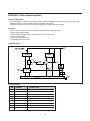
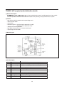
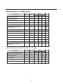
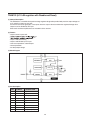
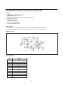
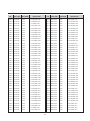
1
Service Manual
59 / 66 Cm STEREO Colour Television
CHASSIS : CP-776
MODEL : DTL- 25G6F
DTL- 25G7F
DTL- 28G2F
DTL- 28G6F
DTL- 28G7F
DTL- 28G8F
DAEWOO ELECTRONICS CO., LTD.
http://svc.dwe.co.kr
Sep,1999
CONTENTS
1. Specifications
. . . . . . . . . . . . . . . . . . . . . . . . . 1
2. Safety Instruction . . . . . . . . . . . . . . . . . . . . . . . 3
3. Circuit Block Diagram
. . . . . . . . . . . . . . . . . . . . . 4
4. Alignment Instructions . . . . . . . . . . . . . . . . . . . . . 5
5. IC Description
. . . . . . . . . . . . . . . . . . . . . . . . . 8
6. IC DC Voltage charts
7. Circuit Description
. . . . . . . . . . . . . . . . . . . . . 33
. . . . . . . . . . . . . . . . . . . . . . 36
8. Service Parts List/Recommendable Spare Parts List . . . . . . . 41
9. Mechanical Exploded View
10. Printed Circuit Board
11. Schematic Diagram
. . . . . . . . . . . . . . . . . .
49
. . . . . . . . . . . . . . . . . . . . .
55
. . . . . . . . . . . . . . . . . . . . .
56
Specifications
CRT
25” : A59EAK071X11 (PHILIPS)
28” : A66EAK071X11 (PHILIPS)
System
PAL/SECAM-B/G, D/K, PAL-I, SECAM-L/L’, NTSC-3.58/4.43(Play back)
Main Voltage
230V AC, 50Hz
Power Consumption
Stand-by mode : 2.5 Watts
Normal operating mode : 25” = 75 Watts
28” = 75 Watts
Sound output
7 + 7 Watts, 10 % THD at RF 60 % mod. (1
Speaker
12W 8 ohm x 2 EA
Antenna
75 ohm unbalanced input
)
Impedance
Tuning system
Frequency Synthesizer(FS) Tuning System
Tuner
DT5-BF14D, EL2782-105-B
Number of
100 programs
program
Aux. Terminal
21 pin EURO-SCART jack ( AV input, TV output, RGB input )
21 pin EURO-SCART jack ( AV input, S-VHS input )
RCA type AV input jack
Headphone jack (3.5 mm )
Remote controller
R-28B07 with 2 “AA” type batteries
Teletext
8 pages memory TOP & FLOF
- West option :English, German/Dutch/Flemish, French, Italian,
Spanish/Portuguese, Swedish/Finnish/Danish, Czech/Slovak
- East option : Polish, Czech/Slovak, Rumanian, Hungarian, Servo-croat,
German/Dutch/Flemish, French, Italian
- Turkish option : Turkish, English, German/Dutch/Flemish, French,
Italian, Spanish/Portuguese, Swedish/Finnish/Danish
OSD language
- West : English, German, French, Italian, Spanish, Netherlands, Portuguese,
Danish, Swedish, Finnish, Norwegian
- East : Polish, Rumanian, Czech, Hungarian
1
21 PIN EURO-SCART
PIN
1
2
3
4
5
6
7
8
9
10
11
12
13
14
15
16
17
18
19
20
21
Signal Designation
Matching Value
Audio Out(linked with 3)
Audio In(linked with 6)
Audio Out(linked with 1)
Audio Earth
Blue Earth
Audio in (linked with 2)
Blue in
Slow(Function) Switching
Green Earth
NC
Green In
NC
Red Earth
NC
Red In, C In
Rapid(Blanking) switching
Video Earth
Rapid Blanking Earth
Video Out
Video In, Y In
Common Earth
0.5Vrms,lmp<1
(RF 60% MOD)
0.5Vrms,lmp<1
(RF 60% MOD)
20
21
18
19
0.5Vrms,lmp>10
0.7Vpp 3dB ,lmp75
TV:0-2V,PERI:9.5-12V,lmp>10
0.7Vpp 3dB
0.7Vpp 3dB,lmp75
16
17
3dB,lmp75
3dB,lmp75
1Vpp
1Vpp
14
15
12
13
10
11
8
9
6
7
2
4
5
2
3
1
• Safety Instruction
WARNING: Only competent service personnel may carry out work involving the testing or repair of
this equipment.
X-RAY RADIATION PRECAUTION
1. Excessive high voltage can produce potentially
hazardous X-RAY RADIATION.To avoid such
hazards, the high voltage must not exceed the
specified limit. The nominal value of the high
voltage of this receiver is 26
at max beam
current. The high voltage must not, under any
circumstances, exceed 29.5 (25"), 30 (28").
Each time a receiver requires servicing, the high
voltage should be checked. It is important to use
an accurate and reliable high voltage meter.
2. The only source of X-RAY Radiation in this TV
receiver is the picture tube.For continued X-RAY
RADIATION protection,the replacement tube
must be exactly the same type tube as specified
in the parts list.
SAFETY PRECAUTION
1. Potentials of high voltage are present when this
receiver is operating. Operation of the receiver
outside the cabinet or with the back board
removed involves a shock hazard from the
receiver.
1) Servicing should not be attempted by anyone
who is not thoroughly familiar with the
precautions necessary when working on highvoltage equipment.
2) Discharge the high potential of the picture tube
before handling the tube. The picture tube is
highly evacuated and if broken, glass
fragments will be violently expelled.
2. If any Fuse in this TV receiver is blown, replace it
with the FUSE specified in the Replacement
Parts List.
3. When replacing a high wattage resistor(oxide
metal film resistor)in circuit board, keep the
resistor 10mm away from circuit board.
4. Keep wires away from high voltage or high
temperature components.
5. This receiver must operate under AC230 volts,
50Hz. NEVER connect to DC supply or any other
power or frequency.
PRODUCT SAFETY NOTICE
Many electrical and mechanical parts in this have
special safety-related characteristics. These
characteristics are often passed unnoticed by a
visual inspection and the X-RAY RADIATION
protection afforded by them cannot necessarily be
obtained by using replacement components rated
for higher voltage,wattage,etc. Replacement parts
which have these special safety characteristics are
identified in this manual and its supplements,
electrical components having such features are
identified by designated symbol on the parts list.
Before replacing any of these components, read the
par ts list in this manual carefully. The use of
substitute replacement parts which do not have the
same safety characterisitics as specified in the parts
list may create X-RAY Radiation.
3
Circuit Block Diagram
4
Alignment Instructions
1. AFT
1.1 Standard B/G,D/K,I and L
1) Set a Signal Generator with
- RF FREQUENCY = 38.9 MHz,
5dBuV
- System = PAL-B/G
2) Connect the Signal Generator RF Output to TP2 (Tuner IF Output).
There must be no signal input to the tuner.
3) Set the L109 to TP1(I603, #22) with DC Voltage to 2.5V 0.3V
2. AGC
1) Set a Pattern Generator with RF LEVEL 63 3dBuV, RF Frequency 210. 25MHz(10CH).
2) Connect a OSCILLOSCOPE PROBE to P101 (TUNER AGC INPUT).
3) Set the RBOI to P101(Tuner AGC Input) with DC Voltage to 2.5V 0.3V
3. SCREEN
1) Set the TV to AVI mode(no signal)
2) Set the TV to NORMAL I mode.
3) Press the SVC key on SVC Remocon.
4) Connect a OSCILLOSCOPE PROBE to P904 ( CRT CATHOD R, G, B ).
5) Adjust the SCREEN VOLUME on FBT
such that the highest black level voltage 145 5Vdc.
4. WHITE BALANCE
1) Set the TV to NOR I mode.
2) Set the R,G,B LEVEL to CENTER with R,G,B UP/DOWN KEY .
3) Adjust the R,G,B UP/DOWN KEY of the other color which did not appear
on the screen to obtain WHITE.
5. FOCUS
1) Apply a RETMA PATTERN signal.
2) Adjust the FOCUS VOLUME on FBT to obtain optimal resolution.
6. GEOMETRY
6.1 VERTICAL SLOPE
1) Apply a RETMA PATTERN Signal.
2) Set the TV to NORMAL I mode.
3) Pressing the V-SLOPE DOWN/UP KEY,
the lower half of the screen is blanked .
4) Adjust the border line of blanked picture
coincident with the retma center using
the V-SLOPE DOWN/UP keys.
6.2 VERTICAL CENTER
1) Apply a RETMA PATTERN Signal.
2) Set the TV to NORMAL I mode.
3) Adjust the center of the picture
with the V-CENTER DOWN/UP kyes.
5
6.3 VERTICAL SIZE
has to be done in advance.
1) Apply a RETMA PATTERN Signal.
2) Set the TV to NORMAL I mode.
3) Adjust the upper part of the picture
with the V-SIZE DOWN/UP keys.
6.4 VERTICAL S-CORRECTION
1) Apply a CROSSHATCH PATTERN signal.
2) Adjust the S-COR UP/DOWN KEY to obtain
the same distance between horizontal lines.
6.5 HORIZONTAL CENTER
1) Apply a RETMA PATTERN signal.
2) Adjust picture centering with CENTER
LEFT/RIGHT keys.
7. EW
7.1 WIDTH
1) Apply a RETMA PATTERN signal.
2) Pressing the EW KEY, the WIDTH OSD appear in the screen.
3) Adjust the over to make a perfect circle with VOL-UP/DOWN KEY.
7.2 PARA
1) Apply a CROSSHATCH PATTERN signal.
2) Pressing the EW KEY, the PARA OSD appear in the screen.
3) Adjust the vertical line to straight with VOL-UP/DOWN KEY.
7.3 CORNER
1) Apply a CROSSHATCH PATTERN signal.
2) Pressing the EW KEY, the CORNER OSD appear in the screen.
3) Adjust the vertical line to straight with VOL-UP/DOWN KEY.
7.4 TRAPI
1) Apply a CROSSHATCH PATTERN signal.
2) Pressing the EW KEY, the TRAPI OSD appear in the screen.
3) Adjust the vertical line to straight with VOL-UP/DOWN KEY.
6
If EEPROM (I702) has been changed ;
- Option data has to be changed and
- all alignment function has to be readjusted .
Service Remocon ( Part Code : 48B1530SVC )
- If you need this service remocon, then please order to our subsidiaries.
PO WE R
N O R M AL
SVC
EW
OPT
ION
PR
VOL
VOL
PR
SEARCH
STOP
EFFECT
TREBLE
MIN
RCH
MAX
BASS
MODE
SEA
MIN
TEM
SYS
SET
CH
AFT
AFT-L’
MAX
BAL
WOOFER
L
R
MAX
MAX
MAX
CONT
BRI
COL
MIN
MIN
MIN
AUTO
TEST
AV
TTX
+
+
+
+
+
V- CENTER
V- SIZE
V- SLOPE
S-COR.
SUB BRI.
-
-
-
-
H-CENTER
+
+
+
R
G
B
-
-
-
L
R
AGC
-
+
R-30SVC
REMOTE CONTROLLER R-30SVC
7
IC Description
DW5457 - AE1
(1) General Description
The DW5457-AE1 is a single chip teletext decoder for decoding World System Teletext data as well as Video
Programming System(VPS), Program Delivery Control(PDC), and Wide Screen Signalling(WSS) data used for
PALplus transmissions(line 23).
Furthermore, the device provides an integrated C500 based general-purpose, fully 8051-compatible microcontroller
with television specific hardware features. The on-chip display unit for displaying¡ ' Level 1.5 ' teletext data can also be
used for customer defined on-screen displays. Up to 10 display pages are available internally.
The DW 5457-AE1 contains a slicer for VPS, WSS, PDC, and TTX, an accelerating acquisition hardware modul, a
display generator for " Level 1.5 " TTX data, and an 8bit microcontroller running at 250 ns cycle time(min.). The
controller with dedicated hardware guarantees flexibility, does most of the internal processing of TTX acquisition,
transfers data to/from the external memory interface and receives/transmits data via I 2C-firmware user-interface. The
slicer combined with dedicated hardware stores TTX data in a VBI buffer of 764Byte. The microcontroller firmware
performs all the acquisition tasks(hamming-and parity-checks, page search and evaluation of header control bits) once
per field. Additionally, the firmware can provide high-end Teletext-features like Packet-26-handling, FLOF, TOP(in 8/10sheet for details).
(2) Feature
Acquisition
- Feature selection via special function register
- Simultaneous reception of TTX, VPS, PDC, and WSS(line 23)
- Fixed framing code for VPS and TTX.
- Acquisition during VBI
- Direct access to VBI RAM buffer.
- Acquisition of packets x/0 to x/24, x/27, 8/30(firmware)
- Assistance of all relevant checks(firmware)
- 1-bit framing code error tolerance(switchable)
- Complete TTX-acquisition firmware with simple user interface
Display
- Features selectable via special function register.
- 50/60/100/120-Hz display.
- Level 1.5 serial attribute display pages.
- Blanking and contrast reduction output.
- 8 direct addressable display pages.
- 12 x 10-character matrix.
- 96 character ROM(standard G0 character set).
- 156 national option characters for 12 languages(European version).
- 288 characters for X/26 display.
- 64 block mosaic graphic characters.
- 32 characters for OSD in expanded character ROM +32 characters inside OSD box.
- Saturation of basic colors adjustable in 4 steps.
- 8 foreground +8 background colours out of 64 colours.
- Conceal/reveal.
- Transparent foreground/background-inside/outside of a box.
- Contrast reduction inside/outside of a box.
- Cursor(colour changes from foreground to background colour).
- Flash(flash rate 1 s, independent of frame rate).
- Programmable horizontal and vertical sync delay.
- Full screen background colour in outer screen.
- Double size/double width/double height characters.
- Character shadowing.
8
¤
¤
- Box shadowing.
- Up to 64 Characters in a display row.
- Software selectable pixel frequency(12, 13.7, 16, 19.2 and 24MHz).
Synchronization
- Display synchronization to Sandcastle Pulse
Microcontroller
- 8bit C500-CPU(8051 compatible)
- 24-MHz internal clock(max.)
- 0.25 (min.) instruction cycle.
- Non-multiplexed 8-bit data and 16 ... 19-bit address bus(ROMless Version)
- Eight 16-bit data pointer registers(DPTR)
- Two 16-bit timers
- Watchdog timer
- Capture compare timer for infrared remote control decoding.
- 256-bytes on-chip RAM.
- Display RAM and TXT/VPS/PDC/WSS-Acquisition-Buffer directly accessible via MOVX.
- 10 Kbyte on-chip display-RAM(access via MOVX) for SDA 5457.
- 8 Kbyte on-chip display-RAM(access via MOVX) SDA 5454 to SDA 5457.
- 1 Kbyte on-ship ACQ-buffer-RAM(XRAM, access via MOVX)for SDA 5450 and SDA 5454 to SDA 5457.
- 6 channel 8-bit pulse width modulation unit.
- 2 channel 14-bit pulse width modulation unit.
- ADC with 8-bit resolution(4 multiplexed input channels)
Ports
- One 8-bit I/O-port with open drain output and optional I2C Bus emulation(Port0).
- Two 8-bit multifuncional I/O-ports(Port1, Port3).
- One 4-bit port working as digital or analog inputs for the ADC(Port2).
- One 1-bit Input-port with secondary functions(P4.7/VS/EVEN_ODD).
- One 2-bit I/O-port with optional RAM/ROM address expansion up to 512 Kbyte(P4.0 and P4.1).
Additional Features
- Single external 6MHz crystal, all necessary clocks are generated internally
- CPU clock speed selectable via special funtion registers(7 possible selections between 3 and 24MHz)
(3) Block Diagram
CPU-XRAM
Port 3
Watchdog-Timer
3)
VBI-Buffer
Slicer
Acquisition
Capture
Compare-Timer
1)
Program-ROM
Port 1
CPU
PWM
Display-RAM
ADC
Port 2
MMU
Port 4
4)
2)
External Memory Interface
9
Character
Font
Display
Generator
3 2bit-DACs
Port 0
(4) Pin Description
Pin
1
Name
P3.1
Symbol
Description
SYS
SECAM-L’ OUT for switching SAW filter K9650-M
- SECAM-L’ : H
- SECAM- L : L
2
P0.7/Open Drain
BUSSTOP
I2C BUS STOP IN for Computer controlled
alignment in Factory ( Active Low )
3
P0.6/Open Drain
SDA
Serial data IN/OUT for I2C
4
P0.5/Open Drain
SCL
Serial clock IN/OUT for I2C
5
P0.4/Open Drain
6
P0.3/Open Drain
7
P0.2/Open Drain
8
P0.1/Open Drain
9
P0.0/Open Drain
LED
LED drive OUT
- Stand-by mode : H
- Operating mode : L
( IR reception : pulse )
10
VSS
VSS
ground
11
VCC
VCC
Power Supply
12
XTAL1
OSCIN
Input to inverting osc. Amplifier
13
XTAL2
OSCOUT
Output of inverting osc. Amplifier
14
P4.0/ALE
15
RESET
16
P1.7/14BIT PWM
Not Used
17
P1.6/14BIT PWM
Not Used
18
P1.5/14BIT PWM
Not Used
19
P1.4/14BIT PWM
Not Used
Not Used
Not Used
RST
RESET IN (ACTIVE LOW)
Degaussing/SW
H : ON
L : OFF
20
P1.3/14BIT PWM
MUTE
AUDIO MUTE OUT
21
P1.2/14BIT PWM
GND
GND
22
P1.1/8BIT PWM
Not Used
23
P1.0/8BIT PWM
Not Used
24
VSSA
VSSA
Analog GND for Slicer
25
FIL3
FIL3
PLL Loop Filter I/O for Phase Shifting
26
FIL2
Not Used
27
FIL1
Not Used
28
VCCA
VCCA
Analog Supply for SlicerNot Used
29
IREF
IREF
Reference Current for Slicer PLLs
30
CVBS
CVBS
CVBS IN
31
P2.3/8 bit ADC
AFT
AFT
32
P2.2/8 bit ADC
AGC
IF AGC INPUT for Auto Tuning System
10
Pin
Name
Symbol
Description
33
P2.1/8 bit ADC
KS
Local KEY SCAN IN
34
P2.0/8 bit ADC
S/SW
S/SW IDENT IN for Automatic
switching between TV/AV mode
- H : AV / RGB mode
- L : TV mode
35
VSS VSS-OSD
VSS
Ground
36
P3.3/INT1
IR
REMOTE IR IN
37
VDD VCC-OSD
VDD
Power Supply
38
LCIN OSCIN-OSD
Not Used
39
LCOUT
Not Used
40
P3.7/TXT I/O
Not Used
41
P3.6/RXD
Not Used
42
P3.5/T1
SYS
Standard switch
Meg. modulated video-IF
Signal : H
Pos. modulated video-IF
Signal : L
43
P3.4/T0
POWER
POWER CONTROL OUT
44
P3.2/INT0
45
HS/SC
46
P4.7/VS
47
R
R
RED OUT
48
G
G
GREEN OUT
49
B
B
BLUE OUT
50
BLANK
BL
BLANK OUT
51
COR
COR
Not Used
(CONTRAST REDUCTION OUT)
52
P3.0 T1C2/PWM1
EVEN/ODD
EVEN/ODD OUT for non-interlacing
in TTX mode
Not Used
Sandcastle IN
Sandcastle IN
Not Used
11
AT24C16-10PC (E2 PROM)
(1) Typical Features
• IC Bus compatible
• Low power CMOS Technology
• Eight-byte page(1k, 2k), 16-byte page(4k, 8k, 16k) write buffer
• Self-Timed Write cycle with Auto-Clear
• 100,000 program/Erase cycles
• 100 Year Data Retention
• Optional High Endurance Device Available
(2) Description
The AT24C16-10PC is a 16K bit serial CMOS E 2 PROM internally organized as 2048x8bits.
The AT24C16-10PC features a 16 byte page write buffer.
(3) Block Diagram
(4) Pin Description
PIN
SYMBOL
DESCRIPTION
1-3
A0, A1, A2
Device Address lnputs
4
Vss
Ground
5
SDA
Serial Data/Address
6
SCL
Serial Clock
7
TEST
Connect to Vss
8
Vcc
+5V Power supply
12
TDA8844N2 (I2C-bus controlled PAL/NTSC/SECAM TV Processors)
(1) General Description
The TDA8844N2 is I2C-bus controlled single chip TV processors which are intended to be applied in PAL/NTSC
television receiver.
The IC is mounted in a S-DIP 56 envelope.
(2) Feature
• Video
- Integrated luminance delay line
- Integrated chroma trap and bandpass filters (auto calibrated)
- Asymmetrical peaking circuit in the luminance channel
- Black stretching of non standard CVBS or luminance signals
• RGB
- RGB control circuit with “Continuous Cathode Calibralion” and white point adjustment.
• Input / Output
- Flexible source selection with CVBS switch and Y(CUBS)/C input so that a comb filter can be applied.
- The output signal of the video source select is externally available ( also as CVBS when Y/C input is used).
- External audio input.
- Linear RGB input with fast blanking.
• Synchronization and Deflection
- Horizontal synchronization with two control loops and alignment free horizontal oscillator.
- Slow start and slow stop of the horizontal drive output to enable low stress start-up and switch-off from the line circuit
at nominal line supply voltage.
- Vertical count-down circuit for stable behavior with provisions for non-standard signals.
- Vertical geometry control.
- Vertical drive optimized for DC coupled vertical output stages.
• Control
- Full I2C bus control, as well for customer controls as for factory alignment.
- All automatic controls have an option for forced mode.
• Packaging
- SDIP-56(Soldering Dual in-line Packages)
13
(3) Block Diagram
14
(4) PIN Description
SYMBOL
ANDIF
AUDIOEXT
NC
NC
PLLLF
IFVO
SCL
SDA
DECBG
CHROMA
CVBS/Y
VP1
CVBSINT
GND1
AUDIOOUT
SECPLL
CVBSEXT
BLKIN
BO
GO
RO
BCLIN
RI
GI
BI
RGBIN
LUMIN
LUMOUT
BYO
RYO
BYI
RYI
REFO
XTAL1
XTAL2
DET
VP2
CABS10
DECDIG
HOUT
FBISO
PH2LF
PH1LF
GND2
EWD
VDRB
VDRA
IFIN1
IFIN2
EHTO
VSC
Irel
DECAGC
AGCOUT
AUDEEM
DECSDEM
PIN
1
2
3
4
5
6
7
8
9
10
11
12
13
14
15
16
17
18
19
20
21
22
23
24
25
26
27
28
29
30
31
32
33
34
35
36
37
38
39
40
41
42
43
44
45
46
47
48
49
50
51
52
53
54
55
56
DESCRIPTION
Sound IF input
Extemal audio input
not connected
not connected
IF-PLL loop filter
IF video output
serial clock input
serial data input/output
bandgap decoupling
chrominance input(S-VHS)
external CVBS/Y input
main supply voltage 1 (+8V)
extemal CVBS input
ground1
audio output
SECAM PLL decoupling
external CVBS input
black-current input
blue output
green output
red output
beam current limiter input/V-guard input
red input for insertion
green input for insertion
blue input for insertion
RGB insertion input
Luminance input
Luminance output
(B-Y) signal output
(R-Y) signal output
(B-Y) signal input
(R-Y) signal input
subcamer reference output
3.58 MHz crystal connection
4.43/3.58 MHz crystal connection
loop fiter phase detector
2nd supply voltage 1(+8V)
CVBS-1 output
Decoupling digital supply
horizontal output
flyback input/sandcastle output
phase-2 filter
phase-1 filter
ground2
east-west drive output
vertical drive B output
verticla drive A output
IF input 1
IF input 2
EHT/overvoltage protection input
vertical sawtooth capacitor
reterence current input
AGC decoupling capacitor
tuner AGC output
Audio deemphasis
Decoupling sound demodulator
15
TDA4470-M(Multistandard V ideo-if and Quasi Parallel Sound Processing)
(1) Feature
• 5V supply voltage; low power consumption
• Active carrier generation by FPLL principle
(frequency-phase-locked-loop)for true synchronous demodulation.
• Very linear video demodulation, good pulse response and excellent intermodulation figures.
• VCO circuit operates at picture carrier frequency, the VCO frequency is switchable for L’-mode.
• Alignment-free AFC without external reference circuit, polarity of the AFC curve is switchable.
• VIF-AGC for negative modulated signals(peak sync detection) and for positive modulation
(peak white/black level detector)
• Tuner AGC with adjustable take over point
• Alignment-free quasi parallel sound(QPS) mixer for FM/NICAM sound IF signals.
• Intercarrier output signal is gain controlled(necessary for digital sound processing)
• Complete Alignment-free AM demodulator with gain control AF output.
• Separate SIF-AGC with average detection
• Two independent SIF inputs
• Parallel operation fo the AM demodulator and QPS mixer (for NICAM-L stereo sound)
(2) Description
The TDA4470 is an intergrated bipolar circuit for multistandard video/sound IF(VIF/SIF) signal processing in
TV/VCR and multimedia applications. The circuit processes all TV video IF signals with negative modulation
(e.g., B/G standard), positive modulation(e.g., L standard) and the AM, FM/NICAM sound IF signals.
16
(3) Block Diagram
17
(4) Pin Description
Pin
Function
Symbol
1,2
Vi, SIF 1
SIF 1 input(symmetrical)
3
VSW
Input selector switch
4, 9, 16
GND
Ground
5
CAGC
SIF-AGC(time constant)
6, 7
Vi, VIF
VIF input(symmetrical)
8
CAGC
VIF-AGC(time constant)
10
Rtop
Take over point, tuner AGC
11
Itun
Tuner AGC output current
12
Vo, vid
Video output
13
VSW
Standard switch
14
VSW
L’switch
15
Cb1
Black level capacitor
17
Cref
Internal reference voltage
18
LF
Loop filter
19
VSW
AFC swich
20, 21
VVCO
VCO circuit
22
VAFC
AFC output
23
VS
Supply voltage
24
VO, FM
Intercarrier output
25
VO, AM
AF output-AM sound
26
Rcomp
Offset compensation
27, 28
Vi, SIF2
SIF 2 input(symmetrical)
18
TDA6106Q ( Video Output Amplifier )
(1) General Description
The TDA6106Q is a monolithic video output amplifier (5MHz bandwidth) in a SIL 9 MPpackage, using high-voltage
DMOS technology, and is intended to drive the cathode of CRT directly .
To obtain maximum performance, the amplifier should be used with black-current control.
(2) Feature
• Black - current measurement output for automatic black current stabilization (ABS)
• Single supply voltage of 200V
• Internal protection against positive appearing CRT flash-over discharge
• Protection against ESD
• Internal 2.5V reference circuit
• Controllable switch-off behavior
(3) Block Diagram
(4) Pin Description
PIN
SYMBOL
DESCRIPTION
1
N.C
2
N.C
3
V in
inverting input
4
GND
ground, substrate
5
I om
Black-current measurement output
6
V dd
supply voltage high
7
N.C
8
V oc
cathode output
9
V of
feedback/transient output
19
TDA8351 (DC-coupled vertical deflection circuit)
(1) General Description
and 110 color deflection systems for field frequencies of 50 to 120 Hz.
The circuit provides a DC driven vertical deflection output circuit, operating as a high efficient class G system.
(2) Feature
• High efficient fully DC-coupled vertical output bridge circuit
• Vertical fly-back switch
• Guard circuit
• Protection against : - short circuit of the output pins (7 and 4)
- short circuit of the output pins to Vp
• Temperature (thermal) protection
• High EMC immunity because of common mode inputs
• A guard signal in zoom mode.
(3) Block Diagram
(4) Pin Description
PIN
SYMBOL
DESCRIPTION
1
I drive (pos)
input power stage (positive); include Ii(sb) signal bias
2
I drive (neg)
input power stage (negative); include Ii(sb) signal bias
3
Vp
operating supply voltage
4
V o(b)
output voltage B
5
GND
ground
6
V fb
input fly-back supply voltage
7
V o(a)
output voltage A
8
V o(guard)
guard output voltage (Not used)
9
V I(fb)
input feedback voltage
20
STR-F6654 (Hybrid IC for a Switching Regulator)
(1) General Description
The STR-F6654 is a Hybrid IC with a built in power transistor and a separate excitation control IC,
designed for converter type switching mode power supply applications.
The IC is capable of quasi-resonant mode and requires small number of external component.
(2) Feature
• Small SIP isolated package : Resin sealed type (transfer mold)
• Lower power dissipation at a lighter load
• Many protection function : - Pulse-by-pulse over current protection
- Over-voltage protection with a latch
- Thermal protection with a latch
• These protection functions are incorporated and can be latched with an external signal.
(3) Block Diagram
(4) Pin Description
Pin
Symblols
Description
Functions
1
O.C.P/F.B
Overcurrent/Feedback terminal
Input of overcurrent detection signal and
constant voltage control signal
2
S
Source terminal
MOS FET source
3
D
Drain terminal
MOS FET drain
4
VIN
Power supply terminal
Input of power supply for control circuit
5
GND
Ground terminal
Ground
21
(5)
)
Rating
Parameter
Terminal
Symbol
Operation start voltage
4-5
Operation stop voltage
Unit
MIN
TYP
MAX
VIN(ON)
14.4
16
17.6
V
4-5
VIN(OFF)
9
100
11
V
Circuit current in operation
4-5
LIN(ON)
-
-
30
mA
Circuit current in non-operation
4-5
LIN(OFF)
-
-
100
-
TOFF(MAX)
45
-
55
1-5
Tth(2)
-
-
1.0
-
TOFF(MIN)
-
-
1.5
1-5
Vth(1)
0.68
0.73
0.78
V
1-5
Vth(2)
1.3
1.45
1.6
V
O.C.P/F.B terminal extraction current
1-2
IO.C.P/F.B
1.2
1.35
1.5
mA
O.V.P operation voltage
4-5
VIN(OVP)
20.5
22.5
24.5
V
Latch ciruit sustaining voltage
4-5
I IN(H)
-
-
400
Latch circuit release voltage
4-5
V IN(La.OFF)
6.6
-
8.4
-
Tj(TSD)
140
-
-
Maximum OFF time
Minimum time for input of quasi
resonant signals
Minimum OFF time
O.C.P/F.B terminal threshold voltage 1
Thermal shutdown operationg
temperature
V
(6) Electrical Characteristics of Power Transistor Part(Trl) (Ta=25 )
Rating
Parameter
Terminal
Symbol
Drain-to-Source breakdown voltage
3-2
Drain leakage current
Unit
MIN
TYP
MAX
VDSS
650
-
-
3-2
IDSS
-
-
300
On-resistance
3-2
RDS(ON)
-
-
1.15
Swotching time
3-2
tf
-
-
250
nsec
ch-F
-
-
0.95
/W
Thermal resistance
-
22
V
TDA8133 (5.1V+8V regulator with Disable and Reset)
(1) General Description
The TDA8133 is a monolithic dual positive voltage regulator designed to provide fixed precision output voltages of
5.1V and 8V at currents up to 0.75A.
An internal reset cuicuit generates a reset pulse when the output 1 decrease below the regulated voltage value.
Output 2 can be disabled by TTL input.
Short circuit and themal protections are included in all the versions.
(2) Feature
• output currents up to 0.75A
•F
2%
•
2%
• output 1 with Reset facility
• output 2 with Disable by TTL input
• short circuit protection at both outputs
• thermal protection
• low drop output voltage
(3) Block Diagram
(4) Pin Description
PIN
SYMBOL
DESCRIPTION
1
V in 1
input 1
2
V in 2
input 2
3
Ce
Delay capacitor
4
V dis
disable
5
GND
ground
6
RST
reset
7
n.c
8
V out 2
output 2 (12V)
9
V out 1
output 1 (5.1V)
23
TDA 7269(10W+10W Stereo Amplifier with Mute & ST-BY)
(1) Features
20V.
• Split supply
• High output power 10+10W @ THD=10%, RL=8 , Vs= 14V
• No pop at turn-ON/OFF
• Mute(POP FREE)
• Stand-by feature(LOWlq)
• Thermal overoad protection
• Short circuit protection to gnd
(2) Description
The TDA7269 is class AB dual Audio power amlifier assembled in the Multiwatt package,
specially designed for high quality sound application as Hi-Fi music centers and stereo TV sets.
(3) Block Diagram
(4) Pin Description
Pin
Symbol
1
2
3
4
5
6
7
8
9
10
11
-Vs
output(1)
+Vs
output(2)
Mute
-Vs
IN+(2)
IN-(2)
GND
IN-(1)
IN+(1)
24
MSP3415D ( Multistandard Sound processor for NICAM & 2-Carrier )
(1) Features
• A single-chip Multistandard Sound Pressor for applications in analog and digital TV sets
• TWO selectable analog inputs
• Automatic Gain control for analog input
• All demoudlation and filtering is performed on chip and is individually programmable
• Adjustment of volume, balance, loudness, treble, bass, base width enlargement, pseudo stereo
• Independent input selection for speaker-out and scart-out
(2) Block Diagram
25
(3) Description
• Analog Sound IF - Input Section
The input pins ANA_IN1+, ANA_IN2+ and ANN_IN-offer the possibility to connect two different sound IF sources to
the MSP 3415D. By means of bit [8] of AD_CV either terrestrial or satellite sound IF signals can be selected.
The analog-to-digital conversion of the preselected sound IF signal is done by a flash-converter, whose output can be
used to con-trol an analog automatic gain circuit (AGC), providing optimum level for a wide range of input levels. It is
possible to switch between automatic gain control and a fixed (setable) input gain. In the optimum case, the input range
of the AD converter is completely covered by the sound if source. Some combinations of SAW filters and sound
IF mixer IC’s however show large picture components on their outputs. In this case filtering is recommended.
It was found, that the high pass filters formed by the coupling capacitors at pins ANA_IN1+ and ANA_IN2+ are sufficient
in most cases.
• Quadrature Mixers
The digital input coming from the integrated A/D converter may contain audio information at a frequency
range of theoretically 0 to 9 MHz corresponding to the selected standards. By means of two
programmable quadrature mixers two different audio sources, for example NICAM and FM-mono, may be
shifted into baseband position. In the following the two main channels are provided to process either:
- NICAM (channel 1) and FM mono (channel 2) simultaneously or alternatively
- FM2 (channel 1) and FM1 (channel2).
Two independent digital oscillators are provided to generate two pairs of sin/cos-functions. Two
programmable increments, to be divided up into Low- and High part, determine frequency of the oscillator,
which corresponds to the frequency of the desired audio carrier.
• Lowpass Filtering Block for Mixed Sound IF Signals
By means of decimation filters the sampling rate is reduced. Then, data shaping and/or FM bandwidth limitation is
performed by a linear phase Finite Impulse Response (FIR-filter). Just like the oscillators’ increments the filter
NICAM versions can easily be implemented. Two not necessarily different sets of coefficients are required, one for
channel 1 (NICAM or FM2) and one for channel 2 (FM1=FM-mono).
Since both MSP channels are designed to process the German FM Stereo System with the same FIR coefficient set
(despite 7 dB power level difference of the two sound carriers), the MSP channel 1 has an internal overall gain of 6
dB. To process two carriers of identical power level these 6 dBs have to be taken into account by decreasing the
values of the channel 1 coefficient set.
• CORDIC Block
The filtered sound IF signals are demodulated by transforming the incoming signals from Cartesian into polar format
by means of a CORDIC processor block. On the output, the phase and amplitude is available for further processing.
AM signals are derived from the amplitude information whereas the phase information serves for FM and NICAM
(DQPSK) demodulation.
• Differentiators
FM demodulation is completed by differentiation the phase information output of the CORDIC block.
• Lowpass Filer Block for Demodulated Signals
The demodulated FM and AM signals are further lowpass filtered and decimated to a final sampling
frequency of 32 kHz. The usable bandwidth of the final baseband signals is about 15 kHz.
26
• DQPSK-Decoder
In case of NICAM-mode the phase samples are decoded according the DQPSK-Coding scheme. The
output of this block contains the original NICAM-bitstream, which is available at the N-Bus interface.
• NICAM-Decoder
Before any NICAM decoding can start, the MSP must lock to the NICAM frame structure by searching and
synchronizing to the so-called Frame Alignment Words (FAW).
To reconstruct the original digital sound samples the NICAM-bitstream has to be descrambled,
deinterleaved and rescaled. Also bit error detection and correction (concealment) is performed in this
NICAM specific block.
To facilitate the Central Control Unit CCU to switch the TV-set to the actual sound mode, control
information on the NICAM mode and bit error rate are supplied by the the NICAM-Decoder, It can be read
out via the I2C-Bus.
• Analog Section and SCART Switches
The analog input and output sections offer a wide range of switching facilities, which are shown in Fig.
The switches are controlled by the ACB bits defined in the audio processing interface (see chapter
“programming the audio processing part”).
If the MSP 3415D is switched off by first pulling STANDBYQ low and then disconnecting the 5V but
keeping the 8V power supply (‘Standby’-mode), the switches S1, S2 and S3 maintain their position and
function.This facilitates the copy from selected SCART-inputs to SCART-outputs in the TV-sets standby
mode.
Fig. SCART-Switching Facilities Bold lines determine the default configuration
27
In case of power-on start or starting from standby, the IC switches automatically to the default
configuration, shown in the figure above. This action takes place after the first I 2C transmission into the
DFP part. By transmitting the ACB register first, the default setting mode can be changed.
• MSP 3415D Audio Baseband Processing
By means of the DFP processor all audio baseband functions are performed by digital signal processing
(DSP). The DSP functions are grouped into three processing parts: Input preprocessing, channel selection
and channel postprocessing.
The input preprocessing is intended to prepare the various signals of all input sources in order to form a
standardized signal at the input to the channel selector. The signals can be adjusted in volume, are
processed with the appropriate deemphasis and are dematrixed if necessary.
Having prepared the signals that way, the channel selector makes it possible to distribute all possible
source signals to the desired output channels.
Of special importance is the ability to route in an external coprocessor for special effects like graphic
equalizer, surround processing and sound field processing. Routing can be done with each input source
and output channel via the I2S inputs and outputs.
All input and output signals can be processed simultaneously with the exception that FM2 cannot be
processed at the same time as NICAM. While processing the adaptive deemphasis, no dual carrier stereo
(German or Korean) or NICAM processing is possible. Identification values are not valid either.
• Dual Carrier FM Stereo/Bilingual Detection
In the German and Korean TV standard, audio information can be transmitted in three modes: Mono,
stereo or bilingual. To obtain information about the current audio operation mode, the MSP 3415D detects
the so-called identification signal. Information is supplied via the Stereo Detection Register to an external
CCU.
28
(4) Pin Description
PIN
PIN NAME
DESCRIPTION
1
AUD_CL_OUT
Audio clock output
2
CW_CL
Pay-TV control clock
3
CW_DA
Pay-TV control data
4
D_CTR_OUT1
Digital control output 1
5
D_CRT_OUT0
Digital control output 0
6
ADR_SEL
Control bus address select
7
STANDBYQ
Standby (low-active)
8
D_CTR_IN 0
For future use
2
9
I C_CL
I2C clock
10
I2C_DA
I2C clock
11
I2S_CL
I2S clock
12
I2S_WS
I2S wordstrobe
13
I2S_DA_OUT
I2S data output
14
I2S_DA_IN
I2S data input
15
S_DA_IN
SBUS data input
16
S_ID
SBUS ident
17
S_CL
SBUS clock
18
DVSUP
Digital power supply +5V
19
DVSS
Digital ground
20
S_DA_OUT
SBUS data output (FM/NICAM-test)
21
FRAME
NBUS frame
22
N_CL
NBUS clock
23
N_DA
NBUS data
24
RESETQ
Power-on-reset
25
DACA_R
Analog output AUX, right
26
DACA_L
Analog output AUX, left
27
VREF2
Reference ground2 high voltage part
28
DACM_R
Analog output MAIN, right
29
DACM_L
Analog output MAIN, left
30
TESTIO2
Test pin 2
31
C_DACS_R
SCART output capacitor to ground
32
C_DACS_L
SCART output capacitor to ground
33
SC2_OUT_R
SCART output2, right
34
SC2_OUT_L
SCART output2, left
35
VREF1
Reference ground1 high voltage part
36
SC1_OUT_R
SCART output, right
37
SC1_OUT_L
SCART output, left
38
CAPL_A
Volume capacitor AUX
39
AHVSUP
Analog power supply 8V
40
CAPL_M
Volume capacitor MAIN
29
PIN
PIN NAME
DESCRIPTION
41
AHVSS
Analog ground
42
AGNDC
Analog reference voltage high voltage part
43
PDMC1
Capacitor to BAGNDI
44
PDMC2
Capacitor to BAGNDI
45
BAGNDI
Buffered AGNDC
46
SC3_IN_L
Scart input3 in, left
47
SC2_IN_R
Scart input3 in, right
48
ASG2
Analog Shield Ground2
49
SC2_IN_L
Scart input2 in, left
50
SC2_IN_R
Scart input2 in, right
51
ASG1
Analog Shield Ground1
52
SC1_IN_L
Scart input1 in, left
53
SC1_IN_R
Scart input1 in, right
54
VREFTOP
Reference voltage IF A/D converter
55
MONO_IN
Mono input
56
AVSS
Analog ground
57
AVSUP
Analog power supply +5V
58
ANA_IN1+
IF input1
59
ANA_IN1-
IF common
60
ANA_IN2+
IF input (if ANA_IN1+is used only, connect to
AVSS with 50pF Capacitor
61
TESTIO1
Test pin1
62
XTAL_IN
Crystal oscillator
63
XTAL_OUT
Crystal oscillator
64
DMA_SYNC
DMAC-sync: signal
30
GMS30112-R098 (4-bit Single Chip Microcomputer for Remote control)
(1) General Description
The GMS30112-R098 is 4-bit single chip CMOS microcomputer.
(2) Feature
• program memory : 1024 bytes
• data memory : 32 x 4 bits
• 43 types of instruction set
• 3 levels of subroutine nesting
• 1 bit output port for a large current (REMOUT signal)
• operating frequency : 300kHz - 1 MHz
• instruction cycle : 12.5 usec @ 480kHz
• CMOS process ( single 3.0 V power supply )
• stop mode (through internal instruction)
• released stop mode by key input (masked option)
• built in capacitor for ceramic oscillation circuit (masked option)
• built in a watch dog timer(WDT)
• low operating voltage (2.0 V to 4.0 V)
(3) Block Diagram
31
(4) Pin Description
PIN
SYMBOL
DESCRIPTION
1,2,3,4
K0,K1,K2,K3
4 bit input port with built in pull up resistor
5,6,7,8,9,10
D0,D1,D2,D3,D4,D5
10 bit output port which can be set or reset pin
by pin independently.
The output structure is N-channel open drain.
11
REMOUT
remote control signal output port which has
high current driving capability
12
OSC 2
oscillator output
13
OSC 1
oscillator input
14
Vdd
2-4V power supply
15
RESET
reset signal input which is a low active
16
GND
ground
17,18,19,20
R0,R1,R2,R3
4 bit programmable I/O port
32
IC DC Voltage charts
Input signal . . . . . . PAL/CH5-Video : 8 step colour bar (87% AM)
Audio : 1 KHz sinewave (60% FM)
User’s control condition . . . . . . Contrast, Brightness, Colour, Volume Controls-max.
Line voltage . . . . . . AC 230V, 50Hz
All the voltage in each point are measured with Multimeter.
1. TDA 8351 (I301)
Pin No.
1
2
3
4
5
6
7
8
9
V(DC)
2.3
2.3
16.0
8.3
0
4.6
8.3
0.6
7.1
2. MSP 3415D (I602)
Pin No.
1
2
3
4
5
6
7
8
9
10
V(DC)
0
0
0
0
0
0
5.0
0
1.8
1.8
Pin No.
11
12
13
14
15
16
17
18
19
20
V(DC)
2.5
2.5
2.5
1.3
1.3
1.3
1.3
5.0
0
3.5
Pin No.
21
22
23
24
25
26
27
28
29
30
V(DC)
0
0
0
5.0
0
0
0
1.5
1.5
0
Pin No.
31
32
33
34
35
36
37
38
39
40
V(DC)
0.1
0
0
0
0
3.8
3.8
3.8
8.0
7.0
Pin No.
41
42
43
44
45
46
47
48
49
50
V(DC)
0
3.7
0
0
0
0
0
0
3.7
3.7
Pin No.
51
52
53
54
55
56
57
58
59
60
V(DC)
0
3.7
3.7
2.6
3.7
0
5.0
1.5
1.5
0
Pin No.
61
62
63
64
V(DC)
0
2.5
2.5
3.7
33
3. TDA 4470-M(I603)
Pin No.
1
2
3
4
5
6
7
8
9
10
V(DC)
3.2
3.2
3.4
0
1.0
2.3
2.3
2.0
0
10
Pin No.
11
12
13
14
15
16
17
18
19
20
V(DC)
1.8
2.0
4.5
3.8
2.5
0
4.2
2.2
3.4
3.3
Pin No.
21
22
23
24
25
26
27
28
V(DC)
3.3
3.2
4.9
2.1
2.1
0.6
0.1
0.1
4. TDA 7269 (I605)
Pin No.
1
2
3
4
5
6
7
8
9
10
11
V(DC)
-14.0
0
13.5
0
6.5
-14
0
0
0
0
0
5. SDAL 5457 (I701)
Pin No.
1
2
3
4
5
6
7
8
9
10
V(DC)
0
5.1
2.2
1.7
0.3
0.3
0.3
0.3
0.4
0
Pin No.
11
12
13
14
15
16
17
18
19
20
V(DC)
5.1
2.5
2.7
5.1
5.1
3.8
5.1
5.1
0.1
0.1
Pin No.
21
22
23
24
25
26
27
28
29
30
V(DC)
0
5.1
5.1
0
2.3
4.8
5.1
4.8
1.4
2.4
Pin No.
31
32
33
34
35
36
37
38
39
40
V(DC)
2.5
1.6
5.1
0
0
4.8
5.0
4.5
4.5
5.0
Pin No.
41
42
43
44
45
46
47
48
49
50
V(DC)
0
5.0
2.1
5.0
0.7
5.0
0
0
0
0
Pin No.
51
52
V(DC)
2.5
0
34
6. AT24C16-10PC (I702)
Pin No.
21
22
23
24
25
26
27
28
V(DC)
0
0
0
0
2.3
1.8
0
5.1
7. STR-F6654 (I801)
Pin No.
1
2
3
4
5
V(DC)
2.6
0.1
286.9
17.4
0
8. TDA 8133 (I801)
Pin No.
21
22
23
24
25
26
27
28
V(DC)
9.4
11.2
3.1
1.9
0
5.1
8.0
5.1
35
Circuit Description
Vision IF Amplifier
The video IF signal(VIF) is fed through a SAW filter to the differential input(pin 6-7) of the VIF amplifier. This amplifier
consists of three AC-coupled amplifier stages. Each differential amplifier is gain controlled by the automatic gain
control(VIF-AGC). The output signal of the VIF amplifier is applied to the FPLL carrier generation and the video
demodulator.
Tuner-and VIF-AGC
At Pin 8, the VIF-AGC charges/discharges the AGC capacitor to generate a control voltage for setting the gain of the VIF
amplifier and tuner in order to keep the video output signal at a constant level. Therefore, in the case of all negative
modulated signals(e.g., B/G standard) the sync. level of the demodulated video signal is the cirterion for a fast
charge/discharge of the AGC capacitor.
For positive modulation(e.g., L standard) the peak white level of video signal controls the charge current. In order to
reduce reaction time for fositive modulation, where a large time constant is needed, an additional black level detector
controls the discharge current in the event of decreasing VIF input signal. The control voltage(AGC voltage at Pin 8) is
transferred to an internal control signal, and is fed to the tuner AGC to generate the tuner AGC can be adjusted at Pin 10
by a potentiometer or an external dc voltage(form interface circuit of microprocessor).
FPLL, VCO and AFC
The FPLL circuit(frequency phase locked loop) consists of a frequency and phase detector to generate the control
voltage for the VCO tuning. In the locked mode, the VCO is controlled by the phase detector and in unlocked mode, the
frequency detector is superimposed. The VCO operates with an external resonance circuit(L and Cparalled) and is
controlled by internal varicaps. The VCO control voltage is also converted to a current and represents the AFC output
signal at Pin 22. At the AFC are possible: AFCcurve “rising” or “falling” and AFC “off”.
A practicable VCO alignment of the external coil is the adjustment to zero AFC output current at Pin 22. At center
frequency the AFC output current is equal to zero. Furthemore, at Pin 14, the VCO center frequency can be switched for
setting to the required L’ value(L’ standard).
The optional potentiometer at Pin 26 allows an offset compensation of the VCO phase for improved sound quality(fine
adjustment). Without a potentiometer(open circuit at Pin 26), this offset compensation is not active.
The oscillator signal passes a phase shifter and supplies the in-phase signal(0¡£) and the quadrature signal(90¡£) of the
generated picture carrier.
Video Demodulation and Amplifier
The video IF signal, which is applied from the gain controlled IF amplifier, is multiplied with the inphase component of the
VCO signal. The video demodulator is designed for low distortion and large bandwidth. The demodulator output signal
passes an integrated low pass filter for attenuation of the residual vision carrier and is fed to the video amplifier. The
video amplifier is realized by an operational amplifier wth internal feedback and 8MHz bandwidth(-3dB). Astandard
dependent dc level shift in this stage delivers the same sync. level for positive and negative modulation. An additional
noise clipping is provided. The video signal is fed to VIF-AGC and to the video output buffer. This amplifier with a 6dB
gain offers easy adaption of the sound trap. For nominal video IF modulation the video output signal at Pin 12 is 2V pp.
Sound IF Amplifier and SIF-AGC
The SIF amplifier is nearly identical with the 3-stage VIF amplifier. Only the first amplifier stage exists twice and is
switchable by a control voltage at Pin 3. Therefore with a minimal external expense it is possible to switch between two
differnt SAW filters. Both SIF inputs features excellent corss-talk attenuation and an input impedance which is
independent from the switching condition.
signal to the AM demodulator and QPS mixer.
36
AM Demodulator
The alignment-free AM demodulator is realized by a synchronous detector. The modulated SIF signal from the SIF
amplifier output is multiplied in phase with the limited SIF signal(AM is removed). The AF signal of the demodulator
output is fed to the output amplifier and to the SIF-AGC. For all TV standards with negative video modulation(e.g., B/G
standard), the AF output signal (Pin 24) is switched off by the standard switch.
Quasi-Parallel-Sound(QPS) Mixer
The QPS mixerj is realized by a multiplier. The SIF signal(FM or NICAM carrier) is converted to the intercarrier frequency
by the regenerated picture carrier(quadrature signal) which is provided from the VCO. The intercarrier signal is fed via an
output amplifier to Pin 24.
Standard Switch
To have equal polarity of the video output signal the polarity can be switched in the demodulation stage in
accordancewith the TV standard. Additional a standard dependent dc level shift in the video amplifier delivers the same
sync. level. In parallel to this, the correct VIF-AGC is selected for positive or negative modulated VIF signals.
In the case of negative modulation(e.g., B/G stamdard) the AM output signal is switched off. For positive modulation(L
standard) the AM demodulator and QPS mixer is active. This condition allows a parallel operation of the AM sound signal
and the NICAM-L stereo sound.
L’ Switch
With a control voltage at Pin 14 the VCO frequency can be switched for setting to the required L’ value(L’ standard). Also
a fine adjustment of the L’-VCO center frequency is possile via a potentiometer. The L’ switch is only active for positive
modulated video IF-signals(standard switch in L mode).
AFC Switch
The AFC output signal at Pin 22 can be controlled by a switching voltage at Pin 19. It is possible to select an AFC output
signal with a rising-or falling AFC curve and to switch off the AFC.
Source select switch
TDA8844 input switch can select one of the following sources ;
pin 13 front-end : CVBS l int
pin17
: CVBS 2 ext
pin 11, pin10 : Y (S-VHS), C (S-VHS)
Selected signal is available at the CVBS output pin 38, in case of Y/C input Y+C are added.
It drive teletext.
For S-VHS applications, the Y,C input can be selected, independent of the CVBS source switch.
Y,C inputs are selected, while the source switch outputs CVBS l int or CVBS 2 ext on CVBS out.
Horizontal synchronization and protection
The synchronization separator adapts its slicing level in the middle between top-sync and black level of the CVBS signal.
The separated synchronization pulses are fed to the first phase detector and to the coincidence detector.
The ¥Õ-1 loop gain is determined by the components at pin 43 (C+RC).
The coincidence detector detects whether the horizontal line oscillator is synchronized to the incoming video.
The line oscillator is a VCO-type, running at twice the line frequency.
It is calibrated with the X-tal oscillator frequency of the colour decoder and has a maximum deviation of 2% of the
nominal frequency, so no alignment is-needed.
The second phase detector ¥Õ-2 locks the phase of the horizontal driver pulses at output pin 40 to the horizontal
flyback pulse at input pin 41 .
This compensates for the storage time of the horizontal deflection transistor.
The ¥Õ- 2 loop filter (C) is externally connected to pin 42.
The horizontal phase can be given a static off set via I2C-but (HSH “horizontal shift”)
A dynamic correction is possible by current feedback into the ¥Õ- 2 loop filter capacitor.
37
To protect the horizontal deflection transistor, the ho rizontal drive is switched off immediately when a power
failure ( “ Power-On Reset “ bit POR ) is detected.
The power failure may have corrupted the contents of the internal data registers, so the TDA8844 should be
started up again.
The TDA8844 has a separate supply input (pin 37) that only used as a clean supply voltage for thehorizontal
oscillator circuits.
Vertical synchronization
The vertical sawtooth generator drives the vertical output.
It uses an external capacitor at pin 51 and a current reference resistor at pin 52.
The TDA8844 vertical drive has differential current outputs for DC-coupled vertical output stage, like the TDA8351 .
At TDA8351 input pins 1 and 2 this current is converted into a drive voltage via a resistor.
Geometry processing
With the TDA8844 is possible to implement automatic geometry alignment, because all parameters are adjusted
via the I2C bus.
The deflection processor of the TDA8844 offers the following five controls;
- Horizontal shift
- Vertical slope.
- Vertical amplitude
- Vertical S-correction
- vertical shift
PAL/NTSC demodulation
The 0 and 90 reference signals from the VCXO are supplied to the HUE phase rotator; it’s outputs (H0, H90) are
supplied to the (B-Y) and (R-Y) burst demodulators respectively.
The demodulated burst from the (B-Y) demodulator supplies NTSC ident information to the ASM(IDN signal).
The demodulated burst from (R-Y) demodulator supplies PAL ident information to the ASM(IDP signal).
For correct demodulation of (R-Y) PAL burst and chroma signals, then the H90 signal requires 180 phase shift on
alternate lines. This is realised with the H/2 switch before the (R-Y) demodulator. It is not active during demodulation of
NTSC signals.
The (B-Y)/(R-Y) baseband signals are obtained from the chroma signal by the (B-Y)/(R-Y) demodulators, filtered and
supplied via the PAL/SECAM switch(PS) to the internal baseband delay line.
The demodulator gain ratio (B-Y)/(R-Y) is typically 1.78 in order to compensate for scaling in the transmitter.
For NTST applications it is possible to bypass the delay line via I2C bus command BPS; the gain is also corrected then
by a factor two.
The V INT and UINT signals from delay line outputs are fed to the YUV selection circuit(see YUV/RGB processing part).
SECAM demodulation
SECAM demodulation is realised with a PLL type demodulator.
When the VCXO is connected to pin 35 (controlled by XTS) and if a 4.43 MHz Xtal is present on that pin then SECAM
demodulation is possible. The auto tuning loop, consisting of PLL demodulator and oscillator, ensures that the PLL
oscillator is locked to the 4.43MHz Xtal frequency during calibration time in the vertical retrace period. The SECAM
reference voltage, generated at pin 16, is regulated in order that the PLL demodulator output is set to a reference voltage
derived from a stable bandgap voltage.
Outside calibration the oscillator remains tracking the SECAM chrominance resulting in the corresponding demodulated
voltage. This is delivered to the LF de-emphasis stage and to the line ident stage of the Automatic System Manager(IDS
switch(PS) to the baseband delay line. The bypass mode of the delay line is not possible for SECAM.
The V INT and UINT signals from delay line outputs are fed to the YUV selection circuit(see YUV/RGB processing part).
38
RGB output and black current stabilization
The colour difference signals (R-Y, B-Y) are matrixed with the luminance signal (Y) to obtain the RGBout output
signals (pins 19, 20, 21).
In the TDA8844 the matrix type automatically adapts to the decoded standard (NTSC,PAL) .
Linear amplifiers are used to interface external RGB in signals (pins 23,24,25) from the SCART connector.
These signals overrule the internal RGB signals when the data insertion pin 26 (FBI) is switched to a level between
1.0V and 3.0V.
The contrast and brightness control and the peak white limiter operate on both internal and external RGB signals
R,G and B each have their own, independent gain control to compensate for the difference in phosphor efficiencies
of the picture tube: so called “white point” adjustment.
The nominal amplitude is about 2V black to white, at nominal input signals and control settings.
TDA8844 has a black current stabilization loop, that automatically adjust the black level to the cut-off voltage of the
picture tubes three gun cathodes.
Since no current is flowing when the voltage the cathode is equal to the cut-off voltage of the tube, the loop stabilizes
at a very small gun current.
This “black current” of the three guns is measured internally and compared with a reference current, to adjust the
black level of RGBout.
The black level loop is active during 4 lines at the end of the vertical blanking.
In the first line the leakage current is measured (max. acceptable 100 ).
In the next three lines the black levels of the three guns are adjusted.
The nominal value of the ‘black current’ is 10
The ratio of the ‘black currents’ for the 3 guns tracks automatically with the white point adjustment, so the
back-ground colour is the same as the adjusted white point.
At switch-on of the TV receiver the black current stabilization circuit is not yet active and RGBout are blanked.
Before the first measurement pulses appear, 0.5 sec delay ensures that the vertical deflection is active, so the pulses
will not be visible on the screen.
During the measuring lines RGBout will supply 4V pulses to the video output stages.
The TDA8844 waits until the black current feedback input (pin 18) exceeds 200 , which indicates that the picture tube
is warm-up.
Then the black current stabilization circuit is active.
After a waiting time of about 1.0 sec, the blanking of RGBout is released.
TDA8351 vertical deflection.
The TDA8351 is a vertical deflection circuit.
It can be used in 90 deflection systems with frame frequencies from 50 up to 120 Hz
With its bridge configuration the deflection output can be DC coupled with few external components.
Only a supply voltage for the scan and a second supply for the flyback are needed.
The TDA8351 can drive max.2A.
The vertical drive currents of TDA8375A pins 47 and 46 are connected to input pins 1 and 2 of the TDA8351.
The currents are converted into a voltage by a resistor between pins 1 and 2.
Pin2 is on a fixed DC level (internal bias voltage) and on pin l the drive voltage can be measured (typical 1.8 Vpp).
The drive voltage is amplified by ‘A’ and fed to two amplifiers ‘B’ and ‘C’, one is inverting and the other is a non
inverting amplifier.
The outputs (pins 4 and 7) are connected to the series connection of the vertical deflection coil and feedback resistor .
The voltage across feed back resistor is fed via pin 9 to correction amplifier ‘D’, to obtain a deflection current which is
proportional to the drive voltage.
39
The supply voltage for the TDA8351 is 16V at pin 3.
The flyback generator has a separate supply voltage of 45V on pin 6.
Horizontal deflection
The circuit contains horizontal drive, line output transformer.
The horizontal driver pulses from the TDA8844 are amplified in the horizontal drive circuit, to get sufficient base-drive
current for the high voltage switching transistor Q401.
During the horizontal scan period( =52 ) Q401 will conduct, and a sawtooth current flows from +132V through the
primary winding of the FBT to ground.
After this time Q401 is switched off and the energy stored in the FBT during the scan period will be transformed to the
flyback capacitor CT.
This energy transfer will take place in a cosine shape because the primary of the FBT and CT from a resonant circuit.
The time the energy is transferred from FBT to CT. and back to the FBT, is called the flyback time and will take place
in about 12 .
The flyback peak voltage is about 9 times the scan voltage.
In series with the horizontal deflection coil there is a (damped) linearity corrector coil.
During the scan there is some loss in the resistance of the deflection coil.
In the first part of a line the linearity corrector stores some energy in a permanent magnet until it is saturated.
This improves the linearity of the horizontal scan speed.
The required S correction for the picture tube can be adjusted with the value of C408.
The beam current limiting information (BeamCurr) is derived from the foot of the H.V winding of the FBT.
This is connected via resistor to +8V.
As the beam current increase, the voltage on line BeamCurrewdecreases.
Beam current is damped by a integration filter before it is fed back to TDA8844 pin 22.
The TDA8844 will decrease the contrast (and eventually the brightness) to limit the average beam current.
EW drive
The DC voltage on pin 45 is determined by the East-West driver stage input and may range from 1 to 8 volts.
To prevent distortion, the voltage must always be >1volt.
Because the DC voltage on pin 45 is equal to the minimal output voltage of the East-West driver stage (reached for i =
0), it is recommended to choose this level close to 1 volt for maximum range.
Video amplifiers
Three TDA6106Q integrated video amplifiers drive cathode of the picture tube directly.
They are protected against CRT flashover discharges and ESD (electro static discharge).
The three video amplifiers, have a beam current output I black, used by the TDA8844 black current loop to control
the black level on the cathodes.
The outputs can be connected together because the black current 100p sequentially controls the black level for each
cathode.
The amplification of the TDA6106Q is set by the resistors between pin 3 and 9 and between pin 3 (negative-input) and
the TDA8844 output.
There are no alignment any more on the CPT panel, because of the automatic black current stabilization and because
the white point adjustment can be done in the TDA8844 via I2C bus.
40
Service Parts List
Caution
LOC
10
"
"
"
"
Parts recommended for stock
Safety critical component, Replace only with genuine Daewoo safety part.
PART CODE
M811
DESCRIPTION
LOC
PART CODE
PART NAME
DESCRIPTION
48B3228B07
TRANSMITTER REMOCON R-28B07
C302
CEYD1H689W
C ELECTRO
50V RHD 6.8MF (16X35.5)
PTACPWD165
ACCESSORY AS DTL-28G2F
C303
CMXM2A104J
C MYLAR
100V 0.1MF J (TP)
4850Q00810
BATTERY
R6P/LN
C304
CMXM2A104J
C MYLAR
100V 0.1MF J (TP)
MANUAL INSTRUCTION
DTM-2082CW
C305
CEXF1E471V
C ELECTRO
25V RSS 470MF (10X16) TP
PTBCSHD165
COVER BACK AS
DTL-28G2F
C310
CMXM2A104J
C MYLAR
100V 0.1MF J (TP)
PTPKCPD165
PACKING AS
DTL-28G2F
C311
CMXM2A103J
C MYLAR
100V 0.01MF J (TP)
4858037300
BOX CARTON
DW-3 2895
C312
CMXM2A104J
C MYLAR
100V 0.1MF J (TP)
EPS 28G2
C401
CEXF1H100V
C ELECTRO
50V RSS 10MF (5X11) TP
10000 48586054K1
M801
PART NAME
4858184600
PAD
48519A5510
CRT GROUND NET 2801H-1015-2P
C402
CMYH3C722J
C MYLAR
1.6KV BUP 7200PF J
58G0000103
COIL DEGAUSSING DC-2701
C403
CEXF1E471V
C ELECTRO
25V RSS 470MF (10X16) TP
48519B6110
CRT GROUND NET DS-DW450T/A
C404
CMYH3C472J
C MYLAR
1.6KV BUP 4700PF J
CABINET AS
DTL-28G2F
C405
CMXE2G273J
C MYLAR
400V PU 0.027MF J (TP)
M211A 7122401612
SCREW TAPPING
T2S TRS 4X16 MFZN BK
C407
CCZB1H102K
C CERA
50V B 1000PF K (AXIAL)
M251
4852534301
GRILL SPKR R/L
PS BK T0.5 28G2 L/R
C408
CMYE2G274J
C MYLAR
400V PU 0.27MF J
M281
4852821001
DOOR
PC SMOG
C409
CEXF2E470V
C ELECTRO
250V RSS 47MF (16X25) TP
NYLON 66 BLK 5280N
C410
CEXF1E102V
C ELECTRO
25V RSS 1000MF (13X20) TP
PTCACAD165
M352
97P4602700
CLAMP CORD
M481
4854852701
BUTTON POWER ABS BK
C411
CEXF2C229V
C ELECTRO
160V RSS 2.2MF (8X11.5)TP
M481A 4856716000
SPRING
SWPA PIE0.5
C413
CEXF2C220V
C ELECTRO
160V RSS 22MF (10X20) TP
M491
BUTTON
ABS BK
C414
CMXM2A104J
C MYLAR
100V 0.1MF J (TP)
CEXF2E100V
C ELECTRO
250V RSS 10MF (10X20) TP
4854934001
M501
4855058201
DECO CTRL
PVC T0.3
C415
M561
4855617401
MARK BRAND
AL (SILVER)
C416
CCYR3D681K
C CERA
2KV R 680PF K 125 DE1007
M681
4856812001
TIE CABLE
NYLON66 DA100
C417
CMXB2G472J
C MYLAR
400V EU 4700PF J (TP)
M683
4856816300
CLAMP WIRE
NYLON 6 (V0)
C501
CMXM2A104J
C MYLAR
100V 0.1MF J (TP)
CEXF1H229V
C ELECTRO
50V RSS 2.2MF (5X11) TP
M783
4857817610
CLOTH BLACK
FELT 300X20X0.7
C502
M791
4857923300
DOOR LOCK
LA701(KIFCO)
C504
CEXF1E101V
C ELECTRO
25V RSS 100MF (6.3X11) TP
P405
4850706S21
CONNECTOR
35135-0620+YLT502+ULW=500
C505
CEXF1H220V
C ELECTRO
50V RSS 22MF (5X11) TP
SCREW TAPPING
T2S TRS 4X12 MFZN BLACK
C506
CEXF1E470V
C ELECTRO
25V RSS 47MF (5X11) TP
CEXF1H109V
C ELECTRO
50V RSS 1MF (5X11) TP
SP01A 7122401212
SP02A 7122401212
SCREW TAPPING
T2S TRS 4X12 MFZN BLACK
C507
V901
CRT
A66EAK071X11
C508
CEXF1H109V
C ELECTRO
50V RSS 1MF (5X11) TP
V901A 4856215402
WASHER RUBBER
CR T2.0
C509
CMXL2E104K
C MYLAR
250V MEU 0.1MF K
V901B 4856015800
SCREW CRT FIX
L=27
C510
CCZF1H473Z
C CERA
50V F 0.047MF Z (AXIAL)
CEXF1H109V
C ELECTRO
50V RSS 1MF (5X11) TP
4859622160
PTFMSJD165
MASK FRONT AS
DTL-28G2F
C515
PTSPPWD165
SPEAKER AS
DTL-28G2F
C520
CBZF1H104Z
C CERA SEMI
50V F 0.1MF Z
P601A 4850704S30
CONNECTOR
YH025-04+35098+ULW=700
C521
CBZF1H104Z
C CERA SEMI
50V F 0.1MF Z
SP01
SPEAKER
12W 8 OHM SP-58126F
C522
CBZF1H104Z
C CERA SEMI
50V F 0.1MF Z
12W 8 OHM SP-58126F
C526
CEXF1H100V
C ELECTRO
50V RSS 10MF (5X11) TP
SP02
4858311110
4858311110
SPEAKER
PTMPMSD165
PCB MAIN MANUAL AS DTL-28G2F
C527
CMXM2A103J
C MYLAR
100V 0.01MF J (TP)
1
1K1A7805P1
IC REGULATOR
KIA7805PI
C601
CXRH1H150J
C CERA
RH 50V 15PF J (TAPPING)
C101
CEXF1E470V
C ELECTRO
25V RSS 47MF (5X11) TP
C602
CEXF1H100V
C ELECTRO
50V RSS 10MF (5X11) TP
CEXF1E470V
C ELECTRO
25V RSS 47MF (5X11) TP
C102
CEXF1H100V
C ELECTRO
50V RSS 10MF (5X11) TP
C605
C103
CZCH1H220J
C CERA
50V CH 22PF J (AXIAL)
C606
CEXF1H479V
C ELECTRO
50V RSS 4.7MF (5X11) TP
C106
CEXF1H330V
C ELECTRO
50V RSS 33MF (6.3X11) TP
C607
CEXF1H479V
C ELECTRO
50V RSS 4.7MF (5X11) TP
C301
CMXM2A223J
C MYLAR
100V 0.022MF J TP
C608
CEXF1H100V
C ELECTRO
50V RSS 10MF (5X11) TP
41
LOC
PART CODE
PART NAME
DESCRIPTION
LOC
PART CODE
PART NAME
C609
CEXF1E470V
C610
C ELECTRO
25V RSS 47MF (5X11) TP
C820
CCXB3A471K
C CERA
1KV B 470PF K (T)
CEXF1H100V
C ELECTRO
50V RSS 10MF (5X11) TP
C821
CCXB2H101K
C CERA
500V B 100PF K (TAPPING)
C611
CEXF1H339V
C ELECTRO
50V RSS 3.3MF (5X11) TP
C822
CEXF1E470V
C ELECTRO
25V RSS 47MF (5X11) TP
C612
CEXF1H109V
C ELECTRO
50V RSS 1MF (5X11) TP
C824
CCXB3A471K
C CERA
1KV B 470PF K (T)
C613
CEXF1H109V
C ELECTRO
50V RSS 1MF (5X11) TP
C827
CEXF1H470V
C ELECTRO
50V RSS 47MF (6.3X11) TP
C614
CEXF1H109V
C ELECTRO
50V RSS 1MF (5X11) TP
C830
CBZF1H104Z
C CERA SEMI
50V F 0.1MF Z
C615
CEXF1H109V
C ELECTRO
50V RSS 1MF (5X11) TP
C831
CCXB3A471K
C CERA
1KV B 470PF K (T)
C616
CEXF1H100V
C ELECTRO
50V RSS 10MF (5X11) TP
C832
CEXF1E101V
C ELECTRO
25V RSS 100MF (6.3X11) TP
C618
CEXF1E470V
C ELECTRO
25V RSS 47MF (5X11) TP
C833
CEXF1E101V
C ELECTRO
25V RSS 100MF (6.3X11) TP
C619
CEXF1H100V
C ELECTRO
50V RSS 10MF (5X11) TP
C834
CEXF1E102V
C ELECTRO
25V RSS 1000MF (13X20) TP
C621
CEXF1H229V
C ELECTRO
50V RSS 2.2MF (5X11) TP
C850
CEXF1E470V
C ELECTRO
25V RSS 47MF (5X11) TP
C623
CEXF1H109V
C ELECTRO
50V RSS 1MF (5X11) TP
C851
CEXF1E471V
C ELECTRO
25V RSS 470MF (10X16) TP
C631
CEXF1H109V
C ELECTRO
50V RSS 1MF (5X11) TP
C860
CEXF1E102V
C ELECTRO
25V RSS 1000MF (13X20) TP
C636
CEXF1H100V
C ELECTRO
50V RSS 10MF (5X11) TP
C861
CEXF1E471V
C ELECTRO
25V RSS 470MF (10X16) TP
C650
CEXF1H109V
C ELECTRO
50V RSS 1MF (5X11) TP
C902
CEXF2E100V
C ELECTRO
250V RSS 10MF (10X20) TP
C660
CEXF1H109V
C ELECTRO
50V RSS 1MF (5X11) TP
C905
CEXF2E100V
C ELECTRO
250V RSS 10MF (10X20) TP
C661
CEXF1E470V
C ELECTRO
25V RSS 47MF (5X11) TP
C965
CCXB3D102K
C CERA
2KV B 1000PF K (TAPPING)
C662
CEXF1H229V
C ELECTRO
50V RSS 2.2MF (5X11) TP
C968
CMXL2E104K
C MYLAR
250V MEU 0.1MF K
C663
CEXF1H478V
C ELECTRO
50V RSS 0.47MF (5X11) TP
C969
CMXL2E104K
C MYLAR
250V MEU 0.1MF K
C701
CEXF1E470V
C ELECTRO
25V RSS 47MF (5X11) TP
C970
CMXL2E104K
C MYLAR
250V MEU 0.1MF K
C702
CEXF1H109V
C ELECTRO
50V RSS 1MF (5X11) TP
CA10
CBXF1H104Z
C CERA SEMI
50V F 0.1MF Z (TAPPING)
C703
CEXF1E470V
C ELECTRO
25V RSS 47MF (5X11) TP
CA11
CCXF1H473Z
C CERA
50V F 0.047MF Z (TAPPING)
C706
CMXM2A333J
C MYLAR
100V 0.033MF J (TP)
CA12
CEXF1H100V
C ELECTRO
50V RSS 10MF (5X11) TP
C707
CEXF1H100V
C ELECTRO
50V RSS 10MF (5X11) TP
CC101 HCFK104ZCA
C CHIP CERA
50V Y5V 0.1MF Z 2012
C708
CEXF1H109V
C ELECTRO
50V RSS 1MF (5X11) TP
CC102 HCBK102KCA
C CHIP CERA
50V X7R 1000PF K 2012
C709
CEXF1H100V
C ELECTRO
50V RSS 10MF (5X11) TP
CC103 HCBK102KCA
C CHIP CERA
50V X7R 1000PF K 2012
C801
CL1JB3474K
C LINE ACROSS
AC250V 0.47MF U/C/SNDF/SV
CC105 HCBK102KCA
C CHIP CERA
50V X7R 1000PF K 2012
C802
CL1JB3474K
C LINE ACROSS
AC250V 0.47MF U/C/SNDF/SV
CC106 HCBK102KCA
C CHIP CERA
50V X7R 1000PF K 2012
C803
CCXF3A472Z
C CERA
1KV F 4700PF Z (T)
CC301 HCBK152KCA
C CHIP CERA
50V X7R 1500PF K 2012
C804
CCXF3A472Z
C CERA
1KV F 4700PF Z (T)
CC402 HCBK102KCA
C CHIP CERA
50V X7R 1000PF K 2012
C805
CEYN2G181P
C ELECTRO
400V LHS 180MF (25X35)
CC403 HCBK102KCA
C CHIP CERA
50V X7R 1000PF K 2012
C806
CEXF1H220V
C ELECTRO
50V RSS 22MF (5X11) TP
CC404 HCBK472KCA
C CHIP CERA
50V X7R 4700PF K 2012
C807
CEXF1C101V
C ELECTRO
16V RSS 100MF (6.3X11) TP
CC501 HCFK104ZCA
C CHIP CERA
50V Y5V 0.1MF Z 2012
C808
CEXF1H100V
C ELECTRO
50V RSS 10MF (5X11) TP
CC502 HCFK104ZCA
C CHIP CERA
50V Y5V 0.1MF Z 2012
C809
CCZB1H561K
C CERA
50V B 560PF K
CC510 HCBK472KCA
C CHIP CERA
50V X7R 4700PF K 2012
C810
CBYB3D152K
C CERA SEMI
2KV BL(N) 1500PF K
CC511 HCFK104ZCA
C CHIP CERA
50V Y5V 0.1MF Z 2012
C811
CEXF1H479V
C ELECTRO
50V RSS 4.7MF (5X11) TP
CC512 HCBK223KCA
C CHIP CERA
50V X7R 0.022MF K 2012
C812
CH1BFE472M
C CERA AC
AC400V 4700PF M U/C/V
CC517 HCQK221JCA
C CHIP CERA
50V CH 220PF J 2012
C813
CEXF2C101V
C ELECTRO
160V RSS 100MF (16X25) TP
CC518 HCQK180JCA
C CHIP CERA
50V CH 18PF J 2012
C814
CEXF2C101V
C ELECTRO
160V RSS 100MF (16X25) TP
CC520 HCBK472KCA
C CHIP CERA
50V X7R 4700PF K 2012
C815
CEYF1E332V
C ELECTRO
25V RSS 3300MF (16X31.5)
CC521 HCBK102KCA
C CHIP CERA
50V X7R 1000PF K 2012
C817
CEXF1E101V
C ELECTRO
25V RSS 100MF (6.3X11) TP
CC522 HCBK102KCA
C CHIP CERA
50V X7R 1000PF K 2012
C819
CEXF1E470V
C ELECTRO
25V RSS 47MF (5X11) TP
CC523 HCFK104ZCA
C CHIP CERA
50V Y5V 0.1MF Z 2012
42
DESCRIPTION
LOC
PART CODE
PART NAME
DESCRIPTION
LOC
PART CODE
PART NAME
DESCRIPTION
CC524 HCFK224ZCA
C CHIP CERA
Y5V 50V 0.22MF Z 2012
CC802 HCBK152KCA
C CHIP CERA
50V X7R 1500PF K 2012
CC528 HCQK181JCA
C CHIP CERA
50V CH 180PF J 2012
CC803 HCFK104ZCA
C CHIP CERA
50V Y5V 0.1MF Z 2012
CC530 HCBK102KCA
C CHIP CERA
50V X7R 1000PF K 2012
CC901 HCBK561KCA
C CHIP CERA
50V X7R 560PF K 2012
CC555 HCBK223KCA
C CHIP CERA
50V X7R 0.022MF K 2012
CC902 HCBK561KCA
C CHIP CERA
50V X7R 560PF K 2012
CC603 HCBK102KCA
C CHIP CERA
50V X7R 1000PF K 2012
CC903 HCBK561KCA
C CHIP CERA
50V X7R 560PF K 2012
CC604 HCFK104ZCA
C CHIP CERA
50V Y5V 0.1MF Z 2012
CCA25 HCBK102KCA
C CHIP CERA
50V X7R 1000PF K 2012
CC607 HCFK104ZCA
C CHIP CERA
50V Y5V 0.1MF Z 2012
D101
D1N4148---
DIODE
1N4148 (TAPPING)
CC608 HCBK223KCA
C CHIP CERA
50V X7R 0.022MF K 2012
D401
D1N4003---
DIODE
1N4003 (TAPPING)
CC609 HCQK509DCA
C CHIP CERA
50V CH 5PF D 2012
D402
D1N4003---
DIODE
1N4003 (TAPPING)
CC610 HCQK509DCA
C CHIP CERA
50V CH 5PF D 2012
D403
DBY228----
DIODE
BY228 (TAPPING)
CC611 HCBK472KCA
C CHIP CERA
50V X7R 4700PF K 2012
D404
DRGP30J---
DIODE
RGP30J
CC612 HCBK472KCA
C CHIP CERA
50V X7R 4700PF K 2012
D405
D1N4936GP-
DIODE
1N4936GP (TAPPING)
CC613 HCBK103KCA
C CHIP CERA
50V X7R 0.01MF K 2012
D406
DRGP30J---
DIODE
RGP30J
CC614 HCBK103KCA
C CHIP CERA
50V X7R 0.01MF K 2012
D407
DRGP15J---
DIODE
RGP15J
CC616 HCBK103KCA
C CHIP CERA
50V X7R 0.01MF K 2012
D408
DRGP15J---
DIODE
RGP15J
CC618 HCQK220JCA
C CHIP CERA
50V CH 22PF J 2012
D410
DRGP15J---
DIODE
RGP15J
CC619 HCQK470JCA
C CHIP CERA
50V CH 47PF J 2012
D501
D1N4148---
DIODE
1N4148 (TAPPING)
CC620 HCBK103KCA
C CHIP CERA
50V X7R 0.01MF K 2012
D503
D1N4148---
DIODE
1N4148 (TAPPING)
CC621 HCBK223KCA
C CHIP CERA
50V X7R 0.022MF K 2012
D504
D1N4148---
DIODE
1N4148 (TAPPING)
CC622 HCFK104ZCA
C CHIP CERA
50V Y5V 0.1MF Z 2012
D505
D1N4148---
DIODE
1N4148 (TAPPING)
CC642 HCBK102KCA
C CHIP CERA
50V X7R 1000PF K 2012
D506
DUZ9R1BM--
DIODE ZENER
UZ-9.1BM 9.1V
CC650 HCFK104ZCA
C CHIP CERA
50V Y5V 0.1MF Z 2012
D507
DUZ9R1BM--
DIODE ZENER
UZ-9.1BM 9.1V
CC651 HCBK472KCA
C CHIP CERA
50V X7R 4700PF K 2012
D508
DUZ9R1BM--
DIODE ZENER
UZ-9.1BM 9.1V
CC652 HCFK104ZCA
C CHIP CERA
50V Y5V 0.1MF Z 2012
D509
DUZ9R1BM--
DIODE ZENER
UZ-9.1BM 9.1V
CC660 HCFK104ZCA
C CHIP CERA
50V Y5V 0.1MF Z 2012
D601
D1SS85TA--
DIODE
1SS85TA
CC661 HCBK472KCA
C CHIP CERA
50V X7R 4700PF K 2012
D602
D1N4148---
DIODE
1N4148 (TAPPING)
CC662 HCFK104ZCA
C CHIP CERA
50V Y5V 0.1MF Z 2012
D701
D1N4148---
DIODE
1N4148 (TAPPING)
CC671 HCFK104ZCA
C CHIP CERA
50V Y5V 0.1MF Z 2012
D702
D1N4148---
DIODE
1N4148 (TAPPING)
CC672 HCFK104ZCA
C CHIP CERA
50V Y5V 0.1MF Z 2012
D703
D1N4148---
DIODE
1N4148 (TAPPING)
CC675 HCFK104ZCA
C CHIP CERA
50V Y5V 0.1MF Z 2012
D704
D1N4148---
DIODE
1N4148 (TAPPING)
CC676 HCBK103KCA
C CHIP CERA
50V X7R 0.01MF K 2012
D705
DMTZ5R6B--
DIODE ZENER
MTZ 5.6-B (TAPPING)
CC677 HCBK103KCA
C CHIP CERA
50V X7R 0.01MF K 2012
D706
DMTZ5R6B--
DIODE ZENER
MTZ 5.6-B (TAPPING)
CC701 HCBK102KCA
C CHIP CERA
50V X7R 1000PF K 2012
D707
DSR54MVW3-
LED
SPR54 MVW RED/GREEN
CC702 HCBK102KCA
C CHIP CERA
50V X7R 1000PF K 2012
D707A 4853533600
HOLDER LED
P.P BK
CC703 HCBK103KCA
C CHIP CERA
50V X7R 0.01MF K 2012
D708
DMTZ6R2B--
DIODE ZENER
MTZ 6.2-B (TAPPING)
CC706 HCFK104ZCA
C CHIP CERA
50V Y5V 0.1MF Z 2012
D709
D1N4148---
DIODE
1N4148 (TAPPING)
CC707 HCBK103KCA
C CHIP CERA
50V X7R 0.01MF K 2012
D801
D1S1888---
DIODE
1S1888 (TAPPING)
CC708 HCBK102KCA
C CHIP CERA
50V X7R 1000PF K 2012
D802
D1S1888---
DIODE
1S1888 (TAPPING)
CC709 HCBK103KCA
C CHIP CERA
50V X7R 0.01MF K 2012
D803
D1S1888---
DIODE
1S1888 (TAPPING)
CC711 HCQK180JCA
C CHIP CERA
50V CH 18PF J 2012
D804
D1S1888---
DIODE
1S1888 (TAPPING)
CC712 HCQK180JCA
C CHIP CERA
50V CH 18PF J 2012
D805
DRGP15J---
DIODE
RGP15J
CC715 HCBK103KCA
C CHIP CERA
50V X7R 0.01MF K 2012
D806
DRGP15J---
DIODE
RGP15J
CC801 HCFK104ZCA
C CHIP CERA
50V Y5V 0.1MF Z 2012
D807
DRGP15J---
DIODE
RGP15J
43
LOC
PART CODE
PART NAME
D808
DRGP15J---
DIODE
D809
DRGP15J---
D810
DESCRIPTION
LOC
PART CODE
PART NAME
RGP15J
HP01
4859102130
JACK EARPHONE
YSC-1537
DIODE
RGP15J
I301
PTA2SW4403
HEAT SINK ASS`Y
1TDA8351-- + 7174301011
D1N4937G--
DIODE
1N4937G
I301
1TDA8351--
IC VERTICAL
TDA8351
D811
DUZ7R5BM--
DIODE ZENER
UZ-7.5BM 7.5V
I301A
4857024403
HEAT SINK
AL EX
D812
D1N4148---
DIODE
1N4148 (TAPPING)
I301B
7174301011
SCREW TAPPTITE
TT2 RND 3X10 MFZN
D813
DRGP30J---
DIODE
RGP30J
I501
1TDA8844N2
IC VIDEO
TDA8844/N2
D814
DRGP30J---
DIODE
RGP30J
I602
1MSP3415D-
IC AUDIO
MSP3415D
D820
DRGP30J---
DIODE
RGP30J
I603
1TDA4470M-
IC IF
TDA4470-M
D821
DRGP15J---
DIODE
RGP15J
I604
1K1A7042AP
IC REGULATOR
KIA7042AP
D824
DRGP15J---
DIODE
RGP15J
I605
PTB2SW4403
HEAT SINK ASS`Y
1TDA7269-- + 7174301011
D825
DRGP15J---
DIODE
RGP15J
I605
1TDA7269--
IC AUDIO
TDA7269
D829
DRGP15J---
DIODE
RGP15J
I605A
4857024403
HEAT SINK
AL EX
D831
DRGP15J---
DIODE
RGP15J
I605B
7174301011
SCREW TAPPTITE
TT2 RND 3X10 MFZN
D832
D1N4148---
DIODE
1N4148 (TAPPING)
I606
1K1A7042AP
IC REGULATOR
KIA7042AP
D903
D1S1888---
DIODE
1S1888 (TAPPING)
I701
1SD545X0TP
IC MICOM
SDA-545XOTP
D904
DMTZ12C---
DIODE ZENER
MTZ-12C
I702
1AT24C16PC
IC
AT24C16-10PC
DA01
D1N4148---
DIODE
1N4148 (TAPPING)
I703
1TS0P1238W
IC PREAMP
TS0P1238WI1
DA02
DMTZ5R6B--
DIODE ZENER
MTZ 5.6-B (TAPPING)
I801
PTH2SW4600
HEAT SINK ASS`Y
1STRF6654- + 7174301011
DA03
DMTZ12C---
DIODE ZENER
MTZ-12C
I801
1STRF6654-
IC SMPS
STR-F6654
DA04
DMTZ5R6B--
DIODE ZENER
MTZ 5.6-B (TAPPING)
I801A
4857024600
HEAT SINK
AL EX B/K
DA06
DMTZ5R6B--
DIODE ZENER
MTZ 5.6-B (TAPPING)
I801B
7174301011
SCREW TAPPTITE
TT2 RND 3X10 MFZN
DA08
DMTZ5R6B--
DIODE ZENER
MTZ 5.6-B (TAPPING)
I802
PTC2SW5401
HEAT SINK ASS`Y
1TDA8133-- + 7174300811
DA09
DMTZ5R6B--
DIODE ZENER
MTZ 5.6-B (TAPPING)
I802
1TDA8133--
IC REGULATOR
TDA8133
DA10
DMTZ5R6B--
DIODE ZENER
MTZ 5.6-B (TAPPING)
I802A
4857025401
HEAT SINK
A1050P-H24 T2
DA11
DMTZ5R6B--
DIODE ZENER
MTZ 5.6-B (TAPPING)
I802B
7174300811
SCREW TAPPTITE
TT2 RND 3X8 MFZN
DA13
DMTZ5R6B--
DIODE ZENER
MTZ 5.6-B (TAPPING)
I803
PTX2SW6900
HEAT SINK ASS`Y
1K1A7805P1 + 7174301011
DA14
DMTZ5R6B--
DIODE ZENER
MTZ 5.6-B (TAPPING)
DA15
DMTZ5R6B--
DIODE ZENER
MTZ 5.6-B (TAPPING)
I805
1UPC574J--
IC
UPC574J
DA16
DMTZ5R6B--
DIODE ZENER
MTZ 5.6-B (TAPPING)
I806
1SE130N---
IC
SE130N
DA20
DMTZ5R6B--
DIODE ZENER
MTZ 5.6-B (TAPPING)
I810
TX0202DA--
THYRISTOR
X0202DA1BA2
DA21
DMTZ5R6B--
DIODE ZENER
MTZ 5.6-B (TAPPING)
I901
1TDA6106Q-
IC AMP
TDA6106Q
DA22
DMTZ5R6B--
DIODE ZENER
MTZ 5.6-B (TAPPING)
I902
1TDA6106Q-
IC AMP
TDA6106Q
DA23
DMTZ5R6B--
DIODE ZENER
MTZ 5.6-B (TAPPING)
I903
1TDA6106Q-
IC AMP
TDA6106Q
DA24
DMTZ5R6B--
DIODE ZENER
MTZ 5.6-B (TAPPING)
JC01-JC59
HRFT000-CA
R CHIP
1/10 0 OHM 2012
DA27
DMTZ5R6B--
DIODE ZENER
MTZ 5.6-B (TAPPING)
JPA01 4859200401
SOCKET RGB
YRS21-R1
DA28
DMTZ5R6B--
DIODE ZENER
MTZ 5.6-B (TAPPING)
JPA02 4859200401
SOCKET RGB
YRS21-R1
DA29
DMTZ5R6B--
DIODE ZENER
MTZ 5.6-B (TAPPING)
JPA03 4859108450
JACK PIN BOARD
YSC03P-4120-14A
F801
5FSCB4022R
FUSE CERA
SEMKO F4AH 4A 250V MF51
L101
5CPX109K--
COIL PEAKING
PL 1 UH K (TAPPING)
F801A 4857415001
CLIP FUSE
PFC5000-0702
L109
5.80E+42
COIL AFT
TRF-A005
F801B 4857415001
CLIP FUSE
PFC5000-0702
L301
5CPZ100K04
COIL PEAKING
10UH 10.5MM K (LAL04TB)
G971
4SG0D00103
SPARK GAP
S-23 900V-1.5KV
L302
5CPZ100K04
COIL PEAKING
10UH 10.5MM K (LAL04TB)
G972
4SG0D00103
SPARK GAP
S-23 900V-1.5KV
L401
58H0000025
COIL H-LINEARITY TRL-330
G973
4SG0D00103
SPARK GAP
S-23 900V-1.5KV
L402
58C7070085
COIL CHOKE
I804 1LTV817C--
44
DESCRIPTION
IC PHOTO COUPLER LTV-817C
TLN-3062A
LOC
PART CODE
PART NAME
L501
5CPZ479K02
COIL PEAKING
L601
5CPZ479K02
L602
LOC
PART CODE
4.7UH K (AXIAL 3.5MM)
Q502
TKTC3198Y-
TR
KTC3198Y
COIL PEAKING
4.7UH K (AXIAL 3.5MM)
Q601
TKTC3198Y-
TR
KTC3198Y
5CPZ479K02
COIL PEAKING
4.7UH K (AXIAL 3.5MM)
Q603
TKTC3198Y-
TR
KTC3198Y
L603
5CPZ479K02
COIL PEAKING
4.7UH K (AXIAL 3.5MM)
Q604
TKTC3197--
TR
KTC3197 (TP)
L604
5CPZ479K02
COIL PEAKING
4.7UH K (AXIAL 3.5MM)
Q605
TKTC3198Y-
TR
KTC3198Y
L801
5MC0000100
COIL BEAD
HC-3550
Q606
TKTA1266Y-
TR
KTA1266Y (TP)
L802
58C9430599
COIL CHOKE
AZ-9004Y(94MH)
Q607
TKTC3198Y-
TR
KTC3198Y
L850
58C9430599
COIL CHOKE
AZ-9004Y(94MH)
Q701
TKTC3198Y-
TR
KTC3198Y
L851
58C9430599
COIL CHOKE
AZ-9004Y(94MH)
Q708
TKTC3198Y-
TR
KTC3198Y
LF801 5PLF24A1--
FILTER LINE
LF-24A1
Q709
TKTC3198Y-
TR
KTC3198Y
M681
4856812001
TIE CABLE
NYLON66 DA100
Q710
TKTA1266Y-
TR
KTA1266Y (TP)
M721
4857235402
SHIELD CASE
SPTH-C T0.25
Q805
TKTC3207--
TR
KTC3207 (TP)
P101
485923162S
CONN WAFER
YW025-03 (STICK)
Q807
TKTC3198Y-
TR
KTC3198Y
P103
485923162S
CONN WAFER
YW025-03 (STICK)
Q808
TKTC3207--
TR
KTC3207 (TP)
P401
485923182S
CONN WAFER
YW025-05 (STICK)
Q809
TKTC3207--
TR
KTC3207 (TP)
P401A 4850705S04
CONNECTOR
YH025-05+YST025+ULW=400
Q810
TKTC3207--
TR
KTC3207 (TP)
P402
4859240120
CONN WAFER
YFW500-06
Q811
TKTC3207--
TR
KTC3207 (TP)
P501
485923192S
CONN WAFER
YW025-06 (STICK)
Q812
TKSA1013Y-
TR
KSA1013Y (TP)
P501A 4850706S02
CONNECTOR
YH025-06+YST025+ULW=400
Q813
TKTC3198Y-
TR
KTC3198Y
P601
485923172S
CONN WAFER
YW025-04 (STICK)
QA01
TKTA1266Y-
TR
KTA1266Y (TP)
P702
485923182S
CONN WAFER
YW025-05 (STICK)
QA02
TKTC3198Y-
TR
KTC3198Y
P801
4859242220
CONN WAFER
YFW800-02
R101
RD-AZ109J-
R CARBON FILM
1/6 1 OHM J
P802
4859242220
CONN WAFER
YFW800-02
R102
RD-AZ101J-
R CARBON FILM
1/6 100 OHM J
P903
4859238620
CONN WAFER
YPW500-02
R103
RD-AZ101J-
R CARBON FILM
1/6 100 OHM J
P904
4859289920
CONN WAFER
YFW254-05S
R302
RD-2Z129J-
R CARBON FILM
1/2 1.2 OHM J
P905
4859262120
CONN WAFER
YFW800-01
R303
RD-2Z129J-
R CARBON FILM
1/2 1.2 OHM J
PW000 4859906111
CORD POWER
M5206+H03VVH2-F=2250
R304
RD-2Z220J-
R CARBON FILM
1/2 22 OHM J
PW001 4857417700
TERM CLAMP
PT-01-T3
R305
RD-2Z101J-
R CARBON FILM
1/2 100 OHM J
CORD POWER ASS`Y
906111+HOUSING+TUBE+17700
R306
RD-2Z101J-
R CARBON FILM
1/2 100 OHM J
PW801 PTWBSW7410
DESCRIPTION
PART NAME
DESCRIPTION
Q301
TKTC3198Y-
TR
KTC3198Y
R307
RD-AZ101J-
R CARBON FILM
1/6 100 OHM J
Q401
PTG2SW4500
HEAT SINK ASS`Y
T2SD1880-- + 7174300811
R308
RD-4Z472J-
R CARBON FILM
1/4 4.7K OHM J
Q401
T2SD1880--
TR
2SD1880
R309
RD-AZ752J-
R CARBON FILM
1/6 7.5K OHM J
Q401A 4857024500
HEAT SINK
AL EX B/K
R333
RN-4Z3001F
R METAL FILM
1/4 3.0K OHM F
Q401B 7174300811
SCREW TAPPTITE
TT2 RND 3X8 MFZN
R401
RD-4Z272J-
R CARBON FILM
1/4 2.7K OHM J
Q402
T2SD1207T-
TR
2SD1207-T (TAPPING)
R403
RD-4Z220J-
R CARBON FILM
1/4 22 OHM J
Q403
PTC2SW4902
HEAT SINK ASS`Y
T2SB54K--- + 7174300811
R404
RD-AZ102J-
R CARBON FILM
1/6 1K OHM J
Q403
T2SB546K--
TR
2SB546-K
R405
RF-2Y309J-
R FUSIBLE
1/2W 3 OHM J
Q403A 4857024902
HEAT SINK
AL EX
R406
RF-2Y479J-
R FUSIBLE
1/2 4.7 OHM J
Q403B 7174300811
SCREW TAPPTITE
TT2 RND 3X8 MFZN
R407
RS02Z561JS
R M-OXIDE FILM
2W 560 OHM J SMALL
Q404
TKTC3198Y-
TR
KTC3198Y
R409
RD-4Z472J-
R CARBON FILM
1/4 4.7K OHM J
Q405
TKTC3198Y-
TR
KTC3198Y
R410
RS02Z223JS
R M-OXIDE FILM
2W 22K OHM J SMALL
Q406
TKTA1266Y-
TR
KTA1266Y (TP)
R415
RS02Z102JS
R M-OXIDE FILM
2W 1K OHM J SMALL
Q501
TKTC3198Y-
TR
KTC3198Y
R421
RF-4Y228K-
R FUSIBLE
1/4 0.22 OHM K
45
LOC
PART CODE
PART NAME
R422
RF-2Y169J-
R FUSIBLE
R423
RF-4Y228K-
R501
DESCRIPTION
LOC
PART CODE
PART NAME
1/2 1.6 OHM J
R830
RD-AZ103J-
R CARBON FILM
1/6 10K OHM J
R FUSIBLE
1/4 0.22 OHM K
R831
RD-4Z300J-
R CARBON FILM
1/4 30 OHM J
RD-AZ109J-
R CARBON FILM
1/6 1 OHM J
R833
RS02Z100JS
R M-OXIDE FILM
2W 10 OHM J SMALL
R502
RD-AZ392J-
R CARBON FILM
1/6 3.9K OHM J
R834
RF02Z338KA
R FUSIBLE
2W 0.33 OHM K A CURVE
R503
RN-AZ3902F
R METAL FILM
1/6 39K OHM F
R835
RF02Z338KA
R FUSIBLE
2W 0.33 OHM K A CURVE
R515
RD-AZ684J-
R CARBON FILM
1/6 680K OHM J
R910
RN-4Z1003F
R METAL FILM
1/4 100K OHM F
R601
RN-AZ3600F
R METAL FILM
1/6 360.0 OHM F
R911
RN-4Z1003F
R METAL FILM
1/4 100K OHM F
R602
RN-AZ1502F
R METAL FILM
1/6 15K OHM F
R912
RN-4Z1003F
R METAL FILM
1/4 100K OHM F
R605
RD-AZ101J-
R CARBON FILM
1/6 100 OHM J
R913
RC-2Z332K-
R CARBON COMP 1/2 3.3K OHM K
R606
RD-AZ101J-
R CARBON FILM
1/6 100 OHM J
R914
RC-2Z332K-
R CARBON COMP 1/2 3.3K OHM K
R608
RD-2Z151J-
R CARBON FILM
1/2 150 OHM J
R915
RC-2Z332K-
R CARBON COMP 1/2 3.3K OHM K
R609
RD-2Z151J-
R CARBON FILM
1/2 150 OHM J
R916
RS02Z101JS
R M-OXIDE FILM
2W 100 OHM J SMALL
R610
RD-AZ102J-
R CARBON FILM
1/6 1K OHM J
R917
RD-4Z105J-
R CARBON FILM
1/4 1M OHM J
R650
RD-AZ101J-
R CARBON FILM
1/6 100 OHM J
R918
RD-2Z102J-
R CARBON FILM
1/2 1K OHM J
R654
RD-2Z479J-
R CARBON FILM
1/2 4.7 OHM J
R919
RF01Z309J-
R FUSIBLE
1W 3 OHM J (TAPPING)
R660
RD-AZ101J-
R CARBON FILM
1/6 100 OHM J
R920
RF01Z129JA
R FUSIBLE
1W 1.2 OHM J A CURVE
R662
RD-AZ153J-
R CARBON FILM
1/6 15K OHM J
RA01
RD-AZ470J-
R CARBON FILM
1/6 47 OHM J
R664
RD-2Z479J-
R CARBON FILM
1/2 4.7 OHM J
RA02
RD-AZ221J-
R CARBON FILM
1/6 220 OHM J
R700
RS02Z912JS
R M-OXIDE FILM
2W 9.1K OHM J SMALL
RA03
RD-AZ221J-
R CARBON FILM
1/6 220 OHM J
R701
RS02Z912JS
R M-OXIDE FILM
2W 9.1K OHM J SMALL
RA04
RD-AZ221J-
R CARBON FILM
1/6 220 OHM J
R702
RD-AZ472J-
R CARBON FILM
1/6 4.7K OHM J
RA05
RD-AZ103J-
R CARBON FILM
1/6 10K OHM J
R715
RD-AZ472J-
R CARBON FILM
1/6 4.7K OHM J
RB01
RV5426103P
R SEMI FIXED
ENV-DJAA03B14 10K OHM B
R801
DEC140M290
POSISTOR
ECPCC140M290
RC101 HRFT183JCA
R CHIP
1/10 18K OHM J 2012
R802
RS02Z623JS
R M-OXIDE FILM
2W 62K OHM J SMALL
RC102 HRFT333JCA
R CHIP
1/10 33K OHM J 2012
R803
RS02Z473JS
R M-OXIDE FILM
2W 47K OHM J SMALL
RC103 HRFT472JCA
R CHIP
1/10 4.7K OHM J 2012
R804
RF02Z228K-
R FUSIBLE
2W 0.22 OHM K (TAPPING)
RC305 HRFT823JCA
R CHIP
1/10 82K OHM J 2012
R805
RD-2Z100J-
R CARBON FILM
1/2 10 OHM J
RC306 HRFT471JCA
R CHIP
1/10 470 OHM J 2012
R807
RD-2Z222J-
R CARBON FILM
1/2 2.2K OHM J
RC401 HRFT272JCA
R CHIP
1/10 2.7K OHM J 2012
R808
RD-AZ102J-
R CARBON FILM
1/6 1K OHM J
RC402 HRFT472JCA
R CHIP
1/10 4.7K OHM J 2012
R809
RF02Z688K-
R FUSIBLE
2W 0.68 OHM K (TAPPING)
RC501 HRFT622JCA
R CHIP
1/10 6.2K OHM J 2012
R810
RD-4Z102J-
R CARBON FILM
1/4 1K OHM J
RC502 HRFT103JCA
R CHIP
1/10 10K OHM J 2012
R811
RC-2Z565J-
R CARBON COMP 1/2 5.6M OHM J
RC503 HRFT273JCA
R CHIP
1/10 27K OHM J 2012
R812
RS02Z689JS
R M-OXIDE FILM
2W 6.8 OHM J SMALL
RC504 HRFT102JCA
R CHIP
1/10 1K OHM J 2012
R813
RS02Z569JS
R M-OXIDE FILM
2W 5.6 OHM J SMALL
RC505 HRFT104JCA
R CHIP
1/10 100K OHM J 2012
R814
RD-AZ153J-
R CARBON FILM
1/6 15K OHM J
RC506 HRFT103JCA
R CHIP
1/10 10K OHM J 2012
R815
RD-AZ223J-
R CARBON FILM
1/6 22K OHM J
RC507 HRFT102JCA
R CHIP
1/10 1K OHM J 2012
R816
85801065GY
WIRE COPPER
AWG22 1/0.65 TIN COATING
RC508 HRFT103JCA
R CHIP
1/10 10K OHM J 2012
R818
RD-AZ682J-
R CARBON FILM
1/6 6.8K OHM J
RC511 HRFT470JCA
R CHIP
1/10 47 OHM J 2012
R819
RX10B339JN
R CEMENT
10W 3.3 OHM J BENCH 4P
RC512 HRFT472JCA
R CHIP
1/10 4.7K OHM J 2012
R820
RD-AZ102J-
R CARBON FILM
1/6 1K OHM J
RC514 HRFT102JCA
R CHIP
1/10 1K OHM J 2012
R821
RS02Z472JS
R M-OXIDE FILM
2W 4.7K OHM J SMALL
RC515 HRFT104JCA
R CHIP
1/10 100K OHM J 2012
R823
RS02Z102JS
R M-OXIDE FILM
2W 1K OHM J SMALL
RC516 HRFT102JCA
R CHIP
1/10 1K OHM J 2012
R824
RD-AZ102J-
R CARBON FILM
1/6 1K OHM J
RC518 HRFT332JCA
R CHIP
1/10 3.3K OHM J 2012
46
DESCRIPTION
LOC
PART CODE
PART NAME
DESCRIPTION
LOC
PART CODE
PART NAME
DESCRIPTION
RC520 HRFT153JCA
R CHIP
1/10 15K OHM J 2012
RC713 HRFT102JCA
R CHIP
1/10 1K OHM J 2012
RC524 HRFT102JCA
R CHIP
1/10 1K OHM J 2012
RC715 HRFT272JCA
R CHIP
1/10 2.7K OHM J 2012
RC525 HRFT470JCA
R CHIP
1/10 47 OHM J 2012
RC717 HRFT153JCA
R CHIP
1/10 15K OHM J 2012
RC526 HRFT273JCA
R CHIP
1/10 27K OHM J 2012
RC718 HRFT392JCA
R CHIP
1/10 3.9K OHM J 2012
RC530 HRFT222JCA
R CHIP
1/10 2.2K OHM J 2012
RC719 HRFT182JCA
R CHIP
1/10 1.8K OHM J 2012
RC531 HRFT222JCA
R CHIP
1/10 2.2K OHM J 2012
RC720 HRFT132JCA
R CHIP
1/10 1.3K OHM J 2012
RC532 HRFT222JCA
R CHIP
1/10 2.2K OHM J 2012
RC721 HRFT101JCA
R CHIP
1/10 100 OHM J 2012
RC533 HRFT103JCA
R CHIP
1/10 10K OHM J 2012
RC722 HRFT101JCA
R CHIP
1/10 100 OHM J 2012
RC534 HRFT334JCA
R CHIP
1/10 330K OHM J 2012
RC723 HRFT101JCA
R CHIP
1/10 100 OHM J 2012
RC601 HRFT101JCA
R CHIP
1/10 100 OHM J 2012
RC725 HRFT102JCA
R CHIP
1/10 1K OHM J 2012
RC602 HRFT222JCA
R CHIP
1/10 2.2K OHM J 2012
RC727 HRFT222JCA
R CHIP
1/10 2.2K OHM J 2012
RC603 HRFT153JCA
R CHIP
1/10 15K OHM J 2012
RC731 HRFT100JCA
R CHIP
1/10 10 OHM J 2012
RC604 HRFT751JCA
R CHIP
1/10 750 OHM J 2012
RC732 HRFT273JCA
R CHIP
1/10 27K OHM J 2012
RC607 HRFT682JCA
R CHIP
1/10 6.8K OHM J 2012
RC733 HRFT105JCA
R CHIP
1/10 1M OHM J 2012
RC608 HRFT222JCA
R CHIP
1/10 2.2K OHM J 2012
RC734 HRFT473JCA
R CHIP
1/10 47K OHM J 2012
RC609 HRFT222JCA
R CHIP
1/10 2.2K OHM J 2012
RC735 HRFT332JCA
R CHIP
1/10 3.3K OHM J 2012
RC610 HRFT562JCA
R CHIP
1/10 5.6K OHM J 2012
RC738 HRFT102JCA
R CHIP
1/10 1K OHM J 2012
RC611 HRFT562JCA
R CHIP
1/10 5.6K OHM J 2012
RC742 HRFT101JCA
R CHIP
1/10 100 OHM J 2012
RC612 HRFT102JCA
R CHIP
1/10 1K OHM J 2012
RC743 HRFT101JCA
R CHIP
1/10 100 OHM J 2012
RC613 HRFT243JCA
R CHIP
1/10 24K OHM J 2012
RC744 HRFT103JCA
R CHIP
1/10 10K OHM J 2012
RC614 HRFT151JCA
R CHIP
1/10 150 OHM J 2012
RC748 HRFT271JCA
R CHIP
1/10 270 OHM J 2012
RC615 HRFT472JCA
R CHIP
1/10 4.7K OHM J 2012
RC749 HRFT271JCA
R CHIP
1/10 270 OHM J 2012
RC616 HRFT202JCA
R CHIP
1/10 2K OHM J 2012
RC750 HRFT331JCA
R CHIP
1/10 330 OHM J 2012
RC623 HRFT153JCA
R CHIP
1/10 15K OHM J 2012
RC751 HRFT161JCA
R CHIP
1/10 160 OHM J 2012
RC624 HRFT103JCA
R CHIP
1/10 10K OHM J 2012
RC752 HRFT102JCA
R CHIP
1/10 1K OHM J 2012
RC625 HRFT103JCA
R CHIP
1/10 10K OHM J 2012
RC801 HRFT472JCA
R CHIP
1/10 4.7K OHM J 2012
RC626 HRFT472JCA
R CHIP
1/10 4.7K OHM J 2012
RC802 HRFT152JCA
R CHIP
1/10 1.5K OHM J 2012
RC627 HRFT472JCA
R CHIP
1/10 4.7K OHM J 2012
RC803 HRFT472JCA
R CHIP
1/10 4.7K OHM J 2012
RC630 HRFT473JCA
R CHIP
1/10 47K OHM J 2012
RC804 HRFT332JCA
R CHIP
1/10 3.3K OHM J 2012
RC631 HRFT223JCA
R CHIP
1/10 22K OHM J 2012
RC805 HRFT103JCA
R CHIP
1/10 10K OHM J 2012
RC632 HRFT472JCA
R CHIP
1/10 4.7K OHM J 2012
RC806 HRFT562JCA
R CHIP
1/10 5.6K OHM J 2012
RC652 HRFT153JCA
R CHIP
1/10 15K OHM J 2012
RC809 HRFT751JCA
R CHIP
1/10 750 OHM J 2012
RC653 HRFT561JCA
R CHIP
1/10 560 OHM J 2012
RC811 HRFT102JCA
R CHIP
1/10 1K OHM J 2012
RC663 HRFT561JCA
R CHIP
1/10 560 OHM J 2012
RC901 HRFT471JCA
R CHIP
1/10 470 OHM J 2012
RC701 HRFT101JCA
R CHIP
1/10 100 OHM J 2012
RC902 HRFT471JCA
R CHIP
1/10 470 OHM J 2012
RC702 HRFT101JCA
R CHIP
1/10 100 OHM J 2012
RC903 HRFT471JCA
R CHIP
1/10 470 OHM J 2012
RC703 HRFT332JCA
R CHIP
1/10 3.3K OHM J 2012
RC904 HRFT162JCA
R CHIP
1/10 1.6K OHM J 2012
RC704 HRFT332JCA
R CHIP
1/10 3.3K OHM J 2012
RC905 HRFT162JCA
R CHIP
1/10 1.6K OHM J 2012
RC705 HRFT332JCA
R CHIP
1/10 3.3K OHM J 2012
RC906 HRFT162JCA
R CHIP
1/10 1.6K OHM J 2012
RC706 HRFT101JCA
R CHIP
1/10 100 OHM J 2012
RCA10 HRFT750JCA
R CHIP
1/10 75 OHM J 2012
RC707 HRFT223JCA
R CHIP
1/10 22K OHM J 2012
RCA11 HRFT750JCA
R CHIP
1/10 75 OHM J 2012
RC709 HRFT100JCA
R CHIP
1/10 10 OHM J 2012
RCA14 HRFT750JCA
R CHIP
1/10 75 OHM J 2012
RC710 HRFT271JCA
R CHIP
1/10 270 OHM J 2012
RCA16 HRFT750JCA
R CHIP
1/10 75 OHM J 2012
47
LOC
PART CODE
RCA17 HRFT750JCA
PART NAME
R CHIP
DESCRIPTION
1/10 75 OHM J 2012
RCA18 HRFT750JCA
R CHIP
1/10 75 OHM J 2012
RCA19 HRFT750JCA
R CHIP
1/10 75 OHM J 2012
RCA20 HRFT102JCA
R CHIP
1/10 1K OHM J 2012
RCA30 HRFT470JCA
R CHIP
1/10 47 OHM J 2012
SCT1
4859302930
SOCKET CRT
ISHS-09S
SF01
5PG3962M--
FILTER SAW
G 3962-M
SF02
5PK9650M--
FILTER SAW
K9650M
SW700 5S50101090
SW TACT
SKHV17910A
SW701 5S50101090
SW TACT
SKHV17910A
SW702 5S50101090
SW TACT
SKHV17910A
SW703 5S50101090
SW TACT
SKHV17910A
SW704 5S50101090
SW TACT
SKHV17910A
SW POWER PUSH
PS3-22SP (P.C.B)
TRANS DRIVE
TD-19A1
T402 50H0000181
FBT
1352.5008E
T801 50M4950A7-
TRANS SMPS
TSM-4950A7
U100 4859719430
TUNER VARACTOR
EL2782/105-B
SW801 5S40101143
T401
50D19A1---
W101
4851900130
GROUND TUNER AS
DS-W1015-S
X501
5XE4R4336E
CRYSTAL QUARTZ
HC-49/U 4.433619MHZ 30PPM
X502
5XE3R5795E
CRYSTAL QUARTZ
HC-49/U 3.579545MHZ 30PPM
X601
5XE18R432E
CRYSTAL QUARTZ
HC-49/U 18.43200MHZ 30PPM
X701
5XE6R0000C
CRYSTAL QUARTZ
HC-49/U 6.0000 MHZ 20PPM
SW RELAY
DG12D1-0(M)-II 1C-1P
Y801 5SC0101003
Z601
5PXF1B471M
FILTER EMI
CFI 06 B 1H 470PF
Z602
5PXF1B471M
FILTER EMI
CFI 06 B 1H 470PF
Z603
5PXF1B471M
FILTER EMI
CFI 06 B 1H 470PF
Z604
5PXF1B471M
FILTER EMI
CFI 06 B 1H 470PF
Z605
5PXF1B471M
FILTER EMI
CFI 06 B 1H 470PF
Z606
5PXF1B471M
FILTER EMI
CFI 06 B 1H 470PF
Z607
5PXF1B471M
FILTER EMI
CFI 06 B 1H 470PF
Z608
5PXF1B471M
FILTER EMI
CFI 06 B 1H 470PF
Z609
5PXF1B471M
FILTER EMI
CFI 06 B 1H 470PF
Z610
5PXF1B471M
FILTER EMI
CFI 06 B 1H 470PF
48
Mechanical Exploded View
25G6F
49
25G7F
50
51
4858213800
4858215400
6520010100
4858037300
4858184600
4855415800
27
26
25
24
23
22
SPEC PLATE
FAD
BOX CARTON
STAPLE PIN
PE FILM
BAC POLY
2
1
1
12
1
1
150ART P/E FILM
EPS 28G2
DW-3
1BM/M JDO
PC FILM T0.6X250X350
T2S TRS 4X12 MFZN
LA701(KIFCO)
8
2
1
4857923300
NO
1
2
3
4
5
PART CODE
4852534301
4854852701
4856716000
4855058201
4852821001
4855617401
7
6
7122401212
9
8
PART NAME
GRILL SPK L/R
BUTTON POWER
SPRING
DOOR
DECO CTRL
MARK BRAND
DOOR LOCK
SCREW TAPPING
SPK
ABS BK
SWPA
PC SMOG
PVC T0.3
PS SHEEL TD 45
Q’ty
MATERIAL
2
1
1
1
1
AL(SILVER)
HIPS BK
1
1
HIPS NC
3
MASK FRONT
RETAINER BLACK
4853311601
4852065501
11
4857817612
ABS BK
FELT T0.7 250X20
CP-775
1
2
BUTTON
CLOTH BLACK
CR
SWRM+SK-SL=27mm
4854934001
10
13
12
NAIN PCB AS
WASHER RUBBER
1
4856215402
14
4856015800
15
FELT T0.7 250X20
4
2
CLOTH BLACK
1
CRT
SCREW CRT FIXING 4
4857817612
HIPS BK
18
17
16
T2S TRS 4X16 MFZN
1
COVER BACK
9
4852148901
FELT T0.7 200X20
4
19
SCREW TAPPING
20
CLOTH BLACK
4857817611
7122401612
21
REMARKS
SPK+M/F
C/B+N/F
28G2F
28G7F
53
22
54
2
5
4
3
1
6
14
15
16
7
8
12
9
10
11
17
23
18
13
4852073001
PART CODE
NO
4852326101
2
1
4854855900
4852326101
4855540400
48556161SD
4854944500
7121301212
4
3
5
7
6
8
9
SPEAKER
PART NAME
QTY
1
1
PANEL CONTROL
MASK FRONT
1
1
1
1
1
2
BUTTON POWER
SPRING
MARK BRAND
BUTTON CTRL
DECO SENSOR
SCREW TAPPING
2
2
8
SCREW TAPPING
CLOTH BLACK
10
4857818702
7122401212
1
2
PCB A’ssy
CLOTH BLACK
4857818701
13
12
11
4
WASHER RUBBER
4856215402
14
8
4
1
4853951200
17
1
3
COVER BACK
CLOTH BLACK
SCREW TAPPING
4
7122401612
18
BKRT
4857817610
19
SCREW CRT FIX
CRT A’ssy
4852155001
20
8
1
1
SCREW TAPPING
GRILL SPKR R
GRILL SPKR L
16
4856015800
15 A66EAK071X11
7122401612
22
21
4852539301
4852539201
23
19
20
21
ABS BK
MATERIAL
HIPS BK
HIPS BK
HIPS BK
SWPA PIE0.5
SILVER DIA-CUTTING
PMMA CL
T2S WAS 3X12 MFZN BK
T2S TRS 4X12 MFZN BK
FELT T0.7 L=250 W=15
cp-776
FELT T0.7 L=350 W=15
CR T2.0
L=27mm
GLASS
EGI T1.0+CLOTH BLACK
T2S TRS 4X16 MFZN BK
FELT 300X20X0.7
HIPS BK
T2S TRS 4X16 MFZN BK
PS SHEET
PS SHEET
REMARKS
28G8F
Printed Circuit Board
Main PCB
55
CP-776 Chassis Schematic Diagram
POWER
SOUND/SIF
VIDEO/CVBS
VERTICAL
HORIZONTAL
56
DAEWOO ELECTRONICS CO., LTD
686, AHYEON-DONG MAPO-GU
SEOUL, KOREA
C.P.O. BOX 8003 SEOUL, KOREA
TELEX : DWELEC K28177-8
CABLE : “DAEWOOELEC”
E-mail : [email protected]
FAX : 82-32-510-7624
TEL: 82-32-510-7630
PRINTED DATE : SEP. 1999