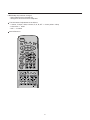
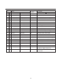
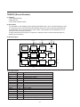
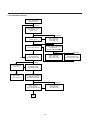
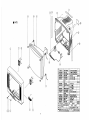
1
Service Manual 38 / 48 / 51 Cm Mono Colour Television CHASSIS : CP-370 MODEL : 14Q1/20Q1/21Q1 14Q2/20Q2/21Q2 14Q3/20Q3/21Q4 14T1/20T1/21T1 14T2/20T2/21T2 14T3/20T3 ÀÀ @@ ,, DAEWOO ELECTRONICS CO., LTD. CONTENTS Specifications ................................................................................................................ 1 Safety Instruction ......................................................................................................... 2 Circuit block Diagram ................................................................................................. 3 Alignment Instructions ............................................................................................... 4 IC Description ................................................................................................................ 7 Circuit Description ....................................................................................................... 31 PCB Layouts PRINTED CIRCUIT BOARDS .................................................................................... 38 SCHEMATIC DIAGRAM ............................................................................................. 39 Trouble Shooting Charis ............................................................................................. 40 Important IC Voltage Charts .............................................................................................. 47 Electrical Part List............................................................................................................... 49 Q Model T Model Difference Part List ............................................................................... 64 Inch difference Part List ..................................................................................................... 65 Mechanical Exploded View and Part List ......................................................................... 66 Specifications Q : 1SPEAKER MODEL, T : 2SPEAKER MODEL VM : WITHOUT TXT. MODEL, TM : WITH TXT. MODEL TV Standard PAL/SECAM-B/G, D/K, I, H, NTSC-3.58/4.43 Mains Voltage 100~250V AC, 50/60Hz Power Consumption 14”Q = 69W, 14”T = 74W 20”Q = 79W, 20”T = 84W 21”Q = 79W, 21”T = 84W Sound output . 1 Speaker : 3W( at 80% MOD. 10% THD) . 2 Speaker : 4W + 4W( at 80% MOD. 10% THD) Speaker . 1 Speaker : 3W, 16 ohm . 2 Speaker : 7.5W, 8 ohm(2EA) Antenna 75 ohm unbalanced Impedance 300 ohm balanced with supplied balun Tuning system Voltage Synthesize Tuning System Memory channel VM : 100 channels, TM : 70 channels Reception VHF - L : CH2 - CH4 channel Unit VHF - H : CH5 - CH12 Cable Band : CHS1’ - CHS3’, CHS1 - CHS20 Hyper Band : CHS21 - CHS40(option) UHF : CH21 - CH69 Remote control VM : R-28B04, TM : R-28B03 Screen size 14” : 34cm (A34JLL 90 02) 20” : 48cm (A48JLL 90 02) 21” : 51cm (A51JLL 90 02) Weight 14” : 9.5Kg(set) 20” : 16.5Kg(set) 21” : 20.5Kg(set) Indication On-Screen Display - MENU Picture(Bright, Color, Contrast, Sharpness, TINT) TIMER(CLOCK, WAKE-UP-TIME, ACTIVATE, WAKE-UP-PROG) LANGUAGE PRESET EDIT SLEEP TIMER AV SOUND MUTE VOLUME CONTROL 1 Safety Instruction WARNING: Before servicing this chassis, read the “X-RAY RADIATION precaution”, “safety precaution” and “product safety notice” below. X-RAY RADIATION PRECAUTION 1. Excessive high voltage can produce potentially hazardous X-RAY RADIATION.To avoid such hazards, the high voltage must not exceed the specified limit. The nominal value of the high voltage of this receiver is 22-23kv(14”), 2526kv(20”, 21”) at max beam current. The high voltage must not, under any circumstances, exceed 27.5kv (14", 20”), 29.0kv(21”). Each time a receiver requires servicing, the high voltage should be checked. It is recommended the reading of the high voltage recorded as a part of the service records. it is important to use an accurate and reliable high voltage meter. 2. The only source of X-RAY Radiation in this TV receiver is the picture tube. For continuous RADIATION protection, the replacement tube must be exactly the same type tube as specified in the parts list. SAFETY PRECAUTION 1. Potentials of high voltage are present when this receiver is operating. Operation of the receiver outside the cabinet or with the back cover removed involves a shock hazard from the receiver. 1) Servicing should not be attempted by anyone who is not thoroughly familiar with the precautions necessary when working on highvoltage equipment. 2) Always discharge the picture tube to avoid the shock hazard before removing the anode cap. 3) Discharge the high potential of the picture tube before handling the tube. The picture tube is highly evacuated and if broken, glass fragments will be violently expelled. 2. If any Fuse in this TV receiver is blown, replace it with the FUSE specified in the Replacement Parts List. 3. When replacing a high wattage resistor(oxide metal film resistor) in circuit board, keep the resistor 10mm away from circuit board. 4. Keep wires away from high voltage or high temperature components. 5. This receiver must operate under AC260 volts, 50Hz/60Hz. (AC 100~250 volts, 50/60Hz)NEVER connect to DC supply or any other power or frequency. PRODUCT SAFETY NOTICE Many electrical and mechanical parts in this chassis have special safety-related characteristics. These characteristics are often passed unnoticed by a visual inspection and the X-RAY RADIATION protection afforded by them cannot necessarily be obtained by using replacement components rated for higher voltage, wattage, etc. Replacement parts which have these special safety characteristics are identified in this manual and its supplements, electrical components having such features are identified by designated symbol on the parts list. Before replacing any of these components, read the parts list in this manual carefully. The use of substitute replacement parts which do not have the same safety characteristics as specified in the parts list may created X-RAY Radiation. 2 Alignment Instructions 1. AFT 1.1 Standard B/G,D/K,I 1) Set a Signal Generator with - RF FREQUENCY = 38.9 MHz, - RF OUTPUT LEVEL = 80 5 dBuV - System = PAL / SECAM - B/G, D/K, I NTSC - 3.58/4.43 2) Connect the Signal Generator RF Output to P101 (Tuner IF Output). There must be no signal input to the tuner. 3) Press the “AFT” KEY and wait until the TV screen display “AFT OK”. 2. AGC 1) Set a Pattern Generator with RF LEVEL 63° 2 dBuV . 2) Connect a OSCILLOSCOPE PROBE to P102 (TUNER AGC INPUT). 3) Adjust AGC UP/DOWN KEY the voltage drop 3.5V dc point its maximum voltage.(TDA8374A N1 VERSION) Adjust AGC UP/DOWN KEY the voltage drop 1.5V dc over blow its maximum voltage(TDA8374A N3 VERSION) Alternative Method 1) Set a Pattern Generator with - RF LEVEL 80 5 dBuV - PAL CROSSHATCH ( without SOUND CARRIER ) 2) Connect a OSCILLOSCOPE ( Bandwidth 100MHz ) PROBE to P101 (TUNER IF OUTPUT). 3) Use AGC UP/DOWN KEY to obtain an envelop amplitude 200 + 20 mVp-p. 3. SCREEN 1) Apply a COLOR BAR pattern signal. 2) Set the CONTRAST, BRIGHTNESS to MAX, COLOR to MIN. 3) Set the R,G,B LEVEL to CENTER (31/63) with R,G,B UP/DOWN KEY. 4) Connect a OSCILLOSCOPE PROBE to P904 ( CRT CATHOD R, G, B ). 5) Adjust the SCREEN VOLUME on FBT such that the highest black level voltage 160 5Vdc (20”, 21”), 130 5Vdc (14”). Black level 160 5Vdc ( 20”, 21” ) 130 5Vdc ( 14” ) GND 4. WHITE BALANCE 1) Set the TV to NOR I mode. 2) Set the R,G,B LEVEL to CENTER with R,G,B UP/DOWN KEY . 3) Adjust the R,G,B UP/DOWN KEY of the other color which did not appear on the screen to obtain WHITE. 5. FOCUS 1) Apply a RETMA PATTERN signal. 2) Adjust the FOCUS VOLUME on FBT to obtain optimal resolution. 4 6. GEOMETRY 6.1 VERTICAL CENTER 1) Set the TV to NOR I mode. 2) Pressing the V-SIZE UP/DOWN KEY, the lower half of the screen is blanked. 3) Adjust the border line of blanked picture coincident with the mechanical center marks of the CRT using the V-CENTER UP/DOWN KEY. 6.2 VERTICAL SIZE The VERTICAL CENTER adjustment has to be done in advance. 1) Apply a RETMA PATTERN signal. 2) Set the TV to NOR I mode. 3) Adjust the upper part of the picture with the V-SIZE UP/DOWN keys. 6.3 VERTICAL SLOPE The VERTICAL SIZE adjustment has to be done in advance. 1) Apply a RETMA PATTERN signal. 2) Adjust the lower part of the picture with the V-SLOPE UP/DOWN keys. 6.4 VERTICAL S-CORRECTION 1) Apply a CROSSHATCH PATTERN signal. 2) Adjust the S-COR UP/DOWN KEY to obtain the same distance between horizontal lines. 6.5 HORIZONTAL CENTER 1) Apply a RETMA PATTERN signal. 2) Adjust picture centering with H-CENTER LEFT/RIGHT keys. 5 If EEPROM(1703) has been changed ; - Option data has to be changed and - all alignment function has to be readjusted. The initial state of adjustment are as follows; - V-Center, V-Slope V-Size, H-Center, R, G, B, AFT = Center (30/64 - 33/64) - S-Correction = 00/64 - AGC = 15~60/64 Service Remocon 6 IC Description DW370ASM* (Micro-controller for Non-Teletext Model) =TMS370C08A05 ( TI Type No.) (1) General Description The TMS370C08A05 devices are members of the cMCU370 family single-chip microcontrollers. The cMCU370 family provides cost effective real-time system control through use of the PRISM methodology. The PRISM methodology modular fabrication process integrates analog, digital, linear and power technologies on a single chip, thereby maximizing the total integration strategy. The TMS370C08A05 devices are designed with the high-performance 8-bit TMS370C8 CPU. Features of the ‘C8 CPU and system module as implemented on this device include three CPU registers (stack pointer, status register, and the program counter), two external interrupts, reset, memory mapped control registers. (2) Feature • Internal Memory Configurations - 16K-Byte ROM Program Memory - 512-Byte RAM • Operating Features - Supply Voltage (VCC) 5 V ° 10% - Input Clock Frequency 2, 20MHz - Industrial Temperature Range • Device Integrity Features - Address Out-of-Range Reset - Stack Overflow Reset - Parallel Signature Analysis (CRC) • Two 16-Bit General Purpose Timer(T8A) Each Includes: - 16-Bit Resettable Counters with individual 8-Bit Prescaler - 2 PWM Channels or - 2 Input Captures or - 1 Input Capture and 1 PWM Channel • One 14-Bit PWM Module - 14-Bit Resettable Counters - 14-Bit PWM Output Port • One 8-Bit PWM Module - 8-Bit Resettable Counters - 8-Bit PWM Output Port with 12V Open Drain • OSD Module - Blanking/ Contrast reduction out - Transparent Background - Transparent Foreground - Full Screen Background Color - Controlled Color, Blink, Size, Smoothing, Fringe of Each lines of Character - Two size of different Font 12x10 and 12x18 by Hard Masking - OSD Window Display with 40x25 lines • 8-Bit A/D Converter With 3 Inputs - Single or Dual Channel Operation - Single or Continuous Conversion Modes • Flexible Interrupt Handling - Global and Individual Interrupt Masking - 2 S/W Programmable Interrupt Levels - 2 External Interrupt (1 Non-Maskable) - Programmable Rising or Falling Edge Detect 7 • 09 CMOS Compatible I/O Pins - All Peripheral Function Pins Software Configurable for Digital I/O - 6 Bidirectionals, 3 Input Pins • Plastic 42 YSDP Pins Package (3) Block Diagram 8 DW5255M*(Micro-controller & West/East Teletext Decoder) DW5255RM*(Micro-controller & Cyrillic Teletext Decoder) =SDA5255-A*** (SIEMENS Type No.) (1) General Description The TDA5255 contains a slicer for VPS and TTX, an accelerating acquisition hardware module, a display generator for “LEVEL 1” TTX data and a 8 bit u-controller running at 333 nsec cycle time. The controller with dedicated hardware guarantees flexibility, does most of the internal processing of TTX acquisition , transfers data to/from the external memory interface and receives/transmits data via I2C and UART user interfaces. The Slicer combined with dedicated hardware stores TTX data in a VBI 1Kbyte buffer. The u-controller firmware does the total acquisition task (hamming- and parity -checks, page search and evaluation of header control bits) once per field. (2) Feature • Acquisition: - feature selection via special function register - simultaneous reception of TTX and VPS - fixed framing code for VPS and TTX - programmable framing code window for TTX - Acquisition during VBI - direct access to VBI RAM buffer - Acquisition of packets x/26, x/27, 8/30 (firmware) - assistance of all relevant checks (firmware) - 1-bit framing-code error tolerance (switchable) • Display: - features selectable via special function register - 50/60 Hz display - level 1 serial attribute display pages - blanking and contrast reduction output - 8 direct addressable display pages - 12 x 10 character matrix - 96 character ROM (standard G0 character set) - 143 national option characters for 11 languages - 288 characters for X/26 display - 64 block mosaic graphic characters - 32 free addressable characters for OSD in expanded character ROM + 32 inside OSD box - double height (TOP/BOTTOM) - conceal/reveal - transparent foreground/background -inside/outside of a box - cursor (colour changes from foreground to background colour) - flash (flash rate 1s) - programmable horizontal und vertical sync delay - hardware assisted fast display page erase - full screen background colour in outer screen • Synchronization: display synchronization to sandcastle or Horizontal Sync (HS) and Vertical Sync (VS) with startstop-oscillator or display synchronization to sandcastle or Horizontal Sync and Vertical Sync with external clock independent clock systems for acquisition, display and controller 9 • Controller: - 8 bit configuration - 18 MHz internal clock - 0.33 us instruction cycle - eight 16-bit data pointer registers (DPTR) - two 16-bit timers - watchdog timer - serial interface (UART) - 256 bytes on-chip RAM - 1 Kbyte on-chip extended RAM (access via MOVX) - 8 Kbyte on-chip ACQ-buffer-RAM (access via MOVX) - 6 channel 8-bit pulse width modulation unit - 2 channel 14-bit pulse width modulation unit - 4 multiplexed ADC inputs with 8-bit resolution - one 8-bit I/O port with open drain output and optional I2C emulation - two 8-bit multifunctional I/O ports - one 4-bit port working as digital or analog inputs - one 2-bit I/O port with optional address latch enable function • P-SDIP 52 package • 5 V supply voltage (3) Block Diagram 10 (4) Pin Description * A : DW5255M*/DW5255RM*, *B : DW370ASM* Pin Name A* B* A* B* 1 1 P3.1 T1IC1/CR Symbol SYS Description A* B* NTSC OUT for switching SAW filter K6259 - PAL/SECAM : L - NTSC : H 2 2 P0.7/Open Drain A0 BUSSTOP I2C BUS STOP IN for Computer controlled alignment in Factory ( Active Low ) 3 3 P0.6/Open Drain A1 SDA Serial data IN/OUT for I2C 4 4 P0.5/Open Drain A2 SCL Serial clock IN/OUT for I2C 5 5 P0.4/Open Drain A3 OPTION #5 #6 Teletext 6 6 P0.3/Open Drain A4 OPTION H H West Teletext H : STAND-BY L H East Teletext L : POWER ON H L Turkish Teletext 7 7 P0.2/Open Drain A5 OPTION Not Used 8 8 P0.1/Open Drain PWM1-0/ Open Drain OPTION Not Used 9 9 P0.0/Open Drain PWM1-1/ Open Drain LED LED drive OUT - Stand-by mode : H - Operating mode : L ( IR reception : pulse ) 10 10 VSS VSS ground 11 11 VCC VCC Power Supply 12 12 XTAL1 OSCIN OSCIN Input to inverting osc. Amplifier 13 13 XTAL2 OSCOUT OSCOUT Output of inverting osc. Amplifier 14 14 P4.0/ALE PWM1-2/Open Drain 15 15 RESET RESET/Open Drain RST RESET IN (ACTIVE LOW) 16 16 P1.7/14BIT PWM PWM2-0 VT TUNING VOLTAGE OUT 17 17 P1.6/14BIT PWM PWM2-1 SW H : I/M L : B/D 18 18 P1.5/8BIT PWM PWM1-3/Open Drain F/SW Not Used 19 19 P1.4/8BIT PWM PWM1-4/Open Drain 20 20 P1.3/8BIT PWM PWM1-5/Open Drain MUTE AUDIO MUTE OUT 21 21 P1.2/8BIT PWM TEST GND (Must be tied 0V for DW370M*) Not Used #6 H : I/M, L : B/D Not Used Not Used 22 P1.1/8BIT PWM Not Used 23 P1.0/8BIT PWM Not Used 24 VSSA VSSA Analog GND for Slicer 25 FIL3 FIL3 PLL Loop Filter I/O for Phase Shifting 26 FIL2 FIL2 PLL Loop Filter I/O for TTX Slicing 27 FIL1 FIL1 PLL Loop Filter I/O for VPS Slicing 28 VCCA VCCA Analog Supply for Slicer 29 IREF IREF Reference Current for Slicer PLLs 11 Pin A* Name B* A* 30 CVBS 31 P2.3/8 bit ADC B* Symbol CVBS Description A* B* CVBS IN Not Used 32 22 P2.2/8 bit ADC B0/AN0/ADC AGC IF AGC INPUT for Auto Tuning System 33 23 P2.1/8 bit ADC B1/AN1/ADC KS Local KEY SCAN IN 34 24 P2.0/8 bit ADC B2/AN2/ADC S/SW Not Used 35 25 VSS VSS-OSD VSS Ground 36 26 P3.3/INT1 INT1 IR REMOTE IR IN 37 27 VDD VCC-OSD VDD Power Supply 38 28 LCIN OSCIN-OSD LCIN CLOCK IN for OSD 39 29 LCOUT OSCOUT-OSD LCOUT CLOCK OUT for OSD 40 30 P3.7/TXT I/O T2EVT/PWM2 BL BAND VHF-L OUT ( Active High ) 41 31 P3.6/RXD T2IC2/PWM1 BH BAND VHF-H OUT ( Active High ) 42 32 P3.5/T1 T2IC1/CR BU BAND UHF OUT ( Active High ) 43 33 P3.4/T0 T1EVT/PWM2 POWER POWER CONTROL OUT 44 34 P3.2/INT0 INT2 45 35 HS/SC HSYNC HSYNC HOR. SYNC. IN (Active High) 46 36 P4.7/VS VSYNC VSYNC VERT. SYNC. IN (Active High) 47 37 R R RED OUT 48 38 G G GREEN OUT 49 39 B B BLUE OUT 50 40 BLANK BL BLANK OUT 51 41 COR COR Not Used (CONTRAST REDUCTION OUT) 52 42 P3.0 EVEN/ODD EVEN/ODD OUT for non-interlacing in TTX mode T1C2/PWM1 Not Used 12 24LC08B (EEPROM) (1) Features • Single supply with operation down to 2.5V • Low power CMOS technology - 1mA active current typical - 10 A standby current typical at 5.5V - 5 A standby current typical at 3.0V • Organized as two or four blocks of 256 bytes (2x256x8) and (4x256x8) • Two wire serial interface bus, I2CTM compatible • Schmitt trigger, filtered inputs for noise suppression • Output slope control to eliminate ground bounce • 100KHz(2.5V) and 400KHz(5V) compatibility • Self-timed write cycle(including auto-erase) • Page-write buffer for up to 16 bytes • 2ms typical write cycle time for page-write • Hardware write protect for entire memory • Can be operated as a serial ROM • Factory programming(QTP) available • ESD protection > 4,000V • 1,000,000 ERASE/WRITE cycles(typical) • Data retention > 40 years • 8-pin DIP, 8-lead or 14-lead SOIC packages • Available for extended temperature ranges - Commercial : 0 C to +70 C -Industrial : -40 C to +85 C (2) General Description The Microchip Technology Inc. 24LC08B is a 8K-bit Electrically Erasable PROM. The device is organized as four blocks of 256x9bit memory with a two wire serial interface. Low voltage design permits operation down to 2.5 volts with standby and active currents of only 5 A and 1mA respectively. The 24LC08B also has a page-write capability for up to 16 bytes of data. The 24L08B is available in the standard 8-pin DIP surface mount 80IC packages. (3) Block Diagram WP I/O CONTROL LOGIC MEMORY CONTROL LOGIC HV GENERATOR XDEC EEPROM ARRAY (4X256X8) PAGE LATCHES SDA SCL YDEC VCC VSS SENSE AMP R/W CONTROL (4) Pin Description PIN SYMBOL DESCRIPTION 1-3 A0, A1, A2 Device Address lnputs 4 Vss Ground 5 SDA Serial Data/Address 6 SCL Serial Clock 7 WP 8 Vcc +5V Power supply 13 TDA8374A (Single chip TV Processor for Negative modulation IF ) TDA8374 (Single chip TV Processor for Negative & positive modulation IF) (1) General Description The TDA8374(A) is I2C-bus controlled single chip TV processors which are intended to be applied in PAL/NTSC television receiver. The IC is mounted in a S-DIL 56 envelope. (2) Feature • IF - Vision IF amplifier with high sensitivity and good figures for differential phase and gain - PLL demodulator with high linearity offering the possibility for (single standard) intercarrier stereo audio application . - Alignment PLL via I2C - [TDA8374] Multistandard IF with negative and positive modulation, switchable via I2C • AUDIO - Alignment free multi standard PLL audio demodulator (4.5 to 6.5 MHz.) - Mono volume control • Video - Integrated luminance delay line - Integrated chroma trap and bandpass filters (auto calibrated) - Asymmetrical peaking circuit in the luminance channel - Black stretching of non standard CVBS or luminance signals • Colour - SECAM interface for application with SECAM add-on TDA8395. • RGB - RGB control (brightness, contrast, saturation) - Black current stabilization and white point adjustment • Input / Output - Flexible video source select with CVBS input for the internal signal and two external video inputs(one switchable for CVBS or Y/C). - The output signal of the video source select is externally available ( also as CVBS when Y/C input is used). - External audio input. - Linear RGB input with fast blanking. • Synchronization and Deflection - Horizontal synchronization with two control loops and alignment free horizontal oscillator. - Slow start and slow stop of the horizontal drive output to enable low stress start-up and switch-off from the line circuit at nominal line supply voltage. - Vertical count-down circuit for stable behavior with provisions for non-standard signals. - Vertical geometry control. - Vertical drive optimized for DC coupled vertical output stages. • Control - Full I2C bus control, as well for customer controls as for factory alignment. - All automatic controls have an option for forced mode. • Power consumption - Low power consumption (900 mW at 8.0 Volts). • Packaging - SDIL-56 (Shrinked Dual In Line, 56 pins). 14 (3) Block Diagram 15 (4) Pin Description No 1 Name SOUND IF INPUT 2 EXT AUDIO INPUT 3 4 VCO REF FILTER 5 PLL LOOP FILTER 6 IF VIDEO OUTPUT 7 8 9 BUS INPUT : SCL BUS INPUT : SDA BANDGAP DECOUPLING 10 CHROMA INPUT 11 12 37 Y/CVBS INPUT MAIN POSITIVE SUPPLY Description The sound equivalent input impedance is 8k5 ohm // 5pF which has to be taken into account for proper termination of the ceramic filters. The DC impedance is very high. The minimum input signal for catching is l mV rms. An external sound signal (500mVrms) for example from SCART can be applied to this pin via a coupling capacitor. The input impedance is 25kohm. The IF VCO tuned circuit is applied to these pin. Its resonance frequency must be two times the IF-frequency and in between a range of 64-120MHz. This range is suitable for the IF standards as 33.4, 38.9, 45.75 and 58.75MHz. The VCO frequency can be adjusted by I2C bus so a fixed coil can be used. The PLL loopfilter is a first order filter with R=390 ohm and C = 100nF in series to ground. The loopfilter bandwidth is 60kHz and is optimal for both fast catching and sufficient video suppression for optimal sound performance. Sound performance can theoretically be improved by adding a small capacitor (approx.0- 4.7nF) between pin 5 and ground. This however must be evaluated further because the normal video signal response should not be effected. Although the video output impedance is low it is recommended to avoid high frequency current in the output due to for instance sound trap filters. This can be achieved by means of an emitter follower at the video output with a 1 resistor in series with the base. Serial clock line Serial data line The bandgap circuit provides a very stable and temperature independent reference voltage. This reference voltage (6.7V) ensures optimal performance of the TDA8374 and is used in almost all functional circuit blocks. The supplied C S-VHS input burst amplitude should be nominally 300mVpp (assumed is a colour bar signal with 75% saturation and with chroma/burst ratio of 2.2/1 ). The C S-VHS input is internally clamped to 4V via 50 . The external AC coupling capacitor with 50 forms a high pass filter. A recommended coupling capacitor is 1 nF; the high pass filter cut off frequency is then approximately 3KHz. The Y S-VHS signal of 1Vpp ( inclusive sync amplitude) is AC coupled to pin11. The TDA8374 has a main supply pin 12 and a horizontal supply pin 37. Both pins have to be supplied simultaneously. Notice that the IC has not been designed to use this pin 37 as start pin. (pin 37 supplies the horizontal oscillator, PHI-1 and PHl-2) (pin 12 supplies the rest of the circuits in the IC) The nominal supply voltage is 8V. With min/max values of 7.2-8.8V. Also in stand-by condition the IC must be supplied with 8V. 16 No Name 13 17 INT CVBS INPUT EXT CVBS INPUT 14 15 GROUND AUDIO OUTPUT 16 DECOUPLING FILTER TUNING 18 BLACK CURRENT INPUT BLUE OUTPUT GREEN OUTPUT RED OUTPUT 19 20 21 22 V-GUARD INPUT/ BEAM CURRENT LIMITER 23 24 25 26 RED INPUT GREEN INPUT BLUE INPUT RGB INSERTION SWITCH INPUT 27 LUMINANCE INPUT Description A voltage detection circuit is connected to both pins. - pin12 if V12 <6.8V than a power on reset, POR, is generated. The Hout output is disabled immediate. - pin37 if V37 <5.8V than the horizontal output is disabled immediate. It is recommended that the CVBS1 int and CVBS2 ext input amplitudes are 1 Vpp (inclusive sync amplitude). This, because the noise detector switches the 1 loop to slow mode (i.e. auto 1mode when FOA, FOB = 0,0) when noise level exceeds 100mVrms (i.e. at S/N of 20dB). All internal circuits are connected to this ground pin 14. The output signal is volume controlled and is active for both internal and external audio signals. The nominal gain is +9dB and -71dB, which gives a total control range of 80dB. The output signal range therefor is 0.14- 1400mVrms The bandwidth is >100kHz, the DC level is 3.3V and the output impedance is 250 . Voltage variations at pin 16, which can be due to external leakage current or crosstalk from interference sources, should be less than 50mV to ensure that tuning of filters/delay cells remains correct. For correct operation of the loop CURRENT information is supplied to the black current input pin. The RGB outputs are supplied to the video output stages from pins 21, 20 and 19 respectively. For nominal signals (i.e. CVBS/S-VHS, -(R-Y)/- (R-Y), TXT inputs) and for nominal control settings, then the RGB output Signal amplitudes is typically 2VBLACK_WHITE. Vertical Guard With this function, the correct working of the vertical deflection can be monitored. If the vertical deflection fails, the RGB outputs are blanked to prevent damage to the picture tube. Beam current limitinq The beam current limiting function is realised by reducing the contrast (and finally the brightness) when the beam current reaches s too high level. The circuit falls apart in two functions: - Average beam current limiting (ABL): reacting on the average content of the picture - Peak white limiting (PWL): reacting on high local peaks in the RGB signal. The Rin, Gin, Bin input signals (nominal signal amplitude of 700mV) are AC coupled to pin 23, 24 and 25 respectively. Clamping action occurs during burstkey period. The table below a survey is given of the three modes which can be selected with a voltage on RGB insertion switch input pin ; Vpin26 I2C function Selected RGB signal 0.9V-3V IE1=0 RGB(internal) IE1=1 Rin,Gin,Bin (fast insertion on pin23,24,25) > 4V IE1=X OSD can be inserted at the RGBout pins An nominal input signal amplitude of 1 Vblack-white MUST be DC coupled 17 No Name 28 29 30 LUMINANCE OUTPUT B-Y OUTPUT R-Y OUTPUT 31 32 B-Y INPUT R-Y INPUT 33 SECAM REF OUTPUT X-TAL 3.58 X-TAL 4.43 34 35 36 38 39 40 LOOP FILTER BURST PHASE DETECTOR CVBS OUTPUT BLACK PEAK HOLD CAPACITOR HOR OUTPUT 41 SANDCASTLE OUTPUT/ FLYBACK INPUT 42 PHI-2 FILTER / FLASH PROTECT Description to the luminance input pin 27. The pin is internally AC coupled to the luminance clamp via a capacitor of 50pF; clamping action occurs during burstkey period. The luminance output signal is approximately l V black-white with typical output impedance of 25O ohm. The maximum output impedance of pins 29 and 30 is 500 when PAL/NTSC signals are identified. When SECAM is identified by the SECAM add-on and no PAL/NTSC is already identified by the ASM, then the ASM sets the -(B-Y)/-(R-Y) output switch open (via DEMSW). This enables the -(B-Y)/-(R-Y) outputs of the TDA8395 to be directly connected to pins 29 and 3O respectively. The -(B-Y),-(R-Y) output signals (supplied from baseband delay line) are AC coupled, via a coupling capacitor of 10nF or greater, to the -(B-Y)/-(R-Y) inputs; both inputs are clamped during burstkey period. The SECAM reference output is directly connected to pin l of the TDA8395 for SECAM decoding ; it also can be used as a reference for comb filter applications. To ensure correct operation of both: - colour processing internal circuits, - sync calibration internal circuits, it is only allowed to have 3.6MHz Xtals on pin34: both 4.4MHz,3.6MHz Xtals are allowed on pin 35. If pin 35 is not used: then it is left open in application (also XA,XB=O,1 ). One of the important aspects of the PLL is the 1oop filter connected to pin 36; it influences the dynamic performance of the loop. The output amplitude is 1Vpp (transfer gain ratio between CVBS1int or CVBS2ext or CVBS3ext/Ys-vhs and CVBSout is 1). The maximum output impedance is 250 ohm. For the correct working of the black stretcher an external time constant should be added at the black peak hold capacitor input. This open collector output is meant to drive the horizontal output stage. The output is active low, i.e. the line transistor should conduct during the low period of the output. Pin 41 is a combined input/output pin. The pin provides a three level sandcastle pulse. Both burstkey pulse and vertical blanking pulse are always available, the line blanking pulse is only present when the external flyback pulse is fed to this pin. The line flyback pulse, fed to this pin is used for two functions: - input signal for the PHI-2 1oop and - RGB line blanking. (without flyback pulse blanking occurs only during the burstkey pulse) To ensure correct working of the delay line and SECAM add-on, the output should not be loaded with more than: - Sandcastle input delay line TDA 4665 - Sandcastle input SECAM add-on TDA 8395 The loopfilter is a first order filter. This pin requires a capacitor (C) only. 18 No Name 43 PHI-1 FILTER 44 45 46 47 GROUND EAST-WEST DRIVE VERT DRIVE + VERT DRIVE - 48 49 IF INPUT 50 EHT/OVERVOLTAGE PROTECT INPUT VERT SAWTOOTH CAPACITOR 51 52 53 54 REFERENCE CURRENT INPUT AGC DECOUPLING CAPACITOR TUNER AGC OUTPUT 55 AUDIO DEEMPHASSIS 56 DECOUPLING SOUND DEMODULATOR Description A flash protection becomes active when this pin is forced >6V. The horizontal drive is switched-off immediately. Once the voltage is <6V the horizontal drive is switched-on again via the slow start procedure. The loopfilter connected to pin 43 is suitable for various signal conditions as strong/weak and VCR signal. This is achieved by switching of the loopfilter time constant by changing the PHI-1 output current. Via I2C bus FOA/B, different time constants can be chosen, including an automatic mode which gives optimal performance under varying conditions. To this pin are connected the IC-substrate and horizontal output. not used The vertical drive has a current output. The output is balanced which ensures a good common mode behavior with temperature and makes the output signal less sensitive for disturbances. The PLL frequency range is 32-60MHz with corresponding VCO frequency 64-120MHz. The IF input impedances is 2 in parallel with 3pF and matches the required load for commonly used SAW filters. A DC coupling is allowed, so no series capacitors between SAW filter and IF input are necessary. not used This pin requires a capacitor to ground of l00nF +, - 5%. The optimal sawtooth amplitude is 3.5V and is determined by the external capacitor and charge current. The sawtooth bottom-level is 2V. This pin requires a resistor to ground. The optimal reference current is 100 . which is determined by this resistor. The AGC capacitor value is 2.2 and has been defined for an optimal compromise between AGC speed and tilt for all AGC modes (negative/positive modulation). This output is used to control (reduce) the tuner gain for strong RF signals. The tuner AGC is an open collector output which is acting as a variable current source to ground. Only a capacitor has to be connected to this pin that defines the deemphasis time constant. The signal is internally connected through to the Audio switch. The deemphasis output is fixed, thus not controlled by the volume, and can be used for SCART. This pin requires a capacitor of 10 connected to ground. The pin acts as a low pass filter needed for the DC feedback loop. 19 TDA4665(Base Band Delay Line) (1) Features • Two comb filters, using the switched-capacitor technique,for one line delay time (64µs) • Adjustment free application • No crosstalk between SECAM colour carriers • Handles negative or positive colour-difference input signals • Clamping of AC-coupled input signals(±(R-Y)and±(B-Y)) • VCO without external components • 3MHz internal clock signal derived from a 6MHz VCO, line-locked by the sandcastle pulse (64µs line) • Sample-and -hold circuits and low-pass filters to suppress the 3 MHz clock signal • Addition of delayed and non-delayed output signals • Output buffer amplifiers • Comb filtering functions for NTSC colour-difference signals to suppress cross-colour (2) General Description The TDA4661 is an integrated baseband delay line circuit with one line delay. It is suitable for decoders with colour-difference signal outputs±(R-Y)and±(B-Y). (3)Block Diagram (4) Pin Description SYMBOL PIN Vp2 1 SYMBOL PIN DESCRIPTION DESCRIPTION +5V supply voltage for digital part Vp1 9 +5V supply voltage for analog part n.c. 2 not connected GND1 10 ground for analog part (0V) GND2 3 ground for digital part (0V) V0 (R-Y) 11 ± (R-Y) output signal i.c. 4 internally connected V0 (B-Y) 12 ± (B-Y) output signal SAND 5 sandcastle pulse input n.c. 13 not connected n.c. 6 not connected V1 (B-Y) 14 ± (B-Y) input signal i.c. 7 internally connected n.c. 15 not connected i.c. 8 internally connected V1 (R-Y) 16 ± (R-Y) input signal 20 TDA8395 (Secam Decoder) (1) Features Fully integrated filters Alignment free For use with baseband delay (2) Description The TDA8395 is a self-calibrating,fully integrated SECAM decoder. The IC should preferably be used in conjunction with the PAL/NTSC decoder TDA8362 and with the switch capacitor baseband delay circuit TDA4665. The IC incorporates HF and LF filters, a demodulator and an identification circuit (Iuminance is not processed in this IC). A highly stable reference frequency is required for calibration and a two-level sandcastle pulse for blanking and burst gating. (3) Block Diagram PLLref CLOCHEref GND TEST Vp 100 nF 220 nF 7 BANDGAP 8 TUNING 3 6 2 TUNING TDA8395 CVBS 16 ACC CLOCHE FILTER PLL INTERFACE CONTROL IDENTIFICATION DEEMPHASIS 9 OUTPUT STAGE –(R-Y) 10 –(B-Y) 1 fref/IDENT (4) Pin Description SYMBOL PIN fp1/IDENT 1 TEST 2 Vp 3 n.c. 4 n.c. 5 GND 6 CLOCHEref 7 PLL ref 8 -(R-Y) 9 -(B-Y) 10 n.c. 11 n.c. 12 n.c. 13 n.c. 14 SAND 15 CVBS 16 15 SAND DESCRIPTION reference frequency input/identification input test output positive supply voltage not connected not connected ground Cloche reference filter PLL reference -(R-Y) output -(B-Y) output not connected not connected not connected not connected sandcastle pulse input video (chrominance) input 21 TDA6106Q ( Video Output Amplifier ) (1) General Description The TDA6106Q is a monolithic video output amplifier (5MHz bandwidth) in a SIL 9 MPpackage, using high-voltage DMOS technology, and is intended to drive the cathode of CRT directly . To obtain maximum performance, the amplifier should be used with black-current control. (2) Feature • Black - current measurement output for automatic black current stabilization (ABS) • Single supply voltage of 200V • Internal protection against positive appearing CRT flash-over discharge • Protection against ESD • Internal 2.5V reference circuit • Controllable switch-off behavior (3) Block Diagram – (4) Pin Description PIN SYMBOL DESCRIPTION 1 N.C 2 N.C 3 V in inverting input 4 GND ground, substrate 5 I om Black-current measurement output 6 V dd supply voltage high 7 N.C 8 V oc cathode output 9 V of feedback/transient output 22 I802 PC817 (1) General Description The specification applies to the structures and characteristics of Model No. PC817 (2) Block Diagram (3) Absolute maximum ratings Parameter Symbol Forward current IF *1) Peak forward current IFM 1 A Reverse voltage VR 6 V Power dissipation P 70 mW Collector-emitter voltage VCEO 35 V Emitter-collector voltage VECO 6 V Collector current IC 50 mA Collector power dissipation Pc 150 mW Total Power dissipation Ptot 200 mW Operating temperature Topr -30~+100 C Storage temperature Tstg -55~+125 C *2) Isolation voltage Viso 5 *3) Soldering temperature Tsol 260 Input Output *1) Pulse width 100 s, duty ratio: 0.001 *2) AC for 1 minute, 40~60% RH *3) For 10 seconds. 23 Rating 50 Unit mA kVrms C TDA8356 (DC-coupled vertical deflection circuit) (1) General Description The TDA8356 is power circuit for use in 90 and 110 color deflection systems for field frequencies of 50 to 120 Hz. The circuit provides a DC driven vertical deflection output circuit, operating as a high efficient class G system. (2) Feature • High efficient fully DC-coupled vertical output bridge circuit • Vertical fly-back switch • Guard circuit • Protection against : - short circuit of the output pins (7 and 4) - short circuit of the output pins to Vp • Temperature (thermal) protection • High EMC immunity because of common mode inputs (3) Block Diagram (4) Pin Description PIN SYMBOL DESCRIPTION 1 I drive (pos) input power stage (positive); include Ii(sb) signal bias 2 I drive (neg) input power stage (negative); include Ii(sb) signal bias 3 Vp operating supply voltage 4 V o(b) output voltage B 5 GND ground 6 V fb input fly-back supply voltage 7 V o(a) output voltage A 8 V o(guard) guard output voltage 9 V I(fb) input feedback voltage 24 TDA7056 (BTL AUDIO OUTPUT AMPLIFIER) : 1 SPEAKER MODEL (1) Features • No external components • No switch-on/off clicks • Good overall stability • Low power consumption • Short circuit proof • ESD protected on all pins (2) General Description The TDA7056 is a mono output amplifier contained in a 9 pin medium power package. The device is designed for batteryfed portable mono recorders, radios and television. (3)Block Diagram (4)Pin Description PIN DESCRIPTION 1 n.c. 2 Vp 3 input (+) 4 signal ground 5 n.c. 6 output (+) 7 power ground 8 output (-) 9 n.c. 25 STR-S5707 (Hybrid IC for a Switching Regulator) (1) General Description The STR-S5707 is a Hybrid IC with a built in power transistor and a separate excitation control IC, designed for converter type switching mode power supply applications. The IC is capable of quasi-resonant mode and requires small number of external component. (2) Feature • Small SIP isolated package : Resin sealed type (transfer mold) • Lower power dissipation at a lighter load • Many protection function : - Pulse-by-pulse over current protection - Over-voltage protection with a latch - Thermal protection with a latch • These protection functions are incorporated and can be latched with an external signal. (3) Block Diagram (4) Pin Description PIN NAME SYMBOL DESCRIPTION 1 Collector C Collector of power Tr 2 Ground GND ground (Emitter of power Tr) 3 Base B Base of power Tr 4 Sink SINK Base current (IS) input 5 Over-current protection OCP over-current sensing signal input 6 Inhibit Latch INH input for synchronizing OFF time and latch circuit operation 7 Sensing SENS constant voltage control signal input 8 Drive DRIVE Base drive current (ID) output 9 Vin VIN supply voltage for control circuit 26 Electrical Characteristics of Control Part (Ta=25 ) Description Terminal Symbol Rating Unit MIN TYP MAX On-state Voltage 9-2 VIN(ON) 7.6 8 8.4 V Off-state Voltage 9-2 VIN(OFF) 4.6 4.9 5.2 V Operating Circuit Current 9-2 IIN(ON) 15 28 mA Stand-by Circuit Current 9-2 IIN(OFF) 200 A On Time TON 33 41 Off Time TOFF 45 55 OCP terminal Threshold Voltage 6-2 VOCP -1.12 -1 -0.88 V INH terminal Threshold Voltage 1 8-2 VINH-1 0.65 0.75 0.85 V INH terminal Threshold Voltage 2 8-2 VINH-2 1.4 2..0 V INH terminal Threshold Voltage 3 8-2 VLatch 3.2 5.1 5.8 V OVP Operating Voltage 9-2 VIN(OVP) 9.2 10.7 V Latch Circuit Sustaining Current 9-2 IH 500 A Latch Circuit Cancellation Voltage 9-2 VIN(La.OFF) 2.5 3.1 Tj(TSD) 125 150 MIC Thermal Shutdown Starting Temp Fixed Reference Voltage 7-2 Temperature Coefficient of Reference Voltage 7-2 VS V 32.0 V +2.5 mV/ Electrical Characteristics of Power Transistor Part(Trl) (Ta=25 ) Description Terminal Symbol Rating 1-2 VCE(sat) 0.4 V 1-2 ICEX 100 A 3-2 VBE(sat) 1.5 V MIN Collector Saturation Voltage Collector Cutoff Current Base-Emitter saturation voltage hFE DC Current Gain Thermal Resistance Switching Time j-F 29 TYP Unit MAX 61 1.3 1-2 ts 15 1-2 tf 0.5 27 /W TDA8138 (5.1V+12V regulator with Disable and Reset) (1) General Description The TDA8138 is a monolithic dual positive voltage regulator designed to provide fixed precision output voltages of 5.1V and 12V at currents up to 1A. A internal reset cuicuit generates a reset pulse when the output 1 decrease below the regulated voltage value. Output 2 can be disabled by TTL input. Shot circuit and themal protections are included. (2) Feature • output currents up to 1A • ixed precision Output 1 voltage 5.1V 2% • fixed precision Output 2 voltage 12V 2% • output 1 with Reset facility • output 2 with Disable by TTL input • short circuit protection at both outputs • thermal protection • low drop output voltage (3) Block Diagram (4) Pin Description PIN SYMBOL DESCRIPTION 1 V in 1 input 1 2 V in 2 input 2 3 Ce Delay capacitor 4 V dis disable 5 GND ground 6 RST reset 7 28 n.c 8 V out 2 output 2 (12V) 9 V out 1 output 1 (5.1V) TDA 1519B(AUDIO OUTPUT AMPLIFIER); 2 SPEAKER MODEL (1) Features • Requires very few external components for Bridge Tied Load(BTL) • Stereo ot BTL application • High output power • Low offset voltage at output (important for BTL) • Fixed gain • Good ripple rejection • Mute/stand-by switch • Load dump protection • AC and DC short-circuit-safe to ground and Vp • Thermally protected • Reverse polarity safe • Capability to handle high energy on outputs(Vp=OV) • No switch-on/switch-off plop • Protected against electrostatic discharge • Identical inputs(inverting and non-inverting) • Compatible with TDA 1519A(except output power) (2) General Description The TDA 1519B is an integrated class-B dual output amplifier in a 9-lead single in-line(SIL) plastic medium power package. The device is primarily developed for car radio applications. (4) Pin Description (3) Block Diagram PIN 1 2 3 4 5 6 7 8 9 Mute Switch 1 Cm 60k VA 4 133 Power Stage 18.1k Vp 8 + Stand-by Switch Stand-by Reference Voltage VA 15k + + - 1 3 15k Mute Switch Mute Reference Voltage TDA1519B 18.1k Power Stage 183 6 VA 9 Cm 60k Mute Switch Input Reference Voltage Signal Ground Vp Power Ground (Substrate) 29 SYMBOL NINV GND1 RR OUT1 GND2 OUT2 Vp M/ss INV DESCRIPTION non-inverting input ground(signal) supply voltage ripple rejection output 1 ground(substrate) output 2 positive supply voltage mute/stand-by switch inverting input PCA84C 122A(IC REMOCON) (1) Features • ROM, RAM and I/O is device dependent • Two test inputs T0, T1 • 3 Single-level vectored interrupt sources • 8 bit programmable timer/counter with 5-bit pre-scaler • Single supply voltage from 2.0V to 5.5V • On-board oscillator 1MHz to 5MHz • Operating temperature range -20 to +50 C (2) General Description The PCA84C122A is a stand-alone micro controller designed for use in remote control unit for a wide range of applications. (3) Pin Description PIN 3 2 23 22 10 11 14 15 19 18 17 16 1 24 12 13 4 5 6 SIGNAL P00 P01 P02 P03 P04 P05 P06 P07 P10 P11 P12 P13 P14 P15 P16 P17 TP/INT T1 RESET 8 9 21 7 20 XTAL 1 XTAL 2 OUT VDD Vss DESCRIPTION Standard I/O Port lines, generally used for keypad scanning Standard I/O Port lines, generally used for keypad scanning Test T0 and external interrupt input Test T1 Active HIGH reset, normally tied to Vss because internal Power-on reset can serve the same function Crystal or ceramic resonator Pulse train output pin, capable of sinking 27mA Power supply Ground 30 Circuit Description Vision IF amplifier, AFC, video demodulator The IF signal from the tuner is fed through a SAW filter to the differential IF input (pin 48 and 49). The first IF stage consists of 3 AC-coupled amplifiers with a total gain control range of over 66 dB. The reference carrier for the video demodulator is obtained by a PLL carrier regenerator (eliminating notch filter compromises, as in reference tuned circuits for passive carrier regeneration). Only an oscillator coil is needed( pin 3 and 4) that can be aligned via l2C-bus to the double IF frequency. The AFC information is derived from the VCO control voltage of the IF-PLL and can be read via I2C-bus. Bit AFB toggles when the picture carrier is exactly at the desired IF frequency (= half the aligned IF-PLL frequency). AFA is active in a window around this point. For fast search-tuning applications this window can be increased by a factor 3 (AFW bit). Tuner A.G.C. The automatic gain control (A.G.C.) circuit operates on top sync level at negative modulated signals or on peak white level at positive modulation, selected by MOD bit. The tuner A.G.C. is controlled via pin 54. The tuner A.G.C. take over point (T.O.P.) can be set over a wide range: 0.8 mVrms .. 80 mVrms IF input signal amplitude. The tuner AGC output may have to operate above Vcc of TDA8374. Therefore pin 54 is an open collector output, that can operate from 0.3 up to Vcc+ 1 Volt (at > 2 mA sink current) PLL sound demodulator The IF-video output at pin 6 (2Vpp) is fed through a sound bandpass filter and connected to the intercarrier sound IF input pin 1. An alignment free PLL tunes itself to the sound carrier and demodulates it. The non volume-controlled front-end audio signal can be obtained from the deemphasis pin 55 (amplitude 300 mVeff). Source select switch TDA8374 input switch can select one of the following sources ; pin 13 front-end : CVBS l int pin17 : CVBS 2 ext pin 11.pinlO : Y s-vhs, C s-vhs Selected signal is available at the CVBS output pin 38, in case of Y/C input Y+C are added. It drive teletext and the TDA8395 SECAM add-on. For S-VHS applications, the Y,C input can be selected, independent of the CVBS source switch. TDA8374 Y,C inputs are selected, while the source switch outputs CVBS l int or CVBS 2 ext on CVBS out. Horizontal synchronization and protection The synchronization separator adapts its slicing level in the middle between top-sync and black level of the CVBS signal. The separated synchronization pulses are fed to the first phase detector and to the coincidence detector. The -1 loop gain is determined by the components at pin 43 (C+RC). The coincidence detector detects whether the horizontal line oscillator is synchronized to the incoming video. The line oscillator is a VCO-type, running at twice the line frequency. It is calibrated with the X-tal oscillator frequency of the colour decoder and has a maximum deviation of 2% of the nominal frequency, so no alignment is-needed. Calibration is done at start up( the TDA8374 must first know what colour X-tals are connected, bits XA and XB) and after synchronization loss ( -1 coincidence detector “Sync Locked” bit SL). The second phase detector -2 locks the phase of the horizontal driver pulses at output pin 40 to the horizontal flyback pulse at input pin 41 . 31 This compensates for the storage time of the horizontal deflection transistor. The - 2 loop filter (C) is externally connected to pin 42. The horizontal phase can be given a static off set via I2C-but (HSH “horizontal shift”) A dynamic correction is possible by current feedback into the - 2 loop filter capacitor. To protect the horizontal deflection transistor, the ho rizontal drive is switched off immediately when a power failure ( “ Power-On Reset “ bit POR ) is detected. The power failure may have corrupted the contents of the internal data registers, so the TDA8374 should be started up again. The TDA8374 has a separate supply input (pin 37) that only used as a clean supply voltage for thehorizontal oscillator circuits. Vertical synchronization The vertical sawtooth generator drives the vertical output. It uses an external capacitor at pin 51 and a current reference resistor at pin 52. The TDA8374 vertical drive has differential current outputs for DC-coupled vertical output stage, like the TDA8356 . At TDA8356 input pins l and 2 this current is converted into a drive voltage via a resistor. Geometry processing With the TDA8374 is possible to implement automatic geometry alignment, because all parameters are adjusted via the I2C bus. The deflection processor of the TDA8374 offers the fo11owing five controls; - Horizontal shift - Vertical slope. - Vertical amplitude - Vertical S-correction - vertical shift Colour decoder The colour decoder contains an alignment-free X-tal oscillator, a dual killer circuit and colour difference demodulators. Together with the TDA8395 SECAM add-on a multi standard PAL/SECAM/NTSC decoder can be built with automatic recognition. Which standard can be decoded depends on the external Xtals used. Two Xtal pins (34and 36) are present so normally no external switching is required. The I.C. must be told which X-tals are connected (bits XA and XB). This is important, because the X-tal frequency of the colour decoder is also used to calibrate many internal circuit. The burst phase detector locks the Xtal oscillator with the chroma burst signal. The phase detector operates during the burst key period only, to prevent disturbance of the PLL by the chroma signal. Two gain modes provide: - Good catching range when the PLL is not Locked. - Low ripple voltage and good noise immunity once the PLL has locked The killer circuit switches-off the R-Y and B-Y demodulators at very low input signal conditions (chroma burst amplitude). A hysteresis prevents on/off switching at low, noisy signals. Color standard pin34 pin35 XA XB PAL4.43/SECAM + NTSC-4.43 none 4.43 1 0 PAL4.43/SECAM + NTSC-M 3.58 4.43 1 1 32 Integrated video filters The TDA8374 has alignment-free internal luminance delay, chroma bandpass and chroma trap. They are implemented as gyrator circuits tuned by tracking to the frequency of the chroma Xtal oscillator. The chroma trap in the Y signal path is by-passed when Y/C input is selected (S-VHS ). For SECAM an extra luminance delay is build-in, for correct delay of the luminance signal. RGB output and black current stabilization The colour difference signals (R-Y, B-Y) are matrixed with the luminance signal (Y) to obtain the RGBout output signals (pins 21,20,29). In the TDA8374 the matrix type automatically adapts to the decoded standard (NTSC,PAL) . Linear amplifiers are used to interface external RGBrn signals (pins 24,25,26) from the SCART connector. These signals overrule the internal RGB signals when the data insertion pin 26 (FBI) is switched to a level between 1.0V and 3.0V. The contrast and brightness control and the peak white limiter operate on both internal and external RGB signals R,G and B each have their own, independent gain control to compensate for the difference in phosphor efficiencies of the picture tube: so called “white point” adjustment. The nominal amplitude is about 2V black to white, at nominal input signals and control settings. TDA8374 has a black current stabilization loop, that automatically adjust the black level to the cut-off voltage of the picture tubes three gun cathodes. Since no current is flowing when the voltage the cathode is equal to the cut-off voltage of the tube, the loop stabilizes at a very small gun current. This “black current” of the three guns is measured internally and compared with a reference current, to adjust the black level of RGBout. The black level 1oop is active during 4 lines at the end of the vertical blanking. In the first line the leakage current is measured (max. acceptable 1l00 A). In the next three lines the black levels of the three guns are adjusted. The nominal value of the ‘black current is 10 A. The ratio of the ‘black currents’ for the 3 guns tracks automatically with the white point adjustment, so the back-ground colour is the same as the adjusted white point. At switch-on of the TV receiver the black current stabilization circuit is not yet active and RGBout are blanked. Before the first measurement pulses appear, O.5 sec delay ensures that the vertical deflection is active, so the pulses will not be visible on the screen. During the measuring lines RGBout will supply 4V pulses to the video output stages. The TDA8374 waits until the black current feedback input (pin 18) exceeds 200 A, which indicates that the picture tube is warm-up. Then the black current stabilization circuit is active. After a waiting time of about 1.0 sec, the blanking of RGBout is released. Tuning The AFC information of the TDA8374 is not available as an analogue voltage. Automatic following (=frequency tracking, AFC) can be done via the I2C-bus by software. The TDA8374 AFC window is typically 80 kHz wide. This value is made higher than the 62.5 kHz tuning step, to prevent an automatic following loop from continuously adapting the tuning frequency.. With this AFC window ( 40 kHz) the maximum tuning error is less than 62.5 kHz. For high speed search-tuning-algorithms, the AFC window can be widened to 240 kHz via bit AFW. 33 TDA8395 SECAM decoder The TDA8395 is an alignment-free SECAM colour decoder, including a Cloche filter, demodulator and line identification circuit. The Cloche filter is a gyrator-capacitor type. Its frequency is calibrated in the vertical retrace period. The calibration reference( pin 1 ) is obtained from the TDA8374 color X-tal oscillator (pin 33). Pin 7 is a decoupling for the Cloche reference. The voltage change at this pin due to leakage currents should be lower than 10 mV, during field scan, resulting in a capacitor of minimal 100 nF. Pin 8 is the reference capacitor for the PLL. The voltage variation during field scan at this pin should be lower than 2 mV , resulting in a capacitor of 220 nF. The sandcastle input (pin 15) is connected to TDA8374 pin 41 and is used for generation of the blanking periods and provides clock information for the identification circuit. The CVBS source select output (TDA8374 pin 38) supplies SECAM chroma to pin 16 of the TDA8395. This is demodulated by a PLL demodulator, that uses the reference frequency at pin l and a bandgap reference to obtain the desired demodulation characteristic. If the digital line identification in theTDA8395 detects SECAM, pin 1 will sink a current of 150 (A out of TDA8374 SECAMref pin 33. When the TDA8374 has not detected PAL or NTSC, it will respond by increasing the voltage at pin 33 from 1.5V to 5V. Now the TDA8374 color difference outputs pin 30 and 29 are made high-ohmic and the TDA8395 output pin 9 and 10 are switched on. These outputs will be disconnected and high-ohmic when no SECAM is detected for two frame periods, the decoder will be initialized before trying again. Base band delay line TDA4665 TDA4665 is an integrated double baseband delay line of 64 S. It couples to the TDA8374 and TDA8395 without any switches or alignments. The TDA4665 consist of two main blocks: - Two delay lines of 64 sec in switched capacitor technique - Internal clock generation of 3 MHz, line locked to the sandcastle pulse The TDA4665 operates according to the mode demanded by the colour transmission standard: - For PAL it operates as geometric adder to satisfy the PAL demodulation requirements - In NTSC mode it reduces cross-colour interference (comb-filtering) - For SECAM it repeats the colour difference signal on consecutive horizontal scan lines. A sandcastle pulse is connected to pin 5. The top pulse voltage (should not exceed 5 V) can be directly coupled to the 5 V sandcastle output of the TDA8374. The R-Y and B-Y colour difference signals (from TDA8374 pins 30 and 29) are AC-coupled and clamped by the input stages at pins 16 and 14. An internal 6 MHz Current controlled oscillator is line locked via a PLL to the sandcastle pulse at pin 5. This clock drives the delay lines to obtain the required 64 sec. Sample and hold low pass filters supress the clock signal. The original and the delayed signals are added, buffered and fed to the output pins 11 and 12. These are AC-coupled to the R-Y and B-Y colour difference input pin 32 and 31 of TDA8374. The TDA4665 needs a 5 V supply voltage on pin l for the digital part and on pin 9 for the analog part. 34 TDA8356 vertical deflection. The TDA8356 is a vertical deflection circuit. It can be used in 90 deflection systems with frame frequencies from 50 up to 120 Hz With its bridge configuration the deflection output can be DC coupled with few external components. Only a supply voltage for the scan and a second supply for the flyback are needed. The TDA8356 can drive max.2A. The vertical drive currents of TDA8374 pins 47 and 46 are connected to input pins l and 2 of the TDA8356. The currents are converted into a voltage by a resistor between pins 1 and 2. Pin2 is on a fixed DC level (internal bias voltage) and on pin l the drive voltage can be measured (typical 1.8 Vpp). The drive voltage is amplified by ‘A’ and fed to two amplifiers ‘B’ and ‘C’, one is inverting and the other is a non inverting amplifier. The outputs (pins 4 and 7) are connected to the series connection of the vertical deflection coil and feedback resistor . The voltage across feed back resistor is fed via pin 9 to correction amplifier ‘D’, to obtain a deflection current which is proportional to the drive voltage. The supply voltage for the TDA8356 is 16V at pin 3. The flyback generator has a separate supply voltage of 45V on pin 6. The guard pulse is useful to synchronize OSD. Horizontal deflection The circuit contains horizontal drive, line output transformer. The horizontal driver pulses from the TDA8374 are amplified in the horizontal drive circuit, to get sufficient base-drive current for the high voltage switching transistor Q401. During the horizontal scan period( =52 s) Q401 will conduct, and a sawtooth current flows from +110/123V through the primary winding of the FBT to ground. After this time Q401 is switched off and the energy stored in the FBT during the scan period will be transformed to the flyback capacitor C410. This energy transfer will take place in a cosine shape because the primary of the FBT and C410 from a resonant circuit. The time the energy is transferred from FBT to C410 and back to the FBT, is called the flyback time and will take place in about 12 s. The flyback peak voltage is about 8 times the scan voltage. In series with the horizontal deflection coil there is a (damped) linearity corrector coi1. During the scan there is some loss in the resistance of the deflection coi1. In the first part of a line the linearity corrector stores some energy in a permanent magnet until it is saturated. This improves the linearity of the horizontal scan speed. The required S correction for the picture tube can be adjusted with the value of C411. The beam current limiting information (BeamCurr) is derived from the foot of the H.V winding of the FBT. This is connected via resistor to +8V. As the beam current increase, the voltage on line BeamCurr decreases. BeamCurr is damped by a integration filter before it is fed back to TDA8374 pin 22. The TDA8374 will decrease the contrast (and eventually the brightness) to limit the average beam current. 35 Video amplifiers Three TDA6106Q integrated video amplifiers drive cathode of the picture tube directly. They are protected against CRT flashover discharges and ESD (electro static discharge). The three video amplifiers, have a beam current output I black, used by the TDA8374 black current loop to control the black level on the cathodes. The outputs can be connected together because the black current 1oop sequentially controls the black level for each cathode. The amplification of the TDA6106Q is set by the resistors between pin 3 and 9 and between pin 3 (negative-input) and the TDA8374 output. There are no alignment any more on the CPT panel, because of the automatic black current stabilization and because the white point adjustment can be done in the TDA8374 via I2C bus. Power Supply STR-S5707 (1) VIN terminal, start-up circuit A start-up circuit is to start and stop a operation of a control IC by detecting a voltage appearing at a VIN terminal (pin-9). At start up of a power supply, when a voltage at the VIN terminal reaches to 8V (typical) by charging up C807 by the function of a start-up resistor, R803, a control circuit starts operating by the function of the start-up circuit. After the control circuit starts its operation, power source is obtained by smoothing voltage appearing at winding of pin6-7 of T801. (2) Oscillator, F/B terminal voltage (Pin 7) A oscillator generates pulse signals which turns a power transistor on and off by making use of charge and discharge of C1 and C2 incorporated in the Hybrid IC. Constant voltage control of a switch-mode power supply is performed by changing both ON-time and OFF-time except when the load is light (ex. remote control stand-by mode of TVs). The ON-time is controlled by changing a current charged by C1, which is as the result of that the detection winding of pin5-7 of T801, which detects a change of voltage in a secondary side, connected to the sensing terminal (Pin 7) has the current in accordance with an output signal from an output voltage detection circuit (an error amplifier) built in. As an AC input voltage to the power supply gets the higher and a load current the smaller, the current flowing to the SENS terminal gets the larger, and the ON-time gets the shorter. (3) Function of INH terminal (Pin 6), control of OFF-time Signal to the INH terminal is used as inputs to COMP.1 and COMP.2 inside of the control IC. A threshold voltage of COMP.1, VTH1 is set at 0.75V (Ta=25°) and an input signal to a drive circuit becomes almost 0V (the power transistor is in OFF mode) when a voltage at the INH terminal reaches the VTH1. A threshold voltage of COMP.2, VTH2, is set at 1.5V (Ta=25°). When the INH terminal voltage reaches VTH2, an output from COMP.2 reverses (the power transistor is in on mode). Quasi-resonant operation By inputting the voltage of winding of pin6-7 of T801 which is synchronized with the energy discharge time of a secondary winding, pin14(or 15)-16 of T801, to the INH terminal through D805 and R809, quasi-resonant operation can be achieved. When the power transistor turns off and a voltage higher than VTH2 is applied to the INH terminal, C3 immediately discharges and then starts charging again. Even after the discharge of energy of a secondary winding is completed, VINH does not immediately increases. When it gets lower than VTH1, the transistor turns on. 36 Stand-By Mode While being in remote control stand-by mode, the output voltage is kept on providing to the secondary side and the power transistor operates at A class mode. By connecting INH terminal (Pin 6) to the GND, the OFF-time of the power transistor is fixed at set time ( T OFF = 50usec at Ta = 25 ) of the built-in oscillator, and only ON-time changes depending on input and output conditions of the power supply. Therefore, it enables to hold an oscillation frequency in light mode below 20KHz (typical). (4) Drive circuit The STR-S5707 applies the proportional drive system in order to minimize turn-on and saturation loss, and storage time. (5) OCP (over-current protection) function Over-current protection is performed pulse by pulse by directly detecting collector current of the power transistor. Detecting voltage is set to -1V below a reference point of GND (ground). (6) Latch circuit It is a circuit which sustains an output from the oscillator low and stops operation of the power supply when over-voltage protection (OVP) circuit and thermal shutdown (TSD) circuit are in operation. As the sustaining current of the latch circuit is 500 A maximum when VIN terminal voltage is 4V, the power supply circuit sustains the off state as long as current of 500 A minimum flows to VIN terminal from a start-up resistor. In order to prevent a malfunction to be caused by a noise and so on, delay time is provided by C1 incorporated in the IC and, therefore, the latch circuit operates when the OVP or TSD circuit is in operation, or an external signal input is provided for about 10 sec or longer. In addition, even after the latch circuit start operating, the constant voltage regulator (Reg) circuit is in operation and the circuit current is at high level. As a result, VIN terminal voltage rapidly decreases. When VIN terminal voltage becomes lower than the shutdown voltage, VIN(OFF) (4.9V typical), it starts increasing as the circuit current is below 500 A. When it reaches the ON-state voltage, VIN (ON) (8V typical), VIN terminal voltage starts decreasing because the circuit current increases again. When the latch circuit is on, VIN terminal voltage increases and decreases within the range from 4.9V typical to 8V typical and is prevented from abnormally rising. Cancellation of the latch is done by decreasing VIN terminal voltage below 3.3V. The power supply can be restarted after disconnecting an AC input to the power supply once. (7) Thermal shutdown circuit It is a circuit to trigger the latch circuit when the frame temperature of the IC exceeds 150 (typical). Although the temperature is actually sensed at the control chip, it works against overheating of the power transistor as the power transistor and the control IC are mounted on the same lead frame. (8) Over-voltage protection circuit It is a circuit to trigger the latch circuit when VIN terminal voltage exceeds 11V (typical). Although it basically functions as protection of VIN terminal against over-voltage, since VIN terminal is usually supplied from the drive winding of the transformer and the voltage is proportional to the output voltage, it also functions against the over-voltage of secondary output which causes when the control circuit opens or in some other events. 37 Trouble Shooting Charts 1. NO RASTER CHECK MAIN B+(+123V/+110V) LINE ABNORMAL NORMAL CHECK VOLTAGE AT (+) OF C807(220µF 400V) 310Vdc AT AC 220V CHECK HEATER VOLTAGE, VIDEO B+(200V) LINE, 16.5V & 48V LINE NORMAL ABNORMAL ABNORMAL CHECK / REPLACE F801 FUSE(T4A 250V) CHECK / REPLACE D801~D804(1S1888X4) R803(10W 3.3OHM) CHECK / REPLACE I801(STR-S5707) & PERIPHERAL COMPONENT NORMAL CHECK HORIZONTAL DRIVE PULSE AT PIN 40 OF I501(TDA8374A) [REFER TO WAVE FORM ] ABNORMAL CHECK /REPLACE I804(PC817) D812(BYW 95C) R814(2W 56K) NORMAL CHECK HORIZONTAL Vcc(+8V DC) AT PIN 37 OF I501 CHECK / REPLACE R410(1/4W 3.9) 1401 (2SD1207) T401 (TD-10A2) Q402 (2SD2499) ABNORMAL CHECK POWER SWITCHING VOLTAGE AT PIN 43 OF I701 *POWER ON; HIGH *STAND-BY ; LOW CHECK SDA(PIN 8) & SCL(PIN7) WAVEFORM OF I501 CHECK / REPLACE I802(TDA8138) I803(KA7808) OK ABNORMAL NORMAL ABNORMAL CHECK VOLTAGE(+5V DC) AT PIN 11 & PIN 37 OF I701 NORMAL ABNORMAL CHECK / REPLACE I501(TDA8374A) CHECK / REPLACE D813 (BYV95C) D814 (BYV95C) R824 (2W 43) Q802 (KTC 3198Y) Q803 (KTC 3198Y) T801 (TSM-4245A) CHECK SDA(PIN 3) & SCL(PIN4) WAVEFORM OF I701 OK NORMAL CHECK / REPLACE X701(20MHz, 18MHz) CHECK / REPLACE T402 F.B.T & CRT CHECK / REPLACE I701 40 2. NO PICTURE(RASTER OK) CHECK VIDEO SIGNAL AT PIN 13 OF I501(TDA8374A) [REFER TO WAVEFORM ] ABNORMAL NORMAL CHANGE INPUT MODE RF AV RF CHECK WAVEFORM AT PIN 29, PIN 30 OF I501 CHECK / REPLACE I701 & PERIPHERAL COMPONENT ABNORMAL ABNORMAL NORMAL CHECK WAVEFORM AT PIN 31, PIN 32 OF I501 CHECK PICTURE CONDITION NORMAL NORMAL FAVOURITE CHECK / REPLACE Q702, Q703 ABNORMAL CHECK TUNING VOLTAGE AT VT OF TUNER ABNORMAL NORMAL CHECK / REPLACE R759,R720 I703 OK CHECK / REPLACE I501 ABNORMAL CHECK / REPLACE I502(TDA4665) I503(TDA8395) ABNORMAL NORMAL CHECK VIDEO SIGNAL AT CATHOD OF CRT [REFER TO WAVEFORM ] ABNORMAL CHECK / REPLACE AT PIN 40, 41, 42 OF I701 CHECK / REPLACE I901, I902, I903 OK (CRT BOARD) CHECK / REPLACE TUNER NORMAL CHECK / REPLACE CRT NORMAL NORMAL CHECK / REPLACE Q101, Q102, SF101 CHECK WAVEFORM AT PIN 19, 20, 21 OF I501 CHECK 33V LINE CHECK BAND SELECT VOLTAGE AT BL,BH,BU & B+ VOLTAGE OF TUNER ABNORMAL NORMAL NORMAL ABNORMAL CHECK / REPLACE OK Q705,Q706,Q707 Q708,Q709,Q710 41 CHECK SIGNAL AT PIN 18 OF I501 ABNORMAL CHECK VOLTAGE VIDEO B+, HEATER ABNORMAL OK CHECK / REPLACE I501 ABNORMAL CHECK HORIZONTAL CIRCUIT PARTS 3. NO VERTICAL SCANING(ONE HORIZONTAL LINE ON SCREEN) CHECK / REPLACE P401 & DY ] CHECK VERTICAL Vcc +16.5V AT PIN3 & +48V AT PIN6 OF I301(TDA 8356) NORMAL ABNORMAL CHECK SIGNAL AT PIN1 & PIN2 OF I301 [REFER TO ] WAVEFORM CHECK / REPLACE D401(BYV95C) D409(BYV95C) R303(1W 15K) ABNORMAL NORMAL CHECK / REPLACE CRT CHECK OUTPUT WAVEFORM AT PIN46, PIN47 OF I501 CHECK SIGNAL AT PIN7 OF I301 NORMAL NORMAL ABNORMAL CHECK / REPLACE R304, R305 C304, R307 CHECK / REPLACE I301 OK 42 ABNORMAL CHECK / REPLACE I501 4. NO COLOR CHECK VIDEO SIGNAL AT PIN13 OF I501(TDA8374A) [REFER TO WAVEFORM ] ABNORMAL NORMAL CHECK SYSTEM MODE AUTO PAL SECAM N3 N4 N5 CHECK SIGNAL AT PIN29, PIN30 OF I501 ABNORMAL NORMAL CHECK / REPLACE I501 CHECK / REPLACE X501(4.43MHz X-TAL) X502(3.58MHz x-tal) CHECK SIGNAL AT PIN31, PIN32 OF I501 ABNORMAL NORMAL CHECK SIGNAL AT PIN19, 20, 21 OF I501 CHECK / REPLACE I502 & I503 ABNORMAL NORMAL CHECK VIDEO SIGNAL AT CATHOD OF CRT [REFER TO ] WAVEFORM CHECK / REPLACE I501 ABNORMAL NORMAL CHECK / REPLACE CRT CHECK / REPLACE I901, I902, I903 (CRT BOARD) OK 43 REFER TO NO PICTURE CHART 5. NO SOUND(PICTURE OK) CHECK AUDIO SIGNAL AT PIN15 OF I501 ABNORMAL CHECK MUTE VOLTAGE AT PIN20 OF I701 *MUTE : HIGH ABNORMAL NORMAL CHECK SIF SIGNAL AT PIN1 OF I501 CHECK /REPLACE R619, C602, Q604 D605, Q606, I701 ABNORMAL NORMAL CHECK SIGNAL WAVEFORM AT PIN6 OF I501 [REFER TO WAVEFORM ] CHECK / REPLACE I501 NORMAL NORMAL CHECK AUDIO SIGNAL AT PIN3(TDA7056) [AT PIN 1&9(TDA1519B)] ABNORMAL CHECK / REPLACE D813, C821 CHECK / REPLACE Q501, R602, R603 Q605 & PERI. COMP NORMAL OK CHECK VOLTAGE Vcc(+15Vdc) AT PIN2(TDA7056) [AT PIN7(TDA1519B)] NG CHECK POWER PART CIRCUITS CHECK AUDIO OUTPUT SIGNAL AT PIN6 & 8(TDA7056) [AT PIN4 & 6(TDA1519B) ABNORMAL NORMAL CHECK / REPLACE SP01(TDA7056) [SP01 & SP02(TDA1519B)] CHECK / REPLACE I601(TDA7056) [I601(TDA1519B] OK 44 ABNORMAL CHECK / REPLACE TUNER, SAW FILTER Q101, Q102 & PERI. COMP 6. NO EXTERNAL A/V(RF OK) CHECK EXTERNA AUDIO & VIDEO SIGNAL AT PIN2 & 17 OF I501 RESPECTIVELY ABNORMAL NORMAL OK CHECK RCA JACK CHECK WAVEFORM AT PIN7 & 8 OF I501 ABNORMAL OK CHECK / REPLACE I701 CHECK / REPLACE I501 OK 7. NO ON-SCREEN DISPLAY(PICTURE OK) CHECK HORI. & VER. SYNC AT PIN46 & 45 OF I701 RESPECTIVELY NORMAL ABNORMAL CHECK / REPLACE Q301, Q302(VER. SYNC) D401, R414(HORI. SYNC) OK ABNORMAL NORMAL CHECK WAVEFORM AT PIN23, 24, 25, 26 OF I501 ABNORMAL CHECK / REPLACE PERI. COMP CHECK OSD R/G/B SIGNAL & BLANKING SIGNAL AT PIN 47, 48, 49 & 50 OF I701 CHECK OSD IN/PUT WAVEFORM AT PIN 38, 39 OF I701 NORMAL OK CHECK / REPLACE I501 CHECK / REPLACE I701 & PERI. COMP OK 45 8. REMOTE CONTROL UNIT TROUBLE(LOCAL CONTROL OK) CHECK PULSE AT COLLECTOR OF Q1(TRANSMITTER BOARD) ABNORMAL CHECK / REPLACE Q1 / LED1 (TRANSMITTER BOARD) CHECK PULSE AT PIN36 OF I701 NG CHECK IC1 (DHR-001S) OK NG CHECK / REPLACE X1, C1 ABNORMAL OK CHECK / REPLACE I704(TFMU5380) NORMAL CHECK / REPLACE I701 & PERI. COMP OK 46 IC DC Voltage Charts • Input signal - Video : color BAR(PM5518)-PAL -Audio : 1khz sine wave • User’s control condition - Contrast, Brightness, Color, Volume(Normal condition) • Line Voltage - AC 220V, 50HZ • All the Voltage in each point are measured with multimeter • I701(µ-com) PIN NO 1 2 3 4 5 6 7 8 9 10 11 12 13 14 15 V(DC) 0 4.7 4.5 4.5 4.7 0 0 0 (option) 0 0 4.4 2.0 2.2 0 4.7 PIN NO 16 17 18 19 20 21 22 23 24 25 26 27 28 29 30 V(DC) 4.0 0 4.4 0 0 MUTE 4.2 0 0 0 0 0 0 0 (TEXT option) 0 0 0 PIN NO 31 32 33 34 35 36 37 38 39 40 41 42 43 44 45 V(DC) 0 4.6 4.7 0 0 4.6 4.6 3.7 3.7 4.4 0 0 4.4 0 2.9 PIN NO 46 47 48 49 50 51 52 V(DC) 0.2 0 0 0 0 0 0 47 • I501(TDA8374A) PIN NO 1 2 3 4 5 6 7 8 9 10 11 12 13 14 V(DC) 0 3.8 3.6 3.6 2.8 3.0 4.6 4.6 6.64 0 3.4 8.0 100mv G PIN NO 15 16 17 18 19 20 21 22 23 24 25 26 27 28 V(DC) 3.76 3.7 3.5 5.3 2.5 3.8 2.7 3.1 3.4 3.4 3.4 0 2.5 2.5 PIN NO 29 30 31 32 33 34 35 36 37 38 39 40 41 42 V(DC) 1.7 1.7 4.0 4.0 1.6 2.6 2.6 4.6 8.0 3.4 6.0 3.0 0 4.8 PIN NO 43 44 45 46 47 48 49 50 51 52 53 54 55 56 V(DC) 4.0 G 8.0 2.3 2.3 4.2 4.2 0 3.9 4.0 3.7 3.4 3.2 4.7 • I301(TDA8356) PIN NO 1 2 3 4 5 6 7 8 9 V(DC) 2.3 2.3 16.8 8.0 0 44 8.1 0 8.1 • I502(TDA4665) PIN NO 1 2 3 4 5 6 7 8 9 10 11 12 13 14 15 16 V(DC) 5.0 0 0 0 0 0 1.0 0 5.0 0 2.9 2.9 0 1.4 0.7 114 • I503(TDA8395) PIN NO 1 2 3 4 5 6 7 8 9 10 11 12 13 14 15 16 V(DC) 1.6 1.2 7.9 0 0 0 3.3 4.2 1.7 1.7 0 0 0 0 0.7 2.8 8 9 • I802(TDA8138) PIN NO 1 2 3 4 5 6 7 V(DC) 13.0 14.0 3.0 4.82 G 5.05 0 11.98 5.05 48 Electrical Parts List LOC. PART-CODE PART-NAME PART TYPE ZZ100 48B3228B04 TRANSMITTER REMOCON R-28B04 ZZ110 PTACPWA499 ACCESSORY AS DTC-14Q1VM M821 4858211400 POLY BAG P.E FILM T0.03X600X550 30 47P7500001 BATTERY AAM 1.5V 10000 48586A1617 MANUAL INSTRUCTION ALL ZZ120 PTBCSHA499 COVER BACK AS DTC-14Q1VM M211 4852147200 COVER BACK HIPS BK M541 4855415800 SPEC PLATE 150ART P/E FILM (C/TV) M781 4857817611 CLOTH BLACK FELT T0.7 L=200 ZZ130 PTPKCPA499 PACKING AS DTC-14Q1VM 10 6520010100 STAPLE PIN 18M/M J D O 20 6520010200 STAPLE PIN #3417 M801 485803871D BOX CARTON SW-2 M811 4858179200 PAD EPS 14Q1 M821 4858210702 BAG P.E L.D.P.E T0.03X1150X1000 M822 4858211400 POLY BAG P.E FILM T0.03X600X550 40 2TF01612CL TAPE FILAMENT 12MMX55ME CLEAR ZZ131 58G0000084 COIL DEGAUSSING DC-1450 ZZ132 48519A4610 CRT GROUND AS 1401H-1015-1P ZZ140 PTCACAA499 CABINET AS DTC-14Q1VM M191 4851924401 BUTTON CTRL AS 4933001+5530400 M201A 4856013300 SCREW CRT FIXING AS 30X80 BK M201B 4856214900 WASHER RUBBER TMR-CA M201C 4856013301 SCREW CRT FIXING AS 30X140 YL M211A 7122401412 SCREW TAPPING T2S TRS 4X14 MFZN BK M211C 7128301212 SCREW TAPPING T2S WAS 3X12 MFZN BK M211D 7122401412 SCREW TAPPING T2S TRS 4X14 MFZN BK M481 4854848200 BUTTON POWER ABS BK M481A 4856716000 SPRING SWPA PIE0.5 M561 4855613600 MARK BRAND COPPER T0.4 SP01A 7128301011 SCREW TAPPING T2S WAS 3X10 MFZN V901 PTRTPWA001 CRT AS PAL 14’ ITC CRT AS V01 58D1000046 COIL DY ODY-M1401 V02 48A96R004- RUBBER WEDGE HMR 28 SR (|0X54) V03 4850PM001- MAGNET CP NY-225 (MINI NECK) V04 2TG00025— TAPE GLASS W25 V05 2224050033 BOND SILICON RTV 252 V901 48A96414P1 CRT BARE A34JLL90X J 48A96414P2 CRT BARE A34JLL91X J 48A96414P3 CRT BARE A34JLL92X ZZ200 PTFMSJA499 MASK FRONT AS DTC-14Q1VM M201 4852060500 MASK FRONT HIPS BK M351 4853533201 HOLDER BRKT HIPS BK 49 REMARK LOC. ZZ220 PART-CODE PTSPPWA499 PART-NAME PART TYPE SPEAKER AS DTC-14Q1VM PA601 4850703S03 CONN AS YH025-03+YST025+ULW=200 SP01 4858306810 SPEAKER 3W 16 OHM F2035C03-3 ZZ290 PTMPMSA499 PCB MAIN MANUAL AS DTC-14Q1VM 10 2193102005 SOLDER BAR SN:PB=63:47 S63S-1320 20 2193011101 SOLDER WIRE RS 60-1.2 1.6A 30 2291050615 FLUX SOLDER DF-2012U 40 2291050301 FLUX SOLVENT IM-1000 50 2291140501 WAX COVER C410 CMYH3C692J C MYLAR 1.6KV BUP 6900PF J C411 CMYE2D334J C MYLAR 200V PU 0.33MF J C416 CCYR3A102K C CERA HIKR 1KV 1000PF K 125C C801 CL1UC3104M C LINE ACROSS WORLD AC250V 0.1UF M R.47 C806 CEYA2G221G C ELECTRO 400V LSS 220MF (30X40) C814 CCYR3D102K C CERA 2KV R 1000PF K 125C C832 CH1BFE472M C CERA AC AC400V 4700PF M U/C/V C911 CCYB3D472K C CERA 2KV B 4700PF K D103 D1S2186—- DIODE 1S2186 D601 D1S2186—- DIODE 1S2186 D706 DKLR114L— LED KLR114L D812 DBYW95C—- DIODE BYW95C (TAPPING) F801 5FSGB4022L FUSE GLASS TUBE SEMKO TL 4A 250V MF51 I301 1TDA8356— IC VERTICAL TDA8356 I301A 4857024617 HEAT SINK AL EX I301B 7174301011 SCREW TAPPTITE TT2 RND 3X10 MFZN I501 1TDA8374A- IC VCD TDA8374A I502 1TDA4665V4 IC DELAY TDA4665/V4 I503 1TDA8395— IC TDA8395 I601 1TDA7056— IC TDA7056 I601A 4857025400 HEAT SINK A1050P-H24 T2.0 I601B 7174300811 SCREW TAPPTITE TT2 RND 3X8 MFZN I701 1DW370ASM1 IC MICOM DW370ASM1 I702 124LC08B— IC MEMORY 24LC08B I703 1UPC574J— IC UPC574J I704 1TFMW5380- IC PREAMP TFMW5380 I801 1STRS5707- IC POWER STR-S5707 I801A 4857026107 HEAT SINK AL EX I801B 7174301011 SCREW TAPPTITE TT2 RND 3X10 MFZN I802 1TDA8138— IC REGULATOR TDA8138 I802A 4857025401 HEAT SINK A1050P-H24 T2 I802B 7174300811 SCREW TAPPTITE TT2 RND 3X8 MFZN I803 1KA7808—- IC REGULATOR KA7808 I804 1LTV817C— IC PHOTO COUPLER LTV-817C 50 REMARK LOC. PART-CODE PART-NAME PART TYPE I901 1TDA6106Q- IC AMP TDA6106Q I902 1TDA6106Q- IC AMP TDA6106Q I903 1TDA6106Q- IC AMP TDA6106Q JA01 WP-1BK1715 WIRE LEAD 1007 AWG22 1/0.65 BK 5-170-5 JA02 WP-1BK1715 WIRE LEAD 1007 AWG22 1/0.65 BK 5-170-5 JV03 4859104250 JACK PIN BOARD YSC-0406(YW+YW+RD+RD) L102 58C9780027 COIL CHOKE TRF-1201B (0.97 UH) L405 58H0000016 COIL H-LINEARITY L-102 (102UH) L603 58C9430599 COIL CHOKE AZ-9004Y(94MH) L801 5PLF20A1— FILTER LINE LF-20A1 L803 58C9430599 COIL CHOKE AZ-9004Y(94MH) M352 97P2316600 HOLDER AC CORD NYLON66 UL/CSA M353 4853530901 HOLDER LED HIPS BK M681 4856812001 TIE CABLE NYLON66 DA100 M791 4857913302 RUBBER CUSHION FR RUBBER SPONGE PA501 4850706S02 CONN AS YH025-06+YST025+ULW=400 PA502 4850704S04 CONN AS YH025-04+YST025+ULW=400 PWC1 4859902910 CORD POWER AS KKP419C+BL102NG+TUBE=2100 A000 4859901111 CORD POWER KKP-419C KLCE-2F (2.1ME) P401 4859240020 CONN WAFER YFW500-05 P801 4859242220 CONN WAFER YFW800-02 P802 4859242220 CONN WAFER YFW800-02 P904 4859275220 CONN WAFER YF254-05R (ANGLE) P905 4859262120 CONN WAFER YFW800-01 Q402 T2SD2499— TR 2SD2499 Q402A 4857027200 HEAT SINK AL T1.0 Q402B 7174301011 SCREW TAPPTITE TT2 RND 3X10 MFZN R801 DEC140M290 POSISTOR ECPCC140M290 R803 RX10B339JN R CEMENT 10W 3.3 OHM J BENCH 4P SCT1 4859303030 SOCKET CRT ISMM03S SF101 5PK6259K— FILTER SAW K6259K SW01 5S50101008 SW TACT KPT-1105V 1C-1P SW02 5S50101008 SW TACT KPT-1105V 1C-1P SW03 5S50101008 SW TACT KPT-1105V 1C-1P SW04 5S50101008 SW TACT KPT-1105V 1C-1P SW05 5S50101008 SW TACT KPT-1105V 1C-1P SW801 5S40101143 SW PUSH PS3-22SP (P.C.B) TU01 4859709230 TUNER VARACTOR VTSS7SZ3 TU01A 4859101820 JACK ANT JACK-D1 T401 50D10A2—- TRANS DRIVE TD-10A2 T402 50H0000177 FBT HST1142.5057 T801 50M4242A5- TRANS SMPS TSM-4242A5 X701 5XE20R000E CRYSTAL QUARTZ HC-49/U 20.000MHZ 30PPM 51 REMARK LOC. PART-CODE PART-NAME PART TYPE Z503 5PTPS60MB- FILTER CERA TPS 6.0MB(EFC-S6ROME3) Z504 5PTPS65MB- FILTER CERA TPS 6.5MB(EFC-S6R5ME3) ZZ200 PTMPJ0A499 PCB MAIN (RHU) AS DTC-14Q1VM C308 CEXF1E471C C ELECTRO 25V RUS 470MF (10X16) TP C412 CEXF2C339V C ELECTRO 160V RSS 3.3MF (8X16) TP C417 CEXF2E330V C ELECTRO 250V RSS 33MF (13X25) TP C427 CCXB3D471K C CERA 2KV B 470PF K (TAPPING) C428 CEXF2C470V C ELECTRO 160V RSS 47MF (13X25) TP C615 CEXF1V331C C ELECTRO 35V RUS 330MF (10X20) TP C809 CEXF1E331V C ELECTRO 25V RSS 330MF (10X12.5)TP C818 CEXF2C101V C ELECTRO 160V RSS 100MF (16X25) TP C819 CEXF2C101V C ELECTRO 160V RSS 100MF (16X25) TP C821 CEXF1V102V C ELECTRO 35V RSS 1000MF (13X25) TP C823 CEXF1E222C C ELECTRO 25V RUS 2200MF (16X25) TP ZZ200 PTMPJBA499 PCB MAIN M-10 AS DTC-14Q1VM L104 58E0000S37 COIL AFT TRF-A001 P101 485923162S CONN WAFER YW025-03 (STICK) P102 485923162S CONN WAFER YW025-03 (STICK) P501 485923192S CONN WAFER YW025-06 (STICK) P502 485923172S CONN WAFER YW025-04 (STICK) P601 485923162S CONN WAFER YW025-03 (STICK) R303 RS01Z153J- R M-OXIDE FILM 1W 15K OHM J (TAPPING) R307 RS02Z271J- R M-OXIDE FILM 2W 270 OHM J (TAPPING) R408 RS02Z561J- R M-OXIDE FILM 2W 560 OHM J (TAPPING) R409 RS01Z103J- R M-OXIDE FILM 1W 10K OHM J (TAPPING) R415 RF01Z129J- R FUSIBLE 1W 1.2 OHM J (TAPPING) R720 RS02Z562JS R M-OXIDE FILM 2W 5.6K OHM J SMALL R759 RS02Z562JS R M-OXIDE FILM 2W 5.6K OHM J SMALL R805 RS02Z363J- R M-OXIDE FILM 2W 36K OHM J (TAPPING) R811 RS01Z240J- R M-OXIDE FILM 1W 24 OHM J (TAPPING) R812 RF02Z338J- R FUSIBLE 2W 0.33 OHM J (TAPPING) R814 RS02Z563J- R M-OXIDE FILM 2W 56K OHM J (TAPPING) R824 RS02Z430JS R M-OXIDE FILM 2W 43 OHM J SMALL R825 RS02Z330J- R M-OXIDE FILM 2W 33 OHM J (TAPPING) ZZ200 PTMPJRA499 PCB MAIN RADIAL AS DTC-14Q1VM CA04 CEXF1H479V C ELECTRO 50V RSS 4.7MF (5X11) TP CA05 CEXF1H100V C ELECTRO 50V RSS 10MF (5X11) TP C103 CEXF1E470V C ELECTRO 25V RSS 47MF (5X11) TP C104 CEXF1H479V C ELECTRO 50V RSS 4.7MF (5X11) TP C105 CEXF1H479V C ELECTRO 50V RSS 4.7MF (5X11) TP C107 CEXF1H479V C ELECTRO 50V RSS 4.7MF (5X11) TP C109 CEXF1H100V C ELECTRO 50V RSS 10MF (5X11) TP C111 CMXM2A104J C MYLAR 100V 0.1MF J (TP) 52 REMARK LOC. PART-CODE PART-NAME PART TYPE C115 CEXF1H229V C ELECTRO 50V RSS 2.2MF (5X11) TP C116 CMXM2A223J C MYLAR 100V 0.022MF J TP C117 CMXM2A473J C MYLAR 100V 0.047MF J (TP) C119 CMXM2A473J C MYLAR 100V 0.047MF J (TP) C301 CMXB1H104J C MYLAR 50V EU 0.1MF J (TP) C304 CMXB1H104J C MYLAR 50V EU 0.1MF J (TP) C305 CMXM2A103J C MYLAR 100V 0.01MF J (TP) C306 CBXF1H104Z C CERA SEMI 50V F 0.1MF Z (TAPPING) C311 CMXM2A104J C MYLAR 100V 0.1MF J (TP) C402 CEXF1H109V C ELECTRO 50V RSS 1MF (5X11) TP C406 CCXB2H222K C CERA 500V B 2200PF K (TAPPING) C413 CEXF1H100V C ELECTRO 50V RSS 10MF (5X11) TP C414 CCXB2H471K C CERA 500V B 470PF K (TAPPING) C415 CMXM2A104J C MYLAR 100V 0.1MF J (TP) C418 CMXM2A223J C MYLAR 100V 0.022MF J TP C419 CEXF1E101V C ELECTRO 25V RSS 100MF (6.3X11) TP C420 CXSL2H470J C CERA 500V SL 47PF J (TAPPING) C423 CCXB2H102K C CERA 500V B 1000PF K (TAPPING) C502 CEXF1H229V C ELECTRO 50V RSS 2.2MF (5X11) TP C503 CMXM2A223J C MYLAR 100V 0.022MF J TP C504 CMXM2A223J C MYLAR 100V 0.022MF J TP C505 CEXF1E101V C ELECTRO 25V RSS 100MF (6.3X11) TP C506 CMXM2A473J C MYLAR 100V 0.047MF J (TP) C508 CMXM2A473J C MYLAR 100V 0.047MF J (TP) C509 CEXF1H478V C ELECTRO 50V RSS 0.47MF (5X11) TP C510 CMXM2A473J C MYLAR 100V 0.047MF J (TP) C512 CEXF1H109V C ELECTRO 50V RSS 1MF (5X11) TP C525 CEXF1E470V C ELECTRO 25V RSS 47MF (5X11) TP C526 CMXM2A104J C MYLAR 100V 0.1MF J (TP) C527 CMXL1J224J C MYLAR 63V MEU 0.22MF J (TP) C529 CEXF1E470V C ELECTRO 25V RSS 47MF (5X11) TP C530 CEXF1H109V C ELECTRO 50V RSS 1MF (5X11) TP C531 CMXM2A104J C MYLAR 100V 0.1MF J (TP) C532 CMXM2A104J C MYLAR 100V 0.1MF J (TP) C533 CMXM2A104J C MYLAR 100V 0.1MF J (TP) C534 CEXF1E101V C ELECTRO 25V RSS 100MF (6.3X11) TP C602 CEXF1E330V C ELECTRO 25V RSS 33MF (5X11) TP C607 CEXD1E100F C ELECTRO 25V RND 10MF (5X11) TP C610 CEXF1H229V C ELECTRO 50V RSS 2.2MF (5X11) TP C611 CEXF1H100V C ELECTRO 50V RSS 10MF (5X11) TP C614 CMXM2A223J C MYLAR 100V 0.022MF J TP C617 CEXF1E221V C ELECTRO 25V RSS 220MF (8X11.5) TP C622 CEXF1H100V C ELECTRO 50V RSS 10MF (5X11) TP 53 REMARK LOC. PART-CODE PART-NAME PART TYPE C702 CEXF1E470V C ELECTRO 25V RSS 47MF (5X11) TP C706 CEXF1H100V C ELECTRO 50V RSS 10MF (5X11) TP C707 CEXF1E101V C ELECTRO 25V RSS 100MF (6.3X11) TP C710 CMXM2A104J C MYLAR 100V 0.1MF J (TP) C711 CMXM2A104J C MYLAR 100V 0.1MF J (TP) C712 CEXF1H470V C ELECTRO 50V RSS 47MF (6.3X11) TP C713 CCXF1H103Z C CERA 50V F 0.01MF Z (TAPPING) C721 CEXF1E470V C ELECTRO 25V RSS 47MF (5X11) TP C725 CEXF1E470V C ELECTRO 25V RSS 47MF (5X11) TP C802 CCXF3A472Z C CERA 1KV F 4700PF Z (T) C803 CCXF3A472Z C CERA 1KV F 4700PF Z (T) C804 CCXF3A472Z C CERA 1KV F 4700PF Z (T) C805 CCXF3A472Z C CERA 1KV F 4700PF Z (T) C808 CEXF2A479V C ELECTRO 100V RSS 4.7MF (5X11) TP C810 CEXF1E221V C ELECTRO 25V RSS 220MF (8X11.5) TP C812 CCXB3A102K C CERA 1KV B 1000PF K (TAPPING) C817 CCXB3A102K C CERA 1KV B 1000PF K (TAPPING) C820 CCXB2H471K C CERA 500V B 470PF K (TAPPING) C822 CCXB2H471K C CERA 500V B 470PF K (TAPPING) C824 CEXF1E101V C ELECTRO 25V RSS 100MF (6.3X11) TP C826 CEXF1E470V C ELECTRO 25V RSS 47MF (5X11) TP C830 CEXF1E101V C ELECTRO 25V RSS 100MF (6.3X11) TP C904 CMXL2E104K C MYLAR 250V MEU 0.1MF K C905 CMXL2E104K C MYLAR 250V MEU 0.1MF K C906 CMXL2E104K C MYLAR 250V MEU 0.1MF K C907 CCXB1H561K C CERA 50V B 560PF K (TAPPING) C908 CCXB1H561K C CERA 50V B 560PF K (TAPPING) C909 CCXB1H561K C CERA 50V B 560PF K (TAPPING) F801A 4857415001 CLIP FUSE PFC5000-0702 F801B 4857415001 CLIP FUSE PFC5000-0702 QA02 TKTC3198Y- TR KTC3198Y Q101 TKTC3197— TR KTC3197 (TP) Q102 TKTC3198Y- TR KTC3198Y Q301 TKTC3198Y- TR KTC3198Y Q302 TKTC3198Y- TR KTC3198Y Q303 TKTC3198Y- TR KTC3198Y Q401 T2SD1207T- TR 2SD1207-T (TAPPING) Q501 TKTC3198Y- TR KTC3198Y Q502 TKTC3198Y- TR KTC3198Y Q503 TKTC3198Y- TR KTC3198Y Q504 TKTA1266Y- TR KTA1266Y (TP) Q505 TKTC3198Y- TR KTC3198Y Q506 TKTC3198Y- TR KTC3198Y 54 REMARK LOC. PART-CODE PART-NAME PART TYPE Q507 TKTA1266Y- TR KTA1266Y (TP) Q601 TKTC3198Y- TR KTC3198Y Q602 TKTC3198Y- TR KTC3198Y Q603 TKTC3198Y- TR KTC3198Y Q604 TKTC3198Y- TR KTC3198Y Q605 TKTC3198Y- TR KTC3198Y Q606 TKTA1266Y- TR KTA1266Y (TP) Q702 TKTC3202Y- TR KTC3202Y (TP) Q703 TKTC3198Y- TR KTC3198Y Q705 TKTC3198Y- TR KTC3198Y Q706 TKTC3198Y- TR KTC3198Y Q707 TKTC3198Y- TR KTC3198Y Q708 TKTA1266Y- TR KTA1266Y (TP) Q709 TKTA1266Y- TR KTA1266Y (TP) Q710 TKTA1266Y- TR KTA1266Y (TP) Q711 TKTC3198Y- TR KTC3198Y Q713 TKTC3198Y- TR KTC3198Y Q715 TKTC3198Y- TR KTC3198Y Q802 TKTC3198Y- TR KTC3198Y Q803 TKTC3198Y- TR KTC3198Y X501 5XEX4R436C CRYSTAL QUARTZ HC-49U 4.433619M 20PP TA X502 5XEX3R579C CRYSTAL QUARTZ HC-49U 3.579545M (TP) Z501 5PXPS45MB- FILTER CERA TPS-4.5MB TRAP (TAPPING) Z502 5PXPS5R5MB FILTER CERA TPS5.5MB-TF21 (TP) Z601 5PXFSH5R5M FILTER CERA SFSH5.5MCB-TF21 (TP) Z602 5PXFSH6R5M FILTER CERA SFSH6.5MCB-TF21 (TP) Z603 5PXFSH4R5M FILTER CERA SFSH4.5MCB-TF21 (TP) Z604 5PXFSH6R0M FILTER CERA SFSH6.0MCB-TF21 (TP) ZZ200 PTMPJAA499 PCB MAIN AXIAL AS DTC-14Q1VM A001 4859811892 PCB MAIN 330X246 S1B CA02 CCZB1H561K C CERA 50V B 560PF K (AXIAL) CA03 CBZF1H104Z C CERA SEMI 50V F 0.1MF Z (AXIAL) C101 CCZB1H102K C CERA 50V B 1000PF K (AXIAL) C102 CCZF1E103Z C CERA 25V F 0.01MF Z (AXIAL) C106 CCZF1E103Z C CERA 25V F 0.01MF Z (AXIAL) C108 CCZF1E103Z C CERA 25V F 0.01MF Z (AXIAL) C110 CCZF1E103Z C CERA 25V F 0.01MF Z (AXIAL) C112 CCZF1E103Z C CERA 25V F 0.01MF Z (AXIAL) C113 CCZF1E103Z C CERA 25V F 0.01MF Z (AXIAL) C114 CCZB1H331K C CERA 50V B 330PF K (AXIAL) C118 CZCH1H100J C CERA 50V CH 10PF J (AXIAL) C120 CCZB1H102K C CERA 50V B 1000PF K (AXIAL) C121 CCZF1E103Z C CERA 25V F 0.01MF Z (AXIAL) 55 REMARK LOC. PART-CODE PART-NAME PART TYPE C122 CBZF1H104Z C CERA SEMI 50V F 0.1MF Z (AXIAL) C302 CCZB1H181K C CERA 50V B 180PF K (AXIAL) C303 CCZB1H181K C CERA 50V B 180PF K (AXIAL) C401 CBZR1C472M C CERA 16V Y5R 4700PF M (AXIAL) C403 CBZR1C222M C CERA 16V Y5R 2200PF M (AXIAL) C404 CBZR1C222M C CERA 16V Y5R 2200PF M (AXIAL) C405 CCZF1E103Z C CERA 25V F 0.01MF Z (AXIAL) C501 CBZF1H104Z C CERA SEMI 50V F 0.1MF Z (AXIAL) C511 CCZB1H181K C CERA 50V B 180PF K (AXIAL) C513 CBZF1H104Z C CERA SEMI 50V F 0.1MF Z (AXIAL) C515 CZCH1H180J C CERA 50V CH 18PF J (AXIAL) C516 CBZF1H104Z C CERA SEMI 50V F 0.1MF Z (AXIAL) C517 CBZR1C472M C CERA 16V Y5R 4700PF M (AXIAL) C518 CZCH1H180J C CERA 50V CH 18PF J (AXIAL) C519 CBZF1H104Z C CERA SEMI 50V F 0.1MF Z (AXIAL) C520 CBZF1H104Z C CERA SEMI 50V F 0.1MF Z (AXIAL) C521 CCZB1H102K C CERA 50V B 1000PF K (AXIAL) C522 CCZB1H102K C CERA 50V B 1000PF K (AXIAL) C523 CCZF1E223Z C CERA 25V F 0.022MF Z (AXIAL) C524 CBZF1H104Z C CERA SEMI 50V F 0.1MF Z (AXIAL) C528 CCZF1E103Z C CERA 25V F 0.01MF Z (AXIAL) C601 CCZB1H102K C CERA 50V B 1000PF K (AXIAL) C605 CZSL1H560J C CERA 50V SL 56PF J (AXIAL) C606 CZSL1H680J C CERA 50V SL 68PF J (AXIAL) C613 CCZF1E103Z C CERA 25V F 0.01MF Z (AXIAL) C616 CBZR1C392M C CERA 16V Y5R 3900PF M (AXIAL) C703 CZCH1H150J C CERA 50V CH 15PF J (AXIAL) C704 CZCH1H150J C CERA 50V CH 15PF J (AXIAL) C705 CCZF1E103Z C CERA 25V F 0.01MF Z (AXIAL) C709 CCZB1H102K C CERA 50V B 1000PF K (AXIAL) C720 CCZF1E103Z C CERA 25V F 0.01MF Z (AXIAL) C722 CZSL1H390J C CERA 50V SL 39PF J (AXIAL) C723 CZSL1H390J C CERA 50V SL 39PF J (AXIAL) C724 CCZF1E103Z C CERA 25V F 0.01MF Z (AXIAL) C726 CCZB1H331K C CERA 50V B 330PF K (AXIAL) C727 CCZB1H561K C CERA 50V B 560PF K (AXIAL) C825 CCZF1E103Z C CERA 25V F 0.01MF Z (AXIAL) C827 CCZF1E103Z C CERA 25V F 0.01MF Z (AXIAL) C829 CCZF1E103Z C CERA 25V F 0.01MF Z (AXIAL) C831 CBZF1H104Z C CERA SEMI 50V F 0.1MF Z (AXIAL) DA01 DUZ6R2BM— DIODE ZENER UZ-6.2BM 6.2V DA02 DUZ9R1BM— DIODE ZENER UZ-9.1BM 9.1V DA03 DUZ6R2BM— DIODE ZENER UZ-6.2BM 6.2V 56 REMARK LOC. PART-CODE PART-NAME PART TYPE DA04 DUZ9R1BM— DIODE ZENER UZ-9.1BM 9.1V DA06 DUZ9R1BM— DIODE ZENER UZ-9.1BM 9.1V DA09 DUZ9R1BM— DIODE ZENER UZ-9.1BM 9.1V DO401 DUZ5R1BM— DIODE ZENER UZ-5.1BM D102 D1N4148—- DIODE 1N4148 (TAPPING) D301 DUZ5R1BM— DIODE ZENER UZ-5.1BM D401 DBYV95C—- DIODE BYV95C (TAPPING) D402 DBYV95C—- DIODE BYV95C (TAPPING) D403 DBYV95C—- DIODE BYV95C (TAPPING) D404 D1N4148—- DIODE 1N4148 (TAPPING) D405 D1N4148—- DIODE 1N4148 (TAPPING) D406 D1N4148—- DIODE 1N4148 (TAPPING) D409 DBYV95C—- DIODE BYV95C (TAPPING) D501 DUZ5R1BM— DIODE ZENER UZ-5.1BM D502 D1N4148—- DIODE 1N4148 (TAPPING) D503 D1N4148—- DIODE 1N4148 (TAPPING) D504 D1N4148—- DIODE 1N4148 (TAPPING) D505 D1N4148—- DIODE 1N4148 (TAPPING) D506 D1N4148—- DIODE 1N4148 (TAPPING) D507 D1N4148—- DIODE 1N4148 (TAPPING) D508 D1N4148—- DIODE 1N4148 (TAPPING) D510 D1N4148—- DIODE 1N4148 (TAPPING) D602 D1N4148—- DIODE 1N4148 (TAPPING) D603 D1N4148—- DIODE 1N4148 (TAPPING) D604 D1N4148—- DIODE 1N4148 (TAPPING) D605 D1N4148—- DIODE 1N4148 (TAPPING) D701 D1N4148—- DIODE 1N4148 (TAPPING) D702 D1N4148—- DIODE 1N4148 (TAPPING) D703 D1N4148—- DIODE 1N4148 (TAPPING) D704 D1N4148—- DIODE 1N4148 (TAPPING) D705 DUZ6R2BM— DIODE ZENER UZ-6.2BM 6.2V D708 DUZ6R2BM— DIODE ZENER UZ-6.2BM 6.2V D709 DUZ6R2BM— DIODE ZENER UZ-6.2BM 6.2V D710 DUZ6R2BM— DIODE ZENER UZ-6.2BM 6.2V D711 DUZ6R2BM— DIODE ZENER UZ-6.2BM 6.2V D801 D1S1888—- DIODE 1S1888 (TAPPING) D802 D1S1888—- DIODE 1S1888 (TAPPING) D803 D1S1888—- DIODE 1S1888 (TAPPING) D804 D1S1888—- DIODE 1S1888 (TAPPING) D807 DBYV95C—- DIODE BYV95C (TAPPING) D808 DBYV95C—- DIODE BYV95C (TAPPING) D809 DBYV95C—- DIODE BYV95C (TAPPING) D811 DBYV95C—- DIODE BYV95C (TAPPING) 57 REMARK LOC. D813 PART-CODE DBYV95C—- PART-NAME PART TYPE DIODE BYV95C (TAPPING) D814 DBYV95C—- DIODE BYV95C (TAPPING) L101 5CPZ100K04 COIL PEAKING 10UH 10.5MM K (LAL04TB) L103 5CPZ220K02 COIL PEAKING 22UH K (AXIAL 3.5MM) L401 5CPZ109M02 COIL PEAKING 1UH M (AXIAL 3.5MM) L501 5CPZ150K02 COIL PEAKING 15UH K (AXIAL 3.5MM) L502 5CPZ829K02 COIL PEAKING 8.2UH K (AXIAL 3.5MM) L503 5CPZ100K02 COIL PEAKING 10UH K (AXIAL 3.5MM) L604 5CPZ829K02 COIL PEAKING 8.2UH K (AXIAL 3.5MM) L701 5CPZ689K02 COIL PEAKING 6.8UH K (AXIAL 3.5MM) L802 5MC0000100 COIL BEAD MD-5 (HC-3550) RA01 RD-AZ750J- R CARBON FILM 1/6 75 OHM J RA02 RD-AZ101J- R CARBON FILM 1/6 100 OHM J RA03 RD-AZ511J- R CARBON FILM 1/6 510 OHM J RA04 RD-AZ302J- R CARBON FILM 1/6 3K OHM J RA09 RD-AZ470J- R CARBON FILM 1/6 47 OHM J RA11 RD-AZ102J- R CARBON FILM 1/6 1K OHM J RA15 RD-AZ221J- R CARBON FILM 1/6 220 OHM J RO401 RD-AZ124J- R CARBON FILM 1/6 120K OHM J R101 RD-AZ470J- R CARBON FILM 1/6 47 OHM J R102 RD-AZ472J- R CARBON FILM 1/6 4.7K OHM J R103 RD-AZ122J- R CARBON FILM 1/6 1.2K OHM J R104 RD-AZ122J- R CARBON FILM 1/6 1.2K OHM J R105 RD-AZ270J- R CARBON FILM 1/6 27 OHM J R106 RD-AZ123J- R CARBON FILM 1/6 12K OHM J R107 RD-AZ333J- R CARBON FILM 1/6 33K OHM J R108 RD-AZ122J- R CARBON FILM 1/6 1.2K OHM J R109 RD-AZ183J- R CARBON FILM 1/6 18K OHM J R110 RD-AZ182J- R CARBON FILM 1/6 1.8K OHM J R111 RD-AZ104J- R CARBON FILM 1/6 100K OHM J R112 RD-AZ104J- R CARBON FILM 1/6 100K OHM J R113 RD-AZ221J- R CARBON FILM 1/6 220 OHM J R114 RD-AZ563J- R CARBON FILM 1/6 56K OHM J R115 RD-AZ562J- R CARBON FILM 1/6 5.6K OHM J R116 RD-AZ562J- R CARBON FILM 1/6 5.6K OHM J R118 RD-4Z825J- R CARBON FILM 1/4 8.2M OHM J R119 RD-4Z825J- R CARBON FILM 1/4 8.2M OHM J R301 RN-AZ3902F R METAL FILM 1/6 39K OHM F R302 RN-AZ1801F R METAL FILM 1/6 1.8K OHM F R304 RD-4Z189J- R CARBON FILM 1/4 1.8 OHM J R305 RD-4Z189J- R CARBON FILM 1/4 1.8 OHM J R308 RD-AZ302J- R CARBON FILM 1/6 3K OHM J R309 RD-AZ103J- R CARBON FILM 1/6 10K OHM J 58 REMARK LOC. PART-CODE PART-NAME PART TYPE R310 RD-4Z392J- R CARBON FILM 1/4 3.9K OHM J R311 RD-AZ102J- R CARBON FILM 1/6 1K OHM J R312 RD-AZ103J- R CARBON FILM 1/6 10K OHM J R313 RD-AZ103J- R CARBON FILM 1/6 10K OHM J R314 RD-4Z223J- R CARBON FILM 1/4 22K OHM J R401 RD-AZ102J- R CARBON FILM 1/6 1K OHM J R402 RD-AZ153J- R CARBON FILM 1/6 15K OHM J R403 RD-AZ479J- R CARBON FILM 1/6 4.7 OHM J R404 RD-AZ101J- R CARBON FILM 1/6 100 OHM J R405 RD-AZ152J- R CARBON FILM 1/6 1.5K OHM J R406 RD-AZ272J- R CARBON FILM 1/6 2.7K OHM J R407 RD-4Z823J- R CARBON FILM 1/4 82K OHM J R410 RD-4Z399J- R CARBON FILM 1/4 3.9 OHM J R411 85801065GY WIRE COPPER AWG22 1/0.65 TIN COATING R412 85801065GY WIRE COPPER AWG22 1/0.65 TIN COATING R413 85801065GY WIRE COPPER AWG22 1/0.65 TIN COATING R414 RD-2Z273J- R CARBON FILM 1/2 27K OHM J R416 RD-AZ303J- R CARBON FILM 1/6 30K OHM J R417 RD-4Z102J- R CARBON FILM 1/4 1K OHM J R418 RD-AZ393J- R CARBON FILM 1/6 39K OHM J R421 RD-AZ472J- R CARBON FILM 1/6 4.7K OHM J R501 RD-AZ102J- R CARBON FILM 1/6 1K OHM J R502 RD-AZ101J- R CARBON FILM 1/6 100 OHM J R503 RD-AZ101J- R CARBON FILM 1/6 100 OHM J R504 RD-AZ181J- R CARBON FILM 1/6 180 OHM J R505 RD-AZ479J- R CARBON FILM 1/6 4.7 OHM J R507 RD-4Z109J- R CARBON FILM 1/4 1 OHM J R508 RD-AZ301J- R CARBON FILM 1/6 300 OHM J R510 RD-AZ222J- R CARBON FILM 1/6 2.2K OHM J R511 RD-AZ101J- R CARBON FILM 1/6 100 OHM J R512 RD-AZ101J- R CARBON FILM 1/6 100 OHM J R513 RD-AZ101J- R CARBON FILM 1/6 100 OHM J R514 RD-AZ104J- R CARBON FILM 1/6 100K OHM J R518 RD-AZ103J- R CARBON FILM 1/6 10K OHM J R519 RD-AZ470J- R CARBON FILM 1/6 47 OHM J R520 RD-AZ203J- R CARBON FILM 1/6 20K OHM J R521 RD-AZ104J- R CARBON FILM 1/6 100K OHM J R524 RD-AZ303J- R CARBON FILM 1/6 30K OHM J R525 RD-AZ121J- R CARBON FILM 1/6 120 OHM J R526 RD-4Z479J- R CARBON FILM 1/4 4.7 OHM J R527 RD-AZ101J- R CARBON FILM 1/6 100 OHM J R528 RD-AZ182J- R CARBON FILM 1/6 1.8K OHM J R529 RD-AZ751J- R CARBON FILM 1/6 750 OHM J 59 REMARK LOC. PART-CODE PART-NAME PART TYPE R530 RD-AZ203J- R CARBON FILM 1/6 20K OHM J R531 RD-AZ682J- R CARBON FILM 1/6 6.8K OHM J R532 RD-AZ361J- R CARBON FILM 1/6 360 OHM J R533 RD-AZ472J- R CARBON FILM 1/6 4.7K OHM J R534 RD-AZ103J- R CARBON FILM 1/6 10K OHM J R535 RD-AZ102J- R CARBON FILM 1/6 1K OHM J R536 RD-AZ101J- R CARBON FILM 1/6 100 OHM J R537 RD-AZ241J- R CARBON FILM 1/6 240 OHM J R538 RD-AZ102J- R CARBON FILM 1/6 1K OHM J R539 RD-AZ102J- R CARBON FILM 1/6 1K OHM J R540 RD-AZ101J- R CARBON FILM 1/6 100 OHM J R541 RD-AZ331J- R CARBON FILM 1/6 330 OHM J R542 RD-AZ331J- R CARBON FILM 1/6 330 OHM J R543 RD-AZ331J- R CARBON FILM 1/6 330 OHM J R544 RD-AZ103J- R CARBON FILM 1/6 10K OHM J R545 RD-AZ152J- R CARBON FILM 1/6 1.5K OHM J R601 RD-AZ471J- R CARBON FILM 1/6 470 OHM J R602 RD-AZ561J- R CARBON FILM 1/6 560 OHM J R603 RD-AZ562J- R CARBON FILM 1/6 5.6K OHM J R604 RD-AZ681J- R CARBON FILM 1/6 680 OHM J R605 RD-AZ270J- R CARBON FILM 1/6 27 OHM J R606 RD-AZ391J- R CARBON FILM 1/6 390 OHM J R607 RD-AZ221J- R CARBON FILM 1/6 220 OHM J R608 RD-AZ102J- R CARBON FILM 1/6 1K OHM J R609 RD-AZ221J- R CARBON FILM 1/6 220 OHM J R610 RD-AZ102J- R CARBON FILM 1/6 1K OHM J R611 RD-AZ562J- R CARBON FILM 1/6 5.6K OHM J R612 RD-AZ562J- R CARBON FILM 1/6 5.6K OHM J R613 RD-AZ562J- R CARBON FILM 1/6 5.6K OHM J R614 RD-AZ562J- R CARBON FILM 1/6 5.6K OHM J R615 RD-AZ103J- R CARBON FILM 1/6 10K OHM J R616 RD-AZ102J- R CARBON FILM 1/6 1K OHM J R617 RD-AZ152J- R CARBON FILM 1/6 1.5K OHM J R618 RD-AZ103J- R CARBON FILM 1/6 10K OHM J R619 RD-AZ102J- R CARBON FILM 1/6 1K OHM J R621 RD-AZ223J- R CARBON FILM 1/6 22K OHM J R622 RD-AZ182J- R CARBON FILM 1/6 1.8K OHM J R623 RD-AZ562J- R CARBON FILM 1/6 5.6K OHM J R624 RD-AZ103J- R CARBON FILM 1/6 10K OHM J R626 RD-AZ753J- R CARBON FILM 1/6 75K OHM J R627 RD-AZ104J- R CARBON FILM 1/6 100K OHM J R701 RD-AZ472J- R CARBON FILM 1/6 4.7K OHM J R702 RD-AZ272J- R CARBON FILM 1/6 2.7K OHM J 60 REMARK LOC. PART-CODE PART-NAME PART TYPE R703 RD-AZ272J- R CARBON FILM 1/6 2.7K OHM J R705 RD-AZ103J- R CARBON FILM 1/6 10K OHM J R708 RD-AZ103J- R CARBON FILM 1/6 10K OHM J R709 RD-AZ103J- R CARBON FILM 1/6 10K OHM J R710 RD-AZ100J- R CARBON FILM 1/6 10 OHM J R711 RD-AZ333J- R CARBON FILM 1/6 33K OHM J R715 RD-AZ912J- R CARBON FILM 1/6 9.1K OHM J R716 RD-AZ333J- R CARBON FILM 1/6 33K OHM J R717 RD-AZ333J- R CARBON FILM 1/6 33K OHM J R718 RD-AZ333J- R CARBON FILM 1/6 33K OHM J R719 RD-4Z333J- R CARBON FILM 1/4 33K OHM J R727 RD-AZ472J- R CARBON FILM 1/6 4.7K OHM J R728 RD-4Z100J- R CARBON FILM 1/4 10 OHM J R729 RD-AZ333J- R CARBON FILM 1/6 33K OHM J R730 RD-AZ333J- R CARBON FILM 1/6 33K OHM J R731 RD-AZ333J- R CARBON FILM 1/6 33K OHM J R732 RD-AZ472J- R CARBON FILM 1/6 4.7K OHM J R733 RD-AZ472J- R CARBON FILM 1/6 4.7K OHM J R734 RD-AZ472J- R CARBON FILM 1/6 4.7K OHM J R735 RD-AZ472J- R CARBON FILM 1/6 4.7K OHM J R736 RD-AZ472J- R CARBON FILM 1/6 4.7K OHM J R737 RD-AZ472J- R CARBON FILM 1/6 4.7K OHM J R738 RD-AZ222J- R CARBON FILM 1/6 2.2K OHM J R739 RD-AZ222J- R CARBON FILM 1/6 2.2K OHM J R740 RD-AZ222J- R CARBON FILM 1/6 2.2K OHM J R741 RD-AZ102J- R CARBON FILM 1/6 1K OHM J R742 RD-AZ472J- R CARBON FILM 1/6 4.7K OHM J R743 RD-AZ101J- R CARBON FILM 1/6 100 OHM J R744 RD-AZ101J- R CARBON FILM 1/6 100 OHM J R745 RD-AZ103J- R CARBON FILM 1/6 10K OHM J R746 RD-AZ102J- R CARBON FILM 1/6 1K OHM J R747 RD-AZ152J- R CARBON FILM 1/6 1.5K OHM J R748 RD-AZ202J- R CARBON FILM 1/6 2K OHM J R750 RD-AZ101J- R CARBON FILM 1/6 100 OHM J R752 RD-4Z101J- R CARBON FILM 1/4 100 OHM J R753 RD-AZ221J- R CARBON FILM 1/6 220 OHM J R754 RD-AZ103J- R CARBON FILM 1/6 10K OHM J R755 RD-AZ101J- R CARBON FILM 1/6 100 OHM J R756 RD-AZ102J- R CARBON FILM 1/6 1K OHM J R757 RD-AZ102J- R CARBON FILM 1/6 1K OHM J R758 RD-AZ102J- R CARBON FILM 1/6 1K OHM J R760 RD-AZ362J- R CARBON FILM 1/6 3.6K OHM J R761 RD-AZ472J- R CARBON FILM 1/6 4.7K OHM J 61 REMARK LOC. PART-CODE PART-NAME PART TYPE R762 RD-AZ103J- R CARBON FILM 1/6 10K OHM J R763 RD-AZ101J- R CARBON FILM 1/6 100 OHM J R764 RD-AZ101J- R CARBON FILM 1/6 100 OHM J R765 RD-AZ102J- R CARBON FILM 1/6 1K OHM J R766 RD-AZ104J- R CARBON FILM 1/6 100K OHM J R767 RD-AZ471J- R CARBON FILM 1/6 470 OHM J R807 RD-4Z330J- R CARBON FILM 1/4 33 OHM J R808 RD-4Z182J- R CARBON FILM 1/4 1.8K OHM J R810 RD-4Z104J- R CARBON FILM 1/4 100K OHM J R813 RD-4Z102J- R CARBON FILM 1/4 1K OHM J R826 RD-AZ102J- R CARBON FILM 1/6 1K OHM J R829 RD-4Z472J- R CARBON FILM 1/4 4.7K OHM J R830 RD-4Z103J- R CARBON FILM 1/4 10K OHM J R831 RD-AZ153J- R CARBON FILM 1/6 15K OHM J R832 RD-AZ104J- R CARBON FILM 1/6 100K OHM J R833 RD-4Z101J- R CARBON FILM 1/4 100 OHM J R834 RD-4Z362J- R CARBON FILM 1/4 3.6K OHM J R835 RC-2Z565J- R CARBON COMP 1/2 5.6M OHM J R901 RD-AZ302J- R CARBON FILM 1/6 3K OHM J R902 RD-AZ302J- R CARBON FILM 1/6 3K OHM J R903 RD-AZ302J- R CARBON FILM 1/6 3K OHM J R904 RD-AZ202J- R CARBON FILM 1/6 2K OHM J R905 RD-AZ202J- R CARBON FILM 1/6 2K OHM J R906 RD-AZ202J- R CARBON FILM 1/6 2K OHM J R907 RD-4Z104J- R CARBON FILM 1/4 100K OHM J R908 RD-4Z104J- R CARBON FILM 1/4 100K OHM J R909 RD-4Z104J- R CARBON FILM 1/4 100K OHM J R910 RD-2Z152J- R CARBON FILM 1/2 1.5K OHM J R911 RD-2Z152J- R CARBON FILM 1/2 1.5K OHM J R912 RD-2Z152J- R CARBON FILM 1/2 1.5K OHM J REMARK # FRONT A/V PART LIST (OPTION) LOC. PART-CODE PART-NAME PART-DESCRIPTION J177 85801065GY- WIRE COPPER AWG22 1/0.65 TIN COATING J121 85801065GY- WIRE COPPER AWG22 1/0.65 TIN COATING J124 85801065GY- WIRE COPPER AWG22 1/0.65 TIN COATING J125 85801065GY- WIRE COPPER AWG22 1/0.65 TIN COATING J136 85801065GY- WIRE COPPER AWG22 1/0.65 TIN COATING J137 85801065GY- WIRE COPPER AWG22 1/0.65 TIN COATING DA10 DU1Z9R1BM- DIODE ZENER UZ-9.1BM DA11 DU1Z9R1BM- DIODE ZENER UZ-9.1BM 62 REMARK Not Used LOC. PART-CODE PART-NAME PART-DESCRIPTION R625 RD-AZ221J- R CARBON FILM 1/4 220 OHM J R628 RD-AZ221J- R CARBON FILM 1/4 220 OHM J C621 CEXF1E470V C ELECTRO 25V RSS 47MF C623 CEXF1E470V C ELECTRO 25V RSS 47MF P603 4859231725 CONN WAFER YW025-04 (STICK) PA603 4850704S03 CONN ASS’Y YH025-04+YST025+TURE=300 JV02 4859108350 JACK PIN BOARD YSC-02P-4100-14A HP01 4859102130 JACK EARPHONE YSC-1537 63 REMARK Q / T Difference Part List NO LOC PART NAME Q MODEL(1spk) T MODEL(2spk) 1 I601 IC AMP TDA 7056 TDA 1519B 2 I601A HEAT SINK 4857025400(A1050P-H24 T2) 4857026402(AL EX BK) 3 PA601 CONN AS YH025-03+YST025+ULW=200 YH025-03+YST025+ULW=300 4 PA602 CONN AS - YH025-03+YST025+ULW=600 5 SP01 SPEAKER 6 SP02 SPEAKER - 95BF03LC 7 P602 CONN WAFER - YW025-03(STICK) 8 C613 C CERA 9 J175,J207,J209 WIRE COPPER 3W 16Ω F2035C03-3 7.5W 8Ω 95BF03LC 25V 0.01µF Z(AXIAL) - AWG22 1/0.65 TIN COATING J210,J212,J214 10 J176,J205,J206 J208,J211,J213 WIRE COPPER AWG22 1/0.65 TIN COATING - J215 11 R620 R CARBON - 1/6W 56KΩ 12 C620 C MYLAR - 100V 0.1µF J 13 C612 C MYLAR - 100V 0.022µF J 14 C619 C ELECTRO - 50V RSS 47MF 15 R621 R CARBON 1/6W 22K 64 1/6W 18K CP-370 Inch Difference Part List NO LOC PART NAME 14” MODEL 20” MODEL 1 R407 R-CARBON 1/4W 82K 1/4W 68K 1/4W 68K ABL 2 C410 C-MYLAR 1.6KV 6900PF 1.6KV 7500PF J 1.6KV 6000PF H.V 3 C411 C-MYLAR 200V 0.33MF J 200V 0.36MF J 200V 0.3MF H.V 4 R415 R-FUSIBLE 1W 1.2OHM 1W 2.2OHM 1W 1.2OHM HEATER 5 R901 R-CARBON 1/6W 3K 1/6W 2K 1/6W 2K R, G, B 6 R902 R-CARBON 1/6W 3K 1/6W 2K 1/6W 2K R, G, B 7 R903 R-CARBON 1/6W 3K 1/6W 2K 1/6W 2K R, G, B 8 R904 R-CARBON 1/6W 2K 1/6W 1.6K 1/6W 1.6K R, G, B 9 R905 R-CARBON 1/6W 2K 1/6W 1.6K 1/6W 1.6K R, G, B 10 R906 R-CARBON 1/6W 2K 1/6W 1.6K 1/6W 1.6K R, G, B 11 R834 R-CARBON 1/4W 3.6K 1/4W 3.3K 1/4W 3.3K - 12 L901 COIL/D DC-1450 DC-2050 DC-2070 - 13 13100 CRT GND AS 1401H-1015-1P 2001H-1015-1P 2101H-1015-1P - 14 V801 CRT BARE A34JLL90X A48JLL90X A51JLL90X - 15 CRT1 CRT AS 14Q1VM 20Q1VM 21Q1VM - 16 J187 WIRE COPPER 17 J218 WIRE COPPER WIRE COPPER WIRE COPPER 18 R302 R-CARBON 1/6W 1.8K 1/6W 2.0K 1/6W 2.4K V-SIZE(1%R) 19 P401 WAFER YFW-500-05 YFW500-05 YFW500-06 D.Y - - 65 21” MODEL WIRE COPPER - REMARK B+:110V B+:123V