1
SAMSUNG COLOR LASER
PRINTER
CLP-510/XBH
Basic Model : CLP-510/CLP-510N
SERVICE
SAMSUNG COLOR LASER PRINTER
Manual
CONTENTS
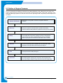
1. Precautions
2. Reference Information
3. Specifications
4. Summary of product
5. System Outline
6. Disassembly and Reassembly
7. Alignment and Adjustments
8. Troubleshooting
9. Exploded Views and Parts List
10. Block Diagram
11. Connection Diagram
Precautions
1
1. Precautions
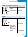
In order to prevent accidents and to prevent damage to the equipment please read the precautions listed
below carefully before servicing the printer and follow them closely.
1.1 Safety Warning
(1) Only to be serviced by appropriately qualified service engineers.
High voltages and lasers inside this product are dangerous. This printer should only be serviced by a suitably
trained and qualified service engineer.
(2) Use only Samsung replacement parts
There are no user serviceable parts inside the printer. Do not make any unauthorized changes or
additions to the printer, these could cause the printer to malfunction and create electric shock or fire hazards.
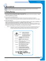
(3) Laser Safety Statement
The Printer is certified in the U.S. to conform to the requirements of DHHS 21 CFR, chapter 1 Subchapter J for
Class 1(1) laser products, and elsewhere, it is certified as a Class I laser product
conforming to the requirements of IEC 825. Class I laser products are not considered to be hazardous. The
laser system and printer are designed so there is never any human access to laser radiation above a Class I
level during normal operation, user maintenance, or prescribed service condition.
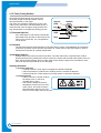
Warning >> Never operate or service the printer with the protective cover removed from Laser/Scanner assembly. The
reflected beam, although invisible, can damage your eyes. When using this product, these basic safety
pre-cautions should always be followed to reduce risk of fire, electric shock, and injury to persons.
CAUTION - INVISIBLE LASER RADIATION
WHEN THIS COVER OPEN.
DO NOT OPEN THIS COVER.
VORSICHT - UNSICHTBARE LASERSTRAHLUNG,
WENN ABDECKUNG GE FFNET.
NICHT DEM STRAHL AUSSETZEN.
ATTENTION - RAYONNEMENT LASER INVISIBLE EN CAS
D OUVERTURE. EXPOSITION DANGEREUSE
AU FAISCEAU.
ATTENZIONE - RADIAZIONE LASER INVISIBILE IN CASO DI
APERTURA. EVITARE L ESPOSIZIONE AL
FASCIO.
PRECAUCION - RADIACION LASER IVISIBLE CUANDO SE ABRE.
EVITAR EXPONERSE AL RAYO.
ADVARSEL. - USYNLIG LASERSTR LNING VED BNING, N R
SIKKERHEDSBRYDERE ER UDE AF FUNKTION.
UNDG UDSAETTELSE FOR STR LNING.
ADVARSEL. - USYNLIG LASERSTR LNING N R DEKSEL
PNES. STIRR IKKE INN I STR LEN.
UNNG EKSPONERING FOR STR LEN.
VARNING - OSYNLIG LASERSTR LNING N R DENNA DEL
R PPNAD OCH SP RREN R URKOPPLAD.
BETRAKTA EJ STR LEN. STR LEN R FARLIG.
VARO! - AVATTAESSA JA SUOJALUKITUS OHITETTAESSA
OLET ALTTIINA N KYM TT M LLE LASERS TEILYLLE L KATSO S TEESEEN.
Service Manual
1-1
Precautions
1.2 Caution for safety
1.2.1 Toxic material
This product contains toxic materials that could cause illness if ingested.
(1) If the LCD control panel is damaged it is possible for the liquid inside to leak. This liquid is toxic. Contact with the skin
should be avoided, wash any splashes from eyes or skin immediately and contact your doctor. If the liquid gets into
the mouth or is swallowed see a doctor immediately.
(2) Please keep toner cartridges away from children. The toner powder contained in the toner cartridge may be harmful
and if swallowed you should contact a doctor.
1.2.2 Electric Shock and Fire Safety Precautions
Failure to follow the following instructions could cause electric shock or potentially cause a fire.
(1) Use only the correct voltage, failure to do so could damage the printer and potentially cause a fire or electric
shock.
(2) Use only the power cable supplied with the printer. Use of an incorrectly specified cable could cause the cable
to overheat and potentially cause a fire.
(3) Do not overload the power socket, this could lead to overheating of the cables inside the wall and could lead to
a fire.
(4) Do not allow water or other liquids to spill into the printer, this can cause electric shock. Do not allow paper
clips, pins or other foreign objects to fall into the printer these could cause a short circuit leading to an electric
shock or fire hazard..
(5) Never touch the plugs on either end of the power cable with wet hands, this can cause electric shock. When
servicing the printer remove the power plug from the wall socket.
(6) Use caution when inserting or removing the power connector. The power connector must be inserted completely otherwise a poor contact could cause overheating possibly leading to a fire. When removing the power
connector grip it firmly and pull.
(7) Take care of the power cable. Do not allow it to become twisted, bent sharply round corners or other wise
damaged. Do not place objects on top of the power cable. If the power cable is damaged it could overheat and
cause a fire or exposed cables could cause an electric shock. Replace a damaged power cable immediately,
do not reuse or repair the damaged cable. Some chemicals can attack the coating on the power cable,
weakening the cover or exposing cables causing fire and shock risks.
(8) Ensure that the power sockets and plugs are not cracked or broken in any way. Any such defects should be
repaired immediately. Take care not to cut or damage the power cable or plugs when moving the machine.
(9) Use caution during thunder or lightening storms. Samsung recommend that this machine be disconnected from
the power source when such weather conditions are expected. Do not touch the machine or the power cord if it
is still connected to the wall socket in these weather conditions.
(10) Avoid damp or dusty areas, install the printer in a clean well ventilated location. Do not position the machine
near a humidifier. Damp and dust build up inside the machine can lead to overheating and cause a fire.
(11) Do not position the printer in direct sunlight. This will cause the temperature inside the printer to rise possibly
leading to the printer failing to work properly and in extreme conditions could lead to a fire.
(12) Do not insert any metal objects into the machine through the ventilator fan or other part of the casing, it could
make contact with a high voltage conductor inside the machine and cause an electric shock.
1-2
Service Manual
Precautions
1.2.3 Handling Precautions
The following instructions are for your own personal safety, to avoid injury and so as not to damage the printer
(1) Ensure the printer is installed on a level surface, capable of supporting its weight. Failure to do so could cause
the printer to tip or fall.
(2) The printer contains many rollers, gears and fans. Take great care to ensure that you do not catch your fingers,
hair or clothing in any of these rotating devices.
(3) Do not place any small metal objects, containers of water, chemicals or other liquids close to the printer which if
spilled could get into the machine and cause damage or a shock or fire hazard.
(4) Do not install the machine in areas with high dust or moisture levels, beside on open window or close to a
humidifier or heater. Damage could be caused to the printer in such areas.
(5) Do not place candles, burning cigarettes, etc on the printer, these could cause a fire.
1.2.4 Assembly / Disassembly Precautions
Replace parts carefully, always use Samsung parts. Take care to note the exact location of parts and also
cable routing before dismantling any part of the machine. Ensure all parts and cables are replaced correctly.
Please carry out the following procedures before dismantling the printer or replacing any parts.
(1) Check the contents of the machine memory and make a note of any user settings. These will be erased if the
mainboard or network card is replaced.
(2) Ensure that power is disconnected before servicing or replacing any electrical parts.
(3) Disconnect printer interface cables and power cables.
(4) Only use approved spare parts. Ensure that part number, product name, any voltage, current or temperature
rating are correct.
(5) When removing or re-fitting any parts do not use excessive force, especially when fitting screws into plastic.
(6) Take care not to drop any small parts into the machine.
(7) Handling of the OPC Drum
- The OPC Drum can be irreparably damaged if it exposed to light.
Take care not to expose the OPC Drum either to direct sunlight or to fluorescent or incandescent room
lighting. Exposure for as little as 5 mins can damage the surface’s photoconductive properties and will result
in print quality degradation. Take extra care when servicing the printer. Remove the OPC Drum and store it in
a black bag or other lightproof container. Take care when working with the covers(especially the top cover)
open as light is admitted to the OPC area and can damage the OPC Drum.
- Take care not to scratch the green surface of OPC Drum Unit.
If the green surface of the Drum Cartridge is scratched or touched the print quality will be compromised.
Service Manual
1-3
Precautions
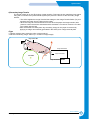
1.2.5 Disregarding this warning may cause bodily injury
(1) Take care - some parts may be hot.
The fuser unit works at a high temperature. Use caution when working on the printer. Wait for the fuser to cool
down before disassembly.
(2) Take care not to trap fingers or hair.
Take care when using a printer. It contains many rotating parts. Ensure that fingers, hair, clothing etc. do not
become caught in the mechanism as this could cause injury.
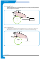
(3) When you move the printer.
This printer weighs 32kg including toner cartridge and cassette. Use safe lifting and handling techniques. Use
the lifting handles located on each side of the machine. Back injury could be caused if you do not lift carefully.
(4) Ensure the printer is installed safely.
The printer weighs 32Kg, ensure the printer is installed on a level surface, capable of supporting its weight.
Failure to do so could cause the printer to tip or fall possibly causing personal injury or damaging the printer.
(5) Do not install the printer on a sloping or unstable surface. After installation, double check that the printer is stable.
1-4
Service Manual
Precautions
1.3 ESD Precautions
Certain semiconductor devices can be easily damaged by static electricity. Such components are commonly called
“Electrostatically Sensitive (ES) Devices”, or ESDs. Examples of typical ESDs are: integrated circuits, some field
effect transistors, and semiconductor “chip” components.
The techniques outlined below should be followed to help reduce the incidence of component damage caused by
static electricity.
Caution >>Be sure no power is applied to the chassis or circuit, and observe all other safety precautions.
1. Immediately before handling a semiconductor component or semiconductor-equipped assembly, drain off any
electrostatic charge on your body by touching a known earth ground. Alternatively, employ a commercially available wrist strap device, which should be removed for your personal safety reasons prior to applying power to the
unit under test.
2. After removing an electrical assembly equipped with ESDs, place the assembly on a conductive surface, such as
aluminum or copper foil, or conductive foam, to prevent electrostatic charge buildup in the vicinity of the assembly.
3. Use only a grounded tip soldering iron to solder or desolder ESDs.
4. Use only an “anti-static” solder removal device. Some solder removal devices not classified as “anti-static” can
generate electrical charges sufficient to damage ESDs.
5. Do not use Freon-propelled chemicals. When sprayed, these can generate electrical charges sufficient to damage ESDs.
6. Do not remove a replacement ESD from its protective packaging until immediately before installing it. Most
replacement ESDs are packaged with all leads shorted together by conductive foam, aluminum foil, or a comparable conductive material.
7. Immediately before removing the protective shorting material from the leads of a replacement ESD, touch the protective material to the chassis or circuit assembly into which the device will be installed.
8. Maintain continuous electrical contact between the ESD and the assembly into which it will be installed, until completely plugged or soldered into the circuit.
9. Minimize bodily motions when handling unpackaged replacement ESDs. Normal motions, such as the brushing
together of clothing fabric and lifting one’s foot from a carpeted floor, can generate static electricity sufficient to
damage an ESD.
1.4 Super Capacitor or Lithium Battery Precautions
1. Exercise caution when replacing a super capacitor or Lithium battery. There could be a danger of explosion and
subsequent operator injury and/or equipment damage if incorrectly installed.
2. Be sure to replace the battery with the same or equivalent type recommended by the manufacturers.
3. Super capacitor or Lithium batteries contain toxic substances and should not be opened, crushed, or burned for
disposal.
4. Dispose of used batteries according to the manufacturer’s instructions.
Service Manual
1-5
Precautions
MEMO
1-6
Service Manual
Reference Information
2
2. Reference Information
This chapter contains the tools list, list of abbreviations used in this manual, and a guide to the
location space required when installing the printer. A definition of tests pages and Wireless
Network information definition is also included.
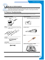
2.1 Tools for Troubleshooting
The following tools are recommended safe and easy troubleshooting as described in this service manual.
• DVM(Digital Volt Meter)
Standard : Indicates more than 3 digits.
• Driver
Standard : "-" type, "+" type (M3 long, M3 short, M2
long, M2 short).
• Cleaning Equipments
Standard : An IPA(Isopropyl Alcohol)dry wipe tissue or a
gentle neutral detergent and lint-free cloth.
• Vacuum Cleaner
• Brush
• Tweezers
Standard : For general home use, small type.
• Cotton Swab
Standard : For general home use, for medical service.
• Software (Driver) installation CD ROM
Install Driver CD
Network S/W CD
Service Manual
Samsung Electronics
2-1
Reference Information
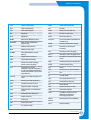
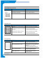
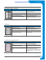
2.2 Acronyms and Abbreviations
The table below explains the abbreviations and acronyms used in this service manual. Where abbreviations
or acronyms are used in the text please refer to this table.
2-2
ADC
Analog-to-Digital-Conversion
EPP
Enhanced Parallel Port
AP
Access Point
F/W
Firmware
AC
Alternating Current
FCF/FCT
ASIC
Circuit
Application Specific Integrated
First Cassette Feeder/First
Cassette Tray
FISO
Front-In, Side-Out
ASSY
Assembly
FPOT
First Print out Time
BIOS
Basic Input Output System
GDI
Windows Graphic Device Interface
BLDC Motor
Brushless DC Motor
GIF
Graphic Interchange Format
CLBP
Color Laser Beam Printer
GND
Ground
CMOS
Complementary Metal Oxide
Semiconductor
HBP
Host Based Printing
HDD
Hard Disk Drive
CMYK
Cyan, Magenta, Yellow, Black
HTML
Hyper Text Transfer Protocol
CN
Connector
HV
High Voltage
CON
Connector
HVPS
High Voltage Power Supply
CPU
Central Processing Unit
I/F
Interface
CTD Sensor
Color Toner Density Sensor
I/O
Input and Output
dB
Decibel
lb
Pound(s)
dBA
A-Weighted decibel
IC
Integrated Circuit
dBm
Decibel milliwatt
ICC
International Color Consortium
DC
Direct Current
IDE
DCU
Diagnostic Control Unit
Intelligent Drive Electronics or
Integrated Drive Electronics
DIMM
Dual In-line Memory Module
IEEE
DPI
Dot Per Inch
Institute of Electrical and
Electronics Engineers. Inc
DRAM
Dynamic Random Access Memory
IOT
Image Output Terminal (Color printer, Copier)
DVM
Digital Voltmeter
IPA
Isopropy Alcohol
ECP
Enhanced Capability Port
IPC
ECU
Engine Control Unit
Inter Process CommunicationEPP
Enhanced parallel Port
EEPROM
Electronically Erasable
Programmable Read Only Memory
IPM
Images Per Minute
ITB
Image Transfer Belt
EMI
Electro Magnetic Interference
LAN
local area network
EP
Electro photographic
LBP
Laser Beam Printer
Service Manual
Samsung Electronics
Reference Information
LCD
Liquid Crystal Display
PWM
Pulse Width Moduration
LED
Light Emitting Diode
Q’ty
Quantity
LSU
Laser Scanning Unit
RAM
Random Access Memory
MB
Megabyte
RCP
Remote Control Panel
MHz
Megahertz
ROM
Read Only Memory
MPBF
Mean Prints Between Failure
SCF/SCT
MPF/MPT
Multi Purpose Feeder/Multi
Purpose Tray
Second Cassette Feeder/Second
Cassette Tray
SMPS
Switching Mode Power Supply
NIC
Network Interface Card
SPGP
NPC
Network Printer Card
Samsung Printer Graphic
Processor
NVRAM
Nonvolatile Random Access
Memory
SPL
Samsung Printer Language
SPL-C
Samsung Printer Language-Color
Spool
Simultaneous Peripheral Operation
Online
SRS
Software Requirment Specification
SURF
Surface Rapid Fusing
SW
Switch
sync
Synchronous or Synchronization
T1
ITB
T2
Transfer Roller
TRC
Toner Reproduction Curve
OPC
Organic Photo Conductor
PBA
Printed Board Assembly
PCL
Printer Command Language ,
Printer Control Language
PCI
PCL5Ce
Peripheral Component
Interconnect by Intel 1992/6/22, is
a local bus standard developed by
Intel and introduced in April, 1993 :
A60, B60 Pins
Printer Command Language 5CeColor
PCL6
Printer Command Language 6
PnP
Universal Plug and Play
PDF
Portable Document Format
U.I.
User Interface
PDL
Page Description Language
URL
Uniform Resource Locator
Ping
Packet internet or Inter-Network
Groper
USB
Universal Serial Bus
PPD
Postscript Printer Discription
VCCI
PPM
Page Per Minute
Voluntary Control Council for
Interference Information
Technology Equipment
PS
Post Script
WECA
Alliance
Wireless Ethernet Compatibility
PS3
Post Script Level3
Wi-Fi
Wireless Fidelity
PTL
Pre-Transfer Lamp
Service Manual
Samsung Electronics
2-3
Reference Information
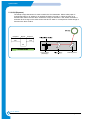
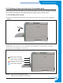
2.3 Select a location for the printer
• Leave enough room to open the printer trays, covers, and allow for proper ventilation. (see diagram
below)
• Provide the proper environment :
- A firm, level surface
- Away from the direct airflow of air conditioners, heaters, or ventilators
- Free of extreme fluctuations of temperature, sunlight, or humidity
- Clean, dry, and free of dust
2-4
Service Manual
Samsung Electronics
Reference Information
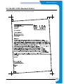
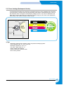
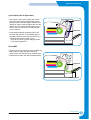
2.4 A4 ISO 19752 Standard Pattern
This test page is reproduced at 70% of the normal A4 size
Service Manual
Samsung Electronics
2-5
Reference Information
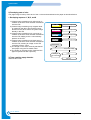
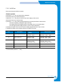
2.5 Wireless LAN
• This product can be used with a wireless LAN, (this is an option.)
- The wireless LAN function uses radio technology, instead of using LAN cable, to connect to an
access point for printing.
- For a wireless LAN connection in Infrastructure mode an AP is needed, (purchased separately)
- For a wireless LAN connection in Ad-Hoc mode an appropriate Wireless I/F card is required fitted
to a computer, (purchased separately)
- It is possible to use a wireless LAN connection with wired LAN.
- If an AP is installed in an office or at home, the wireless LAN function can be simply configured
and used.
• Types of desk top PC (or Lap top) that uses the wireless LAN.
Division
Basic type
Recommend type
CPU
Over PENTIUM 233M
PENTIUM 300MHz
MEMORY
Over 64MB
Over 128MB
VIDEO CARD
Over 800X600
Over 1024X768
OS
Over WINDOWS 98
Over WINDOWS ME
INTERFACE CARD
A product has a certificated mark of Wi-FiTM
• About the certificated mark of Wi-FiTM
- Wi-FiTM is a registered trademark of the WECA (Wireless Ethernet
Compatibility Alliance). Over 50 wireless LAN companies are member of
this organisation. Most of the main wireless networking companies are
attending including such companies as Lucent Technologies, Cisco,
Intel/Symbol, 3Com, Enterasys (Cabletron), Compaq, IBM, Nokia, Dell,
Philips, Samsung Electronics, Sony, Intersil, etc.. This mark certifies mutual
compatibility amongst the product of these companies. Wi-FiTM (IEEE
802.1) is certified as a standard of the wireless LAN market.
2-6
Service Manual
Samsung Electronics
Specifications
3
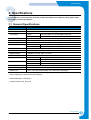
3. Specifications
Specifications are correct at the time of printing. Product specifications are subject to change without notice.
See below for product specifications.
3.1 General Specifications
Items
Print Method
Developing system
*Print Speed
Resolution
Source of Light
Warm-Up Time
First Print Time
Feed Method
Media Size
Media Thickness
Dimension (W X D X H)
Weight
**Acoustic Noise
Power save mode
Toner save mode
Machine Life
Descriptions
Non-impact Electro-photography
Non-Magnetic, Mono-Component Developing System
Mono
Up to 24 PPM in A4, Up to 25 PPM in Letter size
Color
Up to 6 PPM in A4, Up to 6 PPM in Letter size
Up to 1200 DPI effective output, True 600 X 600dpi
Laser diode (LSU : Laser Scanning Unit)
More than 99 sec
Mono
15 seconds (Ready to 1st page out)
Color
24 seconds (Ready to 1st page out)
Cassette , MPT(Multi Purpose Tray), SCT(Second Cassette Tray)
76 X 128mm (3 x 5”) to 216 X 356mm (8.5 X 14”)
Cassette : 16 ~24 lb , MPT : 16 ~ 43 lb
510 X 470 X 405 mm
Net
25.5 Kg
56.2Lbs
Gross
32.0 Kg
70.5Lbs
Stand by
More than 40 dBA-TBD
Printing
More than 48 dBA (Color)-TBD
Available, Setting : 5min/10min/15min/30min/45min/60min/120min
Disable
Mono : More than 300,000 pages, Color : More than 75,000 pages
* Print speed will be affected by Operating System used, computing performance, application software, connecting
method, media type, media size and job complexity.
* Cardstock/Envelope : Half Speed
** Sound Pressure Level, ISO 7779
Service Manual
Samsung Electronics
3-1
Specifications
3.2 Controller Specification
Items
Processor (CPU)
Memory
Emulation
Operating System
Interface
Interface switching
Interface time-out
Font
Color Management
Descriptions
Samsung SPGPm (CLOCK SPEED 120Mhz), 32-bit RISC core (ARM 946ES)
FLASH ROM (PROGRAM) : 8MB flash
*RAM : 64MB (Expandable to 320MB : With Option
Option DIMM module : 64/128/256MB
100Pin SDRAM DIMM (Samsung Printer Only)
EEPROM (NVRAM) : 1024bytes
SPL-Color
Win 95/98/ME/NT4.0/2000/XP, Various Linux OS including Red Hat, Caldera, Debian,
Mandrake, Slackware, SuSE and Turbo Linux
Parallel : IEEE 1284 Bidirectional (Korea, Russia, Asia only)
- Modes supported : Compatible, Nibble, Byte, ECP
USB (without HUB mode)
- USB 2.0 compliant
-12/480 Mbps 1 port
Network Interface
- 10/100 Base TX
10/100 Base TX + 802.11b Wireless LAN
Automatic
5min (Max.)
Windows font, PS english font, PCL english font
ICC ICM V3.4
* Memory Slots : Standard Capacity is
64MB Option Capacity is 320MB (Max)
(100Pin 1 slot, 64MB/128MB/256MB)
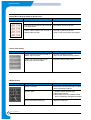
3.3 Electrical Specification
Items
Input Voltage
Power Consumption
Descriptions
Nominal input voltage
200-240 VAC / 100~127VAC
Input voltage range
180-264 VAC/ 90~132VAC
Nominal frequency
50/60 MHz
Frequency tolerance
+3Hz
Printing :450W max (with SCF)
Power Save : 35W max
Remarks
3.4 Environmental Range
Items
Temperature
Humidity
3-2
15~32.5 ˚C(50-90 ˚F)
20~80%RH
Operating
-20~40 ˚C (-4~104 ˚F)
10~80%RH
Storage
Service Manual
Samsung Electronics
Specifications
3.5 Consumable & Maintenance Items
Items
Periodic Replacing Parts
Toner Cartridge(Black)
Toner Cartridge(Cyan)
Toner Cartridge(Magenta)
Toner Cartridge(Yellow)
OPC Unit
ITB Unit(T1 Roller)
Waste Toner Tank
Fuser Unit
Transfer Roller(T2 Roller)
Option
SCT
(Second Cassette Tray)
Network Printing
802.11b Wireless LAN
SDRAM DIMM
Descriptions
Remarks
initial (3,000 pages@5% coverage)
User replace
replacement (7,000 pages@5% coverage)
initial (2,000 pages@5% coverage)
User replace
replacement (5,000 pages@5% coverage)
initial (2,000 pages@5% coverage)
User replace
replacement (5,000 pages@5% coverage)
initial (2,000 pages@5% coverage)
User replace
replacement (5,000 pages@5% coverage)
mono : 50,000 pages
User replace
color : 12,500 pages
mono : 50,000 pages
User replace
color : 12,500 pages
3,000 images
User replace
simplex : 100,000 page (Mono) / 50,000 page (Color) Engineer
duplex : 50,000 page (Mono) / 25,000 page (Color)
simplex : 50,000 page
Engineer
duplex : 25,000 page
- Paper capacity : 500sheets
- Paper weight : 60 ~ 90 g/m2 / 16 ~ 24 lbs
- Ethernet 10/100baseTX + Wireless
- Protocols : TCP/IP, SPX/IPX, Ethertalk, SNMP, HTTP
1.1, DLC/LLC
- 8MB RAM Buffer for faster graphics performance
- 4MB Flash Memory for upgrade
- IEEE802.3b support
- speed : 11, 5.5, 2 ,1Mbps
- WEP : 64bit, 128bit
- Operating range : 30m(Indoors) , 100m(Outdoors)
- 64,128MB, 256MB 100Pin SDRAM DIMM(Use Samsung
Part Only)
Service Manual
Samsung Electronics
3-3
Specifications
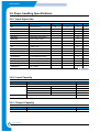
3.6 Paper handling Specifications
3.6.1 input Paper Size
Paper
Paper size
1st Cassette
2nd Cassette
MP tray
Duplex
A4
210 X 297 mm
O
O
O
O
Letter
216 X 279 (8.5 X 11")
O
O
O
O
Folio (Legal13")
216 X 330 (8.5 X 13")
O
O
Legal (Legal14")
216 X 356 (8.5 X14")
O
O
Executive
184 X 267 (7.25 X10.5")
O
Statement
140 X 216(5.5 x8.5")
O
ISO B5
176 X 250
O
JIS B5
182 X257
O
A5
148.5 X 210
O
A6
105 X148.5
O
Com-10 Envelope
105 X 241 (4.15 X 9.5")
O
Monarch Envelope
98 X191 (3.87 X 7.5")
O
DL Envelope
110 X 220(4.33 X 8.66")
O
C5 Envelope
162 X 229 (6.38 X 9.01")
O
C6 Envelope
114 X 162 (4.49 X 6.38")
O
Transparency (OHP)
A4 or Letter
O
Label paper
A4 or Letter
O
O : Supported
3.6.2 Input Capacity
Items
Cassette(FCT)
MP tray
Option Cassette(SCT)
Descriptions
250 sheets
Paper
Transparencies
Envelopes
Labels
500 sheets
Remarks
100 sheets
30 sheets
10 sheets
10 sheets
3.6.3 Output Capacity
Items
Face Down
3-4
Descriptions
Remarks
250 sheets
Service Manual
Samsung Electronics
Summary of product
4
4. Summary of Product
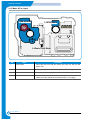
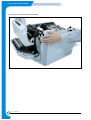
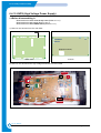
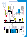
This chapter describes the functions and operating principles of the main components.
4.1 System Structure
4.1.1 Main Parts of System
Deve Cover
HVPS
DEV. - Black
DEV. - Yellow
DEV. - Magenta
LSU
DEV. - Cyan
CASSETTE
FCT
SCT
SCF
PTL
PTL
EXIT
EXIT
UnitUnit
Fuser Unit
T2 Roller
DUPLEX
Feeder
Eraser Lamp
Pick-up
Roller
Pick-up
Roller
ITB Unit
OPC
SCF Path
Pick-up
Roller
MPF Path
TF
MP
Service Manual
Samsung Electronics
4-1
Summary of Product
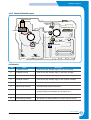
>> Front View
Panel PBA
Waster Toner Sensor
Deve OEM
PBA
Waster Toner Motor
>> Rear View
Deve Drive
Deve Drive PBA
Fan
Main Drive
Duplex Cover
Open S/W
Deve Cover
Open S/W
SMPS
Main Conrtoller PBA
4-2
Service Manual
Samsung Electronics
Summary of product
1) OPC Unit
Images are created on the OPC unit using an electro-photographic process. The unit consists of:* OPC Drum
* Waste Toner Ass'y
used to collect waste toner remaining on the OPC drum,
* Charge Roller Assy
2) ITB Unit
ITB stands for Image Transfer Belt. An image developed on the OPC Drum is transferred first to the
ITB. This is called the T1 Transfer (Primary Image Transfer).
Images are built up in layers on the ITB.
First the Yellow (Y) colour image is created on the OPC and transferred to the ITB
Next the Magenta (M) colour image is created on the OPC and transferred to the ITB
Followed by the Cyan (C) and Black (K) images.
3) Transfer Roller
Once the complete, full colour, image, has been built up on the ITB the Transfer Roller is used to
transfer the image onto paper. This is called the T2 Transfer (Secondary Image Transfer)
4) FCT (First Cassette Tray)
It stores and automatically feeds print paper.
Pick-up Roller picks up paper, controls drive, feeds paper, removes static electricity, and so on.
> Spec.
* Paper arrange way : Side Registration
* Paper Direction : FISO (Front-in, Side-Out)
* Cassette Type : A4, Ltr
* Paper Discharge : Separation Claw
* Capacity : 250 Sheets (Standard paper 75mg/m? 20lb)
* Paper Size : A4, Letter
* Paper Weight (average) : 60~90g/m2 (16~24lbs)
* Paper Type : General Printing Paper
* Additional Function : Paper Empty Sensor
5) SCT (Second Cassette Tray)
This additionally stores and automatically feeds printing paper. Its function is the same as the FCT
(First Cassette Tray)
> Spec.
* Paper arrangement : Side Registration
* Paper Direction : FISO (Front-in, Side-Out)
* Cassette Type : A4, Ltr
* Paper Discharge : Separation Claw
* Capacity : 500 Sheets (Standard paper 75mg/m2 20lb)
* Paper Size : A4, Letter
* Paper Weight (average) : 60~90g/m2 (16~24lbs)
* Paper Type : General Printing Paper
* Additional Function : Paper Empty Sensor
Service Manual
Samsung Electronics
4-3
Summary of Product
6) MPT (Multi Purpose Tray)
The Multi-Purpose Tray not only feeds general printing paper but is also used for many other kinds
of paper such as those paper sizes not supported by the cassette, envelopes, OHP, etc.
> Spec.
*
*
*
*
*
*
*
*
*
*
Capacity : Cut Sheet : 100 Sheets (Standard paper 75mg/m2 20lb)
OHP : 300 Sheets
Envelope & Label & Card Stock : 10 Sheets
Paper Arrangement : Side Registration
Power : Main Motor (BLDC)
Driving Management : Solenoid
Paper Discharge : Friction Pad Method
Paper Size : Legal, Folio, A4, Letter, Executive, JIS B5, A5, A6
Paper Weight (Average) : 60~163g/m2
Paper Type : General, Label, Post Card, Transparency, Envelope, Card Stock (Tracing
Paper is not served)
* Additional Function : Paper Empty Sensor
7) Feeder
* Paper Arrangement : Side Registration.
* Power : Main Motor (BLDC)
* Paper Management : Solenoid
8) Duplex Unit
The Duplex Unit is used to reverse feed paper when printing on the second side (known as Double
sided or Duplex printing). The Duplex Unit is not an optional extra, it is built-in at manufacturing
time and is integral with the Transfer Roller.
> Spec.
* Power : Main Motor (BLDC)
* Paper Reverse Function: After the front side of the original document is printed, it is transferred
to the duplex unit in order to print the reverse side of original document. The motor drives
the exit roller in the reverse direction to feed the paper back into the machine.
9) Exit Unit
The Exit Unit guides paper that is just about to leave the print engine. Printed-paper is discharged
by the Exit Roller and Kicker into the Output Tray.
> Spec.
* Capacity : 250 sheets (Standard A4, 75g/m2)
* Paper Direction : Face Down
* Exit Drive Roller : It is driven by Main Motor (BLDC), and it rotates clockwise for normal
feed and antic-clockwise when reverse feeding for duplex printing.
* Bin Full Sensor : There is no Bin Full sensor fitted on this model.
10) Toner Cartridge
There are four toner cartridges, each containing a different colour ink : C (Cyan), M (Magenta), Y
(Yellow) , and K (Black).
Each one of these toner cartridge is independent and can be changed independently.
11) Fuser Unit
This unit consists of 2 Heat Lamps, 2 Heat Rollers, 2 Thermostats and a Thermistor. It melts and
fuses the toner, transferred by the transfer roller onto the paper, by applying pressure and high
temperature to complete printing job.
12) LSU
This is a core part of LBP. It forms a latent image on the surface of OPC drum using a static
charge.
* Resolution: Real 600 dpi
4-4
Service Manual
Samsung Electronics
Summary of product
13) Main Drive Unit
This motor drives, by way of a gearbox, the OPC unit, ITB unit, feeder unit, fuser unit, exit unit and
duplex unit.
> Spec.
* Power : 20W Max (24V)
* Drives : OPC unit, ITB unit, Fuser, Feeder, Duplex unit, Exit unit
14) DEVE Drive Unit
This motor drives, by way of a gearbox, the toner cartridges and ITB cleaning cam.
> Spec.
* Power : 20W Max (24V)
* Drives : DEV (4 Color)/ITB Cleaning)
15) SMPS (Switching Mode Power Supply)
This power supply uses the AC supply voltage to generate the DC voltages used by the system.
The SMPS has 4 output channels (+3.3V, +5V, +24V, +24VF).
The AC Heater Control Unit that supplies power to the fuser is also located on the SMPS.
16) HVPS (High Voltage Power Supply)
The HVPS creates the high voltages (Charger, Supply, T1, T2, Developer) used for the electro
photographic process. The high voltage is created from the 24V line from the SMPS. High Voltage
output is supplied to the toner cartridge, OPC drum unit, ITB unit, and Transfer roller.
17) Main Controller PBA
The Main controller PBA is very important as it is the heart of printer. It has several major function
blocks.
* CPU and SPGPm Block: This manages the printing order from the host, creates bitmap data for
the engine to print and controls various devices that are needed to operate the printer.
*Engine Control Block: This manages images and controls various kinds of I/O
* Memory Block : The operating system uses this to store video data and printing orders given by host.
* ROM Block : The printer OS and PDL Interpreter are stored here.
* In addition there are USB 2.0 Block, IEEE 1284 Block, Option Block, OPE Panel, etc.
18) DEVE Drive PBA
Each toner cartridge requires the HV Supply only when that colour image is being processed. This
unit takes its HV source from the HVPS and using 4 solenoids selects which cartridge is to receive
the Supply voltage. This section also contains the DEVE motor, DEVE clutch, and DEVE solenoid
drives. These are activated in sequence as required by the printing process.
19) DEVE OEM PBA
This detects new or used toner cartridges and also checks that cartridges are approved parts. If a
toner cartridge is not suitable for the machine an error message is displayed.
20) Waste Toner Ass’y
A cleaner blade on the OPC unit cleans waste toner from the OPC drum after every image is
transferred to the ITB. Once the complete image is transferred from the ITB onto paper the ITB
Cleaning Solenoid activates and a cleaning blade removes waste toner from the ITB. Waste toner
is transferred to the waste toner tank.
The error message "Waste Toner Tank Full/ Not Install" is indicated on the LCD Panel. Replace the
Waste Toner Tank immediately or the printer may be damaged
Service Manual
Samsung Electronics
4-5
Summary of Product
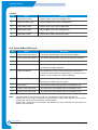
4.1.2 Motor & Fan Layout
1. Main Motor
2. DEVE Motor
Fan
4. Waste Toner Motor
NO.
4-6
Name
Description
1
Main Motor
Drives the OPC unit, ITB unit, feeder unit, fuser unit, exit unit and
duplex unit.
2.
DEVE Motor
Drives C, M, Y and K toner cartridges and ITB cleaning cam.
3.
Fan
Forces cold air into the printer and takes out heat from the fuser.
4.
Waste Toner Motor
Transfers collected waste toner from the OPC drum and ITB to the
waste toner tank. (Refer to front view picture on 4-2 page)
Service Manual
Samsung Electronics
Summary of product
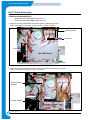
14.1.3 Clutch & Solenoid Layout
Duplex Solenoid
ITB Cleaning
Clutch
K, Y, M)
Cartridge Solenoid(C, M,
K)
T2 Home Clutch
Black Deve
Clutch
Yellow Deve Clutch
Magenta Deve Clutch
Cyan Deve Clutch
Feed Regi
Clutch
MP Pick_up
Solenoid
Pick_up Solenoid
>>Solenoid
NO.
1.
Name
C DEVE solenoid
Description
Controls the High Voltage supply to the cyan cartridge.
2.
K DEVE solenoid
Controls the High Voltage supply to the black cartridge.
3.
Y DEVE solenoid
Controls the High Voltage supply to the yellow cartridge..
4.
M DEVE solenoid
Controls the High Voltage supply to the magenta cartridge.
5.
Pick-up solenoid
Controls the pick-up roller drive.
6.
MP Pick-up solenoid
Controls the MP pick-up roller drive.
7.
Duplex solenoid
When operating in duplex print mode, this reverses the direction
of paper feeding to feed paper into the duplex unit.
8.
T2 Home clutch
This forces the transfer roller into contact with the ITB unit.
9.
ITB cleaning solenoid
This brings the cleaning blade into contact with the ITB unit
Service Manual
Samsung Electronics
4-7
Summary of Product
>>Clutch
NO.
Name
Description
1.
Yellow DEVE clutch
Controls Yellow color toner cartridge drive
2.
Magenta DEVE clutch
Controls Magenta color toner cartridge drive
3.
Cyan DEVE clutch
Controls Cyan color toner cartridge drive
4.
Black DEVE clutch
Controls Black color toner cartridge drive
5.
Feed Regi. Clutch
Controls the location of picked-up paper
4.1.4 Sensor & Micro S/W Layout
NO.
Name
Description
1.
Paper Empty Sensor(FCT)
This sensor detects paper in the first (main) cassette.
2.
Paper Empty Sensor(SCT)
This sensor detects paper in the second (optional) cassette.
3.
Paper Empty Sensor(MPT)
This sensor detects paper in the multi-purpose tray.
4.
Feed Sensor
This sensor must operate within a certain time after paper pickup otherwise a JAM is detected
5.
ITB Home Sensor
This detects the position of the image transfer belt, and in
dicates the start location for image writing. It is used to ensure
that all 4 colour images are correctly registered.
6.
Waste Toner Sensor
This detects whether the waste toner tank is mounted or not and
the amount of waste toner in the tank.
7.
Exit Sensor
This detects whether printing paper is discharged or not.
8.
DEVE Cover Open S/W
This detects the open/closed status of the DEVE Cover.
9.
Duplex Cover Open S/W
This detects the open/closed status of the Duplex Cover.
Note:
4-8
* ITB Home Sensor is located in the ITB unit. If it develops a fault replace the ITB unit.
* Please, refer to the Chap. 7 Arrangement and Adjustment, "Paper Path diagram", for the location
of the paper empty sensor, feed sensor, and exit sensor.
* Please, refer to page 4-2 for the location of the waste toner sensor, DEVE cover open S/W, and
duplex cover open S/W.
Service Manual
Samsung Electronics
Summary of product
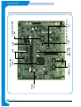
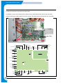
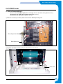
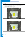
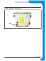
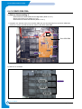
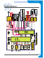
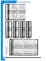
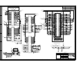
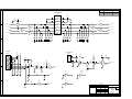
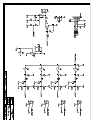
4.1.5 Main Controller PBA
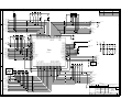
TH3 CN15
WASTE TONER & EXIT CN17
DUPLEX CN24
T2 HOME CN26
BLDC1 CN27
TH1 CN28
FUSER_FAN CN29
SMPS CN30
MP_EMPT CN31
MP SOL CN32
FEED CN33
PICK_UP CN25
CLT_FEED CN23
EMPT CN21
CN11 PTL & TH4
CN10 ITB
CN12 LSU
CN9 NIC
CN38 BLDC2
CN35 SOL_ITB_CLN
CN1 For Test
CN16 SCF
CN6 OPC KEY
Option : NIC
CN5
CN7
HVPS
LAN
PANEL
CN37 OEM_CONN
CN4
USB
DEVE_DRIVER
CN14 LSU SW
Service Manual
4-9
Samsung Electronics
Summary of Product
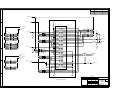
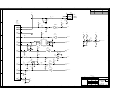
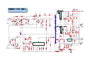
DIMM
U36
OSC3
(Counter Memory) 23.8807368MHz
LPEC1
(ENGINE CONTROL)
OSC2 12MHz
(Reserved)
RAM
FLASH MEMORY
SPGPm
Main Control
OSC1
12MHz
Service Manual
Samsung Electronics
4-10
Summary of product
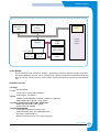
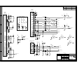
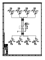
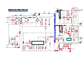
NPC / (W-LAN)
Flash Memory
Optional
2MB
LPEC1
Full Function
Engine
SPGPm
SDRAM
Control
64MB
Bloc k
SDRAM DIMM
34MB~128MB
5 pin UART
Panel
EEPROM
16x2 LCD
4k bit
USB 2.0
1) CPU BLOCK
This is the heart of the machine. A 120MHz - 32bit RISC processor is used to manage commands
and data supplied by the host. This is converted into a bitmap image which is passed to the engine
block for printing. The CPU is also used to control various other devices e.g. the USB 2.0 Interface
chip.
2) SPGPm overview
* Package
- 272 pins PBGA
* Power
- 1.8V(Core), 3.3V(IO) power operation
- P1284 inputs : 5V tolerant
* Speed
- 120MHz core(ARM946ES) operation, 60MHz bus operation
- Supportable Engine Speed : under 30ppm
* Dual bus architecture for bus traffic distribution
- AMBA High performance Bus (AHB)
- System Bus with SDRAM
* Integrated ARM946ES
- 32-bit RISC embedded processor core
- 16KB instruction cache and 16KB data cache
- No Tightly Coupled Memory
- Memory Protection Unit & CP15 control program
Service Manual
Samsung Electronics
4-11
Summary of Product
* Direct connection up to 4 Flash ROM banks
- Burst capability
- Programmable timing per bank
- Up to 16MB address per bank (Limited to 8MB per bank when nDREQ0 is enabled)
* Direct connection up to 6 I/O banks & 4 DMA I/O banks
- Programmable timing per bank
- Programmable recovery timing per bank for slow devices
- Up to 16MB address per bank (Limited to 8MB per bank when nDREQ0 is enabled)
* Direct connection up to 5 SDRAM arrays
- SDRAM controller supports PC-66, PC-100 and PC-133 SDRAMs running at 60MHz
- Up to 128MB per array, up to 512MB totally
- Wide support of various SDRAM configurations, including programmable band and column
address
- Programmable SDRAM refresh time interval
* 4 General Purpose DMA controllers
- Extensible architecture allows peripheral devices such as scan devices to have access to SDRAM
arrays through DMA channels
- 8bits, 16bits and 32bits Data Transfer Modes are supported
- IO to Memory, Memory to IO, Memory to Memory transfer support
* IEEE1284 compliant parallel port interface
- Compatible ECP communications are supported
- Direct support for IEEE1284 compliant data transceivers
* RSH
- Fully Hardware Rotator, Scaler and Halftoner support
- Variable Image Scaler and Image Halftoning Unit for PCL6
- Pattern & Gamma Table Memory : 1024 x 8, 256 x 8 x 4
* Graphic Execution Unit for Banding support of Printer Languages
- Support up to 256 Bit Block Transfer
- Scan Line Transfer
- Polygon Filling
- Enhanced Graphic Order
* Compression / Decompression
- CODEC : Simplified JBIG algorithm for band compression / decompression
- HCT : Halftone Compression Technology (Byte Run-Length Type)
- Independent use of both Codec, but enabling only one Codec is desirable for bus traffic
* UART
- 3 Independent Full Duplex UART channels
- Max 16 bytes FIFO to handle SIR Bit Rate Speed
- DMA support for RX and TX of Channel0
* Printer Video Controller for LBP engines
- 20MHz video rate are targeted
- Two different kinds of Printer Video Controller (Selected by Software)
- PVC : Printer Video Controller without RET Algorithm
- HPVC : Printer Video Controller with RET algorithm
(Line Memory & Lookup Table Memory : 512 x 8 , 4096 x 16)
- High performance DMA based Interface to Printer Engine
- Engine Controller
- Motor Control Unit
- Motor Speed Lookup Table Memory (128 x 16 x 2)
- Pulse Width Modulation Unit
- 4 Channels are supported
- ADC Interface Unit
- 3 ADC Channels are available
- ADC Core (ADC8MUX8) maximum clock frequency : 3 MHz
- Coversion time : 4.3us (@3MHz)
- LSU Interface Unit
4-12
Service Manual
Samsung Electronics
Summary of product
* Timer
*
*
*
*
- 3 Independent Programmable Timers
- Watch Dog Timer for S/W Trap and Tone Generator for MFP Application
Up to 5 External Interrupts support
- High active interrupt signals
- FIQ/IRQ Interrupt mode selectable
Ethernet Controller (MAC)
- Full compliance with IEEE standard 802.3, 802.3u specification
- Support 10/100 Mbps data transfer rates
- DMA engine with burst modes (4 words burst and 8 words burst are supported)
USB 2.0 interface
- USB 1.1 backward compatible
- UDC(USB Device Controller) block and USB Physical block are integrated
- Both of High Speed(480Mbps) and Full Speed(12Mbps) are supported
- 2 DMA channels support : one RX Channel and one TX Channel
- Interrupt transfer support up to 6 Endpoints
- EP0 In/Out (Control transfer), EP1 In/Out (Bulk transfer), EP2 In/Out (Bulk transfer)
Debug support
- Only MultiICE logic support from ARM9 series
- 5 JTAG connections : TCK, TnRST, TMS, TDI, TDO
- Internal logic for synchronizing TCK and high speed CLK
- Maximum TCK frequency : 20MHz (CLK x 1/6)
Service Manual
Samsung Electronics
4-13
Summary of Product
3) Memory Block
The operating program runs from memory (see below). It is used to store video data and printing
jobs from the host. Standard factory fitted memory is 64MB, and can be expanded using a DIMM
module mounted in the SODIMM connector. This is a user fit option, DIMMs from 64Mb - 256MB
can be used giving a total of up to 320MB of memory. DIMM modules are non standard - only
Samsung product should be used.
The memory controller is located in the SPGPm controls the SDRAM memory connected using a
32 bit 60 MHz bus.
4) ROM Block
An 8MB flash ROM is used to store the OS. The ROM controller is contained in the SPGPm
processor. When initializing after power on the contents of ROM are downloaded into memory and
the OS is run from within memory.
5) USB 2.0 Block
A Netchip Co. NET2270 is used to provide support for USB2.0 and is capable of interface speeds
up to 480Mbps. Under control of the SPGPm chip DMA is used to transfer incoming data directly
into memory.
6) IEEE 1284 Block - Korea, Russia and Asia Only
An IEEE 1284 controller is controlled directly by the SPGPm processor. ECP mode is supported.
7) Option Block
An Ethernet card can be attached using the 100 pin connector. It is connected directly to the
SPGPm processor and communicates using a 16bit bus.
8) OPE Panel
The OPE panel is controlled by a UART Block located in the SPGPm and it displays printer status
and helps the user to setup the printer. Various data is transferred using a serial interface between
a Mycom located in the OPE panel and the UART in the SPGPm.
9) Memory
There are two types of memory, program memory that uses flash and a working memory that uses
SDRAM. When printing working memory is used as band memory.
10) Sensor
Various sensors are used to detect various conditions during the printing process. These include
paper empty sensor, feed sensor, exit sensor, ITB sensor, etc.
11) Actuator Control
This section drives the various motors and clutches that are required for the paper feed and printing process. These include DEVE cartridge clutches (4 off), Feed Regi clutch, DEVE solenoids (4
off), Pick solenoids (2 off), Duplex solenoid, ITB and T2 solenoids.
12) ADC
Recognize the current of T1/T2 roll, Recognize the fusing temperature, Recognize the Waste Toner
tank, Recognize the current of Waste agitator DC Motor,Recognize the OPC/ITM key, Recognize
the Developer(Y.M.C.K) key, Recognize the set temperature.
4-14
Service Manual
Samsung Electronics
Summary of product
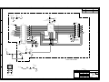
4.1.6 SMPS (Switching Mode Power Supply) PBA
The SMPS unit supplies DC power for driving the whole system, it also contains an AC heater control unit
that supplies power to the fuser.
1) DC output
- Main controller PBA, OP panel, SCF, Developer driver PBA
2) AC output
-Fuser unit (Heat lamp, Thermostat)
3) Output voltage
NO
Item
CH1
CH2
CH3
CH4
1
Channel name
+3.3V
+5V
+24.0V
+24.0VF
2
Rated outputting voltage
3.3V ± 4%
+5V ± 4%
+24V + 15%/-10%
+24V + 15%/-10%
3
Rated outputting crrunt
2.5A
0.5A
1A
2A
4
Uses
MICOM,CMOS
LOGIC
MICOM,CMOS
LOGIC
MOTOR,FAN
MOTOR,FAN
CON1 Fuse
CON2
CON4
CON4
CON3
CON3
CON1
CON2
Service Manual
Samsung Electronics
4-15
Summary of Product
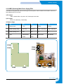
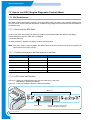
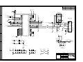
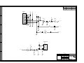
4.1.7 HVPS (High Voltage Power Supply) PBA
The HVPS PBA uses the 24V created by the SMPS to generate the high voltages used by the charger,
supply, T1,T2 and DEVE processes. For bests quality images these high voltages must be ,
controlled accurately to maintain the print quality. The high voltages produced are supplied to toner,
OPC cartridge, ITB unit, and transfer roller.
T1
(BLACK)
CHARGER (RED)
T2
(RED)
SUPPLY (BLACK)
CN2
CN1
T1
CHARGER
T2
SUPPLY
CN2
CN1
4-16
Service Manual
Samsung Electronics
Summary of product
1) Charging Voltage: Charger
* Function : This high voltage is used to charge the surface of the OPC to about -500volt~800volt.
* Output voltage : -200V~-2.0KV DC +/- 3% (Duty is changeable, no loading)
* Error type :If MHV was not present, the surface of the OPC is not charged. As a result, toner on
the developer roller is transferred over to the OPC drum: therefore, black paper could
be printed out.
2) Transfer high voltage: T1(+)
* Function : This high voltage is used to transfer toner from the OPC drum to the ITB unit.
* Output voltage : +400V~ +3.5KV DC +/- 3% (Duty is changeable, no loading)
* Error type : If T1 was not present, it is not possible to transfer toner from the OPC drum to the
ITB. As a result, printer output could be faint.
3) Transfer High Voltage: T2 (+)
* Function : this high voltage is use to transfer toner from the ITB to the paper.
* Output voltage : +400V~ +5KV DC +/- 3% (Duty is changeable, no loading)
* Error type : If T2 was not present, it is not possible to transfer toner from the ITB to the paper. As
a result, printing output could be faint
4) Cleaning voltage: T2 (-)
* This high voltage is used to transfer (-)toner, remains on transfer roller, from the Transfer Roller
to the ITB unit.
* Output voltage : There is no feedback control, and it outputs a fixed voltage (-900V).
* Error type : Toner contamination occurs on the reverse side of the printed-paper.
5) Supplying voltage: Supply
* Function : Supply the duplicated (AC+DC) voltage from the HVPS to the Deve Drive Board.
* Output voltage
AC Voltage f : 1 KHz ~ 3KHz (Duty is changeable)
AC Voltage Vp-p : 1KV ~ 3KV
DC : -100V ~ -1000V
* Error type: 1. If this voltage is GND, print density is extremely low.
2. If this voltage is floating due to unstable contact point at the HV terminal, density
becomes so low as that printing results are not visible to the naked eye.
Service Manual
Samsung Electronics
4-17
Summary of Product
MEMO
4-18
Service Manual
Samsung Electronics
System Outline
5
5 System Outline
This chapter describes the functions and operating principals of the main components.
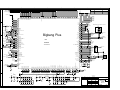
5.1 CLP (Color Laser Printing) Process
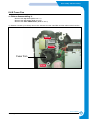
5.1.1 OPC Drum Unit (Charge Section)
The OPC Unit is the image formation unit and it consists of the OPC drum, waster toner assembly, charge
roller assembly, etc. (see diagram below).
OPC Drum
Charge Roller
Cleaning Blade
Waste Toner Tank
-1000V ~ -1500V
Eraser Lamp
LSU
Charge Roller
Cleaning Roller
Charge Bias
HVPS
1) Structure
* OPC drum: The laser light coming from the LSU forms an latent electric image on the surface of
the OPC drum.
* Cleaning Blade: Removes remaining unwanted toner from the OPC drum.
* Waste toner tank: Collects and stores the waste toner.
* Charge roller: The charge roller is charged to a negative high voltage (-1KV~1.5KV) It is in contact with the OPC drum and produces a uniform (-) voltage on its surface of approximately -500~800V.
2) Type
*
*
*
*
*
*
*
*
Life span: 50K Images (Color 12.5K)
Waste toner removal: Transferred to a user replaceable tank
Waste tank sensors: LED type, detects tank present and tank full
OPC drum diameter: 120mm
Power: Main motor (BLDC)
Charging method: Charge roller
Eraser method: LED lamp (+5V/2Pin)
PTL: LED lamp (+5V/2Pin)
Service Manual
Samsung Electronics
5-1
System Outline
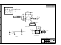
5.1.2 LSU (Exposure)
The bitmap image data stream is used to switch the LSU data beam. Where white paper is
required the beam is off, where ink is required the beam is turned on. When the laser is on
and the beam strikes the OPC drum surface the charge is reduced to -50V, where the beam is
switched off the charge on the OPC surface remains at -600V. In consequence a latent image is
formed on the drum surface.
Unexposed
Expesed
-600V
Unexposed
-600V
-50V
Polygon Motor
(30,000rpm)
5-2
Reflecting Mirror
Service Manual
Samsung Electronics
System Outline
5.1.3 Toner Cartridge (Development Section)
In the development stage toner particles are transferred from the toner cartridge onto the surface
of the OPC drum. The OPC drum and the developer roller rotate in opposite directions. Toner on
the developer roller is charged to the developing voltage (-370V ± 3%). Toner is attracted to the
OPC drum in those areas where the OPC drum surface charge is -50V. Toner is not attracted to
those areas of the surface carrying a -600V charge.
DEV. - Black
Dev Gap
DEV. - Yellow
Dev Roller
OPC
Drum
OPC
DEV. - Magenta
DEV. - Cyan
Developing
Voltage
1) Type
* Developing method: Non-magnetic, Mono-component developing system.
* Toner cartridge order: K, Y, M, C from top.
* Developing sequence: Y, M, C, K
* Life span: 7K(K) / 5K(C, M, Y)
* Power: DEVE motor (BLDC)
* Power transmission: Electric clutch
* Dot counting method
Service Manual
Samsung Electronics
5-3
System Outline
2) Developing state of color
The page image is built up from each of the 4 colors and transferred to the paper as described below.
> Developing sequence: Y, M, C, and K
1) A latent image containing only yellow toner is
created on the OPC drum and then transferred
onto the ITB.
2) A latent image containing only magenta toner
is created on the OPC drum and then transferred onto the ITB to add to the yellow image
already in the ITB.
3) A latent image containing only cyan toner is
created on the OPC drum and then transferred
onto the ITB, adding to the 2 colors already
present on the ITB
4) A latent image containing only black toner is
created on the OPC drum and then transferred
onto the ITB, creating an image on the ITB
consisting of the 4 colors.
5) The Image on the ITB is secondly transferred
onto paper using the T2 transfer roller.
6) The image on the page is then fused and the
paper is ejected into the output tray.
Yellow Color
Developing and Image Transfer
Magenta Color
Developing and Image Transfer
Cyan Color
Developing and Image Transfer
Black
Blacl Bolor
Color
Developing and Image Transfer
Paper Take-up
Image Transfer to page
Cleaning of
Image Transfer Belt
3) Toner cartridge empty detection
Software Dot count.
5-4
Fusing
Paper Exit
Service Manual
Samsung Electronics
System Outline
5.1.4 Image Transfer Section
The toner image formed on the OPC drum is transferred to the ITB (Image Transfer Belt), this is called the
primary image transfer. When the final image has been built on the ITB it is transferred onto paper, this is
called the secondary image transfer.
1) Structure
1
2
3
4
ITB Home Sensor
5
OPC DRUM
DUPLEX
Paper Path
NO.
Name
Description
1.
Image Transfer Belt
Used to build up the 4 color image from the OPC drum.
Colors are transferred in the order Y, M, C, K
2.
Image Transfer Belt cleaner
After the final image is transferred onto paper any waste
toner is removed from the transfer belt using this cleaning
blade
3.
PTL (Pre-Transfer Lamp)
Reduce the electric potential of OPC Drum surface before
primary image transfer the image on the OPC Drum.
4.
Image Transfer Roller (T2 Roller)
This transfers the final toner image on the image transfer belt
to paper.
5.
ITB Home Sensor
This sensor is used to ensure that each of the 4 color
images starts at exactly the same point on the ITB. It works
by detecting a fixed point on the belt.
Service Manual
Samsung Electronics
5-5
System Outline
2) Primary Image Transfer
A colored page is split into 4 component color parts and developed one color at a time in turn on
the OPC (in the order Y, M, C, K). The final image is built up on the ITB by transferring these separate color images from the OPC drum.
Image Transfer Belt
Image Transfer Roller
OPC DRUM
DUPLEX
HVPS
Primary Image Transfer Bias
3) PTL (Pre-Transfer Lamp)
It is arrayed LED on PCB Board. Main function is improving the T1 utility factor by reducing the
adhesive strength of OPC and Toner by irradiation on the OPC Drum formatted the image.
Image Transfer Belt
PTL
(LED)
OPC DRUM
DUPLEX
Image Transfer Roller
5-6
Service Manual
Samsung Electronics
System Outline
4) Secondary Image Transfer
The image is built up on the ITB (primary image transfer). This image is then transferred onto paper
using the T2 transfer roller (roller transfer system) this process is known as the secondary image
transfer.
* The HVPS applies the Image Transfer Bias voltage to the Image Transfer Roller (T2), this
transfers the image from the belt onto the paper.
* When the image is to be transferred from the ITB to the paper the image transfer roller
pressure contact solenoid is activated and this activates a cam which moves the T2 roller
into contact with the belt.
*After the transfer has taken place any remaining charge on the paper is removed by
applying a charge removal bias (generated in the HVPS) to a charge removal plate
>Type
* Transfer method: Semi-conductive roller contact method
* Effective transferring range: 218mm (i.e. maximum image length)
Image Transfer Belt
Charge Removal Bias
Image Transfer Roller
OPC DRUM
Paper
Image Transfer Bias
HVPS
Service Manual
Samsung Electronics
5-7
System Outline
5.1.5 Fuser (Fusing Section)
Toner that has been through the primary and
secondary image transfer processes is fixed,
semi-permanently, to the paper.
The fuser unit consists of heat lamps (2 ea), heat
rollers (2 ea), thermistor, and thermostats (2 ea). It
melts the toner onto the paper using pressure and
high temperature to complete the printing process.
1) Thermostat (2pieces)
If the heat lamps or heat rollers overheat the
thermostat turns off power to the lamps in the
fuser unit to prevent fire. It is a temperature
cut-off device.
Heat Lamp
(500W)
Heat Roller
Heat Lamp
(300W)
Spring
Paper
Heat Roller
2) Thermistor
The thermistor detects the temperature of the heat roller's surface, and feedbacks the information
to the main processor which uses this information to control power to the fuser lamps in order to
maintain the heat roller at a steady temperature.
3) Heat Roller (2pieces)
Halogen lamps are used to heat the heat rollers. The heat rollers have a special Teflon surface
which ensures that any melted toner which comes into contact with the heat roller surface does not
stick. Paper passes between the two rollers which evenly heat the paper from both sides to melt
the toner and semi-permanently fix it to the paper.
4) Safety Information
> Overheat protection
* 1st level protection: Print engine is stopped if overheat is detected
* 2nd level protection: Software turns off lamp power if overheat is detected.
* 3rd level protection: Thermostat turns off lamp power if overheat is detected.
> Protecting device
* Fuser unit power is turned off when
the duplex cover or the toner
cartridge door is open.
* This machine keeps the surface
temperature of the fuser unit cover
under 180°C, and it has a caution
label attached inside the exit cover
where it can be easily seen by the user.
5-8
Service Manual
Samsung Electronics
System Outline
5.1.6 Exit
After passing through the fuser paper is ejected into the paper exit tray. Any static electrical charge
is removed by static discharge brushes.
When operating in duplex print mode, after printing the front side of the page, the paper exit roller
reverses to feed the paper back into the machine in order to print the second side of the page.
5.1.7 Waste Toner Collection Process
Waste toner on the OPC drum and on the image transfer belt is collected into the waste toner tank.
* After transferring the toner image on the OPC drum to the ITB, a cleaning blade scrapes waste
toner from the OPC drum, and the waste toner is collected into a waste toner tank.
* An Image Transfer Belt cleaner scrapes waste toner from the image transfer belt, and the waste
toner is collected into a waste toner tank.
1) Waste toner tank sensor
A waste toner sensor detects the presence of the waste toner tank and also detects if the tank is full.
This is an On / Off detection. Do not operate the printer without a waste toner tank.
> No waste toner tank
When the waste toner tank is not installed the waste toner senor
actuator blocks light from the senor LED.
Waste Toner Sensor
Waste Toner Sensor Actuator
> A little waste toner
When the sensor LED light reaches the photo sensor passing
through the waste toner tank this indicates that the tank is not full.
Waste Toner Sensor
Waste Toner Tank
> Waste toner tank full
When the waste toner tank is full to the level of the waste toner
sensor, the senor LED light is blocked by waste toner indicating
that the tank is full.
Waste Toner Sensor
Waste Toner Tank
Waste Toner Tank
Waste Toner Tank
Service Manual
Samsung Electronics
5-9
System Outline
5.2 Outline of Engine Firmware
The CLP 510/510N use 4 different colored toners (Yellow, Magenta, Cyan, Black) and it is a laser color
printer. Engine firmware controls the print processes, driving the print engine, paper feed, developer, fuser,
and paper discharge systems. It has both color and mono printing modes. The printer process sequence is
as follows:
System Initialization
5-10
When power to the system is turned on all system values are
initialized
Warm-Up
Each part of system is activated and the system automatically
checks its status and all systems are prepared to accept a job for printing.
Ready
The normal state of the printer, waiting to receive a command from
a host to start a job. After a predefined length of time in the Ready
state if no print jobs are received the Power Save mode is entered.
Pre-Print
As soon as a printing order is inputted from host, the printer checks
the status of each part before performing the printing job.
Print
Printer performs the actual printing job.
Post-Print
The finishing state of printing job. The printer puts all systems back
into a state ready to start the next job and then enters the Ready state.
Service Manual
Samsung Electronics
System Outline
5.2.1 System Initialization
The system initialization process is carried out immediately after power on. The following tasks are performed.
1) Initialize ASIC
2) Initialize system variables
3) Initialize a virtual timer
4) Initialize fuser control
5) Initialize ADC
6) Set-up ITB HOME interrupt
5.2.2 Warm-Up
In the warm-up stage, the following tasks are performed.
1) Self Test
* System error check
* Cover open check
* Device (ITB, OPC, DEVE cartridge) check
* Heating error check
* Motion of motor and jam & paper empty check
* Check Feed and exit sensors. If paper is detected it is ejected. If the paper detection does not
clear a jam recovery is carried out and the paper drive unit is instructed to drive for the maximum
permitted paper length.
2) Heat Control
The heater control unit separately manages the temperature of the heat lamps.
* Target temperature (165°C)
* Temperature below 130°C - heat unit fully on,
* Temperature above 135°C temperature is controlled by reading the temperature value
every 10msec.
3) Cleaning
Transfer rollers, OPC and ITB are electrically and mechanically cleaned.
Service Manual
Samsung Electronics
5-11
System Outline
5.2.3 Ready
1) Host interface is monitored for print commands
2) Heat control
* Target temperature (165°C)
* Every 40 seconds, temperature value for the previous 250ms is read and a proportional control
process is carried out
3) This is the standby mode entered after warm-up or after completing a print job.
4) System Error check
5) Power save state is entered after timeout
> Wakeup condition
* When a "wakeup" order is received
* When a cover is opened and then closed
* When the level of the paper empty sensor changes.
> Heat lamp is off
5.2.4 Pre-Print
This is the preparation stage before processing a printing job and after receiving a print command from a host.
1) Start LSU
* Run Scanning motor
* Check motor ready
* Turn LD on
2) Start BLDC motor, Eraser/PTL on
* Run main motor
* Check lock signal
* Run developer roll motor
* Check lock signal
3)Turn High Voltage On
* Charger on
* Developer high voltage off
4) Cleaning
* OPC cleaning (Mechanical motion)
* ITB cleaning
5) Jam check
6) Motor Unlock Check
7) Check and Set a High Voltage Condition (T1, T2, Charger)
8) Initialize Printing Parameters
* Paper size, copies, cassette ...
* Image pixels, image times, y-offset, x-offset
* Flags
9) Check Print mode
* Color print mode:
- Except legal & OHP/Legal/OHP
- Simplex/Duplex
* Mono pint mode: Simplex/Duplex/OHP
5-12
Service Manual
Samsung Electronics
System Outline
5.2.5 Print
After sensing the ITB home position the following tasks are performed,
Send Psync signal to controller -> Operates virtual timer for each color(Vdata) -> Forms latent
image on OPC drum -> Supplies toner on OPC drum -> Transfers image to ITB (T1 ) -> Pickups a
paper -> Transfers image to a paper (T2)
1)Check ITB Home (Treated by Home interrupt): It is designed to detect ITB HOME every 3 seconds.
a) ITB Home sensing
b) If a test mode is set up, a test pattern is printed.
c) A counter value is set up that addresses the timing to turn on page sync.
d) The virtual timer for each color (Y, M, C, and K) is set up
e) If Home is not detected every 3 seconds, an error is reported.
2)Paper path and print
a) Printing paper from cassette, MPT and SCT is picked up
b) Control paper path
* Stop when the leading edge of a piece of paper reaches the feed sensor.
* If the leading edge doesn't reach the feed sensor, it is an error.
* While transferring the last color to the ITB, re-feed the paper.
* Checks if the paper reaches the exit sensor in certain time. If it reaches too soon, or it doesn't
reach, it is an error.
* Checks that the paper passes the exit sensor or not.
c) Jam check
* Check reaching time and passing time for the paper reaching and passing the feed and exit
sensors. If time exceeds a certain time, it is an error.
d) Duplex control
* After passing the exit sensor, the duplex clutch is operated to mechanically change the direction
of the paper flow in order to print the other side.
e) Printing sequence and motion for each color
* Use a virtual timer for printing the colors in sequence. (Yellow, Magenta, Cyan, Black)
> What is a Virtual Timer?
A virtual timer is a mathematical function for creating regular action at fixed time intervals. The standard setting is for a 5msc timer interrupt.
5.2.6 Post-Print
This is the last stage of the printing process. Its functions are described below.
a) Clean transfer rollers
b) Stop all virtual timers
c) Initialize parameters used in the printing process.
d) Stop motors
Service Manual
Samsung Electronics
5-13
System Outline
MEMO
5-14
Service Manual
Samsung Electronics
Disassembly and Reassembly
6
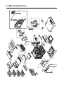
6. Disassembly and Reassembly
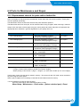
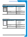
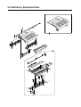
6.1 Precautions When Replacing Parts . . . . . . . . . . . . . . . . . . . . . . . . . . . . . . page(6-2)
6.1.1 Precautions when assembling and disassembling . . . . . . . . . . . . . . page(6-2)
6.1.2 Precautions when handling PBA . . . . . . . . . . . . . . . . . . . . . . . . . . . . . . page(6-2)
6.2 Parts for Maintenance and Repair . . . . . . . . . . . . . . . . . . . . . . . . . . . . . . . page(6-3)
6.2.1 Replacement interval for parts with a limited life . . . . . . . . . . . . . . . . page(6-3)
6.2.2 Printer Cleaning . . . . . . . . . . . . . . . . . . . . . . . . . . . . . . . . . . . . . . . . . . . . . page(6-4)
6.3 Information Related in Disassembly and Assembly . . . . . . . . . . . . . . page(6-5)
6.3.1 Special Service Parts . . . . . . . . . . . . . . . . . . . . . . . . . . . . . . . . . . . . . . . . page(6-5)
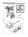
1) Disassemble of LSU Unit . . . . . . . . . . . . . . . . . . . . . . . . . . . . . . . . . . page(6-5)
2) Disassemble of ITB Unit . . . . . . . . . . . . . . . . . . . . . . . . . . . . . . . . . . . page(6-5)
3) Custody of OPC Unit . . . . . . . . . . . . . . . . . . . . . . . . . . . . . . . . . . . . . . page(6-5)
4) Custody of Toner Cartridge . . . . . . . . . . . . . . . . . . . . . . . . . . . . . . . . . page(6-5)
5) Disassemble of DEVE Drive Ass’y and Main Drive Ass’y . . . . . page(6-5)
6) Disassemble of Terminal Parts . . . . . . . . . . . . . . . . . . . . . . . . . . . . . page(6-5)
7) Disassemble of Fuser Unit . . . . . . . . . . . . . . . . . . . . . . . . . . . . . . . . . page(6-5)
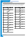
6.3.2 Screws Used in the Printer . . . . . . . . . . . . . . . . . . . . . . . . . . . . . . . . . . . page(6-6)
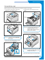
6.3.3 Opening Covers and replacing Consumable parts . . . . . . . . . . . . . . page(6-7)
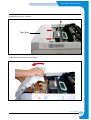
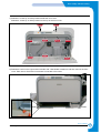
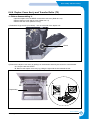
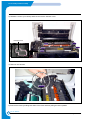
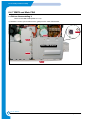
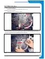
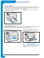
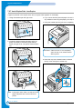
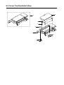
>> Consumable parts removal . . . . . . . . . . . . . . . . . . . . . . . . . . . . . . . . page(6-7)
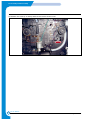
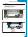
6.3.4 Replacing the Waste Toner Tank . . . . . . . . . . . . . . . . . . . . . . . . . . . . . . . . . page(6-10)
>> Removing the waste toner tank . . . . . . . . . . . . . . . . . . . . . . . . . . . . page(6-10)
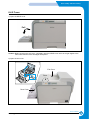
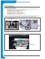
6.4 Process of Disassembly . . . . . . . . . . . . . . . . . . . . . . . . . . . . . . . . . . . . . . . . page(6-12)
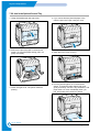
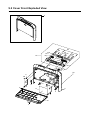
6.4.1 Top Cover and Front Cover . . . . . . . . . . . . . . . . . . . . . . . . . . . . . . . . . . . page(6-12)
6.4.2 OP Panel Ass’y . . . . . . . . . . . . . . . . . . . . . . . . . . . . . . . . . . . . . . . . . . . . . . page(6-16)
6.4.3 Rear Cover . . . . . . . . . . . . . . . . . . . . . . . . . . . . . . . . . . . . . . . . . . . . . . . . . . page(6-17)
6.4.4 Duplex Cover Ass’y and Transfer Roller (T2) . . . . . . . . . . . . . . . . . . . page(6-19)
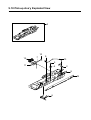
6.4.5 Fuser . . . . . . . . . . . . . . . . . . . . . . . . . . . . . . . . . . . . . . . . . . . . . . . . . . . . . . . page(6-21)
6.4.6 Exit Cover . . . . . . . . . . . . . . . . . . . . . . . . . . . . . . . . . . . . . . . . . . . . . . . . . . . page(6-23)
6.4.7 SMPS and Main PBA . . . . . . . . . . . . . . . . . . . . . . . . . . . . . . . . . . . . . . . . page(6-24)
6.4.8 Fuser Fan . . . . . . . . . . . . . . . . . . . . . . . . . . . . . . . . . . . . . . . . . . . . . . . . . . . page(6-27)
6.4.9 Main Drive Ass’y . . . . . . . . . . . . . . . . . . . . . . . . . . . . . . . . . . . . . . . . . . . . . page(6-28)
6.4.10 HVPS (High Voltage Power Supply) . . . . . . . . . . . . . . . . . . . . . . . . . . page(6-30)
6.4.11 DEVE Drive Ass’y . . . . . . . . . . . . . . . . . . . . . . . . . . . . . . . . . . . . . . . . . . . page(6-32)
6.4.12 DEVE Drive PBA and DEVE Cover Open S/W . . . . . . . . . . . . . . . . page(6-34)
6.4.13 DEVE Drive Motor and ITB Cleaning Solenoid . . . . . . . . . . . . . . . . page(6-36)
6.4.14 DEVE Cover . . . . . . . . . . . . . . . . . . . . . . . . . . . . . . . . . . . . . . . . . . . . . . . page(6-37)
6.4.15 LSU Unit . . . . . . . . . . . . . . . . . . . . . . . . . . . . . . . . . . . . . . . . . . . . . . . . . . . page(6-38)
6.4.16 DEVE OEM PBA . . . . . . . . . . . . . . . . . . . . . . . . . . . . . . . . . . . . . . . . . . . page(6-40)
6.4.17 Waste Toner Ass’y . . . . . . . . . . . . . . . . . . . . . . . . . . . . . . . . . . . . . . . . . . page(6-41)
6.4.18 MPT (Multi Purpose Tray) . . . . . . . . . . . . . . . . . . . . . . . . . . . . page(6-43)
6.4.19 Pick-Up Ass’y . . . . . . . . . . . . . . . . . . . . . . . . . . . . . . . . . . . . . . page(6-44)
6.4.20 Pick-Up Roller replacement . . . . . . . . . . . . . . . . . . . . . . . . . . . page(6-46)
Service Manual
Samsung Electronics
6-1
Disassembly and Reassembly
6.1 Precautions when replacing parts
6.1.1 Precautions when assembling and disassembling
* Use only approved Samsung spare parts. Ensure that part number, product name, any voltage, current or
temperature rating are correct. Failure to do so could result in damage to the machine, circuit overload,
fire or electric shock.
* Do not make any unauthorized changes or additions to the printer, these could cause the printer to malfunction and create electric shock or fire hazards.
* Take care when dismantling the unit to note where each screw goes. There are 19 different screws. Use of
the wrong screw could lead to system failure, short circuit or electric shock.
* Do not disassemble the LSU unit. Once it is disassembled dust is admitted to the mirror chamber and will
seriously degrade print quality. There are no serviceable parts inside.
* Regularly check the condition of the power cord, plug and socket. Bad contacts could lead to overheating
and firfe. Damaged cables could lead to electric shock or unit malfunction.
6.1.2 Preautions when handling PBA
Static electricity can damage a PBA, always used approved anti-static precautions when
handling or storing a PBA.
>> Precautions when moving and storing PBA
1. Please keep PBA in a conductive case, anti-static bag, or wrapped in aluminum foil.
2. Do not store a PBA where it is exposed to direct sunlight.
>> Precautions when replacing PBA
1. Disconnect power connectors first, before disconnecting other cables
2. Do not touch any soldered connections, connector terminals or other electronic parts when handling
insulated parts.
>> Precautions when checking PBA
1. Before touching a PBA, please touch other grounded areas of the chassis to discharge any static electrical charge on the body.
2. Take care not to touch the PBA with your bare hands or metal objects as you could create a short circuit or get an electric shock. Take extra care when handling PBAs with moving parts fitted such as sensors, motors or lamps as they may get hot.
3. Take care when fitting, or removing, screws. Look out for hidden screws. Always ensure that the correct
screw is used and always ensure that when toothed washers are removed they are refitted in their original positions.
6.1.3 Releasing Plastic Latches
Many of the parts are held in place with plastic latches. The latches break easily; release them carefully.
To remove such parts, press the hook end of the latch away from the part to
which it is latched.
6-2
Service Manual
Samsung Electronics
Disassembly and Reassembly
6.2 Parts for Maintenance and Repair
6.2.1 Replacement interval for parts with a limited life
Some of the parts in this printer have a limited life, shorter than that of the whole machine. These parts
must be replaced periodically.
The table below shows the interval at which these parts should be replaced.
The table shows the life of each part, and is measured when using A4 paper. When servicing a machine
always check the status of these parts using the control panel and ensure that parts are replaced at the
appropriate times otherwise a general degradation in print quality will occur.
COMPONENT
REPLACEMENT CYCLE
REMARK
Toner Cartridge (Black)
intial (3,000 pages@5% coverage)
replacement (7,000 pages@5% coverage)
User replace
Toner Cartridge (Cyan)
intial (2,000 pages@5% coverage)
replacement (5,000 pages@5% coverage)
User replace
Toner Cartridge (Magenta)
intial (2,000 pages@5% coverage)
replacement(5,000 pagse@5% coverage)
User replace
Toner Cartridge (Yellow)
intial (2,000 pages@5% coverage)
replacement (5,000 pages@5% coverage)
User replace
OPC Unit
mono : 50,000 pages
color : 12,500 pages
User replace
ITB Unit (T1 Roller)
mono : 50,000 pages
color : 12,500 pages
User replace
Waste Toner Tank
3,000 Images
User replace
Fuser Unit
simplex : 100,000 pages (Mono)
duplex : 50,000 pages
Engineer
Transfer Roller (T2 Roller)
simplex : 50,000 pages
duplex : 25,000 pages
Engineer
* Page: Counted value based on sides of paper printed (Duplex = 2 pages).
* Image: Counted value based on printed monochrome images.
* When printing a color section 1 page = 4 images. (i.e. each side is made up of 4 color images)
The life span of each of these parts is stored in memory. The amount of each 'life' used can be checked at
any time using the control panel.
When a part is replaced it is necessary to reset the 'life used' that is stored in memory.
* How to initialize a the value of part's life span:
From the control panel, select the following items in order:
Menu-Setup - Maintenance - Check other - (Select a desired part) - Reset
Service Manual
Samsung Electronics
6-3
Disassembly and Reassembly
6.2.2 Printer Cleaning
A printer should be regularly cleaned, especially if it is used in a dusty environment. This will ensure that
print quality remains high and failure due to contamination of printing services is less likely to occur.
* Clean the printer with a soft, lint free, cloth dipped in a "Recommended cleaner"
"Recommended cleaner" can be purchased from our service center. (where available)
* Do not touch the transfer roller when cleaning the inside of the printer. Grease and oils from the
skin will contaminate the surface and reduce print quality.
* Do not touch transfer roller when cleaning inside of machine. If transfer roller gets dirty, printing
quality could be low.
* Please refer to the User Manual for cleaning instructions.
6-4
Service Manual
Samsung Electronics
Disassembly and Reassembly
6.3 Information Related to Disassembly and Assembly.
6.3.1 Special service parts
Never disassemble or adjust the items mentioned, a stock of these items should be maintained.
1) Disassembly of the LSU unit
There are no serviceable parts inside the
LSU. Alignment of the mirrors is critical.
Opening the LSU will allow dust into the
laser and significantly reduce print quality.
It is very dangerous to operate or service
a machine with the LSU open or system
interlocks disabled. Exposure to laser
radiation can cause blindness.
2) Disassembly of the ITB unit
Do not disassemble the ITB. The alignment of the home sensor is critical and is
set up in the factory on a special jig.
Incorrect re-assembly will cause print
quality degradation.
3) Care of the OPC unit
If an OPC unit is exposed to direct sunlight for a long time the parameters and
response of the electrostatic surface are
changed causing image transfer and print
quality issues. Also there is no protective
shutter on the OPC drum to prevent
scratching Please take extra care to
ensure the OPC drum is protected from
sunlight and physical contact when servicing the machine.
5) Disassembly of DEVE drive ass'y
and the main drive ass'y
The alignment of the drive mechanism is
critical and it has been set up in factory
using a jig and a driving gear. It is adjusted for the best gearing alignment. If the
motor is disassembled alignment would
not be maintained and this could cause
operational noise and image problems:
image alignment and toner distribution
may be affected.
6) Disassembly of terminal parts
Do not adjust the variable resistors on the
PBA. They have been already adjusted in
the factory.
7) Disassembly of the fuser unit
- The fuser melts toner onto the paper at
a high temperature: therefore, you need
to take special care not to get burned by
a hot fuser. When removing the fuser
from a set that has recently been operating you need to take extra care.
- Do not touch an AC line (Copper contact) on a main frame even after removing the fuser.
4) Care of the Toner cartridge
Toner cartridges contain an extremely fine
powder. Please keep toner cartridges
away from children. The toner powder
contained in the toner cartridge may be
harmful and if swallowed you should contact a doctor. Take care not to spill toner spillages should be cleaned with a
vacume cleaner and washed in could
water (hot water sets the toner). Do not
touch the developer roller surface as contamination will reduce print quality. Take
care not to damage the roller's surface
when installing or removing a toner cartridge.
Service Manual
Samsung Electronics
6-5
Disassembly and Reassembly
6.3.2 Screws used in the printer
The screws listed in the table below are used in this printer. Please ensure that, when
you disassemble the printer, you keep a note of which screw is used for which part and
that, when reassembling the printer, the correct screws are used in the appropriate
places.
NO
DESCRIPTION
SEC CODE
SPEC
NO
DESCRIPTION
SEC CODE
SPEC
S1
SCREW-MACHINE
6001-000485
2.6*4, GOLD
S11
SCREW-TAPTITE
6003-000269
3*6, GOLD
S2
SCREW-TAPPING
6002-000115
4*15, GOLD
S12
SCREW-TAPTITE
6003-001001
3*8, BLACK
S13 SCREW-MACHINE
6001-000568
3*8, SILVER
S14
SCREW-TAPTITE
6003-001256
4*10 SILVER
S15
SCREW-TAPTITE
6003-000261
3*6, GOLD
S16 SCREW-MACHINE
6003-001068
2*16, BLACK
S17
SCREW-TAPTITE
6003-000301
4*6, GOLD
S18
SCREW-SPICIAL
6009-001396
3*10, BLACK
S19
SCREW-TAPTITE
6003-000008
4*6, SILVER
S3
SCREW-TAPPING
6002-000175
3*8, GOLD
S4
SCREW-TAPTITE
6002-000308
2.6*6, GOLD
S5
SCREW-TAPTITE
6003-000119
3*8, BLACK
S6
SCREW-TAPTITE
6003-000152
2*10, GOLD
S7
SCREW-TAPTITE
6003-000179
3*6, GOLD
S8
SCREW-TAPTITE
6003-000196
3*10 SILVER
S9
SCREW-TAPTITE
S10 SCREW-ASS’Y MACH
6-6
6003-000266
3*6, GOLD
6006-001193
3*6, GOLD
Traninung Manual
Samsung Electronics
Disassembly and Reassembly
6.3.3 Opening Covers and replacing Consumable parts
This section shows you how to open the covers (front cover, DEVE cover, exit cover, and duplex cover) and
how to remove and replace the consumable parts (toner cartridge, ITB unit, and OPC drum).
>> Consumable parts removal
1) Pull the side handle to open the DEVE cover and then press down firmly until the toner cartridges are
ejected.
Pull
Caution: Before opening the exit cover, completely open the DEVE cover (eject the toner cartridges)
2) Removing a toner cartridge (K, Y, M, and C)
Black Toner Cartridge
Yellow Toner Cartridge
Margenta Toner Cartridge
Cyan Toner Cartridge
Caution: * Take care not to damage the rollers.
* Keep the toner cartridge on a flat surface.
Service Manual
Samsung Electronics
6-7
Disassembly and Reassembly
3) Open the exit cover by pressing the cover open button.
Exit Cover
Push
Deve Cover
Caution: Before opening the exit over completely open the DEVE cover until it is at right angles to the main
frame and the toner cartridges are ejected
4) Remove the ITB unit by releasing the ITB lock levers on both sides of the unit.
Lever
Lever
ITB Unit
6-8
Service Manual
Samsung Electronics
Disassembly and Reassembly
5) Remove the OPC drum by carefully lifting the unit using the handle provided. Take care to ensure that
the OPC drum surface is not scratched or damaged. Do not touch the surface of the drum when lifting
the drum handle or when removing the drum.
OPC Drum
Caution: The surface of the OPC drum could be damaged if the OPC drum is exposed to direct sunlight for
more than 5 minutes.
Service Manual
Samsung Electronics
6-9
Disassembly and Reassembly
6.3.4 Replacing the Waste Toner Tank
>> Removing the waste toner tank
1) Push the top corners of the front cover to release the cover catches.
PUSH
2) Lift the hook at the top of the waste toner tank and gently pull the top edge of the waste tank forward. Lift
the tank out.
PULL
Caution: Be careful not to let toner spill from the waste toner tank.
6-10
Service Manual
Samsung Electronics
Disassembly and Reassembly
3) Remove the Toner Caps from the side of the tank and fit them to the tank inlets as shown below
Toner Cap
4) Fit a new waste toner tank.
Service Manual
Samsung Electronics
6-11
Disassembly and Reassembly
6.4 Disassembly Procedure
6.4.1 Top cover and Front cover
1) Remove the cassette.
Cassette
2) Open all of the covers in the following order:- Duplex cover - DEVE cover - Exit cover (Refer to 6.3.3)
Exit Cover
Deve Cover
Duplex Cover
6-12
Service Manual
Samsung Electronics
Disassembly and Reassembly
3) Release 2 screws (4*10 silver).
Screw
Top Cover
Screw
4) Take out the Top Cover as shown below.
Service Manual
Samsung Electronics
6-13
Disassembly and Reassembly
5) Push both of the top corners to release the catches and open the front cover and then remove the waste
toner tank. (Refer to 6.3.4)
PUSH
6) Lift the hook at the top of the waste toner tank and gently pull the top edge of the waste tank forward. Lift
the tank out.
Caution: Remember to fit the Toner Caps.
6-14
Service Manual
Samsung Electronics
Disassembly and Reassembly
7) Release 7 screws (3*10 silver) located inside the front cover.
Release 2 screws (3*10 silver) located on the top of the front cover.
Screw
Screw
Screw
Screw
Screw
Screw
Screw
Screw
Screw
8) Release 2 hooks on the right and the left side with a flat bladed screwdriver and then remove the front
cover. Take care to disconnect one harness connected to the frame.
Hook
Hook
Service Manual
Samsung Electronics
6-15
Disassembly and Reassembly
6.4.2 OP Panel Ass’y
>> Before disassembling it: Remove the front cover. (Refer to 6.4.1)
1) Release 4 screws ('A' below 3X8 gold) and take out the OP panel ass'y (Panel PBA).
2) Release 7 screws ('B' below 3X8 black) from the Panel PBA and remove the panel PBA.
3) Release 1 screws ('C' below M2.6X6 gold) from the LCD and then take out the LCD.
C
Screw
Screw
Screw
B
A
Screw
B
B
B
B
A
Screw
A
Screw
Screw
Screw
A
Screw
Screw
Screw
Screw
A : OP Panel Screw, 3 X 8 Gold (4EA)
B : Panel PBA Screw, 3 X 8 Black (7EA)
C : LCD Screw, M2.6 X 6 Gold (1EA)
6-16
Service Manual
Samsung Electronics
Disassembly and Reassembly
6.4.3 Rear Cover
>> Before disassembling it:
*Open the duplex cover, the DEVE cover and the exit cover. (Refer to 6.3.3)
Remove the top cover. (Refer to 6.4.1)
1) 1) Remove 10 screws.
A: Top 2 EA (3 * 10 Silver)
B: Side 3 EA (3 * 10 Silver)
C: Bottom 3 EA (4 * 10 Silver)
D: Rear 2 EA (3 * 10 Silver)
E: NPC(If fitted) 2EA(3 * 10 Silver)
A
Screw
Screw
Screw
Screw
D
B
Screw
Screw
E
Screw
Screw
Screw
Screw
Screw
Screw
C
Service Manual
Samsung Electronics
6-17
Disassembly and Reassembly
2) Take out the Rear Cover as shown below.
6-18
Service Manual
Samsung Electronics
Disassembly and Reassembly
6.4.4 Duplex Cover Ass'y and Transfer Roller (T2)
>> Before disassembling it:
* Open the duplex cover, the DEVE cover and the exit cover. (Refer to 6.3.3)
* Remove the front cover and top cover. (Refer to 6.4.1)
* Remove the rear cover. (Refer to 6.4.3)1)
1) Release 2 hinge screws (3*10 silver) - one on each side of the duplex unit.
Screw
2) Remove the duplex cover ass'y by pulling it in the direction shown by the arrows in A and B below.
* A: Lift up the left side section.
* B: Remove the duplex cover ass'y by pulling the right side section towards the left.
A
A
B
B
Duplex Ass’y
Service Manual
Samsung Electronics
6-19
Disassembly and Reassembly
3) Release 4 hooks on the right and left side with a flat bladed screwdriver and then remove the duplex
ass'y.
Hook
Hook
Duplex Ass’y
Hook
Hook
4) Remove the transfer roller by turning the bush on each end of the roller
Duplex Ass’y
Transfer Roller
6-20
Service Manual
Samsung Electronics
Disassembly and Reassembly
6.4.5 Fuser
1) Open the DEVE cover
Pull
Caution: Before opening the exit cover, completely open the DEVE cover until it is at right angles to the
main frame and the toner cartridges are ejected
2) Open the exit cover.
Exit Cover
Push
Deve Cover
Service Manual
Samsung Electronics
6-21
Disassembly and Reassembly
3) Release 5 screws (3*10 silver) and then remove the harness cover.
Harness Cover
Screw
Screw
Screw
Screw
Screw
4) Remove one harness.
Harness
5) Remove the fuser by holding both sides of the fuser and then pulling the fuser upwards.
6-22
Service Manual
Samsung Electronics
Disassembly and Reassembly
6.4.6 Exit Cover
>> Before disassembling it:
*
*
*
*
Remove
Remove
Remove
Remove
the
the
the
the
front cover (Refer to 6.4.1)
rear cover (Refer to 6.4.3)
duplex cover (Refer to 6.4.4)
fuser (Refer to 6.4.5)
1) Support the Exit Cover and remove the 2 screws (4*10 Silver) indicated using a long blade screwdriver
from inside the OPC cavity. Remove the Exit Cover.
Screw
Screw
2) Remove the exit cover.
Service Manual
Samsung Electronics
6-23
Disassembly and Reassembly
6.4.7 SMPS and Main PBA
>> Before disassembling it
*Remove the rear cover (Refer to 6.4.3)
1) Release 5 screws (3*6 machine screw, gold) from the main PBA bracket.
Screw
Screw
Screw
Main PBA Bracket
Screw
Screw
6-24
Service Manual
Samsung Electronics
Disassembly and Reassembly
2) Release 4 screws from the SMPS.
Release one screw (3*10 silver) from the harness guide.
A: Right side 2EA (3 * 6 Gold)
B: Left side 1EA (3 * 10 Silver)
C: Bottom
1EA (4 * 10 Silver)
Screw
B
Screw
A
A
SMPS
Screw
C
Screw
3) Remove 4 harnesses from the SMPS.
CON4
CON4
CON3
CON3
CON1
CON2
CON1 Fuse
CON2
Service Manual
Samsung Electronics
6-25
Disassembly and Reassembly
4) Remove all harness connected to the main PBA.
5) Release 5 screws (3*6 machine screw, gold) from the main PBA and then remove the main PBA.
6) When replacing the Main PBA the Counter memory chip (U36) must be transferred to the new PBA.
Screw
Screw
Counter Memory
Screw
Main PBA
Screw
Screw
CN11 PTL & TH4
TH3 CN15
CN7
CN35 SOL_ITB_CLN
CN38 BLDC2
WASTE TONER & EXIT CN17
HVPS
CN37 OEM_CONN
CN10 ITB
CN4
PANEL
DUPLEX CN24
T2 HOME CN26
BLDC1 CN27
CN9 NIC
Option : NIC
LAN
TH1 CN28
FUSER_FAN CN29
USB
SMPS CN30
CN1 For Test
MP_EMPT CN31
MP SOL CN32
FEED CN33
PICK_UP CN25
CN16 SCF
CN12 LSU
CLT_FEED CN23
EMPT CN21
6-26
CN5
DEVE_DRIVER
CN14 LSU SW
CN6 OPC KEY
Service Manual
Samsung Electronics
Disassembly and Reassembly
6.4.8 Fuser Fan
>> Before disassembling it:
* Remove the top cover (Refer to 6.4.1)
* Remove the rear cover (Refer to 6.4.3)
* Remove the main PBA bracket. (Refer to 6.4.7)
1) Release 3 screws (3*10 silver) remove one harness from the main PBA and then take out the fuser fan.
Screw
Screw
Fuser Fan
Screw
Service Manual
Samsung Electronics
6-27
Disassembly and Reassembly
6.4.9 Main Drive Ass’y
>>Before disassembling it:
*
*
*
*
Remove
Remove
Remove
Remove
the
the
the
the
rear cover (Refer to 6.4.3)
fuser (Refer to 6.4.5)
SMPS (Refer to 6.4.7)
fuser fan (Refer to 6.4.8)
1) Remove all harnesses from the harness guides.
3) Look inside the OPC drum cavity and locate the T2 cam. Remove the washer using tweezers and then
remove the T2 cam.
Cam-Drive
Washer-Plain
6-28
Service Manual
Samsung Electronics
Disassembly and Reassembly
4) Remove the washer using tweezers and then remove the OPC gear and pin. (The OPC gear can be
found inside the printer after removing the OPC drum unit. Take care that the pin is not lost as you
remove the gear.)
Pin-Drive
Gear-Drive
Washer-Plain
Caution : Please don’t lose the Pin-Drive
5) Remove the motor harness.
Release 5 screws (3*10 silver) and then take out the main drive ass'y.
Screw
Screw
Screw
Screw
Harness
Screw
Service Manual
Samsung Electronics
6-29
Disassembly and Reassembly
6.4.10 HVPS (High Voltage Power Supply)
>>Before disassembling it:
* Disassemble the front cover & top cover (Refer to 6.4.1)
* Disassemble the rear cover (Refer to 6.4.3)
* Disassemble the main PBA bracket (Refer to 6.4.7.)
1) Remove one harness from the main PBA
CN7
HVPS
T1
CHARGER
T2
SUPPLY
USB
CN1(to Deve Driver)
<HVPS>
<Main PBA>
2) Remove one harness and 4 high-voltage harnesses from the HVPS.
Harness
Harness
Red
Black
Red
Black
Harness
6-30
Service Manual
Samsung Electronics
Disassembly and Reassembly
3) Remove 5 screws (3*6 machine screw, silver) and then remove the HVPS.
Screw
Screw
Screw
Screw
Screw
Service Manual
Samsung Electronics
6-31
Disassembly and Reassembly
6.4.11 Deve drive ass’y
>>Before disassembling it:
* Disassemble the rear cover (Refer to 6.4.3)
* Disassemble the main PBA (Refer to 6.4.7)
1) Remove the main PBA shield and harness guide by releasing 5 screws
(2 EA 3*6 machine screw, gold: 1 EA 3*10 silver, 1 EA 4*10 silver)
Harness Guider
Screw
3 x10 Silver
Screw
3 x 6 Gold
Main PBA Shield
Screw
Screw
4 x 10 Silver
2) Remove the ground harness and the harness guide bracket by releasing 3 screws
(2 EA 3*6 machine screw, gold: 1 EA 4*10 silver).
Screw
Screw
Guide Harness
Bracket
Screw
4 x 10 Silver
Ground Harness
Screw
6-32
4 x 10 Silver
Service Manual
Samsung Electronics
Disassembly and Reassembly
3) Separate the harness from the DEVE motor.
Motor Harness
4) Release 5 screws (3*10 silver) from the DEVE drive ass'y.
Remove 4 harnesses connected to the DEVE drive PBA and then remove the DEVE drive ass'y.
SUPPLY
Screw
Screw
Screw
CLT_4TH CN5
Screw
CLT_3RD CN9
Screw
Harness
CLT-2ND CN4
CN8 CLT-1ST
Service Manual
Samsung Electronics
6-33
Disassembly and Reassembly
6.4.12 Deve drive PBA and DEVE cover open S/W
>>Before disassembling it:
* Disassemble the rear cover (Refer to 6.4.3)
* Disassemble the main PBA (Refer to 6.4.7)
* Disassemble the main PBA bracket (Refer to 6.4.7.2)
1) Release 1 screw (3*10 silver) and then take out the DEVE cover open S/W.
Screw
Deve Cover Open S/W
2) Remove all harnesses and 6 screws (3*10 silver) and then take out the DEVE drive PBA.
SUPPLY
Screw
Screw
Screw
BLCD_DEV CN1
CN7 SOL-3RD
Screw
CN2 SOL-2ND
SOL_1ST CN6
SOL_4TH CN3
CLT_4TH CN5
CLT_3RD CN9
CN1
Screw
Screw
CLT-2ND CN4
6-34
CN8 CLT-1ST
Service Manual
Samsung Electronics
Disassembly and Reassembly
3) Remove 4 high-voltage terminals.
Terminal
Terminal
Terminal
Terminal
Service Manual
Samsung Electronics
6-35
Disassembly and Reassembly
6.4.13 Deve Drive Motor ITB Cleaning Solenoid
>>Before disassembling it:
*
*
*
*
Disassemble
Disassemble
Disassemble
Disassemble
the
the
the
the
rear cover (Refer to 6.4.3)
main PBA (Refer to 6.4.7)
main PBA bracket (Refer to 6.4.7)
DEVE drive motor. (Refer to 6.4.7)
1) Release 4 screws (3*6 gold) and then remove the DEVE drive motor.
Screw
Screw
Screw
Screw
2) Unplug one harness from the DEVE drive PBA and then remove the ITB cleaning solenoid.
ITB Solenoid
6-36
Service Manual
Samsung Electronics
Disassembly and Reassembly
6.4.14 DEVE cover
>> Before disassembling it:
* Remove all consumption parts (Toner cartridge, ITB unit, and OPC drum) (Refer to 6.3.3)
* Disassemble the front cover and top cover (Refer to 6.4.1)
* Disassemble the LSU cover. (Refer to 6.4.14)
1) Remove 2 screws (3*10 silver) and then remove the DEVE open link guide.
Screw
Deve Open Link Guide
Screw
Deve Open Link
2) Separate the DEVE cover by pulling it in the direction of the arrow.
Deve Cover
Service Manual
Samsung Electronics
6-37
Disassembly and Reassembly
6.4.15 LSU unit
>> Before disassembling it:
* Remove the consumable parts (Toner cartridge, ITB unit, and OPC drum) (Refer to 6.3.3)
* Disassemble the Deve cover. (Refer to 6.4.15)
1) Release 4 screws (4*10 silver). (Use a short length cross-head screwdriver.)
A
A
Screw
Screw
A
Screw
A
Screw
Caution : When removing the 4 screws labeled “A” you will need to use a short screwdriver.
2) Release one screw (3*8 yellow). (Use a short length cross-head screwdriver.)
LSU Ground
Screw
6-38
Service Manual
Samsung Electronics
Disassembly and Reassembly
3) Separate 2 harnesses and remove the LSU unit.
Harness
Harness
Service Manual
Samsung Electronics
6-39
Disassembly and Reassembly
6.4.16 DEVE OEM PBA
>> Before disassembling it:
* Disassemble the front cover and the top cover. (Refer to 6.4.1)
* Remove the Rear Cover (Refer to 6.4.3)
* Disassemble the Main PBA Bracket (Refer to 6.4.7)
1) Separate one harness (CN1) from the Main PBA and one harness(CN2) from the DEVE OEM PBA.
Remove 6 screws (3*8 black) and then take out the DEVE OEM PBA.
Harness
Screw
Screw
Deve OEM PBA
Screw
Screw
Screw
Screw
2) Remove 12 terminals.
Terminals
6-40
Service Manual
Samsung Electronics
Disassembly and Reassembly
6.4.17 Waste toner ass’y
>> Before disassembling it:
* Disassemble a front cover and a top cover. (Refer to 6.4.1)
1) Release 6 screws (3*10 silver).
* Upper part: 4 screws * Lower part: 2 screws
Screw
Screw
Screw
Screw
Screw
Screw
2) Remove the waste toner ass'y by first reaching into the OPC cavity and lightly depressing the waste
toner receiver whilst at the same time gently pulling the waste toner motor assy away from the set. Once
the ass'y is released refer to the photograph and remove the ass'y.
OPC Lifter
Caution: * It is very likely that waste toner will be spilled when removing the waste toner ass'y.
Service Manual
Samsung Electronics
6-41
Disassembly and Reassembly
3) Release one screw (3*10 silver) and then remove the sensor cover.
Screw
6-42
Service Manual
Samsung Electronics
Disassembly and Reassembly
6.4.18 MPT(Multi Purpose Tray)
>> Before disassembling it:
* Disassemble all consumable parts (Toner cartridge, ITB unit, and OPC drum) (Refer to 6.3.3)
* Disassemble the front cover and top cover (Refer to 6.4.1)
* Disassemble the rear cover. (Refer to 6.4.3)
* Disassemble the duplex cover. (Refer to 6.4.4)
* Disassemble the SMPS & main PBA. (Refer to 6.4.7)
1) Release 4 screws (3*10 silver)
Screw
Screw
Screw
Screw
2) Release the 2 clips located underneath the machine (see photograph). Pull the MP Ass'y upward and
remove
Snap -Fit
Snap -Fit
Service Manual
Samsung Electronics
6-43
Disassembly and Reassembly
6.4.19 Pick-UpAss'y
>> Before disassembling it:
*Disassemble
*Disassemble
*Disassemble
*Disassemble
*Disassemble
*Disassemble
*Disassemble
all consumable parts (Toner cartridges, ITB unit and OPC drum) (Refer to 6.3.3)
the front cover and top cover (Refer to 6.4.1)
the rear cover. (Refer to 6.4.3)
the duplex cover. (Refer to 6.4.4)
the SMPS & main PBA. (Refer to 6.4.7)
the Erase Lamp. (Refer to 6.4.14)
the Waster Toner Ass'y (Refer to 6.4.18)
1) Undo 2 screws (3*10 silver) and remove the “Pick-up Solenoid”. Then remove the plastic circlip which
retains the Pick-Up Gear and also remove the gear wheel. Release the shaft retaining bearing.
Pick-Up Solenoid
Screw
Screw
2) Remove the 3 screws (4*10 silver) in the “Pick-up Ass’y”
Screw
Pick-Up Ass’y
Screw
Screw
6-44
Service Manual
Samsung Electronics
Disassembly and Reassembly
3) Remove the 3*8 black screw retaining the Guide Pick-Up plate. Using a small flat bladed screwdriver or
similar tool force the brass ground plate off the retaining lugs and bend it upward slightly. Release the
Eraser Lamp harness and paper Empty Sensor harness, these pass between the main engine frame and
base frame and cannot be removed.
Guide Pick-Up Plate
Ground Feed
Screw
4) Remove the “ACTUATOR-EMPY (JC72-00465A)” sensor arm and then take out the “Pick-up Ass’y” by
lifting the right hand side and sliding the shaft from the frame.
Service Manual
Samsung Electronics
6-45
Disassembly and Reassembly
6.4.20 Pick-Up Roller replacement
Note It is not necessary to remove the Pick Up Assy in order to replace the Pick Up Roller
>> Before disassembling it:
*Disassemble all consumable parts (Toner cartridges, ITB unit, Waste Toner Collector and OPC
drum) (Refer to 6.3.3)
*Disassemble the rear cover. (Refer to 6.4.3)
*Disassemble the SMPS (Refer to 6.4.7)
1) Undo 2 screws (3*10 silver) and remove the "Pick-up Solenoid". Then remove the plastic circlip which
retains the Pick-Up Gear and also remove the gear wheel. Release the shaft retaining bearing and
remove it.
2) Remove the paper cassette. Use a vacume cleaner to remove any waste toner from the Waste Toner
collectors inside the OPC space.
Waste Toner
Collectors
6-46
Service Manual
Samsung Electronics
Disassembly and Reassembly
3) Turn the set upside down and Release the shaft retaining bearing and slid it away from the roller.
Release the Pick Up spring.
4) Push the rollers firmly towards the frame, if necessary rotate the shaft so that the rubbers do not contact
the frame. Release the shaft and bush from the end support. Note this support is fragile take great care.
Then slide the shaft back away from the frame to remove it.
B. Spring
A Shaft retaining bearing
C. Bush and Support
Service Manual
Samsung Electronics
6-47
Disassembly and Reassembly
MEMO
6-48
Service Manual
Samsung Electronics
Alignment & Adjustments
7
7. Alignment and Adjustments
This chapter describes some of the main service procedures including:
Using the EDC mode; Clearing paper jam and test patterns.
Much of this chapter is also included in the user's guide.
7.1. Paper path and Paper jam
7.1.1 Paper path
Exit Sensor
EXIT
EXITAss’y
Unit
Duplex Path
Fuser Unit
ITB
DEV. - Black
DUPLEX
DEV. - Yellow
DEV. - Magenta
OPC
Feed Sensor
DEV. - Cyan
Pick-up
Roller
Transfer Roller
Feeder
FCF
MPF Path
MPT Path
F
T
P
M
CASSETTE
Paper Empty Sensor(MPT)
FCT Path
SCF
SCF
SCF Path
SCT Path
Paper Empty Sensor(SCT)
Paper Empty Sensor(FCT)
Paper Pick-Up Roller
Service Manual
Samsung Electronics
7-1
Alignment & Adjustments
7.1.2 Jams
1) Jam0 (Jam in feed area)
* After a page was picked up, it was not fed.
* Paper does not reach the feed sensor in a
certain time.
* Feed sensor is faulty and does not detect
paper.
- FCF pickup error: When a paper is not
picked up in the 1st cassette.
- SCF pickup error: When a paper is not
picked up in the 2nd cassette.
Feed Sensor
Pick-up
Roller
Paper Empty Sensor
2) Jam1 (Jam inside printer)
* After the leading edge of the paper has
reached the feed sensor, the feed sensor
doesn't turn off (fails to detect the trailing edge
of the paper) in a certain time
* After the leading edge of the paper has
passed the feed sensor, it doesn't reach the
exit sensor in a certain time.
* Exit senor is faulty and does not detect paper.
Exit Sensor
Feed Sensor
3) Jam2 (Jam in exit area)
* After the leading edge of the paper has
passed, the trailing edge of the paper has not
passed the exit sensor within a certain time
* The paper drive motor has been driving for
longer than the time needed for the longest
paper size and the exit sensor is not off.
7-2
Exit Sensor
Service Manual
Samsung Electronics
Alignment & Adjustments
4) Jam duplex (Jam in duplex area)
* Jam duplex occurs when printing the reverse
side of the paper during duplex printing. After
printing the front side the duplex solenoid must
operate in order to feed the paper back into the
duplex path. If the solenoid fails paper may be
stuck in the exit roller and is not fully elected
into the exit tray
Exit Sensor
Feed Sensor
* If the duplex solenoid operates paper is fed
back into the machine. If the leading edge of
the paper does not reach the feed sensor in a
certain time then Jam Duplex occurs.
- This can be cause by paper being jammed
in the duplex path area.
5) Jam MPF
* Paper could not be picked up from the MPF tray.
* After pickup, a paper has been fed, but it
doesn't reach the feed sensor in a certain time.
* Feed sensor is faulty and does not detect paper.
Feed Sensor
CASSETTE
SCF
SCF Path
MP Empty Sensor
Service Manual
Samsung Electronics
7-3
Alignment & Adjustments
7.2 Jam Removal
When a jam occurs while printing a jam message is displayed on the control panel.
* Jam0 In Tray 1:
Paper jam in the main cassette.
* Jam0 In MP Tray:
Paper jam in the MP tray
* Jam0 Tray2:
Paper jam in the SCT (Second cassette tray)
* Jam Inside Printer:
Jam 1, Paper is jammed inside the printer.
* Jam In Exit Area:
Jam2, Paper is jammed in the exit area when ejecting paper.
* Jam In Duplex Path:
While duplex printing, paper is jammed in the duplex unit.
CAUTION: When removing jammed paper, always pull it firmly and evenly without any sudden jerks. If
at all possible, remove the paper as a single sheet. If the paper tears ensures ALL paper
fragments are removed. Any fragments left inside the machine will cause it to jam again.
7.2.1 Factors that cause paper to jam
- Too much paper is loaded in the cassette.
- Paper in not loaded correctly in the cassette.
- Duplex cover opened while printing.
- Cassette removed while printing.
- Incorrect thickness of paper used.
- Incorrect size of paper used.
- Cassette paper guides not correctly set (loose or too tight).
- Foreign object or other contamination of internal paper path and paper guide ribs.
- Badly damaged or folded leading or trailing edges of the paper.
7-4
Service Manual
Samsung Electronics
Alignment & Adjustments
7.2.2 Tips for Avoiding Paper Jams
By selecting the correct paper types, most paper jams can be avoided. If a paper jam occurs, follow the
steps outlined below:
• Ensure that the adjustable guides are positioned correctly.
• Do not overload the tray. Ensure that the paper is below the paper capacity mark on the right
inside the tray.
7.2.3 Jam 0 In Tray 1
If paper is jammed in the paper feed area,'Jam0 In Tray1 ' appears on the display.
1. Using the handle open the right cover.
4. Pull the tray open. After you pull it all the way
out lift up the front part of the tray slightly to
release the tray from the machine.
2. Carefully remove the misfed paper in the
direction as shown.
5. Remove the jammed paper by gently pulling it
straight out.
3. Close the right cover .The printer resumes printing.
If there is any resistance, and the paper
does not move immediately when you pull,
stop pulling and go to step 4.
6. To replace the tray lower the rear edge, align it
to the slot and slide it into the printer.
7. Close the right cover .The printer resumes printing.
Service Manual
Samsung Electronics
7-5
Alignment & Adjustments
7.2.4 Jam 0 in MP Tray 1
'Jam0 In MP Tray' appears on the display when you are printing using the Multi-purpose Tray and the printer detects either there is no paper or the paper is improperly loaded.
1. If the paper is not feeding properly pull the
paper out of the machine..
2. To resume printing, open and close the right
cover.
7.2.5 Jam Inside Printer : Jam1
‘If paper is jammed inside the printer 'Jam Inside Printer' appears on the display.
1. Using the handle open the right cover.
2. Remove the jammed paper in the direction
shown. To avoid the paper tearing pull it out
gently and slowly.
NOTE : If the paper tears make sure that
all of the paper fragments are
removed from the printer.
3.Close the right cover. The printer resumes
printing.
7-6
Service Manual
Samsung Electronics
Alignment & Adjustments
7.2.6 Jam In Exit Area : Jam2
If paper is jammed in the paper exit area 'Jam In Exit Area ' appears on the display.
1. If a long portion of the paper is visible pull it
straight out. If not continue to step 2.
4. Carefully take the jammed paper out of the
printer.
Fuser
2. Using the handle open the left cover completely.
CAUTION : Do not touch the fuser it is hot and
could cause burns! The fuser's
operating temperature is 180 °C
(356 °F). Take care when removing
paper from the machine.
5. Close the top cover and the left cover firmly
CAUTION : If the left cover is not completely
open the top cover release button
will not press.
3. Press the top cover release button to unlatch
the top cover and open it all the way.
CAUTION : Do not try to close the top cover with
the left cover closed. This may cause
damage to the machine.
6. Open and close the right cover to resume printing.
Service Manual
Samsung Electronics
7-7
Alignment & Adjustments
7.2.7 Jam In Duplex Path : Jam Duplex
If paper is jammed in the duplex area 'Jam In Duplex Path' appears on the display.
1. Using the handle open the right cover.
3. If you cannot find the jammed paper or there is
any resistance removing the paper go to step 4.
4. Using the handle open the left cover completely.
2. Locate the jammed paper and then pull it out
gently and slowly to avoid the paper tearing.
Close the right cover. The printer resumes printing.
CAUTION : If the left cover is not completely
open the top cover release button
will not press.
5. Press the top cover release button to unlatch
the top cover and open it all the way.
or
Note : If the paper tears make sure that all of the
paper fragments are removed from the
printer.
7-8
Service Manual
Samsung Electronics
Alignment & Adjustments
6. Locate the jammed paper and then carefully
take it out of the printer.
7. Close the top cover and the left cover firmly
Fuser
CAUTION : Do not try to close the top cover
with the left cover closed. This may
cause damage to the machine.
CAUTION : Do not touch the fuser it is hot and
could cause burns! The fuser's
operating temperature is 180 °C
(356 °F). Take care when removing
paper from the machine.
Service Manual
Samsung Electronics
7-9
Alignment & Adjustments
7.2.8 Jam In the Optional Second Tray
1. Using the handle open the right cover.
2. Remove the jammed paper in the direction
shown. To avoid the paper tearing pull it out
gently and slowly.
3. Close the right cover. The printer resumes
printing.
7-10
4. If you cannot find the jammed paper in the
machine open the Tray2 outer jam cover.
5. Open the inner cover of Tray 2.
6. Pull the jammed paper out in the direction
shown. To avoid the paper tearing pull it out
gently and slowly. If there is any resistance, and
paper does not move immediately when you
pull, stop pulling and continue to step 8.
Service Manual
Samsung Electronics
Alignment & Adjustments
7. Close the two jam covers. Go to step 11.
9. If you see the jammed paper remove the paper
from the machine by gently pulling it straight out.
8.Pull the optional tray, Tray 2, out of the printer.
10. Slide the tray back into the printer and close
the two jam covers.
11. Open and close the right cover. The printer
resumes printing.
Service Manual
Samsung Electronics
7-11
Alignment & Adjustments
7.3 Sample Pattern
This product provides several printable test patterns for maintenance purposes. These patterns can be used to aid the
diagnosis of print quality problems.
7.3.1 Printing a Demo Page
Print a demo page to make sure that the printer is operating correctly.
1. Press the Menu button
on the control panel until you see “Information ” on the bottom line of the display..
2. Press the Enter button
to access the Menu.
3. Press the scroll button
4. Press the Enter button
until you see “Demo Page ” on the bottom line.
.
A demo page showing the printer ’s features and capabilities prints out.
7.3.2 Printing a Configuration Page
Print a demo page to make sure that the printer is operating correctly.
1. Press the Menu button
on the control panel until you see “Information ” on the bottom line of the display..
2. Press the Enter button
to access the Menu.
3. Press the scroll button
4. Press the Enter button
until you see “Configuration ” on the bottom line.
.
A demo page showing the printer ’s features and capabilities prints out.
7-12
Service Manual
Samsung Electronics
Alignment & Adjustments
7.4 Checking the Remaining Toner and Others
7.4.1 Checking the Remaining Toner
You can check the level of toner left in each cartridge.
1. In ready mode press the Menu button
on the control panel several times until you see ‘Setup ’on the bottom line
of the display.
2 Press the Enter button
to access the menu.
3 Press the scroll button
until ‘Maintenance ’ displays on the bottom line.
4 Press the Enter button
5 When ‘Check Toner ’ displays on the bottom line,,press the Enter button
6 Press the scroll button
7 Press the Enter button
.
until the color of the toner cartridge you want to check displays on the bottom line.
The display shows the percentage of the remaining toner.
8. Press the Upper Level button to return to step 6 and select a different cartridge.
9. To return to the Ready condition press the Upper Level button several times until 'Ready' appears in the display
7.4.2 Checking the Remaining Others
You can check the level of each item.
1. In ready mode press the Menu button
on the control panel everal times until you see ‘Setup ’on the bottom line
of the display.
2 Press the Enter button
3 Press the scroll button
to access the menu.
until ‘Maintenance ’ displays on the bottom line.
4 Press the Enter button
5 When ‘Check Others ’ displays on the bottom line,,press the Enter button
6 Press the scroll button
7 Press the Enter button
.
until the item you want to check displays on the bottom line.
The display shows the percentage of item.
8. Press the scroll button display either 'Image Count' or 'Reset'
9a. Choose 'Reset' and press enter to reset the counter after replacing a consumable item
or
9b Choose Image count to display the counter.
10. Press the Upper Level button to return to step 7 and select a different choice or press it a second time to return to step
6 and choose a different item.
11. To return to the Ready condition press the Upper Level button several times until 'Ready' appears in the display.
Service Manual
Samsung Electronics
7-13
Alignment & Adjustments
7.5 Understanding the Control Panel
The control panel on the top right side of your printer has a display and seven buttons.
7.5.1 Display
Buttorns
Status Map
Display : dispaly the printer
status and job in progress.
Message
Ready
Description
•The printer is on-line and ready to print.
•If you press On Line/Continue ,the printer switches to off-line.
Offline
•The printer is off-line and cannot print.
•If you press On Line/Continue ,the printer switches to on-line.
Processing...
•The printer is printing.
•If you want to cancel printing,press Cancel .
Sleeping...
•The printer is in Power Save mode, using less power.When a print job is
received from the computer or if any button is pressed,the printer switches to
on-line.
•To deactivate the Power Save mode or change the power-saving time.
7-14
Traninung Manual
Samsung Electronics
Alignment & Adjustments
7.5.2 Buttons
Message
Description
When an error occurs,a lamp turns on at the corresponding location on the Status map.An error
message appears on the display so that you can locate the error.
Status map
•Press to switch between on-line and off-line.
•In menu mode,press to return to ready mode.
The color of the On Line/Continue button indicates the status of the printer.
On
The printer is on-line and can receive data from the computer.
• When the backlight blinks slowly,the printer is receiving data from
Green
Blanking
the computer.
• When the backlight blinks quickly,the printer is receiving and printing data.
The printer stops printing due to a major error.Check the display
On
message.
A minor error has occured and the printer is waiting for the error to
Orange
be cleared.Check the display message.When the problem is
Blanking
cleared,the printer resumes printing.If you want to ignore this warning,press this button.
Off
•The printer is off-line and cannot print.
•The printer is in Power Save mode. When data is received,it switches to on-line.
• Press to enter menu mode.
• In menu mode,press to scroll through the menus.
In menu mode,press to select the displayed submenu item or confirm the changed setting.The
selected item is marked with an *.
In menu mode,press to scroll through submenu items or setting options.Pressing • moves you to
the next option and pressing • sends you back to the previous option.
• Press to cancel the current print job.
• In menu mode,press to return to ready mode.
In menu mode,press to go back to the upper menu level.
Service Manual
Samsung Electronics
7-15
Alignment & Adjustments
7.5.3 Using Control Panel Menus
A number of menus are available to make it easy for you to change the printer settings.
You can configure your printer from the printer’s control panel.You can also use the control panel menus while the printer
is in use.
1. In ready mode press the Menu button
2. Press the Enter button
3. Press the scroll button
4. Press the Enter button
until you see the menu you want on the bottom line of the display.
to access the menu.
until the menu item you want displays on the bottom line.
to confirm the selected item.
5. If the menu item has submenus, repeat steps 3 and 4.
6. Press the scroll button
7. Press the Enter button
until the setting option you want displays on the bottom line or enter the required value.
to save your input or selection.
- An asterisk (*) appears next to the selection on the display, indicating that it is now the default.
8. To exit the menu, press the Upper Level button
repeatedly, or the Cancel button
.
- After 60 seconds of inactivity (no key has been pressed), the printer automatically returns to ready mode.
NOTE: Print settings made from the printer driver override the settings on the control panel.
Information
Paper
Layout
Graphics
Printer
Configuration
Tray Source
Orientation
Resolution
Default Set
Menu Map
Media Size
Duplex
Demo Page
Custom Width
Duplex Margin
PS3 Font List
Custom Height
Simplex Margin
PCL Font List
Media Type
Copies
Current Job
Network
PostScript
PCL
Setup
Color
Config. Network
Print PS Error
Typeface
LCD Language
Calibration
Custom Color
Reset Network
Symbol
Emulation
Default Set
Lines
Power Save
Print Net CFG
Pitch
Auto Continue
Jam Recovery
Altitude Adj.
Auto CR
Job Time Out
Maintenance
7-16
Service Manual
Samsung Electronics
Alignment & Adjustments
7.6 Periodic Defective Image
If an image defects appears at regular intervals on the printed-paper, it is due to a faulty or damaged roller.
Refer to the table below and check the condition of the appropriate roller.
No
Roller
Defective image
Typical defect
1
OPC Drum
same position in each page
white spot on black image or black spot
2
Charge Roller
43.96 mm
black spot
3
Supply Roller
31.41 mm
light or dark horizontal image band
4
Developing Roller
35.34 mm
horizontal image band
5
ITB(T1)
same position in each page
black spot
6
Transfer Roller(T2)
75.36 mm
ghost
7
Heat Roller
109.9 mm
Black spot and ghost, printing backside pollution
Service Manual
Samsung Electronics
7-17
Alignment & Adjustments
7.7 How to use EDC (Engine Diagnostic Control) Mode
7.7.1 EDC Establishment
EDC Mode is feature that allows the engineer to check the condition of the print engine. It can check the operating condition of the motors, sensors, solenoids and clutches, measure the High Voltage from the HVPS and check the operation of
the fuser and LSU.
7.7.1.1 How to enter the EDC Mode
a) Turn on the printer while pressing the "Enter" key. Hold the key until 'Select Test mode' appears in the display.
b) Press the direction key until "<EDC Test>" is displayed.
c) Press the "Enter" key.
d) <Enter Access Key> appears in the display. Press the cancel key twice.
Note. There are a number of other test modes. Only EDC Test and Panel Tests should be used by service engineers, all
other functions are for factory use only.
7.7.1.1 Functions of the keys on the Panel and how to use them.
Key
Function
Description
On Line
Not used
Cancel
Not used
Menu
Menu
Display Top Menu of EDC Mode
Left/Right Arrow
Find Menu
Move Menu
Confirm
Run/Select Run
run the Function / Select Menu
Upper Menu
Stop/Move Stop
Stop the selected Function or go to Upper Menu.
7.7.1.2 LCD Function and Directions
Upper Line : Upper Line messages mainly show the current test menu or sub-menu.
[Main Menu] or [Function] is displayed.
Lower Line : Lower Line messages mainly the current test and status.
Buttorns
Status Map
7-18
Display : dispaly the printer
status and job in progress.
Service Manual
Samsung Electronics
Alignment & Adjustments
7.7.2 EDC Whole Menu
Motor Test
Solenoid Test
Main Motor
Dev Motor
Waste Motor
SCF Motor
Fan Motor
Y Clutch
M Clutch
C Clutch
K Clutch
Y Solenoid
M Solenoid
C Solenoid
K Solenoid
Feed Clutch
T2 Solenoid
FCF Solenoid
MPF Solenoid
SCF Solenoid
ITB Solenoid
Duplex Solenoid
HVPS Test
Charger
T1
T2
Dev DC
Dev AC
LSU & Fuser Test
Sensor Test
Feed Sensor
Exit Sensor
FCF Empty Sensor
MPF Empty Sensor
SCF Empty Sensor
SCF Cover Sensor
Waste Box Sensor
Cover Check
Test Print
Select Tray
Select Pattern
Print Pattern
Print Menu Map
LSU Motor
Laser Diode
Fuser
Interface Test
SCF Interface
Service Manual
Samsung Electronics
7-19
Alignment & Adjustments
7.7.2.1 Motor Test
This function allows the operation of the various motors to be checked.
<How to operate>
a) Press the "<" or ">" key until "Motor Test" is displayed.
b) Press the "Enter" key to select this function.
c) Press the "<" or ">" key until you see the name of the motor you wish to test.
d) Press the "Enter" key to run the test. The test is stopped by pressing the "Upper Level" key.
e) Pressing the "Upper Level" key when the test is already stopped will return to step 'c' above.
f) Pressing the "Upper Level" key again will return to the EDC main menu.
7-20
Item
Description
Remarks
Main Motor
Operates Main Motor
Displays "Succeed" if Motor Lock Signal is Normal, "Failed" otherwise.
Dev Motor
Operates Dev Motor
Displays "Succeed" if Motor Lock Signal is Normal, "Failed" otherwise.
Waste Motor
Operates Waste Motor
Display motor status - "On" or "Off".
SCF Motor
Operates SCF Motor
Display motor status - "On" or "Off".
Fan Motor
Operates Fan Motor
Display motor status - "On" or "Off".
Service Manual
Samsung Electronics
Alignment & Adjustments
7.7.2.2 Solenoid Test
This function allows the operation of various solenoids and clutches to be checked.
<How to operate>
a) Press the "<" or ">" key until "Solenoid Test" is displayed.
b) Press the "Enter" key to select this function.
c) Press the "<" or ">" key until you see the name of the clutch or solenoid you wish to test.
d) Press the "Enter" key to run the test. The test is stopped by pressing the "Upper Level" key.
e) Pressing the "Upper Level" key when the test is already stopped will return to step 'c' above.
f) Pressing the "Upper Level" key again will return to the EDC main menu.
Item
Description
Remarks
Y Clutch
Operates Yellow Developer Clutch
Displays clutch status - "On" or "Off".
M Clutch
Operates Magenta Developer Clutch
Displays clutch status - "On" or "Off".
C Clutch
Operates Developer Clutch
Displays clutch status - "On" or "Off".
K Clutch
Operates Black Developer Clutch
Displays clutch status - "On" or "Off".
Y Solenoid
Operates Yellow Developer Solenoid
Displays solenoid status - "On" or "Off".
M Solenoid
Operates Magenta Developer Solenoid
Displays solenoid status - "On" or "Off".
C Solenoid
Operates Cyan Developer Solenoid
Displays solenoid status - "On" or "Off".
K Solenoid
Operates Black Developer Solenoid
Displays solenoid status - "On" or "Off".
Feed Clutch
Operates Feed Clutch
Displays clutch status - "On" or "Off".
T2 Solenoid
Operates T2 Clutch Solenoid
Displays solenoid status - "On" or "Off".
FCF Solenoid
Operates FCF pick-up
Displays solenoid status - "On" or "Off".
MPF Solenoid
Operates MPF pick-up
Displays solenoid status - "On" or "Off".
SCF Solenoid
Operates SCF pick-up (Only if SCF is fitted)
Displays solenoid status - "On" or "Off".
ITB Solenoid
Operates ITB cleaning Solenoid
Displays solenoid status - "On" or "Off".
Duplex Solenoid
OperateS Duplex Solenoid
Displays solenoid status - "On" or "Off".
Service Manual
Samsung Electronics
7-21
Alignment & Adjustments
7.7.2.3 Sensor Test
This function allows the operation of various sensors to be checked
<How to operate>
a) Press the "<" or ">" key until "Sensor Test" is displayed.
b) Press the "Enter" key to select this function.
c) Press the "<" or ">" key until you see the name of the sensor you wish to test.
d) Press the "Enter" key to display the sensor status. If the sensor actuator is moved the displayed status will change to
reflect the new sensor position..
e) Pressing the "Upper Level" key will return to step 'c' above.
f) Pressing the "Upper Level" key again will return to the EDC main menu.
Item
7-22
Description
LCD indication
Feed
Feed Sensor Status
"With Paper" is displayed when Paper is detected,
"Without paper" is displayed when paper is not detected.
Exit
Exit Sensor Status
"With Paper" is displayed when Paper is detected,
"Without paper" is displayed when paper is not detected.
FCF Empty
FCF Empty Sensor status
"With Paper" is displayed when Paper is detected,
"Without paper" is displayed when paper is not detected.
MPF Empty
MPF Empty Sensor Status
"With Paper" is displayed when Paper is detected,
"Without paper" is displayed when paper is not detected.
SCF Empty
SCF Empty Sensor Status
"With Paper" is displayed when Paper is detected,
"Without paper" is displayed when paper is not detected.
SCF Cover
SCF Cover Sensor Status
"Cover Opened" or "Cover Closed" is displayed.
Waste Box
Waste Toner Sensor Status
"Not Installed" is displayed when either the Waste toner tank is not installed or
it is full.
"Installed" is displayed when the Waste Toner tank is installed and is not full.
Cover
Left or Right Cover Sensor Status
"Cover Opened" or "Cover Closed" is displayed.
Service Manual
Samsung Electronics
Alignment & Adjustments
7.7.2.4 LSU & Fuser Test
This function allows the Fuser, LSU Motor and Laser Diode to be tested.
<How to operate>
a) Press the "<" or ">" key until "LSU & Fuser Test" is displayed.
b) Press the "Enter" key to select this function.
c) Press the "<" or ">" key until you see the name of part you wish to test.
d) Press the "Enter" key to run the test. The test is stopped by pressing the "Upper Level" key.
e) Pressing the "Upper Level" key when the test is already stopped will return to step 'c' above.
f) Pressing the "Upper Level" key again will return to the EDC main menu.
Item
Description
LSU Motor
Operates LSU Motor
LD
Operates Laser Diode
Fuser
Heats the Fuser
Remarks
The LSU motor must come into lock within 6 seconds. After 7 secs the
status is displayed either:
"Succeed" if lock is successful within the time limit
"Failed" if lock is not achieved
Repetitive cycle (10secs) - Lamp on for 500msec then off again.
• The LSU Motor Lock Time is a maximum 15 seconds depending on the environment. It may take over 15 seconds until
the <Succeed> or <Failed> message is displayed.
• For safety - after printing a test pattern if you need to return to EDC mode turn the printer off and then re-enter EDC.
7.7.2.5 Interface Test
This function tests communications between the Main PBA controller and the SCF controller.
<How to operate>
a) Press the "<" or ">" key until "Interface Test" is displayed.
b) Press the "Enter" key to select and run this function.
c) "Succeed" or "Failed" is displayed..
d) Pressing the "Upper Level" key again will return to the EDC main menu.
Service Manual
Samsung Electronics
7-23
Alignment & Adjustments
7.7.2.6 Test Print
This function allows you to test the overall function of the print engine. You can select either a 4 * 4 color bar pattern or a
solid color pattern. If the solid pattern is selected 4 pages are printed - one for each color. You can also print the EDC
Mode Menu Map.
<How to operate>
a) Press the "<" or ">" key until "Test Print" is displayed.
b) Press the "Enter" key to select this function.
c) Press the "<" or ">" key until "Select Tray" is displayed.
d) Press the "Enter" key to select this function.
e) Press the "<" or ">" key until required tray is displayed and then press the "Enter Key"
f) Press the "Upper Level" key.
g) Press the "<" or ">" key until "Select Pattern" is displayed.
h Press the "Enter" key to select this function.
i) Press the "<" or ">" key until required pattern is displayed and then press the "Enter Key"
j) Press the "Upper Level" key.
k) Press the "<" or ">" key until "Print Pattern" is displayed.
l) Press the "Enter" key to print the pattern.
For safety - after printing a test pattern if you need to return to EDC mode turn the printer off and then re-enter EDC
Mode by turning power on whilst holding in the "Enter" key.
7-24
Service Manual
Samsung Electronics
Alignment & Adjustments
7.7.2.7 HVPS Test
This function allows the HVPS to be tested
<How to operate>
a) Press the "<" or ">" key until "HVPS Test" is displayed.
b) Press the "Enter" key to select this function.
c) Press the "<" or ">" key until you see the name of the voltage you wish to test.
d) Press the "Enter" key to select the test.
e) Press the "<" or ">" key to select the appropriate Duty Cycle and press "Enter" to start the test
The test is stopped by pressing the "Upper Level" key.
The display shows the acceptable range for this setting (column 4 in the table below)
The mid range (nominal) voltage is shown in column 3 in the table below.
e) Pressing the "Upper Level" key when the test is already stopped will return to step 'c' above.
f) Pressing the "Upper Level" key again will return to the EDC main menu.
Lower Menu & Input
Voltage
Item
Description
LCD Indication
Charger
Supply Voltage to the Charger
Duty 50% : -1262V
Duty 80% : -2037V
Duty 50% : -1224V ~ -1300V
Duty 80% : -1976V ~ -2098V
T1
Supply Voltage to T1
Duty 50% : 1174V
Duty 90% : 2080V
Duty 50% : 1139V ~ 1209V
Duty 90% : 2018V ~ 2142V
T2
Supply Voltage to T2
Duty 30% : 1800V
Duty 80% : 4540V
Reverse Bias : -900V
Duty 30% : 1746V ~ 1854V
Duty 80% : 4404V ~ 4676
Reverse Bias : -800V ~1200V
Dev DC
Supply DC Voltage to Dev
Duty 45% : -370V
Duty 45% : -359V ~ -381V
Dev AC
Supply AC Voltage to Dev
Duty 35% : -2200V
Duty 35% : -2134V ~ -2266V
* The allowed tolerance is commonly +/- 3%, this is the value Displayed, in case of "Dev AC", it is the value of Vpp.
* T2 Reverse Bias.(Tolerance : +/-20%)
Service Manual
Samsung Electronics
7-25
Alignment & Adjustments
MEMO
7-26
Service Manual
Samsung Electronics
Troubleshooting
8
8. Troubleshooting
8.1 Procedure of Checking the Symptoms
Before attempting to repair the printer first obtain a detailed description of the problem from the customer.
Power On
Refer to
"8.1.1 Basic Check List"
OP Panel
ON?
Ready
or
Power Save
- No Power
- LCD Module
- Main PBA
Indicate
"Error Message"
Refer to
"8.5 Error Message"
Print
Printing
guality is
normal?
Refer to
"8.2 Solution of Image Problem"
END
Service Manual
Samsung Electronics
8-1
Troubleshooting
8.1.1 Basic Check List
1. Check the Power.
• Does "Warming Up" appear on the display?
--> If not check power cable, switch or SMPS. (see section 8.1.2 below)
--> Does the wall socket work?
• Do the Motors or other components initialize (listen for main motor, fan and LSU sounds)?
--> If not or there are none of the normal startup sounds check cable, switch or SMPS.
--> Does the wall socket work?
2. Check the LCD Panel.
• Is there any display at all?
--> If not check power cable, switch or SMPS. (see section 8.1.2 below)
--> Does the wall socket work?
• Is the display a meaningful message (are there any broken or badly formed characters)?
--> Check the main PBA and cable harness.
• Is the message on the LCD Panel a standard error message?
--> Refer to section 8.4 or 8.5 (Page 8-14 or 8-18).
3. Check the Paper Path
• Is there a Paper Jam?
--> Remove any paper fragments caught in the paper path.
--> Refer to section 8.3 (Page 8-10).
• Paper Jam occurs repeatedly at a specific point in the Paper Path
--> Dismantle the machine and carefully inspect the region where the jam occurs.
(Especially, check if paper fragments are caught in the Fuser
4. Print the Information Page (Configuration).
• Is there a problem?
--> If there is an error see section 2) or 3) above.
• Try printing a test page from a computer.
--> If there is an error check cables and driver installation.
5. Check the Print Quality.
•Is there are a Print Quality Problem?
--> Refer to section 8.2 (Page 8-5).
6. Check consumables (toner etc.).
•Using the keys print the Information Page.
--> Refer to 8.1.4 below and to section 3.5 (Page 3-3) for expected life of various consumable parts, compare this with
the figures printed and replace as required
8-2
Service Manual
Samsung Electronics
Troubleshooting
8.1.2 Initial Inspection
1. Check Power part
1. The printer does not work no matter how long you wait.
A. Is the Power Switch (printer and wall socket) turned on ?
B. Is the Power Cord connected to the printer correctly ?
C. Is the Power cord connected to the wall socket correctly ?
D. Is wall socket working ?
E. Is the unit rated at the same voltage as the supply ?
2. Does the Fan work when power is turned on?
A. Check the connectors on the SMPS.
B. Check the fuses in the SMPS.
C. Check any error message display on the LCD panel and refer to the troubleshooting section 8.4 or 8.5 (Page 8-14 or 8-18).
2. Check the Installation Environment.
1. Ensure the installation surface is flat, level and free from vibration.
If necessary move the printer.
2. Ensure that the temperature and humidity of the surroundings are within specification
If necessary move the printer.
3. Ensure that the printer is position away from any air conditioning or other heating or cooling equipment. Also ensure
that is not positioned in a direct draft from any air conditioning, fan or open window.
If necessary move the printer.
4. Ensure the printer is not positioned in direct sunlight.
If it is unavoidable use a curtain to shade the printer.
5. Ensure the printer is installed in a clean dust free environment.
Move the printer to clean area if necessary.
6. Some industrial or cleaning processes give of fumes which can affect the printer.
Move the printer away from this type of air pollution
3. Check paper type.
1. Use only paper which is of a suitable quality, weight and size?
See the user guide.
4. Check the overall condition of the printer
1. Is the printer properly maintained ?
Clean the Paper Transport Passages.
Any rollers with dirt surfaces should be cleaned or replaced.
Service Manual
Samsung Electronics
8-3
Troubleshooting
8.1.3 Check the length of life of components
The length of life of consumable components is displayed either by operating time (% of life) or quantity of output. The
printer will not work if any of these parts have exceeded there expected life. When a user replaces any of these consumable
parts they must reset the appropriate counter using the maintenance menus (see section 7.4, page 7-13).
The printer calculates the working time and quantity of output for each component and saves this information.
1. The Working time for each component (OPC Drum, Toner Cartridge, Image Transfer Belt, Fuser Unit) is measured
every 30 seconds when the Transport Motor and Fusing Contact Motor are active.
2. In order to calculate the number of images printed 1 is added to the appropriate counter every 30 seconds. The
amount of waste toner is calculated based on the number of pixels in the image.
3. When the user replaces any of the consumable parts and resets the appropriate counter it starts again from 0.
8-4
Service Manual
Samsung Electronics
Troubleshooting
8.2 Solution of Image Problem
- No Image
Cause
Sequence of Treatment
Driver Installation Problem.
Try printing a Demo Page.
Check that the operating system driver was
installed correctly.
Toner cartridge contacts dirty or not making
good contact or empty Toner Cartridge
(when printing a single color image)
Check and clean the toner contacts.
Re-seat the Toner Cartridge.
Replace the Toner cartridge
ITB cartridge contacts dirty or not making
good contact or Faulty ITB unit
Check and clean the ITB contacts.
Re-seat the ITB Unit.
Replace ITB Unit
LSU cable harness plugs not fitted properly
or faulty LSU.
Check the connectors on the LSU Unit and
main PWA are properly inserted.
Replace the LSU Unit, cables or MAIN PWA
as required
Toner transfer problem
Check all HV contacts and cables.
Replace the HVPS.
- Completely Black Image
Cause
Sequence of Treatment
OPC Drum BIAS contacts dirty or not making good contact.
Clean Drum contacts..
Replace the OPC Drum.
Charge Voltage of the OPC Drum is unstable.
Replace the HVPS Board.
- White Spots / Black Spots / Colored Spots
Cause
Sequence of Treatment
Contamination of the internal mechanism of the
toner cartridge
Replace the Toner Cartridge.
OPC Drum surface contaminated or damaged.
Replace the OPC Drum.
ITB Unit belt is contaminated or damaged.
Replace the ITB Unit Belt.
Fuser Unit is contaminated.
Clean or replace the Fuser Unit.
Service Manual
Samsung Electronics
8-5
Troubleshooting
- Toner Smudges on the reverse side.
Cause
Sequence of Treatment
Paper Path is contaminated.
Open covers fully and clean the Paper Path.
ITB Unit Belt is contaminated.
Clean or replace the ITB Unit.
Pressure Roller of Fuser Unit is contaminated.
Clean or replace the Fuser Unit.
- Foggy back ground
Cause
Sequence of Treatment
If the background is contaminated with only
one color.
Replace the appropriate Toner Cartridge
If the background is generally contaminated
with all color.
Ensure TDC process is enabled.
If problem persists replace the OPC Drum
If Printing Density is dark(one color only).
Replace the appropriate Toner Cartridge
If Printing Density is dark(all colors).
Ensure TDC process is enabled.
If problem persists replace the OPC Drum
- Low image density
Cause
8-6
Sequence of Treatment
Poor toner transfer to OPC-one color only
Check and clean Toner contacts
Replace the appropriate Toner Cartridge
Poor toner transfer to OPC- al colors
Check and clean Toner, ITB and OPC unit
contacts
Ensure TDC process is enabled.
If problem persists replace the OPC Drum
Poor toner transfer to ITB Unit
Check and clean ITB Unit contacts.
Re-install or replace the ITB Unit.
ITB Bias voltage incorrect.
Check and clean ITB Unit contact.
Replace the HVPS.
Service Manual
Samsung Electronics
Troubleshooting
- Black / White / Colored Lines and Bands
Cause
Sequence of Treatment
Developing process is contaminated.
Replace the Toner Cartridge.
Replace the OPC Drum.
ITB Unit is damaged or dirty
Replace the ITB Unit.
Fuser Unit is damaged or dirty
Clean or Replace the Fuser Unit.
Lens Cover of LSU is damaged or dirty.
Clean the Lens Cover of LSU.
Replace the LSU if the glass is damaged
- Offset Image
Cause
Sequence of Treatment
Afterimage on the OPC
Replace the OPC Drum.
Afterimage on the ITB Unit.
Re-install or replace the ITB Unit.
Toner Cartridge is installed incorrectly.
Re-set the Toner Cartridge.
Individual color layers offset.
Replace ITB Unit.
- Deterioration of Print Quality for all Colors.
Cause
Sequence of Treatment
Problem transferring intermediate images to
the ITB .
Check and clean ITB contacts
Re-install or replace the ITB Unit.
Contamination of the Paper Path.
Open the covers, check and clean the Paper
Path.
Problem transferring intermediate image onto
paper
Check and clean T2 roller contacts
Check T2 Solenoid and cam operation - ensure
T2 comes properly into contact when solenoid
operates.
Service Manual
Samsung Electronics
8-7
Troubleshooting
- Deterioration of Printing Quality for Specific Color.
Cause
Sequence of Treatment
If the of Toner Cartridge is bad
Check or replace the Toner Cartridge.
If the alignment betweem the OPC and ITB
Units is not carrect.
Re-install the OPC and ITB Units.
Uneven contact between OPC and ITB or
between ITB and T2 roller.
Re-install or replace the ITB Unit.
Check T2 roller, solenoid and cam operation.
Cause
Sequence of Treatment
- Uneven Color Density
Uneven contact between OPC and ITB or
between ITB and T2 roller.
Re-install or replace the ITB Unit.
Check T2 roller, solenoid and cam operation.
Uneven color may occur when a toner
cartridge has just been installed.
Make test printing a couple of times.
- Whited out area
Cause
8-8
Sequence of Treatment
Moisture or wet paper.
Ensure paper is stored properly and is not damp.
Check paper storage conditions.
Creases in paper.
1) Creases : Replace the Guide Input.
2) Replace the Fuser Unit.
3) Check OPC, Drum, Toner Cartridge and ITB
Unit for contamination and replace as required.
Fault occurs in Duplex Printing only.
Replace the Duplex Unit.
Service Manual
Samsung Electronics
Troubleshooting
- Lateral Lines
Cause
Sequence of Treatment
Contamination or damage to rollers.
Measure distance between lines.
Refer to Table of Circumferences of Rollers.
- Mark in same position on every page.
Replace ITB Unit
Replace OPC Drum
- Mark every 75.36 mm
Replace T2 roller
- Mark every 29.28 mm
Replace Toner cartridge
Laser Unit damaged
Line repeats every 1~2 mmReplace the LSU Unit.
Damage or contemination of OPC drum
Random line spacingReplace the OPC Drum.
- Regularly repeating image defect
Cause
Sequence of Treatment
Contamination or damage to rollers.
Measure distance between lines.
Refer to Table of Circumferences of Rollers.
- Mark in same position on every page.
Replace ITB Unit
Replace OPC Drum
- Mark every 75.36 mm
Replace T2 roller
- Mark every 29.28 mm
Replace Toner cartridge
Laser Unit damaged
Line repeats every 1~2 mmReplace the LSU Unit.
Damage or contemination of OPC drum
Random line spacingReplace the OPC Drum.
Service Manual
Samsung Electronics
8-9
Troubleshooting
8.3 Paper Feeding Problems and Troubleshooting
8.3.1 Top Margin Error.
Symptoms :
Printing begins at wrong position on the paper.
Check and Cause
Solution
Wrong sensor timing caused by defective feed sensor
actuator.
Replace the defective actuator
8.3.2 JAM 0
1. Paper has not exited from the cassette.
2. "Jam-0" occurs even though the paper feeds into the printer.
Symptoms
Check and Cause
Solution
1. Check the Feed Solenoid or PickUp using EDS Mode.
1. Replace the Solenoid.
2. Check that the Separator Pad has
not become loose.
2. Replace the Separator - Pad
(inside the Cassette).
3. Check if the surface of the Pick-Up
Roller is clean.
3. Clean the surface of the Pick-Up
Roller with IPA or water.
4. Check the Feed Sensor is not
sticking by using the EDC Mode
(When “JAM-0” occurs even
though the paper feeds into the
printer.)
4. Replace the main PBA or Sensor.
Feed Sensor
Pick-up
Roller
Paper Empty Sensor
8-10
Service Manual
Samsung Electronics
Troubleshooting
8.3.3 JAM1(JAM inside pinter)
Symptoms
Paper is jammed in front of the Fuser or under the T2 Roller.
Check and Cause
Solution
Exit Sensor
Feed Sensor
1. If the paper is jammed in front of or
inside the Fuser
1. Replace the SMPS.
2. If the paper is caught in the Exit
Roller and the Fuser check the
Feed Sensor actuator opens and
closes freely.
2. - Re-assembly the Feed Actuator
and Spring, or clean the Hinge
with a lint free cloth.
- Replace the Main PBA.
8.3.4 JAM 2 (Jam in Exit Area)
Symptoms
1. Paper is jammed inside the Fuser.
2. Paper is caught in the Exit Sensor Actuator.
3. Paper is caught in the Exit Roller and Fuser, after passing through the Feed Sensor actuator
Check and Cause
Solution
1. The Exit Sensor is defective if Jam
2 occurs after the paper is
completely fed out of the printer.
This can happen if the actuator
sticks open or is slow to close.
1. Check if the Exit Sensor Actuator is
broken or damaged.
• Check if the Exit Sensor Actuator
is deformed (Check that the senor
arms are not deformed).
• Check for Burrs or rough edges in
the Exit Actuator assembly, and
check that the sensor arms are
free to move.
• Check for foreign objects
obstructing the Exit actuator.
2. Paper is rolled into the Fuser.
• “Accordion” folding occurs
repeatedly.
• Fuser temperature is too high
due to failure or other abnormal
conditions.
• If the Heat Roller or Pressure
Roller is conteminated hard
because of Toner.
2. Replace the Fuser.
3. If there are “Accordion” paper folds
inside the Fuser.
3. • Replace the Exit Guide.
• Check that the Exit unit is assembled properly and full functioning
and replace if necessary.
Exit Sensor
4. If the Exit Sensor is defective. a
Jam In Exit Area will occur and
printing will stop.
4. Replace the Exit Sensor.
Service Manual
Samsung Electronics
8-11
Troubleshooting
8.3.5 JAM Duplex
Symptoms
Indicated "Jam in Duplex Area" on the LCD indicator.
Check and Cause
Solution
Exit Sensor
1. Paper in the duplex path fails to
operate the Feed Sensor.
Feed Sensor
2. Paper in the duplex path fails to
reach the Feed Sensor because of
jamming in the Duplex Path.
1. Replace the Feed Sensor or Exit
Sensor.
2. Check that there are no foreign
objects or fragments of paper in the
Duplex Path. If necessary replace
the Duplex Unit.
8.3.6 Multi-Feeding
Symptoms
Multiple sheets of paper are picked up and fed simultaneously.
Check and Cause
8-12
Solution
1. Check the On/Off operation of the pick-up Solenoid
using the EDC Mode.
1. Replace the Solenoid, harness or Main PBA.
2. Check the Friction Pad surface for dirt or other contamination.
2. Clean the Pad-Friction using a lint free cloth and
water or IPA.
3. Check that the paper is not creased, folded or
curved.
3. Use fresh paper.
4. Check that the Paper Guide in the cassette is properly
adjusted and that paper is poperly loaded.
4. Adjust the Paper Guide and load paper under the
Finger.
5. Influence of Static Electricity.
5. Fan paper before loading to reduce the effects of static
electricity.
Service Manual
Samsung Electronics
Troubleshooting
8.3.7 Paper rolling in the Fuser.
Symptoms
Paper is rolled in the Fuser.
Check and Cause
Solution
1. If the Heat Roller is conteminated.
(Background, Hot off set)
1. Replace the Fuser.
2. If “Accordion” folding occurs between the Fuser and
the Exit Unit repeatedly.
2. Check if the Paper Guide Ribs on the Exit Unit are
damaged or contaminated, and check the condition
and operation of the Exit Roller.
3. If the Bearing - Fuser or Gear - Fuser is damaged or
melted by excessive heat.
3. Check the SMPS and Main PBA if the Bearing Gear
is melted.
Service Manual
Samsung Electronics
8-13
Troubleshooting
8.4 Symptoms of Bad Operation and Troubleshooting.
8.4.1 Fuser Error
Symptoms
Open Fuser / Over Heat / Low Heat displayed on the LCD Panel.
Check and Cause
1. Check the continuity of the Thermostat, AC Wire and
Heat Lamp.
Solution
1. Replace the whole Fuser assembly if the Thermostat
is open circuit, otherwise replace heat lamps as
required..
2. Check the continuity of the Thermistor and thermistor
harness / contacts.
2. Replace broken thermistor or cables as necessary.
3. Test the Heat Lamps and the overheat circuitry.
3. Replace the main PBA id the overheat circuit is faulty..
4. Check the fuser for any evidence of damage due to
overheating or melting.
4. Replace the Fuser.
8.4.2 LSU Error
Symptoms
Engine LSU Error displayed on the LCD Panel.
Check and Cause
Solution
1. Check the LSU Connector.
1. Replace the LSU.
2. Check the LSU Motor.
2. If the same error recurs replace the main PBA.
3. Check the HSYNC signal.
4. Check the Deve Cover Micro switch.
8.4.3 Fuser does not work due to the drive gear melting.
Symptoms
The fuser gears melt and the roller drive fails.
Check and Cause
1. The Fuser makes a noise and fails to operate, rollers
may not rotate.
8-14
Solution
- Replace the Fuser.
- Replace the Main PBA.
- Replace the SMPS.
Service Manual
Samsung Electronics
Troubleshooting
8.4.4 Paper Empty
Symptoms
LCD shows "Paper Empty" even though paper is ready.
Check and Cause
Solution
1. Check for a broken or distorted paper empty sensor
actuator. Check that the actuator is not jammed
1. Replace the Paper Empty Sensor actuator.
2. Check the sensor connectors and cable harness.
Ensure that a signal reaches the main PBA
2. Replace the harness.
3. Use the EDC mode to test the actuator.
3. Replace the Sensor Board.
8.4.5 Paper Empty without indication.
Symptoms
The machine remains 'Ready; even when the paper cassette is empty.
Check and Cause
Solution
1. Check for a broken or distorted paper empty sensor
actuator. Check that the actuator is not jammed.
1. Replace the Paper Empty Sensor actuator.
2. Check the sensor connectors and cable harness.
Ensure that a signal reaches the main PBA
2. Replace the harness.
3. Use the EDC mode to test the actuator.
3. Replace the Sensor Board.
8.4.6 Cover Open
Symptoms
LCD displays "Cover Open" error even though the cover is closed.
Check and Cause
Solution
1. Check if the Hook Lever inside the Duplex Cover is
broken or distorted.
1. Replace the Duplex Cover.
2. Check the Cover Open sensor, connectors and cable
harness. Ensure that a signal reaches the main PBA
2. Replace the harness or microswitch as necessary.
3. Use the EDC mode to test the actuator.
3. Replace the Sensor Board.
Service Manual
Samsung Electronics
8-15
Troubleshooting
8.4.7. Can not sense when the Cover is Opened.
Symptoms
LCD Indicates "Ready" even when cover is opened.
Check and Cause
Solution
1. Check if the Hook Lever inside the Duplex Cover is
broken or distorted.
1. Replace the Duplex Cover.
2. Check the Cover Open sensor, connectors and cable
harness. Ensure that a signal reaches the main PBA
2. Replace the harness or microswitch as necessary.
3. Use the EDC mode to test the actuator.
3. Replace the Sensor Board.
8.4.8 Defective Motor
Symptoms
Main Motor does not work and paper does not feed when printing. Jam 0 is displayed.
Check and Cause
Solution
1. Check if the Motor Harness or Motor PCB is broken
or not.
1. Replace the Motor or Motor Harness.
2. Test the Motor using EDC Mode.
2. Replace the Main PBA.
8.4.9 No Power
Symptoms
Power is not supplied to the set, or the LCD display is not on.
Check and Cause
8-16
Solution
1. Check the power supply input and DC voltage output
from the SMPS. Check the fuses in the SMPS.
Check the wall socket.
1. Replace the Power Cable. Replace SMPS fuses. If
the fault recurs replace the SMPS.
2. If the SMPS supply is OK, and the LCD still does not
work check the display connectors and cable harness
2. Replace cables or LCD Panel Ass'y. Replace the
Main PBA.
3. Check if +24VDC or other Power Supplies are shorted
out.
3. Replace the components used for +24VDC.
Service Manual
Samsung Electronics
Troubleshooting
8.4.10 Curved or Distorted Vertical Lines
Symptoms
Curved, wavy or distorted vertical lines.
Check and Cause
Solution
1. Use EDC Mode to test the LSU. Check that the
+24VCD signal between the main PBA and the LSU
is stable
1. Replace the LSU or Main PBA.
2. Check that the LSU clock is stable.
2. Replace the Main PBA.
8.4.11 Low Toner
Symptoms
"Ready Replace [Color]" is displayed on the LCD Panel.
Check and Cause
Solution
1. "Low Toner" is displayed when under 500page or
less toner remains (in any of the cartridges).
1. Using the keypad check which toner is empty and
replace the Toner Cartridge.
2. Check the condition of the contacts on the DEVE
PBA.
- Replace the Toner Joint PBA.
- Replace the Main PBA.
8.4.12 Replace Toner[CART].
Symptoms
LCD displays "Ready Replace [CART]".
Check and Cause
1. “Ready Replace CART” is displayed when the OPC
Image Count value is over 50,000. Image Density
may be reduced. It is possible to continue to print one
Page at a time by pressing the “On-Line” button when
it flashes.
Solution
1. Replace the OPC Drum.
Service Manual
Samsung Electronics
8-17
Troubleshooting
8.5 Treatment of Error Message.
ADC Not Confirm Error
The ADC(Analog -to - Digital Conversion) is defective.
1. Turn the printer off, wait 30 secs and then turn it back on.
2. Replace the Main PBA if the same symptoms recur.
Cover Open
One of the covers is not properly closed
1. DEVE Cover or Duplex Cover is open. Check and close it correctly.
2. Check the condition of the Cover Open Sensor assembly.
--> Replace if it is damaged or nor correctly fitted.
Dev. Motor Error
The developer motor may stop working because of a harness or connector fault, increased torque in any one of the toner cartridges due to
rollers sticking, a power supply fault or a fault on the main PBA.
1. Open the Deve Cover and check each Toner Cartridge to ensure that the rollers rotate.
--> Turn the rollers by hand and check how difficult it is to rotate the rollers.
--> Replace the toner cartridge if it seems excessively tight.
2. Open the Rear Cover and check if the Deve Motor Harness is assembled correctly.
3. Open the Main PBA Cover and check if the Harness (20pins) connected to the Deve Drive PBA is assembled correctly.
--> Replace the Harness if there are damaged or badly fitted parts.
4. Check the Power Supply to the Main PBA.
--> Replace the SMPS if the Power Supply is out of specification.
--> Replace the Main PBA if the Power Supply from the SMPS is OK.
Engine Fuser Low Heat Error
* The temperature of the Fuser is lower than the Printing temperature.
* The Fuser harness is not connected properly.
1. Check that the Fuser is installed correctly.
--> If not, re-install.
2. Check the AC power to the Fuser (Copper contact.)
--> If it is no good go to step 3 below otherwise go to step 5.
3. Check the Thermostat on the Fuser.
--> If it is open circuit replace the Thermostat.
4. Check that the Thermostat on the Fuser is properly positioned and assembled.
--> Replace the Thermostat if it is not.
5. Check both of the fuser Heat Lamps.
--> Replace any faulty lamps.
6. Check the Harness connected to the SMPS and Fuser.
--> Refit the harness or replace if damaged.
7. Replace the Main PBA.
8. Replace the SMPS.
8-18
Service Manual
Samsung Electronics
Troubleshooting
Engine FuserOver Heat Error
The temperature of Fuser is higher than the Printing temperature.
1. Check both of the Thermostats on the Fuser.
--> If it is open circuit replace the Thermostat.
2. Check that the Thermostat on the Fuser is properly positioned and assembled.
--> Replace the Thermostat if it is not.
3. Check the Harness connected to the SMPS and Fuser.
--> Refit the harness or replace if damaged.
4. Check the Fan and the Fan Harness
--> Refit or replace as required
5. Replace the Main PBA.
6. Replace the SMPS.
Warning : You must replace the complete Fuser Ass'y if Over Heat Error has occurred.
Do not replace only the Thermistor.
Engine LSU Error
There is a fault in the LSU unit.
1. Use EDC mode to test the HSYNC signal and LSU Motor.
2. Check the Harness connected to the Engine Controller and LSU.
--> Refit the harness or replace it if it is damaged..
3. Replace the LSU.
Main Motor Error
The Main Motor that drives the OPC, ITB and Pick-Up is faulty.
1. Open the Deve Cover and Top Cover and then check the OPC Unit and ITB Unit.
--> Re-install if they are not correctly fitted or are damaged.
2. Open the Rear Cover and then check the Main Motor Harness.
--> Refit the harness or replace it if it is damaged.
3. Check if the Power Supply from the SMPS to the Main PBA.
--> Replace the SMPS if the voltages are outside specification.
4) Check if the No. 7 of CN27 on the Main PBA is near 0V while Main Motor is powered on under the Mode EDC.
--> Replace the Main PBA if the voltage is near 5V
5) Check if the Motor Clock is generated at the No. 9 of CN27 on the Main PBA while Main Motor is powered on under
the Mode EDC.
--> Replace the Main PBA if isn't generated.
Service Manual
Samsung Electronics
8-19
Troubleshooting
Waste Motor Error
This error is caused by open circuit of Waste Motor Harness or the
motor stalling due to increased Waste Motor torque during operation.
1. Open the Front Cover and then check if the Waste Toner Tank is full or the waste inlets are blocked with the Waste Toner.
--> Replace the Waste Toner Tank and unblock waste inlet feeds.
2. Open the Top Cover and then remove the ITB Unit and OPC Unit and check if the OPC waste toner outlet blocked.
3. Remove the Front Cover and then check the Waste Motor Harness.
--> Refit or replace the harness if it is damaged.
4. Remove the HVPS Cover and then check that the HVPS OEM Harness is correctly fitted.
--> Refit or replace the harness if it is damaged.
5. Measure the Voltage on CN2 Pin1 and Pin3 of OEM PBA. (Normal : Over +10VDC)
--> replace the OEM PBA if there is no output.
Image Transfer Error
This is caused by a badly fitted or unlocked ITB unit or a faulty ITB
Home Sensor.
1. Open Top Cover and then check that the ITB unit properly fitted and locked in position.
--> Remove, replace and re-lock the ITB unit.
--> If the same fault recurs regularly replace the ITB unit.
2. Check the condition of the ITB Harness (especially if replacing the ITB does not resolve the problem).
--> Refit or replace the harness if it is damaged.
3. Check the signal on Pin 1 of CN10 on the Main PBA.
--> Replace the Main PBA if the signal is Active Low.
Invalid Drum Cartridge
Can not communicate with the OPC Unit.
*This is caused by a wrong value of OEM Resistor in the OPC Unit.
*It is also caused by miss-reading the value of the OEM Resistor because of contamination of the contact points.
1. Check that an original Samsung Drum Cartridge is fitted.
--> If not replace the OPC drum.
2. Clean the OPC unit contact points.
3. Check the Harness connected between the Main PBA and Toner OPC Unit.
--> Refit or replace the harness if it is damaged.
4. Check the “R150” on the Engine Controller.
--> Replace the Engine Controller.
8-20
Service Manual
Samsung Electronics
Troubleshooting
Invalid Image Transfer
Can not communicate with ITB Unit.
*This may be caused by a wrong value of OEM Resistor in the OPC Unit.
1. Open the Top Cover and then check that it is correctly locked in position.
--> Remove, replace and re-lock the ITB unit.
2. Replace the ITB Unit.
3. If the fault continues after re-fitting the ITB unit several times check the voltage on Pin4 of CN10 on the Main PBA.
--> Replace the ITB Harness if the voltage is not correct.
4. Replace the Main PBA.
Invalid Toner [Color]
This is caused by a wrong value of OEM Resistor in the Toner
Cartridge.
1. Clean the 3 contact points on the Toner Cartridge and then re-install.
2. Replace the Toner Cartridge if the same error recurs.
3. Remove the Front Cover and then check the condition of the contacts between the OEM PBA and Terminal if the
same error occurs.
--> Clean or Re-assemble.
4. Replace the OEM PBA, HVPS and Main PBA in order if the same error recurs.
Invalid NEW Toner [Color]
This occurs when the Fusible Resistor in the Toner Cartridge does not
become open circuit within regulation time.
1. Clean the 3 contact points on the Toner Cartridge and then re-install.
2. Replace the Toner Cartridge if the same error recurs.
3. Replace the OEM PBA, HVPS and Main PBA in order if the same error recurs.
Jam 0 In [Tray]
Paper is caught in the tray.
1. Open the Duplex Cover and then remove the paper stuck in the machine.
2. Open the Cassette and after removing any trapped paper ensure that the cassette is properly loaded, not overfilled
and that paper guides are properly adjusted.
3. Check that the location of Lever of the Feed Sensor is normal.
4. Check that the operation of the Pick-Up Clutch under the Cassette is normal.
5. If the Clutch does not work check the condition of the cable harness to the Main PBA.
6. Replace the Main PBA if the voltage on Pin 2 of CN32, CN25 on the Main PBA is +24VDC.
(Normal Output : Pin 1 = +24VDC, Pin 2 = 0V)
Service Manual
Samsung Electronics
8-21
Troubleshooting
Chapter
8. Troubleshooting
Jam In Duplex Path
Paper is caught while printing side 2.
1. Open the Duplex Cover and then remove the paper.
2. Remove any foreign objects in the Duplex Path.
Jam In Exit Area
Paper is caught in the Exit Area.
1. Check the Exit Sensor actuator.
--> Replace the Fuser if the Exit Sensor actuator is damaged or bent.
2. Check that the Paper Guide Rib of the Output Guide is clean, and not damaged or distorted.
--> Replace the Fuser or Exit Ass'y if it is not normal.
3. Check the condition and operation of the Fuser Rollers.
Jam Inside Printer
Paper is caught inside printer
1. Open the Duplex Cover and then remove the paper.
2. Check the Feed sensor actuator.
--> Replace the Feed Sensor if it is damaged or distorted.
Load Manual
Press Cont Key
This is only displayed when printing in Manual Feed mode and the
MPF tray is empty..
Load a sheet of print material and press the On-Line/Continue button. You need to press the button for each page to
be printed.
Load [Size] In [Tray]
The size of paper in the tray and the size of paper required by the document being printed are different.
*In this case the size of paper and tray is indicated.
Load the correct size of paper.
8-22
Service Manual
Samsung Electronics
Troubleshooting
Memory Overflow
Not enough Memory Capacity.
The printer has insufficient memory to build the page image. The print process will be cancelled automatically and the
printer will return to the Wait Mode. Add more memory to the printer.
Page Too Complex
The layout of document is to complex.
Try to print again after making the layout simpler and erasing any unnecessary images. If the message is appear
repeatedly you will need to add extra memory to the printer.
Press Cont Key
Replace [Ctrl]
Not enough Toner
* Press the [On-Line/Continue] button to continue printing.
* Replace the Toner Cartridge when the image quality becomes unacceptable.
* You can select if this message will be displayed on the LCD Pane or not.
Press Cont Key
Replace Drum
The OPC drum is coming to the end of its usable life and will need
replacing soon.
* Press the [On-Line/Continue] button to continue printing.
* Replace the OPC Drum when the image quality becomes unacceptable.
* You can select if this message will be displayed on the LCD Pane or not.
Press Cont Key
Replace Transfer
The ITB Unit is coming to the end of its usable life and will need
replacing soon.
* Press the [On-Line/Continue] button to continue printing.
* Replace the ITB Unit when the image quality becomes unacceptable.
* You can select if this message will be displayed on the LCD Pane or not.
Service Manual
Samsung Electronics
8-23
Troubleshooting
Press Cont Key
Replace T2 Roller
The T2 roller is coming to the end of its usable life and will need
replacing soon.
* Press the [On-Line/Continue] button to continue printing.
* Replace the T2 roller when the image quality becomes unacceptable.
* You can select if this message will be displayed on the LCD Pane or not.
Ready IP Conflict
IP address conflict with the address of another device on the network.
This only occurs when the optional network interface is connected and configured for TCP/IP support. Change the IP
Address.
Ready [CMYK] Low Toner
The indicated Toner Color cartridge is almost empty.
Replace the indicated Color Toner Cartridge.
To temporarily improve printing for a short time remove the indicated toner cartridge and rock it gently from side to side
for a short time before replacing it.
Replace Drum Cartridge
This occurs when the OPC drum is not correctly installed.
1. Check that the OPC Unit is installed and locked correctly.
2. Check the OPC OEM Harness to the Main PBA.
--> Refit or replace the harness if it is damaged.
3. Replace the Main PBA.
Replace Image Transfer
There is a problem with the ITB Unit installation.
* This occurs when the ITB Unit is not correctly installed and locked
* This occurs when the value of the OEM Resistor in the ITB Unit is incorrectly detected due to contamination of the
contact.
1. Open the Top Cover and then check that the ITB Unit is installed and locked correctly.
2. Clean the contacts on the ITB Unit
3. Replace the ITB unit.
8-24
Service Manual
Samsung Electronics
Troubleshooting
Replace Toner [Color]
It occurs when the Toner Cartridge of indicated Color is not installed.
*If the Toner Cartridge does not be installed
*The value of OEM Resistor be recognized by the value of opened due to the contamination of Contact point.
1. Open the Deve Cover and then check if the Toner Cartridge is installed.
2. Check if the contact point is contaminated.
3. Replace the Toner Cartridge.
4. Replace the OEM PBA, HVPS and Main PBA in order.
Tray2 Error
This occurs when Tray2 is not installed correctly.
Turn the printer off and re-install Tray2.
Tray2 Jam Cover Open
The cover on Tray 2 is open.
Check and ensure that the cover of Tray2 is closed properly.
Waste Toner Full/Not Install
Waste Toner Tank is full or not installed.
1. Check and replace the Waste Toner Tank or install it correctly.
2. Check that the Waste Toner Sensor actuator lever is free and not damaged or distorted.
3. Check the condition of the waste toner sensor cable harness and refit or replace if it is damaged.
Service Manual
Samsung Electronics
8-25
Troubleshooting
MEMO
8-26
Service Manual
Samsung Electronics
9
9. Exploded Views and Parts List (CLP-510/XBH)
Exploded drawings and service parts lists are given for items which may
be expected to have a higher failure rate.
Where a failure occurs you can identify the part in the exploded diagram
and, using the parts cross reference number, refer to the appropriate parts
list to identify the part number.
Note : Parts numbers given here are correct at the time of publication.
When ordering parts please use the on-line ordering system to check if
there have been any changes to part numbers.
Part Number & Description format.
Part numbers and descriptions are defined according to a company standard. The information below
will help you to understand the part number format and assist when ordering spare parts.
There are two types of Part number format.
number
letter
This format is used throughout Samsung on all product ranges.
Typically it is used for small components and electronic parts.
This format is controlled by individual Samsung Divisions and is used on specific
products, typically for mechanical parts. Type 2 format part numbers fall into 2 categories:
Assemblies consisting of 2 or more parts. Also used for Service manuals,
user guides and diagrams.
Ass’y parts and A/S privately used Parts can be distinguished by the part Code and Description.
They are always Type 2 format. The 2 leading characters indicate private or assembly parts.
Abbreviations for parts description
BRKT Bracket: ex)IPR-BRKT SMPS
MEA
Mechanical Assembly: ex)MEA UNIT-BRKT ECU UPPER
CS
Compress: ex)SPRING-CS
MEC
Mechanic Combined unit: ex)MEC-BRUSH ANTISTATIC
ELA
Electrical Assembly: ex)ELA UNIT-ITB
PBA
Printed circuit Board Assembly: ex)PBA MAIN-CONTROLLER
HOU
Housing: ex)ELA HOU-COVER FRONT
PMO
Processing Mold: ex)PMO-COVER REAR
IPR
Iron Press: ex)IPR-BRKT SMPS
PPR
Plastic Press: ex)PPR-SHEET/GUIDE PAPER
M
Mold: ex)COVER-M-WASTE TONER UPPER
RPR
Rubber Press: ex)RPR-RUBBER
Content
9.1 Main Exploded View
9.2 Cover Front Exploded View
9.3 Cover Top Exploded View
9.4 Cover Deve Exploded View
9.5 Exit Ass’y Exploded View
9.6 Duplex Ass’y Exploded View
9.7 Deve-Drive Ass’y Exploded View
9.8 Main-Drive Ass’y Exploded View
9.9 Fuser Ass’y Exploded View
9.10 Cassette Ass’y Exploded View
9.11 SCF Cassette Ass’y Exploded View
9.12 Frame SCF Ass’y Exploded View
9.13 Main Frame Exploded View
9.14 Front Frame Exploded View
9.15 Rear Frame Exploded View
9.16 Base Frame Exploded View
9.17 MP Ass’y Exploded View
9.18 Pick-up Ass’y Exploded View
9.19 FeederAss’y Exploded View
9.20 Guide Paper Exploded View
9.21 ITB Cam Ass’y Exploded View
9.22 Dummy Fuser Base Ass’y Exploded View
51
35
4
5
6
3
18
57-1
15
20
49-5
2
1
11
14
57
49-3
49-4
49-2
52
49-1
49-3
21
49
17
40
23
58
22
33
38
22
8
9
45
39
26
25
42
7
30
10
29
12
24
43
56-1
13-1
56-2
28
23
40
56
S8
56-3
32
31
13
43-2
37
41
43-1
16
48
19-2
16-4
S9
58
19-1
19
S8
16-1
44
16-2
16-3
9.1 Main Exploded View
9.2 Cover Front Exploded View
0
S3
S5
S4
12-6
12-4
12-5
12
S5
S5
12-2
12-3
12-1
S3
3
6
S3
5
S8
S8
2
3
11
S8
7
5
17
9
2
7
11
10
4
9.3 Cover Top Exploded View
6
0
5
3
4
2
9
1
8
S15
7
S15
9.4 Cover Deve Exploded View
5
1
0
10
9
6
S14
4
11 8
7
12
2
S14
3
9.5 Exit Ass’y Exploded View
4
3
6
5
0
1
2
10
S14
13
S8
7
11
11-6
11-3
11-7
11-2
S8
11-22
11-5
11-9
11-10
11-21
11-8
11-S8
11-1
11-4
11-S8
11-13
11-14
11-15
11-16
11-18
11-12
11-17
S8
11-19
11-20
11-20-1
11-20-2
11-11
11-S8
9.6 Duplex Ass’y Exploded View
1-1-29
S8
1-1-8
1-1
1-1-6
1-1-10 1-1-9
1-1-7
1-1-28
1-1-1
1-1-5
1-1-3
1-1-16
1-1-14
1-1-11
1-1-2
1-1-15
1-1-16
1-1-10
1-1-21
1-1-22
1-1-20
S8
1-1-4
1-1-14
1-1-19
1-1-26 1-1-15
1-1-31
1-1-12
1-1-16
1-1-23
1-1-13
1-1-32
1-1-24 1-1-25
S5
0
1-1-12-6
1-1-12-1
1-1-12-8
1-1-12-2
1-1-12-4
1-1-12-3
1-1-27
1-1-17
S8
2
1-1-30
1-1-12-4
1-1-12-7
1-1-18
1-1-12-5
1-1-17
1-1-30
S8
1-1-18
1
1-7
1-3
S8
1-11
1-9
1-4
1-12
S8
1-13-6
1-12
1-10
1-2
1-13-7
1-8
1-13-5
1-6
1-13-2
1-5
1-13-2
1-13-4
1-13
1-13-3
1-13-1
10
8
20
19 18
9
1
2
3
4
5
6
7
11
12
0
13
14 15
16
17
9.7 Deve-Drive Ass’y Exploded View
8
35
20
14
10
5
37
38
28
33
22
26
33
21
37
23
24
19
11
12
30
27
17
12
36
3
18
25
12
13
15
16
39
4
9
34
31
32
0
6
29
S11
S17
7
2
1
35
S11
9.8 Main-Drive Ass’y Exploded View
9.9 Fuser Ass’y Exploded View
0
19
18
8
17
32
S2
6
31
S3
11
S3
12
21
10 31
3
1
4
13
S2
29
33
5
27
S2
26
7
S3
28
S2
23
30
20
S2
5 22
S2
2
24
25
28
14
15
12
S2
S2
S2
16
S2
9.10. Cassette Ass’y Exploded View
0
13
6
8
3
5
10
14
15
9
7
4
12
S8
11
1
2
9.11. SCF Cassette Ass’y Exploded View
0
14
15
15
6
10
9
5
16
23
3
7
S8
4
8
S8
13
19
20
11
12
22
17
21
2
1
9.12. Frame SCF Ass’y Exploded View
0
S8
3
11
3-18
3-17
3-19
3-6
3-4
3-14
3-13
3-3
3-7
3-2
3-16
3-13
3-10
3-11
3-13
3-8
3-5
S8
3-1
3-12
3-20
3-4
3-13
S8
S8
1
3-9
3-15
S8
3-4
1-5
1-7
1-8
S5
1-S9
S8
S8 17
1-9
16
19
S5
S8
1-1
1-2
1-4
1-3
1-2
S8
1-6
8
9
S5
10
14
6
9
7
4
5
2-7
2-2
2
2-S9
12
2-3
2-4
2-6
2-5
2-1
S5
15
S8
9.13 Main Frame Exploded View
5-5
5-1
5-3
8
5
5-2
29
3
3-6
3-3
3-5
3-4
7
3-7
23
6
3-2
20
3-1
32
36
S5
30
14
25
26
18
27
11
10
1-17
1-1-2
1-21
1-10
1-14
1-1-5
1-1-3
9
1-4
1-15
S1
1-1-4
1-1-1
1-18
1-20
1-11
16
13
1-3
1-8
17-2
17-5
17-1
1-3
2
17-6
1-5
1-16
17-4
1-12
17-9
1-19
1-7
1-2
17-7
17-8
17-3
17
1-9
1-6
1-13
1
24
12
1-1
31
9.14 Front Frame Exploded View
11
14
37
10
24
12
33
2-1
4
2
2-2
2-3
7
25
39
37
23
26
9
31
27
6
4
8
29
3-5
3-1
30
28
3-7
34
36
3-4
3-2
3
3-6
15
3-3
16
22
19
18
17
21
1-4
13
1
1-2
1-1
1-3
S8
17
38
S8
33
5
30
10
25
S8
1
S9
S8
S8
14
36B
S8
16
13
34
37
7
23
15
31
3
19
24
34
4
12
1
9
12
S5
1
12
18
28
26
38
36*
(36A+36B)
1
8
29
S8
32
6
11
20
1
22
36A
35
S8
S5
2
S8
9.15 Rear Frame Exploded View
9.16 Base Frame Exploded View
S7
11
25
S14
4
21
S14
24
26
2
7
S14
16
15
S8
3
S14
23
1
14
S14
22
S8
8
S8
18
6
13
10
S8
17
12
S14
S14
20
19
5
S14
9
S14
9.17 MP Ass’y Exploded View
0
20
13
1
4
17
23
15
3
7
S5
19
11
17
6
18
18
25
2
1
S9
24
9
8
10
14
12
22
21
16
5
9.18 Pick-up Ass’y Exploded View
0
10
12
7
9
13
5
11
4
1
2
8
3
6
9.19 Feeder Ass’y Exploded View
0
23
1
20
1-1
8
19
5
1-3 1-2
8
11
5
10
6
7
8
8
9
21
5
11
5
18
17
12
S8
16
S8
8
11
S8
4
14
3
5
24
13
3-4
3-2
3-5
3-3
2-1
22
2-2
2-3
25
2
3-1
15
9.20 Guide Paper T2 Ass’y Exploded View
0
4
7
3
1
2
5
5
S9
6
9.21 ITB Cam Ass’y Exploded View
0
S18
9
4
8
10
7
6
5
S8
2
1
3
12
13
11
S8
9.22 Dummy Fuser Base Ass’y Exploded View
0
S8
2
3
4
S5
1
Parts List
Parts List(Model code : CLP-510/XBH)
SA : Service Available, SNA : Service not Available
Draw#
Part Code
Description
Location
SNA
9.1 Main
9.1-1
9.1-2
9.1-3
9.1-4
9.1-5
9.1-6
9.1-7
9.1-8
9.1-9
9.1-10
9.1-11
9.1-12
9.1-12-4
9.1-13
9.1-13-1
9.1-14
9.1-15
9.1-16
9.1-16-1
9.1-16-2
9.1-16-3
6-1-16-4
9.1-17
9.1-18
9.1-19
9.1-19-1
9.1-19-2
9.1-20
9.1-21
9.1-22
9.1-23
9.1-24
9.1-25
9.1-26
9.1-28
9.1-29
9.1-30
9.1-31
9.1-32
9.1-33
9.1-34
9.1-35
9.1-36
9.1-37
9.1-38
9.1-39
9.1-40
9.1-41
9.1-42
9.1-43
9.1-43-1
9.1-43-2
JC96-03189A
JC96-03190A
JC96-03191B
JC96-03194B
JC96-03193B
JC96-03192B
JC72-01214A
JC96-03237A
JC66-00563A
JC92-01630C
JC97-02037A
JC97-02039A
JC72-01199B
JC97-01756A
JC97-01761A
JC97-01753A
JC96-03235A
JC97-01764E
JC72-01201A
JC72-01202E
JC72-01203A
JC68-01176A
JC97-01765A
JC97-01766A
JC44-00077A
JC70-00415A
JC63-00236A
JC44-00075A
JC59-00020C
6031-001255
6044-000125
JC70-00382A
JB39-00103A
JB70-00168A
JC39-00271A
JC39-00399A
JC39-00389A
JC39-00293A
JC39-00296A
JC47-00007A
JC61-00984A
JC63-00548A
JC63-00234A
JC63-00549A
JC66-00478A
JC66-00512A
JC66-00616A
JC70-00382A
JC61-00978A
JC97-01760A
JC70-00410A
JC70-00411A
ELA UNIT-ITB_SET;CLP-510,SEC,XAA,ITB,SET
ELA UNIT-OPC_SET;CLP-510,SEC,XAA,OPC,SET
ELA UNIT-DEVE BK_2K;CLP-510,SEC,SEE,DEV
ELA UNIT-DEVE C_1.5K;CLP-510,SEC,SEE,DEV
ELA UNIT-DEVE M_1.5K;CLP-510,SEC,SEE,DEV
ELA UNIT-DEVE Y_1.5K;CLP-510,SEC,SEE,DEV
PMO-COVER DEVE INNER;CLP-500,HIPS,IVORY,
ELA UNIT-DE_DRIVE;CLP-510,SEC,EXPORT,-,ARM-COVER DEVE HINGE;CLP-500,SECC,T1.2,PBA MAIN-CONT_BB_PLUS;CLP-510,SEC,KOREA,
MEA MAIN-FRAME;CLP-510,SEC,EXPORT,-,-,-,
MEA-EXIT;CLP-510,SEC,EXPORT,-,-,-,PMO-OPE KEY 2;CLP-510,ABS,36024,-,-,HB,MEA-DUPLEX;CLP-500,SEC,EXPORT,-,-,-,MEA UNIT-T2;CLP-500,SEC,EXPORT,-,-,-,MEA-CASSETTE;CLP-500,SEC,EXPORT,-,-,-,ELA HOU-COVER FRONT;CLP-510,SEC,EXPORT,MEA HOU-COVER REAR;CLP-510,SEC,EXPORT,PA
PMO-COVER REAR;CLP-500,HIPS,IVORY,-,HR-1
PMO-_M_COVER REAR DECO;CLP-510,HIPS,D.GR
PMO-COVER OPEN BOARD;CLP-500,HIPS,IVORY,
LABEL(P)-REAR;CLP-500,-,YUPO PAPER,100G,
MEA HOU-COVER TOP;CLP-500,SEC,EXPORT,-,MEA HOU-COVER DEVE;CLP-500,SEC,EXPORT,-,
SMPS-V2;CLP-510,-,AC/DC,50W,210-230VAC,IPR-BRKT SMPS;CLP-500,SECC,-,T1.0,-,-,-,
SHEET-SMPS;CLP-500,PVC,T=0.5,W174.0,L259
HVPS-BB_PLUS;-,24V,21.6V~26.4V,-,MAX 5KV
UNIT-LSU BIGBANG PLUS;CLP-510,-,-,600DPI
WASHER-PLAIN;NYLON,CUTTING,ID5,OD9,T0.5,
RING-E;ID4,OD9,T0.6,PASS,STSC
IPR-BRKT GUIDE ECU C;CLP-500,SECC,-,T1.0
CBF HARNESS-LIU GND;SCX-1110F,WIRE,UL100
ICT-PIN ADF;SCX-1110F,STS303,D2.0,-,-,-,
CBF HARNESS-MAIN LSU;CLP-500,WIRE HARNES
CBF HARNESS-PANEL;CLP-600,WIRE HARENSS,U
CBF HARNESS-DEVE_MT;CLP-510,WIRE HARNESS
CBF HARNESS-MAIN_MOTOR;CLP-500,WIRE HARN
CBF HARNESS-MAIN_SMPS;CLP-500,WIRE HARNE
MEP-CLUTCH CAM SOLENOID;-,CLP-500,3.1W,D
BUSH-M-D8 L5;CLP-510,POM,ID8.0,OD12.0,L5
SHEET-WINDOW LCD;CLP-510,PC,T0.5,-,-,-,SHEET-HVPS;MLC-500,PC,T=0.5,W136,L250,-,
COVER-M-SMPS;CLP-510,ABS,-,-,-,-,-,BLK,5
GEAR-OPC DRIVE 2_Z40;CLP-500,POM,DE20028
CAM-T2 ENGAGE;CLP-500,POM,-,-,BLACK,L5.0
SHAFT-COVER EXIT HINGE;CLP-500,SUM24L,L7
IPR-BRKT GUIDE ECU C;CLP-500,SECC,-,T1.0
BRACKET--P-ECU LOWER;CLP-510,SECC,T1.0,MEA UNIT-BRKT ECU UPPER;CLP-500,SEC,EXPO
IPR-BRKT ECU UPPER;CLP-500,SECC,-,T0.5,IPR-BRKT ECU OPTION;CLP-500,SECC,-,T0.5,
1
T2152
T2073
H3000
M0203
F1941
E3212
D3027
K3629
K3657
H0010
C3112
Z2673
Z2658
L0000
Z2375
T2119
S7035
S7030
S0002
S7027
L7045
T2001
B0002
L5004
A2006
L7005
M2052
H1149
C9046
B0010
S7031
S0005
S7034
D4045
C0011
H3068
B0002
K3532
B0005
B0006
SNA
SNA
SNA
SNA
SNA
SNA
SA
SA
SNA
SA
SA
SA
SNA
SA
SA
SA
SA
SA
SA
SNA
SNA
SNA
SA
SA
SA
SA
SA
SA
SA
SA
SA
SNA
SA
SA
SA
SNA
SA
SA
SA
SA
SA
SA
SNA
SA
SA
SNA
SA
SNA
SNA
SA
SNA
SNA
Parts List
SA : Service Available, SNA : Service not Available
Draw#
9.1-45
9.1-48
9.1-49
9.1-49-1
9.1-49-2
9.1-49-3
9.1-49-4
9.1-49-5
9.1-56
9.1-56-1
9.1-56-2
9.1-56-3
9.1-57-1
9.1-57-2
9.1-57-3
9.1-51
9.1-52
Part Code
JC72-01147A
6502-001093
JC97-01838A
JC64-00093A
JC66-00673A
6044-000121
JC61-00843A
JC61-00844A
JC97-01949A
JC72-01150A
JC72-01151A
JC31-00025A
JC63-00271A
JC63-00272A
JC67-00044A
JC72-01176A
JC63-00308A
Description
PMO-COVER SENSOR BASE;CLP-500,HIPS,BLACK
CABLE CLAMP;DAWS-3NE,ID11*L34.8,-,NYLON6
MEA UNIT-LSU CLEANER;CLP-500,SEC,EXPORT,
SHUTTER-LSU CLEANER;CLP-500,PC/ABS,T2.5,
SHAFT-CLEANER;CLP-500,SUM 24L,L229.9,D3.
RING-E;ID2,OD5,T0.4,PASS,STSC
PLATE-LINK REAR;CLP-500,SECC,T1.2,-,-,-,
PLATE-LINK FRONT;CLP-500,SECC,T1.2,-,-,MEA UNIT-DUCT FUSER;CLP-500,SEC,EXPORT,PMO-DUCT FUSER LOWER;CLP-500,PP,BLACK,-,
PMO-DUCT FUSER UPPER;CLP-500,PP,BLACK,-,
FAN-DC;AD0624MSA70GL(R1)DOL,CLP-500,PBT+
COVER-M-WASTE TONER UPPER;CLP-500,ABS,-,
COVER-M-WASTE TONER LOWER;CLP-500,ABS,-,
CAP-TONER OPC;CLP-500,LDPE,-,-,-,GREEN,M
PMO-DEVE OPEN LINK GUIDE;CLP-500,HIPS,BL
COVER-M-LSU;CLP-500,HIPS,T2.0,-,-,HB,-,B
Location
SNA
C0013
C0014
L7026
C0016
S0007
R0001
R0002
F0003
D0010
D0008
D0009
F5016
T2020
T2019
SNA
SNA
SA
SNA
SNA
SA
SNA
SNA
SA
SNA
SNA
SA
SA
SA
SNA
SNA
SA
O0002
C0017
9.2 Cover Front
9.2-0
9.2-2
9.2-3
9.2-5
9.2-6
9.2-7
9.2-9
9.2-10
9.2-11
9.2-12-1
9.2-12-2
9.2-12-5
9.2-12-6
JC96-03235A
JC63-00180A
JC64-00080A
JB64-00007A
JC64-00087A
JC72-00766A
JC63-00546A
JC72-01194A
JC72-01195A
JC63-00547A
JC72-01197B
JC72-01200A
JC92-01633A
ELA HOU-COVER FRONT;CLP-510,SEC,EXPORT,COVER-FRONT HINGE R;CLP-500,POM,-,-,-,-,
LOCKER-M-WASTER TANK;CLP-500,PC/ABS,ICE
LOCKER-LATCH PUSH;MJC-3305/CPQ,POM,BLK,LOCKER-TANK PIN;CLP-500,SUS304-WPB,-,-,PMO-TIE STOPPER;SCX-5100,-,NYLON66,NTR,COVER-M-FRONT INNER;CLP-510,HIPS,-,-,-,H
PMO-COVER FRONT OPEN;CLP-500G,ABS,L-GRAY
PMO-COVER FRONT PUSH;CLP-500,POM,WHITE,COVER-M_OPE PANEL;CLP-510,HIPS,-,-,-,HB,
PMO-OPE KEY 1;CLP-510,ABS,G71312,-,-,HB,
PMO-OPE KEY 2 CAP;CLP-500,PMMA,MILKY WHI
PBA MAIN-CONT_BB_PLUS;CLP-510,SEC,KOREA,
H0010
H3010
L6012
L2004
L6017
K4094
Z2580
P8003
L6018
K0248
M0406
SA
SA
SA
SA
SA
SA
SA
SNA
SA
SA
SNA
SNA
SA
9.3 Cover Top
9.3-0
9.3-1
9.3-2
9.3-3
9.3-5
9.3-6
JC97-01765A
JC72-01204A
6107-001220
JC72-01205A
JC72-01206A
JC72-01207A
MEA HOU-COVER TOP;CLP-500,SEC,EXPORT,-,PMO-COVER TOP;CLP-500,HIPS,IVORY,-,VE-18
SPRING-CS;SUS304WPB,HEAT TREATMEN,PI0.9,
PMO-COVER TOP BUTTON;CLP-500,HIPS,IVORY,
PMO-COVER TOP OPENER;CLP-500,POM,WHITE,PMO-COVER TOP STACKER;CLP-500,HIPS,IVORY
Z2375
Z2712
Z2713
Z2717
Z5039
SA
SA
SNA
SNA
SNA
SA
9.4 Cover Deve
9.4-0
9.4-1
9.4-1
9.4-2
9.4-3
9.4-4
9.4-5
9.4-6
9.4-8
9.4-11
JC97-01766A
6107-001207
6107-001203
JC70-00436A
JC68-01180A
JC72-01081A
JC72-01082A
JC72-01213A
JC72-01215A
6107-001198
MEA HOU-COVER DEVE;CLP-500,SEC,EXPORT,-,
SPRING-TS;SWP,LEFT,PI1.4,D9.2,L6.5,-,-,I
SPRING-ES;SUS304-WPB,-,PI0.5,D4.5,L17.2,
IPR-COVER DEV LOCK BAR;CLP-500,SECC,-,T1
LABEL(P)-DEVE COVER;CLP-500,-,YUPO PAPER
PMO-COVER DUP LOCKER F;CLP-500,POM,WHITE
PMO-COVER DUP LOCKER R;CLP-500,POM,WHITE
PMO-COVER DEVE;CLP-500,HIPS,IVORY,-,HR-1
PMO-COVER DEV SPRING CAP;CLP-500,POM,WHI
SPRING-CS;SUS304-WPB,-,PI1,D11,L24,-,-,I
T2119
S0088
Z2325
L0006
L6026
L6027
T2151
Z4126
S0008
SA
SNA
SNA
SNA
SNA
SNA
SNA
SA
SA
SNA
E3212
Z2567
SA
SA
9.5 Exit Ass'y
9.5-0
9.5-1
JC97-02039A MEA-EXIT;CLP-510,SEC,EXPORT,-,-,-,JC72-01099A PMO-COVER EXIT;CLP-500,HIPS,LIGHT GRAY,-
2
Parts List
SA : Service Available, SNA : Service not Available
Draw#
Part Code
9.5-2
9.5-3
9.5-4
9.5-5
9.5-6
9.5-7
9.5-10
9.5-11
9.5-11-1
9.5-11-2
9.5-11-3
9.5-11-4
9.5-11-5
9.5-11-6
9.5-11-7
9.5-11-8
9.5-11-9
9.5-11-10
9.5-11-11
9.5-11-12
9.5-11-13
9.5-11-14
9.5-11-15
9.5-11-16
9.5-11-17
9.5-11-18
9.5-11-19
9.5-11-20
9.5-11-20-1
9.5-11-20-2
9.5-11-22
9.5-13
JC72-01217A
JC70-00440A
JC72-01081A
JC72-01082A
6107-001223
JC72-01098A
JC70-00372A
JC97-02040A
JC72-01103A
JC66-00607B
JC72-01345A
JC70-00374A
JC72-40978A
JC66-40912A
6044-000159
JC66-40911A
6044-000001
JC67-00065A
JC72-01233A
JC72-01102A
JC72-41007A
JC72-41008A
JC61-00547A
JC61-00484A
JC66-00608A
JC72-20901A
JC70-00375A
JC97-01410A
JC61-70930A
JC70-40912A
JC61-00974A
JC61-00850A
Description
PMO-C/EXIT LOCK COVER;CLP-500,HIPS,LIGHT
IPR-COVER EXIT BAR;CLP-500,SECC,-,T1.2,PMO-COVER DUP LOCKER F;CLP-500,POM,WHITE
PMO-COVER DUP LOCKER R;CLP-500,POM,WHITE
SPRING-TS;SUS304 WPB,-,PI1.2,D9.9,L29,-,
PMO-COVER EXIT GUIDE;CLP-500,HIPS,LIGHT
IPR-COVER EXIT HINGE;CLP-500,SECC,-,T1.2
MEA UNIT-EXIT FRAME;CLP-510,SEC,EXPORT,PMO-GUIDE EXIT UPPER;CLP-500,PC/ABS,IVOR
ROLLER-EXIT DRIVE;CLP-510,EPDM+SUM24L,¥Õ
PMO-BUSHING DP;CLP-500,POM,WHT,ID5MM, OD
IPR-GROUND EXIT;CLP-500,SUS304-3/4H,-,T0
PMO-BEARING LARGE DP;ML-165,POM,BLACK,-,
GEAR-DUPLEX;ML-165,POM,M1.0,Z16,-,WHITE,
RING-C;ID3,OD7,T0.6,PASS,STSC
GEAR-DP,IDLE;ML-165,POM,M1.0,Z21,-,WHITE
RING-CS;ID3,OD3,T0.25,BLACK,SUS304
BRUSH-ANTISTATIC;CLP-500,SWT-805A+SUS 30
PMO-HOLDER GROUND BALL;CLP-500,PC,BLACK,
PMO-GUIDE EXIT LOWER;CLP-500,PC/ABS,IVOR
PMO-ROLLER FD F;ML-165,POM,BLACK,-,-,-,PMO-ROLLER FD R;ML-165,POM,BLACK,-,-,-,HOLDER-EXIT(MC);SCX-5312F,PC,-,-,-,WHITE
SPRING ETC-EXIT LOWER IDLE;SCX-5100,SUS3
ROLLER-EXIT IDLE;CLP-500,TEFLON,PI10.5,L
PEX-ROLLER EXIT F_UP;ML-5000A,TEFLON,WHI
IPR-GROUND EXIT PLATE;CLP-500,SUS304-3/4
MEA UNIT-TERMINAL:L;ML-5000A,SAMSUNG,KOR
SPRING ETC-HV SMALL;ML-5000A,-,D4.5,-,L4
ICT-SHAFT HV LARGE;ML-5000A,SWCH18A,-,¥÷
BRACKET-P-EXIT UPPER;CLP-510,SECC,T0.5,GUIDE-EXIT REAR;CLP-500,PC,T2.0,-,-,BLAC
Location
SNA
Z2507
Z2328
L6026
L6027
SA
SNA
SNA
SNA
SA
SNA
SNA
SNA
SNA
SA
SNA
SNA
SA
SA
SA
SA
SNA
SNA
SA
SNA
SA
SA
SNA
SA
SNA
SA
SNA
SA
SA
SA
SNA
SNA
G2158
H3030
E4117
E3213
E4052
B1041
D3021
R0006
G0198
D4088
B0011
K3987
E4110
K4063
K4064
H0013
Z4180
R0010
E4091
P5050
K3637
Z4198
S4027
G0007
9.6 Duplex Ass'y
9.6-0
9.6-1
9.6-1-1-1
9.6-1-1-2
9.6-1-1-3
9.6-1-1-4
9.6-1-1-5
9.6-1-1-6
9.6-1-1-7
9.6-1-1-8
9.6-1-1-9
9.6-1-1-10
9.6-1-1-11
9.6-1-1-12
9.6-1-1-121
9.6-1-1-12-2
9.6-1-1-12-3
9.6-1-1-12-4
9.6-1-1-12-5
9.6-1-1-12-6
9.6-1-1-12-7
9.6-1-1-12-8
JC97-01756A
JC97-01758A
JC70-00361A
JC61-00841A
JC70-10232A
JC72-01084A
JC72-01094A
JC66-20901A
JC66-00513A
JC72-01077A
JC70-00367A
6107-001202
JC66-00346A
JC97-01761A
6044-000231
JC66-00515A
JC66-00619A
JC72-01087A
JC72-01090A
JC72-01091A
JC72-01092A
JC72-01093A
MEA-DUPLEX;CLP-500,SEC,EXPORT,-,-,-,MEA HOU-COVER RIGHT;CLP-500,SEC,EXPORT,IPR-BRKT GUIDE A;CLP-500,SECC,-,T0.5,-,HOLDER-M-SAW;CLP-500,PC(NH-1023),-,-,-,B
IPR-PLATE SAW;ML-80,SUS304 CSP 1/2H,-,T0
PMO-FRAME DUPLEX;CLP-500,ABS,BLACK,-,HB,
PMO-PULLEY BELT;CLP-500,POM,WHITE,-,M90BELT-TIMMING;B32S2M280,CR+FG+NYLON,-,W3.
GEAR-DUPLEX IDLER_Z25;CLP-500,POM,M0.8,Z
PMO-COVER BELT;CLP-500,HIPS,BLACK,-,HB,IPR-BRKT GROUND TR;CLP-500,C5210P,-,T0.3
SPRING-CS;SUS304,-,PI0.8,D6.9,L20,-,-,ID
GEAR-MP/DUP DRV;SCX-5100,POM,SW-01,M0.8,
MEA UNIT-T2;CLP-500,SEC,EXPORT,-,-,-,RING-E;ID5.0,OD11.0,T0.6,PASS,STS304
GEAR-TRANSFER IDLER_Z47;CLP-500,POM,M0.8
SHAFT-GUIDE TR;CLP-500,SUM22,L276,¥Õ6.0,S
PMO-HOLDER TRANSFER;CLP-500,POM,BLACK,-,
PMO-LEVER TR FRONT;CLP-500,PC+GF20%,BLAC
PMO-LEVER TR REAR;CLP-500,PC+GF20%,BLACK
PMO-LINK TR FRONT;CLP-500,PC+GF20%,BLACK
PMO-LINK TR REAR;CLP-500,PC+GF20%,BLACK,
3
D3027
Z2374
G2101
H4034
K3377
D3033
P7022
B2018
D3020
Z2540
K4291
S0090
G0340
K3629
G0447
S0019
K4004
L4079
L4080
K4041
K4042
SA
SA
SNA
SA
SA
SNA
SNA
SA
SA
SNA
SNA
SNA
SA
SA
SA
SA
NA
SNA
SNA
SNA
SNA
SNA
Parts List
SA : Service Available, SNA : Service not Available
Draw#
9.6-1-1-13
9.6-1-1-14
9.6-1-1-15
9.6-1-1-16
9.6-1-1-17
9.6-1-1-18
9.6-1-1-19
9.6-1-2
9.6-1-3
9.6-1-4
9.6-1-6
9.6-1-7
9.6-1-8
9.6-1-9
9.6-1-10
9.6-1-11
9.6-1-12
9.6-1-13
9.6-1-13-1
9.9.1-13-2
9.6-1-13-3
9.6-1-13-4
9.6-1-13-5
9.6-1-13-6
9.6-1-13-7
9.6-1-1-20
9.6-1-1-21
9.6-1-1-22
9.6-1-1-23
9.6-1-1-24
9.6-1-1-25
9.6-1-1-26
9.6-1-1-27
9.6-1-1-28
9.6-1-1-29
9.6-1-1-30
9.6-1-1-31
9.6-1-1-32
9.6-2
Part Code
JC70-00368A
JC72-00764A
JC73-10203A
JG72-40744A
JC72-40361A
JC61-70976A
JC70-00362A
JC72-01078A
JC70-00370A
JC72-01079A
JC72-01081A
JC72-01082A
JC72-01080A
JC63-00172A
JC72-01083A
JC63-00173A
6107-001194
JC97-01759A
JC72-01096A
JC72-00857B
JB70-10906A
JC72-00777B
JC72-00547H
JC72-00778B
JC68-00697A
JC70-00369A
JC70-00364A
JC70-00363A
JC70-00366A
JC70-00365A
JC39-00036A
JC72-00730A
JC72-01086A
6044-000001
JC72-01085A
6031-001051
JC61-00866A
JC61-00485A
JC96-03238A
Description
IPR-BRKT GROUND TR1;CLP-500,SUS304,-,T0.
PMO-SHAFT DUP DRIVER;SCX-5100,POM,BLACK,
RPR-RUBBER EXIT;ML-80,EDPM RUBBER,-,-,-,
PMO-BUSHING TX(B4);CF5700,POM,NTR+WHT(DE
PMO-ROLLER_EXIT;SCF(XR),POM,NATURAL,-,M9
SPRING ETC-FUSER EXIT;ML-7000,SUS304-WPB
IPR-BRKT GUIDE B;CLP-500,SUS304,-,T0.3,PMO-COVER DUPLEX;CLP-500,HIPS,LIGHT GRAY
IPR-COVER DUP LOCK SHAFT;CLP-500,SECC,-,
PMO-COVER DUPLEX HANDLE;CLP-500,HIPS,LIG
PMO-COVER DUP LOCKER F;CLP-500,POM,WHITE
PMO-COVER DUP LOCKER R;CLP-500,POM,WHITE
PMO-COVER DUPLEX LINK;CLP-500,POM,WHITE,
COVER-DUPLEX LINK R;CLP-500,POM,-,-,-,-,
PMO-COVER DUPLEX RAIL;CLP-500,PC/ABS,BLA
COVER-DUPLEX RAIL R;CLP-500,PC/ABS,-,-,SPRING-CS;SWP-B,BLK,PI0.9,D6.95,L20,-,-,
MEA UNIT-TRAY MP;CLP-500,SEC,EXPORT,-,-,
PMO-TRAY CASE MP;CLP-500,HIPS,LIGHT GRAY
PMO-TRAY LINK MP;CLP-500,PC/ABS,LIGHT GR
IPR-GUIDE LATCH;AMUNDSEN,STS C304-CSP-3/
PMO-TRAY COVER MP;CLP-500,HIPS,LIGHT GRA
PMO-SIDE GUIDE MP;CLP-500,ABS,LIGHT GRAY
PMO-TRAY EXIT MP;CLP-500,HIPS,LIGHT GRAY
LABEL(R)-HEIGHT,MP;SCX-5312F,-,PC,T0.5,W
IPR-BRKT GUIDE DUPLEX;CLP-500,SECC,-,T0.
IPR-BRKT GROUND B;CLP-500,SUS304,-,T0.2,
IPR-BRKT GROUND A;CLP-500,SUS304,-,T0.2,
IPR-BRKT GROUND D;CLP-500,C5210P,-,T0.3,
IPR-BRKT GROUND C;CLP-500,SUS304,-,T0.3,
CBF HARNESS-OPE GND;SF-5100,#18,UL 1007,
PMO-BUSHING FEED;SCX-5100,POM,BLACK,-,-,
PMO-GUIDE LOWER DUPLEX;CLP-500,ABS,BLACK
RING-CS;ID3,OD3,T0.25,BLACK,SUS304
PMO-GUIDE FEED;CLP-500,POM,BLACK,-,M90-4
WASHER-PLAIN;M4,ID4.1,OD7.0,T0.13,*,POLY
GUIDE-M-PAPER T2;CLP-500,PC+SUM24L,HB,-,
SPRING ETC-ACTUATOR6G;SCX-5100,SUS304-WP
MEA UNIT-T2;CLP-500,SEC,EXPORT,-,-,-,-
Location
SNA
K3276
S4079
E4164
SNA
SA
SA
SA
SNA
SNA
SNA
SNA
SNA
SNA
SNA
SNA
SNA
SNA
SNA
SNA
SNA
SA
SNA
SA
SA
SA
SA
SA
SNA
SNA
SNA
SNA
SNA
SNA
SA
SA
SNA
SNA
SNA
SNA
SA
SA
SA
R0015
S0021
G2102
D3031
S4050
D3029
L6026
L6027
D3030
D3014
D3032
D3015
S0032
T4071
T4107
T4121
G2113
T4108
G2300
T4113
L0008
G2103
K4288
K4287
K4290
K4289
H1184
F6161
D3035
D4088
F6175
S2004
G2072
Z4133
K3629
9.7 Deve Drive Ass'y
9.7-0
9.7-1
9.7-2
9.7-3
9.7-4
9.7-5
9.7-6
9.7-7
9.7-8
9.7-9
9.7-10
9.7-11
9.7-12
9.7-13
9.7-14
JC96-03237A
JC61-00972A
0205-001003
JC66-00734A
JC66-00735A
JC66-00733A
JC66-00473B
JC66-00469A
JC66-00732A
6031-000023
JC66-00739A
JC47-00006B
JC61-00973A
6003-000301
JC61-00699A
ELA UNIT-DE_DRIVE;CLP-510,SEC,EXPORT,-,BRACKET-P-DEVE FRONT;CLP-510,SECC,T1.2,GREASE-BEARING;NYOGEL788,DAMPING GREASE,
GEAR-DEVE IDLE Z33;CLP-510,POM,M0.8,Z33,
GEAR-DEVE IDLE Z53;CLP-510,POM,M0.8,Z53,
GEAR-DEVE IDLE Z41;CLP-510,POM,M0.8,Z41,
GEAR-M-DEVE IDEL Z51;CLP-500,POM,DE8903,
GEAR-ITB CLEAN RDCN;CLP-500,POM,M90-44,M
GEAR-DEVE RDCN;CLP-510,POM,M0.5/0.8,Z82/
WASHER-PLAIN;-,ID5.9,OD10.0,T0.5,BLK,POL
SHAFT-DEVE DRIVE;CLP-510,SUM24L,L60.3,D6
MEP-CLUTCH SPRING;-,CLP-510,4.0W,DC24V,0
BRACKET-P-DEVE REAR;CLP-510,SECC,T1.2,-,
SCREW-TAPTITE;BH,+,S,M4,L6,ZPC(YEL),SWRC
BUSH-D6/L4;CLP-500,BRONZE+ST,ID6.0,OD9.0
4
T2073
G0012
G0013
G0011
G0563
G0306
G0010
K2874
SA
SNA
SNA
SA
SA
SA
SA
SA
SA
SNA
SNA
SNA
SNA
SNA
SA
Parts List
SA : Service Available, SNA : Service not Available
Draw#
9.7-15
9.7-16
9.7-17
9.7-18
9.7-19
9.7-20
9.7-21
Part Code
6044-000125
JC31-00021A
6003-000301
JB70-00168A
JC66-00465A
6031-001255
JF68-10532B
Description
Location
SNA
RING-E;ID4,OD9,T0.6,PASS,STSC
MOTOR DC-MAIN(BLDC);50M8432021,CLP-500,1
SCREW-TAPTITE;BH,+,S,M4,L6,ZPC(YEL),SWRC
ICT-PIN ADF;SCX-1110F,STS303,D2.0,-,-,-,
GEAR-DEVE DRIVE 2_Z20;CLP-500,POM,DE8903
WASHER-PLAIN;NYLON,CUTTING,ID5,OD9,T0.5,
LABEL(P)-BAR CODE;CLP-500,-,YUPO PAPER,1
T2001
M0010
SA
SA
SNA
SA
SA
SA
SNA
ELA UNIT-MAIN DRIVE;CLP-510,SEC,EXPORT,MOTOR DC-MAIN(BLDC);50M843A020,CLP-510,1
SOLENOID-DUPLEX;-,CLP-500,DC24V,38.4§Ù,3
MEP-CLUTCH CAM SOLENOID;-,CLP-500,3.1W,D
MEP-CLUTCH ELECTRIC FEED;-,CLP-500,4.0W,
BUSH-M-D8 L5;CLP-510,POM,ID8.0,OD12.0,L5
BUSH-D6/L4;CLP-500,BRONZE+ST,ID6.0,OD9.0
SPRING ETC-SOLENOID DP;ML-165,SUS304-WPB
GEAR-FEED DRIVE_Z37;CLP-500,POM,DE8903,M
GEAR-FUSER DRIVE 1_Z47;CLP-500,POM,M90-4
GEAR-FUSER DRIVE 2_Z30;CLP-500,POM,DEL 5
GEAR-IDLE Z51;CLP-500,POM,DE8903,M0.8,Z5
GEAR-IDLE Z53;CLP-500,POM,DE8903,M0.8,Z5
GEAR-ITB DRIVE 1_Z90;CLP-500,POM,DEL 588
GEAR-ITB DRIVE 2_Z30;CLP-500,POM,DE20028
GEAR-OPC DRIVE 1_Z120;CLP-500,POM,DE2002
GEAR-OPC RDCN_Z120/Z60;CLP-500,POM,M90-4
GEAR-RDCN Z110/Z37;CLP-500,POM,M90-44,M0
GEAR-RDCN Z62/Z48;CLP-500,POM,M90-44,M0.
GEAR-SWING DRIVE;CLP-500,POM,M90-44,M0.8
GEAR-T2 DRIVE_Z25;CLP-500,POM,M90-44,M0.
SHAFT-FEED DRIVE;CLP-510,SUM24L,L62.0,D8
SHAFT-FUSER DRIVE;CLP-500,SUM24L,L62.8,D
SHAFT-ITB DRIVE;CLP-500,SUM24L,L60.5,D8.
SHAFT-OPC DRIVE;CLP-500,SUM24L,L51.8,D8.
SHAFT-T2 CAM;CLP-500,SUM24L,L74.4,D8.0,SHAFT-T2 DRIVE;CLP-510,SUM24L,L57.5,D8.0
GEAR-EXIT/U,ID;ML-1605,POM,M0.8,Z16,-,BL
IPR-BRKT MAIN FRONT;CLP-500,SECC,-,T1.2,
IPR-BRKT MAIN REAR;CLP-500,SECC,-,T1.2,IPR-LINK SOLENOID;CLP-500,SECC,-,T1.6,-,
PMO-HUB CLUTCH;CLP-500,POM,BLACK,-,DE890
PMO-DUMMY CLUTCH;CLP-500,POM,WHITE,-,DEL
WASHER-PLAIN;-,ID5.9,OD10.0,T0.5,BLK,POL
MPR-RING CHARGE;SF6000,POLYSLIDER,OD10,I
WASHER-PLAIN;NYLON,CUTTING,ID5,OD9,T0.5,
RING-C;ID3,OD7,T0.6,PASS,STSC
RING-E;ID5.0,OD11.0,T0.6,PASS,STS304
ICT-PIN ADF;SCX-1110F,STS303,D2.0,-,-,-,
LABEL(P)-BAR CODE;CLP-500,-,YUPO PAPER,1
D4029
M0011
S8014
C9046
C9047
B0010
K2874
S8015
F6074
D4037
D4038
G0284
G0285
D4040
D4041
D4043
G0356
G0402
G0403
D4050
D4051
A2006
G0545
9.8 Main Drive Ass'y
9.8-0
9.8-1
9.8-2
9.8-3
9.8-4
9.8-5
9.8-6
9.8-7
9.8-8
9.8-9
9.8-10
9.8-11
9.8-12
9.8-13
9.8-14
9.8-15
9.8-16
9.8-17
9.8-18
9.8-19
9.8-20
9.8-21
9.8-22
9.8-23
9.8-24
9.8-25
9.8-26
9.8-27
9.8-28
9.8-29
9.8-30
9.8-31
9.8-32
9.8-33
9.8-34
9.8-35
9.8-36
9.8-37
9.8-38
9.8-40
JC96-03236A
JC31-00038A
JC33-00008B
JC47-00007A
JC47-00008A
JC61-00984A
JC61-00699A
JC61-70915A
JC66-00470A
JC66-00471A
JC66-00472A
JC66-00473A
JC66-00474A
JC66-00475A
JC66-00476A
JC66-00477A
JC66-00479A
JC66-00480A
JC66-00481A
JC66-00482A
JC66-00483A
JC66-00740A
JC66-00547A
JC66-00549A
JC66-00550A
JC66-00551A
JC66-00741A
JC66-40211B
JC70-00341A
JC70-00344A
JC70-00346A
JC72-01064A
JC72-01232A
6031-000023
JG74-10541A
6031-001255
6044-000159
6044-000231
JB70-00168A
JF68-10532B
S4099
S4111
S4122
S4137
E4045
K3281
K3282
S8011
C9067
C9065
W3388
R0006
A2006
SA
SA
SA
SA
SA
SA
SA
SA
SA
SA
SA
SA
SA
SA
SA
SA
SA
SA
SA
SA
SA
SNA
SA
SA
SA
SA
SNA
SA
SA
SA
SA
SA
SA
SNA
SA
SA
SA
SA
SA
SNA
9.9 Fuser Ass'y
9.9-0
9.9-1
9.9-2
9.9-3
9.9-4
JC96-03239A
JC66-00517A
JC72-01058A
JC72-01059A
JC66-00510A
ELA UNIT-FUSER 230V;CLP-510,SEC,EXPORT,2
ROLLER-PRESSURE;CLP-510,AL5052+SILICON,D
PMO-BEARING FUSER F;CLP-500,PPS,BLACK,T5
PMO-BEARING FUSER GEAR;CLP-500,PPS,BLACK
GEAR-FUSER_Z35;CLP-500,PPS,M1.0,Z35,-,OF
5
F1940
B0029
B0030
F4095
SA
SNA
SNA
SNA
SA
Parts List
SA : Service Available, SNA : Service not Available
Draw#
9.9-5
9.9-6
9.9-7
9.9-8
9.9-9
9.9-10
9.9-11
9.9-12
9.9-13
9.9-14
9.9-15
9.9-16
9.9-17
9.9-18
9.9-19
9.9-20
9.9-21
9.9-22
9.9-23
9.9-24
9.9-25
9.9-26
9.9-27
9.9-28
9.9-29
9.9-30
9.9-31
9.9-33
Part Code
6107-001193
JC72-01061A
JC72-01062A
JC70-00355A
JC71-00043A
JC71-00047A
JC71-00048A
4712-000001
JC71-00046A
JC71-00049A
JC71-00044A
JC72-01055A
JC72-01060A
JC66-00608A
JC72-20901A
JC72-01100A
JC71-00045A
4713-001176
4713-001175
JC66-00742A
6107-001205
JC72-01063A
1404-001310
6021-001194
JC68-00407A
JC72-01208A
JC75-00165A
JC72-01208A
Description
Location
SNA
SPRING-CS;SUS304-WPB,YEL,PI1.1,D6.1,L19.
PMO-FUSER UPPER;CLP-500,PET+GF30%,BN9030
PMO-FUSER LOWER;CLP-500,PET+GF30%,BN9030
IPR-GROUND FUSER;MLC-500,SUS304 CSP 1/2H
NPR-ELECTRODE AC WIRE;-,CLP-500,C5210P,NPR-ELECTRODE GEAR;-,CLP-500,C5210P,T0.6
NPR-ELECTRODE M;-,CLP-500,C5210P,T0.6,-,
THERMOSTAT;125/250V,15/7.5A,150+-5C,0C,2
NPR-ELECTRODE F;-,CLP-500,C5210P,T0.6,-,
NPR-ELECTRODE PR;-,CLP-500,C5210P,T0.6,NPR-ELECTRODE AC PLATE;-,CLP-500,C5210P,
PMO-COVER THERMOSTAT;CLP-500,PET+GF30%,B
PMO-COVER CLEANING;CLP-500,PET+GF30%,BN9
ROLLER-EXIT IDLE;CLP-500,TEFLON,PI10.5,L
PEX-ROLLER EXIT F_UP;ML-5000A,TEFLON,WHI
PMO-GUIDE DP SIDE;CLP-500,PC,BLACK,-,HH1
NPR-ELECTRODE CONNECTOR;-,CLP-500,C5210P
LAMP-HALOGEN;230V,-,500W,-,-,-,10X295.3M
LAMP-HALOGEN;230V,-,300W,-,-,-,10X293MM
LEVER-M-ACTUATOR EXIT;CLP-510,PET+GF30%,
SPRING-TS;SUS304-WPB,-,PI0.45,D7.95,L9.3
PMO-GUIDE OUTPUT;CLP-500,PET+GF30%,BN903
THERMISTOR-NTC;3.161KOHM,-,4537K,0.3MW/C
NUT-SQUARE;-,M3,PASS,SWCH+ZN COATING,SQU
LABEL(R)-HV FUSER;ML-6060,PVC,-,220V,PMO-GUIDE INPUT;CLP-500,PET+GF30%,BLACK,
MEC-DUMMY THERMISTOR;CLP-500,-,PPS+SUS30
PMO-GUIDE INPUT;CLP-500,PET+GF30%,BLACK,
S0032
F0004
F0005
G0037
E0003
E0004
E0005
T0007
E0006
E0007
E0008
C0058
C0059
R0010
E4091
G0038
C0060
L0017
L0015
SNA
SNA
SNA
SNA
SNA
SNA
SNA
SA
SNA
SNA
SNA
SNA
SNA
SNA
SA
SNA
SNA
SA
SA
SNA
SNA
SNA
SA
SNA
SNA
SNA
SNA
SNA
MEA-CASSETTE;CLP-500,-,KOREA,CASSETTE,-,
PMO-FRAME CASSETTE;CLP-500,HIPS,LIGHT GR
PMO-COVER CASSETTE;CLP-500,ABS,LIGHT GRA
PMO-GUIDE SIDE CST;CLP-500,HIPS,VIOLET B
PMO-GUIDE FRONT CST;CLP-500,HIPS,LIGHT G
PMO-GUIDE REAR;CLP-500,HIPS,VIOLET BLUE,
IPR-PLATE K/UP;CLP-500,SECC,-,T1.0,-,-,IPR-FINGER;SCX-5100,SPCC,-,T1.2,-,-,-,-,
IPR-SPRING PLATE G/SIDE;CLP-500,SUS301,IPR-GUIDE PLATE PAPER;CLP-500,SUS304,-,T
SPRING-CS;SUS304-WPB,-,PI0.85,D21.85,L55
SPRING ETC-LOCKER,PLATE;SF6000,STS304WPB
PMO-LOCKER PLATE;CLP-500,POM,WHITE,-,M90
RPR-PAD CST;ML-165,CORK,25.8*24.6,-,-,NT
LABEL(P)-INSTRUCTION CST;CLP-500,-,YUPO
LABEL(R)-HEIGHT XEROX;ML-6060/XRX,-,ART
K3657
C4024
Z2546
K3926
K3898
K3917
K3372
F0003
P5091
P5060
S0034
Z4215
L6038
K4243
L0040
SA
SNA
SNA
SNA
SNA
SNA
SA
SA
SA
SA
SNA
SA
SA
SA
SNA
SNA
MEA MAIN-FRAME;CLP-510,SEC,EXPORT,-,-,-,
MEA UNIT-OPC TONER DUCT;CLP-500,SEC,EXPO
ELA UNIT-TONER MOTOR;CLP-500,SEC,EXPORT,
RING-E;ID4,OD9,T0.6,PASS,STSC
MOTOR DC-WASTE TONER;HC385G,CLP-500,160M
BRACKET-WASTER TONER MOTOR;CLP-500,SECC,
GEAR WORM-WHEEL IDLE;CLP-500,POM,M0.6,Z3
GEAR WORM-WASTE TONER;CLP-500,POM,M0.6,Z
F1941
D1008
M2107
T2001
T2141
M2050
G0137
T2098
SA
SA
SA
SA
SA
SNA
SA
SA
S0033
G0039
T0008
L0018
G0040
G0040
9.10 Cassette Ass'y
9.10-0
9.10-1
9.10-2
9.10-3
9.10-4
9.10-5
9.10-6
9.10-7
9.10-8
9.10-9
9.10-10
9.10-11
9.10-12
9.10-13
9.10-14
9.10-15
JC97-01753A
JC72-01069A
JC72-01068A
JC72-01072A
JC72-01070A
JC72-01071A
JC70-00357A
JC70-00220A
JC70-00358A
JC70-00356A
6107-001200
JG61-70531A
JC72-01073A
JC73-10910A
JC68-01174A
JC68-00516A
9.13 Main Frame
9.13-0
9.13-1
9.13-1-1
9.13-1-1-1
9.13-1-1-2
9.13-1-1-3
9.13-1-1-4
9.13-1-1-5
JC97-02037A
JC97-01834A
JC96-02882A
6044-000125
JB31-00020B
JC61-00808A
JC66-00653A
JC66-00654A
6
Parts List
SA : Service Available, SNA : Service not Available
Draw#
9.13-1-2
9.13-1-3
9.13-1-4
9.13-1-5
9.13-1-6
9.13-1-7
9.13-1-8
9.13-1-9
9.13-1-10
9.13-1-11
9.13-1-12
9.13-1-13
9.13-1-14
9.13-1-15
9.13-1-16
9.13-1-17
9.13-1-18
9.13-1-19
9.13-1-20
9.13-1-21
9.13-3
9.13-3-4
9.13-3-1
9.13-3-2
9.13-3-3
9.13-3-5
9.13-3-6
9.13-3-7
9.13-5
9.13-5-1
9.13-5-2
9.13-5-3
9.13-5-4
9.13-5-5
9.13-6
9.13-7
9.13-8
9.13-9
9.13-10
9.13-11
9.13-13
9.13-14
9.13-16
9.13-17
9.13-17-1
9.13-17-2
9.13-17-3
9.13-17-4
9.13-17-5
9.13-17-6
9.13-17-8
9.13-17-9
9.13-18
9.13-20
9.13-21
9.13-22
Part Code
6031-000023
JC61-00699A
JC61-00810A
JC61-00820A
JC62-00129A
JC66-00649A
JC66-00651A
JC66-00652A
JC67-00052A
JC67-00053A
JC67-00054A
JC72-01186A
JC72-01278A
JC72-01279A
JC72-01285A
JC72-01290A
6044-000125
6107-001201
6107-001199
JC39-00299A
JC97-01810B
JC70-00428A
JC70-00388A
JC72-01169A
JC70-00444A
JC75-00049A
JC72-01146A
JC39-00229A
JC97-02038A
JC61-00975A
JC70-00386A
6502-000132
6502-000121
JC63-00234A
JC96-02797A
JC96-02795A
JC96-03216A
JC96-02881A
JC96-03215A
JC96-03214A
JC70-00447A
6044-000001
JC72-01284A
JC97-01814A
JC61-00885A
JC61-00812A
JC72-01222A
JC72-01228A
JC72-01230A
JC72-01289A
JC72-01294A
JC72-01295A
JB61-70922A
JC96-03244A
JC39-00276A
JC39-00398A
Description
Location
WASHER-PLAIN;-,ID5.9,OD10.0,T0.5,BLK,POL
BUSH-D6/L4;CLP-500,BRONZE+ST,ID6.0,OD9.0
PLATE-VIBRATOR INLET;CLP-500,SUS304 1/2H
BASE-M-WASTE TONER;CLP-500,PC/ABS,-,-,-,
PIPE-WASTE BAR;CLP-500,SILICON,ID1.0,OD5
CAM-M-WASTE DUCT OUTLET;CLP-500,POM,-,-,
GEAR WORM-WHEEL Z35;CLP-500,POM,M0.6,Z33
SHAFT-M-WASTE DUCT INLET;CLP-500,POM,-,
DUCT-M-WASTE LIFTER;CLP-500,HIPS,-,-,-,B
DUCT-M-WASTE TONER INLET1;CLP-500,HIPS,DUCT-M-WASTE TONER INLET2;CLP-500,PC/ABS
PMO-PIPE WASTE TRANSFER;CLP-500,HDPE,TRP
SPONGE-WASTE LIFTER 1;CLP-500,PE FORM+PE
SPONGE-WASTE LIFTER 2;CLP-500,PE FORM+PE
SPONGE-WASTE DUCT OPC;CLP-500,PE FOAM,-,
SPONGE-WASTE COVER;CLP-500,PE FOAM+PET F
RING-E;ID4,OD9,T0.6,PASS,STSC
SPRING-CS;SWRS-82A,-,W0.8*H0.8,D7.4,L280
SPRING-CS;SUS304-WPB,-,PI0.32,D3.95,L27,
CBF HARNESS-WASTE_MOTOR;CLP-500,WIRE HAR
MEA UNIT-LSU GUIDE BRKT;CLP-510,SEC,EXPO
IPR-PLATE OPC OEM;CLP-500,SUS304 1/2H,-,
IPR-BRKT LSU;CLP-500,SECC,-,T1.6,-,-,-,PMO-LSU BASE;CLP-500,HIPS,BLACK,-,HR-136
IPR-GROUND LSU;CLP-500,SUS304-1/2H,-,T0.
MEC-TERMINAL;SF-5100,SAMSUNG,IVR
PMO-COVER OEM UPPER;CLP-500,HIPS,BLACK,CBF HARNESS-OPC_FUSE;SCX-5312F,WIRE HARN
MEA UNIT-BRKT HVPS;CLP-510,SEC,EXPORT,-,
GUIDE-M-HVPS BOARD;CLP-510,HIPS,HB,-,-,IPR-BRKT HVPS LOWER;CLP-500,SECC,-,T1.0,
CABLE CLAMP;DAWS-1NE,ID11,L21.0,NTR,NYLO
CABLE CLAMP;DAMC-101,D7~8,L19,SCP-1,NTR
SHEET-HVPS;MLC-500,PC,T=0.5,W136,L250,-,
ELA UNIT-GUIDE PAPER T2;CLP-500,SEC,EXPO
ELA UNIT-DUMMY FUSER BASE;CLP-500,SEC,EX
ELA UNIT-ITB CAM;CLP-510,SEC,EXPORT,ITB
ELA UNIT-FRAME BASE;CLP-510,SEC,EXPORT,ELA UNIT-FRAME REAR;CLP-510,SEC,EXPORT,ELA UNIT-FRAME FRONT;CLP-510,SEC,EXPORT,
IPR-SHUTTER TORTION;CLP-500,SUS304-H,-,T
RING-CS;ID3,OD3,T0.25,BLACK,SUS304
SPONGE-DUST OPC COVER;CLP-500,PE FOAM,-,
MEA UNIT-OPC TONER HOUSING;CLP-500,SEC,E
PLATE-P-VIBRATOR OUTLET;CLP-500,SUS304-H
BUSH-M-WASTE CAM;CLP-500,POM,-,-,-,WHITE
PMO-CAP SHUTTER ITB;CLP-500,HIPS,BLACK,PMO-HOUSING TRANSFER;CLP-500,HIPS,BLACK,
PMO-SHUTTER TRANSFER OPC;CLP-500,HIPS,BL
SPONGE-TANK TONER;CLP-500,PE FOAM,-,T3.0
SPONGE-DUCT TONER OPC;CLP-500,PE FOAM+PE
SPONGE-TANK TONER OPC;CLP-500,PE FOAM+PE
SPRING ETC-CLUTCH;MJC-810L,SUS304,-,ID4.
ELA UNIT-DEVE BOARD;CLP-510,-,EXPORT,DEV
CBF HARNESS-MAIN FSR_ROLL;CLP-500,WIRE H
CBF HARNESS-PANEL;CLP-600,WIRE HARNESS,U
7
K2874
P5159
T2015
W1003
D1001
G0137
D1011
D1002
D1003
D1004
W1006
Z3020
Z3021
D1012
Z3019
T2001
S0047
S0048
M2056
O0023
L7020
L7037
L7022
K3739
Z2643
H0023
S7029
C0069
C0071
S0005
K3128
D2014
I2131
B0075
F8823
F8822
S6004
D4088
O0060
H6050
W1000
S6006
H6087
O0051
S0053
D0016
S0055
P2136
H1126
H2133
SNA
SNA
SA
SNA
SNA
SA
SA
SA
SA
SA
SA
SA
SNA
SA
SA
SA
SA
SA
SNA
SNA
SA
SNA
SNA
SNA
SNA
SNA
SA
SNA
SA
SNA
SNA
SNA
SA
SNA
SNA
SA
SA
SA
SA
SA
SA
SNA
SNA
SA
SA
SNA
SA
SNA
SNA
SNA
SNA
SNA
SNA
SA
SA
SA
SA
Parts List
SA : Service Available, SNA : Service not Available
Draw#
9.13-23
9.13-24
9.13-25
9.13-26
9.13-27
9.13-28
9.13-29
9.13-30
9.13-31
9.13-32
9.13-33
9.13-34
9.13-35
9.13-36
Part Code
JC63-00165A
JC63-00247A
JC66-00334A
JC66-40911A
JC66-40964A
JC61-00984A
JC72-01141A
JC72-01145A
JC72-01171A
JC97-02138A
JC63-00360A
JC72-01216A
JC47-00007B
JC72-01216A
Description
GROUND-FUSER FRAME;CLP-500,SUS304CSP,T0.
SHEET-ERASER LAMP;CLP-500,PC,T0.5,W220.5
GEAR-GEAR FUSER DRV OUTER;SCX-5100,POM,M
GEAR-DP,IDLE;ML-165,POM,M1.0,Z21,-,WHITE
GEAR-EXIT,IDLE(Z17);ML-5000,NYLON66,M1.0
BUSH-M-D8 L5;CLP-510,POM,ID8.0,OD12.0,L5
PMO-COVER FUSER BASE;CLP-500,PBT+GF30%,B
PMO-COVER HARNESS FUSER;CLP-500,HIPS,BLA
PMO-LSU SHUTTER COVER;CLP-500,PP,BLACK,MEA UNIT-TERMINAL S;CLP-510,SEC,EXPORT,S
SHEET-TONER COVER;CLP-500,PVC,T0.1,W65,L
PMO-HOLDER GUIDE EXIT UP;CLP-500,POM,BLA
MEP-CLUTCH CAM SOLENOID;-,CLP-500,3.1W,D
PMO-HOLDER GUIDE EXIT UP;CLP-500,POM,BLA
Location
SNA
F2125
L1033
F4097
G0198
E4040
B0010
Z2608
H1327
L7038
T2333
SNA
SA
SA
SA
SA
SA
SNA
SNA
SNA
SA
SNA
SA
SA
SA
G2268
C2222
G2268
9.14 Front Frame
9.14-0
9.14-1
9.14-1-1
9.14-1-2
9.14-1-3
9.14-1-4
9.14-2
9.14-2-1
9.14-2-2
9.14-2-3
9.14-3
9.14-4
9.14-6
9.14-7
9.14-3-1
9.14-3-2
9.14-3-3
9.14-3-4
9.14-3-5
9.14-3-6
9.14-3-7
9.14-3-7
9.14-8
9.14-9
9.14-10
9.14-11
9.14-12
9.14-13
9.14-14
9.14-15
9.14-16
9.14-17
9.14-18
9.14-19
9.14-21
9.14-22
9.14-23
9.14-24
9.14-25
9.14-26
JC96-03214A
JC96-03234A
6044-000001
JC61-00813A
JC72-01189A
JC92-01637A
JC97-01812A
JC72-01282A
JC67-00043A
JC72-01286A
JC97-01813A
6044-000001
JC61-00709A
JC61-00756A
JC61-00814A
JC72-01294A
JC72-01222A
JC72-01229A
JC72-01287A
JC72-01288A
JC72-01292A
JC72-01292A
JC97-02138A
JC63-00166A
JC66-00562A
JC66-00666A
JC68-01149B
JC39-00114A
JC70-00385A
JC70-00406A
JC70-00419A
JC70-00420A
JC70-00421A
JC70-00422A
JC70-00424A
JC70-00447A
JC72-01144A
JC72-01173A
JC72-01174A
JC72-01177A
ELA UNIT-FRAME FRONT;CLP-510,SEC,EXPORT,
ELA UNIT-TONER SENSOR;CLP-510,SEC,EXPORT
RING-CS;ID3,OD3,T0.25,BLACK,SUS304
HOLDER-M-WASTE TONER SENSOR;CLP-500,HIPS
PMO-TONER DETACTER;CLP-500,HIPS,BLACK,-,
PBA SUB-EXIT_WASTE;CLP-510,SEC,KOREA,WAS
MEA UNIT-ITB LIFTER;CLP-500,SEC,EXPORT,SPONGE-DUCT TONER ITB LIFT;CLP-500,PE FO
DUCT-TONER ITB LIFTER;CLP-500,HIPS,-,-,SPONGE-ITB DUCT;CLP-500,PE FOAM,-,T1.0,W
MEA UNIT-ITB TONER HOUSING;CLP-500,SEC,E
RING-CS;ID3,OD3,T0.25,BLACK,SUS304
PLATE-GUIDE T2 FRONT;CLP-500,SECC,T1.0,BRACKET-DUMMY LSU F;CLP-500,SECC,T1.2,-,
HOUSING-M-WASTE TONER ITB;CLP-500,HIPS,H
SPONGE-DUCT TONER OPC;CLP-500,PE FOAM+PE
PMO-CAP SHUTTER ITB;CLP-500,HIPS,BLACK,PMO-SHUTTER TRANSFER ITB;CLP-500,HIPS,BL
SPONGE-ITB TANK DUST;CLP-500,PE FOAM+PET
SPONGE-ITB TANK TONER;CLP-500,PE FOAM+PE
SPONGE-CAP SHUTTER;CLP-500,PE FOAM,-,T2.
SPONGE-CAP SHUTTER;CLP-500,PE FOAM,-,T2.
MEA UNIT-TERMINAL S;CLP-510,SEC,EXPORT,S
GROUND-HVPS LSU;CLP-500,SUS304 1/2H,T0.2
LINK-LOCK OPC F;CLP-500,POM,M90-44,-,-,LEVER-ITB LOCK FRONT;CLP-500,PC/ABS,T3.0
LABEL(R)-COLOR BAR;CLP-510,SEC,PVC,T0.12
CBF HARNESS-BRUSH GND;ML-7050,-,UL1007,IPR-BRKT GUIDE HVPS R;CLP-500,SECC,-,T1.
IPR-BRKT EXIT HINGE F;CLP-500,SECC,-,T1.
IPR-ITB HINGE GROUND;CLP-500,SUS304 1/2H
IPR-ITB GUIDE TORSION;CLP-500,SUS304 H,IPR-OPC GUIDE TORSION;CLP-500,SUS304 1/2
IPR-OPC/ITB GROUND;CLP-500,SUS304 1/2H,IPR-OPC/LSU GROUND;CLP-500,SUS304 1/2H,IPR-SHUTTER TORTION;CLP-500,SUS304-H,-,T
PMO-FRAME FRONT;CLP-500,ABS+GF20%,BLACK,
PMO-COVER TOP LEVER IN;CLP-500,PC+GF20%,
PMO-COVER TOP LEVER OUT;CLP-500,PC+GF20%
PMO-DEVE OPEN PLATE;CLP-500,HIPS,BLACK,-
8
F8822
D4088
H4038
T2162
W2121
K3579
L0028
D1005
D0015
H6049
D4088
P5141
L7001
H6037
D0016
S6006
S6009
S0060
S0061
S0054
S0054
T2333
L7016
O0028
L4032
H1037
G2105
H3023
H3033
G2128
G2129
K3364
L7023
S6004
F2227
L4043
L4044
O1079
SA
SNA
SNA
SA
SA
SA
SA
SNA
SNA
SNA
SA
SNA
SNA
SNA
SA
SNA
SNA
SNA
SNA
SNA
SNA
SNA
SA
SNA
SNA
SA
SNA
SA
SNA
SNA
SNA
SNA
SNA
SNA
SNA
SNA
SNA
SNA
SNA
SNA
Parts List
SA : Service Available, SNA : Service not Available
Draw#
9.14-27
9.14-28
9.14-29
9.14-30
9.14-31
9.14-32
9.14-33
9.14-34
9.14-36
9.14-37
Part Code
JC72-01178A
6107-001196
JC72-01184A
JC72-01185A
JC72-01221A
6107-001199
JC72-01225A
JC72-01283A
JC92-01631A
6107-001214
Description
Location
SNA
PMO-DEV OPEN PLATE GUIDE;CLP-500,HIPS,BL
SPRING-CS;SUS304-WPB,-,PI0.85,D5.65,L21.
PMO-LOCK ITB FRONT;CLP-500,POM,BLACK,-,M
PMO-LOCK COVER FRONT;CLP-500,HIPS,BLACK,
PMO-RACK OPC;CLP-500,POM,BLACK,-,M90-44,
SPRING-CS;SUS304-WPB,-,PI0.32,D3.95,L27,
PMO-GUIDE LOCK OPE F;CLP-500,PC ,BLACK,SPONGE-DUST ITB COVER;CLP-500,PE FOAM,-,
PBA SUB-OEM_BB_PLUS;CLP-510,SEC,KOREA,OE
SPRING-ES;SWP(PW-2),BLACK,PI0.45,D5.35,L
G2166
S0063
K4044
Z2790
O0046
S0048
O1083
Z3017
P2133
S0065
SNA
SA
SNA
SNA
SNA
SNA
SNA
SA
SA
SA
ELA UNIT-FRAME REAR;CLP-510,SEC,EXPORT,RING-CS;ID3,OD3,T0.25,BLACK,SUS304
CBF HARNESS-HVPS_CHARGE;CLP-500,WIRE HAR
CBF HARNESS-HVPS_T1;CLP-500,WIRE HARNESS
CBF HARNESS-HVPS_T2;CLP-500,WIRE HARNESS
MEA UNIT-FEED;CLP-500,SEC,EXPORT,-,-,-,PLATE-S/W DUPLEX;CLP-500,SUS304 1/2H,T0.
PLATE-GUIDE T2 REAR;CLP-500,SECC,T1.0,-,
GROUND-MAIN ITB DEVE;CLP-500,SUS304 H,T0
GROUND-LSU DEVE DRIVE;CLP-500,SUS304 H,T
GROUND-HVPS LSU LOWER;CLP-500,C5210P-1/2
GROUND-EXIT DRIVE;CLP-500,SUS304-1/2H,T0
GEAR-RDCN FEED OUTER;SCX-5100,POM,M90-44
GEAR-T2 IDEL_Z27;CLP-500,POM,DE8903,M0.8
GEAR-T2 RDCN_Z32/Z23;CLP-500,POM,M90-44,
LEVER-ITB LOCK REAR;CLP-500,PC/ABS,T3.0,
IPR-BRKT DUMMY LSU R;MLC-500,SECC,-,T1.6
IPR-BRKT GUIDE HVPS F;CLP-500,SECC,-,T1.
IPR-BRKT LOCK ITB;CLP-500,SECC,-,T1.6,-,
IPR-BRKT EXIT HINGE R;CLP-500,SECC,-,T1.
IPR-PLATE FUSER;CLP-500,SUS304 1/2H,-,T0
IPR-PLATE OPC HV;CLP-500,SUS304 1/2H,-,T
IPR-PLATE T1;CLP-500,SUS304 1/2H,-,T0.4,
IPR-PLATE T2;CLP-500,SUS304 1/2H,-,T0.4,
IPR-GROUND HVPS;CLP-500,C5210P-1/2H,-,T0
IPR-GROUND MAIN;CLP-500,SUS304-1/2H,-,T0
PMO-FRAME REAR;CLP-500,ABS+GF20%,BLACK,PMO-COVER T1 HV;CLP-500,HIPS,BLACK,-,HRPMO-COVER T2 HV;CLP-500,HIPS,BLACK,-,HRPMO-GUIDE LOCK OPC;CLP-500,PC+GF20%,BLAC
PMO-LINK LOCK OPC;CLP-500,POM,BLACK,-,M9
PMO-LOCK ITB;CLP-500,POM,BLACK,-,M90-44,
IPR-GROUND PAPER GUIDE;CLP-500,SUS304-1/
MEC-TERMINAL;SF-5100,SAMSUNG,IVR
CBF HARNESS-100M_GND;CLP-500,-,-,1 PIN,5
ELA UNIT-COVER OPEN SENSOR;CLP-500,SEC,E
PLATE-S/W DEVE;CLP-500,SUS304 1/2H,T0.2,
IPR-BRKT DEVE OPEN;CLP-500,SECC,-,T1.2,SPRING-ES;SWP(PW-2),BLACK,PI0.45,D5.35,L
SPRING-CS;SUS304-WPB,-,PI0.85,D5.65,L21.
F8823
D4088
H1099
H1101
H1102
F6112
P5156
P5142
T2110
L7018
L7017
D4052
F6086
G0432
G0433
L4033
L7019
G2104
K3280
H3024
F4107
O0022
K3379
K3380
S7032
K3328
F2254
Z2710
Z2711
O0043
O0045
K4045
G2110
K3739
H1015
Z2296
P5155
O1045
S0065
S0063
SA
SNA
SA
SA
SA
SA
SNA
SNA
SNA
SNA
SNA
SNA
SA
SA
SA
SA
SNA
SNA
SNA
SNA
SNA
SNA
SNA
SNA
SNA
SNA
SNA
SNA
SNA
SNA
SNA
SNA
SNA
SA
SA
SA
SNA
SNA
SA
SA
B0075
K3155
SA
SA
9.15 Rear Frame
9.15-0
9.15-1
9.15-2
9.15-3
9.15-4
9.15-5
9.15-6
9.15-7
9.15-8
9.15-9
9.15-10
9.15-11
9.15-12
9.15-13
9.15-14
9.15-15
9.15-16
9.15-17
9.15-18
9.15-19
9.15-20
9.15-22
9.15-23
9.15-24
9.15-25
9.15-26
9.15-27
9.15-28
9.15-29
9.15-30
9.15-31
9.15-32
9.15-33
9.15-34
9.15-35
9.15-36
9.15-36A
9.15-36B
9.15-37
9.15-38
JC96-03215A
6044-000001
JC39-00264A
JC39-00265A
JC39-00266A
JC97-01829A
JC61-00707A
JC61-00708A
JC63-00162A
JC63-00163A
JC63-00181A
JC63-00208A
JC66-00343A
JC66-00484A
JC66-00485A
JC66-00667A
JC70-00381A
JC70-00384A
JC70-00387A
JC70-00407A
JC70-00425A
JC70-00427A
JC70-00431A
JC70-00432A
JC70-00443A
JC70-00445A
JC72-01143A
JC72-01148A
JC72-01149A
JC72-01157A
JC72-01158A
JC72-01168A
JC70-00446A
JC75-00049A
JC39-00302A
JC96-02876A
JC61-00706A
JC70-00413A
6107-001214
6107-001196
9.16 Base Frame
9.16-0
9.16-1
JC96-02881A ELA UNIT-FRAME BASE;CLP-500,SEC,EXPORT,JC96-02774A ELA UNIT-MP;CLP-500,SEC,EXPORT,-,-,-,-
9
Parts List
SA : Service Available, SNA : Service not Available
Draw#
9.16-2
9.16-3
9.16-4
9.16-5
9.16-6
9.16-7
9.16-8
9.16-9
9.16-10
9.16-11
9.16-12
9.16-13
9.16-14
9.16-15
9.16-16
9.16-17
9.16-18
9.16-19
9.16-20
9.16-21
9.16-22
9.16-23
9.16-24
9.16-25
9.16-26
Part Code
JC97-01755A
JC39-00082A
JC39-00280A
JC61-00710A
JC61-40001A
JC63-00167A
JC63-00175A
JC63-00207A
JC66-00050A
JC66-00335A
JC70-00379A
JC70-00390A
JC70-00404A
JC70-00405A
JC70-00414A
JC72-00836A
JC72-01156A
JC72-01161A
JC72-01172A
JC72-41191A
JC33-00007B
JC92-01535A
6031-001255
JB39-00103A
6031-000120
Description
Location
SNA
MEA-PICKUP;CLP-500,SEC,EXPORT,-,-,-,CBF HARNESS-SCF;ML-6060,WIRE HARNESS,UL1
CBF HARNESS-SMPS_INLET;CLP-500,WIRE HARN
PLATE-GUIDE RAIL;CLP-500,SUS304 1/2H,T0.
FOOT-ML80;ML-80,NBR,-,GRAY,-,-,GROUND-SCF;CLP-500,SECC,T0.8,-,-,-,COVER-SCREW LOCKING MP;CLP-500,POM,-,-,COVER-M-BASE BAR;CLP-500,HIPS,-,-,-,HB,CAM-CATCH;ML-9400W,POM,-,34¡¿18¡¿7,WHITE S
GEAR-PICK_UP;SCX-5100,POM,M0.8,Z47,-,NTR
IPR-BRKT BASE BAR;CLP-500,SECC,-,T1.6,-,
IPR-CHANNEL FRAME BASE;CLP-500,SECC,-,T1
IPR-BRKT DEVE HINGE F;CLP-500,SECC,-,T1.
IPR-BRKT DEVE HINGE R;CLP-500,SECC,-,T1.
IPR-BRKT POWER;CLP-500,SECC,-,T1.2,-,-,PPR-SHEET/GUIDE PAPER;SCX-5100,PC SHEET,
PMO-FRAME BASE;CLP-500,HIPS,L/GRAY,G7131
PMO-GUIDE SCT PAPER;CLP-500,HIPS,IVORY,PMO-PAPER GUIDE;CLP-500,HIPS,IVORY,-,HRPMO-BEARING SHAFT;ML-6000,POM,BLACK,-,DE
SOLENOID-PICK UP;-,CLP-500,DC24V,80.0§Ù,
PBA SUB-TEMP;CLP-500,SEC,-,TEMP,-,-,-,-,
WASHER-PLAIN;NYLON,CUTTING,ID5,OD9,T0.5,
CBF HARNESS-LIU GND;SCX-1110F,WIRE,UL100
WASHER-E.T;M4,ID4.3,OD8.5,T0.45,ZPC(YEL)
P2104
H1227
H1252
P5140
F1013
S1039
S2019
Z2178
K2892
P2056
B0083
B0086
H3021
H3022
K3287
S5048
B0145
K3924
G2279
S4068
P2163
M0429
SA
SA
SA
SNA
SA
SNA
SNA
SA
SA
SA
SA
SA
SA
SA
SNA
SA
SA
SA
SNA
SA
SA
SA
SA
SA
SNA
ELA UNIT-MP;CLP-500,SEC,EXPORT,-,-,-,RING-E;ID4,OD9,T0.6,PASS,STSC
SOLENOID-MP;-,CLP-500,DC24V,82.0§Ù,27.8*
SPRING ETC--CAM MP;ML-6100,SUS304-WPB,0.
SPRING ETC-PICKUP;SCX-5100,SUS304-WPB,PI
SPRING ETC-KNOCKUP,MP;SCX-5100,SUS304-WP
IPR-BRACKET SOLENOIDE;SCX-5100,SECC,-,1.
PMO-HOLDER CAM MPF;ML-6100,POM,WHT,-,PMO-ROLLER CAM.MP;SCX-5100,POM,WHITE,-,PMO-ACTUATOR,MP;SCX-5100,PC,BLACK,-,-,-,
PMO-ADJUSTER,MP;SCX-5100,POM,BLACK,-,-,PMO-CAM PICK UP,MP;SCX-5100,PC,BLACK,-,PMO-FRAME,MP;SCX-5100,PC/ABS,C8723,-,-,H
PMO-HOLDER PAD,MP;SCX-5100,PC/ABS,BLACK,
PMO-HOLDER SENSOR,MP;SCX-5100,ABS,BLACK,
PMO-HOUSING PICK UP,MP;SCX-5100,POM,BLAC
PMO-PLATE KNOCK UP,MP;SCX-5100,ABS+GF20%
PMO-IDLE PICK UP MP;ML-165,POM,BLK,-,-,PMO-BUSHING_P/U,MP;ML-6100,POM,BLACK,-,C
RPR-RUBBER PICK UP,MP;SCX-5100,EPDM,-,-,
PAD-MP(PLUS);SCX-5315F,URETHANE,0.9T,31,
PBA SUB-MP_EMPTY SENSOR;CLP-500,SEC,-,MP
PMO-GEAR P/U MPF;ML-6100,POM,WHT,-,SHEET-PAPER MP;CLP-500,PC,T=0.25,W15,L38
K3155
T2001
S8014
Z4145
P2913
Z4206
S8009
K3984
K4061
K3818
A3001
P2124
F2243
P0029
S3083
P2129
K5007
P2131
K3855
P2147
M0005
M0396
G0509
S5084
SA
SA
SA
SA
SA
SA
SA
SNA
SA
SA
SA
SA
SA
SA
SA
SA
SA
SA
SA
SA
SA
SA
SA
SA
P2104
P2913
F6093
SA
SA
SA
L5004
9.17 MP Ass'y
9.17-0
9.17-1
9.17-2
9.17-3
9.17-4
9.17-5
9.17-6
9.17-7
9.17-8
9.17-9
9.17-10
9.17-11
9.17-12
9.17-13
9.17-14
9.17-15
9.17-16
9.17-17
9.17-18
9.17-19
9.17-20
9.17-22
9.17-23
9.17-24
JC96-02774A
6044-000125
JC33-00006B
JC61-00003A
JC61-00482A
JC61-00483A
JC70-00237A
JC72-00055A
JC72-00761A
JC72-00767A
JC72-00768A
JC72-00769A
JC72-00770A
JC72-00771A
JC72-00772A
JC72-00773A
JC72-00775A
JC72-41027A
JC72-41364A
JC73-00089A
JC69-00494A
JC92-01500A
JC72-00056A
JC63-00240A
9.18 Pick_Up Ass'y
9.18-0
9.18-1
9.18-2
JC97-01755A MEA-PICKUP;CLP-500,SEC,EXPORT,-,-,-,JC61-00482A SPRING ETC-PICKUP;SCX-5100,SUS304-WPB,PI
JC70-00359A IPR-GROUND FEED;CLP-500,C5210P,-,T0.2,-,
10
Parts List
SA : Service Available, SNA : Service not Available
Draw#
9.18-3
9.18-6
9.18-7
9.18-8
9.18-9
9.18-10
9.18-11
9.18-12
Part Code
JC70-00360B
JC72-00719A
JC72-00729A
JC72-01076A
JC92-01453A
JC72-41191A
JC72-41364A
JC73-00149A
Description
Location
SNA
IPR-GUIDE-P-INPUT;CLP-510,SECC,-,T0.5,-,
PMO-ACTUATOR EMPTY;SCX-5100,-,ABS,BLK,HB
PMO-SHAFT PICK UP;SCX-5100,PC,BLACK,-,-,
PMO-GUIDE PAPER;CLP-500,HIPS,BLACK,-,HB,
PBA SUB-P.EMPTY SENSOR;CLP-500,SEC,-,P.E
PMO-BEARING SHAFT;ML-6000,POM,BLACK,-,DE
PMO-BUSHING_P/U,MP;ML-6100,POM,BLACK,-,C
RUBBER-PICK UP;CLP-500,EDPM,R20.0*W12,-,
K3816
P2134
K3913
M0405
S4068
K3855
P2148
SNA
SA
SA
SA
SA
SA
SA
SA
MEA UNIT-FEED;CLP-500,SEC,EXPORT,-,-,-,MEA-HOLDER PINCH C3;CLP-500,SEC,EXPORT,PMO-HOLDER PINCH C3;CLP-500,PC+GF20%,CP2
PMO-HOLDER PINCH C5;CLP-500,PC+GF20%,CP2
IPR-SHAFT FEED IDLER;ML-80,SUM24L,NI,-,MEA-HOLDER PINCH C5;CLP-500,SEC,EXPORT,PMO-HOLDER PINCH C5;CLP-500,PC+GF20%,CP2
PMO-ROLLER FEED L;ML-80,POM,WHT,-,-,-,-,
IPR-SHAFT FEED IDLER;ML-80,SUM24L,NI,-,MEA-HOLDER PINCH M;CLP-500,SEC,EXPORT,-,
PMO-HOLDER PINCH M;SCX-5100,PC+GF20%,BLA
PMO-ROLLER FEED L;ML-80,POM,WHT,-,-,-,-,
PMO-SUB HOLDER FEED;ML-80,POM,BLK,-,-,-,
PMO-ROLLER FEED S;ML-80,POM,NTR,-,IPR-SHAFT FEED IDLER;ML-80,SUM24L,NI,-,PMO-FRAME FEED;CLP-500,ABS+GF20%,GP2200,
RING-E;ID4,OD9,T0.6,PASS,STSC
PMO-BUSHING FEED MID;CLP-500,POM,WHITE,IPR-BRKT FEED MID;CLP-500,SECC,-,T0.8,-,
WASHER-PLAIN;-,ID6.0,OD16.0,T0.5,BLK,POL
PMO-ROLLER FEED MID;CLP-500,POM/GF25%+UR
SHAFT-FEED MID;CLP-500,SUM24L,L37,¥Õ6.0,S
PMO-BUSHING_P/U,MP;ML-6100,POM,BLACK,-,C
GROUND-PICKUP PLATE;CLP-500,SUS304-3/4H,
PMO-ROLLER FEED;SCX-5100,POM+URETAN,BLAC
SHAFT-FEED;CLP-500,SUM24L,L67.1,¥Õ6.0,-,
GEAR-MP/DUP DRV;SCX-5100,POM,SW-01,M0.8,
PMO-PULLEY FEED L;CLP-500,POM,WHITE,Z=61
BELT-TIMING GEAR;30S2M250,-,T1.36,-,L250
GEAR-FEED;SCX-5100,POM,M9044,M0.8,Z62/54
PMO-PULLEY FEED S;CLP-500,POM,WHITE,Z=32
PMO-BRKT FEED;CLP-500,PC/ABS+SUS430 1.5T
PMO-PULLEY IDLE;CLP-500,POM,WHITE,PI=10,
RING-CS;ID3,OD3,T0.25,BLACK,SUS304
SPRING-TS;SUS304-WPB,-,PI0.9,D6.3,-,-,-,
SPRING-TS;SUS304-WPB,-,PI0.75,D6.25,-,-,
SPRING ETC-FEED MP;SCX-5100,SUS304-WPB,P
F6112
P4004
P4012
P4012
F6099
P4005
P4012
F6192
F6099
P4006
P4012
F6192
F6198
F6194
F6099
F6171
T2001
F6160
F6091
W0031
F6193
S0078
K3855
P2061
F6195
F6210
G0340
F6185
B0055
F6078
F6186
F6159
P7026
D4088
S0080
S0081
F6218
SA
SA
SNA
SNA
SA
SA
SNA
SA
SA
SA
SA
SA
SA
SA
SA
SA
SA
SNA
SNA
SNA
SA
NA
SA
SNA
SA
SA
SA
SA
SA
SA
SA
SA
SA
SNA
SNA
SNA
SA
ELA UNIT-GUIDE PAPER T2;CLP-500,SEC,EXPO
PMO-COVER FEED SENSOR;CLP-500,PC,BLACK,PBA SUB-FEED SENSOR;CLP-500,SEC,-,FEED S
PMO-ACTUATOR FEED SENSOR;CLP-500,PC,BLAC
IPR-BRKT PAPER GUIDE;CLP-500,SECC,-,T1.2
SHEET-PAPER GUIDE;CLP-500,PC,T=0.3,W31.6
PMO-GUIDE PAPER PATH;CLP-500,HIPS,BLACK,
K3128
F6165
F6152
F6157
G2106
S0085
K3910
SA
SA
SA
SA
SNA
SA
SA
9.19 Feeder Ass'y
9.19-0
9.19-1
9.19-1-1
9.19-1-2
9.19-1-3
9.19-2
9.19-2-1
9.19-2-2
9.19-2-3
9.19-3
9.19-3-1
9.19-3-2
9.19-3-3
9.19-3-4
9.19-3-5
9.19-4
9.19-5
9.19-6
9.19-7
9.19-8
9.19-9
9.19-10
9.19-11
9.19-12
9.19-13
9.19-14
9.19-15
9.19-16
9.19-17
9.19-18
9.19-19
9.19-20
9.19-21
9.19-22
9.19-23
9.19-24
9.19-25
JC97-01829A
JC97-01768A
JC72-01107A
JC72-01108A
JC70-10230A
JC97-01769A
JC72-01108A
JC72-40261A
JC70-10230A
JC97-01770A
JC72-00724A
JC72-40261A
JC72-40266A
JC72-40262A
JC70-10230A
JC72-01106A
6044-000125
JC72-01105A
JC70-00376A
6031-000021
JC72-01113A
JC66-00618A
JC72-41364A
JC63-00182A
JC72-00727A
JC66-00617A
JC66-00346A
JC72-01110A
6602-001176
JC66-00332A
JC72-01111A
JC72-01134A
JC72-01112A
6044-000001
6107-001210
6107-001211
JC61-00481A
9.20 Guide Paper T2 Ass'y
9.20-0
9.20-1
9.20-2
9.20-3
9.20-4
9.20-5
9.20-6
JC96-02797A
JC72-01139A
JC92-01455A
JC72-01135A
JC70-00389A
JC63-00235A
JC72-01160A
11
Parts List
SA : Service Available, SNA : Service not Available
Draw#
9.20-7
Part Code
Description
JC61-00050A SPRING ETC-ACTUATOR;ML-6060A,SUS304-WPB,
Location
SNA
Z4132
SA
I2131
D2090
Z2649
P2135
K4055
S4110
K2893
K2874
T2001
D2091
C3122
S4071
G2092
S0088
D4088
SA
SNA
SA
SA
SA
SA
SNA
SA
SA
SNA
SA
SNA
SNA
SNA
SNA
D2014
D2087
Z2607
K3422
H1250
SA
SA
SA
SA
SA
SNA
SNA
SNA
SNA
SNA
SNA
SNA
SNA
SNA
SNA
SNA
SNA
SNA
SNA
SNA
SNA
SNA
SNA
SNA
SNA
SA
SNA
SA
SNA
SNA
SA
SA
SA
SA
SA
SA
9.21 ITB Cam Unit
9.21-0
9.21-1
9.2-12
9.21-2
9.21-3
9.21-4
9.21-5
9.21-6
9.21-7
9.21-8
9.21-9
9.21-10
9.21-11
9.21-12
9.21-13
JC96-03216A
JC72-01154A
JC96-03242A
JC92-01651A
JC72-01187A
JC66-00548A
JC66-00511A
JC61-00699A
6044-000125
JC72-01155A
JC39-00381A
JC72-01136A
JC61-00717A
6107-001203
6044-000001
ELA UNIT-ITB CAM;CLP-510,SEC,EXPORT,ITB
PMO-DUMMY ITB CAM LOWER;CLP-500,HIPS,BLA
ELA UNIT-OPE PANEL;CLP-510,SEC,EXPORT,-,
PBA SUB-PTL_THER;CLP-510,SEC,KOREA,PTL_T
PMO-PTL PATH;CLP-500,PC,TRP,-,KC7133R,-,
SHAFT-ITB CLEAN CAM;CLP-500,SUM24L,L160.
CAM-ITB CLEANING;CLP-500,POM,-,-,BLACK,L
BUSH-D6/L4;CLP-500,BRONZE+ST,ID6.0,OD9.0
RING-E;ID4,OD9,T0.6,PASS,STSC
PMO-DUMMY ITB CAM UPPER;CLP-500,HIPS,BLA
CBF HARNESS-ITB D_SET;CLP-510,WIRE HARNE
PMO-COVER CAM SHAFT;CLP-500,HIPS,BLACK,GUIDE-PTL SPRING;CLP-500,POM,-,-,-,BLACK
SPRING-ES;SUS304-WPB,-,PI0.5,D4.5,L17.2,
RING-CS;ID3,OD3,T0.25,BLACK,SUS304
9.22 Dummy Fuser Base Ass'y
9.22-0
9.22-1
9.22-2
9.22-3
9.22-4
JC96-02795A
JC72-01142A
JC72-01140A
JC70-10961A
JC39-00288A
0105-000101
0105-001032
0201-001162
0201-001183
0202-000008
0202-000108
0202-000137
0202-001025
0203-000007
0203-001102
0203-001189
0203-001235
0203-001236
0204-000469
0205-001007
0205-001056
0205-001059
0205-001067
0205-001080
0205-001144
0401-000005
0401-000116
0402-000129
0402-001189
0403-000471
0403-000525
0403-001507
0404-000112
0407-000101
0501-000010
0501-000279
ELA UNIT-DUMMY FUSER BASE;CLP-500,SEC,EX
PMO-DUMMY FUSER BASE;CLP-500,PBT+GF30%,B
PMO-COVER FUSER AC;CLP-500,PBT+GF30%,BLA
IPR-TERMINAL FU;ML-165,C5210P,-,T0.3,-,CBF HARNESS-SMPS_AC WIRE;CLP-500,WIRE HA
PAPER-ART;75G,W216,-,WHITE,XEROX 3R2047,
PAPER-ART;-,W210,-,WHITE,HANSOL,L297
ADHESIVE-CYA;LOCTITE403,NTR,1250,20G
ADHESIVE-AA;ARON ALPHA #202F,NTR,100,20G
SOLDER-WIRE;HI-FLO,3.0,-,D3.0,63SN/37PB,
SOLDER-CREAM;RMA-20-21L,-,20~38 §-,62.8SS
SOLDER-WIRE FLUX;KR-19 RMA SF,-,D0.7,60S
FLUX;KS-611,-,-,-,SPRAY
TAPE-FILAMENT;3M,T0.15,W18,L55M,TRP
TAPE-OPP MASKING;OPP-2,T0.05,W100,L400M,
TAPE-ACETATE;#810,T0.05,W12,L65000,NTR
TAPE-PAPER;YW-692,T0.15,W5.8,L4000M,TAPE-PAPER;YW-4620,T0.12,W6.2,L4000M,THINNER;#4662,-,0.795,GREASE-BEARING;NYOGEL 759G,HYDROCARBON B
GREASE-GRAPHITE;CRS841,WHT,GREASE-BEARING;PETAMO GHV 133,BEIGE,15KG
GREASE-GRAPHITE;NYOGEL 756G,HYDRO CARBON
GREASE-BEARING;NYOGEL 774H,NOISE DAMPING
GREASE-BEARING;SF-112,HANARL,NOISE TAMPI
DIODE-SWITCHING;1N4148,75V,150MA,DO-35,T
DIODE-SWITCHING;MMSD914T1,100V,200MA,SOD
DIODE-RECTIFIER;1N4003,200V,1A,DO-41,TP
DIODE-RECTIFIER;M4,400V,1A,TS-1,TP
DIODE-ZENER;1N5271B,100V,5%,500mW,DO-35,
DIODE-ZENER;1N4733A,5%,1000MW,DO-41,TP
DIODE-ZENER;ZT10-300B,5%,1000MW,DO-41,BK
DIODE-SCHOTTKY;RB420D,40V,100MA,SOT-23,T
DIODE-ARRAY;DA204K,20V,100mA,C2-3,SOT-23
TR-SMALL SIGNAL;KSC1008,NPN,800mW,TO-92,
TR-SMALL SIGNAL;KSA1182-Y,PNP,150mW,SOT-
12
Parts List
SA : Service Available, SNA : Service not Available
Draw#
Part Code
0501-000294
0501-000457
0502-000245
0502-001048
0601-000353
0601-001138
0601-001383
0601-001444
0603-001021
0604-001154
0604-001257
0803-001097
0803-001393
0803-003263
0803-003264
0904-001752
1001-000170
1006-001250
1103-001183
1103-001328
1105-001384
1107-001287
1202-000164
1203-002220
1203-002233
1205-002339
1404-001141
2001-000008
2001-000047
2001-000058
2001-000111
2001-000281
2001-000290
2001-000429
2001-000577
2001-000621
2001-000812
2001-000935
2003-000557
2003-000631
2005-001058
2007-000033
2007-000066
2007-000070
2007-000074
2007-000078
2007-000082
2007-000084
2007-000086
2007-000090
2007-000092
2007-000097
2007-000102
2007-000113
2007-000116
2007-000118
Description
Location
TR-SMALL SIGNAL;KSA708-Y,PNP,800mW,TO-92
TR-SMALL SIGNAL;MMBT2222A,NPN,350MW,SOTTR-POWER;KSB1151-Y,PNP,1.3W,TO-126,-,16
TR-POWER;KSD1691,NPN,1.3W,TO-126,BK,160
LED;ROUND,RED/Y-GRN,5mm,630/570nm
LED-IR;ROUND,5mm,150mW,4V,950nm,BK
LED;ROUND,RED,3.0MM,700NM
LED;SMD,GRN,1MM,560NM,3X1.5X1.4MM
PHOTO TR;NPN,20V,5V,20mA,75mW,TP
PHOTO-INTERRUPTER;TR,0.2-1.0MA,80MW,DIP,
PHOTO-INTERRUPTER;TR,-,-,DIP-4,BK
IC-TTL;7407,BUFFER/DRIVER,DIP,14,300MIL,
IC-TTL;7407,BUFFER/DRIVER,SOP,14,150MIL,
IC-CMOS LOGIC;74LCX07,HEX BUFFER,SOIC,14
IC-CMOS LOGIC;74LCX06,HEX INVERTER/BUFFE
IC-USC;NET2270,16BIT,TQFP,64P,10X10MM,30
IC-ANALOG SWITCH;MC14051BD,SPDT CMOS,SOP
IC-LINE DRIVER;DS90LV017A,SOIC,8P,150MIL
IC-EEPROM;24C04,512x8,SOP,8P,5x4mm,2.5/5
IC-EEPROM;93C86,2KX8/1KX16BIT,DIP,8P,9.2
IC-DRAM;K4S561632,4X4MX16BIT,TSOP(II),54
IC-FLASH MEMORY;29LV400,512x8/256x16,TSO
IC-VOLTAGE COMP.;393,SOP,8P,150MIL,DUAL,
IC-POSI.ADJUST REG.;LD1117,DPAK,3P,240MI
IC-RESET;XC61F,SOT-23,3P,-,PLASTIC,0.7/1
IC-CLOCK GENERATOR;CY25811SC,SOIC,8P,150
THERMISTOR-NTC;5.6Kohm,5%,3200K,2.1mW/C,
R-CARBON;15KOHM,5%,1/8W,AA,TP,1.8X3.2MM
R-CARBON;2.2KOHM,5%,1/4W,AA,TP,2.4X6.4MM
R-CARBON;5.6Kohm,5%,1/4W,AA,TP,2.4x6.4mm
R-CARBON;150OHM,5%,1/4W,AA,TP,2.4X6.4MM
R-CARBON;100OHM,5%,1/8W,AA,TP,1.8X3.2MM
R-CARBON;10KOHM,5%,1/8W,AA,TP,1.8X3.2MM
R-CARBON;1KOHM,5%,1/8W,AA,TP,1.8X3.2MM
R-CARBON;2KOHM,5%,1/8W,AA,TP,1.8X3.2MM
R-CARBON;300KOHM,5%,1/4W,AA,TP,2.4X6.4MM
R-CARBON;5.6KOHM,5%,1/8W,AA,TP,1.8X3.2MM
R-CARBON;68OHM,5%,1/4W,AA,TP,2.4X6.4MM
R-METAL OXIDE(S);2.2ohm,5%,3W,AA,TP,6x16
R-METAL OXIDE(S);3.3ohm,5%,3W,AA,TP,6x16
R-WIRE WOUND;0.39ohm,1%,1W,AA,TP,4.3x12m
R-CHIP;0ohm,5%,1/4W,TP,3216
R-CHIP;20Kohm,1%,1/10W,TP,1608
R-CHIP;0ohm,5%,1/10W,TP,1608
R-CHIP;100ohm,5%,1/10W,TP,1608
R-CHIP;1Kohm,5%,1/10W,TP,1608
R-CHIP;3.3Kohm,5%,1/10W,TP,1608
R-CHIP;4.7Kohm,5%,1/10W,TP,1608
R-CHIP;5.6Kohm,5%,1/10W,TP,1608
R-CHIP;10Kohm,5%,1/10W,TP,1608
R-CHIP;15Kohm,5%,1/10W,TP,1608
R-CHIP;47Kohm,5%,1/10W,TP,1608
R-CHIP;100Kohm,5%,1/10W,TP,1608
R-CHIP;33ohm,5%,1/10W,TP,1608
R-CHIP;120ohm,5%,1/10W,TP,1608
R-CHIP;390ohm,5%,1/10W,TP,1608
13
SNA
SA
SA
SA
SA
SA
SNA
SNA
SNA
SA
SA
SNA
SA
SA
SA
SNA
SNA
SA
SA
SA
SA
SA
SNA
SA
SA
SNA
SA
SNA
SA
SA
SNA
SA
SA
SA
SA
SA
SNA
SA
SA
SA
SA
SNA
SA
SA
SA
SA
SA
SA
SA
SA
SA
SA
SA
SA
SA
SA
SA
Parts List
SA : Service Available, SNA : Service not Available
Draw#
Part Code
2007-000122
2007-000123
2007-000134
2007-000309
2007-000539
2007-000608
2007-000729
2007-000736
2007-000839
2007-000842
2007-000939
2007-000965
2007-001002
2007-001044
2007-001134
2007-007004
2007-007445
2007-007726
2007-008567
2008-000166
2009-001085
2011-001011
2011-001094
2201-000017
2201-000119
2201-000138
2203-000041
2203-000189
2203-000192
2203-000236
2203-000257
2203-000426
2203-000440
2203-000476
2203-000626
2203-000783
2203-000815
2203-000998
2203-001598
2203-001656
2203-001683
2401-000007
2401-000042
2401-000207
2401-000414
2401-000802
2401-002300
2404-000284
2703-000300
2801-003582
2801-003886
2802-001069
2804-001613
2901-001178
3301-000325
3301-001015
Description
Location
R-CHIP;1.2Kohm,5%,1/10W,TP,1608
R-CHIP;1.5Kohm,5%,1/10W,TP,1608
R-CHIP;33Kohm,5%,1/10W,TP,1608
R-CHIP;10ohm,5%,1/10W,TP,1608
R-CHIP;200ohm,5%,1/10W,TP,1608
R-CHIP;240ohm,5%,1/10W,TP,1608
R-CHIP;300ohm,5%,1/10W,TP,1608
R-CHIP;30Kohm,1%,1/10W,TP,1608
R-CHIP;39ohm,5%,1/10W,TP,1608
R-CHIP;3Kohm,1%,1/10W,TP,1608
R-CHIP;47Kohm,1%,1/10W,TP,1608
R-CHIP;5.1Kohm,5%,1/10W,TP,1608
R-CHIP;510ohm,5%,1/10W,TP,1608
R-CHIP;56ohm,5%,1/10W,TP,1608
R-CHIP;68ohm,5%,1/10W,TP,1608
R-CHIP;12Kohm,1%,1/10W,TP,1608
R-CHIP;9.09Kohm,1%,1/10W,TP,1608
R-CHIP;35.7ohm,1%,1/10W,TP,1608
R-CHIP;15.4KOHM,1%,1/10W,TP,1608
R-FUSIBLE;56ohm,5%,1/4W,AA,TP,2.6x6.7mm
R-METAL GLAZE;10Mohm,3%,1/2W,CM,BK,18x4m
R-NET;10Kohm,5%,1/16W,L,CHIP,8P,TP,3.2x1
R-NET;39OHM,5%,1/16W,L,CHIP,8P,TP
C-CERAMIC,DISC;1NF,10%,50V,Y5P,TP,5X3.5M
C-CERAMIC,DISC;100NF,+80-20%,50V,Y5V,TP,
C-CERAMIC,DISC;0.1NF,10%,50V,Y5P,TP,4X4M
C-CER,CHIP;0.01NF,0.25PF,50V,C0G,TP,1608
C-CER,CHIP;100nF,+80-20%,25V,Y5V,TP,1608
C-CER,CHIP;100nF,+80-20%,50V,Y5V,TP,2012
C-CER,CHIP;0.1NF,5%,50V,C0G,TP,1608
C-CER,CHIP;10nF,10%,50V,X7R,TP,1608
C-CER,CHIP;0.018NF,5%,50V,C0G,TP,1608
C-CER,CHIP;1nF,10%,50V,X7R,TP,1608,C-CER,CHIP;1000nF,+80-20%,16V,Y5V,-,2012
C-CER,CHIP;0.022nF,5%,50V,C0G,TP,1608
C-CER,CHIP;0.33NF,5%,50V,C0G,TP,1608
C-CER,CHIP;0.033NF,5%,50V,C0G,TP,1608
C-CER,CHIP;0.047NF,5%,50V,C0G,TP,1608
C-CER,CHIP;2200nF,+80-20%,16V,Y5V,TP,201
C-CER,CHIP;0.47nF,5%,50V,NP0,TP,1608
C-CER,CHIP;0.068nF,5%,50V,NP0,TP,1608
C-AL;470UF,20%,16V,GP,TP,8X11.5MM,3.5
C-AL;100uF,20%,16V,GP,TP,6.3x7,5
C-AL;100uF,20%,50V,WT,TP,8x12,5
C-AL;10uF,20%,16V,GP,TP,4x7,5
C-AL;220uF,20%,16V,GP,TP,10x9mm,5mm
C-AL;47uF,20%,50V,GP,TP,6.3x11,5
C-TA,CHIP;10uF,20%,16V,-,TP,3528
INDUCTOR-SMD;1uH,10%,1608
CRYSTAL-UNIT;30MHz,50ppm,28-AAA,18pF,80o
CRYSTAL-UNIT;12MHz,50ppm,28-AAA,16pF,50o
RESONATOR-CERAMIC;7.37MHz,0.5%,TP,4.7x4.
OSCILLATOR-CLOCK;23.8807363MHZ,50PPM,15P
FILTER-EMI SMD;25V,2A,-,100000pF,2x1.25x
BEAD-SMD;60ohm,3.2x2.5x1.3mm,400mA,TP,,,
BEAD-AXIAL;70ohm,3.6x0.65x5mm,6000mA,TP,
14
SNA
SA
SA
SA
SA
SA
SA
SA
SNA
SA
SA
SNA
SA
SA
SNA
SA
SA
SNA
SA
SNA
SA
SNA
SNA
SA
SA
SA
SA
SA
SA
SA
SA
SA
SA
SA
SA
SA
SA
SA
SA
SA
SA
SA
SNA
SA
SNA
SNA
SNA
SA
SA
SA
SA
SNA
SNA
SA
SA
SNA
SNA
Parts List
SA : Service Available, SNA : Service not Available
Draw#
Part Code
3301-001240
3301-001258
3301-001594
3404-000165
3702-001121
3704-000349
3708-001408
3709-001131
3711-000164
3711-000198
3711-000225
3711-002000
3711-002003
3711-002808
3711-002809
3711-002810
3711-002811
3711-002813
3711-003408
3711-003409
3711-003410
3711-003411
3722-001101
3903-000085
6001-000125
6001-000485
6001-001068
6002-000175
6002-000308
6003-000115
6003-000152
6003-000196
6003-000264
6003-000266
6003-000267
6003-000269
6003-000282
6003-001001
6003-001256
6006-001078
6006-001193
6009-001396
6031-000019
6031-001490
6031-001491
6043-001097
6107-001197
6107-001204
6107-001206
6107-001208
6107-001212
6501-000004
6601-001227
6902-000048
6902-000288
6902-000332
Description
Location
BEAD-SMD;120ohm,1.6x0.8x0.8mm,200mA,TP,BEAD-SMD;600ohm,1608,100mA,,,,1.8ohm
BEAD-SMD;90ohm,2.0*1.2*1.3mm,-,TP,-,-,SWITCH-TACT;12V,50mA,160gf,6x6mm,SPST
CONNECTOR-RIBBON;60P,MALE,STRAIGHT,AUF
SOCKET-IC;8P,DIP,SN,2.54MM
CONNECTOR-FPC/FFC/PIC;12P,1MM,STRAIGHT,S
CONNECTOR-CARD EDGE;100P,1.27MM,STRAIGHT
CONNECTOR-HEADER;1WALL,2P,1R,2.5mm,STRAI
CONNECTOR-HEADER;1WALL,3P,1R,2.5mm,STRAI
CONNECTOR-HEADER;1WALL,4P,1R,2.5mm,STRAI
CONNECTOR-HEADER;BOX,18P,2R,2mm,STRAIGHT
CONNECTOR-HEADER;BOX,26P,2R,2mm,STRAIGHT
CONNECTOR-HEADER;BOX,7P,1R,2mm,STRAIGHT,
CONNECTOR-HEADER;BOX,8P,1R,2mm,STRAIGHT,
CONNECTOR-HEADER;BOX,9P,1R,2mm,STRAIGHT,
CONNECTOR-HEADER;BOX,10P,1R,2mm,STRAIGHT
CONNECTOR-HEADER;BOX,12P,1R,2mm,STRAIGHT
CONNECTOR-HEADER;BOX,2P,1R,2mm,STRAIGHT,
CONNECTOR-HEADER;BOX,3P,1R,2mm,STRAIGHT,
CONNECTOR-HEADER;BOX,4P,1R,2mm,STRAIGHT,
CONNECTOR-HEADER;BOX,5P,1R,2mm,STRAIGHT,
JACK-USB;4P/1C,AU,IVR,ANGLE,B TYPE
CBF-POWER CORD;DT,US,BP3/YES,I(IEC C13/C
SCREW-MACHINE;BH,+,M3,L4,ZPC(YEL),SM20C,
SCREW-MACHINE;PH,+,M2.6,L4,ZPC(YEL),SWRC
SCREW-MACHINE;PH,+,M2,L16,BLK,SWRCH18A,SCREW-TAPPING;PWH,+,2,M3,L8,ZPC(YEL),SM2
SCREW-TAPTITE;PH,+,B,M2.6,L6,ZPC(YEL),SW
SCREW-TAPTITE;BH,+,B,M3,L6,ZPC(BLK),SWRC
SCREW-TAPTITE;PH,+,B,M2,L10,ZPC(YEL),SWR
SCREW-TAPTITE;PWH,+,B,M3,L10,NI PLT,SWRC
SCREW-TAPTITE;PWH,+,B,M3,L6,ZPC(YEL),SWR
SCREW-TAPTITE;PWH,+,S,M3,L6,ZPC(YEL),SWR
SCREW-TAPTITE;PWH,+,S,M3,L8,ZPC(YEL),SWR
SCREW-TAPTITE;BH,+,S,M3,L6,ZPC(YEL),SWRC
SCREW-TAPTITE;BH,+,B,M3,L8,ZPC(BLK),SWCH
SCREW-TAPTITE;FH,+,B,M3,L8,ZPC(BLK),SWRC
SCREW-TAPTITE;BH,+,B,M4,L10,NI PLT,SWRCH
SCREW-TAPTITE;WSP,PH,+,M3,L10,ZPC(YEL),S
SCREW-MACHINE;WSP,PH,+,M3,10,ZPC(YEL),SW
SCREW-SPECIAL;PH,+,-,M3,L10.3,ZPC(BLK),S
WASHER-PLAIN;-,ID6.1,OD8.5,T0.1,BLK,POLY
WASHER-PLAIN;POLYMIDE,-,ID7.1,OD14,T0.13
WASHER-PLAIN;POLYMIDE,-,ID8.1,OD12,T0.2,
PIN-SPRING;W,D2,L14,-,SUS304 CS 1/2H,T0.
SPRING-CS;SUS304-WPB,-,PI0.9,D5.6,L27,-,
SPRING-ES;SUS304-WPB,-,PI0.6,D7.5,L22.9,
SPRING-TS;SUS304-WPB,BLACK,PI1.5,D10,L5,
SPRING-TS;SWP,RIGHT,PI1.4,D9.2,L6.5,-,-,
SPRING-TS;SUS304-WPB,-,PI0.9,D13,L4.7,-,
CABLE TIE;DA-80,T1,W2.5,L80,NTR,NYLON66
BEARING-BALL;L-1680HH,ID8,OD16,L5.0,SUS4
BAG PE;LDPE,T0.03,L400,W400,TRP,8,2,PE M
BAG PE;LDPE,T0.05,W250,L450,TRP,8,2BAG CONDUCTIVE;PE+CARBON,T0.1,W250,L500,
15
K2903
S0011
K2756
SNA
SNA
SNA
SA
SA
SA
SNA
SA
SNA
SNA
SNA
SNA
SNA
SNA
SNA
SA
SNA
SNA
SA
SNA
SNA
SNA
SNA
SNA
SA
SNA
SNA
SNA
SNA
SA
SA
SA
SA
SNA
SNA
SA
SA
SA
SNA
SNA
SNA
SNA
SNA
SNA
SNA
SNA
SNA
SNA
SNA
SNA
SNA
SNA
SA
SNA
SNA
SNA
SNA
Parts List
SA : Service Available, SNA : Service not Available
Draw#
Part Code
6902-000606
6902-000655
JB13-00004A
JB68-00072A
JB68-00073A
JB68-00916A
JB75-10028A
JB75-10029A
JC02-00017A
JC02-00018A
JC02-00019A
JC02-00020A
JC13-00014C
JC13-00020A
JC33-00011A
JC39-00277A
JC39-00282A
JC39-00284A
JC39-00285A
JC39-00286A
JC39-00290A
JC39-00294A
JC39-00295A
JC39-00306A
JC39-00379A
JC39-00380A
JC39-00382A
JC39-00383A
JC39-00385A
JC39-00388A
JC39-40511A
JC41-00133A
JC41-00166A
JC41-00169A
JC41-00201A
JC41-00202A
JC41-00224A
JC41-00225A
JC41-00254A
JC41-00255A
JC41-00256A
JC41-00257A
JC41-10519A
JC46-00232A
JC61-00011A
JC61-00032A
JC61-00035A
JC61-00549A
JC61-00714A
JC61-00715A
JC61-00753A
JC61-00754A
JC61-00772A
JC61-00774A
JC61-00827A
JC61-00828A
Description
Location
BAG CONDUCTIVE;PE+CARBON,T0.1,W305,L475,
BAG PE;HDPE,T0.03,W800,L1300,TRP,28,6M T
IC ASIC-OPE;SF-3100,HT48C5,SSOP,48P,16.1
LABEL(R)-BAR RIBON;SF-3000,PY,80X91000,T
LABEL(R)-BAR CODE;SF-3000,PY,38X6.5,T0.1
LABEL RATING-BLANK;SF-340,SEC,TETRON,0.0
MEC-RIBBON BARCODE S;-,-,PW-2,PI1, D4.9,
MEC-RIBBON BARCODE S;COLUMBUS,KISCOM,BLK
TONER-GRINDED BLACK;CLP-500,SA-79EK-B,BL
TONER-GRINDED YELLOW;CLP-500,SA-79EK-Y,Y
TONER-GRINDED MAGENTA;CLP-500,SA-79EK-M,
TONER-GRINDED CYAN;CLP-500,SA-79EK-C,CYA
IC ASIC-SPGPM(3);SPGPM_D,SCX-6320F,256PI
IC ASIC-ENGINE CONTROL;LPEC1,CLP-500,128
SOLENOID-DEVE HVPS;-,CLP-500,DC24V,190§Ù
CBF HARNESS-MAIN ERASER;CLP-500,WIRE HAR
CBF HARNESS-MAIN_P.EMPTY;CLP-500,WIRE HA
CBF HARNESS-MAIN_FEED;CLP-500,WIRE HARNE
CBF HARNESS-MAIN-TEMPERATURE;CLP-500,WIR
CBF HARNESS-MAIN_MP.EMPTY;CLP-500,WIRE H
CBF HARNESS-ERASER_BOARD;CLP-500,WIRE HA
CBF HARNESS-MAIN_S/W(5V);CLP-500,WIRE HA
CBF HARNESS-SMPS_COVER S/W;CLP-500,WIRE
CBF HARNESS-LCD;CLP-500,WIRE,UL2877,14-1
CBF HARNESS-EX_WASTE;CLP-510,WIRE HARNES
CBF HARNESS-PTL_THER;CLP-510,WIRE HARNES
CBF HARNESS-ITB D_ITB;CLP-510,WIRE HARNE
CBF HARNESS-DEVE OEM;CLP-510,WIRE HARNES
CBF HARNESS-SUPPLY;CLP-510,WIRE HARNESS,
CBF SIGNAL-DEVE DRI;CLP-510,12PIN,FFC,18
CBF HARNESS;ML-80,JUMPER,AWG22,52mm,SILV
PCB-SENSOR;SCX-5100,FR-1,1L,V1.0,1.6T,11
PCB-DEVE BIAS;CLP-500,FR-1,1L,-,1.6,55*2
PCB-TEMPERATURE;CLP-500,FR-1,1L,-,1.6,22
PCB-TONER_TX;CLP-500,FR-1,1L,-,1.2,15*10
PCB-TONER_RX;CLP-500,FR-1,1L,-,1.2,15*10
PCB SUB-GINKGO_DEVE_CRUM;CLP-500,FR-4,2
PCB SUB-GINKGO_ITB;CLP-500,FR-4,2L,-,1.6
PCB MAIN-CONT_BB_PLUS;CLP-510,FR-4,4,-,1
PCB SUB-OEM_BB_PLUS;CLP-510,FR-1,1L,-,1.
PCB SUB-DRIVER_BB_PLUS;CLP-510,FR-1,1L,PCB MAIN-CONT_BB_PLUS;CLP-510,FR-1,1,0.1
PCB-PTL;ML-165,FR-1,1L,T1.6mm,217.7X9m
S/W APPLICATION-DRV;-,CLP-510,CLP DRV,1.
SPRING ETC-FEED;SF-5100,SUS304WPB,0.6,-,
SPRING ETC--HV SMALL;ML-6060A,SUS 304 WP
SPRING ETC-HV APOLLO;SF-5100,SUS304WPB,0
SPRING ETC-PICKUP,MP;SCX-5312F,SUS304-WP
STOPPER-STACKER F;CLP-500,POM,-,-,-,WHIT
STOPPER-STACKER R;CLP-500,POM,-,-,-,WHIT
PLATE-DUMMY Y;CLP-500,SUS304CSP,1/2H,T0.
PLATE-DUMMY BK;CLP-500,SUS304CSP,1/2H,T0
BUSH-DEV DR;CLP-500,BRONZE,ID7.0,OD9.4,L
BUSH-DEV SR;CLP-500,BRONZE,ID4.0,OD7.0,L
BLADE-SUS BLACK;CLP-500,SUS301-CSP 1/2H,
BLADE-SUS COLOR;CLP-500,SUS301-CSP 1/2H,
16
S7079
E3000
H1144
F6045
H1158
H1142
H1077
H1148
H1251
P2165
Z5098
Z5099
SNA
SNA
SNA
SA
SNA
SNA
SNA
SNA
SNA
SNA
SNA
SNA
SNA
SA
SA
SA
SA
SA
SA
SA
SA
SA
SA
SA
SA
SA
SA
SNA
SA
SA
SA
SA
SNA
SNA
SNA
SNA
SNA
SNA
SNA
SNA
SNA
SNA
SNA
SNA
SNA
SA
SNA
SNA
SA
SA
SA
SNA
SNA
SNA
SNA
SNA
SNA
Parts List
SA : Service Available, SNA : Service not Available
Draw#
Part Code
JC61-00839A
JC61-00869A
JC61-00977A
JC61-00980A
JC61-00981A
JC61-00982A
JC61-00983A
JC61-00985A
JC61-00986A
JC61-00989A
JC61-00989B
JC62-00091A
JC62-00092A
JC62-00093A
JC62-00094A
JC62-00096A
JC62-00097A
JC62-00098A
JC62-00099A
JC62-00100A
JC62-00101A
JC62-00102A
JC62-00103A
JC62-00104A
JC62-00105A
JC62-00106A
JC62-00107A
JC62-00108A
JC62-00115A
JC62-00116A
JC62-00117A
JC62-00118A
JC62-00122A
JC62-00123A
JC62-00124A
JC62-00125A
JC62-00126A
JC62-00127A
JC62-00128A
JC62-00131A
JC62-00132A
JC62-00133A
JC62-00140A
JC62-00144A
JC63-00179A
JC63-00205A
JC63-00206A
JC63-00228A
JC63-00229A
JC63-00230A
JC63-00231A
JC63-00232A
JC63-00233A
JC63-00237A
JC63-00238A
JC63-00239A
Description
Location
BLADE-CLEANING;CLP-500,URETHAN,TRP,W15*L
FRAME-M-DRAWER CONNECTOR;CLP-500,PET+GF3
HOLDER-M-TR REAR;CLP-510,POM,-,-,-,BLACK
HOLDER-M-SHAFT_OPC;CLP-510,POM,5,16,PI 1
GUIDE-M-BRACKET_C;CLP-510,ABS,4,4.4,239.
BRACKET-P-SEAL_C;CLP-510,SECC,0.8,239.6,
BUSH-TR;CLP-510,BRONZE+ST,ID6.0,OD10.0,L
BRACKET-P-SEAL_BK;CLP-510,SECC,0.8,239.6
GUIDE-M-BRACKET_BK;CLP-510,ABS,4,6,239.6
STOPPER-M-ITB SPACER F/R;CLP-510,ABS,V0,
STOPPER-M_REAR;CLP-510,ABS,V0,T3.0,-,-,G
SEAL-MANUAL SHEET;CLP-500,PE FOAM,-,T=10
SEAL-SIDE BLADE DEVE;CLP-500,PE FOAM,-,T
SEAL-BLADE INNER;CLP-500,SM55 FOAM,-,T=2
SEAL-BLADE UPPER;CLP-500,URETHANE FOAM,SEAL-DUST PROOF LSU;CLP-500,PET FILM,-,T
SEAL-COVER WASTE TANK;CLP-500,URETHAN FO
SEAL-GUIDE ERASER LAMP;CLP-500,NITTO #50
SEAL-SHUTTER;CLP-500,URETHAN FOAM,-,T=2.
SEAL-SIDE BLADE;CLP-500,URETHAN FOAM,-,T
SEAL-U_COVER WASTE TANK;CLP-500,URETHAN
SEAL-URETHAN FILM;CLP-500,URETHAN FILM,SEAL-TEFLON FELT FRONT;CLP-500,TEFLON FE
SEAL-TEFLON FELT REAR;CLP-500,TEFLON FEL
SEAL-CLEANING BLADE;CLP-500,URETHANE FOA
SEAL-SHUTTER 2;CLP-500,URETHAN FOAM,-,T4
SEAL-COLLAR PORON;CLP-500,PORON,-,T2.0,
SEAL-BRACKET SIDE;CLP-500,URETHANE FOAM,
SEAL-BRACKET UPPER;CLP-500,EPDM,-,T2.5,W
SEAL-DUMMY HOLE UPPER;CLP-500,PE FOAM,-,
SEAL-DUMMY COVER;CLP-500,PPMB,-,T1.0,W22
SEAL-FELT BLACK F;CLP-500,TEFLON FELT,-,
SEAL-SIDE BLOCK;CLP-500,PE FOAM,-,T3.5,W
SEAL-SIDE SR F;CLP-500,PORON ,-,T5.0,W5,
SEAL-SUPPLY COLOR F;CLP-500,PORON LE20,SEAL-SUPPLY COLOR R;CLP-500,PORON LE20,SEAL-SUPPLY BLACK F;CLP-500,PORON LE20,SEAL-SUPPLY BLACK R;CLP-500,PORON LE20,SEAL-SIDE DUMMY COVER;CLP-500,PE FOAM,-,
SEAL-BRACKET INNER_BK;CLP-500,PE FOAM,GR
SEAL-UPPER COVER;CLP-500,URETHANE FORM,G
SEAL-BLADE INNER_BK;CLP-500,EPDM,GRAY,T2
SEAL-BLADE SIDE_BK;CLP-500,PE FORM,GRAY,
SEAL-AGITATOR_C;CLP-500,PORON(LE-20),-,5
COVER-FRONT HINGE F;CLP-500,POM,-,-,-,-,
COVER-M-DUMMY BLACK;CLP-500,ABS,-,-,-,HB
COVER-M-DUMMY CYAN;CLP-500,ABS,-,-,-,HB,
SHEET-AGITATOR A;CLP-500,PET,T=0.1,W16.5
SHEET-AGITATOR B;CLP-500,PET,T=0.1,W16.5
SHEET-COVER DUMMY;CLP-500,TETRON,T=0.1,W
SHEET-DEVE FRAME;CLP-500,PET,T=0.125,W27
SHEET-ITB WASTE;CLP-500,PE FILM,T=0.2,W1
SHEET-ITB BUFFER;CLP-500,PE FILM,T=0.3,W
SHEET-ITB MAIN;CLP-500,URETHAN FILM,T=0.
SHEET-ITB LOW;CLP-500,PE FILM,T=0.2,W21,
SHEET-ITB TRC;CLP-500,PE FILM,T=0.2,W24.
17
H3009
SNA
SNA
SNA
SNA
SNA
SNA
SNA
SNA
SNA
SNA
SNA
SNA
SNA
SNA
SNA
SNA
SNA
SNA
SNA
SNA
SNA
SNA
SNA
SNA
SNA
SNA
SNA
SNA
SNA
SNA
SNA
SNA
SNA
SNA
SNA
SNA
SNA
SNA
SNA
SNA
SNA
SNA
SNA
SNA
SNA
SA
SNA
SNA
SNA
SNA
SNA
SNA
SNA
SNA
SNA
SNA
SNA
Parts List
SA : Service Available, SNA : Service not Available
Draw#
Part Code
JC63-00241A
JC63-00248A
JC63-00278A
JC63-00279A
JC63-00280A
JC63-00281A
JC63-00282A
JC63-00283A
JC63-00284A
JC63-00427A
JC63-00552A
JC63-00570A
JC66-00486A
JC66-00487A
JC66-00490A
JC66-00491A
JC66-00492A
JC66-00493A
JC66-00494A
JC66-00495A
JC66-00496A
JC66-00497A
JC66-00498A
JC66-00499A
JC66-00501A
JC66-00502A
JC66-00503A
JC66-00504A
JC66-00505A
JC66-00506A
JC66-00507A
JC66-00508A
JC66-00509A
JC66-00514A
JC66-00521A
JC66-00542A
JC66-00603C
JC66-00604A
JC66-00605A
JC66-00606A
JC66-00609B
JC66-00610A
JC66-00611B
JC66-00613A
JC66-00620A
JC66-00621A
JC66-00933A
JC68-00274A
JC68-00320A
JC68-00573A
JC68-01134A
JC68-01154A
JC68-01156A
JC68-01175A
JC68-01181A
JC68-01226A
Description
Location
SHEET-ITB BLADE;CLP-500,PE SHEET,T=0.2,W
SHEET-HV HARNESS;CLP-500,PC,T0.5,W33.5,L
SHEET-REAR BLACK;CLP-500,PET FILM,T0.054
SHEET-REAR COLOR;CLP-500,PET FILM,T0.054
SHEET-RECYCLE BLACK;CLP-500,PET FILM,T0.
SHEET-RECYCLE COLOR;CLP-500,PP FILM,T0.1
SHEET-SUPPLY COLOR;CLP-500,URETHANE SHEE
SHEET-TONER RECYCLE;CLP-500,PET FILM,T0.
SHEET-SUPPLY BLACK;CLP-500,PET,T0.2,W217
SHEET-DEVE FRAME_C;CLP-500,PET,0.125,17,
SHEET-COVER HOLE;CLP-510,PET FILM,T=0.1,
SHEET-AGITATOR_D;CLP-510,PET,0.2,11.8,4.
GEAR-OPC AUGER;CLP-500,POM,M0.8,Z19,-,-,
GEAR-OPC DRUM;CLP-500,PC,LF1025,M0.6,Z12
GEAR-OPC IDLE_Z35;CLP-500,POM,M0.6,Z35,GEAR-OPC IDLE_Z42/Z28;CLP-500,POM,M0.6/M
GEAR-OPC IDLE_Z21;CLP-500,POM,M0.8,Z21,GEAR-OPC IDLE_Z32;CLP-500,POM,M0.8,Z32,GEAR-OPC ROLL CLEAN_Z18;CLP-500,POM,M0.8
GEAR-DEVE Z18/Z18;CLP-500,POM,M0.8/M0.6,
GEAR-DEVE FRONT_Z18;CLP-500,POM,M0.6,Z18
GEAR-DEVE IDEL_Z21;CLP-500,POM,M0.6,Z21,
GEAR-DEVE IDEL_Z24;CLP-500,POM,M0.6,Z24,
GEAR-DEVE IDEL A_Z30/Z19;CLP-500,POM,M0.
GEAR-DEVE IDEL_Z43/Z19;CLP-500,POM,M0.6,
GEAR-DEVE IDEL_Z16;CLP-500,POM,M0.6,Z16,
GEAR-DEVE IDEL_Z23;CLP-500,POM,M0.6,Z23,
GEAR-DEVE RECY_Z16;CLP-500,POM,M0.6,Z16,
GEAR-ITB AUGER_Z28;CLP-500,POM,M0.5,Z28,
GEAR-ITB CLEAN_Z57;CLP-500,POM,M0.5,Z57,
GEAR-ITB DRIVE_Z60;CLP-500,POM,M0.5,Z60,
GEAR-ITB IDLE 1_Z28;CLP-500,POM,M0.5,Z28
GEAR-ITB IDLE 2_Z28;CLP-500,POM,M0.5,Z28
GEAR-TRANSFER_Z23;CLP-500,POM,M0.8,Z23,GEAR-DEVE IDLE_Z18;CLP-500,POM,M0.6,Z18,
ROLLER-ITB DRIVE;CLP-500,AL6063+EDPM,D29
DRUM-OPC RICOH;CLP-500,AL,-,OD120,L266,ROLLER-CHARGER CLEANING;CLP-500,URETHAN+
ROLLER-DEV;CLP-500,NBR+ECO,¥Õ14.0,L228.8S
ROLLER-DEV SUPPLY;CLP-500,SILICON FOAM,
ROLLER-ITB CLEAN BU;CLP-510,AL+SUM24L,¥ÕS
ROLLER-ITB T1;CLP-500,SUM22L,¥Õ12.0,L280S
ROLLER-ITB TENSION;CLP-510,AL+SUM24L,¥Õ1S
ROLLER-TRANSFER;CLP-500,EDPM+SUM24L,¥Õ24S
SHAFT-OPC DRUM;CLP-500,SUS416F,L310,¥Õ10S
DRUM-ITB BELT;CLP-500,PC+ALLOY,¥Õ120,-,WS
ROLLER-M-ITB BELT DF;CLP-510,POM,29.6,L1
LABEL(R)-RIBBON;SF-5100,100,-,-,BLK
MANUAL-(CARD)SEM SVC CARD;ML-5100A,SEM,X
LABEL(R)-BARCODE;ML-4500,PET,T0.05,10mm,
LABEL(P)-BLANK(FUSER);ML-1710D3,-,WHITE
LABEL(R)-POP(A);CLP-500,-,PC+HOLOGRAM,T0
MANUAL-SHEET DEVE;CLP-500,-,ENGLISH,-,AR
LABEL(P)-FRONT INNER;CLP-500,-,YUPO PAPE
LABEL(P)-TOP;CLP-500,-,YUPO PAPER,100G,W
LABEL(R)-COLOR BLACK;CLP-500,-,FASCAL400
18
H1336
L0004
L0005
SNA
SNA
SA
SNA
SNA
SNA
SNA
SNA
SNA
SNA
SNA
SNA
SNA
SNA
SNA
SNA
SNA
SNA
SNA
SNA
SNA
SNA
SNA
SNA
SNA
SNA
SNA
SNA
SNA
SNA
SNA
SNA
SNA
SNA
SA
SNA
SNA
SNA
SNA
NA
SNA
NA
NA
NA
NA
NA
NA
SNA
SNA
SNA
SNA
SNA
SNA
SNA
SNA
SNA
SNA
Parts List
SA : Service Available, SNA : Service not Available
Draw#
Part Code
JC68-01228A
JC68-01229A
JC68-01230A
JC68-01231A
JC68-01428A
JC68-01483A
JC68-01484A
JC68-01488A
JC68-10914D
JC68-10914E
JC68-10914F
JC68-10914G
JC68-10932A
JC68-30928E
JC69-00640A
JC69-00644A
JC69-00732A
JC70-00050A
JC70-00281A
JC70-00345A
JC70-00347A
JC70-00348A
JC70-00349A
JC70-00350A
JC70-00351A
JC70-00352A
JC70-00354A
JC70-00391A
JC70-00392A
JC70-00395A
JC70-00396A
JC70-00398A
JC70-00399A
JC70-00402A
JC70-00403A
JC70-00434A
JC70-00435A
JC72-00463A
JC72-00465A
JC72-01013A
JC72-01014A
JC72-01015A
JC72-01016A
JC72-01017A
JC72-01018A
JC72-01019A
JC72-01020A
JC72-01021A
JC72-01022A
JC72-01023A
JC72-01024A
JC72-01025A
JC72-01026A
JC72-01027A
JC72-01029A
JC72-01030A
Description
Location
LABEL(P)-OPC NOTICE;CLP-500,-,YOPO PAPER
LABEL(R)-COLOR YELLOW;CLP-500,-,FASCAL40
LABEL(R)-COLOR CYAN;CLP-500,-,FASCAL400P
LABEL(R)-COLOR MAGENTA;CLP-500,-,FASCAL4
MANUAL-QIG;CLP-510,SEE,16 LANGUAGE,GERMA
MANUAL-SHEET ITB;CLP-510,SEC,ENGLISH,-,A
MANUAL-QRG;CLP-510,XEROX,EN+FR+IT+GE+SP+
MANUAL-DOC POCKET;CLP-510,SEC,ENGLISH,U.
LABEL(P)-SERIAL NO;ML-85,ART,70X15,G100,
LABEL SERIAL-YELLOW;CLP-510,SEC,ART,0.1,
LABEL SERIAL-CYAN;CLP-510,SEC,ART,0.1,70
LABEL SERIAL-MAGENTA;CLP-510,SEC,ART,0.1
LABEL(P)-BLANK(ML);ML-85/85G,ART,70X60,G
LABEL(P)-CAUTION, HOT_FU;ML-1430,-,PET,T
CUSHION-SET MAIN;CLP-510,EPS,-,W611,L565
BOX(P)-MAIN BBP;CLP-500,DW,A-1,596,550,5
BOX(P)-PAD TOP;CLP-510,DW,-,-,615,545,-,
IPR-TERMINAL;SF-5100,SWRCH1018,-,4.4,-,IPR-BRKT CLEANING;ML-1650,SECC,-,250X18.
IPR-BRKT SOLENOID;CLP-500,SECC,-,T1.2,-,
IPR-CONTCAT DRUM(GND);CLP-500,C5201 1/2H
IPR-CONTCAT ROLL CHARGER;CLP-500,SUS301IPR-CONTCAT SOKET OEM;CLP-500,C5210 1/2H
IPR-OPC SPRING HANDLE;CLP-500,SUS301-CSP
IPR-ITB BRKT DRAW CONN.;CLP-500,SECC,-,T
IPR-ITB PLATE SPRING HV;CLP-500,SUS304 C
IPR-ITB WASHER SPRING;CLP-500,SUS304 CSP
IPR-DEV BRKT DOCTOR;CLP-500,SECC,-,T1.2,
IPR-DEV BRKT DOCTOR BK;CLP-500,SECC,-,T1
IPR-DEV PLATE BIAS;CLP-500,C5210,-,T0.3,
IPR-DEV PLATE FUSERBLE;CLP-500,C5201,-,T
IPR-DEV PLATE BIAS DR BK;CLP-500,SUS304IPR-DEV PLATE BIAS DR C;CLP-500,SUS304-C
IPR-DEV PLATE BIAS SR;CLP-500,SUS304-CSP
IPR-DEV PLATE BIAS SR BK;CLP-500,SUS304IPR-PLATE CONTACT HVPS;CLP-500,C5210P,-,
IPR-PLATE SPRING HVPS;CLP-500,BECU,-,T0.
PMO-CAP CONNECTOR L;ML-6060A,POM,BLACK,PMO-CAP CONNECTOR U;ML-6060A,POM,BLACK,PMO-AUGER WASTE TONER;CLP-500,PC+GF20%,B
PMO-BRKT FRAME FRONT;CLP-500,ABS+GF20%,B
PMO-BRKT FRAME REAR;CLP-500,ABS+GF20%,IC
PMO-COVER ROLL CHARGER;CLP-500,ABS,BLACK
PMO-COVER WASTE TANK;CLP-500,ABS,BLACK,PMO-OPC FLANGE DRUM;CLP-500,POM,WHITE,-,
PMO-OPC FRAME BASE;CLP-500,ABS+GF20%,BLA
PMO-GUIDE ERASER LAMP;CLP-500,ACRYL,TRP
PMO-OPC HANDLE;CLP-500,ABS+GF20%,ICE GRE
PMO-HOLDER CR FRONT;CLP-500,POM,BLACK,-,
PMO-HOLDER CR REAR;CLP-500,POM,BLACK,-,D
PMO-PUSH LOCKING;CLP-500,POM,BLACK,-,DEL
PMO-SHUTTER WASTE TANK;CLP-500,ABS,BLACK
PMO-OPC SOKET OEM;CLP-500,ABS,BLACK,-,HB
PMO-ITB AUGER CLEAN;CLP-500,ABS+GF20%,BL
PMO-ITB BUSH DRIVE F;CLP-500,POM,BLACK,PMO-ITB BUSH DRIVE FIX;CLP-500,POM,BLACK
19
L0020
S8010
S7033
S7034
Z0013
Z0014
SNA
SNA
SNA
SNA
SNA
SNA
SNA
SNA
SNA
SNA
SNA
SNA
SNA
SNA
SNA
SNA
SNA
SNA
SNA
SNA
SNA
SNA
SNA
SNA
SNA
SNA
SNA
SNA
SNA
SNA
SNA
SNA
SNA
SNA
SNA
SNA
SNA
SNA
SA
SA
SNA
SNA
SNA
SNA
SNA
SNA
SNA
SNA
SNA
SNA
SNA
SNA
SNA
SNA
SNA
SNA
SNA
Parts List
SA : Service Available, SNA : Service not Available
Draw#
Part Code
JC72-01031A
JC72-01032A
JC72-01034A
JC72-01035A
JC72-01036A
JC72-01037A
JC72-01038A
JC72-01039A
JC72-01040A
JC72-01041A
JC72-01042A
JC72-01043A
JC72-01044A
JC72-01045A
JC72-01046A
JC72-01047A
JC72-01048A
JC72-01051A
JC72-01052A
JC72-01053A
JC72-01054A
JC72-01088A
JC72-01095A
JC72-01114A
JC72-01119A
JC72-01120A
JC72-01121A
JC72-01122A
JC72-01123A
JC72-01124A
JC72-01125A
JC72-01126A
JC72-01127A
JC72-01128A
JC72-01129A
JC72-01130A
JC72-01131A
JC72-01132A
JC72-01133A
JC72-01175A
JC72-01198B
JC72-01218A
JC72-01219A
JC72-01234A
JC72-01264A
JC72-01265A
JC72-01266A
JC72-01268A
JC72-01269A
JC72-01270A
JC72-01271A
JC72-01272A
JC72-01273A
JC72-01274A
JC72-01275A
JC72-01276A
Description
Location
PMO-ITB BUSH GUIDE CF;CLP-500,POM,WHITE,
PMO-ITB BUSH GUIDE CR;CLP-500,POM,WHITE,
PMO-ITB BUSH GUIDE DR;CLP-500,POM,BLACK,
PMO-ITB BUSH NIP R;CLP-500,POM,BLACK,-,M
PMO-ITB BUSH T1;CLP-500,POM,BLACK,-,DE85
PMO-ITB BUSH TENSION;CLP-500,POM,BLACK,PMO-ITB COVER LOWER;CLP-500,ABS+GF20%,BL
PMO-ITB COVER MAIN;CLP-500,ABS+GF20%,BLA
PMO-ITB COVER UNIT F;CLP-500,ABS,BLACK,PMO-ITB COVER UNIT R;CLP-500,ABS,BLACK,PMO-ITB GAP RING;CLP-500,POM,BROWN,-,500
PMO-ITB GUIDE AUGER;CLP-500,PC/ABS,BLACK
PMO-ITB G/BELT TENSION;CLP-500,POM,BLACK
PMO-ITB HANDLE FIX;CLP-500,POM,BLACK,-,M
PMO-ITB HANDLE UNIT;CLP-500,ABS,ICE GREE
PMO-ITB HINGE BRKT BLADE;CLP-500,POM,BLA
PMO-ITB HOLDER TOF;CLP-500,ABS,BLACK,-,H
PMO-ITB LEVER BLADE;CLP-500,POM,BLACK,-,
PMO-ITB POSITION UNIT F;CLP-500,PC/ABS,P
PMO-ITB POSITION UNIT R;CLP-500,PC/ABS,I
PMO-ITB SHUTTER AUGER;CLP-500,PC/ABS,BLA
PMO-HOOK TR FRONT;CLP-500,POM,PUPPLE,-,M
PMO-GAP RING;CLP-500,POM,BLACK,PI23.66,T
PMO-DEV BUSH SLIDE;CLP-500,POM,BLACK,-,M
PMO-DEV COVER BLACK;CLP-500,HIPS,BLACK,PMO-DEV COVER CYAN;CLP-500,HIPS,BLACK,-,
PMO-DEV COVER MAGENTA;CLP-500,HIPS,BLACK
PMO-DEV COVER YELLOW;CLP-500,HIPS,BLACK,
PMO-DEV FRAME;CLP-500,ABS+PC20%,BLACK,-,
PMO-DEV FRAME BK;CLP-500,ABS+PC20%,BLACK
PMO-DEV GAP RING;CLP-500,POM,WHITE,PI14.
PMO-DEV GUIDE SUPPLY;CLP-500,PC+GF20%,BL
PMO-DEV GUIDE SUPPLY BK;MLC-500,PC+GF20%
PMO-DEV HOUSING BIAS;CLP-500,ABS,BLACK,PMO-DEV HOUSING FUSERBLE;CLP-500,ABS,BLA
PMO-DEV PLATE GEAR;CLP-500,POM,BLACK,-,M
PMO-DEV PLATE GEAR BK;CLP-500,POM,BLACK,
PMO-DEV TONER AGIATOR;CLP-500,PC,BLACK,PMO-DEV TONER RECYCLE;CLP-500,PC,BLACK,PMO-DEVE OPEN LINK;CLP-500,PC/ABS,BLACK,
PMO-OPE KEY 1 CAP;CLP-510,ABS,G71312,-,PMO-HOLDER ERASER;CLP-500,PP,BLACK,-,-,PMO-ITB COVER CLEAN LOW;CLP-500,ABS,BLAC
PMO-DEVE CAP TONER;CLP-500,PP,BLACK,-,H5
SPONGE-ITB BF;CLP-500,URETHAN SPONGE,-,T
SPONGE-ITB BR;CLP-500,URETHAN SPONGE,-,T
SPONGE-ITB GAP;CLP-500,URETHAN SPONGE,-,
SPONGE-ITB SHEET;CLP-500,URETHAN SPONGE,
SPONGE-ITB SR;CLP-500,URETHAN SPONGE,-,T
SPONGE-ITB TOP_BOTTOM;CLP-500,URETHAN SP
SPONGE-ITB BLADE L;CLP-500,URETHANE SPON
SPONGE-ITB BF R;CLP-500,URETHAN SPONGE,SPONGE-ITB BLADE R;CLP-500,URETHAN SPONG
SPONGE-ITB LOWER;CLP-500,URETHAN SPONGE,
SPONGE-ITB SHUTTER;CLP-500,URETHAN SPONG
SPONGE-ITB SIDE;CLP-500,URETHAN SPONGE,-
20
O1078
E3002
SNA
SNA
SNA
SNA
SNA
SNA
SNA
SNA
SNA
SNA
SNA
SNA
SNA
SNA
SNA
SNA
SNA
SNA
SNA
SNA
SNA
SNA
SNA
SNA
SNA
SNA
SNA
SNA
SNA
SNA
SNA
SNA
SNA
SNA
SNA
SNA
SNA
SNA
SNA
SNA
SNA
SNA
SA
SNA
SNA
SNA
SNA
SNA
SNA
SNA
SNA
SNA
SNA
SNA
SNA
SNA
SNA
Parts List
SA : Service Available, SNA : Service not Available
Draw#
Part Code
JC72-01277A
JC73-00090A
JC73-20902A
JC74-10901A
JC75-00032C
JC92-01450A
JC92-01534B
JC92-01551A
JC92-01551B
JC92-01551C
JC92-01551D
JC92-01569A
JC92-01632A
JC96-03213A
JC96-03274A
JC97-01819A
JC97-01820A
JC97-01821A
JC97-01828A
JC97-01835A
JC97-01836A
JC97-01874A
JC99-01744Q
JC99-01810A
JC99-01813A
JC99-01824J
JG07-20001A
JK72-00058A
Description
Location
SPONGE-ITB TOP;CLP-500,URETHAN SPONGE,-,
RPR-RCT PAD PICKUP,MP;SCX-5100,SILICON,T
REX-CLEANING BLADE;ML-6000,URETHANE RUBB
MPR-WASHER SUPPLY;ML-5000,POLY,ID4.1*OD1
MEC-CHRAGER ROLLER;CLP-510,SEC,NBR+HYDRI
PBA SUB-ERASER;CLP-500,SEC,-,ERASER,LED,
PBA SUB-DEVE_BIAS_YK;CLP-500,SEC,-,DEVE_
PBA SUB-DEVE_CRUM;CLP-500,SEC,KOREA,DEVE
PBA SUB-DEVE_CRUM_M;CLP-500,SEC,KOREA,DE
PBA SUB-DEVE_CRUM_C;CLP-500,SEC,KOREA,DE
PBA SUB-DEVE_CRUM_K;CLP-500,SEC,KOREA,DE
PBA SUB-GINKGO_ITB;CLP-500,SEC,KOREA,GIN
PBA SUB-DRIVER_BB_PLUS;CLP-510,SEC,KOREA
ELA HOU-MAIN LINE;CLP-510,SEC,EXPORT,-,ELA HOU-ITB_DRAW;CLP-510,KOREA,KOREA,ITB
MEA UNIT-SUS BLADE BLACK;CLP-500,-,SECC+
MEA UNIT-SUS BLADE COLOR;CLP-500,-,SECC+
MEA UNIT-WASTE TONER TANK;CLP-500,SEC,EX
MEA UNIT-DUPLEX;CLP-500,SEC,EXPORT,-,-,MEA UNIT-CLEANING BLADE;CLP-500,OPC,SECC
MEA UNIT-CLEANING BLADE;CLP-500,ITB,SECC
MEA UNIT-OPC FLANGE;CLP-500,SEC,OPC FLAN
INA-ACCESSORY(XAA);CLP-510/XAA,SAMSUNG,A
PAA MAIN-PACKING;CLP-510,SAMSUNG,EXPORT,
INA-ACCESSORY(XAA);CLP-510/XAA,SAMSUNG,A
PAA-LABEL_XBH;CLP-510/XBH,SAMSUNG,BIGBAN
LCD;SF4000,UC-162937-TNAR5-A,BLK/G
PCT-SILP WASHER;SRP-350,P.A+GRAPHITE,T0.
21
P2146
T2136
E3001
M2011
T2130
D0010
L3015
SNA
SNA
SA
SNA
SNA
SA
SA
SNA
SNA
SNA
SNA
SNA
SNA
SA
SNA
SNA
SNA
SNA
SA
SA
SNA
SNA
SNA
SNA
SNA
SNA
SNA
SA
SNA
Block Diagram
10
10. Block Diagram
Service Manual
Samsung Electronics
10-1
Samsung Electronics
IEEE1284
USB
Panel
CN2
NPC(Option)
SCF(Option)
Sensor(Paper Empty)
Sensor(MP_Empty)
Sensor(Feed)
Solenoid(T1 Clean)
Clutch(Feed)
Solenoid(Pick up)
Solenoid(MP)
Solenoid(Duplex)
Solenoid(T2 home)
Waste toner&Exit
Sensor(Temp3)
ITB
CN1
17
18
19
20
21
22
23
24
14
26
27
28
29
30
31
32
33
34
35
36
37
38
CN3
CN2
CN4
CN9
CN16
CN21
CN31
CN33
CN35
CN23
CN25
CN32
CN24
CN26
CN17
CN15
CN10
CN12
CN11
CN8
CN6
CN13
Engine &
Video
Controller
(MAIN BD)
CN27
CN29
CN5
CN38
CN7
CN37
CN14
CN28
CN30
16
15
11
6
5
4
1
SMPS
CON2
CON3
BLDC Motor
& Drive
CN1 (DEVE)
BLDC Motor
& Drive
CN1
(Main)
FAN
(Fuser)
10
3
2
7
CN11
CN1
13c
13d
13b
13a
12c
12d
12a
12b
Power Inlet
& Switch
Charger Roller
* H.V:High Voltage
T1 Roller
T2 Roller
Developer_4th
Developer_2nd
Developer_3rd
Developer_1st
DC Motor
(Waste Agitator)
Clutch(Deve 3rd)
Clutch(Deve 4th)
Developer_4th
Developer_2nd
Developer_3rd
Developer_1st
Clutch(Deve 2nd)
Clutch(Deve 1st)
Solenoid(Deve 4th)
Solenoid(Deve 2nd)
Solenoid(Deve 3rd)
Solenoid(Deve 1st)
9d
9c
9a
9b
8
V1 H.V(1st Deve Supply)
H.V(2nd Deve Supply)
V2
H.V(3rd Deve Supply )
V3
H.V(4th Deve Supply)
V4
CN9
CN5
CN4
CN8
CN3
CN2
CN7
CN6
Deve Drive
TAB1
V10,11,12
V7,8,9
V4,5,6
Deve CN2
OEM KEY
CN1
V1,2,3
FUSER
Switch2(Left cover)
Switch1(Right cover)
Power(AC Input, 220/110V)
T1 H.V(T1)
H.V(T2)
T2
H.V(Charger)
Charger
Supply H.V(Deve Supply)
HVPS
CN1(1,2)
Switch3(Left cover)
CON4
CON1
11
LSU
PTL & Temp4
Eraser(not us e) CN1
OPC
Sensor(Temp2)
Connection Diagram
11. Connection Diagram
Service Manual
11-1
11-2
+24VF
+24VF
+24VF
+24VF
AGND
AGND
AGND
AGND
+24V
+24V
AGND
AGND
+3.3V
+3.3V
+3.3V
+3.3V
DGND
DGND
DGND
DGND
+5V
+5V
DGND
DGND
nFUSERON
NC
3
4
5
6
7
8
9
10
11
12
13
14
15
16
17
18
19
20
21
22
23
24
25
26
Signal Name
Main BD(CN30)
1
2
Pin
1
26
25
24
23
22
21
19
17
20
15
18
16
14
13
12
11
10
9
7
5
8
3
6
4
2
1
Dir Pin
<NC
GND
GND
+5V
+5V
GND
GND
GND
+3.3V
GND
+3.3V
+3.3V
+3.3V
GND
GND
+24V
+24V
GND
GND
GND
+24VF
GND
+24VF
+24VF
+24VF
Signal Name
SMPS(CON4)
* Dir : Signal direction, NC : No Connection
* < - : s ame signal_name
< Signal Name Table >
1
2
+5V
+5VL
Signal Name
AN_FUSER1_OUT2
2
Pin
AN_FUSER1_OUT
1
Main BD(CN14)
Signal Name
Pin
5
Main BD(CN28)
5096-02C
CON2
NC
Signal Name
SMPS(CON 2)
4
3
1
2
Pin
3
+24VF
3
Signal Name
+24V
NC
1
2
Pin
2 SMPS(CON 3)
<-
<-
Signal Name
Dir Pin
<<-
Signal Name
Switch(Left cover)
Dir Pin
<-
<<-
Signal Name
Fuser Unit
Dir Pin
<-
<<-
Signal Name
Fuser Unit
Dir Pin
Switch
PWM_CHARGE
ENB_DEVE_AC
A_READ_T1
GNDD
10
12
14
16
15
11
13
+5V
PWM_DEVE
A_READ_CHA
PWM_AC
PWM_T1
AGND
ENB_T2
3
5
7
9
+24VF
1
Main BD (CN7)
PWM_AC_VPP
PWM_T2
AGND
Signal Name
+24VF
6
8
4
Pin
2
GNDD
T1_READ
CHARGE_PWM
DEV_REM_PWM
AC_Vpp_PWM
T2_PWM
GND
Signal Name
24V
16
12
14
8
10
4
6
2
+5V
DEVE_PWM
CHARGE_READ
AC_PWM
T1_PWM
GND
T2_EN
24V
HVPS(CN1-2)
15
13
9
11
5
7
3
Dir Pin
1
CONNECTION DIAGRAM
Service Manual
Samsung Electronics
Samsung Electronics
A_WST_AGT
+5VL
Deve_Crum_SCL
Deve_Crum_SDA
AGND
4
5
6
7
8
nWST_AGT
NC
SENSE_AGT
2
3
Signal Name
1
Pin
Deve_Crum_SDA
AGND
+5VL
Deve_Crum_SCL
A_WST_AGT
+24VF
nWST_AGT
Dir Pin
<<-
<-
Signal Name
DC Motor
(Waste Agitator)
8
7
6
5
3
1
4
Signal Name
AGND
Deve OEM Key(CN1)
Dir Pin
2
8 Deve OEM Key(CN2)
+24VF
nWST_AGT
Signal Name
AGND
2
3
Pin
1
7 Main Board(CN37)
DEVE_CRUM_SDA
DGND
SCL_OUT2
V1
V2
V3
DGND
SCL_OUT2
V5
V6
DGND
SCL_OUT2
V8
V9
Signal Name
V12
SCL_OUT2
V10 DEVE_CRUM_SDA
V11 DGND
Pin
9d Deve OEM Key
Signal Name
DEVE_CRUM_SDA
Pin
V7
9c Deve OEM Key
DEVE_CRUM_SDA
Signal Name
V4
Pin
9b Deve OEM Key
Signal Name
Pin
9a Deve OEM Key
SCL_OUT1
DEVE_CRUM_SDA
DGND
Signal Name
DGND
SCL_OUT2
DEVE_CRUM_SDA
Signal Name
SCL_OUT3
DGND
Signal Name
DEVE_CRUM_SDA
Dir Pin
SCL_OUT4
DEVE_CRUM_SDA
DGND
Signal Name
Deve Cartridge(4th)
Dir Pin
Deve Cartridge(3rd)
Dir Pin
Deve Cartridge(2nd)
Dir Pin
Deve Cartridge(1st)
nSOL_DEVE_1ST
nSOL_DEVE_2ND
nSOL_DEVE_3RD
nSOL_DEVE_4TH
nCLT_DEVE_1ST
nCLT_DEVE_2ND
nCLT_DEVE_3RD
nCLT_DEVE_4TH
5
6
7
8
9
10
11
12
Signal Name
START
READY
CLOCK
9
DGND
5V
5
6
7
8
AGND
AGND
24V
24V
3
4
2
Pin
1
11 Main Board
AGND
+24VF
+24VF
2
3
4
AGND
Pin
1
Signal Name
10 Main BD(CN5)
Signal Name
nSOL_DEVE_4TH
nSOL_DEVE_2ND
nSOL_DEVE_3RD
5V
nSOL_DEVE_1ST
DGND
AGND
24V
AGND
24V
24V
AGND
10
9
7
8
5
6
3
4
2
Dir Pin
1
CW/CCW
CLOCK
START
READY
SGND
+5V
PGND
PGND
+24V
+24V
Signal Name
BLDC Motor(Deve)
11
9
12
7
10
8
6
5
4
3
1
Dir Pin
2
Deve Drive(CN1)
Connection Diagram
Service Manual
11-3
11-4
Signal Name
nSOL_DEV_3RD
NC
AGND
Pin
1
2
3
Signal Name
nSOL_DEV_4TH
NC
AGND
Pin
1
2
3
<-
<<-
Signal Name
<-
<<-
Signal Name
Solenoid(Deve 4th)
Dir Pin
Deve Drive(CN3)
12d
<-
<-
Signal Name
<-
Solenoid(Deve 3rd)
Dir Pin
Deve Drive(CN7)
AGND
3
12c
NC
Signal Name
Dir Pin
nSOL_DEV_2ND
Solenoid(Deve 2nd)
<<-
Signal Name
<-
Solenoid(Deve 1st)
Dir Pin
Deve Drive(CN2)
NC
AGND
Signal Name
nSOL_DEV_1ST
Deve Drive(CN6)
2
Pin
1
12b
2
3
Pin
1
12a
3
1
2
Pin
13d
3
1
2
Pin
13c
3
2
Pin
1
13b
2
3
Pin
1
13a
Signal Name
AGND
nCLT_DEV_4TH
NC
<-
<-
Signal Name
<-
Dir Pin
<-
<<-
Signal Name
C lutch(Deve 4th)
<-
<<-
Signal Name
Clutch(Deve 3rd)
Dir Pin
Deve Drive(CN5)
AGND
nCLT_DEV_3RD
NC
Signal Name
Deve Drive(CN9)
AGND
NC
Signal Name
Dir Pin
nCLT_DEV_2ND
Clutch(Deve 2nd)
<<-
Signal Name
<-
Clutch(Deve 1st)
Dir Pin
Deve Drive(CN4)
NC
AGND
Signal Name
nCLT_DEV_1ST
Deve Drive(CN8)
AGND
1
2
3
DGND
BLDC_CLK1
10
9
DGND
+5V
5
6
nBLDC_START1
nBLDC_RDY1
AGND
AGND
3
4
7
8
+24VF
Signal Name
+24VF
2
Pin
1
16 Main BD(CN27)
NC
+24VF
1
2
3
Signal Name
nFAN_FUSER
Pin
15 Main BD (C N29)
Signal Name
nSOL_T1_CLN
NC
Pin
<<-
<-
Signal Name
10
9
7
8
5
6
3
4
2
Dir Pin
1
CW/CCW
CLOCK
START
READY
SGND
+5V
PGND
PGND
+24V
Signal Name
+24V
BLDC Motor(Main)
Dir Pin
Fan Motor(Fuser)
<-
<<-
Signal Name
Solenoid(T1 clean)
Dir Pin
14 Main Board(CN 35)
CONNECTION DIAGRAM
Service Manual
Samsung Electronics
DATA0
DATA1
DATA2
DATA3
DATA4
DATA5
DATA6
DATA7
nACK
BUSY
PERROR
SELECT
nAUTOFD
NC
DGND
AGND
5V1
3
4
5
6
7
8
9
10
11
12
13
14
15
16
17
18
Signal Name
nSTB
2
Pin
1
17 Main BD(CN3)
Dir Pin
Samsung Electronics
<<-
<<-
<-
<<-
<<-
<<-
<-
<<-
<<-
<-
Signal Name
<-
IEEE1284 Port
35
36
NC
nSELECTIN
NC
NC
nINIT
nFAULT
31
32
33
34
DGND
DGND
DGND
DGND
DGND
DGND
DGND
DGND
DGND
DGND
DGND
DGND
Signal Name
30
28
29
26
27
25
23
24
21
22
19
20
Pin
Dir Pin
<<-
<<-
<<-
<-
<<-
<<-
<-
<<-
<<-
<<-
Signal Name
AGND
AGND
DP
DGND
DN
Signal Name
VBUS_2270
5
3
4
1
2
Pin
PANEL_RX
PANEL_TX
nRST_PANEL
DGND
+5V
Signal Name
19 Main BD(CN4)
5
6
3
4
2
Pin
1
18 Main BD(CN2)
5
3
4
1
2
Dir Pin
OPE_TXD
OPE_RXD
/OPE_RST
DGND
VCC
Signal Name
FGND
FGND
D+
AGND
D-
Signal Name
VBUS
Panel(CN2)
Dir Pin
USB Port
Connection Diagram
Service Manual
11-5
11-6
+3.3V
DGND
nNPC_CS
DATA(31)
DATA(30)
DATA(29)
DGND
DATA(28)
DATA(27)
DATA(26)
DGND
DATA(25)
DATA(24)
nNPC_INT
DGND
A_ADDR(5)
A_ADDR(4)
A_ADDR(3)
+3.3V
NC
DATA(23)
DATA(22)
NC
DATA(21)
NC
DATA(20)
A_ADDR(15)
DATA(19)
A_ADDR(14)
2
3
4
5
6
7
8
9
10
11
12
13
14
15
16
17
18
19
20
21
22
23
24
25
26
27
28
29
30
Signal Name
+3.3V
1
Pin
20 Main BD(CN9)
30
28
29
26
27
24
25
23
21
22
19
20
18
16
17
14
15
12
13
11
9
10
7
8
6
4
5
2
3
1
Dir Pin
XPAddr(12)
XPAddr(13)
XPData(19)
NC
XPData(20)
NC
XPData(21)
XPData(22)
NC
XPData(23)
XPAddr(1)
VDD3
XPAddr(2)
GND
XPAddr(3)
XPData(24)
nXIRQ _OUT
GND
XPData(25)
XPData(26)
XPData(28)
XPData(27)
XPData(29)
GND
XPData(30)
nXPCS
XPData(31)
VDD3
GND
VDD3
Signal Name
(Network Print C ard)
N PC(J1)
Signal Name
60
58
59
DGND
DGND
DGND
DGND
nPRT_IRQ
NC
55
56
57
NC
NC
nWR
DGND
NC
nRD
DGND
NC
NC
53
54
51
52
49
50
48
46
47
A_ADDR(7)
NC
NC
43
44
45
nWAIT
A_ADDR(8)
nNPC_RST
A_ADDR(9)
A_ADDR(6)
A_ADDR(10)
A_ADDR(11)
A_ADDR(12)
DATA(16)
A_ADDR(13)
DATA(17)
DATA(18)
41
42
39
40
37
38
36
34
35
32
33
31
Pin
60
58
59
56
57
55
53
54
51
52
49
50
48
46
47
44
45
43
41
42
39
40
37
38
36
34
35
32
33
31
Dir Pin
Signal Name
GND
GND
GND
GND
nXIRQ _IN
NC
NC
NC
nXPWE
GND
NC
nXPRE
GND
NC
NC
XPAddr(5)
NC
NC
nXPWAIT
XPAddr(6)
nRESET_P
XPAddr(7)
XPAddr(4)
XPAddr(8)
XPAddr(9)
XPAddr(10)
XPData(16)
XPAddr(11)
XPData(17)
XPData(18)
AGND
8
3
4
2
Pin
1
DGND
NC
nS_MP_EMPT
Signal Name
+3.3V
AGND
24VS
DGND
SCF_RDY
SCF_CMD
SCF_CLK
<<-
<<-
Signal Name
3
4
2
Dir Pin
1
<<-
<-
Signal Name
<-
Sensor(MP Empty)
3
4
1
2
Dir Pin
23 Main BD(CN31)
DGND
NC
3
4
Signal Name
+3.3V
nS_EMPT
1
2
Pin
Signal Name
3.3V
SCF_STS
Sensor(Paper Empty)
8
6
7
5
3
4
1
2
Dir Pin
22 Main BD(CN21)
+24V
DGND
RDY_SCF
5
6
7
CMD_SCF
CLK_SCF
3
4
Signal Name
+3.3V
STS_SCF
1
2
Pin
SCF Unit(CN9)
(Secondary Cassette Feeder)
21 Main BD(CN16)
CONNECTION DIAGRAM
Service Manual
Samsung Electronics
Samsung Electronics
DGND
+24VF
nCLT_FEED
Signal Name
1
2
nSOL_MP
NC
3
Signal Name
+24VF
2
Pin
1
<<-
Signal Name
Dir Pin
<-
<-
Signal Name
<-
Solenoid(MP)
Dir Pin
28 Main BD(CN32)
Signal Name
+24VF
nSOL_PICKUP
Pin
<<-
Signal Name
Solenoid(Pick up)
Dir Pin
27 Main BD(CN25)
1
2
Pin
<-
<-
C lutch(Feed)
3
2
Signal Name
<-
Sensor(Feed)
Dir Pin
1
26 Main BD(CN23)
nS_FEED
3
Signal Name
+3.3V
2
Pin
1
24 Main BD(CN33)
nSOL_DUP
Signal Name
+24VF
NC
nSOL_T2
Signal Name
+3.3V
+3.3V
nS_EXIT
DGND
7
A_TEMP
GNDA
2
Signal Name
1
Pin
32 Main BD(CN15)
DGND
5
6
DGND
nS_TONER_RX
2
3
4
Signal Name
+3.3V
Pin
1
31 Main BD(CN17)
2
3
Pin
1
<<-
Signal Name
<-
<-
<<-
<-
<<-
Signal Name
<-
2
1
Dir Pin
<-
<-
Signal Name
Sensor(Temperature)
3
1
2
2
2
1
Dir Pin
1
& Exit Sensor
Sensor(Waste Toner)
2
3
Dir Pin
1
Solenoid(T2 home)
<-
Signal Name
<-
Solenoid(Duplex)
Dir Pin
30 Main BD(CN26)
2
Pin
1
29 Main BD(CN24)
A_ITB_HO ME
DGND
ITB_CRUM_SCL
ITB_CRUM_SDA
6
7
nS_ITB_HOME
DGND
+5VL
Signal Name
4
5
2
3
1
Pin
J 13
J 14
J4
J3
J6
J5
J7
<-
<-
<<-
<<-
<-
Signal Name
Connector on Frame)
ITB Unit(Drawer
Dir Pin
33 Main BD(CN10)
Connection Diagram
Service Manual
11-7
11-8
+5VL
DGND
nLDON_LSU
VDO_LSU+
VDO_LSU-
nSH_LSU
CLK_LSU
nRDY_LSU
nSTART_LSU
AGND
+24V
2
3
4
5
6
7
8
9
10
11
12
Signal Name
+5V
EN_ERASER
A_TEMP2
GNDA
Pin
1
2
3
4
*VIDEO-
*LD ON
*VIDEO+
+5V
GND
*HSYNC
VCC
*START
GND
3
2
1
Dir Pin
1
<-
<<-
Signal Name
<-
PTL(CN1)&Temp
5
3
4
7
*S/H
* Motor Driver
1
CLK
2
*READY
6
4
5
2
3
1
Signal Name
* LD Part
LSU
Dir Pin
35 Main BD(CN11)
nHSYNC
Signal Name
1
Pin
34 Main BD(CN12)
2
Pin
1
DGND
Signal Name
A_OPC_KEY
37 Main BD(CN6)
Dir Pin
<-
Signal Name
<-
OPC Unit
CONNECTION DIAGRAM
Service Manual
Samsung Electronics
3
2
1
22pF
22pF
nUSB_RST
BG_Y14
nWAIT
10K
10K
C280
R237
BG_Y12
BG_Y13
100pF
R238
U14
V14
W14
V15
V16
W16
Y16
W15
Y15
W11
Y14
V18
Y12
Y13
V17
W17
U11
BG_V16
BG_W16
BG_Y16
BG_W15
BG_Y15
TEST_LED1
+3.3V
100pF
BG_U14
BG_V14
C202
nRST_PANEL
DO
C
C279
C201
DGND
+3.3V
DGND
BG_V19
BG_T17
BG_U18
BG_U19
BG_U12
NPSYNC1
nPSYNC
39
BG_V12
BG_W12
0
nUSB_DACK
SD(31)
SD(30)
SD(29)
SD(28)
SD(27)
SD(26)
SD(25)
SD(24)
SD(23)
SD(22)
SD(21)
SD(20)
SD(19)
SD(18)
SD(17)
SD(16)
SD(15)
SD(14)
SD(13)
SD(9)
SD(12)
SD(8)
SD(11)
SD(10)
SD(5)
SD(7)
SD(4)
SD(3)
SD(2)
SD(1)
SD(0)
ADDR(22)
ADDR(21)
PD4
PD3
PD2
PD1
PD0
nSTROBE
nIOCS0
nIOCS1
nIOCS2/nDACK0/GPO2
nACK
BUSY
Bigbang Plus
MDC/GPO15
MDIO/GPI26
COL/COL_10M/EINT4
TXCLK/TXCLK_10M/GPI18
TXD0/nIOCS3
TXD1/GPO12
TXD2/GPO13
TXD3/GPO14
TX_EN/TXEN_10M
RXERR/GPI25
CRS/CRS_10M/nWAIT1
RXCLK/RXCLK_10M/GPI19
RXD0/GPI21
RXD1/GPI22
RXD2/GPI23
RXD3/GPI24
RX_DV/LINK_10M/GPI20
PERROR
SLCT_OUT
nFAULT
nINIT
nAUTOFD
nSELECTIN
nWAIT0/PDE
U10
BA1
BA0
SPD/nDREQ3
SPGPm
nSCS0
nSCS1
nSCS2
JC13-00014C
nIOCS4/nSCS3/GPO4
nIOCS5/nSCS4/GPO3/TONEOUT
CKE
SDCLK1
SDCLK0
nWE
nCAS
ATEST_OUT
nRAS
DQM0
DQM1
DQM2
DQM3
nDREQ1/DQM4/GPO8
nLREADY/nEBSY
nLFPHA0/CCLK
nFSYNC/nLFPHA1
nLFPHB0/nCMSG
nLFPHB1/nPRINT
nEMSG/nDACK3/PWMOUT3
nDACK1/DQM5/GPO7
nDREQ2/DQM6/GPO6
nDACK2/DQM7/GPO5
nRxD1/TDI/GPI17
nTxD1/TDO/GPO10
nRxD0
P20
PWMOUT0
P19
PWMOUT1
W18
PWMOUT2
EINT3/nTXD2/GPO9
EINT2/nRXD2/TMS
EINT1/TCK
U4
2
C47
100nF
F
C69
100nF
C54
100nF
C59
100nF
C42
100nF
C83
100nF
3
OUT
IN
C20
100nF
GND
3
1203-002220
LD1117DT
2
IN
OUT
10K
BG_D16
C17
BG_C17
R18
BG_R18
C15
BG_C15
P18
BG_P18
PD(7)
U16
BG_U16
PD(6)
M18
BG_M18
PD(5)
Y17
BG_Y17
PD(4)
L19
BG_L19
PD(3)
Y18
BG_Y18
PD(2)
GND
1
2
1uH
BG_W19
PD(1)
F20
BG_F20
PD(0)
M17
BG_M17
F19
BG_F19
G19
BG_G19
K19
BG_K19
G18
BG_G18
L18
BG_L18
Y20
BG_Y20
K18
BG_K18
R19
BG_R19
M19
BG_M19
W19
B
nSTROBE
nACK
BUSY
PERROR
SLCT_OUT
nFAULT
nINIT
nAUTOFD
nSELECTIN
PDE
BA1
BA0
nUSB_REQ
S_nSCS0
nSCS1
nSCS2
V13
BG_J17
H18
H20
G20
BG_G20
M20
BG_M20
BG_B12
B6
BG_B6
BG_B8
B8
R274
R275
39
39
SDCLK1
E17
BG_C18
BG_C19
NC
SDCLK0
nWE
nCAS
nRAS
DQM0
DQM1
DQM2
DQM3
CS
SK
DI
nNPC_RST
H19
C19
C
CKE
SDCLK1
SDCLK0
A12
C18
RA49
10K
63mW
C20
B12
+3.3V
+3.3V
B20
J17
Remove RA for CLP-511/511G
PD(0:7)
D18
B19
J19
E20
J20
NC3
10pF
+5V
DGND
R3
BG_K17
W9
BG_W9
R4
100
R5
100
V10
BG_V10
V9
BG_V9
Y9
BG_Y9
U9
BG_U9
SERIAL_TXD
3711-003410
DGND
nS_ITB_HOME
nNPC_INT
nUSB_IRQ
W8
BG_V8
R1
R2
R6
10K
10K
10K
E
MCLK
nRESET
E4
DGNDDGND
MCLK
nRESET
BG_K20
BG_G17
39
39
BG_A19
12K
2007-007004|R1608_RES
C22
100uF
16V
C8
100nF
C44
100nF
C41
C64
100nF
100nF
C67
C76
C77
100nF
100nF
100nF
C74
100nF
DGND
C73
100nF
CONFIDENTIAL
C200
470uF
16V
ED.
’04.09.02
1
DATE
SAMSUNG ELECTRONICS
SIGN
TP856
ARP.
S.D AN
CHK:
C.B.LEE
ENG.
C.B.LEE
DRW.
C.B.LEE
TITLE:
DGND
DGND
C40
C45
C75
C72
C61
C58
C66
100nF
100nF
100nF
100nF
100nF
100nF
100nF
DGND
R353
56
2203-000189|R1608_CAP
DGND
C21
100nF
DGND
B
1
B
2
DGND
3
4
1
2
3
4
SERIAL_RXD
PANEL_RX
PANEL_TX
Y8
V8
D
CN1-1
10K
K17
2007-000090|R1608_RES
BG_W10
BG_Y10
DP
DN
VBUS
UCLK
+5V
K20
TESTMODE
nRSTOUT/MCLKOUT/GPO0
G17
W10
D16
R48
1.8V
120
1
3
GND
F1
STS104B
BG_A20
3.3V
R352
+3.3V
3_3V2
C87
470uF
16V
10K
R44
R40
LK16081ROK-T
DGND
DGND
OUT
TESTSE
Y10
VSSC
VSSB
A17
B17
A19
VSSL
GND31
V11
GND30
GND29
G4
T18
RREF
VSS_ADC
VSS_PLL2
VSS_PLL1
C2
A20
D14
W20
VDD3_USB
VDDB
VDDL
VDDC
A18
B16
B18
C16
VDD_USB2
VDD_ARM2
VDD_USB1
D20
A16
W7
VDD_ARM1
VDD_RING_OSC
N3
VDD_ADC
V20
E2
VDD_PLL2
B15
VDD_PLL1
D2
VDD_CORE8
J18
VDD_CORE6
VDD_CORE7
T20
VDD_CORE5
T19
VDD_CORE4
U20
VDD_CORE3
Y11
Y7
VDD_CORE2
Y3
VDD_CORE1
VDD_CORE0
GND28
J4
R1
M12
GND27
M11
GND26
GND25
M10
GND23
GND24
M9
L12
L11
GND22
L10
GND21
L9
GND20
K12
GND18
GND17
GND16
GND19
K11
K10
K9
GND14
GND15
J12
J11
GND13
J10
J9
GND12
U17
GND11
N17
GND10
H17
GND8
GND9
D17
U13
GND7
D13
GND5
GND6
U8
GND3
GND4
D8
U4
N4
GND2
H4
GND1
D4
GND0
A1
F4
K4
R4
D6
U6
U10
D11
D15
U15
F17
L17
R17
+3.3V_V2
1
10K
BG_E4
L33
IN
10K
R87
PD5
1.8V
C94
100nF
10K
R41
PD6
nROMCS0
nROMCS1
nROMCS2
nROMCS3/nIOCS3/GPO1
nRD
nWR
F4
STS104B
2901-001178
10K
10K
PD7
DGND
+3.3V
10K
10K
UCLK
R20
LSUCLK/nCBSY/GPO11
Y19
VCLK
N20
nHSYNC
L42
W13
VDO
BG_W13
B120
10K
C11
VBUS
NC230
15pF
R52
SD31
B11
SD30
D10
A11
SD29
SD28
SD27
C10
SD26
B10
SD25
A10
SD24
D9
SD23
C9
B9
SD22
A9
SD21
C8
SD20
A8
B7
SD19
SD18
SD17
D7
SD16
C7
A7
C6
B1
SD15
SD14
SD13
A5
SD12
A6
D5
B5
C5
SD9
SD8
SD11
SD10
SD7
ADDR(20)
ADDR(19)
ADDR(18)
ADDR(17)
ADDR(16)
ADDR(15)
ADDR(14)
SD(6)
C4
B4
SD6
SD5
A4
SD4
B3
SD3
A3
C3
SD2
B2
SD1
A2
SD0
ADDR22
ADDR21
W4
BG_W4
BG_W3
ADDR20
W3
BG_W2
ADDR19
W2
BG_W1
ADDR18
W1
BG_V4
ADDR17
V4
BG_V3
BG_V2
V2
ADDR16
U3
U2
U1
V1
ADDR15
ADDR14
ADDR13
ADDR12
T4
ADDR11
V3
ADDR(13)
ADDR(12)
ADDR(9)
ADDR(11)
ADDR(8)
ADDR(7)
ADDR(6)
ADDR(5)
ADDR(4)
ADDR(3)
ADDR(2)
ADDR(10)
ADDR10
ADDR9
T3
Y5
W5
ADDR8
ADDR7
U5
U7
ADDR6
V7
ADDR5
V6
ADDR4
ADDR(23)
ADDR(1)
BG_W6
W6
V5
Y6
ADDR3
ADDR1
S_DATA(31)
nDREQ0/ADDR23/GPI0
ADDR2
BG_V5
S_DATA(30)
S_DATA(29)
S_DATA(28)
S_DATA(27)
S_DATA(26)
S_DATA(25)
S_DATA(24)
S_DATA(23)
S_DATA(22)
S_DATA(21)
S_DATA(20)
S_DATA(19)
S_DATA(18)
S_DATA(17)
S_DATA(15)
S_DATA(14)
S_DATA(16)
BG_L20
L20
DATA31
P1
DATA30
M4
M3
DATA29
N2
DATA28
N1
DATA27
L4
L3
DATA25
DATA26
M2
DATA24
M1
DATA23
DATA22
K3
L2
DATA21
DATA20
L1
J3
DATA19
J2
DATA18
J1
DATA17
S_DATA(13)
BG_H1
BG_K1
BG_H2
K2
DATA16
H1
K1
H2
DATA15/GPI16
DATA14/GPI15
DATA13/GPI14
DATA12/GPI13
S_DATA(9)
S_DATA(12)
BG_G3
G3
DATA11/GPI12
S_DATA(8)
S_DATA(11)
BG_G2
G2
DATA10/GPI11
S_DATA(7)
S_DATA(6)
S_DATA(5)
S_DATA(4)
S_DATA(3)
S_DATA(2)
S_DATA(1)
S_DATA(10)
BG_G1
G1
BG_F3
F3
DATA9/GPI10
BG_F2
F2
DATA8/GPI9
BG_F1
F1
DATA7/GPI8
BG_C1
BG_E3
E3
C1
DATA6/GPI7
DATA5/GPI6
DATA4/GPI5
H3
BG_H3
DATA3/GPI4
P2
BG_E1
BG_P2
BG_D1
DATA0/GPI1
DPLS
DMNS
VCC0
VCC1
VCC2
VCC3
VCC4
VCC5
VCC6
VCC7
VCC8
VCC9
VCC10
VCC11
E
R45
ADDR(21)
EINT0/TnRST
BG_R20
BG_Y19
BG_N20
R47
ADDR(17)
ADDR(18)
ADDR(19)
ADDR(20)
nTxD0
VCLK
nHSYNC
nVDI_LPEC
R46
ADDR(22)
ADDR(23)
ADDR(1)
BG_N18
BG_P20
BG_P19
BG_W18
R53
A
T17
AIN0
U18
AIN1
U19
AIN2
BG_P17
R58
P17
U12
R59 BG_N19 N19
V12
W12
R57
N18
10K
D
V19
R34
C323
DGND
R60
100pF
nUSB_CS
R38
C322
nNPC_CS
CHANGE PART
REVISION RECORD
+3.3V
100pF
39
39
D1
BG_D3
R272
R273
NWR1
E1
S_DATA(0)
nPRT_IRQ
nRD
nWR
nCS_LPEC
T1
T2
P3
P4
BG_R2 R2
BG_R3 R3
BG_Y1
Y1
Y2
BG_Y4 Y4
DATA2/GPI3
D3
BG_T1
BG_T2
BG_P3
DGND
SA12
SA11
SA10
SA9
SA8
SA7
SA6
SA5
SA4
SA3
SA2
SA1
SA0
DGND
39
C196
22pF
B
D19
A15
E18
E19
A14
F18
C14
B14
A13
C13
B13
C12
D12
SA(12)
SA(11)
SA(10)
SA(9)
SA(8)
SA(7)
SA(6)
SA(5)
SA(4)
SA(3)
SA(2)
SA(1)
SA(0)
DATA1/GPI2
SA(0:12)
R276
8
7
ED NO.
A
nROMCS0
6
5
4
SD(0:31)
ADDR(1:23)
S_DATA(0:31)
C55
C48
C39
100nF
100nF
100nF
C199
220uF
16V
C43
100nF
DGND
Drawing Number:
REV:
5
6
7
Size:
A3
Bingbang Plus
MAIN
Rev 1.0
SPGPm
8
Page:
1/16
F
1
3
2
4
6
5
8
7
REVISION RECORD
ED NO.
A
CHANGE PART
A
2901-001178
+3.3V
NF5
R55
STS104B
1
100
3
4
3
VCC OUT
GND 2
NC95
UCLK
OUT
IN
100nF
C84
33pF
NOSC2
COS-000607-12.000M
NC
1
DGND
GND
OSC1
DGND
2
2801-003886
ATS-49/U,12MHz,50ppm
DGND
DGND
2804-001536
C9
C10
18pF
18pF
DGND
+3.3V
B
B
+3.3V
NR8
NR9
12-14
S1=0 S1=0 S1=0 S1=M
FRSEL S0=0 S0=M S0=1 S0=0
1
1.2% 0.9% 0.5%
U37
0.4%
R347
NR7
* M= Floating
L32
B600
0
0
MHz
1
0
0
2
3
4
XIN/CLKIN
XOUT
VSS
S1
S0
VDD
FRSEL
SSCLK
STS104B
3
6
1
C28 OUT
C25
IN
10uF
16V
100nF
5
2 GND
DGND
DGND
DGND
CY25811
C
+3.3V
F3
8
7
C
1205-002339
DGND
R30
MCLK
39
RESERVED
NC5
NC6
10pF
10pF
DGND
DGND
[ MAIN SYSCLK ]
4
3
VCC OUT
D
D
OSC3
COS345CTS-23.8807363
NC
GND
1
2
+3.3V
+3.3V
F6
23.88MHz
STS104B
R92
+3.3V
1
10K
IN
U15
3
100nF
1
GND 2
nRESET
100nF
C118
XC61FN3112MR
8
5
VCC
OUT
NC
GND
C109
2
1
10nF
0
NC203
NC229
15pF
33pF
DGND
DGND
L17
4
DGND
2804-001568
E
3301-000325|R3225_BEAD
RESERVED
DGND
R67
200
DXO-3NH,19.900614MHZ
DGND
1203-002233|sot_23_R
DGND
R72
VCLK
OUT
Vin
Vss
C122
E
Vout
NOSC3
3
DGND
[ VCLK SYSCLK ]
[ RESET ]
CONFIDENTIAL
ED.
’04.09.02
1
DATE
SAMSUNG ELECTRONICS
SIGN
F
1
B
2
3
4
5
6
S.D AN
CHK:
C.B.LEE
ENG.
C.B.LEE
DRW.
C.B.LEE
Drawing Number:
REV:
B
ARP.
7
TITLE:
Size:
A3
Bingbang Plus
MAIN
Rev 1.0
RESET & CLK
8
Page:
2/16
F
1
2
4
3
5
8
7
6
REVISION RECORD
ED NO.
CHANGE PART
R233
39
ADDR(22)
A_ADDR(22)
Place near SPGPm
SA(0:12)
A
U6
A_ADDR(2:21)
A
DATA(0:31)
SD(0:31)
A_ADDR(21)
A_ADDR(20)
A_ADDR(19)
A_ADDR(18)
A_ADDR(17)
A_ADDR(16)
A_ADDR(2)
A_ADDR(20)
A_ADDR(19)
A_ADDR(18)
A_ADDR(17)
A_ADDR(16)
A_ADDR(15)
A_ADDR(14)
A_ADDR(13)
A_ADDR(12)
A_ADDR(11)
A_ADDR(10)
A_ADDR(9)
A_ADDR(8)
A_ADDR(7)
A_ADDR(6)
A_ADDR(5)
A_ADDR(4)
A_ADDR(3)
A_ADDR(2)
B
A_ADDR(21)
16
17
48
1
2
3
4
5
6
7
8
18
19
20
21
22
23
24
25
D15
A17
D14
A16
D13
A15
D12
A14
D11
A13
D10
A12
D9
A11
D8
A10
D7
A9
D6
A8
D5
A7
D4
A6
D3
A5
D2
A4
D1
A3
D0
A2
VCC
A1
13
14
43
3709-001131
+3.3V
DATA(14)
DATA(13)
DATA(12)
DATA(11)
DATA(10)
DATA(9)
DATA(8)
S_DATA(7)
S_DATA(6)
S_DATA(5)
S_DATA(4)
S_DATA(3)
S_DATA(2)
S_DATA(1)
S_DATA(0)
41
39
36
34
32
30
44
42
40
38
35
33
31
29
NC3
VSS1
NC4
VSS2
+3.3V
R17
C16
100nF
46
27
36
35
22
34
33
32
31
30
29
26
25
24
23
40
26
nROMCS0
28
nRD
nWR
11
_OE
_BUSY
_WE
_RESET
12
C
A_ADDR(21)
D
17
48
1
2
3
4
5
6
7
8
18
19
20
21
22
23
24
25
9
10
A_ADDR(22)
13
14
A18
D15
A17
D14
A16
D13
A15
D12
A14
D11
A13
D10
A12
D9
A11
D8
A10
D7
A9
D6
A8
D5
A7
D4
A6
D3
A5
D2
A4
D1
A3
D0
45
DATA(31)
43
DATA(30)
DATA(29)
DATA(28)
DATA(27)
DATA(26)
DATA(25)
DATA(24)
DATA(23)
DATA(22)
DATA(21)
DATA(20)
DATA(19)
DATA(18)
DATA(17)
DATA(16)
41
39
36
34
32
30
44
42
40
38
35
33
31
29
D_BA0
D_BA1
20
BA0
21
BA1
nSCS0
D_nWE
19
*CS
16
*WE
D_DQM0
D_DQM1
15
LDQM
39
UDQM
SD_CLK0
D_CLKE
38
CLK
37
CKE
26
28
11
VCC
_BYTE
R37
47
NC1
C53
100nF
10K
NC2
NC3
VSS1
NC4
VSS2
D_SA(12)
D_SA(11)
D_SA(10)
D_SA(9)
D_SA(8)
D_SA(7)
D_SA(6)
D_SA(5)
D_SA(4)
D_SA(3)
D_SA(2)
D_SA(1)
D_SA(0)
46
27
_CE
_OE
_BUSY
_WE
_RESET
15
12
D41
MMSD914T1
CN36-1
WSDIF-8T
R292
33
36
35
22
34
33
32
31
30
29
26
25
24
23
40
R8
10K
U36
1
8
CS VCC
2
7
SK
DC
6
3
DI ORG
4
5
CS
SK
DI
DO
DO GND
C6
100pF
SOCKET
8
7
6
5
1
2
3
4
100pF
39
VDD
1/16W
D_SD(4)
D_SD(5)
D_SD(6)
D_SD(7)
2
4
6
8
DQ4
DQ5
DQ6
DQ7
D_DQM0
RA17
39
DQMB0
1/16W
VSS
D_SA(0)
D_SA(2)
D_SA(4)
D_SA(6)
2
SA(0)
SA(2)
SA(4)
SA(6)
4
6
8
A0
A2
A4
A6
A8
RA22
R279
39
SA(8)
SA(10)
SA(12)
39
1/16W
A10/AP
D_SA(8)
D_SA(10)
D_SA(12)
2
4
6
BA1
A12
VDD
8
VERF
RA25
+3.3V
VDD1
VDD2
VDD3
VDDQ1
VDDQ2
VDDQ3
VDDQ4
VSS1
VSS2
VSS3
VSSQ1
VSSQ2
VSSQ3
VSSQ4
1
14
27
3
9
43
49
C79
C50
100nF
C51
1/16W
RFU
D_BA1
RFU
4
CK0
D_CLKE
D_nWE
6
CLKE
nWE
100nF
39
2
BA1
8
VSS
CKE0
C78
nWE
RA26
100nF
100nF
nSCS1
39
nS0
1/16W
nS2
2
VDD
4
NC
6
28
41
54
6
12
46
52
DQM2
NC
D_DQM2
8
NC
NC
C65
C56
C62
100nF
100nF
100nF
RA28
DGND
SD(16)
SD(17)
SD(18)
SD(19)
2
SD(20)
SD(21)
SD(22)
SD(23)
2
39
VSS
1/16W
DQMB2
D_SD(16)
D_SD(17)
D_SD(18)
D_SD(19)
4
6
8
DQ16
DQ17
DQ18
DQ19
VDD
D_SD(20)
D_SD(21)
D_SD(22)
D_SD(23)
4
6
8
39
DQ20
DQ21
DQ22
DQ23
VSS
1/16W
SDA
SCL
+3.3V
100pF
DQ2
DQ3
RA30
A12
A11
A10
A9
A8
A7
A6
A5
A4
A3
A2
A1
A0
NC/RFU
VDD
DQ15
DQ14
DQ13
DQ12
DQ11
DQ10
DQ9
DQ8
DQ7
DQ6
DQ5
DQ4
DQ3
DQ2
DQ1
DQ0
D_BA0
D_BA1
20
BA0
21
BA1
nSCS0
D_nWE
19
*CS
16
*WE
D_DQM2
D_DQM3
15
LDQM
39
UDQM
SD_CLK0
D_CLKE
38
CLK
37
CKE
+3.3V
53
51
50
48
47
45
44
42
13
11
10
8
7
5
4
2
D_SD(31)
D_SD(30)
D_SD(29)
D_SD(28)
D_SD(27)
D_SD(26)
D_SD(25)
D_SD(24)
D_SD(23)
D_SD(22)
D_SD(21)
D_SD(20)
D_SD(19)
D_SD(18)
D_SD(17)
D_SD(16)
1
2
3
4
5
6
51
52
53
54
55
56
VSS
7
8
9
10
11
12
13
14
15
16
17
18
19
20
21
22
57
58
59
60
61
62
63
64
65
66
67
68
69
70
71
72
DQ12
23
24
25
26
27
28
29
30
31
32
33
34
35
36
37
38
39
40
41
42
43
44
45
46
47
48
49
50
73
74
75
76
77
78
79
80
81
82
83
84
85
86
87
88
89
90
91
92
93
94
95
96
97
98
99
100
nCAS
D_SD(8)
D_SD(9)
D_SD(10)
D_SD(11)
DQ8
DQ9
DQ10
VDD1
VDD2
VDD3
VDDQ1
VDDQ2
VDDQ3
VDDQ4
VSS1
VSS2
VSS3
VSSQ1
VSSQ2
VSSQ3
VSSQ4
VDD
DQ14
DQ15
DQMB1
A1
A3
A5
A9
BA0
A11
2
1/16W
6
4
2
R42
39
D_SA(1)
D_SA(3)
D_SA(5)
D_SA(7)
8
D_SA(9)
D_SA(11)
8
SD(12)
SD(13)
SD(14)
SD(15)
39
DQM1
1/16W
SA(1)
SA(3)
SA(5)
SA(7)
6
4
2
B
39
SA(9)
SA(11)
6
4
RA23
A13
2
VDD
nRAS
1/16W
RA24
2
D_BA0
D_nRAS 4
D_nCAS 6
RFU
CK1
VSS
39
1/16W
BA0
nRAS
nCAS
8
CKE1
NU
R234
39
SDCLK1
D_CLKE
nS1
nS3
RA27
VDD
39
1/16W
2
NC
C
4
NC
6
NC
D_DQM3
NC
VSS
DQ24
DQ25
DQ26
nSCS2
DQM3
8
RA29
D_SD(24)
2
D_SD(25)
4
D_SD(26)
6
D_SD(27)
8
DQMB3
39
SD(24)
SD(25)
SD(26)
SD(27)
DQ27
VDD
D_SD(28)
D_SD(29)
D_SD(30)
D_SD(31)
DQ28
DQ29
DQ30
DQ31
VSS
2
SD(28)
SD(29)
SD(30)
SD(31)
4
6
8
RA31
SA0
39
1/16W
SA1
SA2
D
C104
100nF
C96
100nF
C81
100nF
C49
100nF
C60
100nF
C123
100nF
C92
100nF
C105
100nF
C124
100nF
DGND
* FACTORY OPTION
R73
C98
C88
C82
C106
SDCLK0
100nF
100nF
100nF
100nF
CKE
28
41
54
6
12
46
52
C89
C102
C107
100nF
100nF
100nF
+3.3V
39
R68
1K
nSCS0
R56
10
R74
10
E
SD_CLK0
CLKE
C97
10nF
C85
22pF
DGND
DGND
CONFIDENTIAL
K4S561632B-TC1L
C17
100nF
DGND
DATE
ED.
1105-001384
’04.09.02
1
SAMSUNG ELECTRONICS
SIGN
DGND
REV:
B
39
8
A7
DIP
1
2
RA19
VSS
DGND
B
SD(8)
SD(9)
SD(10)
SD(11)
4
RA12
D_SD(12)
D_SD(13)
D_SD(14)
D_SD(15)
D_DQM1
DQ13
M93C86-WBN6T
1103-001328
1/16W
6
DQ11
S_nSCS0
1
14
27
3
9
43
49
39
8
C115
100uF
16V
+3.3V
18
*RAS
17
*CAS
E
100pF
DQ1
U13
D_nRAS
D_nCAS
C7
8
DQM0
DGND
37
nRESET
C14
6
SD(4)
SD(5)
SD(6)
SD(7)
R43
39
+3.3V
29LV800
C18
4
A0
1107-001302
F
D_SD(15)
D_SD(14)
D_SD(13)
D_SD(12)
D_SD(11)
D_SD(10)
D_SD(9)
D_SD(8)
D_SD(7)
D_SD(6)
D_SD(5)
D_SD(4)
D_SD(3)
D_SD(2)
D_SD(1)
D_SD(0)
1105-001384
DGND
nROMCS0
53
51
50
48
47
45
44
42
13
11
10
8
7
5
4
2
K4S561632B-TC1L
C208
10nF
A2
A1
VSS
DQ0
SDCLK0
18
*RAS
17
*CAS
D_nRAS
D_nCAS
U9
16
NC/RFU
DQ15
DQ14
DQ13
DQ12
DQ11
DQ10
DQ9
DQ8
DQ7
DQ6
DQ5
DQ4
DQ3
DQ2
DQ1
DQ0
15
1107-001302
29LV800
A_ADDR(20)
A_ADDR(19)
A_ADDR(18)
A_ADDR(17)
A_ADDR(16)
A_ADDR(15)
A_ADDR(14)
A_ADDR(13)
A_ADDR(12)
A_ADDR(11)
A_ADDR(10)
A_ADDR(9)
A_ADDR(8)
A_ADDR(7)
A_ADDR(6)
A_ADDR(5)
A_ADDR(4)
A_ADDR(3)
A_ADDR(2)
A12
A11
A10
A9
A8
A7
A6
A5
A4
A3
A2
A1
A0
DGND
_CE
RA8
1/16W
D_SD(0)
D_SD(1)
D_SD(2)
D_SD(3)
RA9
10K
NC2
39
2
U11
D_SA(12)
D_SA(11)
D_SA(10)
D_SA(9)
D_SA(8)
D_SA(7)
D_SA(6)
D_SA(5)
D_SA(4)
D_SA(3)
D_SA(2)
D_SA(1)
D_SA(0)
S_DATA(0:7)
NC1
SD(0)
SD(1)
SD(2)
SD(3)
D_SD(0:31)
37
47
+3.3V
DIMM1-1
71251-100
RA7
D_SA(0:12)
A0
_BYTE
9
10
A_ADDR(22)
A18
DATA(15)
45
3
4
5
6
ARP.
S.D AN
CHK:
C.B.LEE
ENG.
C.B.LEE
DRW.
C.B.LEE
Drawing Number:
7
TITLE:
Size:
A3
Bingbang Plus
MAIN
Rev 1.0
MEMORY
8
Page:
3/16
F
2
1
3
4
6
5
7
8
REVISION RECORD
ED NO.
CHANGE PART
A
A
ADDR(2:13)
+3.3V
S_DATA(16:31)
CN9-1
FX2CA2-60P-1.27DSAL
L19
INSTPAR
S_DATA(0:15)
IN_3.3
B
(SPGPM)
nNPC_CS
1/16W
2
1
3
4
5
6
7
8
1
2
3
4
5
6
7
8
DATA(0)
DATA(1)
DATA(2)
DATA(3)
39
31
2
32
3
33
4
34
5
35
6
36
7
37
A_ADDR(13)
A_ADDR(12)
A_ADDR(11)
A_ADDR(10)
39
2
3
4
5
6
1
3
5
7
DATA(31)
DATA(30)
DATA(29)
DATA(28)
7
8
RA6
39
RA3
39
DATA(4)
DATA(5)
DATA(6)
DATA(7)
DGND
RA10
1/16W
3
5
7
6
5
4
3
2
1
S_DATA(12)
S_DATA(13)
S_DATA(14)
S_DATA(15)
1
DATA(8)
DATA(9)
DATA(10)
DATA(11)
DATA(27)
DATA(26)
DATA(25)
DATA(24)
2
DATA(12)
DATA(13)
DATA(14)
DATA(15)
6
7
8
nNPC_INT
(SPGPM)
C307
4
5
2011-001094
1/16W
100pF
8
7
RA5 39
1
1/16W
S_DATA(8)
S_DATA(9)
S_DATA(10)
S_DATA(11)
ADDR(5)
ADDR(4)
ADDR(3)
ADDR(2)
RA20
39
(ASIC)
1/16W
1
2
3
4
5
6
7
8
A_ADDR(5)
A_ADDR(4)
A_ADDR(3)
A_ADDR(2)
A_ADDR(9)
A_ADDR(8)
A_ADDR(7)
A_ADDR(6)
1
2
3
4
5
6
7
8
8
38
9
39
10
40
ADDR(9)
ADDR(8)
ADDR(7)
ADDR(6)
DGND
ADDR(14:21)
RA15
39
1
3
5
7
3
5
7
RA16
39
10
R65
nNPC_RST
11
41
12
42
13
43
14
44
15
45
16
46
17
47
10
R64
C
nWAIT
C90
100pF
DGND
18
48
19
49
20
50
39
R51
21
51
39
R50
22
52
23
53
24
54
25
55
26
56
27
57
28
58
29
59
30
60
nRD
D
nWR
A_ADDR(14:15)
A_ADDR(15)
R61
10K
R62
100
nPRT_IRQ
1/16W
1
ADDR(18)
ADDR(19)
ADDR(20)
ADDR(21)
10K
+3.3V
2011-001094
A_ADDR(14)
A_ADDR(15)
A_ADDR(16)
A_ADDR(17)
2011-001094
E
DATA(23)
DATA(22)
DATA(21)
DATA(20)
1/16W
1
ADDR(14)
ADDR(15)
ADDR(16)
ADDR(17)
R63
2011-001094
1/16W
S_DATA(23)
S_DATA(22)
S_DATA(21)
S_DATA(20)
A_ADDR(14:21)
(FLASH ROM)
(SPGPM)
39
R66
10K
1/16W
D
RA13
+3.3V
1/16W
S_DATA(27)
S_DATA(26)
S_DATA(25)
S_DATA(24)
C
3
39
ADDR(13)
ADDR(12)
ADDR(11)
ADDR(10)
RA18 39
2011-001094
S_DATA(4)
S_DATA(5)
S_DATA(6)
S_DATA(7)
B
1/16W
1
1/16W
S_DATA(31)
S_DATA(30)
S_DATA(29)
S_DATA(28)
100pF
S_DATA(0)
S_DATA(1)
S_DATA(2)
S_DATA(3)
39
RA14
C306
RA4
1
RA21
DATA(0:15)
3
5
7
A_ADDR(14)
A_ADDR(18)
A_ADDR(19)
A_ADDR(20)
A_ADDR(21)
RA11
39
E
1/16W
2
S_DATA(16)
S_DATA(17)
S_DATA(18)
S_DATA(19)
4
6
8
DATA(16)
DATA(17)
DATA(18)
DATA(19)
3702-001121
2011-001094
DGND
DGND
CONFIDENTIAL
ED.
’04.09.02
1
DATE
SAMSUNG ELECTRONICS
SIGN
F
* FACTORY OPTION
1
B
2
3
4
5
6
S.D AN
CHK:
C.B.LEE
ENG.
C.B.LEE
DRW.
C.B.LEE
Drawing Number:
REV:
B
ARP.
7
TITLE:
Size:
A3
Bingbang Plus
MAIN
Rev 1.0
Page:
Network Interface
4/16
8
F
1
2
3
6
5
4
8
7
ED NO.
USB_3.3V
USB_3.3VA
CHANGE PART
REVISION RECORD
USB_3.3V
A
A
RA48
10K
7
5
3
1
DGND
63mW
RESERVED
U27
0
VBUS_2270
nUSB_DACK
1
TEST1
2
TEST2
64
TEST3
17
VDDIO0
32
VDDIO1
38
DACK
39
EOT
40
ALE
10
VDDC0
42
VDDC1
B
R345
NR13
20K
NR11
DP
DN
VBUS
+3.3V
51
AVDD
62
PVDD
57
VDD
48
VBUS
49
RREF
NR12
0
USB_3.3V
DA204K
0407-000101
R346
10K
[USB_CONN]
B
9.09K,1%
3
AGND_USB
RA47
ADDR(2:6)
39
7
5
3
1
ADDR(2)
ADDR(3)
ADDR(4)
ADDR(5)
8
6
4
2
R216
*DMAWR
*DMARD
*RESET
*IOR
*IOW
*CS
*IRQ
SMC
8
7
6
5
4
LA0
LA1
LA2
LA3
LA4
39
11
12
USB_XOUT
S_DATA(16)
S_DATA(17)
S_DATA(18)
S_DATA(19)
S_DATA(20)
S_DATA(21)
S_DATA(22)
S_DATA(23)
S_DATA(24)
S_DATA(25)
S_DATA(26)
S_DATA(27)
S_DATA(28)
S_DATA(29)
S_DATA(30)
S_DATA(31)
C
14
15
16
18
20
21
22
23
25
26
27
28
30
31
33
34
3722-001101
R351
100
2
XIN
RPU
RSDP
DP
DM
RSDM
XOUT
LD0
LD1
LD2
LD3
LD4
LD5
LD6
LD7
LD8
LD9
LD10
LD11
LD12
LD13
LD14
LD15
1
CN2-1
787780-1
3
ND1
ND2
3
L18
1
VBUS_2270
42ohm
L15
VBUS
2
1
4
2
3
D-
nUSB_REQ
R344
53
55
56
58
59
1.5K
R342
R349
0
R350
0
3
D+
35.7,1%
INSTPAR
R343
L2
35.7,1%
9
VSSC0
41
VSSC1
R220
C278
C234
C239
1nF
1uF
2.2uF
4
42ohm
3301-000325|R3225_BEAD
47K
19
VSSIO0
24
VSSIO1
29
VSSIO2
AGND
5
C
FGND
6
DGND
DGND
50
AVSS0
52
AVSS1
PVSS
2
1
DGND
nUSB_RST
nRD
nWR
nUSB_CS
nUSB_IRQ
35
LCLKO
37
DREQ
ADDR(6)
USB_XIN
13
36
43
44
45
46
47
FGND
DGND
2203-000476|R2012_CAP
DGND
cf) 2.2uF,2012, 2203-001598
61
$P
54
VSS0
60
VSS1
63
VSS2
+5V
AGND
NET2270
S_DATA(16:31)
AGND_USB
DGND
C1
0904-001752
DGND
D
D
100nF
OSC4
HC-49(30MHz,50ppm)
R348
CN4-1
35303-0550
C265
10pF
DGND
1
2
3
4
5
2801-003582
USB_XIN
0
C266
10pF
3301-001258|R1608_BEAD
B600
B600
B600
L12
USB_XOUT
C15
PANEL_TX
L6
L4
nRST_PANEL
PANEL_RX
L28
C2
C3
INSTPAR
1nF
3301-000325
1nF
1nF
L29
CIB32P600NES
E
E
DGND
3301-000325|R3225_BEAD
F9
STS104B
2901-001178
+3.3V
1
PANEL_1
DGND
USB_3.3V
USB_3.3VA
L30
USB_3.3V
USB_3.3VA
LK16081ROK-T
3
2703-000300|R1608_BEAD
C269
C270
C271
C272
C273
C274
C275
2.2uF
2.2uF
100nF
100nF
100nF
100nF
100nF
2
C267
2.2uF
C268
2.2uF
C276
C277
1uH
100nF
100nF
L31
1uH
CONFIDENTIAL
ED.
’04.09.02
1
DATE
SAMSUNG ELECTRONICS
DGND
SIGN
AGND_USB
DGND
F
AGND_USB
REV:
B
1
B
2
3
4
5
6
ARP.
S.D AN
CHK:
C.B.LEE
ENG.
C.B.LEE
DRW.
C.B.LEE
Drawing Number:
7
TITLE:
Size:
A3
Bingbang Plus
MAIN
Rev 1.0
PANEL & USB
8
Page:
5/16
F
1
2
4
3
8
7
6
5
ED NO.
CHANGE PART
REVISION RECORD
A
A
+5V
SEN_5V
5V1
SEN_5V
F2
STS104B
L5
1
3
OUT
IN
GND
INSTPAR
C12
D30
100nF
2
MMSD914T1
0401-000116|R3616_DIO
DGND
DGND
19
24
C
GND1
GND2
GND3
GND4
A7
B6
B7
2011-001334
B8
A8
B9
Data2
23
DATA2
Data3
21
DATA3
Data4
19
DATA4
Data5
18
DATA5
Data6
17
DATA6
Data7
16
DATA7
Data8
nACK
nAck
BUSY
Busy
PERROR
PError
nStrobe
GND
19
GND
2
20
3
21
4
22
5
23
6
24
7
25
8
26
B
GND
GND
GND
GND
GND
GND
GND
9
P8
P7
P6
1
P1
A9
Data1
DATA1
27
GND
10
28
11
29
12
30
13
31
14
32
15
33
GND
GND
SELECT
Select
nAUTOFD
nAutoFd
nInit
nFault
16
34
17
35
18
36
DGND
Chassis GND
nSelectIn
PDE
100nF
R31
C
LCTL4036E09
+3.3V
SEN_5V
(CENT36)
5.1K
AGND
3702-000118
DGND
C46
C36
C32
nSELECTIN
C29
nFAULT
nINIT
1006-001224
100nF
100nF
100nF
5V1
DGND
D
SUPER1284
A6
DATA0
24
27
5.1K
B5
28
7
18
31
42
B4
A5
nSTB
25
5V1
74LVX161284MTD
DGND
GND
VCC
VCC1
VCC2
VCC_C1
VCC_C2
14
HIC1
A4
26
C13
PLHin
HLH
10
15
34
39
13
B3
P5
R33
9
11
B2
A3
P4
48
1
7
A2
P3
DIR
HD
6
B1
A1
P2
30
25
5
2
PLH
HLHin
4
8
41
40
38
37
36
35
33
32
47
46
45
44
43
29
28
27
26
15
nACK
BUSY
nFAULT
SLCT_OUT
PERROR
nAUTOFD
nSELECTIN
nINIT
nSTROBE
B1
B2
B3
B4
B5
B6
B7
B8
Y9
Y10
Y11
Y12
Y13
C4
C5
C6
C7
A1
A2
A3
A4
A5
A6
A7
A8
A9
A10
A11
A12
A13
A14
A15
A16
A17
10
3
8
9
11
12
13
14
16
17
2
3
4
5
6
20
21
22
23
PD(0)
PD(1)
PD(2)
PD(3)
PD(4)
PD(5)
PD(6)
PD(7)
12
PD(0:7)
B
22
20
CN3-1
U7
+3.3V
100nF
DGND
D
Q1
R16
Q16
MMBT2222ALT1
R22
MMBT2222ALT1
10K
0501-000457
1
3
1
1K
3
2
2
R225
10K
DGND
DGND
CLP-511/511G ONLY
E
E
L16
LED5
0601-001444
NL1
SLS-NNGR202TS
N.C
R182
NL2
TEST_LED1
510
CONFIDENTIAL
L3
DATE
ED.
L1
SIGN
F
DGND
’04.09.02
1
SAMSUNG ELECTRONICS
DGND
AGND
ARP.
S.D AN
CHK:
C.B.LEE
ENG.
C.B.LEE
DRW.
C.B.LEE
3301-000325|R3225_BEAD
REV:
B
1
B
2
3
4
5
6
Drawing Number:
7
TITLE:
Size:
A3
Bingbang Plus
MAIN
Rev 1.0
P 1284
8
Page:
6/16
F
2
1
4
3
+3.3V
5
RA36
10K
CHANGE PART
R306
R132
R299
10K
10K
10K
10K
R298
R308
10K
10K
63mW
63mW
A
8
6
4
2
8
6
4
2
R339
10K
A
10K
R307
RA33
10K
R305
8
6
REVISION RECORD
+3.3V
63mW
4
8
ED NO.
RA43
10K
2
7
6
+3.3V
5VL_DETECT
ITB_SCL_OUT
nPTL_LED
100
R117
ITB_SDA_OUT
ITB_SDA_IN
nWST_AGT
BLDC_CLK2
BLDC_CLK1
PWM_DEVE
PWM_CHARGE
DEVE_SCL_OUT
DEVE_SDA_OUT
DEVE_SDA_IN
C242
1nF
* Not used
ADC0
ADC1
ADC2
39
R134
A_OPC_KEY
GNDA
AN_MUX2
nFAN_FUSER
AN_FUSER1_OUT
nBLDC_START1
nBLDC_START2
nS_FEED
+3.3V_LPEC
+3.3V
+3.3V
102
101
100
99
98
97
96
95
94
93
92
91
90
89
88
87
86
85
84
83
82
81
80
79
78
77
76
75
74
73
72
71
70
69
68
67
66
65
C130
10K
nS_EXIT
nS_EMPT
nS_MP_EMPT
C
nEN_CTD_LED
nSOL_ITB_CLN
nHEATER
nSOL_DUP
nSOL_T2
103
104
105
106
107
108
109
110
111
112
113
114
115
116
117
118
119
120
121
122
123
124
125
126
127
128
nCLT_FEED
nSOL_MP
nSOL_PICKUP
nBLDC_RDY2
nBLDC_RDY1
nRDY_LSU
nS_ITB_HOME
RDY_SCF
CPU_DATA0
CPU_DATA1
CPU_DATA2
Y_VDDO2
CPU_DATA3
CPU_DATA4
CPU_DATA5
CPU_DATA6
CPU_DATA7
CPU_ADDR0_IN
Y_VSSO_2
CPU_ADDR1_IN
CPU_ADDR2_IN
CPU_ADDR3_IN
CPU_ADDR4_IN
CPU_ADDR5_IN
CPU_ADDR6_IN
CPU_ADDR7_IN
Y_VDDI2
VD_IN
SCAN_MODE_IN
MCLK_IN
SCAN_EN_IN
RESET_N_IN
CS_N_IN
OE_N_IN
U17
LPEC1
JC13-00020A
GNDA
DATA(0:7)
+3.3V
+3.3V_LPEC
F8
STS104B
DATA(0)
DATA(1)
DATA(2)
64
63
62
61
60
59
58
57
56
55
54
53
52
51
50
49
48
47
46
45
44
43
42
41
40
39
1
3
C
DATA(3)
DATA(4)
DATA(5)
DATA(6)
DATA(7)
A_ADDR(2:9)
2
C155
100uF
16V
C151
C127
C121
C141
100nF
100nF
100nF
100nF
A_ADDR(2)
A_ADDR(3)
A_ADDR(4)
A_ADDR(5)
A_ADDR(6)
A_ADDR(7)
A_ADDR(8)
A_ADDR(9)
DGND
C156
C152
C135
C120
C149
100nF
100nF
100nF
100nF
100nF
nVDI_LPEC
VCLK
nRESET
nCS_LPEC
nRD
GPIO57
START_LSU_N_OUT
CLK_LSU_OUT
HSYNC_N_IN
LDON_LSU_N_OUT
Y_VSSI1
VDO_LSU_N_OUT
SH_LSU_N_OUT
GPIOA_O/SIO_CLK
GPIOA_1/SIO_TXD
GPIOA_2/SIO_RXD
GPIOA_3
Y_VDDI1
GPIO0_0
GPIO0_1
GPIO0_2
GPIO0_3
GPIO0_4
GPIO0_5
GPIO0_6
Y_VSSO1
GPIO0_7
GPIO8_0/MOT0_A
GPIO8_1/MOT0_nA
GPIO8_2/MOT0_B
GPIO8_3/MOT0_nB
GPIO8_4/MOT1_A
GPIO8_5/MOT1_nA
Y_VSSI2
GPIO8_6/MOT1_B
GPIO8_7/MOT1_nB
GPIO9_0/MOT2_A
GPIO9_1/MOT2_nA
GPIO9_2/MOT2_B
GPIO9_3/MOT2_nB
PSYNC_N_OUT
WE_N_IN
Y_VDDO1
D
GPIO3_1
Y_VSSI4
GPIO3_2
GPIO3_3
GPIO3_4
GPIO3_5
GPIO3_6
Y_VDDI4
GPIO3_7
GPIO4_0
GPIO4_1
GPIO4_2
GPIO4_3
GPIO4_4
Y_VSSO4
GPIO4_5
GPIO4_6
GPIO4_7
GPIO5_0/EXT_CON0
GPIO5_1/EXT_CON1
GPIO5_2/EXT_CON2
GPIO5_3/EXT_CON3
Y_VDD4
GPIO5_4
GPIO5_5
GPIO5_6
100nF
D
+3.3V
NR10
680
470pF
C281
R282
10K
R163
10K
GPIO3_0
GPIO2_7
GPIO2_6
GPIO2_5
GPIO2_4
Y_VDDO3
GPIO2_3
GPIO2_2
GPIO2_1
GPIO2_0
GPIO1_7
GPIO1_6
GPIO1_5
Y_VDDI3
GPIO1_4
GPIO1_3
GPIO1_2
GPIO1_1
GPIO1_0
Y_VSSO3
Y_VSSI3
GPIO7_1/PWM9
GPIO7_0/PWM8
GPIO6_7/PWM7
GPIO6_6/PWM6
GPIO6_5/PWM5
GPIO6_4/PWM4
GNDA
DA_OUT
VDDA
AD3_IN
AD2_IN
AD1_IN
AD0_IN
GPIO6_3/PWM3
GPIO6_2/PWM2
GPIO6_1/PWM1
GPIO6_0/PWM0
R322
8
6
4
63mW
2
8
6
4
2
B
RA46
10K
63mW
R340
10K
PWM_T1
PWM_T2
PWM_AC
PWM_AC_VPP
+3.3VA
R323
RA45
10K
10K
B
RA34
10K
NC
R281
R317
R318
10K
10K
10K
DGND
DGND
R280
10K
8
6
2
NC
4
1
2
3
4
5
6
7
8
9
10
11
12
13
14
15
16
17
18
19
20
21
22
23
24
25
26
27
28
29
30
31
32
33
34
35
36
37
38
63mW
+3.3V
RA38
10K
8
6
4
63mW
2
8
6
4
8
6
4
2
8
6
4
2
RA39
10K
63mW
63mW
10pF
DGND
E
RA41
10K
63mW
2
RA42
10K
NC4
nWR
DGND
R103
39
nPSYNC
E
nT_COVER_OPEN
nSTART_LSU
CLK_LSU
nS_TONER_RX
R135
39
nHSYNC
ENB_DEVE_AC
ENB_T2
nLDON_LSU
nVDO_LSU
R123
39
nCUT_OPC
nSH_LSU
CLK_SCF
CMD_SCF
STS_SCF
F
CRUM_SEL1
CRUM_SEL0
CONFIDENTIAL
C128
nCLT_DEV_1ST
nCLT_DEV_2ND
nCLT_DEV_3RD
nCLT_DEV_4TH
ED.
DATE
1
SAMSUNG ELECTRONICS
SIGN
DGND
nSOL_DEV_1ST
nSOL_DEV_2ND
nSOL_DEV_3RD
nSOL_DEV_4TH
REV:
B
’04.09.02
100pF
1
B
2
3
4
5
6
ARP.
S.D AN
CHK:
Y.S EOM
ENG.
Y.S EOM
DRW.
Y.S EOM
Drawing Number:
0.1
7
TITLE:
Size:
A3
Bingbang Plus
MAIN
Rev 1.0
ASIC
8
Page:
7/16
F
2
1
4
3
6
5
8
7
ED NO.
+5V
CHANGE PART
REVISION RECORD
CN14-1
+5VL
35303-0250
A
1
R82
C110
3W
2
0.39
C99
2005-001058
LSU
100nF
+5V
A
3711-003408
C284
470uF
16V
LSU
MICRO
SWITCH
100nF
+3.3V
CN12-1
35303-1250
R156
DGND
R226
3711-002813
U22-6
1K
100
1
B
13
L34
2
DGND
1K
DM7407MX
R166
12
nHSYNC
B
C232
10nF
INSTPAR
0803-001393
+5V
DGND
3
+5VL
R157
DGND
+3.3V
+3.3V
U22-2
10K
DM7407MX
R241
4
4
3
R288
3.3K
nLDON_LSU
R289
3.3K
100
R287
10K
U24-2
LM393D
+3.3V
U12
5
8
C
5
7
6
6
5
DO1-
VCC
DO1+
DI1
NC3
NC1
NC2
GND
1
7
5VL_DETECT
6
2
nVDO_LSU
3
NC231
R290
5.6K
C86
33pF
4
1202-000164
R291
10K
C
C238
100nF
100nF
+5V
C255
C256
0.068nF
0.068nF
DS90LV017ATMX
DGND
R242
DM7407MX
10K
6
5
nSH_LSU
+5V
100
C297
DGND
U22-3
DGND
7
DGND
1006-001250
R151
C163
+5V
1nF
100nF
D
D
U22-1
R164
DGND
8
10K
R243
2
100
+5V
DGND
DM7407MX
14
C207
+5V
+3.3V
1
CLK_LSU
7
1nF
D32
1
10K
DGND
U22-4
R147
3
100nF
C308
9
2
DA204K
0407-000101
L37
B600
R257
R142
DM7407MX
DGND
100
9
10K
8
nRDY_LSU
+5V
C157
E
R150
10nF
DGND
E
U22-5
DM7407MX
10K
DGND
R244
10
100
10
DGND
11
nSTART_LSU
C296
10nF
11
DGND
AGND
CONFIDENTIAL
+24V
ED.
’04.09.02
1
DATE
SAMSUNG ELECTRONICS
12
SIGN
C71
C68
F
100nF
100uF
50V
ARP.
S.D AN
CHK:
Y.S EOM
ENG.
Y.S EOM
DRW.
Y.S EOM
AGND
REV:
B
1
B
2
3
4
5
6
Drawing Number:
0.1
7
TITLE:
Size:
A3
Bingbang Plus
MAIN
Rev 1.0
Page:
BUFFER & LSU
8/16
8
F
1
2
3
6
5
4
8
7
REVISION RECORD
ED NO.
CHANGE PART
HVPS
CN7-1
A
A
+24VF
DF11-18DP-2DSA(18)
1
SMPS
2
CN30-1
C292
+24VF
DF11-26DP-2DSA(22)
3
+5V
C57
100nF
100nF
4
U8-1
1
Power TestPoint
2
AGND
5
3
C175
C166
100uF
50V
100nF
R254
100
+3.3VA
+5VL
DM7407MX
6
24VF1
5VL1
3_3VA1
+24V
+5V
+3.3V
4
C311
24V1
DGND2
7
5V1
1nF
PWM_AC
R246
100
8
9
PWM_T2
U8-5
DM7407MX
DGND1
9
5
DM7407MX
8
1_8V1
6
9
R248
100
10
11
GNDA3
DGND3
GNDA1
AGND1
DGND4
GNDA2
AGND2
+5V
PWM_T1
U8-6
DGND5
10
100
R249
11
100
R253
12
13
U18-1
PWM_CHARGE
100nF
14
10
2
U18-2
AGND
GNDA
12
4
C317
12
3
1nF
DGND
A_READ_CHA
14
A_READ_T1
15
A_READ_T2
C318
DGND
16
+5VL
+3.3V
U18-6
DM7407MX
1nF
17
+3.3V
18
C286
C282
100nF
330pF
2
R196
16
470uF
16V
100nF
1
D23
100K
3
9
11
8
10
DGND
D
DA204K
0407-000101
0803-001393
0803-001393
nT_COVER_OPEN
DGND
DGND
R195
C177
15K
100nF
AGND
DGND
DGND
OEM_CONN
U18-3
DM7407MX
+3.3VA
+24VF
+5VL
CN37-1
35303-0850
17
5
2
18
6
1
AGND
1
19
3
2
+5V
D36
GNDA
U21-2
DM7407MX
3301-001258
3
B600
L38
4
B600
L39
100
4
R251
DGND
3
nWST_AGT
20
E
U18-5
DM7407MX
U18-4
DM7407MX
12
13
DGND
14
D
C
ENB_DEVE_AC
AGND
+24VF
PWM_DEVE
7
13
13
DGND
1
DM7407MX
DM7407MX
DGND
C144
DM7407MX
C
11
B
DGND
DM7407MX
U8-4
+24V
8
C169
ENB_T2
PWM_AC_VPP
U8-3
7
1.8V
3_3V1
3
0803-001393
C312
6
C176
DGND
1
7
1nF
5
15
14
2
U8-2
+24VF
4
B
DM7407MX
E
A_WST_AGT
21
5
22
23
6
B600
L40
7
B600
L41
DEVE_CRUM_SCL
DEVE_CRUM_SDA
8
C197
24
25
nFUSERON
C291
C285
100nF
100nF
C251
1nF
C252
1nF
C243
1nF
CONFIDENTIAL
10nF
DATE
ED.
26
F
C171
C182
470uF
16V
100nF
’04.09.02
1
SAMSUNG ELECTRONICS
SIGN
DGND
DGND
DGND
DGND
AGND
3711-002003
ARP.
S.D AN
CHK:
Y.S EOM
ENG.
Y.S EOM
DRW.
Y.S EOM
DGND
Drawing Number:
REV:
B
1
B
2
3
4
5
6
7
TITLE:
Size:
A3
Bingbang Plus
MAIN
Rev 1.0
Page:
SMPS & HVPS
9/16
8
F
3
2
1
4
5
7
6
8
ED NO.
REVISION RECORD
CHANGE PART
A
A
+5V
+24VF
BLDC1
CN27-1
35303-1050
1
+5V
2
3
4
+5V
R201
R200
R199
10K
10K
10K
5
Q13
6
B
U25-2
74LCX06M
0803-003264
MMBT2222ALT1
R183
0501-000457
7
B
510
3
8
2
9
4
R277
1
3
nBLDC_START1
510
R181
5.1K
10
3711-002811
DGND
C295
C287
100nF
100nF
AGND
DGND
DGND
R192
nBLDC_RDY1
DGND
100
C309
AGND
1nF
C174
10nF
C
C
DGND
U21-4
DM7407MX
DGND
8
C230
R255
1nF
100
9
BLDC_CLK1
0803-001393
DGND
D
D
FUSER FAN
+24VF
CN29-1
35303-0350
3
+5V
D28
M4
E
2
1.2K
U26-4
nFAN_FUSER_ON
9
nFAN_FUSER
E
0402-001189
R171
8
R180
1
510
3
2
1
Q11
MMBT2222ALT1
0501-000457
C209
100nF
74LCX06M
0803-003264
R179
5.1K
CONFIDENTIAL
AGND
SAMSUNG ELECTRONICS
AGND
SIGN
F
1
B
2
3
4
5
6
ARP.
S.D AN
CHK:
Y.S EOM
ENG.
Y.S EOM
DRW.
Y.S EOM
Drawing Number:
REV:
B
’04.09.02
1
DATE
ED.
DGND
7
TITLE:
Size:
A3
Bingbang Plus
MAIN
Rev 1.0
Page:
MOTOR
10/16
8
F
1
3
2
4
5
6
8
7
ED NO.
CHANGE PART
REVISION RECORD
A
A
+3.3V
WASTE_TONER & EXIT
35303-0750
R111
R104
39
15K
1/4W
CN17-1
1
2
+3.3V
FEED
B
DA204K
0407-000101
CN33-1
35303-0350
2
R205
3
100
C125
10nF
B
C288
+3.3V
DGND
3
47K
2
nS_TONER_RX
100
4
1
R204
1
R101
3
D25
+3.3V
100nF
+3.3V
D16
DA204K
0407-000101
DGND
nS_FEED
5
2
DGND
1
C179
R113
47K
10nF
3711-003409
R120
6
DGND
nS_EXIT
100
7
DGND
DGND
3
C289
C133
10nF
100nF
DGND
C
C
DGND
MP_EMPT
+3.3V
EMPT
CN31-1
5045-04A
+3.3V
CN21-1
35303-0450
1
R202
47K
nS_MP_EMPT
100
3
2
C183
nS_EMPT
C150
4
DGND
C290
D
10nF
DGND
3711-000225
R140
100
3
10nF
4
R145
47K
1
R203
2
D
DGND
100nF
3711-003410
DGND
DGND
DGND
E
E
CONFIDENTIAL
ED.
DATE
’04.09.02
1
SAMSUNG ELECTRONICS
SIGN
F
REV:
B
1
B
2
3
4
5
6
ARP.
S.D AN
CHK:
Y.S EOM
ENG.
Y.S EOM
DRW.
Y.S EOM
Drawing Number:
7
TITLE:
Size:
A3
Bingbang Plus
MAIN
Rev 0.21
Page:
SENSER
11/16
8
F
1
2
4
3
5
6
8
7
ED NO.
REVISION RECORD
CHANGE PART
DUPLEX
CN24-1
5045-02A
A
+24VF
C165
+5V
A
1
100nF
D21
M4
PICKUP_SOL
CN25-1
5045-02A
D24
M4
3
C212
100nF
3711-000164
R169
100
2
AGND
13
12
100
1
Q8
nSOL_DUP
0803-003264
C154
100nF
R152
5.6K
AGND
U25-1
10
C167
100nF
R173
5.6K
74LCX06M
DGND
11
1
0501-000010
AGND
14
R168
510
U26-6
510
3
KSD1691-Y
0502-001048
KSC1008-Y
2
C161
100nF
AGND
Q9
0402-001189
C213
100nF
+3.3V
+5V
R146
R153
2
C170
100nF
AGND
0402-001189
+24VF
1
B
2
0402-001189|R5226_DIO
nSOL_PICKUP
7
B
DGND
0803-003264
74LCX06M
CLT_FEED
CN23-1
35303-0250
AGND
+24VF
+5V
C158
100nF
1
DGND
DGND
D20
M4
3
MP_SOL
C
C214
100nF
3711-003408
CN32-1
5045-03A
1
C184
100nF
D29
M4
1K
2
1
2
510
nCLT_FEED
74LCX06M
R139
C153
100nF
5.6K
AGND
U25-5
Q7
+5V
C
0803-003264
AGND
AGND
Q12
MMBT2222ALT1
0402-001189
2
C211
100nF
R184
510
DGND
1
C178
100nF
R186
5.6K
0501-000457
3711-000198
13
12
100
2
AGND
U25-6
74LCX06M
R185
3
3
R138
R144
KSC1008-Y
0501-000010
+24VF
1
AGND
0402-001189
2
nSOL_MP
0803-003264
AGND
D
D
DGND
T2_HOME
CN26-1
5045-03A
+24VF
C172
100nF
1
+5V
E
E
2
3
AGND
D27
M4
Q15
MMBT2222ALT1
0501-000457
0402-001189
3
C215
100nF
3711-000198
R190
100
1
2
2
R189
5.6K
AGND
U26-5
R191
510
C173
100nF
1
nSOL_T2
74LCX06M
0803-003264
AGND
CONFIDENTIAL
ED.
DGND
DATE
’04.09.02
1
SAMSUNG ELECTRONICS
SIGN
F
REV:
B
1
B
2
3
4
5
6
ARP.
S.D AN
CHK:
Y.S EOM
ENG.
Y.S EOM
DRW.
Y.S EOM
Drawing Number:
7
TITLE:
Size:
A3
Bingbang Plus
MAIN
Rev 1.0
SOLENOID
8
Page:
12/16
F
1
3
2
4
6
5
8
7
CHANGE PART
REVISION RECORD
ED NO.
A
A
+3.3VA
C160
100nF
U25-3
74LCX06M
0803-003264
R176
4.7K
GNDA
6
+3.3VA
5
nHEATER
ITB
B
+5VL
CN10-1
35303-0750
+3.3V
+3.3V
R174
20K,1/16W
1
D9
2
0407-000101
R177
68
3
0501-000010
8
D22
3
2007-000066
DA204K
R83
4.7K
1202-000164
KSC1008-Y
1%
1
R178
nFUSERON
3
2
1
DGND
B
Q14
U24-1
LM393D
2
1K
MMSD914T1
1
4
R170
4.7K
R84
2
nS_ITB_HOME
100
GNDA
C108
100nF
+3.3VA
TH1
TO FUSER ROLL
3
C
CN28-1
35303-0250
4
5
A
DGND
C263
100uF
16V
1
C264
100nF
GNDA
R187
3K,1%
C
D15
2007-000842
2
1
DA204K
L23
INSTPAR
3301-001258
GNDA
0407-000101
3
AN_FUSER1_OUT
R266
DGND
L20
INSTPAR
6
ITB_CRUM_SCL
2
L9
INSTPAR
3301-001258
3301-001240|R1608_BEAD
D
5.6K
2007-008567
DGND
+3.3VA
R193
R175
15.4K,1%
1
C180
10nF
3
R198
30K
30K,1%
2007-000736
2
C168
1nF
L21
INSTPAR
7
Q10
MMBT2222ALT1
0501-000457
33K
D
ITB_CRUM_SDA
GNDA
GNDA
E
E
CONFIDENTIAL
ED.
’04.09.02
1
DATE
SAMSUNG ELECTRONICS
SIGN
F
1
B
2
3
4
5
6
S.D AN
CHK:
Y.S EOM
ENG.
Y.S EOM
DRW.
Y.S EOM
Drawing Number:
REV:
B
ARP.
7
TITLE:
Size:
A3
Bingbang Plus
MAIN
Rev 1.0
Page:
ANALOG
13/16
8
F
2
1
3
5
4
6
7
8
ED NO.
REVISION RECORD
CHANGE PART
+3.3VA
AMMSD914T1
+3.3VA
F7
STS104B
1
3
AMMSD914T1
AMMSD914T1
A
C114
C119
100uF
16V
B1
A_WST_AGT
INSTPAR
AN_WST_AGT
100nF
L10
INSTPAR
A_OPC_KEY
A_OPC_KEY
R114
R121
R129
C231
GNDA
DGND
B
AN_READ_CHA
AN_READ_T2
AN_READ_T1
C147
A_READ_CHA
A_READ_T2
A_READ_T1
3301-000325
100K
100K
100K
C140
B
C134
2
D35
47K,1%
47K
+3.3V
D34
R99
D33
47K
47K,1%
A
R267
+3.3VA
+3.3VA
100nF
+24VF
TH3
TO TEMP BD
+24VF
* Not used
10nF 10nF
GNDA
R93
3K,1%
3K
CN15-1
10nF
35303-0250
NR15
5.6K
C
U21-3
DM7407MX
nCUT_OPC
1
NR14
5.6K
6
5
1
2
B600
L35
NQ1
KSA708_Y
C111
3
OPC KEY
100nF
2
35303-0250
L22
INSTPAR
1
ND3
M4
B600
L36
PTL & TH4
3711-003408
A_OPC_KEY
+5V
R228
C117
100nF
2
+5V
GNDA
35303-0450
CN6-1
TH4
A_TEMP
CN11-1
1
150
$P
1/4W
2001-000111|res_p400
R314
1.2K
Q3
3711-003408
DGND
2
R341
MMBT2222ALT1
0501-000457
$P
3
0
C100
+5V
U26-2
74LCX06M
R75
510
1
R69
5.1K
nPTL_LED
3
4
2
100nF
0803-003264
+3.3VA
+3.3VA
C148
R284
DGND
100nF
U20
MC14051BD
14
AN_READ_T2
15
AN_READ_T1
R332
39
12
1
nS_TONER_RX
5
AN_WST_AGT
2
A_TEMP
4
A_TEMP2
X0
VCC
13
AN_READ_CHA
X
E
3
AN_MUX2
100nF
4
X1
X2
GNDA
X3
X4
INH
X5
A
X6
B
X7
GND
E
A_TEMP2
C237
8
GND
16
C
6
11
ADC0
10
CONFIDENTIAL
ADC1
9
ADC2
ED.
DATE
SIGN
F
1001-000170
GNDA
REV:
B
1
B
2
’04.09.02
1
SAMSUNG ELECTRONICS
7
GNDA
3K,1%
3
D42
RB420D T147
0404-000112
3
4
5
6
ARP.
S.D AN
CHK:
Y.S EOM
ENG.
Y.S EOM
DRW.
Y.S EOM
Drawing Number:
7
TITLE:
Size:
A3
Bingbang Plus
MAIN
Rev 1.0
ANALOG MUX
8
Page:
14/16
F
1
3
2
4
6
5
7
8
ED NO.
CHANGE PART
REVISION RECORD
+3.3V
+24V
SCF
A
A
CN16-1
35303-0850
C164
100nF
1
2
DA204K
0407-000101
1
2
1
3
2
3
D14
1
2
3
D13
1
3
D11
D10
DGND
R137
R136
R127
R126
10K
1K
1K
10K
14
R258
100
2
1
2
STS_SCF
U23-2
74LCX07M
7
R259
100
3
DGND
B
4
3
CMD_SCF
B
U23-3
74LCX07M
R260
100
4
R143
10K
R167
1K
DGND
U23-1
74LCX07M
6
5
CLK_SCF
U23-4
74LCX07M
R261
100
5
9
8
RDY_SCF
0803-003263
C143
C142
C138
C137
100pF
100pF
100pF
100pF
6
+5VL
+5V
+3.3V
C
7
C293
C116
100nF
100uF
50V
2
1
R304
DGND
R303
10K
8
ITB_SDA_IN
U28-5
74LCX07M
10K
3
L27
INSTPAR
11
10
D46
DGND
DA204K
ITB_CRUM_SDA
3301-001240|R1608_BEAD
C247
1nF
3711-002809
DGND
+3.3V
AGND
+5V
C248
100nF
+3.3V
DGND
2
1
3
R296
U23-5
74LCX07M
10K
DEVE_SDA_IN
L25
INSTPAR
11
10
DGND
U28-1
74LCX07M
D44
DGND
DA204K
14
DEVE_CRUM_SDA
ITB_SDA_OUT
1
2
3301-001240|R1608_BEAD
C245
1nF
7
+5VL
+5V
C159
100nF
C240
100uF
16V
DGND
R302
U28-2
74LCX07M
14
E
DGND
DEVE_SDA_OUT
1
2
1
1K
DGND
U21-1
DM7407MX
+5V
DGND
ITB_SCL_OUT
2
3
3
L26
INSTPAR
4
DGND
D45
DA204K
E
ITB_CRUM_SCL
3301-001240|R1608_BEAD
C246
1nF
7
+5V
DGND
DGND
2
1
3
U23-6
74LCX07M
13
DEVE_SCL_OUT
D43
CONFIDENTIAL
DA204K
L24
INSTPAR
12
DGND
ED.
C244
1nF
DGND
1
B
2
3
4
5
6
ARP.
S.D AN
CHK:
Y.S EOM
ENG.
Y.S EOM
DRW.
Y.S EOM
Drawing Number:
REV:
B
’04.09.02
1
SIGN
3301-001240|R1608_BEAD
F
DATE
SAMSUNG ELECTRONICS
DEVE_CRUM_SCL
7
Size:
A3
TITLE:
Bingbang Plus
MAIN
Rev 1.0
SCF, CRUM Interface
8
Page:
15/16
F
2
1
3
4
5
6
8
7
REVISION RECORD
ED NO.
CHANGE PART
DEVE DRIVER
CN5-1
+24VF
GF102-12S-TS-NF-S
A
A
+5V
1
2
3
4
5
6
C145
100nF
14
DGND
1
nSOL_DEV_1ST
C216
100nF
U19-1
DM7407MX
AGND
2
U21-6
DM7407MX
AGND
12
U19-2
DM7407MX
7
3
nSOL_DEV_3RD
4
7
8
10
nCLT_DEV_1ST
5
nSOL_DEV_2ND
11
nSOL_DEV_4TH
U19-5
DM7407MX
U19-3
DM7407MX
DGND
13
U21-5
DM7407MX
6
9
9
nCLT_DEV_3RD
11
10
10
U19-4
DM7407MX
B
nCLT_DEV_2ND
U19-6
DM7407MX
8
11
C218
C219
C220
C221
C298
10nF
10nF
10nF
10nF
100pF 100pF 100pF 100pF
C299
C300
12
12
nCLT_DEV_4TH
C301
C302
C303
C304
C225
C305
100pF 100pF 100pF 100pF
DGND
B
13
10nF
C227
C226
1nF
10nF
DGND
C228
1nF
DGND
C320
10nF
C321
10nF
DGND
C
C
BLDC2
SOL_ITB_CLN
+24VF
CN38-1
35303-0950
+5V
CN35-3
5045-03A
$P1
+24VF
+5V
C258
100nF
+5V
$P2
2
$P4
$P5
R319
10K
R321
10K
3
C260
100nF
R334
510
$P6
U26-3
Q20
$P7
3
$P8
5.1K
R337
AGND
nBLDC_START2
5
MMBT2222ALT1
10
DGND
11
nSOL_ITB_CLN
KSC1008-Y
U26-1
6
2
$P9
2
1
D
14
R335
510
Q19
74LCX06M
R333
510
1
R338
1K
0402-001189
1
+5V
R320
10K
D48
M4
AGND
$P3
D
+3.3V
C259
100nF
3
C257
100nF
R336
5.6K
AGND
7
0803-003264
74LCX06M
DGND
0803-003264
DGND
E
C294
C283
100nF
100nF
DGND
R329
100
E
nBLDC_RDY2
DGND
AGND
AGND
U25-4
74LCX06M
0803-003264
U28-6
74LCX07M
DGND
13
12
8
9
DGND
C261
10nF
C319
1nF
DGND
DGND
DGND
U28-4
74LCX07M
R330
100
8
9
DGND
U28-3
74LCX07M
5
BLDC_CLK2
6
CONFIDENTIAL
C262
1nF
ED.
DATE
’04.09.02
1
SAMSUNG ELECTRONICS
SIGN
F
DGND
ARP.
S.D AN
CHK:
Y.S EOM
ENG.
Y.S EOM
DRW.
Y.S EOM
Size:
A3
TITLE:
DGND
REV:
B
1
B
2
3
4
5
6
Drawing Number:
7
Bingbang Plus
MAIN
Rev 1.0
DEVE DRIVER
8
Page:
16/16
F
SAMSUNG
ELECTRONICS CO., LTD.
ALL RIGHTS RESERVED
B
A
C
B
A
1
C
D
E
F
2
3
CRUM_DEVE
4
5
6
7
8
SAMSUNG
ELECTRONICS CO., LTD.
ALL RIGHTS RESERVED
A
B
A
1
B
C
D
E
F
2
3
CRU_ITB
4
5
6
7
8
C
Bigbang-v1 Power Supply
R9
1/2W100mJ +24V
9.10
D13
200V20A
L3-1
L5856
R6
1W22J
D1
200V1A
7
BD1
600V5A
C20 C21 C22
200V1200uF
1W6.8J
R46
1
2
4
ZD1
75V
R9
C26
50V1uF
R44
510J
U2
KA431
R53
36J
GND
D2
1KV1A
5W15mJ
L4
L5843
L5
L5844
R59
3
AY-70
L2
C32
100V103J
R35
330J
50V1uF
C10
R12
1W22J
Q7
A709
D8 60V3A
ZD4
27V
1 I
R21 R22
R23
C13
222J
R16
100J
VCC 6
R17
10KJ
12
PC3-1 R18
C14
8.2KJ 681J
D12
60V3A
C15
104K
R49
10KJ
R50
220J
C41
472MX2
50V1uF
R51
4.7KJ
+5V
0.8A
10V10OOuF
GND
R15
10KJ
R54
220J
R39
220J
ZD2
D9
ZD3
D11
4148
C28
C27
1W0.2JX2
U4
KA78R05
R57
680J
PC2-2
Q6
C1008
10KJ
C16
35V1000uF
C29
5
C6
630V103K
10KJ
O 2
C12
CS 8
7 CT
1 RT
KA7553
2 FB
RV2
500J
4 GND
3 IS
5 OUT
U1
PC2-1
50V47uF
R2
1W47J
500V24A
BTA12-600B
R4
Q1
100J
Q4
L3-2
L5856
11
D4
R24
220J
R52
24KJ
GND
R11
10KJ
0
C7
200V1A
6
R19
22J
R26
5096-02C
R25
220J
Q5
A709
R38
1KF
4 C
Q3
500V24A
104K
CON2
PC1
S21ME4
0
21PIN
+24VVF 1W1.5KJ
0
R36
22J
0
R58
D3
200V1A
C23 C24 C25
R34
330J
U3
KA431
D6
R13
1/2W6.8J
RV1
D10
100J 4148
R28
1KJ
10
D5
4148
+3.3V
3.5A
D7
R14
9
R5
1W180J
R32
R56
4
1W47KJ
AR1 1KV
1
60V20A
C9
YW396
R8
1W47KJ
C5
224
C3
102
10D221
R27
R37
1W22J
13.14
1W22KJ
AC INPUT
C4
224
1/4W
C18
1KV102K
15.16
R3
13SP10
1W22KJ
C1
474
TNR1
LF2
L5858
C2
102
R42
1KJ
PC3-2
8
F2
250V5A
CON1
R43
4.7KJ
Q2
BTA12-600B
3 G
R45
1W6.8J
R1
LF1
1W560KJ
L5861
F1
250V8A
C17
1KV222K
35V1000uFX3
AR2 1KV
1.2.3.4
16V2200uFX3
C8
104K
+24VF
3.5A
R41
1KJ
R29 1KF
R7
1/4W1KJ
1.5A
R30
F3
1/2W40mJ 250V4A
CON3
3W1KJX2
T1
TH1
THERMISTOR
R9
1/2W100mJ
T1
Bigbang-v2 Power Supply
L3-1
R6
1W22J
D1
200V1A
7
C3
102
10D561
C9
R46
1W6.8J
400V270uF
YW396
AR11KV
R10
1
1
2
4
ZD1
150V
R8
1W100KJ
C26
50V1uF
D2
1KV1A
5W15mJ
L4
L5843
L5
L5844
D7
R14
3
L2
AY-70
R59
C32
100V103J
R35
330J
5096-02C
U3
KA431
Q5
A709
R38
1KJ
200V1A
R52
12
R23
10KJ
C13
222J
R16
100J
R17
10KJ
PC3-1 R18 C14
8.2KJ 681J
C15
104K
50V47uF
R21 R22
C16
35V1000uF
3 G
C29
U4
KA78R05
R49
10KJ
R15
10KJ
R54
220J
R39
220J
D9
4148
ZD3
5.1V
R57
47KJ
PC2-2
C6
630V103K
ZD2
R50
27V
220J
Q6
C1008
C41
C28
1W0.44JX2
C27
50V1uF
472MX2
R51
4.7KJ
D11
4148
+5V
0.8A
10V10OOuF
5
RV2
R2
1W47J
D12
60V3A
O 2
C12
CS 8
7 CT
KA7553
1 RT
U1
VCC 6
5 OUT
PC2-1
2 FB
R24
220J
4 GND
R19
22J
L3-2
L5856
11
6
3 IS
800V13A
Q1
BTA12-600B
R4
1 I
D4
4148
Q4
GND
D8 60V3A
ZD4
27V
4 C
0
R11
1/4W10KJ
0
1/8W22J
104K
C7
C23 C24 C25
R34
330J
R13
1/2W6.8J
0
21PIN
+24VVF 1W1.5KJ
CON2
D3
200V1A
RV1
D10
100J 4148
C10
50V1uF
R12
1W22J
Q7
A709
10
R5
1W180J
+3.3V
3.5A
R28
1KJ
D6
PC1
S21ME4
R53
36J
GND
9
0
R44
510J
U2
KA431
R56
4
R58
R32
2W1KJX2
13.14
C5
224
R29 22KF
AC INPUT
C4
224
R37
1W22J
3.5A
1.2.3.4
R43
4.7KJ
C20 C21 C22
R3
13SP10
60V20A
C1
474
PC3-2
+24VF
1/4W
15.16
BD1
600V5A
C2
102
1W100KJ
LF1
0610V
CON1
TNR1
L1
L5857
F2
LF2
250V5A L5842
R42
1KJ
R27
8
1W47KJ
R1
1W560KJ
C18
1KV102K
Q2
BTA12-600B
1W47KJ
F1
250V8A
C17
1KV222K
35V1000uFX3
AR2 1KV
R45
1W6.8J
R30
1/2W40mJ
R41
1KJ
16V2200uFX3
C8
104K
9.10
F3
250V4A
CON3
L5856
R7
1/4W1KJ
+24V
1.5A
D13
200V20A
TH1
THERMISTOR
GND
R9
1/2W100mJ
T1
Bigbang-v2c Power Supply
L3-1
R6
1W22J
D1
200V1A
7
C3
102
10D561
C9
R46
1W6.8J
450V270uF
YW396
AR11KV
R10
1
1
2
4
ZD1
150V
R8
1W100KJ
C26
50V1uF
D2
1KV1A
5W15mJ
L4
L5843
L5
L5844
D7
R14
3
L2
AY-70
R59
C32
100V103J
R35
330J
5096-02C
U3
KA431
Q5
A709
R38
1KJ
200V1A
R52
12
R23
10KJ
C13
222J
R16
100J
R17
10KJ
PC3-1 R18 C14
8.2KJ 681J
C15
104K
50V47uF
R21 R22
C16
35V1000uF
3 G
C29
U4
KA78R05
R49
10KJ
R15
10KJ
R54
220J
R39
220J
D9
4148
ZD3
5.1V
R57
47KJ
PC2-2
C6
630V103K
ZD2
R50
27V
220J
Q6
C1008
C41
C28
1W0.44JX2
C27
50V1uF
472MX2
R51
4.7KJ
D11
4148
+5V
0.8A
10V10OOuF
5
RV2
R2
1W47J
D12
60V3A
O 2
C12
CS 8
7 CT
KA7553
1 RT
U1
VCC 6
5 OUT
PC2-1
2 FB
R24
220J
4 GND
R19
22J
L3-2
L5856
11
6
3 IS
800V13A
Q1
BTA12-600B
R4
1 I
D4
4148
Q4
GND
D8 60V3A
ZD4
27V
4 C
0
R11
1/4W10KJ
0
1/8W22J
104K
C7
C23 C24 C25
R34
330J
R13
1/2W6.8J
0
21PIN
+24VVF 1W1.5KJ
CON2
D3
200V1A
RV1
D10
100J 4148
C10
50V1uF
R12
1W22J
Q7
A709
10
R5
1W180J
+3.3V
3.5A
R28
1KJ
D6
PC1
S21ME4
R53
36J
GND
9
0
R44
510J
U2
KA431
R56
4
R58
R32
2W1KJX2
13.14
C5
224
R29 22KF
AC INPUT
C4
224
R37
1W22J
3.5A
1.2.3.4
R43
4.7KJ
C20 C21 C22
R3
13SP10
60V20A
C1
474
PC3-2
+24VF
1/4W
15.16
BD1
600V5A
C2
102
1W100KJ
LF1
0610V
CON1
TNR1
L1
L5857
F2
LF2
250V5A L5842
R42
1KJ
R27
8
1W47KJ
R1
1W560KJ
C18
1KV102K
Q2
BTA12-600B
1W47KJ
F1
250V8A
C17
1KV222K
35V1000uFX3
AR2 1KV
R45
1W6.8J
R30
1/2W40mJ
R41
1KJ
16V2200uFX3
C8
104K
9.10
F3
250V4A
CON3
L5856
R7
1/4W1KJ
+24V
1.5A
D13
200V20A
TH1
THERMISTOR
GND
* This Service Manual is a property of Samsung Electronics
Co.,Ltd. Any unauthorized use of Manual can be punished
under applicable International and/or domestic law.
* This service manual is also provided on the web,
the ITSELF system f Samsung Electronics Co., Ltd.
http://itself.sec.samsung.co.kr
© Samsung Electronics Co.,Ltd. May 2005
Printed in Korea.
VERSION NO. : 1.00
CODE : JC-0131L