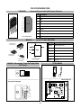
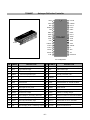
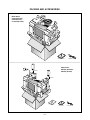
1
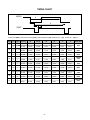
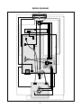
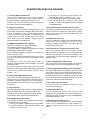
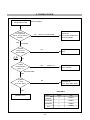
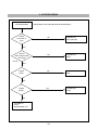
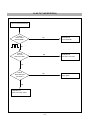
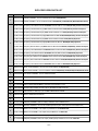
Website:http://biz.LGservice.com
E-mail:http://www.LGEservice.com/techsup.html
COLOR MONITOR
SERVICE MANUAL
CHASSIS NO. : CA-110
FACTORY MODEL: CQ771G
MODEL: S7500 (PE1165T), S7500 (PE1165),
MV7500 (PE1165U), MV7500 (PE1165),
CV7500 (PE1165U)
*(
) ID LABEL Model No.
CAUTION
BEFORE SERVICING THE UNIT,
READ THE SAFETY PRECAUTIONS IN THIS MANUAL.
Colore
alTM
CONTENTS
ADJUSTMENT ...................................................... 10
TROUBLESHOOTING GUIDE .............................. 12
EXPLODED VIEW................................................... 22
REPLACEMENT PARTS LIST ............................... 24
PIN CONFIGURATION........................................... 29
PACKING AND ACCESSORIES ............................ 31
SCHEMATIC DIAGRAM ......................................... 32
PRINTED CIRCUIT BOARD................................... 34
SPECIFICATIONS ................................................... 2
SAFETY PRECAUTIONS ........................................ 3
TIMING CHART ....................................................... 4
OPERATING INSTRUCTIONS ................................ 5
WIRING DIAGRAM ................................................. 6
BLOCK DIAGRAM ................................................... 7
DESCRIPTION OF BLOCK DIAGRAM................... ..8
SPECIFICATIONS
1. PICTURE TUBE
Size
DefIection Angle
Neck Diameter
Dot Pitch
Face Treatment
Diagonal Inch
3-2. Power Consumption
: 17 inch
: 90°
: 29.1 mm
: 0.28 mm
: Anti-Glare
: 16.06"
2. SIGNAL
2-1. Horizontal & Vertical Sync
1) Input Voltage Level : Low=0~1.2V, High=2.5~5.5V
2) Sync Polarity
: Positive or Negative
2-2. Video Input Signal
1) Voltage Level
a) Color 0, 0
b) Color 7, 0
c) Color 15, 0
2) Input Impedance
3) Video Color
4) Signal Format
: 0 ~ 0.7 Vp-p
: 0 Vp-p
: 0.467 Vp-p
: 0.7 Vp-p
: 75 Ω
: R, G, B Analog
: Refer to the Timing Chart
2-3. Signal Connector
3 row 15-pin Connector (Attached)
2-4. Scanning Frequency
Horizontal
Vertical
: 30 ~ 70 kHz
: 50 ~ 140 Hz
3. POWER SUPPLY
3-1. Power Range
AC 100~240V , 50/60Hz, 2.0A
MODE
POWER CONSUMPTION
LED COLOR
FULL POWER
less than 100 W
GREEN
STAND-BY
less than 5 W
AMBER
SUSPEND
less than 5 W
AMBER
POWER OFF
less than 5 W
OFF
4. DISPLAY AREA
4-1. Active Video Area :
• Max Image Size - 326.7 x 245.5 mm (12.86" x 9.67")
• Preset Image Size - 312 x 234 mm (12.28" x 9.21")
4-2. Display Color
: Full Colors
4-3. Display Resolution : 1280 x 1024 / 60Hz
(Non-Interlace)
4-4. Video Bandwidth
: 110 MHz
5. ENVIRONMENT
5-1. Operating Temperature: 10°C ~ 35°C (50°F ~ 95°F)
(Ambient)
5-2. Relative Humidity
: 8%~ 80%
(Non-condensing)
5-3. Altitude
: 5,000 m
6. DIMENSIONS (with TILT/SWIVEL)
Width
: 404.0 mm (15.90 inch)
Depth
: 438.5 mm (17.26 inch)
Height
: 426.0 mm (16.77 inch)
7. WEIGHT (with TILT/SWIVEL)
Net Weight
: 15.1 kg (33.29 lbs.)
Gross Weight
: 17.8 kg (39.24 lbs.)
-2-
SAFETY PRECAUTIONS
SAFETY-RELATED COMPONENT WARNING!
There are special components used in this color monitor
which are important for safety. These parts are marked
on the schematic diagram and the replacement
parts list. It is essential that these critical parts should be
replaced with the manufacturer's specified parts to
prevent X-radiation, shock, fire, or other hazards. Do not
modify the original design without obtaining written
permission from manufacturer or you will void the original
parts and labor guarantee.
CAUTION:
No modification of any circuit should be
attempted.
Service work should be performed only after
you are thoroughly familiar with all of the
following safety checks and servicing
guidelines.
SAFETY CHECK
Care should be taken while servicing this color monitor
because of the high voltage used in the deflection circuits.
These voltages are exposed in such areas as the
associated flyback and yoke circuits.
FIRE & SHOCK HAZARD
An isolation transformer must be inserted between the
color monitor and AC power line before servicing the
chassis.
• In servicing, attention must be paid to the original lead
dress specially in the high voltage circuit. If a short
circuit is found, replace all parts which have been
overheated as a result of the short circuit.
• All the protective devices must be reinstalled per the
original design.
• Soldering must be inspected for the cold solder joints,
frayed leads, damaged insulation, solder splashes, or
the sharp points. Be sure to remove all foreign
materials.
X-RADIATION
The only potential source of X-radiation is the picture tube.
However, when the high voltage circuitry is operating
properly there is no possibility of an X-radiation problem.
The basic precaution which must be exercised is keep the
high voltage at the factory recommended level; the normal
high voltage is about 25.5kV. The following steps describe
how to measure the high voltage and how to prevent Xradiation.
Note : It is important to use an accurate high voltage
meter calibrated periodically.
• To measure the high voltage, use a high impedance
high voltage meter, connect (–) to chassis and (+) to
the CDT anode cap.
• Set the brightness control to maximum point at full
white pattern.
• Measure the high voltage. The high voltage meter
should be indicated at the factory recommended level.
• If the meter indication exceeds the maximum level,
immediate service is required to prevent the possibility
of premature component failure.
• To prevent X-radiation possibility, it is essential to use
the specified picture tube.
IMPLOSION PROTECTION
All used display tubes are equipped with an integral
implosion protection system, but care should be taken to
avoid damage and scratching during installation. Use only
same type display tubes.
-3-
CAUTION:
Please use only a plastic screwdriver to protect yourself
from shock hazard during service operation.
TIMING CHART
VIDEO
B
A
E
C
D
SYNC
F
<< Dot Clock (MHz), Horizontal Frequency (kHz), Vertical Frequency (Hz), Horizontal etc... (µs), Vertical etc... (ms) >>
Mode
1
2
3
4
5
6
7
8
9
H/V
Sort
Sync
Polarity
Frequency
Total Period
(E)
Video Active
Time (A)
Blanking Time Sync Duration
(D)
(B)
Back Porch
(F)
Front Porch
(C)
H
–
37.500
26.667
20.317
6.349
2.032
3.810
0.508
V
–
75.000
13.333
12.800
0.533
0.080
0.427
0.027
H
–
31.469
31.778
25.422
6.356
3.813
1.907
0.636
V
–
59.940
16.683
15.253
1.430
0.064
1.048
0.318
H
–
43.269
23.112
17.778
5.334
1.556
2.222
1.556
V
–
85.008
11.764
11.093
0.671
0.069
0.579
0.023
H
–
31.470
31.778
25.422
6.356
3.813
1.907
0.636
V
+
70.080
14.269
12.711
1.558
0.064
1.080
0.414
H
+
46.880
21.330
16.160
5.170
1.620
3.230
0.320
V
+
75.010
13.331
12.798
0.533
0.064
0.448
0.021
H
+
53.674
18.631
14.222
4.409
1.138
2.702
0.569
V
+
85.061
11.756
11.178
0.578
0.056
0.503
0.019
H
+
60.023
16.660
13.003
3.657
1.219
2.235
0.203
V
+
75.029
13.328
12.795
0.533
0.050
0.466
0.017
H
+
68.677
14.561
10.836
3.725
1.061
2.201
0.508
V
+
84.997
11.765
11.183
0.582
0.044
0.523
0.015
H
+
63.98
15.63
11.85
3.78
1.04
2.30
0.44
V
+
60.02
16.661
16.005
0.656
0.047
0.594
0.015
-4-
Resolution
640x480
75Hz
640x480
60Hz
640x480
85Hz
720x400
70Hz
800x600
75Hz
800x600
85Hz
1024x768
75Hz
1024x768
85Hz
1280x1024
60Hz
OPERATING INSTRUCTIONS
FRONT VIEW
REAR VIEW
ColorealTM
See Front Control Panel
AC Power Socket
Power ON/OFF Button
Signal Connector
Front Control Panel
ColorealTM
4
1.
Power/LED
2
3
4.
1
Select
Launches on-screen displays, selects functions and
adjustments, and exits menus and On-Screen Display.
Controls power to the monitor.
The LED on the power button is illuminated when the
power is on.
5. Hot Key
2.
Right Adjustment
Left Adjustment
Just select
left adjustment key without OSD display.
Contrast menu display.
Moves clockwise through menu options or increases
adjustment levels.
3.
Left Adjustment
Right adjuatment
Just select
right adjustment key with OSD display.
Brightness menu display.
Moves counter-clockwise through menu options or
decreases adjustment levels.
-5-
WIRING DIAGRAM
P201
P402
P405
P501
P702
S
P701
AC
Socket
FBT
S+
T1
P902
Signal
Cable
P302
P301
P303
-6-
+
ColorealTM
-7-
TILT
COIL
DEGAUSSING
COIL
POWER INPUT
100~240VAC
(50/60Hz)
SMPS
CONTROL
(IC901)
15V
15V
I2C
6.3V
15V
80V
50V
I2C
15V
5V
H-Linearity
Correction
H-OUT
( Q706)
V-OUT
( IC601)
TDA4866
50V
400V
B+
40V
Dynamic
Focus
Circuit
FBT
( T701 )
- 160V
Vertical Blanking,
Brightness Control
15V
STEP UP
15V
X-RAY
Protection
Circuit
CUT OFF IC
(IC304)
LM2480
15V
VIDEO
MAIN AMP
(IC303)
LM2467
DC/DC Converter
D/D Feed Back
B-DRV
H-DRV
Vout 2
Vout 1
5V
VIDEO
PRE-AMP
(IC302)
LM1269
R/G/B
Drive/Contrast
Cut-Off
H/V Sync Processor
( IC701 )
TDA4857
I2C
R
G
B
OSD IC
(IC301)
NT6872
Signal
Cable
5V
Voltage
Regulating
Circuit
H/V
Sync
I2C
SCL / SDA
H/V Sync,
PWM Control
DPM
CONTROL
CIRCUIT
SMPS
TRANS
(T901)
E2PROM
(IC402)
MICOM
(IC401)
I2C CLOCK(SCL)
I2C DATA(SDA)
H-Sync Sig
V-Sync Sig
Heater ( 6.3V )
DY
CDT
15V
Auto
Beam
Limit
H.V
Dynamic Focus
Static Focus
Line
Filter
Degaussing
Circuit
6.3V
5V
POWER
80V
G1
Screen(G2)
TILT
Control
Circuit
CONTRAST
BRIGHTNESS
H POSITION
H SIZE
V POSITION
V SIZE
SPCC
TRAPEZOID
PIN BALANCE
PARALLELOGRAM
ROTATION
DEGAUSS
COLOR TEMPERADURE
FACTORY RECALL
EXIT
MENU
< OSD Control >
BLOCK DIAGRAM
DESCRIPTION OF BLOCK DIAGRAM
1. Line Filter & Associated Circuit.
This is used for suppressing noise of power input line
flowing into the monitor and/or some noise generated in
this monitor flowing out through the power input line.
That is to say, this circuit prevents interference between
the monitor and other electric appliances.
3) The Micom sets operating mode and offers the
controlled data. (H-size, H-position, V-size, ... etc.)
4) The controlled data of each mode is stored in itself.
5) User can adjust screen condition by each OSD
function. The data of the adjusted condition is stored
in EEPROM(IC402).
2. Degauss Circuit & Coil.
The degauss circuit consists of the degaussing coil, the
PTC(Positive Temperature Coefficient) thermistor(TH901),
and the relay(RL901). This circuit eliminates abnormal
color of the screen automatically by degaussing the
shadow mask in the CRT during turning on the power
switch. When you need to degauss in using the monitor,
select DEGAUSS on the OSD menu.
7. Horizontal and Vertical Synchronous Processor.
This circuit generates the horizontal drive pulse and the
vertical drive pulse by taking sync-signal from the SignalCable. This circuit consists of the TDA4857(IC701) and
the associated circuit.
3. SMPS(Switching Mode Power Supply).
This circuit is working of 90~264V AC(50/60Hz).
The operation procedure is as follows:
1) AC input voltage is rectified and smoothed by the bridge
diodes (D900) and the capacitor (C908).
2) The rectified voltage(DC) is applied to the primary coil
of the transformer(T901).
3) The control IC(IC901) generates switching pulse to turn
on and off the primary coil of the transformer (T901)
repeatedly.
4) Depending on turn ratio of the transformer, the
secondary voltages appear at the secondary coils of the
transformer(T901).
5) These secondary voltages are rectified by each
diode(D941, D942, D951, D961, D962, D971) and operate
other circuit. (horizontal and vertical deflection, video
amplifier, ...etc.)
4. Display Power Management Circuit.
This circuit control power consumption of the monitor by
detecting H and V sync signal. There are off mode. When no
horizontal or vertical sync signal input, the circuit consists of
Q941 and Q951 becomes off mode. It’s power consumption
is below 5W.
8. D/D(DC to DC) Converter.
This circuit supplies DC voltage to the horizontal deflection
output circuit by increasing DC 50V which is the
secondary voltage of the SMPS in accordance with the
input horizontal sync signal.
9. Side-Pincushion & Trapezoid Correction Cirucit.
This circuit improves the side-pincushion and the
trapezoid distortion of the screen by mixing parabola and
saw-tooth wave to output of the horizontal deflection D/D
converter which is used for the supply voltage(B + ) of the
deflection circuit.
10. Horizontal Deflection Output Circuit.
This circuit makes the horizontal deflection by supplying
the saw-tooth current to the horizontal deflection yoke.
11. High Voltage Output & FBT(Flyback Transformer).
The high voltage output circuit is used for generating pulse
wave to the primary coil of the FBT(Flyback Transformer) .
A boosted voltage(about 25.5KV) appears at the
secondary of the FBT and it is supplied to the anode of the
CDT. And there are another output voltages such as the
dynamic focus and the screen voltage(G2).
12. H-Linearity Correction Circuit.
This circuit corrects the horizontal linearity for each
horizontal sync frequency.
5. X-ray Protection.
If the high voltage of the FBT reaches up to 29kV (abnormal
state), IC401(MICOM) pin 35 Sensing from FBT directly.
Then MICOM control IC701 (Deflection controller) to stop
Horizontal drive pulse and stop Horizontal Deflection.
13. Vertical Output Circuit.
This circuit takes the vertical ramp wave from the
TDA4857(IC701) and performs the vertical deflection by
supplying the saw-tooth current from the TDA4866(IC601)
to the vertical deflection yoke.
6. Micom(Microprocessor) Circuit.
The operating procedure of Micom(Microprocessor) and
its associated circuit is as follows:
1) H and V sync signal is supplied from the signal cable.
2) The Micom(IC401) distinguishes polarity and
frequency of H and V sync.
14. Dynamic Focus Output Circuit.
This circuit takes the horizontal and the vertical parabola
waves from the TDA4857(IC701) and amplifies it to
maintain constant focus on center and corners in the
screen.
-8-
15. H & V Blanking and Brightness Control.
Blanking circuit eliminates retrace line by supplying
negative pulse to the G1 of the CRT. And Brightness
circuit is used for control of the screen brightness.
16. Image Rotation (Tilt) Circuit.
This circuit corrects the tilt of the screen by supplying the
image rotation signal to the tilt coil which is attached near
the deflection yoke of the CRT.
18. Video Pre-Amp Circuit.
This circuit amplifies the analog video signal from 0-0.7V
to 0-4V. It is operated by taking the clamp, R, G, B drive
and contrast signal from the Micom(IC401).
19. Video Output Amp Circuit.
This circuit amplifies the video signal which comes from
the video pre-amp circuit and amplified it to applied the
CRT cathode.
17. OSD Circuit
This circuit is used for performing the OSD(On-ScreenDisplay) function.
When a user selects the OSD Select/Adjustment control,
the adjustment status displays on the screen.
-9-
ADJUSTMENT
GENERAL INFORMATION
7) Adjust tilt as arrow keys to be the best condition.
8) DIST. ADJ. → BALANCE command.
9) Adjust parallelogram as arrow keys to be the best
condition.
10) Adjust balance of pin-balance as arrow keys to be
the best condition.
11) DIST. ADJ. → FOS. ADJ command.
12) Adjust V-SIZE as arrow keys to 234±2mm.
13) Adjust V-POSITION as arrow keys to center of the
screen.
14) Adjust H-SIZE as arrow keys to 312±2mm.
15) Adjust H-POSITION as arrow keys to center of the
screen.
16) Adjust S-PCC (Side-Pincushion) as arrow keys to be
the best condition.
17) Adjust TRAPEZOID as arrow keys to be the best
condition.
18) Save of the Mode 1.
19) Display from Mode 1 to 8 and repeat above from
number 12) to 19)
20) PRESET EXIT → Y (Yes) command.
All adjustment are thoroughly checked and corrected
when the monitor leaves the factory, but sometimes
several adjustments may be required.
Adjustment should be following procedure and after
warming up for a minimum of 30 minutes.
• Alignment appliances and tools.
- IBM compatible PC.
- Programmable Signal Generator.
(eg. VG-819 made by Astrodesign Co.)
- EPROM or EEPROM with saved each mode data.
- Alignment Adaptor and Software.
- Digital Voltmeter.
- White Balance Meter.
- Luminance Meter.
- High-voltage Meter.
AUTOMATIC AND MANUAL DEGAUSSING
The degaussing coil is mounted around the CDT so that
automatic degaussing when turn on the monitor. But a
monitor is moved or faced in a different direction, become
poor color purity cause of CDT magnetized, then press
DEGAUSS on the OSD menu.
ADJUSTMENT PROCEDURE & METHOD
- Install the cable for adjustment such as Figure 1and run
the alignment program on the DOS for IBM compatible PC.
- Set external Brightness and Contrast volume to max position.
1. Adjustment for B+ Voltage.
1) Display cross hatch pattern at Mode 8.
2) Check C999 (+) voltage to 50± 0.5Vdc.
2. Adjustment for High-Voltage.
1) Display cross hatch pattern at Mode 8.
2) DIST.ADJ→CTRL PWM → High Voltage Command.
3) Adjust High Voltage to 25.5kV±0.3 kVdc.
4) Press Enter Key.
3. Adjustment for Factory Mode (Preset Mode).
1) Display cross hatch pattern at Mode 1.
2) Run alignment program for CQ771G on the IBM
compatible PC.
3) EEPROM → ALL CLEAR → Y(Yes) command.
<Caution> Do not run this procedure unless the
EEPROM is changed. All data in EEPROM (mode
data and color data) will be erased.
4) Power button of the monitor turn off → turn on.
5) COMMAND→PRESET START→Y(Yes) command.
6) DIST. ADJ. → CTRL PWM → TILT command.
4. Adjustment for White Balance and Luminance.
1) Set the White Balance Meter.
2) Press the DEGAUSS on the OSD menu for
demagnetization of the CDT.
3) COLOR ADJ. → LUMINANCE command of the
alignment program.
4) Set Brightness and Contrast to Max position.
5) Display color 0,0 pattern at Mode 8.
6) COLOR ADJ.→ BIAS ADJ.→ COLOR No. → 1
command of the alignment program.
7) Check whether green color or not at R-BIAS and GBIAS to min position and B-BIAS to 127(7F) and
Sub-Brightness to 177(B1) position. Adjust G2
(screen) command to 0.4 ± 0.05FL of the raster
luminance.
8) Adjust R-BIAS and G-BIAS command to x=0.283 ±
0.005 and y=0.298 ±0.005 on the White Balance
Meter with PC arrow keys.
9) Adjust SUB-Brightness command to 0.5±0.1FL of the
raster luminance.
10) Adjust repeat number 8).
11) After push the “ENTER” key.
11-1) COMMAND → PRESET START → Y(Yes) command.
12) Display color 15,0 full white pattern at Mode 8.
13) DRIVE ADJ.→ No 1. command.
- 10 -
14) Set Brightness is cut-off(0.06FL) and Contrast to
Max position.
15) Set SUB-CONTRAST Max 127(7F) (decimal) position.
16) Set B-DRIVE to 90(5A); LG CDT at DRIVE of the
alignment program. (TECO CDT: B-DRIVE 100(64))
17-1) Adjust R-DRIVE and G-DRIVE command to white
balance x=0.283±0.003 and y=0.298±0.003 at FullWhite on the White Balance Meter with PC arrow keys.
17-2) Display color 15,0 window pattern 5Box 50x50mm at
mode 8.
18) Adjust SUB-CONTRAST command to 50±1FL at
B/Raster 0.06FL.
19) Display color 15,0 full white patten at Mode 8.
20) Set Brightness and Contrast to Max position.
21) COLOR ADJ. → LUMINANCE → ABL command.
22) Adjust ABL to 33±1FL of the luminance at B/Raster 0.06FL.
23) After push the “ENTER” key, and “COMMAND →
PRESET EXIT → Y(Yes)” command.
24) Exit from the program.
5. Input EDID Data.
1) Display color 15,0 cross hatch pattern at Mode 8.
2) EEPROM → Write EDID command and confirm
“EDID Write OK!!” message of monitor.
3) Exit from the alignment program.
4) Power switch OFF/ON for EDID data save.
6. Adjustment for Focus.
1) Set the Brightness and Contrast to max position.
2) Display cross hatch with quadrant text pattern in full
screen at Mode 8.
3) Adjust two Focus control on the FBT that focus
should be the best condition.
- 11 -
TROUBLESHOOTING GUIDE
1. NO POWER
NO POWER
(POWER INDICATOR OFF)
CHECK
FUSE OK?
NO
TROUBLE IN FUSE
(F901)
NO
TROUBLE IN
D900
NO
TROUBLE IN
IC901
NO
TROUBLE IN
D941, D942, D951,
D961, D962, D971
YES
CHECK
C908 VOLTAGE?
(AC120V: 160VDC,
AC220V: 304VDC)
YES
CHECK
IC901 PIN 6
WAVEFORM
(SQUARE WAVE
COMES OUT?)
YES
CHECK
D941, D942, D951, D961,
D962, D971
VOLTAGE?
YES
TROUBLE IN
Q903, Q952,
Q951, Q942, Q941
- 12 -
2. NO CHARACTER
NO CHARACTER
CHECK
IC302
PIN 9(5V) ?
NO
TROUBLE IN
P302 5V LINE
YES
CHECK
IC302 PIN 5, 6, 7?
NO
TROUBLE IN
PC SIGNAL,
P301 SIGNAL CABLE
YES
CHECK
IC302 PIN 20, 19, 18 ?
NO
TROUBLE IN
IC302
NO
TROUBLE IN
P303 12V LINE/
80V LINE
NO
TROUBLE IN IC303
YES
CHECK
IC303 PIN 4 (80V)
PIN 8 (12V) ?
YES
CHECK
IC303
PIN 1, 2, 3 ?
YES
CHECK
R, G, B CATHODE
VOLTAGE?
NO
YES
TROUBLE IN
CRT SOCKET
- 13 -
TROUBLE IN
R341~R343,
R331~R333, L311~L313,
D307~D312
3. NO RASTER
NO VIDEO
(POWER INDICATOR ON)
CHECK
POWER INDICATOR
GREEN or AMBER?
AMBER
DPM MODE
(NO H and/or V SYNC)
GREEN
CHECK
D712 ANODE
(-157V)?
NO
TROUBLE IN
D712
NO
TROUBLE IN
Q799
NO
TROUBLE IN
D941, Q942, Q941
YES
CHECK
G1 VOLTAGE?
(-55V~-150V)
YES
CHECK
CDT HEAT
VOLTAGE? (6.3V)
YES
TROUBLE IN
CDT
- 14 -
4. NO HORIZONTAL DEFLECTION
NO H-DEFLECTION
(ONE VERTICAL LINE)
CHECK
Q706?
NO
TROUBLE IN
Q706
NO
TROUBLE IN
50V LINE
NO
TROUBLE IN
Q719, Q720, D710
NO
TROUBLE IN
Q701
YES
CHECK
B+ VOLTAGE
(50V)?
YES
CHECK
T701(FBT) PIN 2
(31KHZ 60V,
69KHZ 140V) ?
YES
CHECK
Q701 COLLECTOR
WAVEFORM?
YES
0V
T
TROUBLE IN
T701, P701
- 15 -
5. TROUBLE IN H-LINEARITY
UNBALANCED OF H-LIN.
CHECK
IC401
PIN 5, 6, 7 ?
NO
TROUBLE IN
IC401 (MICOM)
NO
TROUBLE IN
Q711 ~ Q716
NO
TROUBLE IN
L703
YES
CHECK
Q711~Q716?
YES
CHECK
L703?
Cs SIGNAL TABLE
YES
TROUBLE IN
C722, C723, C726, C729
HORIZONTAL
FREQUENCY(fH)
30K
34K
39K
44K
48K
52K
58K
62K
66K
- 16 -
~
~
~
~
~
~
~
~
~
33.9K
38.9K
43.9K
47.9K
51.9K
57.9K
61.9K
65.9K
70K
Cs1
Cs2
Cs3
Cs0
L
L
H
H
H
H
H
H
H
L
H
L
L
L
H
H
H
H
L
L
L
H
H
L
L
H
H
255
155
130
100
85
70
60
60
30
6. NO VERTICAL DEFLECTION
NO V-DEFLECTION
(ONE HORIZONTAL LINE)
CHECK
IC601 PIN 3
(15V)?
NO
TROUBLE IN
R603 15V LINE
YES
CHECK
IC601 PIN 7
(40V)?
NO
TROUBLE IN
HIGH-VOLTAGE OUT
CIRCUIT(FBT),
D721, R606
YES
CHECK
IC701 PIN 12, 13?
NO
3V
YES
TROUBLE IN
IC601, V-CIRCUIT
- 17 -
TROUBLE IN
IC701
7. TROUBLE IN OSD
NO OSD
(ENTER BUTTON MUST BE PRESSED.)
CHECK
IC301 B+
(5V) ?
NO
DC 5V
TROUBLE IN
5V LINE
YES
CHECK
IC301 PIN 5, 10
WAVEFORM?
NO
TROUBLE IN
IC601 PIN8 (V-FBP),
T701 40V LINE (H-FBP)
Pin 10
5V
Pin 5
YES
CHECK
IC301 PIN 12
WAVEFORM ?
NO
TROUBLE IN
IC302, IC301
NO
TROUBLE IN
IC301, IC302
H+V
5V
YES
CHECK
IC301 PIN 13, 14, 15 ?
H+V
5V
YES
TROUBLE IN
OSD PERIPHERAL
CIRCUIT
- 18 -
8. TROUBLE IN DPM
OFF MODE FAILURE
CHECK
IC401 (MICOM)
PIN 31, 32 (H/V INPUT)
SIGNAL?
YES
(NO OFF MODE.)
NO
CHECK PC,
(PC IS NOT GOING INTO
DPM OFF MODE)
INPUT H/V SYNC SIGNAL
H/V SYNC
CHECK
IC401 PIN 13
WAVEFORM?
TROUBLE IN
X401
NO
5V
YES
24MHz
CHECK
IC401 (MICOM)
PIN 2, 3 ?
NO
(DPMF: 0V)
TROUBLE IN
IC401 (MICOM)
SEE DPM TABLE
YES
CHECK
B+ LINE
(6.3V,15V, 80V) ?
NO
TROUBLE IN
Q941, Q942, Q951, Q952,
YES
DPM TABLE
TROUBLE IN PC
Item
DPMF
LED
NORMAL
H
GREEN
STAND-BY
L
AMBER
SUSPEND
L
AMBER
OFF
L
AMBER
Mode
- 19 -
9. NO DEGAUSSING
NO DEGAUSSING
CHECK
IC401 PIN 19
(0V)?
(DEGAUSS ON THE OSD MENU MUST BE PRESSED.)
NO
TROUBLE IN
IC401 (MICOM)
NO
TROUBLE IN
Q953
NO
TROUBLE IN
P902
YES
CHECK
Q953 COLLECTOR
VOLTAGE?
DC 15V
YES
CHECK
P902 ?
YES
CHECK
RL901?
NO
YES
TROUBLE IN
TH901,
DEGAUSSING COIL
- 20 -
TROUBLE IN
RL901
10. NO TILT (NO ROTATION )
NO TILT (NO ROTATION)
CHECK
IC401 PIN21
WAVE FORM ?
NO
TROUBLE IN
IC401 (MICOM)
YES
CHECK
15V LINE
AND 6.3V LINE ?
NO
TROUBLE IN
15V LINE, 6.3V LINE
NO
TROUBLE IN
Q501~Q503
YES
CHECK
Q503 EMITTER
VOLTAGE ?
YES
TROUBLE IN
P501, TILT COIL, D521
- 21 -
- 22 -
2
1
5
A
12
6
B
11
7
10
9
EXPLODED VIEW
11
8
4
13
3
EXPLODED VIEW PARTS LIST
Ref. No.
Description
Part No.
3091TKC078A CABINET ASSEMBLY, CQ771G COMPAQ C072 TCO99 S7500 (PE1165T)
1
3091TKC078B CABINET ASSEMBLY, CQ771G COMPAQ 072 MPR-II S7500(PE1165), CV7500(PE1165U), MV7500(PE1165U, PE1165)
6318L17006A CDT(CIRC), M41LFQ803X 55NLUD LG-PHILIPS 70KHZ 29.1MM FST TCO S7500 (PE1165T); Northern Hemisphere
6318E17002A CDT(CIRC), M41LRS102XX112 (Z) TECO 70KHZ 29.1MM FST MPR-II S7500 (PE1165); Northern Hemisphere
6318E17002B CDT(CIRC), M41LRS102XX112 (EZ) TECO 70KHZ 29.1MM FST TCO S7500 (PE1165T); Northern Hemisphere
6318E17002C CDT(CIRC), M41LRS102XX112 (NS)(Z) TECO 70KHZ 29.1MM CV7500, MV7500(PE1165U); Northern Hemisphere
6318E17002D CDT(CIRC), M41LRS102XX112 (QZ) TECO 70KHZ 29.1MM FST MPR-II S7500 (PE1165); Equatorial
2
6318E17002E CDT(CIRC), M41LRS102XX112 (NS)(QZ) TECO 70KHZ 29.1MM FST- MV7500(PE1165U); Equatorial
6318E17002F CDT(CIRC), M41LRS102XX112 (SZ) TECO 70KHZ 29.1MM FST MPR-II MV7500, S7500(PE1165); Southern Hemisphere
6318L17005A CDT(CIRC), M41LFQ803X55NLAA LG-PHILIPS 70KHZ 29.1MM FST MPR-II S7500(PE1165); Northern Hemisphere
6318L17005B CDT(CIRC), M41LFQ803X 55QLAA LG-PHILIPS 70KHZ 29.1MM FST MPR-II S7500(PE1165); Equatorial
6318L17005C CDT(CIRC), M41LFQ803X 55SLAA LG-PHILIPS 70KHZ 29.1MM FST MPR-II S7500, MV7500(PE1165); Southern Hemisphere
6318L17007A CDT(CIRC), M41LFQ503X 55NLLD LG-PHILIPS 70KHZ 29.1MM FST CV7500, MV7500(PE1165U); Northern Hemisphere
6318L17007B CDT(CIRC), M41LFQ503X 55QLLD LG-PHILIPS 70KHZ 29.1MM FST MV7500(PE1165U);Equatorial
3809TKC044A BACK COVER ASSEMBLY, CQ771G C043 TCO99 COMPAQ S7500 (PE1165T)
3
3809TKC044B BACK COVER ASSEMBLY, CQ771G C043 MPR-II COMPAQ S7500(PE1165), CV7500(PE1165U), MV7500(PE1165U, PE1165)
4
5
3043TKK093C TILT SWIVEL ASSEMBLY, CQ771G T062 B054 HF350U
339-002K
SCREW ASSEMBLY, TAPTITE P TYPE D5.0 L25.0 MSWR/FZMY
6
6140TC3004A COIL,DEGAUSSING, 1090MM 16.5OHM 0.4MM 110T 17" WITH EARTH
7
6174T11003E FBT (FLY BACK TRANSFORMER), 1054A,CB777G LG-PHILIPS 17" T701
8
6620TKB002B SOCKET(CIRC),POWER, SA-4S HUA JIE AC UNIVERSAL 3PIN BLACK SC901
9
6850TA9004C CABLE,D-SUB, UL 2990-9C(7.5) AT 1870MM COMPAQ BK EQ770G DM
10
4950TKS196A METAL, FRAME BOTTOM CQ77XG
11
4810TKK195A BRACKET, CQ77XG SUPPORTER CDT
12
6871TST292B PWB(PCB) ASSEMBLY,SUB, CQ771G(NT) CONTROL TOTAL COMPAQ CA-110
13
6401TZZ022B SPEAKER ASSEMBLY, CQ771G FOR COMPAQ(259139-001) SPK ASSY(L/R) BLACK MV7500(PE1165U)
3313T17258B MAIN TOTAL ASSEMBLY, CQ771G(NT,LG) COMPAQ CA-110 LG-PHILIPS CDT
A
3313T17258D MAIN TOTAL ASSEMBLY, CQ771G(NT,TECO) COMPAQ CA-110 TECO CDT
6871TMT300B PWB(PCB) ASSEMBLY,MAIN, CQ771G(NT) KXLGMT(LG) COMPAQ CA-110 TOTAL LG-PHILIPS CDT
B
6871TMT300D PWB(PCB) ASSEMBLY,MAIN, CQ771G(NT) KXLBNT(TECO) COMPAQ CA-110 TOTAL TECO CDT
- 23 -
REPLACEMENT PARTS LIST
CAUTION: BEFORE REPLACING ANY OF THESE COMPONENTS,
READ CAREFULLY THE SAFETY PRECAUTIONS IN THIS MANUAL.
* NOTE : S SAFETY Mark
AL ALTERNATIVE PARTS
*S *AL LOC. NO.
PART NO.
DATE: 2002. 04. 15.
DESCRIPTION / SPECIFICATION
*S *AL LOC. NO.
PART NO.
DATE: 2002. 04. 15.
DESCRIPTION / SPECIFICATION
0CK1040K945
0CN1040K949
0CE476CF638
0CK1040K945
0CC1800K415
0CC1800K415
0CK1010K515
0CK1010K515
0CK1040K945
0CC5600K415
0CK1010K515
0CK1040K945
0CK1040K945
0CK1040K945
0CK1040K945
0CE106CF638
0CE225CK638
0CE477EH618
181-288B
0CE476CK638
181-288T
0CK1020W515
0CQ5621N419
0CZZTFT001M
0CZZTFT001Z
0CQ8221N519
0CE476CF638
0CZZTFT001Z
0CZZTFT002B
0CE227CH638
181-288P
0CK1040K945
0CQ5621N419
0CE475CK638
0CQ1031N419
0CK2710K515
0CE105CN638
181-288D
0CZZTAB001A
0CK22101515
181-477M
181-303G
181-305C
181-305E
0CN1040K949
181-482H
0CN1040K949
0CQ5621N419
181-305L
0CN1040K949
0CBZTBU004H
0CBZTBU004G
0CQ1031N419
0CBZTBU003H
0.1UF 50V Z F TR
0.1M 50V Z F TA52
47UF SHL,SD 16V M FM5 TP 5
0.1UF 50V Z F TR
18P 50V J NPO TP
18P 50V J NPO TP
100PF 50V K B TR
100PF 50V K B TR
0.1UF 50V Z F TR
56P 50V J NP0 TP
100PF 50V K B TR
0.1UF 50V Z F TR
0.1UF 50V Z F TR
0.1UF 50V Z F TR
0.1UF 50V Z F TR
10UF SHL,SD 16V M FM5 TP 5
2.2UF SHL,SD 50V M FM5 TP 5
470UF KMG 25V M FL TP 5
MKT 100V 104JTR PHS26104
47UF SHL,SD 50V M FM5 TP 5
MKT 100V 223KTR PHS85223
1000P 500V K B TS
5600P 100V J POLY NI TP
ECQB1H103JM3 103J 50V TP5.0 MA
ECQB1H104JM3 104J 50V TP5.0 MA
0.0082U 100V K POLY NI TP
47UF SHL,SD 16V M FM5 TP 5
ECQB1H104JM3 104J 50V TP5.0 MA
ECQV1H154JZ3 154J 50V TP5.0 MA
220UF SHL,SD 25V M FM5 TP 5
MKT 100V 153JTR PHS86153
0.1UF 50V Z F TR
5600P 100V J POLY NI TP
4.7UF SHL,SD 50V M FM5 TP 5
0.01U 100V J POLY NI TP
270P 50V K B TS
1UF SHL,SD 100V M FM5 TP 5
MKT 100V 473JTR PHS26473
SM-BP(P)/BP 10UF 50V 13*25 BK5
220P 1KV K B TP5
822J 19.5*12.0*7.0*7.5 250V J
334J 31.0*22.0*15.0*20.0 250V
154J 19.0*14.0*8.0*10.0 250V J LPD CDT
MPP 250V 224J S=10.0 TECO CDT
0.1M 50V Z F TA52
364J 18.0*19.0*12.0*7.5 250V J
0.1M 50V Z F TA52
5600P 100V J POLY NI TP
684J 26.0*19.0*12.5*15.0 250V
0.1M 50V Z F TA52
5600PF D 2.5KV H M/PP NI FM20 LPD CDT
622J 29.0*21.0*10.0*20.0 2.5KV TECO CDT
0.01U 100V J POLY NI TP
362J 20.0*12.0*7.0*10.0 800V J
CAPACITORS
C201
C301
C302
C303
C304
C305
C306
C307
C308
C309
C310
C311
C312
C313
C314
C315
C316
C316
C317
C318
C319
C320
C321
C322
C323
C324
C325
C326
C327
C328
C329
C330
C331
C332
C333
C334
C335
C336
C337
C338
C339
C340
C341
C342
C343
C346
C351
C352
C353
C354
C355
C356
C358
0CN1040K949
181-288N
0CE107CF638
0CK1040K945
181-288N
0CE107CF638
181-288N
0CN5610K519
0CN1040K949
0CK1040K945
181-288B
0CK1040K945
0CN1040K949
0CK1040K945
0CC4700W405
0CE476CF638
0CK1010W515
0CK1020W515
0CN1040K949
0CK1040K945
0CN1040K949
0CK1040K945
0CE475CK638
0CN6810K519
0CE476CF638
0CK1040K945
181-288D
0CE106CN638
181-288B
0CE106CN638
181-288B
181-288B
181-288G
181-288G
181-288G
181-288B
181-288B
181-288E
0CK5610K515
0CK10302940
0CK4710W515
0CK1040K945
0CK10302940
0CE106CK638
0CC1000W105
0CK10302940
0CC0400K115
0CC0400K115
0CC0400K115
0CC0400K115
0CC0400K115
0CC0400K115
0CK8210K515
C372
C401
C402
C403
C404
C405
C406
C407
C408
C409
C410
C411
C412
C413
C414
C501
C599
C601
C602
C603
C604
C605
C701
C702
C703
C704
C705
C706
C707
C708
C709
C710
C711
C712
C713
C716
C717
C718
C719
C720
C721
C722
C723
C723
C724
C726
C727
C728
C729
C730
C731
C731
C732
C733
0.1M 50V Z F TA52
MKT 100V 103JTR PHS86103
100UF SHL,SD 16V M FM5 TP 5
0.1UF 50V Z F TR
MKT 100V 103JTR PHS86103
100UF SHL,SD 16V M FM5 TP 5
MKT 100V 103JTR PHS86103
560P 50V K B TA52
0.1M 50V Z F TA52
0.1UF 50V Z F TR
MKT 100V 104JTR PHS26104
0.1UF 50V Z F TR
0.1M 50V Z F TA52
0.1UF 50V Z F TR
47PF 500V J SL TP
47UF SHL,SD 16V M FM5 TP 5
100P 500V K B TS LPD CDT
1000P 500V K B TS TECO CDT
0.1M 50V Z F TA52
0.1UF 50V Z F TR
0.1M 50V Z F TA52
0.1UF 50V Z F TR
4.7UF SHL,SD 50V M FM5 TP 5
680P 50V K B TA52
47UF SHL,SD 16V M FM5 TP 5
0.1UF 50V Z F TR
MKT 100V 473JTR PHS26473
10UF SHL,SD 100V M FM5 TP 5
MKT 100V 104JTR PHS26104
10UF SHL,SD 100V M FM5 TP 5
MKT 100V 104JTR PHS26104
MKT 100V 104JTR PHS26104
MKT 100V 334JTR PHS26334
MKT 100V 334JTR PHS26334
MKT 100V 334JTR PHS26334
MKT 100V 104JTR PHS26104
MKT 100V 104JTR PHS26104
MKT 100V 474JTR PHS 26474
560P 50V K B TS
0.01M 2KV Z F S
470P 500V K B TS
0.1UF 50V Z F TR
0.01M 2KV Z F S
10UF SHL,SD 50V M FM5 TP 5
10PF 500V D SL TR
0.01M 2KV Z F S
4P
50V D NP0 TS
4P
50V D NP0 TS
4P
50V D NP0 TS
4P
50V D NP0 TS
4P
50V D NP0 TS
4P
50V D NP0 TS
820P 50V K B TS
- 24 -
*S *AL LOC. NO.
PART NO.
DATE: 2002. 04. 15.
DESCRIPTION / SPECIFICATION
*S *AL LOC. NO.
PART NO.
DATE: 2002. 04. 15.
DESCRIPTION / SPECIFICATION
DIODEs
C737
C738
C739
C740
C741
C742
C743
C744
C745
C746
C747
C748
C749
C750
C751
C752
C754
C755
C767
C771
C773
C774
C775
C781
C801
C802
C805
C810
C821
C822
C901
C902
C903
C904
C905
C906
C908
C909
C910
C911
C912
C913
C914
C914
C915
C915
C941
C942
C943
C944
C944
C945
C945
C951
C952
C953
C954
C971
C999
0CKZTTA002N
0CKZTTA003D
0CE226CK638
0CE227EL630
0CZZTFT002B
0CZZTFT001R
0CK3310W515
0CE107CP630
0CK5610W515
0CK33101515
0CK3320W515
0CZZTFT002B
0CE2256R638
0CK1040K945
181-288N
0CQ4721N419
0CC4700W405
181-288B
0CK10301510
0CK10301510
0CE107CH638
181-288B
0CK2210K515
0CK1030K945
0CK1040K945
0CE106CK638
0CE106CK638
0CE106CK638
0CK1040K945
0CN1040K949
0CBZTBU002B
0CBZTBU002A
0CKZTTA003A
0CKZTTA003A
0CE476EK638
0CK3320K515
181-124R
181-304T
0CK33101515
0CQ1021N419
0CKZTTA003D
0CKZTTA003D
0CKZTBU003C
0CKZTBU003C
0CKZTBU003C
0CKZTBU003C
0CE108EF630
0CE107CF638
0CKZTTA002A
0CKZTBU003C
0CKZTBU003C
0CKZTBU003C
0CKZTBU003C
0CE228EH630
0CE227CH638
0CE107CF638
0CE108ED618
0CE476EN618
0CE337EN630
100PF K 2KV R TP5.0
SC SAMWHA 250V 1000F M TAPING
22UF SHL,SD 50V M FM5 TP 5
220UF KMG 63V M FM5 BULK
ECQV1H154JZ3 154J 50V TP5.0 MA
ECQB1H223JM3 223J 50V TP5.0 MA
330P 500V K B TS
100UF SHL 160V M FM5 BULK
560P 500V K B TS
330P 1KV K B TS
3300P 500V K B TS
ECQV1H154JZ3 154J 50V TP5.0 MA
2.2000UF SMS 250V M FM5 TP5
0.1UF 50V Z F TR
MKT 100V 103JTR PHS86103
0.0047U 100V J POLY NI TP5
47PF 500V J SL TP
MKT 100V 104JTR PHS26104
0.01M 1KV K B S
0.01M 1KV K B S
100UF SHL,SD 25V M FM5 TP 5
MKT 100V 104JTR PHS26104
220P 50V K B TS
0.01UF 50V Z F TR
0.1UF 50V Z F TR
10UF SHL,SD 50V M FM5 TP 5
10UF SHL,SD 50V M FM5 TP 5
10UF SHL,SD 50V M FM5 TP 5
0.1UF 50V Z F TR
0.1M 50V Z F TA52
BULK PCX2 335 474K
BULK PCX2 335 224K
SC E 222M 10.0FF7 250V TP7.5 S
SC E 222M 10.0FF7 250V TP7.5 S
47UF KMG 50V M FM5 TP 5
3300P 50V K B TS
220UF SMG(25.4*40) 400V M VNSN
273J 19.5*14.0*8.5*10.0 400V J
330P 1KV K B TS
1000P 100V J POLY NI TP
SC SAMWHA 250V 1000F M TAPING
SC SAMWHA 250V 1000F M TAPING
SC E 472M 14.0BW7 250V BK7.5 S
SC E 472M 14.0BW7 250V BK7.5 S
SC E 472M 14.0BW7 250V BK7.5 S
SC E 472M 14.0BW7 250V BK7.5 S
1000UF KMG 16V M FM5 BULK
100UF SHL,SD 16V M FM5 TP 5
220PF K 1KV R TP5.0
SC E 472M 14.0BW7 250V BK7.5 S
SC E 472M 14.0BW7 250V BK7.5 S
SC E 472M 14.0BW7 250V BK7.5 S
SC E 472M 14.0BW7 250V BK7.5 S
2200UF KMG 25V M FM5 BULK
220UF SHL,SD 25V M FM5 TP 5
100UF SHL,SD 16V M FM5 TP 5
1000UF KMG 10V M FL TP 5
47UF KMG 100V M FL TP 5
330UF KMG 100V M FM5 BULK
D201
D301
D302
D303
D304
D305
D306
D307
D308
D309
D310
D311
D312
D313
D314
D315
D316
D317
D401
D402
D403
D512
D701
D702
D704
D705
D706
D709
D710
D711
D712
D714
D715
D716
D717
D718
D719
D720
D721
D723
D724
D725
D730
D735
D741
D767
D768
D801
D802
D821
D900
D902
D903
D905
D906
D908
D941
D942
D951
D952
D961
- 25 -
0DL305029BA
0DS141489AB
0DS141489AB
0DS141489AB
0DS141489AB
0DS141489AB
0DS141489AB
0DS124409AA
0DS124409AA
0DS124409AA
0DS124409AA
0DS124409AA
0DS124409AA
0DS124409AA
0DS124409AA
0DS124409AA
6210TCE003J
0DS141489AB
0DS141489AB
0DD140009AA
0DRGS00149A
0DS141489AB
0DS141489AB
0DS124409AA
0IPMGSK004A
0DR140059DA
0DR359150AA
0DR400409AB
0DR320400AA
0DS141489AB
0DR100009CA
0DS141489AB
0DS141489AB
0DR140059DA
0DR140059DA
0DR140059DA
0DR100009DA
0DS141489AB
0DR100009CA
0DS141489AB
0DR140059DA
0DS124409AA
971-0016
0DR140059DA
0DS141489AB
0DR100009DA
971-0016
0DS141489AB
0DS141489AB
0DS141489AB
0DD360000DA
0DR153979AA
0DR100009CA
0DD400709CB
0DS141489AB
0DS141489AB
0DRGS00330A
0DRGS00089A
0DR540400AA
0DS141489AB
0DRGS00090A
LTL-305DJ-0C2 TP LITEON GREEN/
1N4148 TP GRANDE DO-34 500MW 1
1N4148 TP GRANDE DO-34 500MW 1
1N4148 TP GRANDE DO-34 500MW 1
1N4148 TP GRANDE DO-34 500MW 1
1N4148 TP GRANDE DO-34 500MW 1
1N4148 TP GRANDE DO-34 500MW 1
1SS244 TP ROHM KOREA
1SS244 TP ROHM KOREA
1SS244 TP ROHM KOREA
1SS244 TP ROHM KOREA
1SS244 TP ROHM KOREA
1SS244 TP ROHM KOREA
1SS244 TP ROHM KOREA
1SS244 TP ROHM KOREA
1SS244 TP ROHM KOREA
BAS2550T BO SUNG 2550MM AXIAL5
1N4148 TP GRANDE DO-34 500MW 1
1N4148 TP GRANDE DO-34 500MW 1
EK14 V(1) TP SANKEN E/EO-TMD 4
1N5817 GENERAL SEMICONDUCTOR T
1N4148 TP GRANDE DO-34 500MW 1
1N4148 TP GRANDE DO-34 500MW 1
1SS244 TP ROHM KOREA
STR-G8644D(LF1140) SANKEN 5P S
1N4005TB52 TP LITEON DO41 600V
BY359F-1500 BK PHILIPS SOD10
UF4004 TP G.I DO204AL 400V 1A
S3L20U-4004P15 BK SHINDENGEN N
1N4148 TP GRANDE DO-34 500MW 1
RGP10G TP GULF SEMICONDUCTOR L
1N4148 TP GRANDE DO-34 500MW 1
1N4148 TP GRANDE DO-34 500MW 1
1N4005TB52 TP LITEON DO41 600V
1N4005TB52 TP LITEON DO41 600V
1N4005TB52 TP LITEON DO41 600V
RGP10J TP GULF SEMICONDUCTOR L
1N4148 TP GRANDE DO-34 500MW 1
RGP10G TP GULF SEMICONDUCTOR L
1N4148 TP GRANDE DO-34 500MW 1
1N4005TB52 TP LITEON DO41 600V
1SS244 TP ROHM KOREA
TIN HDC 0.60H
1N4005TB52 TP LITEON DO41 600V
1N4148 TP GRANDE DO-34 500MW 1
RGP10J TP GULF SEMICONDUCTOR L
TIN HDC 0.60H
1N4148 TP GRANDE DO-34 500MW 1
1N4148 TP GRANDE DO-34 500MW 1
1N4148 TP GRANDE DO-34 500MW 1
D3SBA60 BK SHINDENGEN 600V 2
1N5397GP TP G.I DO201AD 600V 1
RGP10G TP GULF SEMICONDUCTOR L
UF4007 TP G.I DO204AL 1000V 1
1N4148 TP GRANDE DO-34 500MW 1
1N4148 TP GRANDE DO-34 500MW 1
RGP15D(L-5700) GENERAL SEMICON
SB1H100 GENERAL SEMICONDUCTOR
UF5404L BK G.I DO201AD 400V 3A
1N4148 TP GRANDE DO-34 500MW 1
31GF6L-5701 GENERAL SEMICONDUC
*S *AL LOC. NO.
D962
D971
ZD201
ZD202
ZD203
ZD301
ZD302
ZD401
ZD402
ZD404
ZD405
ZD406
ZD407
ZD410
ZD411
ZD701
ZD702
ZD705
ZD901
ZD902
PART NO.
DATE: 2002. 04. 15.
DESCRIPTION / SPECIFICATION
0DRGS00090A
0DR100009DA
0DZ560009AG
0DZ560009AG
0DZ560009AG
0DZ560009AG
0DZ560009AG
0DZ560009AG
0DZ560009AG
0DZ560009AG
0DZ560009AG
0DZ560009AG
0DZ560009AG
0DZ560009AG
0DZ560009AG
0DZ110009CF
0DZ560009AG
0DZ510009BE
0DZ560009AG
0DZ510009BE
31GF6L-5701 GENERAL SEMICONDUC
RGP10J TP GULF SEMICONDUCTOR L
GDZJ5.6B TP GRANDE DO-34 500MW
GDZJ5.6B TP GRANDE DO-34 500MW
GDZJ5.6B TP GRANDE DO-34 500MW
GDZJ5.6B TP GRANDE DO-34 500MW
GDZJ5.6B TP GRANDE DO-34 500MW
GDZJ5.6B TP GRANDE DO-34 500MW
GDZJ5.6B TP GRANDE DO-34 500MW
GDZJ5.6B TP GRANDE DO-34 500MW
GDZJ5.6B TP GRANDE DO-34 500MW
GDZJ5.6B TP GRANDE DO-34 500MW
GDZJ5.6B TP GRANDE DO-34 500MW
GDZJ5.6B TP GRANDE DO-34 500MW
GDZJ5.6B TP GRANDE DO-34 500MW
GDZJ11B TP GRANDE DO34 0.5W 11
GDZJ5.6B TP GRANDE DO-34 500MW
GDZ5.1B TP GRANDE DO34 500MW 5
GDZJ5.6B TP GRANDE DO-34 500MW
GDZ5.1B TP GRANDE DO34 500MW 5
0IPRPNV008A
0IPRPNS003A
0IPRPNS004A
0IPRPNS005A
0IZZTSZ176A
0ISG240860A
0IKE704200H
0IPH486600C
0IPRPPH008A
0IPMGSK004A
NT68272-20018 NOVATEK 16,DIP S
LM1269NA NATIONAL SEMICONDUCTO
LM2467TA NATIONAL SEMICONDUCTO
LM2480NA NATIONAL SEMICONDUCTO
SS 42PIN ST COMPAQ 4KEY CA-110
M24C08-BN6 8DIP BK 8K SERIAL I
KIA7042AP TO-92 TP 4.2 VOLT.
TDA4866J 9P ST VERTICAL OUTPUT
TDA4857PS(V2) PHILIPS SDIP32 S
STR-G8644D(LF1140) SANKEN 5P S
*S *AL LOC. NO.
FB313
FB314
FB401
FB402
FB403
FB701
FB703
FB705
FB901
FB904
FB913
FB921
FB922
FB923
FB951
Q501
Q502
Q503
Q701
Q706
Q707
Q708
Q709
Q710
Q711
Q712
Q713
Q714
Q715
Q716
Q719
Q720
Q722
Q723
Q799
Q821
Q903
Q903
Q941
Q942
Q951
Q952
Q953
COILs & COREs
L301
L302
L303
L304
L311
L312
L313
L501
L502
L702
L703
L705
L901
FB201
FB301
FB302
FB303
FB304
FB304
FB305
FB306
FB308
FB309
FB310
FB311
FB312
0LA0560K119
0LA0560K119
0LA0560K119
0LA1000K119
0LA0680K119
0LA0680K119
0LA0680K119
0LA1000K119
0LA1000K119
6140TBZ025C
6140TYZ011A
6140TBZ026C
6200TLS004B
6210TCE003J
6210TCE003F
6210TCE003J
6210TCE003J
6210TCE003J
971-0016
6210TCE003J
6210TCE003N
6210TCE003G
971-0016
6210TCE003A
6210TCZ001J
6210TCZ001J
6210TCZ001J
6210TCE003J
6210TCE003J
6210TCE003J
6210TCE003J
6210TCE003J
6210TCE003B
6210TCE003L
6210TCE003P
6210TCE003K
6210TCE003P
6210TCE003A
6210TCE003H
6210TCE003F
6210TCE003J
DATE: 2002. 04. 15.
DESCRIPTION / SPECIFICATION
BAS3550T0(125-022J) BO SUNG RH
BAS2550T BO SUNG 2550MM AXIAL5
BAS2550T BO SUNG 2550MM AXIAL5
BAS2550T BO SUNG 2550MM AXIAL5
BAS2550T BO SUNG 2550MM AXIAL5
BAS2550T BO SUNG 2550MM AXIAL5
BRS3580B BO SUNG 3580MM RADIAL
BAS3580T BO SUNG 3580MM AXIAL5
BRS2550B BO SUNG 2550MM RADIAL
BAS3550T BO SUNG 3550MM AXIAL5
BRS2550B BO SUNG 2550MM RADIAL
BRD3510B BO SUNG 3510MM RADIAL
BAS3510T BO SUNG 3510MM AXIAL5
BRD3580B BO SUNG 3580MM RADIAL
BAS2550T BO SUNG 2550MM AXIAL5
TRANSISTOR
ICs
IC301
IC302
IC303
IC304
IC401
IC402
IC403
IC601
IC701
IC901
PART NO.
0.56UH K 2.3*3.4 TP
0.56UH K 2.3*3.4 TP
0.56UH K 2.3*3.4 TP
100UH K 2.3*3.4 TP
0.68UH K 2.3*3.4 TP
0.68UH K 2.3*3.4 TP
0.68UH K 2.3*3.4 TP
100UH K 2.3*3.4 TP
100UH K 2.3*3.4 TP
DR14*20 150UH 0.12*25MM 51T HDR 14*15-C5.2 14*9T 4.5UH 0.12
DR15*18-C9.8 100UH 0.1*30MM 40
SQE2424 15MH 0.55MM 70T CB775C
BAS2550T BO SUNG 2550MM AXIAL5
BRD3580B BO SUNG 3580MM RADIAL
BAS2550T BO SUNG 2550MM AXIAL5
BAS2550T BO SUNG 2550MM AXIAL5
BAS2550T BO SUNG 2550MM LPD CDT
TIN HDC 0.60H TECO CDT
BAS2550T BO SUNG 2550MM AXIAL5
BRD3565B BO SUNG 3565MM RADIAL
BRS3550B BO SUNG 3550MM RADIAL
TIN HDC 0.60H
BRD3510B BO SUNG 3510MM RADIAL
BAS3550T0(125-022J) BO SUNG RH
BAS3550T0(125-022J) BO SUNG RH
0TR320209AA
0TR127009AA
0TR319809AA
0TR200009AB
0TR580301AA
0TR127009AA
0TR127009AA
0TR141300AB
0TR440009CA
0TF630000CA
0TF630000CA
0TF630000CA
0TR319809AA
0TR319809AA
0TR319809AA
0TF630000CA
0TR390409CA
0TR319809AB
0TR126609AA
0TR920009AB
0TR216101AA
0TRFC10003A
4921TKK356B
0TR319809AA
0TR928009AB
0TR319809AA
0TR928009AB
0TR319809AA
KTC3202-Y(KTC1959) TP KEC TO92
KTA1270-Y(KTA562TM) TP KEC TO9
KTC3198-Y(KTC1815) TP KEC TO92
KTC200-Y TP KEC TO92 NPN
FAIRCHILD KSC5803(TBTU) ST TOKTA1270-Y(KTA562TM) TP KEC TO9
KTA1270-Y(KTA562TM) TP KEC TO9
KTD1413 BK KEC TO220I S NPN
KSP44 TP SAMSUNG
IRFS630A BK SAMSUNG 200V 6.5A
IRFS630A BK SAMSUNG 200V 6.5A
IRFS630A BK SAMSUNG 200V 6.5A
KTC3198-Y(KTC1815) TP KEC TO92
KTC3198-Y(KTC1815) TP KEC TO92
KTC3198-Y(KTC1815) TP KEC TO92
IRFS630A BK SAMSUNG 200V 6.5A
2N3904 TP SAMSUNG TO92 NPN
KTC3198-GR(KTC1815) TP KEC TO9
KTA1266-Y(KTA1015) TP KEC TO92
KSP92 TP SAMSUNG TO92 HIGH VOL
KTD2161-Y ST KEC TO220AB NPN T
FAIRCHILD KSD882Y-S ST TO126 4
KSD882 C009A CQ771G NT
KTC3198-Y(KTC1815) TP KEC TO92
KSA928A-Y TP SAMSUNG TO92L PNP
KTC3198-Y(KTC1815) TP KEC TO92
KSA928A-Y TP SAMSUNG TO92L PNP
KTC3198-Y(KTC1815) TP KEC TO92
RESISTORs
R201
R202
R203
R204
R205
R206
R210
R211
R301
R302
R303
R304
R305
- 26 -
0RD1001Q609
0RD1100Q609
0RD1001Q609
0RD1100Q609
0RD9100Q609
0RD6800Q609
0RD2200Q609
0RD2200Q609
0RD0752Q609
0RD0752Q609
0RD0752Q609
0RN1202F409
0RD5601Q609
1K 1/4W(3 5% TA52
110 1/4W(3 5% TA52
1K 1/4W(3 5% TA52
110 1/4W(3 5% TA52
910 1/4W(3 5% TA52
680 1/4W(3 5% TA52
220 1/4W(3 5% TA52
220 1/4W(3 5% TA52
75 1/4W(3 5% TA52
75 1/4W(3 5% TA52
75 1/4W(3 5% TA52
12K 1/6W 1% TA52
5.60K 1/4W(3 5% TA52
*S *AL LOC. NO.
R306
R307
R310
R311
R312
R314
R315
R316
R317
R318
R319
R320
R321
R322
R323
R324
R327
R328
R329
R330
R331
R332
R333
R334
R335
R336
R337
R340
R341
R342
R343
R344
R345
R346
R347
R348
R388
R389
R390
R401
R402
R403
R404
R405
R406
R407
R408
R409
R410
R412
R413
R414
R415
R416
R417
R418
R419
R421
R422
R423
R430
R431
PART NO.
0RD5601Q609
0RD1004Q609
0RD1002Q609
0RD1502Q609
0RD1001Q609
0RD1000Q609
0RD1000Q609
0RD1000Q609
0RD1000Q609
0RD1000Q609
0RD1000Q609
0RD2001Q609
0RD2200Q609
0RD2200Q609
0RD2200Q609
0RD2200Q609
0RD1001Q609
0RD1001Q609
0RD1001Q609
0RD1000Q609
0RD1500Q609
0RD1500Q609
0RD1500Q609
0RD3303Q609
0RD3303Q609
0RD3303Q609
0RD1000Q609
0RN1002F409
0RD0332A609
0RD0332A609
0RD0332A609
0RD0332Q609
0RD0332Q609
0RD0332Q609
0RD1200Q609
0RC9104A609
0RD1000Q609
0RD1000Q609
0RD1000Q609
0RD1000Q609
0RD1002Q609
0RD2200Q609
0RD1000Q609
0RD1000Q609
0RD2001Q609
0RD2001Q609
0RD3302Q609
0RD1300Q609
0RD1300Q609
0RD2001Q609
0RD1001Q609
0RD1001Q609
0RD1001Q609
0RD1801Q609
0RD1001Q609
0RD3901Q609
0RD1002Q609
0RD1002Q609
0RD1001Q609
0RD5600Q609
0RD1000Q609
0RD1000Q609
DATE: 2002. 04. 15.
DESCRIPTION / SPECIFICATION
*S *AL LOC. NO.
5.60K 1/4W(3 5% TA52
1M OHM 1/4 W (3.4) 5% TA52
10K 1/4W(3 5% TA52
15K 1/4W(3 5% TA52
1K 1/4W(3 5% TA52
100 1/4W(3 5% TA52
100 1/4W(3 5% TA52
100 1/4W(3 5% TA52
100 1/4W(3 5% TA52
100 1/4W(3 5% TA52
100 1/4W(3 5% TA52
2K 1/4W(3 5% TA52
220 1/4W(3 5% TA52
220 1/4W(3 5% TA52
220 1/4W(3 5% TA52
220 1/4W(3 5% TA52
1K 1/4W(3 5% TA52
1K 1/4W(3 5% TA52
1K 1/4W(3 5% TA52
100 1/4W(3 5% TA52
150 1/4W(3 5% TA52
150 1/4W(3 5% TA52
150 1/4W(3 5% TA52
330K 1/4W(3 5% TA52
330K 1/4W(3 5% TA52
330K 1/4W(3 5% TA52
100 1/4W(3 5% TA52
10K 1/6W 1 TA52
33 OHM 1/2 W (7.0) 5% TA52
33 OHM 1/2 W (7.0) 5% TA52
33 OHM 1/2 W (7.0) 5% TA52
33 1/4W(3 5% TA52
33 1/4W(3 5% TA52
33 1/4W(3 5% TA52
120 1/4W(3 5% TA52
9.1M OHM 1/2 W(7.0) 5% TA52
100 1/4W(3 5% TA52
100 1/4W(3 5% TA52
100 1/4W(3 5% TA52
100 1/4W(3 5% TA52
10K 1/4W(3 5% TA52
220 1/4W(3 5% TA52
100 1/4W(3 5% TA52
100 1/4W(3 5% TA52
2K 1/4W(3 5% TA52
2K 1/4W(3 5% TA52
33K 1/4W(3 5% TA52
130 1/4W(3 5% TA52
130 1/4W(3 5% TA52
2K 1/4W(3 5% TA52
1K 1/4W(3 5% TA52
1K 1/4W(3 5% TA52
1K 1/4W(3 5% TA52
1.80K 1/4W(3 5% TA52
1K 1/4W(3 5% TA52
3.90K 1/4W(3 5% TA52
10K 1/4W(3 5% TA52
10K 1/4W(3 5% TA52
1K 1/4W(3 5% TA52
560 1/4W(3 5% TA52
100 1/4W(3 5% TA52
100 1/4W(3 5% TA52
R432
R433
R434
R445
R446
R501
R508
R515
R597
R598
R599
R601
R602
R603
R604
R605
R606
R607
R608
R608
R610
R612
R613
R700
R701
R702
R703
R704
R705
R706
R707
R708
R709
R710
R711
R712
R713
R714
R714-1
R714-2
R715
R716
R717
R718
R719
R720
R721
R723
R724
R725
R726
R727
R728
R728
R729
R730
R731
R732
R733
R734
R735
R736
- 27 -
PART NO.
0RD1000Q609
0RD1202Q609
0RD1202Q609
0RD1002Q609
0RD1002Q609
0RD0102A609
0RD4702Q609
0RD1502Q609
0RD3902Q609
0RD6801Q609
0RD0202Q609
0RD1001Q609
0RD1001Q609
0RN0390H609
0RD0111A609
0RD0102A609
0RD1000A609
0RN5101F409
0RD2700A609
0RD2000A609
0RD1101Q609
0RN5101F409
0RD1801Q609
0RX0221K607
0RD1500A609
0RD5601Q609
0RD0272Q609
0RD3601Q609
0RD1602Q609
0RN2701F409
0RN3301F409
0RN1001F409
0RD2202Q609
0RD1000Q609
0RD1000Q609
0RD5100Q609
971-0016
0RN1501F409
0RN3001F409
0RN6200F409
0RD2702Q509
0RD1004Q609
0RD6801Q609
971-0016
0RD4701Q609
0RC1205Q609
0RD1001Q609
0RD1001Q609
0RD1001Q609
0RD1001Q609
0RD5102A609
0RD1001Q609
0RX0242K665
0RX0202K665
0RD3000A609
0RB0150K665
0RD1002Q609
0RD6802Q509
0RD1002Q609
0RD0222A609
0RD1001Q609
0RX1501K665
DATE: 2002. 04. 15.
DESCRIPTION / SPECIFICATION
100 1/4W(3 5% TA52
12K 1/4W(3 5% TA52
12K 1/4W(3 5% TA52
10K 1/4W(3 5% TA52 TECO CDT
10K 1/4W(3 5% TA52 LPD CDT
10 OHM 1/2 W (7.0) 5% TA52
47K 1/4W(3 5% TA52
15K 1/4W(3 5% TA52
39K 1/4W(3 5% TA52
6.80K 1/4W(3 5% TA52
20 1/4W(3 5% TA52
1K 1/4W(3 5% TA52
1K 1/4W(3 5% TA52
0.39 1/2W 5 TA52
1.1 OHM 1/2 W (7.0) 5% TA52
10 OHM 1/2 W (7.0) 5% TA52
100 OHM 1/2 W (7.0) 5% TA52
5.10K 1/6W 1% TA52
270 OHM 1/2 W (7.0) 5% TA52 LPD CDT
200 OHM 1/2 W (7.0) 5% TA52 TECO CDT
1.1K OHM 1/4 W (3.4) 5% TA52
5.10K 1/6W 1% TA52
1.80K 1/4W(3 5% TA52
2.2 OHM 2 W 5% TA62
150 OHM 1/2 W (7.0) 5% TA52
5.60K 1/4W(3 5% TA52
27 OHM 1/4 W (3.4) 5% TA52
3.60K 1/4W(3 5% TA52
16K 1/4W(3 5% TA52
2.70K 1/6W 1% TA52
3.30K 1/6W 1% TA52
1K 1/6W 1% TA52
22K 1/4W(3 5% TA52
100 1/4W(3 5% TA52
100 1/4W(3 5% TA52
510 1/4W(3 5% TA52
TIN HDC 0.60H
1.5K 1/6W 1 TA52
3K 1/6W 1% TA52
620 1/6W 1% TA52
27K OHM 1/4 W(3.4) 2% TA52
1M OHM 1/4 W (3.4) 5% TA52
6.80K 1/4W(3 5% TA52
TIN HDC 0.60H
4.70K 1/4W(3 5% TA52
12M OHM 1/4 W(3.4) 5% TA52
1K 1/4W(3 5% TA52
1K 1/4W(3 5% TA52
1K 1/4W(3 5% TA52
1K 1/4W(3 5% TA52
51K OHM 1/2 W (7.0) 5% TA52
1K 1/4W(3 5% TA52
24 OHM 2 W 5% SF LPD CDT
20 OHM 2 W 5% SF TECO CDT
300 OHM 1/2 W (7.0) 5% TA52
0.15 OHM 2 W 5% SF
10K 1/4W(3 5% TA52
68K OHM 1/4 W (3.4) 2% TA52
10K 1/4W(3 5% TA52
22 OHM 1/2 W (7.0) 5% TA52
1K 1/4W(3 5% TA52
1.5K OHM 2 W 5% SF
*S *AL LOC. NO.
R737
R738
R740
R741
R742
R743
R744
R745
R746
R747
R748
R749
R750
R751
R752
R753
R754
R755
R756
R757
R758
R759
R759
R760
R761
R762
R763
R764
R766
R768
R771
R772
R773
R773
R775
R778
R779
R782
R784
R789
R793
R797
R798
R799
R801
R801
R802
R803
R805
R806
R808
R809
R813
R814
R816
R818
R819
R821
R822
R823
R824
R831
PART NO.
0RN0560H609
0RN0560H609
0RD0271A609
0RD1000Q609
0RD4702Q609
0RD2701Q509
0RX3900J609
0RD4702Q609
0RD2201Q609
0RD3001Q609
0RD4702Q609
0RD2201Q609
0RD3001Q609
0RX3900J609
0RD2201Q609
0RD3001Q609
0RX4300K607
0RD0471Q609
0RD2202A609
0RD0222A609
0RN1303F409
0RD1202Q509
0RD1302Q509
0RD5103Q609
0RD3001Q609
0RD3001Q609
0RD3001Q609
0RD6201Q609
0RD0752Q609
0RD6803A609
0RD3301Q609
0RD2702Q509
0RD4302A609
0RD2402A609
0RD4701Q609
0RD4301Q609
0RD4701Q609
0RD3301A609
0RD1000Q609
0RD6800Q609
0RD4702Q609
0RD1501Q609
0RD2001Q609
0RD1502Q609
0RD1802Q609
0RD1602Q609
0RD3302Q609
0RD2001Q609
0RD2001Q609
0RD4702Q609
0RD6802Q609
0RMZTWD001G
0RD4302A609
0RD1002Q609
0RN3601F409
0RN2202F409
0RD4702Q609
0RD3001Q609
0RX0122K607
0RX0122K665
0RX0122K665
0RD1002Q609
DATE: 2002. 04. 15.
DESCRIPTION / SPECIFICATION
*S *AL LOC. NO.
0.56 1/2W 5 TA52
0.56 1/2W 5 TA52
2.7 OHM 1/2 W (7.0) 5% TA52
100 1/4W(3 5% TA52
47K 1/4W(3 5% TA52
2.7K OHM 1/4 W(3.4) 2% TA52
390 OHM 1 W 5% TA52
47K 1/4W(3 5% TA52
2.20K 1/4W(3 5% TA52
3K 1/4W(3 5% TA52
47K 1/4W(3 5% TA52
2.20K 1/4W(3 5% TA52
3K 1/4W(3 5% TA52
390 OHM 1 W 5% TA52
2.20K 1/4W(3 5% TA52
3K 1/4W(3 5% TA52
430 OHM 2 W 5% TA62
4.70 1/4W(3 5% TA52
22K OHM 1/2 W (7.0) 5% TA52
22 OHM 1/2 W (7.0) 5% TA52
130K 1/6W 1% TA52
12K OHM 1/4 W (3.4) 2% TA52 LPD CDT
13K OHM 1/4 W (3.4) 2% TA52 TECO CDT
510K 1/4W(3 5% TA52
3K 1/4W(3 5% TA52
3K 1/4W(3 5% TA52
3K 1/4W(3 5% TA52
6.20K 1/4W(3 5% TA52
75 1/4W(3 5% TA52
680K OHM 1/2 W (7.0) 5% TA52
3.30K 1/4W(3 5% TA52
27K OHM 1/4 W(3.4) 2% TA52
43K OHM 1/2 W(7.0) 5.00% TA52 LPD CDT
24K OHM 1/2 W (7.0) 5% TA52 TECO CDT
4.70K 1/4W(3 5% TA52
4.30K 1/4W(3 5% TA52
4.70K 1/4W(3 5% TA52
3.3K OHM 1/2 W(7.0) 5.00% TA52
100 1/4W(3 5% TA52
680 1/4W(3 5% TA52
47K 1/4W(3 5% TA52
1.50K 1/4W(3 5% TA52
2K 1/4W(3 5% TA52
15K 1/4W(3 5% TA52
18K 1/4W(3 5% TA52 LPD CDT
16K 1/4W(3 5% TA52 TECO CDT
33K 1/4W(3 5% TA52
2K 1/4W(3 5% TA52
2K 1/4W(3 5% TA52
47K 1/4W(3 5% TA52
68K 1/4W(3 5% TA52
RWR SMART 1OHM 5 W 5% PD TYPE
43K OHM 1/2 W(7.0) 5.00% TA52
10K 1/4W(3 5% TA52
3.6K 1/6W 1 TA52
22K 1/6W 1% TA52
47K 1/4W(3 5% TA52
3K 1/4W(3 5% TA52
12 OHM 2 W 5% TA62
12 OHM 2 W 5% SF
12 OHM 2 W 5% SF
10K 1/4W(3 5% TA52
R901
R903
R904
R905
R906
R907
R908
R910
R911
R912
R925
R941
R944
R945-1
R951
R952
R953
R954
R955
R956
R957
R960
R967
PART NO.
DATE: 2002. 04. 15.
DESCRIPTION / SPECIFICATION
0RD4703A609
0RD5600A609
0RX1503K607
0RD2201Q609
0RD6200Q609
0RN0220H609
0RN0220H609
0RX9102J609
0RD5602Q609
0RX9102J609
0RB0120K607
0RN0220H609
0RD4700A609
0RD4701Q609
0RN0220H609
0RD4702A609
0RX4700J609
0RD4701Q609
0RD4701Q609
0RD4702Q609
0RD0472A609
0RD2200A609
971-0016
470K OHM 1/2 W (7.0) 5% TA52
560 OHM 1/2 W (7.0) 5% TA52
150K OHM 2 W 5% TA62
2.20K 1/4W(3 5% TA52
620 1/4W(3 5% TA52
0.22 1/2W 5% TA52
0.22 1/2W 5% TA52
91K OHM 1 W 5% TA52
56K OHM 1/4 W(3.4) 5.00% TA52
91K OHM 1 W 5% TA52
0.12 OHM 2 W 5% TA62
0.22 1/2W 5% TA52
470 OHM 1/2 W (7.0) 5% TA52
4.70K 1/4W(3 5% TA52
0.22 1/2W 5% TA52
47K OHM 1/2 W (7.0) 5% TA52
470 OHM 1 W 5% TA52
4.70K 1/4W(3 5% TA52
4.70K 1/4W(3 5% TA52
47K 1/4W(3 5% TA52
47 OHM 1/2 W (7.0) 5% TA52
220 OHM 1/2 W (7.0) 5% TA52
TIN HDC 0.60H
0FZZTTH001D
0RD0471Q609
0RD1000Q609
0RD1001Q609
0RD1501Q609
6920TBB005A
6620TBD004A
6620TKB002B
6918TRT005A
6918TRT005A
6918TRT005A
6918TRT005A
6918TRT005A
6918TRT005A
140-058D
140-058D
140-058D
140-058D
6631T11005D
6174T11003E
6170TCZ006A
6170TCZ001D
6170TMZ132A
6322B00002B
6322TA080BA
6202TTB003B
TIME LAG HBC 3.15A/250V,215 3.
4.70 1/4W(3 5% TA52
100 1/4W(3 5% TA52
1K 1/4W(3 5% TA52
1.50K 1/4W(3 5% TA52
ALA2PF12 MATSUSHITA 250V 5A 12
GZS10-2-101 DUOLING(SANLING) 1
SA-4S HUA JIE AC UNIVERSAL 3PI
SSG-102-A0,1KV SMART RADIAL TA
SSG-102-A0,1KV SMART RADIAL TA
SSG-102-A0,1KV SMART RADIAL TA
SSG-102-A0,1KV SMART RADIAL TA
SSG-102-A0,1KV SMART RADIAL TA
SSG-102-A0,1KV SMART RADIAL TA
SKHV10911A LGEC NON 12 20 HORI
SKHV10911A LGEC NON 12 20 HORI
SKHV10911A LGEC NON 12 20 HORI
SKHV10911A LGEC NON 12 20 HORI
1P W-T 520MM UL 1015 AWG 22 CB
“1054A,CB777G LG-PHILIPS 17”””
EE2218 2.3 MH D/FOCUS(CB775C),
EI2218 4.0MH H-DRIVE,EB770G
EER3541 150UH V-16PIN EB770G S
MZ72-9RM290V GAOLI 9OHM 20% 2P
SCK-084 THINKING 8 ohm 15% 264
HC-49/U HARMONY RADIAL 12MHZ 3
OTHERs
F901
J27
J59
J99
J103
RL901
SC301
SC901
SG301
SG302
SG303
SG304
SG305
SG701
SW201
SW202
SW203
SW204
T1
T701
T702
T703
T901
TH901
TH902
X401
- 28 -
PIN CONFIGURATION
TDA4866J
Current Driven Vertical Deflection Booster
PIN
INA 1
INB 2
SYMBOL
1
INA
2
INB
3
VP
4
OUTB
5
GND
6
OUTA
7
VFB
8
GUARD
9
FEEDB
Vp 3
6J
OUTB 4
86
A4
TD
GND 5
TDA4866J
OUTA 6
VFB 7
GUARD 8
FEEDB 9
9
1
Pin Configuration
M24C08
Serial I2C BUS EEPROM
SYMBOL
PSDIP8 (BN)
0.25mm Frame
8
E0-E2
Chip Enable Input
SDA
Serial Data Address Input/Output
SCL
Serial Clock
WC
Write Control
Vcc
Supply Voltage
Vss
Ground
1
8
SO8 (MN) 1
150mil Width
DESCRIPTION
8
1
Logic Dirgram
TSSOP8 (DW)
169mil Width
STR-G8644D
LM2469 Monolothic Triple 9nS high Gain
CRT Driver
9
1
4
Connection Diagram
Block Diagram
Vin
1 D
START
9
8
7
6
5
4
3
2
1
VIN 1
VBB
VIN 2
VIN 3
GND
VCC
VOUT 3
O.V.P
LATCH
DRIVE
REG.
Vth1
2 S
+
ERROR AMP
+
5 O.C.P/F.B
O.S.C
Vth2
+
VOUT 2
VOUT 1
3 GND
- 29 -
Autosync Deflection Controller
HFLB
1
32 FOCUS
XRAY
2
31 HSMOD
BOP
3
30 HPLL2
BSENS
4
29 HCAP
BIN
5
28 HREF
BDRV
6
27 HBUF
PGND
T
D
A
4
8
5
7
TDA4857
32
7
26 HPLL1
HDRV
8
25 SGND
XSEL
9
TDA4857
24 VCAP
VCC
10
23 VREF
EWDRV
11
22 VAGC
VOUT2
12
21 VSMOD
1
VOUT1
13
20 i.c
VSYNC
14
19 SDA
HSYNC
15
18 SCL
CLBL
16
17 HUNLOCK
Pin Configuration
PIN SYMBOL
DESCRIPTION
PIN SYMBOL
DESCRIPTION
1
HFLB
Horizontal Flyback Input
17
HUNLOCK H-Synchronization Unlock/Protection/V-Blanking Output
2
XRAY
X-ray Protection Input
18
SCL
I2C-Bus Clock Input
3
BOP
B+ Control OTA Output
19
SDA
I2C-Bus Data Input
4
BSENS
B+ Control Comparator Input
20
i.c
Internally connected; nite 1
5
BIN
B+ Control OTA Input
21
VSMOD
Input for EHT Compensation (Via V-Size)
6
BDRV
B+ Control Driver Output
22
VAGC
External Capacitor for V-Amplitude Control
7
PGND
Power Ground
23
VREF
External Resistor for Vertical Oscillator
8
HDRV
Horizontal Driver Output
24
VCAP
External Capacitor for Vertical Oscillator
9
XSEL
Select Input for X-ray reset
25
SGND
Signal Ground
10
Vcc
Supply Voltage
26
HPLL1
External Filter for PLL1
11
EWDRV
EW Waveform Output
27
HBUF
Buffered F/V Voltage Output
12
VOUT2
Vertical Output 2 (Ascending Sawtooth)
28
HREF
Reference Current for Horizontal Oscillator
13
VOUT1
Vertical Output 1 (Descending Sawtooth)
29
HCAP
External Capacitor for Horizontal Oscillator
14
VSYNC
Vertical Synchronization Input
30
HPLL 2
External Filter for PLL2 / Soft Start
15
HSYNC
Horizontal / Composite Synchronization Input
31
HSMOD
Input for EHT Compensation (Via H-Size)
16
CLBL
Video Clamping Pulse / V-Blanking Output
32
FOCUS
Output for Vertical Focus
- 30 -
PACKING AND ACCESSORIES
Model Name:
S7500 (PE1165T),
S7500 (PE1165),
CV7500 (PE1165U)
USER MANUAL
ADAPTER
POWER CORD
Model Name:
MV7500 (PE1165U),
MV7500 (PE1165)
SPEAKER
SPEAKER
KIT MANUAL
- 31 -
USER MANUAL
POWER CORD
SCHEMATIC DIAGRAM
IIC-SDA
IIC-SCL
DDC-SDA
DDC-SCL
NOTICE
Since this is a basic schematic diagram.
The value of components and some partial connection are
sucject to be changed for improvement without notice.
- 32 -
- 33 -
PRINTED CIRCUIT BOARD
1. CONTROL BOARD (Component Side)
2. CONTROL BOARD (Solder Side)
3. MAIN BOARD (Component Side)
4. MAIN BOARD (Solder Side)
- 34 -
- 35 -
P/NO : 3828TSO048C
Apr. 2002
Printed in Korea