1
TM 11-5820-398-35
DEPARTMENT
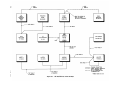
OF
THE
FIELD
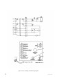
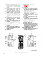
ARMY
TECHNICAL
AND
DEPOT
MAINTENANCE
RADIO
T h i s
c o p y
p a g e s
SET
i s
f r o m
HEADQUARTERS,
a
MANUAL
AN/PRC-25
r e p r i n t
C h a n g e s
MANUAL
w h i c h
1
a n d
i n c l u d e s
2 .
DEPARTMENT
8 JANUARY
c u r r e n t
1963
OF
THE
ARMY
WARNING
DANGEROUS VOLTAGES EXIST IN THIS EQUIPMENT
When Receiver-Transmitter, Radio RT-505/PRC-25
is in a transmit condition, 45 volts dc and 125 volts
dc are generated in module Al and applied to transmitter power amplifier V1. The 45-volt potential is
also applied to modules A6 and A7. Take all necessary
precautions.
DON’T TAKE CHANCES!
CAUTION
This equipment is transistorized. Before connecting
test equipment within the modules, insulate test prods
and clips with insulating tape or sleeving. Leave an
absolute minimum of exposed metal, and be extremely
careful to avoid short circuits; they may cause extensive damage. Do not make resistance measurements
unless specifically directed to do so.
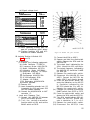
2
TM 5820-396-35-CI-9
Figure 5.1.
TM5820-398-35-CI-4
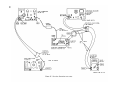
Figure 7.1.
5
TM5820-398-35-CI-2
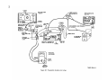
Figure 22.1.
7
Changes in force C 1 and C 2
TM 11-5820-398-35
C 2
HEADQUARTERS
DEPARTMENT OF THE ARMY
W ASHINGTON , D. C., 22 April 1965
C HANGE
No. 2
Field and Depot Maintenance Manual
RADIO SET AN/PRC-25
TM 11-5820-398-35, 8 January 1963, is changed
as follows:
Note. The parenthetical reference to previous changes
(example: page 1 of C 1) indicates that pertinent material wae
published in that change.
Page 3, paragraph 1.1 (page 1 of C 1). Change
“AMSEL-MR-MP” to: AMSEL-MR-(NMP)MA.
Page 7, paragraph 6b(l), line 3. Change (fig. 1)
to (fig. 88).
Page 10, figure 2 (page 1 of C 1). After note 5,
add note 6.
6. IN LATER EQUIPMENT BEARING ORDER NO.
64009-PP-63, CAPACITOR C2 HAS BEEN
OMITTED.
TAGO
8344-A-April
Page 11, figure 3 (page 1 of C 1). After note 5,
add note 6.
6. IN LATER EQUIPMENT BEARING ORDER NO.
64009-PP-63, R4 IS 68 0HM3 AND A MODULE
GROUND STRAP HAS BEEN ADDED.
Page 14, figure 5.1 (page 2 of C 1). Make the
following changes:
Near R12, add (NOTE 4).
After note 3, add note 4:
4. IN LATER EQUIPMENT BEARING ORDER NO.
64009-PP-63, THE VALUE OF R12 HAS BEEN
FACTORY SELECTED AND MAY BE 37.4K,
38.3K, OR 39.2K ±1%.
1
2
Page 20.
figure 10.1
figure 10
TM5820-398-35-C2-1
Figure 10.1.
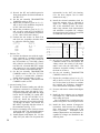
Page 43, paragraph 36a, (page 8 of C 1) chart.
Delete the last line and substitute: RF Millivoltmeter, Hewlett-Packard Model HP411A.
Page 56, figure 31. Add the following note:
Note. ON EQUIPMENT BEARING ORDER NO.
64009-PP-63, SWITCHES S2 AND S3 HAVE BEEN
OMITTED.
Page 60, paragraph 44, heading. After the heading, add the following note.
Note. On equipment bearing Order No. 64009-PP-63,
switches S2 and S3 are omitted. Removal of module Al 1,
A17, A19, or A20 provides the same result as depressing
switches S2 and S3.
Page 71, paragraph 56c chart, P e r f o r m a n c e
standard column. Make the following changes:
Step No. 1: Change 2 watts to 1.6 watts.
2: Change 1,5 watts to 1.1 watts.
TAGO 8344-A
Page 91, paragraph 63c, chart, P e r f o r m a n c e
slandard column. Make the following changes:
Step No. 1d: Change 300 kc to 250 kc.
1g: Delete and substitute—l?requency should
be at least 250 kc below 31.50 mc. The
difference between the upper and lower
frequency indications should be at least
650 kc.
Page 105, paragraph 67, chart, P e r f o r m a n c e
standard column. Make the following changes:
Item la, b, and c: Change 2 to 1.6.
ld, e, and f: Change 1.5 to 1.1.
8a and b: Change 300 to 250.
After Item 8, add the following note.
Note. The difference between the two frequency
indications should be at least 650 kc.
3
Page 124, figure 61. Add figure 61.1 after figure 61:
4
Figure 61.1.
TAGO
8344-A
Page 151. Add chapter 6 after figure 79:
CHAPTER 6
DEPOT INSPECTION STANDARDS
98. Applicability of Depot Inspection Standards
The tests outlined in this chapter are designed
to measure the performance and capability of a
repaired Radio Set AN/PRC–2.5. Equipment that
meets the minimum standards stated in the tests
will furnish satisfactory operation, equivalent to
that of new equipment.
99. Applicable References
a. Repair Standards. Applicable procedures of
the U.S. Army depot performing this test, and the
depot standards for repaired signal equipment, form
a part of the requirements for testing this equipment.
b. Technical Publications. The following technical
publications are applicable to Radio Set AN/PRC25:
(1) TM 11-5820-398-10, Operator’s Manual.
(2) TM 11-5820-398-20, Organizational Maintenance Manual.
(3) TM 11-5820-398-35P, Field and Depot
Maintenance Repair Parts and Special
Tools List.
(4) TM 11-5820-497-35P, Field and Depot
Maintenance Repair Parts and Special
Tools List, Receiver-Transmitters, Radio
RT-505/PRC-25 and RT-505A/PRC-25.
c. Modification Work Orders. Perform all applicable Modification Work Orders pertaining to Radio
Set AN/PRC-25 before making the tests specified.
DA Pam 310-4 lists all available MWO’s.
100. Test Facilities Required
The following equipment, or suitable equivalents,
will be employed in determining compliance with the
requirements of this Specific Standard.
a. Test Equipment.
Equipment
Audio oscillator, Hewlett-Packard Model HP-200AB -------------------Signal Generator, F. M., Marconi Model 1066A -------------------------Voltmeter, Meter ME-30A/U -----------------------------------------Frequency Meter AN/USM-26----------------------------------------Spectrum Analyzer TS-723A/U ----------------------------------------Oscilloscope AN/USM-50A -------------------------------------------Modulation
Meter
ME-57/U-------------------------------------------------------Multimeter
ME-26B/U
----------------------------------------------RF Wattmeter AN/URM-43A ----------------------------------------Signal Generator AN/USM-44----------------------------------------RF Millivoltmeter Hewlett-Packard Model HP-411A --------------------Power Supply, Trygon Model T20-2------------------------------------
Federal stock No.
6625-519-2384
------------6625-669-0742
6625–692-6553
6625-668-9418
6625-668-4676
6625-647-3737
6625-542-6407
6625-635-9186
6625-669-4031
-------------------------
Technical manual.
1
1
1
1
1
1
1
1
1
1
1
2
TM
TM
TM
TM
TM
TM
TM
TM
11-6625-320-12
11-5057
11-5097
11-5129
11-6625-400-12
11-6625-200-12
11-5133
11-6625-508-10
b. Additional Equipment.
Federal stock No.
Enclosure, Electromagnetic, Shielding MX-1761/C -----------------------------------------Tool Kit, Radar and Radio Repairman TK-87/U -------------------------------------------Test Assembly, consisting of: (See fig. 79.6 for fabrication details.)
Lamp, indicator, with push-to-test feature, 12 volts -------------------------------------Connector, Methode Type No. SM-C-454687------------------------------------------Resistor, 150 ohms ±5%, 1 watt, fixed, composition ------------------------------------Resistor, 1,000 ohms ±1%, 1 watt, fixed, composition -----------------------------------Resistor, 10,000 ohms ±5% variable, linear taper, composition ---------------------------Resistor, 15,000 ohms ±5%, 1 watt, fixed, composition ----------------------------------TAGO 8344-A
o
4940-542-0002
5180-690-4452
1
1
-------------------------
1
1
1
1
1
1
5905-683-2243
5905-892-6330
5905-892-6542
5905-102-2824
5
Equipment
Switch, tig~e, singl&pole, singl~throw ------------------------------------------------Barrier terminal biock, Cinch Jones type No. 2-172-Y (2 terminal) ----------------------Barrier terminal block, Cinch Jones type No. 8-172-Y (8 tirminak)----------------------Cable, coaxial, type RG-WA/U ------------------------------------------------------W&, strmded AWGNo. l8---------------------------------------------------------Knob, control ----------------------------------------------------------------------Chassis, aluminum (5 in. by 9% in. by 2 in. suggested nominal size) -----------------------Receiver Dummy Antenna consisting of: (See fig. 79.4 for fabrication details.)
Resistor, 51.1 ohms +l~o, 1 watt, deposited carbon -------------------------------------Reaistor,31.6 ohms *lVO, 1 watt, deposihd carbon -------------------------------------Connector UG-657/U ---------------------------------------------------------------Adapkr, Connector UG+91A/U -----------------------------------------------------A1utinum container 2%in. by2~in. byl~ in----------------------------------------Wlm, strmded AWGNo. l8----------------------------------------------------------
5930-65%1517
-------------
1
1
------------1
6145-542-6092
8 ft
6145-160-5291 16 ft
------------1
------------1
5905-722-1804
5905-722-1805
5935-511-6618
5935-259-7463
1
1
2
1
-------------
1
6145-160-5291
As
reauired
Transmitter Dummy Loads (See fig. 79.5 for fabrication details. )
Long Antenna Loads for the specified frequencies as follows:
30.0 me—Resistor, 130 ohms +lVO, 1 watt, deposited carbon ---------------------------- 5905-060-4153
1
52.5 me-Resistor, 6190hms +1%, 1 watt, deposited carbon ---------------------------- 5905-581-1009
1
53.5 me—Resistor, 4000hms *lVO, 1 watt, deposited carbon ---------------------------- 5905-818-7164
1
—Capacitor,8MJf &5704Wvdc --------------------------------------------- ------------1
75.Omc—Resistor, 82 ohms +170, 1 watt, deposited carbon ----------------------------- 5905-655-3881
1
—Capacitor,68ppf +5%, 4~vdc -------------------------------------------- 5910-615-9812
1
Short Antenna Loads for the specified frequencies SE follows:
1
30.0 me—Resistor, 26.1 ohms +1’ZO, 1 watt, deposited carbon --------------------------- 5905-059-8157
—Capacitor, 12ppf +5%, 400vdc -------------------------------------------- 5910-806-2716
1
52.5 mc and 53.3 mc
—Resistor, 56.2 ohms +270, 1 watt, deposited carbon --------------------------- 5905-817-6049
1
1
—Capacitor, 18~pf +5vo,400 vdc-------------------------------------------- 5910-823-1971
1
75.0 me—Resistor, 61.9 ohms +1%, 1 watt, deposited carbon --------------------------- 5905-756-0425
—Capacitor,82ppf &5~,400 vdc-------------------------------------------- 5910-553-7147
1
Adapters, Antenna Load (See fig. 79.5 for fabrication details.)
1
No. l------------------------------------------------------------------------------- -----------_1
No. 2------------------------------------------------------------------------------ ------------1
Adaptir, ``T'', UG-274/U ----------------------------------------------------------------- 5935-201-2411
1
Attenuator, Adjustable “T”, General Radio type GR-874-GA --------------------------------- ------------1
Decoupling Tool; sheet metal 1 in. by 4 in., by 0.018 in. to 0.035 in. (20 to 26 gage) -------------- -----------------------_1
Test Gable No. 1, (fig. 79.1) consisting of:
1
Clip, electrical, alligator style ---------------------------------------------------------- 5940-18&9835
1
Plug, pin(tist lead probe) ------------------------------------------------------------ ------------Wire, stranded AWGNo. l8---------------------------------------------------------- 6145-160-5291 6 in.
2
------------Test Cable No. 2 (fig. 79.1) consisting of:
6 ft
Cable RG-MA/U -------------------------------------------------------------------- 6145-542-6092
2
Connector UG-88/U ----------------------------------------------------------------- 5935-149-4066
2
Connector, General Wdiotype GR-874-C58A ------------------------------------------ ------------------------1
Test Cable No. 3 (fig. 79.1) consisting of:
3 ft
Cable RG-WA/U -------------------------------------------------------------------- 6145-542-6092
1
Connector UG-21BlU ---------------------------------------------------------------- 5935-149-4236
1
Connector, General Radio type GR-874-C58A ------------------------------------------ -----------_4
------------Test Cable No. 4 (fig. 79.2) consisting of:
Cable RG-WA/U -------------------------------------------------------------------- 6145-542-6092 16 ft
16
Lugs, spade ------------------------------------------------------------------------- ------------1
------------Teat Cable No. 5 (fig. 79.2) consisting of:
3 ft
Cable R&58A/U -------------------------------------------------------------------- 6145-542-6092
1
Connecter UG-88/U ----------------------------------------------------------------- 5935-149-4066
2
Lu~, spade ------------------------------------------------------------------------- ------------1
------------Teat Cable No. 6 (fig. 79.2) consisting of:
3 ft
Cable RG-58A/U -------------------------------------------------------------------- 6145-542-6092
1
Connector UG-88/U ----------------------------------------------------------------- 5935-1494066
1
Insulating Terminal Board, 1 in. by2in. by%b in---------------------------------------- ------------1
Resistor, 15,0000hms +5Vo, lwatt ---------------------------------------------------- 5905-537-6458
6
TAGO .9344A
Eguipmenf
,d?rd dock No.
%%2
Capacitor, O.05pf +10To,4M vdc----------------------------------------------------- ------------Wire, stranded AWGNo. l8---------------------------------------------------------- 6145-160-5291
1
As
required
Lu~, spade ------------------------------------------------------------------------- ------------2
Test Cable No. 7 (fig. 79.3) consisting of:
------------4
Wire, stranded AWGNo. l8---------------------------------------------------------- 6145-160-5291 16 ft
Lu@, spade ------------------------------------------------------------------------- ------------8
Teat Cable No. 8 (fig. 79.3) conaieting of:
------------1
Cable RG-WA/U -------------------------------------------------------------------- 6145-542-6092
3 ft
Insulating Terminal Board, 1 in. by2 in. by lA in---------------------------------------- ------------1
Capacitor, O.l~f +10Yc,400 vdc------------------------------------------------------5910-161-5264
1
Wire, stranded AWG No. l8---------------------------------------------------------- 6145-16(F5291
Aa
required
Lu@, spade ------------------------------------------------------------------------- ------------4
Test Cable No. 9 (fig. 79.3) consisting of:
------------2
Cable, RG-@A/U ------------------------------------------------------------------- 6145-542-6092
6 ft
Connectors, UG-W/U ---------------------------------------------------------------- 5935-149-4236
4
Hm&t H-138/U ----------------------------------------------------------------------- 5965-892-0972
1
Figure 79.1.
TAOO 8344-A
Test cables No. 1, No. 2, and No. 3.
7
Figure 79.2. Test cables No. 4, No.5, and No.6.
8
TAGO
8344-A
Figure 79.3. Test cables No. 7, No. 8, and No. 9.
TACO
8344-A
9
Figure 79.4. Receiver dummy antenna, schematic
and wiring diagrame.
10
TAGO
8344-A
Figure 79.5.
11
TACO 8344-A
Figure 79.6. Test assembly, schematic/wiring diagram.
12
TAGO 8344A
101. General Test Requirements
Most of the tests will he performed under the
conditions listed below and illustrated in figure 79.7
(for the receiver system tests) and in figure 79.8 (for
the transmitter system tests). Testing will be
simplified if preliminary standard control settings
are made initially and changes from these settings
are then made as required for the individual tests.
Perform all tests in Enclosure, Electromagnetic
Shielding MX-1761/C (or equivalent). Do not
apply power to the equipment under test until all
test connections are made and the power supply
output voltages are set.
Caution: When adjusting the power supply
output voltages, do not exceed 3 volts and 15 volts.
a. Remove the shorting cap from POWER connector J3 on the front panel of the RT-505/PRC-25.
b. Loosen and disengage the four captive screws
that hold the case to the front panel of RT-505/
PRC-25. Remove the case.
c. Connect the RT-505/PRC-25 into the applicable test setup (fig. 79.7 for receiver system tests
and fig. 79.8 for transmitter system tests).
d. Apply power to the RT-505/PRC-25 and
allow sufficient stabilization (warmup) time for the
test equipment. Five minutes is adequate for the
RT-505/PRC-25.
e. All specified signal levels apply to the signal at
the RT-505/PRC-25 input and not at the signal
generator output. The dummy load used in the
receiver test setup reduces the rf voltage delivered
at the coaxial ANT connector to half of the signal
generator output attenuator setting (6 db loss).
f. The oscilloscope used in test setups is included
for the convenience of maintenance personnel, but
is not necessary to perform the tests. It provides a
convenient output indication for both receiver and
transmitter tests.
g. ln all receiver tests, set the signal Generator
F. M. Marconi Model 1066A (1066A) frequency to
produce minimum distortion (as read on the TS723A/U) before making any readings.
h. To avoid audio ground loops, do not ground
Audio Oscillator Hewlett-Packard Model HP-200AB
(HP-200AB) output to the common ground at any
point.
102. Receiver Test Setup
(fig. 79.7)
a. Plug the test assembly connector PL into
POWER connector J3 on the front panel of the
RT-505/PRC-25.
TAGO 8344-A
b. Connect a test cable No. 7 from ground of
power supply A (2.5 volts) to terminal D of test
assembly terminal board TB1.
c. Connect a test cable No. 7 from the positive
output of power supply A (2.5 volts) to terminal E
of test assembly terminal board TB1.
d. Connect a test cable No. 7 from ground of
power supply B (12.5 volts) to terminal D of test
assembly terminal board TB1.
e. Connect a test cable No. 7 from the positive
output of power supply B (12.5 volts) to terminal F
of test assembly terminal board TB 1.
f. Connect a test cable No. 4 from the AF input
terminal of TS-723A/U (shield to ground) to
terminals C and D (shield) of test assembly terminal
board TB1.
g. Connect a test cable No. 4 from the audio
input terminals to the meter terminals of the TS723A/U.
h. Connect a test cable No. 4 from the af input
terminals of the TS-723A/U to the vertical input
of the AN/USM-50A.
i. Connect the receiver dummy antenna to the
RT–505/PRC-25 coaxial ANT jack J2. Use
Adapter, Connector UG-491A/U for connection to
ANT jack J2.
j. Connect test cable No. 9 from the receiver
dummy antenna to the 1066A RF input.
k. Connect test cable No. 8 from the 1066A
external modulation input to the HP-200AB
audio output.
l. Connect test cable No. 5 from the HP-200AB
audio output to the AN/USM-26 signal input.
m. Do not turn on the RT-505/PRC-25. Turn on
all test equipment and allow sufficient warmup time.
n. Adjust power supply A to 2.5 volts and power
Supply B to 12.5 volts.
o. Set the RT-505/PRC-25 function switch to
ON and select a frequency of 41.00 mc. Allow 5
minutes to warmup.
p. Adjust the 1066A to produce an RF output of
41.00 mc at a 20-microvolt level with 10-kc deviation at 1,000-cps modulation frequency.
Note. The dummy antenna used in series with the 1066A
output provides 6 db of attenuation. The actual RF level
delivered at the RT-505/PRC-25 coaxial ANT input is
10 microvolt when the 1066A output attenuator is set to
20 microvolt.
q. Adjust the RT-505/PRC-25 VOLUME control to produce a l-volt reading on the TS-723A/U
(used as a vacuum-tube voltmeter).
V. Perform the receiver system tests indicated in
paragraph 104.
13
14
TAGO
Figure 79.7.
8344-A
103. Transmitter Test Setup
(fig. 79.8)
a. Plug the test assembly connector into POWER
connector J3 on the front panel of the RT–505/
PRC-25.
b. Connect a test cable No. 7 from ground of
power supply A (2.5 volts) to terminal D of test
assembly terminal board TB1.
c. Connect a test cable No. 7 from the positive
output of power supply A (2.5 volts) to terminal E
of test assembly terminal board TB1.
d. Connect a test cable No. 7 from ground of
power supply B (12.5 volts) to terminal D of test
assembly terminal board TB1.
e. Connect a test cable No. 7 from the positive
output of powersupply B (12.5 volts) to terminal F
of test assembly terminal board TB1.
f. Connect a test cable No.4 from the HP-200AB
audio output to test assembly terminals A and B
(shieId) of terminal board TB1.
g. Connect test cable No. 4 from the ME-30A/U
input to test assembly terminals A and B (shield)
of terminal board TB 1.
h. Connect a test cable No. 2 from coaxial ANT
jack J2 of the RT-505/PRC-25 to the input of the
Attenuator, Adjustable “T”, General Radio Type
GR-874-GA (adjustable attenuator).
i. Connect test cable ATO. 3 from the unattenuated
output of the adjustable attenuator to the input
of the AN/URM-43A.
j. Connect a test cable No. 2 from the attenuated
output of the adjustable attenuator to the ME-57/U
input through adapter UG-274/U.
k. Connect test cable 9 from the AN/USM-26
input, through adapter UG-274/U, to the ME57/U input.
l. Connect a test cable No. 4 from the ME-57/U
audio output to the TS-723A/U input.
m. Connect a test cable No. 4 from the ME-57/U
audio output to the AN/USM-50A vertical input.
n. Connect a test cable No. 4 from the audio input
terminals to the meter terminals of the TS-723A/U.
o. Do not turn on RT-505/PRC-25. Turn on
all test equipment and allow sufficient warmup
time.
p. Adjust power supply A to 2.5 volts and power
supply B to 12.5 volts.
q. Set the RT-505/PRC-25 function switch to
ON and select a frequency of 41.00 mc. Allow 5
minutes to warmup.
r. Adjust the HP-200AB to 1,000 cps. Adjust the
TRANSMITTER AUDIO INPUT LEVEL control
TAGO
8344-A
on the test assembly and the HP-200AB output
level to produce a 1.4-millivolt reading on the
ME-30A/U.
s. Perform the transmitter system tests indicated
in paragraph 105.
104. Receiver System Tests, Radio Set AN/
PRC-25
a. Sensitivity Test.
(1) Perform the sensitivity test with the
equipment connected in a standard receiver test setup (para 102 and fig. 79.7),
except set the RF signal level at the RT505 /PRC-25 coaxial ANT input to 0.6
microvolt.
(2) Measure the signal-plus-noise-plus-distortion to noise-plus-distortion ratio on the
TS-723A/U, and record. The ratio should
be at least 10 db.
(3) Adjust power supply A to 2.25 volts,
power supply B to 10.0 volts, and repeat
the procedure given in (2) above.
(4) Adjust power supply A to 3.0 volts, power
supply B to 15 volts, and repeat the procedures given in (2) above.
(5) Repeat the procedures given in (2), (3), and
(4) above at 65 mc.
(6) Repeat the procedure given in (2) above
at 30.00, 52.00, 53.00, and 75.95 mc.
b. Distortion, Audio Power Output, Volume Control, and Audio Frequency Response Tests.
(1) Perform these tests with the equipment
connected in a standard receiver test
setup (para 102 and fig. 79.7).
(2) Measure the percentage of distortion on
the TS-723A/U. Maximum allowable
distortion is 6 percent.
(3) Adjust the VOLUME control on RT-505/
PRC-25 to produce a 2-volt reading on
the TS-723A/U (used as a vacuum-tube
voltmeter).
(4) Measure the percentage of distortion on
the TS-723A/U. Maximum allowable
distortion is 10 percent.
(5) Set the VOLUME control on the RT-505/
PRC-25 fully clockwise. The output
indicated on the TS-723A/U (used as a
vacuum-tube voltmeter) should be at
least 2 volts.
(6) Set the VOLUME control on RT-505/
PRC-25 fully counterclockwise and disconnect the RF output cable from the
1066A. The output indicated on the TS15
16
Figure 79.8.
TAGO 8344-A
723A/U (used as a vacuum-tube voltmeter)
should be not greater than 0.02 volt.
(7) Reestablish the standard receiver test
conditions; use the HP-200AB to externally
modulate the 1066A.
(8) Without changing the RT-505/PRC-25
VOLUME control setting, determine the
receiver audio output level produced with
modulation frequencies of 300, 500, 2,000,
and 3,000 cps (at 10-kc deviation). Acceptable frequency response is +0, – 6 db
(from the 1,000-cps reference) at 300 cps,
and +3, –6 db at 500,2,000, and 3,000 cps.
c. Limiting Test
(1) Perform the limiting test with the equipment connected in a standard receiver test
setup (para 102 and fig. 79.7), except set the
RF signal level at the RT-505/PRC-25
coaxial ANT input to 1 microvolt.
(2) Adjust the 1066A frequency for minimum
distortion as checked on the TS-723A/U.
(3) Increase the 1066A output to produce 100
millivolts at the RT-505/PRC-25 coaxial
ANT input.
(4) Readjust the 1066A frequency for minimum
distortion. The new audio output level
on the TS-723A/U (used as a vacuumtube voltmeter) must be within ±3 db of
the original setting (of 1 volt).
d. Squelch Sensitivity and Retransmit Tests.
(l) Perform the squelch sensitivity and retransmit test with the equipment connected in a standard receiver test setup
(para 102 and fig. 79.7) except set the RF
signal level at the RT-505/PRC-25
coaxial ANT input to 0.5 microvolt, the
RT-505/PRC-25 function switch to
SQUELCH, and modulate the 1066A
simultaneously at 1,000 cps and 150 cps as
described in (2) through (7) below.
(2) Set the 1066A SET MODULATION control fully counterclockwise.
(3) Use a 10-second count on the AN/USM26 to adjust the output frequency of the
HP-200AB to 150 Cps ±1.5 cps.
(4) Set the HP-200AB output level to produce
3-kc deviation on the 1066A. Accurately
determine and record the AMPLITUDE
control setting.
(5) Set the HP-200AB AMPLITUDE control fully counterclockwise.
(6) Adjust the 1066A SET MODULATION
control to produce 10-kc deviation.
TAGO
8344-A
(7) Restore the HP-200AB ATTENUATOR
setting to the position determined as noted
in (4) above.
(8) Set the RT-505/PRC-25 function switch
to RETRANS. The test assembly RETRANSMIT lamp should light and the
TS-723A/U (used as a vacuum-tube voltmeter) should indicate receiver audio
output. The RETRANSMIT lamp provides a convenient method of monitoring
operation of the squelch circuit.
(9) Momentarily set the RT-505/PRC-25
function switch to OFF then back to
RETRANS to verify that the receiver will
unsquelch (RETRANSMIT lamp lighted)
with an RF input level of 0.5 microvolt.
(l0) Slowly decrease the RF input level at the
RT-505/PRC-25 coaxial ANT input to
0.35 microvolt. The receiver should remain unsquelched.
(11) Disconnect the 1066A RF output from the
receiver coaxial ANT input. The receiver
should squelch, the lamp associated with
test cable No. 1 should go out, and the
TS-723A/U (used as a vacuum-tube
voltmeter) should indicate no receiver
audio output.
(12) Reduce the 150-cps modulation to zero
and increase the 1,000-cps modulation to
produce l5-kc deviation. Set the RF level
at the RT-505/PRC-25 coaxial ANT jack
to 10 microvolt. The receiver should not
unsquelch.
e. Catching Range Test.
(1) Perform the catching range test with the
equipment connected in a standard receiver
test setup (para 102 and fig. 79.7), except
set the 1066A and the RT-505/PRC-25
to 31.50 mc. Place the RT-505/PRC-25
upside-down for this test.
Caution: Check to see that the RT505/PRC-25 is set to a frequency ending in
50 ( XX.50 ) when disengaging the coupling
in the procedure in (2) below; otherwise
the coupling may become damaged.
(2) Disengage the mechanical coupling finger
(fig. 3, TM 11-5820-398-20). This disables the crystal switching assembly from
module A10. To disengage the coupling,
fabricate a tool from a piece of sheet metal
that measures 1 by 4 inches and is between
0.018 and 0.035 inch thick (20 to 26 gage).
Insert one end of the sheet metal tool into
17
the space between module Al0 and the
brass wheel-like part of the coupling.
(3) Adjust RT-505/PRC-25 to a frequency
50-kc higher than its current setting.
(4) Momentarily set the RT-505/PRC-25
function switch to OFF, then back to
ON, and verify receiver audio output by
observing the oscilloscope and the TS723A/U (used as a vacuum-tube voltmeter)
indications.
(5) Repeat the procedures given in (3) and (4)
above until a frequency setting produces
no audio output within 3 seconds, or
until a frequency of 31.95 mc is reached.
Record the maximum frequency that produces an audio output,
(6) Adjust the RT-505/PRC-25 to 31.50 mc
and repeat the procedures given in (3) and
(4) above except reduce the frequency by
50 kc for each successive step until the
audio output is not obtained or until a
frequency of 31.00 mc is reached. Record
the minimum frequency that produces an
audio output.
(7) Withdraw the decoupling tool and rotate
the kilocycle frequency selector to 50
to re-engage the coupling.
(8) Adjust the RT-505/PRC-25 to 51.50 mc
and disengage the coupling ((2) above).
(9) Repeat the procedures given in (3) and
(4) above until a frequency produces no
audio output within 3 seconds or until a
frequency of 51.95 mc is reached. Record
the maximum frequency that produces an
audio output.
(10) Adjust the RT-505/PRC-25 to 51.50 mc
and repeat the procedures given in (3) and
(4) above except reduce the frequency for
each successive step until the audio output
is not . obtained or until a frequency of
51.00 mc is reached. Record the minimum
frequency that produces an audio output.
(11) Withdraw the decoupling tool and rotate
the kilocycle frequency selector to 50 to
reengage the coupling.
(12) Evaluate the test results. At both test
frequencies (31 .50 and 51.50 me), the minimum acceptable catching range is 650
kc with at least 250 kc on each side of the
test frequency.
f. Selectivity Test.
(1) Perform the selectivity test with the
equipment connected in a standard re18
(2)
(3)
(4)
(5)
(6)
(7)
(8)
ceiver test setup (para 102 and fig. 79.7),
except disconnect test cabIe No. 9 from
the 1066A output- and connect it to the
AN/USM-44 output. Monitor the RF
voltage at A21J3 with RF Millivoltmeter
Hewlett-Packard Model HP-411A (HP411A).
Adjust the AN/USM44 for a 41.00-mc cw
output at approximately 100 UV.
Tune the AN/USM-44 for a maximum
indication on the HP-411A.
Increase the RF output of the AN/USM44 to the point where limiting just starts
(where an increase in the AN/USM-44
output does not increase the reading on the
HP-411A.)
Reduce the AN/USM-44 RF output for
an indication on the HP411A that is 6
db below the limiting level. Sweep the
ANT/USM-44 frequency across the selectivity pass band and select the frequency
that provides the highest peak. Readjust
the AN/USM-44 output level so the
selected peak is 6 db below the limiting level.
Determine the pass-band irregularities and
the 6-db-down points. The pass-band
irregularities should be within 2 db and
the 6-db-down points should be at least
32-kc apart. Use the AN/USM-26 to
determine the AN/USM-44 frequency at
the 6-db points. Disconnect test cable No.
9 from the dummy antenna input and
reconnect cable No. 9 to the AN/USM-26
input. Increase the AN/USM-44 output
level sufficiently to drive the AN/USM-26.
Set the AN/USM-44 to the frequency of
the highest peak of the selectivity pass
band and to an output level 6 db above the
noise level. (Read the noise level on the
HP-411A with the AN/USM-44 output
at zero; then increase the AN/USM-44
RF output until a 6-db increase is indicated by the HP-411A.)
Increase the AN/USM-44 output level 60
db and locate the two frequencies that
produce the same output level (6 db above
noise) as read on the HP-411A ((7) above).
Determine and record the frequencies by
use of the AN/USM-26. The two recorded frequencies are the 60 db-down
points. They should be less than 100-kc
apart.
TAGO
8344-A
(9) Repeat the procedures given in (7) and
(8) above except increase the RF output
70 db to determine the 70-db-down
points. The 70-db-down points should be
less than 120-kc apart.
(l0) Search 50 kc beyond the 70-db-down points
for spurious responses. Detected spurious responses should not be above the -70-dblevel.
Note. The receiver system tests are now
completed. Perform the procedures indicated in
paragraph 103 before proceeding.
105. Transmitter System Tests, Radio Set
AN/PRC-25
a. Power Output Test.
(1) Perform the power output test with the
equipment connected in a standard transmitter test setup (para 103 and fig. 79.8),
except set the HP-200AB output level to
zero and the RT-505/PRC-25 frequency to
30.00 mc.
(2) Set the test assembly TRANSMITTER
CARRIER switch to ON.
(3) Record the frequency and power output
indicated by the AN/USM-26 and AN/
URM-43A respectively.
(4) Set the test assembly TRANSMITTER
CARRIER switch to OFF.
(5) Repeat the procedures given in (2), (3),
and (4) above at 42.00, 52.95, 53.00, 65.00,
and 75.95 mc.
Minimum
(6) Evaluate the test results.
acceptable power output is 1.6 watts on
the low-frequency band (30.00 to 52.95 mc)
and 1.1 watts on the high-frequency band
(53.00 to 75.95 me).
b. Frequency Accuracy Test.
(1) Perform the frequency accuracy test with
the equipment connected in a standard
transmitter test setup (para 103 and fig.
79.8), except set the HP-200AB output
level to zero., and the RT-505/PRC-25
frequency to 75.00 mc.
(2) Set the test assembly TRANSMITTER
CARRIER switch to ON.
(3) Record the selected frequency (from the
RT-505/PRC-25 REC-TRANS FREQUENCY indicators) and the output frequency as indicated by the AN/USM-26.
(4) Set the test assembly TRANSMITTER
CARRIER switch to OFF.
(5) Repeat the procedures given in (2), (3),
and (4) above at 75.05, 75.10, 75.20, 73.30,
TAGO
8344-A
(6)
(7)
(8)
(9)
(l0)
75.40, 75.50, 75.60, 75.70, 75.80, and 75.95
mc.
Repeat frequency check ((5) above) in
reverse order (75.95 mc first).
Turn the megacycles control from 75 to 53,
then back to 75, and repeat the procedures
given in (2), (3), and (4) above.
Return the RT-505/PRC-25 to 75.00 mc,
set power supply A to 2.25 volts, power
supply B to 10.00 volts, and repeat the
procedures given in (2) through (5) above.
Return the RT-505/PRC-25 to 75.00 mc,
set power supply A to 3.0 volts, power
supply B to 15.00 volts, and repeat the
procedures given in (2) through (5) above.
Evaluate the test results.
Maximum
acceptable frequency inaccuracy is ±3.5
kc for all tests.
c. Tone Oscillator Frequency and Modulation Tests.
(1) Perform the tone oscillator frequency and
modulation tests with the equipment connected in a standard transmitter test setup
(para 103 and fig. 79.8) except set the
HP-200AB output level to zero, connect
test cable No. 6 from the AN/USM-26
input to the ME-57/U audio output, and
set the AN/USM-26 for a 10-second count.
(2) Set the test assembly TRANSMITTER
CARRIER switch to ON.
(3) Record the deviation indicated by the
ME-57/U and the frequency indicated by
the AN/USM-26.
(4) Set the test assembly TRANSMITTER
CARRIER switch to OFF.
(5) Evaluate the test results. Acceptable
deviation is 3 kc ±0.5 kc and acceptable
frequency is 150 cps ±1.5 cps (in a 10second count).
d. Modulation Capability and Deviation Tests.
(1) Perform the modulation capability and
deviation tests with the equipment connected in a standard transmitter test setup
(para 103 and fig. 79.8), except set the
RT-505/PRC-25 frequency to 47.00 mc,
ground A23J3 with test cable No. 1, and
adjust the HP-200AB output (and, as
required, the TRANSMITTER AUDIO
INPUT LEVEL control for a 1.4-millivolt
reading on the ME-30A/U.
(2) Set the test assembly Transmitter
CARRIER switch to ON.
19
(3) Record the RF and audiofrequencies
being used and the deviation indicated on
the ME-57/U.
(4) Set the test assembly TRANSMITTER
CARRIER switch to OFF.
(5) Repeat the procedures given in (2), (3),
and (4) above with modulation frequencies
of 300, 2,000, and 3,000 cps.
(6) Repeat the procedures given in (2), (3),
and (4) above with the RT-505/PRC-25
set to 60.00 mc and modulation frequencies
of 300, 1,000, 2,000, and 3,000 cps.
(7) Evaluate the test results. At both 47.00
and 60.00 mc, acceptable deviation must
be within the following limits:
Modulation
frequency (cps)
Acceplable
dcuiation (kc)
300
1,000
2,000
3,000
10 +3, –4
10±2
10±3
10±3
e. Sidetone Test
(1) Perform the sidetone teat with the equipment connected in a standard transmitter
setup (para 103 and fig. 79.8), except set
the RT-505/PRC-25 VOLUME control
fully clockwise and disconnect TS-723A/U
test cable No. 4 from the ME-57/ U output
and connect it to test assembly terminals
C and D (shield) of terminal board TB1.
(2) Set the test assembly TRANSMITTER
CARRIER switch to ON. The TS-723A/
U (used as a vacuum-tube voltmeter)
should indicate greater than 0.7 volt.
(3) Set the test assembly TRANSMITTER
CARRIER switch to OFF.
f. Antenna Loading Tests.
{1) Perform the antenna loading test with the
equipment connected in a standard transmitter test setup (para 103 and fig. 79.8),
except disconnect the AN/URM-43A input
lead at the RT-505/PRC-25 coaxial ANT
connector, set the RT-505/PRC-25 to
30.00 mc, install the transmitter long
antenna 30-megacycle load as described in
(2) through (4) below, and connect the
ME-26B/U in parallel with the resistor of
the transmitter load (fig. 79.5).
(2) Remove a mounting screw from one corner
of the whip ANT jack and install antenna
load adapter No. 1 (ground connection).
(3) Install antenna load adapter No. 2 in the
whip ANT jack; make sure it operates the
20
microswitch in the ANT jack housing.
(Use the brass adapter nut for short
antenna tests only.)
(4) Install the selected transmitter load between the amgator clips as indicated in
figure 79.5. Always ground the resistor
end of the transmitter load. The transmitter long antenna load characteristics
and minimum acceptable RF voltages
developed across the resistor of each load
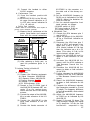
are identified in the chart below.
Long antenna loading
Load
characteristics
Minimum
Test frequency (me)
30.00-----------------52.50----------------53.50-----------------75.00------------------
voltage
Resistance
(ohms)
Capacitance
(uuf)
130
619
400
82
0
0
(rms)
9
21
16
8
8
70
(5) Set the test assembly TRANSMITTER
CARRIER switch to ON and read the RF
voltage across the resistor of the transmitter load with the ME-26B/U. The
minimum acceptable reading is listed in
the chart in (4) above.
(6) Set the test assembly TRANSMITTER
CARRIER switch to OFF.
(7) Repeat the procedures given in (4), (5),
and (6) above at 52.50, 53.50, and 75.00
mc. Use the chart in (4) above to correlate
the required test frequency, transmitter
load, and minimum acceptable voltage.
(8) Unscrew and remove antenna load adapter
No. 2.
(9) Install the brass adapter nut on antenna
load adapter No. 2 and reinstall the adapter
in the whip ANT jack.
Note. Load adapter No. 2, with the brass nut,
should not energize the ANT housing microswitch.
(10) Install the short antenna 30-megacycle
transmitter load between the alligator
clips; make sure the resistor-end of the
load is grounded.
Transmitter short
antenna characteristics and minimum acceptable RF voltages are identified in the
following chart.
TAGO
8344-A
Short
Test frequency (mc)
antenna
loading
Load characteristics
— — — — - — — — — —
Resistance
(ohms)
—————— — —
30.00-----------------52.50-----------------53.50-----------------75.00------------------
Capacitancee
(uff)
(7)
Minimum
voltage
(rms)
— — —————
26.1
56.2
56.2
61.9
12
18
18
82
4
7
5
7
(11) Set the test assembly TRANSMITTER
CARRIER switch to ON and read the
RF voltage across the resistor of the
transmitter load with the ME-26B/U.
The minimum acceptable reading is listed
in the chart in (10) above.
(12) Set the test assembly TRANSMITTER
CARRIER switch to OFF.
(13) Repeat the procedures given in (10), (11),
and (12) above at 52..50, 53.50, and 75.00
mc. Use the chart in (10) above to correlate test frequency, transmitter load, and
minimum acceptable voltage.
(14) Remove the antenna load adapters and
replace the screw in the corner of the whip
ANT jack.
g. Catching Range Test.
(1) Perform the catching range test with the
equipment connected in a standard transmitter test setup (para 103 and fig. 79.8)
except set the HP-200AB output level to
zero and the RT-505/PRC-25 frequency
to 31.50 mc. Set the RT-505/PRC-25
upside-down for this test.
Caution: Check to see that the RT-505/
PRC-25 is set to a frequency ending in 50
( XX.50 ) when disengaging the coupling in
procedure in (2) below; otherwise the
coupling may become damaged.
(2) Disengage the mechanical coupling finger
(fig. 3, TM 11-5820-398-20) that disables
the crystal switching assembly from module
Al0 (para 104e(2)).
(3) Adjust the RT-505/PRC-25 to a frequency
50-kc higher than its current setting.
(4) Set the test assembly TRANSMITTER
CARRIER switch to ON and observe the
frequency indicated by the AN/USM-26.
it should be 31.50 mc ±3.5 kc.
(5) Set the test assembly TRANSMITTER
CARRIER switch to OFF.
(6) Repeat the procedures given in (3), (4), and
(5) above until the AN/USM-26 reading is
TAGO 8344-A
(8)
(9)
(l0)
(11)
(12)
(13)
(14)
(15)
not within ±3.5 kc of 31.50 mc or until
a frequency of 31.9.5 mc is reached.
Record the last RT-505/PRC-25 frequency
setting that produced an AN/USM-26
reading within ±3.5 kc of 31.50 mc.
Adjust RT-505/PRC-25 to 31.50 mc and
repeat the procedures given in (3) through
(7) above except reduce the frequency
setting for each successive step until the
output frequency exceeds ±3.5 kc of 31.50
mc or until a frequency of 31.00 is reached.
Withdraw the decoupling tool and engage
the coupling.
Adjust the RT-505/PRC-25 to 51.50 mc
and disengage the coupling ((2 above).
Repeat the procedures given in (3), (4),
and (5) above until the AN/USM-26
reading produced is not within ±3.5 kc of
51.50 mc or until a frequency of 51.95 mc is
reached.
Record the last RT-505/PRC-25 frequency
that produced an AN/USM-26 reading
within ±3.5 kc of 51.50 mc.
Adjust RT-505/PRC-25 to 51.50 mc and
repeat the procedures given in (3), (4), and
(5) above, except reduce the frequency for
each successive step, check the AN/USM26 for 51.50 mc ±3.5 kc at each step, and
stop if 51.00 mc is reached. Record the
limiting frequency.
Withdraw the decoupling tool and engage
the coupling.
Evaluate the test results. At both test
frequencies (31.50 and 51.50 me), the
minimum acceptable catching range is 650
kc with at least 250 kc on each side of the
test frequency.
h. Distortion Test.
(1) Perform the distortion test with the equipment connected in a standard transmitter
test setup (para 103 and fig. 79.8), except
connect test cable No. 1 from test point
A23J3 to chassis ground. The ME-57/U is
used as a receiver for this test.
(2) Set the test assembly TRANSMITTER
CARRIER switch to ON.
(3) Tune the ME-57/U for minimum distortion.
(4) Read the distortion on the TS-723A/U.
Maximum allowable distortion is 10 percent.
(5) Set the test assembly TRANSMITTER
CARRIER switch to OFF.
21
106. Miscellaneous System Tests and Inspection, Radio Set AN/PRC-25
a. Tests.
(1) Perform the miscellaneous system tests
with the equipment connected in a standard
transmitter test setup (para 103 and fig.
79.8) .
(2) Connect Handset H-138/U to one of the
AUDIO connectors on the front panel of
RT-505/PRC-25.
(3) Press the H-138/U keying button and
speak into the microphone. The AN/
URM-43A; ME-57/U, and AN/USM-50A
should indicate transmitter output, and
sidetone should be heard from the earphone.
(4) Connect the H-138/U to the other AUDIO
connector and repeat the procedure given
in (3) above.
(5) Set the RT-505/PRC-25 function selector
to LITE and observe that the RECTRANS FREQUENCY dials are lighted.
(6) With the ME-26B/U, measure the terminal
voltages of battery connector J4. Voltage
measurements between terminals and
ground should be 0 volt at terminal A, 12.5
volts at terminal B, and 2.5 volts at
terminal C.
22
b. Inspection.
(1) Perform the inspection procedure as a
final step before replacing the RT-505/
PRC-25 case.
(2) Inspect the RT-505/PRC-25 PRESET
knobs. Operate the elements of the presetting
feature to assure moper operation.
(3) Inspect the gasket at the rear of the front
panel of RT-505/PRC-25. It should be
resilient, properly seated in its channel, and
in general good condition.
(4) Inspect the O-ring on J4. It should be
resilient, properly seated in its channel, and in
general good condition. When replacing
the RT-505/PRC-25 case, be sure the Oring is not damaged and that the case is
properly seated against the gasket on the
rear of the front panel. If either gasket is
in poor” condition or not properly seated,
the unit will not be waterproof.
(5) Replace the RT-505/PRC-25 in its case.
Inspect the four captive screws before
engaging them. Engage and tighten the
captive screws.
Page 167, figure 88. Make the following changes:
Near switches S2 and S3 add: (Note 5).
After note 4, add note 5:
5. ON EQUIPMENT BEARING ORDER
No. 64009-PP-63, SWITCHES S2 and S3
ARE OMITTED.
TAGO
8344A
By Order of the Secretary of the Army:
HAROLD K. JOHNSON,
General, United States Army,
Chief of Staff.
official:
J. C. LAMBERT,
Major General, United States Amy,
The Adjutant General.
Distribution:
Active Army:
USASA (2)
CNGB (1)
CC-E (7)
Dir of Trans (l)
CofEngrs (1)
TSG (1)
CofSptS (1)
USAIB (5)
USCONARC (5)
USAMC (5)
ARADCOM (5)
ARADCOM Rgn (2)
OS MAj Cored (4)
LOGCOMD (2)
USAECOM (30)
USAMICOM (4)
USASMC (2)
USACDCEA (1)
USACDCCBRA (1)
USACDCCEA (1)
USACDCCEA (Ft Huachuca Ofc)
(1)
USACDCOA (1)
USACDCQMA (1)
USACDCTA (1)
USACDCADA (1)
USACDCARMA (1)
USACDCAVNA (1)
USACDCARTYA (1)
USACDCSWA (1)
MDW (1)
Armies (2) except
Seventh USA (5)
Corps (2)
USAC (3)
llth Air Aslt Div (3)
lst GM Bde (5)
USA Rsch Spt Gp (Ft Belvoir) (5)
507th USASA Gp (5)
508th USASA Gp (5)
318th USASA Bn (5)
319th USASA Bn (5)
320th USASA Bn (5)
177th USASA Co (5)
182nd USASA Co (5)
183rd USASA Co (5)
184th USASA Co (5)
Instl (2) except
Ft Monmouth (70)
Ft Gordon ( 10)
Ft Huachuca ( 10)
Ft Carson (21)
USMA (5)
Svc Colleges (2)
Br Svc Sch (2) except
MFSS (5)
USAARMS (5)
USASCS (5)
USA Cmbt Survl Sch (5)
USASESCS (50)
GENDEP (2)
Sig See, GENDEP (5)
Sig Dep (12)
Army Dep (2) except SAAD (30)
TOAD (14)
FTWOAD ( 10)
LEAD (5)
SHAD (3)
NAAD, SVAD (5)
CHAD (3)
ATAD (10)
Lexington-Blue Gram (14)
USAMERCC (5)
USASCC (4)
USA Tml Comd (1)
Army Tml (1 ) except
OART (5)
USATC AD (2)
USATC Armor (2)
USATC Engr (2)
USATC Inf (2)
USASTC (2)
WRAMC (1)
Army Pic Cen (2)
USAATC (5)
WSMR (5)
Sig Fld Maint Shopa (2)
AMS (1)
USAERDAA (2)
USAERDAW ( 13)
Units org under fol TOE’e (2 copies
each except as indicated):
11-16
11-35
11-57
11-97
11-98
11-117
11-155
11-157
11-337
11-5’)0 (AA-AE) (4)
11-555
11-557
11-558
11-587
11-592
11-597
29-25 (12)
NG: State AG (3).
USAR: None.
For explanation of abbreviations used, see AR 320-50.
TAGO
8344-A
23
TM 11-5820-398-35
Technical Manual
No. 11-5820-398-35
HEADQUARTERS,
DEPARTMENT OF THE ARMY
WASHINGTON 25, D. C., 8 January 1963
RADIO SET AN/PRC-25
Paragraph
Page
1,2
INTRODUCTION . . . . . . . . . . . . . . . . . . . . . . . . . . . . . . . . . . . .
3
THEORY
4,5
3-5
Block diagram analysis.. . . . . . . . . . . . . . . . . . . . . . . . . . . . . . .
7-40
6-33
Circuit analysis . . . . . . . . . . . . . . . . . . . . . . . . . . . . . . . . . . . . .
THIRD ECHELON MAINTENANCE
CHAPTER
42
34-36
General troubleshooting techniques . . . . . . . . . . . . . . . . . . . . . . . .
Section
44-52
37-39
Third echelon troubleshooting . . . . . . . . . . . . . . . . . . . . . . . . . . . .
40-42
53,54
Third echelon repairs . . . . . . . . . . . . . . . . . . . . . . . . . . . . . . . . .
43-45
59,60
Third echelon alignment. . . . . . . . . . . . . . . . . . . . . . . . . . . . . . .
FOURTH ECHELON MAINTENANCE
CHAPTER
46-48
61-64
Fourth echelon repairs . . . . . . . . . . . . . . . . . . . . . . . . . . . . . . . .
Section
66,67
Fourth echelon alignment. . . . . . . . . . . . . . . . . . . . . . . . . . . . . . . 49-51
52-67 67-105
Fourth echelon testing procedures . . . . . . . . . . . . . . . . . . . . . . . . .
68-97 106-147
FIFTH ECHELON MAINTENANCE . . . . . . . . . . . . . . . . . . . . . . . .
C HAPTER
169
REFERENCES . . . . . . . . . . . . . . . . . . . . . . . . . . . . . . . . . .. ... . . . .
A PPENDIX
170
INDEX . . . . . . . . . . . . . . . . . . . . . . . . . . . . . . . . . . . . . . . . . . . . . . . . . . . . . . . . . . . . .
CHAPTER
CHAPTER
Section
1.
2.
I.
II.
3.
I.
II.
III.
IV.
4.
I.
II.
III.
5.
1
This page left blank intentionally.
2
CHAPTER 1
INTRODUCTION
1. Scope
a. This manual covers field and depot
maintenance for Radio Set AN/PRC-25. It
includes instructions appropriate to third,
fourth, and fifth echelons for troubleshooting, testing, aligning, and repairing the
equipment. Detailed functions of the equipment are covered in the theory chapter.
b. The complete set of technical manuals
for this equipment includes TM 11-5820398-10, TM 11-5820-398-20, TM 11-5820398-20P, and TM 11-5820-398-35P.
c. Forward all comments on this publication direct to: Commanding Officer,
U. S. Army Electronics Materiel Support
Agency, ATTN: SELMS-MP, Fort Monmouth, New Jersey. (DA Form 1598 (Record of Comments on Publications), DA
Form 2496 (Disposition Form), or letter
may be used.)
2. Index of Publications
Refer to the latest issue of DA Pam 310-4
to determine whether there are new editions, Changes, or additional publications
pertaining to your equipment. Department
of the Army Pamphlet No. 310-4 is a current index of Technical Manuals, Technical
Bulletins, Supply Bulletins, Lubrication
Orders, and Modification Work Orders
that are available through publications
supply channels. The index lists the individual parts (-10, -20, -35P, etc) and the
latest Changes to and revisions of each
equipment publication.
3
CHAPTER 2
THEORY
Section I. BLOCK DIAGRAM ANALYSIS
3. Receiving Signal Path
(fig. 82)
Receiver-Transmitter, Radio RT-505/
PRC-25 is tunable in 50-kilocycle (kc)
increments over a frequency range of
30.00 to 75.95 megacycles (me) to provide
920 channels. The frequency range is
covered in two bands: the low band is
30.00 to 52.95 mc; the high band is 53.00
to 75.95 mc. The front panel tuning controls and the BAND switch are used for
tuning the RT-505/PRC-25 to the desired
frequency.
a. The incoming radiofrequency (rf) signals are coupled from the antenna through
the antenna loading network to the power
amplifier tank. The antenna loading network matches the antenna circuit impedance to the long or the short antenna.
The power amplifier tank couples the rf
signal to the receiver first rf amplifier.
The power amplifier tank tunes both the
receiver and transmitter signals. Relay
K1 protects the receiver first rf amplifier
from the high power during transmission
by grounding the input to the receiver
first rf amplifier. The amplified signal
from the receiver first rf amplifier is
applied to the receiver second rf amplifier,
where it is amplified and applied to the
receiver mixer.
b. The output from the variable frequency oscillator (vfo), ranging in frequency
from 41.50 to 64.45 mc in 50-kc increments, is applied through the vfo buffer
to the receiver mixer. The receiver mixer
heterodynes the two signals to produce the
11.5-mc intermediate frequency (if.). The
vfo frequency is stabilized by the output
of the frequency synthesizer system (para
5). The ganged tuning capacitor is positioned by the mc and kc tuning controls
through a gear train.
c. The 11.5-mc if. output of the receiver
4
mixer stage is coupled through the 11.5mc crystal filter, and amplified by the
receiver first, second, third, fourth and
fifth if. amplifiers. The receiver fifth if.
amplifier output is applied to the receiver
discriminator driver. The receiver discriminator driver output is applied to the
receiver discriminator. The five receiver
if. stages (A21) have a power gain of approximately 85 decibels (db). The driver
output is fully limited. The limited if. signal is applied to the receiver discriminator, which demodulates the if. signal.
The audio output of the receiver discriminator is applied to the receiver first audio
amplifier.
d. The receiver first audio amplifier
output is applied to both the VOLUME
control and to the squelch input amplifier. The VOLUME control controls the
audio signal level to the receiver audio
output amplifier. The amplified signal
from the receiver audio output amplifier
is fed to the handset. The two receiver
audio amplifiers also amplify sidetone
signals from the speech amplifier limiter
of the transmitter section during transmission.
e. During squelch operation, when no
signal is being received, the audio output circuit is shorted to ground through
contacts of squelch relay K3. If an rf
carrier having a s qu e 1 c h tone is received, K3 is energized by an output from
the relay driver, the short circuit is removed, and audio signals are fed to the H138/U handset. Relay K3 will be energized
only if the output from the receiver first
audio amplifier includes a 150 cycle-persecond (cps) tone signal. During transmission, the transmitter tone generator
provides a 150-cps signal to the squelch
input amplifier to prevent shorting the
sidetone.
f. The receiver audio amplifier output,
including the 150-cps tone, is applied to
the squelch input amplifier. The squelch
input amplifier with the emitter -follower
and squelch feedback amplifier passes
the 150-cps tone, which is rectified in the
squelch direct current (dc) detector amplifier. When the squelch relay driver
receives a signal from the dc detector
amplifier, it provides the current necessary to energize K3. When K3 is energized,
the ground is removed from the audio
output amplifier to allow the audio signal to be fed to the handset.
g. In addition to the function of squelch
relay K3 described in f above, relay K3
provides a transmitter keying function
when two AN/PRC-25's are used for retransmission. During this type of service,
the receiving AN/PRC-25 is set for
squelch operation. When a signal is received, energizing K3, a ground circuit
is completed, through the interconnecting
cable, to key the transmitting AN/PRC25.
4. Transmitting Signal Path
(fig. 83)
a. The audio signal developed in the
handset microphone is amplified in the
first and second speech amplifiers, and
limited in the output limiter stage. The
output limiter stage has two outputs: it
applies the audio signals to the receiver
first audio amplifier as sidetone, and
applies the audio signal to the modulator.
The modulator also has a 150-cps tone
input from the 150-cycle tone oscillator,
through the feedback amplifier. The modulating voltages applied to the modulator
cause the sidestep oscillator (SSO ) output
frequency to vary at the input audiofrequency (af) rate from the microphone
and at the 150 -cps rate. The output from
the 150-cps tone generator is also applied
to the squelch input amplifier (para 3f).
b The frequency stability of the sso is
greatly improved by the quarter-wave network. The quarter-wave network is a
crystal-controlled passive network connected across the sso tuned circuit. The
quarter-wave network improves the sta-
bility of the sso approximately 40 times
relative to its free-running state.
c. The frequency-modulated (fm) output
of the sso is coupled through the sso
buffer amplifier to the transmitter mixer.
The sso buffer prevents loading of the sso
by the transmitter mixer. The transmitter
mixer heterodynes the 11.5-mc fm signal
from the sso with the vfo signal to produce
the transmitter output frequency. The vfo
is stabilized by application of its output
frequency through the frequency synthesizer buffer to the frequent y synthesizer
system (fss) (para 5). The fss will correct
any vfo frequency drift.
d. The transmitter mixer output is applied to the transmitter first rf amplifier.
The output of the transmitter first rf
amplifier is applied to the transmitter
second rf amplifier, which is cascaded with
the intermediate power amplifier and the
power amplifier. These amplifiers increase the transmitted signal level to
the proper amplitude. The transmitter
power amplifier output is coupled through
the power amplifier tank and antenna
loading network to the antenna. During
transmission, the input to the receiver
is grounded by relay K1 which is energized
by receive-transmit relay K2. Relay K2
also energizes the dc-to-dc converter,
which supplies the operating voltages
(B+ and bias) for the power amplifier
tube.
5. Frequency Synthesizer System
(fig. 84)
The frequency synthesizer system (fss)
is a closed loop, automatic phase control
(apc) system which locks the vfo on frequency. The fss is used both during reception and during transmission. During
transmission, the vfo output frequency is
shifted 50 kc lower than it is during reception. The frequencies shown on figure 84
represent the fss frequencies associated
with two typical received frequencies,
and are used to illustrate the frequency
relationships. The two typical received
frequencies are 33.10 mc (low band) and
68.45 mc (high band). All frequencies used
in a through i below can be converted to
5
those used for transmission, unless otherwise indicated, by subtraction of 50 kc
from the given frequency.
a. The vfo output frequency ranges from
41.50 mc to 64.45 mc. The specific frequency depends on the channel selected,
and whether the channel is in the high or
low band.
(1) When the low band is used, the vfo
operates at 11.50 mc above the
carrier frequency. For example, at
a received frequency of 33.10 mc,
the vfo frequency is 44.60 mc.
(2) When the high band is used, the
vfo operates at 11.50 mc below
the carrier frequency. For example, at a received carrier frequency of 68.45 mc, the vfo frequency is 56.95 mc.
b. The vfo output (a above) is applied
through the fss buffer and the fss first
mixer buffer to the fss first mixer. The
two buffer stages isolate the vfo from the
fss first mixer to prevent feedback of
sidebands created in the mixer. The fss
first mixer receives another ‘input from
the pulse generator, ‘which is driven by
the output of the 1.0-mc crystal oscillator.
(During transmission, the output of the
1-mc crystal oscillator, and, therefore,
that of the pulse generator, do not change
in frequency.) The sinusoidal output of the
l-mc crystal oscillator is applied to the
pulse generator where it is shaped into
pulses that are rich in harmonic content.
The output of the pulse generator, which
is applied to the fss first mixer, is a
frequency spectrum ran gin g from 1
through 12 mc in l-mc increments. (During
transmission, the frequency spectrum
does not change.) The fss first mixer
heterodynes the two inputs and applies the
resultant spectrum to the 53-mc filter.
c. Since the frequencies developed in
the fss first mixer output will be the two
original signals plus their sum and difference, a frequency (plus its upper and
lower sidebands) which approaches the 53mc bandpass will always be generated,
regardless of the vfo output frequency.
For example, when the vfo is operating
at 44.60 mc, the sum of the eighth harmonic
(8 mc) of the pulse generator output fre6
quency and the vfo frequency (44.60 mc)
equals 52.60 mc.
d. The 53-mc filter passes a band of’
frequencies, centered at 53 mc, to the fss
second mixer. The fss second mixer is
also supplied an input signal from the
100-kc interval oscillator (e below)
through the tuned net work, which reduces spurious frequencies. The fss second mixer heterodynes the two signals to
produce their difference, which is the fss.
if. It is applied to the fss if. amplifier.
e. The output frequency of the 100-kc
interval oscillator, which is independent
of the receive-transmit condition, ranges
from 46.85 mc to 47.75 mc in 100-kc
increments. The specific frequency depends on the frequency selected by the kc
tuning knob; that is, whichever 50- or
100-kc channel point is selected. Except
for the 0.95-mc channel point, the frequency relationship is such that the output of the 100-kc interval oscillator is
46.85 mc above a specific 100-kc channel
point (0.00 mc, 0.10 mc, 0.20 mc, etc) and
46.90 mc above a specific 50-kc channel
point (0.05 mc, 0.15 mc, 0.25 mc, etc).
At the 0.95-mc channel point, the 100-kc
interval oscillator is 45.90 mc above the
kc indication; therefore, with the kc tuning
knob set at the 0.95- or 0.00-mc channel
point, the 100-kc interval oscillator frequency will be 46.85 mc; at a 0.05- or
0.10-mc channel point, the frequency will
be 46.95 mc; at a 0.15- or 0.20-mc channel point, the frequency will be 47.05 mc;
at a 0.85- or 0.90-mc channel point, the
frequency will be 47.75 mc.
(1) The fss if. will always be 5.65 mc
at the 100-mc channel points during reception, and 5.60 mc during
transmission.
(2) The fss if. will always be 5.60 mc
at the 50-kc channel points during
reception and 5.55 mc during
transmission.
f. The fss if. amplifier has a power
gain of approximately 40 db to provide
adequate limiting for a constant output
amplitude. The fss if. amplifier output is
applied to the discriminator and to the
phase comparator. The phase comparator
also has an input from the 50-kc interval
oscillator.
g. The- 50-kc interval oscillator generates one of three frequencies: 5.55 mc,
5.60 mc, or 5.65 mc. The specific frequency depends on the frequency selected
by the kc tunin g knob (50- or 100-kc increments) and whether the RT-505/PRC25 is receiving or transmitting. When a
50-kc channel point (37 .45, 71.25, etc) is
selected, the 50-kc interval oscillator output frequency will be 5.60 mc during reception. (During reception, relay K2 causes a
frequency shift to 5.55 me.) When a 100-kc
channel point (37.40, 71.20, etc) is selected, the 50-kc interval oscillator output
frequency will be 5.65 mc, during reception. During transmission, relay K2 causes
a 50-kc shift to 5.60 mc.
(1) During reception, the 50-kc interval oscillator output will always be
5.65 mc at the 100-kc channel
point; during transmission, it will
be 5.60 mc.
(2) During reception, the 50-kc interval oscillator output will always
be 5.60 mc at the 50-kc channel
points; during transmission, it will
be 5.55 mc.
h. The output of the 50-kc interval os cillator (g above) is applied as a reference
signal to the phase comparator. The phase
of the two input signals (reference signal
from the oscillator buffer and fss if.) is
compared and a control voltage is developed in the phase comparator. The control
voltage is applied through the antihunt
network to the apc modulator. If a phase
lock exists, the apc voltage will assume
the reference level to maintain the vfo on
frequency. If a phase difference exists,
an error voltage is developed in the phase
comparator. This error voltage varies
the apc voltage applied to the apc modulator from the reference level to correct
the operating frequency of the vfo.
i. If the vfo output is too far from its
proper frequency to be corrected by the
phase comparator output, the discriminator (which extends the capture range of the
fss) will develop a hunt voltage, which increases the deviation of the apc voltage.
Since the vfo is far from its correct frequency, the frequency of the signal applied
to the discriminator (f above) will be considerably removed from the proper fss if.
(e above). The discriminator will develop
a large error (hunt) voltage. This hunt
voltage which is applied through the antihunt network to the apc modulator, changes
the vfo output frequency to within the pullin and hold-in capabilities of the phase
comparator. The antihunt network stops
the hunting action of the vfo when the phase
comparator has control of the vfo frequency.
Section II. CIRCUIT ANALYSIS
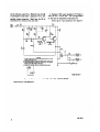
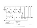
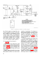
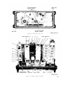
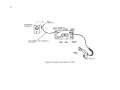
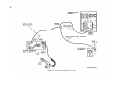
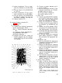
6. First Rf Amplifier Module A3
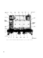
(fig. 1)
First rf amplifier module A3 amplifies
the signal received from module A2 (para
20). The first rf amplifier consists of a
sing1e transistor amplifier, the BAND
switch, and tuned output circuits.
a. The input signal from module A2 is
coupled through transformer T1 and coupling capacitor C 3 to the base and emitter
of transistor Q1. The center-tap of the
secondary of T1 is returned to rf ground
through capacitor C2. The use of the tapped
transformer input coupling neutralizes the
stage and isolates the rf amplifier from
the power amplifier tank circuit. The output of Q1 is taken from the collector
through coupling capacitor C5 and resistor
R4 to BAND switch S1. Resistor R4 suppresses parasitic oscillations.
b. Switch S1 is positioned by the BAND
switch on the front panel. The collector
circuit of Q1 is tuned in each of the two
BAND positions as follows:
(1) Low band. Transformer T2, fixed
capacitor C8, trimmer capacitor
C7 and tuning capacitor C2C (fig.
1) make up the tuned circuit. The
position of tuning capacitor C2C is
determined by the mc and kc controls on the front panel.
7
(2) High band. Transformer T3, fixed
capacitor C11, trimmer capacitor
C9, and tuning capacitor C2C make
up the tuned circuit. Switch S1-D
shorts the low-band tuned circuit
to prevent loss of energy when operating on the high band.
c. The combinatoin of resistors R3 and
R2 establishes the fixed bias for transis tor Q1. Resistor R1 is the emitter swamping resistor. Capacitor C6 and resistor
R4 form a parasitic suppressor. Inductor
L2 is an rf decoupling coil. Capacitors Cl
and C4 and inductor L1 make up a pi-type
rf filter which prevents rf leakage into the
power supply. Capacitor C10 is connected
in series with tuning capacitor C2C (fig.
88) on the high band by SIC to decrease
the effect of tuning capacitor C2C. Test
jack J2 can be used for measuring the input signal to module A3. Inductor L3 (in
the main frame (fig. 88)) is an rf filter
choke in series with the +10-volt regulated
input to module A3.
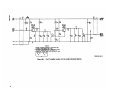
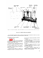
7. Second Rf Amplifier Module A4
(fig. 2)
The second rf amplifier module A4 amplifies the signal from first amplifier module A3 (para 6). The A4 output is applied
to receiver mixer module A5 (para 8). The
second rf amplifier consists of a single
transistor amplifier, a BAND switch, and
tuned output circuits. The circuit configuration and operation of module A4 is similar
to that of first rf amplifier module A3 (para
6) except that tuning capacitor C2D is used.
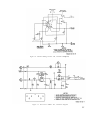
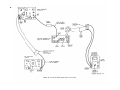
8. Receiver Mixer Module AS
(fig. 3)
Receiver mixer module A5 heterodynes
the rf signal from second rf amplifier
module A4 (para 7) with the vfo output to
produce an if. of 11.5 mc. Module A5 consists of a receiver mixer stage, a vfo buffer stage, a coupling transformer, and a
tuned output circuit. The dc operating voltage is available to this module during reception only.
a. The rf signal input is coupled to the
base of receiver mixer Q1 through isolating resistor R2 and coupling capacitor C2.
8
The vfo input signal from module A9 is
coupled to the base of vfo buffer Q2 through
isolating resistor RI and coupling capacitor C1. Resistor R4 matches the impedance
of the input circuit. The vfo buffer output
is coupled to the emitter circuit of transistor Q1 through coupling transformer T1.
The buffer base bias is determined by a
voltage divider composed of R5 and R6.
b. The potential on the base of transistor
Q1 is varying at the rf signal frequency
and the emitter potential is varying at the
vfo frequency; the collector output circuit
if tuned to the difference between the two
input frequencies; 11.5 mc. The collector
circuit consists of the primary of trans former T2 and capacitor C6.
c. The combination of capacitor C3 and
resistor R9 neutralizes Q1. Capacitors
C4, C5, and C7 are rf bypass capacitors.
The combination of capacitor C8 and inductor L1 decouples the module circuit
from the 10-volt dc supply. Resistors R5
and R6 develop base bias for transistor
Q2. Resistor R7 is the emitter swamping
resistor. Resistor R3 provides damping
for the primary of coupling transformer
T1.
9. Receiver If. Amplifier Module A21
(fig. 85)
The if. amplifiers provide amplification
of the 11.5-mc if. signal from 11.5-mc
filter module A27. The if. amplifier module
consists of five stages of amplification, and
a discriminator driver output.
a. If. Amplifiers 01, 02, and 03.
(1) The input from the 11.5-mc filter
module is coupled through inductor
Ll, developed across resistor R2,
and coupled to the base of receiver
first if. amplifier Q1 through capacitor C1. The signal output from
Q1 is coupled through capacitor C4
and developed across base resistor
R7 of Q2. Amplifier Q2 develops its
output signal across resistor R10.
This output signal is coupled
through capacitor C7 and is developed across base resistor R11 of
third if. amplifier Q3. The collector output of Q3 is developed across
Figure 1.
9
10
Figure 2.
the tuned circuit consisting of capacitor C9 and the primary winding
of transformer T1.
(2) The combination of resistors R2
and R3, R7 and R8, and R11 and R12
develops base-to-emitter bias for
Q1, Q2, and Q3 respectively. Resistors R4, R9, and R13 are emitter swamping resistors. Capacitors C3, C6, and C8 are emitter
rf bypass capacitors for Ql, Q2,
and Q3 respectively. Resistors R5
and R10 are collector load resistors for amplifiers Q1 and Q2, respectively. Resistor R6 and capacitor C2 form a decoupling network
between the +10-volt circuit of the
first if. amplifier and the other
stages. The input signal to module
A21 can be measured at test jack
J3.
b. Receiver Fourth and Fifth If. Amplifiers Q4 and Q5. Transistors Q4 and Q5,
amplify the if. signal, and also limit strong
signals.
(1) The out put of Q4 is developed
across collector load resistor R17
and is coupled through capacitor
C12 to the base of fifth if. amplifier
Q5. The collector output of amplifier Q5 is developed across load
resistor R21 and applied through
coupling capacitor C 15 to the base
of receiver discriminator driver
Q6.
(2) Resistors R14 and R15, and R18,
and R19 develop base-to-emitter
bias for Q4 and Q5 respectively.
Resistors R16 and R20 are emitter
swamping resistors and capacitors
C11 and C14 are the emitter bypass
capacitors for Q4 and Q5 respec-
Figure 3. Receiver mixer module A5, schematic diagram.
11
tively. Resistors R17 and R21 are
collector load resistors for Q4 and
Q5, respectively.
c. Receiver Discriminator Driver Q6.
The receiver discriminator driver amplifies and limits the 11.5-mc if. signal output
from Q5 and applies a strong signal of constant amplitude to discriminator Z1 (fig.
88).
(1) The 11.5-mc signal from Q5 is
coupled through capacitor C15 to
the base of Q6. The output of the
driver is developed across a tuned
circuit consisting of capacitor C18
and the primary of coupling trans former T2. The secondary of transformer T2 and the tuned circuit
consisting of capacitor C21 and
variable inductor L4 match the output impedance of driver Q6 to the
input impedance of discriminator
Z1. Resistor R25 and capacitor C19
form a compensating network which
improves the response and linearity of the input signal to Z1.
Resistors
R22 and R23 develop the
(2)
base-to-emitter bias for driver
Q6. Resistor R24 is the emitter
swamping resistor and capacitor
C16 is the emitter bypass. Resistor R26 is a filter resistor in the
+10-volt supply line. The combination of capacitors C17, C13, and
inductor L3 prevent rf leakage into
the supply. The output is coupled
through capacitor C20 to Z1. The
output from T2 can be measured
at test point J4.
10. Receiver Audio Amplifier Module A25
(fig. 4)
Receiver audio amplifier module A25
amplifies the audio output from the 11.5mc discriminator, Z1, and applies it to the
handset.
a. The audio output from Z1 is coupled
through coupling capacitor Cl to the base
of receiver first audio amplifier Q1. The
output signal from Q1 is developed across
collector load resistor R4 and is coupled
through capacitor C4 to VOLUME control
R1 on the front panel (fig. 88). This signal
12
is also applied to tone squelch module A24
(para 11). The collector signal of amplifier
Q1 is fed back through coupling capacitor
C3 and voltage dropping resistor R1 to the
base of Q1 to supply a small amount of degenerative feedback to minimize audio distortion, and to prevent discriminator loading by presenting a relatively high input
impedance to Z1.
b. The audio signal at the moving contact
of the VOLUME control is applied through
coupling capacitor C5 and isolation resis tor R5 to the base of receiver audio output
amplifier Q2. The output signal at the collector of amplifier Q2 is applied to the
primary of audio transformer T1. The audio signal is applied from the secondary
of T1 to the handset through the contacts
of squelch relay K3 (fig. 88).
c. Capacitor C2 is an rf bypass in the
input circuit. The combination of resistors
R2 and R3 provides fixed base-to-emitter
bias for Q1. The combination of resistors
R7 and R8 provides fixed base-to-emitter
bias for Q2. Resistor R10 is the collector
voltage dropping resistor. Capacitor C7 is
a bypass capacitor for noise. Resistor R9
is the emitter swamping resistor; capacitor C6 is the emitter bypass capacitor.
Resistor R11 presents a constant output
impedance to Q2 when function switch S1
(fig. 88) is in the SQUELCH position and
there is no incoming signal. The input signal to module A25 can be measured at test
jack J3. Resistor R12 isolates the input
circuit of transistor Q1 from external
loads introduced at test jack J3. The output
signal from module A25 can be measured
at test jack J4.
d. During transmission, the sidetone audio from module A22 is coupled through
capacitor C8 to the input circuit of Q1.
e. Capacitor C11 (in the mainframe (fig.
88)) is an rf bypass capacitor on the +10volt regulated input to module A25.
11. Tone Squelch Module A24
(fig. 5)
a. When the function switch on the front
panel is at SQUELCH, +10 volts dc is applied to the tone squelch module. Squelch
input amplifier Q1 and squelch emitter fol-
Figure 4. Receiver audio amplifier module A25, schematic diagram.
lower Q2 have a common emitter resistor,
R6. Transistor Q2 operates near saturation. Audio input signals from the audio
amplifier module are applied through isolation resistor R2, attenuated by dropping
resistor R3, and are applied, through coupling capacitor C2 to input amplifier Q1.
The audio output signals from Q1 are developed across collector load resistor R7
and directly coupled to the base of squelch
feedback amplifier Q3. The audio signals
amplified by transistor Q3 are developed
across a frequency selective (twin T) network which acts as the collector load. Resistors R10 and R11 and capacitor C 5 form
one T; capacitors C 3 and C4, and resistor
R12 form the other. This network is comparable to an antiresonant circuit; it applies minimum signal voltage to the base
of transistor Q2 at the frequency of 150
cps, and maximum signal voltage at other
frequencies. The signal applied to the base
of Q2 is degenerative to the signal at the
emitter of Q1. If the received audio signal
is modulated by a 150-cps tone, minimum
degenerative signal is applied to the base
of Q2. This action reduces the gain of Q1
at all frequencies except 150-cps. The bias
applied to the base of Q2 is determined
only by the voltage divider consisting of
resistors R9 and R13; transistor Q2 will
conduct and effectively cut off Q1 by virtue
of common emitter coupling across R6.
As a result, the bias applied to the base of
Q3 through the voltage divider, consisting
of resistors R8 and R7 and thermistor RT1,
is sufficient to cut off this stage.
b. When the 150-cps tone is present with
the incoming signal, the collector output of
feedback amplifier Q3, a 150-cps tone signal only, is filtered by the combination of
resistor R16 and capacitor C8 and is applied through coupling capacitor C7 to the
base of amplifier-detector Q4. With no signal input, the base of transistor Q4 is at
ground potential. Only the positive half
13
cycles of the 150-cps signal will cause
the amplifier-detector to conduct. The output developed across collector load resistor R18 is a negative-going half-wave
rectified s i g n a 1. The output signal is
filtered by capacitor C9 and is directly
coupled to the base of relay driver Q5. The
negative dc signal causes transistor Q5 to
conduct, which causes current to flow
through the squelch relay winding. When
relay K3 energizes, the receiver circuits
will operate.
c. Capacitor Cl is a bypass for the
higher audiofrequencies. The combination
of resistor R14 and capacitor C6 decouples
the emitter circuit of transistor Q3 from
the +10-volt supply. Potentiometer R15,
which is the emitter swamping resistor
for transistor Q3, is used to adjust the
negative feedback to the base of transistor
Q1 through dropping resistor R5 to thereby
control amplifier gain. Potentiometer R15
is normally adjusted so that an audio input signal of 35 millivolts minimum causes
squelch relay K3 to become energized. The
combination of the squelch relay coil and
resistor R19 provides emitter operating
voltage for relay driver Q5. During transmission, with function switch S1 (main-
frame) (fig. 88) at SQUELCH, sidetone audio is applied to the squelch circuit input,
while the 150-cps tone is coupled across
isolation resistor R1 and superimposed
on the sidetone audio signal. This condition
permits the operator to hear the sidetone
in his handset.
12. Speech Amplifier Limiter Module A22
(fig. 6)
The speech amplifier limiter amplifies
the audiofrequency signals from the microphone section of the handset. This module consists of two speech amplifiers and
an output limiter stage. The audio output
is applied to sidestep oscillator module
A20 (para 14) and sidetone output is supplied to receiver audio amplifier module
A25 (para 10).
a. Audio signals are coupled through an
input matching pad consisting of resistor
Rl, inductor L1, and capacitor Cl through
coupling capacitor C2 to the base of first
speech amplifier Q1. The amplified audio
output from the collector of Q1 is applied
through coupling capacitor C5 to the base
of second speech amplifier Q2. The audio
signal output from Q2 is applied through
Figure 5. Tone squelch module A 2 4 , s c h e m a t i c d i a g r a m .
14
coupling capacitor C7 to the base of output
limiter Q3. The output limiter signal is
developed across collector load resistors
R17 and R18. The audio output to A20 (para
14) of the sso is coupled through capacitor
C10 while the sidetone output to receiver
audio module A25 is directly coupled from
the junction of resistors R17 and R18. A
150-cps tone signal from the tone generator module is superimposed on the audio
output signal to the sso through isolation
resistor R19.
b. Resistors R2 and R3 establish baseto-emitter fixed bias for transistor Q1.
Resistor R5 is an emitter swamping resistor for Q1. The combination of resistor
R4 and capacitor C4 decouples the emitter
circuit from the +10-volt supply. Resistor
R6 is the collector load for first speech
amplifier Q1. Resistor 11 is the collector
load resistor for second speech amplifier
Q2. The combination of resistors R7, and
R8 and diode CR1 establishes base-toemitter bias for speech amplifier Q2. Because of the negative temperature coefficient of diode CR1, the bias varies
inversely with temperature; therefore, the
bias remains constant despite wide variations in temperature. Resistor R10 is the
emitter swamping resistor for Q2. The
combination of resistor R9 and capacitor
C6 decouples the Q2 emitter circuit from
any extraneous noise signals. Resistor
R11 is the collector load for second speech
amplifier Q2.
c. Resistive divider R13 and R14 provides base-to-emitter bias for output limiter Q3. Resistor R16 is the emitter
swamping resistor’ for Q3. The combination of resistor R15 and capacitor C8 decouples the e m i t t e r circuit from any
extraneous noise signals. The combination
of inductor L2 and capacitor C9 decouples
the emitter from the +10-volt supply. Resistor R12 is a power supply voltage dropping resistor. Capacitor C22 filters the
power supply voltage for transistors Q1
and Q2. The audio output to module A20
can be measured at test jack J3. Capacitor
C10 (in the main frame (fig. 88)) is an rf
bypass capacitor on the +10-volt regulated
input to modules A22 and A23.
Figure 6. Speech amplifier limiter module A22, schematic diagram.
15
13. Tone Generator Module A23
(fig. 7)
The tone oscillator functions only during
transmission. The 150-cps output tone is
applied to the speech amplifier limiter
module (para 12) which frequency-modulates the transmitter output carrier signal
with the tone at all times during transmission. The 150-cps tone disables the squelch
circuit in the distant receiver.
a. During transmission, +10-volt dc operating voltage is applied to transistor Q1
which oscillates at 150-cps. The frequency
is determined by the resistance-capacitance (rc) phase-shifting network consisting of capacitors Cl, C2, and C3 and resistors R1, R2, and R4. Slight adjustment
of the frequency can be made by adjustment of FREQ ADJ potentiometer R3. Oscillation is sustained by a feeding back of
the collector output through phase-shifting
capacitors C1, C2, and C3, to the base of
Q1. Each capacitor shifts the signal 60° to
provide the regenerative 180° phase shift,
Temperature compensation is achieved by
thermistor RT2, which provides a temperature compensated bias on the base of Q1,
and thermistor RT1, which compensates
the phase-shift network.
b. The feedback amplifier is used to in-
sure maximum output with minimum distortion. A portion of the tone oscillator
output signal, from the junction of collector
resistor R11 and potentiometer R12, is fed
back through resistor R5 to the base of
transistor Q1 to stabilize the oscillator
gain and prevent distortion due to excessive base drive. The 150-cycle tone output
is applied to speech amplifier A22 (para
12) in the transmitter section and to tone
squelch amplifier A24 (para 11) in the receiver section.
c. The combination of resistors R6, R7,
R5, and RT2 and potentiometer R12 provides base-to-emitter fixed bias for oscillator Q1. Resistor R8 is the emitter
swamping resistor for oscillator Q1; R9
is the swamping resistor for Q2. Resistor
R9 is the emitter swamping resistor for
Q2. Potentiometer R12 is the output level
adjustment for the 150-cps tone output.
The 150-cps tone output from R12 can be
measured at test jack J3.
14. Sidestep Oscillator Module A20 ond
Quarter-Wave Network Module A19
The sidestep oscillator (fig. 8) is a modified Hartley type. A quarter-wave network
(fig. 9) is connected to the oscillator tuned
circuit to stabilize the frequency. The
Figure 7. Tone generator module A23, schematic diagram.
16
network contributes a stability f actor about
40 times greater than that of a free-running oscillator.
a. Sidestep Oscillator Module.
(1) The audio signal from speech amplifier limiter module A22 (para
12) is coupled to the sso through
coupling capacitor C6 and isolating
resistors R8 and R7, across diode
CR1. Diode CR1 is a variable capacitance diode. When the audio
signal is applied across the diode,
the effective capacitance of CR1
changes as the voltage across it
varies. These capacitance changes
are coupled through capacitor C4,
which blocks the audio signal,
across the sso tuned circuit consisting of inductor T1 and capacitor C4. The effective capacitance
of the tuned circuit, and the output
frequency, varies at the audio rate;
therefore, the output frequency of
the sso is frequency-modulated.
(2) The ac component of the emitter
current flows through part of T1,
coupling capacitor Cl, and swamping resistor R2 to the emitter of
Q1. This signal induces an in-phase
voltage at the top of T1 which is
coupled through coupling capacitor
C2 to the base of Q1 to sustain oscillation. Resistors R3 and R4 provide base-to-emitter bias for Q1.
Resistor R1 is the emitter load
resistor. Resistors R5 and R6 establish a dc bias for CR1. Capacitor
C5 is an rf bypass capacitor for
the audio input circuit.
(3) The frequency-modulated rf output
from the oscillator tuned circuit
is coupled from a tap on T1 through
capacitor C7 to the base of buffer
Q2. The buffer stage isolates the
sso from load variations. The buffer output is developed across the
tuned circuit consisting of transformer T2 and capacitor C8. Resistors R9 and R10 establish the
base-to-emitter bias for Q2. Resistor R11 is the emitter voltage
dropping resistor; capacitor C9 is
the emitter bypass. A pi-type filter
consisting of capacitors C10 and
C11 and inductor L1 prevent rf
leakage into the +10-volt dc supply.
The rf output from Q2 can be measured at test jack J2.
b. Quarter-Wave Network Module A19.
(1) The quarter-wave network is made
up of two pi-networks: one for the
high band and one for the low band.
Each network has a crystal which
is used to control the sso frequency. BAND switch S4 (fig. 88)
on the front panel s e 1 e c ts the
proper network.
(2) Each network is an artificial
quarter-wave line. An impedance
or reactance atone end is reflected
as the exact opposite at the other
end. This permits the use of a lowimpedance crystal with the highimpedance tank circuit in the sso.
If the crystal were connected directly into the tuned circuit, deviation of the sso frequency would not
be possible. Inductors L1 and L2
are used to control the amount of
coupling between the crystal and
the tuned circuit.
15. Variable Frequency Oscillator Module A9
(fig. 10)
Variable frequency oscillator (vfo) Q1
functions as the local oscillator during reception and as the master oscillator during
transmission. The vfo is a modified Hartley
type that generates a signal in the frequency range of 41.45 mc to 64.45 mc. The
tank circuit for Q1 receives an automatic
phase control (ape) dc voltage from module
All (para 29). The apc voltage is applied
to capacitance diode CR1. The effective
capacitance of CR1 varies with the voltage
applied to it. Capacitance diode CR1 is
connected across the vfo tank. Any vfo output frequency deviation will develop an error signal and cause a change in the apc
voltage that will change the effective capacitance of CR1; this condition causes
the vfo output to return to its proper frequency. The vfo has outputs to the fss buffer, the receiver mixer, and transmitter
mixer. The fss buffer provides gain,
17
Figure 8. Sidestep oscillator module A20, schematic diagram.
isolation, and proper match for the vfo
signal applied to the fss. An output from
the vfo is directly fed to receiver mixer
A5 (para 8) and heterodyned with the incoming signals to produce the 11.5-mc if.
The third vfo output is applied to transmitter mixer Q2.
a. VFO Q1.
(1) Collector-to-emitter fee db a c k
through capacitor C2 and inductor
T1 maintains oscillation in Q1. The
tuned circuit consists of inductor
Tl, trimmer capacitor C9 fixed
capacitor C10, capacity diode CR1,
and ganged tuning capacitors C1D
C1E which are varied by the tuning
controls on the front panel. Trimmer capacitor C8 controls the effect of CR1.
(2) Input error signals from the frequency synthesizer system are
applied through a filter network
consisting of inductor L4 and capacitor C7, and through isolating
resistor R9 to capacitance diode
CR1. The capacitance of CR1 varies directly with the applied error
voltage to correct the output fre18
quency of the vfo. The automatic
phase control voltage from module
All can be measured at test jack
J3.
(3) Resistors R1 and R2 develop the
base bias for Q1. Resistor R3 is the
emitter swamping resistor. The rf
signal at the tuned circuit can be
measured at test jack J4.
(4) Capacitor C8 (in the main frame
(fig. 88)) is an rf bypass capacitor
on the automatic phase control
voltage line. Capacitor C9 (in the
main frame (fig. 88) is an rf bypass
capacitor on the +10-volt regulated
input line.
b. Frs Buffer Amplifier Q3.
(1) The output from the vfo is applied
through isolation resistor R11 and
coupling capacitor C11 to the base
of Q3. Transformer T2 couples the
output of this stage to the input of
the fss.
(2) Voltage-divider resistors R12 and
R13 develop the fixed base bias for
Q3. Resistor R14 is the emitter
swamping resistor. Capacitor C12
is the rf bypass capacitor for the
Figure 9. Quarter-wave network module A19, schematic diagram.
emitter. Inductor L3 and capacitor
C13 form a filter network to prevent rf leakage into the power supply.
c. Transmitter Mixer Q2.
(1) The transmitter mixer functions
only during transmission. The sso
input from A20 (para 14) is applied
through isolation resistors R8 and
R16 and coupling capacitor C3 to
the base of Q2. The vfo output is
applied through isolating resistors
R10 and R16 and coupling capacitor
C3 to the base of Q2. Resistor R4
is a dc return. The two signals are
heterodyned in this stage; the output from the collector is applied to
transmitter first rf amplifier module A8. The collector returns to
ground through the primary of T1
in module A8 (para 16).
(2) Voltage divider resistors R5 and
R6 develop the fixed bias for Q2.
Resistor R7 is the emitter swamping resistor. Capacitor C5 is an
emitter rf bypass capacitor for the
Q2. Inductor L1 and capacitor C6
form a filter network to prevent rf
leakage into the power supply.
16. Transmitter First Rf Amplifier
Module A8
(fig. 11)
Transmitter first rf amplifier module
A8 amplifies the rf input from variable
frequency oscillator module A9 (para 15).
a. The signal from A9 is coupled from
the top of the tapped secondary of T1
through coupling capacitor C2 to the emitter of Q1 and from the bottom of the secondary of T1 through coupling capacitor
C3 to the base of Q1. The output at the
collector is coupled through BAND switch
SIB to either the low- or high-band tuned
output circuit.
b. Separate tuned output circuits are
used for the high and low bands. Switch S1
selects the circuit when the BAND switch
on the front panel is positioned.
(1) Low band. The low-band tuned output circuit consists of inductor T2,
fixed capacitor C7, trimmer capacitor C6, and ganged tuning capacitor C1C (fig. 88).
(2) High band. The high-band tuned
output circuit consists of transformer T3, fixed capacitor C10,
trimmer capacitor C9, and ganged
tuning capacitor C1C.
c. Capacitors C4 and C5 and inductor
L3 form a filter which prevents rf variations from reaching the -45-volt dc supply.
The combination of resistors R2 and R3
provides fixed bias, and resistor R1 is the
emitter swamping resistor for Q1. Inductors L1 and L2 are rf chokes. Capacitor
C8 is inserted into the high-band output
tuned circuitry by S1C to shift the effective
range of ganged tuning capacitor C1C by
19
20
Figure 10.
Figure 11.
21
decreasing the total capacitance. The rf
input to module A8 can be measured at
test jack J2.
d. Inductor L2 and capacitors C6 and
C7 (in the main frame (fig. 88)) form a
filter in the +10-volt regulated input to
module A8.
17. Transmitter Second Rf Amplifier
Module A7
(fig. 12)
Transmitter second rf amplifier module
A7 amplifies the signal from transmitter
first rf amplifier module A8 (para 16).
Module A7 consists of a single transistor
amplifier, a BAND switch, and a tuned
output circuit.
a. The output signal from A8 is coupled
from the top of the center-tapped secondary of T1 through coupling capacitor C4
to the emitter of Q1 and from the bottom
of the secondary through coupling capacitor C5 to the base of Q1. The output at the
collector is coupled through BAND switch
S1A to either the low- or high-band tuned
output circuit.
b. Separate tuned output circuits are
used for the high and low bands. Switch S1
selects the circuit when the BAND switch
is positioned.
(1) Low band The low-band tuned output circuit consists of inductor T3,
trimmer capacitor C9, and ganged
tuning capacitor C1B (fig. 88),
which is varied by the tuning controls on the front panel. The output
is applied from a tap on T3 through
S1B to A6.
(2) High band. The high-band tuned
output circuit consists of the primary of transformer T2, fixed
capacitor C8, trimmer capacitor
C6, and ganged tuning capacitor
CIB. The output is applied from
the secondary of T2 through SIB
to A6.
Figure 12. Transmitter second rf amplifier module A7, schematic d i a g r a m ,
22
c. Capacitors C2 and C3 and inductor
L1 prevent rf variations from reaching the
-45-volt dc supply. The combination of
resistors R2 and R3 provides fixed bias,
and resistor R1 is the emitter swamping
resistor Q1. Inductors L2 and L3 are rf
chokes. Capacitor C7 is inserted into the
high-band output tank circuit by S1C to
shift the effective range of ganged tuning
capacitor C1B by decreasing the total capacitance. The rf input to module A7 can
be measured at test jack J2.
d. Inductor L1 and capacitor C5 (in the
main frame (fig. 88) ) form a filter in the
-45-volt input to module A7.
18. Transmitter Intermediate Power Amplifier
Module A6
(fig. 13)
Transmitter intermediate power amplifier module A6 amplifies the rf input from
transmitter second rf amplifier module
A7 (para 17). The transmitter intermediate
power amplifier module consists of a
single intermediate power amplifier, a
BAND switch, and a tuned output circuit
for each of the two bands. The output of
A6 is applied to the grid of tube V1.
a. The signal from A7 is coupled from
the top of the center-tapped secondary of
T1 through coupling capacitor C1 to the
emitter of Q1 and from the bottom of the
secondary of T1 through coupling capacitor C2 to the base of Q1. The output at
the collector of Q1 is coupled through
BAND switch S1B to the low-or high-band
tuned output circuit.
b. Separate tuned output circuits are
used for the high and low bands. Switch
S1 selects the proper circuit when the
BAND switch is positioned.
(1) Low band. The low-band tuned output circuit consists of inductor T2,
trimmer capacitor C6, and ganged
tuning capacitor C1A (fig. 88),
which is varied by the tuning controls on the front panel to select
the desired frequency within the
low band. The output is applied from
a tap of T2 through S1A and coupling capacitor C3 in the main frame
(fig. 88) to the grid of V1.
(2) High band. The high-band tuned
output circuit consists of inductor
T3, trimmer capacitor C8, and
ganged tuning capacitor C1A. The
OUTPUT is applied from a tap of
T3 through S1A and coupling capacitor C3 in the main frame (fig.
88) to the grid of V1.
C . The combinations of inductor L1 and
capacitor C3, choke rf L2 and capacitor
C4, and rf choke L3 and capacitor C5 keep
rf variations out of the -45-volt dc supply.
Resistor R1 is an emitter swamping resistor. The combination of resistors R2
and R3 form a voltage divider which supplies base bias for transistor Q1. Capacitor C7 is inserted into the high-band output tank circuit by S1C to shift the effective
range of ganged tuning capacitor C1A by
decreasing the total capacitance. The rf
input to module A6 can be measured at
test jack J2.
19. Power Amplifier A29
(fig. 14)
Power amplifier A29 is a pentode-type
rf amplifier stage which, in conjunction
with power amplifier (pa) tank module A2
(para 20), develops the required rf power
output to the antenna. Plate, screen-grid,
and bias voltages for power amplifier tube
V1 are supplied by de-to-de converter
module A1 (para 31). The dc filament voltage is supplied by battery BT1.
a. The rf input signal from transmitter
ipa A6 (para 18) is applied through parasitic suppression network Z1 to the control grid of V1. The rf signal at the plate
of tube V1 is developed across the lowor high-band tank circuits located in power
amplifier (pa) tank circuit module A2.
b. A bias voltage of -39.5 volts dc is
applied to the control grid of tube V1
through resistor R2, inductor L1, and suppressor network Z1. Resistor R1 is a
voltage dropping resistor in series with
the -45-input circuit. There is a constant
voltage drop of approximately 5.5 volts
dc across Zener diode CR1 which is applied a fixed grid bias voltage for V1. The
combination of inductor L1, resistor R2,
and capacitor C1 prevents rf leakage into
23
Figure 13. Transmitter ipa module A6, schematic diagram.
the -45-volt supply. A pi-type filter consisting of capacitors C2 and C5 and inductor L2 prevents rf variations on the filament of tube V2 and rf leakage into the
2.5-volt filament supply. The combination
of plate inductor L3 and bypass capacitor
C4 prevents rf leakage into the +125-volt
power supply. Resistor R3 is a screengrid voltage dropping resistor; capacitor
C3 is the screen-grid bypass capacitor.
20. Power Amplifier Tank Module A2
(fig. 15)
Power amplifier tank module A2 is used
as both the output load for power amplifier
tube V1 (para 19) (in A29), and as the input
circuit for receiver first rf amplifier module A3 (para 6). Module A2 consists of a
low- and a high-band tuned circuit, and a
BAND switch.
a. BAND switch S1 selects one of two
frequency bands. When S1 is in the lowband position (30-52), the tuned circuit
24
consists of transformer T1, trimmer capacitor C1, and inductor L1. When S1 is in
the high-band position, the tuned circuit
consists of transformer T2, trimmer capacitor C1, and inductor L1. When S1 is in
C5. Tuning capacitor C2B (fig. 88) is connected in parallel with either T1 or T2
through S1C.
b. During transmission, the output from
transmitter power amplifier tube V1 is
applied from J7 through S1AJ1, contact 2
and contact 1 or 3 of S1A to the selected
tuned circuits (a above). The output signal
from the tuned circuit is applied through
contact 1 or 3 and contact 2 of S1D,
through terminal 1 of 2AJ1 and terminal
11 of J7 to the antenna. Input to the receiver through S1B is prevented by the
energized contacts of relay K1 (fig. 88).
During reception, signals from the antenna
are passed through S1D to the selected
tuned circuit. Relay K1 (fig. 88) is not energized. During reception, energy from
the tuned circuit is coupled by inductor
Figure 14. Power amplifier A29, schematic diagram.
L1 (low band) or capacitor C4 (high band)
through switch SIB, through pin 3 of 2AJ1
and pin 9 of J7 to receiver first rf amplifier module A3.
c. On the low-band tuned circuit, the slug
in transformer T1 is an alignment adjustment for the low frequency end, while
capacitor C1 is an alignment adjustment
for the high frequency end. Inductor L1
provides high-impedance coupling for the
receiver to minimize effects of lead length
and to reduce spurious responses and
radiations.
d. On the high-band tuned circuit, the
slug in transformer T2 is an alignment
adjustment for the low frequency end,
while capacitor C2 is an alignment adjustment for the high frequency end. Capacitor
C4 provides high-impedance coupling for
the receiver on the high band. Capacitor
C5, in conjunction with capacitor C4, provides the proper impedance matching to
the receiver. Capacitor C3 is connected
in series with C2B by S1C to reduce the
ratio of capacitance change on the high
band.
21. Antenna Looding Network A28
(fig. 16)
The antenna loading network matches the
short or long antenna to the receivertransmitter by means of tuned coils and
switching assemblies.
a. When the long antenna is used, a
plunger and a leaf spring engages microswitches S2 and S3, closing contacts 2 and
3 on each switch. The rf signal is applied
through contacts of BAND switch S1 to the
power amplifier tank (C2A stator) (fig.
88). Inductor L4 is inserted in parallel to
change the electrical length of the antenna
during operation in the low band.
b. When the short antenna is used,
microswitches S2 and S3 are not actuated.
The rf signal from the antenna is applied
directly to switch S1. When the short antenna is used inductor L4 is not connected.
25
Figure 15. Power amplifier tank module A2, schematic diagram.
c. The tuning controls tune inductors
L1, L2, and L3, which are in series with
capacitors C2, C1, and C3, respectively,
to resonate the antenna in the low and high
bands. When the BAND switch is in the low
position, inductor L3 and capacitor C3 are
placed in the circuit; when the BAND switch
is in the high position, inductors L1 and
L2 and capacitors C2 and Cl are placed in
the circuit.
22. Frequency Synthesizer System First
Mixer Module A14
(fig. 17)
The fss first mixer module, A14, heterodynes the output of vfo module A9 (para
15) with the output of l-me spectrum generator module A15 (para 23) to produce a
band of frequencies around 53 mc. This
output is supplied to the 53-mc filter A13
(para 25). The fss first mixer contains the
fss first buffer amplifier and a mixer
circuit.
a. Fss First Mixer Buffer Q1.
(1) Fss first mixer buffer Q1 provides
isolation and low-power gain. It
has sufficient bandwidth to pass the
26
41.45-mc to 64.45-mc output of the
fss buffer in A9. The combination
of resistors R1 and R2 plus the
input impedance to Q1 provides the
proper termination for the vfo buffer amplifier. Capacitor Cl is a
coupling capacitor. The amplifier
output of Q1 is coupling capacitor.
The amplified output of Q1 is
coupled to the fss first mixer
transformer T1. Resistor R6 increases the frequency response of
T1.
(2) Resistors R3 and R4 form a voltage
divider which develops the fixed
portion of the emitter-to-base bias
for transistor Q1. Resistor R5 is
the emitter swamping resistor.
Capacitor C2 is an rf bypass capacitor for the emitter of Q1.
b. The signal inducted to the secondary
windings of transformer T1 is coupled
through push-pull diodes CR1 and CR2 to
the tuned primary of transformer T2. Capacitor C3 and the primary of transformer
T2 form a tuned circuit. The input from
1-mc spectrum generator A15 is applied
through a pulse-shaping network, consist-
Figure 16. Antenna loading network A28, schematic d i a g r a m ,
Figure 17. First mixer module A14, schematic diagram.
27
ing of diode CR3, capacitor C5, and resistor R8, to the center tap of the primary
of transformer T2. It is terminated in a
tuned network consisting of capacitor C4,
inductor L1, and resistor R7. The network
is broadly tuned to 7 mc. The spectrum
generator output contains the 1st through
the 12th harmonic of the fundamental 1-mc
pulse. Since the signal level of each succeeding harmonic is reduced in amplitude
from the signal level of the preceding
harmonic, the terminating tuned network
is used to equalize the harmonic components of the generated spectrum.
c. The mixed signal in the secondary of
transformer T2 is approximately 53 mc.
The output of the fss first mixer is applied
to 53-mc filter A13. The rf signal input
from Q1 to the fss mixer can be measured
at test jack J2. The rf input from module
A15 to the fss mixer can be measured at
test jack J3.
23. 1-Mc Spectrum Generator Module A15
(fig. 18)
The 1-mc spectrum generator module,
A15, produces harmonics of the l.0-mc
crystal-controlled oscillator for injection
into fss mixer module A14 (para 22).
Module A15 consists of a 1-mc cyrstal
oscillator and a pulse generator.
a. The 1-mc crystal oscillator is a modified Hartley type. Transistor Q1, fixed
capacitor C2, coil T1, and crystal Y1 form
the oscillator circuit. Resistors R1 and R2
form a voltage divider which provides the
fixed bias portion of emitter-base bias.
Resistor R3 is the emitter swamping resistor for Q1. Capacitor C1 bypasses the
base to ground.
b. The sinusoidal 1-mc oscillations are
applied to pulse generator Q2 through
coupling capacitor C3. The pulse generator
is normally cut off by the reverse base
bias applied through, R4, and conducts
only on the negative half cycles of the 1mc signal. a positive pulse, rich in harmonics, is developed in the collector output. This output is applied across the
transformer T2 and coupled to first mixer
module A14.
c. Capacitor C5 broadly tunes output
28
transformer T2 to 7 mc. Capacitor C4 is
an emitter bypass. Resistor R5 is the
emitter swamping resistor for Q2. The
10-volt dc supply is decoupled from the 1mc spectrum generator by coil L1 and
capacitor C6.
24. Interval Oscillator Module A10
(fig. 19)
Interval oscillator module A10 supplies
the fss with two crystal-controlled signals.
This module has two crystal-controlled
oscillators; Q1, generates frequencies of
46.85 mc to 47.75 mc in 100-kc increments, and Q2 generates frequencies of
5.55, 5.60, and 5.65 mc.
a. 46.85-47.75-Mc Oscillator Q1.
(1) Transistor Q1 is connected in a
crystal-controlled oscillator that
uses 1 of 10 crystals. Crystal selection is determined by the kc
tuning control on the front panel.
The toned collector circuit is composed of capacitors C1 and C2 and
the primary of transformer T1.
Oscillation is sustained by feeding
back part of the energy in the collector tank through capacitor C3
and resistor R2. Resistor R4 is
the tuned circuit damping resistor.
(2) Resistors R1 and R2 form a voltage divider network which develops
the base bias for Q1. Resistor R3
is the emitter swamping resistor.
Resistor R18, inductor L1, and
capacitor C 16 form a filter network in the +10-volt supply to Q1.
The rf output of Q1 can be measured at test jack J2.
b. Oscillator 5.55, 5.60, or 5.65 Mc Q2.
(1) Transistor Q2 is connected in a
crystal-controlled oscillator circuit that uses one of four crystals
(three frequencies) to generate the
frequency reference for p has e
comparison in module A17. The
tuned collector circuit is made up
of capacitors C9 and C10 and the
primary of transformer T2. Oscillation is sustained by feeding back
part of the energy in the collector
circuit from the junction of C9 and
Figure 18. 1-mc spectrum generator module A15, schematic diagram.
C10 to the selected crystal ((2) below), and the contacts of S1A to the
emitter of Q2; this action completes the regenerative circuit.
(2) Crystal selection is determined by
the operating mode (received or
transmit) and by the frequency selected by the kc tuning control.
When the RT-505/PRC-25 is in the
receive mode, +10 volts is applied
through normally closed contacts 4
and 6 of front-end relay K1 (fig.
88), through pin E of connectors J12
and A10J1, and current-limiting
resistor R5 to the anode of CR1.
This positive voltage forward
biases CR1; the diode conducts
heavily and allows the regenerative
circuit to crystals Y11 and Y12 to
be completed. If the RT-505/PRC25 is operating on a 100-kc channel
(31.10 mc, 74.20 mc, etc), S1A will
be in the position shown and crystal
Y11 (5.65 mc) will be selected
through contacts 8 and 11 of S1A;
this action completes the regenerative circuit to the emitter of
Q2. If the RT-505/PRC-25 is operating on a 50-kc channel (31.15
mc, 74.25 mc, etc.), S1A will be
turned clockwise one position from
that shown and crystal Y12 (5.60
mc) will be connected through contacts 8 and 9 of S1A; this action
completes the regenerative circuit
to the emitter of Q2.
(3) When the RT-505/PRC-25 is in the
transmit mode, front-end relay K1
(fig. 88) is energized, contacts 4
and 6 open, and +10 volts is no
longer available for diode CR1. The
diode is now reverse-biased and
prevents the selection of crystal
Y11 or Y12. Relay K1 contacts 4
and 7 are closed and apply+ 10 volts
through pin K of connectors J12
29
and A10J1 and current-limiting resistor R7 to the anode of CM. This
positive voltage forward biases
CR2; the diode conducts heavily and
allows the regenerative circuit to
crystals Y13 and Y14 to be completed. If the RT-505/PRC-25 is
operating on a 100-kc channel (31.0
mc, 74.20 mc, etc), S1A will be in
the position shown and crystal Y13
(5.60 mc) will be selected through
contacts 8 and 11 of S1A to complete the regenerative circuit to
the emitter of Q2. If the RT-505/
PRC-25 is operating on a 50-kc
channel (31.15 mc, 74.25 mc, etc),
S1A will be turned clockwise one
position from that shown and crystal Y14 (5.55 mc) will be selected
through contacts 8 and 9 of S1A to
complete the regenerative circuit
to the emitter of Q2.
(4) Capacitor C7 is an rf bypass capacitor. Capacitor C8 is a coupling
capacitor between the base and
collector circuit. Resistors R10,
R11, and R12 develop fixed bias;
resistors R8 and R9 are emitter
swamping resistors for Q2.
c. Buffer Q3.
(1) The output from oscillator Q2 is
coupled through transformer T2
to the base and emitter of Q3. The
buffer isolates Q2 from any varying
loading effects.
(2) Resistors R14, R15, and R16 develop fixed-base bias. Resistor
R13 is the emitter swamping resistor. Capacitors C11, C12, and C13
are rf bypass capacitors. Inductor
L2 and capacitor C15 form a decoupling network to prevent
rf leakage into the power supply.
The rf output from Q3 can be mess ured at test jack J3.
25. 53-Mc FiIter A13
(fig. 20)
The 53-mc filter has two input signals.
a. The output signal from 100-kc interval oscillator module A 10 is coupled
through isolation resistor R1 and a match30
ing network consisting of capacitors C6
and C7 and transformer T3 to fss second
mixer module A12 (para 26). This circuit
minimizes spurious frequency injection
into the second mixer.
b. The 53-mc signal from first mixer
modu1e A14 is coupled to the filter
through transformer T1 to a triple-tuned
network. The three tuned circuits are the
secondary of T1 and C1, L1 and C3, T2
and C5. Capacitors C2 and C4 are couplling capacitors. This triple-tuned network
provides a 2-mc bandpass at the 3decibel (db) points. The output of this network is coupled to second mixer module
A12.
26. Frequency Synthesizer System Second
Mixer Module A12
(fig. 21)
The fss second mixer module heterodynes the output from 53-mc filter A13
(para 25), with the 46.85-mc to 47.75-mc
output of the 100-kc interval oscillator
(applied through A13) to produce an fss
if. of 5.55, 5.60, or 5.65 mc. This output
is applied to fss if. amplifier module A18
(para 27).
a. The 53-mc input from module A13
is coupled through capacitor C1 to the
base of Q1. The 46.85-mc to 47.75-mc input from A13 is coupled through capacitor
C2 to the emitter of Q1. Transistor Q1
heterodynes these two input signals; the
resultant output signals at the collector of
Q1 are applied to the frequency selective
network.
b. The frequency selective network is
composed of capacitors C4 through C7,
variable transformers T1 and T2, and
variable inductors L1 and L2. The outputs
from Q1 are the two original frequencies
plus their sum and difference. The frequency selective network passes only the
difference frequency. The network is a
bandpass filter having a flat characteristic
resonant frequency of 5.6 mc.
c. Resistor R5 and capacitor C 3 filter
rf signals from the +10-volt dc supply.
Resistors R1 and R2 provide the fixed-base
bias. Resistor R3 is the emitter swamping
resistor. Resistors R4 and R6 terminate
Figure 19.
31
Figure 20. 53-Mc filter module A 13, sthematic diagram
the filter properly and minimize variations due to the varying impedances of
transistors. The rf output of module A12
can be measured at test jack J2.
27. Frequency Synthesizer System If.
Amplifier Module A18
(fig. 22)
The fss if. amplifier module (A18) amplifies the 5.6-mc signal input from fss
second mixer module A12 (para 26) and
applies it to fss discriminator driver
module All (para 29) and phase comparator module (para 28) A17. The fss if.
amplifier circuit consists of two cascaded,
double-tuned, transformer-coupled amplifier stages. The signal amplitude applied to the fss if. amplifier is sufficient
to cause limiting.
a. First If. Amplifier Q1.
(1) The 5.6-mc if. signal from module
A12 is coupled through capacitor
C1 to the base of Q1. The signal
output is developed across the
tuned collector circuit, consisting
of variable inductor L1 and capacitor C3. Resistor R4 broadens the
frequency response of the tuned
circuit. The signa1 developed
across this tuned circuit is coupled
through capacitor C4 to a second
tuned circuit consisting of capacitor C5 and the primary of tuned
coupling transformer T1. The
32
center-tapped secondary winding
of transformer T1 neutralizes Q2
(b below).
(2) Resistors R1 and R2 form a voltage-divider network to develop the
fixed-bias portion of the emitterto-base bias of of Q1. Resistor R3
stabilizes the emitter current. Capacitor C2 is an rf bypass capacitor
for the Q1 emitter.
b. Second If. Amplifier Q2.
(1) The amplified 5.6-mc signal from
transistor Q1 is applied from the
secondary of transformer T1
through coupling capacitor C6 to
the base of Q2. The signal output is
developed across the tuned collector circuit consisting of variable
conductor L2 and capacitor C8. The
signal developed across this tuned
circuit is then coupled through capacitor C9 to the second tuned circuit, consisting of capacitor C10
and the primary of transformer T2.
(2) Resistors R6 and R7 form a voltage-divider network which develops the fixed-bias portion of the
emitter-to-base bias of Q2. Resistor R5 stabilizes the emitter current. Capacitor C7 is a bypass
capacitor for the top of transformer T1. Resistor R8 is a load
for the tuned circuit. Resistor R10,
across the secondary of transformer T2, provides the proper
Figure 21. Second mixer module A12, schematic diagram.
output termination and minimizes
variations due to discriminator
loading. The combination of resis-.
tor R9 and capacitor C11 prevents
rf leakage into the +10-volt dc supply.
(3) The rf output of module A18 can be
measured at test jack J2.
28. Phase Comparator Module A17
(fig. 23)
Phase comparator module A17 contains
phase comparator driver Q1 and the phase
comparator. The phase comparator compares the phase of the signals from f ss if.
module A18 (para 27) with those from interval oscillator module Al0 (para 24). The
input signal from A18 is initially generated
by the vfo; the frequency of this signal may
be varying. The signal from A10 is generated by a crystal-controlled oscillator; this
signal is the reference frequency. The dc
output voltage, proportional to the phase
difference, is the automatic phase control
(ape) voltage applied to vfo module A9 (para
15). If the two signals are in phase, the apc
voltage will assume a reference level to
maintain the vfo output frequency. If a
phase difference is detected, an error voltage is developed in the phase comparator.
This change in apc voltage opposes any
change in vfo output frequency by returning
the vfo output to its correct frequency, and
establishes a phase lock.
a. Phase Comparator Driver. The input
from fss if. module A18 is coupled through
capacitor Cl to the base of phase comparator driver Q1. The amplified signal is
coupled to the phase comparator by
33
Figure 22. Speech amplifier limiter module A18, schematic diagram.
transformer T1. Resistors R1 and R2 form
a voltage divider which provides the fixedbias portion of the emitter-to-base bias.
Emitter resistor R3 establishes the fixed
portion of the emitter-to-base bias and
stabilizes the emitter current. Capacitor
C2 is a bypass capacitor for the Q1
emitter. Capacitors C5 and C6 and inductor L1 form a pi-filter which prevents
any rf signals from entering the 10-volt
dc Supply
b. Phase Comparator. The phase comparator consists of the tapped secondary
winding of T1, coupling capacitors C3 and
C4, diodes CR1 and CR2, and resistors R4
and R5. The output voltage of the phase
comparator depends on the phase relationship of the two signals applied to the circuit. The voltage output is pivoted about a
+3.5-volt dc reference level at the junction
of resistors R6 and R7 which is applied to
the center tap of transformer T1 and,
through the secondary winding of transformer T3 in module A10, to the junction
of diodes CR1 and CR2. This voltage is
established by the divider action of resistors R6 and R7 which are connected across
the 10-volt power supply. Capacitor C7 is
an rf bypass capacitor.
(1) The signal induced in the secondary
of T1 is coupled through capacitors
C3 and C4 to diodes CR1 and CR2,
respectively, producing equal and
opposite voltages. E1 is applied to
34
CR1, and E2 to CR2. (The E designations are for purposes of reference only.)
(2) The phase comparator also receives an input signal from crys tal-controlled interval oscillator
module A10 which is injected at the
center tap of transformer T1 and
the junction of diodes CR1 and CR2.
This signal voltage (E3) is exactly
90° out-of-phase with voltages E1
and E2 when the frequency of the
5.6-mc input, developed initially by
the vfo, is the same as the crystalcontrolled input frequency. This
condition exists when the vfo is on
frequency. When the two input signals are 90° out-of-phase, the dc
output voltage, which is the vectorial sum of voltages E1 plus E3 and
E2 plus E3, will be at the +3.5-volt
reference level.
(3) Diode CR1 receives a voltage equal
to the sum of El and E3; diode CR2
receives a voltage equal to the sum
of E2 and E3. The diodes rectify the
signals, and dc voltages appear
across load resistors R4 and R5.
When the signal voltages are equal,
the output voltages across resistors R4 and R5 are equal, and the
total voltage across both resistors,
in respect to the junction of resistors R4 and R5, is canceled out,
Figure 23. Phase comparator module A17, schematic diagram.
since E1 and E2 voltages are exactly 180° out-of -phase.
(4) If the vfo frequency increases or
decreases, changing the 5.6-mc input signal, the 90° vector relationship between the E1 and E2 signal
and the E3 signal no longer exists.
The change in frequency is equivalent to an E1-E2 phase shift with
respect to E3. The resultant vectors of E1 plus E3 and E2 plus E3
are no longer the same l e n g t h
(since the 90° vector relationship of
E1-E2 and E3 no longer exists), and
the ratio of voltage across the
diodes changes. The voltages developed across load resistors R4
and R5 are now unequal, and the dc
output will be changed from the
+3.5-volt reference level.
(5) The amount the reference level is
changed is a function of the phase
difference detected in the comparator; the direction of change is a
function of vfo frequency shift (increase or decrease). When the frequency increases, the dc output
voltage is less than the reference
level; when the frequency increases, it is greater than the reference level. The phase comparator output voltage is applied
through the antihunt network module All to the apc line. The change
in apc voltage corrects the vfo output frequency and returns the apc
voltage to the reference level when
a phase lock is established.
(6) The control voltage output of module A17 can be measured at test
jack J2.
29. Frequency Synthesizer System Discriminator Driver Module All
(fig. 24)
The fss discriminator driver module All
extends the captive range of the fss. It receives two input signals and develops the
35
apc voltage in its output circuit. The two
input signals are the fss if. signal from the
fss if. amplifier module A18 (para 27) and
a dc voltage from phase comparator module A17 (para 28). The apc voltage is applied to the capacitance diode circuit of the
vfo. If aphase-locked condition exists (that
is, if the vfo is on frequency), the apc voltage will assume the reference level to
maintain the vfo output on frequency. If the
vfo output frequency changes, the fss dis criminator will develop ac and dc hunting
voltages. These error signals change the
apc voltage applied to the frequency control circuit of the vfo, which shifts the vfo
output frequent y to within the pull-in and
hold-in range of the phase comparator.
a. A signal from the fss if. module A18
is applied to the base of discriminator
driver Q1 through coupling capacitor C1.
The signal is amplified by Q1 and applied
to the discriminator (b below). Base biasing voltage for Q1 is provided by voltagedivider resistors R1 and R2. Resistor R3
is the emitter swamping resistor for Q1.
Resistors R4 and R13 provide series and
shunt loading, respectively, for the collector tuned circuit. Capacitor C2 is an rf
bypass capacitor for the Q1 emitter.
b. The discriminator is a Travis-type.
The tuned circuit, consisting of the transformer T1 secondary and capacitor C3, is
tuned to 5.95 mc. The tuned circuit, consisting of transformer T2 secondary and
capacitor C4, is tuned to 5.25 mc. At the
center frequency of 5.6 mc, both tank circuits have equal currents induced in them.
The voltage rectified by diode CR1 and
developed across resistor R5, is equal to
the voltage rectified by diode CR2 and developed across resistor R6. Since these
voltages are equal but of opposite polarity,
there is no output. At frequencies above
or below the signal center frequency, the
voltages developed across resistors R5
and R6 are unequal and a resultant output
voltage is developed. Capacitors C5 and
C6 rf filter capacitors across load resistors R5 and R6, respectively. The discriminator output can be measured at test jack
J2 .
c. The discriminator output is pivoted
about the control voltage input from A17
36
at the junction of resistors R8 and R9. The
larger portion of the discriminator voltage
is developed across resistor R8, and is applied in series with the comparator output
to the antihunt network (d below) through
coupling capacitor C9 as the ac portion of
the apc voltage. The remainder of the dis criminator voltage is developed across resistor R9; its polarity is opposite to that
developed across resistor R8. This voltage, plus the phase comparator output dc
voltage, is applied to the antihunt network
(d below) through discriminator load resistor R10 as the dc portion of the apc
voltage. Resistor R7, together with capacitors C7 and C8, determine the reaction
time of the discriminator driver.
d. Resistors R11 and R12 together with
capacitor C10 form the antihunt network
for the fss loop. Both the ac and the dc
portions of the apc voltage are applied
through this network to the vfo. However,
the main effect will occur on the ac portion
(developed by the fss discriminator) since
the higher the frequency of the error voltage, the higher the attenuation (by virtue of
the ac shunting through capacitor C10). To
prevent regeneration, this antihunt network damps the fss loop gain and stops the
hunting action of the vfo when the phase
comparator acquires control of the vfo.
e. Choke L1 and capacitor C11 form a
decoupling network to prevent rf from
being coupled into the power supply.
30. Voltage Regulator Module A16
(fig. 25)
The voltage regulator circuit supplies
the entire fss system, including the vfo,
with a regulated+ 10 volts dc. The regulator
uses a high power germanium transistor
(Q1) as a series regulator in conjunction
with a medium-power silicon transistor
(Q2). Transistor Q2 operates as a dc amplifier. The combination of resistor R5 and
diode CR2 forma voltage-divider network,
with diode CR2 maintaining the base of the
dc amplifier at a constant reference voltage. The combination of diode CR1 and
emitter resistor R4 forms a voltage divider. Any variation in output voltage
appears across resistor R4, since CR1
Figure 24. Fss discriminator module A11, schematic diagram.
maintains a constant voltage drop. When the
output voltage increases due to a decrease
in load or an increase in the input voltage,
a proportional positive voltage increase
appears at the emitter of dc amplifier Q2
and results in more current flow through
Q2. The base of series regulator Q1 goes
more positive; conduction through Q1 decreases, which effectively increases the
impedance of series regulator Q1. The
effect is a decrease in the regulator output; the circuit has compensated for the
increase in output voltage. The opposite
series of events takes place when the output voltage decreases because of a load
increase or input voltage decrease. The
regulator provides two +10-volt outputs,
one filtered and one unfiltered. The filtered output is filtered by a pi-filter network consisting of coil L1 and capacitors
C1 and C2. The filtered output is supplied
to modules A14 (para 22) and A15 (para23).
The unfiltered output is supplied to the
remainder of the circuits requiring regulated +10 volts. The unregulated input
voltage to module A16 can be measured at
test jack J2; the regulated output voltage
from module A16 can be measured at test
jack J3.
31. Dc-to-Dc Converter Module Al
(fig. 26)
The dc-to-dc converter module supplies
power amplifier tube V1 with plate voltage
during transmission. The dc-to-dc converter uses the 12.5-volt dc battery supply
input. Module Al consists of a transistorized power oscillator, transformer, and
rectifier circuit.
a. Transistors Q1 and Q2 are connected
in a common collector power oscillator
circuit which operates at 4,000 cps. The
primary windings, terminals 4 and 6, of
transformer T1 provide the load for the
transistors. Regenerative feedback to sus tain oscillation is applied to the base of
each transistor from the winding, between
terminals 5 and 7, of transformer T1. The
12.5-volt dc input to module Al is applied
when the function switch is at ON and the
handset push-to-talk switch is closed. As
a result of circuit unbalance, a larger current flows through one of the transistors
and its associated portion of the primary
winding of transformer T1 when the supply
voltage is initially applied to the oscillator.
(1) Assume that the larger current is
flowing through transistor Q1. This
37
Figure 25. Voltage regulator module A16, schematic diagram.
condition induces a voltage in the
feedback winding of transformer
T1. The voltzage is applied to the
bases of the transistors, causing
Q1 to conduct even more, and driving Q2 further into cutoff. The flux
in the core of transformer T1
changes at a nearly constant rate
until the core is saturated. When
saturation occurs, no voltage is developed in the feedback windings of
transformer T1. The feedback voltage to transistor Q1 decreases
rapidly and drives transistor Q1
into cutoff.
(2) When transistor Q1 cuts off, the
flux in the core of transformer T1
decreases slightly to induce voltages of opposite polarity across
its windings. This reversal of polarity drives transistor Q1 further
into cutoff and causes transistor
Q2 to conduct. The current through
Q2 increases until the transformer
core saturates, and the cycle then
repeats. During each half cycle,
the transformer flux changes from
saturation in one direction to saturation in the other. Since transis38
tors Q1 and Q2 switch rapidly from
cutoff to saturation, the current in
transformer T1 is essentially a
square wave.
b. Inductor L1 and capacitors C1 and C2
form a pi-type filter circuit which prevents voltage peaks developed in module
Al from reaching the 12.5-volt supply. A
voltage divider, consisting of resistors
RI and R2, establishes the fixed base bias
for transistors Q1 and Q2.
c. The rectifier circuit consits of two
full-wave rectifiers. The 125-volt output
is rectified by diodes CR1 and CR4 and
filtered by capacitor C4. The -45-volt output is rectified by diodes CR2 and CR3,
and filtered by inductor L2 and capacitor
C3. Resistors R4 and R5 are isolating resistors which prevent circuit loading by
test equipment probes placed at voltage
test jacks J2 and J3. Resistor R3 is a
bleeder for the +125-volt output.
32. Test Points
The RT-505/PRC-25 has 28 test points
located on 21 modules which enable a maintenance man to locate a faulty module
rapidly. These test points are normally
used in conjunction with Test Set, Electronic Plug-in Circuit AN/GRM-55 to isolate a faulty module at the organizational
level. If usedproperly, however, the signal
voltages at these test points will expedite
maintenance effort at higher echelons. A
listing of the modules which are equipped
with test points and a description of the
signal to be expected at the test point are
given below.
a. Module A1. Module A1 has two test
points: J2 and J3. Test point J2 permits
the -45-volt output of the converter to be
checked. Test point J3 permits the +125volt output of the converter to be checked.
b. Module A3. Module A3 has one test
point: J2. Test point J2 permits the rf
signal input to A3 (from A2) to be checked.
A typical rf signal level at this test point,
with a 20-millivolt, 65-mc signal injected
at the ANT connector, is 25 millivolts.
c. Module A4. Module A4 has one test
point: J2. Test point J2 permits the rf
signal input to A4 (from A3 to be checked).
A typical rf signal level at this test point,
with a 20-millivolt, 65-mc signal injected
at the ANT connector, is 80 millivolts.
d. Module A5. Module A5 has one test
point: J2. Test point J2 permits sampling
the vfo input. A typical rf signal level at
this test point, with no signal being received, is 20 millivolts.
e. Module A6. Module A6 has one test
point: J2. Test point J2 permits the rf
signal input to A6 (from A7) to be checked.
A typical rf signal level at this test point,
with the RT-505/PRC-25 in transmit condition, is 3 volts.
f. Module A7. Module A7 has one test
point: J2. Test point J2 permits the rf signal input to A7 (from A8) to be checked. A
typical rf signal level at this test point,
with the RT-505/PRC-25 in transmit condition, is 1.5 volts.
g. Module A8. Module A8 has one test
point: J2. Test point J2 permits the rf input from the transmitter mixer (in A9) to
be checked. A typical rf signal level at this
test point, with the RT-505/PRC-25 in
transmit condition, is 0.5 volt.
h. Module A9. Module A9 has two test
points: J3 and J4. Test point J3 permits
the input apc voltage (from A11) to be
checked. A typical apc voltage level, with
the vfo properly aligned, is +3.8 volts dc.
Test point J4 permits the output of vfo Q1
(in A9) to be checked. A typical rf signal
level of the vfo is 0.3 volt.
i. Module A10. Module A10 has two test
points: J2 and J3. Test point J2 permits
Figure 26. Dc-to-dc converter module A1, schematic diagram.
39
the output of oscillator Q1 (in A10) to be
checked. A typical rf signal level at this
test point is 0.2 volt. Test point J3 permits
the output of oscillator Q2 (in A10) to be
checked. A typical rf signal level at this
test point is 1.8 volts.
j. Module A11. Module All has one test
point: J2. Test point J2 permits the output
of the discriminator (in A11) to be checked.
A typical discriminator output level, with
the fss if. input disabled (by pressing S2 on
the main frame), is a l.5-volt peak-topeak, 10-cps signal.
k. Module A12. Module A12 has one test
point: J2. Test point J2 permits the fss if.
output of A12 to be checked. A typical rf
signal level at this test point is 80 millivolts .
1. Module A14. Module A14 has two test
points: J2 and J3. Test point J2 permits
sampling the vfo input (from A9). Atypical
rf signal level at this test point is 0.2 volt.
Test point J3 permits sampling the
spectrum generator input (from A15). A
typical rf signal level at this test point is
a l.5-volt peak-to-peak, l-mc pulse.
m. Module A16. Module A16 has two test
points: J2 and J3. Test point J2 permits
the unregulated voltage input (12 volts dc)
from the battery to be checked. Test jack
J3 permits the regulated voltage output (10
volts dc) to be checked.
n. Module A17. Module A17 has one test
point: J2. Test point J2 permits the control voltage output of All to be checked.
A typical control voltage level, with the
reference frequency input from A10 disabled (by pressing S3 on the main frame),
is +3.6 volts dc.
o. Module A18. Module A18 has one test
point: J2. Test point J2 permits the fss if.
output of A18 to be checked. A typical rf
signal level at this test point is 0.3 volt.
p. Module 40. Module A20 has one test
point: J2. Test point J2 permits the output
of the sidestep oscillator to be checked.
A typical rf signal level at this test point,
with the RF-505/PRC-25 in transmit condition, is 0.7 volt.
q. Module A21. Module A21 has two test
points: J3 and J4. Test point J3 permits
the rf input to A31 (from the 11.5-mc crystal filter] to be checked. A typical rf sig40
nal level at this test point, with a 20-millivolt, 65-mc signal injected at the ANT
connector, is 40 millivolts. Test point J4
permits the amplified output of A21 to be
checked. A typical signal level at this test
point, with the same input as above, is 600
millivolts.
r. Module A22. Module A22 has one test
point: J3. Test point J3 permits the amplified output of the speech amplifier
limiter to be checked. A typical audio signal level at this test point, with a4-millivolt input to A22 (RT-505/PRC-25 in
transmit condition), is 1.8 volts.
s. Module 43. Module A23 has one test
point: J3. Test point J3 permits the 150cps output of the tone generator to be
checked. A typical audio signal level at
this test point, with the RT-505/PRC-25
in transmit condition, is 0.9 volt.
t. Module A24. Module A24 has one test
point: J3. Test point J3 permits the 150cycle squelch tone signal, amplified in the
frequency-selective circuits of the tone
squelch, to be checked. A typical audio
signal level at this test point, with an rf
signal having a 150-cps modulation detected by the receiver, or with the RT505/PRC-25 in transmit condition, is 1
volt.
u. Module A25. Module A25 has two test
points: J3 and J4. Test point J3 permits
the amplitude of the demodulated signal to
be checked. A typical audio signal level
at this test point, with a 20-millivolt, 65mc signal injected at the ANT connector,
is 180 millivolts. Test point J4 permits
the amplified audio output of A25 to be
checked. A typical audio signal level at
this test point, with the above signal injected at the ANT connector and with the
VOLUME control fully clockwise, is 4.5
volts .
33. Power Distribution
a. General. The primary power source
for Radio Set AN/PRC-25 can be either
a Battery, Dry BA-386/PRC-25 or an
Amplifier-Power Supply Group 0A-3633/
GRC is used when the AN/PRC-25 is operated in a vehicle. The power distribution
described in b and c below is for use with
the 0A-3633/GRC. The power distribution
when a BA-386/PRC-25 is used is similar
except that a shorting cap is installed on
J3 and the BA-386/PRC-25 is connected to
J4 (fig. 88).
b. Receive (fig. 86). When function
switch S1 is at ON, and the handset pushto-talk button is not depressed, the RT 505/PRC-25 will receive. The input voltage from the primary power source is
applied through connector J3.
(1) The input voltage from connector
J3E (+12.5 volts) is connected to
contact 2 of S1 (rear). The +12.5
volts is applied through contacts of
switch S1 (rear) and connector
A16J1C to the input of module A16.
Regulated +10 volts from module
A16 is applied through connector
A16J1F and the individual module
connectors to modules A14 and A15
through A16J1A to modules A9,
A10, A11, A17, A18, and A25. Test
switches S2 and S3 are in series
with the voltages supplied to module Al0. Regulated +10 volts is
supplied from module A18 through
contacts C of J14 and D of J18 to
module A12. Regulated +10 volts
is also applied from J11A through
filter L2 (in A30), contacts 4 and
6 of transmit-receive relay K1,
and choke L4 to module A5; from
contact 6 of K1 to module A21, and
from contact 6 of K1 through choke
L3 to module A3. Relay K1 opens
these circuits during transmission. When function switch S1 is at
SQUELCH, regulated +10 volts is
applied from J11A through contacts
4 and 3 of S1 (front) to module A24.
This circuit is opened when switch
S1 is at positions other than
SQUELCH.
(2) When at SQUELCH, a ground is
connected through contacts 8 and
10 of switch S1 (front) and through
contacts 8 and 2 of deenergized
relay K3 to terminal 9 of mother
board A27. This condition grounds
the output of module A25, which
prevents audio signals from being
applied to the handset. When K3 is
energized, the ground is removed
from contact 2 of K3 and applied
to contact 3 of K3 to allow the audio
output of module A25 to be applied
to the handset. Relay K3 is energized by the squelch relay driver
stage (Q5) in module A24.
c. Transmit (fig. 87). When function
switch S1 is at ON and the handset pushto-talk switch is pressed, the transmitter
circuits are activated. When the push-totalk button is pressed, the control circuits
of relays K1 and K2 are completed.
(1) The input voltage from connector
J3E (+12.5 volts) is applied,
through contacts 8 and 3 of relay
K2, to dc-to-dc converter module
Al. Module Al has two dc output
voltages, +125 and -45, which are
used only for transmission. The
+12 5-volt output (from A1J1B) is
applied to the plate circuit of the
transmitter power amplifier
through terminal 2 of assembly
A29. The -45-volt bias (from
A1J1F) is applied directly to the
control grid circuit of assembly
A29 and to module A6; it is also
applied to module A7 through choke
L1.
(2) Filament voltage for transmitter
power amplifier V1 is applied from
the input connector J3-H through
contacts 4 and 7 of relay K2 toterminal 4 of assembly A29.
(3) The input voltage to A16 is applied
from connector J3-E through function switch S1 to input connector
A16J1-C. The regulated +10-volt
output of A16 is coupled from J11A
through inductor L2 (in A30) to contact 4 of relay K1. With relay K1
energized (on transmit), the regulated +10 volts is transferred to
contact 7 of K1 and is applied
through inductor L4 to modules A8,
A10, A20, A22, and A23. The regulated +10 volts ts is applied from
module A16 through J11A direct to
modules A9, A10, A17, and A18 and
from J11F to modules A14 and A15
when both on transmission and reception.
41
CHAPTER 3
THIRD ECHELON MAINTENANCE
Section I. GENERAL TROUBLESHOOTING TECHNIQUES
Warning: Be extremely careful when servicing the RT-505/PRC-25. During operation, 125 volts dc exists at the plate circuit of the power amplifier.
34. Scope of Third Echelon Maintenance
Third echelon maintenance procedures
(para 35 through 45) supplement the maintenance procedures described in TM 115820-398-10 and TM 11-5820-398-20.
Third echelon maintenance includes systematic troubleshooting procedures (para
35 through 39), repair procedures (para
40 through 42), and instructions for aligning power amplifier tank module A2, variable frequency oscillator module A9, and
sidestep oscillator module A20 (para 43
through 45).
35.Organization of Third Echelon Troubleshooting Procedures
a. General. The first step in troubleshooting a defective RT-505/PRC-25 is to
sectional ize the fault to a major area such
as the power supply, function switch circuits, or case wiring. The second step is
to localize the fault to a defective assembly
or area. The third step is to isolate the
faulty part or circuit board within an assembly.
b. Sectionalization. The following group
of tests is arranged to reduce unnecessary
work and to aid in troubleshooting a defective RT-505/PRC-25. Sectionalize the
trouble to faulty units by following the procedures listed in (1) and (2) below:
(1) Visual inspection. Visual inspection may locate faults without testing or measuring the circuits.
(2) Operational tests. O p e r a t i o n a l
tests frequently indicate the general location of a trouble. In many
instances, operational tests, such
as the equipment performance
checklist (TM 11-5820-398-20),
will help in determining the exact
nature of the fault.
42
c. Localization and Isolation. The procedures given in (1) through (3) below will
aid in localizing and isolating the trouble.
Localize the trouble to an area, and then
isolate the trouble to a defective part. Use
the following methods:
(1) Troubleshooting chart. The trouble symptoms listed in the troubleshooting chart (para 38) will aid in
localizing and isolating trouble to
a part or to an assembly.
(2) Voltage and resistance measurements. Most troubles must be located by voltage and resistance
measurements. The RT-505/PRC25 is transistorized. Observe the
following precautions to prevent
transistor damage. Make voltage
and resistance measurements only
as specified. When measuring
voltages, use tape or sleeving to
insulate the entire test probe, except the extreme tip. A momentary
short circuit can ruin a transistor.
(For example, if the bias is shorted
out, excessive current between the
emitter and the base may ruin the
transistor.)
(3) Intermittent troubles. The possibility of intermittent troub1es
should not be overlooked. If present, this type of trouble may often
be made to appear by tapping or
jarring the RT-505/PRC-25. Check
the wiring, the connections, and the
plugs and jacks of the various modules.
36. Test Equipment and Additional Equipment
Required
The following charts list the equipment
required for troubleshooting the RT-505/
PRC-25. The charts also list the associated technical manuals for the equipment.
a. Test Equipment.
‘hat
equipment
Technical
manual
Multimeter ME-26 B/U --R;3tV#meter AN/URM-
TM 11-6625-200-12
TM 11-5133
S~&$;~ratar AN/
TM 11-1257
Frequency Meter AN/
USM-26.
RF Millivoltmeter 411A
TM 11-5057
aIf specific models are not available, other models of tbe same
nomenclature having eimilar oharacteris tics may be used.
b. Additional Equipment Required.
Technical
Antenna AT-892 /PRC-25 -Harxket H-138/U ---------
manual
TM 11-5820-398-10
TM 11-5820-398-10
Equipment
Battery, Dry BA-386/
PRC-25.
Module extenders -------‘l#~~& cover for mod.
Dummy antenna, cons i sting
of :a
Connector, UG-447/U
(two required).
Resistor, fixed, 510
ohms, 1 watt.
Resistor, fixed, 56
ohms, 1 watt (two
required).
Wire, stranded, AWG
No. 18.
Aluminum can 6 in. x
2.5 in. x 2.5 in.
Cord CG-530/U, p/o Frequency Meter AN/USM26.
Technioal
manual
TM 11-5820-398-10
(fig. 27)
(fig. 28)
(fig. 41)
TM 11-5057
aMust be fabricated by maintenance personnel (fig. 27, 28, and 4 1).
Figure 27. Typical module extender for module A20.
43
Figure 28. Typical alignment cover for
module A20.
Section II. THIRD ECHELON TROUBLESHOOTING
Caution: Do not attempt removal or replacement of parts before reading the instructions in paragraph 40.
37. Test Setup
a. Preparatory Steps. Prepare the RT505/PRC-25 for bench testing as follows:
(1) Remove Battery Box CY-2562/
PRC-25 and Battery, Dry BA-386/
PRC-25 (TM 11-5820-398-10 (para
28)).
(2) Remove the receiver-transmitter
case (TM 11-5820-398-20 (para
8)).
(3) Be sure the POWER receptacle
cover is on the POWER receptacle.
The POWER receptacle cover contains jumpers necessary for battery operation.
(4) Connect the BA-386/PRC-25 to the
battery plug on the RT-505/PRC-
25.
b. Test Equipment.
(1) Receiver section.
(a) Use the AN/URM-48 to provide a
test signal. Set the controls on the
AN/URM-48 as follows:
44
Control
BAND SWITCH a ------RF TUNING control s --DEVIATION RANGE
switch.
OPERATION switch ---DEVIATION LEVEL
control.
RF SET TO LINE
control.
RF ATTENUATOR MICROVOLTS control.
Position or indication
C or D
45.00 or 64.00
25
1000
Adjust for 10 kc on
KILOCYCLES DEVIATION meter.
Adjust for MICROVOLTS
meter indication at RF
SET TO LINE.
Adjust for 0.70 microvolt
on right-hand meter,
‘The setting of the BAND SWITCH and the RF TUNING control
will be determined by the RT-505/PRC-25 operating frequency.
(b) Connect the AN/URM-48 RF cable to one end of the dummy antenna.
(c) Connect the other end of the
dummy antenna to the receivertransmitter ANT connector; use
cord CG-530/U.
(d) S e t t h e r e c e i v e r - t r a n s m i t t e r
controls as follows:
(d) Connect Handset H-138/U to one
of the receiver-transmitter AUDIO connectors.
(e) S e t t h e r e c e i v e r - t r a n s m i t t e r
controls as follows:
Function switch -------------BAND switch ---------------Tuning controls -------------VOLUME control -------------
Position or
indicaticm
Control
Function switch -------------BAND switch ---------------Tuning controls -------------VOLUME control -------------
OFF
30-53
45.00
5
1
Indication
UIC-TRANS FREQUENCY channel
dial lamp does not light when the
function switch is at IJTE.
a. Test Conditions. Perform all checks
outlined in the troubleshooting chart with
the equipment under test connected to the
BA-386/PRC-25 and to the additional
equipment as specified in paragraph 37.
Disconnect the BA-386/PRC-25 when making resistance checks.
b. Test Procedure. Turn the test equipment on and allow for a 5-minute warmup.
Set the function switch of the RT-505/PRC25 at ON.
Note: For removal and replacement of modules,
refer to TM 11-5820-398-20, paragraph 10.
c. Troubleshooting Charts.
(1) Troubleshooting chart for receiver
section of R T-505/PRC-25.
Probable trouble
a. Connector J3 or J4 defective -b. Switch S2 defective ----------
2
No 1, 000-cps out~t signal from
the AN/URM-48 is heard in the
H-138/U when the function switd
is at ON.
OFF
30-53
45.00
5
38. Localizing and Isolating Troubles
(f) Use Multimeter ME-26 B/U to
make the voltage and resistance
checks directed in the troubleshooting chart (para 38).
(2) Transmitter section.
(a) Use RF Wattmeter AN/URM-43A
to provide antenna loading for the
transmitter. Set the 15W-60W
switch on the AN/URM-43A at
15W.
(b) Connect the AN/URM-43A to the
receiver-transmitter ANT connector.
(c) Connect Handset H-138/U to one
of the receiver-transmitter AUDIO connectors.
Item
Position or
indication
Control
a. Open circuit between A16 and
A27.
b. Open circuit between A16 and
J4.
c. Open circuit between A25J2
and A27.
d. Open circuit between A27 and
FL1 or FL2.
Procedure
!. Check J3 and J4 (fig. 31 and 32)
for bent, broken, or missing
pins.
5. Check wiring between switch S1,
term~~
7, ~d xDS1 [fig. 29
.-,
and 88). Check wiring be-sveen
terminals 6 and 5 of S1. Check
continuity from S1, terminal 8,
to ground (fig. 88).
~. Check physical condition of Jll.
Check printed wiring of A27
(fig. 34 and 88) by visual
inspection and continuity
measurements. Check continuity between pin A of Jll and
pin 11 of A27, and between pin
D of Jll and pin 4 of A27 (fig.
;8).
5. Check continuity between pin C
of Jll and pill B uf J4 (fig.
68) .
>. Check continuity between pins 1,
2, and 3 of A25J2 and @llS 11,
10, and 9, respectively, of
A27 terminal strip (fig. 88).
1. Check continuity between pins 9
and 10 of A27 terminal strip,
and pins B ad A, respectively,
of FL1 and FL2 (fig. 88).
45
Item
e. Defective relay K3 or relay
socket XK3 .
f. Defective wiring between XK3
and A2’7.
g. Defective capacitor A27C1O or
A27C11.
3
Received signals are not heard,
but a rushing noise is heard fn
the H-138/U when the function
switch is at ON and the long
antenna is fnstalled at ANT
connector J1. Received signals are normal with the short
antenna installed.
a.
Defective A28S2 or A28S3 ----
b. Defective A28S1 or A38L4 ---
c. Defective A28S1, A281.A, or
A28C2.
4
Received signals are not heard,
but a rushing noise is heard in
the H-138/U when the function
switch is at ON and the short
antenna is installed at ANT
connector J1. Received signals
are normal with the long antenna installed.
a. Defective A28S1 or A28L3 ---
b. Defective A28S1 or A28L2 ---
c. Defective A28C1 ------------
5
6
46
When signals from the AN/URM48 are applied, one band operates properly but on the other
band, a rushing noise is heard
in the H-138/U when the furtction switch is at ON.
When s@als from the AN/URM48 are applied, a rushing noise
is heard in the H-138/U on
Procedure
Probable trouble
Indication
Defective BAND switch shaft ----
a. Defective relay K1 ----------
Check continuity between terminals 2 and 8 of relay K3 (normal indication is O ohm).
Check continuity between terminals 3 and 8 of relay X3
(normal indication is infinity).
Check physioal condition of
XK3 (fig. 33 and 88).
f. Cheek continuity between pin 2
of XK3 and pin 9 of A27 terminal strip (fig. 32 and 88).
;. Check resistance of A27C1O and
A27C11 (fig. 88). (Should indicate several megohms. )
I. Check physical condition of
A28S2 and A28S3. Check continuity through A28 S2 and
A28S3, with long antenna
installed (fig. 16 and 31).
I. Change bands and retest. If
signal is received on the high
band but not on the low, turn
S1 to the low-baud position and
check continuity between pins 1
and 2 of A28 (fig. 34 and 88).
If resistance is infinity, check
continuity of A28L4 and between
pins 8 and 9 of A38S1. Check
continuity between J1 and pin
1 of A28 (fig. 88). If resistance is high, check continuity
between terminals 5 and 6 of
A28S1. Check C2A, on main
frame (fig. 34 and 88).
:. K sigmd is received on a low
band but not on the high, turn
S1 to high-bsnd position and
check continuity between A28S1,
terminal 10 and A38, terminal
1. Check A28L1 and A28C2
(fig. 16).
L Change bands and retest. M
signal is received on high band
but not on low, turn S1 to the
low-band position and check
continuity between J1 and
A28S1, terminal 11. Check
A28L3 and A28C3 (fig. 16).
!I. If signal is received on the low
band but not on the high, turn
S1 to the high-band position
and check continuity between
J1 and A28S1, terminal 1 (fig.
88). Check A28L2 (fig. 16).
$. If signal is not received on either
band (with short antenna) but
is normal with long antenna,
check A28C1 (fig. 16).
Higher echelon maintenance required.
?.
~. Check continuity between terminals 4 and 6 of K1 (normal
indication is O ohm). Check
Item
Indication
Probable trouble
either band when the hmction
switch is at ON. Transmit
operation is normal.
b. Be fective A30L2 ------------c. Defective wiring in the regulated +10-vol~line to A3_,
A4, A5, or A21.
d.
Defective wiring between A2
and A3 .
e. Defective wiring between A3
and A4.
f. Defective wiring between A4
and A5.
L?. Defective wiring between A9
and A5.
h. Defective wiring between A5
and 11. 5-me filter FL3.
i. Defective 110 5-me fflter FL3-
J Defective wiring between FL3
and A21.
k. Defective wiring between A21
and 11. 5-me discriminator
Z1 .
1. Defective 11. 5-me discriminator Z1.
m. Defective wiring between Z1
and A25.
n. Defective wiring between A25
and RI (VOLUME control).
7
8
noise is heard in the
A rush
H-138?U when the function switc
is at ON, when either antenna
is ueed on either band. The
transmitter is also inoperative.
a. Defective regulated +10-volt
wiring to A9.
When a signal is not behg received, a rushing noise is heard
a. Defective relay K3 ----------
b. Defective Cl or C2 ---------
Procedure
continuity between contacts 3
and 8 of K1 (fig. 88). (Normal
indication is infinity. )
,. Check continuity between terminals 2 and ‘7 of A30L2 (fig. 88).
,. Connect the common lead of the
ME-26 B/U to pill A of Jll and
successively check continuity
to the following pdnts: pin 1
of A27; pins land 30f J7; and
pin G of J9. If the indication
obtained at pin 3 of J7 is infinity, check L3. If the indication obtained at pin G of J9
is infinity, check L4. Check
the physical condition of J1
and J9 (fig. 88).
L Check continuity between pin 9 of
J8 and pin 8 of J8. Check
physical condition of J8 (fig.
31 and 88).
!. Check continuity between pin 5
andpin40f J8, andpin6 and
3 of J8 (fig. 31 and 88).
f. Check continuity between Din 1
of J8 and pin “B of J9; aid between pin 2 of J8 and pin A of
J9 (fig. 31 and 88).
$. Check continui~ between pin 4
of J5 and pin H of J9 (fig. 31
and 88). If the indication is infinity, check R1. Recheck
wiring.
L Check continuity between pin C of
J9 and IN terminal of FL3 (fig.
31, 32, and 88).
i. Examine external filter wiring for
breaka or other signs of deterioration. Check FL3 by substitution (fig. 32 and 88).
j. Check continuity between OUT
t8rminal of FL3 and pin 2 of
connector A21J1 (fig. 33 and
88).
k. Check continuity between pin 3
of A21J2 and IN terminal of
Z1 (fig. 33 and 88).
1. Examine external filter wiring
for breaks or other signs of
deterioration. Check Z1 by
substitution (fig. 33 and 88).
n. Check continuity between OUT
terminal of Z1 and pin 1 of
A25J1 (fig. 33 and 88).
n. Check continuity between center
tap of R1 and pbl 3 of A25J1.
Check continuiw between pin
4 of A27 and pin 4 of A25J1
(fig. 33 and 88).
a. Check continuity between pin A
of Jll and Din 2 of J5 .(fig. 31
and 88). b. Check physical condition of Cl
and C2. Higher echelon repair
required (fig. 34 and 88).
a. Check continuity between contacts 8 and 3 of relay K3 (fig.
47
Item
indication
in the H-138/U with. the iimction
switch at SQUELCH.
9
b output ia heard in the H-138/U
when the function switch ia at
SQUELCH in either the receim
or tranamit mcde of operation.
10
To output ie heard in the H-138/U
when tlw function switch is at
SQUELCH with a proper (150CPS modulated) signal being received.
No out@ is heard in the H-138/U
during transmit operation when
the function switch is at
SQUELCH. Output is normal
during receive operation.
11
12
Receives and transmits signal on
the wrong channel.
Probable trouble
32 and 88). (Normal indication
ia infinity, with nc signal
input. )
5. Defective A24J2 ------------- I. Check phyeical ccnditicn of A24J2.
Remove relay X3 from XK3 and
check oontinutty between pin 3
of A24J2 (fig. 33 ad 88) and
ground. (Normal indication is
infintty. )
a. Defective S1 ----------------- I. Check continui~ between pine 8
and 10 of S1 and between pine
3 and 4 of S1 (fig. 88).
>. Defective wiring between S1
I. Check continuity between pin 10
of S1 and phl 8 of XK3. Check
and x3.
continuity between pin 4 of S1
and pti 1 of XK3 (fig. 33 and
88).
. Check continuiw between pin 4 of
2. Defective wiring between S1
and A24.
S1 and pin 1 of A24J2 (fig. 33
and 88).
1. Defective wiring between A24
!. Check ccntinutty between pin 3 of
and K3.
A24J2 and pin 5 of relay sccket
XK3 (fig. 33 and 88).
9. Defective relay K3 ----------- I. Check relay K3 by substitution.
‘heck continuity between pin 4 of
Defective wiring between A25 and
A25J1 and pti 1 of A24J1 (fig. 33
A24.
lmd 88).
a.
Defective wiring between A23
and A24.
b. Defective wiring between A27
and A23.
a. Defective regulated +10-volt
wiring to fee modules.
b. Defective wiring between A9
and A14.
c. Defective wiring IxMveen A14
and A13.
48
Procedure
~. Check continui~ between pin 1
of A23J1 and pin 4 of A24J1
(fig. 33 and 88).
5. Check continuity between pin 14
of A27 and pin 2 of A23J2 (fig.
33 and 88).
~. Check continuity between the
following points:
(1) Pin A of Jll and pin D of
J1’7.
(2) Pin A of Jll and pin A of
J13.
(3) Pin A of Jll and pin C of
J14.
(4) Pin A of Jll and pill 2 of
(5) Pi~k of Jll and pill G of
J12.
(6) Pin A of Jll and pin 11 of
J12.
(7) Pin F of Jll and pin B of
J20.
(8) Pin F of Jll and pin A cf
J21.
(9) Pin D of J14 and pin D of
J18 (fig. 31 and 88).
E the measurement between
pin A of Jll and pin G or
H of J12 is infinity, check
S2 and S3.
5. Check continuity between pin 1
of J6 and pin A of J20 (fig. 31
and 88). Check printed wiring
of A26 (fig. 34). Check physical condition of J6 and J20.
x Check continui~ between pin E
of J20 and pill F of J19, and
between pin D of J20 and pin
Item
Indication
13
Receives signal on the wrong
channel. Transmit operation
is normal.
14
High-frequency noise in the audio
output.
Tuning knobs do not function
properly.
15
Probable trouble
Procedure
E of J19. Ch6ck physical condition of J19 (fig. 31 and 88).
d. Defective wiring between A15
d. Check continuity between pin E
and A14.
of J21 and pin F of J20. Check
physical condition of J21 (fig.
31 and 88).
e. Defective wiring between A13
e. Check continuity between pin J
and A1O.
of J12 and pti D of J19”. Check
physical condition of J12 (fig.
31 and 88).
f. Defective wiring between A13
f. Check continuity between pin B
and A12.
of J19 and pill B of J18, and
between pin A ,of J19 and pin
A of J18. Check physical condition of J18 (fig. 31 and 88).
&!. Defective wiring between A12 g. Check continuity between pin F
and A18.
of J18 and pin F of J14. Check
physical condition of J14 (fig.
31 and 88).
h. Defective wiring between A18
h. Check continuity between pin A
and All.
of J14 and pin F of J17. Check
physical condition of J17 (fig.
31 and 88).
i. Defective wiring between A18
i. Check continuity between pin A
and A17.
of J14 and pin B of J13. Check
physical condition of J13 (fig.
31 and 88).
j. Check continuity between pin B
J Defective wiring between A1O
and A17.
of J12 and pill E of J13, and
between pin A of J12 and pin D
of J13 (fig. 31 and 88).
k. Defective wiring between A17
k. Check continuity between pin F
and All.
of J13 and pin B of J17 (fig. 31
and 88).
1. Defective wiring between All
1. Check continuity between pin A
of J17 and pin 2 of J6 (fig. 31
and A9 .
and 88).
n. Capacitor C8 defective ------- n. Check leakage resistance of C8
with A9 and All removed.
(Leakage resistance should be
several megohms. )
Defective wiring to diode switch- Check continuity-between pin M of
ing network in A1O.
J3 and pin C of J12. Check continuity between pin 7 of A30 and
pill E of J12 (fig. 31 and 88).
FL1 or FL2 defective ---------- Replace FL1 or FL2 (fig. 34).
8elector mechanism defective ---
Higher echelon repair required.
(2) Troubleshooting chart for transmitter section of RT-505/PRC-25.
Mm
1
Indication
Low rf power output indicated on
the AN/URM-43A.
Probable trouble
Procedure
a. Low dc voltage applied to A29v1
a. Check dc voltage in~t to A29
(para 39).
b. Perform the procedures in item
3 or 4 of (1) above, as applicable.
c. Higher echelon maintenance
required.
Higher ‘whelon maintenance
required.
b. Improper antenna loading ----c. Improper alignment of Cl ----2
rf power out~t indicated on the
AN/URM-43A on one baud. Receiver also defective on the same
balNL
No
Defective BAND switch shaft -----
49
Item
3
4
Indication
o rf Power output indicated on the
AN/URM-43A on one band. Receiver operation ia normal on
both bands.
o rf power output indicated on the
AN/URM-43A on either band. R&
ceive operation is normal.
Probable trouble
i. Defeotive C 1 ----------------
R.
>. Defeotive S4, or wiring from S4
to A26 assembly.
b.
>. Defeotive wiring between A19
and A20.
c.
i. Defeotive FL1 or FL2 --------
R.
). Defeotive A30L2 ------------
b.
>. Defeotive relay K1 ------—--
c.
i. Defeotive indicator A30L4 ----
d.
?. Defective capacitor A30C 1 ----
&
----------
f.
f. Defeotive relay K2
50
Procedure
;. Defective +12. 5-volt distribution wiring.
E!.
~. Defeotive +2. 5-volt distribution wiring.
h
i. Defective -45-volt distribution
wiring.
i.
j. Defective +125-volt distribution
wiring.
j.
k. Defective +10-volt regulated
distribution wiring.
k,
Higher echelon maintenance
required.
Check S4 and COIltiIIUity of
wiring between S4 and A26.
Check printed wiring of A26
(fig. 34 and 66).
Cheek continuity between pin
D of J15 and pin B of J16
(for low band), ad between
pin F of J15 and pin B of J16
(for high band). Cheek physical
condition of J15 and J16 (fig.
31 and 68).
Conneot the handset to AUDIO
conneotor FL1, press the
H-138/U push-to-talk switch.
Repeat the procedure with
the H-138/U connected to
FL2. If the transmitter operates properly from one AUDIO
cormeotor, but not the other,
replace the defective connector
(pars 47).
Cheek continuity between pine 2
and 7 of A30. Replace A30L2
if indication is infinity (fig. 68).
Key the transmitter and check
the voltage between contacts
4 and 7 of K1. Zero volt should
be obtained, indicating closed
(energized) contaots.
Check continuity between pine 4
and 9 of A30. Replace A30L4
if indication is infinity (fig. 86).
Check A30C 1 by substitution (fig.
88).
With handeet keyed, cheek voltage across contacts 6 and 3
and acrose contacts 4 and 7 of
K2. Ia each case, O volt should
be measured, indicating closed
(energized) relay contacts.
Check continuity between contaot
3 of K2 and pin C (fig. 34 and
68) of J1O. Check physical
condition of J1O (fig. 31 and 88).
Check continuity between contact
7 of K2 and pin 4 (fig. 34) of
A29 (fig. 88).
Check continuity between pin F
of J1O and the following points:
(1) Pin 7 of A29.
(2) Pin 15 of J6.
(3) Pin 8 of J5.
Replace L1 if the measurements
between pin F of J1O and pin
8 of J5 indicate infinity. Check
physical condition of J5 and
J6 (fig. 31 and 66),
Check continuity between pin B
of J1O (fig. 31) and pin 2 of
A29 (fig. 88).
Check continuity between pin 9
of A30 and pins 5 and 6 of J5,
and pin C of J16. Replace L2
if measurement between pin
9 of A30 and pin 6 of J5 in-
Item
Indication
Probable trouble
1. Defective wiring between A26
and A20.
n. Defective wiring between A20
and A9.
n. Defective wiring between A9 ant
A8.
o. Defective wiring between A8 anc
A’7.
p. Defective wiring between AT anc
A6.
q. Defective wiring between A6 anc
A29.
r. Defective C3 and C4 ---.----s. Defective components in A29 --
5
6
7
?ranamits and receives signals on
wrong channel on either band.
?ranamits signal on wrong channel
on either band.” Receiver operation is normal.
Defective fss circuitry ----------
Yanarnits signal on wrong channel
on one band.
a. Defective wiring to diode
switching in A1O.
Defective S4, or wiring from S4
to A26. Defective wiring from
A26 to A20.
b. Defective wiring between A19
and A20.
8
9
rranemits a continuous-wave (CW) Defective wiring between A22 and
A20.
carrier but sidetone is heard in
H-138/U.
a. Defective FL1 or FL2. Defecrranamits a cw carrier but no
tive wiring from FL1 or FL2
sidetone is heard in H-138/U
when the function switch is at ON,
to A22.
b. Defective +10-volt regulated
wiring to A22.
10
11
12
hanamits a modulated carrier but
no sidetone is heard in H-138/U
when the function switch is at ON
rranamits a modulated carrier but
no sidetone is heard in the H138/U in either the transmit or
receive mode of operation when
the function switch is at
SQUELCH.
IYanamits a modulated carrier
but no sidetone is heard in the H138/U when the function switch
Defective wiring between A22 and
A25.
Defective squelch circuitry -----
Defective wiring between A23 and
A24.
Procedure
dicates infinity. Check physical
condition of J16 (fig. 31 and 88).
1. Check continuity between pin 6 of
A26 and pin B of J16. Check
physical condition of J16 (fig.
31 and 88).
n. Check continuity between pin F
of J16 and pin 1 of J5. Check
physical condition of J5.
n. Check continuity between pine
4 and 5 of J6 (fig. 31 and 88).
o. Check continuity between pina
8 and 9 of J6, and between
pina 7 and 10 of J6 (fig. 31
and 88).
p. Check continuity between pins
11 and 14 of J6, and piM 12
and 13 of J6 (fig. 31 and 88).
q. Check continuity between pin 10
of J5 (fig. 31) and pill 6 of
A29 (fig. 88).
r. Check C3 and C4 by substitution
(fig. 88).
s. Perform voltage and resistance
measurements for A29 (pars
39) to determine the faulty
component.
Perform the procedures outlined
in item 12 of (1) above.
Check S4. Check continuity between S4 and A26. Check continuity between pin 6 of A26 and
pin B of J16 (fig. 31 and 88).
a. Check continuity between pin
17 of A26 and pin D of J12
(fig. 31 and 88).
b. Check continuity between pin
D of J15 and pin B of J16
for the low band, and between
pin F of J15 and pin B of J16
for the high band (fig. 31 and
88).
Check continuity between pin 1 of
A22J2 (fig. 33) and pin A of J16
(fig. 33 and 88).
a. Check physical condition of FL1
and FL2 (fig. 34 and 88). Check
continuity between pine D of
FL1 and FL2 and pin 4 of A22J1
(fig. 33 and 88). Check physical
condition of A27 printed wiring
(fig. 34 and 88).
b. Check continuity between pin 9
of A30 and pin 2 of A22J2 (fig.
33 and 88).
Check continuity between pin 2 of
A22J1 and pin 4 of A25J2 (fig.
33 and 88).
Perform the procedures outlined
in item 9 of (1) ahove.
Check continuity between pin 1 of
A23J1 and pin 4 of A24J1 (fig.
33 and 88).
51
Item
13
14
15
16
Indication
is at SQUELCH. Receiver operation is normal.
Transmits a modulated carrier
that cannot be received when an
RT-505/PRC-25 at the receiving
site is in the SQUELCH mode of
operation, Sidetone is heard in
H-138/U.
Same as step 13 except no sidetone
is heard in H-138/U.
BAND switch does not function
properly.
Tuning knobs do not function
properly.
Probable trouble
Defective wiring between A23 and
A22.
Check continuity between pin 1
A23J2 and pin 4 of A22J2 (fig.
33 and 88).
Defective +10-volt regulated wiring to A23.
Check continuity between pin 9
of A30 and pin 2 of A23J2 (fig.
33 and 88).
Higher echelon maintenance
required.
Higher echelon maintenance
required.
BAND switch defective --------Selector mechanism defective --
39. Isolating Trouble in Transmitter Power
Amplifier Circuit
(fig. 14 and 29)
a. Preparation.
(1) Prepare the following equipment:
(a) Multimeter ME-26B/U.
(b) Rf Wattmeter AN/URM-43A.
(c) Handset H-138/U.
(2) Set the front panel controls of the
receiver-transmitter as follows:
(a) BAND switch at 30-52.
(b) Tuning controls for 30.00 mc.
(c) Function switch at ON.
(3) Connect the AN/URM-43A to ANT
connector J2.
(4) Connect the H-138/U to an AUDIO
connector.
b. Output Power Test.
(1) Press the H-138/U push-to-talk
switch. The AN/URM-43A should
indicate 2 watts.
(2) Release the H-138/U push-to-talk
switch.
(3) Set the receiver-transmitter tuning controls for 52.95 mc.
(4) Repeat (1) and (2) above.
(5) Set the front panel controls of the
receiver-transmitter as follows:
(a) BAND switch at 53-75.
(b) Tuning controls for 53.00 mc.
(6) “Press the H-138/U push-to-talk
switch. The AN/URM-43A should
indicate 1.5 watts.
(7) Release the H-138/U push-to-talk
switch.
(8) Set the receiver-transmitter tuning controls for 75.95 mc.
52
Procedure
(9) Repeat (6) and (7) above.
(10) If the output does not meet the
standards outlined in (1) and (6)
above, proceed to c below.
c. Faulty Parts Is elation.
(1) Connect the AN/URM-43A to ANT
connector J2. Connect the H-138/U
to an AUDIO connector.
(2) Set the BAND switch at 30-52 and
set the tuning controls for 30.00
mc.
(3) Press the H-138/U push-to-talk
switch and measure the voltages
at the points listed in the chart
below. Compare them with the normal signal and dc voltages listed.
Note: Measure all voltages to ground.
(a) Signal voltage chart.
Voltage (rnu3)
Point of measurement
16
16
68
A29-5 --------------------A29V1-8 ------------------A29V1-3 - - - - - - - - - - - - - - - - - -
(b) Dc voltage chart.
Point of measurement
A29-2 --------------------A29-7 --------------------A29-4 --------------------A29V1-5 - - - - - - - - - - - - - - - - - A29V1-7 - - - - - - - - - - - - - - - - - A29V1-3 - - - - - - - - - - - - - - - - - A29-5 --------------------A29V1-8 -------------------
I
Voltage (dc )
+125
-45
+2.5
+2. 5
+2. 5
+118
-10.2
-10.2
(4) After the replacement of a faulty
part, perform the procedures given
in a and b above.
Figure 29. Transmitter power amplifier test points and parts location.
Section III. THIRD ECHELON REPAIRS
40. Scope of Third Echelon Repairs
a. The third echelon repairman may remove and replace audio and control chassis
A27, the synthesizer mother board A26,
and all other components within the RT505/PRC-25.
b. Paragraphs 41 and 42 contain instructions for removing and replacing parts of
the RT-505/PRC-25.
53
41. Removal and Replacement of Audio
and Control Chassis A27
(fig. 32)
a. Removal.
(1) Remove modules A21 through A25
as described in TM 11-5820-39820, paragraph 10a.
(2) Remove relay K3.
(3) Unsolder and remove 11.5-mc filter FL3.
(4) Unsolder and remove receiver discriminator Z1.
(5) Tag and unsolder all wiring to relay
socket XK3 and audio and control
chassis A27 terminal strip.
(6) Rem o v e the wiring through the
grommet at the lower left corner of
the audio and control chassis.
(7) Using a hacksaw, cut off one end of
the metal dowel protruding from
the audio and control chassis A27
hinge.
(8) Grasp the other end of the metal
dowel with pliers and remove the
metal dowel from the hinge.
(9) Release the three audio and control
chassis captive screws and separate audio and control chassis A27
from the RT-505/PRC-25.
b. Replacement.
(1) Align the hinge on audio and control
chassis A27 with the hinge on RT505/PRC-25.
(2) Insert a new metal dowel and push
downward until the dowel extends
through the entire hinge.
(3) Crimp the metal dowel at both ends.
(4) Insert the wiring through the grommet at the lower left corner of the
audio and control chassis A27 (fig.
33) and solder all the electrical
leads to XK3 and to the audio and
control chassis A27 terminal strip.
(5) Replace 11.5-mc filter FL3 and
solder the connections.
(6) Replace receiver discriminator Z1
and solder the connections.
(7) Replace relay K3 into socket XK3.
(8) Replace modules A21 through A25
as described in TM 11-5820-39820, paragraph 10b.
(9) Secure audio and control chassis
A27 with the three audio and control chassis captive screws.
42. Removal and Replacement of Synthesizer
Mother Board A26
(fig. 34)
a. Removal.
(1) Remove modules A10 through A20
as described in TM 11-5820-39820, paragraph 10c.
(2) Remove the 10 module nuts and
bushings.
(3) Loosen the four mother board captive fasteners.
(4) Gently pull the mother board away
from the chassis.
(5) Tag and unsolder all wiring to the
mother board.
b. Replacement.
(1) Solder all electrical leads to the
mother board.
(2) Align the four mother board captive
fasteners with the holes in the
chassis.
(3) Secure the mother board captive
fasteners.
(4) Replace and tighten the 10 module
nuts and bushings.
(5) Replace modules AlO through A20
as described in TM 11-5820-39820, paragraph 10d.
Figure 30. Receiver-Transmitter, Radio RT-505/PRC-25, bottom view.
55
Figure 31. Receiver-Transmitter, Radio RT-505/PRC-25, bottom view, modules r e m o v e d .
56
Figure 32. Receiver-Transmitter, Radio RT-505/PRC-25, top view.
57
TM 5820-398-35-31
Figure 33. Receiver-Transmitter, Radio RT-505/PRC-25, top view, modules removed.
58
Figure 34. Receiver-Transmitter, Radio RT-505/PRC-25, top view, audio and control chassis A27 open.
Section IV. THIRD ECHELON ALIGNMENT
Note: Third echelon alignment consists of aligning transmitter power amplifierTank module A2, variable
frequency oscillator module A9, and sidestep oscillator module A20.
43. Alignment of Power Amplifier
Tank Module A2
(fig. 30 and 31)
a. Set the rf output of the AN/URM-48
for 30.00 mc, modulated ±10 kc by a 1,000 cycle-per-second (cps) tone.
b. Connect the RF output lead of the AN/
URM-48 to receiver-transmitter ANT jack
J2 .
c. Set the BAND switch of the receivertransmitter at 30-52, and the tuning controls for 30.00 mc.
d. Adjust the ME-26B/U to measure ac
voltage and connect it across pins A and B
of one of the receiver-transmitter AUDIO
connectors.
e. Adjust A2T1 for a maximum indication on the ME-26B/U.
f. Set the rf output of the AN/URM-48
for 52.95 mc, modulated ±10 kc by a 1,000cps tone.
g. Set the receiver-transmitter tuning
controls for 52.95 mc.
h. Adjust A2C1 for a maximum indication on the ME-26B/U.
i. Repeat c through h above until no
further increase in the ME-26B/U meter
indication can be obtained.
59
j. Set the rf output of the AN/URM-48
for 53.00 mc, modulated ±10 kc by a 1,000cps tone.
k. Set the BAND switch of the receivertransmitter at 53-75, and the tuning controls for 53.00 mc.
1. Adjust A2T2 for a maximum indication on the ME-26B/U.
m. Set the rf output of the AN/URM-48
for 75.95 mc, modulated ±10 kc by a 1,000cps tone.
n. Set the receiver-transmitter tuning
controls for 75.95 mc.
o. Adjust A2C2 for a maximum indication on the ME-26B/U.
p. Repeat k through o above until no
further increase in the ME-26 B/U meter
indication can be obtained.
44. Alignment of Variable Frequency
Oscillator Module A9
(fig. 30 and 31)
a. Connect the AN/USM-26 between
A14J2 and ground.
b. Set the receiver-transmitter BAND
switch to 30-52, and the tuning controls to
30.00 mc.
c. Press and hold S2 and S3.
d. Adjust A9T1 until the AN/USM-26
indicates a frequency of 41.500 mc.
e. Release S2 and S3.
f. Set the receiver-transmitter tuning
controls to 52.95 mc.
g. Press and hold S2 and S3.
h. Adjust A9C9 until the AN/USM26 indicates a frequency of 64.450
mc.
i. Release S2 and S3.
60
j. Repeat b through i above s e v e r a 1
times to insure proper alignment of A9.
45. Alignment of Sidestep Oscillator
Module A20
(fig. 30 and 31)
a. Remove module A20 (TM 11-5820398-20, para 10c).
b. Insert the module extender (fig. 27)
into J16.
c. Remove the cover from module A20
and place the module cover (fig. 28) on the
module.
d. Connect module A20 to the module
extender (fig. 27).
e. Set the receiver-transmitter BAND
switch at 30-52.
f. Connect the AN/USM-26 between
A20J2 (top of module A20) and ground (fig.
30).
g. Connect the AN/URM-43A to receiver-transmitter ANT connector J2.
h. Connect an RF millivoltmeter 411A
between A20J2 and ground (fig. 30).
i. Connect the H-138/U to a receivertransmitter AUDIO connector.
j. Press the H-138/U push-to-talk
switch and adjust A20T1 for an indication
of 11.451 mc ±500 cps on the AN/USM-26.
k. Adjust A20T2 for a maximum indication on the 411A.
l. Remove module A20 and the module
extender from J16.
m. Remove the module alignment cover
from module A20.
n. Replace the cover on module A20.
o. Replace module A20 (TM 11-5820398-20, para 10d).
CHAPTER 4
FOURTH ECHELON MAINTENANCE
Section I. FOURTH ECHELON REPAIRS
46. Scope of Fourth Echelon Repairs
Fourth echelon maintenance includes
those functions allocated to third echelon
maintenance (ch 3). In addition, it also
includes removal and replacement of the
front panel and the selector mechanism
housing assembly, and alignment of tuning
capacitors C1 and C2.
(11)
(12)
(13)
47. Removal and Replacement of Front Panel
a. Removal.
(1) Remove modules A2, A6, A 10, and
A16.
(2) Remove the Allen head screw that
secures the module band positioning arm to the yoke assembly (fig.
35).
(3) Remove the lamp receptacle screw
and its lockwasher and flatwasher
(fig. 35). Remove the lamp receptacle and the lamp.
(4) Loosen the three audio and control
chassis captive screws that secure
the audio and control chassis, and
swing the chassis away (fig. 36).
(5) Unsolder and tag the wire connected to the contact on left side
of tuning capacitor C2 (fig. 39).
(6) Unsolder and tag the shield and
center conductor of the coaxial
cable connected to ANT connector
(fig. 39).
(7) Remove the two clamps that secure
the electrical leads to the selector
mechanism housing assembly (fig.
36).
(8) Remove the two screws that secure
the relay socket to the spacer legs
and remove the assembly (fig. 39).
(9) Remove the four screws that secure the two tuning capacitors C1
and C2 to the selector mechanism
housing assembly.
(10) Loosen the clamps around the
(14)
(15)
(16)
(17)
shafts of tuning capacitors C1 and
C2.
Remove the two screws that secure the selector mechanism housing assembly to the chassis.
Remove the six screws that secure the front panel to the chassis
(fig. 31).
Remove the nuts (fig. 37) on the
front panel that secure the AUDIO
connectors in place.
Remove the POWER connector nut
(fig. 37).
Remove the VOLUME control retaining screw and the VOLUME
control knob (fig. 37). A retaining
nut, and a lockwasher are under
the knob; remove them.
Remove the function switch retaining screw and the function switch
knob. A retaining nut is under the
knob; remove it.
Gently pull the front panel awav
.
from the chassis. Note: It may be necessary to loosen or
remove the three screws that secure the
antenna loading network (fig. 39) to the
front panel so that the POWER connector
can be worked loose.
b. Replacement.
(1) Secure the POWER and AUDIO connectors in their respective openings on the front panel with the
retaining nut.
Note: If necessary, tighten the three
screws that secure the antenna loading
network to the f r o n t panel after the
POWER connector has been replaced.
(2) Replace the function switch shaft
nut and knob.
(3) Replace the star washer, retaining
nut, knob, the VOLUME control,
the lockwasher, nut, and knob.
(4) Replace the six screws that
secure the chassis to the front
panel.
(5) Rep1ace the two screws that
61
secure the selector mechanism
housing assembly to the chassis.
(6) Replace tuning capacitors C1 and
C2 and secure them with four
screws.
Note: Do not tighten the clamp on the
shaft of tuning capacitors C1 and C2 at
this time.
(7) Replace the relay socket assembly
on the spacer legs and secure it
with screws.
(8) Replace the clamps that secure the
electrical leads to the selector
mechanism housing assembly.
(9) Solder the shield and center conductor to ANT connector J2.
(10) Solder the wire removed in a(5)
Figure 35. Receiver-Transmitter,
62
(11)
(12)
(13)
(14)
(15)
above to the contact on the left
side of tuning capacitor C2.
Replace the lamp in the lamp receptacle and s e cure it to the
selector mechanism housing assembly with the flat washer, lockwasher, and screw.
Place the module band positioning arm into the yoke assembly
and secure with the Allen head
screw.
Replace modules A2, A6, A10, and
A16 (TM 11-5820-398-20, para 10).
Align tuning capacitors C1 and C2
(para 50 and 51).
Close the audio and control chassis
Radio RT-505/PRC-25,
bottom v i e w , d i s a s s e m b l y .
Figure
36.
Receiver-Transmitter,
Radio
RT-505/PRC-25,
top
view,
audio
and
control c h a s s i s o p e n .
Figure 37. Receiver-Transmitter, Radio RT-505/PRC-25, front panel, tuning knobs removed.
63
and secure it with the three audio
a n d c o n t r o l c h a s s i s captive
screws.
48. Removal and Replacement of Selector
Mechanism
(fig. 37, 38, and 40)
a. Removal.
(1) Remove the front panel (para 47).
(2) Remove the receiver-transmitter
tuning knobs as follows (fig. 40):
Note: Removal of the mc and the kc tuning knob assemblies from their respective
shafts is identical. Removal of the kc
stop assembly can be accomplished without disassembling the kc tuning knob assembly. Removal of the mc stop assembly
and plate mounting, however, requires the
disassembly and removal of the entire mc
tuning knob assembly.
(a) Remove the roll pin that retains
the wingnut on the selector mechanism shaft.
(b) Remove the wingnut, lockwasher,
flat washer, and upper knob.
(c) Remove the tru-arc retaining
ring from the sleeve assembly
and remove the retaining washer
and spring.
(d) Remove the lower knob.
(e) Remove the spring pin that secures the sleeve assembly to the
selector mechanism shaft.
(f) Remove the sleeve assembly.
(g) Remove the stop assembly and
plate mounting (PRESET mechanical lever) on the mc tuning
knob shaft by removing the four
fillister head. screws around the
shaft.
(h) Remove the stop assembly (PRESET mechanical lever) on the kc
tuning knob shaft by removing the
two screws and two washers that
secure it to the front panel.
(3) Remove the BAND switch retaining
screw that secures the BAND
switch knob (fig. 37) to the shaft
and remove the BAND switch knob.
(4) Remove the dust seal from the se-
64
lector mechanism housing assembly (fig. 38).
(5) Remove the five selector mechanism securing screws that secure the selector mechanism housing assembly to the front panel.
(6) Separate the selector mechanism
housing assembly from the front
panel by tapping the receivertransmitter tuning knobs gently.
b. Replacement.
(1) Reassemble the selector mechanism housing assembly and front
panel.
(2) Replace the five selector mechanism securing screws that secure
the selector mechanism housing
assembly to the front panel.
(3) Replace the dust seal.
(4) Replace the BAND switch knob to
the shaft and secure the knob with
the BAND switch retaining screw.
(5) Replace the receiver-transmitter
tuning knobs as follows:
(a) Replace, the stop assembly (PRESET mechanical lever) on the kc
tuning knob shaft and secure it
to the front panel with two screws
and two washers.
(b) Replace the stop assembly and
plate mounting (PRESET mechanical lever) on the mc tuning
knob shaft and secure with the
four fillister head screws around
the shaft.
(c) Replace the sleeve assembly.
(d) Replace the spring pin that secures the sleeve assembly to
the shaft.
(e) Replace the lower knob.
(f) Replace the spring, retaining
washer, and tru-arc retaining
ring.
(g) Replace the upper knob.
(h) Replace the flat washer, lockwasher, and wingnut.
(i) Replace the roll pin that retains
wingnut on shaft.
(6) Replace front panel (para 47b).
Figure 38. Front panel, rear view.
Figure 39. Tuning capacitor assembly.
65
Figure 40. Tuning knob assembly.
Section II. FOURTH ECHELON ALIGNMENT
49. General
a. Scope of Fourth Eohelon Alignment
Procedures. Fourth echelon alignment
consists of aligning tuning capacitors C1
and C2. These capacitors must be aligned
whenever the front panel is replaced, or
whenever tuning capacitor C1 or C2 is
replaced.
b. Equipment Required.
A Ballantine Direct Capacity Meter Model 520 or
equivalent is required.
50. Tuning Capacitor C1 Alignment
(fig. 39)
Align tuning capacitor C1 as outlined in
a through h below. Do not change the con66
trol settings unless specifically directed.
a. Remove module A8 from the chassis.
b. Adjust the RT-505/PRC-25 tuning
knobs for 30.00 mc and set the BAND
switch at 30-52.
c. Use a Ballantine Direct Capacity
Meter Model 520, or equivalent. Connect
the ground lead of the 520 to the RT505/PRC-25 chassis.
d. Connect the other lead from the 520
to the stator section of tuning capacitor
C1 at (A8), pin 6 (fig. 31).
e. Set the 520 to the X10 uuf scale,
loosen the clamp on the C1 tuning shaft,
and adjust the shaft of tuning capacitor
C1 for an indication of 6.8 on the 520.
Note: Check to see that this adjustment has been
made on the proper side of the capacity-per-degree
rotation curve by turning C1 counterclockwise (from
shaft end) and noting that the 520 indicates a decrease in capacity. Reset to 68 microfarads (uuf).
f. Tighten clamp on the Cl tuning shaft.
g. Adjust the RT-505/PRC-25 tuning
knobs to 52.95. The 520 should indicate
10 uuf, or a difference of 58 uuf from the
30.00 mc indication (e above).
h. If a difference of approximately 58
uuf is not obtained, repeat the procedure
given in b through g above.
i. Replace module A8 in the chassis.
51. Alignment of Tuning Capacitor C2
(fig. 39)
Align tuning capacitor C2 as outlined
below. Do not change the control settings
unless specifically directed.
a. Remove module A3 from the chassis.
b. Adjust the tuning knobs for 30.00 mc
and set the BAND switch at 30-52.
c. Use a Ballantine Direct Capacity
Meter Model 520 or equivalent. Connect
the ground lead to the RT-505/PRC chassis.
d. Connect the other lead of the 520 to
the stator section of tuning capacitor C2
at A3, pin 6 (fig. 31).
e. Set the 520 on the X10 uuf scale,
loosen the clamp on the C1 tuning shaft,
and adjust the s h a f t of the tuning capacitor C2 for an indication of 6.8 on the
520.
Note: Check to see that this adjustment has been
made on the proper side of the capacity-per-degree
rotation curve by turning C2 clockwise (from shaft
end) and noting that the 520 indicates a decrease
in capacity; reset to 68 uuf.
f. Tighten the clamp on the C2 tuning
shaft.
g. Adjust the tuning knobs to 52.95 mc.
The 520 should indicate a difference of
approximately 58 uuf.
h. If a difference of approximately 58
uuf is not obtained, repeat the procedure
given in b through g above.
i. Replace module A3 in the chassis.
Section III. FOURTH ECHELON TESTING PROCEDURES
52. General
a. The testing procedures are prepared
for use by Signal Field Maintenance Shops
and Signal Service organizations responsible for fourth echelon maintenance of
signal equipment to determine the acceptability of repaired signal equipment. These
procedures set forth specific requirements that a repaired Receiver -Trans mitter, Radio RT-505/PRC-25 must meet
before it is returned to the using organization. The testing procedures may also
be used as a guide for the testing of
equipment at third echelon if the proper
tools and test equipments are available.
A summary of the performance standards
is given in paragraph 67.
b. Comply with the instructions preceding each chart before proceeding to the
chart. Perform each test in sequence.
Do not vary the sequence. For each step,
perform all the actions required in the
Test equipment control settings a n d
Equipment under test control settings col-
umns; then perform each specific test
procedure and verify it against its performance standard.
53. Test Equipment, Tools, Materials, and
Additional Equipment Required
a. General. All test equipment, tools,
materials, and other equipment required
to perform the testing procedures given
in this section are listed in the following
charts and are authorized under TA 1117, Signal Field Maintenance Shops, and
TA 11-100(11-17), Allowances of Signal
Corps Expendable Supplies for Signal
Field Maintenance Shop, Continental United
States.
b. Special Requirements.
(1) Specific models of test equipment
were used to perform the test procedures given in paragraphs 56
through 66. If these test procedures
are performed using other models
of the test equipments, it may be
necessary to allow for test con67
nections or test indications that
may differ from those given in
the test procedures.
(2) Unless otherwise specified, all
tests are to be performed with
the RT-505/PRC-25 connected to
Battery, Dry BA-386/PRC-25.
(3) The electrical tests should be conducted in a screen room. If available, use Inclosure, Electromagnetic Shielding MX-1761/G or its
equivalent.
c. Test Equipment.
Technical manual
Nomenclature
I
Audio Oscillator TS382F/U.
Voltmeter, Meter ME-30A/U
Frequency Me@ AN/USM26.
RF Wattmeter AN/URM-43A
Signal Generator AN/URM48 (two required).
Spectrum Analyzer TS723AfU.
Meter, Modulation ME-57/U
Radio Set AN/PRC-25 -----MuMimeter ME-26 B/U -----
TM 11-6625-261-12
TM 11-6625-320-12
TM 11-5057
TM 11-5133
TM 11-1257
TM 11-5097
TM 11-6625-400-12
TM 11-5820-398-10
TM 11-6625-200-12
Nomenclature
Federal stock No.
Connector UG-88/U
Cable, RG-58/U (36 inches)
Test cable No. 2, consisting
of?
Clip, Electrical, Alligator
style.
Wire, stranded AWG No.
18.
6145-542-6092
5940-186-9833
6145-160-5291
I
aMust be fabricated by maintenance personnel (para .54).
54. Fabrication of Test Cables and
Dummy Antenna
a. Dummy Antenna. A special 50-ohm
20-db pad (dummy antenna) is required
to couple the output of Signal Generator
AN/URM-48 to the input of the RT-505/
PRC-25. Fabricate the special 50-ohm,
20-db dummy antenna as shown in figure
41.
b. Test Cable No. 1. Fabricate test
cable No. 1 as illustrated in figure 41.
c. Test Cable No. 2. Fabricate test
cable No. 2 as illustrated in figure 41.
d. Additional Equipment.
Nomenclature
Inolosure, Electromagnetic
Shieldiug MX-1761/G or
equivalent.
Tool Kit TK-87/U -----------Resistors:
1,000 ohms, *1%, 5 Watta
10,000 Ohm$ *5%, 1 watt,
variable.
15,000 ohms *5%, 1 watt--Capacitor, 0.05 uf *1 O%, 600
Vdc.
Dmnmy antenna, consisting of ?
Resistor, 56 ohms, 1 watt
(two required)
Resistor, 510 ohms, 1 watt,
*5%.
Connector UG-447/U (two
required).
Aluminum container, 6 in.
by 2-1/2 in. by 2-1/2 in.
Wire, stranded AWG No.
18 (as required).
Adapter, UG-274B/U
Cable Assembly, Radio Frequency CG-1773/U.
Toggle switch, stigle pole,
single throw.
Te$acable No. 1, consisting
68
Federal stock No.
4940-542-0002
5180-690-4452
5905-692-6543
5905-102-2824
5910-112-7619
Figure 41.
5905-114-1607
None
6145-160-5291
5995-823-2965
5930-655-1517
55.
69
70
Figure 42.
56.
71
72
Figure 43.
57.
73
74
Figure 44.
58.
75
This page left blank intentionally.
77
78
Figure 45.
59.
79
This page left blank intentionally.
81
Figure 46.
60.
83
84
Figure 47.
61.
85
86
Figure 48.
62.
figure 48
87
This page left blank intentionally.
89
90
Figure 49.
63.
figure 49
91
This page left blank intentionally.
93
94
Figure 50.
64.
figure 50
95
This page left blank intentionally.
97
98
Figure 51.
65.
figure 51
99
This page left blank intentionally.
101
102
Figure 52.
66.
figure 52
103
67. Summary of Test Data
Personnel may find it convenient to
arrange the checklist in a manner similar
to that shown below.
8.
RECEIVER
Performance
Performance
standard
CATCHING
RANGE
a. 31.50
Test
data
Test
Test
data
Test
300
mc
kc
minimum
deviation
standard
and
above
below
31.50
m c .
1.
TRANSMITTER
POWER
b. 5 1 . 5 0
300
mc
OUTPUT
30.00
mc
2
watts
minimum
and
b. 4 2 . 0 0
mc
2
watts
minimum
m c .
watts
minimum
a.
52.95
mc
2
d. 5 3 . 0 0
mc
1.5
watts
minimum
e.
65.00
mc
1.5
watts
minimum
f
75.95
mc
1.5
watts
minimum
c.
2.
TONE
9.
SQUELCH
41.00
-
3.0
kc
FREQUENCY
c.
frequency
-
150
cps
5.
mc
-
10%
Function
max
mc
75.00 mc
3. 5 kc
mc
75.05 mc
3.5 kc
75.10-75.90
3.5 kc
mc
75.10-75.90 mc (in
100-kc
increments)
d.
75.95
mc
75.95 mc
3.5 kc
e.
52.00
mc
52.00 mc
3.5 kc
POWER
than
in
11.
At
30.00
Not
less
than
on
as
abwe.
in
(75.
Same
as
above.
00
mc
5%
output
10%
max
max
DEVIA-
12.
range
switch
VOLTS,
se-
at
-50DB)
mc
10 kc
2
b. 5 2 . 0 0
mc
10
2
kc
54.00
mc
10
kc
2
d. 7 5 . 0 0
mc
10
kc
2
TRANSMITTER
DEVIA-
TION.
(ME-30A/U
lector
10 db less in DIS-
LEVEL
on
mc
Same
52.00
mc
Same
as
above.
d. 53.00
mc
Same
as
above.
65.00
mc
Same
as
above.
f. 7 5 . 9 5
mc
Same
as
above.
at
se.01
-40DB)
Less
than
1.414
of
1.414
of
1.414
of
1.414
of
11a.
position
TS-723A/U.
as
a. 3 0 . 0 0
range
switch
VOLTS,
posi-
mc
e.
Same
00
30.00
c.
2
tion than SET
c.
above.
41.00
.003
ME-
TORTION
b. 4 1 . 0 0
as
2-volt
lector
lb
60c).
SENSITImc
Same
DISTOR-
(ME-30A/U
test
step
in
switch
TRANSMITTER
VITY
a.
above.
TION.
in-
30A/U.
RECEIVER
as
TION
AUDIO
mc
RECEIVER
a.
volts
7.
10.
Not less than 40 db
procedure
41.00
Same
00
(65.
SQUELCH
mc).
b. A t
(para
in
(53.
switch
Function
a.
dication
At
above.
mc.)
SIGNAL
OUTPUT
as
00
switch
Function
f.
NOISE-TO-
RECEIVER
Same
mc).
e.
greater
6.
in
(52.
SQUELCH
ACCU-
NOISE RATIO
At 41.00 mc
enerspeci-
mc).
mc
75.00
PLUS
relay
when
00
switch
SQUELCH
MAXIMUM
in
(41.
SQUELCH
1.5
b. 7 5 . 0 5
C.
switch
Function
RACY
a.
Squelch
gizes
mc).
0.5
d.
4.
31.50
present.
deviation
SYSTEM DISTORTION
Distortion at 41.00
above
below
fied audio level is
b. F u n c t i o n
mc
b. M o d u l a t i n g
at
00
mc).
SQUELCH
Frequency
41.00
in
(30.
AND
MODULATION
at
switch
SQUELCH
TRANSMITTER
a/
minimum
SENSITIVITY
a. F u n c t i o n
OSCILLATOR
FREQUENCY
3.
kc
deviation
b. 5 2 . 0 0
mc
Less
than
11b.
above.
c.
54.00
mc
Less
than
11c.
d. 7 5 . 0 0
mc
Less
than
11d.
105
CHAPTER 5
FIFTH ECHELON MAINTENANCE
68. Scope of Fifth Echelon Maintenance
The functions allocated to fifth echelon
maintenance level include troubleshooting,
repair, and alignment of modular assemblies. Also included is replacement of
parts in the selector mechanism assembly
and in module A10.
69. Test Equipment and Additional
Equipment Required
a. Test Equipment.
Item
Audio Oscillator TS-382F/U
Voltmeter, Meter ME-30A/U
Frequenoy Meter AN/USM-26
Meter, Modulation ME-57/U
Multimeter ME-26B/U ------oscilloscope AN/usM-50A---R. F. Signal Generator AN/
URM-25F.
Signal Generator AN/URM-46
Radio Frequency Wattmeter
AN/URM-43A.
Speotrum Analyzer TS-723B/U
RF Millivoltmeter 411A
Transistor Power Supply 721A
I
Technical manual
TM
TM
TM
TM
TM
TM
TM
11-6625-261-12
11-6625-320-12
11-5057
11-6625-400-12
11-6625-200-12
11-5129
11-5551E
TM 11-1257
TM 11-5133
TM 11-5097
b. Additional Equipmen t Required.
(1) Battery cable; a three-conductor
cable of suitable length, with a battery plug on one end, and a battery
receptacle on the other.
(2) Alignment cover (fig. 28).
(3) ModuIe extender (fig. 27).
(4) Adapter UG-274B/U.
(5) Resistor, 470-ohm, l-watt.
(6) Handset H-138/U.
(7) Dummy antenna (fig. 41).
70. GeneraI
Caution: Refer to the caution notice on
the inside front cover of this manual before connecting equipment or making tests.
a. The module assembly trouble isolation procedures given in this chapter are
organized to localize and isolate trouble
in defective modules of the RT-505/PRC25. A separate procedure is provided for
106
each module. Each procedure, where applicable, consists of preparation instructions, test and alignment procedures, and
faulty part isolation information.
b. Rf test signals are unmodulated unless otherwise specified. When the frequency of a signal generator is specified
without an accompanying tolerance (an
example of frequency with a tolerance
specified is 29, 950 kc ±5), set the frequency, by using the AN/USM-26, to the
exact number of significant figures designated.
c. Use a receiver-transmitter (that is
known to be good) as a test set. When working on a module, remove the cover and
plug the module into the test set. When
alignment is required, replace those covers that have alignment holes. Use the
module extender (fig, 27) only when directed.
(1). Remove Battery Box CY-2562/
PRC-25 from the receiver-transmitter case.
(2) Remove the receiver-transmitter
case from the receiver-transmitter.
(3) Connect the battery cable between
Battery, Dry BA-386/PRC-25 (that
is known to be good) and the battery
plug on the receiver-transmitter.
(4) Turn on the test equipment and allow a 5-minute warmup period.
Caution: Do not place the receiver-transmitter in a transmit
condition with a wattmeter connected or an antenna installed.
Waring: The power amplifier
plate voltage is +150 volts dc. Take
all necessary precautions to protect personnel and test equipment.
71. Isolating Trouble in Module A1
(fig. 26 and 53)
a. Preparation.
(1) Prepare the following equipment:
(a) Multimeter ME-26B/U.
(b) Handset H-138/U.
(2) Connect the handset to either
AUDIO connector.
b. Performance Test.
(1) Press the handset push-to-talk
switch.
(2) Set the ME-26 B/U to the 300-volt,
dc range. Normal indication at J3
is +125 volts; normal indication at
J2 is -45 volts dc.
c. Faulty Part Isolation.
Note: Make all measurements with respect to
ground unless otherwise specified.
(1) Measure the dc resistances at the
points listed below and compare
them with the normal resistances.
Meter indications (ohms)
Point of
me=urement
Q1 base ----------Q1 emitter to J1 pin C
Q1 collector -------Q2 base ----------Q2 emitter to J1 pin C
Q2 collector
CR1-A1CR4 junction
CR3-A1CR2 junction
Jo-----------------J3 -----------------
Negative lead
grounded
1000
8
0
1000
8
0
470K
1 meg
1.5 meg
1.5 meg
Pasitive lead
ground ed
1.2
100
0
1.2
100
0
50
40
1.5 meg
1.5 meg
(2) After replacing a faulty part, repeat the procedures given in b
above.
72. Isolating Trouble in Module A2
(fig. 15 and 54)
a. Preparation.
(1) Prepare the following equipment:
(a) Signal Generator AN/URM-48.
(b) Frequency Meter AN/USM-26.
(c) Dummy antenna (fig. 41).
(d) Adapter UG-274B/U.
(e) Rf Millivoltmeter 411A.
(2) Connect a Cord CG-530/U (part of
the AN/USM-26) between ANT connector J2 on the receiver-transmitter and one end of the dummy
antenna.
(3) Connect the output of the AN/URM48 to a male connector of the UG274B/U.
(4) Connect the AN/USM-26 to the
other male connector of the UG274B/U.
(5) Connect the female connector of
UG-274B/U to the connector o n
the other end of the dummy antenna.
(6) Set the AN/URM-48 frequency to
30,000 mc as indicated on the AN/
USM-26. Adjust the deviation for
±10kc at 1,000 cps.
(7) Set the receiver-transmitter front
panel controls as follows:
(a) BAND switch at 30-52.
(b) Tuning knobs at 30.00 mc.
(c) Function switch at ON.
b. Bandwidth Test.
(1) Connect the 411A between pins 1
and 4 of A2J1.
(2) Adjust the output of the AN/URM48 for a 25-millivolt indication on
the 411A.
(3) Disconnect the 411A from pins 1
and 4 of A2J1 and connect it between pins 2 and 3 of A2J1. The
411A should indicate 4.5 db less
than the indication not e d in (2)
above. (This value, -4.5 db, is the
input-to-output voltage ratio.)
(4) Adjust the AN/URM-48 level to
obtain a 0-db indication on the
411A.
(5) Increase the AN/URM-48 frequency until the 411A indicates a
3-db decrease. Record this frequency.
(6) Decrease the AN/URM-48 frequency to obtain a 0-db indication
on the 411A.
(7) Further decrease the AN/URM-48
frequency until the 411A indicates
a 3-db decrease. Record this frequency.
(8) Return the AN/URM-48 frequency
to obtain a 0-db indication on the
411A.
(9) Compute the difference between
the frequencies recorded in (5) and
(7) above. The freqpency difference
is the 3-db bandwidth, which should
be 400 kc.
(10) Adjust the AN/URM-48 frequency
to 52.950 mc as indicated by the
AN/USM-26.
(11) Repeat (1) through (9) above. The
input-to-output voltage ratio noted
in (3) should be -3.0 db; the 3-db
bandwidth
computed in the
107
Figure 53. Module A1 parts location.
108
procedure given in (9) above should
be 1,100 kc.
(12) Change the receiver-transmitter
BAND switch to 53-75.
(13) Adjust the AN/URM-48 frequency
to 53.000 mc as indicated by the
AN/USM-26.
(14) Repeat the procedures given in (1)
through (9) above. The input-tooutput voltage ratio noted in (3)
above should be +1 db; the 3-db
bandwidth computed in the procedure given in (9) above should be
3,300 kc.
(15) Adjust the AN/URM-48 frequency
to 75.950 mc as indicated by the
AN/USM-26.
(16) Repeat the procedures given in (1)
through (9) above. The input-tooutput voltage ratio noted in (3)
above should be -0.5 db; the 3-db
bandwidth computed in the procedure given in (9) above should be
15,000 kc.
(17) If the bandwidth or the input-tooutput voltage ratio does not meet
the given standards, proceed to c
below.
c. Faulty Parts Isolation.
(1) Adjust the AN/URM-48 for a 25millivolt rf signal at the frequencies indicated in the chart below
and measure the voltages at the
switch terminals listed. Compare
them with the nor ma 1 signals
listed.
Note: Measure all voltages to ground.
Point of measurement
Frequency input
(mc )
Millivolts (UIIS)
SID-2
SIA-2
SIC-2
SID-2
SIA-2
SIC-2
30
30
30
53
53
53
23.5
135.0
140.0
26.0
70.0
42.0
(2) After replacing a faulty part, perform the alignment procedures
given in d and e below and then repeat the procedures given in a and
b above.
d. Preparation for Alignment. Set the
receiver-transmitter front panel controls
as follows:
(1) BAND switch at 30-52.
(2) Tuning knobs for 30.00 mc.
(3) Function switch at ON.
e. Alignnment Procedures.
(1) Connect the 411A between pins 1
and 4 of A2J1.
(2) Adjust the output of the AN/URM48 for 30.00 mc and a 25-millivolt
indication on the 411A.
(3) Disconnect the 411A from pins 1
and 4 of A2J1 and connect it between pins 2 and 3 of A2J1.
(4) Tune transformer T1 for a peak
voltage indication on the 411A.
(5) Set the receiver-transmitter tuning knobs at 52.95 mc, and adjust
the AN/URM-48 to 52.95 mc.
(6) Tune capacitor C1 for a peak voltage indication on the 411A.
(7) Repeat the procedures given in (1)
through (6) above until the 411A
indication for 30.00 mc and 52.95
mc can no longer be increased by
tuning.
(8) Set the receiver-transmitter front
panel controls as follows:
(a) BAND switch at 53-75.
(b) Tuning knobs at 53.00 mc.
(9) Repeat the procedures given (1),
(2), and (3) above, except change
the frequency noted in (2) above
to 52.95 mc.
(10) T u n e t r a n s f o r m e r T 2 f o r a
peak voltage indication on the
411A.
(11) Set the receiver-transmitter tuning knobs at 75.95 mc, and adjust
the AN/URM-48 frequency to 75.95
mc.
(12) Tune capacitor C2 for a peak voltage indication on the 411A.
(13) Repeat the procedures given in (9)
through (12) above until the 411A
indication for 53.00 mc and 75.95
mc cannot be increased by
tuning.
73. Isolating Trouble Within Modules
A3 and A4
Because modules A3 and A4 are similar,
their maintenance procedures are similar.
Refer to figures 1 and 2 for schematic
109
Figure 54. Module A2 parts location.
diagrams and to figures 55 and 56 for test
points and parts location.
a.Preparation.
(1) Prepare the following equipment:
(a) Signal Generator AN/URM-48.
(b) Frequency Meter AN/USM-26.
(c) Rf Millivoltmeter 411A.
(d) Adapter UG-274B/U.
(e) Multimeter ME-26B/U.
(2) Connect the AN/URM-48 output to
a male connector of the UG-274B/
u.
(3) Connect the AN/USM-26 to the
other male connector of the UG274B/U.
(4) Connect the female end of the UG274B/U to the receiver-transrnitter ANT connector.
(5) Set the AN/URM-48 frequency to
30.00 mc; set the deviation to 10
kc at 1,000 cps.
b. Gain and Bandwidth Test.
(1) Connect the 411A to J2 of the module under test.
110
(2) Adjust the AN/URM-48 frequency
to 30.00 mc and the level to 10
millivolts as indicated by the
411A.
(3) Disconnect the 411A from J2 and
connect it between pins 3 and 4 of
J1 in the module under test. Note
the output level.
(4) Compute the gain by subtracting
the input db level noted in (2) above
from the output db level noted in
(3) above. Normal gain is 16 db or
greater.
(5) R e c o n n e c t t h e 4 1 1 A t o t e s t
point J2 of the m o du 1 e under
test.
(6) Increase the AN/URM-48 level
until the 411A indicates 20 millivolts .
(7) Repeat the procedure given in (3)
above.
(8) Decrease the AN/URM-48 frequency until the output level indicated by the 411A is at the level
noted in (3) above. Record the frequency.
(9) Increase the AN/URM-48 frequency until the output level indicated by the 411A is again at the
level noted in (3) above. Record
the frequency.
(10) Compute the difference between
the frequencies noted in (8) and (9)
above. The frequency difference
is the 6-db bandwidth, which should
be 700 kc.
(11) Repeat the procedures given in (1)
through (10) above for A3 at 52.95
mc, 53.00 mc, and 75.95 mc. The
gain noted in (4) above should be
14 db, 12 db, and 12 db respectively.
The bandwidth computed in the procedures given in (10) above should
be 2,000 kc, 2,500 kc, and 6,700 kc,
respectively.
(12) Repeat the procedures given in (1)
through (10) above for A4 at 30.00
mc, 52.95 mc, 53.00 mc, and 75.95
mc. The gain noted in (4) above
should be 13.5 db, 19 db, 15 db,
and 13.5 db respectively. The bandwidth computed in (10) above should
be 700 kc, 1,200 kc, 1,600 kc, and
3,100 kc respectively.
(13) If either the gain or bandwidth tests
or both do not meet the outlined
standards of the procedure, proceed to d and e below.
c. Faulty Parts Isolation.
(1) Apply a 30.00 mc signal to the
receiver-transmitter ANT connector, adjusted to 10 millivolts
at test point J2 of A3. Measure
the voltages at the points outlined
below. Compare them with the
normal signal and dc voltages
listed.
Note: Measure all voltages to ground.
(a) Signal voltage chart.
Volts (de)
Point of measurement
C4-L1 junction ---Q1 collector -----Q1 base ---------Q1 emitter -------J1-1 ------------J1-4 -------------
A3
I
10
10
1.3
0.6
0.0
0.0
A4
10
10
;:;
0.0
0.0
(2)
. . After the replacement of a faulty
part, perform the alignment pro:
cedure given in d and e below and
repeat the procedures given in a
and b above.
d. Preparation for Alignment.
(1) Set the receiver-tansmitter front
panel controls as follows:
(a) Set the BAND switch and the tuning knobs at the AN/URM-48 frequency.
(b) Set the function switch at ON.
(c) Remove A5.
(2) Connect a shorting jumper between
pins E and H of J9 (receptacle for
A5) .
e. Alignment Procedures.
(1) Adjust the AN/URM-48 output frequency to 30.00 mc. Connect the
411A between pin B of J9 and
ground.
(2) Tune transformer T2 for a peak
indication on the 411A.
(3) Change the AN/URM-48 frequency
to 52.00 mc.
(4) Tune capacitor C7 for a peak indication on the 411A.
(5) Repeat the procedures give n in
(1) through (4) above until the 411A
indication for 30.00 mc and
52.00 mc cannot be increased by
tuning.
(6) Adjust the AN/URM-48 and the receiver-transmitter to 53.00 mc.
(7) Tune transformer T3 for a peak
indication on the 411A.
Millivol@ (rms)
Point of measurement
A3
(b) Dc voltage chart.
A4
(8) Change the AN/URM-48 and the
receiver-transmitter frequency to
75.95 mco
(9) Tune capacitor C9 for a peak indication on the 411A.
(10) Repeat the procedures given in (6)
through (9) above until the 411A
111
indication cannot be increased by
tuning.
(11) Remove the shorting jumper from
pins E and H of J9.
(12) Replace A5.
74. Isolating Trouble in Module AS
(fig. 3 and 57)
a. Preparation.
(1) Prepare the following equipment:
(a) Signal Generator AN/URM-48.
(b) Frequency Meter AN/USM-26.
(c) Rf Millivoltmeter 411A.
(d) Adapter UG-274B/U.
(e) Multimeter ME-26B/U.
(2) Connect the AN/URM-48 output to
a male connector of the UG-274B/
U.
(3) Connect the AN/USM-26 to the
other male connector of the UG274B/U.
(4) Connect the female connector of
the UG-274B/U to the receiver
transmitter ANT connector.
(5) Adjust the AN/URM-48 frequency
for 30.00 mc, with a deviation of
10 kc at 1,000 cps.
b. Gain and Bandwidth Test.
(1) Connect the 411A between pins B
and A of A5J1.
(2) Adjust the AN/URM-48 level to
obtain a 50-millivolt indication on
the 411A. (Note the db indication.)
(3) Disconnect the 411A from pins A
and B; connect it between pins C
and D of A5J1. Note the db indication.
(4) Compute the gain by subtracting
the db level noted in (2) above from
the db level noted in (3). Normal
gain is 2.5 db.
(5) Connect the 411A between A21J3
and chassis ground and note the db
level.
(6) Repeat the procedures given in (1)
and (2) above, except adjust the
AN/URM-48 level to obtain a 100millivolt indication on the 411A.
(7) Disconnect the 411A from pins A
and B of A5J1 and connect it between A21J3 and chassis ground.
(8) Decrease the AN/URM-48 frequency until the level indicated by
the 411A is again at the level noted
in (5) above. Record the frequency.
Figure 55. Module A 3 parts location.
112
Figure 56. Module Ad parts location.
(9) Increase the AN/URM-48 frequency until the level indicated by
the 411A is again at the level
noted in (5) above. Record the
frequency.
(10) Compute the difference between the
frequencies noted in (8) and (9)
above. The frequency difference is
the 6-db bandwidth, which should be
at least 32 kc.
(11) Perform the procedures given in
(1) through (10) above for 75.95 mc,
except that normal gain in (4) above
is 0 db.
(12) If either the gain or bandwidth tests
or both do not meet the outlined
standards of the procedure, proceed to e and f below.
c. Faulty Parts Isolation.
(1) Apply a 30.00-mc, 10-millivolt
signal to the module under test.
Measure the voltages at the points
outlined below. Compare them with
the normal signal and dc voltages
listed.
Note. Measure all voltages to ground.
(a) Signal voltage chart.
Point of measurement
Millivolts (rms)
100
Q1 collector ----------------------J2 --------------------------------Q1 base --------------------------R9-C6 junction -------------------Q2 collector ----------------------Q2 base --------------------------Q2 emitter -------------------------
’73
10
97
360
8.6
L7
(b) Dc voltage chart.
Point of measurement
J1-G -----------------------------Qlcolleotor ----------------------Ql base --------------------------Q1 emitter -----------------------Q2base ---------------------------
Q2 emitter ------------------------Q2colktor ----------— -----------
I
Volta (dc )
10
9.8
0.65
0.0
8.4
8.8
0.0
(2) After the replacement of a faulty
part, perform the alignment procedure given in d and e below and
repeat the procedures given in a
and b above.
d. Preparation for Alignment. Set the
113
receiver-transmitter front panel controls
as follows:
(1) Turn the BAND switch to 30-52.
(2) Turn the tuning knobs to 30.00 mc.
(3) Turn the function switch to ON.
e. Alignment Procedure.
(1) Adjust the AN/URM-48 frequency
to 30.000 mc and adjust the output
for 10 millivolts between pins A and
B of A5J1.
(2) Connect the 411A between A21J3
and chassis ground.
(3) Adjust A5T2 for a peak indication
on the 411A.
(4) Disconnect all connections.
(5) Replace the module cover.
75. Isolating Trouble in Module A6
(fig. 13 and 58)
a. Preparation.
(1) Prepare the following equipment:
(a) Frequency Meter AN/USM-26.
(b) Signal Generator AN/URM-48.
(c) Rf Millivoltmeter 411A.
(d) Handset H-138/U.
(g) Rf Wattmeter AN/URM-43A.
Multimeter ME-26B/U.
Figure 57. Module A6, parts location.
114
(2) Connect the H-138/U to an AUDIO
connector.
(3) Connect the AN/URM-43A to ANT
connector J2.
(4) Place the front panel controls of
the Receiver-Transmitter as follows:
(a) BAND switch at 30-52.
(b) Tuning knobs to 30.00 mc.
(c) Function switch at ON.
(5) Remove module A7.
(6) Connect the output of the AN/URM48 to the input of AN/USM-26. Adjust AN/URM-48 for 30.000 mc, as
indicated by the AN/USM-26.
(7) Press the push-to-talk switch on
the H-138/U.
b. Gain and Bandwidth Test.
(1) Connect the output of the AN/URM48 between pins 1 and 2 of A6J1.
(2) Connect the 411A across the AN/
URM-48 output. Adjust the AN/
URM-48 for a 100-millivolt indication on the 411A. (Note the db indication.)
(3) Disconnect the 411A from the AN/
URM-48 and connect it between
pins 1 and 2 of S1J1. The 411A
should indicate 22 db more than the
indication obtained in the procedure given in (2) above. (This value,
+22 db, is the stage gain.)
(4) Adjust the AN/URM-48 level to obtain a 0-db indication on the 411A.
Increase the AN/URM-48 frequency until the 411A indicates a
3-db decrease.
(6) Connect the AN/URM-48 to the AN/
USM-26 and record the frequency.
Decrease the frequency of the AN/
URM-48 to 30.00 mc.
(7) Connect the AN/URM-48 between
pins 1 and 2 of A6J1.
(8) Decrease the frequency of the AN/
URM-48 until the 411A indicates a
3-db decrease.
(9) Connect the AN/URM-48 to the AN/
USM-26 and record the frequency.
Increase the AN/URM-48 frequency to 30.00 mc.
(10) Compute the difference between the
frequencies recorded in the procedure given in (6) and (9) above. The
frequency difference is the 3-db
bandwidth, which should be 1,200
kc.
(11) Adjust the AN/URM-48 frequency
to 52.95 mc as indicated by the AN/
USM-26.
(12) Repeat the procedure given in (1)
through (10) above; return the AN/
URM-48 to 52.95 mc noted in (6)
and (9) above.
(13) The gain noted in (3) above should
be +21 db; the 3-db bandwidth computed in the procedure given in (10)
above should be 900 kc.
(14) Change the receiver-transmitter
BAND switch to 53-75.
(15) Adjust the AN/URM-48 frequency
to 53.00 mc as indicated by the AN/
USM-26.
(16) Repeat the procedure given in (1)
through (10) above; return the AN/
URM-48 to 53.00 mc instead of the
indication given in (6) and (9) above.
(17) The gain noted in (3) above should
be +18 db; the 3-db bandwidth computed in the procedure given in (10)
above should be 1,300 kc.
(18) Adjust the AN/URM-48 frequency
to 75.95 mc as indicated by the AN/
USM-26 .
(19) Repeat the procedure given in (1)
through (10) above; return the AN/
URM-48 to 75.95 mc instead of the
indication given in (6) and (9) above.
(20) The gain noted in (3) above should
be +12 db; the 3-db bandwidth computed in the procedure given in (10)
above should be 4,000 kc.
(21) Replace module A7.
(22) If the gain and bandwidth do not
meet the outlined standards of the
procedure, proceed to c below.
c. Faulty Parts Isolation.
(1) Remove module A7. Connect the H138/U to an AUDIO connector and
press the push-to-talk switch. Apply a 30.00 mc, 100-millivolt signal
between pins 1 and 2 of A6J1. Measure the voltages at the points outlined below. Compare them with the
normal signal and dc voltages
listed.
Note: Measure all voltages to ground.
(a) Signal voltage chart.
Point of measurement
J2
Q1
Q1
Q1
I
Voltage (rms )
---------------------------emitter -------------------collector ------------------base -----------------------
0.100
0.054
1.3
0.044
(b) Dc voltage chart.
Point of measurement
J1-3 -------------------------Q1 emitter -------------------Q1 base ----------------------Q1 colleotor -------------------
I
Vo,rs
(k)
-45
-39
-38
0
(2) After the replacement of a faulty
part, perform the alignment procedure given in d and e below and
repeat the procedures given in a
and b above.
d. Preparation fbr Alignment.
(1) Set the receiver-transmitter front
panel controls as follows:
(a) BAND switch at 30-52.
(b) Function switch at ON.
(2) Connect the AN/URM-43A to ANT
connector J2.
(3) Remove module A7.
(4) Connect the AN/URM-48 between
pins 1 and 2 of A6J1.
e. Alignment Procedure.
(1) Set the receiver-transmitter tuning knobs for 30.00 mc.
(2) Connect the 411A across the output
of the AN/URM-48.
(3) Connect the H-138/U to an AUDIO
and press the push-to-talk switch.
(4) Adjust the AN/URM-48 frequency
to 30.00 mc and the level to 100
millivolts, as indicated by the
411A.
(5) Disconnect the 411A from the AN/
URM-48 and connect it between
pins 1 and 2 of S1J1.
(6) Adjust T2 for a peak indication on
the 411A,
(7) Change the AN/URM-48 frequency
and the receiver-transmitter tuning knobs to 52.95 mc.
(8) Adjust C6 for a peak indication on
the 411A.
115
(9) Repeat the procedures given in (1)
through (8) above until the 411A
indication cannot be increased by
tuning.
(lo) Set the BAND switch on the receiver-transmitter at 53-75, and
the tuning knobs at 53.00 mc.
(11) Disconnect the 411A from J1S1 and
connect it across the AN/URM-48
output.
(12) Adjust the AN/URM-48 frequency
to 53.00 mc and the level to 100
millivolts, as indicated by the
411A.
(13) Disconnect the 411A from the AN/
URM-48 and connect it between
pins 1 and 2 of S1J1.
(14) Adjust T3 for a peak indication on
the 411A.
(15) Change the AN/URM-48 frequency
and the RT-505/PRC-25 tuning
knobs to 75.95 mc.
(16) Adjust C8 for a peak indication on
the 411A.
(17) Repeat (10) through (16) above until the 411A indication cannot be increased by tuning.
(18) Replace A7.
76. Isolating Trouble in Module A7
(fig. 12 and 59)
a. Preparation
(1) Prepare the following equipment:
(a) Frequency Meter AN/USM-26.
(b) Signal Generator AN/URM-48.
(c) Rf Millivoltmeter 411A.
(d) Handset H-138/U.
(e) Rf Wattmeter AN/URM-43A.
(f) Multimeter ME-26B/U.
(2) Connect the H-138/U to an AUDIO
connector.
(3) Connect the AN/URM-43A to ANT
connector J2.
(4) Set the front panel controls of the
receiver-transmitter as follows:
(a) BAND switch at 30-52.
(b) Tuning knobs at 30.00 mc.
(c) Function switch at ON.
(5) Remove module A8.
(6) Connect the AN/URM-48 output to
the input of the AN/USM-26. Adjust
the AN/URM-48 for 30.000 mc, as
indicated by the AN/USM-26.
b. Gain and Bandwidth Test.
(1) Connect the output of AN/URM-48
between pins 1 and 2 of J1.
Figure 58. Module A6, parts location.
116
(2) Connect the 411A across the AN/
URM-48 output. Press the push-totalk switch. Adjust the AN/URM-48
for a 100-millivolt indication on the
411A. (Note the db indication.)
(3) Disconnect the 411A from the AN/
URM-48 and connect it between
pins 3 and 4 of J1. The 411A should
indicate 16 db more than the value
indicated in (2) above. (This value,
+16 db, is the stage gain.)
(4) Adjust the AN/URM-48 level to
obtain a 0-db indication on the
411A.
(5) Increase the AN/URM-48 frequency until the 411A indicates a
3-db decrease.
(6) Connect the AN/URM-48 to the AN/
USM-26 and record the frequency.
Decrease the frequency of the AN/
URM-48 to 30.00 mc.
(7) Connect the AN/URM-48 between
pins 1 and 2 of J1.
(8) Decrease the frequency of the AN/
URM-48 until the 411A indicates a
3-db decrease.
(9) Connect the AN/URM-48 to the AN/
USM-26 and record the frequency.
Increase the AN/URM-48 frequency to 30.00 mc.
(lo) Compute the difference between the
frequencies recorded in (6) and (9)
above. The frequency difference is
the 3-db bandwidth, which should be
1,300 kc.
(11) Adjust the AN/URM-48 frequency
to 52.95 mc as indicated by the AN/
USM-26.
(12) Repeat (1) through (10) above; return the AN/URM-48 to 52.95 mc
instead of the indication given in
((6) and (9) above).
(13) The gain noted in (3) above should
be +15 db; the 3-db bandwidth computed in the procedure given in (10)
above should be 1,600 kc.
(14) Change the receiver-transmitter
BAND switch to 53-75.
(15) Adjust the AN/URM-48 frequency
to 53.00 mc as indicatedbythe AN/
USM-26.
(16) Repeat the procedures given in (1)
through (10) above, returning the
AN/URM-48 to 53.00 mc instead of
the indication given in ((6) and (9)
above).
(17) The gain noted in (3) above should
be +9.5 db; the 3-db bandwidth computed in (10) above should be 1,400
kc.
(18) Adjust the AN/URM-48 frequency
to 75.95 mc as indicated by the AN/
USM-26. Set the receiver-transmitter tuning knobs for the same
frequency.
(19) Repeat the procedures given in (1)
through (10) above; return the AN/
URM-48 to 75.95 mc instead of the
indication given in ((6) and (9)
above).
(20) The gain noted in (3) above should
be +10 db; the 3-db bandwidth computed in (10) above should be 2,800
kc.
(21) Replace module A8.
(22) If the gain and bandwidth do not
meet the standards of the procedure, proceed to c below.
c. Faulty Parts Isolation.
(1) Remove module A8. Connect the H138/U to an AUDIO connector.
Apply a 30.00 mc, 100-millivolt
signal between pins 1 and 2 of A7J1.
Press the push-to-talk switch.
Measure the voltages at the points
outlined in the charts in a and b
below. Compare them with the normal signal and dc voltages listed.
Note: Measure all voltages to ground.
(a) Signal voltage chart.
Point of measurement
J2 ---------------------------Q1 emitter -------------------Q1 collector -----------------Q1 base ----------------------J1-4 --------------------------
Voltage (rnks.)
0.100
0.100
1.45
0.100
0.650
(b) DC voltage chart.
Point of measurement
SIJ1-2 ------------------------Q1 emitter ------------------—-Q1 base --------------------———
Q1 collector ------------------—
Volts (de)
-45
-37
-36
0
117
(2) After the replacement of a faulty
part, perform the alignment procedures given in d and e below, and
repeat the procedures in a and b
above.
d. Preparation fix Alignment.
(1) Set the receiver-transmitter front
panel controls as follows:
(a) BAND switch at 30-52.
(b) Function switch at ON.
(2) Connect the AN/URM-43A to ANT
connector J2.
(3) Connect the H-138/U to an AUDIO
connector.
(4) Remove module A8.
(5) Connect the AN/URM-48 between
pins 1 and 2 of A7J1.
e. Alignment Procedure.
(1) Set the receiver-transmitter tuning knobs for 30.00 mc.
(2) Connect the 411A across the output
of the AN/URM-48. Press the
push-to-talk switch.
(3) Adjust the AN/URM-48 frequency
to 30.00 mc and level to 100 millivolts, as indicated by the 411A.
(4) Disconnect the 411A from the AN/
URM-48 and connect between pins
3 and 4 of J1.
(5) Adjust T3 for a peak indication on
the 411A.
(6) Change the AN/URM-48 frequency
and the receiver-transmitter tuning knobs to 52.95 mc.
(7) Adjust C9 for a peak indication on
the 411A.
(8) Repeat the procedures given in (1)
through (7) above until the 411A
indication cannot be increased by
tuning.
(9) Set the BAND switch on the receiver-transmitter to 53-75, and
the tuning knobs to 53.00 mc.
(10) Disconnect the 411A from J1 and
connect it across the AN/URM-48
output.
(11) Adjust the AN/URM-48 frequency
to 53.00 mc and the level to 100
millivolts, as indicated by the
411A.
(12) Disconnect the 411A from the AN/
URM-48 and connect it between
pins 3 and 4 of A7J1.
118
(13) Adjust T2 for a peak indication on
the 411A.
(14) Change the AN/URM-48 frequency
and the receiver-transmitter tuning knobs for 75.95 mc.
(15) Adjust C6 for a peak indication on
the 411A.
(16) Repeat the prc cedures given in (9)
through (15) above until the 411A
indication cannot be increased by
tuning.
(17) Replace A8.
77. Isolating Trouble in Module A8
(fig. 11 and 60)
a. Preparation.
(1) Prepare the following equipment:
(a) Frequency Meter AN/USM-26.
(b) Signal Generator AN/URM-48.
(c) Rf Millivoltmeter 411A.
(d) Handset H-138/U.
(e) Rf Wattmeter AN/URM-43A.
(f) Multimeter ME-26B/U.
(2) Connect the H-138/U to an AUDIO
connector.
(3) Connect AN/URM-43A to ANT connector J2.
(4) Set the front panel controls of the
receiver-transmitter as follows:
(a) BAND switch at 30-52.
(b) Tuning knobs for 30.00 mc.
(c) Function switch at ON.
(5) Remove module A9.
(6) Connect the AN/URM-48 output to
the input of the AN/USM-26. Adjust
AN/URM-48 for 30.000 mc, as indicated by the AN/USM-26.
b. Gain and Bandwidth Test.
(1) Connect the output of the AN/URM48 between pins 1 and 2 of A8J1.
(2) Connect the 411A across the AN/
URM-48 output. Press the push-totalk switch. Adjust the AN/URM-48
for a 100-millivolt indication on the
411A. Note the db indication.
(3) Disconnect the 411A from the AN/
URM-48 and connect it between
pins 3 and 4 of A8J1. The 411A
should indicate 19 db more than the
value indicated in (2) above. (This
value, +19 db, is the stage gain.)
(4) Adjust the AN/URM-48 level to ob-
Figure 59. Module A7, parts location.
(5)
(6)
(7)
(8)
(9)
(lo)
(11)
(12)
tain a O-db indication on the 411A.
Increase the AN/URM-48 frequency until the 411A indicates a
3-db decrease.
Connect the AN/URM-48to the AN/
USM-26 and record the frequency.
Decrease the AN/URM-48 to 30.00
mc.
Connect the AN/URM-48 between
pins 1 and 2 of A8J1.
Decrease frequency of the AN/
URM-48 until the 411A indicates a
3-db decrease.
Connect the AN/URM-48 to the AN/
USM-26 and record the frequency.
Increase the AN/URM-48 frequency to 30.00 mc.
Compute the difference between the
frequencies recorded in (6) and (9)
above. The frequency difference is
the 3-db bandwidth, which should be
600 kc.
Adjust the AN/URM-48 frequency
to 52.95 mc as indicated by the AN/
USM-26.
Repeat the procedures given in (1)
through (10) above; return the AN/
URM-48 to 52.95 mc instead of the
indication given in (6) and (9) above.
(13) The gain noted in (3) should be +20
db; the 3-db bandwidth computed in
(10) above should be 1,100 kc.
(14) Change the receiver-transmitter
BAND switch to 53-75.
(15) Adjust AN/URM-48 frequency to
53.00 mc as indicated by the AN/
USM-26.
(16) Repeat (1) through (10) above; return the AN/URM-48 to 53.00 mc
instead of the indication given in (6)
and (9) above.
(17) The gain noted in (3) above should
be +18 db; the 3-db bandwidth computed in (10) above shouldbe 500 kc.
(18) Adjust the AN/URM-48 frequency
to 75.95 mc as indicated by the AN/
USM-26.
(19) Repeat the procedures given in (1)
through (10) above, returning the
AN/URM-48 to 75.95 mc instead of
the indication given in (6) and (9)
above.
(20) The gain noted in (3) above should
be +20 db; the 3-db bandwidth computed in (10) should be 1,500 kc.
(21) Replace module A9.
119
(22) If the gain and bandwidth do not
meet the standards of the procedure, proceed to c below.
c. Faulty Parts Isolation.
(1) Remove module A9. Connect the H138/U to an AUDIO connector. Apply a 30.00 mc, 100-millivolt signal
between pins 1 and 2 of A8J1. Press
the push-to-talk switch. Measure
the voltages at the points given in
the charts in (a) and (b) below.
Compare them with the normal signal and dc voltages listed.
Note: Measure all voltages to ground.
(4)
(5)
(6)
(7)
(8)
(a) Signal voltage chart.
Point of measurement
Millivolb (rms)
(9)
J2 ----------------------------Q1 beee -----------------------Q1 collector -------------------J1-4 --------------------------
100
180
980
720
(b) DC voltage chart.
Point of measurement
SIJ1-2 -----------------------Q1 baee ---------------------Q1 emitter ---------------------
(11)
Volta (de)
10
7.2
7.3
(2) After the replacement of a faulty
part, perform the alignment procedures outlined in d and e below and
repeat a and b above.
d. Preparation for Alignment.
(1) Set the receiver-transmitter front
panel controls as follows:
(a) BAND switch at 30-52.
(b) Function switch at ON.
(2) Connect the AN/URM-43A to ANT
connector J2.
(3) Connect the H-138/U to an AUDIO
connector.
(4) Remove module A9.
(5) Connect the AN/URM-48, between
pins 1 and 2 of A8J1.
e. Alignment Procedure.
(1) Set the receiver-transmitter tuning knobs to 30.00 mc.
(2) Connect the 411A across the output
of the AN/URM-48. Press the
push-to-talk switch.
(3) Adjust the AN/URM-48 frequency
120
(10)
(12)
(13)
(14)
(15)
(16)
(17)
to 30.00 mc and the level to 100
millivolts, as indicated by the
411A.
Disconnect the 411A from the AN/
URM-48 and connect it between
pins 3 and 4 of J1.
Adjust T2 for a peak indication on
the 411A.
Change the AN/URM-48 frequency
and the receiver-transmitter tuning knobs to 52.95 mc.
Adjust C6 for a peak indication on
the 411A.
Repeat the procedures given in (1)
through (7) above until the 411A indication cannot be increased by
tuning.
Set the BAND s witch on the receiver-transmitter at 53-75, and
the tuning knobs for 53.00 mc.
Discomect the 411A from pins 3
and 4 of A8J1 and connect it across
the AN/URM-48 output.
Adjust the AN/URM-48 frequency
to 53.00 mc and the level to 100
millivolts, as indicated by the
411A.
Disconnect the 411A from the AN/
URM-48 and connect it between
pins 3 and 4 of A8J1.
Adjust T3 for a peak indication on
the 411A.
Change the AN/URM-48 frequency
and the receiver-transmitter tuning knobs to 75.95 mc.
Adjust C9 for a peak indication on
the 411A.
Repeat the procedures given in (9)
through (15) above until the 411A
indication cannot be increased by
tuning.
Replace A9.
78. Isolating Trouble in Module A9
(fig. 10 and 61)
a. Preparation.
(1) Prepare the foIlowing equipment:
(a) Frequency Meter AN/USM-26.
(b) RF Millivoltmeter 411A.
(c) Multimeter ME-26B/U.
(d) Hand set H-138/U.
(2) Connect the AN/USM-26 input to
test point A14J2.
Figure 60. Module A8, parts location.
Connect the ME-26B/U to A9J3.
Connect the 411A to A9J4.
Set the receiver-transmitter front
panel controls as follows:
(a) BAND switch at 30-52.
(b) Tuning knobs for 30.50 mc.
(c) Function switch at ON.
b. Vfo Frequency Test.
(1) While - rotating the mc tuning knob
in 1-mc increments from 30.50 to
52.50 mc, observe the indications
on the ME-26B/U, the AN/USM-26,
and the 411A.
(2) A normal apc voltage indicated
throughout the tuning range by the
ME-26B/U is +3.6 volts dc ±0.5.
(3) Normal frequency indications obtained on the AN/USM-26 when tuning through the 30.50- to 52.50-mc
range are 42.000 mc ±2 kc to 64.000
mc ±2 kc. Each point of observation
should differ by 1 mc ±25 cps.
(4) A normal vfo rf output level indicated throughout the tuning range by
the 411A is 0.40 volt ±1.5 db.
(5) Disconnect the 411A from A9J4 and
connect it to A5J2. Check the injection level into A5 while rotating the
mc tuning knob through the 30.50
to 52.50 mc tuning range. A normal
rf level indicated by the 411A is
0.060 volt ±3 db.
(6) Disconnect the 411A from A5J2 and
connect it to A14J2. Check the injection level into A14 while rotating
the mc tuning knob through the
30.50 to 52.50 mc tuning range. A
normal rf level indicated by the
411A is 0.40 volt ±1.5 db.
(7) Disconnect the 411A from A14J2
and connect it to A8J2. Connect the
H-138/U to AUDIO connector
and press the push-to-talk switch.
Check the injection level into A8
while rotating the mc tuning knob
through the 30.50 to 52.50 mc tuning range. A normal indication on
the 411A is 1.3 volts ±2 db.
(8) Remove module A14. Disconnect
the 411A from A8J2 and connect it
to pin A of J20 (receptacle for A14).
Check the rf signal level while rotating the mc tuning knob through
the 30.50 to 52.50 mc tuning range.
A normal indication on the 411A is
0.60 volt ±2 db.
121
(9) Disconnect the 411A from J20. Replace A14. Connect the 411A to
A9J4.
(10) S e t t h e r e c e i v e r - t r a n s m i t t e r
BAND switch to 53-75.
(11) While rotating the receiver-transmitter mc tuning knob in l-mc increments from 53.50 to 75.50 mc,
observe the indications on the ME26B/U and the 411A.
(12) The ME-26B/U indication should
be the same as that in (2) above;
the 411A indication should be the
same as that in (4) above.
(13) If any of the indications obtained
above are not normal, proceed to
the alignment procedure given in
c and d below.
c. Preparation for Alignment.
(1) Prepare the following equipment:
(a) Transistor Power Supply 721A.
(b) Frequency Meter AN/USM-26.
(c) Multimeter ME-26B/U.
(d) Rf Wattmeter AN/URM-43A.
(2) Connect the positive lead of the
721A to A9J3. Connect the GRD lead
to the receiver-transmitter chassis.
(3) Connect the AN/URM-43A to ANT
connector J2.
(4) Connect the ME-26B/U across the
721A output. Adjust the 721A until
the ME-26B/U indicates exactly
3.6 volts dc.
(5) Connect the AN/USM-26 ,to A14J2.
(6) Set the receiver-transmitter front
panel controls as follows:
(a) BAND switch at 30-52.
(b) Mc and kc tuning knobs for 30.50
mc.
(c) Function switch at ON.
d. Alignment Procedure.
(1) Rotate the mc tuning knob to 31.50
mc. Adjust T1 until the AN/USM-26
indicates 43.000 mc ±25 kc.
(2) Rotate the mc tuning knob to 51.50
mc. Adjust C9 until AN/USM-26
indicates 63.000 mc ±25 kc.
(3) Repeat the procedure given in (1)
and (2) above until no further adjustment is necessary.
(4) Reset the mc tuning knob to 31.50
122
mc (AN/USM-26 indicates 43.000
mc ±25 kc).
(5) Adjust the 721A output voltage
until the ME-26B/U indicates exactly +4.0 volts dc. Record the frequency indicated by the AN/USM(6) Adjust the 721A output voltage until
the ME-26B/U indicates exactly
+3.0 volts dc. Record the frequency
indicated by the AN/USM-26.
(7) Subtract the indication obtained in
(6) above from that obtained in (5)
above. This value, which is the vfo
sensitivity (kc/volt), at the lower
end of the band, should be 300 kc
±30.
(8) Reset the mc tuning knob to 51.50
mc and the 721A output (indicated
by the ME-26B/U) to +3.6 volts dc.
The AN/USM-26 should indicate
63.000 mc ±25 kc.
(9) Adjust the 721A output voltage until
the ME-26B/U indicates exactly
+4.0 volts dc. Record the frequency
indicated by the AN/USM-26.
(10) Adjust the 721A output voltage until
the ME-26B/U indicates exactly
+3.0 volts dc. Record the frequency
indicated by the AN/USM-26.
(11) Subtract the indication obtained in
(10) above from that obtained in
(9) above. This value, which is the
vfo sensitivity at the upper end of
the band, should be equal to the
indication obtained in (7) above
within ±15 kc.
(12) Reset the 721A output voltage to
exactly -3.6 volts dc as indicated
by the ME-26B/U.
(13) If the indications obtained in the
procedures given in (7) and (11)
above are within limits, proceed to
(17) below. If the indications are
greater than ±15 kc apart, proceed
to (14) below.
(14) If the frequency difference given in
(11) above is less than that given
in (7) above, adjust C8 clockwise
until the vfo frequency is decreased
50 kc, as indicated by the AN/USM26. Adjust C9 counterclockwise until the vfo frequency is increased
50 kc, as indicated by the AN/USM26.
(15) If the frequency difference given
in (11) above is greater than that
given in (7) above, adjust C8 counterclockwise until the vfo frequency is increased by 50 kc, as
indicated by the AN/USM-26. Adjust C9 clockwise until the vfo frequency is returned to its nominal
value, 63.000 mc, as indicated by
the AN/USM-26.
(16) Repeat the procedures given in (1)
through (11) above. If necessary,
repeat the procedure given in (14)
or (15) above and the entire alignment procedure until the results
obtained in the procedures given in
(7) and (11) above are within the
prescribed limits.
(17) Reduce the 721A output to zero and
disconnect it from A9J3. (Allow the
ME-26B/U to remain connected to
A9J3.)
(18) Press switches S2 and S3 (fig. 31)
and note the apc closed-loop voltage as indicated by the ME-26B/U.
A normal indication is +3.6 volts
dc ±0.2.
(19) Release S2 and S3. Rotate the mc
tuning knob from 30.50 mc to 52.50
mc in 1-mc steps and record the
apc voltage (indicated by the ME26B/U) at each step. The normal
voltage deviation, relative to the
indication obtained in the procedure given in (18) above, is approximately ±0.5 volt.
(20) If the indications obtained above
are not normal, proceed to e
below.
(21) If the indications obtained above
are normal, alignment procedures
for A9 are completed.
e. Faulty Part Isolation.
(1) Remove modules A8 and A20.
(2) Apply an 11.5-mc, 0.68 -voltsignal
between pin 1 of A9J1 and chassis
wound.
(3) Use an ME-26B/U to measure dc
voltages at the points listed in the
chart below. Compare them with
the typical voltages listed.
Note: Measure all voltages to ground.
Point of measurement
Q1
Q1
Q1
Q2
Q2
Q2
Q3
Q3
Q3
Volts (de)
base -----------------------collector -------------------emitter --------------------bSS# --;--------------------
----------------colkctof
emitter -------------------bsse -----------------------collector -------------------emitter ---------------------
7.5
o
7.’7
6.0
0
6.0
5.8
o
7.6
aFor this measurement connect a jumper wire between pins 5 and 6
of connector J6 (receptacle for module A8) and press tbe push-to-talk
switxh.
(4) After the replacement of a faulty
part, replace the module cover and
perform the alignment procedures
given in d above.
79. Isolating Trouble in Module A10
(fig. 19 and 62)
a. Preparation.
(1) Prepare the following equipment:
(a) Frequency Meter, AN/USM-26.
(b) Voltmeter, Meter ME-30A/U.
(c) Rf Millivoltmeter 411A.
(d) Handset H-138/U.
(e) Resistor, 470-ohm, 1-watt.
(f) Multimeter ME-26B/U.
(g) Rf Wattmeter AN/URM-43A.
(2) Set the receiver-transmitter front
panel controls as follows:
(a) BAND switch at 30-52.
(b) Tuning knobs for 30.00 mc.
(c) Function switch at ON.
(3) Connect the AN/URM-43A to ANT
connector J2.
b. 100-KC Interval Oscillator Test.
(1) Connect the AN/USM-26, in series
with the 470-ohm resistor, between
test point A10J2 and ground. The
AN/USM-26 should indicate 46.850
mc.
(2) Connect the 411A between A10J2
and ground. The 411A should indicate 0.2 volt.
(3) Set the receiver-transmitter tuning knobs for 30.10 mc. The AN/
USM-26 should indicate 46.950 mc;
the 411A should indicate 0.2 volt.
(4) Set the tuning knobs for 30.20 mc.
The AN/USM-26 should indicate
123
Figure 61. Module A9, parts location.
(5)
(6)
(7)
(8)
(9)
(10)
124
47.050; the 411A should indicate
0.2 volt.
Set the tuning knobs for 30.30 mc.
The AN/USM-26 should indicate
47.150 mc; the 411A should indicate
0.2 volt.
Set the tuning knobs for 30.40 me.
The AN/USM-26 should indicate
47.250 mc; the 411A should indicate
0.2 volt.
Set the tuning knobs for 30.50 mco
The AN/USM-26 should indicate
47.350 mc; the 411A should indicate
0.2 volt.
Set the tuning knobs for 30.60 mc.
The AN/USM-26 should indicate
47.450 mc; the 411A should indicate
0.2 volt.
Set the tuning knobs for 30.70 mc.
The AN/USM-26 should indicate
47.550 mc; the 411A should indicate
0.2 volt.
Set the tuning knobs for 30.80 mc.
The AN/USM-26 should indicate
47.650 mc; the 411A should indicate
0.2 volt.
(11) Set the tuning knobs for 30.90 mc.
The AN/USM-26 should indicate
47.750 mc; the 411A should indicate
0.2 volt.
c. 50-Kc Interval Oscillator Test.
(1) Remove the cover from A10;
remove modules A11, A12, and
A17.
(2) Set the BAND switch on the receiver-transmitter at 30-52 mc,
and set the tuning knobs for 30.00
mc.
(3) Connect a jumper between pins C
and D of connector J13 (receptacle
for A17).
(4) Connect the AN/USM-26 between
test point A10J3 and ground. The
AN/USM-26 should indicate 5.6500
mc.
(5) Disconnect the AN/USM-26 from
A10J3 and connect the 411A between A10J3 and ground. The 411A
should indicate 1.8 volts rms.
(6) Set the tuning knobs for 30.05 mc.
The 411A should indicate 1.8 volts
rms. Disconnect the 411A from
A10J3 ana reconnect the AN/USM26. The AN/USM-26 should indicate 5.6000 mc.
(7) Connect the H-138/U to an AUDIO
connector and press the push-totalk switch. The AN/USM-26
should indicate 5.5500 mc.
(8) Set the tuning knobs for 30.00 mc
and press the push-to-talk switch.
The AN/USM-26 should indicate
5.6000 mc.
(9) Disconnect the AN/USM-26 from
A10J3 and reconnect the 411A.
Press the push-to-talk switch. The
411A should indicate 1.8 volts rms.
(10) Set the tuning knobs for 30.05 mc
and press the push-to-talk switch.
The 411A should indicate 1.8 volts
rms.
d. Faulty Parts Isolation.
(1) Set the tuning knobs for 30.00 mc.
Measure the voltages at the points
outlined below. Compare them with
the normal signal and dc voltages
listed.
Note: Measure all voltages to ground.
(a) Signal voltage chart.
Point of measurement
Q1 bee -----------------------Q1 collector -------------------Q2 emitter —------------------Q2 bsse ----------------------R5-CR1 junction (in receive) ----(in transmit) ---R7-CR2 junction (in receive) ----(in transmit) ---Q2 collector -------------------Q3 base -----------------------Q3 collector -------------------
I
Voltage (rms)
0.3
5.0
0.3
0.4
5.1
1.5
0.0
5.1
4.6
0.3
5.0
(b) Dc voltage chart.
Point of measurement
Q1 base ----------------------Q1 collector ------------------Q1 emitter -------------------Q2 base ----------------------Q2 collector ------------------Q2 emitter --------------------Q3 bsse -—-------------------Q3 collector ------------------Q3 emitter ---------------------
cedure given in e, f, and g below,
and repeat the procedures given in
a, b, and c above.
(3) Replace A11, A12, and A17. Replace the cover on A10.
e. Preparation for Alignment.
(1) Prepare the AN/USM-26 and the
411A.
(2) Set the receiver-transmitter controls as follows:
(a) BAND switch to 30-52.
(b) Function switch to ON.
f. 100-KC Interval Oscillator Alignment.
(1) Set the receiver-transmitter tuning knobs to 30.50 mc.
(2) Connect the AN/USM-26, in series
with the 470-ohm resistor, to
A10J2.
(3) Adjust T1 until the AN/USM-26
indicates 47.350 mc.
g. 50-Kc Interval Oscillator Alignment.
( 1 ) Remove the cover from A10. Remove A11, A12, A17, A18 fromthe
mother-board.
(2) Set the tuning knobs to 30.05 mc.
(3) Connect a jumper between pins C
and D of connector J13 (receptacle
for A17).
(4) Connect the AN/USM-26 to A10J3.
(5) Adjust T2 until the AN/USM-26
indicates 5.6000 mc.
(6) Disconnect the AN/USM-26 and
connect the 411A to A10J3.
(7) Adjust T3 for peak indication on
the 411A.
(8) Replace modules A11, A12, A17
and A18.
Volts (de)
7.0
0.0
7.2
8.0
2.5
8.2
7.0
0.0
7.2
(2) After the replacement of a faulty
part, perform the alignment pro-
80. Isolating Trouble in Module A11
(fig. 24 and 63)
a. Preparation.
(1) Prepare the following equipment:
(a) Frequency Meter AN/USM-26.
(b) Rf Millivoltmeter 411A.
(c) Signal Generator AN/URM-48.
(d) Multimeter ME-26B/U.
(e) Module extender.
(2) Remove A11. Insert the module
extender into the receptacle for
A11. Remove the cover from A11
and plug A11 into the module extender. Remove A12 from the
mother board.
125
Figure 62. Module A10, parts location.
(3) Turn the receiver-transmitter
function switch to ON.
b. Dc output Level Test.
(1) Connect the AN/URM-48 between
A18J2 and chassis ground. Connect
the AN/USM-26 and the 411A
across the AN/URM-48 output.
(2) Press S2 (fig. 31) and adjust the
AN/URM-48 frequency to the level
to 0.2-volt as indicated by the 411A.
(3) Disconnect the 411A from the AN/
URM-48 and connect it between pin
F of A11J1 and ground.
(4) Connect the ME-26B/U between
A11J2 and chassis ground. The
ME-26B/U should indicate +2.8
volts dc.
c. Faulty Parts Isolation.
(1) Apply a 5.6-mc, 0.2-volt signal
between A18J2 and chassis ground.
Measure the voltages at the points
outlined in the charts in a a n d
b below. Compare them with the
normal signal and dc voltages
listed.
Note: Measure all voltages to g r o u n d .
(a) Signal voltage chart.
Point of measurement
I
Voltage (rms)
1
.-— -------------- ---------%1 base -----------------------Q1 collector -------------------QI emitter --------------------
126
1.3
0.2
2.8
0.0
(b) DC voltage chart.
Point of measurement
J1 PiIl D ----------------------Q1 base ----------------------Q1 collector ------------------Q1 emitter --------------------J2 ----------------------------
Voltage (de)
10.0
8.0
3.0
8.2
2.8
(2) After the replacement of a faulty
part, perform the alignment procedure given in d and e below and
repeat the procedures given in a
and b above.
(3) Replace module A12.
d. Preparation for Alignment.
(1) Set the receiver-transmitter front
panel controls as follows:
(a) BAND switch at 30-52.
(b) Tuning knobs to 30.00 mc.
(c) Function switch at ON.
(2) Remove A11. Insert the module
extender into the receptacle for
A11. Plug A11 into the module extender. Remove module A12.
(3) Connect the output of the AN/URM48 to A18J2. Connect the 411A
across the AN/URM-48 output.
(4) Set the AN/URM-48 output to 6.10
mc and adjust the output level to
0.2 volt as indicated by the 411A.
e. Alignment Procedure.
(1) Connect the ME-26B/U between
A11J2 and chassis ground.
(2) Adjust transformer T1 for a maximum dc indication on the ME-26B/
U.
(3) Set the output of the AN/URM-48
to 5.20 mc.
(4) Adjust transformer T2 for a minimum indication on the ME-26B/U.
(5) Set the output of the AN/URM-48
to 5.60 mc. Adjust T1 until the
ME-26B/U indicates +2.8 volts dc.
(6) Replace module A12.
81. Isolating Trouble in Module A12
(fig. 21 and 64)
a. Preparation.
(1) Prepare the following equipment:
(a) Rf Millivoltmeter 411A.
(b) R. F. Signal Generator AN/URM25F.
(c) Frequency Meter AN/USM-26.
(d) Multimeter ME-26B/U.
(e) Module extender.
(2) Remove A12 and A13. Insert the
module extender into the receptacle for A12. Plug A12 into the module extender.
Figure 63. Module A11, parts location.
(3) Connect a jumper between pin A
and C of A12J1.
(4) Set the front panel controls of the
receiver-transmitter as follows:
(a) BAND switch at 30-52.
(b) Tuning knobs to 30.00 mc.
(c) Function switch at ON.
b. Gain Test.
(1) Connect the AN/URM-25F between
pin B of A12J1 and ground. Connect
the 411A and the AN/USM-26
across the AN/URM-25 output.
(2) Adjust the AN/URM-25F frequency
to 5.60 mc and the output level to
10 millivolts, as indicated by the
411A.
(3) Connect the 411A between A12J2
and ground. The 411A should indicate approximately 100 millivolts.
(4) If the gain does not meet the standards of the procedure given above,
proceed to d below.
(5) If the gain meets the standards
given above, proceed to c below.
Do not disturb the equipment setings.
c. Bandwidth Test.
(1) With the AN/URM-25F adjusted as
in a above, note the output level indicated by the 411A.
(2) Adjust the AN/URM-25F frequency
to 5.25 mc and maintain the output
level at 10 millivolts. Note the indication on 411A.
(3) Adjust the AN/URM-25F frequency
to 6.10 mc and maintain the output
level at 10 millivolts. Note the indication on 411A.
(4) The indication obtained in the procedure given in (2) and (3) above
should be 6 db less than the response indicated in (1) above.
d. Faulty Parts Isolation.
(1) Apply a 5.60 mc, 10-mv signal between pin B of A12J1 and ground.
Measure the voltages at the points
outlined in the charts in (a) and(b)
below. Compare the normal signals
and the dc voltages listed in the
charts .
Note: Connect a jumper between pins A
and C of A12J1 for the measurements
listed below.
127
(a) Signal voltage chart.
Volts (rma )
Point of measurement
---------------------------~
(2)
0.008
0.0
0.80
0.10
(b) Dc voltage chart.
(3)
Point of measurement
Voltage (dc )
J1-D --------------------- ----Q1 bsse -----------------------Q1 colleotor ------------------Q1 emitter ---------------------
10.0
4.2
0.0
4.5
(2) After the replacement of a faulty
part, perform the alignment produres given in paragraph 86 and
repeat the procedures given in a,
b, and c above. Replace module
A13. Remove the module extender.
e. Preparation for Alignment.
(1) Be sure to perform the preparation
procedures given in a above.
(2) Connect the AN/URM-25F between
pin B of A12J1 and chassis ground.
Connect the 411A and the AN/USM26 across the AN/URM-25 output.
(3) Adjust the AN/URM-25F frequency
to 5.60 mc and the output level to
10 millivolts as indicated by the
411A.
(4) Connect the 411A between A12J2
and ground.
f. Alignment Procedure. To align module A12, alternately adjust T1, L1, T2,
and L2 for a maximum indication on the
411A.
(4)
(5)
(6)
(7)
(8)
(9)
(receptacle for A9) and chassis
ground.
Connect the AN/USM-26 and the
411A across the AN/URM-48 output. Adjust the AN/URM-48 frequency to 46.500 mc as indicated
by the AN/USM-26; set the output
level to 3 millivolts as indicated
by the 411A.
Disconnect the 411A from the AN/
URM-48 and connect it between
A18J2 and chassis ground.
Set the receiver-transmitter tuning knobs to 30.00 mc.
Record the voltage level at A18J2
as indicated by the 411A. This level
should be approximately 40 millivolts.
Adjust the AN/URM-48 frequency
to 47.400 mc as indicated by the
AN/USM-26. (Maintain the 3-millivot output level.)
Set the receiver-transmitter tuning knobs to 30.90 mc.
Record the voltage level at A18J2
as indicated by the 411A.
If the indication obtained in the
82. Isolating Trouble in Module A13
(fig. 20 and 65)
a. Preparation.
(1) Prepare the following equipment:
(a) Signal Genenator AN/URM-48.
(b) Frequency Meter AN/USM-26.
(c) Rf Millivoltmeter 411A.
(2) Turn the receive r-transmitter
function switch to ON.
b. 53-Mc Filter Test.
(1) Remove module A9 and connect the
AN/TIRM-48 between pin 1 of J6
128
Figure 64. Module A12, parts location,
procedure given in (8) above differs from that indicated in (5) above
by more than 2 db, proceed to the
alignment procedures in c below.
(10) If the indications obtained in the
procedure given in (5) and (8) above
are normal, testing of A13 is completed.
c. Faulty Parts Isolation. Insert the
module extender (fig. 27) into the A13 con-
nector on the mother board. Insert A13
into the module extender. Apply a 10millivolt rf signal of the frequency indicated in the chart in (1) below and
measure the voltages across the parts
indicated. Compare them with the normal
signal levels listed. Press switch S3 for
these measurements.
Note: Measure all voltages to ground.
(1) Signal voltage chart.
Injection
Point of measurement
Frequency (me)
51.9
51.2
50.1
46.5
I
Location
Jl@nsEsndF
JIPins Eand F
JIPins Esnd F
J1 piIIS C sad D
(2) After the replacement of a faulty
part, repeat the procedures given
in a and b above.
d. 53-Mc Filter Alignment.
(1) Remove module A15.
(2) Set the receiver-transmitter tuning knobs for 30.50 mc.
(3) Connect the 411A across the AN/
URM-48 output.
(4) Adjust the AN/URM-48 frequency
to 53.000 mc, as indicated by the
AN/USM-26, and the level to 20
millivolts, as indicated by 411A.
(5) Disconnect the 411A from the AN/
URM-48 and connect it between
A12J2 and chassis ground.
(6) Adjust L1, T2, and T3 for a peak
indication on the 411A. A typical
indication is about 100 millivolts.
(7) Disconnect the 411A from A12J2
and connect it across the AN/URM48 output.
(8) Adjust the AN/URM-48 frequency
to 52.500, as indicated by the AN/
USM-26, and set the level to 20
millivolts, as indicated by the
411A.
(9) Disconnect the 411A from the AN/
URM-48 and connect it between
A12J2 and chassis ground.
(10) Set the receiver-transmitter tuning knobs for 30.00 mc. Record the
level at A12J2 as indicated by the
411A.
(11) Adjust the AN/URM-48 frequency
Across
Across
Across
Across
secondsry of T1 -----------T2 -----------------------L1 -----------------------T3 ------------------------
I
Voltage (mv rms)
55
8
25
7
to 53.400 mc, as indicated by the
AN/USM-26.
(12) Set the receiver-transmitter tuning knobs for 30.90 mc. Record the
the level at A12J2 as indicated by
the 411A.
(13) If the levels recorded in (10) and
(12) are not equal, ±2 db, repeat
the procedures given in (8) through
(12) above while adjusting T1.
Figure 65. Module A13, parts location.
129
83. Isolating Trouble in Module A14
(fig. 17 and 66)
a. Preparation.
(1) Prepare the following equipment:
(a) Signal Generator AN/URM-48.
(b) Frequency Meter AN/USM-26.
(c) RF Millivoltmeter 411A.
(d) Oscilloscope AN/USM-50A.
(e) Multimeter ME-26B/U.
(i) Module extender.
(2) Remove module A9.
(3) Turn the receiver-transmitter
function switch to ON.
b. VFO InPut Test.
(1) Connect the AN/URM-48 between
pin 1 of J2 (receptacle for A9) and
chassis ground. Connect the 411A
across the AN/URM-48 output.
(2) Adjust the AN/URM-48 frequency
to 53 mc and set the level to 10
millivolts, as indicated by the
411A.
(3) Disconnect the 411A from the AN/
URM-48 and connect it between
A14J2 and chassis ground.
(4) Slowly vary the AN/URM-48 frequency from 41 to 65 mc while observing the 411A.
(5) The 411A should indicate 25 millivolts ±2 db throughout the 41- to
65-mc tuned range.
c. 1-Mc Input Test.
(1) Connect the AN/USM-26 between
A14J3 and ground. The frequency
meter should indicate 1 mc ±25
Cps .
(2) Connect the AN/USM-50A between
A14J3 and ground. The AN/USM50A should indicate 1.5 volts peakto-peak.
d. Faulty Parts Isolation.
(1) Insert the module extender into the
A14 connector and insert A14 into
the module extender. Remove the
cover from A14.
(2) Apply a 53-mc, 0.01-volt signal
between pin A of A14J1 and chassis
ground. Measure the voltages at
the points listed below. Compare
them with the normal signal and dc
voltages listed.
Note: Measure all voltages to ground.
130
(a) Signal voltage chart.
(b) Dc voltage chart.
Point of measurement
J1 PiIl B ----------------------Q1 emitter -------------------Q1 bsse -----------------------
Voltage (de)
10.0
6.2
6.0
(3) After the replacement of a faulty
part, perform the alignment procedure outlined in e and f below
and repeat the procedures given in
a, b, and c above. Replace module
A9.
e. Prepration for Alignment.
(1) Set the receiver-transmitter front
panel controls as follows:
(a) BAND switch at 30-52.
(b) Tuning knobs to 30.50 mc.
(c) Function switch at ON.
(2) Remove module A9.
f. Alignment Procedures.
(1) Connect the AN/URM-48 between
pin 1 of J6 (receptacle for A9) and
chassis ground. Connect the 411A
across the AN/URM-48 output.
(2) Adjust the AN/URM-48 frequency
to 52 mc and the level to 3 millivolts, as indicated by the 411A.
(3) Disconnect the 411A from the AN/
URM-48 and connect it between
A18J2 and chassis ground.
(4) Record the voltage level at A18J2
as indicated by the 411A.
(5) Adjust the AN/URM-48 frequency
to 54 mc (maintain the output level
at 3 millivolts).
(6) Record the voltage level at A18J2
as indicated by the 411A.
(7) Compare the indications obtained
in the procedures given in (4) and
(6) above. If the indications are
equal to each other, alignment of
A14 is accurate. If the indications
are not equal to each other, proceed to (8) below.
(8) Repeat the procedures given in (1)
through (7) above and adjust T2 until the indications given in (4) and
(6) above are equal. Perform this
step as required.
(9) Replace module A9.
c. Faulty Parts Isolation.
(1) Insert the module extender into the
A15 connector and insert A15 into
the module extender.
(2) Place the function switch on thereceiver-tansmitter at ON. Meas ure the voltages at the points outlined in the charts in (a) and (b)
below. Compare them with the normal signal and dc voltages listed.
Note: Measure all voltages to ground.
(a) Signal voltage chart.
Point of measurement
Voltage
Q1 base -----------------------Q1 emitter --------------------Q1 collector -------------------Q2 base -----------------------Q2 collector ------------------J1-E ---------------------------
(rms)
0.01
0.5
5.3
1.8
4.3
4.3
(b) Dc voltage chart.
Point of measurement
I
Voltage
J1 I)ti A -----------------------L1 - C6 junction ---------------Q1 base -----------------------Q1 emitter --------------------Q2 base -----------------------Q2 emitter ----------------------
Figure 66. Module A14, parts location.
84. Isolating Trouble in Module A15
(fig. 18 and 67)
a. Preparation.
(1) Prepare the following equipment:
(a) Frequency Meter AN/USM-26.
(b) Voltmeter, Meter ME-30A/U.
(c) Oscilloscope AN/USM-50A.
(d) Multimeter ME-26B/U.
(e) Module extender.
(2) Set the receiver-transmitter front
panel controls as follows:
(a) BAND switch at 30-52.
(b) Tuning knobs to 30.00 mc.
(c) Function switch at ON.
b. Output Frequency and Output Level
Test. Connect the AN/USM-26 between
A14J3 and chassis ground. The AN/USM50A should indicate a minimum of 1.5 volts
peak-to-peak.
(de)
10.0
9.8
6.8
6.8
9.8
‘7. 8
(3) After the replacement of a faulty
part, perform alignment procedures given in d and e below and
repeat the procedure given in a and
b above.
d. Alignment Procedure. With A15 extended (c(1) above), set the receivertransmitter front panel controls as follows :
(1) BAND switch at 30-52.
(2) Tuning knobs to 30.00 mc.
(3) Function switch at ON.
e. Alignment Procedure.
(1) Connect the AN/USM-26 between
A14J3 and chassis ground.
(2) Adjust A15T1 until the AN/USM-26
indicates 1.0000 mc ±25 cps.
(3) Remove the module extender.
85. Isolating Trouble in Module A16
(fig. 25 and 68)
a. Preparation.
(1) Insert the module extender into J11
131
c. Faulty Parts Location.
(1) Connect A16 to a 12-volt, dc-power
source. Measure the voltages at
the points outlined in the chart in
(2) below. Compare them with the
normal dc voltages listed.
Note: Measure all voltages to ground.
(2) Dc voltage chart.
I
Point of measurement
I
Volts (de)
J1 pill C ----------------------Q1 emitter -------------------Q1 collector ------------------Q1 bsse ----------------------J1 pill F ----------------------Q2 emitter -------------------Q2 collector ------------------Q2 bsse ------------------—---
12.5
12.2
9.8
12.0
9.8
9.8
4. ‘7
12.0
5.3
(3) Remove the module extender.
86. Isolating Trouble in Module A17
(fig. 23 and 69)
Figure 67, Module A15, parts location.
(receptacle for A16) and insert A16
into the module extender.
(2) Prepare Multimeter ME-26B/U.
(3) Set the front panel controls of the
receiver-transmitter as follows:
(a) BAND switch at 30-52.
(b) Tuning knobs to 30.00 mc.
(c) Function switch at ON.
b. Output Voltage Test.
(1) Connect the ME-26B/U between
pins C and D of A16J1, and note the
voltage.
(2) Connect the ME-26B/U between
A16J2 and ground. The ME-26B/U
should indicate the same voltage as
that in (1) above.
(3) Connect the ME-26B/U between
pins F and D of A16J1. With exactly
+10 volts input, the ME-26B/U
should indicate +9.5 volts dc ±0.5.
With a +15 volts dc input ±0, the
ME-26B/U should indicate +10
volts dc ±0.5.
(4) Connect the ME-26B/U between
A16J3 and ground. The ME-26B/U
should provide the same indications as given in (3) above.
132
a. Preparation.
(1) Prepare the following equipment:
(a) Multimeter ME-26B/U.
Figure 68. Module A 16, parts location.
(b) Rf Millivoltmeter 411A.
(c) Oscilloscope AN/USM-50A.
(d) R. F. Signal Generator AN/URM25F.
(e) Frequency Meter AN/USM-26.
(f) Module extender.
(2) Insert the module extender into J13
(receptacle for A17). Insert A17
into the module extender.
(3) Set the AN/URM-25F output signal
frequency to 5.6 mc.
(4) Connect the AN/URM-25F between
A18J2 and chassis ground.
(5) Connect the 411A between pin B of
A17J1 and ground.
(6) Connect the ME-26B/U between
pin F of A17J1 and ground.
(7) Set the receiver-transmitter function switch to ON, and the tuning
knobs to 30.05 mc.
(8) Remove module A12.
b. Bandwidth Test,
(1) Adjust the AN/URM-25F for a 0.2volt rms indication on the 411A.
(2) Note the voltage at pin F of A17J1,
indicated by the ME-26B/U. Normal voltage indication is 3.8 volts
dc.
(3) Connect the AN/USM-26 across the
AN/URM-25F output and adjust the
AN/URM-25F frequency to 5.6000
mc as indicated by the AN/USM26.
(4) Connect the AN/USM-50A to A17J2.
(5) Connect the 411A across the AN/
URM-25F output.
(6) Adjust the AN/URM-25F signal
level to 0.1 volt as indicated by the
411A and note the indication obtained on the AN/USM-50A.
(7) The normal peak-to-peak indication displayed on the AN/USM-50A
should exceed 4.5 volts.
(8) If the test results are not normal,
proceed to c below. (Do not disturb
the test equipment settings.)
c. Alignment.
(1) Disconnect the 411A from the AN/
URM-25F. Use the 411A to measure signal level between A10J3 and
chassis ground. A normal indication is 1.8 volts rms.
(2) Adjust T1 for a peak indication on
the AN/USM-50A (connected to pin
F of A17J1) .
(3) Repeat the procedures given in b
above.
d. Faulty Part Isolation.
(1) Set the AN/URM-25F frequency to
5.6 mc, and the level to 0.1 volt
rms at A18J2.
(2) Measure the voltages at the points
listed in the charts below. Compare
them with the normal signal and dc
voltages listed.
Note: Measure all voltages to ground,
with S2 (fig. 31) pressed during th. test.
(a) Signal voltage chart.
Point of measurement
I
Q1 base --------------— ------Q1 emitter -------------------Q1 collector -------------------
V01L9 (rms)
0.088
0
4.8
(b) DC voltage chart.
Volts (rms)
Point of measurement
I
J1-A -------------------------Q1 hsse ------------------------------------------Q1 emitter
------------------Q1 collector
CR1-C3 junction -------------.CR2-C4 junction ---------------
10
7.7
8.0
0
6.6
1.3
(3) After replacing a faulty part, repeat the procedures given in b and
c above.
87. Isolating Troubles in Module A18
(fig. 22 and 70)
a. Preparation.
(1) Prepare the following equipment:
(a) Rf Millivoltmeter 411A.
(b) Frequency Meter AN/USM-26.
(c) R.F. Signal Generator AN/URM25F.
(d) Multimeter ME-26B/U.
(e) Module extender.
(2) Remove modules A10, A12, and
A18.
(3) Insert the module extender into J14
(receptacle for A18) and insert A18
into the module extender.
(4) Turn the receiver-transmitter
function switch to ON.
133
Figure 69. Module A17, parts location
b. Gain Test.
(1) Connect the AN/URM-25F between pin F of A18J1 and ground.
Connect the 411A and the AN/
URM-26 across the AN/URM25F output.
(2) Adjust the AN/URM-25F frequency
to 5.6000 mc as indicated by the
AN/USM-26 and the level to 4 millivolts, as indicated by the 411A,
(3) Disconnect the 411A from the AN/
URM-25F and connect it between
A18J2 and chassis ground.
(4) A normal output signal voltage at
A18J2 is 0.1 volt rms, as indicated
by the 411A.
(5) If a proper indication is not obtained, proceed to d below. (Do not
disturb the test equipment settings.)
(6) If the proper indication is obtained,
proceed to c below. (Do not disturb
the test equipment settings.)
c. Bandwidth Test.
(1) Connect the 411A across the AN/
URM-25F output.
134
(2) Adjust the AN/URM-25F signal
level to 1.5 millivolts, as indicated
by the 411A.
(3) Disconnect the 411A from the AN/
URM-25F and connect it between
A18J2 and chassis ground.
(4) Adjust the AN/URM-25 frequency
to 5.3000 mc as indicated by the
AN/USM-26. Normal 411A indication at A18J2 should be 0.07 volt
rms.
(5) Adjust the AN/URM-25F frequency
to 5.9000 mc as indicated by the
AN/USM-26. Normal 411A indication at A18J2 should be 0.07 volt
rms.
(6) If the indications obtained in the
procedures given in (4) and (5)
above are not normal, proceed to
d below. (Do not disturb test equipment settings.)
(7) If the indications obtained in (4) and
(5) above are normal, the A18 testing is completed.
d. Alignment Procedure.
(1) Connect the 411A across the AN/
URM-25F output.
(2) Adjust the AN/URM-25F frequency
to 5.6000 mc as indicated by the
AN/USM-26 and the level to 1.5
millivolts, as indicated by the
411A.
(3) Disconnect the 411A from the AN/
URM-25 F and connect it between
A18J2 and chassis ground.
(4) Adjust L1, T1, L2, and T2 for peak
indication on the 411A.
(5) Repeat the procedure given inb and
c above.
e. Faulty Parts Isolation.
(1) Set the AN/URM-25F output frequency to 5.600 mc as indicated
by the AN/USM-26 and adjust
the voltage level between pin F
of A18J1 and chassis ground to
2 millivolts as indicated by the
411A.
(2) Measure the voltages at the points
listed in the charts given in (a) and
(b) below. Compare these with the
normal signal and dc voltages
listed.
Note: Measure all voltages to ground.
(a) Signal voltage chart.
Point of measurement
Q1
Ql
Ql
Q2
Q2
Volta (rms)
base -------------------—--emitter ---— ---------------collector -------------------base -——-----------------emitter--— ------------------
0.002
0
0.200
0.0025
0.0037
1.4
Q200Wctor ---------------------
J2 ---------—------------—---
0.095
(b) Dc voltage chart.
Point of measurement
I
Volts (de)
Qlbase ----------------------Ql emitter --------------------Ql collector ------------------Q2bsse --------------------Q2 emitter ------— ------------Q2collector ------------------R1-R9junction -----------------
5.0
5.2
0
5.0
5.2
0
8.0
(3) After replacing a faulty part, repeat all procedures given above.
(4) Replace modules A10 and A12.
Remove the module extender.
88. Isolating Troubles in Module A19
(fig. 9 and 71)
a. Preparation.
(1) Prepare the following equipment:
(a) Audio Oscillator TS-382F/U.
(b) Frequency Meter AN/USM-26.
(c) Meter, Modulation ME-57/U.
(d) Voltmeter, Meter ME-30A/U.
(e) Spectrum Analyzer TS-723A/U.
(f) Multimeter ME-26B/U.
(g) Oscilloscope AN/USM-50A.
(h) Rf Millivoltmeter 411A.
(i) Adapter UG-274B/U.
(j) Rf Wattmeter AN/URM-43A.
(k) Module extender.
(2) Remove A19.
(3) Insert themodule extender into J15
(receptacle for A19) and insert A19
into the module extender.
(4) Connect the AN/URM-43A to ANT
connector J2.
b. Level and Frequency Test.
(1) Connect the AN/USM-26 between
A20J2 and chassis ground.
(2) Turn the receiver-transmitter
function switch at ON, and set the
BAND switch at 30-52.
Figure 70. Module A18, parts location.
(3) Connect the 411A to A20J2.
(4) Depress and hold the push-to-talk
switch. Observe the 411A and the
AN/USM-26.
(5) The output level, indicated by the
411A, should be 650 millivolts.
(6) The output frequency, indicated by
the AN/USM-26, should be 11.4485
mc ±300 cps.
(7) Release the push-to-talk switch.
(8) Disconnect the AN/USM-26 from
A20J2. Connect the ME-57/U between A20J2 and chassis ground.
(9) Press the push-to-talk switch. Observe the indication on the ME-57/
U. Deviation indicated by the
ME-57/U should be 3 kc ±0.5 kc.
Release the push-to-talk switch.
(lo) Change the receiver-transmitter
BAND switch from 30-52 to 53-75.
(11) Press the push-to-talk switch and
observe the 411A and the ME-57/U.
(12) The 411A should indicate 650 millivolts; the ME-57/U should indicate a deviation of 3 kc +0.5.
(13) Release the push-to-talk switch.
(14) Disconnect the ME-57/U from
135
A20J2 and connect the AN/USM-26
to that point.
(15) Press the push-to-talk switch.
(16) The AN/USM-26 should indicate
11.5485 mc ±300 cps.
(17) Release the push-to-talk switch.
(18) If the indications obtained in the
procedure given in (5), (6), (9),
(120), and (16) above are not normal, proceed to the alignment
procedures in c below. (Do not dis turb equipment settings or connections.)
(19) If the indications obtained above
are normal, the A19 testing is completed.
c. Alignment Procedure.
(1) Remove module A23.
(2) Connect the TS-382F/U between
pin D of an AUDIO connector and
ground. Connect the ME-30A/U
across the TS-382 F/U output.
(3) Adjust the TS-382F/U frequency to
1 kc and the level to 1.4 millivolts,
as indicated by the ME-30A/U.
(4) Connect the ME-57/U across the
AN/USM-26 input through a UG274B/U.
(5) Connect the TS-723A/U to the
AUDIO OUTPUT connector of the
ME-57/U.
(6) Connect the AN/USM-50A between
A22J3 and chassis ground.
(7) Turn the receiver-transmitter
BAND switch to 30-52. Press and
hold the push-to-talk switch.
(8) Adjust the output level of the TS382 F/U to obtain a 5-volt peak-topeak presentation on the AN/USM50A. If clipping is observed, slowly
decrease the TS-382F/U output
level until the wave becomes sinusoidal.
(9) Adjust C4 for a minimum indication
on the ME-57/U.
(10) Adjust C5 until the AN/USM-26 indicates 11.4485 mc ±300 cps.
(11) Adjust L2 until the ME-57/U indicates a 10 kc ±2 deviation.
(12) Readjust C4 to obtain a maximum
distortion indication on the TS723A/U.
(13) Repeat the procedures given in (10)
136
through (12) above as required. Release the push-to-talk switch.
(14) Change the receiver-transmitter
BAND switch from 30-52 to 53-75.
(15) Press and hold the push-to-talk
switch. Repeat the procedures
given in (8) above if required.
(16) Adjust C1 for a minimum indication
on the ME-57/U.
(17) Adjust C2 until the AN/USM-26 indicates 11.5485 mc ±300 cps.
(18) Adjust L1 until the ME-57/U indicates a 10 kc ±2 deviation.
(19) Readjust C1 to obtain a minimum
distortion indication on the TS723A/U.
(20) Repeat the procedures given in (17)
through (20) above as required. Release the push-to-talk switch.
d. Faulty Part Isolation.
(1) Remove module A19.
(2) Make resistance checks, using the
ME-26B/U, between the pins of J1
on A19 listed in the chart below:
Point of me~urement
ohms
I
(3) Check crystals A19Y1 and A19Y2
by substitution.
(4) After replacing a faulty part, replace module A19 and repeat the
procedures given in b and c above.
Replace module A23,
89. Isolating Troubles in Module A20
(fig. 8 and 72)
a. Preparation.
(1) Prepare the following equipment:
(a) Audio Oscillator TS-382F/U.
(b) Frequency Meter AN/USM-26.
(c) Meter, Modulation ME-57/U.
(d) Rf Millivoltmeter 411A.
(e) Voltmeter, Meter ME-30A/U.
(f) Oscilloscope AN/USM-50A.
(g) Rf Wattmeter AN/URM-43A.
(h) Module extender.
(2) Re move modules A20 and A23.
Figure 71. Module A19, parts location.
Place the alignment cover (fig. 28)
on A20.
(3) Insert themoduleextender into J16
(receptacle for A20). Insert A20
into the module extender.
(4) Connect the AN/URM-43A to ANT
connector J2.
b. Frequency Accuracy Test.
(1) Set
the
receiver-transmitter
BAND switch at 30-52, and the
function switch at ON.
(2) Connect the 411A and the AN/USM26 to A20J2.
(3) Press the push-to-talk switch.
(4) The AN/USM-26 should indicate
11.451 mc ±500 cps, and the 411A
should indicate 0.68 volt rms.
(5) Turn the BAND switch to 53-75.
The AN/USM-26 should indicate
11.551 mc ±500 cps, and the 411A
should indicate 0.68 volt rms.
(6) If the frequencies given in (4) and
(5) above cannot be obtained, proceed to d below.
c. Frequency Deviation Test.
(1) Connect the TS-382F/U between
pin D of an AUDIO connector and
ground. Connect the ME-30A/U
across the TS-382F/U output.
(2) Adjust the TS-382F/U frequency to
1 kc and the level to 1.4 millivolts,
as indicated by the ME-30A/U.
(3) Connect the ME-57/U to A20J2.
(4) Press the push-to-talk switch and
repeat the procedure given in (2)
above.
(5) The ME-57/U should indicate a
deviation of 10 kc ±2.
(6) Release the push-to-talk switch.
(7) If the deviation given in (5) above
is not obtained, proceed to ebelow.
d. Alignment Procedures.
(1) T-urn the receiver-transmitter
BAND switch to 30-52.
(2) Press the push-to-talk switch.
(3) Connect the AN/USM-26 and the
411A between A20J2 and chassis
ground; adjust T1 for 11.451 mc
±500 cps.
(4) Adjust T2 for a peak indication on
the 411A.
(5) Release the push-to-talk switch.
(6) If the indications given in (3) and
(4) are not obtained, proceed to e
below. If they are obtained, repeat
c above.
e. Faulty Part Isolation.
(1) Press the push-to-talk switch.
(2) Set the TS-382F/U frequency to 1
kc and the level to 1.4 millivolts.
Connect TS-382F/U between pin
D of an AUDIO connector and
ground.
(3) Measure the voltages at the points
listed in the charts in (a) and (b)
below. Compare them with the
normal signal and dc voltages
listed.
Note: Measure all voltages to ground.
(a) Signal voltage chart.
Point of measurement
Q1 bsse ------—------—------—
Q1 emitter --------— ----— ----Q1 collector -------------——--CR1-C4 junction ------— -------Q2 base ------—---------— ----Q2 emitter ---------------—----Q2 collector ----—--—---— ----J2 ---------- —------ ----------
VOlrE (rms)
1.8
1.85
0
2.8
0.2
0
1.8
0.88
137
(b) DC voltage chart.
Point of measurement
Q1 tW3~ ------------------Q1 emitter -------—--— ------Q1 collector ---------------—-CR1-C4 junction --------------Q2 base ----~--------—----—R8-R7 junction --------------a}lake this measurement
Volts (de)
5.9
5.7
0
4.8
4.7
4.0 peakto-peak
with the .W,’USW50.A.
(4) After replacing a faulty part, repeat the procedures given in b, c,
and d above.
(5) Replace module A23. Remove the
module extender.
90. Isolating Trouble in Module A21
(fig. 85 and 73)
a. Preparation.
(1) Prepare the following equipment:
(a) Signal Generator AN/URM-48.
(b) Frequency Meter AN/USM-26.
(c) Voltmeter, Meter ME-30A/U.
(d) Rf Millivoltmeter 411A.
(e) Spectrum Analyzer TS-723A/U.
Figure 72. Module A20, parts location.
138
(f) Handset H-138/U.
(g) Rf Wattmeter AN/URM-43A.
(h) Multimeter ME-26B/U.
(2) Remove module A5.
(3) Connect the H-138/U to an AUDIO
connector.
(4) Set
the
receiver-transmitter
function switch at ON.
(5) Connect the AN/URM-43A to ANT
connector J2.
(6) Connect the AN/URM-48 output to
the AN/USM-26. Adjust the AN/
URM-48 frequency to 11.500
mc, as indicated by the AN/USM26.
(7) Disconnect the AN/URM-48 from
the AN/USM-26 and connect it between pins C and D of J9 (receptacle
for A5).
(8) Frequency modulate the AN/URM48 with a 1,000-cps sinusoidal signal at a deviation of ±10 kc peak.
b. Gain Test.
(1) Connect the 411A across the output
of the AN/URM-48.
(2) Adjust the level of the AN/URM48 to obtain a l-millivolt indication
on the 411A.
(3) Connect the ME-26/U between
A25J4 and ground.
(4) Adjust the receiver-transmitter
VOLUME control to obtain a 1.0volt indication on the ME-26/U.
(5) Connect the ME-30A/U between
A25J3 and ground. The ME-30A/U
should indicate between 180 and
360 millivolts. Record the voltage.
(6) Decrease the AN/URM-48 level
until the ME-30A/U indication decreases 3 db from the level noted
in (5) above.
(7) The AN/URM-48 output 1 e v e 1
across pins C and D of J9 should
be between 2.5 and 5.0 microvolt
rms.
(8) If the results given in (1) through
(7) above are not obtained, proceed
toe below.
c. Bandwidth Test.
(1) Repeat the procedures given in a(1)
through (8) above.
(2) Connect the 411A between the case
of Q4 and ground.
(3) Adjust the output of the AN/URM48 until the voltage indicated on the
411A is 100 millivolts. Record the
AN/URM-48 setting, which should
be about 20 microvolt.
(4) Increase the AN/URM-48 output 6
db above that noted in (3) above.
(5) Increase the AN/URM-48 frequency until the voltage indicated
by the 411A is 100 millivolts.
(6) Connect the AN/URM-48 to the AN/
USM-26. Record the frequency indicated by the AN/USM-26.
(7) Adjust the AN/URM-48 frequency
to 11.500 mc and the level to that
noted in (4) above between pins C
and D of J9.
(8) Decrease the AN/URM-48 frequency until the voltage indicated
by the 411A is 100 millivolts.
(9) Connect the AN/URM-48 to the AN/
US M-26. Record the frequency indicated by the AN/USM-26.
(lo) The difference between the frequencies noted in (6) and (9) above
is the 6-db bandwidth and should not
be less than 32 kc.
(11) If the 6-db bandwidth is not as described above, proceed to e below.
(12) Adjust the frequency of the AN/
URM-48 to 11.500 mc and the output voltage to 60 db above the level
noted in (3) above across pins C and
D of J9.
(13) Increase the AN/URM-48 frequency until the voltage indicated
by the 411A is 100 millivolts.
(14) Connect the AN/URM-48 to the AN/
USM-26. Record the frequency indicated by the AN/USM-26.
(15) Adjust the AN/URM-48 frequency
to 11.500 mc and the output voltage to 60 db above the level noted
in (3) above across pins C and D of
J9.
(16) Decrease the AN/URM-48 frequency until the voltage indicated
by the 411A is 100 millivolts.
(17) Connect the AN/URM-48 to the AN/
USM-26. Record the frequency indicated by the AN/USM-26.
(18) The difference between the frequencies noted in (14) and (17)
above is the 60-db bandwidth and
should not exceed 100 kc.
(19) If the 60-db bandwidth is not as described, proceed to e below.
d. Alignment Procedure.
(1) Repeat the procedures given in a (1)
through (9) above.
(2) Set the VOLUME control on the receiver-transmitter fully counterclockwise.
(3) Adjust the AN/URM-48 output voltage to 2.5 microvolt between pins
C and D of J9.
(4) Tune T1 and T2 for a maximum indication on the ME-30A/U.
(5) Adjust the VOLUME control on the
receiver-transmitter to produce
not more than 1 volt of audio signal
as indicated by the ME-26 B/U
(connected between A25J4 and
ground) .
(6) Connect the TS-723A/U between
A25J4 and chassis ground.
(7) Tune L4 and T2 for a minimum
1,000-cycle distortion as indicated
by the TS-723A/U.
(8) Repeat the procedures given in (4)
through (7) above until the audio
output, indicated by the ME-20A/U,
cannot be increased by tuning.
(9) Replace A5.
e. Faulty Parts Isolation.
(1) Remove A5.
(2) With the AN/URM-48 set to 11.50
mc, adjust the output level at J9,
pins C and D, as indicated in the
chart in (a) below.
(3) Measure the voltages at the points
listed in the charts in (a) and (b)
below. Compare them with the normal signal and dc voltage listed.
Note: Measure all voltages tO ground.
(a) Signal voltage chart.
Point of measurement
Q1
Q1
Q2
Q2
Q2
Q3
Q3
64
collqftora ------—----—-—
base .-- —-- -------— ----collectors ------—-- ------basea -;---——---------—emitter ~--—--—-------—---oollector ----------------beeb ----------------------odktd ------.----—-.--
Q4 baseb ---------------
I
Millivolts (rw)
185
22
630
185
17
120
4.6
400
54
139
Point of mewurement
Millivolta (rms)
Q5 colleotoro ---------------Q5 baeeo ------------------Q6collecto@ ------------------Q6 ksec ----------------------
160
49
1.65
volts
150
aMake this meamrement with the ANAJRM-48 output adjusted to
millivolts.
bMake tbie ~e~urement with tbe AN/URM-48 output adjusted tO
100 micr0v01t8.
80
cMake this measurement with the AN/URM-48 output adjusted to
5 miorovok
(b) DC voltage chart.
Point of measurement
Volta (de)
Q1 oolleotor --------------Q1 bese ---— -----------Q1 ezdtter ---------------Q2 colleotor ----------------Q2 bsae ---------------------Q2 emitter-----— ----------Q34!OlleOt02’ ------— ------Q3 ttese —-----------------Q3 emitter -------------------
ookXor —-----------Q4 base -------------..-_----Q4
Q4 emitter -----------------~ :~emtor -------------.—-----------.---Q5 emitter ---------------Q6 colleotor -----------------
GM bsse —---------------W emitter ------------------
1.2
3.0
;:
4.6
4.9
0
3.8
4.2
0.8
2.9
3*3
Lo
2*7
3.0
0
3.7
3.85
(4) After replacing a faulty part, repeat the procedures given in
d above.
91. Isolating Troubles in Module A22
(fig. 6 and 74)
a. Preparation.
(1) Prepare the following test equipment:
(a) Audio Oscillator TS-382F/U.
(b) Multimeter ME-26B/U.
(c) Spectrum Analyzer TS-723A/U.
(d) Handset H-138/U.
(e) Rf Wattmeter AN/URM-43A.
(f) Voltmeter, Meter ME-30A/U.
(2) Connect the AN/URM-43A to ANT
connector J2.
(3) Remove module A23.
(4) Connect the H-138/U to an AUDIO
connector.
(5) Set the front panel controls of the
receiver-transmitter as follows:
(a) BAND switch at 30-52.
140
Figure 73. Module A21, parts location.
(b) Tuning knobs for 30.00 mc.
(c) Function switch at ON.
b. Speech Amplifier Limiter Distortion
Test.
(1) Connect TS-382F/U betweenpins 3
and 4 of A22J1. Connect the ME30A/U across the TS-382F/U output.
(2) Set TS-382F/U for an output frequency of 500 cps. Adjust the
TS-382F/U for a 1-millivolt indication on the ME-30A/U. (Maintain
this level for each frequency setting.)
(3) Connect the TS-723A/U between
A22J3 and ground. Press the pushto-talk switch. Measure the audio
distortion. Repeat the procedure
given above for 300 cps, 2 kc, and
3 kc. Normal test results for each
setting is 3.5 percent. Normal output signal level for each setting is
1.4 volts rms.
(4) If the audio distortion output level
is found to be greater than the prescribed levels, proceed to c below.
c. Faulty Part Isolation.
(1) Set the TS-382F/U to 1 kc, and adjust its output for a l-millivolt rms
indication on the ME-30A/U.
(2) With the push-to-talk switch pressed, measure the voltages at the
points listed in the charts in a and
b below. Compare them with the
normal signal and dc vo1tages
listed.
Note: Measure all voltages to ground.
(a) Signal voltage chart.
Point of measurement
Q1 base ----------------------Q1 emitter -------------------Q1 collector ------------------Q2 base --------------— ------Q2 emitter ---------— ---------Q2 collector -----------------Q3 base -----------—---—---Q3 emitter --------—-----—-Q3 collector ------------------
Millivolts
(rms)
0.86
0.65
15
15
11
158
155
138
1.4 volts
1.4 volts
(b) Dc voltage chart.
Point of measurement
Volts (de)
Q1 base --—------------------Q1 emitter --—---------------Q1 collector -------------------Q2 bcse ---— ------------------Q2 emitter ------— -----------(JZ collector-------------------Q3 base -—-----— -------------Q3 emitter -------------------Q3 collector-------— -----------
6.0
6.3
3.5
5.9
6.0
2.7
5.9
6.0
2.8
(3) After replacing a faulty part, repeat the procedure given in b above.
(4) Replace A23.
92. Isolating Trouble in Module A23
(fig. 7 and 76)
a. Preparation.
(1) Prepare the following equipment:
(a) Frequency Meter AN/USM-26.
Figure 74. Module A22, parts location.
(b) Multimeter ME-26B/U.
(c) Handset H-138/U.
(d) Rf Wattmeter AN/URM-43A.
(2) Connect AN/URM-43A to ANT connector J2.
(3) Set the front panel controls of the
receiver-transmitter as follows:
(a) BAND switch at 30-52.
(b) Tuning knobs for 30.00 mc.
(c) Function switch at ON.
(4) Connect the H-138/U to an AUDIO
connector.
(5) Press the push-to-talk switch.
b. 150-CVS Tone Test.
(1) Connect the ME-26B/U between
A23J3 and ground.
(2) Adjust R12 for an ME-26B/U indication of 0.8 volt.
(3) Adjust the AN/USM-26 to indicate
150 cps and connect it between
A23J3 and ground.
(4) Adjust R3 to obtain a 150-cps indication on the AN/USM-26.
(5) If the prescribed levels are not obtained, proceed to c below.
141
c. Faulty Part Isolation.
(1) Measure the voltages at the points
listed in the charts in (a) and (b)
below. Compare them with the normal signal and dc voltages listed.
Note: Make all voltages to ground.
(a) Signal voltage chart.
Point of measurement
Q1 bese --------------------
Q1 emitter ----------------Q1 collector ---------------Q2 emitter ---------------Jo ---------— ------------
Millivolts (rma)
39
35
2.0 volts
8:
(b) DC voltage chart.
Point of measurement
Volts (dc )
Q1 bese ---------------------Q1 emitter ------------------Q1 collector --------— -------Q2 bsee -------------------Q2 emitter -------------------Q2 collector ----------------J3 -------------------------
8.9
9.2
6.0
9.2
9.4
6.0
2.7
(2) After replacing a faulty part, repeat b above.
93. Isolating Troubles in Module A24
(fig. 5 and 76)
a. Preparation.
(1) Prepare the following equipment:
(a) Audio Oscillator TS-382F/U.
(b) Voltmeter, Meter ME-30A/U.
(c) Multimeter ME-26B/U.
(2) Connect the TS-382F/U between
A25J3 and ground.
(3) Connect the ME-30A/U across the
TS-382F/U output.
(4) Set the TS-382F/U frequency to
150 cps and the level to 20 millivolts, as indicated by the ME30A/U.
(5) Set the ME-26B/U to indicate ohms
(R x 1K.
(6) Remove module A21.
(7) Set the front panel controls of the
receiver-transmitter as follows:
(a) BAND switch at 30-52.
(b) Tuning knobs for 30.00 mc.
(c) Function switch at RETRANS.
142
Figure 75. Module A 23, parts location.
b. Performance Test.
(1) Disconnect the ME-30A/U from the
TS-382F/U and connect it between
pins 1 and 2 of A24J1.
(2) Adjust the TS-382F/U for a 10millivolt indication on the ME30A/U.
(3) Connect the ME-26B/U between
contact 7 of squelch relay K3 and
ground. The ME-26B/U indication
should be infinity.
(4) Slowly increase the TS-382F/U
level until the ME -26 B/U indicates
O ohms.
(5) The ME-30A/U indication should
be 20 millivolts ±5.
(6) If the indication obtained in (5)
above exceeds the limits, adjust the
TS-382F/U level to obtain a 20millivolt indication on the ME30A/U. Adjust R15 until the ME26 B/U indicates 0 ohms.
(7) Increase the TS-382F/U level to
obtain a 50-millivolt indication on
the ME-30A/U.
(8) Increase the TS-382F/U frequency
to 160 cps. The ME-26B/U indication should remain zero.
(9) Increase the TS-382F/U frequency
to 170 cps. The ME-26B/U inication should be infinity.
(10) Deere as e the TS-382F/U frequency to 140 cps. The ME-26B/U
indication should be zero.
(11) Decrease the TS-382F/U frequency to 130 cps. The ME -26 B/U
indication should be infinity.
c. Faulty Parts Isolation.
(1) Set the TS-382F/U frequency to
150 cps and the level to 20 millivolts at A24J1 pins 1 and 2.
(2) Measure the voltages at the points
listed in the charts in (a) and (b)
below. Compare them with the normal signal and dc voltages listed.
Note: Measure all voltages to ground.
(a) Signal voltage chart.
Point of measurement
Q1 base -—--------——--—--Q1 emitter ------------------Q1 aollector --—— -----------Q2 base ----—---—-----—---Q2 emitter -—--—----— -----Q2 collector ----— -----------Q3 base -—------—----— ----Q3 aalktor -----------------Q4 base ---— --------------Q4 emitter ------------------Q4 collector --—------------J2-3 -—---— -----------------
Millivolts (rms)
1.8
2.1
48
2.2
2.1
0
48
600
540
0
90
90
(b) DC voltage chart.
Point of meaaurament
Volta (de)
J2-1 ---—-—--———-----—Q1 base -.----—---.—-.---Q1 emitter —---—----— ----Q1 aollector -----—--— -----Q2 base -—--— -----------Q2 emitter ---------------Q2 aalleator -——----------Q3 base -----------— -----Q3 emitter --—-----— -----Q3 oalleator --—-----------Q4 bnse -————— --------Q4 emittar -——---------Q4 oahatar ----—— -------Q5 bnse — -—--—--—---Q5 emitter ——-— -----Q6 aalleotor ———--— ------
10
9.1
9.3
8.3
9.1
9.3
0
8.3
::
-0.12
0
4.4
4.4
4.6
0
(3) After replacing a faulty part, re-
peat the procedure give n in b
above.
(4) Replace A21.
94. Isolating Trouble in Module A25
(fig. 4 and 77)
a. Preparation.
(1) Prepare the following equipment:
(a) Audio Oscillator TS-382F/U.
(b) Voltmeter, Meter ME-30A/U.
(c) Spectrum Analyzer TS-723A/U.
(d) Handset H-138/U.
(e) Rf Wattmeter AN/URM-43A.
(f) Multimeter ME-26B/U.
(2) Remove module A21.
(3) Connect the AN/URM-43A to ANT
connector J2.
(4) Connect the H-138/U to an AUDIO
connector.
(5) Set the front panel controls of the
receiver-transmitter as follows:
(a) BAND switch at 30-52.
(b) Tuning knobs for 30.00 mc.
(c) Function switch at ON.
(6) Connect the TS-382F/U between
A25J3 and ground. Connect the ME30A/U across the TS-382F/U output.
(7) Adjust the TS-382F/U frequency
to 1 kc and the level to 0.25 volt
as indicated by the ME-30A/U.
b. Audio Amplifier Distortion and Output
Test.
(1) Connect the ME-30A/U to A25J4
and adjust the front panel VOLUME
control to obtain an ME-30A/U indication of 1 volt. Maintain this
level for each setting.
Note: If the l-volt audio output level
cannot be obtained, proceed to c below.
(2) Connect the TS-723A/U to A25J4,
and measure the audio distortion.
Repeat the procedure above for
300 cps, 2 kc, and 3 kc. The normal
result should be less than 3 percent
for each setting.
c. Faulty Part Isolation.
(1) Set the TS-382F/U to 1 kc, and adjust its output for a 0.25 -volt-rms
indication on the ME-30A/U at
A25J3.
(2) Adjust the VOLUME control for a
1-volt rms signal at A25J4.
143
Figure 76. Module A24, parts location.
(3) Measure the voltages at the points
listed in the charts in (a) and (b)
below. Compare them with the normal signal and dc voltages listed.
(4) After replacing a faulty part, repeat the procedures given in a and
b above.
(5) Replace A21.
Note: Make all voltages to ground.
(a) Signal voltage chart.
Point of measurement
J3 -------------------------‘Q1 base ---—----—— --------Q1 emitter -----------— -----Q1 collector -----------------
Q2 base ------------— -------Q2 emitter --------—----—--Q2 collector ------------------
Millivolts (rms)
250
230
230
0
12
7.8
3.35 volts
1 volt
(b) Dc voltage chart.
Point of measurement
Q1
Q1
Q1
Q2
Q2
Q2
144
base ----------------------emitter ------------—--—-collector ------------------base ----------------------emitter --------------—-collector ----— ------------
Volts (de)
4.1
0
4.25
8.5
8.7
0.67
95. Selector Mechanism Disassembly
Procedure
(fig. 78)
Disassemble the gear train only to the
degree required to remove the defective
part.
a. Remove the selector mechanism from
the receiver-transmitter (para 48).
b. Remove taper pin (48) from arm assembly (49) and remove arm assembly
(49). Remove taper pin (13) from stop (14)
and remove stop (14).
Note: Setscrews (47) and (15) are not supplied
with the selector mechanism, but are used to secure arm assembly (49) and stop (14) to their respective shafts while drilling replacement parts
(para 96).
c. Disconnect spring (32) from spring
retainer (18) and move arm assembly (33)
away from shaft assembly (30) to facilitate
removal of shaft assembly (30).
Figure 77. Module A25, parts location.
d. Remove retaining ring (12) fromshaft
assembly (30) and remove shaft assembly
(30), with thrust washer (31) and 0-rings
(29), from housing assembly (59).
e. Remove pin (5) that secures arm (4)
to housing assembly (59) and remove arm
(4) and spring (6). Remove bushing (3)
from sleeve (2).
f. Remove taper pin (7) that secures
sleeve (2) to shaft assembly (16) and remove sleeve (2).
Note: The setscrew (8) is not supplied with the
selector mechanism, but is used to secure sleeve
(2) to shaft assembly (16) during drilling of replacement parts (para 96).
g. Remove retaining ring (1) that secures shaft assembly (16) to housing assembly (59). Remove shaft assembly (16)
and thrust washer (17) from housing assembly (59).
h. Remove retaining ring (34) that secures arm assembly (33) to retaining arm
(35). Remove arm assembly (33) and spring
(32).
Remove ball plunger (38) from housing assembly (59).
Note: To facilitate disassembly, remove shaft
assemblies (57) and (69) in one operation (j below).
j. Remove retaining rings (45) and (46)
that secure shaft assemblies (57) and (69)
to housing assembly (59).
k. Remove shaft assemblies (57) and (69)
with all attached parts from housing assembly (59).
Note: Treat shaft assembly (57), together with
gear segment (81) and gear (82), as one unit. Do
not disassemble further.
l. Remove sleeve (85) from spring retainer (18) and disconnect spring (83) from
spring retainer (18).
m. Remove screw (50) and lockwasher
(51) that secure mask assemblies (53) and
(54) to shaft assembly (57).
n. Remove 0-rings (52), mask assemblies (53) and (54), thrust washer (58),
0-rings (55), and spring (56) from shaft
assembly (57).
145
o. Remove spring (83) and sleeve (84)
from mask assembly (53).
p. Remove retaining ring (79) that secures arm assembly (78) to shaft assembly (57). Remove arm assembly (78).
q. Remove spring (56) from arm assembly (78) .
r. Remove thrust washer (70) from shaft
assembly (69). Remove taper pin (68) from
gear (67); then remove O-rings (65) and
gear (67) from shaft assembly (69).
Note: Setscrew (66) is not supplied with the selector mechanism, but it is used to secure gear
(67) to shaft assembly (69) during drilling of replacement parts (para 96).
s. Remove taper pin (42) and setscrew
(43) that secure coupler assembly (44) and
remove coupler assembly (44).
t. Remove retaining ring (41) that secures antibacklash gear assembly (36) to
housing assembly (59) and remove antibacklash gear assembly (36) and thrust
washer (37).
Note: Do not disassemble the anti backlash gear
assembly (36) further.
u. Remove retaining ring (71) that secures gear arm (72) and spur gear (73)
to stud (74). Remove gear arm (72), spur
gear (73), and thrust washer (77).
v. Remove taper pin (62) and setscrew
(64) that secure coupler assembly (63) to
shaft assembly (75) and remove coupler
assembly (63).
w. Remove retaining ring (61) from shaft
assembly (75). Remove shaft assembly (75)
and thrust washer (76) from housing assembly (59).
x. Remove screw (9), lockwasher (10),
and plate (11) that secure thrust washer
(19), gear (20), worm (21), and thrust
washer (22) to housing assembly (59).
Note. Do not disassemble screw (39), yoke (40),
and worm (21).
y. Remove screw (28), lockwasher (27),
flatwasher (26), and remove housing (25)
from housing assembly (59). Remove lamp
(24) from housing (25). If bushing (23) is
damaged, press it from housing assembly
(59).
96. Selector Mechanism Reassembly
Procedure
(fig. 78)
In reassembling the gear train, start at
146
that point in the procedure in which the
defective part is replaced.
Caution: Before inserting a taper pin
through a gear and a shaft, be sure that
the taper pin holes are aligned correctly.
Failure to observe this procedure will
cause serious damage to the parts.
Note: Make all pinning operations with the dials
set at 30.00 mc. Setscrews (8), (15), (47), and (66)
are not supplied with the selector mechanism, but
are used to secure replacement parts to gear shafts
while drilling. After the pinning operations are
completed, remove the setscrewe. Setscrews (43)
and (64) are supplied with the selector mechanism
and are to be replaced in coupler assemblies (44)
and (63).
a. When replacing the bushing (2 3), apply
locktite (American Sealants, Grade C, or
equal) to the outside shank of the bushing
(23) and press it into the housing assembly
(59).
b. If replacement is required, replace
yoke (40), worm (21), screw (39), and gear
(20) at one time. Install thrust washer (22)
into housing assembly (59). Insert gear
(20) and worm (21) into housing assembly
(59) with yoke (40) positioned through
housing assembly (59). Place thrust
washer (19) over gear (20), and secure in
place with plate (11), lockwasher (10), and
screw (9).
Note: After gear (20) and worm (21 ) are secured
in housing assembly (59), yoke (40) extension
should be 0.462 inch ±0.015. Measure this distance
from the centerline of the outer drill hole in the
yoke (40) to the casting of the housing assembly
(59).
c. Place thrust washer (70) on shaft assembly (69), insert shaft assembly (69)
through housing assembly (59) and secure
in place with retaining ring (46). Install
arm assembly (49) on shaft assembly (69)
and secure taper pin (48).
d. Apply locktite (American Sealants,
Grade C, or equivalent) to threads of ball
plunger (38). Install ball plunger (38) into
housing assembly (59); bottom the ball
plunger (38) against cam (80) on shaft assembly (69) and then back off ball plunger
one-eighth to one-quarter turn.
Note: Before meshing the anti backlash gear assembly (36) with another gear, advance the antibacklash floating gear two teeth, then mesh.
e. Place thrust washer (76) on shaft assembly (75). Insert shaft assembly (75)
through housing assembly (59) and secure
with retaining ring (61). Position coupler
assembly (63) on shaft assembly (75). Align
the holes; insert and secure taper pin (62)
and setscrew (64).
f. Place thrust washer (77) and spur
gear (73) on stud (74) with the gear hub
facing away from housing assembly (59).
Mount gear arm (72) on stud (74) while
obtaining gear mesh between gear arm (72)
and shaft assembly (75). Install retaining
ring (71) on stud (74) and secure. Check
all parts for freedom of operation.
g. Install thrust washer (37) on shaft of
antibacklash gear assembly (36), and insert antibacklash gear assembly (36) into
housing assembly (59). Install and secure
retaining ring (41) on shaft of antibacklash
gear assembly (36). Place coupler assembly (44) on shaft of antibacklash gear assembly (36), align the holes, and secure
taper pin (42) and setscrew (43).
h. Connect spring (56) to arm assembly
(78).
i. Install arm assembly (78) to shaft
assembly (57) and secure with retaining
ring (79). Install O-rings (55) on shaft as sembly (57).
j. Place sleeve (84) and spring (83) on
mask assembly (53). Place sleeve (85) on
spring retainer (18).
k. Place mask assemblies (53 and 54)
on shaft assembly (57); secure in place
with screw (50) and lockwasher (51).
l. Install O-rings (52) on mask assembly
(53) and position spring (56) in place on
shaft assembly (57). Slide thrust washer
(58) on retainer ringside of shaft assembly
(57), then position shaft assembly (57) into
housing assembly (59) and secure in place
with retaining ring (45).
m. Install gear (67) on shaft assembly
(69) with hub of gear (67) facing inboard.
Insert taper pin (68) and secure gear (67)
on shaft assembly (69). Install two O-rings
(65) on shaft assembly (69).
n. Place thrust washer (17) on shaft as sembly (16). Insert shaft assembly (16)
through housing assembly (59) and mesh
gear on shaft assembly (16) with gear segment (81) on shaft assembly (57). Secure
shaft assembly (16) in place with retaining
ring (1).
Note: During the drilling operation (if required)
maintain 0.015 inch end play in shaft assembly (16)
and 0.005 inch end play in shaft assembly (30).
o. Position arm assembly (33) on retaining arm (35) and secure in place with retaining ring (34).
p. Install two O-rings (29) on shaft assembly (30). Place thrust washer (31) over
retaining ring side of shaft assembly (30).
q. Insert shaft assembly (30) through
housing assembly (59) and secure in place
with retaining ring (12).
r. Place stop (14) on shaft assembly (30),
align the taper-pin holes, and insert and
secure taper pin (13).
s. Install one end of spring (32) on arm
assembly (33) and the other on spring retainer (18).
t. Place sleeve (2) on shaft assembly
(16) and align the taper pin holes. Insert
and secure taper pin (7). Place bushing (3)
on sleeve (2).
U . Secure spring (6) to housing assembly
(59) and arm (4). Position the forked end
of arm (4) in bushing (3) and secure arm
(4) to housing assembly (59) with pin (5).
Crimp over both ends of pin (5).
Note: Upon completion of the above assembly
procedures, check all parts for freedom of movement.
v. Place lamp (24) in housing (25), position housing (25) in bushing (2 3), and secure
in place with flat washer (26), lockwasher
(27), and screw (28).
w. When replacing spacer (60) into hous ing assembly (59), apply Locktite (American Sealant, Grade C, or equivalent) to
threads.
97. Disassembly and Reassembly of Interval
Oscillator Module A10
(fig. 79)
a. Disassembly.
(1) Remove two panhead screws (10)
and lockwashers (9) that secure
cover (8) to header-shield assembly (7). Remove the cover.
(2) Remove retaining ring (16) that
secures coupling assembly (1) in
header-shield assembly (7) and remove coupling assembly (1).
(3) Remove two screws (2) and two
screws (4) that support bearing assemblies (3 and 14) to headershield assembly (7) and remove the
two support bearing assemblies.
147
Figure 78. Selector mechanisrn, exploded view.
148
1
2
3
4
5
6
7
8
9
10
11
12
13
14
15
16
17
18
19
20
21
22
Retaining ring
Sleeve
Bushing
Arm
Pin
Spring
Taper pin
Setscrew
Screw
Lockwasher
Plate
Retaining ring
Taper pin
stop
Setscrew
Shaft assembly
Thrust washer
Spring retainer
Thrust washer
Gear
Worm
Thrust washer
23
24
25
26
27
28
29
30
31
32
33
34
35
36
37
38
39
40
41
42
Bushing
Lamp
Housing
Flat washer
Lockwasher
Screw
O-ring
Shaft assembly
Thrust washer
Spring
Arm assembly
Retaining ring
Retaining arm
Anti backlash gear
assembly
Thrust washer
Ball plunger
Screw
Yoke
Retaining ring
Taper pin
43
44
45
46
47
48
49
50
51
52
53
54
55
56
57
58
59
60
61
62
63
Setscrew
Coupler assembly
Retaining ring
Retaining ring
Setscrew
Taper pin
Arm assembly
Screw
Lockwasher
O-ring
Mask assembly
Mask assembly
O-ring
Spring
Shaft assembly
Thrust washer
Housing assembly
Spacer
Retaining ring
Taper pin
Coupler assembly
64
65
66
67
68
69
70
71
72
73
74
75
76
77
78
79
80
81
82
83
84
85
Se~crew
O-ring
Setscrew
Gear
Taper pin
Shaft assembly
Thrust washer
Retaining ring
Gear arm
Spur gear
Stud
Shaft assembly
Thrust washer
Thrust washer
Arm assembly
Retaining ring
Cam
Gear segment
Gear
Spring
Sleeve
Sleeve
Figure 78 - Continued.
(4) Remove four panhead screws (13),
four hexagonal nuts (4) and eight
washers (12), securing board assemblies (6 and 11) to h e a de rshield assembly (7) and remove the
two board assemblies.
b. Assembly.
(1) Install board assemblies (6 and 11)
on header-shield assembly (7) and
secure them with four panhead
screws (13), eight lockwashers (5
and 12), and four hexagonal nuts
(4) .
(2) Install two support bearing assemblies (3 and 14) on header-shield
assembly (7) and secure with four
panhead screws (2 and 15).
(3) Posit ion coupler assembly (1)
through support bearing assemblies (3 and 14). Secure it with retainer ring (16).
(4) Install cover (8) on header-shield
assembly (7) and secure it with two
panhead screws (10), and lockwashers (9).
149
This page left blank intentionally.
150
1
2
3
4
5
6
7
8
Coupling assembly
Screw
Support bearing assembly
Hexagonal nut
Washer
Board assembly
Header-shield assembly
Cover
9
10
11
12
13
14
15
16
Lockwasher
Panhead screw
Board assembly
Washer
Panhead screw
Support bearing assembly
Screw
Retaining ring
Figure 79. Module A10, exploded view.
151
COLOR CODE MARKING FOR MILITARY STANDARD RESISTORS
COMPOSITION-TYPE RESISTORS
WIREWOUND-TYPE RESISTORS
Equal Width Band
BAND A— Signifies Composition-Type
BAND A—
Double Width Signifies
Wire-wound Resistor
COLOR CODE TABLE
BAND B
BAND A
COLOR
FIRST
SIGNIFICANT
FIGURE
BLACK
BAND D
BAND C
CO1OR
SECOND
SIGNIFICANT
FIGURE
COLOR
o
BLACK
o
BLACK
BROWN
1
BROWN
1
BROWN
RED
2
RED
2
RED
ORANGE
3
ORANGE
3
ORANGE
YEL1OW
4
YELLOW
4
YELLOW
10,000
SILVER
GREEN
5
GREEN
5
GREEN
100,000
GOLD
BLUE
BLUE
1,000,000
MULTIPLIER
COLOR
1
10
100
1,000
6
BLUE
&
PURPLE
(VIOLET)
7
PURPLE
(VIOLET)
7
GRAY
8
GRAY
8
SILVER
0.01
WHITE
9
WHITE
9
GOLD
0.1
‘~
10
==5
—
EXAMPLES OF COLOR CODING
BAND
BAND
Figure 80. MIL STD resistor color code.
152
RESISTANCE
TOLERANCE
(PERCENT)
Figure 85.
161
Figure 86.
163
Figure 87.
165
APPENDIX
REFERENCES
TA 11-17
TA 11-100 (11-17)
TM 11-1257
TM 11-5057
TM 11-5097
TM 11-5129
TM 11-5133
TM 11-5551E
TM 11-5820-398-10
TM 1l-5820-398-20
TM 11-5820-398-20P
TM 11-5820-398-35P
TM 1l-6625-200-12
TM 1l-6625-261-12
TM 1l-6625-320-12
TM 1l-6625-400-12
Signal Field Maintenance Shops
Allowances of Signal Corps Expendable Supplies for Signal Field
Maintenance Shops.
Signal Generator AN/URM-48
Frequency Meter AN/USM-26
Spectrum Analyzers TS-723A/U, TS-723B/U, and TS-723C/U
Oscilloscopes AN/USM-50A, B, and C
Radiofrequency Wattmeter AN/URM-43A
R. F. Signal Generator AN/URM-25F
Operator’s Manual: Radio Set AN/PRC-25
Organizational Maintenance Manual: Radio Set AN/PRC-25
Organizational Maintenance Repair Parts and Special Tools
List: Radio Set AN/PRC-25
Field and Depot Maintenance Repair Parts and Special Tools
List: Radio Set AN/PRC-25
Operation and Organizational Maintenance Manual: Multimeters
ME-26A/U and ME-26B/U
Operator’s and Organizational Maintenance Manual: Audio Oscillators TS-382A/U, TS-382B/U, TS-382D/U, TS-382E/U,
and TS-382F/U
Operator’s and Organizational Maintenance Manual: Voltmeter,
Meter ME-30A/U and Voltmeters, Electronic ME-30 B/U and
ME-30C/U
Operator and Organizational Maintenance Manual: Meter, Modulation ME-57/U
169
INDEX
Paragraph
Additional equipment required:
Fourth echelon testing procedures--Third echelon maintenance --------Alignment:
Power amplifier tank module A2 ---Sidestep oscillator module A20-----Tuning capacitor:
C1
C2---------------------------Variable frequency oscillator module
A9 ----------------------------Amplifier, power, A29, theory --------Antenna:
Dummy, fabrication --------------Loading network, theory ----------Audio:
Amplifier, receiver, module A25,
theory -------------------------And control chassis A27, removal
and replacement ----------------Output power test, receiver -------Capacitor, alignment:
C1
------------------------------C2
Catching range test, receiver ---------Chassis A27, audio and control, removal
and replacement -------------------Comparator, phase, module A17, theory
Converter, dc-to-dc, module A1, theory
Dc-to-dc converter module A1, theory-Disassembly:
Interval oscillator module A10-----Selector mechanism --------------Discriminator, frequency synthesizer
system, module A11, theory --------Distortion test:
Receiver ------------------------System --------------------------Distribution, power ------------------Dummy antenna, fabrication ----------Equipment required:
Additional:
Fourth echelon testing procedures --------------------Third echelon maintenance -----Test:
Fourth echelon testing procedures --------------------Third echelon maintenance -----Fabrication of test cables and dummy
antenna ---------------------------Fifth echelon maintenance:
General -------------------------Scope ---------------------------53-mc filter A13, theory -------------Filter, 53-mc, theory ----------------First:
Mixer, frequency synthesizer
system, module A14, theory -----Rf amplifier:
Module A3, theory ------------Transmitter, module A8, theory
170
Page
53
36
67
42
43
45
59
60
50
51
66
67
44
19
60
23
54
21
68
25
10
12
41
61
54
85
50
51
63
66
67
91
41
28
31
54
33
37
31
37
97
95
147
144
29
35
65
58
33
54
99
75
40
68
53
36
67
42
53
36
67
42
54
68
70
68
25
25
106
106
30
30
22
26
6
16
7
19
Paragraph
Fourth echelon:
Maintenance, scope --------------Testing procedures:
Additional equipment required --Frequency accuracy test -------General
----------------------Material required -------------Maximun signal plus noise-tonoise test ------------------Receiver, test:
Audio output power --------Catching range ------------Distortion _________________
Sensitively ----------------Squelch sensitivity ---------Summary of test data ----------System distortion test ---------Test equipment required -------Tone oscillator frequency test --Tools required ----------------Transmitter power output test--Frequency:
Accuracy test --------------------Synthesizer system, theory --------Discriminator module A11 -----First mixer module A14 -------If. amplifier module A18-------Second mixer module A12------Theory ----------------------Test, tone oscillator --------------Front panel, removal and replacement-General, fifth echelon maintenance ----Generator, 1-mc spectrum, module A15,
theory ----------------------------If. amplifier:
Frequency synthesizer system,
module A18, theory -------------Receiver, module A21, theory -----Index of publications -----------------Inspection, physical -----------------Interval oscillator module A10:
Disassembly ---------------------Theory --------------------------Ipa, transmitter, module A6, theory ---Isolating trouble:
Module:
A1---------------------------A2---------------------------A3---------------------------A4---------------------------A5---------------------------A6---------------------------A7---------------------------A8---------------------------A9---------------------------A10--------------------------A11-------------------------A12--------------------------A13--------------------------A14--------------------------A15--------------------------A16--------------------------A17---------------------------
Page
46
61
53
59
52
53
67
79
67
67
60
83
61
63
65
62
64
67
58
53
57
53
56
85
91
99
87
95
105
75
67
73
67
71
59
79
29
22
27
26
5
57
47
35
26
32
30
5
63
61
70
106
23
28
27
9
2
55
32
8
3
69
97
24
18
147
28
23
71
72
73
73
74
75
76
77
78
79
80
81
82
83
84
85
86
106
107
109
109
112
114
116
118
120
123
125
127
128
130
131
131
132
Paragraph
Page
A18--------------------------A19--------------------------A20--------------------------A21--------------------------A22--------------------------A23--------------------------A24--------------------------A25--------------------------Power amplifier circuit -----------Third echelon ---------------------
87
88
89
90
91
92
93
94
39
38
133
135
136
138
140
141
142
143
52
45
Localizing troubles, third echelon -----
38
45
Maintenance:
Fifth echelon:
General
----------------------Scope ------------------------Fourth echelon, scope ------------Third echelon, scope -------------Material required, fourth echelon testing procedures --------------------Maximum signal plus noise-to-noise
ratio test -------------------------Mechanism, selector:
Disassembly ---------------------Reassembly
---------------------Mixer, receiver, module A5, theory ---Modulation test, transmitter ---------Module:
A1:
Dc-to-dc converter, theory ----Isolating trouble --------------A2:
Isolating trouble --------------Power amplifier tank, alignment
A3:
First rf amplifier, theory ------Isolating trouble --------------A4:
Isolating trouble --------------Second rf amplifier, theory ----A5:
Isolating trouble --------------Receiver mixer, theory --------A6:
Isolating trouble --------------Transmitter ipa, theory -------A7:
Isolating trouble --------------Transmitter second rf amplifier,
theory ----------------------A8:
Isolating trouble --------------Transmitter first rf amplifier,
theory ---------------------A9:
Isolating trouble --------------Variable frequency oscillator:
Alignment ----------------Theory
-------------------A10:
Interval oscillator:
Disassembly
--------------Isolating trouble -----------Theory
-------------------A11:
Frequency synthesizer system
discriminator, theory -------Isolating trouble ---------------
70
68
46
34
106
106
61
42
53
67
60
83
95
96
8
57
144
146
8
73
31
71
37
106
72
43
107
59
6
73
7
109
73
7
109
8
74
8
112
8
75
18
114
23
76
116
17
22
77
118
16
19
78
120
44
15
60
17
97
79
24
147
123
28
29
80
35
125
Paragraph
A12:
Frequency synthesizer system
second mixer, theory --------Isolating trouble --------------A14:
Frequency synthesizer system
first mixer, theory ----------Isolating trouble --------------A15:
Isolating trouble --------------1-mc spectrum generator,
theory ---------------------A16:
Isolating trouble --------------Voltage regulator, theory ------A17:
Isolating trouble --------------Phase comparator, theory -----A18:
Frequency synthesizer system if.
amplifier, theory -----------Isolating trouble --------------A19:
Isolating trouble --------------Quarter-wave network, theory--A20:
Isolating trouble - - - - - - - - - - - - - Sidestep oscillator:
Alignment - - - - - - - - - - - - - - - Theory - - - - - - - - - - - - - - - - - - A21:
Isolating trouble - - - - - - - - - - - - - Receiver if. amplifier theory---A22:
Isolating trouble - - - - - - - - - - - - - Speech amplifier-limiter, theory
A23:
Isolating trouble --------------Tone, generator, theory - - - - - - A24:
Isolating trouble --------------Tone squelch, theory ---------A25:
Isolating trouble --------------Receiver audio amplifier, theory
Motherboard, synthesizer:
Removal ------------------------Replacement - - - - - - - - - - - - - - - - - - - - -
Page
26
81
30
127
22
82
26
128
83
130
23
28
84
30
131
36
85
28
131
33
27
86
32
132
87
14
133
16
88
135
45
14
60
16
89
9
136
8
90
12
138
14
91
13
140
16
92
11
141
12
94
10
143
12
42
42
54
54
Network, antenna loading, theory ------
21
25
1-mc spectrum generator module A15--Oscillator:
A20, alignment
Interval, module A10, theory ------Tone, frequency test -------------Output test, transmitter power - - - - - - - -
23
28
45
24
57
56
60
28
73
71
28
55
32
33
69
38
19
39
23
52
43
20
33
56
59
24
40
71
Phase comparator module A17 --------Physical tests and inspection ---------Points, test - - - - - - - - - - - - - - - - - - - - - - - Power:
Amplifier:
A29 ------------------------Circuit, isolating trouble ------Tank module A2:
Alignment ----------------Theory -------------------Distribution ---------------------Output test, transmitter ------------
171
Paragraph
Publications, index ------------------Quarter-wave network, module A19,
theory - - - - - - - - - - - - - - - - - - - - - - - - - - - Reassembly, selector mechanism -----Receiver:
Audio:
Amplifier module A25, theory --Output power test -------------Catching range test - - - - - - - - - - - - - - Distortion test - - - - - - - - - - - - - - - - - - If. amplifier module A21, theory ---Mixer module A5, theory ---------Sensitivity test - - - - - - - - - - - - - - - - - Receiving signal path, theory ---------Regulator, voltage, module A16, theory
Removal:
Audio and control chassis A27 -----Front panel ---------------------Selector-mechanism --------------Synthesizer motherboard - - - - - - - - - Repairs, third echelon, scope --------Replacement:
Audio and control chassis A27 -----Front panel ---------------------Selector mechanism --------------Synthesizer motherboard - - - - - - - - - If amplifier:
First, module A3, theory ---------Second, module A4, theory --------Scope :
Fifth echelon maintenance ---------Fourth echelon maintenance -------Manual -------------------------Third echelon:
Maintenance ------------------Repairs - - - - - - - - - - - - - - - - - - - - - Second:
Mixer, frequency synthesizer system,
module A12, theory - - - - - - - - - - - - If amplifier:
Module A4, theory ------------Transmitter, module A17, theory
Selector mechanism:
Disassembly ---------------------Reassembly - - - - - - - - - - - - - - - - - - - - Removal and replacement ---------Sensitivity test:
Receiver ------------------------Squelch - - - - - - - - - - - - - - - - - - - - - - - - Sidestep oscillator module A20:
Alignment - - - - - - - - - - - - - - - - - - - - - - Theory
-------------------------Signal path:
Receiving, theory ----------------Transmitting, theory -------------Signal plus noise-to-noise ratio, maximum, test ------------------------Speech amplifier-limiter module A22 --Squelch sensitivity test ---------------Summary of test data - - - - - - - - - - - - - - - Synthesizer:
Motherboard:
Removal --------------------Replacement -----------------System, frequency, theory --------System distortion test - - - - - - - - - - - - - - - 172
Page
2
3
14
16
96
146
10
61
63
65
9
8
62
3
30
12
85
91
99
8
8
87
4
36
41
47
48
42
40
54
61
64
54
53
41
47
48
42
54
61
64
54
6
7
7
8
68
46
1
106
61
3
34
40
42
53
26
30
7
17
8
22
95
96
48
144
146
64
62
64
87
95
45
14
60
16
3
3
4
4
60
12
64
67
83
14
95
105
42
42
5
58
54
54
5
75
Paragraph
Tank, power amplifier, module A2 ----Test:
Cables, fabrication --------------Data, summary
Equipment required:
Fourth echelon - - - - - - - - - - - - - - Third echelon
Points
Setup
Testing procedures, fourth echelon,
general - - - - - - - - - - - - - - - - - - - - - - - - - - Tests, physical ---------------------Theory:
Dc-to-dc converter module A1-----53-mc filter
First rf amplifier module A3 ------Frequency synthesizer system - - - - Discriminator module A11 -----First mixer module A14 -------If. amplifier, module A18 -----Second mixer module A12------Interval oscillator module A10 -----1-mc spectrum generator module
A15
Phase comparator module A17-----Power amplifier A29 -------------Power amplifier tank module A2 ---Quarter-wave network module A19-Receiver:
Audio amplifier module A25----If. amplifier module A21-------Mixer module A5
Receiving signal path -------------Second rf amplifier module A4
Sidestep oscillator module A20 ----Speech amplifier-limiter module A22
Transmitter:
First rf amplifier module A8---Ipa module A6
Second rf amplifier module A7 -Transmitting signal path ----------Tone:
Generator module A23---------Squelch module A24
Variable frequency oscillator module
A9 ----------------------------Voltage regulator module A16 -----Third echelon:
Additional equipment required -----Isolating troubles
Maintenance, scope
R e p a i r s ,
s c o p e
Test equipment required ----------Test setup Tone generator module A23, theory ---Tone oscillator frequency test --------Tone squelch module A24, theory -----Tools required, fourth echelon testing
procedures
T rans mitt er:
First rf amplifier module A8, theory
Modulation test
Power output test
Second rf amplifier module A7,
t h e o r y
Transmitting signal path, theory ------Trouble, isolating in module:
A 1 - - - - - - - -- - - - - - - - - - - - - - - - - - - - - -
Page
20
24
54
67
68
105
53
36
32
37
67
42
38
44
52
55
67
69
31
25
6
5
29
22
27
26
24
37
30
7
5
35
26
32
30
28
23
28
19
20
14
28
33
23
24
16
10
9
8
3
7
14
12
12
8
8
4
8
16
14
16
18
17
4
19
23
22
5
13
11
16
12
15
30
17
36
36
38
34
40
36
37
13
57
11
42
45
42
53
42
44
16
73
12
53
67
16
57
56
19
73
71
17
4
22
5
71
106
Paragraph Page
A2 - - - - - - - - - - - - - - - - - - - - - - - - - - - - - A3
A4
A5 - - - - - - - - - - - - - - - - - - - - - - - - - - - - - A6 - - - - - - - - - - - - - - - - - - - - - - - - - - - - - A7
A8 - - - - - - - - - - - - - - - - - - - - - - - - - A9
A10
A11
A12
A13 - - - - - - - - - - - - - - - - - - - - - - - - - - - - A14
A15 - - - - - - - - - - - - - - - - - - - - - - - - - - - - A16
A17
A18 - - - - - - - - - - - - - - - - - - - - - - - - - - - - -
72
73
73
74
75
76
77
78
79
80
81
82
83
84
85
86
87
107
109
109
112
114
116
118
120
123
125
127
128
130
131
131
132
133
Paragraph Page
A19
A20
A21
A22
A23
A24
A25
Troubles:
Isolating at third echelon
Localizing at third echelon - - - - - - - Tuning capacitor, alignment:
C1 -----------------------------C2 -----------------------------Variable frequency oscillator module A9:
Alignment
Theory
Voltage regulator module A16, theory --
88
89
90
91
92
93
94
135
136
138
140
141
142
143
38
38
45
45
50
51
66
67
44
15
30
60
17
36
173
By Order of Secretary of the Army:
EARLE G. WHEELER,
Official:
J. C. LAMBERT,
General, United States Army,
Chief of Staff.
Major General, United States Army,
The Adjutant General.
Distribution
Active Army:
DASA (6)
USASA (2)
CNGB (1)
CofEngrs (1)
TSG (1)
CSigO (5)
CofT (1)
USA CD Agcy (1)
USAATBD (1)
USC ONARC (5)
ARADCOM (2)
ARADCOM Rgn (2)
OS Maj Cored (3)
OS Base Cored (2)
LOGCOMD (2)
MDW (1)
Armies (2)
Corps (2)
Instl (2) except
Ft Monmouth (63)
USATC AD (2)
USATC Armor (2)
USATC Engr (2)
USATC FA (2)
USATC Inf (2)
USA Mat Comd (5)
USA Elct Comd (5)
USA Msl Cored (4)
Svc Colleges (2)
Br Svc Sch (2)
GENDEP (OS) (2)
Sig Sec, GENDEP (5)
Sig Dep (OS) (12)
Army Dep (2) except
Sacramento Army Dep (17)
Tobyhanna Army Dep (12)
Lexington Army Dep (12)
Ft Worth Army Dep (8)
WRAMC (1)
Trans Tml Cored (1)
Army Tml (1)
POE (1)
OSA (1)
AFIP (1)
AMS (1)
Army Pic Cen (2)
USA Mob Spt Cen (1)
USA Strat Comm
Cored (4)
USA Elct Mat Agcy (25)
Chicago Proc Dist (1)
USARCARIB Sig Agcy (1)
Sig Fld Maint Shops (3)
USA Corps (3)
JBUSMC (2)
Units org under fol TOE:
11-7 (2)
11-16 (2)
11-57 (2)
11-98 (2)
11-117 (2)
11-155 (2)
11-157 (2)
11-500 (AA-AE) (4)
11-557 (2)
11-587 (2)
11-592 (2)
11-597 (2)
NG: State AG (3).
USAR: None.
For explanation of abbreviations used, see AR 320-50.
174
U.S. GOVERNMET PRINTING OFFICE : 1 9 9 4 - 3 0 0 - 4 2 1 ( 8 2 6 2 1 )
PIN: 018817-000
This fine document...
Was brought to you by me:
Liberated Manuals -- free army and government manuals
Why do I do it? I am tired of sleazy CD-ROM sellers, who take publicly
available information, slap “watermarks” and other junk on it, and sell it.
Those masters of search engine manipulation make sure that their sites that
sell free information, come up first in search engines. They did not create it...
They did not even scan it... Why should they get your money? Why are not
letting you give those free manuals to your friends?
I am setting this document FREE. This document was made by the US
Government and is NOT protected by Copyright. Feel free to share,
republish, sell and so on.
I am not asking you for donations, fees or handouts. If you can, please
provide a link to liberatedmanuals.com, so that free manuals come up first in
search engines:
<A HREF=http://www.liberatedmanuals.com/>Free Military and Government Manuals</A>
– Sincerely
Igor Chudov
http://igor.chudov.com/