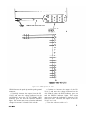
1
TM 11-6625-496-45
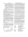
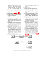
DEPARTMENT OF THE ARMY TECHNICAL MANUAL
FIELD (FOURTH ECHELON) AND DEPOT
MAINTENANCE MANUAL
TEST SET, RADIO AN/VRM-l
This copy is a reprint which includes pen and
ink Changes in force at the time of publication.
HEADQUARTERS, DEPARTMENT OF THE ARMY
3 JULY 1962
Changes in force: C#2 C#4, C#5 and C#6
TM 11-6625-496-45
C6
HEADQUARTERS
DEPARTMENT OF THE ARMY
Washington, DC, 12 March 1980
Change
No. 6
General Support and Depot Maintenance Manual
Including Repair Parts and Special Tools Lists
TEST SETS, RADIO AN/VRM-1 AND AN/VRM-1A
(NSN 6625-00-892-5542)
TM 11-6625-496-45, 3 July 1962, is changed as follows:
The title of the manual is changed to read as shown above.
Page 2. paragraph 1, subparagraph c is superseded as follows:
c. Report of errors, omissions, and recommendations for improving this publication by the individual user is encouraged. Reports should be submitted on DA Form 2028 (Recommended Changes
to Publications and Blank Forms) and fowarded
direct to Commander, US Army (communications
and Electronics Material Readiness Command,
ATTN: DRSEL-ME-MQ. Fort Monmouth, NJ
07703.
Paragraph ld, subparagraph (5) is added after
subparagraph (4). Add the following subparagraphs:
(5) The TS-1777A/VRC displayed a problem of
long warmup voltage data drift. When the CO/NOCO test voltage levels are set at the time the set is
first turned on, it seeks a new set of test trigger
voltage levels after approximately 30 minutes. This
condition has been alleviated by the fol1owing
changes, The changes have been incorporated in the
TS-1777A/VRC starting with serial number 602 and
higher under Contract No. DAAB05-73-C-1632
(1973) and succeeding contracts.
(a) The thermal resistance of diode CR7902
and resistor R7901 (figs. 14 and 54) is reduced
by
the application of a silicon heat sink compound
(Dow Corning No. 340) between the mating surfaces.
(b) Diode CR7901 (figs. 14 and 54), type
1N645, is rated at 400 milliamperes (ma) maximum
current. Actual current measurements arc in excess
of 400 ma when tested at 28.6 volts dc. Therefore,
CR7901 is now type 1N4383 (NSN 5961-00-7656578) which is a l-ampere device. This will result in
a reduced statbilization period.
(c) Resistor R790S (figs. 17 and 55) has been
changed from 475 ohms (fig. 39.1) to 402 ohms
(NSN 5805-00-818-5548) (fig 39.2) This allows the
midpoint trigger leve1 for selector switch positions 9
and 14 to be set closer to the median value for triggering. This action provides a more optimized
operating point. Switch position 14 must be set near
the lower limit to maintain switch position 9 value
below the operating limit.
(d) The TS-1777A/VRC exhibited problems
in sensitivity caused by lack of adjustment
capabilities for positions 2 and 19 of the selector
switch. Fixed resistors R7902 (position 2) and R7919
(position 19) (fig. 11). respectively. have been
replaced with variable resistor R7902 in series with
fixed-film resistor R7923 and variable resistor
R7919 in series with fixed-film resistor R7922 (fig.
11.1). Resistors R7922 and R7923 prevent
overheating of transistors Q7802, Q7803, and
associated components if the variable resistors arc
set for minimum resistance. The minimum
resistance setting of R7902 and R7919 results in the
full input signal level of 20 volts applied to the base
of Q7802, which is in the full input signal level of 20
volts applied to the base of Q7802, which is in excess
of the normal trigger voltage of 2.6 volts. The resul -
tant high current through the base-to-emitter of
Q7802 and R7811 (15 ohms) to ground would cause
both Q7803 and R7811 to fail.
Page 8, paragraph 9a: First sentence, delete
*’R7902° and replace it with R7802.
Page 9, paragraph 10c: Third sentence, line 8;
delete “base” and replace it with collector.
Page 9, paragraph 10d: In line two, delete
"DS7902 and DS7901" and replace it with DS7901
and DS7902.
Page 11, paragraph 12b: In line 4; change
“R7817" to R7921 .
Page 11, paragraph 12c: In line 2, change “ +22
volts dc” to between 21.0 and 22.0 volts dc.
Page 11, paragraph 12d: At the end of paragraph
12d, place the following:
2
Note
In the AN/VRM-1A models that contain
TS-1777A/VRC with serial numbers 802
and higher, inductor L7302 has been replaced with resistor R7304.
Page 12, paragraph 14. Add the following
sentence after the second sentence:
In some equipment (para 1d(5)(d)), the test voltage
is connected through rf choke L7301 and across
voltage divider network consisting of variable
resistor R7902 and resistors R7923 and R7917 (fig.
9.1).
Paragraph 15, line 5. “C7503” is changed to
read C7501.
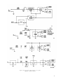
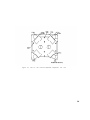
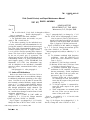
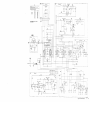
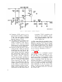
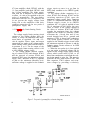
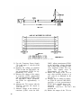
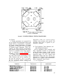
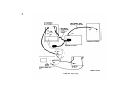
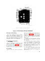
Page 13. Figure 9 is superseded by a new figure 9.
Figure 9. Tests in selector switch positions A. 2..3, and 7.
simplified schematic diagram.
3
Page 14, paragraph 19: In last line, change "475”
to 402.
Paragraph 22: In line 5, add “R7918” after
C7901.
Paragraph 23, line 5. “R7901” is changed to
read R7910.
Page 16, paragraph 27.1. The following sentence
is added after the second sentence:
In some equipment (para 1d(5)(d)), the tested
voltage is connected through rf choke L7301 and
across voltage divider network consisting of
variable resistor R7919 and resistors R7922 and
R7920.
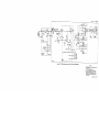
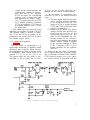
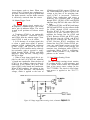
Figure 10.1 is superseded by new figure 10.1.
Figure 10.1. Test in selector switch position 19. simplified
schematic diagram.
Page 29, paragraph 33d. Troulbleshooting Chart.
Make the following changes for symptom 2; insert
the material before the first probable trouble and
correction ("Diode CR7902, etc.”). In Probable
trouble column, insert: Knob on selector switch S7901 is set
180 degrees from proper position.
In Correction column, insert: Set S7901 to position 11. If
GREEN Indicator lights. remove the switch knob and install it
with the arrow pointing to position A. If GREEN indicator does
not Iight, replace the lamp.
Page 20, paragraph 33d, Troubleshooting Chart,
Make the following changes for symptom 4; insert
the material before the first probable trouble and
correction (“Defective R7902, etc.“). In Probable
trouble column. insert: In equipment provided with potentiometer R7902 (fig. 11.1. para Id(5)(d)). the potentiometer is out
of adjustment.
In Correction column, insert: Adjust potentiometer
R7902 (para 43d.1).
Page 21. paragraph 33d, Troubleshooting Chart.
Add the following material after symptom 13.
fig. 11.1
4
para 43d.1
-
Page 22, paragraph 34b. Add the following to the
chart:
Contact No. S7902A
and S7902B
2.
19 .
19
Value (ohms)
Resistor
R7902 and R7923
X7919
R7919 and R7922
8,500..
5,230 ..
5,300
.Two resistors provided in certain equipment; see paragrah 1d(5)(d).
““Value measured will depend on position of potentiometers R7902 and R7919.
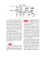
Page 23. New figure 11.2 is added after figure
11.1.
5
Figure 11.2.
6
Page 27, paragraph 38. Make the following
changes:
Subparagraph p. The following note is added:
NOTE
If diode CR7901 is type 1N645 (NSN 596100-577-6084), replace it with type 1N4383
(NSN 5961-00-756-6578) (72699); para 1d(5)
(b)).
Subparagraph r. The following is added before
subparagraph (1): Before inserting diode CR7902 in
its mounting hole, apply a thin evenly spread
coating of Dow Corning No. 340 silicon sealing
(heat sink) compound (NSN 8030-00-998-3337) on
the surface of the diode and the mounting hole.
After securing ((1) below), wipe away excess compound. See paragraph 1d(5)(a) for details.
Subparagraph t. Add the following before subparagraph (1): Before replacing resistor R7901 in
position, apply a thin coating, evenly spread, of
Dow Corning No. 340 silicon heat sink compound
on the surface of the resistor and the mounting sur-
face. After securing ((1) below), wipe away excess
compound. See paragraph 1d(5)(a) for details.
Page 28, paragraph 38u. After paragraph 38v.
add the following note.
NOTE
In some equipment (para 1d(5)(d)), there
are 30 leads instead of 26 connected to
switch S7902.
Page 29, paragraph 38x. The following subparagraphs are added after subparagraph (2):
(3) Measure the resistance of resistor R7908; if
its resistance is 475 ohms, remove it and install a
402-ohm resistor (NSN 5905-00-818-5548) (para
id(s)(c)).
(4) On some equipment (para 1d(5)(c)), fixed
resistors R7922 and R7923 are connected, respectively, to potentiometers R7902 and R7919 (fig.
39.2) for positions 2 and 19, respectively, of the
switch.
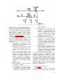
Figure 15 is superseded by a new figure 15:
7
R7902 IS R7923 (1100 OHMS ) WHEN POTENTICMETERS R7902 AND R7919
PROVIDED ON CONTRACT DAAB05 -73 – 6 - 1632 (1973) AND
ARE
SUCEEDING CONTRACTS.
EL4YC004
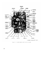
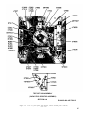
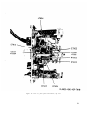
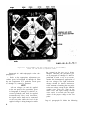
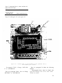
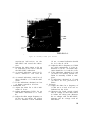
Figure 15. Test Set, Radio TS-1777/VRM-1 and TS-1777A/VRM-1
front panel chassis, top view.
Page 35, paragraph 43. The following is added
after subparagraph d:
d.1. DC Circuits (Positions 2 and 19). The
following procedures are performed on those
equipments with potentiometer R7902 on position 2
of switch R7910 and potentiometer R7919 on position 19 of the switch (fig. 15 and 39.2).
(1) Reduce the 721A output to 0 volt dc. Use
the TS-443/U to measure the 721A output.
(2) Turn the TS-1777A/VRM-1 selector to
position 2.
(3) Set potentiometer R7902 (fig. 11.2 and 15)
approximately midrange.
(4) Raise the 721A output until the GREEN
8
indicator lights. The output of the 721A should be
between 19.00 and 21.10 volts dc.
(5) If necessary, adjust potentiometer R7902
to assure the condition in (4) above.
(6) Reduce the 721A output to 0 volt dc.
(7) Turn the TS-1777A/VRM-1 selector switch
to position 19.
(8) Set potentiometer R7919 (fig. 11.2 and 15)
approximately midrange.
(9) Raise the 721A output until the GREEN
indicator lights. The output of the 721A should be
between 13.00 and 14.70 volts dc.
(10) If necessary, adjust potentiometer R7919
to assure the condition in (9) above.
Make the following changes as idicated:
Page
59
Paragraph
57b(5)
57b(6)
57C(3)
57C(4)
Change
+4.0 volts
+ 5.5 volts
10.500 mc
+ 1.0 volt dc ±0.30
13.000 mc
+1.0 volt dc ±0.30
To
+ 3.5 volts
+ 5.0 volts
10.75 mc ±40 cps
3.00 volts dc ±0.05
10.10 mc ±40 cps
1.65 volts to 275 volts dc
57C add new
paragraph:
(5) Adjust the 606A frequency to 11.60 mc ±40 cps while maintaining a 411A indication of 10 mv. A
normal indication should be 1.65 to 2.75 volts dc.
60
61
57c(5) and (6)
58b(1)
58b(3)
58b(4)
58f(1)
58f(3)
58f(4)
58g(1)
58g(3)
58g(4)
62
67
58g(5)
58g(6)
59b(2)
59c(5)
65g
Add NOTE
after 651:
(5) and (6)
150 mv
+ 3.2 volts
300 mv
200 mv
+ 3.0 volts
300 mv
+ 4.0 volts
200 mv
42.00 mc
200 mv
54.00 mc
200 mv
+ 1.0 volt
+ 1.0 volt
P7801-B
+ 20.7 volts
21.80 volts
(6) and (7)
100 mv
+4.0 volts
200 mv
120 mv
+ 2.5 volts
200 mv
+ 6.0 volts
120 mv
44 mc
120 mv
50.00 mc
120 mv
+ 1.4 volts
+ 1.4 volts
R7901 and R7921
Between 10.00 and 21.10 volts
21.10 volts
NOTE
For R7902 figure 11.2 adjust to occur at 20.0 volts 65l for R7119 fig. 11.2 adjust to occur
at 13.75 volts.
67e
67h
67j
671
68f
68h
68j
69d
0.125 and 0.250 volt
0.200 and 0.250 Volt
0.170 and 0.210 volt
0.650 and 0.810 volt
0.230 and 0.330 volt
0.100 and 0.140 volt
0.180 and 0.250 volt
0.012 and 0.016 volt
0.100 and 0.135 volt
0.110 and
0.155 and
0.155 and
0.645 and
0.215 and
0.085 and
0.165 and
0.0105 and
0.085 and
0.265 volt
0.225 volt
0.225 volt
0.815 volt
0.345 volt
0.155 volt
0.265 volt
d 0.0175 volt
0.150 volt
Page 75. Add figure 38.2 after figure 38.1.
Page 77. Add figure 39.2 after figure 39.1.
9
By Order of the Secretary of the Army:
Official:
E. C. MEYER
General, United States Army
Chief of Staff
J. C. PENNINGTON
Major General, United States Army
The Adjutant General
Distribution:
To be distributed in accordance with DA Form 12-51, Direct and General Support maintenance requirements for AN/VRM-l.
Changes in force: C 2, C 4, and C 5
TM
11-6625-496~5
*C 5
HEADQUARTERS
DEPARTMENT OF THE ARMY
W ASHINGTON , D. C., 4 June 1973
C HANCE
No. 5
General Support and Depot Maintenance Manual
Including Repair Parts and Special Tool List
TEST SETS, RADIO AN/VRM-1 AND AN/VRM-1A
TM 11-6625-496-45, 3 July 1962, is changed as follows:
Page 2, paragraph 1, Delete subparagraph b.
Paragraph 1, Delete subparagraph c and substitute the following:
c. The reporting of errors, omissions, and
recommendations for improving this publication by the individual user is encouraged. Report should be made on DA Form 2028
(Recommended Changes to Publications) and
forwarded to Commander, US Army Electronics Command, ATTN: AMSEL-MA-CR, Fort
Monmouth, N.J. 07703
Paragraph 1.1.
Change the second sentence to read “DA Pam
— 310-4 is an index of current technical manuals,
technical bulletins, supply manuals (types 7,
8, and 9), supply bulletins, and lubrication
orders.”
Page 4, figure 1. At Q7402 and Q7403, delete
“2N270” and insert “2N270 (MOD) OR
2N599.”
Page 6, figure 3. To "2N2208" at Q7701, add
2N588 OR 2N12250
Page 11 of C 4, figure 39.1. Make the following
changes:
At C7602, add 220 UUF (NOTE 7).
At Q7602 and Q7701, add OR 2N1225 (NOTE
8).
At Q7402 and Q7403, delete “2N270” and insert
the following: 2N270 (MOD) OR 2N599
(NOTE 8).
Add the following notes:
7. VALUE OF C7602 IS 220 UUF IN EQUIPMENT PROCURED ON CONTRACT DAAB05-72-C-4921.
8. Q7602 and Q7701 ARE TYPE 2N1225,
AND Q7402 AND Q7403 ARE TYPE 2N599
IN EQUIPMENT PROCURED ON CONTRACT DAAB05-72-C-4921.
Page 69 (page 1 of C 3). Change APPENDIX
to APPENDIX I.
Appendix II. Delete appendix II and substitute
the following.
‘This change supersedes C 3, 17 August 1965.
i
APPENDIX II
GENERAL SUPPORT AND DEPOT MAINTENANCE REPAIR
PARTS AND SPECIAL TOOLS LIST
Section I.
INTRODUCTION
1. Scope
This appendix lists repair parts required for
the performance of general support and depot
maintenance of the AN/VRM-1 and AN/VRM1A
NOTE
No special tools, test, or support equipment is required.
2. General
This repair parts list is divided into the follow-.
ing sections:
a. Repair Parts-Section II. A list of repair
parts authorized for the performance of maintenance at the general support and depot level.
b. Index—Federal Stock Number and Reference Number Cross-Reference to Figure and
Item Number or Reference Designation-Section III. A list of Federal stock numbers in ascending numerical sequence, followed by a list
of reference numbers in ascending alphanumerit sequence, cross-referenced to the figure
number and reference designation.
c. Index-Reference Designation Cross-Reference to Page Number-Section IV. A list of
reference designations cross-referenced to page
numbers.
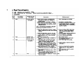
3. Explanation of Columns
The following provides an explanation of columns in the tabular lists:
a. Source, Maintenance, and Recoverability
Codes (SMR), Column 1.
(1) Source codes indicate the selection
status and source for the listed item. Source
codes areCode
Explanation
P—Repair parts which are stocked in or supplied from the GSA/DSA, or Army
supply system, and authorized for use
at indicated maintenance categories.
M—Repair parts which are not procured or
stocked, but are to be manufactured at
indicated maintenance levels.
A—Assemblies which are not procured or
stocked as such, but are made up of two
or more units. Such component units
carry individual stock numbers and descriptions, are procured and stocked
separately and ‘can be assembled to
form the required assembly at indicated
maintenance categories.
X1—Repair parts which are not procured or
stocked. The requirement for such items
will be filled by use of the next higher
assembly or component.
X2—Repair parts which are not stocked. The
indicated maintenance category requiring such repair parts will attempt to
obtain same through cannibalization.
Where such repair parts are not obtainable through cannibalization, requirements will be requisitioned, with accompanying justification, through normal supply channels.
(2) Maintenance codes indicate the lowest
category of maintenance authorized to install
the listed item. The maintenance level codes
areExplanation
Code
0 . ----- Organizational maintenance
H - - - - - - General support maintenance
D - - - - - - Depot maintenance
(3) Recoverability codes indicate whether
unserviceable items should be returned for recovery or salvage. Items not coded are expendable. Recoverability codes areI
Explanation
Code
R—Repair parts and assemblies that are economically repairable at DSU and GSU
activities and are normally furnished
by supply on an exchange basis.
T—High-dollar value recoverable repair parts
which are subject to special handling
and are issued on an exchange basis.
Such repair parts normally are repaired
or overhauled at depot maintenance activities.
b. Federal Stock Number, Column Z . This
column indicates the Federal stock number assigned to the item and will be used for requisitioning purposes.
c. Description, Column 3. This column indicates the Federal item name and any additional
description of the item required. A part number
or other reference number is followed by the
applicable five-digit Federal supply code for
manufacturers in parentheses.
d. Unit of Meaaure (U/M), Column 4. A twocharacter alphabetic abbreviation indicating the
amount or quantity of the item upon which the
allowances are based, e.g., ft, ea, pr, etc.
e. Quantity Incorporated in Unit, Column 5.
This column indicates the quantity of the item
used in the AN/VRM-1 and AN/VRM-1A.
f. Allowances (30-Day DS/GS Maintenance,
1 Year Per Equipment (Contingency), and Depot Maintenance) Columns 6, 7, 8, and 9. Items
authorized for requisition as required are
identified with an asterisk in the allowance
column.
g. Illustrations, Column 10. This column is
divided as follows:
(1) Figure number, column 10a. Indicates
the figure number in which the item is shown.
(2) Item number or reference designation,
column 10b. Indicates the reference designation
used to identify the item in the illustration.
1-4. Special Information
Identification of the usable on codes included in
column 3 of section II areUsed onCode
AN/VRM-1
A ------ ------ ------ ------ B ----- ----- ----- ----- ------ AN/VRM-1A
NOTE
Where no usable codes are indicated,
item is applicable to all models.
2
1-5. Location of Repair Parts
a. This manual contains two cross-reference
indexes (sees. III and IV) to be used to locate
a repair part when either the Federal stock
number, reference number (manufacturer’s
part number), or reference designation is
known. The first column in each index is prepared in numerical or alphanumerical sequence
in ascending order. Where a federal stock number is not listed, refer to the reference number
(manufacturer’s part number) immediately
following the Federal stock number column.
b. When the Federal stock number or reference number is known, follow the procedures
given in (1) and (2) below.
(1) Refer to the index of Federal stock
numbers (sec. HI) and locate the Federal stock
number or reference number. The Federal stock
number or reference number is cross-referenced
to the applicable figure and reference designation.
(2) When the reference designation is determined, refer to the reference designation
index (sec. IV). The reference designations are
listed in alphanumeric ascending order and are
cross-referenced to the page number on which
they appear in the repair parts list (see II).
Refer to the page number noted in the index
and locate the reference designation in the repair parts list (col. 10b).
c. When the reference designation is known,
follow the procedures given in b(2) above.
d. When neither the Federal stock number,
reference number, nor reference designation is
known, identify the part in the illustration and
follow directions given in c above; or scrutinize
column 3 of the repair parts list (sec. H).
1-6. Federal Supply Code for Manufacturers
Manufacturer
Coda
Electrospace
Corporation
13467 ---- . . .
ITT Cannon Electric, Inc.
71468 ---Dialight Corporation
72619
E. F. Johnson Co.
74970 80063
--. Army Electronics Command .
Procurement and Production Directorate
8 0 2 9 4 - - - - - Bourns, Inc.
81349 .- -- Military Specifications
Aeronautical Standards
88044
Military Standards
96906 .-
TM 11-6625-496-45
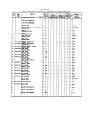
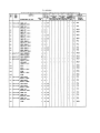
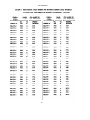
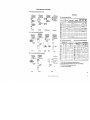
SECTION II REPAIR PARTS FOR DIRECT SUPPORT, GENERAL SUPPORT. AND DEPOT MAINTENANCE
TM 11-6625-496-45
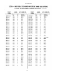
SECTION II REPAIR PARTS FOR DIRECT SUPPORT GFNERAL SUPPORT AND DEPOT MAINTENANCE ( CONTINUED)
6
TM 11-6625-496-45
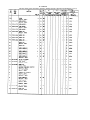
SECTION II REPAIR PARTS FOR DIRECT SUPPORT, GENERAL SUPPORT AND DEPOT MAINTENANCE (CONTINUED)
7
TM 11-6625-496-45
SECTION II REPAIR PARTS FOR DIRECT SUPPORT GENERAL SUPPORT AND DEPOT MAINTENANCE(CONTINUED)
8
TM 11-6625-496-45
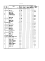
SECTION II REPAIR PARTS FOR DIRECT SUPPORT, GENERAL SUPPORT AND DEPOT MAINTENANCE (CONTINUED)
9
TM 11-6625-496-45
SECTION 11 REPAIR PARTS FOR DIRECT SUPPORT. GENERAL SUPPORT, AND DEPOT MAINTENANCE (CONTINUED )
10
TM 11-6635-496-45
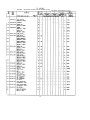
SECTION II REPAIR PARTS FOR DIRECT SUPPORT, GENERAL SUPPORT, AND DEPOT MAINTENANCE (CONTINUED )
11
TM 11-6625-496-45
SECTION II REPAIR PARTS FOR DIRECT SUPPORT, GENERAL SUPPORT, AND DEPOT MAINTENANCE (CONTINUED)
12
TM 11-6625-496-45
SECTION II REPAIR PARTS FOR DIRECT SUPPORT, GENERAL SUPPORT AND DEPOT MAINTENANCE (CONTINUED)
13
TM 11-6625-496-45
SECTION II REPAIR PARTS FOR DIRECT SUPPORT, GENERA SUPPORT, AND DEPOT MAINTENANCE (CONTlNUED)
14
TM 11-6625-496-45
SECTlON II
REPAIR PARTS FOR DIRECT SUPPORT, GENERAL SUPPORT
15
AND DEPOT MAINTENANCE (CONTINUED )
TM 11-6625-496-45
SECTION II REPAIR PARTS FOR DIRECT SUPPORT, GENERAL SUPPORT, AND DEPOT MAINTENANCE (CONTINUED)
16
TM 11-6625-496-45
SECTION II REPAIR PARTS FOR DIRECT SUPPORT, GENERAL SUPPORT, AND DEPOT MAINTENANCE (CONTINUED )
17
TM 11-6625-496-45
SECTION II REPAIR PARTS FOR DIRECT SUPPORT, GENERAL SUPPORT, AND DEPOT MAINTENANCE (CONTINUED)
18
TM 11-6625-496-45
SEClTON II REPAIR PARTS FOR DIRECT SUPPORT, GENERAL SUPPORT, AND DEPOT MAINTENANCE (CONTINUED)
19
TM 11-6625-496-45
SECTION II REPAIR PARTS FOR DIRECT SUPPORT, GENERAL SUPPORT, AND DEPOT MAINTENANCE (CONTINUED)
20
TM 11-6625-496-45
SECTION II REPAIR PARTS FOR DIRECT SUPPORT, GENERAL SUPPORT, AND DEPOT MAINTENANCE (CONTINUED)
21
TM 11-6625-496-45
SECTION II REPAIR PARTS FOR DIRECT SUPPORT, GENERAL SUPPORT AND DEPOT MAINTENANCE (CONTINUED )
22
TM 11-6625-496-45
SECTION II REPAIR PARTS FOR DIRECT SUPPORT, GENERAL SUPPORT AND DEPOT MAINTENANCE (CONTINUED)
23
TM 11-6625-496-45
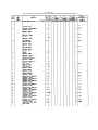
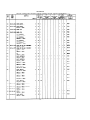
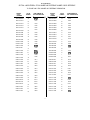
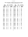
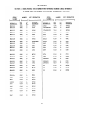
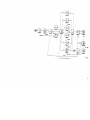
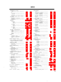
SECTION III INDEX-FEDERAL STOCK NUMBER AND REFERENCE NUMBER CROSS REFERENCE
TO FIGURE AND ITEM NUMBER OR REFERENCE DESIGNATION
FEDERAL
STOCK
NUMBER
FIGURE
NUMBER
FIGURE
NUMBER
5305-543-2761
52
H7510
H7917
5305-543-5059
55
H7903
.
t
ITEM NUMBER OR
REF. DESIGNATION
FEDERAL
STOCK
NUMBER
ITEM NUMBER OR
REF. DESIGNATION
i
5305-059-6809
42
5305-271-8410
54
54
H7919
5305-543-5059
55
H7922
5305-271-8410
54
H7935
5305-543-5059
56
H7925
5305-271-8410
54
H7937
5305-543-5059
56
H7926
5305-531-0298
5305-271-8410
58
H7915
5305-558-4888
53
H7908
5305-531-0298
58
H7933
5305-576-2273
41
H7100
5305-531-9520
49
H7202
5305-576-2273
41
H7101
5305-531-9520
49
H7226
5305-579-3021
44
H7941
50
H7202
5305-619-4409
41
H7102
5305-531-9520
50
H7226
5305-619-4409
41
H7103
5305-531-9521
40
H7208
5305-638-0653
42
H7408
5305-531-9521
40
5305-638-0653
42
5305-638-0653
44
H7940
5305-638-0653
51
H7513
5305-531-9520
5305-531-9521
47
5305-531-9521
47
5305-531-9521
47
H7208
5305-638-0653
51
47
H7239
5305-638-0653
51
H7817
5305-531-9521
49
H7205
5305-638-0653
54
H7901
5305-531-9521
49
H7211
5305-687-6535
54
H7912
5305-531-9521
5305-531-9521
49
H7239
5305-687-6535
54
H7932
5305-531-9521
50
H7205
5305-857-4335
51
H7942
5305-543-2410
54
H7920
5310-045-4007
55
H7905
5305-543-2759
49
H7215
5310-045-4007
55
H7924
5305-543-2759
49
H7216
5310-045-4007
56
H7929
5305-543-2759
49
H7235
5310-045-4007
56
H7930
5305-543-2759
49
H7236
5310-167-0815
51
H7514
5305-543-2759
50
H7215
5310-275-1292
40
5305-543-2759
50
H7216
5310-275-1292
40
H7230
5305-543-2759
50
H7235
5310-275-1292
47
H7209
5305-543-2759
50
H7236
5310-275-1292
47
H7212
5305-543-2761
45
H7602
5310-275-1292
47
H7230
5305-543-2761
45
H7606
5310-275-1292
47
H7240
5305-543-2761
52
H7509
5310-275-1292
49
24
TM 11-6625-496-45
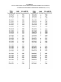
SECTION III INDEX-FEDERAL STOCK NUMBER AND REFERENCE NUMBER CROSS REFERENCE
TO FIGURE AND ITEM NUMBER OR REFERENCE DESIGNATION (CONTINUED )
25
TM 11-6625-496-45
INDEX-FEDERAL STOCK NUMBER AND REFERENCE NUMBER CROSS REFERENCE
TO FIGURE AND ITEM NUMBER OR REFERENCE DESIGNATION ( CONTINUED )
26
TM 11-6625-496-45
27
TM 11-6625-496-45
28
TM 11-6625-496-45
29
TM 11-6625-496-45
30
TM 11-6625-496-45
31
TM 11-6625-496-45
32
TM 11-6625-496-45
33
TM 11-6625-496-45
31
TM 11-6625-496-45
35
TM 11-6625-496-45
36
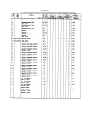
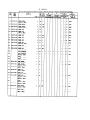
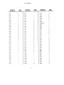
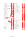
SECTION IV
TM 11-6625-496-45
INDEX-REFERENCE DESIGNATION
CROSS REFERENCE TO PAGE NUMBER (CONTINUED )
REFERENCE
DESIGNATION
.
PAGE
NUMBER
PAGE
NUMBER
REFERENCE
REFERENCE
DESIGNATION
PAGE
NUMBER
H7803
20
H7922
15
L7301
16
H7804
20
H7923
15
L7401
6
H7805
20
H7924
15
L7501
13
H7806
20
H7925
15
L7601
7
H7807
19
H7926
15
L7602
7
H7806
20
H7927
15
L7603
7
H7809
20
H7928
15
L7701
22
H7810
20
H7929
15
L7702
22
H7811
20
H7930
15
L7703
22
H7812
20
H7931
17
L7704
22
H7816
20
H7932
17
L7705
22
H7817
19
H7933
17
MP7000
5
H7900
14
H7934
17
MP7100
5
H7901
14
H7935
17
MP7101
5
H7902
15
H7936
17
MP7102
5
H7903
15
H7937
18
KP7200
8
H7904
15
H7938
18
MP7201
6
H7905
15
H7939
19
MP7202
9
H7907
15
H7940
14
MP7203
9
H7908
16
H7941
14
MP7204
9
9
H7909
16
H7942
14
MP7205
H7910
16
H7943
14
MP7206
9
H7911
17
H7944
19
MP7207
9
H7912
17
H7945
19
MP7208
10
19
MP7209
10
H7913
17
H7946
H7914
17
J71O0
5
MP7210
10
H7915
17
J7902
18
MP7211
10
18
MP7212
10
17
J7903
H7917
17
J7904
18
MP7213
10
H7918
17
J7905
16
MP7214
11
H7919
18
J7906
18
MP7215
11
H7920
18
J7907
18
MP7216
12
H7916
37
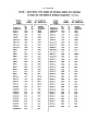
M 11-6625-496-45
SECTION IV INDEX- REFERENCE DESIGNATION
CROSS REFERENCE TO PAGE NUMBER (CONTINUED )
PAGE
NUMBER
REFERENCE
DESIGNATION
REFERENCE
DESIGNATION
PAGE
NUMBER
REFERENCE
DESIGNATION
PAGE
NUMBER
MP7217
12
MP7914
17
R7405
6
MP7218
12
MP7915
18
R7406
6
MP7219
12
P71OO
5
R7407
6
MP7220
12
P7101
5
R7408
6
MP7221
12
P7401
6
R7409
6
MP7222
12
P7501
13
R7410
6
MP7222
13
P7601
7
R7501
14
MP7223
13
P7701
22
R7601
8
MP7224
13
P7801
19
R7602
8
MP7225
13
Q7301
16
R7603
8
8
AP7226
19
C7401
7
R7604
MP7227
19
Q7402
7
R7605
8
MP7239
9
Q7403
7
R7606
8
MP7240
9
Q7601
8
R7607
8
MP7241
9
Q7602
8
R7608
8
MP7242
99
Q7701
23
R7609
8
MP7243
9
Q7702
23
R7611
8
MP7500
14
Q7703
23
R7612
8
MP7900
14
Q7801
21
R7613
8
MP7901
14
Q7802
21
R7701
22
MP7902
15
Q7803
21
R7702
23
MP7903
15
Q7804
21
R7703
2 3
MP7904
15
Q7805
21
R7704
23
MP7905
15
Q7806
21
R7705
23
MP7906
15
R7301
16
R7706
MP7907
15
R7302
16
R7707
MP7906
16
R7303
16
R7708
16
R7304
16
R7709
23
R7710
23
R7711
23
R7712
22
R7713
22
R7714
22
MP7909
MP7910
16
R7401
6
MP7911
16
R7402
6
MP7912
16
R7403
6
MP7913
16
R7404
6
38
23
23
23
22
TM 11-6625-496-45
SECTION lNDEX- REFERENCE DESIGNATION
IV
CROSS REFERENCE TO PAGE NUMBER (CONTINUED )
REFERENCE
DESIGNATIUN
PAGE
NUMBER
REFERENCE
DESIGNATION
PAGE
NUMBER
R7715
22
R7913
18
R7716
23
R7914
18
R7717
23
R7917
17
R7718
22
R7918
14
R7801
20
R7919
“18
R7802
20
R7920
14
R7803
20
R7921
14
17
R7804
21
S7901
R7805
20
S7902
19
R7806
20
T7601
8
R7807
20
T7602
8
R7808
20
T7702
23
R7809
20
TB7300
16
R7811
20
TB7400
6
R7812
20
TB7500
14
R7813
20
TB7600
8
R7814
20
TB7700
22
R7815
20
TB7800
20
R7816
20
TB7900
14
R7818
21
TP7900A
15
R7819
21
TS1777/VRM-1
5
R7901
17
W7000
5
R7902
18
W7001
5
16
R7903
1.8
W7304
R7904
18
W7900
18
R7905
18
W7901
16
R7906
18
XDS7901
15
R7907
18
XDS7902
15
R7908
18
XF7901
15
R7909
18
R7910
18
R7911
18
39
REFERENCE
DESIGNATION
PAGE
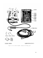
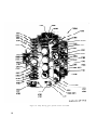
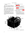
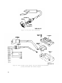
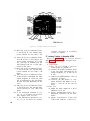
Figure 40. Test Set, Radio AN/VRM-1, components and running spares.
35
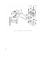
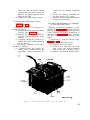
Figure 41. Branched power cable, partially disassembled.
36
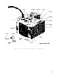
Figure 42. Test set, case removed, three-quarter view from bottom
37
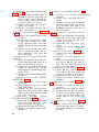
Figure 43.
38
Audiofrequency amplifier printed circuit card A7400.
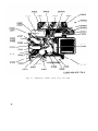
Figure 44.
Teat set, case removed, adjustable components, rear view.
39
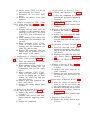
Figure 45.
40
11.5-MHz amplifier printed circuit card A7600.
Figure 46. Case, test set removed, gaaket and bumpers (AN/VRM-1).
41
Figure 47. Test Set, Radio AN/VRM-1A, case cover and instruction plates.
Figure 48.
42
Case,
test
set
removed,
gasket
and
(AN/VRM-1A)
Figure
49.
Test
Set,
Radio
AN/VRM-1,
cover
components.
43
Figure 50. Cover assembly (AN/VRM-1A).
Figure 51.
44
Ted set, case removed, three-quarter view from top.
Figure 52. Band pass filter printed circuit card A7500.
45
Figure 53. Test probe assembly.
46
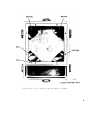
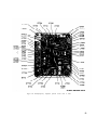
TEST SET SUB-ASSEMBLY
(CAPACITOR- RESISTOR ASSEMBLY)
SECTION A-A
Figure 54.
EL6625-496-40P-TM-15
Test set, front panel and chassis, chassis bottom plate removed,
rear view.
47
Figure 55. Test set, front panel and chassis, bottom view.
48
Figure 56.
Test set, front panel and chassis, left view.
49
Figure 57. Test probe, radiofrequency preamplifier.
50
Figure 58. Teat set, front panel and chassis, top view.
51
Figure 59. Lamp driving gates printed circuit card 7800.
52
Figure 60. Radiofrequency amplifier printed circuit card A 7700.
53
By Order of the Secretary of the Army:
Official:
VERNE L. BOWERS
Major General, United States
The Adjutant General
CREIGHTON W. ABRAMS
General, United States Army
Chief of Staff
Army
.
Distribution:
To be distributed in accordance with DA Form 12-51 (qty rqr block No. 599) Direct and General
Support Maintenance requirements for AN/VRC-12.
Changes in force: C 2, C 3, and C 4
TM 11-6625-496-45
C 4
HEADQUARTERS
DEPARTMENT OF THE ARMY
W ASHINGTON , D.C. 9 July 1970
CHANGE
No. 4
GS and Depot Maintenance Manual
Including Repair Parts and Special Took Lists
TEST SETS AN/VRM-1 AND AN/VRM-1A
TM 11-6625-496-45, 3 July 1962, is changed as follows:
The title of this manual is changed as shown above.
NOTE
.
“GS” maintenance stands for general
support maintenance. All references in
this manual to “fourth echelon” or
“fourth echelon maintenance are the
same as GS or general support maintenance.
Throughout the manual change the following
figure references as indicated
From
To
12 . . . . . . . . .12 and 12.1
l3 . . . . . . . . . . . . 18 and 13.1
15 . . . . . . . . . . ..l5 and l5.l
16 . . . . . . . . . . ..l6 and l6.l
17 . . . . . . . . . . ..l7 and l7.l
18 . . . . . . . . . . ..l8 and l8.l
23 . . . . . . . . . . ..23 and 23.l
30 . . . . . . . . . . . . 30 and 30.1
38 . . . . . . . . . . . . 38 and 38.1
39 . . . . . . . . . . ..39 and 39.l
Page 2, paragraph 1. Make the following
Changes:
Subparagraph c (page 1 of C 3), last line.
Change “(NMP)-MA” to: NMP-EM.
Add subparagraph d after subparagraph c.
d. All references in this manual to ANmRM1 and TS-1777/VRM-l also apply to AN/VRM-
1A and TS-1777A/VRM-l. Model differences are
described in (1) through (4) below.
(1) Test Set, Radio TS-1777A/VRM-l (part
of Test Set, Radio AN/VRM-lA) is identical with
Test Set, Radio TS-1777/VRM-l (part of Test
Set, Radio AN/VRM-1) except for the case and
cover.
(2) The TS-1777/VRM-l and TS-1777A/
VRM-l front panel and attached chassis are
mechanically and electrically identical with each
other and may be mounted in the case of either
the TS-1777/VRM-l or TS-1777A/VRM-l ((3)
below) .
(3) In the TS-1777/VRM-1, the case has
six latches, the chassis panel is flush with the
edge of the case, and the gasket in the cover is
on the edge of the cover. In the TS-1777A/VRM1, the case has four latches, the chassis panel is
sunk below the edge of the case, and the gasket
in the cover is recessed (fig. 11.1).
(4) On instruction plates for the TS-1777A/
VRM-1 (TM 11-6625496-12), an additional instruction in the first plate advises the user to
return good modules to the radio set, and on the
second plate, switch position 19 is used instead
of position A for test No. 11 of crystal reference
system A3000.
1
NOTE
New plates should be requisitioned for
those tat sets that do not have plates
described in (4) above
Paragraph 2 f, line 9. Change “22 volts” to:
21.5 volts.
Page 5, figure 2. Make the following changes:
Change the resistance value of “R7612” and
“R7613” to: 51 (ohms). Add the following:
NOTE
In some units, the resistance value of
R7612 is 75 ohms and R7613 is 33 ohms.
Page 11, figure 8. Make the following changes.
Change the resistance values of “R7818" to
“51 (ohms) “ and “R7819” to “8.2K"
Add the following:
NOTE
In some units, the resistance value of
R7818 is lK and R7819 is lK.
Page 12, paragraph 13 b, line 4. Delete "TP3002"
Page 16, add paragraph 27.1 and figure 10.1
after paragraph 27.
27.1. Selector Switch Position 1.
(fig. 10.1)
When selector switch is in position 19, the +13.5
(±1)-volt dc output of module A2100 to relay
K3001 in assembly A3000 can be tested. The
tested voltage is connected through rf choke
L7301 and voltage dropping resistors R7919 and
R7920 to the voltage supply limits sensing circuit.
The output of this circuit is applied to the Schmitt
trigger circuit. If the voltage is within limits,
GREEN indicator lamp DS7092 lights. If the voltage is not within limits, insufficient voltage will
be applied to the Schmitt trigger circuit, and RED
indicator lamp DS7901 lights. The operating voltage for the Schmitt trigger is supplied from the
+16-volt dc line.
Figure 10.1. Test in selector switch position 19, simplified schematic diagram
Page 19, paragraph 33 d. Add the following
note below the heading:
replace the affected assembly. (Repair
parts for assemblies are not provided.)
NOTE
If a component is detected as defective in assemblies A7300 through A7800,
2
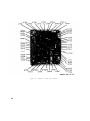
Page 23. Delete figure 11 and substitute new
figure 11.
Figure 11.
3
Add figure 11.1 after figure 11.
Figure 11.1
4
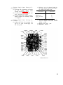
Page 24, paragraph 36. Add the following as
the introductory paragraph:
The front panel and chassis of the TS-1777/VRM1 (AN/VRM-l) and TS-1777A/VRM-l (fig. 11.1)
(AN/VRM-lA) are identical in dimensions but
the case of each is different (para 1 d). Consequentlyt the front panel and chassis of either
odel can be put in the case of the other model
Page 33, paragraph 43. Designate the existing
note as 1 and l dd the following notes:
NOTE 2
All test voltages (ac and dc) applied
to the test probe (c through h below)
shall be increased gradually and shall be
applied instantaneoualy after each increment; and the signal source shall not
be connected to the test set while the
level of the applied voltage is being
changed or while the adjustment control in the test set under test is being
changed. Therefore, the procedures in c
through h below shall be performed in
such a way as to accommodate this instantaneous application of the test voltages
NOTE 3
The light indication change should be
almost instantaneous at the moment of
touching the test probe to the applied
test voltage, except for the 1000-Hz
(audio) tests given in- e below. Thus, in
the audio test the light change should
occur within 10 seconds after the application of the proper voltage to the test
probe.
NOTE 4
Refer to the appropriate adjustment
procedures given in c through h below
when the test requirements of a particular circuit (para 47 through 51, and
64 through 67) cannot be obtained.
Page 35, paragraph 43c(10), last line. Change
"13.0 - volts to: 13.5 Volts. (When the GREEN
indicator goes out, the RED indicator should
light.)
Paragraph 43e(l) (b), line 2. Change “ME20B/U” to: AN/URM-145.
Page 36, paragraph 43h (6), last line. Change
“210 mv” to: 115 mv.
Page 37. Add new figure 23.1 after figure 23.
5
Figure 23.1. TS-1777A/VRM-1 (and later production units of TS-1777/VRM-1),
bottom view and location of adjustable controls.
Paragraph 44. Add subpagraph c after subparagraph b.
c. Refer to the appropriate adjustment procedures given in Paragraph 62 through 69 when
the test requirement of a particular circuit (para
47 through 51) cannot be obtained.
NOTE
All test voltages (ac and dc) applied
to the test probe in the procedures given
in Paragraph 47 through 51 shall be increased gradually and shall be applied
instantaneously after each increment;
the signal source shall not be connected
to the test probe while the level of the
applied voltage is being changed or while
6
the control on the test set is being
changed. Therefore, the procedures given in paragraph 47 through 51 shall be
performed in such a way as to accommodate this instantaneous application of
the test voltages The light indication
change should be almost instaneous
at the moment of touching the test probe
to the test voltage, except for the 1000-Hz
(audio) tests (para 48). Thus in the
audio tests, the light change should
occur within 10 seconds after the application of the proper voltage to the test
probe.
Page 41, paragraph 47c. Make the following
changes in the “Performance Standard" column.
+19.00 and +21.80.
In step 2b, change “+14.2” to: between
+13.40 and +15.00.
In step 4b, change “+10.50” to: between
+9.90 and +1120.
In step 2c, change “+17.6” to: between
+17.30 and +19.50.
In step 4c, change “+13.00” to: between
+12.70 and +14.20.
Add step No. 5 after step No. 4.
In step 3b, change “+20.7” to: between
Step No.
5
Test equipment
control settings
Sane as step No. 4
Equipment under
test control
settings
Same as step No. 1
except: Selector
switch: 19
Test
procedure
Performance
standard
a. Same as step
No. 4a.
a RED indicator
lights.
b. Same as step
No. 4b.
b. TS-443/U indicdes between+13.00 and
+14.70 volts.
Page 43, paragraph 48c. Make the following
changes:
In step No. lc, change “0.180” to: between
.125 and .250.
Add the following after the heading of subparagraph c: The light indication change to
GREEN may occur instantaneously, but if it
does not the change should occur within 10 secnds after required voltage limits are applied to
the test probe.
In step No. 2c, change “0.220” to: between
.200 and .250.
Make the following changes in the “Perfomance Standard" column:
In step lb, change “2.85” to: between 2.60
and 3.30.
In step 2b, change “U3” to: between 1250
and 14.90.
In step 3b, change “0.49” to: between .450
and .520.
In step 4b, change ‘0.90” to: between .800
and 1.00.
In step 5b, change “0.225” to: between .200
and .250.
In step No. 3c, change “0.480” to: between
.170 and 210.
In step No. 4c, change “0.720” to: between
.650 and .810.
Page 51, paragraph 50c. Make the following
changes in the “Performance standard” column:
In step No. lb, change “0.27” to: between
0230 and .330.
In step No. 2b, change “0.130” to: between
.100 and .140.
In step No. 3b, change “0.225” to: between
.180 and .250.
In step No. 4b, change “0.014” to: between
.012 and .016.
In step 6b, change “6.40” to: between 6.00
and 7.30.
Page 53, paragraph 51c. In “Performance standard” column, change subparagraph b to read:
411A indicates between .100 and .135 volt.
Page 47, paragraph 49c. Make the following
changes in the “Performance standard” column:
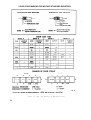
Page 54, paragraph 52, chart. Delete the chart
and substitute:
7
Indicattor
Signal at probe tip
Selector switch
S7902 position
A
2
3
4
5
6
7
8
9
10
11
12
13
14
15
16
17
18
19
Type
Note 1)
Note 2)
dc
dc
dc
dc
dc
af
af (Note 3)
af
af (Note 3)
af
af (Notc3)
af
af (Note 3)
rf
rf
dc
dc
dc
rf
rf
af
af (Note 3)
af
af (Note 3)
rf
rf
rf
rf
rf
rf
rf
rf
rf
rf
rf
rf
rf
rf
dc
dc
Frequency
Voltage
RED
.
.
.
.
.
.
.
l kc
l kc
l kc
l kc
l kc
l kc
l kc
l kc
11.5 mc
11.5 mc
.
.
.
11.5 mc
11.5 mc
1 kc
1 kc
1kc
1 kc
5.65 mc
5.65 mc
11.5 mc
11.5 mc
11.5 mc
11.5 mc
5.65 mc
5.65 mc
5.65 mc
5.65 mc
5.65 mc
5.65 mc
47.0 mc
47.0 mc
.
.
.
.
+7.0
+13.4 40-15.00
+17.30-19.50
+10.0
+19.00-21.00
1.4
2.60-3.30
7.0
12.50-14.80
0.25
0.450-0.520
0.45
0.800-1.00
0.13
0.230-0.330
+5,0
+9.90-11.20
+12.70-14.20
0.06
0.100-0.140
0.11
0.200-0.250
3.2
6.00-7.30
0.08
0.1250.250
0.11
0.180-0.250
0.007
0.012-0.016
0.11
0.200-0.250
0.24
0.180-0.210
0.36
0.650-0.810
0.10
0.100-0.135
+5.0
+13.00-14.70
x
Notes:
1. ON-OFF switch at ON.
2. Test probe tip in test jack A.
3. GREEN indication occurs within 10 seconds after application of required voltage.
8
GREEN
x
x
x
x
x
x
x
x
x
x
x
x
x
x
x
x
x
x
x
x
x
x
x
x
x
x
x
x
x
x
x
x
x
x
x
x
x
x
x
x
x
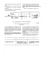
Page 55, paragraph 54b (3), chart Add the folwing item to the chart:
Test equipment
Technical manual
multmeter, Electronic
AN/URM-146 . . . . . TM 11-6625-524-15-1
Pages 59. Add figure 30.1 after figure 30.
Figure 30.1.
Assembly A7500 in TS-1777A/VRM-1 in later production waits of
TS-1777/VRM-1, parts location
Paragraph 57d(2), Change "ME-30B/
U“ to: AN/URM-145
Page 61, paragraph 58, Make the following
changes:
Page 60, paragraph 58d(2), line 48 Change
“ME-30B/U” to: AN/URM-14S
subparagraph d(2)(a), chart, In “Signal volts
age(rms)change the first line from
"81 mv" to: 18 mv.
9
Subparagraph h(2), line 5. Change “ME
30B/U to: AN/URM-145.
Page 63, figure 31. In figure 31, change callout
“Q7606-C” to: Q7602-C.
Page 65 (page 2 of C 2), paragraph 61a, chart.
Delete the chart and substitute:
(1) TM 11-6625-496-12, with current
changes.
(2) TM 11-6625-496-45, with current
changes.
(3) TB SIG 355-1.
(4) TB SIG 355-2.
(5) TB SIG 355-3.
Page 3 of C 2, paragraph 61b, line 4. Change
“DA Pam 310-4” to: DA Pam 310-7.
Page 66 (page 3 of C 2), paragraph 63. Add the
subparagraphs d, e, and f after subparagraph c.
d. All test voltages (ac and dc) applied to
the test probe in the procedures given in paragraphs 64 through 69 shall be increased gradually
and shall be applied instantaneously after each
increment, and the signal source shall not be
connected to the test probe while the level of
the applied voltage is being changed, or while
the adjustment control in the test set under test
is being changed. Therefore, the procedures given
in paragraphs 64 through 69 shall be performed
in such a way as to accommodate this instantaneous application of the test voltages.
e. The light indication change should be almost instantaneous at the moment of touching
the test probe to the test voltage, except for the
10
1,000-Hz (audio) tests given in paragraph 66.
Thus, in the audio tests, the light change should
occur within 10 seconds after the application of
the proper voltage to the test probe.
f. Refer to the appropriate adjustment procedures (paragraph 43) when the requirements of a parrticular circuit (para 64 through
69) cannot be obtained.
Page 67 (page 5 of C 2), paragraph 65e, make
the following changes:
Line 3, change “RED” to: GREEN.
Line 4, change “GREEN” to: RED.
Page 69, appendix I (page 1 of C 3). Add the
following to the appendix.
Depot Inspection Standard
TB SIG 355-3
for Moisture and Fungus
Resistant Treatment.
TM 11-6625-524-15-1 Operator, Organizational,
DS, GS, and Depot
Maintenance Manual:
Electronic Voltmeter
AN/URM-145.
Page 75, figure 38. Make the following changes:
To positions “A”,"2", and "8" of switch
S7902E, front, add position 19 and put the number
in a box.
Change the figure caption to: TS-1777/VRM1, early production units, power distribution
diagram.
By Order of the Secretary of the Army
Official:
W.C. WESTMORELAND,
General, United States Army,
Chief of Staff.
KENNETH G. WICKHAM,
Major General, United States Army
The Adjutant General
13
Distribution:
To be distributed in accordance with DA Form 12-51 Direct/General Support maintenance
literature for AN/VRC-12, AN/VRC-43, AN/VRC-44, AN/VRC-45, AN/VRC-46, AN/VRC-47,
AN/VRC-48, AN/VRC-49 radio equipment.
14
TM 11-6625-496-45
*C 2
Field (Fourth Echoion) and Depot Maintenance Manual
TEST SET, RADIO AN/VRM-1
CHANGE
No. 2
HEADQUARTERS
DEPARTMENT OF THE ARMY
WASHINGTON, D.C., 23 April 1964
TM 11-6625-496-45, 3 July 1962, is changed as follows:
Page 7, paragraph 8a(2) (as change by C1,13
Page 2, paragraph 1. Delete subparagraph c
Jan 64). At the end of subparagraph (2), insert:
(including the note) and d and substitute:
Note. In some test” probes, L7302 has been rec. For applicable forms and records, see paraplaced
by 270-ohm resistor R7304. A 510-µµf
graph 2. TM 11-6625-496-12.
capacitor C7304 has been added. (See note in
d. The direct reporting, by the individual user,
figure 5.) Capacitor C7302 has been removed.
of errors, omissions, and recommendations for imFigure 4, FIRST 47.0 MC AMPL (as changed
proving this manual is authorized and encouraged.
by
C
1, 13 Jan 64). Change the transistor Q7702
DA Form 2028 (Recommended changes to DA
type
from
“2N502A” to: 2N502B.
technical manual parts lists or supply manual 7,
After
paragraph
8a(2) add (as added by C 1, 13
8, or 9) will be used for reporting these improveJan
64):
ments. This form will be completed in triplcate
(3) To eliminate undesired high frequency
by the use of pencil, pen, or typewriter. The
original and one copy will be forwarded direct to
oscillations, some RF amplifier test
Commanding Officer, U.S. Army Electronics Maprobes have been modified as follows
teriel Support Agency, ATTN: SELMS-MP, Fort
(note 1, fig. 5.1).
Monmouth, N.J. 07703. One information copy
(a) Inductor 1.7302 has been removed.
will be furnished to the individual’s immediate
(b) Resistor R7304 and C7304 have been
supervisor (officer, noncommissioned officer, superwired in as shown in figure 5.1.
visor, etc.).
(4) To eliminate undesired high frequency
oscillations in RF amplifier test probes
Add paragraph 1.1 after paragraph 1:
that me permanent] y sealed, components
1.1. index of Publications
have been added to the test probe outRefer to the latest issue of DA Pam 310-4 to
puts (note 2, fig. 5.1) as follows:
determine whether there are new editions, changes,
Resistor R7304 and a 0.l-µf capacitor
or additional publications pertaining to the equipare connected in series and wired bement DA Pam 310-4 is an index of current techtween the RF output of the probe and
nical manuals, technical bulletins, supply manuals
ground (fig. 5.1).
(types 4, 6, 7, 8, and 9), supply bulletins, lubrica(b) A 510-µµf capacitor is connected betion orders, and modification work orders availtween the audio output of the. probe
able through publications supply channels. The
and ground.
index lists the individual parts (-10, -20, -35P,
(c) These components are mounted inside
etc. ) and the latest changes to and revisions of each
the case of the test set near the enequipment publication.
trance of the probe cable.
Page 5, figure 2, FIRST 11.5 MC AMPL (as
Page 8. (As added by C 1, 13 Jan 64) After
changed by C 1, 13 Jan 64). Change transistor
figure
5, insert figure 5.1.
Q7601 type from “2N502” to: 2N502B.
Page 6, figure 3 (as changed by C 1, 13 Jan 64).
Page 15, D of figure 10 (as changed by C 1, 13
Jan 64). Change the value of R7911 to: 84.5.
Change the value of R7707 from “ 1800” to: 5.6K.
*This change supersedes C1, 13 January 1964.
1
NOTES:
1. IN SOME SETS L7302 HAS BEEN REMOVED AND
R7204 AND C7304 HAVE BEEN WIRED IN AS SHOWN.
2. IN SOME SETS C7304, R7304, AND THE .1 Of CAPACITOR
ARE CONNECTED AS SHOWN AND MOUNTED INSIDE THE
TEST SET CASE.
3. UNLESS OTHERWISE INDICATED, RESISTANCES ARE IN OHMS.
TM6625-496-45C1-1
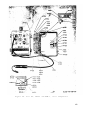
Figure 5.1. Test probe RF preamplifier, showing changes in wiring of components.
Page 16, paragraph 26 (as changed by C 1, 13
Jan 64) Make the following changes:
Subparagraph a, line 6. Change “’113” to:
66.5.
Subparagraph b, line 7. Change "200” to:
402.
Page 22, paragraph 34, chart (as changed of C 1,
caplicability
standards
13 Jan 64). Change the values of the following
resistors:
R7911. From “22.1” to: 84.5.
R7913. From” 113” to: 66.5.
R7914. From “200” to: 402.
Page 65. Delete section II and substitute:
Section II. DEPOT INSPECTION STANDARDS
of Depot Inspection
The tests outlined in this section are designed
to measure the” performance capability of a repaired equipment. Equipment that is to be returned to stock should meet the standards given
in these tests.
61. Applicable References
a. Technical Publications The following technical publications are applicable to this equipment:
2
.
b. Additional Equipment.
Perform all
b.- .Modification
Work Orders.
. .
applicable modification work orders (MWO) pertaining to this equipment before making the tests
Specified. DA Pam 310-4 lists all available
MWO’s.
62. Test Facilities Required
The following equipments, or suitable equipment, will be employed in determining compliance with the requirement of this specific
standard
a. Test Equipment.
63. General Test Requirements
Most of the tests will be performed under conditions listed below and illustrated in figure 34.3.
Testing will be simplified if connections and front
panel control settings are made initially and modifications are made as required for the individual
tests.
a. Connect the special test cable to the model
3206 power supply.
b Connect the three-terminal connector of the
CX 7899/VRM-1 to terminals A, B, and C of the
terminal connector on the special test cable.
c. Connect the four-terminal connector of the
CX-7899/VRM 1 to the POWER connector on
the front of the TS-1777/VRM-1.
Caution: Never apply a signal to the TS-1777/
VRM-1 before turning on the power to the TS1777-VRM-1.
64. Input Test
(fig. 34.3)
a. Be sure that no signal is applied to the probe
of the TS-1777/VRM-l.
b. Adjust the model 3206 power supply for a
0-volt dc output.
c. On the AN/VRM-1, set the ON-OFF switch
to ON and turn the selector switch to A.
d. Increase the model 3206 power supply. output and note the voltage indicated on the ME26A/U when the RED indicator on the TS-1777/
VRM-1 lights. The RED indicator must light
when the indicated voltage is between 21 and 22
volts dc.
e. Connect the dc leads of the ME-26A/U to
terminals A (ground) and J (B+) of the 18terminal female connector of the CX-’7899/VRM 1. The voltage must be between 21 and 22 volts
dc.
3
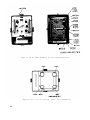
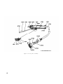
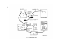
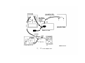
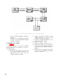
Figure 34.1. (Added) Special junction box.
f. Connect the dc leads of the ME-26A/U to
terminals A (ground) and J (B+) of the 18terminal female connector of the CX-7899/VRM1. The voltage must be between 21 and 22 volts
dc.
Note. For the remaining tests, l djust the model 3206
power supply form output between +23.4 and +28.6 volts
dc.
g. Connect the AN/USM-98 positive lead to
TS-1777/VRM-l test jack A, and the negative
lead to the probe ground connector. The voltage
indicated must be between 15.2 and 16.8 volts dc.
4
h. Insert the TS-1777/VRM-l test probe tip
in test jack A. The GREEN indicator must light.
65. Output Tests
(fig. 34.4)
a. Leave the TS-1777/VRM-l ON-OFF switch
in the ON position, and the selector switch at A.
b. Adjust the output of the PP-3514/U to 0
volt dc.
c. Through the special junction box, connect
the output of the PP-3514/U to the TS-1777/
VRM-1 probe assembly, and connect the AN/
AGO 8834A
Figure 34.2. (Added) Special test cable.
USM-98 across the probe tip and the probe ground
connector.
d. Carefully increase the output from the PP
3514/U and note the voltage indicated on the
AN/USM-98 when the TS-1777/VRM-1 RED
indicator goes out and the GREEN indicator
lights. This action must occur when the indicated
voltage is between 13.40 and 15.00 volts dc.
e. Continue to increase the output of the PP3514 U and note the voltage indicated on the
AN USM-98 when the RED indicator goes out
and the GREEN indicator lights. This action
must occur when the indication is between 17.30
and 19.50 volts. Decrease the output of the PP3514/U to 0 volt.
f. Turn the selector switch to 2.
5
l. Carefully increase the output from the PP3514/U and note the voltage indicated on the
AN/USM-98 when the RED indicator goes out
and the GREEN indicator lights. This action
must occur between 13.00 and 14.70 volts dc. Decrease the output of the PP-3514/U to 0 volt dc.
m. Remove the PP-3514/U, the special junction box, and the AN/USM-98 from the TS-1777/
VRM-1 probe assembly.
66. Audio Voltage Test
(fig. 34.5)
a. Adjust the TS-421/U output to 1,000 cps
±30 as indicated on the AN/USM-26, and decrease the output to 0 volt; use the fine attenuator
control.
b. Using the special junction box, connect the
TS-421/U to the TS-1777/VRM-l probe assembly and connect the ME-30A/U across the probe
tip and probe the ground connector.
c. Turn the TS-I777/VRM-1 selector switch
to 10.
d. Carefully increase the output from the TS421/U and note the voltage indicated on the ME30A/U when the RED indicator goes out and the
GREEN indicator lights. This action must occur
between 0.200 and 0.250 volt. Decrease the outTM6625-496-45-C2-3
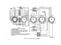
Figure 34.3. (Added) Input test setup, block diagram.
g. Carefully increase the output from the PP
3514/U and note the voltage indicated on the
AN/USM-98 when the RED indicator goes out
and the GREEN indicator lights. This action
must occur between 19.00 and 21.80 volts dc.
Decrease the output of the PP-3514/U to 0 volt
dc
h. Turn the selector switch to 8.
i. Carefully increase the output from the PP3514/U and note the voltage indicated on the
AN/USM-98 when the RED indicator goes out
and the GREEN indicator lights. This action
must ocur between 9.90 and 11.20 volts dc.
j. Continue to increase the output from the
PP-3514/U and note the voltage indicated on the
AN/USM-98 when the GREEN indicator goes
out and the RED indicator lights. This action
must occur between 12.70 and 14.20 volts dc.
Decrease the output of the PP-3514/U to 0 volt
dc.
k. Turn the selector switch to 19.
6
Figure 34.1 (Added) Output tests setup, block diagram
put of the TS-421/U until the RED indicator
lights.
e. Turn the selector switch to 6,
f. Carefully increase the output from the TS421/U and note the voltage indicated on the ME30A/U when the RED indicator goes out and the
GREEN indicator lights. This action must occur
between 0.450 and 0.520 volt. Decrease the output of the TS421/U until the RED indicator
lights.
g. Turn the selector switch to 6.
h. Carefully increase the output from the TS421/U and note the voltage indicated on the ME30A/U when the RED indicator goes out and the
GREEN indicator lights. This action must occur
between 0.800 and 1.000 volt. Decrease the output of the TS-421/U until the RED indicator
lights.
i. rum the selector switch to 3.
j. Carefully increase the output from the TS421/U and note the voltage indicated on the ME30A/U when the RED indicator goes out and the
GREEN indicator lights. This action must occur
between 2.60 and 3.80 volts. Decrease the output of the TS-421/U until the RED indicator
lights.
k. Turn the selector switch to 11.
l. Carefully increase the output from the TS421/U and note the voltage indicated on the ME-
80A/U when the RED indicator goes out and the
GREEN indicator lights. This action must occur
between 6.00 and 7.80 volts. Decrease the output
of the TS-42l/U until the RED indicator lights.
m. Turn the selector switch to 4.
n. Carefully increase the output from the TS421/U and note the voltage indicated on the ME30A/U when the RED indicator goes out and the
GREEN indicator lights. This action must occur
between 12.50 and 14.90 volts. Decrease the output of the TS-421/U to 0 volt.
o. Remove the ME-80A/U, the Special junction
box and the TS-421/U from the TS-1777/VRM1 probe assembly.
47. Amplifier, 5.65-Mc, Tests
(fig. 34.6)
a. Connect the equipment as shown by the solid
lines in figure 34.6. Also make temporary connections A and B.
b. Using the special junction box, connect the
AN/URM-145 across the TS-1777/VRM-l probe
tip and probe ground connector.
c. Turn the TS-1777/VRM-l selector switch
to 12.
d. Adjust the AN/GRM-50 for an output of
5.65 mc ±100 cps as indicated on the AN/USM26, and decrease the output to 0 volt, using the
fine attenuator.
Figure 34.5. (Added) Audio voltage test setup, block diagram
7
a. Carefully increase the output from the AN/
GRM-50and note voltage indicated on the
AN/URM-145 when the RED indicator goes out
and the GREEN indicator lights. Check to be
sure that the output is still 5.65 mc ±100 cps and
that the change in indicator occurs between 0.125
and 0.250 volt.
f. Remove temporary connections A and B (fig.
34.6) and make temporary connection C. Adjust
the AN/GRM-50 for an output of 5.65 mc ±20
kc, as indicted on the AN/USM-26, and decrease
the output to 0 volt, using the fine attenenuator.
g. Turn the selector switch to 15.
h. Carefully increase the output from the AN/
GRM-50 and note the voltage indicated on the
AN/URM-145 when the RED indictor goes out
and the GREEN indictor lights. This action
must occur between 0.200 and 0.250 volt. Decrease the output of the AN/GRM-50 to 0 volt,
using the fine attenuator.
i. Turn the selector switch to 16.
j. Carefully increase the output from the AN/
GRM-50 and note the voltage indicated on the
AN/URM-145 when the RED indicator goes out
and the GREEN indicator lights. This action
must occur between 0.170 and 0.210 volt. De
crease the output of the AN/GRM-50 to 0 volt;
use the fine lttenuator.
k. Turn the selector switch to 17.
L Carefully increase the output from the AN/
GRM-50 and note the voltage indticated on the
AN/URM-145 when the RED indicator goes out
and the GREEN indicator lights. This action
must occur between 0.650 and 0.810 volt. Decrease the output of the AN/GRM-50 to 0 volt;
use the fine attenuator.
68. Amplifier, 11.5-Mc, Tests
(fig. 84.6)
a. See that the special junction box is connected
between the UG-274B/U and the probe assembly
(with the AN/URM-145 connected to the special
junction box), that the output of the AN/GRM50 is connected to the UG-274B/U, and that the
AN/USM-26 is connected direct to the UG
274B/U.
b. Adjust the AN/GRM-50 for an output of
11.6 mc ±40 kc, as indicated on the AN/USM-26,
and dEcrease the output to 0 volt; use the fine
attenuator.
c. Turn the selector switch to 7.
d. Carefully increase the output from the AN/
GRM-50 and note the voltage indicated on the
8
AN/URM-145 when the RED indicator goes out
and the GREEN indicator lights. This action
must occur between 0.230 and 0.330 volt. Decrease the output of the AN/GRM-50 to 0 volt;
use the fine attenuator.
e. Turn the selector switch to 9.
f. Carefully increase the output from the AN/
GRM-50 and note the voltage indicated on the
AN/URM-145 when the RED indicator goes out
and the GREEN indicator lights. This action
must occur between 0.100 and 0.140 volt. Decrease the output of the AN/GRM-50 to 0 volt;
use the fine attenuator.
g. Turn the selector switch to 13.
h. Carefully increase the output from the AN/
GRM-50 and note the voltage indicated on the
AN/URM-145 when the RED indicator goes out
and the GREEN indicator lights. This action
must occur between 0.180 and 0.250 volt. Decrease the output of the AN/GRM–50 to 0 volt;
use the fine attenuator.
i. Turn the selector switch to 14.
j. Carefully increase the output from t h e
AN/GRM-50 and note the voltage indicated on
the AN/URM- 145 when the RED indicator goes
out and the GREEN indicator lights. This action
must occur between 0.012 and 0.016 volt. Decrease the output of the AN/GRM-50 to 0 volt;
use the fine attenuator.
69. Amplifier, 47. 0-MC, Test
(fig 34.5)
a. See that the special junction box is connected
between the UG-274B/U and the probe assembly
(with the AN/URM-145 connected to the special
junction box), that the output of the AN/GRM50 is connected to the UG-274B/U, and that the
AN/USM-26 is connected direct to the UG274 B/U (fig. 34.6).
b. Adjust the AN/GRM-50 for an output o f
47.0 mc ±100 kc, as indicated on the AN/USM26; and decrease the output to 0 volt; use the-fine
attenuator.
c. Turn the selector switch to 18.
d. Carefully increase the output from the AN/
GRM-50 and note the voltage indicated on the
AN/URM-145 when the RED indicator goes out
and the GREEN indicator lights. This action
must occur between 0.100 and 0.135 volt. De
crease the output of the AN/GRM-50 to 0 volt;
use the fine attenuator.
AGO 8834A
Figure 34.6
9
Caution: check to be sure that signal voltages
are removed from the brfore setting the
TS-1777/VRM-1 ON-OFF switch to OFF.
e. Remove all test connections and turn the
power off.
Page 69. Add to the appendix:
Depot Inspection Standard for
TB SIG 355-1
Repaired Signal Equipment.
Depot Inspection Standard for
TB SIG 355-2
Refinishing Repaired signal
Equipment.
Audio Oscillator TS-421/U
TM 11-2649
(Hewlett-Packard Model 205
-AG).
Frequency Meter JW/USMTM 11-5057
26.
Operator and Organizational
TM 11-6625 Maintenance Manual: Mul200-12
timeters ME-26A/U and
ME-26B/U.
Operator’s and Organizational
TM 11-6625320-l2
Maintenance Manual: Voltmeter, Meter ME-30A/U
10
and Voltmeter Electronic
ME-30B/U and ME-30
C/U.
TM 11-6625Operator’s and Organizational
392-12
Maintenance Manual: Test
Set, Transponder Set AN/
URM-125.
Operator’s Manual, Voltmeter,
TM 11-6625436-10
Electronic AN/USM-98.
Page 77, figure 39 (as changed by C 1, 13 January 1964). Make the following changes:
Add to the notes:
6. R7918 (22 OHMS) IS CONNECTED BETWEEN THE PROBE RF OUTPUT AND
THE INPUT OF FL7501.
Change the type number of Q7601 from
“2N502” to: 2N502B.
Change the type number of Q7702 from
“2N502A” to: 2N502B.
Change the values of the following resistors:
R7707. From "1,800” to: 5.6K.
R7914. From “220” to: 402.
R7913. From "113” to: 66.5.
R7911. From “22.1” to: 84.5.
By Order of the Secretary of the Army:
Official:
J. C. LAMBERT,
Major General, United States Army
The Adjutant General.
--
Distribution:
Active Army:
USASA (2)
let USASA Fld Sta (6)
CNGB (1)
C/COMMEL (7)
cofT (1)
CofEngrs (1)
CofsptS (1)
TSG (1)
USAECDA (1)
USACBRCDA (1)
USACECDA (1)
USACECDA (Monmouth Ofc) (1)
USAMSCDA (1)
USAOCDA (1)
USAQMCDA (1)
USATCDA (1)
USAADCDA (1)
USAARMCDA (1)
USAAVNCDA (1)
USAARTYCDA (1)
USASWCDA (1)
USAMC (5)
USCONARC (5)
ARADCOM (2)
ARADCOM Rgn (2)
OS Maj Cored (3)
OS Base Cored (2)
LOGCOMD (2)
USAECOM (7)
USAMICOM (4)
USASMCOM (2)
USASCC (4)
Armies (2 )
Corps (2)
MDW (1)
USATC AD (2)
USATC Armor (2)
USATC Engr (2)
USATC Inf (2)
USASTC (3)
Instl (2) except
Ft Monmouth (63)
Ft Gordon (5)
Ft Huachuu (10)
GENDEP (OS) (2)
NG: State AG (3).
USAR: None.
For explanation of abbreviations used, see AR 320-50.
EARLE G. WHEELER,
General, United States Army,
Chief of Staff.
Sig Sec GENDEP (5)
Sig Dep (OS) (12)
Army Dep (2) except
Lexington (12)
Sacramento (23)
Tobyhanna (12) .
Ft Worth (8)
Letterkenny (5)
Sharpe (8)
Savanna (5)
Navajo (5)
Charleston (3)
Svc Colleges (2)
Br Svc Sch (2)
WRAMC (2)
US Army Tml (1) except Oakland (5)
POE (1)
AMS (1)
Army Pic Cen (2)
USATTCARC (1)
USATTCA (1)
USATTCG (1)
USATTCP (1)
USA Mbl Spt Cen (1)
USA Elct Mat Agcy (9)
Chicago Proc Dist (1)
Sig Fld Maint Shops (3)
USAERDL (2)
USAERDLA (White sands) (13)
USAELRDL Trp Cored (10)
USAARMBD (2)
US-4 Trans Bd (2)
USAARTYBD (2)
USA Corps (3)
WSMR (5)
11th Air Assult Div (3)
USA Cold Regions RE Lab (2)
Units org under fol TOE: 2 ea. UNOINDC
11-500 (AA-AE) (4)
11-16
11-557
11-57
11-587
11-98
11-592
11-117
11-597
11-155
11-157
TM 11-6625-496-45
Technical Manual
No. 11-6625-496-45
HEADQUARTERS,
DEPARTMENT OF THE ARMY
WASHINGTON 25, D. C., 3 ]uly 1962
TEST SET, RADIO AN/VRM-1
Paragraph
C HAPTER 1 .
C HAPTER 2 .
Section I.
II.
III.
IV.
v.
C HAPTER 3 .
Section I.
II.
APPENDIX
INDEX
THEORY . . . . . . . . . . . . . . . . . . . . . . . . . . . . . . . . . . . .
FOURTH ECHELON MAINTENANCE
General troubleshooting techniques . . . . . . . . . . . . . . . . . . . . .
Troubleshooting . . . . . . . . . . . . . . . . . . . . . . . . . . . . .
Repair. . . . . . . . . . . . . . . . . . . . . . . . . . . . .
Final adjustments . . . . . . . . . . . . . . . . . . . . . . . . . . . . . . . .
Fourth echelon testing procedures . . . . . . . . . . . . . . . . . . . . .
FIFTH ECHELON MAINTENANCE
Troubleshooting and repair. . . . . . . . . . . . . . . . . . . . . . . . . .
Fifth echelon testing procedures . . . . . . . . . . . . . . . . . . . . . .
REFERENCES
Page
. . . .
1-27
2-16
. . . .
. . ....
. . .
. . . .
. . . .
28-30
31-34
35-40
41-43
44-52
17,18
18-21
24-29
33
37-54
. . . .
. . . .
53-59
60-67
55-62
65-68
69
79
1
CHAPTER 1
THEORY
1. Scope
a. T h i s m a n u a l c o v e r s f i e l d ( f o u r t h
echelon) and depot mainteriance for Test
Set, Radio AN/VRM-l. It includes instructions appropriate to fourth and fifth
echelon for troubleshooting, testing, aligning, and repairing the equipment. Detailed
functions of the AN/VRM-1 are covered in
this chapter.
b. The complete technical manual for
this equipment includes TM 11-6625-49612, TM 11-6625-496-20P. and TM 11-662545P.
c. Forward comments concerning this
manual to the Commanding Officer, U. S.
Army Signal Materiel Support Agency,
ATTN: SIGMS-MPP-4, Fort Monmouth,
N.J.
Note: For applicable forms and records, refer to
paragraph 2, TM 11-6625-496-12.
d. Refer to DA Pamphlet 310-4 to determine what Changes to or revisions of
this publication are current.
2. Block Diagram
(fig. 37)
Test Set, Radio AN/VRM-1 is a portable
equipment for testing plug-in modules of
Receiver, Radio R-442/VRC and ReceiverTransmitters, Radio RT-246/VRC and
RT-524/VRC. Signal paths are shown in
the block diagram and are discussed in a
through c below. The complete circuit is
shown in the overall schematic diagram
(fig. 39).
a. Selector Witch. The setting of the
20-position selector switch, S7902, is determined by the type of test to be made.
The routing of the voltages under test is
determined by the selector switch position.
b. Rf Signals. The radiofrequency (rf)
signals under test are amplified by the
test probe rf amplifier and routed by
S7902A to the 5.65-mc filter, to an appropriate attenuator network, or directly
to S7902B and S7902C. The latter switch
2
sections apply the signal to one of three rf
amplifiers: 11.5-megacycle (mc), 5.65mc, or 47. O-mc. The amplified signals
are rectified and applied through S7902D
to the Schmitt trigger circuit (e below).
c. Audio signals. T h e a u d i o s i g n a l s
from the test probe are routed by S7902B
or S7902C either through an appropriate
attenuator network or directly to the audio
amplifier. The amplified signal is rectified
and applied through S7902 D to the Schmitt
trigger circuit (e below).
d. Dc Voltages. The dc voltages under
test are routed either through an appropriate attenuator or directly to S7902B or
S7902C. The latter switch sections apply
the voltage to either the voltage divider
or the voltage supply limits sensing circuit. The voltage supply limits sensing
circuit senses whether the voltage under
test is between minimum and maximum
tolerances. The direct-current (de) voltage from the voltage divider or voltage
supply limits sensing circuit is connected
through S7902D to the Schmitt trigger circuit (e below).
e. Schmitt Trigger. The Schmitt trigger
circuit operates in conjunction with two
indicator lamps. In the absence of a signal
or when a signal is not within tolerances,
the RED indicator lamp lights. When a
signal is within tolerances, the GREEN
indicator lamp lights.
f. Power. Power is supplied to the TS1777/VRM-l from a 26-volt dc power
source, such as a vehicle electrical system. The power source is connected to a
16-volt dc regulator circuit and a line voltage sensing circuit. The output of the
16-volt dc regulator circuit is connected
to the line voltage sensing circuit. When
the power source voltage is above 22 volts
dc (minimum limit), the output of the 16volt dc regulator is switched by the line
voltage sensing circuit to the indicator
lamps, the Schmitt trigger circuit, the
voltage supply limits sensing circuit, and
S7902E. The 16 volts dc is supplied to the
audio amplifier or one of the rf amplifiers
and the test probe rf preamplifier from
S7902E.
3. Audio Amplifier
(fig. 1)
The audio amplifier is a three-stage,
direct-coupled, class A amplifier. Power,
input, and output connections to the audio
amplifier are completed when the selector
switch S7902 is in position 3, 4, 5, 6, 10,
or 11. The output from the audio amplifier
is rectified and fed to the Schmitt trigger
circuit.
a. The input signal to the audio amplifier, developed across resistor. R7401, is
coupled through capacitor C7401 to the
base of transistor Q7401. The amplified
output at the collector of transistor Q7401
is directly coupled to the base of transistor
Q7402. Resistors R7402 and R7403 form a
voltage divider which develops the emitterbase bias for transistor Q7401. Resistor
R7404 is the output load resistor in the
collector circuit of Q7401.
b. The output at the collector of transistor Q7401 is amplified by transistor
Q7402. The output of Q7402 is applied
directly to the base of transistor Q7403.
Resistor R7407 is the emitter load resistor for transistor Q7402.
c. The voltage divider, network consisting of resistor R7405, potentiometer
R7406, and capacitor C7402 develops degenerative alternating-current (at) feedback for these directly coupled amplifier
stages. Potentiometer R7406 is a preset
control; its setting determines the overall
gain of the audio amplifier.
d. Resistor R7408 establishes the selfbiasing portion of the emitter-base bias
for transistor Q7403. Capacitor C7403 is
an audio bypass capacitor. Inductor L7401
is the collector load for transistor Q7403.
e. The output of the audio amplifier is
coupled through capacitor C7404 to rectifier CR7404. Resistor R7409 is the diode
return resistor, R7410 is the load resistor,
and C7405 is the filter capacitor. The dc
output from the rectifier circuit is fed to
the Schmitt trigger circuit.
4. Amplifier, 11.5-Mc
(fig. 2)
The 11.5-mc amplifier is a two-stage,
intermediate-frequency (if.) amp1ifier.
The overall gain of the two stages is about
40 decibels (db). Power, input, and output
connections to the 11.5-mc amplifier are
made when selector switch S7902 is in
position 7, 9, 13, or 14. The output from
the 11.5-mc amplifier is rectified and fed
to the Schmitt trigger circuit.
a. The input signal from the test probe
rf preamplifier is limited b y resistor
R7612 and coupled to the primary winding
of transformer T7601 through capacitor
C7601. Resistor R7613 matches the impedance of the test probe rf preamplifier
to that of the 11.5-mc amplifier input.
b. First 11.5-mc amplifier Q7601 is
connected in a common-emitter amplifier
stage which provides about 20-db gain.
(1) Transformer T7601 and capacitor
C7602 tune the input to Q7601. The
input signal is coupled to the base
of transistor Q7601 through capacitor C7603. The output signal from
Q7601 is developed across a tuned
circuit consisting of the primary
winding of transformer T7602 and
capacitor C7608. Resistor R7604
reduces the Q of the tuned circuit
to provide the proper bandwidth.
(2) Resistors R7601 and R7602 form a
voltage divider which provides the
fixed-bias portion of the emitterbase bias for Q7601. Resistor
R7603 establishes the self-biasing
portion of the emitter-base bias
and stabilizes the emitter current.
Capacitor C7607 is an rf bypass
capacitor. Capacitor C7606 neutralizes the first 11.5-mc amplifier. Diode CR7601 prevents the
emitter-base bias from reversing
when a very large input signal is
applied to the stage. Capacitor
C7604 and inductor L7601 form a
decoupling network in the 16-volt
dc supply line.
c. Second 11.5-mc amplifier Q7602 is
connected in a common-emitter amplifier
stage which provides about 20-db gain.
3
Figure 1. Audio amplifier, schematic diagram.
(1) Transistor Q7602 receives its input from the secondary winding of
T7602. The input signal is coupled
to the base of transistor Q7602
through capacitor C761O.
(2) The output signal of Q7602 is developed across a tuned circuit consisting of inductor L7603 and capacitor C7612. Resistor R7609
reduces the Q of the tuned circuit
to provide the proper bandwidth.
(3) Resistors R7606 and R7607 form a
voltage divider which provides the
fixed-biasing portion of the
emitter-base bias for Q7602. Resistors R7608 and R7605 establish
the self-biasing portion of the
emitter-base bias and stabilize
the emitter current. Capacitor
C7609 is an rf bypass capacitor for
resistor R7605. Resistor R7608
pro vi d es emitter degeneration
which stabilizes the stage. The
stage is also stablized by the outof-phase portion of the signal fed
to the emitter of Q7602 from the
tapped secondary winding of trans-.
former T7602. Capacitor C7611, in
conjunction with the bottom half of
4
secondary T7602, neutralizes the
second 11.5-mc amplifier. Capacitor C7605 and inductor L7602 form
a decoupling network in the +16volt dc supply line.
d. The output from the second 11.5-mc
amplifier is rectified by diode CR7602 and
filtered by capacitor C7613. The dc voltage
is taken from potentiometer R7611 and fed
to the Schmitt trigger circuit. The amount
of dc output voltage to the Schmitt trigger
can be varied by adjustment of R7611.
5. Filter, 5.65-Mc
(fig. 39)
Filter FL7501 is a bandpass crystal
filter having a center frequency of 5.65mc. The filter is in series with the output
of the test probe rf preamplifier circuit
when switch S7902 is in position 12. It is
a part of assembly A7500. The filter has a
minimum bandwidth of 5.4 kilocycles (kc)
at the 3-db points, a maximum bandwidth
of 6.6 kc at the 6-db points, and a maximum bandwidth of 12.2 kc at the 50-db
points. Its input and output impedances are
50 ohms. Its insertion loss at 5.65 mc does
not exceed 6db
Figure 2. Amplifier, 11.6-mc, schematic diagram.
6. Amplifier, 5.65-Mc
(fig. 3)
The 5.65-mc amplifier is a singlestage if. amplifier which has a gain of
about 15 db. Power, input, and output connections are made to the 5.65-mc amplifier when selector switch S7902 is inposition 12, 15, 16, or 17. The output from the
amplifier is rectified and fed to the Schmitt
trigger circuit.
a. The input signal from the test probe
rf preamplifier is fed to the input attenuation pad consisting of resistors R7701,
R7702, and R7703. The pad reduces the rf
signal level and isolates the 5.65-mc
amplifier from the test probe rf preamplifier.
b. The 5.65-mc amplifier uses transistor Q7701 in a common-base stage
which provides about 15-db gain.
(1) The attenuated signal is coupled to
the emitter of transistor Q7701
through capacitor C7701. The output signal of Q7701 is developed
across a tuned circuit consisting
of coil L7704 and capacitor C7704.
Resistor R7707 reduces the Q of
the tuned circuit to obtain the
proper bandwidth.
(2) Resistors R7705 and R7706 form a
voltage divider which provides the
fixed-biasing portion of emitterbase bias for Q7701. Resistor
R7704 establishes the self-biasing
5
portion of the emitter-base bias
and stabilizes the emitter current.
Capacitor C7703 is an rf bypass
capacitor. Capacitor C7702 and inductor L7701 form a decoupling
network in the +16-volt dc supply
line.
c. The output from the 5.65-mc amplifier is rectified by diode CR7701 and
filtered by capacitor C7705. The dc output
is taken from potentiometer R7708 and fed
to the Schmitt trigger circuit. The amount
of dc output voltage to the Schmitt trigger
can be varied by adjustment of R7708.
7. Amplifier, 47.0-Mc
(fig. 4)
The 47.0-mc amplifier is a two-stage rf
amplifier. Overall gain of the two stages is
about 15 db. Power, input, and output connections to the 47.0-mc amplifier are made
when selector switch S7902 is in position
18. The output from the 47.0-mc amplifier
is rectified and fed to the Schmitt trigger
circuit.
a. The first 47.0-mc amplifier uses
transistor Q7702 in a common-emitter
stage.
(1) The input signal from the test probe
of transformer T7702, trimmer
capacitor C7708, and fixed capacitor C7715. Resistor R7710 reduces the Q of the tuned circuit to
provide the proper bandwidth.
(2) Resistors R7709 and R7711 form a
voltage divider which provides the
fixed-biasing portion of the
emitter-base bias for Q7702. Resistors R7712 and R7713 establish
the self-biasing portion of the
emitter-base bias and are used for
c u r r e n t stabilization. Capacitor
C7707 is an rf bypass capacitor
across R7713. Since only a portion
of the self-biasing network is rf
bypassed, the input impedance of
Q7702 is effectively raised. Coil
L7702 and capacitor C7710 form a
decoupling network in the +16-volt
dc supply line.
b. The second 47.0-mc amplifier uses
transistor Q7703 in a common-base stage.
(1) The ‘signal appearing at the secondary winding of T7702 is coupled
through C7709 to the emitter of
Q7703. The output of Q7703 is
coupled through C7712 to the tuned
output circuit which consists of
coil L7705 and capacitor C7713.
Resistor R7717 reduces the Q of
the tuned circuit to provide proper
bandwidth.
(2) Resistors R7716 and R7715 form a
Figure 3. Amplifier, 5.65-mc, schematic diagram.
6
voltage divider which provides the
fixed-hissing portion of emitterbase bias for Q7703. Resistor
R7714 develops the self-biasing
portion of the emitter-base bias
and stabilizes the emitter. Capacitor C7711 places the base of Q7703
at rf ground potential. Capacitor
C7716 and inductor L7703 form a
decoupling network in the +16-volt
dc supply line.
c. The output from the second 47.0-mc
amplifier is rectified by diode CR7702.
The rectified signal is filtered by capacitor C7714. Part of the dc voltage, as determined by the setting of R7718, is fed to
the Schmitt trigger circuit.
8. Test Probe Rf Preamplifier
(fig. 5)
The test probe rf preamplifier is a
single-stage wide-band rf amplifier which
develops a gain of about 1. Power and output connections are made to the test probe
rf preamplifier when switch S7902 is in
position 7, 9, 12, 13, 14, 15, 16,17, or 18.
The output from the test probe rf preamplifier is fed to either the 5.65-mc,
11.5-mc, or the 47.0-mc amplifier, depending on the selector switch position.
a. The test probe rf preamplifier uses
transistor Q7301 in an emitter-follower
stage.
(1) The input signal from the test probe
tip is coupled through capacitor
C7301 to the base of Q7301. The
output of Q7301 is coupled through
C7303 and C7901 to the input of the
selected rf amplifier.
(2) Resistors R7301 and R7302 form a
voltage divider that provides the
fixed-biasing portion of the
emitter-base bias for Q7301. Resistor R7303 establishes the selfbiasing portion of the collectorbase bias and stabilizes the emitter
current. Positive voltage is applied
to the collector through rf choke
L7302. Capacitor C7302 is an rf
bypass capacitor for the collector
of Q7301.
b. Power to the test probe rf preamplifier Is supplied from the +16-volt dc supply
line as selected by switch S7902. Inductor
L7501 keeps rf voltages out of the supply
line. Diode CR7401 is associated with the
Figure 4. Amplifier, 47.0-mc, schematic diagram.
7
47.0-mc amplifier; diode CR7402, with the
11.5-mc amplifier; and diode CR7403, with
the 5.65-mc amplifier. The diode associated with the rf amplifier in use conducts
to allow +16 volts to be supplied to the test
probe rf preamplifier. The two diodes
associated with the two rf amplifiers not
in use prevent the supply voltage from
being fed to the amplifiers from their
common connection in the test probe rf
preamplifier supply line.
9. Voltage Supply Limits Sensing Circuit
(fig. 6)
The voltage supply limits sensing circuit
consists of two voltage dividers and a dc
switch. It senses the minimum and maximum limits of regulated +16- and +12volt dc supplies. Power, input, and output
connections are made to the voltage supply
limits sensing circuit when switch S7902 is
in position A or 8. The dc output of the
voltage supply limits sensing circuit is fed
to the Schmitt trigger circuit.
a. The voltage divider network consisting of resistor R7902 and rheostat R7801
and the network of resistor R7804 and
rheostat R7803 sense the minimum voltage
supply limit. Rheostat R7803 is adjusted
so that at the minimum allowable level,
sufficient voltage is applied to the Schmitt
trigger circuit to cause it to go from its
RED (bad) condition to its GREEN (good)
condition.
b. The voltage divider consisting of resistor R7802 and rheostat R7801 and dc
switching transistor Q7801 sense the
maximum voltage supply limit. Transistor
Q7801 is a unijunction transistor. With the
Schmitt trigger circuit in its GREEN
condition, the +16 volta dc applied to base
B2 of transistor Q7801 biases the transistor to cutoff. If the voltage applied to
the divier of resistors R7801 and R7802
exceeds the maximum limit, the voltage
applied at the emitter of transistor Q7801
overcomes the +16-volt bias and is connected through base Bl to _ground, and
transistor Q7801 is biased into conduction.
This action quickly reduces the voltage
applied to the Schmitt trigger circuit below
the minimum required to operate it, and the
Schmitt trigger circuit returns to its RED
(bad) condition.
c. When the test probe tip is first applied
to a test point, a transient voltage can be
applied to the voltage supply limits sensing
circuit which could cause Q7801 to be
biased into conduction even though the voltage being tested is quite lox. The network
of diode CR7801, load resistor R7805, and
filter capacitor C7801 reduces such transient voltages by providing a relatively
Figure 5. Test probe rf preamplifier, schematic diagram.
8
low-resistance path to them. When transistor Q7801 is biased into conduction, it
provides a much lower path to ground than
the diode network, and the diode network
is effectively removed from the circuit.
10. Schmitt Trigger Circuit
(fig.7)
The Schmitt trigger circuit consists of a
dc amplifier, a Schmitt trigger, a dc switch,
and a pair of indicator lamps. The circuit
is used in all positions of selector switch
S7902.
a. Transistor Q7802 is an emitter-follower, dc amplifier. Transistors Q7803
and Q7804 form the schmitt trigger. Transistor Q7805 is used as a dc switch.
b. In the absence of an input signal (de)
or when a small input signal is present,
transistor Q7804 conducts and transistors
Q7802, Q7803, and Q7805 are cut off.
Transistor Q7804 conducts and a relatively
low-resistance path to ground is established through R7811, Q7804, and RED
indicator 1amp DS7902, causing lamp
DS7902 to light.
C . When a large input signal (de) is applied to the base of Q7802, the transistor
s biased into conduction. Since the base of
Q7803 in the Schmitt trigger is directly
connected to the emitter of Q7802, transistor Q7803 is also biased into conduction.
When Q7803 conducts, the voltage at the
base of Q7803 decreases. This decreased
voltage, which is applied to the base of
Q7804 through R7809, causes Q7804 to cut
off. When transistor Q7804 is cut off, the
voltage at the base of dc switching transistor Q7805 is increased. Transistor
Q7805 starts conducting and causes a
relatively low resistance path to ground
through R7815, CR7802, Q7805, and GREEN
indicator lamp DS7901 and causes DS7901
to light.
d. Resistors R7806 and R7808 and lamps
DS7902 and DS7901 are the collector loads
for Q7802 through Q7805 respectively.
Resistor R7807 is the emitter-base bias
resistor for Q7802. Resistor R7811 establishes the emitter bias for Q7803 and
Q7804. Resistors R7809 and R7812 establish the base bias for Q7804, and R7813
and R7814 establish the base bias for
Q7805. Resistor R7815 establishes the
emitter bias for Q7805. Diode CR7802 prevents any small signal present at the base
of transistor Q7805 from biasing the
transistor into conduction while Q7804 is
conducting. When Q7805 is conducting,
diode CR7802 presents a very small impedance to the current.
11. Line Voltage Sensing Circuit
(fig. 8)
The line voltage sensing circuit consists
of a voltage divider, a pulse generator, and
a dc switch which senses the minimum
limit of the power source voltage for the
TS-1777/VRM-l. The circuit is used whenever power is applied to the TS-1777/
VRM-1.
Figure 6. Voltage supply limits sensing circuit, schematic diagram.
Figure 7. Schmitt trigger circuit, schematic diagram.
a. Resistor R7817 and rheostat R7816
form a voltage divider. Rheostat R7816 is
adjusted SO that the minimum source voltage will cause the line voltage sensing
circuit to function. Transistor Q7806 is a
unijunction transistor. When the p o w e r
source voltage is below minimum, the +16
volts dc applied at base B2 of Q7806 biases
it to cutoff. If the power source voltage
reaches or exceeds the minimum, the
voltage applied at the emitter of Q7806
overcomes the +16-volt bias and there will
be conduction through base B2 and load
resistor R7818 to ground.
b. At the instant Q7806 conducts, a sharp
positive-going pulse is generated at B1.
The pulse is coupled through capacitor
C7802 to the gate of dc switch CR7803. DC
switch CR7803 is cut off until a positive
pulse is applied to its gate. Since CR7803
is in series with the +16-volt dc supply
line, operation of the TS-1777/VRM-l is
not possible until Q7806 generates a pulse
large enough to operate the gate of CR7803.
Resistor R7819 is the dc return resistor
for the gate circuit.
12. Power Distribution
(fig. 38)
Test Set, Radio AN/VRNI-l is supplied
26.0 volts dc from a power source such as
a vehicular electrical system. The CX7899/VRM-1 connects the power from an
MT-1029/VRC or MT-1898/VRC to the
TS-1777/VRM-l and to the R-442/VRC,
10
RT-246/VRC, or RT-524/VRC under test.
Figure 38 is a simplified power distribution diagram of a typical test setup for an
RT-246/VRC or RT-524/VRC. The setup
for testing an R-442/VRC is similar except that an MT-1898/VRC is used instead
of an MT-1029/VRC .
a. The negative terminal of the vehicular
electrical system is connected to ground in
the MT-1029/VRC through terminal A of
J21. The positive terminal is connected
to terminal B of connector J21 on the MT1029/VRC; through fuse Fll to terminal
B of connector J24. The positive voltage
is connected by the CX-7899/VRM-l to
terminals B, C, and J of connector P401
on the RT-246/VRC or RT-524/VRC to
provide power and control voltage for the
equipment under test. The positive voltage
is also connected by the CX-7899/VRM-l
to terminal B of POWER connector J7902
on the TS-1777/VRM-l.
b. When switch S7901 is ON, positive
voltage is applied through fuse F7901 and
diode CR7901. Fuse F7901 protects the
TS-1777/VRM-l and associated equipment. Diode CR7901 prevents possible
damage to the TS-1777/VRM-l if power of
improper polarity is accidentally applied
to connector J7902. The positive voltage
appearing at diode CR7901 is applied to
voltage dropping resistor R7901 and
breakdown diode CR7902, which form a
+16-volt dc regulator. The regulated +16
volts dc is applied to terminal C of connectors J7907 and P7801. The voltage at
Figure 8. Line voltage sensing circuit, schematic diagram.
diode CR7901 is also applied through terminal B of connectors J7907 and P7801 to
the line voltage sensing circuit consisting
of resistors R7817, R7818, and R7819,
rheostat R8716, capacitor C7802, unijunction transistor Q7806, and dc switch
CR7803. The operation of this circuit is
explained in paragraph 11.
c. If tie power source voltage is above
its minimum limit of +22 volts dc, +16
volts dc is applied through terminal A of
connectors P7801 and J7907 to the following places:
(1) Terminal F of connectors J7907
and P7801 to supply power for the
Schmitt trigger circuit.
(2) Terminal K of connectors J7907
and P7801 to supply power to the
voltage supply limits sensing circuit.
(3) One side of RED indicator lamp
DS7901 and GREEN indicator lamp
DS7902. The other sides of the
lamps are connected through terminals E and D of connectors
J7907 and P7801 to the collectors
of transistors Q7804 and Q7805,
respectively, in the Schmitt trigger
circuit.
(4) Switch S7902E.
(a) In positions A, 2, and 8. No connections are made.
(b) In positions 3,4,5,6, 10, and 11.
A connection is made through
terminal H of connectors J7905
and P7401 to supply power to the
audio amplifier
(c) In Positions 7, 9, 13, and 14
Connections are made through terminal H of connectors J7906 and
P7601 to supply power to the
11.5-mc amplifier and through
terminal C of connectors J7905
and P7401 to diode CR7402 .
(d) In positions 12, 15, 16, and 17.
Connections are made through
terminal L of connectors J7904
and P7701 to the 5.65-mc amplifier and through terminal A of
connectors J7905 and P7401 to
diode CR7403.
(e) In position 18. Connections are
made through terminal D of connectors J7904 and P7701 to the
47.0-mc amplifier and through
terminal D of connectors J7905
and P7401 to diode CR7401.
d. When +16 volts dc is applied to diode
CR7401, CR7402, or CR7403, it is fed
through terminal B of connectors P7401
and J7905 and through terminal K of
connectors J7903 and P7501. The voltage
is applied through inductor L7501, through
terminal F of connectors P7501 and J7903,
through inductor L7302 and across filter
capacitor C7302 to supply power to the test
probe rf preamplifier.
13. Selector Switch Position A
(A, fig. 9)
When the selector switch is in position
A, either a +16-volt dc point on the unit
11
under test or the TS-1777/VRM-l 16-volt
line can be tested.
a. When the TS-1777/VRM-l 16-volt
line is tested, the test probe tip is inserted
in test jack A. The regulated output of the
+16-volt dc regulator circuit is applied
through rf choke L7301 and level-adjusting
rheostat R7501 to the voltage supply limits
sensing circuit. The output from this circuit is applied to the Schmitt trigger circuit. If the regulated voltage is within
limits, GREEN indicator lamp. D67902
lights. If the regulated voltage is not within
the minimum and maximum limits, insufficient voltage will be applied to the
Schmitt trigger circuit, and RED indicator
lamp DS7901 lights. The voltage supply
limits sensing and Schmitt trigger circuits
are supplied from the +16-volt dc regulated
line.
b. When a +16-volt dc point is tested in
a unit under test, the test probe tip is
inserted in the appropriate test point
(A2100-6, TP3002, TP3005, TP3012,
TP4006, TP4008, TP5010, or TP8001).
The test voltage is then connected through
rf choke L7301 and the remainder of the
test circuit functions as described in a
above.
14. Selector Switch Position 2
(B, fig. 9)
When the selector switch is in position
2, a +25.5-volt dc point on the unit under
test can be tested. The test voltage is
connected through rf choke L7301 and
across voltage divider network consisting
of resistors R7902 and R7917 to the Schmitt
trigger circuit. If the test voltage is above
the minimum limit, GREEN indicator
DS7902 will light. If the test voltage is
below the minimum limit, insufficient voltage will be applied to the Schmitt trigger
circuit, and RED indicator DS7901 will
light. Operating voltage for the Schmitt
trigger circuit is supplied from the +16volt dc regulated line.
15. Seiector Switch Position 3
(C, fig. 9)
When the selector switch is in position
3, the 150-cycle-per-second (cps) output
12
of module A5200 can be tested. The signal
is connected through inductor L7301, coupling capacitor C7503, and attenuating resistor R7903 to the audio amplifier. The
rectified output of the audio amplifier is
applied to the Schmitt trigger circuit. If
the signal voltage is above the minimum
limit, GREEN indicator DS7902 will light.
If the signal voltage is below the minimum
limit, insufficient voltage will be applied
to the Schmitt trigger circuit, and RED
indicator DS7901 will light. The operating
power to the audio amplifier and Schmitt
trigger circuit are supplied from the +16volt dc regulated line.
16. Selector Switch Positions 4, 5, and 6
(c, fig. 9)
a. Position 4. When the selector switch is in position 4, the audio output from
module A5100 can be tested. Operation of
the circuit is similar to that of position 3
(para 15) except that resistor R7904, which
has a resistance of 511K ohms, is used in
place of R7903.
b. Position 5. When the selector switch
is in position 5, the audio output of module
A4300 or A5200 can be tested. Operation
—
of the circuit is similar to that of position
3 (para 15) except that resistor R7905,
which has a resistance of 10K ohms, is
used in place of R7903.
c. Position 6. When the selector switch
is in position 6, the audio output of the
module A5100 monitor amplifier or a
sawtooth output from module A8400 can be
tested. Operation of the circuit is similar
to that of position 3 (para 15) except that
resistor R7906, which has a resistance of
26.lK ohms, is used in place of R7903.
17. Selector Switch Position 7
(D, fig. 9)
When the selector switch is in position
7, the 11.5-mc output of a module A8300
can be tested. The test signal from the test
probe rf preamplifier is connected through
coupling capacitor C7901 and attenuating
resistor R7907 to the 11.5-mc amplifier.
The rectified output of the 11.5-mc amplifier is applied to the Schmitt trigger circuit. If the signal voltage is above the
F i g u r e 9 . T e s t s in selector switch positions A, 2, 3, and 7, simplified schematic d i a g r a m .
13
minimum limit, GREEN indicator DS7902
will light. If the signal voltage is below the
minimum limit, insufficient voltage will be
applied to the Schmitt trigger circuit, and
RED indicator DS7901 will light. Operating voltages are supplied to the 11.5-mc
amplifier and Schmitt trigger circuit from
the +16-volt dc regulated line. Operating
voltage is supplied to the test probe rf
preamplifier from the +16-volt dc regulated line through diode CR7402 and rf
choke L7501.
18. Selector Switch Position 8
(A, fig. 10)
When the selector switch is in position
8, a. +12-volt dc point on assembly A8000
can be tested. The tested voltage is connected through rf choke L7301 to
the voltage supply limits sensing circuit.
The output from the voltage supply limb
sensing circuit is applied to the Schmitt
trigger circuit. If the tested voltage is
within limits, GREEN indicator DS7902
will light. If the tested voltage is not between minimum and maximum limits, insufficient voltage will be applied to the
Schmitt trigger circuit, and RED indicator
DS7901 will light. Operating voltages are
supplied to the voltage supply limits
sensing and Schmitt trigger circuits from
the +16-volt dc regulated line.
19. Selector Switch Position 9
(D, fig. 9)
When the selector switch is in position 9,
the ll.5-mc output of module A8100 can
be tested. The operation is similar to
that of position 7 (para 17) except that
resistor R7908, which has a resistance
of 475 ohms, is used in place of R7907.
20. Selector Switch Position 10
(c, fig. 9)
When the selector switch is in position
10, the audio input to module A5100 can
be tested. The operation is similar to that
of position 3 (para 15) except that R7903
is not used (shorted).
21. Selector Switch Position 11
(c, fig. 9)
When the selector switch is in position
14
11, the high-level audio output from module
A5100 can be tested. The operation is similar to that of position 3 (para 15) except
that resistor R7909, which has a resistance of 243K, is used in place of R7903.
22. Selector Switch Position 12
(C, fig. 10)
When the selector switch is in position
12, the 5.65-mc output of module A3500
can be tested. The signal from the test
probe rf preamplifier is fed through
coupling capacitor C7901 and 5.65-mc
filter FL7501 to the 5.65-mc amplifier.
The rectified output of the 5.65-mc amplifier is applied to the Schmitt trigger
circuit. If the signal voltage is above the
minimum limit, GREEN indicator DS7902
will light. If the signal voltage is below the
minimum limit, insufficient voltage will
be applied to the Schmitt trigger circuit,
and RED indicator DS7901 will light.
Operating voltage for the 5.65-mc amplifier and Schmitt trigger circuit is supplied
from the +16-volt de regulated line. Operating voltage for the test probe rf preamplifier is supplied from the +16-volt dc
regulated line through diode CR7403 and rf
choke L7501.
23. Selector Switch Position 13
(D, fig. 9)
When the selector l switch is in position
13, the limited 11.5-mc output of module
A4200 can be tested. The operation is
similar to that of position 7 (para 17)
except that resistor R7901, which has a
resistance of 845 ohms, is used in place of
R7907.
24. Selector Switch Position 14
(D, fig. 9)
When the selector switch is in position
14, the output of module A3100 can be
tested. The operation is similar to that of
position 7 (para 17) except that R7907 is
not used (shorted).
25. Selector Switch Position 15
(D, fig. 10)
When the selector switch is in position
15, the 5.65-mc output of module A3500
can be tested. The signal from the test
-
Figure 10. Tests in selector switch positions 8, 12, 13, 16, and 18 simplified schematic diagram.
15
probe rf preamplifier is fed through
coupling capacitor C7901 and attenuating
resistor R7911 to the 5.65-mc amplifier.
The rectified output of the 5.65-mc amplifier is applied to the Schmitt trigger
circuit. If the signal voltage is above the
minimum limit, GREEN indicator DS7902
will light. If the signal voltage is below the
minimum limit, insufficient voltage will
be applied to the Schmitt trigger circuit,
and RED indicator D67901 will light. Operating voltage for the 5.65-mc amplifier
and Schmitt trigger circuit is supplied
from the +16-voIt dc regulated line. Operating voltage for the test probe rf preamplifier is supplied from the +16-volt dc
regulated line through diode CR7403 and rf
choke L7501.
26. Selector Switch Positions 16 and 17
(D, fig. 10)
a. Position 16. W h e n t h e s e l e c t o r
switch is in position 16, the 5.65-mc output
of module A3400 can be tested. The operation is similar to that of position 15 (para
25) except that R7913, which has a resistance of 113 ohms, is used in place
of R7911.
b. Position 17. When the selector
16
switch is in position 17, the 5.65-mc output
of module A3500 or the 5.65-mc input to
module A3600 can be tested. The operation
is similar to that of position 15 (para 25)
except that R7914, which has a resistance
of 200 ohms, is used in place of R7911.
27. Selector Switch Position 18
(E, fig. 10)
When the selector switch is in position
18, the output of assembly A1000 can be
tested. The signal from the test probe rf
preamplifier is fed through coupling capacitor C7901 to the 47.0-mc amplifier.
The rectified output of the 47.0-mc amplifier is applied to the Schmitt trigger
circuit. If the signal voltage is above the
minimum limit, GREEN indicator DS7902
will light. If the signal voltage is below the
minimum limit, insufficient voltage will be
applied to the Schmitt trigger circuit, and
RED indicator DS7901 will light. Operating
voltage for the 47.0-mc amplifier a n d
Schmitt trigger circuit is supplied from the
+16-volt dc regulated line. Operating voltage for the test probe rf preamplifier is
supplied from the +16-volt dc regulated
line through diode CR7401 and rf choke
L7501.
CHAPTER 2
FOURTH ECHELON MAINTENANCE
Section I. GENERAL TROUBLESHOOTING TECHNIQUES
Warning: When servicing the TS-1777/VRM-1, be careful when working near power
connections. Injury may result from contact with these connections.
28. General Instructions
Troubleshooting of Test Set, Radio AN/
VRM-1 at the fourth echelon includes all
the techniques outlined for organizational
maintenance and additional techniques required to localize troubles to a particular
plug-in assembly board to isolate a defective part on the front panel and the
selector switch. These fourth echelon procedures are not complete in themselves
but supplement the procedures described
in TM 11-6625-496- 12. The systematic
troubleshooting procedure, which begins
with the operational and equipment performance checklists that can be performed
at the organizational level, must be completely by means of localizing and isolating
techniques. Paragraphs 31 through 34 provide localizing and isolating techniques for
use by fourth echelon personnel. Paragraphs 35 through 40 provide detailed
repair instructions, and paragraphs 41 and
43 contain a procedure for the overall adjustment of the AN/VRM-l.
29. Organization of Troubleshooting
Procedures
a. General. The first step in servicing
a defective AN/VRM-l is to localize the
fault. Localization means tracing the fault
to a plug-in assembly board, the front
panel, or a cable. The second step is to
isolate the fault. Isolation means tracing
the fault to a defective part responsible
for the abnormal condition. Some faults,
such as burned-out resistors, can often be
located by sight or smell. The majority of
faults, however, must be isolated by checking voltages or resistances.
b. Localization. The first step in finding
a trouble is to determine which assembly
or assemblies are at fault by the following
methods:
(1) Visual inspection. The purpose of
visual inspection is to locate faults
without testing or measuring circuits. Cables, connectors, indicator lamps, and the fuse should
be inspected and an attempt made to
localize the fault to a particular
assembly.
(2) Operational tests. O p e r a t i o n a l
tests frequently indicate the general location of trouble. In many
instances, the tests will help in
determining the exact nature of the
fault. The equipment performance
checklist (TM 11-6625-496-12) is
a good operational test.
(3) Troubleshooting Chart. The trouble symptoms listed in the chart
(para 33) will aid in localizing a
trouble to-an assembly or part.
c. Isolation. The tests listed below will
aid in isolating the trouble. After the trouble has been localized to an assembly,
isolate the trouble within the assembly by
voltage, resistance, and continuity measurements.
(1) Voltage and resistance measurements. This equipment contains
transistors. Observe all precautions to prevent damage to transistors. Make voltage and resistance
measurements only as specified.
When measuring voltages, use tape
or sleeving to insulate the entire
test prod, except for the extreme
tip. A momentary short circuit
can ruin the transistor. Use the
resistor and capacitor color codes
(fig. 35 and 36) to find the value of
components. Use the resistance
17
chart (para 34) and the schematic
diagram (fig. 39) to find normal
readings, and compare them with
readings taken.
(2) Intermittent troubles. In all these
tests, the possibility of intermittent
troubles should not be overlooked.
If present, this type of trouble often
may be made to appear by tapping
or jarring the equipment. Check the
wiring and the connections to the
AN/VRM-l.
30. Test Equipment Required
The following chart lists equipment required for troubleshooting Test Set, Radio
AN/VRM-1:
Section Il. TROUBLESHOOTING
Caution: Do not attempt removal or replacement of parts before reading the instructions given in paragraphs 35 through 40.
31. Checking Dc Supply Circuit for Shorts
a. When to Check. Check for short circuits and clear the trouble whenever abnormal symptoms reported from operational tests indicate possible dc supply
circuit troub1es. (Refer to equipment
performance checklist, TM 11-6625-49612.)
b. Conditions for Test. To prepare for
the short-circuit tests, perform the following operations:
(1) Turn the selector switch to A.
(2) Set the ON-OFF switch to ON.
(3) Disconnect CX-7899/VRM-l from
the front panel of the TS-1777/
VRM-1.
(4) Check to be sure that fuse F7901
is good.
(5) Remove the front panel and chassis assembly from the case (para
36).
c. Measurements. Make the resistance
measurements indicated in the chart below. If abnormal results are obtained,
make the additional isolating checks outlined. When the faulty part is found, repair
the trouble before applying power to the
unit.
Note: When measuring resistance, negative voltage is applied to the OHMS lead of the ME-26BAJ.
If another type of meter is used, determine the
polarity of the ohmmeter leads before checking the
dc supply circuit for shorts.
32. Test Setup
a. Power Supply
Connections. For bench
testing power apply PP-2309/U is used
in place of a vehicular electrical system
which is normally used to furnish power
-
Remove the front panel and chassis assemblies from the case (para 36) and make
the test setup outlined below.
18
to the AN/VRM-l. Connect the AN/VRM-l
as follows:
(1) Connect Mounting MT-1029/VRC
to the output of the PP-2309/U;
use the CX-4720/VRC. Connect the
black lead of the CX-4720/VRC to
the negative OUTPUT terminal of
the PR-2309/U.
(2) Plug the three-terminal connector
of the CX-7899/VRM-l into J24 of
the MT-1029/VRC.
(3) Connect the four-terminal connector of the CX-7899/VRM-l to
the POWER connector of the AN/
VRM-1.
Note: If Power Supply PP-2309/U is not
available, use an equivalent power source.
Connect it in the same manner as the PP2309/U.
b. Test Equipment. Connect the test
equipment as specified for the particular
test being performed.
33. Localizing Troubles
a. General. Procedures for localizing
troubles to individual plug-in assemblies
and their associated circuits are given in
the troubleshooting chart (d below). Parts
locations are shown in figures 12 through
17. Figure 39 is a schematic diagram of
the TS-1777/VRM-l. Refer to figure 39 for
parts values. Figure 11 shows the wiring
of switch S7902 .
b. Use of Chart. The troubleshooting
chart is designed to supplement the operational checks detailed in TM 11-6625-49612. If previous operational checks have
not been performed, perform the procedures given in the equipment performance
checklist (TM 11-6625-496-12) and note
any troubles which appear.
Caution: If operational symptoms are
not known, or if they indicate the possibility of a short in the dc supply circuit,
perform the short-circuit checks in paragraph 31 before applying power to the
unit .
c. Conditions for Tests. All checks outlined in the following chart are to be
conducted with the AN/VRM-1 connected
to a power source as described in paragraph 32.
d. Troubleshooting Chart.
19
para 34.
para 34.
para 36.
para 37.
para 43.
20
34. Isolating Troubles in Switch S7902
When trouble has been localized to S7902,
it must be determined if the switch itself
is defective, or if jumper wires between
contacts and between decks are broken,
21
or resistors between S7902A and S7902B
are defeotive.
a. use the wiring diagram (fig. 11) and
oheck for broken jumper leads between
switch oontacts and between decks. Check
also for oold solder joints, or large masses
of solder whioh maybe shorting two contacts together. Cheek for open or shorted
switch oontacts.
b. Use the ohart below and oheck S7902A
and S7902B for open resistors or for resistors with ohanged values. Remove all
22
plug-in assemblies (para 37) before measuring resistances.
Figure 11.
23
Section III. REPAIRS
35. General Parts Replacement
Techniques
All the parts of Test Set, Radio AN/
VRM-1 can be reached and replaced easily
without special procedures. The following
precautions apply specifically to the AN/
VRM-1.
a. Use a pencil-type soldering iron with
a 25-watt maximum capacity. The AN/
VRM-1 contains semiconductor devices
and is transistorized. If the iron must be
used with ac, use an isolating transformer
between the Iron and the ac line. Do not
use a soldering gun damaging voltages can
be induced in Components.
b. When soldering semiconductor leads,
solder quickly, wherever wiring permits,
use a heat sink (such as long-nosed pliers)
between the soldered joint and the semiconductor.
Figue
24
12.
Test
Set,
Radio
36. Removal and Replacement of Front
Panel and Chassis
(fig. 12 and 18)
a. Removal. Remove the front panel
and chassis from the ease as follows:
(1) Loosen the eight captive screws
(fig. 12) that secure the front panel
to the case.
(2) Carefully lift the front panel and
chassis out of the case; be careful
not to damage the gasket (fig. 18).
b. Replacement. Replace the front panel
and chassis as follows:
(1) Place the front panel gasket in
position on the case.
(2) Place the front panel and chassls
over the chassis well (test jack A
next to the case cable compartment)
and carefully lower the front panel
and chassis into the chassis well
TS-177/VRM-1,
upper
left
oblique
view.
make sure that the captive screws
on the front panel line up with the
holes In the gasket and the screw
holes in the ease.
(3) Tighten the eight captive screws.
careful not to damage connector
pins.
(2) Secure the plug-in assembly use
the four screws (a(2) above).
(3) Replace the front panel and chassis
in the ease (pare 36b).
37. Removal and Replacement of Plug-in
Assmblies
(fig. 12 and 13)
a. Removal. Remove each plug-in assembly as follows:
(1) Remove the front panel and chassis
from the ease (para 36a).
(2) Remove the four screws that secure the plug-in assembly to the
chassis.
(3) Carefully unplug the plug-in assembly from the female connector
in the chassis.
b. Replacement. Replace each plug-in
assembly as follows:
(1) Carefully insert the plug-in assembly male connector into the
appropriate chassis receptacle; be
38. Removal and Replacement of Components
on Front Panel and Chassis
Remove all plug-in assemblies as described in paragraph 37a before performing any of the removal procedures given
below. Replace all plug-in assemblies M
described in paragraph 37b after performing the replacement prooedures given
below.
a. Removal of Chassis Bottom Plate
(fig. 12 and 14).
(1) Remove four 440 screwso
(2) Remove two 6-32 screws.
(3) Remove two nuts from the studs
that secure the chassis bottom
plate to the rear of switch S7902.
(4) Remove the chassis bottom plate.
Figure 13. Test Set, Radio TS-1777/VRM-1, lower left oblique view.
25
b. Replacement of Chassis Bottom Plate
(fig. 12 and 14).
(1) Place the chassis bottom plate in
position so that the two studs on
switch S7902 extend through the
holes prodded and secure them:
use the two nuts (a(3) above).
(2) Replace and tighten the two 6-32
screws (a(2) above).
(3) Replace and tighten the four 4-40
screws (a(l) above).
c. Removal of Connector J7902 (fig. 12
and 14) .
(1) Remove the chassis bottom plate
(a above).
(2) Remove the red lead from J7902
at the upper contact of switch
S7901, and the black lead from
J7902 at the ground lug at connector
S7907.
(3) Remove the nut on the front panel
side of connector J7902 and remove connector J7902 from the
rear of the panel.
d. Replacement of Connector J7902 (fig.
12 and 14).
(1) Insert the connector from the rear
of the front panel and secure it in
place; use the nut (c(3) above).
(2) Connect the red lead to the upper
contact of switch S7901, and the
black lead to the ground lug at connector J7907.
(3) Replace the chassis bottom plate
(b above).
e. Removal at Lamp Sockets XDS7901
and XDS7902 (fig. 14).
(1) Remove the chassis bottom plate
(a above).
(2) Remove and tag the three leads
from each socket.
(3) Remove the nut from the front
panel rear side of each socket, and
remove each socket from the front
side of the front panel.
f. Replacement
of Lamp
Sockets
XDS7901 and XDS7902 (fig. 14).
(l) Insert each socket through the front
side of the front panel and secure
each; use the nut (e(3) above).
(2) Reconnect the wires (e(2) above).
(3) Replace the chassis bottom plate
(b above).
26
g. Removal of Fuseholder XF7901 (fig.
14) .
(1) Remove the chassis bottom plate
(a above).
(2) Remove two wires from the fuseholder.
(3) Remove the nut and lookwasher
from the front panel rear side of
the fuseholder, and remove the
fuseholder from the front side of
the front panel.
h. Replacement of Fuseholder XF7901
(fig. 14).
(1) Insert the fuseholder through the
front side of the front panel and
secure it; use the nut and lockwasher (g(3) above).
(2) Reconnect the two wires (g(2)
above).
(3) Replace the chassis bottom plate
(b above).
i. Removal of Test Jack A (fig. 14).
(1) Remove the chassis bottom plate
(a above).
(2) Remove one wire from the test
jack.
(3) Remove the nut from the front panel
rear side of the test jack, and remove the test jack from the front
side of the front panel.
j. Replacement of Test Jack A (fig. 14).
(1) Insert the test jack through the
front side of the front panel and
secure it; use the nut (i(3) above).
(2) Reconnect the Wire (i(2) above).
(3) Replace the chassis bottom cover
(b above).
k. Removal of Switch S7901 (fig. 12 and
14) .
(1) Remove the chassis bottom cover
(a above).
(2) Remove two wires from the switch.
(3) Remove the nut and lockwasher
from the front panel front side
of the switch and remove the
switch from the rear of the front
panel.
1. Replacement of Switch S7901 (fig. 12
and 14).
(1) Insert switch S7901 from the rear
side of the front panel; be careful
to seat the locating lug in the hole
provided.
-
(2) Secure switch S7901; use the nut
and lockwasher (k(3) above).
(3) Reconnect the two wires (k(2)
above) .
(4) Replace the chassis cover plate
(b above).
m. Removal of Connectors J7907, J7904,
J7903, J7906, and J7905 (fig. 14 and 15).
(1) Remove the chassis bottom plate
(a above).
(2) Remove and tag wires from the
terminals of the connector being
removed (11 for J7907, 7 for J7904,
9 for J7903, 4 for J7906 and 8 for
J7905).
(3) When removing J7903, remove two
locating pins, two lockwashers, and
two nuts.
(4) When removing J7907, J7904,
J7906, or J7905, remove the two
locating pins, one lockwasher, one
solder lug, and two nuts.
(5) Remove the connector from the
chassis; note the position of pin A
with respect to the chassis.
n. Replacement of Connectors J79078
J7904, J7903, J7906, and J7905 (fig. 14 and
15) l
(1) Place the connector in position
(noted when removed).
(2) When replacing J7903 secure it in
place; use two locating pins, two
lockwashers, and two nuts (m(3)
above) .
(3) When replacing J7907, J7904,
J7906, or J7905, secure it inplace;
use the two locking pins, one lockwasher, one solder lug, and two
nuts (m(4) above).
(4) Remove tags and reconnect the
wires (m(2) above).
(5) Replace the chassis bottom plate
(b above).
o. Removal of Resistor R7917, Diode
CR7901, and Capacitor C7901 (fig. 14).
(1) Remove the chassis bottom plate
(a above).
(2) Unsolder each end of each component from the supporting terminal.
(3) Remove the component.
p. Replacement of Resistor R7917,
Diode CR7901, and Capacitor C7901 (fig.
14).
l (1) Place the component in position
between the appropriate supporting
terminals.
(2) Solder the components. (Refer to
paragraph 35.)
(3) Replace the chassis bottom plate
(b above).
q. Removal of Diode CR7902 (fig. 14).
(1) Remove the chaasis bottom plate
(a above).
(2) Remove two wires from the diode.
(Refer to paragraph 35.)
(3) Remove the nut and lockwasher
from the diode stud end and remove
the diode.
r. Replacement of Diode CR7902 (fig.
14) .
(1) Insert the stud end of the diode
through the mounting hole and secure It; use the nut and lockwasher
(q(3) above).
(2) Reconnect and solder the two wires
(q(2) above). (Refer to paragraph
35.)
(3) Replace the chassis bottom —plate
(b above).
8. Removal of Resistor R7901 (fig. 14).
(1) Remove the chassis bottom plate
(a above).
(2) Remove two wires from the resistor terminals.
(3) Remove the two screws and two
self-locking nuts and remove the
resistor.
t. Replacement of Resistor R7901 (fig.
14).
(1) Place the resistor in position and
secure it; use the two screws and
two self-locking nuts (s(3) above).
(2) Reconnect and solder the two wires
removed in (s(2) above). (Refer to
paragraph 35.)
(3) Replace the chassis bottom plate
(b above).
u. Removal of Switch S7902.
(1) Remove the chassis bottom plate
(a above).
27
(2) Unsolder and remove the 26 leads
and one lead of capacitor C7901
from S7902; tag each lead as it is
removed (fig. 14).
(3) Remove the screw, knob, nut, and
lockwasher from the front panel
front side of the switch (fig. 13).
(4) Remove the S7902 from the rear
side of the front panel.
v. Replacement of Switch S7902.
(1) Insert the shaft of S7902 through
the rear of the front panel, with
contacts A and 20 uppermost; be
careful to seat the locating lug in
the hole provided in the front panel
(fig. 13).
Figure 14.
28
(2) Replace the lockwasher and tightenthe nut (u(3) above).
(3) I n s t a l l t h e k n o b a n d t i g h t e n t h e
Screw (u(3) above).
(4) Remove the tags and solder the
lead to capacitor C7901 and solder
the 26 leads (u(2) above and fig. 14).
w. R e m o v a l o f R e s i s t o r s M o u n t e d o n
Switch S7902.
(1) Refer to figures 16 and 17 for the
physical location of the resistor.
(2) Unsolder and remove the resistor
leads from the solder lugs of switch
S7902. Be careful not to damage
or drop solder Into the contacts of
switch S7902.
-
Figure 15. Test Set, Radio TS-1777/VRM-1 front panel chassis, top v i e w .
x. Replacement of Resistors Mounted on
switch S7902.
(1) Cut the resistor leads to the proper
length and make a good mechanical
connection at the solder lugs of
switch S7902.
(2) solder the resistor 1 e a d to the
solder lugs of switch S7902. Be
careful not to damage or drop
solder into the contacts of switch
S7902.
39. Removal and Replacement of Case
Gasket
(fig. 18)
a. Removal. Remove the gasket by peeling it off the case face.
b. Replacement. Apply sealant to the
replacement gasket and apply it to the
case face so that the holes in the gasket
line up with the holes in the case.
40. Repair of Cables
a. Removal of Test Probe Cable (fig. 15
and 19).
(1) Remove the outer cable shield connection from terminal E7903.
(2) Remove the inner cab1e shield
connection at the ground lug on
connectcr J7904.
(3) Remove the inner cable conductor
connection at terminal E7912.
(4) Remove the coupling nut on the
front panel front side of the probe
cable box connector, and remove
the cable, nut, washer, and grommet.
29
Figure 16. Teat Set, Radio TS-1777/VRM-l front
panel and chassis. left view.
b. Replacement of Test Probe cable
(fig. 15 and 19).
(1) Insert the probe cable end through
the coupling nut, washer, and
grommet (a(4) above). (A new
grommet should be used if available.)
(2) Connect and solder the inner cable
conductor to terminal E7912.
(3) Connect and solder the inner shield
to the ground lug on connector
J7904.
(4) Connect the outer shield to terminal
E7903.
(5) Press the grommet into the box
connector and tighten the coupling
nut.
c. Repair of Cable Assembly, Special
Purpose, Electrical, Branched CX-7899/
VRM-l(fig. 20).
(1) Repairs of the CX-7899/VRM-l
are limited to replacing the 18terminal connector and repairing
Figure 17. Test Set, Radio TS-1777/VRM-1 front panel and chassis, bottom view.
breaks in the cables near this connector. Figure 20 is a cable wiring
diagram and exploded view of the
CX-7899/VRM-l.
(a) Disassemble the 18-terminal connector as follows:
(a) Remove four screws.
(b) Remove the connector shell.
(c) Remove the connector c1amp
from the female connector.
(3) Reassemble the 18-tertinal connector as follows:
(a) Place the cables in the grooves
provided in the connector shell.
(b) Slide the connector clamp over
the cables and under the female
connector.
(c) Secure the three pieces together
and replace and tighten the four
screws.
Figure 18. Test Set, Radio TS-1777/VRM-1
case
front panel and chassis removed.
with
31
Figure 19. Test probe cable, disassembled.
Figure 20. Cable Assembly, Specail Purpose, E l e c t r i c a l B r a n c h e d C X - 7 8 9 9 / V R M - l ,
partially disassembled and schematic diagram.
32
Section IV. FINAL ADJUSTMENTS
41. General
Final adjustment of the TS-1777/VRM-l
must be performed after major repair,
parts replacement, or extensive alignment
of individual plug-in assemblies. The final
adjustment procedures can also be used
as a quick check to see if the TS-177/
VRM-1 circuits are properly adjusted.
42. Test Equipment and Special. Tools
Required
a. The following chart lists test equipment required for final adjustment of Test
Set, Radio AN/VRM-l. Associated technical manuals are also listed.
b. The special tool required for final
adjustment is Cable No. 10 (fig. 21).
43. Final Adjustments
Adjust the AN/VRM-l as directed in the
procedures below, in the order given. Figure 23 shows the location of the final
adjust ments.
Note: All voltages are measured to chassis unleSS otherwise specified.
a. Connection Data (fig. 22). Perform
the following procedure prior to final adjustments:
(1) Remove the TS-1777/VRM-l front
panel and chassis from the case
(para 36a).
(2) Connect the PP-2309/U, CX-4720/
VRC, MT-1029/VRC, CX-7899/
VRM-1, and TS-1777/VRM-l
(para 32).
(3) Connect the TS-443/U across the
output terminals of the PP-2309/
u.
(4) Set the PP-2309/U for O-volt dc
output, and turn it on.
(5) Set the TS-1777/VRM-l ON-OFF
switch to ON.
Caution: Always remove the test
signal to the test probe before removing power from the TS-177/
VRM-1.
b. Line Voltage Sensing Circuit (fig.
—
33).
(1) Increase the PP-2309/U output for
an indication on the TS443/U of
approximately 5 volts dc.
(2) Measure the dc voltage at the emitter of transistor Q7806 (ungrounded
side of potentiometer R7816); use
the ME-26B/U. Adjust potentiometer R7816 for an indication of less
than +2 volts dc.
(3) Increase- the output of the PP2309/U for an indication on the
TS-443/U of 21.5 volts dc.
(4) Adjust potentiometer R7816 in the
increasing voltage direction until
RED indicator lamp DS7901
switches on (as indicated by a sudden drop in voltage at the emitter
of Q7806). This action should occur
at approximately +12 volts dc.
(5) Reduce the output of the PP-2309/
U to O volt dc; then increase it
slowly until RED indicator DS7901
lights. (Note a sudden drop in voltage measured at the emitter of
Q7806.) The PP-2309/U output
voltage as indicated on the TS443/U, required to light RED indicator lamp DS7901, should be 21.5
volts dc. Readjust the potentiometer R7816 as necessary to assure
this condition.
c. Voltage Supply Limits Sensing Circuit (fig. 33). Connect the equipment as
shown in figure 24.
(1) Turn the TS-1777/VRM-l selector
switch to position 8.
(2) Increase the output of the PP2309/U to 26 volts dc.
33
Figure 21. Fabrication of special test cables.
(3) Use the Transistor Power Supply
721A and apply +5 volts dc to the
test probe.
(4) Measure the voltage at connector
P7801-H with the ME-26B/U; adjust potentiometer R7803 for approximately +0.5 volt dc.
(5) Measure the voltage of the emitter
of transistor Q7801 (ungrounded
side of potentiometer R7801) with
the ME-26B/U; adjust potentiometer R7801 for approximately +1
volt dc .
(6) Measure the 721A output with the
TS443/U; increase the output to
13.0 volts dc.
(7) Measure voltage at the emitter of
transistor Q7801 with the ME34
26B/U; adjust potentiometer R7801
in the increasing voltage direction
until a sharp drop in voltages indicates transistor Q7801 has triggered. This should occur at
approximately +9.5 volts dc.
(8) Reduce the output of the 721A to
zero, then carefully increase it to
10.5 volts dc as indicated by the
TS-443/U.
(9) Measure the dc voltage at connector P7801-H with the ME-26B/U;
carefully a d just potentiometer
R7803 until a sudden drop in the
measured voltage i n d i c a t e s
GREEN indicator DS7902 has
switched on.
(10) Reduce the output of the 721A to
O volt dc; then slowly increase it.
Observe the voltage on the TS443/U when a sudden drop in the
voltage measured by the ME-26B/
U indicates G R E E N indicator
DS7902 has switched on and a
sudden rise in voltage indicates
GREEN indicator DS7902 has
switched off. The GREEN indicator
should switch on when the ME443/U indicates 10.5 volts and
switch off at 13.0 volts.
(11) If necessary, readjust potentiometer R7803 and R7801 to assure the
conditions given in (10), above.
d. DC Circuits (fig. 33). Connect the
equipment as shown in figure 24.
(1) Reduce the 721A output to 0 volt dc.
(2) Turn the TS-1777/VRM-l selector
switch S7902 to position A.
(3) Raise the 721A output to 14.2 volts
dc as indicated by the TS-443/U.
(4) Measure the dc voltage at connector
P7801-H with the ME-26B/U;
adjust potentiometer R7501 on
A7500 for an indication of approximately +2 volts dc.
(5) Carefully adjust potentiometer
R7501 until GREEN indicator
DS7902 switches on indicated by a
sudden drop in voltage measured at
P7801-H.
(6) Reduce the 721A output to 0 volt dc;
then slowly increase it. Observe
, the voltage indication on the TS443/U when a sudden drop in monitor voltage measured by the ME26 B/U occurs, which indicates
that GREEN indicator DS7902 has
switched on. The indication on the
TS-443/U should be 14.2 volts.
(7) If necessary, readjust R7501 to
assure the condition given in (6)
above.
e. Audio Circuits (fig. 22 and 33).
(1) Connect the equipment as shown in
figure 22.
(a) Turn the TS-1777/VRM-l selector switch to position 10.
(b) Connect the TS-382F/U and the
ME-20 B/U to the TS-1777/
VRM-1 test probe.
(c) Make sure the ground lead of the
probe is connected to the ground
of the TS-382F/U.
(d) Adjust the TS-382 F/U for an output of 225 millivolts (rev) at 1,000
cps as indicated on the ME30B/U.
(2) Adjust potentiometer R7406 for an
indication of approximately +2 volts
dc on the ME-26 B/U (connected to
P7801-H).
(3) Carefully adjust potentiometer
R7406 until a sudden drop in voltage on the ME-26B/U indicates
GREEN indicator D67902 has
switched on.
(4) Reduce the TS-382F/U output to
0 mv, then slowly increase it; observe the voltage on the ME-30B/U;
a sudden drop in voltage measured
by the ME-26B/U indicates that
GREEN indicator DS7902 has
switched on, The indication on the
ME-30B/U should be 225 mv.
(5) If necessary readjust potentiometer R7406 to assure the condition
given in (4) above.
f. Circuits 5.65-mc.
(1) Remove the TS-382F/U and the
ME-30B/U from the TS-1777/
VRM-l test probe.
(2) Turn the TS-1777/VRM-l selector
switch to position 15.
(3) Connect the Hf Signal Generator
606A and the Rf Millivoltmeter
411A to the TS-1777/VRM-l test
probe. Make sure the ground lead
of the test probe is connected to
the ground of the 606A.
(4) Adjust the 606A for an output of
5.65 mc at 220 mv as indicated on
the 411A.
(5) Adjust potentiometer R7708 for an
indication of approximately +2 volts
dc on the ME-26 B/U (connected to
P7801-H).
(6) Carefully adjust potentiometer
R7708 until a sudden drop in the
voltage measured by the ME-26 B/U
indicates that GREEN indicator
DS7902 has switched on.
(7) Reduce the 606A output to 0 mv;
then slowly increase it. Observe
the indication on the 411A; a sudden
35
drop in voltage measured by the
ME-26B/U indicates that GREEN
indicator DS7902 has switched
on. The 411A should idicate 220
(8) If necessary, readjust R7708 to
assure the condition given in (7)
above.
g.
Circuits 11.5-mc (fig. 22 and 33).
( 1 ) Reduce the 606A output to 0 volt dc.
(2) Turn the TS-1777/VRM-l selector
switch to position 14.
(3) Adjust the 606A for an output of
11.5 mc at 14 mv as indicated by
the 411A.
(4) Adjust potentiometer R7611 for an
indication of approximately +2 volts
dc by the ME-26B/U (connected to
P7801-H).
(5) Carefully adjust potentiometer
R7611 until a sudden drop in the
voltage measured by the ME-26B/U
indicates that GREEN indicator
lamp DS7902 has switched on.
(6) Reduce the 606A output to 0 mv;
then slowly increase it. Observe
the voltage indication on the 411A
when a sudden drop in the voltage
on the ME-26B/U indicates that
GREEN indicator DS7902 has
switched on. The green indicator
should switch on when the 411A
indicates 14 mv.
(7) If necessary, readjust R7611 to as-
sure the condition given in (6)
above.
h. Circuit 47-mc.
(1) Reduce the 606A output to 0 mv.
(2) Turn the TS-1777/VRM-l selector
switch to position 18.
Adjust the 606A for an output of
47 mc at 210 mv as indicated by the
411A.
(4) Adjust potentiometer R7718 for an
indication of approximately +1.5
volts dc on the ME-26B/U (connected to P7801-H).
(5) Carefully adjust potentiometer
R7718 until a sudden drop in the
voltage measured by the ME-26B/U
indicates that GREEN indicator
DS7902 has switched on.
(6) Reduce the 606A output to 0 mv;
then slowly increase it. Observe
the voltage on the 411A when a
sudden drop in voltage on the ME26B/U indicates that GREEN indicator DS7902 has switched on. The
GREEN indicator should switch on
when the 411A indicates 210 mv.
(7) If necessary, readjust R7718 to assure the condition in (6) above.
(8) Reduce the 606A and PP-2309/U
outputs to 0 volt, turn all equipment
off; remove the TS-1777/VRM-l
from the setup, and reassemble it
into its case as directed in paragraph 36b.
Figure 22. Test setup for final adjustments, block digram.
Figure 23.
Section V. FOURTH ECHELON TESTING PROCEDURES
44. General
a. Testing procedures are prepared for
use by Signal Field Maintenance Shops and
Signal Service Organizations responsible
for fourth echelon maintenance of signal
equipment to determine the acceptability
of repaired signal equipment. These procedures set forth specific requirements
that repaired signal equipment must meet
before it is returned to the using orgauzation. A summary of the performance
standards is given in paragraph 52.
b. Comply with the instructions preceding each chart before proceeding to the
chart. Perform each test in sequence. D O
not vary the sequence. For e a c h step,
per for m all the actions required in
the Test equipment contro1 settings and
Equipment under test control settings
columns; then perform each specific test
procedure and verify it against its performance standard.
45. Test Equipment, Tools, Materials, and
Other Equipment Required
All test equipment, tools, materials, and
other equipment required to perform the
testing procedures given in this section
are listed in the following chart and are
authorized under TA 11-17, Signal Field
Maintenance Shops, and TA 11-100 (11-17),
Allowances of Signal Corps Expendable
Supplies for Signal Field Maintenance
Shop, Continental United States.
a. Test Equipment.
37
Fig. 21
38
46. Physical Tests and Inspection
39
40
Figure 24.
47. Power Tests
41
42
Figure 25.
This page left blank intentionally.
46
Figure 26.
This page left blank intentionally.
49
Figure 27.
50. 11.5 -Mc Amplifier Tests
Figure 27
Fig. 21
51
52
Figure 28.
51. 47.0-Mc Amplifier Test
Figure 28.
fig. 21
53
52. Summary of Test Data
Personnel may find it convenient to arrange data in a manner similar to that
54
shown below. An “X’ in the Indicator column indicates the indicator designated is
lighted.
CHAPTER 3
FIFTH ECHELON MAINTENANCE
Section I. TROUBLESHOOTING AND REPAIR
53. General
This chapter includes troubleshooting
and repair procedures to be performed
by fifth echelon maintenance facilities. It
includes detailed isolation, replacement,
and adjustment data for the plug-in assemblies. Chapter 4 includes fifth echelon
final testing procedures.
54. Plug-In Assembly Repair Procedures
a. General. The plug-in assembly repair procedures direct the isolation and
repair of trouble in these assemblies.
Tests and alignment are included in the
procedures. A separate procedure is provided for each plug-in assembly. Each
procedure consists of preparation, tests,
and isolation steps. The preparation steps
detail the connection of test equipment and
special test cables. The tests indicate the
nature of the trouble. In the isolation
steps, the faulty part is identified. The
tests preceding isolation depend on plugin assembly terminal voltage measurements to disclose the nature of the trouble.
Voltage measurements are taken at circuit points between the plug-in assembly
terminals to isolate the faully part.
b. Preparation.
(1) A TS-1777/VRM-l known to be
good is used as a test fixture. The
plug-in assembly to be tested is
connected, through cable No. 11
(fig. 21), in place of the equivalent
assembly in the TS-1777/VRM-1.
The test equipment is connected to
the connectors or other points
specified to establish the proper
connections for tests and faulty
parts isolation. In general, additional connections or changes to
connections will riot be required.
The plug-in assembly to be tested
is provided with the proper ter-
minals by other plug-in assemblies.
(2) In addition to the listed test equipment, cables No. 10 and 11 (fig.
21) are required.
(3) When the frequency of a signal
generator is specified without an
accompanying tolerance, set the
frequency to the number of signicant figures expressed. For example, 11.500 mc is set to an accuracy of five figures.
Caution: Always remove the test
signal from the test probe before
removing power from the TS-1777/
VRM-1.
C. Tests.
(1) Tests are performed following the
preparation to disclose the nature
of the trouble. The tests compare
present performance of the circuit
functions with original acceptance
levels including the alignment of
individual components.
(2) The tests will disclose the loss of
any of the plug-in assembly circuit
functions. If loss of function or
55
near normal operations encountered, faully parts isolation procedure will be specified. The test
results, which are recorded i n
various test steps, are compared to
a normal indication. All of the conditions included must be satisfied
before a normal indication has
occurred. If a normal indication
is obtained in the first test, the
second test will be performed. This
process continues, with successive
normal indications, until the final
test normal indication is obtained.
(3) Do not attempt very small angular
adjustments on variable transformers or coils. The slug is secured with a semirigid cement and
may spring back and thus nullify
the adjustment. Turn the adjustment at least one-half-turn and
return to the initial setting and proceed from there as required. When
the alignment is completed, use a
fine camel’s-hair brush and brush
Minnesota Mining and Manufacturing type EC-800 cement or
equivalent on the threads to secure
the slug. Apply the cement vertically across the threads and onto
the case at three equally spaced
positions.
(4) After the maintenance has been
completed, remove the plug-in assembly from the TS-1777/VRM-l
and replace the original good plugin assembly. Before attempting
final testing of a repaired AN/
VRM-1, perform the adjustment
procedures s p e c i f i e d in paragraphs 41 through 43.
d. Isolation.
(1) Isolation is the process wherein
faulty parts are located and subsequently replaced. An externally
generated test signal is supplied to
the module, and signal voltage
measurements are taken at selected circuit points. Typical signal voltages are listed for those
circuit locations to provide information concerning the n o r m a 1
presence or absence of signal and
56
the magnitude to be expected. A
listing of dc voltage is also included
to supplement the information provided by the signal voltages. The
order of the dc voltage list follows
the dc distribution route in the
plug-in assembly circuit.
(2) Except for inductor L7401 inplugin assembly A7400, all transformer windings and coils used in
the TS-1777/VRM-l have dc resistances of less than 1 ohm. Inductor
L7401 has a dc resistance of 800
ohms .
55. Isolating Troubles in Assembly A7400
Refer to figure 39 for circuit details and
figure 29 for aid in locating the parts.
a. Preparation.
(1) Connect the equipment as described in paragraph 32.
(2) Set TS-1777/VRM-l selector
switch S7902 to position 10.
(3) Adjust the TS-382F/U for a frequency of 1,000 cps with an output
of O volt and connect it to the test
probe.
(4) Connect the ME-30 B/U to connector P7401-M.
(5) Connect the ME-26 B/U to connector P7801-H and adjust it to
indicate + volts dc on the 30-volt
scale.
b. Gain Test.
(1) Adjust the TS-382 F/U output for
an ME-30 B/U indication of 50 mv.
(2) Adjust potentiometer R7406 for a
maximum indication on the ME26B/U. A normal indication should
be +4.0 dc minimum.
(3) Increase the TS-382F/U output to
100 mv as indicated on the ME30B/U. A normal indication should
be +5.5 volts dc minimum.
(4) If the indications obtained in (2) or
(3) above are low or absent, proceed to d below.
c. Bandwidth Test.
(1) Adjust the TS-382F/U for an ME30 B/U indication of 50 mv.
(2) Adjust potentiometer R7406 for an _
ME-26B/U indication of +3 volts
dc.
(3) Adjust the TS-382F/U frequency to
100 cps while maintaining an ME30 B/U indication of 50 mv. A normal indication should be +1.5 volts
dc ±0.4.
(4) Adjust the TS-382F/U frequency to
3,000 cps while maintaining an ME30 B/U indication of 50 mv. A normal indication should be +3.0 volts
dc ±0.4.
(5) If the indications obtained in (3) and
(4) above are normal, trouble isolation is complete.
(6) If the indications obtained in (3) or
(4) above are low, proceed to d
below.
d. Isolation.
(1) Adjust the TS-382F/U for a frequency of 1,000 cps at a level of
160 mv as indicated on the ME30B/U.
(2) Measure the listed signal and dc
voltages given in the chart below to
isolate the faulty part. Measure the
ac voltages with an ME-30B/U;
measure the dc voltages with an
ME -26B/U.
(a) Signal voltage chart.
Circuit junction
Signal Voltage (rms)
I
160 mv
160 mv
160 mv
10 mv
2.5 v
9 mv
P7401-M
Q7401 base
Q7401 emitter
Q7402 base
Q7402 collector
Q7403 base
(b) DC voltage chart.
Circuit junction
I
P7401-H
Q7401 base
Q7401 emitter
Q7402 base
Q7402 collector
Q7403 base
Q7403 emitter
P7401-K
+dc voltage to
ground (Volts)
16
8.95
8.4
13.8
6.0
14.0
14.1
2.0 (rectified
signal)
(3) Remove the test signal and set the
TS-1777/VRM-1 ON-OFF switch
to OFF.
(4) Replace the faulty part.
(5) Repeat b and c above.
56. Isolating Troubles in Assembly A7500
Refer to figure 39 for circuit details and
figure 30 for test point and parts location.
a. Checking Inductor L7501, Potentiometer R7501, and Capacitor C7503.
(1) Remove assembly A7500 from the
TS-1777/VRM-l.
(2) Check the continuity of inductor
L7501, potentiometer R750.1, and
capacitor C7501 to locate the faulty
part.
b. Filter FL7501 Insertion Loss.
(1) Connect a 50-ohm ±5-percent, 1watt, composition resistor between
connector P7501-C and P7501-D.
(2) Connect Hf Signal Generator output
terminals and the input terminals
of Wide Band Amplifier 460AR and
Rf Millivoltmeter 411A between
connector P7501-M and P7501-L.
(3) Connect the AN/USM-26 to the
460AR.
(4) Adjust the 606A output frequency to
5.65 mc ±100 cps as indicated on
the AN/USM-26 for a 0-db indication on the 411A.
(5) Move the 411A to connector P7501C and P7501-D, and record the db
indication. A normal indication
noted should be an insertion loss
of 6 db or less.
(a) If the indication obtained exceeds
the 6-db insertion loss, replace
filter FL7501.
(b) If the indication is normal, proceed to c below.
c. Filter FL7501 Bandwidth.
(1) Per for m the procedures given
in b(l) through (3) above. (2) Adjust the 606A output frequency
to 5.6555 mc to ±100 cps as indicated by the AN/USM-26 and for
a 0-db indication on the 411A.
(3) Move the 411A to connector P7501C and P7501-D. The normal indication should be less than 6 db
down.
(4) Move the 411A to connector P7501M and P5701-L and adjust the 606A
frequency to 5.6554 mc ±100 cps as
indicated by the AN/USM-26 and
for a 0-db indication on the 411A.
57
Figure 29. Assembly A7400, parts location..
(5) Move the 411A to connector P7501C and P5701-D. The normal indication should be less than 3 db
trouble isolation in assembly
A7500 is complete.
57. Isolating Troubles in Assembly A7600
(6) Move the 411A to connector P7501M and P7501-L and adjust the
666A output frequency to 5.6446
mc ±100 cps as indicated by the
AN/USM-26 and for a 0-db indication on the 411A.
(7) Move the 411A to connector P7501C and P7501-D. The normal indication should be less than 3 db
down.
(8) Move the 411A to connector P7501M and P7501-L and adjust the 606A
output frequency to 5.6434 mc ±100
cps as indicated by the AN/USM26 and for 0-db indication on the
411A.
(9) Move the 411A to connector P7501C and P7501-D. The normal indication should be less than 6db
down.
(10) If the indication obtained in (3),
(5), (7), or (9) above are not normal, replace filter FL7501.
(11) If the indications obtained in (3),
(5), (7), or (9) above are normal,
58
Refer to figure 39 for circuit details —
and figure 31 for test point and parts location.
a. Preparation.
(1) S e t T S - 1 7 7 7 / V R M - l s e l e c t o r
switch S7902 to position 14.
(2) Connect Hf Signal Generator 606A
to the test probe, and adjust for an
output frequency of 11.500 mc at
0 volt.
(3) Connect Rf Millivoltmeter 411A to
connector P7601-C.
(4) Connect the ME-26B/U to connector P7801-H and adjust it to indicate + volts dc on the 30-volt
scale.
b. Gain Test.
(1) Adjust the 606A output for a 411A
indication of 10 mv.
(2) Adjust potentiometer R7611 for a
maximum indication on the ME26B/U.
(3) Adjust transformers T7601 and
T7602 and inductor L7603 for a
Figure 30. Assembly A 7600, parts location
maximum indication on the
ME-26B/U and record the indication.
(4) Increase the 606A output to 20 mv
as indicated on the 411A. Record
the ME-26B/U indication.
(5) A normal indication, noted in (3)
above, should be +4.0 volts dc
(6) A normal indication, noted in (4)
above, should be + 5.5 volts dc minimum.
(7) If the indications obtained are low
or absent, proceed to d below.
c. Bandwidth Test.
(1) Adjust the 606A for a 411A indication of 10 mv.
(2) Adjust potentiometer R7611 for an
ME-26B/U indication of +3 volts
dc.
(3) Adjust the 606A output frequency to
10.500 mc and adjust the output
level to maintain a 411A indication
10 mv. A normal indication should
be +1.0 volts dc ±0.30.
(4) Adjust the 606 A frequency to 13.000
mc while maintaining a 411A indication of 10 mv. A normal indication should be +1.0 volts dc ±0.30.
(5) If the indications obtained in (3) and
(4) above are normal, trouble isolation in assembly A7600 is complete.
(6) If indications obtained in (3) and
(4) above are low, proceed to d
below.
d. Isolation.
(1) Adjust the 606A for a frequency of
11.500 mc at a level of 4.9 mv as
indicated on the 411A.
(2) Measure the listed typical signal
and dc voltage in the Chart below
to isolate the faulty part. Measure
the ac voltages with an ME-30B/U;
measure the dc voltage with an
ME-26B/U.
59
(a)
Signal
voltage
chart.
Circuit junction
Signal voltage (rms)
I
P7601-C
C7601 and T7601
T7601 and C7603
Q7601 base
T7602 and C7609
R7605 and R7606
T7602 and C7610
Q7602 base
Q7602 collector
R7606 and C7611
4.9
3.0
5.7
5.6
5.6
17.0
33.0
34.0
2.5
27.5
mv
mv
mv
mv
mv
mv
mv
mv
v
mv
(b) Dc voltage chart.
Circuit junction
P7601-H
C7604 and R7603
Q7601 base
Q7601 emitter
R7605 and R7606
Q7602 base
Q7602 emitter
R7608 and C7611
CR7602 and R7611
P7601-K
+dc voltage to
ground (volts)
15.3
16. 3
5.35
5.55
8.0
7.6
7.66
8.0
3.1 (rectified
signal)
2.0 (rectified
signal)
(3) Remove the test signal and set the
TS-1777/VRM-l ON-OFF switch
to OFF.
(4) Replace the faulty part.
(5) Repeat b and c above.
58. Isolating Troubles in Assembly A7700
Refer to figure 39 for circuit details and
figure 32 for aid in locating the parts.
a. Preparation for 5.65-Mc Amplifier
Tests.
(1) S e t T S - 1 7 7 7 / V R M - 1 s e l e c t o r
switch S7902 to position 15.
(2) Adjust Hf Signal Generator 606A
for a frequency of 5.650 mc with an
output of O volt and connect it to the
test probe.
(3) Connect Rf Millivoltmeter 411A to
connector P7701-M.
(4) Connect the ME-26B/U to connector P7801-H and adjust to indicate + volts dc on the 30-volt
scale.
b. Gain Test for 5.65-Mc Amplifier.
(1) Adjust the 606A output for a 411A
indication of 150 mv.
60
(2) Adjust potentiometer R7708 for a
maximum indication on the ME26B/U.
(3) Adjust inductor L7704 for a max
imum indication on the ME-26B/U.
A normal indication should be +3.2
volts dc minimum.
(4) Increase the 606A output to 300 mv
as indicated on the 411A. A normal
indication should be +4.5 volts dc
minimum.
(5) If the indication obtained in (3) and
(4) above are low or absent, proceed to d below.
c. Bandwidth Test for 5.65-Mc A m p l i fier.
(1) Adjust the 606A for a 411A indication of 150 mv.
(2) Adjust potentiometer R7708 for an
ME-26B/U indication of +3 volts
dc.
(3) Adjust the 606A frequency to 4.600
mc and adjust the output level to
maintain a 411A indication of 150
mv. A normal indication should be
+1.5 volts dc ±0.3.
—
(4) Adjust the 606A frequency to 6.8.
mc and adjust the output level to
maintain a 411A indication of 150
mv. A normal indication on the
ME-26 B/U should be +1.5 volts
dc ±0.3.
(5) If indications obtained in (3) and
(4) above are normal, proceed to
e below.
(6) If indications obtained in (3) and
(4) above are low, proceed to d
“below.
d. Trouble Isolation in 5.65-Mc Amplifier.
(1) Adjust the 606A for a frequency of
5.650 mc at a level of 18 mv as indicated on the 411A.
(2) Measure the signal and dc voltages listed in the chart below to
isolate the faulty part. Measure the
ac voltages with an ME-30B/U; _
measure the dc voltages with an
ME-26B/U.
(a) Signal voltage chart.
Circuit junction
Signal Voltage (rms)
P7701-M
R7703 and c7701
Q7701 emitter
Q7701 collector
81mv
15.55 mv
17.5 mv
1.75 v
(b) DC voltage chart.
Circuit junction
P7701-L
L7701 and C7702
Q7701 emitter
Q7701 base
CR7701 and R7708
P7701-J
+dc Voltage to
ground (volts)
16.0
14.8
6.95
6.75
2.9 (rectified
signal)
2.0 (rectified
Signal)
(3) Remove the test signal and set the
TS-1777/VRM-1 ON-OFF switch
to OFF.
(4) Replace the faulty part.
(5) Repeat b and c above.
e. P r e p a r a t i o n f o r 4 7 - M c A.m p l i f i e r
Tests.
(1) S e t T S - 1 7 7 7 / V R M - l s e l e c t o r
switch S7 902 to position 18.
(2) Adjust the 606A for a frequency of
47.000 mc with an output of 0 volt
and connect it to the test probe.
(3) Connect the 411A to connector
P7701-B.
(4) Connect the ME-26B/U to connector P7801-H and adjust to indicate + volts dc on the W-volt
scale.
f. Gain Test for 47-Mc Amplifier.
(1) Adjust the 607A output for a 411A
indication of 200 mv.
(2) Adjust potentiometer R7718 for a
maximum indication on the ME26B/U.
(3) Adjust capacitor C7708, transformer T7702, and inductor L6705
for a maximum indication on the
ME-26B/U. A normal indication
should be +3.0 volts dc minimum.
(4) Increase the 606A output to 300
mv as indicated on the 411A. A
normal indication should be +4.0
volts dc minimum.
(5) If the
or (4)
proceed
g. Bandwidth
indications obtained in (3)
above are low or absent,
to h below.
Test for 47-Mc Amplifier.
(1) Adjust the 606A for a 411A indication of 200 mv.
(2) Adjust potentiometer R7718 for an
ME-26 B/U indication of +3 volts
dc.
(3) Adjust the 606A frequency to 42.00
mc and adjust the output level to
maintain a 411A indication of 200
mv. Record the ME-26B/U indication.
(4) Adjust the 606A frequency to 54.00
mc and adjust the output level to
maintain a 411A indication of 200
mv. Record the ME-26B/U indication.
(5) A normal indication, noted in (3)
above, should be +1.0 volt dc ±0.25.
(6) A normal indication, noted in (4)
above is +1.0 volt dc ±0.25.
(a) If indications obtained are normal, trouble isolation in assembly A7700 is complete.
(b) If “ indications are low, proceed
to h below.
h. Trouble Isolation in 47-Mc Amplifier.
(1) Adjust the 606A for a frequency of
47.000 mc at a level of 165 mv as
indicated on the 411A.
(2) Measure the listed typical signal
and dc voltages listed in the charts
below to isolate the faulty part.
Measure the ac voltages with an
ME-30B/U; measure the dc voltages with an ME-26B/U.
(a) Signal voltage chart.
Circuit junction
I
P7701-B
Q7702 base
Q7702 emitter
Q7702 collector
T7702 and C77109
Q7703 emitter
Q7703 collector
C7712 and CR7702
Signal Voltage (rms)
165 Mv
165 mv
120 mv
680 mv
150 mv
165 mv
1.74.V
1.72 V
61
(b) Dc voltage chart.
Circuit junction
I
P7701-D
C7710 and R7913
Q7702 base
Q7702 emitter
R7912 and R7913
Q7703 collector
Q7703 base
Q7703 emitter
P7701-F
+dc voltage to
ground (volts)
15.2
15.15
6.2
6.5
7.25
16.1
7.45
6.7
200 (rectified
signal)
(3) Remove the test signal and set the
TS-1777/VRM-l ON-OFF switch
to OFF.
(4) Replace the faulty part.
(5) Repeat f and g above.
59. Isolating Trouble in Assembly A7800
Refer to figure 39 for circuit details and
figure 33 for aid in locating the parts.
a. Line Voltage Sensing Circuit Test.
(1) Reduce the PP-2309/U output voltage to o volt dc
(2) Perform adjustment procedure for
the line voltage sensing circuit
given in paragraph 43 b .
If
the circuit does not adjust prop(3)
erly, proceed to b below.
(4) If the circuit does adjust properly,
proceed to c below.
b. Line Voltage Sensing Circuit Isolation.
(1) Adjust the PP-2309/U output voltage to 25 volts dc.
(2) Measure the dc voltages listed in
the chart below with an ME-26 B/U
to isolate the faulty part.
Circuit junction
P7801-B
Q7806 emitter
Q7806 base 1
17801-C
R7819 and C7802
P7801-A
+dc voltage to
ground (volts)
25
11.3
7.9
15. 7
15.3
15.0
(3) Reduce the PP-2309/U output to
0 volt dc and replace the faulty
part.
(4) Repeat a above.
c. Schmitt Trigger Test.
(1) Connect Transistor Power Supply
62
721A and the TS-443/U to the test
probe and adjust for an output of
0 volt.
(2) Turn TS-1777/VRM-l selection
switch S7902 to position 2.
(3) Adjust the PP-2309/U output voltage to 26 volts dc.
(4) Increase the 721A output slowly to
+30 volts dc; observe the voltage on
the TS-443/U when GREEN indicator DS7902 switches on.
(5) A normal indication, noted in (4)
above, should be +20.7 volts dc.
(a) If the indication obtained is normal, proceed toe below.
(b) If the indication obtained is not
normal, proceed to d below.
d. Schmitt Trigger Isolation.
(1) Remove the test signal from the
teat probe.
(2) Measure the dc voltages listed in
the chart below with an ME-26B/U
to isolate the faulty part.
Circuit junction
I
Q7802 emitter
Q7602 collector
Q7803 emitter
Q7803 collector
Q7804 base
P7801-E
Q7805 base
Q7805 emitter
P7801-D
P7801-F
Untriggered +dc voltage
to ground (volts)
0.01
15.2
1.35
6.20
2.15
L5
0.47
0.225
15.2
15.7
(3) Apply +20.7 volts dc to the probe
and measure the voltages listed in
the chart below.
Circuit junction
Q7802 emitter
Q7802 collector
Q7803 emitter
Q7803 collector
Q7804 base
Q7601-E
Q7805 base
Q7605 emitter
P7801-D
P7801-F
Triggered +dc voltage
to ground (volts)
1.4
1.32
0.64
0.72
0.37
15.2
3.1
2.32
2.9
15. 7
(4) R e m o v e the test signal and set
TS-1777/VRM-1 ON-OFF switch
S7901 to OFF.
(5) Replace the faulty part.
(6) Repeat c above.
e. Voltage Supply Limits Sensing Circuit Test.
(1) Perform the alignment procedure
for the voltage supply limits
sensing circuit (para 43 c).
(2) If the circuit does not adjust properly. Prooceed to f below.
(9) If the circuit does adjust properly,
trouble Isolation In assembly A7800
is complete.
f. Voltage Supply Limits Sensing Circuit Isolation.
(1) Adjust the 721A for an output voltage of +12 volts dc and apply it to
the test probe.
(2) Measure the dc voltage listed in
the chart below with an ME-26B/U
to isolate the faulty part.
Circuit junction
P7801-K
P7801-L
Q7801 emitter
CR7801 and R7806
P7801-M
+dc voltage to
ground (Volts)
15.7
12
9.5
9.1
1.95
(3) Remove the test signal and set the
TS-1777/VRM-1 ON-OFF switch
S7901 to OFF.
(4) Replace the faulty part.
(5) Repeat e above
63
Figure 32.. Assembly A 7700, parts location.
64
Figure 33. Assembly A 7800, parts Location.
Section II. FIFTH ECHELON TESTING PROCEDURES
60. Purpose of Final Testing
The tests outlined in this section
measure the performance capability of a
repaired TS-1777/VRM-l. Equipment that
meets the minimum standards stated in the
tests will furnish satisfactory operation
equivalent to that of new equipment.
61. Test Equipment Required for
Final Testing
The test equipment required for final
testing is the same as that listed for
fourth echelon testing (para 45). Refer to
the appropriate technical manuals for instructions on the use of the test equipment.
62. Test Setup
Most of the tests will be performed
under the conditions listed below and illustrated in figure 34. Testing will be
simplified if the connections in a through
c below are made initially and modifications are made as required for thle individual tests.
a. Connect the CX-4720/VRC between
the PP-2309/U and connector J21 on the
MT-1029/VRC.
b. Connect the three-terminal connector
of the CX-7899/VRM-l to the three power
(large size) terminals of connector J24
on the front of the MT-1029/VRC. Connect
the four-terminal connector of the CX7899/VRM-l to the POWER connector on
the TS-1777/VRM-l.
c. Turn on the PP-2309/U and set the
TS-1777/VRM-l ON-OFF Switch to ON.
Adjust the PP-2309/U for an output of
26.0 volts dc.
65
63. Power Tests
Check the ability of the TS-1777/VRM-l
to test power circuits as directed below.
a. Preparation.
(1) Insert the test probe tip in test jack
A, turn the selector switch to A,
and check to be sure that the
GREEN indicator lights.
(2) Connect the output of the 721A to
the test probe
b. Dc Test, +16- Volt.
(1) Turn the selector switch to A.
(2) Increase Transistor Power Supply
721A output voltage.
(a) The RED indicator should light
before +7.0 volts is reached.
(b) The GREEN indicator should remain lighted between +14.2 and
+17.6 volts.
(c) The RED indicator should light
and remain lighted above +17.6
volts .
c. Dc Test, +26-Volt.
(1) Turn the selector switch to 2.
(2) Increase the 721A output voltage.
(a) The RED indicator should light
before +10.0 volts is reached.
(b) T h e G R E E N i n d i c a t o r s h o u l d
light and remain lighted above
+20.7 volts.
d. Dc Test, +12-Volt.
(1) Turn the selector switch to 8.
(2) Increase the 721A output voltage.
(a) The RED indicator should light
before +5.0 volts is reached.
(b) The GREEN indicator should remain lighted between +10.5 and
+13.0 volts.
(c) The RED indicator should light
and remain lighted above +13.0
volts .
64. Audio Tests
(fig. 34)
Check the ability of the TS-1777/VRM-1
to test audio circuits as directed below.
a. Preparation.
(1) Insert the test probe tip in test jack
A, turn the selector switch to A,
and check to be sure that the
GREEN indicator lights.
(2) Adjust the TS-382 F/U output fre66
quency to 1,000 cps and connect it
to the test probe.
(3) Connect the ME-30B/U across the
TS-382F/U output.
b. Position 3 Test.
(1) Turn the selector switch to 3.
(2) Adjust the TS-382 F/U for an output
of 1.4 volts ac as indicated by the
ME-30B/U. The RED indicator
should be lighted.
(3) Increase the audio output to 2.85
volts. The GREEN light should be
lighted.
C . Position 4 Test.
(1) Turn the selector switch to 4.
(2) Adjust the TS-382F/U for an output
of 7.0 volts ac as indicated by the
ME-30B/U. The RED indicator
should be lighted.
(3) Increase the output of the TS382 F/U to 13.3 volts. The GREEN
indicator should be lighted.
d. Position 5 Test.
(1) Turn the selector switch to 5.
(2) Adjust the TS-382 F/U for an output
of 0.25 volt ac as indicated by the
ME-30B/U. The RED indicator
should be lighted.
(3) Increase the audio output of the TS382 F/U to 0.49 volt. The GREEN
indicator should be lighted.
e. Position 6 Test.
(1) Turn the selector switch to 6.
(2) Adjust the TS-382F/U for an output
of 0.45 volt ac as indicated by the
ME-30B/U. The RED indicator
should be lighted.
(3) Increase the audio output of the TS382 F/U to 0.90 volt. The GREEN
indicator should be lighted.
f. Position 10 Test.
(1) Turn the selector switch to 10.
(2) Adjust the TS-382F/U for an output
of 0.11 volt ac as indicated by the
ME-30E/U. The RED indicator
should be lighted.
(3) Increase the audio output of the TS382 F/U to 0.225 volt. The GREEN
indication should be lighted.
g. Position 11 Test.
(1) Turn the selector switch to 11.
(2) Adjust the TS-382F/U for an output
of 3.2 volts ac as indicated by the
-
ME-30B/U. The RED indicator
should be lighted.
(3) Increase the audio output of the TS382 F/U to 6.4 volts. The GREEN
indicator should be lighted.
65. Amplifier Tests, 5.65-Mc
(fig. 34)
Check the ability of the TS-1777/VRM-l
to test 5.65-mc amplifier circuits as directed below.
a. Preparation.
(1) Insert the test probe tip in test jack
A, turn the selector switch to A,
and check to be sure that the
GREEN indicator lights.
(2) Connect the output of Hf Signal Generator 606A adjusted to 5.65 mc to
the test probe.
(3) Connect Rf Millivoltmeter 411A
across the 606A output.
b. Position 12 Test.
(1) Turn the selector switch to 12.
(2) Adjust the 606A for an output of
0.09 volt ac as indicated by the
411A. The RED indicator should be
lighted.
(3) Increase the rf output of the 606A
to 0.18 volt. The GREEN indicator
should be lighted.
c. Position 15 Test.
(1) Turn the selector switch to 15.
(2) Adjust the 606A for an output of
0.11 volt ac as indicated by the
411A. The RED indicator should be
lighted.
(3) Increase the rf output of the 606A
to 0.22 volt. The GREEN indicator
should be lighted.
d. Position 16 Test.
(1) Turn the selector switch to 16.
(2) Adjust the 606A for an output of
0.24 v 01 t ac as indicated by the
411A. The RED indicator should be
lighted.
(3) Increase the rf output of the 606A
to 0.48 volt. The GREEN indicator
should be lighted.
e. Position 17 Test.
(1) Turn the selector switch to 17.
(2) Adjust the 606A for an output of
0.36 volt ac as indicated by the
411A. The RED indicator should be
lighted
(3) Increase the rf output of the 606A
to 0.72 volt. The GREEN indicator
should be lighted.
66. Amplifier Tests, 11.5-Mc
(fig. 34)
Check the ability of the TS-1777/VRM-l
to test the 1.5-mc amplifier circuits as
directed below.
a. Preparation.
(1) Insert the test probe tip in test jack
A, turn the selector switch to A,
and check to be sure that the
GREEN indicator lights.
(2) Adjust Hf Signal Generator 6o6A
output frequency to 11.5 mc and
connect it to the test probe.
(3) Connect Rf Millivoltmeter 411A
across the 606A output.
b. Position 7 Test.
(1) Turn the selector switch to 7.
(2) Adjust the 606A for an output of
0.13 volt ac as indicated on the
411A. The RED indicator should be
lighted.
(3) Increase the rf output of the 606A
to 0.27 volt. The GREEN indicator
should be lighted.
c. Position 9 T e s t .
(1) Turn the selector switch to 9.
(2) Adjust the 606A for an output of
0.06 volt ac as indicated on the
411A. The RED indicator should be
lighted.
(3) Increase the rf output of the 606A
to 0.13 volt. The GREEN indicator
should be lighted.
d. Position 13 Test.
(1) Turn the selector switch to 13.
(2) Adjust the 606A for an output of
0.11 volt ac as indicated by the
411A. The RED indicator should be
lighted.
(3) Increase the rf output of the 606A
to 0.225 volt. The GREEN indicator
should be lighted.
e. Position 14 Test.
(1) Turn the selector switch to 14.
(2) Adjust the 606A for an output of
0.007-volt ac as indicated by the
67
Figure 34. Test Set, Radio AN/VRM-1, final tests, block diagram.
411A. The RED indicator should be
lighted.
Increase the rf output of the 606A
to 0.014 volt. The GREEN indicator
should be lighted
—
67. Amplifier Test, 47.0-Mc
(fig. 34)
check the ability of the TS-1777/VRM-l
to test the 47.0-mc amplifier circuit as
directed below.
a. Preparation.
(1) Insert the test probe tip in test jack
A, turn the selector switch to A,
and check to be sure that the
GREEN indicator lights.
68
(2) Adjust Hf Signal Generator 606A
output frequency to 47.0 mc and
connect it to the test probe.
(3) Connect Rf Millivoltmeter 411A
across the 606A output.
b. Position 18 Test.
(1) Turn the selector switch to 18.
(2) Adjust the 606A for an output of
0.10 volt ac as indicated on the
41lA. The RED indicator should be
lighted.
Increase
the rf output of the 606A
(3)
to 0.21 volt. The GREEN indicator
should be lighted.
APPENDIX
REFERENCES
The following is a list of applicable references available to the field and depot maintenance repairmen of Test Set Radio AN/VRM-l.
DA Pam 310-4
TA 11-17
TA 11-100(11-17)
TM 11-2684
TM 11-5057
TM 11-5820401-10
TM 11-5820401-20
TM 11-6625-200-12
TM 11-6625-261-12
TM 11-6625-320-12
TM 11-6625414-10
TM 11-6625496-12
TM 11-6625-496-20P
TM 11-6625-496-45P
Index of Technical Manuals, Technical Bulletins, Supply Bulletins, Lubrication Orders, and Modification Work Orders.
Signal Field Maintenance Shops.
Allowances of Signal Corps Expendable Supplies for Signal
Field Maintenance Shops.
Audio Oscillators TS-312/FSM-1, TS-312A/FSM-1, and TS382/U, and Signal Generator TS-312B/FSM-l.
Frequency Meter AN/USM-26.
Operator’s Manual: Radio Sets AN/VRC-12, and AN/VRC43, 44, -45, 46, -47, 48, and 49.
Organizational Maintenance Manual Radio Sets AN/VRC-12
and AN/VRC-43, 44, 45, 46, -47, -48, and 49.
Operator and Organizational Maintenance Manual: Multimeters ME-26A/U and ME-26B/U.
Operators and organizational Maintenance Manual: Audio
Oscillators TS-382A/U, TS-382B/U, TS-382D/U, TS382E/U, and TS-382F/U.
Operator’s and Organizational Maintenance Manual: Voltmeter, Meter ME-30A/U and Voltmeters, Electronic ME30B/U and ME-30C/U.
Operator’s Manual: Voltmeter TS-443/U.
Operator and Organizational Maintenance Manual Test Set,
Radio AN/VRM-1.
Organizational Maintenance Repair Parts and Special Tools
List for Test Set, Radio AN/VRM-l.
Field and Depot Maintenance Repair Parts and Special Tools
List for Test Set, Radio AN/VRM-l.
.
69
—
. — — .
COLOR CODE MARKING FOR MILTARY STANDARD RESISTORS
Figure 35. Color code markings for MIL-STD resistors
70
INDEX
Paragraph
Adjustments, circuit:
Audio ------ ------ ------ ----DC ------- ------- -----------11.5-mc--------------------5.65-mc --------------------47.0-mc --------------------Voltage supply limits sensing--Aligment
Equipment required ----------General --------------- ------procedures ------- ------- ---Amplifier:
5.65-mc:
Tests - - - - - - - - - - - - - - - - - - - Theory ------------------11.5-mc:
Tests ------------ ------ -Theory ------------------47. 0-mc:
Tests ------- ------- -----Theory ------------------Assembly , troubleshooting :
A7400 -------------- ------- -A7500 -------------- ------- -A7600 ------------ ------- ---A7700 ------- ------- ------- -A7800 -------------- ------- -Audio :
Amplifier, theory ------ -----Circuits, adjustment ---------Tests -------------- ------- -Block diagram, theory -----------Cable Assembly, Special Purpose,
Electrical Branched CX-7899/
VRM-1, repair —--------------cable, test probe:
Removal --------------------Replacement - - - - - - - - - - - - - - - - Chart, troubleshooting ------- ---chassis:
Removal --------------------Replacement -------- --------Chassis bottom plate:
Removal --------------------Replacement ------- ------- --Checking dc power supply for
Shorts -- --- ------- ------- --Circuits, adjustments:
5.65-mc --------------------11.5-mc --—----------------47.0-mc --—----------------Components, removal and
replacement ------- -----------(Connector J7902:
Removal --—-— -------------Replacement - - - - - - - - - - - - - - Connectors
Removal -—----------------Replacement - — - - - - - - - - — - - - -
—
Page
43 e
43 d
43g
43 f
43 h
43 c
35
35
36
35
36
33
42
41
55-59
33
33
56-62
49,65
6
47,67
5
50.66
4
51,67
3
51,67
7
53,68
6
53
56
57
58
59
55
57
58
59
62
3
43 e
48,64
2
3
35
43,66
2
40 c
30
40a
40b
33d
29
30
19
36a
36b
24
24
36a
38b
25
26
31
18
43 f
43 g
43 g
35
36
36
38
25
26
26
Dc Circuit, adjustments ----------
38 n
43 d
27
27
35
Equipment required:
Alignment ------- -----------Final testing ------- -------- -Filter, 5.65-mc, theory ----------
42
61
5
33
65
4
Paragraph
Final testing:
Audio --—-------------------Equipment required ----------11.5-mc amplifier -----------5.65-mc amplifier -—--------47.0-mc amplifier -----------Power -----------------—------Purpose -------------Test setup - - - — - - - - - - - - - - - - - Fourth echelon testing:
Audio - - - - - - - - - - - - - - - - - - - - - - 11.5-mc amplifier ----— -----Equipment required ----------5.65-mc amplifier -----------47.0-mc amplifier -—--------General - - - - - - - - - - - - - - - - - - - - physical ------- -----— -----Power ----—---—---—----—Summary - - - - - - - - - - - - - - - - - - - Front panel:
Removal --------------------Replacement - - - - - - - - - - - - - - - - Fuseholder:
Removal --------------------Replacement - - - — - - - - - - - - - - - Gasket:
Removal --------------------Replacement - - - - - - - - - - - - - - - - General instructions, troubleshooting ----------------------Inspection ----------------------Isolatiting troubles:
Assembly:
A7400 -------------------A7500 ----------- —------47600 -------------------A7700 -------------------A7800 ---------— --------Switch S7902 -------------- --Lamp sockets:
Removal --------------------Replacement - - - - - - - - - - - - - - - - Line voltage sensing circuit:
Adjustment ------------------Theory - - - - - - - - - - - - - - - - - - - - - Localizing troubles --------------Manual, scope ------------------Parts replacement technique - - - - - Physical tests - - - - - - - - — - - - - - - - Plug-in assemblies:
Removal --------------------Repairs ---------------------Replacement -----------------Power:
Distribution, theory ----------Tests -----------------------Procedures:
Alignment -------------------Troubleshooting — - - - - - - - - - - - Purpose, final testing — ----- ----Removal:
Chassis ---------------------Chassis bottom plate ----------
Page
64
61
66
65
67
63
60
62
66
65
67
67
68
66
65
65
48
50
45
49
51
44
46
47
52
43
51
37
47
53
37
39
41
54
24
24
38 g
26
26
39a, c
39b, d
29
29
28
17
46
39
55
56
57
58
59
34
56
57
58
59
62
21
38 e
38 f
26
26
43 b
11
33
33
9
19
1
2
35
46
24
39
37 a
54
37 b
55
25
12
47,63
10
41, 66
55-59
29
60
56-62
17
65
38 a
24
25
79
f
Paragraph
Page
38 c
26
Connector J7902 ---—-— -----38 m
27
Connectors -----—-—-——-—38o, q
27
Diodesa --------- -- —-—--— 36 a
24
Front panel -- — --— -—-——38 g
26
Fuseholder ------——-——39a c
29
Gasket ---------—-———-—38 e
26
Lamp socket
37 a
25
Plug-in assemblies
———
38o, w
27,28
Resistors ---------————
38 k
switch S7901
---——
26
38 u
switch S7802 - - - - - — — — — 27
38 i
26
Test jack — - - - - — — — — — 40
a
28
Test probe cable ------———-40 c
Repair, CX-7899/VRM-1——-—
20
54
55
Repairs, plug-in assemblies ——Replacement:
36 b
24
Chassis —-----------——--—
38 b
26
Chassis bottom plate -—---—38 d
26
Connector J7902 --—--——-—
38 n
27
Connectors ------------——-38p, i
Diode -—---------——--27,26
36 b
Front panel - - - - - - - - - — — 24
38 b
Fuseholder -----------——26
39 b, d
Gasket -—-----—-—-———29
38 f
Lamp socket - - - - - - —
26
37 b
Plug-in aseemblies - - — — 25
Resistors --------—
-38p,t,x 27,27,29
Switch S7901 - — - - - — — — - — 26
38 l
Switch S7902 -- —---- ——-— 28
38 v
Test jack - - - - - - — - — — — 26
38 j
Test probe cable —-—-——--— 40 b
30
Resistor:
Removal
---------——-—
27,28
38-o,w
Replacement - - - - - - - 38p,,t,x 27,27.29
Schematic diagram, ANM/VRM-1,
fig.
39-—---------——-—-Schmitt trigger circuit, theory ----10
s c o p e of manual -------———-—1
Selector switch theory, position:
A ----------------—-------13
2 ---------- -— ------ .- —---14
.
—
—
—
3
15
16 a
7 ---------------- —---— —8 -------- -------- —-——9 ------- -------- -----— —-10 -------------—----——--—
11 - - - - - - - - - - - - - - - - - - — - - - - - - 12 -------------—--———---13 ---—-----------—-——---14 -----—----—---———-—15
-------——- - ----—.----—--- -----— ---1 7 - - - - - - - - - - - - - - - - - -— - - - - - 18 ----------------——--—
Socket , lamp
Removal -------------—-——Replacement - - - - - - — - — Summary, tests - - — - - - - - — — - — Switch S7901:
Removal ----------—-—--Replacement - - - - - - - -
80
16b
16c
17
18
19
20
21
22
23
24
25
26 a
26 b
27
77
9
2
11
12
12
12
12
12
12
14
14
14
14
14
14
14
14
16
16
16
52
26
26
54
38 k
38 l
26
26
38 e
38 f
Switch S7902 :
Remval -----— -------------Replacement - - - - - - - - - - - - - - - - Teat:
Jack:
Removal --—-------------Replacement -----------—Probe cable:
Removal - - - - - - - - - - - - - - - - Replacement -----------—Probe rf preamplifier, theory -s e t u p — --------- ---- —-- ---Setup for final testing - — - - - - - Theory :
Audio amplifier --------------Block diagram -----— --------1 1 . 5 - m c amplifier -----------5.65-mc amplifier -----------5.65-mc filter ---------------47.0-mc amplifler ---------—Line voltage sensing circuit---Power distribution -----------Schmitt trigger circuit --------Selector switch, position:
A ------- ------- ------- --2 ------- -------------- --3 ------- -------------- --4 ------- -------------- --5 ------- -------------- --6 ------- ------- ------- --7 ------- -------------- --8 ------ ------ ------ -----9 -- —--- -------------- --10 - - - - - - - - - - - - - - - - - - - - - - 11 - - - - - - - - - - - - - - - - - - - - - - 12 - - - - - - - - - - - - - - - - - - - - - - 13 - - - - - - - - - - - - - - - - - - - - - - 14 - - - - - - - - - - - - - - - - - - - - - - 15 - - - - - - - - - - - - - - - - - - - - - - 16 - - - - - - - - - - - - - - - - - - - - - - 17 - - - - - - - - - - - - - - - - - - - - 18 - - - - - - - - - - - - - - - - - - - - - - Teat probe rf preamplifier ----Voltage supply limits sensing
circuit ------- — ----- ------Troubleshooting:
Assembly:
A7400 -------------------A7500 ------ — -----------A7600 -------------------A 7 7 0 0 -------------------A 7 8 0 0 -------------------chart -----------------------Checking for shorts --------—Equipment required --------—Fifth echelon, general --------General instructions - - - - - - - - - Localizing troubles — - - - - - - - - Organization of procedures --——
Switch S7902 - - — - - - - - - - - - - Test setup - - - — - - - - - - - - - - - - Voltage supply limits .sensing
circuit:
Adjustments - - - — - - - - - - - - - - - T h e o r y - — - - - - - - —- - - - - - - - - - -
Paragraph
P a g e
38 a
38V
27
28
38i
38j
26
26
40a
8
32
62
29
30
7
18
65
3
2
4
6
5
?
11
12
10
3
2
3
5
4
6
9
10
9
13
14
15
16a
16b
16c
17
18
19
20
21
22
23
24
25
26a
26b
27
8
11
12
12
12
12
12
12
14
14
14
14
14
14
14
14
16
16
16
7
9
8
55
56
57
58
60
33d
31
30
53
28
33
29
34
32
56
57
58
59
65
19
18
18
55
17
19
17
21
18
43 c
9
33
8
40 b
By Order of Secretary of the Army:
G. H. DECKER,
General, United States Army,
Chief of Staff
Official:
J. C. LAMBERT,
Major General, United States Army,
The Adjutant General.
Distribution:
Active Army:
DASA (6)
USASA (2)
CNCB (1)
Tech Stf, DA (1) except
CSigO (14)
Tech Stf Bd (1)
USCONARC (5)
USAARTYBD (1)
USAARMBD (2)
USAIB (1)
USA RADBD (2)
USAAVNBD (1)
USA Abn, Elct & SPWAR Bd (1)
USAATBD (1)
ARADCOM (2)
ARADCOM Rgn (2)
OS Maj Cored (3)
OS Base Cored (2)
LOGCOMD (2)
MDW (1)
Armies (2)
Corps (2)
Instls (2)
Ft Monmouth (63)
USATC AD (2)
USATC Engr (2)
USATC Inf (2)
USATC FA (2)
USATC Armor (2)
USAOMC (2)
Svo College (2)
Br Svc Sch (2)
GENDEP (2) except
Atlanta GENDEP (None)
Sig Sec, GENDEP (5)
Sig Dep (12) except
Sacramaento Sig Dep (17)
WRAMC (1)
USA Trans Tml Cored (1)
Army Tml (1)
POE (1)
OSA (1)
USAEPG (2)
AFIP (1)
AMS (1)
Army Pictorial Cen (2)
EMC (1)
Yuma Test Sta (2)
USA Strat Comm Cored (4)
USASSA (25)
USASSAMRO (1)
USARCARIB Sig Agcy (1)
USA Sig Mal Spt Agcy (13)
Sig Fld Maint Shope ( 3 )
Def Log Svc Cen (1)
USA Corpe (3)
JBUSMC (2)
Units org under fol TOE:
Two copies each UNOINDC:
11-7
11-16
11-57
11-98
11-117
11-155
11-157
11-500 (AA-AE) (4)
11-557
11-587
11-592
11-597
NG: State AG (3).
USAR: n o n e .
For explanation of abbreviations used, see AR 320-50.
U. S. GOVERNMENT PRINTING OFFICE : 1989 0 - 242-451 (5117)
81
020804
This fine document...
Was brought to you by me:
Liberated Manuals -- free army and government manuals
Why do I do it? I am tired of sleazy CD-ROM sellers, who take publicly
available information, slap “watermarks” and other junk on it, and sell it.
Those masters of search engine manipulation make sure that their sites that
sell free information, come up first in search engines. They did not create it...
They did not even scan it... Why should they get your money? Why are not
letting you give those free manuals to your friends?
I am setting this document FREE. This document was made by the US
Government and is NOT protected by Copyright. Feel free to share,
republish, sell and so on.
I am not asking you for donations, fees or handouts. If you can, please
provide a link to liberatedmanuals.com, so that free manuals come up first in
search engines:
<A HREF=http://www.liberatedmanuals.com/>Free Military and Government Manuals</A>
– Sincerely
Igor Chudov
http://igor.chudov.com/