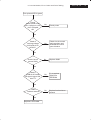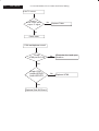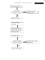
1
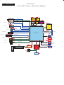
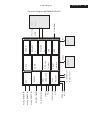
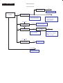
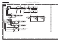
Colour Television
Chassis
TPS1.0E
LA
15PFL4122/93
19PFL4322/93
20PFL4122/93
H_17090_000.eps
050607
Contents
1
2
3
4
5
6
7
Page
Technical Specifications, Connections, and Chassis
Overview
2
Safety Instructions, Warnings, and Notes
6
Directions for Use
8
Mechanical Instructions
10
Service Modes, Error Codes, and Fault Finding 12
Block Diagrams, Test Point Overview, and
Waveforms
Wiring Diagram
18
Block Diagrams
21
Circuit Diagrams and PWB Layouts
Diagram
Scaler Board: Power
(S-01) 25
Scaler Board: Lips & Inverter I/F
(S-02) 26
Scaler Board: Tuner
(S-03) 27
Scaler Board: Video Inputs
(S-04) 28
Scaler Board: DSUB Input
(S-05) 29
Scaler Board: HDMI Input
(S-06) 30
Scaler Board: SCART I/F
(S-07) 31
Scaler Board: MST96885LD/ALD
(S-08) 32
Scaler Board: Flash ROM & SDRAM
(S-09) 33
Scaler Board: Key, IR BD & ComPair I/F (S-10) 34
Scaler Board: ITV I/F
(S-11) 35
Scaler Board: Panel I/F
(S-12) 36
Scaler Board: Audio I/F
(S-13) 37
Scaler Board: Audio Amplifier
(S-14) 38
Waveform Diagram
49
Inverter Board
(IN) 51
Power Panel (For 19PFL4322)
(P) 53
Power Panel (For 19PFL4322)
(P) 54
Power Panel (For 20PFL4122)
(P) 55
Power Panel (For 20PFL4122)
(P) 56
Power Panel (For 20PFL4122)
(P) 56
Data Transfer Board (For 20PFL4122)
61
Keyboard Panel
(K) 63
Contents
Page
IR & LED Panel
(I) 66
8 Alignments
69
9 Circuit Descriptions, Abbreviation List, and IC Data
Sheets
75
Abbreviation List
79
IC Data Sheets
82
10 Recommended / Spare Parts List
86
Styling Sheet
86
Recommended Parts List
92
Spare Parts List
93
11 Different Parts List
112
12 Revision List
113
©
Copyright 2007 Philips Consumer Electronics B.V. Eindhoven, The Netherlands.
All rights reserved. No part of this publication may be reproduced, stored in a
retrieval system or transmitted, in any form or by any means, electronic,
mechanical, photocopying, or otherwise without the prior permission of Philips.
Published by CS 0766 BG CD Customer Service
Printed in the Netherlands
Subject to modification
EN 3122 785 17080
2
TPS 1.0E LA
1. Technical Specifications,Connections,and Chassis Overview
1.Technical Specifications,Connections,and Chassis Overview
Index of this chapter:
1.1 Technical Specifications
1.2 Connections
1.3 Chassis Overview
Notes:
Figures below can deviate slightly from the actual situation,
due to the different set executions.
Specifications are indicative (subject to change)
1.1
Technical Specifications
1.1.1 Technical Specifications
Panel
Display area(mm)
Number of Pixels
Pitch ( mm )
Display operating mode
Color depth
Brightness (cd/m^2)
Viewing angle(CR>10)
Surface treatment
Electrical interface
Response Time
Contrast ratio
Outline Dimension
Module weight (g)
Backlight
: LCD
: 304.128(H) X 228.096(V) (15")
410.4 mm X 256.5 mm (19")
408 mm X 306 mm (20")
: 1024(H) x 768(V) (15")
1440(H) x 900(V)(19")
640(H) x480(V) (20")
: 0.29(H) x 0.29(V) (15")
0.285(H) x 0.285 mm(V) (19")
0.6375(H) x 0.6375(V) (20")
: Normally black (15",20")
Normally White (19")
: 16.7M colors ( 8 bits) (15")
16.2M colors (19")
16.7M colors ( 8 bits) (20")
: 250(Center 1 points, Typ.) (15")
300(Center 1 points, Typ.) Min :
230 (19")
450(Center 1 points, Typ.) (20")
: Viewing angle free
70/70/70/60(R/L/U/D) (15")
Viewing angle free
(R/L 85/85 (Typ.) ,U/D 80/80(Typ.))
(19")
Viewing angle free
(R/L 178(Typ.) ,U/D 178(Typ.)) (20")
: Hard coating 3H (15",19",20")
: LVDS (15",19")
TTL (20")
: 8ms (Gray to Gray) (15")
5ms (Typ) (19")
12ms (Gray to Gray) (20")
: Typical 700 : 1 (15")
Typical 850 : 1 Min : 500 (19")
Typical 800 : 1 (20")
: 326.5 mm(H) x 253.5mm(V) x
14.4(D) mm (Typ.) (15")
427.2 mm(H) x 277.4 mm(V) x
17.0(D) mm (Typ.) (19")
432 mm(H) x 331.5mm(V) x
25.0(D) mm (Typ.) (20")
: 1350(Typ.) (15")
2500g(Typ.) (19")
3500g(Typ.) (20")
: 2 CCFL (15")
4 CCFL (19")
6 CCFL (20")
User video timing specifications:
Mode Resolution
H. freq. / V. freq
1
640 x 350
31.469Khz/70.090Hz
2
720 x 400
31.469Khz/70.085Hz
3
640 x 480
35.000Khz/66.667Hz
4
640 x 480
37.861Khz/72.809Hz
5
640 x 480
37.500Khz/75.000Hz
6
800 x 600
35.200Khz/56.000Hz
7
800 x 600
48.077Khz/72.188Hz
8
800 x 600
46.875Khz/75.000Hz
9
832 x 624
49.700Khz/75.000Hz
10
1024 x 768
56.476Khz/70.069Hz
TV system signal mode:
RF support:
WE: PAL B/G/D/K/I and SECAM L/L’/B/G /D/K .
CVBS/S-video: Support PAL, NTSC and SECAM colour system.
Comp video IN(YpbPr) : including 480i/p 50/60Hz,720p 50/60Hz,
1080i 50//59/60Hz,1080p 50//59/60Hz
HDMI IN : 480p, 576p, 720p 50/60Hz, 1080i 50/59/60Hz,
1080p 50/59/60Hz
For 19PFL4322/10
PC timing table
Mode Resolution
1
640 x 480
2
800 x 600
3
800 x 600
4
1024 x 768
5
1280 x 720
6
1280 x 768
7
1360 x 768
8
1440 x 900
H. freq. / V. freq
31.469Khz/59.940Hz
35.156Khz/56.250Hz
37.879Khz/60.317Hz
48.363Khz/60.004Hz
44.772kHz/59.855 Hz
47.776kHz/59.87Hz
47.712kHz/60.015Hz
55.469kHz/59.901Hz
Standard
VGA
VESA
VESA
VESA
CVT
CVT
CVT
CVT
User video timing specifications:
Mode Resolution
H. freq. / V. freq
1
640 x 350
31.469Khz/70.087Hz
2
720 x 400
31.469Khz/70.087Hz
3
640 x 480
35.000Khz/66.667Hz
4
640 x 480
37.861Khz/72.809Hz
5
640 x 480
37.500Khz/75.000Hz
6
800 x 600
48.077Khz/72.188Hz
7
800 x 600
46.875Khz/75.000Hz
8
832 x 624
49.700Khz/75.000Hz
9
1024 x 768
56.476Khz/70.069Hz
10
1024 x 768
60.023Khz/75.029Hz
Standard
VGA
VGA
Macintosh
VESA
VESA
VESA
VESA
Macintosh
VESA
VESA
TV system signal mode:
RF support:
WE: PAL B/G/D/K/I and SECAM L/L'/B/G /D/K .
CVBS/S-video: Support PAL, NTSC and SECAM colour system.
Comp video IN(YpbPr) : including 480i/p 50/60Hz,720p 50/60Hz,
1080i 50//59/60Hz, 1080p 50//59/60Hz
HDMI IN : 480p, 576p, 720p 50/60Hz, 1080i 50/59/60Hz,
1080p 50/59/60Hz
Allowed signal mode specified
For 20PFL4122/10
For 15PFL4122/10
PC timing table
Mode Resolution
1
640 x 480
2
800 x 600
3
800 x 600
4
1024 x 768
5
1027 x 768
PC timing table
Mode Resolution
1
640 x 480
2
720 x 400
H. freq. / V. freq
31.469Khz/59.940Hz
35.156Khz/56.250Hz
37.879Khz/60.317Hz
48.363Khz/60.004Hz
60.000Khz/75.000Hz
Standard
VGA
VESA
VESA
VESA
VESA
Standard
VGA
VGA
Macintosh
VESA
VESA
VESA
VESA
VESA
Macintosh
VESA
H. freq. / V. freq
31.469Khz/59.940Hz
30.240Khz/66.667Hz
Standard
VGA
VGA
TPS 1.0E LA
1. Technical Specifications, Connections and Chassis Overview
TV WE model
PRG
1
2
3
4
5
6
7
8
9
10
11
12
13
14
15
16
17
18
19
20
21
22
23
24
25
28
CH
AU37
AU2
E7
G47
I23
E12
AU7
G68
AU9
AU10
AU0
AU2
AU5
AU5A
AU7
AU9
AU10
I23
G28
AU37
I40
CH44
I60
I66
K21
G28
Frequency Carriers
Video
Sound
590.25MHz
595.75MHz
64.25MHz
69.75MHz
189.25MHz
194.75MHz
679.25MHz
684.75MHz
487.25MHz
493.75MHz
224.25MHz
229.75MHz
182.25MHz
187.75MHz
847.25MHz
852.75MHz
196.25MHz
201.75MHz
209.25 MHz 214.75 MHz
46.25MHz
51.75MHz
64.25MHz
69.75MHz
102.25 MHz 107.75 MHz
138.25MHz
143.75MHz
182.25MHz
187.75MHz
196.25MHz
201.75MHz
209.25MHz
214.75MHz
487.25MHz
493.75MHz
527.25MHz
532.75MHz
590.25MHz
595.75MHz
623.25MHz
629.75MHz
655.25MHz
661.75MHz
783.25MHz
789.75MHz
831.25MHz
837.75MHz
471.25 MHz 477.75 MHz
527.25MHz
532.75MHz
TV
System
Pattern
PAL B
Pure White
PAL B Circle Pattern
PAL B Circle Pattern
PAL G
Circle Pattern
PAL I
Circle Pattern
PAL B
Color Bar
PAL B
Color Bar
PAL G
100% White
PAL B
Checkerboard
PAL B
Crosshatch
PAL B
Color Bar
PAL B
Color Bar
PAL B
Crosshatch
PAL B
Color Bar
PAL B
Pure White
PAL B
Pure White
PAL B
Circle Pattern
PAL I
Circle Pattern
PAL G
Circle Pattern
PAL G
Circle Pattern
PAL I
Color Bar
PAL DK
Color Bar
PAL I
100% White
PAL I
Checkerboard
SEC K1
Crosshatch
PAL G
Color Bar
Ambient conditions
Temperature
Humidity
3
: 0 to40°C
: 10 to 90%
1.2 Connectors
1.2.1 I/O interface
1. Tuner: Multi-standard for WE model
2.
Audio 1 IN : audio R/L(RCA jack) input
3.
AV1 IN : Composite video input (CVBS)
4.
S-video IN : S-video input
5.
Comp video IN :YPbPr format input
6.
AV2 IN: Composite video (CVBS) input
7.
Audio 2 IN : Comp and AV2 audio R/L(RCA jack) input
8.
Scart IN : YPbPr/CVBS with audio input and CVBS with audio
line out
9.
PC Audio IN: audio R/L(mini-jack).
10. PC IN: VGA input (D-SUB connectors)
11. HDMI : digital video and audio input
12. Earphone : earphone jack
Comp video input mode: 480i, 480p, 576i, 576p, 720p50,
720p59, 720p60, 1080i50, 1080i59,
1080i60, 1080p50, 1080p59, 1080p60
HDMI input mode
1
720x480p/59Hz, 60Hz,720x576p/50Hz,
2
1280X720p, 50Hz , 59Hz, 60Hz
3
1920X1080i, 50Hz, 59Hz, 60Hz
4
1920X1080p, 50Hz, 59Hz, 60Hz
1.2.2 PC mode signal type
a.Analog Video
: 15 pin D-sub ,0.7 Vp-p linear, positive polarity &
separate sync.( TTL level, positive or negative
polarity)
b.Audio signal
1.1.2 Sound
Sound systems
Maximum power
: Mono / Stereo / Virtual Surround
: 2 x 3W
1.1.3 Miscellaneous
Power Supply
AC-input
: 90V ~ 264VAC, 50/60 2Hz (15",19")
: 90V ~ 264VAC, 50/60 3Hz (20")
Power consumption : 35W/Max(at PC mode),35W/Max(at
TV mode) with Audio. (15")
70W/Max(at PC mode),70W/Max(at
TV mode) with Audio. (19")
Normal: (20")
1. PC Mode: TYP 60 W (with audio)
2. TV Mode: TYP 60 W (with audio)
Maximum: 65W (with audio) (20")
Power cord length
1.8m
Power cord type
: European type and China type (15",19")
3 lead with earth plug, pluggable (20")
Power indicator
: LED (On: Blue ,Sleeping mode:
Red ) (15")
LED (On: Blue ,Sleeping mode:
Amber ) (19")
LED (On: Blue, Standby mode:
Amber) (20")
Auto power saving
: < 2W (15",19")
VESA DPMS (20")
: 3.5mm stereo mini-jack
Level: Nominal : 0.5 V rms.
- Maximum : 1.5 V rms.
-Impedance > 10 kW.
c.Signal source: Pattern generator format as attachment table 1 to 12.
Reference generator : CHROMA 2200 or QuantumData 802R
TV mode signal type
RF Signal : Aerial input / 10mV(30-100dBuV)
Video signal : CVBS input ( RCA jack) / 1Vpp (300mV-sync,
700mV-video.)
S video input / 1VppY-signal, +/-300mV C-signal
SCART input: CVBS
YPbPr signal ( for WE model
only)
Comp video in(YPbPr input)/ 1Vpp Y signal,
+/-350mV Pb,Pr signal
HDMI:Digital interface with 4 channels TMDS signal
CVBS output ( SCART line out) / 1Vpp (300mV-sync,
700mV-video.)
Audio signal : Audio (1) R/L for AV IN(AV and S-Video).
Level: - Nominal : 0.5 V rms.
- Maximum : 1.5 V rms.
- Impedance > 10 kW.
Audio (2) R/L for SCART IN
Level: - Nominal : 0.5 V rms.
- Maximum : 1.5 V rms.
- Impedance > 10 k W.
Audio (3) R/L for Comp video IN.
Level: - Nominal : 0.5 V rms.
-Maximum : 1.5 V rms.
-Impedance > 10 k W.
4
TPS 1.0E LA
Audio
1. Technical Specifications,Connections,and Chassis Overview
(4) digital audio for HDMI Video IN.
1.2.5 Scart
Scart output: ( for WE model only)
Video: CVBS output 1Vpp / Impedance : 75W.
Audio: R/L output (from CVBS)
Level: - Nominal
: 0.5 V rms.
- Maximum : 1.5 V rms.
- Impedance < 1 k W.
Headphone
Audio: R/L output -10mW at 32W.
3.5mm stereo jack with switch
Impedance is between 8 and 600 W.
1.2.3 VGA Pin assignment
Pin
1
2
3
4
5
6
7
8
PIN No.
1
2
3
4
5
6
7
8
9
10
11
12
13
14
15
SIGNAL
Red video input
Green video input /SOG
Blue video input
GND
GND– cable detect
Red video ground
Green video ground
Blue video ground
DDC +3.3V (or 5V)
Logic ground
GND
Serial data line (SDA)
H. Sync / H+V
V. Sync
Data clock line (SCL)
1.2.4 HDMI Pin assignment
Type A Connector
No. 1
No. 2
Pin No.
1
2
3
4
5
6
7
8
9
10
11
12
13
14
15
16
17
18
19
No. 19
No. 18
Description
RX2+
GND
RX2RX1+
GND
RX1RX0+
GND
RX0RXC+
GND
RXCCEC
NC
DDC clock
DDC data
GND
+5V POWER
Hot Plug Detect
9
10
11
12
13
14
15
16
17
18
19
20
21
TV SCART
N/C
Right audio input
N/C
Audio ground
Blue ground
Left audio input
Blue output
0-2.5 volts (low) when:
TV output
4.5-7.5 volts (High-to-6v) when:
-inputting picture format setting is '16:9',
9-12 volts (high-to-12v) when:
-inputing picture format setting is '4:3'
Green ground
N/C
Green output
N/C
Red ground
N/C
Red output
0 volt (low) when:- pin 8 of the TV scart is low
or when:
- Composite video signal
1-3 volts (high) when:
- video input setting is 'RGB',
Composite video output ground
Composite video input ground
N/C
Composite video input
Ground
1. Technical Specifications, Connections and Chassis Overview
TPS 1.0E LA
1.3 Chassis Overview
Type: 15PFL4122/10
Key Board
IN
Inverter Board
I
Scaler Board
K
S
IR Board
Type: 19PFL4322/10
Key Board
P
Power Board
I
IR Board
Scaler Board
K
S
Type: 20PFL4122/10
P
I
Key Board
K
Scaler Board
S
Power Board
IR Board
5
6
TPS 1.0E LA
2.Safety Instructions,Warnings,and Notes
2.Safety Instructions,Warnings,and Notes
· Where necessary,measure the waveforms and voltages with( )
and without( )aerial signal.Measure the voltages in the power
supply section both in normal operation( ) and in stand-by( ).
These values are indicated by means of the approprate symbols.
Index of this chapter:
2.1 Safety instructions
2.2 Warnings
2.3 Notes
· The semiconductors indicated in the circuit diagram and in the
parts lists,are interchangeable per position with the
semiconductors in the unit,irrespective of the type indication
on these semiconductors.
· Manufactured under license from Dolby Laboratories. "Dolby ",
"Pro Logic" and the "double-D symbol",are trademarks of Dolby
laboratories.
2.1 Safety Instructions
Safety regulations require the following during a repair:
· Connect set to the Mains/AC Power via an isolation
transformer(>800VA)
· Replace safety components,indicated by the symbol ! ,
only by components identical to the original ones.Any
other component substitution(other than original type)may
increase risk of fire or electrical shock hazard
2.3.2 Schematic Notes
· All resistor values are ohms,and the value multiplier is often used
to indicate the decimal point location(e.g. 2K2 indicates 2.2 kohm).
· Resistor values with no munltiplier may be indicated with either an
"E" or an "R"(e.g.220E or 220R indicates 220 ohm).
· All capacitor values are given in micro-farads(u=x10-6),nanofarads9n=x10 -9 ),or pico-farads(p=x10 -12).
· Capacitor values may also use the value multiplier as the decimal
point indication(e.g. 2p2 indicates 2.2 pF).
· An "asterisk"(*) indicates component usage varies.Refer to the
diversity tables for the correct values.
· The correct component values are listed in the Spare Parts List.
Therefore,always check this list when there is amy doubt.
Safety regulations require that after a repair,the set must
be returned in its original condition.pay in particular
attention to the following points:
· Route the wire trees correctly and fix them with the
mounted cable clamps.
· Check the insulation of the Mains/AC power lead
for external damage.
· Check the strain relief of the Main/AC power cord
for proper function.
· Check the electrical DC resistance between the pins of
the Mains/AC Power plug and secondary side(only for
sets that have a Mains/AC power isolated poer supply):
1. Unplug the Mains/AC Power cord and connect a wire
between the two pins of the Mains/AC power plug.\
2.Set the Mains/AC Power switch to the "ON " position
(keep the Mains/AC Power cord unplugged!)
3.Measure the resistance value between the pins of the
Mains/AC Power plug and the metal shielding of the
tuner or the aerial connection on the set.The reading
should be between 4.5 Mohm and 12 Mohm.
4.Switch "OFF" the set,and remove the wire between
the two pins of the Mains/AC plug.
2.3.3 Lead-free Solder
Philips CE is producing Lead-free sets (PBF) from 1.1.2005
onwards.
Idntification:The bottom line of a type gives a 14-digit serial
number.Digial 5 and 6 refer to the production year,digits 7 and
8 refer to production week( inexample below it is 2007 week14)
· Check the cabinet for defects,to prevent touching of any inner
parts by the customer.
2.2 Warnings
MODEL ID.20PFL4122/10
01
· All ICs and many other semiconductors are susceptible to
electrostatic discharges(ESD ).Careless handling during
repair can redure life drastically.Make sure that,during repair,
you are connected with same potential as the mass of the set
by wristband ith resistance .Keep components and tools also
at this same potential.Available EDS protection equipment:
-Complete kitEDS3(small tablemat,wrisband,connection box
,extension cable and earth cable)4822 310 10671.
-Wristband tester 4822 344 13999.
· Be careful suring measurements in the high voltage section.
· Never replace modues or other components while the unit
is switched"ON".
· When you align the set,use plastic rather than metal tools.This
will prevent any shurt circuits and danger of a circuit becoming
unstable.
0714
0714
2.3 Notes
Figure 2-1 Serial number example
Regardless of the special lead-free logo(which is not always
indicated),one must treat all sets from this date onwards
according to the rules as described below.
P
Ab
2.3.1 General
· Measure the voltages and waveforms with regard to the chassis
(=tuner)ground( ),or hot ground( ), depending on the tested area
of curcuitry.The voltages and waveforms shown in the diagrams
are indicative.Measure them in the Service Default Mode(see
chapter 5)with a colour bar signal and stereo sound(L:3 khz,
R:1 kHz unless statedotehrwise)and picture carrier at 475.25
Mhz for PAL,or 61.25 MHZ for NTSC(channel 3).
Figure 2-2 Lead-free logo
Due to lead-free technology some rules have to be respected
by the workshop during a repair:
2. Safety Instructions,Warnings and Notes
Use only lead-free soldering tin Philips SAC305 with
order code 06622 149 00106.If lead-free solder paste
is required please contact the manufacturer of your
soldering equipment.In general,use of solder paste
within workshops should be avioded because paste is not
easy to store and to handle.
Use only adequate solder tools applicable for lead-free
soldering tin.The solder tool must be able:
-To reach a solder-tip temperature of at least 400 C.
-To stabilise the adjusted temerature at the solder-tip
-To exchange solder-tips for different applications.
Adjust your solder tool so that a temperature of around
360 C -380 C is reached and stablilised at the solder joint.
Heating time of the solder-joint should not exceed~4sec.
Aviod temperatures above 400 C,otherwise wear-out of tips
will increase drastically and flux-fluid will be destroyed.
To aviod wear-out of tips,switch”off” unused equipment or
reduce heat.
Mix of lead-free soldering tim/parts with leaded soldering
tin/parts is possible but PHILIPS recommends strongly to
avoid mixed regimes.If this cannot be avoided,carefully
clear the solder-joint from old tin and re-solder with new
tin.
Use only original spare -parts listed in the Service-Manuals.
Not listed standed material(commodities)has to be purchased
at external companies.
For sets produced before 1.1.2005,containing leaded
soldering tin and components,all needed spare parts will
be available till the end of the service period.For the
repair of such sets nothing changes
In case of doubt whether the board is lead-free or not(or
with mixed technologies),you can use the following method:
Always use the highest temperature to solder,when using
SAC305(see also instructions below).
De-solder thoroughly(clean solder joints to avoid mix of
two alloys).
2.3.4 Alternative BOM identification
In September 2005,Philips CE introduced a change in the way
the serial number(or production number,see Figure 2-1)is
composed.From this data on,the third digit in the serial number
(example:AG2B0335000005) indicates the number of the
TPS 1.0E LA
7
Alternativ BOM(bill of Materials used for producing the sepcific
model of TV set).It is possible that the same TV model on the
market is produced with e.g. Two different types of displays,
coming from two different O.E.M.s.
By looking at the third digit of the serial number,the serivce
technician can see if there is more than one type of B.O.M. Used
in theproduction of the TV set he is working with.He can used in
the Commercial type Version Number of the TV set
(e.g.20PFL4122/93),after which a screen will appear that gives
information about the number of alternative B.O.M.s used.
If the third digit of serial nuber contains the number 1(example:
AG1B0335000001),then there is only one B.O.M. Version of the
TV set on the market.If tje third digit is a 2(example:
AG2B033500001),then there are two different B.O.M.s.
Information about this is important for ordering the correct spare
parts!
For the third digit,the number 1....9 and the characters A.....Z can
be used,so in total:9 plus 26=35 different B.O.M.s can be indicated
by the third digit of the serial number.
2.3.5 Board Level repair(BLR) or Component Level Repair(CLR)
If a board is defective,consult your repair procedure to decide if
the board has to be exchanged or if it should be repaired on
component level.
If your repair procedure says the board should be exchanged
completely,do not solder on the degective board.Otherwise,it
cannot be returned to the O.E.M. Supplier for back charging!
2.3.6 Practical Service precautions
It makes sense to avoid exposure to electrical shock.
While some sources are expected to have a possible dangerous
impact,others of quite high potential are of limited current and are
sometimes held in less regard.
Always respect voltages.While some may not be dangerous in
themselves,they can cause unexpected reactions that are best
avoided.Before reaching into a powered TV set,it is best to test
the high voltage insulation.It is easy to do,and is a good service
precaution.
8
TPS 1.0E LA
3. Directions for Use
3. Directions for Use
You can download this information from the following websites:
http://www.philips.com/support
http://www.p4c.philips.com
1st Layer
Picture
PC MODE
3rd Layer
2nd Layer
Color temp
Brightness
Contrast
Auto adjust
Manual adjust
Normal
Warm
Cool
Yes
Phase
Clock
Horizontal
Vertical
Sound
Smart sound
Settings
Virtual surround
Personal
Speech
Music
Movie
Mulitimedia
Treble
Bass
Balance
On
Off
Features
Picture format
Full screen
4:3
Language
English
Factory reset
No
Yes
Install
1st layer
Picture
2nd layer
Smart picture
Contrast
Brightness
Color
Sharpness
Tint
Color temp
Picture format
TV / AV/ S-VIDEO / HD MODE
3rd layer
4th layer
Personal
Rich
Nature
Soft
Multimedia
Normal
Warm
Cool
Super zoom
4:3
Movie expand 14:9
Movie expand 16:9
16:9 subtitle
Widescreen
5th layer
TPS 1.0E LA
3. Directions for Use
Sound
Smart sound
Settings
Virtual surround
Personal
Speech
Music
Movie
Mulitimedia
Treble
Bass
Balance
On
Off
Features
Timer
NR
Auto lock
Clock
Start time
Stop time
Sleep timer
On
Off
Lock program
Change code
Clear all
Source list
TV
HDMI
Comp video
Scart
S-video
AV 1
AV 2
PC
Language
English
Auto store
Start ?
Manual store
Manual store
Yes
On
Off
Install
Prog. no
Finetune
Store
Channel setting
Channel edit
Channel swap
Name edit
Channel sort
Factory reset
No
Yes
Auto store
Please wait
Prog. found
Frequency
MHz
Start ?
Store ?
Stored
Channel
Skipped
From
To
Exchange
Channel
Name
Sort ?
Active
Skipped
Exchange ?
Exchanged
Sorting. . . . . .
Sort complete
9
10
TPS 1.0E LA
4. Mechanical Instructions
4. Mechanical Instructions
Step 2. Remove the Back cover and SHIELD-MAIN as Fig.4~5.
a. Remove the 4 screws, then remove the back cover as Fig.4.
b. Remove the 5 screws , then remove SHIELD-MAIN as Fig.5.
Index of this chapter:
4.1 Assy/Panel Removal
4.2 Set Re-assembly
4.1 Assy/Panel Removal
Note:Please put your mechine on a soft material to avoid to
scrape panel when you disassemble it.
Front view
Fig.4
Fig.1
Back view
Fig.5
Step 3. Remove the Scaler, Power, IR and Key as Fig.6.
a. Remove the 7 screws and disconnect the 6 cables to remove the
scaler board .
b. Remove the 7 screws and disconnect the 5 cables to remove the
Power board.
c. Remove the 2 screws and disconnect the 1 cable to remove the IR
board.
d. Remove the 2 screws and disconnect the 1 cable to remove the Key
board.
Fig.2
Step 1. Remove the Base.
Remove the 4 screws as Fig.3.
Fig.6
Step 4. Remove the Front bezel as Fig.7.
a. Remove the 27 screws to remove the Frame assy as Fig.7.
Fig.3
4. Mechanical Instructions
11
TPS 1.0E LA
Fig.10
Fig.7
Step 5. Remove the Frame assy as Fig.8~9.
a. Remove the 4 screws as Fig.8.
b. Remove the Frame assy as Fig.9.
c. Remove the Datatransfer board as Fig.10.
Fig.11
Insulation material
Fig.8
4.2 Set Re-assembly
To re-assemble the whole set, execute all processes in reverse
order.
Notes:
a. While re-assembling, make sure that all cables are placed
and connected in their original position.
b. Pay special attention not to damage the EMC foams at the
SSB shielding. Check that EMC foams are put correctly on
their places.
In warranty, it is not allowed to disassembly the LCD panel, even the
backlight unit defect.
Out of warranty, the replacment of backlight unit is a correct way
Fig.9
when the defect is cused by backlight (CCFL,Lamp).
12
TPS 1.0E LA
5. Service Modes, Error Codes and Fault Finding
5. Service Modes, Error Codes and Fault Finding
index of this chapter:
5.1 CSM
5.2 Factory Mode
5. 3 Repair Flow Chart
5.1 CSM
It can display CSM windows message when press 1-2 3-6 5-4 on the button (RC) remote control in normal operation mode.
The following information is displayed on screen:
Set type:
Model type would be displayed on this item. E.g.
15PFL4122/10, 19PFL4322/10 or 20PFL4122/10.
Production code:
S/N would be displayed on this item.
SW main-processor:
Firmware version would be displayed on this item. E.g.
1.77 is the version.
SW other-processor:
N/A
Code 1:
5 last logged errors.
Code 2:
5 first logged errors.
Error code
0x01
0x02
0x03
0x04
0x05
Event
Audio decoder error
IIC bus error
Tuner error
NVRAM error
Scaler chip error
Key (HDCP):
HDCP key valid or invalid status would be displayed
on this item.
NVM-Name:
Same as set type
Software naming, version
19PFL4322/10
TPS1.0E LA1A_,SWMainVersion,
15PFL4122/10
TPS1.0E LA1C_,SWMainVersion,
20PFL4122/10
TPS1.0E LA1C_,SWMainVersion,
1. Press "Menu" to enter the OSD menu as Fig 1.
5. Service Modes, Error Codes and Fault Finding
TPS 1.0E LA
5.2 Factory Mode
Press "Menu062596 " on remote control then Press "Up " or "Down " button to move cursor to bottom item and then press
"OK " button to enter factory mode.
Factory indicate
For white balance alignment
For auto color adjustment
For design only, please don’t adjust it.
Use or to select the item that you want to change. Use and
to change the value. When you finish to set , use or to select "
Save " and press " OK " to save your setup. Then use or to
select " exit " and press "Menu " to leave factory mode.
13
14
TPS 1.0E LA
5. Service Modes, Error Codes and Fault Finding
5.3 Repair flow chart
1.No work/LED is off
Check if
power switch is
normal
No
Replace Power switch
Yes
Check
IR board CN001
pin1=0V,pin2=3.7V,
pin3=3V,pin4=2.85V
,pin5=5V,pin6
=3.3V
No
Check IR board
Yes
Check scaler board U102
pin1=14V,pin4=1.22V,
pin7=16V,pin8=5V,
2.No raster/picture too
dim
Check
Inverter board
CN852,pin1=16V,
pin5=0.9V,pin6
=3V
No
Check Scaler board
Yes
Check
Inverter board
U811 pin2=5V,Q821
pin=5,6=16V
Yes
Check scaler board
No
Check U811,Q821
5. Service Modes, Error Codes and Fault Finding
3.No picture/LED is green
Check
scaler board U102
pin1=14V,pin4=1.22V,
pin7=16V,pin8
=5V
No
Check power
Yes
Check if
working voltage
U152,pin2=3.3V
pin3=5V
No
Check circuit around
each regulator and
eliminate short and
open situation
Yes
Check if clock
source X350
No
Replace X350
Yes
Check if
RGB,clk,H/V and
DE signal output 128
bits TTL
No
Try to replace
flash Rom
EEPROM
Yes
Check
resistors-network
Yes
Replace LVDS cable
No
Replace bad resistorsnetwork
TPS 1.0E LA
15
16
TPS 1.0E LA
5. Service Modes, Error Codes and Fault Finding
4.No TV sound
Check if
tuner TU201 pin11
output IF signal
No
Replace TU201
Yes
Check U301
5.No earthphone sound
Check
U760 pin15=3.3V
No
Eliminate short and open
situation
Yes
Check U760
pin20=HPOUTL
pin6=HPOUTR
Yes
Replace Side AV Board
No
Replace U760
5. Service Modes, Error Codes and Fault Finding
TPS 1.0E LA
6.No remote function
Tty another
remote control
No
Replace one good
remote control
Yes
Check IR receiver
7.LED and function
key poor
Check circuit around
control board and cable
between control board
and scaler board
8.No HDMI picture
Enter CSM mode
to check item 6
Valid
Check Scaler Board
Invalid Change U701 writen
HDCP KEY
17
6. Block Diagram
18
TPS 1.0E LA
6.
Block Diagram
Index of this chapter:
6.1 Wiring Diagram
6.2 Block Diagram
Wiring Diagram
Type: 15PFL4122/10
Panel
089G179E20D904
095T8014 6951 FP
IN
I
S
K
CN7201
9pin
20pin
CN7504
4pin
CN0101
095T8014 4953 FP
2pin
CN6202
2pin
CN6201
095T8013 2981 FP
6pin
CN7301
CN7302
095T8014 9924 FP
095T8013 2980 FP
6pin
CN0201
19
TPS 1.0E LA
6. Block Diagram
Type: 19PFL4322/10
I
P
K
095T8013 2973 FP
095T8014 6947 FP
095T8014 11937 FP
S
089T179E30C917
095T8014 4948 FP
095T8013 2974 FP
6. Block Diagram
TPS 1.0E LA
20
Type: 20PFL4122/10
I
089T176E 50912
095T8014 11938 FP
P
6pin
S
K
11pin
50pin
4pin
4pin
095T8014 4949 FP
2pin
2pin
095T8014 6948 FP
6pin
095T8013 2975 FP
095T8013 2976 FP
Panel
20" TTL
INVERTER
16 V DC
HDMI
23 " 30 P LVDS
PWR
15" 20 P LVDS
D-SUB
SCART
230 mm
AUDIO IN
IR BD
19" 30 P LVDS
iTV
Level 1
TUNER
Audio Amplifier
TA333AW
Speaker
4M X 16 SDRAM
HY57V641620ETP
Key BD
MST 96885LD/ALD
I-BD
ComPair
Headphone
S-Video
150 mm
Y Pb Pr
Audio R/L
PWR I-BD
6. Block Diagram
TPS 1.0E LA
6.2 Block Daigram
15" 20" 19W" Model Scalar Board PCB Layout
21
CVBS Audio
22
TPS 1.0E LA
6. Block Diagram
15 " 20 " 19W " Europe - System Block Diagram
CVBS0
MM Tuner
S-05
S-06
24C02
DSUB EDID
24C02
DVI EDID
SIF0
S-02
TMDS / Video & Audio
HDMI
S-08
S-06
24C32
NVRAM
24C16
HDCP
S-09
SPI Flash
ROM
S-09
SPI
S-06
D-SUB
SDRAM
I2C
R1,G1,B1
S-05
S-04
CVBS
CVBS1
S-Video
Y0,C0
Component-1
S-12
TTL/LVDS
Y,Pb,Pr (R0,G0,B0)
LCD Panel
MST96885LD/ALD
S-04
SCART
RGB/ CVBS
UART1
S-10
Com Pair
S-07
Component Audio-1
CVBS Audio
S-13
AUL0, AUR0
S-13
AUL1, AUR1
Cloning (ITV1)
S-11
Line-out
S-13
AUL2, AUR2
IIS
PC Audio
S-07
S-07
TL062
SCART Audio Output
(5P)
Video I/F
(ITV-2)
(7P)
IR Board
S-10
(3P)
STA333AW
AMP
11P
S-02
S-14
S-14
HP/Bathroom
Speaker (ITV-2)
2x(2P
L-R Speaker
Key Board
S-10
S-14
LIPS control
SPDIF out
I2S out
SIF*2
L/Rx4 + mono
CVBS x4
YC x2
16-bit digital video
DVI/HDCP/HDMI
Analog RGB/YPbPr
Analog RGB/YPbPr
Analog RGB/YPbPr
& L/R Line out
2.1 Speaker out
Processor
Audio
2D/3D Comb
VD w/
HDMI Rx
ADC
SDRAM
Interface
DRAM
Teletext
CC/V-chip
3D NR
Scaler
16bits
MCU
OSD
Tx
TTL/LVDS
3
MStarACE
2D/3D DI
Flash
SPI
Panel
LCD
GPIO/PWM
LVDS
TTL/ 10-bit
6. Block Diagram
TPS 1.0E LA
Function Diagram MST96885LD/ALD
23
24
TPS 1.0E LA
6. Block Diagram
Power Management
+1V8
U7103 AME8815)
- U4101 (MST) : VDDC
LIPS
+3V3_STBY
+16V
+3V3_STBY
U7102 (AIC1596)
- For IR Board
- U1101 (24C02 :DSUB)
- U5101 (24C02 :DVI-D)
- U4101 (MST) : AVVD_DVI,
AVDDA, AVDD_MPLL, VDDP
- U4202 (Flash ROM)
- U4102,4 (NVRAM)
- U4103,5 (HDCP)
ITV_5V_SW
+16V
+5V_ITV
U7105 (AIC1596)
- For ITV use (Reserve)
- U7401 (Sync Slicer)
PWR_SW
+16V
+5V
U7101 (AIC1596)
U7104 (AME8815) or
(AIC1084/5)
- TU2101 (TUNER)
- U6202 (Bath AMP)
+3V3
- U4101 (MST) : AVDD_SIF,
AVDD_AV, AVDD_MemPLL,,
VDDM
- U4201, 3 (SDRAM)
ITV_12V_SW
+16V
U106 (AIC1596)
+12V
- PANEL (+12V)
+16V_AUDIO
- U6201 ( AUD AMP)
7.Circuit Diagrams and PWB Layouts
TPS 1.0E LA
Scaler Board Schematic Diagram-DC-DC POWER
1
2
3
4
5
6
7
8
S-01
9
10
+5V_STBY
+16V
FB7101
CN7101
U7105
F7101
1
2
BEAD
+16V
C7118
0.1uF
7A 125V
C7101
0.1uF(NC)
C7102
0.1uF
IN
5
3
ON/OFF
GND
FB
2
OUT
C7103
470uF 25V
A
35uH
Q7109
ZD7103
SSA34-E3
4
EAR
R7102
R7112
R7111
0R
4
3
2
1
22K
R7101
C7119
470uF 25V
AIC1596-50PM5
1
G
D
D
D
0.1uF(NC)
PWR JACK 2.5MM
5
6
7
8
S
D
D
D
CN7101 A1
C7102 A3
C7104 B2
C7106 C3
C7108 E4
C7110 C5
C7112 C8
C7114 C6
C7116 C9
C7118 A5
C7120 B6
C7122 F6
C7124 F8
C7126 D4
C7128 D7
C7130 D7
C7132 B7
C7134 A8
D7103 C5
FB7101 A2
FB7103 E7
FB7106 F7
L7101 B3
L7103 A6
Q7101 B6
Q7103 E7
Q7105 F2
Q7107 D2
Q7109 A7
R7102 A7
R7104 B3
R7106 F3
R7108 F3
R7110 D2
R7112 A6
R7114 E2
R7116 D2
R7118 D3
R7120 F6
R7122 C7
R7124 B6
R7126 D1
R7128 F2
R7130 F1
R7132 D5
R7134 D5
R7136 E5
TP72 B4
TP74 C6
TP76 E6
U7101 B3
U7103 C6
U7105 A5
U7107 D7
ZD7102 E3
A6
C7134
10uF 50V
SI5441DC
0R
C7120
C7133
0.1uF
+5V
47K
C7132
220N 16V
+5V_STBY
R7113
0R(NC)
47K
R7124
TP72
+16V
T POINT R
U7101
IN
L7101
2
OUT
5
3
C7104
0.1uF
ON/OFF
GND
FB
2
PWR_SW
Q7101
MUN2211J
C7105
470uF 25V
1
1
AIC1596-33PM5
Q7106
BC847C
2
1K
9
ZD7101
SSA34-E3
4
R7125
+3V3_STBY
35uH
2
1
3
B
1
TP71
T POINT R
3
4
EAR
3
2
TP73
T POINT R
L7103
1
2
1
A
0.1uF(NC)
R7121
R7122
TP74
T POINT R
U7103
AME8815AEGT180Z
0R
D7103
1
VIN
2
C7113
10uF 50V
3
+1V8
+5V
2
1
VIN
S1D
GND
C7110
0.1uF
C
VOUT
D7102
1 A K
C7111
0.1uF
C7114
100uF 10V
C7112
0.1uF
C7115
10uF 50V
VOUT
2
2
S1D(NC)
TH
A K
4
1
+3V3_STBY
R7105
0R(NC)
U7104
AME8815AEGT330Z
0R05 (NC)
TP75
T POINT R
3
TH
0R
C7106
GND
R7104
+3V3
C7116
0.1uF
C7117
100uF 10V
4
R7103
0R
+16V
U7106
L7104
2
ON/OFF
GND
FB
ZD7104
SSA34-E3(NC)
4
1
+5V_STBY
R7109
220K(NC)
R7126
47K(NC)
0R(NC)
C7127
0.1uF(NC)
R7123
0R05
0R05 (NC)
+5V_ITV
+5V_PANEL
0R05(NC)
+5V_PANEL
1
A K
S1D
2
3
1
VIN
VOUT
C7130
10uF
2
R7118
0R(NC)
100R(NC)
R7116
0R(NC)
Q7102
MUN2211J(NC)
3
+3V3_PANEL
C7129
0.1uF
C7131
10uF
R7135
+12V
0R05
1
1K(NC)
2
U7107
AME8815AEGT330Z
D7104
R7133
C7128
0.1uF
Q7107
BC847C(NC)
2
3
R7117
R7132
R7110
R7127
R7134
+12V_ITV
+12V_PANEL
+12V_PANEL
0R05(NC)
+5V_PANEL
+3V3_PANEL
C7101 A2
C7103 A3
C7105 B4
C7107 E2
C7109 E4
C7111 C6
C7113 C5
C7115 C8
C7117 C9
C7119 A6
C7121 E7
C7123 F7
C7125 D2
C7127 D3
C7129 D8
C7131 D8
C7133 A8
D7102 C7
D7104 D7
FB7102 E6
FB7104 E6
F7101 A2
L7102 E4
L7104 C3
Q7102 D1
Q7104 F5
Q7106 B7
Q7108 F2
R7101 A7
R7103 C2
R7105 C3
R7107 E4
R7109 D2
R7111 A5
R7113 B6
R7115 F2
R7117 D3
R7119 E6
R7121 C5
R7123 D7
R7125 B6
R7127 D2
R7129 F2
R7131 F1
R7133 D5
R7135 D5
TP71 B2
TP73 A7
TP75 C9
TP77 F7
U7102 E3
U7104 C8
U7106 C3
ZD7101 B3
ZD7103
B
C
D
+16V
ON/OFF
GND
FB
OUT
2
4
AIC 1596-12PM5(NC)
+5V_STBY
R7114
220K(NC)
R7128
47K(NC)
R7120
3
3
R7106
0R(NC)
9 PANEL_PWR
2
1
G
D
D
D
S
D
D
D
C7121
0.1uF
5
6
7
8
TP77
T POINT R
FB7106
SI5441DC
1
100K
C7122
100N
Q7104
MUN2211J
1K(NC)
220R
2
PANEL_VCC
C7123
10uF 50V
C7124
0.1uF
F
1
1
Q7105
BC847C(NC)
2
33K(NC)
R7131
47K(NC)
0.1uF(NC)
4
3
2
1
R7119
22K
1
3
3,9 ITV_12V_SW
C7109
R7108
0R(NC)
100R(NC)
Q7108
BC847C(NC)
2
R7130
0R(NC)
E
Q7103
22K
R7136
R7107
220R
FB7103
R7115
R7129
F
C7108
470uF 25V(NC)
1
+16V
+12V
35uH(NC)
ZD7102
SSA34-E3(NC)
FB7104
220R(NC)
2
IN
5
3
TP76
T POINT R
2
1
2
C7107
0.1uF(NC)
L7102
2
FB7102
220R(NC)
U7102
E
1
1
1
ITV_5V_SW
+5V
C7126
470uF 25V(NC)
AIC1596-50PM5(NC)
+16V
D
+5V_ITV
35uH(NC)
TH
OUT
GND
C7125
0.1uF(NC)
5
3
4
IN
2
1
9
11
G
G
H
H
1
2
3
4
5
6
7
8
9
10
11
25
26
7. Circuit Diagrams and PWB Layouts
TPS 1.0E LA
Scaler Board Schematic Daigram-LIPS & INVERTER I/F
1
2
3
S-02
4
5
6
7
8
+5V
R7201
1K
R7202
3
A
BL_ADJ
R7204
10R
2
R7203
10R
1U
C7201
Q7201
MUN2211J
BRIGHT_ADJ
0.1uF
C7202
+5V
R7205
1K
3
R7206
B
BL_EN
R7208
10R
2
R7207
Q7202
MUN2211J
10R
C7203
1U(NC)
INVERTER_ON_OFF
C7204
0.1uF
1
9
2K2
FB7201
1
120R
2
C7205
0.1uF
+16V
C7206
0.1uF
C7210
220UF 25V
FB7202
For Inverter
C
1
CN7202
CN7201
1
2
3
4
5
6
7
8
63388 8P 2.0MM (NC)
2
1
2
3
4
5
6
7
8
9
10
11
For LIPS/PS
+16V_AUDIO
0.1uF
C7209
C7208
0.1uF
FB7206
1
120R
2
0.1uF
C7211
B
C
+12V_ITV
0.1uF
C7212
TP78
T POINT R
R7209
47R
1
2
FB7204 120R
R7210
47R
1
2
FB7205 120R
R7211
47R
1
2
FB7203 120R
63391 11P 2.0MM
D
120R
A
CN7201 C1
CN7202 C1
C7201 A4
C7202 A4
C7203 B4
C7204 B4
C7205 C2
C7206 C3
C7208 C2
C7209 C3
C7210 C3
C7211 C2
C7212 C3
FB7201 B2
FB7202 C2
FB7203 D2
FB7204 D2
FB7205 D2
FB7206 C2
Q7201 A3
Q7202 B3
R7201 A3
R7202 A3
R7203 A4
R7204 A2
R7205 B3
R7206 B3
R7207 B4
R7208 B2
R7209 D3
R7210 D3
R7211 D3
R7212 D3
R7213 D3
TP78 D3
TP79 D2
1
9
22K
BRIGHT_ADJ
INVERTER_ON_OFF
TP79
T POINT R
R7212
0R(NC)
D
ITV_12V_SW 2,9
R7213
10K
E
E
1
2
3
4
5
6
7
8
7.Circuit Diagrams and PWB Layouts
TPS 1.0E LA
27
Scaler Board Schematic Diagram-TUNER
1
2
3
4
5
6
7
8
S-03
TU2101
15
TH2
16
TH3
17
TH4
18
A
AF O/P
C2101 C5
C2102 B6
C2103 B4
C2104 B5
C2105 B6
C2106 B5
C2107 B6
C2108 C2
C2109 C6
C2110 C3
C2111 C3
C2112 B2
C2113 B2
C2114 B3
FB2102 C3
L2101 C3
R2102 B5
R2103 B3
R2104 B4
R2105 B1
R2106 B1
R2107 B2
R2108 B5
R2109 B4
R2110 B5
R2111 C4
R2112 C5
R2113 B5
TP20 B5
TP21 B5
TU2101 A1
TP20
T POINT R
14
+5V,IF
13
11
12
CVBS
2ND IF SOUND
10
AS_IF
9
NC
6
AS_TU
5
SDA
4
SCL
+5V
3
2
N.C
1
N.C.
A
TH1
R2113
TV_CVBS
R2102
47R
C2102
47N
R2108
0R C2105
0.1uF
SIFP0
9
R2110
0R
0.1uF
SIFM0
9
AUMONO
9
TUNER_CVBS 9
0R
9,12,15 I2C_SCL
B
9,12,15 I2C_SDA
R2105
47R
R2106
47R
R2104
75R 1%
R2103
0R
C2103
330P(NC)
C2104
330P(NC)
C2114
0.1uF
TP21
T POINT R
TV_SIF
R2107
C2112
22P
C2113
22P
R2109
2K2
0R(NC)
22P
C2106
C2107
L2101
MONO
C2108
0.1uF
R2111
10K(NC)
C2109
0.1uF(NC)
22uH(NC)
+5V
FB2102
1
C
100R
C2110
1000uF 16V
R2112
10K(NC)
C2101
100P(NC)
2
C2111
0.1uF
B
C
D
D
E
E
1
2
3
4
5
6
7
8
28
7. Circuit Diagrams and PWB Layouts
TPS 1.0E LA
Scaler Board Schematic Daigram- VIDEO INPUTS
1
2
3
S-04
4
TP26
T POINT R
PR
1
FB2201
8
2
30R
PB
1
FB2203
2
30R
CN2201
R2207
C2206 75R 1%
10P(NC)
R2208
C2207 75R 1%
10P(NC)
R2202
47R
C2202
47N
PR+
PR+
9
R2203
47R
C2203
47N
Y+
Y+
9
R2204
47R
C2204
47N
PB+
PB+
9
R2205
470R C2205
1N
SOY
SOY
9
R2209
47R
C2209
47N
PR-
PR-
9
R2210
47R
C2210
47N
Y-
Y-
9
R2211
47R
C2211
47N
PB-
PB-
9
RCA JACK 2*3 G/B/R+G/B/R
YPbPr_AU_INR
14
YPbPr_AU_INL 14TP25
T POINT R
R2212
1
2
FB2204
30R
B
R2213
75R 1%
C2213
330P(NC)
47R
C2212
47N
AV1_CVBS
+3V3_ESD
9
C2214
330P(NC)
D2202
PR
D2203
2
C2215
Y
0.1uF(NC)
3
C2216
PB
0.1uF(NC)
3
1
2
C
R2201
75R 1%
C2201
330P(NC)
C2217
0.1uF(NC)
3
BAV99(NC)
1
BAV99(NC)
1
47R
C2218
47N
SV_Y0
9
C2219
330P(NC)
5
3
6
7
4
1
FB2205
TP22
T POINT R
R2214
2
30R
2
1
D2201
BAS32L(NC)
8
1
BAV99(NC)
CN2202
RCA_S_JACK
D2204
2
1
FB2206
R2216
75R 1%
D
C2221
330P(NC)
1
FB2207
R2219
75R 1%
C2224
330P(NC)
TP23
T POINT R
R2215
2
30R
47R
C2220
47N
SV_C0
9
47R
C2226
47N
AV2_CVBS
9
C2222
330P(NC)
TP24
T POINT R
R2220
2
30R
8
CN2201 A1
CN2202 C1
C2201 C2
C2202 A5
C2203 A5
C2204 A5
C2205 A5
C2206 A2
C2207 A3
C2208 A4
C2209 A5
C2210 A5
C2211 B5
C2212 B3
C2213 B2
C2214 B2
C2215 B4
C2216 B5
C2217 B6
C2218 C3
C2219 C3
C2220 C3
C2221 D2
C2222 D3
C2224 D2
C2225 D3
C2226 D3
D2201 C5
D2202 B4
D2203 B5
D2204 B6
FB2201 A3
FB2202 A3
FB2203 A4
FB2204 B2
FB2205 C2
FB2206 C2
FB2207 D2
R2201 C2
R2202 A4
R2203 A4
R2204 A4
R2205 A4
R2206 A2
R2207 A3
R2208 A3
R2209 A4
R2210 A4
R2211 B4
R2212 B2
R2213 B1
R2214 C3
R2215 C3
R2216 D2
R2219 D2
R2220 D3
TP22 C3
TP23 C3
TP24 D3
TP25 B2
TP26 A3
TP27 A4
TP28 A4
C2208
10P(NC)
2
9
7
6
4
3
1
R2206
75R 1%
7
A K
5
2
1
FB2202
6
TP28
T POINT R
2
30R
Y
A
TP27
T POINT R
5
C2225
330P(NC)
A
B
C
D
E
E
1
2
3
4
5
6
7
8