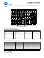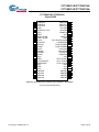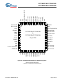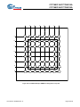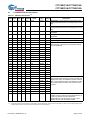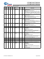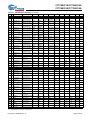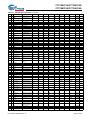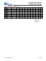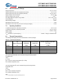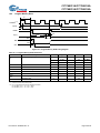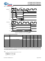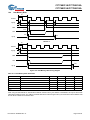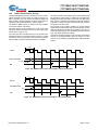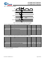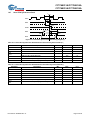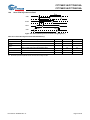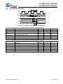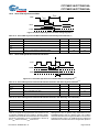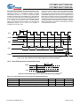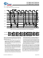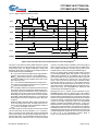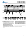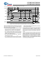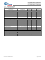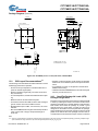
1
CY7C68013A/CY7C68014A
CY7C68015A/CY7C68016A
EZ-USB FX2LP™ USB Microcontroller
1.0
Features (CY7C68013A/14A/15A/16A)
• USB 2.0–USB-IF high speed certified (TID # 40440111)
• Single-chip integrated USB 2.0 transceiver, smart SIE,
and enhanced 8051 microprocessor
• Fit, form and function compatible with the FX2
— Pin-compatible
— Object-code-compatible
— Functionally-compatible (FX2LP is a superset)
• Ultra Low power: ICC no more than 85 mA in any mode
— Ideal for bus and battery powered applications
• Software: 8051 code runs from:
— Programmable waveform descriptors and configuration registers to define waveforms
— Supports multiple Ready (RDY) inputs and Control
(CTL) outputs
• Integrated, industry-standard enhanced 8051
— 48-MHz, 24-MHz, or 12-MHz CPU operation
— Four clocks per instruction cycle
— Two USARTS
— Three counter/timers
— Expanded interrupt system
— Two data pointers
• 3.3V operation with 5V tolerant inputs
— Internal RAM, which is downloaded via USB
— Internal RAM, which is loaded from EEPROM
— External memory device (128 pin package)
• 16 KBytes of on-chip Code/Data RAM
• Vectored USB interrupts and GPIF/FIFO interrupts
• Four programmable BULK/INTERRUPT/ISOCHRONOUS endpoints
— Buffering options: double, triple, and quad
• Additional programmable (BULK/INTERRUPT) 64-byte
endpoint
• Four integrated FIFOs
• Separate data buffers for the Set-up and Data portions
of a CONTROL transfer
• Integrated I2C controller, runs at 100 or 400 kHz
• 8- or 16-bit external data interface
• Smart Media Standard ECC generation
• GPIF (General Programmable Interface)
— Integrated glue logic and FIFOs lower system cost
— Automatic conversion to and from 16-bit buses
— Master or slave operation
— Uses external clock or asynchronous strobes
— Easy interface to ASIC and DSP ICs
• Available in Commercial and Industrial temperature
grade (all packages except VFBGA)
— Allows direct connection to most parallel interface
High-performance micro
using standard tools
with lower-power options
VCC
x20
PLL
/0.5
/1.0
/2.0
Data (8)
Address (16)
FX2LP
8051 Core
12/24/48 MHz,
four clocks/cycle
1.5k
connected for
full speed
D+
D–
USB
2.0
XCVR
Integrated
full- and high-speed
XCVR
CY
Smart
USB
1.1/2.0
Engine
16 KB
RAM
I 2C
Master
Address (16) / Data Bus (8)
24 MHz
Ext. XTAL
RDY (6)
CTL (6)
General
programmable I/F
to ASIC/DSP or bus
standards such as
ATAPI, EPP, etc.
8/16
Up to 96 MBytes/s
burst rate
ADDR (9)
GPIF
ECC
4 kB
FIFO
Enhanced USB core
Simplifies 8051 code
Abundant I/O
including two USARTS
Additional I/Os (24)
“Soft Configuration”
Easy firmware changes
FIFO and endpoint memory
(master or slave operation)
Figure 1-1. Block Diagram
Cypress Semiconductor Corporation
Document #: 38-08032 Rev. *K
•
198 Champion Court
•
San Jose, CA 95134-1709
•
408-943-2600
Revised January 26, 2006
CY7C68013A/CY7C68014A
CY7C68015A/CY7C68016A
1.1
Features (CY7C68013A/14A only)
• CY7C68014A: Ideal for battery powered applications
— Suspend current: 100 µA (typ)
• CY7C68013A: Ideal for non-battery powered applications
— Suspend current: 300 µA (typ)
• Available in five lead-free packages with up to 40 GPIOs
— 128-pin TQFP (40 GPIOs), 100-pin TQFP (40 GPIOs),
56-pin QFN (24 GPIOs), 56-pin SSOP (24 GPIOs), and
56-pin VFBGA (24 GPIOs)
1.2
Features (CY7C68015A/16A only)
• CY7C68016A: Ideal for battery powered applications
— Suspend current: 100 µA (typ)
• CY7C68015A: Ideal for non-battery powered applications
— Suspend current: 300 µA (typ)
• Available in lead-free 56-pin QFN package (26 GPIOs)
— 2 more GPIOs than CY7C68013A/14A enabling additional features in same footprint
Cypress Semiconductor Corporation’s (Cypress’s) EZ-USB
FX2LP™ (CY7C68013A/14A) is a low-power version of the
EZ-USB FX2™ (CY7C68013), which is a highly integrated,
low-power USB 2.0 microcontroller. By integrating the USB 2.0
transceiver, serial interface engine (SIE), enhanced 8051
microcontroller, and a programmable peripheral interface in a
single chip, Cypress has created a very cost-effective solution
that provides superior time-to-market advantages with low
power to enable bus powered applications.
The ingenious architecture of FX2LP results in data transfer
rates of over 53 Mbytes per second, the maximum-allowable
USB 2.0 bandwidth, while still using a low-cost 8051 microcontroller in a package as small as a 56 VFBGA (5mm x 5mm).
Because it incorporates the USB 2.0 transceiver, the FX2LP is
more economical, providing a smaller footprint solution than
USB 2.0 SIE or external transceiver implementations. With
Document #: 38-08032 Rev. *K
EZ-USB FX2LP, the Cypress Smart SIE handles most of the
USB 1.1 and 2.0 protocol in hardware, freeing the embedded
microcontroller for application-specific functions and
decreasing development time to ensure USB compatibility.
The General Programmable Interface (GPIF) and
Master/Slave Endpoint FIFO (8- or 16-bit data bus) provides
an easy and glueless interface to popular interfaces such as
ATA, UTOPIA, EPP, PCMCIA, and most DSP/processors.
The FX2LP draws considerably less current than the FX2
(CY7C68013), has double the on-chip code/data RAM and is
fit, form and function compatible with the 56-, 100-, and
128-pin FX2.
Five packages are defined for the family: 56VFBGA, 56 SSOP,
56 QFN, 100 TQFP, and 128 TQFP.
2.0
Applications
• Portable video recorder
• MPEG/TV conversion
• DSL modems
• ATA interface
• Memory card readers
• Legacy conversion devices
• Cameras
• Scanners
• Home PNA
• Wireless LAN
• MP3 players
• Networking
The “Reference Designs” section of the Cypress web site
provides additional tools for typical USB 2.0 applications. Each
reference design comes complete with firmware source and
object code, schematics, and documentation. Please visit
http://www.cypress.com for more information.
Page 2 of 60
CY7C68013A/CY7C68014A
CY7C68015A/CY7C68016A
3.0
3.1
Functional Overview
USB Signaling Speed
FX2LP operates at two of the three rates defined in the USB
Specification Revision 2.0, dated April 27, 2000:
• Full speed, with a signaling bit rate of 12 Mbps
• High speed, with a signaling bit rate of 480 Mbps.
FX2LP does not support the low-speed signaling mode of
1.5 Mbps.
3.2
8051 Microprocessor
The 8051 microprocessor embedded in the FX2LP family has
256 bytes of register RAM, an expanded interrupt system,
three timer/counters, and two USARTs.
3.2.1
The CLKOUT pin, which can be three-stated and inverted
using internal control bits, outputs the 50% duty cycle 8051
clock, at the selected 8051 clock frequency—48, 24, or 12
MHz.
3.2.2
USARTS
FX2LP contains two standard 8051 USARTs, addressed via
Special Function Register (SFR) bits. The USART interface
pins are available on separate I/O pins, and are not multiplexed with port pins.
UART0 and UART1 can operate using an internal clock at
230 KBaud with no more than 1% baud rate error. 230-KBaud
operation is achieved by an internally derived clock source that
generates overflow pulses at the appropriate time. The
internal clock adjusts for the 8051 clock rate (48, 24, 12 MHz)
such that it always presents the correct frequency for
230-KBaud operation.[1]
8051 Clock Frequency
FX2LP has an on-chip oscillator circuit that uses an external
24-MHz (±100-ppm) crystal with the following characteristics:
• Parallel resonant
• Fundamental mode
• 500-µW drive level
• 12-pF (5% tolerance) load capacitors.
An on-chip PLL multiplies the 24-MHz oscillator up to
480 MHz, as required by the transceiver/PHY, and internal
counters divide it down for use as the 8051 clock. The default
8051 clock frequency is 12 MHz. The clock frequency of the
8051 can be changed by the 8051 through the CPUCS
register, dynamically.
C1
24 MHz
12 pf
C2
12 pf
3.2.3
Certain 8051 SFR addresses are populated to provide fast
access to critical FX2LP functions. These SFR additions are
shown in Table 3-1. Bold type indicates non-standard,
enhanced 8051 registers. The two SFR rows that end with “0”
and “8” contain bit-addressable registers. The four I/O ports
A–D use the SFR addresses used in the standard 8051 for
ports 0–3, which are not implemented in FX2LP. Because of
the faster and more efficient SFR addressing, the FX2LP I/O
ports are not addressable in external RAM space (using the
MOVX instruction).
3.3
I2C Bus
FX2LP supports the I2C bus as a master only at 100-/400-KHz.
SCL and SDA pins have open-drain outputs and hysteresis
inputs. These signals must be pulled up to 3.3V, even if no I2C
device is connected.
3.4
20 × PLL
Special Function Registers
Buses
All packages: 8- or 16-bit “FIFO” bidirectional data bus, multiplexed on I/O ports B and D. 128-pin package: adds 16-bit
output-only 8051 address bus, 8-bit bidirectional data bus.
12-pF capacitor values assumes a trace capacitance
of 3 pF per side on a four-layer FR4 PCA
Figure 3-1. Crystal Configuration
Note:
1. 115-KBaud operation is also possible by programming the 8051 SMOD0 or SMOD1 bits to a “1” for UART0 and/or UART1, respectively.
Document #: 38-08032 Rev. *K
Page 3 of 60
CY7C68013A/CY7C68014A
CY7C68015A/CY7C68016A
Table 3-1. Special Function Registers
x
0
1
2
3
4
5
6
7
8
9
A
B
C
D
E
F
3.5
8x
9x
Ax
Bx
Cx
Dx
Ex
Fx
IOA
SP
DPL0
IOB
EXIF
MPAGE
IOC
INT2CLR
INT4CLR
IOD
IOE
OEA
SCON1
SBUF1
PSW
ACC
B
EICON
EIE
EIP
DPH0
DPL1
DPH1
DPS
PCON
TCON
TMOD
TL0
TL1
TH0
TH1
CKCON
OEB
OEC
OED
OEE
SCON0
SBUF0
AUTOPTRH1
AUTOPTRL1
reserved
AUTOPTRH2
AUTOPTRL2
reserved
IE
IP
T2CON
EP2468STAT
EP24FIFOFLGS
EP68FIFOFLGS
EP01STAT
GPIFTRIG
RCAP2L
RCAP2H
TL2
TH2
AUTOPTRSET-UP
USB Boot Methods
I2C
During the power-up sequence, internal logic checks the
port for the connection of an EEPROM whose first byte is
either 0xC0 or 0xC2. If found, it uses the VID/PID/DID values
in the EEPROM in place of the internally stored values (0xC0),
or it boot-loads the EEPROM contents into internal RAM
(0xC2). If no EEPROM is detected, FX2LP enumerates using
internally stored descriptors. The default ID values for FX2LP
are VID/PID/DID (0x04B4, 0x8613, 0xAxxx where xxx = Chip
revision).[2]
Table 3-2. Default ID Values for FX2LP
Vendor ID
Product ID
Device release
3.6
Default VID/PID/DID
0x04B4 Cypress Semiconductor
0x8613 EZ-USB FX2LP
0xAnnn Depends on chip revision
(nnn = chip revision where first
silicon = 001)
ReNumeration™
GPIFSGLDATH
GPIFSGLDATLX
GPIFSGLDATLNOX
RENUM. To simulate a USB disconnect, the firmware sets
DISCON to 1. To reconnect, the firmware clears DISCON to 0.
Before reconnecting, the firmware sets or clears the RENUM
bit to indicate whether the firmware or the Default USB Device
will handle device requests over endpoint zero: if RENUM = 0,
the Default USB Device will handle device requests; if RENUM
= 1, the firmware will.
3.7
Bus-powered Applications
The FX2LP fully supports bus-powered designs by enumerating with less than 100 mA as required by the USB 2.0 specification.
3.8
Interrupt System
3.8.1
INT2 Interrupt Request and Enable Registers
FX2LP implements an autovector feature for INT2 and INT4.
There are 27 INT2 (USB) vectors, and 14 INT4 (FIFO/GPIF)
vectors. See EZ-USB Technical Reference Manual (TRM) for
more details.
Because the FX2LP’s configuration is soft, one chip can take
on the identities of multiple distinct USB devices.
3.8.2
When first plugged into USB, the FX2LP enumerates automatically and downloads firmware and USB descriptor tables over
the USB cable. Next, the FX2LP enumerates again, this time
as a device defined by the downloaded information. This
patented two-step process, called ReNumeration™, happens
instantly when the device is plugged in, with no hint that the
initial download step has occurred.
The main USB interrupt is shared by 27 interrupt sources. To
save the code and processing time that normally would be
required to identify the individual USB interrupt source, the
FX2LP provides a second level of interrupt vectoring, called
Autovectoring. When a USB interrupt is asserted, the FX2LP
pushes the program counter onto its stack then jumps to
address 0x0043, where it expects to find a “jump” instruction
to the USB Interrupt service routine.
Two control bits in the USBCS (USB Control and Status)
register control the ReNumeration process: DISCON and
USB-Interrupt Autovectors
Note:
2.
The I2C bus SCL and SDA pins must be pulled up, even if an EEPROM is not connected. Otherwise this detection method does not work properly.
Document #: 38-08032 Rev. *K
Page 4 of 60
CY7C68013A/CY7C68014A
CY7C68015A/CY7C68016A
The FX2LP jump instruction is encoded as follows.
Table 3-3. INT2 USB Interrupts
USB INTERRUPT TABLE FOR INT2
Priority
INT2VEC Value
Source
Notes
1
00
SUDAV
Set-up Data Available
2
04
SOF
Start of Frame (or microframe)
3
08
SUTOK
Set-up Token Received
4
0C
SUSPEND
USB Suspend request
5
10
USB RESET
Bus reset
6
14
HISPEED
Entered high speed operation
7
18
EP0ACK
FX2LP ACK’d the CONTROL Handshake
8
1C
reserved
9
20
EP0-IN
EP0-IN ready to be loaded with data
10
24
EP0-OUT
EP0-OUT has USB data
11
28
EP1-IN
EP1-IN ready to be loaded with data
12
2C
EP1-OUT
EP1-OUT has USB data
13
30
EP2
IN: buffer available. OUT: buffer has data
14
34
EP4
IN: buffer available. OUT: buffer has data
15
38
EP6
IN: buffer available. OUT: buffer has data
16
3C
EP8
IN: buffer available. OUT: buffer has data
17
40
IBN
IN-Bulk-NAK (any IN endpoint)
18
44
reserved
19
48
EP0PING
EP0 OUT was Pinged and it NAK’d
20
4C
EP1PING
EP1 OUT was Pinged and it NAK’d
21
50
EP2PING
EP2 OUT was Pinged and it NAK’d
22
54
EP4PING
EP4 OUT was Pinged and it NAK’d
23
58
EP6PING
EP6 OUT was Pinged and it NAK’d
24
5C
EP8PING
EP8 OUT was Pinged and it NAK’d
25
60
ERRLIMIT
Bus errors exceeded the programmed limit
26
64
27
68
reserved
28
6C
reserved
29
70
EP2ISOERR
ISO EP2 OUT PID sequence error
30
74
EP4ISOERR
ISO EP4 OUT PID sequence error
31
78
EP6ISOERR
ISO EP6 OUT PID sequence error
32
7C
EP8ISOERR
ISO EP8 OUT PID sequence error
If Autovectoring is enabled (AV2EN = 1 in the INTSET-UP
register), the FX2LP substitutes its INT2VEC byte. Therefore,
if the high byte (“page”) of a jump-table address is preloaded
at location 0x0044, the automatically-inserted INT2VEC byte
at 0x0045 will direct the jump to the correct address out of the
27 addresses within the page.
Document #: 38-08032 Rev. *K
3.8.3
FIFO/GPIF Interrupt (INT4)
Just as the USB Interrupt is shared among 27 individual
USB-interrupt sources, the FIFO/GPIF interrupt is shared
among 14 individual FIFO/GPIF sources. The FIFO/GPIF
Interrupt, like the USB Interrupt, can employ autovectoring.
Table 3-4 shows the priority and INT4VEC values for the 14
FIFO/GPIF interrupt sources.
Page 5 of 60
CY7C68013A/CY7C68014A
CY7C68015A/CY7C68016A
Table 3-4. Individual FIFO/GPIF Interrupt Sources
Priority
INT4VEC Value
Source
1
80
EP2PF
Notes
Endpoint 2 Programmable Flag
2
84
EP4PF
Endpoint 4 Programmable Flag
3
88
EP6PF
Endpoint 6 Programmable Flag
4
8C
EP8PF
Endpoint 8 Programmable Flag
5
90
EP2EF
Endpoint 2 Empty Flag
6
94
EP4EF
Endpoint 4 Empty Flag
7
98
EP6EF
Endpoint 6 Empty Flag
8
9C
EP8EF
Endpoint 8 Empty Flag
9
A0
EP2FF
Endpoint 2 Full Flag
10
A4
EP4FF
Endpoint 4 Full Flag
11
A8
EP6FF
Endpoint 6 Full Flag
12
AC
EP8FF
13
B0
GPIFDONE
14
B4
GPIFWF
Endpoint 8 Full Flag
GPIF Operation Complete
GPIF Waveform
If Autovectoring is enabled (AV4EN = 1 in the INTSET-UP
register), the FX 2LP substitutes its INT4VEC byte. Therefore,
if the high byte (“page”) of a jump-table address is preloaded
at location 0x0054, the automatically-inserted INT4VEC byte
at 0x0055 will direct the jump to the correct address out of the
14 addresses within the page. When the ISR occurs, the
FX2LP pushes the program counter onto its stack then jumps
to address 0x0053, where it expects to find a “jump” instruction
to the ISR Interrupt service routine.
used with the CY7C680xxA the reset period must allow for the
stabilization of the crystal and the PLL. This reset period
should be approximately 5 ms after VCC has reached 3.0V. If
the crystal input pin is driven by a clock signal the internal PLL
stabilizes in 200 µs after VCC has reached 3.0V[3]. Figure 3-2
shows a power-on reset condition and a reset applied during
operation. A power-on reset is defined as the time reset is
asserted while power is being applied to the circuit. A powered
reset is defined to be when the FX2LP has previously been
powered on and operating and the RESET# pin is asserted.
3.9
Reset and Wakeup
3.9.1
Reset Pin
Cypress provides an application note which describes and
recommends power on reset implementation and can be found
on the Cypress web site. For more information on reset implementation for the FX2 family of products visit the
http://www.cypress.com.
The input pin, RESET#, will reset the FX2LP when asserted.
This pin has hysteresis and is active LOW. When a crystal is
Note:
3. If the external clock is powered at the same time as the CY7C680xxA and has a stabilization wait period, it must be added to the 200 µs.
Document #: 38-08032 Rev. *K
Page 6 of 60
CY7C68013A/CY7C68014A
CY7C68015A/CY7C68016A
RESET#
RESET#
VIL
VIL
3.3V
3.0V
3.3V
VCC
VCC
0V
0V
TRESET
TRESET
Power on Reset
Powered Reset
Figure 3-2. Reset Timing Plots
Table 3-5. Reset Timing Values
Condition
TRESET
Power-on Reset with crystal
Power-on Reset with external
clock
5 ms
200 µs + Clock stability time
Powered Reset
3.9.2
200 µs
Wakeup Pins
The 8051 puts itself and the rest of the chip into a power-down
mode by setting PCON.0 = 1. This stops the oscillator and
PLL. When WAKEUP is asserted by external logic, the oscillator restarts, after the PLL stabilizes, and then the 8051
receives a wakeup interrupt. This applies whether or not
FX2LP is connected to the USB.
The FX2LP exits the power-down (USB suspend) state using
one of the following methods:
• USB bus activity (if D+/D– lines are left floating, noise on
these lines may indicate activity to the FX2LP and initiate a
wakeup).
• External logic asserts the WAKEUP pin
• External logic asserts the PA3/WU2 pin.
The second wakeup pin, WU2, can also be configured as a
general purpose I/O pin. This allows a simple external R-C
network to be used as a periodic wakeup source. Note that
WAKEUP is by default active LOW.
3.10
Program/Data RAM
3.10.1
Size
The FX2LP has 16 KBytes of internal program/data RAM,
where PSEN#/RD# signals are internally ORed to allow the
8051 to access it as both program and data memory. No USB
control registers appear in this space.
Two memory maps are shown in the following diagrams:
Figure 3-3 Internal Code Memory, EA = 0
Figure 3-4 External Code Memory, EA = 1.
3.10.2
Internal Code Memory, EA = 0
This mode implements the internal 16-KByte block of RAM
(starting at 0) as combined code and data memory. When
external RAM or ROM is added, the external read and write
strobes are suppressed for memory spaces that exist inside
the chip. This allows the user to connect a 64-KByte memory
without requiring address decodes to keep clear of internal
memory spaces.
Only the internal 16 KBytes and scratch pad 0.5 KBytes RAM
spaces have the following access:
• USB download
• USB upload
• Set-up data pointer
• I2C interface boot load.
3.10.3
External Code Memory, EA = 1
The bottom 16 KBytes of program memory is external, and
therefore the bottom 16 KBytes of internal RAM is accessible
only as data memory.
Document #: 38-08032 Rev. *K
Page 7 of 60
CY7C68013A/CY7C68014A
CY7C68015A/CY7C68016A
Inside FX2LP
Outside FX2LP
FFFF
7.5 KBytes
USB regs and
4K FIFO buffers
(RD#,WR#)
E200
E1FF 0.5 KBytes RAM
E000 Data (RD#,WR#)*
(OK to populate
data memory
here—RD#/WR#
strobes are not
active)
40 KBytes
External
Data
Memory
(RD#,WR#)
48 KBytes
External
Code
Memory
(PSEN#)
3FFF
16 KBytes RAM
Code and Data
(PSEN#,RD#,WR#)*
(Ok to populate
data memory
here—RD#/WR#
strobes are not
active)
(OK to populate
program
memory here—
PSEN# strobe
is not active)
0000
Data
Code
*SUDPTR, USB upload/download, I2C interface boot access
Figure 3-3. Internal Code Memory, EA = 0
Inside FX2LP
Outside FX2LP
FFFF
7.5 KBytes
USB regs and
4K FIFO buffers
(RD#,WR#)
E200
E1FF
0.5 KBytes RAM
E000 Data (RD#,WR#)*
(OK to populate
data memory
here—RD#/WR#
strobes are not
active)
40 KBytes
External
Data
Memory
(RD#,WR#)
64 KBytes
External
Code
Memory
(PSEN#)
3FFF
16 KBytes
RAM
Data
(RD#,WR#)*
(Ok to populate
data memory
here—RD#/WR#
strobes are not
active)
0000
Data
Code
*SUDPTR, USB upload/download, I2C interface boot access
Figure 3-4. External Code Memory, EA = 1
Document #: 38-08032 Rev. *K
Page 8 of 60
CY7C68013A/CY7C68014A
CY7C68015A/CY7C68016A
3.11
Register Addresses
FFFF
4 KBytes EP2-EP8
buffers
(8 x 512)
F000
EFFF
2 KBytes RESERVED
E800
E7FF
E7C0
E7BF
E780
E77F
E740
E73F
E700
E6FF
E500
E4FF
E480
E47F
E400
E3FF
E200
E1FF
64 Bytes EP1IN
64 Bytes EP1OUT
64 Bytes EP0 IN/OUT
64 Bytes RESERVED
8051 Addressable Registers
(512)
Reserved (128)
128 bytes GPIF Waveforms
Reserved (512)
512 bytes
8051 xdata RAM
E000
3.12
3.12.1
Endpoint RAM
3.12.3
Size
A separate 8-byte buffer at 0xE6B8-0xE6BF holds the Set-up
data from a CONTROL transfer.
• 3× 64 bytes
(Endpoints 0 and 1)
• 8 × 512 bytes (Endpoints 2, 4, 6, 8)
3.12.2
Set-up Data Buffer
Organization
• EP0
• Bidirectional endpoint zero, 64-byte buffer
• EP1IN, EP1OUT
• 64-byte buffers, bulk or interrupt
• EP2,4,6,8
• Eight 512-byte buffers, bulk, interrupt, or isochronous. EP4
and EP8 can be double buffered, while EP2 and 6 can be
either double, triple, or quad buffered. For high-speed endpoint configuration options, see Figure 3-5.
Document #: 38-08032 Rev. *K
3.12.4
Endpoint Configurations (High-speed Mode)
Endpoints 0 and 1 are the same for every configuration.
Endpoint 0 is the only CONTROL endpoint, and endpoint 1 can
be either BULK or INTERRUPT. The endpoint buffers can be
configured in any 1 of the 12 configurations shown in the
vertical columns. When operating in full-speed BULK mode
only the first 64 bytes of each buffer are used. For example in
high-speed, the max packet size is 512 bytes but in full-speed
it is 64 bytes. Even though a buffer is configured to be a 512
byte buffer, in full-speed only the first 64 bytes are used. The
unused endpoint buffer space is not available for other operations. An example endpoint configuration would be:
Page 9 of 60
CY7C68013A/CY7C68014A
CY7C68015A/CY7C68016A
EP2–1024 double
(column 8).
buffered;
EP6–512
quad
buffered
EP0 IN&OUT
64
64
64
64
64
64
64
64
64
64
64
64
EP1 IN
64
64
64
64
64
64
64
64
64
64
64
64
EP1 OUT
64
64
64
64
64
64
64
64
64
64
64
64
EP2
EP2
EP2
EP2
EP2
EP2
EP2
EP2
EP2
EP2
512
512
512
512
512
512
512
512
512
512
512
512
EP4
EP4
512
512
512
512
512
512
512
512
EP6
512
512
512
512
EP6
EP6
EP6
EP6
EP6
512
512
512
512
512
512
1024
512
EP8
512
1024
512
512
1
2
1024
1024
512
1024
1024
3
1024
1024
EP6
EP6
512
512
512
512
512
4
5
EP6
512
512
EP6
512
1024
512
EP8
512
1024
1024
1024
1024
512
EP8
512
1024
512
EP4
512
EP2 EP2
512
512
1024
512
512
512
7
8
6
1024
9
1024
1024
EP8
EP8
512
512
512
512
10
11
1024
1024
12
Figure 3-5. Endpoint Configuration
3.12.5
Default Full-Speed Alternate Settings
Table 3-6. Default Full-Speed Alternate Settings[4, 5]
Alternate Setting
0
1
2
3
ep0
64
64
64
64
ep1out
0
64 bulk
64 int
64 int
ep1in
0
64 bulk
64 int
64 int
ep2
0
64 bulk out (2×)
64 int out (2×)
64 iso out (2×)
ep4
0
64 bulk out (2×)
64 bulk out (2×)
64 bulk out (2×)
ep6
0
64 bulk in (2×)
64 int in (2×)
64 iso in (2×)
ep8
0
64 bulk in (2×)
64 bulk in (2×)
64 bulk in (2×)
3.12.6
Default High-Speed Alternate Settings
Table 3-7. Default High-Speed Alternate Settings[4, 5]
Alternate Setting
0
1
2
3
ep0
64
64
64
64
ep1out
0
512 bulk[6]
64 int
64 int
ep1in
0
512 bulk[6]
64 int
64 int
ep2
0
512 bulk out (2×)
512 int out (2×)
512 iso out (2×)
ep4
0
512 bulk out (2×)
512 bulk out (2×)
512 bulk out (2×)
ep6
0
512 bulk in (2×)
512 int in (2×)
512 iso in (2×)
ep8
0
512 bulk in (2×)
512 bulk in (2×)
512 bulk in (2×)
Notes:
4. “0” means “not implemented.”
5. “2×” means “double buffered.”
6. Even though these buffers are 64 bytes, they are reported as 512 for USB 2.0 compliance. The user must never transfer packets larger than 64 bytes to EP1.
Document #: 38-08032 Rev. *K
Page 10 of 60
CY7C68013A/CY7C68014A
CY7C68015A/CY7C68016A
3.13
External FIFO Interface
3.13.1
Architecture
The FX2LP slave FIFO architecture has eight 512-byte blocks
in the endpoint RAM that directly serve as FIFO memories,
and are controlled by FIFO control signals (such as IFCLK,
SLCS#, SLRD, SLWR, SLOE, PKTEND, and flags).
In operation, some of the eight RAM blocks fill or empty from
the SIE, while the others are connected to the I/O transfer
logic. The transfer logic takes two forms, the GPIF for internally
generated control signals, or the slave FIFO interface for
externally controlled transfers.
3.13.2
Master/Slave Control Signals
The FX2LP endpoint FIFOS are implemented as eight physically distinct 256x16 RAM blocks. The 8051/SIE can switch
any of the RAM blocks between two domains, the USB (SIE)
domain and the 8051-I/O Unit domain. This switching is done
virtually instantaneously, giving essentially zero transfer time
between “USB FIFOS” and “Slave FIFOS.” Since they are
physically the same memory, no bytes are actually transferred
between buffers.
At any given time, some RAM blocks are filling/emptying with
USB data under SIE control, while other RAM blocks are
available to the 8051 and/or the I/O control unit. The RAM
blocks operate as single-port in the USB domain, and
dual-port in the 8051-I/O domain. The blocks can be
configured as single, double, triple, or quad buffered as previously shown.
The I/O control unit implements either an internal-master (M
for master) or external-master (S for Slave) interface.
In Master (M) mode, the GPIF internally controls
FIFOADR[1..0] to select a FIFO. The RDY pins (two in the
56-pin package, six in the 100-pin and 128-pin packages) can
be used as flag inputs from an external FIFO or other logic if
desired. The GPIF can be run from either an internally derived
clock or externally supplied clock (IFCLK), at a rate that
transfers data up to 96 Megabytes/s (48-MHz IFCLK with
16-bit interface).
In Slave (S) mode, the FX2LP accepts either an internally
derived clock or externally supplied clock (IFCLK, max.
frequency 48 MHz) and SLCS#, SLRD, SLWR, SLOE,
PKTEND signals from external logic. When using an external
IFCLK, the external clock must be present before switching to
the external clock with the IFCLKSRC bit. Each endpoint can
individually be selected for byte or word operation by an
internal configuration bit, and a Slave FIFO Output Enable
signal SLOE enables data of the selected width. External logic
must insure that the output enable signal is inactive when
writing data to a slave FIFO. The slave interface can also
operate asynchronously, where the SLRD and SLWR signals
act directly as strobes, rather than a clock qualifier as in
synchronous mode. The signals SLRD, SLWR, SLOE and
PKTEND are gated by the signal SLCS#.
Document #: 38-08032 Rev. *K
3.13.3
GPIF and FIFO Clock Rates
An 8051 register bit selects one of two frequencies for the
internally supplied interface clock: 30 MHz and 48 MHz. Alternatively, an externally supplied clock of 5 MHz–48 MHz
feeding the IFCLK pin can be used as the interface clock.
IFCLK can be configured to function as an output clock when
the GPIF and FIFOs are internally clocked. An output enable
bit in the IFCONFIG register turns this clock output off, if
desired. Another bit within the IFCONFIG register will invert
the IFCLK signal whether internally or externally sourced.
3.14
GPIF
The GPIF is a flexible 8- or 16-bit parallel interface driven by a
user-programmable finite state machine. It allows the
CY7C68013A/15A to perform local bus mastering, and can
implement a wide variety of protocols such as ATA interface,
printer parallel port, and Utopia.
The GPIF has six programmable control outputs (CTL), nine
address outputs (GPIFADRx), and six general-purpose ready
inputs (RDY). The data bus width can be 8 or 16 bits. Each
GPIF vector defines the state of the control outputs, and determines what state a ready input (or multiple inputs) must be
before proceeding. The GPIF vector can be programmed to
advance a FIFO to the next data value, advance an address,
etc. A sequence of the GPIF vectors make up a single
waveform that will be executed to perform the desired data
move between the FX2LP and the external device.
3.14.1
Six Control OUT Signals
The 100- and 128-pin packages bring out all six Control Output
pins (CTL0-CTL5). The 8051 programs the GPIF unit to define
the CTL waveforms. The 56-pin package brings out three of
these signals, CTL0–CTL2. CTLx waveform edges can be
programmed to make transitions as fast as once per clock
(20.8 ns using a 48-MHz clock).
3.14.2
Six Ready IN Signals
The 100- and 128-pin packages bring out all six Ready inputs
(RDY0–RDY5). The 8051 programs the GPIF unit to test the
RDY pins for GPIF branching. The 56-pin package brings out
two of these signals, RDY0–1.
3.14.3
Nine GPIF Address OUT Signals
Nine GPIF address lines are available in the 100- and 128-pin
packages, GPIFADR[8..0]. The GPIF address lines allow
indexing through up to a 512-byte block of RAM. If more
address lines are needed, I/O port pins can be used.
3.14.4
Long Transfer Mode
In master mode, the 8051 appropriately sets GPIF transaction
count registers (GPIFTCB3, GPIFTCB2, GPIFTCB1, or
GPIFTCB0) for unattended transfers of up to 232 transactions.
The GPIF automatically throttles data flow to prevent under or
overflow until the full number of requested transactions
complete. The GPIF decrements the value in these registers
to represent the current status of the transaction.
Page 11 of 60
CY7C68013A/CY7C68014A
CY7C68015A/CY7C68016A
3.15
ECC Generation[7]
I2C Controller
3.18
The EZ-USB can calculate ECCs (Error-Correcting Codes) on
data that passes across its GPIF or Slave FIFO interfaces.
There are two ECC configurations: Two ECCs, each calculated over 256 bytes (SmartMedia Standard); and one ECC
calculated over 512 bytes.
FX2LP has one I2C port that is driven by two internal
controllers, one that automatically operates at boot time to
load VID/PID/DID and configuration information, and another
that the 8051, once running, uses to control external I2C
devices. The I2C port operates in master mode only.
The ECC can correct any one-bit error or detect any two-bit
error.
3.18.1
I2C Port Pins
2
3.15.1
ECC Implementation
The two ECC configurations are selected by the ECCM bit:
3.15.1.1 ECCM = 0
Two 3-byte ECCs, each calculated over a 256-byte block of
data. This configuration conforms to the SmartMedia
Standard.
Write any value to ECCRESET, then pass data across the
GPIF or Slave FIFO interface. The ECC for the first 256 bytes
of data will be calculated and stored in ECC1. The ECC for the
next 256 bytes will be stored in ECC2. After the second ECC
is calculated, the values in the ECCx registers will not change
until ECCRESET is written again, even if more data is subsequently passed across the interface.
3.15.1.2 ECCM = 1
The I C pins SCL and SDA must have external 2.2-kΩ pull-up
resistors even if no EEPROM is connected to the FX2LP.
External EEPROM device address pins must be configured
properly. See Table 3-8 for configuring the device address
pins.
Table 3-8. Strap Boot EEPROM Address Lines to These
Values
Bytes
A2
A1
A0
N/A
N/A
N/A
24LC01
0
0
0
24LC02
0
0
0
4K
24LC32
0
0
1
8K
24LC64
0
0
1
16K
24LC128
0
0
1
24LC00[9]
128
256
One 3-byte ECC calculated over a 512-byte block of data.
Write any value to ECCRESET then pass data across the
GPIF or Slave FIFO interface. The ECC for the first 512 bytes
of data will be calculated and stored in ECC1; ECC2 is unused.
After the ECC is calculated, the value in ECC1 will not change
until ECCRESET is written again, even if more data is subsequently passed across the interface
3.16
USB Uploads and Downloads
The core has the ability to directly edit the data contents of the
internal 16-KByte RAM and of the internal 512-byte scratch
pad RAM via a vendor-specific command. This capability is
normally used when “soft” downloading user code and is
available only to and from internal RAM, only when the 8051
is held in reset. The available RAM spaces are 16 KBytes from
0x0000–0x3FFF (code/data) and 512 bytes from
0xE000–0xE1FF (scratch pad data RAM).[8]
3.17
Autopointer Access
FX2LP provides two identical autopointers. They are similar to
the internal 8051 data pointers, but with an additional feature:
they can optionally increment after every memory access. This
capability is available to and from both internal and external
RAM. The autopointers are available in external FX2LP
registers, under control of a mode bit (AUTOPTRSET-UP.0).
Using the external FX2LP autopointer access (at 0xE67B –
0xE67C) allows the autopointer to access all RAM, internal
and external to the part. Also, the autopointers can point to any
FX2LP register or endpoint buffer space. When autopointer
access to external memory is enabled, location 0xE67B and
0xE67C in XDATA and code space cannot be used.
Example EEPROM
16
3.18.2
I2C Interface Boot Load Access
At power-on reset the I2C interface boot loader will load the
VID/PID/DID configuration bytes and up to 16 KBytes of
program/data. The available RAM spaces are 16 KBytes from
0x0000–0x3FFF and 512 bytes from 0xE000–0xE1FF. The
8051 will be in reset. I2C interface boot loads only occur after
power-on reset.
3.18.3
I2C Interface General-Purpose Access
The 8051 can control peripherals connected to the I2C bus
using the I2CTL and I2DAT registers. FX2LP provides I2C
master control only, it is never an I2C slave.
3.19
Compatible with Previous Generation
EZ-USB FX2
The EZ-USB FX2LP is form/fit and with minor exceptions
functionally compatible with its predecessor, the EZ-USB FX2.
This makes for an easy transition for designers wanting to
upgrade their systems from the FX2 to the FX2LP. The pinout
and package selection are identical, and the vast majority of
firmware previously developed for the FX2 will function in the
FX2LP.
For designers migrating from the FX2 to the FX2LP a change
in the bill of material and review of the memory allocation (due
to increased internal memory) is required for more information
about migrating from EZ-USB FX2 to EZ-USB FX2LP, please
see further details in the application note titled Migrating from
EZ-USB FX2 to EZ-USB FX2LP, which is available on the
Cypress Website.
Notes:
7. To use the ECC logic, the GPIF or Slave FIFO interface must be configured for byte-wide operation.
8. After the data has been downloaded from the host, a “loader” can execute from internal RAM in order to transfer downloaded data to external memory.
9. This EEPROM does not have address pins.
Document #: 38-08032 Rev. *K
Page 12 of 60
CY7C68013A/CY7C68014A
CY7C68015A/CY7C68016A
Table 3-9. Part Number Conversion Table
EZ-USB FX2
Part Number
CY7C68013-56PVC
CY7C68013-56PVCT
EZ-USB FX2LP
Part Number
Package Description
CY7C68013A-56PVXC or CY7C68014A-56PVXC
56-pin SSOP
CY7C68013A-56PVXCT or CY7C68014A-56PVXCT 56-pin SSOP – Tape and Reel
CY7C68013-56LFC
CY7C68013A-56LFXC or CY7C68014A-56LFXC
56-pin QFN
CY7C68013-100AC
CY7C68013A-100AXC or CY7C68014A-100AXC
100-pin TQFP
CY7C68013-128AC
CY7C68013A-128AXC or CY7C68014A-128AXC
128-pin TQFP
3.20
CY7C68013A/14A and CY7C68015A/16A
Differences
CY7C68013A is identical to CY7C68014A in form, fit, and
functionality. CY7C68015A is identical to CY7C68016A in
form, fit, and functionality. CY7C68014A and CY7C68016A
have a lower suspend current than CY7C68013A and
CY7C68015A respectively. CY7C68014A and CY7C68016A
have a lower suspend current than CY7C68013A and
CY7C68015A
respectively:
hence
are
ideal
for
power-sensitive battery applications.
CY7C68015A and CY7C68016A are available in 56-pin QFN
package only. Two additional GPIO signals are available on
the CY7C68015A and CY7C68016A to provide more flexibility
when neither IFCLK or CLKOUT are needed in the 56-pin
Document #: 38-08032 Rev. *K
package. The USB developers who want to convert their FX2
56-pin application to a bus-powered system will directly benefit
from these additional signals. The two GPIOs will give these
developers the signals they need for the power control circuitry
of their bus-powered application without pushing them to a
high-pincount version of FX2LP. The CY7C68015A is only
available in the 56-pin QFN package
Table 3-10. CY7C68013A/14A and CY7C68015A/16A Pin
Differences
CY7C68013A/CY7C68014A CY7C68015A/CY7C68016A
IFCLK
PE0/T0OUT
CLKOUT
PE1/T1OUT
Page 13 of 60
CY7C68013A/CY7C68014A
CY7C68015A/CY7C68016A
4.0
Pin Assignments
Figure 4-1 identifies all signals for the five package types. The
following pages illustrate the individual pin diagrams, plus a
combination diagram showing which of the full set of signals
are available in the 128-, 100-, and 56-pin packages.
The signals on the left edge of the 56-pin package in
Figure 4-1 are common to all versions in the FX2LP family with
the noted differences between the CY7C68013A and the
CY7C68015A. Three modes are available in all package
versions: Port, GPIF master, and Slave FIFO. These modes
define the signals on the right edge of the diagram. The 8051
selects the interface mode using the IFCONFIG[1:0] register
bits. Port mode is the power-on default configuration.
The 100-pin package adds functionality to the 56-pin package
by adding these pins:
• PORTC or alternate GPIFADR[7:0] address signals
Document #: 38-08032 Rev. *K
• PORTE or alternate GPIFADR[8] address signal and seven
additional 8051 signals
• Three GPIF Control signals
• Four GPIF Ready signals
• Nine 8051 signals (two USARTs, three timer inputs,
INT4,and INT5#)
• BKPT, RD#, WR#.
The 128-pin package adds the 8051 address and data buses
plus control signals. Note that two of the required signals, RD#
and WR#, are present in the 100-pin version. In the 100-pin
and 128-pin versions, an 8051 control bit can be set to pulse
the RD# and WR# pins when the 8051 reads from/writes to
PORTC. This feature is enabled by setting PORTCSTB bit in
CPUCS register.
Section 10.5 displays the timing diagram of the read and write
strobing function on accessing PORTC.
Page 14 of 60
CY7C68013A/CY7C68014A
CY7C68015A/CY7C68016A
Port
XTALIN
XTALOUT
RESET#
WAKEUP#
SCL
SDA
56
**PE0 replaces IFCLK
& PE1 replaces CLKOUT
on CY7C68015A
**PE0/T0OUT
**PE1/T1OUT
IFCLK
CLKOUT
DPLUS
DMINUS
GPIF Master
PD7
PD6
PD5
PD4
PD3
PD2
PD1
PD0
PB7
PB6
PB5
PB4
PB3
PB2
PB1
PB0
INT0#/PA0
INT1#/PA1
PA2
WU2/PA3
PA4
PA5
PA6
PA7
FD[15]
FD[14]
FD[13]
FD[12]
FD[11]
FD[10]
FD[9]
FD[8]
FD[7]
FD[6]
FD[5]
FD[4]
FD[3]
FD[2]
FD[1]
FD[0]
Slave FIFO
FD[15]
FD[14]
FD[13]
FD[12]
FD[11]
FD[10]
FD[9]
FD[8]
FD[7]
FD[6]
FD[5]
FD[4]
FD[3]
FD[2]
FD[1]
FD[0]
RDY0
RDY1
SLRD
SLWR
CTL0
CTL1
CTL2
FLAGA
FLAGB
FLAGC
INT0#/PA0
INT1#/PA1
PA2
WU2/PA3
PA4
PA5
PA6
PA7
INT0#/ PA0
INT1#/ PA1
SLOE
WU2/PA3
FIFOADR0
FIFOADR1
PKTEND
PA7/FLAGD/SLCS#
CTL3
CTL4
CTL5
RDY2
RDY3
RDY4
RDY5
100
BKPT
PORTC7/GPIFADR7
PORTC6/GPIFADR6
PORTC5/GPIFADR5
PORTC4/GPIFADR4
PORTC3/GPIFADR3
PORTC2/GPIFADR2
PORTC1/GPIFADR1
PORTC0/GPIFADR0
PE7/GPIFADR8
PE6/T2EX
PE5/INT6
PE4/RxD1OUT
PE3/RxD0OUT
PE2/T2OUT
PE1/T1OUT
PE0/T0OUT
RD#
WR#
CS#
OE#
PSEN#
D7
D6
D5
D4
D3
D2
D1
D0
128
EA
RxD0
TxD0
RxD1
TxD1
INT4
INT5#
T2
T1
T0
A15
A14
A13
A12
A11
A10
A9
A8
A7
A6
A5
A4
A3
A2
A1
A0
Figure 4-1. Signals
** pinout for CY7C68015A/CY7C68016A only
Document #: 38-08032 Rev. *K
Page 15 of 60
CY7C68013A/CY7C68014A
CY7C68015A/CY7C68016A
27
28
29
30
31
32
33
34
35
36
37
38
103
26
104
25
105
24
106
23
107
22
108
21
109
20
110
19
111
18
112
17
113
16
114
15
115
14
116
13
117
12
118
11
119
10
120
9
121
8
122
7
123
6
124
5
125
4
126
3
PD1/FD9
PD2/FD10
PD3/FD11
INT5#
VCC
PE0/T0OUT
PE1/T1OUT
PE2/T2OUT
PE3/RXD0OUT
PE4/RXD1OUT
PE5/INT6
PE6/T2EX
PE7/GPIFADR8
GND
A4
A5
A6
A7
PD4/FD12
PD5/FD13
PD6/FD14
PD7/FD15
GND
A8
A9
A10
2
127
128
1
CLKOUT
VCC
GND
RDY0/*SLRD
RDY1/*SLWR
RDY2
RDY3
RDY4
RDY5
AVCC
XTALOUT
XTALIN
AGND
NC
NC
NC
AVCC
DPLUS
DMINUS
AGND
A11
A12
A13
A14
A15
VCC
GND
INT4
T0
T1
T2
*IFCLK
RESERVED
BKPT
EA
SCL
SDA
OE#
PD0/FD8
*WAKEUP
VCC
RESET#
CTL5
A3
A2
A1
A0
GND
PA7/*FLAGD/SLCS#
PA6/*PKTEND
PA5/FIFOADR1
PA4/FIFOADR0
D7
D6
D5
PA3/*WU2
PA2/*SLOE
PA1/INT1#
PA0/INT0#
VCC
GND
PC7/GPIFADR7
PC6/GPIFADR6
PC5/GPIFADR5
PC4/GPIFADR4
PC3/GPIFADR3
PC2/GPIFADR2
PC1/GPIFADR1
PC0/GPIFADR0
CTL2/*FLAGC
CTL1/*FLAGB
CTL0/*FLAGA
VCC
CTL4
CTL3
GND
CY7C68013A/CY7C68014A
128-pin TQFP
102
101
100
99
98
97
96
95
94
93
92
91
90
89
88
87
86
85
84
83
82
81
80
79
78
77
76
75
74
73
72
71
70
69
68
67
66
65
VCC
D4
D3
D2
D1
D0
GND
PB7/FD7
PB6/FD6
PB5/FD5
PB4/FD4
RXD1
TXD1
RXD0
TXD0
GND
VCC
PB3/FD3
PB2/FD2
PB1/FD1
PB0/FD0
VCC
CS#
WR#
RD#
PSEN#
64
63
62
61
60
59
58
57
56
55
54
53
52
51
50
49
48
47
46
45
44
43
42
41
40
39
Figure 4-2. CY7C68013A/CY7C68014A 128-pin TQFP Pin Assignment
* denotes programmable polarity
Document #: 38-08032 Rev. *K
Page 16 of 60
CY7C68013A/CY7C68014A
CY7C68015A/CY7C68016A
81
82
83
84
85
86
87
88
89
90
91
92
93
94
95
96
97
98
99
100
PD1/FD9
PD2/FD10
PD3/FD11
INT5#
VCC
PE0/T0OUT
PE1/T1OUT
PE2/T2OUT
PE3/RXD0OUT
PE4/RXD1OUT
PE5/INT6
PE6/T2EX
PE7/GPIFADR8
GND
PD4/FD12
PD5/FD13
PD6/FD14
PD7/FD15
GND
CLKOUT
1
2
3
4
5
6
7
8
9
10
11
12
13
14
15
16
17
18
19
20
21
22
23
24
25
26
27
28
29
30
VCC
GND
RDY0/*SLRD
RDY1/*SLWR
RDY2
RDY3
RDY4
RDY5
AVCC
XTALOUT
XTALIN
AGND
NC
NC
NC
AVCC
DPLUS
DMINUS
AGND
VCC
GND
INT4
T0
T1
T2
*IFCLK
RESERVED
BKPT
SCL
SDA
CY7C68013A/CY7C68014A
100-pin TQFP
PD0/FD8
*WAKEUP
VCC
RESET#
CTL5
GND
PA7/*FLAGD/SLCS#
PA6/*PKTEND
PA5/FIFOADR1
PA4/FIFOADR0
PA3/*WU2
PA2/*SLOE
PA1/INT1#
PA0/INT0#
VCC
GND
PC7/GPIFADR7
PC6/GPIFADR6
PC5/GPIFADR5
PC4/GPIFADR4
PC3/GPIFADR3
PC2/GPIFADR2
PC1/GPIFADR1
PC0/GPIFADR0
CTL2/*FLAGC
CTL1/*FLAGB
CTL0/*FLAGA
VCC
CTL4
CTL3
80
79
78
77
76
75
74
73
72
71
70
69
68
67
66
65
64
63
62
61
60
59
58
57
56
55
54
53
52
51
GND
VCC
GND
PB7/FD7
PB6/FD6
PB5/FD5
PB4/FD4
RXD1
TXD1
RXD0
TXD0
GND
VCC
PB3/FD3
PB2/FD2
PB1/FD1
PB0/FD0
VCC
WR#
RD#
50
49
48
47
46
45
44
43
42
41
40
39
38
37
36
35
34
33
32
31
Figure 4-3. CY7C68013A/CY7C68014A 100-pin TQFP Pin Assignment
* denotes programmable polarity
Document #: 38-08032 Rev. *K
Page 17 of 60
CY7C68013A/CY7C68014A
CY7C68015A/CY7C68016A
CY7C68013A/CY7C68014A
56-pin SSOP
1
2
3
4
5
6
7
8
9
10
11
12
13
14
15
16
17
18
19
20
21
22
23
24
25
26
27
28
PD5/FD13
PD6/FD14
PD7/FD15
GND
CLKOUT/T1OUT
VCC
GND
RDY0/*SLRD
RDY1/*SLWR
AVCC
XTALOUT
XTALIN
AGND
AVCC
DPLUS
DMINUS
AGND
VCC
GND
*IFCLK/T0OUT
RESERVED
SCL
SDA
VCC
PB0/FD0
PB1/FD1
PB2/FD2
PB3/FD3
PD4/FD12
PD3/FD11
PD2/FD10
PD1/FD9
PD0/FD8
*WAKEUP
VCC
RESET#
GND
PA7/*FLAGD/SLCS#
PA6/PKTEND
PA5/FIFOADR1
PA4/FIFOADR0
PA3/*WU2
PA2/*SLOE
PA1/INT1#
PA0/INT0#
VCC
CTL2/*FLAGC
CTL1/*FLAGB
CTL0/*FLAGA
GND
VCC
GND
PB7/FD7
PB6/FD6
PB5/FD5
PB4/FD4
56
55
54
53
52
51
50
49
48
47
46
45
44
43
42
41
40
39
38
37
36
35
34
33
32
31
30
29
Figure 4-4. CY7C68013A/CY7C68014A 56-pin SSOP Pin Assignment
* denotes programmable polarity
Document #: 38-08032 Rev. *K
Page 18 of 60
CY7C68013A/CY7C68014A
CY7C68015A/CY7C68016A
GND
VCC
CLKOUT/**PE1/T1OUT
GND
PD7/FD15
PD6/FD14
PD5/FD13
PD4/FD12
PD3/FD11
PD2/FD10
PD1/FD9
PD0/FD8
*WAKEUP
VCC
56
55
54
53
52
51
50
49
48
47
46
45
44
43
RDY0/*SLRD
1
42
RESET#
RDY1/*SLWR
2
41
GND
AVCC
3
40
PA7/*FLAGD/SLCS#
XTALOUT
4
39
PA6/*PKTEND
XTALIN
5
38
PA5/FIFOADR1
AGND
6
37
PA4/FIFOADR0
AVCC
7
36
PA3/*WU2
DPLUS
8
35
PA2/*SLOE
DMINUS
9
34
PA1/INT1#
AGND
10
33
PA0/INT0#
VCC
11
32
VCC
GND
12
31
CTL2/*FLAGC
*IFCLK/**PE0/T0OUT
13
30
CTL1/*FLAGB
RESERVED
14
29
CTL0/*FLAGA
CY7C68013A/CY7C68014A
&
CY7C68015A/CY7C68016A
56-pin QFN
18
19
20
21
22
23
24
25
26
27
28
PB0/FD0
PB1/FD1
PB2/FD2
PB3/FD3
PB4/FD4
PB5/FD5
PB6/FD6
PB7/FD7
GND
VCC
GND
SDA
VCC
16
SCL
17
15
Figure 4-5. CY7C68013A/14A/15A/16A 56-pin QFN Pin Assignment
* denotes programmable polarity
** denotes CY7C68015A/CY7C68016A pinout
Document #: 38-08032 Rev. *K
Page 19 of 60
CY7C68013A/CY7C68014A
CY7C68015A/CY7C68016A
1
2
3
4
5
6
7
8
A
1A
2A
3A
4A
5A
6A
7A
8A
B
1B
2B
3B
4B
5B
6B
7B
8B
C
1C
2C
3C
4C
5C
6C
7C
8C
D
1D
2D
7D
8D
E
1E
2E
7E
8E
F
1F
2F
3F
4F
5F
6F
7F
8F
G
1G
2G
3G
4G
5G
6G
7G
8G
H
1H
2H
3H
4H
5H
6H
7H
8H
Figure 4-6. CY7C68013A 56-pin VFBGA Pin Assignment - Top view
Document #: 38-08032 Rev. *K
Page 20 of 60
CY7C68013A/CY7C68014A
CY7C68015A/CY7C68016A
4.1
CY7C68013A/15A Pin Descriptions
Table 4-1. FX2LP Pin Descriptions [10]
128 100
56
56
56
TQFP TQFP SSOP QFN VFBGA
Name
Type
Default
Description
10
9
10
3
2D
AVCC
Power
N/A
Analog VCC. Connect this pin to 3.3V power source.
This signal provides power to the analog section of the
chip.
17
16
14
7
1D
AVCC
Power
N/A
Analog VCC. Connect this pin to 3.3V power source.
This signal provides power to the analog section of the
chip.
13
12
13
6
2F
AGND
Ground
N/A
Analog Ground. Connect to ground with as short a path
as possible.
20
19
17
10
1F
AGND
Ground
N/A
Analog Ground. Connect to ground with as short a path
as possible.
19
18
16
9
1E
DMINUS
I/O/Z
Z
USB D– Signal. Connect to the USB D– signal.
18
17
15
8
2E
DPLUS
I/O/Z
Z
USB D+ Signal. Connect to the USB D+ signal.
8051 Address Bus. This bus is driven at all times.
When the 8051 is addressing internal RAM it reflects
the internal address.
94
A0
Output
L
95
A1
Output
L
96
A2
Output
L
97
A3
Output
L
117
A4
Output
L
118
A5
Output
L
119
A6
Output
L
120
A7
Output
L
126
A8
Output
L
127
A9
Output
L
128
A10
Output
L
21
A11
Output
L
22
A12
Output
L
23
A13
Output
L
24
A14
Output
L
25
A15
Output
L
59
D0
I/O/Z
Z
60
D1
I/O/Z
Z
61
D2
I/O/Z
Z
62
D3
I/O/Z
Z
63
D4
I/O/Z
Z
86
D5
I/O/Z
Z
87
D6
I/O/Z
Z
88
D7
I/O/Z
Z
39
PSEN#
Output
H
8051 Data Bus. This bidirectional bus is
high-impedance when inactive, input for bus reads, and
output for bus writes. The data bus is used for external
8051 program and data memory. The data bus is active
only for external bus accesses, and is driven LOW in
suspend.
Program Store Enable. This active-LOW signal
indicates an 8051 code fetch from external memory. It
is active for program memory fetches from
0x4000–0xFFFF when the EA pin is LOW, or from
0x0000–0xFFFF when the EA pin is HIGH.
Note:
10. Unused inputs should not be left floating. Tie either HIGH or LOW as appropriate. Outputs should only be pulled up or down to ensure signals at power-up and
in standby. Note also that no pins should be driven while the device is powered down.
Document #: 38-08032 Rev. *K
Page 21 of 60
CY7C68013A/CY7C68014A
CY7C68015A/CY7C68016A
Table 4-1. FX2LP Pin Descriptions (continued)[10]
128 100
56
56
56
TQFP TQFP SSOP QFN VFBGA
34
28
99
77
Name
Type
Default
Description
Output
L
Breakpoint. This pin goes active (HIGH) when the 8051
address bus matches the BPADDRH/L registers and
breakpoints are enabled in the BREAKPT register
(BPEN = 1). If the BPPULSE bit in the BREAKPT
register is HIGH, this signal pulses HIGH for eight
12-/24-/48-MHz clocks. If the BPPULSE bit is LOW, the
signal remains HIGH until the 8051 clears the BREAK
bit (by writing 1 to it) in the BREAKPT register.
RESET#
Input
N/A
Active LOW Reset. Resets the entire chip. See section
3.9 ”Reset and Wakeup” on page 6 for more details.
EA
Input
N/A
External Access. This pin determines where the 8051
fetches code between addresses 0x0000 and 0x3FFF.
If EA = 0 the 8051 fetches this code from its internal
RAM. IF EA = 1 the 8051 fetches this code from external
memory.
Input
N/A
Crystal Input. Connect this signal to a 24-MHz
parallel-resonant, fundamental mode crystal and load
capacitor to GND.
It is also correct to drive XTALIN with an external
24-MHz square wave derived from another clock
source. When driving from an external source, the
driving signal should be a 3.3V square wave.
Output
N/A
Crystal Output. Connect this signal to a 24-MHz
parallel-resonant, fundamental mode crystal and load
capacitor to GND.
If an external clock is used to drive XTALIN, leave this
pin open.
BKPT
49
42
8B
35
12
11
12
5
1C
XTALIN
11
10
11
4
2C
XTALOUT
1
100
5
54
2B
CLKOUT on
CY7C68013A
O/Z
82
67
40
33
8G
PA0 or
INT0#
I/O/Z
I
Multiplexed pin whose function is selected by
(PA0) PORTACFG.0
PA0 is a bidirectional IO port pin.
INT0# is the active-LOW 8051 INT0 interrupt input
signal, which is either edge triggered (IT0 = 1) or level
triggered (IT0 = 0).
83
68
41
34
6G
PA1 or
INT1#
I/O/Z
I
Multiplexed pin whose function is selected by:
(PA1) PORTACFG.1
PA1 is a bidirectional IO port pin.
INT1# is the active-LOW 8051 INT1 interrupt input
signal, which is either edge triggered (IT1 = 1) or level
triggered (IT1 = 0).
12 MHz CLKOUT: 12-, 24- or 48-MHz clock, phase locked to the
24-MHz input clock. The 8051 defaults to 12-MHz
operation. The 8051 may three-state this output by
setting CPUCS.1 = 1.
------------------ ----------- ---------- -----------------------------------------------------------------------Multiplexed pin whose function is selected by the
PE1 or
I/O/Z
I
T1OUT on
(PE1) PORTECFG.0 bit.
PE1 is a bidirectional I/O port pin.
CY7C68015A
T1OUT is an active-HIGH signal from 8051
Timer-counter1. T1OUT outputs a high level for one
CLKOUT clock cycle when Timer1 overflows. If Timer1
is operated in Mode 3 (two separate timer/counters),
T1OUT is active when the low byte timer/counter
overflows.
Port A
Document #: 38-08032 Rev. *K
Page 22 of 60
CY7C68013A/CY7C68014A
CY7C68015A/CY7C68016A
Table 4-1. FX2LP Pin Descriptions (continued)[10]
128 100
56
56
56
TQFP TQFP SSOP QFN VFBGA
Name
Type
Default
Description
84
69
42
35
8F
PA2 or
SLOE or
I/O/Z
I
Multiplexed pin whose function is selected by two bits:
(PA2) IFCONFIG[1:0].
PA2 is a bidirectional IO port pin.
SLOE is an input-only output enable with programmable polarity (FIFOPINPOLAR.4) for the slave FIFOs
connected to FD[7..0] or FD[15..0].
85
70
43
36
7F
PA3 or
WU2
I/O/Z
I
Multiplexed pin whose function is selected by:
(PA3) WAKEUP.7 and OEA.3
PA3 is a bidirectional I/O port pin.
WU2 is an alternate source for USB Wakeup, enabled
by WU2EN bit (WAKEUP.1) and polarity set by
WU2POL (WAKEUP.4). If the 8051 is in suspend and
WU2EN = 1, a transition on this pin starts up the oscillator and interrupts the 8051 to allow it to exit the
suspend mode. Asserting this pin inhibits the chip from
suspending, if WU2EN = 1.
89
71
44
37
6F
PA4 or
FIFOADR0
I/O/Z
I
Multiplexed pin whose function is selected by:
(PA4) IFCONFIG[1..0].
PA4 is a bidirectional I/O port pin.
FIFOADR0 is an input-only address select for the slave
FIFOs connected to FD[7..0] or FD[15..0].
90
72
45
38
8C
PA5 or
FIFOADR1
I/O/Z
I
Multiplexed pin whose function is selected by:
(PA5) IFCONFIG[1..0].
PA5 is a bidirectional I/O port pin.
FIFOADR1 is an input-only address select for the slave
FIFOs connected to FD[7..0] or FD[15..0].
91
73
46
39
7C
PA6 or
PKTEND
I/O/Z
I
Multiplexed pin whose function is selected by the
(PA6) IFCONFIG[1:0] bits.
PA6 is a bidirectional I/O port pin.
PKTEND is an input used to commit the FIFO packet
data to the endpoint and whose polarity is programmable via FIFOPINPOLAR.5.
92
74
47
40
6C
PA7 or
FLAGD or
SLCS#
I/O/Z
I
Multiplexed pin whose function is selected by the
(PA7) IFCONFIG[1:0] and PORTACFG.7 bits.
PA7 is a bidirectional I/O port pin.
FLAGD is a programmable slave-FIFO output status
flag signal.
SLCS# gates all other slave FIFO enable/strobes
44
34
25
18
3H
PB0 or
FD[0]
I/O/Z
I
Multiplexed pin whose function is selected by the
(PB0) following bits: IFCONFIG[1..0].
PB0 is a bidirectional I/O port pin.
FD[0] is the bidirectional FIFO/GPIF data bus.
45
35
26
19
4F
PB1 or
FD[1]
I/O/Z
I
Multiplexed pin whose function is selected by the
(PB1) following bits: IFCONFIG[1..0].
PB1 is a bidirectional I/O port pin.
FD[1] is the bidirectional FIFO/GPIF data bus.
46
36
27
20
4H
PB2 or
FD[2]
I/O/Z
I
Multiplexed pin whose function is selected by the
(PB2) following bits: IFCONFIG[1..0].
PB2 is a bidirectional I/O port pin.
FD[2] is the bidirectional FIFO/GPIF data bus.
47
37
28
21
4G
PB3 or
FD[3]
I/O/Z
I
Multiplexed pin whose function is selected by the
(PB3) following bits: IFCONFIG[1..0].
PB3 is a bidirectional I/O port pin.
FD[3] is the bidirectional FIFO/GPIF data bus.
Port B
Document #: 38-08032 Rev. *K
Page 23 of 60
CY7C68013A/CY7C68014A
CY7C68015A/CY7C68016A
Table 4-1. FX2LP Pin Descriptions (continued)[10]
128 100
56
56
56
TQFP TQFP SSOP QFN VFBGA
Name
Type
Default
Description
54
44
29
22
5H
PB4 or
FD[4]
I/O/Z
I
Multiplexed pin whose function is selected by the
(PB4) following bits: IFCONFIG[1..0].
PB4 is a bidirectional I/O port pin.
FD[4] is the bidirectional FIFO/GPIF data bus.
55
45
30
23
5G
PB5 or
FD[5]
I/O/Z
I
Multiplexed pin whose function is selected by the
(PB5) following bits: IFCONFIG[1..0].
PB5 is a bidirectional I/O port pin.
FD[5] is the bidirectional FIFO/GPIF data bus.
56
46
31
24
5F
PB6 or
FD[6]
I/O/Z
I
Multiplexed pin whose function is selected by the
(PB6) following bits: IFCONFIG[1..0].
PB6 is a bidirectional I/O port pin.
FD[6] is the bidirectional FIFO/GPIF data bus.
57
47
32
25
6H
PB7 or
FD[7]
I/O/Z
I
Multiplexed pin whose function is selected by the
(PB7) following bits: IFCONFIG[1..0].
PB7 is a bidirectional I/O port pin.
FD[7] is the bidirectional FIFO/GPIF data bus.
PORT C
72
57
PC0 or
GPIFADR0
I/O/Z
I
Multiplexed pin whose function is selected by
(PC0) PORTCCFG.0
PC0 is a bidirectional I/O port pin.
GPIFADR0 is a GPIF address output pin.
73
58
PC1 or
GPIFADR1
I/O/Z
I
Multiplexed pin whose function is selected by
(PC1) PORTCCFG.1
PC1 is a bidirectional I/O port pin.
GPIFADR1 is a GPIF address output pin.
74
59
PC2 or
GPIFADR2
I/O/Z
I
Multiplexed pin whose function is selected by
(PC2) PORTCCFG.2
PC2 is a bidirectional I/O port pin.
GPIFADR2 is a GPIF address output pin.
75
60
PC3 or
GPIFADR3
I/O/Z
I
Multiplexed pin whose function is selected by
(PC3) PORTCCFG.3
PC3 is a bidirectional I/O port pin.
GPIFADR3 is a GPIF address output pin.
76
61
PC4 or
GPIFADR4
I/O/Z
I
Multiplexed pin whose function is selected by
(PC4) PORTCCFG.4
PC4 is a bidirectional I/O port pin.
GPIFADR4 is a GPIF address output pin.
77
62
PC5 or
GPIFADR5
I/O/Z
I
Multiplexed pin whose function is selected by
(PC5) PORTCCFG.5
PC5 is a bidirectional I/O port pin.
GPIFADR5 is a GPIF address output pin.
78
63
PC6 or
GPIFADR6
I/O/Z
I
Multiplexed pin whose function is selected by
(PC6) PORTCCFG.6
PC6 is a bidirectional I/O port pin.
GPIFADR6 is a GPIF address output pin.
79
64
PC7 or
GPIFADR7
I/O/Z
I
Multiplexed pin whose function is selected by
(PC7) PORTCCFG.7
PC7 is a bidirectional I/O port pin.
GPIFADR7 is a GPIF address output pin.
PD0 or
FD[8]
I/O/Z
I
Multiplexed pin whose function is selected by the
(PD0) IFCONFIG[1..0] and EPxFIFOCFG.0 (wordwide) bits.
FD[8] is the bidirectional FIFO/GPIF data bus.
PORT D
102
80
52
45
Document #: 38-08032 Rev. *K
8A
Page 24 of 60
CY7C68013A/CY7C68014A
CY7C68015A/CY7C68016A
Table 4-1. FX2LP Pin Descriptions (continued)[10]
128 100
56
56
56
TQFP TQFP SSOP QFN VFBGA
Name
Type
Default
Description
103
81
53
46
7A
PD1 or
FD[9]
I/O/Z
I
Multiplexed pin whose function is selected by the
(PD1) IFCONFIG[1..0] and EPxFIFOCFG.0 (wordwide) bits.
FD[9] is the bidirectional FIFO/GPIF data bus.
104
82
54
47
6B
PD2 or
FD[10]
I/O/Z
I
Multiplexed pin whose function is selected by the
(PD2) IFCONFIG[1..0] and EPxFIFOCFG.0 (wordwide) bits.
FD[10] is the bidirectional FIFO/GPIF data bus.
105
83
55
48
6A
PD3 or
FD[11]
I/O/Z
I
Multiplexed pin whose function is selected by the
(PD3) IFCONFIG[1..0] and EPxFIFOCFG.0 (wordwide) bits.
FD[11] is the bidirectional FIFO/GPIF data bus.
121
95
56
49
3B
PD4 or
FD[12]
I/O/Z
I
Multiplexed pin whose function is selected by the
(PD4) IFCONFIG[1..0] and EPxFIFOCFG.0 (wordwide) bits.
FD[12] is the bidirectional FIFO/GPIF data bus.
122
96
1
50
3A
PD5 or
FD[13]
I/O/Z
I
Multiplexed pin whose function is selected by the
(PD5) IFCONFIG[1..0] and EPxFIFOCFG.0 (wordwide) bits.
FD[13] is the bidirectional FIFO/GPIF data bus.
123
97
2
51
3C
PD6 or
FD[14]
I/O/Z
I
Multiplexed pin whose function is selected by the
(PD6) IFCONFIG[1..0] and EPxFIFOCFG.0 (wordwide) bits.
FD[14] is the bidirectional FIFO/GPIF data bus.
124
98
3
52
2A
PD7 or
FD[15]
I/O/Z
I
Multiplexed pin whose function is selected by the
(PD7) IFCONFIG[1..0] and EPxFIFOCFG.0 (wordwide) bits.
FD[15] is the bidirectional FIFO/GPIF data bus.
Port E
108
86
PE0 or
T0OUT
I/O/Z
I
Multiplexed pin whose function is selected by the
(PE0) PORTECFG.0 bit.
PE0 is a bidirectional I/O port pin.
T0OUT is an active-HIGH signal from 8051
Timer-counter0. T0OUT outputs a high level for one
CLKOUT clock cycle when Timer0 overflows. If Timer0
is operated in Mode 3 (two separate timer/counters),
T0OUT is active when the low byte timer/counter
overflows.
109
87
PE1 or
T1OUT
I/O/Z
I
Multiplexed pin whose function is selected by the
(PE1) PORTECFG.1 bit.
PE1 is a bidirectional I/O port pin.
T1OUT is an active-HIGH signal from 8051
Timer-counter1. T1OUT outputs a high level for one
CLKOUT clock cycle when Timer1 overflows. If Timer1
is operated in Mode 3 (two separate timer/counters),
T1OUT is active when the low byte timer/counter
overflows.
110
88
PE2 or
T2OUT
I/O/Z
I
Multiplexed pin whose function is selected by the
(PE2) PORTECFG.2 bit.
PE2 is a bidirectional I/O port pin.
T2OUT is the active-HIGH output signal from 8051
Timer2. T2OUT is active (HIGH) for one clock cycle
when Timer/Counter 2 overflows.
111
89
PE3 or
RXD0OUT
I/O/Z
I
Multiplexed pin whose function is selected by the
(PE3) PORTECFG.3 bit.
PE3 is a bidirectional I/O port pin.
RXD0OUT is an active-HIGH signal from 8051 UART0.
If RXD0OUT is selected and UART0 is in Mode 0, this
pin provides the output data for UART0 only when it is
in sync mode. Otherwise it is a 1.
Document #: 38-08032 Rev. *K
Page 25 of 60
CY7C68013A/CY7C68014A
CY7C68015A/CY7C68016A
Table 4-1. FX2LP Pin Descriptions (continued)[10]
128 100
56
56
56
TQFP TQFP SSOP QFN VFBGA
Name
Type
Default
Description
112
90
PE4 or
RXD1OUT
I/O/Z
I
Multiplexed pin whose function is selected by the
(PE4) PORTECFG.4 bit.
PE4 is a bidirectional I/O port pin.
RXD1OUT is an active-HIGH output from 8051 UART1.
When RXD1OUT is selected and UART1 is in Mode 0,
this pin provides the output data for UART1 only when
it is in sync mode. In Modes 1, 2, and 3, this pin is HIGH.
113
91
PE5 or
INT6
I/O/Z
I
Multiplexed pin whose function is selected by the
(PE5) PORTECFG.5 bit.
PE5 is a bidirectional I/O port pin.
INT6 is the 8051 INT6 interrupt request input signal. The
INT6 pin is edge-sensitive, active HIGH.
114
92
PE6 or
T2EX
I/O/Z
I
Multiplexed pin whose function is selected by the
(PE6) PORTECFG.6 bit.
PE6 is a bidirectional I/O port pin.
T2EX is an active-HIGH input signal to the 8051 Timer2.
T2EX reloads timer 2 on its falling edge. T2EX is active
only if the EXEN2 bit is set in T2CON.
115
93
PE7 or
GPIFADR8
I/O/Z
I
Multiplexed pin whose function is selected by the
(PE7) PORTECFG.7 bit.
PE7 is a bidirectional I/O port pin.
GPIFADR8 is a GPIF address output pin.
4
3
8
1
1A
RDY0 or
SLRD
Input
N/A
Multiplexed pin whose function is selected by the
following bits:
IFCONFIG[1..0].
RDY0 is a GPIF input signal.
SLRD is the input-only read strobe with programmable
polarity (FIFOPINPOLAR.3) for the slave FIFOs
connected to FD[7..0] or FD[15..0].
5
4
9
2
1B
RDY1 or
SLWR
Input
N/A
Multiplexed pin whose function is selected by the
following bits:
IFCONFIG[1..0].
RDY1 is a GPIF input signal.
SLWR is the input-only write strobe with programmable
polarity (FIFOPINPOLAR.2) for the slave FIFOs
connected to FD[7..0] or FD[15..0].
6
5
RDY2
Input
N/A
RDY2 is a GPIF input signal.
7
6
RDY3
Input
N/A
RDY3 is a GPIF input signal.
8
7
RDY4
Input
N/A
RDY4 is a GPIF input signal.
9
8
RDY5
Input
N/A
RDY5 is a GPIF input signal.
69
54
CTL0 or
FLAGA
O/Z
H
36
29
Document #: 38-08032 Rev. *K
7H
Multiplexed pin whose function is selected by the
following bits:
IFCONFIG[1..0].
CTL0 is a GPIF control output.
FLAGA is a programmable slave-FIFO output status
flag signal.
Defaults to programmable for the FIFO selected by the
FIFOADR[1:0] pins.
Page 26 of 60
CY7C68013A/CY7C68014A
CY7C68015A/CY7C68016A
Table 4-1. FX2LP Pin Descriptions (continued)[10]
128 100
56
56
56
TQFP TQFP SSOP QFN VFBGA
Type
Default
70
55
37
30
7G
CTL1 or
FLAGB
Name
O/Z
H
Multiplexed pin whose function is selected by the
following bits:
IFCONFIG[1..0].
CTL1 is a GPIF control output.
FLAGB is a programmable slave-FIFO output status
flag signal.
Defaults to FULL for the FIFO selected by the
FIFOADR[1:0] pins.
Description
71
56
38
31
8H
CTL2 or
FLAGC
O/Z
H
Multiplexed pin whose function is selected by the
following bits:
IFCONFIG[1..0].
CTL2 is a GPIF control output.
FLAGC is a programmable slave-FIFO output status
flag signal.
Defaults to EMPTY for the FIFO selected by the
FIFOADR[1:0] pins.
66
51
CTL3
O/Z
H
CTL3 is a GPIF control output.
67
52
CTL4
Output
H
CTL4 is a GPIF control output.
98
76
CTL5
Output
H
CTL5 is a GPIF control output.
32
26
IFCLK on
CY7C68013A
I/O/Z
Z
28
22
INT4
Input
N/A
INT4 is the 8051 INT4 interrupt request input signal. The
INT4 pin is edge-sensitive, active HIGH.
106
84
INT5#
Input
N/A
INT5# is the 8051 INT5 interrupt request input signal.
The INT5 pin is edge-sensitive, active LOW.
31
25
T2
Input
N/A
T2 is the active-HIGH T2 input signal to 8051 Timer2,
which provides the input to Timer2 when C/T2 = 1.
When C/T2 = 0, Timer2 does not use this pin.
30
24
T1
Input
N/A
T1 is the active-HIGH T1 signal for 8051 Timer1, which
provides the input to Timer1 when C/T1 is 1. When C/T1
is 0, Timer1 does not use this bit.
29
23
T0
Input
N/A
T0 is the active-HIGH T0 signal for 8051 Timer0, which
provides the input to Timer0 when C/T0 is 1. When C/T0
is 0, Timer0 does not use this bit.
53
43
RXD1
Input
N/A
RXD1is an active-HIGH input signal for 8051 UART1,
which provides data to the UART in all modes.
52
42
TXD1
Output
H
TXD1is an active-HIGH output pin from 8051 UART1,
which provides the output clock in sync mode, and the
output data in async mode.
20
13
Document #: 38-08032 Rev. *K
2G
Interface Clock, used for synchronously clocking data
into or out of the slave FIFOs. IFCLK also serves as a
timing reference for all slave FIFO control signals and
GPIF. When internal clocking is used (IFCONFIG.7 = 1)
the IFCLK pin can be configured to output 30/48 MHz
by bits IFCONFIG.5 and IFCONFIG.6. IFCLK may be
inverted, whether internally or externally sourced, by
setting the bit IFCONFIG.4 =1.
------------------ ----------- ---------- ----------------------------------------------------------------------Multiplexed pin whose function is selected by the
PE0 or
I/O/Z
I
T0OUT on
(PE0) PORTECFG.0 bit.
PE0 is a bidirectional I/O port pin.
CY7C68015A
T0OUT is an active-HIGH signal from 8051
Timer-counter0. T0OUT outputs a high level for one
CLKOUT clock cycle when Timer0 overflows. If Timer0
is operated in Mode 3 (two separate timer/counters),
T0OUT is active when the low byte timer/counter
overflows.
Page 27 of 60
CY7C68013A/CY7C68014A
CY7C68015A/CY7C68016A
Table 4-1. FX2LP Pin Descriptions (continued)[10]
128 100
56
56
56
TQFP TQFP SSOP QFN VFBGA
Type
Default
Description
51
41
RXD0
Input
N/A
RXD0 is the active-HIGH RXD0 input to 8051 UART0,
which provides data to the UART in all modes.
50
40
TXD0
Output
H
TXD0 is the active-HIGH TXD0 output from 8051
UART0, which provides the output clock in sync mode,
and the output data in async mode.
CS#
Output
H
CS# is the active-LOW chip select for external memory.
41
32
WR#
Output
H
WR# is the active-LOW write strobe output for external
memory.
40
31
RD#
Output
H
RD# is the active-LOW read strobe output for external
memory.
OE#
Output
H
OE# is the active-LOW output enable for external
memory.
42
38
Name
33
27
21
14
2H
Reserved
Input
N/A
Reserved. Connect to ground.
101
79
51
44
7B
WAKEUP
Input
N/A
USB Wakeup. If the 8051 is in suspend, asserting this
pin starts up the oscillator and interrupts the 8051 to
allow it to exit the suspend mode. Holding WAKEUP
asserted inhibits the EZ-USB® chip from suspending.
This pin has programmable polarity (WAKEUP.4).
36
29
22
15
3F
SCL
OD
Z
Clock for the I2C interface. Connect to VCC with a 2.2K
resistor, even if no I2C peripheral is attached.
37
30
23
16
3G
SDA
OD
Z
Data for I2C-compatible interface. Connect to VCC
with a 2.2K resistor, even if no I2C-compatible
peripheral is attached.
2
1
6
55
5A
VCC
Power
N/A
VCC. Connect to 3.3V power source.
26
20
18
11
1G
VCC
Power
N/A
VCC. Connect to 3.3V power source.
43
33
24
17
7E
VCC
Power
N/A
VCC. Connect to 3.3V power source.
48
38
64
49
34
27
8E
68
53
VCC
81
66
39
32
5C
VCC
100
78
50
43
5B
VCC
107
85
VCC
3
2
7
56
4B
GND
27
21
19
12
1H
49
39
58
48
33
26
65
50
35
28
80
65
93
75
48
41
4C
116
94
125
99
4
53
4A
VCC
Power
N/A
VCC. Connect to 3.3V power source.
VCC
Power
N/A
VCC. Connect to 3.3V power source.
Power
N/A
VCC. Connect to 3.3V power source.
Power
N/A
VCC. Connect to 3.3V power source.
Power
N/A
VCC. Connect to 3.3V power source.
Power
N/A
VCC. Connect to 3.3V power source.
Ground
N/A
Ground.
GND
Ground
N/A
Ground.
GND
Ground
N/A
Ground.
7D
GND
Ground
N/A
Ground.
8D
GND
Ground
N/A
Ground.
GND
Ground
N/A
Ground.
GND
Ground
N/A
Ground.
GND
Ground
N/A
Ground.
GND
Ground
N/A
Ground.
14
13
NC
N/A
N/A
No Connect. This pin must be left open.
15
14
NC
N/A
N/A
No Connect. This pin must be left open.
16
15
NC
N/A
N/A
No Connect. This pin must be left open.
Document #: 38-08032 Rev. *K
Page 28 of 60
CY7C68013A/CY7C68014A
CY7C68015A/CY7C68016A
5.0
Register Summary
FX2LP register bit definitions are described in the FX2LP TRM in greater detail.
Table 5-1. FX2LP Register Summary
Hex
E400
E480
E50D
E600
E601
E602
E603
E604
E605
E606
E607
E608
E609
E60A
Size Name
Description
b7
GPIF Waveform Memories
128 WAVEDATA
GPIF Waveform
D7
Descriptor 0, 1, 2, 3 data
128 reserved
GENERAL CONFIGURATION
GPCR2
General Purpose Configu- reserved
ration Register 2
1
CPUCS
CPU Control & Status
0
1
IFCONFIG
Interface Configuration
IFCLKSRC
(Ports, GPIF, slave FIFOs)
[11]
1
PINFLAGSAB
Slave FIFO FLAGA and FLAGB3
FLAGB Pin Configuration
[11]
1
PINFLAGSCD
Slave FIFO FLAGC and FLAGD3
FLAGD Pin Configuration
1
FIFORESET[11]
Restore FIFOS to default NAKALL
state
1
BREAKPT
Breakpoint Control
0
1
BPADDRH
Breakpoint Address H
A15
1
BPADDRL
Breakpoint Address L
A7
1
UART230
230 Kbaud internally
0
generated ref. clock
[11]
1
FIFOPINPOLAR
Slave FIFO Interface pins 0
polarity
1
REVID
Chip Revision
rv7
E60B 1
E60C 1
3
E610 1
E611 1
E612
E613
E614
E615
1
1
1
1
2
E618 1
E619 1
E61A 1
E61B 1
E61C 4
E620 1
E621 1
E622 1
E623 1
E624 1
E625 1
E626 1
E627 1
E628
E629
E62A
E62B
E62C
E62D
1
1
1
1
1
1
b6
b5
b4
b3
b2
b1
b0
Default
Access
D6
D5
D4
D3
D2
D1
D0
xxxxxxxx RW
reserved
reserved
reserved
reserved
reserved
00000000 R
0
3048MHZ
FULL_SPEE reserved
D_ONLY
PORTCSTB CLKSPD1 CLKSPD0
IFCLKOE
IFCLKPOL ASYNC
CLKINV
GSTATE
CLKOE
IFCFG1
8051RES
IFCFG0
00000010 rrbbbbbr
10000000 RW
FLAGB2
FLAGB1
FLAGB0
FLAGA3
FLAGA2
FLAGA1
FLAGA0
00000000 RW
FLAGD2
FLAGD1
FLAGD0
FLAGC3
FLAGC2
FLAGC1
FLAGC0
00000000 RW
0
0
0
EP3
EP2
EP1
EP0
xxxxxxxx W
0
A14
A6
0
0
A13
A5
0
0
A12
A4
0
BREAK
A11
A3
0
BPPULSE
A10
A2
0
BPEN
A9
A1
230UART1
0
A8
A0
230UART0
00000000 rrrrbbbr
xxxxxxxx RW
xxxxxxxx RW
00000000 rrrrrrbb
0
PKTEND
SLOE
SLRD
SLWR
EF
FF
00000000 rrbbbbbb
rv6
rv5
rv4
rv3
rv2
rv1
rv0
enh_pkt
RevA
R
00000001
00000000 rrrrrrbb
REVCTL[11]
Chip Revision Control
UDMA
GPIFHOLDAMOUNT MSTB Hold Time
(for UDMA)
reserved
ENDPOINT CONFIGURATION
EP1OUTCFG
Endpoint 1-OUT
Configuration
EP1INCFG
Endpoint 1-IN
Configuration
EP2CFG
Endpoint 2 Configuration
EP4CFG
Endpoint 4 Configuration
EP6CFG
Endpoint 6 Configuration
EP8CFG
Endpoint 8 Configuration
reserved
EP2FIFOCFG[11]
Endpoint 2 / slave FIFO
configuration
EP4FIFOCFG[11]
Endpoint 4 / slave FIFO
configuration
EP6FIFOCFG[11]
Endpoint 6 / slave FIFO
configuration
[11]
EP8FIFOCFG
Endpoint 8 / slave FIFO
configuration
reserved
EP2AUTOINLENH[11 Endpoint 2 AUTOIN
Packet Length H
EP2AUTOINLENL[11] Endpoint 2 AUTOIN
Packet Length L
EP4AUTOINLENH[11] Endpoint 4 AUTOIN
Packet Length H
EP4AUTOINLENL[11] Endpoint 4 AUTOIN
Packet Length L
EP6AUTOINLENH[11] Endpoint 6 AUTOIN
Packet Length H
EP6AUTOINLENL[11] Endpoint 6 AUTOIN
Packet Length L
EP8AUTOINLENH[11] Endpoint 8 AUTOIN
Packet Length H
EP8AUTOINLENL[11] Endpoint 8 AUTOIN
Packet Length L
0
0
0
0
0
0
dyn_out
0
0
0
0
0
0
HOLDTIME1 HOLDTIME0 00000000 rrrrrrbb
VALID
0
TYPE1
TYPE0
0
0
0
0
10100000 brbbrrrr
VALID
0
TYPE1
TYPE0
0
0
0
0
10100000 brbbrrrr
VALID
VALID
VALID
VALID
DIR
DIR
DIR
DIR
TYPE1
TYPE1
TYPE1
TYPE1
TYPE0
TYPE0
TYPE0
TYPE0
SIZE
0
SIZE
0
0
0
0
0
BUF1
0
BUF1
0
BUF0
0
BUF0
0
10100010 bbbbbrbb
10100000 bbbbrrrr
11100010 bbbbbrbb
11100000 bbbbrrrr
0
INFM1
OEP1
AUTOOUT
AUTOIN
ZEROLENIN 0
WORDWIDE 00000101 rbbbbbrb
0
INFM1
OEP1
AUTOOUT
AUTOIN
ZEROLENIN 0
WORDWIDE 00000101 rbbbbbrb
0
INFM1
OEP1
AUTOOUT
AUTOIN
ZEROLENIN 0
WORDWIDE 00000101 rbbbbbrb
0
INFM1
OEP1
AUTOOUT
AUTOIN
ZEROLENIN 0
WORDWIDE 00000101 rbbbbbrb
0
0
0
0
0
PL10
PL9
PL8
00000010 rrrrrbbb
PL7
PL6
PL5
PL4
PL3
PL2
PL1
PL0
00000000 RW
0
0
0
0
0
0
PL9
PL8
00000010 rrrrrrbb
PL7
PL6
PL5
PL4
PL3
PL2
PL1
PL0
00000000 RW
0
0
0
0
0
PL10
PL9
PL8
00000010 rrrrrbbb
PL7
PL6
PL5
PL4
PL3
PL2
PL1
PL0
00000000 RW
0
0
0
0
0
0
PL9
PL8
00000010 rrrrrrbb
PL7
PL6
PL5
PL4
PL3
PL2
PL1
PL0
00000000 RW
ECCCFG
ECCRESET
ECC1B0
ECC1B1
ECC1B2
ECC2B0
0
x
LINE15
LINE7
COL5
LINE15
0
x
LINE14
LINE6
COL4
LINE14
0
x
LINE13
LINE5
COL3
LINE13
0
x
LINE12
LINE4
COL2
LINE12
0
x
LINE11
LINE3
COL1
LINE11
0
x
LINE10
LINE2
COL0
LINE10
0
x
LINE9
LINE1
LINE17
LINE9
ECCM
x
LINE8
LINE0
LINE16
LINE8
00000000 rrrrrrrb
00000000 W
00000000 R
00000000 R
00000000 R
00000000 R
ECC Configuration
ECC Reset
ECC1 Byte 0 Address
ECC1 Byte 1 Address
ECC1 Byte 2 Address
ECC2 Byte 0 Address
Note:
11. Read and writes to these registers may require synchronization delay, see Technical Reference Manual for “Synchronization Delay.”
Document #: 38-08032 Rev. *K
Page 29 of 60
CY7C68013A/CY7C68014A
CY7C68015A/CY7C68016A
Table 5-1. FX2LP Register Summary (continued)
Hex
E62E
E62F
E630
H.S.
E630
F.S.
Size
1
1
1
Name
ECC2B1
ECC2B2
EP2FIFOPFH[11]
1
EP2FIFOPFH[11]
1
EP2FIFOPFL[11]
1
EP2FIFOPFL[11]
1
EP4FIFOPFH[11]
1
EP4FIFOPFH[11]
1
EP4FIFOPFL[11]
1
EP4FIFOPFL[11]
1
EP6FIFOPFH[11]
1
EP6FIFOPFH[11]
1
EP6FIFOPFL[11]
1
EP6FIFOPFL[11]
1
EP8FIFOPFH[11]
1
EP8FIFOPFH[11]
1
EP8FIFOPFL[11]
1
EP8FIFOPFL[11]
8
E640 1
reserved
EP2ISOINPKTS
E641 1
EP4ISOINPKTS
E642 1
EP6ISOINPKTS
E643 1
EP8ISOINPKTS
E644 4
E648 1
E649 7
E650 1
reserved
INPKTEND[11]
OUTPKTEND[11]
INTERRUPTS
EP2FIFOIE[11]
E651 1
EP2FIFOIRQ[11,12]
E652 1
EP4FIFOIE[11]
E631
H.S.
E631
F.S
E632
H.S.
E632
F.S
E633
H.S.
E633
F.S
E634
H.S.
E634
F.S
E635
H.S.
E635
F.S
E636
H.S.
E636
F.S
E637
H.S.
E637
F.S
E653 1
[11,12]
EP4FIFOIRQ
[11]
E654 1
EP6FIFOIE
E655 1
EP6FIFOIRQ[11,12]
E656 1
EP8FIFOIE[11]
[11,12]
E657 1
EP8FIFOIRQ
E658 1
IBNIE
E659 1
IBNIRQ[12]
E65A 1
NAKIE
E65B 1
NAKIRQ[12]
E65C 1
E65D 1
E65E 1
USBIE
USBIRQ[12]
EPIE
E65F 1
EPIRQ[12]
E660 1
E661 1
GPIFIE[11]
GPIFIRQ[11]
Description
ECC2 Byte 1 Address
ECC2 Byte 2 Address
Endpoint 2 / slave FIFO
Programmable Flag H
Endpoint 2 / slave FIFO
Programmable Flag H
b7
LINE7
COL5
DECIS
b6
LINE6
COL4
PKTSTAT
b4
LINE4
COL2
IN:PKTS[1]
OUT:PFC11
OUT:PFC11
b3
b2
LINE3
LINE2
COL1
COL0
IN:PKTS[0] 0
OUT:PFC10
OUT:PFC10 0
b1
LINE1
0
PFC9
b0
LINE0
0
PFC8
Default
Access
00000000 R
00000000 R
10001000 bbbbbrbb
PKTSTAT
b5
LINE5
COL3
IN:PKTS[2]
OUT:PFC12
OUT:PFC12
DECIS
PFC9
IN:PKTS[2]
OUT:PFC8
10001000 bbbbbrbb
Endpoint 2 / slave FIFO
Programmable Flag L
Endpoint 2 / slave FIFO
Programmable Flag L
Endpoint 4 / slave FIFO
Programmable Flag H
Endpoint 4 / slave FIFO
Programmable Flag H
Endpoint 4 / slave FIFO
Programmable Flag L
Endpoint 4 / slave FIFO
Programmable Flag L
Endpoint 6 / slave FIFO
Programmable Flag H
Endpoint 6 / slave FIFO
Programmable Flag H
Endpoint 6 / slave FIFO
Programmable Flag L
PFC7
PFC6
PFC5
PFC4
PFC3
PFC2
PFC1
PFC0
00000000 RW
IN:PKTS[1]
OUT:PFC7
DECIS
IN:PKTS[0]
OUT:PFC6
PKTSTAT
PFC5
PFC4
PFC3
PFC2
PFC1
PFC0
00000000 RW
0
0
PFC8
10001000 bbrbbrrb
DECIS
PKTSTAT
0
IN: PKTS[1] IN: PKTS[0] 0
OUT:PFC10 OUT:PFC9
OUT:PFC10 OUT:PFC9 0
0
PFC8
10001000 bbrbbrrb
PFC7
PFC6
PFC5
PFC4
PFC3
PFC2
PFC1
PFC0
00000000 RW
IN: PKTS[1] IN: PKTS[0] PFC5
OUT:PFC7 OUT:PFC6
DECIS
PKTSTAT
IN:PKTS[2]
OUT:PFC12
DECIS
PKTSTAT
OUT:PFC12
PFC4
PFC3
PFC2
PFC1
PFC0
00000000 RW
IN:PKTS[1] IN:PKTS[0] 0
OUT:PFC11 OUT:PFC10
OUT:PFC11 OUT:PFC10 0
PFC9
PFC8
00001000 bbbbbrbb
PFC9
00001000 bbbbbrbb
PFC7
PFC6
PFC5
PFC4
PFC3
PFC2
PFC1
IN:PKTS[2]
OUT:PFC8
PFC0
Endpoint 6 / slave FIFO
Programmable Flag L
Endpoint 8 / slave FIFO
Programmable Flag H
Endpoint 8 / slave FIFO
Programmable Flag H
Endpoint 8 / slave FIFO
Programmable Flag L
Endpoint 8 / slave FIFO
Programmable Flag L
IN:PKTS[1]
OUT:PFC7
DECIS
IN:PKTS[0]
OUT:PFC6
PKTSTAT
PFC5
PFC4
PFC3
PFC2
PFC1
PFC0
00000000 RW
0
0
PFC8
00001000 bbrbbrrb
DECIS
PKTSTAT
0
IN: PKTS[1] IN: PKTS[0] 0
OUT:PFC10 OUT:PFC9
OUT:PFC10 OUT:PFC9 0
0
PFC8
00001000 bbrbbrrb
PFC7
PFC6
PFC5
PFC4
PFC3
PFC2
PFC1
PFC0
00000000 RW
IN: PKTS[1] IN: PKTS[0] PFC5
OUT:PFC7 OUT:PFC6
PFC4
PFC3
PFC2
PFC1
PFC0
00000000 RW
EP2 (if ISO) IN Packets
per frame (1-3)
EP4 (if ISO) IN Packets
per frame (1-3)
EP6 (if ISO) IN Packets
per frame (1-3)
EP8 (if ISO) IN Packets
per frame (1-3)
AADJ
0
0
0
0
0
INPPF1
INPPF0
00000001 brrrrrbb
AADJ
0
0
0
0
0
INPPF1
INPPF0
00000001 brrrrrrr
AADJ
0
0
0
0
0
INPPF1
INPPF0
00000001 brrrrrbb
AADJ
0
0
0
0
0
INPPF1
INPPF0
00000001 brrrrrrr
Force IN Packet End
Force OUT Packet End
Skip
Skip
0
0
0
0
0
0
EP3
EP3
EP2
EP2
EP1
EP1
EP0
EP0
xxxxxxxx W
xxxxxxxx W
Endpoint 2 slave FIFO
Flag Interrupt Enable
Endpoint 2 slave FIFO
Flag Interrupt Request
Endpoint 4 slave FIFO
Flag Interrupt Enable
Endpoint 4 slave FIFO
Flag Interrupt Request
Endpoint 6 slave FIFO
Flag Interrupt Enable
Endpoint 6 slave FIFO
Flag Interrupt Request
Endpoint 8 slave FIFO
Flag Interrupt Enable
Endpoint 8 slave FIFO
Flag Interrupt Request
IN-BULK-NAK Interrupt
Enable
IN-BULK-NAK interrupt
Request
Endpoint Ping-NAK / IBN
Interrupt Enable
Endpoint Ping-NAK / IBN
Interrupt Request
USB Int Enables
USB Interrupt Requests
Endpoint Interrupt
Enables
Endpoint Interrupt
Requests
GPIF Interrupt Enable
GPIF Interrupt Request
0
0
0
0
EDGEPF
PF
EF
FF
00000000 RW
0
0
0
0
0
PF
EF
FF
00000000 rrrrrbbb
0
0
0
0
EDGEPF
PF
EF
FF
00000000 RW
0
0
0
0
0
PF
EF
FF
00000000 rrrrrbbb
0
0
0
0
EDGEPF
PF
EF
FF
00000000 RW
0
0
0
0
0
PF
EF
FF
00000000 rrrrrbbb
0
0
0
0
EDGEPF
PF
EF
FF
00000000 RW
0
0
0
0
0
PF
EF
FF
00000000 rrrrrbbb
0
0
EP8
EP6
EP4
EP2
EP1
EP0
00000000 RW
0
0
EP8
EP6
EP4
EP2
EP1
EP0
00xxxxxx rrbbbbbb
EP8
EP6
EP4
EP2
EP1
EP0
0
IBN
00000000 RW
EP8
EP6
EP4
EP2
EP1
EP0
0
IBN
xxxxxx0x bbbbbbrb
0
0
EP8
EP0ACK
EP0ACK
EP6
HSGRANT
HSGRANT
EP4
URES
URES
EP2
SUSP
SUSP
EP1OUT
SUTOK
SUTOK
EP1IN
SOF
SOF
EP0OUT
SUDAV
SUDAV
EP0IN
00000000 RW
0xxxxxxx rbbbbbbb
00000000 RW
EP8
EP6
EP4
EP2
EP1OUT
EP1IN
EP0OUT
EP0IN
0
0
0
0
0
0
0
0
0
0
0
0
0
GPIFWF
GPIFWF
GPIFDONE 00000000 RW
GPIFDONE 000000xx RW
00000000 RW
RW
Note:
12. The register can only be reset, it cannot be set.
Document #: 38-08032 Rev. *K
Page 30 of 60
CY7C68013A/CY7C68014A
CY7C68015A/CY7C68016A
Table 5-1. FX2LP Register Summary (continued)
Hex Size Name
E662 1
USBERRIE
E663 1
USBERRIRQ[12]
E664 1
ERRCNTLIM
E665 1
E666 1
CLRERRCNT
INT2IVEC
E667 1
INT4IVEC
E668 1
E669 7
E670 1
INTSET-UP
reserved
INPUT / OUTPUT
PORTACFG
E671 1
PORTCCFG
E672 1
PORTECFG
E673 4
E677 1
reserved
reserved
E678 1
I2CS
E679 1
I2DAT
E67A 1
I2CTL
E67B 1
XAUTODAT1
E67C 1
XAUTODAT2
E680
E681
E682
E683
E684
E685
E686
E687
E688
1
1
1
1
1
1
1
1
2
UDMA CRC
UDMACRCH[11]
UDMACRCL[11]
UDMACRCQUALIFIER
USB CONTROL
USBCS
SUSPEND
WAKEUPCS
TOGCTL
USBFRAMEH
USBFRAMEL
MICROFRAME
FNADDR
reserved
E68A
E68B
E68C
E68D
1
1
1
1
ENDPOINTS
EP0BCH[11]
EP0BCL[11]
reserved
EP1OUTBC
E68E
E68F
E690
E691
E692
E694
E695
E696
E698
E699
E69A
E69C
1
1
1
1
2
1
1
2
1
1
2
1
reserved
EP1INBC
EP2BCH[11]
EP2BCL[11]
reserved
EP4BCH[11]
EP4BCL[11]
reserved
EP6BCH[11]
EP6BCL[11]
reserved
EP8BCH[11]
E69D 1
E69E 2
E6A0 1
EP8BCL[11]
reserved
EP0CS
E6A1 1
EP1OUTCS
E6A2 1
EP1INCS
E6A3 1
EP2CS
E67D 1
E67E 1
E67F 1
Description
USB Error Interrupt
Enables
USB Error Interrupt
Requests
USB Error counter and
limit
b7
ISOEP8
b6
ISOEP6
b5
ISOEP4
b4
ISOEP2
b3
0
b2
0
b1
0
b0
ERRLIMIT
Default
Access
00000000 RW
ISOEP8
ISOEP6
ISOEP4
ISOEP2
0
0
0
ERRLIMIT
0000000x bbbbrrrb
EC3
EC2
EC1
EC0
LIMIT3
LIMIT2
LIMIT1
LIMIT0
xxxx0100 rrrrbbbb
Clear Error Counter EC3:0 x
Interrupt 2 (USB)
0
Autovector
Interrupt 4 (slave FIFO & 1
GPIF) Autovector
Interrupt 2&4 set-up
0
x
I2V4
x
I2V3
x
I2V2
x
I2V1
x
I2V0
x
0
x
0
xxxxxxxx W
00000000 R
0
I4V3
I4V2
I4V1
I4V0
0
0
10000000 R
0
0
0
AV2EN
0
INT4SRC
AV4EN
00000000 RW
I/O PORTA Alternate
Configuration
I/O PORTC Alternate
Configuration
I/O PORTE Alternate
Configuration
FLAGD
SLCS
0
0
0
0
INT1
INT0
00000000 RW
GPIFA7
GPIFA6
GPIFA5
GPIFA4
GPIFA3
GPIFA2
GPIFA1
GPIFA0
00000000 RW
GPIFA8
T2EX
INT6
RXD1OUT
RXD0OUT T2OUT
T1OUT
T0OUT
00000000 RW
I²C Bus
Control & Status
I²C Bus
Data
I²C Bus
Control
Autoptr1 MOVX access,
when APTREN=1
Autoptr2 MOVX access,
when APTREN=1
START
STOP
LASTRD
ID1
ID0
BERR
ACK
DONE
000xx000 bbbrrrrr
d7
d6
d5
d4
d3
d2
d1
d0
xxxxxxxx RW
0
0
0
0
0
0
STOPIE
400KHZ
00000000 RW
D7
D6
D5
D4
D3
D2
D1
D0
xxxxxxxx RW
D7
D6
D5
D4
D3
D2
D1
D0
xxxxxxxx RW
UDMA CRC MSB
UDMA CRC LSB
UDMA CRC Qualifier
CRC15
CRC7
QENABLE
CRC14
CRC6
0
CRC13
CRC5
0
CRC12
CRC4
0
CRC11
CRC3
QSTATE
CRC10
CRC2
QSIGNAL2
CRC9
CRC1
QSIGNAL1
CRC8
CRC0
QSIGNAL0
01001010 RW
10111010 RW
00000000 brrrbbbb
USB Control & Status
Put chip into suspend
Wakeup Control & Status
Toggle Control
USB Frame count H
USB Frame count L
Microframe count, 0-7
USB Function address
HSM
x
WU2
Q
0
FC7
0
0
0
x
WU
S
0
FC6
0
FA6
0
x
WU2POL
R
0
FC5
0
FA5
0
x
WUPOL
IO
0
FC4
0
FA4
DISCON
x
0
EP3
0
FC3
0
FA3
NOSYNSOF
x
DPEN
EP2
FC10
FC2
MF2
FA2
RENUM
x
WU2EN
EP1
FC9
FC1
MF1
FA1
SIGRSUME
x
WUEN
EP0
FC8
FC0
MF0
FA0
x0000000 rrrrbbbb
xxxxxxxx W
xx000101 bbbbrbbb
x0000000 rrrbbbbb
00000xxx R
xxxxxxxx R
00000xxx R
0xxxxxxx R
Endpoint 0 Byte Count H (BC15)
Endpoint 0 Byte Count L (BC7)
(BC14)
BC6
(BC13)
BC5
(BC12)
BC4
(BC11)
BC3
(BC10)
BC2
(BC9)
BC1
(BC8)
BC0
xxxxxxxx RW
xxxxxxxx RW
Endpoint 1 OUT Byte
Count
BC6
BC5
BC4
BC3
BC2
BC1
BC0
0xxxxxxx RW
Endpoint 1 IN Byte Count 0
Endpoint 2 Byte Count H 0
Endpoint 2 Byte Count L BC7/SKIP
BC6
0
BC6
BC5
0
BC5
BC4
0
BC4
BC3
0
BC3
BC2
BC10
BC2
BC1
BC9
BC1
BC0
BC8
BC0
0xxxxxxx RW
00000xxx RW
xxxxxxxx RW
Endpoint 4 Byte Count H 0
Endpoint 4 Byte Count L BC7/SKIP
0
BC6
0
BC5
0
BC4
0
BC3
0
BC2
BC9
BC1
BC8
BC0
000000xx RW
xxxxxxxx RW
Endpoint 6 Byte Count H 0
Endpoint 6 Byte Count L BC7/SKIP
0
BC6
0
BC5
0
BC4
0
BC3
BC10
BC2
BC9
BC1
BC8
BC0
00000xxx RW
xxxxxxxx RW
Endpoint 8 Byte Count H 0
0
0
0
0
0
BC9
BC8
000000xx RW
Endpoint 8 Byte Count L BC7/SKIP
BC6
BC5
BC4
BC3
BC2
BC1
BC0
xxxxxxxx RW
Endpoint 0 Control and
Status
Endpoint 1 OUT Control
and Status
Endpoint 1 IN Control and
Status
Endpoint 2 Control and
Status
HSNAK
0
0
0
0
0
BUSY
STALL
10000000 bbbbbbrb
0
0
0
0
0
0
BUSY
STALL
00000000 bbbbbbrb
0
0
0
0
0
0
BUSY
STALL
00000000 bbbbbbrb
0
NPAK2
NPAK1
NPAK0
FULL
EMPTY
0
STALL
00101000 rrrrrrrb
Document #: 38-08032 Rev. *K
0
Page 31 of 60
CY7C68013A/CY7C68014A
CY7C68015A/CY7C68016A
Table 5-1. FX2LP Register Summary (continued)
Hex Size Name
E6A4 1
EP4CS
E6A5 1
EP6CS
E6A6 1
EP8CS
E6A7 1
EP2FIFOFLGS
E6A8 1
EP4FIFOFLGS
E6A9 1
EP6FIFOFLGS
E6AA 1
EP8FIFOFLGS
E6AB 1
EP2FIFOBCH
E6AC 1
EP2FIFOBCL
E6AD 1
EP4FIFOBCH
E6AE 1
EP4FIFOBCL
E6AF 1
EP6FIFOBCH
E6B0 1
EP6FIFOBCL
E6B1 1
EP8FIFOBCH
E6B2 1
EP8FIFOBCL
E6B3 1
SUDPTRH
E6B4 1
SUDPTRL
E6B5 1
SUDPTRCTL
2
E6B8 8
reserved
SET-UPDAT
E6C0 1
E6C1 1
GPIF
GPIFWFSELECT
GPIFIDLECS
E6C2
E6C3
E6C4
E6C5
1
1
1
1
E6C6 1
GPIFIDLECTL
GPIFCTLCFG
GPIFADRH[11]
GPIFADRL[11]
FLOWSTATE
FLOWSTATE
E6C7 1
E6C8 1
FLOWLOGIC
FLOWEQ0CTL
E6C9 1
FLOWEQ1CTL
E6CA 1
FLOWHOLDOFF
E6CB 1
FLOWSTB
E6CC 1
FLOWSTBEDGE
E6CD 1
E6CE 1
FLOWSTBPERIOD
GPIFTCB3[11]
E6CF 1
GPIFTCB2[11]
E6D0 1
GPIFTCB1[11]
E6D1 1
GPIFTCB0[11]
2
Description
Endpoint 4 Control and
Status
Endpoint 6 Control and
Status
Endpoint 8 Control and
Status
b7
0
b6
0
b5
NPAK1
b4
NPAK0
b3
FULL
b2
EMPTY
b1
0
b0
STALL
Default
Access
00101000 rrrrrrrb
0
NPAK2
NPAK1
NPAK0
FULL
EMPTY
0
STALL
00000100 rrrrrrrb
0
0
NPAK1
NPAK0
FULL
EMPTY
0
STALL
00000100 rrrrrrrb
Endpoint 2 slave FIFO
Flags
Endpoint 4 slave FIFO
Flags
Endpoint 6 slave FIFO
Flags
Endpoint 8 slave FIFO
Flags
Endpoint 2 slave FIFO
total byte count H
Endpoint 2 slave FIFO
total byte count L
Endpoint 4 slave FIFO
total byte count H
Endpoint 4 slave FIFO
total byte count L
Endpoint 6 slave FIFO
total byte count H
0
0
0
0
0
PF
EF
FF
00000010 R
0
0
0
0
0
PF
EF
FF
00000010 R
0
0
0
0
0
PF
EF
FF
00000110 R
0
0
0
0
0
PF
EF
FF
00000110 R
0
0
0
BC12
BC11
BC10
BC9
BC8
00000000 R
BC7
BC6
BC5
BC4
BC3
BC2
BC1
BC0
00000000 R
0
0
0
0
0
BC10
BC9
BC8
00000000 R
BC7
BC6
BC5
BC4
BC3
BC2
BC1
BC0
00000000 R
0
0
0
0
BC11
BC10
BC9
BC8
00000000 R
Endpoint 6 slave FIFO
total byte count L
Endpoint 8 slave FIFO
total byte count H
Endpoint 8 slave FIFO
total byte count L
Set-up Data Pointer high
address byte
Set-up Data Pointer low
address byte
Set-up Data Pointer Auto
Mode
BC7
BC6
BC5
BC4
BC3
BC2
BC1
BC0
00000000 R
0
0
0
0
0
BC10
BC9
BC8
00000000 R
BC7
BC6
BC5
BC4
BC3
BC2
BC1
BC0
00000000 R
A15
A14
A13
A12
A11
A10
A9
A8
xxxxxxxx RW
A7
A6
A5
A4
A3
A2
A1
0
xxxxxxx0 bbbbbbbr
0
0
0
0
0
0
0
SDPAUTO
00000001 RW
D6
D5
D4
D3
D2
D1
D0
xxxxxxxx R
8 bytes of set-up data
D7
SET-UPDAT[0] =
bmRequestType
SET-UPDAT[1] =
bmRequest
SET-UPDAT[2:3] = wValue
SET-UPDAT[4:5] = wIndex
SET-UPDAT[6:7] =
wLength
Waveform Selector
GPIF Done, GPIF IDLE
drive mode
Inactive Bus, CTL states
CTL Drive Type
GPIF Address H
GPIF Address L
SINGLEWR1 SINGLEWR0 SINGLERD1 SINGLERD0 FIFOWR1
DONE
0
0
0
0
FIFOWR0
0
FIFORD1
0
FIFORD0
IDLEDRV
11100100 RW
10000000 RW
0
TRICTL
0
GPIFA7
0
0
0
GPIFA6
CTL5
CTL5
0
GPIFA5
CTL4
CTL4
0
GPIFA4
CTL3
CTL3
0
GPIFA3
CTL2
CTL2
0
GPIFA2
CTL1
CTL1
0
GPIFA1
CTL0
CTL0
GPIFA8
GPIFA0
11111111 RW
00000000 RW
00000000 RW
00000000 RW
Flowstate Enable and
Selector
Flowstate Logic
CTL-Pin States in
Flowstate
(when Logic = 0)
CTL-Pin States in Flowstate (when Logic = 1)
Holdoff Configuration
FSE
0
0
0
0
FS2
FS1
FS0
00000000 brrrrbbb
LFUNC1
CTL0E3
LFUNC0
CTL0E2
TERMA2
CTL0E1/
CTL5
TERMA1
CTL0E0/
CTL4
TERMA0
CTL3
TERMB2
CTL2
TERMB1
CTL1
TERMB0
CTL0
00000000 RW
00000000 RW
CTL0E3
CTL0E2
CTL2
CTL1
CTL0
00000000 RW
HOCTL2
HOCTL1
HOCTL0
00010010 RW
MSTB2
MSTB1
MSTB0
00100000 RW
CTL0E1/
CTL0E0/
CTL3
CTL5
CTL4
HOPERIOD3 HOPERIOD2 HOPERIOD1 HOPERIOD HOSTATE
0
SLAVE
RDYASYNC CTLTOGL
SUSTAIN
0
Flowstate Strobe
Configuration
Flowstate Rising/Falling 0
Edge Configuration
Master-Strobe Half-Period D7
GPIF Transaction Count TC31
Byte 3
GPIF Transaction Count TC23
Byte 2
GPIF Transaction Count TC15
Byte 1
GPIF Transaction Count TC7
Byte 0
reserved
Document #: 38-08032 Rev. *K
0
0
0
0
0
FALLING
RISING
00000001 rrrrrrbb
D6
TC30
D5
TC29
D4
TC28
D3
TC27
D2
TC26
D1
TC25
D0
TC24
00000010 RW
00000000 RW
TC22
TC21
TC20
TC19
TC18
TC17
TC16
00000000 RW
TC14
TC13
TC12
TC11
TC10
TC9
TC8
00000000 RW
TC6
TC5
TC4
TC3
TC2
TC1
TC0
00000001 RW
00000000 RW
Page 32 of 60
CY7C68013A/CY7C68014A
CY7C68015A/CY7C68016A
Table 5-1. FX2LP Register Summary (continued)
Hex
Size Name
Description
b7
reserved
reserved
E6D2 1
EP2GPIFFLGSEL[11] Endpoint 2 GPIF Flag
0
select
E6D3 1
EP2GPIFPFSTOP
Endpoint 2 GPIF stop
0
transaction on prog. flag
E6D4 1
3
EP2GPIFTRIG[11]
b6
b5
b4
b3
b2
b1
b0
Default
Access
0
0
0
0
0
FS1
FS0
00000000 RW
0
0
0
0
0
0
FIFO2FLAG 00000000 RW
Endpoint 2 GPIF Trigger
reserved
reserved
reserved
EP4GPIFFLGSEL[11] Endpoint 4 GPIF Flag
select
EP4GPIFPFSTOP
Endpoint 4 GPIF stop
transaction on GPIF Flag
EP4GPIFTRIG[11]
Endpoint 4 GPIF Trigger
reserved
reserved
reserved
EP6GPIFFLGSEL[11] Endpoint 6 GPIF Flag
select
EP6GPIFPFSTOP
Endpoint 6 GPIF stop
transaction on prog. flag
x
x
x
x
x
x
x
x
xxxxxxxx W
0
0
0
0
0
0
FS1
FS0
00000000 RW
0
0
0
0
0
0
0
FIFO4FLAG 00000000 RW
x
x
x
x
x
x
x
x
xxxxxxxx W
0
0
0
0
0
0
FS1
FS0
00000000 RW
0
0
0
0
0
0
0
FIFO6FLAG 00000000 RW
EP6GPIFTRIG[11]
x
x
x
x
x
x
x
x
xxxxxxxx W
0
0
0
0
0
0
FS1
FS0
00000000 RW
0
0
0
0
0
0
0
FIFO8FLAG 00000000 RW
x
x
x
x
x
x
x
x
xxxxxxxx W
D15
D14
D13
D12
D11
D10
D9
D8
xxxxxxxx RW
D7
D6
D5
D4
D3
D2
D1
D0
xxxxxxxx RW
D7
D6
D5
D4
D3
D2
D1
D0
xxxxxxxx R
INTRDY
SAS
TCXRDY5
0
0
0
0
0
00000000 bbbrrrrr
E6F4 1
E6F5 1
E6F6 2
0
x
0
x
RDY5
x
RDY4
x
RDY3
x
RDY2
x
RDY1
x
RDY0
x
00xxxxxx R
xxxxxxxx W
E740
E780
E7C0
E800
F000
D7
D7
D7
D6
D6
D6
D5
D5
D5
D4
D4
D4
D3
D3
D3
D2
D2
D2
D1
D1
D1
D0
D0
D0
D7
D6
D5
D4
D3
D2
D1
D0
xxxxxxxx RW
xxxxxxxx RW
xxxxxxxx RW
RW
xxxxxxxx RW
D7
D6
D5
D4
D3
D2
D1
D0
xxxxxxxx RW
D7
D6
D5
D4
D3
D2
D1
D0
xxxxxxxx RW
D7
D6
D5
D4
D3
D2
D1
D0
xxxxxxxx RW
0
DISCON
0
0
0
0
0
400KHZ
xxxxxxxx n/a
D7
D7
A7
A15
A7
A15
0
SMOD0
D6
D6
A6
A14
A6
A14
0
x
D5
D5
A5
A13
A5
A13
0
1
D4
D4
A4
A12
A4
A12
0
1
D3
D3
A3
A11
A3
A11
0
x
D2
D2
A2
A10
A2
A10
0
x
D1
D1
A1
A9
A1
A9
0
x
D0
D0
A0
A8
A0
A8
SEL
IDLE
xxxxxxxx RW
00000111 RW
00000000 RW
00000000 RW
00000000 RW
00000000 RW
00000000 RW
00110000 RW
E6DA 1
E6DB 1
E6DC 1
3
E6E2 1
E6E3 1
E6E4 1
3
E6EA 1
E6EB 1
E6EC 1
3
E6F0 1
E6F1 1
E6F2 1
E6F3 1
F400
F600
F800
FC00
FE00
xxxx
80
81
82
83
84
85
86
87
Endpoint 6 GPIF Trigger
reserved
reserved
reserved
EP8GPIFFLGSEL[11] Endpoint 8 GPIF Flag
select
EP8GPIFPFSTOP
Endpoint 8 GPIF stop
transaction on prog. flag
EP8GPIFTRIG[11]
Endpoint 8 GPIF Trigger
reserved
XGPIFSGLDATH
GPIF Data H
(16-bit mode only)
XGPIFSGLDATLX
Read/Write GPIF Data L &
trigger transaction
XGPIFSGLDATLRead GPIF Data L, no
NOX
transaction trigger
GPIFREADYCFG
Internal RDY, Sync/Async,
RDY pin states
GPIFREADYSTAT
GPIF Ready Status
GPIFABORT
Abort GPIF Waveforms
reserved
ENDPOINT BUFFERS
64 EP0BUF
EP0-IN/-OUT buffer
64 EP10UTBUF
EP1-OUT buffer
64 EP1INBUF
EP1-IN buffer
2048 reserved
1024 EP2FIFOBUF
512/1024-byte EP 2 /
slave FIFO buffer (IN or
OUT)
512 EP4FIFOBUF
512 byte EP 4 / slave FIFO
buffer (IN or OUT)
512 reserved
1024 EP6FIFOBUF
512/1024-byte EP 6 /
slave FIFO buffer (IN or
OUT)
512 EP8FIFOBUF
512 byte EP 8 / slave FIFO
buffer (IN or OUT)
512 reserved
I²C Configuration Byte
1
1
1
1
1
1
1
1
Special Function Registers (SFRs)
IOA[13]
Port A (bit addressable)
SP
Stack Pointer
DPL0
Data Pointer 0 L
DPH0
Data Pointer 0 H
DPL1[13]
Data Pointer 1 L
DPH1[13]
Data Pointer 1 H
DPS[13]
Data Pointer 0/1 select
PCON
Power Control
[14]
Notes:
13. SFRs not part of the standard 8051 architecture.
14. If no EEPROM is detected by the SIE then the default is 00000000.
Document #: 38-08032 Rev. *K
Page 33 of 60
CY7C68013A/CY7C68014A
CY7C68015A/CY7C68016A
Table 5-1. FX2LP Register Summary (continued)
Hex
88
Size Name
1
TCON
Description
Timer/Counter Control
(bit addressable)
Timer/Counter Mode
Control
Timer 0 reload L
Timer 1 reload L
b7
TF1
b6
TR1
b5
TF0
b4
TR0
b3
IE1
b2
IT1
b1
IE0
b0
IT0
Default
Access
00000000 RW
89
1
TMOD
8A
8B
1
1
TL0
TL1
GATE
CT
M1
M0
GATE
CT
M1
M0
00000000 RW
D7
D7
D6
D6
D5
D5
D4
D4
D3
D3
D2
D2
D1
D1
D0
D0
00000000 RW
00000000 RW
8C
8D
8E
8F
90
91
92
1
1
1
1
1
1
1
TH0
TH1
CKCON[13]
reserved
IOB[13]
EXIF[13]
MPAGE[13]
Timer 0 reload H
Timer 1 reload H
Clock Control
D15
D15
x
D14
D14
x
D13
D13
T2M
D12
D12
T1M
D11
D11
T0M
D10
D10
MD2
D9
D9
MD1
D8
D8
MD0
00000000 RW
00000000 RW
00000001 RW
Port B (bit addressable) D7
External Interrupt Flag(s) IE5
Upper Addr Byte of MOVX A15
using @R0 / @R1
D6
IE4
A14
D5
I²CINT
A13
D4
USBNT
A12
D3
1
A11
D2
0
A10
D1
0
A9
D0
0
A8
xxxxxxxx RW
00001000 RW
00000000 RW
93
98
5
1
reserved
SCON0
Serial Port 0 Control
(bit addressable)
Serial Port 0 Data Buffer
Autopointer 1 Address H
Autopointer 1 Address L
SM0_0
SM1_0
SM2_0
REN_0
TB8_0
RB8_0
TI_0
RI_0
00000000 RW
99
9A
9B
9C
1
1
1
1
SBUF0
AUTOPTRH1[13]
AUTOPTRL1[13]
reserved
D7
A15
A7
D6
A14
A6
D5
A13
A5
D4
A12
A4
D3
A11
A3
D2
A10
A2
D1
A9
A1
D0
A8
A0
00000000 RW
00000000 RW
00000000 RW
9D
9E
9F
A0
A1
A2
A3
A8
1
1
1
1
1
1
5
1
AUTOPTRH2[13]
AUTOPTRL2[13]
reserved
IOC[13]
INT2CLR[13]
INT4CLR[13]
reserved
IE
Autopointer 2 Address H A15
Autopointer 2 Address L A7
A14
A6
A13
A5
A12
A4
A11
A3
A10
A2
A9
A1
A8
A0
00000000 RW
00000000 RW
Port C (bit addressable)
Interrupt 2 clear
Interrupt 4 clear
D7
x
x
D6
x
x
D5
x
x
D4
x
x
D3
x
x
D2
x
x
D1
x
x
D0
x
x
xxxxxxxx RW
xxxxxxxx W
xxxxxxxx W
Interrupt Enable
(bit addressable)
EA
ES1
ET2
ES0
ET1
EX1
ET0
EX0
00000000 RW
A9
AA
1
1
reserved
EP2468STAT[13]
EP8E
EP6F
EP6E
EP4F
EP4E
EP2F
EP2E
01011010 R
AB
1
EP24FIFOFLGS
AC
1
EP68FIFOFLGS
EP4PF
EP4EF
EP4FF
0
EP2PF
EP2EF
EP2FF
00100010 R
EP8PF
EP8EF
EP8FF
0
EP6PF
EP6EF
EP6FF
01100110 R
AD
AF
B0
B1
2
1
1
1
B2
B3
B4
B5
B6
B7
B8
1
1
1
1
1
1
1
B9
BA
1
1
reserved
AUTOPTRSETUP[13] Autopointer 1&2 set-up
IOD[13]
Port D (bit addressable)
IOE[13]
Port E
(NOT bit addressable)
[13]
OEA
Port A Output Enable
OEB[13]
Port B Output Enable
OEC[13]
Port C Output Enable
OED[13]
Port D Output Enable
OEE[13]
Port E Output Enable
reserved
IP
Interrupt Priority (bit addressable)
reserved
EP01STAT[13]
Endpoint 0&1 Status
0
D7
D7
0
D6
D6
0
D5
D5
0
D4
D4
0
D3
D3
APTR2INC
D2
D2
APTR1INC
D1
D1
APTREN
D0
D0
00000110 RW
xxxxxxxx RW
xxxxxxxx RW
D7
D7
D7
D7
D7
D6
D6
D6
D6
D6
D5
D5
D5
D5
D5
D4
D4
D4
D4
D4
D3
D3
D3
D3
D3
D2
D2
D2
D2
D2
D1
D1
D1
D1
D1
D0
D0
D0
D0
D0
00000000 RW
00000000 RW
00000000 RW
00000000 RW
00000000 RW
1
PS1
PT2
PS0
PT1
PX1
PT0
PX0
10000000 RW
0
0
0
0
0
EP1INBSY
00000000 R
DONE
0
0
0
0
RW
EP1OUTBS EP0BSY
Y
EP1
EP0
GPIF Data H (16-bit mode D15
only)
GPIF Data L w/ Trigger D7
GPIF Data L w/ No Trigger D7
D14
D13
D12
D11
D10
D9
D8
xxxxxxxx RW
D6
D6
D5
D5
D4
D4
D3
D3
D2
D2
D1
D1
D0
D0
xxxxxxxx RW
xxxxxxxx R
Serial Port 1 Control (bit SM0_1
addressable)
Serial Port 1 Data Buffer D7
SM1_1
SM2_1
REN_1
TB8_1
RB8_1
TI_1
RI_1
00000000 RW
D6
D5
D4
D3
D2
D1
D0
00000000 RW
Timer/Counter 2 Control
(bit addressable)
TF2
EXF2
RCLK
TCLK
EXEN2
TR2
CT2
CPRL2
00000000 RW
Capture for Timer 2, auto-reload, up-counter
Capture for Timer 2, auto-reload, up-counter
Timer 2 reload L
Timer 2 reload H
D7
D6
D5
D4
D3
D2
D1
D0
00000000 RW
D7
D6
D5
D4
D3
D2
D1
D0
00000000 RW
D7
D15
D6
D14
D5
D13
D4
D12
D3
D11
D2
D10
D1
D9
D0
D8
00000000 RW
00000000 RW
Endpoint 2,4,6,8 status
EP8F
flags
Endpoint 2,4 slave FIFO 0
status flags
Endpoint 6,8 slave FIFO 0
status flags
[13]
[13]
[13, 11]
BB
1
GPIFTRIG
Endpoint 2,4,6,8 GPIF
slave FIFO Trigger
BC
BD
1
1
reserved
GPIFSGLDATH[13]
[13]
BE
BF
1
1
C0
1
GPIFSGLDATLX
GPIFSGLDATLNOX[13]
SCON1[13]
C1
C2
C8
1
6
1
SBUF1[13]
reserved
T2CON
C9
CA
1
1
reserved
RCAP2L
CB
1
RCAP2H
CC
CD
CE
1
1
2
TL2
TH2
reserved
Document #: 38-08032 Rev. *K
10000xxx brrrrbbb
Page 34 of 60
CY7C68013A/CY7C68014A
CY7C68015A/CY7C68016A
Table 5-1. FX2LP Register Summary (continued)
Hex
D0
Size Name
1
PSW
Description
b7
Program Status Word (bit CY
addressable)
b6
AC
b5
F0
b4
RS1
b3
RS0
b2
OV
b1
F1
b0
P
Default
Access
00000000 RW
D1
D8
D9
7
1
7
reserved
EICON[13]
reserved
External Interrupt Control SMOD1
1
ERESI
RESI
INT6
0
0
0
01000000 RW
E0
1
ACC
Accumulator (bit address- D7
able)
D6
D5
D4
D3
D2
D1
D0
00000000 RW
E1
E8
7
1
reserved
EIE[13]
External Interrupt Enable(s)
1
1
1
EX6
EX5
EX4
EI²C
EUSB
11100000 RW
E9
F0
F1
F8
7
1
7
1
reserved
B
reserved
EIP[13]
B (bit addressable)
D7
D6
D5
D4
D3
D2
D1
D0
00000000 RW
1
1
PX6
PX5
PX4
PI²C
PUSB
11100000 RW
F9
7
reserved
External Interrupt Priority 1
Control
R = all bits read-only
W = all bits write-only
r = read-only bit
w = write-only bit
b = both read/write bit
Document #: 38-08032 Rev. *K
Page 35 of 60
CY7C68013A/CY7C68014A
CY7C68015A/CY7C68016A
6.0
Absolute Maximum Ratings
Storage Temperature ...........................................................................................................................................–65°C to +150°C
Ambient Temperature with Power Supplied (Commercial) ........................................................................................0°C to +70°C
Ambient Temperature with Power Supplied (Industrial) .......................................................................................–40°C to +105°C
Supply Voltage to Ground Potential ........................................................................................................................ –0.5V to +4.0V
DC Input Voltage to Any Input Pin ....................................................................................................................................5.25V[15]
DC Voltage Applied to Outputs in High Z State............................................................................................. –0.5V to VCC + 0.5V
Power Dissipation ............................................................................................................................................................. 300 mW
Static Discharge Voltage ................................................................................................................................................... > 2000V
Max Output Current, per I/O port ......................................................................................................................................... 10 mA
Max Output Current, all five I/O ports (128- and 100-pin packages).................................................................................... 50 mA
7.0
Operating Conditions
TA (Ambient Temperature Under Bias) Commercial ................................................................................................. 0°C to +70°C
TA (Ambient Temperature Under Bias) Industrial .................................................................................................–40°C to +105°C
Supply Voltage .................................................................................................................................................... +3.00V to +3.60V
Ground Voltage .......................................................................................................................................................................... 0V
FOSC (Oscillator or Crystal Frequency) .............................................................................. 24 MHz ± 100 ppm, Parallel Resonant
8.0
Thermal Characteristics
The following table displays the thermal characteristics of various packages
Table 8-1. Thermal Characteristics
θJc
Junction to Case
Ambient Temperature
Temperature
θa
Package
θCa
Case to Ambient
Temperature
θJa
Junction to Ambient Temperature
θJc + θCa
(°C)
(°C/W)
(°C/W)
(°C/W)
56 SSOP
70
24.4
23.3
47.7
100 TQFP
70
11.9
34.0
45.9
128 TQFP
70
15.5
27.7
43.2
56 QFN
70
10.6
14.6
25.2
56 VFBGA
70
30.9
27.7
58.6
The Junction Temperature θj, can be calculated using the following equation
θj = P*θJa + θa
where,
P = Power
θJa = Junction to Ambient Temperature (θJc + θCa)
θa = Ambient Temperature (70 C)
The Case Temperature θc, can be calculated using the following equation
θc = P*θCa + θa
where,
P = Power
θCa = Case to Ambient Temperature
θa = Ambient Temperature (70 C)
Notes:
15. It is recommended to not power I/O with chip power off.
Document #: 38-08032 Rev. *K
Page 36 of 60
CY7C68013A/CY7C68014A
CY7C68015A/CY7C68016A
9.0
DC Characteristics
Table 9-1. DC Characteristics
Parameter
VCC
Description
Conditions
Supply Voltage
VCC Ramp Up 0 to 3.3V
Min.
Typ.
Max.
3.00
3.3
3.60
Unit
V
µs
200
VIH
Input HIGH Voltage
2
5.25
V
VIL
Input LOW Voltage
–0.5
0.8
V
VIH_X
Crystal Input HIGH Voltage
2
5.25
V
VIL_X
Crystal Input LOW Voltage
–0.5
0.8
V
±10
µA
II
Input Leakage Current
0< VIN < VCC
VOH
Output Voltage HIGH
IOUT = 4 mA
VOL
Output LOW Voltage
IOUT = –4 mA
IOH
Output Current HIGH
IOL
Output Current LOW
CIN
Input Pin Capacitance
Except D+/D–
15
pF
ISUSP
Suspend Current
Connected
300
380[16]
µA
CY7C68014/CY7C68016
Disconnected
100
150[16]
µA
Suspend Current
Connected
0.5
1.2[16]
mA
CY7C68013/CY7C68015
Disconnected
0.3
1.0[16]
mA
ICC
Supply Current
8051 running, connected to USB HS
50
85
mA
35
65
mA
TRESET
Reset Time after Valid Power
2.4
V
D+/D–
8051 running, connected to USB FS
Pin Reset after powered on
VCC min = 3.0V
0.4
V
4
mA
4
mA
10
pF
5.0
mS
200
µS
Notes:
16. Measured at Max VCC, 25°C.
9.1
USB Transceiver
USB 2.0-compliant in full- and high-speed modes.
10.0
10.1
AC Electrical Characteristics
USB Transceiver
USB 2.0-compliant in full- and high-speed modes.
Document #: 38-08032 Rev. *K
Page 37 of 60
CY7C68013A/CY7C68014A
CY7C68015A/CY7C68016A
10.2
Program Memory Read
tCL
CLKOUT[17]
tAV
tAV
A[15..0]
tSTBH
tSTBL
PSEN#
[18]
tACC1
D[7..0]
tDH
data in
tSOEL
OE#
tSCSL
CS#
Figure 10-1. Program Memory Read Timing Diagram
Table 10-1. Program Memory Read Parameters
Parameter
tCL
Description
Min.
1/CLKOUT Frequency
Typ.
Max.
Unit
Notes
20.83
ns
48 MHz
41.66
ns
24 MHz
ns
12 MHz
83.2
tAV
Delay from Clock to Valid Address
0
10.7
ns
tSTBL
Clock to PSEN Low
0
8
ns
tSTBH
Clock to PSEN High
0
8
ns
tSOEL
Clock to OE Low
11.1
ns
tSCSL
Clock to CS Low
13
ns
tDSU
Data Set-up to Clock
tDH
Data Hold Time
9.6
ns
0
ns
Notes:
17. CLKOUT is shown with positive polarity.
18. tACC1 is computed from the above parameters as follows:
tACC1(24 MHz) = 3*tCL – tAV – tDSU = 106 ns
tACC1(48 MHz) = 3*tCL – tAV – tDSU = 43 ns.
Document #: 38-08032 Rev. *K
Page 38 of 60
CY7C68013A/CY7C68014A
CY7C68015A/CY7C68016A
10.3
Data Memory Read
tCL
Stretch = 0
CLKOUT[17]
tAV
tAV
A[15..0]
tSTBH
tSTBL
RD#
tSCSL
CS#
tSOEL
OE#
tDSU
[19
tDH
tACC1
D[7..0]
data in
Stretch = 1
tCL
CLKOUT[17]
tAV
A[15..0]
RD#
CS#
tDSU
tACC1[19]
D[7..0]
tDH
data in
Figure 10-2. Data Memory Read Timing Diagram
Table 10-2. Data Memory Read Parameters
Parameter
tCL
Description
Min.
1/CLKOUT Frequency
tAV
Delay from Clock to Valid Address
tSTBL
Clock to RD LOW
tSTBH
tSCSL
tSOEL
Clock to OE LOW
tDSU
Data Set-up to Clock
tDH
Data Hold Time
Typ.
Max.
20.83
Unit
Notes
ns
48 MHz
41.66
ns
24 MHz
83.2
ns
12 MHz
10.7
ns
11
ns
Clock to RD HIGH
11
ns
Clock to CS LOW
13
ns
11.1
ns
9.6
ns
0
ns
When using the AUTPOPTR1 or AUTOPTR2 to address external memory, the address of AUTOPTR1 will only be active while
either RD# or WR# are active. The address of AUTOPTR2 will be active throughout the cycle and meet the above address valid
time for which is based on the stretch value
Note:
19. tACC2 and tACC3 are computed from the above parameters as follows:
tACC2(24 MHz) = 3*tCL – tAV –tDSU = 106 ns
tACC2(48 MHz) = 3*tCL – tAV – tDSU = 43 ns
tACC3(24 MHz) = 5*tCL – tAV –tDSU = 190 ns
tACC3(48 MHz) = 5*tCL – tAV – tDSU = 86 ns.
Document #: 38-08032 Rev. *K
Page 39 of 60
CY7C68013A/CY7C68014A
CY7C68015A/CY7C68016A
10.4
Data Memory Write
tCL
CLKOUT
tAV
tSTBL
tSTBH
tAV
A[15..0]
WR#
tSCSL
CS#
tON1
tOFF1
data out
D[7..0]
Stretch = 1
tCL
CLKOUT
tAV
A[15..0]
WR#
CS#
tON1
tOFF1
data out
D[7..0]
Figure 10-3. Data Memory Write Timing Diagram
Table 10-3. Data Memory Write Parameters
Min.
Max.
Unit
tAV
Parameter
Delay from Clock to Valid Address
Description
0
10.7
ns
tSTBL
Clock to WR Pulse LOW
0
11.2
ns
tSTBH
Clock to WR Pulse HIGH
0
11.2
ns
tSCSL
Clock to CS Pulse LOW
13.0
ns
tON1
Clock to Data Turn-on
0
13.1
ns
tOFF1
Clock to Data Hold Time
0
13.1
ns
Notes
When using the AUTPOPTR1 or AUTOPTR2 to address external memory, the address of AUTOPTR1 will only be active while
either RD# or WR# are active. The address of AUTOPTR2 will be active throughout the cycle and meet the above address valid
time for which is based on the stretch value.
Document #: 38-08032 Rev. *K
Page 40 of 60
CY7C68013A/CY7C68014A
CY7C68015A/CY7C68016A
10.5
PORTC Strobe Feature Timings
The RD# and WR# are present in the 100-pin version and the
128-pin package. In these 100-pin and 128-pin versions, an
8051 control bit can be set to pulse the RD# and WR# pins
when the 8051 reads from/writes to PORTC. This feature is
enabled by setting PORTCSTB bit in CPUCS register.
The RD# and WR# strobes are asserted for two CLKOUT
cycles when PORTC is accessed.
The WR# strobe will be asserted two clock cycles after
PORTC is updated and will be active for two clock cycles after
that as shown in Figure 10-4.
As for read, the value of PORTC three clock cycles before the
assertion of RD# is the value that the 8051 reads in. The RD#
is pulsed for 2 clock cycles after 3 clock cycles from the point
when the 8051 has performed a read function on PORTC.
The way the feature is intended to work is that the RD# signal
will prompt the external logic to prepare the next data byte.
Nothing gets sampled internally on assertion of the RD# signal
itself. It is just a “prefetch” type signal to get the next data byte
prepared. So, using it with that in mind should easily meet the
set-up time to the next read.
The purpose of this pulsing of RD# is to let the external
peripheral know that the 8051 is done reading PORTC and the
data was latched into PORTC three CLKOUT cycles prior to
asserting the RD# signal. Once the RD# is pulsed the external
logic may update the data on PORTC.
Following is the timing diagram of the read and write strobing
function on accessing PORTC. Refer to Section 10.3 and
Section 10.4 for details on propagation delay of RD# and WR#
signals.
tCLKOUT
CLKOUT
PORTC IS UPDATED
tSTBL
tSTBH
WR#
Figure 10-4. WR# Strobe Function when PORTC is Accessed by 8051
tCLKOUT
CLKOUT
8051 READS PORTC
DATA CAN BE UPDATED BY EXTERNAL LOGIC
DATA MUST BE HELD FOR 3 CLK CYLCES
tSTBL
tSTBH
RD#
Figure 10-5. RD# Strobe Function when PORTC is Accessed by 8051
Document #: 38-08032 Rev. *K
Page 41 of 60
CY7C68013A/CY7C68014A
CY7C68015A/CY7C68016A
10.6
GPIF Synchronous Signals
tIFCLK
IFCLK
tSGA
GPIFADR[8:0]
RDYX
tSRY
tRYH
DATA(input)
valid
tSGD
tDAH
CTLX
tXCTL
DATA(output)
N
N+1
tXGD
Figure 10-6. GPIF Synchronous Signals Timing Diagram[20]
Table 10-4. GPIF Synchronous Signals Parameters with Internally Sourced IFCLK[20, 21]
Parameter
Description
tIFCLK
IFCLK Period
tSRY
RDYX to Clock Set-up Time
Min.
Max.
Unit
20.83
ns
8.9
ns
0
ns
9.2
ns
tRYH
Clock to RDYX
tSGD
GPIF Data to Clock Set-up Time
tDAH
GPIF Data Hold Time
tSGA
Clock to GPIF Address Propagation Delay
tXGD
Clock to GPIF Data Output Propagation Delay
11
ns
tXCTL
Clock to CTLX Output Propagation Delay
6.7
ns
Min.
Max.
Unit
20.83
200
ns
0
ns
7.5
ns
Table 10-5. GPIF Synchronous Signals Parameters with Externally Sourced IFCLK[21]
Parameter
Description
tIFCLK
IFCLK Period[22]
tSRY
RDYX to Clock Set-up Time
2.9
ns
tRYH
Clock to RDYX
3.7
ns
tSGD
GPIF Data to Clock Set-up Time
3.2
ns
tDAH
GPIF Data Hold Time
4.5
ns
tSGA
Clock to GPIF Address Propagation Delay
tXGD
Clock to GPIF Data Output Propagation Delay
tXCTL
Clock to CTLX Output Propagation Delay
11.5
ns
15
ns
10.7
ns
Notes:
20. Dashed lines denote signals with programmable polarity.
21. GPIF asynchronous RDYx signals have a minimum Set-up time of 50 ns when using internal 48-MHz IFCLK.
22. IFCLK must not exceed 48 MHz.
Document #: 38-08032 Rev. *K
Page 42 of 60
CY7C68013A/CY7C68014A
CY7C68015A/CY7C68016A
10.7
Slave FIFO Synchronous Read
tIFCLK
IFCLK
tSRD
tRDH
SLRD
tXFLG
FLAGS
DATA
N
tOEon
N+1
tXFD
tOEoff
SLOE
Figure 10-7. Slave FIFO Synchronous Read Timing Diagram[20]
Table 10-6. Slave FIFO Synchronous Read Parameters with Internally Sourced IFCLK[21]
Parameter
Description
Min.
Max.
Unit
tIFCLK
IFCLK Period
20.83
ns
tSRD
SLRD to Clock Set-up Time
18.7
ns
tRDH
Clock to SLRD Hold Time
0
ns
tOEon
SLOE Turn-on to FIFO Data Valid
10.5
ns
tOEoff
SLOE Turn-off to FIFO Data Hold
10.5
ns
tXFLG
Clock to FLAGS Output Propagation Delay
9.5
ns
tXFD
Clock to FIFO Data Output Propagation Delay
11
ns
Table 10-7. Slave FIFO Synchronous Read Parameters with Externally Sourced IFCLK[21]
Min.
Max.
Unit
tIFCLK
Parameter
IFCLK Period
Description
20.83
200
ns
tSRD
SLRD to Clock Set-up Time
12.7
ns
tRDH
Clock to SLRD Hold Time
3.7
ns
tOEon
SLOE Turn-on to FIFO Data Valid
10.5
ns
tOEoff
SLOE Turn-off to FIFO Data Hold
10.5
ns
tXFLG
Clock to FLAGS Output Propagation Delay
13.5
ns
tXFD
Clock to FIFO Data Output Propagation Delay
15
ns
Document #: 38-08032 Rev. *K
Page 43 of 60
CY7C68013A/CY7C68014A
CY7C68015A/CY7C68016A
10.8
Slave FIFO Asynchronous Read
tRDpwh
SLRD
tRDpwl
FLAGS
tXFD
tXFLG
DATA
N
N+1
tOEon
tOEoff
SLOE
Figure 10-8. Slave FIFO Asynchronous Read Timing Diagram[20]
Table 10-8. Slave FIFO Asynchronous Read Parameters[23]
Parameter
Description
Min.
Max.
Unit
tRDpwl
SLRD Pulse Width LOW
50
ns
tRDpwh
SLRD Pulse Width HIGH
50
ns
tXFLG
SLRD to FLAGS Output Propagation Delay
70
ns
tXFD
SLRD to FIFO Data Output Propagation Delay
15
ns
tOEon
SLOE Turn-on to FIFO Data Valid
10.5
ns
tOEoff
SLOE Turn-off to FIFO Data Hold
10.5
ns
Note:
23. Slave FIFO asynchronous parameter values use internal IFCLK setting at 48 MHz.
Document #: 38-08032 Rev. *K
Page 44 of 60
CY7C68013A/CY7C68014A
CY7C68015A/CY7C68016A
10.9
Slave FIFO Synchronous Write
tIFCLK
IFCLK
SLWR
DATA
tSWR
tWRH
N
Z
tSFD
Z
tFDH
FLAGS
tXFLG
Figure 10-9. Slave FIFO Synchronous Write Timing Diagram[20]
Table 10-9. Slave FIFO Synchronous Write Parameters with Internally Sourced IFCLK[21]
Parameter
Description
Min.
Max.
Unit
tIFCLK
IFCLK Period
20.83
tSWR
SLWR to Clock Set-up Time
18.1
ns
tWRH
Clock to SLWR Hold Time
0
ns
tSFD
FIFO Data to Clock Set-up Time
tFDH
Clock to FIFO Data Hold Time
tXFLG
Clock to FLAGS Output Propagation Time
ns
9.2
ns
0
ns
9.5
ns
Table 10-10. Slave FIFO Synchronous Write Parameters with Externally Sourced IFCLK[21]
Min.
Max.
Unit
tIFCLK
Parameter
IFCLK Period
Description
20.83
200
ns
tSWR
SLWR to Clock Set-up Time
12.1
ns
tWRH
Clock to SLWR Hold Time
3.6
ns
tSFD
FIFO Data to Clock Set-up Time
3.2
ns
tFDH
Clock to FIFO Data Hold Time
4.5
ns
tXFLG
Clock to FLAGS Output Propagation Time
Document #: 38-08032 Rev. *K
13.5
ns
Page 45 of 60
CY7C68013A/CY7C68014A
CY7C68015A/CY7C68016A
10.10
Slave FIFO Asynchronous Write
tWRpwh
SLWR
SLWR/SLCS#
tWRpwl
tSFD
tFDH
DATA
tXFD
FLAGS
Figure 10-10. Slave FIFO Asynchronous Write Timing Diagram[20]
Table 10-11. Slave FIFO Asynchronous Write Parameters with Internally Sourced IFCLK [23]
Parameter
Description
Min.
Max.
Unit
tWRpwl
SLWR Pulse LOW
tWRpwh
SLWR Pulse HIGH
70
ns
tSFD
SLWR to FIFO DATA Set-up Time
10
ns
tFDH
FIFO DATA to SLWR Hold Time
10
tXFD
SLWR to FLAGS Output Propagation Delay
10.11
50
ns
ns
70
ns
Slave FIFO Synchronous Packet End Strobe
IFCLK
tPEH
PKTEND
tSPE
FLAGS
tXFLG
Figure 10-11. Slave FIFO Synchronous Packet End Strobe Timing Diagram[20]
Table 10-12. Slave FIFO Synchronous Packet End Strobe Parameters with Internally Sourced IFCLK[21]
Parameter
Description
Min.
Max.
Unit
tIFCLK
IFCLK Period
20.83
ns
tSPE
PKTEND to Clock Set-up Time
14.6
ns
tPEH
Clock to PKTEND Hold Time
tXFLG
Clock to FLAGS Output Propagation Delay
0
ns
9.5
ns
Table 10-13. Slave FIFO Synchronous Packet End Strobe Parameters with Externally Sourced IFCLK[21]
Parameter
Description
Min.
Max.
Unit
20.83
200
ns
tIFCLK
IFCLK Period
tSPE
PKTEND to Clock Set-up Time
8.6
ns
tPEH
Clock to PKTEND Hold Time
2.5
ns
tXFLG
Clock to FLAGS Output Propagation Delay
There is no specific timing requirement that needs to be met
for asserting PKTEND pin with regards to asserting SLWR.
PKTEND can be asserted with the last data value clocked into
the FIFOs or thereafter. The only consideration is the set-up
time tSPE and the hold time tPEH must be met.
Document #: 38-08032 Rev. *K
13.5
ns
Although there are no specific timing requirements for the
PKTEND assertion, there is a specific corner case condition
that needs attention while using the PKTEND to commit a one
byte/word packet. There is an additional timing requirement
that need to be met when the FIFO is configured to operate in
Page 46 of 60
CY7C68013A/CY7C68014A
CY7C68015A/CY7C68016A
Figure 10-12 shows a scenario where two packets are being
committed. The first packet gets committed automatically
when the number of bytes in the FIFO reaches X (value set in
AUTOINLEN register) and the second one byte/word short
packet being committed manually using PKTEND. Note that
there is at least one IFCLK cycle timing between the assertion
of PKTEND and clocking of the last byte of the previous packet
(causing the packet to be committed automatically). Failing to
adhere to this timing, will result in the FX2 failing to send the
one byte/word short packet.
auto mode and it is desired to send two packets back to back:
a full packet (full defined as the number of bytes in the FIFO
meeting the level set in AUTOINLEN register) committed
automatically followed by a short one byte/word packet
committed manually using the PKTEND pin. In this particular
scenario, user must make sure to assert PKTEND at least one
clock cycle after the rising edge that caused the last byte/word
to be clocked into the previous auto committed packet.
Figure 10-12 below shows this scenario. X is the value the
AUTOINLEN register is set to when the IN endpoint is
configured to be in auto mode.
tIFCLK
IFCLK
tSFA
tFAH
FIFOADR
>= tWRH
>= tSWR
SLWR
tFDH
tSFD
X-4
DATA
tSFD
tFDH
X-3
tFDH
tSFD
X-2
tFDH
tSFD
X-1
tSFD
X
tFDH
tSFD
tFDH
1
At least one IFCLK cycle
tSPE
tPEH
PKTEND
Figure 10-12. Slave FIFO Synchronous Write Sequence and Timing Diagram[20]
10.12
Slave FIFO Asynchronous Packet End Strobe
tPEpwh
PKTEND
tPEpwl
FLAGS
tXFLG
Figure 10-13. Slave FIFO Asynchronous Packet End Strobe Timing Diagram[20]
Table 10-14. Slave FIFO Asynchronous Packet End Strobe Parameters[23]
Parameter
Description
Min.
Max.
Unit
tPEpwl
PKTEND Pulse Width LOW
50
ns
tPWpwh
PKTEND Pulse Width HIGH
50
ns
tXFLG
PKTEND to FLAGS Output Propagation Delay
Document #: 38-08032 Rev. *K
115
ns
Page 47 of 60
CY7C68013A/CY7C68014A
CY7C68015A/CY7C68016A
10.13
Slave FIFO Output Enable
SLOE
tOEon
DATA
tOEoff
Figure 10-14. Slave FIFO Output Enable Timing Diagram[20]
Table 10-15. Slave FIFO Output Enable Parameters
Max.
Unit
tOEon
Parameter
SLOE Assert to FIFO DATA Output
10.5
ns
tOEoff
SLOE Deassert to FIFO DATA Hold
10.5
ns
10.14
Description
Min.
Slave FIFO Address to Flags/Data
FIFOADR [1.0]
tXFLG
FLAGS
tXFD
DATA
N
N+1
Figure 10-15. Slave FIFO Address to Flags/Data Timing Diagram[20]
Table 10-16. Slave FIFO Address to Flags/Data Parameters
Max.
Unit
tXFLG
Parameter
FIFOADR[1:0] to FLAGS Output Propagation Delay
Description
10.7
ns
tXFD
FIFOADR[1:0] to FIFODATA Output Propagation Delay
14.3
ns
Document #: 38-08032 Rev. *K
Min.
Page 48 of 60
CY7C68013A/CY7C68014A
CY7C68015A/CY7C68016A
10.15
Slave FIFO Synchronous Address
IFCLK
SLCS/FIFOADR [1:0]
tSFA
tFAH
Figure 10-16. Slave FIFO Synchronous Address Timing Diagram[20]
Table 10-17. Slave FIFO Synchronous Address Parameters [21]
Parameter
Description
Min.
Max.
Unit
20.83
200
ns
tIFCLK
Interface Clock Period
tSFA
FIFOADR[1:0] to Clock Set-up Time
25
ns
tFAH
Clock to FIFOADR[1:0] Hold Time
10
ns
10.16
Slave FIFO Asynchronous Address
SLCS/FIFOADR [1:0]
tSFA
tFAH
SLRD/SLWR/PKTEND
Figure 10-17. Slave FIFO Asynchronous Address Timing Diagram[20]
Slave FIFO Asynchronous Address Parameters[23]
Parameter
Description
Min.
Max.
Unit
tSFA
FIFOADR[1:0] to SLRD/SLWR/PKTEND Set-up Time
10
ns
tFAH
RD/WR/PKTEND to FIFOADR[1:0] Hold Time
10
ns
Document #: 38-08032 Rev. *K
Page 49 of 60
CY7C68013A/CY7C68014A
CY7C68015A/CY7C68016A
10.17
Sequence Diagram
10.17.1 Single and Burst Synchronous Read Example
tIFCLK
IFCLK
tSFA
tSFA
tFAH
tFAH
FIFOADR
t=0
tSRD
T=0
tRDH
>= tSRD
>= tRDH
SLRD
t=3
t=2
T=3
T=2
SLCS
tXFLG
FLAGS
tXFD
tXFD
Data Driven: N
DATA
N+1
N+1
N+2
N+3
tOEon
tOEoff
tOEon
tXFD
tXFD
N+4
tOEoff
SLOE
t=4
t=1
T=4
T=1
Figure 10-18. Slave FIFO Synchronous Read Sequence and Timing Diagram[20]
IFCLK
FIFO POINTER
N
IFCLK
IFCLK
N
N+1
FIFO DATA BUS Not Driven
Driven: N
IFCLK
N+1
N+1
SLOE
SLRD
SLRD
SLOE
IFCLK
N+1
SLOE
Not Driven
IFCLK
N+2
IFCLK
N+3
IFCLK
N+4
SLRD
N+1
IFCLK
SLRD
N+2
N+3
N+4
IFCLK
N+4
N+4
SLOE
N+4
Not Driven
Figure 10-19. Slave FIFO Synchronous Sequence of Events Diagram
Figure 10-18 shows the timing relationship of the SLAVE FIFO
signals during a synchronous FIFO read using IFCLK as the
synchronizing clock. The diagram illustrates a single read
followed by a burst read.
• At t = 0 the FIFO address is stable and the signal SLCS is
asserted (SLCS may be tied low in some applications).
Note: tSFA has a minimum of 25 ns. This means when IFCLK
is running at 48 MHz, the FIFO address set-up time is more
than one IFCLK cycle.
• At t = 1, SLOE is asserted. SLOE is an output enable only,
whose sole function is to drive the data bus. The data that
is driven on the bus is the data that the internal FIFO pointer
is currently pointing to. In this example it is the first data
value in the FIFO. Note: the data is pre-fetched and is driven
on the bus when SLOE is asserted.
• At t = 2, SLRD is asserted. SLRD must meet the set-up time
of tSRD (time from asserting the SLRD signal to the rising
edge of the IFCLK) and maintain a minimum hold time of
tRDH (time from the IFCLK edge to the deassertion of the
SLRD signal). If the SLCS signal is used, it must be asserted
Document #: 38-08032 Rev. *K
before SLRD is asserted (i.e., the SLCS and SLRD signals
must both be asserted to start a valid read condition).
• The FIFO pointer is updated on the rising edge of the IFCLK,
while SLRD is asserted. This starts the propagation of data
from the newly addressed location to the data bus. After a
propagation delay of tXFD (measured from the rising edge
of IFCLK) the new data value is present. N is the first data
value read from the FIFO. In order to have data on the FIFO
data bus, SLOE MUST also be asserted.
The same sequence of events are shown for a burst read and
are marked with the time indicators of T = 0 through 5. Note:
For the burst mode, the SLRD and SLOE are left asserted
during the entire duration of the read. In the burst read mode,
when SLOE is asserted, data indexed by the FIFO pointer is
on the data bus. During the first read cycle, on the rising edge
of the clock the FIFO pointer is updated and increments to
point to address N+1. For each subsequent rising edge of
IFCLK, while the SLRD is asserted, the FIFO pointer is incremented and the next data value is placed on the data bus.
Page 50 of 60
CY7C68013A/CY7C68014A
CY7C68015A/CY7C68016A
10.17.2 Single and Burst Synchronous Write
tIFCLK
IFCLK
tSFA
tSFA
tFAH
tFAH
FIFOADR
t=0
tSWR
tWRH
>= tWRH
>= tSWR
T=0
SLWR
t=2
T=2
t=3
T=5
SLCS
tXFLG
tXFLG
FLAGS
tFDH
tSFD
tSFD
N+1
N
DATA
t=1
tFDH
T=1
tSFD
tSFD
tFDH
N+3
N+2
T=3
tFDH
T=4
tSPE
tPEH
PKTEND
Figure 10-20. Slave FIFO Synchronous Write Sequence and Timing Diagram[20]
The Figure 10-20 shows the timing relationship of the SLAVE
FIFO signals during a synchronous write using IFCLK as the
synchronizing clock. The diagram illustrates a single write
followed by burst write of 3 bytes and committing all 4 bytes as
a short packet using the PKTEND pin.
• At t = 0 the FIFO address is stable and the signal SLCS is
asserted. (SLCS may be tied low in some applications)
Note: tSFA has a minimum of 25 ns. This means when IFCLK
is running at 48 MHz, the FIFO address set-up time is more
than one IFCLK cycle.
• At t = 1, the external master/peripheral must outputs the
data value onto the data bus with a minimum set up time of
tSFD before the rising edge of IFCLK.
• At t = 2, SLWR is asserted. The SLWR must meet the set-up
time of tSWR (time from asserting the SLWR signal to the
rising edge of IFCLK) and maintain a minimum hold time of
tWRH (time from the IFCLK edge to the deassertion of the
SLWR signal). If SLCS signal is used, it must be asserted
with SLWR or before SLWR is asserted. (i.e., the SLCS and
SLWR signals must both be asserted to start a valid write
condition).
• While the SLWR is asserted, data is written to the FIFO and
on the rising edge of the IFCLK, the FIFO pointer is incremented. The FIFO flag will also be updated after a delay of
tXFLG from the rising edge of the clock.
The same sequence of events are also shown for a burst write
and are marked with the time indicators of T = 0 through 5.
Note: For the burst mode, SLWR and SLCS are left asserted
for the entire duration of writing all the required data values. In
this burst write mode, once the SLWR is asserted, the data on
the FIFO data bus is written to the FIFO on every rising edge
Document #: 38-08032 Rev. *K
of IFCLK. The FIFO pointer is updated on each rising edge of
IFCLK. In Figure 10-20, once the four bytes are written to the
FIFO, SLWR is deasserted. The short 4-byte packet can be
committed to the host by asserting the PKTEND signal.
There is no specific timing requirement that needs to be met
for asserting PKTEND signal with regards to asserting the
SLWR signal. PKTEND can be asserted with the last data
value or thereafter. The only requirement is that the set-up time
tSPE and the hold time tPEH must be met. In the scenario of
Figure 10-20, the number of data values committed includes
the last value written to the FIFO. In this example, both the
data value and the PKTEND signal are clocked on the same
rising edge of IFCLK. PKTEND can also be asserted in subsequent clock cycles. The FIFOADDR lines should be held
constant during the PKTEND assertion.
Although there are no specific timing requirement for the
PKTEND assertion, there is a specific corner case condition
that needs attention while using the PKTEND to commit a one
byte/word packet. Additional timing requirements exists when
the FIFO is configured to operate in auto mode and it is desired
to send two packets: a full packet (full defined as the number
of bytes in the FIFO meeting the level set in AUTOINLEN
register) committed automatically followed by a short one
byte/word packet committed manually using the PKTEND pin.
In this case, the external master must make sure to assert the
PKTEND pin at least one clock cycle after the rising edge that
caused the last byte/word to be clocked into the previous auto
committed packet (the packet with the number of bytes equal
to what is set in the AUTOINLEN register). Refer to
Figure 10-12 for further details on this timing.
Page 51 of 60
CY7C68013A/CY7C68014A
CY7C68015A/CY7C68016A
10.17.3 Sequence Diagram of a Single and Burst Asynchronous Read
tSFA
tFAH
tSFA
tFAH
FIFOADR
t=0
tRDpwl
tRDpwh
tRDpwl
T=0
tRDpwl
tRDpwh
tRDpwl
tRDpwh
tRDpwh
SLRD
t=2
t=3
T=2
T=3
T=5
T=4
T=6
SLCS
tXFLG
tXFLG
FLAGS
tXFD
Data (X)
Driven
DATA
tXFD
tXFD
N
N
N+3
N+2
tOEon
tOEoff
tOEon
tXFD
N+1
tOEoff
SLOE
t=4
t=1
T=1
T=7
Figure 10-21. Slave FIFO Asynchronous Read Sequence and Timing Diagram[20]
SLOE
FIFO POINTER
FIFO DATA BUS Not Driven
SLRD
SLRD
N
SLOE
SLOE
SLRD
SLRD
SLRD
SLRD
SLOE
N
N
N+1
N+1
N+1
N+1
N+2
N+2
N+3
N+3
Driven: X
N
N
Not Driven
N
N+1
N+1
N+2
N+2
Not Driven
Figure 10-22. Slave FIFO Asynchronous Read Sequence of Events Diagram
Figure 10-21 diagrams the timing relationship of the SLAVE
FIFO signals during an asynchronous FIFO read. It shows a
single read followed by a burst read.
• At t = 0 the FIFO address is stable and the SLCS signal is
asserted.
• At t = 1, SLOE is asserted. This results in the data bus being
driven. The data that is driven on to the bus is previous data,
it data that was in the FIFO from a prior read cycle.
• At t = 2, SLRD is asserted. The SLRD must meet the
minimum active pulse of tRDpwl and minimum de-active
pulse width of tRDpwh. If SLCS is used then, SLCS must be
asserted before SLRD is asserted (i.e., the SLCS and SLRD
signals must both be asserted to start a valid read
condition.)
Document #: 38-08032 Rev. *K
• The data that will be driven, after asserting SLRD, is the
updated data from the FIFO. This data is valid after a propagation delay of tXFD from the activating edge of SLRD. In
Figure 10-21, data N is the first valid data read from the
FIFO. For data to appear on the data bus during the read
cycle (i.e.,SLRD is asserted), SLOE MUST be in an
asserted state. SLRD and SLOE can also be tied together.
The same sequence of events is also shown for a burst read
marked with T = 0 through 5. Note: In burst read mode, during
SLOE is assertion, the data bus is in a driven state and outputs
the previous data. Once SLRD is asserted, the data from the
FIFO is driven on the data bus (SLOE must also be asserted)
and then the FIFO pointer is incremented.
Page 52 of 60
CY7C68013A/CY7C68014A
CY7C68015A/CY7C68016A
10.17.4 Sequence Diagram of a Single and Burst Asynchronous Write
tSFA
tFAH
tSFA
tFAH
FIFOADR
t=0
tWRpwl
tWRpwh
T=0
tWRpwl
tWRpwl
tWRpwh
tWRpwl
tWRpwh
tWRpwh
SLWR
t=3
t =1
T=1
T=3
T=4
T=6
T=7
T=9
SLCS
tXFLG
tXFLG
FLAGS
tSFD tFDH
tSFD tFDH
tSFD tFDH
tSFD tFDH
N+1
N+2
N+3
N
DATA
t=2
T=2
T=5
T=8
tPEpwl
tPEpwh
PKTEND
Figure 10-23. Slave FIFO Asynchronous Write Sequence and Timing Diagram[20]
Figure 10-23 diagrams the timing relationship of the SLAVE
FIFO write in an asynchronous mode. The diagram shows a
single write followed by a burst write of 3 bytes and committing
the 4-byte-short packet using PKTEND.
• At t = 0 the FIFO address is applied, insuring that it meets
the set-up time of tSFA. If SLCS is used, it must also be
asserted (SLCS may be tied low in some applications).
• At t = 1 SLWR is asserted. SLWR must meet the minimum
active pulse of tWRpwl and minimum de-active pulse width
of tWRpwh. If the SLCS is used, it must be in asserted with
SLWR or before SLWR is asserted.
• At t = 2, data must be present on the bus tSFD before the
deasserting edge of SLWR.
• At t = 3, deasserting SLWR will cause the data to be written
from the data bus to the FIFO and then increments the FIFO
Document #: 38-08032 Rev. *K
pointer. The FIFO flag is also updated after tXFLG from the
deasserting edge of SLWR.
The same sequence of events are shown for a burst write and
is indicated by the timing marks of T = 0 through 5. Note: In
the burst write mode, once SLWR is deasserted, the data is
written to the FIFO and then the FIFO pointer is incremented
to the next byte in the FIFO. The FIFO pointer is post incremented.
In Figure 10-23 once the four bytes are written to the FIFO and
SLWR is deasserted, the short 4-byte packet can be
committed to the host using the PKTEND. The external device
should be designed to not assert SLWR and the PKTEND
signal at the same time. It should be designed to assert the
PKTEND after SLWR is deasserted and met the minimum
deasserted pulse width. The FIFOADDR lines are to be held
constant during the PKTEND assertion.
Page 53 of 60
CY7C68013A/CY7C68014A
CY7C68015A/CY7C68016A
11.0
Ordering Information
Table 11-1. Ordering Information
RAM Size
# Prog I/Os
8051 Address
/Data Busses
128 TQFP – Lead-Free
16K
40
16/8 bit
CY7C68014A-100AXC
100 TQFP – Lead-Free
16K
40
–
CY7C68014A-56PVXC
56 SSOP – Lead-Free
16K
24
–
CY7C68014A-56LFXC
56 QFN – Lead-Free
16K
24
–
CY7C68014A-56BAXC
56 VFBGA – Lead-Free
16K
24
–
CY7C68016A-56LFXC
56 QFN – Lead-Free
16K
26
–
Ordering Code
Package Type
Ideal for battery powered applications
CY7C68014A-128AXC
Ideal for non-battery powered applications
CY7C68013A-128AXC
128 TQFP – Lead-Free
16K
40
16/8 bit
CY7C68013A-128AXI
128 TQFP – Lead-Free (Industrial)
16K
40
16/8 bit
CY7C68013A-100AXC
100 TQFP – Lead-Free
16K
40
–
CY7C68013A-100AXI
100 TQFP – Lead-Free (Industrial)
16K
40
–
CY7C68013A-56PVXC
56 SSOP – Lead-Free
16K
24
–
CY7C68013A-56PVXI
56 SSOP – Lead-Free (Industrial)
16K
24
–
CY7C68013A-56LFXC
56 QFN – Lead-Free
16K
24
–
CY7C68013A-56LFXI
56 QFN – Lead-Free (Industrial)
16K
24
–
CY7C68015A-56LFXC
56 QFN – Lead-Free
16K
26
–
CY7C68013A-56BAXC
56 VFBGA – Lead-Free
16K
24
–
Development Tool Kit
CY3684
EZ-USB FX2LP Development Kit
Reference Design Kit
CY4611B
Document #: 38-08032 Rev. *K
USB 2.0 to ATA/ATAPI Reference Design using EZ-USB FX2LP
Page 54 of 60
CY7C68013A/CY7C68014A
CY7C68015A/CY7C68016A
12.0
Package Diagrams
The FX2LP is available in five packages:
• 56-pin SSOP
• 56-pin QFN
• 100-pin TQFP
• 128-pin TQFP
• 56-ball VFBGA
Package Diagrams
51-85062-*C
Figure 12-1. 56-lead Shrunk Small Outline Package O56
TOP VIEW
BOTTOM VIEW
SIDE VIEW
0.08[0.003]
C
1.00[0.039] MAX.
7.90[0.311]
8.10[0.319]
A
0.05[0.002] MAX.
0.80[0.031] MAX.
7.70[0.303]
7.80[0.307]
0.18[0.007]
0.28[0.011]
0.20[0.008] REF.
0.80[0.031]
DIA.
PIN1 ID
0.20[0.008] R.
N
N
1
1
2
2
0.45[0.018]
6.45[0.254]
6.55[0.258]
7.90[0.311]
8.10[0.319]
7.70[0.303]
7.80[0.307]
E-PAD
(PAD SIZE VARY
BY DEVICE TYPE)
0.30[0.012]
0.50[0.020]
0°-12°
0.50[0.020]
C
SEATING
PLANE
0.24[0.009]
0.60[0.024]
(4X)
6.45[0.254]
6.55[0.258]
51-85144-*D
Figure 12-2. 56-Lead QFN 8 x 8 mm LF56A
Document #: 38-08032 Rev. *K
Page 55 of 60
CY7C68013A/CY7C68014A
CY7C68015A/CY7C68016A
Package Diagrams (continued)
16.00±0.20
1.40±0.05
14.00±0.10
100
81
80
1
20.00±0.10
22.00±0.20
0.30±0.08
0.65
TYP.
30
12°±1°
(8X)
SEE DETAIL
A
51
31
50
0.20 MAX.
0.10
1.60 MAX.
R 0.08 MIN.
0.20 MAX.
0° MIN.
SEATING PLANE
STAND-OFF
0.05 MIN.
0.15 MAX.
0.25
NOTE:
1. JEDEC STD REF MS-026
E
0°-7°
R 0.08 MIN.
0.20 MAX.
2. BODY LENGTH DIMENSION DOES NOT INCLUDE MOLD PROTRUSION/END FLASH
MOLD PROTRUSION/END FLASH SHALL NOT EXCEED 0.0098 in (0.25 mm) PER SIDE
BODY LENGTH DIMENSIONS ARE MAX PLASTIC BODY SIZE INCLUDING MOLD MISMATCH
3. DIMENSIONS IN MILLIMETERS
0.60±0.15
0.20 MIN.
51-85050-*B
1.00 REF.
A
Figure 12-3. 100-Pin Thin Plastic Quad Flatpack (14 x 20 x 1.4 mm) A100RA
DETAIL
Document #: 38-08032 Rev. *K
Page 56 of 60
CY7C68013A/CY7C68014A
CY7C68015A/CY7C68016A
Package Diagrams (continued)
16.00±0.20
14.00±0.10
1.40±0.05
128
1
20.00±0.10
22.00±0.20
0.22±0.05
12°±1°
(8X)
0.50
TYP.
SEE DETAIL
A
0.20 MAX.
1.60 MAX.
0° MIN.
0.08
R 0.08 MIN.
0.20 MAX.
STAND-OFF
0.05 MIN.
0.15 MAX.
0.25
E
0°-7°
R 0.08 MIN.
0.20 MAX.
SEATING PLANE
NOTE:
1. JEDEC STD REF MS-026
2. BODY LENGTH DIMENSION DOES NOT INCLUDE MOLD PROTRUSION/END FLASH
MOLD PROTRUSION/END FLASH SHALL NOT EXCEED 0.0098 in (0.25 mm) PER SIDE
BODY LENGTH DIMENSIONS ARE MAX PLASTIC BODY SIZE INCLUDING MOLD MISMATCH
3. DIMENSIONS IN MILLIMETERS
0.60±0.15
51-85101-*C
0.20 MIN.
1.00 REF.
DETAIL
A
Figure 12-4. 128-Lead Thin Plastic Quad Flatpack (14 x 20 x 1.4 mm) A128
Document #: 38-08032 Rev. *K
Page 57 of 60
CY7C68013A/CY7C68014A
CY7C68015A/CY7C68016A
Package Diagrams (continued)
TOP VIEW
BOTTOM VIEW
Ø0.05 M C
Ø0.15 M C A B
PIN A1 CORNER
A1 CORNER
Ø0.30±0.05(56X)
8 7 6 5 4 3 2 1
A
B
C
D
E
F
G
H
0.50
3.50
A
B
C
D
E
F
G
H
5.00±0.10
5.00±0.10
1 2 3 4 5 6 6 8
0.50
-B3.50
-A-
5.00±0.10
5.00±0.10
0.080 C
0.45
SIDE VIEW
0.10 C
0.10(4X)
REFERENCE JEDEC: MO-195C
SEATING PLANE
0.160 ~0.260
1.0 max
0.21
-C-
PACKAGE WEIGHT: 0.02 grams
001-03901-*B
Figure 12-5. 56 VFBGA (5 x 5 x 1.0 mm) 0.50 Pitch, 0.30 Ball BZ56
13.0
PCB Layout Recommendations[24]
The following recommendations should be followed to ensure
reliable high-performance operation.
• At least a four-layer impedance controlled boards are required to maintain signal quality.
• Specify impedance targets (ask your board vendor what
they can achieve).
• To control impedance, maintain trace widths and trace spacing.
• Minimize stubs to minimize reflected signals.
• Connections between the USB connector shell and signal
ground must be done near the USB connector.
• Bypass/flyback caps on VBus, near connector, are recommended.
• DPLUS and DMINUS trace lengths should be kept to within
2 mm of each other in length, with preferred length of
20–30 mm.
• Maintain a solid ground plane under the DPLUS and DMINUS traces. Do not allow the plane to be split under these
traces.
• It is preferred is to have no vias placed on the DPLUS or
DMINUS trace routing.
• Isolate the DPLUS and DMINUS traces from all other signal
traces by no less than 10 mm.
14.0
Quad Flat Package No Leads (QFN)
Package Design Notes
Electrical contact of the part to the Printed Circuit Board (PCB)
is made by soldering the leads on the bottom surface of the
package to the PCB. Hence, special attention is required to the
heat transfer area below the package to provide a good
thermal bond to the circuit board. A Copper (Cu) fill is to be
designed into the PCB as a thermal pad under the package.
Heat is transferred from the FX2LP through the device’s metal
paddle on the bottom side of the package. Heat from here, is
conducted to the PCB at the thermal pad. It is then conducted
Note:
24. Source for recommendations: EZ-USB FX2™PCB Design Recommendations, http://www.cypress.com/cfuploads/support/app_notes/FX2_PCB.pdf and High
Speed USB Platform Design Guidelines, http://www.usb.org/developers/docs/hs_usb_pdg_r1_0.pdf.
Document #: 38-08032 Rev. *K
Page 58 of 60
CY7C68013A/CY7C68014A
CY7C68015A/CY7C68016A
from the thermal pad to the PCB inner ground plane by a 5 x 5
array of via. A via is a plated through hole in the PCB with a
finished diameter of 13 mil. The QFN’s metal die paddle must
be soldered to the PCB’s thermal pad. Solder mask is placed
on the board top side over each via to resist solder flow into
the via. The mask on the top side also minimizes outgassing
during the solder reflow process.
Figure 14-1 below displays a cross-sectional area underneath
the package. The cross section is of only one via. The solder
paste template needs to be designed to allow at least 50%
solder coverage. The thickness of the solder paste template
should be 5 mil. It is recommended that “No Clean” type 3
solder paste is used for mounting the part. Nitrogen purge is
recommended during reflow.
For further information on this package design please refer to
the application note Surface Mount Assembly of AMKOR’s
MicroLeadFrame (MLF) Technology. This application note can
be downloaded from AMKOR’s website from the following
URL
http://www.amkor.com/products/notes_papers/MLF_AppNote
_0902.pdf. The application note provides detailed information
on board mounting guidelines, soldering flow, rework process,
etc.
Figure 14-2 is a plot of the solder mask pattern and
Figure 14-3 displays an X-Ray image of the assembly (darker
areas indicate solder).
0.017” dia
Solder Mask
Cu Fill
Cu Fill
PCB Material
Via hole for thermally connecting the
QFN to the circuit board ground plane.
0.013” dia
PCB Material
This figure only shows the top three layers of the
circuit board: Top Solder, PCB Dielectric, and
the Ground Plane
Figure 14-1. Cross-section of the Area Underneath the QFN Package
Figure 14-2. Plot of the Solder Mask (White Area)
Figure 14-3. X-ray Image of the Assembly
Purchase of I2C components from Cypress, or one of its sublicensed Associated Companies, conveys a license under the Philips
I2C Patent Rights to use these components in an I2C system, provided that the system conforms to the I2C Standard Specification
as defined by Philips. EZ-USB FX2LP, EZ-USB FX2 and ReNumeration are trademarks, and EZ-USB is a registered trademark,
of Cypress Semiconductor Corporation. All product and company names mentioned in this document are the trademarks of their
respective holders.
Document #: 38-08032 Rev. *K
Page 59 of 60
© Cypress Semiconductor Corporation, 2006. The information contained herein is subject to change without notice. Cypress Semiconductor Corporation assumes no responsibility for the use
of any circuitry other than circuitry embodied in a Cypress product. Nor does it convey or imply any license under patent or other rights. Cypress products are not warranted nor intended to be
used for medical, life support, life saving, critical control or safety applications, unless pursuant to an express written agreement with Cypress. Furthermore, Cypress does not authorize its
products for use as critical components in life-support systems where a malfunction or failure may reasonably be expected to result in significant injury to the user. The inclusion of Cypress
products in life-support systems application implies that the manufacturer assumes all risk of such use and in doing so indemnifies Cypress against all charges.
CY7C68013A/CY7C68014A
CY7C68015A/CY7C68016A
Document History Page
Document Title: CY7C68013A EZ-USB FX2LP™ USB Microcontroller High-Speed USB Peripheral Controller
Document Number: 38-08032
REV. ECN NO.
Issue
Date
Orig. of
Change
Description of Change
**
124316 03/17/03
VCS
New data sheet
*A
128461 09/02/03
VCS
Added PN CY7C68015A throughout data sheet
Modified Figure 1-1 to add ECC block and fix errors
Removed word “compatible” where associated with I2C
Corrected grammar and formatting in various locations
Updated Sections 3.2.1, 3.9, 3.11, Table 3-9, Section 5.0
Added Sections 3.15, 3.18.4, 3.20
Modified Figure 3-5 for clarity
Updated Figure 12-2 to match current spec revision
*B
130335 10/09/03
KKV
Restored PRELIMINARY to header (had been removed in error from rev. *A)
*C
131673 02/12/04
KKU
Section 8.1 changed “certified” to “compliant”
Table 9-1 added parameter VIH_X and VIL_X
Added Sequence diagrams Section 9.16
Updated Ordering information with lead-free parts
Updated Registry Summary
Section 3.12.4:example changed to column 8 from column 9
Updated Figure 10-3 memory write timing Diagram
Updated section 3.9 (reset)
Updated section 3.15 ECC Generation
*D
230713 See ECN
KKU
Changed Lead free Marketing part numbers in Table 11-1 as per spec change in 28-00054.
*E
242398 See ECN
TMD
Minor Change: data sheet posted to the web,
*F
271169 See ECN
MON
Added USB-IF Test ID number
Added USB 2.0 logo
Added values for Isusp, Icc, Power Dissipation, Vih_x, Vil_x
Changed VCC from + 10% to + 5%
Changed E-Pad size to 4.3 mm x 5.0 mm
Changed PKTEND to FLAGS output propagation delay (asynchronous interface) in
Table 10-14 from a max value of 70 ns to 115 ns
*G
316313 See ECN
MON
Removed CY7C68013A-56PVXCT part availability
Added parts ideal for battery powered applications: CY7C68014A, CY7C68016A
Provided additional timing restrictions and requirement regarding the use of PKETEND pin
to commit a short one byte/word packet subsequent to committing a packet automatically
(when in auto mode).
Added Min Vcc Ramp Up time (0 to 3.3v)
*H
338901 See ECN
MON
Added information on the AUTOPTR1/AUTOPTR2 address timing with regards to data
memory read/write timing diagram.
Removed TBD for Min value of Clock to FIFO Data Output Propagation Delay (tXFD) for
Slave FIFO Synchronous Read
Changed Table 11-1 to include part CY7C68016A-56LFXC in the part listed for battery
powered applications
Added register GPCR2 in register summary
*I
371097 See ECN
MON
Added timing for strobing RD#/WR# signals when using PortC strobe feature (Section 10.5)
*J
397239 See ECN
MON
Removed XTALINSRC register from register summary.
Changed Vcc margins to +10%
Added 56-pin VFBGA Pin Package Diagram
Added 56-pin VFBGA definition in pin listing
Added RDK part number to the Ordering Information table
*K
420505 See ECN
MON
Remove SLCS from figure in Section 10.10.
Removed indications that SLRD can be asserted simultaneously with SLCS in Section
10.17.2 and Section 10.17.3
Added Absolute Maximum Temperature Rating for industrial packages in Section 6.0
Changed number of packages stated in the description in Section 4.0 to five.
Added Table 8-1 on Thermal Coefficients for various packages
Document #: 38-08032 Rev. *K
Page 60 of 60