1
EZ-USB
Development Kit Manual
Getting Started
Rev 1.0
• Cypress Semiconductor • Personal Communications Division •
• 15050 Avenue of Science • Suite 200 • San Diego, CA 92128 •
Cypress Disclaimer Agreement
The information in this document is subject to
change without notice and should not be construed as a commitment by Cypress Semiconductor Corporation Incorporated. While
reasonable precautions have been taken,
Cypress Semiconductor Corporation assumes
no responsibility for any errors that may appear
in this document.
No part of this document may be copied or
reproduced in any form or by any means without the prior written consent of Cypress Semiconductor Corporation.
Cypress Semiconductor products are not
designed, intended, or authorized for use as
components in systems intended for surgical
implant into the body, or other applications
intended to support or sustain life, or for any
other application in which the failure of the
Cypress Semiconductor product could create a
situation where personal injury or death may
occur. Should Buyer purchase or use Cypress
Semiconductor products for any such unintended or unauthorized application, Buyer shall
indemnify and hold Cypress Semiconductor
and its officers, employees, subsidiaries, affiliates and distributors harmless against all
claims, costs, damages, expenses, and reasonable attorney fees arising out of, directly or
indirectly, any claim of personal injury or death
associated with such unintended or unauthorized use, even if such claim alleges that
Cypress Semiconductor was negligent regarding the design or manufacture of the part.
The acceptance of this document will be construed as an acceptance of the foregoing conditions.
EZ-USB Development Kit Manual Getting
Started, Version 1.0.
Copyright 2004, Cypress Semiconductor Corporation.
All rights reserved.
Table of Contents
EZ-USB Development Kit Overview . . . . . . . . . . . . . . . . . . . . . . . . . . . . . . . . . . . . . . . . . . . . . . . .1
Introduction . . . . . . . . . . . . . . . . . . . . . . . . . . . . . . . . . . . . . . . . . . . . . . . . . . . . . . . . . . . . . . . .1
EZ-USB Development Kit Contents . . . . . . . . . . . . . . . . . . . . . . . . . . . . . . . . . . . . . . . . . . . . .1
Required Tools Not Included. . . . . . . . . . . . . . . . . . . . . . . . . . . . . . . . . . . . . . . . . . . . . . . .2
Other Suggested Tools. . . . . . . . . . . . . . . . . . . . . . . . . . . . . . . . . . . . . . . . . . . . . . . . . . . . .2
EZ-USB Development Kit Software. . . . . . . . . . . . . . . . . . . . . . . . . . . . . . . . . . . . . . . . . . . . . . . . .2
System Requirements . . . . . . . . . . . . . . . . . . . . . . . . . . . . . . . . . . . . . . . . . . . . . . . . . . . . . . . . .2
Compatibility with Earlier EZ-USB Development Kits. . . . . . . . . . . . . . . . . . . . . . . . . . . . . . .3
Installation Instructions . . . . . . . . . . . . . . . . . . . . . . . . . . . . . . . . . . . . . . . . . . . . . . . . . . . . . . .3
Verifying that the host PC supports USB. . . . . . . . . . . . . . . . . . . . . . . . . . . . . . . . . . . . . . . . . .3
Installing the Development Kit Software . . . . . . . . . . . . . . . . . . . . . . . . . . . . . . . . . . . . . . . . . .4
Installing the Hardware. . . . . . . . . . . . . . . . . . . . . . . . . . . . . . . . . . . . . . . . . . . . . . . . . . . . . . . . . . .4
Confirm Successful Installation using the Cypress USB Console . . . . . . . . . . . . . . . . . . . . . . .5
EZ-USB Advanced Development Board . . . . . . . . . . . . . . . . . . . . . . . . . . . . . . . . . . . . . . . . . . . . .6
Introduction . . . . . . . . . . . . . . . . . . . . . . . . . . . . . . . . . . . . . . . . . . . . . . . . . . . . . . . . . . . . . . . .6
Schematic Summary. . . . . . . . . . . . . . . . . . . . . . . . . . . . . . . . . . . . . . . . . . . . . . . . . . . . . . . . . .6
Jumpers . . . . . . . . . . . . . . . . . . . . . . . . . . . . . . . . . . . . . . . . . . . . . . . . . . . . . . . . . . . . . . . . . . .7
EEPROM Select & Enable Switches SW1 and SW2. . . . . . . . . . . . . . . . . . . . . . . . . . . . . . . . .7
Interface Connectors. . . . . . . . . . . . . . . . . . . . . . . . . . . . . . . . . . . . . . . . . . . . . . . . . . . . . . . . . .9
ATA Connector P8 . . . . . . . . . . . . . . . . . . . . . . . . . . . . . . . . . . . . . . . . . . . . . . . . . . . . . . . . . .12
U2 -- 22v10 GAL . . . . . . . . . . . . . . . . . . . . . . . . . . . . . . . . . . . . . . . . . . . . . . . . . . . . . . . . . . .13
Memory Maps . . . . . . . . . . . . . . . . . . . . . . . . . . . . . . . . . . . . . . . . . . . . . . . . . . . . . . . . . . . . .13
I2C Expanders . . . . . . . . . . . . . . . . . . . . . . . . . . . . . . . . . . . . . . . . . . . . . . . . . . . . . . . . . . . . .14
Indicators—Power and Breakpoint . . . . . . . . . . . . . . . . . . . . . . . . . . . . . . . . . . . . . . . . . . . . .15
General Purpose Indicators. . . . . . . . . . . . . . . . . . . . . . . . . . . . . . . . . . . . . . . . . . . . . . . . . . . .15
Frequently Asked Questions . . . . . . . . . . . . . . . . . . . . . . . . . . . . . . . . . . . . . . . . . . . . . . . . . . . . . .17
Appendix A: U2 (GAL) code (file is 'FX2LP.ABL') . . . . . . . . . . . . . . . . . . . . . . . . . . . . . . . . . . .19
i
ii
Table of Contents
Getting Started
1.0
EZ-USB Development Kit Overview
1.1 Introduction
The EZ-USB Development Kit (DVK) is the best starting point for developing an EZ-USB based
product. The DVK includes everything you will need to get started: A development board, example
firmware, a generic device driver, documentation, and assorted tools.
This manual provides a general overview and installation guide for the DVK. The software installation of the kit includes additional help files and documentation more specific to the various components in the kit.
The DVK is designed to work with the EZ-USB FX2LP and FX1 chips. FX1 is a full-speed only version of FX2LP. Other than the absence of a high-speed transceiver, FX1 is identical to FX2LP.
Except where distinction is required, both chips will be generically referred to as EZ-USB throughout this manual.
1.2 EZ-USB Development Kit Contents
The following list shows the components supplied in the EZ-USB EZ-USB Development Kit. They
represent most of the development tools required to build a USB system.
Hardware
•
EZ-USB Advanced Development Board
•
EZ-USB Proto-typing Board (“Breadboard”)
•
USB Cable
•
RS-232 Cable
•
Software Installation CD-ROM
Software on CD-ROM
•
EZ-USB Firmware Library and Firmware Frameworks
•
Firmware Sample Code
•
Cypress Generic USB Driver
•
Cypress USB Class Library (CyApi)
EZ-USB Development Board
Page -1
EZ-USB Development Kit Manual - Getting Started
•
Cypress USB Console
•
Cypress GPIF Designer
•
Cypress Firmware Download Driver sample
•
EZ-USB Documentation and Help Files
•
Reference Schematics
•
Limited Evaluation Version of the Keil 8051 Development Tools (Compiler, Assembler,
IDE, Debugger)
1.2.1 Required Tools Not Included
•
Full retail Keil Development System (Keil uVision2)
•
Microsoft Visual C++ (all PC sample code is developed under this platform)
•
USB capable PC running Windows XP, 2000, or ME
1.2.2 Other Suggested Tools
•
CATC USB Protocol Analyzer
2.0
EZ-USB Development Kit Software
2.1 System Requirements
Minimum System Requirements
•
Microsoft Windows XP, Windows 2000, or Windows ME
•
Administrative privileges on the system
•
64 MBytes RAM (256 MBytes Recommended)
•
Available Disk Space
–
50 MBytes - full installation of DVK software
–
50 MBytes - Keil Development Tools
•
Pentium III-class PC (300 MHz or higher recommended)
•
Super VGA display (resolution 800 x 600 or higher)
•
USB Host Controller (full-speed or high-speed)
•
Microsoft Developers Studio Version 6.0 or later (in order to compile Windows software
examples)
•
Keil uVision Version 2.38 or later 8051 Tools (in order to compile firmware examples)
Page -2
EZ-USB Development Kit Manual - Getting Started Rev 1.0
2.2 Compatibility with Earlier EZ-USB Development Kits
This EZ-USB Advanced DVK has the ability to co-exist with older EZ-USB Development Kits. This
DVK uses the same basic directory structure as the older Development Kits.
The only conflict with older development kits is with driver binding. The older DVK used a different
device driver - the EZ-USB General Purpose Driver. That device driver is bound to the VID/PID of
the EZ-USB FX2 chip: VID=0x04B4 and PID=0x8613. The EZ-USB FX2LP shares the same PID.
This conflict only applies when the FX2LP enumerates in "Default USB Device" mode (i.e. RENUM
bit is not set and there is no VID/PID stored in EEPROM). You can bind FX2LP to the new Generic
USB driver by right-clicking on it in device manager and choosing "update driver". This should
present you with two driver choices. Choose the driver where the description contains "FX2LP".
2.3 Installation Instructions
Start by collecting the following materials:
•
Installation CD
•
The EZ-USB Advanced Development Board
•
USB A-B Cable
•
A Development Platform (PC) with USB support
Apple Macintosh Note: The EZ-USB Development kit is designed to work only on a Windows
based PC. If you are developing on a Mac, an application note titled “EZ-USB Development for
Mac OS” is available on the Cypress Website (www.cypress.com)
2.4 Verifying that the host PC supports USB
Almost all PCs manufactured after 1997 include full-speed USB host controller hardware. As of
mid-2003, most but not all PCs include a USB 2.0 high-speed host controller. Drivers for full-speed
host controllers have been distributed with Windows 98 and later versions of Windows. Highspeed drivers are a different matter. Support for high-speed USB did not ship in the initial releases
of any of the DVK supported OSs. High-speed drivers for the supported OSs are available as follows:
•
Windows 2000 - Install Service Pack 4 or later
•
Windows XP - Install Service Pack 1 or later
•
Windows ME - For PCI add-in adapters, drivers may be available from the adapter's manufacturer. There is no driver support available for the Intel integrated high-speed host controller (i.e. ICH4). Microsoft has not and will not release high-speed drivers for Windows
ME. For this reason, use of Windows ME is discouraged for high-speed peripheral development.
EZ-USB Development Board
Page -3
EZ-USB Development Kit Manual - Getting Started
•
Windows 98 and 98SE – For PCI add-in adapters, drivers may be available from the
adapter's manufacturer. However, these versions of Windows are not supported by the
EZ-USB DVK.
You can verify that high-speed drivers are installed and correctly bound to your host controller by
looking under Device Manager. To open the device manager, run devmgmt.msc which is located in
the Windows System32 Directory. After starting Device Manager, scroll down and expand the
“Universal Serial Bus Host Controllers” section. If you see a device entry containing the string
“Enhanced Host Controller”, then your system is configured correctly. If you cannot locate this
entry, then it is likely that the host controller is not correctly bound to the high-speed driver. Look in
the “Other Devices” section of the Device Manager for a USB Device marked with a yellow question mark. Right click on this entry and choose “Update Driver”. Then choose the option that allows
Windows to locate the driver for you. If you have installed the required Service Pack, Windows will
bind the controller to the appropriate device driver. You should now see the “Enhanced Host Controller” entry under “Universal Serial Bus Host Controllers”. For further help, contact your PC manufacturer.
2.5 Installing the Development Kit Software
Insert the installation CD into your CD ROM drive and run the program "setup.exe" by going to the
start menu and running Setup.exe on the CD root directory.
For first time users, Cypress recommends accepting the default option at each stage of the Setup.
Even though the Setup will allow you to change the destination folder for the installation, it is
strongly recommended that you accept the default installation directory (c:\cypress\usb) as firmware examples and applications may be path dependent. Also, if you have already installed the
full retail version of the Keil 8051 Development Tools on your system you should choose the “Do
not install” option for the Keil tools.
3.0
Installing the Hardware
The hardware installation procedure is simple and goes as follows:
•
Connect the EZ-USB Development board to a USB port on your development PC using
the USB cable.
•
When the OS finds the new USB device, it will notify you that it is installing the driver. The
driver, which was installed by the Setup program, will be automatically located and loaded.
Note that the Cypress Generic USB Driver is not a signed driver. Because of this, Windows may present a warning dialog box. Choose “Continue” on the warning dialog. For
more information on driver signing go to the Microsoft website and search for “WHQL”
(Windows Hardware Quality Labs) or consult the Windows DDK documentation.
•
The green light (BKPT/Monitor) on the Development Board should illuminate, indicating
that the 8051 Keil monitor code is loaded and running.
The driver, cyusb.sys, was automatically installed into the Windows\System32\Drivers directory
during installation of the DVK software. An .INF file was also created in the Windows\INF directory
Page -4
EZ-USB Development Kit Manual - Getting Started Rev 1.0
3.1 Confirm Successful Installation using the Cypress USB Console
Run the Cypress USB Console application and perform a "Get Device Descriptor" operation. The
Console is added to the Windows Start menu by the DVK Setup program under:
Start->Cypress->USB->CyConsole – EZ-USB mode
This link starts the USB Console in EZ-USB mode.
After starting the USB Console, click on the “GetDev” button to retrieve the Device Descriptor from
your Development Board. The USB Console should display the response from the Development
Board shown below. The “idVendor” (VID) value of 0x04B4 is the Cypress Semiconductor vendor
ID, and the “idProduct” (PID) value of 0x0082 identifies EZ-USB the FX2LP Development Board.
The PID will be different if using an FX1 Development Board. The important thing here is that the
board responds to the request and that the VID is 0x04B4. You may wish first to clear the screen
by clicking the “Clear” button. The “GetDev” button may be clicked anytime, as many times as you
wish.
Opened Driver Successfully
Device Descriptor:
bLength: 18
bDescriptorType: 1
bcdUSB: 256
bDeviceClass: 0xff
bDeviceSubClass: 0xff
bDeviceProtocol: 0xff
bMaxPacketSize0: 0x40
idVendor: 0x4b4
idProduct: 0x0082
bcdDevice: 0x1
iManufacturer: 0x0
iProduct: 0x0
iSerialNumber: 0x0
bNumConfigurations: 0x1
More detailed instructions on using the Cypress USB Console are available under the Console’s
HELP menu. There is also tutorial in the EZ-USB DVK Users Guide that demonstrates many of
the Console’s features. A link to the Users Guide is added to the Windows Start menu by the DVK
Setup.
EZ-USB Development Board
Page -5
EZ-USB Development Kit Manual - Getting Started
4.0
EZ-USB Advanced Development Board
4.1 Introduction
The Cypress Semiconductor EZ-USB Advanced Development Board provides a compact evaluation and design vehicle for the EZ-USB family. The board provides expansion and interface signals on six 20-pin headers. A mating prototype board allows quick construction and testing of
USB designs. All ICs on the board operate at 3.3 volts. The board may be powered from the
USB connector or an external power supply.
The EZ-USB Advanced Development Board is supplied as part of the Cypress Semiconductor EZUSB Development Kit, which includes an evaluation version of Cypress-customized software
development tools from Keil Software Inc. The Keil 8051 assembler, C compiler and debugger
work in concert with the development board to provide a complete code development environment. An 8051 debug monitor is typically loaded into development board expansion RAM to leave
the internal RAM free for code development. The evaluation version of the Keil tools that ships
with the DVK has several restrictions that make it inappropriate for real-world development. Most
significantly, it limits the compiled object size to 4 Kbytes. The full retail version allows code of any
size.
4.2 Schematic Summary
This description should be read while referring to the EZ-USB FX2LP Development Board Schematic and the FX2LP Development Board Assembly drawing. Both drawings are attached to the
end of this document and are available in PDF format in the DVK hardware directory. With the
exception of the EZ-USB chip, the development boards in the FX2LP and FX1 DVKs are identical
and will be referred to generically as the EZ-USB Development Board in the following sections.
U1 is either EZ-USB FX2LP (CY7C68013A-128AC) or FX1 (CY7C64713-128AC). This is the fullfunction EZ-USB chip which brings out the 8051 address and data buses for external memory
expansion. U2, a re-programmable GAL, provides RAM enable signals for four jumper-selectable
memory maps. U3 is a 128 Kilobyte RAM, used for external 8051 memory expansion. Only 64K of
this memory is addressed by the 8051; the A16 pin is connected to a pull-up resistor that may be
attached to a GAL output to provide bank switching options.
U4 is a 3.3V, 500 milliamp voltage regulator. U5 and U6 are socketed EEPROMS, used for EZUSB initialization and 8051 general purpose access. U7 converts the 3.3V 8051 serial port signals
to bipolar RS-232 levels. U8 and U10 are Philips PCF8574 IO expanders, which attach to the EZUSB I2C bus and provide 8 general purpose input-output pins. U10 reads the four push-button
switches S2-S5, and U11 drives the seven-segment readout U9.
Six 20-pin headers, P1-P6, provide interface signals to the plug-in proto-typing board supplied in
this kit, as well as serving as connection points for HP(Agilent) logic analyzer pods. P8 contains a
subset of signals from P1-P6 on a connector that is pinned out for connection to a ‘straightthrough’ ATA cable.
Two slide switches, SW1 and SW2, control the connection and selection of the two socketed
EEPROMS at U5 and U6.
Page -6
EZ-USB Development Kit Manual - Getting Started Rev 1.0
4.3 Jumpers
Table 1. EZ-USB Development Board Jumpers
Jumper
Function
Default
Notes
JP1
Connects 3.3 volt
power to the EZ-USB
chip.
IN
(1-2)
JP2
Powers the on-board
3.3 volt regulator from
USB Vbus pin
IN
(1-2)
To operate the board in self-powered mode, remove JP2 and
supply 4-5V to JP2-1, and GND to a ground pin (TP1 is a
convenient GND point).
JP3
Connects four GAL
pins to LEDS D2, D3,
D4, D5
IN
(1-2)
(3-4)
(5-6)
(7-8)
U2, the on-board GAL, contains code to use the four LEDs
as software settable indicators. If you wish to (a) use the
GAL pins for something else, which requires re-programming
the GAL or (b) wire the general purpose indicators D2-D5 to
other parts of the board, first remove the appropriate shorting
plug(s).
JP5
3.3 Volt Power
IN
(1-2)
Supplies 3.3 volt power to the board. It may be removed and
replaced with ammeter probes in series to measure board
current.
JP6
JP7
Memory map selection
OUT
(1-2)
These jumpers select one of four memory maps for U3, the
external 128 Kilobyte RAM. See the Memory Map section
for details.
JP8
Wakeup2 Pin
OUT
(1-2)
Inserting a shorting plug into JP8 connects an on-board RC
network (R42,C43) to the secondary remote wakeup pin
WU2. This R-C network can be used to test periodic remote
wakeup firmware when this dual-purpose pin (it defaults to
PA3) is programmed as WU2.
JP9
I2C bus test points
n/a
The I2C bus SCL and SDA lines may be monitored or externally connected using JP9.
4.4 EEPROM Select & Enable Switches SW1 and SW2
SW1 selects between two socketed EEPROMS, one strapped to address 000 (U6), and the other
strapped to address 001(U5).
SW2 enables or disables the EEPROM selected by SW1.
The EZ-USB chip has various start-up modes, which depend on the existence of an EEPROM
connected to its SCL and SDA lines. Switches SW1 and SW2 allow the EEPROMS to be “disconnected” from FX2, or to be connected using one of two EEPROMS installed in sockets U5 and U6.
The EZ-USB chip contains two I2C controllers, a “boot load” controller, and an 8051 controller.
The boot load controller operates when EZ-USB comes out of reset, and the 8051 controller operates under firmware control once the 8051 is running, permitting the 8051 to access general- purpose I2C devices connected to the SCL and SDA lines. The discussion below deals with the roles
of SW1 and SW2 in accommodating the various boot load mechanisms.
The EZ-USB boot loader accommodates two EEPROM types, in “Small” and “Large” versions, as
shown by Table 2.
EZ-USB Development Board
Page -7
EZ-USB Development Kit Manual - Getting Started
Table 2. Typical EZ-USB external EEPROMS
EEPROM Type
Size
A2A1A0
Typical P/N
“Small”
16x8
000
24LC00
128x8
000
24LC01
256x8
000
24LC02
8Kx8
001
24LC64/5
“Large”
“Small” EEPROMS are typically used to supply custom VID and PID information, allowing the EZUSB to enumerate with a driver associated with your EZ-USB design.
“Large” EEPROMS are typically used to boot-load code into internal EZ-USB RAM, and then start
up the 8051 to execute this internal code which performs the enumeration.
The EZ-USB loader determines the EEPROM size by first initiating an I2C transfer to address
1010000 (1010 is the EEPROM class address, and 000 is the sub-address). If the device supplies
an I2C acknowledge pulse, the EZ-USB loader writes a single EEPROM address byte to initialize
the internal EEPROM address pointer to zero.
If the above transfer does not return an ACK pulse, the EZ-USB loader initiates a second I2C
transfer, this time to address 10100001 (1010=EEPROM, sub-address 001). If an ACK is returned
by the I2C-device, the EZ-USB loader writes two EEPROM address bytes to initialize the internal
EEPROM address pointer to 0.
If neither transfer returns an ACK pulse, the EZ-USB loader boots in ‘generic’ mode (explained
below).
Tree EZ-USB startup sequences, and the associated settings for SW1 and SW2, are shown
below.
1. Generic’:
SW2=OFF, SW1=either position
When no EEPROM is connected to SCL and SDA, the EZ-USB chip enumerates using its
internal, “hard-wired” VID and PID values. This mode can be selected without requiring the
removal of any socketed EEPROMS by switching SW2 to the ‘off’ (down) position. This electrically disconnects any EEPROMS that occupy the EEPROM sockets U5 and U6. The “OFF”
mode is handy for starting up EZ-USB in a manner (using internal VID/PID) that binds the
development system board to the Cypress debug tools such as the Control Panel and Keil
debug tools. Once running, SW2 can be switched to the ON position to allow 8051 access, for
example to re-program the EEPROM.
2.
‘C0 Load’:
SW2=ON, SW1=SMALL
A “C0” load provides EZ-USB with external VID, PID and DID values, allowing it to enumerate
with the EEPROM-supplied VID/PID/DID.
At power-on, if the EZ-USB chip detects an EEPROM with the hex value ‘C0’ as its first byte,
it continues to load seven additional EEPROM bytes, which correspond to the USB Vendor ID
(VID), Product ID (PID), Device ID (DID), and an EZ-USB configuration byte. Then when EZUSB enumerates, it uses these EEPROM values rather than the hard-wired internal values.
Since only eight bytes of data are required, a ‘small’ EEPROM is generally used for this mode,
for example the 16-byte 24LC00.
Page -8
EZ-USB Development Kit Manual - Getting Started Rev 1.0
3. ‘C2 Load’:
SW2=ON, SW1=LARGE
A “C2” load provides a method for loading the EZ-USB internal RAM with 8051 firmware
before enumeration. This ‘boot load’ mechanism allows EZ-USB to enumerate as a fully custom device, since the 8051 code handles enumeration using VID/PID values embedded in the
code.
At power-on, if the EZ-USB chip detects an EEPROM with the hex value ‘C2’ as its first byte,
it continues to load an EZ-USB configuration byte, followed by blocks of 8051 code. The last
byte loaded takes the 8051 out of reset.
This mode usually requires a large EEPROM, such as the 8 Kilobyte 24LC64.
NOTE: If an EEPROM is connected to the SCL and SDA lines, but does not contain 0xC0 or
0xC2 as its first byte, the loader reverts to case 1, ‘generic’. In other words, the boot loader
operates as though no EEPROM is connected. Once the 8051 is running, however, it has
full access to any connected EEPROM, since the 8051 I2C controller is completely independent of the boot load logic.
4.5 Interface Connectors
Table 3. Logic Analyzer Pinout
Agilent 01650-63203 Pod Pins
CLK1
3
4
D15
D14
5
6
D13
D12
7
8
D11
D10
9
10
D9
D8
11
12
D7
D6
13
14
D5
D4
15
16
D3
D2
17
18
D1
D0
19
20
GND
Six 20-pin headers P1-P6 on the EZ-USB Development Board have pins assigned to be compatible with HP (Agilent) logic analyzers, as shown in Table 3. The slight bulge in the middle rows of
the table (pins 9 and 11) indicates the connector key.
The six headers P1-P6 serve three purposes.
•
They mate with the proto-typing board supplied in the EZ-USB Development Kit.
•
They allow direct connection of HP (Agilent) Logic Analyzer pods (Agilent P/N 0165063203).
•
They allow general purpose probing by other logic analyzers or oscilloscopes.
Table 3 shows the logic analyzer pod pin designations. The EZ-USB signals on P1-P6 are
arranged to fulfill the following requirements:
EZ-USB Development Board
Page -9
EZ-USB Development Kit Manual - Getting Started
•
High speed EZ-USB strobe signals (PSEN, WR#, CLKOUT, IFCLK, and RD#) are connected to pin 3 of each of the five connectors P1-P6, so that they may be used as the logic
analyzer clock CLK1.
•
CLK2 is not used. Instead, each connector brings 3.3V power from the EZ-USB Development Board up to the prototype board using pin 2.
•
The signals are logically grouped. For example, the 8051 address bus is on P5, and the
EZ-USB FIFO data (which shares PORTB and PORTD pins) is on P1.
Because the 20-pin headers on the proto-typing board are stackable, it is possible to build custom
circuitry on the proto board, plug the board into the EZ-USB Development board, and still plug
logic analyzer pods into the six connectors P1-P6.
Tables 4-9 show the EZ-USB pin designations for P1 through P6. For dual-mode pins, the poweron default signal names are shown in bold type, and the alternate pin names are shown in the outside columns.
Table 4.
Alternate
Default
P1
Default
Alternate
N.C.
1
2
3.3V
PSEN#
3
4
PD7
FD[15]
FD[14]
PD6
5
6
PD5
FD[13]
FD[12]
PD4
7
8
PD3
FD[11]
FD[10]
PD2
9
10
PD1
FD[9]
FD[8]
PD0
11
12
PB7
FD[7]
FD[6]
PB6
13
14
PB5
FD[5]
FD[4]
PB4
15
16
PB3
FD[3]
FD[2]
PB2
17
18
PB1
FD[1]
FD[0]
PB0
19
20
GND
Table 5.
Alternate
SLRD
Page -10
Default
P2
Default
N.C.
1
2
3.3V
N.C.
3
4
RDY1
RDY0
5
6
CTL5
CTL4
7
8
CTL3
Alternate
SLWR
FLAGC
CTL2
9
10
CTL1
FLAGB
FLAGA
CTL0
11
12
PA7
FLAGD
PKTEND
PA6
13
14
PA5
FIFOADR1
FIFOADR0
PA4
15
16
PA3
WU2
SLOE
PA2
17
18
PA1
INT1#
INT0#
PA0
19
20
GND
EZ-USB Development Kit Manual - Getting Started Rev 1.0
Table 6.
Alternate
Default
P3
Default
N.C.
1
2
3.3V
WR#
3
4
RDY5
RDY4
5
6
RDY3
RDY2
7
8
BKPT
Alternate
RESET#
9
10
N.C.
N.C.
11
12
PC7
GPIFADR7
GPIFADR6
PC6
13
14
PC5
GPIFADR5
GPIFADR4
PC4
15
16
PC3
GPIFADR3
GPIFADR2
PC2
17
18
PC1
GPIFADR1
GPIFADR0
PC0
19
20
GND
Table 7.
Alternate
Default
P4
Default
N.C.
1
2
3.3V
CLKOUT
3
4
GND
OE#
5
6
CS#
5V
7
8
5V
PLD2
9
10
PLD1
N.C.
11
12
D7
D6
13
14
D5
D4
15
16
D3
D2
17
18
D1
D0
19
20
GND
Alternate
Table 8.
Alternate
EZ-USB Development Board
Default
P5
Default
N.C.
1
2
3.3V
IFCLK
3
4
A15
A14
5
6
A13
A12
7
8
A11
A10
9
10
A9
A8
11
12
A7
A6
13
14
A5
A4
15
16
A3
A2
17
18
A1
A0
19
20
GND
Alternate
Page -11
EZ-USB Development Kit Manual - Getting Started
Table 9.
Alternate
Default
P6
Default
N.C.
1
2
3.3V
RD#
3
4
INT5#
INT4
5
6
T2
T1
7
8
T0
WAKEUP#
9
10
SDA
Alternate
SCL
11
12
PE7
GPIFADR8
T2EX
PE6
13
14
PE5
INT6
RxD1OUT
PE4
15
16
PE3
RxD0OUT
T2OUT
PE2
17
18
PE1
T1OUT
T0OUT
PE0
19
20
GND
4.6 ATA Connector P8
Table 10 shows the pinout for P8, a 40-pin connector that interfaces with a standard ATA cable.
Note: This is for ATA use only. SP1, 2, and 3 should be bridged with solder to connect the appropriate pull-up/down resistors required for ATA. An 80-pin cable is required for UDMA transfer
modes and recommended for all transfer modes.
Table 10.
P8 (ATA)
RESET#
DD7
DD6
DD5
DD4
DD3
DD2
DD1
DD0
GND
DMARQ
DIOW#
DIOR#
IORDY
DMACK#
INTRQ
DA1
DA0
CS0#
DASP#
Page -12
PA7
PB7
PB6
PB5
PB4
PB3
PB2
PB1
PB0
GND
RDY1
CTL0
CTL1
RDY0
CTL2
PA0
PA2
PA1
PA4
10K Pull-up
1
3
5
7
9
11
13
15
17
19
21
23
25
27
29
31
33
35
37
39
2
4
6
8
10
12
14
16
18
20
22
24
26
28
30
32
34
36
38
40
GND
PD0
PD1
PD2
PD3
PD4
PD5
PD6
PD7
N.C.
GND
GND
GND
GND
GND
N.C.
N.C.
PA3
PA5
GND
GND
DD8
DD9
DD10
DD11
DD12
DD13
DD14
DD15
KEYPIN
GND
GND
GND
CSEL
GND
RESERVED
PDIAG#
DA2
CS1#
GND
EZ-USB Development Kit Manual - Getting Started Rev 1.0
4.7 U2 -- 22v10 GAL
A standard 22v10 GAL provides general purpose “glue logic” on the board. It provides the AND
gate required to combine the PSEN and READ signals, adds memory map support, debug LEDs
and provides three spare outputs for customer defined functions.
4.8 Memory Maps
Factory Default
0xFFFF
on-chip off-chip
24K gap
on-chip off-chip
Ext Flash
on-chip off-chip
Single Chip
on-chip off-chip
32K
Ext
RAM
Code
&
Data
64K
Ext
RAM
64K
Ext
RAM
Code
&
Data
Code
0x2000
0x0000
jumpers
16K
RAM
Internal
C&D
Not
Used
MM1: out
MM0: out
16K
RAM
Internal
C&D
MM1: in
MM0: out
16K
RAM
Internal
C&D
MM1: out
MM0: in
16K
RAM
Internal
C&D
MM1: in
MM0: in
Figure 1-1. The four EZ-USB Dev Board memory maps. The GAL sets EA=1 for the Ext Flash
configuration only, enabling external code memory.
The factory default is to have both MM1 and MM0 jumpers removed. This setting should be used
for all development work using the Keil software tools.
–
The default configuration provides 16 Kilobytes of on-chip code and data memory, plus 48
Kilobytes of external RAM. The 8051 begins execution from internal RAM (the GAL sets
EA=0). Note that even though there is an apparent overlap between the internal 16 Kilobytes
and bottom 16 Kilobytes of the external RAM, EZ-USB disables RAM strobes for the bottom
16 Kilobytes, so there is no conflict. This EZ-USB decoding allows a standard 64 Kilobyte
RAM to be used without requiring external decoding to inhibit access to the bottom 16 Kilobytes.
–
The second column, “24K gap”, enables the external RAM only for access to its upper 32 Kilobytes. This configuration is useful for systems that add external devices that require memorymapped access. As with the default configuration, the 8051 begins execution from internal
RAM (the GAL sets EA=0).
EZ-USB Development Board
Page -13
EZ-USB Development Kit Manual - Getting Started
–
The third column, “Ext Flash”, allows a flash memory (or other ROM) to be connected to the
8051 bus. This is the only configuration that starts 8051 execution from external memory (the
GAL sets EA=1). Since external memory occupies the bottom 16K, the internal EZ-USB RAM
is addressed only as data memory, instead of combined prog/data memory in the other three
configurations.
–
The fourth column, “Single Chip”, disables all external memory. This configuration is useful
for testing final code to insure that it uses no external resources present in the development
environment.
4.9 I2C Expanders
U8 and U10 are Philips PCF8574 I/O expanders. They connect to the I2C bus SCL and SDA pins,
and provide 8 general-purpose input-output pins. U8 provides 8 output bits, connected to the
seven-segment readout U9. U10 provides 8 input bits, four of which connect to push buttons S2S5, and four of which are uncommitted.
U8 connects to the 7-segment readout (U9) using the following bit assignments:
bit 1
bit 5
bit 0
bit 2
bit 4
bit 6
bit 3
bit 7
U8 has the group address 0100, and is strapped to unit address 001. Therefore to write a value to
the 7-segment readout, 8051 firmware sends a control byte of 01000010 (the LSB indicates a
write operation), followed by the data byte.
U10 uses its I/O pins as inputs, connected to S2-S5 according to the following table:
Page -14
EZ-USB Development Kit Manual - Getting Started Rev 1.0
Bit
Switch
0
S2
1
S3
2
S4
3
S5
U9 has the group address 0100, and is strapped to unit address 000. Therefore to read the switch
values, 8051 firmware sends a control byte of 01000001 (the LSB indicates a read operation), and
then reads the data byte.
4.10 Indicators—Power and Breakpoint
LED D1 is connected to the PCB 5 volt supply, which is normally supplied from the USB cable
(VBUS pin). Alternatively, JP2 may be removed and external 5 volt power can be applied to JP2
pin 1. In either case, D1 indicates the presence of the 5 volt power.
LED D6 is connected to the 3.3 volt voltage regulator output.
LED D7 is connected to the EZ-USB BKPT (Breakpoint) pin. When using the Keil software development tools, this green LED indicates that the EZ-USB Development Board has enumerated,
and the Keil monitor has loaded and started running.
4.11 General Purpose Indicators
A portion of the GAL (U2) decodes 8051 reads to certain external memory addresses to turn the
four general-purpose indicators D2-D5 on and off. The following figure shows the positions of the
four indicator LEDS, and a table of the external 8051 addresses which are read to turn them on
and off. Note that the four jumpers above the LEDS must be installed to use this feature. These
jumpers connect the LEDS to four GAL outputs.
Note: The CLKOUT signal is used as a clock to latch the LED output signals from the GAL. If
CLKOUT is disabled, the LEDs will not update.
NOTE: If you wish to use the LEDS for other purposes, for example to wire to other PC board signals for observation, first remove the shorting plug to disconnect the LED from the GAL. The LED
terminal is the bottom pin of the connector, and the GAL I/O pin is the top pin.
EZ-USB Development Board
Page -15
EZ-USB Development Kit Manual - Getting Started
These 4 jumpers must be in place
D5 D4
Indicator
D3 D2
Turn ON by reading Turn OFF by reading
D2
0x88--
0x80--
D3
0x98--
0x90--
D4
0xA8--
0xA0--
D5
0xB8--
0xB0--
The low address byte is “don’t care”. This means you can very efficiently add software test points
using the following code:
D5ON:
;
D5OFF:
mov MPAGE,#B8h
movx a,@r0
; turn D5 on
; dummy read
mov MPAGE,#B0h
movx a,@r0
; turn D5 off
; dummy read
This code example uses the 8051 8-bit indirect addressing mode. The MPAGE register (SFR
0x92) supplies the high address byte, and r0 supplies the low address byte. Register r0 does not
require initialization since the low address byte is “don’t care” for the LED decoding.
To turn the LEDS on and off using C code, declare the external memory locations, and then read
their values into dummy variables:
xdata volatile unsigned char D5ON
xdata volatile unsigned char D5OFF
_at_ 0xB800;
_at_ 0xB000;
unsigned char dum;
dum = D5ON;
dum = D5OFF;
// turn D5 on
// turn D5 off
Note: Program execution at these addresses will NOT activate the LEDs.
Page -16
EZ-USB Development Kit Manual - Getting Started Rev 1.0
5.0
Frequently Asked Questions
Q1:
What should I do first (after viewing the printed material from the box)?
A1:
Make sure the hardware works well enough to run the Tutorial. After software installation,
plug in a Dev Board, and go through the DVK tutorial. The tutorial is located in the “EZ-USB
DVK User’s Guide“ which can be found in the “Start“ menu under Cypress >usb >help. The
tutorial is short and worthwhile.
Q2:
What is the first example to try?
A2:
While following the tutorial, you will read the Device ID from the Development Board, and
then load the dev_io example. It turns on the LED so you know that firmware has been
loaded and runs OK.
Q3:
Where's a soft copy of the EZ-USB Getting Started?
A3:
Look at "C:\CYPRESS\USB\Doc\General\EZ-USB Getting Started.PDF".
Q4:
Where's a soft copy of the EZ-USB Technical Reference Manual?
A4:
Look at "C:\CYPRESS\USB\Doc\FX2LP\EZ-USB_TRM.pdf". This is a very well written and
readable manual, and is the key reference you will want to use. Bring up the soft copy so
you can search for the material you are most interested in very quickly.
Q5:
Where's the EZ-USB datasheet?
A5:
See "C:\CYPRESS\USB\Doc\FX2LP\CY7C68013.pdf".
Q6:
Where's the EZ-USB Development Board schematic (pdf and Orcad files)?
A6:
See "C:\CYPRESS\USB\Hardware\FX2LP\DEVBD REVx\" where "x" is the latest Rev.
Q7:
Where can I find the errata sheet(s)?
A7:
Look at: "C:\CYPRESS\USB\Doc\FX2LP\EZ-USB beta release notes.pdf" and
"C:\CYPRESS\USB\Doc\FX2LP\EZ-USB Chip Errata.pdf"
Q8:
How do I to generate "myapp" from (frameworks)?
A8:
Create a (frameworks based) project folder by just copying the "fw" example folder
(C:\CYPRESS\USB\Target\Fw\LP) to a new location (i.e. under "Examples") and then
rename the folder to the new project name. Remove the .hex file, and .Uv2 file. Rename
periph.c to <NewPrj>.c, and then create a new uV2 project file. See: the “EZ-USB Firmware
Frameworks” section of the “EZ-USB DVK User’s Guide” for more information.
Q9:
How do I build an EEPROM image for burning my code?
A9:
See the tutorial for information about generating EEPROMs.
EZ-USB Development Board
Page -17
EZ-USB Development Kit Manual - Getting Started
Q10: Where can I get a summary of the registers?
A10: See the register summary in the TRM.
Q11: Are there any examples?
A11: Yes, see the examples and readme files in the Examples folder.
Q12: What's all this set environment stuff?
A12: If you install into the default directory, "C:\CYPRESS\USB" then you can build and debug
examples with the Keil uV2 project files provided. Since the project files have hard-coded
paths in them, installing to a different, non-default directory location will break these project
files. Also, there are build.bat files for the projects in the Example folders. In order to run
the build.bat files from the command line, you need to set some paths and environment
variables, which can be done for you by running the batch file C:\CYPRESS\USB\Bin\setenv.bat prior to typing "build". Again, if the Dev Kit software or Keil tools are installed to a
non-default location, you would need to modify the setenv.bat file. The setenv.bat also has
directions on how to create a Start menu option to open an MS-DOS window with the correct environment set up.
Q13: Which DB-9 do I plug my mon-51 cable into?
A13: Use SIO-1 by default. There are other versions of the monitor in "C:\CYPRESS\USB\Target\Monitor". They can be loaded using the Control Panel. There are different versions
which load internal or external, and use SIO-0 or SIO-1, as indicated by the name and the
readme.txt file.
Page -18
EZ-USB Development Kit Manual - Getting Started Rev 1.0
6.0
Appendix A: U2 (GAL) code (file is 'FX2LP.ABL')
MODULE fx2lp
" Swapped dipswitch settings 00 and 10 on 4-3-98 to allow the all-switchon default
x,c,z
= .X.,.C.,.Z.;
"Inputs
A12,A13,A14,A15
A11
nRD,nPSEN,CLKOUT
mm1,mm0
"Outputs
EA,nRAMOE,nRAMCE
PF0,PF1,PF2,PF3
pin
pin
pin
pin
11,12,13,16;
4;
6,5,2;
9,7;
pin 21,25,27;
pin 17,18,19,20 istype 'reg_sr';
modesw = [mm1,mm0];
" two dipswitches
addr = [A15,A14,A13,A12,A11,nRD];" high nibble of the address bus + RD
equations
" The 3681 board turns PF0 on at 0x80xx reads and off at 0x81xx reads.
" This board turns PF0 on at 0x8xxx reads and off at 0x88xx reads.
PF0.S = (addr == ^b100000);
PF0.R = (addr == ^b100010);
PF0.CLK = CLKOUT;
PF1.S = (addr == ^b100100);
PF1.R = (addr == ^b100110);
PF1.CLK = CLKOUT;
PF2.S = (addr == ^b101000);
PF2.R = (addr == ^b101010);
PF2.CLK = CLKOUT;
PF3.S = (addr == ^b101100);
PF3.R = (addr == ^b101110);
PF3.CLK = CLKOUT;
WHEN
(modesw == 00) THEN" No
{
nRAMCE = 1;
nRAMOE=
1;
EA =
0;
}
ELSE WHEN(modesw == 01) THEN" Ext
{
!nRAMCE= A15;
!nRAMOE= !nRD # !nPSEN;" Combine
EA =
0;
}
ELSE WHEN(modesw == 11) THEN" Ext
{
!nRAMCE = 1;
EZ-USB Development Board
external memory
P&D mem at 8000 (can add mem to 0-8K)
program & data memory
P&D mem at 0000 and 8000
Page -19
EZ-USB Development Kit Manual - Getting Started
!nRAMOE= !nRD # !nPSEN;
EA =
0;
}
ELSE WHEN(modesw == 10) THEN" All program mem external
{
!nRAMCE = 1;
!nRAMOE =!nRD # !nPSEN;
EA =
1;
}
test_vectors
([mm1,mm0,A15,nRD,nPSEN] -> [nRAMCE, nRAMOE, EA])
[ 0 , 0 , x , x , x ] -> [ 1 , 1 , 0];" 10: all mem selects and
strobes OFF
[ 0
psen
[ 0
[ 0
[ 0
, 1 , 0 , 1 ,
1
] -> [ 1
,
1 ,
0];" 01: top of mem for rd or
, 1 , 1 , 1 ,
, 1 , 1 , 0 ,
, 1 , 1 , 1 ,
0
1
1
] -> [ 0
] -> [ 0
] -> [ 0
,
,
,
0 ,
0 ,
1 ,
0];" PSEN only
0];" RD only
0];" Neither RD or PSEN
, 0 , 1 ,
0
] -> [ 0
,
0 ,
0];" 11: top and bot mem for rd
,
,
,
,
,
,
,
,
,
,
1
1
0
1
1
]
]
]
]
]
0
0
1
1
1
,
,
,
,
,
0
1
0
0
1
,
,
,
,
,
0];
0];
0];" PSEN
0];" RD
0];" neither
[ 1 , 0 , 1 , 1 ,
[ 1 , 0 , 1 , 0 ,
[ 1 , 0 , 1 , 1 ,
0
1
1
] -> [ 1
] -> [ 1
] -> [ 1
,
,
,
0 ,
0 ,
1 ,
1];" PSEN
1];" RD
1];" neither
[
or
[
[
[
[
[
1 , 1
psen
1 , 1
1 , 1
1 , 1
1 , 1
1 , 1
0
0
1
1
1
,
,
,
,
,
0
1
1
0
1
->
->
->
->
->
[
[
[
[
[
test_vectors
([nRD,nPSEN]
[ 0 , 0
]
[ 0 , 1
]
[ 1 , 0
]
[ 1 , 1
]
->
->
->
->
->
[nRAMOE])
[ 0 ];
[ 0 ];
[ 0 ];
[ 1 ];
test_vectors
(addr -> [PF0, PF1, PF2, PF3])
[1,0,0,0,0,0] -> [0, 0, 0, 0];
[1,0,0,0,1,0] -> [1, 0, 0, 0];
END
Page -20
EZ-USB Development Kit Manual - Getting Started Rev 1.0
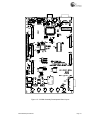
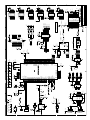
Figure 1-2. CY3684 Assembly Development Board Layout
EZ-USB Development Board
Page -21
EZ-USB Development Kit Manual - Getting Started
The schematic for the CY3684 appears on the following page.
Page -22
EZ-USB Development Kit Manual - Getting Started Rev 1.0
A
B
C
D
3216
10 uFd 16v
C25
C21
1M
+
5V
5
9
4
8
3
7
2
6
1
P10
SIO-1
5
9
4
8
3
7
2
6
1
1
2
3
4
5
6
FRAME
1A
2A
3
0805
nSHDN
IN
FRAME
S6
1B
2B
C39
3216
C41
5
0.1 uFd
TP7
3.3V
WAKEUP#
100K
R28
0805
0805
2
7
8
14
13
5
4
3.3V
C1-
C1+
V-
0.1 uFd
C42
TXD1
RXD1
0.1 uFd
C40
10
9
6
D7
0805
390
R15
R21
R23
SCL
SDA
1
2
3
13
14
15
3.3V
0805
40
41
RD#
WR#
INT4
INT5#
CS#
BKPT
PSEN#
OE#
EA
29
30
31
59
60
61
62
63
86
87
88
D0
D1
D2
D3
D4
D5
D6
D7
T0
T1
T2
94
95
96
97
117
118
119
120
126
127
128
21
22
23
24
25
A0
A1
A2
A3
A4
A5
A6
A7
A8
A9
A10
A11
A12
A13
A14
A15
51
53
50
52
19
18
DM
DP
RXD0
RXD1
TXD0
TXD1
99
10
17
RESET#
0.1 uFd
1
2
3.3V
1
2
AVCC
C18
JP10
JP1
0805
0805
3.3V
A0
A1
A2
INT
SCL
SDA
SO16
U10
PCF8574T
3.3V
0805
0.1 uFd
C3
C37
2.2K
2.2K
P0
P1
P2
P3
P4
P5
P6
P7
4
5
6
7
9
10
11
12
0.1 uFd
4
SCL
SDA
1B
2B
1B
2B
1B
2B
1B
2B
36
37
28
R25
390
106
42
34
39
38
10K
35
0805
IFCLK
R43
22 32
0805
CLKOUT
R17
22
1
WAKEUP# 101
0805
RED
0805
0.1 uFd
C2
0805
0.1 uFd
C4
0805
0.1 uFd
C5
0805
0.1 uFd
C6
3.3V
SCL
SDA
1A
2A
3
f4
FRAME
S5
f3
1A
2A
3
1A
2A
FRAME 3
S4
f2
FRAME
S3
f1
FRAME
S2
1A
2A
3
INT4
INT5#
CS#
BKPT
PSEN#
OE#
EA
IFCLK
CLKOUT
WAKEUP#
RD#
WR#
T0
T1
T2
RXD0
RXD1
TXD0
TXD1
D0
D1
D2
D3
D4
D5
D6
D7
A0
A1
A2
A3
A4
A5
A6
A7
A8
A9
A10
A11
A12
A13
A14
A15
DMINUS
DPLUS
RESET#
AVCC1
AVCC2
3.3VC
12 pFd
0805
0805
C38
4
3
2
1
JP9
i2c compatible
0.1 uFd
PB0/FD0
PB1/FD1
PB2/FD2
PB3/FD3
PB4/FD4
PB5/FD5
PB6/FD6
PB7/FD7
SCL
SDA
3.3V
10K
R27
PC0
PC1
PC2
PC3
PC4
PC5
PC6
PC7
PD0
PD1
PD2
PD3
PD4
PD5
PD6
PD7
PE0
PE1
PE2
PE3
PE4
PE5
PE6
PE7
72
73
74
75
76
77
78
79
102
103
104
105
121
122
123
124
108
109
110
111
112
113
114
115
69
70
71
66
67
98
1
2
3
13
14
15
A0
A1
A2
INT
SCL
SDA
SO16
0805
0805
0805
0805
0805
0805
3.3V
R16
R18
R19
R20
R22
R24
RDY0
RDY1
RDY2
RDY3
RDY4
RDY5
PB0
PB1
PB2
PB3
PB4
PB5
PB6
PB7
44
45
46
47
54
55
56
57
4
5
6
7
8
9
PA0
PA1
PA2
PA3
PA4
PA5
PA6
PA7
12 pFd
C14
82
83
84
85
89
90
91
92
0805
3
0.1 uFd
C10
U8
PCF8574T
CTL0/FLAGA
CTL1/FLAGB
CTL2/FLAGC
CTL3
CTL4
CTL5
RDY0/SLRD
RDY1/SLWR
RDY2
RDY3
RDY4
RDY5
PE0/T0OUT
PE1/T1OUT
PE2/T2OUT
PE3/RXD0OUT
PE4/RXD1OUT
PE5/INT6
PE6/T2EX
PE7/GPIFADR8
PD0/FD8
PD1/FD9
PD2/FD10
PD3/FD11
PD4/FD12
PD5/FD13
PD6/FD14
PD7/FD15
PC0/GPIFADR0
PC1/GPIFADR1
PC2/GPIFADR2
PC3/GPIFADR3
PC4/GPIFADR4
PC5/GPIFADR5
PC6/GPIFADR6
PC7/GPIFADR7
3.3V
0805
0.1 uFd
C9
PA0/INT0#
PA1/INT1#
PA2/SLOE
PA3/WU2
PA4/FIFOADR0
PA5/FIFOADR1
PA6/PKTEND
PA7/FLAGD
24 MHz
Y1
0.1 uFd
C8
CY7C68013A-128AZC
U1
0805
0.1 uFd
C7
C13
PLACE ONE CAP PER EACH VCC PIN ON U1
PWR 3.3V
D6
R9
3216
100K
BKPT/MONITOR
GREEN
11
12
0805
0805
JP5
3.3V IN
2.2 uFd 10v
C17 +
zero
0805
0.1 uFd
C1
3.3V
R2
0805
R12
1 uFd 16v
TXD0
RXD0
3
1
0.1 uFd
TR2OUT TR2IN
RX2IN RX2OUT
V+
C34
3216
100K
R1
+ C16
3.3V
10 uFd 16v
+ C23
NO LOAD
R31
zero
R30
3216
1N4148
D9
5V
TR1OUT TR1IN
RX1IN RX1OUT
C2-
C2+
U7
LTC1386CS
10 uFd 16v
0805
TV8
WAKEUP#
BUS PWR
RED
1206
D1
TP8
VBUS
C24
0.01 uFd
+ C32
3.3V
4
2
1
0.1 uFd
BYP
SENSE
OUTPUT
560
R3
TP6
GND
U4
LT1763CS8-3.3
RESET#
1B
2B
S1
VBUS
WAKEUP#
1A
2A
3
5
8
P9
SIO-0
10K
R78
5V
USB B RA
VBUS
DM
DP
GND
S1
S2
J1
1
2
BUS PWR
JP2
5V
TP5
GND
0805
R7
7163
4700 pFd 250v
0805
TP4
GND
1
2
4
NC1
NC2
NC3
TP3
GND
0805
12
XTALIN
TP2
GND
GND
GND
GND
3
6
7
TP1
GND
0805
1
2
26
81
VCC1
VCC2
AGND1
AGND2
13
20
11
XTALOUT
3.3VC
GND1
GND2
3
P0
P1
P2
P3
P4
P5
P6
P7
C35
3.3V
22
22
22
22
22
22
JP8
WU2
4
5
6
7
9
10
11
12
0.1 uFd
U5
JP6
MM0
C27
JP7
MM1
8
7
6
5
0.1 uFd
C28
0.1 uFd
R34
R35
R36
R37
R38
R39
R40
R41
0805
0805
0805
0805
0805
0805
0805
0805
390
390
390
390
390
390
390
390
a
b
c
d
e
f
g
dec
U6
8
A0
Vcc
7
A1
WP
6
A2
SCL
5
Vss
SDA
24LC00/P
8-PIN DIP SOCKET
1
2
3
4
10K
R29
2.2 uFd 10v
A0
Vcc
A1
WP
A2
SCL
Vss
SDA
24LC128-I/P
8-PIN DIP SOCKET
1
2
3
4
CTL0
CTL1
CTL2
CTL3
CTL4
CTL5
3216
100K
R42
+ C43
3.3V
0805
2
43
48
64
68
100
107
VCC3
VCC4
VCC5
VCC6
VCC7
VCC8
VCC9
27
93
1
2
5V
3.3V
3.3V
SCL
10K
e
a
f
A0
A1
A2
A3
A4
A5
A6
A7
A8
A9
A10
A11
A12
A13
A14
A15
RAMA16
1
2
3
4
13
14
15
16
17
18
19
20
21
29
30
31
32
U3
R32
22K
R14
6
7
1
2
3
3.3V
nc
e
a
f
an1
22K
R26
e
f
1
3
5
7
2
4
6
8
JP3
OE
WE
CE
D0
D1
D2
D3
D4
D5
D6
D7
d
g
a
U9
3.3V
c
b
TV9
g
c
dec
d
an2
b
11
10
9
8
14
13
2
LARGE EEPROM
1
2
3
SMALL EEPROM
g
c
dec
d
b
C20
0805
0805
0805
0805
27
26
25
24
23
21
20
19
18
17
22
15
D3
D4
D5
390
390
390
2
3.3V
1206
LED Red
TV7
TV6
TV5
TV4
TV2
TV3
PF0
PF1
PF2
PF3
SPARE1
SPARE2
SPARE3
3.3V
0805
R33
4.7K
R77
RDY1
CTL0
CTL1
RDY0
CTL2
PA0
PA2
PA1
PA4
390
PB7
PB6
PB5
PB4
PB3
PB2
PB1
PB0
0805
33
4.7K
R44
SP1
SOLDER PAD
SP3
SOLDER PAD
R74
PA7
SDA
3.3V
Date:
Size
C
Title
4.7K
R45
3.3V
P3
2
4
6
8
10
12
14
16
18
20
2
4
6
8
10
12
14
16
18
20
2
4
6
8
10
12
14
16
18
20
22
24
26
28
30
32
34
36
38
40
0805
3.3V
1
Tuesday, November 25, 2003
Sheet
1
CYPRESS SEMICONDUCTOR © 2003
Document Number
REF-11637
1K
R69
0.1 uFd
C36
0.1 uFd
C31
INT5#
T2
T0
SDA
PE7
PE5
PE3
PE1
3.3V
A15
A13
A11
A9
A7
A5
A3
A1
3.3V
D7
D5
D3
D1
CS#
5V
3.3V
PC7
PC5
PC3
PC1
RDY5
RDY3
BKPT
3.3V
0805
0805
0805
0805
0805
0805
of
PCA: 121-08600
PA3
PA5
PD0
PD1
PD2
PD3
PD4
PD5
PD6
PD7
0805
3.3V
PD7
PD5
PD3
PD1
PB7
PB5
PB3
PB1
3.3V
RDY1
CTL5
CTL3
CTL1
PA7
PA5
PA3
PA1
3.3V
2
+5V CLK2
4
CLK1 D15 6
D13 8
D14
D11
D12
10
D9
D10
12
D8
D7
14
D6
D5
16
D4
D3
18
D2
D1
20
D0
GND
LOGIC ANALYZER HDR
P6
2
+5V CLK2 4
CLK1 D15
6
D14
D13 8
D12
D11
10
D10
D9 12
D8
D7 14
D6
D5
16
D4
D3 18
D2
D1
20
D0
GND
LOGIC ANALYZER HDR
1
3
5
7
9
11
13
15
17
19
P5
2
+5V CLK2 4
CLK1 D15
6
D14
D13 8
D12
D11
10
D10
D9 12
D8
D7 14
D6
D5
16
D4
D3 18
D2
D1
20
D0
GND
LOGIC ANALYZER HDR
1
3
5
7
9
11
13
15
17
19
P4
LOGIC ANALYZER HDR
+5V CLK2
CLK1 D15
D13
D14
D11
D12
D9
D10
D8
D7
D6
D5
D4
D3
D2
D1
D0
GND
PCB: PDC-9086
ATA CONNECTOR
GND
DD8
DD9
DD10
DD11
DD12
DD13
DD14
DD15
KEYPIN
GND
GND
GND
CSEL
GND
IOCS16
PDIAG#
DA2
CS1#
GND
+5V CLK2
CLK1 D15
D14
D13
D12
D11
D10
D9
D8
D7
D6
D5
D4
D3
D2
D1
D0
GND
P2
LOGIC ANALYZER HDR
1
3
5
7
9
11
13
15
17
19
1
RD#
3
INT4
5
T1
7
WAKEUP# 9
SCL
11
PE6
13
PE4
15
PE2
17
PE0
19
IFCLK
A14
A12
A10
A8
A6
A4
A2
A0
10K
R13
D6
D4
D2
D0
CLKOUT
OE#
5V
P8
RESET#
DD7
DD6
DD5
DD4
DD3
DD2
DD1
DD0
GND
DMARQ
DIOW#
DIOR#
IORDY
DMACK#
INTRQ
DA1
DA0
CS0#
DASP#
5V
P1
2
+5V CLK2
4
CLK1 D15 6
D14
D13
8
D12
D11 10
D10
D9 12
D8
D7
14
D6
D5 16
D4
D3
18
D2
D1 20
D0
GND
LOGIC ANALYZER HDR
1
3
5
7
9
11
13
15
17
19
1
WR#
3
RDY4
5
RDY2
7
RESET# 9
11
PC6
13
PC4
15
PC2
17
PC0
19
RDY0
CTL4
CTL2
CTL0
PA6
PA4
PA2
PA0
PSEN#
PD6
PD4
PD2
PD0
PB6
PB4
PB2
PB0
1
CY3684 USB 2.0 DEVELOPMENT BOARD
1
3
5
7
9
11
13
15
17
19
21
23
25
27
29
31
33
35
37
39
SP2
SOLDER PAD
Bridge SP1-SP3 for Atapi use.
EA
PF3
PF2
PF1
PF0
3 NO EEPROM
DRIVE RDY
LED Red
RAMOE#
1 EEPROM
D8
LED Red
TV1
LED Red
RAMCE#
D2
390
SW2
EEPROM ENABLE
F9
F8
F7
F6
F5
F4
F3
F2
F1
F0
NC4
NC3
0.1 uFd
R8
R6
R5
3.3V
NC1
NC2
I0/clk
I1
I2
I3
I4
I5
I6
I7
I8
I9
I10
I11
GAL22LV10C-7LJ
SW1
EEPROM SELECT
OE#
A12
A13
A14
A15
1
8
2
3
4
5
6
7
9
10
11
12
13
16
10K
28
U2
WR#
RAMOE#
12
R4
RAMCE#
D0
D1
D2
D3
D4
D5
D6
D7
0.1 uFd
C12
0805
5
6
7
10
11
22
23
26
27
2
R47
CS#
A11
PSEN#
SPARE4
zero
R46
LED SELECT
HDSP-E101
NO LOAD
3.3V
10K
R11
RD#
3.3V
128K x 8 SRAM
PF0
PF1
PF2
PF3
3.3V
A0
A1
A2
A3
A4
A5
A6
A7
A8
A9
A10
A11
A12
A13
A14
A15
A16
CY7C1019BV33-12VC
R10
SCL
3.3V
0805
5V
0805
8
24
VDD
VDD
Vss
Vss
9
25
14
15
16
GND3
GND4
GND5
GND6
GND7
GND8
GND9
3
49
58
65
80
116
125
0805
3.3V
0805
0805
2
1
2
1
0805
5
0805
10
11
0805
RESERVED
33
0805
16
VCC
GND
10
11
0805
15
16
VCC
GND
8
16
VCC
GND
8
0805
0805
0805
0805
0805
0805
28
Vcc
0805
0805
1206
1206
0805
Vss
120 6
0805
14
120 6
SOT23
0805
0805
120 6
0805
120 6
0805
0805
0805
1
Rev
*A
0.1 uFd
C29
0.1 uFd
C26
0.1 uFd
C22
0.1 uFd
C19
0.1 uFd
C15
0.1 uFd
C11
A
B
C
D
EZ-USB Development Kit Manual - Getting Started
Page -24
EZ-USB Development Kit Manual - Getting Started Rev 1.0