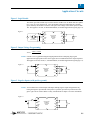
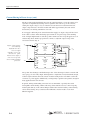
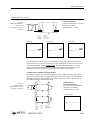
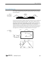
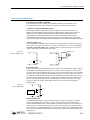
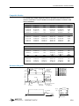
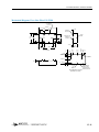
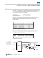
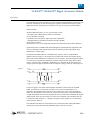
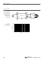
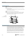
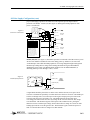
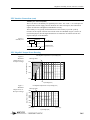
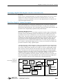
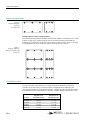
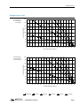
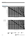
1
45
Applications Manual
First Generation Converters and Accessory Modules
Eighth Edition
+Vout
Lo
Vs
Load
Co
D2
-Vout
+
OVP*
–
C/L
OTP*
+S
–
+
E/A
2.5V
REF.
TRIM
-S
Component Solutions For Your Power System
Total Power Solutions
Vicor Corporation produces families of compact, economical, high performance power components
and systems that offer the system designer a “total solution” to most power system requirements.
This publication provides a review of Vicor’s zero-current-switching technology and helpful
applications information as it applies to Vicor’s first generation of DC-DC converters (VI-200,
VI-J00) and accessory modules (VI-IAM, VI-RAM, VI-AIM,VI-HAM). For information on Vicor’s
2nd generation products visit our website at vicr.com. Additionally, a glossary of technical terms has
been included for your convenience.
System architects are being asked to squeeze more and more power into ever-shrinking spaces. This
applications manual is designed to help system designers make the most of their available space
using Vicor power components.
Please contact Vicor’s Applications Engineering Department at (800) 927-9474, or one of Vicor’s
Technical Support Centers, listed below, if further clarification of the topics presented is required.
Technical Support Centers — U.S.
Technical Support Center — Far East
Vicor Corporation, Andover, MA
Tel: (800) 735-6200, (978) 470-2900
Fax: (978) 475-6715 or (978) 475-6726
Vicor Hong Kong
Tel: +852-2956-1782
Fax: +852-2956-0782
Vicor Corporation and
Vicor Westcor Division, Sunnyvale, CA
Tel: (408) 522-5280
Fax: (408) 774-5555
Vicor Japan Co., Ltd.
Tel: +81-3-5487-3880
Fax: +81-3-5487-3885
Vicor Corporation, Chicago, IL
Tel: (630) 769-8780
Fax: (630) 769-8782
Vicor Integration Architects
Technical Support Centers — Europe
Aegis Power Systems
Murphy, NC
Tel: (828) 837-4029
Fax: (828) 837-4106
Vicor France
Tel: +33-1-3452-1830
Fax: +33-1-3452-2830
Free Phone: 0800 419 419
ConverTec Corporation
Roseville, MN
Tel: (651) 604-0289
Fax: (651) 604-0293
Vicor Germany
Tel: +49-89-962-439-0
Fax: +49-89-962-439-39
Free Phone: 0800 0182 918
Freedom Power Systems
Austin, TX
Tel: (512) 833-6177
Fax: (512) 833-6181
Vicor Italy
Tel: +39-02-2247-2326
Fax: +39-02-2247-3166
Free Phone: 167 899 677
Granite Power Technologies
Manchester, NH
Tel: (603) 623-3222
Fax: (603) 627-3222
Vicor U.K.
Tel: +44-1276-678-222
Fax: +44-1276-681-269
Free Phone: 0800 980 8427
Mission Power Solutions
Oceanside, CA
Tel: (760) 631-6846
Fax: (760) 631-6972
Northwest Power Integrations
Milwaukie, OR
Tel: (503) 652-6161
Fax: (503) 652-6868
Or you may E-mail Vicor’s Application Engineers at
[email protected]
12 1-800-927-9474
i
ii
12 1-800-927-9474
Table of Contents
COMPONENT PRODUCTS
SECTION
Zero-Current-Switching . . . . . . . . . . . . . . . . . . . . . . . . . . . . . . . . . . . . . . . . . . . . . . . . . . . . . . . . . 1
DC-DC Converter Pinouts . . . . . . . . . . . . . . . . . . . . . . . . . . . . . . . . . . . . . . . . . . . . . . . . . . . . . . . 2
Module Do’s and Don’ts . . . . . . . . . . . . . . . . . . . . . . . . . . . . . . . . . . . . . . . . . . . . . . . . . . . . . . . . 3
Module Packaging Options . . . . . . . . . . . . . . . . . . . . . . . . . . . . . . . . . . . . . . . . . . . . . . . . . . . . . . 4
Output Voltage Trimming . . . . . . . . . . . . . . . . . . . . . . . . . . . . . . . . . . . . . . . . . . . . . . . . . . . . . . . 5
Using Boosters to Expand Output Power. . . . . . . . . . . . . . . . . . . . . . . . . . . . . . . . . . . . . . . . . . . . 6
Multiple Gate-In Connections . . . . . . . . . . . . . . . . . . . . . . . . . . . . . . . . . . . . . . . . . . . . . . . . . . . . 7
Overcurrent Protection . . . . . . . . . . . . . . . . . . . . . . . . . . . . . . . . . . . . . . . . . . . . . . . . . . . . . . . . . . 8
Application Circuits / Power Array Design Considerations . . . . . . . . . . . . . . . . . . . . . . . . . . . . . 9
EMC Considerations . . . . . . . . . . . . . . . . . . . . . . . . . . . . . . . . . . . . . . . . . . . . . . . . . . . . . . . . . . . 10
The BatMod™. . . . . . . . . . . . . . . . . . . . . . . . . . . . . . . . . . . . . . . . . . . . . . . . . . . . . . . . . . . . . . . . 11
VI-AIM/MI-AIM™ (Alternating Input Module) . . . . . . . . . . . . . . . . . . . . . . . . . . . . . . . . . . . . . 12
VI-HAM™ (Harmonic Attenuator Module) . . . . . . . . . . . . . . . . . . . . . . . . . . . . . . . . . . . . . . . . . 13
VI-IAM/MI-IAM™ (Input Attenuator Module) . . . . . . . . . . . . . . . . . . . . . . . . . . . . . . . . . . . . . . 14
VI-RAM/MI-RAM™ (Ripple Attenuator Module) . . . . . . . . . . . . . . . . . . . . . . . . . . . . . . . . . . . 15
VI-ARM™ (Autoranging Rectifier Module) . . . . . . . . . . . . . . . . . . . . . . . . . . . . . . . . . . . . . . . . 16
Optional Output Filters . . . . . . . . . . . . . . . . . . . . . . . . . . . . . . . . . . . . . . . . . . . . . . . . . . . . . . . . . 17
CONFIGURABLE PRODUCTS
The ComPAC™ Family . . . . . . . . . . . . . . . . . . . . . . . . . . . . . . . . . . . . . . . . . . . . . . . . . . . . . . . . 18
FlatPAC™ Technical Description. . . . . . . . . . . . . . . . . . . . . . . . . . . . . . . . . . . . . . . . . . . . . . . . . 19
MegaPAC™/Mini MegaPAC™ AC-DC Switchers . . . . . . . . . . . . . . . . . . . . . . . . . . . . . . . . . . 20
PFC Mini/ Power Factor Corrected AC-DC Switchers. . . . . . . . . . . . . . . . . . . . . . . . . . . . . . . . . 21
FRONT END PRODUCTS
Front End Application Notes. . . . . . . . . . . . . . . . . . . . . . . . . . . . . . . . . . . . . . . . . . . . . . . . . . . . . 22
GENERAL
Thermal Considerations . . . . . . . . . . . . . . . . . . . . . . . . . . . . . . . . . . . . . . . . . . . . . . . . . . . . . . . . 23
Thermal Curves . . . . . . . . . . . . . . . . . . . . . . . . . . . . . . . . . . . . . . . . . . . . . . . . . . . . . . . . . . . . . . . 24
Safety Agency Approvals . . . . . . . . . . . . . . . . . . . . . . . . . . . . . . . . . . . . . . . . . . . . . . . . . . . . . . . 25
Product Weights . . . . . . . . . . . . . . . . . . . . . . . . . . . . . . . . . . . . . . . . . . . . . . . . . . . . . . . . . . . . . . 26
Glossary of Technical Terms . . . . . . . . . . . . . . . . . . . . . . . . . . . . . . . . . . . . . . . . . . . . . . . . . . . . 27
Note: This Application does not relate to Vicor’s 2nd Generation Products.
12 1-800-927-9474
iii
iv
12 1-800-927-9474
1
Zero-Current-Switching
Overview
The heart of Vicor’s module technology, zero-current-switching, allows Vicor converters to
operate at frequencies in excess of 1 MHz, with efficiencies greater than 80% and power
densities ten or more times those of conventional converters.
Lossless Energy Transfer
Switch turn-on of the MOSFET switch transfers a quantized energy packet from the input
source to an LC “tank” circuit, composed of inherent transformer leakage inductance of T1 and
a capacitive element, C, in the secondary. Simultaneously, an approximately half-sinusoidal
current flows through the switch, resulting in switch turn-on at zero current and turn-off when
current returns to zero. Resonance, or bidirectional energy flow, cannot occur because D1 will
only permit unidirectional energy transfer. A low-pass filter (Lo, Co) following the capacitor
produces a low ripple DC output. The result is a virtually lossless energy transfer from input to
output with greatly reduced levels of conducted and radiated noise.
1st Generation
Zero-Current-Switching
Block Diagram
Output Filter
Integrator
+Vin
Input
Filter
T1
D1
Reset
Control
MOSFET
-Vin
Lo
Vs
+Vout
D2
C
Co
Load
-Vout
Ip
Vp
OC1*
+
OVP*
–
C/L
OTP*
Gate
In
Gate
Out
Logic
Control
+S
–
OC2
+
E/A
2.5V
REF.
TRIM
-S
Ip
Vp
Vin
*NOT IN VI-J00 SERIES
Vs
Vout
Referenced to -Vin
Gate
Out
12 1-800-927-9474
1-1
1-2
12 1-800-927-9474
2
DC-DC Converter Pinouts
Pinout Description
VI-200, VI-J00
Modules
–IN
–IN
–OUT
GATE
OUT
–S
–OUT
GATE
OUT
–S
GATE
IN
+S
T
T
GATE
IN
+S
+IN
+OUT
+IN
+OUT
–IN, +IN:
DC voltage inputs. See tables below for nominal input voltages and ranges for the VI-200,
VI-J00, MI-200 and MI-J00 Family modules (data sheets contain Brownout and Transient
ratings).
VI-200, VI-J00 Input Voltage
Designator Low
Nominal
0
10V
12V
1
21V
24V
W
18V
24V
2
21V
36V
3
42V
48V
N
36V
48V
4
55V
72V
T
66V
110V
5
100V
150V
6
200V
300V
7
100V 150/300V
Ranges
High
20V
32V
36V
56V
60V
76V
100V
160V
200V
400V
375V
MI-200, MI-J00 Input Voltage Ranges
Designator
Low
Nominal
High
2
18V
28V
50V
5
100V
155V
210V
6
125V
270V
400V
7
100V
165V
310V
GATE OUT, GATE IN:
Gate Out: The pulsed signal at the Gate Out terminal of a regulating driver module is used to
synchronously drive the Gate In terminal of a companion booster module to effect power
sharing between the driver and the booster. Daisy-chaining additional boosters (connecting Gate
Out of one unit to Gate In of a succeeding unit) leads to a virtually unlimited power expansion
capability.
Gate In: The Gate In pin on a driver module may be used as a logic Enable/Disable input.
When Gate In is pulled low (<0.65V @ 6 mA, referenced to –Vin), the module is turned off;
when Gate In is floating (open collector), the module is turned on. The open circuit voltage of
the Gate In pin is less than 10V.
–OUT, +OUT:
DC output pins. See the table below for output voltages and power levels of VI-200, VI-J00,
MI-200 and MI-J00 Family modules.
Output Voltage
<5Vdc
≥5Vdc
Power Level
VI-200
VI-J00
10-40A
5-20A
50-200W 25-100W
Power Level
MI-200 MI-J00
10-30A
5-10A
50-100W 10-50W
Special output voltages from 1 to 95V; consult factory.
12 1-800-927-9474
2-1
Applications Manual
Pinout Description (cont)
T (Trim):
Allows fixed or variable adjustment of the module output.
Trimming Down: Allows output voltage of the module to be trimmed down, with a decrease in
efficiency. Ripple as a percent of output voltage goes up and input range widens since input
voltage dropout (loss of regulation) moves down.
Trimming Up: Reverses the above effects.
–S, +S (–Sense, +Sense):
Maintains specified output voltage to the load. Overvoltage protection will be activated in the
VI-200/MI-200 and module will shut down if remote sense tries to boost output voltage above
110% of nominal. Do not exceed 0.25V drop in negative return; if the voltage drop exceeds
0.25V in the negative return path, the current limit setpoint will increase. Connect + sense to
+ out and –sense to –out at the module if remote sensing is not desired (see figure 4, pg 9-2).
2-2
12 1-800-927-9474
3
Module Do’s and Don’ts
Electrical Considerations
Gate In and Gate Out Terminals:
Logic Disable
When the Gate In terminal of a driver module is pulled low with respect to –Vin (CAUTION:
with off-line applications –Vin is not earth ground), the module shuts off (see Figure 1, page
9-1). In Logic Disable mode, the Gate In terminal should be driven from either an “open collector”
or electromechanical switch that can sink 6 mA when on (Gate In voltage less than 0.65V). If
driven from an electromechanical switch or relay, a 1 µF capacitor should be connected from
Gate In to –Vin to eliminate the effects of switch “bounce”. The 1 µF capacitor may be required
in all applications to provide a “soft start” if the unit is disabled and enabled quickly. This
terminal is not intended for repetitive on/off/on operation.
High Power Arrays
The pulsed signal at the Gate Out terminal of a regulating driver module is used to
synchronously drive the Gate In terminal of a companion booster module to effect power
sharing between the driver and the booster (refer to Figure 5, page 9-2). Daisy-chaining
additional boosters (i.e., connecting Gate Out to Gate In of a succeeding unit) leads to a virtually
unlimited power expansion capability. MI/VI-200 series modules of the same family and power
level can be paralleled (i.e., DRIVER, VI-260-CU with BOOSTER, VI-B60-CU).
In general:
• Don’t drive the Gate In terminal from an “analog” voltage source.
• Don’t leave Gate In terminals of booster modules unterminated.
• Don’t overload Gate Out; limit load to a single Vicor module Gate In connection, or 1 Kohm,
minimum, in parallel with 100 pF, maximum.
• Don’t skimp on traces that interconnect module –Vin terminals in high power arrays.
Gate In and Gate Out are referenced to –Vin; heavy, properly laid out traces will minimize
parasitic impedances that could interfere with proper operation.
• Do use a decoupling capacitor across each module’s input (see Input Source Impedance below).
• Do use a fuse or breaker on each module’s input to prevent fire in the event of module failure.
Input Source Impedance
The converter should be connected to an input source that exhibits low AC impedance. A small
electrolytic capacitor should be mounted close to the module’s input pins if source impedance is
questionable. This will restore low AC impedance, while avoiding the potential resonance
associated with “high-Q” film capacitors. The minimum value of the capacitor, in microfarads,
should be C (µF) = 400 ÷ Vin minimum. Example: Vin, minimum, for a VI-260-CV is 200V.
The minimum capacitance would be 400 ÷ 200 = 2 µF. For applications involving long line or
high inductance additional capacitance will be required.
Input Transients
Don’t exceed the transient input voltage rating of the converter. Input Attenuator Modules or
surge suppressors, in combination with appropriate filtering, should be used in off-line applications
or in applications where source transients may be induced by load changes, blown fuses, etc.
NOTE: On any converter module with a high line rating in excess of 250Vdc, do not allow the rate of
change of input voltage to exceed 10V/µs for any input voltage change in excess of 250V.
The level of transient suppression required will depend on the severity of the transients. A zener
diode, TRANSZORB™ or the like will provide suppression of transients of under 100 µs, act as
12 1-800-927-9474
3-1
Applications Manual
Electrical Considerations (cont)
a voltage clipper for DC input transients and provide reverse input protection. It may be
necessary to incorporate an LC filter for larger energy transients. This LC filter will integrate the
transient energy while the zener clips the peak voltages. The Q of this filter should be kept low
to avoid potential resonance problems. Please see Section 14, VI-IAM/MI-IAM Input Attenuator
Module, for additional information on transient suppression.
Output OVP
Each module, with the exception of VI-J00s and MI-J00s, has an internal overvoltage protection
circuit that monitors the voltage across the output power terminals. It is designed to latch the
converter off at 115% to 135% of rated output voltage. It is not a crowbar circuit, and if a
module is trimmed above 110% of rated output voltage, OVP may be activated. CAUTION:
when trimming up VI-J00 or MI-J00 modules, additional care should be taken as an
improper component selection could result in module failure. Improper connection of the
sense leads on VI-J00 or MI-J00 can also result in an over voltage condition and module
failure.
Input Reverse Voltage Protection
The module may be protected against reverse input voltages by the addition of a diode in series
with the positive input, or a reverse shunt diode with a fuse in series with the positive input.
Input Attenuator Modules (VI-IAMs) provide input reverse voltage protection when used with a
current limiting device (fuse).
Thermal/Mechanical Considerations
Baseplate
Operating temperature of the baseplate, as measured at the center mounting slot on the –Vin,
–Vout side, cannot exceed rated maximum. Thermal compound or a thermal pad should be
used when mounting the module baseplate to a chassis or heatsink. All six mounting holes
should be used. Number six (#6) machine screws should be torqued to 5-7 in.-lbs., and use of
Belville washers is recommended.
EMC Considerations
All applications utilizing DC-DC converters should be properly bypassed, even if no EMC
standards need to be met. Bypass Vin and Vout pins to each module baseplate as shown in
Figure 1 below. Lead length should be as short as possible. Recommended values vary
depending on the front end, if any, that is used with the modules, and are indicated on the
appropriate data sheet. In most applications, C1 is a 4700 pF “Y” capacitor (Vicor P/N 01000)
carrying the appropriate safety agency approval; C2 is a 4700 pF “Y” capacitor (Vicor P/N
01000) or a .01 µF ceramic capacitor rated at 500V. In PC board-mount applications, each of
these components is typically small enough to fit under the module baseplate flange.
Figure 1.
C2a
C1a
+In
C3
–In
C1b
3-2
Zero Current
Switching
Converter
+Out
–Out
C2b
12 1-800-927-9474
Module Do’s and Don’ts
Safety Considerations
Shock Hazard
Agency compliance requires that the baseplate be grounded or made inaccessible.
Fusing
Internal fusing is not provided in Vicor DC-DC converters. To meet safety agency conditions, a
fuse is required. This fuse should be placed in the +input lead, not the –input lead, as opening of
the –input lead will cause the gate terminals to rise to the potential of the +input lead, causing
possible damage to other modules or circuits that share common Gate In or Gate Out
connections.
Safety agency conditions of acceptability require module input fusing. The VI-x7x, VI-x6x
and VI-x5x require the use of a Buss PC-Tron fuse, or other DC-rated fuse. See below for
suggested fuse ratings. This fuse should be inserted in the (+) input lead, as opening of the (–)
input lead will cause the gate terminals to rise to the voltage of the (+) input lead, possibly
causing destruction of the connected modules or devices.
VI-27X
VI-26X
VI-25X
VI-2TX
VI-24X
VI-2NX
VI-23X
VI-22X
VI-2WX
VI-21X
VI-20X
PC-Tron 2.5A
PC-Tron 3A
PC-Tron 5A
PC-Tron 5A
6A/125V
8A/125V
8A/125V
8A/60V
12A/50V
12A/32V
12A/32V
VI-J7X
VI-J6X
VI-J5X
VI-JTX
VI-J4X
VI-JNX
VI-J3X
VI-J2X
VI-JWX
VI-J1X
VI-J0X
PC-Tron 2.5A
PC-Tron 3A
PC-Tron 5A
PC-Tron 5A
PC-Tron 5A
PC-Tron 5A
PC-Tron 5A
PC-Tron 5A
8A/60V
8A/60V
8A/60V
MegaMod Family
Please consult Vicor’s Applications Engineering Department for MegaMod fuse values.
This fuse should be inserted in the (+) input lead, as opening of the (–) input lead will cause the
gate terminals to rise to the voltage of the (+) input lead, possibly causing destruction of
connected modules or devices.
12 1-800-927-9474
3-3
Notes
3-4
12 1-800-927-9474
4
Module Packaging Options
Up to 50 Watts/Cubic Inch
SlimMod™
Vicor’s PC-mountable power components are available in flangeless “SlimMod” package
configurations that provide users with the highest power density available in printed circuit
mount applications.
To order the SlimMod configuration, add the suffix “S” to the standard part number.
Example: VI-260-CV-S.
Full- and Half-Size
SlimMods
FinMod™
Vicor’s PC-mountable power components are also available in flangeless “FinMod” package
configurations with integral finned heatsinks. FinMods eliminate the need for secondary
heatsink assembly operations.
The full-size and half-size module components are available in .25 and .5 inch longitudinal or
transverse fin versions. To order the longitudinal fin configurations add the suffix “F1”
(.25 inch) or “F2” (.5 inch) to the standard part number.* For transverse fins, add the suffix
“F3” (.25 inch) or “F4” (.5 inch) to the standard part number.
Longitudinal and
Transverse FinMods
*F1 and F2 FinMods are now 7-fin products as shown. A 14-fin version is available by
specifying F5 or F6.
12 1-800-927-9474
4-1
Applications Manual
BusMod™
The BusMod is a rugged module housing assembly that combines convenient chassis mounting
with a screw/lug wiring interface for all electrical connections. To order the BusMod option,
add “B1” to the standard part number.
NOTE: The BusMod may be used with any of Vicor’s full-size modules, with the exception of the
VI-HAM.
BusMod Module
Housing Assembly
4-2
12 1-800-927-9474
5
Output Voltage Trimming
Overview
Specifications such as efficiency, ripple and input voltage range are a function of output voltage
settings. As the output voltage is trimmed down, efficiency goes down; ripple as a percent of
Vout goes up and the input voltage range widens since input voltage dropout (loss of regulation)
moves down. As the units are trimmed up, the reverse of the above effects occurs.
All converters have a fixed current limit. The overvoltage protection setpoint is also fixed;
trimming the output voltage does not alter its setting. As the output voltage is trimmed down,
the current limit setpoint remains constant. Therefore, in terms of output power, if the unit is
trimmed down, available output power drops accordingly.
The output voltage of all Vicor converters can be trimmed ±10%. Certain modules can be
trimmed down to 50% of nominal output.
Do not attempt to trim the module output voltage more than +10%, as overvoltage shutdown
may occur. Do not exceed maximum rated output power when the module is trimmed up.
CAUTION: when trimming up VI-J00 or MI-J00 modules, additional care should be
taken as an improper component selection could result in module failure. Improper
connection of the sense leads on VI-J00 or MI-J00 can also result in an over voltage
condition and module failure.
The following procedures describe methods for output voltage adjustment (–50 to +10%
of nominal) of the VI-200, MI-200, VI-J00, MI-J00, ComPAC, FlatPAC and Mega Modules.
* Modules with nominal 3.3V outputs and above have the 2.5V precision reference and 10k
internal resistor. For trim resistor calculations on modules with 2.0V outputs use 0.97V in
place of the 2.5V reference and substitute 3.88 kΩ for the internal 10 kΩ resistor.
NOTE: Resistors are 1/4W. When trimming down any module, always maintain a preload of 1% of
rated output power. For more specific information on trimming down a specific module,
please consult Vicor’s Applications Engineering Department.
Resistive Adjustment Procedure
To achieve a variable trim range, an external resistor network must be added. Refer to Figure 1.
Example 1.
For trimming –20% to +10% with a standard off-the-shelf 10 kΩ potentiometer (R7), values for
resistors R6 and R8 need to be calculated.
Resistor R6 limits the trim down range. For a given percentage, its value is independent of
output voltage. Refer to Table 1, page 5-4, for limiting resistor values.
+ OUT
Figure 1.
External Resistive
Network for Variable
Trimming
R1 10-300Ω
Error Amp
–
+
+ Sense
R8
R2
Trim
R5
10kΩ
2.5 V
R3
C1
R4
20-200Ω
R6
R7
Load
– Sense
– OUT
* Nominal Vout ≥ 3.3V
12 1-800-927-9474
5-1
Applications Manual
Trimming Down –20%
A 20% drop of the 2.5V reference at the trim pin is needed to effect a 20% drop in the output
voltage. Refer to Figure 2.
+ OUT
Figure 2.
Circuit Diagram
"Trim Down"
+ Sense
R5 10 kΩ
(internal)
2.5V
reference
(internal)
Trim R6
V1
I R6
R8
R7 10 kΩ POT
– Sense
– OUT
Vl = 2.5V – 20% = 2V
Therefore:
IR5 =
(2.5V - 2V)
= 50 µA
10 kΩ
Since IR5 = IR6 = 50 µA:
R6 =
2V
= 40 kΩ
50 µA
This value will limit the trim down range to –20% of nominal output voltage.
Trimming Up +10%
To trim +10% above nominal output voltage, the following calculations are needed to determine
the value of R8. This calculation is dependent on the output voltage of the module. A 12V
output will be used as an example. Refer to Figure 3.
It is necessary for the voltage at the trim pin to be 10% greater than the 2.5V reference. This
offset will cause the error amplifier to adjust the output voltage up 10% to 13.2V.
+ OUT
Figure 3.
Circuit Diagram
"Trim Up"
+ Sense
R5 10 kΩ
(internal)
2.5V
reference
(internal)
V1
R8
Trim R6 40 kΩ V2
– Sense 25 µA
I R8
R7 10 kΩ POT
375 µA
– OUT
Vl = 2.5V + 10% = 2.75V
IR5 =
(2.75V - 2.5V)
= 25 µA
10 kΩ
Since IR5 = IR6, the voltage drop across R6 = (40 kΩ) (25 µA) = 1V.
Therefore, V2 = 2.75V + 1V = 3.75V. The current through R7 (10 kΩ pot) is:
IR7 =
5-2
V2 3.75
=
= 375 µA
R7 10 k
12 1-800-927-9474
Output Voltage Trimming
Trimming Up +10% (cont)
Using Kirchoff’s current law:
IR8 = IR7 + IR6 = 400 µA
Thus, knowing the current and voltage, R8 can be determined:
VR8 = (Vout + 10%) – V2 = 13.2V – 3.75V = 9.45V
R8 =
(9.45V)
= 23.63 kΩ
400 µA
This resistor configuration allows a 12V output module to be trimmed up to 13.2V and down to
9.6V. Follow this procedure to determine resistor values for other output voltages.
Fixed Trim
Converters can be trimmed up or down with the addition of one external resistor, either Ru for
programming up or Rd for programming down. Refer to Figure 4 below.
Example 2.
Fixed Trim Up (12V to 12.6V)
To determine Ru, the following calculation must be made:
2.5V + 5% = 2.625V
VR5 = Vtrim – Vref
VR5 = 2.625 – 2.5 = 0.125V
+ OUT
Figure 4.
Fixed Trimming
+ Sense
R5
(internal)
2.5V
reference
(internal)
Ru
Trim
– Sense Rd
Trim Resistor for UP
Programming
or
Trim Resistor for DOWN
Programming
– OUT
Knowing this voltage, the current through R5 can be found:
IR5 =
VR5
= .125V = 12.5 µA
R5
10 kΩ
VRu = 12.6V – 2.625V = 9.975V
Ru =
9.975V
= 798 kΩ
12.5 µA
Connect Ru from the trim pin to the positive sense. Be sure to connect the resistor to the
positive sense, not the positive output, or drops in the positive output lead as a function of load
will cause apparent load regulation problems.
12 1-800-927-9474
5-3
Applications Manual
Fixed Trim (cont)
Example 3.
–25% Fixed Trim Down (24V to 18V)
The trim down methodology is identical to that used in Example 2, except that it is utilized to
trim the output of a 24V module down 25% to 18V. The voltage on the trim pin must be
reduced 25% from its nominal setting of 2.5V. This is accomplished by adding a resistor from
the trim pin to negative sense.
2.5V – 25% = 1.875V
VR5 = Vbandgap – Vtrim
= 2.5V – 1.875V = .625V
Knowing this voltage, the current through R5 can be found:
VR5
= .625V = 62.5 µA
R5
10 kΩ
The voltage across the resistor, Rd, and the current flowing through it are known:
IR5 =
Rd =
(2.5V - .625V)
= 30 kΩ
62.5 µA
Connect Rd (Figure 4) from the trim pin to the negative sense of the module. Be sure to connect
the resistor to the negative sense, not the negative output, or drops in the negative output lead as
a function of load will cause apparent load regulation problems.
Table 1.
Values for Trim Down
by Percentage
(Refer to product data sheet
for allowable trim ranges)
Tables 2a and 2b.
Values for Fixed
Trim Down and
Trim Up by Voltage
Percent
–5%
–10%
–15%
–20%
–25%
–30%
–35%
–40%
–45%
–50%
Vnom
5V
15V
24V
48V
Resistance
190 kΩ
90 kΩ
56.7 kΩ
40 kΩ
30 kΩ
23.3 kΩ
18.6 kΩ
15 kΩ
12.2 kΩ
10 kΩ
Fixed Trim Down
V (Desired) Trim Resistor*
4.5V
90.9 kΩ
3.3V
19.6 kΩ
2V
6.65 kΩ
13.8V
115 kΩ
20V
49.9 kΩ
40V
49.9 kΩ
36V
30.1 kΩ
Fixed Trim Up
Vnom V (Desired) Trim Resistor*
5V
5.2V
261 kΩ
5.5V
110 kΩ
12V
12.5V
953 kΩ
13.2V
422 kΩ
15V
15.5V
1.62 MΩ
16.5V
562 kΩ
24V
25V
2.24 MΩ
48V
50V
4.74 MΩ
*Values listed in the table are the closest standard 1% resistor values.
5-4
12 1-800-927-9474
Output Voltage Trimming
Dynamic Adjustment Procedure
Output voltage can also be dynamically programmed by driving the trim pin from a voltage or
current source; programmable power supplies and power amplifier applications can be addressed
in this way. For dynamic programming, drive the trim pin from a source referenced to the
negative sense lead, and keep the drive voltage in the range of 1.25-2.75V. Applying 1.25 to
2.5V on the trim pin corresponds to 50% to 100% of nominal output voltage. Voltages in excess
of 2.75V (+10% over nominal) may cause overvoltage protection to be activated. For
applications where the module will be programmed on a continuous basis the operating
frequency should be limited to 30 Hz.
Trimming on the Web
Trim values calculated automatically:
Resistor trim calculators are available on Vicor’s web site at
URL: www.vicr.com/tools.html or by requesting a copy of Vicor’s
Applications Manual on a CD ROM.
Resistor values can be calculated for fixed trim up, fixed trim down
and for variable trim up or down cases for both 1st and 2nd
Generation DC-DC converters.
In addition to trimming information, the web site and the
applications manual on CD ROM, also includes design tips,
applications circuits, EMC suggestions, thermal design guidelines
and PDF data sheets for all available Vicor products.
12 1-800-927-9474
5-5
Notes
5-6
12 1-800-927-9474
6
Using Boosters to Expand Output Power
Overview
The VI-200 and MI-200 Family of DC-DC converters are available as driver or booster
modules. The driver can be used as a standalone module, or in multi-kilowatt arrays by adding
parallel boosters. Booster modules do not contain feedback or control circuitry, so it is
necessary to connect the booster Gate In pin to the preceding driver or booster Gate Out, to
synchronize operation. Drivers and boosters have identical power trains, although drivers close
the voltage loop internally while boosters do not.
The concept behind driver/booster operation is that two power trains driven at the same
frequency will inherently load-share if their outputs are tied together. Slaved modules require
only one connection between units when their outputs are connected together; no trimming,
adjustments or external components are required to achieve load sharing. The load sharing is
dynamic and typically within 5 percent.
For additional information, see the heading Electrical Considerations-High Power Arrays in the
Chapter Module Do’s and Don’ts.
IMPORTANT: IT IS IMPORTANT TO REMEMBER THAT WHEN USING BOOSTERS, THE INPUT
VOLTAGE, OUTPUT VOLTAGE AND OUTPUT POWER OF THE BOOSTERS MUST BE
THE SAME AS THE DRIVER.
Using Drivers
with Boosters
+
INPUT
–
+IN
GATE
IN
GATE
OUT
-IN
+IN
GATE
IN
GATE
OUT
-IN
+IN
GATE
IN
GATE
OUT
-IN
12 1-800-927-9474
+OUT
Zero Current
Switching
Driver
VI-2xx-xx
+S
TRIM
-S
-OUT
LOAD
+OUT
Zero Current
Switching
Booster
+S
TRIM
-S
VI-Bxx-xx
-OUT
Zero Current
Switching
Booster
VI-Bxx-xx
+OUT
+S
TRIM
-S
-OUT
6-1
Notes
6-2
12 1-800-927-9474
7
Multiple Gate-In Connections
Overview
A number of Gate In terminals may be connected for remote shutdown and logic disable
(Figure 1). Diodes D1 and D2 provide isolation and prevent multiple failures if the Gate In of a
module becomes shorted to the +input. The zener diodes Z1 and Z2 and capacitors C1 and C2
attenuate transient voltage spikes caused by differential inductance in the –input leg. Capacitors
C1 and C2 will also lengthen turn-on time. SW1 is a mechanical or solid state switch that is
used to disable both driver modules. C3 is used to minimize the effects of “switch bounce”
associated with mechanical devices.
NOTE: Gate In voltage needs to be <0.65V referenced to –Vin to ensure modules are disabled.
Figure 1.
Protection for Multiple
Gate In Connections
F1
+ In
D1
Gate In
Z1
C1
C3
Vicor
DC-DC Converter
Gate Out
— In
DISABLE
SW1
F2
+ In
D2
Gate In
Z2
C2
Vicor
DC-DC Converter
Gate Out
— In
C1, C2, C3 = 1 µF
Z1, Z2 = 15V (1N965A)
D1, D2 = Small signal diode (1N4148)*
*For bus voltages greater than 75V, a 1N4006 diode should be used.
NOTE: –Input leg should be kept as short as possible to minimize differential inductance. Heavy lines
indicate power connections. Use suitably sized conductors.
12 1-800-927-9474
7-1
Notes
7-2
12 1-800-927-9474
8
Overcurrent Protection
Foldback Current Limiting
The MI/VI-200 units with output voltages of 5V or less incorporate foldback current limiting
(Figure 1). In this mode, the output voltage remains constant up to the current knee, Icurrent
limit (Ic), which is 5-25% greater than full-rated current, Imax. Beyond Ic, the output voltage
falls along the vertical line Ic-Ifb until approximately 2V. At ≤2V, the voltage and current fall
back along the foldback line Ifb to Ishort circuit (20% to 80% of Imax). Units will automatically
recover when overcurrent is removed.
When bench testing modules with foldback current limiting, use a constant resistance load as
opposed to a constant current load. Some constant current loads have the ability to pull full
current to near zero Volts. This may cause a latchup condition.
Figure 1.
Foldback
Current Limiting
Ic
Vout
I fb
2V
I short circuit
I out
I max
Straight Line Current Limiting
The MI/VI-200s with output voltages greater than 5V and all MI/VI-J00s incorporate a
straight-line type current limit (Figure 2). As output current is increased beyond Imax, the
output voltage remains constant and within its specified limits up to a point, Ic, which is 5-25%
greater than rated current, Imax. Beyond Ic, the output voltage falls along the vertical line to Isc.
Units will automatically recover after overcurrent is removed.
Figure 2.
Straight-Line
Current Limiting
Ic
Vout
I max
12 1-800-927-9474
I out
I short circuit
8-1
Notes
8-2
12 1-800-927-9474
9
Applications Circuits
Figure 1. Logic Disable
The Gate In pin of the module may be used to turn the module on or off. When Gate In is pulled
low (<.65V @ 6 mA, referenced to –Vin), the module is turned off. When Gate In is floating
(open collector), the module is turned on. The open circuit voltage of the Gate In pin is less than
10V. This applies to VI-200, VI-J00 and M modules (see Product Application Legend, page 9-3).
Figure 1.
+In
+
–
1
2
6
Gate
In
5
1µF
TLP798G
Vicor P/N 13468
Gate
Out
-In
+Out
Zero Current
Switching
Converter
Driver
+S
Trim
-S
Load
-Out
Figure 2. Output Voltage Programming
Vout =
Vtrim x Vnom
2.5V
NOTE: Consult Vicor’s Applications Engineering Department before attempting large signal
applications at high repetition rates due to ripple current considerations in the output capacitors.
This applies to VI-200, VI-J00, C, F and M modules (see Product Application Legend, page 9-3).
Figure 2.
+In
+
–
Gate
In
Gate
Out
-In
+Out
Zero Current
Switching
Converter
Driver
+S
Trim
-S
+
–
Load
-Out
Figure 3. Negative Inputs (with positive ground)
NOTE: Vicor modules have isolated inputs and outputs making negative input configurations easy.
Fusing the negative input instead of the positive is possible, provided any connections to the
gate in /gate out are isolated. Refer to safety considerations in chapter 3 for more information.
Figure 3.
+In
+
–
Gate
In
Gate
Out
-In
12 1-800-927-9474
+Out
Zero Current
Switching
Converter
Driver
+S
Trim
-S
Load
-Out
9-1
Applications Manual
Figure 4. Remote Sensing
NOTE: Output voltage between +Out and –Out must be maintained below 110% of nominal. Do not
exceed 0.25V drop in negative return as the current limit setpoint is moved out proportionately
to the drop >0.25V. The sense must be closed at the module if remote sensing is not desired.
Applies to VI-200, VI-J00, C, F, M, and MP modules (see page 9-3 for Product Application
Legend).Long sense leads and/or capacitance at the load can result in module instability.
Please consult Vicor applications for compensation methods.
Figure 4.
+In
Gate
In
+
–
Zero Current
Switching
Converter
Driver
Gate
Out
-In
+Out
•••
+S
Trim
-S
•••
•••
-Out
•••
Load
Figure 5. Parallel Boost
U.S. Patent #4,648,020 — other patents pending.
NOTE: To retain accurate power sharing between a driver and (n) number of boosters, provide adequate
input and output power bussing. This applies to VI-200 and M modules (see page 9-3 for Product
Application Legend). See module Do’s and Don’ts (section 3) for recommended external
components.
Figure 5.
+In
Gate
In
Disable
Gate
Out
-In
+Out
Zero Current
Switching
Converter
#1
Driver
+S
Trim
-S
VI-2xx-xx
Vnom
-Out
+
–
Load
+In
Gate
In
Gate
Out
-In
+Out
Zero Current
Switching
Converter
#n
Booster
+S
Trim
-S
VI-Bxx-xx
-Out
Figure 6. Programmable Current Source
Vnom not to exceed the rated voltage of the operational amplifier. This applies to VI-200,
VI-J00, C, F and M modules (see page 9-3 for Product Application Legend ).*
I
+In
Figure 6.
+
–
Gate
In
Gate
Out
-In
+Out
Zero Current
Switching
Converter
Driver
+S
Trim
-S
1K
10 µF
–
OP
AMP
+
0.01
1K
1K
Load
1K
-Out
0.05Ω
V Control
0.1 V/A
*When using a VI-J00 family module, the Trim pin voltage should be clamped to 2.75V to
avoid damage to the module. This corresponds to the maximum trim up voltage.
9-2
12 1-800-927-9474
Application Circuits / Power Array Design Considerations
Figure 7. Dual Output Voltage
Vicor modules have isolated outputs so they can easily be referenced to a common node
creating positive and negative rails.
Figure 7.
+In
+
–
Gate
In
Gate
Out
-In
+Out
Zero Current
Switching
Converter
Driver
+
–
Gate
Out
-In
Load
-Out
+In
Gate
In
+S
Trim
-S
+Out
Zero Current
Switching
Converter
Driver
+S
Trim
-S
Load
-Out
Dual voltage output
Legend:
VI-200 (VI- and MI-200)
VI-J00 (VI- and MI-J00)
C (ComPAC and MI- ComPAC)
12 1-800-927-9474
F (FlatPAC)
M (Mega Module and MI-Mega Module)
MP (MegaPAC and Mini MegaPAC)
9-3
Applications Manual
Current Sharing in Power Arrays
Whenever power supplies or converters are operated in a parallel configuration—for higher
output power, fault tolerance, or both—current sharing is an important consideration. Most
current-sharing schemes employed with power converters involve analog approaches. One
analog method artificially increases the output impedance of the converter modules, while
another actually senses the output current of each module and forces all of the currents to be
equal by feedback control.
Synchronous current sharing offers an alternative to analog techniques. In a synchronous
scheme, there is no need for a current-sensing or current-measuring device on each module.
Nor is there a need to artificially increase output impedance, which compromises load
regulation.
There are advantages and disadvantages associated with each approach to current sharing. In
choosing the best approach for a given application, designers should be aware of the tradeoffs
as well as tips for implementing a successful design.
Most paralleled power components, such as transistors, rectifiers, power conversion modules,
and offline power supplies, will not inherently share the load. With power converters, one or
more of the converters will try to assume a disproportionate or excessive fraction of the load
unless forced current-sharing control is designed into the system.
One converter, typically the one with the highest output voltage, may deliver current up to its
current limit setting, which is beyond its rated maximum. Then, the voltage will drop to the
point where another converter in the array—the one with the next highest voltage—will begin
to deliver current. All of the converters in an array may deliver some current, but the load will
be shared unequally. With built-in current limiting, one or more of the converters will deliver
current up to the current limit (generally 15% or 20% above the module’s rated maximum),
while other converters in the array supply just a fraction of load.
Consider a situation where one module in a two-module array is providing all of the load. If it
fails, the load on the second module must go from no load to full load. During that time, the
output voltage is likely to droop temporarily. This could result in system problems, including
shutdown or reset.
On the other hand, if both modules were sharing the load and one failed, the surviving module
would experience a much less severe transient (one-half to full load). Also, the output voltage
would be likely to experience no more than a slight momentary droop. The dynamic response
characteristic of all forward converters, resonant or pulse-width modulated, is degraded when
the load is stepped from zero (no load) where the output inductor current is discontinuous.
In the same two-module array example, the module carrying all of the load also is generating
all of the heat. That results in a much lower mean time between failure for that module. An
often-quoted rule of thumb says that for each 10°C increase in operating temperature, average
component life is cut in half.
9-4
12 1-800-927-9474
Application Circuits / Power Array Design Considerations
Current Sharing in Power Arrays (cont)
In a current-sharing system, the converters or supplies all run at the same temperature. This
temperature is lower than that of the hot-running (heavily loaded) modules in a system without
current sharing. Furthermore, same-temperature operation means that all of the modules in a
current-sharing arrangement age equally.
Current sharing, then, is important because it improves system performance. It optimizes
transient and dynamic response and minimizes thermal problems, which improves reliability
and helps extend the lifetimes of all of the modules in an array. Current sharing is an essential
ingredient in most systems that use multiple power supplies or converters to achieve higher
output power or fault tolerance.
When parallel supplies or converters are used to increase power, current sharing is achieved
through a number of approaches. One scheme simply adds resistance in series with the load.
A more practical variant of that is the “droop-share” method, which actively causes the
output voltage to drop in response to increasing load. Nevertheless, the two most commonly
used approaches to paralleling converters for power expansion are driver/booster arrays and
analog current-sharing control. They appear to be similar, but the implementation of each is
quite different.
Driver/booster arrays usually contain one intelligent module or driver, and one or more
power-train-only modules or boosters. Analog current-sharing control involves paralleling
two or more identical modules, each containing intelligence.
One of the common methods of forcing load sharing in an array of parallel converters is to
sense the output current of each converter and compare it to the average current. Then, the
output of a given converter is adjusted so that its contribution is equal to the average. This is
usually accomplished by current-sense resistors in series with the load, a sensing amplifier for
each converter module, and a summing amplifier. Load sharing is accomplished by actively
trimming the output voltage using trim or sense pins.
Occasionally, a designer is tempted to avoid the expense of a current-sense resistor by using
the IR drops in the wire as a means of sensing the current. Unfortunately, there are a number
of negative issues associated with that idea. First of all, there’s the temperature coefficient
of copper. As the wire heats up, its resistance increases, negating its value as a stable
current-sensing device. Second, there are oxidation and corrosion issues, which also cause
parametric changes. Consequently, a high-precision current-sensing device, such as a precision
resistor, is a must.
The resistor values typically range from a few milliohms up to about 100 mΩ, depending on
the power level or current range of operation. Selecting the right value requires a tradeoff
between power dissipation and sensitivity (signal-to-noise ratio or noise immunity). The larger
the resistor value, the better the noise immunity—and the greater the power dissipation.
Determining the size of the resistor needed to generate a signal above the noise can be a bit
tricky. Another potential pitfall with this (or, for that matter, any other) approach is the need for
good electrical and mechanical design and layout. This requires adequate trace widths,
minimized trace lengths, and decoupling to reduce noise. An experienced designer should have
no difficulty with this, but it is an area rich with opportunities for error.
12 1-800-927-9474
9-5
Applications Manual
Current Sharing in Power Arrays (cont)
The droop-share method artificially increases the output impedance to force the currents to be
equal. It’s accomplished by injecting an error signal into the control loop of the converter,
causing the output voltage to vary as a function of load current. As load current increases,
output voltage decreases. All of the modules will deliver approximately the same current
because they are all being summed into one node.
If one supply is delivering more current than another supply, its output voltage will be forced
down a little so that it will be delivering equal current for an equal voltage at the summing
node. A simple implementation of the droop-share scheme uses the voltage dropped across an
auctioneering diode, which is proportional to current, to adjust the output voltage of the
associated converter (Fig. 1).
Figure 1. Droop-share
current sharing
artificially increases
converter output
impedance to force the
currents to be equal.
Diodes on the output of
each converter provide
current sensing and fault
protection.
+VIN
+In
Gate
In
Gate
Out
-In
+Out
Zero Current
Switching
Converter
#1
Driver
Gate
In
Gate
Out
-In
+VOUT
-Out
+In
–VIN
+S
Trim
-S
+Out
Zero Current
Switching
Converter
#n
Driver
+S
Trim
-S
Return
-Out
Droop share has advantages and disadvantages. One of the advantages is that it can work with
any topology. It’s also fairly simple and inexpensive to implement. A major drawback, though,
is that it requires that the current be sensed. A current-sensing device is needed in each of the
converters or power supplies. Additionally, a small penalty is paid in load regulation, though in
many applications this isn’t an issue.
In general, mixing and matching converters isn’t recommended—especially those with
incompatible current-sharing schemes. The droop-share method, however, is more forgiving
in this regard than any of the other techniques. With a little external circuitry, current sharing
can be achieved using arrays constructed from different converter models or even from
different suppliers.
9-6
12 1-800-927-9474
Application Circuits / Power Array Design Considerations
Current Sharing in Power Arrays (cont)
Most systems can employ the driver/booster (or master/slave) array for increased power
(Fig. 2). The driver is used to set and control output voltage, while booster modules, as slaves
to the master, are used to extend output power to meet system requirements.
Figure 2. Most
converters can use the
driver/booster array to
increase output power.
Driver/booster arrays
usually contain one
intelligent module or
driver, and one or more
power-train-only
modules or boosters.
+VIN
+VIN
+VOUT
Gate In
INPUT
Gate Out
-VIN
Zero current
switching driver
+VIN
+VOUT
Gate In
Zero current
switching driver
+VIN
Gate Out
-VIN
+ Sense
Trim
- Sense
-VOUT
-VIN
Gate In
LOAD
- Sense
-VOUT
-VIN
Gate Out
+ Sense
Trim
+VOUT
Zero current
switching driver
+ Sense
Trim
- Sense
-VOUT
Driver/booster arrays of quasi-resonant converters with identical power trains inherently
current share because the per-pulse energy of each converter is the same. If the inputs and
outputs are tied together and the units operate at the same frequency, all modules will deliver
equal current (within component tolerances).
The single intelligent module in the array determines the transient response, which does not
change as modules are added. Slaved modules require only one connection between units when
their outputs are connected. No trimming, adjustments, or external components are required to
achieve load sharing. The load sharing is dynamic and usually guaranteed within 5%. It’s
important to remember that when using boosters, the input and output voltage and output
power specifications of the boosters must be the same as the driver.
Driver/booster arrays have two advantages. They have only a single control loop, so there are
no loop-within-a-loop stability issues. And, they have excellent transient response. However,
this arrangement isn’t fault tolerant. If the driver module fails, the array won’t maintain its
output voltage.
Analog current-sharing control involves paralleling two or more identical modules, each
containing intelligence. The circuit actively adjusts the output voltage of each supply so the
multiple supplies deliver equal currents. This method, though, has a number of disadvantages.
Each converter in the array has its own voltage regulation loop, and each requires a currentsensing device and current-control loop.
12 1-800-927-9474
9-7
Applications Manual
Current Sharing in Power Arrays (cont)
Analog current-sharing control does support a level of redundancy. But it’s susceptible to
single-point failures within the current-sharing bus that at best can defeat current sharing, and
at worst can destroy every module in the array. The major reason for this is the single-wire
galvanic connection between modules.
Current sharing is an essential element in fault-tolerant arrays. Yet regardless of the approach,
there is an inherent cost incurred by the addition of at least one redundant converter or supply.
Incidentally, most applications today that require fault tolerance or redundancy also require
hot-swap capability to ensure continuous system operation. Hot-swappable cards must be
designed so the operator won’t come in contact with dangerous potentials and currents.
It’s also essential that when a module fails, the failure is detected and identified by an alarm or
notice to provide service. A hot-swap system must ensure that during swap-out, there is
minimal disturbance of the power bus. Specifically, the affected voltage bus must not drop
enough to cause errors in the system, either on the input bus or the output bus.
A power-supply failure can cripple an entire system, so the addition of a redundant converter
or supply is often justified by the need to keep the system operating. Adding an extra module
(N+1) to a group of paralleled modules will significantly increase reliability with only a
modest increase in cost.
The implementation of redundant converters is determined in part by the available space and
cost requirements. For example, two 200W full-size modules could be used to provide a 400W
output with an additional 200W module for 2+1 redundancy (a total of 600W in a volume of
about 16.5 in.3).
Alternatively, four 100W half-size modules might be used with a fifth 100W module to
provide 4+1 redundancy (a total of 500W and 14 in.3). Although the second solution uses less
space, it increases the accumulated failure rate because it employs more converters, more
OR’ing diodes, more monitoring circuitry, and more assembly.
OR’ing diodes may be inserted in series with the output of each module in an N+1 array to
provide output fault tolerance (Fig.1). They’re important in a redundant power system to
maintain fault isolation. Without them, a short-circuit failure in the output of one converter
could bring down the entire array.
But OR’ing diodes add losses to the power system, reducing overall efficiency and decreasing
reliability. To ameliorate the negative effect on efficiency, OR’ing diodes should run hot,
thereby reducing forward voltage drop and increasing efficiency. Reverse leakage current will
be an issue only if the output of a converter shorts and the diode is reverse biased. This is an
important consideration with regard to operating temperature.
9-8
12 1-800-927-9474
10
EMC Considerations
VI-200/MI-200, VI-J00/MI-J00, Mega Modules
The DC Source
Vicor’s DC-DC converters have several input ranges and are designed to accommodate the
dynamic conditions common in computers, industrial control systems, military products,
telecommunications products, and a variety of other applications. This section of Vicor’s
Applications Manual covers:
• Conducted Noise . . . . . . . . . . . . . . . . . . . . . . . . . . . . . . . . . . . . . . . . . . . . . . . . . . . . . . . .10-1
Common Mode . . . . . . . . . . . . . . . . . . . . . . . . . . . . . . . . . . . . . . . . . . . . . . . . . . . . . . . .10-1
- Unfiltered Input . . . . . . . . . . . . . . . . . . . . . . . . . . . . . . . . . . . . . . . . . . . . . . . . . . . .10-1
- With Common Mode Filter . . . . . . . . . . . . . . . . . . . . . . . . . . . . . . . . . . . . . . . . . . .10-2
- Typical Fixed Frequency Converter with Common Mode Filter . . . . . . . . . . . . . . .10-3
- Multiple Modules with Filter . . . . . . . . . . . . . . . . . . . . . . . . . . . . . . . . . . . . . . . . . .10-3
Normal Mode . . . . . . . . . . . . . . . . . . . . . . . . . . . . . . . . . . . . . . . . . . . . . . . . . . . . . . . . . .10-4
• Radiated Noise . . . . . . . . . . . . . . . . . . . . . . . . . . . . . . . . . . . . . . . . . . . . . . . . . . . . . . . . . .10-5
• Differential Output Noise . . . . . . . . . . . . . . . . . . . . . . . . . . . . . . . . . . . . . . . . . . . . . . . . . .10-5
High Frequency . . . . . . . . . . . . . . . . . . . . . . . . . . . . . . . . . . . . . . . . . . . . . . . . . . . . . . . .10-9
Low Frequency, Line Related . . . . . . . . . . . . . . . . . . . . . . . . . . . . . . . . . . . . . . . . . . . . .10-9
- Unfiltered Output . . . . . . . . . . . . . . . . . . . . . . . . . . . . . . . . . . . . . . . . . . . . . . . . . . .10-9
- Additional Output Capacitance . . . . . . . . . . . . . . . . . . . . . . . . . . . . . . . . . . . . . . .10-10
- Additional Output LC Filter . . . . . . . . . . . . . . . . . . . . . . . . . . . . . . . . . . . . . . . . . .10-11
- With the VI-RAM Ripple Attenuator Module . . . . . . . . . . . . . . . . . . . . . . . . . . . .10-11
Conducted Noise
Conducted noise is the AC current flowing between the source voltage and the power supply. It
includes both common mode and normal mode noise. Vicor zero-current-switching converters
are 20 to 40 dB lower in conducted noise than a traditional board-mounted PWM converter;
however, if a specific EMC specification such as FCC or VDE must be met, additional
filtering may be required.
Since the noise generated is 10 to 100 times lower than fixed frequency converters, an existing
filter should provide equal or better performance when the Do’s and Don’ts in Section Three of
this manual are adhered to.
In the event the system does not contain an existing filter, the following will provide valuable
information relative to the attainment of system conducted noise objectives. System requirements,
such as Tempest (military) or UL544/EN60601 (medical), require a somewhat different
approach. Medical requirements vary as a function of the application and country — please call
Vicor Applications Engineering for additional details.
Common Mode Noise
Figure 1.
Conducted Input Noise,
No Additional Filtering
C3
C2
+IN
+O
–IN
–O
C1
C2
C1 = 100 µF
C2 = 4700 pF
C3 = .01 µF
No Filtering
Typical Vicor Module, VI-230-CV
48V Input, 5V Output
Conducted Noise vs. Load
C3
Low Line = 42V
Nominal Line = 48V
High Line = 60V
12 1-800-927-9474
Conditions:
Light Load = 3A
Nominal Load = 15A
Full Load = 30A
10-1
Applications Manual
Conducted Noise (cont)
3 Amp Load
15 Amp Load
30 Amp Load
Common mode conducted noise current is the unidirectional (in phase) component in both the
positive and negative inputs to the module. This current circulates from the converter via the
power input leads to the DC source and returns to the converter via the grounded baseplate or
output lead connections. This represents a potentially large loop cross-sectional area which, if
not effectively controlled, can generate magnetic fields. Common mode noise is a function of
the dv/dt across the main switch in the converter and the effective input to baseplate and input
to output capacitance of the converter.
The most effective means to reduce common mode current is to bypass both input leads to the
baseplate with “Y” capacitors (C2), keeping the leads short to reduce parasitic inductance.
Additionally, a common mode choke (L1) is usually required to meet FCC/VDE A or B.
L1
C4
+IN
+O
–IN
–O
C1
C2
C1 = 100 µF
C2 = 4700 pF
C3 = .01 µF
C4 = 2.2 µF
L1 = 3 mH
3 Amp Load
Common Mode Filter
Typical Vicor Module, VI-230-CV
48V Input, 5V Output
Conducted Noise vs. Load
C3
C2
Figure 2.
Conducted Input Noise,
with Common Mode Choke
C3
Vicor Part #
01000
04872
Conditions:
Light Load = 3A
Nominal Load = 15A
Full Load = 30A
02133
15 Amp Load
30 Amp Load
There are no special precautions that must be exercised in the design of input filters for Vicor
converters. In fact, if the system contains an EMC filter designed for typical fixed frequency
converters, it should be sufficient as is (although not optimal in terms of size), as zero-currentswitching converters inherently generate significantly less conducted noise.
10-2
12 1-800-927-9474
EMC Considerations
Conducted Noise (cont)
Figure 3.
Conducted Input Noise,
Typical Fixed
Frequency Converter
with Filter
C3
C4
L1
C2
C1
+IN
Common Mode Filter
Typical Fixed Frequency Converter
48V Input, 5V Output
Conducted Noise vs. Load
–O
–IN
+O
C3
C4
Conditions:
C1 = 2.2 µF
C2 = 100 µF
C3 = Internal
C4 = Internal
L1 = 3 mH
Light Load = 3A
Nominal Load = 15A
Full Load = 30A
15 Amp Load
3 Amp Load
30 Amp Load
The previous plots are representative of fixed frequency converters with input filtering. Note
that a fixed frequency converter generates more input conducted noise with a filter than Vicor’s
zero-current-switching converter without a filter. Also note that fixed frequency converters
using a construction technique involving control circuitry on the same metal plate as power
processing components will generate significantly more input noise than shown.
Conducted Noise with More than One Module
No special precautions are needed when using two or more modules. The filter required will
have the same characteristics as a single module filter, however the wire size on the magnetics
will need to reflect the increased input current. Shown below is the input conducted noise for
two modules sharing a common input source.
C2
Figure 4.
Conducted Noise,
Multiple Zero-CurrentSwitching Converters
L2
C3
L1
+IN
C4
+O
Load 1
C1
–IN
–O
C2
C3
C2
C3
Differential and
Common Mode Filter
Two Vicor VI-230-CV Modules
48V Inputs, 5V Outputs
Conducted Noise vs. Load
3 Amp/3 Amp Load
+IN
+O
–IN
–O
Load 2
C1
C3
C2
C1 = 47 µF
C2 = 4700 pF
C3 = .01 µF
C4 = 2.2 µF
L1 = 3 mH
L2 = 20 µH
Vicor Part #
01000
04872
Conditions:
Light Load = 3A
Nominal Load = 15A
Full Load = 30A
02133
12 1-800-927-9474
10-3
Applications Manual
Conducted Noise (cont)
3 Amp/6 Amp Load
6 Amp/15 Amp Load
15 Amp/15 Amp Load
3 Amp/30 Amp Load
15 Amp/30 Amp Load
30 Amp/30 Amp Load
Vicor offers three common mode chokes as standard accessories:
Part
Inductance
Max.
Resistance
Number Each Winding DC Current Each Winding
02134
1000 µH
12 Amperes
6.5 mOhm
02133
3000 µH
7 Amperes
18 mOhm
05071
2163µH
1 Ampere
42 mOhm
Common mode filters may be common to one or more modules, but only one should be used
with modules interconnected via Gate In’s or, Gate Out to Gate In. As an example, driver/booster
arrays or drivers with Gate Ins tied together to provide a common disable function.
Normal Mode Noise
Normal mode conducted noise current is the component of current, at the input power terminal,
which is opposite in direction or phase with respect to each other.
Figure 5.
Conducted Noise,
Normal Mode
Filtering
L1
C4
+IN
+O
–IN
–O
C1
L2
C2
C1 = 100 µF
C2 = 4700 pF
C3 = .01 µF
C4 = 2.2 µF
L1 = 20 µH
L2 = 20 µH
10-4
Normal Mode Filter
Typical Vicor Module, VI-230-CV
48V Input, 5V Output
Conducted Noise vs. Loading
C3
C2
C3
Vicor Part #
01000
04872
Conditions:
Light Load = 3A
Nominal Load = 15A
Full Load = 30A
02133
12 1-800-927-9474
EMC Considerations
Conducted Noise (cont)
3 Amp Load
15 Amp Load
30 Amp Load
All Vicor converters have an internal normal mode LC filter which, in conjunction with a small
external capacitor C1 (minimum value in µF = 400/Vin), reduces normal mode conducted noise.
The external capacitor should be placed close to the module to reduce loop cross-sectional area.
Care should be taken to reduce the loop cross-sectional area of normal mode current flowing
between the source and C1. Since differential mode input current is by definition opposite in
phase, twisting the input leads causes noise cancellation. PCB power planes can reduce radiated
noise if the traces are on opposite sides of the PCB directly over one another. If normal mode
inductance is used, it may be common to one or more modules.
Radiated Noise
Radiated noise may be either electric field or magnetic field. Magnetic radiation is caused by
high di/dt’s and is generally what is measured by FCC, VDE or MIL-STD-461. Vicor converters
utilize zero-current-switching topologies, with the advantage over pulsewidth modulated
non-zero-current-switching being that zero-current-switching topologies contain minimal
discontinuities in the switched current waveforms, resulting in lower di/dt’s. Electric field
radiation (caused by dv/dt’s) is “near-field,” i.e., it decays quickly as a function of distance and
as a result does not usually affect radiated measurements.
Radiation can be minimized by proper board layout. Keep all leads with AC current short,
twisted or run as ground planes to minimize loop cross-sectional area.
Also keep in mind the effects of capacitive coupling — even when not expected. Don’t put an
unshielded filter on the opposite side of the PCB from the module. Conducted noise can be
capacitively coupled around the filter. Don’t run input and output leads in the same cable bundle —
they’ll end up talking to each other. Don’t put a filter on each PCB and then run 20 feet of unshielded
cable back to the power entrance. Again, no special precautions, just good design practices.
Noise Considerations
All switchmode power supplies generate a certain amount of “noise”, yet it remains one of the
least understood parameters in power conversion.
VI-200s and VI-J00s both use the same topology, so their operation is very similar. These
products are zero-current-switching converters — i.e., the current is zero when the main switch is
turned on or off. While the switch is on, the current through the switch or the primary of the
12 1-800-927-9474
10-5
Applications Manual
Noise Considerations (cont)
transformer is a half-wave rectified sine wave. Similar in operation to a resonant converter,
these products are commonly referred to as quasi-resonant converters. The LC resonant
frequency is fixed so the on-time of the switch is about 500 ns. When the switch turns on, energy
builds up in the leakage inductance of the transformer (L) and then “transferred” into the
capacitor on the secondary side of the module (C, Figure 6). The energy processed in each pulse
is fixed, and is ultimately the energy stored in this capacitor, 1/2 CV2. Since the energy in every
pulse is fixed, the repetition rate of the pulse train is varied as a function of load to regulate the
output voltage. Maximum repetition rate occurs at minimum line, full load and is approximately
twice the LC time period or 1 µs. If the load drops by 50%, then the repetition rate is
approximately one-half of maximum (since the energy in every pulse is fixed). Therefore the
pulse repetition rate varies linearly with load, to a first order approximation.
Figure 6.
L
+IN
+O
C
Vp
Ip
–O
-IN
Since the energy in every pulse is related to the square of the applied voltage (CV2), the pulse
repetition rate varies as approximately the square of the line voltage. For example, a 300V input
unit can vary from 200V to 400V, or a factor of two, therefore it follows that the repetition rate
must vary by approximately a factor of four to regulate the output. As previously established,
the current in the primary is a half-wave rectified sine wave, but the voltage on the primary is a
square wave. Since this voltage is a square wave, it contains harmonics of the fundamental
frequency. It also includes frequencies, that extends to 50 and 70 MHz.
These frequencies can be of interest in the following circumstances. Rapidly changing voltages
(high dv/dt’s) can generate E-fields (primarily near-field) which do not usually cause system
noise problems since they decay quickly as a function of distance. For this reason, E-fields are
not measured by agencies such as the FCC or VDE. These agencies do, however, measure the
magnetic radiation caused by currents high frequency in a conductor electro. The half-wave
rectified sine wave in the transformer is an example of this, but since there are no discontinuities
in the current waveform and the loop cross-sectional area is very small, the resultant E-field is very
small. E-fields can be a problem if sensitive circuitry is located near the module. In this case, a
shield can be positioned under the epoxy side of the module as a discrete element or as a ground
10-6
12 1-800-927-9474
EMC Considerations
Noise Considerations (cont)
plane on the PC card under the base of the module. The other effect that occurs as a result of
the 50-70 MHz component on the main switch is common-mode noise. This is best explained
by the drawings below.
Figure 7.
The shield layer
serves to reduce
the capacitance
Parasitic
Capacitance
FET
Rectifier
Shield
Ceramic
Shield
Ceramic
Baseplate
The dv/dt of the switch (FET) is a generator. This FET is mounted on a two layer insulating and
shielding assembly which is attached to the baseplate. Since ceramic is a dielectric, there is
capacitance from the FET to the baseplate (Figure 7). The output rectifiers are also tied to the
baseplate with ceramic insulators, adding additional capacitance. The dv/dt of the FET is
differentiated by these two series capacitors, resulting in a spike of noise current at 50-70 MHz
that flows from primary to secondary (Figure 8). This noise current is common-mode as
opposed to differential, and therefore should not affect the operation of the system. It should be
noted, however, that oscilloscopes have a finite ability to reject common-mode signals, and
these signals can be worsened by the use of long ground leads on the scope probe.
Baseplate
C FET
C Rectifier
Primary
Figure 8.
Noise Coupling
Model
Vp
Secondary
Vp
I CM
I CM
C FET
C Rectifier
I DM
Vp
C External
Ycaps
12 1-800-927-9474
C External
Ycaps
10-7
Applications Manual
Noise Considerations (cont)
Long ground leads adversely impact the common-mode rejection capability of oscilloscopes
because the ground lead has inductance not present on the signal lead. These differing
impedances take common-mode signals and convert them to differential signals that show up on
the trace. To check for common-mode noise, put the oscilloscope probe on the ground lead
connection of the probe while the ground lead is tied to either output return or positive output
(Figure 9). If the noise is common-mode, you will still see “noise” even though you are looking
at the same point.
The capacitor that we recommend from the –Vin to the baseplate shunts the common-mode current
from –Vin to the baseplate thus reducing noise current on the input power lines. Again, the
capacitor must have very short leads since the frequency is high. It must also be a good capacitor
(i.e., ceramic or other material that has a low ESR/ESL). This type of capacitor is most important
on high input voltage units since the dv is larger, but is generally recommended for all units.
Figure 9.
Insert probe into female receptacle
(Vicor P/N 06207 or E.F. Johnson #129-0701-301)
for proper output differential
noise measurement technique
To Scope
Ground Ring on Probe
or
To Scope
We recommend a capacitor from –Vout to the baseplate, since the output rectifier has a changing
voltage on it, and, like the FET, can generate common-mode noise. This capacitor is similarly
most important for high output voltage units (48V).
Again, common-mode noise is not differential with respect to the output. It does, however, flow
in both input and output leads of the power supply and is a noise parameter that is measured by
the FCC or VDE. It can cause power systems to fail conducted radiation tests, so it must be
dealt with. We recommend bypass capacitors to the baseplate and a common-mode filter on the
input of the module or the main input of the power supply.
The common-mode filter should be placed on the input side as opposed to the output side.
Theoretically, since this current flows from primary to secondary, the choke could be placed in
either the input or the output, but is usually placed in the input leads for the following reasons:
1) input currents are smaller since the input voltage is usually higher; 2) line regulation of the
module can correct for voltage drops across the choke; and 3) if the choke is in the output and
the senses are connected to the other side of it, the stability of the loop can be impacted.
10-8
12 1-800-927-9474
EMC Considerations
Noise Considerations (cont)
Differential output noise is the AC component of the output voltage that is not common to both
outputs. The noise is comprised of both low frequency, line-related noise (typically 120 Hz) and
high frequency switching noise.
High Frequency Switching Noise
Peak-to-peak output voltage ripple is typically 2% or less (1% for 12V outputs and above).
Hence additional output filtering is generally not required. Digital systems rarely need additional
filtering. However some analog systems, such as front end ultrasound systems, will probably
require additional output filtering. Additional output filter choices are as follows:
No Additional Filter
Low ESR Output Cap.
LC Output Filter
VI-RAM Filter(VI-200)
VI-RAM Filter(VI-J00)
5V Outputs
2% p-p Typ.
1% p-p Typ.
0.4% p-p Typ.
<3 mV p-p Max.
<10 mV, any output
12-15V Outputs
1% p-p Typ.
0.5% p-p Typ.
0.2% p-p Typ.
<3 mV p-p Max.
<10 mV, any output
24-48V Outputs
0.2% p-p Typ.
0.1% p-p Typ.
0.05% p-p Typ.
<3 mV p-p Max.
<10 mV, any output
Line Related Output Noise
Line related output noise can be determined from the converter specification — Input Ripple
Rejection. As an example, a VI-260-CV (300Vin to 5Vout) has a rejection specification at 120
Hz of 30 + 20 Log(Vin/Vo). Vin = 300 and Vo = 5, hence its rejection is 30 + 35.56 = 65.56 dB,
which provides an attenuation factor of 1.89 k. Therefore if the input to the converter has
30V p-p of ripple, the output p-p ripple would be 15.8 mV. It is not practical to attenuate this
component further with passive filtering due to its low frequency, hence active filtering is
required. The VI-RAM contains both a passive filter for high frequency noise and an active
filter for low frequency noise.
Differential Output Noise
Figure 10.
Output Noise,
No Additional Output
Filtering
C2
C3
+O
+IN
+S
TRIM
–S
–O
GATE
IN
GATE
OUT
–IN
C1
C2
C3
Vicor Part #
C1 = 100 µF
C2 = 4700 pF
C3 = .01 µF
Normal Filtering
Typical Vicor Module
VI-230-CV
48V Input, 5V Output
Output Ripple vs. Load
01000
04872
12 1-800-927-9474
Conditions:
Light Load = 3A
Nominal Load = 15A
Full Load = 30A
10-9
Applications Manual
Noise Considerations (cont)
3 Amp Load
15 Amp Load
C2
Figure 11.
Output Noise,
Additional Output
Capacitance
C3
+O
+IN
GATE
IN
GATE
OUT
–IN
C1
+S
TRIM
–S
–O
C1 = 100 µF
C2 = 4700 pF
C3 = .01 µF
C4 = 270 µF (Tant.)
C4
Additional Output Capacitor
Typical Vicor Module
VI-230-CV
48V Input, 5V Output
Output Ripple vs. Load
C3
C2
3 Amp Load
30 Amp Load
Vicor Part #
01000
04872
Conditions:
Light Load = 3A
Nominal Load = 15A
Full Load = 30A
15 Amp Load
30 Amp Load
NOTE: A low ESR capacitor should be used, preferably tantalum.
10-10
12 1-800-927-9474
EMC Considerations
Noise Considerations (cont)
C2
Figure 12.
Output Noise,
Additional Output
Inductor and Capacitor
(LC)
C3
L1
+IN
GATE
IN
GATE
OUT
–IN
C1
+O
+S
TRIM
–S
–O
C2
C4
LC Output Filter
Typical Vicor Module
VI-230-CV
48V Input, 5V Output
Output Ripple vs. Load
C3
Vicor Part #
C1 = 100 µF
C2 = 4700 pF
01000
C3 = .01 µF
04872
C4 = 270 µF (Tant.)
L1 = 110 nH
05298
3 Amp Load
Conditions:
Light Load = 3A
Nominal Load = 15A
Full Load = 30A
15 Amp Load
30 Amp Load
NOTE: The inductor is Vicor P/N 05298 and the capacitor, preferably tantalum, should have a low ESR.
VI-RAM / MI-RAM Operation
The VI-RAM attenuates output noise in two ways. First, an LC filter in the VI-RAM attenuates
high frequency components associated with the switching frequency. Secondly, the VI-RAM
contains an active filter that attenuates low frequency components associated with the input to
the converter. These frequencies are on the order of 60-120 Hz and harmonics would require
very large output LCs if a passive approach were to be used. Essentially, the active circuit looks
at the output ripple from the converter, multiplies it by –1 (inverts it) and adds it to the output.
This effectively cancels out low frequency components.
The VI-RAM does not contain any common-mode filtering, so whatever common-mode noise is
present is passed through. It only provides differential filtering of noise that is present on one
output pin relative to the other.
The use of the VI-RAM is very straightforward, but a couple of cautions should be noted. First,
the LC filter is in the positive output leg, so that if that leg is shorted you will lose high
frequency attenuation. Additionally, the active circuit is in the negative leg, so that if you short
that leg, you will lose low frequency attenuation.
The VI-RAM is intended to be used with the Vicor VI-200, and VI-J00, and the MI-RAM is
intended to be used with Vicor MI-200 and MI-J00 family of DC-DC converters.
12 1-800-927-9474
10-11
Applications Manual
VI-RAM Operation (cont)
Figure 13.
Output Noise,
with VI-RAM Ripple
Attenuator Module
C3
C2
C1
+ OUT
+S
RAM
– Sin
–S
–IN
– OUT
+Sin
+S
TRIM
–S
–O
C2
C3
C1 = 100 µF
C2 = 4700 pF
C3 = .01 µF
3 Amp Load
+IN
+O
+IN
GATE
IN
GATE
OUT
–IN
RAM Output Filter
Typical Vicor Module
VI-230-CV
48V Input, 5V Output
Output Ripple vs. Load
with VI-RAM-C2
Conditions:
Light Load = 3A
Full Load = 15A
Overload Condition = 30A
15 Amp Load
30 Amp Load (Overload Condition)
NOTE: In addition to a passive filter similar to the above, the VI-RAM / MI-RAM contains an active
filter to attenuate low frequencies associated with line harmonics. See section 15 for additional
information on the VI-RAM / MI-RAM.
10-12
12 1-800-927-9474
11
The BatMod™
Overview
The BatMod is a programmable current source module that can also be used as a constant
voltage converter. It can be controlled externally to meet a wide range of charging parameters:
voltage, current, charge rate and charge time.
The BatMod is comparable to the VI-200 voltage module with a variable current limit. It has
three output terminals that differ from conventional voltage output converters: Current Control,
Voltage Adjust and Current Monitor. All of these terminals are referenced to the –Out pin.
Although the BatMod is primarily intended for battery charge applications it can be used as a
programmable current source for resistive loads or CW laser diodes. The BatMod will not
function properly at zero output voltage and current simultaneously. It follows therefore that the
current can not be adjusted to zero with a resistive load. Refer to Safe Operating Area Curves on
the BatMod spec sheet.
Following is a description of the BatMod’s pinout.
CURRENT
ADJUST:
CURRENT TRIM (ITRIM). An input signal with an analog voltage of 1 to 5V that can adjust the
sourced current rating 0 to maximum rating.
5 Vdc
100% of Rating
=
1 Vdc
VOLTAGE
ADJUST:
0 Amps
VOLTAGE TRIM (VTRIM): An input signal that can be set for a maximum voltage with a
fixed resistor or adjusted by an external voltage source. A source voltage referenced to the –Out
of 1.25 to 2.5V for a 50% to 100% of rated voltage adjustment.
2.5 Vdc
Max. Vout
=
1.25 Vdc
CURRENT
MEASUREMENT:
50% of Vout
CURRENT MONITOR (IMON): An output signal that indicates the amount of current being
sourced. It is a linear voltage/current relationship where one Volt corresponds to 0% of sourced
current and 5V corresponds to 100% of sourced current.
5 Vdc
100% of Rating
=
1 Vdc
0 Amps
For DC input current sources (Figure 1, page 11-2), the modules have the same wide range
input rating as VI-200 Family voltage converters for 48 and 300V inputs. BatMods can be
used for higher current sources with a driver booster scheme (Figure 2, page 11-2).
NOTE: Inductance to the load should be limited to 20 µH to avoid possible loop instabilities.
12 1-800-927-9474
11-1
Applications Manual
Overview (cont)
Figure 1.
DC Input
Single Module
+In
Gate In
DC Input
Gate Out
BatMod
–In
Figure 2.
DC Input
High Power Array
+Out
V TRIM
I TRIM
I MON
DC Input
–In
+Out
VTRIM
ITRIM
I MON
–Out
+In
+Out
Gate In
Gate Out
BatMod
Load
–
–Out
+In
Enable/
Disable
+
External
Control
Functions
+
External
Control
Functions
Load
–
Gate In
Gate Out
Booster
–In
–Out
+In
+Out
Gate In
Gate Out
–In
Booster
–Out
Designing a Battery Charger
Vicor’s BatMod current source module enables designers to easily build a compact, lightweight
battery charging system with commonly available parts. The BatMod module provides
programmable controlled current and voltage outputs and is ideal for applications involving
standard input and output voltages. Because the BatMod allows the output voltage and the
charge current to be set independently, the system design is greatly simplified.
Basic Battery Charger
Figure 3, page 11-3, shows a basic charging circuit with a BatMod module for the following
system requirements:
Battery voltage: 12V
Float voltage: 13.8V
Charge current: Adjustable 0–14.5A
Setting the float voltage: Since the open circuit output of a 12V BatMod module
(VI-2__1-CU-BM) is 15V, a trimming resistor (R3) is necessary to set a float voltage of 13.8V.
11-2
12 1-800-927-9474
The BatMod™
Designing a Battery Charger (cont)
Figure 3.
Basic Charging
Circuit Using
a BatMod
Current Source
Module
To Front End:
VI-AIM,
VI-HAM,
VI-IAM, or
Off-Line
Front End
+IN
BatMod VI-2__1-CU-BM
GATE IN
R1
820Ω
VTRIM
Error
Amp
I TRIM
R5
10kΩ
GATE OUT
10mA
+OUT
–IN
RITRIM
≈ 50kΩ
REF
2.5V
I MON
R3
115kΩ
R2
5kΩ
1mA
D1
5.1V
Zener
12V
–OUT
To determine the value of R3, follow these steps:
Solve for VTRIM:
VFLOAT
VREF = VTRIM
VNOM
( )
( )
13.8V 2.5V = 2.3V
15V
• Solve for VR5:
VREF – VTRIM = VR5
2.5V – 2.3V = 0.2V
• Solve for IR5:
I R5 =
VR5
= 0.2V = 20 µA
R5
10 kΩ
• Solve for R3:
VTRIM
= R3
I R5
2.3V = 115 kΩ
20 µA
A 13.8V output requires a 115 kΩ resistor.
Setting the charge current: The charge current can be programmed from 0 to maximum
(14.5A) by applying 1 to 5V to the ITRIM pin. To determine the voltage required to produce a
particular charge current, 10A for example, use the following formula:
4
4
(
(
)
Desired Charge Current + 1 = V
ITRIM
Maximum Output Current
)
10A
+ 1 = 3.76V
14.5A
To set the input to ITRIM to 3.76V, adjust the potentiometer (R2) accordingly.
12 1-800-927-9474
11-3
Applications Manual
Designing a Battery Charger (cont)
The Figure 3 configuration will charge the battery at a maximum of 10A with a 13.8V float
voltage. Other charge rates and float voltages may be similarly calculated. If a fixed charge
current is desired, the potentiometer can be replaced with two fixed resistors. In applications
requiring tight control over the charging current, D1 can be replaced with a precision reference.
Advanced Battery Charger
Many new battery technologies require sophisticated charging and monitoring systems to
preserve their high performance and to extend their life. The BatMod serves as an ideal building
block for constructing an advanced battery management system, which typically incorporates a
microprocessor-based control circuit that is easily adapted for a variety of battery chemistries
and monitoring functions (see Figure 4).
Figure 4.
The BatMod in an
Advanced Battery
Charging System
+OUT
VTRIM
I TRIM
I MON
Control Circuitry
• Voltage
• Battery Temp.
• Ambient Temp.
• Other
–OUT
System
Status
To maintain the optimum charge on the battery, the control circuit independently adjusts the
float voltage and charge current in response to conditions during the charge: the battery’s
voltage, current, temperature and pressure, and other pertinent parameters. It can also relay
battery status information such as capacity, charge and discharge history, and cause of failure.
With its wide range of outputs, the BatMod offers designers a simple, cost-effective solution to
battery charging for all major battery types.
11-4
12 1-800-927-9474
12
VI-AIM™/MI-AIM™ Alternating Input Module
Overview
In combination with VI-200 and VI-J00 Family modules and configured families of DC-DC
converters, the Alternating Input Module provides a high density, low profile, universal AC
input off-line switching power supply for systems requiring up to 200W of total output power.
The VI-AIM accepts 85-264Vac, with a DC output voltage proportional to the peak value of the
AC line. The input voltage required for the VI-AIM module to start operating is between 82V
and 90Vrms (non-distorted).
Features of the VI-AIM
• Line Rectification
• EMC Filtering
• Transient Protection
• Inrush Limiting
• Surge Protection
• UL, CSA, TÜV Approval
The DC output of the VI-AIM is the peak rectified line (Vac RMS X 2), thus, 85Vac corresponds
to 120Vdc and 264Vac corresponds to 373Vdc. Since the DC output range is wide, a “7” series
DC-DC converter is normally used. However, the “5” series DC-DC converter is available
for domestic AC inputs only and the “6” series for European AC inputs only, potentially
reducing the number of modules required in some applications.
Summary of Compatible Modules
Use VI-x7x for inputs of 85-264Vac; VI-x6x for inputs of 170-264Vac; or VI-x5x for
inputs of 85-135Vac. EMC filtering specifications of FCC level A are met by adding a
0.47 µF “X-type” capacitor to the input of the VI-AIM (Vicor Part #03047); “Y-type” bypass
capacitors must also be added from the +/– inputs of the DC-DC converters to their respective
baseplates, which are grounded (Vicor Part #00770, 1500 pF; Vicor Part #01000, 4700 pF). To
select the capacitor appropriate for your application, (see Selecting Capacitors for VI-AIM
Modules page 12-2).
The output ripple of the VI-AIM is a function of output load. It is necessary to keep the ripple
less than 20V p-p to ensure the under/overvoltage protection circuits don’t trigger. A fully
loaded VI-AIM (200W of module output power) requires a minimum of 680 µF of capacitance;
holdup requirements can be met with this capacitor and maximum total capacitance should not
exceed 1200 µF (refer to Selecting Capacitors for VI-AIM Modules on page 12-2). The voltage
rating of this capacitor will be determined by the input operating voltage.
It is necessary to connect all DC-DC converter driver Gate In pins to the Gate In pin of the
VI-AIM. This Gate In to Gate In connection is used to disable the converters at turn-on to allow
proper start-up of the VI-AIM. The DC-DC converters are then enabled through the Gate In pin
when the output bus voltage is in the range of 113-123Vdc. Input overvoltage conditions cause
the Gate In pin of the VI-AIM to disable the converters when the output bus voltage is in the
range of 406-423Vdc. Input undervoltage conditions cause the Gate In to disable the converters
when the output bus voltage drops to 68-89Vdc.
CAUTION: The VI-AIM is not isolated. Do not put scope probes on input and output of
VI-AIM simultaneously.
12 1-800-927-9474
12-1
Applications Manual
Summary of Compatible Modules (cont)
The Gate Out of the VI-AIM must be connected to the Gate Out of only one DC-DC converter.
This input signal to the VI-AIM controls a charge pump (D1, D2, C2) that biases the gate of
Q1, 10V above its source, which turns on Q1 to shunt out a PTC thermistor that limits inrush.
Multiple DC-DC converters operating from an VI-AIM may make it impossible to guarantee a
10% load on the DC-DC converter that provides the Gate Out signal to the VI-AIM. In this
instance, other DC-DC converters can charge pump the FET through the parallel pin, with the
addition of two diodes and a capacitor to each driver module.
Figure 1.
Block Diagram,
VI-AIM
+OUT
L1
Q1
C2
Gate Out
10V
D1
Vref 1
U2
OV
EMI
Filter
D2
Parallel
Vref
2
OC
Gate In
Level
Shift
Q2
U1
-OUT
L2/N
.47 µF
Figure 2.
System Block Diagram
(supervisory connections
not shown)
PIM
L1
VI-AIM
AC IN
L2/N
POM
+IN
+O
C1*
+O
DC-DC CONVERTER
-IN
-O
LOAD
-O
*C1 is a holdup capacitor necessary for proper operation of the VI-AIM. Holdup capacitors
are available through Vicor Express.
Selecting Capacitors for VI-AIM
Holdup Time — General
For maximum flexibility, an external capacitor (Figure 2, C1) is used to set the system’s holdup
requirements. Holdup time, for purposes of this application note, is defined as the time interval
from loss of AC power to the time a DC-DC converter begins to drop out of regulation
(Figure 3, T4 to T5). Holdup time is a function of line voltage, holdup capacitance, output load,
and that point on the AC waveform where the line drops out. For example, if the AC line fails
just after the holdup capacitors were recharged, holdup time will be much greater (Figure 3, T3
to T5) than if the AC line fails just prior to another recharge (Figure 3, T4 to T5).
Figure 3.
AC Waveforms
RECTIFIED
AC
Vp
Vv
Vdo
T0
12-2
T1
T2
T3
TIME
T4
T5
12 1-800-927-9474
VI-AIM™ Alternating Input Module
Selecting Capacitors for VI-AIM (cont)
The basic equations involved in calculating holdup time are:
1
2
x
C1
x
Vp2 – 1
2
x
C1
x
Vdo2 = PIM
x
(T5 – T3)
(1)
solving for C1:
C1 = 2
x
P IM x (T5 – T3)
Vp2 – Vdo2
(2)
Where PIM is power delivered from the VI-AIM:
POM
PIM = Module Output Power =
Module Efficiency
Eff %/100
(3)
The energy (Joules) delivered from the VI-AIM from the time power is lost (T4), until loss of
an output (Figure 2, T5):
Energy (Joules) = PIM x (T5 - T4) (Watt - Seconds)
(4)
where:
POM = Output power from all the modules
PIM = Input power to the modules (output power from the VI-AIM)
Eff = Weighted average efficiency of all modules
The input power to the converter(s) during normal operation is supplied from the AC line during
the conduction time of the rectifiers (T2 to T3) internal to the VI-AIM and by the energy stored
in C1 when the rectifiers in the VI-AIM are reverse biased (T1 to T2). In the event of an AC
failure (T4), C1 must continue to provide energy to the converters until either AC returns or the
converter drops out (T5).
The energy stored in C1 at the peak of the AC is:
1
2
x
C1
x
Vp2 = Joules
(5)
The energy stored in C1 when the converter drops out of regulation is:
1
2
x
C1
x
Vdo 2 = Joules
(6)
The energy delivered by C1 to the converters during normal operation is:
PIM
x
(T2 – T1) = Joules
12 1-800-927-9474
(7)
12-3
Applications Manual
Choosing Appropriate Values
Sample Calculation:
• Converter Output Power (POM) = 100W
• Line Frequency = 60 Hz
• Line Range = 105Vac to 264Vac
• Efficiency = 82%
• Desired Holdup Time = 5 ms Minimum
therefore:
• PIM = 100 = 122 Watts
0.82
• T5 – T3 = 5 ms + 8.3 ms = 13.3ms (minimum holdup time plus half cycle)
• Vp = 105 x 2 = 148V
• Vdo = 100V
and:
C1 = 2
x
122 x .0133
1482 - 100 2
C1 = 270 µ F
where:
Vp = The peak of the rectified AC line or 2 x Vacin. For an input range of 85 to 264Vac,
this voltage will vary from 120V to 373V.
Vv = The low point of the rectified AC line under normal operating conditions. This “valley”
voltage is a function of C1, PIM and line frequency. The peak-to-peak ripple across C1 is
Vp – Vv and determines the ripple current in C1. It is important to verify the rms ripple
current in C1 with a current probe.
Vdo = Voltage at which the DC-DC converter(s) begin(s) to drop out of regulation. This
voltage is from the data sheet of the appropriate module, which for the VI-270 Family is 100Vdc.
Under normal operating conditions,Vv must exceed Vdo.
T1 = The peak of the rectified AC line or the point at which C1 is fully charged. For an input
range of 85 to 264Vac, this voltage will vary from 120V to 373V.
T2 = The low point of the rectified AC line under normal operating conditions and the point at
which C1 is about to be “recharged”. This is the point of lowest energy in C1.
T4 = The low point of the rectified AC line; the point of lowest energy in C1; the point at which
if the AC line fails, holdup time is shortest, i.e., “worst case”.
T5 = The time at which the converter(s) drop out of regulation.
T5 – T4 = Minimum holdup time. Actual holdup time may vary up to a maximum of T5 – T3.
(T3 – T1) x 2 = One line cycle.
12-4
12 1-800-927-9474
VI-AIM™ Alternating Input Module
Choosing Appropriate Values (cont)
The following values are calculated in a similar manner:
Table 1.
Module(s)
Delivered Power
50W
75W
100W
150W
200W
60 Hz
90Vac 105Vac
270 µF 135 µF
400 µF 200 µF
525 µF 270 µF
800 µF 400 µF
1000 µF 540 µF
50 Hz
90Vac 105Vac
300 µF 150 µF
440 µF 230 µF
600 µF 300 µF
890 µF 455 µF
1180 µF 600 µF
C1 values as a function of line voltage, frequency and delivered power, for use with 7-Series
(90-264Vac) or 5-Series (90-132Vac) modules.
NOTE: With 7-Series modules operated over the line range from 90 to 264Vac, 400V capacitors must
be used (Vicor P/N 08377). 5-Series modules used over the range of 90 to 132Vac should use
200V capacitors (Vicor P/N 08376).
Table 2.
Module(s)
Delivered Power
50W
75W
100W
150W
200W
60 Hz
180Vac 210Vac
66 µF 34 µF
100 µF 50 µF
130 µF 67 µF
200 µF 100 µF
262 µF 135 µF
50 Hz
180Vac 210Vac
74 µF 38 µF
110 µF 60 µF
150 µF 75 µF
220 µF 115 µF
300 µF 150 µF
Cl values as a function of line voltage, frequency and delivered power, for use with
6-Series (180-264Vac) modules.
NOTE: With 6-Series modules operated over the line range from 180 to 264Vac, 400V capacitors
must be used (Vicor P/N 08377).
Figure 4.
VI-AIM Connection
Diagram, Multiple
Driver Modules
Bussman Fuses (PCT)
L1
Universal
AC In
.47 µF
N/C
N/C
+Out
Gate In
Parallel
Gate Out
D3
Cout*
-Out
L2/N
VI-AIM
D2 D3
D1, D2: 1N4148
C2: 470 pf/500V
D3: 1N4006
* See page 12-2, Selecting Capacitors
for VI-AIM Modules. See Typical
Application for Vicor Converter with
VI-AIM, page 12-6, for recommended
external components.
12 1-800-927-9474
C2
D1
D3
D2
D1
C2
+In
Gate
In
Gate
Out
-In
+In
Gate
In
Gate
Out
-In
+In
Gate
In
Gate
Out
-In
+Out
Driver
+S
Trim
-S
-Out
+Out
Driver
+S
Trim
-S
-Out
+Out
Driver
+S
Trim
-S
-Out
12-5
Applications Manual
Choosing Appropriate Values (cont)
Figure 5.
Typical Application
for Vicor Converter
with VI-AIM
4700 pf
F1
Universal
AC In
.01 µF Ceramic
F2
L1
N/C
.47 µF
+Out
L2/N
Gate In
Gate In
Parallel
N/C
Gate Out
-Out
+Out
+In
C*
Gate Out
-In
MI/VI-200/J00
Driver
+S
Load
Trim
-S
-Out
.01 µF Ceramic
MI/VI-AIM
4700 pf
* Consult factory or see Vicor's Applications Manual, page 12-2, Selecting Capacitors for VI-AIM Modules.
Fuse 1: 6.3A/250V (IEC 5X20 mm) Buss GDB-6.3 or 7A/250V (3AG 1/4" x 1 1/4") Littlefuse 314-007
Fuse 2: For VI-X7X-XX — Buss PC-Tron 2.5A (250V)
For VI-X6X-XX — Buss PC-Tron 3A (250V)
For VI-X5X-XX — Buss PC-Tron 5A
12-6
12 1-800-927-9474
13
VI-HAM Harmonic Attenuator Module
(includes VI-HAM, VI-HAMD and VI-BAMD)
Overview
Conventional capacitive-input front ends draw energy from the AC line in short bursts of
current at the peaks of the line voltage waveform. These current bursts are characterized by high
peak currents and high harmonic content. The effect of the distorted line current can be
appreciated by measuring the rms line current drawn by a conventional front end: the product of
the measured rms current and the rms line voltage — the “apparent power” being delivered by
the line — will be significantly greater (typically 1.6X) than the DC power delivered by the
front end. The “extra” rms current at the input is circulating harmonic currents which deliver no
power to the load but which flow in the delivery system and contribute to losses. Only the
fundamental component of the line current contributes to “real” power flow. Power factor — the
ratio of “real” to “apparent” power — is a measure of the effectiveness with which an AC load
can extract usable power from an AC source.
Figure 1.
Oscilloscope Photos
Showing Input
Voltage and Current
Without Power Factor
Correction (A) and
With Power Factor
Correction (B).
A
B
The VI-HAM (see Figure 2) consists of a full-wave rectifier, a proprietary high-frequency
zero-current switching boost regulator, active inrush and short-circuit protection circuitry, and
control and housekeeping circuitry. The incoming AC line is rectified and fed to the ZCS boost
converter. The control circuitry varies the operating frequency of the ZCS boost converter so as
to simultaneously maintain the output voltage of the VI-HAM at a DC voltage value above the
peak of the incoming line, while forcing the input current to the ZCS converter to follow the
waveshape of the rectified line. By this means, the AC input current follows the AC voltage
waveform and a power factor better than 0.99 is achieved. Operating efficiency of the ZCS
boost converter is optimized at any incoming line voltage by a proprietary adaptive output
voltage control scheme.
Figure 2.
VI-HAM Block
Diagram
Rectifier
AC
Line
ZCS
Boost
Converter
Inrush
& Short
Circuit
Protection
Current
Sense
Voltage
Waveform
High Frequency
Control
Output Voltage
Control
Module Enable
& Housekeeping
Power OK
Circuitry
Gate In
Gate Out
+
DC
Out
–
Note:
Non-Isolated
Output
Aux. Supply
NOTE: No input to output isolation.
The VI-HAM also includes active circuitry which controls inrush currents when power is
applied and active short circuit protection circuitry — features not normally found in
conventional power factor correctors.
12 1-800-927-9474
13-1
Applications Manual
Overview (cont)
Housekeeping circuitry provides two signals of use to the system designer (see Figure 2):
Module Enable and Power OK. Referencing the timing diagram below, the Module Enable
signal, which is connected to the Gate In inputs of the Vicor DC-DC converters powered by the
VI-HAM, will come high and enable the DC-DC converters when the VI-HAM output voltage
exceeds 240Vdc. The DC-DC converter voltage outputs will be up approximately 10 ms after
Module Enable goes high. Typically, 20 ms after Module Enable goes high the VI-HAM Power
OK signal, which can be used by the system designer to enable circuitry powered by the DC-DC
converter modules, also goes high. On loss of power or brownout, the Power OK signal will go
low when the VI-HAM DC output voltage drops below 230V, signaling an impending loss of
input power to the converter modules. When the DC output dips below 195V, the Module
Enable signal will toggle low, disabling the converter modules and unloading the VI-HAM. The
VI-HAM will provide at least 16 ms of ride-through or holdup time, and at least 5 ms of AC fail
warning time with a 1000 µF output capacitor.
Figure 3.
Functional Timing
Diagram
AC
Mains
120V
RMS
230
Vdc
DC
Output
of HAM
Boost Voltage
240
Vdc
195
Vdc
Rectified Line
Off at
195
Vdc
Module
Enable
25 ms
Off at
230
Vdc
Power OK
Outputs
VI-200
DC-DC
Converter(s)
10 ms
Active power factor correctors incorporate a boost regulator which must operate over a range of
incoming AC line voltages. Conventionally, the output voltage of the boost regulator is set to a
value greater than the maximum anticipated peak value of the incoming AC line. Thus, if the
power factor corrector must operate on line voltages up to 264V rms, the boost regulator output
might typically be set to a value greater than 373V ( 2 x 264); for example, 415V. Unfortunately,
while this works well for operation on most European lines (e.g. 220Vac), a penalty is paid
when such a unit is operated on domestic lines (120Vac). This is because the efficiency of any
boost regulator can be shown to be first-order dependent upon the degree to which it must boost.
In other words, the greater the difference between the input and output voltage the poorer the
efficiency of the boost regulator. Operating a power factor corrector with an output voltage
setting of 415V on a 120Vac line will result in significant efficiency degradation — and more
heat losses and thermal stresses — than if the unit were operated on a 220Vac line. We call this
the “domestic disadvantage”; it translates directly into wasted energy!
13-2
12 1-800-927-9474
VI-HAM Harmonic Attenuator Module
Overview (cont)
Figure 4.
Input Voltage vs.
Output Voltage
250Vac
400 Vdc
350 Vdc
300 Vdc
260Vdc
250 Vdc
200 Vdc
Output Voltage
as a Function
of Input Voltage
46V
Boost
152Vac
80Vac
85Vac
150 Vdc
100 Vdc
Vin x 2
264Vac
50 Vdc
Operating Region
75
25
50
125
100
175
150
Vac
275
225
200
250
300
296
Vicor overcomes the “domestic disadvantage” by varying the output voltage of the VI-HAM as
a function of incoming AC line voltage. On a nominal 120Vac line the output voltage of the
VI-HAM is 260Vdc — well within the input operating voltage range of standard Vicor
converters. As input line increases, so does the VI-HAM output voltage; at 220Vac the
delivered voltage will be about 350V. For any given input line voltage, the VI-HAM maintains
enough headroom between the output voltage and peak input voltage to ensure high quality
active power factor correction without unnecessarily sacrificing operating efficiency and
wasting energy. Another good reason for not running at a constant high value of output voltage
is that since the DC-DC converter loads can operate off of a wide voltage range, reducing the
power factor corrector output voltage as a function of line voltage also reduces voltage stresses
on DC-DC converter circuitry.
Filter Requirements
The VI-HAM requires an external filter (Figure 5) or equivalent design. In addition this filter
enables the VI-HAM to meet the following international standards EN55022, VDE 0878 and
VFG243. To meet IEC 60801-5 Level 3 requires the addition of MOV, P/N 03040. Other filters
are in development.
Figure 5.
VI-HAM-CM
Vac
VI-HAM Filter
P/N 07818
VI-HAM
Safety Note: All VI-HAM configurations must be preceded by an appropriately rated fast-blow
3AG fuse ahead of the line filter. This fuse would be a 10A for a single VI-HAM connected to
line. For fusing information on other VI-HAM configurations, please contact Vicor’s
Applications Engineering Department.
VI-HAM Configurations
VI-HAM-CM — Driver VI-HAM: Fully configured power factor correcting front end.
VI-HAMD-CM — Driver VI-HAM: No internal bridge rectifier or synchronization diodes.
VI-BAMD-CM — Booster VI-HAM: Companion module to VI-HAMD-CM used for
additional output power. No internal bridge rectifier.
12 1-800-927-9474
13-3
Applications Manual
VI-HAM Configurations (cont)
Use the VI-HAM-CM for applications requiring up to 600W from the front end. For
applications in excess of 600W, power can be added in 600W increments with booster
VI-HAMs. It is not possible to simply parallel two driver VI-HAMs due to conflicting control
loops. Gate Out to Gate In connections on respective driver/boosters are used to ensure that the
power train of the VI-HAMs current-share. However, this does not ensure that the diodes in the
lower half of the bridge rectifier will current-share. A solution for this situation is illustrated in
Figure 6.
Figure 6.
VI-HAMD with
Booster VI-HAMs
(VI-BAMDs)
(No Internal Bridge
Rectifier)
VI-HAMD
Vac
Line Filter
VI-BAMD
VI-BAMD
A solution to bridge current sharing issues is to remove the bridge rectifier from each VI-HAM
and use one diode bridge sized to handle the entire load. Approximately 25% of the heat is
removed from the VI-HAM in this approach; use a VI-HAMD-CM with one or more
VI-BAMD-CMs.
13-4
12 1-800-927-9474
VI-HAM Harmonic Attenuator Module
Figure 8.
VI-HAM/VI-HAMD
Derating Curve
Output Power (Watts)
Derating Curves, Pinout — VI-HAM/VI-HAMD
600
400
200
85 110
264
Prod.
Grade
E
C
I
M
Baseplate
Temp.
-10°C to +85°C
–25˚C to +85˚C
–40˚C to +85°C
–55˚C to +85°C
Storage
Temp.
-20°C to +100°C
–40˚C to +100˚C
–55˚C to +100˚C
–65˚C to +100˚C
Model
VI-HAM-EM
VI-HAM-CM
VI-HAM-IM
VI-HAM-MM
Input Voltage (Vac)
Figure 9.
VI-HAM Pinout
(Top View)*
L1
+Out
Gate Input
P/OK
E/O
A/S
-Out
Gate Output
L2/N
* See page 13-9 for pin ID of
VI-HAMD and VI-BAMD.
Pin
L1
Gate Input
Gate Output
L2/N
+Output (+Out)
Power OK (P/OK)
Enable (E/O)
Aux. Supply (A/S)
–Output (–Out)
Description/Status (VI-HAM Only)
AC mains; must be connected
Turns boost on/off; no connection necessary
Synchronizing function; may be connected
AC mains neutral; must be connected
Positive DC output; must be connected
AC status indicator; may be connected
Disables converter; must be connected
Output of 20V@ 3 mA; may be connected
Negative DC output; must be connected
Connecting the VI-HAM/VI-HAMD
The VI-HAM must be used in conjunction with a specific line filter, Vicor’s P/N 07818 or
equivalent (consult factory), appropriate output holdup capacitor(s) and Vicor DC-DC
converters (Figure 10). Connect single phase AC mains to the input of the line filter via a
standard 10 Amp AC fuse. Connect the output of the filter to L1 and L2/N of the VI-HAM. Do
not put an X capacitor across the input of the VI-HAM or use a line filter with an X capacitor on
its output as power factor correction may be impacted. Connect the +Output of the VI-HAM to
the +Input of the converters via a 3 Amp PC Tron DC fuse. Connect the –Output of the
VI-HAM to the –Input of the converters. Connect a 1000 µF electrolytic capacitor rated at a
minimum of 450Vdc across the + and –Output of the VI-HAM (or 500 µF for 300W, etc). This
capacitor must be in close proximity to the VI-HAM. Connect the Enable Output of the
VI-HAM to the Gate Input of each driver converter to disable the converters until the output
of the VI-HAM is within normal operating range. Please refer to Section 3, Module Do’s and
Don’ts, for information on the proper connection of the DC-DC converters.
The above connections are the minimum required. In addition, there are other features available.
The Auxiliary Supply output is approximately 20V at 3 mA max. This output is usually used in
conjunction with the Power OK signal. Care must be taken not to overload or short the Aux.
Supply output. Power OK provides an indication of the status of the DC output and the AC
mains. See Functional Description, page 13-6, for a more detailed discussion of these features.
12 1-800-927-9474
13-5
Applications Manual
Connecting the VI-HAM, VI-HAMD/VI-BAMD
Figure 10.
Connection Diagram,
VI-HAM
10A
260-400 Vdc
Up to 600W
MOV
P/N 03040
Vicor 26X or J6X
Family Converters
PC-Tron
3A
L1
L1
GND
L1
GATE
IN
GATE
OUT
L2/N
Vicor
Line Filter
P/N 07818
6.3A
L2/N
L2/N
VI-HAM
+ OUT
P/OK
E/O
A/S
– OUT
HUB270-P
HUB470-P
300W
870µF
HUB870-P
450W
1100µF
HUB1100-P
600W
+OUT
+S
+IN
GATE IN
Driver
T
GATE OUT
-S
-OUT
Module
Output
Voltage
Y-Capacitor
+OUT
+IN
PC-Tron
3A
150W max
470µF
PC-Tron
0.5A
-IN
Holdup Box (HUB) available as
accessory product through Vicor Express
270µF
+
24V
Zener
(1N4709)
or
(1N5252B)
LOAD
LINE
1000 µF
GATE IN
Booster (n)
GATE OUT
-OUT
-IN
Y-Capacitor
Figure 11.
Connection Diagram,
HAMD/BAMD
10A
+OUT
+IN
GATE IN
20A
Input
Bridge
Rectifier
L1
L1
1N4006
MOV
P/N 03040
GND
Line Filter
12.6A*
1N4006
L2/N
GATE OUT
HAMD
P/OK
E/O
1000 µF @
+ 450 Vdc
To
DC-DC
Converters
A/S
-IN
-OUT
+IN
+OUT
+
–
10A
L2/N
410V Transorb
1.5 KE 130CA
1.5 KE 130CA
1.5 KE 150CA
N/C
GATE IN
BAMD
GATE OUT
-IN
1000 µF @
+ 450 Vdc
N/C
A/S
-OUT
* Please consult Vicor's Application Engineering Department
for specific VI-HAMD/VI-BAMD filtering information.
Functional Description
L1 and L2/N (VI-HAM):
These pins are to be connected to the AC mains output of a suitable EMC filter. Do not
connect an X capacitor across these pins as power factor correction will be slightly degraded.
+IN, –IN (VI-HAMD, VI-BAMD):
These pins are connected to the output of the external bridge rectifier.
Gate Input (VI-HAM):
This pin disables the boost converter only. Rectified line voltage may still be present at the
module output. This pin does not provide the same function as the gate input pin of
I-200/VI-J00 modules. The user should not make any connection to this pin.
Gate Input (VI-HAMD):
This pin serves as a line voltage reference pin for power factor correction and synchronization
to line. Connection must be made through diodes between the line filter and bridge rectifier
(see Figure 10).
Gate Input (VI-BAMD):
The Gate Input pin is an interface pin to the Gate Out pin of a VI-HAMD or VI-BAMD depending
on configuration. The user should not make any other connection to this pin. It is necessary to
connect the VI-BAMD Gate In pin to the Gate Out pin of the preceding VI-HAMD or VI-BAMD.
13-6
12 1-800-927-9474
VI-HAM Harmonic Attenuator Module
Functional Description (cont)
Gate Output (VI-HAMD, VI-BAMD):
The Gate Output pin is an interface pin to BAMDs, depending on configuration. The
user should not make any other connection to this pin. No connection for VI-HAM.
+Output and –Output and Holdup Capacitor:
These outputs should be connected to the respective inputs of Vicor DC-DC converters. In
addition, an external holdup capacitor of 1000 µF with a minimum voltage rating of 450Vdc, is
required across the output for 20 ms holdup time at 600W (500 µF for 300W, etc). Do not
exceed 3000 µF of total output capacitance. Lower values of capacitance may be used for
reduced holdup requirements, but not less than 330 µF. Lower capacitance values may degrade
power factor specifications. Holdup capacitors and holdup boxes are available through Vicor Express.
Auxiliary Supply (A/S):
The VI-HAM and VI-BAMD contain an internal low voltage output (A/S) that may be used to
power primary side logic. This output is 19-23Vdc, referenced to –Out, at 3 mA max. Do not
overload or short this output as the VI-HAM will fail. A typical use for A/S is to power an
optical coupler that isolates the Power OK signal.
Figure 12.
Auxiliary Supply (A/S)
"Power OK" Status
Low = OK
+ OUT
P/OK
E/O
+
A/S
≤ 3mA
–
-OUT
19 - 23V
18 kΩ, 1/4W
A/S
– OUT
Power OK (P/OK)
P/OK is a monitor signal that indicates the status of the AC mains and the DC output voltage of
the VI-HAM. P/OK, during normal operation, is an active low (see Figure 13, below). In the
event AC mains or DC output fails, this pin goes to an open circuit state. P/OK is asserted when
the output bus voltage is within normal operating range and 20-25 ms after DC-DC converters
are enabled by the Module Enable output of the VI-HAM. This provides sufficient time for the
converters to turn on and their outputs to stabilize prior to P/OK being asserted. When the AC
mains is removed and the output of the VI-HAM drops below 230V, P/OK goes to an open
circuit state. When the output voltage drops below 195V the converters are disabled via
Module Enable.
Figure 13.
Power OK (P/OK)
D
P/OK
S
LOGIC
G
-OUT
Module Enable (E/O)
The Module Enable output is used to disable the DC-DC converters until there is sufficient
energy in the holdup capacitor (240V) to support normal operation, while limiting inrush
current. Module Enable must be connected to the Gate Input of all driver DC-DC converters. It
is not necessary to connect this pin to boosters as they are controlled by their respective driver.
If the AC mains fail, Module Enable goes low when the DC output of the VI-HAM drops below
195V. Failure to connect Module Enable may result in the output of the VI-HAM latching low
during turn-on.
12 1-800-927-9474
13-7
Applications Manual
Functional Description (cont)
Overtemperature Shutdown
The VI-HAM incorporates overtemperature shutdown. It is designed to shut down when the
temperature of the baseplate exceeds 90-100°C. This does not mean that it is safe to run the
VI-HAM for extended periods above its maximum operating temperature of 85°C. The
temperature sensor is monitoring the average internal temperature of the VI-HAM. If the
temperature of the VI-HAM increases at a very rapid rate, there can be a large thermal gradient
inside the device and as a result, areas of the VI-HAM can exceed safe temperatures even
though the temperature shutdown has not tripped. This can occur when small heatsinks are
cooled by fans which malfunction.
Figure 14.
Module Enable
(E/O)
E/O
D
LOGIC
S
G
-OUT
VI-HAM Protection Features
Short Circuit Protection
The VI-HAM contains a short circuit shutdown function. Operation of this function does not
blow the input fuse and the output will resume normal operation after removal of the short. A
short period of time may be required to allow for cooling of an internal PTC. Overcurrent
protection is provided by the Vicor DC-DC converters. It is not recommended to exceed the
power rating when the VI-HAM is not connected to Vicor DC-DC converters.
Output Overvoltage Protection
The VI-HAM contains output overvoltage protection. In the event the output voltage exceeds
approximately 415Vdc, the boost will decrease to maintain 415Vdc on the output. When the
peak of the AC line hits 415V (approximately 293Vac), the boost will have been reduced
to zero. Beyond this the protection circuit will be enabled and the output voltage will decrease.
Vicor modules have a transient input voltage specification of 425V for 1 second or
approximately 300Vac.
Inrush Current Limit
The VI-HAM contains inrush current protection in the form of a PTC and a shunt device. The
same PTC is used for overcurrent protection on the output.
Input Overvoltage Protection
This function is included in all VI-HAM compatible filters. If any other filter is used this
function must be provided externally, typically by a transient suppressor.
13-8
12 1-800-927-9474
VI-HAM Harmonic Attenuator Module
Compatible Modules
Over the full range of input voltages (85 to 264Vac), the output varies from 260 to 415Vdc.
Therefore the DC-DC Converters modules used with the VI-HAM are from the VI-260
and VI-J60 families.
VI-200 Family*
2V
VI-26Z-CU
VI-26Z-CV
VI-26Z-CW
VI-26Z-CX
VI-26Z-CY
12V
VI-261-CU
VI-261-CV
VI-261-CW
VI-261-CX
VI-261-CY
3.3V
VI-26Y-CU
VI-26Y-CV
VI-26Y-CW
VI-26Y-CX
VI-26Y-CY
15V
VI-262-CU
VI-262-CV
VI-262-CW
VI-262-CX
VI-262-CY
Output
40A
30A
20A
15A
10A
24V
VI-263-CU
VI-263-CV
VI-263-CW
VI-263-CX
VI-263-CY
5V
VI-260-CU
VI-260-CV
VI-260-CW
VI-260-CX
VI-260-CY
28V
VI-26L-CU
VI-26L-CV
VI-26L-CW
VI-26L-CX
VI-26L-CY
10V
VI-26M-CU
VI-26M-CV
VI-26M-CW
VI-26M-CX
VI-26M-CY
48V
VI-264-CU
VI-264-CV
VI-264-CW
VI-264-CX
VI-264-CY
Output
200W
150W
100W
75W
50W
Output
200W
150W
100W
75W
50W
*High Power modules available as boosters. Change VI-2xx-xx to VI-Bxx-xx.
VI-J00 Family
2V
VI-J6Z-CW
VI-J6Z-CX
VI-J6Z-CY
3.3V
VI-J6Y-CW
VI-J6Y-CX
VI-J6Y-CY
Output
20A
15A
10A
12V
VI-J61-CW
VI-J61-CX
VI-J61-CY
VI-J61-CZ
15V
VI-J62-CW
VI-J62-CX
VI-J62-CY
VI-J62-CZ
24V
VI-J63-CW
VI-J63-CX
VI-J63-CY
VI-J63-CZ
5V
VI-J60-CW
VI-J60-CX
VI-J60-CY
VI-J60-CZ
28V
VI-J6L-CW
VI-J6L-CX
VI-J6L-CY
VI-J60-CZ
10V
VI-J6M-CW
VI-J6M-CX
VI-J6M-CY
VI-J6M-CZ
48V
VI-J64-CW
VI-J64-CX
VI-J64-CY
VI-J6M-CZ
Output
100W
75W
50W
25W
Output
100W
75W
50W
25W
Mechanical Diagram
.50
(12,7)
.30 (7,6)
±.015 (0,38)
2.10
(53,3)
.15
(3,8)
4.60 (116,8)
3.60 (91,4)
4
9
3
2
8
7
6
1
5
VI-HAM
BAMD
+IN
Gate In
Gate Out
–IN
+Out
N/C
N/C
A/S
–Out
1.40
1.00 (35,6)
.70 (25,4)
.40 (17,8)
(10,2)
.35 (8,9)
±.015 (0,38)
FULL R
.15
(3,8)
Pin # HAM
HAMD
1
L1
+IN
2
Gate In
Gate In
3
Gate Out Gate Out
4
L2/N
–IN
5
+Out
+Out
6
P/OK
P/OK
7
E/O
E/O
8
A/S
A/S
9
–Out
–Out
.080 (2,0) Dia.
(2) places
Solder plate
over copper alloy
1.80
(45,7)
.040 (1,0) Dia (7) places
Solder plate
over copper alloy
Product ID
this surface
2.40 (61,0)
.30 (7,6)
Min
4.20 (106,7)
.22
(5,6) MIN
.50 (12,7)
1.75 (44,5)
+.030 (0,76)
-.000
.01
.12 (3,0)
12 1-800-927-9474
Aluminum Base
13-9
Applications Manual
VI-HAM Do’s and Don’ts
The following cautions should be observed before applying power to the VI-HAM.
• It is important that the output of the VI-HAM not be loaded until the input voltage has
exceeded 85Vac and the output has begun to boost to 260Vdc. This means that if the load on
the VI-HAM is a Vicor converter, the Enable Output of theVI- HAM must be connected to the
Gate Input of all driver modules. The VI-HAM will then disable the module output until the
input exceeds 85Vac and the output has been boosted to 260Vdc. If an external load is
connected directly to the output of the VI-HAM, do not apply the load until the output of the
VI- HAM is in boost mode.
• SAFETY NOTE •
All VI-HAM configurations must be preceded by an appropriately rated fast-blow 3AG fuse
ahead of the line filter. This fuse would be a 10A for a single VI-HAM connected to line.
For fusing information on other VI-HAM configurations, please contact Vicor’s Application
Engineering Department.
• Although the efficiency of the VI-HAM is quite high, it still dissipates significantly more
power than a VI-200 DC-DC converter. Care should be taken to cool it. Do not rely on the
internal overtemperature shutdown to take the place of adequate planning relative to the
cooling of the VI-HAM. Thermal compound should be used between the heatsink and
baseplate of the VI-HAM, VI-HAMD or VI-BAMD.
• When making any connections to the VI-HAM for measurement purposes, remember that it
is not isolated from the line — either input or output. A line isolation transformer must be
used when making scope measurements.
• Power factor is .997 at 120Vac and .995 at 240Vac. Harmonic content at 240Vac is
therefore somewhat higher than at 120Vac. Remember that harmonic content measured can
not be any lower than the harmonic content of the AC mains. A precision AC source is
required for accurate power factor measurements.
• The input voltage range of the VI-HAM is 85 to 264Vac; however it may not start boosting
until the AC mains has exceeded 87Vac. Once the VI-HAM has started, it will operate down
to 85Vac. The VI-HAM contains 2.5 to 6V of input hysteresis, therefore if the AC line
impedance is high, i.e., when using a variable autotransformer, the VI-HAM may start, but the
AC line may then fall enough to drop below undervoltage lockout. When this happens the AC
line will go up, the VI-HAM starts and the cycle repeats. Therefore avoid soft AC lines at or
near low line.
13-10
12 1-800-927-9474
VI-HAM Harmonic Attenuator Module
Mechanical Diagram, Vicor Line Filter P/N 07818
4-40 INSERT
.25 DP 4 PL
4.60 ±.02
2.50
1.200
.060
LINE
2.40
±.02 2.00
LOAD
ø.080 PIN
6 PLACES
1.800
VICOR
LABEL
FACE MAY BE
BOWED
.04 MAX.
.900
.100
.30±.02
.13 ±.02
1.00
MAX
.500
.500
2.800
1.45
±.02
A
3.500
4.000
2 PL
4.410
2.500
2 PL
.700
.310
2.260
2.000 2 PL
1.900 2 PL
1.200
2 PL
'0'
BOTTOM VIEW
A
ø .102 TPH
6 PL
1.000 2 PL
.060
'0'
A
.100 2 PL
'0'
A
.260
'0'
ø .136
4 PL
MKED 'A'
REPRESENTS
WORST CASE
LOCATION FOR
EDGE OF FILTER
RECOMMENDED CUSTOMER
MOUNTING (TOP VIEW)
12 1-800-927-9474
13-11
Notes
13-12
12 1-800-927-9474
14
VI-IAM™ /MI-IAM™ Input Attenuator Module
Overview
The VI-IAM is a component-level, DC input front end filter that when used in conjunction with
Vicor converters provides a highly efficient, high density power system with outputs from
1 to 95Vdc and power expansion from 25 to 800W.
• EMC Filtering
• Transient Protection
• Reverse Polarity Protection
• Inrush Current Limiting
• UL, CSA, TÜV Approval
There are five input attenuator modules available for the commercial market that comply with
telecommunication and industrial control EMC specifications: Refer to data sheets for
applicable standards.
Model
VI-A11-CU
VI-AWW-CU
VI-A33-CQ
VI-ANN-CQ
VI-A66-CQ
Max. Output Power*
of Converter Combinations
200W
200W
400W
400W
400W
Input Voltage Range
24V (21-32V)
24V “W” (18-36V)
48V (42-60V)
48V “N” (36-76V)
300V (200-400V)
*Based on 5V output and above converters.
There are two input attenuator modules available for the defense market that comply with
military EMC specifications, transient specifications and spike specifications. Refer to
product datasheet for applicable standards.
Model*
MI-A22-MU
MI-A66-MU
Max. Output Power
Input Voltage Range of Converter Combinations
28V (18-50V)
200W
270V (125-400V)
200W
*I temperature grade is available.
Figure 1.
Block Diagram of
Input Attenuator
Module (VI-IAM)
+OUT
+IN
Q1
+IN
D1
C2
Vref 1
EMI Filter
-IN
OV
U2
Vref
2
OC
D2
Level
Shift
Gate Out
10V
Parallel
Gate In
Q2
U1
-IN
12 1-800-927-9474
-OUT
14-1
Applications Manual
EMC
EMC performance is guaranteed when the VI-IAM is used in conjunction with Vicor converters
within the permissible power rating and in accordance with the recommended installation
procedure (Figure 2, page 14-4). The capacitor shown across the input of the converter, bypass
capacitors and series resistors shown on the –In and +In of the DC-DC converters to ground
are required to meet EMC specifications. The capacitors should be Y-rated (interference
suppression). These capacitors have high voltage breakdown ratings to meet the isolation
characteristics of the module’s input to baseplate specification plus self-healing properties, and
have safety agency approvals.
Input Reverse Polarity Protection
A zener diode in the EMC filter provides reverse polarity protection when used with a current
limiting device external to the VI-IAM. The characteristics of the recommended input line
fuses permit normal full load operation with protection in the event of a reverse polarity;
see table below.
Input Transient Protection
A zener diode, inductor and capacitor in the EMC filter protect against short term transients.
Transient voltages that persist beyond these limits are dropped across an N-channel enhancement
FET, Q1. It is necessary that the FET be kept in saturation mode during normal operation.
Thus it is necessary to connect the DC-DC converters’ Gate Out to the VI-IAM’s Gate Out to
charge pump the gate of the FET to a voltage in excess of its source. In the case where multiple
DC-DC driver modules are connected to one VI-IAM, an external charge pump through the
parallel pin (connected to the gate of the FET) must be added to ensure that the FET remains
enhanced in the event Gate Out enhancement is lost (Figure 3, page 14-4). The additional
circuitry, C2, D1 and D2 are added externally to charge pump through the parallel pin.
Shutdown of the DC-DC converters is accomplished by saturating Q2 during an input
over-voltage to prevent possible damage to the converters. The VI-IAM will automatically
restart when the input overvoltage is reduced to within the input voltage range.
If the long term transient withstand specifications are exceeded, the recommended external fuse
will clear.
Input Voltage
24V
24V “W”
48V
48V “N”
300V
28V
270V
14-2
Recommended Fuse
20A/32V (AGC-20)
20A/36V (AGC-20)
20A/60V (3AB-20)
20A/80V (3AB-20)
5A/250V Bussman PC-Tron
20A/250V (3AB-20 or F03A, 125V, 20A)
5A/250V Bussman PC-Tron or F03A, 250V, 4A
12 1-800-927-9474
VI-IAM / MI-IAM™ Input Attenuator Module
Input Transient Protection (cont)
Safe Operating Area
24V Inputs
Standard
R.E.
100V
48V Input
Wide Range
100V
R.E.
160V
I.S.W.
Full Load
S.D.
100V
36V
32V
1
10ms
100
S.D.
60V
Normal Operating Area
21V
0.1
I.S.W.
Full Load
Normal Operating Area
42V
0.1
18V
1000
1
48V Wide Range Input
10ms
100
VOLTS-PEAK VALUE OF SPIKE VOLTAGE
(1% duty cycle max., Zs = .5Ω, for short duration transient capability refer to specifications)
600
500
400
28 Vdc Input
Ratings Exceeded
300
200
100
OVP
50V
0
-100
-200
Reverse Polarity
Protection
-300
-400
-500
-600
1000
10-6
1µs
300V Input
10-5
10µs
10-4
100µs
10-3
1ms
10-2
10ms
10-1
100ms
100
1s
276V
125V
R.E.
I.S.W.
Full Load
500V
100V
S.D.
76V
I.S.W.
Full Load
S.D.
400V
Normal Operating Area
36V
0.1
R.E.
800V
1
10ms
100
S.D.
1000
Normal Operating Area
200V
0.1
1
10ms
100
500 ms
1000
500 ms
I.S.W.: Input Surge Withstand (no disruption of performance)
R.E.: Ratings Exceeded
S.D.: Shut Down
VOLTS-PEAK VALUE OF SPIKE VOLTAGE
TIME (SECONDS)
270 Vdc Input
Ratings Exceeded
800
600
500V
400V
OVP
400
200
0
200
Reverse Polarity
Protection
400
600
10-6
1µs
10-5
10µs
10-4
100µs
10-3
1ms
10-2
10ms
10-1
100ms
100
1s
TIME (SECONDS)
Input Current
Inrush current is a function of the number of DC-DC converters that are connected to the
input attenuator module (modules are not gated off at turn-on) and the amount of external
capacitance added between the input attenuator module and the DC-DC converter. The inrush
current specification is 125% of steady state input current for 10 ms. To avoid excessive
dissipation in the element controlling the inrush (Q1), the following maximum values of
external capacitance must be adhered to:
Input Voltage
Max. Capacitance*
24Vdc (21-32V)
470 µF
24Vdc (18-36V)
470 µF
28Vdc (18-50V)
390 µF
48Vdc (42-60V)
220 µF
48Vdc (36-76V)
120 µF
270Vdc (125-400V)
27 µF
300Vdc (200-400V)
27 µF
*Capacitance
should be distributed across the input of each DC-DC converter (see Figure 2,
page 14-4 to reference C1).
Output Overcurrent/Short Circuit Protection
Output overcurrent protection is a foldback type, followed by a timed latched shutdown should
the overcurrent persist beyond 2 ms. If the overcurrent condition is removed before the timeout
interval, autorestart shall occur. Should latched shutdown occur, input power must be recycled
to restart.
Output Overcurrent Threshold
24Vin “W”, 28Vin, 48Vin “N”
20A ± 5%
24Vin, 48Vin
15A ± 5%
270Vin, 300Vin
4A ± 5%
12 1-800-927-9474
14-3
Applications Manual
Expansion Capabilities
The input attenuator module incorporates a parallel pin permitting power expansion as long as
the total output power from the DC-DC converters does not exceed the power rating of each
input attenuator module (EMC specifications are guaranteed for up to two input attenuators in
parallel). It is necessary to include a 100 ohm, 1/4W resistor between the minus outputs of the
attenuator modules to ensure equal potential at these points when paralleling input attenuator
modules, so as not to impact the effectiveness of the internal common-mode choke.
Figure 2.
External Components
for EMC Requirements
4700 pF
To VI-IAM
+ In
Gate In
C1
Gate Out
– In
+
–
+ Out
+S
Trim
–S
– Out
Connection to module baseplate
or ground plane
connected to baseplate
4700 pF
Figure 3.
IAM Multiple Driver
Interconnection
Driver/
Booster
+In
+Out
+In
-In
Gate In
Parallel
Gate Out
-In
-Out
+In
Gate
In
Gate
Out
-In
IAM
D3
D1, D2, D3: 1N4148*
C2: 470 pF/500V
D2
D1
C2
D3
D1
* For bus voltages greater than 75V,
a 1N4006 diode should be used for the
diodes (D3) connected to the Gate In pins.
14-4
D2
C2
+In
Gate
In
Gate
Out
-In
+In
Gate
In
Gate
Out
-In
+Out
Driver
+S
Trim
-S
-Out
+Out
Driver
+S
Trim
-S
-Out
+Out
Driver
+S
Trim
-S
-Out
12 1-800-927-9474
VI-IAM / MI-IAM™ Input Attenuator Module
Expansion Capabilities (cont)
Figure 4.
Paralleling
Connections
for the VI-IAM
+
–
+ In
+ In
+ In
Gate In
+ Out
Gate In
Parallel
– In Gate Out
– In
– Out
Gate Out
– In
VI-IAM
+ In
Gate In
Diodes: 1N4148*
C2: 470 pf/500V
Gate Out
VI-200
Driver
+ Out
+S
Trim
–S
– Out
VI-200
Booster
+ Out
+S
Trim
–S
– Out
VI-200
Driver
+ Out
+S
Trim
–S
– Out
VI-200
Booster
+ Out
+S
Trim
–S
– Out
VI-200
Driver
+ Out
+S
Trim
–S
– Out
– In
C2
+ In
Gate In
Gate Out
– In
100Ω
+ In
+ In
+ In
Gate In
+ Out
Gate In
Parallel
– In Gate Out
– In
– Out
Gate Out
– In
VI-IAM
C2
+ In
Gate In
Gate Out
– In
* For bus voltages greater than 75V,
a 1N4006 diode should be used for the
diodes connected to the Gate In pins.
Safety Considerations
SHOCK HAZARD
Agency compliance requires that the baseplate be grounded or made inaccessible.
FUSING
Safety agency conditions of acceptability require module input fusing. See table on page 14-2
for recommended fuse ratings.
12 1-800-927-9474
14-5
Notes
14-6
12 1-800-927-9474
15
VI-RAM™ / MI-RAM™ Ripple Attenuator Module
Overview
The VI-RAM is an accessory product for VI-200, VI-J00 and Mega Modules, ComPAC DC-DC
switchers, and FlatPAC AC-DC switching power supplies. It reduces line frequency related
ripple and converter switching noise to less than 3 mV p-p (10 mV p-p on VI-J00 modules).
Features include:
• Reduced Differential Noise (<3 mV p-p at loads up to 20A)
The input of the VI-RAM must be between 5 and 50Vdc.
• Active and Passive Filtering
• Attenuation of Low Frequency Input Power Source Harmonics
and High Frequency Switching Components from DC-20 MHz
• Efficiencies of 95-99%
• Remote Sense, Trim, Overvoltage Protection and Overcurrent Protection Features Retained
Applications for the VI-RAM include medical diagnostic and automated test equipment, radio
receivers, transmitters and communication products, and other products requiring the noise
performance of a linear supply.
The patented VI-RAM module is a combination active/passive filter. A simplified block
diagram is shown in Figure 1. The output of the switcher feeds directly into a high frequency
passive filter which attenuates the switching noise. Low frequency, line related ripple attenuation
is via a FET series regulator that maintains a constant average forward voltage drop of about
350 mV. The FET gate is modulated to maintain the AC component of the FET drain-source
voltage equal to the ripple component of the incoming DC voltage, effectively cancelling it out.
Figure 1.
+S
+S
+IN
+OUT
-IN
-OUT
-S
-S
The power supply’s sense leads feed through the VI-RAM for connection at the VI-RAM
output, for local sense, or at the load, for remote sense (converter compensation is .5V
maximum). The attenuation and insertion loss are constant up to 10A or 20A, depending on
model. In overload (above 10A or 20A), the voltage drop will increase as the current increases.
A single VI-RAM can be used on any output from 5Vdc to 50Vdc and will maintain the original
output setpoint of the converter within 0.5% at the sense connection. Care should be taken not
to connect In to Out terminals (i.e., through scope probe returns, grounds, etc.) as attenuation
will be adversely affected.
The VI-RAM is intended to be used with the Vicor VI-200 and VI-J00, and the MI-RAM is
intended to be used with the MI-200 and MI-J00 family of DC-DC converters.
12 1-800-927-9474
15-1
Applications Manual
Overview (cont)
Figure 2.
VI-RAM with Optional
Trimming Circuit
and Optional Common
Mode Choke for
Conducted Noise
(see Ch. 10 for
more details)
L1
+ In
Gate In
–
Gate Out
+ S In
+S
VI-200/MI-200
Trim
+ Out
+ S Out
VI-RAM N/C
– S In
–S
– In
Figure 3.
Attenuation vs.
Frequency (Typical)
+ In
+ Out
+
– Out
– In
Load
– S Out
– Out
25 db
30 db
Attenuation
35 db
40 db
45 db
50 db
55 db
60 db
10 Hz
100 Hz
1 KHz
10 KHz
100 KHz
1 MHz
10 MHz
Frequency
15-2
12 1-800-927-9474
16
VI-ARM™ Autoranging Rectifier Module
Overview
The VI-ARM (Autoranging Rectifier Module) provides an effective solution for the AC front
end of a power supply built with Vicor DC-DC converters. This high performance power
system building block satisfies a broad spectrum of requirements and agency standards.
The VI-ARM contains all of the power switching and control circuitry necessary for
autoranging rectification, inrush current limiting, and overvoltage protection. This module also
provides converter enable and status functions for orderly power up/down control or
sequencing. To complete the AC front end configuration, the user needs only to add holdup
capacitors and a suitable input filter with transient protection.
Functional Description
The switch that bypasses the inrush limiting PTC (positive temperature coefficient) thermistor is
open when power is applied, as is the switch that engages the strap for voltage doubling.
(See Figure 1.) In addition, the converter modules are disabled via the Enable (EN) line, and
Bus-OK (BOK) is high.
Figure 1.
Functional block
diagram
+Out
PTC
Thermistor
Strap
L
Strap
–Out
N
EN
Microcontroller
BOK
Power-Up Sequence. (See Figure 2.):
1.1
Upon application of input power, the output bus capacitors begin to charge. The thermistor limits
the charge current, and the exponential time constant is determined by the holdup capacitor
value and the thermistor cold resistance. The slope (dv/dt) of the capacitor voltage approaches
zero as the capacitors become charged to the peak of the AC line voltage.
2.1
If the bus voltage is less than 200V as the slope nears zero, the voltage doubler is activated, and
the bus voltage climbs exponentially to twice the peak line voltage. If the bus voltage is greater
than 200V, the doubler is not activated.
3.1
If the bus voltage is greater than 235V as the slope approaches zero, the inrush limiting
thermistor is bypassed. Below 235V, it is not bypassed.
12 1-800-927-9474
16-1
Applications Manual
Functional Description (cont)
4.1
The converters are enabled 50 milliseconds after the thermistor bypass switch is closed.
5.1
Bus-OK is asserted after an additional 50 millisecond delay to allow the converter outputs to
settle within specification.
Power-Down Sequence. (See Figure 2.) When input power is turned off or fails, the following
sequence occurs as the bus voltage decays:
1.2
Bus-OK is deasserted when the bus voltage falls below 210Vdc.
2.2
The converters are disabled when the bus voltage falls below 190Vdc. If power is reapplied
after the converters are disabled, the entire power-up sequence is repeated. If a momentary
power interruption occurs and power is reestablished before the bus reaches the disable
threshold, the power-up sequence is not repeated.
Figure 2.
Timing diagram:
power up/down sequence
Power
Up
Power
Down
90–132V
AC Line
Output
Bus
(Vdc)
400
300
200
100
0
1.1
2.1
Strap
PTC
Thermistor
Bypass
Converter
Enable
Bus OK
3.1
50ms
50ms
4.1
5.1
2.2
1.2
Off-Line Supply Configuration
The VI-ARM maintains the DC output bus voltage between 200 and 375Vdc over the specified
input range, which is compatible with Vicor VI-260 series and VI-J60 series DC-DC converters,
as well as next-generation 300V input Vicor converters. The VI-ARM automatically switches to
the proper rectification mode (doubled or undoubled) depending on the input voltage,
eliminating the possibility of damage due to improper line connection. The VI-ARM-C12 is
rated at 500W in the low range (90-132Vac input), and 750W in the high range (180-264Vac
input). The VI-ARM-C22 is rated for 1000W and 1500W for the low and high input ranges,
respectively. Either of these modules can serve as the AC front end for any number and
combination of compatible converters as long as the maximum power rating is not exceeded.
Strap (ST) Pin. In addition to input and output power pin connections, it is necessary to
connect the Strap pin to the junction of the series holdup capacitors (C1, C2, Figure 3) for
16-2
12 1-800-927-9474
VI-ARM Autoranging Rectifier Module
Off-Line Supply Configuration (cont)
proper (autoranging) operation. Gas tubes across the capacitors provide input transient
protection. The bleeder resistors (R1, R2, Figure 3) discharge the holdup capacitors when
power is switched off.
Holdup Box (HUB)
820µF HUB820-S,
C3
2200µF HUB2200-S
1200µF HUB1200-S, 2700µF HUB2700-S
Figure 3.
Converter connections
1800µF HUB1800-S, 3300µF HUB3300-S
N
Z1
Filter
ST
R1
+V
VI-ARM
C7*
BOK
EN
L
C8*
–V
C1
F1
+In
V1
Gate In (PC)
V2
Gate Out (PR)
Vicor DC-DC
Converter
–In
R2
C2
Vicor
Part Number
Part
Description
C1,2
Holdup capacitors
see text
C3–6
4700pF
01000
R1,2
150kΩ, 0.5W
00127-1503
V1,2
220V gas tubes
13755
F1,2
3A, PC Tron
02178
D1,2
Diode
00670
C7,8 *
Film Cap., 0.8µf
Z1
MOV
C4
D1
C5
F2
+In
Gate In (PC)
03040
Sizing PCB traces:
Vicor DC-DC
Converter
D2
All traces shown in bold carry significant
current and should be sized accordingly.
Gate Out (PR)
VI-ARM- _12
N/ST/L 10A rms at 90Vac and 500W
4A DC at 190Vdc and 750W
+/– In
–In
VI-ARM- _22
N/ST/L 20A rms at 90Vac and 1000W
+/– In
8A DC at 190Vdc and 1500W
C6
* Required if C1 & C2 are located more than
6 inches from output of VI-ARM.
To additional modules
Enable (EN) Pin. (See Figure 4.) The Enable pin must be connected to the Gate-In or PC pin of
all converter modules to disable the converters during power-up. Otherwise, the converters
would attempt to start while the holdup capacitors were being charged through an unbypassed
thermistor preventing the bus voltage from reaching the thermistor bypass threshold thus
disabling the power supply. The Enable output (the drain of an N channel MOSFET) is
internally pulled up to 15V through a 150 kΩ resistor.
Figure 4.
Enable (EN) function
+In
N
ST
L
15Vdc
150kΩ
Microcontroller
Gate In (PC)
+V
BOK
EN
Vicor
DC-DC
Converter
Gate Out (PR)
–V
–In
To additional modules
A signal diode should be placed close to and in series with the Gate-In (or PC) pin of each
converter to eliminate the possibility of control interference between converters. The Enable pin
switches to the high state (15V) with respect to the negative output power pin to turn on the
converters after the power-up inrush is over. The Enable function also provides input
overvoltage protection for the converters by turning off the converters if the DC bus voltage
exceeds 400Vdc. The thermistor bypass switch opens if this condition occurs, placing the
thermistor in series with the input voltage, which reduces the bus voltage to a safe level while
limiting input current in case the gas tubes fire. The thermistor bypass switch also opens if a
fault or overload reduces the bus voltage to less than 180Vdc.
12 1-800-927-9474
16-3
Applications Manual
Off-Line Power Supply Configuration (cont)
Bus-OK (BOK) Pin. (See Figure 5.) The Bus-OK pin is intended to provide early-warning
power fail information and is also referenced to the negative output pin.
Caution: There is no input to output isolation in the VI-ARM. It is necessary to monitor Bus-OK
via an optoisolator if it is to be used on the secondary (output) side of the converters. A line
isolation transformation should be used when performing scope measurements. Scope probes
should never be applied simultaneously to the input and output as this will destroy the unit.
+In
+5 Vdc
Figure 5.
Bus OK (BOK) isolated
power status indicator
N
ST
Gate In (PC)
+V
15Vdc
BOK
27kΩ
Microcontroller
Secondary
referenced
EN
Gate Out (PR)
–V
L
Vicor
DC-DC
Converter
–In
To additional modules
Filter. (See Figure 6.) The recommended input filter consists of a common mode choke and Y
rated capacitors (line-ground) plus two additional inductors and an X rated capacitor (line-line).
This filter configuration provides sufficient common mode and differential mode insertion loss
in the frequency range between 100kHz and 30MHz to comply with the Level B conducted
emissions limit.
R1
L3
N
Figure 6.
Filter connections
C2
L1
R3
C1
Z1
N
R4
ST
L2
L
L
F1
C3
C4
E
R2
16-4
Part
Description
Vicor
Part Number
C1
1.0µF
02573
C2, C3
4700pF
01000
C4
0.15µF
03269
F1
12A fuse
05147
L1, L2
27µH
14563
L3
1.3mH
15016
R1, R2
10Ω
R3
150kΩ, 0.5W
R4
2.2Ω
Z1
MOV
00127-1503
03040
12 1-800-927-9474
VI-ARM Autoranging Rectifier Module
Selecting Capacitors for the VI-ARM (Visit vicr.com for an online holdup capacitor calculator.)
Holdup Capacitors. Holdup capacitor values should be determined according to output bus
voltage ripple, power fail holdup time, and ride-through time. (See Figure 7.) Many applications
require the power supply to maintain output regulation during a momentary power failure of
specified duration, i.e., the converters must holdup or ride through such an event while maintaining
undisturbed output voltage regulation. Similarly, many of these same systems require notification
of an impending power failure in order to allow time to perform an orderly shutdown.
The energy stored on a capacitor which has been charged to voltage V is:
(1)
Where:
ε = 1/2(CV2)
ε = stored energy
C = capacitance
V = voltage across the capacitor
Energy is given up by the capacitors as they are discharged by the converters. The energy
expended (the power-time product) is:
ε = P∆t = C(V12–V22) / 2
(2)
Where: P = operating power
∆t = discharge interval
V1 = capacitor voltage at the beginning of ∆t
V2 = capacitor voltage at the end of ∆t
Rearranging Equation 2 to solve for the required capacitance:
2
2
C = 2P∆t / (V1 –V2 )
(3)
The AC fail warning time (Dt) is defined as the interval between power fail warning (BOK) and
converter shutdown (EN) as illustrated in Figure 7. The Bus-OK and Enable thresholds are
205V and 185V, respectively. A simplified relationship between AC fail warning time,
operating power, and bus capacitance is obtained by inserting these constants:
2
2
C = 2P∆t / (205 – 185 )
C = 2P∆t / (7,800)
Figure 7.
Holdup time
Hold up Time
Ripple (VPP)
π –θ
AC Fail
Warning
θ
254V
205V
185V
Ride Thru Time
Power
Fail
12 1-800-927-9474
BOK
Converter
Shutdown
16-5
Applications Manual
Selecting Capacitors for the VI-ARM (cont)
It should be noted that the series combination C1, C2, (Figure 3) requires each capacitor to be
twice the calculated value, but the required voltage rating is reduced to 200V.
Allowable ripple voltage on the bus (or ripple current in the capacitors) may define the
capacitance requirement. Consideration should be given to converter ripple rejection and
resulting output ripple voltage. The ripple rejection (R) of many Vicor converters is specified as
a function of the input/output voltage ratio:
(4)
R = 30 + 20log(VIN / VOUT)
Figure 8.
AC fail warning time vs.
operating power and
total bus capacitance,
series combination on
C1, C2 (Figure 3)
AC Fail Warning Time (ms)
40
35
30
1300µF
1600µF
1100µF
820µF
25
20
2200µF (Version 22)
* 680µF
(Version 12)
15
10
5
0
250
*
500
*
750
1000
1250
1500
Operating Power (W)
For example, a converter whose output is 15V and nominal input is 300V will provide 56dB
ripple rejection, i.e., 10VPP of input ripple will produce 15mVPP of output ripple. (See Figure 11.)
Equation 3 is again used to determine the required capacitance. In this case, V1 and V2
are the instantaneous values of bus voltage at the peaks and valleys (Figure 7) of the ripple,
respectively. The capacitors must hold up the bus voltage for the time interval (∆t) between
peaks of the rectified line as given by:
(5)
∆t = (π – θ) / 2πf
Where: f = line frequency
θ = rectifier conduction angle
The approximate conduction angle is given by:
(6)
θ = Cos-1V2/V1
Another consideration in holdup capacitor selection is their ripple current rating. The capacitors’
rating must be higher than the maximum operating ripple current. The approximate operating
ripple current (rms) is given by:
(7)
I RMS = 2P/Vac
Where: P = operating power level
Vac= operating line voltage
16-6
12 1-800-927-9474
VI-ARM Autoranging Rectifier Module
Selecting Capacitors for the Vi-ARM (cont)
Calculated values of bus capacitance for various holdup time, ride-through time, and ripple
voltage requirements are given as a function of operating power level in Figures 8, 9, and 10,
respectively.
100
90
Total
capacitance
820µF
80
Hold up Time (ms)
Figure 9.
Hold up time vs.
operating power
70
90Vac
115Vac
60
50
40
30
20
10
0
250
500
750
1000
1250
1500
Operating Power (W)
30
*
25
P-P Ripple Volts (V)
Figure 10.
Ripple voltage vs.
operating power and
bus capacitance,
series combination
of C1, C2 (Figure 3)
20
*
15
10
5
0
250
500
1100µF
820µF
1300µF
1600µF
750
680µF (Ver. 12)
* 2200µF
(Ver. 22)
1000
1250
1500
Operating Power (W)
Example
In this example, the output required at the point of load is 12Vdc at 320W. Therefore, the output
power from the VI-ARM would be 375W (assuming a converter efficiency of 85%). The desired
holdup time is 9 ms over an input range of 90 to 264Vac.
Determining Required Holdup Capacitance. Figure 8 is used to determine holdup capacitance
for a given AC fail warning time and power level, and shows that the total bus capacitance must
be at least 820 µF. Since two capacitors are used in series, each capacitor must be at least 1,640
µF. Note that AC fail warning time is not dependent on line voltage.
12 1-800-927-9474
16-7
Applications Manual
Selecting Capacitors for the VI-ARM (cont)
Determining Ride-through Time. Figure 9 illustrates hold up time as a function of line
voltage and output power, and shows that at a nominal line of 115Vac, ride-through would be
68 ms. Hold up time is a function of line voltage.
80
75
Ripple Rejection (dB)
Figure 11.
Converter ripple
rejection vs.
output voltage
70
65
60
55
50
45
40
2
5
15
30
50
Output Voltage
Determining Ripple Voltage on the Holdup Capacitors. Figure 10 is used to determine ripple
voltage as a function of operating power and bus capacitance, and shows that the ripple voltage
across the holdup capacitors will be 12Vac.
Determining the Ripple on the Output of the DC-DC Converter. Figure 11 is used to
determine the ripple rejection of the DC-DC converter and indicates a ripple rejection of
approximately 60 dB for a 12V output. Since the ripple on the bus voltage is 12Vac and the
ripple rejection of the converter is 60 dB, the output ripple of the converter due to
ripple on its input (primarily 120 Hz) will be 12 mV p-p. Note that 2nd Generation converters
have greater ripple rejection than either VI-200s or VI-J00s.
16-8
12 1-800-927-9474
17
Optional Filters for Attenuation of Output Ripple
Overview
The LC filter design below is a comparatively simple solution for reducing ripple on the outputs
of Vicor’s 200/J00 Families. These components are small and provide significant peak-to-peak
noise attenuation. Since an output filter capacitor is already present in the DC-DC converter,
adding an inductor and capacitor to the output creates a pi filter. It is important that the inductor
wire be of a size sufficient to carry the load current, including a safety factor, and that the core
does not saturate. LC filters are generally needed only where very accurate analog signals are
involved, and the system power supply rejection is poor at the ripple frequency. The
VI-RAM (Vicor Ripple Attenuator Module) should be used if greater attenuation of output
ripple is required.
L1
+IN
GATE
IN
+OUT
+S
TRIM
GATE
OUT
-IN
-S
C1
C2
-OUT
All standard outputs will function with either remote sense or local sense. Lower ESR is
achieved with capacitors in parallel. Ripple value measured @ 20MHz bandwidth limit.
Filter Components for VI-260-CV (5V Output)
L1 — Vicor P/N 05298 or Micrometals #T38-26/90, 2T #14 (110 nH)
C1, C2 — Vicor P/N 09799, 270 µF/10V solid tantalum
Typical data at high line input (worst case):
With full load, ripple = 11 mV p-p
With 50% load, ripple = 8 mV p-p
Filter Components for VI-261-CW (12V Output)
(Also applicable for a 15V output)
L1 — Vicor P/N 05298 or Micrometals #T38-26/90, 2T #14 (110 nH)
C1, C2 — Vicor P/N 09800, 120 µF/20V solid tantalum
Typical data at high line input (worst case):
With full load, ripple = 5 mV p-p
With 10% load, ripple = 15 mV p-p
Filter Components for VI-263-CW (24V Output)
L1 — Vicor P/N 05298 or Micrometals #T38-26/90, 2T #14 (110 nH)
C1, C2 — 68 µF/30V solid tantalum
Typical data at high line input (worst case):
With full load, ripple = 6 mV p-p
With 10% load, ripple = 18 mV p-p
12 1-800-927-9474
17-1
Notes
17-2
12 1-800-927-9474
18
The ComPAC™ Family
DC-DC Switching Power Supplies
Overview
The ComPAC is a low profile, highly efficient, high density configurable DC-DC power
solution with EMC filtering, transient protection and reverse polarity protection. It has an
isolated master disable input for remote shutdown, and provides outputs from 1-95Vdc and
power up to 600W.
Features
• EMI Filtering
• Transient Protection
• Reverse Polarity Protection
• Inrush Limiting
• UL, CSA, TÜV, VDE Approval
• CE Marked
There are five input voltages available which comply with telecommunication and industrial
control EMC specifications: Refer to datasheet for applicable standards.
Nominal
Input Voltage
24
24 (wide)
48
48 (wide)
300
Input
Designator
1
W
3
N
6
Input Voltage
Range
21.7-32
18.7-36
42-60
36-76
200-400
There are two military input voltages available which comply with military EMC
specifications and the transient and spike specifications. Refer to datasheet for applicable
standards.
Nominal
Input Voltage
28
270
Input
Designator
2
6
Input Voltage
Range
18-50
125-400
ComPACs can be configured in 1-up, 2-up or 3-up packages with total output power limited to
the maximum power of individual VI-200 or MI-200 series converters. Output voltages may be
trimmed by the user.
Output Power
The maximum total power which is delivered from the ComPAC is:
Nominal
Input Voltage
24V and 24V (wide)
28V, 270V (military)
48V and 48V (wide), 300V
Total Output Power
1-Up
2-Up
3-Up
150W
300W
450W
100W
200W
300W
200W
400W
600W
Dimensions and Mechanical Mounting
See page 18-6.
12 1-800-927-9474
18-1
Applications Manual
Features (cont)
Weight
1-up: 1.2 lbs (540g); 2-up: 2.4 lbs (1080g); 3-up: 3.6 lbs (1630g)
Operating Case Temperature
E-Grade = -10˚C to +85˚C
C-Grade = -25˚C to +85°C
I-Grade = -40˚C to +85°C
M-Grade = -55˚C to +85°C
Thermal Data
Operating Ambient Temperature: Depends on factors such as output power, availability of
forced air, and mounting technique. Do not allow the ComPAC to exceed its maximum
operating temperature, which is reached when the case is 85˚C. (Full power can be delivered up
to this temperature.) Refer to Section 24, Thermal Curves, to determine the maximum ambient
temperature for your application.
NOTE: To ensure proper heat transfer from the internal module(s) to the heatsink, the mounting holes
through the heatsink must be properly torqued at all times during operation. If the unit is
operated unmounted, insert a #4-40 or metric M3 flathead screw through each hole from below
and secure with a nut on top, torqued to 6 lb-in (0.83 N-m).
Thermal Impedance, Free Convection
Thermal resistance baseplate to air (˚C/W):
Vertical Mounting
Horizontal Mounting
1-Up
2.44
3.6
2-Up
1.17
1.7
3-Up
0.76
1.35
Forced Convection
Thermal resistance baseplate to air (horizontal mount):
Thermal Resistance (°C/W)
1-Up
2-Up
3-Up
3.6
1.7
1.35
2.7
1.4
1.26
2.3
1.3
1.11
1.6
0.97
0.82
1.15
0.70
0.58
0.9
0.54
0.46
0.78
0.45
0.38
Airflow (LFM)
0
50
100
250
500
750
1000
NOTE: A higher heatsink, option H1, is available; consult factory.
Overall Efficiency
The overall efficiency of the ComPAC is approximately 1% less than the efficiency of the Vicor
DC-DC converters (typical efficiencies: 77% for 2V output, 81% for 5V output and 83% for
12V-48V output).
18-2
12 1-800-927-9474
ComPAC DC-DC Switching Power Supplies
Features (cont)
EMC Performance, Conducted EMC
The ComPAC will conform to the following conducted EMC specifications on the input
power leads:
Telecom (24V and 48V inputs): Bellcore TR-TSY-000513, Issue 2 July 1987 and Rev. 1,
December 1988. British Telecom Document BTR2511, Issue 2.
Commercial (300V input): FCC Pt. 15 Subpt. J, Class A/VDE 0871 Class A.
Military (28V, 270V): MIL-STD-461C Conducted Emissions: CE01, CE03, CE07
Conducted Susceptibility: CS01, CS02, CS06
Radiated EMC
The ComPAC will conform to the following radiated specifications:
Military: Radiated Emissions: RE02; Radiated Susceptibility: MIL-STD-461C, RS02, RS03.
Input Transient Protection
The input transient protection will suppress short term transients appearing on the input line.
Refer to datasheet for applicable standards.
Input Surge Withstand
The 24V, 48V and 300V input ComPAC shall withstand, without damage or interruption of
power, an input line surge shown below for a duration of 100 ms from a source impedance of
500 milliohms.
Extended Input OV Shutdown
Surge protection shall also shut down the ComPAC in the presence of sustained input surges
(>100 ms) which would cause excessive dissipation or damage. The ComPAC will auto restart
when the input overvoltage is removed.
Input Reverse Polarity Protection
The input of the ComPAC is protected against reverse polarity. No damage will occur provided
that external current limiting is present (i.e., fuse).
Output Short Circuit Protection
Output short circuit protection is provided by the current limiting of the Vicor DC-DC
converters.
Undervoltage Lockout
The ComPAC incorporates an undervoltage lockout which will inhibit the output of all converters
until the input line exceeds the brownout voltage specified for the converter input range.
12 1-800-927-9474
18-3
Applications Manual
Features (cont)
Nominal Input
24
24 (wide)
28 (military)
48
48 (wide)
270 (military)
300
UV Lockout (Vdc, typical)
19
17
17
41
35
121
188
Following startup, the undervoltage lockout will inhibit the converter output(s) should the input
drop roughly 8-10V below the UV lockout limits stated above.
Recommended Input Line Fusing
The ComPAC must be fused externally. The table below lists the fuse ratings for one-, two- and
three-up units (max. output 200, 400 and 600W).
Input Voltage
24V
24V (wide)
28V (military)
48V
48V (wide)
270V (military)
300V
1-Up
10A/32V
12A/32V
10A/250V
8A/60V
6A/100V
2A/250V
2A/250V
Fuse Rating
2-Up
20A/32V
20A/32V
20A/250V
15A/60V
15A/100V
4A/250V
4A/250V
3 Up
30A/32V
30A/32V
30A/125V
25A/60V
25A/100V
6A/250V
6A/250V
Recommended Input Wiring and Torque
1 up
#16 AWG
10 in-lb
2 up, 3 up
#14 AWG
15 in-lb
Recommended Output Wiring
Use the output wire gauge that corresponds to the output current of the ComPAC unit:
105A-160A: #4
26A-40A: #10
7A-10A: #16
66A-104A: #6
16A-25A: #12
4A-6A: #18
41A-65A: #8
11A-15A: #14
0A-3A: #20
Grounding
For safe operation, the ComPAC unit must be grounded. Connect a ground lead to the terminal
marked (GND). Use the same wire gauge as that specified for your ComPAC unit’s input
voltage connections.
18-4
12 1-800-927-9474
ComPAC DC-DC Switching Power Supplies
Features (cont)
Master Disable
The ComPAC incorporates an optically isolated Master Disable input which will shut down the
ComPAC output when a current is driven through the disable terminals.
Figure 1.
ComPAC Module
Disable
20 mA Max.
+
Disable
V
DIS+
DIS–
Disable Current
• 4 mA DC minimum for 1 Up ComPAC
• 8 mA DC minimum for 2 Up ComPAC
• 12 mA DC minimum for 3 Up ComPAC
Trimming
The nominal output voltage of the ComPAC can be adjusted from 110% to 50% of nominal
voltage. Refer to Output Voltage Trimming, Section 5, for external resistor values. Do not trim
the outputs higher than 110% of their nominal output power (output overvoltage protection may
trigger). When the output is trimmed up, do not exceed its maximum rated output power.
NOTE: 10V, 12V, and 15V outputs, standard trim range ±10%. Consult factory for wider trim range.
Remote Sensing
+Sense and -Sense must be connected locally or remotely.
Output Terminal Connections
A hardware kit with parts for output terminal connections is provided with each ComPAC unit.
The following drawing shows the assembly of those parts for the proper connection of metal
power terminals. Assembly for PCB power terminals is the same except that they do not require
an external tooth lockwasher. Consult the table below for the recommended torque level for
each stud size.
Figure 2.
Output Terminal
Connections
#10 TERMINAL
RETAINING NUT
EXTERNAL TOOTH
LOCKWASHER
USER OUTPUT
TERMINALS
TERMINAL COVER
NEGATIVE
Terminal and
Product Model
-Output, +Output
LC, PC, RC
Series
MC and NC
Series
QC Series
#10 NUT PLATE
Supervisory:
All Models
Terminal
Style
Stud
Size
Recommended
Torque
PCB
8-32 UNC
10 in -lbs (1.1 N-m)
Metal
10-32 UNC
15 in -lbs (1. 7 N-m)
PCB
8-32 UNC
10 in -lbs (1.1 N-m)
Metal
10-32 UNC
15 in -lbs (1.7 N-m)
Sized to accept Amp Faston© insulated
receptacle #2-520184-2.
HELICAL
LOCKWASHER
(FITS WITHIN
OPENING PROVIDED)
#10 BRASS STUD
12 1-800-927-9474
18-5
Applications Manual
Mechanical Drawings
All Models
1
2
3
4
5
INPUTS
Ground
-Input
+Input
DisableDisable+
.99
Measure case temperature on this surface.
Standard Heatsink
.5
(12,57)
(25,15)
8.63 ±.025
STANDARD UNITS
(219,2±,64)
OUTPUTS
A +Output
B +Sense
C Trim
D -Sense
E
-Output
.41
(10,4)
1.37
1.12
(28,4)
.5
(12,57)
(34,80)
9.25 ±.120
Optional
H1 Heatsink
OPTIONAL HEATSINK (H1)
(235,0 ±3,05)
1 Up
6.00
(152,4)
.18
(4,6)
0
5
3
.20
(5,1)
2
2.156
(54,76)
1
.20
(5,1)
.41 (10,41)
.75 (19,05)
1.14 (28,96)
1.53 (38,86)
A
OUTPUT 1
4
.19
(4,8)
12
.91
( 23,1)
2.54
(64,5)
2.76
(70,1)
B
C
D
2.11 (53,59)
E
.25 TYP
#8-32 STUD
2 PLACES
ø.150 ± .005 THRU 4 PLACES
(ø3,81 ± 0,13)
2 Up
.18
6.00
(152,4)
(4,6)
2.76
(70,1)
0
3.04
3.58
(77,2)
(90,9)
OUTPUT 2
.19
2.281 (4,8)
(57,94)
12
4
3
2
.20
1
(5,1)
OUTPUT 1
(126,0)
.41 (10,41)
.75 (19,05)
1.14 (28,96)
1.53 (38,86)
A
B
C
D
2.11 (53,59)
E
5 4.562
(115,87)
OUTPUT 1
4.96
A
B
C
D
E
ø.150 ± .005 THRU 5 PLACES
(ø3,81 ± 0,13)
2.83 (71,88)
3.17 (80,52)
3.56 (90,42)
3.95 (100,33)
A
B
C
D
4.53 (115,06)
4.
E
#10-32 STUD
2 PLACES
.25 TYP
#8-32 STUD
4 PLACES
3 Up
2.76
(70,1)
#8-32 STUD
2 PLACES
12
4
3
2
.20
(5,1)
D
1
ø.150 ± .005 THRU 6 PLACES
(ø3,81 ± 0,13)
Supervisory:
All Models
Sized to accept Amp Faston© insulated
receptacle #2-520184-2.
A
B
C
D
E
E
A
A
B
C
D
E
B
C
D
E
18-6
C
2.420
(61,47)
#10-32 STUD
2 PLACES
OUTPUT 1
7.00
5 (177,8)
OUTPUT 1
7.380
(187,45)
B
0
OUTPUT 3
4.42
4.96 (112,3)
(126,0)
A
OUTPUT 2
A
.19
2.288 (4,8)
(58,12)
B
C
D
E
#10-32 STUD
2 PLACES
OUTPUT 1
6.00
(152,4)
OUTPUT 2
.18
(4,6)
A
B
C
D
E
.41 (10,41)
.75 (19,05)
1.14 (28,96)
1.53 (38,86)
2.11 (53,59)
2.83 (71,88)
3.17 (80,52)
3.56 (90,42)
3.95 (100,33)
4.53 (115,06)
5.25 (133,35)
5.59 (141,99)
5.98 (151,89)
6.37 (161,80)
6.95 (176,53)
.25 TYP
#8-32 STUD
6 PLACES
12 1-800-927-9474
19
FlatPAC™ Technical Description
Overview
Vicor’s FlatPAC consists of an off-line single phase AC front end and one, two or three
VI-26x/VI-B6x Family DC-DC converter modules (1-up, 2-up, 3-up), combined in an
integrated mechanical assembly. This assembly provides a complete, high efficiency, off-line
switching power supply delivering power up to 600W. The off-line front end provides
rectification and filtering of the AC input, delivering a nominal unregulated 300Vdc bus as
input to the VI-26x/VI-B6x Family converter modules. The front end control circuit will
automatically strap the bridge as a voltage doubler for 115Vac operation or as a full bridge for
230Vac operation.
Circuit Operation
AC line voltage is applied via an agency-approved terminal block providing AC mains (L1,
L2/N and GND). Current in the L1 lead is applied to a 15A/250V fuse for the 3-up FlatPAC, a
12A/250V fuse for the 2-up FlatPAC and a 7A/250V fuse for the 1-up FlatPAC. This current is
interrupted only in the event of a catastrophic failure of a main power component internal to the
FlatPAC.
The input current beyond the fuse is passed through an EMC filter designed to meet conducted
noise limits of FCC Part 15 EN55022 Class B for the 2 up and 3 up versions. At start-up, AC
inrush current is limited by a PTC thermistor prior to being passed to the main energy storage
capacitors. This PTC thermistor serves as both an inrush current limiter on power-up and a
current limiting shutdown device in the event of a line overvoltage condition. The PTC is
shunted out shortly after initial power-up by a pair of inverse parallel SCRs on the 3-Up
FlatPAC (TRIAC for the 1-up and 2-up FlatPAC), controlled by an opto-TRIAC coupler driven
by a DC bus voltage sense circuit. The main rectifiers and filter capacitors are arranged in a
conventional selectable configuration and act as either a full wave bridge or voltage doubler,
delivering a nominal 300Vdc to the converter modules.
At initial power-up, the front end is configured for 230V operation and the PTC inrush limiter
permits the main storage capacitors to charge up at a controlled rate toward full operating DC
bus potential. If the bus voltage is below the operating threshold for the converter, the unit will
autostrap for 115V operation. The autostrapping function is performed by a control circuit and
TRIAC* which configures the front end from a full wave bridge to a voltage doubler. Once the
unit autostraps for 230V operation, it will be necessary to recycle the AC power to allow
operation at 115V. If the unit is operating in the 115V mode and a long duration transient is
applied to the FlatPAC (>150Vac for 50 ms), the unit will autostrap for 230V operation.
The control circuit maintains the converter Gate In pins low, the PTC shunt inactive and the
AC-OK and BUS-OK outputs in FAIL status until the DC bus potential reaches a minimum
threshold at which full power and holdup can be delivered. The Gate In terminals of all driver
modules internal to the FlatPAC are FET-controlled by a logical replica of the BUS-OK status
line, and as such will inhibit converter operation at power-up until the DC bus potential has
settled to full operating level. The converters are then enabled and the PTC shunt activated.
*Dual SCRs on 3-up unit.
12 1-800-927-9474
19-1
Applications Manual
Circuit Operation (cont)
The AC-OK and BUS-OK status lines go to their respective active states almost simultaneously
on initial power-up. AC-OK will de-assert prior to BUS-OK on loss of AC input, providing
advance warning of impending DC failure should the AC line not return prior to the expiration
of the ride thru time (a function of both load and line voltage).
The front end output is bled down automatically after loss of AC input, as the logic circuit
operating power is derived from a bleed path across the DC output bus. Input voltage to the
converters is made via fast-acting 3A/250V Buss PC-Tron fuses in each positive input lead. The
fuse will clear rapidly and protect the front end from damage in the event of a module input short.
Input overvoltage sensing and protection is performed by a voltage sensing circuit connected
across the DC bus. In the event of an overvoltage condition, a SCR/PTC combination will
simultaneously disable the drive for the TRIAC/SCR PTC shunt, disable the converters and
apply a load across the DC bus. Normal operation resumes when the input voltage falls within
the normal operating range.
A master disable function is incorporated in the two- and three-up FlatPAC (MOD DIS+,
MOD DIS–). This optically isolated input will disable the output of all converters simultaneously.
Applying a current to this input will disable the converters. This disable current should be
limited to 30 mA maximum by an external control element.
FlatPAC AC-OK and BUS-OK Status Outputs, MOD-DIS Input (2-up and 3-up only)
The BUS-OK and AC-OK outputs provide the user with both an optically isolated status
indication of the internal DC bus condition and advance warning of pending DC bus drop-out
due to AC line loss. These outputs, in system applications, can provide power supply status,
switch in (standby) backup sources or initiate “power down” sequences to save volatile memory
contents in the event of AC line loss. The MOD-DIS input is an optically coupled input and
allows for remote disabling of the outputs of 2-up- and 3-up FlatPACs.
BUS-OK
An internal replica of BUS-OK is wired to the Gate In input of all internal driver modules. The
modules will be disabled (no DC output) during initial power-up of the FlatPAC until the
internal DC input bus voltage to the DC-DC converters is sufficient to support fully-loaded
operation. The BUS-OK status output reflects the status of this inhibit function. This same logic
circuit will shut down the converters when the internal DC bus voltage is insufficient to support
proper loaded operation. This shutdown will occur during normal power down, AC line
dropouts of duration exceeding the holdup time, or internal faults causing the internal DC bus
voltage at the input of the converters to collapse.
AC-OK
This output is provided primarily as an advance warning of a potential DC BUS-OK shutdown
due to loss of AC line or an internal fault. A minimum advance warning time of 5 ms is
provided at 90Vac and full load.
19-2
12 1-800-927-9474
The FlatPAC AC-DC Switching Power Supply
MOD-DIS+, MOD-DIS–
The module disable function will disable the output(s) of the 2-up- and 3-up FlatPACs. The
supply is disabled by applying current to the MOD-DIS+/MOD-DIS– input. The minimum input
current for disabling the supplies is 1 mA. The maximum allowable current is 30 mA.
Electrical Connections
Status output pairs AC-OK+, AC-OK– and BUS-OK+, BUS-OK– are the collectors (+) and
emitters (–) of NPN optoisolator output transistors (one optoisolator per status signal). The
collector terminals AC-OK+ and BUS-OK+ of the optocouplers, in a typical application, can be
connected via current limiting resistors to a source no greater than 70Vdc. These resistors
should limit the maximum current to the optocoupler output transistors to 1.5 mA. The emitter
terminals AC-OK– and BUS-OK– are connected to the return of the external source. The status
OK condition will set the optocoupler output transistors in saturation and are capable of sinking
up to 1.5 mA with a Vce saturation voltage of 0.4V. Users should be cautioned that although the
output of the FlatPAC can be used as the pull-up source, shortly after BUS-OK changes from
OK (saturated) to NOT OK (high Z), the pull-up voltage will be shut down. It is thus advisable
to provide a capacitive reservoir, if the pull-up source is one of the FlatPAC’s outputs, in order
to maintain the pull-up potential after loss of DC current output. Use edge sensing logic to
detect assertion of logic outputs, or a separate source of bias supply voltage (i.e., backup
batteries) to provide a safe pull-up voltage source regardless of the AC line status.
MOD DIS Input.
Apply a current
of 1 - 30mA to
disable output.
Forward voltage
drop of internal opto
diode is 1.65V max.
at 30mA max.
AC OK and BUS OK
Status Outputs.
Outputs low when OK.
Vce sat. = < 0.4V @
1.5mA. Maximum
external pullup is
70Vdc. AC OK and
BUS OK signals
are isolated and
can have different
reference levels.
30mA max.
FlatPAC
Disable
+
V
+
MOD DIS
+
V
1.5mA
max.
r
+
AC OK
–
1.5mA
max.
+
V
–
r
+
BUS OK
12 1-800-927-9474
–
19-3
Notes
19-4
12 1-800-927-9474
20
The MegaPAC™ Family
AC-DC, DC-DC Switching Power Supplies
Overview
The MegaPAC family is a line of field configurable switching power supplies that leverage
Vicor’s DC-DC converters to provide maximum flexibility. Developing a custom power supply
is as easy as selecting a MegaPAC chassis and sliding in the appropriate output assemblies,
called ConverterPACs. With five different chassis, five different ConverterPAC styles and
thousands of voltage and power combinations, there is a MegaPAC to fit almost any need.
Designing a customized power supply begins with selecting a chassis from the MegaPAC
family; the PFC MegaPAC, Autoranging MegaPAC, Mini MegaPAC, Three Phase MegaPAC or
DC MegaPAC. One or more can accept input voltages from 85 to 264Vac, 208/240 three phase,
or 10 to 380Vdc. Maximum output power ranges up to 4000W, and all five are fan cooled.
Standard features include output sequencing, general shutdown, AC OK and overcurrent
protection.
Customized design continues by selecting the ConverterPACs that meet your requirements. Each
ConverterPAC can be configured to provide one or two separate output voltages and up to 400W
of power. Multiple ConverterPACs can be connected in parallel to achieve higher power levels.
Best of all, ConverterPACs can be added or replaced with the turn of just one screw.
MegaPAC Family Products
Power Factor Corrected (PFC) MegaPAC
Technical Description . . . . . . . . . . . . . . . . . . . . . . . . . . . . . . . . . . . . . . . . . . . . . 20-2
Interface Connections . . . . . . . . . . . . . . . . . . . . . . . . . . . . . . . . . . . . . . . . . . . . . 20-3
Output Power Derating . . . . . . . . . . . . . . . . . . . . . . . . . . . . . . . . . . . . . . . . . . . . 20-5
Autoranging/Mini MegaPAC
Technical Description . . . . . . . . . . . . . . . . . . . . . . . . . . . . . . . . . . . . . . . . . . . . . 20-6
Interface Connections . . . . . . . . . . . . . . . . . . . . . . . . . . . . . . . . . . . . . . . . . . . . . 20-7
Three Phase MegaPAC
Technical Description . . . . . . . . . . . . . . . . . . . . . . . . . . . . . . . . . . . . . . . . . . . . . 20-9
Interface Connections . . . . . . . . . . . . . . . . . . . . . . . . . . . . . . . . . . . . . . . . . . . . . 20-10
DC MegaPAC
Technical Description . . . . . . . . . . . . . . . . . . . . . . . . . . . . . . . . . . . . . . . . . . . . . 20-13
Interface Connections . . . . . . . . . . . . . . . . . . . . . . . . . . . . . . . . . . . . . . . . . . . . . 20-13
Input Voltage Range and Vin OK Limits . . . . . . . . . . . . . . . . . . . . . . . . . . . . . . 20-16
ConverterPAC Functional Descriptions. . . . . . . . . . . . . . . . . . . . . . . . . . . . . . . 20-16
MegaPAC Mechanical Considerations. . . . . . . . . . . . . . . . . . . . . . . . . . . . . . . . 20-19
MegaPAC Do’s and Don’ts . . . . . . . . . . . . . . . . . . . . . . . . . . . . . . . . . . . . . . . . . 20-20
ConverterPAC Derating Curves . . . . . . . . . . . . . . . . . . . . . . . . . . . . . . . . . . . . . 20-21
12 1-800-927-9474
20-1
Applications Manual
PFC MegaPAC Technical Description
The PFC MegaPAC chassis consists of an off-line single phase, power factor corrected front
end, EMC filter, cooling fan, customer interface and associated housekeeping circuits.
Input AC mains voltage (L1, L2/N and GND) is applied to a terminal block. The input current is
passed through an EMC filter designed to meet conducted noise limit “B” specifications of FCC
Part 15 and VDE 0871 and EN55022 level “B”. At start-up, inrush current is limited by a PTC
thermistor prior to being passed to the power rectifiers. The PTC is shunted out shortly after
initial power-up by a DC bus voltage sense circuit driving a relay. After rectification, the input
voltage is put through a boost converter that keeps the AC input current sinusoidal and
synchronized with the input AC voltage (in compliance with EN61000 at nominal line
voltages). The boost converter delivers an unregulated 370Vdc to the hold-up capacitors and a
high voltage backplane. The backplane supplies power to a variety of ConverterPAC assemblies
that provide the desired low voltage, regulated outputs.
At initial power-up, the PFC MegaPAC outputs are disabled to limit the inrush current and to
allow the DC bus potential to settle out to the correct operating level. A low-power flyback
converter operating with PWM current-mode control converts the high voltage DC bus into
regulated low voltage to power the internal housekeeping circuits and DC cooling fan. The
internal housekeeping Vcc comes up within 1 sec after the application of input power. Once the
high voltage bus is within its limits, the AC Power OK signal asserts to a TTL “1” indicating
that the input power is OK, and allows the power outputs to come up within 15-30 ms. An
auxiliary Vcc output of 5Vdc sourcing up to 0.3A is provided for peripheral use on interface
connector J10-9.
An output Enable/Disable function is provided by using an optocoupler to control the Gate In
pins of the ConverterPAC assemblies. If the Enable/Disable control pin is pulled low, the
optocoupler turns on, pulling the Gate In pin low and disabling the ConverterPAC output. The
nominal delay associated for an output to come up when measured from release of the
Enable/Disable pin is 5-10 ms. The General Shutdown function controls all outputs
simultaneously, and works in a similar manner.
The ride-through (holdup) time is the amount of time the load can be supported before loss of
output regulation after the loss of input power. Detecting the loss of input power takes a finite
time period after which the AC Power OK signal goes from a TTL “1” to “0”. This signal is
available for use within 1.2 seconds after initial power-up and may be used to indicate an
impending loss of power. Approximately 3 ms of warning time is obtained. Following the loss
of input power, the outputs are disabled after AC Power OK goes low.
A fault-clearing device such as a fuse is required per safety agency conditions of acceptability.
It should be sized to handle the specific load conditions but not to exceed 20A. 6 to 20A
fast-acting ceramic body type fuses should be used, 3AB-6 to 3AB-20 respectively. For current
ratings less than 6A, use a 3AB slow-blow type fuse. Fuses should be sized with sufficient
voltage rating as well as current rating.
20-2
12 1-800-927-9474
MegaPAC™ Family AC-DC, DC-DC Switchers
PFC MegaPAC Interface Connections
Chassis Input Power Terminals (J9)
Input AC power is applied to terminal block J9, using a pressure screw terminal that accepts a
maximum wire size of 12 AWG. The maximum torque recommended is 10 in-lbs. J9-1 (GND)
is Earth Ground for safety; J9-2 (L2) is the Hot connection; J9-3 (L1/N) is the other Hot or input
Neutral connection.
Figure 1.
Input Connector J9
PFC MegaPAC
Input: 85-264Vac
F1
J9 Input Power Connection
3
2
1
L1
L2
Earth Ground
Chassis Output Power Terminals
Depending on the ConverterPAC used, there are two types of output power terminals available
in the PFC MegaPAC. For single output assemblies (ModuPAC/RamPAC/BatPAC), these
terminals are two 1/4-20 plated steel bolts. The positive polarity of the output is the upper bolt.
For DualPACs there is a 6-pin Molex connector for each output (J1A, J1B). For both connectors
pins 1 and 4 are the +Output, and pins 2 and 5 are the –Output. Pins 3 and 6 are duplicates of
the remote sense pins present on J2A and J2B. The top connector, J1B, provides the first voltage
listed on the DualPAC, while the bottom connector, J1A, provides the second voltage. Each
power output is isolated; thus outputs of positive or negative polarity may be configured by the
user through proper selection of an output reference terminal.
In order to minimize parasitic cable inductance and reduce EMC, the output power cables
should be routed in close proximity to one another, and large current loops should be avoided.
To avoid excessive voltage drop, do not undersize power cables, especially for high current
outputs. Excessive cable inductance coupled with large capacitive loading can introduce
instability in switching power supplies. This problem can be avoided with proper system design.
Consult Vicor’s Applications Engineering Department for assistance with applications that use
long cable lengths and excessive load capacitance.
Figure 2.
Output Power
Connections
J9
+
3
L1
+Out
+
DC-DC
AC-DC
L2
Fuse
2
-
-
+Sense
-Sense
-Out
+Out
+
+Sense
Ground
DC-DC
1
-
12 1-800-927-9474
-Sense
-Out
+P
J2-2
Positive
Output
J2-3
-P
+P
Logic
Ground
J2-2
J2-3
-P
Negative
Output
20-3
Applications Manual
PFC Interface Connections (cont)
Signal Ground (J10-10)
Signal Ground on J10-10 is an isolated secondary ground reference for all J10 interfacing
signals, and for ModuPAC output status signals such as Power Good. This is not the same as
Earth Ground on input power connector J9.
Enable/Disable (J10-8)
The Enable/Disable control pins allow ConverterPAC outputs to be sequenced either on or off.
J10-1 through J10-8 are the control pins for output positions 1 through 8, respectively. For
DualPACs, both outputs are sequenced. In parallel arrays, only the driver ModuPAC need be
controlled. The Enable/Disable pins should be pulled low to less than 0.7V with respect to
Signal Ground to disable the outputs. They will source 10mA maximum. These pins should be
open circuited or allowed to exceed 4.5V when enabled. Do not apply more than 5V to these
inputs at any time.
Figure 3.
Enable/Disable
and General
Shutdown
A TTL "1" applied to the base of the transistor turns
output OFF. Pin 1 (or Pin 12 for GSD) is pulled Low
with respect to Signal Ground.
J10
9
Enable/Disable Output 1
PFC MegaPAC
Vcc
1
Enable/Disable Control
General Shutdown
1
0
TTL "1" (OFF)
TTL "0" (ON)
Signal Ground
12
10
General Shutdown GSD (J10-12)
The GSD control pin on J10-12 allows simultaneous shutdown of all ConverterPAC outputs.
This pin must be pulled down to less than 0.7V, and will source 13 mA maximum to shut down
all outputs. The GSD pin should be open circuited or allowed to exceed 4.5V when not in use,
or when the outputs are to be enabled. Do not apply more than 5V to this input at any time.
Normal open circuit voltage is 1.5 to 3V with respect to Signal Ground.
AC Power OK (J10-11)
This is an active high TTL compatible signal, and provides a status indication of the AC input
power. It is capable of sinking 20 mA maximum. This signal switches to a TTL “1” when the
high voltage bus exceeds low-line condition during turn-on, and switches to a TTL “0” 3 ms
(typical) before loss of output regulation due to the loss of input AC power. This signal may be
used to warn external control circuits of an impending loss of power.
Figure 4.
AC Power OK
J10
+5V
10K
2.49K
11 AC Power OK
PN2222
10 Signal Ground
20-4
12 1-800-927-9474
MegaPAC™ Family AC-DC, DC-DC Switchers
PFC Interface Connections (cont)
Auxiliary Vcc +5V/0.3A (J10-9)
The Vcc on J10-9 is an auxiliary 5V regulated power source. It is +5Vdc +/–5% with respect to
Signal Ground, and can supply 300 mA maximum. It is short circuit proof, but if shorted all
outputs will shut down through the Enable/Disable circuitry.
The Auxiliary Vcc is typically used with the Power Good circuitry to provide a pull-up
reference for the outputs of the DC Power Good circuit on a ModuPAC (Figure 5, below). If
used for this purpose, then the Signal Ground on J10-10 must also be connected to the J3-4
Signal Ground pin of the ModuPAC.
Figure 5.
Auxiliary Vcc
J10
9 Auxiliary Vcc
+5V/300 mA
78M05
0.1 µF
10 Signal Ground
PFC MegaPAC Output Power Derating
PFC MegaPAC Output Power vs. Input Voltage (Vac)
Figure 6.
Maximum
Output Power vs.
AC Input Voltage
1600W @ 145Vac
Output Power (Watts)
1600
Power
Exceeded
Derate at 10 Watts/Volt
1400
Safe Operating Area
1200
1000
85 100
105
125
150
175
200
145
Input Voltage (Vac)
225
250 264
PFC MegaPAC Output Power vs. Input Voltage (Vdc)
Figure 7.
Maximum
Output Power vs.
DC Input Voltage
1600W @ 150Vdc
Output Power (Watts)
1600
1500
Power
Exceeded
1400
1350
1300
Derate at 10Watts/Volt
Safe Operating Area
1200
1100
1000
100 125 150
(Min. Input)
200
250
300
350 380
(Max. Input)
Input Voltage (Vdc)
12 1-800-927-9474
20-5
Applications Manual
Autoranging MegaPAC/Mini MegaPAC Technical Description
The MegaPAC and Mini MegaPAC chassis consist of an off-line single phase AC front end,
EMC filter, cooling fan, customer interface and associated housekeeping circuits.
Input AC mains voltage (L1, L2/N and GND) is applied to a terminal block. The input current is
passed through an EMC filter designed to meet conducted noise limit “A” specifications of FCC
Part 15 and VDE 0871. At start-up, inrush current is limited by an NTC thermistor prior to
being passed to the power rectifiers. The NTC is shunted out shortly after initial power-up by a
relay driven by a DC bus voltage sense circuit. The sense circuit also controls the input
autoranging selection relay on the autoranging MegaPAC. The power rectifiers and filter
capacitors are arranged in a conventional full wave bridge rectifier/voltage doubler configuration.
This operates as a full wave bridge rectifier on 230Vac, and voltage doubler on 115Vac,
delivering unregulated 300Vdc to a high voltage backplane. The backplane supplies power to a
variety of ConverterPAC assemblies that provide the desired low voltage, regulated outputs.
Figure 8.
MegaPAC and
Mini MegaPAC
Architecture
High Voltage Unregulated
300Vdc Bus
Power
Input
FCC/VDE "A"
EMI Filter
AC-DC Power Rectification,
Input Autoranging,
Inrush Current Limiting
Power Output
DC-DC Output
Assembly #1
Power Output
Inrush Current &
Autoranging
Control
DC-DC Output
Assembly #2
Power Output
DC-DC Output
Assembly #3
DC
Fan
Logic Power
Supply
Power Output
Housekeeping
Circuits
DC Bus Sense
DC-DC Output
Assembly #4
Control
Power Output
Customer Interface
(Optoisolators)
DC-DC Output
Assembly #5
At initial power-up, the MegaPAC outputs are disabled to limit the inrush current, reduce peak
currents in the autoranging relay contacts, and to allow the DC bus potential to settle out to the
correct operating level. A low-power flyback converter operating with PWM current-mode
control converts the high voltage DC bus into regulated low voltage to power the internal
housekeeping circuits and DC cooling fan. When operating on 115Vac, the internal housekeeping
Vcc comes up within 1,000 ms after the application of input power. On 230Vac, it comes up
within 500 ms. The input range selection circuit in the Autoranging MegaPAC may take up to
200 ms to select the range if 115Vac is applied. When 230Vac is applied, the circuit
immediately selects for operation on 230Vac. The Mini MegaPAC must be manually strapped
for 115Vac or 230Vac operation. Once the input range selection has taken place, the AC Power
OK signal asserts to a TTL “1” indicating that the input power is OK, and allows the power
outputs to come up within 15-30 ms later. An auxiliary Vcc output of 5Vdc sourcing up to 0.3A
is provided for peripheral use on interface connector J10-9.
20-6
12 1-800-927-9474
MegaPAC™ Family AC-DC, DC-DC Switchers
Autoranging MegaPAC/Mini MegaPAC Interface Connections
An output Enable/Disable function is provided by using an optocoupler to control the Gate In
pins of the ConverterPAC assemblies. If the Enable/Disable control pin is pulled low, the
optocoupler turns on, pulling the Gate In pin low and disabling the ConverterPAC output. The
nominal delay associated for an output to come up when measured from release of the
Enable/Disable pin is 5-10 ms. The General Shutdown function controls all outputs
simultaneously, and works in a similar manner.
The ride-through (holdup) time is the amount of time the load can be supported before loss of
output regulation after the loss of input power. Detecting the loss of input power takes a finite
time period after which the AC Power OK signal goes from a TTL “1” to “0”. This signal is
available for use within 1.2 seconds after initial power-up and may be used to indicate an
impending loss of power. Approximately 3 ms of warning time is obtained. Following the loss
of input power, the outputs are disabled after AC Power OK goes low.
Chassis Input Power Terminals (J9)
Input AC power is applied to terminal block J9, using a pressure screw terminal that accepts a
maximum wire size of 10 AWG. The maximum torque recommended is 10 in-lbs. J9-1 (GND)
is Earth Ground for safety; J9-2 (L2) is the Hot connection; J9-3 (L1/N) is the other Hot or input
Neutral connection.
A fault clearing device such as a fuse is required per safety agency conditions of acceptability. It
should be sized to handle the specific load conditions. The Autoranging MegaPAC should use a
max. 30A fast-blow fuse for 1200W, 115Vac operation and a max. 25A fast-blow fuse for
1600W, 230Vac operation. The Mini MegaPAC should use a 25A max. fast blow fuse. For
current ratings less than 6A, use a 3AB slow-blow type fuse. Fuses should be sized with
sufficient voltage rating as well as current rating.
Figure 9.
Input Power
Connections
Input: Autoranging
90-132, or 180-264Vac, 47-500 Hz
or 260-380Vdc (optional, consult factory)
MegaPAC/Mini MegaPAC
Input Power
Terminal Block
J9
F1
L1/N (or DC–)
L2 (or DC+)
3
2
L1/N
L2
1
Earth Ground
Note: An input fault clearing device, such as fuse F1 or a circuit breaker is recommended.
Signal Ground (J10-10)
Signal Ground on J10-10 is an isolated secondary ground reference for all J10 interfacing
signals, and for ModuPAC output status signals such as Power Good. This is not the same as
Earth Ground on input power connector J9.
Enable/Disable (J10-1 to 8)
The Enable/Disable control pins allow ConverterPAC outputs to be sequenced either on or off.
For the Autoranging MegaPAC, J10-1 through J10-8 are the control pins for output positions 1
through 8, respectively. For the Mini MegaPAC, J10-1 through J10-5 control the outputs for
position 1 through 5. For DualPACs, both outputs are sequenced together. In parallel arrays,
only the driver ModuPAC need be controlled. The Enable/Disable pins should be pulled low to
less than 0.7V with respect to Signal Ground to disable the outputs. They will source 10 mA
maximum. These pins should be open circuited or allowed to exceed 4.5V when enabled. Do
not apply more than 8V to these inputs at any time.
12 1-800-927-9474
20-7
Applications Manual
Autoranging MegaPAC/Mini MegaPAC Interface Connections (cont)
Figure 10.
Enable/Disable
General Shutdown
A TTL "1" applied to the base of the transistor turns
output OFF. Pin 1 (or Pin 12 for GSD) is pulled Low
with respect to Signal Ground.
J10
9
Enable/Disable Output 1
PFC MegaPAC
Vcc
1
Enable/Disable Control
1
0
TTL "1" (OFF)
TTL "0" (ON)
General Shutdown
Signal Ground
12
10
General Shutdown GSD (J10-12)
The GSD control pin on J10-12 allows simultaneous shutdown of all ConverterPAC outputs.
This pin must be pulled down to less than 0.7V, and will source 13 mA maximum to shut down
all outputs. The GSD pin should be open circuited or allowed to exceed 4.5V when not in use,
or when the outputs are to be enabled. Do not apply more than 8V to this input at any time.
Normal open circuit voltage is 1.5 to 3V with respect to Signal Ground.
AC Power OK (J10-11)
This is an active high TTL compatible signal, and provides a status indication of the AC input
power. It is capable of sinking 20 mA maximum. This signal switches to a TTL “1” when the
high voltage bus exceeds low-line condition during turn-on, and switches to a TTL “0” 3 ms
(typical) before loss of output regulation due to the loss of input AC power. This signal may be
used to warn external control circuits of an impending loss of power.
Auxiliary Vcc +5V/0.3A (J10-9)
The Vcc on J10-9 is an auxiliary 5V regulated power source. It is +5Vdc +/–5% with respect
to Signal Ground, and can supply 300 mA maximum. It is short circuit proof, but if shorted all
outputs will shut down through the Enable/Disable circuitry.
The Auxiliary Vcc is typically used with the Power Good circuitry to provide a pull-up reference
for the outputs of the DC Power Good circuit on a ConverterPAC (Figure 11, below). If
used for this purpose, then the Signal Ground on J10-10 must also be connected to the J3-4
Signal Ground pin of the ModuPAC.
Figure 11.
AC Power OK
J10
+5V
10K
2.49K
11 AC Power OK
PN2222
10 Signal Ground
20-8
12 1-800-927-9474
MegaPAC™ Family AC-DC, DC-DC Switchers
Autoranging MegaPAC/Mini MegaPAC Interface Connections (cont)
Vcc (J3-1)
The Vcc on J3-1 is an input that requires +5V either from the Auxiliary Vcc on J10-9, or from
another source. Input current to this pin is limited by an internal resistor to 3 mA. If the
Auxiliary Vcc on J10-9 is connected to Vcc on J3-1, then Signal Ground J10-10 must also be
connected to Signal Ground on J3-4.
Three Phase MegaPAC Technical Description
A Three Phase MegaPAC is configured by installing DC-DC ConverterPAC assemblies into a
three phase front-end chassis. The chassis takes three phase AC input power and performs
filtering and rectification functions. The ConverterPACs plug into a high-voltage backplane and
provide low-noise, independently regulated and fully isolated outputs.
Three Phase MegaPAC Chassis
Input AC mains voltage (L1, L2, L3 and GND) is applied to an agency-approved mating plug.
The input current is passed through an EMC filter designed to meet conducted noise limit "A"
specifications of FCC Part 15 and VDE 0871, before it is passed to a three-phase full-wave
bridge rectifier. The rectifier charges-up storage capacitors and delivers unregulated 300Vdc to
a backplane after passing through a large choke that improves input power factor. The power
factor typically exceeds 0.9 depending upon load, line voltage, frequency and line balance.
Inrush current is actively controlled with an IGBT and never exceeds 30A peak regardless of
hot or cold starts. The backplane supplies power to a variety of ConverterPAC assemblies that
provide the desired low-voltage, regulated outputs.
A housekeeping supply, isolated from the AC input, powers the brushless DC cooling fan and
other input monitoring circuits, in addition to providing an auxiliary +5V power source for the
user. Excessive input currents caused by loss of a phase, or excessive output loading in single
phase operation, will safely shut down the unit and provide a phase fail indication until input
power is recycled. This occurs when the peak input current reaches 30A. Analog and digital
temperature monitors are provided, as well as overtemperature shutdown. An active-high TTL
compatible, Enable control is included for each ConverterPAC assembly, as well as an
active-low General Shutdown control; the polarities, active-high or active-low, are factory set.
Three Phase MegaPACs can be safely paralleled with accurate current sharing for high power
systems. All interface signals are safety-isolated using a common floating return.
Figure 12.
Three-Phase MegaPAC
Architecture
J1
Input
Power
FCC/VDE
"A" EMI
Filter
3 Phase
Full-Wave
Rectifier
IGBT PFC Choke
Start-up Control
Circuits
Housekeeping
Power Supply
J10
Customer
Interface
Opto-isolated
Control/Status
DC Brushless
Cooling Fan
3-Phase MegaPAC Chassis
12 1-800-927-9474
Fuse
+P, -P
Output
Power
DC-DC
Converter
J2
Remote Sense,
Trim Interface
J3
Power Good
Interface
ConverterPAC (Up to 10)
20-9
Applications Manual
Three Phase MegaPAC Technical Description (cont)
Upon power-up, all outputs are first disabled to limit the inrush current, and to allow the
unregulated 300Vdc to reach correct operating levels for ConverterPAC assemblies. The
internal housekeeping supply comes up within 500 ms after input power is applied, at which
time the AC Power OK signal asserts to a TTL “1,” indicating that the input power is OK. The
low-voltage power outputs come up within 10-20 ms after the AC Power OK asserts to a TTL
“1.” Output ramp-up time from Enable or General Shutdown is 10-20 ms. Output fall time from
Disable is dependent on load, but typically a few hundred microseconds.
Three Phase MegaPAC Interface Connections
Input Power Connections (J1)
Input AC power is applied to a plug-in connector, J1, that accepts soldered terminals with a
maximum wire size of 12 AWG. For operation on high voltage DC input, input power may be
connected to any two input lines. A fault-clearing device, such as a fuse, at the power supply
input is required per safety agency conditions of acceptability. A user-accessible input fuse is
not present within the unit. For an output of 2000W with operation on 208Vac, 3Ø input, a 20A
slow-blow fuse in each input line is acceptable. Input power cables should be shielded to
minimize radiated noise effects.
The Three Phase MegaPAC can also operate from a single phase 230Vac input; however, the
output power must be limited to 1200W.
Signal Ground (J10)
Signal Ground on J10 pins 1, 2, 12, and 15 is an isolated secondary ground reference for all J10
interface signals. This is not the same as Earth Ground on input power connector J1.
Enable/Disable and General Shutdown (GSD) (J10)
The Enable/Disable control lines allow individual ConverterPAC outputs to be sequenced either
on or off via TTL compatible HCMOS control inputs. For DualPACs, both outputs are
sequenced together. In parallel arrays, only the driver ModuPAC needs to be sequenced. The
GSD control line on J10-5 allows simultaneous shutdown of all ConverterPAC outputs. An
internal jumper, JP2, selects polarity, either active-high or active-low. A jumper, JP1, selects a
pull-up or pull-down source for the HCMOS control inputs.
Figure 13.
Enable/Disable and
General Shutdown
J10
+5V
JP1
Enable/Disable
24
10K
10K
General Shutdown
2N2222
5
1 µF
Signal Ground 1, 2, 12, 15
20-10
74HC86
+5V
JP2
12 1-800-927-9474
MegaPAC™ Family AC-DC, DC-DC Switchers
Three Phase MegaPAC Interface Connections (cont)
For standard Three Phase MegaPACs, the Enable/Disable controls are configured as active-high
with internal pull-up; outputs are enabled when these pins are open-circuited or allowed to
exceed 4.5V with respect to Signal Ground. Outputs are disabled when the Enable/Disable
control lines are pulled low to less than 0.7V. The GSD control line is configured to be active-low
with internal pull-up; all outputs are simultaneously inhibited when the GSD control line is
pulled low to less than 0.7V. All outputs are enabled when GSD is open circuited or allowed to
exceed 4.5V. Do not apply more than 5V to these inputs at any time. If driven from an
electromechanical switch or relay, a small capacitor should be connected between the control
line and Signal Ground to eliminate latch-up due to the effects of switch bounce (1 µF, typical).
AC Power OK (J10-18)
This signal on J10-18 provides a status of the AC input power. It is active high, TTL compatible
and capable of sinking 10 mA maximum. This signal switches to a TTL “1” when the high
voltage bus exceeds low-line condition during turn-on, and switches to a TTL “0” 3 ms (typical)
before loss of output regulation due to the loss of input AC power. This signal may be used to
warn external control circuits of an impending loss of power.
Figure 14.
AC Power OK,
AC Power Fail and
Phase Fail
J10
+5V
4.99K
14 Phase Fail
2.49K
18 AC Power OK
2N2222
10K
2.49K
19 AC Power Fail
1, 2, 12, 15 Signal Ground
AC Power Fail (J10-19)
J10-19 is the inverse of AC Power OK, and goes to a TTL “1” when the input AC power is not
OK. It is capable of sinking 10 mA maximum. The fan out is 20.
Phase Fail (Input Overcurrent) (J10-14)
J10-14 is a TTL level active-high signal, that is asserted when the peak input current reaches
30A due to the loss of an input phase, or severe line imbalance. This occurs when one input
phase is lost with approximately 1400W output loading. Maximum current that can be sourced
is 10 mA.
Analog Temperature (J10-4)
J10-4 provides an analog DC voltage between 0V and 10V, representing an inlet air temperature
of 0˚C to 100˚C, respectively. The temperature is monitored close to the fan.
Overtemperature Warning (J10-3)
J10-3 asserts a TTL level “1” if the inlet air temperature exceeds the following factory set
levels. For standard units, the warning trip point is between 65˚C to 76˚C. The recovery point is
1˚C lower than the actual trip point.
12 1-800-927-9474
20-11
Applications Manual
Three Phase MegaPAC Interface Connections (cont)
Figure 15.
Analog Temperature
and Overtemperature
Warning
J10
MC34074
100
+
4.99K
4 Analog Temperature
4.99K
100K
4.99K
+
Vref
+5V
3 Overtemperature Warning
1, 2, 12, 15 Signal Ground
LM393
Overtemperature Shutdown
If the inlet ambient air temperature exceeds the following factory set levels, then all outputs are
disabled. For standard units the shutdown trip point is between 70˚C to 81˚C. The recovery
point is 10˚C lower than the actual trip point.
Auxiliary Vcc (J10-16,17)
J10 pins 16 and 17 provide an auxiliary regulated power source. It is +5Vdc +/–5% with respect
to Signal Ground, and can supply 300 mA maximum. It is short circuit proof, but if shorted, all
outputs will shut down.
The Auxiliary Vcc can be used to provide a pull-up reference for the Power Good circuit on
ConverterPACs. In this case, Signal Ground on J10 must also be connected to Signal Ground on
J3-4 of the ConverterPAC Power Good connector.
Figure 16.
Auxiliary Vcc
J10
16, 17 Auxiliary Vcc
+5V/300 mA
78M05
0.1 µF
1, 2, 12, 15 Signal Ground
Gate-In, Gate-Out (J10-13,25)
Gate-In and Gate-Out signals are used for paralleling Three Phase MegaPACs for high power
systems using a proprietary driver/booster technique that provides accurate current sharing between
units. One channel may be paralleled, i.e., one output voltage from unit #1 may be connected to
unit #2. The Three Phase MegaPAC #1 provides a signal from output slot #10 at J10-25, to slot #1
in the Three-Phase MegaPAC #2 at J10-13. These signals are referenced to Signal Ground on J10.
Use twisted pair 20-22 AWG wires. Do not separate the units by more than six feet.
Figure 17.
Gate-In and Gate-Out
3-Phase MegaPAC #1
Slot 10
J10
25 Gate Out
J10
Gate In 13
3-Phase MegaPAC #2
Slot 1
1, 2, 12, 15 Signal Ground 1, 2, 12, 15
0.01 µF
1 kV
Use 20-22 AWG Twisted Pair Wires
20-12
12 1-800-927-9474
MegaPAC™ Family AC-DC, DC-DC Switchers
DC MegaPAC Technical Description
The DC MegaPAC chassis consists of an EMC filter, cooling fan, customer interface and
associated housekeeping circuits.
Input DC voltage (+Vin, –Vin and GND) is applied to the input connectors. The input current is
passed through an EMC filter designed to meet British Telecom specifications. At start-up,
inrush current is limited by a thermistor. The thermistor is shunted out shortly after initial
power-up by a relay driven by a DC bus voltage sense circuit. The DC voltage is then fed to the
backplane. The backplane supplies power to a variety of ConverterPAC assemblies that provide
the desired voltage, regulated outputs.
Figure 18.
DC MegaPAC
Architecture
Power
Input
EMI Filter
Under, Over & Reverse
Voltage Protection
Inrush Current Limiting
Under, Over &
Reverse Voltage
Control
DC
Fan
Logic Power
Supply
Housekeeping
Circuits
Customer Interface
(Otpo-Isolators)
DC Bus Sense
Control
DC-DC Output
Assembly #1
Power
Output
DC-DC Output
Assembly #2
Power
Output
DC-DC Output
Assembly #3
Power
Output
DC-DC Output
Assembly #4
Power
Output
DC-DC Output
Assembly #5
Power
Output
DC-DC Output
Assembly #6
Power
Output
DC-DC Output
Assembly #7
Power
Output
DC-DC Output
Assembly #8
Power
Output
At initial power-up, the DC MegaPAC outputs are disabled to limit the inrush current and to
allow the DC bus potential to charge to the operating level. A low-power flyback converter
operating with PWM current-mode control converts the voltage DC bus into regulated low
voltage to power the internal housekeeping circuits and DC cooling fan. The internal
housekeeping Vcc comes up within three seconds after the application of input power. Once the
input range is within specification, the Vin OK signal asserts to a TTL “1” indicating that the
input voltage is OK, and allows the power outputs to be enabled. The power outputs will be in
regulation 500 ms after the Vin OK signal asserts to a TTL “1”. An auxiliary Vcc output of 5Vdc
sourcing up to 0.3A is provided for peripheral use on interface connector J10-16 and J10-17.
DC MegaPAC Interface Connections
Chassis Input Power Terminals (J9)
Input DC power is applied to solderless lugs J9, using a wire size of 2 AWG. J9-1 is the +DC
Voltage IN connection and J9-3 is the -DC Voltage IN connection. The Earth Ground is
accessed via J9-2, a size 10-32 self-locking PEM nut. Max. torque recommended is 25 in-lbs.
A fault clearing device such as a fuse or circuit breaker at the power supply input is strongly
recommended. For an output of 1600W with operation on 48Vdc (and low line operation
12 1-800-927-9474
20-13
Applications Manual
DC MegaPAC Interface Connections (cont)
of 42V), a fast-blow fuse of 50 Amps is recommended. Start-up inrush current is limited by a
10Ω thermistor and in most cases will be less than nominal line current during operation.
Start-up inrush current can be calculated by I = MaxVin/10 (where MaxVin is the maximum
operating voltage, see Table 1, page 20-16). Example: for a nominal 48V input, the maximum
operating voltage is 60V, therefore, I = 60V/10 = 6 Amps.
Figure 19.
Input Connector J9
DC MegaPAC
Input: 12, 24, 36, 48 or 72Vdc
J9 Input Power Connection
–
3
2
1
+
–Vin
Earth Ground
+ Vin
F1
NOTE: An input fault clearing device such as fuse F1, or a circuit breaker is required per safety agency
conditions of acceptability.
Signal Ground (J10-1,2,12,15)
Signal Ground on J10-1, 2, 12 and 15 are isolated secondary ground references for all J10
interfacing signals. This is not the same as Earth Ground on input power connector J9.
Enable/Disable (J10)
The Enable/Disable control pins allow ConverterPAC outputs to be sequenced either on or off;
see outline drawing for locations. For DualPACs, both outputs are sequenced together. In
parallel arrays, only the driver ConverterPAC need be controlled. The Enable/Disable pins
should be pulled low to less than 0.7V with respect to Signal Ground to disable the outputs.
They will source 8 mA maximum. These pins should be open circuited or allowed to exceed
4.5V when enabled. Do not apply more than 8V to these inputs at any time. If driven from an
electromechanical switch or relay, a capacitor should be connected to eliminate the effects of
switch bounce.
Figure 20.
Enable/Disable
and General
Shutdown
A TTL "1" applied to the base of the transistor turns
output OFF. Pin 24 (or Pin 5 for GSD) is pulled Low
with respect to Signal Ground.
DC MegaPAC
J10
16
Enable/Disable Output 1
Vcc
24
Enable/Disable Control
TTL "1" (OFF)
TTL "0" (ON)
1
0
General Shutdown
Signal Ground
5
1
General Shutdown (GSD) (J10-5)
The GSD control pin on J10-5 allows simultaneous shutdown of all ConverterPAC outputs. This
pin must be pulled low to less than 0.7V, and will source 8 mA maximum to shut down all
outputs. The GSD pin should be open circuited or allowed to exceed 4.5V when not in use, or
when the outputs are to be enabled. Do not apply more than 8V to this input at any time. Normal
open circuit voltage is 1.5 to 3V with respect to Signal Ground. If driven from an electromechanical
switch or relay, a capacitor should be connected to eliminate the effects of switch bounce.
20-14
12 1-800-927-9474
MegaPAC™ Family AC-DC, DC-DC Switchers
DC MegaPAC Interface Connections (cont)
Input Power OK (J10-18)
This is an active high TTL compatible signal on pin J10-18, and provides a status indication of
the DC input power. It is capable of sinking 20 mA maximum. This signal switches to a TTL
“1” when Vin voltage is within specification. See Table 1, page 20-16 for specifications.
Input Power Fail (J10-19)
The Input Power Fail signal on pin J10-19 is the inverse of the Input Power OK signal on J10-18,
and goes to a TTL “0” when the input DC power is OK. It is capable of sinking 20 mA maximum.
Figure 21.
Input Power OK,
Input Power Fail
DC MegaPAC
J10
2.49K
2.49K
16
18
10K
19
1
Auxiliary Vcc (+5V/0.3A)
Input Power OK
Input Power Fail
TTL "1": DC Input Power is OK
TTL "0": DC Input Power is OK
Signal Ground
Analog Temperature (J10-4)
This signal on J10-4, referenced to Signal Ground, provides an analog DC voltage output
between 0V and 10V that represents the air temperature of 0˚C to 100˚C, respectively, inside the
power supply. The inlet air temperature is monitored close to the fan.
Overtemperature Warning (J10-3)
J10-3 is a signal that asserts a TTL level “1” if the air temperature exceeds the following factory
set levels. The warning trip point is 65˚C to 76˚C typically and the recovery point is 1˚C lower
than the actual trip point.
Overtemperature Shutdown
If the inlet ambient air temperature exceeds the following factory set levels, then the outputs are
disabled. The shutdown trip point is 70˚C to 81˚C typically and the recovery point is 10˚C lower
than the actual trip point.
Gate In/Gate Out (J10-13,25)
The Gate In and Gate Out signals are used for paralleling DC MegaPACs for power expansion.
The Gate Out signal, J10-25, of the driver DC MegaPAC should be connected to the Gate In,
J10-13, of the Booster DC MegaPAC; J10 signal ground of the driver DC MegaPAC also needs
to be connected to J10 signal ground of the booster DC MegaPAC.
The driver DC MegaPAC (ModuPAC, slot #8) generates the Gate Out signal and sends it to the
booster DC MegaPAC (ModuPAC, slot #1). Vicor’s zero-current-switching Booster technology
provides for accurate, dynamic power sharing within arrays, without the need for trimming,
module “matching” or external components.
Auxiliary Vcc +5V/0.3A (J10-16,17)
The Vcc on J10-16, 17 is an auxiliary 5V regulated power source. It is +5Vdc +/–5% with
respect to Signal Ground, and can supply 300 mA maximum. It is short circuit protected, but if
shorted all outputs will shut down through the Enable/Disable circuitry.
The Auxiliary Vcc can be used with the Power Good circuitry to provide a pull-up reference for
the outputs of the DC Power Good circuit on a ConverterPAC. If used for this purpose, then the
Signal Ground on J10-1, 2, 12 or 15 must also be connected to the J3-4 Signal Ground pin of the
ConverterPAC.
12 1-800-927-9474
20-15
Applications Manual
DC MegaPAC Input Voltage Range and Vin OK Limits
Table 1.
Code
0
1
W
2
3
N
4
Operating Range
Nominal
Low
High
Vdc
Line
Line
12V
10V
20V
24V
21V
32V
24V Wide 18V
36V
36V
21V
56V
48V
42V
60V
48V Wide 36V
76V
72V
55V
100V
Vin OK Trigger
Low Line
High Line
Cut off
Cut off
6V to 10V
20V to 23V
16V to 21V
32V to 36V
12V to 18V
36V to 41V
11V to 21V
56V to 63V
34V to 42V
60V to 68V
23V to 36V
76V to 86V
40V to 55V
100V to 112V*
*Do not apply greater than 100V to the input of the DC MegaPAC.
ConverterPAC Functional Descriptions
A brief description of the standard output assemblies and the power and interface connections is
provided. Please refer to the MegaPAC Family data sheet for technical specifications and
mechanical details.
ModuPAC
The ModuPAC output assembly consists of a VI-200 DC-DC converter that converts the
unregulated high voltage bus to the desired regulated output voltage. The converter is fused with
a PC-Tron 3A fast-acting fuse in the positive input terminal. The output of the converter
contains a passive LC filter to reduce output ripple/noise down to 1% (typ.), and 2% (max.)
when measured peak to peak up to a 20 MHz bandwidth from 10% to 100% of rated load of the
converter. To meet VXI noise level standards the “V2” option can be selected for outputs up to
15Vdc, and the “V1” option can be selected for 24Vdc outputs. Option “V2” limits output
ripple/noise to 50 mV peak to peak, and option “V1” limits output ripple/noise to 150 mV peak
to peak. An optional DC Power Good signal and/or output voltage adjustment potentiometer
may be specified.
The ModuPAC contains output overvoltage protection (OVP), overcurrent protection (OCP),
and overtemperature protection (OTP). The OCP has automatic recovery when the overcurrent
condition is removed. The OVP and OTP are latching functions, and require recycling of the
AC input power to restart.
JuniorPAC
The JuniorPAC consists of one VI-J00 DC-DC converter that converts the unregulated input
voltage to the desired regulated output voltage. The assembly is fused with a single PC-Tron
fast-acting fuse. The output contains a passive LC filter to reduce output ripple/noise to 1%
(typ.), and 2% (max.) when measured peak to peak up to a 20 MHz bandwidth from 10% to
100% of rated load of the converters. To meet VXI noise level standards the “V2” option can be
selected for outputs up to 15Vdc, and the “V1” option can be selected for 24Vdc outputs.
Option “V2” limits output ripple/noise to 50 mV peak to peak and option “V1” limits output
ripple/noise to 150 mV peak to peak. An optional DC Power Good signal and/or output voltage
adjustment potentiometer may be specified.
20-16
12 1-800-927-9474
MegaPAC™ Family AC-DC, DC-DC Switchers
ConverterPAC Functional Descriptions (cont)
The JuniorPAC contains output overcurrent protection which recovers automatically when the
overcurrent condition is removed. Overvoltage and overtemperature protection are not available.
DualPAC
This output assembly consists of two VI-J00 DC-DC converters that convert the unregulated high
voltage bus to the desired regulated output voltages. The assembly is fused with a single PC-Tron
3A fast-acting fuse. The output of each converter contains a passive LC filter to reduce output
ripple/noise to 1% (typ.), and 2% (max.) when measured peak to peak up to a 20 MHz bandwidth
from 10% to 100% of rated load of the ConverterPACs. To meet VXI noise level standards the
“V2” option can be selected for outputs up to 15Vdc, and the “V1” option can be selected for 24Vdc
outputs. Option “V2” limits output ripple/noise to 50 mV peak to peak and option “V1” limits
output ripple/noise to 150 mV peak to peak. An optional output voltage adjustment potentiometer
may be specified for each output. DC Power Good signal is not available. When using the
Enable/Disable feature on any MegaPAC, both outputs on a DualPAC are controlled simultaneously.
The DualPAC contains output overcurrent protection which recovers automatically when the
overcurrent condition is removed. Overvoltage and overtemperature protection are not available.
RAMPAC
This output assembly consists of a VI-J00 DC-DC converter with a Ripple Attenuator Module
(VI-RAM) and is often used in applications requiring low output ripple/noise. The RAMPAC
attenuates the ripple/noise down to 10 mV when measured peak to peak over a 20 MHz
bandwidth from 10% to 100% of rated load of the converter. The converter is also fused at the
input with a PC-Tron 3A fast-acting fuse. An optional DC Power Good signal, or output voltage
adjustment potentiometer may be specified.
The RAMPAC contains output overcurrent protection which recovers automatically when the
overcurrent condition is removed. Overvoltage and overtemperature protection are not available.
BatPAC
The BatPAC output assembly consists of a VI-200 BatMod current source that converts the
unregulated input voltage to the desired regulated output current or voltage. The converter is
fused with a PC-Tron fast-acting fuse in the positive input terminal. This is a programmable
current source that may be configured as a battery charger. Overvoltage and overtemperature
protection are not available. Maximum current and voltage settings are made using
potentiometers that come as a standard feature. An option to control these maximum settings
externally is also available.
Table 2.
Summary of
ConverterPAC
Features
ConverterPAC
ModuPAC
DualPAC
JuniorPAC
RAMPAC
BatPAC
OVP
Std.
N/A
N/A
N/A
N/A
OCP
Std.
Std.
Std.
Std.
Std.
OVP: Overvoltage Protection
OCP: Overcurrent Protection
OTP: Overtemperature Protection
12 1-800-927-9474
OTP
Std.
N/A
N/A
N/A
N/A
RS
Std.
Std.
Std.
Std.
N/A
LS
Opt.
Opt.
Opt.
Opt.
Std.
PG
Opt.
N/A
Opt.
Opt.
N/A
TrimPot
Opt.
Opt.
Opt.
Opt.
Std.
RS: Remote Sense
LS: Local Sense
PG: Power Good
20-17
Applications Manual
ConverterPAC Functional Descriptions (cont)
Power Good (J3-3)
The optional Power Good signal on J3-3 is referenced to Signal Ground on J3-1, and indicates
the status of the output voltage. It is capable of sinking 20 mA maximum when 5V is used as
Vcc. This signal is asserted a TTL “1” when the output voltage is above 95% of nominal. It is a
TTL “0” when the output voltage is below 85% of nominal.
Power Good Inverted (J3-2)
This is the inverse of the Power Good signal on J3-3, referenced to Signal Ground on J3-1.
Signal Ground (J3-1)
Signal Ground on J3-1 is an isolated secondary ground reference for all J3 status signals. It is
used to provide a reference point for the Power Good circuitry, and is not the same as Earth
Ground on input power connector J9.
Vcc (J3-4)
The Vcc on J3-1 is an input that requires +5V either from the Auxiliary Vcc on J10-9, or from
another source. Input current to this pin is limited by an internal resistor to 3 mA. If the
Auxiliary Vcc on J10-9 is connected to Vcc on J3-4, then Signal Ground J10-10 must also be
connected to Signal Ground on J3-1.
J3
Figure 22.
Power Good and
Vcc
Autoranging/Mini/PFC MegaPAC
J10 Interface Connector
4
2.49K
9
10
Vcc (+5 V/0.3 A)
Signal Ground
J3
3
"Power good" connector (optional).
Mating receptacle is Molex
#39-01-0043 housing using #39-00-0031
terminals and 22-28 AWG stranded wire.
Use Molex tool #57005-5000.
Vcc
Power Good
PIN
2N2222
10K
11
2.49K
2
1
12
Vcc
Power Good
Signal Ground
4
Vcc
3
Power good
2
Power good inv.
1
Signal ground
ConverterPAC Remote Sense and Trim Interface
(J2 for Single Outputs or J2A and J2B for Dual Outputs)
+Sense/–Sense (J2)
The +Sense on J2-2 should be connected to the +Power Out, and the –Sense on J2-3 to the
–Power Out terminal. Do not leave the Sense pins open.
These pins may be terminated locally at the output of the power supply, in which case the power
supply will provide regulation at the output terminals. The voltage appearing at the load may
drop slightly due to voltage drop in the power cables. If it is necessary to compensate for voltage
drop along the output power cables, this termination should be made close to the output load.
Compensation of up to 0.5V can be obtained. Use twisted pair 20-22 AWG wire for this purpose.
For DualPACs, the +Sense pins are available on connectors designated as J2A-2 and J2B-2 for
outputs A and B, respectively. –Sense pins are on J2A-3 and J2B-3, respectively. These pins are
also duplicated on power connectors J1A and J1B.
20-18
12 1-800-927-9474
MegaPAC™ Family AC-DC, DC-DC Switchers
ConverterPAC Functional Descriptions (cont)
Figure 23.
Sense Leads
(Local Sense)
+P +Out
(Remote Sense)
J2-2 +Sense
Load
J2-3 -Sense
-P -Out
Use 20-22 AWG Twisted Pair Wires
Trim (J2)
The Trim pin on J2-1 may be used to control the output voltage. It is referenced to the –Sense
pin on J2-3. For DualPACs, the Trim pins are available on connectors designated as J2A-1 and
J2B-1 for outputs A and B, respectively.
Trimming is accomplished by using the techniques shown earlier in Section 5, Output Voltage
Trimming. These techniques show how a potentiometer placed external to the power supply
may be used to adjust the output voltage (Figure 24, below). Alternatively, a digital-to-analog
converter (DAC) may be used to program the output voltage from 50% to 110% of nominal as
the DAC output is controlled from 1.25 to 2.75Vdc.
Figure 24.
External Trim
(Remote Sense)
+P +Out
J2-2 +Sense
R8
To Error
Amplifier
10K
J2-1
Load
R6
2.5V
Ref.
+
R7
J2-3 -Sense
-P -Out
Use 20-22 AWG Twisted Pair Wires
MegaPAC Mechanical Considerations
The MegaPAC Family may be mounted on any of four surfaces using standard 8-32/M4 size
screws. The chassis comes with four mounting points on each surface; maximum allowable
torque is 20 in.-lbs. The maximum penetration is 0.15 in (3.7 mm).
When selecting a mounting location and orientation, the unit should be positioned so that air
flow is not restricted. Maintain a 2" minimum clearance at both ends of the MegaPAC and route
all cables so that airflow is not obstructed. The standard unit draws air in at the fan side and
exhausts air out the load side. If airflow ducting is used, pay attention as sharp turns could
present back pressure to the MegaPAC. The fan moves approximately 30 CFM of air (38 CFM
for Three-Phase MegaPAC).
12 1-800-927-9474
20-19
Applications Manual
MegaPAC Mechanical Considerations (cont)
Avoid excessive bending of output power cables after they are connected to the MegaPAC.
For high-current outputs, use cable-ties to support heavy cables to minimize mechanical stress
on output studs. Be careful to not short-out to neighboring output studs. The MegaPAC is
supplied with serrated, flanged hex-nuts on all output studs, therefore, Loc-tite® or lock
washers are not required. The maximum torque recommended on flanged nuts is 45 in.- lbs.
Avoid applications in which the unit is exposed to excessive shock or vibration levels. In such
applications, a shock absorption mounting design is required.
MegaPAC Do’s and Don’ts
• Do not leave ConverterPAC sense line open. Always terminate them locally or at the
load. Use twisted pair 20-22 AWG wire.
• Insert proper fault protection at power supply input terminals (i.e., a fuse).
• Use proper size wires to minimize voltage drop.
• Always fill all output slots of the MegaPAC. If a slot is not filled with a ConverterPAC it
should be filled with an Airblock. Failure to do so may result in overheating and damage
to the power supply.
• Never loosen the inner nut on a ConverterPAC.
• Do not unplug ConverterPAC while input power is applied. They are not designed for
hot plug applications.
• Do not restrict airflow to the unit. The cooling fan draws air into the unit and forces it
out of the output power terminals.
• For power expansion use booster ModuPACs. Viewing the unit from the output
terminal side, always insert boosters to the right of the driver.
• Run the output power cables next to each other to minimize inductance.
• Wait 5 minutes after shutting off power to insert or remove ConverterPACs.
• Do not attempt to repair or modify the power supply in any manner other than the
exchange of ConverterPACs as described.
20-20
12 1-800-927-9474
MegaPAC™ Family AC-DC, DC-DC Switchers
ConverterPAC Derating Curves
Figure 25.
Autoranging/Mini/DC/3-Phase MegaPAC Thermal Derating Curve
(5V ConverterPACs)
ModuPAC, BatPAC
200
Load Power (Watts)
175
150
125
75W Max.
@ 65˚C
RAMPAC, DualPAC, JPAC
100
75
37.5W Max.
@ 65˚C
50
25
0
5
10
15
20
25
30
35
40
45
50
55
60 65
Ambient Temperature (˚C)
Autoranging/Mini/DC/3-Phase MegaPAC Thermal Derating Curve
(12-95V ConverterPACs)
Figure 26.
ModuPAC, BatPAC
200
175
Load Power (Watts)
150
100W Max.
@ 65˚C
125
RAMPAC, DualPAC, JPAC
100
50W Max.
@ 65˚C
75
50
25
0
5
10
15
20
25
30
35
40
45
50
55
60
65
Ambient Temperature (˚C)
12 1-800-927-9474
20-21
Applications Manual
ConverterPAC Derating Curves (cont)
PFC MegaPAC Thermal Derating Curve
(5V ConverterPACs)
Figure 27.
ModuPAC, BatPAC
200
175
Load Power (Watts)
150
125
RAMPAC, DualPAC, JPAC
100
75W Max.
@ 60˚C
75
37.5W Max.
@ 60˚C
50
25
0
5
10
15
20
25
30
35
40
45
50
55
60
Ambient Temperature (˚C)
PFC MegaPAC Thermal Derating Curve
(12-48V ConverterPACs)
Figure 28.
ModuPAC, BatPAC
200
Load Power (Watts)
175
150
100W Max.
@ 60˚C
125
RAMPAC, DualPAC, JPAC
100
50W Max.
@ 60˚C
75
50
25
0
5
10
15
20 25
30
35 40
45
50
55
60
Ambient Temperature (˚C)
20-22
12 1-800-927-9474
21
PFC Mini TM
Power Factor Corrected AC-DC Switchers
Overview
The PFC Mini is an extremely low profile switching power supply that combines the advantages
of power factor correction, power density, and user selected isolated outputs. Accepting input
voltages of 85Vac to 264Vac, and 100 to 380Vdc, the PFC Mini can provide up to 1500W in a
package size of 1.75" x 6" x 12". The PFC Mini can provide up to 6 isolated outputs and is
factory configured to meet user requirements. Its inherent flexibility comes from the use of
Vicor’s family of DC-DC converters. Creating a customized power supply is as easy as
choosing a converter and plugging it in.
Technical Description
The PFC Mini consists of an off-line single phase, power-factor-corrected front end, EMC filter,
cooling fan, customer interface, associated housekeeping circuits, and a selection of Vicor’s
DC-DC converters.
Input AC mains voltage is applied to a terminal block. The input current is passed through an
EMC filter designed to meet conducted noise limit "B" specifications of FCC Part 15 and
EN55022 level "B."
At start-up, inrush current is limited by a PTC thermistor. The PTC is shunted out shortly after
initial power-up by a DC bus voltage sense circuit driving a relay. After rectification, the input
voltage is put through a boost converter that keeps the AC input current sinusoidal and
synchronized with the input AC voltage (in compliance with EN61000). The boost converter
delivers an unregulated 370Vdc to the hold-up capacitors and a high voltage backplane. The
backplane supplies power to the DC-DC converters that provide the desired low voltage,
regulated outputs.
Voltage conversion is achieved by Vicor’s family of Zero-Current-Switching (ZCS) DC-DC
converters. These are forward converters in which the main switching element switches at zero
current. This patented topology has a number of unique attributes: Low switching losses; high
frequency operation, resulting in reduced size for magnetics and capacitors; excellent line and
load regulation; wide adjustment range for output; low EMC emission and high efficiencies.
At initial power-up, the PFC Mini outputs are disabled to limit the inrush current and to allow
the DC bus potential to settle out to the correct operating level. A low-power flyback converter
operating with PWM current-mode control converts the high voltage DC bus into regulated low
voltage to power the internal housekeeping circuits and DC cooling fans.
The internal housekeeping Vcc comes up within 1 sec after the application of input power. Once
the high voltage bus is within operating limits, the AC Power OK signal asserts to a TTL "1,"
indicating the input power is OK, and allows the power outputs to come up 15-30 ms later. An
auxiliary Vcc output of 5Vdc sourcing up to 0.3A is provided for peripheral use.
An output Enable/Disable function is provided by using an optocoupler to control Vicor’s
DC-DC converters. If the Enable/Disable control pin is pulled low, the optocoupler turns on and
disables the output. The nominal delay associated for an output to come up when measured
from release of the Enable/Disable pin is 5-10 ms. The General Shutdown function controls all
outputs simultaneously and works in a similar manner.
12 1-800-927-9474
21-1
Applications Manual
Interface Connections
Chassis Input Power Terminals (J1)
Input AC power is applied to terminal block J1 using a pressure screw terminal that accepts a
maximum wire size of 10 AWG. The maximum torque recommended is 10 in-lbs. J1-1 (GND)
is Earth Ground for safety; J1-2 (L2) and J1-3 (L1) are the other Hot connections.
A fault clearing device, such as a fuse or circuit breaker, with a maximum 15A rating at the
power supply input is required for safety agency compliance. It should be sized to handle the
start-up inrush current of 30A at 115Vac and 60A at 230Vac.
Output Power Connections
There are two types of output power terminals available in the PFC Mini. Outputs from
full-sized converters are terminated in two 1/4-20 plated steel bolts. The positive polarity of the
output is the right bolt when viewed from the output end. Outputs from half-sized converters
terminate in a Molex connector. Each power output is isolated, so outputs of positive or
negative polarity can be configured through proper selection of the output reference terminal.
In order to minimize parasitic cable inductance and reduce EMC, the output power cables
should be routed in close proximity to one another, and large current loops should be avoided.
To avoid excessive voltage drop, do not undersize power cables, especially for high current
outputs. Excessive cable inductance coupled with large capacitive loading can introduce
instability in switching power supplies. This problem can be avoided with proper system design.
Consult Vicor’s Applications Engineering Department for assistance with applications that use
long cable lengths and excessive load capacitance.
Signal Ground (J3-4)
Signal Ground on J3-4 is an isolated secondary ground reference for all J3 interfacing signals.
This is not the same as Earth Ground on input power connector J1.
Enable/Disable (J3-1 to J3-3)
The Enable/Disable control pins allow outputs to be sequenced either on or off. J3-1 through
J3-3 are the control pins for output cards 1 through 3, respectively. For 2-output cards, both
outputs are enabled or disabled with a single control. The Enable/Disable pins should be pulled
low to less than 0.7V with respect to Signal Ground to disable the outputs. They will source
3mA maximum. These pins should be open circuited or allowed to exceed 4.5V when enabled.
Do not apply more than 5V to these inputs at any time.
Figure 1.
Enable/Disable
Control
J3
A TTL "1" applied to the base of the transistor turns
output OFF. Pin 1 (or Pin 7 for GSD) is pulled Low
with respect to Signal Ground.
Enable/Disable Output 1
5
PFC Mini
Vcc
1
Enable/Disable Control
TTL "1" (OFF)
TTL "0" (ON)
21-2
1
0
General Shutdown
7
Signal Ground
4
12 1-800-927-9474
PFC Mini Power Factor Corrected AC-DC Switchers
Interface Connections (cont)
General Shutdown /GSD (J3-7)
The GSD control pin on J3-7 allows simultaneous shutdown of all outputs. This pin must be
pulled down to less than 0.7V, and will source 3 mA maximum to shut down all outputs. The
GSD pin should be open circuited or allowed to exceed 4.5V when not in use, or when the
outputs are to be enabled. Do not apply more than 5V to this input at any time. Normal open
circuit voltage is 1.5 to 3V with respect to Signal Ground.
J3
Figure 2.
AC OK
+5V/300 mA
J3-5
Auxiliary Vcc
J3-4
Signal Ground
78M05
0.1 µF
AC OK (J3-6)
AC OK is an active high TTL compatible signal, and provides a status indication of the AC
input power. It is on pin J3-6 and is capable of sinking 16 mA maximum. This signal switches
to a TTL "1" when the high voltage bus exceeds low-line condition during turn-on.
Auxiliary Vcc +5V/0.3A (J3-5)
The Vcc on J3-5 is an auxiliary 5V regulated power source. It is +5Vdc +/–5% with respect to
Signal Ground and can supply 300 mA maximum. It is short-circuit-proof, but if shorted, all
outputs will shut down through the Enable/Disable circuitry.
+Sense/–Sense (J2)
The Sense lines for the outputs are shipped from the factory with Local Sense installed. If
Remote Sense is desired the Local Sense jumpers can be removed for individual outputs. If the
Local Sense jumpers are removed, the Sense lines must be connected for Remote Sense.
Leaving the Sense lines open will prevent proper output regulation and can damage the unit.
+Out
Figure 3.
+Sense
Use 20-22 AWG
Twisted Pair Wires
Load
-Sense
-Out
When Local Sense is used, the power supply will regulate the output at the output terminals. The
voltage appearing at the load may drop slightly due to voltage drop in the power cables. If it is
necessary to compensate for voltage drop along the output power cables, the output can be
trimmed up or configured for Remote Sense. Use twisted pair 20-22 AWG wire for the Remote
Sense lines. Remote Sense can compensate for a voltage drop of up to 0.5V, or 0.25V on each leg.
12 1-800-927-9474
21-3
Applications Manual
Interface Connections (cont)
Installing Remote Sense requires the Local Sense jumpers to be removed. On single output
cards, the Local Sense jumpers are located behind the Sense connector at J1. To remove the
jumpers, pull them off the four pins at J1. On dual output cards, the Local Sense jumpers are on
either side of the output connector at J1 and J3. The jumpers at J1 are for output #1, and the
jumpers at J3 are for output #2.
Note: PFC Mini units built after 12/2000 have been equipped with a new feature called
Autosense. With Autosense, the PFC Mini will automatically operate in a Remote Sense mode
when Remote Sense connections are made. In the event that the Remote Sense is not connected
or needed, no Local Sense selection is necessary –simply hook up the output and the PFC Mini
will automatically operrate in the Local Sense.
The Sense connector for a single output board is a 3 pin connector providing the +Sense
connection on J2-2 and the -Sense connection on J2-3. The Sense connector for a dual output
board is a 14 pin connector that also provides the output and trim connections. +Sense and
–Sense for the first output are located on J2-1 and J2-8, respectively. +Sense and –Sense for the
second output are located on J2-7 and J2-14, respectively.
External Trim (J2)
The Trim pin on J2 can be used to control the output voltage. It is referenced to the –Sense pin.
For dual output cards, the Trim pins are available on J2-4 and J2-11 for outputs 1 and 2,
respectively. To trim the output up, it is necessary for the voltage at the Trim pin to be greater
than the 2.5V bandgap. A 10% increase to 2.75V results in a 10% increase in output voltage.
Bringing the voltage at the trim pin below 2.5V trims the output down. A 50% reduction to
1.25V causes the output to decrease by 50%.
Refer to Section 5 for further information on trimming Vicor’s DC-DC converters.
CONSULT APPLICATIONS ENGINEERING WHEN TRIMMING OUTPUTS BELOW 5V.
Mechanical Considerations
The PFC Mini can be mounted on either of two surfaces using standard 6-32 size screws. The
chassis comes with four mounting points on two surfaces; maximum allowable torque is
20 in.-lbs. The maximum penetration is 0.19 in. (4.8 mm).
When selecting a mounting location and orientation, the unit should be positioned so air flow is
not restricted. Maintain a 2"(50,8 mm) minimum clearance at both ends of the PFC Mini, and
route all cables so airflow is not obstructed. The power supply draws air in at the fan side/AC
input side and exhausts air out the load side. If airflow ducting is used, avoid sharp turns that
could create back pressure. The fans move approximately 30 CFM of air.
Avoid excessive bending of output power cables after they are connected to the output
terminals. For high-current outputs, use cable-ties to support heavy cables and minimize
mechanical stress on connectors. Be careful not to short-out to neighboring outputs. The
maximum torque recommended on output nuts is 18 in.-lbs.
Avoid applications in which the unit is exposed to excessive shock or vibration levels. In such
applications, a shock absorbing mount design is required.
21-4
12 1-800-927-9474
PFC Mini Power Factor Corrected AC-DC Switchers
PFC Mini Do’s and Don’ts
•
If Sense jumpers are removed, do not leave Sense lines open. Use twisted pair 20-22 AWG
wire when installing Remote Sense.
•
Do not restrict airflow to the unit. The cooling fan draws air into the unit and forces it out at the
output power terminals.
•
Run the output (+/–) power cables next to each other to minimize inductance.
•
Do not attempt to repair or modify the power supply in any manner.
•
Insert proper fault protection at power supply input terminals (i.e., a fuse).
•
Use proper size wires to avoid overheating and excessive voltage drop.
12 1-800-927-9474
21-5
Applications Manual
Notes
21-6
12 1-800-927-9474
22
Front End Application Notes
Single Phase Front Ends
Vicor’s single phase non-isolated AC front ends are available in both PCB and chassis mount
versions, and deliver reliable DC bus voltage to VI-x6x converter modules or Mega Modules at
power levels up to 250, 500 and 750W. These front ends are strappable to provide operation
from either 115Vac or 230Vac single phase lines, and provide conducted EMC filtering to
VDE/FCC Level B. They also offer transient surge protection, active inrush limiting, AC OK
(AC fail indicator), and a BUS-OK status output suitable for controlling Vicor modules via the
Gate In pin.
Vicor’s front ends have been designed to comply with the requirements of major safety agencies
when used in conjunction with recommended mains switching and input fusing.
Figure 1.
250W, 500W, 750W
Front Ends
INPUT
OUTPUT
(500W, 750W
FRONT END ONLY)
EARTH
GROUND
AC OK+
F1
A.C. MAINS
Earth Ground
AC OK–
L1 (Phase)
L2 (Neutral)
CONNECT
ST1 TO ST2
FOR 115Vac
OPEN FOR
230Vac
ST1
ST2
Vce sat.
<0.4V @
1.5 mA
+V
<70V
Ground All Baseplates To Earth
Ground
F2
+IN
GATE IN
BUS OK
- IN
VDC–
F3
+IN
GATE IN
VDC+
- IN
USE #4 HARDWARE
TORQUED @ 5 in.-lbs.
(4 PLACES)
VI-x6x
MODULE
VI-x6x
MODULE
F4
FUSING INFORMATION
+IN
GATE IN
FOR SAFE OPERATION, REPLACE ONLY WITH
RECOMMENDED FUSES
- IN
250W — FUSE 1: 6.3A/250V (IEC 5x20 mm) BUSSMAN
GDB-6.3 OR 7A/250V (3AG 1/4" X 1 1/4") LITTLEFUSE
314-007 OR BUSSMAN MTH-7 OR ABC-7
FUSES 2,3,4...n: 3A/250V BUSSMAN PC-TRON
Fn
+IN
GATE IN
- IN
VI-x6x
MODULE
VI-x6x
MODULE
500W — FUSE 1: 12A/250V BUSSMAN ABC-12,
LITTLEFUSE 314-012
FUSES 2,3,4...n: 3A/250V BUSSMAN PC-TRON
750W — FUSE 1: 15A/250V BUSSMAN ABC-15,
LITTLEFUSE 314-015
FUSES 2,3,4...n: 3A/250V BUSSMAN PC-TRON
Notes:
1. Ambient temperature must be less than 50˚C in free air. Temperature may exceed 50˚C with
moving air (refer to derating curves on page 22-2).
2. Do not obstruct vent holes.
3. Observe module installation requirements (refer to Vicor’s Component Power User Guide).
4. Minimize length of all unshielded line cord.
5. Minimum conductor size for supply is 16 AWG (250W), 14 AWG (500W) and 12 AWG
(750W) including the 115/230 strap.
6. If the DC output bus is shorted, the fuse may not blow, and the unit will not turn on.
7. If wire distance from front end to modules is greater than 3 feet, (.91m) install a
TRANSZORB (P/N 1.5KE 400A) across the input of each module.
8. If unit is strapped for 115V operation and 230V is applied, the input fuse will clear. Replace
fuse, strap correctly and reapply power.
9. To control EMC most effectively, the return path to ground from either the front end or
modules should be made via a good RF ground (i.e., a braided wire) if possible.
10. The BUS-OK, Vdc– and Vdc+ lines should be run in close proximity to one another or as a
twisted group between the front end and modules.
11. Bypass the baseplates of the modules to –IN and –OUT
(refer to EMC Considerations, page 10-1).
12 1-800-927-9474
22-1
Applications Manual
250W, 500W, and 750W Front Ends (cont)
Thermal Considerations
Free Convection Derating
• 250W: Derate output power linearly at 7.2W/˚C over 50˚C.
• 500W: Derate output power linearly at 14.3W/˚C over 50˚C.
• 750W: Derate output power linearly at 18.8W/˚C over 45˚C.
Forced Convection
The curves below represent worst case data for chassis mounted (enclosed) front ends; i.e., low
line, full load. System conditions such as higher line voltage, lighter load or PC mount versions
of the front ends will increase reliability if the following data is used as the nominal design criteria.
The sigmoid shape of the curves at low air flow is due to the chassis mount cover restricting the
airflow to the inboard components. When an airflow of approximately 200 LFM is achieved, the
velocity of air rushing over the cover causes air to be pulled in through the side perforations,
resulting in a rapid improvement in the cooling of internal components.
80
Ambient Temperature °C
Figure 2.
Max. Ambient
Temperature vs.
Airflow (LFM) Over
Cover (Full Load,
90Vac Input,
Chassis Mount)
250W
70
60
50
40
0
100
200
300
400
500
600
400
500
600
400
500
600
Airflow (LFM)
500W
Ambient Temperature °C
80
70
60
50
40
0
100
200
300
Airflow (LFM)
80
Ambient Temperature °C
750W
70
60
50
40
0
100
200
300
Airflow (LFM)
22-2
12 1-800-927-9474
Front End Application Notes
Three-Phase Front Ends
Vicor’s three-phase front ends are available as chassis mount products that deliver reliable DC
bus voltage to x6x family (nominal 300Vdc input) converters up to 1.5 kW, 3 kW and 5 kW.
Front ends operate from 3-phase (4-wire delta or 4 or 5-wire wye) AC mains input and provide
conducted EMC filtering to VDE/FCC Class A, transient surge protection, inrush current
limiting and ENABLE output suitable for controlling an array of Vicor converters via the Gate
In pin. Isolated AC-OK and BUS-OK outputs are also provided for advance warning of DC bus
dropout due to AC line failure and indication of internal DC bus integrity in the user system,
respectively.
These front ends have been designed to comply with the requirements of major safety agencies
when used in conjunction with the recommended mains switching and input fusing.
Ground All Baseplates
to Earth Ground
(See Note 9, Pg. 22-1)
Figure 3.
1.5, 3.0 kW Front End
Vce sat.<0.4V
@ 1.5 mA
AC
MAINS
L3
L2
L1
N
GND
EARTH
GROUND
BUS–OK +
BUS–OK –
AC–OK +
AC–OK –
F2
+V
<70V
+IN
GATE IN
+V
<70V
–IN
VI-x6x
MODULE
F3
MOD ENBL
+V
–V
+IN
GATE IN
–IN
VI-x6x
MODULE
F4
Caution: External capacitors connected to +V and -V
will significantly increase inrush current. Also these
capacitors are subject to AC ripple voltages of
approximately 40V at full load.
+IN
GATE IN
–IN
VI-x6x
MODULE
Fn
+IN
GATE IN
–IN
VI-x6x
MODULE
Ground All Baseplates
to Earth Ground
(See Note 9, Pg. 22-1)
Figure 4.
5.0 kW Front End
Vce sat.<0.4V
@ 1.5 mA
BUS–OK +
BUS–OK –
AC–OK +
AC–OK –
F2
+V
<70V
+IN
GATE IN
+V
<70V
–IN
MOD ENBL
VI-x6x
MODULE
F3
+IN
GATE IN
+V
–V
VI-x6x
MODULE
–IN
L3
L2
L1
N
GND
AC
MAINS
F4
+IN
GATE IN
EARTH
GROUND
VI-x6x
MODULE
–IN
Fn
+IN
GATE IN
VI-x6x
MODULE
–IN
12 1-800-927-9474
22-3
Applications Manual
Three-Phase Front Ends (cont)
Fusing Information
1.5 kW Front End
7A/250V normal blow in all three phases of the AC line (Bussman ABC-7 or Littlefuse
314-007).
3 kW Front End
12A/250V normal blow in all three phases of the AC line (Bussman ABC-12 or Littlefuse
314-012).
5 kW Front End
20A/250V normal blow in all three phases of the AC line (Bussman ABC-20).
Environmental Data
• Operating temperature (no load to full load): –20˚C to +50˚C, free convection
• Non operating temperature: –40˚C to +80˚C
• Operating/non operating humidity: 95% relative, non-condensing
Electrical Data — AC Line Input Voltage Connections (phase to phase)
• Three-phase delta: (4 wire): 208Vac (nominal) +20%/–10%.
Connect the three phases (L1, L2, L3) and GND (earth) to the five terminal barrier block
marked as such.
• Three-phase Wye Distribution (5-wire): 208Vac (nominal) +20%/–10%.
Connect the three phases (L1, L2, L3), N (neutral), and GND (earth) to the five terminal
barrier block marked as such.
• Line Frequency: 47-440 Hz
DC Output Connections and Module Enable
A three terminal barrier block labeled V–, V+ and En provides both the DC input enable and
Enable control line for Vicor converters.
• V–: Negative DC input terminal to all Vicor converters.
• V+: Positive DC input terminal to all Vicor converters.
• En: Connect to the Gate In terminal of all driver modules. This connection must be made to
guarantee proper enabling of the converter array on power up and proper shutdown of the
converter array on power loss, loss of phase or output fault.
Cautions
• This product is designed to operate with Vicor x6x Family (300Vdc input) converters and
Mega Modules only.
• This product is not intended for use with European 380-415Vac three phase distribution.
• This product is an off-line AC-DC power supply. It is not isolated from the AC mains.
• Proper grounding is mandatory for safe operation.
22-4
12 1-800-927-9474
23
Thermal Considerations
Overview
Simplified thermal management is one of the benefits of using Vicor converters. High operating
efficiency minimizes heat loss, and the low profile package features an easily accessible,
electrically isolated thermal interface surface.
Proper thermal management pays dividends in terms of improved converter and system MTBFs,
smaller size and lower product life-cycle costs. The following pages provide guidelines for
achieving effective thermal management of Vicor converters.
Efficiency and Dissipated Power
A DC-DC converter takes power from an input source and converts it into regulated output
power for delivery to a load. Not all of the input power is converted to output power however;
some is dissipated as heat within the converter. The ratio of delivered output power to converter
input power is defined as the converter’s efficiency. Efficiency is a basic figure of merit that can
be used to relate power dissipation directly to converter output power, as illustrated in Figures
1a and 1b.
Figures 1a, 1b.
Efficiency
Power Input = Power Dissipated as Heat + Power Output
12, 15, 24, 48V Models
92%
Load
Input
Source
88%
84%
+
–
80%
Power Dissipated = (1 - η)/η x Power Output
5V Models
Power Input x Efficiency (η) = Power Output
20%
50%
75%
100%
Percentage of Load
The first step in evaluating cooling requirements is to calculate worst-case dissipation based on
converter efficiency and worst-case anticipated load power. Clearly, higher efficiency will
translate into lower power dissipation and simplify the cooling problem. Vicor converters are
among the most efficient converters available, with full load efficiencies typically in excess of 80%.
Removing Heat From Vicor Converters
Heat is removed from Vicor converters through the flat metal baseplate on top of the module.
The baseplate is thermally coupled to, but electrically isolated from, all internal heat-generating
components. The basic thermal design problem is to transfer heat from the baseplate into the
surrounding environment as a means of maintaining baseplate temperature at or below rated
maximum.
Heat energy is transferred from regions of high temperature to regions of low temperature via
three basic mechanisms: radiation, conduction and convection.
Radiation: Electromagnetic transfer of heat between masses at different temperatures.
Conduction: Transfer of heat through a solid medium.
Convection: Transfer of heat through the medium of a fluid; typically air.
12 1-800-927-9474
23-1
Applications Manual
Removing Heat From Vicor Converters (cont)
All three of these heat transfer mechanisms are active to some degree in every application.
Convection will be the dominant heat transfer mechanism in most applications. Nondominant
effects will provide an added contribution to cooling; in some cases, however, they may result
in undesirable and unanticipated thermal interactions between components and subassemblies.
All three of these mechanisms should be given consideration when developing a successful
cooling strategy.
Radiation
Radiant heat transfer occurs continuously between objects at different temperatures that are
exposed to each other. The net effect on the temperature of an individual part is dependent on a
great many factors, including its temperature relative to other parts, relative part orientations,
surface finishes and spacing. The difficulty in quantifying many of these factors, combined with
the universal presence of radiant energy exchange, makes calculation of radiational temperature
effects both a complex and generally imprecise task.
Temperature differentials encountered in practical applications of Vicor converters are never
large enough to cause radiational cooling to be the dominant heat transfer mechanism. Radiation
will account for less than 10% of total heat transfer in the majority of cases. For these reasons,
the presence of radiant cooling is often assumed to provide safety margins over and above the
dominant cooling mechanism, and detailed consideration of its effects are neglected. A valid
assumption, in most cases, is that the converter will be warmer than its surroundings and radiant
energy transfer will aid cooling. In some cases, however, nearby objects (PC boards, power
resistors, etc.) may be much hotter than the converter and net radiant energy transfer may
actually increase the converter’s temperature.
Surveying the relative positions and estimated temperatures of converters and surrounding parts
is advisable as a means of anticipating the potential effects of radiant transfer. In cases where
hot components are in close proximity to the converter, the use of interposing barriers can
generally moderate undesirable radiational heating effects.
Conduction
In most applications, heat will be conducted from the baseplate into an attached heatsink or heat
conducting member. Heat conducted across the interface between the baseplate and mating
member will result in a temperature drop which must be controlled. As shown in Figure 2, the
interface can be modeled as a “thermal resistance” in series with the dissipated power flow. The
baseplate temperature will be the sum of the temperature rise in the interface and the temperature
of the member to which the baseplate is attached.
23-2
12 1-800-927-9474
Thermal Considerations
Conduction (cont)
Figure 2.
Surface Irregularities
Produce Temperature
Drop in the Interface
Θbs
Mating Member
at Temperature = Ts
(+)
+
Heat Flow
Pdiss
Power
Dissipated
by Converter
(Watts)
Baseplate
Θbs = Interface Thermal Resistance (°C / Watt)
Ts
Tb
(–)
Tb = Baseplate Temperature
= Ts + Pdiss x Θbs
–
Temperature
of Mating
Surface (°C)
Temperature rise across a surface interface can be significant if not controlled. The area of the
interface should be as large as possible, and the surface flatness of the attached member should
be within 5 mils. Thermal compound or a thermal pad should be used to fill surface irregularities.
Thermal resistance across surface interfaces can be held to under 0.1˚C/Watt with proper measures.
Many applications require that heat be conducted from the baseplate of the converter to a
“remote” dissipative surface via a thermally conductive member. The resulting baseplate
temperature will be the sum of the temperature of the dissipative surface, the temperature rise in
the heat conducting member, and the rises across the two surface interfaces. The thermal
resistance of the conductive member is proportional to its length, and inversely proportional to
both its cross-sectional area and thermal conductivity (Figure 3). Minimizing total temperature
rise is dependent on controlling interface resistance, as described above, and controlling the
thermal resistance of the transfer member through appropriate material selection and dimensioning.
Thermal Resistance of Conducting Member (Θm)
Figure 3.
L
Θm =
KA
K = Thermal Conductivity
A = Cross Sectional Area
L = Length
L
Θbm Θm
+
Pdiss
A
Θbm
Interface
Resistance
Θms
Interface
Resistance
Θms
(+)
Power
Dissipated
by Converter
(Watts)
Cooling
Surface at
Temperature
= Ts
Ts
Tb
–
Temperature
of Cooling
Surface (°C)
(–)
Tb = Baseplate Temperature
= Ts + (Θbm + Θm + Θms) x Pdiss
Θbs
Surrounding Air Temperature (Ta)
Θsa
(+)
Figure 4.
+
Heat Flow
Heatsink
12 1-800-927-9474
Pdiss
Baseplate
Power
Dissipated
by Converter
(Watts)
Tb
(–)
Ta
–
Ambient Air
Temperature
Tb = Baseplate Temperature
Θbs = Baseplate – Heatsink Interface Resistance
Θsa = Heatsink-to-Air Thermal Resistance
Tb = Ta + (Θbs + Θsa) x Pdiss
23-3
Applications Manual
Convection
Convective heat transfer into air is a common method for cooling Vicor converters. “Free” or
“natural” convection refers to heat transfer from a dissipative surface into a cooler surrounding
mass of otherwise still air; forced convection refers to heat transfer into a moving air stream.
The convection cooling model is shown in Figure 4, page 23-3. Baseplate temperature depends
on the temperature of the air, total dissipated power and the values of two thermal resistances:
the thermal resistance of the surface interface between the baseplate and the heatsink, and the
heatsink-to-air thermal resistance. Surface interface resistance can be minimized as discussed
under Conduction. The heatsink-to-air resistance is dependent on a variety of factors
including heatsink material and geometry, air temperature, air density and air flow rate.
Fortunately, thermal resistance data is available for a very wide range of standard heatsinks
(from Vicor, Wakefield Engineering, Aavid, and others) for use in both free and forced convection
applications. The following sections will provide guidelines for both free and forced convection
cooling of Vicor converters.
Free Convection
The benefits of free convection include low cost of implementation, no need for fans, and the
inherent reliability of the cooling process. Compared to forced air cooling, however, free
convection will require more heatsink volume to achieve an equivalent baseplate temperature.
To select a suitable heatsink for free convection cooling, follow these steps:
1. Determine the power to be dissipated by the heatsink. This should be based upon converter
efficiency and worst-case converter power output using the formula given in the section on
Efficiency and Dissipated Power.
2. Estimate or experimentally determine the surface interface thermal resistance. Use of thermal
compound or a thermal pad is recommended to minimize this resistance. An estimate of
0.2˚C/Watt should provide an adequate safety margin.
3. Referencing Figure 4, we can derive the following formula for heatsink-to-air thermal
resistance:
θsa =
(
)
Tb – T a – θ
bs
Pdiss
Ta = Worst case anticipated operating ambient air temperature.
θbs = Surface interface thermal resistance, from Step 2, above.
Pdiss = Worst-case power dissipation, from Step 1, above.
Tb = Baseplate temperature.
Start with a value of Tb = 85˚C or 100˚C (VI-J00) to determine the maximum acceptable
heatsink-to-air thermal resistance.
23-4
12 1-800-927-9474
Thermal Considerations
Free Convection (cont)
4. Select several heatsinks that appear physically acceptable for the application. Using data
provided, obtain values for their free convection thermal resistance, preferably at worst-case
ambient temperature, Ta. If values obtained are less than the value calculated in Step 3, go on to
Step 5. If the values are greater, then either a physically larger heatsink will be required or a
different cooling method will need to be used (i.e., forced air, etc.).
5. Select the heatsink with the lowest available thermal resistance consistent with space and cost
limits. Keep in mind that small reductions in baseplate temperature produce dramatic
improvements in MTBF.
6. Baseplate temperature can be estimated by using the following formula:
Tb = Ta + Pdiss x (θbs + θsa)
7. Test to verify that performance is in line with expectations.
Keep in mind the following:
Heatsink data is almost always given for vertical fin orientation. Orienting the fins horizontally
will reduce cooling effectiveness. If horizontal mounting is mandatory, obtain relevant heatsink
performance data or use forced convection cooling.
Free convection depends on air movement caused by heat-induced density changes. Thermal
resistance data is dependent on the heatsink fins being completely exposed to the ambient air
without any significant interference to air flow at the ends of or along the length of the fins. If
packaging will tend to block or baffle air movement over the fins, a larger heatsink might be
required. In the worst case, free convection may be ineffective. Make sure that the fins are well
exposed to ambient air.
It is not necessary to limit the size of the heatsink to the size of the baseplate. Heatsinks with
footprints larger than the baseplate area can often be used to advantage. In the latter case, heat
must be conducted along the base surface of the heatsink to get to the outer fins, so don’t count
on achieving full cooling capability. Also, several modules can be mounted to a common
heatsink, but cooling calculations must now take into account total power dissipation with
consideration given to possible localized overheating if worst-case converter power dissipations
are greatly imbalanced. When securing a PC board containing two or more converters to a
heatsink, it is good practice to use sockets on the converter pins to allow for mechanical
alignment. If sockets are not used, be sure to mount the converters first mechanically, then
solder the units in place. A fixture should be used to maintain alignment if soldering must be
performed before attachment.
When mounting heatsinks to Vicor modules, use #6 screws torqued uniformly through the
mounting slots provided. The following tightening sequence should be used:
• Lightly finger-tighten all screws
• Torque screws to 5-7 in.-lbs. per Figure 5, page 23-6.
12 1-800-927-9474
23-5
Applications Manual
Free Convection (cont)
Figure 5.
Heatsink Torquing
Sequence
VI-200/VI-J00
4
2
5
1
4
3
1
6
3
2
Multiple Modules Using Common Fasteners
The following mounting scheme should be used to attach modules to a heatsink for two or more
modules. A large, heavy washer should be used on the common fasteners to distribute the
mounting force equally between modules. The torquing sequence shown in Figure 6 can easily
be expanded from two to any number of modules. An array of three is shown.
Figure 6.
Torquing Sequence,
Multiple VI-200/VI-J00
Converters
8
4
12
1
8
7
3
11
7
2
6
2
10
3
6
5
1
9
5
4
Forced Convection
Forced air can make a great difference in cooling effectiveness. Heatsink-to-air thermal
resistance can be improved by as much as an order of magnitude when compared to free
convection performance, by using suitable heatsinks. Consider the following data for baseplateto-air thermal resistance (no heatsink) of a VI-200 or VI-J00 module at various air flow rates:
Air Flow
Free Air
200 LFM
400 LFM
600 LFM
800 LFM
1000 LFM
23-6
VI-200
Baseplate to Air
Thermal Resistance
5.1˚C/W
2.8˚C/W
1.8˚C/W
1.4˚C/W
1.2˚C/W
1.0˚C/W
VI-J00
Baseplate to Air
Thermal Resistance
8.1˚C/W
5.1˚C/W
2.7˚C/W
2.3˚C/W
1.7˚C/W
1.4˚C/W
12 1-800-927-9474
Thermal Considerations
Forced Convection (cont)
Forced air implies the use of fans. Many applications require that fans be used to achieve some
desired combination of overall system reliability and packaging density. In other applications,
however, fans are considered taboo. “Dirty” environments will require filters that must be
changed regularly to maintain cooling efficiency, and neglecting to change a filter or the failure
of the fan could cause the system to shut down or malfunction.
The steps involved in selecting a heatsink/fan combination for forced convection are essentially
the same as those followed for free convection, with the additional requirement that the heatsink
and fan be matched to achieve desired heatsink-to-air thermal resistance. Attention must also be
paid to proper channeling of fan airflow so that maximum utilization of its cooling capability is
realized. Selection of a heatsink/fan combination involves the following steps:
1. Determine maximum acceptable heatsink-to-air thermal resistance by following the first three
steps of the heatsink selection procedure given in the Free Convection section.
2. Selection of a heatsink/fan combination requires that forced convection data for both the
heatsink and fan be available. Forced convection characteristics for heatsinks define both
heatsink-to-air thermal resistance and pressure drop through the heatsink as a function of airflow.
Fan characteristics define airflow as a function of pressure drop. The intersection point of
the airflow versus pressure curves for the fan and heatsink will define the operating airflow
through the heatsink (Figure 7). The heatsink-to-air thermal resistance for this airflow may be
read directly off the airflow versus resistance curve for the heatsink.
Figure 7.
Airflow
(CFM)
Heatsink
Curve
Operating
Airflow
Fan
Curve
Pressure
(in. H 2O)
Airflow
(CFM)
X
Thermal Resistance
at Operating Airflow
Heatsink to Air
Thermal Resistance
(˚C/Watt)
Finding and interpreting the operating point requires consideration of the following:
Units of pressure drop are generally given in inches of water. Units of fan airflow are in cubic
feet per minute (CFM). Occasionally metric units are used, but conversion is straightforward.
Heatsink airflows may be given either in CFM or LFM (linear feet per minute). The conversion
between LFM and CFM is dependent on the cross-sectional area through which air is flowing:
CFM = LFM x Area
12 1-800-927-9474
23-7
Applications Manual
Forced Convection (cont)
The cross-sectional area between the fins is the area through which the total airflow must pass
(Figure 8). Correct interpretation of heatsink data requires that only the airflow through this
area be considered. Simply pointing a fan at a heatsink will clearly not result in all of the flow
going through the cooling cross-section of the sink; some channeling of air is usually required
to get the full benefit of fan output.
The fan curves give output in CFM versus pressure drop. Fan pressure drop is the total of all
drops encountered by the fan airflow. The heatsink, any ducting that is used, and air entry and
exit channels all contribute to pressure drop. Pressure drop represents the work done by the fan
in moving air through a region, so care should be taken to minimize unproductive pressure losses.
Ensure that air entry and exit locations and internal air channels are not unduly constricted,
and avoid sharp turns in airflow paths.
Cooling Airflow is Air Which
Flows Through the Shaded
Cooling Cross-Sectional Area
Area = (N - 1) x H x S
Figure 8.
S
H
S = Fin Spacing
H = Fin Height
N = No. of Fins
The thermal resistance that was determined by overlapping the fan and heatsink curves will
represent an optimistic estimate since it assumes that all the fan output flows through the
heatsink cooling cross-section, and that all the pressure drop occurs along the heatsink. If the
estimated thermal resistance is close to the minimum value determined in Step 1, then it is
likely that a larger fan or different heatsink is required. This will not be a problem in most
cases; relatively modest heatsinks and fans usually provide ample cooling.
Careful channeling and ducting of airflow as a means of both maximizing flow through the
cooling cross-section of the heatsink and minimizing extraneous flow of air around the sink is
well worth the small extra design effort required. Every degree of improvement in baseplate
temperature results in significant improvement in MTBF. If you are paying for a fan, you may
as well leverage it for all that it is worth.
3. Steps 5 through 7 in the Free Convection section will complete the heatsink selection
process. Select the fan/heatsink combination with the lowest thermal resistance consistent with
cost and space constraints, calculate the estimated baseplate temperature and test to verify.
DC-DC Converters and Off-Line Power Supplies
These products fall into three categories: full size modules, 4.6" x 2.4" x 0.5"; half size
modules, 2.28" x 2.4" x 0.5"; and configurable products. Modules are offered in several
different package styles: standard, with mounting flanges; SlimMod, without mounting flanges;
and FinMod, flangeless package (Fl/F3, .25" integral heatsink, F2/F4, .50" integral heatsink).
23-8
12 1-800-927-9474
Thermal Considerations
DC-DC Converters and Off-Line Power Supplies (cont)
Consideration should be given to module baseplate temperature during operation. The most
common cause of power supply failure is thermal stress beyond maximum rating. Refer to the
product data sheet for the maximum baseplate temperature specification. The operating baseplate
temperature is the sum of the ambient or environmental temperature and the module temperature
rise due to internal power dissipation as given by;
Tbp = Ta + θPd
(1)
θ is the thermal impedance between the baseplate and the environment to which the heat is transferred
(C/W), and is primarily a function of heat sink geometry and air flow rate as illustrated in the tables
below. Internal power dissipation depends on conversion efficiency and output power according to
the following expression;
Pd = Po(1/n-1)
(2)
Where n is the converter efficiency which is also available from the product data sheet.
If cooling is by conduction as opposed to convection, the temperature rise is again the product of
internal dissipation and the thermal impedance of the member that is in contact with the baseplate.
Thermal Impedance
Charts (˚C/W)
VI-200
MI-200
θbm = 0.2
Baseplate
θsa
2111
0.9"L
Fins
θsa
6927
.7"L
Fins
θsa
2113
.9"T
Fins
θsa
2092
1.45"L
Fins
θsa
4431
.7"T
Fins
θsa
2112
.4"T
Fins
θsa
Free Air
200 LFM
400 LFM
600 LFM
800 LFM
1000 LFM
5.10
2.80
1.80
1.40
1.20
1.00
3.40
1.50
1.00
0.80
0.60
0.50
4.08
1.80
1.20
0.96
0.72
0.60
2.70
1.10
0.80
0.60
0.50
0.40
2.60
1.00
0.60
0.50
0.40
0.30
3.15
1.28
0.93
0.70
0.58
0.47
3.80
1.55
1.13
0.84
0.70
0.56
VI-J00
MI-J00
θbm = 0.4
Free Air (H)
Free Air (V)
200 LFM
400 LFM
600 LFM
800 LFM
1000 LFM
Configurables
(also applies to
MI-products)
Free Air
50 LFM
100 LFM
250 LFM
500 LFM
750 LFM
1000 LFM
θsa
4306
.9" L
Fins
θsa
4307
.9" T
Fins
θsa
5738
.4" T
Fins
θsa
8.10
7.60
5.10
2.70
2.30
1.70
1.40
4.20
4.00
1.60
1.30
0.90
0.70
0.60
4.00
3.90
1.60
1.30
0.90
0.70
0.60
5.63
5.49
2.25
1.83
1.27
0.99
0.84
Baseplate
FlatPAC*
1 Up 2 Up 3 Up
θbm θbm θbm
0.1 0.05 0.03
θsa
θsa
θsa
2.1
1.3
1.0
1.5
1.1
0.9
1.2
0.9
0.7
0.7
0.5
0.4
0.4
0.3
0.3
0.3
0.2
0.2
0.2
0.2
0.2
ComPAC*
1 Up 2 Up 3 Up
θbm θbm θbm
0.1
0.05 0.03
θsa
θsa
θsa
3.6
1.7
1.4
2.7
1.4
1.3
2.3
1.3
1.1
1.6
1.0
0.8
1.2
0.7
0.6
0.9
0.5
0.5
0.8
0.4
0.4
SlimMod
SlimMod
FinMod FinMod
-F1/-F3 -F2/-F4
θsa
θsa
θsa
5.40
3.20
2.20
1.60
1.30
1.20
5.00
2.40
1.50
1.10
0.90
0.80
3.70
1.80
1.20
0.90
0.70
0.60
FinMod
-F1/-F3
FinMod
-F2/-F4
θsa
θsa
θsa
8.50
8.40
5.50
3.60
2.90
2.30
2.00
8.00
7.30
5.00
2.50
2.10
1.30
1.10
7.00
6.70
2.70
1.50
1.20
0.80
0.70
1 Up
θbm
0.1
θsa
4.4
3.3
2.8
2.0
1.5
1.1
1.0
Mega Module*
2 Up 3 Up
θbm
θbm
0.05
0.03
θsa
θsa
2.1
1.7
1.7
1.6
1.6
1.3
1.2
1.0
0.9
0.7
0.6
0.6
0.5
0.5
*Assumes uniform loading of 2- and 3- output units.
Table Usage: The forced convection thermal impedance data shown in the table above assumes
airflow through the heatsink fins. Actual airflow through the fins should be verified. For purposes
of heatsink calculation, assume efficiencies of 81% for 5V outputs and 85% for 12V and above.
12 1-800-927-9474
23-9
Applications Manual
Typical Examples — Thermal Equations
Tmax = maximum baseplate temperature (From product specifications.)
Ta = ambient temperature
η = efficiency =
Pout
Pin
(Assume efficiencies of 81% for 5V outputs
and 85% for 12V out and above.)
θ bm = baseplate -to-heatsink thermal resistance
(From thermal impedance
tables in section above)
θ sa = baseplate -to-heatsink thermal resistance
(From thermal impedance
tables in section above)
(
P diss = dissipated power = P out 1 - 1
η
(
Airflow (LFM) = CFM
Area
)
)
T
- Ta
Maximum Output Power = max
1
θ sa η - 1
(
)
T
- Ta
Maximum Thermal Impedance = max
1
Pout η - 1
(
)
(
1-1
Maximum Ambient Temperature = Tmax - θ sa x P out η
(
1-1
Temperature Rise = θ sa x P out η
(
Thermal Drop = θ bm x P out 1η - 1
23-10
)
)
)
12 1-800-927-9474
Thermal Considerations
Typical Examples — Thermal Equations (cont)
EXAMPLE 1.
Determine the maximum output power for a 100W, VI-200 converter, no heat sink,
delivering 5V in 400 LFM at a maximum ambient temperature of 45°C.
- Ta
T
Maximum Output Power = max
1-1
θ sa η
(
)
Tmax = 85°C
Ta = 45°C
θsa = 1.8°C/W
η = 81% = (.81)
85 - 45
Maximum Output Power =
1.8
(
1 -1
0.81
)
= 95W max.
EXAMPLE 2.
Determine the maximum thermal impedance of a 50W, VI-J00 converter, no heat sink,
delivering 24V at 45W in free air convection at 55°C ambient.
T
- Ta
Maximum Thermal Impedance = max
1-1
Pout η
(
)
Tmax = 100°C
Ta = 55°C
Pout = 45W
η = 85% = (.85)
Maximum Thermal Impedance =
45
100 - 55
1 -1
0.85
(
)
= 5.7˚C/W Min.
12 1-800-927-9474
23-11
Typical Examples — Thermal Equations (cont)
EXAMPLE 3.
Determine the maximum ambient temperature of a 3-up FlatPAC delivering 12V at 600W
in 500 LFM with no additional conduction cooling to the chassis.
(
Maximum Ambient Temperature = Tmax - θ sa x P out 1 - 1
η
)
Tmax = 85°C
θsa = 0.3°C/W
Pout = 600W
η = 85% = (.85)
Maximum Ambient Temp. = 85 - 0.3 x 600
(
1 -1
0.85
)
= 53°C
EXAMPLE 4.
Determine the temperature rise of a 150W, VI-200 converter delivering 5V at 132W with
a 02113 heatsink in 200 LFM.
(
Temperature Rise = θ sa x P out 1 - 1
η
)
θ sa = 1.1°C/W
Pout = 132W
η = 81% = (0.81)
Temperature Rise = 1.1 x 132
(
)
1 -1
0.85
= 34˚C Over Ambient Temperature
EXAMPLE 5.
Determine the baseplate to coldplate thermal drop for an MI-200 converter delivering 5V
at 50W with a thermal pad.
(
Thermal Drop = θ bm x P out 1 - 1
η
)
θbm = 0.2°C/W
P out = 50W
η = 81% = 0.81
Temperature Rise = 0.2 x 50
(
1 -1
0.85
)
= 2.34˚C
23-12
12 1-800-927-9474
24
Thermal Curves
Thermal Curves (Use as a design guide only. Verify final design by actual temperature measurement.)
200
VI-200 Family
Baseplate-to-Air
(No Heatsink)
5V Output
175
Output Power (Watts)
150
125
100
75
50
25
0
0
5
10
15
20
25
30
35
40
45
50
55
60
65
70
75
80
85
60
65
70
75
80
85
Ambient Temperature (Deg. C)
200
VI-200 Family
Baseplate-to-Air
(No Heatsink)
12-48V Output
175
Output Power (Watts)
150
125
100
75
50
25
0
0
5
10
15
20
25
30
35
40
45
50
55
Ambient Temperature (Deg. C)
FREE AIR
200 LFM
12 1-800-927-9474
400 LFM
600 LFM
800 LFM
1000 LFM
24-1
Applications Manual
Thermal Curves (cont)
VI-200 Family
2111 Heatsink,
5V Output
200
175
Output Power (Watts)
150
125
100
75
50
25
0
0
5
10
15
20
25
30
35
40
45
50
55
60
65
70
75
80
85
60
65
70
75
80
85
Ambient Temperature (Deg. C)
VI-200 Family
2111 Heatsink,
12-48V Output
200
175
Output Power (Watts)
150
125
100
75
50
25
0
0
5
10
15
20
25
30
35
40
45
50
55
Ambient Temperature (Deg. C)
FREE AIR
24-2
200 LFM
400 LFM
600 LFM
800 LFM
1000 LFM
12 1-800-927-9474
Thermal Curves
Thermal Curves (cont)
200
VI-200 Family
2112 Heatsink
5V Output
175
Output Power (Watts)
150
125
100
75
50
25
0
0
5
10
15
20
25
30
35
40
45
50
55
60
65
70
75
80
85
55
60
65
70
75
80
85
Ambient Temperature (Deg. C)
200
VI-200 Family
2112 Heatsink
12-48V Output
175
Output Power (Watts)
150
125
100
75
50
25
0
0
5
10
15
20
25
30
35
40
45
50
Ambient Temperature (Deg. C)
FREE AIR
200 LFM
12 1-800-927-9474
400 LFM
600 LFM
800 LFM
1000 LFM
24-3
Applications Manual
Thermal Curves (cont)
VI-200 Family
2113 Heatsink,
5V Output
200
175
Output Power (Watts)
150
125
100
75
50
25
0
0
5
10
15
20
25
30
35
40
45
50
55
60
65
70
75
80
85
60
65
70
75
80
85
Ambient Temperature (Deg. C)
200
VI-200 Family
2113 Heatsink,
12-48V Output
175
Output Power (Watts)
150
125
100
75
50
25
0
0
5
10
15
20
25
30
35
40
45
50
55
Ambient Temperature (Deg. C)
FREE AIR
24-4
200 LFM
400 LFM
600 LFM
800 LFM
1000 LFM
12 1-800-927-9474
Thermal Curves
Thermal Curves (cont)
VI-200 Family
6927 Heatsink
5V Output
200
175
Output Power (Watts)
150
125
100
75
50
25
0
0
5
10
15
20
25
30
35
40
45
50
55
60
65
70
75
80
85
55
60
65
70
75
80
85
Ambient Temperature (Deg. C)
VI-200 Family
6927 Heatsink
12-48V Output
200
175
Output Power (Watts)
150
125
100
75
50
25
0
0
5
10
15
20
25
30
35
40
45
50
Ambient Temperature (Deg. C)
FREE AIR
200 LFM
12 1-800-927-9474
400 LFM
600 LFM
800 LFM
1000 LFM
24-5
Applications Manual
Thermal Curves (cont)
VI-J00 Family
Baseplate-to-Air
(No Heatsink)
5V Output
100
90
Output Power (Watts)
80
70
60
50
40
30
20
10
0
0
5
10
15
20
25
30
35
40
45
50
55
60
65
70
75
80
85
90
70
75
80
85
90
95 100
Ambient Temperature (Deg. C)
VI-J00 Family
Baseplate-to-Air
(No Heatsink)
12-48V Output
100
90
Output Power (Watts)
80
70
60
50
40
30
20
10
0
0
5
10
15
20
25
30
35
40
45
50
55
60
65
95 100
Ambient Temperature (Deg. C)
24-6
FREE AIR, H
FREE AIR, V
800 LFM
1000 LFM
200 LFM
400 LFM
600 LFM
12 1-800-927-9474
Thermal Curves
Thermal Curves (cont)
VI-J00 Family
4306 Heatsink,
5V Output
100
90
Output Power (Watts)
80
70
60
50
40
30
20
10
0
0
5
10
15
20
25
30
35
40
45
50
55
60
65
70
75
80
85
90
95 100
70
75
80
85
90
95 100
Ambient Temperature (Deg. C)
VI-J00 Family
4306 Heatsink,
12-48V Output
100
90
Output Power (Watts)
80
70
60
50
40
30
20
10
0
0
5
10
15
20
25
30
35
40
45
50
55
60
65
Ambient Temperature (Deg. C)
FREE AIR, H
FREE AIR, V
800 LFM
1000 LFM
12 1-800-927-9474
200 LFM
400 LFM
600 LFM
24-7
Applications Manual
Thermal Curves (cont)
VI-J00 Family
4307 Heatsink,
5V Output
100
90
Output Power (Watts)
80
70
60
50
40
30
20
10
0
0
5
10
15
20
25
30
35
40
45
50
55
60
65
70
75
80
85
90
95 100
70
75
80
85
90
95 100
Ambient Temperature (Deg. C)
100
VI-J00 Family
4307 Heatsink,
12-48V Output
90
Output Power (Watts)
80
70
60
50
40
30
20
10
0
0
5
10
15
20
25
30
35
40
45
50
55
60
65
Ambient Temperature (Deg. C)
24-8
FREE AIR, H
FREE AIR, V
800 LFM
1000 LFM
200 LFM
400 LFM
600 LFM
12 1-800-927-9474
Thermal Curves
100
VI-J00 Family
5738 Heatsink
5V Output
90
Output Power (Watts)
80
70
60
50
40
30
20
10
0
0
5
10
15
20
25
30
35
40
45
50
55
60
65
70
75
80
85
90
95 100
Ambient Temperature (Deg. C)
VI-J00 Family
5738 Heatsink
12-48V Output
100
90
Output Power (Watts)
80
70
60
50
40
30
20
10
0
0
5
10
15
20
25
30
35
40
45
50
55
60
65
70
75
80
85
90
95 100
Ambient Temperature (Deg. C)
FREE AIR, H
FREE AIR, V
800 LFM
1000 LFM
12 1-800-927-9474
200 LFM
400 LFM
600 LFM
24-9
Applications Manual
Thermal Curves (cont)
200
FinMod
VI-200 Family
F1/F3
Configuration
5V Output
175
Output Power (Watts)
150
125
100
75
50
25
0
0
5
10
15
20
25
30
35
40
45
50
55
60
65
70
75
80
85
60
65
70
75
80
85
Ambient Temperature (Deg. C)
FinMod
VI-200 Family
F1/F3
Configuration
12-48V Output
200
175
Output Power (Watts)
150
125
100
75
50
25
0
0
5
10
15
20
25
30
35
40
45
50
55
Ambient Temperature (Deg. C)
FREE AIR
24-10
200 LFM
400 LFM
600 LFM
800 LFM
1000 LFM
12 1-800-927-9474
Thermal Curves
Thermal Curves (cont)
200
FinMod
VI-200 Family
F2/F4 Configuration
5V Output
175
Output Power (Watts)
150
125
100
75
50
25
0
0
5
10
15
20
25
30
35
40
45
50
55
60
65
70
75
80
85
60
65
70
75
80
85
Ambient Temperature (Deg. C)
200
FinMod
VI-200 Family
F2/F4 Configuration
12-48V Output
175
Output Power (Watts)
150
125
100
75
50
25
0
0
5
10
15
20
25
30
35
40
45
50
55
Ambient Temperature (Deg. C)
FREE AIR
200 LFM
12 1-800-927-9474
400 LFM
600 LFM
800 LFM
1000 LFM
24-11
Applications Manual
Thermal Curves (cont)
100
FinMod
VI-J00 Family
F1/F3 Configuration
5V Output
90
Output Power (Watts)
80
70
60
50
40
30
20
10
0
0
5
10
15
20
25
30
35
40
45
50
55
60
65
70
75
80
85
90
95 100
70
75
80
85
90
95 100
Ambient Temperature (Deg. C)
FinMod
VI-J00 Family
F1/F3 Configuration
12-48V Output
100
90
Output Power (Watts)
80
70
60
50
40
30
20
10
0
0
5
10
15
20
25
30
35
40
45
50
55
60
65
Ambient Temperature (Deg. C)
24-12
FREE AIR, H
FREE AIR, V
800 LFM
1000 LFM
200 LFM
400 LFM
600 LFM
12 1-800-927-9474
Thermal Curves
Thermal Curves (cont)
100
FinMod
VI-J00 Family
F2/F4 Configuration
5V Output
90
Output Power (Watts)
80
70
60
50
40
30
20
10
0
0
5
10
15
20
25
30
35
40
45
50
55
60
65
70
75
80
85
90
95 100
70
75
80
85
90
95 100
Ambient Temperature (Deg. C)
100
FinMod
VI-J00 Family
F2/F4 Configuration
12-48V Output
90
Output Power (Watts)
80
70
60
50
40
30
20
10
0
0
5
10
15
20
25
30
35
40
45
50
55
60
65
Ambient Temperature (Deg. C)
FREE AIR, H
FREE AIR, V
800 LFM
1000 LFM
12 1-800-927-9474
200 LFM
400 LFM
600 LFM
24-13
Applications Manual
Thermal Curves (cont)
SlimMod
VI-200 Family
5V Output
200
175
Output Power (Watts)
150
125
100
75
50
25
0
0
5
10
15
20
25
30
35
40
45
50
55
60
65
70
75
80
85
60
65
70
75
80
85
Ambient Temperature (Deg. C)
200
SlimMod
VI-200 Family
12-48V Output
175
Output Power (Watts)
150
125
100
75
50
25
0
0
5
10
15
20
25
30
35
40
45
50
55
Ambient Temperature (Deg. C)
FREE AIR
24-14
200 LFM
400 LFM
600 LFM
800 LFM
1000 LFM
12 1-800-927-9474
Thermal Curves
Thermal Curves (cont)
100
SlimMod
VI-J00 Family
5V Output
90
Output Power (Watts)
80
70
60
50
40
30
20
10
0
0
5
10
15
20
25
30
35
40
45
50
55
60
65
70
75
80
85
90
95 100
70
75
80
85
90
95 100
Ambient Temperature (Deg. C)
100
SlimMod
VI-J00 Family
12-48V Output
90
Output Power (Watts)
80
70
60
50
40
30
20
10
0
0
5
10
15
20
25
30
35
40
45
50
55
60
65
Ambient Temperature (Deg. C)
FREE AIR, H
FREE AIR, V
800 LFM
1000 LFM
12 1-800-927-9474
200 LFM
400 LFM
600 LF
24-15
Applications Manual
Thermal Curves (cont)
200
1-Up ComPAC,
5V Output
175
Output Power (Watts)
150
125
100
75
50
25
0
0
5
10
15
20
25
30
35
40
45
50
55
60
65
70
75
80
85
60
65
70
75
80
85
Ambient Temperature (Deg. C)
200
1-Up ComPAC,
12-48V Output
175
Output Power (Watts)
150
125
100
75
50
25
0
0
5
10
15
20
25
30
35
40
45
50
55
Ambient Temperature (Deg. C)
24-16
FREE AIR
50 LFM
750 LFM
1000 LFM
100 LFM
250 LFM
500 LFM
12 1-800-927-9474
Thermal Curves
Thermal Curves (cont)
2-Up ComPAC,
5V Output
400
350
Output Power (Watts)
300
250
200
150
100
50
0
0
5
10
15
20
25
30
35
40
45
50
55
60
65
70
75
80
85
60
65
70
75
80
85
Ambient Temperature (Deg. C)
2-Up ComPAC,
12-48V Output
400
350
Output Power (Watts)
300
250
200
150
100
50
0
0
5
10
15
20
25
30
35
40
45
50
55
Ambient Temperature (Deg. C)
FREE AIR
50 LFM
750 LFM
1000 LFM
12 1-800-927-9474
100 LFM
250 LFM
500 LFM
24-17
Applications Manual
Thermal Curves (cont)
3-Up ComPAC,
5V Output
600
525
Output Power (Watts)
450
375
300
225
150
75
0
0
5
10
15
20
25
30
35
40
45
50
55
60
65
70
75
80
85
60
65
70
75
80
85
Ambient Temperature (Deg. C)
3-Up ComPAC,
12-48V Output
600
525
Output Power (Watts)
450
375
300
225
150
75
0
0
5
10
15
20
25
30
35
40
45
50
55
Ambient Temperature (Deg. C)
24-18
FREE AIR
50 LFM
750 LFM
1000 LFM
100 LFM
250 LFM
500 LFM
12 1-800-927-9474
Thermal Curves
Thermal Curves (cont)
1-Up FlatPAC,
5V Output
200
175
Output Power (Watts)
150
125
100
75
50
25
0
0
5
10
15
20
25
30
35
40
45
50
55
60
65
70
75
80
85
Ambient Temperature (Deg. C)
200
1-Up FlatPAC,
12-48V Output
175
Output Power (Watts)
150
125
100
75
50
25
0
0
5
10
15
20
25
30
35
40
45
50
55
60
65
70
75
80
85
Ambient Temperature (Deg. C)
FREE AIR
50 LFM
750 LFM
1000 LFM
12 1-800-927-9474
100 LFM
250 LFM
500 LFM
24-19
Applications Manual
Thermal Curves (cont)
400
2-Up FlatPAC,
5V Output
350
Output Power (Watts)
300
250
200
150
100
50
0
0
5
10
15
20
25
30
35
40
45
50
55
60
65
70
75
80
85
60
65
70
75
80
85
Ambient Temperature (Deg. C)
400
2-Up FlatPAC,
12-48V Output
350
Output Power (Watts)
300
250
200
150
100
50
0
0
5
10
15
20
25
30
35
40
45
50
55
Ambient Temperature (Deg. C)
24-20
FREE AIR
50 LFM
750 LFM
1000 LFM
100 LFM
250 LFM
500 LFM
12 1-800-927-9474
Thermal Curves
Thermal Curves (cont)
600
3-Up FlatPAC,
5V Output
525
Output Power (Watts)
450
375
300
225
150
75
0
0
5
10
15
20
25
30
35
40
45
50
55
60
65
70
75
80
85
60
65
70
75
80
85
Ambient Temperature (Deg. C)
600
3-Up FlatPAC,
12-48V Output
525
Output Power (Watts)
450
375
300
225
150
75
0
0
5
10
15
20
25
30
35
40
45
50
55
Ambient Temperature (Deg. C)
FREE AIR
50 LFM
750 LFM
1000 LFM
12 1-800-927-9474
100 LFM
250 LFM
500 LFM
24-21
Notes
24-22
12 1-800-927-9474
25
Agency Approvals
Overview
Below are the agency approvals received on Vicor products as of 1/98. Please consult
the factory for the approvals on our more recent product introductions.
DC-DC Products
Approvals
VI-200 Family
UL: 544, 1012, 1950, 2601-1
CSA: 0, 0.4, 0.7, 125, 142, 220, 234, 950; 1402C, 556B
TÜV: EN 60950
VDE: IEC 60950, EN 60950, VDE 0805, IEC 60601, EN 60601, VDE 0750
BSI: BS 6301, IEC 60950, BS 7002, EN 60950
BABT: EN 41003, EN 60950
Austel: TS001, AS3260
Bellcore: (NEBS) Flammability Requirements
CE: Low Voltage Directive (73/23/EEC, 93/68/EEC)
VI-J00 Family
UL: 1012, 1950
CSA: 0, 0.4, 142, 220, 234, 950; 1402C, 556B
TÜV: EN 60950
VDE: IEC 60950, EN 60950, VDE 0805
BSI: IEC 60950, BS 7002, EN 60950
BABT: EN 41003, EN 60950
Austel: TS001, AS3260
Bellcore: (NEBS) Flammability Requirements
CE: Low Voltage Directive (73/23/EEC, 93/68/EEC)
2nd Generation DC-DC UL: 1012, 1950
(Selected Models)
CSA: 0, 0.4, 142, 234, 950; 1402C
TÜV: EN 60950
VDE: IEC 60950, EN 60950, VDE 0805
BABT: EN 41003, EN 60950
Austel: TS001, AS3260
Bellcore: (NEBS) Flammability Requirements
CE: Low Voltage Directive (73/23/EEC, 93/68/EEC)
MegaModules
UL: 544, 1012, 1950
CSA: 0, 0.4, 234, 950; 1402C
TÜV: EN 60950
VDE: VDE 0805, IEC 60950, EN 60950
BABT: EN 41003, EN 60950
CE: Low Voltage Directive (73/23/EEC, 93/68/EEC)
MegaModule Juniors
UL: 1012, 1950
CSA: 0, 0.4, 234, 950; 1402C
TÜV: EN 60950
BABT: EN 41003, EN 60950
CE: Low Voltage Directive (73/23/EEC, 93/68/EEC)
12 1-800-927-9474
25-1
Applications Manual
DC-DC Products (Cont)
ComPAC
UL: 1012, 1950, 1604
CSA: 0, 0.4, 0.7, 220, 234, 950; 1402C
TÜV: EN 60950
VDE: VDE 0805, IEC 60950, EN 60950
BABT: EN 41003, EN 60950
CE: Low Voltage Directive (73/23/EEC, 93/68/EEC)
ConverterPACs
UL: 1012, 1950
CSA: 0, 0.4, 234, 950; 1402C
TÜV: EN 60950
DC MegaPAC
UL: 1950
CSA: 0, 0.4, 0.7, 142, 234, 950; 1402C
TÜV: EN 60950
CE: Low Voltage Directive (73/23/EEC, 93/68/EEC)
AC-DC Products
Front Ends
250, 500, 750 Watts
UL: 1244, (UL 544 with -LL), 1950
CSA: 0, 0.4, 234, 950; 1402C
TÜV: EN 60950
VDE: VDE 0805, IEC 60950, EN 60950
BABT: EN 41003, EN 60950
CE: Low Voltage Directive (73/23/EEC, 93/68/EEC)
Three Phase
Front Ends
UL: 1012, 1950
CSA: 0, 0.4, 234, 950
TÜV: EN 60950
BABT: EN 41003, EN 60950
CE: Low Voltage Directive (73/23/EEC, 93/68/EEC)
PFC Mini
UL: 1950
CSA: 0, 0.4, 950
TÜV: EN 60950
VDE: VDE 0805, IEC 60950, EN 60950
CE: Low Voltage Directive (73/23/EEC, 93/68/EEC)
FlatPAC
UL: 1950 (UL 544 with -LL), 1604
CSA: 0, 0.4, 234, 950; 1402C
TÜV: EN 60950
VDE: VDE 0805, IEC 60950, EN 60950
BABT: EN 41003, EN 60950
CE: Low Voltage Directive (73/23/EEC, 93/68/EEC)
VI-AIM
UL: 544, 1950
CSA: 0, 0.4, 234, 950
TÜV: EN 60950
VDE: VDE 0805, IEC 60950, EN 60950
BABT: EN 41003, EN 60950
CE: Low Voltage Directive (73/23/EEC, 93/68/EEC)
25-2
12 1-800-927-9474
Agency Approvals
AC-DC Products
VI-ARM
UL: 544, 1950
CSA: 0, 0.4, 234, 950
TÜV: EN 60950
VDE: VDE 0805, IEC 60950, EN 60950
BABT: EN 41003, EN 60950
CE: Low Voltage Directive (73/23/EEC, 93/68/EEC)
VI-HAM
UL: 544, 1950
CSA: 0, 0.4, 234, 950; 1402C
TÜV: EN 60950
BABT: EN 41003, EN 60950
CE: Low Voltage Directive (73/23/EEC, 93/68/EEC)
Mini MegaPAC
UL: 1950
CSA: 0, 0.4, 950
TÜV: EN 60950
CE: Low Voltage Directive (73/23/EEC, 93/68/EEC)
Autoranging MegaPAC UL: 1950
CSA: 0, 0.4, 950
TÜV: EN 60950
CE: Low Voltage Directive (73/23/EEC, 93/68/EEC)
PFC MegaPAC
UL: 1950
CSA: 0, 0.4, 950
TÜV: EN 60950
CE: Low Voltage Directive (73/23/EEC, 93/68/EEC)
3 Phase MegaPAC
UL: 1950
CSA: 0, 0.4, 950
TÜV: EN 60950
CE: Low Voltage Directive (73/23/EEC, 93/68/EEC)
Filters
VI-HAM (P/N 07818)
UL: 1283
CSA: C22.2 No. 8
TÜV: VDE 0565
VI-IAM
UL: 544, 1950
CSA: 0, 0.4, 234, 950
TÜV: EN 60950
VDE: VDE 0805, IEC 60950, EN 60950
BABT: EN 60950, EN 41003
CE: Low Voltage Directive (73/23/EEC, 93/68/EEC)
12 1-800-927-9474
25-3
Agency Classifications
United States
UL (Underwriters
Laboratories, Inc.)
Canada
CSA
(Canadian Standards
Association)
1950
3rd Edition
544
2nd Edition
1012
5th Edition
1244
1st Edition
478
5th Edition
1459
2nd Edition
2601-1/A2
Safety of Information Technology Equipment
Medical and Dental Equipment
Power Supplies
Electric and Electronic Measuring Equipment
Information Processing and Business Equipment (replaced by UL1950 3rd)
Telephone Equipment (replaced by UL1950 3rd)
Medical Electrical Equipment
0-M82
0.4-M82
0.7-M82
Bulletin 1402C
Canadian Electrical Code Part II
Bonding and Grounding of Electrical Equipment
Equipment Connected to a Telecommunication Network
Power Supplies for Use with Information Processing and
Business Equipment
Electronic Instruments and Scientific Apparatus
Process Control Equipment
Electromedical Equipment
Information Processing and Business Equipment
Safety of Component Power Supplies
Safety of Information Technology Equipment
Bulletin 556B
142-M87
125-M84
220-M86
234-M90
950-M95
Germany
VDE (Verband
Deutsche
Elektrotechniker)
IEC 60950
VDE 0805
EN 60950
TÜV Product Service
IEC 61010
(Technischer
IEC 60601
Uberwachungs-Verein) VDE 0750
EN 60601
Safety of Information Technology Equipment
Laboratory Equipment
Medical Electrical Equipment
Agency Classifications
United Kingdom
BSI (British Standards
Institute)
IEC 60950/BS 7002
EN 60950, BS 6301
Safety of Information Technology Equipment
BABT (British
Approvals Board for
Telecommunications)
EN 41003/EN 60950
Connect to Telecom Networks
Bellcore
Network Equipment
TR-EOP-000063 Issue 3 Flame Requirements
Building System (NEBS)
Australia
Austel
(Australian Telecom)
25-4
TS001/AS3260
Telecommunications and ITE
12 1-800-927-9474
26
Product Weights
Overview
The following is a list of typical weights for Vicor products.
DC-DC Products
VI-200/MI-200 Family
(Including SlimMod)
6.0 oz.
170 grams
VI-J00/MI-J00 Family
3.0 oz.
85 grams
BatMod
6.0 oz.
170 grams
BusMod
VI-2XX-XX-B1
MI-2XX-XX-B1
VI-JXX-XX-B1
MI-JXX-XX-B1
FinMod
VI-2XX-XX-F1,
MI-2XX-MX-F1
VI-2XX-XX-F2,
MI-2XX-MX-F2
VI-JXX-XX-F1,
MI-JXX-MX-F1
VI-JXX-XX-F2,
MI-JXX-MX-F2
MI/VI-Mega Module Family
L Family (1-up)
M and P Family (2-up)
N, Q, R Family (3-up)
MI/VI-Mega Module Jr. Family
L Family (1-up)
P Family (2-up)
R Family (3-up)
MI/VI-ComPAC
LC Family (1-up)
MC Family (2-up
NC Family (3-up)
BusMod
VI-2XX-XX-Bl
MI-2XX-XX-Bl
VI-JXX-XX-Bl
MI-JXX-XX-Bl
12 1-800-927-9474
12.6
12.6
6.4
6.4
oz.
oz.
oz.
oz.
357 grams
357 grams
181 grams
181 grams
7.0 oz.
198 grams
7.5 oz.
213 grams
3.5 oz.
99 grams
4.0 oz.
113 grams
9.0 oz.
1.2 lbs.
1.7 lbs
255 grams
545 grams
772 grams
4.5 oz.
8.8 oz.
13.3 oz.
127 grams
250 grams
377 grams
1.2 lbs.
2.4 lbs.
3.6 lbs.
12.6
12.6
6.4
6.4
oz
oz
oz
oz
545 grams
1.248 kilograms
1.633 kilograms
357 grams
357 grams
181 grams
181 grams
26-1
Applications Manual
AC/DC Products
MI-/VI-AIM AC Input Module
3.0 oz.
85 grams
VI-ARM Autoranging Rectifier Module
2.1 oz.
60 grams
VI-HAM Harmonic Attenuator Module
6.0 oz.
170 grams
FlatPAC
LU Family (1-up)
PU, MU Family (2-up)
NU, QU, RU Family (3-up)
1.4 lbs.
2.75 lbs.
4.0 lbs.
Off-Line Front Ends (Includes Industrial Grade)
VI-FPE6-CUX (250W PC Mount)
6.5 oz.
VI-FKE6-CUX (250W Chassis Mount)
12.0 oz.
VI-FPE6-CQX (500W PC Mount
13.8 oz.
VI-FKE6-CQX (500W Chassis Mount)
1.3 lbs.
VI-FPE6-CMX (750W PC Mount)
1.1 lbs.
VI-FPE6-CMX (750W Chassis Mount)
1.6 lbs.
652 grams
1.248 kilograms
1.843 kilograms
184
340
391
610
496
737
grams
grams
grams
grams
grams
grams
Three-Phase Front Ends
VI-TKY6-CHX (1500W)
VI-TKY6-CEX (3000W)
VI-TRY6-CCX (5000W)
1.9 lbs.
3.3 lbs.
6.3 lbs.
ConverterPAC
0.7 lbs.
MegaPAC (Fully Configured)
9.0 lbs.
4.114 kilograms
Mini MegaPAC (Fully Configured)
6.25 lbs.
2.857 kilograms
PFC MegaPAC (Fully Configured)
9.75 lbs.
4.43 kilograms
PFC Mini
4.5 lbs.
2.025 kilograms
Three Phase MegaPAC (Fully Configured)
17 lbs.
7.698 kilograms
MI-/VI-IAM Input Attenuator Module
3.2 oz.
91 grams
MI-/VI-RAM Ripple Attenuator Module
2.8 oz.
79 grams
13.6 oz.
85 grams
862 grams
1.497 kilograms
2.857 kilograms
226 grams
Filters
HAM Filter P/N 07818
26-2
12 1-800-927-9474
27
Glossary of Technical Terms
Glossary
AC-OK SIGNAL. The signal used to indicate the loss of AC input voltage from the
115/230V line.
ALTITUDE TESTING. Generally performed to determine the proper functionality of
equipment in airplanes and other flying objects. MIL-STD-810.
AMBIENT TEMPERATURE. The temperature of the environment, usually the still air in the
immediate proximity of the power supply.
APPARENT POWER. A value of power for AC circuits that is calculated as the product of
rms current times rms voltage, without taking power factor into account.
BANDWIDTH. A range of frequencies over which a certain phenomenon is to be considered.
BASEPLATE. All modular products have an aluminum mounting base at which Vicor
specifies operating temperatures and which should be affixed to a thermally conductive
surface for cooling.
BELLCORE SPECIFICATION. A telecommunications industry standard developed
by Bellcore.
BIPOLAR TRANSISTOR. A transistor that operates by the action of minority carriers across a
P/N junction; and is a current controlled device as opposed to a voltage controlled device.
BLEEDER RESISTOR. A resistor added to a circuit for the purpose of providing a small
current drain, to assure discharge of capacitors.
BOBBIN. A device upon which the windings of a transformer or inductor are wound, it
provides a form for the coil and insulates the windings from the core.
BOOSTER CONVERTER. A “slave” module in a driver/booster combination, connected to the
driver module. Several boosters can be connected to a driver module.
BREAKDOWN VOLTAGE. A voltage level at which dielectric insulation fails by excessive
leakage current or arcing. In reference to power supplies the breakdown voltage is the maximum
AC or DC voltage that can be applied from input to output and/or chassis.
BRIDGE CONVERTER. A DC-DC converter topology (configuration) employing two or
four active switching components in a bridge configuration across a power transformer.
BRIDGE RECTIFIER. A full wave rectifier circuit employing four rectifiers in a
bridge configuration.
BRITISH TELECOM STANDARDS. A telecommunications industry standard developed by
the British PTT authorities.
BROWNOUT. A reduction of the AC mains distribution voltage, usually caused deliberately by
the utility company to reduce power consumption when demand exceeds generation or
distribution capacity.
12 1-800-927-9474
27-1
Applications Manual
Glossary (cont)
BURN-IN. Operating a newly manufactured power supply, usually at rated load, for a period of
time in order to force component infant mortality failures or other latent defects.
CAPACITIVE COUPLING. Coupling of a signal between two circuits, due to discrete or
parasitic capacitance between the circuits.
CENTER TAP. An electrical connection made at the center of a transformer or inductor
winding, usually so as to result in an equal number of turns on either side of the tap.
C-GRADE. Industry standard where the operating temperature of a device does not drop
below –20 degrees Celsius.
CHASSIS MOUNT CONFIGURATION. A configuration where the modules or AC front ends
are mounted directly to the chassis.
COMMON MODE NOISE. Noise present equally on two conductors with respect to some
reference point; often used specifically to refer to noise present on both the hot and neutral AC
lines with respect to ground.
COMPAC. A Vicor DC input power supply that provides EMC filtering and transient
suppression for industrial, military and telecommunications markets.
CONSTANT CURRENT POWER SUPPLY. A power supply designed to regulate output
current for changes in line, load, ambient temperature and drift resulting from time.
CONSTANT VOLTAGE POWER SUPPLY. A power supply designed to regulate output
voltage for changes in line, load, ambient temperature and drift resulting from time.
CONTROL CIRCUIT. A circuit in a closed-loop system, typically containing an error
amplifier, that controls the operation of the system to achieve regulation.
CONVERTER. An electrical circuit that accepts a DC input and generates a DC output of a
different voltage usually achieved by high frequency switching action employing inductive and
capacitive filter elements.
CREST FACTOR. In an AC circuit, the mathematical ratio of the peak to rms values of a
waveform. Crest factor is sometimes used for describing the current stress in AC mains supply
wires, since for a given amount of power transferred, the RMS value, and hence the losses,
become greater with increasing peak values. Crest factor gives essentially the same information
as power factor, and is being replaced by power factor in power supply technology.
CROSS REGULATION. The effect of a load change on one output to the regulation of another
output. It usually only applies to non postregulated (quasi) outputs.
CROWBAR. An overvoltage protection method that shorts the power supply output to ground
in order to protect the load when an overvoltage fault is detected.
27-2
12 1-800-927-9474
Glossary
Glossary (cont)
CSA. Canadian Standards Association. Defines the standards and safety requirements for
power components.
CURRENT LIMITING. An overload protection circuit that limits the maximum output current
of a power supply in order to protect the load and/or the power supply.
CURRENT MODE. A control method for switch-mode converters where the converter adjusts
its regulating pulsewidth in response to measured output current and output voltage, using a
dual loop control circuit.
CURRENT MONITOR. An analog power supply signal that is linearly proportional to output
current flow.
DC-OK SIGNAL. Signal used to monitor the status of the DC output.
DERATING. A reduction in an operating specification to improve reliability. For power
supplies it is usually a specified reduction in output power to facilitate operation at
higher temperatures.
DESIGN LIFE. The expected lifetime of a power supply during which it will operate to its
published specifications.
DIFFERENTIAL MODE NOISE. Noise that is measured between two lines with respect to a
common reference point excluding common-mode noise. The resultant measurement is the
difference of the noise components of the two lines. The noise between the DC output and DC
return is usually measured in power supplies.
DISTRIBUTED POWER ARCHITECTURE. A central power source that is delivered to a local
site, usually in the form of DC.
DRIFT. The change in an output voltage, after a warm-up period, as a function of time when all
other variables such as line, load, and operating temperature are held constant.
DRIVER MODULE. The controlling module in a standalone or driver/booster configuration.
The driver module contains all the control circuitry.
DROPOUT. The lower limit of the AC input voltage where the power supply just begins to
experience insufficient input to maintain regulation. The dropout voltage for linears is largely
line dependent, whereas for most switchers it is largely load dependent, and to a smaller degree
line dependent.
DYNAMIC LOAD REGULATION. The delta in output voltage when the output load is
rapidly changed.
EFFICIENCY. The ratio of total output power to input power expressed as a percentage.
Normally specified at 75% full load and nominal input voltage.
12 1-800-927-9474
27-3
Applications Manual
Glossary (cont)
ELECTRONIC LOAD. An electronic device designed to provide a load to the outputs of a
power supply, usually capable of dynamic loading, and frequently programmable or
computer controlled.
EMC. Electromagnetic Compatibility, relating to compliance with electromagnetic emissions
and susceptibility standards.
EMI. Electromagnetic Interference, which is the generation of unwanted noise during the
operation of a power supply or other electrical or electronic equipment.
ESR. Equivalent Series Resistance. The value of resistance in series with an ideal capacitor that
duplicates the performance characteristics of a real capacitor.
FAULT TOLERANT CONFIGURATION. A method of parallel operation, using output
isolating diodes, in which the failure of a single supply (module) will not result in a loss of
power. The total current of the parallel system must not exceed the load requirements to a point
where the failure of a single unit will not result in a system overload.
FET. Field Effect Transistor, a majority carrier-voltage controlled transistor.
FINMOD. A flangeless/finned packaging option available on Vicor’s VI / MI Family
converters and accessory modules.
FLATPAC. A Vicor AC-DC switcher available with one, two or three outputs, with total power
rating from 50 to 600W.
FLOATING OUTPUT. An output of a power supply that is not connected or referenced to any
other output, usually denoting full galvanic isolation. Floating outputs can generally be used as
either positive or negative outputs. Non floating outputs share a common return line and are
hence DC referenced to one another.
FOLDBACK CURRENT LIMITING. A type of protection circuit where the output current
decreases as the overload increases. The output current reaches a minimum as the load
approaches a short circuit condition.
FORWARD CONVERTER. A switching power supply in which the energy is transferred from
the input to the output during the “on” time of the primary switching device.
GATE IN. The Gate In pin of the module may be used to turn the module on or off. When Gate
In is pulled low (<1 Volt @ 4 mA, referenced to –Vin), the module is turned off. When Gate In
is floating (open collector) the module is turned on. The open circuit voltage of the Gate In pin
is less than 10 Volts, referenced to –Vin. A Gate In/Gate Out connection is necessary to run
driver/booster configurations.
GATE OUT. The Gate Out pin is the clock pulse of the converter. It is used to synchronize
booster modules to a driver module for high power arrays.
GROUND. An electrical connection to earth or some other conductor that is connected to earth.
Sometimes the term “ground” is used in place of “common,” but such usage is not correct
unless the connection is also connected to earth.
27-4
12 1-800-927-9474
Glossary
Glossary (cont)
GROUND LOOP. An unintentionally induced feedback loop caused by two or more circuits
sharing a common electrical ground.
HAM (VI-HAM Harmonic Attenuator Module). The VI-HAM is a component level front end
that accommodates universal input voltage (85-264), provides line rectification, filtering,
transient protection, unity power factor, inrush limiting and a DC output compatible with the
300V input families of DC-DC converters.
HAVERSINE. A waveform that is sinusoidal in nature, but consists of a portion of a sine wave
superimposed on another waveform. The input current waveform to a typical off-line power
supply has the form of a haversine.
HEADROOM. Used in conjunction with series pass regulators, headroom is the difference
between the input and output voltages.
HEATSINK. A medium of high thermal mass that can absorb (sink) heat indefinitely with
negligible change in temperature. Heatsinks are not necessarily needed with Vicor modules, and
their use is highly dependent on the individual application, power and ambient temperature.
HIGH LINE INPUT. The maximum steady-state input voltage on the input pin.
HIPOT. Abbreviation for high potential, and generally refers to the high voltages used to test
dielectric withstand capability for regulatory agency electrical safety requirements.
HOLDUP CAPACITOR. A capacitor whose energy is used to provide output voltage for a
period after the removal of input voltage.
HOLDUP TIME. The length of time a power supply can operate in regulation after failure of
the AC input. Linears have very short holdup times due to the CV2 energy storage product of
their low voltage secondary side output capacitors. Switchers have longer times due to higher
voltage primary side energy storage capacitors.
HOT SWAP. Insertion and extraction of a power supply into a system while power is applied.
IAM (VI-IAM Input Attenuator Module). A Vicor filter module used to provide EMC
conducted noise filtering and transient protection.
I-GRADE. Industry standard where the operation temperature of a device does not drop below
–40 degrees Celsius.
IMPEDANCE. The ratio of voltage to current at a specified frequency.
INDUCED NOISE. Noise generated in a circuit by varying a magnetic field produced by
another circuit.
INPUT LINE FILTER. An internally or externally mounted lowpass or band-reject filter at the
power supply input that reduces the noise fed into the power supply.
12 1-800-927-9474
27-5
Applications Manual
Glossary (cont)
INPUT LINE FILTER. An internally or externally mounted lowpass or band-reject filter at the
power supply input that reduces the noise fed into the power supply.
INRUSH CURRENT. The peak current flowing into a power supply the instant AC power is
applied. This peak may be much higher than the steady state input current due to the charging
of the input filter capacitors.
INRUSH CURRENT LIMITING. A circuit that limits the amount of inrush current when a
power supply is turned on.
ISOLATION. Two circuits that are completely electrically separated with respect to DC
potentials, and almost always AC potentials. In power supplies, it is defined as the electrical
separation of the input and output via the transformer.
ISOLATION VOLTAGE. The maximum AC or DC voltage that may be continuously applied
from input to output and/or chassis of a power supply.
LEAKAGE CURRENT. A term relating to current flowing between the AC supply wires and
earth ground. The term does not necessarily denote a fault condition. In power supplies, leakage
current usually refers to the 60 Hz current that flows through the EMC filter capacitors
connected between the AC lines and ground (Y caps).
LINEAR REGULATOR. A regulating technique where a dissipative active device such as a
transistor is placed in series with a power supply output to regulate the output voltage.
LINE REGULATION. The change in output voltage when the AC input voltage is changed
from minimum to maximum specified.
LINE VOLTAGE (Mains). The sine wave voltage provided to the power supply, usually
expressed in volts rms.
LOAD REGULATION. The change in output voltage when the load on the output is changed.
LOCAL SENSING. Using the voltage output terminals of the power supply as sense points for
voltage regulation.
LONG TERM STABILITY. Power supply output voltage change due to time with all other
factors held constant. This is expressed in percent and is a function of component aging.
LOW LINE. The minimum steady state voltage that can be applied between the + and - input
pins of a converter and still maintain output regulation.
MAINS. The utility AC power distribution wires.
MARGINING. Adjusting a power supply output voltage up or down from its nominal setting in
order to verify system performance margin with respect to supply voltage. This is usually done
electrically by a system-generated control signal.
27-6
12 1-800-927-9474
Glossary
Glossary (cont)
MEGA MODULES. A chassis mount packaging option that incorporates one, two or
three VI/MI-200 Family converters for single, dual or triple outputs having a combined
power of up to 600W.
M-GRADE. An industry standard where the operating temperature of a device does not drop
below –55 degrees Celsius.
MIL-SPECS. Military standards that a device must meet to be used in military environments.
MINIMOD. A junior size (VI-J00) version of the VI/MI-200 Family of DC-DC converters
offering up to half the power in a 2.28" x 2.4" x 0.5" package.
MINIMUM LOAD. The minimum load current/power that must be drawn from the power
supply in order for the supply to meet its performance specifications. Less frequently, a
minimum load is required to prevent the power supply from failing.
MODULE EVALUATION BOARD. A test fixture used to evaluate Vicor DC modules. AC and
DC input versions are available.
MTBF (Mean Time Between Failure). MTBF is the point at which 63% of a given population
no longer meet specification. It can either be calculated or demonstrated. The usual calculation
is per MIL-STD-217 Rev. E. Demonstrated reliability is usually determined by temperature
accelerated life testing and is usually greater than calculated MTBF.
NOMINAL INPUT. The center value for the input voltage range.
NOMINAL VALUE. A usual, average, normal, or expected operating condition. This stated
value will probably not be equal to the value actually measured.
OFF LINE. A power supply that receives its input power from the AC line, without using a
50/60 Hz power transformer prior to rectification and filtering, hence the term “off line”
power supply.
OPEN FRAME. A power supply where there is no external metal chassis; the power supply is
provided to the end user essentially as a printed circuit board that provides mechanical support
as well as supporting the components and making electrical connections.
OPERATING TEMPERATURE. The range of temperatures in which a unit can operate within
specifications.
OPTOISOLATOR. An electro-optical device that transmits a signal across a DC
isolation boundary.
OR’ING DIODES. Diodes used to isolate supplies from one another under a fault condition.
OUTPUT FILTERING. Filter used to reduce switching power supply noise and ripple.
12 1-800-927-9474
27-7
Applications Manual
Glossary (cont)
OUTPUT GOOD. A power supply status signal that indicates the output voltage is within a
certain tolerance. An output that is either too high or too low will deactivate the Output
Good signal.
OUTPUT IMPEDANCE. The ratio of change in output voltage to change in load current.
OUTPUT NOISE. The AC component that may be present on the DC output of a power supply.
Switch-mode power supply output noise usually has two components: a lower frequency
component at the switching frequency of the converter and a high frequency component due to
fast edges of the converter switching transitions. Noise should always be measured directly at
the output terminals with a scope probe having an extremely short grounding lead.
OUTPUT POWER RATING. The maximum power in watts that the power supply can provide
and still maintain safety agency approvals.
OUTPUT VOLTAGE ACCURACY. See Setpoint Accuracy.
OVERLOAD PROTECTION. A power supply protection circuit that limits the output current
under overload conditions.
OVERSHOOT. A transient output voltage change exceeding the high limit of the voltage
accuracy specification caused by turning the power supply on or off, or abruptly changing line
or load conditions.
OVERTEMP WARNING. A TTL compatible signal that indicates an overtemperature
condition exists in the power supply.
OVERVOLTAGE PROTECTION (OVP). A circuit that either shuts down the power supply or
crowbars the output in the event of an output overvoltage condition.
PARALLEL BOOST. VI/MI-200 Family booster modules may be added to a driver to create
multi-kilowatt arrays. Boosters do not contain any feedback or control circuitry.
PARALLEL OPERATION. Connecting the outputs of two or more power supplies together for
the purpose of obtaining a higher output current. This requires power supplies specially
designed for load sharing.
PARD. Periodic And Random Deviation, referring to the sum of all ripple and noise
components on the DC output of a power supply, regardless of nature or source.
PEAK POWER. The absolute maximum output power that a power supply can produce without
immediate damage. Peak power capability is typically well beyond the continuous output power
capability and the resulting average power should not exceed rated specifications.
PI FILTER. A commonly used filter at the input of a switching supply or DC-DC converter
to reduce reflected ripple current. The filter usually consists of two shunt capacitors with
inductance between them.
27-8
12 1-800-927-9474
Glossary
Glossary (cont)
POST REGULATOR. A secondary regulating circuit on an auxiliary output of a power supply
that provides regulation on that output.
POWER FAIL. A power supply interface signal that gives a warning that the input voltage will
no longer sustain full power regulated output.
POWER FACTOR. The ratio of true power to apparent power in an AC circuit. In power
conversion technology, power factor is used in conjunction with describing AC input current to
the power supply.
PRELOAD. A small amount of current drawn from a power supply to stabilize its operation.
PRIMARY. The input section of an isolated power supply, it is connected to the AC mains and
hence has dangerous voltage levels present.
PRODUCT GRADE. The environmental and acceptance tests performed on Vicor products.
PULSE WIDTH MODULATION (PWM). A switching power conversion technique where the
on-time (or width) of a duty cycle is modulated to control power transfer for regulating power
supply outputs.
PUSH-PULL CONVERTER. A switch mode power supply topology that utilizes a centertapped transformer and two power switches. The two switches are alternately driven on and off.
QUASI-REGULATED OUTPUT. The regulation of an auxiliary output that is accomplished by
regulation of the main output. A transformer turns ratio, commensurate with the desired
auxiliary output voltage, is used in conjunction with the output around which the main control
loop is closed. Quasi-regulated outputs are significantly affected by second order effects in
the converter.
RATED OUTPUT CURRENT. The maximum load current that a power supply can provide at a
specified ambient temperature.
REFLECTED RIPPLE CURRENT. The rms or peak-to-peak AC current present at the input
of the power supply that is a result of the switching frequency of the converter.
REGULATION. The ability of a power supply to maintain an output voltage within a specified
tolerance as referenced to changing conditions of input voltage and/or load.
REGULATION BAND. The total error band allowable for an output voltage. This includes the
effects of all of the types of regulation: line, load, temperature and time.
REGULATORY AGENCIES. CSA: Canadian Standards Association; FCC: Federal
Communications Commission; FTZ: Fernmelde Technisches Zentralamt; TÜV: Technischer
Überwachungs Verein; U.L.: Underwriters Laboratory; VDE: Verband Deutscher
Electrotechniker.
12 1-800-927-9474
27-9
Applications Manual
Glossary (cont)
REMOTE INHIBIT. A power supply interface signal, usually TTL compatible, that commands
the power supply to shut down one or all outputs.
REMOTE ON/OFF. Enables power supply to be remotely turned on or off. Turn-on is typically
performed by open circuit or TTL logic “1”, and turn-off by switch closure or TTL logic “0”.
REMOTE SENSE. Wires connected in parallel with power supply output cables such that the
power supply can sense the actual voltage at the load to compensate for voltage drops in the
output cables and/or isolation devices.
RETURN. The designation of the common terminal for the power supply outputs. It carries the
return current for the outputs.
REVERSE VOLTAGE PROTECTION. A protection circuit that prevents the power supply
from being damaged in the event that a reverse voltage is applied at the input or output
terminals.
RFI. An abbreviation for Radio Frequency Interference, undesirable noise produced by a power
supply or other electrical or electronic device during its operation. In power supply technology,
RFI is usually taken to mean the same thing as EMC.
RIPPLE AND NOISE. The amplitude of the AC component on the DC output of a power
supply usually expressed in millivolts peak-to-peak or rms. For a linear power supply it is
usually at the frequency of the AC mains. For a switching power supply, it is usually at the
switching frequency of the converter stage.
SAFETY GROUND. A conductive path to earth that is designed to protect persons from
electrical shock by shunting away any dangerous currents that might occur due to malfunction
or accident.
SECONDARY. The output section of an isolated power supply, it is isolated from the AC
mains and specially designed for safety of personnel who might be working with power on
the system.
SELV. An acronym for Safety Extra Low Voltage, a term generally defined by the regulatory
agencies as the highest voltage that can be contacted by a person and not cause injury. It is
often specifically defined as 30Vac or 42.4Vdc.
SETPOINT ACCURACY. Ratio of actual to specified output voltage.
SEQUENCING. The technique of establishing a desired order of activating the outputs of a
multiple output power supply.
SOFT START. A technique for gradually activating a power supply circuit when the power
supply is first turned on. This technique is generally used to provide a gradual rise in output
voltages and inrush current limiting.
27-10
12 1-800-927-9474
Glossary
Glossary (cont)
SOFT LINE. A condition where there is substantial impedance present in the AC mains feeding
input power to a power supply. The input voltage to the power supply drops significantly with
increasing load.
SPLIT BOBBIN WINDING. A transformer winding technique where the primary and
secondary are wound side-by-side on a bobbin with an insulation barrier between them.
STANDBY CURRENT. The input current drawn by a power supply when shut down by a
control input (remote inhibit) or under no load.
STIFF LINE. A condition where there is no significant impedance present in the AC mains
feeding input power to a power supply. The input voltage to the power supply does not change
appreciably with load.
SWITCHING FREQUENCY. The rate at which the DC voltage is switched on and off in a
switching power supply.
TEMPERATURE COEFFICIENT. The average output voltage change expressed as a percent
per degree Celsius of ambient temperature change. This is usually specified for a predetermined
temperature range.
TEMPERATURE DERATING. Reducing the output power of a power supply with increasing
temperature to maintain reliable operation.
THERMAL PAD. A graphite laminate used as a thermal interface between the converter and a
heatsink or chassis.
THERMAL PROTECTION. A power supply protection circuit that shuts the power supply
down in the event of unacceptably high internal temperatures.
TOPOLOGY. The design type of a converter, indicative of the configuration of switching
transistors, utilization of the transformer, and type of filtering. Examples of topologies are the
Flyback, Forward, Half Bridge, Full Bridge, Resonant and Zero-Current-Switching.
TRACKING. A characteristic in a multiple output power supply where any changes in the
output voltage of one output caused by line, load, and/or temperature are proportional to similar
changes in accompanying outputs.
TRANSIENT RECOVERY TIME. The time required for an output voltage to be within
specified accuracy limits after a step change in line or load conditions.
TRUE POWER. In an AC circuit, true power is the actual power consumed. It is distinguished
from apparent power by eliminating the reactive power component that may be present.
UNDERSHOOT. A transient output voltage change which does not meet the low limit of the
voltage accuracy specification and is caused by turning the power supply on or off, or abruptly
changing line or load conditions.
12 1-800-927-9474
27-11
Applications Manual
Glossary (cont)
UNIVERSAL INPUT. An AC input capable of operating from major AC lines worldwide,
without straps or switches.
VOLTAGE BALANCE. The difference in magnitudes, in percent, of two output voltages that
have equal nominal voltage magnitudes but opposite polarities.
VOLTAGE MODE. A method of closed loop control of a switching converter to correct for
changes in the output voltage.
WARM-UP DRIFT. The initial change in the output voltage of a power supply in the time
period between turn-on and when the power supply reaches thermal equilibrium at 25 degrees
Celsius, full load and nominal line.
WARM-UP TIME. The time required after initial turn-on for a power supply to achieve
compliance to its performance specifications.
X-CAPACITOR. A capacitor connected across the supply lines to suppress normal mode
interference.
Y-CAPACITOR. Power conversion modules generally require bypass capacitors from line to
chassis (earth ground) to shunt common mode noise currents and keep them local to the converter.
In cases where the converters are operating from rectified AC line voltage, the failure of a bypass
capacitor could result in excessive leakage current to the equipment chassis thus creating a ground
fault and shock hazard. For this reason, a special classification of capacitor, referred to as a
Y-capacitor, is recommended. These capacitors contain a dielectric with unique “self-healing”
properties to help prevent against excessive leakage.
To meet general EMC requirements (see chapter 10 of the Vicor Applications Manual), Vicor
recommends the use of Y-capacitors with all power conversion modules. Y-capacitors meet
IEC384-14, EN132400, an UL 1283 standards.
ZERO-CURRENT-SWITCHING. The turn-on and turn-off of a switch at zero current, resulting
in essentially lossless switching. The zero-current-switching topology allows Vicor converters
to operate at frequencies in excess of 1 MHz, with efficiencies greater than 80% and power
densities ten or more times greater than conventional topologies.
27-12
12 1-800-927-9474
45
25 Frontage Road
Andover, MA 01810
(978) 470-2900 • (800) 735-6200
w w w. v i c r. c o m
© Vicor Corporation Printed in U.S.A. P/N 23784 04/01 10/50M