1
Agilent 34980A
Multifunction
Switch/Measure Unit
User’s Guide
Agilent Technologies
Notices
© Agilent Technologies, Inc. 2004, 2005
Manual Part Number
No part of this manual may be reproduced
in any form or by any means (including
electronic storage and retrieval or translation into a foreign language) without prior
agreement and written consent from Agilent Technologies, Inc. as governed by
United States and international copyright
laws.
34980-90001
Edition
Third edition, July 2005
Printed in Malaysia
Agilent Technologies, Inc.
815 14th Street SW
Loveland, CO 80537 USA
agency regulation or contract clause. Use,
duplication or disclosure of Software is
subject to Agilent Technologies’ standard
commercial license terms, and non-DOD
Departments and Agencies of the U.S. Government will receive no greater than
Restricted Rights as defined in FAR
52.227-19(c)(1-2) (June 1987). U.S. Government users will receive no greater than
Limited Rights as defined in FAR 52.227-14
(June 1987) or DFAR 252.227-7015 (b)(2)
(November 1995), as applicable in any
technical data.
Warranty
The material contained in this document is provided “as is,” and is subject to being changed, without notice,
in future editions. Further, to the maximum extent permitted by applicable
law, Agilent disclaims all warranties,
either express or implied, with regard
to this manual and any information
contained herein, including but not
limited to the implied warranties of
merchantability and fitness for a particular purpose. Agilent shall not be
liable for errors or for incidental or
consequential damages in connection
with the furnishing, use, or performance of this document or of any
information contained herein. Should
Agilent and the user have a separate
written agreement with warranty
terms covering the material in this
document that conflict with these
terms, the warranty terms in the separate agreement shall control.
Technology Licenses
The hardware and/or software described in
this document are furnished under a
license and may be used or copied only in
accordance with the terms of such license.
Safety Notices
CAU T ION
A CAUTION notice denotes a hazard. It calls attention to an operating procedure, practice, or the like
that, if not correctly performed or
adhered to, could result in damage
to the product or loss of important
data. Do not proceed beyond a
CAUTION notice until the indicated
conditions are fully understood and
met.
WARN IN G
A WARNING notice denotes a
hazard. It calls attention to an
operating procedure, practice, or
the like that, if not correctly performed or adhered to, could result
in personal injury or death. Do not
proceed beyond a WARNING
notice until the indicated conditions are fully understood and met.
Restricted Rights Legend
If software is for use in the performance of
a U.S. Government prime contract or subcontract, Software is delivered and
licensed as “Commercial computer software” as defined in DFAR 252.227-7014
(June 1995), or as a “commercial item” as
defined in FAR 2.101(a) or as “Restricted
computer software” as defined in FAR
52.227-19 (June 1987) or any equivalent
i
Additional Safety Notices
The following general safety precautions
must be observed during all phases of operation of this instrument. Failure to comply
with these precautions or with specific
warnings or instructions elsewhere in this
manual violates safety standards of design,
manufacture, and intended use of the
instrument. Agilent Technologies assumes
no liability of the customer’s failure to comply with the requirements.
General
Do not use this products in any manner not
specified by the manufacturer. The protective features of this product may be
impaired if it is used in a manner not specified in the operation instructions.
Do Not Modify the Instrument
Do not install substitute parts or perform
any unauthorized modification to the product. Return the product to an Agilent Sales
and Service Office for service and repair to
ensure that safety features are maintained.
In Case of Damage
Instruments that appear damaged or defective should be made inoperative and
secured against unintended operation until
they can be repaired by qualified service
personnel.
Safety Symbols
Before Applying Power
Alternating current
Verify that all safety precautions are taken.
Make all connections to the unit before
applying power.
Frame or chassis
terminal
Ground the Instrument
This product is provided with protective
earth terminals. To minimize shock hazard,
the instrument must be connected to the
ac power mains through a grounded power
cable, with the ground wire firmly connected to an electrical ground (safety
ground) at the power outlet. Any interruption of the protective (grounding) conductor or disconnection of the protective earth
terminal will cause a potential shock hazard that could result in personal injury.
Do Not Operate in an Explosive
Atmosphere
Do not operate the instrument in the presence of flammable gases or fumes.
Standby supply. Unit is
not completely
disconnected from ac
mains when switch is off
Caution, risk of electric
shock
Caution, refer to
accompanying description
If you have questions about your shipment, or if you need information
about warranty, service, or technical support, contact Agilent
Technologies:
Do Not Remove the Instrument
Cover
In the United States: (800) 829-4444
Only qualified, service-trained personal
who are aware of the hazards involved
should remove instrument covers. Always
disconnect the power cable and any external circuits before removing the instrument
cover.
In Japan: 0120-421-345
ii
In Europe: 31 20 547 2111
Or go to ww.agilent.com/find/assist for information on contacting
Agilent in your country of specific location. You can also contact your
Agilent Technologies Representative.
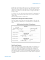
DECLARATION OF CONFORMITY
According to ISO/IEC Guide 22 and CEN/CENELEC EN 45014
Manufacturer’s Name:
Manufacturer’s Address:
Agilent Technologies, Incorporated
th
815 – 14 St. SW
Loveland, CO 80537
USA
Declares under sole responsibility that the product as originally delivered
Product Name:
Model Number:
Multifunction Switch / Measure Unit
34980A, 34921A/T, 34922A/T, 34923A/T, 34924A/T,
34925A/T, 34931A/T, 34932A/T, 34933A/T, 34937A/T,
34938A/T, 34941A, 34942A, 34945A/EXT, 34946A,
34947A, 34950A/T, 34951A/T, 34952A/T, 34959A
This declaration covers all options of and accessories to
the above products
Product Options:
complies with the essential requirements of the following applicable European Directives, and
carries the CE marking accordingly:
Low Voltage Directive (73/23/EEC, amended by 93/68/EEC)
EMC Directive (89/336/EEC, amended by 93/68/EEC)
and conforms with the following product standards:
EMC
Standard
Limit
IEC 61326-1:1997+A1:1998 / EN 61326-1:1997+A1:1998
CISPR 11:1990 / EN 55011:1991
IEC 61000-4-2:1995+A1:1998 / EN 61000-4-2:1995
IEC 61000-4-3:1995 / EN 61000-4-3:1995
IEC 61000-4-4:1995 / EN 61000-4-4:1995
IEC 61000-4-5:1995 / EN 61000-4-5:1995
IEC 61000-4-6:1996 / EN 61000-4-6:1996
IEC 61000-4-11:1994 / EN 61000-4-11:1994
Group 1 Class A
4 kV CD, 4 kV AD
3 V/m, 80-1000 MHz
0.5 kV signal lines, 1 kV power lines
0.5 kV line-line, 1 kV line-ground
3 V, 0.15-80 MHz, 80% mod
Interrupt: 10 ms, 20 ms
Canada: ICES-001:1998
Australia/New Zealand: AS/NZS 2064.1
The product was tested in a typical configuration with Agilent Technologies test systems.
IEC 61010-1:2001 / EN 61010-1:2001
Canada: CSA C22.2 No. 61010.1:2004
USA: UL 61010-1: 2004
Safety
Supplementary Information:
This DoC applies to above-listed products placed on the EU market after:
24 May 2005
Date
Ray Corson
Product Regulations Program Manager
For further information, please contact your local Agilent Technologies sales office, agent or distributor,
or Agilent Technologies Deutschland GmbH, Herrenberger Straße 130, D 71034 Böblingen, Germany.
Template: A5971-5302-2, Rev. B.00
34980A-DoC-D
DoC Revision D
iii
Contents
1 Introduction to the 34980A
Front Panel at a Glance
2
Rear Panel at a Glance
3
Rear Panel Connector Pinouts 4
External Trigger/Alarms Connector (Male D-Sub)
Analog Bus Connector (Female D-Sub) 4
Annunciator Display Indicators
Front Panel Menu Reference
Instrument Rack Mounting
4
5
6
7
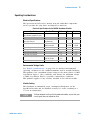
2 Features and Functions
Clearing 34980A Memory
10
SCPI Language Conventions 11
Rules for Using a Channel List
11
General Measurement Configuration 13
Overview of Measurement Modes 13
Analog Buses 16
Measurement Functions 17
Measurement Range 18
Measurement Resolution 19
Custom A/D Integration Time 20
Autozero 22
Trigger Delay 23
Automatic Trigger Delays 24
Safety Interlock 25
User-Defined Channel Labels 26
2-Wire Versus 1-Wire Mode 28
Analog Bus and Internal DMM Considerations
Environmental Operating Conditions 29
Electrical Operating Conditions 30
Temperature Measurement Configuration
Measurement Units 31
Thermocouple Measurements 32
RTD Measurements 34
Thermistor Measurements 35
34980A User’s Guide
29
31
v
Voltage Measurement Configuration
DC Input Resistance 36
AC Low Frequency Filter 37
36
Resistance Measurement Configuration
Offset Compensation 38
Current Measurement Configuration
AC Low Frequency Filter 39
39
Frequency Measurement Configuration
Low Frequency Timeout 40
Mx+B Scaling
38
40
41
Scanning 43
Rules for Scanning 43
Adding Channels to the Scan List 45
Scan Trigger Source 47
Trigger Count 52
Sweep Count 53
Sample Count 54
Channel Delay 56
Automatic Channel Delays 57
Reading Format 59
Non-Sequential Scanning 60
Viewing Readings Stored in Memory 61
Monitor Mode
63
Scanning With External Instruments
65
Alarm Limits 68
Viewing Stored Alarm Data 72
Using the Alarm Output Lines 74
Using Alarms With the Digital Modules
76
Sequences 79
Defining a Sequence 80
Querying the Sequence Definition 82
Executing a Sequence 83
Executing a Sequence on an Alarm Condition
Deleting Sequences 86
Reading the List of Stored Sequences 86
vi
84
34980A User’s Guide
System-Related Operations 87
Firmware Revision 87
Product Firmware Updates 88
Instrument State Storage 88
Error Conditions 89
Self-Test 91
Front-Panel Display Control 91
Front-Panel Number Format 92
Real-Time System Clock 93
Internal DMM Disable 93
Relay Cycle Count 94
SCPI Language Version 94
Calibration Overview 95
Calibration Security 95
Calibration Count 97
Calibration Message 98
Remote Interface Configuration
GPIB Interface 100
USB Interface 100
LAN Interface 100
Factory Reset State
99
109
Instrument Preset State
111
3 Introduction to the Plug-In Modules for the 34980A
Slot and Channel Addressing Scheme
Interconnection Solutions Overview
114
115
Module Considerations 116
General Considerations 116
Environmental Operating Conditions 116
Electrical Operating Conditions 118
4 Low Frequency Multiplexer Switch Modules
Low Frequency Multiplexer Switch Modules 120
Measurement Functions for the MUX Modules 121
SCPI Programming Examples for the MUX Modules 122
34921A 40-Channel Armature Multiplexer with Low Thermal Offset
34921A Simplified Schematic 128
34921A D-Sub Connectors 129
34921T Terminal Block 130
34922A 70-Channel Armature Multiplexer
34922A Simplified Schematic 133
34922A D-Sub Connectors 134
34922T Terminal Block
136
34980A User’s Guide
126
132
vii
34923A 40/80-Channel Reed Multiplexer 137
34923A Simplified Schematic for Two- or Four-Wire Mode 140
34923A D-Sub Connectors for Two- or Four-Wire Mode 141
34923T-001 Terminal Block for Two- or Four-Wire Mode
142
34923A Simplified Schematic for One-Wire Mode 143
34923A D-Sub Connectors for One-Wire Mode 144
34923T-002 Terminal Block for One-Wire Mode
145
34924A 70-Channel Reed Multiplexer 146
34924A Simplified Schematic 148
34924A D-Sub Connectors 149
34924T Terminal Block
151
34925A 40/80-Channel Optically-Isolated FET Multiplexer
152
34925A Simplified Schematic for Two- or Four-Wire Mode 155
34925A D-Sub Connectors for Two- or Four-Wire Mode 156
34925T-001 Terminal Block for Two- or Four-Wire Mode
157
34925A Simplified Schematic for One-Wire Mode 158
34925A D-Sub Connectors for One-Wired Mode 159
34925T-002 Terminal Block for One-Wire Mode
160
5 Matrix Switch Modules
Matrix Switch Modules 162
SCPI Programming Examples for the Matrix Modules
Linking Multiple Matrix Modules 166
163
34931A Dual 4x8 Armature Matrix 168
34931A Simplified Schematic 169
34931A D-Sub Connectors 170
34931T Terminal Block
171
34932A Dual 4x16 Armature Matrix
173
34932A Simplified Schematic
174
34932A D-Sub Connectors 175
34932T Terminal Block 176
34933A Dual/Quad 4x8 Reed Matrix 177
34933A Simplified Schematic for Two-Wire Mode
179
34933A D-Sub Connectors for Two-Wire Mode 180
34933T-001 Terminal Block for Two-Wire Mode 181
34933A Simplified Schematic for One-Wire Mode
183
34933A D-Sub Connectors for One-Wire Mode 184
34933T-002 Terminal Block for One-Wire Mode 185
viii
34980A User’s Guide
6 General Purpose Switch Modules
General Purpose Switch Modules
188
34937A and 34938A SCPI Programming Examples
190
34937A 32-Channel GP Switch 192
34937A Simplified Schematic
192
34937A D-Sub Connectors 193
34937T Terminal Block
194
34938A 20-Channel High-Current GP Switch
34938A Simplified Schematic 195
34938A D-Sub Connectors 196
34938T Terminal Block 197
195
7 RF Multiplexer Switch Modules
34941A and 34942A RF Multiplexer Switch Modules
Installing SMA Connectors 201
Isolating Connector Banks 201
34941A and 34942A SCPI Programming Examples
34941A and 34942A Simplified Schematic
203
200
202
8 Microwave Switch/Attenuator Driver
34945A Microwave Switch/Attenuator Driver 206
Recommended Switches and Attenuators 210
Power Supplies 211
Channel Numbering 212
Simple Switch Control 213
Remote Module Identifiers 214
Drive Modes 214
Using Single Drive Switches and Attenuators 215
Using Dual Drive Switches and Attenuators 216
Using Pulse Drive 217
Long Execution Times 218
Verifying Switch State
218
LED Drive 220
Default and Reset States 221
Distribution Boards 224
Mounting the Remote Modules 257
SCPI Programming Examples 258
9 Dual/Triple Microwave Switch Modules
34946A and 34947A Dual/Triple Microwave Switch Modules
34946A and 34947A SCPI Programming Examples 263
Installing SMA Connectors 264
34946A and 34947A Simplified Schematics 264
34980A User’s Guide
262
ix
10 64-Bit Digital I/O Module with Memory and Counter
34950A 64-Bit Digital I/O Module with Memory and Counter
Basic Digital I/O Operations 267
Handshaking 270
Buffered I/O Operations 277
Interrupt Lines 281
Byte Ordering 282
Pattern Matching 284
Counter 285
Clock 287
34950A D-Sub Connectors
287
34950T Terminal Block 290
266
11 4-Channel Isolated D/A Converter with Waveform Memory Module
34951A 4-Channel Isolated D/A Converter with Waveform Memory Module
34951A SCPI Programming Examples 295
34951A Simplified Block Diagrams 299
34951A D-Sub Connector Pinout 300
34951T Terminal Block
301
292
12 Multifunction Module with DIO, D/A, and Totalizer
34952A Multifunction Module 304
Digital Input/Output 304
Totalizer Input 304
Analog Output (DAC) 304
34952A SCPI Programming Examples 305
34952A Simplified Block Diagram 307
34952A D-Sub Connector 308
34952T Terminal Block
309
13 Breadboard Module
34959A Breadboard Module Description
34959A Breadboard Module Disassembly
312
313
34959A Breadboard Module Layout (shown with cover removed)
Ribbon Cable Header Pin Assignment Information
315
Configuring the 34959A Breadboard Module 317
Accessing the 34980A Mainframe’s Analog Bus 317
Installing Custom Circuitry on the 34959A Breadboard Module
Operating Considerations 321
Dimension Information for the Custom PC Board Area
Programming the 34959A Breadboard Module
Analog Bus Relay Functions 326
General Purpose Relay Functions 327
Digital I/O Functions 328
x
314
319
322
326
34980A User’s Guide
Agilent 34980A Multifunction Switch/Measure Unit
User’s Guide
1
Introduction to the 34980A
Front Panel at a Glance 2
Rear Panel at a Glance 3
Rear Panel Connector Pinouts 4
Annunciator Display Indicators 5
Front Panel Menu Reference 6
Instrument Rack Mounting 7
Agilent Technologies
1
1
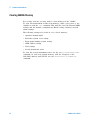
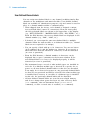
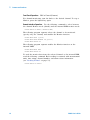
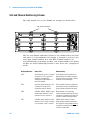
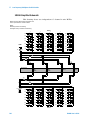
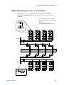
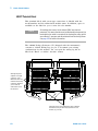
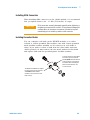
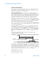
Introduction to the 34980A
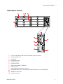
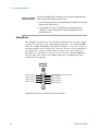
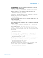
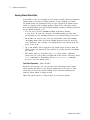
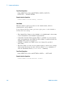
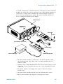
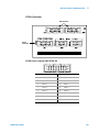
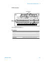
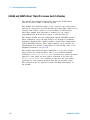
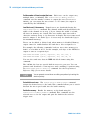
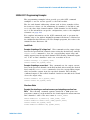
Front Panel at a Glance
1
2
3
4
5
6
7
8
9
10
11
12
13
2
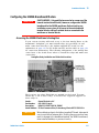
WARNING This switch is standby only. To disconnect the mains from the instrument,
On/Standby switch WARNINGss
remove the power cord.
Utility menu contains settings for Remote I/O (LAN, GPIB, and USB), Date and Time, and other
system-related instrument parameters
Store/recall menu allows you to save and recall up to six instrument setups
Control keys directly control module actions
Number keypad enters numerical characters
Exponent
Cancel key exits a menu without saving changes
Arrow keys move cursor positions
Knob enters alphanumeric characters, selects slots, channels, and navigates menus
Enter key steps you through a menu or saves number entries
Running a program puts the display into “remote” and disables the front panel keys. Local takes you out of
“remote” mode and enables the front panel keys.
Configure keys select functions and set function parameters
Measure keys execute and monitor measurements. Depending on which measurement key you use, you can
have complete/direct control over the switching and measurement operation, or you can have the 34980A
automatically control these to capture the desired data.
34980A User’s Guide
1
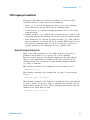
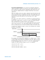
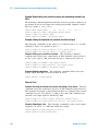
Introduction to the 34980A
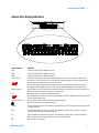
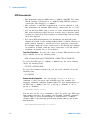
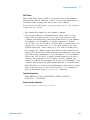
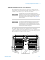
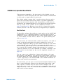
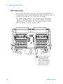
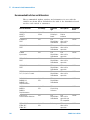
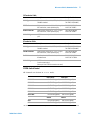
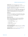
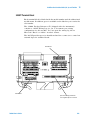
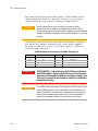
Rear Panel at a Glance
1
2
3
4
5
6
7
8
9
10
11
12
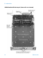
Access to Analog Buses (shown with cover installed). For pinout, see page 4.
Module installed in slot 1
Slot identifier
Module ground screw
Slot cover over slot 2
AC power connector
LAN connector (10Base T/100Base Tx)
USB 2.0 connector
External trigger input. For pinout, see page 4.
Internal DMM option mark. If you ordered the internal DMM option, the circle is marked black.
IEEE 488.2 GPIB Connector
Chassis ground screw
34980A User’s Guide
3
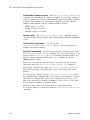
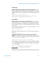
1
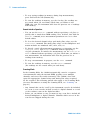
Introduction to the 34980A
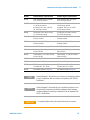
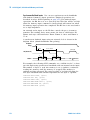
Rear Panel Connector Pinouts
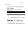
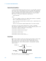
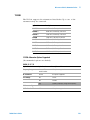
External Trigger/Alarms Connector (Male D-Sub)
Input
5V
0V
6
9
1
5
Ext Trig Input /
Chan Adv Input (Pin 6)
> 1 µs
Output
Gnd (Pin 9)
3.3 V
Chan Closed Output /
VM Comp Output (Pin 5)
0V
Approx. 2 µs
or
Alarm 1 Output (Pin 1)
Alarm 2 Output (Pin 2)
Alarm 3 Output (Pin 3)
Alarm 4 Output (Pin 4)
Gnd (Pin 9)
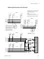
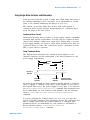
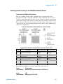
Analog Bus Connector (Female D-Sub)
ANALOG
BUSSES
ABus1 HI (Pin 9)
ABus2 HI (Pin 8)
ABus3 HI (Pin 7)
ABus4 HI (Pin 6)
4
9
5
6
1
Internal DMM Current Input I (Pin 5)
ABus1 LO (Pin 4)
ABus2 LO (Pin 3)
ABus3 LO (Pin 2)
ABus4 LO (Pin 1)
34980A User’s Guide
1
Introduction to the 34980A
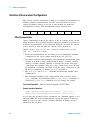
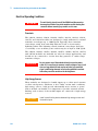
Annunciator Display Indicators
Display Indicator
LAN
USB
GPIB
ABUS [1234]
ERROR
Rmt
Safety Interlock
Trig
HOT
ALARM (H1234L)
Definition
Communicating with the 34980A over LAN.
Communicating with the 34980A over USB.
Communicating with the 34980A over GPIB.
Analog Bus Connectivity. Normally, designated ABus connected on any module in mainframe.
During scan, if ABus 1 and ABus 2 are indicated, they will be used at some point during the scan.
An error has been generated and is in the error queue.
Remote. Running a program puts the display into “remote” and disables the front panel keys.
Pressing the LOCAL button takes you out of “remote” mode and enables the front panel keys.
ABus Safety Interlock. Terminal block or cables have been removed from the D-sub connector of a
module. For more information, see page 120 and page 162.
Waiting for external or manual trigger during scans.
Over-temperature condition. One or more general purpose (34937A/34938A) modules have reached
their over-temperature limits.
HI or LO alarm condition has occurred on the indicated alarms.
Alarms are enabled on the displayed channel.
Mx+B
4W
OC
*
34980A User’s Guide
Scaling enabled on channel. This appears on display after you select scaling function via front panel
or remote interface.
4-wire measurement specified on channel. This appears on display after you select the 4-wire
function via the front panel or remote interface.
Offset Compensation specified on channel. This appears on display after you have selected the
offset compensation function via the front panel or remote interface.
Measurement is in progress.
5
1
Introduction to the 34980A
Front Panel Menu Reference
This section gives an overview of the top two levels of menus that you
access from the front panel. The menus are designed to automatically
guide you through all parameters required to configure a particular
function or operation.
Store/Recall
Store and recall instrument states
• Store up to six instrument states in non-volatile memory
• Assign a name to each storage location.
• Recall stored states, power-down state, factory reset state, or preset state
Utility
•
•
•
•
•
•
Configure system-related instrument parameters
Connecting and configuring to use with LAN, GPIB, or USB
Set the real time clock and calendar
Set radix character, thousand separator
Enable/disable the internal DMM
Secure/unsecure the instrument for calibration
Query and update the firmware revisions for the mainframe and modules
Configure Key Group
Set parameters for measurement
DMM
• Set DMM measurement function (AC volts, DC volts, AC current, DC current, 2-wire ohms, 4-wire ohms,
temperature, frequency, and period)
• Set function parameters
Channel
• Set channel measurement function (AC volts, DC volts, AC current (34921A only), DC current (34921A only)
2-wire ohms, 4-wire ohms, temperature, frequency, and period
• Set function parameters
Scan
• Set up trigger-in parameters
• Set up sweep count
• Set up sample count
Sequence
• View sequence command string
• Execute sequence
• Delete sequence definitions
Module
• Open all relays
• Clear all measurement functions
• Clear channel labels
• Configure external trigger and clock (34951A)
• Set trace or level mode (34951A)
• Set waveform parameters (34951A)
6
34980A User’s Guide
1
Introduction to the 34980A
View
• View errors and alarms
• View the scanned readings from memory
• View errors in the error queue
• Read the number of cycles for the displayed relay (relay maintenance feature)
Advanced
Available at a later firmware release
Alarm
• Select one of four alarms to report alarm conditions on the displayed channel
• Configure a high limit, a low limit, or both for the displayed channel
• Select the slope (rising or falling edge) for the four alarm output lines
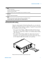
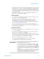
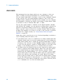
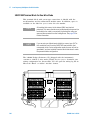
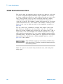
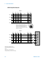
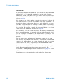
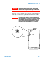
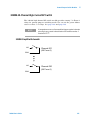
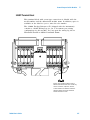
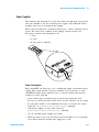
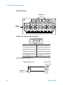
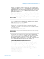
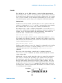
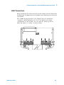
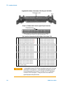
Instrument Rack Mounting
Using the optional Agilent Y1130A Rack Mount Kit, you can mount the
34980A in a standard 19- inch rack cabinet. This kit includes rack mount
brackets and associated hardware required to forward or reverse mount
the instrument in the rack cabinet.
• For forward rack mounting (34980A front panel facing the front of
the cabinet), use the Agilent standard rack mount kit (part number
5063- 9214). For Agilent rack cabinets, use the E3663A Basic Rail Kit
(sold separately).
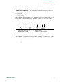
• For reverse rack mounting (34980A rear panel facing the front of
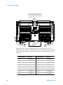
the cabinet), use the longer brackets (see figure below) with the
hardware for the standard rack mount kit. For Agilent rack cabinets,
use the E3664AC Third Party Rail Kit (sold separately).
Reverse Rack Mount Orientation (longer brackets used)
34980A User’s Guide
7
1
Introduction to the 34980A
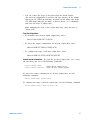
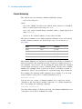
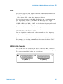
425.6 mm (16.76 in)
367.7 mm (14.48 in)
101.9 mm (4.01 in)
or
70.4 mm (2.78 in)
Agilent 34980A Dimensions (shown with Reverse Rack Mount brackets installed)
8
34980A User’s Guide
Agilent 34980A Multifunction Switch/Measure Unit
User’s Guide
2
Features and Functions
Clearing 34980A Memory 10
SCPI Language Conventions 11
General Measurement Configuration 13
Analog Bus and Internal DMM Considerations 29
Temperature Measurement Configuration 31
Voltage Measurement Configuration 36
Resistance Measurement Configuration 38
Current Measurement Configuration 39
Frequency Measurement Configuration 40
Mx+B Scaling 41
Scanning 43
Monitor Mode 63
Scanning With External Instruments 65
Alarm Limits 68
Sequences 79
System-Related Operations 87
Calibration Overview 95
Remote Interface Configuration 99
Factory Reset State 109
Instrument Preset State 111
You will find that this chapter makes it easy to look up all the details
about a particular feature of the Agilent 34980A. Whether you are
operating the instrument from the front panel or over the remote
interface, this chapter will be useful. For information specific to the
34980A plug- in modules, see the later chapters in this manual.
N O TE
For complete details on the SCPI (Standard Commands for Programmable
Instruments) commands, see the Programmer’s Reference Help file
included on the Agilent 34980A Product Reference CD-ROM.
Agilent Technologies
9
2
Features and Functions
Clearing 34980A Memory
For security reasons, you may want to clear memory in the 34980A.
To clear all measurement results from memory, either cycle power to the
34980A or send the *RST command. This will also clear the internal DMM
settings and all channel configurations, Mx+B scaling constants, and all
alarm settings.
The following settings are stored in non- volatile memory:
• Optional channel labels
• Real- time system clock setting
• Front- panel number format setting
• GPIB address setting
• LAN settings
• Stored instrument states
To clear the stored instrument states, use the MEMory:STATe:DELete:ALL
command. To clear non- volatile memory, with the exception of the
LAN MAC address and USB ID, use the SYSTem:SECurity:IMMediate
command.
10
34980A User’s Guide
Features and Functions
2
SCPI Language Conventions
Throughout this guide, the following conventions are used for SCPI
command syntax for remote interface programming:
• Braces ( { } ) enclose the parameter choices for a given command
string. The braces are not sent with the command string.
• A vertical bar ( | ) separates multiple parameter choices for a given
command string.
• Triangle brackets ( < > ) indicate that you must specify a value for the
enclosed parameter. The brackets are not sent with the command string.
• Some parameters are enclosed in square brackets ( [ ] ). This indicates
that the parameter is optional and can be omitted. The brackets are not
sent with the command string. If you do not specify a value for an
optional parameter, the instrument chooses a default value.
Rules for Using a Channel List
Many of the SCPI commands for the 34980A include a channel list
parameter which allows you to specify one or more channels.
From the remote interface, the channel number has the form (@sccc),
where s is the mainframe slot number (1 through 8) and ccc is the
channel number. You can specify a single channel, multiple channels,
or a range of channels.
The following command closes channel 10 on the module in slot 3.
ROUT:CLOS (@3010)
The following command closes channels 10, 12, and 15 on the module
in slot 2.
ROUT:CLOS (@2010,2012,2015)
The following command closes channels 5 through 10 (slot 1) and channel
15 (slot 2). When you specify a range of channels, any channels that are
invalid will be ignored (no error will be generated) but the first and last
channel in the range must be valid.
ROUT:CLOS (@1005:1010,2015)
34980A User’s Guide
11
2
Features and Functions
The Analog Bus relays (numbered s911, s912, s913, etc.) on the
multiplexer and matrix modules are ignored if they are included in a
range of channels. An error will be generated if an Analog Bus relay is
specified as the first or last channel in a range of channels. For example,
the following command closes all valid channels between channel 30
(slot 1) and channel 5 (slot 2). In addition, this command closes Analog
Bus relay 911 on the module in slot 1 (Bank 1). Note that although the
specified range of channels includes the other Analog Bus relays, they are
ignored and are not closed by this command.
ROUT:CLOS (@1030:2005,1911)
The following command will generate an error since the Analog Bus relays
cannot be specified as the first or last channel in a range of channels
(none of the channels will be closed).
ROUT:CLOS (@1005:1911)
!Generates an error
In the following command, since the optional <ch_list> parameter is
omitted, the command will be applied to the internal DMM. If the internal
DMM is disabled or is not present, an error will be generated.
INP:IMP:AUTO ON
12
!Applies to the internal DMM
34980A User’s Guide
Features and Functions
2
General Measurement Configuration
This section contains general information to help you configure the
instrument for making measurements. Since these parameters are used
by several measurement functions, the discussion is combined into one
common section. Refer to the later sections in this chapter for more
information on parameters that are specific to each measurement function.
Overview of Measurement Modes
Two modes of operation are available with the 34980A, depending on the
level of switching and measurement that you wish to directly control:
the Stand- Alone DMM Mode and the Scanning Mode.
Stand-Alone DMM Mode
In the Stand- Alone DMM Mode, the internal DMM makes measurements of
whatever signals are present on the Analog Buses. In this mode, you have
full control of what channel relays are closed and connected to the
appropriate Analog Bus for the measurement. You can route your signals
directly to the internal DMM using the 34980A multiplexer and matrix
modules, or you can connect to external signals via the Analog Bus
connector located on instrument’s rear panel (see “Analog Buses” on
page 16).
Front Panel Operation:
• To configure the most common measurement parameters for the
internal DMM, use the DMM (Configure) key.
• To close the desired channel relays and Analog Bus relays, use the
Close key. The Analog Bus relays on the multiplexer and matrix modules
are numbered s911, s912, s913, etc.
• To auto- trigger the internal DMM and display continuous readings,
press the DMM (Measure) key. Press the DMM (Measure) key again to stop
taking measurements.
• For additional triggering control and to store DMM readings in memory,
use the Scan (Configure) key to set the triggering parameters, and then
press and hold the Scan (Measure) key to initiate the DMM measurement.
These selections are available only for stand- alone DMM use when a
scan list has not been defined (see “Stand- Alone DMM Mode” on
page 13).
34980A User’s Guide
13
2
Features and Functions
• To stop storing readings in memory during long measurements,
press and hold the Scan (Measure) key.
• To view the readings in memory, use the View key (the readings are
not erased when you read them). Each time you initiate a new
DMM- only scan, the instrument will clear the previous set of readings
from memory.
Remote Interface Operation:
• You can use the MEASure? command without specifying a <ch_list> to
quickly take a stand- alone DMM reading. Note, however, that with the
MEASure? command, most measurement parameters are set to their
default values.
• To close the desired channel relays and Analog Bus relays, use the
ROUTe:CLOSe command. The Analog Bus relays on the multiplexer and
matrix modules are numbered s911, s912, s913, etc.
• To directly control all measurement parameters or triggering, use the
CONFigure, SENSe, and TRIGger commands without specifying a
<ch_list> parameter. To initiate the measurement, use the INITiate or
READ? command without specifying a <ch_list>. Each time you initiate a
new measurement, the instrument will clear the previous set of
readings from memory.
• To stop a measurement in progress, use the ABORt command.
• To view the readings in memory, use the FETCh? command
(the readings are not erased when you read them).
Scanning Mode
In the Scanning Mode, the 34980A automatically controls a sequence
of measurements using the internal DMM, possibly across multiple
channels, and stores the results in memory. The 34980A closes and
opens the appropriate channel relays and Analog Bus relays required
for the sequence. The following general rules apply to the Scanning Mode
(for more information on using the Scanning Mode, see “Scanning” on
page 43.)
• Any channel that can be “read” by the instrument can also be included
in a scan. A scan can also include a read of a digital channel or a read
of the totalizer count on the digital modules.
• Before you can initiate a scan, you must set up a scan list to include all
desired multiplexer or digital channels. Channels which are not in the
scan list are skipped during the scan.
14
34980A User’s Guide
Features and Functions
2
• The Analog Bus relays are automatically opened and closed as required
during the scan to connect to the internal DMM for the measurement.
For example, all 2- wire measurements use the ABus1 (MEAS) relays
for 4- wire measurements, the ABus2 (SENS) relays are used in addition
to the ABus1 relays.
• Each time you initiate a new scan, the instrument will clear the
previous set of readings from memory.
Front Panel Operation:
• To configure the measurement parameters and add a channel to the
scan list, use the Channel (Configure) key.
• To initiate a scan and store all readings in memory, press the
Scan (Measure) key. If you press the Scan (Measure) key with no
scan list defined, the instrument initiates a DMM- only measurement
(see “Stand- Alone DMM Mode” below).
• To stop a scan in progress, press and hold the Scan (Measure) key.
• To view the readings in memory, use the View key (the readings are not
erased when you read them).
Remote Interface Operation:
• To define the list of channels to be included in the scan list, use the
ROUTe:SCAN command.
• To configure the measurement parameters on the desired channels,
use the CONFigure and SENSe commands.
• To initiate a scan and store all readings in memory, use the INITiate
or READ? command. Each time you initiate a new scan, the instrument
will clear the previous set of readings from memory.
• To stop a scan in progress, use the ABORt command.
• To view the readings in memory, use the FETCh? command
(the readings are not erased when you read them).
N O TE
You can use the READ? command in one of three forms depending on
which measurement mode you wish to use.
• If you omit the optional <ch_list> parameter and a scan list is not
currently defined, the READ? command applies to the internal DMM.
• If you omit the optional <ch_list> parameter and a scan list is currently
defined, the READ? command performs a scan of the channels in the
scan list.
• If you specify a <ch_list>, regardless of whether a scan list is currently
defined, the READ? command performs a “temporary” scan of the
specified channels (independent of the present scan list).
34980A User’s Guide
15
2
Features and Functions
N O TE
You can use the MEASure? command in one of two forms depending on
which measurement mode you wish to use.
• If you omit the optional <ch_list> parameter, the MEASure? command
applies to the internal DMM.
• If you specify a <ch_list>, the MEASure? command performs a
“temporary” scan of the specified channels (independent of the
present scan list).
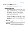
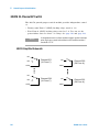
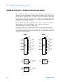
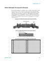
Analog Buses
The 34980A provides four 2- wire internal Analog Buses for easier signal
routing. You can route your measurements directly to the internal DMM
using the 34980A multiplexer and matrix modules, or you can connect to
external signals via the Analog Bus connector located on the instrument’s
rear panel (see connector pinout below). Since four 2- wire buses are
provided, you can dedicate one bus for use with the internal DMM and
use the other three buses for module extensions or additional signal
routing between modules.
ANALOG
BUSSES
ABus1 HI (Pin 9)
ABus2 HI (Pin 8)
ABus3 HI (Pin 7)
ABus4 HI (Pin 6)
9
5
6
1
Internal DMM Current Input I (Pin 5)
ABus1 LO (Pin 4)
ABus2 LO (Pin 3)
ABus3 LO (Pin 2)
ABus4 LO (Pin 1)
Analog Bus connector (as viewed from rear of instrument)
16
34980A User’s Guide
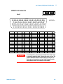
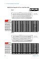
Features and Functions
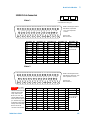
2
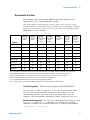
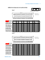
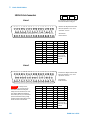
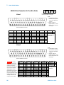
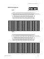
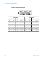
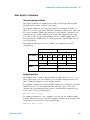
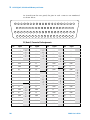
Measurement Functions
The following table shows which DMM measurement functions are
supported by each of the multiplexer modules.
Note that similar considerations must be taken into account on the
34931A, 34932A, and 34933A matrix modules. Since the matrix modules
cannot be incorporated into a scan list, you must use the Stand- Alone
DMM Mode for these modules.
34921A
40-Ch Arm
MUX
34922A
70-Ch Arm
MUX
34923A
40-Ch Reed
MUX
(2-Wire)
34923A
80-Ch Reed
MUX
(1-Wire)
34924A
70-Ch Reed
MUX
34925A
40-Ch FET
MUX
(2-Wire)
34925A
80-Ch FET
MUX
(1-Wire)
Voltage, AC/DC
Yes
Yes
Yes
Yes
Yes
Yes
Yes
Current, AC/DC
Yes1
No
No
No
No
No
No
Frequency/Period
Yes
Yes
Yes
Yes
Yes
Yes
Yes
Ohms 2-Wire
Yes
Yes
Yes5
Yes5
Yes5
Yes6
Yes6
Ohms 4-Wire
Yes
Yes
Yes5
No
Yes5
Yes6
No
Thermocouple
Yes2
Yes3
Yes3,4
Yes3,4
Yes3,4
Yes3
Yes3
RTD 2-Wire
Yes
Yes
Yes5
Yes5
Yes5
No
No
RTD 4-Wire
Yes
Yes
Yes5
No
Yes5
Yes6
No
Yes
Yes5
Yes5
Yes5
No
No
Function
Thermistor
1 Direct
Yes
current measurements are allowed on channels 41 through 44 only (for all other channels, external shunts are required).
2 Optional 34921T Terminal Block is required for thermocouple measurements with built-in internal reference junction.
3 A fixed or external reference junction temperature is required for thermocouple measurement with this module.
4 Impact of higher offset voltage specification (< 50 µV) must be taken into
consideration.
or higher range used unless 100Ω series resistors are bypassed on module.
6 10 kΩ or higher range used for loads over approximately 300Ω due to series resistance of FET channels.
5 1 kΩ
Front Panel Operation:
DMM or Channel (Configure) > DMM MEASUREMENT
Use the knob (or numeric keypad) to select the desired channel. Then
select the desired measurement function for this channel. You are
automatically guided to the next level of the menu where you can
configure other measurement parameters (range, integration time, etc.).
Remote Interface Operation: You can select the measurement function using
the CONFigure and MEASure? commands. For example, the following
command configures the specified channel for dc voltage measurements.
CONF:VOLT:DC 10,DEF,(@3001)
34980A User’s Guide
17
2
Features and Functions
Measurement Range
You can allow the instrument to automatically select the measurement
range using autoranging or you can select a fixed range using manual
ranging. Autoranging is convenient because the instrument decides which
range to use for each measurement based on the input signal. For fastest
scanning operation, use manual ranging on each measurement (some
additional time is required for autoranging since the instrument has to
make a range selection).
• Autorange thresholds:
Down range at:
Up range at:
<10% of range
>120% of range
• If the input signal is greater than can be measured on the selected
range (manual ranging), the instrument gives an overload indication:
“±OVLD” from the front panel or “±9.9E+37” from the remote interface.
• For temperature measurements, the instrument internally selects the
range you cannot select which range is used. For thermocouple
measurements, the instrument internally selects the 100 mV range.
For thermistor and RTD measurements, the instrument autoranges to
the correct range for the transducer resistance measurement.
• For frequency and period measurements, the instrument uses one
“range” for all inputs between 3 Hz and 300 kHz. The range parameter
is required only to specify the resolution. Therefore, it is not necessary
to send a new command for each new frequency to be measured.
• The CONFigure and MEASure? commands contain an optional parameter
which allows you to specify the range or autoranging.
• The instrument returns to autoranging when the measurement function
is changed and after a Factory Reset (*RST command). An Instrument
Preset (SYSTem:PRESet command) or Card Reset (SYSTem:CPON
command) does not change the range setting.
Front Panel Operation:
DMM or Channel (Configure) > RANGE
First, select the measurement function on the active channel. You are
automatically guided to the next level of the menu where you can select
a specific range or autoranging.
Remote Interface Operation: You can select the range using parameters in
the CONFigure and MEASure? commands. For example, the following
command selects the 10 Vdc range on the specified channel.
CONF:VOLT:DC 10,DEF,(@3001)
18
34980A User’s Guide
2
Features and Functions
Measurement Resolution
Resolution is expressed in number of digits the internal DMM can
measure or display on the front panel. You can set the resolution to 4, 5,
or 6 full digits, plus a “½” digit which can be “0” or “1”. To increase the
measurement accuracy and improve noise rejection, select 6½ digits.
To increase the measurement speed, select 4½ digits.
• For ac voltage measurements, the resolution is fixed at 6½ digits.
The only way to control the reading rate for ac measurements is by
changing the channel delay (see page 56) or by setting the ac filter to
the highest frequency limit (see page 37).
• The specified resolution is used for all measurements on the selected
channel. If you have applied Mx+B scaling or have assigned alarms to
the selected channel, those measurements are also made using the
specified resolution. Measurements taken during the Monitor function
also use the specified resolution.
• Changing the number of digits does more than just change the
resolution of the instrument. It also changes the integration time,
which is the period the instrument’s analog- to- digital (A/D) converter
samples the input signal for a measurement. See “Custom A/D
Integration Time” on page 20 for more information.
• The CONFigure and MEASure? commands contain an optional parameter
which allows you to specify the resolution.
• The instrument returns to 5½ digits when the measurement function is
changed and after a Factory Reset (*RST command). An Instrument
Preset (SYSTem:PRESet command) or Card Reset (SYSTem:CPON
command) does not change the resolution setting.
Front Panel Operation:
DMM or Channel (Configure) > INTEGRATION > NPLC
First, select the measurement function on the active channel. You are
automatically guided to the next level of the menu where you can select a
specific resolution.
Remote Interface Operation: Specify the resolution in the same units as
the measurement function, not in number of digits. For example, if the
function is dc voltage, specify the resolution in volts. For frequency,
specify the resolution in hertz.
You can select the resolution using parameters in the CONFigure and
MEASure? commands. For example, the following command selects the
10 Vdc range with 4½ digits of resolution on the specified channel.
CONF:VOLT:DC 10,0.001,(@3001)
34980A User’s Guide
19
2
Features and Functions
The following command selects the 1 A range with 6½ digits of resolution
on channel 2041 (current measurements are allowed only on channels 41
through 44 on the 34921A).
MEAS:CURR:AC? 1,1E-6,(@2041)
You can also select the resolution using the SENSe commands. For example,
the following command specifies a 2- wire ohms measurement with 100Ω of
resolution on channel 1003.
SENS:RES:RES 100,(@1003)
Custom A/D Integration Time
Integration time is the period of time the internal DMM’s analog- to- digital
(A/D) converter samples the input signal for a measurement. Integration
time affects the measurement resolution (for better resolution, use a longer
integration time) and measurement speed (for faster measurements, use a
shorter integration time).
• Integration time is specified in number of power line cycles (PLCs).
Select from 0.02, 0.2, 1, 2, 10, 20, 100, or 200 power line cycles.
The default is 1 PLC.
• Only integral number of power line cycles (1, 2, 10, 20, 100, or 200
PLCs) provide normal mode (line frequency noise) rejection.
• You can also specify integration time directly in seconds (this is called
aperture time). Select a value between 300 µs and 1 second, with
4 µs resolution.
• The only way to control the reading rate for ac measurements is by
changing the channel delay (see “Channel Delay” on page 56) or by
setting the ac filter to the highest frequency limit (see “AC Low
Frequency Filter” on page 37).
• The specified integration time is used for all measurements on the
selected channel. If you have applied Mx+B scaling or have assigned
alarms to the selected channel, those measurements are also made
using the specified integration time. Measurements taken during the
Monitor function also use the specified integration time.
20
34980A User’s Guide
Features and Functions
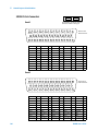
2
• The following table shows the relationship between integration time,
measurement resolution, number of digits, and number of bits.
Relationship between integration time, resolution, digits, and bits
Integration Time
Resolution
Digits
Bits
0.02 PLC
0.2 PLC
1 PLC
2 PLC
10 PLC
20 PLC
100 PLC
200 PLC
< 0.0001 x Range
< 0.00001 x Range
< 0.000003 x Range
< 0.0000022 x Range
< 0.000001 x Range
< 0.0000008 x Range
< 0.0000003 x Range
< 0.00000022 x Range
4½ Digits
5½ Digits
5½ Digits
6½ Digits
6½ Digits
6½ Digits
6½ Digits
6½ Digits
15
18
20
21
24
25
26
26
• The instrument selects 1 PLC when the measurement function is
changed and after a Factory Reset (*RST command). An Instrument
Preset (SYSTem:PRESet command) or Card Reset (SYSTem:CPON
command) does not change the integration time setting.
Front Panel Operation:
DMM or Channel (Configure) > INTEGRATION > TIME
First, select the measurement function on the active channel. You are
automatically guided to the next level of the menu where you can select
a specific integration time.
Remote Interface Operation: You can set the integration time using the
SENSe commands. For example, the following command specifies an
aperture time of 2 ms for resistance measurements on channel 2001.
SENS:RES:APER 0.002,(@2001)
34980A User’s Guide
21
2
Features and Functions
Autozero
When autozero is enabled (default), the instrument internally
disconnects the input signal following each measurement, and takes a
zero reading. It then subtracts the zero reading from the preceding
reading. This prevents offset voltages present on the instrument’s input
circuitry from affecting measurement accuracy.
When autozero is disabled, the instrument takes one zero reading and
subtracts it from all subsequent measurements. It takes a new zero reading
each time you change the function, range, or integration time.
• Applies to temperature, dc voltage, resistance, temperature, and
dc current measurements only.
• The autozero mode is set indirectly when you set the resolution and
integration time. Autozero is automatically turned off when you select
an integration time less than 1 PLC.
• The CONFigure and MEASure? commands automatically enable autozero.
• The autozero setting is stored in volatile memory, and does not change
when power has been off, after a Factory Reset (*RST command), or
after an Instrument Preset (SYSTem:PRESet command).
Front Panel Operation:
DMM or Channel (Configure) > AUTO ZERO
Remote Interface Operation: The OFF and ONCE parameters have a similar
effect. Autozero OFF does not issue a new zero measurement. Autozero
ONCE issues an immediate zero measurement.
[SENSe:]<function>:ZERO:AUTO {OFF|ONCE|ON} [,(@<ch_list>)]
22
34980A User’s Guide
2
Features and Functions
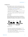
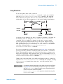
Trigger Delay
In some applications, you want to allow the input to settle before taking a
reading or for pacing a burst of readings. You can add a trigger delay,
which adds a delay between the trigger signal and the first sample taken
by the internal DMM (not used in Scanning Mode). The programmed
trigger delay overrides the default trigger delay that the instrument
automatically adds to the measurement.
Trigger 1
Sample Count
Trigger 2
Sample Count
t
Trigger Delay
(0 to 3600 seconds)
Trigger delay
• The default trigger delay is Automatic (see “Automatic Trigger
Delays” on page 24); the instrument determines the delay based on
function, range, and integration time.
• If you specify a trigger delay other than Automatic, that same delay is
used for all functions and ranges.
• If you have configured the instrument to take more than one reading
per trigger (sample count > 1), the specified trigger delay is inserted
between the trigger and the first reading in the sample burst.
• The CONFigure and MEASure? commands set the trigger delay to
Automatic.
• The instrument selects an automatic trigger delay after a Factory Reset
(*RST command). An Instrument Preset (SYSTem:PRESet command) or
Card Reset (SYSTem:CPON command) does not change the setting.
34980A User’s Guide
23
2
Features and Functions
Automatic Trigger Delays
If you do not specify a trigger delay, the instrument selects a delay
for you. The delay is determined by the function, range, integration time,
and ac filter setting as shown below.
DC Voltage, Thermocouple, DC Current (for all ranges):
Integration Time
Trigger Delay
PLC > 1
PLC ≤ 1
2.0 ms
1.0 ms
Resistance, RTD, Thermistor (2- and 4-wire):
Range
Trigger Delay
(for PLC > 1)
Range
Trigger Delay
(for PLC ≤ 1)
100Ω
1 kΩ
10 kΩ
100 kΩ
1 MΩ
10 MΩ
100 MΩ
2.0 ms
2.0 ms
2.0 ms
25 ms
30 ms
200 ms
200 ms
100Ω
1 kΩ
10 kΩ
100 kΩ
1 MΩ
10 MΩ
100 MΩ
1.0 ms
1.0 ms
1.0 ms
20 ms
25 ms
200 ms
200 ms
AC Voltage, AC Current (for all ranges):
AC Filter
Trigger Delay
Slow (3 Hz)
Medium (20 Hz)
Fast (200 Hz)
7.0 seconds
1.0 second
120 ms
Frequency, Period:
AC Filter
Trigger Delay
Slow (3 Hz)
Medium (20 Hz)
Fast (200 Hz)
600 ms
300 ms
100 ms
Digital Input, Totalize:
Trigger Delay
0 seconds
24
34980A User’s Guide
2
Features and Functions
Safety Interlock
The Safety Interlock feature prevents connections to the Analog Buses
if no terminal block or properly- wired cable is connected to a module
(available on multiplexer and matrix modules only).
Normally, if you attempt to connect to the Analog Buses without a
terminal block or properly- wired cable connected, an error is generated.
You can, however, temporarily disable errors generated by the Safety
Interlock feature. This simulation mode may be useful during test system
development when you may not have connected any terminal blocks or
cables to your module.
This feature is available from the remote interface only
CAU T ION
The Safety Interlock feature is implemented in hardware on the modules
and cannot be circumvented. Regardless of whether the simulation mode
is enabled or disabled, all Analog Bus connections are prohibited as long
as no terminal block or properly-wired cable is connected to the module.
• The simulation mode applies to the entire mainframe and cannot be
selectively used on individual modules.
• When the simulation mode is enabled, the Analog Bus relays will
appear to close and open as directed. For example, no errors are
generated if you close an Analog Bus relay from the front panel, remote
interface, or Web Interface. However, remember that the Safety Interlock
feature prevents the actual hardware state of the Analog Bus relays
from being changed. When you connect a terminal block or cable to the
module, the Analog Bus relays will be closed.
• The simulation setting is stored in volatile memory and will be lost
when power is turned off. To re- enable the simulation mode after
power has been off, you must send the command again.
Remote Interface Operation:
34980A User’s Guide
SYSTem:ABUS:INTerlock:SIMulate {OFF|ON}
25
2
Features and Functions
User-Defined Channel Labels
You can assign user- defined labels to any channel, including Analog Bus
channels on the multiplexer and matrix modules. User- defined channel
labels are available for identification purposes only and cannot be used in
place of a channel number within a command string.
• When shipped from the factory, each channel is assigned a unique
factory- default label (cannot be overwritten). From the front panel,
the factory- default labels are shown on the upper line of the display
(e.g., “MUX CH BANK 1”, “MATRIX1 ROW3 COL4”, “DIO BYTE 1”, etc.).
From the Web Interface, the factory- default labels are displayed as the
channel number (e.g., “1001”, “3020”, etc.).
• If desired, you can assign the same user- defined label to multiple
channels within the same module or on different modules (i.e., channel
labels are not required to be unique).
• You can specify a label with up to 18 characters. You can use letters
(A- Z), numbers (0- 9), and the underscore character. If you specify a
label with more than the allowed 18 characters, it will be truncated
(no error is generated).
• From the Web Interface, a limited number of characters can be
displayed due to space constraints in the browser window. If the
user- defined label it too long to be displayed properly, it will be
truncated (no error is generated).
• The instrument keeps a record of what module types are installed in
each slot. If a different module type is detected in a specific slot at
power on, all user- defined channel labels for that slot are discarded.
If an empty slot is detected at power- on, any previously- defined labels
for that slot are preserved and will be restored if the same module type
is installed later; however, if a module of a different type is installed
in that slot, the previously- defined labels will be discarded.
• All user- defined channel labels are stored in non- volatile memory,
and do not change when power has been off, after a Factory Reset
(*RST command), after an Instrument Preset (SYSTem:PRESet
command), or after a stored state is recalled (*RCL command).
26
34980A User’s Guide
Features and Functions
Front Panel Operation:
2
Channel (Configure) > CHANNEL LABEL
To define the channel label, press the arrow keys to move the cursor to a
specific position and then turn the knob to select the desired letter or
number.
To clear the channel label on the selected channel, change each character
to “ ^ ” (starting with the rightmost character) and then press the left
arrow key to move to the next character.
To clear all channel labels on the selected module, navigate to:
Module (Configure) > CLEAR LABELS? > YES
Remote Interface Operation: The following command assigns a label
(“TEST_PT_1”) to channel 3 in slot 1.
ROUT:CHAN:LABEL "TEST_PT_1",(@1003)
The following command clears the user- defined label previously assigned
to channel 3 in slot 1. The channel will now be identified by its factory
default label (e.g., “MUX CH BANK 1”, “MATRIX1 ROW3 COL4”,
“DIO BYTE 1”, etc.).
ROUT:CHAN:LABEL "",(@1003)
The following command clears all user- defined channel labels on the
module in slot 1. The factory- default labels are assigned to all channels on
the module in slot 1.
ROUT:CHAN:LABEL:CLEAR:MOD 1
The following command clears all user- defined labels on all modules
installed in the 34980A. The factory- default labels are assigned to all
channels on all installed modules.
ROUT:CHAN:LABEL:CLEAR:MOD ALL
34980A User’s Guide
27
2
Features and Functions
2-Wire Versus 1-Wire Mode
You can configure the 34923A, 34925A, and 34933A modules for 2- wire
(differential) or 1- wire (single ended) measurements. If you change the
module configuration, you must cycle power on the 34980A to activate the
new setting.
• To determine whether the module is in the 2- wire or 1- wire
configuration, check the module description shown on the front panel
when the module is selected, or send the SYSTem:CTYPe? or
SYSTem:CDEScription? command. For example, the SYSTem:CTYPe?
response for the 34923A will be either “34923A” (differential mode) or
“34923A- 1W” (single- ended mode).
• If you are using terminal blocks with these modules, be sure to use the
corresponding 2- wire or 1- wire terminal block.
• The module configuration is stored in non- volatile memory on the
module and does not change when you remove the module from the
mainframe, after a Factory Reset (*RST command), or after an
Instrument Preset (SYSTem:PRESet command).
Front Panel Operation:
Module (Configure) > MODE NEXT POWER-ON
After selecting the 2- wire (“WIRE2”) or 1- wire (“WIRE1”), you must cycle
power on the 34980A to activate the new setting.
Remote Interface Operation: The following command selects the 1- wire
configuration on the module in slot 3. The new configuration will not take
effect until you cycle power on the 34980A.
SYST:MOD:WIRE:MODE WIRE1,3
28
34980A User’s Guide
2
Features and Functions
Analog Bus and Internal DMM Considerations
This section provides important environmental and electrical
considerations that can affect mainframe operation.
Environmental Operating Conditions
The 34980A mainframe, including the optional internal DMM, is designed
to operate in a temperature range of 0 °C to +55 °C with non- condensing
humidity. The maximum humidity is 80% at 40 °C or higher. Do not use in
locations where conductive dust or electrolytic salt dust may be present.
The 34980A should be operated in an indoor environment where
temperature and humidity are controlled. Condensation can pose a
potential shock hazard. Condensation can occur when the instrument is
moved from a cold to a warm environment, or if the temperature and/or
humidity of the environment changes quickly.
When used in pollution degree 1 conditions, the maximum voltage rating
for the Analog Buses is 300V. When used in pollution degree 2 conditions,
the maximum voltage rating is 100V. If conditions change, ensure that
condensation has evaporated and the instrument has thermally stabilized
until pollution degree 1 conditions are restored before turning on power to
the equipment.
34980A User’s Guide
N O TE
Pollution Degree 1: No pollution or only dry, non-conductive pollution
occurs. The pollution has no influence (on insulation) (IEC 61010-1
2nd Edition).
N O TE
Pollution Degree 2: Normally only non-conductive pollution occurs.
Occasionally, a temporary conductivity (leakage current between isolated
conductors) caused by condensation can be expected (IEC 61010-1
2nd Edition).
29
2
Features and Functions
Electrical Operating Conditions
WARN IN G
To avoid electric shock, turn off the 34980A and disconnect or
de-energize all field wiring to the modules and the Analog Bus
connector before removing any module or slot cover.
Transients
The Analog Buses and the optional internal DMM are designed to safely
withstand occasional transient overvoltages up to 1000 Vpeak. Typically,
these transient overvoltages result from switching inductive loads or from
nearby lightning strikes. The lightning- caused transient overvoltages that
may occasionally occur on mains power outlets may be as high as
2500 Vpeak.
WARN IN G
Do not connect the Analog Buses directly to a mains power outlet.
If it is necessary to measure a mains voltage or any circuit where a
large inductive load may be switched, you must add signal conditioning
elements to reduce the potential transients before they reach the
Analog Buses.
High Energy Sources
The Analog Buses and the optional internal DMM are designed to handle
inputs up to their rated currents or their rated powers, whichever is less.
Under certain fault conditions, high energy sources could provide
substantially more current or power than the instrument can handle. It is
important to provide external current limiting, such as fuses, if the inputs
are connected to high- energy sources.
CAU T ION
30
Install current limiting devices between high energy sources and the
module inputs.
34980A User’s Guide
2
Features and Functions
Temperature Measurement Configuration
This section contains information to help you configure the instrument
for making temperature measurements. The table below shows the
thermocouple, RTD, and thermistor types for which the instrument
supports direct measurements.
Temperature transducers supported
Thermocouple Types *
RTD Types
Thermistor Types
B, E, J, K, N, R, S, T
R0 = 49Ω to 2.1 kΩ
α = 0.00385 (DIN/IEC 751) *
α = 0.00391 †
2.2 kΩ, 5 kΩ, 10 kΩ
(YSI 44000 Series)
* Using ITS-90 software conversions.
† Using IPTS-68 software conversions.
Measurement Units
• The instrument can report temperature measurements in °C (Celsius),
°F (Fahrenheit), or K (Kelvins). You can mix temperature units on
different channels within the instrument and on the same module.
• The CONFigure and MEASure? commands automatically select °C.
• Setting the Mx+B measurement label to °C, °F, or K has no effect on
the temperature measurement units currently selected.
• The instrument selects Celsius when the probe type is changed and
after a Factory Reset (*RST command). An Instrument Preset
(SYSTem:PRESet command) or Card Reset (SYSTem:CPON command) does
not change the units setting.
Front Panel Operation:
DMM or Channel (Configure) > TEMPERATURE > UNITS
Remote Interface Operation:
34980A User’s Guide
UNIT:TEMP {C|F|K}[,(@<ch_list>)]
31
2
Features and Functions
Thermocouple Measurements
• The instrument supports the following thermocouple types: B, E, J, K,
N, R, S, and T using ITS- 90 software conversions. The default is a
J- Type thermocouple.
• Thermocouple measurements require a reference junction temperature.
For the reference junction temperature, you can use an internal
measurement on the module (34921A only), an external thermistor
or RTD measurement, or a known fixed junction temperature.
• The internal reference junction source is valid only on channels 1
through 40 on the 34921A with the 34921T terminal block installed.
• If you select an external reference, the instrument makes
thermocouple measurements relative to a previously- stored RTD or
thermistor measurement stored in a reference register. To store a
reference temperature, first configure a multiplexer channel for an
RTD or thermistor measurement. Then assign the measurement
from that channel as the external reference. When you initiate a
measurement on an external reference channel, the acquired
temperature is stored in volatile memory in the reference register.
Subsequent thermocouple measurements use the stored temperature
as their reference. The temperature remains in memory until you
measure a subsequent external reference value in the reference
register or remove the mainframe power.
• If you select a fixed reference temperature, specify a value between
- 20 °C and +80 °C (always specify the temperature in °C regardless
of the temperature units currently selected).
• The accuracy of the measurement is highly dependent upon the
thermocouple connections and the type of reference junction used.
Use a fixed temperature reference for the highest accuracy
measurements (you must maintain the known junction temperature).
The internal isothermal block reference (34921A only) requires no
external wiring but provides lower accuracy measurements than a fixed
reference.
• The thermocouple check feature allows you to verify that your
thermocouples are properly connected for measurements. If you enable
this feature, the instrument measures the channel resistance after
each thermocouple measurement to ensure a proper connection. If an
open connection is detected (greater than 5 kΩ on the 10 kΩ range),
the instrument reports an overload condition for that channel
(or displays “OPEN T/C” on the front panel).
32
34980A User’s Guide
Features and Functions
2
Front Panel Operation: To select the thermocouple function on the active
channel, choose the following items.
DMM or Channel (Configure) > TEMPERATURE > PROBE TYPE > THERMOCOUPLE
Then, use the knob to select the thermocouple type from the list.
THERMOCOUPLE TYPE > B|E|J|K|N|R|S|T
If desired, you can enable the thermocouple check feature on the active
channel (opens are reported as “OPEN T/C”).
T/C CHECK > OFF|ON
To select the reference junction source for the active channel, choose one
of the following items.
REFERENCE > FIXED|EXT|INT
For an external reference, configure an RTD or thermistor as the external
reference channel.
Channel (Configure) > TEMPERATURE > PROBE TYPE > RTD > . . . USE AS EXT REF?
Remote Interface Operation: You can use the CONFigure or MEASure?
command to select the probe type and thermocouple type. For example,
the following command configures channel 3001 for a J- type thermocouple
measurement.
CONF:TEMP TC,J,(@3001)
You can also use the SENSe command to select the probe type and
thermocouple type. For example, the following command configures
channel 2003 for a J- type thermocouple measurement.
SENS:TEMP:TRAN:TC:TYPE J,(@2003)
The following commands use the SENSe command to set a fixed reference
junction temperature of 40 degrees (always in °C) on channel 2003.
SENS:TEMP:TRAN:TC:RJUN:TYPE,(@2003)
SENS:TEMP:TRAN:TC:RJUN 40,(@2003)
The following command enables the thermocouple check feature on the
specified channel (opens are reported as “+9.90000000E+37”).
SENS:TEMP:TRAN:TC:CHECK ON,(@2003)
34980A User’s Guide
33
2
Features and Functions
RTD Measurements
• The instrument supports RTDs with α = 0.00385 (DIN/IEC 751) using
ITS- 90 software conversions or α = 0.00391 using IPTS- 68 software
conversions. The default is α = 0.00385.
• The resistance of an RTD is nominal at 0 °C and is referred to as R0.
The instrument can measure RTDs with R0 values from 49Ω to 2.1 kΩ.
• You can measure RTDs using a 2- wire or 4- wire measurement method.
The 4- wire method provides the most accurate way to measure small
resistances. Connection lead resistance is automatically removed using
the 4- wire method.
• For 4- wire RTD measurements, the instrument automatically pairs
channel n in Bank 1 with channel n+20 in Bank 2 (34921A, 34923A) or
n+35 (34922A, 34924A) to provide the source and sense connections.
For example, make the source connections to the HI and LO terminals
on channel 2 in Bank 1 and the sense connections to the HI and LO
terminals on channel 22 (or 37) in Bank 2.
Front Panel Operation: To select the 2- wire or 4- wire RTD function for the
active channel, choose the following items.
DMM or Channel (Configure) > TEMPERATURE > PROBE TYPE > RTD|4W RTD
To select the RTD type (α = 0.00385 or 0.00391) for the active channel,
choose the following item.
RTD TYPE > 0.00391|0.00385
To select the nominal resistance (R0) for the active channel, choose the
following item.
RO > 100 OHM
Remote Interface Operation: You can use the CONFigure or MEASure?
command to select the probe type and RTD type. For example, the
following command configures channel 3001 for 2- wire measurements of
an RTD with α = 0.00385 (use “85” to specify α = 0.00385 or “91” to
specify α = 0.00391).
CONF:TEMP RTD,85,(@3001)
You can also use the SENSe command to select the probe type, RTD type,
and nominal resistance. For example, the following command configures
channel 1003 for 4- wire measurements of an RTD with α = 0.00391
(channel 1003 is automatically paired with channel 1023 for the 4- wire
measurement).
SENS:TEMP:TRAN:FRTD:TYPE 91,(@1003)
34
34980A User’s Guide
Features and Functions
2
The following command sets the nominal resistance (R0) to 1000Ω on
channel 1003.
SENS:TEMP:TRAN:FRTD:RES 1000,(@1003)
Thermistor Measurements
The instrument supports 2.2 kΩ (YSI Series 44004), 5 kΩ (YSI Series 44007),
and 10 kΩ (YSI Series 44006) thermistors.
Front Panel Operation: To select the thermistor function for the active
channel, choose the following items.
DMM or Channel (Configure) > TEMPERATURE > PROBE TYPE > THERMISTOR
To select the thermistor type for the active channel, choose from the
following items.
THERMISTOR TYPE > 10K|5K|2.2K
Remote Interface Operation: You can use the CONFigure or MEASure?
command to select the probe type and thermistor type. For example,
the following command configures channel 3001 for measurements of a
5 kΩ thermistor:
CONF:TEMP THER,5000,(@3001)
You can also use the SENSe command to select the probe type and
thermistor type. For example, the following command configures channel
1003 for measurements of a 10 kΩ thermistor:
SENS:TEMP:TRAN:THERM:TYPE 10000,(@1003)
34980A User’s Guide
35
2
Features and Functions
Voltage Measurement Configuration
This section contains information to help you configure the instrument for
making voltage measurements. The instrument can measure dc and true
RMS ac- coupled voltages on the measurement ranges shown below.
100 mV
1V
10 V
100 V
300 V
Autorange
DC Input Resistance
Normally, the instrument’s input resistance is fixed at 10 MΩ for all
dc voltage ranges to minimize noise pickup. To reduce the effects of
measurement loading errors, you can set the input resistance to greater
than 10 GΩ for the 100 mVdc, 1 Vdc, and 10 Vdc ranges.
Applies to dc voltage measurements only.
DC input resistance
Input Resistance Setting
Input Resistance for:
100 mV, 1 V, 10 V ranges
Input Resistance for:
100 V, 300 V ranges
Input Resistance: Auto OFF
Input Resistance: Auto ON
10 MΩ
> 10 GΩ
10 MΩ
10 MΩ
• The CONFigure and MEASure? commands automatically select AUTO OFF
(fixed at 10 MΩ for all ranges).
• The instrument selects 10 MΩ (fixed input resistance on all dc voltage
ranges) after a Factory Reset (*RST command). An Instrument Preset
(SYSTem:PRESet command) or Card Reset (SYSTem:CPON command)
does not change the input resistance setting.
Front Panel Operation:
DMM or Channel (Configure) > INPUT RESISTANCE
Remote Interface Operation: You can enable or disable the automatic
input resistance mode on the specified channels or the internal DMM.
With AUTO OFF (default), the input resistance is fixed at 10 MΩ for all
ranges. With AUTO ON, the input resistance is set to >10 GΩ for the three
lowest dc voltage ranges.
[SENSe:]<function>:IMPedance:AUTO {OFF|ON} [,(@<ch_list>)]
If you omit the optional <ch_list> parameter, the command applies to the
internal DMM.
36
34980A User’s Guide
2
Features and Functions
AC Low Frequency Filter
The instrument uses three different ac filters which enable you to either
optimize low- frequency accuracy or achieve faster ac settling times.
The instrument selects the slow (3 Hz), medium (20 Hz), or fast (300 Hz)
filter based on the input frequency that you specify for the selected
channels or the internal DMM.
Applies to ac voltage and ac current measurements only.
AC low frequency filter
Input Frequency
Default Settling Delay
Minimum Settling Delay
3 Hz to 300 kHz (Slow)
20 Hz to 300 kHz (Medium)
200 Hz to 300 kHz (Fast)
7 seconds / reading
1 second / reading
0.12 seconds / reading
1.5 seconds
200 ms
20 ms
• The CONFigure and MEASure? commands automatically select the 20 Hz
(medium) filter.
• The instrument selects the default 20 Hz (medium) filter after a Factory
Reset (*RST command). An Instrument Preset (SYSTem:PRESet command) or
Card Reset (SYSTem:CPON command) does not change the setting.
Front Panel Operation:
DMM or Channel (Configure) > AC FILTER
Remote Interface Operation: Specify the lowest frequency expected in
the input signal on the specified channels. The instrument selects the
appropriate filter based on the frequency you specify (see table above).
[SENSe:]VOLTage:AC:BANDwidth {3|20|200} [,(@<ch_list>)]
If you omit the optional <ch_list> parameter, the command applies to the
internal DMM.
34980A User’s Guide
37
2
Features and Functions
Resistance Measurement Configuration
This section contains information to help you configure the instrument for
making resistance measurements. Use the 2- wire method for ease of
wiring and higher density or use the 4- wire method for improved
measurement accuracy. The measurement ranges shown below.
100Ω
1 kΩ
10 kΩ
100 kΩ
1 MΩ
10 MΩ
100 MΩ
Autorange
Offset Compensation
Offset compensation removes the effects of any dc voltages in the circuit
being measured. The technique involves taking the difference between two
resistance measurements on the specified channels, one with the current
source turned on and one with the current source turned off.
Applies only to 2- wire and 4- wire resistance measurements on the
100Ω, 1 kΩ, and 10 kΩ ranges.
• Four- wire measurements are not allowed on the multiplexer modules
configured for the 1- wire (single ended) mode (see page 28).
• For 4- wire resistance measurements, the instrument automatically pairs
channel n in Bank 1 with channel n+20 in Bank 2 (34921A, 34923A,
34925A) or n+35 (34922A, 34924A) to provide the source and sense
connections. For example, make the source connections to the HI and
LO terminals on channel 2 in Bank 1 and the sense connections to the
HI and LO terminals on channel 22 (or 37) in Bank 2.
• The CONFigure and MEASure? commands automatically disable offset
compensation.
• The instrument disables offset compensation after a Factory Reset
(*RST command). An Instrument Preset (SYSTem:PRESet command) or
Card Reset (SYSTem:CPON command) does not change the setting.
Front Panel Operation:
DMM or Channel (Configure) > OFFSET COMP
Remote Interface Operation:
[SENSe:]FRESistance:OCOMpensated {OFF|ON} [,(@<ch_list>)]
[SENSe:]RESistance:OCOMpensated {OFF|ON} [,(@<ch_list>)]
If you omit the optional <ch_list> parameter, the command applies to the
internal DMM. For 4- wire measurements, specify the paired channel in
Bank 1 (source) as the <ch_list> channel (channels in Bank 2 are not
allowed in the <ch_list>).
38
34980A User’s Guide
2
Features and Functions
Current Measurement Configuration
This section contains information to help you configure the instrument
for making current measurements on the 34921A multiplexer module.
The module has four fused channels for direct dc and ac current
measurements on the ranges shown below.
10 mA
100 mA
1A
Autorange
Current measurements are allowed only on channels 41 through 44
on the 34921A module.
AC Low Frequency Filter
The instrument uses three different ac filters which enable you to either
optimize low- frequency accuracy or achieve faster ac settling times.
The instrument selects the slow (3 Hz), medium (20 Hz), or fast (300 Hz)
filter based on the input frequency that you specify for the selected
channels or the internal DMM.
Applies to ac current and ac voltage measurements only.
AC low frequency filter
Input Frequency
Default Settling Delay
Minimum Settling Delay
3 Hz to 300 kHz (Slow)
20 Hz to 300 kHz (Medium)
200 Hz to 300 kHz (Fast)
7 seconds / reading
1 second / reading
0.12 seconds / reading
1.5 seconds
200 ms
20 ms
• The CONFigure and MEASure? commands automatically select the 20 Hz
(medium) filter.
• The instrument selects the default 20 Hz (medium) filter after a Factory
Reset (*RST command). An Instrument Preset (SYSTem:PRESet command) or
Card Reset (SYSTem:CPON command) does not change the setting.
Front Panel Operation:
DMM or Channel (Configure) > AC FILTER
Remote Interface Operation: Specify the lowest frequency expected in
the input signal on the specified channels. The instrument selects the
appropriate filter based on the frequency you specify (see table above).
[SENSe:]CURRent:AC:BANDwidth {3|20|200} [,(@<ch_list>)]
If you omit the optional <ch_list> parameter, the command applies to the
internal DMM.
34980A User’s Guide
39
2
Features and Functions
Frequency Measurement Configuration
This section contains information to help you configure the instrument for
making frequency measurements.
Low Frequency Timeout
The instrument uses three different timeout ranges for frequency
measurements. The instrument selects the slow (3 Hz), medium (20 Hz),
or fast (300 Hz) filter based on the input frequency that you specify with
this command for the selected channels.
Applies to frequency measurements only.
Low frequency timeout
Input Frequency
Timeout
3 Hz to 300 kHz (Slow)
20 Hz to 300 kHz (Medium)
200 Hz to 300 kHz (Fast)
1 second
100 ms
10 ms
• The CONFigure and MEASure? commands automatically select the 20 Hz
(medium) filter.
• The instrument selects the default 20 Hz (medium) filter after a Factory
Reset (*RST command). An Instrument Preset (SYSTem:PRESet command) or
Card Reset (SYSTem:CPON command) does not change the setting.
Front Panel Operation:
DMM or Channel (Configure) > AC FILTER
Remote Interface Operation: Specify the lowest frequency expected in the
input signal on the specified channels. The instrument selects the
appropriate timeout based on the frequency you specify (see table above).
[SENSe:]FREQuency:RANGe:LOWer {3|20|200} [,(@<ch_list>)]
If you omit the optional <ch_list> parameter, the command applies to the
internal DMM.
40
34980A User’s Guide
2
Features and Functions
Mx+B Scaling
The scaling function allows you to apply a gain and offset to readings
during a scan or while making measurements in the stand- alone DMM
mode. In addition to setting the gain (“M”) and offset (“B”) values, you can
also specify a custom measurement label for your scaled readings (RPM,
PSI, etc.). You can apply scaling to any multiplexer channels and for any
measurement function. Scaling is not allowed with any of the channels on
the digital modules.
• Scaling is applied using the following equation:
Scaled Reading = (Gain x Measurement) + Offset
• If you change the measurement configuration (function, transducer type,
etc.) on a channel or the internal DMM, scaling is turned off on those
channels but the gain and offset values are not cleared.
• If you plan to use scaling on a channel which will also use alarms,
be sure to configure the scaling values first. If you attempt to assign
the alarm limits first, the instrument will turn off alarms and clear the
limit values when you enable scaling on that channel. If you specify a
custom measurement label with scaling, it is automatically used when
alarms are logged on that channel.
• If you redefine the scan list, no change will be made to the scaling
state or the gain and offset values. If you decide to add a channel back
to the scan list, the original gain and offset values are restored.
• You can specify a custom label with up to three characters. You can use
letters (A- Z), numbers (0- 9), an underscore ( _ ), blank spaces, or the
“#” character which displays a degree symbol ( ° ) on the front panel
(displayed as a “#” in an output string from the remote interface).
• The maximum value allowed for the gain and offset is ±1E+15.
• The CONFigure and MEASure? commands automatically set the gain
(“M”) to 1 and offset (“B”) to 0.
• A Factory Reset (*RST command) turns off scaling, clears the scaling
values on all channels, and sets the custom label to a null string (“ ”).
An Instrument Preset (SYSTem:PRESet command) does not clear the
scaling values and does not turn off scaling.
34980A User’s Guide
41
2
Features and Functions
Front Panel Operation:
DMM or Channel (Configure) > SCALING > GAIN|OFFSET|UNITS
To define the label on the selected channel, press the arrow keys to move
the cursor to a specific position and then turn the knob to select the
desired letter or number. To clear the label on the selected channel,
change each character to “ ^ ” (starting with the rightmost character) and
then press the left arrow key to move to the next character.
Remote Interface Operation: Use the following commands to set the gain,
offset, and custom measurement label.
CALC:SCALE:GAIN 1.2,(@1003)
CALC:SCALE:OFFSET 10,(@1003)
CALC:SCALE:UNIT 'PSI',(@1003)
After setting the gain and offset values, send the following command to
enable the scaling function on the specified channel.
CALC:SCALE:STATE ON,(@1003)
42
34980A User’s Guide
Features and Functions
2
Scanning
The instrument allows you to combine a DMM (either internal or external)
with multiplexer channels to create a scan. During a scan, the instrument
connects the DMM to the configured multiplexer channels one at a time
and makes a measurement on each channel.
Any channel that can be “read” by the instrument can also be included in
a scan. This includes any combination of temperature, voltage, resistance,
current, frequency, or period measurements on multiplexer channels.
A scan can also include a read of a digital channel or a read of the
totalizer count on the digital modules. Scanning is allowed with the
following modules:
• 34921A through 34925A Multiplexer Modules
• 34950A Digital I/O Module (digital input and counter channels only)
• 34952A Multifunction Module (digital input and totalizer channels only)
Automated scanning is not allowed with the other switching modules.
In addition, a scan cannot include a write to a digital channel or a voltage
output from a DAC channel. You can, however, write your own program to
manually create a “scan” to include these operations.
Rules for Scanning
• Before you can initiate a scan, you must set up a scan list to include all
desired multiplexer or digital channels. Channels which are not in the
scan list are skipped during the scan. By default, the instrument scans
the list of channels in ascending order from slot 1 through slot 8
(channels are reordered as needed). If your application requires
non- ordered scanning of the channels in the present scan list, see
“Non- Sequential Scanning” on page 60. Measurements are taken only
during a scan and only on those channels which are included in the
scan list.
• You can store at least 500,000 readings in memory and all readings are
automatically time stamped. If memory overflows, a status register bit
is set and new readings will overwrite the first (oldest) readings stored.
The most recent readings are always preserved. You can read the
contents of memory at any time, even during a scan. Reading memory
is not cleared when you read it.
• Each time you start a new scan, the instrument clears all readings
(including alarm data) stored in reading memory from the previous
scan. Therefore, the contents of memory are always from the most
recent scan.
34980A User’s Guide
43
2
Features and Functions
• The Analog Bus relays are automatically opened and closed as required
during the scan to connect to the internal DMM for the measurement.
For example, all 2- wire measurements use the ABus1 (MEAS) relays; for
4- wire measurements, the ABus2 (SENS) relays are used in addition to
the ABus1 relays.
• When the scan is initiated, the instrument will open all channels in
banks that contain one or more channels in the scan list.
• In order to guarantee that no signals are connected to the Analog Buses
prior to the scan, the instrument will open all ABus1 relays (applies to
all banks in all slots). In banks that contain channels in the scan list,
the instrument will also open all ABus2 relays (regardless of whether
4- wire measurements are involved). If no channels configured for
4- wire measurements are included in the scan list, the state of the
ABus2 relays in the non- scanned banks is not altered.
• The state of the ABus3 and ABus4 relays is not altered and these relays
remain available for use during the scan. However, be sure to use
CAUTION when closing these relays on banks involved in the scan.
While the scan is running, any signals present on ABus3 and/or ABus4
will be joined with the scanned measurement on ABus1 and ABus2.
• While the scan is running, the instrument prevents use of all channels
in banks that contain one or more channels in the specified scan list
(these channels are dedicated to the scan). In addition, the instrument
prevents use of all ABus1 and ABus2 relays on banks containing
channels in the scan list. If one or more channels configured for 4- wire
measurements are included in the scan list, then the rules for ABus2
relay operations are extended to the non- scanned banks as well.
• If the ABus1 relay used for current measurements (channel 931 on
34921A only) is not closed prior to the initiation of the scan, the four
current channels (channels 41 through 44) are not affected by the scan.
However, if the ABus1 relay is closed, the instrument will open the
ABus1 relay as well as the four associated current channels in a
make- before- break fashion.
• When you add a digital read (digital modules) to a scan list, the
corresponding channel is dedicated to the scan. The instrument issues a
Card Reset to make that channel an input channel (the other channel is
not affected).
• While the scan is running, you can perform low- level control operations
on any channels on the digital modules that are not in the scan.
For example, you can output a DAC voltage or write to a digital channel
(even if the totalizer is part of the scan list). However, you cannot
change any parameters that affect the scan (channel configuration,
scan interval, Card Reset, etc.) while a scan is running.
• If a scan includes a read of the totalizer, the count is reset each time it
is read during the scan only when the totalizer reset mode is enabled.
44
34980A User’s Guide
Features and Functions
2
• At the end of the scan, the last channel that was scanned will be
opened (as well as any Analog Bus relays used during the scan).
Any channels that were opened during the scan will remain open at
the completion of the scan.
• If you abort a scan that is running, the instrument will terminate any
reading in progress (readings are not cleared from memory). If a scan
is in progress when the command is received, the scan will not be
completed and you cannot resume the scan from where it left off.
Note that if you initiate a new scan, all readings are cleared from memory.
• You can use either the internal DMM or an external instrument to make
measurements of your configured channels. However, the 34980A allows
only one scan list at a time; you cannot scan some channels using the
internal DMM and others using an external instrument. Readings are
stored in 34980A memory only when the internal DMM is used.
• The Monitor mode is automatically enabled on all channels that are
part of the active scan list (see “Monitor Mode” on page 63).
• The present scan list is stored in volatile memory and will be lost when
power is turned off or after a Factory Reset (*RST command).
Adding Channels to the Scan List
Before you can initiate a scan, you must set up a scan list to include all
desired multiplexer or digital channels. Channels which are not in the
scan list are skipped during the scan. By default, the instrument scans the
list of channels in ascending order from slot 1 through slot 8 (channels
are reordered as needed).
To Build a Scan List From the Front Panel
• To add the active channel to the scan list, press Channel (Configure).
Then select the function, range, resolution, and other parameters for
this channel. Then add the channel to the scan list by selecting:
SCAN THIS CHANNEL? > YES
• To remove the active channel from the scan list, select:
SCAN THIS CHANNEL? > NO
• To remove all channels from the scan list, select:
Scan (Configure) > CLEAR SCAN LIST? > YES
34980A User’s Guide
45
2
Features and Functions
• To initiate a scan and store all readings in memory, press
Scan (Measure). Each time you initiate a new scan, the instrument
clears all previously stored readings. If you have not defined a scan list,
Scan (Measure) performs an internal DMM scan independent of any
channels.
• To stop a scan in progress, press and hold Scan (Measure).
To Build a Scan List From the Remote Interface
• Use the ROUTe:SCAN command to define the list of channels in the scan
list. To determine what channels are currently in the scan list, use the
ROUTe:SCAN? query command.
• To add channels to the present scan list, use the ROUTe:SCAN:ADD
command. To remove channels from the present scan list, use the
ROUTe:SCAN:REMove command.
• To remove all channels from the scan list, send “ROUT:SCAN (@)”.
• To initiate a scan, use the INITiate or READ? command.
Measurements are stored in memory. Each time you initiate a new scan,
the instrument will clear the previous set of readings from memory.
• To stop a scan in progress, use the ABORt command.
46
34980A User’s Guide
2
Features and Functions
Scan Trigger Source
You can configure the event or action that controls the onset of each
sweep through the scan list (a sweep is one pass through the scan list):
• You can set the instrument’s internal timer to automatically scan at a
specific interval. You can also program a time delay between channels
in the scan list (see “Channel Delay” on page 56).
• You can manually control a scan by repeatedly pressing the
Scan (Measure) key from the front panel.
• You can start a scan by sending a software command from the remote
interface (MEASure? or INITiate command).
• You can start a scan when an external TTL trigger pulse is received.
• You can start a scan when an alarm event is logged on the channel
being monitored.
Interval Scanning
In this configuration, you control the frequency of scan sweeps by
selecting a wait period from the start of one trigger to the start of the
next trigger (called the trigger- to- trigger interval). If the scan interval
is less than the time required to measure all channels in the scan list, the
instrument will scan continuously, as fast as possible (no error is generated).
Trigger 1
Sweep 1
Sweep 2
Sweep n
Trigger 2
...
t
Trigger Timer
(0 to 359,999 seconds)
Trigger-to-trigger interval
• You can set the scan interval to any value between 0 seconds and
99:59:59 hours (359,999 seconds), with 1 ms resolution.
• Once you have initiated the scan, the instrument will continue scanning
until you stop it or until the trigger count is reached. See “Trigger
Count” on page 52 for more information.
• Mx+B scaling and alarm limits are applied to measurements during a
scan and all data is stored in volatile memory.
34980A User’s Guide
47
2
Features and Functions
• The CONFigure and MEASure? commands automatically set the scan
interval to immediate (0 seconds) and the scan count to 1 sweep.
• The instrument sets the scan interval to immediate (0 seconds) after a
Factory Reset (*RST command). An Instrument Preset (SYSTem:PRESet
command) or Card Reset (SYSTem:CPON command) does not change
the setting.
Front Panel Operation:
Scan (Configure) > INTERVAL > SCAN INTERVAL
To initiate the scan and store all readings in memory, press the
Scan (Measure) key. Between scan sweeps, “WAITING FOR TRIG” will be
displayed on the front panel.
Note: To stop a scan, press and hold the Scan (Measure) key.
Remote Interface Operation: The following program segment configures the
instrument for an interval scan.
TRIG:SOURCE TIMER
TRIG:TIMER 5
TRIG:COUNT 2
INIT
Select interval time mode
Set the scan interval to 5 seconds
Sweep the scan list 2 times
Initiate the scan
Note: To stop a scan, send the ABORt command.
Manual Scanning
In this configuration, the instrument waits for either a front- panel key
press or a remote interface command before sweeping through the
scan list.
• All readings from the scan are stored in volatile memory.
Readings accumulate in memory until the scan is terminated
(until the trigger count is reached or until you abort the scan).
• You can specify a trigger count which sets the number of front- panel
key presses or scan trigger commands that will be accepted before
terminating the scan. See “Trigger Count” on page 52 for more
information.
• Mx+B scaling and alarm limits are applied to measurements during a
manual scanning operation and all data is stored in volatile memory.
Front Panel Operation:
Scan (Configure) > INTERVAL > MANUAL
To initiate the scan and store all readings in memory, press the
Scan (Measure) key.
Note: To stop a scan, press and hold the Scan (Measure) key.
48
34980A User’s Guide
2
Features and Functions
Remote Interface Operation: The following program segment configures the
instrument for a manual scanning operation.
TRIG:SOURCE BUS
TRIG:COUNT 2
INIT
Select bus (manual) mode
Sweep the scan list 2 times
Initiate the scan
Then, send the *TRG (trigger) command to begin each scan sweep.
The *TRG command will not be accepted unless the internal DMM is in
the “wait- for- trigger” state.
Note: To stop a scan, send the ABORt command.
Scanning on Alarm
In this configuration, the instrument initiates a scan each time a reading
crosses an alarm limit on a channel. You can also assign alarms to
channels on the digital modules (34950A and 34952A). For example,
you can generate an alarm when a specific bit pattern or bit pattern
change is detected on a digital input channel or when a specific count is
reached on a totalizer channel.
N O TE
For complete details on configuring and using alarms, refer to
“Alarm Limits” on page 68.
• In this scan configuration, you may use the Monitor function to
continuously take readings on a selected channel and wait for an alarm
on that channel. Channels do not have to be part of an active scan list
to be monitored; however, the channel must be configured for a
measurement in order to be monitored.
• All readings from the scan are stored in volatile memory.
Readings accumulate in memory until the scan is terminated
(until the trigger count is reached or until you abort the scan).
• You can specify a trigger count which sets the number of front- panel
key presses or scan trigger commands that will be accepted before
terminating the scan. See “Trigger Count” on page 52 for more
information.
• Mx+B scaling and alarm limits are applied to measurements during a
manual scanning operation and all data is stored in volatile memory.
34980A User’s Guide
49
2
Features and Functions
Front Panel Operation:
Scan (Configure) > ALARM
To enable the Monitor function, select the desired channel and then press
the DMM or Channel (Measure) key. To initiate the scan, press the Scan
(Measure) key. When an alarm occurs, the scan starts and readings are
stored in memory.
Note: To stop a scan, press and hold the Scan (Measure) key.
You can also configure whether the instrument sweeps through the scan
list one time or continuously when an alarm condition is detected:
Scan (Configure) > ALARM > ALARM TRIG MODE > SINGLE|CONTIN
Remote Interface Operation: The following program segment configures the
instrument to continuously scan when an alarm is detected.
TRIG:SOURCE ALARM1
TRIG:SOURCE:ALARM CONT
Select alarm configuration
Select continuous scan mode
CALC:LIM:UPPER 10.25,(@1003)
CALC:LIM:UPPER:STATE ON,(@1003)
OUTPUT:ALARM1:SOURCE (@1003)
Set upper alarm limit
Enable alarms
Report alarms on Alarm 1
ROUT:MON:CHAN (@1003)
ROUT:MON:CHAN:ENABLE ON,(@1003)
ROUT:MON:STATE ON
Select monitor channel
Enable monitoring on channel
Enable monitor mode
INIT
Initiate the scan
Note: To stop a scan, send the ABORt command.
50
34980A User’s Guide
Features and Functions
2
External Scanning
In this configuration, the instrument sweeps through the scan list once
each time a low- going TTL pulse is received on the rear- panel Ext Trig
Input line (pin 6).
6
1
Input
Ext Trig Input (Pin 6)
5V
0V
9
5
Gnd (Pin 9)
> 1 µs
Ext Trig Input connector (as viewed from rear of instrument)
• You can specify a scan count which sets the number of external pulses
the instrument will accept before terminating the scan. See “Trigger
Count” on page 52 for more information.
• If the instrument receives an external trigger before it is ready to
accept one, it will buffer one trigger and then ignore any additional
triggers received (no error is generated).
• All readings from the scan are stored in volatile memory.
Readings accumulate in memory until the scan is terminated
(until the scan count is reached or until you abort the scan).
• Mx+B scaling and alarm limits are applied to measurements during the
scan and all data is stored in volatile memory.
Front Panel Operation:
Scan (Configure) > INTERVAL > EXTERNAL
To initiate the scan and store all readings in memory, press the
Scan (Measure) key. Between scan sweeps, “WAITING FOR TRIG” will be
displayed on the front panel. When a TTL pulse is received, the scan
starts and readings are stored in memory.
Note: To stop a scan, press and hold the Scan (Measure) key.
34980A User’s Guide
51
2
Features and Functions
Remote Interface Operation: The following program segment configures the
instrument for an external scan.
Select external mode
Sweep the scan list 2 times
Initiate the scan
TRIG:SOURCE EXT
TRIG:COUNT 2
INIT
Note: To stop a scan, send the ABORt command.
Trigger Count
You can specify the number of triggers that will be accepted by the
internal DMM before returning to the “idle” state. The trigger count applies
to both scanning and stand- alone DMM measurements (with no scan list).
• Select a trigger count between 1 and 500,000 triggers, or continuous.
• You can store at least 500,000 readings in memory and all readings are
automatically time stamped. If memory overflows, the new readings will
overwrite the first (oldest) readings stored; the most recent readings are
always preserved.
• You can specify a trigger count in conjunction with a sample count and
a sweep count. The three parameters operate independent of one
another, and the total number of readings returned will be the product
of the three parameters.
• The CONFigure and MEASure? commands automatically set the scan
trigger count to 1.
• The instrument sets the scan trigger count to 1 after a Factory Reset
(*RST command). An Instrument Preset (SYSTem:PRESet command) or
Card Reset (SYSTem:CPON command) does not change the setting.
Front Panel Operation:
Scan (Configure) > SCAN TRIGGER > COUNTED|INFINITE
Remote Interface Operation:
TRIGger:COUNt
To configure a continuous scan, send TRIG:COUNT INFINITY.
52
34980A User’s Guide
2
Features and Functions
Sweep Count
The sweep count sets the number of sweeps per trigger event during a
scan (a sweep is one pass through the scan list). The front- panel sample
annunciator (“ *”) turns on during each measurement.
Trigger
Sweep 1
Sweep 2
Sweep n
Trigger
...
t
Sweep Count
(1 to 500,000 sweeps)
Sweep count
• The sweep count is valid only while scanning. If no channels have been
assigned to the scan list, the specified sweep count is ignored (no error
is generated).
• You can specify a sweep count in conjunction with a trigger count and
a sample count. The three parameters operate independent of one
another, and the total number of readings returned will be the product
of the three parameters.
• You can store at least 500,000 readings in memory and all readings are
automatically time stamped. If memory overflows, the new readings will
overwrite the first (oldest) readings stored; the most recent readings are
always preserved.
• The CONFigure and MEASure? commands automatically set the sweep
count to 1 sweep.
• The instrument sets the sweep count to 1 after a Factory Reset
(*RST command). An Instrument Preset (SYSTem:PRESet command) or
Card Reset (SYSTem:CPON command) does not change the setting.
Front Panel Operation:
Scan (Configure) > SWEEP COUNT
Remote Interface Operation:
34980A User’s Guide
SWEep:COUNt
53
2
Features and Functions
Sample Count
The sample count sets the number of auto- triggered samples the internal
DMM will take per channel per trigger. The sample count applies to both
scanning and stand- alone DMM measurements (with no scan list). The
front- panel sample annunciator (“ *”) turns on during each measurement.
Trigger
Sample Count
(1 to 500,000 samples)
Trigger
t
Sample count for Stand-Alone DMM Mode
Sweep Count
Trigger
Sweep 1
Sweep 2
Sweep n
Trigger
...
t
Ch 1
Ch 2
Ch 3
Ch 4
Ch 5
Ch 6
Sample Count
(1 to 500,000 samples)
Sample count for Scanning Mode
54
34980A User’s Guide
2
Features and Functions
• For scanning, the specified sample count sets the number of readings
per channel (same for all channels in the scan list). If no channels have
been assigned to the scan list, the sample count sets the number of
readings per trigger for the internal DMM.
• You can specify a sample count in conjunction with a trigger count and
a sweep count. The three parameters operate independent of one
another, and the total number of readings returned will be the product
of the three parameters.
• You can store at least 500,000 readings in memory and all readings are
automatically time stamped. If memory overflows, the new readings will
overwrite the first (oldest) readings stored; the most recent readings are
always preserved.
• The CONFigure and MEASure? commands automatically set the sample
count to 1.
• The instrument sets the sample count to 1 after a Factory Reset
(*RST command). An Instrument Preset (SYSTem:PRESet command) or
Card Reset (SYSTem:CPON command) does not change the setting.
Front Panel Operation:
Scan (Configure) > SAMPLE COUNT
Remote Interface Operation:
34980A User’s Guide
SAMPle:COUNt
55
2
Features and Functions
Channel Delay
You can control the pacing of a scan sweep by inserting a delay between
multiplexer channels in the scan list (useful for high- impedance or
high- capacitance circuits). The delay is inserted between the relay closure
and the actual measurement on the channel, in addition to any delay that
will implicitly occur due to relay settling time. The programmed channel
delay overrides the default channel delay that the instrument automatically
adds to each channel.
Scan List
t
Ch 1
t1
Ch 2
t2
Ch 3
t3
Ch 4
t4
Ch 5
t5
Ch 6
t6
t
Channel Delay
(0 to 60 seconds)
Channel delay
• You can set the channel delay to any value between 0 seconds and
60 seconds, with 1 ms resolution. You can select a different delay for
each channel. The default channel delay is automatic; the instrument
determines the delay based on function, range, integration time,
and ac filter setting (see “Automatic Channel Delays” on page 57).
• You can select a unique delay for every channel on the module.
• The channel delay is valid only while scanning. If no channels have
been assigned to the scan list, the specified channel delay is ignored
(no error is generated).
56
34980A User’s Guide
Features and Functions
2
• To ensure you are getting the most accurate measurements possible,
use care when setting the channel delay less than the default value
(automatic). The default channel delay is designed to optimize
parameters, such as settling time, for the most accurate measurements.
• The CONFigure and MEASure? commands set the channel delay to
automatic. A Factory Reset (*RST command) also sets the channel delay
to automatic.
Front Panel Operation:
Channel (Configure) > CHANNEL DELAY > TIME
Once you have added the specified channel to the scan list, the channel
delay choice will be visible in the menu.
Interface Operation: The following command add a 2- second channel delay
to the specified channels.
ROUT:CHAN:DELAY 2,(@1003,1013)
Automatic Channel Delays
If you do not specify a channel delay, the instrument selects a delay
for you. The delay is determined by the delay based on function, range,
integration time, and ac filter setting.
DC Voltage, Thermocouple, DC Current (for all ranges):
Integration Time
Channel Delay
PLC > 1
PLC ≤ 1
2.0 ms
1.0 ms
Resistance, RTD, Thermistor (2- and 4-wire):
34980A User’s Guide
Range
Channel Delay
(for PLC > 1)
Range
Channel Delay
(for PLC ≤ 1)
100Ω
1 kΩ
10 kΩ
100 kΩ
1 MΩ
10 MΩ
100 MΩ
2.0 ms
2.0 ms
2.0 ms
25 ms
30 ms
200 ms
200 ms
100Ω
1 kΩ
10 kΩ
100 kΩ
1 MΩ
10 MΩ
100 MΩ
1.0 ms
1.0 ms
1.0 ms
20 ms
25 ms
200 ms
200 ms
57
2
Features and Functions
AC Voltage, AC Current (for all ranges):
AC Filter
Channel Delay
Slow (3 Hz)
Medium (20 Hz)
Fast (200 Hz)
7.0 seconds
1.0 second
120 ms
Frequency, Period:
AC Filter
Channel Delay
Slow (3 Hz)
Medium (20 Hz)
Fast (200 Hz)
600 ms
300 ms
100 ms
Digital Input, Totalize:
Channel Delay
0 seconds
Front Panel Operation:
Channel (Configure) > CHANNEL DELAY > AUTO
Once you have added the specified channel to the scan list, the channel
delay choice will be visible in the menu.
Interface Operation: The following command enables an automatic channel
delay on the specified channels.
ROUT:CHAN:DELAY:AUTO ON,(@1003,1013)
Selecting a specific channel delay using the ROUTe:CHANnel:DELay
command (see “Channel Delay” on page 56) disables the automatic
channel delay.
58
34980A User’s Guide
Features and Functions
2
Reading Format
During a scan, the instrument automatically adds a time stamp to all
readings and stores them in memory. Each reading is stored with
measurement units, time stamp, channel number, and alarm status
information. From the remote interface, you can specify which information
you want returned with the readings (from the front panel, all of the
information is available for viewing). The examples below show a reading
in relative and absolute format with all fields enabled.
Relative Format (Default):
2.61950000E+01
C,000000000.017,1003,2
1
1
2
2
Reading with units (26.195 °C)
Time since start of scan (17 ms)
3
3
4
4
Channel number
Alarm limit threshold crossed
(0 = No Alarm, 1 = LO, 2 = HI)
Absolute Format:
2.61950000E+01
C,2004,11,21,15,30,23.000,1003,2
1
1
2
3
Reading with units (26.195 °C)
Date (November 21, 2004)
Time of day (3:30:23.000 PM)
2
3
4
5
4
5
Channel number
Alarm limit threshold crossed
(0 = No Alarm, 1 = LO, 2 = HI)
• The reading format applies to all readings being removed from the
instrument from a scan; you cannot set the format on a per- channel
basis.
• The CONFigure and MEASure? commands automatically turn off the
units, time, channel, and alarm information.
• The format settings are stored in volatile memory and will be lost when
power is turned off or after a Factory Reset (*RST command).
34980A User’s Guide
59
2
Features and Functions
Remote Interface Operation:
reading format.
Use the following commands to select the
FORMat:READing:ALARm ON
FORMat:READing:CHANnel ON
FORMat:READing:TIME ON
FORMat:READing:TIME:TYPE {ABSolute|RELative}
FORMat:READing:UNIT ON
Non-Sequential Scanning
By default, the instrument scans the list of channels in ascending order
from slot 1 through slot 8 (channels are reordered as needed). If your
application requires non- ordered scanning of the channels in the present
scan list, you can use the non- sequential scanning mode.
This feature is available from the remote interface only.
• The scanning mode applies to the entire mainframe and cannot be
selectively used on individual modules.
• When sequential scanning is enabled (default), the channels in the scan
list are placed in ascending order from slot 1 through slot 8. Duplicate
channels are not allowed. For example, (@2001,1003,1001,1003) will be
interpreted as (@1001,1003,2001).
• When sequential scanning is disabled (OFF), the channels remain in the
order presented in the scan list (see exception below). Multiple
occurrences of the same channel are allowed. For example,
(@2001,2001,2001) and (@3010,1003,1001,1005) are valid and the
channels will be scanned in the order presented.
• When you specify a range of channels in the scan list, the channels are
always sorted in ascending order, regardless of the scan order setting.
Therefore, (@1009:1001) will always be interpreted as 1001, 1002,
1003, etc.
• If you define a scan list with the sequential mode enabled and later
disable the mode, the scan list will not be reordered; however, the scan
list will be treated as a non- sequential list thereafter.
• If you have defined a scan list with the sequential mode disabled (OFF)
and later enable the mode, the channels will be reordered.
60
34980A User’s Guide
2
Features and Functions
• Non- sequential scan lists are not stored as part of the instrument state
by the *SAV command; in this case, the ordered mode will be enabled
and the scan list will be empty when the instrument state is restored
(*RCL command).
• The scan order setting is stored in volatile memory and the ordered
mode will be enabled when power is turned off or after a Factory Reset
(*RST command).
Remote Interface Operation:
ROUTe:SCAN:ORDered {OFF|ON}
Viewing Readings Stored in Memory
• During a scan, the instrument automatically adds a time stamp to all
readings and stores them in memory. You can read the contents of
memory at any time, even during a scan. Reading memory is not
cleared when you read it.
• This feature is available from the remote interface only.
• You can store at least 500,000 readings in memory and all readings are
automatically time stamped. If memory overflows, a status register bit
is set and new readings will overwrite the first (oldest) readings stored.
The most recent readings are always preserved.
• Each time you start a new scan, the instrument clears all readings
(including alarm data) stored in reading memory from the previous
scan. Therefore, the contents of memory are always from the most
recent scan.
• The instrument clears all readings from memory after a Factory Reset
(*RST command), after an Instrument Preset (SYSTem:PRESet
command), or when mainframe power is cycled.
• The instrument clears all readings from memory when a new scan is
initiated, when any measurement parameters are changed (CONFigure
and SENSe commands), and when the triggering configuration is
changed (TRIGger commands).
• While a scan is running, the instrument automatically stores the
minimum and maximum readings and calculates the average for each
channel. You can read these values at any time, even during a scan.
• Each reading is stored with measurement units, time stamp, channel
number, and alarm status information. From the remote interface,
you can specify which information you want returned with the readings
(from the front panel, all of the information is available for viewing).
See “Reading Format” on page 59 for more information.
34980A User’s Guide
61
2
Features and Functions
• Readings acquired during a Monitor are not stored in memory
(however, all readings from a scan in progress at the same time are
stored in memory).
• The INITiate command stores readings in memory. Use the FETCh?
command to retrieve stored readings from memory (the readings are
not erased when you read them).
Remote Interface Operation: The following command retrieves stored
readings from memory (the readings are not erased).
FETCh?
Use the following commands to query the statistics on the readings stored
in memory for a specific channel or from the internal DMM. These
commands do not remove the data from memory.
CALC:AVER:MIN? (@3005)
CALC:AVER:MIN:TIME? (@3005)
Minimum reading on channel
Time minimum was logged
CALC:AVER:MAX? (@3005)
CALC:AVER:MAX:TIME? (@3005)
Maximum reading on channel
Time maximum was logged
CALC:AVER:AVER? (@3005)
Average of all readings on channel
CALC:AVER:COUNT? (@3005)
Number of readings taken on channel
CALC:AVER:PTPEAK? (@3005)
Peak- to- peak (maximum–minimum)
The following command retrieves the last reading taken on channel 1 on
the module in slot 3 during a scan.
DATA:LAST? (@3001)
The following command clears the contents of statistics memory for the
selected channel.
CALC:AVER:CLEAR (@3001)
Use the following command to determine the total number of readings
stored in memory (all channels) from the most recent scan.
DATA:POINTS?
The following command reads and clears the specified number of readings
from memory. This allows you to continue a scan without losing data
stored in memory (if memory becomes full, new readings will overwrite
the first readings stored). The specified number of readings are cleared
from memory, starting with the oldest reading.
DATA:REMOVE? 12
62
34980A User’s Guide
2
Features and Functions
Monitor Mode
In the Monitor mode, the instrument takes readings as often as it can on
a single channel or the internal DMM, even during a scan. This feature is
useful for troubleshooting your system before a test or for watching an
important signal.
• Any channel that can be “read” by the instrument can be monitored.
This includes any combination of temperature, voltage, resistance,
current, frequency, or period measurements on multiplexer channels.
You can also monitor a digital input channel or the totalizer count on
the digital modules. You can also monitor measurements on the internal
DMM, independent of any channel measurements.
• Readings acquired during a Monitor are not stored in memory but they
are displayed on the front panel; however, all readings from a scan in
progress at the same time are stored in memory.
• The Monitor mode is equivalent to making continuous measurements
on a single channel or the internal DMM with an infinite scan count.
Only one channel can be monitored at a time but you can change the
channel being monitored at any time.
• A scan in progress always has priority over the Monitor function.
• Channels do not have to be part of an active scan list to be monitored;
however, the channel must be configured for a measurement in order to
be monitored.
• The Monitor mode ignores all trigger settings and takes continuous
readings on the selected channel using the IMMediate (continuous)
source.
• The Monitor mode is automatically enabled on all channels that are
part of the active scan list. If you define the scan list after monitoring
has already been enabled, any channels that are not part of the active
scan list will be ignored during the monitor operation (no error is
generated).
• Mx+B scaling and alarm limits are applied to the selected channel
during a Monitor and all alarm data is stored in the alarm queue
(which will be cleared if power fails).
• You can monitor a digital input channel or totalizer channel even if the
channel is not part of the scan list (the internal DMM is not required
either). The count on a totalizer channel is not reset when it is being
monitored (the Monitor ignores the totalizer reset mode).
• If a channel that is currently being monitored is manually closed or
opened, the Monitor operation will be disabled on that channel.
34980A User’s Guide
63
2
Features and Functions
Front Panel Operation:
DMM or Channel (Measure)
For channel monitoring, turn the knob to the desired channel. To stop a
Monitor, press the lighted key again.
Remote Interface Operation: Use the following command to select between
the channel Monitor mode (default) and the internal DMM monitor mode.
ROUTe:MONitor:MODE {CHANnel|DMM}
The following program segment selects the channel to be monitored
(specify only one channel) and enables the Monitor function.
ROUTE:MON:CHAN (@1003)
ROUTE:MON:CHAN:ENABLE ON,(@1003)
ROUTE:MON:STATE ON
The following program segment enables the Monitor function on the
internal DMM:
ROUTE:MON:MODE DMM
ROUTE:MON:STATE ON
To read the monitor data from the selected channel or the internal DMM,
send the following command. Each reading is returned with measurement
units, time stamp, channel number, and alarm status information
(see “Reading Format” on page 59).
ROUTe:MONitor:DATA?
64
34980A User’s Guide
Features and Functions
2
Scanning With External Instruments
If your application doesn’t require the built- in measurement capabilities
of the 34980A, you can order the mainframe without the internal DMM.
In this configuration, you can use the system for signal routing or control
applications. If you install a multiplexer plug- in module in the mainframe,
you can use the system for scanning with an external instrument. You can
connect an external instrument such as a DMM to the multiplexer’s COM
terminals (see below) or you can connect to the 34980A’s analog buses.
External DMM
Input
Channels
Common Terminals
(COM)
H
L
The figure on the following page shows the external connections required
to synchronize the scan sequence between the 34980A and an external
instrument. The 34980A must notify the external instrument when a relay
is closed and fully settled (including channel delay). The 34980A outputs
a Channel Closed pulse from pin 5 on the rear- panel Ext Trig connector.
In response, the external instrument must notify the 34980A when it has
finished its measurement and is ready to advance to the next channel in
the scan list. The 34980A accepts a Channel Advance pulse on the
Chan Adv input line (pin 6).
34980A User’s Guide
65
2
Features and Functions
Analog Bus Connector
ABus1 HI
ABus2 HI
ABus3 HI
ABus4 HI
9
6
Ext Trig Connector
5
1
ABus1 LO
ABus2 LO
ABus3 LO
ABus4 LO
Chan Adv In
6
GND
9
1
5
Chan Closed Out
34980A
External DMM
VM Complete Out
Ext Trig In
• For an externally- controlled scan, you must either remove the internal
DMM from the 34980A or disable it (see “Internal DMM Disable” on
page 93). Since the 34980A’s internal DMM is not used, readings from
multiplexer channels are stored in the external DMM’s memory.
• In this configuration, you must set up a scan list to include all desired
multiplexer or digital channels. Channels which are not in the list are
skipped during the scan. By default, the instrument scans the list of
channels in ascending order from slot 1 through slot 8 (channels are
reordered as needed).
• You can configure the event or action that controls the onset of each
sweep through the scan list (a sweep is one pass through the scan list).
The selected source is used for all channels in the scan list. For more
information, refer to “Scan Trigger Source” on page 47.
• You can configure the event or action that notifies the 34980A to
advance to the next channel in the scan list. Note that the Channel
Advance source shares the same sources as the scan trigger. However,
an error is generated if you attempt to set the channel advance source
to the same source (other than IMMediate) used for the scan trigger.
66
34980A User’s Guide
2
Features and Functions
• You can specify the number of times the instrument will sweep through
the scan list. When the specified number of sweeps have occurred, the
scan stops. For more information, refer to “Sweep Count” on page 53.
• An externally- controlled scan can also include a read of a digital port
or a read of the totalizer count on the digital modules. When the
channel advance reaches the first digital channel, the instrument scans
through all of the digital channels in that slot (only one channel
advance signal is required).
• You can configure the list of channels for 4- wire external scanning
without the internal DMM. When enabled, the instrument automatically
pairs channel n in Bank 1 with channel n+20 in Bank 2 (34921A,
34923A, 34925A) or n+35 (34922A, 34924A) to provide the source and
sense connections. For example, make the source connections to the HI
and LO terminals on channel 2 in Bank 1 and the sense connections to
the HI and LO terminals on channel 22 (or 37) in Bank 2.
Front Panel Operation:
following items.
To select the channel advance source, choose the
Scan (Configure) > ADVANCE CHANNEL > AUTO|EXT|MANUAL
To initiate the scan and store all readings in memory, press the
Scan (Measure) key.
To configure the instrument for 4- wire external scanning, choose the
following menu item.
Channel (Configure) > FOUR WIRE > OFF|ON
Remote Interface Operation: The following program segment configures the
instrument for an externally- controlled scan.
INST:DMM OFF
ROUT:SCAN (@1001:1020)
TRIG:SOUR IMM
TRIG:COUN 5
ROUT:CHAN:ADV:SOUR EXT
INIT
Disable internal DMM
Configure scan list
Set trigger source
Set trigger count
Set channel advance source
Initiate the scan
To configure the instrument for 4- wire external scanning, send the
following command.
ROUTe:CHANnel:FWIRe {OFF|ON}, (@<ch_list>)
34980A User’s Guide
67
2
Features and Functions
Alarm Limits
The instrument has four alarms which you can configure to alert you
when a reading exceeds specified limits on a channel during a scan.
You can assign a high limit, a low limit, or both to any configured channel
in the scan list. You can assign multiple channels to any of the four
available alarms (numbered 1 through 4). For example, you can configure
the instrument to generate an alarm on the Alarm 1 output when a limit
is exceeded on any of channels 1003, 2025, or 3020.
You can also assign alarms to channels on the digital modules (34950A
and 34952A). For example, you can generate an alarm when a specific bit
pattern or bit pattern change is detected on a digital input channel or
when a specific count is reached on a totalizer channel. With the digital
modules, the channels do not have to be part of the scan list to generate
an alarm. For complete details, see “Using Alarms With the Digital
Modules” on page 76.
Alarm data can be stored in one of two locations depending on whether a
scan is running when the alarm occurs.
1 If an alarm event occurs on a channel as it is being scanned, then that
channel’s alarm status is stored in reading memory as the readings are
taken. Each reading that is outside the specified alarm limits is logged
in memory. You can store at least 500,000 readings in memory during
a scan. You can read the contents of reading memory at any time, even
during a scan. Reading memory is not cleared when you read it.
2 As alarm events are generated, they are also logged in an alarm queue,
which is separate from reading memory. This is the only place where
non- scanned alarms get logged (alarms during a monitor, alarms
generated by the digital modules, etc.). Up to 20 alarms can be logged
in the alarm queue. If more than 20 alarm events are generated, they
will be lost (only the first 20 alarms are saved). Even if the alarm
queue is full, the alarm status is still stored in reading memory during
a scan. The alarm queue is cleared by the *CLS (clear status) command,
when power is cycled, and by reading all of the entries. A Factory Reset
(*RST command) does not clear the alarm queue.
68
34980A User’s Guide
2
Features and Functions
• You can assign an alarm to any configured channel and multiple
channels can be assigned to the same alarm number. However,
you cannot assign alarms on a specific channel to more than one
alarm number.
• When an alarm occurs, the instrument stores relevant information about
the alarm in the queue. This includes the reading that caused the
alarm, the time of day and date of the alarm, and the channel number
on which the alarm occurred. The information stored in the alarm
queue is always in absolute time format and is not affected by the
FORMat:READing:TIME:TYPE command setting.
• You must configure the channel (function, transducer type, etc.) before
setting any alarm limits. If you change the measurement configuration,
alarms are turned off and the limit values are cleared. Alarms are also
turned off when you change the temperature probe type, temperature
units, or disable the internal DMM.
• If you plan to use scaling on a channel which will also use Mx+B
scaling, be sure to configure the scaling values first. If you attempt to
assign the alarm limits first, the instrument will turn off alarms and
clear the limit values when you enable scaling on that channel. If you
specify a custom measurement label with scaling, it is automatically
used when alarms are logged on that channel.
• If you redefine the scan list, alarms are no longer evaluated on those
channels (during a scan) but the limit values are not cleared. If you
decide to add a channel back to the scan list (without changing the
function), the original limit values are restored and alarms are turned
back on. This makes it easy to temporarily remove a channel from the
scan list without entering the alarm values again.
• Each time you start a new scan, the instrument clears all readings
(including alarm data) stored in reading memory from the previous
scan. Therefore, the contents of reading memory are always from the
most recent scan.
34980A User’s Guide
69
2
Features and Functions
• As shown below, alarms are logged in the alarm queue only when a
reading crosses a limit, not while it remains outside the limit and not
when it returns to within limits.
Alarm Event
No Alarm
Upper Limit
Lower Limit
• Four TTL alarm outputs are available on the rear- panel Alarms
connector. You can use these hardware outputs to trigger external alarm
lights, sirens, or send a TTL pulse to your control system.
You can also initiate a scan sweep (no external wiring required) when
an alarm event is logged on a channel. For complete details, refer to
“Using the Alarm Output Lines” on page 74.
• The following table shows the different combinations of front- panel
annunciators that may appear while using alarms. In addition to being
stored in reading memory, alarms are also recorded in their own SCPI
status system. You can configure the instrument to use the status
system to generate a Service Request (SRQ) when alarms are generated.
Refer to the Agilent 34980A Programmer’s Reference for more
information on the Status System.
An alarm is enabled on the displayed channel.
The indicated HI or LO limit is being configured on the indicated alarm
(shown while in the Alarm menu).
An alarm has occurred on one or more channels. The behavior of the
Alarm Output lines tracks the alarm annunciators on the front panel.
The Alarm Output lines have been cleared but alarms remain in the queue.
70
34980A User’s Guide
2
Features and Functions
• The default values for the upper and lower alarm limits are “0”.
The lower limit must always be less than or equal to the upper limit,
even if you are using only one of the limits.
• For details on configuring alarms on the digital modules, see “Using
Alarms With the Digital Modules” on page 76.
• A Factory Reset (*RST command) clears all alarm limits and turns off
all alarms. An Instrument Preset (SYSTem:PRESet command) or
Card Reset (SYSTem:CPON command) does not clear the alarm limits and
does not turn off alarms.
Front Panel Operation:
Alarm > LOW LIMIT > HIGH LIMIT > THIS CHANNEL ALARM
After selecting the lower and upper limit for the selected channel, assign
one of the four alarm numbers. Note that the instrument does not start
evaluating the alarm conditions until you exit the Alarm menu.
Remote Interface Operation: To assign the alarm number to report any
alarm conditions on the specified channels, use the following command
(if not assigned, all alarms on all channels are reported on Alarm 1
by default).
OUTPUT:ALARM2:SOURCE (@2001,2012)
To set the upper and lower alarm limits on the specified channels,
use the following commands.
CALC:LIMIT:UPPER 5.25,(@2001,2012)
CALC:LIMIT:LOWER 0.025,(@2001,2012)
To enable the upper and lower alarm limits on the specified channels,
use the following commands.
CALC:LIMIT:UPPER:STATE ON,(@2001,2012)
CALC:LIMIT:LOWER:STATE ON,(@2001,2012)
34980A User’s Guide
71
2
Features and Functions
Viewing Stored Alarm Data
If an alarm occurs on a channel as it is being scanned, then that channel’s
alarm status is stored in reading memory as the readings are taken.
As alarm events are generated, they are also logged in an alarm queue,
which is separate from reading memory. This is the only place where
non- scanned alarms get logged (alarms during a monitor, alarms generated
by the digital modules, etc.).
• You can store at least 500,000 readings in memory during
a scan. You can read the contents of reading memory at any time,
even during a scan. Reading memory is not cleared when you read it.
• Each time you start a new scan, the instrument clears all readings
(including alarm data) stored in reading memory from the previous
scan. Therefore, the contents of reading memory are always from the
most recent scan.
• Up to 20 alarms can be logged in the alarm queue. If more than 20
alarm events are generated, they will be lost (only the first 20 alarms
are saved).
• The alarm queue is cleared by the *CLS (clear status) command,
when power is cycled, and by reading all of the entries. A Factory Reset
(*RST command) or Instrument Preset (SYSTem:PRESet command)
does not clear the alarm queue.
Front Panel Operation:
View > ALARMS
From the front panel, you can view the first 20 alarms in the queue.
After turning the knob to the desired channel, press the left or right
arrow keys to view the alarm reading. Notice that the annunciators
indicate which alarm is being viewed.
Note: The alarm queue is cleared when you read the alarms.
72
34980A User’s Guide
Features and Functions
2
Remote Interface Operation: The following command reads data from the
alarm queue (one alarm event is read and cleared each time this command
is executed).
SYSTEM:ALARM?
The following is an example of an alarm stored in the alarm queue (if no
alarm data is in the queue, the command returns “0” for each field).
2.61950000E+01
1
1
2
3
C,2004,11,21,15,30,23.000,1003,2
2
Reading with Units (26.195 °C)
Date (November 21, 2004)
Time (3:30:23.000 PM)
3
4
5
4
5
Channel Number
Alarm Limit Threshold Crossed
(0 = No Alarm, 1 = LO, 2 = HI)
The following command retrieves scanned readings and alarm data from
reading memory (the readings are not erased).
FETCH?
34980A User’s Guide
73
2
Features and Functions
Using the Alarm Output Lines
Four TTL alarm outputs are available on the rear- panel Alarms connector.
You can use these hardware outputs to trigger external alarm lights,
sirens, or send a TTL pulse to your control system. You can assign an
alarm to any configured channel and multiple channels can be assigned to
the same alarm number. Each alarm output line represents the logical
“OR” of all channels assigned to that alarm number (an alarm on any of
the associated channels will pulse the line).
or
Alarm 1 Output (Pin 1)
Alarm 2 Output (Pin 2)
Alarm 3 Output (Pin 3)
Alarm 4 Output (Pin 4)
Gnd (Pin 9)
Alarms connector (as viewed from rear of instrument)
You can configure the behavior of the alarm output lines as described
below. The behavior of the alarm annunciators on the front panel also
tracks the alarm output configuration. The configuration that you select
is used for all four alarm output lines. A Factory Reset (*RST command)
clears all four alarm outputs but does not clear the alarm queue in
either configuration.
• Latch Mode: In this mode, the corresponding output line is latched true
when the first alarm occurs and remains asserted until you clear it by
initiating a new scan or cycling power. You can manually clear the
output lines at any time (even during a scan) and the alarm data in
memory is not cleared (however, data is cleared when you initiate a
new scan).
• Track Mode: In this mode, the corresponding output line is asserted
only when a reading crosses a limit and remains outside the limit.
When a reading returns to within limits, the output line is
automatically cleared. You can manually clear the output lines at any
time
(even during a scan) and the alarm data in memory is not cleared
(however, data is cleared when you initiate a new scan). The alarm
outputs are also cleared when you initiate a new scan.
74
34980A User’s Guide
2
Features and Functions
• You can control the slope of the pulse from the alarm outputs
(the selected configuration is used for all four outputs). In the falling
edge mode, 0V (TTL low) indicates an alarm. In the rising edge mode,
+5V (TTL high) indicates an alarm. A Factory Reset (*RST command)
will reset the slope to falling edge.
Note: Changing the slope of the output lines may cause the lines to
change state.
Front Panel Operation:
• To manually clear all four alarm output lines, select:
Alarm > CLEAR ALARM OUT? > YES|NO
• To select the output configuration for all four output lines, select:
Alarm > ALARM OUT SIGNAL > TRACK|LATCH
• To configure the slope of all four output lines, select:
Alarm > ALARM OUT SLOPE > NEGATIVE|POSITIVE
Remote Interface Operation: To clear the specified output lines (or to clear
all four lines), use one of the following commands.
OUTPUT:ALARM2:CLEAR
OUTPUT:ALARM:CLEAR:ALL
Clear alarm output line 2
Clear all four alarm outputs
To select the output configuration for all four output lines, use the
following command.
OUTPut:ALARm:MODE {LATCh|TRACk}
To configure the slope of all four output lines, use the following command.
OUTPut:ALARm:SLOPe {NEGative|POSitive}
34980A User’s Guide
75
2
Features and Functions
Using Alarms With the Digital Modules
You can configure the instrument to generate an alarm when a specific
bit pattern or bit pattern change is detected on a digital input channel
or when a specific count is reached on a totalizer channel (34950A and
34952A). These channels do not have to be part of the scan list to
generate an alarm. Alarms are evaluated continuously as soon as you
enable them.
• The channel numbering scheme for the digital input and totalizer
channels is shown below (s represents the slot number).
Digital Input Channel Numbering
Totalizer Channel Numbering
34950A
s101 through s104
s201 through s204
s301, s302
34952A
s001 through s004
s005
• Pattern comparisons always start on the lowest- numbered channel in
the bank and extend to all channels involved in the channel width.
• Alarms are evaluated continuously on the digital modules, but alarm
data is stored in reading memory only during a scan.
• Each time you start a new scan, the instrument clears all readings
(including alarm data) stored in reading memory from the previous
scan. However, alarm data stored in the alarm queue from the digital
modules is not cleared. Therefore, although the contents of reading
memory are always from the most recent scan, the alarm queue may
contain data that occurred during previous scans or while the
instrument was not scanning.
Front Panel Operation:
• To configure an alarm on a digital input channel, choose from the
following items and then set the desired patterns for the compare data
and mask. Set each bit to “0” or “1”.
Alarm > COMPARE DATA > COMPARE MASK
• You can either specify that an alarm will occur when certain bits
change or when a specific pattern is read:
Alarm > COMPARE FOR > EQUAL|NOT-EQ
• To configure an alarm on a specific totalizer count, select:
Alarm > TOTALIZER LIMIT
76
34980A User’s Guide
2
Features and Functions
Remote Interface Operation (Digital Input): To assign the alarm number to
report any alarm conditions on the specified digital input channels,
use the following command.
OUTPut:ALARm[1|2|3|4]:SOURce (@<ch_list>)
To configure alarms on the specified digital input channel, use the
following commands (also see the example on the following page).
CALCulate
:COMPare:TYPE {EQUal|NEQual},(@<ch_list>)
:COMPare:DATA <data>,(@<ch_list>)
:COMPare:MASK <mask>,(@<ch_list>)
Select EQUal to generate an alarm when the data read from the port
is equal to CALC:COMP:DATA after being masked by CALC:COMP:MASK.
Select NEQual (not equal) to generate an alarm when the data read from
the port is not equal to CALC:COMP:DATA after being masked by
CALC:COMP:MASK.
Use CALC:COMP:MASK to designate the “don’t care” bits. Bits that you set
to “0” in the mask are ignored. To enable the specified alarm mode,
send the following command.
CALCulate:COMPare:STATe ON,(@<ch_list>)
Example: Configuring an Alarm on a Digital Input
The following program segment sets the digital pattern for the 34950A in
slot 3 and then enables the pattern comparison mode. When the data read
from the bank is equal to the comparison pattern, an alarm is generated
on Alarm 2.
CALC:COMP:DATA:WORD #HF6,(@3101)
CALC:COMP:TYPE EQUAL,(@3101)
OUTP:ALARM2:SOUR (@3101)
CALC:COMP:STAT ON,(@3101)
34980A User’s Guide
Set compare pattern (1111 0110)
Generate alarm on match
Enable alarms
Enable pattern compare mode
77
2
Features and Functions
Remote Interface Operation (Totalizer): To assign the alarm number to
report any alarm conditions on the specified totalizer channels, use the
following command.
OUTPut:ALARm[1|2|3|4]:SOURce (@<ch_list>)
To configure an alarm on a totalizer channel, specify the desired count
as the upper limit using the following command.
CALCulate:LIMit:UPPer <count>,(@<ch_list>)
To enable the upper limit on the specified totalizer channel, use the
following command.
CALCulate:LIMit:UPPer:STATe ON,(@<ch_list>)
78
34980A User’s Guide
2
Features and Functions
Sequences
This section gives information on defining and executing a sequence,
which is a compiled series of SCPI commands stored in non- volatile
memory and identified by a user- defined name. Sequences can be used in
a variety of applications, such as creating a signal path from a
device- under- test to a measurement device or sequencing relays in a
specified order. You can also uses sequences in conjunction with other
operations to configure and synchronize complex measurements without
having to send the routing commands each time.
The following tables summarizes the commands used to define, execute,
and manage sequences. For more information, see the Programmer’s
Reference Help file.
Sequence Definition
ROUTe:SEQuence:DEFine <name>, "<commands>" Defines a sequence.
ROUTe:SEQuence:DEFine? <name>
Returns sequence definition.
Sequence Execution
ROUTe:SEQuence:ABORT
ROUTe:SEQuence:BUSY?
ROUTe:SEQuence:RUNNing:NAME?
ROUTe:SEQuence:TRIGger[:IMMediate]
ROUTe:SEQuence:WAIT
Terminates currently-running sequence.
Returns “1” if sequence is executing (busy).
Returns name of currently-running sequence.
Executes specified sequence.
Blocks until sequence has completed.
Sequence Management
ROUTe:SEQuence:CATalog?
ROUTe:SEQuence:DELete:ALL
ROUTe:SEQuence:DELete[:NAME] <name>
Returns list of defined sequence names.
Deletes all sequences from memory.
Deletes specified sequence from memory.
Alarm Limits
OUTPut:ALARm{1-4}:SEQuence?
Returns sequence associated with alarm.
ROUTe:SEQuence:TRIGger:SOURce <name>, <source> Assigns trigger source to sequence.
ROUTe:SEQuence:TRIGger:SOURce? <name>
Returns trigger source currently selected.
34980A User’s Guide
79
2
Features and Functions
Defining a Sequence
A sequence defines a series of SCPI commands with an associated name.
When the sequence is first defined, the commands are compiled and then
stored in a compressed format in non- volatile memory. The following SCPI
commands are allowed in a sequence definition (all other commands will
generate an error).
ABORt
DISPlay:TEXT '<string>'
OUTPut[:STATe] {OFF|0|ON|1}, (@<ch_list>)
ROUTe:CLOSe (@<ch_list>)
ROUTe:CLOSe:EXCLusive (@<ch_list>)
ROUTe:MODule:WAIT {1-8|SLOT1-SLOT8|ALL}
ROUTe:OPEN (@<ch_list>)
ROUTe:OPEN:ABUS [{1-4|ABUS1-ABUS4|ALL}]
ROUTe:OPEN:ALL [{1-8|SLOT1-SLOT8|ALL}]
ROUTe:SEQuence:TRIGger[:IMMediate] <name>
[SENSe:]TOTalize:CLEar:IMMediate (@<ch_list>)
SOURce:CURRent[:LEVel] {<current>|MIN|MAX|DEF}, (@<ch_list>)
SOURce:DIGital:DATA[:{BYTE|1|WORD|2|LWORd|4}] <data>,(@<ch_list>)
SOURce:DIGital:DATA:BIT {0|1}, <bit>, (@<ch_list>)
SOURce:FUNCtion:TRIGger:IMMediate (@<ch_list>)
SOURce:VOLTage[:LEVel] {<voltage>|MIN|MAX|DEF} , (@<ch_list>)
SYSTem:BEEPer
SYSTem:DELay[:IMMediate] <time>
• Sequences can be defined from the remote interface only. You can,
however, review, execute, and delete sequences from the front panel.
• When a sequence is defined, the specified commands are checked for
proper syntax and absolute parameter range limits. If an error is
detected during compilation, the entire sequence will be discarded.
During compilation, the sequence commands do not have to be valid for
the current instrument configuration; this allows you to define
sequences without regard to compatibility with the current set of
installed modules. More extensive error checking, such as channel range
expansion and validation, is performed when the sequence is executed.
• If you define a sequence with a name already in use by another
sequence, the new definition will overwrite the previous definition
(no error is generated).
80
34980A User’s Guide
2
Features and Functions
• A sequence name can contain up to 30 characters. The first character
must be a letter (A- Z), but the remaining 29 characters can be letters,
numbers (0- 9), or an underscore ( _ ). Blank spaces are not allowed.
• When stored in memory, the user- defined sequence names are
converted to all uppercase letters. For example, when stored “MySeq_1”
is converted to “MYSEQ_1”.
• A sequence may invoke another sequence, but may not invoke itself
recursively. In addition, the number of invocations is limited to four
levels of nesting and this is enforced at the time of execution.
Exceeding the limit will abort the sequence and an error will
be generated.
• At the time of sequence definition, a sequence may reference another
undefined sequence; however, at the time of execution an error will be
generated if an undefined sequence is invoked.
• Up to 500 unique sequences can be stored in non- volatile memory.
Each sequence is limited to 1024 bytes.
• While a scan is running (see “Scanning” on page 43), the instrument
prevents use of all channels in banks that contain one or more
channels in the specified scan list (these channels are dedicated to
the scan). Therefore, if a sequence attempts to operate a channel in
a scanned bank, an error is generated and the entire sequence will
be discarded.
• If the command overlap function is enabled, all switching operations
within the sequence follow the overlapping rules. If the command
overlap function is disabled, all commands within the sequence are
processed in a serial fashion in the exact order in which they are
received. Note, however, that within a single command containing a
<ch_list> parameter (e.g., ROUT:CLOSE (@1001:1010)), the order of the
individual switch operations is not guaranteed.
Remote Interface Operation: The following command defines a sequence
named “MYSEQ_1”, which closes several channels on the module in slot 1
and opens a single channel on the module in slot 2.
ROUT:SEQ:DEF MYSEQ_1,"ROUT:CLOS (@1001:1009);OPEN (@2001)"
34980A User’s Guide
81
2
Features and Functions
Querying the Sequence Definition
Once you have defined a sequence, you can query the definition to review
what SCPI commands have been assigned. Although sequences can be
defined from the remote interface only, you can review them from the
front panel.
• The exact text specified in the original sequence definition is not
preserved when the sequence is compressed/stored in memory.
Therefore, the string returned may not be identical to the original
string, but it will be functionally equivalent. If the specified sequence
name is not currently stored in memory, an error is generated.
• The query command always returns the short form of the command
header in all upper- case letters (e.g., “ROUT:CLOS” is returned instead
of “ROUTE:CLOSE”). Channel numbers and channel range specifiers are
returned as they were specified.
Front Panel Operation:
Sequence > VIEW
Remote Interface Operation: The following command returns a string
containing the SCPI commands assigned to the specified sequence.
ROUT:SEQ:DEF? MYSEQ_1
The above command returns a string in the form (the quotes are
also returned):
":ROUT:CLOS (@1001:1009);:ROUT:OPEN (@2001)"
82
34980A User’s Guide
2
Features and Functions
Executing a Sequence
After you have defined a valid sequence, you can execute it to process the
specified commands. If the specified sequence name is not currently stored
in memory, an error will be generated.
• If you attempt to trigger a sequence while one is already executing,
the trigger will be placed in a queue. When the trigger queue is full,
a “trigger ignored” error will be generated.
• To abort a sequence execution from the remote interface, use the
ROUTe:SEQuence:ABORt command or a Device Clear. When the
sequence is terminated, the resultant instrument state will be
determined by how of the sequence had been executed when the
ABORt/Device Clear was received. An ABORt command (system abort)
executed from within a sequence will not terminate the sequence. The
*RST and SYSTem:PRESet commands will also abort a sequence
execution prior to performing their own actions.
• When a sequence is defined, the specified commands are checked for
proper syntax and absolute parameter range limits. If an error is
detected during compilation, the entire sequence will be discarded.
More extensive error checking, such as channel range expansion and
validation, is performed when the sequence is executed.
• A sequence may invoke another sequence. but may not invoke itself
recursively. In addition, the number of invocations is limited to four
levels of nesting and this is enforced at the time of execution.
Exceeding the limit will abort the sequence and an error will
be generated.
• You can also execute a sequence when an alarm condition is reached.
See “Executing a Sequence on an Alarm Condition” on page 84 for
more information.
• While a scan is running (see “Scanning” on page 43), the instrument
prevents use of all channels in banks that contain one or more
channels in the specified scan list (these channels are dedicated to
the scan). Therefore, if a sequence attempts to operate a channel in a
scanned bank, an error is generated and the entire sequence will
be discarded.
Front Panel Operation:
Sequence > EXECUTE
Although sequences can be defined from the remote interface only, you
can execute pre- defined sequences from the front panel.
34980A User’s Guide
83
2
Features and Functions
Remote Interface Operation: The following command executes a sequence
named “MYSEQ_1”, which closes several channels on the module in slot 1
and opens a single channel on the module in slot 2.
ROUT:SEQ:DEF MYSEQ_1,"ROUT:CLOS (@1001:1009);OPEN (@2001)"
ROUT:SEQ:TRIG MYSEQ_1
Executing a Sequence on an Alarm Condition
After you have defined a valid sequence, you can configure the instrument
to execute a sequence when a reading crosses an alarm limit on a channel.
The specified sequence will execute once when an alarm occurs on the
specified alarm. If the specified sequence name is not currently stored in
memory, an error will be generated.
For more information on configuring alarms, see “Alarm Limits” on
page 68.
• Assigning a sequence to an alarm will remove any other sequence's
association with that alarm, as well as that alarm’s association to any
other sequence.
• You can assign multiple channels to any of the four available alarms
(numbered 1 through 4). For example, you can configure the instrument
to generate an alarm on the Alarm 1 output when a limit is exceeded
on any of channels 1003, 2005, or 3010. You cannot, however, assign
alarms on a specific channel to more than one alarm number.
• The sequence will execute once when an alarm occurs, after which the
trigger source will be automatically set to MANual. The sequence will
not execute again until the trigger source has been reassigned,
the alarm has been cleared, the association of the sequence to the
alarm has been re- established, and the alarm condition exists again.
Front Panel Operation:
Sequence > TRIGGER > MANUAL|ALARM1–ALARM4
Select MANUAL to remove an association without reassigning it to
another alarm.
84
34980A User’s Guide
Features and Functions
2
Remote Interface Operation: To assign the sequence to a specific alarm
number, use the following command. Specify the MANual parameter to
remove an association without reassigning it to another alarm.
ROUTe:SEQuence:TRIGger:SOURce <name>,{ALARm1-ALARm4|MANual}
The following program segment selects the alarm source and configures
the instrument to execute the sequence named “MYSEQ_1” when an alarm
is reported on Alarm 1. The Monitor mode is used to evaluate alarm
conditions on the selected channel.
ROUT:SEQ:DEF MYSEQ_1,"ROUT:CLOS (@1001:1009);OPEN (@2001)"
CALC:LIM:UPP 10.25,(@1003)
CALC:LIM:UPP:STAT ON,(@1003)
OUTP:ALARM1:SOUR (@1003)
ROUT:MON:CHAN (@1003)
ROUT:MON:CHAN:ENAB ON, (@1003)
ROUT:SEQ:TRIG:SOUR MYSEQ_1,ALAR1
ROUT:MON:STAT ON
INIT
Deleting Sequences
You can delete sequences from the front panel or over the remote
interface. Deleting a sequence also frees up space in non- volatile memory
previously allocated for the sequence.
• If you attempt to delete a sequence name that is not currently stored
in memory, an error will be generated.
• If you attempt to delete a sequence while it is executing, an error
will be generated. To abort a sequence execution, use the
ROUTe:SEQuence:ABORt command or a Device Clear.
• Deleting a sequence will remove its association with an alarm if used
(see “Executing a Sequence on an Alarm Condition” on page 84 for
more information).
Front Panel Operation:
Sequence > DELETE|DELETE ALL
Remote Interface Operation:
named “MYSEQ_1”.
The following command deletes the sequence
ROUT:SEQ:DEL MYSEQ_1
The following command deletes all sequences from memory.
ROUT:SEQ:DEL:ALL
34980A User’s Guide
85
2
Features and Functions
Reading the List of Stored Sequences
From the remote interface only, you can read the names of all sequences
currently stored in memory.
• When stored in memory, the user- defined sequence names are
converted to all uppercase letters. For example, when stored “MySeq_1”
is converted to “MYSEQ_1”.
• Up to 500 unique sequences can be stored in non- volatile memory.
Each sequence is limited to 1024 bytes.
Remote Interface Operation: The following command returns a
comma- separated list of sequence names currently stored.
ROUT:SEQ:CAT?
The above command returns a string in the form:
MYSEQ_1,PATH_DUT1,SW_PATH2
If no sequence names have been stored, a null string (“ ”) string
is returned.
86
34980A User’s Guide
2
Features and Functions
System-Related Operations
This section gives information on system- related topics such as instrument
state storage, error conditions, self- test, and front- panel display control.
This information is not directly related to making measurements but is an
important part of operating the instrument.
Firmware Revision
The mainframe, the internal DMM, and each of the plug- in modules has its
own microprocessor. You can query each to determine which version of
firmware is installed. For the mainframe, three firmware revision numbers
are returned: mainframe revision, boot code revision, and front- panel
revision. For the internal DMM and all plug- in modules, one firmware
revision number is returned.
Front Panel Operation:
Utility > FIRMWARE > REVISIONS
Use the knob to scroll through the revision numbers for the mainframe,
internal DMM, and each installed module.
Remote Interface Operation: Use the following command to read the
mainframe firmware revision numbers (be sure to dimension a string
variable with at least 72 characters).
*IDN?
The above command returns a string in the form:
AGILENT TECHNOLOGIES,34980A,<Serial Number>,m.mm–b.bb–f.ff–d.dd
m.mm
b.bb
f.ff
d.dd
=
=
=
=
Mainframe revision number
Boot code revision number
Front-panel revision number
Internal DMM revision number
Use the following command to read the firmware revision number of the
module in the specified slot (be sure to dimension a string variable with
at least 73 characters).
SYSTem:CTYPe? <slot>
This command returns a string in the form:
AGILENT TECHNOLOGIES,<Model Number>,<Serial Number>,<Firmware Rev>
A 10- digit string is returned for the Serial Number field. The Firmware
Revision has the form R.RR and indicates the revision of firmware
currently in use on the specified module.
34980A User’s Guide
87
2
Features and Functions
Product Firmware Updates
As new product features and enhancements become available, you can
easily update your mainframe and plug- in module firmware to ensure
optimum compatibility. The latest firmware updates are available from the
Agilent 34980A product page at www.agilent.com/find/34980a (go to
“Software & Firmware Downloads”).
Front Panel Operation:
Utility > FIRMWARE > UPDATE
Once you have downloaded the latest mainframe firmware (see above),
use the knob to scroll through the installed modules that require a
firmware update. To exit the menu without installing the updates,
select CANCEL.
Instrument State Storage
The instrument has five storage locations in non- volatile memory to store
instrument states, numbered 1 through 5. You can assign a user- defined
name to each of locations 1 through 5.
• You can store the instrument state in any of the five locations, but you
can only recall a state from a location that contains a previously
stored state.
• The instrument stores the state of all plug- in modules including all
channel configurations, scanning setups, and Mx+B scaling values.
However, note that only the measurement attributes of the
currently- selected function (range, resolution, etc.) will be preserved in
the stored states.
• Before recalling a stored state, the instrument verifies that the same
plug- in module types are installed in each slot. If a different module
type is installed, the instrument will perform the equivalent of a
Factory Reset (*RST command) and an error will be generated.
• When shipped from the factory, storage locations 1 through 5 are
empty. In addition, the automatic recall mode is disabled
(MEMory:STATe:RECall:AUTO OFF command) and a Factory Reset (*RST
command) is issued when power is turned on.
• You can name a location from the front panel or over the remote
interface but you can recall a named state only from the front panel.
The name can contain up to 12 characters. The first character must be
a letter (A- Z), but the remaining 11 characters can be letters, numbers
(0- 9), or the underscore character (“_”). Blank spaces are not allowed.
An error is generated if you specify a name with more than 12 characters.
• A Factory Reset (*RST command) does not affect the configurations
stored in memory. Once a state is stored, it remains until it is
overwritten or specifically deleted.
88
34980A User’s Guide
2
Features and Functions
Front Panel Operation:
Store/Recall > STORE|RECALL|DELETE|RENAME|AUTO
To rename a location, select RENAME. Press the arrow keys to move the
cursor to a specific position and then turn the knob to select the desired
letter or number. To clear the name of a location, change each character
to “ ^ ” (starting with the rightmost character) and then press the left
arrow key to move to the next character.
To automatically recall a specific location when power is restored,
select AUTO. Use the knob to scroll through the available locations
containing a stored state.
Remote Interface Operation:
recall instrument states.
Use the following commands to store and
*SAV {1|2|3|4|5}
*RCL {1|2|3|4|5}
To assign a user- defined name to a stored state to be recalled from the
front panel, see the following example. From the remote interface, you can
only recall a stored state using a number (1 through 5).
MEM:STAT:NAME 1,TEST_RACK_1
To configure the instrument to automatically recall location 2 when power
is restored, send the following commands.
*SAV 2
MEM:STATE:RECALL:SELECT 2
MEM:STATE:RECALL:AUTO ON
Error Conditions
When the front panel ERROR annunciator turns on, one or more command
syntax or hardware errors have been detected. A record of up to 20 errors
can be stored in the instrument’s error queue. Each remote interface I/O
session (i.e., GPIB, USB, LAN, etc.) has its own interface- specific error
queue. Errors appear in the error queue of the I/O session that caused
the error (the front panel reports errors from all I/O sessions).
For a complete listing of the error messages, see the Agilent 34980A
Programmer’s Reference Help file, located on the Product Reference
CD- ROM shipped with the instrument.
• The instrument beeps once each time a command syntax or hardware
error is generated.
• A special global error queue holds all power- on and hardware- related
errors (e.g., over- temperature, Safety Interlock, etc.).
34980A User’s Guide
89
2
Features and Functions
• Errors are retrieved in first- in- first- out (FIFO) order. The first error
returned is the first error that was stored. Errors are cleared as you
read them. Once you have read all of the interface- specific errors, the
errors in the global queue are retrieved.
• Errors are cleared as you read them. When you have read all errors
from the interface- specific and global error queues, the ERROR
annunciator turns off and the errors are cleared.
• If more than 20 errors have occurred, the last error stored in the queue
(the most recent error) is replaced with - 350,“Error queue overflow”.
No additional errors are stored until you remove errors from the queue.
If no errors have occurred when you read the error queue, the
instrument responds with +0,“No error”.
• The front panel reports errors from all I/O sessions as well as the
global error queue.
• The interface- specific and global error queues are cleared by the *CLS
(Clear Status) command and when power is cycled. The errors are also
cleared when you read the error queue. The error queue is not cleared
by a Factory Reset (*RST command) or an Instrument Preset
(SYSTem:PRESet command).
Front Panel Operation:
View > ERROR QUEUE
Use the knob to scroll through the errors. Press the right arrow key to
view the text of the error message. All errors are cleared when you exit
the menu.
Remote Interface Operation:
error from the queue.
The following command reads and clears one
SYSTem:ERRor?
90
34980A User’s Guide
Features and Functions
2
Self-Test
A power- on self- test occurs automatically when you turn on the
instrument. This limited test assures you that the instrument and all
installed plug- in modules are operational. This self- test does not perform
the extensive self test described below.
A complete self- test actually performs a series of internal tests and takes
approximately 20 seconds to execute. If all tests pass, you can have high
confidence that the instrument and all installed plug- in modules are
operational. This feature is available from the remote interface only.
• If you have a 34951A Isolated DAC Module installed, the complete
self- test will require an additional 15 seconds to complete per DAC
module (a memory test is performed).
• The complete self- test will abort if any signals are connected to ABus1
via the rear- panel Analog Bus connector (pins 4, 5, and 9; see “Analog
Buses” on page 16). Be sure to disconnect any signals from ABus1 prior
to running the self- test.
• If the power- on or complete self- test fails, and error is stored in the
error queue. See the Agilent 34980A Service Guide for more
information on returning the instrument to Agilent for service.
• Following the complete self- test, the instrument issues a Factory Reset
(*RST command).
Remote Interface Operation: The following command returns “+0” if the
self- test is successful or “+1” if it fails.
*TST?
Front-Panel Display Control
For security reasons or for a slight increase in measurement rates,
you may want to turn off the front- panel display. From the remote
interface, you can also display up to 18 characters on the upper line
of the front- panel display.
• You can disable the front- panel display only by sending a command
from the remote interface (i.e., you cannot disable the front panel while
in local operation).
• When disabled, the entire front- panel display goes dark and all display
annunciators except ERROR, HOT, and Safety Interlock are disabled.
• The front- panel display is automatically enabled when power is cycled,
after a Factory Reset (*RST command), or after an Instrument Preset
(SYSTem:PRESet command).
34980A User’s Guide
91
2
Features and Functions
• You can display a message on the front panel by sending a command
from the remote interface. The instrument can display up to 18
characters on the upper line of the front- panel display; any additional
characters are truncated (no error is generated). You can use letters
(A- Z), numbers (0- 9), and special characters like “@”, “%”, “*”, etc.
Use the “#” character to display a degree symbol (°). Commas, periods,
and semicolons share a display space with the preceding character, and
are not considered individual characters.
• While a message is displayed on the front panel, readings from a scan
or monitor are not sent to the front- panel display.
• Sending a text message to the display overrides the display state;
this means that you can display a message even if the display is
turned off. In addition, pressing any front- panel key will clear the
text message.
Remote Interface Operation:
front- panel display.
The following command turns off the
DISPLAY OFF
The following command displays a message on the front panel and turns
on the display if currently disabled (the quotes are not displayed).
DISPLAY:TEXT "SCANNING ..."
To clear the message displayed on the front panel (without changing the
display state), send the following command.
DISPLAY:TEXT:CLEAR
Front-Panel Number Format
The instrument can show numbers on the front- panel display with periods
or commas for the decimal point (radix) and thousands separator.
This feature is available from the front panel only.
• The number format is stored in non- volatile memory, and does not
change when power has been off, after a Factory Reset (*RST
command), or after an Instrument Preset (SYSTem:PRESet command).
• When shipped from the factory, a period is used as the radix character
and commas are used for the digits separator (e.g., +1.234,56 VDC).
Front Panel Operation:
92
Utility > MISC. SETTINGS > RADIX|THOUSAND SEPARATOR
34980A User’s Guide
Features and Functions
2
Real-Time System Clock
During a scan, the instrument stores all readings and alarms with the
current time and date (based on a 24- hour clock).
• When shipped from the factory, the instrument is set to the current
time and date for Greenwich Mean Time (GMT).
• The clock setting is stored in non- volatile memory, and does not change
when power has been off, after a Factory Reset (*RST command),
or after an Instrument Preset (SYSTem:PRESet command).
Front Panel Operation:
Utility > DATE/TIME
Remote Interface Operation:
time and date.
The following commands show how to set the
Set time to 3:30:23.000 PM
Set date to November 21, 2004
SYST:TIME 15,30,23.000
SYST:DATE 2004,11,24
Internal DMM Disable
You can scan through the configured channels using either the internal
DMM (an optional accessory with the 34980A) or an external instrument.
For externally- controlled scans, you must either disable the internal DMM
or remove it from the instrument.
• For information on controlling a scan with an external instrument,
refer to “Scanning With External Instruments” on page 65.
• With the internal DMM disabled, any command received that is directed
to the DMM or requires its use (e.g., configuring a multiplexer channel
for a DMM measurement), will generate an error.
• When you change the state of the internal DMM, the instrument issues
a Factory Reset (*RST command).
• If you ordered the internal DMM, it is enabled when shipped from
the factory.
• The internal DMM setting is stored in volatile memory and will
be enabled (ON) when power is turned off or after a Factory Reset
(*RST command).
Front Panel Operation:
Utility > DMM
Remote Interface Operation:
34980A User’s Guide
INSTrument:DMM[:STATe] {OFF|ON}
93
2
Features and Functions
Relay Cycle Count
The instrument has a Relay Maintenance System to help you predict relay
end- of- life. The instrument counts the cycles on each relay in the
instrument and stores the total count in non- volatile memory on each
relay module. You can use this feature on any of the relay modules and
the internal DMM.
• In addition to the channel relays, you can also query the count on the
Analog Bus relays and bank relays.
• You can query the state of six relays associated with function selection
and isolation on the internal DMM. These relays are numbered K102
through K107.
• You can reset the cycle count on any of the channel relays, Analog Bus
relays, or bank relays (allowed only from remote) but the instrument
must be unsecured. See “To Unsecure the Instrument for
Calibration” on page 95 for more information.
Front Panel Operation:
View > RELAY CYCLES
Turn the knob to read the count on the desired channel relay or
Analog Bus relay.
Remote Interface Operation: To read the count on either the specified
internal DMM relay or module channel relays, send the following commands.
DIAG:DMM:CYCLES? 2
DIAG:RELAY:CYCLES? (@1003,1013)
To reset the cycle count on the specified module channel relays, send the
following command (the instrument must be unsecured).
DIAG:RELAY:CYCLES:CLEAR (@1003,1911)
SCPI Language Version
The instrument complies with the rules and conventions of the present
version of SCPI (Standard Commands for Programmable Instruments).
You can determine the SCPI version with which the instrument is in
compliance by sending a command from the remote interface.
• You can query the SCPI version from the remote interface only.
• The SCPI version is returned in the form “YYYY.V”, where “YYYY”
represents the year of the version, and “V” represents a version number
for that year (for example, 1994.0).
Remote Interface Operation:
94
SYSTem:VERSion?
34980A User’s Guide
2
Features and Functions
Calibration Overview
This section gives a brief introduction to the calibration features of the
instrument and plug- in modules. For a more detailed discussion of the
calibration procedures, see the Agilent 34980A Service Guide.
Calibration Security
This feature allows you to enter a security code to prevent accidental or
unauthorized calibrations of the instrument. The specified code is used to
unsecure the mainframe and all installed modules. When you first receive
your instrument, it is secured. Before you can calibrate the instrument,
you must unsecure it by entering the correct security code.
• The security code is set to “AT34980” when the instrument is shipped
from the factory. The security code is stored in non- volatile memory in
the mainframe, and does not change when power has been off, after a
Factory Reset (*RST command), or after an Instrument Preset
(SYSTem:PRESet command).
• The security code can contain up to 12 characters. The first character
must be a letter (A- Z), but the remaining 11 characters can be letters,
numbers (0- 9), or the underscore character (“_”). Blank spaces are not
allowed. You do not have to use all 12 characters but the first character
must always be a letter.
To Unsecure the Instrument for Calibration
You can unsecure the instrument from either the front panel or over the
remote interface. The instrument is secured when shipped from the
factory.
Once you enter a security code, that code must be used for both
front- panel and remote operation. For example, if you secure the
instrument from the front panel, you must use that same code to unsecure
it from the remote interface.
Front Panel Operation:
Utility > CALIBRATE > UNSECURE
Remote Interface Operation: To unsecure the instrument, send the following
command (the factory security code is shown).
CAL:SECURE:STATE OFF,AT34980
34980A User’s Guide
95
2
Features and Functions
To Secure the Instrument for Calibration
You can secure the instrument either from the front panel or over the
remote interface. The instrument is secured when shipped from the
factory.
Once you enter a security code, that code must be used for both
front- panel and remote operation. For example, if you secure the
instrument from the front panel, you must use that same code to
secure it from the remote interface.
Front Panel Operation:
Utility > CALIBRATE > SECURE
Remote Interface Operation: To secure the instrument, send the following
command (the factory security code is shown).
CAL:SECURE:STATE ON,AT34980
To Change the Security Code
To change the security code, you must first unsecure the instrument,
and then enter a new code. Make sure you have read the security code
rules described on page 95 before attempting to change the security code.
Front Panel Operation:
Utility > CALIBRATE > SET CAL CODE
To change the security code, unsecure the instrument using the old
security code. Then go back into the menu and change the code.
Changing the code from the front panel also changes the security code
as seen from the remote interface.
Remote Interface Operation: To change the security code, unsecure the
instrument using the old security code. Then enter the new code as
shown below.
CAL:SECURE:STATE OFF,AT34980
CAL:SECURE:CODE SN123456789
96
Unsecure with old code
Enter new code
34980A User’s Guide
Features and Functions
2
Calibration Count
You can query the instrument to determine how many calibrations have
been performed on the entire mainframe, the digital modules, or the
internal DMM. Note that your instrument was calibrated before it left
the factory. When you receive your instrument, be sure to read the various
counts to determine the initial values.
• The calibration count is stored in non- volatile memory in the
mainframe, and does not change when power has been off, after a
Factory Reset (*RST command), or after an Instrument Preset
(SYSTem:PRESet command).
• The calibration counts increments up to a maximum of 4,294,967,295
after which they roll over to “0”. Since the value increments by one for
each calibration point, a complete calibration may increase the value by
many counts.
• The calibration count is also incremented with calibrations of DAC
channels on the 34951A Isolated DAC Module and 34952A Multifunction
Module.
Front Panel Operation:
Utility > CALIBRATE > COUNT
Remote Interface Operation:
34980A User’s Guide
CALibration:COUNt?
97
2
Features and Functions
Calibration Message
The instrument allows you to store one message in calibration memory
in the mainframe, a digital module, or the internal DMM. For example,
you can store such information as the date when the last calibration was
performed, the date when the next calibration is due, the instrument’s
serial number, or even the name and phone number of the person to
contact for a new calibration.
• You can record a calibration message only from the remote interface
and only when the instrument is unsecured. You can read the message
(mainframe message only) from either the front- panel or over the
remote interface. You can read the calibration message whether the
instrument is secured or unsecured.
• The calibration message may contain up to 40 characters. From the
front panel, you can view 18 characters of the message at a time.
• Storing a calibration message will overwrite any message previously
stored in memory.
• The calibration message is stored in non- volatile memory in the
mainframe, a digital module, or the internal DMM, and does not change
when power has been off, after a Factory Reset (*RST command),
or after an Instrument Preset (SYSTem:PRESet command).
Front Panel Operation:
Utility > CALIBRATE > CAL MESSAGE
Remote Interface Operation: The following example shows how to store a
message in calibration memory on the module in slot 3.
CAL:STRING "CAL: 21 NOV 2005",3
98
34980A User’s Guide
2
Features and Functions
Remote Interface Configuration
This section gives information on configuring the instrument for remote
interface communication. For more information on the SCPI commands
available to program the instrument over the remote interface, see the
Programmer’s Reference Help file included on the Agilent 34980A
Product Reference CD- ROM shipped with the instrument.
The Agilent 34980A supports GPIB, USB, and LAN interfaces. All three
interfaces are enabled at power on. The corresponding front- panel
annunciator turns on whenever there is activity on the remote interface.
GPIB Interface You need only set the GPIB address for the instrument
and connect it to your PC using a GPIB cable (sold separately).
USB Interface There is nothing to configure on your instrument for a
USB connection. Just connect the instrument to your PC using a
USB 2.0 cable (sold separately).
LAN Interface By default, DHCP is enabled on the instrument, which may
enable network communication over the LAN interface (10BaseT/100BaseTx).
You may need to set several configuration parameters as described in the
LAN configuration sections that follow. A crossover LAN cable is shipped
with your instrument.
N O TE
To easily configure and verify an interface connection between the 34980A
and your PC, you can use the Agilent IO Libraries Suite (E2094M Agilent IO
Libraries for Windows) or an equivalent. For more information about
Agilent's I/O connectivity software, go to www.agilent.com/find/iolib.
• Agilent IO Libraries Suite for Windows® 98/2000/ME/XP. For more
information and to install this software, see the Automation-Ready CD,
which is shipped with your 34980A.
• Previous versions of the Agilent IO Libraries for Windows® 98/NT/
2000/ME/XP. For more information and to download this software
from the Web, go to www.agilent.com/find/iolib.
N O TE
For more information on connecting instruments to USB, LAN, and GPIB
and how to configure and troubleshoot these interfaces, refer to the
Agilent Connectivity Guide.
If you have installed the Agilent IO Libraries Suite, you can access the
guide from the Agilent IO Libraries Control icon. Or, you can download the
guide from the Web at www.agilent.com/find/connectivity.
34980A User’s Guide
99
2
Features and Functions
GPIB Interface
Each device on the GPIB (IEEE- 488) interface must have a unique address.
You can set the instrument’s address to any value between 0 and 30.
The address is set to “9” when the instrument is shipped from the factory.
• Your computer’s GPIB interface card has its own address. Be sure to
avoid using the computer’s address for any instrument on the interface
bus.
• The GPIB address is stored in non- volatile memory, and does not
change when power has been off, after a Factory Reset (*RST
command), or after an Instrument Preset (SYSTem:PRESet command).
Front Panel Operation:
Utility > REMOTE I/O > GPIB > GPIB ADDRESS
To set the GPIB address, turn the knob (or use the number keypad)
to select the desired address.
Remote Interface Operation:
SYSTem:COMMunicate:GPIB:ADDRess
USB Interface
For the USB interface, no configuration parameters are required to set up
the instrument. Connect your instrument to a USB port on your computer.
Note that it may take several seconds for the computer to recognize and
establish a connection to the instrument.
LAN Interface
By default, DHCP is enabled on the instrument, which may enable network
communication over the LAN interface. You may need to set several
configuration parameters as described in this section.
100
34980A User’s Guide
2
Features and Functions
34980A Web Browser Interface
The Agilent 34980A provides a Web Interface which is built into the
instrument. You can use this interface over LAN for remote access and
control of the instrument via a Java®- enabled Web browser, such as
Microsoft® Internet Explorer.
To access and use the 34980A Web Interface:
3 Establish a LAN interface connection from your computer to
the 34980A.
4 Open your computer’s Web browser.
5 Launch the 34980A Web Interface by entering the IP address of your
34980A, or its fully- qualified host name, in the browser address field.
6 Follow the instructions in the 34980A Web Interface’s on- line Help.
Agilent 34980A Web Interface
If desired, you can control access to the 34980A Web Interface using
password protection. As shipped from the factory, no password is set.
To set a password (available from the front panel only), navigate to the
WEB PASSWORD menu selection from the 34980A front panel.
Utility > REMOTE I/O > LAN > LAN SETTINGS > MODIFY > . . . WEB PASSWORD
34980A User’s Guide
101
2
Features and Functions
DHCP
DHCP (Dynamic Host Configuration Protocol) is a protocol for
automatically assigning a dynamic IP address to a device on a network.
DHCP is typically the easiest way to configure your instrument for remote
communication using the LAN interface.
If you change the DHCP setting, you must cycle power on the 34980A to
activate the new setting.
• When DHCP is enabled (factory setting), the instrument will try to
obtain an IP address from a DHCP server. If a DHCP server is found,
it will assign a dynamic IP address, Subnet Mask, and Default Gateway
to the instrument.
• When DHCP is disabled or unavailable, the instrument will use the
static IP address, Subnet Mask, and Default Gateway during power- on.
• If a DHCP LAN address is not assigned by a DHCP server, then a static
IP will be assumed after approximately 2 minutes.
• The DHCP setting is stored in non- volatile memory, and does not
change when power has been off, after a Factory Reset (*RST
command), or after an Instrument Preset (SYSTem:PRESet command).
Front Panel Operation:
Utility > REMOTE I/O > LAN > LAN SETTINGS > MODIFY > DHCP
Remote Interface Operation:
SYSTem:COMMunicate:LAN:DHCP {OFF|ON}
IP Address
An Internet Protocol (IP) Address is required for all IP and TCP/IP
communications with the instrument. If DHCP is enabled (factory setting),
the specified static IP address is not used. However, if the DHCP server
fails to assign a valid IP address, the currently configured static IP
address will be used.
If you change the IP address, you must cycle power on the 34980A to
activate the new setting.
• The default IP Address for the 34980A is “169.254.9.80”.
102
34980A User’s Guide
2
Features and Functions
• Dot- notation addresses (“nnn.nnn.nnn.nnn” where “nnn” is a byte
value) must be expressed with care, as most web software on the
computer will interpret byte values with leading zeros as octal numbers.
For example, “255.255.020.011” is actually equivalent to decimal
“255.255.16.9” not “255.255.20.11” because “.020” is interpreted as “16”
expressed in octal, and “.011” as “9”. To avoid confusion, use only
decimal expressions of byte values (0 to 255), with no leading zeros.
For example, the 34980A assumes that all dot- notation addresses are
expressed as decimal byte values and strips all leading zeros from these
byte values. Thus, attempting to set an IP address of “255.255.020.011”
will become “255.255.20.11” (a purely decimal expression). Be sure to
enter the exact expression, “255.255.20.11”, in your computer web
software to address the instrument. Do not use “255.255.020.011” — the
computer will interpret this address differently due to the leading zeros.
• If you are planning to use a static IP address on a Corporate LAN,
contact your network administrator to obtain a fixed IP address to be
used exclusively for your instrument.
• The IP address is stored in non- volatile memory, and does not change
when power has been off, after a Factory Reset (*RST command), or
after an Instrument Preset (SYSTem:PRESet command).
Front Panel Operation:
Utility > REMOTE I/O > LAN > LAN SETTINGS > MODIFY > DHCP OFF >
AUTO IP OFF > IP ADDRESS
Remote Interface Operation:
SYSTem:COMMunicate:LAN:IPADdress <address>
Auto-IP
The Auto- IP standard automatically assigns an IP address to the 34980A
when on a network that does not have DHCP servers.
If you change the Auto- IP configuration, you must cycle power on the
34980A to activate the new setting.
• Auto- IP allocates IP addresses from the link- local address range
(169.254.xxx.xxx).
• From the factory, the Auto- IP setting is enabled.
• The Auto- IP setting is stored in non- volatile memory, and does not
change when power has been off, after a Factory Reset (*RST
command), or after an Instrument Preset (SYSTem:PRESet command).
34980A User’s Guide
103
2
Features and Functions
Front Panel Operation:
Utility > REMOTE I/O > LAN > LAN SETTINGS > MODIFY > DHCP OFF > AUTO IP
Remote Interface Operation:
SYSTem:COMMunicate:LAN:AUTOip (OFF|ON}
Subnet Mask
The instrument uses the Subnet Mask to determine if a client IP address
is on the same local subnet. When a client IP address is on a different
subnet, all packets must be sent to the Default Gateway. Contact your
network administrator to determine if subnetting is being used and for the
correct Subnet Mask.
If you change the Subnet Mask, you must cycle power on the 34980A to
activate the setting.
• The default Subnet Mask for the 34980A is “255.255.0.0”.
• If DHCP is enabled, the specified Subnet Mask is not used. However,
if the DHCP server fails to assign a valid IP address, the currently
configured Subnet Mask will be used.
• Dot- notation addresses (“nnn.nnn.nnn.nnn” where “nnn” is a byte
value) must be expressed with care, as most web software on the
computer will interpret byte values with leading zeros as octal numbers.
For example, “255.255.020.011” is actually equivalent to decimal
“255.255.16.9” not “255.255.20.11” because “.020” is interpreted as “16”
expressed in octal, and “.011” as “9”. To avoid confusion, use only
decimal expressions of byte values (0 to 255), with no leading zeros.
For example, the 34980A assumes that all dot- notation addresses are
expressed as decimal byte values and strips all leading zeros from these
byte values. Thus, attempting to set a Subnet Mask of “255.255.020.011”
will become “255.255.20.11” (a purely decimal expression). Be sure to
enter the exact expression, “255.255.20.11”, in your computer web
software to address the instrument. Do not use “255.255.020.011” — the
the computer will interpret this address differently due to the leading
zeros.
• A value of “0.0.0.0” or “255.255.255.255” indicates that subnetting is not
being used.
• The Subnet Mask is stored in non- volatile memory, and does not change
when power has been off, after a Factory Reset (*RST command), or
after an Instrument Preset (SYSTem:PRESet command).
104
34980A User’s Guide
2
Features and Functions
Front Panel Operation:
Utility > REMOTE I/O > LAN > LAN SETTINGS > MODIFY > DHCP OFF >
AUTO IP OFF > . . . SUBNET MASK
Remote Interface Operation:
SYSTem:COMMunicate:LAN:SMASk <mask>
Default Gateway
A Default Gateway address allows the instrument to communicate with
systems that are not on the local subnet. Thus, this is the Default Gateway
where packets are sent which are destined for a device not on the local
subnet, as determined by the Subnet Mask setting. Contact your network
administrator to determine if a gateway is being used and for the
correct address.
If you change the Default Gateway, you must cycle power on the 34980A
to activate the new setting.
• The default for the 34980A is “0.0.0.0” (no gateway, and subnetting is
not being used).
• If DHCP is enabled, the specified Default Gateway is not used.
However, if the DHCP server fails to assign a valid IP address,
the currently configured Default Gateway will be used.
• Dot- notation addresses (“nnn.nnn.nnn.nnn” where “nnn” is a byte
value) must be expressed with care, as most web software on the
computer will interpret byte values with leading zeros as octal numbers.
For example, “255.255.020.011” is actually equivalent to decimal
“255.255.16.9” not “255.255.20.11” because “.020” is interpreted as “16”
expressed in octal, and “.011” as “9”. To avoid confusion, use only
decimal expressions of byte values (0 to 255), with no leading zeros.
For example, the 34980A assumes that all dot- notation addresses are
expressed as decimal byte values and strips all leading zeros from these
byte values. Thus, attempting to set a Default Gateway of
“255.255.020.011” will become “255.255.20.11” (a purely decimal
expression). Be sure to enter the exact expression, “255.255.20.11”, in
your computer web software to address the instrument. Do not use
“255.255.020.011” — the computer will interpret this address differently
due to the leading zeros.
• The Default Gateway is stored in non- volatile memory, and does not
change when power has been off, after a Factory Reset (*RST
command), or after an Instrument Preset (SYSTem:PRESet command).
34980A User’s Guide
105
2
Features and Functions
Front Panel Operation:
Utility > REMOTE I/O > LAN > LAN SETTINGS > MODIFY > DHCP OFF >
AUTO IP OFF > . . . DEFAULT GATEWAY
Remote Interface Operation:
SYSTem:COMMunicate:LAN:GATEway <address>
Host Name
The Host Name is the host portion of the domain name, which is
translated into an IP address.
If you change the Host Name, you must cycle power on the 34980A to
activate the new setting.
• The default Host Name for the 34980A is “A- 34980A- nnn”, where nnn
is the instrument’s serial number representation.
• If Dynamic Domain Name System (DNS) is available on your network
and your instrument uses DHCP, the Host Name is registered with the
Dynamic DNS service at power- on.
• If DHCP is enabled, the DHCP server can change the specified
Host Name.
• The Host Name is stored in non- volatile memory, and does not change
when power has been off, after a Factory Reset (*RST command), or
after an Instrument Preset (SYSTem:PRESet command).
Front Panel Operation:
Utility > REMOTE I/O > LAN > LAN SETTINGS > MODIFY > . . . HOST NAME
Remote Interface Operation:
SYSTem:COMMunicate:LAN:HOSTname "<name>"
106
34980A User’s Guide
2
Features and Functions
DNS Server
The Domain Name Service (DNS) is an Internet service that translates
Domain names into IP addresses. Contact your network administrator to
determine if DNS is being used and for the correct address.
If you change the DNS address, you must cycle power on the 34980A to
activate the new setting.
• The default DNS Address for the 34980A is “0.0.0.0”.
• Dot- notation addresses (“nnn.nnn.nnn.nnn” where “nnn” is a byte
value) must be expressed with care, as most web software on the
computer will interpret byte values with leading zeros as octal numbers.
For example, “255.255.020.011” is actually equivalent to decimal
“255.255.16.9” not “255.255.20.11” because “.020” is interpreted as “16”
expressed in octal, and “.011” as “9”. To avoid confusion, use only
decimal expressions of byte values (0 to 255), with no leading zeros.
For example, the 34980A assumes that all dot- notation addresses are
expressed as decimal byte values and strips all leading zeros from these
byte values. Thus, attempting to set an IP address of “255.255.020.011”
will become “255.255.20.11” (a purely decimal expression). Be sure to
enter the exact expression, “255.255.20.11”, in your computer web
software to address the instrument. Do not use “255.255.020.011” — the
computer will interpret this address differently due to the leading zeros.
• The DNS address is stored in non- volatile memory, and does not change
when power has been off, after a Factory Reset (*RST command), or
after an Instrument Preset (SYSTem:PRESet command).
Front Panel Operation:
Utility > REMOTE I/O > LAN > LAN SETTINGS > MODIFY > DHCP OFF >
AUTO IP OFF > . . . DNS SERVER
Remote Interface Operation:
SYSTem:COMMunicate:LAN:DNS <address>
34980A User’s Guide
107
2
Features and Functions
Domain Name
A domain name is a registered name on the Internet, which is translated
into an IP address. This feature is available from the remote interface only.
If you change the Domain Name, you must cycle power on the 34980A to
activate the new setting.
• If Dynamic Domain Name System (DNS) is available on your network
and your instrument uses DHCP, the Domain Name is registered with
the Dynamic DNS service at power- on.
• If DHCP is enabled, the DHCP server can change the specified
Domain Name.
• The Domain Name is stored in non- volatile memory, and does not
change when power has been off, after a Factory Reset (*RST
command), or after an Instrument Preset (SYSTem:PRESet command).
Remote Interface Operation:
SYSTem:COMMunicate:LAN:DOMain "<name>"
108
34980A User’s Guide
Features and Functions
2
Factory Reset State
The following tables show the state of the instrument after a *RST
or SYSTem:CPON command is executed.
34980A User’s Guide
Measurement Configuration
Factory Reset State
Function
Range
Resolution
Integration Time
Input Resistance
Channel Labels
Channel Delay
Reading Format
Sample Count
Trigger Count
Trigger Delay
Trigger Source
DC Volts
Autorange
5½ Digits
1 PLC
10 M Ω (fixed for all DCV ranges)
No Change
Automatic Delay
Reading Only (no units, channel, time)
1 Sample per Trigger
1 Trigger
Automatic Delay
Immediate
Scanning Operations
Factory Reset State
Scan List
Reading Memory
Min, Max, and Average
Sweep Count
Trigger Interval
Monitor in Progress
Empty
All Readings are Cleared
All Statistical Data is Cleared
1 Sweep
1 Second
Stopped
Mx+B Scaling
Factory Reset State
Scaling State
Gain Factor (“M”)
Offset Factor (“B”)
Scale Label
Off
1
0
Null String (““)
Alarm Limits
Factory Reset State
Alarm Queue
Alarm State
HI and LO Alarm Limits
Alarm Output
Alarm Output Configuration
Alarm Output State
Alarm Output Slope
Not Cleared
Off
0
Alarm 1
Latched Mode
Output Lines are Cleared
Fail = Low
109
2
Features and Functions
Module Hardware
Factory Reset State
Multiplexer Modules
All Channels Open
2-Wire/1-Wire Mode: No Change
Matrix Modules
All Channels Open
2-Wire/1-Wire Mode: No Change
GP Modules
All Channels Open
RF Modules
Channels b01 and b02 Selected (b=Bank)
Microwave Modules
34945A: All Channel Drives = Default
34946A: Channels 101 and 201 to COM
34947A: Channels 101, 201, and 301 to COM
System Control Modules
34950A: DIO Ports = Input, Count = 0,
Trace Patterns are Cleared
34951A: DACs=0 Vdc,
Trace Waveforms Cleared
34952A: DIO Ports=Input, Count=0,
DACs=0 Vdc
34959A: DIO Ports=Input,
All Relay Channels Open
110
System-Related Operations
Factory Reset State
Display State
Error Queue
Stored States
System Date
System Time
Temperature Units
On
Errors Not Cleared
No Change
No Change
No Change
°C
34980A User’s Guide
Features and Functions
2
Instrument Preset State
The following tables show the state of the instrument after a
SYSTem:PRESet command is executed.
34980A User’s Guide
Measurement Configuration
Preset State
Function
Range
Resolution
Integration Time
Input Resistance
Channel Labels
Channel Delay
Reading Format
Sample Count
Trigger Count
Trigger Delay
Trigger Source
No Change
No Change
No Change
No Change
No Change
No Change
No Change
No Change
No Change
No Change
No Change
No Change
Scanning Operations
Preset State
Scan List
Reading Memory
Min, Max, and Average
Sweep Count
Trigger Interval
Monitor in Progress
No Change
All Readings are Cleared
All Statistical Data is Cleared
No Change
No Change
Stopped
Mx+B Scaling
Preset State
Scaling State
Gain Factor (“M”)
Offset Factor (“B”)
Scale Label
No Change
No Change
No Change
No Change
Alarm Limits
Preset State
Alarm Queue
Alarm State
HI and LO Alarm Limits
Alarm Output
Alarm Output Configuration
Alarm Output State
Alarm Output Slope
No Change
No Change
No Change
No Change
No Change
Output Lines are Cleared
No Change
111
2
Features and Functions
Module Hardware
Preset State
Multiplexer Modules
All Channels Open
2-Wire/1-Wire Mode: No Change
Matrix Modules
All Channels Open
2-Wire/1-Wire Mode: No Change
GP Modules
All Channels Open
RF Modules
Channels b01 and b02 Selected (b=Bank)
Microwave Modules
34945A: All Channel Drives = Default
34946A: Channels 101 and 201 to COM
34947A: Channels 101, 201, and 301 to COM
System Control Modules
34950A: DIO Ports = Input, Count = 0,
Trace Patterns are Cleared
34951A: DACs=0 Vdc,
Trace Waveforms Cleared
34952A: DIO Ports=Input, Count=0,
DACs=0 Vdc
34959A: DIO Ports=Input,
All Relay Channels Open
112
System-Related Operations
Preset State
Display State
Error Queue
Stored States
System Date
System Time
Temperature Units
On
Errors Not Cleared
No Change
No Change
No Change
°C
34980A User’s Guide
Agilent 34980A Multifunction Switch/Measure Unit
User’s Guide
3
Introduction to the Plug-In Modules
for the 34980A
Slot and Channel Addressing Scheme 114
Interconnection Solutions Overview 115
Module Considerations 116
Agilent Technologies
113
3
Introduction to the Plug-In Modules for the 34980A
Slot and Channel Addressing Scheme
The eight module slots in the 34980A are arranged as shown below.
Slot number indications
The slot and channel addressing scheme for the 34980A follows the form
sccc where s is the mainframe slot number (1 through 8) and ccc is the
three- digit channel number. Note that MUX channels numbers are
derived differently from matrix modules, and channel numbers for matrix
modules are derived differently between 1- wire and 2- wire configuration
modes.
114
Displayed Number...
Means This...
Determined by...
1014
A MUX module is in slot 1, channel
of interest is 14. This channel is
labeled on the simplified
schematics as 014 on Bank 1 of
each MUX module.
MUX module channel numbers are
determined by the numbers assigned
to the switches on each bank. Channel
numbers contain three digits.
3921
A MUX or matrix module is in slot
3, channel of interest is 921
(Analog Bus relay on ABus1)
MUX and matrix channel numbers for
the Analog Bus relays are determined
by the number assigned to the relays.
5304
A 34931A, 34932A, 34933A (2-wire
mode) matrix module is in slot 5,
crosspoint is row 3, column 4.
Matrix module (in 2-wire mode)
channel numbers are derived from the
crosspoint or intersection of rows and
columns, columns having two digits).
2437
A 34933A matrix module in 1-wire
mode is in slot 2, matrix of interest
is 4, crosspoint is row 3, column 7.
34933A matrix module (in 1-wire
mode) channel numbers are derived
from a specific matrix number and the
crosspoint or intersection of rows and
columns on that matrix.
34980A User’s Guide
3
Introduction to the Plug-In Modules for the 34980A
Interconnection Solutions Overview
Depending on your specific requirements, you can connect your DUT
to the 34980A using the following optional interconnection solutions.
See the 34980A Product Data Sheet for additional information.
Terminal Blocks Detachable terminal blocks are available for the
low- frequency modules and offer a flexible method for connecting
external wiring (300V rated). Each terminal block is customized for
a specific module (not available for RF and microwave modules).
Ordering Information: 349xxT (e.g., 34921T, 34922T, etc.)
Shielded Cables Standard cables are available for 50- pin D- sub and
78- pin D- sub connectors. Depending on the module and your specific
requirements, one or two cables may be required per module.
Ordering Information:
Y1135A (1.5 meters, 50- pin D- sub, 300V)
Y1136A (3 meters, 50- pin D- sub, 300V)
Y1137A (1.5 meters, 78- pin D- sub, 300V)
Y1138A (3 meters, 78- pin D- sub, 300V)
Solder Cup Connector Kits These connector kits are available if you want to
build your own custom cables.
Ordering Information:
Y1139A (50- pin D- sub
Y1140A (78- pin D- sub
Y1141A (50- pin D- sub
Y1142A (78- pin D- sub
female, 125V, for 34921/23/25/31/32/33/37/38)
female, 60V, for 34922/24)
male, 125V, for 34951/52)
male, 60V, for 34950)
Solder Cup Connectors
(50- or 78-Pin D-Sub)
349xxT Terminal Block
(Module Specific)
34980A User’s Guide
300V Shielded Cables
(50- or 78-Pin D-Sub)
115
3
Introduction to the Plug-In Modules for the 34980A
Module Considerations
This section lists important items and actions that can affect the
operation of your modules.
General Considerations
N O TE
To reduce wear on the internal DMM relays, wire like functions on
adjacent channels.
Environmental Operating Conditions
These modules are designed to operate in a temperature range of 0 °C to
+55 °C with non- condensing humidity. The maximum humidity is 80% at
40 °C or higher. Do not use in locations where conductive dust or
electrolytic salt dust may be present.
These modules should be operated in an indoor environment where
temperature and humidity are controlled. Condensation can pose a
potential shock hazard. Condensation can occur when the modules are
moved from a cold to a warm environment, or if the temperature and/or
humidity of the environment changes quickly.
The following table shows maximum voltage ratings for each module.
If conditions change, ensure that condensation has evaporated and the
instrument has thermally stabilized until pollution degree 1 conditions
are restored before turning on power to the equipment.
116
Module
Pollution Degree 1 Specifications
Pollution Degree 2 Specifications
34921A
40 channels, 300 V rms or DC, 1 A,
60 VA per channel
40 channels, 100V rms or DC, 1 A,
60 VA per channel
34922A
70 channels, 300 V rms or DC, 1 A
60 VA per channel
70 channels, 100 V, 1 A,
60 VA per channel
34923A
20/40/80 channels, 150 Vpeak, 0.5 A,
10 VA per channel
20/40/80 channels, 100 Vpeak, 0.5 A,
10 VA per channel
34924A
70 channels, 150 Vpeak, 0.5 A,
10 VA per channel
70 channels, 100 Vpeak, 0.5 A,
10 VA per channel
34925A
40/80 channels, 80 Vpeak, 50 mA
40/80 channels, 80 Vpeak, 50 mA
34931A
Dual 4x8 matrix, 300 V rms or DC,
1 A, 60 VA per channel
Dual 4x8 matrix, 100 V rms or DC,
1 A, 60 VA per channel
34932A
Dual 4x16 matrix, 300 V rms or DC,
1 A, 60 VA per channel
Dual 4x16 matrix, 100 V rms or DC,
1 A, 60 VA per channel
34980A User’s Guide
3
Introduction to the Plug-In Modules for the 34980A
Module
Pollution Degree 1 Specifications
Pollution Degree 2 Specifications
34933A
Dual/quad 4x8 matrix, 150 Vpeak,
0.5 A, 10 VA per channel
Dual/quad 4x8 matrix, 100 Vpeak,
0.5 A, 10 VA per channel
34937A
28 channels, 300 V rms or DC,
1 A, 60 VA per channel
4 channels, 250 V rms or 30 VDC,
5A, 150 VA per channel
28 channels, 100 V rms or DC,
1 A, 60 VA per channel
4 channels, 100 V rms or 30 VDC,
5A, 150 VA per channel
34938A
20 channels, 250 V rms or 30 VDC,
5 A, 150 VA per channel
20 channels, 100 V rms or 30 VDC,
5 A, 150 VA per channel
34941A
Four channels, 30 V, 0.5 A,
10 W per channel
Four channels, 30 V, 0.5 A,
10 W per channel
34942A
Four channels, 30 V, 0.5 A,
10 W per channel
Four channels, 30 V, 0.5 A,
10 W per channel
34945A
See 34945A chapter on page 205.
See 34945A chapter on page 205.
34946A
Dual channel, 7 V, 1 W per channel,
4 GHz or 20 GHz
Dual channel, 7 V, 1 W per channel, 4
GHz or 20 GHz
34947A
Triple channel, 7 V, 1 W per channel,
4 GHz or 20 GHz
Triple channel, 7 V, 1 W per channel,
4 GHz or 20 GHz
34950A
64 channels, 5 V, 30 mA Max
64 channels, 5V, 30 mA Max
34951A
4 channels, 16 V, 20 mA
4 channels, 16 V, 20 mA
34952A
32 DIO channels, 42 V, 400 mA,
2 channel DAC, 12 V, 10 mA
32 DIO channels, 42 V, 400 mA,
2 channel DAC, 12 V, 10 mA
34959A
See 34959A chapter on page 311.
See 34959A chapter on page 311.
N O TE
Pollution Degree 1: No pollution or only dry, non-conductive pollution
occurs. The pollution has no influence (on insulation) (IEC 61010-1
2nd Edition).
N O TE
Pollution Degree 2: Normally only non-conductive pollution occurs.
Occasionally, a temporary conductivity (leakage current between
isolated conductors) caused by condensation can be expected (IEC
61010-1 2nd Edition).
CAU T ION
34980A User’s Guide
For proper module cooling, all unused slots must be covered.
117
3
Introduction to the Plug-In Modules for the 34980A
Electrical Operating Conditions
WARN IN G
To avoid electric shock, turn off the 34980A and disconnect or
de-energize all field wiring to the modules and the Analog Bus
connector before removing any module or slot cover.
Transients
The 34921A, 34922A, 34923A, 34924A, 34925A, 34931A, 34932A, 34933A,
34937A, and 34938A modules are designed to safely withstand occasional
transient overvoltages up to 1000 Vpeak. Typically, these transient
overvoltages result from switching inductive loads or from nearby
lightning strikes. The lightning- caused transient overvoltages that may
occasionally occur on mains power outlets may be as high as 2500 Vpeak.
The 34941A, 34942A, 34945A, 34946A, 34947A, 34950A, 34951A, 34952A
and 34959A modules are intended for only low- voltage applications, and
should not be connected to circuits that may generate or conduct large
transient voltages.
WARN IN G
Do not connect any of the modules directly to a mains power
outlet. If it is necessary to measure a mains voltage or any circuit
where a large inductive load may be switched, you must add
signal conditioning elements to reduce the potential transients
before they reach the module or the Analog Buses.
High Energy Sources
These modules are designed to handle inputs up to their rated currents
or their rated powers, whichever is less. Under certain fault conditions,
high energy sources could provide substantially more current or power
than a module can handle. It is important to provide external current
limiting, such as fuses, if the module inputs are connected to high- energy
sources.
CAU T ION
118
Install current limiting devices between high energy sources and
the module inputs.
34980A User’s Guide
Agilent 34980A Multifunction Switch/Measure Unit
User’s Guide
4
Low Frequency Multiplexer Switch
Modules
Low Frequency Multiplexer Switch Modules 120
Measurement Functions for the MUX Modules 121
SCPI Programming Examples for the MUX Modules 122
34921A 40-Channel Armature Multiplexer with Low Thermal Offset 126
34921T Terminal Block 130
34922A 70-Channel Armature Multiplexer 132
34922T Terminal Block 136
34923A 40/80-Channel Reed Multiplexer 137
34923T-001 Terminal Block for Two- or Four-Wire Mode 142
34923T-002 Terminal Block for One-Wire Mode 145
34924A 70-Channel Reed Multiplexer 146
34924T Terminal Block 151
34925A 40/80-Channel Optically-Isolated FET Multiplexer 152
34925T-001 Terminal Block for Two- or Four-Wire Mode 157
34925T-002 Terminal Block for One-Wire Mode 160
Agilent Technologies
119
4
Low Frequency Multiplexer Switch Modules
Low Frequency Multiplexer Switch Modules
All low frequency multiplexer (MUX) switch modules feature two banks
of channels that provide broad multiplexing and measuring capabilities.
You can connect a MUX to an external instrument, and/or switch
multiple analog signals to the internal DMM. With the 34921A, 34922A,
34923A, and the 34924A modules, you can close more than one channel
in each bank simultaneously (N:1 configuration). As the 34925A module
is protected with overvoltage circuitry, you can close only one channel in
each bank at one time (1:N configuration).
And, you can connect multiple MUXes to the built- in Analog Buses,
which allow you to scan as many as 560 2- wire (differential) channels or
640 1- wire (single- ended) channels in one 34980A mainframe.
N O TE
Safety Interlock The Analog Buses of the 34980A are capable of
carrying 300V signals. The MUX and matrix modules have a
hardware Safety Interlock feature that automatically opens the
Analog Bus relays when the associated interlock pins on the D-sub
connectors (faceplate) lose continuity. This prevents signals on the
Analog Buses from being present on the D-sub connector pins.
Optional terminal blocks available from Agilent automatically
provide continuity for these interlock pins. If cables are used,
you must provide continuity for the interlock pins in your DUT
assembly. See the pinout information later in this chapter for the
location of interlock pins on each module.
The MUX modules have Analog Bus relays on each of their two
banks. Therefore, the interlock pins are present on both the Bank 1
and Bank 2 D-sub connectors on the MUX modules.
Normally, if you attempt to connect to the Analog Buses without
a terminal block or cable connected, an error is generated.
The SYSTem:ABUS:INTerlock:SIMulate command
allows you to temporarily disable errors generated by the Safety
Interlock feature and enables the simulation mode. Although Safety
Interlock errors are suppressed in this mode, the actual Analog Bus
relays affected by the Safety Interlock are disabled as long as no
terminal block or cable is connected to the module.
120
34980A User’s Guide
4
Low Frequency Multiplexer Switch Modules
Measurement Functions for the MUX Modules
The MUX modules support the DMM measurement functions as shown in
the following table.
34921A
40-Ch Arm
MUX
34922A
70-Ch Arm
MUX
34923A
40-Ch Reed
MUX
(2-Wire)
34923A
80-Ch Reed
MUX
(1-Wire)
34924A
70-Ch Reed
MUX
34925A
40-Ch FET
MUX
(2-Wire)
34925A
80-Ch FET
MUX
(1-Wire)
Voltage, AC/DC
Yes
Yes
Yes
Yes
Yes
Yes
Yes
Current, AC/DC
Yes1
No
No
No
No
No
No
Frequency/Period
Yes
Yes
Yes
Yes
Yes
Yes
Yes
Ohms 2-Wire
Yes
Yes
Yes5
Yes5
Yes5
Yes6
Yes6
Ohms 4-Wire
Yes
Yes
Yes5
No
Yes5
Yes6
No
Thermocouple
Yes2
Yes3
Yes3,4
Yes3,4
Yes3,4
Yes3
Yes3
RTD 2-Wire
Yes
Yes
Yes5
Yes5
Yes5
No
No
RTD 4-Wire
Yes
Yes
Yes5
No
Yes5
Yes6
No
Yes
Yes5
Yes5
Yes5
No
No
Function
Thermistor
1 Direct
Yes
current measurements are allowed on channels 41 through 44 only (for all other channels, external shunts are required).
2 Optional 34921T Terminal Block is required for thermocouple measurements with built-in internal reference junction.
3 A fixed or external reference junction temperature is required for thermocouple measurement with this module.
4 Impact of higher offset voltage specification (< 50 µV) must be taken into
consideration.
or higher range used unless 100Ω series resistors are bypassed on module.
6 10 kΩ or higher range used for loads over approximately 300Ω due to series resistance of FET channels.
5 1 kΩ
34980A User’s Guide
121
4
Low Frequency Multiplexer Switch Modules
SCPI Programming Examples for the MUX Modules
The programming examples below provide you with SCPI command
examples to use for actions specific to the MUX modules.
The slot and channel addressing scheme used in these examples follow
the form sccc where s is the mainframe slot number (1 through 8) and
ccc is the three- digit channel number. For information on specific MUX
channel configurations, refer to the simplified schematics contained in
each MUX section of this chapter.
For complete information on the SCPI commands used to program the
34980A, refer to the Agilent 34980A Programmer’s Reference contained
on the 34980A Product Reference CD. For example programs, also refer
to the 34980A Product Reference CD.
Opening and Closing Channels
Example: Closing and opening channels on the armature and reed MUX modules
This command closes the specified channels on a MUX module. If any
channel in a bank is defined to be part of the scan list, and a scan is
occurring, attempting to close another channel (including Analog Bus
channels) within the same bank will result in an error. Channel closures
in the other bank are allowed as long as no channels are part of the
scan list.
The following commands close and open channels 13 and 15 through 18
in slot 3.
ROUTe:CLOSe (@3013,3015:3018)
ROUTe:OPEN (@3013,3015:3018)
Example: Closing channels on the FET MUX module The FET MUX module
supports a 1:N type closure, meaning that you can have only one channel
per bank closed at a time. The following command closes then
automatically opens each channel from 1- 19 (Bank 1) in succession,
leaving channel 20 closed. Then the command continues closing and
opening channels 21 to 39 (Bank 2), then leaving channel 40 closed.
At the end, only channels 20 and 40 will be closed, while all other
channels will have been closed and then opened. In this process,
a channel will open before the next channel in succession closes, making
this a “break- before- make” series.
ROUTe:CLOSe (@3001:3040)
The following command opens the closed channel on Bank 1 of a FET
MUX module in slot 3, and closes channel 15 on that bank.
ROUTe:CLOSe (@3015)
122
34980A User’s Guide
4
Low Frequency Multiplexer Switch Modules
Example: Closing and opening Analog Bus relays The following command
connects the Analog Buses to Bank 1 (via the Analog Bus relays on Bank
1) for a module in slot 3.
ROUTe:CLOSe (@3911,3912,3913,3914)
ROUTe:OPEN (@3911,3912,3913,3914)
The Analog Bus relays (numbered s911, s912, s913, etc.) on the MUX
modules are ignored if they are included in a range of channels.
An error will be generated if an Analog Bus relay is specified as the
first or last channel in a range of channels. For example, the following
command closes all valid channels between channel 30 (slot 1) and
channel 5 (slot 2). In addition, this command closes Analog Bus relay
911 on the module in slot 1 (Bank 1). Note that although the specified
range of channels includes the other Analog Bus relays, they are ignored
and are not closed by this command.
ROUTe:CLOSe (@1030:2005,1911)
Example: Querying channels for open or close state The following command
returns a 1 (true) or 0 (false) state of channel 036 for a module in
slot 3.
ROUTe:CLOSe (@3036)
ROUTe:CLOSe? (@3036) !Returns a 1
ROUTe:OPEN? (@3036) !Returns a 0
Making Measurements
Example: Making voltage measurements The following command configures
channels 9 and 10 in slot 4 for DC voltage measurements, triggers the
internal DMM to scan channels 9 and 10, and returns the reading.
The 1 V range is selected with 1 mV resolution.
MEASure:VOLTage:DC? 1,0.001, (@4009,4010)
Example: Making voltage measurements using INITiate and FETCh?
The following program segment shows how to use the INITiate
command with the CONFigure and FETCh? commands. The ROUTe:SCAN
command puts channels 3 and 8 (of a module in slot 1) into the scan list
(and redefines the scan list). The INITiate command scans the specified
channels, and then sends the readings to memory. The FETCh? command
transfers the readings from memory to the user.
CONFigure:VOLTage:DC 10,0.003,(@1003,1008)
ROUTe:SCAN (@1003,1008)
INITiate
FETCh?
34980A User’s Guide
123
4
Low Frequency Multiplexer Switch Modules
Example: Making current measurements The following command configures
channel 43 for a 34921A modules in slot 7 for dc current measurements,
triggers the internal DMM to scan the channel, and then sends the
reading to the output buffer of the 34980A. The default settings for range
(autorange) and resolution (1 PLC) are used for the measurement.
MEASure:CURRent:DC? (@7043)
Configuring a Module
Example: Configuring a module for 2-wire or 1-wire mode The following
command configures a MUX module in slot 4 for 1- wire mode. Because
you can configure only the 34923A and 34925A MUX modules (and the
34933A matrix module) for either 2- wire or 1- wire mode, an error is
generated if you send this command to a slot that does not contain
one of those three modules. If you are using terminal blocks with
these modules, be sure to use the corresponding 2- wire or 1- wire
terminal block.
SYSTem:MODule:WIRE:MODE WIRE1,4
N O TE
When using a command to configure the system, the new
configuration does not take effect until you cycle power on the
34980A.
Example: Querying the system for module Identify The following command
returns the identity of the module installed in slot 7.
SYSTem:CTYPe? 7
N O TE
For the 34923A and the 34925A MUX modules, the query response
may include a suffix to indicate a 1-wire configuration. For example,
the response for the 34923A will be either "34923A" (differential
mode) or "34923A-1W" (single-ended mode).
Querying and Clearing Cycle Count, and Resetting Modules
Example: Querying the cycle count for a relay The following command
returns the cycle count on channel 7 and channel 16 for a MUX module
in slot 1.
DIAGnostic:RELay:CYCLes? (@1007,1016)
N O TE
124
The 34925A will return 0 for relay counts because the FET relays on
that module are non-mechanical and have an undefined lifetime.
34980A User’s Guide
4
Low Frequency Multiplexer Switch Modules
Example: Clearing the cycle count for a relay The following command resets
the cycle count to zero on the channels 7 and 16 for a MUX module in
slot 1.
DIAGnostic:RELay:CYCLes:CLEar (@1007,1016)
Example: Resetting module(s) to power-on state The following command
resets a module in slot 4 to its power- on state.
SYSTem:CPON 4
34980A User’s Guide
125
4
Low Frequency Multiplexer Switch Modules
34921A 40-Channel Armature Multiplexer with Low Thermal Offset
The 34921A 40- Channel Armature Multiplexer (40- Ch Arm MUX) is
divided into two banks with 20 latching armature switches (channels
1- 20 and 21- 40) in each. This module also offers four additional fused
relays (channels 41- 44) for making AC and DC current measurements
with the internal DMM with no external shunts needed. These current
channels feature “make- before- break” connections to ensure continuous
current flow when switching from one current channel to another.
The current fuses are replaceable. Refer to the 34980A Service Guide for
specific information about these fuses.
This module also contains nine armature Analog Bus relays (channels
911- 914, 921- 924, and 931), four on each bank that can connect the bank
relays to the system Analog Buses and one that connects the current
relays to the current input of the DMM. Through ABus1 and ABus2 you
can connect any of the channels to the internal DMM for voltage or
resistance measurements. Refer to the simplified schematic on page 128.
N O TE
ABus1 consists of three wires that are used for current and voltage
measurements. You cannot measure current and voltage on ABus1
simultaneously.
Using program commands or the mainframe front panel, you can control
each of the channel switches individually, and thus configure this module
in these modes:
• two independent 20- channel 2- wire MUXes. This configuration
requires neither using external wiring nor connecting through the
internal Analog Buses.
• one 20- channel 4- wire MUX. This configuration requires neither using
external wiring nor connecting through the internal Analog Buses.
For 4- wire resistance measurements, the instrument automatically
pairs channel n on Bank 1 with channel n+20 (Bank 2) to provide the
source and sense connections. Four- wire controls occur only when
doing 4- wire measurement operations through the internal DMM, such
as MEASure:FRESistance? or scanning a channel previously
configured as 4- wire.
• one 40- channel 2- wire MUX. You must use external wiring or connect
through the internal Analog Bus relays for this configuration. For
example, closing Analog Bus channels 913 and 923 connects Bank 1
and Bank 2 through ABus3. Or, externally you can connect COM1 to
COM2 to create this configuration.
126
34980A User’s Guide
4
Low Frequency Multiplexer Switch Modules
Low thermal offset voltage makes the 34921A ideal for low- level signal
switching. The 34921T optional terminal block provides a built- in
thermocouple reference junction that helps minimize errors due to
thermal offset when you measure thermocouples.
This module has capability to scan as many as 100 channels/second
using the internal DMM. With the automatic “break- before- make”
connection operation, you are assured that no two signals are connected
to each other during a scan. When using the module in a non- scanning
mode, you can close as many channels as you wish.
This module is safety interlock protected, which means whenever the
D- sub connector end of the modules is exposed, the Analog Bus relays
automatically open and disconnect from the Analog Bus. For more
information, refer to page 120 and page 129.
When power is off, all channel relays maintain state, and the Analog Bus
relays open.
34980A User’s Guide
127
4
Low Frequency Multiplexer Switch Modules
34921A Simplified Schematic
This drawing shows two independent 20- channel 2- wire MUXes.
NOTE: The three-digit number assigned to each switch represents the channel number.
NOTE:
Bank Relays: Armature latching
Analog Bus Relays: Armature non-latching
Bank 1
H
H
H
001
H
011
006
L
016
L
L
L
002
007
012
017
003
008
013
018
004
009
014
019
005
010
015
020
COM 1
H
L
911
912
H
L
913
H
L
914
H
L
H
L
Analog Buses
ABus1
I
Current
041 L
I
Fuse
L
042
I
Fuse
043 L
I
Fuse
044 L
I
Fuse
L
931
H
L
H
921
H
ABus2
DMM
(SENS)
DMM
(MEAS)
Current
ABus3
L
H
922
ABus4
L
923
H
L
924
L
021
026
031
036
022
027
032
037
023
028
033
038
COM 2
024
029
025
H
H
L
039
034
H
030
L
035
H
L
040
L
Bank 2
128
34980A User’s Guide
4
Low Frequency Multiplexer Switch Modules
34921A D-Sub Connectors
Bank 1
Bank 2
Bank 1
For orientation, the D-sub connector
end of the module is facing you.
*TSIL represents
Temperature Sensor
Interface Line. This line
is used for temperature
interface only.
1H
1L
2H
2L
3H
3L
1
2
3
4
5
6
TSIL* 11H 11L
18
19
34
WARNING
WARNING:: As a safety
feature, interlock 1 pins
(17 and 33) on Bank 1
must be shorted to
enable the Bank 1 Analog
Bus relays to close. The
optional 34921T terminal
block shorts these pins
for you. This feature
protects inadvertent
routing of high voltages
from the Analog Bus to
the D-sub connector of
the module.
35
Description
1H
1L
2H
2L
3H
3L
4H
4L
5H
5L
7L
17H
21
22
23
6L
16H
36
37
Pin
1
2
3
4
5
6
9
10
13
14
7
7H
20
GND 6H
COM COM
1H
1L
16L 12H
38
4H
4L
14H
14L
5H
5L
9
10
11
12
13
14
8
17L 13H
24
25
13L
9H
9L
26
27
28
12L
8H
8L
18H
40
41
42
43
39
Description
6H
6L
7H
7L
8H
8L
9H
9L
10H
10L
Pin
35
36
21
22
41
42
27
28
45
46
29
30
16
17
31
32
50-Pin D-Sub
Male Connector
33
AMP AMP AMP AMP
10L 41L 41I 42L 42I
45
Description
11H
11L
12H
12L
13H
13L
14H
14L
15H
15L
15
19H 19L 15H 15L Interlock 1
18L 10H
44
20H 20L Interlock1
46
Pin
19
20
39
40
25
26
11
12
31
32
47
48
49
Description
16H
16L
17H
17L
18H
18L
19H
19L
20H
20L
50
Pin
37
38
23
24
43
44
29
30
15
16
Description
COM1 H
COM1 L
Interlock 1
Interlock 1
GND
TSIL*
AMP 41L
AMP 41I
AMP 42L
AMP 42I
Pin
7
8
17
33
34
18
47
48
49
50
Bank 2
*TSIL represents
Temperature Sensor
Interface Line. This line
is used for temperature
interface only.
21H
21L
1
2
34980A User’s Guide
3
4
18
19
GND 26H
35
Description
21H
21L
22H
22L
23H
23L
24H
24L
25H
25L
20
6
7
22
24
23
36L 32H
38
39
Description
26H
26L
27H
27L
28H
28L
29H
29L
30H
30L
25
32L 28H
40
41
Pin
35
36
21
22
41
42
27
28
45
46
24L 34H
9
37L 33H
36
37
8
27L 37H
26L 36H
Pin
1
2
3
4
5
6
9
10
13
14
21
COM COM
2H
2L 24H
23L
5
TSIL* 31H 31L 27H
34
WARNING
WARNING:: As a safety
feature, interlock 2 pins
(17 and 33) on Bank 2
must be shorted to
enable the Bank 2 Analog
Bus relays to close. The
optional 34921T terminal
block shorts these pins
for you. This feature
protects inadvertent
routing of high voltages
from the Analog Bus to
the D-sub connector of
the module.
22H 22L 23H
10
34L 25H 25L
11
33L
29H
26
27
12
13
14
29L 39H 39L
28
29
40H 40L Interlock 2
15
16
17
35H 35L Interlock 2
30
31
32
33
28L 38H
AMP AMP AMP AMP
38L 30H 30L 43L 43I 44L 44I
42
44
43
Description
31H
31L
32H
32L
33H
33L
34H
34L
35H
35L
45
Pin
19
20
39
40
25
26
11
12
31
32
46
47
48
50-Pin D-Sub
Male Connector
49
Description
36H
36L
37H
37L
38H
38L
39H
39L
40H
40L
50
Pin
37
38
23
24
43
44
29
30
15
16
Description
COM2 H
COM2 L
Interlock 2
Interlock 2
GND
TSIL*
AMP 43L
AMP 43I
AMP 44L
AMP 44I
Pin
7
8
17
33
34
18
47
48
49
50
129
4
Low Frequency Multiplexer Switch Modules
34921T Terminal Block
This terminal block with screw- type connections is labeled with the
model number and the abbreviated module name. In addition, space is
available on the label for you to write the slot number.
N O TE
All modules that connect to the internal DMM are interlock
protected. This means that when an installed module is exposed
(no terminal block or cable is connected), the Analog Bus relays are
open and disconnected from the Analog Buses. See page 120 for
further information.
The 34921T is the only terminal block that provides an isothermal
block with temperature reference for thermocouple measurements.
The temperature sensor is located on the bottom side of the PC board
as shown below. Also shown are two holes that you can use for
connecting an external temperature reference to the terminal block.
Temperature
Sensor
External
Reference
34921T (viewed from bottom side)
CAU T ION
130
When wiring the terminal block via cables to the mainframe, make
sure the cables are connected to the correct connector. The cables
provide communication and power to the temperature sensor on
the 34921T terminal block. If cabling is not correct, an error may
occur indicating that the 34921A module is not fully operational.
34980A User’s Guide
4
Low Frequency Multiplexer Switch Modules
The 34980A Product Reference CD (shipped with the instrument)
contains a 34921T Wiring Log for you to document your wiring
configuration for this module. You can open the wiring log file in
Microsoft® Excel® or Adobe® Acrobat® format.
34980A User’s Guide
131
4
Low Frequency Multiplexer Switch Modules
34922A 70-Channel Armature Multiplexer
The high- density 34922A 70- Channel Armature Multiplexer (70- Ch Arm
MUX) is divided into two banks with 35 latching armature switches
(channels 1- 35 and 36- 70) in each. This module also contains eight
armature Analog Bus relays (channels 911- 914 and 921- 924), four on
each bank that can connect the bank relays to the system Analog Buses.
Through ABus1 and ABus2 you can connect any of the channels to the
internal DMM for voltage or resistance measurements. Refer to the
simplified schematic on page 133.
Using program commands or the mainframe front panel, you can control
each of the channel switches individually, and thus configure this module
in these modes:
• two independent 35- channel 2- wire MUXes. This configuration
requires neither using external wiring nor connecting through the
internal Analog Buses.
• one 35- channel 4- wire MUX. This configuration requires neither using
external wiring nor connecting through the internal Analog Buses.
For 4- wire resistance measurements, the instrument automatically
pairs channel n on Bank 1 with channel n+35 (Bank 2) to provide the
source and sense connections. Four- wire controls occur only when
doing 4- wire measurement operations through the internal DMM, such
as MEASure:FRESistance? or scanning a channel previously
configured as 4- wire.
• one 70- channel 2- wire MUX. You must use external wiring or connect
through the internal Analog Bus relays for this configuration.
For example, closing Analog Bus channels 913 and 923 connects
Bank 1 and Bank 2 through ABus3. Or, externally you can connect
COM1 to COM2 to create this configuration.
This module has capability to scan as many as 100 channels/second
using the internal DMM. With the automatic “break- before- make”
connection operation, you are assured that no two signals are connect to
each other during a scan. When using the module in a non- scanning
mode, you can close as many channels as you wish.
This module is interlock protected, which means whenever the D- sub
connector end of the modules is exposed, the Analog Bus relays
automatically open and disconnect from the Analog Bus. For more
information, refer to page 120 and page 134.
When the power is off, all channel relays maintain state, and the Analog
Bus relays open.
132
34980A User’s Guide
4
Low Frequency Multiplexer Switch Modules
34922A Simplified Schematic
This drawing shows two independent 35- channel 2- wire MUXes.
NOTE: The three-digit number
assigned to each switch represents
the channel number.
NOTE:
Bank Relays: Armature latching
Analog Bus Relays: Armature non-latching
Bank 1
H
H
001
H
008
H
015
L
H
022
L
L
L
029
002
009
016
023
030
003
010
017
024
031
004
011
018
025
032
005
012
019
026
033
006
013
020
027
034
007
014
021
028
035
L
COM 1
H
L
911
912
H
L
913
H
L
914
H
L
H
L
Analog Buses
ABus1
DMM
(MEAS)
H
ABus2
DMM
(SENS)
L
H
921
H
ABus3
L
H
922
ABus4
L
H
923
L
924
L
036
043
050
057
064
037
044
051
058
065
038
045
052
059
066
039
046
053
060
067
040
047
054
061
068
COM 2
041
048
H
042
L
049
H
H
L
069
062
055
H
L
056
063
H
L
070
L
Bank 2
34980A User’s Guide
133
4
Low Frequency Multiplexer Switch Modules
34922A D-Sub Connectors
Bank 1
Bank 1
For orientation, the D-sub connector
end of the module is facing you.
6H
6L
1H
1L
7H
7L
2H
2L
1
2
3
4
5
6
7
8
3H
3L
9H
9L
4H
4L
10H
10L
5H
11
12
13
14
15
16
17
18
19
10
11H
11L
17H
17L
12H
12L
8H
8L
34H
34L
19H
19L
14H
14L
20H
20L
21
22
23
24
25
26
27
28
29
30
31
32
33
34
35
36
37
38
26L
21H
21L
22H
22L
27H
27L
13H
13L
28H
28L
24H
24L
29H
29L
15H
42
43
44
45
46
47
48
49
50
51
52
53
54
55
56
57
41
GND 32H
60
Pin
3
4
7
8
11
12
15
16
19
20
1
2
5
6
61
5L
20
Interlock1
15L Interlock 1
58
59
31H
31L
33H
33L
18H
18L
23H
23L
35H
35L
30H
30L
25H
25L
NC
NC
62
63
64
65
66
67
68
69
70
71
72
73
74
75
76
77
78
Description
8H
8L
9H
9L
10H
10L
11H
11L
12H
12L
13H
13L
14H
14L
Pin
29
30
13
14
17
18
23
24
27
28
49
50
35
36
Description
15H
15L
16H
16L
17H
17L
18H
18L
19H
19L
20H
20L
21H
21L
Pin
57
58
21
22
25
26
67
68
33
34
37
38
43
44
Description
22H
22L
23H
23L
24H
24L
25H
25L
26H
26L
27H
27L
28H
28L
Pin
45
46
69
70
53
54
75
76
41
42
47
48
51
52
78-Pin D-Sub
Male Connector
39
32L
WARN IN G
134
9
16L
40
Description
1H
1L
2H
2L
3H
3L
4H
4L
5H
5L
6H
6L
7H
7L
COM COM
1H
1L
16H
GND 26H
Bank 2
Description
29H
29L
30H
30L
31H
31L
32H
32L
33H
33L
34H
34L
35H
35L
Pin
55
56
73
74
63
64
61
62
65
66
31
32
71
72
Description
COM1 H
COM1 L
Interlock 1
Interlock 1
GND
GND
No Connect
No Connect
Pin
9
10
39
59
40
60
77
78
As a safety feature, interlock 1 pins (39 and 59) on Bank 1 must be
shorted to enable the Bank 1 Analog Bus relays to close. The
optional 34922T terminal block shorts these pins for you. This
feature protects inadvertent routing of high voltages from the
Analog Buses to the D-sub connector of the module.
34980A User’s Guide
4
Low Frequency Multiplexer Switch Modules
Bank 2
Bank 1
Bank 2
For orientation, the D-sub connector
end of the module is facing you.
41H
41L
36H
36L
42H
42L
37H
37L
1
2
3
4
5
6
7
8
9
10
38L
44H
44L
39H
39L
45H
45L
40H
40L
12
13
14
15
16
17
18
19
20
11
51H
51L
46H
46L
52H
52L
47H
47L
43H
43L
69H
69L
54H
54L
49H
49L
55H
21
22
23
24
25
26
27
28
29
30
31
32
33
34
35
36
37
GND 61H
40
61L
41
60
Pin
3
4
7
8
11
12
15
16
19
20
1
2
5
6
56H
42
GND 67H
Description
36H
36L
37H
37L
38H
38L
39H
39L
40H
40L
41H
41L
42H
42L
COM COM
2H
2L 38H
61
56L
57H
44
43
57L
45
62L
47
46
48H
48
48L
49
63H
50
63L
51
59H
52
59L
53
64H
54
64L
55
56
50H
38
39
57
58
59
66H
66L
68H
68L
53H
53L
58H
58L
70H
70L
65H
65L
60H
60L
NC
NC
62
63
64
65
66
67
68
69
70
71
72
73
74
75
76
77
78
Description
43H
43L
44H
44L
45H
45L
46H
46L
47H
47L
48H
48L
49H
49L
Pin
29
30
13
14
17
18
23
24
27
28
49
50
35
36
Description
50H
50L
51H
51L
52H
52L
53H
53L
54H
54L
55H
55L
56H
56L
Pin
57
58
21
22
25
26
67
68
33
34
37
38
43
44
Description
57H
57L
58H
58L
59H
59L
60H
60L
61H
61L
62H
62L
63H
63L
Pin
45
46
69
70
53
54
75
76
41
42
47
48
51
52
78-Pin D-Sub
Male Connector
50L Interlock 2
67L
WARN IN G
34980A User’s Guide
62H
55L Interlock 2
Description
64H
64L
65H
65L
66H
66L
67H
67L
68H
68L
69H
69L
70H
70L
Pin
55
56
73
74
63
64
61
62
65
66
31
32
71
72
Description
COM2 H
COM2 L
Interlock 2
Interlock 2
GND
GND
No Connect
No Connect
Pin
9
10
39
59
40
60
77
78
As a safety feature, interlock 2 pins (39 and 59) on Bank 2 must be
shorted to enable the Bank 2 Analog Bus relays to close. the
optional 34922T terminal block shorts these pins for you. This
feature protects inadvertent routing of high voltages from the
Analog Buses to the D-sub connector of the module.
135
4
Low Frequency Multiplexer Switch Modules
34922T Terminal Block
This terminal block with solder- type connections is labeled with the
model number and the abbreviated module name. In addition, space is
available on the label for you to write the slot number.
N O TE
All modules that connect to the internal DMM are interlock
protected. This means that when an installed module is exposed (no
terminal block or cable is connected), the Analog Bus relays are
open and disconnected from the Analog Buses. See page 120 for
further information.
The 34980A Product Reference CD (shipped with the instrument)
contains a 34922T Wiring Log for you to document your wiring
configuration for this module. You can open the wiring log file in
Microsoft® Excel® or Adobe® Acrobat® format.
136
34980A User’s Guide
4
Low Frequency Multiplexer Switch Modules
34923A 40/80-Channel Reed Multiplexer
The 34923A 40/80- Channel Reed Multiplexer (40/80- Ch Reed MUX) is
divided into two equal banks of non- latching reed switches. This module
also contains eight armature Analog Bus relays (channels 911- 914 and
921- 924), four on each bank that can connect the bank relays to the
system Analog Buses. You can connect any of the channels to the
internal DMM through ABus1 and ABus2 for voltage or resistance
measurements.
Using program commands or the mainframe front panel, you can control
each of the channel switches individually, and configure this module for
differential (2- wire or 4- wire) or single- ended (1- wire) mode. Refer to
the simplified schematics on page 140 and page 143.
If you are using an optional Agilent 349xxT terminal block to connect
your DUT to this module be sure to use the terminal block that
corresponds to your module configuration. Use the 34923T- 001 terminal
block for 2- wire or 4- wire configuration. Use the 34923T- 002 terminal
block for 1- wire configuration. Refer to drawings on page 142 and
page 145.
You can confirm the mode in which your module is configured by using
the SYSTem:CTYPe? <slot number> program command. This command
returns the identity of the plug- in module in the specified slot.
N O TE
Whenever you change from 2- or 4-wire mode to 1-wire mode, or the
reverse, you must cycle power on the 34980A for the configuration
to take effect.
Two-Wire Mode
• two independent 20- channel 2- wire MUXes. This configuration
requires neither using external wiring nor connecting through the
internal Analog Buses.
• one 40- channel, 2- wire MUX. You must use external wiring or connect
through the internal Analog Buses for this configuration.
In 2- wire mode, you can close no more than 20 channels simultaneously
due to power dissipation. These 20 channels are split 10 to a bank.
However, note that Analog Bus relays count half as much as channel
relays in that total. For example, with one Analog Bus relay closed, you
can close up to a maximum of 19 channel relays. If you try to close more
than the allowed number of channels, you will receive an error message.
34980A User’s Guide
137
4
Low Frequency Multiplexer Switch Modules
Four-Wire Mode
This 20- channel 4- wire MUX This configuration requires neither using
external wiring nor connecting through the internal Analog Buses.
For 4- wire resistance measurements, the instrument automatically pairs
channel n on Bank 1 with channel n +20 (Bank 2) to provide the source
and sense connections. Four- wire controls occur only when doing 4- wire
measurement operations through the internal DMM, such as
MEASure:FRESistance? or scanning a channel previously configured as
4- wire.
One-Wire Mode
• two independent 40- channel 1- wire MUXes. This configuration
requires neither using external wiring nor connecting through the
internal Analog Buses.
• one 80- channel 1- wire MUX. You must use external wiring or connect
through the internal Analog Bus for this configuration.
N O TE
Because all bank relays supply only HI signals, you can apply a
LOW signal through COM1 L or COM2 L when you are making
2-wire resistance measurements in 1-wire mode.
In 1- wire mode, you can close no more than 40 channels simultaneously
due to power dissipation. These channels are split 20 to a bank. For
example, with one Analog Bus relay closed you can close up to a
maximum of 39 channel relays. If you try to close more than the allowed
number of channels, you will receive an error message.
In all modes, this module has capability to scan as many as 500
channels/second using the internal DMM. With the automatic
“break- before- make” connection operation, you are assured that no two
signals are connect to each other during a scan.
This module is interlock protected, which means whenever the D- sub
connector end of the modules is exposed, the Analog Bus relays
immediately open and disconnect from the Analog Bus. For more
information, refer to page 120, and page 141 or page 144.
138
34980A User’s Guide
4
Low Frequency Multiplexer Switch Modules
CAU T ION
Because user-attached reactive loads and backplane parasitic
capacitance may result in high in-rush currents, 100 Ω in-rush
resistors protect the reed relays from damage and performance
degradation. Therefore, you must consider these resistors when
you are designing a measurement. Refer to the simplified
schematics on page 140 and page 143.
Lifetime of relays is severely degraded as current or voltage goes up.
If higher voltage is being switched, limits on source current are
recommended.
When the power is off, all channel and Analog Bus relays open.
34980A User’s Guide
139
4
Low Frequency Multiplexer Switch Modules
34923A Simplified Schematic for Two- or Four-Wire Mode
This drawing shows two independent 20- channel 2- wire MUXes.
To change configuration modes, use the SYSTem:MODule:WIRE:MODE
command.
NOTE: The three-digit number assigned to each switch represents the channel number.
Bank 1
NOTE:
Bank Relays: Reed non-latching
Analog Bus Relays: Armature
non-latching
H
100Ω
H
006
H
011
L
L
COM 1
H
H
001
L
016
002
007
012
017
003
008
013
018
004
009
014
019
L
L
005
100Ω
010
H
015
H
L
020
H
L
L
L
H
100Ω
100Ω
100Ω
100Ω
911
912
H
Analog Buses
L
913
H
L
ABus1
DMM
(MEAS)
H
914
H
L
ABus2
DMM
(SENS)
L
H
921
L
ABus3
L
H
922
H
ABus4
L
H
923
L
924
100Ω
100Ω
100Ω
100Ω
H
100Ω
H
100Ω
L
COM 2
L
H
L
H
L
H
021
026
031
036
022
027
032
037
023
028
033
038
024
029
034
H
025
H
L
030
039
H
L
035
L
H
L
040
L
Bank 2
140
34980A User’s Guide
4
Low Frequency Multiplexer Switch Modules
34923A D-Sub Connectors for Two- or Four-Wire Mode
Bank 1
Bank 1
For orientation, the D-sub connector
end of the module is facing you.
1H
1L
2H
2L
3H
3L
1
2
3
4
5
6
Reserved 11H 11L
18
19
GND 6H
34
WARNING As a safety
WARNING::
feature, interlock 1 pins
(17 and 33) on Bank 1
must be shorted to enable
the Bank 1 Analog Bus
relays to close. The
optional 34923T-001 (for
2-wire) terminal block
shorts these pins for you.
This feature protects
inadvertent routing of
high voltages from the
Analog Bus to the D-sub
connector of the module.
Bank 2
35
7
7H
7L
17H
21
22
23
20
6L
16H
36
37
Description
1H
1L
2H
2L
3H
3L
4H
4L
5H
5L
COM COM
1H
1L
16L 12H
38
Pin
1
2
3
4
5
6
9
10
13
14
4H
4L
14H
14L
5H
5L
9
10
11
12
13
14
8
17L 13H
24
13L
9H
9L
26
27
28
25
12L
8H
8L
18H
40
41
42
43
39
Description
6H
6L
7H
7L
8H
8L
9H
9L
10H
10L
Pin
35
36
21
22
41
42
27
28
45
46
15
16
17
19H 19L 15H 15L Interlock 1
29
18L 10H
44
20H 20L Interlock1
30
31
46
Description
11H
11L
12H
12L
13H
13L
14H
14L
15H
15L
33
Reserved
10L
45
32
50-Pin D-Sub
Male Connector
47
48
Pin
19
20
39
40
25
26
11
12
31
32
49
50
Description
16H
16L
17H
17L
18H
18L
19H
19L
20H
20L
Pin
37
38
23
24
43
44
29
30
15
16
Description
COM1 H
COM1 L
Interlock 1
Interlock 1
GND
Reserved
Reserved
Reserved
Reserved
Reserved
Pin
7
8
17
33
34
18
47
48
49
50
Bank 2
21H
21L
1
2
22H 22L 23H
3
4
Reserved 31H 31L 27H
18
GND 26H
34
WARNING As a safety
WARNING::
feature, interlock 2 pins
(17 and 33) on Bank 2
must be shorted to enable
the Bank 2 Analog Bus
relays to close. The
optional 34923T-001 (for
2-wire) shorts these pins
for you. This feature
protects inadvertent
routing of high voltages
from the Analog Buses to
the D-sub connector of
the module.
34980A User’s Guide
35
6
7
27L 37H
21
20
19
COM COM
2H
2L 24H
23L
5
26L 36H
36L 32H
36
38
37
Pin
39
24
25
32L 28H
40
24L 34H
9
37L 33H
23
22
8
41
10
33L
29H
26
27
28L 38H
42
34L 25H 25L
11
43
12
13
29L 39H 39L
28
29
45
46
15
16
17
35H 35L Interlock 2
30
31
32
50-Pin D-Sub
Male Connector
33
Reserved
38L 30H 30L
44
40H 40L Interlock 2
14
47
48
49
50
Description
21H
21L
22H
22L
23H
23L
24H
1
2
3
4
5
6
9
Description
26H
26L
27H
27L
28H
28L
29H
Pin
35
36
21
22
41
42
27
Description
31H
31L
32H
32L
33H
33L
34H
Pin
19
20
39
40
25
26
11
Description
36H
36L
37H
37L
38H
38L
39H
Pin
37
38
23
24
43
44
29
24L
25H
25L
10
13
14
29L
30H
30L
28
45
46
34L
35H
35L
12
31
32
39L
40H
40L
30
15
16
Description
COM2 H
COM2 L
Interlock 2
Interlock 2
GND
Reserved
Reserved
Reserved
Reserved
Reserved
Pin
7
8
17
33
34
18
47
48
49
50
141
4
Low Frequency Multiplexer Switch Modules
34923T-001 Terminal Block for Two- or Four-Wire Mode
This terminal block with screw- type connections is labeled with the
model number and the abbreviated module name. In addition, space is
available on the label for you to write the slot number.
N O TE
All modules that connect to the internal DMM are interlock
protected. This means that when an installed module is exposed (no
terminal block or cable is connected), the Analog Bus relays are
open and disconnected from the Analog Buses. See page 120 for
further information.
N O TE
If you are using an Agilent terminal block to connect your DUT to
this module be sure to use the 34923T-001 terminal block that
corresponds to the 2- or 4-wire configuration mode. An error will
not be generated if you have installed a terminal block that doesn't
match the present module configuration.
The 34980A Product Reference CD (shipped with the instrument)
contains a 34923T (2- wire mode) Wiring Log for you to document your
wiring configuration for this module. You can open the wiring log file in
Microsoft® Excel® or Adobe® Acrobat® format.
142
34980A User’s Guide
4
Low Frequency Multiplexer Switch Modules
34923A Simplified Schematic for One-Wire Mode
This drawing shows two independent 40- channel 1- wire MUXes.
To change configuration modes, use the SYSTem:MODule:WIRE:MODE
command.
NOTE: The three-digit number
assigned to each switch represents
the channel number.
Bank 1
NOTE:
Bank relays: Reed non-latching
Analog Bus relays: Armature non-latching
001
COM 1
H
100Ω
H
L
H
011
H
021
H
031
002
012
022
032
003
013
023
033
004
014
024
034
005
015
025
035
006
016
026
036
007
017
027
037
008
018
028
038
009
019
029
039
010
020
030
040
100Ω
100Ω
100Ω
100Ω
100Ω
911
912
H
Analog Buses
L
913
H
L
ABus1
DMM
(MEAS)
H
914
H
ABus2
DMM
(SENS)
H
L
921
H
H
L
H
923
L
ABus4
ABus3
L
922
L
L
924
100Ω
100Ω
100Ω
100Ω
100Ω
H
100Ω
L
COM 2
041
051
061
071
042
052
062
072
043
053
063
073
044
054
064
074
045
055
065
075
046
056
066
076
047
057
067
077
048
058
068
078
049
059
069
079
050
060
070
H
H
080
H
H
Bank 2
34980A User’s Guide
143
4
Low Frequency Multiplexer Switch Modules
34923A D-Sub Connectors for One-Wire Mode
Bank 1
Bank 1
Bank 2
For orientation, the D-sub connector
end of the module is facing you.
1
2
3
4
5
6
1
2
3
4
5
6
Reserved
18
COM COM
1H 1L
7
8
7
8
27
28
9
10
39
40 Interlock1
9
10
11
12
13
14
15
16
21
22
13
14
33
34
25
26
17
18
37
38
29
19
20
21
22
23
24
25
26
27
28
29
30
31
17
30 Interlock 1
32
50-Pin D-Sub
Male Connector
33
Reserved
WARNING
WARNING:: As a safety
feature, interlock 1 pins
(17 and 33) on Bank 1
must be shorted to enable
the Bank 1 Analog Bus
relays to close. The
optional 34923T-002 (for
1-wire) shorts these pins
for you. This feature
protects inadvertent
routing of high voltages
from the Analog Bus to
the D-sub connector of
the module.
GND
11
12
31
32
23
24
15
16
35
36
19
20
34
35
36
37
38
39
40
41
42
43
44
45
46
Description
1
2
3
4
5
6
7
8
9
10
Pin
1
2
3
4
5
6
9
10
13
14
Description
11
12
13
14
15
16
17
18
19
20
Pin
35
36
21
22
41
42
27
28
45
46
47
48
49
50
Description
21
22
23
24
25
26
27
28
29
30
Pin
19
20
39
40
25
26
11
12
31
32
Description
31
31
33
34
35
36
37
38
39
40
Pin
37
38
23
24
43
44
29
30
15
16
48
67
68
49
50
79
80 Interlock 2
10
11
12
13
14
15
16
Description
COM1 H
COM1 L
Interlock 1
Interlock 1
GND
Reserved
Reserved
Reserved
Reserved
Reserved
Pin
7
8
17
33
34
18
47
48
49
50
Bank 2
41
42
43
44
45
46
1
2
3
4
5
6
Reserved
18
WARNING As a safety
WARNING::
feature, interlock 2 pins
(17 and 33) on Bank 2
must be shorted to enable
the Bank 2 Analog Bus
relays to close. The
optional 34923T-002 (for
1-wire) shorts these pins
for you. This feature
protects inadvertent
routing of high voltages
from the Analog Buses to
the D-sub connector of
the module.
144
COM COM
2H
2L
47
7
8
9
61
62
53
54
73
74
65
66
57
58
77
78
69
19
20
21
22
23
24
25
26
27
28
29
30
31
GND
51
52
71
72
63
64
55
56
75
76
59
60
34
35
36
37
38
39
40
41
42
43
44
45
46
Description
41
42
43
44
45
46
47
48
49
50
Pin
1
2
3
4
5
6
9
10
13
14
Description
51
52
53
54
55
56
57
58
59
60
Pin
35
36
21
22
41
42
27
28
45
46
Description
61
62
63
64
65
66
67
68
69
70
17
70 Interlock 2
32
50-Pin D-Sub
Male Connector
33
Reserved
47
Pin
19
20
39
40
25
26
11
12
31
32
48
49
50
Description
71
72
73
74
75
76
77
78
79
80
Pin
37
38
23
24
43
44
29
30
15
16
Description
COM2 H
COM2 L
Interlock 2
Interlock 2
GND
Reserved
Reserved
Reserved
Reserved
Reserved
Pin
7
8
17
33
34
18
47
48
49
50
34980A User’s Guide
4
Low Frequency Multiplexer Switch Modules
34923T-002 Terminal Block for One-Wire Mode
This terminal block with screw- type connections is labeled with the
model number and the abbreviated module name. In addition, space is
available on the label for you to write the slot number.
N O TE
All modules that connect to the internal DMM are interlock
protected. This means that when an installed module is exposed (no
terminal block or cable is connected), the Analog Bus relays are
open and disconnected from the Analog Buses. See page 120 for
further information.
N O TE
If you are using an Agilent terminal block to connect your DUT to
this module be sure to use the 34923T-002 terminal block that
corresponds to the 1-wire configuration mode. An error will not be
generated if you have installed a terminal block that doesn't match
the present module configuration.
The 34980A Product Reference CD (shipped with the instrument)
contains a 34923T (1- wire mode) Wiring Log for you to document your
wiring configuration for this module. You can open the wiring log file in
Microsoft® Excel® or Adobe® Acrobat® format.
34980A User’s Guide
145
4
Low Frequency Multiplexer Switch Modules
34924A 70-Channel Reed Multiplexer
The high- density 34924A 70- Channel Reed Multiplexer (70- Ch Reed
MUX) is divided into two banks with 35 non- latching reed switches
(channels 1- 35 and 36- 70) in each. This module also contains eight
armature Analog Bus relays (channels 911- 914 and 921- 924), four on
each bank that can connect the bank relays to the system Analog Buses.
Through ABus1 and ABus2 you can connect any of the channels to the
system DMM for voltage or resistance measurements. See the simplified
schematic on page 148.
Using program commands or the mainframe front panel, you can control
each of the channel switches individually, and thus configure this module
in the modes listed below.
• two independent 35- channel 2- wire MUXes. This configuration
requires neither using external wiring nor connecting through the
internal Analog Buses.
• one 70- channel, 2- wire MUX. You must use external wiring or connect
through the internal Analog Buses for this configuration.
• one 35- channel 4- wire MUX. This configuration requires neither using
external wiring nor connecting through the internal Analog Buses. For
4- wire resistance measurements, the instrument automatically pairs
channel n on Bank 1 with channel n+35 (Bank 2) to provide the
source and sense connections. Four- wire controls occur only when
doing 4- wire measurement operations through the internal DMM, such
as MEASure:FRESistance? or scanning a channel previously
configured as 4- wire.
In 2- wire mode, you can close no more than 20 channels simultaneously
due to power dissipation. These 20 channels are split 10 to a bank.
However, note that Analog Bus relays count half as much as channel
relays in that total. For example, with one Analog Bus relay closed, you
can close up to a maximum of 19 channel relays. If you try to close more
than the allowed number of channels, you will receive an error message.
In all modes, this module has capability to scan as many as 500
channels/second using the internal DMM. With the automatic
“break- before- make” connection operation, you are assured that no two
signals are connect to each other during a scan.
CAU T ION
146
Because user-attached reactive loads and backplane parasitic
capacitance may result in high in-rush currents, 100 Ω in-rush
resistors protect the reed relays from damage and performance
degradation. Therefore, you must consider these resistors when
you are designing a measurement. Refer to the simplified schematic
on page 148.
34980A User’s Guide
4
Low Frequency Multiplexer Switch Modules
This module is interlock protected, which means whenever the D- sub
connector end of the modules is exposed, the Analog Bus relays
immediately open and disconnect from the Analog Bus. For more
information, refer to page 120.
Lifetime of relays is severely degraded as current or voltage goes up.
If higher voltage is being switched, limits on source current are
recommended.
When the power is off, all channel and Analog Bus relays open.
34980A User’s Guide
147
4
Low Frequency Multiplexer Switch Modules
34924A Simplified Schematic
This drawing shows two independent 35- channel 2- wire MUXes.
NOTE: The three-digit number assigned to each
switch represents the channel number.
NOTE:
Bank relays: Reed non-latching
Analog Bus relays: Armature non-latching
Bank 1
H
H
001
L
008
H
015
L
H
L
H
022
L
029
002
009
016
023
030
003
010
017
024
031
004
011
018
025
032
005
012
019
026
033
006
013
020
027
034
007
014
021
028
035
L
COM 1
H
L
100Ω
100Ω
100Ω
100Ω
100Ω
100Ω
911
912
H
Analog Buses
L
913
H
ABus1
DMM
(MEAS)
H
914
H
L
H
L
921
H
L
ABus2
DMM
(SENS)
L
ABus3
L
H
922
ABus4
H
L
923
L
924
100Ω
100Ω
100Ω
100Ω
100Ω
H
100Ω
036
043
050
057
064
037
044
051
058
065
038
045
052
059
066
039
046
053
060
067
040
047
054
061
068
L
COM 2
041
048
H
042
055
L
049
H
H
L
069
062
H
056
L
063
H
L
070
L
Bank 2
148
34980A User’s Guide
4
Low Frequency Multiplexer Switch Modules
34924A D-Sub Connectors
Bank 1
Bank 1
For orientation, the D-sub connector
end of the module is facing you.
6H
6L
1H
1L
7H
7L
2H
2L
1
2
3
4
5
6
7
8
COM COM
1H
1L
9
3H
3L
9H
9L
4H
4L
10H
10L
5H
11
12
13
14
15
16
17
18
19
10
16H
16H
11L
11H
17H
17L
12H
12L
8H
8L
34H
34L
19H
19H
14H
14L
20H
20L
21
22
23
24
25
26
27
28
29
30
31
32
33
34
35
36
37
38
GND 26H
40
26L
21H
21L
22H
22L
27H
27L
13H
13L
28H
28L
24L
24L
29H
29L
15H
42
43
44
45
46
47
48
49
50
51
52
53
54
55
56
57
41
GND 32H
60
Description
1H
1L
2H
2L
3H
3L
4H
4L
5H
5L
6H
6L
7H
7L
61
Pin
3
4
7
8
11
12
15
16
19
20
1
2
5
6
5L
20
Interlock1
39
58
59
31H
31L
33H
33L
18H
18L
23H
23L
35H
35L
30H
30L
25H
25L
NC
NC
62
63
64
65
66
67
68
69
70
71
72
73
74
75
76
77
78
Description
8H
8L
9H
9L
10H
10L
11H
11L
12H
12L
13H
13L
14H
14L
Pin
29
30
13
14
17
18
23
24
27
28
49
50
35
36
Description
15H
15L
16H
16L
17H
17L
18H
18L
19H
19L
20H
20L
21H
21L
Pin
57
58
21
22
25
26
67
68
33
34
37
38
43
44
Description
22H
22L
23H
23L
24H
24L
25H
25L
26H
26L
27H
27L
28H
28L
Pin
45
46
69
70
53
54
75
76
41
42
47
48
51
52
78-Pin D-Sub
Male Connector
15L Interlock 1
32L
WARN IN G
34980A User’s Guide
Bank 2
Description
29H
29L
30H
30L
31H
31L
32H
32L
33H
33L
34H
34L
35H
35L
Pin
55
56
73
74
63
64
61
62
65
66
31
32
71
72
Description
COM1 H
COM1 L
Interlock 1
Interlock 1
GND
GND
No Connect
No Connect
Pin
9
10
39
59
40
60
77
78
As a safety feature, interlock 1 pins (39 and 59) on Bank 1 must
be shorted to enable the Bank 1 Analog Bus relays to close. The
optional 34924T terminal block shorts these pins for you. This
feature protects inadvertent routing of high voltages from the
Analog Buses to the D-sub connector of the module.
149
4
Low Frequency Multiplexer Switch Modules
Bank 2
Bank 1
Bank 2
For orientation, the D-sub connector
end of the module is facing you.
41H
41L
36H
1
2
3
36L
42H
42L
37H
37L
5
6
7
8
4
9
10
38L
44H
44L
39H
39L
45H
45L
40H
40L
12
13
14
15
16
17
18
19
20
11
51H
51L
46H
46L
52H
52L
47H
47L
43H
43L
69H
69L
54H
54L
49H
49L
55H
21
22
23
24
25
26
27
28
29
30
31
32
33
34
35
36
37
GND 61H
40
61L
41
60
Description
36H
36L
37H
37L
38H
38L
39H
39L
40H
40L
41H
41L
42H
42L
56H
42
GND 67H
61
Pin
3
4
7
8
11
12
15
16
19
20
1
2
5
6
56L
57H
44
43
57L
45
62H
62L
47
46
48H
48L
49
48
63H
50
63L
51
59H
59L
53
52
64H
54
64L
55
56
50H
55L Interlock 2
38
39
57
58
59
66H
66L
68H
68L
53H
53L
58H
58L
70H
70L
65H
65L
60H
60L
NC
NC
62
63
64
65
66
67
68
69
70
71
72
73
74
75
76
77
78
Description
43H
43L
44H
44L
45H
45L
46H
46L
47H
47L
48H
48L
49H
49L
Pin
29
30
13
14
17
18
23
24
27
28
49
50
35
36
Description
50H
50L
51H
51L
52H
52L
53H
53L
54H
54L
55H
55L
56H
56L
Pin
57
58
21
22
25
26
67
68
33
34
37
38
43
44
Description
57H
57L
58H
58L
59H
59L
60H
60L
61H
61L
62H
62L
63H
63L
Pin
45
46
69
70
53
54
75
76
41
42
47
48
51
52
78-Pin D-Sub
Male Connector
50L Interlock 2
67L
WARN IN G
150
COM COM
2H
2L 38H
Description
64H
64L
65H
65L
66H
66L
67H
67L
68H
68L
69H
69L
70H
70L
Pin
55
56
73
74
63
64
61
62
65
66
31
32
71
72
Description
COM2 H
COM2 L
Interlock 2
Interlock 2
GND
GND
No Connect
No Connect
Pin
9
10
39
59
40
60
77
78
As a safety feature, interlock 2 pins (39 and 59) on Bank 2 must be
shorted to enable the Bank 2 Analog Bus relays to close. The
optional 34924T terminal block shorts these pins for you. This
feature protects inadvertent routing of high voltages from the
Analog Buses to the D-sub connector of the module.
34980A User’s Guide
4
Low Frequency Multiplexer Switch Modules
34924T Terminal Block
This terminal block with solder- type connections is labeled with the
model number and the abbreviated module name. In addition, space is
available on the label for you to write the slot number.
N O TE
All modules that connect to the internal DMM are interlock
protected. This means that when an installed module is exposed (no
terminal block or cable is connected), the Analog Bus relays are
open and disconnected from the Analog Buses. See page 120 for
further information.
The 34980A Product Reference CD (shipped with the instrument)
contains a 34924T Wiring Log for you to document your wiring
configuration for this module. You can open the wiring log file in
Microsoft® Excel® or Adobe® Acrobat® format.
34980A User’s Guide
151
4
Low Frequency Multiplexer Switch Modules
34925A 40/80-Channel Optically-Isolated FET Multiplexer
The 34925A 40/80- Channel Optically- Isolated FET Multiplexer (40/80- Ch
FET MUX) module is a high- speed and high- density FET MUX for high
throughput production test. This module is divided into two equal banks
of non- latching FET switches. This module also contains four armature
Analog Bus relays. Through ABus1 and ABus2 you can connect any of
the channels to the internal DMM for voltage or resistance
measurements. When the power is off, all channel and Analog Bus
relays open.
Using program commands or the mainframe front panel, you can control
each of the FET channel switches individually, and configure this module
for differential (2- wire or 4- wire) or single- ended (1- wire) mode.
Refer to the simplified schematics on page 155 and page 158.
If you are using an Agilent 349xxT terminal block to connect your DUT
to this module, be sure to use the terminal block that corresponds to
your module configuration mode. Use the 34925T- 001 terminal block for
differential mode (2- wire or 4- wire configuration). Use the 34925T- 002
terminal block for single- ended mode (1- wire configuration). Refer to
drawings on page 157 and page 160.
You can confirm the mode in which your module is configured by using
the SYSTem:CTYPe? <slot number> program command. This command
returns the identity of the plug- in module in the specified slot.
N O TE
Whenever you change from 2- or 4-wire mode to 1-wire mode, or
the reverse, you must cycle power on the 34980A for the
configuration to take effect.
Two-Wire
• two independent 20- channel 2- wire MUXes. This configuration
requires neither using external wiring nor connecting through the
internal Analog Bus relays.
• one 40- channel, 2- wire MUX. You must use external wiring or connect
through the Analog Bus relays to for this configuration.
152
34980A User’s Guide
4
Low Frequency Multiplexer Switch Modules
Four-Wire
• one 20- channel 4- wire MUX. This configuration requires using neither
external wiring nor connecting through the internal Analog Buses. For
4- wire resistance measurements, the instrument automatically pairs
channel n on Bank 1 with channel n+20 (Bank 2) to provide the
source and sense connections. Four- wire controls occur only when
doing 4- wire measurement operations through the internal DMM, such
as MEASure:FRESistance? or scanning a channel previously
configured as 4- wire.
One-Wire
• two independent 40- channel 1- wire MUXes. This configuration
requires neither using external wiring nor connecting through the
Analog Bus relays.
• one 80- channel 1- wire MUX. You must use external wiring or connect
through the Analog Bus relays for this configuration.
N O TE
Because all bank relays supply only HI signals, you can apply a
LOW signal through COM1 L or COM2 L when you are making
2-wire resistance measurements in 1-wire mode.
Interlock Protection
This module is interlock protected, which means whenever the D- sub
connector end of the modules is exposed, the Analog Bus relays
immediately open and disconnect from the Analog Buses. For more
information, refer to page 120.
Overvoltage Protection
This module also features high voltage detection (< 100 V) and current
limiting circuitry to protect the FET relays. This circuitry senses current
flows from input overvoltages. These overvoltages may come from either
the MUX input or from the Analog Buses. In addition, each channel is
also protected from input overvoltages with a resistor.
When overvoltage is detected, all relays (Analog Bus and FET) are
opened. While in the overvoltage state, any attempts to close any Analog
Bus or FET switch, results in an error status response from the module.
Once in the overvoltage state, you must restore normal module operation
with one of these actions:
• using the SYSTem:CPON <slot> command. This affects only the
module specified.
34980A User’s Guide
153
4
Low Frequency Multiplexer Switch Modules
• using the *RST command. This command resets the mainframe and all
installed modules to the Factory configuration. This affects all
installed modules.
• cycling system power. This affects all installed modules.
If the overvoltage situation is not resolved, clearing the overvoltage will
result in a new overvoltage event occurring immediately.
Further FET protection is assured only as one channel in each bank is
closed at any time. Thus this module will operate as only a 1:N MUX
module. For more information about FET channel closures, refer to
page 122.
154
34980A User’s Guide
4
Low Frequency Multiplexer Switch Modules
34925A Simplified Schematic for Two- or Four-Wire Mode
This drawing shows two independent 20- channel 2- wire MUXes.
To change configuration modes, use the SYSTem:MODule:WIRE:MODE
command.
100Ω
NOTE: The three-digit number assigned to
each switch represents the channel number.
NOTE:
Bank relays: FET non-latching
Analog Bus relays: Armature non-latching
H
100Ω
L
Bank 1
Overvoltage Protection
(each channel)
H
001
COM 1
H
L
H
L
017
003
008
013
018
004
009
014
019
005
010
015
020
912
L
H
L
H
L
H
L
H
H
031
036
022
027
032
037
023
028
033
038
025
L
034
030
039
H
L
035
L
924
026
H
ABus4
L
923
029
L
ABus3
021
H
11Ω
H
922
024
11Ω
L
L
914
ABus2
DMM
(SENS)
921
51.1Ω
913
ABus1
DMM
(MEAS)
H
100Ω
L
012
H
L
L
016
007
Analog Buses
H
H
011
002
911
COM 2
H
006
H
L
040
L
Bank 2
Current-Limiting Circuitry
34980A User’s Guide
155
4
Low Frequency Multiplexer Switch Modules
34925A D-Sub Connectors for Two- or Four-Wire Mode
Bank 1
Bank 2
Bank 1
For orientation, the D-sub connector
end of the module is facing you.
1H
1L
2H
2L
3H
3L
1
2
3
4
5
6
Reserved 11H 11L
18
19
GND 6H
34
WARNING
WARNING: As a safety
feature, interlock 1 pins
(17 and 33) on Bank 1
must be shorted to enable
the Bank 1 Analog Bus
relays to close. The
optional 34925T-001 (for
2-wire) terminal block
shorts these pins for you.
This feature protects
inadvertent routing of
high voltages from the
Analog Bus to the D-sub
connector of the module.
7L
17H
21
22
23
6L
16H
36
37
Description
1H
1L
2H
2L
3H
3L
4H
4L
5H
5L
7
7H
20
35
COM COM
1H
1L
16L 12H
38
Pin
1
2
3
4
5
6
9
10
13
14
4H
4L
14H
14L
5H
5L
9
10
11
12
13
14
8
17L 13H
24
13L
9H
9L
26
27
28
25
12L
8H
8L
18H
40
41
42
43
39
Description
6H
6L
7H
7L
8H
8L
9H
9L
10H
10L
Pin
35
36
21
22
41
42
27
28
45
46
15
16
17
19H 19L 15H 15L Interlock 1
29
18L 10H
44
20H 20L Interlock1
45
Description
11H
11L
12H
12L
13H
13L
14H
14L
15H
15L
30
31
32
33
10L
NC
NC
NC
NC
46
47
48
49
50
Pin
19
20
39
40
25
26
11
12
31
32
50-Pin D-Sub
Male Connector
Description
16H
16L
17H
17L
18H
18L
19H
19L
20H
20L
Pin
37
38
23
24
43
44
29
30
15
16
Description
COM1 H
COM1 L
Interlock 1
Interlock 1
Reserved
GND
No Connect
No Connect
No Connect
No Connect
Pin
7
8
17
33
18
34
47
48
49
50
Bank 2
21H
21L
1
2
22H 22L 23H
3
4
5
Reserved 31H 31L 27H
18
GND 26H
34
WARNING::
WARNING As a safety
feature, interlock 2 pins
(17 and 33) on Bank 2
must be shorted to enable
the Bank 2 Analog Bus
relays to close. The
optional 34925T-001 (for
2-wire) terminal block
shorts these pins for you.
This feature protects
inadvertent routing of
high voltages from the
Analog Buses to the
D-sub connector of the
156
6
7
27L 37H
21
20
19
COM COM
2H 2L 24H
23L
23
22
26L 36H
36L 32H
36
38
35
Description
21H
21L
22H
22L
23H
23L
24H
24L
25H
25L
37
Pin
1
2
3
4
5
6
9
10
13
14
39
8
24L 34H
9
10
34L 25H 25L
11
12
13
14
37L 33H
33L
29H
29L 39H 39L
24
26
27
28
25
32L 28H
40
Description
26H
26L
27H
27L
28H
28L
29H
29L
30H
30L
41
28L 38H
42
Pin
35
36
21
22
41
42
27
28
45
46
43
29
44
45
Description
31H
31L
32H
32L
33H
33L
34H
34L
35H
35L
15
46
Pin
19
20
39
40
25
26
11
12
31
32
16
17
35H 35L Interlock 2
30
38L 30H 30L
40H 40L Interlock 2
31
32
50-Pin D-Sub
Male Connector
33
NC
NC
NC
NC
47
48
49
50
Description
36H
36L
37H
37L
38H
38L
39H
39L
40H
40L
Pin
37
38
23
24
43
44
29
30
15
16
Description
COM2 H
COM2 L
Interlock 2
Interlock 2
Reserved
GND
No Connect
No Connect
No Connect
No Connect
Pin
7
8
17
33
18
34
47
48
49
50
34980A User’s Guide
4
Low Frequency Multiplexer Switch Modules
34925T-001 Terminal Block for Two- or Four-Wire Mode
This terminal block with screw- type connections is labeled with the
model number and the abbreviated module name. In addition, space is
available on the label for you to write the slot number.
N O TE
All modules that connect to the internal DMM are interlock
protected. This means that when an installed module is exposed (no
terminal block or cable is connected), the Analog Bus relays are
open and disconnected from the Analog Buses. See page 120 for
further information.
N O TE
If you are using an Agilent terminal block to connect your DUT to
this module be sure to use the 34925T-001 terminal block that
corresponds to the 2- or 4-wire configuration mode. An error will
not be generated if you have installed a terminal block that doesn't
match the present module configuration.
The 34980A Product Reference CD (shipped with the instrument)
contains a 34925T (2- wire mode) Wiring Log for you to document your
wiring configuration for this module. You can open the wiring log file in
Microsoft® Excel® or Adobe® Acrobat® format.
34980A User’s Guide
157
4
Low Frequency Multiplexer Switch Modules
34925A Simplified Schematic for One-Wire Mode
This drawing shows two independent 40- channel, 1- wire MUXes.
To change configuration modes, use the SYSTem:MODule:WIRE:MODE
command.
100Ω
NOTE: The three-digit number assigned to each
switch represents the channel number.
NOTE:
Bank relays: FET non-latching
Analog Bus relays: Armature non-latching
H
Overvoltage Protection
(each channel)
Bank 1
001
011
021
H
COM 1
H
H
022
032
003
013
023
033
004
014
024
034
005
015
025
035
006
016
026
036
007
017
027
037
008
018
028
038
009
019
029
039
010
020
030
040
L
912
H
L
Analog Buses
H
COM 2
100Ω
H
L
L
ABus2
DMM
(SENS)
L
H
H
L
ABus4
ABus3
H
L
922
921
L
914
913
ABus1
DMM
(MEAS)
H
L
H
923
L
924
041
051
061
071
042
052
062
072
043
053
063
073
044
054
064
074
045
055
065
075
046
056
066
076
047
057
067
077
048
058
068
078
049
059
069
51.1Ω
11Ω
11Ω
Current-Limiting Circuitry
158
H
012
911
H
031
H
002
050
H
H
060
070
079
H
080
H
Bank 2
34980A User’s Guide
4
Low Frequency Multiplexer Switch Modules
34925A D-Sub Connectors for One-Wired Mode
Bank 1
Bank 1
For orientation, the D-sub connector
end of the module is facing you.
1
2
3
4
5
6
1
2
3
4
5
6
Reserved
18
WARNING As a safety
WARNING::
feature, interlock 1 pins
(17 and 33) on Bank 1
must be shorted to enable
the Bank 1 Analog Bus
relays to close. The
optional 34925T-002 (for
1-wire) terminal block
shorts these pins for you.
This feature protects
inadvertent routing of
high voltages from the
Analog Bus to the D-sub
connector of the module.
Bank 2
COM COM
1H
1L
7
8
7
8
27
28
9
10
39
40 Interlock1
9
10
11
12
13
14
15
16
17
21
22
13
14
33
34
25
26
17
18
37
38
29
30 Interlock 1
19
20
21
22
23
24
25
26
27
28
29
30
31
32
33
GND
11
12
31
32
23
24
15
16
35
36
19
20
NC
NC
NC
NC
34
35
36
37
38
39
40
41
42
43
44
45
46
47
48
49
50
Description
1
2
3
4
5
6
7
8
9
10
Pin
1
2
3
4
5
6
9
10
13
14
Description
11
12
13
14
15
16
17
18
19
20
Pin
35
36
21
22
41
42
27
28
45
46
50-Pin D-Sub
Male Connector
Description
21
22
23
24
25
26
27
28
29
30
Pin
19
20
39
40
25
26
11
12
31
32
Description
31
32
33
34
35
36
37
38
39
40
Pin
37
38
23
24
43
44
29
30
15
16
47
48
67
68
49
50
79
80 Interlock 2
9
10
11
12
13
14
15
16
Description
COM1 H
COM1 L
Interlock 1
Interlock 1
Reserved
GND
No Connect
No Connect
No Connect
No Connect
Pin
7
8
17
33
18
34
47
48
49
50
Bank 2
41
42
43
44
45
46
1
2
3
4
5
6
Reserved
18
WARNING
WARNING:: As a safety
feature, interlock 2 pins
(17 and 33) on Bank 2
must be shorted to enable
the Bank 2 Analog Bus
relays to close. The
optional 34925T-002 (for
1-wire) terminal block
shorts these pins for you.
This feature protects
inadvertent routing of
high voltages from the
Analog Buses to the
D-sub connector of the
34980A User’s Guide
COM COM
2H
2L
7
8
17
61
62
53
54
73
74
65
66
57
58
77
78
69
70 Interlock 2
19
20
21
22
23
24
25
26
27
28
29
30
31
32
33
GND
51
52
71
72
63
64
55
56
75
76
59
60
NC
NC
NC
NC
34
35
36
37
38
39
40
41
42
43
44
45
46
47
48
49
50
Description
41
42
43
44
45
46
47
48
49
50
Pin
1
2
3
4
5
6
9
10
13
14
Description
51
52
53
54
55
56
57
58
59
60
Pin
35
36
21
22
41
42
27
28
45
46
Description
61
62
63
64
65
66
67
68
69
70
Pin
19
20
39
40
25
26
11
12
31
32
50-Pin D-Sub
Male Connector
Description
71
72
73
74
75
76
77
78
79
80
Pin
37
38
23
24
43
44
29
30
15
16
Description
COM2 H
COM2 L
Interlock 2
Interlock 2
Reserved
GND
No Connect
No Connect
No Connect
No Connect
Pin
7
8
17
33
18
34
47
48
49
50
159
4
Low Frequency Multiplexer Switch Modules
34925T-002 Terminal Block for One-Wire Mode
This terminal block with screw- type connections is labeled with the
model number and the abbreviated module name. In addition, space is
available on the label for you to write the slot number.
N O TE
All modules that connect to the internal DMM are interlock
protected. This means that when an installed module is exposed (no
terminal block or cable is connected), the Analog Bus relays are
open and disconnected from the Analog Buses. See page 120 for
further information.
N O TE
If you are using an Agilent terminal block to connect your DUT to
this module be sure to use the 34925T-002 terminal block that
corresponds to the 1-wire configuration mode. An error will not be
generated if you have installed a terminal block that doesn't match
the present module configuration.
The 34980A Product Reference CD (shipped with the instrument)
contains a 34925T (1- wire mode) Wiring Log for you to document your
wiring configuration for this module. You can open the wiring log file in
Microsoft® Excel® or Adobe® Acrobat® format.
160
34980A User’s Guide
Agilent 34980A Multifunction Switch/Measure Unit
User’s Guide
5
Matrix Switch Modules
Matrix Switch Modules 162
SCPI Programming Examples for the Matrix Modules 163
Linking Multiple Matrix Modules 166
34931A Dual 4x8 Armature Matrix 168
34931T Terminal Block 171
34932A Dual 4x16 Armature Matrix 173
34932T Terminal Block 176
34933A Dual/Quad 4x8 Reed Matrix 177
34933T-001 Terminal Block for Two-Wire Mode 181
34933T-002 Terminal Block for One-Wire Mode 185
Agilent Technologies
161
5
Matrix Switch Modules
Matrix Switch Modules
The matrix switch modules for the 34980A offer a convenient way for you to
connect multiple instruments to multiple points on your DUT. For a lower
cost and better specification alternative, you can connect both matrix and
multiplexer (MUX) modules.
Although flexible, it is possible to connect more than one source at the same
time with a matrix. Make sure that dangerous or unwanted conditions are
not created by these connections.
The family of matrix switch modules consists of:
• the 34931A with two (dual) matrices of latching armature switches.
Each matrix is organized in a 4- row by 8- column configuration.
• the 34932A with two (dual) matrices of latching armature switches.
Each matrix is organized in a 4- row by 16- column configuration.
• the 34933A, with non- latching reed switches, which you can configure for:
• differential (2- wire) mode, which has two (dual) matrices.
Each matrix is organized in a 4- row by 8- column configuration.
• single- ended (1- wire) mode, which has four (quad) matrices.
Each matrix is organized in a 4- row by 8- column configuration.
N O TE
Safety Interlock The Analog Buses of the 34980A are capable of
carrying 300V signals. The matrix modules have a hardware
Safety Interlock feature that automatically opens the Analog Bus
relays when the associated interlock pins on the D-sub connectors
(faceplate) lose continuity. This prevents signals on the Analog
Buses from being present on the D-sub connector pins. Optional
terminal blocks available from Agilent automatically provide
continuity for these interlock pins. If cables are used, you must
provide continuity for the interlock pins in your DUT assembly.
See the pinout information later in this chapter for the location of
interlock pins on each module.
The matrix modules have Analog Bus relays on Bank 2 only.
Therefore, the interlock pins are present on only the Bank 2 D-sub
connectors.
Normally, if you attempt to connect to the Analog Buses without
a terminal block or cable connected, an error is generated.
The SYSTem:ABUS:INTerlock:SIMulate command
allows you to temporarily disable errors generated by the Safety
Interlock feature and enables the simulation mode. Although Safety
Interlock errors are suppressed in this mode, the actual Analog Bus
relays affected by the Safety Interlock are disabled as long as no
terminal block or cable is connected to the module.
162
34980A User’s Guide
5
Matrix Switch Modules
SCPI Programming Examples for the Matrix Modules
The programming examples below provide you with SCPI command
examples to use for actions specific to the matrix switch modules.
The slot and channel addressing scheme used in these examples follow
the general form sccc where s is the mainframe slot number (1 through
8) and ccc is the three- digit channel number. Channel numbers for the
matrix modules are derived as follows:
Two-wire mode: The channel numbers for the 34931A, 34932A, and the
34933A (2- wire mode) are derived from the crosspoint or intersection of
rows and columns, columns having two digits. See the example below.
Displayed Channel
Means This...
5304
A 34931A, 34932A, 34933A (2-wire mode) matrix
module is in slot 5, crosspoint is row 3, column 4.
It might be easy to remember this channel
configuration as “srcc” (slot, row, column,
column)
One-wire mode: The channel numbers for the 34933A (in 1- wire mode)
are derived from a specific matrix number and the crosspoint or
intersection of rows and columns on that matrix. See the example below.
Displayed Channel
Means This...
2437
A 34933A matrix module in 1-wire mode is in slot
2, matrix of interest is 4, crosspoint is row 3,
column 7. It might be easy to remember this
channel configuration as “smrc” (slot, matrix,
row, column)
For information on specific configurations, refer to the simplified
schematics for the matrix modules. The schematics are in this chapter.
For complete information on the SCPI commands used to program the
34980A, refer to the Agilent 34980A Programmer’s Reference contained
on the 34980A Product Reference CD. For example programs, also refer
to the 34980A Product Reference CD.
34980A User’s Guide
163
5
Matrix Switch Modules
Opening and Closing Channels
Example: Closing and opening matrix channels (34931A, 34932A, and 34933A in
two-wire mode) The following commands close and open channels 311
and 312 through 315 of a 34932A matrix module in 2- wire mode. This
module is in slot 3. The channel number represents the matrix crosspoint
of a row (one digit) and a column (two digits). For example, channel 311
represents crosspoint at row 3 and column 11 on a 34932A module.
ROUTe:CLOSe (@3311,3312:3315)
ROUTe:OPEN (@3311,3312:3315)
Example: Closing and opening matrix channels (34933A in one-wire mode) The
following commands close and open channels 311 and 312 through 315 of
the 34933A module in 1- wire mode. The module is in slot 4. The channel
number represents the matrix and the matrix crosspoint of a row (one
digit) and a column (one digit). For example, channel 311 represents the
crosspoint on matrix 3 at row 1, column 1 on a 34933A module in
1- wire mode.
ROUTe:CLOSe (@3311,3312:3315)
ROUTe:OPEN (@3311,3312:3315)
N O TE
Although the previous two examples show the same channel
numbers, the channels are derived differently as determined by a
module’s configuration mode. See page 163 for channel number
derivation.
Example: Closing and opening Analog Bus relays The following command
connects the Analog Buses to Matrix 2 for a module (in 2- wire mode) in
slot 3.
ROUTe:CLOSe (@3921,3922,3923,3924)
ROUTe:OPEN (@3921,3922,3923,3924)
N O TE
For matrix modules in 2-wire mode, only Matrix 2 connects to the
the Analog Buses. For the 34933A in 1-wire mode, only Matrix 3 and
Matrix 4 connect to the Analog Buses.
The Analog Bus relays (numbered s921, s922, s923, etc.) on the matrix
modules are ignored if they are included in a range of channels. An
error will be generated if an Analog Bus relay is specified as the first or
last channel in a range of channels. For example, the following command
closes all valid channels between channel 304 and channel 615 (slot 2).
In addition, this command closes Analog Bus relay 911 on the module in
slot 1 (Bank 1). Note that although the specified range of channels
includes the other Analog Bus relays, they are ignored and are not closed
by this command.
164
34980A User’s Guide
5
Matrix Switch Modules
ROUTe:CLOSe (@2304:2615,1911)
Example: Querying channels for open or close state The following command
returns a 1 (true) or 0 (false) state of channel 204 for a module in slot
3.
ROUTe:CLOSe (@3204)
ROUTe:CLOSe? (@3204) !Returns a 1
ROUTe:OPEN? (@3204) !Returns a 0
Configuring a Module
Example: Configuring the 34933A module for 2-wire or 1-wire mode The
following command configures a matrix module in slot 4 for 1- wire
measurements. Because you can configure only the 34933A (and the
34923A and 34925A MUX modules) for either 2- wire or 1- wire mode, an
error is generated if you send this command to a slot that does not
contain one of those three modules. If you are using terminal blocks with
the 34933A module, be sure to use the corresponding 2- wire or 1- wire
terminal block.
SYSTem:MODule:WIRE:MODE WIRE1,4
N O TE
When using a command to configure the system, the new
configuration does not take effect until you cycle power on the
34980A.
Example: Querying the system for module Identify The following command
returns the identity of the module installed in slot 7.
SYSTem:CTYPe? 7
N O TE
For the 34933A matrix module, the query response may include a
suffix to indicate a 1-wire configuration. For example, the response
for the 34933A will be either "34933A" (differential mode) or
"34933A-1W" (single-ended mode).
Reading Cycle Count and Resetting Modules to Power-On State
Example: Reading the cycle count for a relay The following command returns
the cycle count on channels 304 and 308 for a matrix module in slot 3.
DIAGnostic:RELay:CYCLes? (@3304,3308)
Example: Resetting module(s) to power-on state The following command
resets a module in slot 4 to its power- on state.
SYSTem:CPON 4
34980A User’s Guide
165
5
Matrix Switch Modules
Linking Multiple Matrix Modules
You can link multiple matrix modules to form a larger matrix. The
following two drawings show two- module connections through rows and
columns.
Wiring Multiple 34931A or 34932A Modules
With a 34931A you can combine two matrices to form 8x8 (connecting
columns) or 4x16 (connecting rows) configurations. Using two 34932A
matrices on a 34932A module, you can create 16x8 (connecting columns)
or 4x32 (connecting rows) configurations.
You can connect rows in separate modules using external wiring. Or,
using Bank 2 matrices, you can connect through the mainframe Analog
Buses. For a clear idea of how matrices are arranged and their
connections to the Analog Buses, see the simplified schematics on
page 169 (34931A) and page 174 (34932A).
You must use external wiring whenever you connect:
• Rows in Matrix 1 of separate modules
• Rows in Matrix 1 to rows in Matrix 2 on the same or separate
modules
• Columns of two matrices on the same or separate modules
You can expand upon these two- module configurations and add up to
eight modules to design your own large matrices. From a programming
standpoint, each matrix module operates as an independent module
regardless of the external connections. When linking modules, the
channel numbering scheme remains the same as for single modules.
Wiring Multiple 34933A Modules
You can connect matrices on the 34933A module in a similar fashion to
the 34931A. However, the presence of in- rush resistors on the Analog
Buses and columns require additional consideration, and you must take
care when linking multiple 34933A matrix modules. See the simplified
schematics on page 179 and page 183.
166
34980A User’s Guide
5
Matrix Switch Modules
Module 1
Increase number of rows by
connecting through
columns
1
2
3
4
1
2
n-1
3
n*
8 Rows
8 or 16 Columns
1
2
n-1
3
n*
1
2
3
4
Module 2
*n can be 8 or 16
Increase number of
columns by connecting
through rows
16 or 32 Columns
1
2
n-1
3
n*
1
Module 1
2
n-1
3
n*
Module 2
1
2
3
1
Analog
Buses
4
2
3
4
*n can be 8 or 16
4 Rows
34980A User’s Guide
167
5
Matrix Switch Modules
34931A Dual 4x8 Armature Matrix
The 34931A dual 4x8 armature matrix contains two matrices, each with
32 2- wire crosspoint latching armature relays organized in a 4- row by
8- column configuration. Every row and column are made up of two wires
each, a high (H) and a low (L). Each crosspoint relay has a unique
channel number representing the row and column that intersects to
create the crosspoint. For example, channel 304 represent the crosspoint
connection between row 3 and column 4 (all columns consisting of two
digits; in this case the digits are 04). See the simplified schematic on
page 169.
You can connect any combination of inputs and outputs at the same
time. However, only Matrix 2 in this module connects to the Analog
Buses. By closing channels 921 and 922 you can connect rows 5 and 6
respectively to the internal DMM of the 34980A mainframe for voltage
and resistance measurements. You can connect multiple matrix modules
externally and/or through the Analog Buses for applications that require
large matrices. For information on linking multiple matrices, refer to
page 166 of this chapter.
N O TE
When the DMM is scanning, it controls ABus1 and ABus2 relays,
which are on Matrix 2. Therefore, consider this behavior when you
are connecting matrices.
When the power is off, matrix relays maintain state, and Analog Bus
relays open.
168
34980A User’s Guide
5
Matrix Switch Modules
34931A Simplified Schematic
Matrix 1
Col 1
H
Row 1
L
Col 2
H
L
Col 3
Col 4
Col 5
H
H
H
L
L
L
Col 6
H
Col 7
L
H
L
Col 8
H
L
L
H
Row 2
L
H
Row 3
L
H
Row 4
L
H
NOTE: Three-digit channel numbers are
derived from the intersection of the rows
and columns, columns having two digits.
The intersection shown here represents
Channel 304 (Row 3, Column 4)
L
H
L
Matrix 2
Row 5
Col 1
Col 2
Col 3
H
H
H
L
L
L
H
Row 6
Row 7
L
Col 4
Col 5
Col 6
Col 7
Col 8
H
H
H
H
H
L
L
L
L
Analog Buses
L
H
921
ABus1
DMM
(MEAS)
922
ABus2
DMM
(SENS)
L
L
H
L
H
H
L
L
ABus3
923
Row 8
H
H
L
L
ABus4
924
NOTE: Matrix 1 and Matrix 2 are electrically
separate from one another.
NOTE:
Matrix Relays: Armature latching
Analog Bus Relays: Armature non-latching
34980A User’s Guide
169
5
Matrix Switch Modules
34931A D-Sub Connectors
Matrix 1
Matrix 1
C4H
C4L
NC
1
2
3
R4H
NC
4
5
For orientation, the D-sub connector
end of the module is facing you.
R4L C5H
6
C5L
NC
NC
NC
NC
C7H
C7L
NC
NC
NC
8
9
10
11
12
13
14
15
16
17
7
NC
NC
NC
NC
NC
C2H
C2L
NC
NC
R2H
18
19
20
21
22
23
24
25
26
27
NC
C3H
34
35
C3L C1H
36
C1L R3H
38
37
R2L C8H C8L
28
29
NC
NC
NC
NC
41
43
44
45
46
40
42
NC
NC
31
32
30
R3L C6H C6L
39
Matrix 2
NC
NC
47
Description
R1H
R1L
R2H
R2L
R3H
R3L
R4H
R4L
C1H
C1L
Pin
49
50
27
28
39
40
5
6
37
38
NOTE: In this diagram and the table
below, R represents “row,” and C
represents “column.”
GND
33
R1H
R1L
49
50
48
Description
C2H
C2L
C3H
C3L
C4H
C4L
C5H
C5L
C6H
C6L
Pin
23
24
35
36
1
2
7
8
41
42
50-Pin D-Sub
Male Connector
Description Pin
C7H
13
C7L
14
C8H
29
C8L
30
GND
33
No Connect pins:
3-4, 9-12, 15-22,
25-26, 31-32, 34,
and 43-48.
Matrix 2
C4H
C4L
NC
1
2
3
R8H
NC
4
5
R8L C5H
6
NC
NC
NC
NC
C7H
C7L
NC
NC
Interlock
8
9
10
11
12
13
14
15
16
17
NC
NC
NC
NC
NC
C2H
C2L
NC
NC
R6H
18
19
20
21
22
23
24
25
26
27
NC
C3H
34
35
C3L C1H
36
37
C1L R7H
38
39
R6L C8H C8L
28
29
30
R7L C6H C6L
NC
NC
NC
NC
41
43
44
45
46
40
WARNING::
WARNING As a safety feature,
interlock pins (17 and 33) must be
shorted to enable the Analog Bus
relays, which are on Matrix 2, to close.
The optional 34931T terminal block
shorts these pins for you. This feature
protects inadvertent routing of high
voltages from the Analog Buses to the
D-sub connector of the module.
170
C5L
7
42
Description
R5H
R5L
R6H
R6L
R7H
R7L
R8H
R8L
C1H
C1L
Pin
49
50
27
28
39
40
5
6
37
38
NC
47
NC
NC
31
32
NC
48
Interlock
NOTE: In this diagram and the table
below, R represents “row,” and C
represents “column.”
33
R5H
R5L
49
50
Description
C2H
C2L
C3H
C3L
C4H
C4L
C5H
C5L
C6H
C6L
Pin
23
24
35
36
1
2
7
8
41
42
50-Pin D-Sub
Male Connector
Description Pin
C7H
13
C7L
14
C8H
29
C8L
30
Interlock
17
Interlock
33
No Connect pins:
3-4, 9-12, 15-16.
18-22, 25-26, 31-32,
34, 43-48
34980A User’s Guide
5
Matrix Switch Modules
34931T Terminal Block
This terminal block with screw- type connections is labeled with the
model number and the abbreviated module name. In addition, space is
available on the label for you to write the slot number.
N O TE
All modules that connect to the internal DMM are interlock
protected. This means that when an installed module is exposed (no
terminal block or cable is connected), the Analog Bus relays, which
are on Matrix 2, are open and disconnected from the Analog Buses.
See page 162 for further information.
The 34980A Product Reference CD (shipped with the instrument)
contains a 34931T Wiring Log for you to document your wiring
configuration for this module. You can open the wiring log file in
Microsoft® Excel® or Adobe® Acrobat® format.
34980A User’s Guide
171
5
Matrix Switch Modules
N O TE
On the 34931T terminal block, only two sets of screw terminals are
for use with the 34931A module. See the following drawing.
When using the 34931T terminal block, be sure to
wire your connections to the two sets of screw terminals
closest to the 50-pin D-sub connectors.
Although columns are numbered the same on
Matrix 1 and Matrix 2, they are electrically separate
from one another (e.g., Col C8).
172
34980A User’s Guide
5
Matrix Switch Modules
34932A Dual 4x16 Armature Matrix
The 34932A dual 4x16 armature matrix contains two matrices, each with
64 2- wire crosspoint latching armature relays organized in a 4- row by
16- column configuration. Every row and column are made up of two
wires each, a high (H) and a low (L). Each crosspoint relay has a unique
channel number representing the row and column that intersect to create
the crosspoint. For example, channel 315 represents the crosspoint
connection between row 3 and column 15 (all columns consisting of two
digits; in this case the digits are 15). See the simplified schematic on
page 174.
You can connect any combination of inputs and outputs at the same
time. However, only Matrix 2 in this module connects to the Analog
Buses. By closing channels 921 and 922 you can connect rows 5 and 6
respectively to the internal DMM of the 34980A mainframe for voltage
and resistance measurements. You can connect multiple matrix modules
externally and/or through the Analog Buses for applications that require
large matrices. For information on linking multiple matrix modules, refer
to page 166 of this chapter.
N O TE
When the DMM is scanning, it controls ABus1 and ABus2 relays,
which are on Matrix 2. Therefore, consider this behavior when you
are connecting matrices.
When the power is off, matrix relays maintain state, and Analog Bus
relays open.
34980A User’s Guide
173
5
Matrix Switch Modules
34932A Simplified Schematic
Matrix 1
Col 1
H
Row 1
L
Col 2
H
L
Col 3
Col 4
Col 15
Col 16
H
H
H
H
L
L
L
L
L
H
Row 2
L
H
Row 3
L
H
Row 4
L
NOTE: Three-digit channel numbers are
derived from the intersection of the rows and
columns, columns having two digits. The
intersection shown here represents Channel
315 (Row 3, Column 15).
H
L
H
L
Matrix 2
Col 1
H
Row 5
L
Col 2
Col 3
Col 4
Col 15
Col 16
H
H
H
H
H
L
H
Row 6
Row 7
L
L
L
L
L
L
Analog Buses
H
921
ABus1
DMM
(MEAS)
922
ABus2
DMM
(SENS)
L
H
L
H
H
L
L
ABus3
923
Row 8
H
H
L
L
ABus4
924
NOTE: Matrix 1 and Matrix 2 are
electrically separate from one another.
NOTE:
Matrix Relays: Armature latching
Analog Bus Relays: Armature non-latching
174
34980A User’s Guide
5
Matrix Switch Modules
34932A D-Sub Connectors
Matrix 1
Matrix 1
C4H
2
3
4
5
6
C11H C11L C9H
NC
18
19
NC
C3H
34
35
C3L C1H
36
22
8
38
9
10
NC
NC
C7H
11
12
13
C2L C14H C14L R2H
24
23
C1L R3H
37
C5L C13H C13L
7
C9L C2H
21
20
For orientation, the D-sub connector end
of the module is facing you.
R4L C5H
C4L C12H C12L R4H
1
Matrix 2
25
28
R3L C6H C6L C10H C10L
39
41
40
Description
R1H
R1L
R2H
R2L
R3H
R3L
R4H
R4L
C1H
C1L
43
42
Pin
49
50
27
28
39
40
5
6
37
38
14
R2L C8H C8L
27
26
C7L C15H C15L
44
Description
C2H
C2L
C3H
C3L
C4H
C4L
C5H
C5L
C6H
C6L
29
30
NC
NC
45
46
Pin
23
24
35
36
1
2
7
8
41
42
15
NC
NC
31
32
17
GND
33
C16H C16L R1H
47
48
49
Description
C7H
C7L
C8H
C8L
C9H
C9L
C10H
C10L
C11H
C11L
NOTE: In this diagram and the
table below, R represents
“row,” and C represents
“column.”
NC
16
R1L
50
Pin
13
14
29
30
21
22
43
44
19
20
50-Pin D-Sub
Male Connector
Description
C12H
C12L
C13H
C13L
C14H
C14L
C15H
C15L
C16H
C16L
Pin
3
4
9
10
25
26
15
16
47
48
Description Pin
GND
33
No Connect pins:
11-12, 17-18, 31-32,
34, and 45-46
Matrix 2
C4H
C4L C12H C12L R8H
1
2
NC
3
4
5
C11H C11L C9H
18
19
NC
C3H
34
35
21
20
C3L C1H
36
37
WARNING
WARNING:: As a safety
feature, interlock pins (17
and 33) must be shorted to
enable the Analog Bus
relays, which are on
Matrix 2, to close. The
optional 34932T terminal
block shorts these pins for
you. This feature protects
inadvertent routing of high
voltages from the Analog
Buses to the D-sub
connector of the module.
34980A User’s Guide
R8L C5H
6
9
NC
NC
C7H
11
12
13
10
C2L C14H C14L R6H
24
23
C1L R7H
38
8
C9L C2H
22
C5L C13H C13L
7
25
28
R7L C6H C6L C10H C10L
39
Description
R5H
R5L
R6H
R6L
R7H
R7L
R8H
R8L
C1H
C1L
40
Pin
49
50
27
28
39
40
5
6
37
38
41
29
30
NC
NC
44
45
46
Description
C2H
C2L
C3H
C3L
C4H
C4L
C5H
C5L
C6H
C6L
Pin
23
24
35
36
1
2
7
8
41
42
42
43
14
R6L C8H C8L
27
26
C7L C15H C15L Interlock
15
16
17
NC
NC
Interlock
31
32
33
C16H C16L R5H
47
48
Description
C7H
C7L
C8H
C8L
C9H
C9L
C10H
C10L
C11H
C11L
49
Pin
13
14
29
30
21
22
43
44
19
20
R5L
50
NOTE: In this diagram and the
table below, R represents “row,”
and C represents “column.”
50-Pin D-Sub
Male Connector
Description
C12H
C12L
C13H
C13L
C14H
C14L
C15H
C15L
C16H
C16L
Pin
3
4
9
10
25
26
15
16
47
48
Description Pin
Interlock
17
Interlock
33
No connect pins:
11-12, 18, 31-32,
34, and 45-46.
175
5
Matrix Switch Modules
34932T Terminal Block
This terminal block with screw- type connections is labeled with the
model number and the abbreviated module name. In addition, space is
available on the label for you to write the slot number.
N O TE
All modules that connect to the internal DMM are interlock
protected. This means that when an installed module is exposed (no
terminal block or cable is connected), the Analog Bus relays, which
are on Matrix 2, are open and disconnected from the Analog Buses.
See page 162 for further information.
The 34980A Product Reference CD (shipped with the instrument)
contains a 34932T Wiring Log for you to document your wiring
configuration for this module. You can open the wiring log file in
Microsoft® Excel® or Adobe® Acrobat® format
Although they have
separate screw-type
connectors, rows
labeled the same on a
matrix are electrically
connected. Therefore,
you can wire the
same-matrix rows in
two locations.
Although columns are numbered the same on Matrix 1
and Matrix 2, they are electrically separate from one
another (e.g., Col C13).
176
34980A User’s Guide
5
Matrix Switch Modules
34933A Dual/Quad 4x8 Reed Matrix
Using program commands or the front panel of the 34980A, you can
configure the 34933A dual/quad 4x8 reed matrix module for differential
(2- wire) mode or single- ended (1- wire) mode.
The 34933A module contains 100 Ω in- rush resistors that are used to
protect the reed relays from reactive loads. If you have applications
where in- rush resistors interfere with measurements, connections are
provided on the terminal blocks for you to bypass the in- rush resistors
that are located on the columns. See the simplified schematics on
page 179 and page 183. However, if you choose to bypass the in- rush
resistors, the life of the reed relays that you bypass may be degraded.
Two-Wire Mode
To physically configure the module for 2- wire mode, use the 34933T- 001
terminal block, or a compatible standard or custom cable. If using a
standard or custom cable, make sure you connect interlock pins 17 and
33 on the Matrix 2 D- sub connector. Refer to the pinout drawing and
table on page 180.
In 2- wire mode, the 34933A module contains two matrices, each with 32
2- wire crosspoint non- latching reed relays organized in a 4- row by
8- column configuration. Every row and column are made up of two wires
each, a high (H) and a low (L). Each crosspoint relay has a unique
channel number representing the row and column that intersect to create
the crosspoint. For example, channel 308 represents the crosspoint
connection between row 3 and column 08 (all columns consisting of two
digits; in this case the digits are 08). See the simplified schematic on
page 179.
You can connect any combination of inputs and outputs at the same
time. However, only Matrix 2 in 2- wire mode of this module connects to
the Analog Buses. By closing channels 921 and 922 you can connect rows
5 and 6 respectively to the internal DMM of the 34980A mainframe for
voltage and resistance measurements.
In 2- wire mode, you can close no more than 20 channels simultaneously
due to power dissipation. However, note that Analog Bus relays count
half as much as channel relays in that total. For example, with one
Analog Bus relay closed, you can close up to a maximum of 19 channel
relays. If you try to close more than the allowed number of channels, you
will receive an error message.
34980A User’s Guide
177
5
Matrix Switch Modules
One-Wire Mode
To physically configure the module in 1- wire mode, use the 34933T- 002
terminal block, or a compatible standard or custom cable. If using a
standard or custom cable, make sure you connect interlock pins 17 and
33 on the Matrix 2 D- sub connector. Refer to the pinout drawing and
table on page 184.
In 1- wire mode, the 34933A module contains four matrices (1 through 4),
each with 32 1- wire crosspoint non- latching reed relays organized in a
4- row by 8- column configuration. Every row and column has one wire
each. Each crosspoint relay has a unique channel number representing
the matrix, and the single- wire row and column that intersect to make
the crosspoint. For example, channel 218 represents Matrix 2, row 1 and
column 8. See the simplified schematic on page 183.
In 1- wire mode, you can close no more than 40 channels simultaneously
due to power dissipation. For example, with one Analog Bus relay closed
you can close up to a maximum of 39 channel relays. If you try to close
more than the allowed number of channels, you will receive an error
message.
You can connect any combination of inputs and outputs at the same
time. However, only Matrix 3 and Matrix 4 in 1- wire mode of this module
connect to the Analog Buses. By closing channels 921 and 922 you can
connect rows 1 and rows 2 respectively to the internal DMM of the
34980A mainframe for voltage and resistance measurements.
You can connect multiple matrix modules externally and/or through the
Analog Buses for applications that require large matrices. For
information on linking multiple matrix modules, refer to page 166 of this
chapter.
When the power is off, matrix relays and Analog Bus relays open.
178
34980A User’s Guide
5
Matrix Switch Modules
34933A Simplified Schematic for Two-Wire Mode
Matrix 1
Col 1H
Col 1L
C1H
C1L
C1H bypass C1L bypass
H
L
Col 2H
Col 2L
C2H
C2L
C2H bypass C2L bypass
H
L
Col 8H
Col 8L
C8H
C8L
C8H bypass C8L bypass
H
L
H
Row 1
NOTE:
Matrix Relays: Reed non-latchin
Analog Bus Relays: Armature
non-latching
NOTE: Although columns are
numbered the same on Matrix
1 and Matrix 2, they are
electrically separate from one
another.
NOTE: All series resistors
shown are 100Ω.
L
H
Row 2
L
H
Row 3
L
H
Row 4
H
L
L
H
NOTE: Three-digit channel numbers are derived from the intersection of the
rows and columns, columns having two digits. The intersection shown here
represents Channel 308 (Row 3, Column 8).
L
Matrix 2
Col 1H
Col 1L
C1H
C1L
C1H bypass C1L bypass
Col 2H
Col 2L
C2H
C2L
C2H bypass C2L bypass
Col 8H
Col 8L
C8H
C8L
C8H bypass C8L bypass
Row 6
Analog Buses
H
H 7
Row
Row 5
Row 6
Row 7
L
H
Row
8
L
H
L
H
L
H
921
ABus1
DMM
(MEAS)
922
ABus2
DMM
(SENS)
L
L
H
L
H
H
L
L
ABus3
923
Row 8
H
H
L
L
ABus4
924
34980A User’s Guide
179
5
Matrix Switch Modules
34933A D-Sub Connectors for Two-Wire Mode
Matrix 1
For orientation, the D-sub connector
end of the module is facing you.
Matrix 1
C4H
C4L
1
2
NC
C4H
C4L
bypass bypass
3
4
R4H
R4L
C5H
C5L
5
6
7
8
C3H
C3L
C1H
C1L
bypass bypass bypass bypass
18
19
21
20
C2H
22
9
10
C6H
C6L
bypass bypass
C2L
24
23
C5H
C5L
bypass bypass
25
26
NC
C3H
C3L
C1H
C1L
R3H
R3L
C6H
C6L
34
35
36
37
38
39
40
41
42
NC
NC
C7H
C7L
11
12
13
14
R2H
R2L
27
28
C2H
C2L
bypass bypass
43
44
C8H
NC
45
46
15
NC
NC
30
31
32
C8H
C8L
bypass bypass
47
NC
16
C8L
29
NC
C7H
C7L
bypass bypass
48
NOTE:
• In this diagram and the
table below, R represents
“row,” and C represents
“column.”
• Bypass” means to
bypass the 100Ω in-rush
resistor that protects the
reed relays.
17
GND
33
R1H
R1L
49
50
50-Pin D-Sub Male Connector
Description
R1H
R1L
R2H
R2L
R3H
R3L
R4H
R4L
Pin
49
50
27
28
39
40
5
6
Matrix 2
Description
C1H
C1L
C2H
C2L
C3H
C3L
C4H
C4L
Pin
37
38
23
24
35
36
1
2
Description
C5H
C5L
C6H
C6L
C7H
C7L
C8H
C8L
Pin
7
8
41
42
13
14
29
30
Description
C1H bypass
C1L bypass
C2H bypass
C2L bypass
C3H bypass
C3L bypass
C4H bypass
C4L bypass
Pin
21
22
43
44
19
20
3
4
Description
C5H bypass
C5L bypass
C6H bypass
C6L bypass
C7H bypass
C7L bypass
C8H bypass
C8L bypass
Pin
9
10
25
26
15
16
47
48
Description Pin
GND
33
No Connect pins:
11-12, 17-18, 31-32,
34, and 45-46
Matrix 2
C4H
C4L
1
2
NC
C4H
C4L
bypass bypass
3
4
R8H
R8L
C5H
C5L
5
6
7
8
C3H
C3L
C1H
C1L
bypass bypass bypass bypass
18
19
21
20
C2H
22
C2L
9
10
C6H
C6L
bypass bypass
24
23
C5H
C5L
bypass bypass
25
26
NC
C3H
C3L
C1H
C1L
R7H
R7L
C6H
C6L
34
35
36
37
38
39
40
41
42
NC
NC
C7H
C7L
11
12
13
14
R6H
R6L
27
28
C2H
C2L
bypass bypass
43
44
C8H
29
NC
NC
45
46
C7H
C7L
bypass bypass Interlock
15
16
C8L
NC
NC
30
31
32
C8H
C8L
bypass bypass
47
NOTE:
• In this diagram and the
table below, R represents
“row,” and C represents
“column.”
• “Bypass” means to
bypass the 100Ω in-rush
resistor that protects the
reed relays.
48
17
Interlock
33
R5H
R5L
49
50
50-Pin D-Sub Male Connector
WARNING As a safety
WARNING::
feature, interlock pins (17
and 33) must be shorted to
enable the Analog Bus
relays, which are on Matrix
2, to close. The optional
34933T-001 (for 2-wire)
terminal block shorts these
pins for you. This feature
protects inadvertent routing
of high voltages from the
Analog Bus to the D-sub
connector of the module.
180
Description
R5H
R5L
R6H
R6L
R7H
R7L
R8H
R8L
C1H
C1L
Pin
49
50
27
28
39
40
5
6
37
38
Description
C2H
C2L
C3H
C3L
C4H
C4L
C5H
C5L
C6H
C6L
Pin
23
24
35
36
1
2
7
8
41
42
Description
C7H
C7L
C8H
C8L
C1H bypass
C1L bypass
C2H bypass
C2L bypass
C3H bypass
C3L bypass
Pin
13
14
29
30
21
22
43
44
19
20
Description
C4H bypass
C4L bypass
C5H bypass
C5L bypass
C6H bypass
C6L bypass
C7H bypass
C7L bypass
C8H bypass
C8L bypass
Pin
3
4
9
10
25
26
15
16
47
48
Description Pin
Interlock
17
Interlock
33
No Connect pins:
11-12, 18, 31-32, 34,
and 45-46
34980A User’s Guide
5
Matrix Switch Modules
34933T-001 Terminal Block for Two-Wire Mode
This terminal block with screw- type connections is labeled with the
model number and the abbreviated module name. In addition, space is
available on the label for you to write the slot number.
N O TE
All modules that connect to the internal DMM are interlock
protected. This means that when an installed module is exposed (no
terminal block or cable is connected), the Analog Bus relays, which
are on Matrix 2, are open and disconnected from the Analog Buses.
See page 162 for further information.
The 34980A Product Reference CD (shipped with the instrument)
contains a 34933T (2- wire) Wiring Log for you to document your wiring
configuration for this module. You can open the wiring log file in
Microsoft® Excel® or Adobe® Acrobat® format
N O TE
34980A User’s Guide
If you are using an Agilent terminal block to connect your DUT to
this module be sure to use the 34933T-001 terminal block that
corresponds to the 2-wire configuration mode. Note that an error
will not be generated if you have installed a terminal block that
doesn't match the present module configuration.
181
5
Matrix Switch Modules
Although columns are numbered the
same on Matrix 1 and Matrix 2, they are
electrically separate from one another
(e.g., Col C2).
COLUMN
When using the 34933T terminal block for 2- wire mode, access is
provided to the bypass columns through the columns labeled C9 through
C16. Follow this wiring convention shown in the table below for both
matrices.
Terminal marked...
182
Connects to...
Terminal marked...
Connects to...
C9H
C1Hbypass
C13H
C5H bypass
C9L
C1L bypass
C13L
C5L bypass
C10H
C2H bypass
C14H
C6H bypass
C10L
C2L bypass
C14L
C6L bypass
C11H
C3H bypass
C15H
C7H bypass
C11L
C3L bypass
C15L
CC7L bypass
C12H
C4H bypass
C16H
C8H bypass
C12L
C4L bypass
C16L
C8L bypass
34980A User’s Guide
5
Matrix Switch Modules
34933A Simplified Schematic for One-Wire Mode
NOTE: Although rows are numbered the same
across the matrices, they are electrically
separate from one another.
Matrix 1
1C1
1C1 bypass
1C2
1C2 bypass
NOTE:
Matrix Relays: Reed non-latching
Analog Bus Relays: Armature non-latching
1C8
1C8 bypass
NOTE: All series resistors shown are 100Ω.
Row 1
Row 2
Row 3
Row 4
Matrix 2
H
2C1
2C1 bypass
H
2C2
2C2L bypass
2C8
2C8 bypass
H
H
NOTE: Three-digit channel
numbers are derived from a
specific matrix number and the
intersection of rows and
columns on that matrix. The
channel shown here is 132
(Matrix 1, Row 3, Column 2.)
Row 1
H
H
Row 2
L
Row 3
L
Row 4
L
L
L
Matrix 3
3C1
3C1 bypass
L
3C2
3C2 bypass
3C8
3C8 bypass
Channel 218
(Matrix 2, Row 1, Column 8)
Analog Buses
Row 1
H
Row 2
H
Row 3
H
Row 4
H
H
Row 1
L
921
Matrix 4
4C1
4C1 bypass
Row 1
4C2
4C2 bypass
Row 2
H
Row 2
L
4C8
4C8 bypass
922
Row 3
ABus1
DMM
(MEAS)
ABus2
DMM
(SENS)
H
Row 3
L
ABus3
923
Row 1
Row 2
L
L
Row 3
L
Row 4
L
34980A User’s Guide
Row 4
H
Row 4
L
ABus4
924
183
5
Matrix Switch Modules
34933A D-Sub Connectors for One-Wire Mode
Matrices 1 & 2
Matrices 1 and 2
1C4
2C4
1
2
NC
1C4
2C4
bypass bypass
3
4
18
19
2R4
1C5
2C5
5
6
7
8
21
20
For orientation, the D-sub connector
end of the module is facing you.
1R4
1C3
2C3
1C1
2C1
bypass bypass bypass bypass
1C2
22
2C2
9
25
26
1C3
2C3
1C1
2C1
1R3
2R3
1C6
2C6
34
35
36
37
38
39
40
41
42
Description
1R1
1R2
1R3
1R4
2R1
2R2
2R3
2R4
1C1
2C1
Pin
49
27
39
5
50
28
40
6
37
38
10
1C6
2C6
bypass bypass
24
23
1C5
2C5
bypass bypass
NC
NOTE: Conventions for these
drawings and tables as they
relate to pinout information:
• 2R4 means Matrix 2, Row
4.
• 1C5 means Matrix 1,
Column 5
• 4C2 bypass means: Matrix
4, Column 2, and the
connection bypasses the
100Ω in-rush resistor that
protects the reed relays
Matrices 3 & 4
Description
1C2
2C2
1C3
2C3
1C4
2C4
1C5
2C5
1C6
2C6
NC
NC
1C7
2C7
11
12
13
14
1R2
2R2
27
28
1C2
2C2
bypass bypass
43
Pin
23
24
35
36
1
2
7
8
41
42
44
1C8
NC
45
46
Description
1C7
2C7
1C8
2C8
1C1 bypass
2C1 bypass
1C2 bypass
2C2 bypass
1C3 bypass
2C3 bypass
15
NC
NC
30
31
32
1C8
2C8
bypass bypass
47
Pin
13
14
29
30
21
22
43
44
19
20
NC
16
2C8
29
NC
1C7
2C7
bypass bypass
48
50-Pin D-Sub
Male Connector
17
GND
33
1R1
2R1
49
50
Description
1C4 bypass
2C4 bypass
1C5 bypass
2C5 bypass
1C6 bypass
2C6 bypass
1C7 bypass
2C7 bypass
1C8 bypass
2C8 bypass
Pin
3
4
9
10
25
26
15
16
47
48
Description Pin
GND
33
No connect pins:
11-12, 17-18,
31-32, 34, and
45-46
Matrices 3 and 4
3C4
4C4
1
2
NC
3C4
4C4
bypass bypass
3
3R4
4R4
3C5
4C5
5
6
7
8
3C3
4C3
3C1
4C1
bypass bypass bypass bypass
18
19
21
20
3C2
22
NC
3C3
4C3
3C1
4C1
34
35
36
37
38
WARNING
WARNING:: As a safety
feature, interlock pins (17
and 33) must be shorted to
enable the Analog Bus
relays, which are on Matrix
2, to close. The optional
34933T-002 (for 1-wire)
terminal block shorts these
pins for you. This safety
feature protects inadvertent
routing of high voltages
from the Analog Buses to
the D-sub connector of the
module.
184
4
4C2
25
26
3C6
4C6
40
41
42
Pin
49
27
39
5
50
28
40
6
37
38
10
3C6
4C6
bypass bypass
4R3
39
Description
3R1
3R2
3R3
3R4
4R1
4R2
4R3
4R4
3C1
4C1
9
24
23
3R3
3C5
4C5
bypass bypass
Description
3C2
4C2
3C3
4C3
3C4
4C4
3C5
4C5
3C6
4C6
NC
NC
3C7
4C7
11
12
13
14
3R2
4R2
27
28
3C2
4C2
bypass bypass
43
Pin
23
24
35
36
1
2
7
8
41
42
44
3C8
29
NC
NC
45
46
Description
3C7
4C7
3C8
4C8
3C1 bypass
4C1 bypass
3C2 bypass
4C2 bypass
3C3 bypass
4C3 bypass
3C7
4C7
bypass bypass
15
4C8
NC
NC
30
31
32
Pin
13
14
29
30
21
22
43
44
19
20
3C8
4C8
bypass bypass
47
Interlock
16
17
Interlock
50-Pin D-Sub
Male Connector
33
3R1
4R1
49
50
48
Description
3C4 bypass
4C4 bypass
3C5 bypass
4C5 bypass
3C6 bypass
4C6 bypass
3C7 bypass
4C7 bypass
3C8 bypass
4C8 bypass
Pin Description Pin
3
Interlock
17
4
Interlock
33
9 No connect pins:
10 11-12, 18, 31-32, 34,
25 and 45-46
26
15
16
47
48
34980A User’s Guide
5
Matrix Switch Modules
34933T-002 Terminal Block for One-Wire Mode
This terminal block with screw- type connections is labeled with the
model number and the abbreviated module name. In addition, space is
available on the label for you to write the slot number.
N O TE
All modules that connect to the internal DMM are interlock
protected. This means that when an installed module is exposed (no
terminal block or cable is connected), the Analog Bus relays and
current channels are open and disconnected from the Analog
Buses. See page 162 for further information.
The 34980A Product Reference CD (shipped with the instrument)
contains a 34933T (1- wire) Wiring Log for you to document your wiring
configuration for this module. You can open the wiring log file in
Microsoft® Excel® or Adobe® Acrobat® format
N O TE
If you are using an Agilent terminal block to connect your DUT to
this module be sure to use the 34933T-002 terminal block that
corresponds to the 1-wire configuration mode. Note that an error
will not be generated if you have installed a terminal block that
doesn't match the present module configuration.
NOTE: Analog
Bus connections
are on Matrix 3
and Matrix 4.
34980A User’s Guide
185
5
186
Matrix Switch Modules
34980A User’s Guide
Agilent 34980A Multifunction Switch/Measure Unit
User’s Guide
6
General Purpose Switch Modules
General Purpose Switch Modules 188
34937A and 34938A SCPI Programming Examples 190
34937A 32-Channel GP Switch 192
34937T Terminal Block 194
34938A 20-Channel High-Current GP Switch 195
34938T Terminal Block 197
Agilent Technologies
187
6
General Purpose Switch Modules
General Purpose Switch Modules
Use the general- purpose (GP) switch modules in your 34980A mainframe to
route signals or control other system devices.
• The 34937A 32- Channel Form C and Form A GP Switch Module provides
independent control of 32 latching relays:
• Twenty- eight Form C relays rated for 1 A at 60 W per channel
• Four Form A relays rated for 5 A at 150 W per channel.
• For power switching applications, the 34938A 21- Channel 5 A Form A
Switch Module offers 20 Form A relays rated for 5 A at 150 W per channel.
Both modules contain armature- latching relays, and you can use these
switches for device actuation, digital output, or combined with other switch
modules to create flexible switching topologies. You can close multiple
channels at the same time. These modules do not connect to the analog
buses.
A temperature sensor on these modules triggers system interrupts when
high- carry current- induced heat on the modules is excessive and sets the
HOT annunciator on the front panel. This over- temperature situation
generates an SRQ event when the factory- set 70 oC threshold is reached. It is
up to the user to determine what, if any, action should be taken.
Reactive loads (those that include significant inductance or capacitance) can
cause voltage spikes or current spikes during switching operations. The
general purpose modules are designed for switching reactive loads. The
optional 34937T and 34938T terminal blocks have solder pads for adding
snubber circuits for the 5 A relays to reduce the reactive transients. See the
drawings on page 194 and page 197 for the locations of snubber circuit
pads and installation information about a snubber circuit.
A hardware jumper on each of the GP modules allows you to define the
power- failure states for the modules’ 5 A latching relays. Depending on the
position of the jumper, the 5 A relays will either open or maintain state when
system power failure occurs. When shipped from the factory, the power- fail
jumper is in “MAINTAIN” position (all relays maintain their present state
when power fails).
N O TE
188
The 34937A has five 5 A relays, and the 34938A modules has 20
5 A relays
34980A User’s Guide
6
General Purpose Switch Modules
WARN IN G
Before changing the position of the jumper, remove external
connections from the module. Wait five to ten seconds to allow
the module’s internal capacitors to discharge.
After a five- to ten- second delay, remove the sheet metal cover from the
module and move the position of the jumper mounted on the module.
See the figure below for the jumper’s location on the module.
WARN IN G
Do not connect either the 34937A or 34938A module directly to a
mains power outlet. If it is necessary to switch a mains voltage or
any circuit where a large inductive load may be switched, you
must add signal conditioning elements to reduce the potential
transients before they reach the module or the Analog Buses.
Open
Maintain
U205
5Amp relays
Power Down State
34980A User’s Guide
U301
C301
189
6
General Purpose Switch Modules
34937A and 34938A SCPI Programming Examples
The programming examples below provide you with SCPI command
examples to use for actions specific to the general purpose switch
modules.
The slot and channel addressing scheme used in these examples follow
the form sccc where s is the mainframe slot number (1 through 8) and
ccc is the channel number.
For complete information on the SCPI commands used to program the
34980A, refer to the Agilent 34980A Programmer’s Reference contained
on the 34980A Product Reference CD. For example programs, also refer
to the 34980A Product Reference CD.
Opening and Closing Channels
Example: Closing and opening channels The first two commands close
channel 3 for a module in slot 2, then channel 5 for that module.
The last command opens both channel 3 and channel 5.
ROUTe:CLOSe (@2003)
ROUTe:CLOSe (@2005)
ROUTe:OPEN (@2003,2005)
Example: Querying channels for open or close state The following command
returns a 1 (true) or 0 (false) state of channel 016 for a module in
slot 3.
ROUTe:CLOSe (@3016)
ROUTe:CLOSe? (@3016) !Returns a 1
ROUTe:OPEN? (@3016) !Returns a 0
Reading Jumper State and System Identity
Example: Querying the power-failure state of 5 A relays The following
command returns the position of the power- fail jumper, either “MAIN”
(all relays maintain their present state when power fails) or “OPEN” (all
relays open when power fails) for a module in slot 4. If this command is
sent to a module other than the 34937A or 34938A, “NONE” is returned
(no error is generated).
SYSTem:MODule:PFAil:JUMPer:AMP5? 4
Example: Querying the system for module identify (all modules) The following
command returns the identify of the module installed in slot 7.
SYSTem:CTYPe? 7
190
34980A User’s Guide
6
General Purpose Switch Modules
Reading Cycle Count and Resetting Modules to Power-On State
Example: Reading the cycle count for a relay (all switch modules) The
following command returns the relay cycle count on channel 7 and
channel 16 for a module in slot 1.
DIAGnostic:RELay:CYCLes? (@1007,1016)
Example: Clearing the cycle count for a relay (all switch modules) The
following command resets the relay cycle count on channels 7 and 16 for
a module in slot 1.
DIAGnostic:RELay:CYCLes:CLEar (@1007,1016)
Example: Resetting Module(s) to power-on state (all modules) The following
command resets a module in slot 4 to its power- on state.
SYSTem:CPON 4
34980A User’s Guide
191
6
General Purpose Switch Modules
34937A 32-Channel GP Switch
The 34937A general- purpose switch module provides independent control
of:
• Twenty- eight Form C (DPST) latching relays rated at 1 A
• Four Form A (SPST) latching relays rated at 5 A. You can set the
power- failure state for these 5 A relays. See page 188 and page 189.
N O TE
A temperature sensor on these modules triggers system interrupts
when high-carry current-induced heat on the modules reaches a
threshold of 70 oC.
34937A Simplified Schematic
NC
NO
Channel 001
(1A Form C)
COM
NO
Channel 029
(5A Form A)
COM
NC
NO
COM
192
Channel 028
(1A Form C)
NO
Channel 032
(5A Form A)
COM
34980A User’s Guide
6
General Purpose Switch Modules
34937A D-Sub Connectors
Bank 1
Bank 1
For orientation, the D-sub connector end
of the module is facing you.
29NO 29C
1
7NO 3NO 12NO 8NO
2
Reserved
18
3
4
5
Channel
1 NC
1 Common
1 NO
2 NC
2 Common
2 NO
3 NC
3 Common
3 NO
Pin
42
25
8
46
29
12
38
21
4
4NO 1NO 13NO 9NO 5NO
6
7
8
9
10
2NO 14NO 10NO 30NO 30C
11
12
13
14
15
NC
16
17
11C
7C
3C
12C
8C
4C
1C
13C
9C
5C
2C
14C
10C
6C
GND
19
20
21
22
23
24
25
26
27
28
29
30
31
32
33
GND 11NO 11NC 7NC
34
Bank 2
35
36
Channel
4 NC
4 Common
4 NO
5 NC
5 Common
5 NO
6 NC
6 Common
6 NO
4NC 1NC 13NC 9NC 5NC 2NC 14NC 10NC 6NC 6NO
3NC 12NC 8NC
38
37
Pin
41
24
7
45
28
11
49
32
50
39
50-Pin D-Sub
Male Connector
41
40
Channel
7 NC
7 Common
7 NO
8 NC
8 Common
8 NO
9 NC
9 Common
9 NO
43
42
Pin
37
20
3
40
23
6
44
27
10
44
45
47
46
Channel
10 NC
10 Common
10 NO
11 NC
11 Common
11 NO
12 NC
12 Common
12 NO
Pins
48
31
14
36
19
35
39
22
5
48
49
Channel
13 NC
13 Common
13 NO
14 NC
14 Common
14 NO
29 NO
29 Common
50
Pins
43
26
9
47
30
13
1
2
30 NO
30 Common
Reserved
GND
GND
No Connect
15
16
18
33
34
17
Bank 2
31NO 31C 21NO 17NO 26NO 22NO 18NO 15NO 27NO 23NO 19NO 16NO 28NO 24NO 32NO 32C
1
2
Reserved
3
25C
18
4
5
21C 17C
19
21
20
6
7
26C
22C
22
23
8
9
18C 15C
24
25
10
11
12
13
14
27C
23C
19C
16C
28C
26
27
28
29
30
15
24C 20C
31
NC
16
17
GND
32
50-Pin D-Sub
Male Connector
33
GND 25NO 25NC 21NC 17NC 26NC 22NC 18NC 15NC 27NC 23NC 19NC 16NC 28NC 24NC 20NC 20NO
34
Channel
15 NC
15 Common
15 NO
16 NC
16 Common
16 NO
17 NC
17 Common
17 NO
34980A User’s Guide
Pin
42
25
8
46
29
12
38
21
4
35
36
Channel
18 NC
18 Common
18 NO
19 NC
19 Common
19 NO
20 NC
20 Common
20 NO
37
Pin
41
24
7
45
28
11
49
32
50
38
39
40
Channel
21 NC
21 Common
21 NO
22 NC
22 Common
22 NO
23 NC
23 Common
23 NO
41
Pin
37
20
3
40
23
6
44
27
10
42
43
44
45
Channel
24 NC
24 Common
24 NO
25 NC
25 Common
25 NO
26 NC
26 Common
26 NO
46
Pins
48
31
14
36
19
35
39
22
5
47
48
49
Channel
27 NC
27 Common
27 NO
28 NC
28 Common
28 NO
31 NO
31 Common
50
Pins
43
26
9
47
30
13
1
2
32 NO
32 Common
Reserved
GND
GND
No Connect
15
16
18
33
34
17
193
6
General Purpose Switch Modules
34937T Terminal Block
This terminal block with screw- type connections is labeled with the
model number and the abbreviated module name. In addition, space is
available on the label for you to write the slot number.
The 34980A Product Reference CD (shipped with the instrument)
contains a 34937T Wiring Log for you to document your wiring
configuration for this module. You can open the wiring log file in
Microsoft® Excel® or Adobe® Acrobat® format.
Pads for user-supplied snubber
circuity to alleviate reactive
transients. The circuits may
consist of resistors, capacitors,
varistors, or other elements as
needed to reduce the switching
voltage and current transients
inherent in reactive circuits.
194
34980A User’s Guide
6
General Purpose Switch Modules
34938A 20-Channel High-Current GP Switch
The 34938A high- channel GP switch module provides twenty 5 A Form A
relays for general purpose switching needs. You can set the power- failure
state for these 5 A relays. See page 188 and page 189.
N O TE
A temperature sensor on these modules triggers system interrupts
when high-carry current-induced heat on the modules reaches a
threshold of 70 oC.
34938A Simplified Schematic
NO
Channel 001
(5A Form A)
COM
NO
Channel 020
(5A Form A)
COM
34980A User’s Guide
195
6
General Purpose Switch Modules
34938A D-Sub Connectors
Bank 1
Bank 1
Bank 2
For orientation, the D-sub connector
end of the module is facing you.
6NO
6C
1NO
1C
7NO
7C
2NO
2C
3NO
3C
9NO
9C
4NO
4C
5NO
5C
NC
1
2
3
4
5
6
7
8
9
10
11
12
13
14
15
16
17
Reserved 1NO
18
19
GND 6NO
34
35
1C
7NO
7C
2NO
2C
3NO
3C
9NO
9C
4NO
4C
5NO
5C
GND
20
21
22
23
24
25
26
27
28
29
30
31
32
33
6C
7NO
7C
36
37
38
Channel
1NO
1Common
1NO
1Common
2NO
2Common
2NO
2Common
3NO
3Common
Pin
3
4
19
20
7
8
23
24
9
10
8NO
39
8C
8NO
8C
9NO
9C
4NO
40
41
42
43
44
45
Channel
3NO
3Common
4NO
4Common
4NO
4Common
4NO
4Common
5NO
5Common
Pin
25
26
13
14
29
30
45
46
15
16
Channel
5NO
5Common
6NO
6Common
6NO
6Common
7NO
7Common
7NO
7Common
50-Pin D-Sub
Male Connector
4C 10NO 10C 10NO 10C
47
46
Pin
31
32
1
2
35
36
5
6
21
22
48
49
Channel
7NO
7Common
8NO
8Common
8NO
8Common
9NO
9Common
9NO
9Common
50
Pins
37
38
39
30
41
42
11
12
27
28
Channel
9NO
9Common
10NO
10Common
10NO
10Common
Reserved
GND
GND
No Connect
Pins
43
44
47
48
49
50
18
33
34
17
Bank 2
16NO 16C 11NO 11C 17NO 17C 12NO 12C 13NO 13C 19NO 19C 14NO 14C 15NO 15C
1
2
3
4
5
6
7
8
9
10
11
12
13
14
15
Reserved 11NO 11C 17NO 17C 12NO 12C 13NO 13C 19NO 19C 14NO 14C 15NO 15C
18
19
21
20
22
24
23
25
27
26
28
29
30
31
NC
16
17
GND
32
50-Pin D-Sub
Male Connector
33
GND 16NO 16C 17NO 17C 18NO 18C 18NO 18C 19NO 19C 14NO 14C 20NO 20C 20NO 20C
34
35
36
Channel
11NO
11Common
11NO
11Common
12NO
12Common
12NO
12Common
13NO
13Common
196
37
Pin
3
4
19
20
7
8
23
24
9
10
38
39
40
Channel
13NO
13Common
14NO
14Common
14NO
14Common
14NO
14Common
15NO
15Common
41
Pin
25
26
13
14
29
30
45
46
15
16
42
43
44
Channel
15NO
15Common
16NO
16Common
16NO
16Common
17NO
17Common
17NO
17Common
45
46
Pin
31
32
1
2
35
36
5
6
21
22
47
48
49
Channel
17NO
17Common
18NO
18Common
18NO
18Common
19NO
19Common
19NO
19Common
50
Pins
37
38
39
40
41
42
11
12
27
28
Channel
19NO
19Common
20NO
20Common
20NO
20Common
Reserved
GND
GND
No Connect
Pins
43
44
47
48
49
50
18
33
34
17
34980A User’s Guide
6
General Purpose Switch Modules
34938T Terminal Block
This terminal block with screw- type connections is labeled with the
model number and the abbreviated module name. In addition, space is
available on the label for you to write the slot number.
The 34980A Product Reference CD (shipped with the instrument)
contains a 34938T Wiring Log for you to document your wiring
configuration for this module. You can open the wiring log file in
Microsoft® Excel® or Adobe® Acrobat® format.
Pads for user-supplied snubber circuity to
alleviate reactive transients. The circuits may
consist of resistors, capacitors, varistors,
or other elements as needed to reduce the
switching voltage and current transients
inherent in reactive circuits.
34980A User’s Guide
197
6
198
General Purpose Switch Modules
34980A User’s Guide
Agilent 34980A Multifunction Switch/Measure Unit
User’s Guide
7
RF Multiplexer Switch Modules
34941A and 34942A RF Multiplexer Switch Modules 200
Installing SMA Connectors 201
Isolating Connector Banks 201
34941A and 34942A SCPI Programming Examples 202
34941A and 34942A Simplified Schematic 203
Agilent Technologies
199
7
RF Multiplexer Switch Modules
34941A and 34942A RF Multiplexer Switch Modules
The 34941A and 34942A Quad 1x4 RF MUX switch modules provide high
density RF signal switching with four independent 1x4 multiplexer banks
in each module.
The important differences between the two RF MUX modules lie in their
characteristic impedance and their use of connectors (connectors are not
provided with the module). The 34941A, the 50- Ω version, uses SMA
connectors. The 34942A, the 75- Ω variation, uses Mini SMB connectors.
Both the 34941A and 34942A modules contain four banks of latching
switches. Each bank consists of three form C relays. See the simplified
schematic on page 203.
The RF MUX modules do not connect to the analog buses. Instead, all
signal connections are made through the visible connectors via external
cables. Each visible connector on an RF MUX module is labeled with a
number
(11 through 44) that represents a channel you can close program a tic
ally, from the front panel, or with the Web UI. When you close a channel
on the RF MUX modules you automatically close all relays that create a
direct path to the Common of a bank.
With RF MUX switches, you cannot open switches program a tic ally. You
can only close a channel. When you close one channel, another channel
automatically opens. Therefore, only one channel relay in each bank is
closed at any time.
Each bank is chassis- grounded. Alternatively, you can easily isolate a
bank from other banks and from chassis ground as well. Refer to
page 201 for instructions to install insulating washers.
You can connect the banks in this modules and to banks in other RF
MUX modules to create a larger switching configuration. For example,
you can create up to 1x97 RF MUX in a single 34980A mainframe.
N O TE
200
For the 34942A, it is recommended that you use gold-plated straight plug
connectors (75Ω Miniature SMB). Because of the space constraints
between connectors on this module, right-angle plugs and SMB adapters
are not recommended.
34980A User’s Guide
7
RF Multiplexer Switch Modules
Installing SMA Connectors
When installing SMA connectors on the 34941A module, it is recommend
that you tighten them to 0.8 - 1.1 Nm (7- 10 in- lbs) of torque.
CAU T ION
SMA connectors are easily damaged, especially when tightening a
neighboring connector with a wrench. To help prevent damage and
contamination, do not remove a connector's protective cap until
immediately prior to installing a cable on that connector.
Isolating Connector Banks
You can configure each bank on the RF MUX modules to be either
isolated or chassis- grounded. The modules come with chassis- grounded
metal shoulder washers installed on all connectors in each bank of
relays. If you want to isolate a bank from the other banks and from
chassis- ground, you must remove the five metal washers in that bank
and replace them with the provided plastic shoulder washers.
To isolate a bank from other banks
and chassis-ground, install the
provided plastic shoulder washers
on the connectors in the bank to
be isolated. When installing the
plastic shoulder washers, use
7 in-lbs of torque.
The 34941A and 34942A are shipped
from the factory chassis-grounded
with metal shoulder washers
installed on all connectors in each
bank of relays.
34980A User’s Guide
201
7
RF Multiplexer Switch Modules
34941A and 34942A SCPI Programming Examples
The programming examples below provide you with SCPI command
examples to use for actions specific to the RF MUX switch modules.
The slot and channel addressing scheme used in these examples follow
the form sccc where s is the mainframe slot number (1 through 8) and
ccc is the channel number. For information on specific configurations,
refer to the simplified schematic on page 203.
For complete information on the SCPI commands used to program the
34980A, refer to the Agilent 34980A Programmer’s Reference contained
on the 34980A Product Reference CD. For example programs, also refer
to the 34980A Product Reference CD.
Example: Closing channels You can only close channels on the RF MUX
modules. You cannot open channels. When you close a channel, any
already- closed channels automatically open. With this “one- step”
operation, the relays switch in the proper order that avoids momentary
connection of the wrong input to the multiplexer output. The following
command closes channel 03 on Bank 1 of an RF MUX module installed
in slot 5.
ROUTe:CLOSe (@5103)
Example: Querying channels for open or close state The following commands
returns the close or open state of channel 33 of a module installed in
slot 5.
ROUT:CLOSe? (@5033)
ROUT:OPEN? (@5033)
Example: Querying the system for module identify The following command
returns the identify of the module installed in slot 7.
SYSTem:CTYPe? 7
Example: Reading the cycle count for a relay On these modules, each bank
consists of two leaf relays and one tree relay (see the simplified
schematic on page 203). The module stores the cycle count for each of
the three relays on all four banks. The cycle count is the greater of the
three values on the specified bank (i.e., reflecting the cycle count for the
entire bank). Therefore, the count for Channels 101, 102, 103, and 104
will always be equal. The following statement reads back the number of
completed cycles for the channels 101 and 202 on a module installed in
slot 6.
DIAGnostic:RELay:CYCLes? (@6101,6202)
202
34980A User’s Guide
7
RF Multiplexer Switch Modules
Example: Clearing the cycle count for a relay The following command resets
the cycle count on the channels 103 and 201 for a module in slot 1.
Note that clearing the cycle count on a specific channel will clear the
count on all three relays in the corresponding bank.
DIAGnostic:RELay:CYCLes:CLEar (@1103,1201)
Example: Resetting module to power-on state The following command resets
a module in slot 4 to its power- on state.
SYSTem:CPON 4
34941A and 34942A Simplified Schematic
Both the 34941A and 34942A modules are configured alike. They each
contain four banks of latching switches. Each bank consists of three form
C relays.
The front panel of the two RF MUX modules are similar with channel
labels in the same positions, the unique product number on the left, and
the product description on the right.
Bank 1
101
102
COM
103
104
201
202
COM
203
204
3494xA 301
302
COM
303
304
401
402
COM
403
404 xx Ohm
Bank 3
34980A User’s Guide
Bank 2
Quad 1x4
RF MUX
Bank 4
203
7
204
RF Multiplexer Switch Modules
34980A User’s Guide
Agilent 34980A Multifunction Switch/Measure Unit
User’s Guide
8
Microwave Switch/Attenuator Driver
34945A Microwave Switch/Attenuator Driver 206
Recommended Switches and Attenuators 210
Power Supplies 211
Channel Numbering 212
Simple Switch Control 213
Using Single Drive Switches and Attenuators 215
Remote Module Identifiers 214
Drive Modes 214
Using Single Drive Switches and Attenuators 215
Using Dual Drive Switches and Attenuators 216
Using Pulse Drive 217
Long Execution Times 218
Verifying Switch State 218
LED Drive 220
Default and Reset States 221
Distribution Boards 224
Y1150A 225
Y1151A 229
Y1152A 234
Y1153A 239
Y1154A 244
Y1155A 249
Mounting the Remote Modules 257
SCPI Programming Examples 258
Agilent Technologies
205
8
Microwave Switch/Attenuator Driver
34945A Microwave Switch/Attenuator Driver
The 34945A consists of a plug- in driver interface module (34945A) and
one or more external remote modules (34945EXT). The first remote
module is electrically attached to the driver module using a provided cable
(equipped with 9- pin D- Sub connectors). The first remote module attached
to the driver module is referred to as the master module. Any additional
external remote modules are referred to as slave modules.
Additional remote modules (34945EXT) are connected in a daisy- chain
fashion using RJ- 45 connectors and cables. A cable is provided with each
additional remote module. Up to eight remote modules can be controlled
by a single 34945A and up to eight 34945As may be installed in a 34980A
mainframe. However, the maximum number of 34945EXTs allowed per
mainframe is eight in any configuration.
Each remote module is divided into four banks for switch control.
Each bank has a connector for a distribution board. The distribution
boards provide an electrical connection between the user- supplied
microwave switches or attenuators and the remote module. A variety
of distribution boards are available that provide the most common
connections to Agilent microwave switches and attenuators. A screw
terminal distribution board is also available for other devices. A list of the
available distribution boards is shown on page 224. The microwave
switches or attenuators and the cables connecting them to the distribution
boards are not supplied with the 34945A.
The cables and the remote modules allow the microwave switches and
attenuators to be located closer to the device under test. This helps to
keep the signal transmission paths shorter and corresponding signal
losses lower.
Microwave switches and attenuators have larger power requirements than
other switch devices. In many cases, the 34980A mainframe is able to
power 24 Volt switches or attenuators on the first remote module (master).
Any additional remote modules (slaves) require an external power supply
since no power is supplied through the expansion bus cable. The first
remote module may use either an external power supply or the mainframe
power to supply high power devices or devices requiring drive voltages
other than 24 Volt. Each remote module has screw terminals for the
external power supply connections.
206
34980A User’s Guide
8
Microwave Switch/Attenuator Driver
A system configuration is illustrated below. As shown, two driver interface
modules are used, one in slot 1 and one is slot 6. Each driver interface is
connected to a single remote module. The remote module attached to
slot 1 uses an external power supply. The remote module attached to
slot 6 is using the internal power supply.
34980A Mainframe
34945A Driver
Interface Module
Switch Cable
Switch
D-Sub Cable (RS-232 Extension)
Distribution Board
24 Volts
External Power Supply
34945EXT Remote Module
• The first remote module is connected to the driver interface using
the provided D- Sub cable. This cable is a fully populated RS- 232
extension cable.
• Although only a single distribution board is show in the figure for each
remote, each remote module may have up to four distribution boards
connected.
• The driver interface can supply 24 V power to the first remote
module only.
• The first remote module may also use an external power source.
• Each remote module only supports a single power source.
34980A User’s Guide
207
8
Microwave Switch/Attenuator Driver
An alternate system configuration, using multiple remote modules,
is illustrated below. As shown, the driver interface module is installed in
slot 1. The first remote module, connected via the D- Sub cable, is the
master remote module. Additional remote modules are connected in a
daisy chain fashion using standard ethernet RJ- 45 connectors and Cat 5
cable. These remote modules are referred to as slaves. The master and
first slave remote module are powered from a 24 Volt external power
supply. The last slave remote module is powered from a 12 Volt external
power supply.
12 V Power Supply
Remote Module 2
Slave
Remote Module(s)
3 through 8
Slave(s)
12 Volts
Remote Module 1
Master
24 Volts
RJ-45 Connectors
and Cables
24 V Power Supply
Must connect to Port 1
on master remote module
• All slave modules must obtain power from an external power supply.
the master remote module may obtain power from the mainframe.
• The Cat 5 Ethernet connecting cable must be plugged- in to port 1 on
the master remote module. Port 1 and Port 2 are interchangeable on
all slaves.
• Each remote module may be powered by a separate power supply.
All distribution boards on each remote module must use the same
power supply voltage.
• You may have up to eight 34945EXTs in a system.
208
34980A User’s Guide
Microwave Switch/Attenuator Driver
8
A 34945EXT remote module is shown below.
Bank 1
Ch 1 - 8
Ch 11 - 18
Expansion Bus
Bank 2
Ch 21 - 28
Ch 31 - 38
Bank 3
Ch 41 - 48
Ch 51 - 58
Port 2
Port 1
Bank 4
Ch 61 - 68
Ch 71 - 78
I/O Access LED
External Power
Supply Connections
Each 34945EXT has an I/O Access LED used to indicate transactions
between the 34980A mainframe and the 34945EXT module. When power is
first applied to a 34945EXT module, this LED is continuously illuminated
indicating that power has been applied.
After the module has booted, the LED illuminates only intermittently
during interactions from the Mainframe.
Should the mainframe encounter problems communicating with the
34945EXT the LED is continuously illuminated.
LED
N O TE
34980A User’s Guide
Meaning
Not Illuminated
Power is not applied to the module or the
module is not processing any mainframe
commands.
Continuously
Illuminated
The 34945EXT is not booted, either due to
an internal error or a mainframe error.
Blinking
Intermittently
Normal operation during command
transactions. Send the
SYSTem:CTYPe:RMODule? query to
initiate a transfer and blink the LED.
Always tighten the screws securing the 34945A in the mainframe and the
screws on both ends of the D-Sub cable. Incorrect grounding can cause
malfunctions of the modules due to electro-static discharge.
209
8
Microwave Switch/Attenuator Driver
Recommended Switches and Attenuators
The recommended Agilent switches and attenuators for use with the
34945A are shown below. Included in the table is the distribution board
used for each switch or attenuator.
210
Switch/Attenuator
Coil Voltage
Connection
Type
Drive Options
Distribution
Board
N1810UL/TL
N1811TL
N1812TL
Option 124
24 Vdc
Option 201
D-Sub 9-pin
female
Option 402
Position
Indicators
Y1150A
87104A/B/C
SP4T
24 V
STD
16-pin Ribbon
Cable Header
STD
direct coil for
open drain
Y1151A
87106A/B/C
SP6T
24 V
STD
16-pin Ribbon
Cable Header
STD
direct coil for
open drain
Y1151A
87406B
6 port matrix
24 V
STD
16-pin Ribbon
Cable Header
STD
direct coil for
open drain
Y1151A
87204A/B/C
SP4T
24 V
STD
16-pin Ribbon
Cable Header
STD
direct coil for
open drain
Y1152A
87206A/B/C
SP6T
24 V
STD
16-pin Ribbon
Cable Header
STD
direct coil for
open drain
Y1152A
87606B
3 x 3, 2 x 4, or 1 x 5 matrix
24 V
STD
16-pin Ribbon
Cable Header
STD
direct coil for
open drain
Y1152A
84904K/L M
84906K/L M
849807K/L M
Step Attenuators
Option 024
24 V
STD
10-pin Ribbon
Cable Header
Y1153A
8494G/H
8495G/H
8496G/H
Step Attenuators
Option 024
24 V
STD
12-pin Viking
Connector
Y1153A
87222C/D/E
Coaxial Transfer Switches
24 V
STD
10-pin Ribbon
Cable Header
STD
direct coil for
open drain and
TTL compatible
Y1154A
8762A/B/C/F
8763A/B/C
8764A/B/C
Option 024
24 V
Solder Lugs
STD
direct coil for
open drain
Y1155A
34980A User’s Guide
8
Microwave Switch/Attenuator Driver
Power Supplies
The switches and attenuators on the first remote module may be powered
from the 34980A or use an external power supply. All additional remote
modules must use an external power supply.
Each remote module has a terminal strip used to connect external switch
power. The three most common power supply voltages used by the
microwave switches and attenuators are:
• 5 Volts
• 15 Volts
• 24 Volts (most common)
+V
AL T
RN PU
TE IN
EX WER MAX
PO VCD
30
+V
GND
Power Consumption
Each 34945EXT can drive up to 6A continuously using an external power
supply. The actual amount of power available for the switches on each
34945EXT module varies with the type of switches being used and the
settings for those switches.
• Some switch types consume power even in their quiescent state.
Be sure to review the switch data sheets for the switches you are using.
• Set the pulse width to the minimum necessary to activate the switch
using the ROUTe:CHANnel:DRIVe:PULSe:WIDTh command.
• Add power supply recovery time using the
ROUTe:CHANnel:DRIVe:TIMe:RECovery command
• Use an external power supply if possible.
• When the drive source for the master remote module is set to internal,
each driver interface module may supply up to 6A.
34980A User’s Guide
211
8
Microwave Switch/Attenuator Driver
Channel Numbering
The 34945A uses the following channel numbering scheme:
<slot><rem><channel>
where:
slot is the 34980A slot where the 34945A driver interface is installed,
and is a single digit in the range of 1 to 8.
rem is the remote module being controlled, and is a single digit in the
range of 1 to 8.
channel is the channel number on the remote module.
The channel number is two digits spanning channels across each remote
module. Channel numbers are shown below (also see the figure on
page 209).
Bank
Channels
Channels
Bank 1
1 to 8
11 to 18
Bank 2
21 to 28
31 to 38
Bank 3
41 to 48
51 to 58
Bank 4
61 to 68
71 to 78
The channel numbers are arranged to facilitate the pairing of channels for
dual coil switches and attenuators. Dual coil devices require the use of
two channels, one for each coil. By pairing the upper and lower channels
in each bank, the devices can be controlled using only the lower channel
number. For example, when a paired- coil device is installed on bank 1,
channels 21 and 31 are paired and are controlled using only channel 21.
For example, the following SCPI command closes channel 5 on the first
remote module connected to a 34945A installed in slot 2.
ROUT:CLOS (@2105)
You can also use a range of channel numbers. You could close all the
channels on the first remote module connected to a 34945A installed in
slot 2 by sending the following command.
ROUT:CLOS (@2101:2178)
Note that when single- coil devices are used, the channel numbering is not
consecutive across all 16 channels in a bank.
212
34980A User’s Guide
8
Microwave Switch/Attenuator Driver
Simple Switch Control
All examples in this chapter make reference to SCPI commands for switch
control. Details of these commands and their parameters can be found in
the Programmer’s Reference Help file shipped with your 34980A
mainframe.
The switches and attenuators are designed to respond to the SCPI
ROUTe:CLOSe and ROUTe:OPEN commands. For example, to open and close
a switch attached to channel 1 on bank 1 of the second remote module
attached to a 34945A installed in slot 3 of the mainframe, you could use
the following commands (slot = 3, rem = 2, channel = 01).
ROUT:OPEN (@3201)
ROUT:CLOS (@3201)
Before you can close or open a switch, however, several other parameters
must be configured. Each distribution board has a set of factory default
parameters designed to support the type of switches intended to be
present. These defaults are described in more detail on page 221.
Additionally, the drive current source must be selected and configured.
The following commands show a simple command sequence controlling
channel 1 of an Agilent N1810 switch (installed on a Y1150A distribution
board) of the third remote module attached to a 34945A installed in slot 4
of the mainframe (slot = 4, rem = 3, channel = 01).
SYST:RMOD:RES 4
ROUT:RMOD:BANK:PRESET BANK1,(@4300)
ROUT:CHAN:DRIV:CLOS:DEF (@4301)
ROUT:RMOD:DRIV:SOUR INT,(@4300)
ROUT:OPEN (@4301)
<-- other commands -->
ROUT:CLOS (@4301)
In the example above, the SYSTem:RMODule:RESet command resets the
module and disables all drive currents. The next command loads the
factory default settings for the distribution board (Y1150A) used to
support the Agilent N1810 switch. The default state of switch closed is
then configured. When the drive source is set to internal (third remote
module only), the switch assumes its default closed state. The configured
switch may now be controlled using the ROUTe:OPEN and ROUTe:CLOSe
commands.
N O TE
You must turn off the channel drive before sending the
ROUTe:RMODule:BANK:PRESet command. Once configured, turn the
channel drive back on
(ROUTe:RMODule:DRIVe:SOURce:IMMediate).
These commands and settings are described in more detail later in this
chapter and in the Programmer’s Reference Help file.
34980A User’s Guide
213
8
Microwave Switch/Attenuator Driver
Remote Module Identifiers
A special channel numbering method exists for use with SCPI commands
that operate one or more banks of the remote module. This addressing
uses a non- existent channel number (00) to indicate the commands are
useful for all channel in a bank or all channels on a remote module.
The format of this special channel list is specified as:
<slot><rem><00>
where:
slot is the 34980A slot where the 34945A driver interface is installed,
and is a single digit in the range of 1 to 8.
rem is the remote module being controlled, and is a single digit in the
range of 1 to 8.
channel is non- existent channel number 00 on the remote module.
You may not use this special channel list in a range of channels.
The following commands use this form of channel addressing. Refer to the
Programmer’s Reference Help file for more details.
ROUTe:RMODule:BANK:DRIVe:MODE
ROUTe:RMODule:BANK:LED:DRIVe:ENABle
ROUTe:RMODule:BANK:LED:DRIVe:LEVel
ROUTe:RMODule:BANK:PREset
ROUTe:RMODule:DRIVe:LIMit
ROUTe:RMODule:DRIVe:SOURce:BOOT
ROUTe:RMODule:DRIVe:SOURce:IMMediate
Drive Modes
Each remote module can drive the switches and attenuators using either
TTL or open collector drive methods. The TTL drive mode uses a
pull- down resistor on the output and drives a TTL high level when
asserted. The open collector drive provides a current path to ground
when asserted.
TTL Drive
H
L
Drive Active
H
Open Collector
Drive
L
The drive mode is set on a per bank basis using the
ROUTe:RMODule:BANK:DRIVe:MODE command.
214
34980A User’s Guide
8
Microwave Switch/Attenuator Driver
Using Single Drive Switches and Attenuators
Some microwave switches require a single drive. With single drive devices
the channel numbering is not consecutive across all channels in a bank
(refer to the channel numbering description on page 212).
The 34945A can provide single drive devices with either pulsed or
continuous drive current. Settings and parameters for continuous drive
mode are given in the next section.
Continuous Drive Current
Driving non- latching devices requires a power supply capable of handling
sustained high current requirements. You may only use continuous drive
current with channel configured for single drive. Additionally, to prevent
power supply loading, care must be taken when operating more than one
continuous drive at a time. The actual drive may be configured as either
TTL or open- collector operation.
Using Continuous Drive
The diagram below illustrates the continuous drive signals for two
channels (switches) and the relationship of the drive parameters to the
power supply requirements.
T(Setttle)
T(Recovery)
Drive Ch 1
Drive Ch2
Start Drive
Channel 1
Start Drive
Channel 2
Channel 1 Position
Indicators Evaluated
As shown in the diagram, the drive signal is initially applied to channel 1.
Drive is applied to channel 2 only after a power supply recovery period
has elapsed T(Recovery). The power supply recovery time is set using the
the ROUTe:CHANnel:DRIVe:TIMe:RECovery command. This parameter may
be set individually for each channel or will default to 0.0 ms following
either a SYSTem:RMODule:RESet or ROUTe:RMODule:BANK:PRESet
command.
If you are verifying the channel closure (see page 218), you may also
specify a T(Settle) parameter. This parameter ensures the switch has had
time to change state before the position indicator is evaluated. This
parameter may be set individually for each channel or will default to
0.0 ms following either a SYSTem:RMODule:PRESet or
ROUTe:RMODule:BANK:PRESet command.
34980A User’s Guide
215
8
Microwave Switch/Attenuator Driver
Using Dual Drive Switches and Attenuators
Many microwave switches and attenuators have a paired drive input.
Typically, one drive is electrically connected to the lower channel number
in a bank and one connected to a corresponding upper channel number.
For example, a dual drive switch should have its ‘State A’ coil connected
to channel 21 and its ‘State B’ coil connected to channel 31 on bank two.
The 34945A drives dual drive devices in pulsed mode only. Pairing two
channels automatically configures the channels to pulsed mode (you must
explicitly un- pair the channels before continuous drive mode can be
re- enabled). Settings and parameters for pulsed drive mode are given on
page 217.
Pairing Channels
With dual drive devices the channels in each bank may be paired (refer to
the channel numbering description on page 212). For example, one drive
might be ‘State A’ and one drive ‘State B’ on a switch. Pairing channels
allows settings and control to be shared between the two drives.
To pair channels use the ROUTe:CHANnel:DRIVe:PAIRed:MODE command.
When paired, the lower and upper channel number on a bank are
combined. For example, the following command pairs channel 1 and
channel 11 on bank 1.
ROUTe:CHANnel:DRIVe:PAIRed:MODE ON, (@1101)
You may also pair all channels in a bank by specifying a range of
channels:
ROUTe:CHANnel:DRIVe:PAIRed:MODE ON, (@1101:1108)
Typically, pairing is performed using the lower channel numbers in the
bank. You may set channel parameters using either the lower or upper
channel number. The settings will apply to both channels in the pair.
You must have the channel drive turned off before attempting to pair
channels. Channel drive is turned off by sending the
ROUTe:RMODule:DRIVe:SOURce OFF command.
Once a channel is paired, only pulse drive is allowed on that channel.
Setting any of the following parameters applies the setting to both of the
paired channels:
• ROUTe:CHANnel:DRIVe:PULSe:WIDTh
• ROUTe:CHANnel:DRIVe:TIMe:RECovery
• ROUTe:CHANnel:DRIVe:TIMe:SETTle
• ROUTe:CHANnel:VERify:ENABle
216
34980A User’s Guide
8
Microwave Switch/Attenuator Driver
Using Pulse Drive
To use the pulse drive mode, send the
ROUTe:CHANnel:DRIVe:PULSe:MODE ON command or pair two channels
with the ROUTe:CHANnel:DRIVe:PAIRed:MODE command. The diagram
below illustrates the pulse drive for two channels (switches) and the
relationship of the drive parameters to the power supply requirements.
T(Pulse)
T(Setttle)
T(Recovery)
Drive Ch 1
Drive Ch2
Start Drive
Channel 1
Start Drive
Channel 2
Channel 1 Position
Indicators Evaluated
As shown in the diagram, the drive is applied to channel 1 and held for
the T(Pulse) time set using the ROUTe:CHANnel:DRIVe:PULSe:WIDTh
command. Drive is applied to channel 2 only after a power supply
recovery period has elapsed T(Recovery). The power supply recovery
time is set using the ROUTe:CHANnel:DRIVe:TIMe:RECovery command.
This parameter may be set individually for each channel or will default
to 0.0 ms following either a SYSTem:RMODule:RESet or
ROUTe:RMODule:BANK:PRESet command.
If you are verifying the channel operation (see page 218), you may also
specify a T(Settle) parameter. During T(Settle) the switch is considered
‘busy’. This parameter ensures the switch has had time to change state
before the verification. This parameter may be set individually for each
channel or will default to 0.0 ms following either a SYSTem:RMODule:RESet
or ROUTe:RMODule:BANK:PRESet command.
Unlike other switch modules, the 34945A will always pulse a channel in
response to a ROUTe:OPEN or ROUTe:CLOSe command. For example, sending
ROUTe:CLOSe to a channel three times in a row will result in three
output pulses.
N O TE
34980A User’s Guide
A single drive channel operating in pulse mode with channel verification
(see page 218) turned off (default) will report the channel as ‘stateless’
and the ROUTe:CLOSe? query will return an error. Single drive pulsed
channels must have verification enabled
(ROUTe:CHANnel:VERify ON) to query the channel state using the
ROUTe:CLOSe? query.
217
8
Microwave Switch/Attenuator Driver
Long Execution Times
When configuring long channel pulse drive times and/or power supply
recovery times, be aware that the results may be long execution times in
the mainframe. For example, you can set a channel pulse width of 255 ms
and a recovery time of 255 ms. This channel will require 510 ms to open
or close. If you set such parameters across all the channels on a remote
module then the execution time will be over 30 seconds. The mainframe
will display the message LONG OPERATION SLOT n BUSY on the display
when this is happening.
Be aware, all channel states are driven when the remote module is reset.
So, this lengthy execution can occur following a power on, *RST,
SYSTem:CPON, SYSTem:PRESet, or ROUTe:RMODule:DRIVe:SOURce command.
Verifying Switch State
Many switches and attenuators have a built- in switch position indicator.
This indicator can be used to drive LED position indicators (some position
indicator circuits are shown beginning on page 254). Additionally, the
34945A checks the position indicators against the SCPI command last sent
to provide verification of switch states.
By default, verification is disabled and the switch state is assumed to be
the last open/close state driven. Verification is enabled using the
ROUTe:CHANnel:VERify:ENABle command. Enabling verification can cause
multiple errors to be generated if the system is incorrectly configured.
If a switch operation appears to have failed, an error is generated at the
time the ROUTe:CLOSe or ROUTe:OPEN command is executed. If you send a
ROUTe:CLOSe or ROUTe:OPEN command with a channel list (i.e., multiple
channels), the verification is performed after all open/close operations
have been completed. An error is generated for each channel operation
that did not properly verify.
The verification process will affect the operation of the ROUTe:CLOSe? and
ROUTe:OPEN? commands. If verification is enabled, these commands will
check the actual hardware state of the specified channels, rather than just
reporting the presumed state.
When verification is enabled and a remote module is reset, a series of
errors will be consolidated and reported as one error.
Verification will slow switching performance on any remote module with
one or more verified channels. Additionally, if you have enabled the
command overlap function (using the ROUTe:OPERation:OVERlap:ENABle
command), the verification will be performed at the end of each
close/open operation, before processing the next command.
218
34980A User’s Guide
Microwave Switch/Attenuator Driver
8
The state of all verified channels on a remote module is refreshed
whenever any channel on that remote module is operated. This helps to
ensure the front panel and web based interface have a valid state.
Switch state is stored in the mainframe. In contrast, the ROUTe:OPEN? and
ROUTe:CLOSe queries always check the actual hardware state of the switch
for verified channels.
For paired operations on the 34945A (using the
ROUTe:CHANnel:DRIVe:PAIRed:MODE command), when you enable
verification on either paired channel verification will be enabled on both
channels. In addition, the module checks for complementary position
indicators on the lower and upper channels of the pair (i.e., the position
indicators should indicate opposite states). If the state of the lower and
upper position indicators are found to be in the same state (due to a
hardware issue), an error is generated and the state of the lower channel
is assumed.
When the paired mode is disabled and pulsed mode is enabled, you cannot
query the open/closed state of the associated channels unless verification
is enabled. While in this mode (single drive operation), only “close”
operations are allowed on the channels (“open” operations are not
allowed). In this mode, a close operation provides a single pulse on the
specified channel.
If you enable verification on a non- paired (single drive), non- pulsed
(continuous drive) channel on the 34945A, the ROUTe:CLOSe? and
ROUTe:OPEN? commands return the state of the verified device, rather than
the drive state of the specified channel. It is possible to have such a
channel being driven via a ROUTe:CLOSe command by the channel position
indicators show the channel as open. In these cases, use the
ROUTe:CHANnel:VERify:POSition:STATe? command to determine exactly
which channels are currently being driven.
The ROUTe:CHANnel:VERify:POLarity command sets the logic polarity of
the verification lines on specific channels. You can specify the polarity as
NORMal (active high) or INVerted (active low).
If you have not enabled verification, you can still query the indicator state
of a specific channel using the ROUTe:CHANnel:VERify:POSition:STATe?
command. This command is useful for channels on which verification is
disabled for activities such as debugging or when verification is disabled
for performance reasons.
34980A User’s Guide
219
8
Microwave Switch/Attenuator Driver
LED Drive
The distribution boards contain a ribbon cable header you can use to
connect LEDs to provide a visual indication of switch state. These lines
reflect the state of their corresponding channel’s position indicator. Some
systems use LEDs as a graphical indicator of switch positions.
Use the ROUTe:RMODule:BANK:LED:DRIVe:LEVel command to set the drive
current for the LEDs. You do not need to provide an external current
limiting resistor. This command uses special channel addressing as
described in “Remote Module Identifiers” on page 214.
Once the drive current is set, enable the LED drives using the
ROUTe:RMODule:BANK:LED:DRIVe:ENABle command. This command uses
special channel addressing as described in “Remote Module Identifiers” on
page 214.
N O TE
The LEDs obtain their power from the remote module power supply. If the
ROUTe:RMODule:DRIVe:SOURce OFF command has been sent, the
LEDs will not operate.
Simplified connections for the position indicators are shown in the
diagrams beginning on page 254.
220
34980A User’s Guide
8
Microwave Switch/Attenuator Driver
Default and Reset States
The 34945A allows several types of reset and default actions. Most resets
rely on states stored in non- volatile memory on the remote modules.
Default parameters can be set to ensure the system always returns to a
safe state.
SYSTem:RMODule:RESet
This command is the only command that will reset all remote modules
connected to a slot to the factory defaults. No determination of the
distribution boards present is made. The system is set to the following
conditions after executing this command.
34980A User’s Guide
ROUTe:RMODule:DRIVe:SOURce:IMMediate
OFF
ROUTe:RMODule:DRIVe:SOURce:BOOT
OFF
ROUTe:RMODule:DRIVe:LIMit
1
ROUTe:RMODule:BANK:DRIVe:MODE
OCOLlector
ROUTe:RMODule:BANK:LED:DRIVe:ENABle
ON
ROUTe:RMODule:BANK:LED:DRIVe:LEVel
5 mA
ROUTe:CHANnel:DRIVe:PAIRed:MODE
OFF
ROUTe:CHANnel:DRIVe:PULSe:MODE
ON
ROUTe:CHANnel:DRIVe:PULSe:WIDTh
15 ms
ROUTe:CHANnel:DRIVe:TIME:RECovery
0.0 seconds
ROUTe:CHANnel:DRIVe:TIME:SETTle
0.0 seconds
ROUTe:CHANnel:DRIVe:OPEN:DEFault
OPEN selected
ROUTe:CHANnel:VERify:ENABle
OFF
ROUTe:CHANnel:VERify:POLarity
NORMal
221
8
Microwave Switch/Attenuator Driver
SYSTem:PRESet, *RST, SYSTem:CPON and Power On
These actions drive the channels to their defined DEFault state (using the
configuration stored on the remote module) and force the system to
recognize new topologies (caused by power or connectivity changes).
These actions set the defaults shown in the table on page 221.
Two parameters are controllable to ensure safety of operation in the
system; the default state for channel closure and the default state for
drive enabled.
The default channel state (open or closed) for each channel can be set
using either of the following commands.
ROUTe:CHANnel:DRIVe:CLOSe:DEFault
ROUTe:CHANnel:DRIVe:OPEN:DEFault
N O TE
If a channel is configured for a single drive in pulsed mode, OPEN
operations are undefined. When these channels are configured to a
default state of OPEN, no action is taken on these channels.
The drive state can be set as a default using the
ROUTe:RMODule:DRIVe:SOURce:BOOT command. This command allows you
to specify whether the drive current, when present, should be applied to
the switches or not. You can set OFF, INTernal, and EXTernal for the
default.
The *RST command forces a re- evaluation of all connected remote
modules, followed by setting all channels to their default states.
The system connections and drive states. This is very similar in
operation to what occurs at power- up. The SYSTem:CPON command
performs a reset operation on a 34945A in single slot. *RST resets all
modules in the mainframe.
222
34980A User’s Guide
8
Microwave Switch/Attenuator Driver
ROUTe:RMODule:BANK:PRESet
This command sets a bank to default values that vary according to which
distribution board is attached. The following table shows the default states
set by ROUTe:RMODule:BANK:PRESet.
Y1150A
Y1151A
Y1152A
Y1153A
Y1154A
Y1155A
ROUT:CHAN:DRIV:PULS:MODE
ON
ON
ON
ON
ON
ON
ROUT:CHAN:DRIV:PULS:WIDT
15 ms
15 ms
15 ms
15 ms
15 ms
15 ms
ROUT:CHAN:PAIR:MODE
ON
OFF
ON
ON
ON
OFF
ROUT:CHAN:DRIV:TIME:REC
0s
0s
0s
0s
0s
0s
ROUT:CHAN:DRIV:TIME:SETT
0s
0s
0s
0s
0s
0s
ROUT:CHAN:VER:ENAB
OFF
OFF
OFF
OFF
OFF
OFF
ROUT:CHAN:VER:POL
NORM
NORM
INV
INV
NORM
NORM
ROUT:RMOD:BANK:DRIV:MODE
OCOL
OCOL
OCOL
OCOL
OCOL
OCOL
ROUT:RMOD:BANK:LED:DRIV
ON
ON
ON
ON
ON
ON
ROUT:RMOD:BANK:LED:LEV
0.005 A
0.005 A
0.005 A
0.005 A
0.005 A
0.005 A
ROUT:CHAN:DRIV:CLOS:DEF
OFF
OFF (except
channel 7, 17)
ON
OFF
OFF
OFF
ROUT:CHAN:DRIV:OPEN:DEF
ON
ON (except
channel 7, 17)
OFF
ON
ON
ON
This command uses special channel addressing as described in “Remote
Module Identifiers” on page 214.
This command requires the channel drive source be in order to allow
execution (ROUTe:RMODule:DRIVe:SOURce OFF)
34980A User’s Guide
223
8
Microwave Switch/Attenuator Driver
Distribution Boards
Each 34945EXT remote module can hold up to four distribution boards.
Distribution boards are designed to support the most common types of
Agilent microwave switches and attenuators. The table below shows the
distribution boards available and lists the supported switches and
attenuators.
Y1150A
Distribution board for up to eight N181x SPDT switches
(9-pin Dsub connectors)
Y1151A
Distribution board for two 87104x/106x multiport or
87406B matrix switches
Y1152A
Distribution board for a single 87204x/206x or
87606B switches and two N181x ultra switches
Y1153A
Distribution board for two 84904/5/8x or
8494/5/6 step attenuators
Y1154A
Distribution board for two 87222 transfer switches and
up to six N181x SPDT switches
Y1155A
Distribution board with screw terminals for up to 16 switch drives
Specific information for each distribution board and the supported switch
types is given in the following sections.
Distribution boards are specialized terminal boards and hold no active
electronic components. The distribution boards can be identified by the
system (refer to the SYSTem:CTYPe:RMODule? and
SYSTem:CDEScription:RMODule? commands description in the
Programmers Reference Help file).
Channel drive attributes for each distribution board will be set to the
values shown on page 223.
224
34980A User’s Guide
8
Microwave Switch/Attenuator Driver
Y1150A
The Y1150A supports the Agilent N181x series microwave switches shown
below. Up to eight switches in any combination can be connected to each
distribution board.
Agilent Switch
Description
N1810UL
Unterminated latching 3-port (SPDT)
N1810TL
Terminated latching 3-port (SPDT)
N1811TL
Terminated latching 4-port (transfer)
N1812UL
Unterminated latching 5-port
Y1150A Switch Options Supported
(Recommended options are shaded).
Option Name
Description and Comments
Frequency Range
various
All options supported
Coil Voltage
105
+5VDC
Highest coil current requirement of all coil voltage
options. May limit system speed because current
capacity limitations. This option draws 600 mA
(except N1810UL 300 mA). Therefore, a maximum of 3 (6)
devices may be switched simultaneously.
115
+15VDC
124
+24VDC (required if using internal power)
201
D-Sub 9 pin female
202
Solder lugs
Can use ribbon cables with the Y1150A, or discrete wires
with the Y1155A.
RF Performance
various
All options supported
Drive Options
401
TTL/CMOS compatible
All switches on the same distribution board must use the
same drive mode.
402
Position indicators (required to use verification feature)
403
Current interrupts
For pulsed operation, current interrupts are not required.
May provide system switching speed improvements.
DC Connector
Type
34980A User’s Guide
Option Number
225
8
Microwave Switch/Attenuator Driver
Y1150A Connections
LED Connectors
Switch
Connectors
Y1150A Switch Connectors SW1 Through SW8
2
10
1
9
Pin
Use
Pin
Use
1
GND
2
IND B
3
N.C.
4
+VI
5
Drive B
6
IND A
7
Drive A
8
+VI
9
+VR
10
N.C.
+VR is the Voltage source for the Relay
+VI is the Voltage source for the LED Indicator
Distribution Board Connector
Switch Connector
Pin 1
No Connection
To This Pin
226
34980A User’s Guide
Microwave Switch/Attenuator Driver
Item
Description
Example Part Numbers
Cable Type
9 conductor ribbon cable, 0.050"pitch, 26 or 28
AWG stranded*
3M 3801/09 (26 AWG)
3M 3365/09 (28 AWG)
Y1150A Connector
10 pin socket connector, 0.1" x 0.1" pin grid,
IDC termination, center polarizing key
3M P/N 89110-0101
AMP P/N 76288-1
Switch Connector
9 pin D-sub male, IDC termination, without
threaded insert
3M P/N 8209-6000
AMP P/N 747306-4
Cable Wiring
Y1150A socket connector pin 1 to switch
D-sub connector pin 1
(Note: pin 10 of Y1150A connector not used)
*
8
26 AWG recommended for 5V coil switches
Y1150A Switch Control
All switches are driven in PAIRed mode
34980A User’s Guide
State A
State B
SW1
ROUT:OPEN (@xx01)
ROUT:CLOS (@xx01)
SW2
ROUT:OPEN (@xx02)
ROUT:CLOS (@xx02)
SW3
ROUT:OPEN (@xx03)
ROUT:CLOS (@xx03)
SW4
ROUT:OPEN (@xx04)
ROUT:CLOS (@xx04)
SW5
ROUT:OPEN (@xx05)
ROUT:CLOS (@xx05)
SW6
ROUT:OPEN (@xx06)
ROUT:CLOS (@xx06)
SW7
ROUT:OPEN (@xx07)
ROUT:CLOS (@xx07)
SW8
ROUT:OPEN (@xx08)
ROUT:CLOS (@xx08)
227
8
Microwave Switch/Attenuator Driver
Y1150A LED Connectors LED1 and LED2
2
16
1
15
LED1 Connector
228
Pin
Use
Pin
1
+VI
3
LED2 Connector
Use
Pin
Use
Pin
Use
2
SW1 - A
1
+VI
2
SW5 - A
+VI
4
SW1 - B
3
+VI
4
SW5 - B
5
+VI
6
SW2 - A
5
+VI
6
SW6 - A
7
+VI
8
SW2 - B
7
+VI
8
SW6 - B
9
+VI
10
SW3 - A
9
+VI
10
SW7 - A
11
+VI
12
SW3 - B
11
+VI
12
SW7 - B
13
+VI
14
SW4 - A
13
+VI
14
SW8 - A
15
+VI
16
SW4 - B
15
+VI
16
SW8 - B
34980A User’s Guide
8
Microwave Switch/Attenuator Driver
Y1151A
The Y1151A supports up to two of the Agilent microwave switches
shown below.
Agilent Switch
Description
87104A/B/C
SP4T 4 port latching
87106A/B/C
SP6T 6 port latching
87406B
6 port matrix
Y1151A Switch Options Supported
(Recommended options are shaded).
Option Name
34980A User’s Guide
Option Number
Description and Comments
Frequency Range
letter suffix in model
number
All options supported
Coil Voltage
STD (no options)
+24VDC nominal (+20VDC to +32VDC allowed)
DC Connector Type
STD
16 pin ribbon cable header
100
Solder lugs
Can use ribbon cables with the Y1150A, or
discrete wires with the Y1155A.
Calibration
Certificate
UK6, UKS
All options supported
Drive Options
STD
Direct coil connections for open drain drive
T24
TTL/CMOS compatible
All switches on the same distribution board must
use the same drive mode.
T00 (87406 only)
Solder lugs and TTL/5V CMOS compatible
options combined - see comments above.
229
8
Microwave Switch/Attenuator Driver
Y1151A Connections
LED Connectors
Switch
Connectors
Y1151A Switch Connector SW1 and SW2
2
16
1
15
Pin
Use
Pin
Use
1
+VR
2
+VI
3
Path 1
4
IND 1
5
Path 2
6
IND 2
7
Path 3
8
IND 3
9
Path 4
10
IND 4
11
Path 5
12
IND 5
13
Path 6
14
IND 6
15
GND
16
Open All Paths
+VR is the Voltage source for the Relay
+VI is the Voltage source the LED Indicator
230
34980A User’s Guide
8
Microwave Switch/Attenuator Driver
Pin 1
Item
34980A User’s Guide
Description
Pin 1
Example Part Numbers
Cable Type
16 conductor ribbon cable, 0.050" pitch, 26 or
28 AWG stranded
3M 3801/16 (26 AWG)
3M 3365/16 (28 AWG)
Y1151A Connector
16 pin socket connector, 0.1" x 0.1" pin grid,
IDC termination, center polarizing key
3M P/N 89116-0101
AMP P/N 76288-3
Switch Connector
16 pin socket connector, 0.1" x 0.1" pin grid,
IDC termination, center polarizing key
3M P/N 89116-0101
AMP P/N 76288-3
Cable Wiring
Y1151A connector pin 1 to switch connector
pin 1
231
8
Microwave Switch/Attenuator Driver
Y1151A Switch Control
All channels are single drive.
232
Path Closed
Path Open
SW1 Path 1
ROUT:CLOS (@xx01)
Close another path or open all
SW1 Path 2
ROUT:CLOS (@xx02)
Close another path or open all
SW1 Path 3
ROUT:CLOS (@xx03)
Close another path or open all
SW1 Path 4
ROUT:CLOS (@xx04)
Close another path or open all
SW1 Path 5
ROUT:CLOS (@xx05)
Close another path or open all
SW1 Path 6
ROUT:CLOS (@xx06)
Close another path or open all
SW1 Open All 1
ROUT:CLOS (@xx07)
SW2 Open All 1
ROUT:CLOS (@xx08)
Path Closed
Path Open
SW2 Path 1
ROUT:CLOS (@xx11)
Close another path or open all
SW2 Path 2
ROUT:CLOS (@xx12)
Close another path or open all
SW2 Path 3
ROUT:CLOS (@xx13)
Close another path or open all
SW2Path 4
ROUT:CLOS (@xx14)
Close another path or open all
SW2 Path 5
ROUT:CLOS (@xx15)
Close another path or open all
SW2 Path 6
ROUT:CLOS (@xx16)
Close another path or open all
SW2 Open All 2
ROUT:CLOS (@xx17)
SW2 Open All 2
ROUT:CLOS (@xx18)
34980A User’s Guide
8
Microwave Switch/Attenuator Driver
Y1151A LED Connectors LED1 and LED2
2
16
1
15
LED1 Connector
Pin
Use
Pin
1
+VI
3
LED2 Connector
Use
Pin
Use
Pin
Use
2
SW1 - Path 1
1
+VI
2
SW2- Path 1
+VI
4
SW1 - Path 2
3
+VI
4
SW2 - Path 2
5
+VI
6
SW1 - Path 3
5
+VI
6
SW2 - Path 3
7
+VI
8
SW1 - Path 4
7
+VI
8
SW2 - Path 4
9
+VI
10
SW1 - Path 5
9
+VI
10
SW2 - Path 5
11
+VI
12
SW1 - Path 6
11
+VI
12
SW2 - Path 6
13
+VI
14
Not Used
13
+VI
14
Not Used
15
+VI
16
Not Used
15
+VI
16
Not Used
34980A User’s Guide
233
8
Microwave Switch/Attenuator Driver
Y1152A
The Y1152A supports one of the 87xxx switches and up to two of the
Agilent N181x switches. Supported switches are shown below.
Agilent Switch
Description
87204A/B/C
SP4T 4 port latching
87206A/B/C
SP6T 6 port latching
87606B
6 port matrix
N1810UL
Unterminated latching 3-port (SPDT)
N1810TL
Terminated latching 3-port (SPDT)
N1811TL
Terminated latching 4-port (transfer)
N1812UL
Unterminated latching 5-port
Y1152A Switch Options Supported
(Recommended options are shaded).
Option Name
234
Option Number
Description and Comments
Frequency Range
letter suffix in model
number
All options supported
Coil Voltage
STD (no options)
+24VDC nominal (+20VDC to +32VDC allowed)
DC Connector Type
STD
16 pin ribbon cable header
100
Solder lugs
Can use ribbon cables with the Y1152A, or
discrete wires with the Y1155A.
Calibration certificate
UK6, UKS
All options supported
Drive Options
STD
Direct coil connections for open collector drive
34980A User’s Guide
Microwave Switch/Attenuator Driver
8
Y1152A Connections
LED Connectors
Switch
Connectors
Y1152A Switch connector SW1 (87204/06)
34980A User’s Guide
2
16
1
15
Pin
Use
Pin
Use
1
+VR
2
N.C.
3
Close 1
4
Open 1
5
Close 2
6
Open 2
7
Close 3
8
Open 3
9
Close 4
10
Open 4
11
Close 5
12
Open 5
13
Close 6
14
Open 6
15
GND
16
N.C.
235
8
Microwave Switch/Attenuator Driver
Y1152A Switch Connector SW2 and SW3 (N181x)
Pin
2
10
1
9
Use
Pin
Use
1
GND
2
IND B
3
N.C.
4
+VI
5
Drive B
6
IND A
7
Drive A
8
+VI
9
+VR
10
N.C.
+VR is the Voltage source for the Relay
+VI is the Voltage source for the LED Indicator
Pin 1
Distribution Board Connector
Pin 1
Switch Connector
Pin 1
No Connection
To This Pin
236
34980A User’s Guide
8
Microwave Switch/Attenuator Driver
16 Conductor Cable
Item
Description
Example Part Numbers
Cable Type
16 conductor ribbon cable, 0.050" pitch, 26 or
28 AWG stranded
3M 3801/16 (26 AWG)
3M 3365/16 (28 AWG)
Y1152A Connector
10 pin socket connector, 0.1" x 0.1" pin grid,
IDC termination, center polarizing key
3M P/N 89116-0101
AMP P/N 76288-3
Switch Connector
16 pin socket connector, 0.1" x 0.1" pin grid,
IDC termination, center polarizing key
3M P/N 89116-0101
AMP P/N 76288-3
Cable Wiring
Y1152A connector pin 1 to switch connector
pin 1
9 Conductor Cable
Item
Description
Example Part Numbers
Cable Type
9 conductor ribbon cable, 0.050" pitch, 26 or
28 AWG stranded
3M 3801/09 (26 AWG)
3M 3365/09 (28 AWG)
Y1150A Connector
10 pin socket connector, 0.1" x 0.1" pin grid,
IDC termination, center polarizing key
3M P/N 89110-0101
AMP P/N 76288-1
Switch Connector
9 pin D-sub male, IDC termination, without
threaded insert
3M P/N 8209-6000
AMP P/N 747306-4
Cable Wiring
Y1152A socket connector pin 1 to switch
D-sub connector pin 1
(Note: pin 10 of Y1152A connector not used)
Y1152A Switch Control
All channels are driven in PAIRed mode.
Path closed*
Path open*
SW1 Path1
ROUT:OPEN (@xx01)
ROUT:CLOS (@xx01)
SW1 Path2
ROUT:OPEN (@xx02)
ROUT:CLOS (@xx02)
SW1 Path3
ROUT:OPEN (@xx03)
ROUT:CLOS (@xx03)
SW1 Path4
ROUT:OPEN (@xx04)
ROUT:CLOS (@xx04)
SW1 Path5
ROUT:OPEN (@xx05)
ROUT:CLOS (@xx05)
SW1 Path6
ROUT:OPEN (@xx06)
ROUT:CLOS (@xx06)
State A
State B
SW2
ROUT:OPEN (@xx07)
ROUT:CLOS (@xx07)
SW3
ROUT:OPEN (@xx08)
ROUT:CLOS (@xx08)
* For switches connected to SW1, note the path closed is accomplished with the ROUTe:OPEN command.
34980A User’s Guide
237
8
Microwave Switch/Attenuator Driver
Y1152A LED Connectors LED1 and LED2
2
16
1
15
LED1 Connector
238
Pin
Use
Pin
1
+VI
3
LED2 Connector
Use
Pin
Use
Pin
Use
2
SW1 - Close 1
1
+VI
2
SW1 - Close 5
+VI
4
SW1 - Open 1
3
+VI
4
SW1 - Open 5
5
+VI
6
SW1 - Close 2
5
+VI
6
SW1 - Close 6
7
+VI
8
SW1 - Open 2
7
+VI
8
SW1 - Open 6
9
+VI
10
SW1 - Close 3
9
+VI
10
SW2 - Ind A
11
+VI
12
SW1 - Open 3
11
+VI
12
SW2 - Ind B
13
+VI
14
SW1 - Close 4
13
+VI
14
SW3 - Ind A
15
+VI
16
SW1 - Open 4
15
+VI
16
SW3 - Ind B
34980A User’s Guide
Microwave Switch/Attenuator Driver
8
Y1153A
The Y1153A supports the attenuators listed below. Up to two of the
attenuators may be connected.
Agilent Attenuator
Description
84904K/L
11 dB max, 1 dB steps, 4 sections
84906K/L
90 dB max, 10 dB steps, 4 sections
84907K/L
70 dB max, 10 dB steps, 3 sections
84904M
11 dB max, 1 dB steps, 4 sections
84905M
60 dB max, 10 dB steps, 3 sections
84908M
65 dB max, 5 dB steps, 4 sections
8494G/H
11 dB max, 1 dB steps, 4 sections
8495G/H
70 dB max, 10 dB steps, 3 sections
8496G/H
110 dB max, 10 dB steps, 4 sections
Y1153A Attenuator Options Supported
(Recommended options are shaded).
84904/5/6/7/8
Option Name
34980A User’s Guide
Option Number
Description and Comments
Frequency Range
letter suffix in
model number
All options supported
RF Connectors
various
All options supported
Coil Voltage
011
+5VDC
015
+15VDC
024
+24VDC (required if using internal power)
DC Connector Type
STD
10 pin ribbon cable header
Calibration Certificate
UK6
All options supported
239
8
Microwave Switch/Attenuator Driver
8494/5/6
Option Name
Option Number
Description and Comments
Frequency Range
letter suffix in
model number
All options supported
RF connectors
various
All options supported
Coil Voltage
STD
+24VDC
DC connector type
STD
12 pin Viking connector (includes 5 foot cable
with Viking connector on one end, no
terminations on other end)
016
Flat Pack - ribbon cable connected to attenuator
with 14 pin DIP header on free end. Not
recommended.
UK6
All options supported
Calibration certificate
Y1153A Connections
LED Connectors
Attenuator
Ribbon Connectors
Attenuator
Screw Terminals
240
34980A User’s Guide
8
Microwave Switch/Attenuator Driver
Y1153A Attenuator connector P101 and P102 (84904/5/8)
Pin
N O TE
2
10
1
9
Use
Pin
Use
1
Section 1 Thru Line
2
Section 1 Atten
3
N.C.
4
Section 3 Thru Line
5
Section 2 Thru Line
6
Section 4 Thru Line
7
Section 4 Atten
8
Section 2 Atten
9
Section 3 Atten
10
+VR
You may use either the ribbon cable header or the screw terminals to make
connections to the attenuators. You should not use both.
Pin 1
84904/5/6/7/8
Item
34980A User’s Guide
Description
Example Part Numbers
Cable Type
10 conductor ribbon cable, 0.050" pitch,
26 or 28 AWG stranded
3M 3801/10 (26 AWG)
3M 3365/10 (28 AWG)
Y1153A Connector
10 pin socket connector, 0.1" x 0.1" pin
grid, IDC termination, center polarizing key
3M P/N 89110-0101
AMP P/N 76288-1
Attenuator Connector
10 pin socket connector, 0.1" x 0.1" pin
grid, IDC termination, center polarizing key
3M P/N 89110-0101
AMP P/N 76288-1
Cable Wiring
Y1153A connector pin 1 to attenuator connector pin 1
241
8
Microwave Switch/Attenuator Driver
8494/5/6
Item
Description
Example Part Numbers
Cable Supplied with
Attenuator
Cable with Viking connector on attenuator
end, bare wires on other end
Cable Type
12 conductor round cable, 22 or 24 AWG
stranded, 0.25" dia.
Y1153A Connection
Screw terminals provided on Y1153A
distribution cable connection
Attenuator Connector
12 pin Viking Industries, Inc. circular connector
Cable Wiring
See attenuator manual
Agilent 8120-2178
Viking connector body
TNP12-102P
contacts TS-100-AU
Y1153A Attenuator Control
All channel are operated in PAIRed mode.
Attenuation Section In Attenuation Section Out
ATTEN 1 SECTION 1
ROUT:OPEN (@xx01)
ROUT:CLOS (@xx01)
ATTEN 1 SECTION 2
ROUT:OPEN (@xx02)
ROUT:CLOS (@xx02)
ATTEN 1 SECTION 3
ROUT:OPEN (@xx03)
ROUT:CLOS (@xx03)
ATTEN 1 SECTION 4
ROUT:OPEN (@xx04)
ROUT:CLOS (@xx04)
ATTEN 2 SECTION 1
ROUT:OPEN (@xx05)
ROUT:CLOS (@xx05)
ATTEN 2 SECTION 2
ROUT:OPEN (@xx06)
ROUT:CLOS (@xx06)
ATTEN 2 SECTION 3
ROUT:OPEN (@xx07)
ROUT:CLOS (@xx07)
ATTEN 2 SECTION 4
ROUT:OPEN (@xx08)
ROUT:CLOS (@xx08)
N O TE
ROUTe:OPEN adds that section's attenuation amount to the overall
attenuation. Total attenuation is the sum of the dB amounts for the
individual sections switched in.
When all channels open at reset maximum attenuation is set.
242
34980A User’s Guide
8
Microwave Switch/Attenuator Driver
Y1153A LED Connectors LED1 and LED2
2
16
1
15
LED1 Connector
Pin
Use
Pin
1
+VI
3
LED2 Connector
Use
Pin
Use
Pin
2
P101 Atten 1
1
+VI
2
P102 Atten 1
+VI
4
P101 Thru Line 1
3
+VI
4
P102 Thru Line 1
5
+VI
6
P101 Atten 2
5
+VI
6
P102 Atten 2
7
+VI
8
P101 Thru Line 2
7
+VI
8
P102 Thru Line 2
9
+VI
10
P101 Atten 3
9
+VI
10
P102 Atten 3
11
+VI
12
P101 Thru Line 3
11
+VI
12
P102 Thru Line 3
13
+VI
14
P101 Atten 4
13
+VI
14
P102 Atten 4
15
+VI
16
P101 Thru Line 4
15
+VI
16
P102 Thru Line 4
34980A User’s Guide
Use
243
8
Microwave Switch/Attenuator Driver
Y1154A
The Y1154A supports one of the transfer switches listed below and up to
six N181x switches.
Agilent Switch
Description
87222C/D/E
4 port transfer switch
N1810UL
Unterminated latching 3-port (SPDT)
N1810TL
Terminated latching 3-port (SPDT)
N1811TL
Terminated latching 4-port (transfer)
N1812UL
Unterminated latching 5-port
Y1154A Switch Options Supported
(Recommended options are shaded).
Option Name
244
Option Number
Description and Comments
Frequency Range
letter suffix in
model number
All options supported
Coil Voltage
STD (no options)
+24VDC nominal (+20VDC to +32VDC allowed)
DC Connector Type
STD
10 pin ribbon cable header
100
Solder lugs
Can use ribbon cables with the Y1154A,
or discrete wires with the Y1155A.
Mounting Bracket
201
All options supported
Calibration Certificate
UK6
All options supported
Drive Options
STD
Direct coil connections for open collector drive
and TTL/5V CMOS compatible inputs standard
34980A User’s Guide
Microwave Switch/Attenuator Driver
8
Y1154A Connections
LED Connectors
Transfer Switch
Connectors
Switch Connectors
Y1154A Switch connector SW1 and SW2 (87222)
2
14
1
13
Pin
34980A User’s Guide
Use
Pin
Use
1
+VR
2
+VI
3
Drive A
4
Ind A
5
Drive B
6
Ind B
7
N.C.
8
N.C.
9
GND
10
N.C.
11
N.C.
12
N.C.
13
N.C.
14
N.C.
245
8
Microwave Switch/Attenuator Driver
Y1154A Switch connector SW3 Through SW8 (N181x)
Pin
2
10
1
9
Use
Pin
Use
1
GND
2
IND B
3
N.C.
4
+VI
5
Drive B
6
IND A
7
Drive A
8
+VI
9
+VR
10
N.C.
+VR is the Voltage source for the Relay
+VI is the Voltage source for the LED Indicator
Distribution Board Connector
Switch Connector
No Connection
To These Pins
Distribution Board Connector
Switch Connector
Pin 1
No Connection
To This Pin
246
34980A User’s Guide
8
Microwave Switch/Attenuator Driver
87222 Cable
Item
Description
Example Part Numbers
Cable Type
10 conductor ribbon cable, 0.050" pitch, 26 or
28 AWG stranded
3M 3801/10 (26 AWG)
3M 3365/10 (28 AWG)
Y1154A Connector
14 pin socket connector, 0.1" x 0.1" pin grid,
IDC termination, center polarizing key
3M P/N 89114-0101
AMP P/N 76288-2
Switch Connector
10 pin socket connector, 0.1" x 0.1" pin grid,
IDC termination, center polarizing key
3M P/N 89110-0101
AMP P/N 76288-1
Cable Wiring
Y1154A connector pin 1 to switch connector
pin 1 (Note: pins 11 - 14 of 14 pin connector not
used)
9 Conductor Cable
Item
Description
Example Part Numbers
Cable Type
9 conductor ribbon cable, 0.050" pitch, 26 or
28 AWG stranded
3M 3801/09 (26 AWG)
3M 3365/09 (28 AWG)
Y1154A Connector
10 pin socket connector, 0.1" x 0.1" pin grid,
IDC termination, center polarizing key
3M P/N 89110-0101
AMP P/N 76288-1
Switch Connector
9 pin D-sub male, IDC termination, without
threaded insert
3M P/N 8209-6000
AMP P/N 747306-4
Cable Wiring
Y1154A socket connector pin 1 to switch
D-sub connector pin 1
(Note: pin 10 of Y1154A connector not used)
Y1154A Switch Control
All channels are operated in PAIRed mode.
State A
34980A User’s Guide
State B
SW1
ROUT:OPEN (@xx01)
ROUT:CLOS (@xx01)
SW2
ROUT:OPEN (@xx02)
ROUT:CLOS (@xx02)
SW3
ROUT:OPEN (@xx03)
ROUT:CLOS (@xx03)
SW4
ROUT:OPEN (@xx04)
ROUT:CLOS (@xx04)
SW5
ROUT:OPEN (@xx05)
ROUT:CLOS (@xx05)
SW6
ROUT:OPEN (@xx06)
ROUT:CLOS (@xx06)
SW7
ROUT:OPEN (@xx07)
ROUT:CLOS (@xx07)
SW8
ROUT:OPEN (@xx08)
ROUT:CLOS (@xx08)
247
8
Microwave Switch/Attenuator Driver
Y1154A LED Connectors LED1 and LED2
2
16
1
15
LED1 Connector
248
Pin
Use
Pin
1
+VI
3
LED2 Connector
Use
Pin
Use
Pin
Use
2
SW1 - A
1
+VI
2
SW5 - A
+VI
4
SW1 - B
3
+VI
4
SW5 - B
5
+VI
6
SW2 - A
5
+VI
6
SW6 - A
7
+VI
8
SW2 - B
7
+VI
8
SW6 - B
9
+VI
10
SW3 - A
9
+VI
10
SW7 - A
11
+VI
12
SW3 - B
11
+VI
12
SW7 - B
13
+VI
14
SW4 - A
13
+VI
14
SW8 - A
15
+VI
16
SW4 - B
15
+VI
16
SW8 - B
34980A User’s Guide
8
Microwave Switch/Attenuator Driver
Y1155A
The Y1155A provides screw terminal connections can support the Agilent
switches listed below. Additionally, the screw terminals make it adaptable
to most any switch.
N O TE
34980A User’s Guide
Agilent Switch
Description
8762A/B/C
Terminated latching 3-port (SPDT)
8762F
75 ohm terminated SPDT
8763A/B/C
Terminated latching 4-port (transfer)
8764A/B/C
Terminated latching 5-port
Other Switches
Numerous
When using the Y1155A, the ROUTe:RMODule:BANK:PRESet
command’s default configuration (see page 223) may not be suitable for
the wide variety of switches and devices available. You will need to
manually configure the channel drive attributes to ensure safe reset
operations of these switch systems.
249
8
Microwave Switch/Attenuator Driver
Y1155A Switch Options Supported
Recommended options are shaded.
Option Name
250
Option Number
Description and Comments
Frequency Range
Various
All options supported
Coil Voltage
011
+5VDC
+5VDC
Highest coil current requirement of all coil voltage
options. May limit system speed because current
capacity limitations. 34945EXT limits total switch
current to 2A; opt 011 coils draw 400 mA. Therefore, a
maximum of 5 devices may be switched simultaneously.
015
+15VDC
024
+24VDC (required if using internal power)
DC Connector Type
STD
solder lugs
RF Performance
various
All options supported
Drive Options
STD
Direct coil connections for open collector drive
T24
TTL/5V CMOS compatible inputs with +24VDC coils
(Note: position indicators do not function; wiring
pattern differs from direct drive)
T15
TTL/5V CMOS compatible inputs with +15VDC coils
(Note: position indicators do not function; wiring
pattern differs from direct drive)
34980A User’s Guide
Microwave Switch/Attenuator Driver
8
Y1155A Connections
LED Connectors
Screw
Terminals
+VR is the Voltage source for the Relay
+VI is the Voltage source for the LED Indicator
876x Switches
Item
34980A User’s Guide
Description
Cable Type
3 wire cable, 24 AWG stranded
Y1155A Connector
Screw terminal connection for wire provided on Y1155A
Switch Connector
Solder wire to switch solder lug
Cable Wiring
Varies with drive option; see switch documentation
251
8
Microwave Switch/Attenuator Driver
Y1155A Switch Control
Paired Operations*
Drive 1
ROUT:OPEN (@xx01)
Drive 11
ROUT:CLOS (@xx01)
Drive 2
ROUT:OPEN (@xx02)
Drive 12
ROUT:CLOS (@xx02)
Drive 3
ROUT:OPEN (@xx03)
Drive 13
ROUT:CLOS (@xx03)
Drive 4
ROUT:OPEN (@xx04)
Drive 14
ROUT:CLOS (@xx04)
Drive 5
ROUT:OPEN (@xx05)
Drive 15
ROUT:CLOS (@xx05)
Drive 6
ROUT:OPEN (@xx06)
Drive 16
ROUT:CLOS (@xx06)
Drive 7
ROUT:OPEN (@xx07)
Drive 17
ROUT:CLOS (@xx07)
Drive 8
ROUT:OPEN (@xx08)
Drive 18
ROUT:CLOS (@xx08)
* PAIRed operation must be configured manually. The ROUTe:RMODule:BANK:PRESet does not
configure Y1155A channels for PAIRed operations.
Unpaired Operations
252
Drive 1
ROUT:CLOS (@xx01)
Drive 2
ROUT:CLOS (@xx02)
Drive 3
ROUT:CLOS (@xx03)
Drive 4
ROUT:CLOS (@xx04)
Drive 5
ROUT:CLOS (@xx05)
Drive 6
ROUT:CLOS (@xx06)
Drive 7
ROUT:CLOS (@xx07)
Drive 8
ROUT:CLOS (@xx08)
Drive 11
ROUT:CLOS (@xx11)
Drive 12
ROUT:CLOS (@xx12)
Drive 13
ROUT:CLOS (@xx13)
Drive 14
ROUT:CLOS (@xx14)
Drive 15
ROUT:CLOS (@xx15)
Drive 16
ROUT:CLOS (@xx16)
Drive 17
ROUT:CLOS (@xx17)
Drive 18
ROUT:CLOS (@xx18)
34980A User’s Guide
Microwave Switch/Attenuator Driver
8
Y1155A LED Connectors LED1 and LED2
2
16
1
15
LED1 Connector
Pin
Use
Pin
1
+VI
3
LED2 Connector
Use
Pin
Use
Pin
2
SW1 - A
1
+VI
2
SW5 - A
+VI
4
SW1 - B
3
+VI
4
SW5 - B
5
+VI
6
SW2 - A
5
+VI
6
SW6 - A
7
+VI
8
SW2 - B
7
+VI
8
SW6 - B
9
+VI
10
SW3 - A
9
+VI
10
SW7 - A
11
+VI
12
SW3 - B
11
+VI
12
SW7 - B
13
+VI
14
SW4 - A
13
+VI
14
SW8 - A
15
+VI
16
SW4 - B
15
+VI
16
SW8 - B
34980A User’s Guide
Use
253
8
Microwave Switch/Attenuator Driver
Simplified Connection Diagrams
Single Drive With Separate Position Indicators
The simplified schematic below illustrates the connection for a single drive
switch with separate position indicators. The position indicators for this
type of switch are independent relay contacts that are mechanically linked
to the RF switch position.
Even though this is a single drive switch, each switch state has its own
coil. The switch uses internal logic to open all paths except the one being
closed.
The RF paths are not shown in the simplified diagram. The coils are
driven in open collector mode. The position indicator is set so that a high
level indicates an active switch. The logic level of the position indicator
can be inverted using the ROUTe:CHANnel:VERify:POLarity command.
The schematic shown is similar to the Agilent 87104A/B/C, 87106A/B/C,
and 87406B switches. Many other switches use this technique (both with
and without the position indicator).
34945EXT
Switch
Y1155A
Distribution
Board
6
Logic Gate
Sense
Pull Down
Resistor
5
4
3
2
1
IND 1
To IND 2 through 6
+VI
+VR
Open
All
Open Collector
Output Driver
5
4
3
2
1
DRV 1
To DRV 7
254
6
To DRV 2 through 6
34980A User’s Guide
8
Microwave Switch/Attenuator Driver
Paired Drive With Separate Position Indicators
The simplified schematic below illustrates the connection for a dual drive
switch with separate position indicators. The position indicators for this
type of switch are independent relay contacts that are mechanically linked
to the RF switch position.
The RF paths are not shown in the simplified diagram. The coils are
driven in open collector mode. The position indicator is set so that a high
level indicates an active switch. The logic level of the position indicator
can be inverted using the ROUTe:CHANnel:VERify:POLarity command.
As shown, Channel 01 was pulsed to close Coil A. The corresponding
position indicator also closed. Closing position indicator A opens position
indicator B.
The schematic shown is similar to the Agilent N181x series of switches.
34945EXT
Logic Gate
Sense
Y1155A
Distribution
Board
Switch
IND 11
IND 1
Pull Down
Resistor
A
B
+VI
+VR
Coil A
Coil B
Open Collector
Output Drivers
DRV 1
DRV 11
34980A User’s Guide
255
8
Microwave Switch/Attenuator Driver
Paired Drive With Combined Position Indicators
The simplified schematic below illustrates the connection for a dual drive
switch with an integral position indicator. The position indicators for this
type of switch are electrically connected to the device’s drive coil. This is
a typical arrangement for microwave attenuators. For these types of
position indicators, you must make a parallel connection at the
distribution board between the channel drive and the indicator input.
With these types of devices, positive voltage is present on the paired coil
opposite the position the switch is currently in. Typically you will need to
invert the logic level of the position indicator using the
ROUTe:CHANnel:VERify:POLarity command.
As shown, Channel 01 was pulsed to close Port 1. The corresponding
position indicator also closed.
The schematic shown is similar to the Agilent 876x series of switches and
849x series of step attenuators.
34945EXT
Logic Gate
Sense
Y1155A
Distribution
Board
IND 11
Switch
Drive Port 2 –
Pull Down
Resistor
+VR
Logic Gate
Sense
Pull Down
Resistor
Drive Common +
IND 1
+VI
Drive Port 1 –
Open Collector
Output Drivers
Pivot
Armature
DRV 1
DRV 11
Port 1
256
Port C
Port 2
34980A User’s Guide
Microwave Switch/Attenuator Driver
8
Mounting the Remote Modules
The figure below shows the dimensions of the remote module and the
locations of usable mounting holes.
38.35
205.54
114.1
57.05
All Mounting Holes are
Metric M4X0.7 Threads
11.34
9.73
11.73
15.05
41.74
114.1
84
114.1
26.6
30.96
280.64
34980A User’s Guide
257
8
Microwave Switch/Attenuator Driver
SCPI Programming Examples
These programming examples provide you with SCPI command examples
to use for driving the microwave switch modules.
The slot and channel addressing scheme used in these examples follow the
form srcc where s is the mainframe slot number (1 through 8), r is the
remote module number (1 through 8), and cc is the two- digit channel
number. For more information about channel numbering, refer to “Channel
Numbering” on page 212.
For complete information on SCPI commands, see the Programmer’s
Reference Help file.
Example: Configuring an Agilent N1810UL
The following example illustrate controlling an Agilent N1810UL attached
to a Y1150A distribution board. The distribution board is connected to
Bank 1 of the first remote module attached to the 34945A installed in
slot 1 of the mainframe. This example uses the bank preset (described on
page 223).
ROUTe:RMODule:DRIVe:SOURce OFF,(@1100)
ROUTe:RMODule:BANK:PRESet BANK1,(@1100)
ROUTe:RMODule:DRIVe:SOURce INT,(@1101)
ROUT:CLOSe (@1101)
258
34980A User’s Guide
8
Microwave Switch/Attenuator Driver
Example: Configuring a Paired Drive Channel
The following example illustrates the sequence of commands used to
configure a paired drive channel. In the example, the 34945A is installed
in slot 4 of the mainframe, and operations are directed to channel 1 on
remote module 3.
The drive source must be disabled before configuring either the channel
pairing or the pulse mode. The channel is then paired and the pulse width
set to 15 ms. Power supply recovery time and settling time is then set to
12 ms and 10 ms, respectively. Verify is then enabled. The default behavior
for the switches is set to OPEN and TTL drive using an EXTernal power
supply. Finally, the channel is closed.
ROUTe:RMODule:DRIVe:SOURce OFF,(@4300)
ROUTe:CHANnel:DRIVe:PAIRed ON,(@4301)
ROUTe:CHANnel:DRIVe:PULSe 0.015,(@4301)
ROUTe:CHANnel:DRIVe:TIME:SETTle 0.012,(@4301)
ROUTe:CHANnel:DRIVe:TIME:RECovery 0.010,(@4301)
ROUTe:CHANnel:VERify ON,(@4301)
ROUTe:CHANnel:DRIVe:OPEN:DEFault (@4301)
ROUTe:RMODule:BANK:DRIVe:MODE TTL,BANK1,(@4300)
ROUTe:RMODule:DRIVe:SOURce EXT,(@4300)
ROUT:CLOSe (@4301)
34980A User’s Guide
259
8
Microwave Switch/Attenuator Driver
Example: Configuring a Single Drive Channel
The following example illustrates the sequence of command to configure a
single drive channel with continuous drive. In the example, the 34945A is
installed in slot 4 of the mainframe, and operations are directed to
channel 1 on remote module 3.
The drive source must be disabled before configuring pulse or paired
modes. The channel is then un- paired and the pulse mode disabled
(enables continuous drive). Power supply recovery time and settling time
is then set to 10 ms and 12 ms, respectively. Verify is then enabled.
The switches are set to a CLOSe default state and OCOLlector drive with
an EXTernal power supply is selected. The channel is closed. The final
query of the channel state involves querying both verified state and
whether channel drive is occurring.
ROUTe:RMODule:DRIVe:SOURce OFF,(@4300)
ROUTe:CHANnel:DRIVe:PAIRed OFF,(@4301)
ROUTe:CHANnel:DRIVe:PULSe:MODE OFF,(@4301)
ROUTe:CHANnel:DRIVe:TIME:SETTle 0.010,(@4301)
ROUTe:CHANnel:DRIVe:TIME:RECovery 0.012,(@4301)
ROUTe:CHANnel:VERify ON,(@4301)
ROUTe:CHANnel:DRIVe:CLOSe:DEFault (@4301)
ROUTe:RMOD:BANK:DRIVe:MODE OCOLlector,BANK1,(@4300)
ROUTe:RMODule:DRIVe:SOURce EXT,(@4300)
ROUT:CLOSe (@4301)
ROUT:CLOSe? (@4301)
ROUTe:CHANnel:DRIVE:STATe? (@4301)
The ROUTe:CHANnel:DRIVE:STATe? query returns a 0 if the channel is not
being driven and a 1 if the channel is being driven.
260
34980A User’s Guide
Agilent 34980A Multifunction Switch/Measure Unit
User’s Guide
9
Dual/Triple Microwave Switch
Modules
34946A and 34947A Dual/Triple Microwave Switch Modules 262
34946A and 34947A SCPI Programming Examples 263
Installing SMA Connectors 264
34946A and 34947A Simplified Schematics 264
Agilent Technologies
261
9
Dual/Triple Microwave Switch Modules
34946A and 34947A Dual/Triple Microwave Switch Modules
The 34946A and 34947A modules offer single- pole, double- throw
switches in either 4- GHz or 20- GHz options.
The 34946A and 34947A modules do not connect to the analog buses.
Instead, all connections are made through the visible SMA connectors via
external cables. Each connector on the modules is labeled with a
three- digit number that represents a channel you can control
programmatically, from the front panel, or with the Web UI.
The 34946A module uses two independent Agilent N1810TL switches.
These terminated 3- port 50- ohm switches are designed to maintain
impedance matching. The 34947A module contains three independent
Agilent N1810UL switches. These higher density 3- port switches are
unterminated. For channel configuration on each module, refer to the
simplified schematics on page 264.
The 34946A and 34947A modules implement a verification feature,
which senses the actual hardware state of the specified channels
following a ROUTe:CLOSe or ROUTe:OPEN operation. If a switch operation
appears to have failed, an error will be generated at the time the
ROUTe:CLOSe or ROUTe:OPEN command is executed. An error will be
generated for each channel operation that did not properly verify.
The verification process will slow overall switching performance on
the module.
262
34980A User’s Guide
9
Dual/Triple Microwave Switch Modules
34946A and 34947A SCPI Programming Examples
The programming examples below provide you with SCPI command
examples to use for actions specific to the microwave switch modules.
The slot and channel addressing scheme used in these examples follow
the form sccc where s is the mainframe slot number (1 through 8) and
ccc is the three- digit channel number. For information on specific
configurations, refer to the simplified schematics in this chapter.
For complete information on the SCPI commands used to program the
34980A, refer to the Agilent 34980A Programmer’s Reference contained
on the 34980A Product Reference CD. For example programs, also refer
to the 34980A Product Reference CD.
Example: Closing channels You can use the ROUTe:CLOSe to close channels
on the microwave switch modules, but these modules do not support the
ROUTe:OPEN command. You can open channels by closing other channels.
With this “one- step” operation, the relays switch in the proper order that
avoids momentary connection of the wrong input to the switch output.
The following statement closes channel 201 of a microwave switch
module installed in slot 5.
ROUTe:CLOSe (@5201)
Example: Querying channels for open or close state The following command
returns the open (1) or close (0) state of channel 202 for a module in
slot 3.
ROUTe:CLOSe? (@3202)
Example: Querying the system for module identify The following command
returns the identify of the module installed in slot 7.
SYSTem:CTYPe? 7
Example: Reading the cycle count for a relay The following command reads
back the number of completed cycles for the channel 201 relay of a
module installed in slot 6.
DIAGnostic:RELay:CYCLes? (@6201)
Example: Clearing the cycle count for a relay The following command resets
the cycle count on channels 201 and 202 for a module in slot 1.
DIAGnostic:RELay:CYCLes:CLEar (@1201,1202)
34980A User’s Guide
263
9
Dual/Triple Microwave Switch Modules
Example: Resetting Module(s) to Power-On State The following command
resets a module in slot 4 to its power- on state.
SYSTem:CPON 4
Example: Enabling Verification The following command enables verification
on channels 201 and 202 for a module in slot 1. When verification is
enabled, the actual hardware state of each relay is sensed for the
correct state.
ROUTe:CHANnel:VERify:ENABle ON,(@1201,1202)
Installing SMA Connectors
When installing SMA connectors, it is recommend that you tighten them
to 0.8 - 1.1 Nm (7- 10 in- lbs) of torque.
34946A and 34947A Simplified Schematics
The following drawings show the channel configuration for the 34946A
and 34947A modules, respectively.
50Ω
50Ω
101
101
264
COM
COM
102
50Ω
50Ω
102
201
201
COM
202
COM
301
COM
202
302
34980A User’s Guide
Agilent 34980A Multifunction Switch/Measure Unit
User’s Guide
10
64-Bit Digital I/O Module with Memory
and Counter
Basic Digital I/O Operations 267
Handshaking 270
Buffered I/O Operations 277
Interrupt Lines 281
Byte Ordering 282
Pattern Matching 284
Counter 285
Clock 287
34950A D-Sub Connectors 287
34950T Terminal Block 290
Agilent Technologies
265
10 64-Bit Digital I/O Module with Memory and Counter
34950A 64-Bit Digital I/O Module with Memory and Counter
The 34950A has 64- bits of general- purpose digital I/O grouped in 8- bit
channels with programmable polarity, input thresholds, and output levels.
The module is segmented into two banks of four 8- bit channels. Each bank
has 64 Kb of volatile memory for pattern capture and pattern generation
with hardware interrupt capability. Up to three pins of handshaking are
available for each bank of 32 bits.
The module also has two 10 MHz frequency counter/totalizer measurement
input channels and a programmable clock output for frequency
synchronization or general clocking needs.
The digital channels are numbered by bank; 101 through 104 and 201
through 204 for banks 1 and 2 respectively. The counter/totalizer channels
are assigned channel numbers 301 and 302. The programmable clock is not
assigned a channel number.
Bank 1
Bank 2
INTR
Bit 0
8
Channel
101
Bit 7
Bit 8
8
8
Channel
102
DIO
Bank
1
8
32 Bits
INTR
Bit 15
Bit 16
Channel
103
Bit 23
Bit 24
Channel
104
Counter/
Totalizer
1
Bit 0
8
Channel
201
Bit 7
Bit 8
8
8
Channel
202
DIO
Bank
2
8
Bit 15
Bit 16
Channel
203
Bit 23
Bit 24
Channel
204
Bit 31
Bit 31
H0
H1
H2
H0
H1
H2
IN
Gate
Channel
301
24 Bits
Clock
Out
CLK
20 MHz - 10 Hz
32 Bits
266
Counter/
Totalizer
2
IN
Gate
Channel
302
34980A User’s Guide
64-Bit Digital I/O Module with Memory and Counter
10
Basic Digital I/O Operations
Channel Numbering and Width
The digital channels are numbered by bank; 101 through 104 and 201
through 204 for banks 1 and 2 respectively.
Using SCPI commands you can group digital I/O channels together to
allow 16- or 32- bit operations. The first and third channels on a bank can
be control channels. Width and direction of the memory operations are
controlled by the width and direction of the first channel on the bank
(i.e., 101 or 201). In the SCPI language for the 34950A, BYTE refers to
8- bit operations, WORD refers to 16- bit operations, and LWORd refers to
32- bit operations.
This diagram illustrates how the channels are numbered for each
configuration.
Bank 1
Bank 2
Channel
BYTE (default)
WORD
LWORd
101
102
103
104
201
202
203
204
8-bits
8-bits
8-bits
8-bits
8-bits
8-bits
8-bits
8-bits
101
103
201
203
16-bits
16-bits
16-bits
16-bits
101
201
32-bits
32-bits
Reading Digital Data
The simplest way to read a digital channel is using the MEASure:DIGital?
query. This query sets the channel to be an input channel and sets all
other channel parameters to the default settings.
For example, sending the following SCPI command to a Digital I/O module
installed in slot 1 of the mainframe will read the value of the 8- bit
channel 102. An unsigned integer value is returned that represents the
state of the 8 bits on channel 102.
MEAS:DIG? BYTE, (@1102)
By adding parameters to the command, you can set the channel width,
polarity, and threshold for read. For example, sending the following SCPI
command you can read the 32- bit channel 201.
MEAS:DIG? LWOR, (@1201)
34980A User’s Guide
267
10 64-Bit Digital I/O Module with Memory and Counter
To read digital data with more control over the channel parameters,
use the SCPI CONFigure and SENSe commands. The CONFigure commands
set up the digital I/O channel parameters. For example, sending the
following SCPI command to a Digital I/O module installed in slot 1 of the
mainframe, sets a 16- bit input channel (103) to use a 2.5 V input
threshold, and normal polarity.
CONF:DIG WORD, 2.5, NORM, (@1103)
Once configured, the data is read using the following command.
SENS:DIG:DATA:WORD? (@1103)
You may also read an individual bit using the SENSe commands.
This allows you to check the state of an individual bit in a channel
without having to create an input mask. For example, the following
command returns the state of bit 3 in the channel 101 byte.
SENS:DIG:DATA:BIT? 3, (@1101)
The acceptable range for the bit parameter is based on the channel width
as shown below:
• BYTE (8- bit): <bit> can range from ‘0’ to ‘7’
• WORD (16- bit): <bit> can range from ‘0’ to ‘15’
• LWORd (32- bit): <bit> can range from ‘0’ to ‘31’
The SENSe command differs from the MEASure command in that it will not
change the direction (input or output) of the channel. If the channel is
configured as an output, the SENSe command will return the value being
driven.
Writing Digital Data
To write digital data, set the channel output parameters using the SOURce
commands. For example, sending the following SCPI commands to a Digital
I/O module in slot 1 sets a 32- bit channel to use normal polarity,
with active drive and a ‘set’ output voltage of 4 volts.
CONF:DIG:WIDT LWOR,(@1201)
CONF:DIG:POL NORM,(@1201)
SOUR:DIG:DRIV ACT,(@1201)
SOUR:DIG:LEV 4,(@1201)
The width and polarity parameters apply to both input and output
operations.
268
34980A User’s Guide
10
64-Bit Digital I/O Module with Memory and Counter
You can set a channel to output in either active drive or open collector
configurations. When set to ACTive, the module drives the digital lines for
both high and low. The voltage level that represents a logic ‘1’ can be set
using the SOURce:DIGital:LEVel command. Output voltages can range
from 1.66 V (default) to 5 V.
When the channel is set to OCOLlector, lines are driven low, but set to
high impedance (Hi- Z) when asserted. In the open collector mode, multiple
lines can be connected together by providing external pull- ups.
N O TE
When using external pull-ups in the open collector mode, the outputs will
not exceed 5 V.
Once a channel has been configured, write digital data to the channel
using the SOURce:DIGital:DATA command.
SOUR:DIG:DATA:LWOR 26503,(@1201)
You may also use a hexadecimal format to represent values in the
commands. For example, to send the decimal value of 26503 in hex use
the command form:
SOUR:DIG:DATA:LWOR #h6787,(@1201)
N O TE
Writing to a channel automatically configures the channel as an output.
Note that the data should match the channel width configured using
CONFigure:DIGital:DATA:WIDTh command. The data written is masked
by the configured width so that any extra bytes will be discarded.
For example: sending the value 65531 to a byte wide channel will result
in the channel discarding the upper byte and outputting 251.
Channel Width and Polarity, Threshold, Level, and Drive
When the width of a channel is set to WORD or LWORd, the channel
direction (input or output) of the channels spanned by the width is
controlled by the channel in operation. That is, all grouped channels are
automatically set to the same input or output operation.
Channel settings of polarity, threshold, level, and drive mode are
unchanged when channels are combined. For example, consider the
following command sequence.
CONF:DIG:POL NORM,(@1101)
CONF:DIG:POL INV,(@1102)
CONF:DIG:WIDT WORD,(@1101)
34980A User’s Guide
269
10 64-Bit Digital I/O Module with Memory and Counter
This command sequence set the first 8 bits (channel 101) to normal
polarity for input and output operations, set the next 8 bits (channel 102)
to inverted polarity, and then combines the bits into a 16- bit channel.
When this WORD channel is used, the first eight bits will input or output
using normal polarity but the next 8 bits will read or written using
inverted polarity.
Threshold, level, and drive settings all behave in the same manner as the
polarity setting described above.
Handshaking
Handshaking provides a means to synchronize the input or output of
digital data. By default, no handshaking is used and data is input or
output as the command is executed. The handshake is configured per
bank.
The 34950A provides a synchronous handshake mode (strobe handshake).
You can use this mode with basic input and output operations. You must
use this handshake mode to use buffered I/O (see “Buffered I/O
Operations” on page 277).
The handshake is performed using three lines on each bank. The lines are
labeled H0, H1, and H2. The function of each line is set by the input or
output mode in use. Since there are only three handshake lines per bank,
the SCPI handshake commands are only valid for the first channel in a
bank. Once handshaking is enabled, it applies to the width of the first
channel in the bank.
The three handshaking lines on each bank also differ slightly if you are
using buffered (memory) I/O (see page 277) or unbuffered I/O operations.
You can also perform unbuffered operations without any handshake.
The function of each line for each mode of operation is defined in the
table below.
270
H0
H1
H2
Unbuffered Synchronous
Input
I/O Direction (output)
Strobe (output)
Not Used (Hi-Z)
Unbuffered Synchronous
Output
I/O Direction (output)
Strobe (output)
Not Used (Hi-Z)
Buffered Synchronous Input
Start/Stop (output)
Not Used (Hi-Z)
Input Strobe (input)
Buffered Synchronous Output
(internal clock)
Start/Stop (output)
Strobe (output)
Not Used (Hi-Z)
Buffered Synchronous Output
(external clock)
Start/Stop (output)
Not Used (Hi-Z)
Output Strobe
(input)
34980A User’s Guide
64-Bit Digital I/O Module with Memory and Counter
10
The following handshake command sets the synchronous handshaking
mode for the channels in bank 1.
CONF:DIG:HAND SYNC, (@1101)
This form of the handshaking command also allows you to optionally set
the input threshold, output drive level, and polarity of all the handshake
lines. For example, the following command sets bank 2 to use synchronous
handshaking, with an input threshold of 2.5 V, an output drive level of
2.5 V, and normal polarity. Other parameters such as the handshake
timing are set to default values (refer to the Programmer’s Reference
Help file for details).
CONF:DIG:HAND SYNC, 2.5, 2.5, NORM, (@1201)
You can set parameters by using a sequence of commands instead of the
CONFigure macro command. For example, the following command sequence
sets the handshaking mode to synchronous, the output drive to open
collector, and the handshake rate to 1 MHz.
CONF:DIG:HAND:MODE SYNC, (@1101)
CONF:DIG:HAND:DRIV OCOL, (@1101)
CONF:DIG:HAND:RATE 1000000, (@1101)
Setting the Handshake Line Parameters
You can set the handshake lines’ input threshold, output drive mode, and
output drive voltage. These settings affect all the handshake lines in the
bank. Handshake line polarity can be set for each individual handshake
line.
For example, you can invert the polarity of the handshake line H1 on
bank 2 with the following command.
CONF:DIG:HAND:POL INV, H1, (@1201)
You can set the output drive mode, output voltage, and input threshold for
all handshake lines in each bank. For example, the following commands set
the drive mode to active, the drive voltage to 4.5 V, and the input
threshold to 1.0 V on bank 2.
CONF:DIG:HAND:DRIV ACT, (@1201)
SOUR:DIG:HAND:LEV 4.5, (@1201)
SENS:DIG:HAND:THR 1, (@1202)
34980A User’s Guide
N O TE
The settings for drive mode, output drive level, and input threshold also
apply to the bank’s interrupt line.
N O TE
When using external pull-ups in the open collector mode, the outputs will
not exceed 5 V.
271
10 64-Bit Digital I/O Module with Memory and Counter
Synchronous Handshake Mode
In the synchronous handshake mode, a strobe or clock signal is used to
transfer data to or from an external device. The strobe line (H1) is an
output and is pulsed once for each transfer.
Synchronous Unbuffered Inputs For synchronous handshake unbuffered
inputs the H0 line indicates the direction of the transfer. This line is set
high to indicate an input operation. The H0 line will remain in the high
state until the 34950A direction is changed. The H1 line is the strobe
output line. The H2 line is not used and is set to high impedance.
The timing of the input operation is controlled by the TCYCLE parameter
set using the CONFigure:DIGital:HANDshake:RATE command. This setting
affects strobe width, memory clock rate, as well as the setup and hold
times. Alternatively, the reciprocal form of the command
CONFigure:DIGital:HANDshake:CTIMe can be used to specify the speed in
terms of time instead of a rate. TCYCLE begins when the 34950A executes
one of the input commands.
The timing should be set such that the device sending the data ensures
the data lines are valid prior to TSETUP time. The trailing edge of the
strobe line indicates the 34950A will latch the data within the THOLD time.
TSETUP is 90 ns and THOLD is 0 ns. Since THOLD = 0 µs, the sending device
can use the trailing edge of the strobe to initiate a change in the data
lines.
A synchronous unbuffered input is shown in the diagram below
(default handshake line polarity).
H0 (Direction)
TCYC LE
TCYC LE / 2
TCYC LE / 2
H1 (Strobe)
TSETUP
Data In
Don't-Care
Valid
THOLD
Don't-Care
For example, the following SCPI commands set a 34950A in slot 5 to have
a 16- bit input using synchronous handshake. Two data inputs are then
performed and the strobe line is pulsed for each query. The I/O direction
line is set high following the first SENSe:DIGital:DATA:WORD? query and
remains high until the digital channel is reset or reconfigured.
CONF:DIG:WIDT WORD, (@5101)
CONF:DIG:DIR INP, (@5101)
CONF:DIG:HAND SYNC, (@5101)
SENS:DIG:DATA:WORD? (@5101)
SENS:DIG:DATA:WORD? (@5101)
272
34980A User’s Guide
64-Bit Digital I/O Module with Memory and Counter
10
Synchronous Unbuffered Outputs For synchronous handshake unbuffered
outputs, the H0 line indicates the direction of the transfer. This line is set
low to indicate an output operation. The H0 line will remain in the low
state until the 34950A direction is changed. The H1 line is the strobe
output line.
When the 34950A executes an output command, it sets the data lines and
waits for TCYCLE/2 before asserting the strobe line. The leading edge of the
strobe indicates the data is valid. The strobe line is asserted for TCYCLE /2
and then de- asserted. The H2 line is not used and is set to high
impedance.
The timing of the output operation is controlled by the TCYCLE parameter
set using the CONFigure:DIGital:HANDshake:RATE command. This setting
affects strobe width, memory clock rate, as well as the setup and hold
times. Alternatively, the reciprocal form of the command
CONFigure:DIGital:HANDshake:CTIMe can be used to specify the speed in
terms of time instead of a rate. The timing should be set such that the
device receiving the data can read the data lines during the TCYCLE/2 time.
A synchronous unbuffered output is shown in the diagram below (default
handshake line polarity).
H0 (Direction)
Data Out
Invalid
Valid
TCYC LE
TCYC LE / 2
TCYC LE / 2
H1 (Strobe)
For example, the following SCPI commands set a 34950A in slot 5 to have
a 16- bit output using synchronous handshake. Two data outputs are then
performed and the strobe line is pulsed for each. The I/O direction line is
set low following the first SOURce:DIGital:DATA:WORD command and
remains low until the digital channel is reset of reconfigured.
CONF:DIG:WIDT WORD, (@5101)
CONF:DIG:DIR OUTP, (@5101)
CONF:DIG:HAND SYNC, (@5101)
SOUR:DIG:DATA:WORD #hFFFF, (@5101)
SOUR:DIG:DATA:WORD #h4DB5, (@5101)
34980A User’s Guide
273
10 64-Bit Digital I/O Module with Memory and Counter
Synchronous Buffered Inputs You can use synchronous mode handshake
with buffered (memory) input operations. (Buffered operations are
described in more detail beginning on page 277.) For buffered input
operations, the H0 line acts as a start/stop line. This line will be set high
when the memory input command is executed and will return low when
the memory input operation has completed. The H1 line is not used and is
set to high impedance.
An external strobe input on the H2 line controls the pace of memory
transfers. The sending device must ensure the data is valid before the
TSETUP and stays valid until after THOLD. TSETUP is 30 ns and THOLD is
55 ns.
A synchronous buffered input using an external clock is shown in the
diagram below (default handshake line polarity).
H0 (Start/
Stop)
> 50 ns
TCYCLE > 100 ns
(Last Cycle)
H2 (Strobe In)
TSETUP
Data In
Don't-Care
THOLD
Valid
TSETUP
Don't-Care
THOLD
Valid
Don't-Care
Valid
Don't-Care
For example, the following SCPI commands set a 34950A in slot 5 to have
an 8- bit input using synchronous handshake with an external strobe input.
The number of bytes to read into memory is set to infinite (continuous
reading into memory until the memory is stopped). The memory is
enabled and then triggered. The start/stop line is set high following the
first byte handshake and remains high until the last byte is captured.
CONF:DIG:WIDT BYTE, (@5101)
CONF:DIG:DIR INP, (@5101)
CONF:DIG:HAND SYNC, (@5101)
SENS:DIG:MEM:SAMP:COUN 0, (@5101)
SENS:DIG:MEM:ENAB ON, (@5101)
SENS:DIG:MEM:STAR (@5101)
274
34980A User’s Guide
10
64-Bit Digital I/O Module with Memory and Counter
Synchronous Buffered Outputs You can use synchronous mode handshake
with buffered (memory) output operations. (Buffered operations are
described in more detail beginning on page 277.) For buffered output
operations, the H0 line acts as a start/stop line. This line will be set high
when the memory output command is executed by the 34950A and will
return low when the memory output operation has completed.
Synchronous memory output operations can be paced using either the
internal strobe or an external strobe.
When using the internal strobe, the H1 line is the strobe output line.
The timing of the output operation when using the default INTernal clock
is controlled by the CONFigure:DIGital:HANDshake:RATE command.
This setting affects strobe width, memory clock rate, as well as the setup
and hold times. Alternatively, the reciprocal form of the command
CONFigure:DIGital:HANDshake:CTIMe can be used to specify the speed in
terms of time instead of a rate. The timing should be set such that the
device receiving the data can latch the data lines during the TCYCLE time.
The receiving device should detect the leading edge of the strobe line, wait
for the 34950A to set the data (TPD) and then latch the data. Latching the
data on the trailing edge of the strobe is recommended, however, you can
the data following TPD. TPD ranges from - 23 to 23 ns.
A synchronous buffered output using the internal clock is shown in the
diagram below (default handshake line polarity).
H0 (Start/Stop)
TCYC LE / 2
TCYC LE
(Last Cycle)
H1 (Strobe Out)
TPD
Data Out
34980A User’s Guide
Invalid
TPD
TPD
Valid
275
10 64-Bit Digital I/O Module with Memory and Counter
Optionally, you can provide an external strobe input on the H2 line to
control the memory transfers. If you pace the memory inputs from an
external clock, the 34950A will sense the leading edge of the strobe and
set the data. The data will be valid after TPD and the receiving device may
latch the data. TPD ranges from 140 ns to 60 ns. The maximum TPD of
140 ns limits operation in this mode to 7 MHz.
A synchronous buffered output using an external clock is shown in the
diagram below (default handshake line polarity).
H0 (Start/Stop)
TCYC LE
(Last Cycle)
H2 (Clock In)
TPD
Data Out
Invalid
TPD
TPD
Valid
For example, using the internal strobe, the following SCPI commands set
a 34950A in slot 5 to have a 32- bit output using synchronous handshake.
The number of times to output the traces is set to 4. A trace is then
loaded into memory and assigned to the channel. The memory is enabled
and then triggered. The start/stop line is set high following the first byte
handshake and remains high until the last byte is output.
CONF:DIG:WIDT LWOR, (@5101)
CONF:DIG:DIR OUTP, (@5101)
CONF:DIG:HAND SYNC, (@5101)
SOUR:DIG:MEM:NCYC 4, (@5101)
TRAC:DATA:DIG:LWOR (@5101), mytrace, #hFFEEFFEE, #hBCBC9999
SOUR:DIG:MEM:TRAC mytrace,(@5101)
SOUR:DIG:MEM:ENAB ON, (@5101)
SOUR:DIG:MEM:STAR (@5101)
Using an external strobe, the following SCPI commands set a 34950A in
slot 5 to have an 8- bit output using synchronous handshake with an
external strobe input. The number of times to output the traces is set to
infinite (continuous output until the memory is stopped). The memory is
enabled and then triggered. The start/stop line is set high following the
first byte handshake and remains high until the last byte is output.
CONF:DIG:WIDT BYTE, (@5101)
CONF:DIG:DIR OUTP, (@5101)
CONF:DIG:HAND SYNC, (@5101)
CONF:DIG:HAND:SYNC:STR:SOUR EXT, (@5101)
SOUR:DIG:MEM:NCYC 0, (@5101)
TRAC:DATA:DIG:BYTE (@5101), mytrace, 260, 139
SOUR:DIG:MEM:TRAC mytrace,(@5101)
SOUR:DIG:MEM:ENAB ON, (@5101)
SOUR:DIG:MEM:STAR (@5101)
276
34980A User’s Guide
64-Bit Digital I/O Module with Memory and Counter
10
Buffered I/O Operations
Each of the two banks on the 34950A has its own memory that can be
used to store patterns to output (traces) or to store input patterns. The
width of the first channel in each bank controls the width of the memory
operations. Memory may be used as:
• 64K x 8 bits
• 64K x 16 bits
• 32K x 32 bits
Buffered (Memory) Output
Each bank on the 34950A has its own memory for use in buffered
transfers. Changing a bank from an input to an output will clear all
memory for that bank. For buffered outputs, you download “traces” of
digital data to the memory. Multiple traces (up to 32) can be downloaded
into each bank. A specified trace is then output using the handshaking
parameters set.
The general steps to output from memory are:
1 Set the channel width and direction.
2 Set the handshake mode.
3 Set the trigger source.
4 Set the number of times to output the trace.
5 Load the trace(s) into memory.
6 Set which trace to use.
7 Enable the memory.
8 Trigger the output.
Set the channel width and direction. Use the SOURce:DIGital:DATA command
to set the channel width and set the channel as an output. Additionally,
the data specified in the command will be the initial state of the data
lines before the memory operation begins.
Set the handshake mode. You must use synchronous handshaking mode.
You can use either an internal or external strobe (clock) to pace the
outputs. Handshaking is described in more detail on page 270.
Set the trigger source. By default, the trigger source is set to use a
software trigger. You can also use one of the interrupt lines (see page
page 281) as a trigger source.
34980A User’s Guide
277
10 64-Bit Digital I/O Module with Memory and Counter
Set the number of times to output the trace. Each trace can be output once,
multiple times, or infinitely. The SOURce:DIGital:MEMory:NCYCles
command sets the number of times to output the trace. If not set to
infinite, you can output the trace from 1 to 255 times (the output is
controlled by the handshake).
Load the trace(s) into memory. Named traces are downloaded using the
TRACe:DATA:DIGital command. The channel width used should match the
width of the channel set in step 1. If you change the width of a bank,
all traces in memory are cleared. The trace names must start with a
character and may be up to 12 characters in length. The trace name used
must be unique to the bank. Up to 32 traces may be downloaded (up to
the maximum memory).
Traces can be added or deleted only when memory is disabled. Memory
output cannot be enabled unless the bank has a trace assigned to it.
For example, the following commands load two traces into memory for
bank 1 of a module in slot 1. In this example, each byte of the LWORd to
output is sent as a separate byte.
TRAC:DATA:DIG:LWOR (@1101), MyTrace1, 255, 200, 128, 0
TRAC:DATA:DIG:LWOR (@1101), MyTrace2, 254, 192, 64, 32
You can also send trace data in IEEE- 488 block format using this
command.
The 34950A also has two special built- in traces for your use. You can
generate and download a count- up trace and a walking 1’s pattern using
the TRACe:DATA:DIGital:FUNCtion command. See the Programmer's
Reference Help file for more details.
N O TE
You can generate a count-down or walking zero pattern by inverting the
data line polarity.
Set which trace to use. The SOURce:DIGital:MEMory:TRACe command
assigns the desired trace to the bank. This command allows you to switch
between the traces pre- loaded into the bank’s memory.
Enable the memory.
Enable the memory on the bank using the
SOURce:DIGital:MEMory:ENABle command. This command sets the
selected trace to be the output and puts the bank in the wait- fortrigger state.
278
34980A User’s Guide
64-Bit Digital I/O Module with Memory and Counter
Trigger the output.
10
When the default trigger source is used, the
SOURce:DIGital:MEMory:STARt command triggers the output. The selected
trace will be output when the handshake occurs.
If the trigger source has been set to one of the interrupt lines (see page
page 281), the output will wait for the interrupt to occur and then the
handshake to occur before the trace is output.
You can also output the trace one sample at a time on the data lines using
the SOURce:DIGital:MEMory:STEP command. This command outputs one
sample and then puts the memory in the stopped state. The STEP
command also overrides the interrupt line so it can be used to trigger a
transfer even if the interrupt line is set to be the trigger source.
Deleting Traces
You can delete traces in memory to recover the memory space. Use the
TRACe:DELete:NAME command to delete a specific trace. Note that deleting
a specific trace does not de- fragment the memory. You can delete all
traces using the TRACe:DELete:ALL command.
Buffered (Memory) Input
Each bank on the 34950A has its own memory for use in buffered
transfers. Changing a bank from an output to an input will clear all
memory for that bank. The general steps to use input memory are:
1 Set the channel width and parameters.
2 Set the handshake mode.
3 Set the number of samples to collect.
4 Start the capture.
5 Check the status of the transfer.
6 Retrieve the captured data.
Set the channel width and direction. Use the CONFigure:DIGital command
to set the channel width, direction, thresholds, and polarity. See page 267
for basic input operations.
Set the handshake mode. You must use synchronous handshaking mode.
Handshaking is described in more detail on page 270.
34980A User’s Guide
279
10 64-Bit Digital I/O Module with Memory and Counter
Set the number of samples to collect. The SENSe:DIGital:MEMory:SAMPle:COUNt
command sets the number of samples to capture. If you set the number of
counts to infinite (0 = default), the bank will capture data until a STOP is
received. Older samples are overwritten if memory gets full. Allowed
sample counts depend upon the channel width as follows:
• BYTE (8- bit) 1 to 65535
• WORD (16- bit) 1 to 65535
• LWORd (32- bit) 1 to 32767
Start the capture. The SENSe:DIGital:MEMory:STARt command sets the
channel to begin the data capture. The capture begins when the handshake
occurs.
Check the status of the transfer.
You can use the
SENSe:DIGital:MEMory:DATA:POINts? query to return the number of
samples currently in memory.
Retrieve the captured data. Set the desired memory retrieval format using
the SENSe:DIGital:DATA:FORMat command. You can set the memory to be
read as either LIST or BLOCk. The LIST parameter (default) returns the
data as comma separated ASCII values. BLOCk returns the data in
IEEE- 488 block format.
Before you can read the data in memory, you must stop the memory
operations using the SENSe:DIGital:MEMory:ENABle OFF command.
Read all the captured data using the SENSe:DIGital:MEMory:DATA:ALL?
query. This performs a non- destructive read of all data in the bank’s
memory.
To read specific captures, use the SENSe:DIGital:MEMory:DATA? form of
the command. This command takes index and count parameters to specify
which data to retrieve. The oldest data in memory has an index of ‘0’.
The count specifies the number of samples to read. count + index must
be less than the number of captured points.
Both these data reads are non- destructive to the bank memory.
To clear the memory for new data, send the SENSe:DIGital:MEMory:CLEar
command.
280
34980A User’s Guide
64-Bit Digital I/O Module with Memory and Counter
10
Interrupt Lines
Each bank has an interrupt line that can be used with memory input or
output operations. When a bank is set to input data, the interrupt line is
an output. When a bank is set to output data, the interrupt line is set to
be an input. You can set the polarity of the interrupt line for input and
output operations using the CONFigure:DIGital:INTerrupt:POLarity
command.
You can configure the interrupt line drive mode, output drive level, and
input threshold. These parameters are set for both the handshake lines
and interrupt line on a bank. See page 271 for details about setting these
parameters.
Memory Output Operations
For memory output operations, the interrupt line is sensed and can be
used to start or stop memory output operations. This provides a hardware
means to control the data output.
The SOURce:DIGital:INTerrupt:MODE command sets how the bank will
behave when using memory output. The mode can be set to one of three
values:
• STARt: The memory output will begin on the rising edge of the
interrupt line.
• STOP: The memory output is halted on the rising edge of the
interrupt line.
• GATE: The interrupt line acts a a gate for the memory output. The bank
can output when the interrupt line is asserted, and will stop when the
interrupt line is de- asserted.
When you have set the polarity and mode, enable the interrupt using the
SOURce:DIGital:INTerrupt:ENABle command.
Memory Input Operations
For memory input operations, the interrupt line is an output and is set on
a pattern match or when the memory has been filled. You can set the
interrupt line to be driven or open collector using the
SENSe:DIGital:HANDshake:DRIVe command.
N O TE
34980A User’s Guide
The settings for drive mode, output drive level, and input threshold also
apply to the bank’s handshake lines.
281
10 64-Bit Digital I/O Module with Memory and Counter
When set to ACTive the interrupt line will be driven by the module.
The high output voltage is set for both the handshaking and interrupt line
on a bank with the SOURce:DIGital:HANDshake:LEVel command.
When set to OCOLlector the interrupt line will be driven low, but will go
to high impedance mode when in the ‘High’ state. The open collector mode
requires external pull- ups.
The SENSe:DIGital:INTerrupt:MODE command sets the condition that will
cause the interrupt to be asserted. When set to MFULl the interrupt is
given when the memory is full. When set to COMPare the interrupt is
asserted when the pattern is detected (see page page 284). When either
condition is removed, the interrupt is de- asserted.
The interrupt line is enabled by the SENSe:DIGital:INTerrupt:ENABle
command and the status can be checked using the SCPI Status System
(refer to the Programmer's Reference Help file).
Byte Ordering
When using buffered memory operations, the width of the data sets how
the memory data is interpreted. Changing the width of the first channel in
a bank invalidates any traces stored or captured.
Output Operations For output operations (see page 277), traces are put
into memory using the TRACe:DATA:DIGital command.
For output operations, the data stored in memory is output as follows:
• BYTE output - first byte in memory on the first handshake, next byte in
memory on the second handshake, and so on.
• WORD output - first and second byte in memory on the first handshake,
next two bytes in memory on the second handshake, and so on.
• LWORd output - first four bytes in memory on the first handshake, next
four bytes in memory on the second handshake, and so on.
Note that for WORD outputs the first byte in memory is considered the
most significant byte and is output on the upper bits (8 through 15).
For LWORd outputs the first byte is output on bits 24 through 31.
You can change the byte order reported using the FORMat:BORDer
command. This command allows you to swap the most- significant and
least- significant byte ordering for all data transfer operations.
The command is applied globally and cannot be assigned to an individual
slot or channel.
282
34980A User’s Guide
10
64-Bit Digital I/O Module with Memory and Counter
Input Operations For input operations (see page page 279), bytes are read
into memory as follows:
• BYTE input - the first byte in memory was read on the first handshake,
the next byte in memory was read on the second handshake, and so on.
• WORD input - first and second byte in memory were read on the first
handshake, next two bytes in memory were read on the second
handshake, and so on.
• LWORd input - first four bytes in memory were read on the first
handshake, next four bytes in memory were read on the second
handshake, and so on.
Note that for WORD inputs the first byte in memory is considered the most
significant byte and was read on the upper bits (8 through 15). For LWORd
inputs the first byte was read on bits 24 through 31.
34980A User’s Guide
283
10 64-Bit Digital I/O Module with Memory and Counter
Pattern Matching
Pattern matching can be used on input channels only. Pattern matching
can be done with or without handshaking. When a pattern match occurs,
the 34950A can set an interrupt line or system alarm. A pattern match
can also be used to start or stop a buffered (memory) transfer.
Pattern matching is done on a per bank basis and always starts at the
first channel of a bank and works up to encompass the configured width
of the channel.
Patterns are set up and enabled using the CALCulate subsystem of SCPI
commands. For example, the following commands set up a pattern match
(#HF00F) and assert the interrupt line when the input pattern is equal to
the match pattern.
CONF:DIG:WIDT WORD, (@1101)
CALC:COMP:DATA #HF00F, (@1101)
CALC:COMP:TYPE EQUAL, (@1101)
SENS:DIG:INT:MODE COMP, (@1101)
SENS:DIG:INT:ENAB ON, (@1101)
CALC:COMP:STAT ON, (@1101)
Once the pattern matching state is turned on, the 34950A polls for the
pattern #HF00F to appear on the data lines of channel 101. The interrupt
line will be asserted when the pattern is matched. In the example above
the last command, CALCulate:COMPare:STATe, also sets the mainframe
alarm on a pattern match.
You can use pattern matching to start or stop a buffered (memory) input
transfer. When the desired pattern is found, the 34950A can be set to start
or stop a capture.
For example, the following commands establish a byte pattern match on
channels 101 and 201. When the pattern is found, 200 samples are
captured.
CONF:DIG:WIDTH BYTE,(@3101,3201)
CALC:COMP:DATA:BYTE 140,(@3101,3201)
CALC:COMP:STAT ON,(@3101,3201)
DIG:MEM:SAMP:COUN 200,(@3101,3201)
DIG:MEM:COMP:ACT STAR,(@3101,3201)
DIG:MEM:ENAB ON,(@3101,3201)
284
34980A User’s Guide
64-Bit Digital I/O Module with Memory and Counter
10
Counter
The 34950A has two 10 MHz frequency counter/totalizer measurement
input channels. The counters can operate in two general modes: Totalizer
mode, and Initiated Measurement mode. In the totalizer mode, the counter
acts as a basic totalizer. In the initiated measurement mode, the counter
can make frequency, period, duty cycle, and pulse width measurements.
Totalizer Mode
Totalizer mode is the default operating mode for the counters. When the
counter is configured for TOTalizer mode, it automatically starts running.
The totalized count can be read, reset, scanned, and monitored.
The simplest way to take a totalizer measurement is to use the MEASure
form of the command. For example, the following command configures the
totalizer on the first bank, initiates the measurement, and returns the
result. The data is returned in a floating point format.
MEAS:COUN:TOT? READ, (@1301)
You can also reset the totalizer count by setting the parameter to RRESet.
For example, the following command configures the totalizer on the first
bank, initiates the measurement, and returns the result. The totalize count
is reset when the data is read.
MEAS:COUN:TOT? RRES, (@1301)
Totalizer counts begin as soon as the channel is configured for the totalize
measurement. You can stop a count by sending SENSe:COUNter:ABORt
command and restart the count using the SENSe:COUNter:INITiate
command.
The slope of the edges being counted can be configured using the
SENSe:COUNter:SLOPe command. By default, when started, the totalizer
counts rising edges.
Additionally, you can control when the edges are counted by setting the
gate source to external and providing a gate signal on the gate input.
In external gate mode the counter totalizes when the gate is asserted.
The gate time setting controls how long the counter totalizes. Once the
external gate has been de- asserted a new measurement must be armed
via the SENSe:COUNter:INITiate command. The figure below shows an
externally gated totalizer measurement. The number of totalized counts is
‘5’ in this particular example.
Ext Gate
Input
Init
34980A User’s Guide
285
10 64-Bit Digital I/O Module with Memory and Counter
Initiated Measurement Mode
Measurements such as frequency, period, duty cycle, and pulse width
require an initiate command and a gate. The SENSe:COUNter:INITiate
command is used to initiate (arm) the measurement. The measurement
is gated by either an internal (default) or the external gate source.
For measurements the external gate acts like an external trigger which
triggers the internal gate timer.
The gate source is set using the SENSe:COUNter:SOURce command.
The default gate source is INTernal. The gate is the aperture over which
the signal data is gathered. When the gate is internal, the measurement
begins as soon as the INITiate command is received.
Since the measurements are all derived from the same basic measurement,
you can retrieve the measured frequency, period, duty- cycle, and pulse
width from the same initiated and gated measurement. For example, the
following commands set the counter to measure the input signal for 1 ms
using the internal gate. The frequency, period, duty cycle, and pulse width
are returned as floating point numbers.
CONF:COUN:FREQ 1e-3, (@1301)
SENS:COUN:INIT (@1301)
SENS:COUN:FREQ? (@1301)
SENS:COUN:PER? (@1301)
SENS:COUN:PWID? (@1301)
SENS:COUN:DCYC? (@1301)
The CONFigure:COUNter:FREQuency command parameter sets the internal
gate time (to 1e- 3 or 1 ms in the above example). You can also set the
gate time using the SENSe:COUNter:GATE:TIME command.
286
34980A User’s Guide
64-Bit Digital I/O Module with Memory and Counter
10
Clock
The general- purpose clock output is derived from the internal time base.
The output clock is divided down from the time base clock such that:
Clock Output (Hz) = (time base frequency)/(divisor)
The time base frequency is 40 MHz. The divisor can be an integer from
2 to 46 providing a range of 20 MHz to 10 Hz for the clock output.
The valid values for the clock output rate are: 20 MHz, 13.33 MHz,
10 MHz, 8 MHz, 6.667 MHz, ... 10Hz. The clock output frequency will round
to the nearest achievable frequency.
The commands used to control the clock output are:
SOUR:MOD:CLOC:FREQ {<freq>|MIN|MAX|DEF},<slot>
SOUR:MOD:CLOC {OFF|ON|0|1},<slot>
You can obtain the rounded value of the currently set clock frequency
using the following query.
SOUR:MOD:CLOC:FREQ?
You can also set the logic “1” voltage level for external clock output.
For example, the following command sets the output clock level to 4.5 V
for the module in slot 5.
SOUR:MOD:CLOC:LEV 4.5, 5
34950A D-Sub Connectors
The 34950A uses two D- sub 78- pin female connectors. Each connector
provides contains one bank of the module. As viewed from the rear panel,
the connectors and their banks are shown below.
P1 (Bank 1)
34980A User’s Guide
P2 (Bank 2)
287
10 64-Bit Digital I/O Module with Memory and Counter
As viewed from the rear panel, the pins in each connector are numbered
as shown below.
19
20
38
39
59
58
78
37
36
56
57
77
16
17
18
76
15
54
55
75
33
34
35
74
13
14
53
73
12
51
71
10
49
50
70
9
29
30
31
32
52
72
11
69
28
48
68
7
8
6
26
27
46
47
67
66
24
25
44
45
65
4
5
64
23
43
63
2
3
22
21
41
42
62
1
61
40
60
P1 (Bank 1) Connector Pin Assignments
288
Pin
Signal
1
GND
2
CNTR
3
GND
4
C
H
3
0
1
Pin
Signal
21
GND
C
H
1
0
4
Pin
Signal
Pin
Signal
40
18
60
8
41
GND
61
GND
42
17
62
NC
43
GND
63
GND
64
7
22
27
23
GND
GATE
24
26
5
GND
25
GND
44
16
6
INTR
26
25
45
GND
65
GND
7
GND
27
GND
46
15
66
6
8
H2
28
24
47
GND
67
GND
9
GND
29
GND
48
14
68
5
10
H1
30
23
49
GND
69
GND
70
4
71
GND
72
3
11
GND
31
GND
12
H0
32
22
13
GND
33
GND
14
31
34
15
GND
16
30
17
GND
18
C
H
1
0
3
C
H
1
0
3
C
H
1
0
2
50
13
51
GND
52
12
21
53
GND
73
GND
35
GND
54
11
74
2
36
20
55
GND
75
GND
37
GND
56
10
76
1
29
38
19
57
GND
77
GND
19
GND
39
GND
58
9
78
0
20
28
59
GND
C
H
1
0
4
CH102
C
H
1
0
1
34980A User’s Guide
64-Bit Digital I/O Module with Memory and Counter
10
P2 (Bank 2) Connector Pin Assignments
Pin
Signal
Pin
Signal
Pin
Signal
Pin
Signal
1
GND
21
GND
40
18
60
8
2
CNTR
22
27
41
GND
61
GND
3
GND
23
GND
42
17
62
CLK
4
GATE
24
26
43
GND
63
GND
5
GND
25
GND
44
16
64
7
6
INTR
26
25
45
GND
65
GND
7
GND
27
GND
46
15
66
6
8
H2
28
24
47
GND
67
GND
9
GND
29
GND
48
14
68
5
10
H1
30
23
49
GND
69
GND
11
GND
31
GND
50
13
70
4
12
H0
32
22
51
GND
71
GND
13
GND
33
GND
52
12
72
3
14
31
34
21
53
GND
73
GND
15
GND
35
GND
54
11
74
2
16
30
36
20
55
GND
75
GND
17
GND
37
GND
56
10
76
1
18
29
38
19
57
GND
77
GND
19
GND
39
GND
58
9
78
0
20
28
59
GND
34980A User’s Guide
C
H
3
0
2
C
H
2
0
4
C
H
2
0
4
C
H
2
0
3
C
H
2
0
3
C
H
2
0
2
CH202
C
H
2
0
1
289
10 64-Bit Digital I/O Module with Memory and Counter
34950T Terminal Block
The optional 34950T terminal block has screw type connections and the
terminal are labeled with the channel and bit information. The 34980A
Product Reference CD (shipped with the instrument) contains a 34950T
Wiring Log for you to document your wiring configuration for this module.
You can open the wiring log file in Microsoft® Excel® or Adobe® Acrobat®
format.
290
34980A User’s Guide
Agilent 34980A Multifunction Switch/Measure Unit
User’s Guide
11
4-Channel Isolated D/A Converter
with Waveform Memory Module
34951A 4-Channel Isolated D/A Converter with Waveform Memory
Module 292
34951A SCPI Programming Examples 295
34951A Simplified Block Diagrams 299
34951A D-Sub Connector Pinout 300
34951T Terminal Block 301
Agilent Technologies
291
11 4-Channel Isolated D/A Converter with Waveform Memory Module
34951A 4-Channel Isolated D/A Converter with Waveform Memory
Module
The 34951A 4- Ch Isolated D/A module (DAC module) has four independent,
isolated DAC channels that output DC voltage up to ±16V or DC current up to
±20 mA. Since the DACs are electrically isolated, you can stack or combine
multiple DACs to have up to ±64 V on a module. You can control each channel
manually, or use the onboard memory to store multiple sequenced points.
Level Output Mode
The module can generate voltages between - 16 V DC and +16 V DC at
500 µV resolution on any or all four channels. Each channel configured
for voltage output has hardware remote- sensing capability to ensure that
an accurate voltage is present at the load. With the remote sensing
feature, the DAC channel outputs an additional voltage to compensate for
the voltage drop in the test leads. Thus, using the sense connections, the
load voltage equals the programmed voltage as long as the resistance in
each sense lead is less than 2.5Ω and the maximum voltage drop in the
output leads is 0.5 volts.
N O TE
To ensure that an accurate voltage is present at the loads, it is
recommended that you use remote-sensing. However, if
remote-sensing is not used, do not connect loads or cables to the
remote-sensing terminals (H Sense and L Sense).
When using the remote- sensing feature, connect sense wires from the load to
the High Sense and Low Sense terminals for the desired channels.
Each channel can also generate current between - 20 mA and +20 mA at
630 nA resolution. When outputting current the High Sense and Low
Sense terminals are not used and are opened. For protection, each
channel incorporates a fuse that will open at greater than 20 mA. If an
overload condition exists, the fuse will open, but no error or SRQ will be
generated. To reset the fuse, remove the overload and wait a few minutes
for the fuse to cool.
Waveform (Trace) Mode
Using the internal waveform point storage, you can output provided sine,
square, or ramp and triangle wave shapes, or define your own wave shape
with up to 512,000 points. The module can output points with a settling time
of 40 µs and a 200 kHz point- to- point update rate.
292
34980A User’s Guide
4-Channel Isolated D/A Converter with Waveform Memory Module
11
The on- board memory provides storage for you to create up to 32 voltage or
current waveforms. You can apply a different waveform to each channel to
output. Or you can apply the same waveform to more than one channel. For
each channel you can designate the gain, frequency, and/or offset for its
output.
The waveforms are stored in volatile memory. Therefore, whenever power to
the 34980A is cycled, the volatile memory empties of data it has contained.
The waveform feature of the 34951A is not intended as a full- featured
substitute for a function generator, but as a means of storing point- to- point
updates.
Clock In
You can configure each DAC channel on the module to synchronize off either
an internally- generated 20 MHz clock or the positive edge of an external
user- supplied clock.
An external clock must be less than 10 MHz or indeterminate behavior will
result. Additionally, as the maximum point- to- point update rate of the DACs
is 200 kHz, if you configure a DAC to run off an external clock, you will need
to ensure that the correct clock divisor is also configured for that DAC. For
example, if you supply a 10 MHz external clock, the minimum clock divisor is
50 because the maximum update rate is 200 kHz. If a clock divisor less than
the minimum is configured, indeterminate behavior will results. Thresholds
for the Clock In are 5 V TTL tolerant.
Clock Out
There is one clock output on the DAC module, which you can configure to
output at frequencies up to 10 MHz. Since it uses a 16- bit clock divisor, the
available output frequencies range in steps of 20 MHz/216 with a minimum
output frequency of 305 Hz. The output impedance of the Clock Out is 50 Ω.
N O TE
The line between external Clock Out and external Clock In is shared.
You can use the external Clock Out to provide the external Clock In
signal. However, both a user-supplied external clock and the
module’s Clock Out cannot drive the line at the same time.
Trigger In
You can configure each DAC on the module to trigger off an externally
provide Trigger In that has a pulse width greater than 100 ns. The Trigger In
line is 5V TTL tolerant.
Trigger Out
The DAC module can source a TTL level Trigger Out. Trigger Out has a pulse
width between 5 and 10 µs.
34980A User’s Guide
293
11 4-Channel Isolated D/A Converter with Waveform Memory Module
N O TE
The line between external Trigger Out and external Trigger In is
shared. You can use the external Trigger Out to provide the external
Trigger In signal. However, both a user-supplied external trigger and
the 34951A Trigger Out cannot drive the line at the same time.
Auto- Calibration
The 34951A features auto- calibration (auto- cal). Upon receipt of the
CALibration:MODule? command, you can adjust all four channels of the
DAC module. The adjustments, performed under complete control of the
34980A, require approximately one minute per module.
WARN IN G
Because the auto-cal uses the internal DMM, do not route signals
on ABus1 when performing an auto-cal of a DAC module. Do not
apply a signal to ABus1 via the Analog Bus connector on the rear
of the mainframe (pins 4, 5, and 9). The auto-cal will abort if a
signal is detected on ABus1.
Before performing an auto calibration, be sure to allow a one- hour warm- up
of the DMM and 34951A module. The adjustment is valid for 90 days for
temperatures within 5 oC of the auto- cal temperature. For the calibration
constants to be saved, calibration security must be off. Otherwise, the new
calibration constants can be used while power is on. But when power is lost,
the DAC module will revert to using the previously stored calibration
constants. For SCPI programming examples for the auto- cal, refer to
page 297.
294
34980A User’s Guide
4-Channel Isolated D/A Converter with Waveform Memory Module
11
34951A SCPI Programming Examples
The programming examples below provide you with SCPI command
examples to use for actions specific to the DAC module.
The slot and channel addressing scheme used in these examples follow
the form sccc where s is the mainframe slot number (1 through 8) and
ccc is the three- digit channel number. Valid channels for this module
are 1- 4. For information on specific configurations, refer to the simplified
schematic on page 299.
For complete information on the SCPI commands used to program the
34980A, refer to the Agilent 34980A Programmer’s Reference contained on
the 34980A Product Reference CD. For example programs, also refer to the
34980A Product Reference CD.
Level Mode
Example: Outputting a DC voltage level This command sets the output voltage
level for the specified DAC channels. After setting the desired level, send the
OUTPut:STATe command to close the corresponding output relay and
enable outputs from the specified channels. The following command outputs
+2.5 V DC on DAC channels 1 and 2 for a module in slot 4.
SOURce:VOLTage 2.5,(@4001,4002)
OUTPut:STATe ON,(@4001,4002)
Example: Outputting a current level This command sets the output current
level on the specified channels on the DAC module. After setting the desired
level, send the OUTPut:STATe command to close the corresponding output
relay and enable outputs from the specified channels. The following
command outputs +5 mA on DAC channels 1 and 2 for a module in slot 4 and
closes the output relay.
SOURce:CURRent 5E-3,(@4001,4002)
OUTPut:STATe ON,(@4001,4002)
Waveform Mode
Example: Downloading a waveform to memory and outputting waveform from
DACs The following command segment downloads a 1000- point sine
waveform to memory on the module in slot 4 and outputs the waveform from
DAC channels 1 and 2. The trace name is "TEST_SINE".
TRACe:FUNCtion 4,SINusoid, TEST_SINE, 1000
SOURce:FUNCtion:TRACe TEST_SINE,(@4001,4002)
OUTPut:STATe ON,(@4001,4002)
SOURe:FUNCtion:ENABle ON,(@4001,4002)
34980A User’s Guide
295
11 4-Channel Isolated D/A Converter with Waveform Memory Module
Example: Downloading trace points to memory and outputting waveform from
DACs
The following command segment downloads seven trace points to memory on
the module in slot 4 and output the waveform from DAC channels 1 and 2.
The trace name is "NEG_RAMP".
TRACe:DATA 4,NEG_RAMP, 1, .67, .33, 0, -.33, -.67, -1
SOURce:FUNCtion:TRACe NEG_RAMP,(@4001,4002)
OUTPut:STATe ON,(@4001,4002)
SOURe:FUNCtion:ENABle ON,(@4001,4002)
Example: Setting the amplitude of a waveform for offset and gain
The following commands set the offset to 5.25 and the gain to 1.5 on DAC
channels 1 and 2 of a module in slot 4.
SOURce:FUNCtion:VOLTage:OFFSet 5.25,(@4001,4002)
SOURce:FUNCtion:VOLTage:GAIN 1.5,(@4001,4002)
Example: Setting cycle count for a waveform The following command
segments turn off the trace output mode on DAC channels 1 and 2 in slot 4,
set the cycle count to 100, then turn the trace output mode back on.
SOURce:FUNCtion:ENABle OFF,(@4001,4002)
SOURce:FUNCtion:TRACe:NCYCles 100,(@4001,4002)
SOURce:FUNCtion:ENABle ON,(@4001,4002)
Example: Deleting a waveform The following command deletes the trace
named "TEST_WFORM" from the module in slot 4.
TRACe:DELete 4,TEST_WFORM
External Clock
Example: Selecting an external clock source and setting a clock divisor The first
command selects the external clock source on DAC channels 1 and 2 in slot 4.
The external clock input is shared between these two channels. The second
command sets the clock divisor to 100 on the same DAC channels (the
external clock input signal is divided by 100).
SOURce:FUNCtion:CLOCk:SOURce EXTernal,(@4001,4002)
SOURce:FUNCtion:CLOCk:EXTernal:DIVisor 100,(@4001,4002)
Example: Outputting a clock The following commands set the clock output
frequency for slot 4 to 5 kHz and enable the output.
SOURce:MODule:CLOCK:FREQuency 5E+3,4
SOURce:MODule:CLOCK:STATE ON,4
296
34980A User’s Guide
4-Channel Isolated D/A Converter with Waveform Memory Module
11
External Trigger
Example: Selecting the external trigger source and issuing trigger source The
following command segment enables the trigger output mode on a DAC
module installed in slot 4, then enables the external trigger source on DAC
channels 1 and 2. The last command issues an external trigger pulse from the
module.
SOURce:MODule:TRIGger:OUTPut ON,4
SOURce:FUNCtion:TRIGger:SOURce EXTernal,(@4001,4002)
SOURce:MODule:TRIGger:EXTernal:IMMediate 4
Auto Calibration
Example: Performing an auto calibration on all DAC channels This command
performs an auto- cal of all four channels on a DAC module. Because the
auto- cal takes can take up to one minute per DAC channel, you may want to
increase the time- out value of your programming application prior to sending
this command.
The following command performs an auto- cal of a DAC module in slot 5 and
returns a pass/fail indication.
CALibration:MODule? 5
The following command performs an auto- cal of all 34951A DAC modules in a
mainframe.
CALibration:MODule? ALL
Example: Effects of using the secure state command on storing calibration
constants The following command removes instrument security, and the
calibration constants are stored in non- volatile memory if sent before the
CALibration:MODule? command.
CALibration:SECure:STATe OFF <security code>
If the instrument is secured at the time of auto- cal, the calibration constants
are stored in volatile memory and are lost when power is turned off. The
*RST command will not discard the calibration constants. The command to
secure the instrument is:
CALibration:SECure:STATe ON <security code>
N O TE
34980A User’s Guide
The default security code is AT34980.
297
11 4-Channel Isolated D/A Converter with Waveform Memory Module
Configuring a DAC Module
Example: Querying the system for module identify (all modules) The following
command returns the identify of the module installed in slot 7.
SYSTem:CTYPe? 7
Example: Resetting the module(s) to power-on state The following command
resets a module in slot 4 to its power- on state.
SYST:CPON 4
N O TE
298
Using this command will erase any downloaded waveforms.
34980A User’s Guide
11
4-Channel Isolated D/A Converter with Waveform Memory Module
34951A Simplified Block Diagrams
The following diagram shows how the module is generally configured.
34951A Module
Ext Clock Out
Enable
Int Clock
User-Supplied Connections
Ext Trig Out
Enable
Int Trig
Ext Clock In/Out
Ext Trig In/Out
16 Bits
16 Bits
16 Bits
16 Bits
DAC
1
Channel 001
DAC
2
Channel 002
DAC
3
Channel 003
DAC
4
Channel 004
For more detail on the internal configuration of each DAC channel,
see the next page.
34980A User’s Guide
299
11 4-Channel Isolated D/A Converter with Waveform Memory Module
The following diagram shows individual DAC channel configuration.
All channels are configured the same.
34951A Module
User-Supplied Connections
Calibration Constant
(non-volatile memory)
DAC x
Immediate
Data
HI Voltage Sense
(1 of 4 Channels)
16 Bits
Waveform
Memory
HI Voltage, + Current
Control Logic
25 mA Thermal Fuse
(resettable)
Internal
Clock
LO Voltage, − Current
Internal
Trigger
LO Voltage Sense
Ext Clock In/Out
Ext Trig In/Out
34951A D-Sub Connector Pinout
GND NC
1
2
4L
4H
3L
3
4
5
3H GND GND GND NC
6
4L
4H
3L
3H
19
20
21
22
7
8
9
10
2L
2H
GND
NC
1L
1H
GND
11
12
13
14
15
16
17
EXT
1L
1H
2H
2L
GND Sense Sense Sense Sense GND CLK TRIG GND Sense Sense GND GND Sense Sense GND
18
23
24
25
26
27
28
29
30
31
32
50-Pin D-Sub
Female Connector
33
GND GND GND GND GND GND GND GND GND GND GND GND GND GND GND GND GND
34
Description
1L
1H
1L Sense
1H Sense
2L
2H
2L Sense
2H Sense
3L
3H
300
Socket
15
16
31
32
11
12
27
28
5
6
35
36
Description
3L Sense
3H Sense
4L
4H
4L Sense
4H Sense
External Clock
Trigger
GND
GND
37
38
Socket
21
22
3
4
19
20
24
25
1
7
39
40
41
42
Description
GND
GND
GND
GND
GND
GND
GND
GND
GND
GND
43
44
Socket
8
9
13
17
18
23
26
29
30
33
45
46
47
48
Description
GND
GND
GND
GND
GND
GND
GND
GND
GND
GND
49
50
Socket
34
35
36
37
38
39
40
41
42
43
Description
GND
GND
GND
GND
GND
GND
GND
No Connect
No Connect
No Connect
Socket
44
45
46
47
48
49
50
2
10
14
34980A User’s Guide
4-Channel Isolated D/A Converter with Waveform Memory Module
11
34951T Terminal Block
Each terminal block is labeled with the model number and the abbreviated
module name. In addition, space is available on the label for you to write the
slot number.
The 34980A Product Reference CD (shipped with the instrument)
contains a 34951T Wiring Log for you to document your wiring
configuration for this module. You can open the wiring log file in
Microsoft® Excel® or Adobe® Acrobat® format.
34980A User’s Guide
301
11 4-Channel Isolated D/A Converter with Waveform Memory Module
302
34980A User’s Guide
Agilent 34980A Multifunction Switch/Measure Unit
User’s Guide
12
Multifunction Module with DIO, D/A,
and Totalizer
34952A Multifunction Module 304
34952A SCPI Programming Examples 305
34952A Simplified Block Diagram 307
34952A D-Sub Connector 308
34952T Terminal Block 309
Agilent Technologies
303
12 Multifunction Module with DIO, D/A, and Totalizer
34952A Multifunction Module
The 34952A Multifunction Module with DIO, D/A, and Totalizer combines
four 8- bit ports of digital input/output, a 100 kHz totalizer, and two ±12 volt
earth- referenced analog outputs. You can include digital inputs and totalizer
input in a scan list. You can make connections via standard 50- pin D- sub
cables or the optional 34952T terminal block.
Digital Input/Output
The Digital Input/Output (DIO) consists of four 8- bit ports with
TTL- compatible inputs and output. The open- drain outputs can sink up to
400 mA. From the front panel, you can read data from only one 8- bit input
port at a time. You can configure the DIO ports for 8, 16, or 32- bit operations.
The DIO channels are connected by internal 5 V pull- up resistors when
configured as inputs.
Totalizer Input
The 32- bit totalizer can count pulses at a 100 kHz rate. You can configure the
totalizer to count on the rising edge or falling edge of the input signal. A TTL
high signal applied to the Gate terminal enables counting and a low
signal disables counting. A TTL low signal applied to the Not- Gate
terminal enables counting and a high signal disables counting. The
totalizer counts only when both terminals are enabled.
N O TE
When a gate is not connected, the gate terminal is pulled to the
enabled state, effectively creating a “gate always” condition.
Analog Output (DAC)
The two analog outputs are capable of outputting voltages between ±12 volts
with 16 bits of resolution. Each DAC channel is capable of 10 mA maximum
current. Use the two analog outputs to source bias voltages to your DUT, to
control your analog programmable power supplies, or as set points for your
control systems. The outputs are programmed directly in volts.
304
34980A User’s Guide
12
Multifunction Module with DIO, D/A, and Totalizer
34952A SCPI Programming Examples
The programming examples below provide you with SCPI command
examples to use for actions specific to the general purpose switch modules.
The slot and channel addressing scheme used in these examples follow the
form sccc where s is the mainframe slot number (1 through 8) and ccc is the
channel number. For information on specific configurations, refer to the
simplified schematic on page 307.
For complete information on the SCPI commands used to program the
34980A, refer to the Agilent 34980A Programmer’s Reference contained on
the 34980A Product Reference CD. For example programs, also refer to the
34980A Product Reference CD.
Digital Input/Output
Example: Configuring a DIO channel The following program segment
configures channel 1 on the DAC module in slot 3 as an output and then
reads the output value (the channel is not reconfigured as an input). Then,
the channel is reconfigured as an input and the value is read again.
The second command below returns 64 as it is physically reading the
output data.
SOURce:DIGital:DATA:BYTE 64,(@3001)
SENSe:DIGital:DATA:BIT? 0,(@3001)
The second command below returns whatever is being input externally.
CONFigure:DIGital:STATe INPut,(@3001)
SENSe:DIGital:DATA:BIT? 0,(@3001)
Totalizer
Example: Reading totalizer channel count The following command reads the
count on totalizer channel 5 on the Multifunction module in slot 3.
SENSe:TOTalize:DATA? (@3005)
Example: Configuring the totalizer reset mode To configure the totalizer reset
mode, send either of the following commands.
The following command configures totalizer channel 5 on the Multifunction
module in slot 3 to be read without resetting its count.
SENSe:TOTalize:TYPE READ,(@3005)
34980A User’s Guide
305
12 Multifunction Module with DIO, D/A, and Totalizer
The following command configures totalizer channel 5 on the
Multifunction module in slot 2 to be reset to "0" after it is read (RRESet
means “read and reset”).
CONFigure:TOTalize RRES,(@2005)
Example: Configuring the totalizer for count This command configures the
totalizer to count on the rising edge (positive) or falling edge (negative) of the
input signal. The following command configures the totalizer (channel 5) on a
Multifunction module in slot 3 to count on the negative edge (falling) of the
input signal.
TOTalize:SLOPe NEGative,(@3005)
Example: Clearing count on the totalizer channel This command immediately
clears the count on the specified totalizer channels. The following
command clears the count on the totalizer (channel 5) on a Multifunction
module in slot 3.
TOTalize:CLEAR:IMMediate (@3005)
DAC Output
Example: Setting output voltage This command sets the output voltage level
for the specified DAC channels. The following command outputs +2.5 V DC on
DAC channels (6 and 7) of a Multifunction module in slot 4.
SOURce:VOLTage 2.5,(@4006,4007)
Configuring a Multifunction Module
Example: Querying the system for module identify The following command
returns the identify of the module installed in slot 7.
SYSTem:CTYPe? 7
Example: Resetting module(s) to power-on state The following command
resets a module in slot 4 to its power- on state.
SYSTem:CPON 4
306
34980A User’s Guide
Multifunction Module with DIO, D/A, and Totalizer
12
34952A Simplified Block Diagram
Internal to the 34952A Module
User-Supplied Connections
Bit 0
8
Channel
001
Bit 7
Bit 8
8
Channel
002
DIO
Bit 15
Bit 16
8
Channel
003
Bit 23
Bit 24
8
Channel
004
Bit 31
Count +
32 Bits
Count -
Totalizer
Gate
Channel
005
Gate
16 Bits
D/A1
DAC 1H
DAC 1L
Channel
006
16 Bits
D/A2
DAC 2H
DAC 2L
34980A User’s Guide
Channel
007
307
12 Multifunction Module with DIO, D/A, and Totalizer
34952A D-Sub Connector
BIT
0
CNT - CNT + GND
1
2
GND
3
GND
34
35
Bit 0
Bit 1
Bit 2
Bit 3
Channel 1
Bit 4
Bit 5
Bit 6
Bit 7
Bit 8
Bit 9
Bit 10
Bit 11
Channel 2
Bit 12
Bit 13
Bit 14
Bit 15
308
19
DAC
2L
Description
4
GATE GATE
18
BIT
1
20
GND
5
BIT
2
BIT
3
7
8
6
BIT
12
BIT
13
BIT
14
21
22
23
NC
DAC
2H
DAC
1L
DAC
1H
BIT
23
36
37
38
39
40
Socket
4
5
7
8
9
10
11
12
14
15
16
17
21
22
23
25
BIT
4
BIT
5
9
BIT
6
10
BIT
7
11
GND
BIT
8
13
14
12
GND
BIT
15
BIT
16
BIT
17
BIT
18
BIT
19
24
25
26
27
28
29
GND
BIT
20
30
31
GND
BIT
24
BIT
25
BIT
26
BIT
27
BIT
28
41
42
43
44
45
46
Description
Bit 16
Bit 17
Bit 18
Bit 19
Channel 3
Bit 20
Bit 21
Bit 22
Bit 23
Bit 24
Bit 25
Bit 26
Bit 27
Channel 4
Bit 28
Bit 29
Bit 30
Bit 31
Socket
26
27
28
29
31
32
33
40
42
43
44
45
46
48
49
50
BIT
9
BIT
10
BIT
11
15
16
17
BIT
21
BIT
22
32
33
GND
BIT
29
BIT
30
BIT
31
47
48
49
50
Description
Count Count +
Channel 5
Gate
Totalizer
Not-Gate
DAC 1L
Channel 6
DAC 1H
DAC 2L
Channel 7
DAC 2H
GND
GND
GND
GND
GND
GND
GND
GND
50-Pin D-Sub
Female Connector
Socket
Description
1
2
19
20
38
39
34
37
3
6
13
18
24
30
35
GND
No Connect
Socket
47
36
41
34980A User’s Guide
Multifunction Module with DIO, D/A, and Totalizer
12
34952T Terminal Block
Each terminal block is labeled with the model number and the abbreviated
module name. In addition, space is available on the label for you to write the
slot number.
The 34980A Product Reference CD (shipped with the instrument)
contains a 34952T Wiring Log for you to document your wiring
configuration for this module. You can open the wiring log file in
Microsoft® Excel® or Adobe® Acrobat® format.
The 34952T provides space for breadboard and for a connector to control an
external Opto- 22 standard board.
Breadboard
Breadboard
Space and wiring provided for
user-supplied Opto-22 connector
34980A User’s Guide
309
12 Multifunction Module with DIO, D/A, and Totalizer
310
34980A User’s Guide
Agilent 34980A Multifunction Switch/Measure Unit
User’s Guide
13
Breadboard Module
34959A Breadboard Module Description 312
34959A Breadboard Module Disassembly 313
34959A Breadboard Module Layout (shown with cover removed) 314
Ribbon Cable Header Pin Assignment Information 315
Configuring the 34959A Breadboard Module 317
Dimension Information for the Custom PC Board Area 322
Programming the 34959A Breadboard Module 326
Agilent Technologies
311
13 Breadboard Module
34959A Breadboard Module Description
The 34959A Breadboard Module provides a 137mm x 190mm x 23mm
(5.4” x 7.5” x 0.9”) space inside the 34980A Multifunction Switch/Measure
Unit, for you to install custom circuitry to support applications not
available on the standard plug- in modules.
This module minimizes the need for customer- supplied circuitry by
providing +5V and +12V power supplies for logic and relay drive use,
16 general purpose digital I/O bit lines with control lines, and 32 relay
drive lines. Your custom circuitry can access the 34980A mainframe’s
internal DMM and four Analog Buses. Desired measurement and I/O
functions can be programmed using standard read/write commands.
Internally, most of the customer- provided circuitry connects to the module
through two ribbon cables; the Analog Bus connections are made by
hard- soldering to a grid of holes provided on the Agilent- supplied PC
board. Two external ports are provided for Dsub connectors (DB50 or
DB78) between the module and your field wiring.
The sheet metal base of the module provides fifteen countersunk holes for
flexible mounting of circuit boards, terminal blocks or other components.
As with all other plug- in modules for the 34980A, cooling is provided
within the mainframe chassis.
34959A Breadboard Simplified Block Diagram
34980A Mainframe
34959A Breadboard PC Board
Custom PC Board
34980A
Analog
Buses
Analog Bus
Relays
(4)
34980A
Mainframe
Digital
Backplane
+12V
Ribbon
Cable
Connector
(P101)
32 Relay Drives
+5V
Digital
I/O
16 Bits
312
Custom
Circuitry
and
Field
Wiring
Ribbon
Cable
Connector
(P102)
34980A User’s Guide
Breadboard Module
13
34959A Breadboard Module Disassembly
The module as shipped as shown below. The port covers must be removed
if DB50/78 connectors will be installed for external connections; otherwise
they can remain in place. The top cover provides mechanical integrity and
shielding for the module, and should be attached except when the module
is being configured. To unfasten the top cover, remove the screw with a
Torx T10 driver, slide the cover back 5mm as shown, and lift the cover up.
Reverse this procedure to replace the cover.
34959A Breadboard Module as Shipped
The Agilent- supplied PC board must be removed if you are making
connections to the Analog Buses, in order to solder the necessary relays
(not provided) and lead wires. To remove this PC board, remove the Torx
T10 screw shown, slide the cover back 5mm to clear the two retaining
tabs, and lift the board up. Reverse this procedure to reinstall the board.
Removal of the Agilent-Supplied PC Board
34980A User’s Guide
313
13 Breadboard Module
34959A Breadboard Module Layout (shown with cover removed)
314
34980A User’s Guide
Breadboard Module
13
Ribbon Cable Header Pin Assignment Information
The 34959A breadboard is supplied with two ribbon cable headers, which
may be used to access 5V and 12V power, open/close four Analog Bus
channels, open/close up to 28 customer- supplied general- purpose relays,
and utilize two 8- bit banks of digital I/O. The supplied cable headers
(3M Pak 100 series), recommended connectors and their respective pin
assignments are shown below. Pay careful attention to the polarization
notches (indexing keys) on the connectors and headers, to correctly
identify Pin #1.
Supplied 26-Pin Ribbon Cable Header P102 (3M part #3429-5602)
26-pin 0.1” Ribbon Cable Connector (typical keyed connector)
Pin Connection Information for 26-Pin Ribbon Cable Header P102
1
2
3
4
5
6
7
8
9
10
11
12
13
34980A User’s Guide
Relay Ground
Digital Channel 002; Bit 7
Digital Channel 002; Bit 6
Digital Channel 002; Bit 5
Digital Channel 002; Bit 4
+5V power supply
Digital Channel 002; Bit 3
Digital Channel 002; Bit 2
Digital Channel 002; Bit 1
Digital Channel 002; Bit 0
Relay Ground
Digital Channel 001; Bit 7
Digital Channel 001; Bit 6
14
15
16
17
18
19
20
21
22
23
24
25
26
Digital Channel 001; Bit 5
Digital Channel 001; Bit 4
+5V power supply
Digital Channel 001; Bit 3
Digital Channel 001; Bit 2
Digital Channel 001; Bit 1
Digital Channel 001; Bit 0
Relay Ground
Control Line 1: Channel 1 Strobe Line
Control Line 2: Channel 2 Strobe Line
Control Line 3: Read/Write Status Line
+5V power supply
Relay Ground
315
13 Breadboard Module
Supplied 40-Pin Ribbon Cable Header P101 (3M part #3432-5602)
40-pin 0.1” Ribbon Cable Connector (typical keyed connector)
Pin Connection Information for 40-Pin Ribbon Cable Header P101
1
2
3
4
5
6
7
8
9
10
11
12
13
14
15
16
17
18
19
20
Channel 914 (dual-purpose relay drive∗)
Channel 913 (dual-purpose relay drive∗)
Channel 912 (dual-purpose relay drive∗)
Channel 911 (dual-purpose relay drive∗)
Channel 128 (gen. purpose relay drive)
Channel 127 (gen. purpose relay drive)
Channel 126 (gen. purpose relay drive)
Channel 125 (gen. purpose relay drive)
Channel 124 (gen. purpose relay drive)
Channel 123 (gen. purpose relay drive)
Channel 122 (gen. purpose relay drive)
Channel 121 (gen. purpose relay drive)
Channel 120 (gen. purpose relay drive)
Channel 119 (gen. purpose relay drive)
Channel 118 (gen. purpose relay drive)
Channel 117 (gen. purpose relay drive)
reserved - do not connect to this pin
reserved - do not connect to this pin
reserved - do not connect to this pin
+12V power supply
CAU T ION
316
21
22
23
24
25
26
27
28
29
30
31
32
33
34
35
36
37
38
39
40
+12V power supply
reserved - do not connect to this pin
reserved - do not connect to this pin
reserved - do not connect to this pin
Channel 116 (gen. purpose relay drive)
Channel 115 (gen. purpose relay drive)
Channel 114 (gen. purpose relay drive)
Channel 113 (gen. purpose relay drive)
Channel 112 (gen. purpose relay drive)
Channel 111 (gen. purpose relay drive)
Channel 110 (gen. purpose relay drive)
Channel 109 (gen. purpose relay drive)
Channel 108 (gen. purpose relay drive)
Channel 107 (gen. purpose relay drive)
Channel 105 (gen. purpose relay drive)
Channel 106 (gen. purpose relay drive)
Channel 104 (gen. purpose relay drive)
Channel 103 (gen. purpose relay drive)
Channel 102 (gen. purpose relay drive)
Channel 101 (gen. purpose relay drive)
∗If Analog Bus relays K101-K104 are installed, channels 911-914 are
dedicated to Analog Buses 1-4 and equipment damage may result
from making connections to pins 1 through 4 of P101. Otherwise,
channels 911-914 and pins 1-4 may be used as four additional
general purpose relay drive lines.
34980A User’s Guide
Breadboard Module
13
Configuring the 34959A Breadboard Module
WARN IN G
SHOCK HAZARD Only qualified personnel who are aware of the
hazards involved should install, remove or configure the 34959A
breadboard for the 34980A mainframe. Before touching any
installed accessory, turn off all power to the mainframe and
terminal blocks, and to all external devices connected to the
mainframe or terminal blocks.
Accessing the 34980A Mainframe’s Analog Bus
If your custom circuitry will need access to the four Analog Buses on the
mainframe’s backplane, you must install relays (not provided) on and
make connections directly to the Agilent- supplied PC board (see the
explanation on page 313 for PC board removal, and the table on page 318
for connection information). The following enlargement of the Analog Bus
control area of the board shows where to install the relays and make wire
connections:
Analog Bus Relay Installation and Solder Hole Locations
The locations for relays K101- 104 are marked on the board. You may
install any or all of these relays, as needed. The suggested supplier for
these relays is:
Vendor:
Part Number:
Description:
Vendor Address:
CAU T ION
34980A User’s Guide
Omron Electronics LLC
G6S-2-DC12 (qty 4)
RELAY 2C 12VDC-COIL 2A 250VDC
55 East Commerce Drive, Schaumberg, Illinois 60173-5302 U.S.A.
When soldering relays to the Agilent-supplied PC board, take special
care to avoid shorts between pins. Shorting these connections may
result in damage to the breadboard module, the 34980A mainframe,
other installed modules, or your test circuitry.
317
13 Breadboard Module
The connections from the Analog Bus outputs (8 holes marked on the
Agilent- supplied PC board as 1 through 4, H and L) to your custom
circuitry should be made with wire insulated for 300V service.
CAU T ION
When soldering wire to the Analog Bus connection holes,
take special care to avoid shorts between wires and/or holes.
Shorting these connections may result in damage to the breadboard
module, the 34980A mainframe, other installed modules, or your test
circuitry.
The following table shows which relays must be installed to control the
four Analog Bus channels, and which holes on the Agilent- supplied
PC board (see the photo on page 317 for the locations to solder each
two- wire output connection):
34959A Breadboard: Connections to the 34980A Analog Buses
Relay #
K101
K102
K103
K104
318
Analog Bus Channel
911
912
913
914
Bus #
1
2
3
4
Connect to Hole on PC Board
1H and 1L
2H and 2L
3H and 3L
4H and 4L
WARN IN G
SHOCK HAZARD If any of the relays K101-K104 are installed on
the 34959A module’s Agilent-supplied PC board and connections
are made to the Analog Bus output area, hazardous voltages (up to
300V) may be present on the customer’s installed circuit board or
attached test circuitry.
CAU T ION
The 34980A mainframe may provide significant current (up to 5A) to
the breadboard before current limits within the mainframe or the
Agilent-supplied PC board activate. Use adequate current limiting
devices (power supply fuses rated at 0.5A are recommended) to
protect the hardware installed on your custom circuit board.
34980A User’s Guide
Breadboard Module
13
Installing Custom Circuitry on the 34959A Breadboard Module
Connection to the Ribbon Cable Headers
The two supplied headers P101 and P102 have ejecting latches and
polarization notches. Although individual crimp terminals can be used to
connect to the header pins, the most secure connection will be achieved by
using keyed ribbon cable connectors. The selection of ribbon connectors is
left to the user. However, if you desire to hard- solder connections to your
custom PC board, the following diagram and connector part numbers are
offered as a suggestion:
Connection from Headers P101 and P102 to a Custom PC Board
Suggested Part Numbers for Ribbon Cable Connections Shown above
Part
A
B
C
D
A
B
C
D
Description
for connection to 26-pin header
26-pin wire-mount socket
26-pin strain relief
26-conductor ribbon cable
PC-board mount
for connection to 40-pin header
40-pin wire-mount socket
40-pin strain relief
40-conductor ribbon cable
PC-board mount
AMP Part Number
3M Part Number
746288-6
499252-3
971111-3
2-216093-6
3399-xxxx
3448-3026
746288-9
499252-1
971111-5
4-216093-0
3417-xxxx
3448-3040
The suggested suppliers for these cables and connectors are:
34980A User’s Guide
Vendor:
Vendor Address:
3M Corporation
6801 River Place Boulevard, Austin, TX 78726 U.S.A.
Vendor:
Vendor Address:
AMP
Harrisburg, PA 17105 U.S.A.
319
13 Breadboard Module
Installing a Custom PC Board
The remaining space in the breadboard module is available for installing
custom circuitry. Fifteen 3.18 mm (0.125”) diameter holes, countersunk on
the bottom of the sheet metal base, are provided for mounting the PC
board to the base. The maximum allowable height of the board and
attached components above the base, including spacers, is 23 mm.
Assuming a PC board thickness of 1.6 mm, you should use 5.1 mm long
spacers and M3x0.5mm thread flathead screws. The figure on page 323
provides the dimensions of the largest PC board which will fit the
breadboard module, the locations of the countersunk mounting holes, and
their location relative to the ribbon cable headers and Dsub ports.
If you utilize a PC board with the maximum allowable dimensions, it may
be necessary to first remove the Agilent- supplied PC board (34980A
backplane interface with ribbon cable headers), install the custom board
by inserting the Dsub connectors into the ports provided, secure the
custom board, and then reinstall the Agilent- supplied PC board. When the
module assembly is complete, replace the sheet metal cover and install the
module in an available slot within the 34980A mainframe.
Extending the Breadboard Connections During Development
During development of your custom circuitry, you may need to work with
your PC board on a test bench, outside the confines of the breadboard
module. This should be done by using ribbon cable extenders and extra
length of Analog Bus connection wire. Once your final PC board
configuration is achieved, these leads should be shortened to allow fixed
installation of the PC board inside the module.
CAU T ION
Use of the Y1132A Service Extender from the 34980A mainframe to
the breadboard module is not recommended, because the Service
Extender is not rated for the 300V potentials available on the
breadboard’s Analog Bus connectors.
Spacing and Insulation Requirements for High Voltage Applications
If your planned use of the 34959A breadboard module will involve the
application of high voltages (}30Vrms AC or }60V DC), refer to
appropriate electrical standards for high- voltage circuit spacing and wire
insulation requirements.
N O TE
320
The International Electrotechnical Commission (IEC) Standard 61010-1
(available at www.IEC.ch) lists the insulation requirements for high
voltage applications in Pollution Degree Levels 1, 2 and 3.
34980A User’s Guide
13
Breadboard Module
Operating Considerations
Electrical Specifications
The specifications below were derived from the individual components
used to provide the relay drive and digital I/O functions:
Electrical Specifications for the 34959A Breadboard Module
Specification
Total Power Consumption
(by customer-installed circuits)
Connector P101 (Relay Drive)
Current Limit
(per relay drive pin)
On Resistance (to chassis)
Input Voltage
Leakage Current
Connector P102 (Digital I/O)
High level input voltage
Low level input voltage
High level output voltage
Low level output voltage
Test Conditions
Minimum
Typical
all connections total
6W
all outputs driven
simultaneously
@ 100 mA output
@ 400 mA output
150 mA
4.2W
6.5W
@ max. input voltage
@ 4 mA output
@ 500 3A output
@ 8 mA output
Maximum
2V
0V
2.4V
3.0V
5.7W
8.0W
42V
8 3A
5.5V
0.8V
0.4V
Environmental Voltage Limits
See “Module Considerations” on page 116 for detailed environmental
operating conditions for the 34980A mainframe and its installed modules.
That guidance sets a maximum voltage rating for the Analog Buses of 300V
in pollution degree 1 (dry) conditions, and derates the maximum voltage
to 100V for pollution degree 2 (possible condensation) conditions.
This guidance applies to any circuitry installed in the 34959A module.
Module Cooling
The maximum recommended power consumption/dissipation for the
breadboard module and its installed circuitry is 6 watts, resulting in a
5oC rise in temperature.
N O TE
34980A User’s Guide
To allow adequate cooling of the breadboard module, ensure that your
circuit layout does not impede air flow.
321
13 Breadboard Module
Dimension Information for the Custom PC Board Area
Utilization of the empty space within the 34959A breadboard module is
left entirely up to the user. However, assuming you want to most fully
utilize the space provided, output signals through the Dsub ports, and
connect your board securely to the supplied ribbon cable headers, four
detailed dimension drawings are provided in this section to assist with
your PC board fabrication.
The figure on page 323 illustrates the external dimensions of the largest
PC board that will fit into the space provided, and provides distances on
the plane of that board from the datum to the following locations:
• The 15 PC board mounting holes in the sheet metal base.
• Pin 1 of the board mounting position for the 26- pin ribbon cable
connector carrying digital I/O signals and control power to/from
header P102.
• Pin 1 of the board mounting position for the 40- pin ribbon cable
connector carrying relay drive signals and control power from header
P101.
• The center of the two user- supplied Dsub output connectors.
• The mounting holes for the two Dsub connectors. Note that this
dimension, labelled “Dimension A” on the drawing, varies with the
selection of Dsub connector used (e.g., DB50, DB78M, DB78F).
The figure on page 324 shows the mounting footprints for the
recommended DB50(M/F) connectors. The two figures on page 325 show
the footprints for the recommended DB78M and DB78F connectors,
respectively. The part numbers for the recommended connectors are listed
in the following table:
Recommended Dsub Connectors as Shown in Dimension Drawings 2 through 4
Connector
DB-50 (M)
DB-50 (F)
DB-78 (M)
DB-78 (F)
Agilent Part Number
1253-5853
1253-5854
1253-6006
1253-6007
Conec Part Number
161C18569X
DSSEXSTCM39A
DLH5XP8CK53X
DLH5XS8CK53X
The suggested supplier for the Dsub connectors is:
Vendor:
Vendor Address:
322
Conec Corporation
343 Technology Drive, Garner, NC 27529 U.S.A.
34980A User’s Guide
Breadboard Module
13
Dimensions of Suggested (maximum size) Custom PC Board
34980A User’s Guide
323
13 Breadboard Module
PC Board Footprint of Suggested DB50 Connectors (M/F)
324
34980A User’s Guide
Breadboard Module
13
PC Board Footprint of Suggested DB78M Connector
PC Board Footprint of Suggested DB78F Connector
34980A User’s Guide
325
13 Breadboard Module
Programming the 34959A Breadboard Module
The 34959A Breadboard Module has three methods of signal input/output
between the 34980A mainframe and the user- designed circuitry. The first
is to access the four Analog Buses. The second provides control for up to
32 general purpose relays you may install on your PC board (only 28
general purpose relays if the four Analog Bus relay control lines will be
used). The third provides two bytes of simple digital I/O with handshake
signals.
Analog Bus Relay Functions
The 34980A mainframe provides four two- wire internal Analog Buses for
signal routing. The channels for the four Analog Buses are numbered 911
through 914. If any of the optional Analog Bus relays K101 through K104
are installed on the 34959A, you can route external signals to the Analog
Buses or access signals introduced to those buses through other installed
modules. Refer to Chapter 2 for configuring the internal DMM for making
voltage, current, resistance, temperature or frequency measurements.
The Agilent 34980A Programmer’s Reference details the SCPI language
and syntax for all commands available through the remote interface.
Examples of some commands you will use to control relays to the analog
bus, query relay status or assign custom labels to these channels are
described below:
The ROUTe:OPEN command is used to open a relay. The syntax is:
ROUTe:OPEN (@<ch_list>)
Example: If the Breadboard Module is in slot 1, the following command
opens relay K101 to Analog Bus 1 (channel 911):
ROUTe:OPEN (@1911)
The ROUTe:OPEN? command is used to query the status of a relay. The
syntax is:
ROUTe:OPEN? (@<ch_list>)
Example: If the Breadboard Module is in slot 3, the following query
returns the status of relay K104 to Analog Bus 4 (channel 914). A 1 is
returned if the relay is open; a 0 is returned if the relay is closed:
ROUTe:OPEN? (@3914)
The ROUTe:CLOSe command is used to close a relay. The syntax is:
ROUTe:CLOSe (@<ch_list>)
326
34980A User’s Guide
13
Breadboard Module
Example: If the Breadboard Module is in slot 7, the following command
closes relay K103 to Analog Bus 3 (channel 913):
ROUTe:CLOSe (@7913)
The ROUTe:CLOSe? command is used to query the status of a relay, with
opposite results to the ROUTe:OPEN? command. The syntax is:
ROUTe:CLOSe? (@<ch_list>)
Example: If the Breadboard Module is in slot 6, the following query
returns the status of relay K104 to Analog Bus 4 (channel 914). A 1 is
returned if the relay is closed; a 0 is returned if the relay is open:
ROUTe:CLOSe? (@6914)
The ROUTe:CHANnel:LABel command is used to assign a user- defined label
to any of the 32 channels accessible by the Breadboard Module, including
the Analog Bus channels. These labels may be up to 18 ASCII characters
in length, and are not required to be unique. The syntax is:
ROUTe:CHANnel:LABel <label>, (@<ch_list>)
Example: If the Breadboard Module is in slot 2, the following command
assigns the label “Test Point A” to Analog Bus channel 913:
ROUTe:CHANnel:LABel "Test Point A",(@2913)
Most SCPI commands can address more than one channel at a time,
including specifying a range of channels. Refer to the Agilent 34980A
Programmer’s Reference for more complete information.
General Purpose Relay Functions
In addition to the four dual- purpose relay channels 911- 914, which may
be used as general purpose relay drive channels if relays K101- K104 are
not installed, the 34959A breadboard module provides 28 additional
general purpose relay drive lines. The channels for these relay drives are
numbered 101 through 128. All of the SCPI commands described in the
previous section, “Analog Bus Relay Functions” on page 326, also apply to
these relay drives. Since relay selection is left to the user’s discretion, take
particular note of the maximum current limits specified in the Electrical
Specifications table on page 321 when choosing and driving your relays.
34980A User’s Guide
327
13 Breadboard Module
Digital I/O Functions
The Digital input/output (DIO) interface provides two 8- bit bytes of DIO,
which may be accessed individually or combined together to form one
16- bit word. Three control lines are provided. See the Pin Connection
Information table (for P102) on page 315 for connection information.
The three control lines provide handshake of the read/write SCPI
commands (SENSe and SOURce) sent to the mainframe, as follows:
Timing for Read Commands
When the 34980A receives a SCPI command to read from the breadboard,
control line 3 is set high (its default setting, indicating a read request).
If the read target is byte 1, control line 1 is set strobe low, the byte 1
data is read, and then control line 1 is set strobe high. The strobe pulse
width is 3.75 3s, and the time from strobe low to valid data is 1.25 3s.
Similarly, if the read target is byte 2, control line 2 is set strobe low, the
byte 2 data is read, and then control line 2 is set strobe high. The strobe
pulse width is 3.75 3s, and the time from strobe low to valid data is
1.25 3s.
If both bytes are configured as a word, and targeted as a word in the
read (SENSe) command, both control lines 1 and 2 are set strobe low,
all 16 bits are read, and then both control lines are set strobe high.
The strobe pulse width is longer (5 3s) than for a single byte read, but the
time from strobe low to valid data is still 1.25 3s.
In all three cases, once the data has been read by the mainframe, the data
lines are left in tri- state (indeterminate).
The read timing diagram is shown on page 329.
Timing for Write Commands
When the 34980A receives a SCPI command to write to the breadboard,
control line 3 is set low (indicating a write request).
If the write target is byte 1, control line 1 is set strobe low, the byte 1
data is written to the 8 output bits, and then control line 1 is set strobe
high. Valid data is present 1.25 3s before the control line strobe is
set high. Control line 3 is then set high.
Similarly, if the write target is byte 2, control line 2 is set strobe low, the
byte 2 data is written to the 8 output bits, and then control line 2 is set
strobe high. Valid data is present 1.25 3s before the control line strobe is
set high. Control line 3 is then set high.
328
34980A User’s Guide
13
Breadboard Module
If both bytes are targeted in the write (SOURce ) command, both control
lines 1 and 2 are set strobe low, both bytes’ data are written to the 16
output bits, and then both control lines are set strobe high. Valid data is
present 1.25 3s before the control line strobe is set high. Control line 3
is then set high.
In all three cases, once the data has been written by the mainframe, the
data is kept on the data lines until another (read or write) command
changes them.
The write timing diagram is shown below.
Timing Diagrams for the Digital Read and Write Commands
The strobe timing, control line status and data timing for the read and
write commands as explained above are illustrated in the diagrams that
follow:
34959A Breadboard Module Digital I/O Timing Diagrams
Digital Channel Numbering
The two 8- bit DIO channels, numbered 001 and 002, are intended to be
used as two separate channels (bytes). However, they can be grouped
together as a single 16- bit channel (word). When these channels are
grouped, all bits in Channel 002 will be reconfigured to operate in the
same direction (input or output) as Channel 001; Channel 001 will become
the control channel, and should be used for all DIO channel configuration
commands.
34980A User’s Guide
329
13 Breadboard Module
Read Command Syntax
Before reading digital data from the breadboard, you must first configure
the digital channel width as byte or word, using the
CONFigure:DIGital:WIDTh command. The syntax is:
CONFigure:DIGital:WIDTh <width>,(@<ch_list>)
Example: If the Breadboard Module is in slot 1, the following command
configures channel 002 as a byte:
CONFigure:DIGital:WIDTh BYTE, (@1002)
Example: If the Breadboard Module is in slot 7, the following command
configures channels 001 and 002 together as a word:
CONFigure:DIGital:WIDTh WORD, (@7001)
After either channel has been configured as a byte, or both have been
configured as a word, you must then specify the target channel for input
operations, using the CONFigure:DIGital:DIRection command. The
syntax is:
CONFigure:DIGital:DIRection <direction>, (@<ch_list>)
Example: If the Breadboard Module is in slot 3, and channel 002 has been
configured as a byte, the following command configures channel 002 as a
byte- width input:
CONFigure:DIGital:DIRection INPut, (@3002)
Example: If the Breadboard Module is in slot 5, and both channels have
been configured as a word, the following command configures the
combined channel as a word- width input (note that it is only necessary to
specify the first channel in SCPI, once the word width has been specified):
CONFigure:DIGital:DIRection INPut, (@5001)
Once the data width and direction have been configured, the data (either
word, byte or bit) is read using the SENSe command. The syntax is:
SENSe:DIGital:DATA:<width>? (@<ch_list>)
Example: If the Breadboard Module is in slot 3, and channel 002 has been
configured as a byte input, the following command returns the value of the
channel 002 byte as an integer:
SENSe:DIGital:DATA:BYTE? (@3002)
330
34980A User’s Guide
Breadboard Module
13
Example: If the Breadboard Module is in slot 4, and channels 001 and 002
have been configured as a word input, the following command returns the
value of the combined channel word as an integer:
SENSe:DIGital:DATA:WORD? (@4001)
Example: If the Breadboard Module is in slot 6, and channel 001 has been
configured as a byte input, the following command returns the state of bit
4 on the channel 001 byte:
SENSe:DIGital:DATA:BIT? 4,(@6001)
Write Command Syntax
Before writing digital data to the breadboard outputs, you must first
configure the digital channel width as byte or word, using the same
commands listed under “Read Command Syntax” on page 330.
After either channel has been configured as a byte, or both have been
configured as a word, you must then specify the target channel for output
operations, using the CONFigure:DIGital:DIRection command. The
syntax is the same as for input operations, except for the specified
<direction>.
Example: If the Breadboard Module is in slot 3, and channel 002 has been
configured as a byte, the following command configures channel 002 as a
byte- width output:
CONFigure:DIGital:DIRection OUTPut, (@3002)
Example: If the Breadboard Module is in slot 5, and both channels have
been configured as a word, the following command configures the
combined channel as a word- width output (note that it is only necessary
to specify the first channel in SCPI, once the two channels have been
configured as a word):
CONFigure:DIGital:DIRection OUTPut, (@5001)
Once the data width and direction have been configured, the data (either
word, byte or bit) is written to the output lines using the SOURce
command. The syntax of that command is subtly different for writing a
single bit versus writing an entire byte or word.
To output a digital bit, the specified bit number must be 0 (LSB) through
7 (MSB) of the targeted byte, and the syntax is:
SOURce:DIGital:DATA:BIT {0|1}, <bit>, (@<ch_list>)
34980A User’s Guide
331
13 Breadboard Module
Example: If the Breadboard Module is in slot 3, and channel 002 has been
configured as a byte output, the following command writes a 1 to bit 6 of
channel 002:
SOURce:DIGital:DATA:BIT 6,1 (@3002)
To output a digital byte, the specified value may be binary (valid values
from #B00000000 through #B11111111), hexadecimal (valid values from
#H0 through #HFF) or integer (valid values 0 through 255) and the
syntax is:
SOURce:DIGital:DATA:BYTE <data>, (@<ch_list>)
Example: If the Breadboard Module is in slot 6, and channel 002 has been
configured as a byte output, any of the following commands will write the
value 10011101 to channel 002:
SOURce:DIGital:DATA:BYTE #B10011101,(@6002)
SOURce:DIGital:DATA:BYTE #H9D,(@6002)
SOURce:DIGital:DATA:BYTE 157,(@6002)
To output a digital word, the specified value may be binary (valid values
from #B0000000000000000 through #B1111111111111111), hexadecimal
(valid values from #H0 through #HFFFF) or integer (valid values 0
through 65535) and the syntax is:
SOURce:DIGital:DATA:WORD <data>, (@<ch_list>)
Example: If the Breadboard Module is in slot 8, and channels 001 and 002
have been configured as a word output, any of the following commands
will write the value 1001100110011001 to the combined digital channel:
SOURce:DIGital:DATA:WORD #B1001100110011001,(@8001)
SOURce:DIGital:DATA:WORD #H9999,(@8001)
SOURce:DIGital:DATA:WORD 39321,(@8001)
332
34980A User’s Guide
Index
Symbols
*RST state, 109
±9.9E+37 (overload), 18
Numerics
10BaseT/100Base Tx, 3
2-wire versus 1-wire mode, 28
34921A
connector pinouts, 129
description, 126
external reference, 130
programming examples, 122
simplified schematic, 128
temperature sensor, 130
terminal block, 130
valid measurement functions, 121
wiring log, 130
34922A
connector pinouts, 134
description, 132
programming examples, 122
simplified schematic, 133
terminal block, 136
valid measurement functions, 121
wiring log, 136
34923A
connector pinouts, 141, 144
description, 137
programming examples, 122
simplified schematic, 140, 143
terminal block, 142, 145
valid measurement functions, 121
wiring log, 142, 145
34924A
connector pinouts, 149
description, 146
programming examples, 122
simplified schematic, 148
terminal block, 151
valid measurement functions, 121
wiring log, 151
34925A
connector pinouts, 156, 159
description, 152
overload protection, 153
programming examples, 122
simplified schematic, 155, 158
terminal block, 157, 160
valid measurement functions, 121
wiring log, 157, 160
34931A
channel numbering, 163
connector pinouts, 170
description, 168
linking multiple modules, 166
programming examples, 163
simplified schematic, 169
terminal block, 171
wiring log, 171
34980A User’s Guide
34932A
channel numbering, 163
connector pinouts, 175
description, 173
linking multiple modules, 166
programming examples, 163
simplified schematic, 174
terminal block, 176
wiring log, 176
34933A
channel numbering, 163
connector pinouts, 180, 184
description, 177
linking multiple modules, 166
programming examples, 163
simplified schematic, 179, 183
terminal block, 181, 185
wiring log, 181, 185
34937A
connector pinouts, 193
description, 188
power-fail jumper, 188
programming examples, 190
simplified schematic, 192
snubber circuitry, 194
temperature sensor, 188
terminal block, 194
wiring log, 194
34938A
connector pinouts, 196
description, 188
power-fail jumper, 188
programming examples, 190
simplified schematic, 195
snubber circuitry, 197
temperature sensor, 188
terminal block, 197
wiring log, 197
34941A
description, 200, 202
programming examples, 202
simplified schematic, 203
34942A
description, 200, 202
programming examples, 202
simplified schematic, 203
34945A
channel numbering, 212
channel pairing, 216
continuous drive mode, 215
default and reset states, 221
description, 206
dimensions, 257
distribution boards, 224
drive modes, 214
dual drive mode, 216
example configurations, 208, 209
LED position indicators, 218
long execution times, 218
open-collector drive mode, 214
programming examples, 214, 258
pulse drive mode, 217
recovery time, 217
settling time, 217
single drive mode, 215
TTL drive mode, 214
verification, 218
34945EXT
bank numbering, 212
description, 206
dimensions, 257
external power, 206
external power connections, 211
maximum number, 206
power consumption, 211
remote module identifiers, 214
34946A
programming examples, 263
simplified schematic, 264
verification, 262
34947A
programming examples, 263
simplified schematic, 264
verification, 262
34950A
buffered input, 279
buffered output, 277
byte ordering, 282
channel drive voltage, 269
channel numbering, 266
channel polarity, 269
channel threshold, 269
channel width, 267, 269
clock output, 287
connector pinouts, 287
counter operations, 285
deleting traces from memory, 279
description, 266
external pullups, 269
frequency measurements, 286
handshake line drive mode, 271
handshake line output voltage level, 271
handshake line polarity, 271
handshake line threshold, 271
handshaking, 270
interrupt lines, 281
memory operations, 277
pattern matching, 284
reading digital data, 267
simplified block diagram, 266
terminal block, 290
totalizer, 285
wiring log, 290
writing digital data, 268
34951A
auto-calibration, 294
connector pinouts, 300
description, 292
overload fuse, 292
programming examples, 295
simplified block diagrams, 299
terminal block, 301
wiring log, 301
333
Index
34952A
connector pinouts, 308
description, 304
programming examples, 305
simplified block diagram, 307
terminal block, 309
wiring log, 309
34959A
Analog Bus Connections, 316
analog bus connections, 317
channel numbering, 327, 329
configuring, 317
custom PCB dimensions, 322
description, 312
digital I/O functions, 328
disassembly, 313
electrical specifications, 321
installing custom circuitry, 319
module layout, 314
programming examples, 326
ribbon cable pinout, 315
simplified block diagram, 312
4W channel pairing, 38
A
abort measurements, 14, 15
absolute reading format, 59
ABus connector, 3, 4, 16
ac current measurements, 39
low frequency filter, 37
ac low frequency filter, 37
ac voltage measurements, 36
low frequency filter, 37
Agilent Connectivity Guide, 99
Agilent IO Libraries Suite, 99
Agilent Technical Support, ii
alarm queue, 68
alarms, 68
Alarm Output connector, 74
annunciators, 70
latch mode, 74
output polarity, 75
rules, 68
scanning on alarm, 49
track mode, 74
viewing stored data, 72
with digital modules, 76
Alarms connector, 3, 4, 74
analog bus connector, 3, 4, 16
annunciators, 5
alarms, 70
auto-IP address, 103
automatic channel delay, 57
automatic trigger delay, 24
autorange, 18
autorange thresholds, 18
autozero, 22
334
B
buffered input (34950A), 279
buffered output (34950A), 277
buttons
front panel, 2
byte ordering, 282
cooling requirements, 117
counter
totalizer (34950A), 285
current measurements, 39
ac filter, 39
custom channel labels, 26
cycle count, 93, 94
C
D
cables, 115
calendar, 93
calibration, 95
34951A, 294
count, 97
default code, 95
message, 98
securing instrument, 95
security, 95
unsecuring instrument, 95
celsius, 31
Chan Advance connector, 4
Chan Closed connector, 3, 4
channel advance, 65
channel closed, 65
channel delay, 56
automatic delay, 57
channel labels, 26
channel numbering, 114
channel pairing (4W), 38
clearing memory, 10
clock, 93
clock output (34950A), 287
command errors.
See 34980A Programmer’s Reference
Help file
condensation, 116
connectivity software, 99
connector
Alarms, 3, 74
analog bus, 3, 16
Chan Advance, 3
Chan Closed, 3
Ext Trig, 3, 51
GPIB (IEEE 488.2), 3
LAN, 3
USB, 3
VM Complete, 3
connector pinouts, 4
34921A, 129
34922A, 134
34923A, 141, 144
34924A, 149
34925A, 156, 159
34931A, 170
34932A, 175
34933A, 180, 184
34937A, 193
34938A, 196
34950A, 287
34951A, 300
34952A, 308
date, 93
dc current measurements, 39
dc input resistance, 36
dc voltage measurements, 36
input resistance, 36
default (reset) state, 109
default gateway, 105
degrees C, 31
degrees F, 31
delay
trigger, 23
deleting traces from memory (34950A), 279
DHCP, 102
differential mode, 28
digital data
34959A, 328
reading on 34950A, 267
writing on 34950A, 268
dimensions
rack mounting, 8
display
annunciators, 5
disabling, 91
displaying message, 92
number format, 92
display annunciators, 5
display indicators, 5
distribution board
Y1150A, 225
Y1151A, 229
Y1152A, 234
Y1153A, 239
Y1154A, 244
Y1155A, 249
distribution boards, 224
DMM
disabling, 93
DNS, 106
DNS server, 107
domain name, 108
34980A User’s Guide
Index
D-sub pinouts
34921A, 129
34922A, 134
34923A, 141, 144
34924A, 149
34925A, 156, 159
34931A, 170
34932A, 175
34933A, 180, 184
34937A, 193
34938A, 196
34950A, 287
34951A, 300
34952A, 308
dynamic IP address, 102
E
E3663A Basic Rail Kit, 7
E3664AC Third Party Rail Kit, 7
electrical operating conditions, 30, 118
environmental operating conditions, 29, 116
error queue, 89
errors.
See 34980A Programmer’s Reference
Help file
Ext Trig connector, 3, 4, 51
external DMM, 65
external pullups (34950A), 269
external reference, 130
external scanning, 51
connections, 65
external trigger connector, 3
F
factory reset state, 109
fahrenheit, 31
fast ac filter, 37, 39
fast filter, 39, 40
FET protection, 153
firmware revision, 80, 87
firmware updates, 88
For, 273
format
number, 92
reading, 59
four-wire channel pairing, 38
frequency measurements, 40
front panel
annunciators, 5
keys, 2
front panel annunciators, 5
alarms, 70
front panel menus, 6
front-panel display
annunciators, 5
disabling, 91
displaying message, 92
number format, 92
34980A User’s Guide
G
L
gateway, 105
global error queue, 89
GPIB (IEEE 488.2)
address, 100
configuring, 100
connector, 3
grounding requirements, ii
grounding screw, 3
labels, 26
LAN
Auto-IP, 103
DHCP, 102
DNS, 106
DNS server, 107
domain name, 108
gateway, 105
host name, 106
IP address, 102
subnet mask, 104
web browser interface, 101
LAN connector, 3
latch mode (alarms), 74
leading zeros (IP address), 103
LED position indicators, 218
low frequency filter, 37
low frequency timeout, 40
H
handshaking digital data, 270
high energy sources, 30, 118
host name, 106
humidity, 116
humidity limits, 29
I
I/O Access LED, 209
IEEE 488.2 (GPIB)
address, 100
configuring, 100
connector, 3
input resistance, 36
instrument grounding, ii
instrument preset state, 111
instrument rack mounting, 7
instrument specifications.
See 34980A Data Sheet
(www.agilent.com/find/34980a)
instrument states, 88
integration time, 20
internal DMM
disabling, 93
Internet Explorer, 101
interrupt lines (34950A), 281
IO libraries, 99
IP address
Auto-IP, 103
default, 102
DHCP, 102
leading zeros, 103
setting, 102
IPTS-68 software conversions, 31
isothermal block, 130
ITS-90 software conversions, 31
J
Java, 101
K
kelvins, 31
keys
front panel, 2
M
manual range, 18
master module, 206
measurement range, 18
measurement resolution, 19
medium ac filter, 37, 39
medium filter, 39, 40
memory
clearing, 10
stored states, 88
viewing alarm data, 72
viewing readings, 14, 61
memory available, 61
memory limits, 61
memory operations (34950A), 277
memory storage, 43
menus
front panel, 6
message
front panel, 92
Microsoft Internet Explorer, 101
monitor mode, 63
Mx+B scaling, 41
N
N1810TL switches, 262
N1810UL switches, 262
noise rejection, 19
nominal resistance (RTDs), 34
non-sequential scanning, 60
non-volatile memory, 10
NPLCs, 20
number format, 92
number of digits, 19
numbering
slots, 114
335
Index
O
R
odometer, 93, 94
offset compensation, 38
OPEN T/C, 32
operating conditions, 29, 30, 116, 118
overload, 18
overload protection, 153
overvoltage protection, 153
OVLD, 18
R0 values (RTDs), 34
rack mounting, 7
forward orientation, 7
instrument dimensions, 8
reverse orientation, 8
radix, 92
range, 18
reading format, 59
reading memory available, 61
reading memory limits, 61
reading storage, 43
real-time clock, 93
rear panel
slot numbering, 3
recall stored state, 88
recovery time, 217
reference junction, 32
relative reading format, 59
relay cycle count, 93, 94
relay odometer, 93, 94
remote module identifiers, 214
remote sensing (34951A), 292
reset state, 109
resistance measurements, 38
offset compensation, 38
resolution, 19
RTD
nominal resistance, 34
R0 values, 34
types, 34
RTD measurements, 34
RTD types, 31
P
password
calibration, 95
web browser, 101
paths (sequences)
catalog, 86
defining, 79
deleting, 85
executing, 83
executing on alarm, 84
querying definition, 82
valid commands, 80
pattern matching (34950A), 284
pinouts
34921A, 129
34922A, 134
34923A, 141, 144
34924A, 149
34925A, 156, 159
34931A, 170
34932A, 175
34933A, 180, 184
34937A, 193
34938A, 196
34950A, 287
34951A, 300
34952A, 308
analog bus, 16
rear panel connectors, 4
pollution degree, 116
pollution degree definitions, 29
position indicators, 218
power line cycles, 20
power-on self test, 91
preset state, 111
product specifications.
See 34980A Data Sheet
(www.agilent.com/find/34980a)
programming conventions, 11
programming errors.
See 34980A Programmer’s Reference
Help file
336
S
Safety Interlock
annunciator, 5
safety interlock, 25, 120
safety symbols, ii
sample count, 54
scaling, 41
scan interval, 47
scan list, 14, 15, 45
scan sample count, 54
scan sweep count, 53
scan trigger, 47
scan trigger count, 52
scanning, 43
adding channels, 45
external, 65
non-sequential, 60
on alarm, 49
overview, 14
rules, 14, 43
sccc numbering, 114
SCPI errors, 89
SCPI errors.
See 34980A Programmer’s Reference
Help file
SCPI language conventions, 11
SCPI version, 94
self test, 91
sense terminals, 292
sequences
catalog, 86
defining, 79
deleting, 85
executing, 83
executing on alarm, 84
querying definition, 82
valid commands, 80
serial number, 87
setting the clock, 93
settling delay, 56
settling time, 217
shielded cables, 115
simulation mode (Safety Interlock), 25
single-ended mode, 28
slave module, 206
slot cover, 3
slot numbering, 3, 114
slow ac filter, 37, 39
slow filter, 39, 40
software
Agilent IO Libraries Suite, 99
software revision, 80, 87
solder cup connectors, 115
specifications.
See 34980A Data Sheet
(www.agilent.com/find/34980a)
stand-alone DMM mode, 13
stop measurements, 14
stored readings
viewing, 61
stored states, 88
subnet mask, 104
sweep count, 53
switch position indicators, 218
switch verification, 218, 262
synchronous handshake mode, 272
inputs, 272, 274
outputs, 275
syntax conventions, 11
system clock, 93
34980A User’s Guide
Index
T
V
technical support, ii
temperature limits, 29
temperature measurements, 31
temperature sensor, 130
temperature units, 31
terminal blocks, 115
text message, 92
thermistor
types, 35
thermistor measurements, 35
thermistor types, 31
thermocouple
reference junction, 32
types, 32
thermocouple types, 31
timeout, 40
track mode (alarms), 74
transients, 30, 118
trigger count, 52
trigger delay, 23
automatic, 24
trigger interval, 47
trigger timer, 47
true RMS measurements, 36
ventilation requirements, 117
verification
34945A, 218
34946A, 262
34947A, 262
viewing alarm data, 72
viewing readings, 14, 15
VM Complete, 66
VM Complete connector, 3, 4
voltage measurements, 36
voltmeter complete, 66
U
updating firmware, 88
USB, 100
USB connector, 3
user-defined labels, 26
34980A User’s Guide
W
warranty, 2
web browser
password, 101
web browser interface, 101
WIRE1, 28
WIRE2, 28
Y
Y1130A rack mount kit, 7
Y113xA cables, 115
Y114xA connectors, 115
Y1150A distribution board, 225
Y1151A distribution board, 229
Y1152A distribution board, 234
Y1153A distribution board, 239
Y1154A distribution board, 244
Y1155A distribution board, 249
YSI 44000 series thermistors, 31
337