1
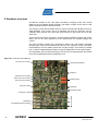
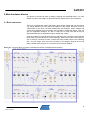
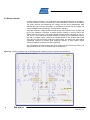
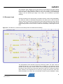
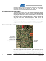
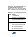
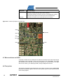
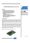
AVR451: BC100 Hardware User's Guide
Features
• Tripple buck converter for battery charging.
- Low voltage/current (max 20V/1A).
- Medium voltage/current (max 20V/2.5A).
- High voltage/current (max 38V/5A).
• Battery (dis)charging using ATtiny261/461/861 or ATtiny25/45/85.
- Uses DC supply voltage and buck converter to charge batteries.
- Powers application/own circuits when line power is missing.
• Support for two battery packs.
- Relay controlled enabling of battery packs.
• Host controller (ATmega644).
- Interface MCU responsible for charging.
- Support for DB101 graphical display board.
- Monitor voltages and currents on the board.
8-bit
Microcontrollers
Application Note
1 Introduction
The BC100 is reference design/development kit that targets especially battery
charging. As the kit is general in nature it can be used to charge various battery
types, as long as the requirements to charging voltage and currents are within the
output range that the kit offers (1.2V to 38V, max 5A).
The kit can be used to develop applications such as battery chargers, battery
backup, Un-interruptable power supply, switch mode power supply and other.
Figure 1-1. BC100 hardware.
Rev. 8088A-AVR-09/07
2 Hardware overview
The BC100 consists of two main parts: the battery charging circuits and circuits
related to the ATmega644 board controller. The battery charger circuits can be used
without interaction with the board controller.
The charger circuits has two AVR® sockets, one for the ATtiny261/461/861 and on for
ATtiny25/45/85. From factory the kit is delivered with both an ATtiny861 and an
ATtiny85. Both of these can control the buck-converts on the board, but not at the
same time.
The board has three buck-converters: These three have different voltage and current
rating, and can be used depending on the requirements for charging voltage and
current.
The buck-converter outputs are connected to either of the two battery terminals
through relays, which are controlled by the device in the ATtinyx81 socket. This offers
the possibility to use two battery packs with a single charger. This makes it possible
to e.g. replace a depleted battery while running the application from the other battery.
The schematics, bill of material and layout can be found as separate PDF documents
in the ZIP file distributed with this application note.
Figure 2-1. Overview of the BC100.
DC Power (7.5V-40V)
RS232 (ATmega644)
Battery A
38V/5A buck converter
30V/2.5A buck converter
20V/1A buck converter
ATtinyx5 socket
Battery relays
Battery B
Electronic loads
DataFlash
ATmega644 board controller
2
DB101 connectors
ATtinyx61 socket
AVR451
8088A-AVR-09/07
AVR451
3 Main hardware blocks
The blocks of the BC100 used for battery charging are described below. For more
details on parts of the design not described below, please refer to the schematics.
3.1 Buck converters
The buck converters are used to generate a given output voltage that can be used to
e.g. charge batteries (or even control the speed of a DC motor). Since the choice of
components for the buck converter determines the maximum output voltage and
current three different buck-converters are included in the BC100 design. This can
give the application designer an idea of what kind of PCB size that should be
expected depending on the desired output voltage and current.
At set of jumpers are used to select which of the three buck converter circuits that are
used (refer to jumper section for jumper settings): these connect the board supply to
one of the buck converter circuits, connect the ATtiny PWM output to the switching
FET, and the output from the buck converters to the battery (through shunt and
relays). Please refer to Figure 3-1 to see the buck converter designs.
Figure 3-1. The three buck converters of the BC100 (section of the BC100 schematics).
3
8088A-AVR-09/07
3.2 Shunt network
A shunt resistor (70mOhm, 1%) is placed in the charge/discharge path of the battery.
The shunt resistor is used to measure the current that flows in and out of the battery.
The ATtiny devices are measuring the voltage over the shunt (differentially ADC
reading) and can use this information to calculate the current flow and adjust the
charge voltage/current accordingly, or terminate the charging.
Since the maximum voltage at the terminals of the shunt depend on the number and
type of the batteries connected, a resistor divider network is used to reduce the
voltage seen by the ATtiny. The resistor divider network can be configured to 1/2, 1/4,
1/8, 1/12 or 1/16 of the shunt terminal voltages by setting the corresponding jumpers:
One set of jumpers (J405) configure the resistor divider on the positive side of the
shunt and one set of jumpers (J406) the negative side. The side of the shunt that is
considered “positive” is positive while charging a battery. If other resistor divider
values are desired the resistors must be replaced.
The ATmega644 can also measure the shunt voltage, but only with 9 bit accuracy, as
opposed to the ATtiny, which measure with 10 bit accuracy.
Figure 3-2. The shunt resistor and configurable divider network (section of the BC100 schematics).
4
AVR451
8088A-AVR-09/07
AVR451
The maximum input voltages to the ATtiny device must be below the supply voltage
of the ATtiny, and the differential voltage over the shunt (resistor dividers) must be
below the ADC’s voltage reference, which is 2.5V (0.1% accuracy). If the differential
voltage is low the internal gain stage of the ATtiny can be enabled to get better
readings.
3.3 Electronic load
The BC100 features two electronically controlled constant current loads (adjustable).
The loads are meant for development purposes: One load can be used to load the
output of the buck converters to verify that the ADC reads the expected current during
“charging” (no battery connected while the load is connected). The other load can be
used to verify that the correct current is read when the battery is discharged into the
load.
Figure 3-3. The electronic constant current loads (section of the BC100 schematics).
The ATmega644 board controller controls the electronic loads. The load current is
controlled by the duty cycle of the PWM (OC2A on TIMER 2). The electronic load is
will NOT endure very high currents, and the current flowing through the loads should
be limited so that it does not exceed the tolerances of the FETs (15W) and resistors
(2W). Warning: the components do not have any cooling area and may suffer from
thermal damage even below the recommended maximum power dissipation rating.
5
8088A-AVR-09/07
Always keep the temperature of the FETs (Q404 and Q405) and the resistors (R444
and R445) below a reasonable temperature (very warm is ok, untouchable is bad).
The equations below can be used to determine the maximum currents for the load
resistors and FET transistors – still, keep well below these values.
Equation 3-1. Maximum current in the resistor in the electronic load.
I res, max =
2W
= 4.47 A
100 mΩ
Equation 3-2. Maximum current in the FET transistor in the electronic load.
I FET, max =
15W
Vsupply − Vres
3.4 Supply voltages and ground levels
The board operates with three supply voltages (V3P3, V6P0 and V3P3A) and two
grounds (PGND and GND).
The VP3P3 (3.5V) and VP6P0 (6.3V) are the supply voltage for the ATmega644 and
other miscellaneous parts of the design, such as the electronic load, that are used to
support the development of an application.
The V3P3A (3.3V) is an adjustable mixed analog and digital supply voltage for the
ATtiny devices – this is used for the core part of the battery-charger. The mega644
can adjust this voltage, if desired. The PWM from OC2B set the adjustment and the
output Q3 on the port expanded U202 enables the adjustment.
PGND is used as ground reference for all power electronics (buck converter,
electronic load and so on), while GND is used as ground reference for other noise
sensitive analog circuits and low-current part of the circuits such as the
microcontrollers. The PGND and GND are connected at two points, the R142 and the
R143, which are both 0 ohm resistors.
3.5 ADC reference
To achieve sufficiently high accuracy on the current measurements a 2.500V (0.1%)
external reference is used. The reference is a high-accuracy zener diode, buffered by
operational amplifiers.
If it is desired to use the AVR’s internal voltage reference rather than the external one
the external voltage reference can be disconnected by removing the resistor R141.
4 Connectors and jumpers
The connectors and jumpers on the BC100 are described in the sections below.
4.1 Power connector
The BC100 can be connected to a DC power supply (9V-40V) through either the 4mm
banana connectors, or through the power jack (negative center). Please refer to
Figure 2-1 to identify the power connectors.
6
AVR451
8088A-AVR-09/07
AVR451
4.2 RS232C connector
A RS232C connector is available to connect the BC100 to e.g. a PC. The RS232C
connector is connected to the ATmega644 board controller (USART0) and can be
used interact with or as a gateway to the ATtiny AVRs connected to the charging
circuits.
4.3 Battery terminals
The charger can connect to two individual battery packs, which can be connected to
the board through two sets of screw-terminals. Please refer to Figure 2-1 to identify
the battery terminals (Battery A and Battery B).
The battery connectors (J500 and J501) support various types of battery packs.
Therefore, in addition to the positive and negative battery poles, the connector has
additional terminals (see Table 4-1, below).
Table 4-1. Terminals on the battery connectors.
Terminal label
Use
BATTERY+
Positive pole of the battery
BATTERY-
Negative pole of the battery
RID/NTC(1)
For batteries that have either a Resistor ID (RID) or Negative
Temperature Coefficient resistor (NTC) line.
1-WIRE/SDA
For batteries that have a built-in 1-Wire eeprom (from where
battery parameters can be read).
Alternative, a TWI/SMBus data line can be connected to this line
(for a smart battery charger)
SCL(1)
A TWI/SMBus clock line can be connected to this line (for a smart
battery charger)
ENABLE
Can be connected if the battery has an enable line.
Notes:
1. In applications were both NTC and RID are used the SCL terminal can be used
as alternative RID input.
The buck converter outputs are connected to the terminals through relays, to make it
possible to connect two batteries to one charger. The relays are default open (not
conducting), and should therefore be actively closed to connect a battery. The two
relays should not be closed at the same time unless the two batteries are having the
same voltage level. When a relay is closed the corresponding active-LED (D500 and
D501) will light up.
When using an ATtinyx5 to charge a battery, only one battery pack should be
connected (unless the battery packs are meant to be in parallel). Note that the
ATtinyx5 cannot control the relays, due to the lack of available pins, and therefore it is
required to either program the ATtinyx61 to enable the relay(s) or to short pin 7
(battery A enable) / pin 8 (battery B enable) of the ATtinyx61 socket to V3P3A (pin 5).
4.4 DB101 headers
A DB101 display board can be mounted as a top module on the BC100: The BC100
board controller (ATmega644) can pass information to the DB101 through a serial
link. The information can in this way be presented on the graphical display on the
DB101. Please refer to Figure 2-1 to identify the three DB101 female pin header.
7
8088A-AVR-09/07
Note that ATmega644 firmware for communicating with the DB101 is not included in
the firmware distributed with this application note. Please refer to the DB101
documentation for more information about the DB101 connectors.
4.5 Programming and debugging headers
The ATtinyx61 and ATtinyx5 can be ISP programmed through their respective
ISP/dW 6 pin headers (2.54mm). The same connectors can be used for debugging
using DebugWire. Please refer to Figure 4-1 (below) to identify the programming and
debugging pin headers.
Note that, to be able to run DebugWire debugging it is required to disconnect the
ATtiny reset circuit (pull-up, decoupling and clamping diode), otherwise the
DebugWire communicate will fail. For the ATtinyx5 devices the resistor R302 must be
removed to disconnect the reset circuit. For the ATtinyx61 the resistor R303 should
be removed.
The board controller (also referred to as “master”) can be programmed and debugged
through either ISP or JTAG. The device’s RESET lines are connected individually.
Figure 4-1. Programming and debugging headers.
ATtinyx5 ISP and
DebugWire header
ATtinyx61 ISP and
DebugWire header
ATmega644 JTAG header
ATmega644
ISP header
Note that the three AVRs on the board share the SPI programming lines for
communication purposes: if one device is driving the SPI lines while SPI
programming of the other device is attempted the programming is likely to fail.
Therefore, ensure that no devices are driving the shared SPI programming lines while
SPI programming is performed. If JTAG programming is used to program the
8
AVR451
8088A-AVR-09/07
AVR451
ATmega644 board controller it can be programmed regardless of the state of the SPI
lines. If SPI communication is used between a ATtiny and the ATmega644 a way to
ensure that programming is successful, is to erase the ATmega644 first, next
program the ATtiny and finally program the ATmega644.
During development the JTAG and DebugWire debugging interfaces are used, these
are not using the SPI lines to program the devices, and there are thus no special
procedures that should be followed to ensure successful programming.
In general the ATtinyx5 and the ATtinyx61 sockets should not be populated at the
same time, as the devices in these sockets are connected to the same traces on the
BC100. If devices are placed in both of these sockets it could potentially result in
drive contention.
4.6 Jumpers overview
A number of jumpers are available on the BC100, to be able to configure it for the
desired use. Please refer to Table 4-2 for a list of jumper and use, and refer to Figure
4-2 to identify the jumper’s location.
Table 4-2. Jumper and their use.
Designator
Use and settings
J302
Selects if the PB1 pin on ATtinyx5 is connected to the ISP/dW header or if
it is connected to the buck converters.
Use “PROG” position (left on Figure 4-2) when programming the
ATtinyx5.
Use “CHARGE” position when the ATtinyx5 should be connected to a
buck burst converter.
J400/401
Select which buck converter the supply voltage is connected to use.
Two jumpers should be mounted in side by side at the label “BUCK-A”
(40V/5A), BUCK-B” (30V/2.5A) or BUCK-C” (20V/1A). “BUCK-A is the
rightmost jumper pair on Figure 4-2
J402
Selects if the buck PWM control signal is connected or disconnected from
the BUCK-A (40V/5A). This jumper should be mounted in the disable
position while J403 or J404 is mounted in the enable position.
J403
Selects if the buck PWM control signal is connected or disconnected from
the BUCK-B (30V/2.5A). This jumper should be mounted in the disable
position while J402 or J404 is mounted in the enable position.
J404
Selects if the buck PWM control signal is connected or disconnected from
the BUCK-C (20V/1A). This jumper should be mounted in the disable
position while J402 or J403 is mounted in the enable position.
J405
Selects the resistor divider network setting for the ADC input from the
V_BAT+ voltage (positive ADC input from shunt resistor).
The divider can be set to 1/2, 1/4, 1/8, 1/12, and 1/16 V_BAT+.
Note that the setting used should match the setting on J406.
J406
Selects the resistor divider network setting for the ADC input from the
V_BAT- voltage (negative ADC input from shunt resistor).
The divider can be set to 1/2, 1/4, 1/8, 1/12, and 1/16 V_BAT-.
Note that the setting used should match the setting on J405.
9
8088A-AVR-09/07
Designator
Use and settings
J407/408
Connects the either “BUCK-A”, BUCK-B” or “BUCK-C” converter output to
the battery terminals (through shunt resistor network).
The jumpers should be mounted in pairs due to potentially high currents.
Never place the jumpers so that the output from the different buck
converters are shorted, this may damage the buck converters.
Figure 4-2. Location of jumpers on the BC100.
J402
J400/401
J403
J404
J302
J406
J405
4.7 Micro switches and LEDs
A number of LEDs and microswitches are placed in the same end of the board as the
ATmega644 board controller. These are connected to the ATmega644. The LEDs
and switches on the left side can be used for general IO, and the LEDs in the right
side can be used e.g. for displaying battery charge voltage and currents.
4.8 Test points
Test points are placed on all relevant lines of the buck converter circuits. GND/PGND
test points are placed together with the line test points to get accurate measurements
of the analog signals.
10
AVR451
8088A-AVR-09/07
AVR451
5 Preprogrammed firmware
The BC100 comes with the firmware from application note AVR458 “Charging
Lithium-Ion Batteries with ATAVRBC100” programmed in the ATtiny861.
The ATtiny85, is programmed with a small program that does nothing but putting the
device in Power Down mode.
The ATmega644 is programmed with a firmware that controls the power switch on the
board, but other wise do nothing. The source code for this firmware is distributed with
this application note.
11
8088A-AVR-09/07
Disclaimer
Headquarters
International
Atmel Corporation
2325 Orchard Parkway
San Jose, CA 95131
USA
Tel: 1(408) 441-0311
Fax: 1(408) 487-2600
Atmel Asia
Room 1219
Chinachem Golden Plaza
77 Mody Road Tsimshatsui
East Kowloon
Hong Kong
Tel: (852) 2721-9778
Fax: (852) 2722-1369
Atmel Europe
Le Krebs
8, Rue Jean-Pierre Timbaud
BP 309
78054 Saint-Quentin-enYvelines Cedex
France
Tel: (33) 1-30-60-70-00
Fax: (33) 1-30-60-71-11
Atmel Japan
9F, Tonetsu Shinkawa Bldg.
1-24-8 Shinkawa
Chuo-ku, Tokyo 104-0033
Japan
Tel: (81) 3-3523-3551
Fax: (81) 3-3523-7581
Technical Support
[email protected]
Sales Contact
www.atmel.com/contacts
Product Contact
Web Site
www.atmel.com
Literature Request
www.atmel.com/literature
Disclaimer: The information in this document is provided in connection with Atmel products. No license, express or implied, by estoppel or otherwise, to any
intellectual property right is granted by this document or in connection with the sale of Atmel products. EXCEPT AS SET FORTH IN ATMEL’S TERMS AND
CONDITIONS OF SALE LOCATED ON ATMEL’S WEB SITE, ATMEL ASSUMES NO LIABILITY WHATSOEVER AND DISCLAIMS ANY EXPRESS, IMPLIED
OR STATUTORY WARRANTY RELATING TO ITS PRODUCTS INCLUDING, BUT NOT LIMITED TO, THE IMPLIED WARRANTY OF MERCHANTABILITY,
FITNESS FOR A PARTICULAR PURPOSE, OR NON-INFRINGEMENT. IN NO EVENT SHALL ATMEL BE LIABLE FOR ANY DIRECT, INDIRECT,
CONSEQUENTIAL, PUNITIVE, SPECIAL OR INCIDENTAL DAMAGES (INCLUDING, WITHOUT LIMITATION, DAMAGES FOR LOSS OF PROFITS,
BUSINESS INTERRUPTION, OR LOSS OF INFORMATION) ARISING OUT OF THE USE OR INABILITY TO USE THIS DOCUMENT, EVEN IF ATMEL HAS
BEEN ADVISED OF THE POSSIBILITY OF SUCH DAMAGES. Atmel makes no representations or warranties with respect to the accuracy or completeness of the
contents of this document and reserves the right to make changes to specifications and product descriptions at any time without notice. Atmel does not make any
commitment to update the information contained herein. Unless specifically provided otherwise, Atmel products are not suitable for, and shall not be used in,
automotive applications. Atmel’s products are not intended, authorized, or warranted for use as components in applications intended to support or sustain life.
©2007 Atmel Corporation. All rights reserved. Atmel®, logo and combinations thereof, AVR®, and others are
registered trademarks or trademarks of Atmel Corporation or its subsidiaries. Other terms and product names may
be trademarks of others.
8088A-AVR-09/07
Mouser Electronics
Authorized Distributor
Click to View Pricing, Inventory, Delivery & Lifecycle Information:
Atmel:
ATAVRBC100