1
Chapter 2 – SocketModem (MT5600SMI & MT5656SMI)
SCR – Scratch Register
(Addr = 7)
The Scratchpad Register is a read-write register at location 7. This register is not used by the modem and
can be used by the host for temporary storage.
Divisor Registers
(Addr = 0 and 1, DLAB = 1)
The Divisor Latch LS (least significant byte) and Divisor Latch MS (most significant byte) are two read-write
registers at locations 0 and 1 when DLAB = 1, respectively.
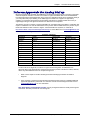
The baud rate is selected by loading each divisor latch with the appropriate hex value.
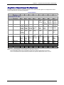
Programmable values corresponding to the desired baud rate are listed in Table on following page.
Divisor Latch (Hex)
MS
LS
06
00
04
17
03
00
01
80
00
C0
00
60
00
30
00
18
00
0C
00
06
00
04
00
03
00
02
00
01
00
00
Divisor (Decimal)
1536
1047
768
384
192
96
48
24
12
6
4
3
2
1
NA
Baud Rate
75
110
150
300
600
1200
2400
4800
9600
19200
28800
38400
57600
115600
230400
Programmable Baud Rates
Multi-Tech Systems, Inc. Universal Socket Hardware Guide for Developers (S000342F)
68