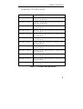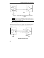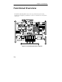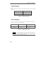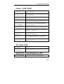
1
PowerDAQ User Manual
PowerDAQ PD2/PDXI-MF/MFS and PDL-MF DAQ boards
High-Performance Multifunction I/O boards for PCI and Compact
PCI/PXI Computer
January 2002 Edition
© Copyright 1998-2002 Omega Engineering, Inc. All rights reserved
All rights reserved. No part of this publication may be reproduced,
stored in a retrieval system, or transmitted, in any form by any means,
electronic, mechanical, by photocopying, recording, or otherwise
without prior written permission.
Fourth Edition
January 2002 Printing
Information furnished in this manual is believed to be accurate and
reliable. However, no responsibility is assumed for its use, or for any
infringements of patents or other rights of third parties that may result
from its use.
Contacting Omega Engineering
✉
Address:
OMEGA Engineering, Inc.
One Omega Drive
Stamford, Connecticut 06907-0047
U.S.A.
! Support:
Telephone:
1-800-622-2378
Fax:
1-800-848-4271
"Internet Access:
Support
[email protected]
Web site
http://www.omega.com
FTP site
ftp://ftp.omega.com
Table of Contents
Table of Contents
How to Use This Manual...................................................................... vi
Introduction ...................................................................................... vi
Who Should Read This Book?..........................................................viii
Organization of This Manual...........................................................viii
Conventions Used in This Manual .................................................... ix
Feedback ........................................................................................... ix
Introduction .............................................................................. 1
About the PowerDAQ board................................................................. 2
Overview ............................................................................................ 2
Features.............................................................................................. 2
PowerDAQ Models ............................................................................ 3
Installation and Configuration............................................ 11
Before You Begin .................................................................................12
Installing PowerDAQ ............................................................................13
Installing the Software .........................................................................14
Confirming the Installation ..................................................................15
Configuring the PowerDAQ Board.......................................................16
Input Modes: .................................................................................... 17
Test Program:....................................................................................21
Connectors for PD2/PDXI.................................................................21
Connectors for PDL-MF................................................................... 27
Architecture ............................................................................31
Functional Overview ............................................................................ 32
Analog Input Subsystem ..................................................................... 37
Input Modes .................................................................................... 42
Input Ranges....................................................................................44
Gain Settings....................................................................................44
Channel List .....................................................................................45
Clocking ...........................................................................................46
Triggering .........................................................................................48
ADC FIFO .........................................................................................49
Data format .....................................................................................50
Analog Output Subsystem .................................................................. 53
Single Update................................................................................... 53
Event-based Waveform ................................................................... 53
Continuous (polled-I/O) Waveform................................................ 53
Auto-regeneration Waveform (circular waveform)........................54
Channel List .....................................................................................54
Clocking ........................................................................................... 55
i
Table of Contents
Triggering ......................................................................................... 55
Digital Input/Output Subsystem ......................................................... 56
User Counter-Timer Subsystem...........................................................58
PD2/PDXI .........................................................................................58
PDL-MF ............................................................................................ 59
PowerDAQ Software Development Kit (PD-SDK) ........61
PowerDAQ Software ........................................................................... 62
PowerDAQ SDK Structure................................................................ 62
PowerDAQ Libraries ......................................................................... 63
PowerDAQ Include Files...................................................................64
Analog Input Subsystem .....................................................................68
Analog Output Subsystem ..................................................................86
Digital Input/Output Subsystems........................................................94
User Counter-Timer Subsystem...........................................................98
PD2/PDXI .........................................................................................98
PowerDAQ Example Programs ........................................................... 101
Third Party Software Support ............................................................103
Calibration.............................................................................105
Calibration ......................................................................................... 106
Overview ........................................................................................ 106
When to calibrate .......................................................................... 106
Appendix A: Specifications................................................107
Appendix B: Accessories .....................................................111
Accessories ..........................................................................................112
Screw Terminal Panels (PDL-MF only) ............................................112
Screw Terminal Panels (PD2/PDXI) .................................................112
BNC Connection Panels (PD2/PDXI) .............................................. 113
Thermocouple Input Racks (All) ..................................................... 114
5B/7B/OEM Distribution Panels (PD2/PDXI)................................. 114
Mating cables, connectors, PCB connection board (PD2/PDXI) ... 114
Cables (PD2/PDXI) ........................................................................ 115
19” Racks (All) ................................................................................ 115
Solid State Relay Backplane (All).................................................... 115
Signal Conditioning Expansion Units (All)...................................... 116
Appendix C: Application Notes ........................................ 117
Application Note: 1 ............................................................................. 118
Application Note: 2 ............................................................................ 122
Appendix D: Warranty .......................................................123
Overview .............................................................................................124
ii
Table of Contents
Appendix E: Glossary .......................................................... 127
Glossary ..............................................................................................128
Index ...................................................................................................145
iii
Table of Contents
List of Figures
Figure 1: Control Panel Application ......................................................15
Figure 2:
PD2- Board connector layout.............................................16
Figure 3:
PDXI-MF Board connector layout ......................................16
Figure 4:
PDL-MF- Board connector layout ...................................... 17
Figure 5:
Single-ended Inputs and pseudo-differential inputs ........ 18
Figure 6:
Differential Inputs ............................................................. 18
Figure 7: PDXI Configurator................................................................. 20
Figure 8:
Simple Test Application ......................................................21
Figure 9:
Fujitsu Connector Layout................................................... 22
Figure 10:
PowerDAQ PD2 Block diagram ......................................... 32
Figure 11:
PowerDAQ PDXI Block diagram........................................ 33
Figure 12:
PowerDAQ PDL-MF Block diagram................................... 34
Figure 13:
PowerDAQ Multifunction Board front-end ......................38
Figure 14:
PowerDAQ Sample and Hold Board front-end................. 39
Figure 15:
PD2/PDXI Series Acquisition Process ................................40
Figure 16:
PD2/PDXI Acquisition Process...........................................40
Figure 17:
Single-Ended Inputs........................................................... 42
Figure 18:
Differential Inputs ............................................................. 43
Figure 19:
Digital Input Subsystem .................................................... 56
Figure 20:
PowerDAQ Software Structure ......................................... 62
Figure 21:
Communication between user application and PowerDAQ
board 66
Figure 22:
Advanced Circular Buffer..................................................121
iv
Table of Contents
List of Tables
Table
Table
Table
Table
Table
Table
Table
Table
Table
Table
Table
Table
Table
Table
Table
Table
Table
Table
Table
Table
Table
Table
Table
Table
Table
Table
Table
Table
Table
Table
1:
2:
3:
4:
5:
6:
7:
8:
9:
10:
11:
12:
13:
14:
15:
16:
17:
16:
19:
20:
21:
22:
23:
24:
25:
26:
27:
28:
29:
30:
PowerDAQ PD2-MF Models ...................................................4
PowerDAQ PD2-MFS Models.................................................. 5
PowerDAQ PD2-MF Models ................................................... 7
PowerDAQ PDXI-MFS Models ................................................8
MFS Differential Upgrade Options......................................... 9
PD2-/PDXI- FIFO upgrade options ......................................... 9
PDL-MF board specifications .................................................10
J1 Connector (Single-Ended Mode)................................... 23
J1 Connector (Differential Input Mode) ............................... 24
Connector Pin Assignments for J2.................................... 25
Connector Pin Assignments for J4 ....................................... 26
Connector Pin Assignment for J6 ..................................... 27
Connector Pin Assignments for PDL-MF J1 ...................... 28
Connector Pin Assignments for PDXI J2........................... 29
Input Range Table .............................................................44
Programmable Gains .........................................................44
Channel List Format ..............................................................45
Programmable Gain Codes................................................45
Different Clocking Combinations...................................... 47
External Trigger Modes .....................................................49
Data Format Table for a 16-bit Board ..............................50
PowerDAQ II 12-bit data format.......................................50
PowerDAQ II 14-bit data format ......................................50
PowerDAQ II 16-bit data format ......................................50
Bit Weight vs. Input Range ................................................51
Displacement vs. Input Range ..........................................51
Analog Output Data Format .............................................54
Digital Input Configuration Word (PD2/PDXI only)......... 57
Setting up External Trigger ............................................... 76
Third Party Software Support ..........................................103
v
How to Use This Manual
How to Use This Manual
Introduction
This manual describes the hardware of each of the PowerDAQ series of
PCI and PXI DAQ boards. The following boards are supported:
PowerDAQ PD2-MF Multifunction Series:
PD2-MF-16-2M/14H
PD2-MF-64-2M/14H
PD2-MF-16-400/14L
PD2-MF-16-400/14H
PD2-MF-64-400/14L
PD2-MF-64-400/14H
PD2-MF-16-1M/12L
PD2-MF-16-1M/12H
PD2-MF-64-1M/12L
PD2-MF-64-1M/12H
PD2-MF-16-150/16L
PD2-MF-16-150/16H
PD2-MF-16-333/16L
PD2-MF-16-333/16H
PD2-MF-64-333/16L
PD2-MF-64-333/16H
PD2-MF-16-500/16H
PD2-MF-16-500/16L
PD2-MF-64-500/16H
PD2-MF-64-500/16L
PowerDAQ PD2-MFS Multifunction Sample and
Hold Series:
PD2-MFS-4-2M/14
PD2-MFS-8-2M/14
PD2-MFS-4-800/14
PD2-MFS-8-800/14
PD2-MFS-4-500/14
PD2-MFS-8-500/14
PD2-MFS-4-1M/12
PD2-MFS-8-1M/12
PD2-MFS-4-300/16
PD2-MFS-8-300/16
PD2-MFS-4-500/16
PD2-MFS-8-500/16
vi
How to Use This Manual
PowerDAQ PDXI-MF Multifunction Series:
PDXI-MF-16-2M/14H
PDXI-MF-64-2M/14H
PDXI-MF-16-400/14L
PDXI-MF-16-400/14H
PDXI-MF-64-400/14L
PDXI-MF-64-400/14H
PDXI-MF-16-1M/12L
PDXI-MF-16-1M/12H
PDXI-MF-64-1M/12L
PDXI-MF-64-1M/12H
PDXI-MF-16-150/16L
PDXI-MF-16-150/16H
PDXI-MF-16-333/16L
PDXI-MF-16-333/16H
PDXI-MF-64-333/16L
PDXI-MF-64-333/16H
PDXI-MF-16-500/16H
PDXI-MF-16-500/16L
PDXI-MF-64-500/16H
PDXI-MF-64-500/16L
PowerDAQ PDXI-MFS Multifunction Sample and
Hold Series:
PDXI-MFS-4-2M/14
PDXI-MFS-8-2M/14
PDXI-MFS-4-800/14
PDXI-MFS-8-800/14
PDXI-MFS-4-500/14
PDXI-MFS-8-500/14
PDXI-MFS-4-1M/12
PDXI-MFS-8-1M/12
PDXI-MFS-4-300/16
PDXI-MFS-8-300/16
PDXI-MFS-4-500/16
PDXI-MFS-8-500/16
PowerDAQ PDL-MF Lab Boards:
PDL-MF
The word PowerDAQ will be used in this manual to reference
all the models listed above.
vii
How to Use This Manual
Who Should Read This Book?
This manual has been designed to benefit the user of PowerDAQ
boards. To use PowerDAQ, it is assumed that you have basic PC skills,
and that you are familiar with Microsoft Windows XP/2000/NT/ 9x,
QNX or Linux/RTLinux/RTAI Linux operating environments.
Organization of This Manual
The PowerDAQ User Manual is organized as follows:
Chapter 1 - Introduction
This chapter gives you an overview of PowerDAQ features, the various
models available and lists what you need to get started.
Chapter 2 - Installation and Configuration
This chapter explains how to install and configure your PowerDAQ
board.
Chapter 3 - Architecture
This chapter discusses the subsystems of your PowerDAQ board.
Chapter 4 – PowerDAQ Software Development Kit
This chapter describes the software for your PowerDAQ board.
Chapter 5 - Calibration
This chapter discusses the auto calibration system of your PowerDAQ
board.
Appendix A - Specifications
This chapter lists the PowerDAQ hardware specifications.
Appendix B - Accessories
This appendix lists the PowerDAQ accessories products.
Appendix C – Application Notes
Includes useful application notes on understanding PowerDAQ products.
Appendix D - Warranty
This appendix contains a detailed explanation of PowerDAQ warranty.
Glossary
viii
How to Use This Manual
The Glossary contains an alphabetical list and description of terms used
in this manual.
Index
The Index alphabetically lists topics covered in this manual.
Conventions Used in This Manual
These are the main conventions used to help you get the most out of
this manual:
TIP
Note
Tips are designed to highlight quick ways to get the job
done, or good ideas you might not discover on your
own.
Notes alert you to important information.
CAUTION! Caution advises you of precautions to
take to avoid injury, data loss, or system crash.
Text formatted in bold typeface may also represent type that should be
entered verbatim or a command, as in the following example:
You can instruct users how to run setup using a command such as
setup.exe.
Feedback
We are interested in any feedback you might have concerning our
products and manuals. A Reader Evaluation form is available on the last
page of the manual.
ix
How to Use This Manual
x
1
Introduction
1
Chapter 1: Introduction
About the PowerDAQ board
This chapter describes the basic features of the PowerDAQ boards.
Overview
Thank you for purchasing a PowerDAQ board. The PowerDAQ board
was designed from the ground-up to overcome the problems associated
with previous ISA-based data acquisition boards.
The associated PowerDAQ software has been written specifically for
these products, using advanced software design.
Features
The major features of the PowerDAQ board are:
•
•
•
•
•
•
•
•
•
•
•
•
Note
24-bit 80/100 MHz Motorola 56301 DSP (Digital Signal
Processor)
PCI Bus Host PC Interface (PCI 2.1 Compliant)
Custom designed programmable gain amplifier
Analog Input - 16/64 channels- 12, 14 or 16 bit AD
resolutions
Analog Output - 2 channels - 2K DSP based FIFO
Digital In – 16 inputs (24 on PDL-MF)
Digital Out – 16 outputs (24 on PDL-MF)
Three Counter/Timers (8254) – 3 Clock In/Gate control
Auto calibration (3 24-bit DSP shared counters on PDLMF)
Extensive triggering and clocking of Analog Input
Extensive triggering and clocking of Analog Output
Simultaneous Analog In, Analog Out, Digital In, Digital
Out and Counter/Timer operations
For the full list of specifications, see Appendix A:
Specifications.
2
Chapter 1: Introduction
PowerDAQ Models
PowerDAQ model numbers are derived from the following:
[Family]-[Type Of Board]-[Channels]-[Speed]/[Resolution][Gain]
Family:
PD2-
PowerDAQ PCI Board
PDXI - PowerDAQ CompactPCI/PXI Boards
The types of boards are:
•
•
•
•
MF
MFS
AO
DIO
manual)
Multifunction
Multifunction with sample and hold
Analog Output (requires PD2-AO user manual)
Digital Input/Output (requires PD2-DIO user
PowerDAQ PD2-MF Series:
Model:
Analog features:
PD2-MF-16-2M/14H
2.2 MS/s, 14-bit, 16SE/8DI A/D, Gains: 1,2,4,8;
Two 12-bit D/A
PD2-MF-64-2M/14H
2.2 MS/s, 14-bit, 64SE/32DI A/D, Gains: 1,2,4,8;
Two 12-bit D/A
PD2-MF-16-400/14L
400 kS/s, 14-bit, 16SE/8DI A/D, Gains:
1,10,100,1000; Two 12-bit D/A
PD2-MF-16-400/14H
400 kS/s, 14-bit, 16SE/8DI A/D, Gains: 1,2,4,8;
Two 12-bit D/A
PD2-MF-64-400/14L
400 kS/s, 14-bit, 64SE/32DI A/D, Gains:
1,10,100,1000; Two 12-bit D/A
PD2-MF-64-400/14H
400 kS/s, 14-bit, 64SE/32DI A/D, Gains: 1,2,4,8;
Two 12-bit D/A
PD2-MF-16-1M/12L
1.25 MS/s, 12-bit, 16SE/8DI A/D, Gains:
1,10,100,1000; Two 12-bit D/A
3
Chapter 1: Introduction
PD2-MF-16-1M/12H
1.25 MS/s, 12-bit, 16SE/8DI A/D, Gains: 1,2,4,8;
Two 12-bit D/A
PD2-MF-64-1M/12L
1.25 MS/s, 12-bit, 64SE/32DI A/D, Gains:
1,10,100,1000; Two 12-bit D/A
PD2-MF-64-1M/12H
1.25 MS/s, 12-bit, 64SE/32DI A/D, Gains: 1,2,4,8
Two 12-bit D/A
PD2-MF-16-150/16L
150 kS/s, 16-bit, 16SE/8DI A/D, Gains:
1,10,100,1000; Two 12-bit D/A
PD2-MF-16-150/16H
150 kS/s, 16-bit, 16SE/8DI A/D, Gains: 1,2,4,8;
Two 12-bit D/A
PD2-MF-16-333/16L
333 kS/s, 16-bit, 16SE/8DI A/D, Gains:
1,10,100,1000; Two 12-bit D/A
PD2-MF-16-333/16H
333 kS/s, 16-bit, 16SE/8DI A/D, Gains: 1,2,4,8;
Two 12-bit D/A
PD2-MF-64-333/16L
333 kS/s, 16-bit, 64SE/32DI A/D, Gains:
1,10,100,1000; Two 12-bit D/A
PD2-MF-64-333/16H
333 kS/s, 16-bit, 64SE/32DI A/D, Gains: 1,2,4,8;
Two 12-bit D/A
PD2-MF-16-500/16L
500 kS/s, 16-bit, 16SE/8DI A/D, Gains:
1,10,100,1000; Two 12-bit D/A
PD2-MF-16-500/16H
500 kS/s, 16-bit, 16SE/8DI A/D, Gains: 1,2,4,8;
Two 12-bit D/A
PD2-MF-64-500/16L
500 kS/s, 16-bit, 64SE/32DI A/D, Gains:
1,10,100,1000; Two 12-bit D/A
PD2-MF-64-500/16H
500 kS/s, 16-bit, 64SE/32DI A/D, Gains: 1,2,4,8;
Two 12-bit D/A
Table 1:
PowerDAQ PD2-MF Models
All PowerDAQ PD2 models include 3 counter/timers and 32 Digital I/O
lines
4
Chapter 1: Introduction
PowerDAQ PD2-MFS Series:
Model:
Analog features:
PD2-MFS-4-2M/14
1.65 MS/s, 14-bit, 4SE Simultaneous Sample &
Hold; Two 12-bit D/As
PD2-MFS-8-2M/14
1.65 MS/s, 14-bit, 8SE Simultaneous Sample &
Hold; Two 12-bit D/As
PD2-MFS-4-800/14
800 kS/s, 14-bit, 4SE Simultaneous Sample & Hold
Two 12-bit D/As
PD2-MFS-8-800/14
800 kS/s, 14-bit, 8SE Simultaneous Sample & Hold
Two 12-bit D/As
PD2-MFS-4-500/14
500 kS/s, 14-bit, 4SE Simultaneous Sample & Hold
Two 12-bit D/As
PD2-MFS-8-500/14
500 kS/s, 14-bit, 8SE Simultaneous Sample & Hold
Two 12-bit D/As
PD2-MFS-4-1M/12
1 MS/s, 12-bit, 4SE Simultaneous Sample & Hold;
Two 12-bit D/As
PD2-MFS-8-1M/12
1 MS/s, 12-bit, 8SE Simultaneous Sample & Hold;
Two 12-bit D/As
PD2-MFS-4-300/16
300 kS/s, 16-bit, 4SE Simultaneous Sample & Hold
Two 12-bit D/As
PD2-MFS-8-300/16
300 kS/s, 16-bit, 8SE Simultaneous Sample & Hold
Two 12-bit D/As
PD2-MFS-4-500/16
500 kS/s, 16-bit, 4SE Simultaneous Sample & Hold
Two 12-bit D/As
PD2-MFS-8-500/16
500 kS/s, 16-bit, 8SE Simultaneous Sample & Hold
Two 12-bit D/As
Table 2:
PowerDAQ PD2-MFS Models
5
Chapter 1: Introduction
Note The PD2-MFS series have onboard sample and hold
amplifiers for each channel. These are part of the boards
hardware design and do not require any software programming
to be enabled.
PowerDAQ PDXI-MF Series:
Model:
Analog features:
PDXI-MF-16-2M/14H
2.2 MS/s, 14-bit, 16SE/8DI A/D, Gains: 1,2,4,8;
Two 12-bit D/A
PDXI-MF-64-2M/14H
2.2 MS/s, 14-bit, 64SE/32DI A/D, Gains: 1,2,4,8;
Two 12-bit D/A
PDXI-MF-16-400/14L
400 kS/s, 14-bit, 16SE/8DI A/D, Gains:
1,10,100,1000; Two 12-bit D/A
PDXI-MF-16-400/14H
400 kS/s, 14-bit, 16SE/8DI A/D, Gains: 1,2,4,8;
Two 12-bit D/A
PDXI-MF-64-400/14L
400 kS/s, 14-bit, 64SE/32DI A/D, Gains:
1,10,100,1000; Two 12-bit D/A
PDXI-MF-64-400/14H 400 kS/s, 14-bit, 64SE/32DI A/D, Gains: 1,2,4,8;
Two 12-bit D/A
PDXI-MF-16-1M/12L
1.25 MS/s, 12-bit, 16SE/8DI A/D, Gains:
1,10,100,1000; Two 12-bit D/A
PDXI-MF-16-1M/12H
1.25 MS/s, 12-bit, 16SE/8DI A/D, Gains: 1,2,4,8;
Two 12-bit D/A
PDXI-MF-64-1M/12L
1.25 MS/s, 12-bit, 64SE/32DI A/D, Gains:
1,10,100,1000; Two 12-bit D/A
PDXI-MF-64-1M/12H
1.25 MS/s, 12-bit, 64SE/32DI A/D, Gains: 1,2,4,8
Two 12-bit D/A
PDXI-MF-16-150/16L
150 kS/s, 16-bit, 16SE/8DI A/D, Gains:
1,10,100,1000; Two 12-bit D/A
PDXI-MF-16-150/16H
150 kS/s, 16-bit, 16SE/8DI A/D, Gains: 1,2,4,8;
Two 12-bit D/A
6
Chapter 1: Introduction
PDXI-MF-16-333/16L
333 kS/s, 16-bit, 16SE/8DI A/D, Gains:
1,10,100,1000; Two 12-bit D/A
PDXI-MF-16-333/16H
333 kS/s, 16-bit, 16SE/8DI A/D, Gains: 1,2,4,8;
Two 12-bit D/A
PDXI-MF-64-333/16L
333 kS/s, 16-bit, 64SE/32DI A/D, Gains:
1,10,100,1000; Two 12-bit D/A
PDXI-MF-64-333/16H
333 kS/s, 16-bit, 64SE/32DI A/D, Gains: 1,2,4,8;
Two 12-bit D/A
PDXI-MF-16-500/16L
500 kS/s, 16-bit, 16SE/8DI A/D, Gains:
1,10,100,1000; Two 12-bit D/A
PDXI-MF-16-500/16H
500 kS/s, 16-bit, 16SE/8DI A/D, Gains: 1,2,4,8;
Two 12-bit D/A
PDXI-MF-64-500/16L
500 kS/s, 16-bit, 64SE/32DI A/D, Gains:
1,10,100,1000; Two 12-bit D/A
PDXI-MF-64-500/16H
500 kS/s, 16-bit, 64SE/32DI A/D, Gains: 1,2,4,8;
Two 12-bit D/A
Table 3:
PowerDAQ PD2-MF Models
All PowerDAQ PD2 models include 3 counter/timers and 32 Digital I/O
lines
PowerDAQ PDXI-MFS Series:
Model:
Analog features:
PDXI-MFS-4-2M/14
1.65 MS/s, 14-bit, 4SE Simultaneous Sample &
Hold; Two 12-bit D/As
PDXI-MFS-8-2M/14
1.65 MS/s, 14-bit, 8SE Simultaneous Sample &
Hold; Two 12-bit D/As
PDXI-MFS-4-800/14
800 kS/s, 14-bit, 4SE Simultaneous Sample & Hold
Two 12-bit D/As
PDXI-MFS-8-800/14
800 kS/s, 14-bit, 8SE Simultaneous Sample & Hold
7
Chapter 1: Introduction
Two 12-bit D/As
PDXI-MFS-4-500/14
500 kS/s, 14-bit, 4SE Simultaneous Sample & Hold
Two 12-bit D/As
PDXI-MFS-8-500/14
500 kS/s, 14-bit, 8SE Simultaneous Sample & Hold
Two 12-bit D/As
PDXI-MFS-4-1M/12
1 MS/s, 12-bit, 4SE Simultaneous Sample & Hold;
Two 12-bit D/As
PDXI-MFS-8-1M/12
1 MS/s, 12-bit, 8SE Simultaneous Sample & Hold;
Two 12-bit D/As
PDXI-MFS-4-300/16
300 kS/s, 16-bit, 4SE Simultaneous Sample & Hold
Two 12-bit D/As
PDXI-MFS-8-300/16
300 kS/s, 16-bit, 8SE Simultaneous Sample & Hold
Two 12-bit D/As
PDXI-MFS-4-500/16
500 kS/s, 16-bit, 4SE Simultaneous Sample & Hold
Two 12-bit D/As
PDXI-MFS-8-500/16
500 kS/s, 16-bit, 8SE Simultaneous Sample & Hold
Two 12-bit D/As
Table 4:
PowerDAQ PDXI-MFS Models
Note The PDXI-MFS series have onboard sample and hold
amplifiers for each channel. These are part of the boards
hardware design and do not require any software programming
to be enabled.
PowerDAQ Sample
upgrade with gains:
and
Hold
differential
The PD2-MFS/PDXI-MFS series can be upgraded to differential inputs
with gains for each channel. One PGA per channel is installed on the
board.
8
Chapter 1: Introduction
Upgrade Part Number:
Additional features added:
PD2-MFS-4-DG4
Upgrade any PD2-MFS board from 4SE to 4DI
with Gains (1,2,5,10)
PD2-MFS-8-DG8
Upgrade any PD2-MFS board from 8SE to 8DI
with Gains (1,2,5,10)
PDXI-MFS-4-DG4
Upgrade any PDXI-MFS board from 4SE to 4DI
with Gains (1,2,5,10)
PDXI-MFS-8-DG8
Upgrade any PDXI-MFS board from 8SE to 8DI
with Gains (1,2,5,10)
Table 5:
PowerDAQ
features:
MFS Differential Upgrade Options
D/A,
DIO
and
Counter
Timer
All PowerDAQ PD2/PDXI boards have the following additional features:
•
•
•
•
Analog Output
Digital Input
interrupts)
Digital Output
Counter Timers
Two 12-bit 200 kHz DAC’s
16 TTL (of which 8 can generate
16 TTL
Three 16-bit (8254 type)
PowerDAQ MF/MFS FIFO Upgrade options:
PD2/PDXI PowerDAQ multifunction boards can have the analog input
FIFOs upgraded. Below is a list of current upgrade options:
Upgrade part number:
Additional features added:
PD-16KFIFO
Upgrade board from 1K FIFO to 16K FIFO
PD-32KFIFO
Upgrade board from 1K FIFO to 32K FIFO
PD-64KFIFO
Upgrade board from 1K FIFO to 64K FIFO
Table 6: PD2-/PDXI- FIFO upgrade options
9
PowerDAQ PDL-MF Lab Board:
This low cost Lab series board features:
150 kS/s, 16-bit, 16SE/16PDI, 8DI ; Two
12-bit D/As, 48 DIO and 3 CTM
PDL-MF
Table 7: PDL-MF board specifications
The PDL-MF board have the following additional features:
•
•
•
•
Analog Output
Digital Input
Digital Output
Counter Timers
Two 12-bit 200 kHz DAC’s
24 lines
24 lines
Three 24-bit 16.5/33 MHz
2
Installation and
Configuration
11
Chapter 2: Installation and Configuration
Before You Begin
Before you install your PowerDAQ board, you should read and
understand the following information.
System Requirements:
To install and run your PowerDAQ board, you must have the following:
•
•
•
A PC with PCI slots, a Pentium-class processor, and a
BIOS that is compliant with PCI Local Bus Specification
Revision 2.1 or greater
Windows 95, 98, NT 4.0, 2000/XP
Linux, QNX, RTLinux
Packing List
In your PowerDAQ package you should have received:
•
•
•
Note
•
A PowerDAQ board
A user manual
A CD containing the PowerDAQ software development kit
(SDK) and documentation
The CD label shows the version number of the SDK.
A calibration certificate
Precautions
PowerDAQ boards contain sensitive electronic components. When
handling your PowerDAQ board, you should:
•
•
12
Ensure that you are properly grounded.
While holding the board in its antistatic bag, discharge
any static electricity by touching the metal part of your
PC.
Chapter 2: Installation and Configuration
Installing PowerDAQ
Installing the Board:
To install your PowerDAQ board:
1. Turn off your PC and remove the cover from your PC.
2. Locate an empty PCI slot and remove the slot cover on
the back panel of your PC. Save the screw.
3. Insert the board into the PCI slot.
4. Fasten the board’s mounting bracket to your PC’s back
panel with the screw that held the slot cover.
5. Inspect the board and ensure that it has been properly
inserted in the slot.
6. Replace the cover of your PC and turn on the power.
Note The PowerDAQ PCI interface must be set to 32-bit, 5V
power and signaling (the default setting for most PCs).
13
Chapter 2: Installation and Configuration
Installing the Software
To install the PowerDAQ SDK:
1.
Start your PC and, if you are running Windows NT, login as an
administrator.
2.
Insert the PowerDAQ CD into your CD-ROM drive. Windows should
automatically start the PowerDAQ Setup program. If you see the
OMEGA logo and then the PowerDAQ welcome screen, go to step
6.
3. If the Setup program does not start automatically, select Run from
the Start menu.
4. Enter D:\Setup.exe in the Open: textbox. (Substitute the correct
letter if D is not the drive letter of your CD-ROM drive.)
5. Click OK.
6. As the Setup program runs, you will be asked to enter information
about your PowerDAQ configuration. Unless you are an expert user
and have specific requirements, you should select a Typical
installation and accept the default configuration.
14
Chapter 2: Installation and Configuration
7.
If the Setup program asks for information about third-party
software packages that you do not have installed on your PC, leave
the textbox blank and click the Next button.
8. When the installation is complete, you should restart your PC when
prompted.
Confirming the Installation
Once you have installed the PowerDAQ board and software on your PC,
you should confirm the installation:
•
Select Programs ! PowerDAQ ! Control Panel: from
the Start menu. If the Control Panel applet is displayed
and correctly identifies your PowerDAQ board, the
installation is correct.
Figure 1: Control Panel Application
15
Chapter 2: Installation and Configuration
Configuring the PowerDAQ
Board
PowerDAQ
1
1
J2 Connector
Logic
Control
Logic
1
J4 Connector
Boot
ROM
DSP
Low Noise DC-DC
Onboard
FIFO
Onboard
FIFO
PowerDAQ II MF board
Input Multiplexors
J1 Connector
1
J 6 Conne ctor
PCI Bus
Figure 2: PD2- Board connector layout
Low N oise DC- DC
PXI
PDXI-MF board
DSP
PowerDAQ
Figure 3: PDXI-MF Board connector layout
16
CompactPCI Bu s
Input M ultiple xors
J2 Conn ecto r
J1 C onnector
1
Chapter 2: Installation and Configuration
PowerDAQ PDL-MF board
1
J1 Connector
Boot
ROM
DSP
PowerDAQ
PCI Bus
Figure 4: PDL-MF- Board connector layout
Input Modes:
The analog input section multiplexes the active input channels (64/16
single-ended or 32/8)differential) to a single 12- or 16-bit successive
approximation analog-to-digital converter (ADC).
Single-Ended:
PowerDAQ boards can be configured to operate with either a singleended or differential input. Single-ended inputs allow up to 64 channels
and share a common return path connected to analog ground (AGND).
17
Chapter 2: Installation and Configuration
Ain
V1
Aout
Agnd
Figure 5: Single-ended Inputs and pseudo-differential
inputs
Note Unused channels should be shorted to ground using 0to 1-KΩ resistor. In pseudo-differential mode ground reference
level is taken from remote system.
Differential Inputs:
Differential inputs allow up to 32 channels. Each differential channel
uses two analog channels — one analog channel connects to the positive
input of the programmable gain amplifier, and the other to the
negative.
Ain (+)
V1
Ain (RETURN)
AGND
Figure 6: Differential Inputs
18
Chapter 2: Installation and Configuration
Note Positive and negative differential inputs should not be
driven by voltages more then AGND ±14V.
When wiring applications to your PowerDAQ board, consider the
following:
•
When working in an environment with electrical noise or
when using gains, use differential input.
•
When working in an environment with electrical noise,
use individually shielded twisted-pair wiring.
•
Physically separate wiring paths or conduits carrying
power lines and signal lines.
•
Signal cables should never be put in the same wiring
harness as high-current or high-voltage cables. Avoid
routing signal and power cables together in parallel paths
unless a reasonable distance separates the paths —
reasonable being determined by the strength of the
power signals and the amount of shielding.
•
Signal lines near devices that create high levels of
electrical noise should be run through a metal cable
trough above or below the work area.
•
Power lines, poorly designed video monitors and
switching power supplies, solenoids, electric arcs from
breakers or welders, and unshielded signal cables can
affect the accuracy of your measurements.
Installing Multiple Boards (PD-CBL-SYNC):
You can install multiple PowerDAQ boards in one PC. The internal J6
synchronization header will allow a master/slave configuration to be
setup. A special PowerDAQ cable (PD-CBL-SYNC): will allow you to
connect up to four boards in one PC. Synchronization cables for more
than four boards are available from your distributor or the factory.
19
Chapter 2: Installation and Configuration
Note
PXI boards are synchronized via PXI interface using the
PXI Configurator program.
Figure 7:
PDXI Configurator
PDL-MF board is synchronized via connections on a screwterminal panel.
Note
When using more than 4 PCI slots (standard PC), you
will need a PCI bridge chip to support additional PCI slots. These
bridge chips reduce the PCI bus throughput and will reduce your
maximum sampling speed.
Base address, DMA, Interrupt settings
The PowerDAQ boards are configured automatically by the PCI bus on
power up. You do not have to set any base address, DMA channels or
interrupt levels. In case of the performance problems try for more
PowerDAQ boards and mass-storage/video/network/USB devices for
different IRQs.
20
Chapter 2: Installation and Configuration
Test Program:
After you have wired an application to your PowerDAQ board, you
should run the Simple Test program:
1.
Select Programs " PowerDAQ " Simple Test : from
the Start menu. The Simple Test dialog box is displayed.
Figure 8: Simple Test Application
2.
Use the Analog In, Analog Out, Digital In, Digital Out,
and Counters tabs to observe your application running
on the board.
Connectors for PD2/PDXI
PowerDAQ multifunction boards have four connectors:
•
96-contact pin-less main connector (J1)
Manufactured by: Fujitsu: PN# FCN-245P096-G/U (Male)
http://www.fta.fujitsu.com/
21
Chapter 2: Installation and Configuration
•
36-pin internal digital connector (J2)
Manufactured by: Thomas and Betts PN# 609-3627
(Male)
http://www.thomasandbetts.com/
• 36-pin internal digital connector (J4)
Manufactured by: Thomas and Betts PN# 609-3627
(Male)
http://www.thomasandbetts.com/
• 8-pin internal digital clock-signal connector (J6)
Manufactured by: Adam Tech PN# PH2-08-TA-SMT
http://www.adam-tech.com/
Connector Pin Assignments for J1
Figure 9: Fujitsu Connector Layout
22
Chapter 2: Installation and Configuration
J1 Connector (Single-Ended Mode)
AGND
AGND
AGND
AGND
DGND
AGND
AIN55
AIN53
AIN51
AIN49
AGND
AIN38
AIN36
AIN34
AIN33
AIN23
AIN21
AGND
AIN18
AIN16
AIN6
AIN5
AIN3
AIN1
AGND
DSP Trigger Input/AO External Clock
*ADC Conversion Start Out/ Pacer clock out
N/C
AGND
ADC Channel List Start Input / Burst Clock
AIN62
AIN60
AIN59
AIN57
AIN47
AGND
AIN44
AIN42
AIN40
AGND
AIN29
AIN27
AIN25
AIN24
AIN14
AIN12
AGND
AIN9
Table 8:
1
2
3
4
5
6
7
8
10
11
12
13
15
16
17
18
19
20
21
22
23
24
25
26
27
28
29
30
31
32
33
34
35
36
37
38
39
40
41
42
43
44
45
46
47
48
49
50
51
52
53
54
55
56
57
58
59
60
61
62
63
64
65
66
67
68
69
70
71
72
73
74
75
76
77
78
79
80
81
82
83
84
85
86
87
88
89
90
91
92
93
94
95
96
AGND
AOUT0
AGND
AOUT1
AGND
AGND
AIN54
AIN52
AIN50
AIN48
AIN39
AIN37
AIN35
AGND
AIN32
AIN22
AIN20
AIN19
AIN17
AIN7
AGND
AIN4
AIN2
AIN0
AGND
+5V (100 mA max)
ADC Conversion Start Input / Pacer clock
AGND
N/C
AIN63
AIN61
AGND
AIN58
AIN56
AIN46
AIN45
AIN43
AIN41
AIN31
AIN30
AIN28
AIN26
AGND
AIN15
AIN13
AIN11
AIN10
AIN8
J1 Connector (Single-Ended Mode)
* Disconnected by default, consult factory if you need this clock on J1
connector.
23
Chapter 2: Installation and Configuration
J1 Connector (Differential Input Mode)
AGND
AGND
AGND
AGND
DGND
AGND
AIN55
AIN53
AIN51
AIN49
AGND
AIN38
AIN36
AIN34
AIN33
AIN23
AIN21
AGND
AIN18
AIN16
AIN6
AIN5
AIN3
AIN1
AGND
DSP Trigger Input/AO External Clock
ADC Conversion Start Out/ Pacer clock out
N/C
AGND
ADC Channel List Start Input / Burst Clock
AIN54 Return
AIN52 Return
AIN51 Return
AIN49 Return
AIN39 Return
AGND
AIN36 Return
AIN34 Return
AIN32 Return
AGND
AIN21 Return
AIN19 Return
AIN17 Return
AIN16 Return
AIN6 Return
AIN4 Return
AGND
AIN1 Return
Table 9:
24
1
2
3
4
5
6
7
8
10
11
12
13
15
16
17
18
19
20
21
22
23
24
25
26
27
28
29
30
31
32
33
34
35
36
37
38
39
40
41
42
43
44
45
46
47
48
49
50
51
52
53
54
55
56
57
58
59
60
61
62
63
64
65
66
67
68
69
70
71
72
73
74
75
76
77
78
79
80
81
82
83
84
85
86
87
88
89
90
91
92
93
94
95
96
AGND
AOUT0
AGND
AOUT1
AGND
AGND
AIN54
AIN52
AIN50
AIN48
AIN39
AIN37
AIN35
AGND
AIN32
AIN22
AIN20
AIN19
AIN17
AIN7
AGND
AIN4
AIN2
AIN0
AGND
+5V (100 mA max)
ADC Conversion Start Input / Pacer clock
AGND
N/C
AIN55 Return
AIN53 Return
AGND
AIN50 Return
AIN48 Return
AIN38 Return
AIN37 Return
AIN35 Return
AIN33 Return
AIN23 Return
AIN22 Return
AIN20 Return
AIN18 Return
AGND
AIN7 Return
AIN5 return
AIN3 Return
AIN2 Return
AIN0 Return
J1 Connector (Differential Input Mode)
Chapter 2: Installation and Configuration
Connector Pin Assignments for J2
The J2 digital internal connector contains eight digital input and eight
digital output lines.
1 2
3 4
5 6
7 8
9 10
11 12
13 14
16
17 18
19 20
21 22
23 24
26
27 28
29 30
Pacer Clock / ADC Conversion Start Input 31 32
DGND 33 34
Burst Clock /ADC Channel List Start Output 35 36
CTR0-IN
CTR0-OUT
CTR0-GATE
CTR1-IN
CTR1-OUT
DIN0
DIN1
DIN2
DIN3
DIN4
DIN5
DIN6
DIN7
Burst Clock / ADC Channel List Start Input
CTR2-IN
CTR2-OUT
CTR2-GATE
CTR1-GATE
+5V (100 mA max)
DGND
DOUT0
DOUT1
DOUT2
DOUT3
DOUT4
DOUT5
DOUT6
DOUT7
DGND
ADC Conversion Start Output / Pacer Clock Output
DGND
NC
Table 10: Connector Pin Assignments for J2
25
Chapter 2: Installation and Configuration
Connector Pin Assignments for J4
The J4 Connector contains eight digital input and eight digital output
lines.
DGND
DGND
DGND
DGND
DGND
DIN8
DIN9
DIN10
DIN11
DIN12
DIN13
DIN14
DIN15
DGND
DGND
DGND
DGND
DGND
1 2
3 4
5 6
7 8
9 10
11 12
13 14
16
17 18
19 20
21 22
23 24
26
27 28
29 30
31 32
33 34
35 36
DGND
DGND
DGND
DGND
+5V (100 mA max)
DGND
DOUT8
DOUT9
DOUT10
DOUT11
DOUT12
DOUT13
DOUT14
DOUT15
DGND
DGND
DGND
DGND
Table 11: Connector Pin Assignments for J4
26
Chapter 2: Installation and Configuration
Connector Pin Assignments for J6
The J6 Interboard Synchronization Connector contains two pairs of
clock signal lines:
•
•
The ADC Clock (also known as the conversion clock.
The Channel List Clock (also known as the scan clock or
burst clock).
CV_START_OUT
CL_START_OUT
CV_START_IN
CL_START_IN
1
3
5
7
2
4
6
8
DGND
DGND
DGND
DGND
Table 12: Connector Pin Assignment for J6
Connectors for PDL-MF
PowerDAQ multifunction boards have one connector:
•
100-way connector (J1)
Manufactured by: Fujitsu : PN# FCN-245P096-G/U
(Male)
http://www.fta.fujitsu.com/
27
Chapter 2: Installation and Configuration
Connector Pin Assignments for PDL-MF J1
TMR0
DGND
TMR 1
DGND
TMR2
DGND
DOUT22
DOUT 20
1
2
3
4
51
52
53
54
5 55
6 56
7 57
8
DOUT18 9
DOUT16 10
DOUT14 1 1
DOUT12
DOUT10
DOUT 8
+5VPJ2
DOUT6
DOUT4
DOUT2
DOUT0
DIN22
DIN20
DIN18
DIN16
DGND
DIN14
DIN12
DIN10
DIN8
DIN6
DIN4
DI N2
58
59
60
61
12 62
13 63
14 64
15
16
17
18
19
20
65
66
67
68
69
70
21 71
22 72
23 73
24
25
26
27
28
29
30
31
32
33
34
74
75
76
77
78
79
80
81
DIN0
82
AGND
83
AOUT 1
84
E XT_GND 35 85
AIN 7 36 86
AGND 37 87
AIN6
AGND
EXT_C LK
DGND
IRQC
DGND
EXT_T RIG
DGND
DOUT 23
DOUT 21
DOUT 19
DOUT 17
DOUT 15
DOUT 13
DOUT 11
DOUT 9
DGND
DOUT 7
DOUT 5
DOUT 3
DOUT 1
DIN23
DIN21
DIN19
DIN17
DGND
DIN15
DIN13
DIN11
DIN9
DIN7
DIN5
DIN3
DIN1
AGND
AOUT 0
AGND
AIN15
AGND
38 88
39 89
AIN5 40 9 0
AGND 4 1 9 1
AIN4 42 92
AGND 43 93
AIN3 44 94
AGND 45 95
AI N2 46 96
AIN14
AGND
AGND 47 97
AIN 1 48 98
AGND
AIN9
AGND
AIN0
AGND
AIN8
49 99
50 100
AIN13
AGND
AIN12
AGND
AIN11
AGND
AIN10
Table 13: Connector Pin Assignments for PDL-MF J1
28
Chapter 2: Installation and Configuration
Connector Pin Assignments for PDXI J2
DOUT11
DIN13
DOUT12
DIN14
DOUT13
DIN15
DOUT14
DOUT15
DGND
DGND
DGND
DGND
DGND
DGND
DGND
DGND
DGND
DGND
DGND
DGND
DGND
DGND
DGND
DGND
DGND
DGND
DGND
DGND
DGND
DGND
DGND
DGND
DGND
UCT0_CLK_IN
UCT2_CLK_IN
UCT0_OUT
UCT2_OUT
UCT0_GATE
UCT2_GATE
UCT1_CLK_IN
1
3
5
7
9
11
13
15
19
21
23
25
29
31
33
35
37
39
41
43
45
47
49
51
53
55
57
59
61
63
65
67
69
71
73
75
77
79
2
4
6
8
10
12
14
16
18
20
22
24
26
28
30
32
34
36
38
40
42
44
46
48
50
52
54
56
58
60
62
64
66
68
70
72
74
76
78
80
DIN12
DOUT10
DIN11
DOUT9
DIN10
DOUT8
DIN9
DGND
DIN8
+5VPJ2
DGND
CL_DONE_OUT
CL_START_OUT_BACK
DGND
DGND
CL_START_OUT
CL_START_IN_BACK
DGND
TRIG_IN_BACK
DOUT7
CL_START_IN_BACK
DOUT6
DIN7
DOUT5
DIN6
DOUT4
DIN5
DOUT3
DIN4
DOUT2
DIN3
DOUT1
DIN2
DOUT0
DIN1
DGND
DIN0
+5VPJ2
UCT1_OUT
UCT1_GATE
Table 14: Connector Pin Assignments for PDXI J2
29
Chapter 2: Installation and Configuration
PXI lines support
Following PXI lines may be used for the synchronization: PXI_TR16 0..7,
PXI_STAR
30
3
Architecture
31
Chapter 3: Architecture
Functional Overview
PowerDAQ PD2-MF/MFS series have very extensive input modes,
clocking and triggering capabilities as well as simultaneous subsystems
operations.
+
Custom
PGIA Gain
Amp.
Aln Power
Conditioner
Clock
12,14,
16-bit
Sampling
A/D
Converter
-
User
Counter
Timer
(82C54)
Upgradable
1k Sample
ADC
FIFO
3
Gate
3
Out
3
Ext. Aln Conv Clock
Aln Control
Ext. Aln Scan Clock
Channel
List
FIFO
UCT Control
Aln Clock Out
Digital
Input
Buffer
Latch
DIn Control
Ext. Aln Conv Clock
DOut Control
Ext. Trigger
Digital
Output
(Driver)
Local Data Bus
Bootstrap
ROM
Aln Conv
Clock
Aln Scan
Clock
6 Channel
DMA
12k Program
RAM
12k Data RAM
Configuration
& Calibration
EEPROM
Motorola 66MHz DSP 56301
Data
Bus Master PCI Interface
32 Bit PCI Bus
Figure 10: PowerDAQ PD2 Block diagram
32
(16)
AIn Clocking & Triggering
Address
Voltage
Reference
ESSI
DAC1
Control
AOut Calibration
DACs
DAC0
AOut Clock
Address
Aln Clock Out
Analog
Output
Amplifiers
(16)
Interrupt
Ext. Aln Scan Clock
AOut FIFO
External Analog I/O Connector
Ext. Trigger
Channel/
Gain
Control
Logic
(4)
Interboard Synchronization
16 or 64
Channel
Analog
Multiplexer
(64)
Aln Calibration
DACs
Internal Digital I/O Connectors J2,J4
Voltage
Reference
Chapter 3: Architecture
16 or 64
Ch annel
An alog
Multiplexer
(64)
Aln Power
Cond itioner
Aln C alibration
DACs
+
C ustom
P GIA Gain
A mp.
12,14 ,
16-bit
Sampling
A/D
Converter
-
Use r
Counter
Timer
(82C5 4)
U pgradable
1k Sample
ADC
FIFO
C lock
3
Gate
3
Out
3
Ext. Aln Co nv Clock
Aln Con trol
Ext. Al n Scan Cl ock
Channel
Li st
FIF O
U CT C ontro l
PowerDAQ II
Data Acquisition
Control and
Timing Logic
Ext. Aln Conv Clock
Ext. Al n Scan Cl ock
A ln Clock Out
DI n Control
Interru pt
Digit al
Outp ut
(Drive r)
Local Da ta Bus
(16)
Bootstrap
ROM
Aln Conv
Clock
Aln Scan
Clock
Clock ing & Trig gering Lin es
12k Program
RAM
12 k Data RAM
6 Channel
DMA
A Out Cloc k
Address
PXI
Control
Logic
Con figuration
& C alibration
EE PR OM
Moto rola 66MHz DSP 56301
32 Bit C ompactPC I Bus
Dat a
Bus Master PC I Interface
Address
Volt ag e
R efere nce
ESSI
DAC 1
Control
A Out Calib ration
DACs
DAC 0
(16)
Latch
DO ut Control
A ln Clock Out
Analog
Output
Amplifiers
Digital
Input
Buffe r
Ext. Trig ger
AOut FIFO
External A nalog I/O Connec tor
Ext. Trigger
Channel/
G ain
Co ntrol
Lo gic
Internal Digital I/ O Conne ctor J2
Voltage
Refe rence
P XI
Figure 11: PowerDAQ PDXI Block diagram
33
Chapter 3: Architecture
+
P GIA
G ain
A mp.
Aln Power
Cond itioner
16-bit
Sampling
A/D
Converter
-
D SP
Cou nter
Ti mer
(24)
16 Channel
Analog
Mu ltiplexer
(3)
Aln Calibration
DACs
Volt age
R efe rence
U pgradable
1k Sample
ADC
FIFO
(24)
A ln Clo ck Out
Ext. Trigger
Ext. Aln Co nv Clock
Remou te Gro und
( 16)
External Analo g/Digital I/O Conn ector
Aln Con trol
DSP
Channel L ist
FIFO
U CT C ontro l
DIn Con trol
Latch
DO ut Control
Local Da ta Bus
Motorola 66MHz DSP 56301
Digital
Output
(Driver)
Co nfiguration
& Calibratio n
EEPR OM
Data
Ad dress
Bus Master PCI Interface
Co ntrol
Buffer
Bootstrap
ROM
Aln Co nv
Clock
Aln Sca n
Clock
Address
6 Chan nel
DMA
Voltag e
R eferen ce
AOut Cl ock
AOut Calibration
DACs
DAC1
ESSI
DAC0
AOut FI FO
Analog
Output
Amplifiers
Digital
Input
PowerDAQ II
Data Acquisition
Control and
Timing Logic
12k Prog ram
RAM
12k Data RAM
Ch annel/
G ain
Co ntrol
Logic
32 B it PCI Bu s
Figure 12: PowerDAQ PDL-MF Block diagram
The heart of the board is the Motorola DSP 56301 running at 66 MHz.
The DSP ensures a highly efficient interface with the PCI bus and
sophisticated control over all board subsystems.
Analog Input subsystem includes:
•
34
The Input multiplexor (MUX) selects which channels to
acquire. The channel list (CL) FIFO controls the input
muxes. PD2-MFS boards have sample-and-hold amplifiers
(SHA) preceding the muxes. SHA amplifiers sample all
Chapter 3: Architecture
•
•
•
•
•
input channels simultaneously and then hold the acquired
voltages while the ADC converts channel by channel.
The Programmable Gain Amplifier (PGA) amplifies an
input signal in order to provide adequate voltage to the
analog-to-digital converter (ADC). The PGA amplification
depends on the board model and can be software
selected {1,2,4,8} or {1,10,100,1000} for MF series boards
and {1,2,5,10} for MFS/PDL-MF boards when the
differential gain (DG) option is installed. Gains are
software selectable on a per-channel basis.
The A/D FIFOs hold digitized samples until the DSP
transfers them into the host memory, via the PCI bus. The
default A/D FIFO size is 1kS. You can upgrade the A/D
FIFO size to 16kS or 32kS depending on your application.
Larger FIFOs give you smother operations especially at
high acquisition rates and degrade response time in a
case of control loop application.
The Calibration DACs provide voltages to adjust the
offset and gain settings. All boards are factory calibrated
for each input range and mode specified.
The Timing, triggering and clocking controls allow you to
select the timebase, clock and triggering sources, “slow
bit” and other options.
The Interrupt mechanism notifies the DSP about interrupt
conditions
Analog Output subsystem includes:
•
•
•
•
•
DSP based D/A FIFO keeps up to 2kS of digitized
waveform values.
Digital-to-analog converter (DAC) converts digitized
waveform values into analog output voltages.
Calibration DACs provide voltages to adjust offset and
gain of analog output.
Timing, triggering and clocking controls allow you to
select analog output rate and clock source.
Interrupt mechanism notifies the DSP about interrupt
conditions.
35
Chapter 3: Architecture
Digital Input/Output subsystem includes
•
•
•
•
16-bit input register to read logical levels on digital input
lines (24-bit on PDL-MF)
8-bit Schmidt trigger to catch logic level changes on
digital input lines (not present on PDL-MF)
16-bit output register to hold logical levels on digital
output lines, once data has been written (24-bit on PDLMF)
Interrupt mechanism to notify DSP about interrupt
conditions
User Counter-Timer subsystem includes
•
•
•
•
36
Three 16-bit Intel 82C54 counter timers (fully accessible)
(24-bit DSP 56301 sharable counter/timers on PDL-MF)
Clock source selection and control logic
Gate source selection and control logic
Interrupt mechanism to notify DSP about interrupt
conditions
Chapter 3: Architecture
Analog Input Subsystem
The analog input front-end multiplexes multiplex the first stage of the
input channels (64/16 single-ended or 32/8 differential) into a single,
12, 14 or 16-bit successive approximation ADC. The A/D subsystem also
includes input modes, polarity, gain settings, channel gains, channel
queue, trigger and clocking control.
MF boards have multiplexors located at the signal inputs and can be
switched to select single ended (SE) or differential (DF) mode of
operation (Fig 8). SE/DF mode is selected for all input channels. The
output of the mux signal is fed into a instrumentation amplifier (INA)
and then into a custom programmable gain amplifier (PGA). Channel
numbers along with their gains are stored in the channel list. This allows
you to select different gains on a per-channel basis.
Note Input muxes have high input impedance. It is highly
recommended to ground all unused channels. Use signal sources
with low output impedance (<100 Ohms) to avoid crosstalk;
place a capacitor between signals and ground (SE) or between
signal and return lines on screw terminal (suggested capacitor
values can be 1000pF to 0.047uF depending on your input
frequency).
Note
PDL-MF boards also have a jumper-configurable
pseudo-differential mode when ground reference level is taken
from the remote source.
37
Chapter 3: Architecture
channel and
gain control
MUX A
~
Analog
input 0
…
INA
…
PGA
… to range
control,
calibration
circuitry and
ADC
MUX B
…
~
SE/DI/PD (PDL-MF only)
switch control signal
Analog
input N
Figure 13: PowerDAQ Multifunction Board front-end
MFS boards have sample and hold amplifiers (SHA) located at the
signal inputs. PD2-MFS-DGx options include a INA and PGA in the one
device located on the back side of the board (Fig. 9). SE or DF mode is
selected by grounding negative input of the INA to the boards analog
ground (AGND). Channel numbers along with their gains are stored in
the channel list. This allows you to select different gains on a perchannel basis.
38
Chapter 3: Architecture
Analog
input 0
~
INA
PGA
MUX
SHA
…
… to range
control,
calibration
circuitry
and ADC
…
Analog
input N
~
INA
SE/DF
switch
control
signal
PGA
Gain
contro
l
signal
SHA
S/H
signal
channel
select
signal
Figure 14: PowerDAQ Sample and Hold Board front-end
The major difference between MF and MFS boards are the SHAs.
‘Sample and Hold’ signal switches SHAs between ‘sampled’ and ‘hold’
states. When the SHA is in a sample state its output repeats its input.
In the hold state, SHAs keep the output voltage at the same level at
time of switching.
39
Chapter 3: Architecture
Channels
Ch 0
Ch 1
Ch 2
t0
t1
Time
t2
Moment of digitizing
Signal level at the moment of
Figure 15: PD2/PDXI Series Acquisition Process
Channels
Ch 0
Ch 1
Ch 2
Hold
t0
t1
t2
Sampl
Time
Moment of digitizing
Signal level
Figure 16: PD2/PDXI Acquisition Process
40
Chapter 3: Architecture
Figures 10 and 11 show the differences in data acquired using MF and
MFS boards. When a sine wave is applied to the channels 0, 1 and 2.
t0, t1 and t2 is the time when the channel reading has happened.
Minimum delay between them is limited by the rated speed of the
board and can be calculated as 1/rate in kS (seconds).
Note PowerDAQ boards acquire channels sequentially at the
rated speed that is referenced as the aggregate rate. When the
channel list contains two channels, per channel rate is a half of
aggregate rate.
Maximum per channel rate can be calculated as:
Aggregate_rate / Number_of_channels (kS/s).
Depending on certain MFS models, maximum per channel rate is slower
because of the hold delay time.
The MF board (fig. 10) acquires input signals with a small delay
between acquisitions. If the input signal frequency is relatively low (510 times lower then acquisition rate), the difference in the acquired
signal level is minimal. Data acquisition is virtually simultaneous. If the
input signal has a fairly high frequency, sequential acquisition can cause
significant error in the digitized signal levels. MFS board would be
more suitable for such an application.
The MFS (Fig. 11) board holds the signal at the same level while
digitizing all of the channels in the channel list. There is no difference
in the acquired signal level among the channels. Data acquisition is truly
simultaneous regardless of the input signal frequency. The MFS boards
have a unique exact timing feature. SHAs have a negative delay. In
other words the signal captured by switching them into the hold mode
is the signal 15ns previously. MFS board control logic delays external
hold signals for the same amount of time. This guarantees that the
board acquires a signal level at the exact time of the external pulse.
Note Always use PowerDAQ MFS series of board if you
require true difference between input channels levels and
working with signals close to nyquist frequency.
41
Chapter 3: Architecture
Note Complete timing tables for all PowerDAQ boards are
located Appendix A.
Input Modes
Single Ended
The PowerDAQ boards operate with either a single-ended or a
differential input configuration. Single-ended inputs allow up to 64
channels and share a common low side, which is the analog ground.
Single ended inputs are shown diagrammatically in figure 12. See Table
5 for complete wiring instructions.
Note Unused channels should be shorted to ground using a 0
to 1KOhm resistor.
+
-
Ain
V1
Agnd
Figure 17: Single-Ended Inputs
42
+
-
Chapter 3: Architecture
Differential Inputs
Differential inputs allow up to 32 channels. (Differential inputs use two
analog input channels. One channel connects to the positive input of
the programmable gain amplifier and the other to the negative of the
instrumentation amplifier).
Note
Both inputs must remain in AGND ±14V rails; otherwise
input multiplexors lookup may occur.
+
-
V1
Ain(+)
Ain (RETURN)
+
-
Agnd
Figure 18: Differential Inputs
Example: For a 16 channel PowerDAQ board in differential mode,
channels 0 and 8 form the high and low inputs of input channel 0,
channels 1 and 9 that of input channel 1. Differential inputs are shown
diagrammatically below. See Table 6 for complete wiring instructions.
Note PowerDAQ MFS boards with DG option installed have
the same number of differential and single-ended channels.
43
Chapter 3: Architecture
Input Ranges
The PowerDAQ boards have four possible input ranges. These are global
settings.
UNIPOLAR
BIPOLAR
0V to +10V
- 10V to + 10V
0V to +5V*
-5V to +5V
* Not Available on PDL-MF board.
Table 15: Input Range Table
Gain Settings
You can set a gain for each channel prior to acquisition. Depending on
your board, there are three gain ranges.
MF L Gains
MF H Gains
PDL-MF/
MFS DG-option Gains
1, 10, 100, 1000
1, 2, 4, 8
1, 2, 5, 10
Table 16: Programmable Gains
Note For low-level signals, you need high gains and you
should use a L model. For high level signals, you need a low gain
board and you should use the H model.
44
Chapter 3: Architecture
Channel List
The Channel List contains sequences of channels to be acquired and
their per channel gains. This sequence is known as the SCAN. The ADC
Channel List can contain 1 to 256 channel entries (64 entries on PDLMF). Configuration data for each channel will include the channel
selection, gain, and slow bit setting. Each Channel List block written
clears and overwrites the previous settings.
The Slow Bit is a special marker which guaranties longer settling time
for a particular channel. It is very useful when the signal is acquired has
a high (100 or 1000) gain.
The Channel list has the following format:
Bit 8
Bits 7 and 6
Bits 5 to 0
Slow bit
Gain
Channel to acquire
Table 17: Channel List Format
Gain coding
(bits 7,6)
MF L Gains
MF H Gains
MFS DG-option
Gains
00
1
1
1
01
10
2
2
10
100
4
5
11
1000
8
10
Table 18: Programmable Gain Codes
On PDL-MF channel list may have up to 64 entries.
45
Chapter 3: Architecture
Clocking
The PowerDAQ board has two selectable base frequencies (11 MHz and
33 MHz) to clock acquisition. Lower frequencies are obtained by
dividing the base frequency by a 24-bit number (from 1 to 16M). To
calculate the result frequency use following formula:
Timebase = Base Frequency / (divisor + 1)
Acquisition is clocked by two signals: conversion start (CV Start) and
channel list start (CL Start). There are four selectable sources for these
clocks:
•
•
•
•
Software command
Internal timebase
External clock
Continuous clocking (or self-retriggerable clock)
Additionally for internal or external clocks, an active edge (rising or
falling) can be selected.
Note The PowerDAQ board will generate an error condition
each time a clock signal is applied, before the board is ready to
process it. For example, if you clock the board with a clock
frequency higher than the rated aggregate rate, the board
reports a CV/CL start error.
The CV Start clock starts the A/D conversion. The CL Start clock starts
the channel list execution. The CV Start clocks are ignored until the CL
Start pulse is sensed. If any clock is switched to continuous clocking, it
re-triggers itself immediately after board is ready to process it.
Note
On the PDL-MF board only one clock may be used at
the time. If CV clock is specified as internal or external, CL clock
must be set to continuous, if CL clock set to internal/external,
CV clock is ignored and board is running A/D on maximum
speed.
46
Chapter 3: Architecture
Clock combination
CL Clock
CV Clock
source
source
SW
Continuous
Internal
Continuous
External
Continuous
Continuous
Continuous
Continuous
or SW
Internal
Continuous
External
Internal
Internal
External
External
SW
SW
Typical use
Acquire one set of data points (one
scan). SW clock causes channel list to be
executed once. The board will wait until
next CL clock comes before restarting.
Continuous acquisition with accurate
timebase. After each CL Clock pulse, the
channel list is executed at the maximum
acquisition rate. This is the most useful
mode.
Continuous acquisition when each run of
the channel list is triggered by the
external signal. This mode is used to
synchronize external events with scans.
Performs acquisition at maximum speed
possible. Less accurate than using the
timebase.
MF boards only. You can select the
specific time between conversions. Use
this type of clocking when you want to
increase settling time between
acquisitions especially when your signal
source has high output impedance.
MF boards only. Useful when one
channel is acquired and you want to
start acquisition exactly at the external
pulse edge.
Rarely used. MF boards only. Useful with
slow scan rates and you need to provide
exact time between conversions.
Rarely used. Gives full control of the
boards timing to the external device
Rarely used. Gives full control of the
boards timing to your software
Table 19: Different Clocking Combinations
47
Chapter 3: Architecture
Triggering
The Analog input subsystem needs a trigger signal to start and stop
acquisition. The Trigger signal is selectable. It can be either software
command or an external pulse. External trigger is edge-sensitive. You
can select rising or falling edge to be active. If the board is set up to
start on an external trigger, all clocks will be ignored until the pulse
comes. Acquisition continues until the stop trigger comes.
Note If CV Start clock is set to continuous start/stop, the
trigger is guaranteed to start and stop acquisition at the
beginning of channel list. If CV Start is external, it’s up to
external equipment settings.
Note
The PDL-MF board provides gated mode on the
external clock, when external trigger line used as a gate for the
internal/external clock. On the MF/MFS boards gated mode may
be implemented using the 8254 counter-timers.
48
Chapter 3: Architecture
Start
trigger
edge
Stop
trigger
edge
Rising
Rising
Rising
Falling
Falling
Falling
Falling
Rising
External TTL signal
Acquisition started
Acquisition stopped
Table 20: External Trigger Modes
ADC FIFO
The PowerDAQ boards have an on-board FIFO. The FIFO could contain
from 1kS (default) up to 64 kS depending on the FIFO option
purchased.
When the PowerDAQ board acquires data in continuous mode, data is
written into the ADC FIFO. When the FIFO becomes half-full, the DSP
initiates data transfer from the ADC FIFO into the host memory. When
a minimal amount of data is to be transferred to the host memory in
continuous acquisition mode, it is 512 samples for 1kS FIFO, 2048
samples for 4kS FIFO, etc.
49
Chapter 3: Architecture
Data format
Data in the data stream has the following format. Each two
consecutive bytes contain a single sample from the A/D converter.
Data is stored repeatedly sample by sample for all channels in the
channel list. (Table 19 shows a PowerDAQ 16-bit board data format.
For PowerDAQ 12-bit boards, only 12 LSBs (Least Significant Bits) are
valid. PowerDAQ II boards automatically place zeroes in any unused bit
locations.)
1st channel
sample
2nd channel
sample
…
last channel
sample
1st channel …
sample
bit15 bit14 bit13 bit12 bit11 bit10 bit9 bit bit7 bit6 bit5 bit4 bit3 bit2 bit1 bit0
Table 21: Data Format Table for a 16-bit Board
bit15 bit14 bit13 bit12 bit11 bit10 bit9 bit8 bit7 bit6 bit5 bit4 0x0 0x0 0x0 0x0
Table 22: PowerDAQ II 12-bit data format
bit15 bit14 bit13 bit12 bit11 bit10 bit9 bit8 bit7 bit6 bit5 bit4 bit3 bit2 0x0 0x0
Table 23: PowerDAQ II 14-bit data format
bit15 bit14 bit13 bit12 bit11 bit10 bit9 bit8 bit7 bit6 bit5 bit4 bit3 bit2 bit1 bit0
Table 24: PowerDAQ II 16-bit data format
50
Chapter 3: Architecture
The following calculations should be performed to convert the raw,
stored hexadecimal data to scaled (Voltage) data:
1.
Determine the value of a single bit (“bit weight”) in Volts
depending on the input range.
PowerDAQ II (span)/65535
0 - 5V unipolar (5V span)
0.000076295 Volts/bit
0 - 10V unipolar (10V span)
0.000152590 Volts/bit
+/-5V bipolar (10V span)
0.000152590 Volts/bit
+/-10V bipolar (20V span)
0.000305180 Volts/bit
Table 25: Bit Weight vs. Input Range
2.
Determine the “zero offset” which depends on the input
range selected.
5V, 10V unipolar
0
+/-5V biploar
-5V
+/-10V biploar
-10V
Table 26: Displacement vs. Input Range
3. Perform an arithmetical XOR with 0h8000 for all
PowerDAQ boards
4. Multiply by the “bit weight” from step 1
5. Add the “zero offset” from step 2
6. If a gain other than 1 was used for a selected channel,
divide the value received by the gain factor (Doing this
step last guarantees the maximal data accuracy.)
51
Chapter 3: Architecture
7.
To convert voltage into analog output value you can use
following formulas:
For all other models
Value = ((HexData XOR 0x8000) * BitWeight +
Displacement) / Gain
52
Chapter 3: Architecture
Analog Output Subsystem
Analog output subsystem contains two DACs (Digital to Analog
Converters) and supports the following operating modes:
Single Update
The PowerDAQ PD2-MF(S) boards operate with either a single-update
or streaming (waveform) output configuration. Single-update mode
allows direct write access to the pair of 12-bit DACs. The update
frequency is at least 1 kHz for the single update mode. This single
update speed is dependent on your PC system speed. Since data is
written to the DAC, if holds it indefinetly.
Event-based Waveform
Event-based waveform mode allows continuous waveform generation
and is not limited by the amount of data. The interrupt-based data
requests, from the board, will be received each time the DSP based
FIFO is ½ full. (with 2K samples on-board FIFO, you can load a
maximum of 1024 samples at a time).
Note If the FIFO is empty or the last value is outputted, the
board continues outputting the last value.
Continuous (polled-I/O) Waveform
An alternative continuous waveform mode does not require you to use
the event handling mechanism. Using polled I/O, you initialize the
analog output subsystem, and write data to the output buffer (2048
samples). After the application starts, the buffer is downloaded to the
DSP FIFO and the values are outputted to the DAC’s
53
Chapter 3: Architecture
Auto-regeneration Waveform (circular
waveform)
Auto-regeneration waveform mode can be used to create fixed length
waveforms (2048 samples maximum) without any host PC intervention
after initialization of the subsystem. An application writes data to the
buffer of the board and each time the end of buffer is reached, it
starts to resend the same buffer again.
Note
Revision 3.x of PowerDAQ SDK allows to create
waveforms up to the size of memory available in PC.
Channel List
There is a fixed Channel List for the analog output on the PD2-MF(S)
boards. The channel list always contains channel 0 and 1 and they are
updated simultaneously.
Note
The two channels are updated at the same time,
therefore you have to configure both DACs to the same mode
of operation.
Data Format
24 23
31
Unused 1
0
12 11
12-bit output data
for Aout1 1
12-bit output data
for Aout 0
Table 27: Analog Output Data Format
The analog outputs have a fixed output range of +/- 10V. Data
representation is in straight binary. To convert voltage into binary codes
you can use the following formula.
HexValue = ((Voltage + 10V) / 20) * 0xFFF
54
Chapter 3: Architecture
The two Hex values for Aout channel 0 and 1 respectively can be
combined to write to the analog output as follows:
Value_To_Write = (HexValue1 << 12) OR (HexValue0)
Clocking
The analog output subsystem can be clocked using software command,
internal 11 MHz base frequency or external trigger input line.
In the case where the internal 11MHz timebase is used, calculate the
output rate as follows:
Timebase = 11 MHz / (divisor + 1)
Every time a clock pulse comes, the board reads the next value from
the D/A FIFO and converts it into a voltage and outputs the analog
data on the selected channel.
Triggering
The external trigger line can also be used as an analog output start and
stop trigger. You can select internal clock as the analog output
timebase and use the trigger line to start and stop output.
Additionally you can use the external trigger line to synchronize analog
input with the analog output subsystems.
55
Chapter 3: Architecture
Digital Input/Output
Subsystem
Digital Output subsystem contains one 16-bit (PD2/PDXI-MF/MFS) and
24-bit (PDL-MF) output register. The Digital outputs do not support
clocked output, it can only be used in software-polled mode.
The digital Input subsystem contains one 16-bit (PD2/PDXI-MF/MFS)
and 24-bit (PDL-MF) input register. Digital inputs do not support
clocked input, it can only be used in software-polled mode.
Eight lower lines of the digital input are connected to a latch register.
This register could be programmed to detect rising or/and falling edges
on those digital input lines.
16-bit
Input
Register
8-bit
Edge
Detector
and
Latch
Logic
Figure 19: Digital Input Subsystem
56
Input levels
Latch status
Latch config
IRQ
Chapter 3: Architecture
Latch configuration is a 16-bit word, two bits for each one of eight
sense inputs.
Bit 7
Bit 6
Bit 5
Bit 4
Bit 3
Bit 2
Bit 1
F
R
F
R
F
R
F
R
F
R
F
R
F
R
F: 1 in this position, the inputs are sensitive to falling edge
F
Bit 0
R
R: 1 in this position, the inputs are sensitive to rising edge
Table 28: Digital Input Configuration Word (PD2/PDXI only)
The Edge Detector and Latch Logic detect configured edges on the
digital input lines. A 8-bit latch register has 1 bit per input line. It is set
to “1” when the configured edge is detected. Additionally, the logic
fires an interrupt to the DSP to inform it when the configured
conditions are met.
If you set up a latch configuration to watch for edges on several lines,
the interrupt fires as soon as any of the selected conditions happen.
However, the interrupt will not be re-fired again until the user
application clears the bit. If a change is detected on another line, the
interrupt will re-fire. To recognize which line caused an interrupt you
have to read the digital input status (i.e. latch register).
57
Chapter 3: Architecture
User Counter-Timer
Subsystem
PD2/PDXI
User counter-timer is based on the Intel 82C54 16-bit counter-timer
chip. It contains three fully independent counter-timers. It’s fully
dedicated for user applications and it is not used by any of the
PowerDAQ systems. The logic allows you to select the clock and gate
source for each of the three independent counter-timers. The countertimer outputs can generate interrupts to the host PC on change of
their state.
You can feed a clock input from one of the following four sources:
•
•
•
•
Software command
1-MHz internal timebase
External clock input line
UCT0 output line (available for UCT1 and 2)
Gate can be controlled from two sources
•
•
Software command
External gate input line
Each of the UCT can be used in following modes:
•
•
•
•
"Pulse" - generates one pulse with value/frequency length
(Mode 1)
"Train" - generates pulse train with value/frequency rate.
Pulse length is 1/frequency (Mode 2)
"Rate" - generates pulse train with value/frequency rate.
Pulse length is 1/2 value/frequency high and 1/2
value/frequency low (Mode 3)
"Delay" - waits value/frequency time and then generates
one pulse (Mode 5)
See Intel 82C54 datasheet and PowerDAQ SDK examples for
implementation details.
58
Chapter 3: Architecture
Special frequency measurement mode is implemented on PD2/PDXI
boards. Using this mode external frequency may be measured in
0..65535 interval with absolute accuracy.
The UCT is extremely useful in combination with the external clock and
trigger lines. Using the UCT you can create very sophisticated
acquisition setups.
PDL-MF
There are three DSP-based 24-bit counter/timers are available on the
PDL-MF board. They are independent from each other and capable to
generate interrupts. Maximum frequency is 16.5 MHz for external and
33 MHz for internal clock. Please refer to Motorola DSP5601 user
manual for the details. (www.mot.com).
Modes:
•
•
•
•
•
•
timer
external event counting
pulse output
square wave output
Pulse Width Modulation (PWM) output
width/period/capture measurement
Note TMR0 is shared with AIn clock, TMR2 is shared with
AOut clock.
59
Chapter 3: Architecture
60
4
PowerDAQ Software
Development Kit
(PD-SDK)
61
Chapter 4: PowerDAQ Software (SDK)
PowerDAQ Software
PowerDAQ SDK Structure
The installation will create the following directory structure in Program
Files. This assumes you selected the SDK installation (default).
PowerDAQ
PowerDAQ root directory
Applications
Applications – ready to run
Documentation
Documents and manuals
SDK
Software developers Kit (SDK)
Examples
Examples (including
applications with source code)
C Builder
Examples Borland C++ Builder
3.5
Delphi
Examples for Borland Delphi
3/4/5
Visual Basic
Examples for MS Visual Basic
VB3
Example for 16-bit VB3
VB5
Examples for V5(can use
withVB6)
VB6
Examples for VB6
Visual C
Examples for MS
Visual C++ 5/6
Include
VB, VC, Delphi API
declarations
16-bit
VC files for 16 bit OS
Lib
VB3
Figure 20:
MS VB3 16-bit files with API
Library .LIB files for VC, Inprise
Borland C++ Builder
PowerDAQ Software Structure
PowerDAQ drivers
Windows 9x operating System
Location: \windows\system directory
Files:
pwrdaq95.vxd device driver
Windows NT/2000/XP operating system
62
Chapter 4: PowerDAQ Software (SDK)
Location: \winnt\system32\drivers
Files:
pwrdaq.sys
device driver
PowerDAQ DLLs
The PowerDAQ software includes various DLLs (dynamic linked libraries)
for Windows operating systems. The location of these DLLs is as
follows:
Windows 9x operating System
Location: \windows\system directory
Files:
PwrDAQ32.dll
32-bit DLL
PwrDAQ16.dll 16-bit DLL
Windows NT/2000/XP operating system
Location: \winNT\system32
Files:
PwrDAQ32.dll
32-bit DLL
PwrDAQ16.dll 16-bit DLL
The DLLs have identical names for Windows 9x and Windows
NT/2000/XP however they are implemented differently. Both of them
support the same API therefore PowerDAQ applications, which do not
use specific Win9x and WinNT/2000/XP functions, would run on both
OS.
PowerDAQ Libraries
PowerDAQ SDK contains libraries for all major software development
tools.
63
Chapter 4: PowerDAQ Software (SDK)
/lib
pwrdaq32.lib
pd32bb.lib
pd16bb.lib
pd16bc45.lib
pwrdaq16.lib
-
MSVC/MSVS v.5.x, 6.x
Borland C Builder v.3.0, 4.0
16-bit Borland compilers
16-bit Borland C++ 4.5x
16-bit MSVC 1.5x
PowerDAQ Include Files
/include
pdfw_def.h
- firmware constant definition file for C/C++
pdfw_def.pas - firmware constant definition file for Borland Delphi
pdfw_def.bas - firmware constant definition file for Visual Basic
pwrdaq.h
pwrdaq.pas
pwrdaq.bas
- driver constants and definitions file for C/C++
- driver constants and definitions file for Borland Delphi
- driver constants and definitions file for Visual Basic
pwrdaq32.h
pwrdaq32.hpp
pwrdaq32.pas
Borland Delphi
pwrdaq32.bas
Basic
- API function prototypes and structures file for C
- API function prototypes and structures file for C++
- API function prototypes and structures file for
pd_hcaps.h
pd_hcaps.pas
pd_hcaps.bas
- boards capabilities definition file for C/C++
- boards capabilities definition file for Borland Delphi
- boards capabilities definition file for Visual Basic
- API function prototypes and structures file for Visual
vbdll.bas
- auxiliary functions to access PowerDAQ buffer from
within VB
Aliases.bas
- auxiliary functions to access PowerDAQ structures
from within VB
PdApi.bas
- module used in SimpleTest VB example
64
Chapter 4: PowerDAQ Software (SDK)
/include/vb3
pwrdaq16.bas
Basic v.3.0
pdfw_def.bas
pd_hcaps.bas
daqdefs.bas
- API function prototypes and structures file for Visual
- firmware constant definition file for Visual Basic v.3.0
- boards capabilities definition file for Visual Basic v.3.0
- event word definition for Visual Basic v.3.0
/include/16-bit
pwrdaq16.h
C/C++
pwrdaq.h
pdd_vb3.h
pd_hcaps.h
- API function prototypes and structures file for 16-bit
- driver constants and definitions file for 16-bit C/C++
- auxiliary functions to access PowerDAQ structures
from within VB v.3.0
- boards capabilities definition file for 16-bit C/C++
65
Chapter 4: PowerDAQ Software (SDK)
Communication between user application and
PowerDAQ PD2/PDXI/PDLboard
PowerDAQ board (using
the PD2 as an example)
DSP
PCI Bus Interface
PowerDAQ driver
PowerDAQ DLL
samples
Data Buffer
events
User Application
Figure 21: Communication between user application and
PowerDAQ board
DSP – Digital Signal Processor controls all on board devices. User
application communicates with the board via the PowerDAQ API
encompassed into the PowerDAQ dynamic-link library (DLL). To inform
application about hardware events, the driver creates Win32 events.
Data is transferred from the board through the PCI bus and stored in
the user-level buffer. The PowerDAQ API includes a set of information
functions which allow user applications to get board-specific
information such as model , serial number, IRQ line, etc.
66
Chapter 4: PowerDAQ Software (SDK)
Programming subsystems
All PowerDAQ subsystems have two modes of operation:
•
•
Polled
Event-based
Polled mode is preferred when the application does not need to be
notified about hardware events. Event-based mode allows you to write
truly asynchronous applications.
Opening the subsystems
You have to open the driver, adapter and acquired subsystem before
starting any operation and after completion, release the subsystem ,
close adapter and driver. The manual explains generalized algorithms
and important API calls. For programming details, see “PowerDAQ
Programming Guide.
API calls required for opening subsystems
•
•
•
•
•
•
•
PdDriverOpen(…)
_PdAdapterOpen(…)
Opens driver
Opens adapter (only one process
can open adapter at a time)
_PdAcquireSubsystem(…)Acquire named subsystem in use
(if dwAcquire = 1)
… work with the subsystem, then …
_PdAcquireSubsystem(…)
Releases named
subsystem from
use ( if dwAcquire = 0)
_PdAdapterClose(…)
Closes adapter
PdDriverClose(…)
Closes driver
67
Chapter 4: PowerDAQ Software (SDK)
Analog Input Subsystem
There are many ways of working with the analog input subsystem.
Before you start programming your application, consider how you
would like to use the board.
To select the input mode you need to OR your analog input
configuration word with the input mode selection constants.
Input Mode
Single-Ended, 0..5V*
Single-Ended, 0..10V
Single-Ended, -5..+5V
Single-Ended, -10..+10V
Differential, 0..5V*
Differential, 0..10V
Differential, -5..+5V
Differential, -10..+10V
* Not available in PDL-MF.
68
Constant
0
AIB_INPRANGE
AIB_INPTYPE
AIB_INPTYPE + AIB_INPRANGE
AIB_INPMODE
AIB_INPMODE + AIB_INPRANGE
AIB_INPMODE + AIB_INPTYPE
AIB_INPMODE + AIB_INPTYPE +
AIB_INPRANGE
Chapter 4: PowerDAQ Software (SDK)
Method A. Single scan operation
See SDK Examples SimpleAin.c, simplescan.pas, simplescan.bas,
vm64.pas, voltmeter.vbp, Vl16.cpp, PDGABoards.cpp
This method is useful when you need to get one set of data points
(one scan). This method allows you to acquire up to 100 scans per
second, depending on the channel list size and maximal board speed.
For example, applications such as a multi-channel voltmeter or
sensor/thermocouple monitor are best suited for this method.
Acquisition can be initiated by software command or external CL Clock
signal. This method does not require buffering because the maximum
number of samples acquired is less then the minimal size of the ADC
FIFO.
Initialization – Method A
Reset the board
PdAInReset(…)
Set up configuration
_PdAInSetCfg(…)
Analog input configuration bits are defined in pdfw_def.h file.
Recommended configuration for Method A is:
DwCfg = (AIB_CVSTART0 | AIB_CVSTART1) for software clock
DwCfg = (AIB_CVSTART0 | AIB_CVSTART1 |
AIB_CLSTART1) for
external clock
Set up channel list (which can contain one or more scan
sequences)
_PdAInSetChList(…)
Channel list is an array of 32-bit words. See channel list entry format in
“Functional Overview” chapter of this manual
Enable conversions
_PdAInEnableConv(…) with dwEnable = 1
_PdAInSwStartTrig(…) issue start trigger
If software clock is selected, clock the first scan
_PdAInSwClStart(…)
69
Chapter 4: PowerDAQ Software (SDK)
Acquisition - call the acquisition sequence using the timer or in a
program loop. Allow all points in the scan to be acquired, then calculate
how much time it takes to digitize the entire channel list. One channel
takes (1 / maximum_board_rate) (s) to be digitized. Do not forget the
“Slow bit” adds additional time and some PowerDAQ MFS models have
small additional “hold delay” time.
Get all sample already acquired
_PdAInGetSamples(…)
If software clock is selected, clock the next scan
_PdAInSwClStart(…)
Note If you are using external pulses to clock the channel list
start, you have to address the situation when the next scan
clock comes; during your _PdAInGetSamples(…) call. This
function will return the number of points that are stored in the
buffer. If the number of scans is equal to the board’s A/D FIFO
size, scan synchronization might be lost. You need to be aware
of
these
situations
in
your
algorithm.
Using
_PdAInEnableConv(…) can enable/disable conversion “on the fly”
and clear A/D FIFO using _PdAInClearData(…).
De-Initialization
Reset the board
_PdAInReset(…)
Note Use averaging if possible. Put several scan sequences
into the channel list and average them to reduce noise and
increase the resolution.
70
Chapter 4: PowerDAQ Software (SDK)
Note The PowerDAQ boards have a special “slow bit” in the
channel list. You might want to increase settling time for a
particular channel with the high gain selected or a channel
connected to a high output impedance signal. See your board
specifications to calculate how much “slow bit” affects time
needed to acquire that channel.
71
Chapter 4: PowerDAQ Software (SDK)
Method B. Burst Buffered Acquisition – One
Shot
See SDK Examples
Stream2.c, SimpleExample.vbp
This method is useful when you need to get one-shot data acquisition
with significant delay between acquisition runs. For example if you
need an application like an oscilloscope or FFT , run acquisition one
time, then stop it, analyze data and run it again Method B is for you.
The size of the acquired data will required buffered A/D FIFO reads.
This method requires initializing and using the PowerDAQ buffering
mechanism. See Appendix C to learn more about the PowerDAQ
buffering mechanism.
Method B uses asynchronous notification from the driver via Win32
events. This means that you should program the board for
asynchronous operation and use Win32 function such as
WaitForSingleObject(…) to wait until the driver notifies that data is
acquired.
Initialization
•
•
•
Reset the board
# _PdAInReset(…)
Allocate and register buffer with the board
# _PdAllocateBuffer(…)
Use as big a buffer as you need. Buffer size is limited by
the amount of memory installed on your PC. Buffer should
contain at least two frames. The PowerDAQ API allocates
buffers for you.
# _PdRegisterBuffer(…)
Register the buffer with the AnalogIn subsystem. Use
dwWrapAround = FALSE for single-run operation.
Set up analog input configuration and events you want to
be notified of:
Analog input configuration bits as defined in the file
pdfw_def.h. Recommended configuration for Method B is:
dwCfg = (AIB_CVSTART0 | AIB_CVSTART1 |
AIB_CLSTART0) for internal clock
72
Chapter 4: PowerDAQ Software (SDK)
dwCfg = (AIB_CVSTART0 | AIB_CVSTART1 |
AIB_CLSTART1) for external clock
Add AIB_INTCLSBASE constant to select 33 MHz base
frequency instead of 11 MHz.
Analog input event bits are defined in the file pwrdaq.h.
Recommended event notification method:
dwEvents = eFrameDone + eBufferDone + eBufferError +
eStopped
Your application will be notified when at least one frame is
done. The buffer will be filled with data or buffer error, if
an error occurs. The most common reason for buffer errors
is heavily loading from other applications running on the PC
during acquisition and the interrupt was not serviced in
time. Consider using the A/D FIFO upgrades to improve
system performance. (PD-16KFIFO or PD-32KFIFO).
Initiate asynchronous operation
•
•
# _PdAsyncInit(…)
Use selected input configuration and events. Provide
dwAInClClkDiv to set up the desired scan rate. Fill and pass
channel list as it was explained in Method A. Make sure
that aggregate rate set up (scan rate * number of
channels) is lower or equal to the maximum board rate.
Set up event notification
# _PdAInSetPrivateEvent(…)
The API will create Win32 events for you and return a valid
event handle.
Start asynchronous operation
# _PdAInAsyncStart(…)
This call starts asynchronous operation.
Acquisition
•
Wait for event notification
# WaitForSingleObject(hEventObject, Timeout)
This function puts your program into a sleep mode and
gives processor time to other processes. It is activated when
the board signals an event or the timeout period has
expired. The timeout period should be long enough to fill
73
Chapter 4: PowerDAQ Software (SDK)
•
•
your buffer with samples. When it returns event from the
board you have to check what caused it
Check events
# _PdGetUserEvents(…)
This function returns events for the subsystem specified
(AnalogIn). Your code should analyze them and make a
decision based on the result.
An Event word could contain following flags:
eFrameDone – get a frame of data
eBufferDone + eStopped – acquisition is completed. All
data is stored in the buffer. Data is available for analysis.
eBufferError – data integrity was compromised because of
lack of performance or system latency while serving
interrupts (see note about interrupts). On board A/D FIFO
overflows. If error persists check interrupt settings and/or
purchase bigger A/D FIFO option.
Reset events
# _PdSetUserEvents(…)
Call this function to notify the driver that events are
processed.
Restart
•
Stop asynchronous operation
# _PdAInAsyncStop(…)
# _PdAInAsyncTerm(…)
This call stops asynchronous operation. You need to call
these functions before you call _PdAInAsyncInit(…)and
_PdAInAsyncStart(…).You can start and restart acquisition
as many times as your application needs. Each time you
restart acquisition, board overwrites data in the buffer with
a new one.
De-Initialization
•
•
•
74
Stop asynchronous operation
# _PdAInAsyncStop(…)
# _PdAInAsyncTerm(…)
Release event object handle
# _PdAInClearPrivateEvent(…)
Unregister and deallocate buffer
Chapter 4: PowerDAQ Software (SDK)
#
#
_PdUnregisterBuffer(…)
_PdFreeBuffer(…)
Note External trigger. If you want your acquisition process
to be started (or stopped) by an external pulse, connect your
trigger source to the external trigger line and setup your analog
input configuration word (dwAInCfg) with trigger settings as
stated below.
75
Chapter 4: PowerDAQ Software (SDK)
Trigger type
Start trigger rising edge
Start trigger falling edge
Stop trigger rising edge
Stop trigger falling edge
Configuration
AIB_STARTTRIG0
AIB_STARTTRIG0 + AIB_STARTTRIG1
AIB_STOPTRIG0
AIB_ STOPTRIG0+ AIB_STOPTRIG1
Table 29: Setting up External Trigger
TIP
76
When the board is clocked from the low frequency
internal timebase or external clock you might not get an
immediate response because the board transfers data
into the host memory only when the A/D FIFO becomes
half-full. For example, if your board’s FIFO size is 1kS,
acquisition rate is 100Hz and you put one channel into
the channel list, the board notifies the driver (and
application) only after 5 seconds of acquisition no
matter how small your frame is. If you clock your board
externally you will not get any response from the board
until the board will get enough pulses to get half-a-FIFO
of samples. However, you can use
_PdImmediateUpdate(…) function on a timer loop to
force data from the A/D FIFO into the host buffer. Do
not call this function too frequently because it can
degrade system performance.
Chapter 4: PowerDAQ Software (SDK)
Method C. Continuous Acquisition using ACB
See SDK Examples Stream2.c
Method C uses the PowerDAQ Advanced Circular Buffer mechanism.
Acquisition runs continuously and each time an event occurs, the
application takes control. You can create separate threads in your
application to run the acquisition process.
Analog input configuration is very similar to Method B, however the
buffer is setup is a different way:
Set up the buffers
•
Allocate and register the buffer with the board
# _PdAllocateBuffer(…)
Use as big a buffer as you need. The buffer size is limited
by the amount of memory installed on your PC. You can
specify from two to N frames to use. Frame size (in scans)
notifies the driver when the application wants to receive
eFrameDone events. In the case of two frames per buffer
we’re dealing with the classic double-buffering mechanism.
The larger number of frames makes the operations elastic
and decreases probability of buffer overflow.
•
_PdRegisterBuffer(…)
Set dwWrapAround = AIB_BUFFERWRAPPED to use
the circular buffer. The circular buffer mechanism is
explained in Appendix C.
Applications should process events in a different way. Each time it
detects eFrameDone events it means that one or more frames were
filled with data.
Acquisition
•
Wait for event notification
77
Chapter 4: PowerDAQ Software (SDK)
•
•
# WaitForSingleObject(hEventObject, Timeout)
This function puts your program into a sleep mode and
gives processor time to other processes. It is activated when
the board signals an event or the timeout period has
expired. The timeout period should be long enough to fill
your buffer with samples. When it returns event from the
board you have to check what caused it
Check events
# _PdGetUserEvents(…)
This function returns events for the subsystem specified
(AnalogIn). Your code should analyze them and make a
decision based on the result.
An Event word could contain following flags:
eFrameDone – get a frame of data
eBufferDone + eStopped – acquisition is completed. All
data is stored in the buffer. Data is available for analysis.
eBufferDone + eBufferWrapped – data has reached the
end of the buffer. The next frame to fill is located at the
start of the buffer.
eStopped – acquisition is stopped. The reason could be a
trigger pulse on external trigger line, software command or
buffer error. Also, if the application does not take data
fast enough from the buffer and there is no room to place
new incoming data. Check other bits to find what caused
acquisition to stop.
eBufferError – data integrity was compromised because of
lack of performance or system latency while serving
interrupts (see note about interrupts).
eStopTrig – acquisition was stopped because of the stop
trigger pulse or software command
Get data
# _PdAInGetScans(…)
Retrieves information about position of unread frame in
the buffer n scans (ScanIndex) and the number of scans
available for the application (NumValidScans). If the
boundary of buffer has been crossed and data fills the
buffer from the beginning, the eFrameDone event will
come twice. The first time it comes to let the user
application retrieve data from the point of the last retrieval
to the end of the buffer and second time from the
beginning of the buffer to the latest complete frame.
During any _PdAInGetScans(…) call, the application gets the
78
Chapter 4: PowerDAQ Software (SDK)
data in a one piece. This eliminates need of the user
application to take care about data wrap around situations.
_PdAInGetScans(…) has a side effect. When it’s called it
marks frames it returns as “read”. This means that these
frames can be reused for new data.
•
•
Reset events
# _PdSetUserEvents(…)
Call this function to tell the driver that events are
processed.
Perform your application specific tasks. At this point you
can do whatever you want with the data. Make sure that
your procedure is short enough to process everything you
need before the next eFrameDone event. Otherwise the
buffer can overflows and the driver can stop acquisition.
79
Chapter 4: PowerDAQ Software (SDK)
TIP
How to find optimal frame size for data acquisition?
The following should be taken into account when
selecting the frame size. Events consume host CPU and
on-board DSP time and a small frame decreases overall
system performance, on the other hand, larger frames
decrease event rates and you might need faster
response especially in control-loop applications.
Performance-wise we recommend selecting frame sizes
to receive 4 to 10 events/second. For example, if you
have four channels in the channel list and the
acquisition rate is 100k scans/s, the recommended
frame size is from 10000 to 25000 scans.
TIP
How to determine optimal buffer sizes and number
of frames? Normally four frames in a buffer are
enough to obtain smooth operation. Four frames give
enough time to avoid buffer overflow if the OS delays
in responding. The buffer should be big enough to
accommodate from 0.33 to 1 second of streaming data.
Note
Analog trigger, pre- and post- triggers. This is
implemented in your user application or application yourself or
using 3rd party software such as LabVIEW, DASYLab, DIADem,
TestPoint or HP VEE. Analog trigger support has been
implemented in these drivers.
TIP
80
Reading thermocouples and other slow-speed
processes. There’re two ways of reading slow-speed
processes. Method A is better when your application
does not require a precise timebase and it needs 10 data
points per second or less. Method C is better for rates
over 10 data points per second. If you need faster
update rates you can either use
_PdImmediateUpdate(…)call on a timer loop or let the
driver do it by calling _PdAInEnableTimer(…). Actually,
both functions force the board to move all samples
from A/D FIFO to the buffer. The difference is that
_PdAInEnableTimer(…) starts/stops the built-in timer in
the driver.
Chapter 4: PowerDAQ Software (SDK)
Method D. Retrieving ‘always-fresh’ data using
ACB recycled mode
See SDK Examples
Stream2.c
Another very useful feature introduced by the PowerDAQ API’s ACB is
recycled buffering mode. It allows frames to be overwritten with new
data without reading it. For example, you can run acquisition in
continuous mode as it was explained in Method C. If at one time your
application needs much longer time to process data then there is time
to fill the frame, the driver continues acquisition. All frames that were
not retrieved will be overwritten with the new data. When your
application will receive next event, the eFrameRecycled flag will be set.
To switch your buffer into this mode, setup buffer as follows:
• _PdRegisterBuffer(…)
Set dwWrapAround = AIB_BUFFERRECYCLED to use
recycled mode of the circular buffer. This mode is
explained in Appendix C.
One of the obvious reasons to use this mode is in situations when you
cannot predict the exact time needed to process the data. For example,
your control application monitors input data streams, at some point it
needs to perform exhaustive calculations and change equipment
settings. Instead of stopping and restarting the process it leaves the
acquisition running. After processing is completed it keeps up with the
latest data received.
TIP
Multithreaded applications with data visualization.
One of the best ways of writing data acquisition
applications with visualization is to run data operation
and visualization in separate threads.
81
Chapter 4: PowerDAQ Software (SDK)
Method F. Multi-board operations.
disk applications
Stream to
See SDK Examples stream4.c, SingleBoardStreamBasic.vbp
A special cable to synchronize data acquisition from several boards is
required ( PD-CBL-SYNC4 See Appendix) . This cable has one master
connector and three slaves. (Custom versions of this cable are available
for more than 4 boards in one system). It connects the CL and CV clock
outputs from master board to CL and CV clock inputs of the slave
boards. For the PDXI boards all synchronization settings must be done
via PDXI Configurator. To synchronize multi-board acquisition you
should program the master board CL (or CV) clock to use internal,
external or SW clocking and the slave boards to use external CL (or CV
clock). Any of the Methods A thru D can be used.
The best way to set up multi-boards operation is to launch separate
execution threads for each board. Start the slave boards threads first
and then the master board thread.
82
Chapter 4: PowerDAQ Software (SDK)
Method G. Combining Analog and Digital
subsystems
See SDK Examples SimpleTest.dpr
The tricky part of combining digital and analog operations is the event
handling. The PowerDAQ API has two sets of function to solve this.
The first way is to set up all subsystem operations in a one thread and
create an event using _PdSetPrivateEvent(…). This function creates a
single event that is set when any subsystem needs attention. Note that
each active subsystem events should be sequentially retrieved and
processed. To release a event object use _PdClearPrivateEvent(…).
The second way is to set up each subsystem operation in a separate
thread. You can create separate event objects for each subsystem using
_PdAInSetPrivateEvent(…), _PdAOutSetPrivateEvent(…),,
_PdDInSetPrivateEvent(…),,_PdUctSetPrivateEvent(…),.
When one or another subsystem needs an attention, the appropriate
event is set. Subsystem thread wake up on WaitForSingleObject(…),
,Win32 API calls and processes event as described above. To release
event objects use appropriate _PdxxxClearPrivateEvents(…).
TIP
Averaging and inertial filters. Use averaging to
increase resolution and reduce noise. For applications
where the DC value is crucial, consider using an inertial
filter. This filter can be better described as an averaging
window over an array of averages. Each time you
calculate the average value of the frame you put it into
an array of averages replacing the oldest one. Then your
program calculates the average value of the array of
averages and uses it as a final value.
83
Chapter 4: PowerDAQ Software (SDK)
Method H.
operation
Synchronous
stimulus/response
This is subset of Method A. Some applications require a analog stimulus
to be applied to a system and a response read. You can do this by
setting the analog input to start the scan from an external clock (CL
Clock line) and the analog output to output the next data point on the
external trigger line pulse. Then connect one of the UCT to start a
countdown from the external trigger line pulse and output to this UCT
to the CL Clock line. When an external trigger pulse is detected, it starts
the countdown and initializes the analog output update. Then the UCT
clocks the CL Clock after the desired delay.
The PowerDAQ board is very flexible and can be configured in many
different ways.
TIP
To convert analog input raw values to float voltages use
the PdAInRawToVolts(…)
Note Shared interrupts and IRQ level. PowerDAQ boards
are designed to share interrupts. We do not recommend
PowerDAQ boards to share interrupts with devices like video and
network cards or hard drives. These devices tie up interrupt lines
extensively and can significantly delay interrupt response from a
data acquisition board. Windows 9x/NT/2000 are not real-time
operating systems however your PowerDAQ data acquisition
board is a real-time application. Many motherboard
manufacturers allow you to set up a IRQ level to a particular PCI
slot. If you do not use serial and/or parallel ports you can
disable them and use IRQs 3, 4, 5, 7 for your data acquisition
boards.
84
Chapter 4: PowerDAQ Software (SDK)
When starting out, first recognize that a driver for a data
acquisition card differs from one for a printer, CD-ROM or
other peripheral in one fundamental way: real-time operation. A
printer can wait before it gets the next data to print; a CD-ROM
can pause for a short while to let some other activity go on. A
data-acq board, though, typically is collecting data continuously
and can pause only as long as its onboard FIFO can store
intermediate results. If this buffer overflows, incoming data is
lost.
The interrupt can be assigned by the BIOS of your PC and if
allowed, it might be re-assigned during the operation system
boot up process. If you have an Advanced Interrupt Controller
on your motherboard – just enable it in the BIOS – this will
allow you to use more than 16 generic interrupt lines. If not –
use the manual settings to assign the interrupt to the PCI slot
where PowerDAQ board is installed.
Modern motherboards can easily contain four, five or even more
PCI slots plus integrated PCI devices such as network cards
and/or video card. Usually only three of them are independent
and do not share interrupts you’re your video, disk or network
subsystem. Please refer to your motherboard manual to find out
which slots share interrupts and cannot be used for fast data
acquisition.
85
Chapter 4: PowerDAQ Software (SDK)
Analog Output Subsystem
There are four update modes for the analog output subsystem:
•
•
•
•
Polled I/O update mode
Buffered event-based waveform mode using PCI
interrupts
Buffered polled-I/O waveform mode
Auto-retriggerable waveform mode
Method A. Polled I/O update mode
See SDK Examples SimpleAOut.cpp, SimpleTest.vbp
This method allows you to update analog output values immediately
(see Functional Overview for data format).
Initialization
•
Reset the board
#
_PdAInReset(…)
Output value
•
86
Output analog output value
#
_PdAOutPutValue(…)
Chapter 4: PowerDAQ Software (SDK)
Method B. Buffered event-based waveform
mode using PCI interrupts
See SDK Examples AOEvents.c, AEOutBlk.vbp
Buffered event-based waveform mode allows you to generate any
continuous waveforms. When the on-board output FIFO is less than
half full, the board sends an interrupt to the host to request additional
data. You can process analog output events in a separate event handler
or in the common event handler for all subsystems.
Initialization
Reset analog output
# _PdAOutReset(…)
•
•
•
Set analog output configuration
# _PdAOutSetCfg(…)set
dwConfig
=
AOB_CVSTART0 to use 11 MHz internal base clock.
Set timebase
# _PdAOutSetCvClk(…)use the same calculations to
set up the timebase as it was described in the
analog input subsystem
Set up event object
# _PdAOutSetPrivateEvent(…)
•
Enable interrupt
# _PdAdapterEnableInterrupt(…)
•
Set events to be notified about
# _PdSetUserEvents(…)
set
dwEventsNotify
=
eFrameDone | eBufferDone | eBufferError |
eStopped. These are all events needed for eventbased waveform mode. Do not forget the
subsystem = AnalogOut
•
Write the first block of data
# _PdAOutPutBlock(…)
87
Chapter 4: PowerDAQ Software (SDK)
•
Enable and start analog output waveform generation
# _PdAOutEnableConv(…) use 1 as dwEnable
# _PdAOutSwStartTrig(…)
Note Use
_PdAOutSwStartTrig()
to
start
waveform
generation by software. If you wish to synchronize analog
output signal with external trigger, set appropriate flags in
_PdAOutSetCfg() (flags AOB_STARTTRIG0, AOB_STARTTRIG1,
AOB_STOPTRIG0, AOB_STOPTRIG1 has the same functionality
as for the analog input subsystem).
Wait
for
events
and
process
WaitForSingleObject(…) Win32 API call).
them
(using
Event handler
88
•
Check when event object was set
# _PdGetUserEvents(…)
Look at three events: eFrameDone means that half of the
D/A FIFO is outputted, eBufferDone + eBufferError means
that the entire buffer has been outputted and there is no
more data available.
•
Re-Enable Event
# _PdSetUserEvents(…)
•
Write the Data
# _PdAOutPutBlock(…)
•
Continue waveform generation
# _PdAOutEnableConv(…) use 1 as dwEnable
# _PdAOutSwStartTrig(…)
Chapter 4: PowerDAQ Software (SDK)
Stop acquisition
•
Issue a stop trigger if external trigger was not configured
# _PdAOutSwStopTrig()
•
Disable D/A conversions
# _PdAOutEnableConv(…) use 0 (false) as dwEnable
De-Initialize
•
Disable interrupt (if no other subsystem uses interrupt at
that time)
# _PdAdapterEnableInterrupt(…) use dwEnable = 0
•
Release event object
# _PdAOutClearPrivateEvent(…)
•
Clear subsystem and set both outputs to zero volt
# _PdAOutReset(…)
89
Chapter 4: PowerDAQ Software (SDK)
Method C. Buffered polled-I/O waveform mode
See SDK Example AoutBlock.vbp
Buffered polled-I/O waveform mode does not require an event handler.
Instead, the analog output subsystem is initialized and the initial data is
written to the output buffer (2048 samples maximum).
After the subsystem and buffer have been initialized, the application
continues to write samples to the buffer. Since the board can only
accept a number of samples for which it has buffer space, the
application must keep track of the number of the samples it writes.
Buffered polled-I/O waveform mode is easier to implement than eventbased and it is a good mode to use in single-subsystem applications.
Initialization
•
Reset analog output
# _PdAOutReset(…)
•
Set analog output configuration
# _PdAOutSetCfg(…)
set
dwConfig
=
AOB_CVSTART0 to use 11Mhz internal base clock
Set timebase
# _PdAOutSetCvClk(…) use the same calculations to
set up timebase as it was described for analog
input subsystem
Enable and start analog output waveform generation
# _PdAOutEnableConv(…) use 1 as dwEnable
# _PdAOutSwStartTrig(…)
•
•
Timer loop
•
90
Write the Data
# _PdAOutPutBlock(…)
Chapter 4: PowerDAQ Software (SDK)
•
Continue waveform generation
# _PdAOutEnableConv(…) use 1 as dwEnable
# _PdAOutSwStartTrig(…)
•
Sleep for a while using Sleep(…) Win32 API call to give up
processor time to other processes
# Sleep(n) – time for process to sleep depends on
output rate. Setup sleep time to about half the
buffer output time
Stop acquisition
•
•
Issue stop trigger if external trigger was not configured
# _PdAOutSwStopTrig()
Disable D/A conversions
# _PdAOutEnableConv(…) use 0 (false) as dwEnable
De-Initialize
•
Clear subsystem and set both outputs to zero volt
# _PdAOutReset(…)
91
Chapter 4: PowerDAQ Software (SDK)
Method D. Auto-retriggerable waveform mode
(no CPU usage)
See SDK Example SimpleTest.dpr
Auto-regeneration waveform mode is used to create fixed-length
waveforms (2048 samples/scans maximum) without using any CPU
cycles in the host PC. After an application writes datum to the buffer,
the board starts to output the waveform, which will be restarted
automatically when the buffer pointer reaches the end of the buffer.
Use this mode when you need a continuous waveform shorter or equal
to the D/A FIFO size. The benefit of this mode is that it does not use
any CPU time. (everything is run using the PowerDAQ on-board DSP).
Initialization
92
•
Reset analog output
# _PdAOutReset(…)
•
Set analog output configuration
# _PdAOutSetCfg(…)
set
dwConfig
=
AOB_CVSTART0
|
AOB_DACBLK0
|
AOB_DACBLK1
|
AOB_REGENERATE to use 11 MHz internal base
clock in auto-retriggerable waveform generation
mode.
•
Set timebase
# _PdAOutSetCvClk(…) use the same calculations to
set up timebase as described in the analog input
subsystem
•
Write the Data
# _PdAOutPutBlock(…)
•
Start waveform generation
Chapter 4: PowerDAQ Software (SDK)
#
#
_PdAOutEnableConv(…) use 1 as dwEnable
_PdAOutSwStartTrig(…)
Stop acquisition
• Reset analog output subsystem
_PDAOutReset(…)
Note Board will stop waveform generation when it reaches
the end of the buffer.
TIP
To convert float voltages to raw values use function
PdAOutVoltsToRaw(…)
93
Chapter 4: PowerDAQ Software (SDK)
Digital Input/Output
Subsystems
The digital input/output subsystem can be used in two ways.
Method A: 16-bit digital input and digital output polled configuration.
Note: The digital subsystem has no clocked operations available.
Method B: Set up an input configuration and the digital input fires an
event when it detects a specified edge on the selected input line. The
eight lower lines are edge-sensitive.
Method A. Polled I/O
See SDK Example SimpleTest.dpr
Initialization
•
Reset digital subsystem
# _PdDOutReset(…)sets output lines to logical zero
# _PdDInReset(…)clears latch and configuration
register
Input/Output
•
•
Read digital inputs
# _PdDInRead(…)
Write digital outputs
# _PdDOutWrite(…)
Set up digital input configuration
•
94
Set up edge-sensitivity configuration
# _PdDInSetCfg(…)use this function to specify an
input line and an edge to be detected.
Chapter 4: PowerDAQ Software (SDK)
•
•
Configuration word is explained in Digital I/O
Architecture section of this manual.
Read status of digital input latch
# _PdDInGetStatus(…)function returns current state
of the digital input lines in a single byte and digital
input latch register in the other byte. If the
specified edge was detected, the latch contains “1”
in the appropriate bit.
Clear status of digital input latch
# _PdDInClearData(…)clears latch register and reenables edge detection on the line which previously
caused an event
TIP
Acquiring digital signals as analog. In an application
where you need to acquire some digital signals along
with analog input you can build a simple D/A converter.
Using a resistor ladder creates a simple D/A converter. It
allows you to convert up to 8 digital input lines into
analog signal for reliable detection using a 12-bit
PowerDAQ board.
95
Chapter 4: PowerDAQ Software (SDK)
Method B. Generate event when specified edge
is detected
See SDK Example DIEvents.c
This method is very similar in setup parameters with Method A. The
difference is that you should additionally enable and set up event
notification. Like the analog output subsystem, the digital input can
share the same event handler with other subsystems or have its own
event handler.
Initialization
•
Reset digital input subsystem
# _PdDInReset(…) clears latch and configuration
register
Set up digital input configuration
•
Set up edge-sensivity configuration
# _PdDInSetCfg(…) use this function to specify input
line and an edge to be detected. Configuration
word is explained in Digital I/O Architecture section
of this manual
# _PdAdapterEnableInterrupt(…) with dwEnable = 1
# _PdDInSetPrivateEvent(…) set up event object
# _PdSetUserEvent(…) use DigitalIn as a subsystem
name. There is only one digital input event defined
– eDInEvent. This means that one or more edges
were detected
Event handler
•
96
Check event
Chapter 4: PowerDAQ Software (SDK)
#
•
•
•
_PdGetUserEvent(…) should return eDInEvent flag
in the status word.
Read status of digital input latch
# _PdDInGetStatus(…) function returns current state
of the digital input lines in a one byte and digital
input latch register in the other byte. If specified
edge was detected, the latch contains “1” in the
appropriate bit.
Clear status of digital input latch
# _PdDInClearData(…) clears latch register and reenables edge detection on the line which previously
caused an event
Re-enable events
# _PdSetUserEvent(…) use DigitalIn as a subsystem
name. There is only one digital input event defined
– eDInEvent. It means that one or more edges
were detected
De-Initialization
•
•
•
Disable interrupts if there is no other subsystem running
# _PdAdapterEnableInterrupt(…) with dwEnable = 0
Release event object and clear user-level events
# _PdDInClearPrivateEvent(…) release the event object
# _PdClearUserEvent(…) use DigitalIn as a subsystem
name
Reset digital input to clear configuration and latch register
# _PdDInReset(…)
The PowerDAQ 16-bit digital input/output subsystem is easy to use and
a powerful tool to use in any data acquisition and control applications.
97
Chapter 4: PowerDAQ Software (SDK)
User Counter-Timer
Subsystem
PD2/PDXI
The User Counter-Timer subsystem can be used in many different ways.
Counter-timers are fully dedicated to the user tasks. Three on-board
counter-timers can be set up to any configurable Intel 82C54 chip
mode. Using counter-timers output to control analog input and analog
output subsystems allows you to create setups to solve very
sophisticated data acquisition tasks. Certain applications will require
external digital circuitry to be built.
Additionally counter-timers can generate events when they reach zero
count. These events can be used to clock other subsystems and perform
various operations.
Programming of Intel 82C54 can be difficult because of it has various
modes and settings. To make it easy to you we provided definitions
needed and a set of example functions in uct_progr.c file located in
the same folder with UCTEvents Visual C++ example. Please refer to
that file and to the Intel 82C54 data sheet to learn how to program
UCT.
Using UCT Events
See Examples DIEvents.c, uct_progr.c, SimpleTest.dpr,
SimpleTest.vbp
PowerDAQ API provides separate event flags for each counter
timer.
98
Chapter 4: PowerDAQ Software (SDK)
Initialization
•
Reset UCT subsystem
# _PdUctReset(…)clears
register
latch
and
configuration
Set up UCT configuration
•
Set up edge-sensivity configuration
# _PdUctSetCfg(…)use this function to set up UCT
configuration. Refer to uct_progr.c for bit
definition
# _PdAdapterEnableInterrupt(…) with dwEnable = 1
# _PdUctSetPrivateEvent(…)set up event object
# _PdSetUserEvent(…) use CounterTimer as a
subsystem name. There are three events defined one per each counter-timer – eUct0Event,
eUct1Event and eUct2Event
Event handler
•
•
•
Check event
# _PdGetUserEvent(…) could return eUct0Event,
eUct1Event or eUct2Event flags in the status word.
Read status of UCT output
# _PdUctGetStatus(…) function returns current state
of the UCT output
Re-enable events
# _PdSetUserEvent(…)
De-Initialization
•
•
•
Disable interrupts if there is no other subsystem running
# _PdAdapterEnableInterrupt(…) with dwEnable = 0
Release event object and clear user-level events
# _PdUctClearPrivateEvent(…) release the event object
# _PdClearUserEvent(…) use CounterTimer as a
subsystem name
Reset UCT to clear configuration and stop ongoing
operations
99
Chapter 4: PowerDAQ Software (SDK)
#
_PdUctReset(…)
Note To write to the counter-timer, an input clock must be
applied to appropriate UCT. You can control the gate using the
API call _PdUctSwSetGate(…).
100
Chapter 4: PowerDAQ Software (SDK)
PowerDAQ Example Programs
A complete range of sample programs with source code is included
with your PowerDAQ board. For complete details on programming the
PowerDAQ board, refer to the PowerDAQ Software Manual
Note Listed below are summary of a few examples. Please
review the installation directories for new examples or online at
www.PowerDAQ.com
Visual C++ examples
Versions supported: VC 1.5 (16 bit), VC 5 and 6 (32-bit)
Examples supplied:
VM16.exe – simple voltmeter application displaying up to 64 channels.
Stream4.exe – continuous acquisition and stream to disk application.
Visual BASIC examples
Versions supported: VB 3 (16 bit), VB 5 and 6 (32-bit)
Examples supplied:
SimpleTest application which allows Analog Input, Analog Output,
Digital Input, Digital Output and Counter Timer operation. This program
also allows simultaneous subsystem operation.
Additional examples are located on the PowerDAQ SDK CD in the
VBExecutables directory. After running the installation, these additional
examples will be located in the
PowerDAQ\SDK\Examples\VisualBasic\VB5 (OR VB6)\[Example Name]
directory.
Delphi examples
Versions supported: Delphi 3 and 4 (32-bit)
Examples supplied:
101
Chapter 4: PowerDAQ Software (SDK)
SimpleTest application which allows Analog Input, Analog Output,
Digital Input, Digital Output and Counter Timer operation. This program
also allows simultaneous subsystem operation.
Borland C++ Builder examples
Versions supported: Inprise/Borland 3.5
Examples supplied:
Stream4.exe – continuous acquisition and stream to disk application.
Note The include files for the above languages may have the
same file name. This means they can be used with either
language.
102
Chapter 4: PowerDAQ Software (SDK)
Third Party Software Support
The PowerDAQ CD contains drivers for most of the popular third party
software packages. The installation procedure automatically detects if
you have installed any of the third party packages and will install the
drivers and examples automatically
If you install a third party software package after installing the
PowerDAQ software, you must re-install the PowerDAQ software to
include support for this new third party package.
The following third party software is supported:
Software
Version
Supports
multiple
PowerDAQ
Boards
What’s included
LabVIEW
5.x or greater
YES
Extensive VI’s
including click
and replace Vis
Agilent VEE
5.x or greater
YES
Examples
DASYLab
4.x or greater
NO
Examples
Test Point
3.3 or greater
YES
Examples
LabWindows/CVI
5.x or greater
YES
Callable from our
VC+ support
DIADEM
6.x or greater
YES
Examples
Table 30: Third Party Software Support
103
5
Calibration
105
Chapter 5: Calibration
Calibration
Overview
This chapter contains information on the calibration procedures for the
A/D and D/A subsystems on the PowerDAQ series of boards.
When to calibrate
These procedures should be performed at six-month intervals. It is
highly recommended to send board back to OMEGA, Inc. calibration
facility for recalibration.
Note Allow the host PC and the board to warm up for at
least one hour before calibration.
Equipment required
Precision voltage source with range +/-10V, absolute accuracy better
than 0.005%, resolution 100 uV or better. Any type of PowerDAQ
screw terminal.
PD CAL Program
The PowerDAQ calibration software is included with the CD. The
PD_Cal program allows you to recalibrate the board. All boards shipped
are fully calibrated and do not require additional calibration.
The PD CAL program is located in the PowerDAQ\Applications directory
or can be accessed by selecting Programs ! PowerDAQ !
Calibration Software from the Start menu.
See online help included with the calibration program.
PowerDAQ boards stores calibration values for each range and each
gain. Driver loads calibration values stored in EEPROM each time when
user application sets up analog input configuration loads.
106
A
Appendix A:
Specifications
107
Appendix A: Specifications
PowerDAQ II Board Acquisition Timing
The table below shows continuous acquisition and timing delays
controlled by the PowerDAQ II onboard logic. These timings guarantee
accuracy.
PD2-MF Series Timing:
1
2
3
4
5
6
7
8
9
A
B
C
D
E
F
OMEGA Model
Res / Speed / Gain
PD2-MF-1M/12L
PD2-MF-1M/12H
PD2-MF-400/14L
PD2-MF-400/14H
PD2-MF-800/14L
PD2-MF-800/14H
PD2-MF-2M/14H
PD2-MF-150/16L
PD2-MF-150/16H
PD2-MF-100/16L
PD2-MF-100/16H
PD2-MF-333/16L
PD2-MF-333/16H
PD2-MF-500/16L
PD2-MF-500/16H
12,
12,
14,
14,
14,
14,
14,
16,
16,
16,
16,
16,
16,
16,
16,
1.25 MHz,
1.25 MHz,
400 kHz,
400 kHz,
800 kHz,
800 kHz,
2.2 MHz,
150 kHz,
150 kHz,
100 kHz,
100 kHz,
333 kHz,
333 kHz,
500 kHz,
500 kHz,
High
Low
High
Low
High
Low
Low
High
Low
Low
High
High
Low
High
Low
Fast Acq
Delay
800.0 ns
800.0 ns
2.5 us
2.5 us
1.25 us
1.25 us
450.0 ns
6 us
6 us
10.0 us
10.0 us
3.0 us
3.0 us
2.0 us
2.0 us
Slow Acq
Delay
20.0 us
5.0 us
25.0 us
10.0 us
20.0 us
10.0 us
3.0 us
20 us
10 us
50.0 us
50.0 us
20.0 us
10.0 us
20.0 us
10.0 us
PD2-MFS Series Timing:
10
11
12
13
14
OMEGA Model
Res/Speed
PD2-MFS-1M/12
PD2-MFS-500/14
PD2-MFS-800/14
PD2-MFS-2M/14
PD2-MFS-333/16
12,
14,
14,
14,
16,
108
1.25 MHz
500 kHz
800 kHz
2.2 MHz
333 kHz
Fast Acq
Delay
800.0 ns
2.0 us
1.25 us
450.0 ns
3.0 us
Slow Acq
Delay
2.0 us
3.0 us
3.0 us
2.0 us
10.0 us
SSH Acq
Delay
700.0
900.0
900.0
700.0
900.0
ns
ns
ns
ns
ns
SSH Hold
Delay
500.0
700.0
700.0
500.0
700.0
ns
ns
ns
ns
ns
Appendix A: Specifications
PDXI-MF Series Timing:
ID
OMEGA Model
Res / Speed / Gain
1
2
3
4
5
6
7
8
9
A
B
C
D
E
F
PDXI-MF-1M/12L
PDXI-MF-1M/12H
PDXI-MF-400/14L
PDXI-MF-400/14H
PDXI-MF-800/14L
PDXI-MF-800/14H
PDXI-MF-2M/14H
PDXI-MF-150/16L
PDXI-MF-150/16H
PDXI-MF-100/16L
PDXI-MF-100/16H
PDXI-MF-333/16L
PDXI-MF-333/16H
PDXI-MF-500/16L
PDXI-MF-500/16H
12,
12,
14,
14,
14,
14,
14,
16,
16,
16,
16,
16,
16,
16,
16,
1.25 MHz,
1.25 MHz,
400 kHz,
400 kHz,
800 kHz,
800 kHz,
1.65 MHz,
150 kHz,
150 kHz,
100 kHz,
100 kHz,
333 kHz,
333 kHz,
500 kHz,
500 kHz,
High
Low
High
Low
High
Low
Low
High
Low
Low
High
High
Low
High
Low
Fast Acq
Delay
800.0 ns
800.0 ns
2.5 us
2.5 us
1.25 us
1.25 us
450.0 ns
6.0 us
6.0 us
10.0 us
10.0 us
3.0 us
3.0 us
2.0 us
2.0 us
Slow Acq
Delay
20.0 us
5.0 us
25.0 us
10.0 us
20.0 us
10.0 us
3.0 us
20.0 us
10.0 us
50.0 us
50.0 us
20.0 us
10.0 us
20.0 us
10.0 us
PDXI-MFS Series Timing:
ID
OMEGA Model
Res / Speed
10
11
12
13
14
PDXI-MFS-1M/12
PDXI-MFS-500/14
PDXI-MFS-800/14
PDXI-MFS-2M/14
PDXI-MFS-333/16
12,
14,
14,
14,
16,
1.25 MHz
500 kHz
800 kHz
2.2 MHz
333 kHz
Fast Acq
Delay
800.0 ns
2.0 us
1.25 us
450.0 ns
3.0 us
Slow Acq
Delay
2.0 us
3.0 us
3.0 us
2.0 us
10.0 us
SSH Acq
Delay
700.0
900.0
900.0
700.0
900.0
ns
ns
ns
ns
ns
PDL-MF Series Timing:
ID
OMEGA Model
Res / Speed / Gain
1
PDL-MF
16,
150 kHz, High
Fast Acq
Delay
6 us
Slow Acq
Delay
n/a
SSH Hold
Delay
500.0
700.0
700.0
500.0
700.0
ns
ns
ns
ns
ns
Appendix A: Specifications
B
Appendix B:
Accessories
111
Appendix B: Accessories
Accessories
The following accessories are available for the PowerDAQ PD2/PXI
boards.
Screw Terminal Panels (PDL-MF only)
PDL-STP
The PDL-STP is a 16-channel screw-terminal pane
with 50-way header for direct connection to 50way cables. The PDL-STP includes metal
standoffs for use on a desktop or for mounting
on a custom panel.
Screw Terminal Panels (PD2/PDXI)
PD-STP-96
Screw Terminal Panel with 96-pin and 37-pin
connector for 64-channel boards
PD-STP-96-KIT
Complete Kit: Includes PD-STP-96, PD-CBL-96
and PD-CBL-37 for 64-channel boards
PD-STP-9616
Screw Terminal Panel with 96-pin and 37-pin
connector for 4/8/16-channel boards
PD-STP-9616-KIT
Complete Kit: Includes PD-STP-9616, PD-CBL-96
and PD-CBL-37 for 4/8/16-channel boards
PD-STP-3716
Low cost Screw Terminal Panel with 37-pin
connector for 16-channel boards
PD-STP-3716-KIT
Complete Kit: Includes PD-STP-3716, PD-CBL9637 for 16-channel boards
PDXI-DIO-STP
Screw-terminal panel with 80-way high-density
ribbon cable connector for the DIO lines only.
(PDXI only)
112
Appendix B: Accessories
BNC Connection Panels (PD2/PDXI)
PD-BNC-16
16-channel BNC panel for 16-channel boards
PD-BNC-16-KIT
Complete Kit: Includes PD-BNC-16, PD-CBL-96,
PD-CBL-37 (for 16-channel boards)
PD-BNC-64
64-channel BNC panel for 64-channel boards
PD-BNC-64-KIT
Complete Kit: Includes PD-BNC-64, PD-CBL96,PD-CBL-37 (for 64-channel boards)
Note See appendix C, Application Notes for additional PDBNC wiring options.
113
Appendix B: Accessories
Thermocouple Input Racks (All)
PD-TCR-16-J
16-channel Isolated Thermocouple Input Rack—
Type J
PD-TCR-16-K
16-channel Isolated Thermocouple Input Rack—
Type K
5B/7B/OEM
(PD2/PDXI)
Distribution
Panels
PD-5BCONN
Connects 16- or 64-channel PowerDAQ II board
to 1 to 4, 5B-xx racks
PD-7BCONN
Connects 16- or 64-channel PowerDAQ II board
to 1 to 4, 7B-xx racks
PD-100HDR
Connects 16- or 64-channel PowerDAQ II board
to two 50-way IDC headers
Mating
cables,
connectors,
connection board (PD2/PDXI)
PCB
PD-CONN
Mating connector with metal cover (Includes
Fujitsu PN# FCN-230C096-C/E and FCN247J096-G/E)
PD-CONN-CBL
96-way pinless, 0.5m, round, shielded cable with
metal cover plate (bare wires at one end)
PD-CONN-PCB
PowerDAQ mating connector with PCB attached
PD-CONN-STR
Individual Fujitsu connector (PN FCN-244P096G/E), which is a PCB board vertical mount
PD-CONN-RTA
Individual Fujitsu connector (PN FCN-245P096),
which right angle PCB mount version as used on
PowerDAQ II board
114
Appendix B: Accessories
Cables (PD2/PDXI)
PD-CBL-96
96-way pinless, 1m round, shielded cable with
metal cover plates
PD-CBL-96-6FT
96-way pinless, 6 ft round, shielded cable with
metal cover plates
PD-CBL-96-9FT
96-way pinless, 9 ft round, shielded cable with
metal cover plates
PD-CBL-37
DIO cable set: 37-way, 1m D-sub cable, Internal
cable with mounting bracket
PD-CBL-37BRKT
DIO cable: 37-way, 1m internal cable with
mounting bracket
PD-CBL-37TP
DIO Twisted-pair cable set: 37-way, 1m D-sub
cable, Internal cable with mounting bracket
PD-CBL-5B
18" ribbon cables that connect from the PD5BCONN to 5B-xx racks
PD-CBL-7B
18" ribbon cables that connect from the PD7BCONN to 7B-xx racks
PD-CBL-9626
18" round shielded cable that connects from the
PD-5BCONN to PD-STP-16 or PD-BNC-16
PD-CBL-SYNC4
Internal cable to synchronize up to 4 PowerDAQ
II MF(S) boards
19” Racks (All)
PD-19RACK
19" rack
PD-19RACKW
19" rack (wide version for PD-TCR-16-x or PDBNC-64)
Solid State Relay Backplane (All)
PD2-DIO-BPLANE16
16-channel solid-state relay backplane
115
Appendix B: Accessories
Signal
(All)
Conditioning
Expansion
Units
PD-SCXU-F8
8 Anti-aliasing filters
PD-SCXU-F16
16 Anti-aliasing filters
PD-SCXU-G8
8 Programmable gain amplifiers
PD-SCXU-G16
16 Programmable gain amplifiers
PD-SCXU-FP8
8 Anti-aliasing filters combined with 8
programmable gain amplifiers
PD-SCXU-F8-P8
8 Anti-aliasing filters and 8 programmable gain
amplifies (not combined)
PD-SCXU-FG16
16 Anti-aliasing filters combined with 16
programmable gain amplifiers
PD-SCXU-TJ8
8 J-type isolated thermocouple
PD-SCXU-TJ16
16 J-type isolated thermocouple
PD-SCXU-TK8
8 K-type isolated thermocouple
PD-SCXU-TK16
16 K-type isolated thermocouple
PD-SCXU-S8
8-channel isolated strain gauge
PD-SCXU-S16
16-channel isolated strain gauge
PD-SCXU-TJ8-S8
8 J-type thermocouple and 8-channel isolated
strain gauge
PD-SCXU-TK8-S8
8 K-type thermocouple and 8-channel isolated
strain gauge
116
C
Appendix C:
Application Notes
117
Appendix C: Application Notes
Application Note: 1
PowerDAQ Advanced Circular Buffer (ACB)
The Advanced Circular Buffer solves many of the problems associated
with high throughput data acquisition on a multi-threaded /multitasking OS. For simplicity, data acquisition as an input process is
discussed, however, the same concepts can be applied to output signal
generation.
• Asynchronous Operation
• Non-deterministic processor time-slots per thread
• Dynamic processor loading
• Non-deterministic user operation
The ACB involves DAQ interface library allocating a large circular buffer
in the application's memory space. The buffer size must be no larger
than the available physical memory with sufficient physical memory left
over for most of the executable portion of the OS and active
applications to reside in memory. This is to prevent code and/or data
from frequently being swapped to disk. Consequently, if continuous,
gap-free acquisition is to be performed, the buffer should be large
enough to hold all acquired data for the maximum time period
expected between application execution latency and the time required
for the application to process all data in a full buffer. This also implies
that the application must be able to process the data at a faster rate
than the rate of acquisition.
Once acquisition is started, the DAQ board/driver will transfer and
store data into the buffer at one rate and the application generally
reads the data from the buffer at another rate. Both operations occur
asynchronous of each other.
The application can be synchronized to the acquisition process by either
timer notification or by an event from the driver notifying that a
certain sample count boundary has been passed.
118
Appendix C: Application Notes
To receive notification on a sample or scan count boundary, the buffer
is segmented into frames. Whenever the data transferred to the buffer
crosses a frame boundary, the driver sends an event to the application.
This event "wakes up" the application thread that is responsible for
processing data in the buffer. To keep the frame boundaries at fixed
buffer locations, the buffer size should be a multiple of the frame size.
If multi-channel acquisition is performed, then the frame size should
also be a multiple of the scan size. Doing so keeps the pointer
arithmetic from becoming unnecessarily complex.
With the ACB, three modes of operation are possible:
•
•
•
Single Buffer
Circular Buffer
Recycled Circular Buffer
In all three modes, data is written to the beginning of the buffer at the
start of acquisition. The three modes differ in what is done when the
end of the buffer is reached and if the buffer head catches up with
the buffer tail.
Single Buffer
In the Single Buffer mode acquisition stops when the buffer end is
reached. In this mode the application can access the buffer and process
the data any time during acquisition or wait until the buffer is full and
acquisition stops. The Single Buffer mode is the simplest to program,
and also the most common, is useful in applications where acquiring
data in a continuous stream is not required. This is similar to the way
digital multi-meters and digital storage oscilloscopes acquire signals,
whereby a single buffer is filled, and then the waveform is displayed.
This process can also be repeated for any number of times.
119
Appendix C: Application Notes
Circular Buffer
In the Circular Buffer mode the buffer head and tail wrap to the
beginning of the buffer when the end is reached. Data is written at the
location pointed to by head and the head pointer is incremented and
likewise data is read from the location pointed to by the tail and the
tail pointer is incremented. When the head pointer wraps around and
reaches the tail pointer, then the buffer is considered full and
acquisition stops with a buffer overflow condition. To prevent
unintentional incrementing of the tail pointer, the pointer should be
incremented after the application has
finished reading the data in the buffer and has indicated that the
buffer space is relinquished for the write operation. The Circular Buffer
mode is useful in applications that must acquire data with no sample
loss. Each acquired sample must be stored by the hardware/driver and
read by the application. The data acquisition operation continues until
the application issues a stop command to the driver. If the application
cannot keep up with the acquisition process and the buffer overflows,
then acquisition is stopped and the error condition is reported.
Recycled Circular Buffer
The Recycled Circular Buffer mode is similar to the Circular Buffer mode
with the exception in that when the head pointer catches up with the
tail pointer, the tail pointer is automatically incremented to the next
frame boundary. This buffer space recycling occurs irrespective of
whether the application read the data or not. In this mode, the buffer
overflow condition never occurs.
The Recycled Circular Buffer is best applied in applications that monitor
acquired signals at periodic intervals. The application may require the
signals to be acquired at a high rate, but not all acquired samples need
to be processed. Also, an application may only need the latest block of
samples acquired. As the buffer fills up, the driver is free to recycle
frames, automatically incrementing the buffer tail, and use the space to
store new samples.
120
Appendix C: Application Notes
Driver Asserts
Frame Done Events
When Data Written
Passes Frame
Boundry
Advanced Circular
Buffer
Board/Driver
Write New Data
At Buffer Head
Buffer Head
Application
Reads Data From
Buffer Tail
Buffer Tail
Frame Markers
Figure 22: Advanced Circular Buffer
While the Advanced Circular Buffer may appear as a much different
buffering mechanism as compared to the much simpler single and
double buffer mechanisms, in essence, it is actually a superset of the
simpler buffers. The ACB configured in the single buffer mode will
behave just as the simple ordinary single buffer. If the ACB is
configured as
Circular Buffer with two frames, it will behave as a double buffer. With
multiple frames, the ACB can be used in algorithms that were designed
for buffer queues. The only limitation, which consequently results more
efficient performance, is that the logical buffers in the buffer queues
cannot be dynamically allocated and freed and their order is fixed.
121
Appendix C: Application Notes
Application Note: 2
PD-BNC-xx wiring options:
Voltage dividers
In order to build a voltage divider, resistors should be installed into the
R0A, R8A and R0C positions, for the channel 0 and channel 8 pair, and
similarly for the other pairs. Note that as supplied by the factory, the
RxA resistors have zero Ohm jumpers installed.
Low pass filter
In order to build a low pass filter, resistors should be installed into the
R0A and R8A positions, and a capacitor into the C0B position for the
channel 0 and channel 8 pair, and similarly for the other pairs. Note
that as supplied by the factory, the RxA resistors have zero Ohm
jumpers installed.
High pass filter
In order to build a high pass filter, capacitors should be installed into
the R0A and R8A positions, and a resistor into the C0B position for the
channel 0 and channel 8 pair, and similarly for the other pairs. Note
that as supplied by the factory, the RxA resistors have zero Ohm
jumpers installed.
122
D
Appendix D: Warranty
123
Appendix D: Warranty
Overview
IBM, IBM PC/XT/AT and IBM PS/2 are trademarks of International
Business Machine Corporation.
BASIC is a trademark of Dartmouth College.
Microsoft is a trademark of Microsoft Corporation.
LabVIEW, LabWindows/CVI is a trademark of National Instruments
Corporation
All PowerDAQ boards have received CE Mark certification according to
the following:
• EN55011
• EN50082-1
Life Support Policy
OMEGA ENGINEERING' PRODUCTS ARE NOT AUTHORIZED FOR USE AS
CRITICAL COMPONENTS IN LIFE SUPPORT DEVICES OR SYSTEMS
WITHOUT THE EXPRESS WRITTEN APPROVAL OF THE LEGAL AFFAIRS
DEPARTMENT OF OMEGA ENGINEERING CORPORATION. As used
herein:
1. Life support devices or systems are devices or systems which, (a) are
intended for surgical implant into the body, or (b) support or sustain
life, and whose failure to perform, when properly used in accordance
with instructions for use provided in the labeling, can reasonably be
expected to result in a significant injury to the user or (c) should the
device or system fail to perform, may reasonably be expected to result
in a significant hazard to human life, or a significant potential for injury
to the user.
2. A critical component is any component of a life support device or
system whose failure to perform can be reasonably expected to cause
the failure of the life support device or system, or to effect its safety
or effectiveness.
124
Appendix D: Warranty
Omega Engineering warrants that the products furnished under this
agreement will be free from material defects for a period of one year
from the date of shipment. The customer shall provide notice to Omega
Engineering of such defect within one week after the Customer’s
discovery of such defect. The sole obligation and liability of Untied
Electronic Industries under this warranty shall be to repair or replace, at
its option, without cost to the Customer, the product or part which is
so defective and as to which such notice is given.
Upon request by Omega Engineering, the product or part claimed to be
defective shall immediately be returned at the customer’s expense to
Omega Engineering.
There shall be no warranty or liability for any products or parts which
have been subject to misuses, accident, negligence, failure or electrical
power or modification by the Customer without Omega Engineering’
approval. Final determination of warranty eligibility shall be made by
Omega Engineering. If a warranty claim is considered invalid for any
reason, the Customer will be charged for services performed and
expenses incurred by Omega Engineering in handling and shipping the
return item.
As to replacement parts supplied or repairs made during the original
warranty period, the warranty period of the replacement or repaired
part shall terminate with the termination of the warranty period with
respect to the original product or part.
THE FOREGOING WARRANTY CONSTITUTES UNTIED ELECTRONICS
INDUSTRIES SOLE LIABILITY AND THE CUSTOMER’S SOLE REMEDT
WITH RESPECT TO THE PRODUCTS AND IS IN LIEU OF ALL OTHER
WARRANTIES. LIABILITIES AND REMEDIES, EXCEPT AS THUS PROVIDED,
OMEGA ENGINEERING DISCLAIMS ALL WARRANTIES, EXPRESSED OR
IMPLIED, INCLUDING ANY WARRANTY OF MERCHANTABILITY OR
FITNESS FOR A PARTICULAR PURPOSE.
125
E
Appendix E: Glossary
127
Appendix E: Glossary
Glossary
A
A/D
Analog-to-digital.
ADC
Analog-to-Digital
Converter.
An
integrated circuit that converts an
analog voltage to a digital number.
ADC Conversion
The process of converting a single
analog input to a digital value.
ADC Conversion Start
Signal used to start the conversion
process of an analog input to a digital
value. The source of this signal can be
either an internal ADC synchronous
clock or an external asynchronous
signal. This signal causes the stepping
in the Channel List.
ADC Channel List Start
Signal used to start the A/D acquisition
of channels in the channel list. The
triggering edge of this signal (falling
edge) enables the ADC Conversion Start
signals.
Alias
A false lower frequency component
that appears in sampled data acquired
at too low a sampling rate.
Analog Trigger
A trigger that occurs at a user-selected
point on an incoming analog signal.
Triggering can be set to occur at a
specific level on either an increasing or
a decreasing signal (positive or negative
slope).
Asynchronous
(1) Hardware - A property of an event
that occurs at an arbitrary time,
without synchronization to a reference
clock.
128
Appendix E: Glossary
(2) Software - A property of a function
that begins an operation and returns
prior to the completion or termination
of the operation.
B
Background Acquisition
Data is acquired by a DAQ system
while another program or processing
routine is running without apparent
interruption.
Base Address
A memory address that serves as the
starting address for programmable
registers. All other addresses are
located by adding to the base address.
Bipolar
A signal range that includes both
positive and negative values (for
example, -5 V to +5 V).
Bit
One binary digit, either 0 or 1.
Block-Mode
A high-speed data transfer in which
the address of the data is sent
followed by a specified number of
back-to-back data words.
Burst-Mode
A high-speed data transfer in which
the address of the data is sent
followed by back-to-back data words
while a physical signal is asserted.
Bus
The
group
of
conductors
that
interconnect individual circuitry in a
computer. Typically, a bus is the
expansion vehicle to which I/O or other
devices are connected. Examples of PC
buses are the AT PCI Bus.
Bus Master
A type of a plug-in board or controller
with the ability to read and write
devices on the computer bus.
Byte
Eight related bits of data, an eight-bit
binary number. Also used to denote the
129
Appendix E: Glossary
amount of memory required to store
one byte of data.
C
Cache
High-speed processor memory that
buffers commonly used instructions or
data to increase processing throughput.
Channel List
A variable length list of 1 to 256
channels and their associated gains and
“slow bits” specifying which analog
input channels to convert to digital
values. In continuous A/D acquisition
mode the list wraps around to the first
channel after it reaches the end. The
channels need not be in any particular
order.
Control Register(s)
Registers containing control bits to
initiate control signals to various
onboard subsystems.
CMRR
Common-Mode Rejection Ratio A
measure of an instrument's ability to
reject interference from a commonmode signal, usually expressed in
decibels (dB).
Code Generator
A software program, controlled from
an intuitive user interface that creates
syntactically correct high-level source
code in languages such as C or Basic.
Cold-Junction
Compensation
The means to compensate for the
ambient temperature in a thermocouple
measurement circuit.
Common-Mode Range
The input range over which a circuit
can handle a common-mode signal.
Common-Mode Signal
The mathematical average voltage,
relative to the computer's ground, of
the signals from a differential input.
130
Appendix E: Glossary
Component Software
An application that contains one or
more component objects that can
freely interact with other component
software. Examples include OLEenabled applications such as Microsoft
Visual Basic and OLE Controls for
virtual instrumentation in Component
Works.
Conversion Time
The time required, in an analog input or
output system, from the moment a
channel is interrogated (such as with a
read instruction) to the moment that
accurate data is available.
Counter/Timer
A circuit that counts external pulses or
clock pulses (timing), such as the Intel
8254 device.
Coupling
The manner in which a signal is
connected from one location to
another.
Crosstalk
An unwanted signal on one channel
due to an input on a different channel.
Current Drive Capability
The amount of current a digital or
analog output channel is capable of
sourcing or sinking while still operating
within voltage range specifications.
Current Sinking
The ability of a DAQ board to dissipate
current for analog or digital output
signals.
Current Sourcing
The ability of a DAQ board to supply
current for analog or digital output
signals.
D
D/A
Digital-to-analog.
DAC
Digital-to-Analog
Converter:
An
integrated circuit, that converts a digital
number into a corresponding analog
voltage or current.
131
Appendix E: Glossary
DAC Conversion Start
signal used to start the conversion
process of digital value to an analog
output. The source of this signal can be
either an internal DAC synchronous
clock or an external asynchronous
signal. This is a common signal fed to
both DACs.
DAQ
Data Acquisition
(1) Collecting and measuring electrical
signals from sensors, transducers, and
test probes or fixtures and inputting
them to a computer for processing;
(2) Collecting and measuring the same
kinds of electrical signals with A/D
and/or DIO boards plugged into a PC,
and possibly generating control signals
with D/A and/or DIO boards in the
same PC.
Data point
Digitized data from one or more
channels taken at the same or virtually
same time.
dB
Decibel The unit for expressing a
logarithmic measure of the ratio of two
signal levels: dB=20log10 V1/V2, for
signals in volts.
Differential Input
An analog input consisting of two
terminals, both of which are isolated
from
computer
ground,
whose
difference is measured.
DIO
Digital input/output.
DLL
Dynamic Link Library A software
module
in
Microsoft
Windows
containing executable code and data
that can be called or used by Windows
applications or other DLLs. Functions
and data in a DLL are loaded and linked
at run time when they are referenced
by a Windows application or other
DLLs.
132
Appendix E: Glossary
DNL
Differential Non-linearity: A measure in
LSB of the worst-case deviation of
code widths from their ideal value of 1
LSB.
DMA
Direct Memory Access: A method by
which data can be transferred to/from
computer memory from/to a device or
memory on the bus while the processor
does something else. DMA is the
fastest method of transferring data
to/from computer memory.
Drivers
Software that controls a specific
hardware device, such as DAQ boards.
DSP
Digital signal processing.
Dual-Access Memory
Memory that can be sequentially
accessed by more than one controller
or processor but not simultaneously
accessed. Also known as shared
memory.
Dual-Ported Memory
Memory that can be simultaneously
accessed by more than one controller
or processor.
Dynamic Range
The ratio of the largest signal level a
circuit can handle to the smallest signal
level it can handle (usually taken to be
the noise level), normally expressed
indB.
E
EEPROM
Electrically
Erasable
Programmable
Read-Only Memory ROM that can be
erased with an electrical signal and
reprogrammed.
Encoder
A device that converts linear or rotary
displacement into digital or pulse
signals. The most popular type of
encoder is the optical encoder, which
uses a rotating disk with alternating
133
Appendix E: Glossary
opaque areas, a light source, and a
photo detector.
EPROM
Erasable
Programmable
Read-Only
Memory: ROM that can be erased
(usually by ultraviolet light exposure)
and reprogrammed.
Events
Signals or interrupts generated by a
device to notify another device of an
asynchronous event. The contents of
events are device-dependent.
External Trigger
A voltage pulse from an external source
that triggers an event such as A/D
conversion.
F
FIFO
First-In First-Out Memory Buffer: The
first data stored is the first data sent to
the acceptor.
Fixed-Point
A format for processing or storing
numbers as digital integers.
Floating-Point
A format for processing or storing
numbers in scientific exponential
notation (digits multiplied by a power
of 10).
Function
A set of software instructions executed
by a single line of code that may have
input and/or output parameters and
returns a value when executed.
G
Gain
The factor by which a signal is
amplified, sometimes expressed in dB.
Gain Accuracy
A measure of deviation of the gain of
an amplifier from the ideal gain.
GUI
Graphical User Interface: An intuitive,
easy-to-use means of communicating
information to and from a computer
134
Appendix E: Glossary
program by means of graphical screen
displays. GUIs can resemble the front
panels of instruments or other objects
associated with a computer program.
H
Handler
A device driver that is installed as part
of the operating system of the
computer.
Hardware
The physical components of a computer
system, such as the circuit boards,
plug-in boards, chassis, enclosures,
peripherals, cables, and so on.
I
IMD
Intermodulation Distortion: The ratio, in
dB, of the total rms signal level of
harmonic sum and difference distortion
products, to the overall rms signal level.
The test signal is two sine waves added
together according to the following
standards:
INL
Integral Non-linearity: A measure in LSB
of the worst-case deviation from the
ideal A/D or D/A transfer characteristic
of the analog I/O circuitry.
Input Bias Current
The current that flows into the inputs
of a circuit.
Input Impedance
The
measured
resistance
capacitance
between
the
terminals of a circuit.
Input Offset Current
The difference in the input bias
currents of the two inputs of an
instrumentation amplifier.
Instrumentation Amplifier
A circuit whose output voltage with
respect to ground is proportional to the
difference between the voltages at its
two inputs.
and
input
135
Appendix E: Glossary
Integral Control
A control action that eliminates the
offset inherent in proportional control.
Integrating ADC
An ADC whose output code represents
the average value of the input voltage
over a given time interval.
Interpreter
A software utility that executes source
code from a high-level language such
as Basic, C or Pascal, by reading one
line at a time and executing the
specified operation. See also Compiler.
Interrupt
A computer signal indicating that the
CPU should suspend its current task to
service a designated activity.
I/O
Input/Output: The transfer of data
to/from a computer system involving
communications channels, operator
interface
devices,
and/or
data
acquisition and control interfaces.
IPC
Interprocess Communication Protocol
by which processes can pass messages.
Messages can be either blocks of data
and information packets, or instructions
and requests for pro-cess(es) to
perform actions. A process can send
messages to itself, other processes on
the same machine, or processes located
anywhere on the network.
Isolation Voltage
The voltage that an isolated circuit can
normally withstand, usually specified
from input to input and/or from any
input to the amplifier output, or to the
computer bus.
K
k
136
Kilo, the standard metric prefix for
1,000, or 103, used with units of
measure such as volts, hertz, and
meters.
Appendix E: Glossary
K
Kilo, the prefix for 1,024, or 210, used
with B in quantifying data or computer
memory.
kbytes/s
A unit for data transfer that means
1,000 or 103 bytes/s.
L
Linearity
The adherence of device response to
the equation R = KS, where R
=response, S = stimulus, and K = a
constant.
LSB
Least significant bit.
M
M
(1) mega, the standard metric prefix
for 1 million or 106, when used with
units of measure such as volts and
hertz;
(2) mega, the prefix for 1,048,576, or
220, when used with B to quantify
data or computer memory.
Mbytes/s
A unit for data transfer that means 1
million or 106 bytes/s.
MMI
Man-Machine Interface, also HumanMachine Interface: The means by which
an operator interacts with an industrial
automation system; often a GUI.
Multitasking
A property of an operating system in
which several processes can be run
simultaneously.
Mux
Multiplexer: A switching device with
multiple
inputs
that
sequentially
connects each of its inputs to its
output, typically at high speeds, in
order to measure several signals with a
single analog input channel.
137
Appendix E: Glossary
N
Noise
An undesirable electrical signal. Noise
comes from external sources such as
the AC power line, motors, generators,
transformers,
fluorescent
lights,
soldering
irons,
CRT
dis-plays,
computers, electrical storms, welders,
radio transmitters, and internal sources
such as semiconductors, resistors, and
capacitors.
O
OLE
Object Linking and Embedding: A set of
system services that provides a means
for applications to interact and
interoperate. Based on the underlying
Component Object Model, OLE is
object-enabling
system
software.
Through
OLE
Automation,
an
application can dynamically identify and
use the services of other applications,
to build powerful solutions using
packaged software. OLE also makes it
possible
to
create
compound
documents consisting of multiple
sources of information from different
applications.
OLE Controls
See ActiveX Controls.
Operating System
Base-level software that controls a
computer, runs programs, interacts
with users, and communicates with
installed hardware or peripheral devices.
Optical Isolation
The technique of using an optoelectric
transmitter and receiver to transfer
data without electrical continuity, to
eliminate high-potential differences and
transients.
138
Appendix E: Glossary
Output Settling Time
The amount of time required for the
analog output voltage to reach its final
value within specified limits.
Output Slew Rate
The maximum rate of change of analog
output voltage from one level to
another.
Overhead
The amount of computer processing
resources, such as time and/or
memory, required to accomplish a task.
P
Paging
A technique used for extending the
address range of a device to point into
a larger address space
PCI
Peripheral Component Interconnect: A
high-performance
expansion
bus
architecture originally developed by
Intel to replace ISA and EISA. It is
achieving widespread acceptance as a
standard for PCs and work-stations; it
offers a theoretical maximum transfer
rate of 132 Mbytes/s.
PID Control
A three-term
control mechanism
combining proportional, integral, and
derivative control actions. Also see
proportional control, integral control,
and derivative control.
Pipeline
A high-performance processor
in which the completion
instruction is broken into its
so that several elements
processed
simultaneously
different instructions.
PLC
Programmable logic controller: A highly
reliable special-purpose computer used
in industrial monitoring and control
applications.
PLCs
typically
have
proprietary
programming
and
structure
of an
elements
can be
from
139
Appendix E: Glossary
networking protocols, and specialpurpose digital and analog I/O ports.
Plug and Play ISA
A specification prepared by Microsoft,
Intel, and other PC-related companies
that will result in PCs with plug-in
boards that can be fully configured in
software, without jumpers or switches
on the boards.
Port
A communications connection on a
computer or a remote controller.
Postriggering
The technique used on a DAQ board to
acquire a programmed number of
samples after trigger conditions are
met.
Potentiometer
An electrical device the resistance of
which can be manually adjusted; used
for manual adjustment of electrical
circuits and as a transducer for linear or
rotary position.
Pretriggering
The technique used on a DAQ board to
keep a continuous buffer filled with
data, so that when the trigger
conditions are met, the sample includes
the data leading up to the trigger
condition.
Programmed I/O
The standard method a CPU uses to
access an I/O device-- each byte of
data is read or written by the CPU.
Propagation Delay
The amount of time required for a
signal to pass through a circuit.
Proportional
Control
A control action with an output that is
to be proportional to the deviation of
the controlled variable from a desired
set point.
Protocol
The exact sequence of bits, characters
and control codes used to transfer data
between computers and peripherals
140
Appendix E: Glossary
through a communications
such as the GPIB.
channel,
Q
Quantization Error
The inherent uncertainty in digitizing an
analog value due to the finite resolution
of the conversion process.
R
Real Time
A property of an event or system in
which data is processed as it is acquired
in-stead of being accumulated and
processed at a later time.
Relative Accuracy
A measure in LSB of the accuracy of an
ADC. It includes all non-linearity and
quantization errors. It does not include
offset and gain errors of the circuitry
feeding the ADC.
Resolution
The smallest signal increment that can
be detected by a measurement system.
Resolution can be expressed in bits, in
proportions, or in percent of full scale.
For example, a system has 12-bit
resolution, one part in 4,096 resolution,
and 0.0244 percent of full scale.
Resource Locking
A technique whereby a device is
signaled not to use its local memory
while the memory is in use from the
bus.
Ribbon Cable
A flat cable in which the conductors
are side by side.
RTD
Resistance Temperature Detector: A
metallic
probe
that
measures
temperature based upon its coefficient
of resistivity.
S
141
Appendix E: Glossary
SE
Single-Ended: A term used to describe
an analog input that is measured with
respect to a common ground.
Scan
Set of the channels, or data point, to
be acquired at the same time.
Self-Calibrating
DAQ board that calibrates its own A/D
and D/A circuits with and external
reference source.
Sensor
A device that responds to a physical
stimulus (heat, light, sound, pressure,
motion, flow, and so on), and
produces a corresponding electrical
signal.
S/H
Sample-and-Hold:
A
circuit
that
acquires and stores an analog voltage
on a capacitor for a short period of
time.
SNR
Signal-to-Noise Ratio: The ratio of the
overall rms signal level to the rms noise
level, expressed in dB.
Software Trigger
A programmed event that triggers an
event such as data acquisition.
SPDT
Single-Pole Double Throw: A property
of a switch in which one terminal can
be connected to one of two other
terminals.
SSH
Simultaneous Sampling and Hold: A
property of a system in which each
input or output channel is digitized or
updated at the same instant.
S/s
Samples per second; used to express
the rate at which a DAQ board samples
an analog signal.
Strain Gauge
A sensor whose resistance is a function
of the applied force.
142
Appendix E: Glossary
Subroutine
A set of software instructions executed
by a single line of code that may have
input and/or output parameters.
Successive-Approximation ADC
An ADC that sequentially
compares a series of binary-weighted
values with an analog input to produce
an output digital word in n steps,
where n is the bit resolution of the
ADC.
Synchronous
A property of a function that begins an
operation and returns only when the
operation is complete.
System Noise
A measure of the amount of noise
seen by an analog circuit or an ADC
when the analog inputs are grounded.
T
TCP/IP
A set of standard protocols for
communicating across a single network
or interconnected set of networks. The
Internet Protocol (IP) for the low-level
service of taking data and packaging of
components, and Transmission Control
Protocol (TCP) for high-reliability data
transmissions.
THD
Total Harmonic Distortion: The ratio of
the total rms signal due to harmonic
distortion to the overall rms signal, in
dB or percent.
THD+N
Signal-to-THD Plus Noise: The ratio in
decibels of the overall rms signal to the
rms signal of harmonic distortion plus
noise introduced.
Thermistor
A semiconductor sensor that exhibits a
repeatable
change
in
electrical
resistance
as
a
function
of
temperature. Most thermistors exhibit a
negative temperature coefficient.
143
Appendix E: Glossary
Thermocouple
A temperature sensor created by joining
two dissimilar metals. The junction
produces a small voltage as a function
of the temperature.
Throughput Rate
The data, measured in bytes/s, for a
given continuous operation.
Transducer
A device that responds to a physical
stimulus (heat, light, sound, pressure,
motion, flow, and so on), and
produces a corresponding electrical
signal.
Transfer Rate
The rate, measured in bytes/s, at which
data is moved from source to
destination after software initialization
and set up operations; the maximum
rate at which the hardware can
operate.
U
Unipolar
A signal range that is always positive
(for example, 0 to +10 V).
Z
Zero-Overhead Looping
The ability of a high-performance
processor to repeat instructions without
requiring time to branch to the
beginning of the instructions.
Zero-Wait-State Memory
Memory fast enough that the processor
does not have to wait during any reads
and
writes
to
the
memory.
144
Index
Index
_
_PdAdapterEnableInterrupt ... 77
_PdAInAsyncInit.....................65
_PdAInAsyncStart ........... 64, 65
_PdAInAsyncStop...................65
_PdAInClearPrivateEvent........65
_PdAInEnableConv.................59
_PdAInEnableTimer................ 70
_PdAInGet Samples ...............60
_PdAInSetCfg ........................59
_PdAInSetChList.....................59
_PdAinSetPrivateEvent ...........63
_PdAInSetPrivateEvent........... 73
_PdAInStartTrig......................59
_PdAInSwClStart ....................60
_PdAllocateBuffer .................62
_PdAOutClearPrivateEvents ... 79
_PdAOutEnableConv..............78
_PdAOutPutBlock................... 77
_PdAOutReset........................ 77
_PdAOutSetCfg ..................... 77
_PdAOutSetCvClk .................. 77
_PdAOutSetPrivateEvent........ 77
_PdAOutSetPrivateEvent........ 73
_PdAOutSwStartTRig .............78
_PdAOutSwStopTrig .............. 79
_PdAsyncInit ..........................63
_PdClearPrivateEvent ............. 73
_PdDInClearData....................85
_PdDInGetStatus....................85
_PdDInRead .......................... 84
_PdDInReset.......................... 84
_PdDInSetCfg ....................... 84
_PdDInSetPrivateEvent........... 73
_PdDOutReset....................... 84
_PdDOutWrite ...................... 84
_PdFReeBuffer.......................65
_PdGetUserEvents .................64
_PdImmediateUpdate ............ 70
_PdRegisterBuffer ................. 62
_PdSetPrivateEvent ................ 73
_PdUctReset ..........................89
_PdUctSerCfg ........................89
_PdUctSetPrivateEvent...........89
_PdUctSetPrivateEvent........... 73
_PdUnregisterBuffer.............. 65
8
82C54..................................... 27
A
A/D FIFO................................ 26
Acquisition timing .................102
ADC FIFO ................................41
Advanced Circular Buffer (ACB)
.......................................... 110
AIB_BUFFERRECYCLED ........... 71
AIB_INPMODE .......................58
AIB_INPRANGE......................58
AIB_INPTYPE..........................58
aliases.bas ..............................54
Analog input subsystem ........ 26
Analog output subsystem26, 44
Analog Trigger .......................69
AOB_STARTTRIG ...................66
AOB_STOPTRIG .....................66
B
Base address ...........................16
Board specifications...............96
Borland C++ Examples.......... 92
Buffer size .............................69
Burst buffered acquisition ..... 62
145
Index
C
F
Calibration ..............................95
Calibration DACs ....................26
CE Mark
CE Mark Certification ........ 117
Channel list.......................26, 37
Channel list D/A ....................45
Circular waveform..................45
CL start clock .........................38
Clock source ........................... 27
Clocking........................... 26, 38
Clocking D/A..........................46
Combining analog and digital
subsystems ......................... 73
Continuous Acquisition ..........66
Continuous waveform............44
Control Panel Application .......12
Counter Timer subsystem ..... 88
CV start clock .........................38
FIFO Upgrades ......................... 6
Frame size ..............................69
Fujitsu Connector .................... 17
Functional Overview............... 25
D
D/A FIFO ................................26
daqdefs.bas............................55
DASYLab Support...................93
Data format ........................... 41
Delphi Examples ..................... 91
DIADEM support ....................93
Differential inputs ..................34
Differential Inputs.................. 14
Digital I/O subsystem ........... 84
Digital I/O subsystem ...... 27, 47
DMA ....................................... 16
E
eBufferDone...........................64
eBufferError ...........................64
Edge detection for DIO......... 86
eFrameDone ...........................64
eStopped ................................64
Event based waveform ..........44
146
G
Gain settings .......................... 36
Gate source............................ 27
Glossary.................................120
H
high pass filter ...................... 114
HP VEE Support ..................... 93
I
Include files............................54
Input impedance .................... 28
Input Modes............................13
Input muxes ........................... 28
Input Ranges .......................... 36
Installing Multiple Board.........15
Installing the Board.................10
Installing the software............ 11
Instrumentation Amplifier ..... 28
Interrupts ................................16
J
J1 connector ............................ 17
J2 Connector ........................... 17
J4 Connector ........................... 17
J6 Connector ........................... 17
L
LabVIEW Support ................... 93
LabWindows/CVI support ..... 93
Libraries.................................. 53
Life Support Policy .................117
low pass filter ....................... 114
Index
M
Maximum per channel rate.... 32
Multi-board operation ........... 72
Multiplexors............................28
Multithreaded applications .....71
P
PD CAL Application ................95
pd_hcaps.bas .........................55
pd_hcaps.h ..................... 54, 55
pd_hcaps.pas .........................54
PD2-MF Series ..........................3
PD2-MFS Series ........................4
PD2-MFS Series Gain Option ...5
PD2-MFS-DGx ........................29
PdAInAsyncTerm ....................65
PdAInRawToVolts ................ 74
PdAInReset .............................59
PdAInSwCwStart ....................60
PdApi.bas ...............................54
PD-CBL-SYNC4....................... 15
pdd_vb3.h..............................55
pdfw_def.bas ................. 54, 55
pdfw_def.h............................54
pdfw_def.pas ........................54
Pin Assignment for J1 .............17
Pin Assignment for J2............20
Pin Assignment for J4.............21
Pin Assignment for J6............ 22
Polled I/O – D/A ................ 76
Polled I/O for DIO ................ 84
Pre – Post triggers.................69
Programmable Gain Amplifier26
Programming subsystems ...... 57
pwrdaq.bas.............................54
pwrdaq.h ................................54
pwrdaq.pas.............................54
Pwrdaq.sys .............................53
pwrdaq16.bas .........................55
PwrDAQ16.dll .........................53
pwrdaq16.h.............................55
PwrDAQ32.dll .........................53
pwrdaq32.h ............................54
pwrdaq32.hpp........................54
pwrdaq32.pas.........................54
Pwrdaq95.vxd ........................ 52
R
Recycled mode acquisition...... 71
S
Sample and Hold Amplifiers .. 29
SDK structure ......................... 52
Simple Test..............................16
Single Ended..................... 13, 34
Single scan operation............. 59
Single Update.........................44
Slow bit .................................. 37
Stream to disk........................ 72
Successive Approximation
ADC .................................... 28
Synchronous operation .......... 74
System Requirements............... 9
T
Test Program...........................16
TestPoint Support................... 93
Thermocuple readings............ 70
Timing .................................... 26
Triggering ........................ 26, 40
Triggering D/A.......................46
Types of boards ....................... 3
U
uct_prog.c .............................88
User Counter-Timer
subsystem.....................27, 49
V
vbdll.bas .................................54
Visual BASIC examples............91
Visual C++ examples..............91
147
Index
voltage divider....................... 114
W
WaitForSingleObject ...............64
WaitForSingleObject ............... 73
Warranty ............................... 116
Waveform – auto
retriggerable .......................82
Waveform – buffered event
based .................................. 77
Waveform – buffered polled
I/O ..................................... 80
Windows 9x ...........................53
148
Index
149
Reader Evaluation
We are committed to improving the quality of our documentation, in
order to serve you better. Your feedback will help us in the effort.
Thanks for taking the time to fill out and return this form.
Is the manual well organized?
Yes
No
Can you find information easily?
Yes
No
Were you able to install the PowerDAQ
boards?
Yes
No
Were you able to connect the PowerDAQ
board to the accessories?
Yes
No
Did you find any technical errors?
Yes
No
Is the manual size appropriate?
Yes
No
Are the design, type style, and layout
attractive?
Yes
No
Is the quality of illustrations satisfactory?
Yes
No
How would you rate this
manual?
Why?
Suggested improvements:
Other Comments:
Your background (optional)
Your application:
Rev. 1001
Excellent
Good
Fair
Poor