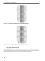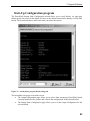
1
PowerDAQ DIO Series User Manual
PD2/PDXI-DIO Series Digital I/O Boards
PDL-DIO “Lab” Series Digital I/O Boards
including the -CT, -ST, -TS and PD2-DIO-128i models
February 2006 Edition
PN: PDAQ-MAN- DIO Rev 5.0.0
© Copyright 1998-2006 United Electronic Industries, Inc. All rights reserved
No part of this publication may be reproduced, stored in a retrieval system or transmitted in any
form by any means—whether electronic, mechanical, by photocopying, recording, or otherwise—
without prior written permission.
February 2006 Printing
Information furnished in this manual is believed to be accurate and reliable. However, no
responsibility is assumed for its use, or for any infringements of patents or other rights of third
parties that may result from its use.
All product names listed are trademarks or trade names of their respective companies.
See UEI’s website for complete Terms and Conditions of sale:
http://www.ueidaq.com/company/terms.aspx
Contacting United Electronic Industries
Mailing Address:
611 Neponset St
Canton, MA 02021
U.S.A.
For a list of our distributors and partners in the US and around the world, please see
http://www.ueidaq.com/partners/
Support:
Telephone:
(781) 821-2890
Fax:
(781) 821-2891
Also see the FAQs and online “Live Help” feature on our web site.
Internet Access:
Support
[email protected]
Web site
www.ueidaq.com
FTP site
ftp://ftp.ueidaq.com
ii
Table of Contents
Introduction ..........................................................................................................iii
Who should read this manual?..................................................................................................... iv
Conventions................................................................................................................................. iv
Organization of this manual ........................................................................................................ iv
1. PowerDAQ DIO Series Features Overview .................................................... 1
Overview ...................................................................................................................................... 1
Features ........................................................................................................................................ 2
PowerDAQ DIO Applications...................................................................................................... 2
Form Factors................................................................................................................................. 3
PowerDAQ DIO Models .............................................................................................................. 4
PCI-bus model summary .............................................................................................................. 5
PXI-bus model summary .............................................................................................................. 5
2. Installation and Configuration......................................................................... 7
Software installation ..................................................................................................................... 9
Hardware installation.................................................................................................................. 11
Making connections to panels .................................................................................................... 29
Confirming the installation......................................................................................................... 34
Hardware diagnostics (excludes PD2-DIO-128i) ....................................................................... 35
3. PowerDAQ DIO Series Architecture............................................................. 37
Functional Overview .................................................................................................................. 37
Programming Model................................................................................................................... 43
4. Digital I/O Subsystem ..................................................................................... 47
Architecture ................................................................................................................................ 47
I/O Modes................................................................................................................................... 48
DIO Channel List ....................................................................................................................... 56
Digital input change-of-state interrupts ...................................................................................... 58
Timing and Control .................................................................................................................... 60
Multiboard synchronization........................................................................................................ 62
High-speed user interrupts.......................................................................................................... 63
Enhanced Synchronous Serial Interfaces (ESSI)........................................................................ 63
5. Counter/Timer Subsystem.............................................................................. 65
6. Streaming I/O Versions .................................................................................. 69
DIO-64CT Continuous Event Counter ....................................................................................... 70
DIO-64ST/128ST Streaming Digital I/O.................................................................................... 71
DIO-64TS Timing Sequencer..................................................................................................... 74
7. Support Software............................................................................................. 81
Control Panel Applet .................................................................................................................. 81
i
DIO Test program .......................................................................................................................82
Start-Up Configuration program .................................................................................................83
PowerDAQ Example Programs ..................................................................................................86
Third-Party Software Support .....................................................................................................88
Appendix A: Specifications.................................................................................89
PD2-DIO Series ..........................................................................................................................89
PD2-DIO-128i.............................................................................................................................91
PDL-DIO Series..........................................................................................................................94
PDXI-DIO Series ........................................................................................................................96
Appendix B: PowerDAQ SDK Structure ..........................................................99
PowerDAQ Windows device drivers ........................................................................................100
PowerDAQ Windows DLLs .....................................................................................................100
PowerDAQ language libraries ..................................................................................................101
PowerDAQ Include files ...........................................................................................................101
PowerDAQ Linux support ........................................................................................................103
PowerDAQ QNX support .........................................................................................................103
Appendix C: Accessories...................................................................................104
Memory Upgrade ......................................................................................................................104
Screw-Terminal Panels .............................................................................................................104
Cables........................................................................................................................................105
Connectors ................................................................................................................................106
Signal-Conditioning Panels.......................................................................................................106
Appendix D: Warranty .....................................................................................107
Glossary ..............................................................................................................109
Index ...................................................................................................................123
Reader Feedback ...............................................................................................127
ii
Introduction
This manual describes the features and functions of hardware in the PowerDAQ series of PCI- and
PXI-bus digital input/output boards. These high-performance systems support functions including
64 digital I/O points (PCI and PXI bus) or 128 points (PCI bus only) and three user counter/timers.
Special models offer high-speed event-count input streaming (-CT versions), high-speed digital
I/O streaming and pattern generation (-ST versions), time-sequencing functions (-TS versions) and
isolated I/O (PD2-DIO-128i).
Model summary
PCI bus
PD2-DIO-64, PD2-DIO-128, PD2-DIO-128ST-KIT
PDL-DIO-64, PDL-DIO-64CT-KIT, PDL-DIO-64ST-KIT, PDL-DIO-64TS-KIT,
PD2-DIO-128i-KIT
cPCI/PXI bus
PDXI-DIO-64, PDXI-DIO-64CT-KIT, PDXI-DIO-64ST-KIT, PDXI-DIO64TS-KIT
Note
The -CT, -ST, -TS and –I versions come standard as a KIT package that, for the PDL and PDXI
families (but not the PS2 family) includes the PD-64KMEM memory option (64k x 24 bits of
onboard expansion memory) along with all required brackets, cables and termination panels. Any
reference in this manual to the -CT, -ST and -TS versions imply the KIT version. The bare board
without these extras is available upon special request.
Other boards in the PowerDAQ Series (see separate manuals) include the
• PD2/PDXI-MF Series—Multifunction analog and digital I/O cards
• PD2/PDXI-MFS Series—Simultaneous-sampling multifunction I/O cards
• PDL-MF—Entry level “Lab” multifunction card for the PCI bus
•
PD2/PDXI-AO Series—Analog output (with digital I/O, counter/timers)
iii
Introduction
Who should read this manual?
This manual has been designed to benefit the user of PowerDAQ DIO boards. To use these
products it is assumed that you have basic PC skills and that you are familiar with Microsoft
Windows NT/2000/XP or the Linux operating environments.
Conventions
To help you get the most out of this manual and our products, please note that we use the
following conventions:
TIP
Note
Tips are designed to highlight quick ways to get the job done or reveal good ideas you might not
discover on your own.
Notes alert you to important information.
CAUTION! Caution advises you of precautions to take to avoid injury, data loss or system
crash.
Text formatted in bold typeface generally represents type that should be entered verbatim. For
instance, it can represent a command as in the following example: “You can run our setup utility
using a command such as setup.exe.”
Organization of this manual
The PowerDAQ DIO User Manual is organized as follows:
Introduction
This section gives you a quick introduction to the PowerDAQ family, features specific to the DIO
Series, the various models available, and what you need to get started.
Chapter 1—PowerDAQ DIO Series Features Overview
In this chapter you get a more detailed review of how PowerDAQ DIO boards function, the
features they offer, and a rundown on all available models.
Chapter 2—Installation and Configuration
This chapter explains how to install the PowerDAQ Software Suite as well as install, configure
and verify the operation of your PowerDAQ DIO board.
Chapter 3—PowerDAQ DIO Series Architecture
iv
Introduction
This chapter discusses the internal structure and subsystems of your PowerDAQ DIO board. It
also reviews the general programming model for creating applications.
Chapter 4—Digital I/O Subsystem
This chapter explains, in considerable detail, how the DIO subsystem runs—including the various
I/O modes—and how you can best take advantage of its features.
Chapter 5—Counter/Timer Subsystem
This chapter explains, in considerable detail, how the Counter/Timer subsystem runs and how you
can best take advantage of its features.
Chapter 6—Streaming I/O Versions
This chapter explains the enhanced functionality of three special versions of our DIO cards: the
-CT, -ST, and -TS models.
Chapter 7—Support Software
Each board ships with the PowerDAQ Software Suite, an extensive collection of sample programs
and utilities. This chapter reviews the support software we supply and how it can help you write
applications more quickly.
Appendix A—Specifications
This chapter lists the specifications for all PowerDAQ DIO models.
Appendix B—PowerDAQ SDK Structure
This section explains where you can expect to find language drivers, include files and example
programs for various languages.
Appendix C—Accessories
This appendix lists the PowerDAQ DIO accessories including cables, termination panels and
external backplanes.
Appendix D—Warranty
This section contains a detailed explanation of the warranty for PowerDAQ DIO boards.
Glossary
This section contains an alphabetical list and description of terms used in this manual and with
other PowerDAQ products.
Index
The Index alphabetically lists topics covered in this manual so you can quickly find references to
them.
v
Introduction
Other PowerDAQ Documentation
The PowerDAQ PD2/PDXI DIO Manual is one part of the documentation set available for the
PowerDAQ system. There are several other manuals you might want to read before programming
an application. They are available either on the PowerDAQ Software Suite CD or can be
downloaded from the UEI web site.
PowerDAQ Programmer Manual
PowerDAQ for LabVIEW User Manual
PowerDAQ for LabVIEW Real-Time Software Manual
Feedback
We are interested in any feedback you might have concerning our products and manuals. A Reader
Evaluation form is available on the last page of the manual, or you can send an email to
[email protected].
vi
1. PowerDAQ DIO Series
Features Overview
This chapter provides an overview of the key features of the PowerDAQ DIO Series as well as
detailed information on the various models currently available.
Overview
Thank you for purchasing a PowerDAQ DIO board. We designed these products from the ground
up to provide the best possible features, reliability and performance at an economical price.
The associated PowerDAQ Software Suite that ships with the hardware has been written
specifically for these boards. It includes support for numerous third-party software products
including realtime operating systems such as real-time Linux and QNX. It also supports most
popular test-programming environments such as LabVIEW (Windows, Linux, Real-Time),
Agilent VEE and many others.
We designed all PowerDAQ digital IO boards to correct the flaws of traditional boards based on
the Intel 8255 chip. The PD2/PDL/PDXI-DIO is feature-rich; no longer must you design external
circuitry for startup states, to overcome limitations associated with the 8255 or relays, nor must
you have a separate mechanism for generating interrupts. Additionally, the boards feature ESDprotected I/O lines and automatic user-defined values on power-up, values that load 200 msec
after a system reset.
The PowerDAQ DIO boards are configured with either 64 or, for PD2 versions only, also 128
lines. The boards use 16-bit line drivers instead of 8255 devices and thus allow you to configure
the startup state direction (input/output) in groups of 16, also output port values are per-bit
configurable.. The on-board DSP offers three user-accessible 24-bit counter/timers, four additional
100-nsec high-speed interrupts, and two 16.5M bps ESSI (Enhanced Synchronous Serial Interface)
ports.
Also special member of PD2-DIO family – PD2-DIO-128i offers 128 optically isolated channels
with fixed direction, 64 inputs and 64 outputs accessible in groups of 16 channels.
1
1. Features Overview
Features
Key features of PowerDAQ DIO boards include:
•
•
•
•
•
•
•
•
•
•
•
•
•
•
•
•
•
•
Note
24-bit Motorola 56301 digital signal processor set to run at 66 MHz in order to support
the 33-MHz 32-bit PCI bus (-TS boards use a 100-MHz DSP)
PCI/cPCI/PXI-bus interface (PCI 2.2 compliant, 5V version; check factory for
availability of 3.3V versions).
64 or 128 static digital I/O points (5V TTL), configured in 16-bit ports
64k x 24-bit memory option for PDL and PDXI versions (not available on PD2 versions
at this time)
High output-current drive (-32/64 mA per pin, 180 mA per port)
Generate interrupts on any I/O line
The PDL- and PDXI-DIO models provide 10-kΩ pulldown resistors on all I/O lines;
these resistor positions can be left unpopulated upon customer request. The PD2-DIO
models do not have any pullup or pulldown resistors installed.
Four separate high-speed (100-nsec) interrupt lines
No legacy 8255-based devices
Ideal for controlling solid-state relays
User-defined powerup states in groups of 16-bit ports with per-bit state for the output
mode (High, Low, Tri-stated)
Two ESSI (Enhanced Synchronous Serial Interface) ports
Three 24-bit counter/timers with pulse-width modulation and measurement modes
High-speed digital streaming to/from disk (-CT, -ST models)
High-precision continuous pulse/word generation (-TS models)
Optical isolation (PD2-DIO-128i)
Port scan list
Multiboard synchronization through external connections
For the full list of specifications, see Appendix A: Specifications.
PowerDAQ DIO Applications
PowerDAQ DIO Series boards supply a wide range of powerful features that allows you to
employ them in a variety of end-user applications. The most common are:
• Electromechanical relay control
• Solid-state relay control
• Alarm-system sensors
• Digital streaming
• Digital motion control and closed-loop applications
• Counter/timer streaming
• Pulse-width modulation generation and measurement
2
1. Features Overview
•
TIP
Note
Custom high-speed synchronous serial interfaces
UEI welcomes inquiries into custom OEM applications that require specialized hardware or
software modifications. Please call the factory or your local sales rep to consult with our engineers.
The easiest way to expand the possibilities of a PowerDAQ DIO board is to use it in the same
backplane as a PowerDAQ MF, MFS or AO Series board. They are all easily synchronized and use
the same drivers and API.
Form Factors
PowerDAQ DIO boards are available in three different formats:
•
•
•
•
PD2-DIO—this half-slot PCI-bus card comes with either 64 or 128 channels and uses a
100-way high-density ribbon cable connector. Measurements: pc-board, with edge
connector, 218 x 106.5 mm; with mounting bracket, 220 x 106.5 mm.
PD2-DIO-128i – this full-slot PCI card comes with 128 optically isolated channels which
consists of 64 inputs and 64 outputs distributed over four 40-way 0.1” boxed headres.
ESSI ports, high-speed IRQs and conter-timers are not user-accessible on this board.
PDL-DIO—a one-third slot card, also on the PCI bus, this 64-channel digital I/O board
comes with a high-density 96-way shielded metal pinless connector. It’s ideal for noisy
industrial environments. Measurements: pc-board, with edge connector, 132 x 105 mm;
with mounting bracket, 140 x 105 mm.
PDXI-DIO—for the PXI bus, this card comes only in a 64-channel version. It
implements PXI bus clocking and advanced triggering. It’s also the most robust and
protected version. It shares all cabling and accessories with PDL-DIO family.
Measurements: pc-board, 160 x 100 mm; with mounting bracket and bus connector, 100
x 172 mm.
3
1. Features Overview
PowerDAQ DIO Models
PowerDAQ DIO model numbers are based on the following conventions:
[Family] - DIO - [Channels][Optional model designator]
Family:
•
•
•
PD2
PDL
PDXI
PCI-bus boards
“Lab” boards, PCI bus
PXI/CompactPCI boards
Number of channels
•
•
64
128
(available only on PD2 Series)
Optional models
• CT
High-speed event-count input streaming
This model repetitively counts events in a certain time window for long periods of time without
the need for reprogramming, and it streams the counts for each period into either system RAM or a
disk file.
• ST
High-speed digital streaming and pattern generation
This model streams data in and out of the digital I/O lines at user-programmable speeds
continuously for long periods of time and at rates as high as 1.6 MHz. It takes the source data
either from system RAM or a disk file.
• TS
Timer sequencer
This model generates a continuous series of digital pulses or words without the need to reprogram
the subsystem between each output sequence. The width of each pulse or word can vary with each
new entry. The definitions of the timing and raw data reside in system RAM or a disk file, and the
subsystem can continually repeat a certain sequence.
• i
Optoisolated DIO (125V isolation, 12-32V DIO)
This model provide reliable optical isolation between PC and all I/O ports and also between 16-bit
ports themselves.
Note
4
Only the -ST, -CT and -TS boards are suitable for streaming I/O operations. Standard PowerDAQ
DIO boards provide only static I/O points that are updated based on the host clock, and only at update
rates < 1 kHz under Windows or 10 kHz under Linux or QNX.
1. Features Overview
PCI-bus model summary
Model
Connector
Digital I/O features
PD2-DIO-64
PD2-DIO-128
PD2-DIO-128ST-KIT
100-way header
2 x 100-way header
2 x 100-way header
PD2-DIO-128i
PDL-DIO-64
4 x 40-way 0.1”
header
96-way pinless
64 points (in banks of 16)
128 points (in banks of 16)
128 points (in banks of 16) with high-speed
streaming
128 points (in banks of 16), 64 inputs and 64
outputs
64 points (in banks of 16)
PDL-DIO-64CT-KIT
96-way pinless
DL-DIO-64ST-KIT
96-way pinless
PDL-DIO-64TS-KIT
96-way pinless
64 points (in banks of 16) and 2-channel event
counting
64 points (in banks of 16) with high-speed
streaming
64 points (in banks of 16 with timing-sequencer
output)
Table 1.1—PowerDAQ DIO Models
PXI-bus model summary
Model
Connector
Digital I/O features
PDXI-DIO-64
PDXI-DIO-64CT-KIT
96-way pinless
96-way pinless
PDXI-DIO-64ST-KIT
96-way pinless
PDXI-DIO-64TS-KIT
96-way pinless
64 points (in banks of 16)
64 points (in banks of 16) and 2-channel event
counting
64 points (in banks of 16) with high-speed
streaming
64 points (in banks of 16) with timing-sequencer
output
Table 1.2—PowerDAQ DIO Models
Note All DIO boards have two high-speed ESSI serial interfaces as well as three 24-bit counter/timers.
5
1. Features Overview
The -KIT versions come in these configurations:
1a. the PDL-DIO-64CT-KIT comes with:
• the PDL-DIO-64CT card
• the PD-64KMEM option (onboard expansion memory holds 64k I/O words)
• the PDL-DIO-CBL-16-36 1m twisted-pair cable set
• the PDL-DIO-STP-64KIT (which combines the standard rear-bracket connector and
screw-terminal panel for making DIO connections, and a connection for the PDL-DIOCBL-16-36 for the counter/timer channels).
1b. the PDXI-DIO-64CT-KIT
Same as above except comes with the PXI version of the DIO card.
2a. the PDL-DIO-64TS-KIT comes with:
• the PDL-DIO-64TS card with a 100-MHz DSP
• the 64KMEM option (64k x 24 bits of onboard expansion memory to increase the Time
Sequence list from 256 to 8192 entries)
• thePDL-DIO-STP-64KIT (which combines the standard rear-bracket connector and
screw-terminal panel for making DIO connections).
2b. the PDXI-DIO-64TS-KIT
Same as above except comes with the PXI version of the DIO card.
3a. the PDL-DIO-64ST-KIT comes with:
• the PDL-DIO-64ST card
• the PD-64KMEM option (64k x 24 bits of onboard expansion memory)
• the PDL-DIO-STP-64KIT (which combines the standard rear-bracket connector and
screw-terminal panel for making DIO connections).
3b. the PDXI-DIO-64ST-KIT
Same as above except comes with the PXI version of the DIO card.
3c. the PD2-DIO-128ST-KIT
Same as above except comes with the 128-line PCI DIO card and all necessary
connectors and brackets. Does not accommodate the 64k memory option at this time.
3d. the PD2-DIO-128i-KIT comes with:
• the PD2-DIO-128i card
• the 4x PD-STP-40
• the 4x PD-CBL-40 (40-way ribbon cable from the board to the terminal panel, 1m)
6
2. Installation and Configuration
This chapter describes the hardware and software installation and configuration of the PowerDAQ
DIO board.
Before installing a PowerDAQ board, be sure to read and understand the following information.
System requirements
•
Note
•
•
Note
A system with either a PCI, CompactPCI or PXI backplane and a free slot, a Pentium-class
processor, and a BIOS compliant with PCI Local Bus Specification Rev 2.1 or greater. Note that
these cards are designed as 5V PCI cards and do not presently support the 3.3V version of the bus;
check the factory for updates in this regard.
The PowerDAQ PD2-DIO or PDL-DIO PCI-bus interface must be mechanically keyed as 32/64 bit,
5V power and signaling.
An operating system including Windows NT 4.0, 2000 or XP, Linux, Realtime Linux or QNX
The minimum recommended amount of RAM is 32M bytes for Windows NT, QNX and Linux, 64M
bytes for Windows 2000 and 128M bytes for XP
Support for Windows 95/98/Me was discontinued in Version 3.0 of the PowerDAQ SDK. For certain
cards we might have legacy drivers that work under these operating systems; check the sales
department for details.
Packing list
In your PowerDAQ package, you should have received the following:
•
•
•
•
•
Note
a PowerDAQ DIO board
all necessary brackets, cables and termination panels (with -KIT versions)
a calibration certificate
this manual
a CD containing the PowerDAQ Software Suite, including the full Software Development Kit
(SDK) and documentation
The label on the CD shows the version number of the SDK. The latest release of our support software
is always available for downloading at www.ueidaq.com. Please refer to the readme file for details
about new features for the SDK version with which you are working.
7
2. Installation and Configuration
Caution:
Although all PowerDAQ DIO boards are designed for maximum protection against electrostatic
discharges, they still contain sensitive electronic components. When handling your PowerDAQ
DIO board, make certain you observe good grounding and other safety practices. In particular:
8
•
Ensure that you are properly grounded during hardware installation; a wrist strap is a
good idea.
•
Discharge any static electricity by touching the metal part of your PC while holding the
board in its antistatic bag.
2. Installation and Configuration
Software installation
Support software on the PowerDAQ Software Suite CD that ships with your DIO Series card
supports a wide range of operating systems and programming environments (see details in Chapter
6, “Third-Party Support Software”). This section describes how to load the UEI software onto a
Windows-based computer and run some initial tests. (For a non-Windows OS installation, please
refer to the procedures outlined in the readme file distributed with the corresponding driver.)
Note
Because the installation process modifies your Windows registry, you should always install or
uninstall the software using the appropriate utilities. Never remove PowerDAQ software from your
PC directly by deleting individual files; always use the Uninstall program in the PowerDAQ folder,
or use the Windows Control Panel/Add-Remove Programs utility.
Note The PowerDAQ SDK must be installed before you plug in a PowerDAQ board to ensure that the
driver properly detects the board.
Note All third-party software must be installed prior to installing the PowerDAQ SDK.
To install the PowerDAQ SDK:
1.
2.
3.
4.
5.
Start your PC; if running Windows NT, 2000 or XP, log in as an administrator.
Insert the PowerDAQ Software Suite CD into your CD-ROM drive. Windows
should automatically start the PowerDAQ Setup program. If you see the UEI logo
and then the PowerDAQ Welcome screen, go to Step 6.
If the Setup program does not start automatically, select Run from the Start menu.
Enter d:\setup.exe in the Open: textbox (substitute the correct letter if d: is not the
drive letter for your CD-ROM drive.)
Click OK.
9
2. Installation and Configuration
Figure 2.1—PowerDAQ Software Installation Startup Screen
6.
7.
8.
10
As the Setup program runs, it will request information about the PowerDAQ
configuration. Unless you’re an expert user and have specific requirements, we
advise you to select a Typical installation and accept the default configuration.
If the Setup program asks for information about third-party software packages that
you do not have installed on the PC, leave the text box blank and click the Next
button.
When the installation is complete, restart the PC when prompted.
2. Installation and Configuration
Hardware installation
Before installing the hardware, you should first be familiar with all of a board’s connectors, their
locations and how to work with them.
Connectors/panels for DIO Series boards
The following diagrams point out any on-board connectors or headers of interest to end-users; all
others are reserved for factory use. If these standard cables don’t meet your needs because of their
length, their end connectors or for another reason, UEI can manufacture a cable to meet custom
requirements. For details, please contact the factory or your distributor.
PD2-DIO connector layout
PowerDAQ-PD2-DIO Series boards (including the -128ST model) have five connectors. None of
them are mounted on the front bracket, which has only an opening through which you snake
cables from the board to a termination panel.
Figure 2.2—PowerDAQ PD2-DIO connector layout
•
•
J1—Digital I/O connector. This 100-pin connector provides access to the board’s first 64 digital
I/O lines as well as LIn0 (the External Latch signal, see details in the “Architecture” section on
page 47) as well as 5VPJ (a 5V source jack outfitted with a 200-mA resettable fuse; with this line
you can supply power to external circuits). If you wish to develop a custom cable, you can purchase
the matching connector from the factory or your distributor. Similarly, should you want to build an
external circuit that uses the high-density IDC connector normally mounted on the board, you can
special-order it from the factory or your distributor.
J2—Digital I/O connector. This 100-pin connector handles the extra DIO points (DIO 64-127) on
high-density cards as well as other signals including LIn1 (an external latch line).
11
2. Installation and Configuration
Note
•
•
•
12
To access all 128 channels on the PD2-DIO-128, you must purchase two cable/termination panel sets,
we recommend the PD2-DIO-STP-64-KIT for each set of 64 channels.
J3—Counter/timer, IRQ connector. A 14-pin 0.1” header with counter/timer inputs and interrupt
lines.
J4—ESSI connector. A 12-pin header with lines that control the first of two Enhanced Synchronous
Serial interfaces on the DSP. It is a 2 x 12-pin non-boxed 0.1” header on PD2-DIO boards and 26pin boxed 0.1” header on all other models. A mated IDC cable fits over both J4 and J5 on the PD2DIO boards.
J5—ESSI connector. A 12-pin header with lines that control the second of two Enhanced
Synchronous Serial interfaces on the DSP. A mated IDC cable fits over both J4 and J5 on the PD2DIO boards.
2. Installation and Configuration
Figure 2.3a—Physical layout of J1 on PD2-DIO.
Figure 2.3b—Connector pinout assignments for J1 on PD2-DIO Series boards
13
2. Installation and Configuration
Fig 2.4a— Physical layout of J2 (appears only on the PD2-DIO-128).
Figure 2.4b—Connector pinout assignment for J2 (appears only on the PD2-DIO-128 board)
14
2. Installation and Configuration
Figure 2.5a—Physical layout of J3 on PD2-DIO Series boards.
Figure 2.5b—Connector pin assignments for J3 on PD2-DIO Series boards.
Figure 2.6a—Physical layout of J4 and J5 on PD2-DIO.
Figure 2.6b—Connector pin assignments for J4 (left) and J5 (right) on PD2-DIO Series boards.
Note
The J4/J5 connectors are designed to use either a 26-way IDC header for both ports, or one 12-way
IDC header for single-port operation. For the combined J4/J5 port, the pin numbering is 1-12 for
ESSI0 (J4); pins 13 and 14 are not connected; pins 15-26 for ESSI1 (J5). To see how the 26-pin
connector fits over both headers, refer to the PD2-DIO-CBL-26 cable in Figure 2.14.
15
2. Installation and Configuration
PD2-DIO-128i connector layout
PowerDAQ PD2-DIO-128i board has four connectors. None of them are mounted on the front
bracket, which has only an opening through which you snake cables from the board to a terminal
panel.
Figure 2.7a – PowerDAQ PD2-DIO-128i connector layout
•
J1- (for digital inputs) connects four input bytes (internally arranged for the software as a two 16bit output ports). Port 0 (DIN0 - DIN15) is powered with +VIN0, and Port 1 (DIN16 - DIN31) is
powered via +VIN1
•
J2 - (for digital inputs) connects four input bytes (internally arranged for the software as a two 16bit output ports). Port 2 (DIN32 - DIN47) is powered with +VIN2 and Port 3 (DIN48 - DIN63) is
powered with +VIN3
•
J3 - (for digital outputs) connects 4 output bytes (internally arranged for the software as a two 16bit output ports). Port 0 (DOUT0 - DOUT15) is powered with +VOUT0/GND0, and Port 1
(DOUT16 - DOUT31) is powered with +VOUT1/GND1
•
J4 - (for digital outputs) connects 4 output bytes (internally arranged for the software as a two 16bit output ports). Port 2 (DOUT32 - DOUT47) is powered with +VOUT2/GND2, and Port 3
(DOUT48 - DOUT63) is powered with +VOUT3/GND3
16
2. Installation and Configuration
Figure 2.7b – Physical layout of J1-J4 Connectors on PD2-DIO-128i board
Figure 2.7c – Connector pin assignments for J1 on PD2-DIO-128i board
Figure 2.7d – Connector pin assignments for J2 on PD2-DIO-128i board
17
2. Installation and Configuration
Figure 2.7e – Connector pin assignments for J3 on PD2-DIO-128i board
Figure 2.7f – Connector pin assignments for J4 on PD2-DIO-128i board
PDL-DIO connector layout
PowerDAQ-PDL-DIO Series boards have three user connectors, one of which is situated on the
board’s mounting bracket. These connectors, although physically located on different positions on
the board, are electrically identical to the connectors on the PDXI-DIO Series.
18
2. Installation and Configuration
Figure 2.8a—PowerDAQ PDL-DIO connector layout
•
•
•
J1—Digital I/O connector. This 96-position pinless connector built into the card’s mounting
bracket provides access to the board’s 64 digital I/O lines along with external latch input (LIn0,
see details in the Architecture section on page 47) as well as the propagate strobe output (PROP0,
see details in the Architecture section on page 47). If you wish to develop a custom cable, you can
purchase a matching connector and metal cover from your distributor or the factory; the UEI part
number is PD-CONN.
J3—Counter/timer and IRQ connector. This is a 16-pin boxed 0.1” header with counter/timer
inputs and interrupt lines.
J4—ESSI connector. This 26-pin 0.1” header has lines that control both of the Enhanced
Synchronous Serial interfaces on the DSP.
Figure 2.8b—Physical layout of J1 Connector on PDL-DIO and PDXI-DIO Series boards.
19
2. Installation and Configuration
Figure 2.8c—Connector pin assignments for J1 on PDL-DIO and PDXI-DIO Series boards
Figure 2.9a—Physical layout of J3 Connector on PDL-DIO and PDXI-DIO Series boards (and J6 on
PDXI-DIO Series boards)..
20
2. Installation and Configuration
Figure 2.9b—Connector pin assignments for J3 on PDL-DIO boards (and J6 on PDXI-DIO Series
boards).
Figure 2.10a—Physical layout of J4 Connector on PDL-DIO boards (and J2 on PDXI-DIO Series
boards).
Figure 2.10b—Connector pin assignments for J4 on PDL-DIO boards (and J2 on PDXI-DIO Series
boards).
21
2. Installation and Configuration
PDXI-DIO connector layout
PowerDAQ-PDXI-DIO Series boards (including the -CT, -ST and -TS models) have three user
connectors, one of which is situated on the board’s mounting bracket. These connectors, although
physically located on different positions on the board, are electrically identical to the connectors
on the PDL-DIO Series.
Figure 2.11—PowerDAQ PDXI-DIO connector layout.
•
•
•
22
J1—Digital I/O connector. This 96-pin connector built into the card’s mounting bracket
provides access to the board’s 64 digital I/O lines along with external latch line (LIn0) as well
as a programmable propagate/strobe signal PROP0 (see details in the Architecture section on
page 47). If you wish to develop a custom cable, you can purchase a matching connector and
metal cover from your distributor or the factory; The UEI catalog number is PD-CONN.
J2—ESSI connector. A 26-pin 0.1” header with lines that control both of the Enhanced
Synchronous Serial Interfaces on the DSP.
J6—Counter/timer and IRQ connector. A 16-pin boxed 0.1” header with counter/timer inputs
and interrupt lines.
2. Installation and Configuration
Installing PD2-DIO and PDL-DIO cards in PCI-bus machines
It is possible to install multiple PowerDAQ DIO boards in one computer; the only limit is the
number of free PCI or PXI/cPCI slots.
You can install a PowerDAQ PD2/PDL-DIO Series board in any free PCI slot; follow these steps:
1.
2.
3.
4.
5.
6.
•
Turn off the PC and disconnect the power.
Remove the chassis cover and make sure you have clear access to the PCI slots.
Remove the DIO board from the antistatic bag (it’s a good idea to save the bag in the
event you later want to remove the card from the PC).
Inspect the board for any damage. If you spot any problems, contact Customer Support to
evaluate the problem and possibly the need to return the board to UEI.
Before physically installing a board, first make certain that you have attached all the
cables that attach to external termination panels (see the previous section in this chapter
“Connectors/panels for DIO Series boards” on page 11). Note that on the PD2 family, the
board’s mounting bracket does not have a connector; it merely has an opening through
which you snake one or more cables depending on your I/O configuration.
If you are installing a PDL-DIO board and plan to use its ESSI ports, its counter/timers,
or want access to external clocking, you must either snake a ribbon cable beside the
card’s mounting bracket or will need another slot’s mounting bracket.
For the first option: Start by connecting the appropriate cables (PDL-DIO-CBL-16 or 26) to the J3 or J4 connectors on the board. Next remove the mounting bracket from the
card; it attaches with two screws; note that the J1 connector is mounted directly on the
board and does not come off with the bracket. Now snake the cable(s) through the hole in
the bracket. Finally, reattach the mounting bracket, making sure that all cables as well as
the J1 connector come through the hole in the bracket.
Fig 2.12a—Passing cables for J3 or J4 through the mounting bracket on a PDL-DIO board.
•
For the second option, purchase the PDL-DIO-CBL-37 assembly. It has a split cable that
attaches to both J3 and J4; these cables combine into one that attaches to a connector
situated inside a mounting bracket that takes an adjacent slot in the PCI bus. The
23
2. Installation and Configuration
assembly also include a cable that leads from the bracket side outside the PC to the
screw-terminal panel of your choice.
Fig 2.12b—Using an adjacent slot’s bracket position to pass signals from J3 or J4 on a PDL-DIO
board.
7.
With all board cables attached, insert the DIO card into a slot. (If the bus slots have not
been used for a long time, it’s a good idea to clean the contacts; to do so, insert and
immediately remove the DIO card, clean the edge connector with alcohol, and then
reinsert the board.)
8. Screw the bracket in place and replace the cover on the computer.
9. On PDL-DIO Series cards, find the cable that plugs into the connector on the mounting
bracket, plug it in and also do the same on the corresponding terminal panel.
10. Turn on the PC.
The PowerDAQ PD2/PDL-DIO board is now installed. All configuration settings are made in
software.
24
2. Installation and Configuration
Fig 2.12c – Passing cables for J1-J4 connectors through the
mounting bracket on a PD2-DIO-128i board.
25
2. Installation and Configuration
Installing PDXI-DIO cards in PXI/CompactPCI machines
You can install a PowerDAQ PDXI-DIO Series board in any free CompactPCI or PXI-bus slot;
follow these steps:
Note
You can also use PDXI cards in a standard Compact PCI chassis—but all PXI-specific functions are
not available.
We recommend you use the first available slot and complete the following instructions:
1. Turn off your PC.
2. Remove the blank bracket from the desired slot.
3. If you are installing a PDXI-DIO board and plan to use its ESSI ports, its counter/timers,
or want access to external clocking, you must either snake a ribbon cable beside the
card’s mounting bracket or will need another slot’s mounting bracket. First connect the
appropriate cables (PDL-DIO-CBL-16 or -26) to the J2 or J6 connectors on the board.
Next remove the mounting bracket from the card; it attaches with two screws; note that
the J1 connector is mounted directly on the board and does not come off with the bracket.
Now snake the cable(s) through the hole in the bracket. Finally, reattach the mounting
bracket, making sure that all cables as well as the J1 connector come through the hole in
the bracket.
Figure 2.13—Passing cables for J2 or J6 through the mounting bracket on a PDXI-DIO board.
4.
5.
6.
26
Insert the PDXI-DIO board into a cPCI or PXI slot. To do so, push the insertion lock
down and push the board carefully into the chassis, making sure that the board edges are
located in the safety rails.
Make sure that the board is completely inserted into the slot and the pull the lock back up.
Secure the safety screw on the bracket of the PDXI-DIO board.
2. Installation and Configuration
7.
8.
Find the cable that plugs into the connector on the mounting bracket, plug it in and also
do the same on the corresponding terminal panel.
Turn the PC on.
The PowerDAQ PDXI-DIO board is now installed. All configuration settings are made in
software.
Base address, DMA and interrupt settings
When you power up your PC, the PCI or PXI bus automatically configures any PowerDAQ boards
that are installed. It’s not necessary to set any base address, DMA channels or interrupt levels. Be
aware, though, that performance problems can arise when the system has insufficient interrupts
and is unable to assign a unique one to each peripheral so that a PowerDAQ board must share an
interrupt with some other device. One solution is to decide which system resources you do not
need—possible candidates being serial ports, the parallel port, USB ports or network interfaces—
and disable their interrupts, thereby freeing those lines up for assignment to other devices. This
can lead to the optimal case where a PowerDAQ board is assigned a dedicated IRQ line.
Note PowerDAQ boards are designed to share interrupts, but we do not recommend that they share them
with devices such as video drivers, network cards or hard disks. These devices tie up interrupt lines
extensively and can significantly delay responding to an interrupt from a data-acquisition board.
Although Windows NT/2000 are not realtime operating systems, your PowerDAQ board is a realtime
system within the PC thanks to its own DSP and realtime kernel. Many motherboard manufacturers
allow you to set an IRQ level to a particular PCI slot. If you do not use your PC’s serial or parallel
ports, you can disable them and use IRQ 3, 4, 5 or 7 for your data-acquisition boards.
Note
A data-acq card’s interrupt is generally assigned by the PC BIOS, and some PC systems even let you
reassign it during the boot process. If your motherboard has an Advanced Interrupt Controller, simply
enable it in the BIOS. This allows you to use more than 16 generic interrupt lines. If you don’t have
this facility, use manual settings to assign the interrupt to the PCI slot where PowerDAQ board is
installed.
Note
Modern motherboards can easily contain four, five or even more PCI slots plus integrated PCI
devices such as networking modules and a video driver. Usually only three of these slots are
independent and don’t share interrupts with these host system peripherals. Please refer to your
motherboard manual to find out which slots share interrupts and cannot be used for fast data
acquisition.
The PDXI-DIO Series boards incorporate support for the PXI-TRIGx and PXI_STAR lines in
accordance with the PXI standard.
Startup configuration
Often it’s critical that the lines on a digital I/O board have a predictable output state during the
startup process. PowerDAQ DIO boards provide a flexible way to define the startup state of every
I/O point. For this we provide the StartUpState utility (see Chapter 6 “Software Support”). The
card stores startup values along with other critical data in an on-board EEPROM. Those values are
loaded from memory to the board’s registers approximately 10 msec following the rising edge of
27
2. Installation and Configuration
the system Reset signal. On the PXI boards, that EEPROM also stores the configuration of the
PXI lines.
28
2. Installation and Configuration
Making connections to panels
PD2-DIO Series wiring
When working with PD2-DIO Series boards, the most convenient way to gain field access to
signals—including those for the first 64 digital I/O points, the counter/timers, interrupts and ESSI
ports—is to use the PD2-DIO-STP-64 screw-terminal panel; for high-density applications where
you need more than 64 digital I/O points, you must employ a second PD2-DIO-STP-64 panel.
Figure 2.14—Wiring a PD2-DIO series board to the PD2-DIO-STP-64 screw-terminal panel. The PD2DIO-CBL-100 carries the digital I/O signals; the PD2-DIO-CBL-26 fits over both J4 and J5 to carry all
ESSI signals; the PD2-DIO-CBL-16 connects to J3 and carries counter/timer and interrupt signals.
Figure 2.14 shows the typical connections between the PD2-DIO and PD2-DIO-STP-64 terminal
panel. J1 accepts a 1m, 100-conductor IDC cable (PD2-DIO-CBL-100) that plugs directly into the
terminal panel. For high-density applications with more than 64 digital I/O points, you need an
additional panel/cable combination.
If the application involves the counter/timers or high-speed interrupt lines, you must also make a
connection to J3 using the PD2-DIO-CBL-16. This 16-conductor cable uses twisted-pair wiring
and measures 18”. The other end plugs directly into the -STP-64 or a custom user board.
If your application involves use of the high-speed ESSI serial ports, you make connections from
J4 and J5 to the terminal panel with the help of the PD2-DIO-CBL-26. This is an 18”, 26conductor twisted-pair cable that plugs directly into the STP-64 or a custom user board. This one
26-pin connector fits over the two 12-pin connectors on the board.
29
2. Installation and Configuration
PD2-DIO-128i wiring
When working with PD2-DIO Series boards, the most convenient way to gain field access to
signals is to use the PD-STP-40 screw-terminal panel; please note, that because of the isolation
nature of the PD2-DIO-128i board external 12-32V power supply is required for the proper
operation, please refer to the simplified channel schematic below for the detail:
Simplified Single Channel Diagram
PDL-DIO Series wiring
When working with PDL-DIO Series boards, the most convenient way to gain field access to
signals—including those for the 64 digital I/O points, the counter/timers, interrupts and ESSI
ports—is to use the PDL-DIO-STP-64 screw-terminal panel.
30
2. Installation and Configuration
Figure 2.15—Wiring from PDL-DIO card to the PDL-DIO-STP-64 screw-terminal panel. Note that if
no slot is free, you can also snake the two internal ribbon cables through the front mounting bracket.
Figure 2.15 shows the typical connections between the PDL-DIO and the PDL-DIO-STP-64
terminal panel. J1 on the mounting bracket accepts the PDL-DIO-CBL-96, a 1m round shielded
cable whose other end plugs directly into the terminal panel.
If your application involves the counter/timers, high-speed interrupts or ESSI ports, you must
either use the mounting bracket from an adjacent slot or snake the cables through the card’s own
mounting bracket; see the section on Connectors/panels for DIO Series boards on page 11 for
details.
31
2. Installation and Configuration
PDXI-DIO Series wiring
When working with PDXI-DIO Series boards, the most convenient way to gain field access to
signals—including those for the 64 digital I/O points, the counter/timers, interrupts and ESSI
ports—is to use the PDXI-DIO-STP-64 screw-terminal panel.
Figure 2.17—Wiring from PDXI-DIO card to the PDXI-DIO-STP-64 screw-terminal panel.
Figure 2.17 shows the typical connections between the PDXI-DIO and PDXI-DIO-STP-64
terminal panel. J1 on the mounting bracket accepts the PDXI-CBL-96, a 1m round shielded cable
whose other end plugs directly into the terminal panel.
If your application involves the counter/timers, high-speed interrupts or ESSI ports, you need a
dedicated cable for each: the PD2-DIO-CBL-16 for J3, or the PD2-DIO-CBL-26 for J4. In this
case you unscrew the bracket from the board, slide the cable(s) through the slim rectangular hole
adjacent to the card, and screw the bracket back onto the board. For details see Figure 2.13 in the
section Connectors/panels for DIO Series boards on page 11.
32
2. Installation and Configuration
Solid-State Relay Panels
Some users wish to connect their DIO Series boards to commercial relay modules to switch very
high voltages or currents, or to achieve high levels of isolation. These users should replace the
normal screw-terminal panel with a breakout distribution panel that connects to the main J1
connector on a DIO board; this panel distributes 64 digital I/O lines into four sets 16 lines, each
being routed through a 50-pin IDC connector. These connectors, in turn, typically attach to
backplanes (such as the PD2-DIO-BPLANE16) that hold relay modules.
The choice of cable and panel depends on the DIO board family:
• PD2: panel, PD2-CONN64-4; cable, PD2-DIO-CBL-100
Note
•
•
If you are working with a high-density PD2 DIO board with 128 points, you can use the two onboard
DIO connectors (J1 and J2) and as before use the PD2-DIO-CBL-100 to connect a dedicated CONN64-4 distribution panel for each of them.
PDL: panel, PDL-CONN64-4; cable, PDL-DIO-CBL-96
PDXI: panel, PDXI-CONN64-4; cable, PDL-DIO-CBL-96
Figure 2.18—Connecting solid-state relay backplane panels, in this case the PD2-DIO-BPLANE16,
using the example of a PD2-DIO Series card.
33
2. Installation and Configuration
Confirming the installation
After you’ve installed the PowerDAQ Software Suite and a PowerDAQ DIO board, upon reboot
the OS should recognize that board along with all PowerDAQ software. To confirm that the
installation has been successful, run the PowerDAQ Control Panel applet and diagnostic program
that should have been loaded during the previously described software-installation procedure.
The Control Panel applet verifies that the board is installed and displays general information such
as the board model, serial number and manufacturing/calibration dates. It does not perform a
diagnostic check of the on-board subsystems; for that task, use the test program described in the
next section under Hardware Diagnostics.
To access the PowerDAQ Control Panel applet, go to the Windows Start menu and select Settings
> Control Panel whereupon the PowerDAQ icon should appear as one of the choices.
Figure 2.19—Control Panel applet showing details of a PD2-DIO-64 board.
34
2. Installation and Configuration
Hardware diagnostics (excludes PD2-DIO-128i)
To verify proper operation of the various subsystems on your DIO board, you can make some
measurements directly on the board or instead use the DIO Test applet (DIOTest.exe), a diagnostic
program supplied with the PowerDAQ Software Suite.
Make sure you first connect the DIO board to a screw-terminal panel using the proper cable. One
of the first things to verify is the presence of 5V on the termination panel, which has 200-mA
maximum load capability.
In addition, you can attach a scope or logic analyzer to certain I/O pins and examine their outputs.
One way to exercise the lines is to run the DIOTest application, set up the lines as outputs and
verify that the signal on every enabled channel appears as a positive pulse.
Figure 2.20—DIO Test applet
To run this program, find its icon in the PowerDAQ program folder in the Windows
Start/Programs menu. The program performs a “running light” test for every I/O point. By default
the I/Os are configured as inputs. To test them as outputs, one possibility is to wire signals from
Port0 (DIO0...15) to Port1 (DIO16...31) using resistors in the range 100Ω to 1 kΩ; then set the onscreen toggle switch to turn the Port0 signals into outputs. You can try other combinations to
exercise the other ports.
35
2. Installation and Configuration
Note that although the PDL-DIO-STP-64 and PDXI-DIO-STP-64 screw-terminal panels provide
jumper blocks that allow you to easily make the connections just described, be careful and do not
enable two ports both as outputs because that termination panel provides no current-limiting
resistors, such as if you connect Port 0 to Port 1 as just mentioned or when using other
combinations such as connecting Port 2 to Port 3.
Chapter 6 “Support Software” lists a number of example programs that can also help test the
functionality of your PowerDAQ DIO board.
36
3. PowerDAQ DIO Series
Architecture
Functional Overview
This chapter describes the functional operation of the PowerDAQ DIO boards.
The immediately following figures show block diagrams of the PD2-DIO, PDL-DIO and PDXIDIO Series boards.
Figure 3.1a—Block diagram of PowerDAQ PD2-DIO boards
37
3. PowerDAQ DIO Architecture
Figure 3.1b—Block diagram of PowerDAQ PD2-DIO-128i board
38
3. PowerDAQ DIO Architecture
Figure 3.1c—Block diagram of PowerDAQ PDL-DIO boards
Figure 3.1d—Block diagram of PowerDAQ PDXI-DIO boards
39
3. PowerDAQ DIO Architecture
All PowerDAQ DIO boards are based on the Motorola 56301 DSP running at 66 MHz, which
supports a 32-bit 33-MHz PCI bus. All subsystems except digital I/O reside on the DSP itself and
are accessible through PowerDAQ API functions. The DIO subsystem is implemented as a set of
16-bit bidirectional registers with overvoltage and ESD protection circuitry as well as 10-kΩ
pulldown resistors (PDL-DIO and PDXI-DIO series only.) These registers are controlled by
dedicated logic that manages read/write access and provides directional control. The DSP can
monitor all input ports and then interrupt the host PC on a state change on any selected line with
edge detection. Users program the startup state and direction of the DIO ports through software
(the StartUpState program is supplied on the PowerDAQ Software Suite CD, see Chapter 6,
“Support Software”) and these values are stored in the on-board EEPROM. It takes less than 10
msec following a system reset to restore those values.
The following user subsystems are available on every DIO board:
•
•
•
•
•
Digital inputs
Digital outputs
Counter/timers
Serial ESSI ports
High-speed digital interrupts
The differences between PD2-DIO and PDL-DIO boards start with their form factor: the PDLDIO Series products are 1/3-slot cards, while PD2-DIO Series products are 1/2-slot cards. In
addition, the PD2 uses no bracket-mounted connector and carries all I/O lines with ribbon cables
that lead from on-board headers directly to a termination panel, whereas the PDL-DIO and PDXIDIO Series products use a bracket-mounted connector (J1) for digital I/O lines.
PD2-DIO-128i provides isolation between PC and DIO and between DIO ports, it does not include
ESSI ports, high-speed interrupts and allows limited access to Counter/Timer subsustem (Timer
outputs are not available and there are no external clock.
On-board 56301 DSP
All PowerDAQ DIO boards are based on the Motorola 56301 DSP. The chip’s PCI interface
implements the PCI Local Bus specification so the boards are fully autoconfigured (users need not
worry about setting the base address or interrupt).
When you first run the PowerDAQ DIO software, the board’s operating firmware is downloaded
to the DSP over the PCI bus. This firmware contains all the code necessary to communicate with
the board subsystems and the host PC driver.
Note The drivers from the UEI web site always contains the latest versions of the DSP firmware. Please
check www.ueidaq.com for updates.
40
3. PowerDAQ DIO Architecture
Note
Custom programming of the DSP is a user option with PowerDAQ DIO cards, but you need the
corresponding expertise and programming tools. Should an application require specialized signalprocessing functionality, please consult the factory.
Digital I/O subsystem
(see details in Chapter 4) The PowerDAQ digital I/O boards are configured with 64 DIO points
(128 points available only on the PD2-DIO-128 boards for the PCI bus). All boards use 16-bit line
drivers (instead of 8255 devices), which allow you to configure the startup states in groups of 16.
You declare every port as an input or output at startup and with user-defined default output values.
The DIO subsystem has various input modes, channel-list options, start and stop triggering, and
clocking control—all of which are described in detail in this manual. In addition, you can
software-configure any individual digital input that has edge-detection to generate an interrupt on
any change of state.
The digital I/O lines on all PDx-DIO boards, except PD2-DIO-128i can source/sink as much as 32
mA at a logic One and 64 mA at logic Zero (guaranteed TTL levels, 0.55V/2.4V, see the full
specifications in Appendix A for details). These current levels support standard solid-state relays
and similar devices. PD2-DIO-128i board operates with isolated digital signals resides in 12-32V
with logic high threshold set at 11.5V, and offers inverted input and output logic (see simplified
input and output schematic, p.31), that is, input voltafe of 11.5V and higher will be read as logic 0
and logic output 1 will be clamp output to the ground.
Counter/timer subsystem
(see details in Chapter 5) Depending on the operating mode of the PowerDAQ DIO board, the
card can support as many as three DSP-based 24-bit counter/timers with a maximum count rate of
33 MHz (50 MHz on -TS boards) on the internal clock or 16.5 MHz (25 MHz on -TS boards) for
an external clock. The minimum count rate is 0.00002 Hz for the internal clock, and there is no
lower limit for the external clock (but that clock does require a relatively sharp falling edge, no
longer than 1 µsec). Note, that on PD2-DIO-128i board counter-timer subsystem still may be used
to generate interrupts on interval count but has no external connections and thus provide no
external clock capabilities.
TIP
TMR1 is used in the Digital Input Buffered mode described in the programming section of this
manual, and TMR2 is used in the Digital Output Buffered mode or Time Sequencer mode. In those
modes, you no longer have access to all three counter/timers on the DSP.
Enhanced Synchronous Serial Interfaces
(see details in Chapter 4, page 63) The Motorola 56301 DSP supplies two high-speed ESSI
(Enhanced Synchronous Serial Interface) ports (Not available on PD2-DIO-128i). Each contains
three transmitters and one receiver, and it specs a maximum operational speed of 16.5M bits/sec;
41
3. PowerDAQ DIO Architecture
the slowest output bit rate, based on the DSP’s 66-MHz clock, is 16,113 bits/sec. PowerDAQ DIO
boards allow limited buffered and unlimited register-based access through these ports depending
upon the board's operational mode, which you can explore in the Motorola 56301 DSP User
Manual available on the Motorola’s website. In combination with the PowerDAQ DIO software,
you can employ the ESSI subsystem for high-speed communication tasks. The ESSI port itself is
quite flexible and can be adapted to most high-speed serial synchronous protocols.
DSP interrupt lines
(see details in Chapter 4, page 58) The DSP56301 is a powerful processor using an advanced
Harvard architecture. One of its features consists of four high-speed external interrupt lines, a
feature that these boards pass along to PowerDAQ users (Not available on PD2-DIO-128i).
TIP
42
Interrupt lines called IRQA, IRQB, IRQC and IRQD act as a part of an initial system boot process.
Those lines must be properly pulled up or down (or left unconnected / tristated) during the system
bootup sequence. The following recommendations must be met to allow your PC to boot properly.
When the IRQ lines are used on the PowerDAQ: IRQA = 1, IRQB = 0, IRQC = 0, IRQD = 1. The
PC will not boot if the IRQx lines are used but are not in the proper state during the bootup process.
3. PowerDAQ DIO Architecture
Programming Model
No matter which subsystem you choose to work with, the way you initialize and set up the board
is very much the same, so before digging into details of individual subsystems it makes sense to
review these general procedures.
An onboard DSP controls all subsystems. User applications communicate with the board via the
PowerDAQ API, which is integrated into the PowerDAQ dynamic-link library (DLL). To inform
an application about hardware events, the driver creates kernel events. Data moves from the board
through the PCI bus and is stored in a user buffer in system memory.
The PowerDAQ API also includes a set of information functions that allow user applications to
get board-specific information such as model, serial number and IRQ line.
Figure 3.2—Communication between a user application and a PowerDAQ board
43
3. PowerDAQ DIO Architecture
Programming subsystems
All PowerDAQ subsystems have two modes of operation:
•
•
Polled—in this mode, the user application queries the board about the status of various subsystems
as needed. This method is preferred when the application does not need to be notified about
hardware events.
Event-based—in this mode, the board notifies the user application of certain predefined subsystem
events using Win32 calls, thereby allowing you to write truly asynchronous applications.
Opening a subsystem
Before starting any board operations whatsoever, you must first open the driver, open the adapter
(another term that refers to a specific board), and acquire the subsystem. After completion of a
specific task, the user application can release the subsystem, and when the application has
completed its work make sure it closes the adapter and driver.
This manual explains the general procedures for creating a program and important API calls. The
following calls outline the sequence you must make when programming under Win32; in
particular, the calls to open/close the driver and open/close the adapter are specific to Windows.
The remaining calls are valid for any OS.
For details on various functions and their calling parameters, see the PowerDAQ Programmer
Manual which is supplied as a file on the PowerDAQ Software Suite CD-ROM. The specific calls
and their names might vary with other operating systems, so once again you might want to refer to
that manual.
API calls for opening/closing a subsystem
PdDriverOpen()
This function call opens the PowerDAQ driver for user access and returns the
number of the PowerDAQ adapters available. This step is required for the
WIN32 platform only. For the QNX API, you should use pd_find_devices() and
omit this function for all other OSs.
Note The PdDriverOpen() and PdDriverClose() functions do NOT have an underscore in front of them; in
contrast, the functions to open/close the adapter and subsystem DO have an underscore in front of
them.
_PdAdapterOpen()
This call opens a PowerDAQ card and locks it for the exclusive use of the
calling user application. This function returns the hAdapter handle, which is
used in all other adapter-related functions. For the QNX API, you should use
pd_find_devices() and omit this function for all other OSs.
_PdAcquireSubsystem()
44
3. PowerDAQ DIO Architecture
This call acquires the named subsystem for use (if you set dwAcquire = 1), and
the parameter dwSubsystem can be one of the following (as defined in typedef
enum _PD_SUBSYSTEM): DigitalIn, DigitalOut or DSPCounterTimer.
… let the user app work with the subsystem, then …
_PdAcquireSubsystem()
Release the subsystem from use (if you set dwAcquire = 0).
_PdAdapterClose()
Close the adapter.
PdDriverClose()
Close the driver.
45
4. Digital I/O Subsystem
Architecture
All PD2/PDL/PDXI Series DIO boards are visible to the external world as a set of 16-bit
bidirectional registers called ports. Valid designations for 64-channel boards are Port 0 (lines
0...15), Port 1 (lines 16...31), Port 2 (lines 32...47) and Port 3 (lines 48...63). In addition to these,
128-channel boards add Port 4 (lines 64...79), Port 5 (lines 80...95), Port 6 (lines 96...111) and Port
7 (lines 112...127).
PD2-DIO-128i represents it’s DIO lines as input Ports 0-3 (Port 0 (DIn 0...15), Port 1 (DIn
16...31), Port 2 (DIn 32...47) and Port 3 (DIn 48...63) and output Ports 0-3 (Port 0 (DOut 0...15),
Port 1 (DOut 16...31), Port 2 (DOut 32...47) and Port 3 (DOut 48...63). There are no provisions for
the external clock connections on this board.
The DIO subsystem makes provisions for both input and output clocks. The subsystem performs
only one port/register update or read per clock pulse. The clock may come either from an internal
or external source for both input and output operations. For an external clock, the subsystem
expects TTL pulses with a minimum width of 32 nsec. For input operations, connect the external
clock to the TMR1 terminal using a 100-200Ω series resistor, and for an output operation make
the clock connection with a resistor to the TMR2 terminal. When you work with the internal
clock, TMR1 and TMR2 both provide a corresponding clock output that can be useful for
synchronizing multiple boards.
Digital I/O is also possible through the two ESSI (Enhanced Synchronous Serial Interface) ports
that are integrated into the DSP56301 on every PowerDAQ DIO board. The ESSI clock defines
the speed of the bit I/O stream operation, and you configure it with special on-chip ESSI registers.
The ESSI clock is one quarter of that of the DSP core speed, (66 MHz / 4 = 16.5 MHz) and does
not depend on the frequency on the TMR1/TMR2 pins.
On PowerDAQ DIO boards it’s possible to latch input data with an external signal. This external
latch has a dedicated input line LIn0 (Ports 0-3) and LIn1 (4-7). You can combine the latch signal
with an external clock and high-speed interrupt for flexible operation. The board provides only
one external latch line for every 64 input channels. All 64 lines are latched at the same time. The
PowerDAQ SDK provides two functions to handle external latching: _PdDIOExtLatchEnable()
and_PdDIOExtLatchRead().
For handshaking purposes, DIO Series cards provide a propagate signal on the PROP0 line for the
64 output channels (and for the PD2-DIO-128 models, also PROP1 for the second set of 64 output
channels). These dedicated outputs generate a pulse every time any selected ports are updated,
47
4. Digital I/O Subsystem
either by host software or by the DSP during a streaming operation. Although the cards provide
only one propagate output for every 64 channels, with software you can configure them to show
an update when one, some or all of the four available ports on a given 64-channel connector are
updated. Please refer to information about _PdDIOPropEnable() for details.
Note
PD2-DIO-128i board offers only DIO subsystem and limited counter-timer support. ESSI ports and
high-speed IRQs are unavailable on this board.
I/O Modes
PowerDAQ DIO boards operate in three modes:
• performing a single I/O update
• running continuous I/O updates in a buffered event-triggered streaming mode
• streaming I/O in an autoregenerative fashion.
Note
Only -ST , -CT and -TS boards are suitable for streaming I/O operations and with a maximum clock
frequency to 1.6 MHz. Regular DIO boards provide only static I/O whereby the lines are updated
based on the PC clock. This static I/O method works only for update rates < 1 kHz under Windows
or < 10 kHz under Linux or QNX.
A. Single Update mode
The Single Update I/O mode gives you direct read/write access to any of the 16-bit ports. The
standard DIO Series boards function only in this mode; only the -CT, -ST and -TS models support
streaming I/O as discussed later. The update frequency is limited by the PC and OS performance,
and it generally falls in the range of 1k to 10k updates/sec (the value might be higher for some
realtime OSs).
Note
Single Update mode is the easiest way to implement most DIO applications such as controlling a
relay or reading a digital sensor. In addition, a change-of-state interrupt works fine in combination
with this mode.
The general sequence of PowerDAQ SDK function calls for this mode is:
1.
Acquire all resources.
Open the driver
PdDriverOpen()
Open the adapter
_PdAdapterOpen()
Acquire subsystem
_PdAdapterAcquireSubsystem()
48
4. Digital I/O Subsystem
2.
Note
Enable the desired ports as an output.
_PdDIOEnableOutput()
All digital I/O ports are by default set up as inputs. Unless you specifically enable a port as an output,
it functions as an input port.
This function sets the digital lines to either input (tri-stated) or output (driven) mode. The
dwRegMask parameter selects which of the 16-bit registers sets DIn and which sets DOut. If a
register is set for Din, it is tri-stated. The PDx-DIO-64 cards use only the four lower bits of
dwRegMask whereas the PD2-DIO-128 uses eight bits. You should set all remaining bits to Zero.
The binary format for dwRegMask is:
r7 r6 r5 r4 r3 r2 r1 r0
A One in dwRegMask means that the register is selected for outputs; a Zero means that the register
is selected for inputs.
Example: To select registers 0, 1 and 4, 5 for outputs
dwRegMask = 0xCC ( 11001100 )
3.
Note
Configure the events, interrupts and state-change detection as needed.
If the application does not use change-of-state interrupts/events this step is not required.
_PdDIOSetIntrMask(..., masks);
Sets interrupt masks, each of which is an array of eight DWORDs. Each element
of this array represents a DIO port. When you set any bit position (0-15), the
card monitors the corresponding DIO channel for state changes.
_PdDIOIntrEnable(.., TRUE);
Enables interrupts on the DIO subsystem
_PdDInSetPrivateEvent(.., &hNotifyEvent);
Requests an event handle from the PowerDAQ driver
_PdAdapterEnableInterrupt(..,TRUE);
Enables interrupts from the board
_PdSetUserEvents(..,DigitalIn|EdgeDetect,..)
Sets a list of the events requested
4.
Read/Write data to/from DIO ports
_PdDIOWrite()
Write data to the port
_PdDIORead()
Read data from the port
49
4. Digital I/O Subsystem
5.
Wait for the event to happen (if interrupts are used)
WaitForSingleObject(hNotifyEvent,dwTimeout)
In case of an event, process it:
_PdGetUserEvents(..,&dwEvents)
dwEvents returns a bit mask that identifies events from the board
_PdSetUserEvents(..,DigitalIn|EdgeDetect,..)
Re-enable events (if needed)
_PdDIOGetIntrData(.., intData, edgeData)
Request information about state change and edge
_PdDIOIntrEnable(..,TRUE)
Re-enable interrupts
6.
Release all resources being used
Release event handle (only if events were used)
_PdDInClearPrivateEvent(.., &hNotifyEvent);
Release the named subsystem (by setting dwAcquire = 0)
_PdAdapterAcquireSubsystem()
Close the adapter
_PdAdapterClose()
Close the driver
PdDriverClose()
Steps 4-5 may repeat indefinitely, and Step 5 is unnecessary if application is not using interrupts.
You can combine all the above function to create high-level versions.
Note
•
•
•
50
The following C-language examples for this mode are provided with the PowerDAQ SDK:
pddi_in.c
pddi_ou.c
pddi_evt.c
digital I/O single read example
digital I/O single write example
digital I/O events/interrupts example
4. Digital I/O Subsystem
B. Buffered event-driven streamed I/O
Event-driven streamed I/O mode, available only on the -CT, -ST and -TS boards, allows
continuous pattern generation/digital data input streaming or event counting (-CT only) and does
not limit the amount of data. Every time the DSP’s FIFO buffer is half full, that device issues an
interrupt to request that the host send additional data to the board. The PowerDAQ Advanced
Circular Buffer (ACB) mechanism hides those interrupts from the user and allows you to work
with large output arrays logically divided by frames. The end of each frame can generate an event,
which requests more data from the application.
Note Regular DIO Series boards (that is, NOT the –CT/-ST/-TS versions) do not support streaming
operations.
Note If the on-board FIFO is empty or the last value has been output, the output registers continue to hold
the final value.
Note The standard output FIFO size on DIO boards is 2k 24-bit words where the 16 lower bits always
represent data and the upper 8 bits in some modes supply control information. The input FIFO size is
1k 24-bit words (the -ST boards use all 24 bits; all other models use the lower 16 bits for digital input
data and leave the upper 8 bits undefined). To increase the onboard output FIFO size to 64k 24-bit
I/O words, purchase the PD-64KMEM option (see Appendix C: Accessories). This 64k memory is
standard on the -CT, -ST and -TS versions.
Note Throughout this manual, we use the term “sample” to refer to a 16-bit input word or output word on
one digital I/O port. It does not refer to a single sample in the same sense that it does for an A/D or
D/A converter.
The I/O buffer in the host PC memory is organized as an array of 16- or 32- bit words (for inputs)
or 32-bit words (for outputs), divided in logical blocks called frames. Note, that only the 16 or 24
lower bits are used for input/output data. Frames, in turn, are divided into a number of scans,
where each scan is one set of samples, one for every entry in the channel list. The number of
frames you define depends on the specific application; four to eight frames gives a good first
choice for most cases. A larger number of smaller frames allow you to scan data more often, but it
is not permissible to drop the frame size below 512 samples for inputs and 1024 samples for
outputs because the card transfers data in and out in FIFO increments. In addition, you can
optionally read/write the entire buffer automatically just once when the driver stops an acquisition
run.
To set up the desired buffer behavior, you define the appropriate values in selected configuration
constants that you pass as part of the _PdAcquireBuffer() API function:
•
AIB_DWORDVALUES—Defines digital outputs for a port (and counter inputs on the -CT
boards). In this 32-bit double word, the lower 16 bits represent the actual data, and bits
16-18 represents the output port number (0-7). For input this mode is applicable only to
the -CT boards, and the 24 lower bits hold the value of the acquired counters. This
51
4. Digital I/O Subsystem
•
•
•
•
constant is valid only for non-DMA output mode (where you do not set AOB_DMAEN
for an output operation or AIB_FIXEDDMA for an input operation).
AIB_BUFFERWRAPPED—This constant allows the driver to use data in the buffer
multiple times. If this flag is not set, the driver stops acquisition at the end of the buffer,
and it sets the flags eBufferDone and eStopped in the application event.
AIB_BUFFERRECYCLED—This constant overwrites data in the buffer even if the
application has not yet read or updated all existing data.
AIB_FIXEDDMA—This default input mode is used in a fixed-channel-list mode (with
either 1, 2, 4 or 8 channels only). The DMA modes provide an advantage in terms of
speed (operating at rates as high as 1600 kHz) but limit the number of channels in the
channel list.
AOB_DMAEN—This default output mode is used in a fixed-channel-list mode (with
either 1, 2, 4 or 8 channels only). It must be part of the configuration word for the
_PdDOAsyncInit() call. In that case, the board works in the output DMA mode, which
limits the number of channels to 1, 2, 4 or 8 but increases the maximum output rate to
1600 kHz
Note All non-DMA modes limits output speed to 450 kHz but provide more flexibility in configuring the
channel list.
The following steps are required to operate the event-based streamed I/O mode:
1.
Acquire all resources
Open the driver
PdDriverOpen()
Open the adapter
_PdAdapterOpen()
Acquire subsystem
_PdAdapterAcquireSubsystem()
2.
Allocate buffer in the PC memory for the buffered I/O operation
_PdAcquireBuffer()
3.
Enable the desired ports as an output
_PdDIOEnableOutput()
This function sets the digital lines to input (tri-stated) or output (driven) mode.
The dwRegMask parameter selects which 16-bit registers act as DIn and which
act as DOut. If a register is set as Din, it is tri-stated. The PDx-DIO-64 uses only
the four lower bits of dwRegMask whereas the PD2-DIO-128 uses the eight
lower bits. You should set all remaining bits to Zero.
The format for dwRegMask is
52
4. Digital I/O Subsystem
r7 r6 r5 r4 r3 r2 r1 r0.
A One in dwRegMask means that the register is selected for outputs; a Zero means that
the register is selected for inputs.
Example: To select registers 0, 1 and 4, 5 as outputs,
dwRegMask = 0xCC ( 11001100 )
4.
Configure the events (set the driver to report eFrameDone, eBufferDone and all error
events)
dwEventsNotify = eFrameDone | eBufferDone | eBufferWrapped | eTimeout |
eBufferError;
_PdDIAsyncInit(..,dwEventsNotify,..) for inputs, or
_PdDOAsyncInit(..,dwEventsNotify,..) for outputs, or
_PdCTAsyncInit(..,dwEventsNotify,..) for counter/timers.
Note that if you employ DMA mode, you set the (xx_DMAxx) flag in the
configuration word. The number of channels in the channel list should be 1, 2, 4
or 8, and first element in the channel list array indicates the Start channel for the
list. For example, configuring the word for four channels with CL[0] = 3 means
to use four entries in the channel list starting the third one (use ports 3, 4, 5 and
6)
_PdDISetPrivateEvent() for digital inputs or
_PdDOSetPrivateEvent() for digital outputs
5.
For an output operation, fill the buffer with the initial user data. This task is done within
the user application without PowerDAQ SDK calls
6.
Start the I/O operation
_PdDIAsyncStart() or _PdDOAsyncStart()
7.
Set and enable events for the first time
_PdDISetPrivateEvent() or _PdDOSetPrivateEvent()
8.
Process the data in an event-based loop
Wait for the event to happen
WaitForSingleObject(hNotifyEvent,dwTimeout)
Non-Windows OSs should use OS-specific synchronization functions such as
_PdWaitForEvent() in Linux
In case of event, process it:
_PdGetUserEvents(..,&dwEvents)
dwEvents returns a bit mask that identifies events from the board
53
4. Digital I/O Subsystem
_PdDIGetBufState() or
_PdDOGetBufState() or
_PdCTGetBufState()
This command updates the state of the buffer, gets input data (for an
input operation) or places output data in the buffer (for an output
operation)
Re-enable events
_PdSetUserEvents ()
9.
Release all resources used
Release event handle
_PdDIClearPrivateEvent() or
_PdDOClearPrivateEvent() or
_PdCTClearPrivateEvent()
Stop asynchronous I/O operation
_PdDIAsyncStop() or
_PdDOAsyncStop() or
_PdCTAsyncStop()
Release the buffer
_PdReleaseBuffer( )
Release subsystem
_PdAdapterAcquireSubsystem()
Release the named subsystem for use (if you set dwAcquire = 0)
Close the adapter and close the driver
_PdAdapterClose()
PdDriverClose()
Note
•
•
•
•
The following C examples for this mode are provided with the PowerDAQ SD
pddi_buf.c
pddo_buf.c
pdct_buf.c
pddo_buf_ts.c
digital input streaming (-ST/-CT/-TS boards only)
digital output streaming (-ST/-CT/-TS boards only)
counter input streaming example (-CT)
time-sequencer example (-TS)
C. Auto-Regeneration Output mode
Some test and control applications require a continuous regeneration of the same output pattern.
For such pattern-generation tasks, PowerDAQ DIO boards define a dedicated mode called autoregeneration output.
54
4. Digital I/O Subsystem
This mode can create fixed-length patterns without any intervention by the host or user
application. After the subsystem has initialized, it free-runs until instructed to halt. An application
writes data to the driver’s buffer, and each time the subsystem processes the last entry in the buffer
it starts resending the same buffer again. Note that 2048 samples (here a sample is a 16-bit word
corresponding to a digital I/O port) can fit into the on-board DSP memory, and auto regeneration
of as many as 2048 samples requires no host intervention. To increase the onboard output FIFO
size to 64k 24-bit samples, purchase the PD-64KMEM option (a standard feature with the -CT, ST and -TS KIT packages. This memory option is available only on the PDL and PDXI families;
not on the PD2 family at this time.
Auto-regeneration is basically subset of a buffered output mode, and you can easily modify every
buffered output example to Regenerate mode. To do so, set #define RECYCLE to One and make
the buffer size less than or equal to the size of the on-board buffer; also set #define USE_EXTM to
One if you have the PD-64KMEM option installed and wish to use it.
Note
•
•
The following C-language examples for this mode are provided in the PowerDAQ SDK:
pddo_buf.c
pddo_buf_ts.c
digital output stream (-ST/-CT/-TS boards only)
time-sequencer example (-TS board only)
55
4. Digital I/O Subsystem
DIO Channel List
The Channel List is a powerful feature of DIO Series boards. It allows you to select in which order
the driver reads or updates various ports. You may define and use the Channel List only when a
board operates in buffered I/O modes; thus only the –CT, -ST and -TS boards support this feature.
Two channel-list modes are available on PowerDAQ DIO boards:
•
Continuous unlimited-length channel list. This option provides the most flexible solution.
Here every sample (16-bit digital I/O word) in the list is accompanied by read/write
location information.
For an output sample, every 16-bit word also contains information about from which
I/O port the data should be written to; the driver stores list data in bits 16-23 of the output
data word in the buffer for every 16-bit data word it outputs. For an input operation, the
driver automatically takes care of adding the I/O port information to the sample so you
can identify the source of any bit. The only tradeoff is a performance limitation (450k
samples/sec maximum for inputs or outputs).
You activate this mode by disabling the AIB_FIXEDDMA flag in the
_PdDIAsyncInit() function for inputs or by disabling the AOB_DMA_EN flag in the
_PdDOAsyncInit() function for outputs.
•
Fixed-length channel list. Use this option when you need higher I/O rates (as fast as 1.6M
samples/sec). In this case, only 1, 2, 4 or 8 sequential channels are available in the
channel list for streamed I/O. Acquisition can start from any available port. For example,
the PDL-DIO-64ST acquires the 16-bit ports 3, 4, 5 and 6 in the DMA Buffered mode;
in this case, ports 0, 1, 2 and 7 are still available for non-buffered operation.
Example of channel-list output operations:
1a. Unlimited channel-list implementation
if (dwMode & BUF_DWORDVALUES) // Samples are DWORD size
{
// For the DWORD buffer format only – channel number is embedded
pdwBuffer = (DWORD*)pwBuf;
for (i=0; i < (dwDOBufferSize); i+= dwChListChan)
for (j = 0; j < dwChListChan; j++) {
// incorporate channel list into data
ch = (CL_BUILT_IN)?(j << 16):(0);
dwVal = <Calculate output value here>;
*(pdwBuffer+i+j) = dwVal | ch ;
}
} else {
pwBuffer = (WORD*)pwBuf;
// Samples are WORD size
for (i=0; i < (dwDOBufferSize); i+= dwChListChan)
56
4. Digital I/O Subsystem
for (j = 0; j < dwChListChan; j++) {
dwVal = <Calculate output value here>;
*(pwBuffer+i+j)= wVal;
}
}
1b. Fixed channel-list implementation
if (CL_USE_DMA) {
for (i = 0; i < 8; i++)
if (dwDoChListSize == (DWORD)(1<<i)) break;
if (i == 8) {
printf("Use 2^n number of channels for DMA mode\n");
exit(9);
}
dwDOCfg |= AOB_DMAEN;
DOChList[0] = 0; // start from first port
// any port may be selected as the start port
}
2. Regardless of the channel-list mode, you should pass the channel list that has been created to
the _PdXXAsyncInit call
// Initialize DO Async operation - for MF(S) board
bResult = _PdDOAsyncInit(hAdapter, &dwError,
dwDOCfg, dwDOCvClkDiv,
dwEventsNotify,
(CL_BUILT_IN)?(0):(dwDoChListSize),
DOChList);
57
4. Digital I/O Subsystem
Digital input change-of-state interrupts
A powerful feature of PowerDAQ DIO boards is the ability to detect a state change on any
selected input line and optionally interrupt the host PC when the card detects predefined
conditions. We implement this feature in such a way as to guarantee minimum response time for a
digital input change—all unused DSP cycles are dedicated to detecting state changes. Usually the
minimum width of the signal being monitored is 10 µsec when working with all lines (64 or 128,
depending on the board), and that value drops to 2 µsec if you are monitoring only 16 lines. Note
that this number can grow to 20-30 µsec under heavy buffered I/O loads. Also note, that
optocouplers on the PD2-DIO-128i are inherently slow (relatively to the DSP performance)
devices. Propagation time on the input varies from few microseconds to the two-three hndred
microseconds and this time should be added into the actual change of state detection interrupt
delay.
The user application accesses the change-of-state interrupt function through a set of three 16-bit
arrays, each of which has eight entries corresponding to ports 0 through 7. The arrays are:
•
•
•
The Interrupt mask, which is the only user-configured array. Place a One in every bit
corresponding to the input line for which the user software fires an interrupt when this
line changes its state.
The Interrupt Data array returns a One for every bit that was not masked (0 in Interrupt
Mask) and that has changed its state since interrupts were enabled.
The Edge Data array indicates in which direction the line that caused the state-change
interrupt has moved. In the appropriate bit positions it contains a One for a rising edge
and a Zero for a falling edge. Only those bits are valid that have a corresponding bit set to
One in the Interrupt Data array.
Generally you initialize interrupts in the following sequence (driver/board initialization not
included):
1.
Acquire all resources
Open the driver
PdDriverOpen()
Open the adapter
_PdAdapterOpen()
Acquire subsystem
_PdAdapterAcquireSubsystem()
58
2.
Define the direction of the I/O ports
_PdDIOEnableOutput()
3.
Create the Interrupt Mask array
4. Digital I/O Subsystem
DWORD masks[8]={0,0,0x0F0F7,0,0,0,0,0};
// Enable IRQs for some bits of Port 2
4.
Enable events/interrupts
_PdDIOSetIntrMask(..., masks)
_PdDIOIntrEnable(…, TRUE)
_PdDInSetPrivateEvent()
_PdAdapterEnableInterrupt(…, TRUE)
_PdSetUserEvents(.., DigitalIn|EdgeDetect, ..);
Set user events with a special event mask defined for edge/state-change detection
5.
Wait for an interrupt
WaitForSingleObject(hNotifyEvent,dwTimeout)
Note: Non-Windows OSs should use OS-specific synchronization functions
such as _PdWaitForEvent() in Linux
6.
Every time an interrupt occurs, read the Interrupt Data and Interrupt Edge arrays
_PdGetUserEvents();
Get list of the latest events from the driver
_PdSetUserEvents(…, DigitalIn|EdgeDetect, …);
Re-enable edge/state-change detection
_PdDIOGetIntrData(hAdapter, &dwError, intData, edgeData);
Request and process information about DIO channels changed
_PdDIOIntrEnable(.., TRUE);
Re-enable events
7.
Stop this process
_PdDInClearPrivateEvent();
Release subsystem
_PdAdapterAcquireSubsystem()
Release the named subsystem for use (if you set dwAcquire = 0)
_PdAdapterClose()
Close the adapter
PdDriverClose()
Close the driver
Note
The following C-language example for this mode is provided in the PowerDAQ SDK:
•
pddi_evt.c
shows how to work with change-of-state interrupts.
59
4. Digital I/O Subsystem
Timing and Control
PowerDAQ DIO boards offer extensive clocking and triggering functions you configure in various
ways.
LIn
terminal
External
latch
status
Clock
selector
Input
channel
list
External (Connected
to TMR1 terminal)
Internal (Accessible
on TMR1 terminal)
Trigger selector
External (falling
edge only),
connected to IRQC
terminal
Software
Trigger selector
PROP
terminal
Clock
selector
Output
channel
list
External (Connected
to TMR2 terminal)
Internal (Accessible
on TMR2 terminal)
“Propagate
” strobe
generator
Fig 4.1—Clocking and timing diagram for PD-DIO boards (LIn = Latch input)
Digital I/O Clocking
Clocking a digital I/O operation involves two possible input signals
• Input clock—dictates when the subsystem reads those digital inputs defined in the
channel list.
• Output clock—dictates when the subsystem updates those digital outputs defined in the
channel list.
60
4. Digital I/O Subsystem
You must load the channel list prior to starting an I/O run. Note that only -CT, -ST and -TS boards
support clocked I/O operations. Standard DIO boards use different firmware and hardware that
does not support clocking operations.
You can control clocking with:
• Internal clock (on the DSP)
• External clock
• Software clock (non-timed operation only)
• External trigger
External clock
You can clock streaming digital inputs and outputs from an external source supplied by user
hardware (only on -CT, -ST and -TS boards). Each clock must be a negative-going TTL signal
with a pulse of at least 20 nsec.
Note The maximum clock frequency should not exceed 450 kHz in the Unlimited Channel List mode and 1.6
MHz for the Fixed Channel List mode.
To clock a streaming digital input, connect the clock source to the TMR1 line; to clock a
streaming digital output, connect it to the TMR2 line. Make these connections on a PDx-DIOSTP-64 screw-terminal panel, and be sure to add a 200Ω current-limiting resistor in series with the
signal. Then use a PD-DIO-CBL-16 cable or equivalent to connect the panel to a PDx-DIO
board’s J3 connector.
You set the external clock with software using the xx_CVSTARTx constant ORed with other
settings in the configuration word for the _PdXXAsyncInit() function call.
External triggers
When clocking operations from an external event, you can trigger a digital input stream, a digital
output stream, a counter/timer stream, or an ESSI operation. This clock, which can start or stop an
operation, must be a TTL-level signal with a pulse at least 20 nsec long. The trigger is activated on
the signal’s negative-going (1 -> 0) edge. If you enable both Start and Stop triggers, the first pulse
starts the acquisition, the next pulse stops it and so on.
Note The maximum trigger input frequency should not exceed 1000 triggers/sec to ensure proper operation,
but the minimum time between two triggers can be as short as 1 µsec.
The external trigger event comes from user hardware, and you attach that signal to the IRQC line
on the PDx-DIO-STP-64 screw-terminal panel using a 200Ω current-limiting resistor connected in
series with trigger signal. You then attach the panel to the J3 connector on the corresponding DIO
board using a PD-DIO-CBL-16 cable an equivalent. (See the section “High-speed user interrupts”
on page 63 for more details about IRQ handling.)
61
4. Digital I/O Subsystem
You configure the external trigger with software using the xx_STARTTRIGx and xx_STOPTRIGx
constants ORed together with any other required settings in the configuration word for the
_PdXXAsyncInit() function call.
Multiboard synchronization
Some applications require that multiple boards be synchronized. As a general rule, follow this
procedure: connect the output clock of one board (the master) to the input clocks of all the slave
boards using a 200Ω series resistor at every slave clock terminal. Also make sure that the
application always starts all slave boards prior to starting the master.
Cabling requirements might differ according to the board family. At this time, all PowerDAQ DIO
boards require external cabling for synchronization.
Note
Use the PowerDAQ Control Panel applet to confirm that the software driver recognizes the
PowerDAQ boards you wish to synchronize.
To synchronize multiple boards with external cables, use the TMRx pins on the J3 connector
found on each DIO Series board. When you select the internal clock as the source, TMR1
represents the output clock for input streaming, and TMR2 represents the output clock for output
streaming. To synchronize acquisition, you connect the corresponding pin to the TMRx pin of the
next board.
Example: Synchronizing multiple DIO boards
Assume you want to acquire a digital-input stream of 256 channels using four PDL-DIO-64ST
boards clocked simultaneously. In software, you configure one PDL-DIO board (called the master)
to use the internal clock for the input-streaming operations, while you configure the three other
boards (called slaves) to use an external clock source. The application should call the
_PdDIAsyncStart function for the three slave boards first and then do the same for the master. This
example requires the following wiring: route the TMR1 line from the master to the TMR1
terminals on the three slaves using 200Ω series resistors on the slave terminals for protection.
In addition, you can synchronize a PDx-DIO board with any other PowerDAQ boards including
the PD2/PDXI/PDL-MF[S} multifunction boards and the PDx-AO analog output series.
Example: Synchronizing DIO with analog inputs
Assume you want to acquire 16 digital inputs from a PD2-DIO-64ST simultaneously with every
analog sample acquired by a multifunction board (PD2-MF). The PD2-MF board has more
clocking options than PD2-DIO, and for the simplest solution you should configure it for the
internal conversion clock (CV) and the continuous channel list (CL) clock. Then configure the
PD2-DIO for an external clock on its digital inputs. In this case PD2-DIO board acts as a slave and
the PD2-MF serves as the master. As for hardware connections, attach the CV Clock Out terminal
62
4. Digital I/O Subsystem
from the PD2-MF board J2 connector to the TMR1 pin of the PD2-DIO board using a 200Ω series
resistor.
Example: Synchronizing DIO with analog outputs
Assume you want to output a 16-bit digital pattern from the PDL-DIO-64ST synchronous with
every analog output from a PD2-AO-8/16 board. In this case, either board can act as a master; for
this example assign the PD2-AO as the master and the PDL-DIO as the slave. In software, you
should configure the PD2-DIO for an external clock and the PD2-AO for an internal clock. The
application should always call _PdXXAsyncStart first for the slave board. For wiring, connect the
TMR2 terminal of the PD2-AO board to the TMR2 terminal of the PD2-DIO board using a 200Ω
series resistor.
High-speed user interrupts
(Not supported on PD2-DIO-128i board) All boards in the PDx-DIO family support four highspeed interrupt lines called IRQA, IRQB, IRQC and IRQD. Each one issues a fast PCI interrupt to
the host PC when the selected line is asserted. If enabled, each line issues an interrupt and notifies
the host PC on the negative edge of the signal it is monitoring. Because of the high priority level
assigned to these high-speed interrupts, it takes only approximately 100 nsec before the DSP
issues a PCI interrupt.
You can use these interrupt lines to monitor high-speed notification/handshaking signals. The lines
latch the state of the interrupt event, and the user application is notified even if that interrupt line
has already been de-asserted during interrupt handling. The minimum detectable interrupt should
have negative pulse width of at least 16.5 nsec.
Note
High-speed interrupt lines share some important resources with the on-board DSP. As a result, the
following restriction exists on high-speed interrupt lines during a system reset/boot sequence: You
should leave all four interrupt lines floating, or connect both IRQA and IRQD to Logic 1 and also
connect both IRQB and IRQC to Logic 0. Failure to follow this rule will result in the PC failing to
boot or the PowerDAQ driver not recognizing the PowerDAQ board.
Note
The following example, which supports high-speed interrupt lines, is supplied with the PowerDAQ
SDK:
•
dsp_irqs.c
high-speed DSP interrupts example
Enhanced Synchronous Serial Interfaces (ESSI)
(Not supported on PD2-DIO-128i board). As noted earlier, the ESSI port is implemented on the
onboard DSP and provides two high-speed serial lines. Each ESSI port has input and output data
lines, input and output clock lines, and input and output frame-synchronization lines. A frame
consists of from 1 to 32 words of data, and the length of a word can be 8, 12, 16, 24 or 32 bits. The
32-bit mode does not use either the 8 MSBs (most significant bits) or LSBs (least significant bits).
63
4. Digital I/O Subsystem
Operational modes includes Normal and Network; the Network mode adds an extra clock bit after
every frame for synchronization. The I/O and clock polarity are programmable in software.
The PowerDAQ SDK provides two ways to access the ESSI ports.
1.
The easiest way is to program ESSI registers directly using the DSP access functions
PdDSPRegRead() and PdDSPRegWrite(). The SDK provides a set of necessary
constants, and the example essi_io.c shows how to access an ESSI port in this way. Note
that this mode does not support interrupts; the user application must poll readiness bits in
the ESSI registers to ensure the integrity of a data transfer.
2.
The second method is to use limited buffered ESSI0 support, functionality supported by
high-level PowerDAQ SDK functions. This method enables transfer speeds as high as
1.05M words/sec (based on the ESSI 16.5M bit/sec rate). This mode supports a single
transmitter on the TX0 output (pin STD0 on the J4 connector) and a single receiver on
the RX0 input (Pin SRD0 on the J4 connector) with full clock and frame
synchronization. The TX and RX subsystems are independent and can be used
simultaneously.
Note
The TX subsystem in buffered mode shares some resources with the digital output subsystem in
buffered mode, so they are mutually exclusive. The same is true for the RX subsystem and digitalinput or counter/timer event input modes. Thus, if you decide to use the ESSI subsystem on the –ST,
–CT or –TS boards, please make sure that you are not creating a conflict with the existing software. If
the ESSI TX Subsystem is active, do not use any buffered digital output/time-sequencer operations. If
the RX subsystem is working, do not use buffered digital input or counter/timer-streaming functions.
Note
When using the ESSI features, you need the PD-DIO-CBL-26 cable or equivalent to connect a PDxDIO board’s J4 connector to the PDx-DIO-STP-64 terminal panel.
Note
The following examples, which supports ESSI input/output buffered modes, are supplied with the
PowerDAQ SDK:
•
•
TIP
64
pdssi_ib.c
pdssi_ob.c
ESSI0 RX0 input stream
ESSI0 TX0 output stream
For extensive details about ESSI features and how to take advantage of them, refer to the example
source code and the Motorola DSP56301 DSP user manual (Motorola PN DSP565301UM).
Further, Motorola’s web site (www.mot.com) provides a number of useful applications notes, in
particular AN1764, “DSP56300 Enhanced Synchronous Serial Interface (ESSI) Programming.”
5. Counter/Timer Subsystem
The counter/timer subsystem on each PDx-DIO card features three 24-bit counters (TMR0, TMR1
and TMR2) integrated into the onboard Motorola 56301 DSP. All three are available to users, and
they all share an optional 21-bit divider called a prescaler. Each counter has its own load, count,
status and compare registers. Please refer to the example source code supplied in the PowerDAQ
SDK and the Motorola DSP56301 DSP User Manual (Motorola PN DSP565301UM) for extensive
details about programming the DSP’s counter/timers.
Each timer can use internal or external clocking. Each can interrupt the DSP after a specified
number of events (clock pulses), or it can signal an external device after counting internal events.
Each timer connects to the external world through a single bidirectional pin (TIOx) that is
protected to 7 kV against electrostatic discharge and ±30V against overvoltage. When you
configure TIOx as an input, the timer functions as an external event counter, or it can measure an
external pulse’s width or signal period. When you configure TIOx as an output, the timer
functions as either a timer, a watchdog or a pulse-width modulator.
Note
If, for any reason, the protection device detects an overvoltage condition, it clamps the input signal to
the positive or negative supply rail. It can take as long as 200 msec for the protection device to exit
this saturation/clamping state once the input voltage returns to the allowable range
Some common timer/counter/output functions that applications often require are:
• Realtime clock
• Event counter
• Digital one-shot
• Programmable rate generator
• Squarewave generator
• Binary-rate multiplier
• Complex digital waveform generator
• Complex motor controller
PD2-DIO-128i does not provide external connections to the counter/timers, but still allow use of
the timers as interval counters for the interrupt generation.
The -ST, -CT and -TS boards use the DSP counter/timers to define a timebase for streamed I/O
operations. In addition, TMR1 is used for buffered modes such as buffered digital input, ESSI
buffered RX functions, and buffered external event streaming. TMR2 serves as a timebase for the
buffered digital output mode, time-sequencer and buffered ESSI TX operations. TMR0 and TMR2
65
5. Counter/Timer Subsystem
can also act as sources (counters, counting events) for the counter-streaming operation on a -CT
board.
Each counter functions as a 24-bit up counter. On power-up, the DSP sets the count value and
output of every counter to zero. You must program each counter with commands from the SDK
before using it; unused counters need not be programmed. Each counter is fully independent of the
others except all share the same prescaler; each may operate in a different mode.
Generally, you set up counter/timer functions using the following steps:
1.
Acquire all resources
Open the driver
PdDriverOpen()
Open the adapter
_PdAdapterOpen()
Acquire the subsystem
_PdAdapterAcquireSubsystem(.., CounterTimer, 1)
(Use the CounterTimer predefined constant as a subsystem identifier)
66
2.
Disable counters (if any chance exists that the counters were previously enabled). This
step is important because the counters might continue to operate independently for the
application that initially started them.
_PdDspCtEnableCounter(.., DCT_UCT, FALSE)
where DCT_UCT is a counter number, 0-2
3.
Load the prescaler (if any of the counters must use it). The Prescaler is a 21-bit counter
that predivides the input frequency before feeding it to the DSP counters. It can use the
following sources: any of the counters’ TIOx pins, or one-half the internal DSP clock (33
MHz for all DIO boards except the -TS board, which features a 50-MHz prescaler clock).
_PdDspPSLoad(.., dwDivider, dwSource);
use the M_PS_xx constants for the prescaler source
4.
Get a private counter/timer event handler from the PowerDAQ driver and set the event
with the driver, if required
_PdUctSetPrivateEvent(…, &hEvent)
_PdSetUserEvents(..,CounterTimer,dwEvents0;
where dwEventsNotify is an ORed combination of eUct0Event, eUct1Event and
eUct2Event.
5.
Enable interrupts from the board if the user application requires interrupts from the
counter
_PdAdapterEnableInterrupt(…, TRUE)
6.
Program the DSP counters/timers using wrapper functions
5. Counter/Timer Subsystem
_PdDspCtLoad();
Load all required registers and set different mode flags
_PdDspCtEnableCounter(.., DCT_UCT, TRUE);
Enable the selected counter
7.
Process events from the counter
WaitForSingleObject(hEvent, dwTimeOut),
Note: Non-Windows OSs should use OS-specific synchronization functions such as
_PdWaitForEvent() in Linux
8.
Get and re-enable events
_PdGetUserEvents(..,CounterTimer, &dwEvt)
Parse the dwEvt bit mask to look for the Uct0Event, eUct1Event or eUct2Event event
flags
_PdSetUserEvents(.., CounterTimer, dwEvents)
9.
Disable all used counters
_PdDspCtEnableCounter(..., DCT_UCT, FALSE);
_PdDspCtLoad(..., DCT_UCT, 0, 0, 0, 0, 0, 0);
10. Stop this process
_PdUCTClearPrivateEvent(...,hEvent);
Release the subsystem
_PdAdapterAcquireSubsystem()
Release the named subsystem for use (if you set dwAcquire = 0)
_PdAdapterClose()
Close the adapter
PdDriverClose()
Close the driver
Note
If the application uses more than one counter, you should use all counter-oriented functions
(load/enable) individually for every counter. You can omit event processing if the user application
does not require it.
Note
The following C-language examples that illustrate usage of the DSP counter/timers are provided with
the PowerDAQ SDK:
•
•
•
pdct_dsp.c
pdct_evt.c
pdct_buf.c
highlights basic timer programming.
highlights the use of interrupts with external event counting.
shows how to use the counter/timer streaming mode on the
-CT and -TS boards.
67
6. Streaming I/O Versions
For applications that require continuous digital I/O for long periods of time, we offer three special
variants of our DIO family:
•
-CT: Continuous Event Counter. This high-speed continuous event counter is available
for either the PCI or PXI/CompactPCI bus:
o PDL-DIO-64CT (PCI bus)
o PDXI-DIO-64CT (PXI bus)
These cards monitor high-speed digital inputs for long periods. Users supply an external
pulsed signal to the inputs of two 24-bit counters; the peak input frequency is 16.5 MHz.
At user-defined intervals, at rates as high as 1.6 MHz, the card reads the contents of each
counter and sends them to system RAM or a disk file.
•
-ST: Streaming Digital I/O. This high-speed streaming I/O card is available for either
the PCI or PXI/CompactPCI bus:
o PDL-DIO-64ST (PCI bus)
o PD2-DIO-128ST (PCI bus)
o PDXI-DIO-64ST (PXI bus)
These cards performs continuous digital I/O word streaming for long periods without
interruption. The maximum input or output rate is 1.6M words/sec, and the cards can
stream both inputs and outputs simultaneously. The streamed word inputs can go either
to system RAM or a disk file, and those two types of memory also serve as the source of
definition data for the outputs.
•
-TS: Timing Sequencer. This precision timing-sequencer card is available for either the
PCI or PXI/CompactPCI bus:
o PDL-DIO-64TS
o PDXI-DIO-64TS
These cards generate a continually running series of digital pulses or words with strictly
defined timing intervals. With it, you can generate a continual series of pulses of
differing widths without any gaps between the pulses. Further, each I/O line can generate
a different pattern.
In reviewing these models, note that the -CT board is a superset of the -ST board, and the -TS
board is a superset of the -CT board. Thus the -TS board supports all the functionality of the -CT
and -ST boards. Some of the modes (digital input streaming, counter/timer streaming and buffered
ESSI input streaming) are supported by the bus-mastering features of the PowerDAQ firmware
and driver, thus increasing the number of boards you can run simultaneously on the same PCI bus.
When you enable bus mastering (do so using the PowerDAQ Control Panel applet), you can use as
69
6. Streaming I/O Versions
many as ten PDx-DIO boards in the bus-master supported modes with maximum rates to 1.6M
samples/sec per board. If you disable bus mastering, the maximum rate is roughly 3.3M
samples/sec per PCI bus segment.
DIO-64CT Continuous Event Counter
With the DIO-64CT variation of our digital I/O board, users can take advantage of special features
available with the counter/timer subsystem. They can count external events on two inputs
continuously and uninterrupted, while periodically sending the count readings to system memory
or a disk file. They can do this for as long as desired and as long as memory can accommodate
more readings. In normal operation without the -CT version, users must stop a counter, read its
value and then reactivate it to continue operation; this pause is no longer necessary.
Users supply an external pulsed signal to the inputs of two 24-bit counters; the peak input
frequency is 16.5 MHz. At user-defined intervals, at rates as high as 1.6 MHz, a third
counter/timer issues a signal that triggers a read of the contents of each counter (there is a 30-nsec
delay between reading the first and second counter) and then the subsystem sends this reading to
the 1k-reading FIFO buffer on the DSP. Every time the buffer is half full (512 readings), the DSP
sends the values to host memory or a disk file using Bus Mastering or DMA transfers. The
counters continue incrementing until they reach their maximum count value (2^24 = 16,777,216
counts) at which time they roll over and start counting again from zero.
When not being used in this special counting mode, the card functions similar to the standard
PDL-DIO-64 card. Even better, the digital I/O lines are available for static I/O while the counters
are working in CT mode.
Functional Details
Counter streaming operation are based on the clock divider for the TMR1 clock or an external
clock source connected to the TMR1 pin. Every time the TMR1 counter reaches 0, it initiates a
DMA transfer of the internal value of the TMR0 counter (in single counter mode) or TMR0 and
TMR2 counters (in dual counter mode) into the 1k x 24-bit input buffer. When this buffer is half
full, the DSP transfers those data to host memory using a DSP DMA transfer (if you have disabled
bus mastering in the PowerDAQ Control Panel applet) or using a PCI Bus Master transfer (if you
have enabled bus mastering). As a result, the board reads the value of the one or two counters at
predefined time intervals, and thus allowing an uninterrupted counting sequence in which you can
define the number of external events that takes place during the interval between TMR1 clocks.
Because the DSP reads the TMR0/TMR2 counters without resetting them, there is no potential for
obtaining an incorrect number of counts.
Operating Modes
For the -CT cards, only one mode of operation is supported:
70
6. Streaming I/O Versions
•
Note
Event-based streamed I/O allows a continuous counter input stream into the host memory
and, if desired, subsequently to the hard disk. The aggregate input should fall within
1.6M samples/second
If you take a counter stream only from one counter, you should connect the input signal to the TMR0
pin. If you work with a dual counter stream, connect the input signals to the TMR0 and TMR2 pins,
and use an external jumper to connect TMR1 to IRQD. Also note that in all counter-streaming modes
that you should use the PDx-DIO-CBL-16 cable
Data Format
Data is delivered in a 16-bit or 32-bit format and represent the current value of the corresponding
counter at time of the read. In either 16- or 32-bit format, the DSP counters are working in 24-bit
count-up mode with maximum hex value of 0xFFFFFF.
In 16-bit mode, a data read represents the 16 LSBs of the counters, and this mode is generally
sufficient for the majority of the applications if there is no possibility that more than 65,535
counts/events will take place on the input of the given counter between two TMR1 counts. In 32bit mode, all 24 bits of the counter are accessible to the user application with the upper eight bits
of the 32-bit word being undefined. You switch between the 16- and 32- bit modes with the
AIB_DWVALUES configuration word.
Programming Sequence
See the section discussing I/O Modes on page 48 for details about the sequence of PowerDAQ
SDK function calls required to implement the counter-buffered streaming mode.
Further, the pdct_buf.c example provides a complete fully functional template for the counterstreaming operation. The basic programming sequence includes allocation of all resources (acquire
the driver, adapter and subsystem), event settings/processing, and deallocation (close and release
all resources) at the end of the operation.
DIO-64ST/128ST Streaming Digital I/O
For those applications that require a long, continuous stream of high-speed digital input or output
words even when running under an operating system such as Windows, the DSP-based DIO64ST/128ST offer a powerful solution. With a configuration word you define the initial channel in
an input- or output-channel sequence along with the total number of ports (that value must be a
power of two: 1, 2, 4 or 8). Because each port supports 16 channels, the card can operate with as
many as 64 or 128 digital I/O points in this mode. You can set these ports up as inputs or outputs,
and the card allows the operation of both streaming inputs and outputs simultaneously.
All the inputs operate together at one rate, and all the outputs operate together at one rate, but the
input and output rates need not be the same. You can clock these operations from either an internal
or an external clock, and in either case the maximum rate for either digital inputs or digital outputs
is 1.6M words/sec
71
6. Streaming I/O Versions
When the card reads the digital words, it sends the results continually into the 1k-sample FIFO
buffer in the DSP. Every time the buffer is half full (512 samples), the DSP sends the values to
host memory or a disk file using bus mastering or DMA transfers.
When the card outputs digital words, it obtains data from one of two sources depending on the
mode.
• In Regenerate mode, it continuously cycles through digital words stored in an onboard
buffer (64k words).
• In Buffered mode, you continuously download the words into the onboard memory in
response to interrupt requests from the board. When generating digital outputs, the perchannel rate is the aggregate rate from system RAM or the disk file divided by the
number of digital output channels.
When not being used in this special counting mode, the card functions similar to the standard
DIO-64/128 card. And when the digital I/O lines are working in this streaming fashion, the
counter/timers are available to the user (TMR1 is used by the input stream and TMR2 by the
output stream operation).
Functional Details
Operation of the PowerDAQ -ST digital I/O boards is based on the pacer clock provided by one of
the integrated DSP counter/timers. Counter/timer 1 (TMR1) is used to pace the input stream, while
counter/timer 2 (TMR2) paces the output stream. At the beginning of a sequence, the counter is
loaded with 0, and at every clock it increments this internal value. When this value equals the
value in the compare register, the counter reloads itself with a Zero and initiates one DSP DMA
transfer (in DMA mode) or invokes a special interrupt service routine (ISR) that transfers data to
or from the DIO port. Thus for every clock, it can process only one port. Every time the DSP input
FIFO is half full (512 samples) or the output FIFO is half empty (32k samples), the DSP processes
collected data or requests more data from the PowerDAQ driver with a PCI interrupt. In the inputstream mode the card supports PCI bus mastering (if enabled from the PowerDAQ Control Panel
applet), thus allowing as many as ten boards to stream data from their DIO ports into PC memory
at 1.6M samples/sec each.
72
6. Streaming I/O Versions
Operating Modes
Two operating modes are available on DIO-ST Series boards:
•
Event-based streamed I/O allows continuous digital input or output streaming and is not
limited by the amount of data supplied to the board. The aggregate input/output rate
should fall within 1.6 M samples/sec.
•
Autoregeneration is an output-only mode that creates fixed-length digital patterns the
card outputs at a fixed rate without any host or user software intervention once you have
initialized the subsystem. An application writes data to the buffer created by the
PowerDAQ board driver, and each time the I/O subsystem reaches the end of this buffer
it starts to resend data from the same buffer over again. Note that 64k samples are
available in the buffer. Switching into this mode is automatic if the size of the created
PowerDAQ buffer is 64k samples and you set the AOB_BUFRECYCLE flag.
Data Format
The –ST boards support two data formats:
•
16-bit data (input modes only), where all 16 bits represent data assigned to or acquired
from the selected port. This data format is available only in conjunction with one of the
following configuration flags:
o AIB_FIXEDDMA—for inputs only, and when you use the fixed-channel list mode (1,
2, 4 or 8 channels). This DMA modes provide an advantage in terms of speed (to
1600 kHz) but limits the number of channels in the channel list.
o AOB_DMAEN—plays the same role as the previous constant but in output mode
•
32-bit data (output mode only), where bits 31-19 are unused, bits 18-16 represent the
target port number, and bits 15-0 hold the binary data to output.
Programming Sequence
See the section on I/O Modes (page 48) for the details about sequence of PowerDAQ SDK
function calls required for the input/output buffered I/O mode. In addition, the pddi_buf.c example
provides a complete functional template for digital input buffering and supports all possible input
modes and data formats. For the buffered output mode, a dedicated template example is provided
in the example program pddo_buf.c.
73
6. Streaming I/O Versions
DIO-64TS Timing Sequencer
In some applications, it is necessary to generate a continually running series of digital pulses or
words with strictly defined time intervals, and the PDL- and PDXI-DIO-64TS Timing Sequencer
boards accomplish this task with ease.
With the DIO-64TS you create a series of commands, each of which defines a precise time
interval and the digital pattern to be generated during that interval. You store these commands in
the form of entries in a Time Sequence list (TS List) that resides in an onboard buffer memory.
The board supplies four 16-bit digital I/O ports, and when you haveenabled one or more of them
as outputs, an entry in the TS List defines the levels the selected digital output lines should assume
(logic Hi or Lo) as well as exactly how long they should retain these states. That duration can
range from 1 µsec to 16,776 sec with an accuracy of 20 nsec. After that time has elapsed, the card
moves to the next entry in the TS List and immediately reconfigures its output lines accordingly.
After the beginning of the execution of an entry in the TS List, the card can optionally send an
interrupt to the host CPU.
The number of entries possible in the TS List depends upon the selected operating mode. In
Regenerate mode, you place entries in the on-board DSP buffer memory with 64k 24-bit words
(holding 8192 entries). You can elect to run through these entries just one time or step through
them repeatedly in a continuous cycle. In Buffered mode, you continuously download TS List
entries into onboard memory in response to interrupt requests from the board.
When not being used in this timing-sequencing mode, the card functions similar to the standard
DIO-64 card. When the digital I/O lines are working in this sequencing fashion, the counter/timers
are not available to the user.
Timing specifications
The minimum time interval for any entry is 1 µsec for the internal clock, and 2 µsec for an
external clock
Each entry can be 1 µsec for the 1-shot and Regenerate modes from the on-board memory. But for
the Buffered Event-based mode, the minimum combined time interval for every 128 entries when
working with the internal DSP buffer should be 512 µsec; when working with the 4096-entry
external memory option, that value increases to 12.29 msec.
Functional Details
An on-board Motorola DSP56301 running at 100 MHz effectively creates a time scale with 20nsec resolution using DSP counter/timer2 (TMR2) and thereby creates strictly defined time
intervals (see Figure 6.1). It is possible to form time intervals from 1 µsec to 16,777 sec with 20nsec resolution. Intervals longer than 0.355 sec require two TS List entries as described later. The
74
6. Streaming I/O Versions
output signals (DOUT0—DOUT63) change after TMR2 has completed counting down from the
specified time interval.
The following sequence describes the algorithm that the TS boards use internally:
1.
2.
3.
4.
5.
Extract the next entry from the TS List.
Program the TMR2 Control register (TCSR2) and the Timer Compare register (TCPR2)
using the data provided in the first two words of the TS List entry. The user assumes
responsibility for programming a time interval for TMR2 (the driver automatically
recalculates TCSR2 and TCPR2 automatically). The timer then starts counting pulses
from a 50-MHz internal clock (or 100-kHz clock pulses if you elect to use the internal
DSP prescaler, which you should pre-program in advance before starting any TS mode
operations).
Write data into the DIO output Ports #0-3.
Generate an interrupt (if requested) that call an ISR (interrupt service routine) for
informing the user application that it has started executing the entry.
When Timer2 stops counting as dictated by the number of pulses that define the desired
time interval, it calls an ISR (interrupt service routine) that repeats the entire process.
Figure 6.1—Creation of strictly defined time intervals (timing sequencing) with DIO-TS family boards.
On every pulse in TMR2, one or more lines in the digital output pattern can change.
Note The minimum time interval that you can receive from output TMR2 is 1 µsec. If the programmed
value is smaller, correct results are not guaranteed.
75
6. Streaming I/O Versions
Figure 6.2—Logic-analyzer printout during operation of a DIO-64TS board
•
t1 = 1 µsec, t2 = 2 µsec, t3 = 3 µsec—strictly defined time intervals
•
t4= 380-410 nsec—ISR for TMR2
•
t5 = 28-30 nsec—interval between the output of data on Port0 and Port1
•
t6 = 116-120 nsec—interval between the output of data on Port0 and Port2
•
t7 = 148-150 nsec—interval between the output of data on Port0 and Port3
Operating modes
Three operating modes are available on DIO-TS Series boards:
76
•
Event-based streamed I/O (EBSIO) mode allows continuous pattern generation and is
not limited by the amount of data supplied to the board. If you employ the EBSIO mode,
the minimum combined time interval for every 4096 entries in the internal DSP buffer
should be at least 12.29 msec.
•
Autoregeneration (Autoregenerate mode) outputs fixed-length patterns without any host
or user software intervention once you have initialized the subsystem. The user
6. Streaming I/O Versions
application writes data to the buffer created by the PowerDAQ board driver, and each
time the I/O subsystem reaches the end of that buffer it starts to resend the same data in
the buffer again. Note that 64k samples, holding 256 TS List entries, can fit into the DSP
memory
Autoregeneration of all 64k samples does not require any intervention by the host PC.
Switching into this mode is automatic if the size of the created PowerDAQ buffer is 64k
samples and you set the AOB_BUFRECYCLE flag.
•
1-shot mode. This mode applies when the board outputs one or more time-sequencer
entries and stops at last entry. The user application can be notified if you have set an
interrupt request for the last entry.
When the EBSIO mode is in use, the PCI bus load varies from 5% to 50% depending on the time
sequence being generated; for Autoregenerate or 1-shot mode, bus loading varies from 0% to 5%.
The –TS board supports the following clocking/timing options with any mode:
• Internal/external clock
• External start/stop trigger
• External restart trigger.
Note
The minimum size of the PowerDAQ buffer in Event-based streamed I/O mode is 64k words (8192
entries). The TS mode will not work if the buffer size is smaller and the driver detects timeouts.
Note
The minimum time interval for any entry is 1µsec for the internal clock and 2 µsec for an external
clock.
Note
Every entry can be 1 µsec for the 1-shot and Regenerate modes.
Note
According to our test results, a fiberoptic PXI extender will not work correctly on the -TS boards. A
system with a fiberoptic PXI extender introduces unpredictable delays and can rearrange some PCI
cycles, thus destroying the DSP’s DMA timing.
External clock
You can clock digital outputs from an external source supplied by user hardware. You must
connect the clock source to the TMR2 line (to clock a streaming digital output) on a PDx-DIOSTP-64 terminal panel. Be sure to add a 200Ω current-limiting resistor in series with the signal.
Then use a PD-DIO-CBL-16 cable or equivalent to connect the panel to a PDx-DIO board’s J3
connector.
Note
The external clock is internally synchronized to the internal 100-MHz DSP clock, and its frequency
should be lower than the internal operating frequency divided by 4. Thus the maximum external
clock frequency should not exceed 25 MHz.
77
6. Streaming I/O Versions
External restart trigger
Use an external restart trigger if you wish to restart a sequence based on an external signal. This
feature is edge-programmable. The trigger source must be connected with a 200Ω current-limiting
resistor in series to the TMR0 line on a PDx-DIO-STP-64 terminal panel.
You set the restart trigger and edge with software using the AOB_TSEQTMR0EN and
AOB_TSEQTMR0EDGE constants together with other settings in the configuration word for the
_PdDOAsyncInit function call.
Note This feature makes sense only in Regenerate from on-board memory mode.
Note The External restart trigger is valid only when the digital I/O lines are working in this timing
sequencing mode.
Data format
You control the TS mode of a PowerDAQ board with a series of commands. The user application
creates these commands, loads them into the output buffer and can continuously upload them
when the board issues a “buffer half empty” IRQ.
Every command sent to the board contains eight 32-bit double words, the 8 MSBs of which are
always ignored, thereby matching the DSP56301’s 24-bit format. This data block contains three
parts:
• control data for the TMR2 (see pd_ct_def.h for more details)
• output data for the DIO ports
• execution control flags.
Note A detailed description of the DSP Timer can be found in the “DSP56301 User Manual. 24-Bit Digital
Signal Processor” on Motorola’s website:
(http://e-www.motorola.com/brdata/PDFDB/docs/DSP56301UM.pdf)
78
6. Streaming I/O Versions
Control data for TMR2
# Format (hex)
0 00CCCCCC
1 00SSSSSS
Note
-bit#23-0:
Evaluates a calculated value based on the desired time interval for the entry. t
= (CCCCCC+1)/f where f is the count frequency for TMR2 (50 MHz for the
internal clock, 100 kHz for the prescaler clock, and a user-defined frequency
when using an external clock. See the next word for selecting the clock
source.
Note that CCCCCC is a 24-bit number with a maximum value of 0xFFFFFF
Example: 0x98967F in this field sets Timer2 to count 10,000,000 counts
(9,999,999+1), which is 0.2 sec at 50 MHz
-bit#31-24: unused
-bit#23-0:
The control register word for TMR2 is based on a combination of the
following bits and bit fields (fields indicated in bold are mandatory and
required for proper operation)
M_TE
(1 << 0)
// Timer enable
M_TCIE (1 << 2)
// Timer Compare Interrupt enable
M_PCE (1 << 15)
// Prescaler Clock enable
// Timer Mode masks
#define DCT_Timer
0x0 // Internal clock
#define DCT_EventCounter 0x30 // External clock
Output data for the
DIO ports
Example: 0x000005 SSSSSS indicates that the timer runs from the internal
50-MHz clock and calls the ISR after it counts the required number of pulses.
2 0000EEEE
3 0000LLLL
4 0000PPPP
5 0000TTTT
Execution control flags
6 0000000H
-bit#31-24:
-bit#23-0:
-bit#31-24:
-bit#23-0:
-bit#31-24:
-bit#23-0:
-bit#31-24:
-bit#23-0:
-bit#31-24:
-bit#0:TSIE
unused
output data for DIO Port0 (DIO lines 15…0)
unused
output data for DIO Port1 (DIO lines 31…16)
unused
output data for DIO Port2 (DIO lines 47…32)
unused
output data for DIO Port3 (DIO lines 63…48)
unused
(1<<0) //Time Sequencer Interrupt Enable
If this bit is set, a host interrupt is generated when the entry's instructions have
finished executing.
-bit#1:TSLE (1<<1) // Last Entry in a Time Sequence
If this bit is set, the first entry is executed after the current entry. (which is the
final entry). This feature make sense only in Regenerate from on-board
memory mode.
7 00RRRR
-bit#31-2: unused
-bit#23-0:
The entry ID is used when an interrupt is generated so you can determine
which entry caused the interrupt
-bit#31-24: unused
Figure 6.3—TS List entry command format
79
6. Streaming I/O Versions
Programming sequence
Besides using some unique resources, the Timing Sequencer subsystem also employs some
resources that are part of the Buffered Digital Input/Output subsystems. As a result, these two
modes are mutually exclusive.
Because the TS mode uses the PowerDAQ Advanced Circular Buffer (ACB) mechanism, the
major data-transfer mechanisms for TS mode are as follows:
• Create a PowerDAQ buffer in host memory
• Write user data to this buffer. Each DIO board has an internal buffer that holds 8192
entries (64k x 24 bits)
• The TS subsystem transfers user data from the PowerDAQ buffer in host memory to the
onboard buffer; it then sends the data to DIO Ports as defined in the TS Entry lists.
See the section on I/O Modes (page 48) for details about the sequence of PowerDAQ SDK
function calls required for the timing sequencer buffered output mode.
Note
When you activate the Timer Sequencing mode (by setting the AOB_TSEQ flag in the dwCfg
configuration word of the _PdTSAsyncInit() call) be sure to load the Counter/Timer Prescaler Load
register if required using _PdDspPSLoad() call
Note When loading the 1-kHz divider into the Timer Prescaler Load register (TPLR), you can achieve the
maximum time interval of 16,777 sec (for other prescaler values: 10 kHz gives 1677 sec, 100 kHz
gives 167 sec, and 1 MHz gives 16 sec). If you don’t use the TPLR, the maximal time interval is
0.335 sec.
Using the prescaler limits the entry’s resolution to that of the prescaler. For a more accurate time
interval, you might want to use an additional entry without the use of the prescaler.
Note
•
80
The following C-language example, provided with the PowerDAQ SDK, illustrates usage of the
Timer Prescaler Load register:
pddo_buf_ts.c
gives details on how to use the TS mode
7. Support Software
Control Panel Applet
For a Windows installation, the PowerDAQ SDK installer loads a Control Panel applet.
Figure 7.1—PowerDAQ Control Panel Applet driver settings dialog
Use it as a first diagnostic tool for board recognition, determining the driver/firmware version,
finding out which upgrade options are installed, and other related information. You should also
use it to switch among the various data- transfer modes:
Note Throughout this manual, we use the term “sample” to refer to a 16-bit input word or output word on
one digital I/O port. It does not refer to a single sample in the same sense that it does for an A/D or
D/A converter.
•
Normal—the board and driver verify the readiness of the PCI bus before every transfer.
This is the most reliable mode and works on all systems, even those that don’t comply
81
7. Support Software
•
•
•
with the PCI 2.1 specs or with multiple PCI-PCI bridges and industrial PCs. Also use this
mode if you have purchased the External Memory upgrade option on a PDx-DIO board.
The disadvantage of this mode is high DSP/CPU loading, and overall speed is usually
limited to 400k samples/sec.
Fast—here the board and driver both transfer data over the PCI bus using DSP DMA in
512 32-bit words/transfer. This mode helps with some transfer problems on chipsets that
do not support bus mastering. It also loads down the main CPU and limits the maximum
transfer rate to 1.6M samples/sec per board and 3.3M samples/sec per PCI bus segment
Bus Master —the default mode, in which the board performs buffered input operations
and transfers data into the PC memory without any involvement of the host CPU. It
moves data in 4096-sample blocks with driver notification of a successful transfer with a
PCI interrupt. This is a very reliable high-speed mode with an input rate of 1.6M
samples/sec per board for as many as ten boards per PCI bus segment. It can cause
transfer problems on PCI chipsets with limited bus-mastering support. Also note that this
mode performs all buffered output operations using the Fast mode
Bus-Master Short Burst—the same as Bus-Master mode but uses a shorter block bursts (8
32-bit words) during transfers. It improves reliability on some industrial chassis/chipsets
yet still allows the use of the Bus-Master transfers. It limits the maximum input transfer
rate to 1.5M samples/sec per board
See the section “Confirming the installation” on page 34 for details on the Control Panel applet.
To get information about an installed board under Linux, use the cat command:
root@localhost powerdaq-3.3]# cat /proc/pwrdaq
The output of this command shows board information in this format:
PowerDAQ Driver, version 3.3
PowerDAQ Info: 1 board(s) installed
PowerDAQ board #1 type:
s/n:
Input Fifo size:
CL FIFO Size:
Output Fifo size
Mfg. date:
Cal. date:
Base address:
IRQ line:
Firmware type:
PD2-DIO-64
0019115
1024 samples
1024 entries
2048 samples
01-JUN-2003
02-JUN-2003
0xf4000000
0xa
DIO rev: 3.33/31218
DIO Test program
A DIOTest application is accessible from the Start/Programs/PowerDAQ/Utilities menu. It allows
you to verify the basic functionality of a PDx-DIO board.
82
7. Support Software
Start-Up Configuration program
The PowerDAQ Startup State Configuration wizard allows you to read, display, set, and write
default power-on values for the digital I/O lines to the onboard nonvolatile memory on PDx-DIO
boards. The board reads these values each time you reboot the system.
Figure 7.2—StartUpState program initial settings tab
This wizard has two pages on its main screen:
• The Adapter Information page allows you to select from among any PowerDAQ boards
currently installed in the system, and it shows the configuration of the selected board.
• The Startup State Configuration page allows you to set the output configuration for the
selected board.
83
7. Support Software
The Startup Configuration program opens with Adapter Information Tab, thus allowing you to
choose any available PowerDAQ boards in the system. You should configure one board at the
time. After you have selected a board, you can update its settings in the Startup State
Configuration tab.
Figure 7.3—StartUpState program startup configuration tab
The PowerDAQ DIO board has the following configurable parameters:
• the direction of each 16-bit port—you can change this with the radio buttons labeled Port
x Direction.
• an output value for each port—you can change the startup value using the edit fields next
to the Port x Value buttons, or you can modify each individual bit in the special edit
window that pops up when you click the Port x Value button.
84
7. Support Software
After defining the new startup states, you must store them in the onboard EEPROM. To do so,
simply click the Write button.
Note
It takes approximately 200 msec after a system reset before the startup values are loaded from the
PowerDAQ''s onboard EEPROM.
Following are summary descriptions for the buttons on the Startup State Configuration page:
• The Read button rereads and displays the current data in the EEPROM
• The Write button saves the specified startup state in the EEPROM
• The Close button closes the application without saving any changes into the EEPROM
• The Help button brings up some basic information about using the applet.
85
7. Support Software
PowerDAQ Example Programs
A complete range of sample programs with source code is included with each PowerDAQ board
as part of the PowerDAQ Software Suite CD-ROM. For complete details on programming the
PowerDAQ board, refer to the PowerDAQ Software Manual
Note Listed below are summaries of just a few of the examples we supply. Please review the installation
directories for new examples or visit us online at www.PowerDAQ.com
Visual C++ examples
Versions supported: VC 5 and 6 (32 bit)
pddi_buf
Buffered digital input example for PDx-DIO-x-[CT|ST|TS] boards.
pddo_buf
Buffered digital output example for PDx-DIO-x-[CT|ST|TS] boards.
dinout_buf
Buffered digital I/O example for the PDx-DIO-x-[CT|ST|TS] boards.
pdct_buf Buffered DSP counter/timer example for PDx-DIO-x-[CT|TS] boards.
pdssi_ib Buffered ESSI output example for PDx-DIO boards.
pdssi_ob Buffered ESSI input example for PDx-DIO boards.
dsp_irqs DSP high-speed IRQ example for PDx-DIO boards.
pdct_evt DSP counter/timer event example for PDx-DIO, PDL-MF boards.
pddi_evt Digital input event example for PDx-DIO boards.
pddio_inDigital input simple example for PDx-DIO boards.
pddio_ou
Digital output simple example for PDx-DIO boards.
essi_io
ESSI I/O simple example for PDx-DIO boards.
pdct_dsp
DSP counter/timer simple example for PDx-DIO, PDL-MF boards.
pddo_buf_ts
Time Sequencer mode example for PDx-DIO-64TS boards.
DStream4
Digital stream to disk for PDx-DIO-x-[CT|ST|TS] boards.
86
7. Support Software
Visual BASIC examples
Versions supported: VB 6 (32 bit)
BufferDI(DIO)
BufferDO(DIO)
PD2DIOOutput
PD2DIOOutputSimple
PD2DIOSingleShot
PD2DIOTimers
SimpleDOut
DspIrqs
pdct_evt
Buffered Digital Input example for PDx-DIO-x-[CT|ST|TS] boards.
Buffered Digital Output example for PDx-DIO-x-[CT|ST|TS] boards.
Digital Output example for PDx-DIO boards.
Digital Output example for PDx-DIO boards. Very simple example. Write value into
port.
Write/Read data from/To PDx-DIO boards.
Write/Read data from/To DSP Timers. PDx-DIO, PDL-MF boards.
Digital Output simple example for PDx-DIO boards.
DSP high-speed IRQs example for PDx-DIO boards.
DSP Counter Timer events example for PDx-DIO, PDL-MF boards.
Delphi examples
Versions supported: Delphi 5/6/7 (32-bit)
SimpleDIn
Digital input simple example for PDx-DIO boards.
SimpleDInEvents Digital input events example for PDx-DIO boards.
DIOTest
Source for the DIOTest application
Borland C++ Builder examples
Versions supported: Inprise/Borland 3.5
PD2DIOSingleOutput
Digital 0utput simple example for PDx-DIO boards.
Note The files included for the above programming languages may have the same file name. This means
they can be used with either language.
87
7. Support Software
Third-Party Software Support
The PowerDAQ CD contains drivers for most popular third-party software packages. The
installation procedure automatically detects if you have installed any of the third-party packages,
and will install the drivers and examples automatically. If you install a third-party software
package after installing the PowerDAQ software, you must reinstall our software to include
support for this new third-party package.
As of the writing of this manual, we support the following third-party software:
Software
Package
Version
LabVIEW
6.x or greater
Supports multiple
PowerDAQ
boards
Yes
LabVIEW for Linux
6.x or greater
Yes
LabVIEW Real-Time
6.x or greater
Yes
Agilent VEE
DASYLab
TestPoint
LabWindows/CVI
5.x or greater
4.x or greater
3.3 or greater
5.x or greater
Yes
No
Yes
Yes
What’s included
Extensive VIs including click-andreplace low-level VIs
VIs that mirror standard LabVIEW
support but run under Linux
VIs that mirror standard LabVIEW
support but run under this
environment.
Examples
Examples
Examples
Callable from our VC++ support
Table 7.1—Third-party software support
Note
88
If you have an earlier version of a particular applications package than is listed above, we likely have
an earlier version of our driver that works with it. Check with customer support, tell them exactly
which software application and version you are running, and ask them if they can locate a legacy
version of the driver that is compatible.
Appendix A: Specifications
Note
Electrical specs for the –CT/-ST/-TS versions are identical except a 64k-word DSP FIFO memory
upgrade is on the board, which we ship standard as the -KIT version, which also comes with all
necessary cables and terminal panels. Also, the –TS version uses a 100-MHz version of the DSPPD2DIO Series
PD2-DIO Series
General
Bus type
Onboard processor
Power requirements
Power consumption (unloaded)
Physical dimensions
Number of digital I/O lines
Pullup/down resistors
Port size
IRQ lines
On-board FIFO
Operating temperature range
Humidity range
PCI Ver 2.2 (5V only)
33-MHz DSP56301
5V
1W @ 5V
8.58 x 4.2” (218 x 106 mm)
64 or 128 (5V/TTL)
none onboard
16 lines
4
1k digital words in;
2k digital words out
0-85 deg C
90%, noncondensing
89
Appendix A: Specifications
DC Electrical Characteristics Over Operating Range
Parameter
Input High level
Input Low level
Input High current
Input Low current
3-state output current
3-state output current
Short-circuit current
Test conditions
Guaranteed logic High
level
Guaranteed logic Low
level
VI = 5V
VI = Gnd
VO = 2.7V
VO = 0.5V
VO = Gnd (momentary)
Input hysteresis
Result
2.0V min
0.8V max
±1 µA max
±1 µA max
±1 µA max
±1 µA max
-80 mA min,
-140 mA typ,
-250 mA max
100 mV typ
Output Drive Characteristics
Parameter
Output drive current
Test conditions
VO = 2.5V
Output High voltage
Output High voltage
Output High voltage
Output Low voltage
I/O power Off leakage
IOH = -3 mA
IOH = -15 mA
IOH = -32 mA
IOL = 64 mA
VI/O ≤≤4.5V
90
Result
-32 mA per pin
-180 mA per port
3.5V typ, 4.8V max
3.5V typ, 4.7V max
2.4V min, 3.0V typ
0.2V typ, 0.55V max
±1 µA max
Appendix A: Specifications
Counter/Timer
Parameter
Prescaler
Number of channels
Resolution
Maximum frequency
Minimum frequency
Minimum pulse width
Output High level
Output Low level
Protection
Input Low voltage
Input High voltage
Value
1 (21 bits)
3
24 bits
16.5M digital words/sec for external clock;
33M words/sec for internal DSP clock
0.0000002 digital words/sec for internal clock; no
low limit for external clock
20 nsec
2.0V min @ -4 mA
0.5V max @ 4 mA
7 kV ESD, ±30V overshoot/undershoot
0.0–0.8V
2.0–5.0V
PD2-DIO-128i
General
Parameter
Value
Bus Type
PCI v2.2 (3.3 / 5V)
Onboard Processor
33-MHz DSP56301
Number of I/O Lines
64 inputs, 64 outputs
Pullup/down Resistors
none on the board
Port Size
16 lines
Onboard FIFO
1k 16-bit words in; 2k 16-bit words out
Oper. Temp. Range
0 - 85°C
Physical Dimensions
Full-slot PCI card, 12.28 x 4.2” (w/o bracket)
91
Appendix A: Specifications
Power Consumption
Logic: 1.25W @ 3.3-5V (from PCI);
DIO: 4W typ., 10W max @ 12V external
6W typ., 14W max @ 24V external
8W typ., 18W max @ 32V external
Humidity Range
90%, noncondencing
Digital Inputs
Number of channels
64
Organization
4 ports, 16 lines/port
Isolation
125V port-port
Input type
Source
Protection
Reverse diode (0.5A continuous; 5.5A peak) + 4.7kΩ
series resistor
Input rate
10 kHz/port max
Input supply voltage
12V-32V (each port has its own isolated power-supply
pins)
Sensitivity current
6 mA
Input High range
from 11V to level of input supply voltage
Input Low range
0-4V
Input logic
Inverted (12V read as logic 1, 0V read as logic 0)
Propagation delay
0->1: 70 µsec; 1->0: 10 µsec (typical)
92
Appendix A: Specifications
Digital Outputs
Number of channels
64
Organization
4 ports, 16 lines/port
Isolation
125V port-port
Output type
Darlington transistor / sink
Output current
500 mA/channel peak; 200 mA/channel continuous;
1A/port max
Output rate
3 kHz/port max
Output supply voltage
12V-32V (each port has its own isolated ground
reference and power-supply pins)
Output Low range
0-6V
Output High range
from 12V to level of output supply voltage
Output logic
Inverted (0 output as High, 1 output as Low)
Protection
Reverse diode (0.5A continuous; 5.5A peak)
Output supply load
625Ω/port
Propagation delay
0->1: 5 µsec; 1->0: 250 µsec (typical)
93
Appendix A: Specifications
PDL-DIO Series
General
Bus type
Onboard processor
Power requirements
Power consumption (unloaded)
Physical dimensions
Number of digital I/O lines
Pullup/down resistors
Port size
IRQ lines
On-board FIFO
Operating temperature range
Humidity range
PCI Ver 2.2 (5V only)
33-MHz DSP56301
5V
1.2W @ 5V
5.2 x 4.15” (132 x 106 mm)
64 (5V/TTL)
10-kΩ pulldown resistors on all I/O lines
16 lines
4
1k digital words in;
2k digital words out
0-85 deg C
90%, noncondensing
DC Electrical Characteristics Over Operating Range
Parameter
Input High level
Input Low level
Input High current
Input Low current
3-state output current
3-state output current
Short-circuit current
Input hysteresis
94
Test conditions
Guaranteed logic High
level
Guaranteed logic Low
level
VI = 5V
VI = Gnd
VO = 2.7V
VO = 0.5V
VO = Gnd (momentary)
Result
2.0V min
0.8V max
±1 µA max
±1 µA max
±1 µA max
±1 µA max
-80 mA min,
-140 mA typ,
-250 mA max
100 mV typ
Appendix A: Specifications
Output Drive Characteristics
Parameter
Output drive current
Test conditions
VO = 2.5V
Output High voltage
Output High voltage
Output High voltage
Output Low voltage
I/O power Off leakage
IOH = -3 mA
IOH = -15 mA
IOH = -32 mA
IOL = 64 mA
VI/O ≤≤4.5V
Result
-32 mA per pin
-180 mA per port
3.5V typ, 4.8V max
3.5V typ, 4.7V max
2.4V min, 3.0V typ
0.2V typ, 0.55V max
±1 µA max
Counter/Timer
Parameter
Prescaler
Number of channels
Resolution
Maximum frequency
Minimum frequency
Minimum pulse width
Output High level
Output Low level
Protection
Input Low voltage
Input High voltage
Value
1 (21 bits)
3
24 bits
16.5M digital words/sec for external clock;
33M words/sec for internal DSP clock
0.0000002 digital words/sec for internal clock; no
low limit for external clock
20 nsec
2.0V min @ -4 mA
0.5V max @ 4 mA
7 kV ESD, ±30V overshoot/undershoot
0.0–0.8V
2.0–5.0V
95
Appendix A: Specifications
PDXI-DIO Series
General
Bus type
Onboard processor
Power requirements
Power consumption (unloaded)
Physical dimensions
Number of digital I/O lines
Pullup/down resistors
Port size
IRQ lines
On-board FIFO
Operating temperature range
Humidity range
PCI Ver 2.2 (5V only); PXI Ver 2.1
33-MHz DSP56301
5V
1.2W @ 5V
3.94 x 6.3” (100 x 160 mm)
64 (5V/TTL)
10-kΩ pulldown resistors on all I/O lines
16 lines
4
1k digital words in; 2k digital words out
0-85 deg C
90%, noncondensing
DC Electrical Characteristics Over Operating Range
Parameter
Input High level
Input Low level
Input High current
Input Low current
3-state output current
3-state output current
Short-circuit current
Input hysteresis
96
Test conditions
Guaranteed logic High
level
Guaranteed logic Low
level
VI = 5V
VI = Gnd
VO = 2.7V
VO = 0.5V
VO = Gnd (momentary)
Result
2.0V min
0.8V max
±1 µA max
±1 µA max
±1 µA max
±1 µA max
-80 mA min,
-140 mA typ,
-250 mA max
100 mV typ
Appendix A: Specifications
Output Drive Characteristics
Parameter
Output drive current
Test conditions
VO = 2.5V
Output High voltage
Output High voltage
Output High voltage
Output Low voltage
I/O power Off leakage
IOH = -3 mA
IOH = -15 mA
IOH = -32 mA
IOL = 64 mA
VI/O ≤ 4.5V
Result
-32 mA per pin
-180 mA per port
3.5V typ, 4.8V max
3.5V typ, 4.7V max
2.4V min, 3.0V typ
0.2V typ, 0.55V max
±1 µA max
Counter/Timer
Parameter
Prescaler
Number of channels
Resolution
Maximum frequency
Minimum frequency
Minimum pulse width
Output High level
Output Low level
Protection
Input Low voltage
Input High voltage
Value
1 (21 bits)
3
24 bits
16.5M digital words/sec for external clock;
33M words/sec for internal DSP clock
0.0000002 digital words/sec for internal clock; no
low limit for external clock
20 nsec
2.0V min @ -4 mA
0.5V max @ 4 mA
7 kV ESD, ±30V overshoot/undershoot
0.0–0.8V
2.0–5.0V
97
Appendix A: Specifications
.
98
Appendix B: PowerDAQ SDK
Structure
The installation will create the following directory structure in Program Files. This assumes you
selected the SDK installation (default). This software ships on the PowerDAQ Software Suite CDROM that accompanies each board.
Figure B.1—PowerDAQ Software Structure
99
Appendix B: PowerDAQ SDK Structure
PowerDAQ Windows device drivers
Windows 9x
\windows\system
pwrdaq95.vxd
Windows NT
\winnt\system32\drivers pwrdaq.sys
Windows 2000
\winnt\system32\drivers PwrDAQ2K.sys
\winnt\inf
PwrDAQ2K.inf
Windows XP
\windows\system32\drivers
PwrDAQ2K.sys
\windows\inf
PwrDAQ2K.inf
Note The PDL-MF works on all operating systems except Windows 9x, and it also runs under Linux and
QNX. The PowerDAQ Software Suite Version 3 or above is required.
PowerDAQ Windows DLLs
The PowerDAQ Software Suite includes various DLLs (dynamic linked libraries) for different
versions of the Windows operating system. The location of these DLLs is as follows:
Windows 9x
\windows\system
Windows NT/2000
\winnt\system32
Windows XP
\windows\system32
PwrDAQ32.dll (32-bit)
PwrDAQ16.dll (16-bit)
PwrDAQ32.dll
PwrDAQ16.dll
PwrDAQ32.dll
PwrDAQ16.dll
The DLLs have identical names for Windows 9x and NT/2000/XP, but note that they are
implemented differently. Both support the same API, so PowerDAQ applications that don’t use
functions specific to Win9x or WinNT/2000/XP should run on any version of Windows.
100
Appendix B: PowerDAQ SDK Structure
PowerDAQ language libraries
PowerDAQ SDK contains libraries for all major software development tools.
/lib
pwrdaq32.lib
pd32bb.lib
pd16bb.lib
pwrdaq16.lib
MSVC/MSVS v.5.x, 6.x
Borland C Builder v.3.0, 4.0
16-bit Borland compilers
16-bit MSVC 1.5x
PowerDAQ Include files
/include
aliases.bas
auxiliary functions to access PowerDAQ structures from within VB
DAQDefs.bas
DAQDefs.pas
DAQ constant and variable definitions file for Visual Basic
DAQ constant and variable definitions file for Delphi
pdApi.bas
module used in SimpleTest VB example
pd_dsp_ct.h
pd_dsp_ct.pas
pd_dsp_es.h
pd_dsp_es.pas
DSP counter-timer register definitions file for C/C++
DSP counter-timer register definitions file for Delphi
ESSI port register definitions file for C/C++
ESSI port register definitions file for Delphi
pd32hdr.h
pd32hdr.pas
PowerDAQ DLL driver interface function definitions file for C\C++
PowerDAQ DLL driver interface function definitions file for Delphi
pdfw_bitsdef.bas
pdfw_bitsdef.pas
pdfw_def.h
pdfw_def.pas
pdfw_def.bas
PowerDAQ Firmware Command definitions file for Visual Basic
PowerDAQ Firmware Command definitions file for Delphi
firmware constant definition file for C/C++
firmware constant definition file for Borland Delphi
firmware constant definition file for Visual Basic
pd_hcaps.h
pd_hcaps.pas
pdpcidef.h
pdpcidef.pas
boards capabilities definition file for C/C++
PowerDAQ Firmware PCI interface definitions file for Visual Basic
PowerDAQ Firmware PCI interface definitions file for C\C++
PowerDAQ Firmware PCI interface definitions file for Delphi
101
Appendix B: PowerDAQ SDK Structure
pwrdaq.h
pwrdaq.pas
pwrdaq.bas
driver constants and definitions file for C/C++
driver constants and definitions file for Delphi
driver constants and definitions file for Visual Basic
pwrdaq32.h
pwrdaq32.hpp
pwrdaq32.pas
pwrdaq32.bas
API function prototypes and structures file for C
API function prototypes and structures file for C++
API function prototypes and structures file for Delphi
API function prototypes and structures file for Visual Basic
pxi.bas
pxi.h
PXI related function definitions file for Visual Basic
PXI related function definitions file for C\C++
sigproc.h
sigproc.hpp
PowerDAQ FFT and windows routines definition file for C
PowerDAQ FFT and windows routines definition file for C++
vbdll.bas
auxiliary functions to access PowerDAQ buffer from within VB
/include/vb3
pwrdaq16.bas
pdfw_def.bas
pd_hcaps.bas
daqdefs.bas
API function prototypes and structures file for Visual Basic v.3.0
firmware constant definition file for Visual Basic v.3.0
boards capabilities definition file for Visual Basic v.3.0
event word definition for Visual Basic v.3.0
/include/16-bit
pwrdaq16.h
pwrdaq.h
pdd_vb3.h
pd_hcaps.h
102
API function prototypes and structures file for 16-bit C/C++
driver constants and definitions file for 16-bit C/C++
auxiliary functions to access PowerDAQ structures from within VB
v.3.0
boards capabilities definition file for 16-bit C
Appendix B: PowerDAQ SDK Structure
PowerDAQ Linux support
The PowerDAQ API for Linux, which also supports two variations of realtime Linux (the kernels
from RTAI and FSMLabs) is very similar to the Windows API.
Note that under Linux it is possible to have different processes use different subsystems on the
same adapter. For instance, an application might split the board up into 32 outputs, 32 inputs and
the user counter/timers; one process can handle the inputs, a second can handle the outputs, and a
third can handle the counter/timer.
Kernel driver:
/lib/modules/<kernel_version>/misc/pwrdaq.o
Shared library:
/usr/local/lib/libpowerdaq32.so.1.0
Header files:
win_sdk_types.h datatype definitions needed by the files above.
pdfw_def.h
firmware constant definition file for C/C++
powerdaq.h
driver constants and definitions file for C/C++
powerdaq32.h
API function prototypes and structures file for C/C++
PowerDAQ QNX support
QNX driver:
/usr/bin/dev-pwrdaq
Shared library:
/usr/lib/libpwrdaq.so
/usr/lib/libpowerdaq32.so
Header files:
pdl_headers.h
powerdaq.h
powerdaq32.h
pdfw_def.h
win2qnx.h
header files specific to QNX6 and QNX4
driver constants and definitions file for C/C++
API function prototypes and structures file for C/C++
firmware constant definition file for C/C++
DDK types conversion into QNX types.
103
Appendix C: Accessories
UEI supplies a wide range of accessories for the PowerDAQ PD2/PDXI boards. They greatly
expand the core functionality of standard MF(S) hardware and allow you to employ these cards in
very demanding applications. These accessories also provide the means for implementing custom
interconnection schemes for OEM applications.
Memory Upgrade
PD-64KMEM
Factory-installed upgrade for onboard DSP FIFO to 64k 16-bit digital I/O
words. May be purchased only with PDL-DIO and PDXI-DIO boards; not on
PD2 family. Comes standard on -CT/-ST/-TS KIT versions.
Screw-Terminal Panels
PD-STP-40
PD2-DIO-128i-KIT
PD2-DIO-STP-64
PDL-DIO-STP-64
PDXI-DIO-STP-64
PD2-DIO-STP-64-KIT
PDL-DIO-STP-64-KIT
PDXI-DIO-STP-64-KIT
40-position screw-terminal panel accommodates 32 digital I/O lines
Complete kit: includes PD2-DIO-128i board, four PD-STP-40 screw-terminal
panels and four PD-CBL-40 cables.
64-position screw-terminal panel accommodates 64 digital I/O lines and also
provide access to the counter-timers, high-speed interrupts and ESSI lines. For
use only with PD2-DIO-64 and PD2-DIO-128 boards
64-position screw-terminal panel accommodates 64 digital I/O lines and also
provide access to the counter-timers, high-speed interrupts and ESSI lines. For
use only with PDL-DIO-64x boards
64-position screw-terminal panel accommodates 64 digital I/O lines and also
provide access to the counter-timers, high-speed interrupts and ESSI lines. For
use only with PDXI-DIO-64x boards
Complete kit: Includes PD2-DIO-STP-64 panel and PD2-DIO-CBL-100 cable.
For use only with PD2-DIO-64x and PD2-DIO-128x boards
Complete kit: Includes PDL-DIO-STP-64 panel and PDL-CBL-96CE cable.
For use only with PDL-DIO-64x boards
Complete kit: Includes PDXI-DIO-STP-64 panel and PDXI-CBL-96 cable.
For use only with PDXI-DIO-64x boards
Note For applications that require access to a PD2-DIO board’s counter/timers and high-speed interrupts,
please purchase the PD2-DIO-CBL-16 cable; for ESSI access purchase the PD2-DIO-CBL-26 cable.
Neither cable is part of the kits listed above.
104
Appendix C: Accessories
Cables
PD2-DIO-CBL-100
PD-CBL-40
PD2-DIO-CBL-50
PD2-DIO-CBL-26
PD2-DIO-CBL-16
PD2-DIO-CBL-16-36
PDL-DIO-CBL-50
PDL-CBL-96
PDL-DIO-CBL-37
PDXI-CBL-96
PD-CONN-CBL
100-way 1m cable to interface PD2-DIO-64 or -128 to PD2-DIO-STP-64
panel. Note that a 128-channel board requires two cable/panel assemblies (64
channels each).
3’ 40-way IDC ribbon cable. Intended for use with PD2-DIO-128i board.
18” 50/50-way IDC ribbon cable, connects PD2-DIO-CONN64-4
distribution panel to the PD2-BPLANE16 relay backplane. Intended for use
with PD2 DIO boards.
18” dual ESSI port cable (twisted pair)
18” universal IRQ and counter/timer cable (twisted pair)
36” universal IRQ and counter/timer cable (twisted pair)
Same as above but for PDL DIO boards.
96-way round shielded cable to interface a PDL-DIO-64 to the PDL-DIOSTP-64 panel.
37-way internal/external cable with mounting bracket. Use this assembly if
you want to make connections to the ESSI ports, counter/timers, or want
access to external clocking on a PDL-DIO board but prefer not to snake a
ribbon cable through the bracket on the DIO card itself. This assembly
requires an blank edge connector on the PC’s chassis rear. The internal cables
attach to J3 and J4 on the card inside the computer; the external cable
attaches to your choice of termination panel.
96-way shielded cable to interface a PDXI-DIO-64 to the PDXI-DIO-STP-64
96-way pinless, 0.5m, round shielded cable; connector with metal cover
plate on one end; bare wires at one end. For use with PDL-DIO and PDXIDIO cards as well as any other PowerDAQ cards using the standard 96-pin
bracket-mounted connector.
105
Appendix C: Accessories
Connectors
PD-CONN
PD-CONN-PCB
PD-CONN-9696
PD-CONN-STR
PD-CONN-RTA
96-way mating connector with metal cover. Allows users to create custom connector
pinouts.. For use with PDL-DIO and PDXI-DIO cards as well as any other PowerDAQ
cards using the standard 96-pin bracket-mounted connector.
Small pc-board assembly that includes a 96-pin mating connector. Users can use blank
pcb area to create custom circuitry or accessories. For use with PDL-DIO and PDXIDIO cards as well as any other PowerDAQ cards using the standard 96-pin bracketmounted connector.
Small pc-board with 96-pin connectors on either side. Allows users to interface I/O
boards to custom/OEM boxes or equipment. For use with PDL-DIO and PDXI-DIO
cards as well as any other PowerDAQ cards using the standard 96-pin bracket-mounted
connector.
96-pin connector with a vertical pc-board mount. Users mount this connector on
custom termination panels so they can attach to standard 96-pin PowerDAQ cables.
96-pin connector with a right-angle pc-board mount (same as used on PowerDAQ
boards). Users mount this connector on custom termination panels so they can attach to
standard 96-pin PowerDAQ cables.
Signal-Conditioning Panels
Note
The diagram in Fig 2.18 (page 34) makes it easy to understand how these various cables and panels
work together to accommodate solid-state relay modules.
PD2-DIO-BPLANE16
PD2-DIO-CONN64-4
PDL-DIO-CONN64-4
PDXI-DIO-CONN64-4
Backplane that holds 16 solid-state relay modules. Connects to the PD2-DIOCONN64-4 distribution panel.
Distribution board, converts DIO board’s 100-way connector to four 50-way
IDC headers that then lead to, for example, DIO backplanes.
Distribution board, converts DIO board’s 96-way cable to four 50-way IDC
headers that then lead to, for example, DIO backplanes.
Distribution board, converts DIO board’s 96-way cable to four 50-way IDC
headers that then lead to, for example, DIO backplanes.
Note UEI supplies a wide range of digital signal-conditioning modules for use on the BPLANE-16
backplane. The list is far too extensive to publish in this manual. For the latest list, contact the factory
or your local distributor, or review the list on our web site at www.ueidaq.com.
106
Appendix D: Warranty
IBM, IBM PC/XT/AT and IBM PS/2 are trademarks of International Business Machine
Corporation. BASIC is a trademark of Dartmouth College. Microsoft is a trademark of Microsoft
Corporation. LabVIEW and LabWindows/CVI are trademarks of National Instruments
Corporation.
All PowerDAQ boards discussed in this manual (with the exception of the PD2-DIO family) have
received CE Mark certification according to the following:
EN55011
EN50082-1
Life Support Policy
UNITED ELECTRONIC INDUSTRIES' PRODUCTS ARE NOT AUTHORIZED FOR USE AS
CRITICAL COMPONENTS IN LIFE SUPPORT DEVICES OR SYSTEMS WITHOUT THE
EXPRESS WRITTEN APPROVAL OF THE LEGAL AFFAIRS DEPARTMENT OF UNITED
ELECTRONIC INDUSTRIES CORPORATION.
As used herein:
1. Life support devices or systems are devices or systems which,
(a) are intended for surgical implant into the body, or
(b) support or sustain life, and whose failure to perform, when properly used in accordance with
instructions for use provided in the labeling, can reasonably be expected to result in a significant
injury to the user or
(c) should the device or system fail to perform, may reasonably be expected to result in a
significant hazard to human life, or a significant potential for injury to the user.
2. A critical component is any component of a life support device or system whose failure to
perform can be reasonably expected to cause the failure of the life support device or system, or to
affect its safety or effectiveness. United Electronics Industries, Inc. warrants that the products
furnished under this agreement will be free from material defects for a period of one year from the
date of shipment. The customer shall provide notice to United Electronics Industries of such defect
within one week after the Customers discovery of such defect. The sole obligation and liability of
United Electronic Industries under this warranty shall be to repair or replace, at its option, without
107
Appendix D: Warranty
cost to the Customer, the product or part which is so defective and as to which such notice is
given.
Upon request by United Electronics Industries, the product or part claimed to be defective shall
immediately be returned at the customer’s expense to United Electronics Industries.
There shall be no warranty or liability for any products or parts which have been subject to
misuses, accident, negligence, failure or electrical power or modification by the Customer without
United Electronics Industries’ approval. Final determination of warranty eligibility shall be made
by United Electronics Industries. If a warranty claim is considered invalid for any reason, the
Customer will be charged for services performed and expenses incurred by United Electronics
Industries in handling and shipping the return item. As to replacement parts supplied or repairs
made during the original warranty period, the warranty period of the replacement or repaired part
shall terminate with the termination of the warranty period with respect to the original product or
part.
THE FOREGOING WARRANTY CONSTITUTES UNITED ELECTRONICS INDUSTRIES
SOLE LIABILITY AND THE CUSTOMER’S SOLE REMEDY WITH RESPECT TO THE
PRODUCTS AND IS IN LIEU OF ALL OTHER WARRANTIES. LIABILITIES AND
REMEDIES, EXCEPT AS THUS PROVIDED, UNITED ELECTRONIC INDUSTRIES
DISCLAIMS ALL WARRANTIES, EXPRESSED OR IMPLIED, INCLUDING ANY
WARRANTY OF MERCHANTABILITY OR FITNESS FOR A PARTICULAR PURPOSE.
All Rights Reserved
United Electronic Industries, Inc. makes no warrantees, express or implied, with respect to any of
the foregoing portions.
(c) 1998-2004 United Electronic Industries, Inc.
611 Neponset Street
Canton, MA 02021
USA
Tel: 1-781-821-2890
Fax: 1-781-821-2891
Email: [email protected]
Web site: www.ueidaq.com
108
Glossary
A
ACB
see Advanced Circular Buffer
A/D (see ADC)
Analog/digital, often used in connection with an A/D
converter.
adapter
Alternate designation for a function card that plugs into a
backplane, often a PC.
ADC (also see A/D)
Analog-to-Digital Converter. An integrated circuit that
converts an analog voltage to a digital number.
ADC conversion
The process of converting an analog input to its digital
equivalent.
ADC conversion Start
Signal used to start the process of converting an analog input
to a digital value. The source of this signal can be an internal
clock or an external asynchronous signal.
ADC Channel List Start
Signal used to start the acquisition of digitized values as
defined in the Channel List. The triggering edge of this signal
(falling edge) enables the ADC conversion Start signals.
Advanced Circular Buffer
A special user-defined buffer in host memory that stores
frames of collected data. The PowerDAQ driver allows the
user application to fetch data from this buffer in several
modes.
alias
A false lower-frequency component that appears in sampled
data that has been acquired at an insufficiently high sampling
rate.
analog trigger
A trigger that occurs when an analog signal reaches a userselected level. Users can configure triggering to occur at a
specific level on either an increasing or a decreasing signal
(positive or negative slope).
API
Application Programming Interface, a collection of high-level
language function calls that provide access the functions in a
driver or other utility.
109
Glossary
asynchronous
(1) Hardware—A property of an event that occurs at an
arbitrary time, without synchronization to a reference clock.
(2) Software—A property of a function that begins an
operation and returns prior to the completion or termination of
the operation.
B
background acquisition
Data is acquired by a DAQ system while another program or
processing routine is running without apparent interruption.
base address
A memory address that serves as the starting address for
programmable registers. All other addresses are located by
adding to the base address.
bipolar
A signal range that includes both positive and negative values
(for example, -5V to +5V, also represented as ±5V).
bit
One binary digit, either 0 or 1.
Block mode
A high-speed data transfer in which the address of the data is
sent followed by a specified number of back-to-back data
words.
Burst mode
A high-speed data transfer in which the address of the data is
sent followed by back-to-back data words while a physical
signal is asserted.
bus
The group of conductors that interconnect individual circuitry
in a computer. Typically, a bus is the expansion vehicle to
which I/O or other devices are connected. Examples of PC
buses are the PCI bus and the PXI bus.
bus master
A type of plug-in board or controller that can read and write to
devices on the computer bus without the assistance of the host
CPU.
byte
Eight related bits of data, an 8-bit binary number. Also used to
denote the amount of memory required to store one byte of
data.
C
cache
High-speed processor memory that buffers commonly used
instructions or data to increase processing throughput.
calibration
The setting or correcting of a measuring device or base level,
usually by adjusting it to match or conform to a dependably
known and unvarying measure.
110
Glossary
channel list
A variable length list of from 1 to 256 entries, each of which
defines a channel, its gain any Slow Bits. In continuous A/D
acquisition mode, the list wraps around to the first channel
after it reaches the end. The channels need not be in any
particular order and may appear multiple times in the list.
Channel List FIFO
The on-board memory that holds the Channel List.
CL clock
The Channel List clock, also known as the Burst clock, tells
the control logic how quickly to move to the next entry in the
Channel List and set up the front-end operating parameters
such as gain.
control register
Register containing control bits that set up and configure
various onboard subsystems.
CMRR
Common-Mode Rejection Ratio, a measure of an instrument's
ability to reject interference from a common-mode signal,
usually expressed in decibels (dB).
code generator
A software program, controlled from an intuitive user
interface, that creates syntactically correct high-level source
code in languages such as C or Basic.
cold-junction compensation
The means to compensate for the ambient temperature in a
thermocouple measurement circuit.
common-mode range
The input range over which a circuit can handle a commonmode signal.
common-mode signal
The mathematical average voltage, relative to the computer's
ground, of the signals going into a differential input.
component software
An application that contains one or more component objects
that can freely interact with other component software.
Examples include OLE-enabled applications such as
Microsoft Visual Basic and OLE Controls.
The time, in an analog input or output system, from the
moment a channel is interrogated (such as with a Read
instruction) to the moment that accurate data is available.
conversion time
counter/timer
A circuit that counts external pulses or clock pulses (timing),
such as the Intel 8254 device.
coupling
The manner in which a signal is connected from one location
to another.
crosstalk
An unwanted signal on one channel due to an input on a
different channel.
111
Glossary
current drive capability
The amount of current a digital or analog output channel can
source or sink while still operating within voltage range
specifications.
current sinking
The ability of a DAQ board to dissipate power from an output
signal, either analog or digital. Some sensors apply a voltage
to a loop, and the DAQ card must be able to accept the
resulting current flow.
current sourcing
The ability of a DAQ board to supply current for analog or
digital output signals.
CV clock
The Conversion Clock, also known as the Pacer clock, it
triggers individual acquisitions and thus tells the A/D how fast
to digitize successive samples.
D
D/A
Digital-to-analog, digital/analog
DAC
Digital-to-Analog Converter, an integrated circuit that
converts a digital value into a corresponding analog voltage or
current.
DAC conversion Start
Signal used to start the process of converting a digital value to
an analog output. The source of this signal can be either an
internal synchronous clock or an external asynchronous signal.
DAQ
Data Acquisition
(1) Collecting and measuring electrical signals from sensors,
transducers, and test probes or fixtures, and moving them to a
computer for processing;
(2) Collecting and measuring the same kinds of electrical
signals with A/D or DIO boards plugged into a PC, and
possibly generating control signals with D/A or DIO boards in
the same PC.
dB
Decibel, the unit for expressing a logarithmic measure of the
ratio of two signal levels: dB = 20log10(V1/V2) for signals in
volts.
differential input
An analog-input configuration that measures the difference
between signals on two terminals, both of which are isolated
from computer ground.
DIO
Digital input/output.
DLL
Dynamic Link Library, a software module in Microsoft
Windows containing executable code and data that can be
called or used by Windows applications or other DLLs.
112
Glossary
Functions and data in a DLL are loaded and linked at run time
when they are referenced by a Windows application or other
DLLs.
DNL
Differential nonlinearity, a measure in LSBs of the worst-case
deviation of code widths from their ideal value of 1 LSB.
DMA
Direct Memory Access, a method of transferring data to/from
computer memory from/to a device or memory on the bus,
taking place while the host processor does something else.
DMA is the fastest method of transferring data to/from
computer memory.
drivers
Software that controls a specific hardware device such as a
DAQ board.
DSP
Digital signal processing.
dual-access memory
Memory that can be sequentially accessed by more than one
controller or processor but not simultaneously. Also known as
shared memory.
dual-port memory
Memory that can be simultaneously accessed by more than
one controller or processor.
dynamic range
The ratio, normally expressed in dB, of the largest signal level
in a circuit to the smallest signal level. In DAQ boards it
typically refers to the range of signals a board can handle or
the amount of noise it suppresses.
E
EEPROM
Electrically Erasable Programmable Read-Only Memory, a
nonvolatile memory device you can repeatedly program for
storage, erase and reprogram.
encoder
A device that converts linear or rotary displacement into
digital or pulse signals. The most popular type of encoder is
the optical encoder.
EPROM
Erasable Programmable Read-Only Memory: A nonvolatile
memory device that can be erased (usually by ultraviolet light
exposure) and reprogrammed.
ESSI
All DSP56300 devices contain two independent and identical
Enhanced Synchronous Serial Interfaces, ESSI0 and ESSI1.
Its maximum frequency is the speed of the DSP core divided
by four, and thus on most PowerDAQ cards 16.5 MHz.
113
Glossary
event
A signal or interrupt generated by a device to notify another
device of an asynchronous event. The contents of events are
device-dependent.
event-based mode
A board operating mode whereby it notifies the user
application of certain predefined subsystem events using
Win32 calls. It allows you to write asynchronous applications.
external trigger
A voltage pulse from an external source that triggers an event
such as an A/D conversion.
F
FIFO
First-In First-Out, usually used in reference to a memory
buffer where the first data stored is the first sent out.
fixed point
A format for processing or storing numbers as digital integers.
In fixed-point arithmetic all numbers are represented by
integers, fractions (usually restricted between ±1.0) or a
combination of both integers and fractions. Thus integer
mathematics can be implemented on all general-purpose
processors.
floating point
Representing data as a combination of a mantissa and an
exponent. The mantissa is usually described by a signed
fractional value that has a magnitude >= 1.0 and restricted to<
2.0. The exponent, instead, is an integer and represents the
number of places any binary number must be shifted, left or
right, in order to yield the desired value.
frame
A user-defined number of scans, and these datapoints reside in
a predefined portion of a buffer in host-memory. This hostmemory buffer is also known as the Advanced Circular Buffer
(ACB).
function
A set of software instructions executed by a single line of code
that may have input and/or output parameters and returns a
value when executed.
G
gain
The factor by which a signal is amplified, sometimes
expressed in dB.
gain accuracy
A measure of the deviation of an amplifier’s gain from the
ideal gain.
GUI
Graphical User Interface, an intuitive means of
communicating information to and from a computer program
by means of graphical screen displays. GUIs can resemble the
114
Glossary
front panels of instruments or other objects associated with a
computer program.
H
handler
A device driver installed as part of the computer’s OS.
hardware
The physical components of a computer system, such as the
circuit boards, plug-in boards, chassis, enclosures, peripherals,
cables, and so on.
I
IMD
Intermodulation Distortion, the ratio, in dB, of the total RMS
signal level of harmonic sum and difference distortion
products, to the overall RMS signal level. The test signal
consists of two sinewaves added together.
INL
Integral Nonlinearity, a measure in LSB of the worst-case
deviation from the ideal A/D or D/A transfer characteristic of
the analog I/O circuitry.
input bias current
The current that flows into the inputs of a circuit.
input impedance
The measured resistance and impedance between the input
terminals of a circuit.
input offset current
The difference in the input bias currents of the two inputs of
an instrumentation amplifier.
instrumentation amplifier
A circuit whose output voltage with respect to ground is
proportional to the difference between the voltages at its two
inputs.
integral control
A control action that eliminates the offset inherent in
proportional control.
integrating A/D
An A/D whose output code represents the average value of the
input voltage over a given time interval.
interrupt
A computer signal indicating that the CPU should suspend its
current task to service a designated activity.
I/O
Input/Output, the transfer of data to/from a computer system
involving communications channels, operator interface
devices, and/or data-acquisition and control interfaces.
IPC
Interprocess Communication, protocol by which processes can
pass messages. Messages can be either blocks of data and
information packets, or instructions and requests for
process(es) to perform actions. A process can send messages
115
Glossary
to itself, other processes on the same machine, or processes
located anywhere on the network.
isolation voltage
The voltage that an isolated circuit can normally withstand,
usually specified from input to input and/or from any input to
the amplifier output, or to the computer bus.
K
k
kilo, the standard metric prefix for 1000 or 103, used with
units of measure such as volts, Hertz, and meters.
L
linearity
The adherence of device response to the equation R = KS,
where R = response, S = stimulus, and K is a constant.
LSB
Least-significant bit.
M
M
mega, the standard metric prefix for 1 million or 106, when
used with units of measure such as volts and Hertz; the prefix
for 1,048,576, or 220, when used to quantify data or computer
memory.
Mbytes/s
A unit for data transfer that means 1 million or 106 bytes/sec.
MMI
Man-machine interface, the means by which an operator
interacts with an industrial automation system; often called a
GUI.
multiplexer
A switching device with multiple inputs that sequentially
connects each of its inputs to its output, typically at high
speeds, in order to measure several signals with a single
analog input channel.
multitasking
A property of an operating system in which several processes
can run simultaneously.
mux
see multiplexer
N
noise
116
An undesirable electrical signal. Noise comes from external
sources such as the AC
Glossary
power line, motors, generators, transformers, fluorescent
lights, soldering irons, CRT displays, computers, electrical
storms, welders, radio transmitters as well as internal sources
such as semiconductors, resistors and capacitors.
O
OLE
Object Linking and Embedding, a set of system services that
provides a means for applications to interact and interoperate.
Based on the underlying Component Object Model, OLE is
object-enabling system software. Through OLE Automation,
an application can dynamically identify and use the services of
other applications. OLE also makes it possible to create
compound documents consisting of multiple sources of
information from different applications.
OLE controls
see ActiveX controls.
operating system
Base-level software that controls a computer, runs programs,
interacts with users, and communicates with installed
hardware or peripheral devices.
optical isolation
The technique of using an optoelectronic transmitter and
receiver to transfer data without electrical continuity to
eliminate high potential differences and transients.
OS
see operating system
output settling time
The amount of time required for the analog output voltage of
an amplifier to reach its final value within specified limits.
output slew rate
The rate of change of an analog output voltage from one level
to another.
overhead
The amount of computer processing resources, such as time or
memory, required to accomplish a task.
P
paging
A technique used for extending the address range of a device
to point into a larger address space
PCI
Peripheral Component Interconnect, an expansion bus
architecture originally developed by Intel to replace ISA and
EISA. It offers a theoretical maximum transfer rate of 132M
bytes/sec.
PDXI
PowerDAQ eXtensions for Instrumentation, UEI’s
implementation of the PXI bus standard.
PGA
see Programmable-gain amplifier
117
Glossary
PID control
A 3-term control algorithm combining proportional, integral
and derivative control actions.
pipeline
A high-performance processor structure in which the
completion of an instruction is broken into its elements so that
several elements can be processed simultaneously from
different instructions.
PLC
Programmable logic controller, a special-purpose computer
used in industrial monitoring and control applications. PLCs
typically have proprietary programming and networking
protocols and special-purpose digital and analog I/O ports.
Polled mode
DAQ board operating mode whereby the user application
queries the board about the status of various subsystems as
needed.
port
A communications connection on a computer or a remote
controller.
postriggering
The technique used on a DAQ board to acquire a programmed
number of samples after trigger conditions are met.
potentiometer
An electrical device whose resistance you can manually
adjusted; known among engineers as a “pot.”
pretriggering
The technique used on a DAQ board to keep a continuous
buffer filled with data, so that when the trigger conditions are
met, the sample includes the data leading up to the trigger
condition.
programmable-gain amplifier
also see PGA, an amplifier where you can change the amount
of gain applied to the inputs. Gain settings today are usually
made with software instead of setting jumpers as was
necessary with first-generation DAQ boards.
programmed I/O
The standard method a CPU uses to access an I/O device—
each byte of data is read or written by the CPU.
propagation delay
The amount of time required for a signal to pass through a
circuit.
proportional control
A control action whose output is proportional to the deviation
of the controlled variable from a desired setpoint.
protocol
The exact sequence of bits, characters and control codes used
to transfer data between computers and peripherals through a
communications channel.
pseudodifferential
An analog-input configuration where all channels refer their
inputs to a common ground—but this ground is not connected
to the computer ground.
118
Glossary
PXI
PCI eXtensions for Instrumentation, a bus standard that
combines the mechanical form factor of the CompactPCI
specification and the electrical aspects of the PCI bus. It also
adds integrated timing and triggering designed specifically for
measurement and automation applications.
Q
quantization error
The inherent uncertainty in digitizing an analog value due to
the finite resolution of the conversion process.
R
real time
A system in which the desired action takes place immediately
when all input conditions are fulfilled; it never has to wait for
other processes to complete before it can start. In DAQ terms,
it generally refers to the processing of data as it is acquired
instead of being accumulated and getting processed at a later
time.
relative accuracy
A measure in LSB of the accuracy of an A/D. It includes all
nonlinearity and quantization errors. It does not include offset
and gain errors of the circuitry feeding the ADC.
resolution
The smallest signal increment that a measurement system can
detect. Resolution can be expressed in bits, in proportions, or
in percent of full scale. For example, a system has a resolution
equal to 12 bits = one part in 4,096 = 0.0244% of full scale.
resource locking
A technique whereby a device is signaled not to use one of its
resources, often local memory, while that resource is being
used by another device, generally the system bus.
ribbon cable
A flat cable in which conductors are placed side by side.
RMS
Root-mean square, computed by squaring the instantaneous
voltage, integrating over the desired time and taking the
square root.
RTD
Resistance temperature detectors operate based on the
principle that electrical resistance varies with temperature.
They generally use pure metal elements, platinum being the
most widely specified RTD element type although nickel,
copper, and Balco (nickel-iron) alloys are also used. Platinum
is popular due to its wide temperature range, accuracy,
stability as well as the degree of standardization among
manufacturers. RTDs are characterized by a linear positive
change in resistance with respect to temperature. They exhibit
the most linear signal over temperature of any electronic
sensing device
119
Glossary
RTSI
Real Time Systems Integration bus, developed by National
Instruments, this intercard bus allows you to transfer data and
control signals without using the backplane bus.
S
sample
a.) for an A/D converter, the result of one digitization; or the
input word to a D/A converter.
b.) for a digital I/O subsystem, a 16-bit word that represents
the state on the lines of a specific I/O port.
samples/sec
expresses the rate at which a DAQ board digitizes an analog
signal.
scan
one run through the presently configured Channel List
SDK
Software developer’s kit, a collection of drivers and utilities
that allow engineers to write their own application programs.
SE
see single-ended.
self-calibrating
reference to a DAQ board that calibrates its own A/D and D/A
circuits with a reference source, sometimes provided internally
with a precision D/A converter.
sensor
A device that generates an electrical signal in response to a
physical stimulus (such as heat, light, sound, pressure, motion
or flow).
S/H
Sample/Hold, a circuit that acquires and stores an analog
voltage on a capacitor for a short period of time.
simultaneous sampling
the act of digitizing multiple channels simultaneously, with
interchannel skew often being measured in psec.
single-ended
a term used to describe an analog-input configuration where
you measure each channel with respect to a common analog
ground.
Slow Bit
a control bit in the analog-input configuration word that
instructs the A/D to wait a short while before actually
digitizing the input voltage; it gives the input amplifier time to
settle, and is very useful when working with very high gains.
SNR
also S/N ratio or Signal/Noise ratio, the ratio of the peak
power level to the remaining noise power, expressed in dB.
software trigger
A programmed event that triggers an event such as a data
acquisition.
SPDT
Single-pole double-throw, a switch in which one terminal can
be connected to one of two other terminals.
120
Glossary
SSH
Simultaneous Sample/Hold, see simultaneous sampling
S/s, S/sec
see samples/sec
strain gage
A sensor that converts mechanical motion into an electronic
signal. A change in capacitance, inductance or resistance is
proportional to the strain experienced by the sensor, but
resistance is the most widely used characteristic that varies in
proportion to strain.
subroutine
A set of software instructions executed by a single line of code
that may have input and/or output parameters.
subsystem
On PowerDAQ cards, a group of circuits that perform either
analog input, analog output, digital input, digital output or
counter/timer functions.
successive-approximation A/D
An A/D that sequentially compares a series of binaryweighted values with an analog input to produce an output
digital word in n steps, where n is the A/D’s resolution in bits.
synchronous
A property of a function that begins an operation and returns
only when the operation is complete.
system noise
A measure of the amount of noise seen by an analog circuit or
an A/D when the analog inputs are grounded.
T
TCP/IP
Transmission Control Protocol/Internet Protocol, the basic 2layer communication protocol of the Internet but that is also
used in a private network (either an intranet or an extranet).
The higher layer, TCP, manages the assembling of a message
or file into smaller packets that are transmitted and received
by a TCP layer that reassembles the packets into the original
message. IP handles the address portion of each packet so it
gets to the right destination.
THD
Total harmonic distortion, the ratio of the total RMS signal
due to harmonic distortion to the overall RMS signal,
expressed in dB or percent.
THD+N
The percentage of Total Harmonic Distortion + Noise
(THD+N) of a sine wave equals 100 times the ratio of the
RMS voltage measured with the fundamental component of a
sine wave removed by a notch filter, to the RMS voltage of the
fundamental component.
thermistor
A temperature-sensing element that exhibits a large change in
resistance proportional to a small change in temperature.
Thermistors usually have negative temperature coefficients.
121
Glossary
They tend to be more accurate than thermocouples or RTDs,
but they have a much more limited temperature range.
thermocouple
A temperature sensor created by joining two dissimilar metals.
The junction produces a small voltage as a function of
temperature.
throughput rate
The flow of data, measured in bytes/sec, for a given
continuous operation.
transducer
A device that converts energy from one form to another.
Generally applied to devices that convert a physical
phenomenon (such as pressure, temperature, humidity or flow)
to an electrical signal.
transfer rate
The rate, measured in bytes/sec, at which data is moved from a
source to a destination after software initialization and setup
operations; the maximum rate at which the hardware can
operate.
Trigger
A signal, in either hardware or software, that initiates or halts
a process. In DAQ boards, it generally refers to a signal that
starts or stops an A/D, D/A or DIO operation.
U
UCT
User counter/timer
unipolar
A signal range that is always positive (for example, 0 to 10 V).
Z
zero offset
The difference between true zero and an indication given by a
measuring instrument.
zero-overhead looping
The ability of a high-performance processor to repeat
instructions without requiring time to branch to the beginning
of the instructions.
zero-Wait-State memory
Memory fast enough that the processor does not have to wait
during any reads and writes to the memory.
122
Index
5
5VPJ
11
6
64KMEM option
iii, 6
A
Accessories
Adapter Information page
Advanced Circular Buffer
on TS version
Agilent VEE support
108
88
53
84
92
B
Base address
27
Boot sequence
66
Bootup process
interrupts
44
Borland C++ Builder examples
91
Buffer
See I/O buffer or FIFO buffer
output
55
Bus Master mode
86
Bus mastering
74
Bus-Master Short Burst mode
86
C
CE Mark
Change-of-state interrupts
Channel list
Channel list modes
Continuous unlimited-length
111
60
58
Fixed-length
Clocks
Digital I/O, external
digital input
digital output
external trigger
functions
multiboard
Configuration
Connections
relay panels
screw-terminal panels
Connector layout
PD2-DIO
PDL-DIO
PDXI-DIO
Connectors, custom pinouts
Connectors, master list
Continuous event counting
Control
Control Panel applet
Counter
operation
set up
Counter/timer
min/max clock rates
Counter/timer subsystem
Counter/Timer subsystem
CT version
data format
I/O modes
mode
programming sequence
Current-limiting resistors
58
49
63
63
63
63
62
64
7
34
29
11
18
22
110
110
73, 74
62
35, 85
70
70
43
43
69
73, 74
75
53
75
75
37
58
123
Index
D
DASYLab support
Data-transfer modes
Bus Master
Bus-Master Short Burst
Fast
Normal
Delphi examples
Device drivers
Diagnostics
DIO Test applet
hardware
Digital data input streaming
Digital I/O subsystem
Digital pulse series
Digital word series
DIO Test program
DMA
settings
Documentation
Driver
board detection
DSP
custom programming
interrupt lines
Motorola 56301
dwRegMask
92
86
86
86
85
91
104
36
36
53
43, 49
78
78
87
27
vi
9
43
44
42
51
E
EEPROM
ESSI ports
Event counting
Event-based mode
Events
Example programs
89
44, 49, 66
53, 69
46
45
90
F
Fast mode
FIFO buffer
empty
last value been output
size
Firmware
on DIO board
124
86
53
53
53
53
42
Form factor
PXI
Form factors
Frame
Fuse
3
3
53
11
H
Handshaking
50, 65
I
I/O buffer
configuration words
53
frames
53
in host memory
53
scans
53
I/O modes
50
Auto-Regeneration Output mode
57
Buffered event-driven streamed I/O 53
Single Update
50
I/O point startup values
89
I/O ports
default state
51
enabled as inputs
51
enabled as outputs
51
Include Files
105
Installation
7
CompactPCI
26
hardware
11
PCI
23
PXI
26
software
9
Interrupt mask
51
Interrupts
change-of-state
60
High-speed
65
restriction
66
settings
27
shared
27
K
KIT versions
iii, 6
Index
L
LabVIEW for Linux support
LabVIEW Real-Time support
LabVIEW support
LabWindows/CVI support
Language libraries
Latch
external
Life Support policy
Linux support
92
92
92
92
105
49
111
107
M
Memory option
Memory upgrade
Model summary
Models
naming conventions
summary
Modes
event-based
polled
Mounting bracket
no connector
PD2-DIO
PDL-DIO
Multiboard synchronization
iii
108
iii
4
5
46
46
23
23
23, 26
64
N
Normal mode
85
54
2
69
P
Panel connections
Pattern generation
PCI bus
3.3V
5V
voltage, 5V vs. 3.3V
42
iii, 6, 108
69
46
89
49
69, 70
84
45
46
45
19, 22
2, 42
69
69
27
27
Q
QNX Support
107
R
Resistors
current-limiting
pulldown
37
2
S
O
Output speed
in non-DMA modes
Output-current drive
Overvoltage protection
PD2-DIO
difference with PDL-DIO
PD-64KMEM
Period
measuring
Polled mode
Port direction
Ports
Prescaler
on TS version
Programming
events
modes of operation
Programming model
Propagate signal
Pulldown resistors
Pulse-width measurements
Pulse-width modulator
PXI
Star trigger lines
trigger lines
29
53, 57
2
2
7
Sample
definition for digital I/O
Scan
Screw-terminal panels
jumpers on
SDK Structure
Serial ports
high-speed ESSI
Signal-conditioning panels
Software
Agilent VEE
Borland C++ Builder examples
Control Panel applet
53, 85
53
37
103
44, 66
110
92
91
85
125
Index
DASYLab
92
Delphi examples
91
device drivers
104
diagnostics
85
DIO Test program
87
Example programs
90
include files
105
LabVIEW
92
LabVIEW for Linux
92
LabVIEW Real-Time
92
LabWindows/CVI
92
language libraries
105
Linux
107
QNX
107
SDK Structure
103
Start-Up Configuration program
87
TestPoint
92
Third-party support
92
Visual BASIC examples
91
Visual C++ examples
90
Windows DLLs
104
Solid-state relay modules
34, 110
Specifications
93
ST version
73, 75
Buffered mode
76
data format
77
I/O modes
53
modes
77
programming sequence
77
Regenerate mode
76
Startup configuration
28
Start-Up Configuration program
87
Startup State Configuration page
88
Startup values
89
Streaming Digital I/O
75
Streaming I/O
50, 73
Subsystem
opening/closing
46
Support Software
85
Syncing
DIO with analog inputs
65
DIO with analog outputs
65
126
multiple DIO boards
System requirements
64
7
T
TestPoint support
Third-party software support
Time intervals, strict
Time Sequence list
Timer
clocking, external
clocking, internal
set up
watchdog
Timing
Timing sequencer
Triggering functions
TS version
1-shot mode
Autoregenerate mode
data format
Event-based streamed I/O mode
external clock
external restart trigger
I/O modes
modes
programming sequence
92
92
78
78
69
69
70
69
62
73
62
73, 78
81
81
82
80
81
82
53
80
84
V
Visual BASIC examples
Visual C++ examples
Voltage source
on-board
91
90
11
W
Warranty
Windows 95/98/Me
support discontinued
Windows DLLs
Windows NT 4.0/2000/XP
111
7
104
7
Reader Feedback
We are committed to improving the quality of our documentation, in order to serve you better. Your feedback
will help us in the effort. Thanks for taking the time to fill out and return this form.
Is the manual well organized?
Yes
No
Can you find information easily?
Yes
No
Were you able to install the PowerDAQ boards?
Yes
No
Were you able to connect the PowerDAQ board to
the accessories?
Yes
No
Did you find any technical errors?
Yes
No
Is the manual size appropriate?
Yes
No
Are the design, type style, and layout attractive?
Yes
No
Is the quality of illustrations satisfactory?
Yes
No
Fair
Poor
How would you rate this manual?
Excellent
Good
Why?
Suggested improvements:
Other Comments:
Your background (optional):
Your application:
127