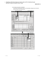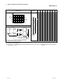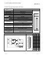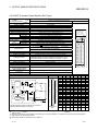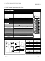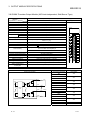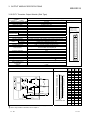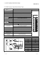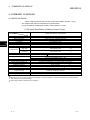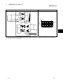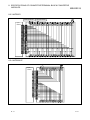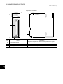
1
MITSUBISHI ELECTRIC
MELSEC System Q
Programmable Logic Controllers
Users's Manual
Digital I/O Modules
Art. no.: 130383
01 09 2007
SH (NA)-080042
Version R
MITSUBISHI ELECTRIC
INDUSTRIAL AUTOMATION
• SAFETY PRECAUTIONS •
(Always read these instructions before using this equipment.)
Before using this product, please read this manual and the relevant manuals introduced in this manual
carefully and pay full attention to safety to handle the product correctly.
The instructions given in this manual are concerned with this product. For the safety instructions of the
programmable controller system, please read the CPU module user's manual.
In this manual, the safety instructions are ranked as "DANGER" and "CAUTION".
DANGER
Indicates that incorrect handling may cause hazardous conditions,
resulting in death or severe injury.
! CAUTION
Indicates that incorrect handling may cause hazardous conditions,
resulting in medium or slight personal injury or physical damage.
!
Note that the ! CAUTION level may lead to a serious consequence according to the circumstances.
Always follow the instructions of both levels because they are important to personal safety.
Please save this manual to make it accessible when required and always forward it to the end user.
[Design Instructions]
!
DANGER
• Install a safety circuit external to the PLC that keeps the entire system safe if there are problems
with the external power supply or PLC. Not doing so may cause false output or malfunction,
leading to accidents.
(1) Outside the PLC, construct mechanical damage preventing interlock circuits, e.g. emergency
stop circuits, protective circuits, forward/reverse or other conflicting operation interlocking
circuits, and upper and lower positioning limit switches.
(2) When the PLC detects either of the following problems, it will stop arithmetic operation and
turn off all outputs in the case of (a). In the case of (b), it will stop arithmetic operation and
hold or turn off all outputs according to the parameter setting.
(a) The overcurrent protection or overvoltage protection of the power supply module is
activated.
(b) The self-diagnostic function of the PLC CPU has detected a fault such as the watchdog
timer error.
In addition, all outputs may be turned on when there are problems undetectable by the PLC
CPU, such as in the I/O controller. Build a fail-safe circuit or provide a mechanism externally
of the PLC to operate the machine safely at such times. Refer to the CPU module user's
manual for fail-safe circuit examples.
(3) Output could be left on or off when there is trouble in the output module's relays, transistors,
etc. So build an external monitoring circuit that will monitor any output signal that could lead
to a serious accident.
A-1
A-1
[Design Instructions]
!
DANGER
• When overcurrent exceeding the rated load current or caused by a shorted load or the like flows
in the output module for a long time, it may cause smoke or fire. To prevent this, configure an
external safety circuit, such as fuses.
• Build a circuit that turns on the external power supply after the PLC power supply has been
turned on. If the external power supply is turned on first, it could result in false output or
malfunction.
• When there are communication problems with the data link, refer to the corresponding data link
manual for the operating status of each station. Not doing so could result in false output or
malfunction.
• When connecting a peripheral device to the CPU module or connecting a personal computer or
the like to the intelligent function module to exercise control (data change) on the running PLC,
configure up an interlock circuit in the sequence program to ensure that the whole system will
always operate safely.
Also before exercising other control (program change, operating status change (status control))
on the running PLC, read the manual carefully and fully confirm safety.
Especially for the above control on the remote PLC from an external device, an immediate
action may not be taken for PLC trouble due to a data communication fault.
In addition to configuring up the interlock circuit in the sequence program, corrective and other
actions to be taken as a system for the occurrence of a data communication fault should be
predetermined between the external device and PLC CPU.
!
CAUTION
• Do not bundle the control wires or communication cables with the main circuit or power wires, or
run them close to each other.
They should be run 100mm (3.94in.) or more away from each other.
Not doing so could result in noise that would cause malfunction.
• When the output module is used to control a lamp load, heater, solenoid valve or the like, large
current (approximately 10 times greater than the normal) may flow when the output is turned
from OFF to ON. Choose an output module having a sufficient rated current.
A-2
A-2
[Installation Instructions]
!
CAUTION
• Use the PLC in an environment that meets the general specifications contained in this manual.
Using this PLC in an environment outside the range of the general specifications could result in
electric shock, fire, erroneous operation, and damage to or deterioration of the product.
• Hold down the module-loading lever at the module bottom, and securely insert the module-fixing
hook into the fixing hole in the base unit. Incorrect loading of the module can cause a
malfunction, failure or drop.
When using the PLC in the environment of much vibration, tighten the module with a screw.
Tighten the screw in the specified torque range. Undertightening can cause a drop, short circuit
or malfunction. Overtightening can cause a drop, short circuit or malfunction due to damage to
the screw or module.
• When installing extension cables, be sure that the base unit and the extension module
connectors are installed correctly.
After installation, check them for looseness.
Poor connections could cause an input or output failure.
• Securely load the memory card into the memory card loading connector.
After installation, check for lifting.
Poor connections could cause an operation fault.
• Completely turn off the external power supply before loading or unloading the module. Not doing
so could result in damage to the product.
• Do not directly touch the module's conductive parts or electronic components.
Touching the conductive parts could cause an operation failure or give damage to the module.
[Wiring Instructions]
!
DANGER
• Completely turn off the external power supply before starting wiring. Not doing so could result in
electric shock or damage to the product.
• When turning on the power supply or starting operation after wiring work, always mount the
product with the supplied terminal cover.
Not doing so could result in electric shock.
A-3
A-3
[Wiring Instructions]
!
CAUTION
• Always ground the FG and LG terminals to the protective ground conductor. Not doing so could
result in electric shock or malfunction.
• Before wiring the module, confirm the rated voltage and terminal layout of the product.
Connecting a power supply that is different from the rating or incorrectly wiring the product could
result in fire or failure.
• External connectors should be crimped or pressure-welded with the specified tools, or correctly
soldered. Imperfect connections could result in short circuit, fires or malfunction.
• Tighten the terminal screws in the specified torque range.
Undertightening could result in short circuit, fire or malfunction.
Overtightening could cause damage to the screws and/or the module, resulting in drop, short
circuit or malfunction.
• Be careful not to allow foreign matter such as chips and wire off-cuts to enter the module.
Foreign matter could cause fire, failure, or malfunction.
• The module has an ingress prevention label on its top to prevent foreign matter, such as wire
offcuts, from entering the module during wiring.
Do not peel this label during wiring.
Before starting system operation, be sure to peel this label because of heat dissipation.
• Install our PLC in a control panel for use.
Wire the main power supply to the power supply module installed in a control panel through a
distribution terminal block.
Furthermore, the wiring and replacement of a power supply module have to be performed by a
maintenance worker who acquainted with shock protection.
(For the wiring methods, refer to the QCPU User's Manual (Hardware Design, Maintenance and
Inspection).)
[Startup/Maintenance Instructions]
!
DANGER
• Do not touch the terminals while power is on.
Doing so could cause electric shock.
• Correctly connect the battery. Do not charge, disassemble, heat, place in fire, short circuit, or
solder the battery.
Mishandling of the battery can cause heat generation, burst or ignition which could result in
injury or fire.
• Switch off all phases of the externally supplied power used in the system when cleaning the
module or retightening the terminal or module mounting screws.
Not doing so could result in electric shock.
Undertightening of terminal screws can cause a short circuit or malfunction.
Overtightening of screws can cause damages to the screws and/or the module, resulting in
fallout, short circuits, or malfunction.
A-4
A-4
[Startup/Maintenance Instructions]
!
CAUTION
• The online operations conducted for the running CPU module by connecting a peripheral device
(especially program modification, forced output, operating status change) should be performed
after you have read the manual carefully read and fully confirmed safety.
Operation mistakes could cause machine damage or accident.
• Do not disassemble or modify the modules.
Doing so could cause failure, malfunction, injury or fire.
• Completely turn off the externally supplied power used in the system before mounting or
removing the module. Not doing so could result in damage to the product.
• Do not mount/remove the module to/from the base unit or the terminal block more than 50 times
(IEC61131-2-compliant), after the first use of the product.
Failure to do so may cause module malfunctions.
• Before touching the module, always touch grounded metal, etc. to discharge static electricity
from human body, etc.
Not doing so can cause the module to fail or malfunction.
[Disposal Instructions]
!
CAUTION
• When disposing of this product, treat it as industrial waste.
A-5
A-5
REVISIONS
The manual number is given on the bottom left of the back cover.
Print Date
Dec., 1999
Feb., 2000
Manual Number
Revision
SH (NA)-080042-A First edition
SH (NA)-080042-B Addition model
QH42P, QX48Y57, QX70, QX71, QX72, QY18A
Addition
Chapter 4
Partial correction
Section 1.2, Chapter 5, 8.1,
Chapters 4 to 8 (changed into Chapters 5 to 9)
Apr., 2000
SH (NA)-080042-C
Deletion
QY18A
Jul., 2000
SH (NA)-080042-D
Addition model
QX28,QX40-S1,QY18A,QY22,QI60
Addition
Chapter 5
Partial correction
Section 1.2
Chapters 5 to 9 (changed into Chapters 6 to 10)
Nov., 2000
SH (NA)-080042-E
Addition model
QY70, QY71
Addition
Section 1.3
Partial correction
CONTENTS, Section 3.3, 5.1
Jan., 2001
SH (NA)-080042-F
Addition model
QY68A
Addition
Section 10.2
Partial correction
CONTENTS, Section 1.2, 3.3, 5.1, Chapters 7
Mar., 2001
SH (NA)-080042-G
Partial correction
Section 2.4, 8.1
Jul., 2001
SH (NA)-080042-H
Addition model
Q6TE-18S
Addition
Chapter 9, APP 1.3
Partial correction
CONTENTS, Section 2.1, 2.2, 2.4, 5.1
Chapters 9 to 10 (changed into Chapters 10 to 11)
Jul., 2002
SH (NA)-080042-I
Addition model
QX41-S1, QX42-S1, A6CON4
Japanese Manual Version SH-080024-R
This manual confers no industrial property rights or any rights of any other kind, nor does it confer any patent licenses.
Mitsubishi Electric Corporation cannot be held responsible for any problems involving industrial property rights which
may occur as a result of using the contents noted in this manual.
© 1999 MITSUBISHI ELECTRIC CORPORATION
A-6
A-6
Print Date
Manual Number
Revision
Mar., 2003
SH (NA)-080042-J
Addition model
QX82
May, 2003
SH (NA)-080042-K
Partial correction
Section 1.2, 2.2
May, 2003
SH (NA)-080042-L
Addition model
QX82-S1
Partial correction
Section 1.2, 3.3
Addition
Section 2.15
Jul., 2004
SH (NA)-080042-M
Partial correction
Section 1.2, 2.1 to 2.15, 3.1 to 3.12, 4.1, 4.2, 5.1, 8.1, 8.2.1, 8.2.2, 10
Jul., 2005
SH (NA)-080042-N
Partial correction
SAFETY PRECAUTIONS, Section 3.3
Addition
Appendix 1.3
Apr., 2006
SH (NA)-080042-O
Partial correction
SAFETY PRECAUTIONS, Section 4.1, Chapter6
Sep., 2006
SH (NA)-080042-P
Partial correction
Section 11.1, 11.2, Appendix 1.2, 1.3
Oct., 2006
SH (NA)-080042-Q
Addition model
QX50
Partial correction
SAFETY PRECAUTIONS, Section 2.10 to 2.16, 3.4 to 3.12, 4.1, 4.2
Addition
Section 2.9
Sep., 2007
SH (NA)-080042-R
Addition model
QX41Y41P
Partial correction
Section 1.2, 1.3.3, 2.1 to 2.16, 3.1 to 3.12, 4.1, 4.3, 5.1, 7.1, 8.1, Chapter
10, Section 11.1, 11.2, Appendix 1.2
Addition
Section 4.2
A-7
A-7
INTRODUCTION
Thank you for choosing the MITSUBISHI MELSEC-Q Series General-Purpose Programmable Logic Controller.
Before using this product, please read this manual carefully to use the equipment to its optimum.
CONTENTS
About Manuals ..............................................................................................................................................A- 12
1. GENERAL SPECIFICATIONS OF INPUT AND OUTPUT MODULES AND INSTRUCTIONS FOR
SELECTING THEM
1- 1 to 1- 12
1.1 General Specifications ............................................................................................................................ 1- 1
1.2 Selecting Instructions.............................................................................................................................. 1- 1
1.3 How to Make Settings on GX Developer ................................................................................................ 1- 9
1.3.1 Setting of I/O response time ............................................................................................................. 1- 9
1.3.2 Setting of error-time output mode..................................................................................................... 1-11
1.3.3 QI60 switch setting ............................................................................................................................ 1-12
2. INPUT MODULE SPECIFICATIONS
2- 1 to 2-22
2.1 QX10 AC Input Module........................................................................................................................... 2- 1
2.2 QX28 AC Input Module........................................................................................................................... 2- 2
2.3 QX40 DC Input Module (Positive Common Type)................................................................................. 2- 3
2.4 QX40-S1 DC Input Module (Positive Common Type) ........................................................................... 2- 4
2.5 QX41 DC Input Module (Positive Common Type)................................................................................. 2- 5
2.6 QX41-S1 DC Input Module (Positive Common Type) ........................................................................... 2- 6
2.7 QX42 DC Input Module (Positive Common Type)................................................................................. 2- 8
2.8 QX42-S1 DC Input Module (Positive Common Type) ........................................................................... 2-10
2.9 QX50 DC (Positive Common/Negative Common Shared Type)/ AC Input Module............................. 2-12
2.10 QX70 DC Input Module (Positive Common/Negative Common Shared Type) ................................... 2-13
2.11 QX71 DC Input Module (Positive Common/Negative Common Shared Type) ................................... 2-14
2.12 QX72 DC Input Module (Positive Common/Negative Common Shared Type) ................................... 2-15
2.13 QX80 DC Input Module (Negative Common Type) .............................................................................. 2-16
2.14 QX81 DC Input Module (Negative Common Type) .............................................................................. 2-17
2.15 QX82 DC Input Module (Negative Common Type) .............................................................................. 2-18
2.16 QX82-S1 DC Input Module (Negative Common Type) ........................................................................ 2-20
3. OUTPUT MODULE SPECIFICATIONS
3- 1 to 3- 13
3.1 QY10 Contact Output Module ................................................................................................................ 3- 1
3.2 QY18A Contact Output Module (All Points Independent) ..................................................................... 3- 2
3.3 QY22 TRIAC Output Module .................................................................................................................. 3- 3
3.4 QY40P Transistor Output Module (Sink Type) ...................................................................................... 3- 4
3.5 QY41P Transistor Output Module (Sink Type) ...................................................................................... 3- 5
3.6 QY42P Transistor Output Module (Sink Type) ...................................................................................... 3- 6
3.7 QY50 Transistor Output Module (Sink Type)......................................................................................... 3- 7
3.8 QY68 Transistor Output Module (All Points Independent, Sink/Source Type)..................................... 3- 8
3.9 QY70 Transistor Output Module (Sink Type)......................................................................................... 3- 9
3.10 QY71 Transistor Output Module (Sink Type)........................................................................................ 3-10
3.11 QY80 Transistor Output Module (Source Type) ................................................................................... 3-11
A-8
A-8
3.12 QY81P Transistor Output Module (Source Type)................................................................................. 3-12
4. COMBINED I/O MODULE
4- 1 to 4- 10
4.1 QH42P I/O Module.................................................................................................................................. 4- 1
4.2 QX41Y41P I/O Module ........................................................................................................................... 4- 4
4.3 QX48Y57P I/O Module ........................................................................................................................... 4- 7
5. INTERRUPT MODULE
5- 1 to 5- 2
5.1 QI60 Interrupt Module ............................................................................................................................. 5- 1
6. BLANK COVER MODULE
6- 1 to 6- 2
7. CONNECTORS
7- 1 to 7- 2
8. SPECIFICATIONS OF CONNECTOR/TERMINAL BLOCK CONVERTOR MODULES
8- 1 to 8- 7
8.1 Specifications of Connector/Terminal Block Convertor Modules .......................................................... 88.2 Connector/Terminal Block Convertor Module Connection Diagrams ................................................... 88.2.1 A6TBXY36........................................................................................................................................ 88.2.2 A6TBXY54........................................................................................................................................ 88.2.3 A6TBX70 .......................................................................................................................................... 88.2.4 A6TBX36-E....................................................................................................................................... 88.2.5 A6TBY36-E....................................................................................................................................... 88.2.6 A6TBX54-E....................................................................................................................................... 88.2.7 A6TBY54-E....................................................................................................................................... 88.2.8 A6TBX70-E....................................................................................................................................... 89. SPRING CLAMP TERMINAL BLOCK
1
3
3
4
5
5
6
6
7
7
9- 1 to 9- 2
9.1 Q6TE-18S............................................................................................................................................. 9- 1
10. NAMES OF MODULE PARTS
10- 1 to 10- 4
11. I/O MODULE TROUBLESHOOTING
11- 1 to 11- 7
11.1 Input Circuit Troubleshooting.............................................................................................................. 11- 1
11.2 Output Circuit Troubleshooting........................................................................................................... 11- 4
APPENDICES
App- 1 to App-12
Appendix 1 External Dimensional Drawings ............................................................................................AppAppendix 1.1 I/O modules.....................................................................................................................AppAppendix 1.2 Connectors, connector/terminal block converter modules ............................................AppAppendix 1.3 Connector/ terminal block converter module cable .......................................................AppAppendix 1.4 Spring Clamp Terminal Block.........................................................................................AppA-9
A-9
1
1
4
8
9
Appendix 2 Compatibility with MELSEC-AnS Series I/O modules..........................................................App-10
A - 10
A - 10
MEMO
A - 11
A - 11
About Manuals
The following manuals are also related to this product.
In necessary, order them by quoting the details in the tables below.
Related Manuals
Manual Number
(Model Code)
Manual Name
QCPU User's Manual (Hardware Design/Maintenance and Inspection)
This manual provides the specifications of the CPU modules, power supply modules, base units, extension
cables, memory cards and others.
(Sold separately)
QCPU User's Manual (Function Explanation/Program Fundamentals)
This manual explains the functions, programming methods, devices on necessary to create programs with
the QCPU.
SH-080483ENG
(13JR73)
SH-080484ENG
(13JR74)
(Sold separately)
Conformation to the EMC Directive and Low Voltage Instruction
For details on making Mitsubishi PLC conform to the EMC directive and low voltage instruction when installing
it in your product, please refer to Chapter 3, "EMC Directive and Low Voltage Instruction" of the PLC CPU
User's Manual(Hardware).
The CE logo is printed on the rating plate on the main body of the PLC that conforms to the EMC directive and
low voltage instruction.
A - 12
A - 12
1
GENERAL SPECIFICATIONS OF INPUT AND OUTPUT MODULES AND
INSTRUCTIONS FOR SELECTING THEM
MELSEC-Q
1. GENERAL SPECIFICATIONS OF INPUT AND OUTPUT MODULES AND
INSTRUCTIONS FOR SELECTING THEM
This chapter describes the general specifications of I/O modules and instructions for
selecting them.
1.1 General Specifications
Refer to the following manual for the general specifications of the I/O modules.
• QCPU User's Manual (Hardware Design/Maintenance and Inspection)
1.2 Selecting Instructions
(1) If an output module drives an inductive load, it must be switched ON for 1 second
or longer and switched OFF for 1 second or longer.
(2) If a counter or timer which has a DC-DC converter as a load is used with an output
module, using an average current to choose an output module can cause a fault
due to periodic rush currents when it is turned ON or during operation.
To reduce the influence of rush currents for use of the above load, connect a
resistor or an inductance to the load in series or use a module whose maximum
load current is larger.
Resistor
Output
module
Load
Inductance Load
Output
module
(3) Fuses installed in output modules cannot be replaced. They are designed to protect
external wiring if the module outputs are shorted.
Therefore, output modules may not be protected from a short circuit.
If an output module becomes faulty due to any cause other than a short circuit, its
fuse may not function.
(4) The number of signals, which can be turned ON simultaneously in an input module,
varies according to the input voltage and ambient temperature.
Refer to the corresponding input module specifications.
1-1
1-1
1
1
GENERAL SPECIFICATIONS OF INPUT AND OUTPUT MODULES AND
INSTRUCTIONS FOR SELECTING THEM
MELSEC-Q
(4) Connecting the transistor output modules in parallel may result in failure of the
output elements.
If connecting the transistor output modules in parallel, use diodes for the circuit as
shown below.
1
Load
OUT1
Load
OUT1
Load
Load
OUT2
OUT2
COM
COM
OUT1
OUT1
OUT2
OUT2
COM
COM
Sink type
Sourse type
(5) The number of signals, which can be turned ON simultaneously in an input
module, varies according to the input voltage and ambient temperature.
Refer to the corresponding input module specifications.
1-2
1-2
GENERAL SPECIFICATIONS OF INPUT AND OUTPUT MODULES AND
INSTRUCTIONS FOR SELECTING THEM
MELSEC-Q
(6) The following chart shows the actual service value of relay life for a relay output
module.
Applicable module: QY10, QY18A
200
100
70
Switching life (10,000 times)
1
50
30
20
10
7
DC30V =0ms
5
DC100
=7ms
AC100V cos =0.7
AC200V cos =0.7
3
(L/R): Time constant
cos
: Power factor
AC100V cos =0.35
AC200V cos =0.35
DC24V =7ms
2
AC120V cos =0.2
AC240V cos =0.2
1
0.1
0.2
0.3
0.5
0.7
1
2
3
5
Switching current (A)
1-3
1-3
1
GENERAL SPECIFICATIONS OF INPUT AND OUTPUT MODULES AND
INSTRUCTIONS FOR SELECTING THEM
MELSEC-Q
POINT
(1) When using the module for the application in which the relay contact is
frequently switched, the relay life span should be considered. Therefore, it is
recommended to use a triac output module.
(2) The relay life curve shows the value based on actual use, which is not
guaranteed. Therefore, make sure to allow for a margin of error.
The relay life span differs according to the specifications as follows:
Rated switching voltage, current load
100 thousand operations
100 thousand operations
200V AC 1.5A, 240V AC 1A (COS =0.7)
300 thousand operations
200V AC 0.4A, 240V AC 0.3A (COS =0.7)
100 thousand operations
200V AC 1A, 240V AC 0.5A (COS =0.35)
300 thousand operations
200V AC 0.3A, 240V AC 0.15A (COS =0.35)
24V DC 1A, 100V DC 0.1A (L/R=7ms)
100 thousand operations
24V DC 0.3A, 100V DC 0.03A (L/R=7ms)
300 thousand operations
(3) Relay life is substantially affected by the load type and inrush current
characteristics.
The inrush current may cause the contact welding. Therefore, consideration
should be given to it as well as constant current.
(a) Inductive load
When the inductive load such as electromagnetic contactor or solenoid is
shut off, high counter-electromotive force is generated between the
contacting materials to produce an arc discharge. Consideration should be
made especially when the power factor is low, as it may decrease the life
period.
In addition, make sure to consider the contact melting, as the inrush current
equivalent to 5 to 15 times of constant current flows when the module is
powered on.
(b) Lamp load
Make sure to consider the contact melting, as the inrush current equivalent
to 10 to 15 times of constant current flows in the lamp circuit.
(c) Capacitive load
Make sure to consider the contact melting when a device such as condenser
is used in a load circuit, as the inrush current equivalent to 20 to 40 times of
constant current may flow in the circuit.
Also, pay full attention to the wire capacity if long length of wire is routed.
(7) Insulation-sleeved crimping terminals cannot be used with the terminal block.
It is recommended to cover the wire connections of the crimping terminals with
mark or insulation tubes.
(8) Use wires of 0.3 to 0.75mm2 core and 2.8mm (0.11in.) OD max. to connect to the
terminal block. When using a wire whose core is 0.75mm or more, it is preferable to
use the spring terminal block(Q6TE-18S).
(9) Do not use I/O modules under pressure higher than the atmospheric pressure of
0m (0ft.) altitude. Doing so can cause a malfunction.
When using I/O modules under pressure, please consult your sales representative.
1-4
1-4
1
GENERAL SPECIFICATIONS OF INPUT AND OUTPUT MODULES AND
INSTRUCTIONS FOR SELECTING THEM
MELSEC-Q
(10) Tighten the module fixing and terminal block screws to the torques in the following
ranges.
Screw Location
Tightening Torque Range
Module fixing screw (M3 12 screw)
36 to 48 N•cm
I/O module terminal block screw (M3 screw)
42 to 58 N•cm
I/O module terminal block mounting screw (M3 screw)
66 to 89 N•cm
(11)The overload protection function and overheat protection function of the following
modules will be explained below.
(a) QY40P, QY41P, QY42P, QX41Y41P, QH42P
Function
Common
(Overload and overheat
protection functions)
Description
• If an overcurrent keeps flowing due to overload, heat is generated
to activate the overheat protective function.
• Each protection function is designed to protect the internal
elements of the module, not the external equipment.
• The overload protection function is activated in 1 point increments
Overload protection
function
in terms of 1A to 3A/point.
• The overload protection function returns operation to normal when
the load becomes a rated load
Overheat protection
function
1-5
• The overheat protection function is activated in 1 point increments.
• The overheat protection function automatically returns operation to
normal when heat reduces.
1-5
1
GENERAL SPECIFICATIONS OF INPUT AND OUTPUT MODULES AND
INSTRUCTIONS FOR SELECTING THEM
MELSEC-Q
(b) QY81P
Function
Description
• If an overcurrent keeps flowing due to overload, heat is generated
Common
(Overload and overheat
protective functions)
to activate the overheat protective function.
• Each protective function is designed to protect the internal
elements of the module, not the external equipment.
• The overload protective function is activated in 1 point increments
in terms of 1A to 3A/point.
Overload protective
function
• The overload protective function returns operation to normal when
the load becomes a rated load.
• The overheat protective function is activated in 2 point increments.
(It is activated in 2 point increments of Y0/Y1, Y2/Y3, ..., and when
overheat protection is activated, that of 2 points is activated
simultaneously. If an overheat condition persists, heat transferred
may activate the other overheat protective function.)
• If an output turns ON at the activation of the overheat protective
function, the actual output voltage oscillates between 0V and load
voltage.
Overheat protective
At the load voltage of 24V, the average voltage during oscillation is
function
approx. 7V.
No oscillation is encountered when the output is OFF at the
activation of the overheat protective function.
To ensure that the output is turned OFF at the activation of the
overheat protective function, use an external load which switches
OFF at 7V or more.
• The overheat protective function automatically returns operation to
normal when heat reduces.
(12)Input modules may import noise or the like as an input depending on the pulse
width of a signal.
This pulse width has a value as listed below depending on the parameter-set
response time. The operating environment should be fully considered when making
the response time setting.
Response Time Setting (ms)
1-6
Minimum Value of Pulse Width
That May Be Imported (ms)
1
0.3
5
3
10
6
20
12
70
45
1-6
1
GENERAL SPECIFICATIONS OF INPUT AND OUTPUT MODULES AND
INSTRUCTIONS FOR SELECTING THEM
MELSEC-Q
(13)When confirming the product information on the CPU PLC, observe the system
monitor in the DIAGNOSIS menu of the GX Developer.
Confirm by
observing here.
(14)When using the QH42P, QX41Y41P or QX48Y57, configure it with the following
devices.
Part name
Detail
CPU PLC
Product of product information [011120000000000-A] or later
GX Developer
SW5D5C-GPPW or later
The CPU PLCs other than those listed above cannot be used.
When the SW4D5C-GPPW is used, the response time cannot be set
(fixed at 10ms).
Set OUTPUT for the I/O allocation.
(15)Possible constructions for QI60 compatible time settings
When setting compatible times for QI60, use the constructions listed below.
If using other constructions, compatible times can not be set. (Fixed at 0.2 ms)
1-7
Product name
Contents
PLC CPU
Product information "021120000000000-B" or later
GX Developer
SW6D5C-GPPW or later
1-7
1
GENERAL SPECIFICATIONS OF INPUT AND OUTPUT MODULES AND
INSTRUCTIONS FOR SELECTING THEM
MELSEC-Q
(16)Instructions for use of QY22
It is recommended to fit a fuse to each external terminal in order to prevent the
external device and module from being burnt if a load short-circuit occurs.
The fuse recommended for fitting is the one conforming to IEC60127 Sheet 1.
The following fuses have been confirmed by Mitsubishi to operate properly.
Fuse Model
216 02.5
Rated current
2.5A
Manufacturer
216 002
2A
Littelfuse, Inc
(17)Caution points when using QY68A
Installing a fuse to the external terminal to prevent burn out of external devices and
modules in the case of a load short is recommended.
A rated voltage 3A fast type fuse is recommended.
Fuses confirmed for operation by this company are listed below.
Fuse Model
216 3.15
312 003
Rated current
3.15A
3A
Manufacturer
Littelfuse, Inc
(18)I/O numbers of combined I/O modules
There are two types of combined I/O modules:
• Module using same I/O numbers for input and output
Since same number is used for input and output, the I/O numbers to be used can
be saved.
• Module using sequential I/O numbers for input and output
Since I/O assignments are the same for A series, it is useful when replacing
modules from those of A series.
00
Input (X)
Output (Y)
X00
Y00
Input (X)
00
X00
1F
X1F
32 points
1F
X1F
Y1F
Output (Y)
Vacant
Y20
20
32 points
Vacant
3F
32 points
Y3F
Module using same I/O numbers for input
Module using sequential I/O numbers for input
and output (QH42P)
and output (QX41Y41P)
(19)Precaution when Connecting the Uninterruptive Power Supply (UPS)
Use an on-line UPS with 5 % or less voltage fluctuation.
Do not use an off-line UPS.
1-8
1-8
1
GENERAL SPECIFICATIONS OF INPUT AND OUTPUT MODULES AND
INSTRUCTIONS FOR SELECTING THEM
MELSEC-Q
1.3 How to Make Settings on GX Developer
This section describes how to make settings using GX Developer.
1.3.1 Setting of I/O response time
Set the I/O response time in I/O assignment of PLC Parameter.
(1) For Input/I/O mix module
Choose [Input/I/O mix] in Type, choose [Detailed setting], and choose [I/O response
time] in I/O response time.
Choose Input/I/O mix.
Choose Detailed setting.
Choose I/O response time
(default: 10ms).
1-9
1-9
1
GENERAL SPECIFICATIONS OF INPUT AND OUTPUT MODULES AND
INSTRUCTIONS FOR SELECTING THEM
MELSEC-Q
(2) For high-speed input module/QI60
Choose [Hi. input/Interrupt] in Type, choose [Detailed setting], and choose [I/O
response time] in I/O response time.
Choose Hi. input/Interrupt.
Choose Detailed setting.
Choose I/O response time
(default: 0.2ms).
1 - 10
1 - 10
1
GENERAL SPECIFICATIONS OF INPUT AND OUTPUT MODULES AND
INSTRUCTIONS FOR SELECTING THEM
MELSEC-Q
1.3.2 Setting of error-time output mode
Set the error-time output mode in I/O assignment of PLC Parameter.
Choose [Output/I/O mix] in Type, choose [Detailed setting], and choose [Clear/Hold] in
Error time output mode.
Choose Output/I/O mix.
Choose Detailed setting.
Choose Clear/Hold
(default: Clear).
1 - 11
1 - 11
1
GENERAL SPECIFICATIONS OF INPUT AND OUTPUT MODULES AND
INSTRUCTIONS FOR SELECTING THEM
MELSEC-Q
1.3.3 QI60 switch setting
Set the QI60 switches in I/O assignment of PLC Parameter.
Choose [Interrupt] in Type, choose [Switch setting], choose [HEX.] in Input format, and
set the interrupt processing conditions in Switch 1.
Choose Interrupt.
Choose Switch setting.
Choose HEX.
Set the interrupt processing conditions
Setting inhibited.
(leading edge/trailing edge) of CH1 to CH16.
Set the interrupt processing condition with switch 1. The relationships between bits and inputs are as indicated
below.
b15
XF
to
XE
XD
XC
XB
XA
X9
X8
b0
X7
X6
X5
X4
X3
X2
X1
X0
0: Leading edge, 1: Trailing edge
1 - 12
1 - 12
2 INPUT MODULE SPECIFICATIONS
MELSEC-Q
2. INPUT MODULE SPECIFICATIONS
2.1 QX10 AC Input Module
Type
Specifications
Number of input points
Isolation method
Rated input voltage, frequency
Input voltage distortion
Rated input current
Input derating
Inrush current
ON voltage/ON current
OFF voltage/OFF current
Input impedance
Response
OFF to ON
time
ON to OFF
Dielectric withstand voltage
Insulation resistance
Noise immunity
Protection of degree
Common terminal arrangement
Number of I/O points
Operation indicator
External connections
Applicable wire size
Applicable crimping terminal
5VDC internal current
consumption
Weight
AC Input Module
QX10
16 points
Photocoupler
100-120VAC (+10/-15%) 50/60Hz (±3Hz)
Within 5% (Refer to section 1.2 (17))
Approx. 8mA (100VAC, 60Hz), approx. 7mA (100VAC, 50Hz)
Refer to the derating chart.
Max. 200mA within 1ms (at 132VAC)
80VAC or higher/5mA or higher (50Hz, 60Hz)
30VAC or lower/1.7mA or lower (50Hz, 60Hz)
Approx. 12k (60Hz), approx. 15k (50Hz)
15ms or less (100VAC 50Hz, 60Hz)
20ms or less (100VAC 50Hz, 60Hz)
1780VAC rms/3 cycles (altitude 2000m (6557.38ft.))
10M or more by insulation resistance tester
By noise simulator of 1500Vp-p noise voltage, 1 s noise width
and 25 to 60Hz noise frequency
First transient noise IEC61000-4-4: 1kV
IP1X
16 points/common (common terminal: TB17)
16 (I/O allocation is set as a 16-points input module)
ON indication (LED)
18-point terminal block (M3 6 screws)
0.3 to 0.75mm2 core (2.8mm (0.11in.) OD max.)
R1.25-3 (sleeved crimping terminals cannot be used.)
120VAC
132VAC
10 20 30 40 50 55( C )
Ambient temperature
LED
TB1
Internal
circuit
TB17
100VAC
2-1
QX10
0 1 2 3 4 5 6 7
8 9 A B CDE F
0
0
1
2
3
4
5
6
7
8
9
A
B
C
D
E
F
1
2
3
4
5
6
7
8
9
A
B
C
D
E
F
COM
NC
100VAC
8mA60Hz
7mA50Hz
0.17kg
External Connections
TB16
2
50mA (TYP. all points ON)
Derating Chart
(%)
100
90
ON 80
ratio 70
60
50
40
0
Appearance
LED
Terminal Block Number
Signal Name
TB1
X00
TB2
X01
TB3
X02
TB4
X03
TB5
X04
TB6
X05
TB7
X06
TB8
X07
TB9
X08
TB10
X09
TB11
X0A
TB12
X0B
TB13
X0C
TB14
X0D
TB15
X0E
TB16
X0F
TB17
COM
TB18
Vacant
2-1
2 INPUT MODULE SPECIFICATIONS
MELSEC-Q
2.2 QX28 AC Input Module
Type
AC Input Module
Specifications
2
QX28
Number of input points
Isolation method
Rated input voltage, frequency
Input voltage distortion
Rated input current
Input derating
Inrush current
ON voltage/ON current
OFF voltage/OFF current
Input impedance
Response
OFF to ON
time
ON to OFF
Dielectric withstand voltage
Insulation resistance
Noise immunity
Protection of degree
Common terminal arrangement
Number of I/O points
Operation indicator
External connections
Applicable wire size
Applicable crimping terminal
5VDC internal current
consumption
Weight
R1.25-3 (sleeved crimping terminals cannot be used.)
Terminal Block Number
100% 55 C
87.5% 55 C
240V
264V
10 20 30 40 50 55( C )
Ambient temperature
External Connections
LED
TB1
Internal
circuit
TB17
100/200VAC
2-2
0
0
1
2
3
4
5
6
7
8
9
A
B
C
D
E
F
NC
1
NC
2
NC
3
NC
4
NC
5
NC
6
NC
7
NC
COM
NC
200VAC
17mA60Hz
14mA50Hz
0.20kg
100% 45 C
TB15
QX28
0 1 2 3 4 5 6 7
50mA (TYP. all points ON)
Derating Chart
(%)
100
90
ON 80
ratio 70
60
50
40
0
Appearance
8 points
Photocoupler
100-240VAC (+10/-15%) 50/60Hz (±3Hz)
Within 5% (Refer to section 1.2 (17))
Approx. 17mA (200VAC, 60Hz), approx. 14mA (200VAC, 50Hz)
Approx. 8mA (100VAC, 60Hz), approx. 7mA (100VAC, 50Hz)
Refer to the derating chart.
Max. 500mA within 1ms (at 264VAC)
80VAC or higher/5mA or higher (50Hz, 60Hz)
30VAC or lower/1.7mA or lower (50Hz, 60Hz)
Approx. 12k (60Hz), approx. 15k (50Hz)
10ms or less (100VAC 50Hz, 60Hz)
20ms or less (100VAC 50Hz, 60Hz)
2830VAC rms/3 cycles (altitude 2000m (6557.38ft.))
10M or more by insulation resistance tester
By noise simulator of 1500Vp-p noise voltage, 1 s noise width
and 25 to 60Hz noise frequency
First transient noise IEC61000-4-4: 1kV
IP1X
8 points/common (common terminal: TB17)
16 (I/O allocation is set as a 16-points input module)
ON indication (LED)
18-point terminal block (M3 6 screws)
0.3 to 0.75mm2 core (2.8mm (0.11in.) OD max.)
LED
Signal Name
TB1
X00
TB2
Vacant
TB3
X01
TB4
Vacant
TB5
X02
TB6
Vacant
TB7
X03
TB8
Vacant
TB9
X04
TB10
Vacant
TB11
X05
TB12
Vacant
TB13
X06
TB14
Vacant
TB15
X07
TB16
Vacant
TB17
COM
TB18
Vacant
2-2
2 INPUT MODULE SPECIFICATIONS
MELSEC-Q
2.3 QX40 DC Input Module (Positive Common Type)
Type
DC Input Module (Positive Common Type)
Specifications
QX40
Number of input points
Isolation method
Rated input voltage
Rated input current
Input derating
ON voltage/ON current
OFF voltage/OFF current
Input impedance
Appearance
Applicable wire size
16 points
Photocoupler
24VDC (+20/-15%, ripple ratio within 5%)
Approx. 4mA
No
19V or higher/3mA or higher
11V or lower/1.7mA or lower
Approx. 5.6k
1ms/5ms/10ms/20ms/70ms or less (CPU parameter setting)
Initial setting is 10ms.
1ms/5ms/10ms/20ms/70ms or less (CPU parameter setting)
Initial setting is 10ms.
560VAC rms/3 cycles (altitude 2000m (6557.38ft.))
10M or more by insulation resistance tester
By noise simulator of 500Vp-p noise voltage, 1 s noise width
and 25 to 60Hz noise frequency
First transient noise IEC61000-4-4: 1kV
IP2X
16 points/common (common terminal: TB17)
16 (I/O allocation is set as a 16-points input module)
ON indication (LED)
18-point terminal block (M3 6 screws)
0.3 to 0.75mm2 core (2.8mm (0.11in.) OD max.)
Applicable crimping terminal
5VDC internal current consumption
Weight
R1.25-3 (sleeved crimping terminals cannot be used.)
50mA (TYP. all points ON)
0.16kg
OFF to ON
Response
time
ON to OFF
Dielectric withstand voltage
Insulation resistance
Noise immunity
Protection of degree
Common terminal arrangement
Number of I/O points
Operation indicator
External connections
External Connections
LED
TB1
Internal
circuit
LED
QX40
0 1 2 3 4 5 6 7
8 9 A B CDE F
0
0
1
2
3
4
5
6
7
8
9
A
B
C
D
E
F
1
2
3
4
5
6
7
8
9
A
B
C
D
E
F
- +
COM
NC
24VDC
4mA
Terminal Block Number
Signal Name
TB1
X00
TB2
X01
TB3
X02
TB4
X03
TB5
X04
TB6
X05
TB7
X06
TB8
X07
TB9
X08
TB10
X09
TB16
TB11
X0A
TB17
TB12
X0B
TB13
X0C
TB14
X0D
TB15
X0E
24VDC
TB16
X0F
TB17
COM
TB18
Vacant
: For the setting method, refer to the section 1.3.1.
2-3
2-3
2 INPUT MODULE SPECIFICATIONS
MELSEC-Q
2.4 QX40-S1 DC Input Module (Positive Common Type)
Type
DC Input Module (Positive Common Type)
Specifications
QX40-S1
Number of input points
Isolation method
Rated input voltage
Rated input current
Input derating
ON voltage/ON current
OFF voltage/OFF current
Input impedance
Set value 1
Typ
Response OFF to ON
max
time
Typ
ON to OFF
max
Dielectric withstand voltage
Insulation resistance
Noise immunity
Protection of degree
Common terminal arrangement
Number of I/O points
Operation indicator
External connections
Applicable wire size
Applicable crimping terminal
5VDC internal current
consumption
Weight
Appearance
16 points
Photocoupler
24VDC (+20/-15%, ripple ratio within 5%)
Approx. 6mA
No
19V or higher/4.0mA or higher
11V or lower/1.7mA or lower
Approx. 3.9k
0.1
0.2
0.4
0.6
1
0.05ms
0.15ms
0.30ms
0.55ms
1.05ms
0.10ms
0.20ms
0.40ms
0.60ms
1.20ms
0.15ms
0.20ms
0.35ms
0.60ms
1.10ms
0.20ms
0.30ms
0.50ms
0.70ms
1.30ms
560VAC rms/3 cycles (altitude 2000m (6557.38ft.))
10M or more by insulation resistance tester
By noise simulator of 500Vp-p noise voltage, 1 s noise width
and 25 to 60Hz noise frequency
First transient noise IEC61000-4-4: 1kV
IP2X
16 points/common (common terminal: TB17)
16 (I/O allocation is set as a 16-points Hi. input module)
ON indication (LED)
18-point terminal block (M3 6 screws)
0.3 to 0.75mm2 core (2.8mm (0.11in.) OD max.)
R1.25-3 (sleeved crimping terminals cannot be used.)
QX40-S1
0 1 2 3 4 5 6 7
8 9 A B CDE F
0
0
1
2
3
4
5
6
7
8
9
A
B
C
D
E
F
1
2
3
4
5
6
7
8
9
A
B
C
D
E
F
- +
COM
NC
24VDC
6mA
60mA (TYP. all points ON)
0.20kg
External Connections
LED
TB 1
Internal
circuit
Terminal Block Number
Signal Name
TB1
X00
TB2
X01
TB3
X02
TB4
X03
TB5
X04
TB6
X05
TB7
X06
TB8
X07
TB9
X08
TB10
X09
TB16
TB11
X0A
TB17
TB12
X0B
TB13
X0C
TB14
X0D
TB15
X0E
24VDC
TB16
X0F
TB17
COM
TB18
Vacant
1: CPU parameter setting. (Initial setting is 0.2ms)
Response time can be changed on SW5D5C-GPPW or later.
For the setting method, refer to the section 1.3.1.
2-4
2-4
2 INPUT MODULE SPECIFICATIONS
MELSEC-Q
2.5 QX41 DC Input Module (Positive Common Type)
Type
Specifications
QX41
32 points
Photocoupler
24VDC (+20/-15%, ripple ratio within 5%)
Approx. 4mA
Refer to the derating chart.
19V or higher/3mA or higher
11V or lower/1.7mA or lower
Approx. 5.6k
1ms/5ms/10ms/20ms/70ms or less (CPU parameter setting)
Number of input points
Isolation method
Rated input voltage
Rated input current
Input derating
ON voltage/ON current
OFF voltage/OFF current
Input impedance
OFF to ON
Response
time
DC Input Module (Positive Common Type)
ON to OFF
Dielectric withstand voltage
Insulation resistance
Noise immunity
Protection of degree
Common terminal arrangement
Number of I/O points
Operation indicator
External connections
Applicable wire size
External wiring connector
Applicable connector/terminal block
conversion module
5VDC internal current consumption
Weight
QX41
0 1
8 9
0 1
8 9
2
A
2
A
3
B
3
B
4
C
4
C
24VDC
4mA
5
D
5
D
6
E
6
E
7
F
7
F
QX41
1
Initial setting is 10ms.
1ms/5ms/10ms/20ms/70ms or less (CPU parameter setting) 1
Initial setting is 10ms.
560VAC rms/3 cycles (altitude 2000m (6557.38ft.))
10M or more by insulation resistance tester
By noise simulator of 500Vp-p noise voltage, 1 s noise width
and 25 to 60Hz noise frequency
First transient noise IEC61000-4-4: 1kV
IP2X
32 points/common (common terminal: B01, B02)
32 (I/O allocation is set as a 32-points input module)
ON indication (LED)
40-pin connector
0.3mm2 (For A6CON1 or A6CON4) 2
A6CON1, A6CON2, A6CON3, A6CON4 (optional)
A6TBXY36, A6TBXY54, A6TBX70
75mA (TYP. all points ON)
0.15kg
Derating Chart
(%)
100
90
80
ON
ratio 70
60
50
40
0
Appearance
Pin-Outs
28.8VDC
10 20 30 40 50 55 ( C )
Ambient temperature
External Connections
LED
B20
Internal
circuit
A05
B01,B02
24VDC
LED
B20
B19
B18
B17
B16
B15
B14
B13
B12
B11
B10
B9
B8
B7
B6
B5
B4
B3
B2
B1
A20
A19
A18
A17
A16
A15
A14
A13
A12
A11
A10
A9
A8
A7
A6
A5
A4
A3
A2
A1
Module front view
Pin
No.
Signal
No.
Pin
No.
Signal
No.
B20
X00
A20
X10
B19
X01
A19
X11
B18
X02
A18
X12
B17
X03
A17
X13
B16
X04
A16
X14
B15
X05
A15
X15
B14
X06
A14
X16
B13
X07
A13
X17
B12
X08
A12
X18
B11
X09
A11
X19
B10
X0A
A10
X1A
B09
X0B
A09
X1B
B08
X0C
A08
X1C
B07
X0D
A07
X1D
B06
X0E
A06
X1E
B05
X0F
A05
X1F
B04 Vacant A04 Vacant
B03 Vacant A03 Vacant
B02
COM
A02 Vacant
B01
COM
A01 Vacant
1: For the setting method, refer to the section 1.3.1.
2: When using A6CON2 or A6CON3, refer to Chapter 7.
2-5
2-5
2 INPUT MODULE SPECIFICATIONS
MELSEC-Q
2.6 QX41-S1 DC Input Module (Positive Common Type)
Type
Specifications
Number of input points
Isolation method
Rated input voltage
Rated input current
Input derating
ON voltage/ON current
OFF voltage/OFF current
Input impedance
Set value 1
Typ
Response OFF to ON
max
time
Typ
ON to OFF
max
Dielectric withstand voltage
Insulation resistance
Noise immunity
Protection of degree
Common terminal arrangement
Number of I/O points
Operation indicator
External connections
Applicable wire size
External wiring connector
Applicable connector/terminal
block conversion module
5VDC internal current
consumption
Weight
DC Input Module (Positive Common Type)
QX41-S1
32 points
Photocoupler
24VDC (+20/-15%, ripple ratio within 5%)
Approx. 4mA
Refer to the derating chart.
19V or higher/3.0mA or higher
9.5V or lower/1.5mA or lower
Approx. 5.6k
0.1
0.2
0.4
0.6
1
0.05ms
0.15ms
0.30ms
0.55ms
1.05ms
0.12ms
0.20ms
0.40ms
0.60ms
1.20ms
0.15ms
0.20ms
0.35ms
0.60ms
1.10ms
0.20ms
0.30ms
0.50ms
0.70ms
1.30ms
560VAC rms/3 cycles (altitude 2000m (6557.38ft.))
10M or more by insulation resistance tester
By noise simulator of 500Vp-p noise voltage, 1 s noise width
and 25 to 60Hz noise frequency
First transient noise IEC61000-4-4: 1kV
IP2X
32 points/common (common terminal: B01, B02)
32 (I/O allocation is set as a 32-points Hi. input module)
ON indication (LED)
40-pin connector
0.3mm2 (For A6CON1 or A6CON4) 2
Appearance
QX41-S1
0 1 2 3
8 9 A B
0 1 2 3
8 9 A B
24VDC
4mA
4
C
4
C
5
D
5
D
6
E
6
E
7
F
7
F
QX41-S1
A6CON1, A6CON2, A6CON3, A6CON4 (optional)
A6TBXY36, A6TBXY54, A6TBX70
75mA (TYP. all points ON)
0.15kg
1: CPU parameter setting. (Initial setting is 0.2ms)
Response time can be changed on SW5D5C-GPPW or later.
For the setting method, refer to the section 1.3.1.
2: When using A6CON2 or A6CON3, refer to Chapter 7.
2-6
2-6
2 INPUT MODULE SPECIFICATIONS
MELSEC-Q
Derating Chart
(%)
100
90
80
ON
ratio 70
60
50
40
0
Pin-Outs
28.8VDC
10 20 30 40 50 55 ( C )
Ambient temperature
External Connections
LED
B20
Internal
circuit
A05
B01,B02
24VDC
2-7
LED
B20
B19
B18
B17
B16
B15
B14
B13
B12
B11
B10
B9
B8
B7
B6
B5
B4
B3
B2
B1
A20
A19
A18
A17
A16
A15
A14
A13
A12
A11
A10
A9
A8
A7
A6
A5
A4
A3
A2
A1
Module front view
Pin
No.
Signal
No.
Pin
No.
Signal
No.
B20
X00
A20
X10
B19
X01
A19
X11
B18
X02
A18
X12
B17
X03
A17
X13
B16
X04
A16
X14
B15
X05
A15
X15
B14
X06
A14
X16
B13
X07
A13
X17
B12
X08
A12
X18
B11
X09
A11
X19
B10
X0A
A10
X1A
B09
X0B
A09
X1B
B08
X0C
A08
X1C
B07
X0D
A07
X1D
B06
X0E
A06
X1E
B05
X0F
A05
X1F
B04 Vacant A04 Vacant
B03 Vacant A03 Vacant
B02
COM
A02 Vacant
B01
COM
A01 Vacant
2-7
2 INPUT MODULE SPECIFICATIONS
MELSEC-Q
2.7 QX42 DC Input Module (Positive Common Type)
Type
Specifications
Number of input points
Isolation method
Rated input voltage
Rated input current
Input derating
ON voltage/ON current
OFF voltage/OFF current
Input impedance
Response
time
OFF to ON
ON to OFF
Dielectric withstand voltage
Insulation resistance
Noise immunity
Protection of degree
Common terminal arrangement
Number of I/O points
Operation indicator
External connections
Applicable wire size
External wiring connector
Applicable connector/terminal block
conversion module
5VDC internal current consumption
Weight
DC Input Module (Positive Common Type)
QX42
64 points
Photocoupler
24VDC (+20/-15%, ripple ratio within 5%)
Approx. 4mA
Refer to the derating chart.
19V or higher/3mA or higher
11V or lower/1.7mA or lower
Approx. 5.6k
1ms/5ms/10ms/20ms/70ms or less (CPU parameter setting) 1
Initial setting is 10ms.
1ms/5ms/10ms/20ms/70ms or less (CPU parameter setting) 1
Initial setting is 10ms.
560VAC rms/3 cycles (altitude 2000m (6557.38ft.))
10M or more by insulation resistance tester
By noise simulator of 500Vp-p noise voltage, 1 s noise width
and 25 to 60Hz noise frequency
First transient noise IEC61000-4-4: 1kV
IP2X
32 points/common (common terminal: 1B01, 1B02, 2B01, 2B02)
64 (I/O allocation is set as a 32-points input module)
ON indication (LED), 32 point switch-over using switch
40-pin connector
0.3mm2 (For A6CON1 or A6CON4) 2
A6CON1, A6CON2, A6CON3, A6CON4 (optional)
Appearance
QX42
0 1
8 9
0 1
8 9
2
A
2
A
24VDC
4mA
3
B
3
B
4
C
4
C
5
D
5
D
6
E
6
E
7
F
7
F
QX42
DISPLAY
F
L
A6TBXY36, A6TBXY54, A6TBX70
90mA (TYP. all points ON)
0.18kg
1: For the setting method, refer to the section 1.3.1.
2: When using A6CON2 or A6CON3, refer to Chapter 7.
2-8
2-8
2 INPUT MODULE SPECIFICATIONS
MELSEC-Q
Derating Chart
(%)
100
90
80
ON 70
ratio
60
50
40
30
20
0
Pin-Outs
24VDC
26.4VDC
28.8VDC
10 20 30 40 50 55 ( C )
Ambient temperature
External Connections
1B20
Internal
circuit
1A05
Left side
(first half)
1B01,1B02
Right side
(latter half)
sw Indication
3
selector
circuit
24VDC
The above diagram shows the first half of 32 points (F).
The latter half of 32 points (L) are similar.
LED
B20
B19
B18
B17
B16
B15
B14
B13
B12
B11
B10
B9
B8
B7
B6
B5
B4
B3
B2
B1
A20
A19
A18
A17
A16
A15
A14
A13
A12
A11
A10
A9
A8
A7
A6
A5
A4
A3
A2
A1
Module front
view
Pin
No.
4
Signal
No.
Pin
No.
4
Signal
No.
Pin
No.
4
Signal
No.
Pin
No.
4
Signal
No.
1B20
X00
1A20
X10
2B20
X20
2A20
X30
1B19
X01
1A19
X11
2B19
X21
2A19
X31
1B18
X02
1A18
X12
2B18
X22
2A18
X32
1B17
X03
1A17
X13
2B17
X23
2A17
X33
1B16
X04
1A16
X14
2B16
X24
2A16
X34
1B15
X05
1A15
X15
2B15
X25
2A15
X35
1B14
X06
1A14
X16
2B14
X26
2A14
X36
1B13
X07
1A13
X17
2B13
X27
2A13
X37
1B12
X08
1A12
X18
2B12
X28
2A12
X38
1B11
X09
1A11
X19
2B11
X29
2A11
X39
1B10
X0A
1A10
X1A
2B10
X2A
2A10
X3A
1B09
X0B
1A09
X1B
2B09
X2B
2A09
X3B
1B08
X0C
1A08
X1C
2B08
X2C
2A08
X3C
1B07
X0D
1A07
X1D
2B07
X2D
2A07
X3D
1B06
X0E
1A06
X1E
2B06
X2E
2A06
X3E
1B05
X0F
1A05
X1F
2B05
X2F
2A05
X3F
1B04 Vacant 1A04 Vacant 2B04 Vacant 2A04 Vacant
1B03 Vacant 1A03 Vacant 2B03 Vacant 2A03 Vacant
1B02 COM1 1A02 Vacant 2B02
COM2
2A02 Vacant
1B01 COM1 1A01 Vacant 2B01
COM2
2A01 Vacant
3: Selection of left-hand (F) side provides the first half (X00 to X1F) LED indications, and selection of right-hand (L) side provides the
latter half (X20 to X3F) LED indications.
4: Pin number of 1
indicates that of the left-hand side connector, and pin number of 2
indicates that of the right-hand
side connector.
2-9
2-9
2 INPUT MODULE SPECIFICATIONS
MELSEC-Q
2.8 QX42-S1 DC Input Module (Positive Common Type)
Type
DC Input Module (Positive Common Type)
Specifications
Number of input points
Isolation method
Rated input voltage
Rated input current
Input derating
ON voltage/ON current
OFF voltage/OFF current
Input impedance
Set value 1
Typ
Response OFF to ON
max
time
Typ
ON to OFF
max
Dielectric withstand voltage
Insulation resistance
Noise immunity
Protection of degree
Common terminal arrangement
Number of I/O points
Operation indicator
External connections
Applicable wire size
External wiring connector
Applicable connector/terminal
block conversion module
5VDC internal current
consumption
Weight
QX42-S1
64 points
Photocoupler
24VDC (+20/-15%, ripple ratio within 5%)
Approx. 4mA
Refer to the derating chart.
19V or higher/3.0mA or higher
9.5V or lower/1.5mA or lower
Approx. 5.6k
0.1
0.2
0.4
0.6
1
0.05ms
0.15ms
0.30ms
0.55ms
1.05ms
0.12ms
0.20ms
0.40ms
0.60ms
1.20ms
0.15ms
0.20ms
0.35ms
0.60ms
1.10ms
0.20ms
0.30ms
0.50ms
0.70ms
1.30ms
560VAC rms/3 cycles (altitude 2000m (6557.38ft.))
10M or more by insulation resistance tester
By noise simulator of 500Vp-p noise voltage, 1 s noise width
and 25 to 60Hz noise frequency
First transient noise IEC61000-4-4: 1kV
IP2X
32 points/common (common terminal: 1B01, 1B02, 2B01, 2B02)
64 (I/O allocation is set as a 64-points Hi. input module)
ON indication (LED), 32 point switch-over using switch
40-pin connector
0.3mm2 (For A6CON1 or A6CON4) 2
A6CON1, A6CON2, A6CON3, A6CON4 (optional)
Appearance
QX42-S1
0 1 2 3
8 9 A B
0 1 2 3
8 9 A B
4
C
4
C
5
D
5
D
24VDC
4mA
F
QX42-S1
DISPLAY
L
6
E
6
E
7
F
7
F
A6TBXY36, A6TBXY54, A6TBX70
90mA (TYP. all points ON)
0.18kg
1: CPU parameter setting. (Initial setting is 0.2ms)
Response time can be changed on SW5D5C-GPPW or later.
For the setting method, refer to the section 1.3.1.
2: When using A6CON2 or A6CON3, refer to Chapter 7.
2 - 10
2 - 10
2 INPUT MODULE SPECIFICATIONS
Derating Chart
(%)
100
90
80
ON 70
ratio
60
50
40
30
20
0
Pin-Outs
24VDC
26.4VDC
28.8VDC
10 20 30 40 50 55 ( C )
Ambient temperature
External Connections
1B20
Internal
circuit
LED
B20
B19
B18
B17
B16
B15
B14
B13
B12
B11
B10
B9
B8
B7
B6
B5
B4
B3
B2
B1
A20
A19
A18
A17
A16
A15
A14
A13
A12
A11
A10
A9
A8
A7
A6
A5
A4
A3
A2
A1
Module front
view
1A05
Left side
(first half)
1B01,1B02
MELSEC-Q
Right side
(latter half)
sw Indication
3
selector
circuit
24VDC
Pin
No.
4
Signal
No.
Pin
No.
4
Signal
No.
Pin
No.
4
Signal
No.
Pin
No.
4
Signal
No.
1B20
X00
1A20
X10
2B20
X20
2A20
X30
1B19
X01
1A19
X11
2B19
X21
2A19
X31
1B18
X02
1A18
X12
2B18
X22
2A18
X32
1B17
X03
1A17
X13
2B17
X23
2A17
X33
1B16
X04
1A16
X14
2B16
X24
2A16
X34
1B15
X05
1A15
X15
2B15
X25
2A15
X35
1B14
X06
1A14
X16
2B14
X26
2A14
X36
1B13
X07
1A13
X17
2B13
X27
2A13
X37
1B12
X08
1A12
X18
2B12
X28
2A12
X38
1B11
X09
1A11
X19
2B11
X29
2A11
X39
1B10
X0A
1A10
X1A
2B10
X2A
2A10
X3A
1B09
X0B
1A09
X1B
2B09
X2B
2A09
X3B
1B08
X0C
1A08
X1C
2B08
X2C
2A08
X3C
1B07
X0D
1A07
X1D
2B07
X2D
2A07
X3D
1B06
X0E
1A06
X1E
2B06
X2E
2A06
X3E
1B05
X0F
1A05
X1F
2B05
X2F
2A05
X3F
1B04 Vacant 1A04 Vacant 2B04 Vacant 2A04 Vacant
1B03 Vacant 1A03 Vacant 2B03 Vacant 2A03 Vacant
1B02 COM1 1A02 Vacant 2B02 COM2 2A02 Vacant
1B01 COM1 1A01 Vacant 2B01 COM2 2A01 Vacant
The above diagram shows the first half of 32 points (F).
The latter half of 32 points (L) are similar.
3: Selection of left-hand (F) side provides the first half (X00 to X1F) LED indications, and selection of right-hand (L) side provides the
latter half (X20 to X3F) LED indications.
indicates that of the left-hand side connector, and pin number of 2
indicates that of the right-hand
4: Pin number of 1
side connector.
2 - 11
2 - 11
2 INPUT MODULE SPECIFICATIONS
MELSEC-Q
2.9 QX50 DC (Positive Common/Negative Common Shared Type)/ AC Input Module
DC (positive common/negative common shared type)/ AC input module
QX50
Appearance
DC Input
AC Input
16 points
Photocoupler
QX50
012 345 67
48VDC
48VAC (+10/-15%) 50/60Hz
8 9 A BCDEF
(+20/-15%, ripple ratio within 5%)
(±3Hz) (ripple ratio within 5%)
Approx. 4mA
Refer to the derating chart.
28V or higher/2.5mA or higher
0
10V or lower/1.0mA or lower
0
1
Approx. 11.2k
2
1
5ms or less
15ms or less
3
2
20ms or less
20ms or less
4
3
1060VAC rms/3 cycles (altitude 2000m (6557.38ft.))
5
4
6
10M or more by insulation resistance tester
5
7
By noise simulator of 500Vp-p noise voltage, 1 s noise width
6
8
and 25 to 60Hz noise frequency
9
7
First transient noise IEC61000-4-4: 1kV
A
8
IP2X
B
9
16 points/common (common terminal: TB17)
C
A
16 (I/O allocation is set as a 16 points input module)
D
B
ON indication (LED)
E
C
F
18-point terminal block (M3 6 screws)
D
0.3 to 0.75mm2 core (2.8mm (0.11in.) OD max.)
R1.25-3 (sleeved crimping terminals cannot be used.)
E
Type
Specifications
Number of input points
Isolation method
Rated input voltage
Rated input current
Input derating
ON voltage/ON current
OFF voltage/OFF current
Input impedance
Response
OFF to ON
time 1
ON to OFF
Dielectric withstand voltage
Insulation resistance
Noise immunity
Protection of degree
Common terminal arrangement
Number of I/O points
Operation indicator
External connections
Applicable wire size
Applicable crimping terminal
5VDC internal current
consumption
Weight
0.13kg
Derating Chart
Terminal Block Number
Signal Name
TB1
X00
TB2
X01
TB3
X02
TB4
X03
TB5
X04
TB6
X05
TB7
X06
TB8
X07
TB9
X08
TB10
X09
TB11
X0A
(%)
100
90
80
ON 70
ratio
60
50
40
0
48VDC/AC
57.6VDC
52.8VAC
10
20
30
40
50 55 ( C)
Ambient temperature
External Connections
LED
TB1
TB16
F
50mA (TYP. all points ON)
Internal
circuit
LED
TB17
48V
DC/AC
TB12
X0B
TB13
X0C
TB14
X0D
TB15
X0E
TB16
X0F
TB17
COM
TB18
Vacant
1: Response time cannot be changed. Parameter setting of the CPU module will be invalid.
2 - 12
2 - 12
2 INPUT MODULE SPECIFICATIONS
MELSEC-Q
2.10 QX70 DC Input Module (Positive Common/Negative Common Shared Type)
Type
DC Input Module (Positive Common/Negative Common Shared Type)
QX70
Appearance
Specifications
Number of input points
Insulation method
16 points
Photocoupler
5VDC
(+20/-10%, ripple ratio within 5%)
Approx. 1.2mA
Rated input voltage
Rated input current
Input derating
ON voltage/ON current
OFF voltage/OFF current
Input resistance
Response
time
OFF to ON
ON to OFF
Dielectric maximum voltage
Insulation resistance
Noise immunity
Protection of degree
Common terminal arrangement
Number of I/O points
Operation indicator
External connections
Applicable wire size
Applicable connector terminal
5VDC internal current
consumption
Weight
12VDC
(+20/-15%, ripple ratio within 5%)
Approx. 3.3mA
None
3.5V or higher/1mA or higher
1V or lower/0.1mA or lower
Approx. 3.3k
1ms/5ms/10ms/20ms/70ms or less (CPU parameter setting)
Initial setting is 10ms
1ms/5ms/10ms/20ms/70ms or less (CPU parameter setting)
Initial setting is 10ms
560VAC rms/3 cycles (altitude 2000m)
10M or more by insulation resistance tester
By noise simulator of 500Vp-p noise voltage,
1 s noise width and 25 to 60Hz noise frequency
First transient noise IEC61000-4-4: 0.25kV
IP2X
16 points/common (common terminal: TB17)
16 (I/O allocation is set as a 16-points input module)
ON indication (LED)
18-point terminal block (M3 6 screw)
Core cable: 0.3 to 0.75mm2 (Outside diameter: 2.8mm or smaller)
0
0
1
2
3
4
5
6
7
8
9
A
B
C
D
E
F
1
2
3
4
5
6
7
8
9
A
B
C
D
E
F
- +
COM
NC
5/12VDC
1.2mA
3.3mA
R1.25-3 (Terminals with sleeve cannot be used)
55mA (TYP, all points ON)
0.14kg
External Connections
For open collector (positive common) connection
LED
TB1
Internal
circuit
LED
TB16
TB17
5/12VDC
For TTL, LS-TTL, CMOS buffer
(positive common) connections
QX70
0 1 2 3 4 5 6 7
8 9 A B CDE F
For sensor (negative common)
connections
TB1
TB17
TB1
TB17
Terminal Block Number
Signal Name
TB1
X00
TB2
X01
TB3
X02
TB4
X03
TB5
X04
TB6
X05
TB7
X06
TB8
X07
TB9
X08
TB10
X09
TB11
X0A
TB12
X0B
TB13
X0C
TB14
X0D
TB15
X0E
TB16
X0F
TB17
COM
TB18
Vacant
: For the setting method, refer to the section 1.3.1.
2 - 13
2 - 13
2 INPUT MODULE SPECIFICATIONS
MELSEC-Q
2.11 QX71 DC Input Module (Positive Common/Negative Common Shared Type)
Type
DC Input Module (Positive Common/Negative Common Shared Type)
QX71
Appearance
Specifications
Number of input points
Insulation method
32 points
Photocoupler
5VDC
(+20/-10%, ripple ratio within 5%)
Approx. 1.2mA
Rated input voltage
Rated input current
Input derating
ON voltage/ON current
OFF voltage/OFF current
Input resistance
Response
time
12VDC
(+20/-15%, ripple ratio within 5%)
Approx. 3.3mA
None
3.5V or higher/1mA or higher
1V or lower/0.1mA or lower
Approx. 3.3k
1ms/5ms/10ms/20ms/70ms or less (CPU parameter setting) 1
Initial setting is 10ms
1ms/5ms/10ms/20ms/70ms or less (CPU parameter setting) 1
Initial setting is 10ms
560VAC rms/3 cycles (altitude 2000m)
10M or more by insulation resistance tester
By noise simulator of 500Vp-p noise voltage,
1 s noise width and 25 to 60Hz noise frequency
First transient noise IEC61000-4-4: 0.25kV
IP2X
32 points/common (common terminal: B01, B02)
32 (I/O allocation is set as a 32-points input module)
ON indication (LED)
40-pin connector
0.3mm2 (For A6CON1 or A6CON4) 2
OFF to ON
ON to OFF
Dielectric maximum voltage
Insulation resistance
Noise immunity
Protection of degree
Common terminal arrangement
Number of I/O points
Operation indicator
External connections
Applicable wire size
External wiring connector
5VDC internal current
consumption
Weight
QX71
0 1
8 9
0 1
8 9
2
A
2
A
3
B
3
B
4
C
4
C
5
D
5
D
6
E
6
E
7
F
7
F
QX71
5/12VDC
1.2 / 3.3mA
A6CON1, A6CON2, A6CON3, A6CON4 (optional)
70mA (TYP, all points ON)
0.12kg
External Connections
Pin-Outs
For open collector (positive common) connection
1B20
LED
Internal
circuit
1A05
LED
Left side
(first half)
1B01,1B02
5/12VDC
Right side
(latter half)
For TTL, LS-TTL, CMOS buffer
(positive common) connections
sw
3
Indication
selector
circuit
For sensor (negative common)
connections
1B20
1B20
B20
B19
B18
B17
B16
B15
B14
B13
B12
B11
B10
B9
B8
B7
B6
B5
B4
B3
B2
B1
A20
A19
A18
A17
A16
A15
A14
A13
A12
A11
A10
A9
A8
A7
A6
A5
A4
A3
A2
A1
Pin
No.
Signal
No.
Pin
No.
Signal
No.
B20
X00
A20
X10
B19
X01
A19
X11
B18
X02
A18
X12
B17
X03
A17
X13
B16
X04
A16
X14
B15
X05
A15
X15
B14
X06
A14
X16
B13
X07
A13
X17
B12
X08
A12
X18
B11
X09
A11
X19
B10
X0A
A10
X1A
B09
X0B
A09
X1B
B08
X0C
A08
X1C
B07
X0D
A07
X1D
B06
X0E
A06
X1E
B05
X0F
A05
X1F
B04 Vacant A04 Vacant
Module front view
1B02
1B02
B03 Vacant A03 Vacant
B02
COM
A02 Vacant
B01
COM
A01 Vacant
1: For the setting method, refer to the section 1.3.1.
2: When using A6CON2 or A6CON3, refer to Chapter 7.
2 - 14
2 - 14
2 INPUT MODULE SPECIFICATIONS
MELSEC-Q
2.12 QX72 DC Input Module (Positive Common/Negative Common Shared Type)
Type
Specifications
Number of input points
Insulation method
Rated input voltage
Rated input current
Input derating
ON voltage/ON current
OFF voltage/OFF current
Input resistance
OFF to ON
Response
time
ON to OFF
Dielectric maximum voltage
Insulation resistance
Noise immunity
Protection of degree
Common terminal arrangement
Number of I/O points
Operation indicator
External connections
Applicable wire size
External wiring connector
5VDC internal current consumption
Weight
DC Input Module (Positive Common/Negative Common Shared Type)
QX72
Appearance
64 points
Photocoupler
5VDC
12VDC
QX72
0 1 2 3 4 5 6 7
(+20/-10%, ripple ratio within 5%) (+20/-15%, ripple ratio within 5%)
8 9 A B CDE F
0 1 2 3 4 5 6 7
Approx. 1.2mA
Approx. 3.3mA
8 9 A B CDE F
None
QX72
3.5V or higher/3mA or higher
DISPLAY
5/12VDC
F
L
1.2/3.3mA
1V or lower/0.1mA or lower
Approx. 3.3k
1ms/5ms/10ms/20ms/70ms or less (CPU parameter setting) 1
Initial setting is 10ms
1ms/5ms/10ms/20ms/70ms or less (CPU parameter setting) 1
Initial setting is 10ms
560VAC rms/3 cycles (altitude 2000m)
10M or more by insulation resistance tester
By noise simulator of 500Vp-p noise voltage,
1 s noise width and 25 to 60Hz noise frequency
First transient noise IEC61000-4-4: 0.25kV
IP2X
32 points/common (common terminal: 1B01, 1B02, 2B01, 2B02)
64 (I/O allocation is set as a 64-points input module)
ON indication (LED), 32-point switchover using switch
40-pin connector
0.3mm2 (For A6CON1 or A6CON4) 4
A6CON1, A6CON2, A6CON3, A6CON4 (optional)
85mA (TYP, all points ON)
0.13kg
External Connections
Pin-Outs
For open collector (positive common) connection
1B20
LED
Internal
circuit
1A05
LED
Left side
(first half)
1B01,1B02
5/12VDC
Right side
(latter half)
For TTL, LS-TTL, CMOS buffer
(positive common) connections
1B20
1B02
sw
3
Indication
selector
circuit
For sensor (negative common)
connections
1B20
1B02
The above diagram shows the first half of 32 points (F).
The latter half of 32 points (L) are similar.
B20
B19
B18
B17
B16
B15
B14
B13
B12
B11
B10
B9
B8
B7
B6
B5
B4
B3
B2
B1
A20
A19
A18
A17
A16
A15
A14
A13
A12
A11
A10
A9
A8
A7
A6
A5
A4
A3
A2
A1
Module
front view
Pin
No.
2
Signal
No.
Pin
No.
2
Signal
No.
Pin
No.
2
Signal
No.
Pin
No.
2
Signal
No.
1B20
X00
1A20
X10
2B20
X20
2A20
X30
1B19
X01
1A19
X11
2B19
X21
2A19
X31
1B18
X02
1A18
X12
2B18
X22
2A18
X32
1B17
X03
1A17
X13
2B17
X23
2A17
X33
1B16
X04
1A16
X14
2B16
X24
2A16
X34
1B15
X05
1A15
X15
2B15
X25
2A15
X35
1B14
X06
1A14
X16
2B14
X26
2A14
X36
1B13
X07
1A13
X17
2B13
X27
2A13
X37
1B12
X08
1A12
X18
2B12
X28
2A12
X38
1B11
X09
1A11
X19
2B11
X29
2A11
X39
1B10
X0A
1A10
X1A
2B10
X2A
2A10
X3A
1B09
X0B
1A09
X1B
2B09
X2B
2A09
X3B
1B08
X0C
1A08
X1C
2B08
X2C
2A08
X3C
1B07
X0D
1A07
X1D
2B07
X2D
2A07
X3D
1B06
X0E
1A06
X1E
2B06
X2E
2A06
X3E
1B05
X0F
1A05
X1F
2B05
X2F
2A05
X3F
1B04 Vacant 1A04 Vacant 2B04 Vacant 2A04 Vacant
1B03 Vacant 1A03 Vacant 2B03 Vacant 2A03 Vacant
1B02 COM1 1A02 Vacant 2B02 COM2 2A02 Vacant
1B01 COM1 1A01 Vacant 2B01 COM2 2A01 Vacant
1: For the setting method, refer to the section 1.3.1.
2: Pin number of 1
indicates that of the left-hand side connector, and pin number of 2
indicates that of the right-hand
side connector.
3: Selection of left-hand (F) side provides the first half (X00 to X1F) LED indications, and selection of right-hand (L) side provides the
latter half (X20 to X3F) LED indications.
4: When using A6CON2 or A6CON3, refer to Chapter 7.
2 - 15
2 - 15
2 INPUT MODULE SPECIFICATIONS
MELSEC-Q
2.13 QX80 DC Input Module (Negative Common Type)
Type
DC Input Module (Negative Common Type)
Specifications
QX80
Number of input points
Isolation method
Rated input voltage
Rated input current
Input derating
ON voltage/ON current
OFF voltage/OFF current
Input impedance
Appearance
Applicable wire size
16 points
Photocoupler
24VDC (+20/-15%, ripple ratio within 5%)
Approx. 4mA
No
19V or higher/3mA or higher
11V or lower/1.7mA or lower
Approx. 5.6k
1ms/5ms/10ms/20ms/70ms or less (CPU parameter setting)
Initial setting is 10ms.
1ms/5ms/10ms/20ms/70ms or less (CPU parameter setting)
Initial setting is 10ms.
560VAC rms/3 cycles (altitude 2000m (6557.38ft.))
10M or more by insulation resistance tester
By noise simulator of 500Vp-p noise voltage, 1 s noise width
and 25 to 60Hz noise frequency
First transient noise IEC61000-4-4: 1kV
IP2X
16 points/common (common terminal: TB18)
16 (I/O allocation is set as a 16-points input module)
ON indication (LED)
18-point terminal block (M3 6 screws)
0.3 to 0.75mm2 core (2.8mm (0.11in.) OD max.)
Applicable crimping terminal
5VDC internal current consumption
Weight
R1.25-3 (sleeved crimping terminals cannot be used.)
50mA (TYP. all points ON)
0.16kg
OFF to ON
Response
time
ON to OFF
Dielectric withstand voltage
Insulation resistance
Noise immunity
Protection of degree
Common terminal arrangement
Number of I/O points
Operation indicator
External connections
External Connections
TB1
TB16
TB18
24VDC
LED
Internal
circuit
LED
QX80
0 1 2 3 4 5 6 7
8 9 A B CDE F
0
0
1
2
3
4
5
6
7
8
9
A
B
C
D
E
F
1
2
3
4
5
6
7
8
9
A
B
C
D
E
F
NC
COM
24VDC
4mA
Terminal Block Number
Signal Name
TB1
X00
TB2
X01
TB3
X02
TB4
X03
TB5
X04
TB6
X05
TB7
X06
TB8
X07
TB9
X08
TB10
X09
TB11
X0A
TB12
X0B
TB13
X0C
TB14
X0D
TB15
X0E
TB16
X0F
TB17
Vacant
TB18
COM
: For the setting method, refer to the section 1.3.1.
2 - 16
2 - 16
2 INPUT MODULE SPECIFICATIONS
MELSEC-Q
2.14 QX81 DC Input Module (Negative Common Type)
Type
Specifications
Number of input points
Isolation method
Rated input voltage
Rated input current
Input derating
ON voltage/ON current
OFF voltage/OFF current
Input impedance
OFF to ON
Response
time
ON to OFF
Dielectric withstand voltage
Insulation resistance
Noise immunity
Protection of degree
Common terminal arrangement
Number of I/O points
Operation indicator
External connections
Applicable wire size
External wiring connector
Applicable connector/terminal block
conversion module
5VDC internal current consumption
Weight
DC Input Module (Negative Common Type)
QX81
32 points
Photocoupler
24VDC (+20/-15%, ripple ratio within 5%)
Approx. 4mA
Refer to the derating chart.
19V or higher/3mA or higher
11V or lower/1.7mA or lower
Approx. 5.6k
1ms/5ms/10ms/20ms/70ms or less (CPU parameter setting) 1
Initial setting is 10ms.
1ms/5ms/10ms/20ms/70ms or less (CPU parameter setting) 1
Initial setting is 10ms.
560VAC rms/3 cycles (altitude 2000m (6557.38ft.))
10M or more by insulation resistance tester
By noise simulator of 500Vp-p noise voltage, 1 s noise width
and 25 to 60Hz noise frequency
First transient noise IEC61000-4-4: 1kV
IP2X
32 points/common (common terminal: 17, 18, 36)
32 (I/O allocation is set as a 32-points input module)
ON indication (LED)
37-pin D-sub connector
0.3mm2 (For A6CON1E) 2
2
A
2
A
3
B
3
B
4
C
4
C
5
D
5
D
6
E
6
E
7
F
7
F
QX81
24VDC
4mA
A6TBX36-E, A6TBX54-E, A6TBX70-E
75mA (TYP. all points ON)
0.16kg
Pin
No.
Pin-Outs
28.8VDC
10 20 30 40 50 55 ( C )
Ambient temperature
External Connections
1
35
QX81
0 1
8 9
0 1
8 9
A6CON1E, A6CON2E, A6CON3E (optional)
Derating Chart
(%)
100
90
ON 80
ratio 70
60
50
40
0
Appearance
LED
Internal
circuit
LED
19
18
17
16
15
14
13
12
11
10
9
8
7
6
5
4
3
2
1
37
36
35
34
33
32
31
30
29
28
27
26
25
24
23
22
21
20
Module front view
17,18,36
24VDC
Signal
No.
Pin
No.
Signal
No.
1
X00
9
X10
20
X01
28
X11
2
X02
10
X12
21
X03
29
X13
3
X04
11
X14
22
X05
30
X15
4
X06
12
X16
23
X07
31
X17
5
X08
13
X18
24
X09
32
X19
6
X0A
14
X1A
25
X0B
33
X1B
7
X0C
15
X1C
26
X0D
34
X1D
8
X0E
16
X1E
27
X0F
35
X1F
17
COM
37
Vacant
36
COM
19
Vacant
18
COM
1: For the setting method, refer to the section 1.3.1.
2: When using A6CON2E or A6CON3E, refer to Chapter 7.
2 - 17
2 - 17
2 INPUT MODULE SPECIFICATIONS
MELSEC-Q
2.15 QX82 DC Input Module (Negative Common Type)
Type
Specifications
Number of input points
Isolation method
Rated input voltage
Rated input current
Input derating
ON voltage/ON current
OFF voltage/OFF current
Input impedance
Response
time
OFF to ON
ON to OFF
Dielectric withstand voltage
Insulation resistance
Noise immunity
Protection of degree
Common terminal arrangement
Number of I/O points
Operation indicator
External connections
Applicable wire size
External wiring connector
Applicable connector/terminal block
conversion module
5VDC internal current consumption
Weight
DC Input Module (Negative Common Type)
QX82
64 points
Photocoupler
24VDC (+20/-15%, ripple ratio within 5%)
Approx. 4mA
Refer to the derating chart.
19V or higher/3mA or higher
11V or lower/1.7mA or lower
Approx. 5.6k
1ms/5ms/10ms/20ms/70ms or less (CPU parameter setting) 1
Initial setting is 10ms.
1ms/5ms/10ms/20ms/70ms or less (CPU parameter setting) 1
Initial setting is 10ms.
560VAC rms/3 cycles (altitude 2000m (6557.38ft.))
10M or more by insulation resistance tester
By noise simulator of 500Vp-p noise voltage, 1 s noise width
and 25 to 60Hz noise frequency
First transient noise IEC61000-4-4: 1kV
IP2X
32 points/common (common terminal: 1B01, 1B02, 2B01, 2B02)
64 (I/O allocation is set as a 64-points input module)
ON indication (LED), 32 point switch-over using switch
40-pin connector
0.3mm2 (For A6CON1 or A6CON4) 2
A6CON1, A6CON2, A6CON3, A6CON4 (optional)
Appearance
QX82
0 1
8 9
0 1
8 9
2
A
2
A
24VDC
4mA
3
B
3
B
4
C
4
C
5
D
5
D
6
E
6
E
7
F
7
F
F
QX82
DISPLAY
L
—————
90mA (TYP. all points ON)
0.18kg
1: For the setting method, refer to the section 1.3.1.
2: When using A6CON2 or A6CON3, refer to Chapter 7.
2 - 18
2 - 18
2 INPUT MODULE SPECIFICATIONS
Derating Chart
(%)
100
90
80
ON 70
ratio
60
50
40
30
20
0
Pin-Outs
24VDC
26.4VDC
28.8VDC
10 20 30 40 50 55 ( C )
Ambient temperature
External Connections
1B20
Internal
circuit
1A05
LED
Left side
(first half)
Right side
(latter half)
B20
B19
B18
B17
B16
B15
B14
B13
B12
B11
B10
B9
B8
B7
B6
B5
B4
B3
B2
B1
A20
A19
A18
A17
A16
A15
A14
A13
A12
A11
A10
A9
A8
A7
A6
A5
A4
A3
A2
A1
Module front
view
1B01,1B02
24VDC
MELSEC-Q
Pin
No.
2
Signal
No.
Pin
No.
2
Signal
No.
Pin
No.
2
Signal
No.
Pin
No.
2
Signal
No.
1B20
X00
1A20
X10
2B20
X20
2A20
X30
1B19
X01
1A19
X11
2B19
X21
2A19
X31
1B18
X02
1A18
X12
2B18
X22
2A18
X32
1B17
X03
1A17
X13
2B17
X23
2A17
X33
1B16
X04
1A16
X14
2B16
X24
2A16
X34
1B15
X05
1A15
X15
2B15
X25
2A15
X35
1B14
X06
1A14
X16
2B14
X26
2A14
X36
1B13
X07
1A13
X17
2B13
X27
2A13
X37
1B12
X08
1A12
X18
2B12
X28
2A12
X38
1B11
X09
1A11
X19
2B11
X29
2A11
X39
1B10
X0A
1A10
X1A
2B10
X2A
2A10
X3A
1B09
X0B
1A09
X1B
2B09
X2B
2A09
X3B
1B08
X0C
1A08
X1C
2B08
X2C
2A08
X3C
1B07
X0D
1A07
X1D
2B07
X2D
2A07
X3D
1B06
X0E
1A06
X1E
2B06
X2E
2A06
X3E
1B05
X0F
1A05
X1F
2B05
X2F
2A05
X3F
1B04 Vacant 1A04 Vacant 2B04 Vacant 2A04 Vacant
sw Indication
1B03 Vacant 1A03 Vacant 2B03 Vacant 2A03 Vacant
3
1B02 COM1 1A02 Vacant 2B02 COM2 2A02 Vacant
selector
circuit
The above diagram shows the first half of 32 points (F).
The latter half of 32 points (L) are similar.
1B01 COM1 1A01 Vacant 2B01 COM2 2A01 Vacant
3: Selection of left-hand (F) side provides the first half (X00 to X1F) LED indications, and selection of right-hand (L) side provides the
latter half (X20 to X3F) LED indications.
4: Pin number of 1
indicates that of the left-hand side connector, and pin number of 2
indicates that of the right-hand
side connector.
2 - 19
2 - 19
2 INPUT MODULE SPECIFICATIONS
MELSEC-Q
2.16 QX82-S1 DC Input Module (Negative Common Type)
Type
DC Input Module (Negative Common Type)
Specifications
Number of input points
Isolation method
Rated input voltage
Rated input current
Input derating
ON voltage/ON current
OFF voltage/OFF current
Input impedance
Set value 1
Typ
Response OFF to ON
max
time
Typ
ON to OFF
max
Dielectric withstand voltage
Insulation resistance
Noise immunity
Protection of degree
Common terminal arrangement
Number of I/O points
Operation indicator
External connections
Applicable wire size
External wiring connector
Applicable connector/terminal
block conversion module
5VDC internal current
consumption
Weight
QX82-S1
64 points
Photocoupler
24VDC (+20/-15%, ripple ratio within 5%)
Approx. 4mA
Refer to the derating chart.
19V or higher/3.0mA or higher
9.5V or lower/1.5mA or lower
Approx. 5.6k
0.1
0.2
0.4
0.6
1
0.05ms
0.15ms
0.30ms
0.55ms
1.05ms
0.12ms
0.20ms
0.40ms
0.60ms
1.20ms
0.15ms
0.20ms
0.35ms
0.60ms
1.10ms
0.20ms
0.30ms
0.50ms
0.70ms
1.30ms
560VAC rms/3 cycles (altitude 2000m (6557.38ft.))
10M or more by insulation resistance tester
By noise simulator of 500Vp-p noise voltage, 1 s noise width
and 25 to 60Hz noise frequency
First transient noise IEC61000-4-4: 1kV
IP2X
32 points/common (common terminal: 1B01, 1B02, 2B01, 2B02)
64 (I/O allocation is set as a 64-points Hi. input module)
ON indication (LED), 32 point switch-over using switch
40-pin connector
0.3mm2 (For A6CON1 or A6CON4) 2
A6CON1, A6CON2, A6CON3, A6CON4 (optional)
Appearance
QX82-S1
0 1 2 3
8 9 A B
0 1 2 3
8 9 A B
4
C
4
C
5
D
5
D
24VDC
4mA
F
QX82-S1
DISPLAY
L
6
E
6
E
7
F
7
F
—————
90mA (TYP. all points ON)
0.18kg
1: CPU parameter setting. (Initial setting is 0.2ms)
Response time can be changed on SW5D5C-GPPW or later.
For the setting method, refer to the section 1.3.1.
2: When using A6CON2 or A6CON3, refer to Chapter 7.
2 - 20
2 - 20
2 INPUT MODULE SPECIFICATIONS
Derating Chart
(%)
100
90
80
ON 70
ratio
60
50
40
30
20
0
Pin-Outs
24VDC
26.4VDC
28.8VDC
10 20 30 40 50 55 ( C )
Ambient temperature
External Connections
1B20
Internal
LED
“à circuit
•” ñ
‰˜H
1A05
1B01,1B02
24VDC
Left side
(first half)
Right side
(latter half)
MELSEC-Q
sw Indication
3
selector
circuit
The above diagram shows the first half of 32 points (F).
The latter half of 32 points (L) are similar.
B20
B19
B18
B17
B16
B15
B14
B13
B12
B11
B10
B9
B8
B7
B6
B5
B4
B3
B2
B1
A20
A19
A18
A17
A16
A15
A14
A13
A12
A11
A10
A9
A8
A7
A6
A5
A4
A3
A2
A1
Module front
view
Pin
No.
4
Signal
No.
Pin
No.
4
Signal
No.
Pin
No.
4
Signal
No.
Pin
No.
4
Signal
No.
1B20
X00
1A20
X10
2B20
X20
2A20
X30
1B19
X01
1A19
X11
2B19
X21
2A19
X31
1B18
X02
1A18
X12
2B18
X22
2A18
X32
1B17
X03
1A17
X13
2B17
X23
2A17
X33
1B16
X04
1A16
X14
2B16
X24
2A16
X34
1B15
X05
1A15
X15
2B15
X25
2A15
X35
1B14
X06
1A14
X16
2B14
X26
2A14
X36
1B13
X07
1A13
X17
2B13
X27
2A13
X37
1B12
X08
1A12
X18
2B12
X28
2A12
X38
1B11
X09
1A11
X19
2B11
X29
2A11
X39
1B10
X0A
1A10
X1A
2B10
X2A
2A10
X3A
1B09
X0B
1A09
X1B
2B09
X2B
2A09
X3B
1B08
X0C
1A08
X1C
2B08
X2C
2A08
X3C
1B07
X0D
1A07
X1D
2B07
X2D
2A07
X3D
1B06
X0E
1A06
X1E
2B06
X2E
2A06
X3E
1B05
X0F
1A05
X1F
2B05
X2F
2A05
X3F
1B04 Vacant 1A04 Vacant 2B04 Vacant 2A04 Vacant
1B03 Vacant 1A03 Vacant 2B03 Vacant 2A03 Vacant
1B02 COM1 1A02 Vacant 2B02 COM2 2A02 Vacant
1B01 COM1 1A01 Vacant 2B01 COM2 2A01 Vacant
3: Selection of left-hand (F) side provides the first half (X00 to X1F) LED indications, and selection of right-hand (L) side provides the latter
half (X20 to X3F) LED indications.
4: Pin number of 1
indicates that of the left-hand side connector, and pin number of 2
indicates that of the right-hand
side connector.
2 - 21
2 - 21
2 INPUT MODULE SPECIFICATIONS
MELSEC-Q
MEMO
2 - 22
2 - 22
3 OUTPUT MODULE SPECIFICATIONS
MELSEC-Q
3. OUTPUT MODULE SPECIFICATIONS
3.1 QY10 Contact Output Module
Type
Specifications
Number of output points
Isolation method
Rated switching voltage,
current
Minimum switching load
Maximum switching load
Response
OFF to ON
time
ON to OFF
Mechanical
Life
Electrical
Maximum switching
frequency
Surge suppressor
Fuse
Dielectric withstand voltage
Insulation resistance
Contact Output Module
QY10
16 points
Relay
24VDC 2A (resistive load)
/point, 8A/common
240VAC 2A (cos =1)
5VDC 1mA
264VAC 125VDC
10ms or less
12ms or less
20 million times or more
Rated switching voltage/current load
More than 100 thousand times or more
200VAC 1.5A, 240VAC 1A (COS =0.7) 100 thousand times or more
200VAC 0.4A, 240VAC 0.3A (COS =0.7) 300 thousand times or more
200VAC 1A, 240VAC 0.5A (COS =0.35) 100 thousand times or more
200VAC 0.3A, 240VAC 0.15A (COS =0.35) 300 thousand times or more
24VDC 1A, 100VDC 0.1A (L/R=7ms) 100 thousand times or more
24VDC 0.3A, 100VDC 0.03A (L/R=7ms) 300 thousand times or more
Protection of degree
Common terminal
arrangement
Number of I/O points
Operation indicator
External connections
Applicable wire size
Applicable crimping terminal
5VDC internal current
consumption
Weight
16 points/common (common terminal: TB17)
16 (I/O allocation is set as a 16-points output module)
ON indication (LED)
18-point terminal block (M3 6 screws)
0.3 to 0.75mm2 core (2.8mm (0.11in.) OD max.)
2
L
L
3
4
L
5
L
6
7
8
L
L
9
A
L
L
B
C
L
L
D
E
L
L
F
COM
NC
24VDC
240VAC
2A
0
1
2
3
4
5
6
7
8
9
A
B
C
D
E
F
0.22kg
L
TB16
L
RA
TB17
100/200VAC
or 24VDC
3-1
1
430mA (TYP. all points ON)
TB1
Internal
circuit
L
R1.25-3 (sleeved crimping terminals cannot be used.)
RA
LED
0
L
L
No
No
2830VAC rms/3 cycles (altitude 2000m (6557.38ft.))
10M or more by insulation resistance tester
By noise simulator of 1500Vp-p noise voltage, 1 s noise width
and 25 to 60Hz noise frequency
First transient noise IEC61000-4-4: 1kV
IP1X
External Connections
LED
QY10
0 1 2 3 4 5 6 7
8 9 A B CDE F
L
3600 times/hour
Noise immunity
Appearance
Terminal Block Number
TB1
TB2
TB3
TB4
TB5
TB6
TB7
TB8
TB9
TB10
TB11
TB12
TB13
TB14
TB15
TB16
TB17
TB18
Signal Name
Y00
Y01
Y02
Y03
Y04
Y05
Y06
Y07
Y08
Y09
Y0A
Y0B
Y0C
Y0D
Y0E
Y0F
COM
Vacant
3-1
3
3 OUTPUT MODULE SPECIFICATIONS
MELSEC-Q
3.2 QY18A Contact Output Module (All Independent)
3
Type
Specifications
Number of output points
Isolation method
Rated switching
voltage/current
Min. switching load
Max. switching load
Response
OFF to ON
time
ON to OFF
Mechanical
Life
Electrical
Max. switching frequency
Surge killer
Fuse
Dielectric maximum voltage
Insulation resistance
Noise immunity
Protection of degree
Number of I/O points
Operation indicator
External connections
Applicable wire size
Applicable connector terminal
5VDC internal current
consumption
Weight
Contact Output Module (All points Independent)
QY18A
8 points
Relay isolation
24VDC 2A (resistive load)
point, 8A/unit
240VAC 2A (cos =1)
5VDC 1mA
264VAC 125VDC
10ms or shoter
12ms or shoter
20 million cycles or more
Rated switching voltage/current load: 100 thousand cycles or more
200VAC 1.5A, 240VAC 1A (COS =0.7) 100 thousand cycles or more
200VAC 0.4A, 240VAC 0.3A (COS =0.7) 300 thousand cycles or more
200VAC 1A, 240VAC 0.5A (COS =0.35) 100 thousand cycles or more
200VAC 0.3A, 240VAC 0.15A (COS =0.35) 300 thousand cycles or more
24VDC 1A, 100VDC 0.1A (L/R=7ms) 100 thousand cycles or more
24VDC 0.3A, 100VDC 0.03A (L/R=7ms) 300 thousand cycles or more
3600 cycles/hour
None
None
2830VAC rms/3 cycles (altitude 2000m)
10M or more by insulation resistance tester
By noise simulator of 1500Vp-p noise voltage,
1 s noise width and 25 to 60Hz noise frequency
First transient noise IEC61000-4-4: 1kV
IP1X
16 (I/O allocation is set as a 16-points output module)
ON indication (LED)
18-point terminal block (M3 6 screws)
Core cable: 0.3 to 0.75mm2 (Outside diameter: 2.8mm or smaller)
L
TB 2
100/200VAC
or
24VDC
TB15
Internal
circuit
L
RA
TB16
100/200VAC
or
24VDC
3-2
L
L
L
L
L
L
L
0
0
1
2
3
4
5
6
7
8
9
A
B
C
D
E
F
1
2
3
4
5
6
7
NC
NC
24VDC
240VAC
2A
0.22kg
RA
LED
L
240mA (TYP. all points ON)
TB 1
Internal
circuit
QY18A
0 1 2 3 4 5 6 7
8 9 A B CDE F
R1.25-3 (Terminals with sleeve cannot be used)
External Connections
LED
Appearance
Terminal Block Number
TB1
TB2
TB3
TB4
TB5
TB6
TB7
TB8
TB9
TB10
TB11
TB12
TB13
TB14
TB15
TB16
TB17
TB18
Signal Name
Y00
Y01
Y02
Y03
Y04
Y05
Y06
Y07
Vacant
Vacant
3-2
3 OUTPUT MODULE SPECIFICATIONS
MELSEC-Q
3.3 QY22 TRIAC Output Module
Type
TRIAC Output Module
Specifications
QY22
Number of output points
16 points
Isolation method
Photocoupler
Appearance
Rated load voltage
100 to 240VDC 50/60Hz±5%
Load voltage distortion rate
Within 5%
Maximum load voltage
264VAC
Maximum load current
0.6A/point, 4.8A/common
Minimum load voltage/current
24VAC 100mA, 100VAC 25mA, 240VAC 25mA
Maximum rush current
20A/cycle or less
Leakage current at OFF
3mA or lower (for 240V, 60Hz), 1.5mA or lower (for 120V, 60Hz)
Maximum voltage drop at ON
1.5V or lower
Response time
1ms or less
ON to OFF
1ms + 0.5 cycles or less (rated load, resistance load)
L
L
Fuse
None (Attaching a fuse to each external wiring is recommended. Refer to
Section 1.2 (16))
L
Dielectric maximum voltage
2830VAC rms/3 cycles (altitude 2000m)
L
10M
or higher by insulation resistance meter
By noise simulator of 1.5kVp-p noise voltage,
1 s noise width and 25 to 60Hz noise frequency
Noise immunity
First transient noise IEC61000-4-4: 1kV
Protection of degree
IP1X
Common terminal arrangement
16 points/common (common terminal: TB17)
Number of I/O points
16 (I/O allocation is set as a 16-points output module)
Operation indicator
ON indication (LED)
External connections
Applicable wire size
18-point terminal block (M3 6 screws)
Core cable: 0.3 to 0.75mm2 (Outside diameter: 2.8mm or smaller)
Applicable connector terminal
R1.25-3 (Terminals with sleeve cannot be used)
5VDC internal current
consumption
250mA (Max., all points ON)
Weight
0.40kg
External Connections
TB1
LED
LED
L
Internal
circuit
TB16
L
TB17
100 to 240VAC
1
2
L
CR absorber
Insulation resistance
0
L
OFF to ON
Surge killer
QY22
0 1 2 3 4 5 6 7
8 9 A B CDE F
L
3
4
5
6
L
7
8
L
L
9
A
L
L
B
C
L
L
D
E
L
Terminal Block Number
TB1
TB2
TB3
TB4
TB5
TB6
TB7
TB8
TB9
TB10
TB11
TB12
TB13
TB14
TB15
TB16
TB17
TB18
L
F
COM
100VAC
240VAC
0.6A
0
1
2
3
4
5
6
7
8
9
A
B
C
D
E
F
Signal Name
Y00
Y01
Y02
Y03
Y04
Y05
Y06
Y07
Y08
Y09
Y0A
Y0B
Y0C
Y0D
Y0E
Y0F
COM
Vacant
1: Wire the module taking care so that the wiring does not interfere with the left-side module.
3-3
3-3
3 OUTPUT MODULE SPECIFICATIONS
MELSEC-Q
3.4 QY40P Transistor Output Module (Sink Type)
Type
Transistor Output Module (Sink Type)
Specifications
QY40P
Number of output points
Isolation method
Rated load voltage
Maximum load current
Maximum inrush current
Leakage current at OFF
Maximum voltage drop at ON
OFF to ON
Response time
ON to OFF
Surge suppressor
Fuse
External supply
Voltage
power
Current
Dielectric withstand voltage
Insulation resistance
Noise immunity
Protection of degree
Common terminal arrangement
Number of I/O points
Protection function
Operation indicator
External connections
Applicable wire size
Applicable crimping terminal
5VDC internal current
consumption
Weight
0
L
L
1
2
L
L
3
4
L
L
5
6
L
L
7
8
L
L
9
A
L
L
B
C
L
L
D
E
L
L
F
COM
12VDC
24VDC
0.1A
0
1
2
3
4
5
6
7
8
9
A
B
C
D
E
F
0.16kg
LED
TB1
L
Internal
circuit
TB16
Constant
voltage circuit
L
TB17
TB18
12/24VDC
3-4
QY40P
0 1 2 3 4 5 6 7
8 9 A B CDE F
65mA (TYP. all points ON)
External Connections
LED
Appearance
16 points
Photocoupler
12-24VDC (+20/-15%)
0.1A/point, 1.6A/common
0.7A, 10ms or less
0.1mA or less
0.1VDC (TYP.) 0.1A, 0.2VDC (MAX.) 0.1A
1ms or less
1ms or less (rated load, resistive load)
Zener diode
No
12-24VDC (+20/-15%) (ripple ratio within 5%)
10mA (when 24VDC and all point is ON)
560VAC rms/3 cycles (altitude 2000m (6557.38ft.))
10M or more by insulation resistance tester
By noise simulator of 500Vp-p noise voltage, 1 s noise width
and 25 to 60Hz noise frequency
First transient noise IEC61000-4-4: 1kV
IP2X
16 points/common (common terminal: TB18)
16 (I/O allocation is set as a 16-points output module)
Yes (overload protection function, overheat protection function)
• Overheat protection function is activated in increments of 1 point.
• Overload protection function is activated in increments of 1 point.
ON indication (LED)
18-point terminal block (M3 6 screws)
0.3 to 0.75mm2 core (2.8mm (0.11in.) OD max.)
R1.25-3 (sleeved crimping terminals cannot be used.)
Terminal Block Number
TB1
TB2
TB3
TB4
TB5
TB6
TB7
TB8
TB9
TB10
TB11
TB12
TB13
TB14
TB15
TB16
TB17
TB18
Signal Name
Y00
Y01
Y02
Y03
Y04
Y05
Y06
Y07
Y08
Y09
Y0A
Y0B
Y0C
Y0D
Y0E
Y0F
12/24VDC
COM
3-4
3 OUTPUT MODULE SPECIFICATIONS
MELSEC-Q
3.5 QY41P Transistor Output Module (Sink Type)
Type
Specifications
Number of output points
Isolation method
Rated load voltage
Maximum load current
Maximum inrush current
Leakage current at OFF
Maximum voltage drop at ON
OFF to ON
Response time
ON to OFF
Surge suppressor
Fuse
External supply
Voltage
power
Current
Dielectric withstand voltage
Insulation resistance
Noise immunity
Protection of degree
Common terminal arrangement
Number of I/O points
Protection function
Operation indicator
External connections
Applicable wire size
External wiring connector
Applicable connector/terminal
block conversion module
5VDC internal current
consumption
Weight
Transistor Output Module (Sink Type)
QY41P
32 points
Photocoupler
12-24VDC (+20/-15%)
0.1A/point, 2A/common
0.7A, 10ms or less
0.1mA or less
0.1VDC (TYP.) 0.1A, 0.2VDC (MAX.) 0.1A
1ms or less
1ms or less (rated load, resistive load)
Zener diode
No
12-24VDC (+20/-15%) (ripple ratio within 5%)
20mA (at 24VDC)
560VAC rms/3 cycles (altitude 2000m (6557.38ft.))
10M or more by insulation resistance tester
By noise simulator of 500Vp-p noise voltage, 1 s noise width
and 25 to 60Hz noise frequency
First transient noise IEC61000-4-4: 1kV
IP2X
32 points/common (common terminal: A01, A02)
32 (I/O allocation is set as a 32-points output module)
Yes (overheat protection function, overload protection function)
• Overheat protection function is activated in increments of 1 point.
• Overload protection function is activated in increments of 1 point.
ON indication (LED)
40-pin connector
0.3mm2 (For A6CON1 or A6CON4)
A6CON1, A6CON2, A6CON3, A6CON4 (optional)
Appearance
QY41P
0 1 2
8 9 A
0 1 2
8 9 A
3
B
3
B
4
C
4
C
12/24VDC
0.1A
5
D
5
D
6
E
6
E
7
F
7
F
QY41P
A6TBXY36, A6TBXY54
105mA (TYP. all points ON)
0.15kg
External Connections
Pin-Outs
LED
B20
L
Internal
circuit
LED
A05
Constant
voltage circuit
L
B01,B02
A01,A02
12/24VDC
B20
B19
B18
B17
B16
B15
B14
B13
B12
B11
B10
B9
B8
B7
B6
B5
B4
B3
B2
B1
A20
A19
A18
A17
A16
A15
A14
A13
A12
A11
A10
A9
A8
A7
A6
A5
A4
A3
A2
A1
Module front view
Pin
No.
Signal
No.
Pin
No.
Signal
No.
B20
Y00
A20
Y10
B19
B18
Y01
Y02
A19
A18
Y11
Y12
B17
B16
Y03
Y04
A17
A16
Y13
Y14
B15
B14
Y05
Y06
A15
A14
Y15
Y16
B13
B12
Y07
Y08
A13
A12
Y17
Y18
B11
B10
Y09
Y0A
A11
A10
Y19
Y1A
B09
B08
Y0B
Y0C
A09
A08
Y1B
Y1C
B07
B06
Y0D
Y0E
A07
A06
Y1D
Y1E
B05
Y0F
A05
Y1F
B04 Vacant A04 Vacant
B03 Vacant A03 Vacant
12/24
B02
A02 COM
VDC
B01
12/24
VDC
A01
COM
: When using A6CON2 or A6CON3, refer to Chapter 7.
3-5
3-5
3 OUTPUT MODULE SPECIFICATIONS
MELSEC-Q
3.6 QY42P Transistor Output Module (Sink Type)
Type
Specifications
Number of output points
Isolation method
Rated load voltage
Maximum load current
Maximum inrush current
Leakage current at OFF
Maximum voltage drop at ON
OFF to ON
Response time
ON to OFF
Surge suppressor
Fuse
External supply
Voltage
power
Current
Dielectric withstand voltage
Insulation resistance
Noise immunity
Protection of degree
Common terminal arrangement
Number of I/O points
Protection function
Operation indicator
External connections
Applicable wire size
External wiring connector
Applicable connector/terminal
block conversion module
5VDC internal current
consumption
Weight
Transistor Output Module (Sink Type)
QY42P
64 points
Photocoupler
12-24VDC (+20/-15%)
0.1A/point, 2A/common
0.7A, 10ms or less
0.1mA or less
0.1VDC (TYP.) 0.1A, 0.2VDC (MAX.) 0.1A
1ms or less
1ms or less (rated load, resistive load)
Zener diode
No
12-24VDC (+20/-15%) (ripple ratio within 5%)
20mA (at 24VDC)/common
560VAC rms/3 cycles (altitude 2000m (6557.38ft.))
10M or more by insulation resistance tester
By noise simulator of 500Vp-p noise voltage, 1 s noise width
and 25 to 60Hz noise frequency
First transient noise IEC61000-4-4: 1kV
IP2X
32 points/common (common terminal: 1A01, 1A02, 2A01, 2A02)
64 (I/O allocation is set as a 64-points output module)
Yes (overheat protection function, overload protection function)
• Overheat protection function is activated in increments of 1 point.
• Overload protection function is activated in increments of 1 point.
ON indication (LED), 32 point switch-over using switch
40-pin connector
0.3mm2 (For A6CON1 or A6CON4) 3
A6CON1, A6CON2, A6CON3, A6CON4 (optional)
4
C
4
C
12/24VDC
F
0.1A
5
D
5
D
6
E
6
E
7
F
7
F
QY42P
DISPLAY
L
0.17kg
Pin-Outs
L
LED
Internal
circuit
1A05
L
Left side
(first half)
sw
3
B
3
B
150mA (TYP. all points ON)
1B20
Right side
(latter half)
2
QY42P
0 1 2
8 9 A
0 1 2
8 9 A
A6TBXY36, A6TBXY54
External Connections
Indication
selector
circuit
Appearance
Constant
voltage circuit
1B01,1B02
1A01,1A02
12/24VDC
The above diagram shows the first half of 32 points (F).
The latter half of 32 points (L) are similar.
B20
B19
B18
B17
B16
B15
B14
B13
B12
B11
B10
B9
B8
B7
B6
B5
B4
B3
B2
B1
A20
A19
A18
A17
A16
A15
A14
A13
A12
A11
A10
A9
A8
A7
A6
A5
A4
A3
A2
A1
Module front
view
Pin Signal Pin Signal Pin
No.
No.
No.
No.
No.
1B20 Y00 1A20 Y10 2B20
1B19 Y01 1A19 Y11 2B19
1B18 Y02 1A18 Y12 2B18
1B17 Y03 1A17 Y13 2B17
1B16 Y04 1A16 Y14 2B16
1B15 Y05 1A15 Y15 2B15
1B14 Y06 1A14 Y16 2B14
1B13 Y07 1A13 Y17 2B13
1B12 Y08 1A12 Y18 2B12
1B11 Y09 1A11 Y19 2B11
1B10 Y0A 1A10 Y1A 2B10
1B09 Y0B 1A09 Y1B 2B09
1B08 Y0C 1A08 Y1C 2B08
1B07 Y0D 1A07 Y1D 2B07
1B06 Y0E 1A06 Y1E 2B06
1B05 Y0F 1A05 Y1F 2B05
1B04 Vacant 1A04 Vacant 2B04
1B03 Vacant 1A03 Vacant 2B03
12/24V
1B02
1A02 COM1 2B02
DC
12/24V
1B01
1A01 COM1 2B01
DC
Signal
No.
Y20
Y21
Y22
Y23
Y24
Y25
Y26
Y27
Y28
Y29
Y2A
Y2B
Y2C
Y2D
Y2E
Y2F
Vacant
Vacant
12/24V
DC
12/24V
DC
Pin Signal
No.
No.
2A20 Y30
2A19 Y31
2A18 Y32
2A17 Y33
2A16 Y34
2A15 Y35
2A14 Y36
2A13 Y37
2A12 Y38
2A11 Y39
2A10 Y3A
2A09 Y3B
2A08 Y3C
2A07 Y3D
2A06 Y3E
2A05 Y3F
2A04 Vacant
2A03 Vacant
2A02 COM2
2A01 COM2
1: Pin number of 1
indicates that of the left-hand side connector, and pin number of 2
indicates that of the right-hand
side connector.
2: Selection of left-hand (F) side provides the first half (Y00 to Y1F) LED indications, and selection of right-hand (L) side provides the
latter half (Y20 to Y3F) LED indications.
3: When using A6CON2 or A6CON3, refer to Chapter 7.
3-6
3-6
3 OUTPUT MODULE SPECIFICATIONS
MELSEC-Q
3.7 QY50 Transistor Output Module (Sink Type)
Type
Transistor Output Module (Sink Type)
Specifications
QY50
Number of output points
16 points
Isolation method
Photocoupler
Appearance
Rated load voltage
12-24VDC (+20/-15%)
Maximum load current
0.5A/point, 4A/common
Maximum inrush current
4A, 10ms or less
Leakage current at OFF
0.1mA or less
Maximum voltage drop at ON
0.2VDC (TYP.) 0.5A, 0.3VDC (MAX.) 0.5A
Response time
OFF to ON
1ms or less
ON to OFF
1ms or less (rated load, resistive load)
QY50
0 1 2 3 4 5 6 7
8 9 A B CDE F
FUSE
Surge suppressor
Zener diode
L
Fuse
6.7A (unchangeable) (fuse blow capacity: 50A)
L
Fuse blow indication
External supply
power
Yes (When fuse blows, LED indicates it and signal is output to CPU)
L
12-24VDC (+20/-15%) (ripple ratio within 5%)
L
Current
20mA (at 24VDC)
L
560VAC rms/3 cycles (altitude 2000m (6557.38ft.))
Insulation resistance
10M
or more by insulation resistance tester
By noise simulator of 500Vp-p noise voltage, 1
s noise width
and 25 to 60Hz noise frequency
Noise immunity
IP2X
Number of I/O points
16 (I/O allocation is set as a 16-points output module)
Operation indicator
ON indication (LED)
External connections
Applicable wire size
18-point terminal block (M3 6 screws)
0.3 to 0.75mm2 core (2.8mm (0.11in.) OD max.)
Applicable crimping terminal
R1.25-3 (sleeved crimping terminals cannot be used.)
5VDC internal current
consumption
80mA (TYP. all points ON)
Weight
0.17kg
External Connections
LED
TB1
L
Internal
circuit
TB16
L
TB17
Fuse
TB18
12/24VDC
Terminal Block Number
TB1
TB2
TB3
TB4
TB5
TB6
TB7
TB8
TB9
TB10
TB11
TB12
TB13
TB14
TB15
TB16
TB17
TB18
4
5
6
7
8
L
L
9
A
L
L
L
16 points/common (common terminal: TB18)
Constant
voltage circuit
L
L
Protection of degree
3
L
First transient noise IEC61000-4-4: 1kV
Common terminal arrangement
2
L
Voltage
Dielectric withstand voltage
LED
1
0
1
B
C
D
E
L
L
F
COM
12VDC
24VDC
0.5A
0
1
2
3
4
5
6
7
8
9
A
B
C
D
E
F
Signal Name
Y00
Y01
Y02
Y03
Y04
Y05
Y06
Y07
Y08
Y09
Y0A
Y0B
Y0C
Y0D
Y0E
Y0F
12/24VDC
COM
1: Fuse disconnection is not detected when the external power supply is off.
3-7
3-7
3 OUTPUT MODULE SPECIFICATIONS
MELSEC-Q
3.8 QY68A Transistor Output Module (All Points Independent, Sink/Source Type)
Type
Transistor Output Module (All Points Independent, Sink/Source Type)
Specifications
QY68A
Number of output points
Isolation method
Rated load voltage
Maximum load current
Maximum inrush current
Leakage current at OFF
Maximum voltage drop at ON
OFF to ON
Response time
ON to OFF
Surge suppressor
Fuse
External supply power
Dielectric withstand voltage
Insulation resistance
Noise immunity
Protection of degree
Common terminal arrangement
Number of I/O points
Operation indicator
External connections
Applicable wire size
Applicable crimping terminal
5VDC internal current
consumption
Weight
Appearance
8 points
Photocoupler
5-24VDC (+20/-10%)
2A/point, 8A/unit
8A, 10ms or less
0.1mA or less
0.3VDC (MAX.) 2A
3ms or less
10ms or less (resistive load)
Zener diode
None (Attaching a fuse to external wiring is recommended. Refer to
Section 1.2 (17))
None
560VAC rms/3 cycles (altitude 2000m (6557.38ft.))
10M or more by insulation resistance tester
By noise simulator of 500Vp-p noise voltage, 1 s noise width
and 25 to 60Hz noise frequency
First transient noise IEC61000-4-4: 1kV
IP2X
All points Independent
16 (I/O allocation is set as a 16-points output module)
ON indication (LED)
18-point terminal block (M3 6 screws)
0.3 to 0.75mm2 core (2.8mm (0.11in.) OD max.)
R1.25-3 (sleeved crimping terminals cannot be used.)
0
1
2
3
4
5
6
7
8
9
A
B
C
D
E
F
1
L
2
L
3
L
4
L
5
L
6
L
7
L
NC
NC
5/12/
24VDC
2A
0.14kg
Terminal Block Number
TB1
TB2
TB3
TB1
L
Sink
LED
TB4
TB5
TB6
TB7
TB2
TB8
TB9
TB15
Source
TB10
TB11
LED
TB12
TB16
TB13
L
TB14
TB15
TB16
3-8
0
L
110mA (TYP. all points ON)
External Connections
Internal
circuit
QY68A
0 1 2 3 4 5 6 7
Signal Name
Y00
Y01
Y02
Y03
Y04
Y05
Y06
Y07
TB17
Vacant
TB18
Vacant
3-8
3 OUTPUT MODULE SPECIFICATIONS
MELSEC-Q
3.9 QY70 Transistor Output Module (Sink Type)
Type
Transistor Output Module (Sink Type)
Specifications
QY70
Number of output points
16 points
Isolation method
Photocoupler
Appearance
Rated load voltage
5/12VDC (+25/-10%)
Maximum load current
16mA/point, 256mA/common
Maximum inrush current
40mA, 10ms or less
Output voltage at OFF
VOH: 3.5VDC (VCC=5VDC, IOH=0.4mA)
Maximum voltage drop at ON
VOL: 0.3VDC
OFF to ON
0.5ms or less
ON to OFF
0.5ms or less (resistive load)
Response time
QY70
0 1 2 3 4 5 6 7
8 9 A B CDE F
FUSE
Surge suppressor
None
L
Fuse
1.6A (unchangeable) (fuse blow capacity: 50A)
L
Fuse blow indication
External supply
power
Yes (When fuse blows, LED indicates it and signal is output to CPU)
1
L
5/12VDC (+25/-10%) (ripple ratio within 5%)
Current
90mA (when 12VDC and all point is ON)
L
560VAC rms/3 cycles (altitude 2000m (6557.38ft.))
L
Insulation resistance
10M
or more by insulation resistance tester
By noise simulator of 500Vp-p noise voltage, 1
s noise width
and 25 to 60Hz noise frequency
Noise immunity
First transient noise IEC61000-4-4: 1kV
Protection of degree
IP2X
Common terminal arrangement
16 points/common (common terminal: TB18)
Number of I/O points
16 (I/O allocation is set as a 16-points output module)
Operation indicator
ON indication (LED)
External connections
Applicable wire size
18-point terminal block (M3 6 screws)
0.3 to 0.75mm2 core (2.8mm (0.11in.) OD max.)
Applicable crimping terminal
R1.25-3 (sleeved crimping terminals cannot be used.)
5VDC internal current
consumption
95mA (TYP. all points ON)
Weight
0.14kg
External Connections
3.3k
LED
Internal
circuit
3.3k
LED
Constant
voltage circuit
TB1
TB16
L
L
TB17
Fuse
TB18
5/12VDC
2
L
Voltage
Dielectric withstand voltage
0
1
3
4
L
L
5
6
7
8
L
L
9
A
L
L
B
C
L
L
D
E
L
L
F
COM
Terminal Block Number
TB1
TB2
TB3
TB4
TB5
TB6
TB7
TB8
TB9
TB10
TB11
TB12
TB13
TB14
TB15
TB16
TB17
TB18
5VDC
12VDC
16mA
0
1
2
3
4
5
6
7
8
9
A
B
C
D
E
F
Signal Name
Y00
Y01
Y02
Y03
Y04
Y05
Y06
Y07
Y08
Y09
Y0A
Y0B
Y0C
Y0D
Y0E
Y0F
5/12VDC
COM
1: Fuse disconnection is not detected when the external power supply is off.
3-9
3-9
3 OUTPUT MODULE SPECIFICATIONS
MELSEC-Q
3.10 QY71 Transistor Output Module (Sink Type)
Type
Specifications
Number of output points
Isolation method
Rated load voltage
Maximum load current
Maximum inrush current
Output voltage at OFF
Maximum voltage drop at ON
OFF to ON
Response time
ON to OFF
Surge suppressor
Fuse
Fuse blow indication
External supply
Voltage
power
Current
Dielectric withstand voltage
Insulation resistance
Noise immunity
Protection of degree
Common terminal arrangement
Number of I/O points
Operation indicator
External connections
Applicable wire size
External wiring connector
5VDC internal current
consumption
Weight
Transistor Output Module (Sink Type)
QY71
32 points
Photocoupler
5/12VDC (+25/-10%)
16mA/point, 512mA/common
40mA, 10ms or less
VOH: 3.5VDC (VCC=5VDC, IOH=0.4mA)
VOL: 0.3VDC
0.5ms or less
0.5ms or less (resistive load)
None
1.6A (unchangeable) (fuse blow capacity: 50A)
Yes (When fuse blows, LED indicates it and signal is output to CPU)
5/12VDC (+25/-10%) (ripple ratio within 5%)
170mA (when 12VDC and point is ON)
560VAC rms/3 cycles (altitude 2000m (6557.38ft.))
10M or more by insulation resistance tester
By noise simulator of 500Vp-p noise voltage, 1 s noise width
and 25 to 60Hz noise frequency
First transient noise IEC61000-4-4: 1kV
IP2X
32 points/common (common terminal: A01, A02)
32 (I/O allocation is set as a 32-points output module)
ON indication (LED)
40-pin connector
2
0.3mm (For A6CON1 or A6CON4) 2
A6CON1, A6CON2, A6CON3, A6CON4 (optional)
Appearance
QY71
0 1
8 9
0 1
8 9
2
A
2
A
3
B
3
B
4
C
4
C
5/12VDC
16mA
5
D
5
D
6
E
6
E
7
F
7
F
QY71
FUSE
1
150mA (TYP. all points ON)
0.14kg
External Connections
3.3k
LED
Internal
circuit
3.3k
LED
Constant
voltage circuit
Pin-Outs
B20
A05
L
L
B01,B02
Fuse
A01,A02
5/12VDC
B20
B19
B18
B17
B16
B15
B14
B13
B12
B11
B10
B9
B8
B7
B6
B5
B4
B3
B2
B1
A20
A19
A18
A17
A16
A15
A14
A13
A12
A11
A10
A9
A8
A7
A6
A5
A4
A3
A2
A1
Module front view
Pin
No.
Signal
No.
Pin
No.
Signal
No.
B20
Y00
A20
Y10
B19
Y01
A19
Y11
B18
Y02
A18
Y12
B17
Y03
A17
Y13
B16
Y04
A16
Y14
B15
Y05
A15
Y15
B14
Y06
A14
Y16
B13
Y07
A13
Y17
B12
Y08
A12
Y18
B11
Y09
A11
Y19
B10
Y0A
A10
Y1A
B09
Y0B
A09
Y1B
B08
Y0C
A08
Y1C
B07
Y0D
A07
Y1D
B06
Y0E
A06
Y1E
B05
Y0F
A05
Y1F
B04 Vacant A04 Vacant
B03 Vacant A03 Vacant
5/12
B02 VDC A02 COM
5/12
B01 VDC A01 COM
1: Fuse disconnection is not detected when the external power supply is off.
2: When using A6CON2 or A6CON3, refer to Chapter 7.
3 - 10
3 - 10
3 OUTPUT MODULE SPECIFICATIONS
MELSEC-Q
3.11 QY80 Transistor Output Module (Source Type)
Type
Transistor Output Module (Source Type)
Specifications
QY80
Number of output points
16 points
Isolation method
Photocoupler
Appearance
Rated load voltage
12-24VDC (+20/-15%)
Maximum load current
0.5A/point, 4A/common
Maximum inrush current
4A, 10ms or less
Leakage current at OFF
0.1mA or less
Maximum voltage drop at ON
0.2VDC (TYP.) 0.5A, 0.3VDC (MAX.) 0.5A
Response time
OFF to ON
1ms or less
ON to OFF
1ms or less (rated load, resistive load)
QY80
0 1 2 3 4 5 6 7
8 9 A B CDE F
FUSE
Surge suppressor
Zener diode
L
Fuse
6.7A (unchangeable) (fuse blow capacity: 50A)
L
Fuse blow indication
External supply
power
Yes (When fuse blows, LED indicates it and signal is output to CPU)
L
12-24VDC (+20/-15%) (ripple ratio within 5%)
L
Current
20mA (at 24VDC)
L
560VAC rms/3 cycles (altitude 2000m (6557.38ft.))
Insulation resistance
10M
or more by insulation resistance tester
By noise simulator of 500Vp-p noise voltage, 1
s noise width
and 25 to 60Hz noise frequency
Noise immunity
IP2X
Number of I/O points
16 (I/O allocation is set as a 16-points output module)
Operation indicator
ON indication (LED)
External connections
Applicable wire size
18-point terminal block (M3 6 screws)
0.3 to 0.75mm2 core (2.8mm (0.11in.) OD max.)
Applicable crimping terminal
R1.25-3 (sleeved crimping terminals cannot be used.)
5VDC internal current
consumption
80mA (TYP. all points ON)
Weight
0.17kg
External Connections
LED
TB1
L
Internal
circuit
TB16
Fuse
L
TB17
12/24VDC
TB18
Terminal Block Number
TB1
TB2
TB3
TB4
TB5
TB6
TB7
TB8
TB9
TB10
TB11
TB12
TB13
TB14
TB15
TB16
TB17
TB18
4
5
6
7
8
L
L
9
A
L
L
L
16 points/common (common terminal: TB17)
Constant
voltage circuit
L
L
Protection of degree
3
L
First transient noise IEC61000-4-4: 1kV
Common terminal arrangement
2
L
Voltage
Dielectric withstand voltage
LED
1
0
1
B
C
D
E
L
F
L
- +
COM
12VDC
24VDC
0.5A
0
1
2
3
4
5
6
7
8
9
A
B
C
D
E
F
Signal Name
Y00
Y01
Y02
Y03
Y04
Y05
Y06
Y07
Y08
Y09
Y0A
Y0B
Y0C
Y0D
Y0E
Y0F
COM
0V
1: Fuse disconnection is not detected when the external power supply is off.
3 - 11
3 - 11
3 OUTPUT MODULE SPECIFICATIONS
MELSEC-Q
3.12 QY81P Transistor Output Module (Source Type)
Type
Specifications
Number of output points
Isolation method
Rated load voltage
Maximum load current
Maximum inrush current
Leakage current at OFF
Maximum voltage drop at ON
OFF to ON
Response time
ON to OFF
Surge suppressor
Fuse
External supply
Voltage
power
Current
Dielectric withstand voltage
Insulation resistance
Noise immunity
Protection of degree
Common terminal arrangement
Number of I/O points
Protection function
Operation indicator
External connections
Applicable wire size
External wiring connector
Applicable connector/terminal
block conversion module
5VDC internal current
consumption
Weight
Transistor Output Module (Source Type)
QY81P
32 points
Photocoupler
12-24VDC (+20/-15%)
0.1A/point, 2A/common
0.7A, 10ms or less
0.1mA or less
0.1VDC (TYP.) 0.1A, 0.2VDC (MAX.) 0.1A
1ms or less
1ms or less (rated load, resistive load)
Zener diode
No
12-24VDC (+20/-15%) (ripple ratio within 5%)
40mA (at 24VDC)
560VAC rms/3 cycles (altitude 2000m (6557.38ft.))
10M or more by insulation resistance tester
By noise simulator of 500Vp-p noise voltage, 1 s noise width
and 25 to 60Hz noise frequency
First transient noise IEC61000-4-4: 1kV
IP2X
32 points/common (common terminal: 17, 18, 36)
32 (I/O allocation is set as a 32-points output module)
Yes (overheat protection function, overload protection function)
• Overheat protection function is activated in increments of 2 points.
• Overload protection function is activated in increments of 1 point.
ON indication (LED)
37-pin D-sub connector
2
0.3mm (For A6CON1E)
A6CON1E, A6CON2E, A6CON3E (optional)
Appearance
QY81P
0 1 2
8 9 A
0 1 2
8 9 A
3
B
3
B
4
C
4
C
5
D
5
D
6
E
6
E
7
F
7
F
QY81P
12/24VDC
0.1A
A6TBY36-E, A6TBY54-E
95mA (TYP. all points ON)
0.15kg
Derating Chart
LED
1
L
Internal
circuit
LED
35
Constant
voltage circuit
Pin
No.
Pin-Outs
L
17,18,36
19,37
DC12/24V
19
18
17
16
15
14
13
12
11
10
9
8
7
6
5
4
3
2
1
37
36
35
34
33
32
31
30
29
28
27
26
25
24
23
22
21
20
Module front view
Signal
No.
Pin
No.
Signal
No.
1
Y00
9
Y10
20
Y01
28
Y11
2
Y02
10
Y12
21
Y03
29
Y13
3
Y04
11
Y14
22
Y05
30
Y15
4
Y06
12
Y16
23
Y07
31
Y17
5
Y08
13
Y18
24
Y09
32
Y19
6
Y0A
14
Y1A
25
Y0B
33
Y1B
7
Y0C
15
Y1C
26
Y0D
34
Y1D
8
Y0E
16
Y1E
27
Y0F
35
Y1F
17
COM
37
0V
36
COM
19
0V
18
COM
: When using A6CON2E or A6CON3E, refer to Chapter 7.
3 - 12
3 - 12
3 OUTPUT MODULE SPECIFICATIONS
MELSEC-Q
MEMO
3 - 13
3 - 13
4
COMBINED I/O MODULE
MELSEC-Q
4. COMBINED I/O MODULE
4.1 QH42P I/O Module
• When using the main module, use the constructions listed in Section 1.2 (14).
• This module uses same I/O numbers for input and output.
For I/O numbers of combined I/O modules, refer to Section 1.2 (18).
(1) DC Input Specification (Positive Common Type)
Type
Specifications
4
Number of input points
Insulation method
Rated input voltage
Rated input current
Input derating
ON voltage/ON current
OFF voltage/OFF current
Input resistance
OFF
ON
Response time
ON OFF
Dielectric maximum voltage
Insulation resistance
Noise immunity
Protection of degree
Common terminal arrangement
Number of I/O occupied points
Operation indicator
External connections
Applicable wire size
External wiring connector
Mixed connector/terminal block
conversion module
5VDC internal current consumption
Weight
QH42P I/O Module (Input Specification)
32 points
Photocoupler
24VDC (+20/-15%, ripple ratio within 5%)
Approx. 4mA
See the derating chart.
19V or higher/3mA or higher
11V or lower/1.7mA or lower
Approx. 5.6k
1ms/5ms/10ms/20ms/70ms or less (CPU parameter setting) 1
Initial setting is 10ms
1ms/5ms/10ms/20ms/70ms or less (CPU parameter setting) 1
Initial setting is 10ms
560VAC rms/3 cycles (altitude 2000m)
10M or more by insulation resistance tester
By noise simulator of 500Vp-p noise voltage, 1 s noise width and 25 to 60Hz noise frequency
First transient noise IEC61000-4-4: 1kV
IP2X
32 points/common (common terminal: 1B01, 1B02)
32 points (For I/O allocation on I/O mixed module, set 32 points.)
ON indication (LED), 32-point switchover using switch 2
40-pin connector
2
0.3mm (For A6CON1 or A6CON4) 3
A6CON1, A6CON2, A6CON3, A6CON4 (optional)
A6TBXY36, A6TBXY54, A6TBX70
130mA (TYP, all points ON)
0.20kg
1: For the setting method, refer to the Section 1.3.1.
2: Selection of left-hand (F) side provides the first half (X00 to X1F) LED indications, and selection of right-hand (L) side provides the
latter half (Y00 to Y1F) LED indications.
3: When using A6CON2 or A6CON3, refer to Chapter 7.
4-1
4-1
COMBINED I/O MODULE
MELSEC-Q
External Connections
1B20
Derating Chart
LED
Internal
“à •” ñ
‰˜H
circuit
1A05
1B01,1B02
24VDC
Left side
(first half)
2 Right side
(latter half)
sw Indication
selector
circuit
2B20
Internal
circuit
2A05
L
(%)
100
90
80
70
60
50
40
0
ON Ratio
4
28.8VDC
10 20 30 40 50 55 (°C)
Ambient temperature
L
4
Constant
voltage circuit
2B01,2B02
2A01,2A02
12/24VDC
2: Selection of left-hand (F) side provides the first half (X00 to X1F) LED indications, and selection of right-hand (L) side provides the
latter half (Y00 to Y1F) LED indications.
4-2
4-2
4
COMBINED I/O MODULE
MELSEC-Q
(2) Transistor Output Specification (Sink Type)
Type
QH42P I/O Module (Output Specification)
Specifications
Number of output points
Insulation method
Rated load voltage
Max. load current
Max. rush current
Leakage current at OFF
Max. voltage drop at ON
OFF ON
Response time
ON OFF
Surge killer
Fuse
External power
Voltage
supply
Current
Common terminal arrangement
32 points
Photocoupler
12-24VDC (+20/-15%)
0.1A/point, 2A/common
0.7A/10ms or less
0.1mA or lower
0.1VDC (TYP.) 0.1A, 0.2VDC (MAX.) 0.1A
1ms or shorter
1ms or shorter (rated load, resistance load)
Zener diode
None
12-24VDC (+20/-15%) (ripple ratio within 5%)
15mA /common (when 24VDC and all point is ON)
32 points/common (common terminal: 2A01, 2A02)
3
B
3
B
4
C
4
C
5
D
5
D
6
E
6
E
7
F
7
F
QH42P
24VDC4mA
DISPLAY
12/24VDC
F
L
0.1A
Pin
Pin
Pin
Pin
No.4 Signal No.4 Signal No.4 Signal No.4 Signal
No.
No.
No.
No.
Pin-Outs
B20
B19
B18
B17
B16
B15
B14
B13
B12
B11
B10
B9
B8
B7
B6
B5
B4
B3
B2
B1
4
A20
A19
A18
A17
A16
A15
A14
A13
A12
A11
A10
A9
A8
A7
A6
A5
A4
A3
A2
A1
Module front view
4-3
QH42P
0 1 2
8 9 A
0 1 2
8 9 A
Provided (overheat protection function, overload protection function)
• Overheat protection function operate independently of each other.
• Overload protection function operate independently of each other.
Protection function
4: Pin number of 1
side connector.
Appearance
4
4
4
1B20
X00
1A20
X10
2B20
Y00
2A20
Y10
1B19
X01
1A19
X11
2B19
Y01
2A19
Y11
1B18
X02
1A18
X12
2B18
Y02
2A18
Y12
1B17
X03
1A17
X13
2B17
Y03
2A17
Y13
1B16
X04
1A16
X14
2B16
Y04
2A16
Y14
1B15
X05
1A15
X15
2B15
Y05
2A15
Y15
1B14
X06
1A14
X16
2B14
Y06
2A14
Y16
1B13
X07
1A13
X17
2B13
Y07
2A13
Y17
1B12
X08
1A12
X18
2B12
Y08
2A12
Y18
1B11
X09
1A11
X19
2B11
Y09
2A11
Y19
1B10
X0A
1A10
X1A
2B10
Y0A
2A10
Y1A
1B09
X0B
1A09
X1B
2B09
Y0B
2A09
Y1B
1B08
X0C
1A08
X1C
2B08
Y0C
2A08
Y1C
1B07
X0D
1A07
X1D
2B07
Y0D
2A07
Y1D
1B06
X0E
1A06
X1E
2B06
Y0E
2A06
Y1E
1B05
X0F
1A05
X1F
2B05
Y0F
2A05
Y1F
1B04 Vacant 1A04 Vacant 2B04 Vacant 2A04 Vacant
1B03 Vacant 1A03 Vacant 2B03 Vacant 2A03 Vacant
12/24
1B02 COM1 1A02 Vacant 2B02
2A02 COM2
VDC
12/24
1B01 COM1 1A01 Vacant 2B01
2A01 COM2
VDC
indicates that of the left-hand side connector, and pin number of 2
indicates that of the right-hand
4-3
4
COMBINED I/O MODULE
MELSEC-Q
4.2 QX41Y41P I/O Module
• When using the main module, use the constructions listed in Section 1.2 (14).
• This module uses sequential I/O numbers for input and output.
For I/O numbers of combined I/O modules, refer to Section 1.2 (18).
(1) DC Input Specification (Positive Common Type)
Type
Specifications
Number of input points
Insulation method
Rated input voltage
Rated input current
Input derating
ON voltage/ON current
OFF voltage/OFF current
Input resistance
OFF
ON
Response time
ON OFF
Dielectric maximum voltage
Insulation resistance
Noise immunity
Protection of degree
Common terminal arrangement
Number of I/O occupied points
Operation indicator
External connections
Applicable wire size
External wiring connector
Mixed connector/terminal block
conversion module
5VDC internal current consumption
Weight
QX41Y41P I/O Module (Input Specification)
32 points
Photocoupler
20.4 to 28.8VDC (ripple ratio within 5%)
Approx. 4mA
See the derating chart.
19V or higher/3mA or higher
11V or lower/1.7mA or lower
Approx. 5.6k
1ms/5ms/10ms/20ms/70ms or less (CPU parameter setting) 1
Initial setting is 10ms
1ms/5ms/10ms/20ms/70ms or less (CPU parameter setting) 1
Initial setting is 10ms
560VAC rms/3 cycles (altitude 2000m)
10M or more by insulation resistance tester
By noise simulator of 500Vp-p noise voltage, 1 s noise width and 25 to 60Hz noise frequency
First transient noise IEC61000-4-4: 1kV
IP2X
32 points/common (common terminal: 1B01, 1B02)
64 points (For I/O allocation on I/O mixed module, set 64 points.)
ON indication (LED), 32-point switchover using switch 2
40-pin connector
2
0.3mm (For A6CON1 or A6CON4) 3
A6CON1, A6CON2, A6CON3, A6CON4 (optional)
A6TBXY36, A6TBXY54, A6TBX70
130mA (TYP, all points ON)
0.20kg
1: For the setting method, refer to the Section 1.3.1.
2: Selection of left-hand (F) side provides the first half (X00 to X1F) LED indications, and selection of right-hand (L) side provides the
latter half (Y00 to Y1F) LED indications.
3: When using A6CON2 or A6CON3, refer to Chapter 7.
4-4
4-4
COMBINED I/O MODULE
MELSEC-Q
External Connections
1B20
Derating Chart
LED
Internal
“à •” ñ
‰˜H
circuit
1A05
1B01,1B02
24VDC
Left side
(first half)
2 Right side
(latter half)
sw Indication
selector
circuit
2B20
Internal
circuit
2A05
Constant
voltage circuit
L
(%)
100
90
80
70
60
50
40
0
ON Ratio
4
28.8VDC
10 20 30 40 50 55 (°C)
Ambient temperature
L
2B01,2B02
2A01,2A02
12/24VDC
2: Selection of left-hand (F) side provides the first half (X00 to X1F) LED indications, and selection of right-hand (L) side provides the
latter half (Y00 to Y1F) LED indications.
4-5
4-5
4
COMBINED I/O MODULE
MELSEC-Q
(2) Transistor Output Specification (Sink Type)
Type
QX41Y41P I/O Module (Output Specification)
Specifications
Number of output points
Insulation method
Rated load voltage
Max. load current
Max. rush current
Leakage current at OFF
Max. voltage drop at ON
OFF ON
Response time
ON OFF
Surge killer
Fuse
External power
Voltage
supply
Current
Common terminal arrangement
32 points
Photocoupler
12-24VDC (+20/-15%)
0.1A/point, 2A/common
0.7A/10ms or less
0.1mA or lower
0.1VDC (TYP.) 0.1A, 0.2VDC (MAX.) 0.1A
1ms or shorter
1ms or shorter (rated load, resistance load)
Zener diode
None
12-24VDC (+20/-15%) (ripple ratio within 5%)
15mA /common (when 24VDC and all point is ON)
32 points/common (common terminal: 2A01, 2A02)
5
D
5
D
6
E
6
E
7
F
7
F
24VDC4mA QX41Y41P
DISPLAY
12/24VDC
F
L
0.1A
Pin
Pin
Pin
Pin
No.4 Signal No.4 Signal No.4 Signal No.4 Signal
No.
No.
No.
No.
Pin-Outs
B20
B19
B18
B17
B16
B15
B14
B13
B12
B11
B10
B9
B8
B7
B6
B5
B4
B3
B2
B1
4
A20
A19
A18
A17
A16
A15
A14
A13
A12
A11
A10
A9
A8
A7
A6
A5
A4
A3
A2
A1
Module front view
4-6
QX41Y41P
0 1 2 3 4
8 9 A B C
0 1 2 3 4
8 9 A B C
Provided (overheat protection function, overload protection function)
• Overheat protection function operate independently of each other.
• Overload protection function operate independently of each other.
Protection function
4: Pin number of 1
side connector.
Appearance
4
4
4
1B20
X00
1A20
X10
2B20
Y20
2A20
Y30
1B19
X01
1A19
X11
2B19
Y21
2A19
Y31
1B18
X02
1A18
X12
2B18
Y22
2A18
Y32
1B17
X03
1A17
X13
2B17
Y23
2A17
Y33
1B16
X04
1A16
X14
2B16
Y24
2A16
Y34
1B15
X05
1A15
X15
2B15
Y25
2A15
Y35
1B14
X06
1A14
X16
2B14
Y26
2A14
Y36
1B13
X07
1A13
X17
2B13
Y27
2A13
Y37
1B12
X08
1A12
X18
2B12
Y28
2A12
Y38
1B11
X09
1A11
X19
2B11
Y29
2A11
Y39
1B10
X0A
1A10
X1A
2B10
Y2A
2A10
Y3A
1B09
X0B
1A09
X1B
2B09
Y2B
2A09
Y3B
1B08
X0C
1A08
X1C
2B08
Y2C
2A08
Y3C
1B07
X0D
1A07
X1D
2B07
Y2D
2A07
Y3D
1B06
X0E
1A06
X1E
2B06
Y2E
2A06
Y3E
1B05
X0F
1A05
X1F
2B05
Y2F
2A05
Y3F
1B04 Vacant 1A04 Vacant 2B04 Vacant 2A04 Vacant
1B03 Vacant 1A03 Vacant 2B03 Vacant 2A03 Vacant
12/24
1B02 COM1 1A02 Vacant 2B02
2A02 COM2
VDC
12/24
1B01 COM1 1A01 Vacant 2B01
2A01 COM2
VDC
indicates that of the left-hand side connector, and pin number of 2
indicates that of the right-hand
4-6
4
COMBINED I/O MODULE
MELSEC-Q
4.3 QX48Y57 I/O Module
• When using the main module, use the constructions listed in Section 1.2 (14).
• This module uses sequential I/O numbers for input and output.
For I/O numbers of combined I/O modules, refer to Section 1.2 (18).
(1) DC Input Specification (Positive Common Type)
Type
Specifications
Number of input points
Insulation method
Rated input voltage
Rated input current
Input derating
ON voltage/ON current
OFF voltage/OFF current
Input resistance
Response
time
OFF
ON
ON OFF
Dielectric maximum voltage
Insulation resistance
Noise immunity
Protection of degree
Common terminal
arrangement
Number of I/O occupied
points
Operation indicator
External connections
Applicable wire size
Applicable connector terminal
5VDC internal current
consumption
Weight
QX48Y57 I/O Module (Input Specification)
8 points
Photocoupler
24VDC (+20/-15%, ripple ratio within 5%)
Approx. 4mA
None
19V or higher/3mA or higher
11V or lower/1.7mA or lower
Approx. 5.6k
1ms/5ms/10ms/20ms/70ms or less (CPU parameter setting)
Initial setting is 10ms
1ms/5ms/10ms/20ms/70ms or less (CPU parameter setting)
Initial setting is 10ms
560VAC rms/3 cycles (altitude 2000m)
10M or more by insulation resistance tester
By noise simulator of 500Vp-p noise voltage,
1 s noise width and 25 to 60Hz noise frequency
First transient noise IEC61000-4-4: 1kV
IP2X
Appearance
QX48Y57
0 1 2 3 4 5 6 7
8 9 A B CDE F
FUSE
1
0
1
1
8 points/common (common terminal: TB9)
2
3
4
5
6
7
- +
COM
L
L
ON indication (LED)
18-point terminal block (M3 6 screw)
2
Core cable: 0.3 to 0.75mm (Outside diameter: 2.8mm or smaller)
R1.25-3 (Terminals with sleeve cannot be used)
9
A
B
L
L
16 points (For I/O allocation on I/O mixed module, set 16 points.)
8
L
C
D
L
L
E
COM
24VDC4mA
12/24VDC
0.5A
0
1
2
3
4
5
6
7
8
9
A
B
C
D
E
F
80mA (TYP, all points ON)
0.20kg
1: For the setting method, refer to the Section 1.3.1.
4-7
4-7
4
COMBINED I/O MODULE
MELSEC-Q
External Connections
LED
TB1
LED
TB8
Internal
circuit
TB10
L
TB9
24VDC
TB16
Constant
voltage circuit
L
TB17
Fuse
TB18
Terminal Block No. Signal Name
TB1
X00
TB2
X01
TB3
X02
TB4
X03
TB5
X04
TB6
X05
TB7
X06
TB8
X07
TB9
COM1
TB10
Y08
TB11
Y09
TB12
Y0A
TB13
Y0B
TB14
Y0C
TB15
Y0D
TB16
Y0E
TB17
12/24VDC
12/24VDC
TB18
4-8
COM2
4-8
4
COMBINED I/O MODULE
MELSEC-Q
(2) Transistor Output Specifications (Sink Type)
Type
Specifications
Number of output points
Insulation method
Rated load voltage
Max. load current
Max. rush current
Leakage current at OFF
Max. voltage drop at ON
Response
OFF ON
time
ON OFF
Surge killer
Fuse
Fuse breakage indication
External
Voltage
power supply
Current
Common terminal
arrangement
QX48Y57 I/O Module (Output Specification)
7 points
Photocoupler
12-24VDC (+20/-15%)
0.5A/point, 2A/common
4A/10ms or less
0.1mA or lower
0.2VDC (TYP.) 0.5A, 0.3VDC (MAX.) 0.5A
1ms or shorter
1ms or shorter (rated load, resistance load)
Zener diode
4A (Not replaceable) (Fuse breakage capacity: 50A)
Provided (When fuse is broken, LED lights and a signal is output to CPU) 2
12-24VDC (+20/-15%) (ripple ratio within 5%)
10mA (at 24VDC)
7 points/common (common terminal: TB18)
2: When the external power supply is turned off, fuse breakage is not detected.
4-9
4-9
4
COMBINED I/O MODULE
MELSEC-Q
MEMO
4 - 10
4 - 10
5 INTERRUPT MODULE
MELSEC-Q
5. INTERRUPT MODULE
5.1 QI60 Interrupt Module
For usage of the main module, refer to the QCPU User's Manual (Function
Explanation/Program Fundamentals).
Type
Specifications
5
Number of input points
Isolation method
Rated input voltage
Rated input current
Input derating
ON voltage/ON current
OFF voltage/OFF current
Input impedance
Set value 1
Typ
Response OFF to ON
max
time
Typ
ON to OFF
max
Dielectric withstand voltage
Insulation resistance
Noise immunity
Protection of degree
Common terminal
arrangement
Number of I/O points
Interrupt processing condition
Operation indicator
External connections
Applicable wire size
Applicable crimping terminal
5VDC internal current
consumption
Weight
Interrupt Module
QI60
16 points
Photocoupler
24VDC (+20/-15%, ripple ratio within 5%)
Approx. 6mA
No
19V or higher/4.0mA or higher
11V or lower/1.7mA or lower
Approx. 3.9k
0.1
0.2
0.4
0.6
1
0.05ms
0.15ms
0.30ms
0.55ms
1.05ms
0.10ms
0.20ms
0.40ms
0.60ms
1.20ms
0.15ms
0.20ms
0.35ms
0.60ms
1.10ms
0.20ms
0.30ms
0.50ms
0.70ms
1.30ms
560VAC rms/3 cycles (altitude 2000m (6557.38ft.))
10M or more by insulation resistance tester
By noise simulator of 500Vp-p noise voltage, 1 s noise width
and 25 to 60Hz noise frequency
First transient noise IEC61000-4-4: 1kV
IP2X
16 (I/O allocation is set as a 16-points interrupt module)
Set by setting the CPU parameter switch. 2
ON indication (LED)
18-point terminal block (M3 6 screws)
0.3 to 0.75mm2 core (2.8mm (0.11in.) OD max.)
2
3
4
5
6
7
8
9
A
B
C
3
E
F
- +
COM
NC
24VDC
6mA
0
1
2
3
4
5
6
7
8
9
A
B
C
D
E
F
R1.25-3 (sleeved crimping terminals cannot be used.)
60mA (TYP. all points ON)
0.20kg
LED
Internal
circuit
TB17
0
1
D
TB 1
24VDC
QI60
0 1 2 3 4 5 6 7
8 9 A B CDE F
16 points/common (common terminal: TB17)
External Connections
TB16
Appearance
Terminal Block Number
TB1
TB2
TB3
TB4
TB5
TB6
TB7
TB8
TB9
TB10
TB11
TB12
TB13
TB14
TB15
TB16
TB17
TB18
Signal Name
X00
X01
X02
X03
X04
X05
X06
X07
X08
X09
X0A
X0B
X0C
X0D
X0E
X0F
COM
Vacant
1: Use the CPU parameter settings to select. (Default: 0.2ms). Refer to Section 1.3.1 for the setting method.
2: For the setting method, refer to the section 1.3.3.
3: When making settings with an SW5D5C-GPPW or earlier GX Developer, select "16 point intelligent module."
5-1
5-1
5 INTERRUPT MODULE
MELSEC-Q
MEMO
5
5-2
5-2
6 BLANK COVER MODULE
MELSEC-Q
6. BLANK COVER MODULE
This chapter provides the specifications of the blank cover module used to protect the
vacant slot (between I/O modules) of the base module from dust.
Table 6.1 Blank Cover Module Specifications
Type
Item
Number of I/O points
occupied
dimensions
Weight
Default: 16 points
(Can be changed to 0, 16, 32, 48, 64, 128, 256, 512, 1024 points by
"PLC system" of "PLC parameter".)
Used as a dustproof cover for a slot not loaded with an I/O module
Application
External
QG60
(especially a vacant slot between modules).
H
98(3.86) mm(inch)
W
27.4(1.08) mm(inch)
D
90(3.55) mm(inch)
0.07 kg
Load the blank cover module with the connector cover of the base module fitted.
6
6-1
6-1
6 BLANK COVER MODULE
MELSEC-Q
MEMO
6
6-2
6-2
7 CONNECTORS
MELSEC-Q
7. CONNECTORS
The 40-pin connectors and 37-pin D-sub connectors used with the input and output
modules are to be user-prepared.
The following tables list the connector types and applicable models, and introduce
crimp-contact and pressure-displacement tools.
(1) 40-pin connectors
(a) 40-pin connectors
Soldering type connector
Type
Model Name
A6CON1
Applicable Wire Size
0.3mm2 (AWG#22)
QX41, QX41-S1, QX42,
Applicable Model
Crimp-contact type connector
A6CON2
AWG#24 to 28
QX42-S1, QX71, QX72,
Pressure-displacement type connector
A6CON3
AWG#28 (twisted)
QX82, QY41P, QY42P,
QY71, QH42P,
Soldering type connector
A6CON4
AWG#30 (single wire)
0.3mm2 (AWG#22)
QX41Y41P
(b) 40-pin connector crimp-contact and pressure-displacement
tools
Type
Crimp-contact tool
Model Name
Contact
FCN-363T-T005/H
FCN-367T-T012/H
(locator plate)
Pressure-displacement tool
FCN-707T-T001/H
(cable cutter)
FUJITSU COMPONENT
LIMITED
FCN-707T-T101/H
(hand press)
7
(2) 37-pin D-sub connectors
(a) 37-pin D-sub connectors
Type
Soldering type connector
A6CON1E
Applicable Wire Size
0.3mm2 (AWG#22)
Crimp-contact type connector
A6CON2E
AWG#24 to 24
Pressure-displacement type connector
7-1
Model Name
A6CON3E
AWG#28 (twisted)
Applicable Model
QX81, QY81P
AWG#30 (single wire)
7-1
7 CONNECTORS
MELSEC-Q
(b) 37-pin D-sub connector crimp-contact and pressuredisplacement tools
Type
Crimp-contact tool
Model Name
Contact
91503-1
768349-1 (die set)
768338-1
Pressure-displacement
tool
91220-1 (cable cutter)
Tyco Electronics AMP K.K.
91085-2 (hand minipress)
7
7-2
7-2
8 SPECIFICATIONS OF CONNECTOR/TERMINAL BLOCK CONVERTOR
MODULES
MELSEC-Q
8. SPECIFICATIONS OF CONNECTOR/TERMINAL BLOCK CONVERTOR
MODULES
8.1 Specifications of Connector/Terminal Block Convertor Modules
This chapter explains the specifications of connector/terminal block convertor modules.
(1) Connector/Terminal Block Convertor Module Specifications
Type
Weight
For positive common type input
A6TBXY36 modules and sink type output
modules (standard type)
0.4kg
For positive common type input
A6TBXY54 modules and sink type output
modules (2-wire type)
0.5kg
A6TBX70
A6TBX36-E
A6TBX54-E
A6TBX70-E
A6TBY36-E
8
Details
A6TBY54-E
8-1
For positive common type input
modules
(3-wire type)
For negative common type input
modules (standard type)
For negative common type input
modules (2-wire type)
For negative common type input
modules (3-wire type)
For source type output modules
(standard type)
For source type output modules
(2-wire type)
Applicable
wire size
Applicable
crimping
terminal
Applicable Models
Q series:
0.6kg
0.75
to
2
2mm
1.25-3.5(JIS)
1.25-YS3A
V1.25-M3
V1.25-YS3A
2-3.5(JIS)
2-YS3A
V2-S3
V2-YS3A
QX41, QX41-S1, QX42, QX42-S1,
QY41P, QY42P, QH42P, QX41Y41P
AnS series: A1SX41, A1SX41-S1, A1SX41-S2,
A1SX42, A1SX42-S1, A1SX42-S2,
A1SX82-S1,A1SY41, A1SY41P,
A1SY42, A1SY42P, A1SY82, A1SH42,
A1SH42-S1
A series: AX42, AX42-S1, AY42, AY42-S1,
AY42-S3, AY42-S4, AH42
CC-Link: AJ65SBTCF1-32D, AJ65SBTCF1-32T,
AJ65SBC1-32D, AJ65SBC1-32T
MELSECNET-MINI: AJ35TC1-32D, AJ35TC1-32T
Q series: QX41, QX41-S1, QX42, QX42-S1,
QH42P, QX41Y41P
AnS series: A1SX41, A1SX41-S1, A1SX41-S2,
A1SX42, A1SX42-S1, A1SX42-S2,
A1SX82-S1, A1SH42, A1SH42-S1
A series: AX42, AX42-S1, AH42
CC-Link: AJ65SBTCF1-32D, AJ65SBC1-32D
MELSECNET-MINI: AJ35TC1-32D
0.4kg
0.5kg
Q series: QX81
AnS series: A1SX81, A1SX81-S2
A series: AX82
0.6kg
0.4kg
0.5kg
Q series: QY81P
AnS series: A1SY81
A series: AY82EP
8-1
8 SPECIFICATIONS OF CONNECTOR/TERMINAL BLOCK CONVERTOR
MODULES
MELSEC-Q
POINT
(1) The number of connectable I/O points is 32 for all connector/terminal block
convertor modules.
Two connector/terminal block convertor modules and two cables for
connector/terminal block convertor modules are required for 64-point I/O
modules.
(2) Though the A1SX81(S2) is used either as a sink or source type, use the
A6TBX36-E, A6TBX54-E or A6TBX70-E.
The A6TBXY36, A6TBXY54 or A6TBX70 cannot be used.
(3) Though the A1SX82-S1 is used either as a sink or source type, the
A6TBXY36/XY54/X70 may be used only when the A1SX82-S1 is used as a sink
type.
When it is used as a source type, the A6TBXY36/XY54/X70 cannot be used.
(4) Though the A1SY82 is a source type output module, use theA6TBXY36 or
A6TBXY54. The A6TBXY36-E or A6TBXY54-E cannot be used.
(5) In the A series, the plus common input module is separately labeled as a sink
type input module, and the minus common input module is separately labeled
as a source type input module.
(6) When using the A6TBXY70 as a mixed input/output module, use at the input
side.
(7) Tighten the module terminal screws to the following torque.
Supply line connecting terminal screw (M3.5 screw): Tightening torque
78.4N•cm
(2) Cable
Type
AC05TB
AC10TB
AC20TB
AC30TB
AC50TB
AC80TB
AC100TB
AC05TB-E
AC10TB-E
AC20TB-E
AC30TB-E
AC50TB-E
8-2
Details
0.5 m (19.69 in.), for sink modules
1 m (39.37 in.), for sink modules
2 m (78.74 in.), for sink modules
3 m (118.11 in.), for sink modules
5 m (196.85 in.), for sink modules
8 m (314.96 in.), for sink modules (common
current not exceeding 0.5 A)
10 m (393.7 in.), for sink modules (common
current not exceeding 0.5 A)
0.5 m (19.69 in.), for source modules
1 m (39.37 in.), for source modules
2 m (78.74 in.), for source modules
3 m (118.11 in.), for source modules
5 m (196.85 in.), for source modules
Weight
0.17kg
0.23kg
0.37kg
0.51kg
0.76kg
1.2kg
Applicable Models
A6TBXY36
A6TBXY54
A6TBX70
8
1.5kg
0.17kg
0.23kg
0.37kg
0.51kg
0.76kg
A6TBX36-E
A6TBY36-E
A6TBX54-E
A6TBY54-E
A6TBX70-E
8-2
8 SPECIFICATIONS OF CONNECTOR/TERMINAL BLOCK CONVERTOR
MODULES
MELSEC-Q
8.2 Connector/Terminal Block Convertor Module Connection Diagrams
8.2.1 A6TBXY36
(1) When connecting an input
module
Input
Module
(2) When connecting an
output module
(a) Sink Type
Load
Output
Module
(b) Source Type
Load
Output
Module
8-3
8-3
8 SPECIFICATIONS OF CONNECTOR/TERMINAL BLOCK CONVERTOR
MODULES
MELSEC-Q
8.2.2 A6TBXY54
(1) When connecting an input
module
2-wire type sensor
6
Input
Module
(2) When connecting an
output module
(a) Sink Type
Load
Output
Module
(b) Source Type
Load
Output
Module
8-4
6
6
8-4
8 SPECIFICATIONS OF CONNECTOR/TERMINAL BLOCK CONVERTOR
MODULES
MELSEC-Q
8.2.3 A6TBX70
3-wire type sensor
2-wire type sensor
Input
Module
8.2.4 A6TBX36-E
Input
Module
8-5
8-5
8 SPECIFICATIONS OF CONNECTOR/TERMINAL BLOCK CONVERTOR
MODULES
MELSEC-Q
8.2.5 A6TBY36-E
Load
Output
Module
8.2.6 A6TBX54-E
2-wire type sensor
Input
Module
8-6
6
8-6
8 SPECIFICATIONS OF CONNECTOR/TERMINAL BLOCK CONVERTOR
MODULES
MELSEC-Q
8.2.7 A6TBY54-E
Load
6
Output
Module
8.2.8 A6TBX70-E
3-wire type sensor
2-wire type sensor
Input
Module
8-7
8-7
9 SPRING CLAMP TERMINAL BLOCK
MELSEC-Q
9. SPRING CLAMP TERMINAL BLOCK
9.1 Q6TE-18S
The Q6TE-18S shall be used attached to a Q Series terminal block type I/O module or
an intelligent function module.
Since the Q6TE-18S uses a spring clamp it does not require screw tightening, which
greatly reduces the number of wiring procedures.
(1) Compatible Models
The QT6E-18S can be used with the following models:
Model type
I/O module
Intelligent function
module
QX10
QX80
QY68A
Q62DA
Q64AD
Q64TCRT
QX28
QY10
QY70
Q64DA
Q68ADV
Q64TCRTBW
Model name
QX40
QX40-S1
QY18A
QY22
QY80
QX48Y57
Q68DAV
Q68DAI
Q68ADI
Q64RD
QX50
QY40P
QI60
QX70
QY50
POINT
The terminal numbers of the Q6TE-18S correspond to the terminal numbers on the
compatible module.
For the signal names corresponding to the terminal numbers when connected to an
external device, please refer to the User's Manual of the module to use.
(2) Specifications
Q6TE-18S specification is explained.
Item
Applicable wire size
Wire strip length
Specifications
0.3 to 1.5 mm2 (AWG22 to 16)
Mounting screw tightening torque range
66 to 89 Nycm
Weight
0.07kg
8 to 11 mm
(3) Removal of Terminal Block and Installation of Q6TE-18S
(a) Removal of terminal block
Unscrew the two terminal block mounting screws situated at the top and
bottom of the terminal block and take them off.
Module
Terminal
block mounting
screw
Terminal block
9-1
9-1
9
9 SPRING CLAMP TERMINAL BLOCK
MELSEC-Q
(b) Installation of Q6TE-18S
Mount Q6TE-18S onto the module and tighten the terminal block mounting
screws within the specified torque range.
Module
Q6TE-18S
Terminal block
mounting screw
(c) Cable Installation
Insert the tool into the square shaped hole, which corresponds to the
terminal you wish to use.
While the tool is inside the hole, insert the wire into the circular shaped hole
(as shown below).
Remove the tool from the square shaped hole, taking care not to remove
the wire.
After the wire has been clamped, gently pull the wire to confirm that it is
secure.
Square shaped hole
Tool
Circular shaped hole
Wire
Wire strip length:
8mm to 11mm *
9
[Cautions]
* Take care that the wire strip length is between 8mm to 11mm.
If the wire strip length is too long, this will expose the bare wire, which increases the risk of
electric shock or short circuit.
If the wire strip length is too short, this will result in the wire not being securely attached.
(d) Cable removal
Insert the tool into the corresponding square shaped hall until it stops.
Pull the wire out of the hall completely.
9-2
9-2
10 NAMES OF MODULE PARTS
MELSEC-Q
10. NAMES OF MODULE PARTS
This chapter explains the names of the I/O module parts.
Terminal block connector
40-pin connector
1)
1)
QX10
0 1 2 3 4 5 6 7
8 9 A B CDE F
2)
2)
QX41
0 1
8 9
0 1
8 9
2
A
2
A
3
B
3
B
24VDC
4mA
3)
0
1
2
3
4
5
6
7
8
9
10
11
12
13
14
15
16
17
18
1
2
3
4
5
6
7
8
9
A
B
C
D
E
F
COM
NC
100VAC
8mA60Hz
7mA50Hz
5
D
5
D
6
E
6
E
1)
7
F
7
F
2)
QX42
0 1
8 9
0 1
8 9
2
A
2
A
3
B
3
B
4
C
4
C
5
D
5
D
F
QX42
DISPLAY
L
QX41
24VDC
4mA
6
E
6
E
7
F
7
F
6)
4)
7)
No.
4
C
4
C
5)
5)
7)
7)
Name
Description
Hook used to fix the module to the base unit.
1)
Module fixing hook
2)
I/O indicator LED
Indicates the ON/OFF status of I/O and lit when I/O is ON.
3)
Terminal block
Used to connect power and I/O signal wires.
4)
Terminal cover
Terminal cover with recording paper
5)
40-pin connector
6)
Indication selector switch
7)
Module loading lever
(Single-motion installation)
Designed for 32- or 64-point module and used to connect power and
I/O signal wires.
1
Used to switch the LED indications between the first-half 32 points
and latter-half 32 points of a 64-point module.
Used to load the module into the base unit.
1: Operate the indication selector switch with your fingertip.
Do not use a screwdriver or similar tool as it may damage the switch.
10
10 - 1
10 - 1
10 NAMES OF MODULE PARTS
MELSEC-Q
37-pin D-sub connector
1)
2)
QX81
0 1
8 9
0 1
8 9
2
A
2
A
3
B
3
B
4
C
4
C
5
D
5
D
6
E
6
E
9)
7
F
7
F
QX81
24VDC
4mA
8)
10)
7)
No.
8)
Name
37-pin D-sub connector
Description
Designed for 32 points and used to connect power and I/O signal
wires.
9)
Module fixing screw hole
Used to fix the module to the base unit.
10)
Metal fitting
Do not touch as this may be deformed.
10
10 - 2
10 - 2
10 NAMES OF MODULE PARTS
MELSEC-Q
A6TB
36
2)
1)
0
3)
2
4
6
8
A
24V
E
C
1
3
5
7
9
B
D
F
11
13
15
17
19
1B
1D
1F
10
12
14
16
18
1A
1E
1C
0V
0V
24V
4)
2)
1)
A6TB
54
2)
1)
COM 2
0
1
3)
11
10
4
COM 3
COM 13
COM 12
COM
5
15
14
6
8
COM
7
COM
17
COM
16
2)
No.
Name
COM
9
19
18
A
C
COM B
COM 1B
COM 1A
COM
D
1D
1C
E
COM
COM
F
COM
1F
COM
1E
0V
24V
24V
COM
0V
4)
1)
Description
1)
Panel mounting hole
Used for mounting to panel (for M4 screw).
2)
Terminal block
Used to connect power and signal wires.
3)
40-pin connector
Designed for 32-point module and used to connect power and
I/O signal wires.
4)
Module fixing hook
Used for mounting onto DIN rail.
10 - 3
10 - 3
10 NAMES OF MODULE PARTS
MELSEC-Q
A6TBX70
2)
1)
+C
-C
0
3)
10
+C
+C
1
11
-C
-C
2
12
+C
+C
3
13
-C
-C
4
14
+C
+C
5
15
-C
-C
17
16
+C
+C
7
6
-C
-C
8
18
+C
+C
9
19
-C
-C
A
1A
+C
+C
B
1B
-C
-C
C
1C
+C
+C
D
1D
-C
-C
-C
2)
No.
0V
24V
1F
1E
+C
+C
F
E
24V
+C
0V
4)
1)
Name
Description
1)
Panel mounting hole
Used for mounting to panel (for M4 screw).
2)
Terminal block
Used to connect power and signal wires.
3)
40-pin connector
Designed for 32-point module and used to connect power and
I/O signal wires.
4)
Module fixing hook
Used for mounting onto DIN rail.
Q6TE-18S
1)
Q6TE
-18S
2)
1
2
3)
3
4
5
6
7
8
9
10
11
12
13
14
15
16
17
18
No.
Name
Description
1)
Terminal block mounting screw
This is for securing Q6TE-18S terminal block to a module
2)
Circular shaped hole
A hole for inserting wire when wiring
3)
Square shaped hole
A hole for inserting a tool when wiring
10 - 4
10 - 4
11 I/O MODULE TROUBLESHOOTING
MELSEC-Q
11. I/O MODULE TROUBLESHOOTING
This chapter explains possible problems with I/O circuits and their corrective actions.
11.1 Input Circuit Troubleshooting
This section describes possible problems with input circuits and their corrective
actions.
Example 2
Example 1
Table 11.1 Input Circuit Problems and Corrective Actions
Condition
Input signal
is not
turned
OFF.
Cause
• Leakage current of input switch
(e.g. drive by non-contact switch).
AC input
Leakage
current
AC input
Input module
R
Power supply
Input signal
is not
turned
OFF.
• Drive by a limit switch with neon lamp.
Input signal
is not
turned
OFF.
• Leakage current due to line capacity of wiring
cable.
(Line capacity C of twisted pair wire is approx.
100 PF/m).
AC input
Leakage
current
Corrective Action
• Connect an appropriate resister so that the
voltage across the terminals of the input
module becomes below the OFF voltage
value.
Input module
It is recommended to use 0.1 to 47 F + 47 to
120 (1/2W) for the CR constant.
• Same as Example 1.
• Or make up another independent display
circuit.
Input module
Example 3
Power supply
Leakage
current
Power supply
11 - 1
• Same as Example 1.
• However, leakage current is not generated
when the power supply is located in the input
equipment side as shown below.
AC input
AC input
Input module
Input module
Power supply
11 - 1
11
11 I/O MODULE TROUBLESHOOTING
MELSEC-Q
Table 11.1 Input Circuit Problems and Corrective Actions (Continued)
Condition
11
Input signal
is not
turned
OFF.
Cause
DC input
(Positive common)
Leakage
current
Example 4
Example 5
Corrective Action
• Drive by switch with LED indicator.
• Connect an appropriate resister, as shown
below, so that the current flowing along the
input module becomes below the OFF current.
DC input
(Positive common)
Input module
Resistor
Input signal
is not
turned
OFF.
• Sneak path due to the use of two power
supplies.
DC Input
Input module
A calculation example of a value for a
connected resistor is given on the following
page.
• Use only one power supply.
• Connect a sneak path prevention diode.
(Figure below)
DC Input
E1
E2
Input module
E1
E2
Input module
Input signal
is not
turned ON
(AC input
module).
Stepwise distortion as shown below appears to
the zero cross voltage of input signal (AC).
False input
due to
noise
Depending on response time setting, noise is
imported as input.
Example 6
Example 6
E1 > E2
11 - 2
Improve input signal waveform by using the online system etc.
Zero cross
voltage
Change response time setting.
Example
1ms 5ms
(Setting of a shorter response time may produce
a higher effect on periodic excessive noise.) If
no effects are produced by the above, take
basic actions to prevent excessive noise from
entering, e.g. avoid bundling the power and I/O
cables, and suppress noise by adding surge
absorbers to such noise sources as relays and
contactors used with the same power supply.)
11 - 2
11 I/O MODULE TROUBLESHOOTING
MELSEC-Q
<Calculation example of Example 4>
Consider a switch with LED indicator connected to the QX40, giving a leakage current
of 4mA when a 24VDC power is turned on.
QX40
Leakage
current 4mA
Input module
24VDC
(1) The 1.7mA OFF current of the QX40 is not satisfied. Hence, connect a resistor as
shown below.
QX40
4mA
IR=2.3mA
Iz=1.7mA
Input impedance
5.6K
R
24VDC
(2) Calculate the resistor value R as indicated below.
To satisfy the 1.7mA OFF current of the QX40, the resistor R to be connected may
be the one where 2.3mA or more will flow.
IR: IZ=Z (Input impedance): R
R
IZ
IR
Z (Input impedance) =
1.7
2.3
5.6=4.13[k
]
R<4.13k .
Assuming that resistor R is 3.9k , the power capacity W of resistor R is:
W = (input voltage)2 ÷ R = 28.82 ÷ 3900 = 0.213(W)
(3) The power capacity of the resistor selected is 3 to 5 times greater than the actual
power consumption. A 3.9 (k ), 1 to 2 (W) resistor may therefore be connected to
the terminal in question.
11 - 3
11 - 3
11 I/O MODULE TROUBLESHOOTING
MELSEC-Q
11.2 Output Circuit Troubleshooting
This section describes possible problems with output circuits and their corrective
actions.
Table 11.2 Output Circuit Problems and Corrective Actions
Condition
When the
output is
Cause
Corrective Action
• Load is half-wave rectified inside (in some
cases, this is true of a solenoid).
• Connect a resistor several tens to hundreds of
k
across the load.
OFF,
excessive
voltage is
QY22
Output module
applied to
[1]
Resistor
Load
Load
the load.
Example 1
D1
[2]
• When the polarity of the power supply is as
shown in [1], C is charged. When the polarity is
as shown in [2], the voltage charged in C plus
the line voltage are applied across D1. Max.
voltage is approx. 2.2E.
(If a resistor is used in this way, it does not
pose a problem to the output element. But it
may cause the diode, which is built into the
load, to deteriorate, resulting in a fire, etc.)
The load is
not turned
• Leakage current due to built-in noise
suppression.
(When the wiring distance from the output card
Example 2
OFF (triac
output).
• Connect C and R across the load.
to the load is long, there may be a leakage
QY22
Output module
current due to the line capacity.)
Load
Resistor
Leakage current
Load
11 - 4
11 - 4
11 I/O MODULE TROUBLESHOOTING
MELSEC-Q
Table 11.2 Output Circuit Problems and Corrective Actions (Continued)
Condition
The load is
not turned
OFF. (Triac
output)
Cause
Corrective Action
• The load current is lower than the minimum
load current.
Surge suppressor
QY22
• Connect a resistor to both ends of a load so
that the load current is higher than the
minimum load current.
Resistor
Phototriac
Load
Example 3
Control
circuit
Load
Triac
• When the load current is lower than the
minimum load current of the output module,
the triac does not operate since the load
current flows into a phototriac as shown
below.
When an inductive load is connected, the load
may not be turned OFF since surge at the
time of OFF is applied to the phototriac.
11 - 5
11 - 5
11 I/O MODULE TROUBLESHOOTING
MELSEC-Q
Table 11.2 Output Circuit Problems and Corrective Actions (Continued)
Condition
When the
external power
supply turns
on, the load
turns on for a
moment.
Cause
Corrective Action
Erroneous output due to the stray capacitance (C) between
collector and emitter of hotocoupler.
There is no erroneous output at normal road.
An erroneous output may occur at high sensitivity load
(such as solid state relay)
Output module, Combined module
Primary side
Secondary
external power side
supply
SW1
PLC
Photocoupler
C
Tr1
Y0
L
Ic
(1) When the external power turns ON/OFF,
check that the external power supply rising
edge must be 10ms or more, and switch the
SW1 to the primary side of external power
supply.
(2) When switching to the secondary side of the
external power supply is required, the
external power supply rising edge
connected a condenser must be slow, and
measured 10ms or more.
Y0
12/24VDC
SW
COM
L
Constant
voltage circuit
Example 4
24V
(1) If the external power supply is turned on precipitously, Ic
current flows due to the stray capacitance (C) between
collector and emitter of hotocoupler.
(2) Ic current flows to the next stage of transister Tr1 gate and
Y0 output turns on by 100 s
R1
12/24VDC
SW
C1
COM
24V
R1: Several tens of ohms
Power capacity
SW: External power
supply (24V) at On
10ms or less
Output Y0
Approx.100 s
(external power supply
current*1)2
resistance value
(3 to 5)*2
C1: several hundreds of microfarads 50V
*1 Refer to consumption current of the external
power supply for modules used in this
manual.
*2 Select the power capacity of resistance to be
3 to 5 times lager than the actual power
consumption.
(Example)
R1=40 , C1=300 F
Use the below expression to calculated a
time constant
C1 R1=300 10-6 40
=12 10-3s
=12ms
11 - 6
11 - 6
11 I/O MODULE TROUBLESHOOTING
MELSEC-Q
Table 11.2 Output Circuit Problems and Corrective Actions (Continued)
Condition
The load
which was
turned OFF
is turned
ON for a
moment at
power-off.
(Transistor
output)
Cause
Corrective Action
The load [2] which was turned OFF may be
turned ON due to back electromotive force at
the time of power-off [1] if an inductive load is
used.
Output module,
ombined module
Back electromotive
force
Source output
ON
[3]
Source output
[3]
Load
TB1 ON
To prevent the generation of the back
electromotive force, connect diode in parallel
with load where the back electromotive force
has been generated.
Back electromotive
force
[2]
TB2 OFF
Load
Load
OFF
Example 5
[1]
Shut off
COM+
CTL-
Sink output
[3]
Output module,
ombined module
Back electromotive
force
Sink output
ON
[3]
Back electromotive
force
Load
Load
TB1 ON
[2]
TB2 OFF
OFF
Load
[1]
Shut off
COMCTL+
11 - 7
11 - 7
APPENDICES
MELSEC-Q
APPENDICES
Appendix 1 External Dimensional Drawings
Appendix 1.1 I/O modules
(1) Terminal block connector type
(a) Other than QY22
2
(0.08)
APP.
QX10
0 1 2 3 4 5 6 7
89ABCDEF
0
0
1
2
3
4
5
6
7
8
9
A
B
C
D
E
F
1
2
3
105 (4.14)
98 (3.86)
4
5
6
7
8
9
A
B
C
D
E
F
COM
NC
5
(0.2)
100VAC
8mA60Hz
2 (0.08)
7mA50Hz
27.4 (1.08)
90 (3.55)
Unit: mm (inch)
2
(0.08)
(b) QY22 TRIAC Output Module
QY22
0 1 2 3 4 5 6 7
8 9 A B CDE F
FUSE
0
L
L
1
2
L
105 (4.14)
98 (3.86)
L3
4
L
L
5
6
L
L
7
8
L
L
9
A
L
L
B
C
L
L
D
E
L
L
F
5
(0.2)
COM
2 (0.08)
112.3 (4.42)
100VAC
240VAC
0.6A
0
1
2
3
4
5
6
7
8
9
A
B
C
D
E
F
27.4 (1.08)
Unit: mm (inch)
App - 1
App - 1
APPENDICES
MELSEC-Q
2
(0.08)
(2) 40-pin connector type
(a) 32-point I/O module
QX41
0 1 2
89A
0 1 2
89A
3
B
3
B
4
C
4
C
5
D
5
D
6
E
6
E
2 (0.08)
105 (4.14)
5
(0.2)
98 (3.86)
24VDC
4mA
7
F
7
F
QX41
90 (3.55)
45 (1.77)
27.4 (1.08)
Unit: mm (inch)
2
(0.08)
(b) 64-point I/O module
QX42
0 1 2
89A
0 1 2
89A
5
D
5
D
6
E
6
E
7
F
7
F
F
QX42
DISPLAY
L
105 (4.14)
4
C
4
C
5
(0.2)
98 (3.86)
24VDC
4mA
3
B
3
B
2 (0.08)
90 (3.55)
45 (1.77)
27.4 (1.08)
Unit: mm (inch)
App - 2
App - 2
APP.
APPENDICES
MELSEC-Q
2
(0.08)
(3) 37-pin D-sub connector type 32-point I/O module
QX81
0 1 2 3 4
89ABC
0 1 2 3 4
89ABC
5
D
5
D
6
E
6
E
7
F
7
F
QX81
105 (4.14)
5
(0.2)
98 (3.86)
24VDC
4mA
2 (0.08)
90 (3.55)
46 (1.81)
27.4 (1.08)
Unit: mm (inch)
2 (0.08)
(4) Blank cover module
QG60
2 (0.08)
90 (3.55)
100 (3.94)
98 (3.86)
QG60
27.4 (1.08)
Unit: mm (inch)
App - 3
App - 3
APPENDICES
MELSEC-Q
Appendix 1.2 Connectors, connector/terminal block converter modules
(1) 40-pin connectors
(a) A6CON1 soldering type, A6CON2 crimp-contact type 40-pin
connector
1
14 (0.55)
or less
1
R4
46
(1.81)
6.9 (0.27) 8 (0.31)
6
(0.24)
14
(0.55)
72.72 (2.86)
Unit: mm (inch)
(b) A6CON3 pressure-displacement type 40-pin connector
69.48 (2.74)
8.25 (0.33)
22.5 (0.89)
Flat cable
arrangement is in the
following sequence.
A1 B1 A2…
10 (0.39)
Unit: mm (inch)
App - 4
App - 4
APPENDICES
MELSEC-Q
(c) A6CON4 soldering type 40-pin connector (straight/diagonal out
type)
1
14 (0.55) or less
1
1
1
R4
47
(1.85)
6.9 (0.27) 8 (0.31)
50.8
(2.0)
6
(0.24)
14
(0.55)
71.8 (2.83)
Unit: mm (inch)
If the cable diameter is thinner than the clamp portion, wind tape, etc. to
secure the cable so that it will not come off the cable clamp portion.
If the cable is made of slippery material, it is recommended to take anti-slip
measures by winding rubber-based tape, etc.
App - 5
App - 5
APPENDICES
MELSEC-Q
(2) 37-pin D-sub connectors
(a) A6CON1E soldering type 37-pin D sub-connector
(straight out type)
A6CON2E crimp-contact-type 37-pin D sub-connector
(straight out type)
20.3
(0.80)
20.3
(0.80)
16.5
46 (1.81)
69.5 (2.74)
Unit: mm (inch)
(b) A6CON3E pressure-displacement type 37-pin D-sub connector
(flat cable type)
69.4 (2.73)
12.6 (0.5)
3.4 (0.13)
5.9 (0.23)
Unit: mm (inch)
App - 6
App - 6
APPENDICES
MELSEC-Q
(3) A6TB
36
connector/terminal block converter module
78.5 (3.09)
17.3
(0.68)
44 (1.73)
2- 4.5 (0.18) mounting hole
(M4 25)
89.6 (3.53)
5.5 (0.22)
48 (1.89)
120 (4.73)
52 (2.05)
Unit: mm (inch)
(4) A6TB
54
connector/terminal block converter module
78.5 (3.09)
17.3
(0.68)
44 (1.73)
2- 4.5 (0.18) mounting hole
(M4 25)
124.6 (4.91)
5.5 (0.22)
48 (1.89)
155 (6.11)
52 (2.05)
Unit: mm (inch)
(5) A6TBX70
connector/terminal block converter module
78.5 (3.09)
17.3
(0.68)
44 (1.73)
2- 4.5 (0.18) mounting hole
(M4 25)
159.6 (6.29)
190 (7.49)
5.5 (0.22)
48 (1.89)
52 (2.05)
Unit: mm (inch)
App - 7
App - 7
APPENDICES
MELSEC-Q
Appendix 1.3 Connector/ terminal block converter module cable.
8.25
(0.32)
69.48
(2.74)
TB
8.25
(0.32)
AC
32.5
(1.28)
TB
32.5
(1.28)
(1) AC
69.48
(2.74)
Unit: mm (inch)
(2) AC
TB-E
Unit: mm (inch)
App - 8
App - 8
APPENDICES
MELSEC-Q
Appendix 1.4 Spring Clamp Terminal Block
(1) Q6TE-18S
Installed on a module (Example: QX10)
Q6TE
-18S
1
2
3
4
7
8
9
10
11
7.62 (0.30)
82.5 (3.25)
5
6
12
13
14
15
16
17
18
27
(1.06)
23
(0.91)
90*
(3.54)
Unit: mm(inch)
*: The depth of the module installed with a Q6TE-18S is equivalent with the factory default dimensions for that
module.
App - 9
App - 9
APPENDICES
MELSEC-Q
Appendix 2 Compatibility with MELSEC-AnS Series I/O modules
Note that the MELSEC-Q series I/O modules and MELSEC-AnS series I/O modules
are different in external terminal block configuration.
Differences in terminal block configuration are indicated below.
(1) Input modules
Terminal Block
A1SX10, A1SX40,
QX10, QX40
QX80
TB9
X08
X08
COM
TB10
X09
X09
X08
TB11
X0A
X0A
X09
•
•
•
•
•
•
•
•
•
•
•
•
TB16
X0F
X0F
X0E
TB17
COM
NC
X0F
TB18
NC
COM
COM
TB19
—
—
Vacant
TB20
—
—
Vacant
Number
A1SX80
(2) Output modules
Terminal
Block
QY10
QY40P
A1SY10
A1SY40
TB9
Y08
Y08
COM1
12/24VDC
TB10
Y09
Y09
Y08
COM1
TB11
Y0A
Y0A
Y09
Y08
•
•
•
•
•
•
•
•
•
•
•
•
•
•
•
TB16
Y0F
Y0F
Y0E
Y0D
TB17
COM
12/24VDC
Y0F
Y0E
TB18
NC
COM
COM2
Y0F
TB19
—
—
24VDC
12/24VDC
TB20
—
—
0V
COM2
Number
App - 10
App - 10
APPENDICES
MELSEC-Q
Terminal
Block
Terminal
QY50
A1SY50
QY80
A1SY80
TB9
Y08
12/24VDC
TB9
Y08
COM1
TB10
Y09
COM1
TB10
Y09
0V
TB11
Y0A
Y08
TB11
Y0A
Y08
•
•
•
•
•
•
•
•
•
•
•
•
Number
Block
Number
•
•
•
•
•
•
TB16
Y0F
Y0D
TB16
Y0F
Y0D
TB17
12/24VDC
Y0E
TB17
COM
Y0E
TB18
COM
Y0F
TB18
0V
Y0F
TB19
—
12/24VDC
TB19
—
COM2
TB20
—
COM2
TB20
—
0V
POINT
The 40-pin connector used with the MELSEC-AnS series I/O module can be used
intact with the MELSEC-Q series I/O module.
The 37-pin D-sub connector used with the MELSEC-AnS series I/O module is the
same in wiring as, but opposite in cable pulling direction to, the MELSEC-Q series
I/O module. (The conventional cable for A6TB cannot be used.)
App - 11
App - 11
APPENDICES
MELSEC-Q
MEMO
App - 12
App - 12
WARRANTY
Please confirm the following product warranty details before using this product.
1. Gratis Warranty Term and Gratis Warranty Range
If any faults or defects (hereinafter "Failure") found to be the responsibility of Mitsubishi occurs during use of the product
within the gratis warranty term, the product shall be repaired at no cost via the sales representative or Mitsubishi Service
Company.
However, if repairs are required onsite at domestic or overseas location, expenses to send an engineer will be solely at
the customer’s discretion. Mitsubishi shall not be held responsible for any re-commissioning, maintenance, or testing onsite that involves replacement of the failed module.
[Gratis Warranty Term]
The gratis warranty term of the product shall be for one year after the date of purchase or delivery to a designated
place.
Note that after manufacture and shipment from Mitsubishi, the maximum distribution period shall be six (6) months, and
the longest gratis warranty term after manufacturing shall be eighteen (18) months. The gratis warranty term of repair
parts shall not exceed the gratis warranty term before repairs.
[Gratis Warranty Range]
(1) The range shall be limited to normal use within the usage state, usage methods and usage environment, etc.,
which follow the conditions and precautions, etc., given in the instruction manual, user's manual and caution labels
on the product.
(2) Even within the gratis warranty term, repairs shall be charged for in the following cases.
1. Failure occurring from inappropriate storage or handling, carelessness or negligence by the user. Failure caused
by the user's hardware or software design.
2. Failure caused by unapproved modifications, etc., to the product by the user.
3. When the Mitsubishi product is assembled into a user's device, Failure that could have been avoided if functions
or structures, judged as necessary in the legal safety measures the user's device is subject to or as necessary
by industry standards, had been provided.
4. Failure that could have been avoided if consumable parts (battery, backlight, fuse, etc.) designated in the
instruction manual had been correctly serviced or replaced.
5. Failure caused by external irresistible forces such as fires or abnormal voltages, and Failure caused by force
majeure such as earthquakes, lightning, wind and water damage.
6. Failure caused by reasons unpredictable by scientific technology standards at time of shipment from Mitsubishi.
7. Any other failure found not to be the responsibility of Mitsubishi or that admitted not to be so by the user.
2. Onerous repair term after discontinuation of production
(1) Mitsubishi shall accept onerous product repairs for seven (7) years after production of the product is discontinued.
Discontinuation of production shall be notified with Mitsubishi Technical Bulletins, etc.
(2) Product supply (including repair parts) is not available after production is discontinued.
3. Overseas service
Overseas, repairs shall be accepted by Mitsubishi's local overseas FA Center. Note that the repair conditions at each FA
Center may differ.
4. Exclusion of loss in opportunity and secondary loss from warranty liability
Regardless of the gratis warranty term, Mitsubishi shall not be liable for compensation of damages caused by any cause
found not to be the responsibility of Mitsubishi, loss in opportunity, lost profits incurred to the user by Failures of Mitsubishi
products, special damages and secondary damages whether foreseeable or not , compensation for accidents, and
compensation for damages to products other than Mitsubishi products, replacement by the user, maintenance of on-site
equipment, start-up test run and other tasks.
5. Changes in product specifications
The specifications given in the catalogs, manuals or technical documents are subject to change without prior notice.
6. Product application
(1) In using the Mitsubishi MELSEC programmable controller, the usage conditions shall be that the application will not
lead to a major accident even if any problem or fault should occur in the programmable controller device, and that
backup and fail-safe functions are systematically provided outside of the device for any problem or fault.
(2) The Mitsubishi programmable controller has been designed and manufactured for applications in general industries,
etc. Thus, applications in which the public could be affected such as in nuclear power plants and other power plants
operated by respective power companies, and applications in which a special quality assurance system is required,
such as for Railway companies or Public service purposes shall be excluded from the programmable controller
applications.
In addition, applications in which human life or property that could be greatly affected, such as in aircraft, medical
applications, incineration and fuel devices, manned transportation, equipment for recreation and amusement, and
safety devices, shall also be excluded from the programmable controller range of applications.
However, in certain cases, some applications may be possible, providing the user consults their local Mitsubishi
representative outlining the special requirements of the project, and providing that all parties concerned agree to the
special circumstances, solely at the users discretion.
SH (NA)-080042-R
MITSUBISHI ELECTRIC
HEADQUARTERS
EUROPEAN REPRESENTATIVES
MITSUBISHI ELECTRIC EUROPE B.V.
German Branch
Gothaer Straße 8
Phone: +49 (0)2102 / 486-0
Fax: +49 (0)2102 / 486-1120
MITSUBISHI ELECTRIC EUROPE B.V.
French Branch
25, Boulevard des Bouvets
Phone: +33 (0)1 / 55 68 55 68
Fax: +33 (0)1 / 55 68 57 57
MITSUBISHI ELECTRIC EUROPE B.V.
Irish Branch
Westgate Business Park, Ballymount
Kazpromautomatics Ltd.
2, Scladskaya str.
Phone: +43 (0)2252 / 85 55 20
Fax: +43 (0)2252 / 488 60
TEHNIKON
Oktyabrskaya 16/5, Off. 703-711
Phone: +370 (0)5 / 232 3101
Fax: +370 (0)5 / 232 2980
INTEHSIS srl
bld. Traian 23/1
Phone: +7 3212 / 50 11 50
Fax: +7 3212 / 50 11 50
ELEKTROSTILY
Rubzowskaja nab. 4-3, No. 8
Phone: +375 (0)17 / 210 46 26
Fax: +375 (0)17 / 210 46 26
Koning & Hartman B.V.
Industrial Solutions
Woluwelaan 31
Phone: +373 (0)22 / 66 4242
Fax: +373 (0)22 / 66 4280
Koning & Hartman B.V.
Haarlerbergweg 21-23
Phone: +7 495 / 545 3419
Fax: +7 495 / 545 3419
ICOS
Industrial Computer Systems ZAO
Ryazanskij Prospekt, 8A, Office 100
Phone: +359 (0)2 / 97 44 05 8
Fax: +359 (0)2 / 97 44 06 1
INEA CR d.o.o.
Losinjska 4 a
Phone: +39 039 / 60 53 1
Fax: +39 039 / 60 53 312
MITSUBISHI ELECTRIC CORPORATION
Office Tower “Z” 14 F
Phone: +385 (0)1 / 36 940 - 01/ -02/ -03
Fax: +385 (0)1 / 36 940 - 03
AutoCont Control Systems, s.r.o.
Jelinkova 59/3
Tokyo 104-6212
Phone: +81 3 622 160 60
Fax: +81 3 622 160 75
MITSUBISHI ELECTRIC EUROPE B.V.
UK Branch
Travellers Lane
Phone: +420 (0)59 / 5691 150
Fax: +420 (0)59 / 5691 199
AutoCont Control Systems, s.r.o.
Technologická 374/6
Phone: +44 (0)1707 / 27 61 00
Fax: +44 (0)1707 / 27 86 95
MITSUBISHI ELECTRIC EUROPE B.V.
Spanish Branch
Carretera de Rubí 76-80
Phone: +420 595 691 150
Fax: +420 595 691 199
B:TECH, a.s.
Na Ostrove 84
Phone: +34 93 / 565 3131
Fax: +34 93 / 589 1579
MITSUBISHI ELECTRIC AUTOMATION
500 Corporate Woods Parkway
Phone: +420 (0)569 / 408 841
Fax: +420 (0)569 / 408 889
B:TECH, a.s.
Headoffice
U Borové 69
Phone: +1 847 478 21 00
Fax: +1 847 478 22 83
USA
EURASIAN REPRESENTATIVES
Beijer Electronics UAB
Savanoriu Pr. 187
Phone: +32 (0)2 / 257 02 40
Fax: +32 (0)2 / 257 02 49
AKHNATON
4 Andrej Ljapchev Blvd. Pb 21
Phone: +353 (0)1 4198800
Fax: +353 (0)1 4198890
MITSUBISHI ELECTRIC EUROPE B.V.
Italian Branch
Viale Colleoni 7
EUROPEAN REPRESENTATIVES
GEVA
Wiener Straße 89
Phone: +420 569 777 777
Fax: +420 569 777 778
Beijer Electronics A/S
Lautruphoj 1-3
Phone: +45 (0)70 / 26 46 46
Fax: +45 (0)70 / 26 48 48
Beijer Electronics Eesti OÜ
Pärnu mnt.160i
Phone: +372 (0)6 / 51 81 40
Fax: +372 (0)6 / 51 81 49
Beijer Electronics OY
Jaakonkatu 2
Phone: +358 (0)207 / 463 500
Fax: +358 (0)207 / 463 501
UTECO A.B.E.E.
5, Mavrogenous Str.
Phone: +30 211 / 1206 900
Fax: +30 211 / 1206 999
Meltrade Ltd.
Fertő utca 14.
Phone: +31 (0)20 / 587 76 00
Fax: +31 (0)20 / 587 76 05
Beijer Electronics AS
Postboks 487
Phone: +47 (0)32 / 24 30 00
Fax: +47 (0)32 / 84 85 77
MPL Technology Sp. z o.o.
Ul. Krakowska 50
Phone: +48 (0)12 / 630 47 00
Fax: +48 (0)12 / 630 47 01
Sirius Trading & Services srl
Aleea Lacul Morii Nr. 3
Phone: +40 (0)21 / 430 40 06
Fax: +40 (0)21 / 430 40 02
CRAFT Consulting & Engineering d.o.o.
Bulevar Svetog Cara Konstantina 80-86
Phone: +381 (0)18 / 292-24-4/5 , 523 962
Fax: +381 (0)18 / 292-24-4/5 , 523 962
INEA SR d.o.o.
Karadjordjeva 12/260
Phone: +381 (0)26 / 617 163
Fax: +381 (0)26 / 617 163
CS MTrade Slovensko, s.r.o.
Vajanskeho 58
Phone: +421 (0)33 / 7742 760
Fax: +421 (0)33 / 7735 144
INEA d.o.o.
Stegne 11
Phone: +7 495 / 232 0207
Fax: +7 495 / 232 0327
NPP “URALELEKTRA”
Sverdlova 11A
Phone: +7 343 / 353 2745
Fax: +7 343 / 353 2461
MIDDLE EAST
REPRESENTATIVES
Ilan & Gavish Ltd.
Automation Service
24 Shenkar St., Kiryat Arie
Phone: +972 (0)3 / 922 18 24
Fax: +972 (0)3 / 924 0761
Texel Electronics Ltd.
2 Ha´umanut, P.O.B. 6272
Phone: +972 (0)9 / 863 08 91
Fax: +972 (0)9 / 885 24 30
AFRICAN REPRESENTATIVE
CBI Ltd.
Private Bag 2016
Phone: + 27 (0)11 / 928 2000
Fax: + 27 (0)11 / 392 2354
Phone: +386 (0)1 / 513 8100
Fax: +386 (0)1 / 513 8170
Beijer Electronics Automation AB
Box 426
Phone: +46 (0)40 / 35 86 00
Fax: +46 (0)40 / 35 86 02
ECONOTEC AG
Hinterdorfstr. 12
Phone: +41 (0)44 / 838 48 11
Fax: +41 (0)44 / 838 48 12
GTS
Darulaceze Cad. No. 43 KAT. 2
Phone: +90 (0)212 / 320 1640
Fax: +90 (0)212 / 320 1649
CSC Automation Ltd.
15, M. Raskova St., Fl. 10, Office 1010
Phone: +380 (0)44 / 494 33 55
Fax: +380 (0)44 / 494-33-66
Phone: +36 (0)1 / 431-9726
Fax: +36 (0)1 / 431-9727
Beijer Electronics SIA
Vestienas iela 2
Phone: +371 (0)784 / 2280
Fax: +371 (0)784 / 2281
MITSUBISHI
ELECTRIC
FACTORY AUTOMATION
Mitsubishi Electric Europe B.V. /// FA - European Business Group /// Gothaer Straße 8 /// D-40880 Ratingen /// Germany
Tel.: +49(0)2102-4860 /// Fax: +49(0)2102-4861120 /// [email protected] /// www.mitsubishi-automation.com
Specifications subject to change /// 01.2008