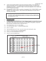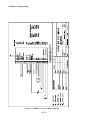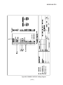
1
Users Guide http://www.dasieee.com e-mail: [email protected] RTU Series Radio Telemetry Systems OMEGAnet® On-Line Service http://www.omega.com Internet e-mail [email protected] Servicing North America: USA: ISO 9001 Certified Canada: One Omega Drive, Box 4047 Stamford, CT 06907-0047 Tel: (203) 359-1660 FAX: (203) 359-7700 e-mail: [email protected] 976 Bergar Laval (Quebec) H7L 5A1 Tel: (514) 856-6928 FAX: (514) 856-6886 e-mail: [email protected] For immediate technical or application assistance: USA and Canada: Mexico and Latin America: Sales Service: 1-800-826-6342 / 1-800-TC-OMEGASM Customer Service: 1-800-622-2378 / 1-800-622-BESTSM Engineering Service: 1-800-872-9436 / 1-800-USA-WHENSM TELEX: 996404 EASYLINK: 62968934 CABLE: OMEGA Tel: (95) 800-826-6342 FAX: (95) 203-359-7807 En Espanol: (95) 203-359-7803 e-mail: [email protected] Servicing Europe: Benelux: Czech Republic: France: Germany/Austria: United Kingdom: ISO 9002 Certified Postbus 8034, 1180 LA Amstelveen, The Netherlands Tel: (31) 20 6418405 FAX: (31) 20 6434643 Toll Free in Benelux: 0800 0993344 e-mail: [email protected] ul. Rude armady 1868, 733 01 Karvina-Hranice Tel: 420 (69) 6311899 FAX: 420 (69) 6311114 Toll Free: 0800-1-66342 e-mail: [email protected] 9, rue Denis Papin, 78190 Trappes Tel: (33) 130-621-400 FAX: (33) 130-699-120 Toll Free in France: 0800-4-06342 e-mail: [email protected] Daimlerstrasse 26, D-75392 Deckenpfronn, Germany Tel: 49 (07056) 3017 FAX: 49 (07056) 8540 Toll Free in Germany: 0130 11 21 66 e-mail: [email protected] One Omega Drive, River Bend Technology Centre Northbank, Irlam, Manchester M44 5EX, England Tel: 44 (161) 777-6611 FAX: 44 (161) 777-6622 Toll Free in the United Kingdom: 0800-488-488 e-mail: [email protected] It is the policy of OMEGA to comply with all worldwide safety and EMC/EMI regulations that apply. OMEGA is constantly pursuing certification of its products to the European New Approach Directives. OMEGA will add the CE mark to every appropriate device upon certification. The information contained in this document is believed to be correct, but OMEGA Engineering, Inc. accepts no liability for any errors it contains, and reserves the right to alter specifications without notice. WARNING: These products are not designed for use in, and should not be used for, patient-connected applications. WARRANTY/DISCLAIMER OMEGA ENGINEERING, INC. warrants this unit to be free of defects in materials and workmanship for a period of 13 months from date of purchase. OMEGA Warranty adds an additional one (1) month grace period to the normal one (1) year product warranty to cover handling and shipping time. This ensures that OMEGAs customers receive maximum coverage on each product. If the unit malfunctions, it must be returned to the factory for evaluation. OMEGAs Customer Service Department will issue an Authorized Return (AR) number immediately upon phone or written request. Upon examination by OMEGA, if the unit is found to be defective, it will be repaired or replaced at no charge. OMEGAs WARRANTY does not apply to defects resulting from any action of the purchaser, including but not limited to mishandling, improper interfacing, operation outside of design limits, improper repair, or unauthorized modification. This WARRANTY is VOID if the unit shows evidence of having been tampered with or shows evidence of having been damaged as a result of excessive corrosion; or current, heat, moisture or vibration; improper specification; misapplication; misuse or other operating conditions outside of OMEGAs control. Components which wear are not warranted, including but not limited to contact points, fuses, and triacs. OMEGA is pleased to offer suggestions on the use of its various products. However, OMEGA neither assumes responsibility for any omissions or errors nor assumes liability for any damages that result from the use of its products in accordance with information provided by OMEGA, either verbal or written. OMEGA warrants only that the parts manufactured by it will be as specified and free of defects. OMEGA MAKES NO OTHER WARRANTIES OR REPRESENTATIONS OF ANY KIND WHATSOEVER, EXPRESS OR IMPLIED, EXCEPT THAT OF TITLE, AND ALL IMPLIED WARRANTIES INCLUDING ANY WARRANTY OF MERCHANTABILITY AND FITNESS FOR A PARTICULAR PURPOSE ARE HEREBY DISCLAIMED. LIMITATION OF LIABILITY: The remedies of purchaser set forth herein are exclusive, and the total liability of OMEGA with respect to this order, whether based on contract, warranty, negligence, indemnification, strict liability or otherwise, shall not exceed the purchase price of the component upon which liability is based. In no event shall OMEGA be liable for consequential, incidental or special damages. CONDITIONS: Equipment sold by OMEGA is not intended to be used, nor shall it be used: (1) as a Basic Component under 10 CFR 21 (NRC), used in or with any nuclear installation or activity; or (2) in medical applications or used on humans. Should any Product(s) be used in or with any nuclear installation or activity, medical application, used on humans, or misused in any way, OMEGA assumes no responsibility as set forth in our basic WARRANTY / DISCLAIMER language, and, additionally, purchaser will indemnify OMEGA and hold OMEGA harmless from any liability or damage whatsoever arising out of the use of the Product(s) in such a manner. RETURN REQUESTS / INQUIRIES Direct all warranty and repair requests/inquiries to the OMEGA Customer Service Department. BEFORE RETURNING ANY PRODUCT(S) TO OMEGA, PURCHASER MUST OBTAIN AN AUTHORIZED RETURN (AR) NUMBER FROM OMEGAS CUSTOMER SERVICE DEPARTMENT (IN ORDER TO AVOID PROCESSING DELAYS). The assigned AR number should then be marked on the outside of the return package and on any correspondence. The purchaser is responsible for shipping charges, freight, insurance and proper packaging to prevent breakage in transit. FOR WARRANTY RETURNS, please have the following information available BEFORE contacting OMEGA: 1. Purchase Order number under which the product was PURCHASED, 2. Model and serial number of the product under warranty, and 3. Repair instructions and/or specific problems relative to the product. FOR NON-WARRANTY REPAIRS, consult OMEGA for current repair charges. Have the following information available BEFORE contacting OMEGA: 1. Purchase Order number to cover the COST of the repair, 2. Model and serial number of the product, and 3. Repair instructions and/or specific problems relative to the product. OMEGA’s policy is to make running changes, not model changes, whenever an improvement is possible. This affords our customers the latest in technology and engineering. OMEGA is a registered trademark of OMEGA ENGINEERING, INC. © 2002 OMEGA ENGINEERING, INC. All rights reserved. This document may not be copied, photocopied, reproduced, translated, or reduced to any electronic medium or machine-readable form, in whole or in part, without the prior written consent of OMEGA ENGINEERING, INC. Installation/Operation/Software/Programming Manual DATAFLOW RTU OWNER INFORMATION FCC REGULATIONS LICENSING The FCC requires you to obtain a station license for your DATAFLOW RTU system before using it, but does not require an operation license or permit. The station licensee is responsible for ensuring that the transmitter power, frequency and deviation are within the limits specified by the station license. The licensee is also responsible for the proper operation and maintenance of the radio equipment. This includes checking the transmitter frequency and deviation periodically, using appropriate methods. You will need to obtain a FCC license to operate the DATAFLOW RTU. To get a FCC license for VHF or UHF frequencies, submit FCC application Form 600. SAFETY STANDARDS The FCC (with its action in General Docket 79-144, March 13, 1985), has adopted a safety standard for human exposure to radio frequency electromagnetic energy emitted by FCC regulated equipment. OMEGA observes these guidelines, and recommends that you do also: • • • DO NOT hold the DATAFLOW RTU so the antenna is very close to or touching exposed parts of the body, especially the face or eyes, while transmitting. DO NOT operate radio equipment near electrical blasting caps or in an explosive atmosphere. DO NOT allow children to play with any radio equipment that contains a transmitting device. REPAIR of OMEGA products should be performed only by OMEGA authorized personnel. ( iii ) Installation/Operation/Software/Programming Manual DATAFLOW RTU CAUTIONS 1. ALL DIGITAL INPUTS, ANALOG INPUTS, ANALOG OUTPUTS, AND MEASUREMENTS OF THE DATAFLOW RTU ARE REFERENCED TO GROUND. DO NOT USE THE DATAFLOW RTU WITH EQUIPMENT THAT REQUIRES COMPLETE ISOLATION. 2. ALL DATAFLOW RTU DIGITAL OUTPUTS ARE ISOLATED LATCHING RELAYS. DO NOT EXCEED CONTACT RATINGS OF THESE RELAYS. 3. EXCITATION VOLTAGE AND LOAD DRIVE VARY FROM MANUFACTURER TO MANUFACTURER. CONSULT MANUFACTURER DOCUMENTATION BEFORE CONNECTING THE SENSORS OR INDICATORS TO THE DATAFLOW RTU. 4. THE DATAFLOW RTU CASE IS CONNECTED TO GROUND. 5. ALL DATAFLOW RTU SYSTEMS REQUIRE AN FCC LICENSE 6. THE FREQUENCY DEVIATION IS CONTROLLED BY VARIABLE RESISTOR R131. THIS DEVIATION ADJUSTMENT SHOULD ONLY BE PERFORMED BY AUTHORIZED OMEGA PERSONNEL USING THE APPROPRIATE METHODS AND TEST EQUIPMENT. 7. · · · DO NOT SHORT THE RED WIRE (PIN 6) OF CONNECTOR J105 TO GROUND. DO NOT SHORT THE RED WIRE (PIN 5) OF CONNECTOR J101 TO GROUND. IF AN INTERNAL BATTERY IS INSTALLED DO NOT SHORT THE ORANGE WIRE (PIN 7) OF CONNECTOR J105 TO GROUND. PERFORMING ANY OF THESE ACTIONS WILL DESTROY THE FUSE (F101)LOCATED ON THE DATAFLOW RTU CONTROL BOARD. 8. DO NOT OPERATE THE DATAFLOW RTU WITHOUT AN ANTENNA OR SUITABLE LOAD. TO DO SO MAY DAMAGE THE TRANSMITTER. ( iv ) Installation/Operation DATAFLOW RTU Installation/ Operation Table of Contents SECTION 1 2 3 4 5 6 7 8 9 10 11 12 13 14 15 16 17 18 19 20 21 22 23 24 25 TITLE PAGE NO. Introduction Operation Microprocessor Updates Part Number Definition Accessories Specifications Control Board Schematic Control Board Layout RF Board Schematic RF Board Layout Interconnects Hardware Configuration Software Configuration Mounting Information Power Serial Link I/O Mapping Digital Inputs Digital Outputs Analog Inputs Analog Outputs Antennas Alignment Theory of Operation Voltage Charts A-1 A-1 A-1 A-2 A-2 A-3 A-5 A-6 A-9 A-9 A-9 A-11 A-12 A-12 A-14 A-15 A-15 A-15 A-16 A-16 A-17 A-19 A-19 A-19 A-21 Installation/ Operation Table of Figures TITLE PAGE NO. Figure A1 - Control Board Schematic A-5 Figure A2 - Control Board Top Side Parts Placement with Reference Designators A-6 Figure A3 - Circular Connector Pin Designations A-9 Figure A4 - Mounting Hole Pattern for Fastening Directly to the DATAFLOW RTU Case A-12 Figure A5 - Mounting Hole Pattern for Use with Optional Mounting Bracket A-13 Figure A6 - Battery Connection Wiring Diagram A-14 Figure A7 - Connecting a Current Loop Sensor to a DATAFLOW RTU Analog Input A-17 Figure A8 - Connecting a Current Loop Indicator to a DATAFLOW RTU Analog Output A-18 Software/ Programming (Part B) Table of Contents B-i ( A-v ) DATAFLOW RTU 1. INTRODUCTION 1.1 The DATAFLOW RTU from OMEGA is a complete wireless telemetry system designed to deliver industrial instrumentation signals from a source to other instruments via radio frequency communications. The DATAFLOW RTU allows you to access industrial measuring devices in remote locations without running wires, installing microwave links or leasing a telephone line. OMEGA DATAFLOW RTU and MODBUS radio communications equipment replaces these methods. 1.2 Manual Part A is intended to provide information needed for the installation and operation of DATAFLOW RTU systems. The intended readers are people familiar with industrial instrumentation. A basic understanding of radio communications is helpful. The included information is valid only for models listed on the cover. 2. OPERATION 2.1 DATAFLOW RTU is a radio telemetry system. It operates on either 450-470 MHz with a transmitter power of 2 Watts or 5 Watts (UHF-FM), or 136 to 151 MHz, 150 to 165 MHz, 160 to 174 MHz with a transmitter power of 5 Watts (VHF-FM). An RTU system operating in the UHFFM band at 2 Watts with directional antennas and 50-foot towers has an effective range of 20 to 25 miles over level terrain. Changes in the frequency of operation, transmitter power, terrain and antenna structure will affect the range of the link. 2.2 All DATAFLOW RTU systems require FCC licensing. 3. MICROPROCESSOR UPDATES 3.1 A microprocessor, IC105, the main controlling device of a DATAFLOW RTU, is located in a socket on the Control Board. Socket configuration provides ease in replacing or updating microprocessor firmware. 3.2 The microprocessor firmware version available when this manual was printed is Version 3.27. (In Version 3.x, x represents the [number] designation of a minor revision.) ( A-1 ) Installation/Operation 4. 4.1 5. 5.1 PART NUMBER DEFINITION The following is a list of the part numbers available at the printing of this material. Band Option RTU-X X X - X / / / / 150- E 136-151 MHz. RF Board (OMEGA # DTX-150-E0DD) 150- 0 150-165 MHz. RF Board (OMEGA # DTX-150-00DD) 150- F 160-174 MHz. RF Board (OMEGA # DTX-150-F0DD) 450- 0 450-470 MHz. RF Board (OMEGA # DTX-450-00DD) 400- G 400-430 MHz. RF Board (OMEGA # DTX-150-G0DD) RTU-/ / / - / X / / / RF Connection U UHF Connector RTU-/ / / - / / X / / Enclosure S Small Enclosure RTU-/ / / - / / / X / Power Option 1 2 D One 8-cell AA battery holders (batteries not included) Two 4-cell NiCad rechargeable battery packs No internal power RTU-/ / / - / / / / X Data Encryption C Clear ACCESSORIES The following list reflects available accessories. OMEGA PART NO. RTU-06001123 RTU-06001124 RTU-25104600 RTU-25605100 DESCRIPTION Power/ Serial Cable, 6 foot length for small (S) enclosure User I/O Cable, 6 foot length for small (S) enclosure Mounting Bracket for small (S) enclosure Enclosure Cover Seal RTU-BATNICD RTU-BATHOLD RTU-AFP-150 NiCad Rechargeable Battery Pack Battery Holder VHF Flexible Antenna RTU-AFP-150H RTU-RYA-15 RTU-AFP-450 VHF Flexible Antenna for 164-174 MHz VHF Directional Antenna, 6.5 dB Gain UHF Flexible Antenna RTU-RYA-45 RTU-ROA-45 RTU-RAC-05 UHF Directional Antenna, 10 dB Gain UHF Omnidirectional Antenna, 2.5 dB Gain Coaxial Cable, 50 feet, RG-8A/U w/PL-250 Connectors RTU-RAC-10 RTU-9/RTC-PAS RTU-PCPC Coaxial Cable, 100 feet, RG-8A/U w/PL-250 Connectors Programming Cable for small (S) enclosure Programming Cable for small (S) enclosure RTU-PCPS-3.0 RTU-PCPK Programming software (Version 3.03 for DOS & Windows PCs on 3.5" disk Programming Kit RTU-PS RPS-1 1.5 Amp AC-to-DC Power supply 1 Amp AC to DC Power Supply 14800018-0 RTU Series Users Guide ( A-2 ) DATAFLOW RTU 6 SPECIFICATIONS 6.1 SYSTEM SPECIFICATIONS FCC ID:......................................... Emission designator: RTU-150 - AIERIT04-150; RTU-450 - AIERIT04-450 10K8FID Digital Inputs:............................... LOW: HIGH: Maximum of 6 Programmable from 0 to 5 V Programmable from 0 to 5 V Digital Outputs:............................. UL/CSA rating: Two (2) isolated latching relays 2A 30VDC 0.5A 110VDC 0.5A 125VAC Analog Inputs: :............................. Voltage Mode Range: Current Loop Mode Range: Resolution: Maximum of 6 0-5 VDC 0-20 mA 8 bits Analog Outputs:............................ Analog Voltage Mode Range: Current Loop Mode Range: Resolution: Maximum of 2 0-5 VDC 0-20 mA 8 bits Radio Communications:................. FSK, 1200 BPS, proprietary Manchester-Encoded data format Serial Communications: ............... RS-485; 1200, 2400, 4800, or 9600 BPS; MODBUS RTU protocol; for programming and external control Power Requirements:..................... 10-16 VDC 300mA sleep, 100 mA receive 1.5A low power transmit, 2.5A high power transmit Housing:........................................ Diecast Aluminum, Weather-resistant, (Enclosure S) Dimensions (L x W x H):................ 4.5" x 3.5" x 2.2" (Enclosure option S) Weight:.......................................... 1.4 lb. (Enclosure option S) Operating Temperature:................. -30 to +60 degrees Centigrade -22 to +140 degrees Fahrenheit 6.2 DTX SPECIFICATIONS TRANSMITTER Bandspread: Freq. Stability: RF Power Out: RF Output Z: Mod. Dist.: 20 MHz 5 PPM 5 W, programmable to 2 W 50 Ohms less than 4% RECEIVER Bandspread: Freq. Stability: Sensitivity: RF Input Z: Selectivity: Mod. Input Z: 100 K Ohms Audio Dist.: ( A-3 ) 20 MHz 5 PPM .3 mV 50 Ohms 70 dB @ 30 kHz 65 dB @ 25 kHz less than 3% Installation/Operation N O T E S ......................................................................................................................................................................... ................................................................................................................................................ .............................................................................................................................................. ............................................................................................................................................ ........................................................................................................................................... ................................................................................................................................................. ...................................................................................................................................................... .......................................................................................................................................... .......................................................................................................................................... ........................................................................................................................................ .................................................................................................................................................... .......................................................................................................................................... ........................................................................................................................................... ................................................................................................................................................ ...................................................................................................................................... .................................................................................................................................... ........................................................................................................................................ .................................................................................................................................... ....................................................................................................................................... ............................................................................................................................................. ................................................................................................................................................. ........................................................................................................................................................ .......................................................................................................................................... ............................................................................................................................................ ..................................................................................................................................................... .................................................................................................................................................. ............................................................................................................................................ ...................................................................................................................................................... ............................................................................................................................................ ............................................................................................................................................. .......................................................................................................................................... ......................................................................................................................................... ............................................................................................................................................. ................................................................................................................................................................. ................................................................................................................................................ .......................................................................................................................................... ................................................................................................................................................. ....................................................................................................................................... .......................................................................................................................................... ................................................................................................................................................. ......................................................................................................................................... ........................................................................................................................................... ..................................................................................................................................... ( A-4 ) 7. CONTROL BOARD SCHEMATIC 7.1 The following is the DATAFLOW RTU Control Board schematic. Figure A1 - Control Board Schematic ( A-5 ) Installation/ Operation 8. CONTROL BOARD LAYOUT 8.1 The following diagram shows the physical layout of the RTU control board X Y 1750090C 12/16/97 TOP SIDE PARTS PLACEMENT W/ REF. DES. 1750092G LAST ECN 2540 Figure A2 - Control Board top side parts placement with reference deisgnators. 8.2 EXAMPLE: The location of a particular component is given by the following notation - J101 PIN 1 (Y 0.3 - X 1.8). This means the pin 1 of connector J101 is located at a horizontal (X) coordinate of 1.8 inches and a vertical (Y) coordinate of 0.3 inches. 8.3 SCHEMATIC REFERENCE NUMBER PARTS LIST, RTU-CNTL, 03/05/98 REF. PART NO. CAPACITORS C 101 01503021 C 102 15111102 C 103 152B8106 C 104 15121104 C 105 15110100 C 106 15110100 C 107 15121104 C 108 15121104 C 109 15121104 C 110 15121104 C 111 15121104 C 112 15121104 C 113 15110180 C 114 15110180 C 115 15111103 C 116 15111103 C 117 15111103 C 118 15111103 C 119 15111103 C 120 15111103 C 121 15111472 C 122 15121104 RITRON, INC. DESCRIPTION Y X 10uf ELT CAP 50V .1" .2"x.46" r .001MF X7R 0805 50V CHIP CAP CAP 10uF 16V 3.4 X 2.8 CHIP TANTALUM .1MF X7R 1206 50V CHIP CAP 10PF NPO 0805 50V CHIP CAP 10PF NPO 0805 50V CHIP CAP .1MF X7R 1206 50V CHIP CAP .1MF X7R 1206 50V CHIP CAP .1MF X7R 1206 50V CHIP CAP .1MF X7R 1206 50V CHIP CAP .1MF X7R 1206 50V CHIP CAP .1MF X7R 1206 50V CHIP CAP 18PF NPO 0805 50V CHIP 18PF NPO 0805 50V CHIP .01MF X7R 0805 50V CHIP .01MF X7R 0805 50V CHIP .01MF X7R 0805 50V CHIP .01MF X7R 0805 50V CHIP .01MF X7R 0805 50V CHIP .01MF X7R 0805 50V CHIP .0047MF X7R 0805 50V CHIP .1MF X7R 1206 50V CHIP CAP 0.585 1.189 1.113 2.470 2.294 2.372 1.755 1.849 1.850 1.851 1.234 0.999 2.114 2.332 1.489 0.935 1.069 0.935 1.069 1.110 0.964 0.632 3.939 3.291 3.104 3.670 4.155 4.155 0.428 0.666 0.897 1.130 1.001 1.001 1.100 1.099 1.719 2.159 2.007 1.810 1.926 1.340 1.149 1.951 ( A-6 ) DATAFLOW RTU REF. DESCRIPTION Y 22uf 10V 6.0 X 3.2 CHIP TANTALUM CAP .33MF 35V "3.2X1.6" CHIP TANTALUM .1MF X7R 1206 50V CHIP CAP CAPACITOR .047F 5.5V TANTALUM .1MF X7R 1206 50V CHIP CAP .01MF X7R 0805 50V CHIP .01MF X7R 0805 50V CHIP .01MF X7R 0805 50V CHIP .01MF X7R 0805 50V CHIP .001MF X7R 0805 50V CHIP CAP .1MF X7R 1206 50V CHIP CAP .001MF X7R 0805 50V CHIP CAP .001MF X7R 0805 50V CHIP CAP .001MF X7R 0805 50V CHIP CAP 0.028 0.044 1.402 1.065 2.086 2.442 2.441 2.578 2.579 0.026 1.851 1.241 1.004 0.610 2.955 3.375 4.111 4.027 0.369 0.971 1.124 0.971 1.124 3.469 1.255 2.313 2.316 3.791 DIODES CR101 48A1005C CR102 48A1005C CR103 48A1005C CR104 48A1005C CR105 48A1005C CR106 48A1005C CR107 48A1005C CR108 48A1005C CR109 48A1005C CR110 48A1005C CR112 48A100A3 CR113 48A100A3 CR114 48A1005C CR115 04810003 CR116 48B10001 CR117 48B1008W CR118 48B1008W MMBD7000 DUAL DIODE SOT-23 MMBD7000 DUAL DIODE SOT-23 MMBD7000 DUAL DIODE SOT-23 MMBD7000 DUAL DIODE SOT-23 MMBD7000 DUAL DIODE SOT-23 MMBD7000 DUAL DIODE SOT-23 MMBD7000 DUAL DIODE SOT-23 MMBD7000 DUAL DIODE SOT-23 MMBD7000 DUAL DIODE SOT-23 MMBD7000 DUAL DIODE SOT-23 MMBD2835, DUAL DIODE SOT-23 MMBD2835, DUAL DIODE SOT-23 MMBD7000 DUAL DIODE SOT-23 1N4001 DIODE 50 VOLT/1AMP DIODE, ZENER, 6.2V 5% 225MW SOT-23 MMBZ 5245 ZENER DIODE SOT23 MMBZ 5245 ZENER DIODE SOT23 1.080 1.105 2.634 2.306 1.588 1.680 1.680 1.681 1.274 1.039 0.170 0.171 0.945 0.398 0.572 1.358 1.121 3.285 3.664 3.633 3.630 0.388 0.626 0.857 1.090 0.820 0.825 1.067 1.629 2.496 4.019 3.203 2.313 2.316 FUSE F 101 3.180 C 123 C 124 C 125 C 126 C 127 C 128 C 129 C 130 C 131 C 132 C 133 C 134 C 135 C 136 PART NO. 152C6226 152AB334 15121104 01517014 15121104 15111103 15111103 15111103 15111103 15111102 15121104 15111102 15111102 15111102 06000040 X WIRE; #40AWG TINNED BUS (INCHES) 0.044 INTEGRATED CIRCUITS IC101 31040001 IC102 31130002 IC105 314B0005 IC107 31020324 IC108 312G0001 IC109 311A0001 IC110 31110001 IC112 03131056 IC113 31120001 IC114 31010008 IC, SO-16 WIDE VOLT. REG. LT1020 CD4060 COUNTER, SO-16, CD4060 IC, PLCC-52 MICROPROCESSOR, 68HC705B16 LMT324AD/NJM324E QUAD OP-AMP IC, SO-28 WIDE 32KB STATIC RAM HM52256 IC, PLCC-44, PERIPHERAL INTERFACE 82C55A RS-485 TRANSCEIVER, SO-8, MAX487 IC, TO-220 5 PIN VOLT. REG. MIC29302 INVERTER, HEX CD4069 LMT2904D DUAL OP AMP SO-8 0.789 3.513 2.419 3.901 2.073 1.926 1.162 1.595 1.785 3.803 1.709 3.000 1.109 2.805 BOTTOM SIDE 0.706 2.966 2.345 0.444 JACKS J 102 J 103 CONNECTOR; 6 POSITION PC VERT. GOLD CONNECTOR; 6 POSITION PC VERT. GOLD 21443061 21443071 RELAYS K 101 04500016 K 102 04500016 RELAY, SPDT 5V LATCHING RELAY, SPDT 5V LATCHING 0.161 0.162 2.201 2.675 JUMPERS PJ101 02100024 PJ102 02100024 PJ103 02100024 PJ104 02100098 PJ105 02100098 PJ106 02100159 3 PIN STRAIGHT HEADER 3 PIN STRAIGHT HEADER 3 PIN STRAIGHT HEADER 4 PIN 0.1" HEADER 4 PIN 0.1" HEADER 2 PIN .1" HEADER STRIP 2.810 2.809 2.809 2.902 2.709 0.211 1.975 1.775 1.575 1.375 1.375 2.888 TRANSISTORS Q 101 4801001Q Q 102 4801001Q Q 103 4801001Q Q 104 4801001Q Q 105 4801001Q Q 106 4801001Q Q 107 4801001Q MMBT-5088 "SOT-23" MMBT-5088 "SOT-23" MMBT-5088 "SOT-23" MMBT-5088 "SOT-23" MMBT-5088 "SOT-23" MMBT-5088 "SOT-23" MMBT-5088 "SOT-23" 1.328 0.171 0.171 0.027 0.170 2.071 2.590 3.754 1.399 1.796 2.752 1.257 0.485 0.409 RESISTORS R 101 47403163 R 102 47403012 R 103 47402873 R 104 47100103 R 105 47100473 316K OHM 1% 0805 CHIP 30.1K OHM 1% 0805 CHIP 287K OHM 1% 0805 CHIP 10K OHM 0805 CHIP RES 47K OHM 0805 CHIP RES. 1.264 1.180 1.068 1.180 1.219 3.291 3.399 3.439 3.554 3.702 ( A-7 ) RITRON, INC. Installation/ Operation REF. PART NO. R 106 R 107 R 108 R 109 R 110 R 111 R 112 R 113 R 114 R 115 R 116 R 117 R 118 R 119 R 120 R 121 R 122 R 123 R 124 R 125 R 126 R 127 R 128 R 129 R 130 R 131 R 132 R 133 R 134 R 135 R 136 R 137 R 138 R 139 R 140 R 141 R 142 R 143 R 144 R 145 R 146 R 147 R 148 R 149 R 150 R 151 R 152 R 153 R 154 R 155 R 156 R 157 R 158 R 159 R 160 R 161 R 162 R 163 R 164 R 165 R 166 R 167 R 168 R 169 R 170 R 171 R 172 R 173 R 174 R 175 R 176 47100102 47100106 47100474 47100103 47402002 47100103 47402002 47100103 47402002 47100103 47402002 47100103 47402002 47100103 47402002 47100106 47401003 47403163 47100682 47401003 47100332 47402802 47402002 47402002 47100393 47270103 47100102 47100682 47100393 47100332 47100682 47100682 47100393 47403012 47403012 47402002 47100752 47100243 47401003 47402002 47100103 47100103 47402802 47404751 47401003 47401003 47100103 47100270 47100270 47100102 47100123 47404990 47404990 47100334 47100334 47100334 47100334 47100103 47100102 47404990 47100102 47404990 47100106 47100102 47100102 47100102 47100102 47100102 47100102 47100682 47403012 CRYSTALS Y 101 02300041 Y 102 02300058 RITRON, INC. DESCRIPTION Y X 1K OHM 0805 CHIP RES RESISTOR, 10M OHM 0805 5% CHIP 470K OHM 0805 CHIP RES. 10K OHM 0805 CHIP RES 20K OHM 1% 0805 CHIP 10K OHM 0805 CHIP RES 20K OHM 1% 0805 CHIP 10K OHM 0805 CHIP RES 20K OHM 1% 0805 CHIP 10K OHM 0805 CHIP RES 20K OHM 1% 0805 CHIP 10K OHM 0805 CHIP RES 20K OHM 1% 0805 CHIP 10K OHM 0805 CHIP RES 20K OHM 1% 0805 CHIP RESISTOR, 10M OHM 0805 5% CHIP 100K OHM 1% 0805 CHIP 316K OHM 1% 0805 CHIP 6.8K OHM 0805 CHIP RES. 100K OHM 1% 0805 CHIP 3.3K OHM 0805 CHIP RES. 28K OHM 1% 0805 CHIP 20K OHM 1% 0805 CHIP 20K OHM 1% 0805 CHIP 39K OHM 0805 CHIP RES. VARIABLE RESISTOR 10K SEALED 1K OHM 0805 CHIP RES 6.8K OHM 0805 CHIP RES. 39K OHM 0805 CHIP RES. 3.3K OHM 0805 CHIP RES. 6.8K OHM 0805 CHIP RES. 6.8K OHM 0805 CHIP RES. 39K OHM 0805 CHIP RES. 30.1K OHM 1% 0805 CHIP 30.1K OHM 1% 0805 CHIP 20K OHM 1% 0805 CHIP RESISTOR, 7.5K OHM 0805 CHIP 24K OHM 0805 CHIP RESISTOR 100K OHM 1% 0805 CHIP 20K OHM 1% 0805 CHIP 10K OHM 0805 CHIP RES 10K OHM 0805 CHIP RES 28K OHM 1% 0805 CHIP 4.75K OHM 1% 0805 CHIP 100K OHM 1% 0805 CHIP 100K OHM 1% 0805 CHIP 10K OHM 0805 CHIP RES 27 OHM 0805 CHIP RESISTOR 27 OHM 0805 CHIP RESISTOR 1K OHM 0805 CHIP RES 12K OHM 0805 CHIP RES. RESISTOR, 499 OHM 1% 0805 CHIP RESISTOR, 499 OHM 1% 0805 CHIP 330K OHM 0805 CHIP RES. 330K OHM 0805 CHIP RES. 330K OHM 0805 CHIP RES. 330K OHM 0805 CHIP RES. 10K OHM 0805 CHIP RES 1K OHM 0805 CHIP RES RESISTOR, 499 OHM 1% 0805 CHIP 1K OHM 0805 CHIP RES RESISTOR, 499 OHM 1% 0805 CHIP RESISTOR, 10M OHM 0805 5% CHIP 1K OHM 0805 CHIP RES 1K OHM 0805 CHIP RES 1K OHM 0805 CHIP RES 1K OHM 0805 CHIP RES 1K OHM 0805 CHIP RES 1K OHM 0805 CHIP RES 6.8K OHM 0805 CHIP RES 30.1K OHM 1% 0805 CHIP RES 1.337 2.473 2.625 1.442 1.443 1.537 1.537 1.537 1.537 1.537 1.537 1.314 1.234 1.079 0.999 2.222 1.477 1.400 1.391 1.250 1.187 1.215 1.255 1.413 1.175 2.882 1.252 1.094 1.410 1.410 0.935 1.070 0.935 0.935 1.002 1.002 0.543 0.543 0.835 0.543 0.835 0.835 0.346 0.463 1.248 0.931 0.835 1.084 1.172 1.366 1.373 2.035 2.636 2.442 2.485 2.579 2.608 1.180 2.035 2.035 2.737 2.636 2.549 1.775 1.868 1.868 1.869 1.321 1.085 1.492 3.914 4.155 4.155 0.348 0.428 0.586 0.666 0.817 0.897 1.050 1.130 0.676 0.676 0.676 0.676 1.139 1.877 1.877 1.350 1.350 1.234 1.879 1.986 2.115 1.985 2.265 2.134 2.159 1.491 1.640 1.947 1.850 1.510 1.662 1.354 1.250 1.333 1.508 1.990 1.588 2.294 2.154 3.455 3.368 2.540 2.758 2.433 2.540 2.540 4.028 1.249 0.611 0.695 1.048 1.310 1.048 1.253 3.477 0.852 0.689 0.971 0.617 4.155 0.339 0.578 0.807 1.040 1.020 1.019 2.036 2.372 2.195 4.344 1.294 32.768 KHz CRYSTAL CRYSTAL 4.000MHZ; AT-49 ( A-8 ) DATAFLOW RTU 9. RF BOARD SCHEMATIC 9.1 Contact Omega for more detailed information on the DTX RF board schematic. 10. RF BOARD LAYOUT 10.1 Contact Omega for more detailed information on the DTX RF board layout. 11. INTERCONNECTS C A U T I O N On DATAFLOW RTUs shipped before the 2nd quarter of 1998, do not exceed 6 volts referenced to GNDon RS-485 connections (the GREEN and BLUE wires of the External Power/Serial Cable: OMEGA Part No. 06001123). Exceeding 6 volts will damage protection circuitry and render the units serial link inoperable. 11.1 For a weather-resistant aluminum enclosure for DATAFLOW RTU, purchase it in a small (S) enclosure option. This option also provides bulkhead circular connectors and one UHF antenna port. See Figure A3 for pin number designations of the circular connectors. BULKHEAD CONNECTOR CABLE CONNECTOR KEYING PIN KEYING SLOT 1 7 7 6 2 7-PIN 3 4 5 18-PIN 8 7 12 9 13 16 17 1 15 10 18 18 8 9 14 15 3 4 5 6 11 11 10 14 3 2 6 5 4 KEYING SLOT 2 4 3 2 5 KEYING PIN 1 1 6 13 17 7 12 16 Figure A3 - Circular connector pin designators 11.1.1 BULKHEAD CONNECTORS: CONNECTOR PIN NAME DESCRIPTION Ext. Power/ Serial: 1 2 3 4 5 6 7 A B GND LDR GND VI B+ Serial Pair A Serial Pair B Loader Ground Loader Connected/Program Enable Power Ground Power In to Controller and Radio From Internal Battery ( A-9 ) Installation/Operation CONNECTOR PIN NAME DESCRIPTION User Input/ Output: 1 2 3 4 5 6 7 8 9 10 11 12 13 14 15 16 17 18 R11 R12 R21 R22 PWR GND S1 GND S2 GND S3 GND S4 GND S5 GND S6 GND Relay 1 Contact 1 Relay 1 Contact 2 Relay 2 Contact 1 Relay 2 Contact 2 Power Out Power Out Ground Input 1 Input 1 Ground Input 2 Input 2 Ground Input 3 Input 3 Ground Input 4 Input 4 Ground Input 5/ Output 1 Input 5/ Output 1 Ground Input 6/ Output 2 Input 6/ Output 2 Ground 11.1.2 OPTIONAL INTERFACE CABLES, part numbers RTU-06001123 and RTU-06001124, may be purchased for use with the small (S) enclosure. These cables provide the user with 6-foot long, color-coded cables designed specifically for use with DATAFLOW RTU. 11.1.3 INTERFACE CABLE CONNECTIONS: CABLE PIN Ext. Pwr./ Serial: Part # 06001123 User Input/ Output: Part # 06001124 NOTE: NAME COLOR CODE DESCRIPTION 1 2 3 4 5 6 7 A B GND LDR GND VI B+ GREEN BLUE BLACK WHITE BROWN RED ORANGE Serial Pair A Serial Pair B Loader Ground Loader Connected/Program Enable Power Ground Power In to Controller and Radio From Internal Battery 1 2 3 4 5 6 7 8 9 10 11 12 13 14 15 16 17 18 R11 R12 R21 R22 PWR GND S1 GND S2 GND S3 GND S4 GND S5 GND S6 GND WHITE RED GREEN RED RED BLACK BROWN BLACK ORANGE BLACK YELLOW BLACK GREEN BLACK BLUE BLACK WHITE BLACK Relay 1 Contact 1 Relay 1 Contact 2 Relay 2 Contact 1 Relay 2 Contact 2 Power Out Power Out Ground Input 1 Input 1 Ground Input 2 Input 2 Ground Input 3 Input 3 Ground Input 4 Input 4 Ground Input 5/ Output 1 Input 5/ Output 1 Ground Input 6/ Output 2 Input 6/ Output 2 Ground The following pin groups are twisted pairs: 1-2, 3-4, 5-6, 7-8, 9-10, 11-12, 13-14, 15-16, 17-18 ( A-10( A-3 ) ) DATAFLOW RTU 11.1.4 CONNECTIONS CONNECTOR PIN NAME DESCRIPTION Ext. Power/ Serial: J105 (X3.8 Y0.2) 1 2 3 4 5 6 7 A B GND LDR GND VI B+ Serial Pair A Serial Pair B Loader Ground Loader Connected/ Program Enable Power Ground Power In to Controller and Radio From Internal Battery User Input/ Output: J101 (X1.8 Y0.3) 1 2 3 4 5 6 7 8 9 10 11 12 13 14 15 16 17 18 R11 R21 R12 R22 PWR GND S1 GND S2 GND S3 GND S4 GND S5 GND S6 GND Relay 1 Contact 1 Relay 2 Contact 1 Relay 1 Contact 2 Relay 2 Contact 2 Power Out Power Out Ground Input 1 Input 1 Ground Input 2 Input 2 Ground Input 3 Input 3 Ground Input 4 Input 4 Ground Input 5/ Output 1 Input 5/ Output 1 Ground Input 6/ Output 2 Input 6/ Output 2 Ground 12. HARDWARE CONFIGURATION 12.1 The DATAFLOW RTU has six hardware configurable jumpers. Jumper functions are described in the following paragraphs 12.1.1 to 12.1.6. See Figure A2, page A-6, for location references. 12.1.1 PJ101 (Y 2.8 - X 2.0): This jumper setting determines whether configurable I/O 1 is an input or an analog output. The jumper across pins 1 and 2 configures the pin to be an input. The jumper across pins 2 and 3 configures the pin to be an output, the default setting. 12.1.2 PJ102 (Y 2.8 - X 1.8): This jumper setting determines if configurable I/O 2 is an input or an analog output. The jumper across pins 1 and 2 configures the pin to be an input. The jumper across pins 2 and 3 configures the pin to be an output, the default setting. 12.1.3 PJ103 (Y 2.8 - X 1.6): This jumper setting determines how the configurable analog outputs 1 and 2 are powered. The jumper setting is valid only if PJ101 or PJ102 is set for output. The jumper across pins 2 and 3 configures the output to be powered by system power. The jumper across pins 1 and 2 configures the output to be powered by regulated radio power, the default setting. PJ104 (Y 2.9 - X 1.2): This jumper setting determines if configurable I/O 1 is set for voltage or current loop analog output. This jumper setting is valid only if PJ101 is set for output. With one jumper across pins 1 and 2 and another jumper across pins 3 and 4, the output is configured for voltage, the default setting. Only one jumper across pins 2 and 3 configures the output for current loop. ( A-11 ) Installation/Operation 12.1.5 PJ105 (Y 2.7 - X 1.2): This jumper setting determines if configurable I/O 2 is set for voltage or current loop analog output. This jumper setting is valid only if PJ102 is set for output. With one jumper across pins 1 and 2 and another jumper across pins 3 and 4, the output is configured for voltage, the default setting. Only one jumper across pins 2 and 3 configures the output for current loop. 12.1.6 PJ106 (Y 0.2 - X 2.9): This jumper connects the internal battery power to the power input of the control board. This jumper setting is valid only when using the internal battery power. With the jumper installed, the default condition, the internal battery is always connected to control board power, meaning the unit is always ON with the internal batteries installed. 13. SOFTWARE CONFIGURATION 13.1 All DATAFLOW RTUs contain identical hardware; the software configuration of a unit makes it perform a particular task. This programmable configuration can be changed using any PC compatible computer, DATAFLOW RTU Programming Software and a DATAFLOW RTU Programming Cable. 14. MOUNTING INFORMATION 14.1 To provide DATAFLOW RTU with an aluminum enclosure, it may be purchased with the small enclosure (S). The S enclosure has four pilot holes drilled into the back corners of the case; the holes are tapped with four (4) #6 - 32 x 3/8 thread-forming screws. The DATAFLOW RTU is shipped with these screws installed in the case. A T-15 Torx© drive tool is required to remove the screws. 14.1.1 You can use the holes in the back of the enclosure to mount the DATAFLOW RTU directly to a surface, using the recommended hole pattern shown in Figure A4. The four thread-forming screws can be used to secure the case to the surface, if desired, by removing the screws and reusing them. Alternately, four #6 32 machine screws may be used; ensure they do not extend more than 5/16" into the case. 4.050 .144 DIA. MIN. 4-PLACES (CLEARANCE FOR #6-32 SCREW) 3.050 Figure A4 - Mounting hole pattern for fastening directly to the DATAFLOW RTU case ( A-12 ) DATAFLOW RTU 14.1.2 Optional mounting bracket OMEGA part number RTU-25104600 is available for DATAFLOW RTU. To install this bracket to the case, remove and save the four thread-forming screws described in paragraph 14.1 to attach the mounting bracket to the case. Be sure the narrow portion of the keyhole is positioned towards the top (UHF antenna connector) of the DATAFLOW RTU. Use the recommended hole pattern for the optional mounting bracket shown in Figure A5. .201 DIA. MIN. TYP (CLEARANCE FOR #10-32 SCREW) OPTIONAL MOUNTING - 2-PLACES 3.250 1.882 4.437 Figure A5 - Mounting hole pattern for use with optional mounting bracket 14.2 Reassembling DATAFLOW RTU Cover/ Waterproofing the Antenna Connection 14.2.1 The DATAFLOW RTU is weather-resistant if it has been properly sealed. If you have opened or disassembled the device, refer to the following instructions. 14.2.2 Sealing the Housing Cover: Inspect the seal and mating surfaces for flaws (tears, gaps, dents, etc.). Repair the surface or replace the part as necessary. Purchase replacement cover gaskets through Omega: Part No. RTU-25605100. Insert the seal in the cover. Thread the four (4) screws through the cover, into the housing; do not tighten the screws. Snug down the screws in an X sequence; i.e.: top left, then bottom right, then top right, then bottom left. Then fully tighten the screws in this same sequence. 14.2.3 Replacing Connectors: OMEGA discourages the practice of removing and discarding the protective cap from the connectors. Doing this may reduce the water-resistance of the unit. If you must remove a connector for any reason, make sure it has been retightened properly finger-tight connector nuts will not provide an effective water barrier. 14.2.4 Connecting the Antenna: Seal screws are used to secure the antenna to the housing. Always replace with a new seal screw, not a common screw. Do not remove the antenna connector from the housing; doing so will destroy the silicone rubber seal in the interface. The screw securing the ground strap inside the housing must be fully tight. 14.2.5 If this device is to be used in a wet environment, use seal tape around the antenna connection. Use Archer Connector Sealant, Radio Shack Number 278-1645 or an equivalent. Wrap the connection with the sealant tape and press it securely in place. ( A-13 ) Installation/Operation 15. POWER 15.1 The DATAFLOW RTU small enclosure (S) may be purchased with the delete internal power (D) option. The RTU power source is a user-provided external power supply meeting the following criteria: · Between 10 VDC and 16 VDC with 12 VDC nominal; · Has less than 1 V peak-to-peak of ripple; · Provides 1.5 A with the transmitter in low power setting; · Provides 2.5 A with the transmitter in high power setting. 15.1.1 Connect the positive side of the power supply to J105 pin 6. Connect the negative side of the power supply to J105 pin. The negative side of the power supply is considered to be GROUND and is the REFERENCE to which all inputs, outputs and measurements are to be made. GROUND is connected to the enclosure. 15.2 You can purchase the DATAFLOW RTU with an eight-cell internal battery holder (power option 1). In this option, internal AA batteries are used as the power source. CAUTION: When installing the batteries, be sure to match polarities of the batteries with the battery holder. Not matching polarities can damage the RTU. 15.2.1 The negative side of the battery assembly is considered to be GROUND and is the REFERENCE by which all inputs, outputs, and measurements are to be made. GROUND is connected to the case. 15.2.2 The battery voltage appears at pin 8 of J105 pin 8, and is not connected directly to the input power of the RTU control board. With jumper PJ106 installed, the battery is jumpered to the input power. With jumper PJ106 not installed, an external connection is required between pin 6 and 7, which allows the user to install an external ON/OFF switch to the RTU while using internal power. 15.3 J101 pin 5 is connected to the RTU power source, and J101 pin 6 is connected to GROUND. This power supply provides excitation voltage to external equipment with maximum current draw of .25 A. 15.4 Fuse F101 (X3.2 - Y0.1) is a 40-gauge tinned wire designed to open at 2.5A. If this fuse is destroyed, replace it with nothing larger than 40-gauge wire. 15.5 Optional Internal Battery Back-up (Refer to 11.1.3 for the appropriate pin numbers.) Either of the following two options may be used as an optional internal battery back-up: a. A two 4-cell battery pack (OMEGA Part No. RTU-BATNICD), OR b. An 8-cell AA battery holder (OMEGA Part No. RTU-BAT/HOLD). 15.5.1 Connect the battery as shown in Figure A6: CR1 NOTE: CR1and CR2 are to be 1N5817 V source R1 CR2 GND RTU 7-PIN CONNECTOR 7 ORN B+ 6 RED V1 5 BRN GND Figure A6 - Battery Connection Wiring Diagram 15.5.2 The following equations define the values required for R1. R1 = (Vsource - Vdiode - Vbattfull) / Icharge PR1 = (Vsource - Vdiode - Vbattempty)2 / R1 WHERE: R1 is the value of R1 in Ohms Vsource is the input voltage to the RTU. Vdiode is the voltage drop of the diode (CR1). Vbatfull is the fully charged voltage of the internal battery. Icharge is the charge current to the battery. PR1 is the power rating of R1 in Watts. Vbattempty is the empty voltage of the internal battery. ( A-14 ) DATAFLOW RTU 15.5.3 The following calculations apply to RTU-BATNICD, using a 14V source. R1 = (14 - 0.4 - 12) / .05 = 32 W PR1 = (14 - 0.4 - 8)2 / R1 = 0.98 W 15.5.4 For RTU-BATHOLD, use a rechargeable battery type. Confirm the manufacturers specification for full charge voltage, empty voltage, and trickle charge current. 16. SERIAL LINK 16.1 J105 pins 1 and 2 comprises the pair of differential lines used for the RS-485 link. This link provides the user access to change the software configuration, and allows the RTU to be controlled by an external computer via MODBUS RTU Protocol. The baud rate of this link is programmable between 1200, 2400, 4800, and 9600 BPS. 17. I/O MAPPING 17.1 I/O mapping is the connection of one DATAFLOW RTU input to (another) DATAFLOW RTU input via radio communication. The current mapping scheme allows any input of any DATAFLOW RTU to be sent to any output of any other DATAFLOW RTU. 17.2 A digital output used as a warning indicator is not available for mapping to an input of another unit. Because of this, a DATAFLOW RTU having a digital output used as a warning indicator can have only one digital signal sent to it. 17.3 Using the analog output as a warning indicator is not recommended. If used in this way, it is not available to be mapped to an input of another unit, meaning a DATAFLOW RTU having an analog output used in this manner can have only one analog signal sent to it. NOTE: Be sure to not exceed the load drive capability if an analog output is used as a warning indicator. 18. DIGITAL INPUTS 18.1 The (up to) six digital inputs are pins 7, 9, 11, 13, 15 and 17 of J101. (NOTE: Pins 15 and 17 are inputs only if jumpers PJ101 and PJ102 are configured as inputs.) Inputs are to be considered either HIGH or LOW. The following table defines the characteristics of the input pin. The absolute limits are the safe operating region. Operation outside of this region can damage the device. A HIGH state may be obtained by letting the input pin float, and a LOW state may be obtained by connecting the input pin to GROUND. The threshold level between HIGH and LOW is programmed with DATAFLOW RTU Programming Software. PARAMETER HIGH LOW ABSOLUTE LIMITS MINIMUM programmable V programmable kΩ 0V 0Ω -2 V MAXIMUM 5V infinite Ω programmable V programmable kΩ 7V You can invert the input state of an RTU unit, which will cause a DATAFLOW RTU reading a switch as HIGH to transmit the switch status as LOW to another DATAFLOW RTU. Inversion allows a NORMALLY OPEN switch to control a NORMALLY CLOSED relay output without external circuitry. ( A-15 ) Installation/Operation 19. DIGITAL OUTPUTS 19.1 The two digital outputs are defined to be pins 1-3 and 2-4. These outputs are two dry-contact closurelatching relays. They are controlled by the DATAFLOW RTU software, and are either OPEN or CLOSED. The following table defines the characteristics of the relay. The UL/ CSA power rating is the safe operating region. Operation outside of this region can damage the device. PARAMETER MINIMUM OPEN 1 MΩ CLOSED UL/ CSA POWER RATING MAXIMUM 1Ω 2A 30VDC .5A 110VDC .5A 125VAC 19.1.1 The relays can be programmed to have both initial and fail-safe conditions. The initial condition forces the relays to a desired state at power on of the device. The fail-safe condition forces the relays to a desired state if a RF data link problem is detected. For details on how to set these conditions, see the DATAFLOW RTU Software/Programmers Manual. 19.2 If a digital output is used for a warning indicator, it is not available to be mapped to the corresponding digital input of the other unit. This means that if a digital output is used for a warning indicator, only one digital signal may be sent to that DATAFLOW RTU. 19.3 Because the relays are latching relays, they retain the state they are in if power to the DATAFLOW RTU is lost; they will not go to OPEN state during power outage. 20. ANALOG INPUTS 20.1 The (up to) six analog inputs are defined as pins 7, 8, 11, 13, 15 and 17. (NOTE: Pins 15 and 17 are inputs only if PJ101 and PJ102 are configured as inputs.) These inputs can be of two types: voltage or current loop. These inputs are used to digitize the analog signal and transmit it to another DATAFLOW RTU. 20.1.1 If the signal to be read is a voltage source, the input pin is ready as is. The following table defines the characteristics of the input pin working as voltage input. Absolute limits define the safe operating region; operating outside this region can damage the device. PARAMETER INPUT RANGE SOURCE IMPEDANCE ABSOLUTE LIMITS MINIMUM 0V -2 V MAXIMUM 5V 1000 Ω 7V 20.1.2 If the signal to be transmitted is a 0 - 20mA current source, the input pin must have a 250W resistor placed between the pin and GROUND. The following table defines the characteristics of the input pin working as a current input. Absolute limits define the safe operating region. Operating outside this region can damage the device. See Figure A7, below, for an example of connecting a current loop sensor to the DATAFLOW RTU. PARAMETER INPUT RANGE SOURCE IMPEDANCE ABSOLUTE LIMITS MINIMUM 0 mA (Ev-5) / .02 Ω -8 mA NOTE: Ev is excitation voltage ( A-16 ) MAXIMUM 20 mA 28 mA DATAFLOW RTU USING DATAFLOW RTU AS THE EXCITATION VOLTAGE DATAFLOW RTU POWER OUT SENSOR ANALOG IN 250 Ω RESISTOR ANALOG IN GND USING AN EXTERNAL SOURCE AS THE EXCITATION VOLTAGE DATAFLOW RTU POWER OUT EXCITATION VOLTAGE V SENSOR ANALOG IN 250 Ω RESISTOR ANALOG IN GND Figure A7 - Connecting a Current loop sensor to a DATAFLOW RTU analog input. 20.2 All analog inputs are non-isolated. All analog measurements are referenced to GROUND. Take care when connecting the DATAFLOW RTU to external sensors. 20.3 The user can invert the input state of a DATAFLOW RTU if desired, which will cause a DATAFLOW RTU that reads an analog signal as full scale to transmit the signal status as zero scale to another DATAFLOW RTU. This inversion allows a positive transfer function signal to control a negative transfer function signal without external circuitry. 20.4 Sensor excitation voltage may be supplied by the DATAFLOW RTU, using the J101 Power Out pin. For this configuration, make sure to not exceed the maximum current drive of the pin, and ascertain your sensor will operate on a supply voltage of Vsupply-5Volts. 21. ANALOG OUTPUTS 21.1 The two analog outputs are defined to be pins 15 and 17. (NOTE: Pins 15 and 17 are outputs only if PJ101 and PJ102 are configured as outputs.) These outputs are two low power outputs hardware configured as either a voltage source or a current sink. All analog outputs are referenced to GROUND. 21.1.1 If the output pin is desired to be a voltage source, correctly set the hardware configuration. The pin is to be hardware-configured as an output and as a voltage source. The following table defines the characteristics of the output pin set as a voltage source. Attempting to drive a load less than the minimum will cause incorrect output and can possibly damage the device. PARAMETER OUTPUT RANGE LOAD RESISTANCE MINIMUM 0V 1000 Ω MAXIMUM 5V ( A-17 ) Installation/Operation 21.1.2 If the output pin is to be a current sink, correctly set the hardware configuration. The pin is to be hardware configured as an output and as a current source. The following table defines the characteristics of the output pins set as a current sink. Attempting to drive a load less than the minimum will cause incorrect output and possibly can damage the device. See Figure A8, below, for an example of how to connect a current loop meter to the DATAFLOW RTU. PARAMETER OUTPUT RANGE LOAD RESISTANCE MINIMUM MAXIMUM 0 mA 20 mA (Ev-5.5)/.02 Ω NOTE: Ev is excitation voltage USING DATAFLOW RTU AS THE EXCITATION VOLTAGE DATAFLOW RTU POWER OUT INDICATOR ANALOG OUT ANALOG OUT GND USING AN EXTERNAL SOURCE AS THE EXCITATION VOLTAGE DATAFLOW RTU POWER OUT INDICATOR ANALOG OUT EXCITATION VOLTAGE V ANALOG OUT GND Figure A8. - Connecting a Current loop indicator to a DATAFLOW RTU analog output 21.2 The analog outputs can be programmed to have both initial and fail-safe conditions. The initial condition forces the output to a desired state at power ON of the device. The fail-safe condition forces the output to a desired state if an RF data link problem is detected. Refer to DATAFLOW RTU Software/Programmers Manual for details on setting these conditions. 21.3 Meter excitation voltage may be provided by the DATAFLOW RTU using the Power Out pin of connector J101. If the Power Out pin is used as the excitation supply make sure that the maximum current drive of the pin is not exceeded and that your indicator will operate on a supply voltage of Vsupply-5.5Volts. 21.4 It is not recommended to use the analog output as a warning indicator. If used, it is not available to be mapped to the corresponding analog input of the other unit; meaning that a DATAFLOW RTU having an analog output used in this manner can have only one analog signal sent to it. NOTE: Be sure to not exceed the load drive capability if an analog output is used for a warning indicator. ( A-18 ) Software/Programming DATAFLOW RTU Software/ Programming Table of Contents SECTION 1 2 3 4 5 6 7 8 TITLE Introduction Operation Microprocessor Updates Programming Kit Programming Software MODBUS Memory Map Technical Notes Application Examples PAGE NO. B-1 B-1 B-1 B-1 B-3 B-11 B-13 B-15 Software/ Programming Table of Figures TITLE B1 B2 B3 B4 B5 B6 B7 B8 B9 B10 B11 B12 B13 PAGE NO. - Configuration Screen - Example 1 RTU ID 1 Wiring Diagram - Example 1 RTU ID 2 Wiring Diagram - Example 2 RTU ID 1 Wiring Diagram - Example 2 RTU ID 2 Wiring Diagram - Example 2 RTU ID 3 Wiring Diagram - Example 4 RTU ID 1 Wiring Diagram - Example 4 RTU ID 2 Wiring Diagram - Example 5 RTU ID 1 Wiring Diagram - Example 5 RTU ID 2 Wiring Diagram - Example 5 RTU ID 3 Wiring Diagram - Example 6 RTU ID 1 Wiring Diagram - Example 6 RTU ID 1 Wiring Diagram ( B-i ) B-13 B-26 B-27 B-28 B-29 B-30 B-31 B-32 B-33 B-34 B-35 B-36 B-37 DATAFLOW RTU 1. INTRODUCTION 1.1 The DATAFLOW RTU from OMEGA is a complete wireless telemetry system designed to deliver industrial instrumentation signals from a source to other instruments via radio frequency communications. The DATAFLOW RTU allows you to access industrial measuring devices in remote locations without running wires, installing microwave links or leasing a telephone line. OMEGA DATAFLOW RTU and MODBUS radio communications equipment replaces these methods. 1.2 Manual Part B is intended to provide information needed for the programming and MODBUS control of OMEGA DATAFLOW® RTU systems. The intended readers are people familiar with industrial instrumentation. A basic understanding of radio communi-cations is helpful. The included information is valid only for models listed on the cover. 2. OPERATION 2.1 DATAFLOW RTU is a radio telemetry system that operates on either UHF-FM (450-470 MHz with transmitter power of 2 Watts or 5 Watts); or VHF-FM (150 - 165 MHz, 136 - 151 MHz, 160 - 174 MHz with transmitter power of 5 Watts). An RTU system operating in the UHF-FM band at 2 Watts with directional antennas and 50-foot towers has an effective range of 20 to 25 miles over level terrain. Changes in the frequency of operation, transmitter power, terrain and antenna structure will affect the range of the link. 2.2 All DATAFLOW RTU systems require FCC licensing. 3. MICROPROCESSOR UPDATES 3.1 A microprocessor, the main controlling device of a DATAFLOW RTU, is located in a socket on the Control Board. Socket configuration provides ease in replacing or updating microprocessor firmware. 3.2 The microprocessor firmware version available when this manual was printed is Version 3.27. (In Version 3.x, x represents the [number] designation of a minor revision.) OMEGA Users Guide for DATAFLOW RTU is written for all 3.2 minor designation number DATAFLOW RTU microprocessors. 3.3 Custom software is also available. Call OMEGA for help in determining if custom software is cost-effective for you. 4. PROGRAMMING KIT 4.1 A programming kit for user configuration, OMEGA part number RTU-PCPK, is available on separate purchase. It is for connecting and providing power to the DATAFLOW RTU, and for connecting a MODBUS PC controller to the DATAFLOW RTU. 4.2 The programming kit RTU-PCPK, consists of: · (1) AC Power Supply, OMEGA part number RTU-PS · (1) Computer Cable, OMEGA part number RTU-9/RTC-PAS · (1) DATAFLOW RTU Cable, OMEGA part number RTU-PCPC · (1) RTU Programming Software Disk, OMEGA part number RTU-PCPS-3.05 NOTE: You can download the RTU-PCPS-3.05 software from the OMEGA website at <www.dasieee.com/> ( B-1 ) Software/Programming 4.2.1 The AC Power Supply, OMEGA part number RTU-PS, converts 110 Volts AC to a DC voltage for use by the DATAFLOW RTU. The power supply provides power to the RTU when RTU programming software is being used, and also provides power to the RTU, if it is to be connected to a MODBUS PC controller. CAUTION: Plug the power supply only into a 110 VAC outlet. AC Power Supply, OMEGA part number RTU-PS is intended only for indoor use at normal room temperatures. It is not intended to provide protection from water or any other contaminants; it is not intended to function over the full temperature range of the DATAFLOW RTU. To correctly use the power supply, plug the two-pronged end into a 110 VAC 50-60 Hz wall outlet. Plug the 2.1 mm power jack into the 2.1 mm power receptacle of the RTU-PCPC cable. NOTE: The AC Power Supply furnished with the programming kit is not guaranteed to provide adequate current to the RTU in HIGH (5W) power mode. When the transceiver is operating in the HIGH power mode, DC power supply of 12 Volts and 2.5 Amps minimum is required. For external power supply connection, mate the coaxial power connector of the RTU-PCPC cable to a coaxial power connector, Radio Shack part number 274-1569 or equivalent, having an outer diameter of 5.5 mm and an inner diameter of 2.1 mm. 4.2.2 The Computer Cable, OMEGA part number RTU- 9/RTC-PAS, connects the 25-pin PC compatible COM port to the RTU-PCPC cable. Plug the 25-pin connector into the computer port and the modular telephone jack into the RTU-PCPC. CAUTION: Computer Cable, OMEGA part number RTU-9/RTC-PAS is intended to operate at normal room temperatures; it is not intended to function over the full temperature range of the DATAFLOW RTU. NOTE: If the COM port has a 9-pin connector, a 9-pin to 25-pin serial port adapter is required. The adapter is not included with the programming kit. 4.2.3 DATAFLOW RTU Cable, OMEGA part number RTU-PCPC is used to connect the RTU to the power supply and the computer cable. Plug the 7-pin circular connector of the RTU-PCPC into the 7-pin connector of the RTU. CAUTION: DATAFLOW RTU Cable, OMEGA part number RTU-PCPC is intended to operate at normal room temperatures, it is not intended to function over the full temperature range of the DATAFLOW RTU. ( B-2 ) DATAFLOW RTU 4.2.4 RTU Programming Software Disk, OMEGA part number RTU-PCPS-3.0, provided with the programming kit to facilitate configuration of a DATAFLOW RTU is version 3.0. To install it on the computer hard drive, insert the 3.5" diskette into the floppy drive, select that drive and type INSTALL.EXE. Follow the instructions on the computer monitor screen to load the software onto the hard drive. DATAFLOW RTU programming software is not copy-protected; it may be copied, or loaded onto more than one computer. 5. DATAFLOW RTU PROGRAMMING SOFTWARE 5.1 The DATAFLOW RTU programming software is a DOS-based executable program. System requirement is a PC-compatible computer with a serial port. The availability of a mouse and a printer is helpful, but not required. 5.2 Menus and function keys are used for program navigation. Execute menu choices by pressing the key of the corresponding menu choice number or by clicking the mouse on the menu choice. Function key commands are executed when they are displayed by pressing the corresponding function key or by clicking the mouse on the command. 5.3 The user interfaces the programming software by modifying highlighted fields of the monitor screen display. Position the cursor in the chosen highlighted field, then type in the desired text. The cursor can be moved using the mouse, or shifted to the next field by pressing the <TAB> key. Press <SHIFT> <TAB> to shift the cursor to the previous field. The <ENTER> key, the arrow keys and page control keys can also be used to move the cursor. Press the <F1> FIELD HELP key at any time. A Help dialog box will appear on the monitor screen with a brief explanation of the selected field. 5.4 The <F3> and <F4> function keys are used in several fields of the programming software. The <F3> UPLOAD key transfers configuration data from the DATAFLOW RTU to the computer. The <F4> DOWNLOAD key transfers configuration data from the computer to the DATAFLOW RTU. UPLOADed and DOWNLOADed data is transferred over the serial link. 5.4.1 The <F3> UPLOAD key executes the upload function by causing the computer to read the RTU configuration from the DATAFLOW RTU. When the configuration is successfully read, all programming field values are updated to the current RTU configuration. NOTE: If an upload is unsuccessfully attempted, none of the field values will update. The computer indicates an unsuccessful upload by displaying a message in the lower right corner of the monitor screen and by sounding a two-tone beep. 5.4.2 The <F4> DOWNLOAD key executes the download function by causing the computer to write all current field values to the DATAFLOW RTU by sending 16 sequential messages. NOTE: If one or more of these messages is unsuccessfully sent, the RTU configuration may be corrupted. The computer indicates an unsuccessful download by displaying a message in the lower right corner of the monitor screen and by sounding a two-tone beep. When these signals of an unsuccessful download are given, attempt the download operation again. When the download is successful, the current field values are successfully written so the RTUs configurations are the same as the computer field values. ( B-3 ) Software/Programming 5.5 The <F5>, <F6> and <F9> function keys are used in several fields of the programming software to perform file functions. The <F5> READ DISK key transfers file data from the computer hard disk to the computer screen field values. The <F6> WRITE DISK key transfers file data from the computer-screen field values to the computer hard disk. The <F9> DIR key displays all files of the proper type that are on the computer hard disk. CAUTION: To prevent loss of configuration data, save all RTU configuration files to the hard disk. NOTE: Selecting a file with the <F9> DIR key DOES NOT LOAD the file. Use the <F5> READ FILE key after the <F9> DIR key to load the selected file. 5.6 If a printer is connected to the computer system, press the <PRINT SCREEN> key at any time during the operation of the programming software to generate a hard copy of the current configuration data. 5.7 A Help file is available for several areas of the programming software. The user can display, read and close the Help text file while running and programming the software. A copy of the Help text is included in this manual on pages B-5 to B-10. NOTE: In the event of a difference between the included text of this file and the actual file in the software, the computer file supersedes. 5.8 Software Utilities Menu: refer to UTILITIES, Item 3, for system diagnostics and remote monitoring, which is also covered on pages B-9 - B-10 of this manual. ( B-4 ) DATAFLOW RTU >>> RTU PROGRAMMER VERSION 3.03 960724 HELP FILE <<< 1.0 RTU System Configuration Screen: The system configuration screen provides an area for the user to configure system parameters, send list, repeat list, and fail-safe states. It allows access to RTU configuration and disk files. It also provides access to the input/output configuration and the SCADA configuration. 1.1 System Parameters: The frequency must be the same for all RTUs in a system. The frequency must be a multiple of the channel spacing. The standard channel spacing for UHF channels (RTU-450s) is 12.5kHz. VHF radios (RTU-150s) may operate at either 5 kHz or 12.5 kHz channel spacing. UHF RTUs can be programmed to operate on either high or low power. High power is approximately 5 Watts. Low power is approximately 2 Watts. VHF RTUs can only operate on high power. The ID must be unique for each RTU in the system. Other MODBUS devices in the system must each also have a unique ID. All RTUs which communicate together must have the same group number. For version 3.27 firmware, the group is limited to 1. Multiple groups will be supported in a later version of the firmware. Each RTU can send periodic status messages that are not triggered by a change on the inputs. The time between these periodic check-ins is variable from 1 second to 48 days. A check-in time of zero indicates that the periodic check-in is not used, and messages will be sent on input change only. The check-in interval must be larger than the number of message attempts times the transmit time (about 180 ms) plus the listen time. If an acknowledge is not received, the sending RTU tries to send the message again until the number of message attempts has been exhausted. If, at the end of these attempts, an acknowledge has not been received, the unit will set its fail-safe condition. Some of the variables particular to the radio operation of the RTU are displayed on the System configuration screen. These values include the carrier detect level, back-off time, cold start time, and attack time. These values are preset and should not be altered without consultation with the factory. The serial port baud rate is selectable between 1200, 2400, 4800, and 9600. Version 3.0 software locks the baud rate at 9600 baud. The radio communicates at a constant 1200 baud. This RF data rate is not selectable. The RTU can be programmed to operate in sleep mode. In this mode, the RTU acts as an input device only. The RTUs radio receiver is turned off during normal operation. The RTU transmits only on status change or at a set check-in interval. After message transmission, the RTU turns on the receiver and waits for an acknowledge. It then turns off the receiver and goes back to sleep. The maximum time that the sleeping units receiver stays on is equal to the awake time. ( B-5 ) Software/Programming >>> RTU PROGRAMMER VERSION 3.03 HELP FILE <<<(continued) Enabling RF spy mode on one RTU allows that RTU to report all incoming RF messages over the serial link. These messages can be displayed using the RF Spy screen available from the Utilities menu. While the RF Spy feature is enabled, the unit will only operate in RF Spy mode and will not respond to the RF messages. 1.2 Send List: The send list indicates up to four other RTUs to which this RTU can send its status. All inputs will be sent to each of the units on the list. Enter an ID of 0 (zero) for any unused entries. If any of these listed units fail to acknowledge the message, the fail-safe state indicated by the letter next to that units ID will be set. The lettered fail-safe states are listed in the lower right corner of the system configuration screen. 1.3 Repeat List: When this unit receives a message from another unit, it can use the message AND send it along to other RTUs. This information is configured in the repeat list. Each incoming message can be repeated to up to four RTUs. The first column indicates the unit that originates the message and the next four columns show the IDs of the units which will receive the message. 1.4 Fail-Safe States: If a unit fails to receive an acknowledge a fail-safe condition can be set. Each of the four outputs can be set to a distinct fail-safe condition. The analogs can be set to any value from 0% to 100%. A no change option is also available. For the analog outputs, the no change is indicated by a 999%. Any number over 101% will be interpreted as a no change. The programmer will automatically replace this number with 999% when it downloads the information to the RTU. For the digital outputs, the choices are: open on fail, close on fail, or no change on fail. The R column indicates whether the output should revert to its initial condition when the signal is re-acquired. The choices for the field are yes or no. Example 1: Revert to initial condition is selected for a digital output. The initial condition for this output is relay open. The fail-safe condition for this output is relay closed. This output is not actively controlled by any other RTU. The relay will be open when the system is started. The relay will close when the RF link is lost. The relay will open when the RF link is regained. Example 2: Revert to initial condition is NOT selected for digital output. The initial condition for this output is relay open. The fail-safe condition for this output is relay closed. This output is not actively controlled by any other RTU. The relay will be open when the system is started. The relay will close when the RF link is lost. The relay will remain closed after the RF link is regained. ( B-6 ) DATAFLOW RTU >>> RTU PROGRAMMER VERSION 3.03 HELP FILE <<<(continued) 1.5 Message Line The third line from the bottom of the RTU system configuration screen is the message line. This line displays important information about the status of uploads, downloads, disk reads, and disk writes. 1.6 Function Keys The last two lines of the RTU system configuration screen form the function key menu. To perform one of the listed tasks either press the related function key or click the command with your mouse. Field help will display a short help message for the field where the cursor is. Full help will display this text file. Upload will read the contents of the RTU currently connected to the serial programming cable and display the configuration on the screen. Download will cause the currently displayed configuration to be written to the RTU. Read disk will get the configuration stored in the file named in the file name field at the top of the screen and display this configuration on the screen. Write disk will save the currently displayed configuration to the file named at the top of the screen. Selecting I/O CONFIG will display the RTU input/output configuration screen. SCADA CONFIG will display the RTU SCADA configuration screen. Press F9 to display a list of .USR files which you can select. F10 will return the program to the main screen. 2.0 RTU Input/Output Configuration Screen: The input/output screen allows the user to edit the configuration of the RTU connected to the serial programming cable. Inputs will be sent to any RTU on send list. Outputs are controlled by the RTU listed under each output number You must also be certain that the unit which has the input controlling this output has its inputs and send list properly configured. 2.1 Inputs: There are six EXTERNAL analog inputs to the RTU. Although these inputs are all analog, they can be treated as digital by the microprocessor. The battery voltage is a seventh INTERNAL input to the RTU. An eight character long name may be used to identify each of the inputs ( i.e.: TANK1LVL, PUMP2PWR). These tag names will be stored in the configuration files when they are saved to disk, but they will not be stored in the RTU due to EEPROM space limitations. All inputs to the RTU are read by the microprocessor as analogs. The microprocessor converts the input to a value between 0 and 255 (8-bit resolution). Inputs can be treated as digital inputs by taking their analog value and comparing it to a digital threshold or set point to determine whether it is a high or low. Digital inputs cause a message to be created only when they cross the set point in either direction. Analog inputs cause a message to be created whenever they change from the previously reported value by a certain amount. This amount is called the dead zone. ( B-7 ) Software/Programming >>> RTU PROGRAMMER VERSION 3.03 HELP FILE <<<(continued) If this input is selected as a Digital input, the value in this field will be a threshold. Any value above this threshold will be a 1 and any value below this threshold will be a zero. A message is created only when the input crosses from one side of the threshold to the other. If the input type is analog, the value in this field is a dead zone. The dead zone is minimum change necessary to initiate a message. Digital and analog inputs can be inverted. Inverting a digital value will cause a closed contact to be transmitted as closed contact and vice versa. Inverting an analog input will cause a full scale reading to be transmitted as a zero. A zero reading will translate to a full scale output at the receiver. All input values are sent when a message is created. You can select which inputs will trigger a message. If no is selected, changes on this input will not cause a message to be sent. The status of this input will only be sent if an active input changes or it is time for the unit to checkin. If yes is selected, changes on this input will cause a message to be sent. The time delay is the length of time a signal must change before it is processed as a valid change. A momentary change with a duration less than the time delay will be ignored. 2.2 Outputs: The RTU has two digital outputs and two analog outputs. These two analog outputs share their external connection with two of the inputs. They are hardware selectable between inputs and analog outputs. An eight character long name may be used to identify each of the outputs( i.e.: TANK1LVL, PUMP2PWR). These tag names will be stored in the configuration files when they are saved to disk, but will not be stored in the RTU due to EEPROM space limitations. A used output is controlled by another RTUs input. When this RTU receives a message from the other RTU, it sets its corresponding output to the same value. The from ID is the ID number of the RTU which has the input controlling this output. The from location is the input number of the input which controls this output. This input number corresponds to the input number in the top half of the screen for the RTU listed in the from ID field. Example 3: RTU #1 has 1 digital input and 1 analog input which must be transmitted to RTU #2. The digital input must be inverted. The threshold between a high and a low value is half scale. The digital input is a noisy signal and we do not want a momentary glitch to trigger a false alarm. However, we want any state which persists for more than 5 seconds to be treated as a true signal. The analog input is a 0 (zero) V to 5 V input. We do not want to receive a status report unless the input changes by more than 0.5 V. Typical entries on the input configuration of RTU # 1 would be: ( B-8 ) DATAFLOW RTU >>> RTU PROGRAMMER VERSION 3.03 HELP FILE <<<(continued) Input Tag Name Initiate Xmit Type Invert Threshold / Dead Zone Time Delay # 1 # 2 # 3 # 4 # 5 # 6 BATTERY YES D YES 50 % YES A NO 10 % NO D NO 50 % NO D NO 50 % NO D NO 50 % NO D NO 50 % NO A NO 1.00 V 5.00 S 0.25 S 0.25 S 0.25 S 0.25 S 0.25 S 0.25 S D=Digital, A=Analog The corresponding entries for the output configuration of RTU # 2 would be: Output Digital 1 Digital 2 Analog 1 Analog 2 Tag Name Used Init Condition From ID From Location Rcv Check-In Fail-Safe State YES OPN 1 INPUT 1 0: 0: 0: 0 E NO CLO 0 INPUT 1 0: 0: 0: 0 F YES 0% 1 INPUT 2 0: 0: 0: 0 G NO 0% 0 INPUT 1 0: 0: 0: 0 H When the RTU is turned on, the outputs will be set to the initial conditions. These values will remain on the outputs until an incoming message changes the outputs or until a fail-safe condition is set. Both used and unused outputs can have an initial condition and a fail-safe state. This RTU can be programmed to expect a check-in from other units. If this check-in message is jammed or the other RTU fails to respond, this RTU can set a fail-safe condition. The value in this field is the amount of time this RTU must go without receiving a message from the other RTU before it can set its fail-safe state. Each From ID can have only one receive check-in time. Place this check-in time in the first column which contains the appropriate From ID. The letter in the fail-safe state field indicates which fail-safe state will be used upon loss of signal from the unit listed in From ID. The fail-safe states are listed in the lower right corner of the system configuration screen. 2.3 Function Keys The bottom two rows of the RTU input/output configuration screen form the function key menu. Select an input field and press F1 to display help for the selected field. Press F2 to display this full help document. Press F10 to return to the RTU system configuration screen. 3.0 RTU SCADA Configuration Screen The SCADA configuration screen lists four SCADA points which can be stored in the RTU EEPROM. The function key menu provides access to the full SCADA configuration. SCADA configuration allows the user to connect one RTU to a supervisory control and data acquisition program and poll remote RTUs over RF. The SCADA program must use the MODBUS protocol. The SCADA configuration must reside in the one RTU connected directly to the SCADA program. That RTU uses the routing information in the SCADA configuration to send an RF message to the addressed RTU. ( B-9 ) Software/Programming >>> RTU PROGRAMMER VERSION 3.03 HELP FILE <<<(continued) 3.1 EEPROM SCADA Points Four SCADA points can be stored in EEPROM. If power to the RTU is temporarily lost and then returns, the EEPROM points will not be lost. The repeater columns list, in order, the repeaters between this RTU and the End RTU. The To ID is the RTU or other MODBUS device which the SCADA program will request information from. If the To ID is an RTU, the To ID and End RTU will be identical. If the To ID is another MODBUS device, the End RTU must be directly connected to the MODBUS device by a serial link. Example 4: |--------------- | | . . . . . . .. .. .. .. ..| . . . . . . .. .. | | SCADA | Serial | RF link 1-2 | RF link 2-3 | Serial |------------| | Controller link |---------| |-------| |-------| link | | | RTU | | RTU | | RTU | |--------------| | 1 | | 2 | | 3 | | | | | | | | | |--------------| |------------ | |------------ | |----------- | |Modbus| | Device | 4 | |------------ | | | | The SCADA controller is directly connected to RTU 1 by a serial link. The SCADA controller polls RTU 1, RTU 2, RTU 3, and MODBUS Device 4. The EEPROM configuration for RTU 1 should be: Repeaters EEPROM Point # EEPROM Point # EEPROM Point # EEPROM Point # 1 2 3 4 1 0 2 2 0 2 0 0 0 0 3 0 0 0 0 4 0 0 0 0 End RTU TO ID 2 3 3 0 ID 2 3 4 0 In the previous example, there are no repeaters between RTU 1 and RTU 2. If the SCADA controller polls RTU 2, the last RTU in the path is RTU 2. If the SCADA controller polls RTU 3, then RTU 2 acts as a repeater. The last RTU is RTU 3 Entry number 3 is the same as entry number 2 except that the final address is MODBUS device 4. RTU 3 is the end RTU. It transmits the message to the MODBUS device serially. ( B-10 ) DATAFLOW RTU 6. MODBUS MEMORY MAP 6.1 The DATAFLOW RTU supports three types of MODBUS messages; it will recognize: · · · READ OUTPUT REGISTER function code 03 PRESET SINGLE REGISTER function code 06 PRESET MULTIPLE REGISTER function code 10 (hexadecimal). All other messages will be ignored. 6.2 The DATAFLOW RTU operates in the MODBUS RTU mode with 8 data bits, 1 stop bit and no parity bit. 6.3 The DATAFLOW RTU accesses MODBUS information by two different methods: · Direct data access, which involves direct polling of the RTUs registers. When this method is used, RTUs not directly connected to the MODBUS controller are polled via the RF link. NOTE: Direct data access can result in unacceptably high levels of RF traffic. · Stored data method, in which copies of the current state of each RTU in the system is stored in the memory of the RTU connected to the MODBUS controller. Having current data stored eliminates the need to poll RF. NOTE: For a more detailed explanation of these two methods, refer to Examples 6 and 7 in the following section of this manual. 6.3.1 Following is a MODBUS memory map of the DATAFLOW RTU for direct data access. RTU REGISTER INPUT 1 INPUT 2 INPUT 3 INPUT 4 INPUT 5 INPUT 6 INPUT VOLTAGE RSSI RTU ADDRESS (HEX) 0050 0051 0052 0053 0054 0055 0056 0057 DATA RANGE 00H to FFH 00H to FFH 00H to FFH 00H to FFH 00H to FFH 00H to FFH 00H to FFH 07H to 50H ANALOG OUTPUT 2 009C ANALOG OUTPUT 1 009D DIGITAL OUTPUTS 009E DIGITAL 1 OUTPUT OPEN DIGITAL 1 OUTPUT CLOSED DIGITAL 2 OUTPUT OPEN DIGITAL 2 OUTPUT CLOSED 00H to FFH 00H to FFH 00H to 03H 000000X0 B 000000X1 B 0000000X B 0000001X B XMIT CONTROL XMIT OFF XMIT ON XMIT TEST 00C5 01 to FF H 00 H 00H to 0FH ì P CHECKSUM SELFTEST REGISTER CLOCK TEST FAIL CLOCK TEST PASS RAM TEST FAIL RAM TEST PASS 005F 00C8 00C2 ( B-11 ) 1XXXXXXX B 0XXXXXXX B X1XXXXXX B X0XXXXXX B Software/Programming 6.3.2 DECIMAL MODBUS MEMORY MAP AND TABLES 6.3.2.1 Decimal MODBUS memory map for stored data access: RTU ID 0 1 2 3 · · · 253 254 255 6.3.2.2 InputVoltage 4104 4168 4232 4296 · · · 20296 20360 20424 Input 6 4105 4169 4233 4297 · · · 20297 20361 20425 Input 4 4107 4171 4235 4299 · · · 20299 20363 20427 Input 3 4108 4172 4236 4300 · · · 20300 20364 20428 Input 2 4109 4173 4237 4301 · · · 20301 20365 20429 = = = = RTU RTU RTU RTU ID ID ID ID x x x x 64 64 64 64 + + + + 4104 4105 4106 4107 Input 3 Address Input 2 Address Input 1 Address Message Counter Address Voltage Conversion (Volts) (DATA ÷ 255) x 5 (DATA ÷ 255) x 5 x (416 ÷ 100) Current Conversion (mAmps) (DATA ÷ 255) x 20 N/A (DATA ÷ 255) x 5 Analog Output 1 and 2 (DATA ÷ 255) x 20 6.3.3 HEXADECIMAL MODBUS MEMORY MAP AND TABLES 6.3.3.1 Hexadecimal MODBUS memory map for stored data access: 6.3.3.2 InputVoltage 1008 1048 1088 10C8 · · · 4F48 4F88 4FC8 Input 6 1009 1049 1089 10C9 · · · 4F49 4F89 4FC9 Input 5 100A 104A 108A 10CA · · · 4F4A 4F8A 4FCA Input 4 100B 104B 108B 10CB · · · 4F4B 4F8B 4FCB Input 3 100C 104C 108C 10CC · · · 4F4C 4F8C 4FCC Input 2 100D 104D 108D 10CD · · · 4F4D 4F8D 4FCD Message Counter 100F 104F 108F 10CF · · · 4F4F 4F8F 4FCF Input 1 100E 104E 108E 10CE · · · 4F4E 4F8E 4FCE Hexadecimal equation table for calculating addresses: Input Voltage Address Input 6 Address Input 5 Address Input 4 Address 6.3.3.3 RTU ID x 64 + 4108 RTU ID x 64 + 4109 RTU ID x 64 + 4110 RTU ID x 64 + 4111 = = = = Equation table to convert decimal register values to voltage and current values: Register Input 1 to Input Voltage (i.e.: Battery) RTU ID 00 01 02 03 · · · FD FE FF Message Counter 4111 4175 4239 4303 · · · 20303 20367 20431 Input 1 4110 4174 4238 4302 · · · 20302 20366 20430 Decimal equation table for calculating addresses: Input Voltage Address Input 6 Address Input 5 Address Input 4 Address 6.3.2.3 Input 5 4106 4170 4234 4298 · · · 20298 20362 20426 = = = = RTU RTU RTU RTU ID ID ID ID x x x x 40 40 40 40 + + + + 1008 1009 100A 100B Input 3 Address Input 2 Address Input 1 Address Message Counter Address = = = = RTU ID RTU ID RTU ID RTU ID x x x x 40 40 40 40 + + + + 100C 100D 100E 100F Equation table to convert hexadecimal register values to voltage and current values: Register Input 1 to 6 Input Voltage (i.e.: Battery) Analog Output 1 and 2 Voltage Conversion (Volts) (DATA H ÷ FF H) x 5 (DATA H ÷ FF H) x 5 * 416 ÷ 100 (DATA H ÷ FF H) x 5 ( B-12 ) Current Conversion (mAmps) (DATA H ÷ FF H) x 20 N/A (DATA H ÷ FF H) x 20 DATAFLOW RTU 6.4 Load the FULL SCADA CONFIG, using RTU Programming Software. The configuration is stored in RTU RAM, which has a large capacitor to hold the information in memory for an extended period of time 3 months or longer. If the stored configuration is lost, reload it with the RTU Programming Software. 6.4.1 If the application requires a MODBUS controller to download the FULL SCADA CONFIG, consult OMEGA for the proper procedure. This procedure varies depending on the type of MODBUS controller you are using. CAUTION: For Firmware Versions earlier than 3.25 (released in the 2nd quarter of 1998), in a SCADA system, use unit IDs or MODBUS addresses from 40 to 255 only. Communication errors may result from using IDs and addresses from 1 to 39. 7. TECHNICAL NOTES 7.1 CLEARING SERIAL RESPONSE DELAY for Firmware Version 3.27 or later: this note explains how to set the DATAFLOW RTU serial response delay to 0 (zero). DATAFLOW RTU configuration can be changed either before or after programming the serial delay. (Any other aspect of Configuration, except Serial Response Delay, is accessed from the Configuration Screen.) 7.1.1 From the Main Screen, press 3 to select Utilities. 7.1.2 From the Utilities Menu, press 1 to select EEPROM Block Edit. 7.1.3 Press 3 to Upload. 7.1.4 Type the hexadecimal value 00 (zero, zero) into Location 01A6. See Figure B1, below. 7.1.5 Press F4 to download the data to the DATAFLOW RTU. 7.1.6 Press F10" to Exit the EEPROM block edit screen. 7.1.7 Press R to return to the Main Screen. ************** RTU EEPROM CONFIGURATION SCREEN ************** Device ID: 01 File Name: DEFAULT.cnf Address $0100 $0110 ---------$0120 $0130 $0140 $0150 $0160 $0170 $0180 $0190 $01A0 $01B0 $01C0 $01D0 $01E0 $01F0 -0-1 -2-3 -4-5 -6-7 -8-9 -A-B -C-D -E-F XXXX XXXX XXXX XXXX XXXX XXXX XXXX XXXX XXXX XXXX XXXX XXXX XXXX XXXX XXXX XXXX ------------------------------------------------------------------------------------------XXXX XXXX XXXX XXXX XXXX XXXX XXXX XXXX XXXX XXXX XXXX XXXX XXXX XXXX XXXX XXXX XXXX XXXX XXXX XXXX XXXX XXXX XXXX XXXX XXXX XXXX XXXX XXXX XXXX XXXX XXXX XXXX XXXX XXXX XXXX XXXX XXXX XXXX XXXX XXXX XXXX XXXX XXXX XXXX XXXX XXXX XXXX XXXX XXXX XXXX XXXX XXXX XXXX XXXX XXXX XXXX XXXX XXXX XXXX XXXX XXXX XXXX XXXX XXXX XXXX XXXX XXXX 00XX XXXX XXXX XXXX XXXX XXXX XXXX XXXX XXXX XXXX XXXX XXXX XXXX XXXX XXXX XXXX XXXX XXXX XXXX XXXX XXXX XXXX XXXX XXXX XXXX XXXX XXXX XXXX XXXX XXXX XXXX XXXX XXXX XXXX XXXX XXXX XXXX XXXX XXXX XXXX XXXX XXXX XXXX XXXX XXXX Figure B1 - Configuration Screen ( B-13) 00 programmed into Location 01A6 Software/Programming 7.2 COPYING CONFIGURATION between DATAFLOW RTU Units: This note explains how to preserve programmed default settings. TO COPY CONFIGURATION FROM AN OLDER-FIRMWARE DATAFLOW RTU TO A NEWERFIRMWARE DATAFLOW RTU, while preserving the default settings of additional programmable features: 7.2.1 Connect older-firmware unit to the serial cable and power supply. 7.2.2 From the Programmer Main Screen, press 2 to select DATAFLOW RTU configuration. 7.2.3 Press F3 to Upload. 7.2.4 Enter a filename in the File Name field. 7.2.5 Press F6 to write this configuration to the (named) file. 7.2.6 Disconnect the older-firmware unit from the serial cable and power supply. 7.2.7 Connect the newer-firmware unit to the serial cable and power supply 7.2.8 Press F3 to Upload from the new unit. 7.2.9 Enter the filename from Step 4 in the File Name field. 7.2.10 Press F5 to Read the (named) file. 7.2.11 Press F4 to download the configuration to the newer-firmware unit. 7.2.12 Press F10 to Return to the Programmer Main Screen. 7.3 7.3.1 7.3.2 7.3.3 7.3.4 7.3.5 7.3.6 7.3.7 8. 8.1 8.1.1 8.1.2 8.1.3 TO COPY ALL INFORMATION from source-configuration DATAFLOW RTU to same-version target DATAFLOW RTU: Connect older-firmware unit to the serial cable and power supply. From the Programmer Main Screen, press 2 to select DATAFLOW RTU configuration. Press F3 to Upload. Disconnect the source-configuration unit from the serial cable and power supply. Connect the (same-version) target unit to the serial cable and power supply. Press F4 to download the configuration to the target unit. Press F10 to Return to the Programmer Main Screen. APPLICATION EXAMPLES The following examples provide demonstrations of OMEGA DATAFLOW RTU operation. All examples are included and can be loaded as Software Programming configuration files on the accompanying programming disk. These are not stand alone examples. Examine and understand each example in sequence before proceeding to the next. These illustrations and demonstrations have been designed to run in a laboratory environment using dummy loads for antennas. The frequency programmed into the configuration files is 460 MHz. If your RTU system does not operate in this band, change the configuration file frequency to reflect a value you can use. UPLOAD or DOWNLOAD commands that change RTU configuration also disable the transmitter. Cycle the RTU by turning it OFF then ON to re-enable the transmitter and reestablish normal RTU operation. ( B-14 ) DATAFLOW RTU EXAMPLE 1 8.2 EXAMPLE 1 is a pair of DATAFLOW RTUs having two digital channels and two analog channels in each direction; each RTU is configured for a maximum of five (5) message attempts. If an RTU detects loss of RF link, both relay outputs close, and both analog outputs are driven to full scale. The inputs and outputs are mapped to each other as shown in the following table: RTU ID 1 Input 1 Input 2 Input 3 Input 4 Digital Output 1 Digital Output 2 Analog Output 1 Analog Output 2 RF LINK RTU ID 2 connected to Digital Output 1 Digital Output 2 Analog Output 1 Analog Output 2 Input 1 Input 2 Input 3 Input 4 8.2.1 RTU ID 1 SETUP: Example 1 requires one DATAFLOW RTU to be wired and its hardware configured according to Figure B2 - EXAMPLE 1 RTU ID 1 Wiring Diagram, shown on page B-26. Load Software Programming configuration file EXP1ID1.USR into RTU ID 1. 8.2.2 RTU ID 2 SETUP: Example 1 requires the other DATAFLOW RTU to be wired and its hardware configured according to Figure B3 - EXAMPLE 1 RTU ID 2 Wiring Diagram, shown on page B-27. Load Software Programming configuration file EXP1ID2.USR into RTU ID 2. 8.2.3 EXPLANATION: Example 1 illustrates basic RTU operation. Examine the configuration files of the RTUs to understand the following items before advancing to Example 2: · · · · 8.2.3.1 (RTU) ID SEND LIST FAIL-SAFE STATE I/O CONFIG (RTU) ID is a unique address given to each RTU in a system. Example 1 uses ID numbers 1 and 2. The ID number is compared to the ID number of every incoming message. When the ID number on an incoming message matches the (unit) ID number, the RTU processes the message and sends an acknowledgment. The RTU ignores the message if the ID number does not match. NOTE: Use any unique number(s) from 1 to 255 to assign ID numbers. 8.2.3.2 SEND LIST is the list of IDs used by the RTU when transmitting messages. Each outgoing message has to ID n attached to it. In Example 1, RTU ID 1 has to ID 2 in its SEND LIST and RTU ID 2 has to ID 1 in its SEND LIST. Hence, RTU ID 1 transmits messages intended only for RTU ID 2, and RTU ID 2 transmits messages intended only for RTU ID 1. Because each RTU in Example 1 sends information to only one ID, other SEND LIST values are set for 0. NOTE: The maximum number of ID entries in the SEND LIST is four. (Example 1 continued on next page) ( B-15 ) Software/Programming EXAMPLE 1 (continued) 8.2.3.3 The FAIL-SAFE STATE table controls RTU outputs when the RTU detects a loss of RF link. Because Example 1 has only one entry in the SEND LIST of each RTU, only FAILSAFE STATE A is used. If RTU ID 1 detects loss of RF link, RTU ID 1 outputs are controlled according to its FAIL-SAFE STATE A; if RTU ID 2 detects loss of RF link, RTU ID 2 outputs are controlled according to its FAIL-SAFE STATE A. 8.2.3.3.1 The loss of RF link is detected by a RTU according to the following process: After a RTU transmits a message, it waits for acknowledge. · If acknowledge is received, the RF link is good and the process ends. · If acknowledge is not received, the RTU retransmits the message, repeating the sequence until reaching the maximum number of retransmit attempts. The process ends with the RTU detecting loss of RF if the last (maximum number) retransmit is made with no acknowledge being received. 8.2.3.4 I/O CONFIG is Input/ Output control of the RTU displayed in the Programming Software I/O configuration screen. Examine the following items for Example 1: 8.2.3.4.1 Inputs 1 and 2 are configured to be inverted digital inputs. NOTES: Set digital inputs INVERT to YES to make an open digital input produce an open relay output and a closed digital input produce a closed relay output. Set the INVERT for analog inputs 3 and 4 to NO to produce a positive transfer function on an output. 8.2.3.4.2 All four outputs are used. The initial condition the state an output is forced to upon power-on is set for relays to be open and analog outputs to be forced to 0 scale. 8.2.3.4.3 FROM ID is the transmitting RTU ID number; FROM ID numbers are listed in the following chart: FROM ID (RTU ID #) RTU ID 1 RTU ID 2 8.2.3.4.4 2 1 FROM LOC is the number of the input that controls the output; FROM LOC numbers are listed in the following chart: FROM LOC (INPUT #) Digital Output 1 Digital Output 2 Analog Output 1 Analog Output 2 1 2 3 4 ( B-16 ) DATAFLOW RTU EXAMPLE 2 8.3 EXAMPLE 2 configures three DATAFLOW RTUs with one connected to two others. RTU ID 1 has two digital inputs, two digital outputs and two analog outputs. RTU ID 2 and RTU ID 3 each have one digital input, one digital output and one analog input. The inputs and outputs are mapped to each other as shown in the following tables: RTU ID 1 Input 1 Input 2 Input 3 Input 4 Digital Output 1 Digital Output 2 Analog Output 1 Analog Output 2 RTU ID 1 Input 1 Input 2 Input 3 Input 4 Digital Output 1 Digital Output 2 Analog Output 1 Analog Output 2 RF LINK 1 RTU ID 2 connected to Digital Output 1 connected to Input 1 connected to Input 2 RF LINK 2 RTU ID 3 connected to Digital Output 1 connected to Input 1 connected to Input 2 8.3.1 RTU ID 1 SETUP: Example 2 requires one DATAFLOW RTU to be wired and its hardware configured according to Figure B4 - EXAMPLE 2 RTU ID 1 Wiring Diagram, shown on page B-28. Load Software Programming configuration file EXP2ID1.USR into RTU ID 1. 8.3.2 RTU ID 2 SETUP: Example 2 requires one DATAFLOW RTU to be wired and its hardware configured according to Figure B5 - EXAMPLE 2 RTU ID 2 Wiring Diagram, shown on page B-29. Load Software Programming configuration file EXP2ID2.USR into RTU ID 2. 8.3.3 RTU ID 3 SETUP: Example 2 requires one DATAFLOW RTU to be wired and its hardware configured according to Figure B6 - EXAMPLE 2 RTU ID 3 Wiring Diagram, shown on page B-30. Load Software Programming configuration file EXP2ID3.USR into RTU ID 3. 8.3.4 EXPLANATION: Example 2 illustrates point-to-multipoint RTU operation. Examine the configuration files of these three RTUs. Be certain to understand the following items before advancing to Example 3: · · · SEND LIST FAIL-SAFE STATE I/O CONFIG The following text provides detailed descriptions of the above items. 8.3.4.1 SEND LIST is the list of IDs used by the RTU when transmitting messages. Each outgoing message has to ID n attached to it. In Example 2, RTU ID 1 has to ID 2 and to ID 3 in its SEND LIST. RTU ID 1 transmit messages first to RTU ID 2. When an acknowledge is received from RTU ID 2 or when the maximum number of attempts is reached, the message is then transmitted to RTU ID 3. (Example 2 continued on next page) ( B-17 ) Software/Programming EXAMPLE 2 (continued) 8.3.4.2 The FAIL-SAFE STATE table controls the RTU outputs when the RTU detects a loss of RF link. Because Example 2 has two entries in the SEND LIST, both FAIL-SAFE states A & B are used. If RTU ID 1 detects a loss of RF link from RTU ID 2, outputs are controlled according to FAIL-SAFE STATE A. If RTU ID 1 detects a loss of RF link from RTU ID 3, outputs are controlled according to FAIL-SAFE STATE B. 8.3.4.3 I/O CONFIG is Input/ Output control of the RTU displayed in the Programming Software I/O configuration screen. 8.3.4.3.1 In Example 2, RTU ID 1, Input 1 and Input 2; RTU ID 2, Input 1 and RTU ID3, Input 1 are configured to be inverted digital inputs. 8.3.4.3.2 In Example 2, all four outputs of RTU ID 1 are used, RTU ID 2, Digital Output 1 is used, and RTU ID 3, Digital Output 1 is used. The initial condition the state an output is forced to upon power-on is set for all relays to be open and all analog outputs to be forced to 0 scale. 8.3.4.3.3 In Example 2, FROM ID is the ID number of the transmitting RTU; FROM ID numbers are listed in the following 2 charts: RTU ID 1 FROM ID (Transmitting RTU ID) Digital Output 1 Analog Output 1 Digital Output 2 Analog Output 2 2 2 3 3 RTU ID 2 &RTU ID 3 Digital Output 1 8.3.4.3.4 FROM ID (Transmitting RTU ID) 1 FROM LOC is the number of the input controlling the output; FROM LOC numbers are listed in the following chart: RTU ID 1 FROM LOC (Controlling Input) Digital Output 1 Digital Output 2 Analog Output 1 Analog Output 2 1 1 2 2 ( B-18 ) DATAFLOW RTU EXAMPLE 3 8.4 EXAMPLE 3 configures DATAFLOW RTU inputs to illustrate THRESHOLD, DEAD ZONE and TIME DELAY. The configuration includes Digital Input 1 having a 25% Threshold and Digital Input 2 having a 75% Threshold and a 5-second Time Delay; Analog Input 3 having a 10% Dead Zone and Analog Input 2 having a 20% Dead Zone. The configuration of Example 3 is similar to that of Example 1. 8.4.1 RTU ID 1 SETUP: Example 3 requires one DATAFLOW RTU to be wired and its hardware configured according to Figure B2 - EXAMPLE 1 RTU ID 1 Wiring Diagram, shown on page B-26. Load Software Programming configuration file EXP3ID1.USR into RTU ID 1. Replace the switches connected to Input 1 and Input 2 with a 100 kOhm potentiometer. Connect a multimeter to measure voltage across the potentiometer. 8.4.2 RTU ID 2 SETUP: Example 3 requires the other DATAFLOW RTU to be wired and its hardware configured according to Figure B3 - EXAMPLE 1 RTU ID 2 Wiring Diagram, shown on page B-27. Load Software Programming configuration file EXP1ID2.USR into RTU ID 2. 8.4.3 EXPLANATION: THRESHOLD/ DEAD ZONE is a value that differs depending on the type of Input. 8.4.3.1 · For a DIGITAL Input, the value is THRESHOLD, the border between a digital HIGH and LOW. Any value above the border as decoded by the RTU is a HIGH; any value below the border as decoded by the RTU is a LOW. · For an ANALOG Input, the value is DEAD ZONE, the amount of change the Input must incur to transmit a message. The THRESHOLD of RTU ID 1, Input 1 is programmed to be 25%, the value relating to 1.25 Volts on the multimeter. RTU ID 2, Digital Output 1 opens with a multimeter reading above 1.25 Volts; RTU ID 2, Digital Output 1 closes with a multimeter reading below 1.25 Volts. NOTE: Because of the internal 20 kOhm resistor, the highest voltage possible across the 100 kOhm potentiometer on Input 1 is 4.2 Volts. 8.4.3.2 The THRESHOLD of RTU ID 1, Input 2 is programmed to be 75%, the value relating to 3.75 Volts on the multimeter. RTU ID 2, Digital Output 2 OPENS when the multimeter reading is above 3.75 Volts; RTU ID 2, Digital Output 2 CLOSES when the multimeter reading is below 3.75 Volts. NOTE: See Paragraph 7.4.4 for details of the TIME DELAY programmed into Input 2. 8.4.3.3 The DEAD ZONE of RTU ID 1, Input 3 is programmed to be 10 %. Cycle the power of the RTU (turn the RTU power OFF, then ON) to ensure the current source for Input 3 is 10 mA. Change the value of the current source to Input 3. RTU ID 2, Analog Output 1 should not change until RTU ID 1, Input 3 changes to over 11 mA or under 9 mA. 8.4.3.4 The DEAD ZONE of RTU ID 1, Input 4 is programmed to be 20 %. Cycle the power of the RTU to ensure the voltage value for Input 3 is 2 Volts. Change the value of the voltage source to Input 3. RTU ID 2, Analog Output 2 should not change until RTU ID 1, Input 4 changes to over 2.4 Volts or under 1.6 Volts. 8.4.4 EXPLANATION: TIME DELAY is the amount of time an input must remain changed before the RTU will consider the change valid Digital Input 2 must remain changed for at least 5 seconds. If the current state of this input is LOW, changing the state to HIGH for less than 5 seconds then returning the state to LOW will not cause the RTU to transmit a message. TIME DELAY is used to ignore false activation and glitches on an input. ( B-19 ) Software/Programming EXAMPLE 4 8.5 EXAMPLE 4 configures two RTUs to illustrate XMIT CHECK-IN and RCV CHECK-IN intervals, and R (Revert) FAIL-SAFE STATE of the DATAFLOW RTU. RTU ID 1 sends one contact closure to RTU ID 2. All Digital Outputs are OPEN at power-on. · When RTU ID 1 detects a loss of RF link, both Digital Outputs close. When the RF link is re-established, Digital Output 1 opens and Digital Output 2 remains closed. · When RTU ID 2 detects a loss of RF link, Digital Output 1 will open and Digital Output 2 will close. When the RF link is re-established, Digital Output 1 produces the proper status from RTU ID 1 and Digital Output 2 opens. · The RF link is tested at least every 10 seconds. NOTE: Example 4 uses a XMIT CHECK-IN interval of 10 seconds, purposely a short interval for demonstration purposes. In real applications, use longer check-in intervals to help maintain the life span of the RTU the longer the check-in interval, the fewer transmissions the RTU makes. 8.5.1 RTU ID 1 SETUP: Example 4 requires one DATAFLOW RTU to be wired and its hardware configured according to Figure B7 - EXAMPLE 4 RTU ID 1 Wiring Diagram shown on page B-31. Load Software Programming configuration file EXP4ID1.USR into RTU ID 1. 8.5.2 RTU ID 2 SETUP: Example 4 requires the other DATAFLOW RTU to be wired and its hardware configured according to Figure B8 - EXAMPLE 4 RTU ID 2 Wiring Diagram shown on page B-32. Load Software Programming configuration file EXP4ID2.USR into RTU ID 2. 8.5.3 EXPLANATION: · RTU ID 1 XMIT CHECK-IN is set to 10 seconds. · RTU ID 2 RCV CHECK-IN is set to 12 seconds. NOTE: The difference in the XMIT CHECK-IN and RCV CHECK-IN times allows for tolerance differences in the two RTUs. 8.5.3.1 RTU ID 1 sends a message (XMIT CHECK-IN) every 10 seconds whether or not a change occurs on the input. If a valid response is not received within 12 seconds, FAIL-SAFE STATE A is executed. This ensures that 10 seconds is the longest period of time RTU ID 2 can be inactive before RTU ID 1 determines the RF link has failed. 8.5.3.2 RTU ID 2 requires a valid message (RCV CHECK-IN) from RTU ID 1 every 12 seconds or less. If a valid message is not received within 12 seconds, FAIL-SAFE STATE E is executed. This ensures that 12 seconds is the longest period of time RTU ID 1 can be inactive before RTU ID 2 determines the RF link has failed. 8.5.3.3 The R (Revert) columns of the FAIL-SAFE STATE table determines the state of an output when RF link is re-established. · With R (Revert) setting Y, the output is forced to its initial condition. With R (Revert) setting N, the output remains in its current state. · If the output is controlled by another RTU, the controlling input state determines the state of the output; R (Revert) setting is not valid. ( B-20 ) DATAFLOW RTU EXAMPLE 5 8.6 EXAMPLE 5 illustrates a DATAFLOW RTU system with one RTU configured as a repeater. Connect the RTUs according to the following 2 tables: RTU END 1 Input 1 Input 2 Input 3 Input 4 Digital Output 1 Digital Output 2 Analog Output 1 Analog Output 2 RTU END 1 Input 1 Input 2 Input 3 Input 4 Digital Output 1 Digital Output 2 Analog Output 1 Analog Output 2 NOTE: · · · RF LINK 1 RTU END 2 connected to Digital Output 1 connected to Input 1 RF LINK 2 RTU END 3 connected to Digital Output 1 connected to Input 1 In Example 5: RTU ID 1 has line of sight with RTU ID 2, and RTU ID 2 has line of sight with RTU ID 3. RTU ID 1 DOES NOT HAVE line of sight with RTU ID 3. RTU ID 2 is configured as a repeater between RTU ID 1 and RTU ID 3. 8.6.1 RTU ID 1 SETUP: Example 5 requires one DATAFLOW RTU to be wired and its hardware configured according to Figure B9 - EXAMPLE 5 ID 1 Wiring Diagram on page B-33. Load Software Programming configuration file EXP5ID1.USR into RTU ID 1. 8.6.2 RTU ID 2 SETUP: Example 5 requires one DATAFLOW RTU to be wired and its hardware configured according to Figure B10 - EXAMPLE 5 ID 2 Wiring Diagram on page B-34. Load Software Programming configuration file EXP5ID2.USR into RTU ID 2. 8.6.3 RTU ID 3 SETUP: Example 5 requires one DATAFLOW RTU to be wired and its hardware configured according to Figure B11 - EXAMPLE 5 ID 3 Wiring Diagram on page B-35. Load Software Programming configuration file EXP5ID3.USR into RTU ID 3. 8.6.4 EXPLANATION: Using an RTU as a digital repeater can increase DATAFLOW RTU range. This RTU performs both repeating and normal Input/ Output functions. Examine the configurations of the three RTUs. Notice the fail-safe performance of each unit. · RTU ID 1 send list contains only ID 2. · RTU ID 2 first line of the REPEAT LIST contains FROM ID 1 and TO ID 3; second line of the REPEAT LIST contains FROM ID 3 and TO ID 1. · RTU ID 3 send list contains only ID 2. NOTE: You must extend the listen time of ID1 and ID3 to .8 seconds to allow for the repeat function. ( B-21 ) Software/Programming EXAMPLE 6 8.7 EXAMPLE 6 demonstrates the DATAFLOW RTU as a MODBUS device using direct data access. The configuration consists of a remote RTU with another RTU connected to a MODBUS controller, utilizing RTU Programming Software as the MODBUS controller. Each RTU has five digital inputs and one analog input. NOTE: In real applications the MODBUS controller is a PLC or a SCADA program operating with a MODBUS driver. 8.7.1 RTU ID 1 SETUP: Example 6 requires one DATAFLOW RTU to be wired and its hardware configured according to Figure B12 - EXAMPLE 6 ID 1 Wiring Diagram on page B-36. Load Software Programming configuration file EXP6ID1.USR into RTU ID 1. When configuration of RTU ID 1 is completed, turn the RTU power OFF then back ON to ensure the RTU microprocessor addressing data is updated. Refer to the NOTE with 8.7.4 for further details. 8.7.2 RTU ID 2 SETUP: Example 6 requires the other DATAFLOW RTU to be wired and its hardware configured according to Figure B13 - EXAMPLE 6 ID 2 Wiring Diagram on page B-37. Load Software Programming configuration file EXP6ID2.USR into RTU ID 2. 8.7.3 EXPLANATION: Although the RTU can operate in two different MODBUS modes, Example 6 demonstrates direct access only. In this mode, the remote RTU is polled by RF whenever data is required, generating a large amount of RF traffic. NOTE: This configuration is recommended only for applications having long polling intervals (over 2 minutes) and few RTUs (fewer than 5). 8.7.4 Examine the configuration of RTU ID 1 and RTU ID 2. Because the RTUs are no longer in control of the process and are simply MODBUS devices under control of the MODBUS controller: · · · · · XMIT CHECK IN is set to 0. SEND LIST is all 0s. REPEAT LIST is all 0s. All inputs have INITIATE XMIT set to NO. All outputs have USED set to NO. NOTE: Examine the SCADA CONFIG. screen display for RTU ID 1, containing four SCADA points stored in EEPROM. The four points load into FULL SCADA list at power ON. Cycling the power updates data for this screen. In Example 6, the END RTU ID and the TO ID are the same ID because an RTU is the MODBUS device being controlled. (Example 6 continued on next page) ( B-22 ) DATAFLOW RTU EXAMPLE 6 (continued) 8.7.5 Execute the SYSTEM MONITOR - UTILITIES screen to view two ID fields: The top left field on the UTILITIES screen selects which RTU is active when polling inputs or setting outputs. This field is the only field used in Example 6 configuration. · · · · Set this ID to 1, then execute the SINGLE POLL command. The current input status of RTU ID 1 displays on the screen. Change the ID to 2, then execute the SINGLE POLL command. The current input status of RTU ID 2 displays on the screen. Execute the START POLL command to cause continuous polling at 5-second intervals. (If RTU ID 1 Inputs are changed, the changes are reflected in screen updates.) Execute STOP POLL command to stop polling. NOTE: The lower left ID field is used to select which RTU is active when a transmitter test is requested not needed for Example 6 configuration. ( B-23 ) Software/Programming EXAMPLE 7 8.8 EXAMPLE 7 demonstrates the DATAFLOW RTU as a MODBUS device using stored data access. The configuration consists of a remote RTU with another RTU connected to a MODBUS controller. Example 7 uses RTU Programming Software as the MODBUS controller. The remote RTU and the RTU connected to the MODBUS controller each have five digital inputs and one analog input. NOTE: In real applications the MODBUS controller is a PLC or a SCADA program operating with a MODBUS driver. 8.8.1 RTU ID 1 SETUP: Example 7 requires one DATAFLOW RTU to be wired and its hard-ware configured according to Figure B12 - EXAMPLE 6 ID 1 Wiring Diagram on page B-36. Load Software Programming configuration file EXP7ID1.USR into RTU ID 1. 8.8.2 RTU ID 2 SETUP: Example 7 requires the other DATAFLOW RTU to be wired and its hardware configured according to Figure B13 - EXAMPLE 6 ID 2 Wiring Diagram on page B-37. Load Software Programming configuration file EXP7ID2.USR into RTU ID 2. NOTE: Except the configuration files, these two setups are identical to Example 6. 8.8.3 EXPLANATION: Although the RTU can operate in two different MODBUS modes, Example 7 deals with stored access only. In this mode, only the RTU connected to the MODBUS controller is polled, eliminating the need for RF polling. 8.8.4 Examine the configuration of RTU ID 1. It is no longer in control of the process and is simply a MODBUS device controlled by the MODBUS controller: · · · · · XMIT CHECK IN is set to 0. SEND LIST is all 0s. REPEAT LIST is all 0s. All inputs have INITIATE XMIT set to NO. All outputs have USED set to NO. Examine the configuration of RTU ID 2. It controls activation of RTU ID 1. · · · · · XMIT CHECK IN is set to 30 seconds. SEND LIST is set to 1. REPEAT LIST is all 0s. All inputs have INITIATE XMIT set to YES. All outputs have USED set to NO. NOTE: Examine the SCADA CONFIG screen display for RTU ID 1. All entries in the list are 0 because no RF polling is taking place. 8.8.5 Example 7 demonstrates polling by stored access, using the RTU Programming Software as the MODBUS controller. To examine the polling method, execute the EXTERNAL BLOCK EDIT option from the UTILITIES screen. · · Set the ID to 01 and the PAGE ADDRESS to 10. Execute the UPLOAD command. Examine memory locations 1089 to 108E. These values are the current state of RTU ID 2 inputs 6 to 1. Memory location 108F is a message counter. This value is incremented every time RTU ID 1 receives a valid message from RTU ID 2. Change the inputs on RTU ID 2 while continuously executing the UPLOAD command. Watch the 1089 to 108F memory locations update each time. ( B-24 ) DATAFLOW RTU EXAMPLE 8 8.9 EXAMPLE 8 illustrates the DATAFLOW RTU performing a MODBUS modem function. Configuration files EXP8ID1 and EXP8ID2 allow two MODBUS devices to communicate with each other by RF. This configuration can connect two PLCs (MODBUS protocol) to communicate with each other over RF, as long as one PLC is a master and the other is a slave with an ID of 3. No set-up or wiring diagram is provided with this example. 8.9.1 These files configure one RTU to be ID 1 and the other RTU to be ID2. These two RTUs will take MODBUS commands generated on the RS-485 link and transmit them over RF. When this RF message is received by the other RTU, the message is sent out the RS-485 link. Because this message traffic is in both directions, either RTU may be connected to NOTES ............................................................................................................................................................. ...................................................................................................................................................................................... ........................................................................................................................................................................................................................ ........................................................................................................................................................................................ ....................................................................................................................................................................................... ...................................................................................................................................................................................... ........................................................................................................................................................................................................ .................................................................................................................................................................................................. ............................................................................................................................................................................................ ........................................................................................................................................................................................................................ .............................................................................................................................................................................................. .......................................................................................................................................................................................... ............................................................................................................................................................................................................................... ..................................................................................................................................................................................................................................... ........................................................................................................................................................................................... ................................................................................................................................................................................................................................................... .............................................................................................................................................................................................. ........................................................................................................................................................................................ ........................................................................................................................................................................................................................................................ .......................................................................................................................................................................................... ..................................................................................................................................................................................................................... ......................................................................................................................................................................................... ......................................................................................................................................................................................... .......................................................................................................................................................................................................... ............................................................................................................................................................................................................................................................................................................. ............................................................................................................................................................................................................................................. .................................................................................................................................................................................................................................................... ............................................................................................................................................................................................................................................................................................................................................................................................ ....................................................................................................................................................................................... ...................................................................................................................................................................................... ................................................................................................................................................................................................................... .............................................................................................................................................................................................. ........................................................................................................................................................................................... ( B-25 ) Software/ Programming Figure B1 - EXAMPLE 1 RTU ID 1 Wiring Diagram RITRON, INC. ( B-26 ) DATAFLOW RTU Figure B2 - EXAMPLE 1 RTU ID 2 Wiring Diagram ( B-27 ) RITRON, INC. Software/ Programming Figure B3 - EXAMPLE 2 RTU ID 1 Wiring Diagram RITRON, INC. ( B-28 ) DATAFLOW RTU Figure B4 - EXAMPLE 2 RTU ID 2 Wiring Diagram ( B-29 ) RITRON, INC. Software/ Programming Figure B5 - EXAMPLE 2 RTU ID 3 Wiring Diagram RITRON, INC. ( B-30 ) DATAFLOW RTU Figure B6 - EXAMPLE 4 RTU ID 1 Wiring Diagram ( B-31 ) RITRON, INC. Software/ Programming Figure B7 - EXAMPLE 4 RTU ID 2 Wiring Diagram RITRON, INC. ( B-32 ) DATAFLOW RTU Figure B8 - EXAMPLE 5 RTU ID 1 Wiring Diagram ( B-33 ) RITRON, INC. Software/ Programming Figure B9 - EXAMPLE 5 RTU ID 2 Wiring Diagram RITRON, INC. ( B-34 ) DATAFLOW RTU Figure B10 - EXAMPLE 5 RTU ID 3 Wiring Diagram ( B-35 ) RITRON, INC. Software/ Programming Figure B11 - EXAMPLE 6 RTU ID 1 Wiring Diagram RITRON, INC. ( B-36 ) DATAFLOW RTU Figure B12 - EXAMPLE 6 RTU ID 2 Wiring Diagram ( B-37 ) RITRON, INC. Where Do I Find Everything I Need for Process Measurement and Control? OMEGA Of Course! TEMPERATURE Thermocouple, RTD & Thermistor Probes, Connectors, Panels & Assemblies Wire: Thermocouple, RTD & Thermistor Calibrators & Ice Point References Recorders, Controllers & Process Monitors Infrared Pyrometers PRESSURE, STRAIN AND FORCE Transducers & Strain Gauges Load Cells & Pressure Gauges Displacement Transducers Instrumentation & Accessories FLOW/LEVEL Rotameters, Gas Mass Flowmeters & Flow Computers Air Velocity Indicators Turbine/Paddlewheel Systems Totalizers & Batch Controllers pH/CONDUCTIVITY pH Electrodes, Testers & Accessories Benchtop/Laboratory Meters Controllers, Calibrators, Simulators & Pumps Industrial pH & Conductivity Equipment DATA ACQUISITION Data Acquisition & Engineering Software Communications-Based Acquisition Systems Plug-in Cards for Apple, IBM & Compatibles Datalogging Systems Recorders, Printers & Plotters HEATERS Heating Cable Cartridge & Strip Heaters Immersion & Band Heaters Flexible Heaters Laboratory Heaters ENVIRONMENTAL MONITORING AND CONTROL Metering & Control Instrumentation Refractometers Pumps & Tubing Air, Soil & Water Monitors Industrial Water & Wastewater Treatment pH, Conductivity & Dissolved Oxygen Instruments M3389/0702