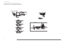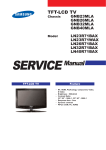
1
TFT-LCD TV
Chassis
GBP23SEN
GBP26SEN
GBP32SEN
GBP37SEN
GBP40SEN
Model
LE23R86BD
LE26R86BD
LE32R86BD
LE37R86BD
LE40R86BD
SERVICE
TFT-LCD TV
Manual
Fashion Feature
- Luxurious Slim Design
- Supreme Picture Quality
- Supreme Sound Quality
- Supreme Convenience Quality
- Convenience for Users
- iDTV
Copyright
2007 by Samsung Electronics Co., Ltd.
All rights reserved.
This manual may not, in whole or in part, be copied,
photocopied, reproduced, translated, or converted to any
electronic or machine readable form without prior
written permission of Samsung Electronics Co., Ltd.
LE23R86BD/LE26R86BD/LE32R86BD/
LE40R86BD/LE46R86BD Service Manual
First edition March 2007.
Printed in Korea.
ii
Trademarks
Samsung is the registered trademark of Samsung
Electronics Co., Ltd.
LE23R86BD/LE26R86BD/LE32R86BD/
LE40R86BD/LE46R86BD Service Manual and
Macmaster Cable Adapter are trademarks of Samsung
Electronics Co., Ltd.
Macintosh and Power Macintosh are trademarks of
Apple Computer, Inc.
All other trademarks are the property of their respective
owners.
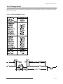
Contents
Contents
1 Precautions
1 Precautions
Follow these safety, servicing and ESD precautions to prevent damage and to protect against potential hazards such as electrical shock.
1-1 Safety Precautions
1-1-1 Warnings
1.
For continued safety, do not attempt to modify the
circuit board.
2.
Disconnect the AC power and DC Power Jack before
servicing.
1-1-2 Servicing the LCD Monitor
1.
When servicing the LCD Monitor Disconnect the AC
line cord from the AC outlet.
2.
It is essential that service technicians have an accurate
voltage meter available at all times. Check the
calibration of this meter periodically.
1-1-3 Fire and Shock Hazard
Before returning the monitor to the user, perform the
following safety checks:
1.
Inspect each lead dress to make certain that the leads
are not pinched or that hardware is not lodged between
the chassis and other metal parts in the monitor.
2.
Inspect all protective devices such as nonmetallic
control knobs, insulating materials, cabinet backs,
adjustment and compartment covers or shields,
isolation resistor-capacitor networks, mechanical
insulators, etc.
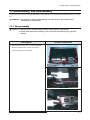
3.
Leakage Current Hot Check (Figure 1-1):
WARNING: Do not use an isolation
transformer during
th
Use a leakage current tester or a metering system that
complies with American National Standards Institute
(ANSI C101.1, Leakage Current for Appliances), and
Underwriters Laboratories (UL Publication UL1410,
59.7).
Figure 1-1. Leakage Current Test Circuit
1-1-4 Product Safety Notices
Some electrical and mechanical parts have special
safety-related characteristics which are often not evident
from visual inspection. The protection they give may not
be obtained by replacing them with components rated for
higher voltage, wattage, etc. Parts that have special safety
characteristics are identified by
on schematics and parts
lists. A substitute replacement that does not have the same
safety characteristics as the recommended replacement part
might create shock, fire and/or other hazards. Product
safety is under review continuously and new instructions
are issued whenever appropriate.
1-1
1 Precautions
1-2 Servicing Precautions
WARNING:
An electrolytic capacitor installed with the wrong polarity might explode.
Caution:
Before servicing units covered by this service manual, read and follow the Safety
Precautions section of this manual.
Note:
If unforeseen circumstances create conflict between the following servicing precautions and any of the safety
precautions, always follow the safety precautions.
1-2-1 General Servicing
Precautions
1.
4.
Check the insulation between the blades of the AC
plug and accessible conductive parts (examples: metal
panels, input terminals and earphone jacks).
5.
Insulation Checking Procedure: Disconnect the power
cord from the AC source and turn the power switch
ON. Connect an insulation resistance meter (500 V) to
the blades of the AC plug.
Always unplug the unit s AC power cord from the AC
power source and disconnect the DC Power Jack
before attempting to:
(a) remove or reinstall any component or assembly, (b)
disconnect PCB plugs or connectors, (c) connect a test
component in parallel with an electrolytic capacitor.
2.
Some components are raised above the printed circuit
board for safety. An insulation tube or tape is
sometimes used. The internal wiring is sometimes
clamped to prevent contact with thermally hot
components. Reinstall all such elements to their
original position.
3.
After servicing, always check that the screws,
components and wiring have been correctly
reinstalled. Make sure that the area around the
serviced part has not been damaged.
The insulation resistance between each blade of the
AC plug and accessible conductive parts (see above)
should be greater than 1 megohm.
6.
Always connect a test instrument s ground lead to the
instrument chassis ground before connecting the
positive lead; always remove the instrument s ground
lead last.
1-3 Static Electricity Precautions
Some semiconductor (solid state) devices can be easily damaged by static electricity. Such components are commonly called
Electrostatically Sensitive Devices (ESD). Examples of typical ESD are integrated circuits and some field-effect transistors.
The following techniques will reduce the incidence of component damage caused by static electricity.
1.
Immediately before handling any semiconductor
components or assemblies, drain the electrostatic
charge from your body by touching a known earth
ground. Alternatively, wear a discharging wrist-strap
device. To avoid a shock hazard, be sure to remove the
wrist strap before applying power to the monitor.
2.
After removing an ESD-equipped assembly, place it
on a conductive surface such as aluminum foil to
prevent accumulation of an electrostatic charge.
3.
Do not use freon-propelled chemicals. These can
generate electrical charges sufficient to damage ESDs.
4.
Use only a grounded-tip soldering iron to solder or
desolder ESDs.
5.
Use only an anti-static solder removal device. Some
solder removal devices not classified as anti-static
can generate electrical charges sufficient to damage
ESDs.
1-2
6.
Do not remove a replacement ESD from its protective
package until you are ready to install it. Most
replacement ESDs are packaged with leads that are
electrically shorted together by conductive foam,
aluminum foil or other conductive materials.
7.
Immediately before removing the protective material
from the leads of a replacement ESD, touch the
protective material to the chassis or circuit assembly
into which the device will be installed.
Caution: Be sure no power is applied to
the chassis or circuit and
observe all other safety
precautions.
8.
Minimize body motions when handling unpackaged
replacement ESDs. Motions such as brushing clothes
together, or lifting your foot from a carpeted floor can
generate enough static electricity to damage an ESD.
1 Precautions
1-4 Installation Precautions
1. For safety reasons, more than two people are
required for carrying the product.
2. Keep the power cord away from any heat emitting
devices, as a melted covering may cause fire or
electric shock.
3. Do not place the product in areas with poor
ventilation such as a bookshelf or closet. The
increased internal temperature may cause fire.
6. Keep the antenna far away from any high-voltage
cables and install it firmly. Contact with the highvoltage cable or the antenna falling over may
cause fire or electric shock.
7. When installing the product, leave enough space
(10cm) between the product and the wall for
ventilation purposes.
A rise in temperature within the product may
cause fire.
4. Bend the external antenna cable when connecting
it to the product. This is a measure to protect it
from being exposed to moisture. Otherwise, it
may cause a fire or electric shock.
5. Make sure to turn the power off and unplug the
power cord from the outlet before repositioning
the product. Also check the antenna cable or the
external connectors if they are fully unplugged.
Damage to the cord may cause fire or electric
shock.
1-3
2 Product Specifications
2 Product specifications
2-1 Fashion Feature
Supreme Digital Interface & Networking
-With a built-in HD digital tuner, it supports HD broadcasting with no particular set-top box and provides
simple access with a single remote control.
Excellent Picture Quality
-DNIe technology provides life-like clear images.
My Color Control
-Colors can be set to your preference by adjusting Red, Green, Blue, Yellow, Pink and White.
Dynamic Contrast
-Automatically detects the input visual signal and adjusts to create optimum contrast.
Brightness Sensor
-Adjusts the screen brightness automatically depending on the brightness of the surrounding
environment.
SRS TruSurround XT
-SRS TruSurround XT provides a virtual Dolby surround system.
Convenience
-The TV utilizes the HDMI system to implement perfect digital sound and picture quality.
The Anynet system enables you to easily control Samsung audio-video (AV) devices from this TV.
2-1
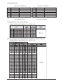
2 Product Specifications
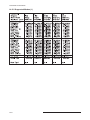
2-2 LE23R86BD Specifications
Item
Description
±
°
°
2-2
°
°
°
°
°
°
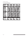
2 Product Specifications
2 Product Specifications
2-3 LE26R86BD Specifications
Item
Description
±
°
°
°
°
°
°
°
°
2-3
2 Product Specifications
2-4 LE32R86BD Specifications
Item
Description
±
°
°
2-4
°
°
°
°
°
°
2 Product Specifications
2-5 LE37R86BD Specifications
Item
Description
±
°
°
°
°
°
°
°
°
2-5
2 Product Specifications
2-6 LE40R86BD Specifications
Item
Description
±
°
°
2-6
°
°
°
°
°
°
2 Product Specifications
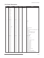
2-7 Spec Comparison
Model
LE26R51B / LE32R51B / LE40R51B
LE23R86BD/LE26R86BD/
LE32R86BD/LE37R86BD/
LE40R86BD
30 ~ 61 kHz
60 ~ 75 Hz
16,777,216 colors
30 ~ 61 kHz
60 ~ 75 Hz
16,777,216 colors
WXGA, 1360 x 768 @ 60 Hz
WXGA, 1366 x 768 @ 60 Hz
H/V Separate, TTL, P. or N.
0.7 Vp-p @ 75ohm
H/V Separate, TTL, P. or N.
0.7 Vp-p @ 75ohm
140W / 184W / 285W
< 1W
90W / 135W / 155W / 205W / 210W
< 1W
Design
Frequency
Horizontal
Vertical
Display Color
PC Resolution
Maximum mode
Input Signal
Sync Signal
Video Signal
Power
Consumption
Normal
Power Saving
2-7
2 Product Specifications
2-8 Option Specification
Item
Item Name
Code.No
Remote Control
&
Batteries (AAA x 2)
BN59-00603A
Power Cord
3903-000042
Cleaning Cloth
BN63-001798A
Stand
26" : BN90-00848A
32" : BN90-00842A
40" : BN90-00847A
Stand Screw
Cover-Bottom
2-8
26" : BN63-02323A
32" : BN63-02323A
40" : BN63-02366A
Remark
3 Alignments and Adjustments
3 Alignments and Adjustments
3-1 Service Instruction
1. Usually, a color TV-VCR needs only slight touch-up adjustment upon installation.
Check the basic characteristics such as height, horizontal and vertical sync.
2. Use the specified test equipment or its equivalent.
3. Correct impedance matching is essential.
4. Avoid overload. Excessive signal from a sweep generator might overload the front-end
of the TV. When inserting signal markers, do not allow the marker generator to distort
test result.
5. Connect the TV only to an AC power source with voltage and frequency as specified on
the backcover nameplate.
6. Do not attempt to connect or disconnect any wire while the TV is turned on. Make sure
that the power cord is disconnected before replacing any parts.
7. To protect aganist shock hazard, use an isolation transform.
3-1
3 Alignments and Adjustments
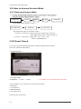
3-2 How to Access Service Mode
3-2-1 Entering Factory Mode
"
Power OFF
"
INFO
MENU
MUTE
Power ON
- If you have Factory remote - control
DISPLAY
PICTURE ON
FACTORY
- The buttons are active in the service mode.
1. Remote - Control Key : Power, Arrow Up, Arrow Down, Arrow Left
Arrow Right, Menu, Enter, Number Key(0~9)
2. Function - Control Key : Power, CH +, CH -, VOL +, VOL -,
Menu, TV/VIDEO(Enter)
3-2-2 Panel Check
You have to check Panel Maker Because of different adjustments as follows.
First of all, Check the label rating!
1) Label Rating File
- LCD PANEL MARK A:ACER(AUO) S : SEC
C : CMO
* If not printed you could consider S(sec) panel mark.
2) If Panel Mark is "A", Set the factory mode indicating as follows.
* Option Byte
1. Inch Option 32"
2. Gamma 32"AUO
3. Panel Option AUO
Others are same shown below.
3-2
3 Alignments and Adjustments
3-3 Factory Data
1. Calibration
2. Service
3. White Balance
4. SVP-UX
5. Option Block
6. SGTV5810/NTP3000
7. YC Delay
8. Option Table
9. I2C Check
10. W/B MOVIE
11. Checksum
12. Reset
13. Spread Spectrum
T-BDPMPEUD-xxxx (Main Micom Ver)
T-BDPMPEUS-xxxx
BORD2_CALLA_TR-xxxx (Sub Micom Ver)
Month / Day / Year / Hour / Min. / Sec.
1. Calibration
1) AV Calibration
2) COMP Calibration
3) PC Calibration
4) HDMI Calibration
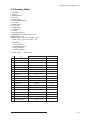
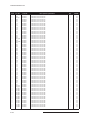
2. Option Table
No
XXXX XXXX
Item
1
Ready
2
Inch Option
3
Panel Vender
4
Gamma
5
Panel Type
6
Model Option
7
Tuner
8
Range
ON/OFF
OFF
23"/ 26" / 32"¡¦
32"
AUO/CMO¡¦
AMLCDINT
ON/OFF
OFF
Normal1/Normal2¡¦
Normal1
Calla/Lily/Bord Plus/Jasmine
Bord Plus
SEMCO/ALPS
SEMCO
Tuner TOP
0~31
8
9
Auto Power
ON/OFF
ON
10
Nordic
ON/OFF
OFF
11
LNA Menu
ON/OFF
ON
12
TTX On/Off
ON/OFF
ON
13
TTX List
Flof/List
Flof
14
Carrier Mute
ON/OFF
OFF
15
High Deviation
ON/OFF
OFF
16
VOL.Curve
Small/Large
Small
17
HDMI Hotplug
1/0
1
18
HDMI Clock CtrI
1/0
1
19
HDMI Hotplug Dly
3~50
9
3-3
3 Alignments and Adjustments
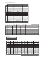
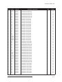
No
Range
Item
Hotel Option
20
Hotel Mode
ON/OFF
OFF
Power On Channel
1~99
1
Power On Volume
1~100
10
Max Volume
1~100
100
ON/OFF
OFF
RF/Ext.1¡¦
RF
Local Key Lock
Power On Source
21
Shop Mode
ON/OFF
OFF
22
Color Space
ON/OFF
ON
23
PC Ident
ON/OFF
OFF
24
Language
English/German¡¦
English
25
ANYNET+
ON/OFF
ON
26
Ch.Table
SUWON/SESK/SEH/TTSEC
SUWON
27
TTX Group
Auto/West Europe¡¦
Auto
28
iDTV_Cntry
UK/France¡¦
UK
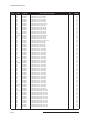
3. White Balance
Item
No
Range
TV/AV/Scart
Comp/iDTV
PC
HDMI
1
Sub-Briteness
00H~FFH
128
128
128
128
2
R-offset
00H~FFH
128
128
128
128
3
G-offset
00H~FFH
128
128
128
128
4
B-offset
00H~FFH
128
128
128
128
5
Sub-Contrast
00H~FFH
128
128
128
128
6
R-Gain
00H~FFH
128
128
128
128
7
G-Gain
00H~FFH
128
128
128
128
8
B-Gain
00H~FFH
128
128
128
128
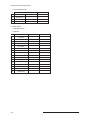
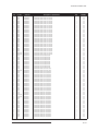
4. SVP-PX
1) ComB Filter
No
Item
Range
1
Y-Filter
00H~FFH
2) Sharpness
3-4
No
Item
Range
RF
AV
Comp480i
HDMI
PC
iDTV
1
H2Gain
00 ~ 1FH
05H
05H
05H
05H
04H
04H
0AH
05H
05H
2
H4Gain
00 ~ 1FH
04H
0AH
05H
05H
02H
02H
0AH
05H
05H
3
V2Gain
00 ~ 1FH
0CH
0CH
0AH
0CH
0AH
0AH
10H
0AH
0AH
4
V4Gain
00 ~ 1FH
0CH
10H
0CH
0CH
0AH
0AH
10H
0AH
0AH
5
Sr2Gain
00 ~ 1FH
00H
6
Sr4Gain
00 ~ 1FH
00H
00H
00H
00H
00H
00H
00H
00H
00H
02H
00H
00H
02H
02H
04H
02H
02H
7
Sl2Gain
00 ~ 1FH
00H
00H
00H
00H
00H
00H
00H
00H
00H
8
Sl4Gain
00 ~ 1FH
00H
02H
00H
00H
02H
02H
04H
02H
02H
9
Peakth1
00H~FFH
06H
02H
03H
03H
03H
03H
03H
08H
04H
10
Peakth2
00H~FFH
2FH
2FH
2FH
2FH
2FH
2FH
2FH
2FH
2FH
11
Peskth3
00H~FFH
3FH
3FH
3FH
3FH
3FH
3FH
3FH
3FH
3FH
Comp480p Comp720p Comp1080i
3 Alignments and Adjustments
3) NR
No
Item
Range
1
Y_NR_OFF
00H~FFH(Y_NR_OFF)
00H
2
C_NR_OFF
00H~FFH(C_NR_OFF)
00H
3
Y_NR_ON
00H~FFH(Y_NR_ON)
00H
4
C_NR_ON
00H~FFH(C_NR_ON)
00H
4) RGB Calibration
No
Item
Range
TV/AV/S_Video
Component
PC
HDMI
1
R-Offset
00H~FFH
3AH
40H
32H
82H
2
G-Offset
00H~FFH
3AH
40H
32H
82H
3
B-Offset
00H~FFH
3AH
40H
32H
82H
4
R-Gain
00H~FFH
A6H
92H
A9H
6CH
5
G-Gain
00H~FFH
A6H
92H
A9H
6CH
6
B-Gan
00H~FFH
A6H
92H
A9H
6CH
Item
Range
TV/AV/S_Video
Component
PC
HDMI
1
TCD3 Contrast
00H~FFH
79H
78H
78H
78H
2
TCD3 Brightness
00H~FFH
29H
20H
20H
20H
3
TCD3 CR
00H~FFH
80H
80H
80H
80H
4
TCD3 CB
00H~FFH
80H
80H
80H
80H
5
TCD3 Delay
00H~FFH
00H
00H
00H
00H
6
Analog Y Offset
00H~FFH
40H
3DH
44H
40H
7
Analog PB Offset
00H~FFH
80H
80H
44H
80H
8
Analog PR Offset
00H~FFH
80H
80H
44H
80H
9
Analog Y Gain
00H~FFH
D6H
B3H
A4H
80H
10
Analog PB Gain
00H~FFH
80H
B3H
ACH
80H
11
Analog PR Gain
00H~FFH
80H
B3H
A7H
80H
12
Black Level
00H~FFH
00H
00H
00H
00H
13
Svp Brightness
00H~FFH
00H
00H
00H
00H
5) ADC Calibration
No
6) Caliration Target
No
Item
Range
low
high
Delta
1
AV ADC
00H~FFH
10H
DCH
02H
2
COMP ADC
00H~FFH
10H
EBH
02H
3
PC ADC
00H~FFH
10H
DCH
04H
4
ALL RGB
00H~FFH
01H
EBH
0AH
3-5
3 Alignments and Adjustments
7) Color Management
No
Item
Range
1
Skin Direction
Reddish/Yellowish
Reddish
2
Skin Enhance
00H~FFH
00H
3
Green Stretch
00H~FFH
00H
4
Blue Stretch
00H~FFH
00H
5. Option Block
1) FRC(Micronas)
2) FRC2X
No
Item
Range
1
OUTCON
1~3
0
2
GAMMA
1~7
0
3
OCC_MODE
0/1
0
4
FALLBACK
0/1
0
5
DBG_MARK
0/1
0
6
SPR_CBR
0/1
0
7
BIT_EXPAND
0/1
0
8
INV_BIT_EXPAND
0/1
0
9
REPEAT_MODE
0/1
0
10
DEMO_ON_OFF
0/1
0
11
MMU_RD_START
00H~FFH
00H
12
ME_RD_START
00H~FFH
00H
13
MC_RD_START
00H~FFH
00H
14
CMZL(0x36E)
00H~0FH
0H
15
BLOL(0x2A7)
00H~0FH
0H
16
LOGO(0x2A7)
00H~0FH
0H
3-6
3 Alignments and Adjustments
3) FBE2
AV/
COMP
COMP
No
Item
Range
RF
1
Pattern Select
0~20
0
0
0
0
2
BS-On
0/1
1
1
1
3
B-Slope Gain
0~255
34
44
4
B-Tilt Min
0~255
20
5
B-Tilt Max
0~255
6
B-Tilt Slope
7
COMP
HDMI
DTV
DTV
0
0
0
0
1
1
1
1
1
44
64
64
64
64
64
20
20
20
20
20
20
20
120
120
120
120
120
120
120
120
0~255
128
128
128
128
128
128
128
128
LFunc-Basis
0~255
30
20
20
40
70
55
75
75
8
Hfunc-Basis
0~255
30
40
40
40
75
65
88
88
9
Mean-Offset1
0~255
20
100
100
75
75
75
75
75
10
Mean Offset2
0~255
120
200
200
155
225
225
225
225
11
Mean Slope
0~255
56
56
56
45
85
85
85
85
12
Input Offset
0~255
128
128
128
128
128
128
128
128
13
Input Gain
0~255
128
128
128
128
128
128
128
128
14
ACR Offset
0~128
15
15
15
15
15
15
15
15
15
ACR Th1
0~255
30
30
30
30
30
30
30
30
16
ARC Th2
0~255
130
130
130
130
130
130
130
130
17
Skin Enable
0/1
1
1
1
1
1
1
1
1
18
Skin Tu
0~255
165
165
165
150
165
165
128
128
19
Skin Tv
0~255
140
140
140
140
128
128
128
128
20
M Skin Tu
0~255
128
128
128
128
128
128
128
128
21
M Skin TV
0~255
128
128
128
128
128
128
128
128
22
Sub Color
0~255
115
128
128
135
140
150
143
143
23 M-Au-Sub Color
0~255
128
128
128
128
128
128
128
128
24 M-Wi-Sub Color
0~255
128
128
128
128
128
128
128
128
25
MW-Skin-Tu
0~255
128
128
128
128
128
128
128
128
26
MW-Skin-Tv
0~255
128
128
128
128
128
128
128
128
S-VIDEO (480i/576i) (480p/576p) (720p/1080i/1080p)
3-7
3 Alignments and Adjustments
4) Pdp Logic
No
Item
Range
1
Pattern Srlect
0~63
0
2
Data updata
ON/OFF
OFF
3
Data Type
42"EU MRT/42"EU MESH/.......
42"EU MRT
4
CDC Sw
ON/OFF
OFF
5
CDC Strengh Th
0~31
0
6
BRE Sw
ON/OFF
OFF
7
FRC Repeat Mode
ON/OFF
OFF
8
FRC CBG Mark On
0~15
0
9
ERC Bypass
ON/OFF
OFF
10
Panel Type
-
0H
11
Panel Inch
-
SD
12
Panel Version
-
13
Logic Sw Version
-
0H 0H 0H
6. SGTV5810/NTP3000
No
Item
Range
1
ID Tone Shift
1H~FH
01H
2
ID Tone Thresh
00H~FFH
7FH
3
Demod Prescaler
00H~20H
13H
4
Master Volume
00H~30H
13H
5
PWM Modulation
80H~F2H
F1H
6
DRC Threshold
00H~7FH
06H
7
Speaker EQ
ON/OFF
OFF
7. YC Delay
No
Item
Range
1
RF PAL-B/G
00H~FFH
AAH
2
RF PAL - D/K
00H~FFH
99H
3
RF PAL - I
00H~FFH
99H
4
RF SECAM - B/G
00H~FFH
88H
5
RF SECAM - D/K
00H~FFH
44H
6
RF SECAM -L/L'
00H~FFH
88H
7
RF NTSC 3.58
00H~FFH
44H
8
RF NTSC 4.43
00H~FFH
CCH
9
AV PAL
00H~FFH
AAH
10
AV SECAM
00H~FFH
88H
11
AV NTSC 3.58
00H~FFH
30H
12
AV NTSC 4.43
00H~FFH
AAH
13
AV PAL60
00H~FFH
77H
3-8
3 Alignments and Adjustments
8. Adjust
No
Item
Range
1
Video Mute Time
0~255
10
2
Dynamic Contrast
ON/OFF
OFF
3
Dynamic Dimming
ON/OFF
ON
4
Dynamic CE
ON/OFF
OFF
5
LNA PLUS
RFDB-1 Level
0~255
2
RFDB-2 Level
0~255
5
RFDB-3 Level
0~255
7
RFDB-4 Level
0~255
24
6
Magazine LNA
ON/OFF
OFF
7
PixelShift Test
ON/OFF
OFF
8
Debug
ON/OFF
OFF
9
ACR
ON/OFF
OFF
10
D-Watchdog
ON/OFF
ON
11
UART Select
MAIN / IDTV / PDP Lvds ON / PDP Lvds OFF
OFF
9. I2C Check
10. W/B MOVIE
No
Item
Range
TV/AV/S_Video
Component
PC
HDMI
Scart1/2
1
WB Movie
ON/OFF
OFF
OFF
OFF
OFF
OFF
2
Color Mode
Movie
Movie
Dynamic
Dynamic
Dynamic
Dynamic
3
Color Tone
Cool1
Cool1
Cool1
Cool1
Cool1
4
Msub Brigh
0~255
128
128
128
128
128
5
Msub Contr
0~255
128
128
128
128
128
6
W1_RGAIN
0~255
157
161
144
161
157
7
W1_BGAIN
0~255
76
74
117
76
76
8
W1_R_OFFS
0~255
119
119
127
118
119
9
W1_B_OFFS
0~255
138
140
110
141
138
10
W2_RGAIN
0~255
142
143
149
142
142
8
W2_BGAIN
0~255
48
47
93
51
48
9
W2_R_OFFS
0~255
129
127
124
128
129
10
W2_B_OFFS
0~255
143
145
110
143
143
11
NO_RGAIN
0~255
141
139
137
141
141
12
NO_BGAIN
0~255
104
102
123
104
104
13
NO_R_OFFS
0~255
126
125
126
121
126
14
NO_B_OFFS
0~255
136
133
114
133
136
15
C2_RGAIN
0~255
124
122
123
125
124
16
C2_BGAIN
0~255
142
141
156
143
142
17
C2_R_OFFS
0~255
128
129
117
128
128
18
C2_B_OFFS
0~255
128
127
116
128
128
19
Movie Contr
0~100
100
100
100
100
100
20
Movie Brigh
0~100
45
45
45
45
45
21
Movie Color
0~100
55
55
55
55
55
22
Movie Sharp
0~100
75
75
75
75
75
3-9
3 Alignments and Adjustments
11. Checksum
7A72
12. Reset
13. Spread Spectrun
No
Item
Range
1
Spectrum
ON/OFF
ON
2
Delta
-128 ~ +128
0
3
Positive
0~99
8
4
Negative
0~99
2
5
Speed
0~7
0
6
Time
0~7
4
7
FBE Spectrum
ON/OFF
OFF
8
FEE Delta
0~5
0
3-10
3 Alignments and Adjustments
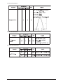
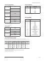
3-4 Service Adjustment
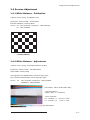
3-4-1 White Balance - Calibration
If picture color is wrong, do calibration first.
Equipment : CA210, Patten : chess pattern
Execute calibration in Factory Mode
Source AV : PAL composite, Component : 1280*720/60Hz
PC : 1024*768/60Hz
( chess patten )
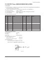
3-4-2 White Balance - Adjustment
If picture color is wrong, check White Balance condition.
Equipment : CA210, Patten : Flat W/B Pattern
Adjust W/B in Factory Mode
Sub brightness and R/G/B Offset controls low light region
Sub contrast and R/G/B Gain controls high light region
Source AV : PAL composite, Component : 1280*720/60Hz
HDMI[DVI] : 1280*720/60Hz
[ Test Pattern : MIK K-7256 PAttern #92 ]
*Color temperature
1500K +/-500, -6 ~-20 MPCD
*Color coordinate
H/L : 267/263 +/- 2 35.0 Ft +/- 2.0Ft
L/L : 270/260 +/- 3
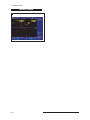
1.5 Ft +/- 0.2Ft
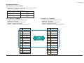
Flat W/B Pattern
3-11
3 Alignments and Adjustments
3-4-3 Conditions for Measurement
1. On the basis of toshiba ABL pattern : High Light level (57 IRE)
- INPUT SIGNAL GENERATOR : MSPG-925LTH
* Mode
NO
2 : 744X484@60 Hz
NO
6 : 1280X720@60 Hz
NO 21 : 1024X768@60 Hz
* Pattern NO 36 : 16 Color Pattern
NO 16 : Toshiba ABL Pattern
2. Optical measuring device : CA210 (FL)
Please use the MSPG-925 LTH generator for model LE26M51B/LE32M51B/LE40M51B/LE46M51B.
3-4-4 Method of Adjustment
1. Adjust the white balance of AV, Component and DVI Modes.
(AV
Component)
a) Set the input to the mode in which the adjustment will be made
(RF
DTV
PC
DVI).
* Input signal - VIDEO Mode : Model #2 (744*484 Mode), Pattern #16
- DTV,DVI Mode : Model #6 (1280*720 Mode), Pattern #16
- HDMI Mode: Model #6(1280*720 Mode), Pattern #16
b) Enter factory color control, confirm the data.
c) Adjust the low light. (Refer to table 1, 2 in adjustment position by mode)
- Adjust sub - Brightness to set the 'Y' value.
- Adjust red offset ('x') and blue offset ('y') to the color coordinates.
Picture 4-2 Flat W/B Pattern
Low light
Measurement point
* Do not adjust green offset data.
d) Adjust the high light. (Refer to table 1, 2 in adjustment position by mode)
- Adjust red gain ('x') and blue gain ('y') to the color coordinates.
* Do not adjust the green gain and sub-contrast (Y) data.
3-12
3 Alignments and Adjustments
d) Adjust the high light. (Refer to table 1, 2 in adjustment position by mode)
- Adjust red gain ('x') and blue gain ('y') to the color coordinates.
* Do not adjust the green gain and sub-contrast (Y) data.
Picture 4-3 Flat W/B Pattern
High light
Measurement point
3-13
3 Alignments and Adjustments
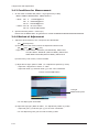
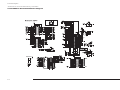
3-5 Software Upgrade
3-5-1 How to Update Flash ROM
1. Install the Flash Downloader
ConnectSet(Service Jack)and Jig Cable to execute Program Update.
2. Flash Downloader program update
-Before Turning on the set,Click "connect"which is under of OSD Screen!
-Turn on the Set.
3-14
4 Troubleshooting
4 Troubleshooting
4-1 First Checklist for Troubleshooting
1. Check the various cable connections first.
- Check to see if there is a burnt or damaged cable.
- Check to see if there is a disconnected cable connection or a connection is too loose.
- Check to see if the cables are connected according to the connection diagram.
2. Check the power input to the Main Board.
3. Check the voltage in and out between the SMPS
Main Board, between the SMPS
INVERTER Board, and between the Main LVDS Boards.
4-1
4 Troubleshooting
4-2 Checkpoints by Error Mode
4-2-1 No Power
LAMP off, power indicator
LED red color?
No
Check a connection a power cable.
Yes
Does proper DC 13V
appear at JP845?
No
Change a Assy PCB Power.
Yes
Does proper DC A3.3V,
A5V appear at
C854, C1166_LCD?
No
Check a IC1112, Q1103.
Change a main PCB ass'y.
No
Check a IC1111, IC1102, IC1113.
Change a main PCB ass'y
No
Check a other function.
(No picture part)
Replace a lcd panel.
Yes
Does proper DC 5V, 3.3V,
1.2V appear at C1153, C1178,
C1170?
Yes
A power is supplied to set?
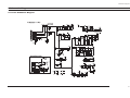
TIP: How to drive the circuit by force when LCD panel Lamp is faulty.
- It is available to drive the circuit when the pin of 2 in Main_Power_control CN1101
connect the pin of 4.
4-2
4 Troubleshooting
4-2-2 No Video (Analog PC)
Power Indicator is off.
Lamp on, no video.
Yes
Check a PC source and check
the connection of DSUB cable?
No
Input a analog PC signal and
connected cable(DPMS).
No
PC cable. Change a PC
cable. Change a main PCB ass'y.
No
Check a IC2001
Change a main PCB ass'y.
Yes
Does the signal appear at
1 C2078,C2077,C2079(R, G, B)
of IC2001?
Yes
Does the digital data appear
at the output of
LVDS (RA2008~2013)?
Yes
Check a LVDS cable?
Replace a lcd panel?
No
Please, Call to Samsung Co. LTD.
4-3
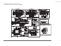
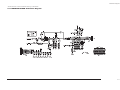
4 Troubleshooting
WAVEFORMS
1 R,G,B Output Signal of IC2001
4-4
4 Troubleshooting
4-2-3 No Video (Digital-HDMI)
Power Indicator is off.
Lamp on, no video.
Yes
Check the connection
of HDMI cable?
No
Input a HDMI cable.
Yes
Does the digital data appear at
3 R1333_UX~R1340_UX?
No
Check a a IC1405
Change a main PCB ass'y.
No
Check a IC1405
Change a main PCB ass'y.
Yes
2 Does the digital data
appear at output of IC4001
LVDS(RA2008~2013)?
Yes
Check a LVDS cable?
Replace lcd panel?
No
Please, Call to Samsung Co. LTD.
4-5
4 Troubleshooting
2 Digital Output Data of IC4001
4-6
3 Signal of HDMI(Data)
4 Troubleshooting
4-2-4 No Picture (Tuner_CVBS)
Power Indicator is off.
Lamp on, no picure.
No
Connect the RF cable and
check RF signal.
No
Check a B+ voltage (#3 of Tuner) 5V,
change a main PCB ass'y
Yes
4
Dose the signal appear
at R2207?
Yes
4
Does the signal appear at
C2085 of IC2001?
No
Change a main PCB ass'y.
Yes
3
Does the digital data appear at
output of RA2008~2013?
No
Check a IC4001.
Change a main PCB ass'y.
Yes
Check a LVDS cable?
Replacea lcd panel?
No
Please, Call to Samsung Co. LTD.
4-7
4 Troubleshooting
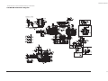
WAVEFORMS
3 CVBS Output Signal
4-8
4 Tuner_CVBS Output Signal
4 Troubleshooting
4-2-5 No Picture (Video_CVBS)
Power Indicator is off.
Lamp on, no picture.
No
Check a A/V cable and video signal.
Yes
4
Dose the signal appear at
C2101 of IC2001?
No
Check a connection harness.
Yes
Does the signal appear at
Out of IC2001
RA2008~RA2013?
No
Check a IC 2001.
Change a main PCB ass'y
Yes
Check a LVDS cable?
Replace lcd panel?
No
Please, Call to Samsung Co. LTD.
4-9
4 Troubleshooting
WAVEFORMS
4 CVBS Output Signal
4-10
4 Troubleshooting
4-2-6 No Picture (S-VIDEO_Y,C)
Power Indicator is off.
Lamp on, no picure.
No
Connect the s-video cable.
Operating a video player.
Yes
5 Dose the Y/C signal appear at
No
Check a connection harness.
C2088, C2091 of IC2001?
Yes
2
Does the digital data appear
at Output of IC 2001,
RA2008~RA2013?
No
Check a IC 2001.
Change a main PCB ass'y.
Yes
Check a LVDS cable?
Replacea lcd panel?
No
Please, Call to Samsung Co. LTD.
4-11
4 Troubleshooting
WAVEFORMS
2 Digital Output Data of IC2001
4-12
5 Analog Signal(Y,C) to IC2001
4 Troubleshooting
4-2-7 No Sound
No
Picture is display, no sound.
Connect a sound cable.
control a volume.
Yes
Does the signal appear at
Pin #10, #12, #13, #9 (I2S_CLK,
6
I2S_SCLK, I2S_LRCLK,
I2S_DATA) of IC1202?
No
Check a connection harness and
headphone jack./Side AV
Check Sound Processor
IC1202 (SGTV5810)
Yes
Check the DC 12V
of IC1203?
No
Check a B12V Line.
Change a main PCB ass'y.
Yes
7
Does the signal appear at
Pin #47 or 48, #53 or
54(CH1_L, R Sound) And Pin
#36 or 37, #30 or 31
(CH2_L, R Sound)
of IC1203?
No
Change a main PCB ass'y.
Yes
Replace the speaker ass'y?
4-13
4 Troubleshooting
WAVEFORMS
6 The Signal are Inputed to IC1202
4-14
7 The Signal are Inputed to IC1203
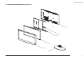
5 Exploded View & Parts List
5 Exploded View and Parts List
- You can search for updated part codes through ITSELF web site.
URL : http://itself.sec.samsung.co.kr/
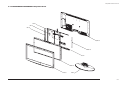
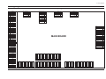
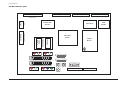
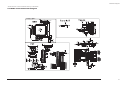
5-1 LE23R86BDX/LE23R86BCX Exploded View
M0107
M0014
M0013
M0115
M0146
M0107
M0027
M0215
T0175
T0003
5-1
5 Exploded View & Parts List
5-2 LE23R86BCX/LE23R86BCX Parts list
Location
Code.No
Item & Specification
T0003
BN96-04660B
ASSY COVER P-FRONT;23R81,EO(IDTV),-,ABS+
1
S.A
T0175
BN96-04767A
ASSY SPEAKER P;16ohm,4pin,5W,Bordeaux Pl
1
S.A
M0215
BN07-00365A
LCD-PANEL;T230XW01,8bit,23inch,16.7M,16:
1
S.A
M0107
BN63-03039A
SHIELD-COVER;MURANO40,PCM,T0.5,IDTV
1
S.N.A
M0107
BN61-03037A
BRACKET-PCB;23 BORDEAUX PLUS,SECC,T1.0
1
S.N.A
M0146
BN61-03060A
BRACKET-PANEL SIDE;BORDEAUX PLUS 23,SECC
2
S.N.A
M0115
BN61-02965A
BRACKET-STAND LINK;32 BORDEAUX PLUS,SECC
1
S.N.A
M0014
BN94-01121E
ASSY PCB MAIN;LE23R86BDX/*
1
S.A
M0013
BN96-04663A
ASSY STAND P-BASE;23,26R81,NORMAL,-,ABS+
1
S.A
M0013
BN96-04673A
ASSY COVER P-REAR;23R81,EO(IDTV),-,ABS+P
1
S.A
5-2
Q'ty
SA/SNA
Remark
5 Exploded View & Parts List
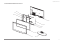
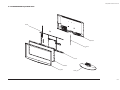
5-3 LE26R86BDX/LE26R86BCX Exploded View
M0107
M0014
M0013
M0115
T0447
M0215
T0175
M0027
T0003
5-3
5 Exploded View & Parts List
5-4 LE26R86BDX/LE26R86BCX Parts list
Location
Code.No
Item & Specification
T0003
BN96-05171C
ASSY COVER P-FRONT;26R89,EO(IDTV),ABS+PM
Q'ty
SA/SNA
1
S.A
T0175
BN96-04767A
ASSY SPEAKER P;16ohm,4pin,5W,Bordeaux Pl
1
S.A
M0215
BN07-00367A
LCD-PANEL;LTA260W2-L13,-,8bit,26inch,16.
1
S.A
T0447
BN96-04682A
ASSY BRACKET P-PANEL;26R81,AMLCD,-,-,-,-
1
S.N.A
M0115
BN61-02965A
BRACKET-STAND LINK;32 BORDEAUX PLUS,SECC
1
S.N.A
M0014
BN94-01121B
ASSY PCB MAIN;LE26R86BDX/*
1
S.A
M0107
BN63-03039A
SHIELD-COVER;MURANO40,PCM,T0.5,IDTV
1
S.N.A
M0013
BN96-04663A
ASSY STAND P-BASE;23,26R81,NORMAL,-,ABS+
1
S.A
M0013
BN96-04672A
ASSY COVER P-REAR;26R81,EO(IDTV),-,ABS+P
1
S.A
5-4
Remark
5 Exploded View & Parts List
5-5 LE32R86BDX/LE32R86BCX Exploded View
M0013
M0115
T0447
M0215
T0003
M0027
5-5
5 Exploded View & Parts List
5-6 LE32R86BDX/LE32R86BCX Parts list
Location
Code.No
Item & Specification
T0003
BN96-04658D
ASSY COVER P-FRONT;32R81,EO,-,ABS+PMMA,H
Q'ty
SA/SNA
1
S.A
T0175
BN96-04768B
ASSY SPEAKER P;8ohm,4pin,10W,150/650,Bor
1
S.A
M0215
BN07-00348A
LCD-PANEL;V315B1-L01,8bit,31.5inch,16.7M
1
S.A
T0447
BN96-04681G
ASSY BRACKET P-PANEL;32R81,CMO,PAL,SPACE
1
S.N.A
M0115
BN61-02965A
BRACKET-STAND LINK;32 BORDEAUX PLUS,SECC
1
S.N.A
M0014
BN94-01325A
ASSY PCB MAIN-CMO;LE32R81BX/*
1
S.N.A
M0013
BN96-04662A
ASSY STAND P-BASE;32R81,M81,SWIVEL,-,ABS
1
S.A
M0013
BN96-04671B
ASSY COVER P-REAR;32R81,EO,ABS+PMMA,HB,B
1
S.A
5-6
Remark
5 Exploded View & Parts List
5-7 LE32R81BX Exploded View
M0013
M0115
T0447
M0215
T0003
M0027
5-7
5 Exploded View & Parts List
5-8 LE32R81BX Parts list
Location
Code.No
Item & Specification
T0003
BN96-04658V
ASSY COVER P-FRONT;32R81,EO,-,ABS+PMMA,H
Q'ty
SA/SNA
1
S.A
T0175
BN96-04768B
ASSY SPEAKER P;8ohm,4pin,10W,150/650,Bor
1
S.A
M0215
BN07-00385A
LCD-PANEL;LTA320WT-L07,8bit,32inch,16.7M
1
S.A
T0447
BN96-04681A
ASSY BRACKET P-PANEL;32R81,-,-,-,-,AM,CM
1
S.N.A
M0115
BN61-02965A
BRACKET-STAND LINK;32 BORDEAUX PLUS,SECC
1
S.N.A
M0014
BN94-01184Y
ASSY PCB MAIN-AMLCD;LE32R81BX/*
1
S.N.A
M0027
BN96-04662A
ASSY STAND P-BASE;32R81,M81,SWIVEL,-,ABS
1
S.A
M0013
BN96-04671B
ASSY COVER P-REAR;32R81,EO,ABS+PMMA,HB,B
1
S.A
5-8
Remark
5 Exploded View & Parts List
5-9 LE37R86BDX/LE37R86BCX Exploded View
M0014
M0107
M0146
M0013
M0146
M0115
T0447
M0215
T0003
M0027
5-9
5 Exploded View & Parts List
5-10 LE37R86BDX/LE37R86BCX Parts list
Location
Code.No
Item & Specification
T0003
BN96-04657A
ASSY COVER P-FRONT;37R81,EO(IDTV),-,ABS+
Q'ty
SA/SNA
1
S.A
T0175
BN96-04768A
ASSY SPEAKER P;8ohm,4pin,10W,Bordeaux Pl
1
S.A
M0215
BN07-00393A
LCD-PANEL;T370XW02,8bit,37inch,16.7M,16:
1
S.A
T0447
BN96-04680A
ASSY BRACKET P-PANEL;BORDEAUX PLUS37
1
S.N.A
M0115
BN61-02882A
BRACKET-STAND LINK;TULIP,40,SECC,T1.6,-,
1
S.N.A
M0014
BN94-01121C
ASSY PCB MAIN;LE37R86BDX/*
1
S.A
M0146
BN61-02241A
BRACKET-PANEL SIDE;Bordeaux 37,SECC,T1.2
1
S.N.A
M0146
BN61-02242A
BRACKET-PANEL SIDE;Bordeaux 37,SECC,T1.2
1
S.N.A
M0013
BN96-04661A
ASSY STAND P-BASE;37,40R81,SWIVEL,-,ABS+
1
S.A
M0013
BN96-04670A
ASSY COVER P-REAR;37R81,EO(IDTV),-,ABS+P
1
S.A
5-10
Remark
5 Exploded View & Parts List
5-11 LE37R81BX Exploded View
M0014
M0146
M0013
M0146
M0115
T0447
M0215
M0027
T0003
5-11
5 Exploded View & Parts List
5-12 LE37R81BX Parts list
Location
Code.No
Item & Specification
T0003
BN96-04657A
ASSY COVER P-FRONT;37R81,EO(IDTV),-,ABS+
Q'ty
SA/SNA
1
S.A
T0175
BN96-04768A
ASSY SPEAKER P;8ohm,4pin,10W,Bordeaux Pl
1
S.A
M0215
BN07-00393A
LCD-PANEL;T370XW02,8bit,37inch,16.7M,16:
1
S.A
T0447
BN96-04680A
ASSY BRACKET P-PANEL;BORDEAUX PLUS37
1
S.N.A
M0115
BN61-02882A
BRACKET-STAND LINK;TULIP,40,SECC,T1.6,-,
1
S.N.A
M0014
BN94-01121C
ASSY PCB MAIN;LE37R86BDX/*
1
S.A
M0146
BN61-02241A
BRACKET-PANEL SIDE;Bordeaux 37,SECC,T1.2
1
S.N.A
M0146
BN61-02242A
BRACKET-PANEL SIDE;Bordeaux 37,SECC,T1.2
1
S.N.A
M0013
BN96-04661A
ASSY STAND P-BASE;37,40R81,SWIVEL,-,ABS+
1
S.A
M0013
BN96-04670A
ASSY COVER P-REAR;37R81,EO(IDTV),-,ABS+P
1
S.A
5-12
Remark
5 Exploded View & Parts List
5-13 LE40R86BDX/LE40R86BCX Exploded View
M0014
M0107
M0146
M0013
M0146
T0447
M0215
T0003
M0027
5-13
5 Exploded View & Parts List
5-14 LE40R86BDX/LE40R86BCX Parts list
Location
Code.No
Item & Specification
Q'ty
SA/SNA
T0003
BN96-04656B
ASSY COVER P-FRONT;40R81,EO(IDTV),-,ABS+
1
S.A
T0175
BN96-04768A
ASSY SPEAKER P;8ohm,4pin,10W,Bordeaux Pl
1
S.A
M0215
BN07-00387A
LCD-PANEL; LTA400WT-L06,8bit,40inch,16.7
1
S.A
T0447
BN96-04679A
ASSY BRACKET P-PANEL;BORDEAUX PLUS40
1
S.N.A
M0107
BN63-03039A
SHIELD-COVER;MURANO40,PCM,T0.5,IDTV
1
S.N.A
M0146
BN61-02256B
BRACKET-PANEL SIDE;Bordeaux 40,SECC,T1.2
1
S.N.A
M0146
BN61-02257B
BRACKET-PANEL SIDE;Bordeaux 40,SECC,T1.2
1
S.N.A
M0013
BN96-04661A
ASSY STAND P-BASE;37,40R81,SWIVEL,-,ABS+
1
S.A
M0013
BN96-04669A
ASSY COVER P-REAR;40R81,EO(IDTV),-,ABS+P
1
S.A
5-14
Remark
5 Exploded View & Parts List
5-15 LE40R81WX Exploded View
M0146
M0013
M0146
T0447
M0215
T0003
M0027
5-15
5 Exploded View & Parts List
5-16 LE40R81WX Parts list
Location
Code.No
Item & Specification
T0003
BN96-04656L
ASSY COVER P-FRONT;40R81,EO,ABS+PMMA,HB,
1
S.A
T0175
BN96-04768A
ASSY SPEAKER P;8ohm,4pin,10W,Bordeaux Pl
1
S.A
M0215
BN07-00387A
LCD-PANEL; LTA400WT-L06,8bit,40inch,16.7
1
S.A
T0447
BN96-04679D
ASSY BRACKET P-PANEL;40R81,IP BOARD,SPAC
1
S.N.A
M0107
BN61-03036A
BRACKET-PCB;40 BORDEAUX PLUS,SECC,T1.2,S
1
S.N.A
M0146
BN61-02256B
BRACKET-PANEL SIDE;Bordeaux 40,SECC,T1.2
1
S.N.A
M0146
BN61-02257B
BRACKET-PANEL SIDE;Bordeaux 40,SECC,T1.2
1
S.N.A
M0027
BN96-04661B
ASSY STAND P-BASE;40R81,WHITE,SWIVEL,-,A
1
S.A
M0013
BN96-04669D
ASSY COVER P-REAR;40R81,EO,-,ABS+PMMA,HB
1
S.A
5-16
Q'ty
SA/SNA
Remark
6 Electrical Parts List
6 Electrical Parts List
-You can search for updated part codes through ITSELF web site.
URL : http://itself.sec.samsung.co.kr/
6-1 LE32R81BX Parts List
Level
Loc. No.
Code No.
Description & Specification
Q'ty
SA/SNA
LE32R81BX/XEC
LE32R81B,N31A/32R80-GBP,32,LCD-TV,SPAIN
BN90-01145Z
BN96-04658V
6002-001294
6003-001188
AA60-00091G
BN60-00051C
BN63-01151A
BN63-02183F
BN63-03099D
BN63-03415A
BN64-00588A
BN96-04701A
BN61-02944A
BN61-03261A
BN96-04802A
BN96-04809A
BN96-04768B
ASSY COVER FRONT;32R81,EO,-,ABS+PMMA,HB,
ASSY COVER P-FRONT;32R81,EO,-,ABS+PMMA,H
SCREW-TAPPING;BH,+,,M4,L16,ZPC(BLK)
SCREW-TAPTITE;BH,+,-,B,M4,L10,ZPC(WHT),S
SPACER-FELT;-,FELT,200X10,-,-,BLK,T0.5,SPACER-FELT;FELT,L70,BLK,T0.5,W4
FELT-NON WOVEN;MM17NS,T0.5,393,10,BLACK
COVER-SHEET;Rhcm,PE Vinyl,T0.05,900mm,20
COVER-FRONT;32R81,EO,ABS+PMMA,-,-,-,HB,COVER-DECORATION;32 BORDEAUX PLUS,PC,CLE
WINDOW-RMC;32,BORDEAUX PLUS,PC,-,-,-,HB,
ASSY HOLDER P-BOSS;32R81,-,HIPS,HB,-,BK5
HOLDER-BOSS BOTTOM;32R81,HIPS,HB,-,-,-,B
BOSS-TAPE;Tulip,ACRYL,T1.1,W12mm,GRAY,TA
ASSY MISC P-BLU;Bordeaux Plus,BACK LIGHT
ASSY BOARD P-FUNCTION&IR&800/1;LE32R86BD
ASSY SPEAKER P;8ohm,4pin,10W,150/650,Bor
1
1
2
1
1
2
2
1.48
1
1
1
1
1
1.17
1
1
1
S.N.A
S.A
S.A
S.N.A
S.N.A
S.N.A
S.N.A
S.N.A
S.N.A
S.N.A
S.N.A
S.N.A
S.N.A
S.N.A
S.N.A
S.A
S.A
ASSY STAND;32R81,M81,SWIVEL,-,-,-,BAG PE;NITRON/HDPE,T0.5/T0.012,W600,L600
ASSY STAND P-BASE;32R81,M81,SWIVEL,-,ABS
SCREW-TAPPING;BH,+,,M4,L16,ZPC(BLK)
SCREW-TAPTITE;FH,+,-,B,M4,L10,ZPC(WHT),S
HOLDER-SWIVEL RING;32R71,ACETAL NATUAL,T
HOLDER-SWIVEL RING;32R71,ACETAL NATUAL,B
BRACKET-HINGE SWIVEL;BORDEAUX 32,SECC,T1
BRACKET-STAND BOTTOM;32,BORDEAUX PLUS,SE
GUIDE-STAND;32R81,ABS,V0,-,-,-,BK500,BRACKET-SUPPORT STAND;32 BORDEAUX PLUS,S
BRACKET-SUPPORT;32 BORDEAUX PLUS,SECC,2.
COVER-SHEET;Rhcm,PE Vinyl,T0.05,680mm,20
COVER-STAND BASE;32R81,ABS+PMMA,-,-,-,HB
RUBBER FOOT;ARES 17,SILICON,DIA 17 * T1.
1
1
1
4
4
1
1
1
1
1
1
1
0.4
1
4
S.N.A
S.N.A
S.A
S.A
S.A
S.N.A
S.N.A
S.N.A
S.N.A
S.N.A
S.N.A
S.N.A
S.N.A
S.N.A
S.N.A
0.1
..2
...3
...3
...3
...3
...3
...3
...3
...3
...3
...3
....4
....4
...3
...3
..2
M0001
T0003
T0081
M0081
T0069
T0069
0.1
..2
..2
...3
...3
...3
...3
...3
...3
...3
....4
....4
...3
...3
...3
M0216
T0524
M0027
T0081
M0081
T0514
CCM1
T0004
T0132
BN90-01149A
6902-000241
BN96-04662A
6002-001294
6003-001239
BN61-02232A
BN61-02233A
BN61-02236A
BN61-02942A
BN61-02943A
BN61-02967A
BN61-03046A
BN63-02183D
BN63-03102A
BN73-00052A
0.1
..2
..2
..2
...3
...3
...3
...3
...3
...3
M0002
T0081
T0081
M0013
M0081
CCM1
M0006
T0071
T0064
T0101
BN90-01153D
6002-001294
6002-001294
BN96-04671B
6003-001188
BN63-02183F
BN63-03167B
BN64-00555A
BN65-00002A
BN61-03348A
ASSY COVER REAR;32R81,EO,-,ABS+PMMA,HB,B
SCREW-TAPPING;BH,+,,M4,L16,ZPC(BLK)
SCREW-TAPPING;BH,+,,M4,L16,ZPC(BLK)
ASSY COVER P-REAR;32R81,EO,ABS+PMMA,HB,B
SCREW-TAPTITE;BH,+,-,B,M4,L10,ZPC(WHT),S
COVER-SHEET;Rhcm,PE Vinyl,T0.05,900mm,20
COVER-REAR;32R81,EO,ABS+PMMA,-,-,-,HB,-,
INLAY-TERMINAL;07,COMMON,EO,PS SHEET,T0.
CLAMPER CORE;BORDEAUX,PP,V0,BLK
BRACKET-WALL;LCD TV 32",SECC T1.6
1
2
13
1
4
0.7
1
1
1
4
S.N.A
S.A
S.A
S.A
S.N.A
S.N.A
S.N.A
S.N.A
S.N.A
S.N.A
0.1
..2
..2
..2
..2
..2
..2
..2
..2
..2
..2
..2
..2
..2
..2
M0081
M0081
M0081
M0081
M0081
M0081
T0073
M2893
T0076
M2893
M2893
M2893
T0764
M0146
BN91-01332M
6003-000115
6003-000115
6003-000337
6003-001188
6003-001188
6003-001439
AA63-01200A
BN39-00603M
BN39-00615D
BN39-00802A
BN39-00890A
BN39-00918B
BN44-00156A
BN61-02419A
ASSY SHIELD-SPE;LE32R81BX/*
SCREW-TAPTITE;BH,+,B,M3,L6,ZPC(BLK),SWRC
SCREW-TAPTITE;BH,+,B,M3,L6,ZPC(BLK),SWRC
SCREW-TAPTITE;BH,+,S,M4,L10,ZPC(BLK),SWR
SCREW-TAPTITE;BH,+,-,B,M4,L10,ZPC(WHT),S
SCREW-TAPTITE;BH,+,-,B,M4,L10,ZPC(WHT),S
SCREW-TAPTITE;BH,+,-,S,M4,L8,ZPC(WHT),SW
GASKET-EMI;42S5,Ni,T0.1,W40,L70,Fabric
LEAD CONNECTOR;LE40R73BDX,UL1007#26,UL/C
CBF HARNESS;BORDEAUX,1617#22,3P,1P,RING,
LEAD CONNECTOR;LE32R86BDX,UL1007#26,UL/C
LEAD CONNECTOR;LE32R86BDX,UL1571#30,30P,
LEAD CONNECTOR;BORDEAUX PLUS,UL1007#26,U
SMPS-LCDTV;MK32P,SEM,AC/DC,180W,AC100 ~
BRACKET-PANEL SIDE;SONOMA 32,SECC,T1.2,A
1
4
4
4
2
8
1
2
1
1
1
1
1
1
4
S.N.A
S.A
S.A
S.A
S.N.A
S.N.A
S.N.A
S.N.A
S.A
S.A
S.A
S.A
S.A
S.A
S.N.A
CCM1
M0112
T0056
T0603
M0145
T0175
T0920
6-1
6 Electrical Parts List
Level
Loc. No.
..2
..2
..2
..2
...3
...3
...3
...3
...3
...3
...3
...3
M0114
Code No.
Description & Specification
Q'ty
SA/SNA
M0131
BN61-02500A
BN61-02952B
BN61-02965A
BN96-04681A
AA63-01437A
BN61-02200A
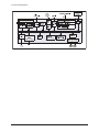
BN61-02970A
BN61-02974A
BN61-02978A
AA63-01438A
BN61-02199B
BN63-03327A
HOLDER-WIRE;NYLON6.6,NATURAL
HOLDER-SIDE AV;07 COMMON,EO,ABS+PMMA,HB,
BRACKET-STAND LINK;32 BORDEAUX PLUS,SECC
ASSY BRACKET P-PANEL;32R81,-,-,-,-,AM,CM
GASKET;Bordeaux,Conductive Fabric,20mm,9
BRACKET-GUIDE POWER;Bordeaux 32,SECC,T1.
BRACKET-PANEL TOP;32 BORDEAUX PLUS,SECC,
BRACKET-PANEL BOTTOM;32 BORDEAUX PLUS,SE
BRACKET-GUIDE MAIN;32 BORDEAUX PLUS,SECC
GASKET;Bordeaux,Conductive Fabric,7mm,8m
BRACKET-GUIDE POWER;Bordeaux 32,SECC,T1.
GASKET;BORDEAUX PLUS,Conductive Fabric,2
2
1
1
1
1
1
1
1
1
1
1
1
S.N.A
S.N.A
S.N.A
S.N.A
S.N.A
S.N.A
S.N.A
S.N.A
S.N.A
S.N.A
S.N.A
S.N.A
0.1
..2
M0215
BN91-01342B
BN07-00385A
ASSY LCD-AMLCD;LNT3253HX/*
LCD-PANEL;LTA320WT-L07,8bit,32inch,16.7M
1
1
S.N.A
S.A
0.1
..2
...3
...3
...3
...3
...3
...3
...3
...3
...3
...3
...3
...3
...3
...3
...3
...3
...3
...3
...3
...3
...3
...3
...3
...3
...3
...3
....4
....4
....4
....4
....4
....4
....4
....4
....4
....4
....4
....4
....4
....4
....4
....4
....4
....4
....4
....4
....4
....4
....4
....4
....4
M0017
M0014
T0245
JA1410_NSI
JA1406_OP
CN330
CN330
CN330
CN330
CN330
JA330
JA1601_EU
JA1608_EU
JA330
JA330
JA332
JA333
JA333
JA333
JA333
JA333
CIS3
T0603
T0603
M0131
CCMM1
CCMM1
T0174
SUB05
D1107
D1204
D1208
D1209
D1210
D1211
D1212
D1213
D1214
D1218
D1219
D1640
D1641
D1807
D2201_LUX
D1101
D1403
D1404
D1407
D1410
D1411
D1412
D1424
D1425
BN91-01367M
BN94-01184Y
0202-001492
3701-001388
3701-001400
3711-000058
3711-004484
3711-004531
3711-005606
3711-005842
3722-000143
3722-000498
3722-000498
3722-001061
3722-001061
3722-001163
3722-002360
3722-002362
3722-002362
3722-002362
3722-002543
BN40-00079A
BN63-02494A
BN63-03197A
BN63-03549A
BN73-00024D
BN73-00151A
BN97-01399Y
0202-001477
0401-000133
0401-000133
0401-000133
0401-000133
0401-000133
0401-000133
0401-000133
0401-000133
0401-000133
0401-000133
0401-000133
0401-000133
0401-000133
0401-000133
0401-000133
0401-001056
0401-001056
0401-001056
0401-001056
0401-001056
0401-001056
0401-001056
0401-001056
0401-001056
ASSY CHASSIS;LE32R81BX/*
ASSY PCB MAIN-AMLCD;LE32R81BX/*
SOLDER-WIRE FLUX;HSE-02 LFM48 SR-34 S,-,
CONNECTOR-HDMI;20P,Phosphor Bronze,ANGLE
CONNECTOR-DSUB;15P,3R,FEMALE,STRAIGHT,Ni
HEADER-BOARD TO CABLE;BOX,4P,1R,2.5MM,AN
HEADER-BOARD TO CABLE;BOX,5P,1R,2mm,STRA
HEADER-BOARD TO CABLE;BOX,10P,1R,2mm,ANG
HEADER-BOARD TO CABLE;BOX,30P,2R,2mm,STR
HEADER-BOARD TO CABLE;BOX,24P,2R,2MM,STR
JACK-PHONE;1P(VER),AG,BLK,ANGLE
JACK-SCART;21P,-,SN,BLK,NO
JACK-SCART;21P,-,SN,BLK,NO
JACK-PHONE;1P,3.6PI,AG,BLK,N
JACK-PHONE;1P,3.6PI,AG,BLK,N
JACK-VHS;4P,AU,BLK,ANGLE
JACK-PIN;3P,AU,GRN/BLU/RED,STRAIGHT
JACK-PIN;2P,Sn,WHT/RED,STRAIGHT
JACK-PIN;2P,Sn,WHT/RED,STRAIGHT
JACK-PIN;2P,Sn,WHT/RED,STRAIGHT
JACK-PIN;3P,Sn,RED/WHT/YEL,ANGLE
TUNER;TCPW3001PD32S(H),TCPW3001PD32S(H),
SHIELD-PCB MAIN;MOSEL 40",SPTE,T0.3,EURO
SHIELD-PCB MAIN;TULIP PAL,SPTE,T0.5
GASKET;BORDEAUX PLUS,Conductive Fabric,1
SILICON/RUBBER;BORDEAUX,SILICON,28x28XT6
SILICON/RUBBER;GP1500 380MIL,20X20X9.5T
ASSY SMD;LE32R81BX/*
SOLDER-CREAM;LST309-M,-,D20~45§-,96.5Sn/
DIODE-SWITCHING;RLS4148,75V,150mA,LL-34,
DIODE-SWITCHING;RLS4148,75V,150mA,LL-34,
DIODE-SWITCHING;RLS4148,75V,150mA,LL-34,
DIODE-SWITCHING;RLS4148,75V,150mA,LL-34,
DIODE-SWITCHING;RLS4148,75V,150mA,LL-34,
DIODE-SWITCHING;RLS4148,75V,150mA,LL-34,
DIODE-SWITCHING;RLS4148,75V,150mA,LL-34,
DIODE-SWITCHING;RLS4148,75V,150mA,LL-34,
DIODE-SWITCHING;RLS4148,75V,150mA,LL-34,
DIODE-SWITCHING;RLS4148,75V,150mA,LL-34,
DIODE-SWITCHING;RLS4148,75V,150mA,LL-34,
DIODE-SWITCHING;RLS4148,75V,150mA,LL-34,
DIODE-SWITCHING;RLS4148,75V,150mA,LL-34,
DIODE-SWITCHING;RLS4148,75V,150mA,LL-34,
DIODE-SWITCHING;RLS4148,75V,150mA,LL-34,
DIODE-SWITCHING;MMBD4148SE,100V,200mA,SO
DIODE-SWITCHING;MMBD4148SE,100V,200mA,SO
DIODE-SWITCHING;MMBD4148SE,100V,200mA,SO
DIODE-SWITCHING;MMBD4148SE,100V,200mA,SO
DIODE-SWITCHING;MMBD4148SE,100V,200mA,SO
DIODE-SWITCHING;MMBD4148SE,100V,200mA,SO
DIODE-SWITCHING;MMBD4148SE,100V,200mA,SO
DIODE-SWITCHING;MMBD4148SE,100V,200mA,SO
DIODE-SWITCHING;MMBD4148SE,100V,200mA,SO
1
1
0.25
1
1
1
1
1
1
1
1
1
1
1
1
1
1
1
1
1
1
1
1
1
1
1
1
1
4.559
1
1
1
1
1
1
1
1
1
1
1
1
1
1
1
1
1
1
1
1
1
1
1
1
S.N.A
S.N.A
S.N.A
S.A
S.A
S.A
S.A
S.A
S.A
S.A
S.A
S.A
S.A
S.A
S.A
S.A
S.A
S.A
S.A
S.A
S.A
S.A
S.N.A
S.N.A
S.N.A
S.N.A
S.N.A
S.N.A
S.N.A
S.A
S.A
S.A
S.A
S.A
S.A
S.A
S.A
S.A
S.A
S.A
S.A
S.A
S.A
S.A
S.A
S.A
S.A
S.A
S.A
S.A
S.A
S.A
S.A
6-2
M0115
T0447
M0131
M0146
M0131
6 Electrical Parts List
Level
Loc. No.
....4
....4
....4
....4
....4
....4
....4
....4
....4
....4
....4
....4
....4
....4
....4
....4
....4
....4
....4
....4
....4
....4
....4
....4
....4
....4
....4
....4
....4
....4
....4
....4
....4
....4
....4
....4
....4
....4
....4
....4
....4
....4
....4
....4
....4
....4
....4
....4
....4
....4
....4
....4
....4
....4
....4
....4
....4
....4
....4
....4
....4
....4
....4
....4
....4
....4
....4
....4
....4
D1426
D1434
D1435
D1450_NSID
D1451_NSID
D1472
D1473
D1474
D1475
D1476
D1477
D1478
D1479
D1482
D1483
D1484
D1485
D1486
D1487
D1488
D1489
D1492_NSID
D1493_NSID
D1494_NSID
D1495_NSID
D1496_NSID
D1497_NSID
D1498_NSID
D1499_NSID
D1603_LCD
D1621_LCD
D1624_LCD
D1643
D1644
D1645
D1646_PAD
D1647
D1648_LAMP
D1649
D1650
D1653
D1808
D1507
D1508
D1509
D1651
D1652
D1654
D0254
D0254
D1436
D1104
D1217
D1429
D1430
D1431
D1432
D1433
D1452
D1453
D1454_NSID
D1806
D1500
D1501
D1502_NSID
D1503
D1504
D1505
D1506
Code No.
0401-001056
0401-001056
0401-001056
0401-001056
0401-001056
0401-001056
0401-001056
0401-001056
0401-001056
0401-001056
0401-001056
0401-001056
0401-001056
0401-001056
0401-001056
0401-001056
0401-001056
0401-001056
0401-001056
0401-001056
0401-001056
0401-001056
0401-001056
0401-001056
0401-001056
0401-001056
0401-001056
0401-001056
0401-001056
0401-001056
0401-001056
0401-001056
0401-001056
0401-001056
0401-001056
0401-001056
0401-001056
0401-001056
0401-001056
0401-001056
0401-001056
0401-001056
0401-001099
0401-001099
0401-001099
0401-001099
0401-001099
0401-001099
0402-001019
0402-001019
0403-000258
0403-000614
0403-000620
0403-000620
0403-000620
0403-000620
0403-000620
0403-000620
0403-000620
0403-000620
0403-000620
0403-000620
0403-001016
0403-001016
0403-001016
0403-001016
0403-001016
0403-001016
0403-001016
Description & Specification
DIODE-SWITCHING;MMBD4148SE,100V,200mA,SO
DIODE-SWITCHING;MMBD4148SE,100V,200mA,SO
DIODE-SWITCHING;MMBD4148SE,100V,200mA,SO
DIODE-SWITCHING;MMBD4148SE,100V,200mA,SO
DIODE-SWITCHING;MMBD4148SE,100V,200mA,SO
DIODE-SWITCHING;MMBD4148SE,100V,200mA,SO
DIODE-SWITCHING;MMBD4148SE,100V,200mA,SO
DIODE-SWITCHING;MMBD4148SE,100V,200mA,SO
DIODE-SWITCHING;MMBD4148SE,100V,200mA,SO
DIODE-SWITCHING;MMBD4148SE,100V,200mA,SO
DIODE-SWITCHING;MMBD4148SE,100V,200mA,SO
DIODE-SWITCHING;MMBD4148SE,100V,200mA,SO
DIODE-SWITCHING;MMBD4148SE,100V,200mA,SO
DIODE-SWITCHING;MMBD4148SE,100V,200mA,SO
DIODE-SWITCHING;MMBD4148SE,100V,200mA,SO
DIODE-SWITCHING;MMBD4148SE,100V,200mA,SO
DIODE-SWITCHING;MMBD4148SE,100V,200mA,SO
DIODE-SWITCHING;MMBD4148SE,100V,200mA,SO
DIODE-SWITCHING;MMBD4148SE,100V,200mA,SO
DIODE-SWITCHING;MMBD4148SE,100V,200mA,SO
DIODE-SWITCHING;MMBD4148SE,100V,200mA,SO
DIODE-SWITCHING;MMBD4148SE,100V,200mA,SO
DIODE-SWITCHING;MMBD4148SE,100V,200mA,SO
DIODE-SWITCHING;MMBD4148SE,100V,200mA,SO
DIODE-SWITCHING;MMBD4148SE,100V,200mA,SO
DIODE-SWITCHING;MMBD4148SE,100V,200mA,SO
DIODE-SWITCHING;MMBD4148SE,100V,200mA,SO
DIODE-SWITCHING;MMBD4148SE,100V,200mA,SO
DIODE-SWITCHING;MMBD4148SE,100V,200mA,SO
DIODE-SWITCHING;MMBD4148SE,100V,200mA,SO
DIODE-SWITCHING;MMBD4148SE,100V,200mA,SO
DIODE-SWITCHING;MMBD4148SE,100V,200mA,SO
DIODE-SWITCHING;MMBD4148SE,100V,200mA,SO
DIODE-SWITCHING;MMBD4148SE,100V,200mA,SO
DIODE-SWITCHING;MMBD4148SE,100V,200mA,SO
DIODE-SWITCHING;MMBD4148SE,100V,200mA,SO
DIODE-SWITCHING;MMBD4148SE,100V,200mA,SO
DIODE-SWITCHING;MMBD4148SE,100V,200mA,SO
DIODE-SWITCHING;MMBD4148SE,100V,200mA,SO
DIODE-SWITCHING;MMBD4148SE,100V,200mA,SO
DIODE-SWITCHING;MMBD4148SE,100V,200mA,SO
DIODE-SWITCHING;MMBD4148SE,100V,200mA,SO
DIODE-SWITCHING;1N4148WS,75V,150mA,SOD-3
DIODE-SWITCHING;1N4148WS,75V,150mA,SOD-3
DIODE-SWITCHING;1N4148WS,75V,150mA,SOD-3
DIODE-SWITCHING;1N4148WS,75V,150mA,SOD-3
DIODE-SWITCHING;1N4148WS,75V,150mA,SOD-3
DIODE-SWITCHING;1N4148WS,75V,150mA,SOD-3
DIODE-SCHOTTKY;MBRS340,40V,3000mA,DO-214
DIODE-SCHOTTKY;MBRS340,40V,3000mA,DO-214
DIODE-ZENER;BZX84C5V6,5.2-6V,225mW,SOT-2
DIODE-ZENER;RLZ8.2B,7.78-8.19V,500mW,LLDIODE-ZENER;RLZ5.6B,5.45-5.73V,500mW,LLDIODE-ZENER;RLZ5.6B,5.45-5.73V,500mW,LLDIODE-ZENER;RLZ5.6B,5.45-5.73V,500mW,LLDIODE-ZENER;RLZ5.6B,5.45-5.73V,500mW,LLDIODE-ZENER;RLZ5.6B,5.45-5.73V,500mW,LLDIODE-ZENER;RLZ5.6B,5.45-5.73V,500mW,LLDIODE-ZENER;RLZ5.6B,5.45-5.73V,500mW,LLDIODE-ZENER;RLZ5.6B,5.45-5.73V,500mW,LLDIODE-ZENER;RLZ5.6B,5.45-5.73V,500mW,LLDIODE-ZENER;RLZ5.6B,5.45-5.73V,500mW,LLDIODE-ZENER;RLZ6.2B,5.96-6.27V,500mW,LLDIODE-ZENER;RLZ6.2B,5.96-6.27V,500mW,LLDIODE-ZENER;RLZ6.2B,5.96-6.27V,500mW,LLDIODE-ZENER;RLZ6.2B,5.96-6.27V,500mW,LLDIODE-ZENER;RLZ6.2B,5.96-6.27V,500mW,LLDIODE-ZENER;RLZ6.2B,5.96-6.27V,500mW,LLDIODE-ZENER;RLZ6.2B,5.96-6.27V,500mW,LL-
Q'ty
1
1
1
1
1
1
1
1
1
1
1
1
1
1
1
1
1
1
1
1
1
1
1
1
1
1
1
1
1
1
1
1
1
1
1
1
1
1
1
1
1
1
1
1
1
1
1
1
1
1
1
1
1
1
1
1
1
1
1
1
1
1
1
1
1
1
1
1
1
SA/SNA
S.A
S.A
S.A
S.A
S.A
S.A
S.A
S.A
S.A
S.A
S.A
S.A
S.A
S.A
S.A
S.A
S.A
S.A
S.A
S.A
S.A
S.A
S.A
S.A
S.A
S.A
S.A
S.A
S.A
S.A
S.A
S.A
S.A
S.A
S.A
S.A
S.A
S.A
S.A
S.A
S.A
S.A
S.A
S.A
S.A
S.A
S.A
S.A
S.A
S.A
S.A
S.A
S.A
S.A
S.A
S.A
S.A
S.A
S.A
S.A
S.A
S.A
S.A
S.A
S.A
S.A
S.A
S.A
S.A
6-3
6 Electrical Parts List
Level
Loc. No.
....4
....4
....4
....4
....4
....4
....4
....4
....4
....4
....4
....4
....4
....4
....4
....4
....4
....4
....4
....4
....4
....4
....4
....4
....4
....4
....4
....4
....4
....4
....4
....4
....4
....4
....4
....4
....4
....4
....4
....4
....4
....4
....4
....4
....4
....4
....4
....4
....4
....4
....4
....4
....4
....4
....4
....4
....4
....4
....4
....4
....4
....4
....4
....4
....4
....4
....4
....4
....4
D1402
D1428
D1449_NSID
D1804
D1810
D1608
D1636
D1105
D1405
D1406
D1408
D1409
D1413
D1414
D1422
D1423
D1446
D1447
D1601_LCD
D1602_LCD
D1604_EU
D1605
D1606_EU
D1607
D1615
D1616_LCD
D1617_LCD
D1618_LCD
D1619
D1620_EU
D1622_LCD
D1623_LCD
D1630
D1631
D1632
D1633
D1634
D1635_EU
D1201
D1801
D1802
D1803_NSID
Q1201
Q1202
Q1101_LCD
Q1102_LCD
Q1104
Q1203
Q1204
Q1205
Q1206
Q1207
Q1208
Q1209
Q1210
Q1211
Q1602
Q1603
Q1604_RED
Q1801
Q1805
Q1821
Q1823
Q2201_LUX
Q2202_LCD
Q409
Q409
Q409
Q409
6-4
Code No.
0403-001052
0403-001052
0403-001052
0403-001052
0403-001052
0403-001169
0403-001169
0403-001425
0406-001172
0406-001172
0406-001172
0406-001172
0406-001172
0406-001172
0406-001172
0406-001172
0406-001172
0406-001172
0406-001172
0406-001172
0406-001172
0406-001172
0406-001172
0406-001172
0406-001172
0406-001172
0406-001172
0406-001172
0406-001172
0406-001172
0406-001172
0406-001172
0406-001172
0406-001172
0406-001172
0406-001172
0406-001172
0406-001172
0407-000123
0407-000123
0407-000123
0407-000123
0501-000280
0501-000280
0501-000342
0501-000342
0501-000342
0501-000342
0501-000342
0501-000342
0501-000342
0501-000342
0501-000342
0501-000342
0501-000342
0501-000342
0501-000342
0501-000342
0501-000342
0501-000342
0501-000342
0501-000342
0501-000342
0501-000342
0501-000342
0505-000110
0505-000110
0505-000110
0505-000110
Description & Specification
DIODE-ZENER;RD8.2MB,7.7-8.7V,200mW,SOT-2
DIODE-ZENER;RD8.2MB,7.7-8.7V,200mW,SOT-2
DIODE-ZENER;RD8.2MB,7.7-8.7V,200mW,SOT-2
DIODE-ZENER;RD8.2MB,7.7-8.7V,200mW,SOT-2
DIODE-ZENER;RD8.2MB,7.7-8.7V,200mW,SOT-2
DIODE-ZENER;RLZ16C,15.96-16.51V,500MW,LL
DIODE-ZENER;RLZ16C,15.96-16.51V,500MW,LL
DIODE-ZENER;BZX84C33,31-35V,350mW,SOT-23
DIODE-TVS;CDS3C30GTH,48V,SMD
DIODE-TVS;CDS3C30GTH,48V,SMD
DIODE-TVS;CDS3C30GTH,48V,SMD
DIODE-TVS;CDS3C30GTH,48V,SMD
DIODE-TVS;CDS3C30GTH,48V,SMD
DIODE-TVS;CDS3C30GTH,48V,SMD
DIODE-TVS;CDS3C30GTH,48V,SMD
DIODE-TVS;CDS3C30GTH,48V,SMD
DIODE-TVS;CDS3C30GTH,48V,SMD
DIODE-TVS;CDS3C30GTH,48V,SMD
DIODE-TVS;CDS3C30GTH,48V,SMD
DIODE-TVS;CDS3C30GTH,48V,SMD
DIODE-TVS;CDS3C30GTH,48V,SMD
DIODE-TVS;CDS3C30GTH,48V,SMD
DIODE-TVS;CDS3C30GTH,48V,SMD
DIODE-TVS;CDS3C30GTH,48V,SMD
DIODE-TVS;CDS3C30GTH,48V,SMD
DIODE-TVS;CDS3C30GTH,48V,SMD
DIODE-TVS;CDS3C30GTH,48V,SMD
DIODE-TVS;CDS3C30GTH,48V,SMD
DIODE-TVS;CDS3C30GTH,48V,SMD
DIODE-TVS;CDS3C30GTH,48V,SMD
DIODE-TVS;CDS3C30GTH,48V,SMD
DIODE-TVS;CDS3C30GTH,48V,SMD
DIODE-TVS;CDS3C30GTH,48V,SMD
DIODE-TVS;CDS3C30GTH,48V,SMD
DIODE-TVS;CDS3C30GTH,48V,SMD
DIODE-TVS;CDS3C30GTH,48V,SMD
DIODE-TVS;CDS3C30GTH,48V,SMD
DIODE-TVS;CDS3C30GTH,48V,SMD
DIODE-ARRAY;DAN202K,80V,100mA,CA2-3,SOTDIODE-ARRAY;DAN202K,80V,100mA,CA2-3,SOTDIODE-ARRAY;DAN202K,80V,100mA,CA2-3,SOTDIODE-ARRAY;DAN202K,80V,100mA,CA2-3,SOTTR-SMALL SIGNAL;KSA1182,PNP,150MW,SOT-23
TR-SMALL SIGNAL;KSA1182,PNP,150MW,SOT-23
TR-SMALL SIGNAL;KSC1623-Y,NPN,200mW,SOTTR-SMALL SIGNAL;KSC1623-Y,NPN,200mW,SOTTR-SMALL SIGNAL;KSC1623-Y,NPN,200mW,SOTTR-SMALL SIGNAL;KSC1623-Y,NPN,200mW,SOTTR-SMALL SIGNAL;KSC1623-Y,NPN,200mW,SOTTR-SMALL SIGNAL;KSC1623-Y,NPN,200mW,SOTTR-SMALL SIGNAL;KSC1623-Y,NPN,200mW,SOTTR-SMALL SIGNAL;KSC1623-Y,NPN,200mW,SOTTR-SMALL SIGNAL;KSC1623-Y,NPN,200mW,SOTTR-SMALL SIGNAL;KSC1623-Y,NPN,200mW,SOTTR-SMALL SIGNAL;KSC1623-Y,NPN,200mW,SOTTR-SMALL SIGNAL;KSC1623-Y,NPN,200mW,SOTTR-SMALL SIGNAL;KSC1623-Y,NPN,200mW,SOTTR-SMALL SIGNAL;KSC1623-Y,NPN,200mW,SOTTR-SMALL SIGNAL;KSC1623-Y,NPN,200mW,SOTTR-SMALL SIGNAL;KSC1623-Y,NPN,200mW,SOTTR-SMALL SIGNAL;KSC1623-Y,NPN,200mW,SOTTR-SMALL SIGNAL;KSC1623-Y,NPN,200mW,SOTTR-SMALL SIGNAL;KSC1623-Y,NPN,200mW,SOTTR-SMALL SIGNAL;KSC1623-Y,NPN,200mW,SOTTR-SMALL SIGNAL;KSC1623-Y,NPN,200mW,SOTFET-SILICON;2N7002,N,60V,115mA,7.5ohm,0.
FET-SILICON;2N7002,N,60V,115mA,7.5ohm,0.
FET-SILICON;2N7002,N,60V,115mA,7.5ohm,0.
FET-SILICON;2N7002,N,60V,115mA,7.5ohm,0.
Q'ty
1
1
1
1
1
1
1
1
1
1
1
1
1
1
1
1
1
1
1
1
1
1
1
1
1
1
1
1
1
1
1
1
1
1
1
1
1
1
1
1
1
1
1
1
1
1
1
1
1
1
1
1
1
1
1
1
1
1
1
1
1
1
1
1
1
1
1
1
1
SA/SNA
S.A
S.A
S.A
S.A
S.A
S.A
S.A
S.A
S.A
S.A
S.A
S.A
S.A
S.A
S.A
S.A
S.A
S.A
S.A
S.A
S.A
S.A
S.A
S.A
S.A
S.A
S.A
S.A
S.A
S.A
S.A
S.A
S.A
S.A
S.A
S.A
S.A
S.A
S.A
S.A
S.A
S.A
S.A
S.A
S.A
S.A
S.A
S.A
S.A
S.A
S.A
S.A
S.A
S.A
S.A
S.A
S.A
S.A
S.A
S.A
S.A
S.A
S.A
S.A
S.A
S.A
S.A
S.A
S.A
6 Electrical Parts List
Level
Loc. No.
....4
....4
....4
....4
....4
....4
....4
....4
....4
....4
....4
....4
....4
....4
....4
....4
....4
....4
....4
....4
....4
....4
....4
....4
....4
....4
....4
....4
....4
....4
....4
....4
....4
....4
....4
....4
....4
....4
....4
....4
....4
....4
....4
....4
....4
....4
....4
....4
....4
....4
....4
....4
....4
....4
....4
....4
....4
....4
....4
....4
....4
....4
....4
....4
....4
....4
....4
....4
....4
Q409
Q409
Q409
Q409
Q409
Q409
Q409
Q409
Q409
Q409
IC104
IC104
IC1802
IC1805
IC106
IC110
IC112
IC112
IC112
IC112
IC112
IC113
DU410
T0124
IC012
T0087
T0087
T0087
T0087
T0087
IC012
T0170
T0087
IC1809
IC1810
IC1113
IC118
IC1202
IC118
D1471
D1481
D1491_NSID
D1612
D1613
D1614
D1809
R1527
R2139
R2226
R2227
R1903
R1904
R1905
R1906
R1907
R1908
R1909
R1910
R1941
R1944
R1993_LCD
R1111
R2205
R1117
R1118
R1266
R1333_UX
R1334_UX
R1335_UX
Code No.
0505-000110
0505-000110
0505-000110
0505-000110
0505-000110
0505-000110
0505-000110
0505-000110
0505-000110
0505-000275
0801-002095
0801-002633
0903-001488
1001-000164
1001-001440
1006-001076
1103-000129
1103-000129
1103-000129
1103-000129
1103-001385
1105-001791
1201-000166
1201-002430
1203-001519
1203-001815
1203-002842
1203-002855
1203-002898
1203-002974
1203-002995
1203-003059
1203-003696
1203-004363
1203-004364
1203-004379
1204-002718
1204-002719
1204-002729
1405-001185
1405-001185
1405-001185
1405-001185
1405-001185
1405-001185
1405-001185
2007-000042
2007-000043
2007-000043
2007-000043
2007-000052
2007-000052
2007-000052
2007-000052
2007-000052
2007-000052
2007-000052
2007-000052
2007-000052
2007-000052
2007-000052
2007-000060
2007-000060
2007-000066
2007-000067
2007-000070
2007-000070
2007-000070
2007-000070
Description & Specification
FET-SILICON;2N7002,N,60V,115mA,7.5ohm,0.
FET-SILICON;2N7002,N,60V,115mA,7.5ohm,0.
FET-SILICON;2N7002,N,60V,115mA,7.5ohm,0.
FET-SILICON;2N7002,N,60V,115mA,7.5ohm,0.
FET-SILICON;2N7002,N,60V,115mA,7.5ohm,0.
FET-SILICON;2N7002,N,60V,115mA,7.5ohm,0.
FET-SILICON;2N7002,N,60V,115mA,7.5ohm,0.
FET-SILICON;2N7002,N,60V,115mA,7.5ohm,0.
FET-SILICON;2N7002,N,60V,115mA,7.5ohm,0.
FET-SILICON;SI4435DY,P,-30V,+-8.0A,0.014
IC-CMOS LOGIC;74LCX245,TRANSCEIVER,TSSOP
IC-CMOS LOGIC;NC7WBD3125,2BIT BUS SWITCH
IC-MICROCOMPUTER;M308A0SGP,LQFP,100P,14x
IC-ANALOG MULTIPLEX;74HC4052,CMOS,SOP,16
IC-VIDEO SWITCH;SiI9185CTU,QFP,80P,3.3V,
IC-DRIVER/RECEIVER;MAX232ECWE+T,SOP,16P,
IC-EEPROM;24C02,2Kbit,256x8Bit,SOP,8P,5x
IC-EEPROM;24C02,2Kbit,256x8Bit,SOP,8P,5x
IC-EEPROM;24C02,2Kbit,256x8Bit,SOP,8P,5x
IC-EEPROM;24C02,2Kbit,256x8Bit,SOP,8P,5x
IC-EEPROM;24C256,256Kbit,32Kx8,SOP,8P,5x
IC-DRAM;EM6A9320BI,DDR,128Mbit,4Mx32,FBG
IC-OP AMP;LM358,SOP,ST,8P,150MIL,DUAL,10
IC-POWER AMP;NTP-3000,QFN,56P,8x8mm,DUAL
IC-POSI.ADJUST REG.;LM317,SOT223,3P,274
IC-POSI.FIXED REG.;78M09,TO-252,3P,-,PLA
IC-POSI.FIXED REG.;AP1117D-33A,TO-252,3P
IC-POSI.FIXED REG.;MC33269DTRK-5.0,DPRK,
IC-POSI.FIXED REG.;G950T45R,T0-252,3P,6.
IC-POSI.FIXED REG.;AP1117D-25A,TO-252,3P
IC-POSI.ADJUST REG.;AP1117D-A,TO-252,3P,
IC-SWITCH VOL. REG.;MP1583,SOIC,8P,4.9x3
IC-POSI.FIXED REG.;NCP1117DT18T5G,DPAK,3
IC-VOL. DETECTOR;RT9818C-29PV,SOT-23,3P,
IC-VOL. DETECTOR;RT9818C-42PV,SOT-23,3P,
IC-DC/DC CONVERTER;AP1530SA,SOP,8P,5x3.9
IC-VIDEO PROCESS;SVP-UX68,BGA,336P,27x27
IC-AUDIO PROCESSOR;SGTV5810,LQFP,100P,14
IC-VIDEO PROCESS;S4LF119X01,PBGA,208P,17
VARISTOR;24Vdc,1.6x0.8x0.36mm,TP
VARISTOR;24Vdc,1.6x0.8x0.36mm,TP
VARISTOR;24Vdc,1.6x0.8x0.36mm,TP
VARISTOR;24Vdc,1.6x0.8x0.36mm,TP
VARISTOR;24Vdc,1.6x0.8x0.36mm,TP
VARISTOR;24Vdc,1.6x0.8x0.36mm,TP
VARISTOR;24Vdc,1.6x0.8x0.36mm,TP
R-CHIP;499ohm,1%,1/10W,TP,1608
R-CHIP;1Kohm,1%,1/10W,TP,1608
R-CHIP;1Kohm,1%,1/10W,TP,1608
R-CHIP;1Kohm,1%,1/10W,TP,1608
R-CHIP;10Kohm,1%,1/10W,TP,1608
R-CHIP;10Kohm,1%,1/10W,TP,1608
R-CHIP;10Kohm,1%,1/10W,TP,1608
R-CHIP;10Kohm,1%,1/10W,TP,1608
R-CHIP;10Kohm,1%,1/10W,TP,1608
R-CHIP;10Kohm,1%,1/10W,TP,1608
R-CHIP;10Kohm,1%,1/10W,TP,1608
R-CHIP;10Kohm,1%,1/10W,TP,1608
R-CHIP;10Kohm,1%,1/10W,TP,1608
R-CHIP;10Kohm,1%,1/10W,TP,1608
R-CHIP;10Kohm,1%,1/10W,TP,1608
R-CHIP;100Kohm,1%,1/10W,TP,1608
R-CHIP;100Kohm,1%,1/10W,TP,1608
R-CHIP;20Kohm,1%,1/10W,TP,1608
R-CHIP;15Kohm,1%,1/10W,TP,1608
R-CHIP;0ohm,5%,1/10W,TP,1608
R-CHIP;0ohm,5%,1/10W,TP,1608
R-CHIP;0ohm,5%,1/10W,TP,1608
R-CHIP;0ohm,5%,1/10W,TP,1608
Q'ty
1
1
1
1
1
1
1
1
1
1
1
1
1
1
1
1
1
1
1
1
1
1
1
1
1
1
1
1
1
1
1
1
1
1
1
1
1
1
1
1
1
1
1
1
1
1
1
1
1
1
1
1
1
1
1
1
1
1
1
1
1
1
1
1
1
1
1
1
1
SA/SNA
S.A
S.A
S.A
S.A
S.A
S.A
S.A
S.A
S.A
S.A
S.A
S.A
S.A
S.A
S.A
S.A
S.A
S.A
S.A
S.A
S.A
S.A
S.A
S.A
S.A
S.A
S.A
S.A
S.A
S.A
S.A
S.A
S.A
S.A
S.A
S.A
S.A
S.A
S.A
S.A
S.A
S.A
S.A
S.A
S.A
S.A
S.A
S.A
S.A
S.A
S.A
S.A
S.A
S.A
S.A
S.A
S.A
S.A
S.A
S.A
S.A
S.A
S.A
S.A
S.A
S.A
S.A
S.A
S.A
6-5
6 Electrical Parts List
Level
Loc. No.
....4
....4
....4
....4
....4
....4
....4
....4
....4
....4
....4
....4
....4
....4
....4
....4
....4
....4
....4
....4
....4
....4
....4
....4
....4
....4
....4
....4
....4
....4
....4
....4
....4
....4
....4
....4
....4
....4
....4
....4
....4
....4
....4
....4
....4
....4
....4
....4
....4
....4
....4
....4
....4
....4
....4
....4
....4
....4
....4
....4
....4
....4
....4
....4
....4
....4
....4
....4
....4
R1336_UX
R1337_UX
R1338_UX
R1339_UX
R1340_UX
R1418
R1456
R1464
R1501_HDMI
R1502
R1507_HDMI
R1519
R1524
R1525
R1542
R1543
R1547
R1550
R1553
R1554
R1555
R1556
R1557
R1558
R1559
R1560
R1561
R1574
R1575
R1576
R1578
R1581_NSID
R1584
R1585
R1586_HDMI
R1587_HDMI
R1621_EU
R1655
R1708_NMMS
R1709_NMMS
R1710_NMMS
R1805
R1826
R1828
R1830
R1831
R1834
R1837
R1838
R1839
R1840
R1844
R1879
R1895
R1927
R1932
R1934
R1935
R1936
R1937
R1957
R1975
R1976
R2001_TEST
R2002_TEST
R2003_TEST
R2004
R2007
R2011
6-6
Code No.
2007-000070
2007-000070
2007-000070
2007-000070
2007-000070
2007-000070
2007-000070
2007-000070
2007-000070
2007-000070
2007-000070
2007-000070
2007-000070
2007-000070
2007-000070
2007-000070
2007-000070
2007-000070
2007-000070
2007-000070
2007-000070
2007-000070
2007-000070
2007-000070
2007-000070
2007-000070
2007-000070
2007-000070
2007-000070
2007-000070
2007-000070
2007-000070
2007-000070
2007-000070
2007-000070
2007-000070
2007-000070
2007-000070
2007-000070
2007-000070
2007-000070
2007-000070
2007-000070
2007-000070
2007-000070
2007-000070
2007-000070
2007-000070
2007-000070
2007-000070
2007-000070
2007-000070
2007-000070
2007-000070
2007-000070
2007-000070
2007-000070
2007-000070
2007-000070
2007-000070
2007-000070
2007-000070
2007-000070
2007-000070
2007-000070
2007-000070
2007-000070
2007-000070
2007-000070
Description & Specification
R-CHIP;0ohm,5%,1/10W,TP,1608
R-CHIP;0ohm,5%,1/10W,TP,1608
R-CHIP;0ohm,5%,1/10W,TP,1608
R-CHIP;0ohm,5%,1/10W,TP,1608
R-CHIP;0ohm,5%,1/10W,TP,1608
R-CHIP;0ohm,5%,1/10W,TP,1608
R-CHIP;0ohm,5%,1/10W,TP,1608
R-CHIP;0ohm,5%,1/10W,TP,1608
R-CHIP;0ohm,5%,1/10W,TP,1608
R-CHIP;0ohm,5%,1/10W,TP,1608
R-CHIP;0ohm,5%,1/10W,TP,1608
R-CHIP;0ohm,5%,1/10W,TP,1608
R-CHIP;0ohm,5%,1/10W,TP,1608
R-CHIP;0ohm,5%,1/10W,TP,1608
R-CHIP;0ohm,5%,1/10W,TP,1608
R-CHIP;0ohm,5%,1/10W,TP,1608
R-CHIP;0ohm,5%,1/10W,TP,1608
R-CHIP;0ohm,5%,1/10W,TP,1608
R-CHIP;0ohm,5%,1/10W,TP,1608
R-CHIP;0ohm,5%,1/10W,TP,1608
R-CHIP;0ohm,5%,1/10W,TP,1608
R-CHIP;0ohm,5%,1/10W,TP,1608
R-CHIP;0ohm,5%,1/10W,TP,1608
R-CHIP;0ohm,5%,1/10W,TP,1608
R-CHIP;0ohm,5%,1/10W,TP,1608
R-CHIP;0ohm,5%,1/10W,TP,1608
R-CHIP;0ohm,5%,1/10W,TP,1608
R-CHIP;0ohm,5%,1/10W,TP,1608
R-CHIP;0ohm,5%,1/10W,TP,1608
R-CHIP;0ohm,5%,1/10W,TP,1608
R-CHIP;0ohm,5%,1/10W,TP,1608
R-CHIP;0ohm,5%,1/10W,TP,1608
R-CHIP;0ohm,5%,1/10W,TP,1608
R-CHIP;0ohm,5%,1/10W,TP,1608
R-CHIP;0ohm,5%,1/10W,TP,1608
R-CHIP;0ohm,5%,1/10W,TP,1608
R-CHIP;0ohm,5%,1/10W,TP,1608
R-CHIP;0ohm,5%,1/10W,TP,1608
R-CHIP;0ohm,5%,1/10W,TP,1608
R-CHIP;0ohm,5%,1/10W,TP,1608
R-CHIP;0ohm,5%,1/10W,TP,1608
R-CHIP;0ohm,5%,1/10W,TP,1608
R-CHIP;0ohm,5%,1/10W,TP,1608
R-CHIP;0ohm,5%,1/10W,TP,1608
R-CHIP;0ohm,5%,1/10W,TP,1608
R-CHIP;0ohm,5%,1/10W,TP,1608
R-CHIP;0ohm,5%,1/10W,TP,1608
R-CHIP;0ohm,5%,1/10W,TP,1608
R-CHIP;0ohm,5%,1/10W,TP,1608
R-CHIP;0ohm,5%,1/10W,TP,1608
R-CHIP;0ohm,5%,1/10W,TP,1608
R-CHIP;0ohm,5%,1/10W,TP,1608
R-CHIP;0ohm,5%,1/10W,TP,1608
R-CHIP;0ohm,5%,1/10W,TP,1608
R-CHIP;0ohm,5%,1/10W,TP,1608
R-CHIP;0ohm,5%,1/10W,TP,1608
R-CHIP;0ohm,5%,1/10W,TP,1608
R-CHIP;0ohm,5%,1/10W,TP,1608
R-CHIP;0ohm,5%,1/10W,TP,1608
R-CHIP;0ohm,5%,1/10W,TP,1608
R-CHIP;0ohm,5%,1/10W,TP,1608
R-CHIP;0ohm,5%,1/10W,TP,1608
R-CHIP;0ohm,5%,1/10W,TP,1608
R-CHIP;0ohm,5%,1/10W,TP,1608
R-CHIP;0ohm,5%,1/10W,TP,1608
R-CHIP;0ohm,5%,1/10W,TP,1608
R-CHIP;0ohm,5%,1/10W,TP,1608
R-CHIP;0ohm,5%,1/10W,TP,1608
R-CHIP;0ohm,5%,1/10W,TP,1608
Q'ty
1
1
1
1
1
1
1
1
1
1
1
1
1
1
1
1
1
1
1
1
1
1
1
1
1
1
1
1
1
1
1
1
1
1
1
1
1
1
1
1
1
1
1
1
1
1
1
1
1
1
1
1
1
1
1
1
1
1
1
1
1
1
1
1
1
1
1
1
1
SA/SNA
S.A
S.A
S.A
S.A
S.A
S.A
S.A
S.A
S.A
S.A
S.A
S.A
S.A
S.A
S.A
S.A
S.A
S.A
S.A
S.A
S.A
S.A
S.A
S.A
S.A
S.A
S.A
S.A
S.A
S.A
S.A
S.A
S.A
S.A
S.A
S.A
S.A
S.A
S.A
S.A
S.A
S.A
S.A
S.A
S.A
S.A
S.A
S.A
S.A
S.A
S.A
S.A
S.A
S.A
S.A
S.A
S.A
S.A
S.A
S.A
S.A
S.A
S.A
S.A
S.A
S.A
S.A
S.A
S.A
6 Electrical Parts List
Level
Loc. No.
....4
....4
....4
....4
....4
....4
....4
....4
....4
....4
....4
....4
....4
....4
....4
....4
....4
....4
....4
....4
....4
....4
....4
....4
....4
....4
....4
....4
....4
....4
....4
....4
....4
....4
....4
....4
....4
....4
....4
....4
....4
....4
....4
....4
....4
....4
....4
....4
....4
....4
....4
....4
....4
....4
....4
....4
....4
....4
....4
....4
....4
....4
....4
....4
....4
....4
....4
....4
....4
R2014_UX
R2015_UX
R2022_FBE
R2023_FBE
R2024_FBE
R2028_FBE
R2029_FBE
R2031_FBE
R2032_UX
R2033_UX
R2039_FBE
R2040_FBE
R2041_FBE
R2053
R2054_FBE
R2057_FBE
R2058_FBE
R2059
R2066
R2067
R2068
R2070_FBE
R2072_FBE
R2074_FBE
R2076_FBE
R2078_FBE
R2080_FBE
R2082_FBE
R2084_FBE
R2086_FBE
R2088_FBE
R2090_FBE
R2092_FBE
R2255_LCD
R2257_LCD
R2260_LCD
R2279_LCD
R2291_FBE
R2302_LCD
R2303_OP
R2304_OP
R2306_LCD
R2364_FBE
R2366_FBE
R2379_FBE
R2380_FBE
R1413
R1414
R1451
R1462
R1468
R1469
R1498_OP
R1499_OP
R1700_LAMP
R1701_LAMP
R2063
R2149
R2228
R2229
R2230
R2231
R2281_OP
R1205
R1206
R1405
R1406
R1450
R1452
Code No.
2007-000070
2007-000070
2007-000070
2007-000070
2007-000070
2007-000070
2007-000070
2007-000070
2007-000070
2007-000070
2007-000070
2007-000070
2007-000070
2007-000070
2007-000070
2007-000070
2007-000070
2007-000070
2007-000070
2007-000070
2007-000070
2007-000070
2007-000070
2007-000070
2007-000070
2007-000070
2007-000070
2007-000070
2007-000070
2007-000070
2007-000070
2007-000070
2007-000070
2007-000070
2007-000070
2007-000070
2007-000070
2007-000070
2007-000070
2007-000070
2007-000070
2007-000070
2007-000070
2007-000070
2007-000070
2007-000070
2007-000071
2007-000071
2007-000071
2007-000071
2007-000071
2007-000071
2007-000071
2007-000071
2007-000071
2007-000071
2007-000071
2007-000071
2007-000071
2007-000071
2007-000071
2007-000071
2007-000071
2007-000072
2007-000072
2007-000072
2007-000072
2007-000072
2007-000072
Description & Specification
R-CHIP;0ohm,5%,1/10W,TP,1608
R-CHIP;0ohm,5%,1/10W,TP,1608
R-CHIP;0ohm,5%,1/10W,TP,1608
R-CHIP;0ohm,5%,1/10W,TP,1608
R-CHIP;0ohm,5%,1/10W,TP,1608
R-CHIP;0ohm,5%,1/10W,TP,1608
R-CHIP;0ohm,5%,1/10W,TP,1608
R-CHIP;0ohm,5%,1/10W,TP,1608
R-CHIP;0ohm,5%,1/10W,TP,1608
R-CHIP;0ohm,5%,1/10W,TP,1608
R-CHIP;0ohm,5%,1/10W,TP,1608
R-CHIP;0ohm,5%,1/10W,TP,1608
R-CHIP;0ohm,5%,1/10W,TP,1608
R-CHIP;0ohm,5%,1/10W,TP,1608
R-CHIP;0ohm,5%,1/10W,TP,1608
R-CHIP;0ohm,5%,1/10W,TP,1608
R-CHIP;0ohm,5%,1/10W,TP,1608
R-CHIP;0ohm,5%,1/10W,TP,1608
R-CHIP;0ohm,5%,1/10W,TP,1608
R-CHIP;0ohm,5%,1/10W,TP,1608
R-CHIP;0ohm,5%,1/10W,TP,1608
R-CHIP;0ohm,5%,1/10W,TP,1608
R-CHIP;0ohm,5%,1/10W,TP,1608
R-CHIP;0ohm,5%,1/10W,TP,1608
R-CHIP;0ohm,5%,1/10W,TP,1608
R-CHIP;0ohm,5%,1/10W,TP,1608
R-CHIP;0ohm,5%,1/10W,TP,1608
R-CHIP;0ohm,5%,1/10W,TP,1608
R-CHIP;0ohm,5%,1/10W,TP,1608
R-CHIP;0ohm,5%,1/10W,TP,1608
R-CHIP;0ohm,5%,1/10W,TP,1608
R-CHIP;0ohm,5%,1/10W,TP,1608
R-CHIP;0ohm,5%,1/10W,TP,1608
R-CHIP;0ohm,5%,1/10W,TP,1608
R-CHIP;0ohm,5%,1/10W,TP,1608
R-CHIP;0ohm,5%,1/10W,TP,1608
R-CHIP;0ohm,5%,1/10W,TP,1608
R-CHIP;0ohm,5%,1/10W,TP,1608
R-CHIP;0ohm,5%,1/10W,TP,1608
R-CHIP;0ohm,5%,1/10W,TP,1608
R-CHIP;0ohm,5%,1/10W,TP,1608
R-CHIP;0ohm,5%,1/10W,TP,1608
R-CHIP;0ohm,5%,1/10W,TP,1608
R-CHIP;0ohm,5%,1/10W,TP,1608
R-CHIP;0ohm,5%,1/10W,TP,1608
R-CHIP;0ohm,5%,1/10W,TP,1608
R-CHIP;22ohm,5%,1/10W,TP,1608
R-CHIP;22ohm,5%,1/10W,TP,1608
R-CHIP;22ohm,5%,1/10W,TP,1608
R-CHIP;22ohm,5%,1/10W,TP,1608
R-CHIP;22ohm,5%,1/10W,TP,1608
R-CHIP;22ohm,5%,1/10W,TP,1608
R-CHIP;22ohm,5%,1/10W,TP,1608
R-CHIP;22ohm,5%,1/10W,TP,1608
R-CHIP;22ohm,5%,1/10W,TP,1608
R-CHIP;22ohm,5%,1/10W,TP,1608
R-CHIP;22ohm,5%,1/10W,TP,1608
R-CHIP;22ohm,5%,1/10W,TP,1608
R-CHIP;22ohm,5%,1/10W,TP,1608
R-CHIP;22ohm,5%,1/10W,TP,1608
R-CHIP;22ohm,5%,1/10W,TP,1608
R-CHIP;22ohm,5%,1/10W,TP,1608
R-CHIP;22ohm,5%,1/10W,TP,1608
R-CHIP;47ohm,5%,1/10W,TP,1608
R-CHIP;47ohm,5%,1/10W,TP,1608
R-CHIP;47ohm,5%,1/10W,TP,1608
R-CHIP;47ohm,5%,1/10W,TP,1608
R-CHIP;47ohm,5%,1/10W,TP,1608
R-CHIP;47ohm,5%,1/10W,TP,1608
Q'ty
1
1
1
1
1
1
1
1
1
1
1
1
1
1
1
1
1
1
1
1
1
1
1
1
1
1
1
1
1
1
1
1
1
1
1
1
1
1
1
1
1
1
1
1
1
1
1
1
1
1
1
1
1
1
1
1
1
1
1
1
1
1
1
1
1
1
1
1
1
SA/SNA
S.A
S.A
S.A
S.A
S.A
S.A
S.A
S.A
S.A
S.A
S.A
S.A
S.A
S.A
S.A
S.A
S.A
S.A
S.A
S.A
S.A
S.A
S.A
S.A
S.A
S.A
S.A
S.A
S.A
S.A
S.A
S.A
S.A
S.A
S.A
S.A
S.A
S.A
S.A
S.A
S.A
S.A
S.A
S.A
S.A
S.A
S.A
S.A
S.A
S.A
S.A
S.A
S.A
S.A
S.A
S.A
S.A
S.A
S.A
S.A
S.A
S.A
S.A
S.A
S.A
S.A
S.A
S.A
S.A
6-7
6 Electrical Parts List
Level
Loc. No.
....4
....4
....4
....4
....4
....4
....4
....4
....4
....4
....4
....4
....4
....4
....4
....4
....4
....4
....4
....4
....4
....4
....4
....4
....4
....4
....4
....4
....4
....4
....4
....4
....4
....4
....4
....4
....4
....4
....4
....4
....4
....4
....4
....4
....4
....4
....4
....4
....4
....4
....4
....4
....4
....4
....4
....4
....4
....4
....4
....4
....4
....4
....4
....4
....4
....4
....4
....4
....4
R1460
R1461
R1493_NSID
R1494_NSID
R1864
R1960
R1961
R2201
R2202
R1203
R1217
R1218
R1219
R1220
R1222
R1225
R1226
R1228
R1229
R1230
R1231
R1232
R1233
R1234
R1235
R1236
R1237
R1240
R1241
R1243
R1244
R1254
R1264
R1273
R1419
R1459
R1488
R1489
R1603_LCD
R1617
R1622_EU
R1631_LCD
R1634
R1639_LCD
R1666
R1668
R1808
R1835
R1836
R1855
R1856
R1858
R1861
R1862
R1868
R1870
R1874
R1875
R1877
R1878
R1949
R1952
R1955
R2005
R2006
R2030
R2204
R2208
R2243_FBE
6-8
Code No.
2007-000072
2007-000072
2007-000072
2007-000072
2007-000072
2007-000072
2007-000072
2007-000072
2007-000072
2007-000074
2007-000074
2007-000074
2007-000074
2007-000074
2007-000074
2007-000074
2007-000074
2007-000074
2007-000074
2007-000074
2007-000074
2007-000074
2007-000074
2007-000074
2007-000074
2007-000074
2007-000074
2007-000074
2007-000074
2007-000074
2007-000074
2007-000074
2007-000074
2007-000074
2007-000074
2007-000074
2007-000074
2007-000074
2007-000074
2007-000074
2007-000074
2007-000074
2007-000074
2007-000074
2007-000074
2007-000074
2007-000074
2007-000074
2007-000074
2007-000074
2007-000074
2007-000074
2007-000074
2007-000074
2007-000074
2007-000074
2007-000074
2007-000074
2007-000074
2007-000074
2007-000074
2007-000074
2007-000074
2007-000074
2007-000074
2007-000074
2007-000074
2007-000074
2007-000074
Description & Specification
R-CHIP;47ohm,5%,1/10W,TP,1608
R-CHIP;47ohm,5%,1/10W,TP,1608
R-CHIP;47ohm,5%,1/10W,TP,1608
R-CHIP;47ohm,5%,1/10W,TP,1608
R-CHIP;47ohm,5%,1/10W,TP,1608
R-CHIP;47ohm,5%,1/10W,TP,1608
R-CHIP;47ohm,5%,1/10W,TP,1608
R-CHIP;47ohm,5%,1/10W,TP,1608
R-CHIP;47ohm,5%,1/10W,TP,1608
R-CHIP;100ohm,5%,1/10W,TP,1608
R-CHIP;100ohm,5%,1/10W,TP,1608
R-CHIP;100ohm,5%,1/10W,TP,1608
R-CHIP;100ohm,5%,1/10W,TP,1608
R-CHIP;100ohm,5%,1/10W,TP,1608
R-CHIP;100ohm,5%,1/10W,TP,1608
R-CHIP;100ohm,5%,1/10W,TP,1608
R-CHIP;100ohm,5%,1/10W,TP,1608
R-CHIP;100ohm,5%,1/10W,TP,1608
R-CHIP;100ohm,5%,1/10W,TP,1608
R-CHIP;100ohm,5%,1/10W,TP,1608
R-CHIP;100ohm,5%,1/10W,TP,1608
R-CHIP;100ohm,5%,1/10W,TP,1608
R-CHIP;100ohm,5%,1/10W,TP,1608
R-CHIP;100ohm,5%,1/10W,TP,1608
R-CHIP;100ohm,5%,1/10W,TP,1608
R-CHIP;100ohm,5%,1/10W,TP,1608
R-CHIP;100ohm,5%,1/10W,TP,1608
R-CHIP;100ohm,5%,1/10W,TP,1608
R-CHIP;100ohm,5%,1/10W,TP,1608
R-CHIP;100ohm,5%,1/10W,TP,1608
R-CHIP;100ohm,5%,1/10W,TP,1608
R-CHIP;100ohm,5%,1/10W,TP,1608
R-CHIP;100ohm,5%,1/10W,TP,1608
R-CHIP;100ohm,5%,1/10W,TP,1608
R-CHIP;100ohm,5%,1/10W,TP,1608
R-CHIP;100ohm,5%,1/10W,TP,1608
R-CHIP;100ohm,5%,1/10W,TP,1608
R-CHIP;100ohm,5%,1/10W,TP,1608
R-CHIP;100ohm,5%,1/10W,TP,1608
R-CHIP;100ohm,5%,1/10W,TP,1608
R-CHIP;100ohm,5%,1/10W,TP,1608
R-CHIP;100ohm,5%,1/10W,TP,1608
R-CHIP;100ohm,5%,1/10W,TP,1608
R-CHIP;100ohm,5%,1/10W,TP,1608
R-CHIP;100ohm,5%,1/10W,TP,1608
R-CHIP;100ohm,5%,1/10W,TP,1608
R-CHIP;100ohm,5%,1/10W,TP,1608
R-CHIP;100ohm,5%,1/10W,TP,1608
R-CHIP;100ohm,5%,1/10W,TP,1608
R-CHIP;100ohm,5%,1/10W,TP,1608
R-CHIP;100ohm,5%,1/10W,TP,1608
R-CHIP;100ohm,5%,1/10W,TP,1608
R-CHIP;100ohm,5%,1/10W,TP,1608
R-CHIP;100ohm,5%,1/10W,TP,1608
R-CHIP;100ohm,5%,1/10W,TP,1608
R-CHIP;100ohm,5%,1/10W,TP,1608
R-CHIP;100ohm,5%,1/10W,TP,1608
R-CHIP;100ohm,5%,1/10W,TP,1608
R-CHIP;100ohm,5%,1/10W,TP,1608
R-CHIP;100ohm,5%,1/10W,TP,1608
R-CHIP;100ohm,5%,1/10W,TP,1608
R-CHIP;100ohm,5%,1/10W,TP,1608
R-CHIP;100ohm,5%,1/10W,TP,1608
R-CHIP;100ohm,5%,1/10W,TP,1608
R-CHIP;100ohm,5%,1/10W,TP,1608
R-CHIP;100ohm,5%,1/10W,TP,1608
R-CHIP;100ohm,5%,1/10W,TP,1608
R-CHIP;100ohm,5%,1/10W,TP,1608
R-CHIP;100ohm,5%,1/10W,TP,1608
Q'ty
1
1
1
1
1
1
1
1
1
1
1
1
1
1
1
1
1
1
1
1
1
1
1
1
1
1
1
1
1
1
1
1
1
1
1
1
1
1
1
1
1
1
1
1
1
1
1
1
1
1
1
1
1
1
1
1
1
1
1
1
1
1
1
1
1
1
1
1
1
SA/SNA
S.A
S.A
S.A
S.A
S.A
S.A
S.A
S.A
S.A
S.A
S.A
S.A
S.A
S.A
S.A
S.A
S.A
S.A
S.A
S.A
S.A
S.A
S.A
S.A
S.A
S.A
S.A
S.A
S.A
S.A
S.A
S.A
S.A
S.A
S.A
S.A
S.A
S.A
S.A
S.A
S.A
S.A
S.A
S.A
S.A
S.A
S.A
S.A
S.A
S.A
S.A
S.A
S.A
S.A
S.A
S.A
S.A
S.A
S.A
S.A
S.A
S.A
S.A
S.A
S.A
S.A
S.A
S.A
S.A
6 Electrical Parts List
Level
Loc. No.
....4
....4
....4
....4
....4
....4
....4
....4
....4
....4
....4
....4
....4
....4
....4
....4
....4
....4
....4
....4
....4
....4
....4
....4
....4
....4
....4
....4
....4
....4
....4
....4
....4
....4
....4
....4
....4
....4
....4
....4
....4
....4
....4
....4
....4
....4
....4
....4
....4
....4
....4
....4
....4
....4
....4
....4
....4
....4
....4
....4
....4
....4
....4
....4
....4
....4
....4
....4
....4
R2285_LCD
R2292_LCD
R2381_FBE
R2382_FBE
R2383_FBE
R2384_FBE
R2385_FBE
R2386_FBE
R2387_FBE
R2388_FBE
R2389_FBE
R2390_FBE
R2391_FBE
R2392_FBE
R1101
R1267
R1268
R1582
R1583
R1604_EU
R1607_EU
R1654
R1659
R1891
R1403
R1404
R1407
R1412
R1442
R1444
R1605
R1613
R1628_LCD
R1629_LCD
R1657
R1661
R1688
R1691
R1958
R2052
R2246_LCD
R2287_LCD
R1265
R1408
R1416
R1463
R1470
R1495_NSID
R1500_HDMI
R1640_LCD
R1641_LCD
R1698_PAD
R1702_LAMP
R1823
R1829
R1833
R1845
R1846
R1915_LCD
R1929
R1939
R1951
R2008
R2061
R2210
R2252_LCD
R2284_LCD
R2293_LCD
R1816
Code No.
2007-000074
2007-000074
2007-000074
2007-000074
2007-000074
2007-000074
2007-000074
2007-000074
2007-000074
2007-000074
2007-000074
2007-000074
2007-000074
2007-000074
2007-000076
2007-000076
2007-000076
2007-000076
2007-000076
2007-000076
2007-000076
2007-000076
2007-000076
2007-000076
2007-000077
2007-000077
2007-000077
2007-000077
2007-000077
2007-000077
2007-000077
2007-000077
2007-000077
2007-000077
2007-000077
2007-000077
2007-000077
2007-000077
2007-000077
2007-000077
2007-000077
2007-000077
2007-000078
2007-000078
2007-000078
2007-000078
2007-000078
2007-000078
2007-000078
2007-000078
2007-000078
2007-000078
2007-000078
2007-000078
2007-000078
2007-000078
2007-000078
2007-000078
2007-000078
2007-000078
2007-000078
2007-000078
2007-000078
2007-000078
2007-000078
2007-000078
2007-000078
2007-000078
2007-000082
Description & Specification
R-CHIP;100ohm,5%,1/10W,TP,1608
R-CHIP;100ohm,5%,1/10W,TP,1608
R-CHIP;100ohm,5%,1/10W,TP,1608
R-CHIP;100ohm,5%,1/10W,TP,1608
R-CHIP;100ohm,5%,1/10W,TP,1608
R-CHIP;100ohm,5%,1/10W,TP,1608
R-CHIP;100ohm,5%,1/10W,TP,1608
R-CHIP;100ohm,5%,1/10W,TP,1608
R-CHIP;100ohm,5%,1/10W,TP,1608
R-CHIP;100ohm,5%,1/10W,TP,1608
R-CHIP;100ohm,5%,1/10W,TP,1608
R-CHIP;100ohm,5%,1/10W,TP,1608
R-CHIP;100ohm,5%,1/10W,TP,1608
R-CHIP;100ohm,5%,1/10W,TP,1608
R-CHIP;330ohm,5%,1/10W,TP,1608
R-CHIP;330ohm,5%,1/10W,TP,1608
R-CHIP;330ohm,5%,1/10W,TP,1608
R-CHIP;330ohm,5%,1/10W,TP,1608
R-CHIP;330ohm,5%,1/10W,TP,1608
R-CHIP;330ohm,5%,1/10W,TP,1608
R-CHIP;330ohm,5%,1/10W,TP,1608
R-CHIP;330ohm,5%,1/10W,TP,1608
R-CHIP;330ohm,5%,1/10W,TP,1608
R-CHIP;330ohm,5%,1/10W,TP,1608
R-CHIP;470ohm,5%,1/10W,TP,1608
R-CHIP;470ohm,5%,1/10W,TP,1608
R-CHIP;470ohm,5%,1/10W,TP,1608
R-CHIP;470ohm,5%,1/10W,TP,1608
R-CHIP;470ohm,5%,1/10W,TP,1608
R-CHIP;470ohm,5%,1/10W,TP,1608
R-CHIP;470ohm,5%,1/10W,TP,1608
R-CHIP;470ohm,5%,1/10W,TP,1608
R-CHIP;470ohm,5%,1/10W,TP,1608
R-CHIP;470ohm,5%,1/10W,TP,1608
R-CHIP;470ohm,5%,1/10W,TP,1608
R-CHIP;470ohm,5%,1/10W,TP,1608
R-CHIP;470ohm,5%,1/10W,TP,1608
R-CHIP;470ohm,5%,1/10W,TP,1608
R-CHIP;470ohm,5%,1/10W,TP,1608
R-CHIP;470ohm,5%,1/10W,TP,1608
R-CHIP;470ohm,5%,1/10W,TP,1608
R-CHIP;470ohm,5%,1/10W,TP,1608
R-CHIP;1Kohm,5%,1/10W,TP,1608
R-CHIP;1Kohm,5%,1/10W,TP,1608
R-CHIP;1Kohm,5%,1/10W,TP,1608
R-CHIP;1Kohm,5%,1/10W,TP,1608
R-CHIP;1Kohm,5%,1/10W,TP,1608
R-CHIP;1Kohm,5%,1/10W,TP,1608
R-CHIP;1Kohm,5%,1/10W,TP,1608
R-CHIP;1Kohm,5%,1/10W,TP,1608
R-CHIP;1Kohm,5%,1/10W,TP,1608
R-CHIP;1Kohm,5%,1/10W,TP,1608
R-CHIP;1Kohm,5%,1/10W,TP,1608
R-CHIP;1Kohm,5%,1/10W,TP,1608
R-CHIP;1Kohm,5%,1/10W,TP,1608
R-CHIP;1Kohm,5%,1/10W,TP,1608
R-CHIP;1Kohm,5%,1/10W,TP,1608
R-CHIP;1Kohm,5%,1/10W,TP,1608
R-CHIP;1Kohm,5%,1/10W,TP,1608
R-CHIP;1Kohm,5%,1/10W,TP,1608
R-CHIP;1Kohm,5%,1/10W,TP,1608
R-CHIP;1Kohm,5%,1/10W,TP,1608
R-CHIP;1Kohm,5%,1/10W,TP,1608
R-CHIP;1Kohm,5%,1/10W,TP,1608
R-CHIP;1Kohm,5%,1/10W,TP,1608
R-CHIP;1Kohm,5%,1/10W,TP,1608
R-CHIP;1Kohm,5%,1/10W,TP,1608
R-CHIP;1Kohm,5%,1/10W,TP,1608
R-CHIP;3.3Kohm,5%,1/10W,TP,1608
Q'ty
1
1
1
1
1
1
1
1
1
1
1
1
1
1
1
1
1
1
1
1
1
1
1
1
1
1
1
1
1
1
1
1
1
1
1
1
1
1
1
1
1
1
1
1
1
1
1
1
1
1
1
1
1
1
1
1
1
1
1
1
1
1
1
1
1
1
1
1
1
SA/SNA
S.A
S.A
S.A
S.A
S.A
S.A
S.A
S.A
S.A
S.A
S.A
S.A
S.A
S.A
S.A
S.A
S.A
S.A
S.A
S.A
S.A
S.A
S.A
S.A
S.A
S.A
S.A
S.A
S.A
S.A
S.A
S.A
S.A
S.A
S.A
S.A
S.A
S.A
S.A
S.A
S.A
S.A
S.A
S.A
S.A
S.A
S.A
S.A
S.A
S.A
S.A
S.A
S.A
S.A
S.A
S.A
S.A
S.A
S.A
S.A
S.A
S.A
S.A
S.A
S.A
S.A
S.A
S.A
S.A
6-9
6 Electrical Parts List
Level
Loc. No.
....4
....4
....4
....4
....4
....4
....4
....4
....4
....4
....4
....4
....4
....4
....4
....4
....4
....4
....4
....4
....4
....4
....4
....4
....4
....4
....4
....4
....4
....4
....4
....4
....4
....4
....4
....4
....4
....4
....4
....4
....4
....4
....4
....4
....4
....4
....4
....4
....4
....4
....4
....4
....4
....4
....4
....4
....4
....4
....4
....4
....4
....4
....4
....4
....4
....4
....4
....4
....4
R1820
R1821
R1851
R1866
R1867
R1894
R2288_LCD
R2289_LCD
R1109_LCD
R1248
R1250
R1256
R1257
R1411
R1467
R1497_HDMI
R1520
R1521
R1523
R1552
R1697_RED
R1802
R1803
R1807
R1818
R1819
R1824
R1825
R1865
R1885
R1886
R1887
R1888
R1892
R1893
R1902
R1912
R1913
R1917
R1918
R1923
R1925
R1930
R1954
R1959
R1974
R1989
R1991
R1992
R1994_PAD
R1995
R1997
R1998
R1999
R2254_LCD
R2286_LCD
R2294_LUX
R2295_LCD
R2371_FBE
R2372_FBE
R2373_FBE
R2374_HD
R1114
R1121
R1627
R1669
R1106_LCD
R1107_LCD
R1119
6-10
Code No.
2007-000082
2007-000082
2007-000082
2007-000082
2007-000082
2007-000082
2007-000082
2007-000082
2007-000084
2007-000084
2007-000084
2007-000084
2007-000084
2007-000084
2007-000084
2007-000084
2007-000084
2007-000084
2007-000084
2007-000084
2007-000084
2007-000084
2007-000084
2007-000084
2007-000084
2007-000084
2007-000084
2007-000084
2007-000084
2007-000084
2007-000084
2007-000084
2007-000084
2007-000084
2007-000084
2007-000084
2007-000084
2007-000084
2007-000084
2007-000084
2007-000084
2007-000084
2007-000084
2007-000084
2007-000084
2007-000084
2007-000084
2007-000084
2007-000084
2007-000084
2007-000084
2007-000084
2007-000084
2007-000084
2007-000084
2007-000084
2007-000084
2007-000084
2007-000084
2007-000084
2007-000084
2007-000084
2007-000086
2007-000086
2007-000087
2007-000087
2007-000090
2007-000090
2007-000090
Description & Specification
R-CHIP;3.3Kohm,5%,1/10W,TP,1608
R-CHIP;3.3Kohm,5%,1/10W,TP,1608
R-CHIP;3.3Kohm,5%,1/10W,TP,1608
R-CHIP;3.3Kohm,5%,1/10W,TP,1608
R-CHIP;3.3Kohm,5%,1/10W,TP,1608
R-CHIP;3.3Kohm,5%,1/10W,TP,1608
R-CHIP;3.3Kohm,5%,1/10W,TP,1608
R-CHIP;3.3Kohm,5%,1/10W,TP,1608
R-CHIP;4.7Kohm,5%,1/10W,TP,1608
R-CHIP;4.7Kohm,5%,1/10W,TP,1608
R-CHIP;4.7Kohm,5%,1/10W,TP,1608
R-CHIP;4.7Kohm,5%,1/10W,TP,1608
R-CHIP;4.7Kohm,5%,1/10W,TP,1608
R-CHIP;4.7Kohm,5%,1/10W,TP,1608
R-CHIP;4.7Kohm,5%,1/10W,TP,1608
R-CHIP;4.7Kohm,5%,1/10W,TP,1608
R-CHIP;4.7Kohm,5%,1/10W,TP,1608
R-CHIP;4.7Kohm,5%,1/10W,TP,1608
R-CHIP;4.7Kohm,5%,1/10W,TP,1608
R-CHIP;4.7Kohm,5%,1/10W,TP,1608
R-CHIP;4.7Kohm,5%,1/10W,TP,1608
R-CHIP;4.7Kohm,5%,1/10W,TP,1608
R-CHIP;4.7Kohm,5%,1/10W,TP,1608
R-CHIP;4.7Kohm,5%,1/10W,TP,1608
R-CHIP;4.7Kohm,5%,1/10W,TP,1608
R-CHIP;4.7Kohm,5%,1/10W,TP,1608
R-CHIP;4.7Kohm,5%,1/10W,TP,1608
R-CHIP;4.7Kohm,5%,1/10W,TP,1608
R-CHIP;4.7Kohm,5%,1/10W,TP,1608
R-CHIP;4.7Kohm,5%,1/10W,TP,1608
R-CHIP;4.7Kohm,5%,1/10W,TP,1608
R-CHIP;4.7Kohm,5%,1/10W,TP,1608
R-CHIP;4.7Kohm,5%,1/10W,TP,1608
R-CHIP;4.7Kohm,5%,1/10W,TP,1608
R-CHIP;4.7Kohm,5%,1/10W,TP,1608
R-CHIP;4.7Kohm,5%,1/10W,TP,1608
R-CHIP;4.7Kohm,5%,1/10W,TP,1608
R-CHIP;4.7Kohm,5%,1/10W,TP,1608
R-CHIP;4.7Kohm,5%,1/10W,TP,1608
R-CHIP;4.7Kohm,5%,1/10W,TP,1608
R-CHIP;4.7Kohm,5%,1/10W,TP,1608
R-CHIP;4.7Kohm,5%,1/10W,TP,1608
R-CHIP;4.7Kohm,5%,1/10W,TP,1608
R-CHIP;4.7Kohm,5%,1/10W,TP,1608
R-CHIP;4.7Kohm,5%,1/10W,TP,1608
R-CHIP;4.7Kohm,5%,1/10W,TP,1608
R-CHIP;4.7Kohm,5%,1/10W,TP,1608
R-CHIP;4.7Kohm,5%,1/10W,TP,1608
R-CHIP;4.7Kohm,5%,1/10W,TP,1608
R-CHIP;4.7Kohm,5%,1/10W,TP,1608
R-CHIP;4.7Kohm,5%,1/10W,TP,1608
R-CHIP;4.7Kohm,5%,1/10W,TP,1608
R-CHIP;4.7Kohm,5%,1/10W,TP,1608
R-CHIP;4.7Kohm,5%,1/10W,TP,1608
R-CHIP;4.7Kohm,5%,1/10W,TP,1608
R-CHIP;4.7Kohm,5%,1/10W,TP,1608
R-CHIP;4.7Kohm,5%,1/10W,TP,1608
R-CHIP;4.7Kohm,5%,1/10W,TP,1608
R-CHIP;4.7Kohm,5%,1/10W,TP,1608
R-CHIP;4.7Kohm,5%,1/10W,TP,1608
R-CHIP;4.7Kohm,5%,1/10W,TP,1608
R-CHIP;4.7Kohm,5%,1/10W,TP,1608
R-CHIP;5.6Kohm,5%,1/10W,TP,1608
R-CHIP;5.6Kohm,5%,1/10W,TP,1608
R-CHIP;6.8Kohm,5%,1/10W,TP,1608
R-CHIP;6.8Kohm,5%,1/10W,TP,1608
R-CHIP;10Kohm,5%,1/10W,TP,1608
R-CHIP;10Kohm,5%,1/10W,TP,1608
R-CHIP;10Kohm,5%,1/10W,TP,1608
Q'ty
1
1
1
1
1
1
1
1
1
1
1
1
1
1
1
1
1
1
1
1
1
1
1
1
1
1
1
1
1
1
1
1
1
1
1
1
1
1
1
1
1
1
1
1
1
1
1
1
1
1
1
1
1
1
1
1
1
1
1
1
1
1
1
1
1
1
1
1
1
SA/SNA
S.A
S.A
S.A
S.A
S.A
S.A
S.A
S.A
S.A
S.A
S.A
S.A
S.A
S.A
S.A
S.A
S.A
S.A
S.A
S.A
S.A
S.A
S.A
S.A
S.A
S.A
S.A
S.A
S.A
S.A
S.A
S.A
S.A
S.A
S.A
S.A
S.A
S.A
S.A
S.A
S.A
S.A
S.A
S.A
S.A
S.A
S.A
S.A
S.A
S.A
S.A
S.A
S.A
S.A
S.A
S.A
S.A
S.A
S.A
S.A
S.A
S.A
S.A
S.A
S.A
S.A
S.A
S.A
S.A
6 Electrical Parts List
Level
Loc. No.
....4
....4
....4
....4
....4
....4
....4
....4
....4
....4
....4
....4
....4
....4
....4
....4
....4
....4
....4
....4
....4
....4
....4
....4
....4
....4
....4
....4
....4
....4
....4
....4
....4
....4
....4
....4
....4
....4
....4
....4
....4
....4
....4
....4
....4
....4
....4
....4
....4
....4
....4
....4
....4
....4
....4
....4
....4
....4
....4
....4
....4
....4
....4
....4
....4
....4
....4
....4
....4
R1204
R1207
R1208
R1209
R1212
R1401
R1402
R1409
R1445
R1446
R1453
R1454
R1457
R1465
R1466
R1490_HDMI
R1491_HDMI
R1496_HDMI
R1588
R1801
R1813
R1814
R1815
R1876
R1880
R1881
R1882
R1883
R1889
R1896
R1931_2M
R1938_2M
R1972
R1996
R2013
R2150
R2151
R2152
R2290_FBE
R1126
R1104
R1201
R1202
R1221
R1223
R1224
R1227
R1242
R1245
R1687
R1690
R1812
R1540
R1541
R1614_EU
R1615_EU
R1684_EU
R1685_EU
R1102_LCD
R1103
R1699_LAMP
R2203
R2207
R2209
R1990
R1271
R1272
R2017_UX
R2019_UX
Code No.
2007-000090
2007-000090
2007-000090
2007-000090
2007-000090
2007-000090
2007-000090
2007-000090
2007-000090
2007-000090
2007-000090
2007-000090
2007-000090
2007-000090
2007-000090
2007-000090
2007-000090
2007-000090
2007-000090
2007-000090
2007-000090
2007-000090
2007-000090
2007-000090
2007-000090
2007-000090
2007-000090
2007-000090
2007-000090
2007-000090
2007-000090
2007-000090
2007-000090
2007-000090
2007-000090
2007-000090
2007-000090
2007-000090
2007-000090
2007-000092
2007-000094
2007-000094
2007-000094
2007-000094
2007-000094
2007-000094
2007-000094
2007-000094
2007-000094
2007-000094
2007-000094
2007-000094
2007-000097
2007-000097
2007-000097
2007-000097
2007-000097
2007-000097
2007-000102
2007-000102
2007-000102
2007-000106
2007-000106
2007-000106
2007-000107
2007-000113
2007-000113
2007-000113
2007-000113
Description & Specification
R-CHIP;10Kohm,5%,1/10W,TP,1608
R-CHIP;10Kohm,5%,1/10W,TP,1608
R-CHIP;10Kohm,5%,1/10W,TP,1608
R-CHIP;10Kohm,5%,1/10W,TP,1608
R-CHIP;10Kohm,5%,1/10W,TP,1608
R-CHIP;10Kohm,5%,1/10W,TP,1608
R-CHIP;10Kohm,5%,1/10W,TP,1608
R-CHIP;10Kohm,5%,1/10W,TP,1608
R-CHIP;10Kohm,5%,1/10W,TP,1608
R-CHIP;10Kohm,5%,1/10W,TP,1608
R-CHIP;10Kohm,5%,1/10W,TP,1608
R-CHIP;10Kohm,5%,1/10W,TP,1608
R-CHIP;10Kohm,5%,1/10W,TP,1608
R-CHIP;10Kohm,5%,1/10W,TP,1608
R-CHIP;10Kohm,5%,1/10W,TP,1608
R-CHIP;10Kohm,5%,1/10W,TP,1608
R-CHIP;10Kohm,5%,1/10W,TP,1608
R-CHIP;10Kohm,5%,1/10W,TP,1608
R-CHIP;10Kohm,5%,1/10W,TP,1608
R-CHIP;10Kohm,5%,1/10W,TP,1608
R-CHIP;10Kohm,5%,1/10W,TP,1608
R-CHIP;10Kohm,5%,1/10W,TP,1608
R-CHIP;10Kohm,5%,1/10W,TP,1608
R-CHIP;10Kohm,5%,1/10W,TP,1608
R-CHIP;10Kohm,5%,1/10W,TP,1608
R-CHIP;10Kohm,5%,1/10W,TP,1608
R-CHIP;10Kohm,5%,1/10W,TP,1608
R-CHIP;10Kohm,5%,1/10W,TP,1608
R-CHIP;10Kohm,5%,1/10W,TP,1608
R-CHIP;10Kohm,5%,1/10W,TP,1608
R-CHIP;10Kohm,5%,1/10W,TP,1608
R-CHIP;10Kohm,5%,1/10W,TP,1608
R-CHIP;10Kohm,5%,1/10W,TP,1608
R-CHIP;10Kohm,5%,1/10W,TP,1608
R-CHIP;10Kohm,5%,1/10W,TP,1608
R-CHIP;10Kohm,5%,1/10W,TP,1608
R-CHIP;10Kohm,5%,1/10W,TP,1608
R-CHIP;10Kohm,5%,1/10W,TP,1608
R-CHIP;10Kohm,5%,1/10W,TP,1608
R-CHIP;15Kohm,5%,1/10W,TP,1608
R-CHIP;22Kohm,5%,1/10W,TP,1608
R-CHIP;22Kohm,5%,1/10W,TP,1608
R-CHIP;22Kohm,5%,1/10W,TP,1608
R-CHIP;22Kohm,5%,1/10W,TP,1608
R-CHIP;22Kohm,5%,1/10W,TP,1608
R-CHIP;22Kohm,5%,1/10W,TP,1608
R-CHIP;22Kohm,5%,1/10W,TP,1608
R-CHIP;22Kohm,5%,1/10W,TP,1608
R-CHIP;22Kohm,5%,1/10W,TP,1608
R-CHIP;22Kohm,5%,1/10W,TP,1608
R-CHIP;22Kohm,5%,1/10W,TP,1608
R-CHIP;22Kohm,5%,1/10W,TP,1608
R-CHIP;47Kohm,5%,1/10W,TP,1608
R-CHIP;47Kohm,5%,1/10W,TP,1608
R-CHIP;47Kohm,5%,1/10W,TP,1608
R-CHIP;47Kohm,5%,1/10W,TP,1608
R-CHIP;47Kohm,5%,1/10W,TP,1608
R-CHIP;47Kohm,5%,1/10W,TP,1608
R-CHIP;100Kohm,5%,1/10W,TP,1608
R-CHIP;100Kohm,5%,1/10W,TP,1608
R-CHIP;100Kohm,5%,1/10W,TP,1608
R-CHIP;220Kohm,5%,1/10W,TP,1608
R-CHIP;220Kohm,5%,1/10W,TP,1608
R-CHIP;220Kohm,5%,1/10W,TP,1608
R-CHIP;470Kohm,5%,1/10W,TP,1608
R-CHIP;33ohm,5%,1/10W,TP,1608
R-CHIP;33ohm,5%,1/10W,TP,1608
R-CHIP;33ohm,5%,1/10W,TP,1608
R-CHIP;33ohm,5%,1/10W,TP,1608
Q'ty
1
1
1
1
1
1
1
1
1
1
1
1
1
1
1
1
1
1
1
1
1
1
1
1
1
1
1
1
1
1
1
1
1
1
1
1
1
1
1
1
1
1
1
1
1
1
1
1
1
1
1
1
1
1
1
1
1
1
1
1
1
1
1
1
1
1
1
1
1
SA/SNA
S.A
S.A
S.A
S.A
S.A
S.A
S.A
S.A
S.A
S.A
S.A
S.A
S.A
S.A
S.A
S.A
S.A
S.A
S.A
S.A
S.A
S.A
S.A
S.A
S.A
S.A
S.A
S.A
S.A
S.A
S.A
S.A
S.A
S.A
S.A
S.A
S.A
S.A
S.A
S.A
S.A
S.A
S.A
S.A
S.A
S.A
S.A
S.A
S.A
S.A
S.A
S.A
S.A
S.A
S.A
S.A
S.A
S.A
S.A
S.A
S.A
S.A
S.A
S.A
S.A
S.A
S.A
S.A
S.A
6-11
6 Electrical Parts List
Level
Loc. No.
....4
....4
....4
....4
....4
....4
....4
....4
....4
....4
....4
....4
....4
....4
....4
....4
....4
....4
....4
....4
....4
....4
....4
....4
....4
....4
....4
....4
....4
....4
....4
....4
....4
....4
....4
....4
....4
....4
....4
....4
....4
....4
....4
....4
....4
....4
....4
....4
....4
....4
....4
....4
....4
....4
....4
....4
....4
....4
....4
....4
....4
....4
....4
....4
....4
....4
....4
....4
....4
R2020_UX
R2025
R1128
R2148
R1350
R1940
R1108_LCD
R1349
R1694_RED
R1695_RED
R1696_RED
R1942
R1973
R1124
R1113
R1420
R1421
R1423
R1424
R1428
R1429
R1430
R1431
R1432
R1433
R1434
R1435
R1436
R1437
R1438
R1439
R1472
R1473
R1474
R1475
R1476
R1477
R1478
R1479
R1480
R1481
R1482
R1483
R1484
R1485
R1486
R1487
R1504_HDMI
R1506_HDMI
R1508_HDMI
R1509_HDMI
R1510_HDMI
R1511_HDMI
R1512_HDMI
R1513_HDMI
R1514_HDMI
R1515_HDMI
R1516_HDMI
R1518_HDMI
R1538_HDMI
R1539_HDMI
R1544_HDMI
R1546_HDMI
R1577
R1579
R1580
R1841
R1842
R1847
6-12
Code No.
2007-000113
2007-000113
2007-000116
2007-000118
2007-000119
2007-000120
2007-000124
2007-000124
2007-000124
2007-000124
2007-000124
2007-000124
2007-000129
2007-000208
2007-000219
2007-000309
2007-000309
2007-000309
2007-000309
2007-000309
2007-000309
2007-000309
2007-000309
2007-000309
2007-000309
2007-000309
2007-000309
2007-000309
2007-000309
2007-000309
2007-000309
2007-000309
2007-000309
2007-000309
2007-000309
2007-000309
2007-000309
2007-000309
2007-000309
2007-000309
2007-000309
2007-000309
2007-000309
2007-000309
2007-000309
2007-000309
2007-000309
2007-000309
2007-000309
2007-000309
2007-000309
2007-000309
2007-000309
2007-000309
2007-000309
2007-000309
2007-000309
2007-000309
2007-000309
2007-000309
2007-000309
2007-000309
2007-000309
2007-000309
2007-000309
2007-000309
2007-000309
2007-000309
2007-000309
Description & Specification
R-CHIP;33ohm,5%,1/10W,TP,1608
R-CHIP;33ohm,5%,1/10W,TP,1608
R-CHIP;120ohm,5%,1/10W,TP,1608
R-CHIP;390ohm,5%,1/10W,TP,1608
R-CHIP;560ohm,5%,1/10W,TP,1608
R-CHIP;680ohm,5%,1/10W,TP,1608
R-CHIP;2.2Kohm,5%,1/10W,TP,1608
R-CHIP;2.2Kohm,5%,1/10W,TP,1608
R-CHIP;2.2Kohm,5%,1/10W,TP,1608
R-CHIP;2.2Kohm,5%,1/10W,TP,1608
R-CHIP;2.2Kohm,5%,1/10W,TP,1608
R-CHIP;2.2Kohm,5%,1/10W,TP,1608
R-CHIP;27Kohm,5%,1/10W,TP,1608
R-CHIP;1.1Kohm,1%,1/10W,TP,1608
R-CHIP;1.2Kohm,1%,1/10W,TP,1608
R-CHIP;10ohm,5%,1/10W,TP,1608
R-CHIP;10ohm,5%,1/10W,TP,1608
R-CHIP;10ohm,5%,1/10W,TP,1608
R-CHIP;10ohm,5%,1/10W,TP,1608
R-CHIP;10ohm,5%,1/10W,TP,1608
R-CHIP;10ohm,5%,1/10W,TP,1608
R-CHIP;10ohm,5%,1/10W,TP,1608
R-CHIP;10ohm,5%,1/10W,TP,1608
R-CHIP;10ohm,5%,1/10W,TP,1608
R-CHIP;10ohm,5%,1/10W,TP,1608
R-CHIP;10ohm,5%,1/10W,TP,1608
R-CHIP;10ohm,5%,1/10W,TP,1608
R-CHIP;10ohm,5%,1/10W,TP,1608
R-CHIP;10ohm,5%,1/10W,TP,1608
R-CHIP;10ohm,5%,1/10W,TP,1608
R-CHIP;10ohm,5%,1/10W,TP,1608
R-CHIP;10ohm,5%,1/10W,TP,1608
R-CHIP;10ohm,5%,1/10W,TP,1608
R-CHIP;10ohm,5%,1/10W,TP,1608
R-CHIP;10ohm,5%,1/10W,TP,1608
R-CHIP;10ohm,5%,1/10W,TP,1608
R-CHIP;10ohm,5%,1/10W,TP,1608
R-CHIP;10ohm,5%,1/10W,TP,1608
R-CHIP;10ohm,5%,1/10W,TP,1608
R-CHIP;10ohm,5%,1/10W,TP,1608
R-CHIP;10ohm,5%,1/10W,TP,1608
R-CHIP;10ohm,5%,1/10W,TP,1608
R-CHIP;10ohm,5%,1/10W,TP,1608
R-CHIP;10ohm,5%,1/10W,TP,1608
R-CHIP;10ohm,5%,1/10W,TP,1608
R-CHIP;10ohm,5%,1/10W,TP,1608
R-CHIP;10ohm,5%,1/10W,TP,1608
R-CHIP;10ohm,5%,1/10W,TP,1608
R-CHIP;10ohm,5%,1/10W,TP,1608
R-CHIP;10ohm,5%,1/10W,TP,1608
R-CHIP;10ohm,5%,1/10W,TP,1608
R-CHIP;10ohm,5%,1/10W,TP,1608
R-CHIP;10ohm,5%,1/10W,TP,1608
R-CHIP;10ohm,5%,1/10W,TP,1608
R-CHIP;10ohm,5%,1/10W,TP,1608
R-CHIP;10ohm,5%,1/10W,TP,1608
R-CHIP;10ohm,5%,1/10W,TP,1608
R-CHIP;10ohm,5%,1/10W,TP,1608
R-CHIP;10ohm,5%,1/10W,TP,1608
R-CHIP;10ohm,5%,1/10W,TP,1608
R-CHIP;10ohm,5%,1/10W,TP,1608
R-CHIP;10ohm,5%,1/10W,TP,1608
R-CHIP;10ohm,5%,1/10W,TP,1608
R-CHIP;10ohm,5%,1/10W,TP,1608
R-CHIP;10ohm,5%,1/10W,TP,1608
R-CHIP;10ohm,5%,1/10W,TP,1608
R-CHIP;10ohm,5%,1/10W,TP,1608
R-CHIP;10ohm,5%,1/10W,TP,1608
R-CHIP;10ohm,5%,1/10W,TP,1608
Q'ty
1
1
1
1
1
1
1
1
1
1
1
1
1
1
1
1
1
1
1
1
1
1
1
1
1
1
1
1
1
1
1
1
1
1
1
1
1
1
1
1
1
1
1
1
1
1
1
1
1
1
1
1
1
1
1
1
1
1
1
1
1
1
1
1
1
1
1
1
1
SA/SNA
S.A
S.A
S.A
S.A
S.A
S.A
S.A
S.A
S.A
S.A
S.A
S.A
S.A
S.A
S.A
S.A
S.A
S.A
S.A
S.A
S.A
S.A
S.A
S.A
S.A
S.A
S.A
S.A
S.A
S.A
S.A
S.A
S.A
S.A
S.A
S.A
S.A
S.A
S.A
S.A
S.A
S.A
S.A
S.A
S.A
S.A
S.A
S.A
S.A
S.A
S.A
S.A
S.A
S.A
S.A
S.A
S.A
S.A
S.A
S.A
S.A
S.A
S.A
S.A
S.A
S.A
S.A
S.A
S.A
6 Electrical Parts List
Level
Loc. No.
....4
....4
....4
....4
....4
....4
....4
....4
....4
....4
....4
....4
....4
....4
....4
....4
....4
....4
....4
....4
....4
....4
....4
....4
....4
....4
....4
....4
....4
....4
....4
....4
....4
....4
....4
....4
....4
....4
....4
....4
....4
....4
....4
....4
....4
....4
....4
....4
....4
....4
....4
....4
....4
....4
....4
....4
....4
....4
....4
....4
....4
....4
....4
....4
....4
....4
....4
....4
....4
R1848_1M2M
R1849_1M2M
R1857
R1859
R1860
R1863
R1869
R1871
R1872
R1873
R1953_2M
R1637_LCD
R1638_LCD
R1112
R1616
R1665
R1686
R1689
R2021
R1123
R2318_FBE
R1258
R1269
R1246
R1247
R1249
R1251
R1252
R1253
R1259
R1260
R1410
R1415
R1422
R1601_LCD
R1602_LCD
R1618
R1619
R1620
R1633_LCD
R1125
R1115
R2233
R2237
R1131
R1132
R1425
R1426
R1427
R1611_LCD
R1612_LCD
R1623
R1624
R1625
R1626
R1632_EU
R1635_LCD
R1636
R1667_EU
R1670
R2206
R1440
R1441
R1443
R1447
R1448
R1449
R1455
R1458
Code No.
2007-000309
2007-000309
2007-000309
2007-000309
2007-000309
2007-000309
2007-000309
2007-000309
2007-000309
2007-000309
2007-000309
2007-000312
2007-000312
2007-000402
2007-000458
2007-000458
2007-000458
2007-000458
2007-000475
2007-000640
2007-000669
2007-000683
2007-000869
2007-000882
2007-000882
2007-000882
2007-000882
2007-000882
2007-000882
2007-000882
2007-000882
2007-000950
2007-000950
2007-000950
2007-000950
2007-000950
2007-000950
2007-000950
2007-000950
2007-000950
2007-000962
2007-000979
2007-001014
2007-001014
2007-001135
2007-001135
2007-001164
2007-001164
2007-001164
2007-001164
2007-001164
2007-001164
2007-001164
2007-001164
2007-001164
2007-001164
2007-001164
2007-001164
2007-001164
2007-001164
2007-001164
2007-001167
2007-001167
2007-001167
2007-001167
2007-001167
2007-001167
2007-001167
2007-001167
Description & Specification
R-CHIP;10ohm,5%,1/10W,TP,1608
R-CHIP;10ohm,5%,1/10W,TP,1608
R-CHIP;10ohm,5%,1/10W,TP,1608
R-CHIP;10ohm,5%,1/10W,TP,1608
R-CHIP;10ohm,5%,1/10W,TP,1608
R-CHIP;10ohm,5%,1/10W,TP,1608
R-CHIP;10ohm,5%,1/10W,TP,1608
R-CHIP;10ohm,5%,1/10W,TP,1608
R-CHIP;10ohm,5%,1/10W,TP,1608
R-CHIP;10ohm,5%,1/10W,TP,1608
R-CHIP;10ohm,5%,1/10W,TP,1608
R-CHIP;10ohm,5%,1/4W,TP,3216
R-CHIP;10ohm,5%,1/4W,TP,3216
R-CHIP;150ohm,5%,1/10W,TP,1608
R-CHIP;18Kohm,5%,1/10W,TP,1608
R-CHIP;18Kohm,5%,1/10W,TP,1608
R-CHIP;18Kohm,5%,1/10W,TP,1608
R-CHIP;18Kohm,5%,1/10W,TP,1608
R-CHIP;1Mohm,1%,1/10W,TP,1608
R-CHIP;270ohm,1%,1/10W,TP,1608
R-CHIP;2Kohm,1%,1/10W,TP,1608
R-CHIP;3.3Kohm,1%,1/10W,TP,1608
R-CHIP;4.7Kohm,1%,1/10W,TP,1608
R-CHIP;4.7ohm,5%,1/10W,TP,1608
R-CHIP;4.7ohm,5%,1/10W,TP,1608
R-CHIP;4.7ohm,5%,1/10W,TP,1608
R-CHIP;4.7ohm,5%,1/10W,TP,1608
R-CHIP;4.7ohm,5%,1/10W,TP,1608
R-CHIP;4.7ohm,5%,1/10W,TP,1608
R-CHIP;4.7ohm,5%,1/10W,TP,1608
R-CHIP;4.7ohm,5%,1/10W,TP,1608
R-CHIP;47ohm,5%,1/4W,TP,3216
R-CHIP;47ohm,5%,1/4W,TP,3216
R-CHIP;47ohm,5%,1/4W,TP,3216
R-CHIP;47ohm,5%,1/4W,TP,3216
R-CHIP;47ohm,5%,1/4W,TP,3216
R-CHIP;47ohm,5%,1/4W,TP,3216
R-CHIP;47ohm,5%,1/4W,TP,3216
R-CHIP;47ohm,5%,1/4W,TP,3216
R-CHIP;47ohm,5%,1/4W,TP,3216
R-CHIP;5.1Kohm,1%,1/10W,TP,1608
R-CHIP;5.6Kohm,1%,1/10W,TP,1608
R-CHIP;51OHM,5%,1/10W,TP,1608
R-CHIP;51OHM,5%,1/10W,TP,1608
R-CHIP;68ohm,5%,1/4W,TP,3216
R-CHIP;68ohm,5%,1/4W,TP,3216
R-CHIP;75ohm,1%,1/10W,TP,1608
R-CHIP;75ohm,1%,1/10W,TP,1608
R-CHIP;75ohm,1%,1/10W,TP,1608
R-CHIP;75ohm,1%,1/10W,TP,1608
R-CHIP;75ohm,1%,1/10W,TP,1608
R-CHIP;75ohm,1%,1/10W,TP,1608
R-CHIP;75ohm,1%,1/10W,TP,1608
R-CHIP;75ohm,1%,1/10W,TP,1608
R-CHIP;75ohm,1%,1/10W,TP,1608
R-CHIP;75ohm,1%,1/10W,TP,1608
R-CHIP;75ohm,1%,1/10W,TP,1608
R-CHIP;75ohm,1%,1/10W,TP,1608
R-CHIP;75ohm,1%,1/10W,TP,1608
R-CHIP;75ohm,1%,1/10W,TP,1608
R-CHIP;75ohm,1%,1/10W,TP,1608
R-CHIP;75ohm,5%,1/10W,TP,1608
R-CHIP;75ohm,5%,1/10W,TP,1608
R-CHIP;75ohm,5%,1/10W,TP,1608
R-CHIP;75ohm,5%,1/10W,TP,1608
R-CHIP;75ohm,5%,1/10W,TP,1608
R-CHIP;75ohm,5%,1/10W,TP,1608
R-CHIP;75ohm,5%,1/10W,TP,1608
R-CHIP;75ohm,5%,1/10W,TP,1608
Q'ty
1
1
1
1
1
1
1
1
1
1
1
1
1
1
1
1
1
1
1
1
1
1
1
1
1
1
1
1
1
1
1
1
1
1
1
1
1
1
1
1
1
1
1
1
1
1
1
1
1
1
1
1
1
1
1
1
1
1
1
1
1
1
1
1
1
1
1
1
1
SA/SNA
S.A
S.A
S.A
S.A
S.A
S.A
S.A
S.A
S.A
S.A
S.A
S.A
S.A
S.A
S.A
S.A
S.A
S.A
S.A
S.A
S.A
S.A
S.A
S.A
S.A
S.A
S.A
S.A
S.A
S.A
S.A
S.A
S.A
S.A
S.A
S.A
S.A
S.A
S.A
S.A
S.A
S.A
S.A
S.A
S.A
S.A
S.A
S.A
S.A
S.A
S.A
S.A
S.A
S.A
S.A
S.A
S.A
S.A
S.A
S.A
S.A
S.A
S.A
S.A
S.A
S.A
S.A
S.A
S.A
6-13
6 Electrical Parts List
Level
Loc. No.
....4
....4
....4
....4
....4
....4
....4
....4
....4
....4
....4
....4
....4
....4
....4
....4
....4
....4
....4
....4
....4
....4
....4
....4
....4
....4
....4
....4
....4
....4
....4
....4
....4
....4
....4
....4
....4
....4
....4
....4
....4
....4
....4
....4
....4
....4
....4
....4
....4
....4
....4
....4
....4
....4
....4
....4
....4
....4
....4
....4
....4
....4
....4
....4
....4
....4
....4
....4
....4
R2055
R2056
RA2201
RA2202
RA2203
RA2204
RA2205
RA2206
RA2207
RA2208
RA1803
RA1804
RA1807
RA1808
RA1809
RA1811
RA1814
RA1401_NSI
RA1402_NSI
RA1403_NSI
RA2209_FBE
RA2212
RA2213
RA2214
RA2215
RA2216
RA2217
RA2218
RA1801
RA1802
RA1806
RA1810
RA1812
RA1813
RA1815
RA1816
RA1818
RA1820
RA1821
RA1822
RA1823
C1106
C1111
C1118
C1120
C1122
C1129
C1143
C1144
C1151
C1168
C1170
C1178
C1214
C1216
C1217
C1218
C1219
C1220
C1221
C1231
C1232
C1256
C1281
C1282
C1295
C1296
C1298
C1300
6-14
Code No.
2007-001167
2007-001167
2011-000002
2011-000002
2011-000002
2011-000002
2011-000002
2011-000002
2011-000002
2011-000002
2011-000651
2011-000651
2011-000651
2011-000651
2011-000651
2011-000651
2011-000881
2011-001001
2011-001001
2011-001001
2011-001001
2011-001001
2011-001001
2011-001001
2011-001001
2011-001001
2011-001001
2011-001001
2011-001093
2011-001093
2011-001093
2011-001093
2011-001093
2011-001093
2011-001093
2011-001093
2011-001093
2011-001093
2011-001093
2011-001093
2011-001093
2203-000189
2203-000189
2203-000189
2203-000189
2203-000189
2203-000189
2203-000189
2203-000189
2203-000189
2203-000189
2203-000189
2203-000189
2203-000189
2203-000189
2203-000189
2203-000189
2203-000189
2203-000189
2203-000189
2203-000189
2203-000189
2203-000189
2203-000189
2203-000189
2203-000189
2203-000189
2203-000189
2203-000189
Description & Specification
R-CHIP;75ohm,5%,1/10W,TP,1608
R-CHIP;75ohm,5%,1/10W,TP,1608
R-NET;22ohm,5%,1/16W,L,CHIP,8P,TP,3216
R-NET;22ohm,5%,1/16W,L,CHIP,8P,TP,3216
R-NET;22ohm,5%,1/16W,L,CHIP,8P,TP,3216
R-NET;22ohm,5%,1/16W,L,CHIP,8P,TP,3216
R-NET;22ohm,5%,1/16W,L,CHIP,8P,TP,3216
R-NET;22ohm,5%,1/16W,L,CHIP,8P,TP,3216
R-NET;22ohm,5%,1/16W,L,CHIP,8P,TP,3216
R-NET;22ohm,5%,1/16W,L,CHIP,8P,TP,3216
R-NET;10ohm,5%,1/16W,L,CHIP,8P,TP,3216
R-NET;10ohm,5%,1/16W,L,CHIP,8P,TP,3216
R-NET;10ohm,5%,1/16W,L,CHIP,8P,TP,3216
R-NET;10ohm,5%,1/16W,L,CHIP,8P,TP,3216
R-NET;10ohm,5%,1/16W,L,CHIP,8P,TP,3216
R-NET;10ohm,5%,1/16W,L,CHIP,8P,TP,3216
R-NET;33ohm,5%,1/16W,L,CHIP,8P,TP,3.2x1.
R-NET;0ohm,5%,1/16W,L,CHIP,8P,TP,3.2x1.6
R-NET;0ohm,5%,1/16W,L,CHIP,8P,TP,3.2x1.6
R-NET;0ohm,5%,1/16W,L,CHIP,8P,TP,3.2x1.6
R-NET;0ohm,5%,1/16W,L,CHIP,8P,TP,3.2x1.6
R-NET;0ohm,5%,1/16W,L,CHIP,8P,TP,3.2x1.6
R-NET;0ohm,5%,1/16W,L,CHIP,8P,TP,3.2x1.6
R-NET;0ohm,5%,1/16W,L,CHIP,8P,TP,3.2x1.6
R-NET;0ohm,5%,1/16W,L,CHIP,8P,TP,3.2x1.6
R-NET;0ohm,5%,1/16W,L,CHIP,8P,TP,3.2x1.6
R-NET;0ohm,5%,1/16W,L,CHIP,8P,TP,3.2x1.6
R-NET;0ohm,5%,1/16W,L,CHIP,8P,TP,3.2x1.6
R-NET;100OHM,5%,1/16W,L,CHIP,8P,TP,3216
R-NET;100OHM,5%,1/16W,L,CHIP,8P,TP,3216
R-NET;100OHM,5%,1/16W,L,CHIP,8P,TP,3216
R-NET;100OHM,5%,1/16W,L,CHIP,8P,TP,3216
R-NET;100OHM,5%,1/16W,L,CHIP,8P,TP,3216
R-NET;100OHM,5%,1/16W,L,CHIP,8P,TP,3216
R-NET;100OHM,5%,1/16W,L,CHIP,8P,TP,3216
R-NET;100OHM,5%,1/16W,L,CHIP,8P,TP,3216
R-NET;100OHM,5%,1/16W,L,CHIP,8P,TP,3216
R-NET;100OHM,5%,1/16W,L,CHIP,8P,TP,3216
R-NET;100OHM,5%,1/16W,L,CHIP,8P,TP,3216
R-NET;100OHM,5%,1/16W,L,CHIP,8P,TP,3216
R-NET;100OHM,5%,1/16W,L,CHIP,8P,TP,3216
C-CER,CHIP;100nF,+80-20%,25V,Y5V,1608
C-CER,CHIP;100nF,+80-20%,25V,Y5V,1608
C-CER,CHIP;100nF,+80-20%,25V,Y5V,1608
C-CER,CHIP;100nF,+80-20%,25V,Y5V,1608
C-CER,CHIP;100nF,+80-20%,25V,Y5V,1608
C-CER,CHIP;100nF,+80-20%,25V,Y5V,1608
C-CER,CHIP;100nF,+80-20%,25V,Y5V,1608
C-CER,CHIP;100nF,+80-20%,25V,Y5V,1608
C-CER,CHIP;100nF,+80-20%,25V,Y5V,1608
C-CER,CHIP;100nF,+80-20%,25V,Y5V,1608
C-CER,CHIP;100nF,+80-20%,25V,Y5V,1608
C-CER,CHIP;100nF,+80-20%,25V,Y5V,1608
C-CER,CHIP;100nF,+80-20%,25V,Y5V,1608
C-CER,CHIP;100nF,+80-20%,25V,Y5V,1608
C-CER,CHIP;100nF,+80-20%,25V,Y5V,1608
C-CER,CHIP;100nF,+80-20%,25V,Y5V,1608
C-CER,CHIP;100nF,+80-20%,25V,Y5V,1608
C-CER,CHIP;100nF,+80-20%,25V,Y5V,1608
C-CER,CHIP;100nF,+80-20%,25V,Y5V,1608
C-CER,CHIP;100nF,+80-20%,25V,Y5V,1608
C-CER,CHIP;100nF,+80-20%,25V,Y5V,1608
C-CER,CHIP;100nF,+80-20%,25V,Y5V,1608
C-CER,CHIP;100nF,+80-20%,25V,Y5V,1608
C-CER,CHIP;100nF,+80-20%,25V,Y5V,1608
C-CER,CHIP;100nF,+80-20%,25V,Y5V,1608
C-CER,CHIP;100nF,+80-20%,25V,Y5V,1608
C-CER,CHIP;100nF,+80-20%,25V,Y5V,1608
C-CER,CHIP;100nF,+80-20%,25V,Y5V,1608
Q'ty
1
1
1
1
1
1
1
1
1
1
1
1
1
1
1
1
1
1
1
1
1
1
1
1
1
1
1
1
1
1
1
1
1
1
1
1
1
1
1
1
1
1
1
1
1
1
1
1
1
1
1
1
1
1
1
1
1
1
1
1
1
1
1
1
1
1
1
1
1
SA/SNA
S.A
S.A
S.A
S.A
S.A
S.A
S.A
S.A
S.A
S.A
S.A
S.A
S.A
S.A
S.A
S.A
S.A
S.A
S.A
S.A
S.A
S.A
S.A
S.A
S.A
S.A
S.A
S.A
S.A
S.A
S.A
S.A
S.A
S.A
S.A
S.A
S.A
S.A
S.A
S.A
S.A
S.A
S.A
S.A
S.A
S.A
S.A
S.A
S.A
S.A
S.A
S.A
S.A
S.A
S.A
S.A
S.A
S.A
S.A
S.A
S.A
S.A
S.A
S.A
S.A
S.A
S.A
S.A
S.A
6 Electrical Parts List
Level
Loc. No.
....4
....4
....4
....4
....4
....4
....4
....4
....4
....4
....4
....4
....4
....4
....4
....4
....4
....4
....4
....4
....4
....4
....4
....4
....4
....4
....4
....4
....4
....4
....4
....4
....4
....4
....4
....4
....4
....4
....4
....4
....4
....4
....4
....4
....4
....4
....4
....4
....4
....4
....4
....4
....4
....4
....4
....4
....4
....4
....4
....4
....4
....4
....4
....4
....4
....4
....4
....4
....4
C1303
C1319
C1339
C1402
C1414
C1416
C1423_NSID
C1427
C1428
C1429
C1430
C1445
C1446
C1448
C1449
C1450
C1451
C1452
C1453
C1454
C1645
C1648
C1819
C1820
C1851
C2074
C2077_UX
C2078_UX
C2079_UX
C2085
C2086
C2087
C2088
C2091
C2092
C2093
C2095
C2096
C2097
C2098
C2101
C2121
C2272_FBE
C2273_FBE
C2274_FBE
C2281_FBE
C2282_FBE
C2283_FBE
C2302_FBE
C2304_FBE
C2305_FBE
C2316_FBE
C2409
C2227
C2228
C1293
C1309
C1408
C1409
C1417
C1418
C1419
C1420
C1601_LCD
C1605
C1607
C1608_LCD
C1611_EU
C1620
Code No.
2203-000189
2203-000189
2203-000189
2203-000189
2203-000189
2203-000189
2203-000189
2203-000189
2203-000189
2203-000189
2203-000189
2203-000189
2203-000189
2203-000189
2203-000189
2203-000189
2203-000189
2203-000189
2203-000189
2203-000189
2203-000189
2203-000189
2203-000189
2203-000189
2203-000189
2203-000189
2203-000189
2203-000189
2203-000189
2203-000189
2203-000189
2203-000189
2203-000189
2203-000189
2203-000189
2203-000189
2203-000189
2203-000189
2203-000189
2203-000189
2203-000189
2203-000189
2203-000189
2203-000189
2203-000189
2203-000189
2203-000189
2203-000189
2203-000189
2203-000189
2203-000189
2203-000189
2203-000189
2203-000204
2203-000204
2203-000236
2203-000236
2203-000236
2203-000236
2203-000236
2203-000236
2203-000236
2203-000236
2203-000236
2203-000236
2203-000236
2203-000236
2203-000236
2203-000236
Description & Specification
C-CER,CHIP;100nF,+80-20%,25V,Y5V,1608
C-CER,CHIP;100nF,+80-20%,25V,Y5V,1608
C-CER,CHIP;100nF,+80-20%,25V,Y5V,1608
C-CER,CHIP;100nF,+80-20%,25V,Y5V,1608
C-CER,CHIP;100nF,+80-20%,25V,Y5V,1608
C-CER,CHIP;100nF,+80-20%,25V,Y5V,1608
C-CER,CHIP;100nF,+80-20%,25V,Y5V,1608
C-CER,CHIP;100nF,+80-20%,25V,Y5V,1608
C-CER,CHIP;100nF,+80-20%,25V,Y5V,1608
C-CER,CHIP;100nF,+80-20%,25V,Y5V,1608
C-CER,CHIP;100nF,+80-20%,25V,Y5V,1608
C-CER,CHIP;100nF,+80-20%,25V,Y5V,1608
C-CER,CHIP;100nF,+80-20%,25V,Y5V,1608
C-CER,CHIP;100nF,+80-20%,25V,Y5V,1608
C-CER,CHIP;100nF,+80-20%,25V,Y5V,1608
C-CER,CHIP;100nF,+80-20%,25V,Y5V,1608
C-CER,CHIP;100nF,+80-20%,25V,Y5V,1608
C-CER,CHIP;100nF,+80-20%,25V,Y5V,1608
C-CER,CHIP;100nF,+80-20%,25V,Y5V,1608
C-CER,CHIP;100nF,+80-20%,25V,Y5V,1608
C-CER,CHIP;100nF,+80-20%,25V,Y5V,1608
C-CER,CHIP;100nF,+80-20%,25V,Y5V,1608
C-CER,CHIP;100nF,+80-20%,25V,Y5V,1608
C-CER,CHIP;100nF,+80-20%,25V,Y5V,1608
C-CER,CHIP;100nF,+80-20%,25V,Y5V,1608
C-CER,CHIP;100nF,+80-20%,25V,Y5V,1608
C-CER,CHIP;100nF,+80-20%,25V,Y5V,1608
C-CER,CHIP;100nF,+80-20%,25V,Y5V,1608
C-CER,CHIP;100nF,+80-20%,25V,Y5V,1608
C-CER,CHIP;100nF,+80-20%,25V,Y5V,1608
C-CER,CHIP;100nF,+80-20%,25V,Y5V,1608
C-CER,CHIP;100nF,+80-20%,25V,Y5V,1608
C-CER,CHIP;100nF,+80-20%,25V,Y5V,1608
C-CER,CHIP;100nF,+80-20%,25V,Y5V,1608
C-CER,CHIP;100nF,+80-20%,25V,Y5V,1608
C-CER,CHIP;100nF,+80-20%,25V,Y5V,1608
C-CER,CHIP;100nF,+80-20%,25V,Y5V,1608
C-CER,CHIP;100nF,+80-20%,25V,Y5V,1608
C-CER,CHIP;100nF,+80-20%,25V,Y5V,1608
C-CER,CHIP;100nF,+80-20%,25V,Y5V,1608
C-CER,CHIP;100nF,+80-20%,25V,Y5V,1608
C-CER,CHIP;100nF,+80-20%,25V,Y5V,1608
C-CER,CHIP;100nF,+80-20%,25V,Y5V,1608
C-CER,CHIP;100nF,+80-20%,25V,Y5V,1608
C-CER,CHIP;100nF,+80-20%,25V,Y5V,1608
C-CER,CHIP;100nF,+80-20%,25V,Y5V,1608
C-CER,CHIP;100nF,+80-20%,25V,Y5V,1608
C-CER,CHIP;100nF,+80-20%,25V,Y5V,1608
C-CER,CHIP;100nF,+80-20%,25V,Y5V,1608
C-CER,CHIP;100nF,+80-20%,25V,Y5V,1608
C-CER,CHIP;100nF,+80-20%,25V,Y5V,1608
C-CER,CHIP;100nF,+80-20%,25V,Y5V,1608
C-CER,CHIP;100nF,+80-20%,25V,Y5V,1608
C-CER,CHIP;100nF,10%,25V,X7R,2012
C-CER,CHIP;100nF,10%,25V,X7R,2012
C-CER,CHIP;0.1nF,5%,50V,C0G,1608
C-CER,CHIP;0.1nF,5%,50V,C0G,1608
C-CER,CHIP;0.1nF,5%,50V,C0G,1608
C-CER,CHIP;0.1nF,5%,50V,C0G,1608
C-CER,CHIP;0.1nF,5%,50V,C0G,1608
C-CER,CHIP;0.1nF,5%,50V,C0G,1608
C-CER,CHIP;0.1nF,5%,50V,C0G,1608
C-CER,CHIP;0.1nF,5%,50V,C0G,1608
C-CER,CHIP;0.1nF,5%,50V,C0G,1608
C-CER,CHIP;0.1nF,5%,50V,C0G,1608
C-CER,CHIP;0.1nF,5%,50V,C0G,1608
C-CER,CHIP;0.1nF,5%,50V,C0G,1608
C-CER,CHIP;0.1nF,5%,50V,C0G,1608
C-CER,CHIP;0.1nF,5%,50V,C0G,1608
Q'ty
1
1
1
1
1
1
1
1
1
1
1
1
1
1
1
1
1
1
1
1
1
1
1
1
1
1
1
1
1
1
1
1
1
1
1
1
1
1
1
1
1
1
1
1
1
1
1
1
1
1
1
1
1
1
1
1
1
1
1
1
1
1
1
1
1
1
1
1
1
SA/SNA
S.A
S.A
S.A
S.A
S.A
S.A
S.A
S.A
S.A
S.A
S.A
S.A
S.A
S.A
S.A
S.A
S.A
S.A
S.A
S.A
S.A
S.A
S.A
S.A
S.A
S.A
S.A
S.A
S.A
S.A
S.A
S.A
S.A
S.A
S.A
S.A
S.A
S.A
S.A
S.A
S.A
S.A
S.A
S.A
S.A
S.A
S.A
S.A
S.A
S.A
S.A
S.A
S.A
S.A
S.A
S.A
S.A
S.A
S.A
S.A
S.A
S.A
S.A
S.A
S.A
S.A
S.A
S.A
S.A
6-15
6 Electrical Parts List
Level
Loc. No.
....4
....4
....4
....4
....4
....4
....4
....4
....4
....4
....4
....4
....4
....4
....4
....4
....4
....4
....4
....4
....4
....4
....4
....4
....4
....4
....4
....4
....4
....4
....4
....4
....4
....4
....4
....4
....4
....4
....4
....4
....4
....4
....4
....4
....4
....4
....4
....4
....4
....4
....4
....4
....4
....4
....4
....4
....4
....4
....4
....4
....4
....4
....4
....4
....4
....4
....4
....4
....4
C1622
C1623_EU
C2406
C2407
C1101
C1116
C1121
C1130
C1138
C1148
C1155
C1164
C1173
C1174
C1647
C1652
C1653
C1654_PAD
C1655
C1656_LAMP
C1853
C2027
C2032
C2033
C2034
C2035
C2043
C2044
C2045
C2105
C2106
C2107
C2108
C2109
C2110
C2111
C2112
C2113
C2114
C2115
C2116
C2117
C2118
C2119
C2120
C2206
C2207
C2208
C2209
C2210
C2221
C2231
C2268_LCD
C2269_LCD
C2275_FBE
C2276_FBE
C2277_FBE
C2284_FBE
C2285_FBE
C2286_FBE
C2293_FBE
C2294_FBE
C2295_FBE
C2296_FBE
C2297_FBE
C2312_FBE
C2313_FBE
C2314_FBE
C2315_FBE
6-16
Code No.
2203-000236
2203-000236
2203-000236
2203-000236
2203-000257
2203-000257
2203-000257
2203-000257
2203-000257
2203-000257
2203-000257
2203-000257
2203-000257
2203-000257
2203-000257
2203-000257
2203-000257
2203-000257
2203-000257
2203-000257
2203-000257
2203-000257
2203-000257
2203-000257
2203-000257
2203-000257
2203-000257
2203-000257
2203-000257
2203-000257
2203-000257
2203-000257
2203-000257
2203-000257
2203-000257
2203-000257
2203-000257
2203-000257
2203-000257
2203-000257
2203-000257
2203-000257
2203-000257
2203-000257
2203-000257
2203-000257
2203-000257
2203-000257
2203-000257
2203-000257
2203-000257
2203-000257
2203-000257
2203-000257
2203-000257
2203-000257
2203-000257
2203-000257
2203-000257
2203-000257
2203-000257
2203-000257
2203-000257
2203-000257
2203-000257
2203-000257
2203-000257
2203-000257
2203-000257
Description & Specification
C-CER,CHIP;0.1nF,5%,50V,C0G,1608
C-CER,CHIP;0.1nF,5%,50V,C0G,1608
C-CER,CHIP;0.1nF,5%,50V,C0G,1608
C-CER,CHIP;0.1nF,5%,50V,C0G,1608
C-CER,CHIP;10nF,10%,50V,X7R,1608
C-CER,CHIP;10nF,10%,50V,X7R,1608
C-CER,CHIP;10nF,10%,50V,X7R,1608
C-CER,CHIP;10nF,10%,50V,X7R,1608
C-CER,CHIP;10nF,10%,50V,X7R,1608
C-CER,CHIP;10nF,10%,50V,X7R,1608
C-CER,CHIP;10nF,10%,50V,X7R,1608
C-CER,CHIP;10nF,10%,50V,X7R,1608
C-CER,CHIP;10nF,10%,50V,X7R,1608
C-CER,CHIP;10nF,10%,50V,X7R,1608
C-CER,CHIP;10nF,10%,50V,X7R,1608
C-CER,CHIP;10nF,10%,50V,X7R,1608
C-CER,CHIP;10nF,10%,50V,X7R,1608
C-CER,CHIP;10nF,10%,50V,X7R,1608
C-CER,CHIP;10nF,10%,50V,X7R,1608
C-CER,CHIP;10nF,10%,50V,X7R,1608
C-CER,CHIP;10nF,10%,50V,X7R,1608
C-CER,CHIP;10nF,10%,50V,X7R,1608
C-CER,CHIP;10nF,10%,50V,X7R,1608
C-CER,CHIP;10nF,10%,50V,X7R,1608
C-CER,CHIP;10nF,10%,50V,X7R,1608
C-CER,CHIP;10nF,10%,50V,X7R,1608
C-CER,CHIP;10nF,10%,50V,X7R,1608
C-CER,CHIP;10nF,10%,50V,X7R,1608
C-CER,CHIP;10nF,10%,50V,X7R,1608
C-CER,CHIP;10nF,10%,50V,X7R,1608
C-CER,CHIP;10nF,10%,50V,X7R,1608
C-CER,CHIP;10nF,10%,50V,X7R,1608
C-CER,CHIP;10nF,10%,50V,X7R,1608
C-CER,CHIP;10nF,10%,50V,X7R,1608
C-CER,CHIP;10nF,10%,50V,X7R,1608
C-CER,CHIP;10nF,10%,50V,X7R,1608
C-CER,CHIP;10nF,10%,50V,X7R,1608
C-CER,CHIP;10nF,10%,50V,X7R,1608
C-CER,CHIP;10nF,10%,50V,X7R,1608
C-CER,CHIP;10nF,10%,50V,X7R,1608
C-CER,CHIP;10nF,10%,50V,X7R,1608
C-CER,CHIP;10nF,10%,50V,X7R,1608
C-CER,CHIP;10nF,10%,50V,X7R,1608
C-CER,CHIP;10nF,10%,50V,X7R,1608
C-CER,CHIP;10nF,10%,50V,X7R,1608
C-CER,CHIP;10nF,10%,50V,X7R,1608
C-CER,CHIP;10nF,10%,50V,X7R,1608
C-CER,CHIP;10nF,10%,50V,X7R,1608
C-CER,CHIP;10nF,10%,50V,X7R,1608
C-CER,CHIP;10nF,10%,50V,X7R,1608
C-CER,CHIP;10nF,10%,50V,X7R,1608
C-CER,CHIP;10nF,10%,50V,X7R,1608
C-CER,CHIP;10nF,10%,50V,X7R,1608
C-CER,CHIP;10nF,10%,50V,X7R,1608
C-CER,CHIP;10nF,10%,50V,X7R,1608
C-CER,CHIP;10nF,10%,50V,X7R,1608
C-CER,CHIP;10nF,10%,50V,X7R,1608
C-CER,CHIP;10nF,10%,50V,X7R,1608
C-CER,CHIP;10nF,10%,50V,X7R,1608
C-CER,CHIP;10nF,10%,50V,X7R,1608
C-CER,CHIP;10nF,10%,50V,X7R,1608
C-CER,CHIP;10nF,10%,50V,X7R,1608
C-CER,CHIP;10nF,10%,50V,X7R,1608
C-CER,CHIP;10nF,10%,50V,X7R,1608
C-CER,CHIP;10nF,10%,50V,X7R,1608
C-CER,CHIP;10nF,10%,50V,X7R,1608
C-CER,CHIP;10nF,10%,50V,X7R,1608
C-CER,CHIP;10nF,10%,50V,X7R,1608
C-CER,CHIP;10nF,10%,50V,X7R,1608
Q'ty
1
1
1
1
1
1
1
1
1
1
1
1
1
1
1
1
1
1
1
1
1
1
1
1
1
1
1
1
1
1
1
1
1
1
1
1
1
1
1
1
1
1
1
1
1
1
1
1
1
1
1
1
1
1
1
1
1
1
1
1
1
1
1
1
1
1
1
1
1
SA/SNA
S.A
S.A
S.A
S.A
S.A
S.A
S.A
S.A
S.A
S.A
S.A
S.A
S.A
S.A
S.A
S.A
S.A
S.A
S.A
S.A
S.A
S.A
S.A
S.A
S.A
S.A
S.A
S.A
S.A
S.A
S.A
S.A
S.A
S.A
S.A
S.A
S.A
S.A
S.A
S.A
S.A
S.A
S.A
S.A
S.A
S.A
S.A
S.A
S.A
S.A
S.A
S.A
S.A
S.A
S.A
S.A
S.A
S.A
S.A
S.A
S.A
S.A
S.A
S.A
S.A
S.A
S.A
S.A
S.A
6 Electrical Parts List
Level
Loc. No.
....4
....4
....4
....4
....4
....4
....4
....4
....4
....4
....4
....4
....4
....4
....4
....4
....4
....4
....4
....4
....4
....4
....4
....4
....4
....4
....4
....4
....4
....4
....4
....4
....4
....4
....4
....4
....4
....4
....4
....4
....4
....4
....4
....4
....4
....4
....4
....4
....4
....4
....4
....4
....4
....4
....4
....4
....4
....4
....4
....4
....4
....4
....4
....4
....4
....4
....4
....4
....4
C2317_FBE
C1855
C1856
C1112
C1205
C1206
C2080
C2082
C1215
C1230
C1272
C1273
C1274
C1277
C1279
C1283
C1291
C1292
C1294
C1299
C1308
C1310
C1311
C1816
C1818
C1823
C1843
C2257_LCD
C2288_FBE
C2289_FBE
C2299_FBE
C2300_FBE
C2301_FBE
C1105
C2019
C2030
C1824
C1825
C1134
C1403
C1404
C1411
C1412
C1457
C1458
C1603_LCD
C1604_EU
C1606_EU
C1609_LCD
C1610_LCD
C1613_LCD
C1614_LCD
C1615_LCD
C1619
C1621
C1317
C1318
C1107
C1233
C1234
C1235
C1236
C1259
C1260
C1261
C1262
C1263
C1264
C1265
Code No.
2203-000257
2203-000332
2203-000332
2203-000405
2203-000426
2203-000426
2203-000426
2203-000426
2203-000440
2203-000440
2203-000440
2203-000440
2203-000440
2203-000440
2203-000440
2203-000440
2203-000440
2203-000440
2203-000440
2203-000440
2203-000440
2203-000440
2203-000440
2203-000440
2203-000440
2203-000440
2203-000440
2203-000440
2203-000440
2203-000440
2203-000440
2203-000440
2203-000440
2203-000491
2203-000531
2203-000531
2203-000626
2203-000626
2203-000715
2203-000783
2203-000783
2203-000783
2203-000783
2203-000783
2203-000783
2203-000783
2203-000783
2203-000783
2203-000783
2203-000783
2203-000783
2203-000783
2203-000783
2203-000783
2203-000783
2203-000815
2203-000815
2203-000888
2203-000888
2203-000888
2203-000888
2203-000888
2203-000888
2203-000888
2203-000888
2203-000888
2203-000888
2203-000888
2203-000888
Description & Specification
C-CER,CHIP;10nF,10%,50V,X7R,1608
C-CER,CHIP;0.012nF,5%,50V,C0G,1608
C-CER,CHIP;0.012nF,5%,50V,C0G,1608
C-CER,CHIP;0.18nF,5%,50V,C0G,1608
C-CER,CHIP;0.018nF,5%,50V,C0G,1608
C-CER,CHIP;0.018nF,5%,50V,C0G,1608
C-CER,CHIP;0.018nF,5%,50V,C0G,1608
C-CER,CHIP;0.018nF,5%,50V,C0G,1608
C-CER,CHIP;1nF,10%,50V,X7R,1608
C-CER,CHIP;1nF,10%,50V,X7R,1608
C-CER,CHIP;1nF,10%,50V,X7R,1608
C-CER,CHIP;1nF,10%,50V,X7R,1608
C-CER,CHIP;1nF,10%,50V,X7R,1608
C-CER,CHIP;1nF,10%,50V,X7R,1608
C-CER,CHIP;1nF,10%,50V,X7R,1608
C-CER,CHIP;1nF,10%,50V,X7R,1608
C-CER,CHIP;1nF,10%,50V,X7R,1608
C-CER,CHIP;1nF,10%,50V,X7R,1608
C-CER,CHIP;1nF,10%,50V,X7R,1608
C-CER,CHIP;1nF,10%,50V,X7R,1608
C-CER,CHIP;1nF,10%,50V,X7R,1608
C-CER,CHIP;1nF,10%,50V,X7R,1608
C-CER,CHIP;1nF,10%,50V,X7R,1608
C-CER,CHIP;1nF,10%,50V,X7R,1608
C-CER,CHIP;1nF,10%,50V,X7R,1608
C-CER,CHIP;1nF,10%,50V,X7R,1608
C-CER,CHIP;1nF,10%,50V,X7R,1608
C-CER,CHIP;1nF,10%,50V,X7R,1608
C-CER,CHIP;1nF,10%,50V,X7R,1608
C-CER,CHIP;1nF,10%,50V,X7R,1608
C-CER,CHIP;1nF,10%,50V,X7R,1608
C-CER,CHIP;1nF,10%,50V,X7R,1608
C-CER,CHIP;1nF,10%,50V,X7R,1608
C-CER,CHIP;2.2nF,10%,50V,X7R,1608
C-CER,CHIP;2.7nF,10%,50V,X7R,1608
C-CER,CHIP;2.7nF,10%,50V,X7R,1608
C-CER,CHIP;0.022nF,5%,50V,C0G,1608
C-CER,CHIP;0.022nF,5%,50V,C0G,1608
C-CER,CHIP;3.3nF,10%,50V,X7R,1608
C-CER,CHIP;0.33nF,5%,50V,C0G,1608
C-CER,CHIP;0.33nF,5%,50V,C0G,1608
C-CER,CHIP;0.33nF,5%,50V,C0G,1608
C-CER,CHIP;0.33nF,5%,50V,C0G,1608
C-CER,CHIP;0.33nF,5%,50V,C0G,1608
C-CER,CHIP;0.33nF,5%,50V,C0G,1608
C-CER,CHIP;0.33nF,5%,50V,C0G,1608
C-CER,CHIP;0.33nF,5%,50V,C0G,1608
C-CER,CHIP;0.33nF,5%,50V,C0G,1608
C-CER,CHIP;0.33nF,5%,50V,C0G,1608
C-CER,CHIP;0.33nF,5%,50V,C0G,1608
C-CER,CHIP;0.33nF,5%,50V,C0G,1608
C-CER,CHIP;0.33nF,5%,50V,C0G,1608
C-CER,CHIP;0.33nF,5%,50V,C0G,1608
C-CER,CHIP;0.33nF,5%,50V,C0G,1608
C-CER,CHIP;0.33nF,5%,50V,C0G,1608
C-CER,CHIP;0.033nF,5%,50V,C0G,1608
C-CER,CHIP;0.033nF,5%,50V,C0G,1608
C-CER,CHIP;4.7nF,10%,50V,X7R,1608
C-CER,CHIP;4.7nF,10%,50V,X7R,1608
C-CER,CHIP;4.7nF,10%,50V,X7R,1608
C-CER,CHIP;4.7nF,10%,50V,X7R,1608
C-CER,CHIP;4.7nF,10%,50V,X7R,1608
C-CER,CHIP;4.7nF,10%,50V,X7R,1608
C-CER,CHIP;4.7nF,10%,50V,X7R,1608
C-CER,CHIP;4.7nF,10%,50V,X7R,1608
C-CER,CHIP;4.7nF,10%,50V,X7R,1608
C-CER,CHIP;4.7nF,10%,50V,X7R,1608
C-CER,CHIP;4.7nF,10%,50V,X7R,1608
C-CER,CHIP;4.7nF,10%,50V,X7R,1608
Q'ty
1
1
1
1
1
1
1
1
1
1
1
1
1
1
1
1
1
1
1
1
1
1
1
1
1
1
1
1
1
1
1
1
1
1
1
1
1
1
1
1
1
1
1
1
1
1
1
1
1
1
1
1
1
1
1
1
1
1
1
1
1
1
1
1
1
1
1
1
1
SA/SNA
S.A
S.A
S.A
S.A
S.A
S.A
S.A
S.A
S.A
S.A
S.A
S.A
S.A
S.A
S.A
S.A
S.A
S.A
S.A
S.A
S.A
S.A
S.A
S.A
S.A
S.A
S.A
S.A
S.A
S.A
S.A
S.A
S.A
S.A
S.A
S.A
S.A
S.A
S.A
S.A
S.A
S.A
S.A
S.A
S.A
S.A
S.A
S.A
S.A
S.A
S.A
S.A
S.A
S.A
S.A
S.A
S.A
S.A
S.A
S.A
S.A
S.A
S.A
S.A
S.A
S.A
S.A
S.A
S.A
6-17
6 Electrical Parts List
Level
Loc. No.
....4
....4
....4
....4
....4
....4
....4
....4
....4
....4
....4
....4
....4
....4
....4
....4
....4
....4
....4
....4
....4
....4
....4
....4
....4
....4
....4
....4
....4
....4
....4
....4
....4
....4
....4
....4
....4
....4
....4
....4
....4
....4
....4
....4
....4
....4
....4
....4
....4
....4
....4
....4
....4
....4
....4
....4
....4
....4
....4
....4
....4
....4
....4
....4
....4
....4
....4
....4
....4
C1266
C1267
C1268
C2203
C2204
C1278
C1302
C1136
C1612
C1624
C1651
C1800
C1801
C2319_FBE
C2320_FBE
C1203
C1226
C1227
C1202
C1139
C1284
C1285
C1290
C1316
C1128
C1146
C1147
C1153
C1154
C1157
C1159
C1161_LCD
C1162
C1171
C1425
C1650_RED
C1826
C1827
C1829
C1830
C1831
C1836
C1837
C1838
C1847
C1849
C1854
C2201
C2202
C2214
C2215
C2253_LCD
C2265_LCD
C2404
C2405
C1132
C1135_LCD
C1201
C1286
C1288
C1289
C1312
C1852
C2003
C2004
C2006
C2008
C2011
C2014
6-18
Code No.
2203-000888
2203-000888
2203-000888
2203-000888
2203-000888
2203-000925
2203-000925
2203-000972
2203-000998
2203-000998
2203-000998
2203-000998
2203-000998
2203-001034
2203-001052
2203-001222
2203-001222
2203-001222
2203-001402
2203-001607
2203-002398
2203-002398
2203-002398
2203-002398
2203-005005
2203-005005
2203-005005
2203-005005
2203-005005
2203-005005
2203-005005
2203-005005
2203-005005
2203-005005
2203-005005
2203-005005
2203-005005
2203-005005
2203-005005
2203-005005
2203-005005
2203-005005
2203-005005
2203-005005
2203-005005
2203-005005
2203-005005
2203-005005
2203-005005
2203-005005
2203-005005
2203-005005
2203-005005
2203-005005
2203-005005
2203-005065
2203-005065
2203-005065
2203-005065
2203-005065
2203-005065
2203-005065
2203-005065
2203-005065
2203-005065
2203-005065
2203-005065
2203-005065
2203-005065
Description & Specification
C-CER,CHIP;4.7nF,10%,50V,X7R,1608
C-CER,CHIP;4.7nF,10%,50V,X7R,1608
C-CER,CHIP;4.7nF,10%,50V,X7R,1608
C-CER,CHIP;4.7nF,10%,50V,X7R,1608
C-CER,CHIP;4.7nF,10%,50V,X7R,1608
C-CER,CHIP;470nF,+80-20%,50V,Y5V,2012
C-CER,CHIP;470nF,+80-20%,50V,Y5V,2012
C-CER,CHIP;47nF,10%,16V,X7R,1608
C-CER,CHIP;0.047nF,5%,50V,C0G,1608
C-CER,CHIP;0.047nF,5%,50V,C0G,1608
C-CER,CHIP;0.047nF,5%,50V,C0G,1608
C-CER,CHIP;0.047nF,5%,50V,C0G,1608
C-CER,CHIP;0.047nF,5%,50V,C0G,1608
C-CER,CHIP;5.6nF,10%,50V,X7R,1608
C-CER,CHIP;0.56nF,10%,50V,X7R,TP,1608
C-CER,CHIP;0.82nF,10%,50V,X7R,1608
C-CER,CHIP;0.82nF,10%,50V,X7R,1608
C-CER,CHIP;0.82nF,10%,50V,X7R,1608
C-CER,CHIP;220nF,+80-20%,16V,Y5V,TP,1608
C-CER,CHIP;0.22nF,5%,50V,NP0,1608
C-CER,CHIP;22nF,10%,50V,X7R,1608
C-CER,CHIP;22nF,10%,50V,X7R,1608
C-CER,CHIP;22nF,10%,50V,X7R,1608
C-CER,CHIP;22nF,10%,50V,X7R,1608
C-CER,CHIP;100nF,10%,16V,X7R,1608
C-CER,CHIP;100nF,10%,16V,X7R,1608
C-CER,CHIP;100nF,10%,16V,X7R,1608
C-CER,CHIP;100nF,10%,16V,X7R,1608
C-CER,CHIP;100nF,10%,16V,X7R,1608
C-CER,CHIP;100nF,10%,16V,X7R,1608
C-CER,CHIP;100nF,10%,16V,X7R,1608
C-CER,CHIP;100nF,10%,16V,X7R,1608
C-CER,CHIP;100nF,10%,16V,X7R,1608
C-CER,CHIP;100nF,10%,16V,X7R,1608
C-CER,CHIP;100nF,10%,16V,X7R,1608
C-CER,CHIP;100nF,10%,16V,X7R,1608
C-CER,CHIP;100nF,10%,16V,X7R,1608
C-CER,CHIP;100nF,10%,16V,X7R,1608
C-CER,CHIP;100nF,10%,16V,X7R,1608
C-CER,CHIP;100nF,10%,16V,X7R,1608
C-CER,CHIP;100nF,10%,16V,X7R,1608
C-CER,CHIP;100nF,10%,16V,X7R,1608
C-CER,CHIP;100nF,10%,16V,X7R,1608
C-CER,CHIP;100nF,10%,16V,X7R,1608
C-CER,CHIP;100nF,10%,16V,X7R,1608
C-CER,CHIP;100nF,10%,16V,X7R,1608
C-CER,CHIP;100nF,10%,16V,X7R,1608
C-CER,CHIP;100nF,10%,16V,X7R,1608
C-CER,CHIP;100nF,10%,16V,X7R,1608
C-CER,CHIP;100nF,10%,16V,X7R,1608
C-CER,CHIP;100nF,10%,16V,X7R,1608
C-CER,CHIP;100nF,10%,16V,X7R,1608
C-CER,CHIP;100nF,10%,16V,X7R,1608
C-CER,CHIP;100nF,10%,16V,X7R,1608
C-CER,CHIP;100nF,10%,16V,X7R,1608
C-CER,CHIP;1000nF,+80-20%,10V,Y5V,1608
C-CER,CHIP;1000nF,+80-20%,10V,Y5V,1608
C-CER,CHIP;1000nF,+80-20%,10V,Y5V,1608
C-CER,CHIP;1000nF,+80-20%,10V,Y5V,1608
C-CER,CHIP;1000nF,+80-20%,10V,Y5V,1608
C-CER,CHIP;1000nF,+80-20%,10V,Y5V,1608
C-CER,CHIP;1000nF,+80-20%,10V,Y5V,1608
C-CER,CHIP;1000nF,+80-20%,10V,Y5V,1608
C-CER,CHIP;1000nF,+80-20%,10V,Y5V,1608
C-CER,CHIP;1000nF,+80-20%,10V,Y5V,1608
C-CER,CHIP;1000nF,+80-20%,10V,Y5V,1608
C-CER,CHIP;1000nF,+80-20%,10V,Y5V,1608
C-CER,CHIP;1000nF,+80-20%,10V,Y5V,1608
C-CER,CHIP;1000nF,+80-20%,10V,Y5V,1608
Q'ty
1
1
1
1
1
1
1
1
1
1
1
1
1
1
1
1
1
1
1
1
1
1
1
1
1
1
1
1
1
1
1
1
1
1
1
1
1
1
1
1
1
1
1
1
1
1
1
1
1
1
1
1
1
1
1
1
1
1
1
1
1
1
1
1
1
1
1
1
1
SA/SNA
S.A
S.A
S.A
S.A
S.A
S.A
S.A
S.A
S.A
S.A
S.A
S.A
S.A
S.A
S.A
S.A
S.A
S.A
S.A
S.A
S.A
S.A
S.A
S.A
S.A
S.A
S.A
S.A
S.A
S.A
S.A
S.A
S.A
S.A
S.A
S.A
S.A
S.A
S.A
S.A
S.A
S.A
S.A
S.A
S.A
S.A
S.A
S.A
S.A
S.A
S.A
S.A
S.A
S.A
S.A
S.A
S.A
S.A
S.A
S.A
S.A
S.A
S.A
S.A
S.A
S.A
S.A
S.A
S.A
6 Electrical Parts List
Level
Loc. No.
....4
....4
....4
....4
....4
....4
....4
....4
....4
....4
....4
....4
....4
....4
....4
....4
....4
....4
....4
....4
....4
....4
....4
....4
....4
....4
....4
....4
....4
....4
....4
....4
....4
....4
....4
....4
....4
....4
....4
....4
....4
....4
....4
....4
....4
....4
....4
....4
....4
....4
....4
....4
....4
....4
....4
....4
....4
....4
....4
....4
....4
....4
....4
....4
....4
....4
....4
....4
....4
C2016
C2017
C2020
C2022
C2023
C2024
C2031
C2039
C2040
C2041
C2042
C2052
C2055
C2056
C2059
C2060
C2061
C2062
C2070
C2071
C2072
C2073
C2075
C2076
C2255_LCD
C2256_LCD
C1210
C1276
C1280
C1297
C1305
C1321
C1322
C1323
C1324
C1102
C2266_LCD
C1222
C1223
C1224
C1225
C1237
C1238
C1239
C1240
C1241
C1242
C1243
C1244
C1245
C1247
C1103
C1145
C1160_LCD
C1166_LCD
C1208
C1211
C1212
C1213
C1228
C1229
C1246
C1248
C1251
C1252
C1253
C1254
C1255
C1271
Code No.
2203-005065
2203-005065
2203-005065
2203-005065
2203-005065
2203-005065
2203-005065
2203-005065
2203-005065
2203-005065
2203-005065
2203-005065
2203-005065
2203-005065
2203-005065
2203-005065
2203-005065
2203-005065
2203-005065
2203-005065
2203-005065
2203-005065
2203-005065
2203-005065
2203-005065
2203-005065
2203-005249
2203-005249
2203-005249
2203-005249
2203-005249
2203-005249
2203-005249
2203-005249
2203-005249
2203-005809
2203-005809
2203-005918
2203-005918
2203-005918
2203-005918
2203-005918
2203-005918
2203-005918
2203-005918
2203-005918
2203-005918
2203-005918
2203-005918
2203-005918
2203-005918
2203-006361
2203-006361
2203-006361
2203-006361
2203-006361
2203-006361
2203-006361
2203-006361
2203-006361
2203-006361
2203-006361
2203-006361
2203-006361
2203-006361
2203-006361
2203-006361
2203-006361
2203-006361
Description & Specification
C-CER,CHIP;1000nF,+80-20%,10V,Y5V,1608
C-CER,CHIP;1000nF,+80-20%,10V,Y5V,1608
C-CER,CHIP;1000nF,+80-20%,10V,Y5V,1608
C-CER,CHIP;1000nF,+80-20%,10V,Y5V,1608
C-CER,CHIP;1000nF,+80-20%,10V,Y5V,1608
C-CER,CHIP;1000nF,+80-20%,10V,Y5V,1608
C-CER,CHIP;1000nF,+80-20%,10V,Y5V,1608
C-CER,CHIP;1000nF,+80-20%,10V,Y5V,1608
C-CER,CHIP;1000nF,+80-20%,10V,Y5V,1608
C-CER,CHIP;1000nF,+80-20%,10V,Y5V,1608
C-CER,CHIP;1000nF,+80-20%,10V,Y5V,1608
C-CER,CHIP;1000nF,+80-20%,10V,Y5V,1608
C-CER,CHIP;1000nF,+80-20%,10V,Y5V,1608
C-CER,CHIP;1000nF,+80-20%,10V,Y5V,1608
C-CER,CHIP;1000nF,+80-20%,10V,Y5V,1608
C-CER,CHIP;1000nF,+80-20%,10V,Y5V,1608
C-CER,CHIP;1000nF,+80-20%,10V,Y5V,1608
C-CER,CHIP;1000nF,+80-20%,10V,Y5V,1608
C-CER,CHIP;1000nF,+80-20%,10V,Y5V,1608
C-CER,CHIP;1000nF,+80-20%,10V,Y5V,1608
C-CER,CHIP;1000nF,+80-20%,10V,Y5V,1608
C-CER,CHIP;1000nF,+80-20%,10V,Y5V,1608
C-CER,CHIP;1000nF,+80-20%,10V,Y5V,1608
C-CER,CHIP;1000nF,+80-20%,10V,Y5V,1608
C-CER,CHIP;1000nF,+80-20%,10V,Y5V,1608
C-CER,CHIP;1000nF,+80-20%,10V,Y5V,1608
C-CER,CHIP;100nF,10%,50V,X7R,1608
C-CER,CHIP;100nF,10%,50V,X7R,1608
C-CER,CHIP;100nF,10%,50V,X7R,1608
C-CER,CHIP;100nF,10%,50V,X7R,1608
C-CER,CHIP;100nF,10%,50V,X7R,1608
C-CER,CHIP;100nF,10%,50V,X7R,1608
C-CER,CHIP;100nF,10%,50V,X7R,1608
C-CER,CHIP;100nF,10%,50V,X7R,1608
C-CER,CHIP;100nF,10%,50V,X7R,1608
C-CER,CHIP;1000nF,10%,16V,X7R,-,2012
C-CER,CHIP;1000nF,10%,16V,X7R,-,2012
C-CER,CHIP;1000nF,10%,6.3V,X7R,1608
C-CER,CHIP;1000nF,10%,6.3V,X7R,1608
C-CER,CHIP;1000nF,10%,6.3V,X7R,1608
C-CER,CHIP;1000nF,10%,6.3V,X7R,1608
C-CER,CHIP;1000nF,10%,6.3V,X7R,1608
C-CER,CHIP;1000nF,10%,6.3V,X7R,1608
C-CER,CHIP;1000nF,10%,6.3V,X7R,1608
C-CER,CHIP;1000nF,10%,6.3V,X7R,1608
C-CER,CHIP;1000nF,10%,6.3V,X7R,1608
C-CER,CHIP;1000nF,10%,6.3V,X7R,1608
C-CER,CHIP;1000nF,10%,6.3V,X7R,1608
C-CER,CHIP;1000nF,10%,6.3V,X7R,1608
C-CER,CHIP;1000nF,10%,6.3V,X7R,1608
C-CER,CHIP;1000nF,10%,6.3V,X7R,1608
C-CER,CHIP;10000nF,10%,10V,X5R,2012
C-CER,CHIP;10000nF,10%,10V,X5R,2012
C-CER,CHIP;10000nF,10%,10V,X5R,2012
C-CER,CHIP;10000nF,10%,10V,X5R,2012
C-CER,CHIP;10000nF,10%,10V,X5R,2012
C-CER,CHIP;10000nF,10%,10V,X5R,2012
C-CER,CHIP;10000nF,10%,10V,X5R,2012
C-CER,CHIP;10000nF,10%,10V,X5R,2012
C-CER,CHIP;10000nF,10%,10V,X5R,2012
C-CER,CHIP;10000nF,10%,10V,X5R,2012
C-CER,CHIP;10000nF,10%,10V,X5R,2012
C-CER,CHIP;10000nF,10%,10V,X5R,2012
C-CER,CHIP;10000nF,10%,10V,X5R,2012
C-CER,CHIP;10000nF,10%,10V,X5R,2012
C-CER,CHIP;10000nF,10%,10V,X5R,2012
C-CER,CHIP;10000nF,10%,10V,X5R,2012
C-CER,CHIP;10000nF,10%,10V,X5R,2012
C-CER,CHIP;10000nF,10%,10V,X5R,2012
Q'ty
1
1
1
1
1
1
1
1
1
1
1
1
1
1
1
1
1
1
1
1
1
1
1
1
1
1
1
1
1
1
1
1
1
1
1
1
1
1
1
1
1
1
1
1
1
1
1
1
1
1
1
1
1
1
1
1
1
1
1
1
1
1
1
1
1
1
1
1
1
SA/SNA
S.A
S.A
S.A
S.A
S.A
S.A
S.A
S.A
S.A
S.A
S.A
S.A
S.A
S.A
S.A
S.A
S.A
S.A
S.A
S.A
S.A
S.A
S.A
S.A
S.A
S.A
S.A
S.A
S.A
S.A
S.A
S.A
S.A
S.A
S.A
S.A
S.A
S.A
S.A
S.A
S.A
S.A
S.A
S.A
S.A
S.A
S.A
S.A
S.A
S.A
S.A
S.A
S.A
S.A
S.A
S.A
S.A
S.A
S.A
S.A
S.A
S.A
S.A
S.A
S.A
S.A
S.A
S.A
S.A
6-19
6 Electrical Parts List
Level
Loc. No.
....4
....4
....4
....4
....4
....4
....4
....4
....4
....4
....4
....4
....4
....4
....4
....4
....4
....4
....4
....4
....4
....4
....4
....4
....4
....4
....4
....4
....4
....4
....4
....4
....4
....4
....4
....4
....4
....4
....4
....4
....4
....4
....4
....4
....4
....4
....4
....4
....4
....4
....4
....4
....4
....4
....4
....4
....4
....4
....4
....4
....4
....4
....4
....4
....4
....4
....4
....4
....4
C1301
C1304
C1401
C1413
C1415
C1422_NSID
C1426
C1431
C1432
C1435
C1447
C1455
C1456
C1459
C1460
C1461
C1646
C1821
C1822
C1828
C1839
C1840
C1846
C1850
C2089
C2090
C2211
C2212
C2213
C2220
C2280_FBE
C2287_FBE
C2298_FBE
C1424
C1117
C1123
C1127
C1131
C1140
C1150
C1158
C1204
C1269
C1270
C2267_LCD
C1149
C1179
C1649
C2408
C1137
C1209
C1104
C1110
C1165
C1167
C1177
C1275
C1287
C1108
C1141
C1172
C1175
C2046
C2099
T0052
T0052
T0052
T0052
T0052
6-20
Code No.
2203-006361
2203-006361
2203-006361
2203-006361
2203-006361
2203-006361
2203-006361
2203-006361
2203-006361
2203-006361
2203-006361
2203-006361
2203-006361
2203-006361
2203-006361
2203-006361
2203-006361
2203-006361
2203-006361
2203-006361
2203-006361
2203-006361
2203-006361
2203-006361
2203-006361
2203-006361
2203-006361
2203-006361
2203-006361
2203-006361
2203-006361
2203-006361
2203-006361
2402-001086
2402-001128
2402-001128
2402-001128
2402-001128
2402-001128
2402-001128
2402-001128
2402-001128
2402-001128
2402-001128
2402-001128
2402-001129
2402-001129
2402-001129
2402-001129
2402-001183
2402-001226
2402-001238
2402-001263
2402-001263
2402-001263
2402-001263
2402-001273
2402-001273
2409-001051
2409-001051
2409-001051
2409-001051
2409-001051
2409-001051
2703-000274
2703-000398
2703-000398
2703-000398
2703-000398
Description & Specification
C-CER,CHIP;10000nF,10%,10V,X5R,2012
C-CER,CHIP;10000nF,10%,10V,X5R,2012
C-CER,CHIP;10000nF,10%,10V,X5R,2012
C-CER,CHIP;10000nF,10%,10V,X5R,2012
C-CER,CHIP;10000nF,10%,10V,X5R,2012
C-CER,CHIP;10000nF,10%,10V,X5R,2012
C-CER,CHIP;10000nF,10%,10V,X5R,2012
C-CER,CHIP;10000nF,10%,10V,X5R,2012
C-CER,CHIP;10000nF,10%,10V,X5R,2012
C-CER,CHIP;10000nF,10%,10V,X5R,2012
C-CER,CHIP;10000nF,10%,10V,X5R,2012
C-CER,CHIP;10000nF,10%,10V,X5R,2012
C-CER,CHIP;10000nF,10%,10V,X5R,2012
C-CER,CHIP;10000nF,10%,10V,X5R,2012
C-CER,CHIP;10000nF,10%,10V,X5R,2012
C-CER,CHIP;10000nF,10%,10V,X5R,2012
C-CER,CHIP;10000nF,10%,10V,X5R,2012
C-CER,CHIP;10000nF,10%,10V,X5R,2012
C-CER,CHIP;10000nF,10%,10V,X5R,2012
C-CER,CHIP;10000nF,10%,10V,X5R,2012
C-CER,CHIP;10000nF,10%,10V,X5R,2012
C-CER,CHIP;10000nF,10%,10V,X5R,2012
C-CER,CHIP;10000nF,10%,10V,X5R,2012
C-CER,CHIP;10000nF,10%,10V,X5R,2012
C-CER,CHIP;10000nF,10%,10V,X5R,2012
C-CER,CHIP;10000nF,10%,10V,X5R,2012
C-CER,CHIP;10000nF,10%,10V,X5R,2012
C-CER,CHIP;10000nF,10%,10V,X5R,2012
C-CER,CHIP;10000nF,10%,10V,X5R,2012
C-CER,CHIP;10000nF,10%,10V,X5R,2012
C-CER,CHIP;10000nF,10%,10V,X5R,2012
C-CER,CHIP;10000nF,10%,10V,X5R,2012
C-CER,CHIP;10000nF,10%,10V,X5R,2012
C-AL,SMD;100UF,20%,16V,WT,TP,6.6X6.6X5.3
C-AL,SMD;100¥ìF,20%,16V,-,TP,6.3X5.7mm
C-AL,SMD;100¥ìF,20%,16V,-,TP,6.3X5.7mm
C-AL,SMD;100¥ìF,20%,16V,-,TP,6.3X5.7mm
C-AL,SMD;100¥ìF,20%,16V,-,TP,6.3X5.7mm
C-AL,SMD;100¥ìF,20%,16V,-,TP,6.3X5.7mm
C-AL,SMD;100¥ìF,20%,16V,-,TP,6.3X5.7mm
C-AL,SMD;100¥ìF,20%,16V,-,TP,6.3X5.7mm
C-AL,SMD;100¥ìF,20%,16V,-,TP,6.3X5.7mm
C-AL,SMD;100¥ìF,20%,16V,-,TP,6.3X5.7mm
C-AL,SMD;100¥ìF,20%,16V,-,TP,6.3X5.7mm
C-AL,SMD;100¥ìF,20%,16V,-,TP,6.3X5.7mm
C-AL,SMD;47UF,20%,16V,WT,TP,6.3X5.2MM
C-AL,SMD;47UF,20%,16V,WT,TP,6.3X5.2MM
C-AL,SMD;47UF,20%,16V,WT,TP,6.3X5.2MM
C-AL,SMD;47UF,20%,16V,WT,TP,6.3X5.2MM
C-AL,SMD;22UF,20%,16V,WT,TP,5.3X5.3X6MM
C-AL,SMD;4.7UF,20%,35V,HR,TP,4.3X4.3X5.8
C-AL,SMD;1uF,20%,50V,HR,TP,4.3x4.3x5.2mm
C-AL,SMD;1000uF,20%,10V,WT,SMD,10x10
C-AL,SMD;1000uF,20%,10V,WT,SMD,10x10
C-AL,SMD;1000uF,20%,10V,WT,SMD,10x10
C-AL,SMD;1000uF,20%,10V,WT,SMD,10x10
C-AL,SMD;220uF,20%,35V,WT,REEL,10X10mm
C-AL,SMD;220uF,20%,35V,WT,REEL,10X10mm
C-ORGANIC;82UF,20%,6.3V,WT,TP,6.3*5.9MM,
C-ORGANIC;82UF,20%,6.3V,WT,TP,6.3*5.9MM,
C-ORGANIC;82UF,20%,6.3V,WT,TP,6.3*5.9MM,
C-ORGANIC;82UF,20%,6.3V,WT,TP,6.3*5.9MM,
C-ORGANIC;82UF,20%,6.3V,WT,TP,6.3*5.9MM,
C-ORGANIC;82UF,20%,6.3V,WT,TP,6.3*5.9MM,
INDUCTOR-SMD;2.2uH,10%,2012
INDUCTOR-SMD;10uH,10%,3225
INDUCTOR-SMD;10uH,10%,3225
INDUCTOR-SMD;10uH,10%,3225
INDUCTOR-SMD;10uH,10%,3225
Q'ty
1
1
1
1
1
1
1
1
1
1
1
1
1
1
1
1
1
1
1
1
1
1
1
1
1
1
1
1
1
1
1
1
1
1
1
1
1
1
1
1
1
1
1
1
1
1
1
1
1
1
1
1
1
1
1
1
1
1
1
1
1
1
1
1
1
1
1
1
1
SA/SNA
S.A
S.A
S.A
S.A
S.A
S.A
S.A
S.A
S.A
S.A
S.A
S.A
S.A
S.A
S.A
S.A
S.A
S.A
S.A
S.A
S.A
S.A
S.A
S.A
S.A
S.A
S.A
S.A
S.A
S.A
S.A
S.A
S.A
S.A
S.A
S.A
S.A
S.A
S.A
S.A
S.A
S.A
S.A
S.A
S.A
S.A
S.A
S.A
S.A
S.A
S.A
S.A
S.A
S.A
S.A
S.A
S.A
S.A
S.A
S.A
S.A
S.A
S.A
S.A
S.A
S.A
S.A
S.A
S.A
6 Electrical Parts List
Level
Loc. No.
....4
....4
....4
....4
....4
....4
....4
....4
....4
....4
....4
....4
....4
....4
....4
....4
....4
....4
....4
....4
....4
....4
....4
....4
....4
....4
....4
....4
....4
....4
....4
....4
....4
....4
....4
....4
....4
....4
....4
....4
....4
....4
....4
....4
....4
....4
....4
....4
....4
....4
....4
....4
....4
....4
....4
....4
....4
....4
....4
....4
....4
....4
....4
....4
....4
....4
....4
....4
....4
T0052
T0052
T0052
T0052
T0052
T0052
T0052
T0052
T0052
T0052
T0052
T0052
T0052
T0052
L1201
L1202
X1802
X2001
X1201
X1801
T0568
T0568
T0568
T0568
T0568
T0568
T0568
T0568
T0568
T0568
T0568
T0568
T0568
T0568
T0568
T0568
T0568
T0568
T0568
T0568
T0568
T0568
T0568
T0568
T0568
T0568
T0568
T0568
T0568
T0568
T0568
T0568
T0568
T0568
T0568
T0568
T0568
T0568
T0568
T0568
T0568
T0568
T0568
T0568
T0568
T0568
T0568
T0568
T0568
Code No.
2703-000398
2703-000398
2703-000417
2703-001229
2703-001229
2703-001229
2703-001229
2703-001229
2703-001229
2703-001426
2703-001778
2703-001778
2703-002722
2703-002722
2704-000018
2704-000018
2801-003326
2801-003326
2801-003804
2801-003923
3301-000314
3301-000314
3301-001145
3301-001145
3301-001145
3301-001145
3301-001145
3301-001145
3301-001145
3301-001145
3301-001145
3301-001148
3301-001163
3301-001163
3301-001176
3301-001236
3301-001236
3301-001236
3301-001324
3301-001324
3301-001324
3301-001324
3301-001324
3301-001324
3301-001324
3301-001324
3301-001324
3301-001324
3301-001324
3301-001324
3301-001324
3301-001324
3301-001324
3301-001324
3301-001324
3301-001393
3301-001393
3301-001393
3301-001393
3301-001393
3301-001404
3301-001404
3301-001404
3301-001404
3301-001404
3301-001404
3301-001404
3301-001404
3301-001428
Description & Specification
INDUCTOR-SMD;10uH,10%,3225
INDUCTOR-SMD;10uH,10%,3225
INDUCTOR-SMD;220uH,5%,3225
INDUCTOR-SMD;2.2uH,10%,1608
INDUCTOR-SMD;2.2uH,10%,1608
INDUCTOR-SMD;2.2uH,10%,1608
INDUCTOR-SMD;2.2uH,10%,1608
INDUCTOR-SMD;2.2uH,10%,1608
INDUCTOR-SMD;2.2uH,10%,1608
INDUCTOR-SMD;680uH,20%,7070
INDUCTOR-SMD;3.3uH,20%,3225
INDUCTOR-SMD;3.3uH,20%,3225
INDUCTOR-SMD;22uH,20%,12x12mm
INDUCTOR-SMD;22uH,20%,12x12mm
INDUCTOR-SMD-ARRAY;15uH,2000mA,2,0.124oh
INDUCTOR-SMD-ARRAY;15uH,2000mA,2,0.124oh
CRYSTAL-SMD;24MHZ,30PPM,28-ABX,20PF,50OH
CRYSTAL-SMD;24MHZ,30PPM,28-ABX,20PF,50OH
CRYSTAL-SMD;24.576MHz,30ppm,28-AAN,20pF,
CRYSTAL-SMD;10MHz,30ppm,28-AAN,20pF,60oh
BEAD-SMD;120ohm,1.6x0.8x0.8mm,-,-,BEAD-SMD;120ohm,1.6x0.8x0.8mm,-,-,BEAD-SMD;60ohm,4516,TP,70ohm/45MHz,82ohm
BEAD-SMD;60ohm,4516,TP,70ohm/45MHz,82ohm
BEAD-SMD;60ohm,4516,TP,70ohm/45MHz,82ohm
BEAD-SMD;60ohm,4516,TP,70ohm/45MHz,82ohm
BEAD-SMD;60ohm,4516,TP,70ohm/45MHz,82ohm
BEAD-SMD;60ohm,4516,TP,70ohm/45MHz,82ohm
BEAD-SMD;60ohm,4516,TP,70ohm/45MHz,82ohm
BEAD-SMD;60ohm,4516,TP,70ohm/45MHz,82ohm
BEAD-SMD;60ohm,4516,TP,70ohm/45MHz,82ohm
BEAD-SMD;60ohm,1608,TP,-,BEAD-SMD;80ohm,2012,TP,-,192ohm/867MHz
BEAD-SMD;80ohm,2012,TP,-,192ohm/867MHz
BEAD-SMD;80ohm,2012,TP,-,BEAD-SMD;60ohm,1608,-,-,BEAD-SMD;60ohm,1608,-,-,BEAD-SMD;60ohm,1608,-,-,BEAD-SMD;15ohm,2012,600mA,TP,,,0.1ohm
BEAD-SMD;15ohm,2012,600mA,TP,,,0.1ohm
BEAD-SMD;15ohm,2012,600mA,TP,,,0.1ohm
BEAD-SMD;15ohm,2012,600mA,TP,,,0.1ohm
BEAD-SMD;15ohm,2012,600mA,TP,,,0.1ohm
BEAD-SMD;15ohm,2012,600mA,TP,,,0.1ohm
BEAD-SMD;15ohm,2012,600mA,TP,,,0.1ohm
BEAD-SMD;15ohm,2012,600mA,TP,,,0.1ohm
BEAD-SMD;15ohm,2012,600mA,TP,,,0.1ohm
BEAD-SMD;15ohm,2012,600mA,TP,,,0.1ohm
BEAD-SMD;15ohm,2012,600mA,TP,,,0.1ohm
BEAD-SMD;15ohm,2012,600mA,TP,,,0.1ohm
BEAD-SMD;15ohm,2012,600mA,TP,,,0.1ohm
BEAD-SMD;15ohm,2012,600mA,TP,,,0.1ohm
BEAD-SMD;15ohm,2012,600mA,TP,,,0.1ohm
BEAD-SMD;15ohm,2012,600mA,TP,,,0.1ohm
BEAD-SMD;15ohm,2012,600mA,TP,,,0.1ohm
BEAD-SMD;60ohm,3216,1500mA,TP,41ohm/40MH
BEAD-SMD;60ohm,3216,1500mA,TP,41ohm/40MH
BEAD-SMD;60ohm,3216,1500mA,TP,41ohm/40MH
BEAD-SMD;60ohm,3216,1500mA,TP,41ohm/40MH
BEAD-SMD;60ohm,3216,1500mA,TP,41ohm/40MH
BEAD-SMD;30ohm,2012,TP,15.9OHM/30MHz
BEAD-SMD;30ohm,2012,TP,15.9OHM/30MHz
BEAD-SMD;30ohm,2012,TP,15.9OHM/30MHz
BEAD-SMD;30ohm,2012,TP,15.9OHM/30MHz
BEAD-SMD;30ohm,2012,TP,15.9OHM/30MHz
BEAD-SMD;30ohm,2012,TP,15.9OHM/30MHz
BEAD-SMD;30ohm,2012,TP,15.9OHM/30MHz
BEAD-SMD;30ohm,2012,TP,15.9OHM/30MHz
BEAD-SMD;2000ohm,2x1.25x0.85mm,200mA,TP,
Q'ty
1
1
1
1
1
1
1
1
1
1
1
1
1
1
1
1
1
1
1
1
1
1
1
1
1
1
1
1
1
1
1
1
1
1
1
1
1
1
1
1
1
1
1
1
1
1
1
1
1
1
1
1
1
1
1
1
1
1
1
1
1
1
1
1
1
1
1
1
1
SA/SNA
S.A
S.A
S.A
S.A
S.A
S.A
S.A
S.A
S.A
S.A
S.A
S.A
S.A
S.A
S.N.A
S.N.A
S.A
S.A
S.A
S.A
S.N.A
S.N.A
S.N.A
S.N.A
S.N.A
S.N.A
S.N.A
S.N.A
S.N.A
S.N.A
S.N.A
S.N.A
S.N.A
S.N.A
S.N.A
S.N.A
S.N.A
S.N.A
S.A
S.A
S.A
S.A
S.A
S.A
S.A
S.A
S.A
S.A
S.A
S.A
S.A
S.A
S.A
S.A
S.A
S.N.A
S.N.A
S.N.A
S.N.A
S.N.A
S.A
S.A
S.A
S.A
S.A
S.A
S.A
S.A
S.N.A
6-21
6 Electrical Parts List
Level
Loc. No.
....4
....4
....4
....4
....4
....4
.....5
....4
.....5
T0568
T0568
JA1404
JA1407
T0077
M0018
IC115
M0018
IC520
3301-001428
3301-001428
3701-001367
3701-001367
BN41-00839D
BN97-01388B
1107-001453
BN97-01388C
0903-001485
BEAD-SMD;2000ohm,2x1.25x0.85mm,200mA,TP,
BEAD-SMD;2000ohm,2x1.25x0.85mm,200mA,TP,
CONNECTOR-HDMI;19P,2R,FEMALE,SMD,AU
CONNECTOR-HDMI;19P,2R,FEMALE,SMD,AU
PCB MAIN;BORDEAUX PLUS READY,FR-4,4,RD3,
ASSY MICOM;T-BDPPEUMD-2001,N30A,2007.6.0
IC-FLASH MEMORY;29W160E,16Mbit,2Mx8/1Mx1
ASSY MICOM;T-BDPMPEUS-1004,N30A,T-CALMPE
IC-MICROCONTROLLER;44P,12x12mm,24MHz,TR,
1
1
1
1
1
1
1
1
1
S.N.A
S.N.A
S.A
S.A
S.N.A
S.N.A
S.N.A
S.N.A
S.N.A
0.1
..2
M0003
T0130
BN92-02375B
BN69-01708A
ASSY BOX;32R81,UO,EO,LO,-,-,BOX-00,SET;32R8,CB,DY-06,AB,YEL,A1,W899,
1
1.02
S.N.A
S.N.A
0.1
..2
..2
..2
..2
M0113
T0376
T0376
T0524
T0003
BN92-02376A
6902-000061
6902-000379
6902-000519
6902-000604
ASSY P/MATERIAL;32R81,EO,SO,LO,-,-,-,BAG AIR;LDPE,T0.2,L1000,W500,TRP,,,
BAG AIR;LDPE,T0.2,W1000,L1800,TRP,-,-BAG PE;HDPE/NITRON(DOUBLE),T0.015/T0.05(
BAG WRAPPING;LDPE,T0.02,W500,L10000,TRP,
1
0.017
0.006
1
5.7
S.N.A
S.N.A
S.N.A
S.N.A
S.N.A
0.1
..2
...3
...3
...3
...3
...3
...3
....4
....4
..2
...3
...3
...3
...3
...3
...3
...3
...3
...3
...3
...3
...3
M0045
M0045
T0268
T0524
T0074
ACCESSORY
T0531
M0045
T0081
ACCESSORY
M0045
T0524
ACCESSORY
ACCESSORY
ACCESSORY
ACCESSORY
ACCESSORY
ACCESSORY
ACCESSORY
M0156
ACCESSORY
ACCESSORY
T0511
BN92-02381A
BN96-04791A
3903-000145
6902-000110
BN59-00602A
BN63-01798A
BN63-03103A
BN96-01800A
6002-001294
6902-000128
BN96-04791B
6902-000110
AA68-03575A
AA68-03575B
AA68-03575C
AA68-03575D
AA68-03575E
AA68-03575F
AA68-03575G
BN68-01166A
AA68-03575H
BN68-00514E
AA68-03242K
ASSY ACCESSORY;LE32R81BX/XEC
ASSY ACCESSORY;LE32R81BX/XEC
CBF-POWER CORD;DT,EU,FP3/YES,U(IEC C13-R
BAG PE;LDPE,T0.05,W250,L400,TRP,28,2
REMOCON;BORDEAUX PLUS,TM87C,samsung 28p+
CLOTH-CLEAN;RE40**,CLOTH,180,200,RHCM
COVER-BOTTOM;32R81,M81,HIPS,-,-,-,HB,-,B
ASSY ACCESSORY;ROME32,SCREW
SCREW-TAPPING;BH,+,,M4,L16,ZPC(BLK)
BAG ZIPPER;LDPE,T0.05,W200,L150,TRP,8,2ASSY ACCESSORY;LE32R81BX/XEC
BAG PE;LDPE,T0.05,W250,L400,TRP,28,2
MANUAL FLYER-02,REGISTRATION C;XEU,ENG,U
MANUAL FLYER-02,REGISTRATION C;XEG,GERMA
MANUAL FLYER-02,REGISTRATION C;XEF,FRENC
MANUAL FLYER-03,REGISTRATION C;XEC,SPANI
MANUAL FLYER-04,REGISTRATION C;XET,ITALY
MANUAL FLYER-02,REGISTRATION C;XEN,DUTCH
MANUAL FLYER-02,REGISTRATION C;XEP,PORTU
MANUAL USERS-01;COMM,SAMSUNG,E/F/G/D/I/S
MANUAL-02,REGISTRATION CARD;XEH,Hungaria
MANUAL FLYER-00,WARRANTY CARD;comm,Samsu
MANUAL FLYER-SAFETY GUIDE;comm,Samsung,8
1
1
1
1
1
1
1
1
4
1
1
1
1
1
1
1
1
1
1
1
1
1
1
S.N.A
S.A
S.A
S.N.A
S.A
S.N.A
S.A
S.A
S.A
S.N.A
S.A
S.N.A
S.N.A
S.N.A
S.N.A
S.N.A
S.N.A
S.N.A
S.N.A
S.N.A
S.N.A
S.N.A
S.N.A
0.1
M0019
BN92-02596K
ASSY LABEL;LE32R81BX/XEC
1
S.N.A
6-22
Code No.
Description & Specification
Q'ty
SA/SNA
7 Block Diagram
- This Document can not be used without Samsung’s authorization
7 Block Diagrams
7-1
8 Wiring Diagrams
8 Wiring Diagram
8-1 LE23R86BD/LE26R86BD/LE32R86BD/LE37R86BD/LE40R86BD Wiring Diagram
SW_INVERTER
ANA_DIM
PWM_DIM
GND
GND
RxIN0RxIN0+
RxIN1RxIN1+
RxIN2RxIN2+
RxINCLKRxINCLK+
RxIN3RxIN3+
NC
NC
NC
NC
NC
NC
GND
WP
SCL
SDA
LVDS Opt
DCC Opt
GND
GND
GND
Vdd
Vdd
Vdd
Vdd
Vdd
ErrorOut_Trigin 1
GND 2
GND 3
DP_TMS 4
DP_TCK 5
DP_TDI 6
DP_TDO 7
nRESET 8
nTRst 9
GND 10
SDA1
SCL1
GND
B5V_VCCA
BUS_STOP
1
2
3
4
5
SDA_D
SCL_D
MICOM_RESET
SW_POWER
GND
1
2
3
4
5
RX2+
GND
RX2RX1+
GND
RX1RX0+
GND
RX0RXCLK+
GND
RXCLKCEC
N.C
DDC_SCL
DDC_SDA
GND
IDENT_HDMI
DDC_WP
GND
GND
GND
GND
DDC_WP
IDENT_HDMI
GND
DDC_SDA
DDC_SCL
N.C
CEC
RXCLK-
GND
RXCLK+
RX0-
GND
RX0+
RX1-
GND
RX1+
RX2-
GND
RX2+
1
2
3
4
5
6
7
8
9
10
11
12
13
14
15
16
17
18
19
20
21
GND
PC_SR-IN
PC_SL-IN
PC_SL-IN
PC_SL-IN
PC_SR-IN
PC_SR-IN
PC_RED
PC_GREEN
PC_BLUE
GND
GND
GND
GND
GND
PC_5V
INDET_PC
GND
PC_SDA
PC_H_SYNC
PC_Y_SYNC
PC_SCL
4
5
6
7
8
9
10
1
2
3
4
5
6
7
8
9
10
11
12
13
14
15
GND
GND
DDC_WP
IDENT_HDMI
GND
DDC_SDA
DDC_SCL
N.C
CEC
RXCLK-
GND
RXCLK+
RX0-
GND
RX0+
RX1-
GND
RX1+
RX2-
1
2
3
4
5
6
7
8
9
10
11
12
13
14
15
16
17
18
19
20
21
GND
RX2+
1
2
3
4
5
6
7
8
9
10
11
12
13
14
15
16
17
18
19
20
21
DVI_SR_IN
DVI_SL_IN
GND
DVI_SL_IN
DVI_SR_IN
GND
1
2
3
4
5
6
MONITOR_OUT_SR
MONITOR_OUT_SR
GND
MONITOR_OUT_SL
MONITOR_OUT_SL
GND
1
N.C
2 Main_PWR_CTRL
3
GND
4
A5V
5
Sound_AMP
6
Sound_AMP
7
B12VS
8
B12VS
9
GND
10
GND
11
GND
12
GND
13
B5V
14
B5V
15
B5V
16
B5V
17
GND
18
GND
19
GND
20
B13V
21
B13V
22
B13V
23
N.C
24
N.C
1
2
3
4
5
MAIN BOARD
1
2
3
4
5
6
1
2
3
4
5
6
7
8
9
10
11
12
13
14
15
16
17
18
19
20
21
22
23
24
25
26
27
28
29
30
8-1
8 Wiring Diagrams
8-2 Main Board Layout
CN2201_LCD
CN3001_TEST
CN3001_TEST 10PIN
TEST1801_TEST
Main Micom
SVP_UX68
BLOCK
TUNER
BLOCK
SGTV5810
SOUND BLOCK
LVDS
POWER SUPPLY
STx5105 DTV
Decoder
NTP3000
IC AMP
30PIN
CN10016PIN
Panel control
CN1606 10PIN
FUNCTION & CONTROL
8-2
CN1203 4PIN
SPEAKER JACK
SUB
MICOM
8 Wiring Diagrams
8-3 PIN characteristic
CN1101 - Main Board power supply
PIN
1
3
2
4
6
5
7
8
9
10
11
12
13
14
15
16
17
18
19
20
21
22
23
NAME N.C Main_PWR_CTRL GND A5V Sound_AMP Sound_AMP B12VS B12VS GND GND GND GND B5V B5V B5V B5V GND GND GND B13V B13V B13V N.C
Function Define
- 13V
- 5V
- 12VS
24
N.C
B5V_VCCA, B5V_VCCB, IC611 POWER SUPPERLY
B5V, B3.3V, B2.5V_VDD, B3.3VD, VCC50
B12VS
CN1203 - SPEAKER CONNECTOR
PIN
1
2
3
4
NAME
R+_OUT
R-_OUT
L+_OUT
L-_OUT
8-3
8 Wiring Diagrams
CN1606 - Front control
PIN
1
2
3
4
5
NAME
IR
GND
A5V_1
LED_STB
BUZZER
6
7
KEY_INPUT1 KEY_INPUT2
Function Define
- A5V
Front control board poewr supply
- KEY INPUT1,2 Key control, from the memu, change up/down Etc.
- IR
Remote control signal
- LED_CTRL
Control the timing and stand by LED color
CN2201_LCD - Panel control
PIN
1
2
3
4
5
NAME
SW_inverter
Ana_dimming
PWM_dimming
GND
SENSOR POWER
Function Define
- SW_inverter
- Ana_dimming
- PWM_dimming
- SENSOR POWER
8-4
panel inverter control, about 5V
panel dimming control
panel PWM control, duty 40% ~ 90%
brightness sensor power supply
8
9
10
GND
B5V
LED_CTRL
8 Wiring Diagrams
CN2202-HD LVDS SIGNAL
PIN
NAME
PIN
NAME
1
RxIN0-
16
NC
2
RxIN0+
17
GND
3
RxIN1-
18
WP
4
RxIN1+
19
SCL
5
RxIN2-
20
SDA
6
RxIN2+
21
LVDS Opt
7
RxINCLK-
22
DCC Opt
8
RxINCLK+
23
GND
9
RxIN3-
24
GND
10
RxIN3+
25
GND
11
NC
26
Vdd
12
NC
27
Vdd
13
NC
28
Vdd
14
NC
29
Vdd
15
NC
30
Vdd
8-5
8 Wiring Diagrams
8-4 Connector Location and PCB outline figure
1
1
CNI803 14PIN
CNI802 14PIN
CN801
¡Ø NOTICE
- Component Location: Within 5mm from guide line
- Pattern : drawn within 2mm from guide line
8-6
CNM801 24PIN
1
1
CNM804 5PIN
AC INPUT
8 Wiring Diagrams
8-5 Output Connector
8-5-1 AC_INPUT connector (CN801)
CONNECTOR-HEADER, 2P, 7.92mm, 1R, BOX, STRAIGHT TYPE
INSULATOR : NYLON66(UL 94V-0) G10%
VENDOR : MOLEX KOREA, 35328-0210
PIN
Signal
1
AC_L
2
AC_N
8-5-3 Connector - A (CNM803)
8-5-2 Connector - S (CNM802)
CONNECTOR-HEADER(STRAIGHT) 14P, 1R,
2.0MM PITCH STRAIGHT
INSULATOR : NYLON66(UL 94V-0) G10%
CONTACT : BRASS(TIN-PLATED)
VENDOR : YEONHO ELECTRONICS, SMW200-14P
CONNECTOR-HEADER(STRAIGHT) 14P, 1R,
2.0MM PITCH STRAIGHT
INSULATOR : NYLON66(UL 94V-0) G10%
CONTACT : BRASS(TIN-PLATED)
VENDOR : YEONHO ELECTRONICS, SMW200-14P
PIN #
Signal
PIN #
Signal
1
24V
1
24V
2
24V
2
24V
3
24V
3
24V
4
24V
4
24V
5
24V
5
24V
6
RTN
6
RTN
7
RTN
7
RTN
8
RTN
8
RTN
9
RTN
9
RTN
10
RTN
10
RTN
11
N.C.
11
Analog Dimming
12
BL ON/OFF
12
BL ON/OFF
13
Analog Dimming
13
PWM Dimming
14
PWM Dimming
14
RTN
8-7
8 Wiring Diagrams
8-5-4 Image_Analog (CNM801)
8-5-5 Image_Analog (CNM804)
CONNECTOR-HEADER(STRAIGHT) 24P, 1R,
2.0MM PITCH STRAIGHT
INSULATOR : NYLON66(UL 94V-0) G10%
CONTACT : BRASS(TIN-PLATED)
VENDOR : YEONHO ELECTRONICS, SMW200-05P
8-8
PIN
Description
PIN
Description
1
Power-On/Off
2
N/C(Auto_V)
3
STBY(5.2V)
4
GND_STBY
5
GND_12V SOUND
6
GND_12V SOUND
7
12V SOUND
8
12V SOUND
9
GND_5V
10
GND_5V
11
GND_5V
12
GND_5V
13
5.3V
14
5.3V
15
5.3V
16
5.3V
17
GND_13V
18
GND_13V
19
13V
20
GND_13V
21
13V
22
13V
23
N.C(FAN_ON)
24
N.C(FAN_DET)
CONNECTOR-HEADER(STRAIGHT) 05P, 1R,
2.0MM PITCH STRAIGHT
INSULATOR : NYLON66(UL 94V-0) G10%
CONTACT : BRASS(TIN-PLATED)
VENDOR : YEONHO ELECTRONICS, SMW200-05P
PIN
Description
1
BL ON/OFF
2
Analog Dimming
3
PWM Dimming
4
RTN
5
24V Detection(5V)
9 Schematic Diagrams
9 Schematic Diagrams
-This Document can not be used without Samsung's authorization.
9-1 Power Schematic Diagram
9-1
9 Schematic Diagrams
-This Document can not be used without Samsung ’ s authorization.
9-2 Sound Processing Schematic Diagram
9-2
9 Schematic Diagrams
-This Document can not be used without Samsung ’ s authorization.
9-3 Input & Output Jack I Schematic Diagram
9-3
9 Schematic Diagrams
-This Document can not be used without Samsung ’ s authorization.
9-4 Input & Output Jack II Schematic Diagram
9-4
9 Schematic Diagrams
-This Document can not be used without Samsung ’ s authorization.
9-5 MICOM Schematic Diagram
9-5
9 Schematic Diagrams
-This Document can not be used without Samsung ’ s authorization.
9-6 SVP-UX (Scaler) Schematic Diagram
9-6
9 Schematic Diagrams
-This Document can not be used without Samsung ’ s authorization.
9-7 DDR & Tuner Schematic Diagram
9-7
9 Schematic Diagrams
-This Document can not be used without Samsung ’ s authorization.
9-8 DTV Reset & AV out Schematic Diagram
9-8
9 Schematic Diagrams
-This Document can not be used without Samsung ’ s authorization.
9-9 DTV Memory & STi5105 Schematic Diagram
9-9
9 Schematic Diagrams
-This Document can not be used without Samsung ’ s authorization.
9-10 PCMCIA & STi5105 Schematic Diagram
9-10
9 Schematic Diagrams
-This Document can not be used without Samsung ’ s authorization.
9-11 DIMMING BOARD Schematic Diagram
9-11
10 Operating Instructions and Installation
10 Operating Instructions and Installation
10-1 Front
Front Panel buttons
Touch the right side of each
button to operate.
- The product color and shape may vary depending on the model.
1. SOURCE
4.
C/P.
Toggles between all the available input
Press to change channels.
sources (TV, Ext.1, Ext.2, AV, S-Video, Component,
In the on-screen menu, use the < C/P.
PC, HDMI1, HDMI2, HDMI3, DTV). In the on-screen
as you use the
menu, use this button as you use the ENTER/OK
control. (Without the Remote Control, you can turn
button on the remote control.
on the TV by using the Channel buttons.)
2. MENU
5.
and
> buttons
buttons on the remote
(Power)
Press to see an on-screen menu of your TV's features.
Press to turn the TV on and off.
In case of DTV mode, the DTV menu appears.
Power Indicator
Blinks and turns off when the power is on and
3.
lights up in stand-by mode.
Press to decrease or increase the volume.
In the on-screen menu, use the
you use the
and
buttons as
buttons on the remote control.
6. Remote Control Sensor
Aim the remote control towards this spot on the TV.
7. Speakers
10-1
10 Operating Instructions and Installation
10-2 Viewing the Connection Panel
- Whenever you connect an external device to your TV, make sure that power on the unit is turned off.
- When connecting an external device, match the colour of the connection terminal to the cable.
1.
Connecting Set-Top Box, VCR or DVD
Connector
Output
Input
Video
Audio (L/R)
RGB
Video + Audio (L/R)
EXT 1
Only TV or DTV output is available.
EXT 2
Output you can choose.
- Inputs or outputs for external devices, such as VCR, DVD, video game device or video disc players.
2.
Connecting AUDIO
- Connect RCA audio cables to "R - AUDIO - L" on the rear of your set and the other ends to corresponding audio
in connectors on the Amplifier or DVD Home Theater.
10-2
10 Operating Instructions and Installation
3.
Connecting HDMI/DVI
- Supports connections between HDMI-connection-enabled AV devices (Set-Top Boxes, DVD players, AV receivers
and digital TVs).
- No additional Audio connection is needed for an HDMI to HDMI connection.
What is HDMI?
- "High Definition Multimedia interface" allows the transmission of high definition digital video data and
multiple channels of digital audio ( 5.1 channels).
- The HDMI/DVI terminal supports DVI connection to an extended device with the appropriate cable (not supplied).
The difference between HDMI and DVI is that the HDMI device is smaller in size, has the HDCP
(High Bandwidth Digital Copy Protection) coding feature installed, and supports multi - channel digital audio.
You should use the DVI-to-HDMI cable or DVI-HDMI Adapter for the connection, and the "R - AUDIO - L"
terminal on DVI for sound output.
- When connecting this product via HDMI or DVI to a Set Top Box, DVD Player or Games Console etc, make
sure that it has been set to a compatible video output mode as shown in the table below.
Failure to observe this may result in picture distortion, image breakup or no picture.
Supported modes for DVI or HDMI
50Hz
480i
480p
576i
576p
720p
1080i
X
O
X
O
O
O
60Hz
X
O
X
X
O
O
Component
O
O
O
O
O
O
- Do not attempt to connect the HDMI/DVI connector to a PC or Laptop Graphics Card.
(This will result in a blank screen being displayed)
4.
Connecting an Aerial or Cable Television Network
To view television channels correctly, a signal must be received by the set from one of the following sources:
- An outdoor aerial / A cable television network / A satellite network
5.
Connecting CI (Common Interface) CARD
- When not inserting "CI CARD" in some channels,"Scrambled Signal" is displayed on the screen.
- The pairing information containing a telephone number, CI CARD ID, Host ID and other information will be
displayed in about 2~3 minutes. If an error message is displayed, please contact your service provider.
- When the channel information configuration has finished, the message "Updating Completed" is displayed,
indicating that the channel list is now updated.
. You must obtain a CI CARD from a local cable service provider.
7.
Connecting External A/V Devices
- Connect RCA or S-VIDEO cable to an appropriate external A/V device such as VCR, DVD or Camcorder.
- Connect RCA audio cables to "R - AUDIO - L" on the rear of your set and the other ends to corresponding audio
out connectors on the A/V device.
- Headphone may be connected to the headphone output ( 6 ) on the rear of your set. While the headphone is
connected, the sound from the built-in speakers will be disabled.
8.
Connecting Computer
- Connect the D- Sub cable (optional) to "PC (PC IN)" on the rear of your set and the other end to the Video Card
of your computer.
- Connect the stereo audio cable (optional) to "AUDIO (PC IN)" on the rear of your set and the other end to "Audio
Out" of the sound card on your computer.
9.
DIGITAL AUDIO OUT (OPTICAL)
- Connect to a Digital Audio Component.
10. SERVICE
- Service connection for qualified service engineer.
10-3
10 Operating Instructions and Installation
11. Connecting Component Devices (DTV/DVD)
- Connect component video cables (optional) to component connector ("PR", "PB", "Y") on the rear of your set and
the other ends to corresponding component video out connectors on the DTV or DVD.
- If you wish to connect both the Set-Top Box and DTV (or DVD), you should connect the Set-Top Box to the DTV
(or DVD) and connect the DTV (or DVD) to component connector ("PR", "PB", "Y") on your set.
- The PR, PB and Y connectors on your component devices (DTV or DVD) are sometimes labeled Y, B-Y and R-Y
or Y, Cb and Cr.
- Connect RCA audio cables (optional) to "R - AUDIO - L" on the rear of your set and the other ends to
corresponding audio out connectors on the DTV or DVD.
- This LCD TV displays its optimum picture resolution in 720p mode.
- This LCD TV displays its maximum picture resolution in 1 080i mode.
12. Kensington Lock
- The Kensington lock (optional) is a device used to physically fix the system when used in a public place.
- If you want to use a locking device, contact the dealer where you purchased the TV.
- The place of the Kensington Lock may be different depending on its model.
10-4
10 Operating Instructions and Installation
10-3 Remote Control
1. Selects a target device to be controlled by the Samsung
remote control (TV, DVD, STB, CABLE, VCR)
2. Television Standby button
3. Number buttons for direct channel access
4. One/Two-digit channel selection
5. It display "Channel Manager" on the screen.
6. Selects the TV mode directly
7. VCR/DVD Functions
Rewind, Stop, Play/Pause,
Fast/Forward
8.
Volume increase
Volume decrease
9. Temporary sound switch-off
10. Menu display and change confirmation
11. Returns to the previous menu
13. Electronic Program Guide (EPG) display
14. Picture size selection
15. Sound effect selection
16. Adjusts 5 separate devices - TV, DVD, STB, CABLE,
or VCR.
17. When pressing this button, a number of buttons on the
remote control (e.g. Selects a target device, volume,
channel and MUTE buttons) light up for a few seconds
and then turn off to save power. This function is to
conveniently use the remote control at night or when dark.
18. Available source selection
19. Previous channel
20. DTV menu display
21. Records for Live Broadcasting
22. P
: Next channel
P
: Previous channel
23. Exit the OSD
24. Control the cursor in the menu
25. Use to see information on the current broadcast
26. Runs the Anynet view functions and sets up Anynet
devices. Please refer to the Anynet Owner's Instruction.
27. Picture size selection
28. Picture-In-Picture On / Off
29. Digital subtitle display
30. Picture effect selection
31. SRS TSXT selection
32. When your remote does not work, change the batteries
and press the "RESET" button for 2-3 seconds before use.
Teletext Functions
8. Exit from the teletext display
10. Teletext index
12. Alternately select Teletext, Double, or Mix.
14. Teletext size selection
18. Teletext mode selection (LIST/FLOF)
19. Teletext sub page
22. P
: Teletext next page
P
: Teletext previous page
23. Teletext cancel
25. Teletext reveal
27. Fastext topic selection
28. Teletext hold
30. Teletext store
The performance of the remote control may be affected by bright light.
This is a special remote contro for the visually impaired, and has Braille points on the Power, Channel
and Volume buttons.
10-5
10 Operating Instructions and Installation
10-4 Installing the Stand
<2>
<3>
1. Place the TV faced down on a soft cloth or cushion on a table.
2. Put the stand into the hole at the bottom of the TV.
3. Insert screw into the hole indicated and tighten.
The stand is installed for models with the screen size of 40 inch and above.
10-5 Installing the Wall Mount Kit
Wall mount items (sold separately) allow you to mount the TV on the wall.
For detailed information on installing the wall mount, see the instructions provided with the Wall Mount
items. Contact a technician for assistance when installing the wall mounted bracket.
Samsung Electronics is not responsible for any damage to the product or injury to yourself or others if you
elect to install the TV on your own.
Remove the stand and cover the bottom hole with a cap and fasten with two screws.
10-6
11 Disassembly and Reassembly
11 Disassembly and Reassembly
This section of the service manual describes the disassembly and reassembly procedures for the TFT-LCD
TV.
WARNING : This monitor contains electrostatically sensitive devices. Use caution when
handling these components.
11-1 Disassembly
Cautions : 1. Disconnect the monitor from the power source before disassembly.
2. Follow these directions carefully; never use metal instruments to pry apart the
cabinet.
Description
Picture Description
1. Place monitor face down on cushioned table.
Remove screws from the rear cover and
remove screws from the stand.
11-1
11 Disassembly and Reassembly
Description
2. Lift up the rear cover and remove the stand.
3. Remove Screws from the stand BRKT and lift
up the stand BRKT.
11-2
Picture Description
11 Disassembly and Reassembly
Description
Picture Description
4. Lift up the shield and disonnect cables from
the boards.
5. Remove screws from the boards and remove
screw from theside connector.
11-3
11 Disassembly and Reassembly
Description
6. Remove screws and lift up the BRKT
11-4
Picture Description
11 Disassembly and Reassembly
11-2 Reassembly
Reassembly procedures are in the reverse order of disassembly procedures.
11-5
12 PCB Diagram
12 PCB Diagram
12-1 Main PCB Diagram (Without Card Slot)
12-1
12 PCB Diagram
12-2 Main PCB Diagram (With Card Slot)
12-2
13 Circuit Descriptions
13-1 Main Signal Description
13 Circuit Descriptions
13-1
13 Circuit Descriptions
13-2 DTV Signal Description
13-2
13 Circuit Descriptions
13-3 RF/DTV Tuner (DNOS403MH261B(S)) SPEC.
1. Description
1-1 Receiving System : Designed to cover all bands in VHF and UHF including digital terrestrial(DVB-T)
and hyper channels for CCIR system.
1-2 It built in COFDM-Demod IC & Analog Demod IC (PAL B/G, I, D/K, SECAM L/L')
1-3 Receiving Channel
: 47MHz ~ 862MHz
1-4 Intermediate Frequency
: Digital(center) 36.167 MHz, Analog(picture) 38.9MHz
1-5 Input Impedance
: 75§Ù, Unbalanced.
1-6 Terminals name and function
Pin No
1
2
3
4
5
6
7
Connection
LNA 9V
RF AGC
5V
AFT
30V
N.C (AS)
RESET
8
9
10
11
12
13
14
ERROR
VIDEO OUT
N.C
SIF OUT
3.3V
GND
N.C
Remark
Only Analog part
Initial power-up,
Reset need Low status ¡Ã50mS
Pin No
15
16
17
18
19
20
21
Connection
N.C
SYNC
VALID
MD7
MD6
MD5
MD4
Remark
22
23
24
25
26
27
28
MD4
MD2
MD1
MD0
MPEG CLK
SDA
SCL
MPEG data output3
MPEG data output2
MPEG data output1
MPEG data output0
MPEG data output7
MPEG data output6
MPEG data output5
MPEG data output4
2. Mechanical Characteristics
2-1 Dimensions
: refer Fig1
2-2 Weight
: 60g
2-3 RF input
: DIN jack(female)
2-4 Holding Strength of Ant jack.
Initial Inserting Force
: 5.0kg max.
Extracting Force After 5 Cycles
: 0.7kg min.
2-5 Terminal Strength
The terminal shall not withdraw to the inside
when a force of 1.0Kgf(9.8N) is applied to the end.
Fig - 2
13-3
13 Circuit Descriptions
3. General Characteristics
3-1 Temperature Range
Storage Temperature :
-20
Operation Temperature :
0
3-2 Test conditions :
All data hold under following conditions
T(amb.) : +25 2
: 45 ~ 65 % RH
/ Humidity
~ +80
~ +65
Supply voltage(5V)
: +5V
2%
Supply voltage(9V)
: +9V
2%
Tuning voltage (BT)
: +30V
2%
Supply voltage(3.3V)
: +3.3V
2%
3-3 Current Consumption
Supply Voltage (5V)
: Typ 210mA, Max 240mA
Supply Voltage (9V)
: Typ 40mA, Max 70mA
Tuning Voltage(30V)
: Max 2mA
Supply Voltage(3.3V)
: Max 240mA Max 260mA
4. Electrical Characteristics ( RF block & Digital Demodulation )
4-1 Input Frequency Range
Analog
DVB-T
VHF-Low Band
: 48.25MHz ~ 168.25MHz
VHF-High Band
: 175.25MHz ~ 463.25MHz
UHF Band
: 471.25MHz ~ 855.25MHz
VHF-High Band
: 174(177.5)MHz ~ 230(226.5)MHz
UHF Band
: 470(474)MHz ~ 862(858)MHz
4-2 Input Signal Level
: -80dBm ~ -10dBm (AveragePower, 64QAM, 2/3CR)
4-3 Voltage Gain
1st IF
: 40dB typ. 38dBmin.
4-4 Noise Figure
1st IF
: 4.5dB typ. 6.5dB max. (at max. gain)
4-5 OFDM-Demod IC
: MT5131 (produced by MediaTek)
4-6 Input Impedance
: 75
4-7 RF Input/Output Return Loss : -8dB typ. -6dB min.
4-8 IF Frequency
1) Digital center frequency
2) Analog
: 36.125MHz
(PAL B/G, I, D/K, SECAM L/L')
Picture intermediate frequency :
38.9MHz(PAL B/G & SECAM L), 33.9MHz(SECAM L')
Sound intermediate frequency :
33.4MHz(B/G), 32.9MHz(I), 32.4MHz(D/K,SECAM L), 40.4MHz(SECAM L')
4-9 Spurious
Signals at Input Terminal
Local Oscillator Leakage
4-10 Reference Frequency
The X-tal for the RF block's PLL : 4MHz
13-4
: 46dBuV max.
13 Circuit Descriptions
4-11 Phase Noise (step frequency 166.67kHz for digital)
@ 1kHz
: -84dBc/Hz typ. -75dBc/Hz max.
@ 10kHz
: -90dBc/Hz typ. -80dBc/Hz max.
4-12 Control Data Bus
: I 2C
4-13 Control Data Format
: refer 5 section
4-14 Image PAL Interference Protection Ratio
: -49dB typ. -46dB min (at 2K, 8K mode) Note1.
4-15 Adjacent PAL Interference Protection Ratio. (N
1 channel)
: -38dB typ. -35dB min (at 2K, 8K mode) Note1.
4-16 Adjacent DVB-T Interference Protection Ratio. (N ¡¾1 channel)
: -33dB typ. -30dB min (at 2K, 8K mode) Note1.
4-17 Co-Channel PAL Interference Ratio.
: +1dB typ. +4dB min (at 2K, 8K mode) Note1.
Note1 :
Desire input signal condition
a : Modulation - 64QAM
b : Guard Interval - 1/32
c : Puncture Rate - 2/3
Undesired input signal condition :
PAL : Video 75% color bars
FM sound : 1kHz tone (P/S : 13dB,
50kHz deviation, freq. P/S : 6.0MHz)
Adjacent & Image channel PAL interference test procedure
a. Turn DVB-T source off ; adjust PAL PSP level to -25dBm
b. Turn PAL off ; turn DVB-T on
c. Adjust DVB-T to -25dBm
d. Turn PAL on and increase step PAL level to see the pixelation on the screen
e. Note protection ratio as the difference value between DVB-Tand PAL's level
Co-Channel PAL interference test procedure
a. Turn PAL source off ; adjust DVB-T level to -50dBm
b. Turn DVB-T off ; turn PAL on
c. Adjust PAL to -50dBm
d. Turn DVB-T on and increase step attenuator in PAL channel until QEF.
4-18 Input Carrier to Noise (Additive White Gaussian Noise, QEF. Condition)
: 17.4dB typ. 18.4dB max. (64QAM, 2K,8K Mode, Code rate:2/3, input level:-50dBm)
: 22.5dB typ. 23.5dB max. (64QAM, 2K,8K Mode, Code rate:7/8, input level:-50dBm)
4-19 Sensitivity (QEF. Condition)
: -80dBm typ. -78.5dBm max.(64QAM, 2K,8K Mode, Code rate:2/3,Guard Interval 1/32)
: -76dBm typ. -74.7dBm max.(64QAM, 2K,8K Mode, Code rate:7/8,Guard Interval 1/32)
4-20 Multipath channel Interference (64QAM, 2K, 2/3code rate, 1/32G.I)
4-21 C(N+1) Performance in Single Frequency Networks outside the guard interval
- NorDig Unified Test Specification, ver 1.0 (Task 3.28)
13-5
13 Circuit Descriptions
short echo : 20.5dB max
Pin No
1
2
3
4
5
6
Delay(us)
0
0.05
0.4
1.45
2.3
2.8
Relative Attenuation(dB)
2.8
0
3.8
0.1
2.6
1.3
long echo : 21.5dB max
Pin No
1
2
3
4
5
6
short delay parameter
Delay(us)
0
5
14
35
54
75
long delay parameter
4-22 Performance in Time-Varying Channels
- NorDig Unified Test Specification, ver 1.0 (Task 3.25)
4-23 C(N+1) Performance in Single Frequency Networks for more than one echo
- NorDig Unified Test Specification, ver 1.0 (Task 3.26)
13-6
Relative Attenuation(dB)
0
9
22
25
27
28
13 Circuit Descriptions
5. Electrical Characteristics ( Analog Demodulation )
5-1 PIF characteristics
13-7
13 Circuit Descriptions
5-2 AFT Characteristics
5-3 Audio characteristics
13-8
13 Circuit Descriptions
13-4 DTV MAIN ChipSet
13-5-1 STx5105 SPEC.
Enhanced ST20 32-bit VL-RISC CPU
PAL/NTSC/SECAM encoder
- 200 MHz, single cycle cache/4 Kbyte instruction cache,/
4 Kbyte data cache, 2 Kbyte SRAM
Unified memory interface
- RGB, CVBS, Y/C and YUV outputs with four 10-bit DAC
outputs. RGB/CVBS or YUV/CVBS or YC/CVBS.
- Encoding of CGMS, Teletext, WSS, VPS, close caption
- Up to133 MHz,16-bit wide DDR SDRAM interface
Audio subsystem
Programmable flash memory interface
- MPEG-1 layers I/II
- Simultaneous MPEG audio decode and output of Dolby
streams on S/PDIF
- IEC958/IEC1937 digital audio output interface
- Integrated stereo audio DAC system
- 4 separately configurable banks, 8/16-bits wide
- SRAM, peripheral, Flash, SFlash support
- Support for low cost DVB-CI
Programmable transport interface (PTI)
- Single transport stream input
- Support for DVB transport streams
- Integrated DVB, ICAM descramblers
MPEG-2 MP@ML video decoder
- Fully programmable horizontal and vertical SRCs
Graphics/display
- 4 display planes
- 8 bpp CLUT graphics, 256 x 30 bits (AYCbCr) CLUT
entries. 16 bpp true color graphics, RGB565,
ARGB1555, ARGB4444 formats. Link-list control
- Alpha blending, antialiasing, antiflutter, antiflicker filters
- 2D paced blitter engine with fill function
- Blitter based display compositor
Central DMA controller
On-chip peripherals
- Two ASCs (UARTs) with Tx and Rx FIFOs
- Three 8-bit banks of parallel I/O and one 7-bit bank
- One smartcard interface and clock generator
- Two SSCs for I©÷C/SPI master/slave interfaces
- Infrared transmitter/receiver
- Integrated VCXO
- Low-power / RTC / watchdog controller
JTAG/TAP interface
Package 23 x 23 PBGA
13-9
13 Circuit Descriptions
13-10
13 Circuit Descriptions
13-4-3 S29AL032D(Flash Memory) SPEC.
13-11
14 Reference Infomation
14 Reference Infomation
14-1 Technical Terms
- TFT-LCD
(Thin film Transistor Liquid Crystal Display)
ADC(Analog to Digital Converter)
This is a circuit that converts from analog signal to
digital signals.
- PLL(Phase Locked Loop)
During progressing ADC, Device makes clock synchronizing HSYNC with Video clock
- Inverter
Device that supply Power to LCD panel lamp. this
device gernerate about 1,500~2,000V.
- AC Adapter
Device that converts AC(90V~240V) to DC(+12V
or 14V)
- SMPS(Switching Mode Power Supply)
Switching Mode Power supply. This design technology is used to step up/down the input power by
switching on/off
- FRC(Frame Rate Controller)
Technology that change image frame quantity displayed on screen for one second.
Actually TFT-LCD panel require 60 pcs of frame
for one second.
so,this technology is needed to convert input
image to 60 pcs regardless input frame quantity.
- Image Scaler
Technology that convert various input resolution to
other resolution.(ex. 640* 480 to 1024*768)
- Auto Configuration(Auto adjustment)
This is an algorithm to adjust monitor to optimum
condition by pushing one key.
- OSD(On Screen Display)
On screen display. customer can control the
screen easily with this.
- Image Lock
This means "Fineness adjustment" in LCD
Monitor, the features are "Fine" and "Coarse"
- FINE
"Fine" adjustment is used to adjust visibility by
control phase difference.
- COARSE
This is a adjustment by tuning with Video colck
and PLL clock.
- DVI (Digital Visual Interface)
This provides a high speed digital connection for
visual data types that is display technology
independent. this interface is primarily forcused at
providing a connection between a computer and
its display device.
- L.V.D.S.(Low Voltage Differential Signaling)
a kind of transmission method for Digital.It can be
used from Main PBA to Panel.
- DVI (Digital Visual Interface)
This provides a high speed digital connection for
visual data types that is display technology independent. this interface is primarily forcused at providing a connection between a computer and its
display device.
- T.M.D.S
(Transition minimized Differential Signaling)
a kind of transmission method for Digital.
It can be used from Video card to Main PBA.
- DDC(Display data channel)
It is a communication method between Host
Computer and related equipment.
It can make it Plug and Play between PC and
Monitor.
- EDID
Extended Display Identification Data PC can recognize the monitor information as Product data,
Product name,Display mode,Serial number and
Signal source,etc through DDC Line communicating with PC and Monitor.
14-1
14 Reference Infomation
The number of horizontal and vertical dots used to
compose the screen image is called 'resolution'.
- Dot Pitch
This number shows the accuracy of the display.
The image on a monitor is composed of red, green
and blue dots. The closer the dots, the higher the
High resolution is good for performing multiple
tasks as more image information can be shown on
resolution. The distance between two dots of the
same color is called the 'Dot Pitch'. Unit: mm
the screen.
Example: If the resolution is 1280 x 1024 , this
means the screen is composed of 1280 horizontal
- Vertical Frequency
dots (horizontal resolution) and 1024 vertical lines
(vertical resolution).
The screen must be redrawn several times per
second in order to create and display an image for
the user. The frequency of this repetition per sec-
- BTSC
ond is called Vertical Frequency or Refresh Rate.
Unit: Hz
Broadcast Television System Committee
The stereo broadcasting system that is used in
Example: If the same light repeats itself 60 times
most of the countries that have adopted the NTSC
per second, this is regarded as 60 Hz.
system, including the United States, Canada,
Chile, Venezuela and Taiwan. It also refers to the
- Horizontal Frequency
organization that has been organized to promote
its development and management.
The time to scan one line connecting the right
edge to the left edge of the screen horizontally is
called Horizontal Cycle. The inverse number of the
- EIAJ
Horizontal Cycle is called Horizontal Frequency.
Unit: kHz
Electronic Industries Association of Japan.
- RF Cable
A round signal cable generally used for TV antennas.
- Interlace and Non-Interlace Methods
Showing the horizontal lines of the screen from the
top to the bottom in order is called the NonInterlace method while showing odd lines and then
even lines in turn is called the Interlace method.
The Non-Interlace method is used for the majority
of monitors to ensure a clear image. The Interlace
method is the same as that used in TVs.
- Plug & Play
This is a function that provides the best quality
screen for the user by allowing the computer and
the monitor to exchange information automatically.
This monitor follows the international standard
VESA DDC for the Plug & Play function.
- Resolution
14-2
- Satellite Broadcasting
Broadcasting service provided via satellite.
Enables high picture quality and clear sound
throughout the country regardless of the location of
the viewer.
- Sound Balance
Balances the levels of the sound coming from
each speaker in televisions with two speakers.
- Cable TV
Whereas the terrestrial broadcasting is delivered
via frequency signals through the air, cable broadcasting is transmitted via a cable network. In order
to view cable TV, one must purchase a cable
receiver and hook it up to the cable network.
14 Reference Infomation
- CATV
"CATV" refers to the broadcasting service offered
at hotels, schools and other buildings through their
own broadcasting system, apart from VHF or UHF
broadcasting by terrestrial broadcasters. The
CATV programs may include movies, entertainment and educational programs. (Different from
cable TV.)
CATV can be viewed only within the area in which
the CATV service is offered.
- S-Video
Short for "Super Video." S-Video allows up to 800
lines of horizontal resolution, enabling high-quality
video.
- VHF/UHF
VHF indicates TV channels 2 to 13, and UHF indicates channels 14 through 69.
- Channel Fine Tuning
This feature allows the viewer to fine-tune the TV
channel to obtain the best viewing conditions. The
Samsung LCD TV has both automatic and manual
channel fine-tuning features to enable the viewer
to adjust their desired settings.
- External Device Input
External device input refers to video input from
such external video devices as VCRs, camcorders
and DVD players, separate from a TV broadcast.
14-3
14 Reference Infomation
14-2 Pin Assignments
14-2-1 DVI-D
Sync
Type
Pin No.
24P DVI-D
1
Rx2-
13
NC
2
Rx2+
14
DDC Input power (+5V)
3
GND
15
IDENT-DVI
4
NC
16
Output Signal (HDCP Control)
5
NC
17
Rx0-
6
DDC - SCL
18
Rx0+
7
DDC - SDA
19
GND
8
NC
20
NC
9
Rx1-
21
NC
10
Rx1+
22
GND
11
GND
23
RxC+
12
NC
24
RxC-
Figure 1.
14-4
14 Reference Infomation
14-2-2 Component
14-2-3 S-Video
Y
Pin
Separate
GND
1
2
3
4
5
GND
Y
C
GND
GND
RCA Green
Pb (Cb)
RCA Blue
GND
Pr (Cr)
RCA Red
GND
Audio L
14-2-5 D-SUB
RCA White
GND
Audio R
RCA Red
GND
14-2-4 A/V
RCA Yellow
CVBS
Audio L
RCA White
GND
Audio R
RCA Red
GND
Pin
Separate
1
2
3
4
5
6
7
8
9
10
11
12
13
14
15
Red
Green
Blue
GND
GND
GND Red
GND Green
GND Blue
DDC Input power(+5V)
IDENT PC
GND
DDC Data(SDA)
H SYNC
V SYNC
DDC Clock(SCL)
14-2-6 PC Display mode
Both screen position and size will vary depending on the type of PC monitor and its resolution.
The resolutions in the table are recommended. (All resolutions between the supported limits are supported)
Mode
Resolution
Horizontal
Frequency (kHz)
Vertical
Frequency (Hz)
Pixel Clock
Frequency (MHz)
Sync Polarity
(H/V)
IBM
640 x 480
720 x 400
31.469
31.469
59.940
70.087
25.175
28.322
-/-/+
VESA
640 x 480
640 x 480
800 x 600
800 x 600
800 x 600
1024 x 768
1024 x 768
1024 x 768
1360 x 768
37.861
37.500
37.879
48.077
46.875
48.364
56.476
60.023
47.712
72.809
75.000
60.317
72.188
75.000
60.000
70.069
75.029
60.015
31.500
31.500
40.000
50.000
49.500
65.000
75.000
78.750
85.800
-/-/+ /+
+ /+
+ /+
-/-/+ /+
+ /+
- The interlace mode is not supported.
- The set might operate abnormally if a non-standard video format is selected.
- DVI dose not support PC function.
14-5
14 Reference Infomation
14-2-7 Scart 1
Pin
Signal
Pin
Signal
1
2
3
4
5
6
Audio output R
Audio input R
Audio output L
Audio common GND
Video GND (RGB blue)
Audio input L
7
8
9
10
11
RGB blue input
Switching voltage
Video GND (RGB green)
NC
RGB green input
12
13
14
15
16
17
18
19
20
21
NC
Video GND (RGB red)
GND
RGB red input
Fast Blanking signal (RGB switching)
Video output GND
Video input GND
Video output (CVBS out)
Video input (CVBS in)
Common GND
Signal
Pin
Signal
1
2
3
4
5
6
7
8
9
Audio output R
Audio input R
Audio output L
Audio common GND
Video GND (RGB blue)
Audio input L
RGB blue input
Switching voltage
Video GND (RGB green)
12
13
14
15
16
17
18
19
20
NC
Video GND (RGB red)
GND
RGB red input
NC
Video output GND
Video input GND
Video output (CVBS out)
Video input (CVBS in)
10
11
NC
RGB green input
21
Common GND
14-2-8 Scart 2
Pin
14-6
14 Reference Infomation
14-3 Timing Chart
This section of the service manual describes the timing that the computer industry recognizes as standard for computergenerated video signals.
14-3-1 LCD Panel Mode1 mode
14-7
14 Reference Infomation
14-3-2 Supported Modes (1)
14-8
14 Reference Infomation
14-3-3 Supported Modes (2)
14-9
14 Reference Infomation
14-3-4 Supported Modes (3)
14-10
14 Reference Infomation
14-4 Panel Description
Maker
VENDOR P/N
PANEL_CODE
PANEL_ABB
STICKER_CODE
BN68-00239H
Remarks
SEC
LT140X1-002
BN07-00004A
SA
SEC
LT150XS-L01
BN07-00009A
SB
-
SEC
LT150XS-L01-B
BN07-00022A
SC
-
SEC
LTM150XS-L02
BN07-00005A
SD
-
SEC
LT181E2-132
BN07-00001A
SE
-
SEC
LT150XS-T01
BN07-00010A
SF
-
SEC
LTM181E3-132
BN07-00019A
SG
-
SEC
LT170E2-131
BN07-10001D
SH
-
SEC
LT181E2-131
BN07-10001E
SJ
-
SEC
LTM170E4-L01
BN07-00018A
SK
-
SEC
LTM240W1-L01
BN07-00015A
SL
-
SEC
LTM213U3-L01
BN07-00016A
SM
-
SEC
LTM150XH-L01
BN07-00026A
SN
SEC
LTM150XH-L03
BN07-00027A
SP
-
SEC
LTM150XS-L01
BN07-00032A
SQ
DELL(ZPD)
SEC
LTM181E4-L01
BN07-00034A
SR
PVA
SEC
LTM170EH-L01
BN07-00036A
SS
TN
SEC
LTM170E5-L01
BN07-00037A
SU
PVA
SEC
LTM150XH-L11
BN07-00041A
SV
-
SEC
LTM213U4-L01
BN07-00039A
SW
PVA
SEC
LTM150XH-L01(ZPD)
BN07-00045A
SX
ZPD
SEC
LTM150XH-L04
BN07-00046A
SY
New panel with high brightness
SEC
LTM170W1-L01
BN07-00047A
SZ
Panel for TV
SEC
LTM150XH-L06
BN07-00053A
EA
Panel for TV/ High luminance for 450cd _ SONY&EOS Team Panel for TV
SEC
LTM153W1-L01
BN07-00054A
EB
Use NIKE MODEL
SEC
LTM170EH-L05
BN07-00055A
EC
Panel EOS proj. for high brightness of 17" EH-L05
SEC
LTM170E5-L03
BN07-00056A
ED
Dell 1702FP pro. E4. EH mechanical Compatible
SEC
LTM190E1-L01
BN07-00057A
EE
DELL 1900 FP
SEC
LTM181E5-L01
BN07-00061A
EF
18" narrow bezel GH18PS
SEC
LTM150XP-L01
BN07-00065A
EG
AMLCD PVA PANEL
SEC
LTM240W1-L02
BN07-00062A
EH
Panel for 15" Wide TV
SEC
LTM170EU-L01
BN07-00071A
EJ
Slim design, TN
SEC
LTM170E5-L04
BN07-00072A
EK
E5-L04 6 bits FRC... for IBM
SEC
LTA220W1-L01
BN07-00074A
EL
Panel for 22" TV
SEC
LTM170E6-L02
BN07-00075A
EM
AMLCD Narrow & slim design 17" PVA mode
SEC
LTM170W1-L01
BN07-00082A
EN
LTM170W1-L01 ZPD panel
SEC
LTM170EH-L01
BN07-00080A
EP
LTM170EH-L01 ZPD panel
SEC
LTM170E5-L01
BN07-00081A
EQ
LTM170E5-L01 ZPD panel
SEC
LTM170EH-L05
BN07-00083A
ER
LTM170EH-L05 ZPD panel
SEC
LTM170E5-L03
BN07-00084A
ES
LTM170E5-L03 ZPD panel
SEC
LTM170EU-L01
BN07-00085A
ET
LTM170EU-L01 ZPD panel
SEC
LTM170E5-L04
BN07-00086A
EU
LTM170E5-L04 ZPD panel
SEC
LTM170E6-L02
BN07-00087A
EV
LTM170E6-L02 ZPD panel
SEC
LTM150XH-L06
BN07-00091A
EW
Color coordinates change for LCD TV
SEC
LTM153W1-L01
BN07-00092A
EX
AMLCD WIDE 15",9/10
SEC
LTM170W1-L01
BN07-00100A
EY
Color Coordinates change code management
SEC
LTM170EH-L05
BN07-00097A
EZ
LTM170E5-L05 Color Coordinates Change Panel Code
14-11
14 Reference Infomation
Maker
VENDOR P/N
PANEL_CODE
S1
STICKER_CODE
Remarks
SEC
LTA400W1-L01
SEC
LTM153W1-L01
BN07-00110A
S2
Color coordinates change 0.280/0.290, 10000k & ZPD Panel
SEC
LTM150XH-L06
BN07-00111A
S3
Color coordinates change 0.280/0.290, 10000k & ZPD Panel
SEC
LTM170W1-L01
BN07-00112A
S4
Color coordinates change 0.280/0.290, 10000k & ZPD Panel
SEC
LTM170EH-L05
BN07-00113A
S5
Color coordinates change 0.280/0.290, 10000k & ZPD Panel
SEC
LTM220W1-L01
BN07-00114A
S6
ZPD Panel for AMLCD 22" TV
SEC
LTM150XH-L06
BN07-00117A
S7
ZPD Panel code
SEC
LTM153W1-L01
BN07-00118A
S8
ZPD Panel code
SEC
LTM170WP-L01
BN07-00119A
S9
PVA Panel for NIKE
SEC
LTM213U4-L01
BN07-00039A
E1
21.3" NARROW
SEC
LTA260W1-L01
BN07-00121A
E2
VENUS
SEC
LTA220W1-L01
BN07-00074B
E3
"Panel B-level panel code for 22"" TV Panel "
SEC
LTA320W1-L01
BN07-00108A
E4
"Panel for AMLCD 32"" TV"
SEC
LTM213U4-L01
BN07-00124A
E5
NARROW BEZEL 21 " PANEL
SEC
LTM170E6-L04
BN07-00129A
E6
"HIGHLAND 17"" LOW PANEL (Panel only for TCO03)"
SEC
LTM190E1-L01
BN07-00088A
E7
LTM190E1-L01 ZPD panel
SEC
M150X4-L06
BN07-00137A
E8
15" Narrow & Slim panel
SEC
LTA170V1
BN07-00139A
E9
"17"" Panel for Muse 4:3 VGA TV"
SEC
LTM190E1-L02
BN07-00128A
E10
"New Panel from AMLCDl, Specification : 6bit Driver IC"
SEC
LTM170EX-L01
BN07-00143A
E11
"Development new Panel from AMLCD"
SEC
LTM170E8-L01
BN07-00144A
E12
"Development new Panel from AMLCD"
SEC
LTM170E6-L04
BN07-00129B
E13
"ZPD panel for AMLCD (Panel only for TCO03)"
SEC
LTA320W1-L02
BN07-00108B
E14
"Creat B-level Panel code for AMLCD 32"" TV"
SEC
LTM190E1-L03
BN07-00151A
E15
"Development new 19"" Panel form AMLCD (Panel only for TCO03)"
SEC
LTM240W1-L03
BN07-00134A
E16
"AMLCD 24"" panel development"
SEC
LTM190E1-L02
BN07-00128B
E17
"New Panel from AMLCD, Specification : 6bit Driver IC(ZPD)"
SEC
LTM190E4-L01
BN07-00145A
E18
"AMLCD 24"" new panel development"
SEC
LTM170E8-L01
BN07-00158A
E19
"ZPD code derivation"
SEC
LTM170EX-L01
BN07-00159A
E20
"ZPD code derivation"
SEC
LTM190E1-L03
BN07-00151B
E21
"Creat new panel code for AMLCD 19"" (Panel only for TCO03)"
SEC
LTA460H1-L01
BN07-00157A
E22
"creat panel code for AMLCD 46"" TV "
SEC
LTM170EU-L11
BN07-00160A
E23
"creat new panel code for AMLCD 17"" (Panel only for TCO03)"
SEC
LTM240W1-L03
BN07-00134B
E24
"24"" panel ZPD code derivation"
SEC
LTM190E4-L01
BN07-00145B
E25
"AMLCD 19"" ZPD Panel code derivation"
SEC
LTM240W1-L03
BN07-00134B
E26
"24"" panel ZPD code derivation"
SEC
LTM150XO-L01
BN07-00164A
E27
"AMLCD 15"" XO-L01 new panel development"
SEC
LTM150XO-L01
BN07-00164B
E28
"AMLCD 15"" XO-L01 ZPD code derivation"
SEC
LTM170EU-L11
BN07-00160B
E29
"AMLCD 17"" NEW panel code derivation"
SEC
LTA320W2-L01
BN07-00172A
SPZ
AMLCD 32" NEW panel
SEC
LTM213U4-L01
BN07-00124B
SPZ
21.3" Narrow PANEL ZPD Panel derivation
SEC
LTM170EU-L11
BN07-00189A
STH
AMLCD EU-L11 Pb free panel code derivation
SEC
LTM170EU-L11
BN07-00189B
STZ
AMLCD EU-L11 Pb free panel ZPD code derivation
SEC
LTM240W1-L04
BN07-00188A
SPH
24" A-DCC new panel development
SEC
LTM240W1-L04
BN07-00188B
SPZ
24" A-DCC panel ZPD code derivation
SEC
LTM190EX-L01
BN07-00191A
STH
AMLCD 19" TN new Panel
SEC
LTM190EX-L02
BN07-00191B
STZ
AMLCD 19" TN new Panel ZPD derivation
SEC
LTA230W1-L02
BN07-00184A
SPZ
AMLCD 23" 16:9 new Panel
14-12
BN07-00109A
PANEL_ABB
PANEL of AMLCD 40" TV
14 Reference Infomation
Maker
VENDOR P/N
PANEL_CODE
PANEL_ABB
STICKER_CODE
Remarks
SEC
LTA260W2-L01
BN07-00185A
SPZ
AMLCD 26" 16:9 new Panel
SEC
LTM240M1-L01
BN07-00195A
SPH
24" panel with high brightness deveiopment
SEC
LTA400W2-L01
BN07-00186A
SPZ
AMLCD 40" 16:9 new Panel
SEC
LTM150XO-L01
BN07-00197A
STH
AMLCD 15" XO-L01 Pb free panel code
SEC
LTM150XO-L01
BN07-00197B
STZ
AMLCD 15" XO-L01 Pb free panel ZPD code
SEC
LTM170EU-L21
BN07-00202A
STZ
AMLCD EU-L21 ZPD new code derivation
SEC
LTA460W2-L03
BN07-00187A
SPZ
BEETOVEN 46"ZPD new panel
SEC
LTM240M1-L01
BN07-00195B
SPZ
24" igh brightness panel ZPD code derivation
SEC
M170EX-L21
BN07-00206A
STZ
AMLCD LTM170EX-L21 ZPD new code derivation
SEC
LTA460H3-L01
BN07-00200A
SPZ
AMLCD 46" LED BLU panel
SEC
LTM170EU-L15
BN07-00214A
STZ
AMLCD EU-L15 TV high brightness ZPD new code derivation
SEC
LTM170E8-L21
BN07-00218A
SPZ
AMLCD LTM170E8-L21 PVA ZPD new code derivation
SEC
LTM190EX-L21
BN07-00222A
STZ
DISPLAY LCD
SEC
LTM201U1-L01
BN07-00190B
SPZ
AMLCD 20.1" Normal panel ZPD code derivation
SEC
LTM190E4-L21
BN07-00223A
SPZ
HAYDN 17" PZD code PANEL derivation
SEC
LTA570H1-L01
BN07-00196A
SPZ
AMLCD 57" new panel development
SEC
LTM150XO-L21
BN07-00229A
STZ
AMLCD 15" XO-L21 8ms panel code
SEC
LTA260W2-L11
BN07-00239A
SPZ
AMLCD 26" 16:9 7Line new Panel
SEC
LTA400WS-LH1
BN07-00245A
SPZ
AMLCD 40" 16:9 SPVA 90% new Panel
SEC
LTM213U6-L01
BN07-00231A
SPZ
AMLCD 21.3" PVA new Panel Code
SEC
LTA320WS-LH2
BN07-00244A
SPZ
AMLCD 32" 16:9 SPVA 90% new Panel
SEC
LTA400WS-LH1
BN07-00245A
SPZ
AMLCD 40" 16:9 SPVA 90% new Panel
CPT
CLAA150XG09
BN07-00141A
PA
"CPT 15"" Monitor new panel development"
CPT
CLAA170EA02
BN07-00148A
PB
"17"" CPT NEW development panel"
CPT
CLAA170EA02
BN07-00148B
PC
"17"" CPT ZPD panel code derivation"
CPT
CLAA150XG09
BN07-00141B
PTZ
"CPT 15"" panel ZPD code derivation (GOYA-PJT)"
CPT
CLAA150XP01
BN07-00173A
PTH
CPT 15" PSWG code derivation
CPT
CLAA150XP01
BN07-00173B
PTZ
CPT 15" PSWG panel ZPD code
CPT
CLAA170EA07
BN07-00174A
PTH
"CPT 17"" PSWG panel code derivation
CPT
CLAA170EA07
BN07-00174B
PTZ
CPT 17"""" PSWG type new Panel code"""
CPT
CLAA170EA07
BN07-00174B
PTZ
CPT 17" PSWG type new Panel code
CPT
CLAA170EA07Q
BN07-00220A
PTZ
CPT 17" PSWG R/T 8msec code derivation
CPT
CLAA170EA07Q
BN07-00220B
PTH
CPT 17" PSWG R/T 8msec HPD code derivation
CPT
CLAA150XP01F
BN07-00236A
PTZ
CPT 15" PSWG panel ZPD & Lead free code derivation
TOSHIBA
LTM15C419(A)
BN07-00002A
TA
-
TOSHIBA
LTM15C423(B)
BN07-00006A
TB
-
TOSHIBA
LTM18C161
BN07-00008A
TC
-
TOSHIBA
LTM15C443
BN07-00031A
TD
-
TOSHIBA
LTM15C458
BN07-00043A
TE
-
TOSHIBA
LTM15C458S
BN07-00077A
TF
"TSB 15"" high brightness Panel"
TOSHIBA
LTM15C458
BN07-00078A
TG
Toshiba ZPD panel
TOSHIBA
LTM15C458S
BN07-00099A
TH
TSB LTM15C458S ( ZPD )
HANNSTAR
HSD150MX41A(A)
BN07-00020A
NA
"TTL type"
HANNSTAR
HSD150MX12
BN07-00030A
NB
"TTL type"
HANNSTAR
HSD170ME13
BN07-00180A
NTH
Hannstar 17" TN new panel development
HANNSTAR
HSD170ME13
BN07-00180B
NTZ
Hannstar 17" TN new panel development ZPD code derivation
HANNSTAR
HSD190ME12
BN07-00210A
NTZ
Hannstar 19" TN new panel development
14-13
14 Reference Infomation
Maker
VENDOR P/N
PANEL_CODE
PANEL_ABB
STICKER_CODE
Remarks
HANNSTAR
HSD150MX17-A
BN07-00226A
NTZ
Hannstar 15" slim panel ZPD code derivation
TORISAN
TM150XG-22L03(A)
BN07-00021A
RA
-
TORISAN
TM150XG-26L06
BN07-00042A
RB
-
TORISAN
TM181SX-76N01
BN07-00048A
RC
-
TORISAN
TM150XG-26L06
BN07-00059A
RD
15" XGA TN MODE(ZPD)
TORISAN
TM290WX-71N31
BN07-00063A
RE
"RS24NS (TORISAN 29"" NEW PANEL)"
TORISAN
TM396WX-71N31
BN07-00064A
RF
"RS24NS (TORISAN 40"" NEW PANEL)"
TORISAN
TM150XG-26L09
BN07-00073A
RG
"Panel for 15"" TV"
TORISAN
TM150XG-26L10
BN07-00089A
RH
"L10(change except D/IC) ZPD"
TORISAN
TM150XG-26L10
BN07-00090A
RJ
L10 NORMAL
TORISAN
TM190SX-70N01
BN07-00098A
RK
Torisan 19" Panel
TORISAN
TM181SX-76N01
BN07-00106A
RL
ZPD Panel code
TORISAN
TM190SX-70N01
BN07-00107A
RM
ZPD Panel code
TORISAN
TM290WX-71N31
BN07-00115A
RN
"Color Coordinates change panel for TORISAN 29"" TV"
TORISAN
TM396WX-71N31
BN07-00116A
RP,Q
"Color Coordinates change panel for TORISAN 40"" TV"
TORISAN
TM22OWX-71N31
BN07-00125A
RR
"Development TORISAN 22"" TV PANEL (ZPD)"
TORISAN
TM22OWX-71N31
BN07-00127A
RS
"Development TORISAN 22"" TV PANEL (HPD)"
TORISAN
TM396WX-71N32A
BN07-00150A
RT
120V inverter Exclusive panel
TORISAN
TM190SX-70N02
BN07-00154A
RMH
Torisan 6bit panel code Derivation
TORISAN
TM190SX-70N02
BN07-00154B
RMZ
Torisan 6bit panel code Derivation
TORISAN
TM150XG-A01
BN07-00162A
RTH
Torisan 15" Narrow & Slim panel development
TORISAN
TM150XG-A01
BN07-00162B
RTZ
Torisan 15" N&S panel ZPD code Derivation
SHARP
LQ181E1DG11(A)
BN07-10001C
PA
-
SHARP
LQ150X1LW71
BN07-00067A
PB
SHARP 15" PVA PANEL
SHARP
LQ370T3LZ41
BN07-00216A
FAZ
Rome2
HITACHI
TX38D12VC0CAA(A)
BN07-00003A
HA
-
HITACHI
TX43DVCOCAB
BN07-00060A
HB
17" SXGA PVA MODE
HITACHI
TX43D15VC0CAB
BN07-00101A
HC
ZPD Panel
HITACHI
TX51D11VC0CAB
BN07-00122A
HD
20.1" NARROW
HITACHI
TX54D11VC0CAB
BN07-00123A
HE
21.3" NARROW
HITACHI
TX80D12VC0CAB
BN07-00169A
HIZ
"Development new panel for Hitachi 32"" TV (ZPD)"
HITACHI
TX54D11VC0CAB
BN07-00123B
HIZ
Hitachi 21.3"ZPD panel
IBM
ITSX94S
BN07-00017A
IA
-
UNIPAC
UM170E0
BN07-00028A
UA
Loaded by cisdba
HYUNDAI
HT15X13
BN07-00035A
DA
-
HYUNDAI
HT17E11-200
BN07-00049A
DB
TN MODE
HYUNDAI
HT17E11-300
BN07-00093A
DC
HT17E11-300 ZPD panel
HYUNDAI
HT17E11-400
BN07-00094A
DD
HT17E11-400 normal panel
HYUNDAI
HT17E11-400
BN07-00095A
DE
HT17E11-400 ZPD panel code
HYUNDAI
HT17E12
BN07-00096A
DF
HT17E12 ( Narow & slim Design )
HYUNDAI
HT17E12
BN07-00105A
DG
ZPD Panel code
HYUNDAI
HT15X15-D00
BN07-00146A
DH
"Development for Ares 15"" Hydis TV"
HYUNDAI
HT15X15-D01
BN07-00146B
DJ
"Derivation panel HPD for Ares 15"" Hydis TV "
HYUNDAI
HT17E13-100
BN07-00167A
DTH
"PINEHURST-2(IBM) PJT 17"" HYDIS PANEL Derivation"
HYUNDAI
HT17E13-100
BN07-00167B
DTZ
"PINEHURST-2(IBM) Hydis 17"" ZPD code Derivation"
ACER
L170E3
BN07-00044A
AA
TN(ADT)
ACER
M170EN05
BN07-00076A
AB
AU 17" Panel ( Narrow & slim design )
14-14
14 Reference Infomation
Maker
VENDOR P/N
PANEL_CODE
PANEL_ABB
STICKER_CODE
Remarks
ACER
M170EN05
BN07-00102A
AC
ZPD Panel code
ACER
M190EN02
BN07-00170A
AMH
"AU Monitor 19"" new panel development (P19-1S)"
ACER
M190EN02
BN07-00170B
AMZ
"AU 19"" ZPD code derivation (ZPD)"
ACER
M170EN06
BN07-00171A
ATH
"AU Monitor 17"" New panel development "
ACER
T260XW01
BN07-00163A
AMZ
"AU 26"" new panel development (NF26EO)"
ACER
A201SN01
BN07-00177A
ATZ
"AU TV panel 20.1"" TN SVGA new panel development"
ACER
M170EN06
BN07-00171B
ATZ
AU Monitor 17" ZPD code derivation
ACER
T315XW01
BN07-00194A
AMZ
AU 32" new
ACER
M170EG01
BN07-00192A
ATH
AU TN PSWG type new Panel code
ACER
M170EG01
BN07-00192B
ATZ
AU TN PSWG type NEW panel code derivation
ACER
M190EN04
BN07-00203A
ATH
AU Monitor 19" ZPD new Panel code
ACER
T260XW02
BN07-00208A
AMZ
AUO 26" ZPD panel
ACER
M170EG01 V8
BN07-00221A
ATZ
AU TN PSWG type new Panel (8msec) ZPD code derivation
ACER
T260XW02
BN07-00233A
AMZ
AUO 26" Panel new (Cosmetic spec down grade)
ACER
T315XW01
BN07-00234A
AMZ
AUO 32" Grade new (Cosmetic spec down grade)
ACER
M190EN03
BN07-00224A
AMZ
AU Monitor 19" MVA new code derivation
ACER
T315XW01
BN07-00237A
AMZ
LCD TV VE project new
ACER
T315XW01
BN07-00238A
AMZ
LCD TV VE project new
ACER
M201UN02 V3
BN07-00168A
AMZ
CHIMEI
M170E3-LO1
BN07-00050A
CA
CHIMEI
M150X3-L01
BN07-00051A
CB
COMPATIBLE
CHIMEI
M170E4-L01
BN07-00052A
CC
MVA PANEL
CHIMEI
M150X2-L01
BN07-00066A
CD
CHIME 15"I PVA PANEL
CHIMEI
M150X3-L01
BN07-00079A
CE
Chimei ZPD panel
CHIMEI
M170E3-L01
BN07-00103A
CF
ZPD Panel code
CHIMEI
M170E4-L01
BN07-00104A
CG
ZPD Panel code
CHIMEI
V296W1-L01
BN07-00120A
CH
MVA
CHIMEI
M170E6-L02
BN07-00126A
CJ
HIGHLAND 17" LOW PANEL
CHIMEI
M190E2-L01
BN07-00131A
CK
GH19AS,BS CHIMEI PANEL
CHIMEI
M150X4-L06
BN07-00137A
CL
15" Narrow & Slim panel
CHIMEI
M170E6-L01
BN07-00133A
CM
"2003-03-11 vendor change"
CHIMEI
M170E6-L01
BN07-00133B
CN
ZPD derivation panel
CHIMEI
V201V1-T01
BN07-00135A
CP
CHIMEI 20.1" panel development
CHIMEI
M170E6-L02
BN07-00126B
CQ
"HIGHLAND 17"" LOW PANEL ZPD derivation panel"
CHIMEI
M170E6-L05
BN07-00152A
CR
"CMO 17"" new panel development code"
CHIMEI
M170E6-L05
BN07-00152B
CS
"CMO 17"" ZPD panel code derivation"
CHIMEI
M150X4-L06
BN07-00137B
CT
Chimei 15" Narrow & Slim panel ZPD derivation
CHIMEI
M170E5-L05
BN07-00165A
CTH
CMO 17" new panel development code (GOYA2-PJT)
CHIMEI
M170E5-L05
BN07-00165B
CTZ
CMO 17" ZPD panel(GOYA2-PJT)
CHIMEI
V230W1-L02
BN07-00209A
CMZ
CMO 23" development
CHIMEI
V320B1-L01
BN07-00207A
CMZ
CMO 32" development
CHIMEI
V270W1-L01
BN07-00136A
CMZ
CHI MEI 27" panel development
NEC
SVA150XG04TB
BN07-00225A
BTZ
SVA NEC 15" panel ZPD code
TN PANEL
14-15