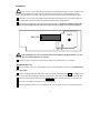
1
ELECRAF T KAF2
A U D I O F I LT E R a n d R E A L - T I M E C L O C K
Assembly and Operating Instructions
Revision A, August 30, 2001. Copyright © 2001, Elecraft; All Rights Reserved
Introduction
The KAF2 option supplements the K2's crystal filters with effective, low-noise audio filtering. It also adds
a real-time clock, allowing you to check the time or date with a tap of the K2's D I S P L A Y button.
Audio Filter
The KAF2 includes a passive, balanced low-pass filter (LPF) that is in-circuit at all times. It provides
significant attenuation of signals above 3 kHz, including hiss, high-pitched splatter, and carrier leakthrough. The LPF is particularly useful on quiet bands, when using headphones, or with small antennas.
Also included is a narrow, active band-pass filter for CW or data use. The center frequency of the filter is
tunable via two potentiometers. The A F I L switch on the K2 front panel selects either O F F (LPF only),
A F 1 (first CW filter stage), or A F 2 (both stages). The operator can choose to treat both CW filter stages as
a single setting (A F 2) by installing jumper W1.
Real-Time Clock
The real-time clock displays 24-hour time, as well as date. You'll find the clock convenient for field
operation since it eliminates the need to bring a separate clock. Time can be easily set using the B A N D +
and B A N D - switches. The on-board lithium backup battery will power the clock for up to several years.
Specifications
Low-pass filter
Band-pass filter
Clock Accuracy
Date Formats
Current Drain
Size
Flatness: better than 1 dB, 0.5 to 2 kHz; Atten.: approx. -20 dB at 4 kHz
Bandwidth: approx. 80 Hz @ -3 dB, 270 Hz @ -20 dB (two stages cascaded)
+/- 20 ppm (+/- 1.7 seconds per day) at 25 degrees C
MM-DD-YY or DD-MM-YY; handles all calendar months and leap years
Approx. 10 mA
1.5" (L) x 1.5" (D) x 0.5" (H) (3.8 x 3.8 x 12 cm)
i
Caution: Some parts in this kit can be damaged by static discharge. Before handling any
transistors or ICs, put on an anti-static wrist strap, or touch a grounded, unpainted metal surface.
Elecraft
•
www.elecraft.com
•
831-662-8345
Parts Inventory
The table below lists all parts in the kit. Refer to the K2 manual parts lists for photographs.
Ref.
BT1
C19
C9, C15, C16
C11, C14
C3, C4, C7, C8
C5, C6
C1, C2
C12, C13, C17, C18
C10
D1, D2
CTRL-J1
CTRL-J2
L1, L2
P1
P2
Q1, Q2, Q3
R11, R12, R15-R17
R3, R7
R13
R14
R9, R10
R4
R5
R6
R8
R1, R2
RP1
S1
U1
U2
U3
U4
W1
X1
Z1
MISC
MISC
MISC
MISC
HDWR
Description
Battery, 3V lithium, 20 mm dia., CR2032 or equivalent
Capacitor, 33 pF ("33" or "330")
Capacitor, 470 pF ("471")
Capacitor, .01 µF ("103"), 0.1" lead spacing
Capacitor, .01 µF ("103"), 0.2" lead spacing
Capacitor, .022 µF ("223")
Capacitor, .068 µF ("683")
Capacitor, 0.22 µF ("224")
Capacitor, electrolytic, 10 µF
Diode, 1N5711
Conn., 5 pin female, 0.1" spcg., gold
Conn., 3 pin female, 0.1" spcg., gold
Inductor, 82 mH, 5%, shielded ("823")
Conn., 5-pin male, 0.1" spcg., gold
Conn., 3-pin male, 0.1" spcg., gold
Transistor, J309 JFET
Resistor, 220 ohms, 1/4 watt, 5% (red-red-brown)
Resistor, 470 ohms, 1/4 watt, 5% (yellow-violet-brown)
Resistor, 910 ohms, 1/4 watt, 5% (white-brown-brown )
Resistor, 2.7 k, 1/4 watt, 5% (red-violet-red)
Resistor, 10 k, 1/4 watt, 5% (brown-black-orange)
Resistor, 47 k, 1/4 watt, 5% (yellow-violet-orange)
Resistor, 100 k, 1/4 watt, 5% (brown-black-yellow)
Resistor, 180 k, 1/4 watt, 5% (brown-gray-yellow)
Resistor, 510 k, 1/4 watt, 5% (green-brown-yellow)
Trimmer potentiometer, 5K ("502")
Resistor network, 3.9 k, 4 resistors, 8 pins
Miniature slide switch, DPDT
IC, quad low-noise op-amp, LM837N
IC, programmed microcontroller, PIC16C621A-04/P
IC, real-time clock, NJU6355ED
IC, voltage regulator, 6V, 2.5%, ZR78L06C
Conn., 2-pin male, 0.1" spacing
Crystal, cylindrical, 32.768 kHz
Ceramic resonator, 4 MHz, 3 pins
Jumper, 2-pin shorting (for W1)
KAF2 PC board
Socket for BT1
IC socket (for U2), 18 pins
Standoff, male-female, 1/2" long x 1/4" dia, 4-40 thd
2
Part No.
E980039
E530064
E530080
E530019
E530009
E530056
E530081
E530079
E530045
E560004
E620051
E620009
E690015
E620052
E620053
E580009
E500002
E500003
E500070
E500005
E500015
E500067
E500006
E500068
E500069
E520009
E510000
E640009
E600037
E610009
E600038
E600017
E620054
E660015
E660001
E620031
E100128
E980040
E620031
E700057
Qty
1
1
3
2
4
2
2
4
1
2
1
1
2
1
1
3
5
2
1
1
2
1
1
1
1
2
1
1
1
1
1
1
1
1
1
1
1
1
1
1
Firmware Requirements
To use the KAF2's real-time clock, you'll need main microcontroller firmware revision 2.01 or later. If you
have an earlier version (1.xx), you should have received an upgrade. You can install the firmware upgrade
during assembly of the KAF2 (as explained later), or you can install it ahead of time.
Note: The main micro is U6 on the K2 Control board. To check your firmware revision, hold any switch
when powering up the K2. When you release the switch, the revision will be shown on the LCD (left side).
Assembly
i
A fine-point, temperature-controlled soldering iron (700-800 degrees F maximum) is
required to assemble the PC boards. A higher-wattage iron or one with a wide tip may damage
components, pads, or traces. We also recommended the use of a Panavise (or equivalent bench vise)
and an illuminated magnifying glass to facilitate PCB and connector assembly.
i
To avoid soldering conflicts, install components only in the order described below. Doublecheck all values before soldering, since removing parts from double-sided PC boards can be difficult.
Locate the KAF2 PC board and identify the top and bottom sides. The side of the board with outlines
of the ICs (U1-U4) and most other components is the top; the side with the "KAF2" label is the bottom. If
an assembly step does not specify top or bottom, the component should be installed on the top side.
On the top side of the board, install the two 1N5711 diodes, D1 and D2. The cathode end of each
diode has a black band which must be aligned with the banded end of its PC board component outline. The
leads of the diodes must be bent very close to the body in order to fit between the two pads.
Make sure D1 and D2 are seated flat against the PC board, then solder and trim the leads.
i
The leads on small capacitors can be fragile. When handling capacitors in the following
steps, do not pull on the leads or bend them excessively.
There are two different types of .01-µF capacitors supplied. Both are labeled ".01" or "103", but they
have different lead spacing. Locate the two .01-µF capacitors with 0.1" (2.5 mm) lead spacing, as well as
the four with 0.2" (5 mm) lead spacing. Separate them into two groups.
Note: For all remaining assembly steps, you should solder and trim component leads after installing each
group of components unless otherwise instructed. Leads can be trimmed before or after soldering, but trim
them as short as possible.
On the top side of the PC board, install the four .01-µF capacitors with 0.2" (5 mm) lead spacing:
__C3, __C4, __C7 and __C8.
3
i
Some components will be installed on the bottom of the board. These components must be
seated down onto the board as far as they'll go. In the case of capacitors with formed leads, there is
no need to re-form the leads. A small amount of lead length can remain exposed.
Install the two .01-µF capacitors with 0.1" (2.5 mm) lead spacing:
__C11 (top side of the board), __C14 (bottom side).
Trim the leads of C14 as short as possible, using flush-cutters if available. If the leads are not kept
very short, they may interfere with installation of U1 on the top side of the board.
Locate the two .022-µF capacitors, labeled "223". Also locate the four 0.22-µF capacitors ("224").
Make sure you can tell the two types apart, and separate them into two groups.
Install the four 0.22-µF capacitors ("224") on the top side of the board:
__C12, __C13, __C17, __C18.
On the bottom side of the board, install the 470-pF capacitors ("471"):
__C9, __C15, __C16.
Trim the leads of C15 and C16 as short as possible, preferably flush with the board.
On the top side, install the .068-µF capacitors ("683"): __C1, __C2.
Install electrolytic capacitor C10 (10 µF). The (+) lead of C10 must be installed in the hole marked
"+". The (+) lead is usually longer than the (-) lead. The (-) lead is identified by a stripe on the body.
Install the following resistors (top side). When installing R9 (10 k), keep the body of the resistor
elevated just slightly above the board so that it doesn’t contact the soldered leads of C16.
__R9, __R10 (10 k, brown-black-orange)
__R15, __R16 (220 ohms, red-red-brown)
__R3 (470 ohms, yellow-violet-brown)
__R5 (100 k, brown-black-yellow)
__R8 (510 k, green-brown-yellow)
Install the following resistors (bottom side). When soldering, be very careful not to touch adjacent
components with the soldering iron.
__R11, __R12, __R17 (220 ohms, red-red-brown)
__R7 (470 ohms, yellow-violet-brown)
__R13 (910 ohms, white-brown-brown)
__R4 (47 k, yellow-violet-orange)
__R6 (180 k, brown-gray-yellow)
__R14 (2.7 k, red-violet-red)
Trim the leads of R14 as short as possible so it won't interfere with the installation of U3.
4
Install trimmers R1 and R2 (5 k) as indicated by their component outlines on the top side of the board.
Install resistor network RP1 (3.9 k, 8 pins). This resistor network is symmetrical and can be installed
in either orientation, but for consistency you should orient it with the pin 1 end (black dot) toward pin 1 of
the PCB outline (round pad, also labeled "1").
Install the miniature slide switch, S1. The switch should be pressed down onto the board as far as it
will go before soldering. Use a minimum amount of heat to avoid melting S1's plastic body.
Set S1 to the OUT position.
Locate the 18-pin IC socket. One end will have a notch or other mark indicating the pin 1 end. Install
this socket at U2, with the pin 1 end of the socket toward the notched end of the IC's PC board outline.
Install the ceramic resonator, Z1. (Z1 looks like a capacitor with three leads.)
i
Before handling ICs and transistors, touch an unpainted, grounded metal surface.
Install transistors Q1, Q2, and Q3 (J309) as indicated by their outlines. The installed height of the
transistors should be no more than 3/8" (9 mm). Use a minimum of soldering time (1-2 seconds per lead).
Voltage regulator U4 (ZR78L06C) has a 3-pin TO-92 package, like a transistor. Install U4 in the same
manner as Q1-Q3.
Install the quad op-amp IC, U1 (LM837N). Orient the notched or dotted end of U1 toward the notched
end of its PC board outline (pin 1 end, to the left). Double-check the orientation before soldering.
The real-time clock IC, U3 (NJU6355ED), must be handled carefully. Be sure to touch a grounded
surface before and during its installation. Install U3, noting the orientation of the notched end as you did
with U1. Verify the orientation before soldering.
Install C5 and C6 (.022 µF, "223"). C6 may be a tight fit due to its proximity to U1. Adjust C6's
position slightly if necessary, but be careful not to stress the leads.
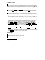
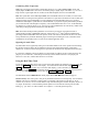
Install the 2-pin male connector on the top side of the board at W1 as shown below. The short ends of
the pins are inserted into the board, and the long ends face up. Do not solder yet.
W1
P1
P2
5
Make sure that the 2-pin male connector is flat against the PC board, then solder.
Install the 5-pin and 3-pin male connectors on the bottom side of the board at P1 and P2. The short
ends of the pins are inserted into the PC board from the bottom (see drawing, page 5). Do not solder yet.
Solder just one pin each of P1 and P2. If the connectors do not appear to be seated flat against the PC
board, or they are tilted, re-heat the pins and adjust the connectors as needed. Once the connectors are
correctly installed, solder all remaining pins.
Install the two shielded inductors (L1 and L2) as indicated by their component outlines. Make sure the
inductors are pressed down onto the PC board as far as they can go, then bend the leads slightly to hold
them into position while soldering. Trim the leads as close to the board as possible.
Install the battery socket, straightening the leads if necessary. The battery itself will be installed
later. If it is installed in the socket at this time, remove it.
Install cylindrical crystal X1 vertically between U3 and BT1. The exposed lead length should be 0.1"
(2.5 mm) or less. Be careful with the crystal's leads, which are very thin and may break if stressed.
The KAF2 date display format is normally MM-DD-YY. If you prefer DD-MM-YY, solder a short
wire jumper at W2. The pads for W2 are located on the bottom of the board, near pin 10 of U2.
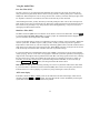
Capacitor C19 (33 pF) must be soldered onto two pads of U3, on the bottom side of the PC board (see
below). Pin 1 is identified in the illustration (round pad). C19 should be soldered to pins 2 and 4. Make sure
that the body of C19 is not touching any adjacent pads.
R14
U3-1
C19
i
Before handling U2, touch an unpainted, grounded metal surface.
Carefully straighten the pins on the microcontroller, U2 (PIC16C621A). The two rows of pins must be
parallel to each other, with no pins bent.
Press the microcontroller into its socket, orienting the notched or dimpled end of the IC with the
notched end of its component outline. The labeling on the microcontroller should read from left to right,
like the other ICs on the board.
6
Control Board Preparation
If the firmware on the Control board must be upgraded, do so now. Follow all instructions supplied
with the upgrade, but leave the cover off when finished. Make sure the firmware installation is complete
and that the K2 is working correctly before continuing.
Turn off the K2. If the internal battery (KBT2) is installed, put its switch in the OFF position.
Remove the K2's top cover (six screws). Disconnect cables for the options, speaker, and freq. counter.
Remove the two screws that hold the Control board to the Front Panel board. Extract the Control
board using the long-handled Allen wrench as explained on page 40 of the K2 Owner's Manual (fig. 6-11).
Place the Control board on a clean work surface, with the top side up (the side with most parts).
Check the revision of your Control board, which appears at the bottom right. If your Control board is
revision A (or earlier, i.e. XA, XB, XC), you'll find that the component outlines for the KAF2 connectors
(J1 and J2), as well as the audio filter module itself, appear on the bottom side of the board. DO NOT
install J1 and J2 on the bottom side of the Control board. The KAF2 module and associated
connectors will be installed on the top side.
i
When removing R18 and R19 from the Control board in the following steps, be very careful not to
damage the pads or traces. You can use solder wick or a vacuum desoldering tool. Another method is to
clip the leads of the resistors right at the body, then remove the leads one at a time. Use long-nose pliers to
hold the lead, then heat the joint until the lead slides out with very little pulling force. If R18 and R19 are
jumpers rather than resistors, removal will be easier, but it must still be done carefully.
Locate R18 and R19 (resistors or jumper), located near the right end of the 36-pin connector, P2.
De-solder and remove them from the Control board. Observe the precautions above.
Use solder wick or a vacuum desoldering tool to remove residual solder from the resistor holes. Do
not overheat the pads. The holes must be completely clean to allow installation of the KAF2 connectors.
Install the 5-pin and 3-pin female connectors, J1 and J2, on the top side of the Control board. (As
mentioned above, if you have an older Control board, the outlines are on the bottom. You'll still use the
same holes.) Solder just one pin of each connector.
If either J1 or J2 is not seated flat against the board, reheat the appropriate pin and adjust the connector
as needed. Once both connectors are straight and seated correctly, solder all remaining pins.
There are several electrolytic capacitors on the top side of the Control board in the area where the
KAF2 will be installed. (See illustration on next page.) Straighten C28, C29, C32, and C33 to avoid
possible interference with the KAF2. Make sure that all other components in this general area have short
leads and are seated correctly.
Plug the Control board into the RF board. Make sure that all three connectors on the Control board are
properly mated with their respective RF board connectors.
7
Installation
i
Two screws are used to hold the Control board to the Front Panel board. The screw on the left end
(as viewed from the K2 front panel) will be replaced with the male-female standoff supplied with the
KAF2. Once the KAF2 is in position, the original screw and lock washer will be used to hold it in place.
Thread the 1/2" (12 mm) male-female standoff through the mounting hole in the control board (near
C29) and into the front panel standoff. The standoff should be firmly hand-tightened.
Plug the KAF2 module into the Control board as shown below. All pins of P1 and P2 on the KAF2
must be correctly mated with J1 and J2 on the Control board, or either board could be damaged.
KAF2
MCU (U6 )
J1 J2
i
If the standoff does not line up with the hole near the middle of the KAF2 module, you may
have the pins of J1 and J2 shifted by one position.
Use the original Control board screw and lock washer to secure the KAF2 to its standoff.
Alignment and Test
Turn on the K2. If you see or smell smoke, turn the rig off immediately and refer to Troubleshooting.
Low-Pass Filter
Switch to LSB or USB mode and select a wide crystal filter bandwidth using X F I L . Use O P 1 (option
filter 1) if you have the SSB adapter installed; otherwise use a wide setting of the variable-bandwidth filter.
Turn the preamp and attenuator off using P R E / A T T N. (Make sure the annunciators are turned off.)
Disconnect the antenna, and plug in a pair of headphones.
Set RF GAIN fully clockwise. Set AF GAIN so that you can clearly hear receiver background noise.
8
Move S1 on the KAF2 module to the IN position, which puts the KAF2's low-pass filter in-circuit.
You should hear a significant reduction in noise (hiss). If not, see Troubleshooting.
Connect an antenna and tune in an SSB or AM broadcast station. Again test the OUT and IN positions
of S1. Switching the KAF2 IN should not affect the intelligibility of voice-band signals, but it will result in
a slightly "warmer" tone due to the low-pass filter1.
Band-Pass Filter
The band-pass filter will be aligned to match your CW sidetone pitch. The cover of the K2 must be off
to make this adjustment, so be sure you've selected your preferred sidetone pitch (S T P menu entry).
Switch to 40 meters. With the K2 still set for a wide bandwidth, locate the K2's weak "birdie" at 7000
kHz. You may need to turn on the preamp and disconnect the antenna. You can also use an on-air signal.
Tune the VFO until the pitch of the weak RF signal matches your CW sidetone pitch. To do this by
ear: (1) hold S P O T; (2) adjust the AF GAIN control until both the sidetone and RF signal are at about the
same strength; (3) move the VFO slowly until the RF signal seems to "disappear"; (4) cancel the K2's spot
signal by tapping any switch. Alternatively, you can use an audio spectral-analysis program to do pitch
matching and filter alignment2.
Make sure S1 on the KAF2 is in the IN position, enabling all audio filter circuits. (Also make sure that
jumper W1 is not installed.) Then hold the K2's A F I L switch. You should see A F 1 on the display,
indicating that the first band-pass filter section has been enabled. The receiver sound should change due to
the narrower bandwidth. The signal may decrease in amplitude.
Using a small screwdriver, adjust R1 on the KAF2 (the pot closest to the RF board) for maximum
signal strength. The peak will be broad. Hold A F I L again to enable the second band-pass filter section; you
should see A F 2 on the display. Adjust R2 for maximum signal strength; then re-peak R1. Hold A F I L
again to return the KAF2 to O F F.
Repeat the two band-pass filter adjustments if necessary. When the filter sections are properly
adjusted, the RF signal should be clear, distinct, and slightly louder when A F 2 is selected.
A 2-pin shorting jumper is supplied for optional use at W1. When the jumper is installed, audio filter
mode A F 1 will be skipped. If you prefer to keep the A F 1 setting, you can still store the jumper on W1 by
attaching it to just one of W1's two pins.
Connect the frequency counter cable from P6 on the Control board to TP2 (BFO) on the RF board.
We recommend that you adjust all CW filter BFO settings so that their center pitch matches your
sidetone pitch. Since the audio filter was also matched to the sidetone pitch, this will ensure that the KAF2
works well in combination with narrow crystal filter settings. Refer to the K2 Owner's Manual for details
on BFO and filter setup (C A L F I L). Again, this can be done by ear or with the aid of a computer program.
1
2
The roll-off point of the low-pass filter can be altered if desired; see Using the Audio Filter.
See http://www.elecraft.com/Apps/new_fil_docs/filter_apps.htm for further information.
9
3-Volt Battery Installation
Turn the K2 off. Remove the top cover or left side panel to gain access to the KAF2.
The (+) side of the 3-volt battery must be oriented toward the "+" symbol on the KAF2 board. The (-)
side must face the left side panel of the K2. Insert the battery in its socket, under the spring clip. DO NOT
use long-nose pliers to hold the battery--this will short the + and - sides of the battery together.
Setting the Date and Time
Turn the K2 on. Tap M E N U, then tap D I S P L A Y to switch to the secondary menu, and locate the
R T C menu entry. E D I T the parameter and change it to O N using B A N D + or B A N D -. (This enables the
clock feature.) Tap M E N U twice to return to the frequency display.
To set the real-time clock you must set the date first, then the time, as described below. (The KAF2
firmware enforces this sequence to help prevent accidental time changes. If you attempt to set the time first,
or if you switch between time and date display more than once, any changes will be disabled.)
1.
2.
3.
4.
5.
6.
7.
Turn the K2 off, wait a few seconds, then turn it back on. If you plan to use WWV or some other onair time announcement, tune it in now. If you're setting the clock to UTC, don't forget to use the UTC
date if it's different from the local date.
Tap D I S P L A Y. After about 1 second, you should see a time display (H H . M M . S S). The time may
not be changing at this point, and may be set to 0 1 . 0 1 . 0 1 or to a random time. Note: The receiver is
not muted when time is displayed, so you may hear microcontroller-generated noise. If the noise is
objectionable, turn down the AF gain when leaving the clock displayed for long periods of time.
Hold B A N D + and B A N D - together to switch to date display (M M - D D - Y Y or D D - M M - Y Y3).
Tapping B A N D + or B A N D - will now change the day, and holding B A N D + or B A N D - will
change the month. To change the year: If the month is set to 1 2, each subsequent hold of B A N D +
will increment the year. If the month is set to 1 , each subsequent hold of B A N D - will decrement the
year. Once the desired year is selected, you can set the month by moving it back in the other direction.
With the date now set, hold B A N D + and B A N D - together to switch back to time display.
Tapping B A N D + or B A N D - will now change the minute, and holding B A N D + or B A N D - will
change the hour. Every change resets seconds to 0 0, so you can sync to a time reference if desired.
To disable further changes, switch to date display, then back to time display. Then move the VFO knob
or tap D I S P L A Y twice to return to the normal frequency display.
Final Assembly
Turn off the K2. Re-connect the speaker cable and any option cables.
Replace the K2 top cover and secure it with six screws.
Set the internal battery switch to ON if applicable.
3
Jumper W2 must be installed to select D D - M M - Y Y date format; see page 6.
10
Using the Audio Filter
Low-Pass Filter (LPF)
The LPF is always on, providing high-pitch QRM and noise reduction in all modes. This effect will be
most pronounced on quiet bands, with low-noise receiving antennas, with the preamp off, or when using
headphones. When atmospheric noise is strong, the K2's AGC is heavily activated, reducing the gain of the
I.F. amplifier. Under these circumstances, the effect of the LPF may be less noticeable.
After installing the KAF2, you may find that you need the preamp less often. This is due to the improved
audio signal-to-noise ratio provided by the LPF. Having the preamp turned off is most beneficial when the
K2 is used in close proximity to very strong stations, such as during Field Day, or if you live in an area
with high-power HF broadcast stations.
Band-Pass Filter (BPF)
The BPF is useful for QRM and noise reduction in CW mode as well as some data modes. Just hold A F I L
to select the BPF mode (O F F, A F 1, A F 2). If you have jumper W1 installed, A F 1 will be skipped. When
you turn on the K2, the band-pass filter will be O F F.
You can use the BPF either by itself or in combination with narrow settings of the crystal filter. When used
with the crystal filter, the BPF's response (-3dB @ 80 Hz, -20 dB @ 270 Hz) will provide a significant
improvement in skirt selectivity. This can really help with DXing, QRP contests, and other situations where
much of the activity takes place right at the noise floor. When A F 2 is selected, overall gain will be around
2 dB, which helps overcome the loss of the K2's narrowest crystal filter settings.
If you use the BPF with a wideband filter setting (such as O P 1), you'll need to be aware of the possibility
of AGC pumping. This can occur when a strong signal is within the crystal filter passband, even though you
might not hear it through the narrow passband of the audio BPF. The strong signal activates AGC, reducing
the gain of the receiver, which in turn makes the weak signal you're listening to decrease in volume. To
avoid this, you can either use the narrow crystal filter along with the audio BPF, or turn AGC OFF (by
holding P R E / A T T N and A G C together) and using the manual RF GAIN control.
Data Modes: The BPF has one interesting advantage over narrow crystal filters when used in data modes.
If you use the BPF in combination with the wide filter (O P 1), there will be zero frequency shift between
transmit and receive. If AGC pumping is a problem, try using manual gain control (see above).
AFIL status display
If the BPF is turned on (A F 1 or A F 2), you'll see this reflected in the filter status display. Filter status is
checked by holding A G C and X F I L together. The audio filter mode is shown immediately following the
crystal filter selection (e.g., F L 2 0 . 7 0 followed by A F 2).
11
Customizing Filter Components
Gain: The overall gain of the KAF2 is intentionally kept low: 0 to 1 dB in O F F and A F 1 modes, and
slightly higher in A F 2 mode. Gain can be increased by using a slightly larger value at R9, e.g., 12-15 k. A
large increase in gain might result in overdrive of the audio amplifier, and is not recommended.
LPF: The crystal filter on the SSB adapter (O P 1) has a bandwidth of about 2.0-2.2 kHz, so it will be the
dominant factor in setting the K2's passband. The KAF2's low-pass filter roll-off starts around 2.5 kHz, and
should not reduce speech intelligibility or cause problems with wide-band data. However, if you have
modified the SSB adapter crystal filter for wider bandwidth, or just prefer a higher-pitched audio passband,
you can shift the LPF roll-off higher in frequency. The recommended values are: L1-L2, 56 mH shielded,
5% (Mouser cat. # 434-02-563J); C1-C2, .047 µF (5%). The modified filter will roll off only 1 dB at 3 kHz,
while still providing significant attenuation of wide-band hiss.
BPF: The KAF2's band-pass filter parameters were chosen to provide low ringing but still offer a
significant improvement in QRM/QRN reduction. Each section is a 2nd-order, multiple-feedback filter,
providing constant bandwidth as the center pitch is varied. (This filter is described in the Electronic Filter
Design Handbook, by Arthur B. Williams, pages 5-42 through 5-44 and figure 5-25b.) Alternative filter
configurations are possible; refer to our web site for related application notes.
Bypassing the Audio Filter
The audio filter can be bypassed by setting S1 on the KAF2 module to the "OUT" position. In this setting
the real-time clock will still work (if enabled), but the low-pass and band-pass filters will be totally
disabled. S1 can also be used for testing the low-pass filter as described in the Alignment and Test section.
If you need to completely remove the KAF2, you must install two jumpers on the Control board. For this
purpose you can insert bare, solid hookup wire directly into the female connectors. One jumper goes
between J1-1 and J2-1, and the other between J1-2 and J2-2.
Using the Real-Time Clock
To use the clock, you'll first need to turn it on and set the date and time as explained on page 10. After that,
simply tap D I S P L A Y to show the clock display. To switch between time and date, hold B A N D + and
B A N D - together. There are four ways to clear the clock display: (1) move the VFO; (2) key the
transceiver; (3) tap D I S P L A Y twice (the first tap shows the voltage/current display, the second returns to
the frequency display); (4) tap any switch other than D I S P L A Y, B A N D +, or B A N D -.
The default date format is M M - D D - Y Y. Install jumper W2 for D D - M M - Y Y format (see page 6).
Clock Accuracy: The clock's gain or loss per day should be better than 2 seconds per day. You can select a
different value of C19, if desired, to improve this. For example, if the clock runs a bit fast, try 39 pF.
Another way to choose C19 is to tack in different caps while measuring the oscillator frequency at pin 2 of
U3 (target: 32768.0 Hz). Use the smallest possible capacitor in series with the counter probe to reduce
loading, e.g. 1 pF. Note: A 0.5-Hz oscillator error equates to 1.3 seconds gain/loss per day.
12
Troubleshooting
If your symptoms are not covered below, check the orientation of all components, connectors, and wiring;
look for cold solder joints; and check all DC voltages (see DC Voltage Chart).
Band-pass filter passband not adjustable, or low-pass filter doesn't roll off high-pitch noise: If there's
a problem with the audio filter, verify that U1 (LM837) is not installed backwards. Also check all
components in the low-pass and band-pass filter sections. Check continuity of L1 and L2.
Clock time doesn't increment: This probably indicates that U3 is installed backwards or is defective, or
that the 32.768-kHz oscillator is not running. Check X1 and C19.
Clock doesn't keep time with K2 power turned off: Make sure the battery is installed correctly. (Nothing
will be damaged if the battery is installed backwards, thanks to diode D2.) If you suspect the battery is bad,
measure it with a voltmeter, and replace it if it reads under about 2.5 volts.
Receiver noise heard when in time or date display mode: This is normal. The main microcontroller polls
the KAF2 for time or date information once per second, waking up all option module processors, which
generates noise that is audible at some frequencies. The K2 does not mute the receiver when date or time is
being displayed, because the operator may want to use WWV or some other on-air time source for clock
setting. If you wish to leave the clock display on for long periods of time, simply turn down the receiver's
volume control or use the squelch menu entry (S L C H, in the secondary menu).
Error messages: If you see N O T I N S T or a similar message when you hold A F I L or tap D I S P L A Y, the
KAF2's microcontroller (U2) may not functioning. Make sure it isn't installed backwards. Also check for
bent pins, check voltages on all pins, etc. Try turning power off and back on.
DC Voltage Chart
Voltages are approximate. Measurements were made under the following conditions: 13.8 V power supply,
K2 turned on, 3 V battery installed, O F F audio filter mode in effect, jumpers W1 and W2 removed, and S1
set to IN.
Pin
V
Pin
V
Pin
V
Pin
V
Pin
V
Pin
V
Pin
V
U1-1
2
3
4
5
6
7
6.0
6.0
6.0
~12
6.0
6.0
6.0
U1-8
9
10
11
12
13
14
6.0
6.0
6.0
0
6.0
6.0
6.0
U2-1
2
3
4
5
6
7
8
9
0
6.0
0
6.0
0
6.0
6.0
0
0
U1-10
11
12
13
14
15
16
17
18
6.0
6.0
6.0
5.5
6.0
~3
~3
0
0
U3-1
2
3
4
5
6
7
8
6.0
~3
~3
0
0
0
0
5.1
Q1-G
S
D
Q2-G
S
D
Q3-G
S
D
6.0
6.0
6.0
0
6.0
6.0
0
6.0
6.0
D1-A
D1-C
D2-A
D2-C
5.5
5.1
3.0
5.1
U4-I
U4-G
U4-O
13.8
0
6.0
13
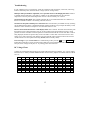
Circuit Details
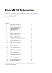
Refer to the schematic diagram, page 16.
The filter circuits of the KAF2 are inserted between the receiver's product detector and AF amp stages. This
is a fairly low-level point in the receive chain, so to maximize signal-to-noise ratio, a very low-noise opamp is required (U1, LM837).
U1 has four sections. The first section (U1A) converts the K2's balanced audio path to single-ended to drive
the active band-pass filter. The second and third sections (U1B-C) are 2nd-order, multiple-feedback bandpass filters, which provide approximately constant bandwidth over a center pitch range of 400-800 Hz. The
5% components used in the two stages, in combination with the two center-frequency setting trimmers,
result in gain and bandwidth repeatability on the order of +/- 1 dB. The fourth section of U1 (U1D) inverts
the audio waveform so that both 0-degree and 180-degree signals will be available to drive the balanced
low-pass filter. This preserves balance and common-mode noise rejection when the signal is routed back to
the K2's audio amplifier, which has a differential input.
A passive, elliptic low-pass filter is used at the output of the KAF2, providing rolloff of high-pitch signals
and noise. Shielded inductors and a balanced filter topology are used to prevent noise and hum pickup. The
passive filter contributes no noise of its own and is located after all active filter stages, so it completely
removes even the very small amount of noise generated by the LM837 op-amp.
JFET transistors Q1-Q3 are used as low-noise, low-loss series switching elements for audio signal routing.
For example, in the OFF mode (LPF only), Q1 is turned on (low resistance from source to drain) and Q2-3
are turned off (very high resistance). To turn a JFET on, its gate is set to 6 volts, matching the resting bias
voltage on the source and drain. To turn a JFET off, its gate is set to 0 volts.
U3, the real-time-clock, runs from a 32768.00 Hz crystal. This frequency is divided down to 1 Hz and used
to drive a series of counters whose outputs serve as the time and date registers. D1 and D2 route either 5 V
or 3 V to U3, depending on whether the K2 is turned on. U3 draws on the order of only 4 microamps in
standby mode. Since battery BT1 is rated at 220 mAHr, it should last an estimated 5 years or more.
Microcontroller U2 handles auxBus requests from the main microcontroller (U6 on the Control board),
signal routing, and real-time-clock reading/setting/data formatting. It is normally in sleep mode with its
oscillator disabled, and only wakes up when responding to auxBus messages.
14
(This page intentionally left blank)
15
R17
6V Reg.
U4
Z1
4 MHz
BT1
3V
-
Note 2
10µF
12V
1N5711
C11
.01
W2
C10
IN
D2
+
OUT
GND
+
GND
1N5711
R14
2.7K
IN
OUT
220
78L06
78L06
D1
5.5V
W1
6
5
CE
7
8
VDD
CLK
GND
U3
4
/XT
3
XT
2
1
I/O
RB3
9
8
RB2
NJU6355ED
RB1
7
6
RB0
VSS
5
DATA
11
12
13
14
10
RB4
RB5
RB6
RB7
15
16
RA4
4
RA2
RA3
3
220
C9
2
1
J309
MCLR
16C621A
U2
R16
AUXBUS
VDD
0.22
OSC2
RA1
C17
OSC1
18
220
C
RA0
12A
1N5711
A
17
R15
470
D
S
Controller
G
6V
S1
Filter Bypass
C19
33 pF
G
Q1
Q3
5
4
1
2
3
Q2
D
S
D
S
Real-Time Clock
D
LPF1
Low-Pass Filter
IN
OUT
C3
.01
LPF2
LPF1
4
3
12
+
3
2
2
R10
13
14
-
L1
82 mH
1
C1
.068
1
R9
10K
5%
R11
220
U1D
5
6V
P2
To Ctrl Board, J2
P1
To Ctrl Board, J1
X1
32.768 kHz
G
J309
S
6
G
5%
10K
C16
C4
220
LPF2
5%
8
AF2
RP1
AF1
7
3.9K
RP1
1
12A
U1A
3
C14
+
.01
-
C12
3
0.22
RP1
3.9K
U1: LM837N
2
4
C6 .022, 5%
C8
.01, 5%
OFF
2
3.9K
0.22
R13
910
.01
6V
C13
5%
82 mH
R12
470
C2
.068
L2
6
RP1
C15
4
1
R4
47K
C5
.022, 5%
11
5
R1
5K
5
3.9K
470
6
AF1
SET
R3
470
R5
R8
100K
510K
R6
180K
+
C7
.01, 5%
9
7
10
U1B
+
R2
8
U1C
5K
R7
AF2
SET
470
6V
Band-Pass Filter
NOTES:
C18
0.22
= On bottom of PC board.
1. R18 and R19 on the Control board (which may be jumpers)
must be removed when the KAF2 is installed.
2. Install W1 to skip the first-stage band-pass filter output (AF1).
Install W2 to select DD-MM-YY date format.
Elecraft
KAF2 Audio Filter/RTC
By W. Burdick
Rev.
E. Swartz
16
A
Date
8-16-01
Sht.
1 of 1