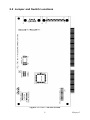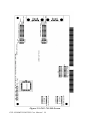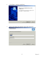
1
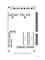
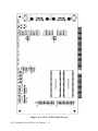
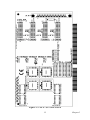
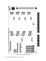
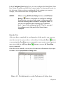
PCL Communication
Industrial Serial Communication
Cards with ISA Interface
PCL-740A
PCL-741A
PCL-743B
PCL-743S
PCL-745B
PCL-745S
PCL-746+
PCL-846A
PCL-846B
PCL-849A
PCL-849B
PCL-849+
PCL-849L
PCL-858A
PCL-858B
User Manual
Copyright
The documentation and the software included with this product are copyrighted 2005 by Advantech Co., Ltd. All rights are reserved. Advantech
Co., Ltd. reserves the right to make improvements in the products
described in this manual at any time without notice. No part of this manual may be reproduced, copied, translated or transmitted in any form or
by any means without the prior written permission of Advantech Co., Ltd.
Information provided in this manual is intended to be accurate and reliable. However, Advantech Co., Ltd. assumes no responsibility for its use,
nor for any infringements of the rights of third parties, which may result
from its use.
Acknowledgements
Award is a trademark of Award Software International, Inc.
VIA is a trademark of VIA Technologies, Inc.
IBM, PC/AT, PS/2 and VGA are trademarks of International Business
Machines Corporation.
Intel and Pentium are trademarks of Intel Corporation.
Microsoft Windows® is a registered trademark of Microsoft Corp.
RTL is a trademark of Realtek Semi-Conductor Co., Ltd.
ESS is a trademark of ESS Technology, Inc.
UMC is a trademark of United Microelectronics Corporation.
SMI is a trademark of Silicon Motion, Inc.
Creative is a trademark of Creative Technology LTD.
All other product names or trademarks are properties of their respective
owners.
Part No. 2003543510
1st Edition
Printed in Taiwan
February 2005
PCL COMMUNICATION User Manual
ii
Product Warranty (2 years)
Advantech warrants to you, the original purchaser, that each of its products will be free from defects in materials and workmanship for two years
from the date of purchase.
This warranty does not apply to any products which have been repaired or
altered by persons other than repair personnel authorized by Advantech,
or which have been subject to misuse, abuse, accident or improper installation. Advantech assumes no liability under the terms of this warranty as
a consequence of such events.
Because of Advantech’s high quality-control standards and rigorous testing, most of our customers never need to use our repair service. If an
Advantech product is defective, it will be repaired or replaced at no
charge during the warranty period. For out-of-warranty repairs, you will
be billed according to the cost of replacement materials, service time and
freight. Please consult your dealer for more details.
If you think you have a defective product, follow these steps:
1.
Collect all the information about the problem encountered. (For
example, CPU speed, Advantech products used, other hardware
and software used, etc.) Note anything abnormal and list any
onscreen messages you get when the problem occurs.
2.
Call your dealer and describe the problem. Please have your manual, product, and any helpful information readily available.
3.
If your product is diagnosed as defective, obtain an RMA (return
merchandize authorization) number from your dealer. This allows
us to process your return more quickly.
4.
Carefully pack the defective product, a fully-completed Repair and
Replacement Order Card and a photocopy proof of purchase date
(such as your sales receipt) in a shippable container. A product
returned without proof of the purchase date is not eligible for warranty service.
5.
Write the RMA number visibly on the outside of the package and
ship it prepaid to your dealer.
iii
CE
This product has passed the CE test for environmental specifications
when shielded cables are used for external wiring. We recommend the use
of shielded cables. This kind of cable is available from Advantech. Please
contact your local supplier for ordering information.
FCC Class A
This equipment has been tested and found to comply with the limits for a
Class A digital device, pursuant to Part 15 of the FCC Rules. These limits
are designed to provide reasonable protection against harmful interference when the equipment is operated in a commercial environment. This
equipment generates, uses and can radiate radio frequency energy and, if
not installed and used in accordance with the instruction manual, may
cause harmful interference to radio communications. Operation of this
equipment in a residential area is likely to cause harmful interference in
which case the user will be required to correct the interference at his own
expense.
Technical Support and Assistance
Step 1. Visit the Advantech web site at www.advantech.com/support
where you can find the latest information about the product.
Step 2. Contact your distributor, sales representative, or Advantech's customer service center for technical support if you need additional
assistance. Please have the following information ready before
you call:
- Product name and serial number
- Description of your peripheral attachments
- Description of your software (operating system, version, application software, etc.)
- A complete description of the problem
- The exact wording of any error messages
PCL COMMUNICATION User Manual
iv
Packing List
Before setting up the system, check that the items listed below are
included and in good condition. If any item does not accord with the
table, please contact your dealer immediately.
• PCL communication interface card
• Industrial communication driver, utility and user manual in ICOM CDROM
Safety Precaution - Static Electricity
Follow these simple precautions to protect yourself from harm and the
products from damage.
1.
To avoid electrical shock, always disconnect the power from your
PC chassis before you work on it. Don't touch any components on
the CPU card or other cards while the PC is on.
2.
Disconnect power before making any configuration changes. The
sudden rush of power as you connect a jumper or install a card may
damage sensitive electronic components.
v
PCL COMMUNICATION User Manual
vi
Contents
Chapter
1 Introduction ..................................................... 2
1.1
1.2
1.3
1.4
Chapter
Description ........................................................................ 2
Features ............................................................................. 2
Specifications .................................................................... 3
Ordering Information ........................................................ 5
1.4.1
1.4.2
PCL Communication Cards ........................................... 5
Accessories .................................................................... 6
Table 1.1:ISA Communication Cards Selection Guide . 6
2 Hardware Configuration ................................ 8
2.1
2.2
2.3
Initial Inspection................................................................ 8
Jumper and Switch Locations ........................................... 9
Figure 2.1:PCL-740 Silk Screen .................................... 9
Figure 2.2:PCL-741 Silk Screen .................................. 10
Figure 2.3:PCL-743B/S Silk Screen ............................ 11
Figure 2.4:PCL-745B/S Silk Screen ............................ 12
Figure 2.5:PCL-746+ Silk Screen ................................ 13
Figure 2.6:PCL-846A/B Silk ....................................... 14
Figure 2.7:PCL-849A/B/+/L Silk Screen .................... 15
Figure 2.8:PCL-858A/B Silk Screen ........................... 16
Jumper Settings ............................................................... 17
2.3.1
2.3.2
2.3.3
2.3.4
2.3.5
How to Set Jumpers ..................................................... 17
Figure 2.9:Jumper Setting ............................................ 17
Card Configuration ...................................................... 17
Default Setting ............................................................. 18
Table 2.1:Default setting of ISA Comm. Cards ........... 18
Mode Selection ............................................................ 18
Figure 2.10:Mode Selections for PCL-740 .................. 18
Figure 2.11:Mode Selections for PCL-741 .................. 19
Figure 2.12:Active & Passive Setting for C. Loop ...... 19
Figure 2.13:Current Loop Link .................................... 20
Figure 2.14:RS-422/485 Mode Selection for PCL-743B/
S, PCL-745B/S and PCL-846A/B ................... 20
Figure 2.15:Enable Mode Selection for PCL-743B/S,
PCL-745B/S and PCL-846A/B ....................... 21
Figure 2.16:RS-232/422/485 Mode sel. for PCL-746+ 21
Figure 2.17:Mode selection for PCL-746+ .................. 22
I/O Address and Interrupt Setup .................................. 22
Figure 2.18:Standard or Enhanced Mode selection for
PCL-746+ ........................................................ 22
Figure 2.19:Standard or Enhanced Mode selection for
PCL-846A/B .................................................... 23
vii
2.3.6
2.3.7
2.3.8
Chapter
3 Software Installation ..................................... 32
3.1
Operating Environment Selection ................................... 32
3.2
Driver Setup .................................................................... 32
3.3
3.4
Chapter
Figure 2.20:Standard or Enhanced Mode selection for
PCL-849A/B/+ ................................................. 23
Figure 2.21:Port Base Address Setting ........................ 24
Figure 2.22:Setting to 2F8 ........................................... 25
Figure 2.23:Shared or Independent IRQ selection for
PCL-746+ ........................................................ 26
Figure 2.24:Shared or Independent IRQ selection for S2
of PCL-746+ and S1 of PCL-849A/B/+ .......... 26
Figure 2.25:IRQ Selection ........................................... 27
Interrupt Status Register Setup (SW2 or S5) ............... 27
Interrupt Status Register .............................................. 28
Figure 2.26:Vector Address Setting ............................. 28
Figure 2.27:Vector Address Setting ............................. 28
Speed Mode selection .................................................. 29
Figure 3.1:OS Jumper Selection .................................. 32
3.2.1
Steps for Windows 98/2000/XP Driver Setup ............. 32
Configuring ISA ICOM Serial Devices .......................... 39
Driver Uninstallation....................................................... 42
4 ICOM Tools ................................................... 46
4.1
4.2
4.3
4.4
Introduction .................................................................... 46
Installation....................................................................... 46
User Interface of ICOM Tools ........................................ 47
4.3.1
4.3.2
4.3.3
4.3.4
4.3.5
4.3.6
4.3.7
4.3.8
Menu Bar ..................................................................... 47
Tool Bar ....................................................................... 48
Com Port Tab ............................................................... 49
Port Status .................................................................... 50
Message Logo .............................................................. 50
Tx Slide Bar ................................................................. 51
Performance Listing Area ............................................ 51
Status Bar ..................................................................... 51
Using the ICOM Tools Utility ........................................ 52
4.4.1
4.4.2
4.4.3
4.4.4
Port Selection ............................................................... 52
Figure 4.1:ICOM Tools program window ................... 52
Figure 4.2:Select Port dialog box ................................ 53
Figure 4.3:Ports You Select Will Appear in the Selected
Port Checkbox Group ...................................... 53
Figure 4.4:ICOM Tools User Interface ........................ 54
Configuring a Port ....................................................... 54
Figure 4.5:Test Information on the Performance Listing
Area .................................................................. 55
Close Port ..................................................................... 56
Exit the ICOM Tools utility ......................................... 56
PCL COMMUNICATION User Manual viii
4.5
Chapter
Messages on Status Bar and Message Logo Area........... 57
4.5.1
4.5.2
Status Bar Messages .................................................... 57
Message Logo Messages ............................................. 58
5 Pin Assignments and Wiring........................ 60
5.1
Pin Assignments.............................................................. 60
5.1.1
5.1.2
5.1.3
5.1.4
5.2
Wiring.............................................................................. 67
5.2.1
5.2.2
5.2.3
5.3
PCL-740 and PCL-741 ................................................ 60
Figure 5.1:PCL-740 Pin Assignments ......................... 60
Figure 5.2:PCL-741 Pin Assignments ......................... 60
PCL-743B/S, PCL-745B/S, and PCL-846A/B ............ 61
Table 5.1:PCL-743B/S, PCL-745B/S Pin Description
(DB-9 male) ..................................................... 61
PCL-746+ and PCL-849A/B/+/L ................................ 61
Figure 5.3:PCL-746+, PCL849A/B/+/L RS-232 DB-37
Pin Assignments .............................................. 61
Figure 5.4:PCL-746+, PCL849A/B/+/L RS-232 DB-25
Pin Assignments .............................................. 62
Figure 5.5:PCL-746+, PCL849A/B/+/L RS-232 DB-9
Pin Assignments .............................................. 62
Figure 5.6:PCL-746+ RS-422/RS-485 DB-37 Pin Assignments ......................................................... 63
Figure 5.7:PCL-746+ RS-422 DB-25 Pin Assig. ........ 63
Figure 5.8:PCL-746+ RS-422 DB-9 Pin Assig. .......... 64
Figure 5.9:PCL-746+ RS-485 DB-25 Pin Assig. ........ 64
Figure 5.10:PCL-746+ RS-485 DB-9 Pin Assig. ........ 64
PCL-858A/B ................................................................ 65
Figure 5.11:PCL-858A/B RS-232 DB-62 Pin Assig. .. 65
Figure 5.12:PCL-858A/B with OPT8A+ RS-232 DB-25
Pin Assignments .............................................. 66
Figure 5.13:PCL-858A/B with OPT8B+/C RS-232 DB25 Pin Assignments ......................................... 66
Figure 5.14:PCL-858A/B with OPT8H RS-232 DB-9 Pin
Assignments ..................................................... 66
RS-232 Signal Wiring .................................................. 67
Table 5.2:Terminal or PC (DTE) connections ............. 67
Table 5.3:Modem Connections .................................... 68
Table 5.4:Terminal without Handshake ....................... 68
RS-422 Signal Wiring .................................................. 69
Table 5.5:PCL-743B/S, PCL-745B/S RS-422 Wiring Table ................................................................... 69
RS-485 Signal Wiring .................................................. 70
Figure 5.15:RS-485 Wiring Topology ......................... 70
Terminator Resistor Setup............................................... 70
ix
PCL COMMUNICATION User Manual
x
CHAPTER
1
2
Introduction
This chapter introduces the PCL series
and their specifications.
Sections include:
• Description
• Features
• Specification
• Ordering Information
Chapter 1 Introduction
1.1 Description
The ISA cards of the PCL Series provide an independent processor
16C550, 16C554 or 16C654 UART with an on-chip 16-byte or 64-byte
FIFO buffer for reliable high-speed serial I/O. The UART buffers data
into 16-byte or 64-byte packets before putting it on the bus. This drastically reduces the CPU’s load and avoids data loss when the system is
busy and can’t process the interrupt quickly, which is especially useful
for high speed serial I/O under Windows.
The ISA cards utilize onboard optical isolators to protect your PC and
equipment against damage from ground loops, increasing system reliability in harsh environments. In order to meet the demand for reliability, the
ISA cards also have surge protection technology. This surge protection
can prevent damage from abrupt high voltage sources such as lightning
power line strikes.
1.2 Features
• Speeds up to 921.6 kbps
• 16C550 with 16-byte FIFO
• 16C654 with 64-byte FIFO
• Wide IRQ selection
• OS supported: Windows 98/2000/XP, Linux
• Optional surge protection
• Optional isolation protection
• Complete RS-232 modem-control signal
• Space reserved for termination resistors
• LED indicator on each port indicates data flow
• RS-232, RS-422 or RS-485 modes jumper selectable
• Automatic RS-485 data flow control
• Support 2-wire or 4-wire operation
• ISA Configuration tools
PCL-COMMUNICATION User Manual
2
1.3 Specifications
• Bus interface: ISA
• I/O address selection
• Interrupt status register
000H to 3F8H (for PCL-746+, PCL-858A/B)
200H to 3F8H (for PCL-740, PCL-741, PCL-743B/S, PCL-745B/S,
PCL-846, PCL-849A/B/+/L)
• IRQ selection
3,4,5,6,7,9,10,11,12 or 15 (for PCL-846A/B, PCL-849A/B/+/L)
3,4,5,7,9,10,11,12 or 15 (for PCL-743B/S, PCL-745B/S, PCL-746+)
• Communication controller
16c550 for PCL-740, PCL-741, PCL-743B/S, PCL745B/S, PCL-746+,
PCL-846A/B
16c554 for PCL-849A/B/L, PCL-858A/B
16c654 for PCL-849+
• Stop bits: 1,1.5,2
• Data bits: 5,6,7,8
• Parity: Even, odd and none
• Speed (bps):
Current loop: 50 ~ 57.6 k
Others: 50 ~ 921.6 k
• Data Signal:
TxD, RxD, RTS, CTS, DTR, DSR, DCD, RI and GND (for RS-232,
PCL-740, PCL-741, PCL-746+, PCL-849A/B/+/L, PCL-858A/B)
TxD+, TxD-, RxD+, RxD-, RTS+, RTS-, CTS+, CTS- and GND (for
RS-422, PCL-743B/S, PCL745B/S, PCL-746+, PCL-846A/B)
DATA+, DATA- and GND (for RS-485, PCL-743B/S, PCL745B/S,
PCL-746+, PCL-846A/B)
• Dimensions:
184 x 105 mm (for PCL-740, PCL-741, PCL-746+)
185 x 100 mm (for PCL-743B/S, PCL745B/S, PCL-746+, PCL-846A/
B, PCL-858A/B)
185 x 98 mm (for PCL-746+, PCL849A/B/+)
158 x 75 mm (for PCL-849L)
3
Chapter 1
• Power Consumption
Typical
Max
PCL-740
250 mA (+5V)
350 mA (+5V)
PCL-741
300 mA (+5V)
1100 mA (+5V)
PCL-743B/S
400 mA (+5V)
950 mA (+5V)
PCL-745B/S
400 mA (+5V)
950 mA (+5V)
800 mA (+5V)
1500 mA (+5V)
60 mA (±12V)
120 mA (±12V)
970 mA (+5V)
1200 mA (+5V)
250 mA (+5V)
500 mA (+5V)
70 mA (±12V)
120 mA (±12V)
450 mA (+5V)
950 mA (+5V)
140 mA (±12V)
240 mA (±12V)
PCL-746+
PCL-846A/B
PCL-849A/B/+/L
PCL-858A/B
• Operating Temperature (refer to IEC 68-1.2.3)
0~ 50° C (32~122° F) (for PCL-740, PCL741)
0~ 60° C (32~140° F) (for PCL-846A/B, PCL-849A/B/+/L,PCL858A/B)
0~ 65° C (32~149° F) (for PCL-743B/S, PCL-745B/S)
• Operating Humidity: 5 ~ 95% Relative Humidity, non-condensing
(See IEC 68-2-3)
• Storage Temperature
-25 ~ 80° C (-13~176° F) (for PCL-743B/S, PCL-745B/S, PCL-846A/
B, PCL-849A/B/+/L)
• MTBF
PCL-743B/S: over 251,319 hrs at 25° C, Ground-fix environment
PCL-745B/S: over 122,264 hrs at 25° C, Ground-fix environment
PCL-846A: over 105,014 hrs at 25° C, Ground-fix environment
PCL-846B: over 101,107 hrs at 25° C, Ground-fix environment
PCL-849A/B/+/L: over 135,000 hrs at 25° C, Ground-fix environment
PCL-858A: over 99,100 hrs at 25° C, Ground-fix environment
PCL-858B: over 92,363 hrs at 25° C, Ground-fix environment
• Current-loop Interface
Signal Driver/receive: SN 75188, SN 75189 (for PCL-740)
Signal Driver/receive: MAX-213 (for PCL-741)
• Signals: TxD+, TxD-, RxD+, RxDPCL-COMMUNICATION User Manual
4
• Current Value: 4~20mA
• Mode: Asynchronous, full duplex
• Baud-rate: 50 ~ 57,600 bps
• Transmission Distance: 1000 m
1.4 Ordering Information
1.4.1 PCL Communication Cards
• PCL-740: RS-232/RS-422/RS-485/current-loop serial interface card
• PCL-741: Isolated dual-port RS-232/current-loop interface card
• PCL-743B: 2-port RS-422/485 communication card
• PCL-743S: 2-port RS-422/485 communication card with surge protection
• PCL-745B: 2-port RS-422/485 communication card with isolation protection
• PCL-745S: 2-port RS-422/485 communication card with isolation and
surge protection
• PCL-746+: 4-port serial interface card. Includes 30-cm DB-37-to-DB25 cable
• PCL-846A: 4-port RS-422/485 interface card w/isolation protection
• PCL-846B: 4-port RS-422/485 interface card w/isolation and surge
protection
• PCL-849A: 4-port high-speed RS-232 interface card
• PCL-849B: 4-port high-speed RS-232 interface card w/ surge protection
• PCL-849+: 4-port high-speed RS-232 interface card w/ surge protection and 16C654 UART
• PCL-849L: 4-port RS-232 interface card
• PCL-858A: 8-port high-speed RS-232 interface card
• PCL-858B: 8-port high-speed RS-232 interface card w/surge protection
5
Chapter 1
1.4.2 Accessories
• OPT4A: 4-Port RS-232/422/485 Cable Male DB9 Connector 30 cm
• OPT8A+: 8-Port RS-232 Connection Box/Female DB25 Connect
(DCE) (1 m cable connector with card and connection box included)
• OPT8AS: 8-Port RS-232 Connection Box/Female DB25 Connector w/
surge protection (DCE) (1 m cable connector with card and connection
box included)
• OPT8B+: 8-Port RS-232 Connection Box/Male DB25 Connector
(DTE) (1 m cable connector with card and connection box included)
• OPT8BS+: 8-Port RS-232 Connection Box/Male DB25 Connector w/
surge protection (DTE) (1 m cable connector with card and connection
box included)
• OPT8C: 8-Port RS-232 Octopus Cable/Male DB25 Connect 1 m
• OPT8H: 8-Port RS-232 Octopus Cable/Male DB9 Connect 1 m
Table 1.1: ISA Communication Cards Selection Guide
Model Name
Ports
PCL-740
1
PCL-741
2
Communication
Interface Support
Protection
Surge
Isolation
RS-232/422/485/
Current loop
RS-232/Current
loop
RS-422/485
-
-
-
2,500 VDC
-
-
PCL-743
B
2
PCL-743
S
2
2,500 VDC
-
PCL-745
B
2
-
3,000 VDC
PCL-745
S
2
2,500 VDC
3,000 VDC
4
RS-232/422/485
-
-
A
4
RS-422/485
-
1,000 VDC
B
4
2,000 VDC
1,000 VDC
-
-
3,000 VDC
-
PCL-746+
PCL-846
PCL-849
PCL-858
A
4
B
4
RS-232
+
4
3,000 VDC
-
L
4
2,000 VDC
-
A
8
-
-
B
8
3,000 VDC
-
PCL-COMMUNICATION User Manual
6
CHAPTER
2
2
Hardware
Configuration
This chapter shows how to configure
your PCL card and then install it.
Sections include:
• Initial Inspection
• Jumper & Switch Location
• Jumper Settings
• Card Installation
Chapter 2 Hardware Configuration
2.1 Initial Inspection
You should find the following items inside the shipping package:
• PCL communication interface card
• Industrial Communication Driver, Utility and PCL communication card
• User manual in ICOM CD-ROM
We carefully inspected the PCL communication card series mechanically
and electrically before we shipped it. It should be free of marks and
scratches and in perfect working order on receipt.
As you unpack the PCL communication card series, check it for signs of
shipping damage (damaged box, scratches, dents, etc.). If it is damaged or
it fails to meet specifications, notify our service department or your local
sales representative immediately. Also notify the carrier. Retain the shipping carton and packing material for inspection by the carrier. After
inspection we will make arrangements to repair or replace the unit.
When you handle the PCL communication card series, remove it from its
protective packaging by grasping the rear metal panel. Keep the antivibration packing. Whenever you remove the card from the PC, store it in
this package for protection
.
Warning
Discharge your body’s static electric charge by touching the back of the grounded chassis of the system
unit (metal) before handling the board. You should
avoid contact with materials that hold a static charge
such as plastic, vinyl and Styrofoam.
Handle the board only by its edges to avoid static
damage to its integrated circuits. Avoid touching the
exposed circuit connectors. We also recommend that
you use a grounded wrist strap and place the card on
a static dissipative mat whenever you work with it.
PCL-COMMUNICATION User Manual
8
2.2 Jumper and Switch Locations
Figure 2.1: PCL-740 Silk Screen
9
Chapter 2
Figure 2.2: PCL-741 Silk Screen
PCL-COMMUNICATION User Manual 10
Figure 2.3: PCL-743B/S Silk Screen
11
Chapter 2
Figure 2.4: PCL-745B/S Silk Screen
PCL-COMMUNICATION User Manual 12
Figure 2.5: PCL-746+ Silk Screen
13
Chapter 2
Figure 2.6: PCL-846A/B Silk
PCL-COMMUNICATION User Manual 14
Figure 2.7: PCL-849A/B/+/L Silk Screen
15
Chapter 2
Figure 2.8: PCL-858A/B Silk Screen
PCL-COMMUNICATION User Manual 16
2.3 Jumper Settings
This section tells how to set the jumpers to configure your card. It gives
the card default configuration and your options for each jumper.
2.3.1 How to Set Jumpers
You configure your card to match the needs of your application by setting
jumpers. A jumper is the simplest kind of electric switch. It consists of
two metal pins and a small metal clip (often protected by a plastic cover)
that slides over the pins to connect them. To close a jumper you connect
the pins with the clip. To open a jumper you remove the clip.
Sometimes a jumper will have three pins, labeled 1, 2 and 3. In this case
you would connect either pins 1 and 2 or 2 and 3.
You may find a pair of needle-nose pliers useful for setting the jumpers.
If you have any doubts about the best hardware configuration for your
application, contact your local distributor or sales representative before
you make any changes.
Figure 2.9: Jumper Setting
2.3.2 Card Configuration
The DIP switch sets the port to the appropriate I/O address and speed
mode. The jumpers set the port's mode (RS-232, RS422, RS485 or Current Loop) or IRQ.
17
Chapter 2
2.3.3 Default Setting
The board is shipped with default settings. If you need to change these
settings, however, see the following sections. Otherwise, you can simply
install the card. Note that you will need to disable your CPU card's onboard COM ports, if any, or set them to alternate addresses / IRQ.
Table 2.1: Default setting of ISA Comm. Cards
Card
PCL740
PCL741
PCL743B/S,
PCL745B/S
PCL746+
PCL-846
PCL-849A/B/
+/L
PCL-858
Mode
Selection
RS232
RS232
RS-422
RS-232
RS-422
RS-232
Base
Address
3F8
3F8 &
2F8
3F8 &
2F8
Address
300H
Address
300H
Address
300H
Vector
Address
-
-
-
Interrupt
280H
Interrupt
280H
Interrupt
280H
IRQ
Mode
-
-
-
Share
Share
Share
IRQ
4
4&3
4&3
12
12
12
Speed
Mode
-
-
1x
1X
1X
1X
2.3.4 Mode Selection
PCL-740 and PCL-741
First, you have to decide which mode each port will operate in. There is
RS-232, RS-422, RS-485 or current-loop driver mode for PCL-740, and
RS-232 or current-loop for PCL-741.
Figure 2.10: Mode Selections for PCL-740
PCL-COMMUNICATION User Manual 18
Figure 2.11: Mode Selections for PCL-741
Note:
When RS-232, RS-422 or RS-485 mode is
selected, current-loop Tx/Rx active/passive
jumpers are inoperable.
Should you want to configure the PCL-740 or PCL-741 to operate in the
current loop mode, configure the main jumper for current-loop. You also
have to set Tx and Rx for active or passive mode. In the active mode the
Tx or Rx will generate the current required for data transfer over the link.
In the passive mode the current is generated by the card at the other end
of the link. You may configure both the Tx and Rx to operate in the same
mode, or you can configure each Tx and Rx to operate in different modes.
Figure 2.12: Active and Passive Setting for Current Loop
Note:
Whatever mode you select, you must ensure that
this is not the same mode as the device that
PCL-740 or PCL-741 is connected to. The diagram below shows a typical configuration.
19
Chapter 2
Figure 2.13: Current Loop Link
PCL-743B/S, PCL-745B/S, PCL-846A/B
You can set each port individually for either RS-422 (the default) or RS485 operation. The figure below shows the jumper settings.
Figure 2.14: RS-422/485 Mode Selection for PCL-743B/S, PCL-745B/S and
PCL-846A/B
Enable Mode Selection
Jumpers set the driver enable mode selections of every port respectively.
If a jumper is set to "AUTO," the driver automatically senses the direction of the data flow and switches the direction of transmission. No handshaking is necessary.
If a jumper is set to "RTS" (request to send), a high RTS signal will
enable the driver. Otherwise, the driver output will remain in high impedance status.
PCL-COMMUNICATION User Manual 20
If a jumper is set to "ON," the driver is always enabled, and always in
high or low status. The user must select a mode before beginning RS-422
applications.
Figure 2.15: Enable Mode Selection for PCL-743B/S, PCL-745B/S and
PCL-846A/B
PCL-746+
Should you wish to configure the PCL-746+ to operate in the RS-232
mode, then the upper two pins of the 12*3 pin jumper should be connected. For RS-422/ RS-485 mode selection, the bottom two pins of the
12*3 pin jumper should be connected as shown below.
Figure 2.16: RS-232/422/485 Mode selection for PCL-746+
For either RS-422 or RS-485 mode selection the 1*3 pin jumpers for each
port have to be configured. For RS-422 configuration the upper two pins
of the 3-pin jumper should be connected. A 2-pin jumper is used for Tx
control. Closing the jumper initiates Tx automatic flow control. An open
jumper means that Tx is always on. For RS-485 configuration the bottom
two pins of the 3-pin jumper should be connected and the 2-pin jumper is
always closed as shown below.
21
Chapter 2
Figure 2.17: Mode selection for PCL-746+
2.3.5 I/O Address and Interrupt Setup
Next, you will need to select an IRQ (interrupt request) number, and an I/
O base address for the Card. In PCL-746+, PCL-846A/B and PCL-849A/
B/+, you can choose standard mode or enhanced mode. For other cards
such as PCL-740, PCL-741, PCL-743B/S, PCL-745B/S, PCL-849L and
PCL-858A/B, the cards are designed for enhanced mode.
Mode Setup (S5 for PCL-746+, S2 for PCL-846A/B and S1 for PCL849A/B/+)
The card base address can be set using the DIP switches on the card. The
DIP switch labeled "MODE 1" will set the card to standard or enhanced
mode, as shown below. You can select standard or enhanced mode in
PCL-846A/B, but PCL-858A/B are designed for enhanced mode.
Figure 2.18: Standard or Enhanced Mode selection for PCL-746+
PCL-COMMUNICATION User Manual 22
Figure 2.19: Standard or Enhanced Mode selection for PCL-846A/B
Figure 2.20: Standard or Enhanced Mode selection for PCL-849A/B/+
Standard Mode
In this mode each of the four ports can be setup as the address or the IRQ
channel individually.
Port
Base Address
1
3F8
2
2F8
3
3E8
4
2E8
Enhanced Mode
In this mode all four ports share the same IRQ and continue to use the
cards designated IRQ address. This mode also utilizes an interrupt status
register designed to indicate which serial port has generated an interrupt.
This mode speeds up interrupt processing resulting in a greater throughput for each multi-port card.
23
Chapter 2
Base address setting (SW1 or S2)
For base address specify the I/O address of the first port and subsequent
ports are set continuous base addresses by the offset of 8 bytes. For
instance, if the first port is set for 300H, then the second port is set to
308H sequentially. For 8 ports, specify the continuous PORT number of
the first port and subsequent ports are mapped to continuous PORT numbers. For example:
Port
Address
1
Address 300H
2
Address 308H
3
Address 310H
4
Address 318H
5
Address 320H
6
Address 328H
7
Address 330H
8
Address 338H
Select an address, which is not already in use by another card in the system. If you are installing more than one card in your system, set the card
to different base address. DIP switch (SW1) controls each card’s base
address, as shown below.
Figure 2.21: Port Base Address Setting
PCL-COMMUNICATION User Manual 24
The following example shows how to set the base address to 2F8. The
switch sum is set to 2F8: 200 + 80 + 40 + 20 + 10 + 8 (HEX).
Figure 2.22: Setting to 2F8
Note:
On the PCL-740, PCL-741, PCL-743B/S, PCL745B/S, PCL-846, PCL-849A/B/+/L address line
A9 does not appear on the DIP switch, as it is
permanently hardwired to hex 200.
Interrupt Level (IRQ) Setting
In PCL-746+, PCL-846A/B and PCL-849A/B/+, you can choose shared
IRQ or Independent IRQ. For other cards such as PCL-740, PCL-741,
PCL-743B/S, PCL-745B/S, PCL-849L and PCL-858A/B, the cards are
designed for shared IRQ.
IRQ mode select
In PCL-746+, PCL-846A/B and PCL-849A/B/+, you can choose shared
IRQ or Independent IRQ.
The card's IRQ mode can be set using S1 for PCL-849A/B/+, S2 for PCL846A/B and S5 for PCL-746+. Please note that the DIP switch on the
labeled MODE 0 is for setting the mode, as shown below.
25
Chapter 2
Figure 2.23: Shared or Independent IRQ selection for PCL-746+
Figure 2.24: Shared or Independent IRQ selection for S2 of PCL-746+ and
S1 of PCL-849A/B/+
Independent IRQ Mode
In this mode, each of the four ports can have IRQ channels set individually. For each port, select an IRQ, which is not already in use by another
card in the system. The mapping of jumpers to ports is as shown below.
Port PCL-746+
Jumper
PCL-846A/B
Jumper
PCL-849A/B/+
Jumper
1
JP4
JP11
JP1
2
JP3
JP12
JP2
3
JP2
JP13
JP3
4
JP1
JP14
JP4
PCL-COMMUNICATION User Manual 26
Shared IRQ Mode
In this mode, all channels in card share the same interrupt (IRQ), and
interrupt status register is available for determining the interrupt source.
Select an IRQ, which is not already in use by another card in the system.
If you are installing more than one card, set them to different IRQ number. Jumper Bank JP1 controls the card IRQ. Simply place the jumper on
the interrupt level as shown in the following figure. You can set share
IRQ selection as the following table shows.
Figure 2.25: IRQ Selection
Item
Jumper
PCL-746+
JP4
PCL-846A/B
JP11
PCL-849A/B/+
JP1
2.3.6 Interrupt Status Register Setup (SW2 or S5)
When data arrives at one of the eight ports, it will generate an interrupt in
the interrupt register. The software can read this, and identify immediately which port generated the interrupt. This saves time, and makes programming easier. In Windows 98/2000/XP environment, when a data bit
of the interrupt status register is set to 1, the corresponding channel is
select to generate an interrupt. If the bit is 0, then no interrupt status register, as shown in the following figure and table.
27
Chapter 2
2.3.7 Interrupt Status Register
Bit
Function
0
Port 1
1
Port 2
2
Port 3
3
Port 4
4
Port 5
5
Port 6
6
Port 7
7
Port 8
You may change the interrupt status address via SW2 or S5. Please note
the address decoder will occupy a continuous, 8-byte area related to
switch setting. For example, if you set the switch to 210H, the addresses
210H to 217H will all be decoded. The various DIP switch settings (SW2
or S5) for the interrupt status register are shown in the figure below.
Figure 2.26: Vector Address Setting
Figure 2.27: Vector Address Setting
Note:
On PCL-849A/B/+/L address line A9 does not
appear on the DIP switch, as it is permanently
hardwired to hex 200.
PCL-COMMUNICATION User Manual 28
2.3.8 Speed Mode selection
PCL-735B/S, PCL-745B/S, PCL-746+, PCL-846A/B and PCL-858A/B
employ a unique speed option that allows the user to choose either normal
speed mode (1x) or high speed mode (8x). The high speed mode is
selected with SW2.
Normal Speed Mode
To select the baud rate commonly associated with COM ports, such as
2400, 4800, 9600 bps, or 115.2 kbps, place the switch as follows.
High Speed Mode
To increase normal mode rates up to eight times, (e.g. if 115.2 kbps is
selected, the rate can be increased up to 921.6 kbps), place the switch as
follows.
29
Chapter 2
PCL-COMMUNICATION User Manual 30
CHAPTER
3
2
Software Installation
This chapter shows to how install the
driver and then configure your PCL
card.
Sections include:
• Operating Environment Selection
• Driver Setup
• Configuring ISA ICOM Serial
Devices
• Driver Uninstallation
Chapter 3 Software Installation
3.1 Operating Environment Selection
Set jumper 3 (JP3) to correspond with the supported operating environment. Connect the two pins on the right to operate in Windows 98/2000/
XP mode as shown below.
Figure 3.1: OS Jumper Selection
Note
Setting the pin to 1-2 is for DOS and Windows
3.1, which was supported before 2005. From
2005, Advantech’s PCL cards no longer supports DOS and Windows 3.1.
3.2 Driver Setup
Windows 98/2000/XP supports COM1 to COM256, meaning up to 256
serial ports. In order to fully utilize the advanced features of Windows 98/
2000/XP, such as multi-process and multithread, pure 32-bit Windows
98/2000/XP device drivers are provided for the ISA communication
cards. All these drivers conform to the Win32 COMM API standard.
3.2.1 Steps for Windows 98/2000/XP Driver Setup
Before you install the card into your system, we recommend you install
the driver first. Please follow the steps below for the ISA communication
card’s Windows 98/2000/XP driver installation.
1.
Insert your companion CD-ROM disc into your CD-ROM drive.
2.
The driver setup program will be launched automatically. If the
auto-play function is not enabled on your system, use Windows
Explorer or the Windows Run command to execute autorun.exe on
the companion CD-ROM. You’ll see the screen on the next page,
where you should click Continue.
PCL-COMMUNICATION User Manual 32
3.
Click the Installation button to start installation.
33
Chapter 3
4.
Click ICOM Card Drivers for Installation
5.
Choose the product you want to install, and then click the hyperlink.
PCL-COMMUNICATION User Manual 34
6.
Click Next to continue installation.
7.
Type a user name and company name, then click Next.
35
Chapter 3
8.
Click Next to accept the default installation folder, or specify a
folder by clicking the Browse button.
9.
Choose tools and click Next.
PCL-COMMUNICATION User Manual 36
10.
Confirm the program folder and click Next.
11.
Click Back to review or change your settings, or click Next to
begin copying files.
37
Chapter 3
12.
Click Finish to complete the installation.
PCL-COMMUNICATION User Manual 38
3.3 Configuring ISA ICOM Serial Devices
After you install the driver, you can configure it in the ISA Configuration
Tool. Please follow the steps below to set up the ISA communication
card’s configuration tool.
1.
Execute the program from the Taskbar [Start] button, and then
select [Programs] menu, then [Advantech Automation] menu and
then [ICOM] icon and then [ISA Configure Tool] icon and execute
the ISA Configure Tool.
2.
You can see the configuration screen.
39
Chapter 3
3.
Click the Add Board button to add a board.
4.
Choose the Board Type you want to install, and set up the Base
Address, Specify the base address of the first port and subsequent
base address is mapped to continuous COM numbers. For instance,
if the first port is mapped to 300H, then the second port is mapped
to 308H sequentially. Base port Name, Specify the COM number
of the first port and subsequent ports are mapped to continuous
COM numbers. For instance, if the first port is mapped to COM10,
then the second port is mapped to COM11 sequentially. IRQ setting, 3,4,5,6,7,9,10,11,12 or 15 and Vector Address, 000H ~ 3F8H.
PCL-COMMUNICATION User Manual 40
5.
After all configuration are set up, click add a new port. Configuration will assign all ports automatically.
6.
You will see information about all ports, and should click exit to
restart your system. Unless the system is restarted, the changed
configurations won’t be saved.
41
Chapter 3
3.4 Driver Uninstallation
You have to remove the original device you installed, the COM port in
Window’s device manager and uninstall the driver before installing
another model from Advantech’s ISA ICOM series devices. Please follow the below steps for uninstalling the driver.
1.
Insert the ICOM CD and choose the product that you want to uninstall the driver for.
PCL-COMMUNICATION User Manual 42
2.
Click Remove and Next button to remove all installed components.
3.
Click the Finish button to complete the uninstall
Note:
We recommend you to remove both the original
device and COM port in Window’s device manager and driver before installing another model
of Advantech ISA ICOM series device.
43
Chapter 3
PCL-COMMUNICATION User Manual 44
CHAPTER
4
2
ICOM Tools
This chapter provides information on
installation and usage of ICOM Tools.
Sections include:
• Introduction
• Installation
• User Interface of ICOM Tools
Chapter 4 ICOM Tools
4.1 Introduction
Advantech ICOM Tools is a convenient utility that has been designed to
help you test the performance of ICOM cards through analyzing the port
status. It features an easy to use graphical user interface that will soon
make you familiar with testing via menu commands and toolbar buttons.
Advantech ICOM Tools is applicable to all series of Advantech ICOM
cards, and can even be used with other third-party ICOM cards. It is
included for free on the diskette or on the companion CD-ROM with all
Advantech Industrial Communication cards.
4.2 Installation
To begin installation, double-click the ICOM_Tools.exe program icon in
the Tools folder or click the Advantech ICOM Utility hyperlink in the
installation window to launch the ICOM Tools setup program. The setup
program will copy the program files to the destination folder you choose
or to the default installation path (i.e. C:\Program Files\Advantech\ICOM
Tools). A program folder will be created in your Start/Programs menu.
(Later you can just access the program through:
Start/Program/Advantech Automation/ICOM/ICOM Tools/
PCL-COMMUNICATION User Manual 46
4.3 User Interface of ICOM Tools
4.3.1 Menu Bar
On the Menu Bar you can select various menu commands to perform
port-testing functions. You can also use the short-cut keys.
Port Submenu
Select: Select the ports you want to configure
Setup: Setup the configuration of a specific port
Close: Close a specific port
Run: Run the test on a specific port
Stop: Stop the test on a specific port
All Ports Submenu
Setup: Setup the configurations of all ports
Run: Run the test on all ports
Stop: Stop the test on all ports
Help Submenu Access Online help
47
Chapter 4
4.3.2 Tool Bar
Using the Tool Bar buttons is a more intuitive way to implement the
functions of ICOM Tools.
Port Select: Selects the port(s) you want to perform testing on
Port Setup: Sets up configuration of the port you have
selected
Port Close: Closes the port you have selected
Port Run: Runs the port test on the port you have selected
Port Stop: Stops the port test on the port you have
selected
All Ports Setup: Sets up the configuration of all ports not
running test
All Ports Run: Runs test on all ports
All Ports Stop: Stops test on all ports
Clear Message: Clears messages on Message Logo area
and the Rx length information on the Performance Listing
area
PCL-COMMUNICATION User Manual 48
4.3.3 Com Port Tab
Each Com Port tab represents a specific port you have selected for test
and configuration. On the tab, you can see the Transfer Mode, Port Status, and Message Logo area.
Transfer Modes
You can specify the transfer mode to be Normal, loopback (active) or
loopback (passive).
Normal—allows data to be transmitted and received simultaneously. The
data reception rate is helpful in identifying the performance of a communication card installed on your system.
Loopback- In loopback mode a series of special data will be transmitted,
which are expected to appear on the receiving end. Using the loopback
mode, you can check the integrity of received data and find whether any
error occurred on the transmission line. The active loopback and passive
loopback must work in pair to enable the loopback mode. When a port
operates as active loopback mode, it will send data first and receive data
later. Another port, which operates as passive loopback, will retransmit
any received data on the Rx line and then send these data onto the Tx line.
These two modes will form a logical loop and help to verify the integrity
of data transmitted over the communication link.
49
Chapter 4
4.3.4 Port Status
DTR (data-terminal-ready)
DSR (data-set-ready)
RTS (request-to-send)
CTS (clear-to-send)
CD (carrier-detect)
For RS-232 specifications, DTR and RTS are for output signals and can
be toggled on and off by double-clicking the labels (such as DTR, DSR,
RTS, CTS, CD) under the red/green marks. However, if you are using
RTS/CTS for flow control to run the test, you will see the RTS mark
appear in black. This indicates that the RTS can no longer be toggled on/
off since it is controlled by driver itself.
A black mark represents that the function is controlled by the driver itself and therefore not controllable by software.
4.3.5 Message Logo
On the Message Logo area, you can see the relevant messages about the
port(s) you have selected.
For information about specific messages in this area, please refer to Section 4.5, Messages on the Status Bar and Message Logo area.
PCL-COMMUNICATION User Manual 50
4.3.6 Tx Slide Bar
The Tx Slide Bar allows you to control the overall system loading. You
can adjust the transmission rate of your port(s) from 0% to 100%. Just
drag the slide button along the track to adjust the transmission rate.
4.3.7 Performance Listing Area
On the performance listing area, you can see the relevant information,
such as Rx Length (received packet byte length), Bytes/Sec (transmission
rate) and Last Abnormal Status of each port running a test.
4.3.8 Status Bar
The Status Bar is where you can glimpse the current information of the
port you have selected. The Status Bar indicates whether the port is
READY, RUNNING, BUSY or STOPPED, N/A PORT and the configuration information such as baud rate, data bit, stop bit, parity bit and flow
control (represented as 1200 N 8 1 None) settings. Also we can see the
duration of the test in hh:mm:ss format on the right.
For information about specific messages on this area, please refer to Section 4.5, Messages on the Status Bar and Message Logo area.
51
Chapter 4
4.4 Using the ICOM Tools Utility
To launch the ICOM Tools testing utility, access Start/Program/Advantech Automation/ICOM/ICOM Tools to start the COM port examine tool.
4.4.1 Port Selection
Please follow the steps below to make your port selection:
1.
Launch ICOM Tools. You will first see the Program Window such
as Figure 4.1. Since you haven’t selected any port for testing yet,
all you can see now is a blank window area.
Figure 4.1: ICOM Tools program window
2.
Select the port(s) you want to test by the Port/Select menu command or by clicking the Port Select button on the Toolbar, and a
dialog box such as Fig. 2 will appear.
PCL-COMMUNICATION User Manual 52
Figure 4.2: Select Port dialog box
Select the port(s) you want to perform test on from the checkboxes next
to each COM port. You can either click the checkbox or double-click the
name(s) of the port(s) to select/deselect port(s) to perform the test on. The
port(s) you selected will immediately appear in the Selected Port field.
Figure 4.3: Ports You Select Will Appear in the Selected Port Checkbox
Group
Click OK to bring up the ICOM Tools User Interface such as below:
53
Chapter 4
Figure 4.4: ICOM Tools User Interface
4.4.2 Configuring a Port
You can choose to configure a specific port (or to configure all ports)
before running your test. Just click a Com Port Tab to select the port you
want to configure, and then click the Port Setup
button or use the
Port/Setup menu command (or if you want to configure all ports at once,
just click the All Ports Setup
button or access the All Ports/Setup
menu command) to bring up the Configure Port dialog box such as
below.
PCL-COMMUNICATION User Manual 54
In the Configure Port dialog box, you can configure the Baud Rate, Data
bits, Parity, Stop Bits and the flow control mode for that specific port (or
for all ports). After you have configured all the settings you want to
change, click OKto make this configuration active.
NOTE:
When using All Ports Setup button or All Ports/
Setup
menu command to configure settings
for all ports, you must take care to stop any ports
that are running test in order to configure them. If
you do not stop the test running on a specific
port, it won’t be configured at all. That is, you get
to configure only the ports that have been
stopped.
Run the Test
After you have completed the configuration of the port(s), you can now
start the test on the port you have selected by clicking the Run
button
or accessing the Port/Run menu command (or you want to run all ports at
once, just click the All Ports Run
menu command).
button or access All Ports/Run
Once the test is started, you can see relevant test information of port performance on the performance listing area.
Figure 4.5: Test Information on the Performance Listing Area
55
Chapter 4
The Performance Listing Area
Port
The com port number
Rx length
Received packet length in bytes
Bytes/Sec
Transmission rate in Bytes/Sec
Last Abnormal Status
Last abnormal status
Stop the Test
If you want to stop the test on a specific port, just click Port Stop
button or access Port/Stop menu command (or if you want to stop test on all
ports, just click All Ports Stop
command).
button or access All Ports/Stop menu
You can restart the test by clicking the Run
button or accessing the
Port/Run menu command (or if you want to run all ports at once, just
click the All Ports Run
mand).
button or access All Ports/Run menu com-
4.4.3 Close Port
If you want to close a port, just select the Com Port tab and click Port
Close button or access Port/Close menu command to close the port.
4.4.4 Exit the ICOM Tools utility
To exit the ICOM Tools utility, simply access Port/Exit menu command
or click the Close button on the upper right corner of the program window.
PCL-COMMUNICATION User Manual 56
4.5 Messages on Status Bar and Message Logo Area
Messages appearing on the Status Bar and Message Logo area are helpful
in understanding specific information of your system settings and performance.
4.5.1 Status Bar Messages
BUSY: the port is currently used by another application.
FAIL: the configuration parameters are not accepted by the port
N/A PORT: the port is not available in the system
READY: the port is ready to run or to be configured.
RUNNING: the test is running on the port
STOPPED: the test running on the port has been stopped by the user
57
Chapter 4
4.5.2 Message Logo Messages
Port Opened: The user has opened the port
Port Setup Fail: The user has set up the port configuration with parameters that are either incorrect or unsupported.
Port Running: The port is running a test
Port Stopped: The test is stopped on the port
Tx Starting/Tx Stopped: transmitting starting/transmitting stop
Rx Starting/Rx Stopped : receiving starting/receiving stop
Break Error: a break event has been detected on the port
Framing Error: A timing error (i.e. from start bit to stop bit) has been
detected on the port
Port I/O Error: An incorrect I/O event has been detected on the port
Rx Overrun: Received data has been overwritten before being processed
Rx Buffer Full Error: The buffer on the receiving end is saturated so
that newly arrived data are ignored
Tx Buffer Full Error: The buffer on the transmitting end is saturated so
that the data transmitted by applications are ignored.
LB Error - %d: data error is detected in loop back
LB Rx Pending: Loop back mode is waiting for incoming data
Data Setup Error: parameter error in port configuration
PCL-COMMUNICATION User Manual 58
CHAPTER
5
2
Pin Assignments and
Wiring
This chapter shows all pin assignments,
wiring and the setup of termination
resistors.
Sections include:
• Pin Assignments
• Wiring
• Terminator Resistor Setup
Chapter 5 Pin Assignments and Wiring
5.1 Pin Assignments
5.1.1 PCL-740 and PCL-741
The following figures show the pin assignments for the card's DB-9 and
DB-25 connectors in RS-232/422/485 and current-loop modes.
Figure 5.1: PCL-740 Pin Assignments
Figure 5.2: PCL-741 Pin Assignments
PCL-COMMUNICATION User Manual 60
5.1.2 PCL-743B/S, PCL-745B/S, and PCL-846A/B
The following table show the pin assignments for the card's DB-9 connectors in RS-422 and RS-485 modes.
Table 5.1: PCL-743B/S, PCL-745B/S Pin Description (DB-9 male)
1
TX-(DATA-) or send data - (DTE)
2
TX+(DATA+) or send data + (DTE)
3
RX+ or receive data + (DTE)
4
RX - or receive data - (DTE)
5
GROUND
6
RTS - or ready to send -
7
RTS+ or ready to send +
8
CTS+ or clear to send +
9
CTS- or clear to send -
5.1.3 PCL-746+ and PCL-849A/B/+/L
The following diagrams show the pin assignments for DB-37, DB-25 and
DB-9 connectors for RS-232, RS-422 and RS-485 Modes.
Figure 5.3: PCL-746+, PCL849A/B/+/L RS-232 DB-37 Pin Assignments
61
Chapter 5
Figure 5.4: PCL-746+, PCL849A/B/+/L RS-232 DB-25 Pin Assignments
Figure 5.5: PCL-746+, PCL849A/B/+/L RS-232 DB-9 Pin Assignments
PCL-COMMUNICATION User Manual 62
Figure 5.6: PCL-746+ RS-422/RS-485 DB-37 Pin Assignments
Figure 5.7: PCL-746+ RS-422 DB-25 Pin Assignments
63
Chapter 5
Figure 5.8: PCL-746+ RS-422 DB-9 Pin Assignments
Figure 5.9: PCL-746+ RS-485 DB-25 Pin Assignments
Figure 5.10: PCL-746+ RS-485 DB-9 Pin Assignments
PCL-COMMUNICATION User Manual 64
5.1.4 PCL-858A/B
RS-232 8-port connection boxes/octopus cables designed for PCL-858
are:
• Opt8A+: 8-port DB25 female connection box
• Opt8B+: 8-port DB25 male connection box
• Opt8C: Octopus cable with 8 male RS-232 DB25 ports
• Opt8H: Octopus cable with 8 male RS-232 DB9 ports
The following shows the pin assignments of the DB62 connector on the
bracket. You may fabricate octopus cable for 8 x DB25 or 8 x DB9 with
these pin-outs.
Figure 5.11: PCL-858A/B RS-232 DB-62 Pin Assignments
65
Chapter 5
Figure 5.12: PCL-858A/B with OPT8A+ RS-232 DB-25 Pin Assignments
Figure 5.13: PCL-858A/B with OPT8B+/C RS-232 DB-25 Pin Assignments
Figure 5.14: PCL-858A/B with OPT8H RS-232 DB-9 Pin Assignments
PCL-COMMUNICATION User Manual 66
5.2 Wiring
5.2.1 RS-232 Signal Wiring
Since the RS-232 interface is not strictly defined, many devices have their
own connection methods, which may ignore some signal lines or define
reserved lines for other functions. It is best to refer to the user’s manual of
your device for installation instructions. You may find the following
helpful.
In general, DTE (Data Terminal Equipment) refers to the device that is
leading the communication. Examples include PCs, terminals and some
printers. DCE refers to the device being communicated with or controlled. Examples include modems, DSUs (digital service units), printers
and lab/factory equipment.
In some situations you may be able to get by with just three lines: data on
TXD, Rxd, and a signal ground.
Table 5.2: Terminal or PC (DTE) connections
DB-25 Male
DB-25 Male or Female: Terminal
Pin
Signal
Pin
2
TxD
3
RxD
3
RxD
2
TxD
4
RTS
5
CTS
5
CTS
4
RTS
6
DSR
20
DTR
7
GND
7
GND
20
DTR
6
DSR
8
DCD
8
DCD
67
Signal
Chapter 5
For DTE to DCE connections, use straight through cable (i.e., you don't
have to reverse lines 2 and 3, lines 4 and 5, and lines 6 and 20 since, in
general, the DCE RS-232 interfaces are reversed themselves).
Table 5.3: Modem Connections
DB-25 Male
Modem (DCE)
Pin
Signal
Pin
Signal
2
TxD
2
RxD
3
RxD
3
TxD
4
RTS
4
CTS
5
CTS
5
RTS
6
DSR
6
DTR
7
GND
7
GND
20
DTR
20
DSR
8
DCD
8
DCD
Therefore, if you are not using CTS, RTS, DSR ,DTR and DCD signals,
please short pins 4 and 5 together, and please short pins 6, 8,and 20
together.
Table 5.4: Terminal without Handshake
DB-25 Male
Terminal, PC (DTE)
Pin
Signal
Pin
Signal
2
TxD
3
RxD
3
RxD
2
TxD
4
5
RTS —
CTS —
7
GND
7
GND
6
20
8
DSR —
DTR —
DCD —
PCL-COMMUNICATION User Manual 68
5.2.2 RS-422 Signal Wiring
The RS-422 interface wiring is based on one-to-one principles. The transmit lines on one side connect to the receive lines on the other side, and
vice versa. With RS-422, you can transmit and receive data simultaneously (full duplex). The connections are as follows:
Table 5.5: PCL-743B/S, PCL-745B/S RS-422 Wiring Table
DTE (Male DB-9)
Terminal DTE
Pin
Signal
Signal
1
2
TxDTxD+
RxDRxD+
3
RxD+
TxD+
4
RxD-
TxD-
5
GND
GND
6
RTS-
CTS-
7
RTS+
CTS+
8
CTS+
RTS+
9
CTS-
RTS-
The signals DSR, DTR and DCD are shorted internally on the cards when
operating in RS-422 mode.
Terminator Resistors Setup
A user can solder in termination resistors if necessary for impedance
matching. The card has two jumpers for termination resistors, but no
resistors are installed at the factory. Resistors are usually installed at both
ends of the communication lines. The value of each resistor should equal
the characteristic impedance of the signal wires used (approximately 120
Ohms or 300 Ohms). The following table shows every card’s terminator
resistor.
Item
Port 1
Port 2
Port 3
Port 4
PCL-740
TR1, TR2
PCL-743S/B
PCL-745S/B
TR1, TR2,
TR5, TR6
TR3, TR4,
TR7, TR8
PCL-746+
TR1, TR8
TR2, TR5
TR3, TR6
TR4, TR7
PCL-846A/B
TR1 ~ TR4
TR5 ~ TR8
TR9 ~ TR12
TR13 ~
TR16
69
Chapter 5
5.2.3 RS-485 Signal Wiring
The RS-485 standard supports half-duplex communication. This means
that just two wires are needed to both transmit and receive data. Handshaking signals (such as RTS, Request To Send) are normally used to
control the direction of the data flow and to switch the transmission
accordingly. In RS-485 mode, the communication card automatically
senses the direction of the data flow and switches the transmission direction — no handshaking is necessary. This means a user can build an RS485 network with just two wires. This RS-485 control is completely
transparent to the user. The software written for half duplex RS-232
works without the need for any modification.
Figure 5.15: RS-485 Wiring Topology
5.3 Terminator Resistor Setup
You can install termination resistors if necessary for impedance matching. The card has jumpers for termination resistors, but no resistors are
installed at the factory. Depending on your application you may need to
solder in a single resistor to handle the DATA+/ DATA- pair (and a corresponding resistor on the other end of the connection). The value of the
resistor should equal the characteristic impedance of the signal wires
(approximately 120 or 300 Ohms). The following table shows every
card’s terminator resistor.
Item
Port 1
PCL-740
TR1
PCL-743S/B
PCL-745S/B
TR1
TR3
PCL-746+
TR1
PCL-846A/B
TR1
PCL-COMMUNICATION User Manual 70
Port 2
Port 3
Port 4
TR2
TR3
TR4
TR5
TR9
TR13