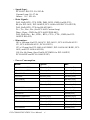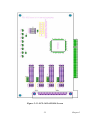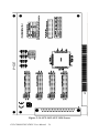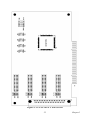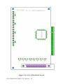
1
PCI-COMM Series
Industrial Serial Communication
Cards
PCI-1601A
PCI-1601AU
PCI-1601B
PCI-1601BU
PCI-1602A
PCI-1602AU
PCI-1602B
PCI-1602BU
PCI-1602UP
PCI-1603
PCI-1604UP
PCI-1610A
PCI-1610AJU
PCI-1610B
PCI-1610CU
PCI-1610AUP
PCI-1610UP
PCI-1611U
PCI-1612A
PCI-1612AU
PCI-1612B
PCI-1612U
PCI-1612CU
PCI-1620A
PCI-1620AU
PCI-1620B
PCI-1620U
PCI-1622CU
User Manual
Copyright
The documentation and the software included with this product are copyrighted 2005 by Advantech Co., Ltd. All rights are reserved. Advantech
Co., Ltd. reserves the right to make improvements in the products
described in this manual at any time without notice. No part of this manual may be reproduced, copied, translated or transmitted in any form or
by any means without the prior written permission of Advantech Co., Ltd.
Information provided in this manual is intended to be accurate and reliable. However, Advantech Co., Ltd. assumes no responsibility for its use,
nor for any infringements of the rights of third parties, which may result
from its use.
Acknowledgements
Award is a trademark of Award Software International, Inc.
VIA is a trademark of VIA Technologies, Inc.
IBM, PC/AT, PS/2 and VGA are trademarks of International Business
Machines Corporation.
Intel and Pentium are trademarks of Intel Corporation.
Microsoft Windows® is a registered trademark of Microsoft Corp.
RTL is a trademark of Realtek Semi-Conductor Co., Ltd.
ESS is a trademark of ESS Technology, Inc.
UMC is a trademark of United Microelectronics Corporation.
SMI is a trademark of Silicon Motion, Inc.
Creative is a trademark of Creative Technology LTD.
All other product names or trademarks are properties of their respective
owners.
Part No. 2003543502
6th Edition
Printed in Taiwan
July 2005
PCI-COMMUNICATION User Manual
ii
Product Warranty (2 years)
Advantech warrants to you, the original purchaser, that each of its products will be free from defects in materials and workmanship for two years
from the date of purchase.
This warranty does not apply to any products which have been repaired or
altered by persons other than repair personnel authorized by Advantech,
or which have been subject to misuse, abuse, accident or improper installation. Advantech assumes no liability under the terms of this warranty as
a consequence of such events.
Because of Advantech’s high quality-control standards and rigorous testing, most of our customers never need to use our repair service. If an
Advantech product is defective, it will be repaired or replaced at no
charge during the warranty period. For out-of-warranty repairs, you will
be billed according to the cost of replacement materials, service time and
freight. Please consult your dealer for more details.
If you think you have a defective product, follow these steps:
1.
Collect all the information about the problem encountered. (For
example, CPU speed, Advantech products used, other hardware
and software used, etc.) Note anything abnormal and list any
onscreen messages you get when the problem occurs.
2.
Call your dealer and describe the problem. Please have your manual, product, and any helpful information readily available.
3.
If your product is diagnosed as defective, obtain an RMA (return
merchandize authorization) number from your dealer. This allows
us to process your return more quickly.
4.
Carefully pack the defective product, a fully-completed Repair and
Replacement Order Card and a photocopy proof of purchase date
(such as your sales receipt) in a shippable container. A product
returned without proof of the purchase date is not eligible for warranty service.
Write the RMA number visibly on the outside of the package and ship it
prepaid to your dealer.
iii
CE
This product has passed the CE test for environmental specifications
when shielded cables are used for external wiring. We recommend the use
of shielded cables. This kind of cable is available from Advantech. Please
contact your local supplier for ordering information.
FCC Class A
This equipment has been tested and found to comply with the limits for a
Class A digital device, pursuant to Part 15 of the FCC Rules. These limits
are designed to provide reasonable protection against harmful interference when the equipment is operated in a commercial environment. This
equipment generates, uses and can radiate radio frequency energy and, if
not installed and used in accordance with the instruction manual, may
cause harmful interference to radio communications. Operation of this
equipment in a residential area is likely to cause harmful interference in
which case the user will be required to correct the interference at his own
expense.
Safety Precaution - Static Electricity
Follow these simple precautions to protect yourself from harm and the
products from damage.
1.
To avoid electrical shock, always disconnect the power from your
PC chassis before you work on it. Don't touch any components on
the CPU card or other cards while the PC is on.
2.
Disconnect power before making any configuration changes. The
sudden rush of power as you connect a jumper or install a card may
damage sensitive electronic components.
PCI-COMMUNICATION User Manual
iv
Technical Support and Assistance
Step 1. Visit the Advantech web site at www.advantech.com/support
where you can find the latest information about the product.
Step 2. Contact your distributor, sales representative, or Advantech's customer service center for technical support if you need additional
assistance. Please have the following information ready before
you call:
- Product name and serial number
- Description of your peripheral attachments
- Description of your software (operating system, version, application software, etc.)
- A complete description of the problem
- The exact wording of any error messages
Document Feedback
To assist us in making improvements to this manual, we would welcome
comments and constructive criticism. Please send all such - in writing to:
[email protected]
v
PCI-COMMUNICATION User Manual
vi
Contents
Chapter
1 Introduction ..................................................... 2
1.1
1.2
1.3
1.4
Chapter
Description ........................................................................ 2
Features ............................................................................. 3
Specifications .................................................................... 3
Ordering Information ........................................................ 5
1.4.1
Accessories .................................................................... 7
Table 1.1:PCI Communication Cards Selection Guide . 8
2 Hardware Configuration .............................. 10
2.1
2.2
2.3
Initial Inspection.............................................................. 10
Jumper and Switch Locations ......................................... 11
Figure 2.1: PCI-1601A/B Silk Screen ......................... 11
Figure 2.2:PCI-1601AU/BU Silk Screen ..................... 12
Figure 2.3:PCI-1602A/B Silk Screen .......................... 13
Figure 2.4:PCI-1602AU/BU Silk Screen ..................... 14
Figure 2.5:PCI-1602UP Silk Screen ............................ 15
Figure 2.6:PCI-1603 Silk Screen ................................. 16
Figure 2.7:PCI-1604UP Silk Screen ............................ 17
Figure 2.8:PCI-1610A/B Silk Screen .......................... 18
Figure 2.9:PCI-1610CU Silk Screen ........................... 19
Figure 2.10:PCI-1610AUP/UP Silk Screen ................. 20
Figure 2.11:PCI-1610AJP Silk Screen ........................ 21
Figure 2.12:PCI-1611U Silk Screen ............................ 22
Figure 2.13:PCI-1612A/B Silk Screen ........................ 23
Figure 2.14:PCI-1612AU/U Silk Screen ..................... 24
Figure 2.15:PCI-1612CU Silk Screen ......................... 25
Figure 2.16:PCI-1620A/B Silk Screen ........................ 26
Figure 2.17:PCI-1620AU/U Silk Screen ..................... 27
Figure 2.18:PCI-1622CU Silk Screen ......................... 28
Jumper Settings ............................................................. 29
2.3.1
2.3.2
2.3.3
How to Set Jumpers ..................................................... 29
Figure 2.19:How to Set Jumpers .................................. 29
Default Settings ............................................................ 30
Table 2.1:PCI-1601/1602/1611/1612/1622 Default Setting ................................................................... 30
Figure 2.20:PCI-1603 Default Setting ......................... 30
Mode Selection by Jumper/DIP Settings ..................... 31
Figure 2.21:PCI-1612 Series RS-232/422/485 Selec. . 31
Figure 2.22:RS-422/485 Selection by Jumper Setting . 31
Figure 2.23:PCI-1603 RS-232 Mode Jumper Setting .. 32
Figure 2.24:PCI-1603 Current-loop Md Jmp Setting .. 32
Figure 2.25:Active Mode Jumper Setting .................... 32
Figure 2.26:Passive Mode Jumper Setting .................. 33
Figure 2.27:Resistor Selection ..................................... 34
vii
2.4
Chapter
Chapter
Card Installation .............................................................. 35
3 Driver Setup & Installation.......................... 38
3.1
3.2
Introduction ..................................................................... 38
Driver Setup .................................................................... 38
3.3
Reboot System after Win98/2000/XP Driver Setup ....... 44
3.4
3.5
Verify your Win98/2000/XP Driver Setup ..................... 47
Configuring Serial Devices for Win 98/2000/XP ........... 50
3.6
3.7
Remove PCI ICOM Series Device.................................. 54
Driver Uninstall............................................................... 57
3.2.1
3.3.1
3.3.2
3.5.1
3.5.2
3.5.3
PCI UARTs Device Driver Installation ....................... 44
PCI Bridge Device Driver Installation ......................... 46
Configuring a PCI UARTs Device .............................. 52
Configuring a PCI Bridge Device ................................ 53
Configuring Ports ......................................................... 53
4 ICOM Tools ................................................... 60
4.1
4.2
4.3
4.4
Introduction .................................................................... 60
Installation....................................................................... 60
User Interface of ICOM Tools ........................................ 61
4.3.1
4.3.2
4.3.3
4.3.4
4.3.5
4.3.6
4.3.7
4.3.8
4.4.3
4.4.4
4.5
Menu Bar ..................................................................... 61
Tool Bar ....................................................................... 62
Com Port Tab ............................................................... 63
Port Status .................................................................... 64
Message Logo .............................................................. 64
Tx Slide Bar ................................................................. 65
Performance Listing Area ............................................ 65
Status Bar ..................................................................... 65
Using the ICOM Tools Utility ........................................ 66
4.4.1
4.4.2
Chapter
Steps for Windows 98/2000/XP Driver Setup ............. 38
Port Selection ............................................................... 66
Figure 4.1:ICOM Tools program window ................... 66
Figure 4.2:Select Port dialog box ................................ 67
Figure 4.3:Ports You Select Will Appear in the Selected
Port Checkbox Group ...................................... 67
Figure 4.4:ICOM Tools User Interface ........................ 68
Configuring a Port ....................................................... 68
Figure 4.5:Test Info. on Performance Listing Area ..... 69
Close Port ..................................................................... 70
Exit the ICOM Tools utility ......................................... 70
Messages on Status Bar and Message Logo Area........... 71
4.5.1
4.5.2
Status Bar Messages .................................................... 71
Message Logo Messages ............................................. 72
5 Pin Assignments and Wiring........................ 74
5.1
Pin assignments ............................................................... 74
5.1.1
PCI-1601A/AU/B/BU, PCI-1602A/AU/B/BU ............ 74
Table 5.1:PCI-1601/1602 Male DB9 on bracket ......... 74
Figure 5.1:PCI-1601/1602 Pin Assignment ................. 74
PCI-COMMUNICATION User Manual viii
5.1.2
5.2
PCI-1602UP ................................................................. 75
Table 5.2:PCI-1602UP Male DB9 on cable ................ 75
Table 5.3:PCI-1602UP Female DB25 on bracket ....... 75
5.1.3 PCI-1603 ...................................................................... 76
Table 5.4:PCI-1603 Male DB9 on bracket .................. 76
5.1.4 PCI-1604UP ................................................................. 77
Table 5.5:PCI-1604 Male DB9 on cable ..................... 77
Table 5.6:PCI-1604UP Female DB25 on bracket ....... 77
5.1.5 PCI-1610A/B/CU ......................................................... 78
Table 5.7:PCI-1610A/B/CU Male DB9 on cable ........ 78
Table 5.8:PCI-1610A/B/CU male DB25 on cable ....... 78
Table 5.9:PCI-1610A/B/CU female DB37 on bracket 79
5.1.6 PCI-1610AUP/UP ........................................................ 80
Table 5.10:PCI-1610AUP/UP male DB9 on cable ...... 80
Table 5.11:PCI-1610AUP/UP f. DB44 on bracket ...... 80
5.1.7 PCI-1610AJU ............................................................... 81
Table 5.12:PCI-1610AJU male DB9 on cable ............. 81
Table 5.13:PCI-1610AJU RJ45 on bracket ................. 81
5.1.8 PCI-1611U ................................................................... 82
Table 5.14:PCI-1611U male DB9 on cable ................. 82
Table 5.15:PCI-1611U male DB25 on cable ............... 82
Table 5.16:PCI-1611U female DB37 on bracket ......... 83
5.1.9 PCI-1612A/B/AU/U/CU .............................................. 84
Table 5.17:PCI-1612A/B/AU/U/CU m. DB9 on cable 84
Table 5.18:PCI-1612A/B/AU/U/CU m.DB25 cable ... 84
Table 5.19:PCI-1612A/B/AU/U/CU female DB37 on
bracket .............................................................. 85
5.1.10 PCI-1620A/B/AU/U .................................................... 86
Table 5.20:PCI-1620A/B/AU/U f. DB62 on bracket .. 86
Table 5.21:PCI-1620A/B/AU/U male DB9 on cable
(OPT8H) .......................................................... 87
Table 5.22:PCI-1620A/B/AU/U male DB25 on cable
(OPT8BP,OPT8C) ........................................... 87
Table 5.23:PCI-1620A/B/AU/U female DB25 on cable
(OPT8AP) ........................................................ 88
Table 5.24:PCI-1620A/B/AU/U female DB25 on cable
(OPT8FP) ......................................................... 88
5.1.11 PCI-1622CU ................................................................ 89
Table 5.25:PCI-1622CU male DB9 on cable (OPT8J) 89
Table 5.26:PCI-1622CU m. DB25 on cable(OPT8I) .. 89
Table 5.27:PCI-1622CU female DB78 on bracket ...... 90
Wiring.............................................................................. 92
5.2.1
5.2.2
5.2.3
RS-232 Signal Wiring .................................................. 92
Table 5.28:Terminal or PC (DTE) Connections .......... 92
Table 5.29:Modem Connections .................................. 93
Table 5.30:Terminal without Handshake ..................... 93
RS-422 Signal Wiring .................................................. 94
Table 5.31:RS-422 DB9 Pin Assignment .................... 94
RS-485 Signal Wiring .................................................. 95
Figure 5.2:RS-485 Wiring Topology ........................... 95
ix
PCI-COMMUNICATION User Manual
x
CHAPTER
1
2
Introduction
This chapter provides detailed specifications for the PCI COMMUNICATION cards.
Sections include:
• Description
• Features
• Specifications
• Ordering Information
• Selection Guide
Chapter 1 Introduction
1.1 Description
The PCI Local Bus is a high-performance bus that provides a processorindependent data path between the CPU and high-speed peripherals. PCI
is a robust inter-connect mechanism designed specifically to accommodate multiple high performance peripherals for series communication,
SCSI, LAN, etc.
Advantech serial communication card leverages the " Plug and Play "
capability defined in the PCI 2.1/2.2 bus specification. The board requires
only one PCI slot within the personal computer and provides independent
serial channels. All channels are addressed in a continuous 32 byte I/O
block for simplified software access. And, all channels may also share
one PCI interrupt. An interrupt status register is available for determining
the interrupt source.
The Advantech PCI communication card comes standard with 16PCI952/
954 UARTs containing 128 byte FIFOs which are available as an option.
These upgraded FIFOs greatly reduce CPU overhead and are an ideal
choice for heavy multitasking environments.
16PCI952/954
The 16PCI952/954 is a high performance Twin/Quad UART with an onchip PCI interface. Targeted at PCI-based serial and parallel expansion
cards, PCI-architecture computer systems and embedded applications, the
16PCI952/954 integrates a PCI bus interface together with two/four of
16C950 high performance UARTs, a bi-directional parallel port and a
local bus bridge function. This single-chip solution replaces five or more
integrated circuits used in today products, giving performance, cost and
size advantages for new designs.
PCI-COMMUNICATION User Manual
2
1.2 Features
• PCI Specification 2.1/2.2 compliant
• Speeds up to 921.6 kbps
• 16PCI952/954 , 16C954 UARTs with 128-byte FIFOs standard
• I/O address automatically assigned by PCI plug-and play
• OS supported: Windows 98/ME/2000/XP, Linux
• Optional surge protection
• Optional isolation protection for RS-232/422/485
• Interrupt status register for increased performance
• Space reserved for termination resistors
• Automatic RS-485 data flow control
• Utility-ICOM Tools
1.3 Specifications
• Bus Interface:
PCI bus specification 2.1 compliant for: PCI-1601A/B, PCI-1602A/B,
PCI-1610A/B, PCI-1612A/B, and PCI-1620A/B.
PCI bus specification 2.2 compliant for: PCI-1601AU/BU,PCI1602AU/BU, PCI-1602UP, PCI-1603, PCI-1604UP, PCI-1610CU/
AJU/AUP/UP, PCI-1611U, PCI-1612AU/U/CU, PCI-1620AU/U and
PCI-1622CU
• IRQ: all ports use the same IRQ assigned by PCI Plug-and-Play
• Data bits: 5, 6, 7, 8
• Stop bits: 1, 1.5, 2
• Parity: none, even, odd
• Communication Controller:
16PCI954 + 16C954 for PCI-1620A/B/AU/Uand PCI-1622CU
16PCI954 for PCI-1610A/AJU/B/CU/AUP/UP, PCI-1611U and PCI1612A/B/AU/U/CU
16PCI952 for PCI-1601A/AU/B/BU, PCI-1602A/AU/B/BU/UP,
PCI-1603 and PCI-1604UP
3
Chapter 1
• Speed (bps) :
PCI-1603: RS-232: 50~203.4k
Current Loop: 50~57.6k
Others: 50 ~ 921.6 k
• Data Signals:
TxD, RxD, RTS, CTS, DTR, DSR, DCD, GND (for RS-232)
RI (for PCI-1603, PCI-1604UP, PCI-1610A/AJU/B/CU/AUP/UP)
TxD, RxD, RTS, CTS (for RS-422/485)
Tx+, Tx-, Rx+, Rx- (for PCI-1603 Current loop)
Data+, Data-, GND (for PCI-1602UP RS-485)
TxD, RxD, Rx+, Rx-, RTS+, RTS-, CTS+, CTS-, GND (for PCI1602UP RS-422)
• Dimensions:
185 x 100 mm (for PCI-1610CU, PCI-1611U, PCI-1612A/B/AU/U/
CU, PCI-1620A/B/AU/U, PCI-1622CU)
123 x 92 mm (for PCI-1601A/AU/B/BU, PCI-1602A/AU/B/BU, PCI1603, and PCI-1610A/AJU/B)
119.91x 64.41mm (Low Profile PCI MD1 for PCI-1602UP,
PCI-1604UP and PCI-1610AUP/UP)
• Power Consumption
Model
Typical
Max
PCI-1601A/AU/B/BU
220 mA (+5V)
270 mA (+5V)
PCI-1602A/AU/B/BU
250 mA (+5V)
300 mA (+5V)
PCI-1602UP
-
300 mA (+5V)
PCI-1603
250 mA (+5V)
300 mA (+5V)
PCI-1604UP
-
300 mA (+5V)
PCI-1610A/B
60 mA (+12 V)
80 mA (+12 V)
150 mA (+5 V)
180 mA (+5 V)
PCI-1610CU
-
750mA(+5V)
PCI-1610AJU/AUP/UP
-
400 mA (+5V)
PCI-1611U
-
600mA(+5V)
PCI-1612A/B/AU/U
270 mA (+5 V)
338 mA (+5 V)
PCI-1612CU
758 mA (+5V)
803 mA (+5V)
PCI-1620A/B/AU/U
120 mA (+12 V)
150 mA (+12 V)
180 mA (+5 V)
220 mA (+5 V)
-
600mA(+5V)
PCI-1622CU
PCI-COMMUNICATION User Manual
4
• Operating Temperature: 0~ 65° C (See IEC 68-2-1, 2), (32~149° F)
• Operating Humidity: 5 ~ 95% Relative Humidity, non-condensing
(See IEC 68-2-3)
• Storage Temperature: -25 ~ 85° C (-13~185° F)
• Current-loop Interface
Signal Driver/receiver: 6N136
Signals:
TxD+, TxD-, RxD+, RxD• Current Value: 20mA (Standard)
• Mode: Asynchronous, full duplex
• Baud-rate: 50 ~ 57600 bps
• Transmission Distance: 1000 m
1.4 Ordering Information
• PCI-1601A: 2-port RS-422/485 PCI Comm. Card
• PCI-1601AU: 2-port RS-422/485 Universal PCI Comm. Card
• PCI-1601B: 2-port RS-422/485 PCI Comm. Card, w/surge protection
• PCI-1601BU: 2-port RS-422/485 Universal PCI Comm. Card w/surge
protection
• PCI-1602A: 2-port RS-422/485 PCI Comm. Card. w/ isolation protection
• PCI-1602AU: 2-port RS-422/485 Universal PCI Comm. Card w/ isolation
• PCI-1602B: 2-port RS-422/485 PCI Comm. Card, w/isolation and
surge protection
• PCI-1602BU: 2-port RS-422/485 Universal PCI Comm. Card w/ isolation and surge protection
• PCI-1602UP: 2-port RS-422/485 Low-Profile Universal PCI Comm.
Card, w/isolation and surge protection
• PCI-1603: 2-port Isolated RS-232/current-loop PCI Comm. Card
• PCI-1604UP: 2-port RS-232 Low-Profile Universal PCI Comm. Card,
w/surge protection
• PCI-1610A: 4-port RS-232 PCI Comm. Card
5
Chapter 1
• PCI-1610AJU: 4-port RS-232 Universal PCI Comm. Card w/ RJ45
connector
• PCI-1610AUP: 4-port RS-232 Low-Profile Universal PCI Comm.
Card
• PCI-1610B: 4-port RS-232 PCI Comm. Card, w/surge protection
• PCI-1610CU: 4-port RS-232 Universal PCI Comm. Card, w/isolation
and surge protection
• PCI-1610UP: 4-port RS-232 Low-Profile Universal PCI Comm. Card,
w/surge protection
• PCI-1611U: 4-port RS-422/485 Universal PCI Comm. Card, w/isolation and surge protection
• PCI-1612A: 4-port RS-232/422/485 PCI Comm. Card
• PCI-1612AU: 4-port RS-232/422/485 Universal PCI Comm. Card
• PCI-1612B: 4-port RS-232/422/485 PCI Comm. Card, w/surge protection
• PCI-1612CU: 4-port RS-232/422/485 Universal PCI Comm. Card, w/
isolation and surge protection
• PCI-1612U: 4-port RS-232/422/485 Universal PCI Comm. Card, w/
surge protection
• PCI-1620A: 8-port RS-232 PCI Comm. Card
• PCI-1620AU: 8-port RS-232 Universal PCI Comm. Card
• PCI-1620B: 8-port RS-232 PCI Comm. Card, w/surge protection
• PCI-1620U: 8-port RS-232 Universal PCI Comm. Card, w/surge protection
• PCI-1622CU: 8-port RS-422/485 Universal PCI Comm. Card, w/isolation and surge protection
PCI-COMMUNICATION User Manual
6
1.4.1 Accessories
• OPT8AP: 8-Port RS-232 Connection Box/Female DB25 Connectors
(DCE) (1 m cable connectors with card and connection box included)
• OPT8ASP: 8-Port RS-232 Connection Box/Female DB25 Connectorsw/ surge protection (DCE) (1m cable connectors with card and
connection box included)
• OPT8BP: 8-Port RS-232 Connection Box/Male DB25 Connectors
(DTE) (1 m cable connectos with card and connection box included)
• OPT8BSP: 8-Port RS-232 Connection Box/Male DB25 Connector w/
surge protection (DTE) (1 m cable connectors with card and connection BOX included)
• OPT8C: 8-Port RS-232 Octopus Cable/Male DB25 Connect 1 m
• OPT8H: 8-Port RS-232 Octopus Cable/Male DB9 Connect 1 m
• OPT8I: 1 m female DB78 to 8* male DB25 cable (To be used with
PCI-1622CU)
• OPT8J: 1 m female DB9 to 8* male DB25 cable (To be used with PCI1622CU)
• OPT8FP: 8-port RS-422 to RS-232 converter connection box with isolation protection (1 m cable connectors with card and connection box
included)
7
Chapter 1
Table 1.1: PCI Communication Cards Selection Guide
Model Name
PCI-1601
PCI-1602
A
B
-
AU
BU
Ports Comm.
Interface
Support
PCI-1620
Isolation
Universal
Universal
2500VDC
-
A
-
-
3000VDC
B
-
2500VDC
3000VDC
AU
Universal
-
3000VDC
BU
Universal
2500VDC
3000VDC
UP
Low-Profile/
Universal
Universal
2500VDC
2500VDC
RS-232/Cur- rent loop
RS-232
2500VDC
3000VDC
RS-232
-
A
B
Low-Profile/
Universal
-
CU
Universal
4
AJU Universal
AUP Low-Profile/
Universal
UP Low-Profile/
Universal
PCI-1611U
Universal
PCI-1612
Surge
-
PCI-1604UP
2
Protection
RS-422/485 2500VDC
PCI-1603
PCI-1610
Form Factor
A
B
-
AU
U
Universal
Universal
CU
Universal
A
B
-
AU
U
PCI-1622CU
3000VDC
-
2500VDC
2500VDC
-
-
2500VDC
-
RS-422/485 2500VDC
2000VDC
RS-232/422/ 485
2500VDC
-
2500VDC
-
2500VDC
2500VDC
3000VDC
-
Universal
Universal
2500VDC
-
Universal
RS-422/485 2500VDC
8
PCI-COMMUNICATION User Manual
RS-232
8
2500VDC
CHAPTER
2
2
Hardware
Configuration
This chapter provides information on
the hardware configuration of PCI
COMMUNICATION cards.
Sections include:
• Initial Inspection
• Jumper and Switch Locations
• Jumper Settings
• Card Installation
Chapter 2 Hardware Configuration
2.1 Initial Inspection
You should find the following items inside the shipping package:
PCI communication interface card
Industrial Communication Driver, Utility and PCI communication card
user manual in ICOM CD-ROM
We carefully inspected the PCI communication card series mechanically
and electrically before we shipped it. It should be free of marks and
scratches and in perfect working order on receipt.
As you unpack the PCI communication card series, check it for signs of
shipping damage (damaged box, scratches, dents, etc.). If it is damaged or
it fails to meet specifications, notify our service department or your local
sales representative immediately. Also notify the carrier. Retain the shipping carton and packing material for inspection by the carrier. After
inspection we will make arrangements to repair or replace the unit.
When you handle the PCI communication card series, remove it from its
protective packaging by grasping the rear metal panel. Keep the antivibration packing. Whenever you remove the card from the PC, store it in
this package for protection.
Discharge your body’s static electric charge by
touching the back of the grounded chassis of the
system unit (metal) before handling the board. You
should avoid contact with materials that hold a static
charge such as plastic, vinyl and styrofoam. Handle
the board only by its edges to avoid static damage to
its integrated circuits. Avoid touching the exposed
circuit connectors. We also recommend that you use
a grounded wrist strap and place the card on a static
dissipative mat whenever you work with it.
PCI-COMMUNICATION User Manual
10
2.2 Jumper and Switch Locations
Figure 2.1: PCI-1601A/B Silk Screen
11
Chapter 2
Figure 2.2: PCI-1601AU/BU Silk Screen
PCI-COMMUNICATION User Manual
12
Figure 2.3: PCI-1602A/B Silk Screen
13
Chapter 2
Figure 2.4: PCI-1602AU/BU Silk Screen
PCI-COMMUNICATION User Manual
14
Figure 2.5: PCI-1602UP Silk Screen
15
Chapter 2
Figure 2.6: PCI-1603 Silk Screen
PCI-COMMUNICATION User Manual
16
Figure 2.7: PCI-1604UP Silk Screen
17
Chapter 2
Figure 2.8: PCI-1610A/B Silk Screen
PCI-COMMUNICATION User Manual
18
Figure 2.9: PCI-1610CU Silk Screen
19
Chapter 2
Figure 2.10: PCI-1610AUP/UP Silk Screen
PCI-COMMUNICATION User Manual
20
Figure 2.11: PCI-1610AJP Silk Screen
21
Chapter 2
Figure 2.12: PCI-1611U Silk Screen
PCI-COMMUNICATION User Manual
22
Figure 2.13: PCI-1612A/B Silk Screen
23
Chapter 2
Figure 2.14: PCI-1612AU/U Silk Screen
PCI-COMMUNICATION User Manual
24
Figure 2.15: PCI-1612CU Silk Screen
25
Chapter 2
Figure 2.16: PCI-1620A/B Silk Screen
PCI-COMMUNICATION User Manual
26
Figure 2.17: PCI-1620AU/U Silk Screen
27
Chapter 2
Figure 2.18: PCI-1622CU Silk Screen
PCI-COMMUNICATION User Manual
28
2.3 Jumper Settings
This section tells how to set the jumpers to configure your card. It gives
the card default configuration and your options for each jumper.
2.3.1 How to Set Jumpers
You configure your card to match the needs of your application by setting
jumpers. A jumper is the simplest kind of electric switch. It consists of
two metal pins and a small metal clip (often protected by a plastic cover)
that slides over the pins to connect them. To “close” a jumper you connect
the pins with the clip. To “open” a jumper you remove the clip.
Sometimes a jumper will have three pins, labeled 1, 2 and 3. In this case
you would connect either pins 1 and 2 or 2 and 3.
You may find a pair of needle-nose pliers useful for setting the jumpers.
If you have any doubts about the best hardware configuration for your
application, contact your local distributor or sales representative before
you make any changes.
Figure 2.19: How to Set Jumpers
29
Chapter 2
2.3.2 Default Settings
The board is shipped with default settings. If you need to change these
settings, however, see the following sections. Otherwise, you can simply
install the card.
PCI-1601/1602/1611/1612/1622.
Table 2.1: PCI-1601/1602/1611/1612/1622 Default Setting
RS-422/485 Mode
RS-422
Auto
Enable Mode
PCI-1603
The board will be shipped in the RS-232 mode, passive Rx and active Tx.
On the 10*2 pin jumper groups (JP2 & JP4)— A, B, C, D and E are set to
RS-232 transmission mode. On the 6*2 pin jumper groups (JP3 & JP5)—
C, D and E are set to passive Rx and active Tx. They are the card default
settings.
A
B
C
D
E
F
G
H
B
C
D
E
F
JP2 & JP4
A
JP3 & JP5
Figure 2.20: PCI-1603 Default Setting
PCI-COMMUNICATION User Manual
30
I
J
2.3.3 Mode Selection by Jumper/DIP Settings
RS-232/422/485 Selection (for PCI-1612A/B/AU/U/CU)
Should you wish to configure the PCI-1612A/B/AU/U/CU to operate in
the RS-232 mode, the upper two pins of the 12*3 pin jumper should be
connected. For RS-422/ RS-485 mode selection, the bottom two pins of
the 12*3 pin jumper should be connected as shown below.
Figure 2.21: PCI-1612 Series RS-232/422/485 Selection
RS-422/485 Selection (for PCI-1601/1602/1611/1612/1622)
You can set each port individually for either RS-422 (the default) or RS485 operation. The figure 2.11 shows the jumper setting. See section 2.2
"Jumper and Switch Locations" from figure 2.1 to figure 2.17 for help to
locate the jumpers.
Figure 2.22: RS-422/485 Selection by Jumper Setting
31
Chapter 2
PCI-1603 RS-232/Current-loop Mode Selection
For RS-232 mode operations, the jumpers will be set as the default mode.
The jumpers on the 10*2 pin jumper must be set to A, B, C, D and E.
Figure 2.23: PCI-1603 RS-232 Mode Jumper Setting
To enable the channel to operate in the current-loop mode, you should set
F, G, H, I and J on the 10*2 pin jumpers.
Figure 2.24: PCI-1603 Current-loop Mode Jumper Setting
Then decide which mode the Tx and Rx will operate in. The options are
active or passive. In the active mode, the Tx or Rx will generate the current requirement for data transfer over the link. In the passive mode, the
current is generated by the card at the other end of the link.
A and B are set to be active Rx, and E is set to be active Tx.
Figure 2.25: Active Mode Jumper Setting
PCI-COMMUNICATION User Manual
32
C and D are set to be passive Rx, and F is set to be passive Tx.
Figure 2.26: Passive Mode Jumper Setting
You may configure both Tx and Rx on one port to operate in the same
mode, or you can configure each Tx and Rx on one port to operate in different modes.
If you set PCI-1603 to the current-loop mode, plug the card to your
device and turn on the device, both LEDs Rx1 and Rx2 on top corner of
PCI-1603 board are lighten, indicating that current-loop mode is enabled!
Note:
When either channel is configured in the RS-232
mode, the two associated Tx/Rx active/passive jumpers will be inoperable.
Enable mode selection
You set the Enable mode using two, four or eight position DIP switches,
one for each port. If the switches are set to "AUTO", the driver automatically senses the direction of the data flow and switches the direction of
transmission. No handshaking is necessary.
If DIP switches are set to "On," the driver is always enabled, and always
in high or low status. The user must select a mode before beginning RS422 applications.
Mode
Switch Position
RS-485
AUTO
RS-422_master
ON
RS-422_slave
AUTO
33
Chapter 2
Terminator resistor setup (for PCI-1601/1602/1611/1612/1622)
You can install terminator resistors if necessary to match impedance.
Each signal line (Tx, Rx) has a separate resistor.
Especially in fields with serious electric noise, installing terminal resistors is helpful to stabilize communications. Make sure that both sides of
the RS-485 communication ports are installed on BUS. See details in
Chapter 5.2.2 and 5.2.3
Figure 2.27: Resistor Selection
PCI-COMMUNICATION User Manual
34
2.4 Card Installation
Note:
We strongly recommend that you install the software driver before you install the hardware into
your system, since this will guarantee a smooth
and trouble-free installation process.
Turn off your PC’s power supply whenever you
install or remove the PCI communication card or
its cables. Static electricity can easily damage
computer equipment. Ground yourself by touching the chassis of the computer (metal) before
you touch any boards. See the static warning on
Ch.2
1.
Install the driver; see chapter 3.1 and chapter 3.2.
2.
Turn off the computer and all peripheral devices (such as printers
and monitors).
3.
Disconnect the power cord and any other cables from the back of
the computer.
4.
Remove the PC’s cover (refer to your user’s guide if necessary).
5.
Install and plug the PCI communication card on your PCI BUS.
6.
Replace the PC’s cover. Connect the cables you removed in step 3.
7.
Turn the computer power on.
8.
Driver will install PCI Communication card automatically, see
chapter 3.3 and 3.4 and 3.5.
9.
Test your COM port and verify if COM port could work normally,
see chapter 4.
10.
Refer to the pin assignment and cabling for further information, see
chapter 5.
35
Chapter 2
PCI-COMMUNICATION User Manual
36
CHAPTER
3
2
Driver Setup and
Installation
This chapter describes the driver installation, configuration and removal procedures for the Windows operating
system, including Windows 98/2000/
XP.
Sections include:
• Introduction
• Driver Setup
Chapter 3 Driver Setup & Installation
3.1 Introduction
This chapter describes the driver installation, configuration and removal
procedures for the Windows operating system, including Windows 98/
NT/2000/XP. We strongly recommend that you install the software
driver before you install the hardware into your system, since this
will guarantee a smooth and trouble-free installation process.
3.2 Driver Setup
Windows 98/2000/XP supports COM1 to COM256, meaning up to 256
serial ports. In order to fully utilize the advanced features of Windows 98/
2000/XP, such as multi-process and multithread, pure 32-bit Windows
98/2000/XP device drivers are provided for the PCI communication
cards. All these drivers conform to the Win32 COMM API standard.
3.2.1 Steps for Windows 98/2000/XP Driver Setup
Before you install the card into your system, we recommend you install
the driver first. Please follow the steps below for the PCI communication
card’s Windows 98/2000/XP driver installation.
1.
Insert your companion CD-ROM disc into your CD-ROM drive.
2.
The driver setup program will be launched automatically. If the
auto-play function is not enabled on your system, use Windows
Explorer or the Windows Run command to execute autorun.exe on
the companion CD-ROM.
PCI-COMMUNICATION User Manual
38
3.
After the setup program is launched, you’ll see the following
Screen.
4.
Click the Continue button and the catalogue select page appears.
Then click the Installation button for installation
39
Chapter 3
5.
Choose the driver you want to install, then click the hyperlink.
6.
Click Next to continue installation.
PCI-COMMUNICATION User Manual
40
7.
Type user name and company name, then click Next.
8.
Just click Next to accept the default installation folder, or you can
specify a folder by clicking the Browse button.
41
Chapter 3
9.
Select a program folder or type a new folder name.
10.
Click Back to review or change your setting, or click Next to begin
copying files.
PCI-COMMUNICATION User Manual
42
11.
Perfom the requested operations and select Finish.
43
Chapter 3
3.3 Reboot System after Win98/2000/XP Driver Setup
3.3.1 PCI UARTs Device Driver Installation
1.
When you reboot your system, Windows 98/2000/XP will recognize your card devices and will automatically search for the device
driver for PCI UARTs as shown in the following dialog box.
2.
Choose “Search for the best driver for your device” radio button,
and click Next.
PCI-COMMUNICATION User Manual
44
3.
You don’t have to choose the location of the device driver program,
since it is already installed on your system. Just click Next to proceed.
4.
Windows 98/2000/XP has found the driver location and is ready to
install the driver. Click Next.
45
Chapter 3
5.
The driver installation is complete. Click Finish.
3.3.2 PCI Bridge Device Driver Installation
After the PCI UARTs device driver has been installed, Windows 98/
2000/XP will recognize the PCI Bridge device and automatically install
the device driver for PCI Bridge.
PCI-COMMUNICATION User Manual
46
3.4 Verify your Win98/2000/XP Driver Setup
After you have installed your card, go to Control Panel/System/Device
Manager to look for the Device Name that will appear after you have
installed the driver.
Note:
If your device has not been properly installed, there will
be an exclamation mark (!) on the device name to indicate a conflicting device. If this is the case, just remove
that device and start the driver installation process all
over again.
47
Chapter 3
You can also check the COM Port properties by double-clicking the specific com port device configuration you want to see. On the Properties
sheet, select the specific tabs to see relevant information.
On the General tab, you can see whether the device is working properly.
If your device functions normally, you can see a message under the
Device status box, stating “This device is working properly”.
PCI-COMMUNICATION User Manual
48
On the Settings tab, you can view relevant information about that specific
port, as you can see on the figures below.
49
Chapter 3
If you want to configure FIFO Properties, select the FIFOs tab. On the
tab, you can see the relevant FIFO configurations. We recommend you
use the default settings. However, you can set the configurations manually according to your preferences. If you want to restore the default settings, just click the Restore Default button.
3.5 Configuring Serial Devices for Win 98/2000/XP
After your serial devices have been properly installed in your system, you
can now proceed to configure your serial devices according to the following steps:
1.
Access Control Panel/System
PCI-COMMUNICATION User Manual
50
2.
Select Device Manager tab on the System Properties sheet.
3.
Click the plus sign (+) on the right of the ADSPCIUART device
category to expand it. As shown on the figure below, you can see
Advantech PCI UARTs and Advantech PCI Bridge device names
listed under the device category.
51
Chapter 3
3.5.1 Configuring a PCI UARTs Device
1.
Double-click the Advantech PCI UARTs device to evoke its Properties page, and then select the Resource tab on the Properties page
to look up or configure the current settings of the PCI UARTs
device.
2.
After you have made the necessary changes or if you are just satisfied with the default settings, click OK to accept. If you want to
cancel the configuration, click Cancel.
PCI-COMMUNICATION User Manual
52
3.5.2 Configuring a PCI Bridge Device
Double-click the Advantech PCI Bridge device to evoke its Properties
page, and then select the Resources tab on the Properties page to look up
or configure the current configuration of the PCI Bridge device to make
sure there are no conflicting devices. Click other tabs to look up or configure the device.
Note:
The Input/Output Range information is helpful to recognize the communication port attached to the device.
After you have made necessary changes or if you are satisfied with the
default settings, click OK to accept. If you want to cancel the configuration, just click Cancel.
3.5.3 Configuring Ports
The ports will be configured automatically, so you don’t need to do anything.
53
Chapter 3
3.6 Remove PCI ICOM Series Device
1.
Access Control Panel/System to bring up the System Properties
window.
2.
Select the Device Manager tab.
PCI-COMMUNICATION User Manual
54
3.
Click the plus sign (+) on the left of the Ports (COM & LPT)
device category to expand it. Select the specific “Advantech PCI
communication port” you want to remove, and click the Remove
button to remove the device you had selected.
4.
The following dialog box will appear to prompt you again to make
sure you really want to remove the device from your system.
55
Chapter 3
5.
Note:
Click the plus sign (+) on the left of the ADSPCIUART device category to expand it, and select the Advantech PCI UARTs or
Advantech PCI Bridge you want to remove.
You must remove all used ports settings and
device settings before you remove the device, or
there may be a mistake in the port setting when you
install another card.
PCI-COMMUNICATION User Manual
56
6.
Note:
Click the Remove button and the following dialog boxes appear to
prompt you whether you really want to remove the device.
We recommend you to remove the original device
before installing another model of Advantech PCI ICOM
series device in the same PCI slot.
3.7 Driver Uninstall
1.
Insert the ICOM CD and click the driver you want to uninstall.
57
Chapter 3
2.
Choose “Modify” radio button if you want to save another driver.
Or choose “Remove” radio button to remove all installed components.
3.
Click “Finish“ button to complete the uninstall.
PCI-COMMUNICATION User Manual
58
CHAPTER
4
2
ICOM Tools
This chapter provides information on
installation and usage of ICOM Tools.
Sections include:
• Introduction
• Installation
• User Interface of ICOM Tools
Chapter 4 ICOM Tools
4.1 Introduction
Advantech ICOM Tools is a convenient utility that has been designed to
help you test the performance of ICOM cards through analyzing the port
status. It features an easy to use graphical user interface that will soon
make you familiar with testing via menu commands and toolbar buttons.
Advantech ICOM Tools is applicable to all series of Advantech ICOM
cards, and can even be used with other third-party ICOM cards. It is
included for free on the diskette or on the companion CD-ROM with all
Advantech Industrial Communication cards.
4.2 Installation
To begin installation, double-click the ICOM_Tools.exe program icon in
the Tools folder or click the Advantech ICOM Utility hyperlink in the
installation window to launch the ICOM Tools setup program. The setup
program will copy the program files to the destination folder you choose
or to the default installation path (i.e. C:\Program Files\Advantech\ICOM
Tools). A program folder will be created in your Start/Programs menu.
(Later you can just access the program through Start/Program/Advantech PCI Comm Tools/COM Examine Tool)
PCI-COMMUNICATION User Manual
60
4.3 User Interface of ICOM Tools
4.3.1 Menu Bar
On the Menu Bar you can select various menu commands to perform
port-testing functions. You can also use the short-cut keys.
Port Submenu
Select: Select the ports you want to configure
Setup: Setup the configuration of a specific port
Close: Close a specific port
Run: Run the test on a specific port
Stop: Stop the test on a specific port
All Ports Submenu
Setup: Setup the configurations of all ports
Run: Run the test on all ports
Stop: Stop the test on all ports
Help Submenu Access Online help
61
Chapter 4
4.3.2 Tool Bar
Using the Tool Bar buttons is a more intuitive way to implement the
functions of ICOM Tools.
Port Select: Selects the port(s) you want to perform testing on
Port Setup: Sets up configuration of the port you have
selected
Port Close: Closes the port you have selected
Port Run: Runs the port test on the port you have selected
Port Stop: Stops the port test on the port you have
selected
All Ports Setup: Sets up the configuration of all ports not
running test
All Ports Run: Runs test on all ports
All Ports Stop: Stops test on all ports
Clear Message: Clears messages on Message Logo area
and the Rx length information on the Performance Listing
area
PCI-COMMUNICATION User Manual
62
4.3.3 Com Port Tab
Each Com Port tab represents a specific port you have selected for test
and configuration. On the tab, you can see the Transfer Mode, Port Status, and Message Logo area.
Transfer Modes
You can specify the transfer mode to be Normal, loopback (active) or
loopback (passive).
Normal—allows data to be transmitted and received simultaneously. The
data reception rate is helpful in identifying the performance of a communication card installed on your system.
Loopback- In loopback mode a series of special data will be transmitted,
which are expected to appear on the receiving end. Using the loopback
mode, you can check the integrity of received data and find whether any
error occurred on the transmission line. The active loopback and passive
loopback must work in pair to enable the loopback mode. When a port
operates as active loopback mode, it will send data first and receive data
later. Another port, which operates as passive loopback, will retransmit
any received data on the Rx line and then send these data onto the Tx line.
These two modes will form a logical loop and help to verify the integrity
of data transmitted over the communication link.
63
Chapter 4
4.3.4 Port Status
DTR (data-terminal-ready)
DSR (data-set-ready)
RTS (request-to-send)
CTS (clear-to-send)
CD (carrier-detect)
For RS-232 specifications, DTR and RTS are for output signals and can
be toggled on and off by double-clicking the labels (such as DTR, DSR,
RTS, CTS, CD) under the red/green marks. However, if you are using
RTS/CTS for flow control to run the test, you will see the RTS mark
appear in black. This indicates that the RTS can no longer be toggled on/
off since it is controlled by driver itself.
A black mark represents that the function is controlled by the driver itself and therefore not controllable by software.
4.3.5 Message Logo
On the Message Logo area, you can see the relevant messages about the
port(s) you have selected.
For information about specific messages in this area, please refer to Section 4.5, Messages on the Status Bar and Message Logo area.
PCI-COMMUNICATION User Manual
64
4.3.6 Tx Slide Bar
The Tx Slide Bar allows you to control the overall system loading. You
can adjust the transmission rate of your port(s) from 0% to 100%. Just
drag the slide button along the track to adjust the transmission rate.
4.3.7 Performance Listing Area
On the performance listing area, you can see the relevant information,
such as Rx Length (received packet byte length), Bytes/Sec (transmission
rate) and Last Abnormal Status of each port running a test.
4.3.8 Status Bar
The Status Bar is where you can glimpse the current information of the
port you have selected. The Status Bar indicates whether the port is
READY, RUNNING, BUSY or STOPPED, N/A PORT and the configuration information such as baud rate, data bit, stop bit, parity bit and flow
control (represented as 1200 N 8 1 None) settings. Also we can see the
duration of the test in hh:mm:ss format on the right.
For information about specific messages on this area, please refer to Section 4.5, Messages on the Status Bar and Message Logo area.
65
Chapter 4
4.4 Using the ICOM Tools Utility
To launch the ICOM Tools testing utility, access Start/Programs/Advantech PCI Comm Tools/COM Examine Tools to start the port testing utility.
4.4.1 Port Selection
Please follow the steps below to make your port selection:
1.
Launch ICOM Tools. You will first see the Program Window such
as Figure 4.1. Since you haven’t selected any port for testing yet,
all you can see now is a blank window area.
Figure 4.1: ICOM Tools program window
PCI-COMMUNICATION User Manual
66
2.
Select the port(s) you want to test by the Port/Select menu command or by clicking the Port Select button on the Toolbar, and a
dialog box such as Fig. 2 will appear.
Figure 4.2: Select Port dialog box
Select the port(s) you want to perform test on from the checkboxes next
to each COM port. You can either click the checkbox or double-click the
name(s) of the port(s) to select/deselect port(s) to perform the test on. The
port(s) you selected will immediately appear in the Selected Port field.
Figure 4.3: Ports You Select Will Appear in the Selected Port Checkbox
Group
67
Chapter 4
Click OK to bring up the ICOM Tools User Interface such as below:
Figure 4.4: ICOM Tools User Interface
4.4.2 Configuring a Port
You can choose to configure a specific port (or to configure all ports)
before running your test. Just click a Com Port Tab to select the port you
want to configure, and then click the Port Setup
button or use the
Port/Setup menu command (or if you want to configure all ports at once,
just click the All Ports Setup
button or access the All Ports/Setup
menu command) to bring up the Configure Port dialog box such as
below.
PCI-COMMUNICATION User Manual
68
In the Configure Port dialog box, you can configure the Baud Rate, Data
bits, Parity, Stop Bits and the flow control mode for that specific port (or
for all ports). After you have configured all the settings you want to
change, click OKto make this configuration active.
NOTE:
When using All Ports Setup button or All Ports/
Setup
menu command to configure settings
for all ports, you must take care to stop any ports
that are running test in order to configure them. If
you do not stop the test running on a specific
port, it won’t be configured at all. That is, you get
to configure only the ports that have been
stopped.
Run the Test
After you have completed the configuration of the port(s), you can now
start the test on the port you have selected by clicking the Run
button
or accessing the Port/Run menu command (or you want to run all ports at
once, just click the All Ports Run
menu command).
button or access All Ports/Run
Once the test is started, you can see relevant test information of port performance on the performance listing area.
Figure 4.5: Test Information on the Performance Listing Area
69
Chapter 4
The Performance Listing Area
Port
The com port number
Rx length
Received packet length in bytes
Bytes/Sec
Transmission rate in Bytes/Sec
Last Abnormal Status
Last abnormal status
Stop the Test
If you want to stop the test on a specific port, just click Port Stop
button or access Port/Stop menu command (or if you want to stop test on all
ports, just click All Ports Stop
command).
button or access All Ports/Stop menu
You can restart the test by clicking the Run
button or accessing the
Port/Run menu command (or if you want to run all ports at once, just
click the All Ports Run
mand).
button or access All Ports/Run menu com-
4.4.3 Close Port
If you want to close a port, just select the Com Port tab and click Port
Close button or access Port/Close menu command to close the port.
4.4.4 Exit the ICOM Tools utility
To exit the ICOM Tools utility, simply access Port/Exit menu command
or click the Close button on the upper right corner of the program window.
PCI-COMMUNICATION User Manual
70
4.5 Messages on Status Bar and Message Logo Area
Messages appearing on the Status Bar and Message Logo area are helpful
in understanding specific information of your system settings and performance.
4.5.1 Status Bar Messages
BUSY: the port is currently used by another application.
FAIL: the configuration parameters are not accepted by the port
N/A PORT: the port is not available in the system
READY: the port is ready to run or to be configured.
RUNNING: the test is running on the port
STOPPED: the test running on the port has been stopped by the user
71
Chapter 4
4.5.2 Message Logo Messages
Port Opened: The user has opened the port
Port Setup Fail: The user has set up the port configuration with parameters that are either incorrect or unsupported.
Port Running: The port is running a test
Port Stopped: The test is stopped on the port
Tx Starting/Tx Stopped: transmitting starting/transmitting stop
Rx Starting/Rx Stopped : receiving starting/receiving stop
Break Error: a break event has been detected on the port
Framing Error: A timing error (i.e. from start bit to stop bit) has been
detected on the port
Port I/O Error: An incorrect I/O event has been detected on the port
Rx Overrun: Received data has been overwritten before being processed
Rx Buffer Full Error: The buffer on the receiving end is saturated so
that newly arrived data are ignored
Tx Buffer Full Error: The buffer on the transmitting end is saturated so
that the data transmitted by applications are ignored.
LB Error - %d: data error is detected in loop back
LB Rx Pending: Loop back mode is waiting for incoming data
Data Setup Error: parameter error in port configuration
PCI-COMMUNICATION User Manual
72
CHAPTER
5
2
Pin Assignments and
Wiring
This chapter provides information on
the pin assignments and wiring.
Sections include:
• Pin Assignments
• Wiring
Chapter 5 Pin Assignments and Wiring
5.1 Pin assignments
5.1.1 PCI-1601A/AU/B/BU, PCI-1602A/AU/B/BU
The following table and figure shows the pin assignments for the PCI1601A/B/AU/BU, and PCI-1602A/B/AU/BU cards’ male DB9 connectors on the bracket in RS-422 and RS-485 modes.
Table 5.1: PCI-1601/1602 Male DB9 on bracket
Pin
RS-422
RS-485
1
Tx-
Data-
2
Tx+
Data+
3
Rx+
-
4
Rx-
-
5
GND
GND
6
RTS-
-
7
RTS+
-
8
CTS+
-
9
CTS-
-
Figure 5.1: PCI-1601/1602 Pin Assignment
PCI-COMMUNICATION User Manual
74
5.1.2 PCI-1602UP
The following table and figure show the pin assignments for the PCI1602UP card’s male DB9 on the cable and female DB25 on the bracket in
RS-422 and RS-485 modes.
Table 5.2: PCI-1602UP Male DB9 on cable
Pin
RS-422
RS-485
1
Tx-
Data-
2
Tx+
Data+
3
Rx+
-
4
Rx-
-
5
GND
GND
6
RTS-
-
7
RTS+
-
8
CTS+
-
9
CTS-
-
Table 5.3: PCI-1602UP Female DB25 on bracket
Pin
RS-422
RS-485
Pin RS-422
RS-485
1
2
3
4
5
6
7
8
9
10
11
12
13
2_Tx2_Tx+
2_Rx+
2_Rx2_GND
1_Tx1_Tx+
1_Rx+
1_Rx1_GND
2_Data2_Data+
2_GND
1_Data1_Data+
14
15
16
17
18
19
20
21
22
23
24
25
-
2_RTS2_RTS+
2_CTS+
2_CTS1_RTS1_RTS+
1_CTS+
1_CTS-
1_GND
75
Chapter 5
5.1.3 PCI-1603
The following table and figure show the pin assignments for the PCI1603 card’s male DB9 on the bracket in RS-232 and current loop modes.
Table 5.4: PCI-1603 Male DB9 on bracket
Pin
RS-232
Current loop
1
DCD
TxD-
2
RxD
TxD+
3
TxD
RxD+
4
DTR
RxD-
5
GND
-
6
DSR
-
7
RTS
-
8
CTS
-
9
RI
-
PCI-COMMUNICATION User Manual
76
5.1.4 PCI-1604UP
The following table and figure show the pin assignments for the PCI1604UP card’s male DB9 on the cable and female DB25 on the bracket in
RS-232 modes.
Table 5.5: PCI-1604 Male DB9 on cable
Pin
RS-232
1
DCD
2
RxD
3
TxD
4
DTR
5
GND
6
DSR
7
RTS
8
CTS
9
RI
Table 5.6: PCI-1604UP Female DB25 on bracket
Pin
RS-232
Pin
RS-232
1
2
3
4
5
6
7
8
9
10
11
12
13
2_DCD
2_RxD
2_TxD
2_DTR
GND
1_DCD
1_RxD
1_TxD
1_DTR
GND
14
15
16
17
18
19
20
21
22
23
24
25
2_DSR
2_RTS
2_CTS
2_RI
1_DSR
1_RTS
1_CTS
1_RI
77
Chapter 5
5.1.5 PCI-1610A/B/CU
The following table and figure show the pin assignments for the PCI1610A/B/CU card’s male DB9 and male DB25 on the cable and female
DB37 on the bracket in RS-232 modes.
Table 5.7: PCI-1610A/B/CU Male DB9 on cable
Pin
RS-232
1
DCD
2
RxD
3
TxD
4
DTR
5
GND
6
DSR
7
RTS
8
CTS
9
RI
Table 5.8: PCI-1610A/B/CU male DB25 on cable
Pin
RS-232
2
TxD
3
RxD
4
RTS
5
CTS
6
DSR
7
GND
8
DCD
20
DTR
22
RI
PCI-COMMUNICATION User Manual
78
Table 5.9: PCI-1610A/B/CU female DB37 on bracket
Pin
RS-232
Pin
RS-232
1
-
20
3_RI
2
3_DCD
21
3_DTR
3
3_GND
22
3_DSR
4
3_CTS
23
3_RTS
5
3_RxD
24
3_TxD
6
4_RI
25
4_DCD
7
4_DTR
26
4_GND
8
4_DSR
27
4_CTS
9
4_RTS
28
4_RxD
10
4_TxD
29
2_RI
11
2_DCD
30
2_DTR
12
2_GND
31
2_DSR
13
2_CTS
32
2_RTS
14
2_RxD
33
2_TxD
15
1_RI
34
1_DCD
16
1_DTR
35
1_GND
17
1_DSR
36
1_CTS
18
1_RTS
37
1_RxD
19
1_TxD
79
Chapter 5
5.1.6 PCI-1610AUP/UP
The following tables and figures show the pin assignments for the PCI1610AUP/UP card’s male DB9 on the cable and female DB44 on the
bracket in RS-232 mode.
Table 5.10: PCI-1610AUP/UP male DB9 on cable
Pin
RS-232
1
DCD
2
RxD
3
TxD
4
DTR
5
GND
6
DSR
7
RTS
8
CTS
9
RI
Table 5.11: PCI-1610AUP/UP female DB44 on bracket
Pin
RS-232
Pin RS-232
Pin RS-232
1
1_TxD
16
1_CTS
31
1_DCD
2
1_RxD
17
1_DTR
32
1_RI
3
1_RTS
18
1_DSR
33
1_GND
4
-
19
-
34
-
5
2_TxD
20
2_CTS
35
2_DCD
6
2_RxD
21
2_DTR
36
2_RI
7
2_RTS
22
2_DSR
37
2_GND
8
-
23
-
38
-
9
3_TxD
24
3_CTS
39
3_DCD
10
3_RxD
25
3_DTR
40
3_RI
11
3_RTS
26
3_DSR
41
3_GND
12
-
27
-
13
4_TxD
28
4_CTS
42
4_DCD
14
4_RxD
29
4_DTR
43
4_RI
15
4_RTS
30
4_DSR
44
4_GND
PCI-COMMUNICATION User Manual
80
5.1.7 PCI-1610AJU
The following table and figure show the pin assignments for the PCI1610AJU card’s male DB9 on the cable and RJ45 on the bracket in RS232 modes.
Table 5.12: PCI-1610AJU male DB9 on cable
Pin
RS-232
1
DCD
2
RxD
3
TxD
4
DTR
5
GND
6
DSR
7
RTS
8
CTS
Table 5.13: PCI-1610AJU RJ45 on bracket
Pin
RS-232
1
RTS
2
DTR
3
RxD
4
DSR
5
TxD
6
GND
7
DCD
8
CTS
81
Chapter 5
5.1.8 PCI-1611U
The following table and figure show the pin assignments for the PCI1611U card’s male DB9 and male DB25 on the cable and female DB37
on the bracket in RS-422 and RS-485 modes.
Table 5.14: PCI-1611U male DB9 on cable
Pin
RS-422
RS-485
1
TxD-
Data-
2
TxD+
Data+
3
RxD+
-
4
RxD-
-
5
GND
GND
6
RTS-
-
7
RTS+
-
8
CTS+
-
9
CTS-
-
Table 5.15: PCI-1611U male DB25 on cable
Pin
RS-422
RS-485
2
RxD+
-
3
TxD+
Data+
4
RTS+
-
5
CTS+
-
6
RTS-
-
7
GND
GND
8
TxD-
Data-
20
RxD-
-
22
CTS-
-
PCI-COMMUNICATION User Manual
82
Table 5.16: PCI-1611U female DB37 on bracket
Pin
RS-422
RS-485
Pin
RS-422
RS-485
1
-
-
20
3_CTS-
-
2
3_TxD-
3_Data-
21
3_RxD-
-
3
3_GND
3_GND
22
3_RTS-
-
4
3_CTS+
-
23
3_RTS+
-
5
3_TxD+
3_Data+
24
3_RxD+
-
6
4_CTS-
-
25
4_TxD-
4_Data-
7
4_RxD-
-
26
4_GND
4_GND
8
4_RTS-
-
27
4_CTS+
-
9
4_RTS+
-
28
4_TxD+
4_Data+
10
4_RxD+
29
2_CTS-
-
11
2_TxD-
2_Data-
30
2_RxD-
-
12
2_GND
2_GND
31
2_RTS-
-
13
2_CTS+
32
2_RTS+
-
14
2_TxD+
2_Data+
33
2_RxD+
-
15
1_CTS-
-
34
1_TxD-
1_Data-
16
1_RxD-
-
35
1_GND
1_GND
17
1_RTS-
-
36
1_CTS+
-
18
1_RTS+
-
37
1_TxD+
1_Data+
19
1_RxD+
-
83
Chapter 5
5.1.9 PCI-1612A/B/AU/U/CU
The following table and figure show the pin assignments for the PCI1612A/B/AU/U/CU card’s male DB9 and male DB25 on the cable and
female DB37 on the bracket in RS-232, RS-422 and RS-485 modes.
Table 5.17: PCI-1612A/B/AU/U/CU male DB9 on cable
Pin
RS-232
RS-422
RS-485
1
DCD
TxD-
Data-
2
RxD
TxD+
Data+
3
TxD
RxD+
-
4
DTR
RxD-
-
5
GND
GND
GND
6
DSR
RTS-
-
7
RTS
RTS+
-
8
CTS
CTS+
-
9
RI
CTS-
-
Table 5.18: PCI-1612A/B/AU/U/CU male DB25 on cable
Pin
RS-232
RS-422
RS-485
2
TxD
RxD+
-
3
RxD
TxD+
Data+
4
RTS
RTS+
-
5
CTS
CTS+
-
6
DSR
RTS-
-
7
GND
GND
GND
8
DCD
TxD-
Data-
20
DTR
RxD-
-
22
RI
CTS-
-
PCI-COMMUNICATION User Manual
84
Table 5.19: PCI-1612A/B/AU/U/CU female DB37 on bracket
Pin
RS-232
RS-422
RS-485
Pin RS-232
RS-422
RS-485
1
-
-
-
20
3_RI
3_CTS-
-
2
3_DCD
3_TxD-
3_Data-
21
3_DTR
3_RxD-
-
3
3_GND
3_GND
3_GND
22
3_DSR
3_RTS-
-
4
3_CTS
3_CTS+
-
23
3_RTS
3_RTS+
-
5
3_RxD
3_TxD+
3_Data+
24
3_TxD
3_RxD+
-
6
4_RI
4_CTS-
-
25
4_DCD
4_TxD-
4_Data-
7
4_DTR
4_RxD-
-
26
4_GND
4_GND
4_GND
8
4_DSR
4_RTS-
-
27
4_CTS
4_CTS+
-
9
4_RTS
4_RTS+
-
28
4_RxD
4_TxD+
4_Data+
10
4_TxD
4_RxD+
29
2_RI
2_CTS-
-
11
2_DCD
2_TxD-
2_Data-
30
2_DTR
2_RxD-
-
12
2_GND
2_GND
2_GND
31
2_DSR
2_RTS-
-
13
2_CTS
2_CTS+
32
2_RTS
2_RTS+
-
14
2_RxD
2_TxD+
2_Data+
33
2_TxD
2_RxD+
-
15
1_RI
1_CTS-
-
34
1_DCD
1_TxD-
1_Data-
16
1_DTR
1_RxD-
-
35
1_GND
1_GND
1_GND
17
1_DSR
1_RTS-
-
36
1_CTS
1_CTS+
-
18
1_RTS
1_RTS+
-
37
1_RxD
1_TxD+
1_Data+
19
1_TxD
1_RxD+
-
85
Chapter 5
5.1.10 PCI-1620A/B/AU/U
The following tables and figures show the pin assignments for the PCI1620A/B/AU/U card’s female DB62 on the bracket in RS-232 modes and
male DB9 if you link cable OPT8H, male DB25 if you link cable or connection box with OPT8BP, OPT8C, and female DB25 if you link connection box with OPT8AP. You could also link the RS-422 device through
OPT8FP which is a RS-422 to RS-232 conversion box, so you could link
OPT8FP and PCI-1620A/B/AU/U or PCI-1625U, OPT8FP’s RS-422 pin
assignment is shown as below.
Table 5.20: PCI-1620A/B/AU/U female DB62 on bracket
Pin
RS-232
Pin
RS-232
Pin
RS-232
1
2
3
4
5
6
7
8
9
10
11
12
13
14
15
16
17
18
19
20
21
1_TxD
1_DTR
2_RxD
2_DSR
2_DCD
3_TxD
3_DTR
4_RxD
4_DSR
4_DCD
5_RxD
5_DSR
5_DCD
6_TxD
6_DTR
7_RxD
7_DSR
7_DCD
8_RxD
8_DSR
8_DCD
22
23
24
25
26
27
28
29
30
31
32
33
34
35
36
37
38
39
40
41
42
1_RxD
1_DSR
1_DCD
2_TxD
2_DTR
3_RxD
3_DSR
3_DCD
4_TxD
4_DTR
4_GND
5_TxD
5_DTR
6_RxD
6_DSR
6_DCD
7_TxD
7_DTR
7_GND
8_TxD
8_DTR
43
44
45
46
47
48
49
50
51
52
53
54
55
56
57
58
59
60
61
62
1_CTS
1_RTS
1_GND
2_CTS
2_RTS
3_CTS
3_RTS
3_GND
4_CTS
4_RTS
5_CTS
5_RTS
5_GND
6_CTS
6_RTS
6_GND
7_CTS
7_RTS
8_CTS
8_RTS
PCI-COMMUNICATION User Manual
86
Table 5.21: PCI-1620A/B/AU/U male DB9 on cable (OPT8H)
Pin
RS-232
1
DCD
2
RxD
3
TxD
4
DTR
5
GND
6
DSR
7
RTS
8
CTS
Table 5.22: PCI-1620A/B/AU/U male DB25 on cable
(OPT8BP,OPT8C)
Pin
RS-232
2
TxD
3
RxD
4
RTS
5
CTS
6
DSR
7
GND
8
DCD
20
DTR
87
Chapter 5
Table 5.23: PCI-1620A/B/AU/U female DB25 on cable (OPT8AP)
Pin
RS-232
2
RxD
3
TxD
4
CTS
5
RTS
6
DTR
7
GND
8
DCD
20
DSR
Table 5.24: PCI-1620A/B/AU/U female DB25 on cable (OPT8FP)
Pin
RS-422
2
RxD+
3
TxD+
7
GND
14
RxD-
16
TxD-
PCI-COMMUNICATION User Manual
88
5.1.11 PCI-1622CU
The following table and figure show the pin assignments for the PCI1622CU card’s female DB78 on the bracket in RS-422 and RS-485
modes and male DB9 if you link cable OPT8J, male DB25 if you link
cable with OPT8I.
Table 5.25: PCI-1622CU male DB9 on cable (OPT8J)
Pin
RS-422
RS-485
1
TxD-
Data-
2
TxD+
Data+
3
RxD+
-
4
RxD-
-
5
GND
GND
6
RTS-
-
7
RTS+
-
8
CTS+
-
9
CTS-
-
Table 5.26: PCI-1622CU male DB25 on cable(OPT8I)
Pin
RS-422
RS-485
2
RxD+
-
3
TxD+
Data+
4
RTS+
-
5
CTS+
-
6
RTS-
-
7
GND
GND
8
TxD-
Data-
20
RxD-
-
22
CTS-
-
89
Chapter 5
Table 5.27: PCI-1622CU female DB78 on bracket
Pin
RS-422
RS-485
Pin
RS-422
RS-485
1
8_GND
8_GND
40
8_TxD-
8_Data-
2
8_RTS-
41
8_TxD+
8_Data+
3
8_RTS+
42
7_GND
7_GND
4
7_RTS-
43
7_TxD-
7_Data-
5
7_RTS+
44
7_TxD+
7_Data+
6
6_RTS-
45
6_TxD-
6_Data-
7
6_RTS+
46
6_TxD+
6_Data+
8
-
47
5_GND
5_GND
9
5_RTS-
48
5_TxD-
5_Data-
10
5_RTS+
49
5_TxD+
5_Data+
11
4_RTS-
50
4_TxD-
4_Data-
12
4_RTS+
51
4_TxD+
4_Data+
13
-
52
3_GND
3_GND
14
3_RTS-
53
3_TxD-
3_Data-
15
3_RTS+
54
3_TxD+
3_Data+
16
2_RTS-
55
2_TxD-
2_Data-
17
2_RTS+
56
2_TxD+
2_Data+
18
-
57
1_GND
1_GND
19
1_RTS-
58
1_TxD-
1_Data-
20
1_RTS+
59
1_TxD+
1_Data+
21
8_CTS+
60
8_RxD+
22
8_CTS-
61
8_RxD-
23
7_CTS+
62
7_RxD+
24
7_CTS-
63
7_RxD-
25
-
64
6_GND
26
6_CTS+
65
6_RxD+
27
6_CTS-
66
6_RxD-
28
5_CTS+
67
5_RxD+
29
5_CTS-
68
5_RxD-
30
-
69
4_GND
PCI-COMMUNICATION User Manual
90
6_GND
4_GND
Table 5.27: PCI-1622CU female DB78 on bracket
31
4_CTS+
70
4_RxD+
32
4_CTS-
71
4_RxD-
33
3_CTS+
72
3_RxD+
34
3_CTS-
73
3_RxD-
35
-
74
2_GND
36
2_CTS+
75
2_RxD+
37
2_CTS-
76
2_RxD-
38
1_CTS+
77
1_RxD+
39
1_CTS-
78
1_RxD-
91
2_GND
Chapter 5
5.2 Wiring
5.2.1 RS-232 Signal Wiring
Since the RS-232 interface is not strictly defined, many devices have their
own connection methods which may ignore some signal lines or define
reserved lines for other functions. It is best to refer to the user’s manual
for your device for installation instructions. You may find the following
helpful.
In general, DTE (Data Terminal Equipment) refers to the device that is
leading the communication. Examples include PC’s, terminals and some
printers. DCE refers to the device being communicated with or controlled. Examples include modems, DSU’s (digital service units), printers
and lab/factory equipment.
In some situations you may be able to get by with just three lines: data on
TXD, a signal ground and a handshaking line. Examples are printer or
plotter connections, troubleshooting and situations where you require
only one-wire communication.
Table 5.28: Terminal or PC (DTE) Connections
DB-25 Male
DB-25 Male or Female: Terminal
Pin
Signal
2
TxD
3
RxD
3
RxD
2
TxD
4
RTS
5
CTS
5
CTS
4
RTS
6
DSR
20
DTR
7
GND
7
GND
20
DTR
6
DSR
8
DCD
8
DCD
PCI-COMMUNICATION User Manual
Pin
92
Signal
Table 5.29: Modem Connections
DB-25 Male
Modem (DCE)
Pin
Signal
Pin
Signal
2
TxD
2
RxD
3
RxD
3
TxD
4
RTS
4
CTS
5
CTS
5
RTS
6
DSR
6
DTR
7
GND
7
GND
20
DTR
20
DSR
8
DCD
8
DCD
For DTE to DCE connections, use a straight through cable (i.e., you don't
have to reverse lines 2 and 3, lines 4 and 5, and lines 6 and 20 since, in
general, the DCE RS-232 interfaces are reversed themselves).
Table 5.30: Terminal without Handshake
DB-25 Male
Terminal, PC (DTE)
Pin
Signal
Pin
Signal
2
TxD
3
RxD
3
RxD
2
TxD
4
5
RTS —
CTS —
7
GND
7
GND
6
20
8
DSR —
DTR —
DCD —
Therefore, if you are not using CTS, RTS, DSR ,DTR and DCD signals,
please short pins 4 and 5 together, and please short pins 6, 8,and 20
together.
93
Chapter 5
5.2.2 RS-422 Signal Wiring
The RS-422 interface wiring is based on one-to-one principles. The transmit lines on one side connect to the receive lines on the other side, and
vice versa. With RS-422, you can transmit and receive data simultaneously (full duplex). The connections are as follows:
Table 5.31: RS-422 DB9 Pin Assignment
DTE(Male DB-9)
Terminal DTE
Pin
Signal
Pin
Signal
1
TxD-
1
RxD-
2
TxD+
2
RxD+
3
RxD+
3
TxD+
4
RxD-
4
TxD-
5
GND
5
GND
6
RTS-
6
CTS-
7
RTS+
7
CTS+
8
CTS+
8
RTS+
9
CTS-
9
RTS-
Terminator Resistors Setup
The signals DSR, DTR and DCD are shorted internally on the PCI-1601/
1602/1611/1612/1622 cards when operating in RS-422 mode.
A user can solder in termination resistors if necessary for impedance
matching. The card has two mounting spaces for termination resistors,
but no resistors are installed at the factory. Each pair of signal lines has a
separate resistor (RxD+/-, TxD+/-).
PCI-COMMUNICATION User Manual
94
5.2.3 RS-485 Signal Wiring
The RS-485 standard supports half-duplex communication. This means
that just two wires are needed to both transmit and receive data. Handshaking signals (such as RTS, Request To Send) are normally used to
control the direction of the data flow and to switch the transmission
accordingly. In RS-485 mode, the PCI-1601/1602/1611/1612/1622 cards
automatically sense the direction of the data flow and switch the transmission direction — no handshaking is necessary. This means a user can
build an RS-485 network with just two wires. This RS-485 control is
completely transparent to the user. The software written for half duplex
RS-232 works without any modification.
Figure 5.2: RS-485 Wiring Topology
Termination Resistor Setup
You can install termination resistors if necessary for impedance matching. The card has mounting spaces for termination resistors, but no resistors are installed at the factory. Depending on your application you may
need to solder in a single resistor to handle the DATA+/DATA- pair (and
a corresponding resistor on the other end of the connection). The
value of the resistor should equal the characteristic impedance of the signal wires (approximately 120 Ohms or 300 Ohms).
95
Chapter 5
PCI-COMMUNICATION User Manual
96