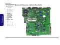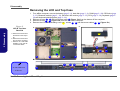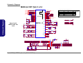
1
Preface
Notebook Computer
D400S/D410S
Service Manual
Preface
I
Preface
Notice
The company reserves the right to revise this publication or to change its contents without notice. Information contained
herein is for reference only and does not constitute a commitment on the part of the manufacturer or any subsequent vendor. They assume no responsibility or liability for any errors or inaccuracies that may appear in this publication nor are
they in anyway responsible for any loss or damage resulting from the use (or misuse) of this publication.
This publication and any accompanying software may not, in whole or in part, be reproduced, translated, transmitted or
reduced to any machine readable form without prior consent from the vendor, manufacturer or creators of this publication, except for copies kept by the user for backup purposes.
Preface
Brand and product names mentioned in this publication may or may not be copyrights and/or registered trademarks of
their respective companies. They are mentioned for identification purposes only and are not intended as an endorsement
of that product or its manufacturer.
Version 1.0
March 2003
Trademarks
Intel® and Pentium® are registered trademarks of Intel Corporation.
Windows® is a registered trademark of Microsoft Corporation.
Other brand and product names are trademarks and./or registered trademarks of their respective companies.
II
Preface
About this Manual
This manual is intended for service personnel who have completed sufficient training to undertake the maintenance and
inspection of personal computers.
It is organized to allow you to look up basic information for servicing and/or upgrading components of the D400S/D410S
series notebook PC.
The following information is included:
Chapter 1, Introduction, provides general information about the location of system elements and their specifications.
Chapter 2, Disassembly, provides step-by-step instructions for disassembling parts and subsystems and how to upgrade
elements of the system.
Preface
Appendix A, Part Lists
Appendix B, Schematic Diagrams
Appendix C, Upgrading Flash ROM BIOS
III
Preface
Related Documents
You may also need to consult the following manual for additional information:
Preface
User’s Manual on CD
This describes the notebook PC’s features and the procedures for operating the computer and its ROM-based setup program. It also describes the installation and operation of the utility programs provided with the notebook PC.
IV
Preface
Contents
Introduction ..............................................1-1
Disassembly ...............................................2-1
Overview ......................................................................................... 2-1
Maintenance Tools .......................................................................... 2-2
Connections .................................................................................... 2-2
Maintenance Precautions ................................................................ 2-3
Cleaning .......................................................................................... 2-3
Disassembly Steps .......................................................................... 2-4
Removing the Battery ..................................................................... 2-8
Removing the Hard Disk Drive ...................................................... 2-9
Hard Disk Upgrade Process ............................................................ 2-9
Removing the System Memory (RAM) ....................................... 2-10
Memory Upgrade Process ............................................................. 2-10
Removing the CD Device ............................................................. 2-12
Removing the Bluetooth Module .................................................. 2-14
Removing the Wireless LAN Module .......................................... 2-15
Removing the Processor ............................................................... 2-16
Removing the Keyboard ............................................................... 2-18
Removing the Keyboard Shielding Plate ...................................... 2-19
Removing the LCD and Top Case ................................................ 2-20
Removing the TouchPad and Click Board ................................... 2-22
Removing the Switch Board ......................................................... 2-23
Removing the Modem .................................................................. 2-24
Removing the Speakers ................................................................ 2-25
Removing the Mainboard ............................................................. 2-26
Removing the Fan Unit ................................................................. 2-27
Removing the Floppy Disk Drive Assembly ................................ 2-28
Removing the PC Card Assembly ................................................ 2-29
V
Preface
Overview .........................................................................................1-1
System Specifications .....................................................................1-2
Processor .........................................................................................1-2
Core Logic .......................................................................................1-2
Structure ..........................................................................................1-2
Security ............................................................................................1-2
Memory ...........................................................................................1-2
BIOS ................................................................................................1-2
LCD Options ...................................................................................1-2
Display ............................................................................................1-3
Storage Devices ...............................................................................1-3
Audio ...............................................................................................1-3
Keyboard .........................................................................................1-4
Interface ...........................................................................................1-4
PC Card ...........................................................................................1-4
Communication ...............................................................................1-4
Power Management .........................................................................1-5
Power ...............................................................................................1-5
Indicators .........................................................................................1-5
Environmental Spec ........................................................................1-5
Physical Dimensions .......................................................................1-5
Weight .............................................................................................1-5
Optional ...........................................................................................1-6
Design Differences ..........................................................................1-6
External Locator - Top View ..........................................................1-7
External Locator - Front & Left Side Views ...................................1-8
External Locator - Right Side & Rear Views ..................................1-9
External Locator - Bottom View ...................................................1-10
Mainboard Overview - Top (Key Parts) .......................................1-11
Mainboard Overview - Bottom (Key Parts) ................................. 1-12
Mainboard Overview - Top (Connectors) .................................... 1-13
Mainboard Overview - Bottom (Connectors) ............................... 1-14
Preface
Removing the LCD Front Panel Module ......................................2-30
Removing the Inverter ...................................................................2-31
Removing the PC Video Camera Module .....................................2-32
Removing the LCD Module ..........................................................2-33
Preface
Part Lists ..................................................A-1
Part List Illustration Location ........................................................ A-2
Top (400S) ...................................................................................... A-3
Bottom (400S) ................................................................................ A-4
LCD 14" (400S) ............................................................................. A-5
LCD 15" (400S) ............................................................................. A-6
CD-ROM Drive (400S) .................................................................. A-7
CD-RW Drive (400S) ..................................................................... A-8
Combo Drive (400S) ...................................................................... A-9
DVD-ROM Drive (400S) ............................................................. A-10
Floppy Disk Drive (400S) ............................................................ A-11
Hard Disk Drive (400S) ............................................................... A-12
Top (410S) .................................................................................... A-13
Bottom (410S) .............................................................................. A-14
LCD 14" (410S) ........................................................................... A-15
LCD 15" (410S) ........................................................................... A-16
CD-ROM Drive (410S) ................................................................ A-17
CD-RW Drive (410S) ................................................................... A-18
Combo Drive (410S) .................................................................... A-19
DVD-ROM Drive (410S) ............................................................. A-20
Floppy Disk Drive (410S) ............................................................ A-21
Hard Disk Drive (410S) ............................................................... A-22
Schematic Diagrams................................. B-1
System Block Diagram ................................................................... B-2
Socket 478 1 of 2 ............................................................................ B-3
Socket 478 & ITP 2 of 2 ................................................................. B-4
Clock Generator ............................................................................. B-5
VI
M650 (Host/AGP) 1 of 4 ................................................................B-6
M650 (Memory for DDR) 2 of 4 ....................................................B-7
M650 (& CRT Out) 3 of 4 ..............................................................B-8
M650 (Power) 4 of 4 .......................................................................B-9
DDR Memory DIMM ...................................................................B-10
DDR SSTL-2 Termination ...........................................................B-11
LVDS Interface (SiS302LV) ........................................................B-12
Panel Con & LED Indicator .........................................................B-13
962 (PCI/IDE/HyperZip) 1 of 4 ....................................................B-14
962 (Misc Signals) 2 of 4 ..............................................................B-15
962 (USB I/F) 3 of 4 .....................................................................B-16
962 (Power & RTC) 4 of 4 ...........................................................B-17
HDD/Combo Connector ...............................................................B-18
USB Port .......................................................................................B-19
PCMCIA TI1410 ..........................................................................B-20
PCMCIA Power ............................................................................B-21
1394 PHY TSB41LV01 ................................................................B-22
LPC SI/O ......................................................................................B-23
LPT/COM Port .............................................................................B-24
LPC H8 .........................................................................................B-25
LAN RTL8100BL ........................................................................B-26
Audio Codec ALC201A ...............................................................B-27
Audio Out & Off Board Connectors .............................................B-28
System Power Control ..................................................................B-29
Fan Control and SpeedStep ..........................................................B-30
VCORE .........................................................................................B-31
DDR Power ...................................................................................B-32
System ...........................................................................................B-33
Charger .........................................................................................B-34
SW Board and HotKey .................................................................B-35
TouchPad and Switch Board ........................................................B-36
Updating the FLASH ROM BIOS......... C-1
Introduction
1: Introduction
Overview
This manual covers the information you need to service or upgrade the D400S/D410S series notebook computer. Information about operating the computer (e.g. getting started, and the Setup utility) is in the User’s Manual. Information
about drivers (e.g. VGA & audio) is also found in User’s Manual. That manual is shipped with the computer.
Operating systems (e.g. DOS, Windows 9x, Windows NT 4.0, Windows 2000, Windows XP, OS/2 Warp, UNIX, etc.) have
their own manuals as do application software (e.g. word processing and database programs). If you have questions about
those programs, you should consult those manuals.
1.Introduction
The D400S/D410S series notebook is designed to be upgradeable. See “Disassembly” on page 2 - 1 for a detailed description of the upgrade procedures for each specific component. Please note the warning and safety information indicated by the “!” symbol.
The balance of this chapter reviews the computer’s technical specifications and features.
Overview 1 - 1
Introduction
System Specifications
Processor
• Intel Pentium 4 Processor - (478-pin) FC-PGA2 package
(µ0.13) 0.13 Micron Process Technology, 512KB L2 Cache & 400MHz FSB - 2.0/ 2.2/ 2.4/ 2.5 /2.6 GHz
(µ0.13) 0.13 Micron Process Technology, 512KB L2 Cache & 533MHz FSB - 2.26/ 2.4/ 2.53/ 2.66/ 2.66/ 2.8 GHz
Core Logic
1.Introduction
• SIS M650 + 962
Structure
• PC99 compliant
Security
• Security (Kensington® Type) Lock
• BIOS Password
Memory
• Two 200-pin DDR SODIMM sockets, supporting DDR SDRAM SODIMM (2.5V) - DDR 200/ DDR 266/ DDR 333 compliant
• Memory expandable up to 1024MB (128/256/512MB SODIMM Modules)
BIOS
• One 512KB Flash ROM
• Phoenix BIOS
LCD Options
• 14.1" XGA TFT (1024*768)
• 15.0" XGA TFT (1024*768)
• 15.0" SXGA+ TFT(1400*1050)
1 - 2 System Specifications
Introduction
Display
•
•
•
•
•
High Performance 256-bit 3D engine
Advanced HW accelerator for DVD playback
Fully Direct X 8.0 compliant graphics engine
Dual-View display monitor
CRT Resolution up to 2048 * 1536
Storage Devices
• 3.5" 3-mode Floppy Disk Drive
•
•
•
•
•
•
Video Memory
The system allocates
or "shares" a portion of
system memory for
video use. "Shared"
memory is user-configurable via the SCU.
The default setting is
set to 32MB.
1.Introduction
• Easy changeable 2.5" 9.5 mm (h) Hard Disk Drive
Supporting Master mode IDE
Supports PIO mode 4
ATA-33/66/100/133
Ultra DMA
!
12.7mm(h) Device Bay for ONE of the following drive configuration options:
24* CD-ROM
8* DVD-ROM
CD-RW (16* CD-R/ 10* CD-RW/ 24* CD-ROM)
Combo (8* DVD-ROM/ 8* CD-R/ 8* CD-RW/ 24* CD-ROM)
Combo (8* DVD-ROM/ 24* CD-R/ 10* CD-RW/ 24* CD-ROM)
Audio
•
•
•
•
•
•
•
•
AC'97 2.1 compliant interface
3D stereo enhanced sound system
Compatible with Sound-Blaster PRO™
S/PDIF Digital output (5.1 CH) for DVD content and stereo audio
Microphone-in jack
Headphone-out jack
Built-in microphone
2 built-in speakers (1 watt 35 * 16 mm)
System Specifications 1 - 3
Introduction
Keyboard
• “Win Key” keyboard
1.Introduction
Interface
•
•
•
•
•
•
•
•
•
•
•
•
•
•
•
Built-in TouchPad (scrolling key functionality integrated)
Three USB 2.0 ports
One IEEE 1394 port
One S-Video jack for TV output
One serial port
One parallel port (LPT1), supporting ECP / EPP
Infrared transceiver IrDA 1.1 FIR/SIR/ASKIR
One external CRT monitor port
One external keyboard/mouse (through Y cable) PS/2 port
One speaker-out/headphone-out jack
One microphone-in jack
One RJ-11 jack for modem
One RJ-45 jack for 100M/10M LAN
One S/PDIF out port
One DC-in jack
PC Card
• One type II PCMCIA 3.3V/5V socket supporting CardBus
Communication
•
•
•
•
•
•
Wireless Infrared transfer IrDA 1.1 compliant, 1cm - 1M operating distance, 115.2K bps SIR/ 4Mbps FIR
10/100Mb Ethernet LAN built-in
56K MDC modem V.90 & V.92 compliant
802.11b wireless LAN module (available as a factory option)
Bluetooth module (available as a factory option)
Built-in PC camera module (available as a factory option)
1 - 4 System Specifications
Introduction
Power Management
•
•
•
•
•
Supports ACPI v1.0b
Supports Hibernate mode
Supports Standby mode
Supports battery low sleep
Supports resume from modem ring
Power
•
•
•
•
Full range AC adapter
AC-Input 100~240V, 50~60Hz
DC Output 20V, 3.25A (90w)
Supports one removable Smart Li-Ion battery 2200mAH/8 cell
• LED indicators (HDD, Power On/ AC-In/ Suspend, Battery Charging/Battery Full, Num Lock, Caps Lock, Scroll Lock)
Environmental Spec
• Temperature
Operating:
Non-Operating:
5°C ~ 35°C
-20°C ~ 60°C
• Relative Humidity
Operating:
Non-Operating:
20% ~ 80%
10% ~ 90%
Physical Dimensions
• 329 (w) x 275 (d) x 36.5 (h) mm
Weight
• 3.0 kg w/o battery
System Specifications 1 - 5
1.Introduction
Indicators
Introduction
Optional
•
•
•
•
•
•
•
DVD-ROM Drive
CD-RW Drive
Combination Drive
Software DVD player
Wireless LAN module
Bluetooth module
Video Camera
Design Differences
1.Introduction
This manual refers to the two notebook designs pictured below. The designs vary slightly in external design. Photographs
used throughout this manual are of Design I.
Figure 1
Design Differences
Design I
1 - 6 System Specifications
Design II
Introduction
External Locator - Top View
Figure 2
Top View
1
2
7
4
5
6
8
9
10
External Locator - Top View 1 - 7
1.Introduction
3
1. Optional Built-in
USB Camera
2. LCD
3. Built-In
Microphone
4. LED Power &
Communication
Indicators
5. LED Status
Indicators
6. Hot-Key buttons
7. Close Cover
Switch
8. Power Button
9. Keyboard
10. TouchPad and
Buttons
Introduction
Figure 3
External Locator - Front & Left Side Views
Front View
1.
2.
3.
4.
5.
1.Introduction
6.
7.
8.
LCD Latches
IEEE 1394 Port
S/PDIF Out Port
Microphone-In
Jack
Headphone-Out
Jack
Infrared
Transceiver
Wireless LAN On/
Off Switch
Built-In Speakers
1
1
8
8
2
Figure 4
CD Device Bay
USB 2.0 Port
Floppy Disk Drive
PC Card Slot
PC Card Slot Eject
Buttons
4
5
6
7
2
Left Side View
1.
2.
3.
4.
5.
3
1
1 - 8 External Locator - Front & Left Side Views
4
3
5
Introduction
External Locator - Right Side & Rear Views
Figure 5
Right Side View
1. Security Lock Slot
1
1
Figure 6
4
5
6
7
8
Rear View
9 10
1.
2.
3.
4.
Vent
DC-In Jack
2 * USB Ports
External Monitor
(CRT) Port
5. Parallel Port
6. Serial Port
7. S-Video-Out Port
8. PS/2 Type Port
9. RJ-11 Phone Jack
10. RJ-45 LAN Jack
External Locator - Right Side & Rear Views 1 - 9
1.Introduction
2
3
Introduction
External Locator - Bottom View
Figure 7
Bottom View
Vent/Fan Outlets
Battery Cover
Hard Disk Cover
Bluetooth
Module Cover
5. CPU Heatsink
Cover
1.Introduction
1.
2.
3.
4.
Note: The RAM and
optional
Wireless
LAN module are located under the CPU
Heatsink Cover
5
1
1
4
2
1 - 10 External Locator - Bottom View
3
Introduction
Mainboard Overview - Top (Key Parts)
Figure 8
Mainboard Top
Key Parts
5
2
3
4
1
Mainboard Overview - Top (Key Parts) 1 - 11
1.Introduction
1. PC Card
Assembly
2. Northbridge - SiS
M650
3. Southbridge - SiS
962
4. LPC Super I/O
NS PC87393
5. Flash ROM BIOS
Introduction
Figure 9
Mainboard Overview - Bottom (Key Parts)
1.Introduction
Mainboard Bottom
Key Parts
1. CPU Socket (no
CPU installed)
2. Memory Sockets
(no memory
installed)
3. SiS 302LV TVOut Controller
4. LAN Controller
RTL8100BL
5. CardBus ENE
1410
6. ALC202 - Audio
Codec
7. 1394 PHY
TSB41LV01
8. Clock Generator
9. Keyboard
Controller - KBC
H8 H8S-2149 HM
1
3
4
8
2
9
7
6
1 - 12 Mainboard Overview - Bottom (Key Parts)
5
Introduction
Mainboard Overview - Top (Connectors)
Figure 10
Mainboard Top
Connectors
1
2
3
5
6
7
8
11
10
9
Mainboard Overview - Top (Connectors) 1 - 13
1.Introduction
4
1. Modem Cable
Connector (CN1)
2. LCD and Inverter
Connector
(JLCD1)
3. Video Camera
Module
Connector
(JCCD1)
4. Switch Board
Connector
(JSW1)
5. Fan Connector
(JFAN1)
6. TouchPad
Connector (JTP1)
7. Keyboard
Connector (JKB1)
8. Modem
Connector
(JMDC1)
9. Speaker
Connector
(JSPK1)
10. Floppy Disk
Controller
(JFDD1)
11. Speaker
Connector
(JSPK2)
Introduction
Figure 11
Mainboard Overview - Bottom (Connectors)
Mainboard Bottom
Connectors
1.Introduction
1
1. Wireless LAN
Connector
(JWL1)
2. Fan Connector
(JFAN2)
3. CD Connector
(JCDROM1)
4. Hard Disk
Connector
(JHDD1)
5. Bluetooth
Connector (JBT1)
6. Battery
Connector
(JBAT1)
7. Battery
Connector (CN5)
2
3
4
7
1 - 14 Mainboard Overview - Bottom (Connectors)
5
6
Disassembly
2: Disassembly
Overview
This chapter provides step-by-step instructions for disassembling the D400S/D410S series notebook’s parts and subsystems. When it comes to reassembly, reverse the procedures (unless otherwise indicated).
We suggest you completely review any procedure before you take the computer apart.
!
Component Parts
To make the disassembly process easier each section may have a box in the page margin. Information contained under
the figure # will give a synopsis of the sequence of procedures involved in the disassembly procedure. A box with a !
lists the relevant parts you will have after the disassembly process is complete. Note: The parts listed will be for the disassembly procedure listed ONLY, and not any previous disassembly step(s) required. Refer to the part list for the previous disassembly procedure. The amount of screws you should be left with will be listed here also.
"
Information
A box with a " will provide any possible helpful information. A box with a ! contains warnings.
An example of these types of boxes are shown in the sidebar.
!
Warning
Overview 2 - 1
2.Disassembly
Procedures such as upgrading/replacing the RAM, CD device and hard disk are included in the User’s Manual but are
repeated here for your convenience.
Disassembly
NOTE: All disassembly procedures assume that the system is turned OFF, and disconnected from any power supply (the
battery is removed too).
Maintenance Tools
The following tools are recommended when working on the notebook PC:
2.Disassembly
•
•
•
•
•
•
M3 Philips-head screwdriver
M2.5 Philips-head screwdriver (magnetized)
M2 Philips-head screwdriver
Small flat-head screwdriver
Pair of needle-nose pliers
Anti-static wrist-strap
Connections
Connections within the computer are one of four types:
2 - 2 Overview
Locking collar sockets for ribbon connectors
To release these connectors, use a small flat-head screwdriver to
gently pry the locking collar away from its base. When replacing the connection, make sure the connector is oriented in the
same way. The pin1 side is usually not indicated.
Pressure sockets for multi-wire connectors
To release this connector type, grasp it at its head and gently
rock it from side to side as you pull it out. Do not pull on the
wires themselves. When replacing the connection, do not try to
force it. The socket only fits one way.
Pressure sockets for ribbon connectors
To release these connectors, use a small pair of needle-nose pliers to gently lift the connector away from its socket. When replacing the connection, make sure the connector is oriented in
the same way. The pin1 side is usually not indicated.
Board-to-board or multi-pin sockets
To separate the boards, gently rock them from side to side as
you pull them apart. If the connection is very tight, use a small
flat-head screwdriver - use just enough force to start.
Disassembly
Maintenance Precautions
The following precautions are a reminder. To avoid personal injury or damage to the computer while performing a removal and/or replacement job, take the following precautions:
Power Safety
Warning
Before you undertake
any upgrade procedures, make sure that
you have turned off the
power, and disconnected all peripherals
and cables (including
telephone lines). It is
advisable to also remove your battery in
order to prevent accidentally turning the
machine on.
Cleaning
Do not apply cleaner directly to the computer, use a soft clean cloth.
Do not use volatile (petroleum distillates) or abrasive cleaners on any part of the computer.
Overview 2 - 3
2.Disassembly
1. Don't drop it. Perform your repairs and/or upgrades on a stable surface. If the computer falls, the case and other
components could be damaged.
2. Don't overheat it. Note the proximity of any heating elements. Keep the computer out of direct sunlight.
3. Avoid interference. Note the proximity of any high capacity transformers, electric motors, and other strong magnetic fields. These can hinder proper performance and damage components and/or data. You should also monitor
the position of magnetized tools (i.e. screwdrivers).
4. Keep it dry. This is an electrical appliance. If water or any other liquid gets into it, the computer could be badly
damaged.
5. Be careful with power. Avoid accidental shocks, discharges or explosions.
•Before removing or servicing any part from the computer, turn the computer off and detach any power supplies.
•When you want to unplug the power cord or any cable/wire, be sure to disconnect it by the plug head. Do not pull on the wire.
6. Peripherals – Turn off and detach any peripherals.
7. Beware of static discharge. ICs, such as the CPU and main support chips, are vulnerable to static electricity.
Before handling any part in the computer, discharge any static electricity inside the computer. When handling a
printed circuit board, do not use gloves or other materials which allow static electricity buildup. We suggest that
you use an anti-static wrist strap instead.
8. Beware of corrosion. As you perform your job, avoid touching any connector leads. Even the cleanest hands produce oils which can attract corrosive elements.
9. Keep your work environment clean. Tobacco smoke, dust or other air-born particulate matter is often attracted
to charged surfaces, reducing performance.
10. Keep track of the components. When removing or replacing any part, be careful not to leave small parts, such as
screws, loose inside the computer.
!
Disassembly
Disassembly Steps
The following table lists the disassembly steps, and on which page to find the related information. PLEASE PERFORM
THE DISASSEMBLY STEPS IN THE ORDER INDICATED.
To remove the Battery:
1. Remove the battery
To remove the Processor:
page 2 - 8
1. Remove the battery
2. Remove the processor
page 2 - 8
page 2 - 16
page 2 - 8
page 2 - 9
To remove the Keyboard:
page 2 - 8
page 2 - 10
To remove the Keyboard Shielding Plate:
To remove the HDD:
2.Disassembly
1. Remove the battery
2. Remove the HDD
1. Remove the battery
2. Remove the keyboard
page 2 - 8
page 2 - 18
To remove the System Memory:
1. Remove the battery
2. Remove the system memory
To remove the CD Device:
1. Remove the battery
2. Remove the CD Device
page 2 - 8
page 2 - 12
To remove the Bluetooth Module:
1. Remove the battery
2. Remove the Bluetooth module
page 2 - 8
page 2 - 14
To remove the Wireless LAN Module:
1. Remove the battery
2. Remove the Wireless LAN module
2 - 4 Disassembly Steps
page 2 - 8
page 2 - 15
1. Remove the battery
page 2 - 8
2. Remove the keyboard
page 2 - 18
3. Remove the keyboard shielding plate page 2 - 19
To remove the LCD and Top Case:
1.
2.
3.
4.
5.
6.
7.
8.
9.
10.
Remove the battery
Remove the HDD
Remove the system memory
Remove the CD Device
Remove the Bluetooth module
Remove the Wireless LAN module
Remove the processor
Remove the keyboard
Remove the keyboard shielding plate
Remove the LCD & top case
page 2 - 8
page 2 - 9
page 2 - 10
page 2 - 12
page 2 - 14
page 2 - 15
page 2 - 16
page 2 - 18
page 2 - 19
page 2 - 20
Disassembly
To remove the Modem:
1.
2.
3.
4.
5.
6.
7.
8.
9.
10.
11.
1.
2.
3.
4.
5.
6.
7.
8.
9.
10.
11.
Remove the battery
Remove the HDD
Remove the system memory
Remove the CD Device
Remove the Bluetooth module
Remove the Wireless LAN module
Remove the processor
Remove the keyboard
Remove the keyboard shielding plate
Remove the LCD & top case
Remove the touchpad and click board
page 2 - 8
page 2 - 9
page 2 - 10
page 2 - 12
page 2 - 14
page 2 - 15
page 2 - 16
page 2 - 18
page 2 - 19
page 2 - 20
page 2 - 22
To remove the Switch Board:
1.
2.
3.
4.
5.
6.
7.
8.
9.
10.
11.
Remove the battery
Remove the HDD
Remove the system memory
Remove the CD Device
Remove the Bluetooth module
Remove the Wireless LAN module
Remove the processor
Remove the keyboard
Remove the keyboard shielding plate
Remove the LCD & top case
Remove the switch board
Remove the battery
Remove the HDD
Remove the system memory
Remove the CD Device
Remove the Bluetooth module
Remove the Wireless LAN module
Remove the processor
Remove the keyboard
Remove the keyboard shielding plate
Remove the LCD & top case
Remove the modem
page 2 - 8
page 2 - 9
page 2 - 10
page 2 - 12
page 2 - 14
page 2 - 15
page 2 - 16
page 2 - 18
page 2 - 19
page 2 - 20
page 2 - 24
To remove the Speakers:
page 2 - 8
page 2 - 9
page 2 - 10
page 2 - 12
page 2 - 14
page 2 - 15
page 2 - 16
page 2 - 18
page 2 - 19
page 2 - 20
page 2 - 23
1.
2.
3.
4.
5.
6.
7.
8.
9.
10.
11.
Remove the battery
Remove the HDD
Remove the system memory
Remove the CD Device
Remove the Bluetooth module
Remove the Wireless LAN module
Remove the processor
Remove the keyboard
Remove the keyboard shielding plate
Remove the LCD & top case
Remove the speakers
page 2 - 8
page 2 - 9
page 2 - 10
page 2 - 12
page 2 - 14
page 2 - 15
page 2 - 16
page 2 - 18
page 2 - 19
page 2 - 20
page 2 - 25
Disassembly Steps 2 - 5
2.Disassembly
To remove the TouchPad and Click Board:
Disassembly
2.Disassembly
To remove the Mainboard:
1.
2.
3.
4.
5.
6.
7.
8.
9.
10.
11.
12.
Remove the battery
Remove the HDD
Remove the system memory
Remove the CD Device
Remove the Bluetooth module
Remove the Wireless LAN module
Remove the processor
Remove the keyboard
Remove the keyboard shielding plate
Remove the LCD & top case
Remove the speakers
Remove the mainboard
To remove the Floppy Disk Drive Assembly:
page 2 - 8
page 2 - 9
page 2 - 10
page 2 - 12
page 2 - 14
page 2 - 15
page 2 - 16
page 2 - 18
page 2 - 19
page 2 - 20
page 2 - 25
page 2 - 26
1.
2.
3.
4.
5.
6.
7.
8.
9.
10.
11.
12.
13.
Remove the battery
Remove the HDD
Remove the system memory
Remove the CD Device
Remove the Bluetooth module
Remove the Wireless LAN module
Remove the processor
Remove the keyboard
Remove the keyboard shielding plate
Remove the LCD & top case
Remove the speakers
Remove the mainboard
Remove the floppy disk drive
page 2 - 8
page 2 - 9
page 2 - 10
page 2 - 12
page 2 - 14
page 2 - 15
page 2 - 16
page 2 - 18
page 2 - 19
page 2 - 20
page 2 - 25
page 2 - 26
page 2 - 28
page 2 - 8
page 2 - 9
page 2 - 10
page 2 - 12
page 2 - 14
page 2 - 15
page 2 - 16
page 2 - 18
page 2 - 19
page 2 - 20
page 2 - 25
page 2 - 26
page 2 - 27
To remove the PC Card Assembly:
To remove the Fan Unit:
1.
2.
3.
4.
5.
6.
7.
8.
9.
10.
11.
12.
13.
2 - 6 Disassembly Steps
Remove the battery
Remove the HDD
Remove the system memory
Remove the CD Device
Remove the Bluetooth module
Remove the Wireless LAN module
Remove the processor
Remove the keyboard
Remove the keyboard shielding plate
Remove the LCD & top case
Remove the speakers
Remove the mainboard
Remove the fan unit
1.
2.
3.
4.
5.
6.
7.
8.
9.
10.
11.
12.
13.
Remove the battery
Remove the HDD
Remove the system memory
Remove the CD Device
Remove the Bluetooth module
Remove the Wireless LAN module
Remove the processor
Remove the keyboard
Remove the keyboard shielding plate
Remove the LCD & top case
Remove the speakers
Remove the mainboard
Remove the PC Card assembly
page 2 - 8
page 2 - 9
page 2 - 10
page 2 - 12
page 2 - 14
page 2 - 15
page 2 - 16
page 2 - 18
page 2 - 19
page 2 - 20
page 2 - 25
page 2 - 26
page 2 - 29
Disassembly
To remove the PC Video Camera Module:
1.
2.
3.
4.
5.
6.
7.
8.
9.
10.
11.
page 2 - 8
page 2 - 9
page 2 - 10
page 2 - 12
page 2 - 14
page 2 - 15
page 2 - 16
page 2 - 18
page 2 - 19
page 2 - 20
page 2 - 30
1.
2.
3.
4.
5.
6.
7.
8.
9.
10.
11.
12.
page 2 - 8
page 2 - 9
page 2 - 10
page 2 - 12
page 2 - 14
page 2 - 15
page 2 - 16
page 2 - 18
page 2 - 19
page 2 - 20
page 2 - 30
page 2 - 31
To remove the LCD Module:
Remove the battery
Remove the HDD
Remove the system memory
Remove the CD Device
Remove the Bluetooth module
Remove the Wireless LAN module
Remove the processor
Remove the keyboard
Remove the keyboard shielding plate
Remove the LCD & top case
Remove the front panel module
Remove the battery
Remove the HDD
Remove the system memory
Remove the CD Device
Remove the Bluetooth module
Remove the Wireless LAN module
Remove the processor
Remove the keyboard
Remove the keyboard shielding plate
Remove the LCD & top case
Remove the front panel module
Remove the PC Video Camera
page 2 - 8
page 2 - 9
page 2 - 10
page 2 - 12
page 2 - 14
page 2 - 15
page 2 - 16
page 2 - 18
page 2 - 19
page 2 - 20
page 2 - 30
page 2 - 32
To remove the Inverter:
1.
2.
3.
4.
5.
6.
7.
8.
9.
10.
11.
12.
Remove the battery
Remove the HDD
Remove the system memory
Remove the CD Device
Remove the Bluetooth module
Remove the Wireless LAN module
Remove the processor
Remove the keyboard
Remove the keyboard shielding plate
Remove the LCD & top case
Remove the front panel module
Remove the inverter
1.
2.
3.
4.
5.
6.
7.
8.
9.
10.
11.
12.
13.
Remove the battery
Remove the HDD
Remove the system memory
Remove the CD Device
Remove the Bluetooth module
Remove the Wireless LAN module
Remove the processor
Remove the keyboard
Remove the keyboard shielding plate
Remove the LCD & top case
Remove the front panel module
Remove the inverter
Remove the LCD module
page 2 - 8
page 2 - 9
page 2 - 10
page 2 - 12
page 2 - 14
page 2 - 15
page 2 - 16
page 2 - 18
page 2 - 19
page 2 - 20
page 2 - 30
page 2 - 31
page 2 - 33
Disassembly Steps 2 - 7
2.Disassembly
To remove the LCD Front Panel Module:
Disassembly
Removing the Battery
1.
2.
3.
4.
5.
Turn the computer off, and turn it over.
Remove screws 1 & 2 (Figure 1a) from the battery cover 3 , and remove the cover.
Carefully (use a small screwdriver) disconnect the battery cable at point 4 (Figure 1b).
Lift the battery 5 out of the computer.
When replacing the battery, connect the cable first.
Figure 1
Battery Removal
2.Disassembly
a.
b.
a. Remove the 2 screws
and the battery cover.
b. Carefully disconnect the
battery cable and remove
the battery.
4
3
1
2
5
!
3. Battery Cover
5. Battery
• 2 Screws
2 - 8 Removing the Battery
Disassembly
Removing the Hard Disk Drive
The hard disk drive is mounted in a removable case and can be taken out to accommodate other 2.5" IDE hard disk drives
with a height of 9.5mm (h). Follow your operating system’s installation instructions, and install all necessary drivers and
utilities (as outlined in Chapter 4 of the User’s Manual) when setting up a new hard disk.
Hard Disk Upgrade Process
1.
2.
3.
4.
5.
Turn off the computer, remove the battery (page 2 - 8) and turn it over.
Remove screws 1 & 4 (Figure 2a) from the hard disk cover 5 , and remove the cover.
Carefully (use a small screwdriver) disconnect the battery cable at point 6 (Figure 2b).
Lift the HDD assembly 7 out of the computer.
Reverse the process to install a new hard disk.
b.
Figure 2
!
HDD Assembly
Assembly Removal
HDD System Warning
5
New HDD’s are blank. Before
you begin make sure:
6
You have backed up any data
you want to keep from your old
HDD.
You have all the CD-ROMs
and FDDs required to install
your operating system and
programs.
1
a. Remove the 4 screws.
b. Disconnect the HDD cable and lift the HDD assembly out of the bay.
2
!
If you have access to the internet, download the latest application and hardware driver
updates for the operating system you plan to install. Copy
these to a removable medium.
7
4
3
5. Hard Disk Cover
7. Hard Disk
• 4 Screws
Removing the Hard Disk Drive 2 - 9
2.Disassembly
a.
Disassembly
Removing the System Memory (RAM)
The computer has two memory sockets for 200 pin Small Outline Dual In-line Memory Modules (SO-DIMM) supporting
DDR 200/266/333MHz. The main memory can be expanded up to 1024MB. The SO-DIMM modules supported are
128Mb, 256Mb, and 512Mb. The total memory size is automatically detected by the POST routine once you turn on your
computer.
Memory Upgrade Process
2.Disassembly
Figure 3
Memory Socket
Cover Removal
1. Turn off the computer, remove the battery (page 2 - 8) and turn it over.
2. Remove screws 1 - 6 (Figure 3a) from the memory socket cover.
3. Carefully lift up the memory socket cover 7 (Figure 3b) (a fan cable 8 is still attached to the mainboard and you
can disconnect it).
4. If there is a module currently installed which needs to be upgraded/replaced then remove it.
b.
a.
a. Remove the screws.
b. Carefully lift the cover off
the computer.
7
8
1
!
2
6
3
7. Socket Cover
• 6 Screws
2 - 10 Removing the System Memory (RAM)
4
5
Disassembly
5. Gently pull the two release latches ( 1 & 2 ) on the sides of the memory socket toward the sides of the computer.
Figure 4
a.
Removing/
Installing a RAM
Module
a. Pull the release
latches.
b.Remove the module.
3
2
The module 3 (Figure 4b) will pop-up, and you can remove it.
Repeat the process for the second module if necessary.
Insert a new module holding it at about a 30° angle and fit the connectors firmly into the memory slot.
The module will only fit one way as defined by its pin alignment. Make sure the module is seated as far into the slot
as it will go. DO NOT FORCE IT; it should fit without much pressure.
b.
3
10.
11.
12.
13.
!
Contact Warning
Be careful not to touch
the metal pins on the
module’s connecting
edge. Even the cleanest hands have oils
which can attract particles, and degrade the
module’s
performance.
3
Press the module down towards the mainboard until the slot levers click into place to secure the module.
Replace the memory socket cover (be careful with the fan cable) and the 6 screws (see page 2 - 10).
Restart the computer.
The BIOS will register the new memory configuration as it starts up.
!
3. RAM Module
Removing the System Memory (RAM) 2 - 11
2.Disassembly
6.
7.
8.
9.
1
Disassembly
Removing the CD Device
The easy changeable CD device may be upgraded or changed.
1. Turn off the computer, remove the battery (page 2 - 8) and turn it over.
2. Remove screws 1 - 6 (Figure 5a) from the memory socket cover.
3. Carefully lift up the memory socket cover 7 (a fan cable 8 is still attached to the mainboard and you can disconnect it).
b.
2.Disassembly
a.
Figure 5
Memory Socket
Cover Removal
7
a. Remove the screws.
b. Carefully lift the cover off
the computer.
8
1
2
!
7. Socket Cover
• 6 Screws
2 - 12 Removing the CD Device
6
3
4
5
Disassembly
4. Use a screwdriver to carefully push the CD device assembly 1 out of the computer at point 2 .
Figure 6
CD Device Removal
Push the CD device out
off the computer at point
2.
2
2.Disassembly
1
5. Insert the new device and carefully slide it into the computer (the device only fits one way. DO NOT FORCE IT; The
screw holes should line up.
6. Replace the memory socket cover (be careful with the fan cable) and the 6 screws (see page 2 - 12 ).
7. Restart the computer to allow it to automatically detect the new device.
!
1. CD Device
Removing the CD Device 2 - 13
Disassembly
Removing the Bluetooth Module
Turn off the computer, remove the battery (page 2 - 8) and turn it over.
Remove screws 1 - 2 (Figure 7a) from the Bluetooth module cover.
Carefully lift up the Bluetooth module cover 3 off the computer.
Remove screws 3 - 6 (Figure 7c) and carefully disconnect cables 8 - 9 , then remove the Bluetooth module
10 (Figure 7d).
1.
2.
3.
4.
Figure 7
2.Disassembly
Bluetooth Module
Removal
a. Remove the screws.
b. Carefully lift the cover off
the computer.
c. Remove the screws and
disconnect the cables.
d. Remove the Bluetooth
module.
b.
a.
1
2
3
c.
d.
3
4
8
9
6
!
3. Bluetooth Cover
10. Bluetooth Module
• 6 Screws
2 - 14 Removing the Bluetooth Module
5
10
Disassembly
Removing the Wireless LAN Module
1. Turn off the computer, remove the battery (page 2 - 8) and turn it over.
2. Remove screws 1 - 6 from the memory socket cover.
3. Carefully lift up the memory socket cover 7 (a fan cable 8 is still attached to the mainboard and you can disconnect it).
4. Remove screws 9 - 10 (Figure 8c), and carefully disconnect cables 11 & 12 .
5. Lift the Wireless Lan module 13 (Figure 8d) off the computer.
Figure 8
Wireless LAN
Module Removal
a.
1
b.
a. Remove the screws.
b. Carefully lift the cover off
the computer.
6
3
4
c.
!
7
5
Antenna Cable
Connection
When re-inserting a
Wireless LAN module,
make sure the antenna
cable connects to the
connector J1 which is
indicated as point 12
in Figure 8c.
d.
11
10
9
13
!
7. Socket Cover
13. WLAN Module
12
.
• 8 Screws
Removing the Wireless LAN Module 2 - 15
2.Disassembly
2
8
Disassembly
Removing the Processor
Figure 9
2.Disassembly
Processor Removal
a. Remove the screws.
b. Carefully lift the cover off
the computer.
c. Remove the screws in
the order indicated.
d. Remove the heat sink.
1. Turn off the computer, remove the battery (page 2 - 8) and turn it over.
2. Remove screws 1 - 6 from the memory socket cover.
3. Carefully lift up the memory socket cover 7 (a fan cable 8 is still attached to the mainboard and you can disconnect it).
4. Remove screws 9 - 12 (Figure 9c) from the heat sink, in the order indicated on the label.
5. Carefully lift up the heat sink 13 (Figure 9d) off the computer.
a.
1
b.
2
4
Reassembly Screw
Order
When replacing the
heat sink, make sure
you insert the screws
in the same order indicated on the label.
6
3
!
7. Socket Cover
13. Heat Sink
• 10 Screws
2 - 16 Removing the Processor
7
5
c.
!
8
d.
11
9
10
12
13
Disassembly
6. Use a screwdriver to unlock the CPU by giving the lock 1 (Figure 10a) a turn to the left.
7. Lift the CPU 3 (Figure 10c) off the computer (make sure the lock is fully turned to the left as the CPU will lift off
with ease).
a.
Figure 10
b.
Processor Removal
(cont’d)
Unlocked
Locked
a. Locate the CPU lock.
b. Turn the lock to the left to
unlock it.
c. Remove the CPU.
2.Disassembly
1
c.
!
Caution
3
The heat sink, and
CPU area in general,
contains parts which
are subject to high
temperatures.
Allow
the area time to cool
before removing these
parts.
!
3. CPU
Removing the Processor 2 - 17
Disassembly
Removing the Keyboard
1. Turn off the computer, remove the battery (page 2 - 8).
2. Press the three keyboard latches at the top of the keyboard to elevate the keyboard from its normal position (you
may need to use a small screwdriver to do this).
3. Carefully lift the keyboard up and out, being careful not to bend the keyboard ribbon cable 1 (Figure 11b).
4. Disconnect the keyboard ribbon cable from the locking collar socket 2 (Figure 11b) and lift the keyboard 3 up
out of the computer.
Figure 11
a.
c.
2.Disassembly
Keyboard Removal
a. Press the latches to elevate the keyboard.
b. Disconnect the keyboard
cable form the locking
collar.
c. Remove the keyboard.
b.
1
3
!
3. Keyboard
2 - 18 Removing the Keyboard
2
Disassembly
Removing the Keyboard Shielding Plate
1. Turn off the computer, remove the battery (page 2 - 8) and keyboard (page 2 - 18).
2. Remove screws 1 - 9 (Figure 12a) from the keyboard shielding plate and lift the plate 10 off the computer.
Figure 12
a.
Keyboard Shielding
Plate Removal
b.
1
2
3
4
8
5
2.Disassembly
6
a. Remove the screws from
the shielding plate.
b. Lift the plate off the computer.
7
9
10
!
10. Shielding Plate
• 9 Screws
Removing the Keyboard Shielding Plate 2 - 19
Disassembly
Removing the LCD and Top Case
1. Turn off the computer, remove the battery (page 2 - 8), hard disk (page 2 - 9), RAM (page 2 - 10), CD Device (page
2 - 12), Bluetooth module (page 2 - 14), Wireless LAN module (page 2 - 15), CPU (page 2 - 16), keyboard (page 2 18) and keyboard shielding plate (page 2 - 19).
2. Remove screws 1 - 10 , and disconnect cable 11 (Figure 13a) from the bottom off the computer.
3. Remove screws 12 - 21 (Figure 13b) from the rear off the computer.
4. Remove the LCD cable shielding cover 26 , screws 22 - 23 and disconnect cables 24 - 25 (Figure 13c).
Figure 13
2.Disassembly
LCD & Top Case
Removal
c.
a.
1
2
3
26
a. Remove the screws from
the bottom of the computer.
b. Remove the screws from
the rear of the computer.
c. Remove the LCD cable
shielding cover and disconnect the cables.
10
11
4
22
23
24
25
7
9
8
6
5
b.
!
26. LCD cable cover
13
14
16
17 19
12
• 20 Screws
2 - 20 Removing the LCD and Top Case
15
18
20
21
Disassembly
5. Slide the LCD hinge covers 1 & 2 (Figure 14a) out of the computer.
6. Remove screws 3 & 4 (Figure 14b) then carefully (pay careful attention to the antenna cables) lift the LCD
assembly 5 (Figure 14c) off the computer.
7. Remove screws 6 & 7 (Figure 14d) and disconnect cables 8 & 9 , then lift the top case assembly 10 off the
computer.
a.
c.
Figure 14
LCD & Top Case
Removal Cont’d
1
2
5
b.
3
4
d.
6
7
e.
!
8
10
9
1&2. Hinge covers
5.
LCD Assembly
10. Top Case
• 4 Screws
Removing the LCD and Top Case 2 - 21
2.Disassembly
a. Remove the hinge covers.
b. Remove the screws from
the LCD.
c. Lift the LCD top case assembly.
d. Remove the screws and
disconnect the cables.
e. Lift the top case assembly off the computer.
Disassembly
Removing the TouchPad and Click Board
1. Turn off the computer, remove the battery (page 2 - 8), hard disk (page 2 - 9), RAM (page 2 - 10), CD Device (page
2 - 12), Bluetooth module (page 2 - 14), Wireless LAN module (page 2 - 15), CPU (page 2 - 16), keyboard (page 2 18), keyboard shielding plate (page 2 - 19) and the top case and LCD (page 2 - 20).
2. Remove screws 1 - 8 (Figure 15a) from the touchpad and click board assembly, and lift the assembly off the top
case.
3. Disconnect cable 9 (Figure 15c) and remove screws 10 - 11 (Figure 15d).
4. Separate the touchpad 12 and click board 13 (Figure 15e).
Figure 15
2.Disassembly
TouchPad and Click
Board Removal
a.
b.
c.
2
a. Remove the screws.
b. Separate the assembly
from the top case.
c. Disconnect the cable.
d. Remove the screws.
e. Separate the touchpad
and click board.
1
3
8
4
7
5
6
9
d.
e.
!
12. Touch Pad
13. Click Board
10
11
• 10 Screws
2 - 22 Removing the TouchPad and Click Board
12
13
Disassembly
Removing the Switch Board
1. Turn off the computer, remove the battery (page 2 - 8), hard disk (page 2 - 9), RAM (page 2 - 10), CD Device (page
2 - 12), Bluetooth module (page 2 - 14), Wireless LAN module (page 2 - 15), CPU (page 2 - 16), keyboard (page 2 18), keyboard shielding plate (page 2 - 19) and the top case and LCD (page 2 - 20). 10
2. Remove screws 1 & 2 (Figure 16a) from the switch board assembly.
3. Lift the switch board assembly 3 (Figure 16b) off the top case.
a.
b.
Figure 16
Switch Board
Removal
2
a. Remove the screws.
b. Lift the switch board assembly off the top case.
3
!
3. Switch Board
• 2 Screws
Removing the Switch Board 2 - 23
2.Disassembly
1
Disassembly
Removing the Modem
1. Turn off the computer, remove the battery (page 2 - 8), hard disk (page 2 - 9), RAM (page 2 - 10), CD Device (page
2 - 12), Bluetooth module (page 2 - 14), Wireless LAN module (page 2 - 15), CPU (page 2 - 16), keyboard (page 2 18), keyboard shielding plate (page 2 - 19) and the top case and LCD (page 2 - 20).
2. Remove screws 1 & 2 (Figure 17) from the modem and disconnect cable 3 .
3. Remove the modem module 4 .
Figure 17
2.Disassembly
Modem Removal
3
Remove the screws, disconnect the cable, and
remove the modem
module.
2
4
!
4. Modem
• 2 Screws
2 - 24 Removing the Modem
1
Disassembly
Removing the Speakers
1. Turn off the computer, remove the battery (page 2 - 8), hard disk (page 2 - 9), RAM (page 2 - 10), CD Device (page
2 - 12), Bluetooth module (page 2 - 14), Wireless LAN module (page 2 - 15), CPU (page 2 - 16), keyboard (page 2 18), keyboard shielding plate (page 2 - 19) and the top case and LCD (page 2 - 20).
2. Disconnect cables 1 & 2 (Figure 18a) from the speakers to the mainboard.
3. Remove the speakers 3 (Figure 18b).
a.
Figure 18
Speakers Removal
2
1
b.
3
3
!
3. Speakers
Removing the Speakers 2 - 25
2.Disassembly
a. Disconnect the cables.
b. Remove the speakers.
Disassembly
Removing the Mainboard
1. Turn off the computer, remove the battery (page 2 - 8), hard disk (page 2 - 9), RAM (page 2 - 10), CD Device (page
2 - 12), Bluetooth module (page 2 - 14), Wireless LAN module (page 2 - 15), CPU (page 2 - 16), keyboard (page 2 18), keyboard shielding plate (page 2 - 19), the top case and LCD (page 2 - 20) and speakers (page 2 - 25).
2. Disconnect cables 1 & 2 (Figure 19a) and remove screws 3 & 4 .
3. Separate the mainboard 5 , rear bracket 6 and bottom case 7 (Figure 19b).
Figure 19
2.Disassembly
Mainboard Removal
a.
b.
a. Disconnect the cables
and remove the screws.
b. Separate the mainboard,
rear bracket and bottom
case.
4
5
2
3
7
!
5. Mainboard
6. Rear Bracket
7. Bottom Case
• 2 Screws
2 - 26 Removing the Mainboard
1
6
Disassembly
Removing the Fan Unit
1. Turn off the computer, remove the battery (page 2 - 8), hard disk (page 2 - 9), RAM (page 2 - 10), CD Device (page
2 - 12), Bluetooth module (page 2 - 14), Wireless LAN module (page 2 - 15), CPU (page 2 - 16), keyboard (page 2 18), keyboard shielding plate (page 2 - 19), the top case and LCD (page 2 - 20), speakers (page 2 - 25) and mainboard (page 2 - 26).
2. Remove screws 1 - 4 (Figure 20a) and lift out the fan unit 5 .
Figure 20
a.
Fan Unit Removal
2
1
a. Remove the screws
b. Lift out the fan unit.
2.Disassembly
4
3
b.
5
!
5. Fan Unit
• 4 Screws
Removing the Fan Unit 2 - 27
Disassembly
Removing the Floppy Disk Drive Assembly
Figure 21
2.Disassembly
Floppy Disk Drive
Assembly Removal
1. Turn off the computer, remove the battery (page 2 - 8), hard disk (page 2 - 9), RAM (page 2 - 10), CD Device (page
2 - 12), Bluetooth module (page 2 - 14), Wireless LAN module (page 2 - 15), CPU (page 2 - 16), keyboard (page 2 18), keyboard shielding plate (page 2 - 19), the top case and LCD (page 2 - 20), speakers (page 2 - 25) and mainboard (page 2 - 26).
2. Remove screws 1 - 4 (Figure 21a) and lift out the floppy disk drive assembly.
3. Remove screws 5 - 8 (Figure 21c) and you can then separate the brackets 9 , floppy disk drive unit 10 , and
cable 11 .
a.
b.
1
2
4
3
a. Remove the screws
b. Lift out the FDD assembly
c. Separate the brackets,
FDD and cable.
c.
11
!
5
9. Brackets
10. Floppy Disk Drive
11. Cable
6
9
10
9
• 8 Screws
8
2 - 28 Removing the Floppy Disk Drive Assembly
7
Disassembly
Removing the PC Card Assembly
1. Turn off the computer, remove the battery (page 2 - 8), hard disk (page 2 - 9), RAM (page 2 - 10), CD Device (page
2 - 12), Bluetooth module (page 2 - 14), Wireless LAN module (page 2 - 15), CPU (page 2 - 16), keyboard (page 2 18), keyboard shielding plate (page 2 - 19), the top case and LCD (page 2 - 20), speakers (page 2 - 25) and mainboard (page 2 - 26).
2. Remove screws 1 & 2 (Figure 22a).
3. Carefully ease (use a small screwdriver) the metal pins which hold the PC Card assembly in place, at points 3 &
4 (Figure 22b) off the black plastic unit.
4. Lift off the PC Card assembly 5 (Figure 22c) off the mainboard.
a.
b.
1
Figure 22
4
PC Card Assembly
Removal
2
5
3
!
5. PC Card Assembly
c.
• 2 Screws
Removing the PC Card Assembly 2 - 29
2.Disassembly
a. Remove the screws.
b. Separate the metal pins
from the black plastic
unit.
c. Lift the PC Card assembly off the mainboard.
Disassembly
Removing the LCD Front Panel Module
1. Turn off the computer, remove the battery (page 2 - 8), hard disk (page 2 - 9), RAM (page 2 - 10), CD Device (page
2 - 12), Bluetooth module (page 2 - 14), Wireless LAN module (page 2 - 15), CPU (page 2 - 16), keyboard (page 2 18), keyboard shielding plate (page 2 - 19), and the top case and LCD (page 2 - 20).
2. Remove the rubber covers and screws at points 1 - 6 (Figure 23a).
3. Run your finger around the middle of the frame to carefully unsnap the LCD front panel module 7 (Figure 23b)
from the back.
Figure 23
a.
2.Disassembly
2
1
LCD Front Panel
Module Removal
3
4
a. Remove the rubber covwers and screws.
b. Unsnap the LCD front
panel from the back.
6
5
b.
!
7. LCD Front Panel
• 6 Screws &
Rubber Covers
2 - 30
7
Disassembly
Removing the Inverter
1. Turn off the computer, remove the battery (page 2 - 8), hard disk (page 2 - 9), RAM (page 2 - 10), CD Device (page
2 - 12), Bluetooth module (page 2 - 14), Wireless LAN module (page 2 - 15), CPU (page 2 - 16), keyboard (page 2 18), keyboard shielding plate (page 2 - 19), the top case and LCD (page 2 - 20) and LCD front panel (page 2 - 30).
2. Remove screw 1 (Figure 24a).
3. Turn the inverter over and disconnect the cables 2 & 3 (Figure 24b).
4. Lift the inverter 4 (Figure 24c) off the LCD assembly.
Figure 24
Inverter Removal
a.
1
b.
2
3
c.
!
4. Inverter
4
• 1 Screw
Removing the Inverter 2 - 31
2.Disassembly
a. Remove the screw.
b. Turn the inverter over
and disconnect the cables.
c. Lift the inverter off the
LCD assembly.
Disassembly
Removing the PC Video Camera Module
1. Turn off the computer, remove the battery (page 2 - 8), hard disk (page 2 - 9), RAM (page 2 - 10), CD Device (page
2 - 12), Bluetooth module (page 2 - 14), Wireless LAN module (page 2 - 15), CPU (page 2 - 16), keyboard (page 2 18), keyboard shielding plate (page 2 - 19), the top case and LCD (page 2 - 20) and LCD front panel (page 2 - 30).
2. Disconnect cable 1 (Figure 25a).
3. Lift the PC camera module 2 (Figure 25b) off the LCD assembly.
4. If you need to remove the antenna cable, first remove the LCD module (page 2 - 33), then remove screw 3 and
the antenna cable 4 (Figure 25c).
Figure 25
2.Disassembly
PC Camera Module
Removal
c.
a.
3
a. Disconnect the cable.
b. Lift the PC Camera off
the LCD assembly.
c. If you need to remove
the antenna first remove
the LCD module then the
screw, and the antenna
cable.
1
4
b.
2
!
2. PC Camera
4. Antenna Cable
• 1 Screw
2 - 32 Removing the PC Video Camera Module
Disassembly
Removing the LCD Module
1. Turn off the computer, remove the battery (page 2 - 8), hard disk (page 2 - 9), RAM (page 2 - 10), CD Device (page
2 - 12), Bluetooth module (page 2 - 14), Wireless LAN module (page 2 - 15), CPU (page 2 - 16), keyboard (page 2 18), keyboard shielding plate (page 2 - 19), the top case and LCD (page 2 - 20), LCD front panel (page 2 - 30) and
inverter (page 2 - 31).
2. Remove screws 1 - 6 (Figure 26a).
3. Separate the display back panel 7 (Figure 26b), hinges 8 and LCD module assembly.
4. Remove screws 9 - 16 (Figure 26c) and separate the LCD module 17 and brackets 18 .
a.
1
2
b.
Figure 26
LCD Module
Removal
7
8
8
c.
6
5
4
3
17
9
13
10
14
18
18
!
11
15
12
16
7. Back Panel
8. Hinges
17. LCD module
18. Brackets
• 14 Screws
Removing the LCD Module 2 - 33
2.Disassembly
a. Remove the screws.
b. Separate the back panel, hinges and LCD module assembly.
c. Remove the screws and
separate the brackets
and LCD module.
2.Disassembly
Disassembly
2 - 34 Removing the LCD Module
Part Lists
Appendix A:Part Lists
This appendix breaks down the D400S/D410S series notebook’s construction into a series of illustrations. The component part numbers are indicated in the tables opposite the drawings.
Note: This section indicates the manufacturer’s part numbers. Your organization may use a different system, so be sure
to cross-check any relevant documentation.
Note: Some assemblies may have parts in common (especially screws). However, the part lists DO NOT indicate the
total number of duplicated parts used.
A.Part Lists
Note: Be sure to check any update notices. The parts shown in these illustrations are appropriate for the system at the
time of publication. Over the product life, some parts may be improved or re-configured, resulting in new part numbers.
A - 1
Part Lists
Part List Illustration Location
The following table indicates where to find the appropriate part list illustration.
Table 1 - 1
A.Part Lists
Part List Illustration
Location
A - 2 Part List Illustration Location
Part
400S
410S
Top
page A - 3
page A - 13
Bottom
page A - 4
page A - 14
LCD 14”
page A - 5
page A - 15
LCD 15"
page A - 6
page A - 16
CD-ROM Drive
page A - 7
page A - 17
CD-RW Drive
page A - 8
page A - 18
Combo Drive
page A - 9
page A - 19
DVD-ROM Drive
page A - 10
page A - 20
Floppy Disk Drive
page A - 11
page A - 21
Hard Disk Drive
page A - 12
page A - 22
Part Lists
Top (400S)
Top (400S)
Top (400S) A - 3
A.Part Lists
Figure 1
Part Lists
Bottom (400S)
A.Part Lists
Figure 2
Bottom (400S)
A - 4 Bottom (400S)
Part Lists
LCD 14" (400S)
Figure 3
LCD 14" (400S) A - 5
A.Part Lists
LCD 14" (400S)
Part Lists
LCD 15" (400S)
A.Part Lists
Figure 4
LCD 15" (400S)
A - 6 LCD 15" (400S)
Part Lists
CD-ROM Drive (400S)
Figure 5
CD-ROM Drive (400S) A - 7
A.Part Lists
CD-ROM Drive
(400S)
Part Lists
CD-RW Drive (400S)
A.Part Lists
Figure 6
CD-RW Drive
(400S)
A - 8 CD-RW Drive (400S)
Part Lists
Combo Drive (400S)
Figure 7
Combo Drive (400S) A - 9
A.Part Lists
Combo Drive
(400S)
Part Lists
DVD-ROM Drive (400S)
A.Part Lists
Figure 8
DVD-ROM Drive
(400S)
A - 10 DVD-ROM Drive (400S)
Part Lists
Floppy Disk Drive (400S)
Figure 9
Floppy Disk Drive (400S) A - 11
A.Part Lists
Floppy Disk Drive
(400S)
Part Lists
Hard Disk Drive (400S)
A.Part Lists
Figure 10
HDD Drive (400S)
A - 12 Hard Disk Drive (400S)
Part Lists
Top (410S)
Top (410S)
Top (410S) A - 13
A.Part Lists
Figure 11
Part Lists
Bottom (410S)
A.Part Lists
Figure 12
Bottom (410S)
A - 14 Bottom (410S)
Part Lists
LCD 14" (410S)
Figure 13
LCD 14" (410S) A - 15
A.Part Lists
LCD 14" (410S)
Part Lists
LCD 15" (410S)
A.Part Lists
Figure 14
LCD 15" (410S)
A - 16 LCD 15" (410S)
Part Lists
CD-ROM Drive (410S)
Figure 15
CD-ROM Drive (410S) A - 17
A.Part Lists
CD-ROM Drive
(410S)
Part Lists
CD-RW Drive (410S)
A.Part Lists
Figure 16
CD-RW Drive
(410S)
A - 18 CD-RW Drive (410S)
Part Lists
Combo Drive (410S)
Figure 17
Combo Drive (410S) A - 19
A.Part Lists
Combo Drive
(410S)
Part Lists
DVD-ROM Drive (410S)
A.Part Lists
Figure 18
DVD-ROM Drive
(410S)
A - 20 DVD-ROM Drive (410S)
Part Lists
Floppy Disk Drive (410S)
Figure 19
Floppy Disk Drive (410S) A - 21
A.Part Lists
Floppy Disk Drive
(410S)
Part Lists
Hard Disk Drive (410S)
A.Part Lists
Figure 20
HDD Drive (410S)
A - 22 Hard Disk Drive (410S)
Schematic Diagrams
Appendix B:Schematic Diagrams
This appendix has circuit diagrams of the D400S/D410S notebook’s PCB’s. The following table indicates where to find
the appropriate schematic diagram.
Diagram - Page
Diagram - Page
USB Port - Page B - 19
Socket 478 1 of 2 - Page B - 3
PCMCIA TI1410 - Page B - 20
Socket 478 & ITP 2 of 2 - Page B - 4
PCMCIA Power - Page B - 21
Clock Generator - Page B - 5
1394 PHY TSB41LV01 - Page B - 22
M650 (Host/AGP) 1 of 4 - Page B - 6
LPC SI/O - Page B - 23
M650 (Memory for DDR) 2 of 4 - Page B - 7
LPT/COM Port - Page B - 24
M650 (& CRT Out) 3 of 4 - Page B - 8
LPC H8 - Page B - 25
M650 (Power) 4 of 4 - Page B - 9
LAN RTL8100BL - Page B - 26
DDR Memory DIMM - Page B - 10
Audio Codec ALC201A - Page B - 27
DDR SSTL-2 Termination - Page B - 11
Audio Out & Off Board Connectors - Page B - 28
LVDS Interface (SiS302LV) - Page B - 12
System Power Control - Page B - 29
Panel Con & LED Indicator - Page B - 13
Fan Control and SpeedStep - Page B - 30
962 (PCI/IDE/HyperZip) 1 of 4 - Page B - 14
VCORE - Page B - 31
962 (Misc Signals) 2 of 4 - Page B - 15
DDR Power - Page B - 32
962 (USB I/F) 3 of 4 - Page B - 16
System - Page B - 33
962 (Power & RTC) 4 of 4 - Page B - 17
Charger - Page B - 34
HDD/Combo Connector - Page B - 18
SW Board and HotKey - Page B - 35
Schematic
Diagrams
B.Schematic Diagrams
System Block Diagram - Page B - 2
Table 1
B - 1
Schematic Diagrams
System Block Diagram
D400 System Block Diagram
CLOCK
GENERATOR
NORTHWOOD
Host Bus
GTL+ & AGTL
TV-OUT
SiS 302LV
VB-LINK
PANEL
DDR INTERFACE
SiS M650
RGB
702 mBGA
DIMM2
CRT PORT
DIMM1
Sheet 1 of 35
System Block
Diagram
MuTIOL
B.Schematic Diagrams
SOCKET - 478
HDD/CD-ROM CON
Ultra 66/100/133
USB 2.0 I/F
AC ' 97 I/F
BLUE BOOTH
Rtt
M I II/F
SiS 962
371 mBGA
PCI I/F
USB PORT
MDC
MODEM
AUDIOCODEC
ALC201A
Realtek
RTL8100BL
CardBus
ENE 1410
1394 PHY
TSB41LV01
Video Camera
LPC I/F
Wireless LAN
INT.KB
KBC H8
H8S-2149 HM
LPC Super I/O
NS PC87393
TOUCH PAD
FLASH ROM
EXT.KB
XBUS
EXT.PS2
B-2
COM/PRT PORT
IR
FDD CON
Schematic Diagrams
Socket 478 1 of 2
HD#[0..63]
HD#[0..63] [5]
A10
A12
A14
A16
A18
A20
A8
AA10
AA12
AA14
AA16
AA18
AA8
AB11
AB13
AB15
AB17
AB19
AB7
AB9
AC10
AC12
AC14
AC16
AC18
AC8
AD11
AD13
AD15
AD17
AD19
AD7
AD9
AE10
AE12
AE14
AE16
AE18
AE20
AE6
AE8
AF11
AF13
AF15
AF17
AF19
AF2
AF21
AF5
AF7
AF9
B11
B13
B15
B17
B19
B7
B9
C10
C12
C14
C16
C18
C20
C8
D11
D13
D15
D17
D19
D7
D9
E10
E12
E14
E16
E18
E20
E8
F11
F13
F15
F17
F19
F9
A7
A22
AD2
AD3
AE21
L25
K26
K25
J26
AF24
AF25
T
T
T
T
T
T
T
T
T
T
T
VCC_CORE
RS0
RS1
RS2
INTEL P4 CPU SOCKET 478 PART 1
REQ4
REQ3
REQ2
REQ1
REQ0
BPM5
BPM4
BPM3
BPM2
BPM1
BPM0
MOBIL CPU
AD25=DPSLP(H_DPSLP#)
A6=GHI#(PM_CPUPERF#)
DPSLP#
GHI#
TESTHI10
TESTHI9
TESTHI8
TESTHI7
TESTHI6
TESTHI5
TESTHI4
TESTHI3
TESTHI2
TESTHI1
TESTHI0
T
T
T
HA#31 T
HA#30
HA#29
HA#28
HA#27
HA#26
HA#25
HA#24
HA#23
HA#22
HA#21
HA#20
HA#19
HA#18
HA#17
HA#16
HA#15
HA#14
HA#13
HA#12
HA#11
HA#10
HA#9
HA#8
HA#7
HA#6
HA#5
HA#4
HA#3
AE5
AE4
AE3
AE2
AE1
VID0
VID1
VID2
VID3
VID4
HA#[3..31]
HA#[3..31]
+3V
L<0.1inch
R535
1K(R)
AB4
AA5
Y6
AC4
AB5
AC6
R536
B
CPURST#
4.7K(R)
C
Q30(R)
E
2N3904
Disable HT
function
+3VS
2N7002
Sheet 2 of 35
Socket 478 1 of 2
R281R282R294R295R304
1K 1K 1K 1K 1K
HREQ#[0..4][5]
HREQ#4
HREQ#3
HREQ#2
HREQ#1
HREQ#0
HBPRM5#
HBPRM4#
HBPRM5#
HBPRM4#
HBPM1#
HBPM0#
H_DPSLP#
PM_CPUPERF#
AD25
A6
Y3
W4
U6
AB22
AA20
AC23
AC24
AC20
AC21
AA2
AD24
HA#31
Q29(R)
G
HREQ#[0..4]
H3
J3
J4
K5
J1
[5]
D
AB1
Y1
W2
V3
U4
T5
W1
R6
V2
T4
U3
P6
U1
T2
R3
P4
P3
R2
T1
N5
N4
N2
M1
N1
M4
M3
L2
M6
L3
K1
L6
K4
K2
S
A35
A34
A33
A32
A31
A30
A29
A28
A27
A26
A25
A24
A23
A22
A21
A20
A19
A18
A17
A16
A15
A14
A13
A12
A11
A10
A9
A8
A7
A6
A5
A4
A3
VID0
VID1
VID2
VID3
VID4
H1
H4 VSS
H23 VSS
H26 VSS
A11 VSS
A13 VSS
A15 VSS
A17 VSS
A19 VSS
A21 VSS
A24 VSS
A26 VSS
A3 VSS
A9 VSS
AA1 VSS
AA11 VSS
AA13 VSS
AA15 VSS
AA17 VSS
AA19 VSS
AA23 VSS
AA26 VSS
AA4 VSS
AA7 VSS
AA9 VSS
AB10 VSS
AB12 VSS
AB14 VSS
AB16 VSS
AB18 VSS
AB20 VSS
AB21 VSS
AB24 VSS
AB3 VSS
AB6 VSS
AB8 VSS
AC11 VSS
AC13 VSS
AC15 VSS
AC17 VSS
AC19 VSS
AC2 VSS
AC22 VSS
AC25 VSS
AC5 VSS
AC7 VSS
AC9 VSS
AD1 VSS
AD10 VSS
AD12 VSS
AD14 VSS
AD16 VSS
AD18 VSS
AD21 VSS
AD23 VSS
AD4 VSS
AD8 VSS
AE11 VSS
AE13 VSS
AE15 VSS
AE17 VSS
AE19 VSS
AE22 VSS
AE24 VSS
AE26 VSS
AE7 VSS
AE9 VSS
AF1 VSS
AF10 VSS
AF12 VSS
AF14 VSS
AF16 VSS
AF18 VSS
AF20 VSS
AF26 VSS
AF6 SKTOCC#
AF8 VSS
B10 VSS
B12 VSS
B14 VSS
B16 VSS
B18 VSS
B20 VSS
B23 VSS
B26 VSS
B4 VSS
B8 VSS
C11 VSS
C13 VSS
C15 VSS
C17 VSS
C19 VSS
C2 VSS
VSS
RS#0 F1
RS#1 G5
RS#2 F4
D0
D1
D2
D3
D4
D5
D6
D7
D8
D9
D10
D11
D12
D13
D14
D15
D16
D17
D18
D19
D20
D21
D22
D23
D24
D25
D26
D27
D28
D29
D30
D31
D32
D33
D34
D35
D36
D37
D38
D39
D40
D41
D42
D43
D44
D45
D46
D47
D48
D49
D50
D51
D52
D53
D54
D55
D56
D57
D58
D59
D60
D61
D62
D63
R245
R279
R320
R326
R325
R259
R260
R246
R248
R261
R262
R321
R247
HBPM1#
HBPM0#
51
51
51
51
51
51
51
51
51
51
51
51
51
[3]
[3]
[3]
[3]
H_DPSLP#[29]
PM_CPUPERF#
[15]
Design Guide
updates for
P4P/845
VCC_CORE
NORTHWOOD478
VID[0..4] [15,30]
T
VID[0..4]
VCC_CORE
C683
VCC_CORE
+2.5V
0.1UF
C312
C416
C389
C328
C315
C314
C325
C340
C347
C348
C345
C324
C391
C126
C111
C98
C99
C31
C45
10U(0805) 10U(0805) 10U(0805) 10U(0805) 10U(0805) 10U(0805) 10U(0805) 10U(0805) 10U(0805) 10U(0805) 10U(0805) 10U(0805) 10U(0805) 10U(0805) 10U(0805) 10U(0805) 10U(0805) 10U(0805) 10U(0805)
VCC_CORE
C341
C417
C418
C343
C388
C300
C342
C327
C329
C344
C311
C310
C326
C339
C350
C109
C386
C390
C110
0.1UF
0.1UF
0.1UF
0.1UF
0.1UF
0.1UF
0.1UF
0.1UF
0.1UF
0.1UF
0.1UF
0.1UF
0.1UF
0.1UF
0.1UF
0.1UF
0.1UF
0.1UF
0.1UF
Socket 478 1 of 2 (71-D4000-D04) B - 3
B.Schematic Diagrams
[5] RS#0
[5] RS#1
[5] RS#2
B21
B22
A23
A25
C21
D22
B24
C23
C24
B25
G22
H21
C26
D23
J21
D25
H22
E24
G23
F23
F24
E25
F26
D26
L21
G26
H24
M21
L22
J24
K23
H25
M23
N22
P21
M24
N23
M26
N26
N25
R21
P24
R25
R24
T26
T25
T22
T23
U26
U24
U23
V25
U21
V22
V24
W26
Y26
W25
Y23
Y24
Y21
AA25
AA22
AA24
VCC
VCC
VCC
VCC
VCC
VCC
VCC
VCC
VCC
VCC
VCC
VCC
VCC
VCC
VCC
VCC
VCC
VCC
VCC
VCC
VCC
VCC
VCC
VCC
VCC
VCC
VCC
VCC
VCC
VCC
VCC
VCC
VCC
VCC
VCC
VCC
VCC
VCC
VCC
VCC
VCC
VCC
VCC
VCC
VCC
VCC
VCC
VCC
VCC
VCC
VCC
VCC
VCC
VCC
VCC
VCC
VCC
VCC
VCC
VCC
VCC
VCC
VCC
VCC
VCC
VCC
VCC
VCC
VCC
VCC
VCC
VCC
VCC
VCC
VCC
VCC
VCC
VCC
VCC
VCC
VCC
VCC
VCC
VCC
VCC
NC
NC
NC
NC
NC
DEP3
DEP2
DEP1
DEP0
NC
NC
JCPU1A
HD#0
HD#1
HD#2
HD#3
HD#4
HD#5
HD#6
HD#7
HD#8
HD#9
HD#10
HD#11
HD#12
HD#13
HD#14
HD#15
HD#16
HD#17
HD#18
HD#19
HD#20
HD#21
HD#22
HD#23
HD#24
HD#25
HD#26
HD#27
HD#28
HD#29
HD#30
HD#31
HD#32
HD#33
HD#34
HD#35
HD#36
HD#37
HD#38
HD#39
HD#40
HD#41
HD#42
HD#43
HD#44
HD#45
HD#46
HD#47
HD#48
HD#49
HD#50
HD#51
HD#52
HD#53
HD#54
HD#55
HD#56
HD#57
HD#58
HD#59
HD#60
HD#61
HD#62
HD#63
Schematic Diagrams
Socket 478 & ITP 2 of 2
VCC_CORE
JCPU1B
2
1
AE23
2
L71
AD20
C318
C317
AD22
4.7uH_SMD_30%
47U/16V
HCLK-CPU
HCLK-CPU#
AC26
AD26
DBI#3
DBI#2
DBI#1
DBI#0
[5] DBI#[0..3]
Sheet 3 of 35
Socket 478 & ITP
2 of 2
DBI#[0..3]
[5] HASTB#1
[5] HASTB#0
HASTB#1
HASTB#0
DBRESET
R5
L5
AE25
NMI
INTR
[15] NMI
[15] INTR
E5
D1
HCLK-CPU
HCLK-CPU#
[4] HCLK-CPU
[4] HCLK-CPU#
AF22
AF23
51.1_1%
51.1_1%
R42
R243
[5]
[5]
[5]
[5]
[5]
[5]
[5]
[5]
V21
P26
G25
E21
P1
L24
HDSTBP#3
HDSTBP#2
HDSTBP#1
HDSTBP#0
HDSTBN#3
HDSTBN#2
HDSTBN#1
HDSTBN#0
HDSTBP#3
HDSTBP#2
HDSTBP#1
HDSTBP#0
HDSTBN#3
HDSTBN#2
HDSTBN#1
HDSTBN#0
W23
P23
J23
F21
W22
R22
K22
E22
T
T
A5
A4
C346
C349
C112
R64
100_1%
220P
220P
1UF
100_1%
CPU SIGNAL TERMINALION
VSSA
ITP_CLK0
ITP_CLK1
DB#3
DB#2
DB#1
DB#0
ADSTB1
ADSTB0
DBRESET
LINT1
LINT0
BCLK0
BCLK1
COMP1
COMP0
THERMDA
THERMDC
THERMTRIP
STBP3
STBP2
STBP1
STBP0
STBN3
STBN2
STBN1
STBN0
BSEL0
BSEL1
AP0
AP1
VCCVID
VCCVIDPRG
VCC_SENSE
VSS_SENSE
FERR#
STPCLK#
FERR# [15]
STPCLK# [15]
VCC_CORE
T
INIT#
INIT#
T
DBSY#
DRDY#
HTRDY#
ADS#
HLOCK#
BREQ0#
BNR#
HIT#
HITM#
BPRI#
DEFER#
HTCK
HTDI
HTMS
HTRST#
HTDO
PROCHOT#
IGNNE#
SMI#
A20M#
CPUSLP#
CPUPWRGD
CPURST#
[15]
DBSY# [5]
DRDY# [5]
HTRDY# [5]
ADS# [5]
HLOCK# [5]
BREQ0# [5]
BNR# [5]
HIT# [5]
HITM# [5]
BPRI# [5]
DEFER# [5]
IGNNE# [15]
SMI# [15]
A20M# [15]
CPUSLP# [15]
CPUPWRGD [5]
CPURST# [5]
AD6
AD5
AC1
V5
T
C302
C387
C301
0.1UF
0.1UF
0.1UF
0.1UF
[2] HBPM0#
T
[2] HBPM1#
VSS
VSS
VSS
VSS
VSS
VSS
VSS
VSS
VSS
VSS
VSS
VSS
VSS
VSS
VSS
VSS
VSS
VSS
VSS
VSS
VSS
VSS
VSS
VSS
VSS
VSS
VSS
VSS
VSS
VSS
VSS
VSS
VSS
VSS
VSS
VSS
VSS
VSS
VSS
VSS
VSS
VSS
VSS
VSS
HBPM0#-T
HBPM1#-T
HBPRM4#-T
HBPRM5#-T
CPURST#-T R350
HTCK-T
HCLK_ITP1
4
HCLK_ITP1#
3
4P2R-0(R)
PRDY#
PREQ#
0
1
3
5
7
9
11
13
15
17
19
21
23
25
1
3
5
7
9
11
13
15
17
19
21
23
25
ITP(R)
B - 4 Socket 478 & ITP 2 of 2 (71-D4000-D04)
2
4
6
8
10
12
14
16
18
20
22
24
26
2
4
6
8
10
12
14
16
18
20
22
24
26
[2] HBPRM4#
Y5
Y25
Y22
Y2
W6
W3
W24
W21
V4
V26
V23
V1
U5
U25
U22
U2
T6
T3
T24
T21
R4
[2] HBPRM5#
T
DBRESET-T
HTDI-T
HTMS-T
HTRST#-T
HTCK-T
T
BREQ0#
51_1%
PROCHOT#
R293
62_1%
CPUPWRGD
R270
THERMTRIP#
R302
51_1%
62_1%
A20M#
R273
STPCLK#
R327
CPUSLP#
R256
56_1%
SMI#
R292
56_1%
INIT#
R328
56_1%
IGNNE#
R303
56_1%
INTR
R57
56_1%
NMI
R58
56_1%
CPURST#
R258
51_1%
HTDO
56_1%
56_1%
R280
75
IERR
R297
10K
DBRESET
R257
150
HTMS
R52
40.2_1%
HCLK-ITP0
R219
51_1%
HCLK-ITP0#
R218
51_1%
ITP_STPWR
R244
1.5K
HBPM0#
R284
51
HBPM1#
R285
51
HBPRM4#
R298
51
HBPRM5#
R299
51
HTCK
R50
27.4_1%
CLOSE TO ITP PORT
ITP/TAP TERMINATION
CLOSE TO CPU
+3VS
1
C385
2
0.1UF
C80
T
T
T
T
T
T
ITP_STPWR-T
HTDO-T
62_1%
R56
ITP/TAP TERMINATION
+3VS
DBA#
R274
VCCVID
SENSE_VCC
T
T
R317
2
VCC
STBY#
SMBDATA
3
4
10K
R319
11
7
8
DXP
SMBCLK
DXN
ALERT#
GND
GND
EN1617
ADD1
ADD0
NC/CRIT1
NC/CRIT0
NC/OS#
NC
NC
R316
R318 R156 R157
4.7K
4.7K
2.2K
R306
150
HTRST#
R51
680
2.2K
12
H8_SMDATA[24,33]
NEAR U18
6
10
1
5
9
13
16
HTDI
NORTHWOOD478
15
14
T
T
T
T
T
VCC_CORE
VDD3
200
U27
20
mils
RP45
C113
T
AF4
AF3
THERMDC
1
2
0.1UF
BSEL0 [4]
BSEL1 [4]
JITP1
T
T
C376
0.1UF
THERMDA
THERMDC
THERMTRIP#
B3
C4
A2
2200P
T
T
T
T
C323
VCC_CORE
THERMDA
T
T
VCC_CORE
CLOSE TO CPU
FERR#
IERR
AC3
V6
B6
Y4
AA3
W5
AB2
H5
H2
J6
G1
G4
H6
G2
F3
E3
D2
E2
D4
C1
F7
E6
D5
C3
B2
B5
C6
AB26
AB23
AB25
VSS
VSS
VSS
VSS
VSS
VSS
VSS
VSS
VSS
VSS
VSS
VSS
VSS
VSS
VSS
VSS
VSS
VSS
VSS
VSS
VSS
VSS
VSS
VSS
VSS
VSS
VSS
VSS
E11
E13
E15
E17
E19
E23
E26
E4
E7
E9
F10
F12
F14
F16
F18
F2
F22
F25
F5
F8
G21
G24
G3
R276
1UF
G6
J2
J22
J25
J5
K21
K24
K3
K6
L1
L23
L26
L4
M2
M22
M25
M5
N21
N24
N3
N6
P2
P22
P25
P5
R1
R23
R26
B.Schematic Diagrams
RP40
VCCA
C330
220P
IERR
MCERR
FERR
STPCLK
BINIT
INIT
RSP
DBSY
DRDY
TRDY
ADS
LOCK
BR0
BNR
HIT
HITM
BPRI
DEFER
TCK
TDI
TMS
TRST
TDO
PROCHOT
IGNNE
SMI
A20M
SLP
PWRGOOD
RESET
47U/16V
1 HCLK-ITP0
2 HCLK-ITP0#
4P2R-0(R)
4
3
VCCIOPLL
C313
220P
AA21
AA6
F20
F6
L69
4.7uH_SMD_30%
1
49.9_1%
49.9_1%
R275
R63
C316
GTLREF0
GTLREF1
GTLREF2
GTLREF3
VCC_CORE
VSS
VSS
VSS
VSS
VSS
VSS
VSS
VSS
VSS
VSS
VSS
VSS
VSS
VSS
VSS
VSS
VSS
C25
C5
C7
C9
D10
D12
D14
D16
D18
D20
D21
D24
D3
D6
D8
E1
C22
CPUGTLVREFA
CPUGTLVREFB
H8_SMCLK[24,33]
Schematic Diagrams
Clock Generator
Damping Resistors
Place near to the
Clock Outputs
Main Clock Generator
+3VS
FCM2012V121
2
10UF/10V
C85
C84
C81
C102
C103
C105
0.1UF
0.1UF
0.1UF
0.1UF
0.1UF
0.1UF
C104
0.1UF
12
5
8
18
24
25
32
41
46
+3VS
+3VS
+3VS
R37
10K
R43
R59
C
[15,29] CPUSTP#
VTT
C
A
45
B
Q19
E Q20
2N3904
10K
33
C
B
E
R45
38
2N3904
475_1%
L21
1
+3VS
2FCM1608K121
C90
C83
0.1UF
0.1UF
36
CPU_STOP#
0.01UF
IREF
48M
24_48M/MULTISEL
SCLK
SDATA
37
VSSA
0.01UF
0.1UF
C92
10PF
C557
3
12
23
C207
0.1UF
VDD
VDD
VDD
FCM1608K121
BUF_2.5VS
C560
10U(0805)
Frequency
Selection
FS0
FS1
FS2
FS3
FS4
[6] FWDSDCLKO
+3VS
C684
0.1UF
10
C549
C556
0.01UF
0.1UF
7
22
FWDSDCLKO
CLK0
CLK#0
CLK2
CLK#2
AVDD
CLK4
CLK#4
SMBDAT
T
T
T
SD-1
R309
31
30
AGP-1
AGP-2
R310
R311
22
22
AGPCLK
GCLK_AGP
9
10
ZIP-1
ZIP-2
R334
R335
22
22
ZCLK0
ZCLK1
R336
R337
R338
R339
R340
R341
R342
33
33
33
33
33
33
33
PCICLK961
T
R331
R332
R333
33
33
33
REFCLK0
REFCLK1
CLKAPIC
R312
R313
22
22
UCLK48M
SIO48M
14
15
16
17
20
21
22
23
FS3
FS4
PCI-1
PCI-2
PCI-3
PCI-4
PCI-5
PCI-6
2
3
4
FS0
FS1
FS2
27
26
USB-1
MULTISEL
35
34
SMBCLK
SMBDAT
R296
4.7K
+1.8VS
4.7K
HCLK-CPU [3]
HCLK-CPU# [3]
HCLK-650
HCLK-650#
HCLK-650 [5]
HCLK-650# [5]
SDCLK
SDCLK [6]
HCLK-CPU
HCLK-CPU#
R34
R33
49.9_1%
49.9_1%
HCLK-650
HCLK-650#
R36
R35
49.9_1%
49.9_1%
SDCLK
C75
10PF(R)
AGPCLK
C74
10PF(R)
ZCLK0
C121
10PF(R)
ZCLK1
C120
10PF(R)
PCICLK961
C119
10PF(R)
PCICLK1394
C118
10PF(R)
PCICLKPCM
C117
10PF(R)
PCICLKLAN
C116
10PF(R)
PCICLKIO
C115
10PF(R)
PCICLKH8
C114
10PF(R)
UCLK48M
C73
10PF(R)
AGPCLK [5]
T
ZCLK0 [9]
ZCLK1 [13]
PCICLK1394
PCICLKPCM
PCICLK961 [13]
T
PCICLKPCM [19]
PCICLKLAN [25]
PCICLKIO [22]
PCICLKH8 [24]
PCLK_80P [20]
PCICLKLAN
PCICLKIO
PCICLKH8
PCLK_80P
14.381MHZ
REFCLK0 [9]
REFCLK1 [15]
CLKAPIC [15]
48 MHZ
UCLK48M [16]
SIO48M [22]
Sheet 4 of 35
Clock Generator
0(R)
R44
8
20
9
18
21
SCLK
CLK5
CLK#5
2
1
RP75
3
4
2 4P2R-0
1
DDRCLK3
DDRCLK#3
4
5
RP76
4
3
1 4P2R-0
2
DDRCLK0
DDRCLK#0
13
14
RP77
2
1
3 4P2R-0
4
DDRCLK2
DDRCLK#2
17
16
RP62
1
2
4 4P2R-0
3
DDRCLK4
DDRCLK#4
24
25
RP61
2
1
3 4P2R-0
4
DDRCLK1
DDRCLK#1
26
27
RP60
2
1
3 4P2R-0
4
DDRCLK5
DDRCLK#5
DDRCLK3[7]
DDRCLK#3[7]
DDRCLK0[7]
DDRCLK#0[7]
DDRCLK2[7]
DDRCLK#2[7]
DDRCLK4[7]
DDRCLK#4[7]
DDRCLK1[7]
DDRCLK#1[7]
DDRCLK5[7]
DDRCLK#5[7]
SDATA
FB_OUT
19
FB_OUT
R384
22
FB_IN
CLK_IN
FB_IN
NC
NC
NC
GND
GND
GND
GND
28
15
11
6
NEAR DDR SODIMM
By-Pass Capacitors
Place near to the Clock Buffer
FB_IN
R283
HCLK-CPU
HCLK-CPU#
SMBCLK [7,15,24]
SMBDAT [7,15,24]
MULTISEL
CLK3
CLK#3
SMBCLK
FB_IN
+2.5V
47
4
3
4P2R-33
4
3
4P2R-33
22
C91
10PF
CLK1
CLK#1
0.1UF
0.1UF
2
1
2
U29
CLOCK BUFFER (DDR48)
BUFFERVCC
0.1UF
1
2
CPU-3 RP43
CPU-4
2
10UF/10V
C550
CPU-1 RP44
CPU-2
44
43
Y5
1
14.318MHz
C532
40
39
VDDA
C86
+2.5VS L94
1
4.7K
4.7K
4.7K(R)
4.7K(R)
4.7K(R)
REF0/FS0
REF1/FS1
REF2/FS2
PD#/VTT_PWRGD
C78
10U(0805)
R67
R66
R65
R61
R60
PCICLK_F0/FS3
PCICLK_F1/FS4
PCICLK0
PCICLK1
PCICLK2
PCICLK3
PCICLK4
PCICLK5
C77
C523
C565
10U(0805)
ZCLK0
ZCLK1
ICS 952001
CY 28342
L33
1
2
FCM2012V121
+3VS
VSSREF
VSSZ
VSSPCI
VSSPCI
VSS48
VSSAGP
VSSCPU
VSSSD
Clock Buffer (DDR)
C208
SDCLK
AGPCLK0
AGPCLK1
PCI_STOP#
C82
0.01UF
+3VS
+2.5VS
CPUCLK1
CPUCLK#1
D10
10K
1SS355
R62
CPUCLK0
CPUCLK#0
By-Pass Capacitors
Place near to the Clock
Outputs
C533
10PF(R)
ICS 93722
CY28352
BSEL0 [3]
BSEL1 [3]
PLEASE PLACE IN COMP SIDE
AND NEAR TOGETHER
BSEL1
L
L
H
H
BSEL0
L
H
L
H
Function
FS4 FS3 FS2 FS1 FS0 CPU SDRAM ZCLK AGP PCI
0
0
0
1
1
100M 133M
66M 66M 33M
0
0
0
0
1
100M 100M
66M 66M 33M
Clock Generator (71-D4000-D04) B - 5
B.Schematic Diagrams
10K
VDDREF
VDDZ
VDDPCI
VDDPCI
VDD48
VDDAGP
VDDCPU
VDDSD
XOUT
0.1UF
1
11
13
19
28
29
42
48
7
C401
C76
CLK_VCC3
XIN
1
6
L84
U28
CLOCK GEN (650)
Schematic Diagrams
M650 (Host/AGP) 1 of 4
VTT
R264
AHSYNC
R26
22
AVSYNC
R28
22
VAHSYNC [10]
BHSYNC R17
VAVSYNC [10]
BVSYNC
22
R25
VADE
VBHSYNC [10]
22
AD24
AA24
HA#31
HA#30
HA#29
HA#28
HA#27
HA#26
HA#25
HA#24
HA#23
HA#22
HA#21
HA#20
HA#19
HA#18
HA#17
HA#16
HA#15
HA#14
HA#13
HA#12
HA#11
HA#10
HA#9
HA#8
HA#7
HA#6
HA#5
HA#4
HA#3
VTT
R272
150_1%
C29
0.01UF
HNCVREF
R271
75_1%
C30
0.01UF
AF26
AE25
AH28
AD26
AG29
AE26
AF28
AC24
AG28
AE29
AD28
AC25
AD27
AE28
AF27
AB24
AB26
AC28
AC26
AC29
AA26
AB28
AB27
AA25
AA29
AA28
Y26
Y24
Y28
T
T
T
T
T
T
T
VBD7
VBD6
VBD5
VBD4
VBD3
VBD2
VBD1
VBD0
VAD6
VAD5
VAD4
VAD7
VAD8
VAD9
VAD10
VAD11
VADE
AVSYNC
AHSYNC
VBD11
VBD10
VBD8
VBD9
VAD1
VAD0
VAD2
VAD3
VBDE
VBCTL0
VBCTL1
BHSYNC
BVSYNC
D6
A3
D7
C5
A5
C6
D8
C7
HPCOMP
HNCOMP
B20
B19
A19
HNCVREF
HVREF
U21
T21
P21
N21
J17
T
T
T
C1XAVDD
A7
F9
B7
M6
M5
M4
L3
L6
L4
K6
L2
K3
J3
K4
J2
J6
J4
J1
H6
F4
F1
G6
E3
F5
E2
E4
E1
D3
D4
C2
F7
C3
E6
B2
D5
C1XAVSS
C4XAVSS
C4XAVDD
VBHCLK/RBF#
VGPIO2/WBF#
VGPIO3/PIPE#
NC
NC
NC
HREQ#4
HREQ#3
HREQ#2
HREQ#1
HREQ#0
SB_STB
SB_STB#
M650-1
HASTB#1
HASTB#0
HA#31
HA#30
HA#29
HA#28
HA#27
HA#26
HA#25
HA#24
HA#23
HA#22
HA#21
HA#20
HA#19
HA#18
HA#17
HA#16
HA#15
HA#14
HA#13
HA#12
HA#11
HA#10
HA#9
HA#8
HA#7
HA#6
HA#5
HA#4
HA#3
VAGCLK/AD_STB0
VAGCLKN/AD_STB#0
VBGCLK/AD_STB1
VBGCLKN/AD_STB#1
AGPCLK
AGPRCOMP
A1XAVDD
A1XAVSS
A4XAVDD
A4XAVSS
AGPVREF
AGPVSSREF
HDSTBN#3
HDSTBN#2
HDSTBN#1
HDSTBN#0
HOST
HDSTBP#3
HDSTBP#2
HDSTBP#1
HDSTBP#0
E21
A27 DBI#3
H27 DBI#2
R25 DBI#1
DBI#0
HASTB#1
HASTB#0
HA#[3..31]
HREQ#4
HREQ#3
HREQ#2
HREQ#1
HREQ#0
APAR
ADS#
HITM#
HIT#
DRDY#
DBSY#
BNR#
DBI#3
DBI#2
DBI#1
DBI#0
W28
W29
W24
W25
Y27
AC/BE#3
AC/BE#2
AC/BE#1
AC/BE#0
VBCAD/AREQ#
AGNT#
AFRAME#
AIRDY#
ATRDY#
ADEVSEL#
ASERR#
ASTOP#
AGP
RS#2
RS#1
RS#0
VBD[0..11]
SBA7
SBA6
SBA5
SBA4
SBA3
SBA2
SBA1
VBCLK/SBA0
HREQ#4
HREQ#3
HREQ#2
HREQ#1
HREQ#0
[3] ADS#
[3] HITM#
[3] HIT#
[3] DRDY#
[3] DBSY#
[3] BNR#
VBCLK [10]
VAD[0..11]
ST0
ST1
ST2
VBD7/AAD0
VBD6/AAD1
VBD5/AAD2
VBD4/AAD3
VBD3/AAD4
VBD2/AAD5
CBD1/AAD6
CBD0/AAD7
VAD6/AAD8
VAD5/AAD9
VAD4/AAD10
VAD7/AAD11
VAD8/AAD12
VAD9/AAD13
VAD10/AAD14
VAD11/AAD15
VADE/AAD16
VAVSYNC/AAD17
VAHSYNC/AAD18
VBD11/AAD19
VBD10/AAD20
VBD8/AAD21
VBD9/AAD22
VAD1/AAD23
VAD0/AAD24
VAD2/AAD25
VAD3/AAD26
VBDE/AAD27
VBCTL0AAD28
VBCTL1/AAD29
VBHSYNC/AAD30
VBVSYNCAAD31
V28
T28
U28
W26
V24
V27
HPCOMP
HNCOMP
HNCOMPVREF
T24
T26
U29
ADS#
HITM#
HIT#
DRDY#
DBSY#
BNR#
HLOCK#
DEFER#
HTRDY#
CPURST#
CPUPWRGD
BPRI#
BREQ0#
HVREF0
HVREF1
HVREF2
HVREF3
HVREF4
RS#2
RS#1
RS#0
[2] RS#2
[2] RS#1
[2] RS#0
CPUCLK
CPUCLK#
C4XAVSS
C4XAVDD
U24
U26
V26
C20
D19
T27
U25
22
BGA1A
HD#63
HD#62
HD#61
HD#60
HD#59
HD#58
HD#57
HD#56
HD#55
HD#54
HD#53
HD#52
HD#51
HD#50
HD#49
HD#48
HD#47
HD#46
HD#45
HD#44
HD#43
HD#42
HD#41
HD#40
HD#39
HD#38
HD#37
HD#36
HD#35
HD#34
HD#33
HD#32
HD#31
HD#30
HD#29
HD#28
HD#27
HD#26
HD#25
HD#24
HD#23
HD#22
HD#21
HD#20
HD#19
HD#18
HD#17
HD#16
HD#15
HD#14
HD#13
HD#12
HD#11
HD#10
HD#9
HD#8
HD#7
HD#6
HD#5
HD#4
HD#3
HD#2
HD#1
HD#0
HLOCK#
DEFER#
HTRDY#
CPURST#
CPUPWRGD
BPRI#
BREQ0#
[3] HLOCK#
[3] DEFER#
[3] HTRDY#
[3] CPURST#
[3] CPUPWRGD
[3] BPRI#
[3] BREQ0#
[3] HASTB#1
[3] HASTB#0
[2] HA#[3..31]
AJ26
AH26
B21
F19
A21
E19
D22
D20
B22
C22
B23
A23
D21
F22
D24
D23
C24
B24
E25
E23
D25
A25
C26
B26
B27
D26
B28
E26
F28
G25
F27
F26
G24
H24
G29
J26
G26
J25
H26
G28
H28
J24
K28
J29
K27
J28
M24
L26
K26
L25
L28
M26
P26
L29
N24
N26
M27
N28
P27
N29
R24
R28
M28
P28
R26
R29
HCLK-650
HCLK-650#
[4] HCLK-650
[4] HCLK-650#
B.Schematic Diagrams
Rds-on(p) = 56 ohm
HPCVERF = 2/3 VCCP
R18
C26
10PF(R) NEAR SISM650
HD#63
HD#62
HD#61
HD#60
HD#59
HD#58
HD#57
HD#56
HD#55
HD#54
HD#53
HD#52
HD#51
HD#50
HD#49
HD#48
HD#47
HD#46
HD#45
HD#44
HD#43
HD#42
HD#41
HD#40
HD#39
HD#38
HD#37
HD#36
HD#35
HD#34
HD#33
HD#32
HD#31
HD#30
HD#29
HD#28
HD#27
HD#26
HD#25
HD#24
HD#23
HD#22
HD#21
HD#20
HD#19
HD#18
HD#17
HD#16
HD#15
HD#14
HD#13
HD#12
HD#11
HD#10
HD#9
HD#8
HD#7
HD#6
HD#5
HD#4
HD#3
HD#2
HD#1
HD#0
113_1%
AH27
AJ27
HPCOMP
C1XAVSS
C1XAVDD
R263
Rds-on(n) = 10 ohm
HNCVERF = 1/3 VCCP
AH25
AJ25
BCLK
[2]
[2]
[2]
[2]
[2]
VBDE [10]
HNCOMP
20_1%
Sheet 5 of 35
M650 (Host/AGP)
1 of 4
VADE [10]
VBDE
VBVSYNC [10]
F6
F3
H4
K5
VBCTL[0..1]
T
T
T
T
C9
A6
G2
G1
G3
G4
H5
H1
R253
0
VBCAD
R265
R266
R252
0
0(R)
0(R)
VBHCLK
H3
R254
T
E8
F8
D9
[10]
VBCTL[0..1]
[10]
VBCAD [10]
D10
B3
C4
R251
T
T
T
B5
A4
4.7K(R)
+3VS
VBHCLK [10]
VBCAD
VBCAD [10]
4.7K
+3VS
PIN D1 CH7017 CONNECT TO VBGCLKN
SIS301LV NC BUT SIS301LV PULL GND
T
T
C383 0603(R)
K1
L1
AGCLK R40
AGCLKN
22
C1
D1
BGCLK R21
BGCLKN
22
T
VAGCLK
C24
VAGCLK [10]
0603(R)
VBGCLK
VBGCLK [10]
T
B10
AGPCLK
M1
AGPRCOMP
B9
A9
A1XAVDD
A1XAVSS
B8
A8
A4XAVDD
A4XAVSS
M3
M2
AVREFGC
AGPCLK [4]
+3VS
AGPRCOMP R41
F20
F23
K24
P24
HDSTBN#3
HDSTBN#2
HDSTBN#1
HDSTBN#0
F21
F24
L24
N25
HDSTBP#3
HDSTBP#2
HDSTBP#1
HDSTBP#0
HDSTBN#[0..3]
HDSTBP#[0..3]
60_1%
HDSTBN#[0..3]
[3]
HDSTBP#[0..3]
[3]
+3VS
SIS M650
R38
200_1%
DBI#[0..3]
DBI#[0..3]
[3]
HD#[0..63]
[2]
10mA
R39
300_1%
VTT
L73
FCM1608K121
C303
0.01UF
A4XAVDD
place this
capacitor
under 650 solder
side
HVREF
R250
150_1%
[10]
VBD[0..11]
T
T
T
T
T
T
T
HD#[0..63]
R249
75_1%
VAD[0..11]
C304
C365
0.01UF
0.1UF
L89
FCM1608K121
C1XAVDD
9.06mA
1
C447
C448
0.1UF
0.01UF
C474
10UF/10V
N19
20MIL
L88
FCM1608K121
C4XAVDD
2
C1XAVSS
B - 6 M650 (Host/AGP) 1 of 4 (71-D4000-D04)
+3VS
C4XAVSS
10mA
+3VS
1
C445
C446
0.1UF
0.01UF
L72
FCM1608K121
A1XAVDD
2
C473
10UF/10V
N18
20MIL
A1XAVSS
10mA
+3VS
1
A4XAVSS
2
C333
C332
C305
0.1UF
0.01UF
10UF/10V
N13
20MIL
10mA
+3VS
1
2
C335
C334
0.1UF
0.01UF
C306
10UF/10V
N14
20MIL
AVREFGC
C79
0.1UF
Schematic Diagrams
M650 (Memory for DDR) 2 of 4
/RMD[0..63]
/RMD[0..63] [7,8]
/RDQM[0..7]
/RDQM[0..7] [7,8]
/RDQS[0..7]
/RDQS[0..7]
/RMA[0..14]
[7,8]
/RMA[0..14] [7,8]
/RCS#[0..5]
/RCS#[0..5]
CKE[0..5]
[7,8]
CKE[0..5] [7]
BGA1B
Rs place close to DIMM1
+2.5V
MD4
RP46
MD5
DQM0
MD6 8P4R-10
MD13
DQM1
MD14
MD15
RP47
8P4R-10
MD17
MD16
MD20
MD21
RP14
8P4R-10
DQM2 RP48
MD22
MD23
MD28 8P4R-10
MD29
DQM3
MD30
MD31
MD39
MD44
MD45
DQM5
RP49
8P4R-10
MD36 RP52
MD37
DQM4
MD38 8P4R-10
RP53
8P4R-10
MD46 RP54
MD47
MD52
MD53 8P4R-10
DQM6
MD54
MD55
MD60
RP55
8P4R-10
RP56
MD61
DQM7
MD62
MD63 8P4R-10
MD0
MD1
DQS0
MD2
RP17
8P4R-10
MD10 RP15
MD11
DQS1
MD9 8P4R-10
MD24
MD19 RP13
MD18
DQS2 8P4R-10
MD27
MD26 RP12
DQS3
MD25 8P4R-10
MD34
DQS4 RP9
MD33
MD32 8P4R-10
DQS5
MD41 RP8
MD40
MD35 8P4R-10
MD48
MD49 RP7
MD43
MD42 8P4R-10
MD56
MD51 RP6
MD50
DQS6 8P4R-10
MD59
MD58 RP5
DQS7
MD57 8P4R-10
1
2
3
4
1
2
3
4
1
2
3
4
1
2
3
4
1
2
3
4
1
2
3
4
1
2
3
4
1
2
3
4
1
2
3
4
1
2
3
4
1
2
3
4
4
3
2
1
1
2
3
4
1
2
3
4
1
2
3
4
1
2
3
4
1
2
3
4
1
2
3
4
1
2
3
4
1
2
3
4
/RMD4
/RMD5
/RDQM0
/RMD6
/RMD13
/RDQM1
/RMD14
/RMD15
/RMD3
/RMD8
/RMD12
/RMD7
/RMD17
/RMD16
/RMD20
/RMD21
/RDQM2
/RMD22
/RMD23
/RMD28
/RMD29
/RDQM3
/RMD30
/RMD31
/RMD39
/RMD44
/RMD45
/RDQM5
/RMD36
/RMD37
/RDQM4
/RMD38
/RMD46
/RMD47
/RMD52
/RMD53
/RDQM6
/RMD54
/RMD55
/RMD60
/RMD61
/RDQM7
/RMD62
/RMD63
/RMD0
/RMD1
/RDQS0
/RMD2
/RMD10
/RMD11
/RDQS1
/RMD9
/RMD24
/RMD19
/RMD18
/RDQS2
/RMD27
/RMD26
/RDQS3
/RMD25
/RMD34
/RDQS4
/RMD33
/RMD32
/RDQS5
/RMD41
/RMD40
/RMD35
/RMD48
/RMD49
/RMD43
/RMD42
/RMD56
/RMD51
/RMD50
/RDQS6
/RMD59
/RMD58
/RDQS7
/RMD57
MD0
MD1
MD2
MD3
MD4
MD5
MD6
MD7
DQM0
DQS0
MD8
MD9
MD10
MD11
MD12
MD13
MD14
MD15
DQM1
DQS1
MD16
MD17
MD18
MD19
MD20
MD21
MD22
MD23
DQM2
DQS2
MD24
MD25
MD26
MD27
MD28
MD29
MD30
MD31
DQM3
DQS3
MD32
MD33
MD34
MD35
MD36
MD37
MD38
MD39
DQM4
DQS4
MD40
MD41
MD42
MD43
MD44
MD45
MD46
MD47
DQM5
DQS5
MD48
MD49
MD50
MD51
MD52
MD53
MD54
MD55
DQM6
DQS6
MD56
MD57
MD58
MD59
MD60
MD61
MD62
MD63
DQM7
DQS7
AJ23
AG22
AH21
AJ21
AD23
AE23
AF22
AF21
AD22
AH22
AD21
AG20
AE19
AF19
AE21
AD20
AD19
AH19
AF20
AH20
AF18
AG18
AH17
AD16
AD18
AD17
AF17
AJ17
AE17
AH18
AD14
AG14
AJ13
AE13
AJ15
AF14
AD13
AF13
AH13
AH14
AD10
AH10
AE9
AD8
AG10
AF10
AH9
AF9
AD9
AJ9
AH5
AG4
AE5
AH3
AG6
AF6
AF5
AF4
AH4
AJ3
AE4
AD6
AE2
AC5
AG2
AG1
AF3
AC6
AD4
AF2
AB6
AD3
AA6
AB3
AC4
AE1
AD2
AC1
AB4
AC2
MD0
MD1
MD2
MD3
MD4
MD5
MD6
MD7
DQM0
DQS0/CSB#0
MD8
MD9
MD10
MD11
MD12
MD13
MD14
MD15
DQM1
DQS1/CSB#1
MD16
MD17
MD18
MD19
MD20
MD21
MD22
MD23
DQM2
DQS2/CSB#2
MD24
MD25
MD26
MD27
MD28
MD29
MD30
MD31
DQM3
DQS3/CSB#3
MD32
MD33
MD34
MD35
MD36
MD37
MD38
MD39
DQM4
DQS4/CSB#4
MD40
MD41
MD42
MD43
MD44
MD45
MD46
MD47
DQM5
DQS5/CSB#5
MD48
MD49
MD50
MD51
MD52
MD53
MD54
MD55
DQM6
DQS6/CSB#6
MD56
MD57
MD58
MD59
MD60
MD61
MD62
MD63
DQM7
DQS7/CSB#7
Rs place close to DIMM1
MA0
MA1
MA2
MA3
MA4
MA5
MA6
MA7
MA8
MA9
MA10
MA11
MA12
MA13
MA14
SRAS#
SCAS#
SWE#
M650-2
CS#0
CS#1
CS#2
CS#3
CS#4
CS#5
RP50
T
8
MA13
7
MA8
6
MA6
5
MA4 RP51 8
MA2
7
MA0
6
MA12
5
MA5
RP11
8
MA7
7
MA9
6
MA14
5
RP10
MA11
8
MA10
7
MA1
6
MA3
5
AH11
AF12
AH12
AG12
AD12
AH15
AF15
AH16
AE15
AD15
AF11
AG8
AJ11
AG16
AF16
MA0
MA1
MA2
MA3
MA4
MA5
MA6
MA7
MA8
MA9
MA10
MA11
MA12
MA13
MA14
AH8
AJ7
AH7
SRAS#
SCAS#
SWE#
R355
R356
R106
AE7
AF7
AH6
AJ5
AF8
AD7
CS#0
CS#1
CS#2
CS#3
CS#4
CS#5
R105
R357
R140
R116
R119
R120
0
0
0
0
0
0
R111
R110
0
0
/RSRAS#
/RSCAS#
/RSWE#
0
0
0
1 8P4R-0
T
2
3
4
1 8P4R-0
2
3
4
1 8P4R-0
2
3
4
1 8P4R-0
2
3
4
C450
R343
0.01UF
150_1%
C470
R345
0.01UF
150_1%
DDRVREFA
/RMA13
/RMA8
/RMA6
/RMA4
/RMA2
/RMA0
/RMA12
/RMA5
/RMA7
/RMA9
/RMA14
/RMA11
/RMA10
/RMA1
/RMA3
+2.5V
/RSRAS# [7,8]
/RSCAS# [7,8]
/RSWE# [7,8]
/RCS#0
/RCS#1
/RCS#2
/RCS#3
/RCS#4
/RCS#5
SRAS#
C454
C457
R344
0.01UF
150_1%
10PF(R)
SCAS#
C455
10PF(R)
SWE#
C471
10PF(R)
DDRVREFB
C472
R346
150_1%
0.01UF
CKE0
CKE1
CKE2
CKE3
CKE4
CKE5
S3AUXSW#
AB2
AA4
AB1
Y6
AA5
Y5
Y4
CKE0
CKE1
CKE2
CKE3
CKE4
CKE5
S3AUXSW#
SDCLK
FWDSDCLKO
SDRCLKI
SDAVDD
SDAVSS
DDRAVDD
DDRAVSS
AD11
AE11
Y1
SDCLK
R329
C424
S3AUXSW# [28]
10K
R330
AA3
SDCLK [4]
FWDSDCLKO
22
+3V
FWDSDCLKO
[4]
5.69mA
FCM1608K121
1
2
10PF(R)
C108
C107
0.1UF
0.01UF
C106
AA1
DDRAVDD
AA2
DDRAVSS
AJ19
AH2
DDRVREFA
DDRVREFB
10UF/10V
N8
SDAVSS
SDAVSS
+3VS
L25
SDAVDD
SDAVDD
Y2
20MIL
+3VS
L26
DDRVREFA
DDRVREFB
DRAM_SEL
Sheet 6 of 35
M650
(Memory for DDR)
2 of 4
W3
+3V
R55
4.7K
FCM1608K121
DDRAVDD
DDRAVSS
8.76mA
1
2
C124
C125
0.1UF
0.01UF
C123
10UF/10V
N9
20MIL
SIS M650
M650 (Memory for DDR) 2 of 4 (71-D4000-D04) B - 7
B.Schematic Diagrams
MD3
RP16
MD8
MD12
MD7 8P4R-10
8
7
6
5
8
7
6
5
8
7
6
5
8
7
6
5
8
7
6
5
8
7
6
5
8
7
6
5
8
7
6
5
8
7
6
5
8
7
6
5
8
7
6
5
5
6
7
8
8
7
6
5
8
7
6
5
8
7
6
5
8
7
6
5
8
7
6
5
8
7
6
5
8
7
6
5
8
7
6
5
Schematic Diagrams
M650 (& CRT Out) 3 of 4
BGA1C
SIS M650
[4] ZCLK0
[13] ZUREQ
[13] ZDREQ
[13] ZSTB0
[13] ZSTB#0
V3
ZUREQ
ZDREQ
U6
U1
ZSTB0
ZSTB#0
T3
T1
ZSTB1
ZSTB#1
[13] ZSTB1
[13] ZSTB#1
[13] ZAD[0..15]
ZCLK
VOSCI
R47
C399
0.1UF
150_1%
ZAD0
ZAD1
ZAD2
ZAD3
ZAD4
ZAD5
ZAD6
ZAD7
ZAD8
ZAD9
ZAD10
ZAD11
ZAD12
ZAD13
ZAD14
ZAD15
Sheet 7 of 35
M650 & CRT Out
3 of 4
C87
C95
10UF/10V
0.1UF
INT#A
PCIRST#
PWROK
AUXOK
VCOMP
56
VDDZCMP
V5
ZCMP_N
U4
ZCMP_P
U2
VSSZCMP
V6
33
33
R231
R229
CSYNC
RSYNC
LSYNC
INTA#
PCIRST#
PWRGD
AUXOK
E14
VCOMP C19
C93
Z1XAVDD
B12
C13
0.1UF
DACAVDD
C96
1UF
DCLKAVDD
10UF/10V
D14
VRSET
B15
DCLKAVDD
VSSZCMP
+3VS
C21
ECLKAVDD
A14
ECLKAVSS
E11
C11
F11
A10
DLLEN#
TMODE0
TMODE1
TMODE2
E10
D11
F10
TRAP0
TRAP1
ENTEST
C287
Z1XAVSS
0.01UF
ECLKAVSS
7.92mA
C415
C414
10UF/10V
0.1UF
Z4XAVDD
V2
DLLEN#
TESTMODE0
TESTMODE1
TESTMODE2
Z4XAVDD
C413
0.01UF
Z4XAVSS
N15
B14
0.1UF
L85
FCM1608K121
1
2
V1
TRAP0
TRAP1
ENTEST
Z4XAVSS
10MIL
N1
ROUT
R4
FCM1608K121
FRED_10
GOUT
R5
FCM1608K121
FGRN_10
BOUT
R3
FCM1608K121
FBLU_10
R200 C8
R199 C6
R201
C243 C242 C245
22P
D21
+5VS
B - 8 M650 (& CRT Out) 3 of 4 (71-D4000-D04)
C
DA204U
A
C
DA204U
A
22P
75
4.7K
C428
0.1UF
10UF/10V
AUXOK
C442
0.1UF
130_1%
+3VS
L10
7.57mA
2
FCM1608K121
C13
C22
10UF/10V
0.1UF
+3VS
L52
18.07mA
1
2
FCM1608K121
C265
C271
10UF/10V
0.1UF
10MIL
N12
T
T
T
T
T
T
T
22P
22P
VJVGA1
CEN/VGA DSUB
1
9
2
10
3
11
4
12
5
13
6
14
7
15
8
17
16
D3
DA204U
C
75
AC
D2
A
75
AC
AC
22P
22P
R234
PWRGD
20MIL
D1
C
C7
ENTEST
C266
A15
ECLKAVDD
Z1XAVSS W2
84.8mA
10MIL 1
Z1XAVDD
10MIL
N7
4.7K
R233
DACAVSS
R16
ZCMP_P
2
C17
0.1UF
C12
C14
0
0
1
0
+3VS
FCM1608K121
C18
VRSET
C97
0.01UF
TV selection, NTSC/PAL(0/1)
enable VB
enable VGA interface
enable panel link
+1.8VS
1
ZCMP_N
W1
TRAP1
CSYNC
RSYNC
LSYNC
Default
0
1(DDR)
0
1
disable PLL
DDR
NB debug mode
0.1UF
VVBWN C20
F14
DCLKAVSS
6.49mA
0
enable PLL
SDR
normal
INTA# [10,13]
PCIRST# [10,13,14,20,22,24]
PWRGD [15,26,29]
AUXOK [15,24,28]
L9
VDDZCMP
0.01UF
L24
FCM1608K121
1
2
HSYNC
VSYNC
DLLEN#
DRAM_SEL
TRAP0
T
T
T
B11
Y3
W4
W6
0.01UF
+3VS
NB Hardware Trap Table
DDC1CLK
DDC1DATA
100
100
ZVREF
DACAVSS1
DACAVSS2
56
R48
ROUT
GOUT
BOUT
REFCLK0 [4]
RSYNC
M650-3
R49
20MIL
N6
VGPIO0
VGPIO1
CSYNC
RSYNC
LSYNC
HyperZip
DACAVDD1
DACAVDD2
35.4mA
C94
A12
B13
A13
D13
D12
E12
A11
F12
VVBWN
U3
C400
0.1UF
+1.8VS
L22
FCM1608K121
1
2
REFCLK0
F13 Z0801 R232
E13 Z0802 R230
HSYNC
VSYNC
R46
150_1%
ROUT
GOUT
BOUT
ZSTB1
ZSTB#1
T4
R3
T5
T6
R2
R6
R1
R4
P4
N3
P5
P6
N1
N6
N2
N4
ZVREF
VGA
ZSTB0
ZSTB#0
P1
P3
ZAD0
ZAD1
ZAD2
ZAD3
ZAD4
ZAD5
ZAD6
ZAD7
ZAD8
ZAD9
ZAD10
ZAD11
ZAD12
ZAD13
ZAD14
ZAD15
C15
ZUREQ
ZDREQ
ZAD[0..15]
+1.8VS
B.Schematic Diagrams
NOTE: This page is for universal PCB design( suitable for both 645 or 650)
ZCLK0
F01J2E
A
+5VS
+5VS
R207 R209 R210
2.2K
FCM1608K121
L6 1
2
FCM1608K121
L45 1
2
FCM1608K121
L43 1
2
FCM1608K121
L44 1
2
MID1_10
HS_10
VS_10
MID3_10
C244 C3
C5
C4
220P 220P 220P 220P
2.2K
R208
4.7K(R) 4.7K(R)
DDC1DATA
HSYNC
VSYNC
DDC1CLK
embedded pull-low
(30~50K Ohm)
yes
yes
yes
Schematic Diagrams
M650 (Power) 4 of 4
+3VS
+1.8VS
+3VS
+3V
C360
10UF/10V
0.1UF
C374
10UF/10V
0.1UF
C423
1UF
C381
1UF
C426
1UF
C395
0.1UF
C367
0.1UF
0.1UF
0.1UF
+1.8V
+3V
+1.8VS
N5
R5
U5
W5
P9
P10
R9
R10
T9
T10
T11
W10
Y11
Y13
Y15
Y17
PVDDM
PVDDM
PVDDM
PVDDM
PVDDM
P11
J14
J15
K15
K10
K12
K14
M10
OVDD
OVDD
OVDD
PVDD
PVDD
PVDD
PVDD
PVDDZ
L12
L14
L15
L16
L18
M11
M19
N11
P19
R11
T19
U11
V19
W11
W13
W15
W17
IVDD
IVDD
IVDD
IVDD
IVDD
IVDD
IVDD
IVDD
IVDD
IVDD
IVDD
IVDD
IVDD
IVDD
IVDD
IVDD
IVDD
VDDQ
VDDQ
VDDQ
VDDQ
VDDQ
VDDQ
10U(0805)
C427
AUX1.8
AUX3.3
VSS
VSS
VSS
VSS
VSS
VSS
VSS
VSS
VSS
VSS
VSS
VSS
VSS
VSS
VSS
VSS
VSS
VSS
VSS
VSS
VSS
VSS
VSS
VSS
VSS
VSS
VSS
VSS
VSS
VSS
VSS
VSS
VSS
VSS
VSS
VSS
VSS
VSS
VSS
VSS
VSS
VSS
VSS
VSS
VSS
VSS
VSS
VSS
VSS
VSS
VSS
VSS
VSS
VSS
VSS
VSS
VSS
VSS
VSS
VSS
VSS
VSS
VSS
VSS
VSS
VSS
VSS
VSS
VSS
VSS
VSS
VSS
VSS
VSS
VSS
VSS
VSS
VSS
VSS
VSS
VSS
VSS
VSS
VSS
VSS
VDDQ
VDDQ
VDDQ
VDDQ
VDDQ
VDDQ
VDDQ
VDDQ
VDDQ
VDDQ
VDDQ
VDDQ
VDDZ
VDDZ
VDDZ
VDDZ
VDDZ
VDDZ
VDDZ
VDDZ
VDDZ
VDDZ
VDDZ
B25
C28 VSS
C29 VSS
D27 VSS
D28 VSS
E28 VSS
E29 VSS
AF23 VSS
AF24 VSS
AF25 VSS
AG24 VSS
AG26 VSS
AH23 VSS
AH24 VSS
VSS
H8
H9
J8
J9
J10
J13
K9
K11
K13
L10
N9
N10
Power
VSS
VSS
VSS
VSS
VSS
VSS
VSS
VSS
VSS
VSS
VSS
VSS
VSS
VSS
VSS
VSS
VSS
VSS
VSS
VSS
VSS
VSS
VSS
VSS
VSS
VSS
VSS
VSS
VSS
VSS
VSS
VSS
VSS
VSS
VSS
VSS
VSS
VSS
VSS
VSS
VSS
VSS
VSS
VSS
VSS
VSS
VSS
VSS
VSS
E5
E7
E9
G5
J5
L5
M650-4
M12
M13
M14
M15
M16
M17
M18
N12
N13
N14
N15
N16
N17
N18
P12
P13
P14
P15
P16
P17
P18
R12
R13
R14
R15
R16
R17
R18
T12
T13
T14
T15
T16
T17
T18
U12
U13
U14
U15
U16
U17
U18
V12
V13
V14
V15
V16
V17
V18
+3VS
VDDM
VDDM
VDDM
VDDM
VDDM
VDDM
VDDM
VDDM
VDDM
VDDM
VDDM
VDDM
VDDM
VDDM
VDDM
VDDM
VDDM
VDDM
VDDM
VDDM
VDDM
VDDM
PVDDP
PVDDP
PVDDP
PVDDP
PVDDP
PVDDP
V10
V11
W18
Y9
Y10
Y12
Y14
Y16
Y18
Y19
AA8
AA9
AA10
AA13
AA14
AA15
AA16
AA17
AB8
AB9
AB13
AB17
VDDM
VDDM
VDDM
VDDM
VDDM
VDDM
VDDM
VDDM
VDDM
VDDM
VDDM
L17
L19
N19
R19
U19
W19
AB5
AD5
AE6
AE8
AE10
AE12
AE14
AE16
AE18
AE20
AE22
VTT
VTT
VTT
VTT
VTT
VTT
VTT
VTT
VTT
VTT
VTT
VTT
VTT
VTT
VTT
VTT
VTT
VTT
VTT
VTT
VTT
C410
C44
BGA1D
U10
U9
A20
A22
A24
A26
C19
C21
C23
C25
C27
E20
E22
E24
F25
H25
K25
M25
P25
T25
V25
Y25
AB25
AD25
E27
G27
J27
L27
N27
R27
U27
W27
AA27
AC27
AE27
D29
F29
H29
K29
M29
P29
T29
V29
Y29
AB29
AD29
AF29
AE24
AG25
B4
B6
C8
C10
D2
F2
H2
K2
P2
T2
V4
AD1
AF1
AC3
AE3
AG3
AG5
AG7
AG9
AG11
AG13
AG15
AG17
AG19
AG21
AG23
AJ4
AJ6
AJ8
AJ10
AJ12
AJ14
AJ16
AJ18
AJ20
AJ22
AJ24
AG27
+1.8V
+3V
+1.8VS
VTT
+3VS
C681 0.1UF
C382
+1.8VS
C363
C682 0.1UF
0.1UF
C380
C377
1UF
C357
0.1UF
C398
10U(0805)
C331
1UF
C405
Sheet 8 of 35
M650 (Power)
4 of 4
10U(0805)
C421
10U(0805)
C420
1UF
C366
1UF
10U(0805)
C353
1UF
10U(0805)
C371
0.1UF
+3VS
+2.5V
C368
C500
0.1UF
C358
C370
0.1UF
C25
0.1UF
C359
0.1UF
C372
0.1UF
C369
0.1UF
C373
0.1UF
0.1UF
C449
C451
10U(0805)
C411
1UF
C425
1UF
C433
10U(0805)
C456
1UF
C436
1UF
C434
10U(0805)
C422
0.1UF
C441
0.1UF
C439
10U(0805)
0.1UF
0.1UF
Place these capacitors under 650 solder
side
VTT
+1.8VS
220U(D)
C452
+1.8VS
+3V
C396
+2.5V
C407
0.1UF
C378
0.1UF
C408
C392
C394
C438
0.1UF
C419
0.1UF
C409
0.1UF
C435
0.1UF
C364
0.1UF
C379
0.1UF
C453
C23
C397
0.1UF
C352
0.1UF
C393
0.1UF
C437
0.1UF
C28
0.1UF
C61
0.1UF
0.1UF
0.1UF
0.1UF
0.1UF
10U(0805)
+3VS
0.1UF
+3VS
SIS M650
+1.8VS
M650 (Power) 4 of 4 (71-D4000-D04) B - 9
B.Schematic Diagrams
+2.5V
A16
A17
A18
B16
B17
B18
C16
C17
C18
D15
D16
D17
D18
E15
E16
E17
E18
F15
F16
F17
F18
VTT
VTT
VTT
VTT
VTT
VTT
VTT
VTT
VTT
VTT
VTT
VTT
VTT
VTT
VTT
VTT
VTT
VTT
VTT
VTT
VTT
VTT
VTT
VTT
VTT
VTT
VTT
VTT
VTT
H21
H22
J16
J20
J21
J22
K16
K17
K18
K19
K20
K21
L20
M20
N20
P20
R20
R21
T20
U20
V20
W20
Y20
Y21
AA20
AA21
AA22
AB21
AB22
C412
VTT
+3VS
C27
+
VTT
Schematic Diagrams
DDR Memory DIMM
12
26
48
62
134
148
170
184
78
/RDQS0
/RDQS1
/RDQS2
/RDQS3
/RDQS4
/RDQS5
/RDQS6
/RDQS7
11
25
47
61
133
147
169
183
77
8.2K
/RSRAS#
/RSWE#
/RSCAS#
[6,8] /RSRAS#
[6,8] /RSWE#
[6,8] /RSCAS#
118
119
120
/RCS#0
/RCS#1
121
122
CKE0
CKE1
96
95
DDRCLK0
DDRCLK#0
DDRCLK1
DDRCLK#1
DDRCLK2
DDRCLK#2
35
37
160
158
89
91
SMBDAT
SMBCLK
193
195
71
73
79
83
72
74
80
84
+3VS
R115
0
DDRVREF
1
2
197
199
VDDSPD
VDDSPD
C152
R114
0.1UF
10K
BA0
BA1
DM0
DM1
DM2
DM3
DM4
DM5
DM6
DM7
DM8
DQS0
DQS1
DQS2
DQS3
DQS4
DQS5
DQS6
DQS7
DQS8
RAS#
WE#
CAS#
S0#
S1#
CKE0
CKE1
CK0
CK0#
CK1
CK1#
CK2
CK2#
SDA
SCL
CB0
CB1
CB2
CB3
CB4
CB5
CB6
CB7
DU
DU
DU
DU
DU/RESET#
DU/A13
DU/BA2
addr =1010000b
VREF
VREF
VDDSPD
VDDID
SA0
SA1
SA2
5
7
13
17
6
8
14
18
19
23
29
31
20
24
30
32
41
43
49
53
42
44
50
54
55
59
65
67
56
60
66
68
127
129
135
139
128
130
136
140
141
145
151
153
142
146
152
154
163
165
171
175
164
166
172
176
177
181
187
189
178
182
188
190
/RMD0
/RMD1
/RMD2
/RMD3
/RMD4
/RMD5
/RMD6
/RMD7
/RMD8
/RMD9
/RMD10
/RMD11
/RMD12
/RMD13
/RMD14
/RMD15
/RMD16
/RMD17
/RMD18
/RMD19
/RMD20
/RMD21
/RMD22
/RMD23
/RMD24
/RMD25
/RMD26
/RMD27
/RMD28
/RMD29
/RMD30
/RMD31
/RMD32
/RMD33
/RMD34
/RMD35
/RMD36
/RMD37
/RMD38
/RMD39
/RMD40
/RMD41
/RMD42
/RMD43
/RMD44
/RMD45
/RMD46
/RMD47
/RMD48
/RMD49
/RMD50
/RMD51
/RMD52
/RMD53
/RMD54
/RMD55
/RMD56
/RMD57
/RMD58
5
7
13
17
6
8
14
18
19
23
29
31
20
24
30
32
41
43
49
53
42
44
50
54
55
59
65
67
56
60
66
68
127
129
135
139
128
130
136
140
141
145
151
153
142
146
152
154
163
165
171
175
164
166
172
176
177
181
187
189
178
182
188
190
/RMD59
/RMD60
/RMD61
/RMD62
/RMD63
85
123
124
200
86
97
98
T
T
T
T
T
T
TDDRSTT
194
196
198
85
123
124
200
86
97
98
194
196
198
VDD
VDD
VDD
VDD
VDD
VDD
VDD
VDD
VDD
VDD
VDD
VDD
VDD
VDD
VDD
VDD
VDD
VDD
VDD
VDD
VDD
VDD
VDD
VDD
VDD
VDD
VDD
VDD
VDD
VDD
VDD
VDD
VDD
192
191
180
179
168
167
157
156
155
144
143
132
131
114
113
94
93
92
82
81
70
69
58
57
46
45
36
34
33
22
21
10
9
DQ0
DQ1
DQ2
DQ3
DQ4
DQ5
DQ6
DQ7
DQ8
DQ9
DQ10
DQ11
DQ12
DQ13
DQ14
DQ15
DQ16
DQ17
DQ18
DQ19
DQ20
DQ21
DQ22
DQ23
DQ24
DQ25
DQ26
DQ27
DQ28
DQ29
DQ30
DQ31
DQ32
DQ33
DQ34
DQ35
DQ36
DQ37
DQ38
DQ39
DQ40
DQ41
DQ42
DQ43
DQ44
DQ45
DQ46
DQ47
DQ48
DQ49
DQ50
DQ51
DQ52
DQ53
DQ54
DQ55
DQ56
DQ57
DQ58
DQ59
DQ60
DQ61
DQ62
DQ63
A0
A1
A2
A3
A4
A5
A6
A7
A8
A9
A10/AP
A11
A12
DQ0
DQ1
DQ2
DQ3
DQ4
DQ5
DQ6
DQ7
DQ8
DQ9
DQ10
DQ11
DQ12
DQ13
DQ14
DQ15
DQ16
DQ17
DQ18
DQ19
DQ20
DQ21
DQ22
DQ23
DQ24
DQ25
DQ26
DQ27
DQ28
DQ29
DQ30
DQ31
DQ32
DQ33
DQ34
DQ35
DQ36
DQ37
DQ38
DQ39
DQ40
DQ41
DQ42
DQ43
DQ44
DQ45
DQ46
DQ47
DQ48
DQ49
DQ50
DQ51
DQ52
DQ53
DQ54
DQ55
DQ56
DQ57
DQ58
DQ59
DQ60
DQ61
DQ62
DQ63
DDR SO-DIMM
A0
A1
A2
A3
A4
A5
A6
A7
A8
A9
A10/AP
A11
A12
BA0
BA1
DM0
DM1
DM2
DM3
DM4
DM5
DM6
DM7
DM8
DQS0
DQS1
DQS2
DQS3
DQS4
DQS5
DQS6
DQS7
DQS8
RAS#
WE#
CAS#
S0#
S1#
VDDSPD
/RMA0
/RMA1
/RMA2
/RMA3
/RMA4
/RMA5
/RMA6
/RMA7
/RMA8
/RMA9
/RMA10
/RMA13
/RMA14
117
116
/RMA11
/RMA12
12
26
48
62
134
148
170
184
78
/RDQM0
/RDQM1
/RDQM2
/RDQM3
/RDQM4
/RDQM5
/RDQM6
/RDQM7
11
25
47
61
133
147
169
183
77
/RDQS0
/RDQS1
/RDQS2
/RDQS3
/RDQS4
/RDQS5
/RDQS6
/RDQS7
118
119
120
/RSRAS#
/RSWE#
/RSCAS#
121
122
/RCS#2
/RCS#3
96
95
CKE2
CKE3
35
37
160
158
89
91
DDRCLK3
DDRCLK#3
DDRCLK4
DDRCLK#4
DDRCLK5
DDRCLK#5
193
195
SMBDAT
SMBCLK
RP20
CKE4
CKE2
CKE3
CKE5
1
2
3
4
8
7
6
5
8P4R-470
R112
R107
CKE0
CKE1
470
470
+2.5V
R126
8.2K
DDRVREF GEN. & DECOUPLING
+2.5V
C138
C139
0.1UF
0.01UF
CKE0
CKE1
CK0
CK0#
CK1
CK1#
CK2
CK2#
SDA
SCL
CB0
CB1
CB2
CB3
CB4
CB5
CB6
CB7
addr =1010001b
VREF
VREF
VDDSPD
VDDID
SA0
SA1
SA2
C149 C144
0.01UF
NEAR DIMM0
NEAR M650
[4,15,24] SMBCLK
[4,15,24] SMBDAT
/RMA[0..14]
[4] DDRCLK[0..5]
[6,8] /RDQM[0..7]
[6,8] /RCS#[0..5]
[6,8] /RDQS[0..7]
B - 10 DDR Memory DIMM (71-D4000-D04)
/RDQM[0..7]
/RCS#[0..5]
/RDQS[0..7]
[4] DDRCLK#[0..5]
[6,8] /RMD[0..63]
[6] CKE[0..5]
+2.5V
C487
C174
C488
C158
C168
C136
0.1UF
0.1UF
0.1UF
0.1UF
0.1UF
0.1UF
DDRVREF
+2.5V
VDDSPD
R136
DDR SO-DIMM_H10K
C173
C142
C184
C176
C172
C182
0.1UF
0.1UF
0.1UF
0.1UF
0.1UF
0.1UF
+2.5V
DDRCLK[0..5]
C691
SMBDAT
0.01UF
NEAR DIMM1
DIMM
DECOUPLING
71
73
79
83
72
74
80
84
1
2
197
199
C170
R108
75_1%
+2.5V
[6,8] /RMA[0..14]
0.01UF
DDRVREF
1K
SMBCLK
C171
R92
75_1%
0.1UF
DU
DU
DU
DU
DU/RESET#
DU/A13
DU/BA2
R121
+2.5V
112
111
110
109
108
107
106
105
102
101
115
100
99
VSS
VSS
VSS
VSS
VSS
VSS
VSS
VSS
VSS
VSS
VSS
VSS
VSS
VSS
VSS
VSS
VSS
VSS
VSS
VSS
VSS
VSS
VSS
VSS
VSS
VSS
VSS
VSS
VSS
VSS
VSS
VSS
VSS
117
116
/RDQM0
/RDQM1
/RDQM2
/RDQM3
/RDQM4
/RDQM5
/RDQM6
/RDQM7
VDD
VDD
VDD
VDD
VDD
VDD
VDD
VDD
VDD
VDD
VDD
VDD
VDD
VDD
VDD
VDD
VDD
VDD
VDD
VDD
VDD
VDD
VDD
VDD
VDD
VDD
VDD
VDD
VDD
VDD
VDD
VDD
VDD
/RMA11
/RMA12
CN4
186
185
174
173
162
161
159
150
149
138
137
126
125
104
103
90
88
87
76
75
64
63
52
51
40
39
38
28
27
16
15
4
3
R354
Sheet 9 of 35
DDR Memory DIMM
112
111
110
109
108
107
106
105
102
101
115
100
99
VSS
VSS
VSS
VSS
VSS
VSS
VSS
VSS
VSS
VSS
VSS
VSS
VSS
VSS
VSS
VSS
VSS
VSS
VSS
VSS
VSS
VSS
VSS
VSS
VSS
VSS
VSS
VSS
VSS
VSS
VSS
VSS
VSS
+2.5V
/RMA0
/RMA1
/RMA2
/RMA3
/RMA4
/RMA5
/RMA6
/RMA7
/RMA8
/RMA9
/RMA10
/RMA13
/RMA14
3
4
15
16
27
28
38
39
40
51
52
63
64
75
76
87
88
90
103
104
125
126
137
138
149
150
159
161
162
173
174
185
186
B.Schematic Diagrams
CN3
9
10
21
22
33
34
36
45
46
57
58
69
70
81
82
92
93
94
113
114
131
132
143
144
155
156
157
167
168
179
180
191
192
+2.5V
+
C519
+
C141
C180
C137
C534
DDRCLK#[0..5]
220U(D)
/RMD[0..63]
CKE[0..5]
220U(D)
10U(0805) 10U(0805) 10U(0805) 10U(0805)
C169
C183
C175
C181
C143
C535
0.1UF
0.1UF
0.1UF
0.1UF
0.1UF
0.1UF
Schematic Diagrams
DDR SSTL-2 Termination
SSTL-2 Termination Resistors
DDR
MD/DQM(/DQS)
MA/Control
CS
CKE
SSTL-2
SSTL-2
SSTL-2
OD 2.5V
Rs
10
0
0
Rtt
33
33
47
/RMD[0..63]
/RMD[0..63][6,7]
/RDQM[0..7]
+1.25VS
+1.25VS
/RDQM[0..7][6,7]
/RDQS[0..7]
/RDQS[0..7][6,7]
/RMA[0..14]
/RMD3
/RMD8
/RMD9
/RDQS1
/RMD10
/RMD11
/RMD16
/RMD17
/RDQS2
/RMD18
/RMD19
/RMD24
/RMD25
/RDQS3
/RMD26
/RMD27
/RMA14
/RMA9
/RMA7
/RMA5
/RMA3
/RMA1
/RMA10
/RMA11
/RMD32
/RMD33
/RDQS4
/RMD34
/RMD35
/RMD40
/RMD41
/RDQS5
/RMD42
/RMD43
/RMD48
/RMD49
/RDQS6
/RMD50
/RMD51
/RMD56
/RMD57
/RDQS7
/RMD58
/RMD59
8
7
6
5
RP63
8
7
6
5
RP64
8
7
6
5
RP65
8
7
6
5
RP66
8
7
6
5
RP67
8
7
6
5
RP68
8
7
6
5
RP69
8
7
6
5
RP70
8
7
6
5
RP71
8
7
6
5
RP72
8
7
6
5
RP73
8
7
6
5
RP74
1
2
3
4
8P4R-33
1
2
3
4
8P4R-33
1
2
3
4
8P4R-33
1
2
3
4
8P4R-33
1
2
3
4
8P4R-33
1
2
3
4
8P4R-33
1
2
3
4
8P4R-33
1
2
3
4
8P4R-33
1
2
3
4
8P4R-33
1
2
3
4
8P4R-33
1
2
3
4
8P4R-33
1
2
3
4
8P4R-33
[6,7] /RSRAS#
/RMA2
/RMA0
/RMA12
/RSRAS#
/RMD6
/RDQM0
/RMD5
/RMD4
/RDQM1
/RMD13
/RMD12
/RMD7
/RMD20
/RMD21
/RMD15
/RMD14
/RDQM2
/RMD22
/RMD23
/RMD28
/RMD29
/RDQM3
/RMD30
/RMD31
/RMA8
/RMA13
/RMA4
/RMA6
/RMD37
/RMD36
/RDQM4
/RMD38
/RMD44
/RMD45
/RDQM5
/RMD39
/RMD47
/RMD46
/RMD52
/RMD53
/RDQM6
/RMD54
/RMD55
/RMD60
/RMD61
/RDQM7
/RMD62
/RMD63
5
6
7
8
RP34
1
2
3
4
RP31
1
2
3
4
RP30
1
2
3
4
RP29
4
3
2
1
RP28
4
3
2
1
RP27
4
3
2
1
RP25
5
6
7
8
RP33
1
2
3
4
RP24
4
3
2
1
RP23
4
3
2
1
RP22
4
3
2
1
RP21
4
3
2
1
8P4R-33
8
7
6
5
8P4R-33
8
7
6
5
8P4R-33
8
7
6
5
8P4R-33
5
6
7
8
8P4R-33
5
6
7
8
8P4R-33
5
6
7
8
8P4R-33
4
3
2
1
8P4R-33
8
7
6
5
8P4R-33
5
6
7
8
8P4R-33
5
6
7
8
8P4R-33
5
6
7
8
8P4R-33
/RMA[0..14] [6,7]
1
2
3
4
RP26
8
7
6
5
8P4R-47
+1.25VS
/RCS#[0..5] [6,7]
Sheet 10 of 35
DDR SSTL-2
Termination
DECOUPLING CAPACITOR FOR SSTL-2 END TERMIANTION VTT ISLAND
0603 Package placed within 200mils of VTT Termination R-packs
C154
0.1UF
C156
0.1UF
C185
0.1UF
C188
0.1UF
C189
0.1UF
C537
0.1UF
C193
0.1UF
C161
0.1UF
C162
0.1UF
C159
0.1UF
C166
0.1UF
C165
0.1UF
C536
0.1UF
C164
0.1UF
C157
0.1UF
C163
0.1UF
C160
0.1UF
C192
0.1UF
C191
0.1UF
C190
0.1UF
C187
0.1UF
C186
0.1UF
C153
0.1UF
C155
0.1UF
C538
0.1UF
C546
0.1UF
C544
0.1UF
C543
0.1UF
C541
0.1UF
C542
0.1UF
C540
0.1UF
C545
0.1UF
+1.25VS
+1.25VS
[6,7] /RSCAS#
[6,7] /RSWE#
/RSCAS#
/RSWE#
R137
R396
33
33
/RCS#1
/RCS#0
/RCS#3
/RCS#2
/RCS#4
/RCS#5
R138
R139
47
47
DDR SSTL-2 Termination (71-D4000-D04) B - 11
B.Schematic Diagrams
/RMD0
/RMD1
/RDQS0
/RMD2
/RCS#[0..5]
Schematic Diagrams
LVDS Interface (SiS302LV)
C248
COMPOSITE
R211
0(R)
R212
0
33PF(R)
+3VS
Z1301
L12
LVDD1
Y
FCM1608K121
L46
1
2
FCM1608K-121T07
JTV1
L47
C
1
2
4
3
2
1
C37
C36
C35
10UF/10V
0.1UF
0.1UF
LGND
33PF(R)
C262
C251
330PF
330PF
R202
C261
C249
75
330PF
330PF
+3VS
L13
6
5
AC
C250
C
A
C
D23
DA204U(R) R213
75
A
AC
2.7UH
D22
DA204U(R)
LVDD2
SVIDEO CON
PIN(GND1,GND2)=GND
C38
C39
C40
10UF/10V
0.1UF
0.1UF
LGND
VAD0
VAD1
VAD2
VAD3
VAD4
VAD5
VAD6
VAD7
VAD8
VAD9
VAD10
VAD11
+3VS
DVDD
VADE
DGND
[5] VADE
T
VBCAD
VBHCLK
DGND
DVDD
VREF2
[5] VBCAD
[5] VBHCLK
T
T
LDDCDATA
LDDCCLK
T
T
T
T R19
R20
100
100
V5V
T
T
T
[9,13] INTA#
[9,13,14,20,22,24]
PCIRST#
T
T
T
[11] ENAVDD
[11] ENABKL
R242
2.2K
LDDCDATA
R241
2.2K
LDDCCLK
L20
VDDV
FCM1608K121
C60
INTA#
PCIRST#
ENAVDD
ENABKL
103
104
105
106
107
108
109
110
111
112
113
114
115
116
117
118
119
120
121
122
123
124
125
126
127
128
DVDD/DVDD4
DE2/VADE
FLD/STL2/DVSS4
AS/RESERVED
SPD/VBCAD
SPC/VBHCLK
HIN/DVSS5
VIN/DVDD5
VREF2/OVDD
SDD/GPIOA(GPI)
SDC/GPIOB(GPI)
DD1/GPIOC(GPI)
DC1/GPIOD(GPI)
DD2/LDDCDATA
DC2/LDDCCLK
V5V/V5V
HOUT/V2HSYNC
VOUT/V2VSYNC
HPD/LCDSENSE
HPINT*/INTA#
GPIO[0]/EXTRSTN
GPIO[1]/PFTEST1
GPIO[2]/PFTEST2
GPIO[3]/PFTESTO
ENAVDD/GPIOG(GP
ENABKL/GPIOH(GP
C59
10UF/10V
0.1UF
DGND
DVDD
VBD5
VBD4
VBD3
VBD2
VBD1
VBD0
VBD11
VBD10
VBD9
VBD8
VBD7
VBD6
VBGCLK [5]
VBCTL0 [5]
VBHSYNC [5]
VBVSYNC [5]
102
101
100
99
98
97
96
95
94
93
92
91
90
89
88
87
86
85
84
83
82
81
80
79
78
77
76
75
74
73
72
71
70
69
68
67
66
65
VBD0
VBD1
VBD2
VBD3
VBD4
VBD5
VBD6
VBD7
VBD8
VBD9
VBD10
VBD11
DGND
DVDD
VAD5
VAD4
VAD3
VAD2
VAD1
VAD0
VAVSYNC
VAHSYNC
DGND
VAD11
VAD10
VAD9
VAD8
VAD7
VAD6
VBD[0..11]
[5] VBD[0..11]
+3VS
VBGCLK
VBCTL0
VBHSYNC
VBVSYNC
T
T
VAGCLK
[5] VAGCLK
[5] VAHSYNC
[5] VAVSYNC
+3VS
U22
L18
V2/VAVSYNC
H2/VAHSYNC
DGND/OVSS
D2[11]/VAD11
D2[10]/VAD10
D2[9]/VAD9
D2[8]/VAD8
D2[7]/VAD7
D2[6]/VAD6
XCLK2/VAGCLK
DGND/DVSS3
XCLK2*/DVDD3
D2[5]/VAD5
D2[4]/VAD4
D2[3]/VAD3
D2[2]/VAD2
D2[1]/VAD1
D2[0]/VAD0
DVDD/RESERVED
DVDD/RESERVED
D1[11]/VBD11
D1[10]/VBD10
D1[9]/VBD9
D1[8]/VBD8
D1[7]/VBD7
D1[6]/VBD6
XCLK1/VBGCLK
DGND/DVSS2
XCLK1*/DVDD2
D1[5]/VBD5
D1[4]/VBD4
D1[3]/VBD3
D1[2]/VBD2
D1[1]/VBD1
D1[0]/VBD0
DGND/VBCTL0
H1/VBHSYNC
V1/VBVSYNC
Sheet 11 of 35
LVDS interface
(Sis302LV)
FCM1608K121
VAD[0..11]
[5] VAD[0..11]
DVDD
FCM1608K121
N5
C67
C66
C68
10UF/10V
0.1UF
0.1UF
DGND
DVDD1/DVDD
VBDE/DE1
VBCTL1/FLD/STL1
DVSS1/VREF1
OVDD/VDDV
VBCLK/P-OUT
DVSS0/RESET*
TVCLKO/GPIO[5]
TSCLKI/GPIO4
DVDD0/TVPLL_VDD
PLL1VDD/TVPLL_V
VBOSCO/XO
VBRCLK(XIN)/XIN
PLL1GND/TVPLL_G
RESERVED/BOC/VS
IOCS/C/HSYNC
DAC_GND/DAC_GND
DAC_VDD/DACA3
RESERVED/DACB3
IOC/DACA2
RESERVED/DACB2
IOY/DACA1
RESERVED/DACB1
IOCOMP/DACA0
V2COMP/DACB0
DAC_GND/DAC_GND
64
63
62
61
60
59
58
57
56
55
54
53
52
51
50
49
48
47
46
45
44
43
42
41
40
39
DVDD
VBDE
VBCTL1
DGND
VDDV
VBCLK
DGND
DVDD
TVPLLVDD
VBOSCO
VBRCLK
TVPLLGND
IOCS
DAC_GND
DAC_VDD
C42
+3VS
VBDE [5]
VBCTL1 [5]
NC/0.1uF
C50
VBCLK [5]
N3
10UF/10V
T
T
Y
+5VS
T
T
C51
0.1UF
0.1UF
+3VS
L11
V5V
T
LPLLVDD
C48
C47
FCM1608K121
C32
10UF/10V
0.1UF
0.1UF
N2
C33
10UF/10V
+3VS
L19
LDC4LDC4+
LDC5LDC5+
LDC6LDC6+
LDC7LDC7+
LL2C+
LL2C-
LVDD2
LDC3+
LDC3LGND
LL1C+
LL1CLVDD2
LDC2+
LDC2LGND
LDC1+
LDC1LVDD2
LDC0+
LDC0LGND
VSWING
DAC_VDD
ISET
LDC4LDC4+
LDC5LDC5+
LDC6LDC6+
LDC7LDC7+
LL2C+
LL2C-
NC
LPLLVDD
R23
NC
LVDD1
R22
0
301LV/302LV:R894/R895
B - 12 LVDS Interface (SiS302LV) (71-D4000-D04)
Choose clock source:main board/crystal
R1 :NC/22
Spread range:R120:+-1.5%/+-2.5%
Y3
SIS302LV
VBOSCO
C52
R267
R268
C49
TVPLLVDD
C46
FCM1608K121
C69
0.1UF
0.1UF
N4
C58
10UF/10V
C57
0.1UF
TVPLLGND
1
2
3
4
5
6
7
8
9
10
11
12
13
14
15
16
17
18
19
20
21
22
23
24
25
26
27
28
29
30
31
32
33
34
35
36
37
38
[11]
[11]
[11]
[11]
[11]
[11]
[11]
[11]
[11]
[11]
LVDSPLLVDD/LPLL
RESERVED/LPLLCA
LVDSPLLVSS/LPLL
LAVSS/LGND
RESERVED/LL2C
RESERVED/LL2C*
LAVDD/LVDD
RESERVED/LDC7
RESERVED?LDC7*
LAVSS/LGND
RESERVED/LDC6
RESERVED/LDC6*
LAVDD/LVDD
RESERVED/LDC5
RESERVED/LDC5*
LVDSPLLVSS/LGND
RESERVED/LDC4
RESERVED/LDC4*
LVDSPLLVDD/LVDD
LAVDD/LVDD
LX3P/LDC3
LX3N/LDC3*
LAVSS/LGND
LXC1P/LL1C
LXC1N/LL1C*
LAVDD/LVDD
LX2P/LDC2
LX2N/LDC2*
LAVSS/LGND
LX1P/LDC1
LX1N/LDC1*
LAVDD/LVDD
LX0P/LDC0
LX0N/LDC0*
LAVSS/LGND
EXTSWING/VSWING
DACVDD/DACVDD
V2RSET/ISET
FCM1608K121
LDC0LDC0+
LDC1LDC1+
LDC2LDC2+
LDC3LDC3+
LL1CLL1C+
0.1UF
LPLLGND
VREF2
LDC0LDC0+
LDC1LDC1+
LDC2LDC2+
LDC3LDC3+
LL1CLL1C+
C34
T
L15
[11]
[11]
[11]
[11]
[11]
[11]
[11]
[11]
[11]
[11]
DAC_VDD
C41
DAC_GND
C
COMPOSITE
V2COMP
DAC_GND
V2COMP
L14
FCM1608K121
+3VS
LPLLVDD
LPLLCAP
LPLLGND
LGND
LL2C+
LL2CLVDD1
LDC7+
LDC7LGND
LDC6+
LDC6LVDD1
LDC5+
LDC5LGND
LDC4+
LDC4-
B.Schematic Diagrams
+3VS
R269
22P
147
6K
2K C321
1UF
14.318MHZ
R24
C43
22P
10
+3VS
L17
DVDD
VBRCLK
FCM1608K121
C65
C56
C55
10UF/10V
0.1UF
0.1UF
DGND
Schematic Diagrams
Panel Con & LED Indicator
Q16
+3VS
12V
+3VS
C337
C338
R278
L68
FCM2012V-121
LCDVCC
LCDVCC
4800
8
7
6
5
4.7U(0805) 0.1UF
4
R301
TXOUT-LN0
TXOUT-LP0
C285
C286
0.1UF
4.7U(0805)
TXOUT-LN1
TXOUT-LP1
Z245
10K
TXOUT-LN2
TXOUT-LP2
D Q17
C336
S
2N7002
TXOUT-LN3
TXOUT-LP3
0.1UF
D Q18
[10] ENAVDD
ENAVDD
G
TXCLK-LN
TXCLK-LP
S
2N7002
12V
VDD5
R528
100K
D Q26
100K
R289
10K
LEDPWR
D8
GATE_LID_SW
C
LID_SW#
[10] ENABKL
G
S
2N7002
L70
VIN
L(1206)
C289
1
3
5
7
9
11
13
15
17
19
21
23
25
27
29
31
33
35
37
39
41
43
45
47
49
2
4
6
8
10
12
14
16
18
20
22
24
26
28
30
32
34
36
38
40
42
44
46
48
50
0.1UF
2
4
6
8
10
12
14
16
18
20
22
24
26
28
30
32
34
36
38
40
42
44
46
48
50
TXOUT-UN0
TXOUT-UP0
TXOUT-UN1
TXOUT-UP1
TXOUT-UN2
TXOUT-UP2
TXOUT-UN3
TXOUT-UP3
TXCLK-UN
TXCLK-UP
L67
C273
0.1UF(R)
0.1UF(R)
Sheet 12 of 35
Panel Con & LED
Indicator
R529
LID_SW#
C
A
10K
5
2
PANEL
4
ENABKL
F01J2E
1
3
U23
R288
SYS5V
INTMIC [27]
BRIGADJ [24]
ACIN_LED
C272
CON50
0.1UF
LEDVDD
FCM2012V-121
BAT_FULL
PWR/SUS_LED
INTMIC
BRIGADJ
ACIN_LED
A
F01J2E
D9
[24,27]
LEDPWR
G
D
Q27
S
2N7002
G
D
Q28
S
2N7002
1
3
5
7
9
11
13
15
17
19
21
23
25
27
29
31
33
35
37
39
41
43
45
47
49
TC7SZ08
10K
LEDVDD
[24] LEDCLK
[24] H8_RESET#
1
2
LEDCLK
8
H8_RESET#
9
VCC
LEDDATA
A
B
CLK
CLR
74HCT164
QA
QB
QC
QD
QE
QF
QG
QH
SCROLLOCK
CAPSLOCK
NUMLOCK
BAT_FULL
CHA/BATLOW
WL_LED
PWR/SUS_LED
E-MAIL
3
4
5
6
10
11
12
13
D7
C
A R11
SML_010MT_G
D6
C
A R10
220(0805)
CAPSLOCK
SML_010MT_G
D5
C
A R9
220(0805)
NUMLOCK
D4
R8
+5VS
Q15
2N3906
IDE_LED#
R220
0
LDC0-
L82
0
LDC0+
TXOUT-LN1
L81
0
LDC1-
TXOUT-LP1
L80
0
LDC1+
TXOUT-LN2
L79
0
LDC2-
TXOUT-LP2
L78
0
LDC2+
TXOUT-LN3
L77
0
LDC3-
TXOUT-LP3
L76
0
LDC3+
TXCLK-LN
L75
0
LL1C-
TXCLK-LP
L74
0
LL1C+
TXOUT-UN0
L63
0
LDC4-
TXOUT-UP0
L62
0
LDC4+
TXOUT-UN1
L61
0
LDC5-
TXOUT-UP1
L60
0
LDC5+
TXOUT-UN2
L59
0
LDC6-
TXOUT-UP2
L58
0
LDC6+
TXOUT-UN3
L57
0
LDC7-
TXOUT-UP3
L56
0
LDC7+
TXCLK-UN
L55
0
LL2C-
TXCLK-UP
L54
0
LL2C+
SCROLLOCK
220(0805)
SML_010MT_G
[14] IDE_LED#
L83
TXOUT-LP0
7
[24] LEDDATA
GND
U3
14
C288
0.1UF
TXOUT-LN0
220(0805)
A
C274
C276
C278
C280
C282
C290
C292
C294
C296
C298
10PF
10PF
10PF
10PF
10PF
10PF
10PF
10PF
10PF
10PF
C275
C277
C279
C281
C283
C291
C293
C295
C297
C299
10PF
10PF
10PF
10PF
10PF
10PF
10PF
10PF
10PF
10PF
LDC0- [10]
LDC0+ [10]
LDC1- [10]
LDC1+ [10]
LDC2- [10]
LDC2+ [10]
LDC3- [10]
LDC3+ [10]
LL1C- [10]
LL1C+ [10]
LDC4- [10]
LDC4+ [10]
LDC5- [10]
LDC5+ [10]
LDC6- [10]
LDC6+ [10]
LDC7- [10]
LDC7+ [10]
LL2C- [10]
LL2C+ [10]
C
SML_010MT_G
4.7K Z511
Panel Con & LED Indicator (71-D4000-D04) B - 13
B.Schematic Diagrams
LCDID0
LCDID1
LCDID2
E-MAIL
CHA/BATLOW
PANEL
WL_LED
[15] LCDID0
[15] LCDID1
[15] LCDID2
R527
+5VS
[15] GATE_LID_SW
LCDVCC
JLCD1
47K
G
L65
FCM2012V-121
C284
C322
0.1UF
3
2
1
Schematic Diagrams
962 (PCI/IDE/HyperZip) 1 of 4
AD[0..31]
[19,20,25] AD[0..31]
IDESAA[0..2]
IDESAA[0..2]
AD0
AD1
AD2
AD3
AD4
AD5
AD6
AD7
AD8
AD9
AD10
AD11
AD12
AD13
AD14
AD15
AD16
AD17
AD18
AD19
AD20
AD21
AD22
AD23
AD24
AD25
AD26
AD27
AD28
AD29
AD30
AD31
IDECS#A[0..1]
IDESAB[0..2]
IDECS#B[0..1]
RP32
FRAME#
REQ2#
SERR#
STOP#
1
2
3
4
5
1
2
3
4
5
[25] REQ2#
10
9
8
7
6
10
9
8
7
6
TRDY#
IRDY#
PLOCK#
DEVSEL#
[19] REQ0#
[25] GNT2#
10P8R-2.7K
+3VS
[19,20,25]
[19,20,25]
[19,20,25]
[19,20,25]
RN5
INTD#
INTA#
INTB#
INTC#
8
7
6
5
8P4R-2.2K
Sheet 13 of 35
962 (PCI/IDE/
HyperZip)
1 of 4
REQ0#
REQ3#
REQ4#
REQ1#
1
2
3
4
1
2
3
4
[19] INTC#
[25] INTD#
R390
R388
R389
4.7K
4.7K
4.7K
[19,20,25] FRAME#
[19,20,25] IRDY#
[19,20,25] TRDY#
[19,25] STOP#
8P4R-4.7K
GNT1#
GNT3#
GNT4#
PCICLK961
PCIRST#
R125
+1.8VS
[4] ZCLK1
[9] ZSTB0
[9] ZSTB#0
R76
[9] ZSTB1
[9] ZSTB#1
C460
0.1UF
150_1%
SZVREF
[9] ZUREQ
[9] ZDREQ
K3
M4
P1
R4
INTA#
INTB#
INTC#
INTD#
E3
F4
E2
G4
FRAME#
IRDY#
TRDY#
STOP#
M3
M1
M2
N4
SERR#
PAR
DEVSEL#
PLOCK#
[19,25] SERR#
[19,25] PAR
[19,25] DEVSEL#
[4] PCICLK961
[9,10,14,20,22,24] PCIRST#
33
ZCLK1
M5
N3
N1
N2
Y2
C3
V20
ZSTB0 N19
ZSTB#0 N20
ZSTB1
ZSTB#1
K20
K19
ZUREQ
ZDREQ
N16
N17
C150
AD31
AD30
AD29
AD28
AD27
AD26
AD25
AD24
AD23
AD22
AD21
AD20
AD19
AD18
AD17
AD16
AD15
AD14
AD13
AD12
AD11
AD10
AD9
AD8
AD7
AD6
AD5
AD4
AD3
AD2
AD1
AD0
H3
G1
G2
G3
H4
C/BE#3
C/BE#2
C/BE#1
C/BE#0
C/BE#3
C/BE#2
C/BE#1
C/BE#0
[9,10] INTA#
RN6
8
7
6
5
GNT4#
GNT3#
GNT2#
GNT1#
GNT0#
PREQ#4
PREQ#3
PREQ#2
PREQ#1
PREQ#0
IDEAVDD
IDEAVSS
ICHRDYA
IDREQA
IIRQA
CBLIDA
PCI
PGNT#4
PGNT#3
PGNT#2
PGNT#1
PGNT#0
IIOR#A
IIOW#A
IDACK#A
IDSAA2
IDSAA1
IDSAA0
C/BE#3
C/BE#2
C/BE#1
C/BE#0
IDECSA#1
IDECSA#0
INT#A
INT#B
INT#C
INT#D
ICHRDYB
IDREQB
IIRQB
CBLIDB
FRAME#
IRDY#
TRDY#
STOP#
IDE
IIOR#B
IIOW#B
IDACK#B
SERR#
PAR
DEVSEL#
PLOCK#
IDSAB2
IDSAB1
IDSAB0
PCICLK
PCIRST#
IDECSB#1
IDECSB#0
IDA0
IDA1
IDA2
IDA3
IDA4
IDA5
IDA6
IDA7
IDA8
IDA9
IDA10
IDA11
IDA12
IDA13
IDA14
IDA15
962-1
ZCLK
ZSTB0
ZSTB0#
ZSTB1
ZSTB1#
ZUREQ
ZDREQ
R77
C459
0.1UF
150_1%
N10
SVDDZCMP
SZCMP_N
R19
N18
SZCMP_P
SVSSZCMP
R18
P18
SZ1XAVDD
SZ1XAVSS
U20
U19
SZ4XAVDD
SZ4XAVSS
T20
T19
SZVREF
R20
P20
10MIL
R365
10K
Z1XAVDD
Z1XAVSS
HyperZip
Z4XAVDD
Z4XAVSS
VZREF
ZVSSREF
+3V
M18
M19
M17
M16
M20
L16
L20
L18
K18
J20
K17
K16
H20
J18
H19
H18
R366
330K
ZCMP_P
VSSZCMP
ZAD0
ZAD1
ZAD2
ZAD3
ZAD4
ZAD5
ZAD6
ZAD7
ZAD8
ZAD9
ZAD10
ZAD11
ZAD12
ZAD13
ZAD14
ZAD15
+3V
C146
U7
[24,28] SUSB#
SUSB#
T
C514 0.1UF
1
2
3
4
13
12
11
10
PCIRST#
C513
0.1UF(R)
CLR1#
D1
CLK1
PR1#
CLR2#
D2
CLK2
PR2#
14
5
6
T
T
9
8
7
PRST#
T
74LVC74
1
1
2
6.49mA
2
C129
0.1UF
10UF/10V
N11
10MIL
0.1UF
0.01UF
FCM1608K121
2
C440
7.92mA
C458
0.1UF
10UF/10V
N16
B - 14 962 (PCI/IDE/HyperZip) 1 of 4 (71-D4000-D04)
+1.8VS
[14] R118
0
SZ4XAVDD
C443
0.01UF
SZ4XAVSS
10MIL
C151
0.1UF
V11
Y9
Y10
MIDEIOR#A
MIDEIOW#A
MIDACK#A
R98
R104
R103
10
22
22
T11
U11
W11
MIDESAA2
MIDESAA1
MIDESAA0
R360
R363
R97
33
33
33
T12
V12
MIDECS#A1
MIDECS#A0
R358
R91
33
33
ICHRDYB
IDEREQB
IDEIRQB
CBLIDB
W17
Y17
T16
U17
T14
W16
V16
MIDEIOR#B R352
MIDEIOW#B R90
MIDACK#B R87
10
22
22
Y18
T15
V17
MIDESAB2 R80
MIDESAB1 R351
MIDESAB0 R86
33
33
33
U16
W18
MIDECS#B1
MIDECS#B0
R349
R79
U10
V9
W8
T9
Y7
V7
Y6
Y5
W6
U8
W7
V8
U9
Y8
T10
W9
IDEDA0
IDEDA1
IDEDA2
IDEDA3
IDEDA4
IDEDA5
IDEDA6
IDEDA7
IDEDA8
IDEDA9
IDEDA10
IDEDA11
IDEDA12
IDEDA13
IDEDA14
IDEDA15
Y16
V15
U14
W14
V13
T13
Y13
Y12
W12
W13
U13
Y14
V14
W15
Y15
U15
IDEDB0
IDEDB1
IDEDB2
IDEDB3
IDEDB4
IDEDB5
IDEDB6
IDEDB7
IDEDB8
IDEDB9
IDEDB10
IDEDB11
IDEDB12
IDEDB13
IDEDB14
IDEDB15
SVDDZCMP
L86
+3VS
SZ1XAVSS
ICHRDYA
IDEREQA
IDEIRQA
CBLIDA
R75
56
SZCMP_N
R74
56
SZCMP_P
C444
10MIL
N17
SZ1XAVDD
C128
0.01UF
35.64mA
C461
1
C122
W10
V10
Y11
U12
SVSSZCMP
Analog Power supplies of Transzip
function for 96X Chip.
L27
+3VS FCM1608K121
0.01UF
SIS962
10UF/10V
PRST# [19,24,25]
Y3
Y4
FCM1608K121
C462
[9] ZAD[0..15]
Q2
Q2#
GND
L87
+1.8VS
0.1UF
VCC
Q1
Q1#
IDB0
IDB1
IDB2
IDB3
IDB4
IDB5
IDB6
IDB7
IDB8
IDB9
IDB10
IDB11
IDB12
IDB13
IDB14
IDB15
VDDZCMP
ZCMP_N
ZAD0
ZAD1
ZAD2
ZAD3
ZAD4
ZAD5
ZAD6
ZAD7
ZAD8
ZAD9
ZAD10
ZAD11
ZAD12
ZAD13
ZAD14
ZAD15
B.Schematic Diagrams
[19] GNT0#
F1
F2
E1
H5
F3
[14]
[14]
IDECS#B[0..1]
J5
J4
H2
H1
J3
K4
J2
J1
K5
K2
L3
K1
L1
L4
L5
L2
N5
P2
P3
P4
R2
R3
R1
T1
P5
T2
U1
U2
T3
R5
U3
V1
BGA2A
+3VS
REQ4#
REQ3#
REQ2#
REQ1#
REQ0#
[14]
IDECS#A[0..1]
IDESAB[0..2]
33
33
ICHRDYA [14]
IDEREQA [14]
IDEIRQA [14]
CBLIDA [14]
IDEIOR#A
IDEIOR#A [14]
IDEIOW#A
IDEIOW#A [14]
IDACK#A
IDACK#A [14]
IDESAA2
IDESAA1
IDESAA0
IDECS#A1
IDECS#A0
ICHRDYB [14]
IDEREQB [14]
IDEIRQB [14]
CBLIDB [14]
IDEIOR#B
IDEIOR#B [14]
IDEIOW#B
IDEIOW#B [14]
IDACK#B
IDACK#B [14]
IDESAB2
IDESAB1
IDESAB0
IDECS#B1
IDECS#B0
IDEDA[0..15]
[14]
IDEDB[0..15]
[14]
Schematic Diagrams
962 (Misc Signals) 2 of 4
BGA2B
Programable on-die pull-high strength for CPU_S:
( Infinite, 150, 110, 56 Ohm)
INIT#
A20M#
SMI#
INTR
NMI
IGNNE#
FERR#
STPCLK#
CPUSLP#
[3] INIT#
[3] A20M#
[3] SMI#
[3] INTR
[3] NMI
[3] IGNNE#
[3] FERR#
[3] STPCLK#
[3] CPUSLP#
T18
P16
R17
R16
Y20
U18
T17
W20
V19
Y19
V18
W19
CLKAPIC
[4] CLKAPIC
OSC25MHI
OSC25MHO
INIT#
A20M#
SMI#
INTR
NMI
IGNNE#
FERR#
STPCLK#
CPUSLP#
CPU_S
APICCK
APICD0
APTCD1
APIC
MIITXCLK
MIITXEN
MIITXD0
MIITXD1
MIITXD2
[22,24]
[22,24]
[22,24]
[22,24]
LPC_AD0
LPC_AD1
LPC_AD2
LPC_AD3
15PF
C179
20PF
LPC_FRAME#
LPC_DRQ#
SERIRQ
W4
U7
V6
LAD0
LAD1
LAD2
LAD3
MIITXD3
MIIRXCLK
LFRAME#
LDRQ#
SIRQ
MIIRXDV
R132
Y7
C2
32.768KHZ
10M
1
OSC32KHO
D2
BATOK
PWRGD
[18] BATOK
[9,26,29] PWRGD
D3
D1
C196
MIIRXER
OSC32KHI
MII
OSC32KHO
BATOK
PWROK
(AUX)
MIIRXD0
C1
C177
E4
MIIRXD1
MIIRXD2
RTCVSS
MIIRXD3
962-2
MIICOL
SMBDAT
SMBDAT
[4,7,24]
R130
0
SMBCLK R129
SMBCLK
0
B2
A1
GPIO20
GPIO
GPIO19
MIICRS
MIIMDC
AC_SDIN0
AC_SDIN1
[26] AC_SDIN0
[20,26] AC_SDIN1
A2
D5
R135
R387
[20,26] AC_SDOUT
[20,26] AC_SYNC
D6
Y1
10K
[29] PCBEEP
PWRBTN#
+3V
FROM H8
[24] PWRBTN#
961PME#
PSON#
[28,29] PSON#
[9,24,28]
AC_SDOUT
AC_SYNC
AUXOK
AUXOK
T
W3
G5
V3
A14
B14
D14
A3
A15
(MAIN)
OSCI
ENTEST
SPK
PWRBTN#
PME#
PSON#
(AUX)
(AUX)
(AUX)
ACPI
/others
AUXOK
ACPILED
FOR C4
DPERSLP
4.7K(R)
R398
+3V
EXTSMI#
[24] EXTSMI#
C
D17
A
1SS355(R)
GMUXSEL
+3V
+3VS
[29] VGATE
R84
R353
4.7K
0(R)
4.7K
VGATE
PCBEEP( LPC addr mapping)
SB Hardware Trap
R134
A16
D13
GPIO18
PCBEEP
E5
E13
R361
PM_CPUPERF#
B1
B15
GPIO13/DPRSLPVR
GPIO14
(AUX)
GPIO16
(AUX)
GPIO17
(MAIN)
GPIO2/THERM#
GPIO(MAIN)
GPIO3/EXTSMI#
GPIO4/CLKRUN#
(MAIN)
GPIO5/PREQ5#
D7
RP18
1
2
3
4
5
C6
B4
(MAIN)
GPIO6/PGNT5#
(AUX)
(AUX)
GPIO7
GPIO8/RING
8
7
6
5
10
9
8
7
6
1
2
3
4
LPC_DRQ#
8P4R-4.7K
R364
4.7K
SERIRQ
R109
4.7K
SENTEST
R399
0
10P8R-10K
GPIO pins
NEED NOT to place
close to 96X
+3VS
ATF_INT#
R395
4.7K
CPUSTP#
R141
4.7K
C7
C8
SMBDAT
R391
4.7K
SMBCLK
R392
4.7K
GPIO18
R94
4.7K
LCDID0
R133
10K
LCDID1
R385
10K
LCDID2
D8
A5
10
9
8
7
6
B5
10
9
8
7
6
1
2
3
4
5
1
2
3
4
5
R386
10K
GMUXSEL
R101
4.7K(R)
Sheet 14 of 35
962 (Misc Signals)
2 of 4
A4
10P8R-10K
B7
DPERSLP
R131
4.7K
AC_SDIN0
R124
100K
AC_SDIN1
R370
100K
LAN_PWRON
R371
100K
E9
C5
R369
10K
E7
R368
10K
+3V
B9
B8
V2
C518
C510
0.1UF
0.01UF
+3V
V_ADJ
T
T8
GATE_LID_SW
T4
ATF_INT#
GATE_LID_SW
4.7K
R394
T6
A
D16
W1
LCDID0
U5
LCDID1
U4
LCDID2
C4
R123
A
D14
C14
A
D13
[11]
R117
100K
961PME#
R95
4.7K
VGATE
R100
4.7K
HWSUS_CB#
R375
4.7k
+3VS
EXTSMI#
C
1N4148(R)
LCDID0 [11]
LCDID1 [11]
LCDID2 [11]
4.7K
C
1SS355
R362
C
1SS355
+3V
SCI#
4.7K
WAKE-UP
SCI# [24]
+3V
WAKE-UP [24]
D15
KBC
/geyserville
(AUX)
GPIO18/PMCLK
10
9
8
7
6
1
2
3
4
5
A7
(AUX)
(AUX)
GPIO15
GPIO0
GPIO1/LDRQ1#
(MAIN)
C167
0.1UF
[2] PM_CPUPERF#
MIIAVDD
MIIAVSS
AC97
AC_RESET#
AC_BIT_CLK
(MAIN)
REFCLK1
SENTEST
PCBEEP
[4] REFCLK1
R96
W2
T5
0
0
AC_RST#
AC_BCLK
[20,26] AC_RST#
[20,26] AC_BCLK
MIIMDIO
AC_SDIN0
AC_SDIN1
LPC_AD1
LPC_AD3
LPC_AD2
LPC_AD0
E8
RTCVDD
0.1UF
[4,7,24]
B6
RP19
RTC
+3VS
RN11
RTCVDD
0.1UF
NEED NOT to place
close to 96X
4.7K
LPC
OSC32KHI
2
C178
V5
T7
U6
W5
R102
A6
(AUX)
GPIO9/AC_SDIN2
(AUX)
GPIO10/AC_SDIN3
(AUX)
GPIO12/CPUSTP#
(AUX)
(AUX)
GPIO11
E6
B3
LAN_PWRON
V_ADJ
F5
HWSUS_CB#
D4
CPUSTP#
It will change next
verison
[2,30] VID1
VID1
C
A
ATF_INT#
F01J2E
V_ADJ [30]
HWSUS_CB#[19]
CPUSTP#
[4,29]
+3VS
SIS962
4.7K
962 (Misc Signals) 2 of 4 (71-D4000-D04) B - 15
B.Schematic Diagrams
[22,24] LPC_FRAME#
[22] LPC_DRQ#
[19,22,24] SERIRQ
LPC_AD0
LPC_AD1
LPC_AD2
LPC_AD3
A8
A9
Schematic Diagrams
962 (USB I/F) 3 of 4
BGA2C
B.Schematic Diagrams
1394_MA2/EESK
1394_MA1/EEDI
1394_MA0/EEDO
1394_EECS
[21] PHY_LPS
[21] PHY_REQ
[21] PHY_LKON
[21] PHY_D0
[21] PHY_D1
[21] PHY_D2
[21] PHY_D3
[21] PHY_D4
[21] PHY_D5
[21] PHY_D6
[21] PHY_D7
[21] PHY_CTL0
[21] PHY_CTL1
[21] PHY_CLK
F20
D20
E20
C20
PHY_LPS
PHY_REQ
PHY_LKON
PHY_D0
PHY_D1
PHY_D2
PHY_D3
PHY_D4
PHY_D5
PHY_D6
PHY_D7
PHY_CTL0
PHY_CTL1
PHY_CLK
Sheet 15 of 35
962 (USB I/F)
3 of 4
EESK(GPI21)
EEDI(GPI22)
EEDO(GPI23)
EECS(GPI24)
A20
A19
C19
A12
B12
C12
D12
E12
A13
B13
C13
D11
C11
E11
LPS
LREQ
LINKON
D0
D1
D2
D3
D4
D5
D6
D7
CTL0
CTL1
SCLK
A10
T
OSC12MHI
NC
OSC12MHO
B11
T
USBREF
NC
C9
T
NC
USBPVDD
C10
T
UCLK48M[4]
UV0+
UV0UV1+
UV1UV2+
UV2UV3+
UV3UV4+
UV4UV5+
UV5-
UV0+
UV0UV1+
UV1UV2+
UV2-
[17]
[17]
[17]
[17]
[17]
[17]
OC0#
OC1#
OC2#
G20
G17
J16
H17
H16
G16
R78
R347
R85
D16
F17
D17
E17
UV3-
R71
22
-DATA3
UV3+
R70
22
+DATA3
C465
C466
R239
R240
22P
22P
15K
15K
USBPVSS
USBREFAVDD
+3V
C478
C484
C479
C480
0.1UF
0.1UF
1UF
UV4-
R68
22
-DATA4
UV4+
R69
22
+DATA4
10UF/10V
C468
C467
R222
R221
22P
22P
15K
15K
B17
E19
B19
F19
B16
OSC12MHI
A17
OSC12MHO
USBREF
F16
R89
UV5-
R72
22
-DATA5
UV5+
R73
22
+DATA5
10M
USBPVDD
A18
C464
C463
R401
R402
22P
22P
15K
15K
Y6 12MHz
C15
USBPVSS
C16
C17
IVDD_AUX
C131
C135
15PF
20PF
Place these components
near to SiS96X
B20
+3V
USBREFAVDD
L29
12 mil
1
2
FCM2012V121
C134
C130
C496
0.1UF
0.1UF
10UF/10V
+3VS
JA3
U6
2
1394_EECS
1394_MA2/EESK
1394_MA1/EEDI
1394_MA0/EEDO
SHORT-A
+3VS
R113
1
2
3
4
47K
CS
SK
DI
DO
9346
+1.8V
+3V
L30
1
USBREF R88
2
412_1%
FCM2012V121
C132
0.1UF
0.1UF
L28 1
2
USBPVDD
L90
20 mil
1
4.7uH_SMD_30%
C140
JA1
1
-DATA4
[17]
+DATA4
[17]
-DATA5
[17]
+DATA5
[17]
Place these components
near to SiS96X
1
C133
[17]
+3V
SIS962
20 mil
[17]
+DATA3
OC0# [17]
OC1# [17]
OC2# [17]
10K
10K
10K
NC
IVDD_AUX
IVDD_AUX
IVDD_AUX
-DATA3
Place these components
near to SiS96X
NC
D10
T
UCLK48M
B18
C18
D18
D19
E14
D15
E18
F18
E16
E15
G18
G19
NC
D9
T
USBVSS
USBVSS
USBVSS
USBVSS
NC
E10
T
USBVDD
USBVDD
USBVDD
USBVDD
V4
IPB_OUT0
A11
T
UV0+
UV0UV1+
UV1UV2+
UV2UV3+
UV3UV4+
UV4UV5+
UV5OC0#
OC1#
OC2#
OC4#
OC3#
OC5#
IPB_OUT1
B10
T
USBCLK48M
C486
C498
C497
C485
0.1UF
10UF/10V
0.1UF
0.1UF
C503
10UF/10V
JA4
10UF/10V
2
SHORT-A
B - 16 962 (USB I/F) 3 of 4 (71-D4000-D04)
2
FCM2012V121
USBPVSS
1
2
SHORT-A
VCC
NC
NC
GND
8
7
6
5
T
T
C145
0.1UF
Schematic Diagrams
962 (Power & RTC) 4 of 4
C489
C490
C505
C508
C469
C147
C482
C476
C501
C477
C127
10UF/10V
0.1UF
0.1UF
0.1UF
1UF
1UF
0.1UF
0.1UF
0.1UF
0.1UF
10UF/10V
C512
C511
C351
C406
0.1UF
1UF
0.1UF
1UF
+3VS
C679 0.1UF
+3V
VTT
VTT
+3VS
+3VS
C517
0.1UF
C516
0.1UF
C492
0.1UF
C493
0.1UF
+1.8V
C475
0.1UF
C525
0.1UF
C524
C507
0.1UF
0.1UF
C506
C481
0.1UF
0.1UF
C680 0.1UF
C495
0.1UF
+3V
C509
0.1UF
C483
C502
0.1UF
0.1UF
P15
R15
H6
K6
M6
P6
R7
R9
R11
R13
+2.5V
C491
J6
N6
R8
R12
+1.8V
0.1UF
G15
J15
J17
L15
L17
N15
P17
K15
G6
H15
L6
M15
R6
R10
R14
C494
F9
F12
+3V
0.1UF
C527
C520
10UF/10V
0.1UF
C528
0.1UF
F7
F10
F11
F14
F15
F8
F13
VDDZ
VDDZ
VDDZ
VDDZ
VDDZ
VDDZ
VDDZ
PVDDZ
IVDD
IVDD
IVDD
IVDD
IVDD
IVDD
IVDD
VTT
VTT
OVDD
OVDD
OVDD
OVDD
OVDD
OVDD
OVDD
OVDD
PVDD
PVDD
PVDD
PVDD
IVDD_AUX
IVDD_AUX
OVDD_AUX
OVDD_AUX
OVDD_AUX
OVDD_AUX
OVDD_AUX
VSS
VSS
VSS
VSS
VSS
VSS
VSS
VSS
VSS
VSS
VSS
VSS
VSS
VSS
VSS
VSS
VSS
VSS
VSS
VSS
VSS
VSS
VSS
VSS
VSS
VSS
VSS
VSS
VSS
VSSZ
VSSZ
VSSZ
VSSZ
VSSZ
VSSZ
VSSZ
VSSZ
VSSZ
VSSZ
H8
H9
H10
H11
H12
H13
J8
J9
J10
J11
J12
K8
K9
K10
K11
L8
L9
L10
L11
M8
M9
M10
M11
N8
N9
N10
N11
N12
N13
Sheet 16 of 35
962 (Power & RTC)
4 of 4
J13
J19
K12
K13
L12
L13
L19
M12
M13
P19
PVDD_AUX
PVDD_AUX
SIS962
RTCVDD
D27
+3V
C
A
1SS355
MMBT3906
Q22
R403
C
100
R405
20K
BATOK [15]
1UF
B
R407
51K
C551
D26
10UF/10V
1SS355
R406
J1
A
BAT
B
10K
Q5
C553
10UF/10V
Decoupling Capacitor
R404
R408
C195
0.01UF
JOPEN
10K
C
C194
1UF
2
C552
1
C
E
Place close to 96X
1K
E MMBT3904
JBAT1
2
2 1
1
please put J5 on
component
side
CON2
962 (Power & RTC) 4 of 4 (71-D4000-D04) B - 17
B.Schematic Diagrams
Put under 96X solder side
+3VS
BGA2D
+1.8VS
962 -4
C526
10UF/10V
+1.8VS
VTT
+1.8V
Power
+1.8VS
+3VS
Schematic Diagrams
HDD/Combo Connector
RP41
[13] IDEDB7
[13] IDEDB6
[13] IDEDB5
[13] IDEDB4
R277
R32
R300
R238
4.7K
5.6K
10K
10K
MICHRDYB
MIDEREQB
IDEIRQB
IDEDB7
4
3
2
1
RP3
/2IDB7
/2IDB6
/2IDB5
/2IDB4
5
6
7
8
JCDROM1
8P4R-10
RP42
[13]
[13]
[13]
[13]
IDEDB3
IDEDB2
IDEDB1
IDEDB0
IDEDB3
IDEDB2
IDEDB1
IDEDB0
4
3
2
1
CD-L
CDGND
IDERST#
/2IDB7
/2IDB6
/2IDB5
/2IDB4
/2IDB3
/2IDB2
/2IDB1
/2IDB0
[26] CD-L
[26] CDGND
/2IDB3
/2IDB2
/2IDB1
/2IDB0
5
6
7
8
8P4R-10
+3VS
4.7K
5.6K
10K
10K
MICHRDYA
MIDEREQA
IDEIRQA
IDEDA7
[13] IDEIOW#B
[13] ICHRDYB
[13] IDEIRQB
[13] IDESAB1
[13] IDESAB0
[13] IDECS#B0
+3VS
IDEIOW#B
ICHRDYB R286
10
IDEIRQB R287
82
IDESAB1
IDESAB0
IDECS#B0
MICHRDYB
MIDEIRQB
HDDLED-1
+5VS
R348
4.7K
R359
4.7K
CBLIDB[13]
C361
CBLIDA [13]
CSEL
C320
0.1UF
10UF/10V
T
R305
[13] IDEDA8
[13] IDEDA9
[13] IDEDA10
[13] IDEDA11
[13] IDEDA12
[13] IDEDA13
[13] IDEDA14
[13] IDEDA15
C375
0.1UF
[9,10,13,20,22,24] PCIRST#
PCIRST#
IDEDA8
IDEDA9
IDEDA10
IDEDA11
IDEDA12
IDEDA13
IDEDA14
IDEDA15
5
2
1
2
3
4
1
2
3
4
8
7
6
5
8
7
6
5
1IDA8
1IDA9
1IDA10
1IDA11
1IDA12
1IDA13
1IDA14
1IDA15
1IDA8
1IDA9
1IDA10
1IDA11
1IDA12
1IDA13
1IDA14
1IDA15
IDERST#
1
3
U25
TC7SZ08
IDESAA2
IDECS#A1
[13] IDESAA2
[13] IDECS#A1
T
T
R148
FDDVCC
CD-R
T
T
[22] MTR0#
[22] DIR#
[22] 3MODE#
[22] STEP#
[22] WDATA#
[22] WGATE#
[22] TRK0#
[22] WRPRT#
[22] RDATA#
[22] HDSEL#
DRV0#
JFDD1
DISKCHG#
MTR0#
DIR#
3MODE#
STEP#
WDATA#
WGATE#
TRK0#
WRPRT#
RDATA#
HDSEL#
T
T
T
T
FDD CON 26P
B - 18 HDD/Combo Connector (71-D4000-D04)
IDEDB8
IDEDB11
IDEDB9
IDEDB10
5
6
7
8
IDEDB12
IDEDB15
IDEDB14
IDEDB13
IDEDB8[13]
IDEDB11[13]
IDEDB9[13]
IDEDB10[13]
8P4R-10
RP4
IDEDB12[13]
IDEDB15[13]
IDEDB14[13]
IDEDB13[13]
8P4R-10
R31
IDEREQB
82
IDEREQB [13]
IDEIOR#B [13]
IDACK#B [13]
IDESAB2
IDECS#B1
IDESAB2 [13]
IDECS#B1 [13]
+5VS
T
C319
C307
100U/10V
0.1UF
1
3
5
7
9
11
13
15
17
19
21
23
25
27
29
31
33
35
37
39
41
43
2
4
6
8
10
12
14
16
18
20
22
24
26
28
30
32
34
36
38
40
42
44
1
3
5
7
9
11
13
15
17
19
21
23
25
27
29
31
33
35
37
39
41
43
T
RP36
8P4R-10
1IDA7
1IDA6
1IDA5
1IDA4
1IDA3
1IDA2
1IDA1
1IDA0
IDERST#
1IDA7
1IDA6
1IDA5
1IDA4
1IDA3
1IDA2
1IDA1
1IDA0
8
7
6
5
8
7
6
5
1
2
3
4
1
2
3
4
IDEDA7
IDEDA6
IDEDA5
IDEDA4
IDEDA3
IDEDA2
IDEDA1
IDEDA0
IDEDA7 [13]
IDEDA6 [13]
IDEDA5 [13]
IDEDA4 [13]
IDEDA3 [13]
IDEDA2 [13]
IDEDA1 [13]
IDEDA0 [13]
RP38
8P4R-10
MIDEREQA R144
IDEIOW#A
IDEIOR#A
MICHRDYA R146
IDACK#A
R149
MIDEIRQA
IDESAA1
IDESAA0
IDECS#A0
HDDLED-0
82
IDEREQA [13]
IDEIOW#A [13]
IDEIOR#A [13]
ICHRDYA [13]
IDACK#A [13]
IDEIRQA [13]
IDESAA1 [13]
IDESAA0 [13]
IDECS#A0 [13]
10
82
+5VS
HDD CON
1
2
3
4
5
6
7
8
9
10
11
12
13
14
15
16
17
18
19
20
21
22
23
24
25
26
5
6
7
8
C198
C197
0.1UF
10UF/10V
+ C201
100U/10V
2
[22] DRV0#
[22] DISKCHG#
INDEX#
4
3
2
1
IDACK#B
0
[22] INDEX#
/2IDB12
/2IDB15
/2IDB14
/2IDB13
CD-R [26]
/2IDB8
/2IDB9
/2IDB10
/2IDB11
/2IDB12
/2IDB13
/2IDB14
/2IDB15
MIDEREQB
IDEIOR#B
JHDD1
2
4
6
8
10
12
14
16
18
20
22
24
26
28
30
32
34
36
38
40
42
44
RP37
8P4R-10
4
2
4
6
8
10
12
14
16
18
20
22
24
26
28
30
32
34
36
38
40
42
44
46
48
50
PIN(GND1,GND2)=GND
RP35
8P4R-10
+3VS
2
4
6
8
10
12
14
16
18
20
22
24
26
28
30
32
34
36
38
40
42
44
46
48
50
4
3
2
1
CDROM CON 50P
0
Sheet 17 of 35
HDD/Combo
Connector
1
3
5
7
9
11
13
15
17
19
21
23
25
27
29
31
33
35
37
39
41
43
45
47
49
T
B.Schematic Diagrams
R147
R145
R150
R143
1
3
5
7
9
11
13
15
17
19
21
23
25
27
29
31
33
35
37
39
41
43
45
47
49
/2IDB8
/2IDB11
/2IDB9
/2IDB10
1
+3VS
IDEDB7
IDEDB6
IDEDB5
IDEDB4
L100
BK3216HS800
FDDVCC
+5VS
C673 C674 C675
+5VS
R151
10K
R236
10K
+5VS
0.1UF 0.1UF 10UF/10V
HDDLED-1
5
2
4
Near To The Connector
HDDLED-0
1
3
U2
TC7SZ08
IDE_LED#
IDE_LED#
[11]
Schematic Diagrams
USB Port
R6
+5V
16
16
-DATA3
16
+DATA3
-DATA3
L101
1
+DATA3
L102
1
C308
0.1UF
10U
470K
1
+5V
C309
560K
R7
OC0#
OC0#
F1
A
C
1
2
FCM2012V121
C1
1.1A
L7
D30
USBVCC0
2
F1AJ3
C10
10UF/10V
0.1UF
JCCD1
2
1
2
3
4
FCM1608K121
2
FCM1608K121
CCD CON
NEAR CCD CON.
16
UV0-
16
UV0+
UV0-
R54
0
UV0+
R53
0
C101
C100
22P(R)
22P(R)
-DATA0
+DATA0
R204
15K(R)
R217
15K(R)
C264
C259
100PF(R)
100PF(R)
JUSB2
USB-PLUG
L51 1
L109
1
C689
0.1UF
10U
16
OC1#
OC1#
2
R205
470K
1
+5V
JCR1
F3
1
2
3
4
FCM1608K121
2
FCM1608K121
Place these components
near to SiS96X
L42
D31
USBVCC1
2
4
3
PLW3216S161SQ2
L50 1
2
A
C
1
4
3
PLW3216S161SQ2
2
FCM2012V121
1.1A
F1AJ3
V+_OUT1
DATA_L1
DATA_H1
GND
V+_OUT2
DATA_L2
DATA_H2
GND
PLEASE CLOSE USB PORT
C258
C241
0.1UF
Sheet 18 of 35
USB Port
9
10
USB2+
C688
560K
10UF/10V
Card Reader CON
NEAR CRD CON.
16
UV1-
16
UV1+
UV1-
R322
0
UV1+
R323
0
C429
C430
22P(R)
22P(R)
-DATA1
+DATA1
R216
15K(R)
R203
C263
15K(R)
100PF(R) 100PF(R)
C257
RFVCC
PLEASE CLOSE USB PORT
+
C11
0.1UF
16
-DATA4
16
+DATA4
-DATA4
L103
1
100U/10V
JWL1
2
1
2
3
4
5
FCM1608K121
+DATA4
L104
1
2
FCM1608K121
NEAR CCD CON.
WLAN_DET#
24 WLAN_DET#
Place these components
near to SiS96X
C12
R419
16
OC2#
OC2#
WIRELESS_CON
+5V
R514
560K
R418
470K
1
2
F2
1.1A
10K
L32
D32
USBVCC2
A
C
1
2
FCM2012V121
C564
F1AJ3
C205
10UF/10V
0.1UF
0(R)
0(R)
JUSB1
16
UV2-
16
UV2+
R93
0
-DATA2
UV2+
R99
0
+DATA2
BTVCC
2
4
3
PLW3216S161SQ2
2
3
4
1
2
3
4
5
6
7
8
9
10
11
12
C554
+
0.1UF
C200
100U/10V
L34 1
JBT1
BT CON
2
-DATA5
2
+DATA5
-DATA5
FCM1608K121
L106
1
C504
R433
R438
22P(R)
22P(R)
15K(R)
15K(R)
DATA_L
DATA_H
GND
USB
5
L105
1
C499
V+
16
+DATA5 16
BT_DETACT#
FCM1608K121
GND2
1
UV2-
GND1
R518
R519
6
USB2USB2+
+3V
Place these components
near to SiS96X
24
R237
10K
C548 C547
47PF 47PF
+3V
NEAR CON
USB Port (71-D4000-D04) B - 19
B.Schematic Diagrams
USB2-
L108
1
R206
GND
GND
+5V
5
6
7
8
1
2
3
4
2
Schematic Diagrams
PCMCIA TI1410
+3V
B_VCC
C618
C645
0.1UF
0.1UF
C627
C619
C608
C602
C601
C644
C617
C632
0.1UF
0.1UF
0.1UF
0.1UF
0.1UF
0.1UF
0.1UF
0.1UF 10UF/10V10UF/10V
C595
C646
+3V
R473
+3V
[13,24,25] PRST#
C620
15P(R)
R483
HWSUS_CB#
[15] HWSUS_CB#
+3V
0(R)
C/BE#3
C/BE#2
C/BE#1
C/BE#0
12
27
37
48
GRST#
R472
0
66
20
28
29
31
32
33
34
35
36
1
2
21
PRST#
FRAME#
IRDY#
TRDY#
DEVSEL#
STOP#
PERR#
SERR#
PAR
REQ0#
GNT0#
PCICLKPCM
[13,20,25] FRAME#
[13,20,25] IRDY#
[13,20,25] TRDY#
[13,25] DEVSEL#
[13,25] STOP#
[25] PERR#
[13,25] SERR#
[13,25] PAR
[13] REQ0#
[13] GNT0#
75(R) [4] PCICLKPCM
PME#
[22,23,24,25]
R469
33 PME#
R470
INTC#
[13] INTC#
59
70
10K(R)
AD23R491
[13,25] AD23
R475
[15,22,24] SERIRQ
[29] SPKROUT
100
13
0
ZVSEL0#
PC_RING#
SERIRQ
ZVSEL1#
LED_SKT
60
61
64
65
67
68
69
SPKROUT
62
+3V
R471
10K
R465
R474
R466
47K
47K
47K
R464 R537
47K
10K
PERR#
LED_SKT
PC_RING#
ZVSEL0#
ZVSEL1#
B - 20 PCMCIA TI1410 (71-D4000-D04)
RI_OUT#/PME#
SUSPEND#
IDSEL
MF0/INTA#
MF1/ZVSEL0#
MF2/PC_RING#
MF3/SERIRQ
MF4/ZVSEL1#
MF5/LED_SKT
MF6/CLKRUN#
SPKROUT
VCCI
63
138
122
102
86
50
30
14
VCC
VCC
VCC
VCC
VCC
VCC
VCC
126
90
72
71
44
18
VCCP
VCCP
D0/CAD27
D1/CAD29
D2/CRSVD
D3/CAD0
D4/CAD1
D5/CAD3
D6/CAD5
D7/CAD7
D8/CAD28
D9/CAD30
D10/CAD31
D11/CAD2
D12/CAD4
D13/CAD6
D14/CRSVD
D15/CAD8
ENE1410
C/BE3#
C/BE2#
C/BE1#
C/BE0#
GRST#
PRST#
FRAME#
IRDY#
TRDY#
DEVSEL#
STOP#
PERR#
SERR#
PAR
REQ#
GNT#
PCLK
U32
A0/CAD26
A1/CAD25
A2/CAD24
A3/CAD23
A4/CAD22
A5/CAD21
A6/CAD20
A7/CAD18
A8/CC/BE1#
A9/CAD14
A10/CAD9
A11/CAD12
A12/CC/BE2#
A13/CPAR
A14/CPERR#
A15/CIRDY#
A16/CCLK
A17/CAD16
A18/CRSVD
A19/CBLOCK#
A20/CSTOP#
A21/CDEVSEL#
A22/CTRDY#
A23/CFRAME#
A24/CAD17
A25/CAD19
INPACK#/CREQ#
IORD#/CAD13
IOWR#/CAD15
OE#/CAD11
WE#/CGNT#
WP(IOIS16#)/CCLKRUN#
WAIT#/CSERR#
REG#/CC/BE3#
READY(IREQ#)/CINT#
RESET/CRST#
BVD1(STSCHG#/RI#)/CSTSCHG
BVD2(SPKR#)/CAUDIO
CD1#/CCD1#
CD2#/CCD2#
CE1#/CC/BE0#
CE2#/CAD10
VS1#/CVS1
VS2#/CVS2
GND
GND
GND
GND
GND
GND
GND
GND
C/BE#[0..3]
AD31
AD30
AD29
AD28
AD27
AD26
AD25
AD24
AD23
AD22
AD21
AD20
AD19
AD18
AD17
AD16
AD15
AD14
AD13
AD12
AD11
AD10
AD9
AD8
AD7
AD6
AD5
AD4
AD3
AD2
AD1
AD0
6
22
42
58
78
94
114
130
[13,20,25]
C/BE#[0..3]
3
4
5
7
8
9
10
11
15
16
17
19
23
24
25
26
38
39
40
41
43
45
46
47
49
51
52
53
54
55
56
57
VCCCB
VCCCB
74
73
VCCD1#
VCCD0#
B.Schematic Diagrams
Sheet 19 of 35
PCMCIA TI1410
AD31
AD30
AD29
AD28
AD27
AD26
AD25
AD24
AD23
AD22
AD21
AD20
AD19
AD18
AD17
AD16
AD15
AD14
AD13
AD12
AD11
AD10
AD9
AD8
AD7
AD6
AD5
AD4
AD3
AD2
AD1
AD0
VPPD1
VPPD0
AD[0..31]
[13,20,25] AD[0..31]
JPCM1
VPPD0
VPPD1
VCCD0#
VCCD1#
[20] VPPD0
[20] VPPD1
[20] VCCD0#
[20] VCCD1#
PCI1410
139
141
143
76
79
81
83
85
140
142
144
77
80
82
84
87
B_CD0
B_CD1
B_CD2
B_CD3
B_CD4
B_CD5
B_CD6
B_CD7
B_CD8
B_CD9
B_CD10
B_CD11
B_CD12
B_CD13
B_CD14
B_CD15
129
128
127
124
121
120
118
115
99
97
89
95
112
101
104
110
108
98
100
103
105
107
109
111
113
116
B_CA0
B_CA1
B_CA2
B_CA3
B_CA4
B_CA5
B_CA6
B_CA7
B_CA8
B_CA9
B_CA10
B_CA11
B_CA12
B_CA13
B_CA14
B_CA15
B_CA16
B_CA17
B_CA18
B_CA19
B_CA20
B_CA21
B_CA22
B_CA23
B_CA24
B_CA25
123
93
96
92
106
136
133
125
132
119
B_INPACK
B_IORD#
B_IOWR#
B_OE#
B_WE#
B_WP#
B_WAIT#
B_REG#
B_RDYBY#
B_RESET
B_INPACK[20]
135
134
75
137
88
91
131
117
B_BVD1#
B_BVD2#
B_CD1#
B_CD2#
B_CE1#
B_CE2#
B_VS1
B_VS2
B_BVD1# [20]
B_BVD2# [20]
B_CD1# [20]
B_CD2# [20]
B_VCC
R490
R
B_CA16
R489
R495
R
B_CA14 [20]
B_CA19
B_CA20
B_CA21
B_CA22
B_CA23
[20]
[20]
[20]
[20]
[20]
B_WP# [20]
B_WAIT# [20]
B_RDYBY# [20]
B_RESET[20]
B_VS1 [20]
B_VS2 [20]
B_CD0
B_CD1
B_CD2
B_CD3
B_CD4
B_CD5
B_CD6
B_CD7
B_CD8
B_CD9
B_CD10
B_CD11
B_CD12
B_CD13
B_CD14
B_CD15
30
31
32
2
3
4
5
6
64
65
66
37
38
39
40
41
B_CA0
B_CA1
B_CA2
B_CA3
B_CA4
B_CA5
B_CA6
B_CA7
B_CA8
B_CA9
B_CA10
B_CA11
B_CA12
B_CA13
B_CA14
B_CA15
B_CA17
B_CA18
B_CA19
B_CA20
B_CA21
B_CA22
B_CA23
B_CA24
B_CA25
29
28
27
26
25
24
23
22
12
11
8
10
21
13
14
20
19
46
47
48
49
50
53
54
55
56
B_INPACK
B_IORD#
B_IOWR#
B_OE#
B_WE#
B_WP#
B_WAIT#
B_REG#
B_RDYBY#
B_RESET
60
44
45
9
15
33
59
61
16
58
B_BVD1#
B_BVD2#
B_CD1#
B_CD2#
B_CE1#
B_CE2#
B_VS1
B_VS2
63
62
36
67
7
42
43
57
47
A30
A31
A32
A2
A3
A4
A5
A6
A64
A65
A66
A37
A38
A39
A40
A41
VCC
VCC
C625
0.1UF
B_VPP
VPP1
VPP1
18
52
C626
0.1UF
A29
A28
A27
A26
A25
A24
A23
A22
A12
A11
A8
A10
A21
A13
A14
A20
A19
A46
A47
A48
A49
A50
A53
A54
A55
A56
A60
A44
A45
A9
A15
A33
A59
A61
A16
A58
A63
A62
A36
A67
A7
A42
A43
A57
B_VCC
17
51
NC
NC
GND
GND
GND
GND
PCMCIA CON 68P
72
71
1
34
35
68
Schematic Diagrams
PCMCIA Power
+5V
+12V
+3VS
U17
9
12V
BVCC
BVCC
BVCC
C588
0.1UF
11
12
13
C590
C591
R423
0.1UF
4.7U(0805)
8.2K(R)
T
T
VDD3
5
6
+3V
C598
5V
5V
BVPP
10
B_VPP
C589
4.7U(0805)
T
T
B_VCC
+5V
C597
T
0.1UF
3
4
C600
C599
R187
0.1UF
0.1UF
VCCD0#
VCCD1#
VPPD0
VPPD1
10K
OC#
GND
16
1
2
15
14
VCCD0#
VCCD1#
VPPD0
VPPD1
8
7
T
AC_SDOUT
AC_RST#
R437
+3V
0
C567
T
0.1UF
C568
0.1UF
2
4
6
8
10
12
14
16
18
20
22
24
26
28
30
MONO_OUT
AUDIO_PD
GND
MONO_PHONE
AUXR
R_D
AUXL
GND
CDGND
VCC
CD_R
R_D
CD_L
R_D
GND
P_DN
3.3V
VCC
GND
GND
3.3V
SYNC
SDATA_O
SDATA_INB
RESET#
SDATA_INA
GND
GND
MCLK
BCLK
T
PHONE
PHONE [26]
T
10K(R)
AC_SYNC
AC_SDIN1
AC_SYNC [15,26]
AC_SDIN1 [15,26]
T
AC_BCLK [15,26]
MDC CON
VCCD0# [19]
VCCD1# [19]
VPPD0 [19]
VPPD1 [19]
Sheet 20 of 35
PCMCIA Power
SHDN#
R496
43K
B_WP#
B_WP# [19]
Debug Port
RN17
1
2
3
4
8
7
6
5
B_RDYBY#
B_WAIT#
B_BVD2#
B_BVD1#
B_RDYBY# [19]
B_WAIT# [19]
B_BVD2# [19]
B_BVD1# [19]
[13,19,25] AD[0..31]
P1
AD0
AD2
AD4
AD6
AD8
AD10
AD12
AD14
8P4R-43K
RP78
[19] B_INPACK
[19] B_RESET
[19] B_CA22
[19] B_CA23
B_INPACK
B_RESET
B_CA22
B_CA23
1
2
3
4
5
1
2
3
4
5
10
9
8
7
6
10
9
8
7
6
B_CA14
B_CA19
B_CA20
B_CA21
B_CA14
B_CA19
B_CA20
B_CA21
[19]
[19]
[19]
[19]
[13,19,25] C/BE#[0..3]
C/BE#0
C/BE#1
C/BE#2
C/BE#3
10P8R-43K
+3V
R432
0
AC_BCLK
TPS2211
B_VCC
R431
T
T
RN16
1
2
3
4
B_CD1#
B_CD2#
B_VS2
B_VS1
8
7
6
5
8P4R-43K
T
T
B_CD1# [19]
B_CD2# [19]
B_VS2 [19]
B_VS1 [19]
+5V
1
3
5
7
9
11
13
15
17
19
21
23
25
27
29
31
L
L
L
L
L
L
L
L
L
L
L
L
L
L
L
L
U
U
U
U
U
U
U
U
U
U
U
U
U
U
U
U
2
4
6
8
10
12
14
16
18
20
22
24
26
28
30
32
AD1
AD3
AD5
AD7
AD9
AD11
AD13
AD15
PCLK_80P
PCIRST#
FRAME#
IRDY#
TRDY#
PCLK_80P[4]
PCIRST#[9,10,13,14,22,24]
FRAME# [13,19,25]
IRDY# [13,19,25]
TRDY# [13,19,25]
T
+5V
DEBUG-P80
C594
0.1UF(R)
C662
0.1UF(R)
PCMCIA Power (71-D4000-D04) B - 21
B.Schematic Diagrams
4.7U(0805)
+3V
3.3V
3.3V
[15,26] AC_SDOUT
[15,26] AC_RST#
1
3
5
7
9
11
13
15
17
19
21
23
25
27
29
+5VS
C563 0.1UF
JMDC1
Schematic Diagrams
1394 PHY TSB41LV01
+3VS
PHY3V
L95
BLM21P221SGPTM00-03
C583
C581
C586
C580
C585
C572
0.01UF
0.01UF
0.1UF
0.1UF
0.1UF
0.1UF
4.7U(0805)
R170
6.34K_1%
PHY3V
PHY_CTL0
PHY_CTL1
PHY_CLK R429
PHY_REQ
PHY_LKON R436
PHY_LPS
1K
T
4.7K
60
59
Y1
1
2
24.576MHz
C577
10PF
PHY_REQ
C690
1M
100P
B - 22 1394 PHY TSB41LV01 (71-D4000-D04)
C578
10PF
40
41
R0
R1
56
PVDD
30
31
42
51
52
TPB1TPB1+
TPA1TPA1+
TPBIAS1
FILTER1
FILTER0
XO
XI
U31
23
24
3
R422
1K(R)
R439
4.7K
R440
1K
C566
0.1UF
PHYISO#
PHYCPS
Z1062
14
53
Z241
27
28
29
Z218
Z219
R172
R177
1K
1K
20
21
22
Z220
Z221
Z222
R171
R173
R174
4.7K(R)
R
R
R166
220
PHYCNA
C213
R167
R178
PGND
PGND
C211
R520
PC0
PC1
PC2
10K
55
0.1UF(K%) 54
ISO#
CPS
CNA
TESTM
SE
SM
CTL0
CTL1
PHYCLK/49.152M
LREQ
C/LKON
LPS
NC
57
58
R435
Z240
PWRDN
RESET#
AGND
AGND
AGND
AGND
AGND
AGND
R427
PHY3V
33
4
5
2
1
19
15
16
DATA0
DATA1
DATA2
DATA3
DATA4
DATA5
DATA6
DATA7
32
33
39
48
49
50
16 PHY_CTL0
16 PHY_CTL1
16
PHY_CLK
16
PHY_REQ
16 PHY_LKON
16
PHY_LPS
6
7
8
9
10
11
12
13
AVDD
AVDD
AVDD
AVDD
AVDD
25
26
61
62
PHY_D0
PHY_D1
PHY_D2
PHY_D3
PHY_D4
PHY_D5
PHY_D6
PHY_D7
PHY_D0
PHY_D1
PHY_D2
PHY_D3
PHY_D4
PHY_D5
PHY_D6
PHY_D7
DGND
DGND
DGND
DGND
16
16
16
16
16
16
16
16
1M
Z216
DVDD
DVDD
DVDD
DVDD
Sheet 21 of 35
1394 PHY
TSB41LV01
17
18
63
64
B.Schematic Diagrams
R176
TPB2TPB2+
TPA2TPA2+
TPBIAS2
34
35
36
37
38
43
44
45
46
47
VDD5
PHY3V
R428
0.1UF
220
PHY3V
PHY3V
J2
220
220
L40
1
TPB1TPB1+
TPA1TPA1+
TPBIAS1
Z223
Z224
Z225
Z226
Z227
R459
R460
1K
1K
T
T
T
2
8
. .
C582
0.01UF
3
R458
R457
56.2_1%
R456
R455
56.2_1%
56.2_1%
TSB41AB1
C593
1UF
FRC-1394
56.2_1%
R463
4.7K
4
C592
220P
7
6
. .
C573
1
2
3
4
TPBTPB+
TPATPA+
GND
GND
5
1394_CON
6
5
Schematic Diagrams
LPC SI/O
22
24
1
31
U20
FLASH#
1
MEMW#
2
3
IN
VCC
5
R227
1K
IN
GND
OUT
4
VCC
CE
OE
VPP
PGM
GND
SD0
SD1
SD2
SD3
SD4
SD5
SD6
SD7
13
14
15
17
18
19
20
21
+3VS
U8
+5VS
A17
[15,24]
LPC_AD[0..3]
LPC_AD0
LPC_AD1
LPC_AD2
LPC_AD3
SA17
30
C270
0.1UF
16
MX29F004
TC7S32F
LPC_AD[0..3]
32
PCICLKIO
PCIRST#
LPC_FRAME#
LPC_DRQ#
[4] PCICLKIO
[9,10,13,14,20,24]
PCIRST#
[15,24] LPC_FRAME#
[15] LPC_DRQ#
+3VS
[15,19,24]
SERIRQ
[4] SIO48M
[14] DISKCHG#
[14] HDSEL#
[14] RDATA#
[14] WRPRT#
[14] TRK0#
[14] WGATE#
[14] WDATA#
[14] STEP#
[14] DIR#
[14] DRV0#
[14] MTR0#
[14] INDEX#
[14] 3MODE#
FIRVCC
L41
+3VS
C237
4.7U(0805)
4
3
2
1
4
3
2
1
FCM2012V121
RN7
8P4R-18
RN8
8P4R-18
FIRGND
R506
DISKCHG#
HDSEL#
RDATA#
WRPRT#
TRK0#
WGATE#
WDATA#
STEP#
DIR#
DRV0#
MTR0#
INDEX#
3MODE#
21
22
23
24
25
26
27
28
29
30
31
32
33
34
T
SA0
SA1
SA2
SA3
SA4
SA5
SA6
SA7
SA8
SA9
SA10
SA11
SA12
SA13
SA14
SA15
SA16
SA17
SA18
9
11
TXD
U35
FIRGND
MDO
MD1
GNDPAD
NC
R507
FIR_SEL
C240
1000P
4
R504
2.2K
5
R505
2.2K
VCC
3
IRTX
LEAD
IRMODE
RXD
AGNDD
8
GND
IRRX
20
47K
10
4.7K(R)
SIO48M
5
6
7
8
5
6
7
8
R503
BID0
SERIRQ
FLASH#
FIRGND
HSDL-3602
1
2
7
6
4.7K
JA2
1
2
47K
C677
0.1UF
C238
0.047U
C239
10UF/10V
T
T
C529
0.1UF
0.1UF
PD[0..7]
LAD0
LAD1
LAD2
LAD3
LCLK
LRESET#
LFRAME#
LDRQ#
LPCPD#
CLKRUN#/GPIO36
SERIRQ
SMI#/GPIO35
PC87393
PD0/INDEX#
PD1/TRK0#
PD2/WP#
PD3/RDATA#
PD4/DSKCHG#
PD5/MSEN0
PD6/DRATE0
PD7/MSEN1
PNF/XRDY
SLCT/WGATE#
PE/WDATA#
BUSY_WAIT#/MTR1#
ACK#/DR1#
SLIN#_ASTRB#/STEP#
INIT#/DIR#
ERR#/HDSEL#
AFD#_DSTRB#/DENSEL
STB#_WRITE#
CLKIN
DSKCHG#
HDSEL#
RDATA#
WP#
TRK0#
WGATE#
WDATA#
SETP#
DIR#
DR0#
MTR0#
INDEX#
DENSEL
DRATE0/IRSL2
DCD1#
DSR1#
SIN1
RTS1#/TEST
SOUT1/XCNF0
CTS1#
DTR1#_BOUT1/BADDR
RI1#
IRTX
IRRX1
XA0/GPIO20
IRRX2_IRSL0
XA1/GPIO21
IRSL1
XA2/GPIO22
IRSL3/PWUREQ#
XA3/GPIO23
XA4/GPIO24/XSTB0#
XA5/XSTB1#/XCNF2
XD0/GPIO00/JOYABTN1
XA6/GPIO26/PRIQA/XSTB2#
XD1/GPIO01/JOYBBTN1
XA7/GPIO27/PIRQB
XD2/GPIO02/JOYAY
XA8/GPIO30/PIRQC
XD3/GPIO03/JOYBY
XA9/GPIO31/MTR1#/PIRQD
XD4/GPIO04/JOYBX
XA10/GPIO32/XIORD#/MDRX
XD5/GPIO05/JOYAX
XA11/GPIO33/XIOWR#/MDTX
XD6/GPIO06/JOYBBTN0
XA12/GPIO10/JOYABTN1/RI2#
XD7/GPIO07/JOYABTN0
XA13/GPIO11/JOYBBTN1/DTR2#_BOUT2
XA14/GPIO12/JOYAY/CTS2#
XWR#/XCNF1
XA15/GPIO13/JOYBY/SOUT2
XRD#/GPIO34/WDO#
XA16/GPIO14/JOYBX/RTS2#
XIOWR#/XCS1#/MTR1#/DRATE0
XA17/GPIO15/JOYAX/SIN2
XIORD#/GPIO37/IRSL2/DR1#
XA18/GPIO16/JOYBBTN0/DSR2#
XCS0#/DR1#/XDRY/GPIO25
XA19/DCD2#/JOYABTN0/GPIO17
95
94
93
92
91
90
87
86
85
84
83
82
81
80
79
78
77
76
75
74
52
50
48
46
45
44
43
42
PD0
PD1
PD2
PD3
PD4
PD5
PD6
PD7
35
36
37
40
41
47
49
51
53
54
PSLCT
PPE
PBUSY
PACK#
PSLIN#
PINIT#
PPERR#
PATFD#
PSTB#
55
56
57
58
59
60
61
62
R400
4.7K
PD[0..7] [23]
+3VS
PSLCT [23]
PPE [23]
PBUSY [23]
PACK# [23]
PSLIN# [23]
PINIT# [23]
PPERR# [23]
PATFD# [23]
PSTB# [23]
DCDA#
DSRA#
SINA
RTSA#
SOUTA
CTSA#
DTRA
RIA#
DCDA# [23]
DSRA# [23]
SINA [23]
RTSA# [23]
SOUTA [23]
CTSA# [23]
DTRA [23]
RIA# [23]
Sheet 22 of 35
LPC SI/O
IRTX
IRRX
IRMODE
70
69
68
67
66
R393 T
3
2
1
100
99
98
97
96
SD0
SD1
SD2
SD3
SD4
SD5
SD6
SD7
4
5
73
71
72
MEMW#
MEMR#
0(R)
PME# [19,23,24,25]
TBID1
BIOSCS#
VSS
VSS
VSS
VSS
SHORT-A
FIRGND
C539
0.1UF
13
38
64
89
PC87393
FIRVCC
+5VS
RP58
SA7
SA6
SA13
SA8
1
2
3
4
5
1
2
3
4
5
10
9
8
7
6
10
9
8
7
6
PCICLKIO
SA9
SA2
SA3
SA4
+3VS
+3VS
R382
+3VS
10(R)
10P8R-8.2K
RP57
SA16
SA15
SA14
SA18
1
2
3
4
5
1
2
3
4
5
10
9
8
7
6
10
9
8
7
6
SA17
SA10
SA11
SA12
8
7
6
5
RN13 8P4R-10K
INDEX#
1
TRK0#
2
RDATA#
3
DISKCHG#
4
1
2
3
4
5
10
9
8
7
6
10
9
8
7
6
SA5
SA0
SA1
8
7
6
5
RN12 8P4R-10K
BIOSCS#
1
MEMR#
2
3MODE#
3
WRPRT#
4
8
7
6
5
RN14 8P4R-47K
CTSA#
1
SINA
2
DSRA#
3
DCDA#
4
10K(R)
R383
10(R)
R127
R377
10K(R)
8.2K
8.2K
8.2K
SD5
SD6
SD7
R122
C521
10PF(R)
BID0
BID1
10K
PLACE NEAR PC87393
10K(R)
R374
10K
R376
10K
BASE ADDRESS CONFIGURATION
DTRA# PULL-UP :4E
DTRA# PULL-DOWN :2E (DEFAULT)
RTSA#
SD3
10P8R-8.2K
R380
R378
R379
SOUTA
DTRA
RP59
1
2
3
4
5
R373
10K
XBUS RESET CONFIGURATION
10P8R-8.2K
SD0
SD1
SD2
SD4
MEMW#
R372
R128
4.7K(R)
LPC SI/O (71-D4000-D04) B - 23
B.Schematic Diagrams
C269
0.1UF
15
16
17
18
8
9
12
11
7
6
10
19
R381
C530
14
39
63
88
BIOSCS#
MEMR#
SA18
WBIOS#
+5VS
O0
O1
O2
O3
O4
O5
O6
O7
A0
A1
A2
A3
A4
A5
A6
A7
A8
A9
A10
A11
A12
A13
A14
A15
A16
VDD
VDD
VDD
VDD
12
11
10
9
8
7
6
5
27
26
23
25
4
28
29
3
2
+3VS
R228
10K
U1
SA0
SA1
SA2
SA3
SA4
SA5
SA6
SA7
SA8
SA9
SA10
SA11
SA12
SA13
SA14
SA15
SA16
Schematic Diagrams
LPT/COM Port
VDD5
VDD3
C260
0.1UF
C247
24
0.1UF(K%)
VCC
26
R223
28
C1+
C1-
100K
V+
V-
27
PME#
1
C267
D
C246
C268
COM1RI
C2+
0.1UF(K%)
A
20
19
18
17
16
15
23
VDD5
+5V
R225
100K
R226
100K(R)
22
21
T
R2OUTB
R1OUT
R2OUT
R3OUT
R4OUT
R5OUT
R1IN
R2IN
R3IN
R4IN
R5IN
1
2
3
4
9
10
11
GND
100K
5
9
4
8
3
7
2
6
1
FCA3216K4-121
4
5
6
7
8
13
RN9
1
2
3
4
FORCEON
/FORCEOFF
8
7
6
5
25
/INVALID
COM1_DB9
8
7
6
5
FCA3216K4-121
U19
MAX3243
CP3
8P4C-120P
CP2
8P4C-120P
5
6
7
8
Sheet 23 of 35
LPT/COM Port
T1OUT
T2OUT
T3OUT
R224
4
3
2
1
COM1RI
DSRA#
RIA#
CTSA#
SINA
DCDA#
T1IN
T2IN
T3IN
G
1SS355
12
+5V
5
6
7
8
14
13
12
RN10
4
3
2
1
[22] DSRA#
[22] RIA#
[22] CTSA#
[22] SINA
[22] DCDA#
SOUTA
RTSA#
DTRA
C
0.1UF(K%)
C2-
RP2
PSTB#
PATFD#
PD0
PD1
1
2
3
4
5
1
2
3
4
5
10
9
8
7
6
10
9
8
7
6
PSLIN#
PD3
PD2
PINIT#
10P8R-4.7K
R2
PD1
PD2
PD3
PD4
PD5
PD6
PD7
PINIT#
RN3
4
3
2
1
4
3
2
1
FCA3216K4-221
5
6
7
8
5
6
7
8
RN2
FCA3216K4-221
PACK#
PBUSY
PPE
PSLCT
CP6
8P4C-180P
CP5
8P4C-180P
JPRT1
4
3
2
1
4
3
2
1
1
2
3
4
4
3
2
1
29
CP4
8P4C-180P
PD0
[22] PPERR#
[22] PSLIN#
PACK#
PBUSY
PPE
PSLCT
PSTB#
PATFD#
PPERR#
PSLIN#
RN1
4
3
2
1
4
3
2
1
FCA3216K4-221
5
6
7
8
5
6
7
8
RN4
FCA3216K4-221
5
6
7
8
CP1
8P4C-180P
[22] PACK#
[22] PBUSY
[22] PPE
[22] PSLCT
[22] PSTB#
[22] PATFD#
C2
180P
1
14
2
15
3
16
4
17
5
18
6
19
7
20
8
21
9
22
10
23
11
24
12
25
13
28
R1
FCM1608K221
PRT_PORT
B - 24 LPT/COM Port (71-D4000-D04)
PPERR#
RP1
1
2
3
4
5
1
2
3
4
5
10
9
8
7
6
10
9
8
7
6
10P8R-4.7K
5
6
7
8
[22] PINIT#
2K
+5V
PD[0..7]
5
6
7
8
[22] PD[0..7]
8
7
6
5
B.Schematic Diagrams
[22] SOUTA
[22] RTSA#
[22] DTRA
Q1
S 2N7002
D24
JCOM1
2
0.1UF(K%)
PME# [19,22,24,25]
3
PD7
PD6
PD5
PD4
Schematic Diagrams
LPC H8
3VH8
VDD3
3VH8
R175
10K
6
5
LEDPWR
47P
19,22,23,25 PME#
R155
BATVOLT
100
H8_BATVOLT
TP_CLK
TP_DATA
PS2_CLK1
PS2_DATA1
PS2_CLK2
PS2_DATA2
4.7K
4.7K
4.7K
4.7K
4.7K
4.7K
LEDPWR
PME#
BATTEMP
R414
R413
GND
33
33
CURSEN
INCURSEN
33
11
I_CHG
BRIGADJ
C206
1UF
15
CURSEN
INCURSEN
38
39
40
41
42
43
I_CHG
BRIGADJ
44
45
WAKE-UP
93
94
95
96
97
98
H8_BATVOLT
10K
10K
WAKE-UP
T
R449
VDD3
14
13
GND
10K
28 SUSC#
ACIN_LED
3VH8
33
R180
R181
R179
10K
10K
10K
BATTEMP
C203
EXTSMI#
SCI#
VDD3
33
CURSEN
3VH8
C204
1UF
RN15
8
7
6
5
WEB0#
WEB1#
WEB2#
LPCDETECT
1
2
3
4
R452
R421
R451
R420
4,7,15 SMBCLK
4,7,15 SMBDAT
1UF
WAKE-UP
15
29
8P4R-10K
15,22 LPC_AD0
15,22 LPC_AD1
15,22 LPC_AD2
15,22 LPC_AD3
15,22 LPC_FRAME#
9,10,13,14,20,22 PCIRST#
4
PCICLKH8
15,19,22 SERIRQ
13,19,25 PRST#
PWRBTN# A
PWRBTN#
PWROK D19
PWROK
LPC_AD0
LPC_AD1
LPC_AD2
LPC_AD3
LPC_FRAME#
82
83
84
85
86
87
88
89
R447
0
SERIRQ
0(R)
C
1SS355
10K
48
47
PS2_CLK2
PS2_DATA2
PS2_CLK1
PS2_DATA1
3VH8
3VH8
27
27
TP_CLK
TP_DATA
R162
150K
U11
5
2
D20
MR#
RESET#
VCC
WDI
1
4
C
1SS355
A
H8_RESET#
H8_RESET#
C209
1UF
GND
U38
9,15,28
LID_SW#
+5V
R513
0(R)
R161
R531
0
R532
2K
R533
2K
C
A
D37
1SS355
R534
100K
VDD3
T
T
BATTEMP R538
0
T
AUXOK
FAN2_SEN
FAN3_SEN
4
3
2
1
15
14
13
12
R160
VCC
D0
D1
D2
D3
D4
D5
D6
D7
Y
W
G
A
B
C
GND
R81
0(R)
3VH8
16
5
6
8
1
2
3
4
5
27
27
27
R83
4.7K(R) 4.7K(R)
80DATA
80CLK
LPCDETECT
29
WEB0#
WEB1#
WEB2#
17 BT_DETACT#
17 WLAN_DET#
27
SW_ON
FAN_SEN
FAN_SEN
WEB0#
WEB1#
WEB2#
LPCDETECT
BT_DETACT#
WLAN_DET#
SW_ON
R515
4
3
2
1
15
14
13
12
2K
R516
D0
D1
D2
D3
D4
D5
D6
D7
VCC
Y
W
G
A
B
C
KB-CTL0
KB-CTL1
KB-CTL2
C694
GND
74HC151
85205-5(R)
8
36
37
4
P80/HA0/PME#
P81//CS2#/GA20
P82/CLKRUN#/HIFSD
P83/LPCPD#
P84/IRQ3#/TxD1
P85/IRQ4#/RxD1
P86/IRQ5#/SCK1/SCL1
P42/SCK2/SDA1
P30/D8/HDB0/LAD0
P31/D9/HDB1/LAD1
P32/D10/HDB2/LAD2
P33/D11/HDB3/LAD3
P34/D12/HDB4/LFRAME#
P35/D13/HDB5/LRESET#
P36/D14/HDB6/LCLK
P37/D15/HDB7/SERIRQ
P90/IRQ2#
P91/IRQ1#
P92/IRQ0#
P93/RD#/IOR#
P94/HWR#/IOW#
P95/AS#/IOS#/CS1#
P96
P97/WAIT#/SDA0
P52/SCK0/SCL0
PA0/A16/CIN8/KIN8#
PA1/A17/CIN9/KIN9#
P40/TxD2/IRTxD
P41/RxD2/IRRxD
PA2/PS2AC/TPADCLK
PA3/PS2AD/TPADDATA
PA4/PS2BC/MCLK
PA5/PS2BD/MDATA
PA6/PS2CC/KBCLK
PA7/PS2CD/KBDATA
P43/HIRQ11/HSYNCI
P44/HIRQ1/HSYNCO
P45/HIRQ12/CSYNCI
P46/PWX0
P47/PWX1
PB0/D0/HIRQ3/LSMI#
PB1/D1/HIRQ4/LSCI
PB2/D2/CS3#
PB3/D3/CS4#
PB4/D4
PB5/D5
PB6/D6
PB7/D7
RESET_OUT#
RESET#
60
61
62
63
64
65
66
67
72
73
74
75
76
77
78
79
KB-S015
KB-S014
KB-S013
KB-S012
KB-S011
KB-S010
KB-S09
KB-S08
KB-S07
KB-S06
KB-S05
KB-S04
KB-S03
KB-S02
KB-S01
KB-S00
KB-S00
KB-S01
KB-S02
KB-SI0
KB-SI1
KB-SI2
KB-S03
KB-SI3
KB-S04
KB-S05
KB-SI4
KB-SI5
KB-S06
KB-SI6
KB-SI7
KB-S07
KB-S08
KB-S09
KB-S010
KB-S011
KB-S012
KB-S013
KB-S014
KB-S015
SUSB#
13,28
ACIN
11,32
PWRSW# 32
H8_SMDATA 3,33
H8_SMCLK 3,33
49
50
LEDDATA
LEDCLK
52
53
54
55
56
80DATA
80CLK
WATCH-DOG
FAN1-ON
FAN2-ON
91
90
81
80
69
68
58
57
EXTSMI#
SCI#
DD_ON
H8BEEP
CHAGEN
BTPWR_EN
LEDDATA 11
LEDCLK 11
FAN1-ON
XTAL
29
FAN2-ON
EXTSMI# 15
SCI#
15
DD_ON 32
H8BEEP 29
CHAGEN 33
R424
0(R)
WLPWR_EN
R530
STBY#
Sheet 24 of 35
LPC H8
SFW-24S
SUSB#
25
ACIN
24
PWRSW#
23
KB-CTL0
22
KB-CTL1
19
KB-CTL2
18
EXT_GPI
17
16 R158
22
12 R168
22
NMI
1
2
3
4
5
6
7
8
9
10
11
12
13
14
15
16
17
18
19
20
21
22
23
24
0
BTPWR_EN 27
AUXOK 9,15,28
WLPWR_EN 27
EXT_GPI2
2
R441
1M
EXTAL
3
C579
Y2
22P
PCICLKH8
C576
22P
R448
10(R)
H8S/2149 LPC
C584
10PF(R)
16
7
11
10
9
8
P27/SCAN15
P26/SCAN14
P25/SCAN13
P24/SCAN12
P23/SCAN11
P22/SCAN10
P21/SCAN9
P20/SCAN8
P17/SCAN7
P16/SCAN6
P15/SCAN5
P14/SCAN4
P13/SCAN3
P12/SCAN2
P11/SCAN1
P10/SCAN0
P76/AN6/DA0
P77/AN7/DA1
KB-SI7
KB-SI6
KB-SI5
KB-SI4
KB-SI3
KB-SI2
KB-SI1
KB-SI0
10MHZ
0.1UF
5
6
10K
P70/AN0
P71/AN1
P72/AN2
P73/AN3
P74/AN4
P75/AN5
JKB1
35
34
33
32
29
28
27
26
T
7
11
10
9
74HC151
R82
7
P50/TxD0
P51/RxD0
EXT_GPI2
U10
J80DEBUG1
10K
WATCH-DOG
MAX823S_SOT23
VDD5
H8_RESET#11
1
P67/SENSE7
P66/SENSE6
P65/SENSE5
P64/SENSE4
P63/SENSE3
P62/SENSE2
P61/SENSE1
P60/SENSE0
MD1
2
3
31
30
21
20
11
10
100
T
R163
10K
3VH8
99
51
R446
R412
3VH8
0(R)
0(R)
10K
10K
MD0
EXT_GPI
T
KB-CTL0
KB-CTL1
KB-CTL2
C555
0.1UF
3.3K(R)
LPC H8 (71-D4000-D04) B - 25
B.Schematic Diagrams
33
R434
R159
R425
R426
R415
R416
C202
10UF/10V
10P8R-10K
8
33
+5VS
C561
0.1UF
1
47P
C562
0.1UF
U30
AVSS
47P
0.1UF
C569
0.1UF
R169
10K
MS_K/B
C256 C254 C253 C252
47P
C571
0.1UF
9
59
KB-SI4
KB-SI5
KB-SI6
KB-SI7
AVref
7
1
5
3
10
9
8
7
6
4.7U(0805)
46
FCM2012V121
FCM2012V121
10
9
8
7
6
VSS
VSS
VSS
VSS
PS2_DATA1 L4
PS2_CLK1 L5
1
2
3
4
5
AVCC
C570
0.1UF
RP39
1
2
3
4
5
KB-SI3
KB-SI2
KB-SI1
KB-SI0
JPS1
4
6
2
3VH8
C212
C575
0.1UF
VCCB
C255
HF50ACB321611T
FCM2012V121
FCM2012V121
VDD5
3VH8
L2
C9 0.1UF
PS2_CLK2 L1
PS2_DATA2 L3
0(0805)
15
70
71
92
+5VS
1.1A
2
0(0805)(R)
R509
VCL
VCC
F4
1
R508
Schematic Diagrams
LAN RTL8100BL
VCTRL
Q2
LANVDD3
LANVDD3
LANVCC25
2SB1198K
C70
C72
C431
0.1UF
C432
0.1UF
C404
0.1UF
C384
0.1UF
C403
0.1UF
C71
10UF/10V
0.1UF
10UF/10V
DE-COUPLE CAPS PLEASE CLOSE CHIP POWER PIN
*For RTL8100C application, all bead must be rated
300mA/100ohm@100Mhz
The maximum voltage drop when on should be less than 0.3V
LANVDD3
C64
L16
C63
FCM2012V121
LANVCC25
C62
0.1UF
0.1UF
LANVCC25
0.1UF
T
T
T
T
T
LANVDD3
T
T
T
0.1UF
D12
VDD3
A
VDD3
C
LANVDD3
49
48
47
46
69
58
76
AVDD25
AVDD25
AVDD25
97
39
90
34
22
6
VDD
VDD
VDD
VDD
VDD
VDD
59
70
75
96
51
40
35
7
VDD25
VDD25
VDD25
VDD25
VDD25
AVDD
AVDD
+3V
8
7
6
5
C
F01J2E
T
T
FCM2012V121
C356
C88
C89
10UF/10V
0.1UF
0.1UF
55
0.1UF
VCTRL
JLAN1
CN1
H0009
54
53
52
78
T
T
T
T
RXIN+
1
RXIN-
2
3
8
TXD-
6
TXD+
DEVSELB
FRAMEB
GNTB
REQB
IDSEL
INTAB
IRDYB
TRDYB
PAR
PERRB
SERRB
STOPB
RSTB
CLK
RXINTXDTXD+
X1
X2
68
R30
1K
C/BE#[0..3]
+3VS
TX-
TD-
TXC
TDC
TX+
TD+
71
C15
0.1UF
72
R13
61
63
65
2
14
3
15
4
10
9
1
7
2
6
3
5
4
9
FRC-1394
5
11
6
10
7
8
R12
75
R215
75
RING
TIP
R214
75
TX+
TXRX+
N/C
N/C
RXN/C
GND
N/C
GND
11
12
0(R)
LANVDD3
PJS-28VL3
C16
1000P/2KV
C14
0.1UF(R)
60
25MHz
for EMI supression
T
R29
RTL8100BL
PME#
RD-
16
R255
75
15K(R)
R27
RXC
67
T
C/BE#0
C/BE#1
C/BE#2
C/BE#3
RDC
R15
51
Y4
RTT3
RTSET
RD+
RX-
RING
TIP
8
4
5
12
13
R14
51
L8 1
MDC 2P
RX+
FCM1608K121
FCM1608K121
T
T
T
T
RXIN+
7
L49
L48
. .
1
2
R291
51
. .
R290
51
NC
NC
NC
NC
NC
NC
NC
NC
C402
B - 26 LAN RTL8100BL (71-D4000-D04)
VCC
NC
NC
GND
A
9346
5.6K
10P(R)
CS
SK
DI
DO
U21
EMI supression can be
changed to 33 ohm
R314
10(R)
1
2
3
4
0.1UF
0
[13,19,20] C/BE#[0..3]
EECS
MA2/EESK
MA1/EEDI
MA0/EEDO
50
L23
D11
U24
C354
LWAKE
ISOLATEB
PMEB
83
AUX
VCTRL
RTL8100BL
64
74
57
R315
[4] PCICLKLAN
LANVDD3
R308
5.6K
C355
GND
GND
GND
GND
GND
GND
GND
GND
GND
R324
100
R307
0
IRDY#
TRDY#
PAR
PERR#
SERR#
STOP#
PRST#
15
12
84
85
99
81
13
14
20
18
19
17
82
U26
EECS
MA2/EESK
MA1/EEDI
MA0/EEDO
2
16
31
43
56
62
66
73
88
[13,19] DEVSEL#
[13,19,20] FRAME#
[13] GNT2#
[13] REQ2#
[13,19] AD21
[13] INTD#
[13,19,20] IRDY#
[13,19,20] TRDY#
[13,19] PAR
[19] PERR#
[13,19] SERR#
[13,19] STOP#
[13,19,24] PRST#
DEVSEL#
FRAME#
GNT2#
REQ2#
AD0
AD1
AD2
AD3
AD4
AD5
AD6
AD7
AD8
AD9
AD10
AD11
AD12
AD13
AD14
AD15
AD16
AD17
AD18
AD19
AD20
AD21
AD22
AD23
AD24
AD25
AD26
AD27
AD28
AD29
AD30
AD31
AVDD
45
AD0
44
AD1
42
AD2
41
AD3
38
AD4
37
AD5
36
AD6
33
AD7
30
AD8
29
AD9
AD10 28
AD11 27
AD12 26
AD13 25
AD14 24
AD15 23
AD16 10
9
AD17
8
AD18
5
AD19
4
AD20
3
AD21
1
AD22
AD23 100
AD24 95
AD25 94
AD26 93
AD27 92
AD28 91
AD29 89
AD30 87
AD31 86
LED0
LED1
LED2
[13,19,20] AD[0..31]
80
79
77
F01J2E
AD[0..31]
CBE0B
CBE1B
CBE2B
CBE3B
Sheet 25 of 35
LAN RTL8100BL
32
21
11
98
B.Schematic Diagrams
C362
PME# [19,22,23,24]
C53
27P
C54
27P
Schematic Diagrams
Audio Codec ALC201A
L96
FCM1608K-121
+3VS
VDDA
U18 78L05(SO8)(R)
the bias resistor is needed
0.01UF
C624
C609
C607
0.01UF
0.01UF
0.01UF
C629
0.01UF
AGND
AGND
CDGND
[14] CDGND
C611
0.01UF
C605
0.01UF
R492
0
R488
0
C628
0.1UF(R)
T
25
38
43
AVDD
35
36
37
L99
C639 10UF/10V
Vrefout
29
30
Vrefout [27]
C641 1000P
C649
31
32
33
34
1000P
+5VS
FCM2012V121
C663
C678
10UF/10V
10UF/10V
L97
BK3216HS800
C661
0.1UF
C653 0.47U
46
45
48
39
40
41
47
T
T
AGND
C651
1UF
1UF
C650
1UF
AGND
AGND
SPDIF [27]
1UF
C631
R485
C652
AGND AGND
SPDIF
C636
1UF
AC_SDIN0
R478
10K
AC_SDIN1
R430
10K
AC_BCLK
R479
10K(R)
4.7K(R)
AMP_MUTE
ALC201A
AGND
0.1UF
C640
T
27
28
AVSS
AGND
AVDD
AVDD
1
9
C634
C647 0.1UF
C648 0.1UF
C630
R494 R484
4.7K 4.7K
ID1#
ID0#
SPDIFO
HP-OUT-L
AVSS
HP-OUT-R
JD
44
1UF
VRAD
VRDA
CAP1
NC
PC-BEEP
PHONE
AUX-L
AUX-R
VIDEO-L
VIDEO-R
CD-L
CD-R
MIC1
MIC2
LINE-L
LINE-R
CD-GND
C635 0.1UF
AFILT1
AFILT2
AVSS
NC
4.7K
4.7K
12
13
14
15
16
17
18
20
21
22
23
24
4.7U(0805)
[15,20] AC_SDIN1
AGND
For headphone application,
Sheet 26 of 35
Audio Codec
ALC201A
1UF
AGND
U34
LOUT-L C667 0.22U
R502
10K
4
5
C668 0.22U
L_OUT+
[27] L_OUT+
C666
5P
R501
15K
L_LINE IN
L_HP IN
R_LINE IN
R_HP IN
21
R498
LOUT-R
R497
15K
C654
AGND
R_OUT+
AGND
R_OUT+[27]
5P
JSPK1
L110
L112
FCM1608K-121
FCM1608K-121
3
L_OUT-
10
CON2
6
MUTEOUT
8
9
7
18
OPVCC
L98
+5VS
C655 0.22U
C656 0.22U
JSPK2
1
2
10K
20
C671
C659
C658 C670
C669
FCM2012V121
4.7U(0805) 4.7U(0805) 0.1UF 0.1UF
0.1UF
1
12
13
24
L_OUT+
R_OUT+
L_OUT-
R_OUT-
L_BYPASS
SHUTDOWN
MUTE OUT
VDD
VDD
GND/HS
GND/HS
GND/HS
GND/HS
R_BYPASS
SE/BTL#
HP/LINE#
MUTE IN
NC
NC
NC
22
L111
L113
R_OUT-
15
1
2
CON2
19
HP_SENSE
14
16
2
17
23
HP_SENSE[27]
D29
11
C
T
T
T
A
AMP_MUTE
ISS355
R499
1K
R500 C657 C660
D
1UF
10K
AGND
FCM1608K-121
FCM1608K-121
0.1UF
S
Q3
2N7002
G
PWRGD
PWRGD [9,15,29]
AGND:25,26,27,28,29,30,31,32,33
TPA0202
OPVCC
AGND
AC_BCLK
C603
47P
Audio Codec ALC201A (71-D4000-D04) B - 27
B.Schematic Diagrams
AGND
CD-L R487
CD-R R493
MIC1
C606 1UF
C604 1UF
C612 1UF
C610 1UF
C623 0.1UF
C621 0.1UF
C622 1UF
C633 1UF
C664
0.1UF
LOUT-L
1UF
LOUT-R
VREF
VREFOUT
26
42
10K
PHONE
[20] PHONE
[14] CD-L
[14] CD-R
[27] MIC1
47
C665
12V
C672
C643 1UF
RESET#
BIT-CLK
SYNC
SDATA-OUT
SDATA-IN
VSS
VSS
R477
47
C642
8
U33
LINE-OUTL
LINE-OUTR
MONO-OUT
19
LBP
11
6
10
5
8
XTL-IN
XTL-OUT
4
7
AGND
[29] LBP
AC_RST#
AC_BCLK R481
AC_SYNC
AC_SDOUT
AC_SDIN0 R480
[15,20] AC_RST#
[15,20] AC_BCLK
[15,20] AC_SYNC
[15,20] AC_SDOUT
10K[15] AC_SDIN0
R476
2
3
22P
VDD
VDD
24.576MHz
C614
22P
AGND
IN
GND
GND1
GND2
GND3
T
10UF/10V
Y8
C615
OUT
C638
0.1UF
0(R)
AGND
C616
10UF/10V 0.1UF
AGND
C613
1M(R)
R482
1
VDDA
R486
C637
2
3
6
7
4
For some crystal,
Schematic Diagrams
Audio Out & Off Board Connectors
VDDA
INTMIC
R192
2.2K
INTMIC
11
C225
T
T
T
FCM1608K-121
C234
0.1UF
C226
26
R191 L35
2.2K
10UF/10V
SPDIF
SPDIF
L39
5
4
3
6
2
1
JAUDIO3
5
4
3
6
2
1
JAUDIO2
5
4
3
6
2
1
JAUDIO1
SPDIF OUT
47P
BK1608HS330
26
Vrefout
26
MIC1
Vrefout
R190
2.2K(R)
MIC1
R196
1K
T
T
T
AGND
L38
FCM1608K-121
MIC IN
C231
C232
C233
T
T
0.22U(R)
680P
AGND
26
R193
HP_SENSE
HP_SENSE
100K
R198
100K
SPEAKER OUT
+5VS
Sheet 27 of 35
Audio Out & Off
Board Connectors
R_OUT+
R_OUT+ C223 1
26
L_OUT+
L_OUT+ C224 1
+
L36
26
+
FCM2012V121
2 MSPKR
47U/16V
2 MSPKL
47U/16V
L37
FCM2012V121
C227 C230
R194
R195
1K
1K
680P 680P
C229
C228 C236
680P
680P 0.1UF
+5V
AGND
L107
+3V
24 WLPWR_EN
WLPWR_EN
14
1
HF50ACB321611T(R)
U36
MIC39102
2
VIN
VOUT
3
RFVCC
R510
U37A
3
1
2
7
287K
EN
C686
GND
GND
GND
GND
74(A)HC08
ADJ
4
C685
R521
10UF/10V
10K
R511
100K
5
6
7
8
0.1UF
+5V
+5V
C148 0.1UF
JTP1
TP_DATA
TP_CLK
TP_DATA
TP_CLK
+3V
1
2
3
4
L31
24
S1
SW_ON
PWRS
LID_SW#
WEB0#
WEB1#
WEB2#
1
2
3
4
5
6
7
8
CON8
5
7
R142
VIN
VOUT
SW SPDT
+3V
T
14
9
U37C
8
10
7
T
T
T
14
12
U37D
11
13
7
74(A)HC08
T
3
BTVCC
R153
74(A)HC08
10K
287K
EN
C559
74(A)HC08
B - 28 Audio Out & Off Board Connectors (71-D4000-D04)
2
0.1UF
T
OFF-BOARD CON.
6
SW_ON
HF50ACB321611T(R)
U9
MIC39102
U37B
1
2
1
JSW1
PWRS
LID_SW#
WEB0#
WEB1#
WEB2#
14
4
3
+3V
VIN
32
11,24
24
24
24
BTPWR_EN
24 BTPWR_EN
CON4
GND
GND
GND
GND
24
24
5
6
7
8
B.Schematic Diagrams
0.01UF
ADJ
4
C558
R522
10K
R411
100K
10UF/10V
Schematic Diagrams
System Power Control
+3V
+3V
14 U14B
+3V
3
R462
14 U14C
1K
14
4
S3AUXSW#
PSON#
5
6
SUSB#
+12VS
+12V
Q14
S
74LVC14
SUSB# [13,24]
5
7
7
T
7
6
[15,29] PSON#
4
U15B
14 U14D
74(A)HC08
9
SLP S3
74LVC14
D
G
8
R197
T
100K SI2301
C235
7
R523
PSON
100K
U15C
10
T
PSON
G
2N7002
7
S
74LVC14
8
PSON#
11
14 U14F
13
10
7
12
SUSC# [24]
7
74(A)HC08
SLP S5
74LVC14
AS SIS AP NOTE 002
+2.5V
+5V
Q11
8
7
6
5
+5VS
Q8
4800
+12VS
330K
R188
100K
PSON#
G
D
10UF/10V
PSON#
6
2
3
4
5
H7
1
MTH276D107-5
10UF/10V
330K
100K
Q24
G
PSON#
0.1UF
D
S
R165
100K
C210
G
D
0.1UF
S
2N7002
2N7002
H20
1
R185
C217
Q10
2N7002
H22
G
C574
C216
330K
0.1UF
S
S
+12VS
R164
R186
C222
Q12
MTH276D107
AO3400
D
3
2
1
4
4
C221
10UF/10V
2
3
4
5
+3VS
+12VS
R189
Q23
4800
8
7
6
5
3
2
1
Sheet 28 of 35
System Power
Control
+2.5VS
+3V
2
3
4
5
H8
1
MTH335D165
7
6
2
3
4
5
H17
1
MTH335D165
7
6
2
3
4
5
H14
1
MTH335D165
7
6
2
3
4
5
H9
1
MTH335D165
7
6
2
3
4
5
+3V
H15
1
MTH335D165
7
6
2
3
4
5
1
MTH335D165
7
6
D28
C
A
F01J2E
R468
AUXOK
1K
AUXOK [9,15,24]
+ C596
R467
H29
H1
H3
H4
H10
H2
H11
C315D111 C315D111 C315D111 C315D111 C315D111 C315D111 C315D111
H18
H21
H19
H26
H27
H28
C315D111 C315D111 C315D111 C315D111 C315D111 C315D111
H13
H6
C394D189 C307D189MSK394
22UF
100K
H12
H5
C394D189 C394D189
System Power Control (71-D4000-D04) B - 29
B.Schematic Diagrams
[6] S3AUXSW#
Q13
+3V
14
9
D
14 U14E
+3V
4.7UF/25V
74LVC14
PSON [33]
Schematic Diagrams
Fan Control and SpeedStep
L91
1
2
FCM2012V121
+5VS
+3V
FAN_VCC
MAIN FAN
JFAN1
A
D25
24
FAN1-ON
FAN1-ON R367
470
CQ21
R517
A
1SS355
C522
0.1UF
E2SC4672
H_DPSLP#
R410
24.9K(R)
4.7K(R)
H_DPSLP#
2
C
Q4
E
3904(R)
B
FI-S03P-HF
10K
C
D33
B
R409
1
2
3
FAN_SEN
FAN_SEN
+3VS
C1
24
C
F01J2E
CPUSTP#
CPUSTP#
2ND FAN
4,15
JFAN2
C515
0.1UF(R)
24
+5V
FI-S03P-HF
R524
10K
C
D34
A
1SS355
+5V
R182
4.7K(R)
U16
1
FAN_VCC1
DDR FAN
15
24
24
FAN2-ON
FAN2-ON R526
470
C
F01J2E
FAN3_SEN
+3VS
C
B
E
Q25
R525
10K
C
D36
A
1SS355
VGATE
VGATE
1
2
3
FAN3_SEN
VR_PWRGD
30 VR_PWRGD
IN
2
VCC
5
IN
3
GND
OUT
4
PM_GATEM
TC7S32F(R)
S
JFAN3
A
D35
Q9
2N7002(R)
G
D
L114
1
2
FCM2012V121
+5VS
Sheet 29 of 35
Fan Control &
SpeedStep
C1
B.Schematic Diagrams
+3VS
1
2
3
FAN2_SEN
FAN2_SEN
FANCON3
C692
+3V
0.1UF
2SC4672
+3VS
C693
0.1UF(R)
R183
ADD 12/4
+3V
10K
R444
U15D
24
PWROK
PWROK R154
0
VR_PWRGD
14
12
11
PM_GATEM
R453
R454
13
7
R442
+1.8VS
74(A)HC08
0
3
10K_1%
4
+5VS
R184
20K(R)
10K
U13
0(R)
5
C215
C214
10PF
0.1UF
R443
MR#
PWRGD
1
RESET#
RST-IN
VCC
GND
100K
MAX6306
56K_1%
15,28
PSON#
PSON#
B
+3VS
U12
3
C219
H8_BEEP
+3V
1
1UF
15
PCBEEP
PCBEEP
LBP
1UF
U15A
26
24
H8BEEP
14
1
H8BEEP
3
C218
19
SPKROUT
H8_BEEP
2
7
SPKROUT
74(A)HC08
1UF
+3V
U14A
2
14
1
R461
7
C587
74LVC14
2200PF
B - 30 Fan Control and SpeedStep (71-D4000-D04)
VCC
RESET
GND
MAX809(R)_SOT-23
C220
1M
PWRGD
R445
2
2
PWRGD
C
Q7
PDC114
E
9,15,26
Schematic Diagrams
VCORE
PR131
29 VR_PWRGD
PC80
0.1U
100K
10
SENSE1-
11
SENSE2+
12
SENSE2-
13
S
D
D
SENSE1+
PQ13
2N7002
SENSE3-
14
SENSE3+
15
S
PQ12
2N7002
PQ11
2N7002
G
G
V_ADJ
0.1UF
16
S
PC12
PC11
PC17
470PF
1500PF PR18
PR10
17
4.64K
18
SENSE1+
BG1
SENSE-1
PGND
SENSE2+
BG2
SENSE2-
BG3
SENSE3-
SW3
SENSE3+
TG3
BOOST3
RUN/SS
VID4
Ith
VID3
VID2
VID3
2
VID4
PC8
0.1U
22
D
21
D
PQ7
SI4892
4 G
1
1
1
1
1
1
2
2
2
2
2
PJ6
1
+
2
PC73
0.1U
PC74
1U
VTT
6mm
2
+
1
+
1
1
1
1
1
1
+
PC5
220U/4V
PC71
220U/4V
PC69
220U/4V
PC7
220U/4V
SENSE2+
PQ6
SI4892
PC86 1000PF
PR67
S
19
PR68
S
10
SYS5V
2
1UH
PQ2
SI4362
4 G
S
1
C
D
PQ1
SI4362
4 G
2
10
PR1
0.002
PL5
5
6
7
8
5
6
7
8
D
A
RB751V
Sheet 30 of 35
VCORE
4 G
LTC3732CG
PD25
F1J3FTP
S
VIN
PR7
2
SENSE2-
1
2
3
2
2
VIN
24
39.2K_1%
C
PD4
+
VOS-
25
1
2
3
VID2
+
A
VRON
2
1
1
2
PC3
220U/4V
26
20
+
2
S
27
23
+
PD24
F1J3FTP
2
2
10U
+
PC6
220U/4V
2
1
PC9
+
PC72
220U/4V
2
S
INTVCC
28
PR2
0.002
1UH
PQ4
SI4362
4 G
PC75
220U/4V
1
D
PQ3
SI4362
1
D
4 G
29
PC4
220U/4V
1
0.1U
VCC_CORE
PC70
220U/4V
2
1
PC10
30
VOS+
10
1
2
Vcc
31
2
2
SGND
1
2
SW2
PR66
10
PL4
32
2
TG2
EAIN
33
PR65
2
BOOSt2
DIFFOUT
7.5K_1%
PR5
PC144
0.1U
PC85 1000PF
S
2
IN-
S
0.1U
C
SW!
PC14
1
2
3
TG1
IN+
34
1
INTVCC
PC143
0.1U
A
8
68.1K_1%
D
100K
PC142
0.1U
1
2
3
7
100PF
9
G
SENSE3-
100K
D
D
100K
5
6
7
8
5
6
7
8
SENSE3+
VRON
PR8
4 G
S
S
1
2
3
1
2
3
100K
PJ1
2mm
2
1UH
PQ37
SI4362
4 G
S
1
C
D
PQ36
SI4362
4 G
2
PD26
F1J3FTP
S
A
PR151
D
PQ57
2N7002
1
2
3
D
G
5
6
7
8
5
6
7
8
TEST
10
PR62
0.002
PL6
1
1
2
3
SYS5V
PR69
PR70
10
G
S
TEST
PC87 1000PF
PQ10
SI4892
S
D
31 PWRGOOD_VID
PQ38
2N7002
PQ39
2N7002
D
PQ5
SI4892
4 G
G
S
15
PC13
FCB
2
2
R
PR17
PC141
0.1U
PR152
1M
VCORE (71-D4000-D04) B - 31
B.Schematic Diagrams
PR15
PR22
PC77
10U/25V
SENSE1+
5
6
7
8
6
PR16
SYS5V
PC78
10U/25V
4 G
5
6
7
8
5
BOOST1
4 G
PQ9
SI4892
1
2
3
4
10
10
PLLFLTR
35
1
2
3
R
VOS+ PR12
VOS- PR11
PGOOD
5
6
7
8
PR19
3
PLLIN
1
2
3
2K
VID0
VID1
5
6
7
8
0
2
D
PQ8
SI4892
1
2
3
PR9
1K
D
C
PR13
PR64
PC82
10U/25V
SENSE1-
PD1
RB751V RB751V RB751V
36
C
1
C
1000PF
5
6
7
8
PD2
5
6
7
8
PD3
PU7
PC18
PC76
10U/25V
PC81
0.1U
A
VID1
A
VID0
2,15
PC79
0.1U
30K
A
2
1
1
10K
2
PR21
R
0
PC84
10U
1
1
PR6
+3V
PR20
VIN
INTVCC
FCM1608K121
2
PR63
SYS5V
Schematic Diagrams
DDR Power
VIN
1
PR96
SYS5V
2 VDDP
1
PR95
0
2
10
2
1
PC113
1U
2
1
PC521U
2
RB751V
2
2
PC50
1
7
0.1uF
26
PQ21B
FDS6982
8
1
PC31
220U/4V
1.25_VREF
PR100
16.5K 1%
10
2
2
2
24
PC51
1uF
1
22
VCCA1
VDDP1
VCCA2
ILIM1
TON1
LX1
TON2
DH2
DL1
BST2
BST1
SC1486
FBK1
ILIM2
REFIN
LX2
REFOUT
DL2
VOUT1
FBK2
EN/PSV1
VDDP2
13
2
PC132
2
PC133
25
1
1000P
1
1000P
11
2
23
PR93
1M
9
PR105
750K
1
20
100K
SUSB-
PR133
2
1
PC112 0.1uF
1
2
PR97 15K 1%
18
FDS6982
4
PL1
19
16
PC30 +
220U/4V
12
15
+1.25VS
5mm
PC26 +
*220U/4V
2
17
VDDP
PQ20B
1
FDS6982
PC111
PGND2
AGND2
1
PJ2
3A
2
4.7UH
2
1U
PU5
SYS5V
PQ51
2N7002
1
PQ52
2N7002
PR53
2
0
PR98
1 G
1
10K
D
1
100K
G
PC33
10U_1210
S
33
2
1
2
PR132
S
2
D
+5V
PGND1
AGND1
1 1000pF
28
D
PC116
10K 1%
14
1
PR101
1
PQ20A
21
1
2
2
PC107
0.1uF/25V
1
4
2
+
2
2
1 2
1
3
2
20K 1%
5
1
PC27+
*220U/4V
PR102
9.53K 1%
Sheet 31 of 35
DDR Power
1
1
PR99
64.9K 1%
2
2
1
PC115
G
DD_ON#
PQ25
2N7002
2
SYS5V
1
2
SYS3V
PC109
PR81
1
1U
10K
2
3
VIN
VO
5
3
VCCVID
PU4
MIC5258-1.2BM5
5
VO
VIN
PJ11
100mA
SD
2.5V
1mm
GND
PC117
3A
MIC37302(S-PAK5)
2
1U
PC121
100mA
PR153
PC118
0
VI
VO
4
ON/OFF
ADJ
5
PR27
10K_1%
PC44
33
1U
SUSB10K
PR23
PC93
100K
0.1UF(R)
PC108
C(R)
PR28
PR50
10K
PR51
10K
+3V
SYS3V
1
2
3
PC19
VIN
VO
5
B - 32 DDR Power (71-D4000-D04)
100mA
PR154
GND
SD
BP
4
PC15
1U
PC16
0.01U
1U
+1.8V
PU1
MIC5245-1.8BM5
30 mil
PWRGOOD_VID30
1
0
2
4mm
1
10U
PR25
PG
+1.8VS
PJ7
3A
4
PC92
0.01U
1U
GND
EN
1.8VS
PU8
4
BP
3
30 mil
3VH8
PU9
MIC5245-3.3BM5
30 mil
+3VS
0.01U
GND
32
S
B.Schematic Diagrams
1
1
4.7uH
6mm
PC134
100pF
2
1
1U
8
7 3
5A
+2.5V
2
PC49
1
PR103
PL2
PGOOD2
2
2.5V
PJ3
PGOOD1
DH1
1
6
5
6
6
5
27
PQ21A
FDS6982
4
2
PC34
10U_1210
7 3
8
1
C
PC106
0.1uF/25V
1
C
2
A
A
PD16
RB751V
PD17
22.1K_1%
PC20 PC22
PC91 PC21
10U
10U
PR26
200
0.1UF
10U
Schematic Diagrams
System
VL
PR108
V+
VIN1
5.1
VIN
PC56
0.1A
PC62
10U/25V
A
PC123
0.1U
PC45
+
24
PC47
+
2
PQ43B
AO4900
3
1
1M
CSH3
DL5
CSL3
CSH5
FB3
47P
10K_1%
LX5
CSL5
FB5
VDD
9
PC122
0.1U
18
PQ44A
AO4900
4
16
PR107
PL9
4
2
1
3
SYS5V
VDD5
PR130
19
CDRH125-100
6mm
1:2.2
14
2
13
PC127
12
PQ44B
AO4900 PR112
2M
11
PR57
C
10K
PWRSW#24
D
PWSEN
6
0
3VON
RESET
5VON
SHDN
GND
PGND
28
3VON
7
5VON
23
PR106
1K
PD20
VA
VIN
A
10K
PR115
10K
C
Sheet 32 of 35
System
PR114
10K_1%
E
VL
PQ27
DTA114EUA
C
PR111
100K
E
PC120
0.1U
PC129
PC124
0.01U
0.01U
+3V
+5V
PR116
B
VIN1
PQ28 100K
DTC114EUA
+2.5V
VIN1
B
PR122
12V
1SS355
C
A
100K
1mm
VIN1
1SS355
C
PD21
PQ30
2SB1198
PR121
PR110
V+
20
MAX1632
C
150U
10U_1210
*R
E
150U
4
S
G
SKIP
SYNC
8
PR119
PQ47
2N7002
10K_1%
B
10
A
PR59
VDD3
PR113
100P
+ PC65
12VR
5
PJ8
12VOUT
VL
PR117
R
PC128
+ PC64
47P
PC60
0
0
PJ5
4A
0.015_2010
SEQ
PC61
1U_0805
PR58
10U_1210
REF
15
VL
PC63
11FS2
0
17
PR118
PR55
30K_1%
PD23 1SS355
PD22
VL
E
C
100K
PR124
PR129
PR125
10(0805)
10(0805)
10(0805)
DD_ONH
PQ29
DTA114EUA
0.1U
DD_ON# 31
DB
D
G
PQ31
2N7002
1M
100K G
PQ48
2N7002
S
G
G
100K
PQ45
2N7002
G
PQ50
2N7002
TEST
G
TEST
S
D
DD_ON
PR127
PR126
S
DD_ONH
PR134
D
DD_ONH
G
PQ33
2N7002
S
PQ32
2N7002
D
G
PC131
D
10 mil
S
PR3
100K
24
S
PWSEN
S
100K
S
PR4
PWRS
PQ58
2N7002
PQ46
2N7002
NEAR J4
VDD3
12V
VDD3
4A
+3V
PQ24
Si4800
8
7
6
5
12V
PQ34
Si4800
VDD5
3
2
1
4
PR54
100K
4A
4A
8
7
6
5
PQ59
+5V
S
PR31
10K
+12V
PQ16
D 2N7002
S
PR30
330K
11,24
PR33
100K
VA
3
2
1
4
PR60
100K
ACIN
G
Si2301
D
G
4A
PR29
100K
PR156
100K
DD_ON#
G
0.1UF(0805)
DD_ON#
D
PC66
PQ35
2N7002
PQ60
2N7002
G
S
G
0.1UF(0805)(R)
S
PC48
PQ26
2N7002
D
PR157
100K
D
12V
S
27
100K
D
D
PR123
System (71-D4000-D04) B - 33
B.Schematic Diagrams
100P
PR56
DH5
5
6
V+
1
PC59
PR120
BST5
LX3
DL3
2
220U/4V 220U/4V
PC130
VL
DH3
21
PD19
RB751V
A
C
3
CDRH-1205-100
26
10U/16V
PU6
BST3
27
3
0.015_2010
6mm
0
PC119
0.1U
0.1U
7
8
PR109
PL8
4A
10U/25V
1
PR86
C
6
5
SYS3V
PJ4
25
8
7
VDD3
PC54
1U/50V_0805
PC53
0.1U
22
PD18
RB751V
PQ43A
AO4900
4
12VR
PC58
PC55
C
0.1U
A
PC57
Schematic Diagrams
Charger
A
VA
PC89
10U_1210
0.1U
A
0.1U
PQ40
Si4435
8
3
7
2
6
1
5
4
2.5A
PC24
PQ18
DTA114EUA
PC94
PD7
1N4148
E
10U/25V_DIP
CDRH-1205-470
PD30
100m(2512)
PC99
PC32
PC97
8
7
6
5
0.1U(1206)
10U/25V_DIP
5.1
PR76
2K(0805)
PR77
2K(0805)
E
10K
C
C
B
CHAGEN
PQ23
2SD1782K
B
PC37
PD12
0.01U
9.1V(LL34)
PR36
PR41
1K 1%
1K 1%
0.1U(1206)
PR73
510K
C
PD29
A
1SS355
C
E
0.1U(0805)
PR71
VA
5.1
PR74
200K
PD11
A
PC38
1N4148
PR39
C A
9
PR78
3
PF1
PC29
2
7A
*C
PC110
RB751
E1
11
10
E2
7.5K 1%
1U_0805
A
13
14
15
12
C2
VCC
OUT
REF
16
-
PU3
TL594
PR32
PC42
1U
PC28
49.9K 1%
*1U_1206
C1
GND
SYS3V
PC40
R
PR91
TL431
PC105
0.1U
0.1U
PR88
PR90
2.2K
*26.7K_1%
*402K
SYS3V
D
PR89
0.1U
C
10K
G
C
PD15
PR52
PD32
RB751
RB751
PC102
SUSB-
30P
PC101
30P
31
PC114
PR94
15K
PC46
*0.1U
*1M
A
RB751
*100K
PC43
PR87
PD14
RB751
CN5
330
330
100
*C
PR38
30K 1%
C A
VBB
BATVOLT 24
A
PD37
PR143
CN2
RB751
PR37
6.8K 1%
1U_0805
PF2
A
1
2
3
4
7A
100m(2512)
VA
PC139
PC140
PC67
PL3
PR144
100m(2512)
PC68
PR61
PC2
PC1
0.1U(0805)
100K
1000P
0.1U(0805)
PR141
PR142
PD38
10K 1%
10K 1%
UDZ18B
3
2
1
4PQ56
Si4435
VIN
PC83
PR140
SYS3V
10K
SUSB-
SUSB-
31
VA
PR136
100K
B
RB751
PQ61
2N7002
PR146
TEST
10K 1%
PD40
PR148
PC135
TEST
B
+
7
PU2B
LM358
5
E PQ55
2N3904
6
PR137
100K
40.2K 1%(R)
1U_0805
A
G
S
200K
C
PR149
PC136
B - 34 Charger (71-D4000-D04)
10K
*1U_0805
4
INCURSEN
C A
INCURSEN
RB751
PQ54
2N7002
G
S
PSON
D
D
24
28
PR138
PC137
PR145
100K 1%
PD39
8
PQ53
DTA114EUA
C
C PR135
100K 1%
*1U_0805
PC23
0.1U
PR139
SYS3V
E
PC88
PC126
PC125
PC90
10U/25V_DIP
510K
A
0.1U(0805) 0.1U(0805) 0.1U(0805) 0.1U(0805)
C
F1J3FTP
HCB4532K-800(1812)
PC138
ACIN CON
PD33
8
7
6
5
C
PC39
1
2
3
4
5
6
7
BAT CON
1SS355 1000P
PD36
PR49
6.8K 1%
PR46
PR47
PR158
PD13
PQ42
*2N7002
A
PC41
S
A
0.1U
PR42 PD31
4.7K
RB751
A
3,24 H8_SMCLK
3,24 H8_SMDATA
24
BATTEMP
RB751
C
PC104
*100K 1% VREF2.5
PD9
A
PD10
PR92
PD8
PR48
4.7K RB751
C
C
C
10K
0.1U
24
A
I_CHG
A
I_CHG
C
100K
PR80
C
PC100
PR150
VREF2.5
SYS3V
8
7
RT
DTC
CT
6
5
4
3
1
*R
2
PR85
1IN-
1IN+
17.4K 1%
FBK
10K
*R
C
PR45
E
+
1
PU2A
LM358
PR84
PR44
10K
30K 1%
A
C
2IN-
2IN+
PQ22
DTC114EUA
B
PR79
PD35
2N7002
8
RB751
2K 1%
PR43
0.1U(0805)
*R
0.1U
SYS3V
CURSEN24
S
PC98
PD34
PR83
G
VDD5
0.1U
100K 1%
PC35
Sheet 33 of 35
Charger
PQ41
*1U_1206
PC36
PR40
4
PQ19
DTA114EUA
C
C
VBB
E
PR35
VA 49.9K 1%
SYS3V
D
C
VB
B
B.Schematic Diagrams
PC103
0.1U(0805)
3
2
1
4PQ14
Si4435
A
PR34
24
VIN
3
2
1
4PQ15
Si4435
C
A
PQ17
DTC114EUA
C
03A04
PC95
10U/25V_DIP
PR75
C
8
7
6
5
PC96
PD28
F1J3FTP
100K
C
PR72
A
PR24
B
2.5A
PL7
C
PC25
PD6
F1J3FTP
VB
10U/25V_DIP
10U/25V_DIP
0.1U(1206) 10U/25V_DIP
Schematic Diagrams
SW Board and HotKey
VSW2
1
LID_SW#_10
3
2
4
VCN1
0.1U
GND_L
1
2
3
4
5
6
7
8
VIN_10
PWRS_10
LID_SW#_10
WEB0#_10
WEB1#_10
WEB2#_10
VIN_10
PWRS_10
LID_SW#_10
WEB0#_10
WEB1#_10
WEB2#_10
MPU-101-81
VC2
GND_L
A
B
C
D
E
F
G
H
CON8
GND_L
VIN_10
Sheet 34 of 35
SW Board and
HotKey
VSW1
1
3
2
4
PWRS_10
VC1
0.1U
HCH STS-05-A
GND_L
H30
2
H23
5
2
4
3
1
3
5
2
4
3
2
4
WEB0#_10
HCH STS-05-A
5
1
C237D87N
GND_L
SWEB6
3
SWEB5
1
3
2
4
WEB1#_10
1
3
2
4
WEB2#_10
H16
1
C237D87N
GND_L
SWEB7
1
GND_L
HCH STS-05-A
GND_L
HCH STS-05-A
GND_L
4
C237D87N
GND_L
GND_L
SW Board and HotKey (71-D4000-D04) B - 35
B.Schematic Diagrams
Hot keys,Power
switch,key,Lid
Schematic Diagrams
TouchPad and Switch Board
VCC5_T
10MIL
VCN3
VCC5_T
1
2
3
4
B.Schematic Diagrams
TPADDATA
TPADCLK
1
2
3
4
TP_FFC4-R
VC3
0.1U
H24
Sheet 35 of 35
TouchPad and
Switch Board
2
2
1
VR5
plan
GND_A
1
4
3
C178D83N
GND_A
10MIL
SW_UP
SW_DOWN
SW_L
SW_R
5
GND_A
3
10K
TPADDATA
TPADCLK
0(R)
H25
5
VR7
10K
10MIL
12
11
10
9
8
7
6
5
4
3
2
1
12
11
10
9
8
7
6
5
4
3
2
1
VCN2
VR6
4
C178D83N
GND_A
GND_A
VCC5_T
VCC5_T
VR1
VR3
10K
10K
SWEB4
SWEB1
1
3
2
4
SW_L
HCH STS-05-A
1
3
2
4
SW_R
HCH STS-05-A
GND_A
GND_A
VCC5_T
VCC5_T
VR2
VR4
10K
10K
SWEB2
SWEB3
1
3
2
4
HCH STS-05-A
GND_A
B - 36 TouchPad and Switch Board (71-D4000-D04)
SW_DOWN
1
3
2
4
HCH STS-05-A
GND_A
SW_UP
VC6
120P
VC5
120P
VC4
120P
BIOS Update
Appendix C:Updating the FLASH ROM BIOS
To update the FLASH ROM BIOS you must:
•
•
•
•
•
Using your web browser go to www.clevo.com.tw
Choose Download from the menu bar at the top of the page.
In the Driver section select the model of your computer (D400S/D410S Series) and the driver type (BIOS).
Select GO.
Click on D4x0Sxxx.zip to download the BIOS files (including BIOS refresh tools).
C.BIOS Update
1.
2.
3.
4.
5.
Download the BIOS update from the web site.
Unzip the files onto a bootable Floppy Disk.
Reboot your computer from the FDD.
Use the flash tools to update the flash BIOS.
Restart the computer booting from the HDD.
Unzip the file you have just downloaded on to a bootable floppy disk.
(The files you should see on this disk are: Phlash.exe, autoexec.bat, Platform.bin, D4x0Sxxx.ROM & Readme.txt)
1.
2.
3.
4.
With the bootable floppy disk containing the BIOS files in your floppy drive, restart the computer.
The BIOS refresh process will execute automatically.
Reboot the computer and enter the BIOS setup.
Exit the BIOS and restore the default settings by choosing “Save and Exit”.
C - 1