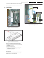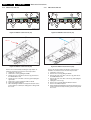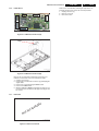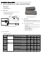
1
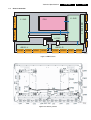
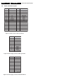
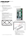
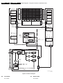
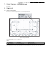
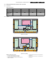
Colour Television
Module
FHP PDP Repair Manual
FPF42C128135UA-52 (42” A4)
Contents
1.
2.
3.
4.
5.
6.
7.
8.
9.
10.
11.
Page
Technical Specifications
2
Safety Instructions, Warnings, and Notes
5
Directions for Use
6
Mechanical Instructions
6
Service Modes, Error Codes, and Fault Finding 10
Block Diagrams, Test point Overview, and Wave
Forms
27
Circuit Diagrams and PWB Layouts
29
Alignments
29
Circuit Descriptions and Abbreviation List
30
Spare Parts List
33
Revision List
34
©
Copyright 2006 Philips Consumer Electronics B.V. Eindhoven, The Netherlands.
All rights reserved. No part of this publication may be reproduced, stored in a
retrieval system or transmitted, in any form or by any means, electronic,
mechanical, photocopying, or otherwise without the prior permission of Philips.
Published by MW 0667 BG CD Customer Service
Printed in The Netherlands
Subject to modification
EN 3122 785 16400
EN 2
1.
Technical Specifications
FHP PDP
1. Technical Specifications
Index of this chapter:
1.1 Specifications
1.2 Serial Numbers
1.3 Chassis overview
1.1
Specifications
1.1.1
42” A4
FPF42C128128UC -52 䊶䊶䊶䊶䊶䊶䊶 42A1 (
covered
)
FPF42C128128UD -52 䊶䊶䊶䊶䊶䊶䊶 42A2 ( by manual
)
FPF42C128128UE -52 䊶䊶䊶䊶䊶䊶䊶 42A3 ( 3122 785 14580)
FPF42C128135UA -52 䊶䊶䊶䊶䊶䊶䊶 42A4 (in this manual)
G_16400_004.eps
270706
Figure 1-4 List of model numbers
No Item
Spec. FPF42C128135UA-52
1
Resolution
1024 (H) x 1080 (V) pixels
(1 pixel = 1 R,G,B cells)
2
Number of Cells
3072 (H) x 1080 (V)
3
Pixel Pitch
0.90 mm (H) x 0.485 mm (V)
4
Cell Pitch
0.30 mm (H) x 0.485 mm (V)
5
Display size
921.60 (H) x 523.8 mm (V)
6
Screen size
Diagonal 42"
7
Screen aspect
16:9
8
Dimensions
994 (W) x 587 (H) x 66 (D) mm
9
Weight
About 16 kg
10 H sync, V sync, data
1.2
50 kHz (H), 50/60/70 Hz (V),
LVDS
Serial Numbers
Check the serial ID number of the product requested for repair,
before starting the problem analysis and repair.
Serial Number
G_16400_001.eps
280706
Figure 1-1 PDP Serial number
P7A 6 01
001A1
01A
Version Number
Lot Number
Week code, 1 – 53, from Jan. to Dec.
Last digit of year of production: 6 means 2006
Product code: N7A, P7A, S7A are 42 inch type PDP
G_16400_002.eps
180706
Figure 1-2 PDP Serial number explanation
Model Number
Figure 1-3 PDP Model number
G_16400_003.eps
280706
Note: The PDP serial number and the serial number of the
completed chassis (product requested for repair) are usually
the same when the product is brought in for repair the first time.
Technical Specifications
1.
EN 3
㪯㪝㪧㪚
㪯㪝㪧㪚
㪯㪄㪪㪬㪪
㪧㪪㪬
㪯㪝㪧㪚
㪰㪄㪪㪬㪪
㪯㪄㪙㪬㪪㩷㩿㪯㪙㪙㪀
㪪㪛㪤㪄㪬
Chassis overview
㪪㪛㪤㪄㪛
㪣㪦㪞㪠㪚
㪯㪝㪧㪚
1.3
FHP PDP
㪘㪙㪬㪪㪄㪣
㪘㪛㪤㪈
㪘㪛㪤㪉
㪘㪙㪬㪪㪄㪩
㪘㪛㪤㪊
㪘㪛㪤㪋
㪘㪛㪤㪌
㪘㪛㪤㪍
㪘㪛㪤㪎
㪘㪛㪤㪏
G_16400_005.eps
180706
Figure 1-5 PWB locations
G_16400_006.eps
270706
Figure 1-6 Connector positions
EN 4
1.4
1.
Technical Specifications
FHP PDP
Some connector layouts
Pin No.
Signal name
Pin No.
Signal name
1
RA-
2
GND (LVDS)
3
RA+
4
SCL
5
RB-
6
GND
7
RB+
8
SDA
9
RC-
10
GND (LVDS)
11
RC+
12
CPUGO
13
RXCLKIN-
14
PDPGO
15
RXCLKIN+
16
IRQ
17
RD-
18
PDWN
19
RD+
20
GND (LVDS)
21
RE-
22
GND
23
RE+
24
GND
25
GND
26
GND
27
GND
28
GND
29
GND
30
GND
G_16400_035.eps
280706
Figure 1-7 LVDS connector CN1 Logic Board
Pin No.
Symbol
1
Vcc
2
GND
3
Vpr2
4
GND
5
Vra
6
Vrs
7
VCEGO
8
VSAGO
9
PFCGO
G_16400_036.eps
270706
Figure 1-8 Power supply connector CN6 Logic Board
Pin No.
Symbol
1
Va
2
N.C.
3
Vcc
4
GND
5
GND
6
GND
7
N.C.
8
Vs
9
Vs
10
Vs
G_16400_037.eps
270706
Figure 1-9 Power supply connector CN23 X-SUS Board
Safety Instructions, Warnings, and Notes
FHP PDP
2.
EN 5
2. Safety Instructions, Warnings, and Notes
2.1
Safety Instructions h
It is not allowed to operate the FTV-set without glass plate. One
function of this glass plate is to absorb Infrared Radiation.
Without this glass plate the level of Infrared Radiation produced
by the plasma display could damage your eyes.
1. Safety regulations require that during a repair:
– the set should be connected to the mains via an
isolating transformer (in this particular case a
transformer of ≥ 800 VA).
– safety components, indicated by the symbol h,
should be replaced by components identical to the
original ones.
2. Safety regulations require that after a repair the set must
be returned in its original condition. In particular attention
should be paid to the following points.
– Note: The wire trees should be routed correctly and
fixed with the mounted cable clamps.
– The insulation of the mains lead should be checked for
external damage.
– The electrical DC resistance between the mains plug
and the secondary side should be checked (only for
sets that have a mains isolated power supply). This
check can be done as follows:
• unplug the mains cord and connect a wire between
the two pins of the mains plug;
• set the mains switch to the on position (keep the
mains cord unplugged!);
• measure the resistance value between the pins of
the mains plug and the metal shielding of the tuner
or the aerial connection on the set. The reading
should be between 4.5 MΩ and 12 MΩ;
• switch off the TV and remove the wire between the
two pins of the mains plug.
– The cabinet should be checked for defects to avoid
touching of any inner parts by the customer.
2.2
Warnings
ESD w
All ICs and many other semiconductors are susceptible to
electrostatic discharges (ESD w). Careless handling during
repair can reduce life drastically. When repairing, make sure
that you are connected with the same potential as the mass of
the set by a wristband with resistance. Keep components and
tools also at this same potential.
1. Available ESD protection equipment:
– complete kit ESD3 (combining all 6 prior products small table mat) 4822 310 10671
– wristband tester 4822 344 13999
2. Never replace modules or other components while the unit
is switched on.
3. When making settings, use plastic rather than metal tools.
This will prevent any short circuits and the danger of a
circuit becoming unstable.
2.3
Notes
1. A glass plate is positioned before the plasma display. This
glass plate can be cleaned with a slightly humid cloth. If
due to circumstances there is some dirt between the glass
plate and the plasma display panel it is recommended to do
some maintenance by a qualified service employee only.
2. Never disconnect the power display cable when the set is
operating
3. With DST no failures (error-codes) can be red, when the
set is in Service-mode.
4. If DST reacts with "error 2", there is no communication
between the TV and the DST. Note that the IR-transmitter
LED is positioned at the right side of IR-receiver eye of the
E-box. Take into account that receiver-LED on DST is
positioned not in the middle but at the left side. Point
corresponding LEDs to each other. In case the amount of
Infrared produced by the screen pollutes the
communication, the set can be set in Stand-by-mode. Then
still the error-messages can be retrieved.
2.3.1
Notes on Safe Handling of the Plasma Display
Notes to Follow During Service
• The work procedures shown with the Note indication are
important for ensuring the safety of the product and the
servicing work. Be sure to follow these instructions.
• Before starting the work, secure a sufficient working space.
• At all times other than when adjusting and checking the
product, be sure to turn OFF the main POWER switch and
disconnect the power cable from the power supply of the
display during servicing.
• To prevent electric shock and breakage of PC board, start
the servicing work at least 30 seconds after the main power
has been turned off. Especially when installing and
removing the power supply PC board and the SUS PC
board in which high voltages are applied, start servicing at
least 2 minutes after the main power has been turned off.
• While the main power is on, do not touch any parts or
circuits other than the ones specified. The high voltage
power supply block within the PDP module has a floating
ground. If any connection other than the one specified is
made between the measuring equipment and the high
voltage power supply block, it can result in electric shock or
activation of the leakage-detection circuit breaker.
• When installing the PDP module in, and removing it from
the packing carton, be sure to have at least two persons
perform the work white being careful to ensure that the
flexible printed-circuit cable of the PDP module does not
get caught by the packing carton.
• When the surface of the panel comes into contact with the
cushioning materials, be sure to confirm that there is no
foreign matter on top of the cushioning materials before the
surface of the panel comes into contact with the cushioning
materials. Failure to observe this precaution may result in,
the surface of the panel being scratched by foreign matter.
• When handling the circuit PC board, be sure to remove
static electricity from your body before handling the circuit
PC board.
• Be sure to handle the circuit PC board by holding the large
parts as the heat sink or transformer. Failure to observe
this precaution may result in the occurrence of an
abnormality in the soldered areas.
• Do not stack the circuit PC boards. Failure to observe this
precaution may result in problems resulting from scratches
on the parts, the deformation of parts, and short-circuits
due to residual electric charge.
• Routing of the wires and fixing them in position must be
done in accordance with the original routing and fixing
configuration when servicing is completed. All the wires are
routed far away from the areas that become hot (such as
the heat sink). These wires are fixed in position with the
wire clamps so that the wires do not move, thereby
ensuring that they are not damaged and their materials do
not deteriorate over long periods of time. Therefore, route
the cables and fix the cables to the original position and
states using the wire clamps.
• Perform a safety check when servicing is completed. Verify
that the peripherals of the serviced points have not
undergone any deterioration during servicing. Also verify
that the screws, parts and cables removed for servicing
purposes have all been returned to their proper locations in
accordance with the original setup
EN 6
3.
FHP PDP
Directions for Use
3. Directions for Use
Not applicable.
4. Mechanical Instructions
Notes:
• Figures below can deviate from the actual situation, due to
different set executions.
• For more detailed instructions regarding the (dis)assembly
of the TV chassis that hold these PDPs, read the
corresponding TV Service Manual.
4.1.2
X-SUS and X-BUS Circuit Boards
5
5
4.1
Board Swap Instructions
4.1.1
General
Before dismounting panels read notes below!
3
2
Caution when removing circuit board!
When removing the circuit board after the main power is turned
on/off, wait for at least one minute before starting to remove the
circuit board.
If the circuit board removal is started immediately after turning
off the main power, it can result in electric shock or damage to
the circuit due to residual electric charge.
4
2
2
Caution on handling the FPC connector!
To release the black lock lever of the connector, flip it up gently
in the middle with the nail of the thumb or forefinger, from the
side with the cable.
Never pinch the lock lever with fingers or tools. Doing so might
damage the lock lever.
5
3
1
4
5
G_16400_007.eps
300706
Figure 4-2 X-BUS and X-SUS board removal (1/2)
X-BUS
X-SUS
E_14580_025.eps
071005
Figure 4-1 Handling the FPC connector
G_16400_008.eps
180706
Figure 4-3 X-BUS and X-SUS board removal (2/2)
5. Release the white stand-offs [5] from the X-SUS board,
Remove the circuit boards by following the steps below. To
install the circuit boards, reverse the removal procedure.
1. Release the lock of the FPC connector [1] and unplug the
signal cable.
2. Unplug the connectors [2].
3. Unplug the 4 XFPC’s [3] on the X-BUS board.
4. Remove the fixing screws [4].
and from the top and bottom of the X-BUS board.
Mechanical Instructions
FHP PDP
4.
EN 7
6. Remove the X-BUS board and the X-SUS board together.
Make sure that you do not touch the heat sink when removing
the Y-SUS board.
4.1.3
Threaded bush for
SDM-U board
Y-SUS Circuit Board
4
Adhesive side should be
against the IC of SDM-U
5
3
SDM-U board
Y-SUS board
2
Radiation Plate
4
G_16400_010.eps
310706
1
Figure 4-6 Radiation plate position
G_16400_009.eps
300706
Figure 4-4 Y-SUS board removal (1/2)
Y-SUS
G_16400_011.eps
180706
Figure 4-5 Y-SUS board removal (2/2)
Remove the circuit board by following the steps below. To
install the circuit board, reverse the removal procedure.
1. Release the lock of the FPC connector [1] and unplug the
signal cable.
2. Unplug the connector [2].
3. Remove the fixing screws [3].
4. Release the white stand-offs [4] from the Y-SUS board.
5. Pull out the Y-SUS board horizontally, in this way
unplugging the connectors [5].
6. Remove the Y-SUS board.
Make sure that you do not touch the heat sink when removing
the Y-SUS board.
Note: Make sure the radiation plate is positioned correctly. It is
located underneath the upper SDM, and the threaded bush
should sit in the hole of the radiation plate.
EN 8
4.1.4
4.
Mechanical Instructions
FHP PDP
4.1.5
ABUS-L Circuit Board
ABUS-R Circuit Board
1
6
4
6
4
6
5
7
7
5
5
2
2
2
2
2
2
2
2
2
2
1
3
6
3
3
G_16400_012.eps
310706
Figure 4-7 ABUS-L board removal (1/2)
3
G_16400_014.eps
310706
Figure 4-9 ABUS-R board removal (1/2)
ABUS-R
ABUS-L
G_16400_015.eps
180706
G_16400_013.eps
180706
Figure 4-8 ABUS-L board removal (2/2)
Remove the circuit board by following the steps below. To
install the circuit board, reverse the removal procedure.
1. Unplug the connector [1].
2. Remove the screws [2] fixing the ADMs.
3. Release the lock of the FPC connectors [3], and remove
the ADM flexible board.
4. Release the lock of the FPC connector [4] and unplug the
signal cable.
5. Remove the screws [5] fixing the ABUS-L board.
6. Remove the ABUS-L board.
7. When installing the ABUS-L board, put the board in such a
position that it is locked by the tabs [6] before fixing it with
the screws.
Figure 4-10 ABUS-R board removal (2/2)
Remove the circuit board by following the steps below. To
install the circuit board, reverse the removal procedure.
1. Unplug the connector [1].
2. Remove the screws [2] fixing the ADMs.
3. Release the lock of the FPC connectors [3], and remove
the ADM flexible board.
4. Release the lock of the FPC connector [4] and unplug the
signal cable.
5. Unplug the connector [5].
6. Remove the screws [6] fixing the ABUS-R board.
7. Remove the ABUS-R board.
8. When installing the ABUS-R board, put the board in such a
position that it is locked by the tabs [7] before fixing it with
the screws.
Mechanical Instructions
4.1.6
4.
EN 9
Remove the circuit board by following the steps below. To
install the circuit board, reverse the removal procedure.
1. Unplug connectors [1].
2. Remove screws [2].
3. Remove the PSU.
LOGIC Board
3
3
1
2
4
4
G_16400_016.eps
310706
Figure 4-11 LOGIC board removal (1/2)
Logic
G_16400_017.eps
180706
Figure 4-12 LOGIC board removal (2/2)
Remove the circuit board by following the steps below. To
install the circuit board, reverse the removal procedure.
1. Unplug connectors [1].
2. Release the lock of the FPC connectors [2] and unplug the
signal cables.
3. Remove the screws [3] fixing the LOGIC board.
4. Remove the LOGIC board.
5. When installing the LOGIC board, put the board in such a
position that it is locked by the tabs [4] before fixing it with
the screws.
4.1.7
FHP PDP
PSU Board
le
b
a
il
a
v
ta
ye
t
No
E_06532_032.eps
270706
Figure 4-13 PSU board removal
EN 10
5.
Service Modes, Error Codes, and Fault Finding
FHP PDP
5. Service Modes, Error Codes, and Fault Finding
Index of this chapter:
5.1 Repair Tools
5.3 Process Flow
5.4 Repair Instructions
5.5 Defect Description Form
5.1
Repair Tools
To be able to repair the Plasma Display Panels on board level,
the following repair tools are available:
• Special LVDS cable: T.B.D.
• Foam buffers: 3122 785 90581.
CN06
E_14580_024.eps
250304
CN01
14
3
Vpr
Power Supply
3k3
8
6
4
SDA
GND
SCL
3k3
Figure 5-2 Foam buffers for FTV
I2C
5.2
Error codes
Compair
When an error causes the PDP to switch “OFF”, an error code
is put into an EEPROM on the Logic Board. You can read out
the contents of the error code memory with the ComPair tool.
CN06
2
I C
Compair
G_16400_018.eps
270706
CN01
Logic Board
Figure 5-1 Extension cable kit ALiS PDP
5.2.1
How to Connect the ComPair Tool
•
•
•
•
•
•
5.2.2
Carefully disconnect the LVDS cable from CN01 on the
Logic Board.
If necessary connect a PSU with a voltage of 3.3V to drive
the LOGIC board.
Connect the cable from the ComPair tool to connector
CN01 of the LOGIC board.
Turn on the ComPair tool.
Launch the ComPair software.
Read out the error buffer.
Error Code Overview
Table 5-1 Error code table
Error code
Detected by board
Error description
21
X-SUS
Vxx power voltage is too high
X-SUS
LOGIC
Vxx power voltage is too low
X-SUS
LOGIC
25
Vex power voltage is too high
X-SUS
26
Vex power startup is faulty
X-SUS
LOGIC
Vey power voltage is too low
Y-SUS
LOGIC
45
Vey power voltage is too high
Y-SUS
46
Vey power startup is faulty
Y-SUS
LOGIC
4C
Temperature too high
Y-SUS
LOGIC
Vs power voltage is too high
Y-SUS
X-SUS
LOGIC
PSU
Vs power startup is faulty
X-SUS
Y-SUS
PSU
LOGIC
64
Ve power voltage is too low
LOGIC
X-SUS
Y-SUS
65
Ve power voltage is too high
Y-SUS
Y-SUS
24
44
61
62
Y-SUS
X-SUS
Y-SUS
Suspected board(s)
66
Ve power startup is faulty
LOGIC
X-SUS
68
Vw power voltage is too low
Y-SUS
LOGIC
Y-SUS
69
Vw power voltage is too high
LOGIC
Y-SUS
6A
Vw power startup is faulty
Y-SUS
LOGIC
79
Vw power current is too high (during operation)
Y-SUS
X-SUS
LOGIC
7B
Vs power voltage is too high (during startup)
Y-SUS
X-SUS
LOGIC
Service Modes, Error Codes, and Fault Finding
5.3
Process Flow
5.
EN 11
the defective PDP, accompanied by a completely filled in
Defect Description Form (see figure “Defect Description Form
(DDF)“), in this flight case to EuroService. EuroService makes
sure the defect PDP is repaired and afterwards added to its
swap pool. The workshop makes the TV set complete by
building in the refurbished PDP. Afterwards the TV set is
returned to the customer.
The selected workshop receives the defect TV set and
investigates the PDP. Two possible solutions follow:
5.3.1
FHP PDP
Advanced PDP Exchange (Actual Way-of-Working)
In case of:
• Glass broken,
• Flex foil damaged,
• Y-COM IC on flex foil is damaged, or
• NVM on logic board defect: no communication with
ComPair
the procedure for repair is as follows:
A new PDP will be ordered at EuroService. They issue an RMA
number and ship a refurbished PDP from its swap pool in a
flight case to the workshop. After receipt, the workshop sends
5.3.2
Customized Repair
If the defect is not mentioned in 5.2.1, the workshop orders the
necessary spare parts, being boards, at EuroService. After
receipt the workshop swaps the concerning board and makes
the TV set complete by building in the PDP. Afterwards the TV
set is returned to the customer.
PDP flow chart
(from 1st May 2003 onward s)
End user contacts dealer because his
plasma TV set is defective
Dealer requests VIP workshop
to contact end user
VIP workshop pays home visit to end user
and swaps defective TV set with a loan set
VIP workshop analyses the PDP
of the defective plasma TV set
VIP workshop orders refurbished PDP
at EuroService
YES
PDP:
glass repair
or
fl ex c able mach ine
needed
??
NO
VIP workshop orders spare part(s)
being boards at EuroService
EuroService ships refurbished PDP from its
swap pool to VIP workshop in a flight case
EuroService ships spare part(s) with
next-day-delivery to VIP workshop
VIP workshop swaps PDP's
and makes plasma TV set complete
VIP workshop repairs PDP on board level
and makes plasma TV set complete
VIP workshop brings plasma TV set to
end user and swaps with loan set
VIP workshop brings plasma TV set to
end user and swaps with loan set
E_14580_027.eps
280706
Figure 5-3 PDP flow chart
EN 12
5.
Service Modes, Error Codes, and Fault Finding
FHP PDP
5.4
Repair Instructions
5.4.1
General
In case of:
• a broken glass panel,
• a defective flex foil, or
• a defective Y-COM IC on the flex foil
the PDPs need to be send back via the central repair procedure
of EuroService.
In other cases the Plasma Display Panels must be repaired on
board level.
5.4.2
42” A4 ALiS Plasma Display Panel
The involved Plasma Display Panel is:
Display type
Service code number
FPF42C128135UA-52
9322 235 43682
The available modules for these Plasma Display Panels are:
Module description
FHP code number
Service code number
X-SUS board
FPF33R-XSS0041
9965 000 35647
Y-SUS board
FPF33R-YSS0042
9965 000 35648
Logic board
FPF33R-LGC0061
9965 000 35646
A-BUS Left
FPF33R-ABL0038
9965 000 35649
A-BUS Right
FPF33R-ABR0039
9965 000 35650
X-BUS board
FPF33R-XBU0035
9965 000 35651
Signal Cable LOGIC-X-SUS
FPF29R-CBL001411
9965 000 32669
Signal Cable LOGIC-Y-SUS
FPF29R-CBL001412
9965 000 32670
Signal Cable LOGIC-ABUS-L
FPF29R-CBL001401
9965 000 32668
Signal Cable LOGIC-ABUS-R
FPF29R-CBL001421
9965 000 32671
Power Cable X-SUS-Y-SUS
FPF29R-CBL003601
9965 000 32672
Power Cable X-SUS-ABUS-R
FPF29R-CBL003701
9965 000 32673
Remark:
1. If the LOGIC board is defective, the procedure mentioned
in figures "Logic Board Exchange (1 and 2)" must be used.
Service Modes, Error Codes, and Fault Finding
5.4.3
FHP PDP
5.
EN 13
Fault Finding Flowcharts
Problem analysis procedure: PDP repair / board swap
PDP Repair procedure Board Swap
The entire Screen does not light.
The set is going into protection.
(PSU is OK)
Go to Step 1 in the procedure
Check the 3.3V Vpr2 on the PSU
and the Logic board
Go to Step 2 in the procedure
Check if there is a short circuit
on boardsY-SUS, X-SUS, SDMs,
X-BUS, or XFPCs
Go to Step 3 in the procedure
Vertical Line / Vertical Bar?
Go to the
"Vertical line/Vertical bar"
problem analysis procedure
Horizontal bar?
Go to the
"Horizontal bar"
problem analysis procedure
Logic Board Exchange
procedure.
Use of ComPair
Copy data from the
defective Logic board
Restore data into the new
board
Check if there is a short circuit on
boards ABUS-L, ABUS-R, or ADMs
Go to Step 4 in the procedure
Check if Vcc (5V), Vs (85V) and
Va (63V) are present
on PSU and boards
Ship Out
Auto alignment procedure
Figure 5-4 Problem analysis procedure: PDP repair / board swap
G_16400_025.eps
310706
EN 14
5.
FHP PDP
Service Modes, Error Codes, and Fault Finding
Problem Analysis Procedure: The entire screen does not light
1
The entire screen does not light
Caution 1: never disconnect connectors or
remove boards when the mains plug is connected.
Allow discharge of power supplies before
disconnecting connectors!
Remove CN06
(on LOGIC Board,
PSU-LOGIC cable)
Caution 2: do not interchange boards between
different PDPs, this might damage your PDP
All the boards are connected
Connect the set to mains.
Switch “ON” the set
via the mains switch
Vpr2 (3.3 V) on
the PSU board is present?
N
PSU board is
defective
Y
Turn “OFF” AC power
Connect CN 6 (LOGIC)
Turn on AC power
Vpr2 (3.3 V) on
the PSU board is present?
Replace the
Power Supply
N
LOGIC board is
defective
Y
Disconnect the mains plug.
Remove the following power connections:
on X-SUS: CN23 (PSU -> X-SUS)
on X-SUS: CN26 (X-SUS -> ABUS-R)
on X-SUS: CN32 (X-SUS -> Y-SUS)
on ABUS-R: CN47 (ABUS-R -> ABUS-L)
Replace Logic Board
Follow the
“Logic Board Exchange” procedure
2
Figure 5-5 Problem analysis procedure: the entire screen does not light
G_16400_026.eps
310706
Service Modes, Error Codes, and Fault Finding
FHP PDP
5.
EN 15
Short-circuit check on Boards and Power Supply Lines
2
Check with an ohmmeter if following
pins are shorted
X-SUS
CN23
X-SUS Board:
CN23 pins 3 - 4
CN23 pins 6 - 8
CN22 pins 10 - 13
are shorted?
CN22
[X-SUS - PSU]
[X-SUS - Y-SUS]
10
Vs
-Vs
-Vs
9
8
Vs
Vs
NC
GND
7
6
NC
GND
NC
Vu
5
4
3
GND
GND
Vcc
NC
NC
Vcc
2
1
Va
NC
GND
NC
Vs
Vs
13
12
11
X-SUS board is
defective
Y
(Switching circuit (power
supply) has a short-circuit)
10
9
8
7
N
6
5
4
3
2
1
Y-SUS
Board:
On
Y-SUS
board,
CN32 pins 1 - 4
CN32 pins 8 - 10
CN32 pins 10 - 13
are shorted?
Y-SUS board is
defective
Y
(Switching circuit (power
supply) has a short-circuit)
Y-SUS
CN32
N
[Y-SUS - X-SUS]
Vs
Vs
NC
GND
NC
Vcc
NC
Vx
NC
GND
NC
-Vs
-Vs
13
12
Remove SDM from the following
two connectors of Y-SUS:
CN34 and CN35
11
10
9
8
7
6
5
4
3
On SDM board,
A1-A2, B1-B2,
C1-C2, D1-D2,
are shorted?
2
1
SDM is defective
(PDP is defective)
Y
N
A2
A1
B1
B2
C1 C2
D1 D2
On X-BUS board,
CN61 pins 1 - 9
are shorted?
Y
Remove the 4 XFPCs
(disconnect CN63 , CN64, CN65, CN66)
N
On X-BUS board,
CN61 pins 1 - 9
are shorted?
Y
N
X-BUS board is
defective
PDP
is defective
3
End of analysis
G_16400_027.eps
310706
Figure 5-6 Short circuit check on boards and power supply lines (1/3)
EN 16
5.
Service Modes, Error Codes, and Fault Finding
FHP PDP
3
ABUS-L board:
CN52 pins 1 - 3 or
CN52 pins 4 - 7
are shorted?
ABUS-L
Y
Remove ADM from the
following connectors.
CN 53, CN 54,
CN 55, CN 56
N
ABUS-L board:
CN52 pins 1 - 3 or
CN52 pins 4 - 7
are shorted?
N
ADM is defective
(PDP is defective)
Y
ABUS-L board is defective.
ABUS-R board
CN42 pins 1 - 3 or
CN42 pins 3 - 5
are shorted?
Y
ABUS-R
N
Remove ADM from the
following connectors:
CN 43, CN 44,
CN 45, CN 46
ABUS-R board
CN42 pins 1 - 3 or
CN42 pins 3 - 5
are shorted?
N
ADM is defective
(PDP is defective)
Y
ABUS-R board is defective.
Replace the defective part
4
G_16400_028.eps
310706
Figure 5-7 Short circuit check on boards and power supply lines (2/3)
Service Modes, Error Codes, and Fault Finding
FHP PDP
5.
4
Connect CN23 (X-SUS) and
CN32 (Y-SUS), and
give the “PDP-go” signal (*1)
*1 When turning “ON” the PDP with PDP-go, refer to following procedure:
1. Connect the special LVDS cable (see paragraph “Repair Tools”)
between CN01 and CN06
2. Supply power to the PSU
Are Vcc (5V), Vs (85V),
and Va (63V) present on
the PSU board?
Logic board, or X-SUS board, or
Y-SUS board is defective
N
In case that Vs Power system or Va Power
system of X-SUS or Y-SUS is defective, Vcc
starts but goes down in a few seconds.
Y
Turn “OFF” AC power
Connect SDM (with CN34 and CN35)
Give the “PDP-go” signal (*1)
On PSU board
Vcc (5V), Vs (85V)
exist ?
N
SDM or PDP is defective
Y
Turn “OFF” AC power.
Connect CN 26 (X-SUS)
Give the “PDP-go” signal (*1)
PSU board
Va (63V) exists ?
Turn “OFF” AC power.
And remove ADMs from following connectors
CN43, CN44, CD45, CN46
Afterwards give the “PDP-go” signal (*1)
N
Y
PSU board
Va (63V) exists ?
Turn “OFF” the AC power.
Connect CN 47 (ABUS-R)
Give the “PDP-go” signal (*1)
PSU board
Va (63V) exists ?
N
ADM is defective
(PDP is defective)
Y
N
ABUS-R board is defective
Turn “OFF” AC power.
And remove ADMs from following connectors
CN53, CN54, CD55, CN56
Afterwards give the “PDP-go” signal (*1)
Y
PSU board
Va (63V) exists ?
Y
End of analysis
N
ABUS-L board is defective
ADM is defective
(PDP is defective)
Replace defective boards
(In case of Logic Board replacement:
Follow the “Logic Board Exchange”
procedure!)
G_16400_029.eps
310706
Figure 5-8 Short circuit check on boards and power supply lines (3/3)
EN 17
EN 18
5.
FHP PDP
Service Modes, Error Codes, and Fault Finding
"Vertical line/Vertical bar" problem analysis procedure
Vertical line / Vertical bar
Y
LOGIC board – ABUS-R/L
board signal cable has
abnormal appearance?
Signal cable is
defective
N
Y
ADM flexible cable has
abnormal appearance?
N
*1 When turning “ON” the PDP with PDP-go, refer to following procedure:
1. Connect the special LVDS cable (see paragraph “Repair Tools”)
between CN01 and CN06
2. Supply power to the PSU
Give the “PDP-go” signal (*1)
One vertical line?
ADM is defective
(PDP is defective)
Y
Tap lightly heat seal portion on
ADM flexible cable
N
Any
changes?
Y
N
Left half of the
panel does
not light?
Heat-melted junction is defective
(PDP is defective)
Panel address has open circuit or
ADM IC chip is defective
(PDP is defective)
Logic board is defective,
or ABUS-R board is defective,
or Signal cable is defective,
or loose contact of
CN02 (LOGIC) or CN41(ABUS-R)
Y
N
Right half of the
panel does
not light?
N
Y
Va (63V) exists on
RL41(resistor) on
ABUS-L board?
N
Y
Logic board is defective,
or ABUS-L board is defective,
or Signal cable is defective,
or loose contact of
CN03 (LOGIC) or CN51 (ABUS-L)
Power cable (CN52 to CN47) is defective
or loose contact of CN47 (ABUS-R)
Replace defective parts
(1)
Figure 5-9 Vertical line / vertical bar problem analysis procedure (1/3)
G_16400_030.eps
310706
Service Modes, Error Codes, and Fault Finding
FHP PDP
5.
EN 19
(1)
Is vertical bar
monochromatic?
Y
*1 When turning “ON” the PDP with PDP-go, refer to following procedure:
1. Connect the special LVDS cable (see paragraph “Repair Tools”)
between CN01 and CN06
2. Supply power to the PSU
N
Does the vertical bar
appear in left
half of panel?
N
Y
Turn “OFF” the AC power
Replace ABUS-L board
Give the “PDP-go” signal (*1)
Normal?
Y
ABUS-L board is defective
N
Turn “OFF” AC power
Replace LOGIC board
Give the “PDP-go” signal (*1)
Normal?
Y
LOGIC board is defective
N
Turn “OFF” AC power
Replace LOGIC - ABUS-L signal cable
Give the “PDP-go” signal (*1)
Normal?
Y
Signal cable is defective
N
ADM is defective
(PDP is defective)
Replace the defective parts
(2)
(3)
Figure 5-10 Vertical line / vertical bar problem analysis procedure (2/3)
G_16400_031.eps
310706
EN 20
5.
FHP PDP
(2)
Service Modes, Error Codes, and Fault Finding
(3)
*1 When turning “ON” the PDP with PDP-go, refer to following procedure:
1. Connect the special LVDS cable (see paragraph “Repair Tools”)
between CN01 and CN06
2. Supply power to the PSU
Turn “OFF” the main power
Replace ABUS-R board
Give the “PDP-go” signal (*1)
Normal?
Y
ABUS-R board is defective
N
Turn “OFF” the main power
Replace LOGIC board
Give the “PDP-go” signal (*1)
Normal?
Y
LOGIC board is defective
N
Turn “OFF” the main power
Replace signal cables LOGIC - ABUS-R
Give the “PDP-go” signal (*1)
Y
Normal?
Signal cable is defective
N
ADM is defective
(PDP is defective)
Panel is defective
(PDP is defective)
Replace the defective parts
G_16400_032.eps
310706
Figure 5-11 Vertical line / vertical bar problem analysis procedure (3/3)
Service Modes, Error Codes, and Fault Finding
FHP PDP
5.
EN 21
"Horizontal bar" problem analysis procedure
Horizontal bar
*1 When turning “ON” the PDP with PDP-go, refer to following procedure:
1. Connect the special LVDS cable (see paragraph “Repair Tools”)
between CN01 and CN06
2. Supply power to the PSU
Turn “OFF” the main power
Replace the X-SUS board
Give the “PDP-go” signal (*1)
Normal?
Y
X-SUS board is defective
N
Turn “OFF” the main power
Remove the X-SUS board
Put back the initial X-SUS board
Replace Y-SUS board
Give the “PDP-go” signal (*1)
Normal?
Y
Y-SUS board is defective
N
PDP is defective
Replace the defective parts
G_16400_033.eps
310706
Figure 5-12 Horizontal line problem analysis procedure
Remark: Do not interchange boards between different PDPs,
this might damage your PDP
EN 22
5.
FHP PDP
Service Modes, Error Codes, and Fault Finding
Logic Board Exchange (1)
1. Copy NVM Data from defective Logic Board
1.
2.
Remove the Small Signal Board
Disconnect the LVDS cable from CN01 and
the power cable from CN06 of the Logic Board
3. Connect the FHP A4 Service cable to CN01
and CN06 of the Logic Board. Reconnect the power
cable from the PSU to the FHP A4 Service cable on the
CN06 side of the Logic Board. Connect the ComPair
cable to the CN01 side of the FHP A4 Service cable.
4.
5.
Plug in the Mains cable to the Mains filter and the
screen will start up in Stand alone mode.
Set will go into protection or into stand-by
6. Click the link in ComPair to open the Logic Board
exchange window
7.
8.
Click the "On" button.
In the title bar the module type will appear
Click button "copy from original"
9.
Use the "Save" button to save the information to a file
10.
11.
Click the "Off" button
Remove the Mains cable from the Mains filter.
G_16400_019.eps
010806
Figure 5-13 Logic Board Exchange (1/2)
1. Remove the SSB. Now you can reach the cable going to
connector CN01 on the Logic Board.
2. Unplug the LVDS cable from the SSB at connector CN01.
Also unplug the power cable at CN06.
3. Connect the FHP A4 service cable to CN01 and CN06.
Connect the ComPair I2C cable to the CN01 side of the
service cable, and the power cable to the CN06 side of it.
4. Plug in the mains cable. The display starts up in standalone mode.
5. Click the link in ComPair to open the Logic Board exchange
window.
6. Click the 'On' button. In the title bar the module type will
appear: 42A4, or something similar.
7. Click button 'Copy from original'
8. The data is read from the EEPROM on the logic board and
displayed in the list.
9. Use the 'Save' button to save the information to a file. This
is optional, but better safe than sorry!
Note: If you close the window without saving, all settings
Service Modes, Error Codes, and Fault Finding
will be lost. If you intend to close this window before
replacing the board, you should save the settings so you
can load them later.
10. Click the 'Off' button.
FHP PDP
5.
EN 23
11. Switch off the set and replace the Logic Board with another
one.
Logic Board Exchange (2)
2. Write NVM Data to the new Logic Board
1.
2.
3.
4.
5.
6.
Remove the Mains cable from the Mains filter.
Connect the FHP A4 Service cable to CN01
and CN06 of the Logic Board. Connect the power
cable from the PSU to the FHP A4 Service cable on the
CN06 side of the Logic Board. Connect the ComPair
cable to the CN01 side of the FHP A4 Service cable.
Click the "On" button
Load the saved values
Click button “paste to replacement”
Click button "Ship Out" (1)
7. Disconnect the ComPair cable and Power cable from the
FHP A4 Service cable on the CN01 and CN06 sides of the
Logic Board. Disconnect the FHP A4 Service cable. Reconnect
the Power cable from the PSU to CN06 and the LVDS cable
to CN01 on the Logic Board.
(1) The PDP screen will be blanked for about 15s,
then 15s later, the 'Ship out' process will end
G_16400_020.eps
010806
Figure 5-14 Logic Board Exchange (2/2)
1. Switch off the set and replace the Logic Board by another
one. Now connect the service cable to connectors CN01
and CN06. Connect the power cable to the CN06 side of
the service cable, and the ComPair cable to the CN01 side.
2. Restart the display with the new board.
3. Click the 'On' button.
4. The module type will again appear in the title bar. This may
be different now from step 6 on the previous page, because
now another Logic Board is used. If you closed the window
after step 9 and did save the settings you should load them
now. Use the ‘Load’ button to do so.
5. Click button 'Paste to replacement'. The settings previously
copied from the old board are now written to the new board.
If successful the button 'Ship out' will be enabled.
6. Click button 'Ship out'.
7. Now a process of voltage feedback initialization and selfadjustment starts. This will take a few seconds. When
ready you can switch off the display.
8. Disconnect ComPair and remove the service cable, plug in
the power cable at CN06 and the original LVDS cable at
CN01.
EN 24
5.
NO
Fault
contents
FHP PDP
Service Modes, Error Codes, and Fault Finding
Fault status
Refer to
“Entire screen
does not light”
Screen lights dimly even on the
back screen.
LOGIC
Replace the LOGIC
board, following the
“Logic Board
Exchange” procedure
Single vertical line (of different
color)
Panel chassis
LOGIC
Refer to
“Vertical line/bar”
Vertical line from the middle of
effective scan area (vertical line
of different color)
Panel chassis
Replace panel
chassis
Bar width of 1/7 of horizontal size
or in multiples of 1/7, is displayed.
Abnormal display
Panel chassis
ABUS-L
ABUS-R
LOGIC
Above boards
are connected.
Refer to
“Vertical line/bar”
Bar width of 3/7 or 4/7 of the
screen width, is displayed.
Abnormal display (vertical line of
different color)
ABUS-L
ABUS-R
LOGIC
Above boards
are connected.
Single horizontal line (no light) or
single horizontal line does not
light among the effective scanning
area.
Single horizontal line does not
light.
Panel chassis
X-SUS
Y-SUS
ABUS-L
ABUS-R
Replace panel
chassis
Every other line (no light) in entire
screen
X-SUS
Y-SUS
ABUS-L
ABUS-R
Replace
X-SUS, Y-SUS
Entire screen After momentarily going on, the
does not
screen becomes black
light.
immediately or after a few
seconds (main power is turned
off.)
2
Vertical line
4
5
Vertical bar
6
7
8
Horizontal
line
Analysis procedure
and measure
X-SUS
Y-SUS
PSU
Panel chassis
LOGIC
ABUSL
ABUSR
1
3
Suspected
fault location
G_16400_023.eps
280706
Figure 5-15 Fault symptom overview (1/2)
Service Modes, Error Codes, and Fault Finding
NO
Fault contents
9
Horizontal bar
FHP PDP
Fault status
Suspected
fault
location
5.
Analysis procedure
and measure
Bar width of 1/8 or multiples of
1/8 of the screen height, is
displayed.
Abnormal (screen does not
light)
Panel chassis
Replace panel
chassis
Bar width of 1/2 of the screen
height.
Abnormal display
(screen does not light)
Panel chassis
Y-SUS
X-SUS
Above boards
are connected.
Refer to
“Horizontal bar”
Image sticking
(Image
retention)
Fixed display contents are
always displayed.
Panel chassis
Perform all white heat
run. After judgement,
replace panel chassis
12
Twinkle
The entire screen momentarily
becomes brighter or darker.
Poor connector
contact
13
Flicker
The entire screen flickers
continuously.
Poor connector
contact
(CN2,3,21,31)
Connector / cable
re-connection or
cable exchange
14
Luminance is
abnormal
Screen is too dark or too bright.
(Out of specifications)
15
Chrominance
is abnormal
Colors cannot be displayed
correctly.
LOGIC board
Replace Logic
board, following the
“Logic Board
Exchange” procedure
16
Sync is
disturbed
17
Picture
distorted
18
Steps of
gradation are
skipped
19
Abnormal
sound
PSU
X-SUS
Y-SUS
(Core is broken,
or transformer
is abnormal.)
Locate cause of
abnormality from
listening and viewing.
Replace the cause of
problem.
20
Control on
external
communication
is abnormal
LOGIC board
Replace Logic
board, following the
“Logic Board
Exchange” procedure
10
11
#$%&'(
Luminance linearity is poor.
Contrast, color temperature
adjustment and ϒ cannot be
changed.
G_16400_024.eps
190706
Figure 5-16 Fault symptom overview (2/2)
EN 25
EN 26
Service Modes, Error Codes, and Fault Finding
FHP PDP
Defect Description Form
This form must be used by the workshops for warranty claims:
DDF FLAT TV (panels & boards) version 1.1
Date last modified: 08/03/2005
To be filled in by WORKSHOP / WORK CENTER
Philips
Country:
Type nr./Model nr. set
Serial nr. set
LCD & Plasma
Customer Account nr.:
Type nr. display
DEFECT DESCRIPTION
Serial nr. display
FORM
Job sheet nr.:
Part nr display (12nc)
G E N E R A L R E P A IR DA T A
Return number
Condition
Symptom(s)
P A N E L R E P A IR
Pixel
Defect(s):
Symptoms
Out of
warranty
0170 _ _ _ _ _ _
❐
Constantly
❐
In a hot environment
❐
Intermittently
❐
In a cold environment
❐
After a while
❐
Other : …………………………………
❐
No backlight
❐
Flickering / flashing picture
❐
No picture
❐
Lines across/down image
❐
Picture too bright
❐
Inactive row(s)
❐
Shading / smearing on
picture
❐
Inactive column(s)
❐
Missing colour(s)
❐
Other: ………………………………………………
❐
Only partial picture
❐
Unstabel picture
……………………………………………….
Qty of dots :
❐
Dark dots
……..
❐
Bright dots
……..
---------- Picture ----------
Mark
Defect(s)
Insert picture or mark defect !
Following defect symptoms are out of warranty:
• Broken glass
• Number of dark/bright pixels within spec.
• Scratch(es) on display
• Burn in
Spare Part Nr. New Board
B O A R D R E P A IR
5.5
5.
(only for Plasma TV)
Barcode Nr. Defect Board
These
symptoms
are not
claimable.
Barcode Nr. Replaced Board
1.
For Plasma
TV repair
only
2.
3.
4.
To be filled in by EUROSERVICE
Note 1:
Note 2:
RMA number:
Date of receipt:
The defective LCD-panel / PDP needs to be returned in the same packaging as the new part was send. If not
the warranty claim will be rejected.
Please fill out this form completely and correctly, otherwise Euroservice is unable to fulfil the repair request!
Owner: PHILIPS CE EUROSERVICE
DE10WEG
F_15590_115.eps
110705
Figure 5-17 Defect Description Form (DDF)
Block Diagrams, Test point Overview, and Wave Forms
FHP PDP
6.
EN 27
6. Block Diagrams, Test point Overview, and Wave Forms
Block Diagrams
Y-SUS
X-SUS
S
D
M
U
Y-SUS
EVEN SW
Y-SCAN
EVEN SW
S
D
M
D
Y-SUS
ODD SW
Y-SCAN
ODD SW
X-SUS
EVEN SW
X
B
U
S
X-SCAN
EVEN SW
X-SUS
ODD SW
X-SCAN
ADM1 ADM2 ADM3 ADM4
POS /NEG
ABUS-L
RESET SW
CN51
ADM5
ADM6
ADM7
ODD SW
ADM8
ABUS-R
POS
RESET SW
CN41
CN31
CN21
LOGIC Board
TIMING ROM
CN2
CN3
SCAN CONTROLLER
OSC
24MHz
CN5
SIGNAL
INPUT
DATA CONVERTER
DATA PROCESSOR
CN1
LVDS
γ comp.
RGB
GAIN
DITHER
/ERR
SUB FIELD
PRC.
MPU
V-SYNC cont.
2
IC
Analog Sw
OSC
SCI.
MEMORY
CONTROLLER
CN4
6.1
FRAME
OSC
OSC
40MH
80MH
MEMORY
EEPROM
Failure DET.
APC cont.
FLASH
I/O
Vrs
Vra
Vrw
Vrx
D/A
10MHz
CN7
CN69
PSU
PFCgo
Vsago
Vcego
G_16400_021.eps
190706
Figure 6-1 Signal block diagram
EN 28
6.
Block Diagrams, Test point Overview, and Wave Forms
FHP PDP
Y-SUS
Y-SUS
EVEN SW
Y-SCAN
EVEN SW
Y-SUS
ODD SW
Y-SCAN
ODD SW
X-SUS
S
D
M
U
X-SUS
EVEN SW
X
B
U
S
S
D
M
D
ADM2
ADM1
CN52
POS/NEG
RESET SW
Va 63V
CN36
Vcc 5V
Vs 85V
Va 63V
Vw 190V
Vu 55V
ADM3
ADM4
ADM5
ADM6
ADM7
Vcc 5V
X-SUS
ODD SW
X-SCAN
ODD SW
ADM8
CN42
ABUS-R
ABUS-L
X-SCAN
EVEN SW
Va 63V
Vcc 5V
POS/NEG
RESET SW
CN26
CN32
Vcc 5V
Vs 85V
Va 63V
CN22
Vxwgo
DC/DC
CONVERTER
Vs 85V
YFVE Vy VE
18V 18V 17V
DC/DC
CONVERTER
Vra
Vrs
Vrw
Vrx
D/A
CPUgo
PDPgo
XFVE
18V
MPU
Vcc
RST
Vrst
Vpr2 3.3V
Vxx
VE
20V
17V
DC/DC
CONVERTER
Vcc
5V
LOGIC board
CN6
Vs
85V
CN23
AC100
~240V
10A
PFC
380V
63V
Va
CN61
Vsago
5V
Vcc
CN68
Vcego
Servce
SW
Vs
85V
PFCgo
5/3.3V
PFCgo
Vsago
Vcego
Vpr2
Vpr1
3.3V
5V
Control
CN64
PSU
Vra
G_16400_022.eps
190706
Figure 6-2 Power block diagram
6.2
Test Points
Not available.
6.3
Wave Forms
Not available.
Circuit Diagrams and PWB Layouts
FHP PDP
7.
EN 29
7. Circuit Diagrams and PWB Layouts
Not applicable.
8. Alignments
8.1
Voltage Setting Procedure
On the back of the PDP, in the top right hand corner, you find the Voltage Setting label:
G_16400_034.eps
270706
Figure 8-1 Voltage setting label
This Voltage Setting label shows the following messages:
Table 8-1
Item
Adjustment items
Measurement point
Adjustment value (conditions)
1
Vs voltage adjustment
Pins 8-9-10 of CN23 on the X-SUS board
Voltage setting label indication value* ± 1%
2
Va voltage adjustment
Pin 1 of CN23 on the X-SUS board
Voltage setting label indication value* ± 1%
If the voltage adjustments Vs and Va on the Power Supply Unit must be performed, depends on the version of the Power Supply Unit.
EN 30
9.
FHP PDP
Circuit Descriptions and Abbreviation List
9. Circuit Descriptions and Abbreviation List
9.1
Board Function Description
9.1.1
Logic Board Function
9.1.3
DC/DC Power Supply Block
• Vcc (+5V) -> Ve (+17V) / YFve (+ 18V, floating)
• Vs (+85V) -> Vw (+185V)
Data Processor
• Gamma adjustment (1 / 2.2 / 2.4 / 2.6 / 2.8).
• NTSC/EBU format (Colour matrix) Switch.
• RGB gain Control (White balance adjustment, amplitude
limitation).
• Error diffusion technology (grey scale adjustment).
• Dither (grey scale adjustment).
• Burn-in pattern generation.
Switching Block
• Switching during address period.
• Switching during sustain period.
• Switching during reset period.
Current Detector Block
• I_sy (sustain) current detection.
• I_sp (SDM) current detection.
Data Converter
• Quasi out-line adjustment (luminous pattern control).
9.1.4
Scan Controller
• Address driver control signal generator (ADM).
• Scan driver control signal generator (SDM).
• X/Y sustain control signal generator.
9.1.5
EEPROM
• Control parameter memory.
• Counts operating time (number of hours).
• Abnormal status memory (16 places).
9.1.2
Function of X-SUS Board
DC/DC power supply block
• Vcc (+5V) -> Ve (+17V) / XFve (+18V, floating).
X Switching Block
• Switching during address period.
• Switching during sustain period.
• Switching during reset period.
Current Detector Block
• I_sx (sustain) current detection.
• I_ax (address) current detection.
Function of ADM Board
Address Driver Module
• Supplies voltage Va to the glass plate.
Waveform ROM
• Waveform pattern for drive / timing memory.
MPU
• Synchronous detection.
• System control.
• Driving voltage (Va, Vs, Vr, Vw) adjustment.
• Abnormal watch (breakdown detection) / abnormal
processing.
• I_s (sustain) current control (sustain pulse control).
• I_a (address) current control (sub-field control).
• External communication control.
• Flash memory (firmware).
Function of Y-SUS Board
Function of SDM Board
Scan Driver Module
• Supplies voltage Vs to the glass plate.
9.1.6
Function of PSU Board
Stand-by Power Supply Block
• AC100-240: +5V & +3V3 Stand-by.
PFC Block (AD/DC Power Supply Block)
• AC100-240: +390V.
AD/DC Power Supply Block
• +380V, Vcc (+5V), Vs (+80V), Va (+60V).
Current Detection Block
• l_a (address) current detection.
Abnormal Voltage Monitoring
• Vs excess voltage monitoring.
• Va excess voltage monitoring.
Circuit Descriptions and Abbreviation List
9.2
Differences between the Versions A1, A2, A3, and A4
9.2.1
Specifications
FHP PDP
9.
EN 31
Table 9-1 Specifications
Item
Dimensions (mm)
Weight (kg)
42A2
42A3
42A4
994 x 585 x 66
994 x 587 x 66
994 x 587 x 66
16
16
16
16
Resolution (h x v)
1024 x 1024
1024 x 1024
1024 x 1024
1024 x 1080
Brightness (cd/m2)
(display load 1%,
standard)
1,100
1,200
1,400
1,400
1000 : 1
1000 : 1
3000 : 1
3000 : 1
Contrast (dark room)
XBB-U
X-SUS
PSU
XBB-D
Y-SUS
SDM-D
SDM-U
Layouts
LOGIC
ABUS-R
ABUS-L
ADM1
ADM2 ADM3 ADM4
ADM5 ADM6 ADM7
ADM8
G_16400_038.eps
310706
X-SUS
Y-SUS
LOGIC
ABUS-L
ADM1
XBB-U
PSU
XBB-D
SDM-U
Figure 9-1 Layout 42A1
SDM-D
9.2.2
42A1
994 x 585 x 66
ABUS-R
ADM2 ADM3 ADM4
ADM5
ADM6
ADM7
ADM8
G_16400_039.eps
310706
Figure 9-2 Layout 42A2
Differences with respect to 42A1:
• The signal cable arrangement has changed.
• The power cable arrangement has changed.
• An 80-pin FPC cable is used between Logic Board and
ABUS-L and ABUS-R.
•
•
The signal cable from the PSU to the Logic Board is
standardised.
The power cable from the PSU to the Logic Board is
standardised.
SDM-D
XFPC
XFPC
X-SUS
PSU
Y-SUS
XFPC
Circuit Descriptions and Abbreviation List
FHP PDP
X-BUS (XBB)
9.
SDM-U
EN 32
XFPC
LOGIC
ABUS-L
ADM1
ABUS-R
ADM2 ADM3 ADM4
ADM5 ADM6 ADM7
ADM8
G_16400_040.eps
310706
Figure 9-3 Layout 42A3
XFPC
XFPC
X-BUS (XBB)
XFPC
X-SUS
PSU
Y-SUS
SDM-D
SDM-U
Differences with respect to 42A2:
• The signal cable arrangement has changed (now similar to
42A1).
• The power cable arrangement has changed (now similar to
42A1).
• The XBB has been replaced by XFPC and X-BUS.
• A new connector type is used on ABUS-L, ABUS-R, and XBUS.
XFPC
LOGIC
ABUS-L
ADM1
ABUS-R
ADM2 ADM3 ADM4
ADM5 ADM6 ADM7
ADM8
G_16400_041.eps
310706
Figure 9-4 Layout 42A4
Differences with respect to 42A3:
• There are no differences in cable arrangements with
respect to 42A3.
Spare Parts List
9.3
List of abbreviations
Probe
ADM
Burn-in rack
Protection cover
CPU
DOXE
DOXO
DOYSD
DOYSU
External power ON
External power OFF
Flexible cable
Flicker
Gradation
OPUMP
Oscilloscope
Panel
Panel voltage
Parts
PDP
Address driver module
Test equipment of the shelf test in
which the PDP unit is left to stand in
drive condition
The unit for controlling the circuit
operation
The control voltage for evennumbered lines in the X direction
The control voltage for odd-numbered
lines in the X direction
Used in the drive voltage in the Y
direction (down)
Used in the drive voltage in the Y
direction (up)
Running the external powers (Vcc, Va,
Vs) on the designated voltage. Unless
otherwise specified
Making the external powers (Vcc, Va,
Vs) to stop their operation completely.
Unless otherwise specified
The cable to connect the electric
circuit to the panel
Continuous switching between bright
and dark views by the PDP itself
Shading of the display colour
The name of a circuit where the
current from X/Y-SUS is returned
A device that allows the flow and
strength of the running current to be
visually checked and measured
The indication part of the plasma
display panel (PDP)
The voltage required operating the
PDP normally
Each PC board and parts mounted in
the PC boards
Plasma display panel abbreviated
10. Spare Parts List
For spare parts list see chapter 5
ROM
SCAVIO
SDM
SUS
Tapping
Unit of COM
Va
Vcc
Vs
Solid white
X-SUS
YCOM
YCOMDV
Y-SUS
FHP PDP
10.
EN 33
A cable with contact finger that can
transfer the status of the electric circuit
to be measured to an oscilloscope
A cover made of aluminium to protect
the PDP entirely during test
Memory that stores the drive
sequence and other data
Scaler Control Audio Video Output &
Input
Scan driver module
X-SUS or Y-SUS
Light impact
The unit of circuits connected to the
panel with flexible cable (YCOM UP/
DOWN, X-BUS UP/DOWN, address
sections, the unit of PC boards in
ACOM 1 to 5).
The power supply at 60 V, which is
used to write data on the panel
The power supply at 5 V, which is used
to operate the logic section mainly
The power supply ranging from 127 V
to 180 V, which is used to maintain
display data. In addition, this can serve
as the primary side for the secondary
voltage (Vw, -Vy, Vsc)
A condition when the screen display is
entirely white
The name of the circuit that controls
the panel operation in the X direction
The circuit used to output a panel Y
line selection signal and the voltage of
a display data keep signal
The name of the panel drives voltage
signal output from YCOM UP/DOWN
section
The name of the circuit that controls
the panel operation in the Y direction
EN 34
11.
FHP PDP
Revision List
11. Revision List
This manual is a supplement to the following service manuals:
Table 11-1 Overview of chassis and manuals, covered by
this manual
Display type
Model CTN
Chassis
42" A4
42PF5331/10
LC4.41E AA
3122 785 16240
42PF5411/10
LC4.41E AA
3122 785 16240
42PF9531/79
BJ3.0A PA
3122 785 15980
42PF9531/93
BJ3.0A PA
3122 785 15980
42PF9531/98
BJ3.0A PA
3122 785 15980
42PF9631D/10
BJ3.0E PA
3122 785 15960
11.1 Service Manual xxxx xxx xxxx.0
First release.
12NC Manual