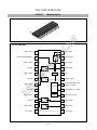
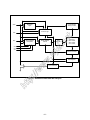
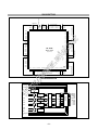
1
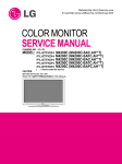
Website:http://biz.LGservice.com
E-mail:http://www.LGEservice.com/techsup.html
t
COLOR MONITOR
SERVICE MANUAL
L3000A (L3000AL-AL), (L3000AL-SL)
*(
) ID LABEL MODEL No.
.w
j
CAUTION
el.
MODEL:
ne
CHASSIS NO. : CL-36
FACTORY MODEL: L3000AL
ww
BEFORE SERVICING THE UNIT,
READ THE SAFETY PRECAUTIONS IN THIS MANUAL.
ht
tp
://
w
L3000A
CONTENTS
SPECIFICATIONS ................................................... 2
PRECAUTIONS ....................................................... 4
TIMING CHART ....................................................... 5
OPERATING INSTRUCTIONS ................................ 6
WIRING DIAGRAM ................................................. 9
BLOCK DIAGRAM ................................................. 10
DESCRIPTION OF BLOCK DIAGRAM...................11
ADJUSTMENT ...................................................... 13
TROUBLESHOOTING GUIDE .............................. 14
PRINTED CIRCUIT BOARD................................... 19
EXPLODED VIEW...................................................22
REPLACEMENT PARTS LIST ...............................24
PIN CONFIGURATION............................................31
SCHEMATIC DIAGRAM ......................................... 35
SPECIFICATIONS
≥ 10
: 350(min), 414(Typ)
2-3. Contrast Ratio
: 2300(min), 350(Typ)
://
w
2-2. Luminance
el.
ne
t
4-1. Power Adaptor
Input
: AC 100~240V, 50/60Hz , 2.0A
Output : DC 5V 0.9A, DC12V 1.5A
DC18V 1.0A, DC24V 5.0A
4-2. Power Consumption
MODE
ht
3-3. Sync Input
Horizontal
Vertical
Input Form
POWER ON (NORMAL)
ON/ON
ACTIVE
less than 165 W
GREEN
STAND-BY
OFF/ON
OFF
less than 5 W
AMBER
SUSPEND
ON/OFF
OFF
less than 5 W
AMBER
DPM OFF
OFF/OFF
OFF
less than 5 W
AMBER
POWER OFF
-
-
less than 1 W
OFF
5. ENVIRONMENT
6-1. Operating Temperature: 10°C~35°C (50°F~95°F)
(Ambient)
6-2. Relative Humidity
: 10%~80%
(Non-condensing)
6-3. MTBF
: 30,000 Hours(Typ.)
6. DIMENSIONS (with TILT/SWIVEL)
tp
3. SIGNAL (Refer to the Timing Chart)
3-1. Video Input
1)Signal Input : 15pin D-sub Connector/ S-video,
RCA
2)Input Form : RGB Analog(0.7Vp-p/75ohm), CVBS,
Digital, Y/C
3)Resolution(max) : Analog -1280 x 1024@60Hz
Digital -1024 x 768@75Hz
3-2. Audio Signal
1) Input:
H/V SYNC VIDEO POWER CONSUMPTION LED COLOR
ww
2. OPTICAL CHARACTERISTICS
2-1. Viewing Angle by Contrast Ratio
Left
: -80° min., -85°(Typ)
Right : +80° min., +85°(Typ)
Top
: +80° min., +85°(Typ)
Bottom : -80° min., -85°(Typ)
4. POWER SUPPLY
.w
j
1. LCD CHARACTERISTICS
Type
: TFT Color LCD Module
Size
: 30inch
Pixel Pitch
: 0.5025 x 0.1675 x RGB
Color Depth
: 8-bit, 16,777,216 colors
Electrical Interface
: LVDS
Active Display Area : 643.2mm x 385.92mm
Surface Treatment
: Anti-Glare, Hard Coating(3H)
Operating Mode
: Normally Black
Backlight Unit
: 16-CCFL (Cold Cathode
Fluorescent Lamp)
Width
Depth
Height
: 734 mm (28.90'')
: 487 mm (19.17')
: 96 mm (3.78'')
7. WEIGHT (with TILT/SWIVEL)
PC : 700mVrms
VCR : 450mVrms
DVD: 450mVrms
Net. Weight
Gross Weight
: 30 ~ 66kHz(Digital: 30~63kHz)
: 56 ~ 85Hz
: Separate, TTL,
Positive/Negative Digital, SOG
-2-
: 18.0kg (39.68 lbs)
: 22.0kg (48.51 lbs)
Signal Connector Pin Assignment
• DVI-D Connector (Digital)
Signal (DVI-D)
t
Hot Plug Detect
T. M. D. S. Data0T. M. D. S. Data0+
T. M. D. S. Data0/5 Shield
T. M. D. S. Data5T. M. D. S. Data5+
T. M. D. S. Clock Shield
T. M. D. S. Clock+
T. M. D. S. Clock-
ne
T. M. D. S. Data2T. M. D. S. Data2+
T. M. D. S. Data2/4 Shield
T. M. D. S. Data4T. M. D. S. Data4+
DDC Clock
DDC Data
Analog Vertical Sync.
T. M. D. S. Data1T. M. D. S. Data1+
T. M. D. S. Data1/3 Shield
T. M. D. S. Data3T. M. D. S. Data3+
+5V Power
Ground (return for +5V,
Pin
16
17
18
19
20
21
22
23
24
el.
8
16
24
Signal (DVI-D)
.w
j
1
9
17
Pin
1
2
3
4
5
6
7
8
9
10
11
12
13
14
15
H. Sync. and V. Sync.)
ht
tp
://
w
ww
T. M. D. S. (Transition Minimized Differential Signaling)
-3-
PRECAUTION
WARNING FOR THE SAFETY-RELATED COMPONENT.
WARNING
• There are some special components used in LCD
monitor that are important for safety. These parts are
marked on the schematic diagram and the
replacement parts list. It is essential that these critical
parts should be replaced with the manufacturer’s
specified parts to prevent electric shock, fire or other
hazard.
• If you want to replace with the new backlight (CCFL) or
inverter circuit, must disconnect the AC adapter
because high voltage appears at inverter circuit about
650Vrms.
• Handle with care wires or connectors of the inverter
circuit. If the wires are pressed cause short and may
burn or take fire.
ne
t
• Do not modify original design without obtaining written
permission from manufacturer or you will void the
original parts and labor guarantee.
BE CAREFUL ELECTRIC SHOCK !
• Must mount the module using mounting holes arranged
in four corners.
.w
j
• Do not press on the panel, edge of the frame strongly
or electric shock as this will result in damage to the
screen.
el.
TAKE CARE DURING HANDLING THE LCD MODULE
WITH BACKLIGHT UNIT.
ww
• Do not scratch or press on the panel with any sharp
objects, such as pencil or pen as this may result in
damage to the panel.
• Protect the module from the ESD as it may damage the
electronic circuit (C-MOS).
://
w
• Make certain that treatment person’s body are
grounded through wrist band.
• Do not leave the module in high temperature and in
areas of high humidity for a long time.
• The module not be exposed to the direct sunlight.
tp
• Avoid contact with water as it may a short circuit within
the module.
ht
• If the surface of panel become dirty, please wipe it off
with a softmaterial. (Cleaning with a dirty or rough cloth
may damage the panel.)
CAUTION
Please use only a plastic screwdriver to protect yourself
from shock hazard during service operation.
-4-
TIMING CHART
VIDEO
B
A
E
C
D
ne
t
SYNC
F
<< Dot Clock (MHz), Horizontal Frequency (kHz), Vertical Frequency (Hz), Horizontal etc... (µs), Vertical etc... (ms) >>
5
6
7
8
9
10
11
12
13
–
H
–
V
H
+
–
V
–
H
–
V
H
–
–
V
–
H
+
V
+
H
+
V
+
H
+
V
+
H
+/–
V
+/–
H
V
H
28.321
25.175
31.5
36.0
40.0
49.5
56.25
31.469
800
640
70.8
449
350
31.468
900
70.8
31.469
449
800
59.94
525
37.5
840
75
43.269
85.0
37.879
57.283
720
Front Porch
(C)
Sync Duration
(D)
Back Porch
(F)
16
96
48
37
2
60
18
el.
V
25.175
Total Period Video Active Time
(E)
(A)
108
54
400
640
12
16
2
96
35
48
480
10
2
33
640
16
64
120
1
56
3
56
16
80
.w
j
4
+
Frequency
ww
3
H
Dot
Clock
500
832
480
640
509
480
1
3
25
1056
800
40
128
88
600
1
4
23
://
w
2
Sync
Polarity
60.317
628
46.875
1056
800
16
80
160
75.0
625
600
1
3
21
53.674
1048
800
32
64
152
85.061
631
600
1
3
27
49.725
1152
832
32
64
224
tp
1
H/V
Sort
74.55
667
624
1
3
39
ht
Mode
48.363
1344
1024
24
136
160
60.0
806
768
3
6
29
60.123
1312
1024
16
96
176
75.029
63.981
800
1688
768
1280
1
48
3
112
28
248
60.02
1066
1024
1
3
38
47.7
1680
1280
66
134
200
60
795
768
1
3
23
–
–
–
V
H
–
+
V
+
H
+
V
+
65.0
78.75
108.0
80.14
-5-
Resolution
640x350
70Hz
720x400
70Hz
640x480
60Hz
640x480
75Hz
640x480
85Hz
800x600
60Hz
800x600
75Hz
800x600
85Hz
832x624
75Hz
1024x768
60Hz
1024x768
75Hz
1280x1024
60Hz
1280x768
60Hz
OPERATING INSTRUCTIONS
FRONT VIEW
REAR VIEW
Rear View Pannel
.w
j
Front Control Panel
el.
ne
t
L3000A
ww
REAR VIEW CONNECTOR PANEL
AUDIO
Input
ht
tp
://
w
Factory adjustment
or AS Port
Power
Cord
DVI-D
Connector
D-Sub
D-Sub
RCA Cable
Connector Connector Connector
-6-
S-Video
Connector
AUDIO
Output
OPERATING INSTRUCTIONS
Front Control Panel
7
6
3
4
5
1
.w
j
8
el.
ne
t
2
1
Power Button
• Use this button to turn the display on or off.
2
Power (DPMS)
Indicator
• This Indicator lights up green when the display operates normally. If the display is in
3
MENU Button
• Use this button to enter or exit the On Screen Display.
4
OSD Buttons
ww
DPM (Energy Saving) mode, this indicator color changes to amber.
://
w
• Use these buttons to choose or adjust items in the On Screen Display.
• Bring up Contrast and
Brightness adjustment.
Use these buttons to decrease or increase the volume level.
• Use this button to enter a selection in the On Screen Display.
• When adjusting your display settings, always press the AUTO/SELECT button before
tp
5
AUTO/SELECT Button
6
ht
entering the On Screen Display(OSD). This will automatically adjust your display image
to the ideal settings for the current screen resolution size (display mode).
SOURCE Button
SOURCE
AUTO/SELECT
• Use this button to select an input signal.
• DVI DIGITAL: DVI digital signal
• DSUB ANALOG: 15-pin D-sub analog signal
• V1 (AV): Composite video
• V2 (S): S video
7
Remote Control Sensor
8
Power On/Off switch
CONTROLS LOCKED/UNLOCKED : This function allows you to secure the current control settings, so that they cannot be
inadvertently changed. Press and hold the MENU button and button for 3 seconds: the
MENU and
message “CONTROLS LOCKED” appears.
You can unlock the OSD controls at any time by pushing the MENU button and
button for 3 seconds:
the message “CONTROLS UNLOCKED” will appear.
-7-
Attaching temporary stand
Follow below procedures to temporarily use the display on the floor.
First, check if the following parts are all present.
Parts
Screws
Bottom Rubbers
t
Temporary Stand
.w
j
el.
ne
1. Take out 2 screws from the rear of the display.
2. As shown in the diagram, place the bottom rubbers where you took out the 2
://
w
ww
screws and then secure them with those 2 screws.
ht
tp
3. Attach the temporary stand as shown.
-8-
WIRING DIAGRAM
Connector Ass’y P/N:
6631T11016A
ne
t
Connector Ass’y P/N:
6631T20020P
J703
Connector Ass’y P/N:
6631T12002P
el.
J19
.w
j
J710
J704
J705
Connector Ass’y P/N:
6631T12002N
://
w
ww
J706
CN1
ht
tp
CN1
-9-
- 10 -
PC L/R
L
R
Y/C
5V
8V
3.3V
RGB
(MSP3420G)
Audio
Processor
(SAA 7114H)
Video
Decoder
(BA 7657F)
Analo g
Switch
Input Selection
GVS
GHS
Rece iver
(SIL1 61A )
(SDA 9400)
(74LVC541ct)
Control Board
Key_Data
(0...15)
(THC63LVDM83R)
Transm itte r
LVDS
EEPROM
8V
5V 3.3V 2.5V
R,G,B
differential
t
24V,18V,12V,5V
Input
from Power B/d
Power Block
ne
12V
(74LVC273D)
I/O expander
PCB_PWR
INV_PWR
LCM_PWR
ROMOE
ROMWE
TMDSTX_PDNN
(M29W800DT)
Flash
Memory
Control Signals
3.3V
R,G,B
Odd
R,G,B
Eve n
el.
Data
(PWD0...7 )
Buffer
RDN CS0N
YUV
.w
j
RDN CS1N
CS0N
(PW166B-20 T)
ROMOE
ROMWE
Data
(PWD 0 ..7)
(PWA 0 ..19)
Format Converter Circuit 3.3V
2.5V 3.3V
Video Signal
Processor
ww
Eve n
Odd
GVS
GHS
Sync_ Sel
GREF
GREF
NCTL_S CL
NCTL_S DA
Deinterlacer
Line-out L
YUV
3.3V
(AD 9883-140)
ADC
Line-out R
3.3V
://
w
TMDSRX_PDNN
tp
ht
TMDS
(74L VC257)
Multiplexer
H V Sync
H V Sync
CVBS
D-SUB
3.3V
Sync_ Sel
DVI-D
Digital
Signal
3.3V
Video Signal
12V
Ready
LCD
Module
BLOCK DIAGRAM
DESCRIPTION OF BLOCK DIAGRAM
1. Input Selection Circuit
This block is composed of 74LVC257(U5) and peripheral devices.
There are two inputs, Analog and Digital H/V Sync.
LVC257 IC chooses one input and outputs selected input through sync selection pin (Pin 1).
2. A/D Converter
This block is composed of AD9883 (U4) and peripheral devices.
AD9883 includes A/D converter, Pre-amp, and PLL.
The Analog RGB signal (0.7Vp-p) is input to R,G,B port of AD9883(U4).
Input signal is amplified, phase locked , A/D converted in 8bits digital signal by this IC(U4), and sent to the Digital
video signal to PW166B-20T.
U4 makes clock for PW166B-20T(U8).
ne
t
3. TMDS PanelLink Receiver
This Block is composed of SiI161B (U201) and peripheral devices.
This IC decodes PanelLink Digital Input signal(TMDS) from DVI-D Pin (J18) and make 8bit digital RGB signal with
Digital EVEN/ODD format to PW166B-20T(U8).
.w
j
el.
4. DDC controller
This block is composed of PW166B-20T(U8) and peripheral devices.
PW166B-20T controls peripheral devices through IIC line.
Major functions are (1) to control Flash memory through DDC-SCLA, DDC-SDAA of D-sub And (2) to store EDID
data in the EEPROM (U17, U30)
ww
5. Video Decoder
This block is composed of SAA7114H (U7) and peripheral devices.
PW166B-20T controls this IC through IIC Line.
This IC analyzes input signal of CVBS, Y/C and outputs analyzed signal (8bit interlace signal) to De-interlace block.
Analyzed signal has video control signals like Contrast, Brightness, Sharpness, Color, tint signals Including Adaptive
Comb Filter.
://
w
6. Audio Decoder
This block is composed of MSP3420G (U49) and peripheral devices.
PW166B-20T controls this IC through IIC Line.
This IC analyzes Audio input signal through A/V Jack and PC audio.
And output the analyzed signals
ht
tp
7. De-interlace
This block is composed of SDA9400 (U16) and peripheral devices.
PW166B-20T (U8) controls this IC through IIC Line.
And this IC convert 8 Bit Interlaced Y/UV signal to De-interlace signal.
It outputs converted signal to Format Converter (PW166B-20T).
8. Format Converter(Scaler)
This block is composed of PW166B-20T (U8), M29W800DT (U19) and peripheral devices.
MICOM in PW166B-20T (U7) processes outputs of A/D Converter and TMDS Receiver,
De-interlace output and output processed 48 Bit Digital signal to TMDS Transmitter.
PW166B-20T is Format Converter IC that receives Digital signal and outputs proper frame signal to LCD Module
Timing(1280x768,WXGA).
9. PanelLink Circuit
TMDS Transmitter (THC63LVDM83R, U401) is the IC that receives output digital signal of PW166B-20T (U8) and
output to LCD Module.
The signal format is Panel-link.
LCD Module has Panel-link receiver that is same output of PW166B-20T.
This is the best for reduction EMI problem and the number of pin connector.
- 11 -
10. DC/DC Converter block
DC/DC Converters convert the input 12V, 24V to proper 2.5V, 3.3V, 5V, 8V for main control system.
For shooting heat trouble, we use the DC/DC converting IC.
ht
tp
://
w
ww
.w
j
el.
ne
t
11. Power Supply Block
This Block generates DC Voltages(5V, 12V, 18V and 24V) to Main Control system from AC Power(100-240 V, 50/60
Hz, 1.0 A).
This Circuit contains PFC(Power Factor correction) circuit.
The Minimum of Power efficiency is about 75%.
- 12 -
ADJUSTMENT
All adjustment are thoroughly checked and corrected
when the monitor leaves the factory, but sometimes
several minor adjustment may be required.
Adjustment should be following procedure and after
warming up for a minimum of 30 minutes.
6) No attempt to manually adjust, BIAS and Drive data
is automatically adjustde and saved to the EEPROM.
7) After “OK” message, Press SET KEY.
8) Select “SERVICE MODE EXIT” and Press SET KEY.
• Alignment appliances and tools.
- IBM compatible PC
- Programmable Signal Generator.
(eg. VG-819 made by Astrodesign Co.)
- Oscilloscope.
- White Balance Meter. (CA-110)
3. DDC Data Write Procedure-Analog
1) Use this procedure only when there is some
problem on Analog EDID data.
2) Run alignment program for LM805L on the IBM
compatible PC.
3) Select EEPROM → Analog EDID write command
and Enter.
4) This will write the Analog EDID data to EEPROM.
ne
t
1. Adjustment for Factory Preset Mode
No read to adjust FOS data for Factory Preset Mode.
2. Adjustment for White Balance
1) Set External Bright to MAX position and Contrast to
MAX position.
2) Display Color 0,0 pattern at Mode 15.
3) Press Menu key, Vp key, Right key of Remote
controller or Menu Buttons in sequence.
4) Select “WHITE BALANCE ADJUST” and Press SET
key.
5) After “INPUT WHITE PATTERN” message, Display
Color 15, 0 pattern at Mode 15.
://
w
ww
.w
j
el.
4. DDC Data Write Procedure-Digital
1) Use this procedure only when there is some
problem on Digital EDID data.
2) Run alignment program for LM805L on the IBM
compatible PC.
3) Select EEPROM → Digital EDID write command
and Enter.
4) This will write the Digital EDID data to EEPROM.
A
tp
IBM
Compatible PC
9
15
10
5
11
6
1
6
1
5
C
se
d
Parallel Port
23
RS
EL
5V
OFF
14
ON
F
RA
PA
Power inlet (required)
5V
R
220
WE
VG
CS
T
MO
NI
ON
TO
R
4.7K
OFF
74LS06
B
E ST Switch
B
DVI-D Connector
F V-Sync On/Off Switch
(Switch must be ON.)
Figure 1. Cable Connection
- 13 -
4.7K
4.7K
5V
E
YN
A
PO
S
Power Select Switch
(110V/220V)
Power LED
V-S
Control Line
C
1
25
LL
ht
No
2C
tu
13
74LS06
TROUBLESHOOTING GUIDE
1. OUT OF ORDER ON POWER
POWER LAMP OFF STATE
M29W800DT(U19)
INPUT POWER
CHECK
ne
INVERTER
INPUT POWER
CHECK
ww
PW166(U8)
INPUT POWER
CHECK
.w
j
el.
KEY CHECK
74LVC541(U25),
CONN(J19)CHECK
t
POWER BOARD OUTPUT CHECK
(5V, 12V, 24V)
BA033T(U37)
=>3.3V
LM317(U10)
=>2.5STB
L53,L54 => 24V
://
w
BA033T(U37)
=>3.3V
ht
tp
INVERTER CHECK
OTHER CIRCUIT CHECK
- 14 -
MODULE
INPUT POWER
CHECK PIN 1=>
12VS
IRF7314(U35)
=>LCD-VDD
MODULE CHECK
2.NO RASTER STATE ON ANALOG SIGNAL
NO RASTER ON ANALOG
SIGNAL
el.
ne
t
POWER CHECK OF 74LVC257(U5) : U37(3.3V)
POWER CHECK OF AD9883 : U2(DVDD,AVD), L11(V33-ADC)
POWER CHECK OF PW166(U8) :BA033T(U37) =>3.3V, LM317(U10) =>2.5STB
POWER CHECK OF LVDS(U401) : L401(3.3V-LVDS)
.w
j
CONN(J17) CHECK
ww
CHECK I/O SYNC OF
74LVC257(U5)
NO INPUT SIGNAL
CHECK AD9883 I/O SIGNAL
CHECK THE PERIPHERAL IC
OF D-SUB(J17)
://
w
NO OUTPUT SIGNAL
NO INPUT SIGNAL
CHECK THE PERIPHERAL IC
OF AD9883(U4)
CHECK PW166(U8) I/O SIGNAL
tp
NO OUTPUT SIGNAL
NO INPUT SIGNAL
CHECK LVDS(U401) I/O
SIGNAL
ht
CHECK THE PERIPHERAL IC
OF PW166(U8)
NO OUTPUT SIGNAL
- 15 -
CHECK THE PERIPHERAL IC
OF LVDS(U401)
3. NO RASTER STATE ON DIGITAL SIGNAL
NO RASTER STATE ON
ANALOG SIGNAL
el.
POWER CHECK OF SIL161(U201) : L4(AVCC),L5(PVCC)
L9(DVCC),L210(OVCC)
ww
.w
j
CONN(J10) CHECK
CHECK I/O SYNC OF
74LVC257(U5)
NO INPUT SIGNAL
://
w
CHECK SIL161(U201) I/O
SIGNAL
ne
t
POWER CHECK OF 74LVC257(U5) : U37(3.3V)
POWER CHECK OF AD9883 : U2(DVDD,AVD), L11(V33-ADC)
POWER CHECK OF PW166(U8) : BA033T(U37) =>3.3V, LM317(U10) =>2.5STB
POWER CHECK OF LVDS(U401) : L401(3.3V-LVDS)
CHECK THE PERIPHERAL IC
OF D-SUB(J17)
NO OUTPUT SIGNAL
NO INPUT SIGNAL
CHECK THE PERIPHERAL IC
OF SIL161(U201)
ht
tp
CHECK PW166(U8) I/O SIGNAL
NO OUTPUT SIGNAL
CHECK THE PERIPHERAL IC
OF PW166(U8)
NO INPUT SIGNAL
CHECK LVDS(U401) I/O
SIGNAL
NO OUTPUT SIGNAL
- 16 -
CHECK THE PERIPHERAL IC
OF LVDS(U401)
4. NO RASTER ON VIDEO SIGNAL INPUT
NO RASTER ON VIDEO SIGNAL
ne
t
POWER CHECK OF SAA7114(U7) : L19,L21(3.3V)
POWER CHECK OF SDA9400(U16) : L23(3.3V)
POWER CHECK OF PW166(U8) : BA033T(U37) =>3.3V, LM317(U10) =>2.5STB
POWER CHECK OF LVDS(U401) : L401(3.3V-LVDS)
.w
j
el.
CHECK CABLE OF
VCR,DVD
NO INPUT SIGNAL
CHECK SAA7114(U7) I/O
SIGNAL
ww
NO OUTPUT SIGNAL
NO INPUT SIGNAL
NO OUTPUT SIGNAL
://
w
CHECK SDA9400(U16) I/O
SIGNAL
CHECK VCR,DVD INPUT SIGNAL
CHECK THE PERIPHERAL IC
OF SAA7114(U7)
CHECK THE PERIPHERAL IC
OF SDA9400(U16)
NO INPUT SIGNAL
CHECK PW166(U8) I/O SIGNAL
tp
NO OUTPUT SIGNAL
ht
CHECK LVDS(U401) I/O
SIGNAL
CHECK THE PERIPHERAL IC
OF PW166(U8)
NO INPUT SIGNAL
NO INPUT SIGNAL
- 17 -
CHECK THE PERIPHERAL IC
OF LVDS(U401)
5. SOUND TROBLE SHOOTING
NO SOUND OUTPUT
el.
ne
t
POWER CHECK OF MSP3420G(U49) : L34,L35,L36(5V)
POWER CHECK OF TDA7268(U39) : 12V
POWER CHECK OF PW166(U8) : BA033T(U37) =>3.3V, LM317(U10) =>2.5STB
CHECK SOUND INPUT
=>PC SOUND(J7)
=>VIDEO SOUND
(RDE,WHITE OF J702)
CHECK THE PERIPHERAL IC
.w
j
CHECK SOUND OF VCR,DVD,PC
ww
NO INPUT SIGNAL
CHECK MSP3420G(U49) INPUT
SIGNAL
NO OUTPUT SIGNAL
ht
tp
://
w
NO INPUT SIGNAL
- 18 -
CHECK THE PERIPHERAL IC
OFMSP3420G(U49)
PRINTED CIRCUIT BOARD
C98
J1
J19
1. MAIN BOARD (Component Side)
R19
R20
C101 C102
R42
R41
J7
ZD8
C111
C91
ZD7
J5
R248
R247
R185
R526
ZD28
t
R183
R529
ZD29
J702
ne
D9
D12
R182
R223
R224
SOLDERING DIRECTION
C127
L70 R525
L71 R523
L66 R532 D11
D32
R222
D33
ZD1
D31
D27
D26
D2
D25
J3
D28
R206
R173
D29
R177 R187
D30
R65
C11
C9
C10
C7
C8
R36 D5
L31
C99
R38 ZD3
R207
L8
C5
C6
C3
C13
L6 R34
L7
C4
C1
R1
L1 D3
D1
C121C2
R51
R50
R43
D10
ZD23
J17
D37
U30
ZD27
ZD25
D18
ZD21
ZD24
C150
D17
C103
R101
R102
R103
R104
R118
R112
R114
C43
C109
C94
R277 R278
R275 R276
R273 R274
R271 R272
R233
L4
L9
R234
J10
C66
R158
C45
R159
R160
J2
R162
R163
L210
C154
CA203 CA204
C195
R254
D8
R52 C72
C120
U13 R111
R164
U201
CA201
L12
- 19 -
L5
R2
CA206
C816
CA205
RA223 RA224 RA225 RA226
CA202
C87
ZD26
R193 R192
C216
R3
L56
C73
R53
R21
R12
R11
R342
C248
U17
C217
D23
C92
C225
Q10
R201
J706
J705
R194
L3
C12
C235
U1
C122
C153
ZD22 C136
C218
L53
L54
R801
R97
R196 C88
C39
C123
R48
C802
R49
RA221
U801
C86
1
L30
R105
U3
R203
R205
R139
R700
U5
C115
R215
R214
R161
10
C159
C116
C32
CA210 CA211 CA212
RA227 RA228 RA229 RA230 RA231 RA232
TRANS801
C807
R804
C805
20
C79
RA23
C227
R57
C179
J704
C809
15
C803
U2
RA20
RA19
80
ZD806
20
10
RA22
RA21
R213
C801
RA1
C26
C132
C203
C204
C117
C33
80
90
ZD4
C67
R198
C24
R58
R59
C118
U4
C172
ht
C220
100
C840
L17 L18
30
70
C806
C82
Q19
R94
R107
70
L11
C148
C149
C152
RA28
tp
40
R7
R8
R61
CA207 CA208 CA209
1
R169
R170
1
L29
R60
C19
R6
C30
R227
60
L59
C21 C22
50
10
ZD20
C35
C23
U8
://
w
RA8
RA29 RA32 RA33
20
10
1
R209 R211
U29
R175 C223
R178
60
C37
C173
Q3
R87
50
C93
C20
R122
20
L10
C234
C31
C25
C34
C18
C17
R5
R56
R55
R54
R210
C814
ZD5
C14
RA222
C804
ZD6
RA6
40
1
RA7
30
1
C187
ZD10
R186
R220
L55
C185
RA4
C71
C812
R166
R96
R189 R184
1
L25 L22
J703
R93
R92
R155
R137
R125
C76 X2
C74
R91
R126
X3
U6
C38
RA37
C410
C405
R143
D39
C215
C177
L28
C221
U37
L58
L52
RA5
R119
R221
R120
C171
R225
C158
R202
R197
R204
U10
1
D7
R144
R110
U19
U22
X4
C36
C44
C40
J710
L401
D38
L57
R27
R33
5
R176
RA24
R86
R138
R208
R219
ZD2
R190
ZD9
ZD11
C90
10
R174
RA2
60
C186
R151
C85
C70
R35
1314 15 16 17 18 19 20
C402
C401
U401
R98
R39
R157
R32
C75
R188
R195
20
50
C113
C47
20
X1
L13
RA25
50
R401
C112
D24
R191
C89
Q22
R145
R165
C78
RA3
C50 C51
C52
C81
U16
ww
R106
R117
R90
R109
R108
C41
R26
1 2 3 4 5 6 7 8 9 10 1112
40
C108
C65
R25
C403
C107
C413
10
C55
.w
j
R141 C188 C316
R142
U12
R78
R77
L20
R22
1
30
C106
C64
R18
R17
R70
C62
el.
C
C46
U7
C124
C178
C63
C60
C329
R253
C322
R252
C321
R259
C324
R255
C323
C387
R146
R31
R29
R156
R28
C83
R147
R149
A
B
C
D
E
F
G
H
J
K
L
M
N
P
R
T
U
V
W
Y
R404
C325
C305
C404
C412
R265
Q11
R266
R75
C196
J6
R140
R115
R123 R121
U33
U15
10
R76
U11
10
40
R37
R405
C307
C
C407
R267
L42
L36
U27
20
20
1
U35
C385
R127
R15
L67
R24
R71
L23 L19
30
30
1
L27
L68
R69
C198
1
U18
20
C145
R63
R68
R134
40
20
R72
R67
R99
C306
U20
C384
C144
R218
Q6
U23
1
50
C383
C375
L2
C374
Q4
U9
R181
Q1
Q13
C380
C42
R124
R100
R73
R64
L64
R44
L21
R80
C48
R79
C59
C100
C130
C110
C58
C125
C138
C129
C61
R62
C131
C57
C128
C53
C126
R238
R82
R23
R40
R74
R403
C304
60
Q9
C156
10
40
70
10
30
80
R153
C377
C416
R268
90
C54
Q12
100
C175
R228 C176
R150
R14
C137
R528
R245
1
C68
R45
C15
U24
R129
R130
R66
C16
C141
C142
R217
R229
U14
C140
R531
C415
R116
R113
U25
R46
R131
R13
R9
R10
R246
60
C143
R270
C97
R269
C95
50
C69
R16
R168 C302
C182
L62
C331
R212
R128
R83
U32
L35
40
R4
R30
C308
U49
C184
C104 C105
J4
X5
R171 C320 C319
30
R136 R180
R179
R47
R167
R235
C381
1
R81
C276
C147
C278
C155
C280
C287
R132
R231
R232
R133
C288
E R230
C146
C77
R95
U21
C96 R216
E
Q5
D34
R85
R84
R135
C317
C197
C328
20
R236
D36
L16
L34
C310
C311
R172
10
R152
C49
R237
Q14
D35
R261
R262
R263
C332
R251
R250
R264
C388
C183
70
D4
1
R148
U34
R154
C303
1
MODEL:L3000A
P/N :6870T597A11
DATE :2002.11.27
Q2
L15
D6
D21 D13 D14
D19 D15 D16
ZD12 ZD14 ZD16
ZD13 ZD15 ZD17
D20
D22
ZD18
ZD19
2. MAIN BOARD (Solder Side)
C114
C80
C201
C200
C84
C210
C211
TP815
C181
C180
C212
C208
C209
C213
C56
C214
t
C242
C810
C174
L49
C811
C224
C119
C27
C29
el.
C28
ne
C206
C219
C134
C133
C169
C167
.w
j
C161
C168
R88
C163
C162
C135
R89
C157
C164
R199
C170
C165
C160
C139
C166
R200
C313
C189
ht
tp
C190
L51
L14
L40
L39
L38
L44
1
L24
1
L26
L47
L48
L46 L43
L45
L41
- 20 -
L37
L32
L33
TP455
://
w
ww
C151
ht
tp
://
w
ww
.w
j
el.
ne
t
3. POWER BOARD (Component Side)
4. CONTROL BOARD (Component Side)
J1
C1
ZD2
1
POWER
SW8
LED1
U1
- 21 -
ZD4
Q1
ZD1
SW6
R2
SELECT
R1
SW4
R3
RIGHT
R21
SW2
Q14
Q12
R19
LEFT
R17
UP
SW10
R15
SW9
Q10
Q18
R13
R24
SW7
DOWN
R26
MENU
R25
R22
R20
ZD6
ZD8
ZD7
SW5
R18
ZD5
L1
C2
ZD9
ZD3
ZD10
ZD11
SOURCE
Q17
Q15
C3
MODEL:L3000A(KEY)
DATE :2002.11.28
P/N :6870T598C11
Q13
EXPLODED VIEW
10
a
a
12
a
a
16
t
a
a
a
ne
a
a
a
a
a
13
a
a
a
.w
j
a
17
el.
a
a
3
ww
8
9
14
18
15
19
SET
CH
ht
5
CH
VOL
tp
6
://
w
7
b
4
2
11
1
- 22 -
VOL
EXPLODED VIEW PARTS LIST
Ref. No.
1
2
Description
Part No.
3091TKL059A
CABINET ASSEMBLY, L3000AL BRAND 3090TKL056A (30") -(L3000AL-AL)
3091TKL059B
CABINET ASSEMBLY, L3000AL BRAND 3090TKL056 B30""" -(L3000AL-SL)
6304FLP049A
LCD(LIQUID CRYSTAL DISPLAY), LC300W01-A3M2 LG PHILPS TFT COLOR LPL INVERTER APPLY
or 6304FLP017A LCD(LIQUID CRYSTAL DISPLAY), LC300W01-A3 LG PHILPS TFT COLOR WITH INVERTER29.53",1280*768,450CD/M2,8BIT
or 6304FLP054A LCD(LIQUID CRYSTAL DISPLAY), LC300W01-A3M3 LG PHILPS TFT COLOR 8BIT LVDS 16LAMP
3
4814TKK234J
SHIELD, REAR L3000AL -(L3000AL-AL)
t
or 4814TKK234K SHIELD, REAR (L3000AL)-(L3000AL-SL)
METAL, STAND TEMP.-(L3000AL-AL)
4950TKK502B
METAL, STAND TEMP-(L3000AL-SL)
5
4950TKS215C
METAL, FRAME
6
6871TPT240A
PWB(PCB) ASSEMBLY, POWER, L3000AL POWER TOTAL HAEPYUNG U200-M30LZ1A
7
6871TMT418A PWB(PCB) ASSEMBLY,MAIN, L3000A ALEUA BRAND CL-36 TOTAL
8
6631T11016A
CONNECTOR ASSEMBLY, 20P H-H 180MM UL20276 I/FACE CABLE LB200A
4815TKK026B
SHIELD ASSEMBLY, REAR MAIN (PAL) -(L3000AL-AL)
4815TKK026D
SHIELD ASSEMBLY, REAR MAIN(SILVER_PAL) -(L3000AL-SL)
4951TKK127A
METAL ASSEMBLY, STAND(ST3000-BLACK)
4951TKK127B
METAL ASSEMBLY, STAND(ST3000-SILVER)
11
6871TST358A
PWB(PCB) ASSEMBLY,SUB, L3000AL CONTROL TOTAL BRAND CL-36
12
6852TAZ006B
CORD, A/V, RCA CABLE UL 2863 #25 3000MM BLACK(9930) DH-3P-N300C LM295B
13
6852TAZ006C
CORD, A/V, SCART CABLE UL 2863 #25 1500MM GRAY(85964) DH-3P-150SRC LM295B
14
6852TAZ006D
CORD, A/V, DIN CABLE UL 2990-9C(5.5) 1560MM BLACK(9930) DH-150DIN LM295B
15
6852TAZ006J
CORD, A/V, A/V KHC-LG-3-0010 UL 2851 #28-2C 1500MM BLACK(9930) KSD WITH CORE LM295B
ne
4950TKK502A
16
.w
j
ww
://
w
tp
10
ht
9
el.
4
6850TD9001G
CABLE, D-SUB, UL 2990-9C(7.5) DT 1870MM BLACK(9930) , DM -(L3000AL-AL)
6850TD9001J
CABLE, D-SUB, UL 2990-9C(7.5) DT 1870MM PEARL WH T541K DM -(L3000AL-SL)
6866TDV004J
CABLE, DVI, UL20276 DT 2000MM BLACK(9930) LG883D DM -(L3000AL-AL)
17
6866TDV004C CABLE, DVI, UL20276 DT 2000MM GRAY(85964) LB885C DM -(L3000AL-SL)
18
5040TKM050A RUBBER, FOOT MOLDING BOTTOM(L3000AL)
19
6710T00001C
a
332-102R
b
REMOTE CONTROLLER, LM295B -KALU (22")
SCREW,DRAWING, TAP-TITE(P) TRUSS HEAD TYPE D4.0 L14.0 MSWR/BK (L3000AL)
1SZZTMF010A SCREW,DRAWING, MACHINE FILLISTER TYPE D5.0 L10.0 MSWR/FN L3000AL
- 23 -
REPLACEMENT PARTS LIST
CAUTION: BEFORE REPLACING ANY OF THESE COMPONENTS,
READ CAREFULLY THE SAFETY PRECAUTIONS IN THIS MANUAL.
* NOTE : S SAFETY Mark
AL ALTERNATIVE PARTS
DATE: 2003. 3. 5.
DESCRIPTION / SPECIFICATION
*S *AL LOC. NO.
0CK473CK56A
0CK104CK56A
0CK104CK56A
0CK104CK56A
0CK104CK56A
0CK104CK56A
0CK104CK56A
0CH8476K611
0CK104CK56A
0CH3105H946
0CK104CK56A
0CH8226F611
0CC101CK41A
0CC101CK41A
0CC180CK41A
0CK104CK56A
0CC180CK41A
0CH8107F611
0CK104CK56A
0CK104CK56A
0CH3104K946
0CK104CK56A
0CK103CK51A
0CK104CK56A
0CH3104K946
0CK104CK56A
0CE227CF638
0CK104CK56A
0CC331CK41A
0CC331CK41A
0CC331CK41A
0CK104CK56A
0CK104CK56A
0CH8226F611
0CH3474H946
0CK104CK56A
0CH3474H946
0CH8106F611
0CE106VK6DC
0CC100CK41A
0CK104CK56A
0CC101CK41A
0CC100CK41A
0CH3104K946
0CH3104K946
0CH8226F611
0CK104CK56A
0CH8226F611
0CH8226F611
0CH8226F611
0CC100CK41A
0CH8106F611
0CH8226F611
0CK473CK56A
.w
j
://
w
ww
47UF MV 6.3V 20% R/TP(SMD) S
0.01UF 1608 50V 10% R/TP B(Y
47UF MV 6.3V 20% R/TP(SMD) S
0.01UF 1608 50V 10% R/TP B(Y
47UF MV 6.3V 20% R/TP(SMD) S
0.01UF 1608 50V 10% R/TP B(Y
47UF MV 6.3V 20% R/TP(SMD) S
0.01UF 1608 50V 10% R/TP B(Y
47UF MV 6.3V 20% R/TP(SMD) S
0.01UF 1608 50V 10% R/TP B(Y
47UF MV 6.3V 20% R/TP(SMD) S
0.01UF 1608 50V 10% R/TP B(Y
470PF 1608 50V 5% R/TP NP0
“0.47UF 25V 80%,-20% F(Y5V) 2”
1500PF 1608 50V 10% R/TP B(Y
1500PF 1608 50V 10% R/TP B(Y
82NF 1608 50V 10% R/TP X7R
8200PF 1608 50V 10% X7R R/TP
47000PF 1608 50V 10% R/TP X7
47000PF 1608 50V 10% R/TP X7
47000PF 1608 50V 10% R/TP X7
1000PF 1608 50V 5% R/TP NP0
0.1UF 1608 50V 10% R/TP X7R
0.1UF 1608 50V 10% R/TP X7R
0.1UF 1608 50V 10% R/TP X7R
100000PF 50V Z F 2012 R/TP
100000PF 50V Z F 2012 R/TP
100000PF 50V Z F 2012 R/TP
0.1UF 1608 50V 10% R/TP X7R
0.1UF 1608 50V 10% R/TP X7R
0.1UF 1608 50V 10% R/TP X7R
0.1UF 1608 50V 10% R/TP X7R
0.1UF 1608 50V 10% R/TP X7R
0.1UF 1608 50V 10% R/TP X7R
470UF SHL 16V M FL TP5
0.1UF 1608 50V 10% R/TP X7R
0.1UF 1608 50V 10% R/TP X7R
100PF 1608 50V 5% R/TP NP0
47UF 50V 20% 85STD (CYL) R/T
0.1UF 1608 50V 10% R/TP X7R
0.1UF 1608 50V 10% R/TP X7R
0.1UF 1608 50V 10% R/TP X7R
0.1UF 1608 50V 10% R/TP X7R
39PF 1608 50V 5% R/TP NP0
39PF 1608 50V 5% R/TP NP0
0.1UF 1608 50V 10% R/TP X7R
0.1UF 1608 50V 10% R/TP X7R
0.1UF 1608 50V 10% R/TP X7R
0.1UF 1608 50V 10% R/TP X7R
100000PF 50V Z F 2012 R/TP
0.1UF 1608 50V 10% R/TP X7R
47000PF 1608 50V 10% R/TP X7
tp
0CE476VC6DC
0CK103CK51A
0CE476VC6DC
0CK103CK51A
0CE476VC6DC
0CK103CK51A
0CE476VC6DC
0CK103CK51A
0CE476VC6DC
0CK103CK51A
0CE476VC6DC
0CK103CK51A
0CC471CK41A
0CH3474H946
0CK152CK51A
0CK152CK51A
0CK823CK56A
0CK822CK56A
0CK473CK56A
0CK473CK56A
0CK473CK56A
0CC102CK41A
0CK104CK56A
0CK104CK56A
0CK104CK56A
0CH3104K946
0CH3104K946
0CH3104K946
0CK104CK56A
0CK104CK56A
0CK104CK56A
0CK104CK56A
0CK104CK56A
0CK104CK56A
0CE477CF618
0CK104CK56A
0CK104CK56A
0CC101CK41A
0CH8476K611
0CK104CK56A
0CK104CK56A
0CK104CK56A
0CK104CK56A
0CC390CK41A
0CC390CK41A
0CK104CK56A
0CK104CK56A
0CK104CK56A
0CK104CK56A
0CH3104K946
0CK104CK56A
0CK473CK56A
ht
C1
C2
C3
C4
C5
C6
C7
C8
C9
C10
C11
C12
C13
C14
C15
C16
C17
C18
C20
C21
C22
C23
C24
C25
C26
C27
C28
C29
C30
C31
C32
C33
C34
C35
C39
C41
C42
C43
C45
C46
C47
C48
C49
C50
C51
C52
C53
C54
C55
C56
C57
C58
C59
C60
C61
C62
C63
C64
C65
C66
C67
C68
C70
C71
C72
C73
C74
C75
C76
C77
C78
C79
C80
C81
C82
C83
C84
C85
C86
C87
C88
C89
C90
C92
C93
C94
C95
C96
C97
C98
C99
C100
C103
C109
C110
C114
C119
C120
C121
C122
C123
C124
C125
C126
C127
C128
DATE: 2002. 3. 5.
DESCRIPTION / SPECIFICATION
47000PF 1608 50V 10% R/TP X7
0.1UF 1608 50V 10% R/TP X7R
0.1UF 1608 50V 10% R/TP X7R
0.1UF 1608 50V 10% R/TP X7R
0.1UF 1608 50V 10% R/TP X7R
0.1UF 1608 50V 10% R/TP X7R
0.1UF 1608 50V 10% R/TP X7R
47UF 50V 20% 85STD (CYL) R/T
0.1UF 1608 50V 10% R/TP X7R
“1UF 25V 80%,-20% F(Y5V) 2012”
0.1UF 1608 50V 10% R/TP X7R
22UF 16V M 85STD(CYL) R/TP
100PF 1608 50V 5% R/TP NP0
100PF 1608 50V 5% R/TP NP0
18PF 1608 50V 5% R/TP NP0
0.1UF 1608 50V 10% R/TP X7R
18PF 1608 50V 5% R/TP NP0
100UF 16V M 85STD(CYL) R/TP
0.1UF 1608 50V 10% R/TP X7R
0.1UF 1608 50V 10% R/TP X7R
100000PF 50V Z F 2012 R/TP
0.1UF 1608 50V 10% R/TP X7R
0.01UF 1608 50V 10% R/TP B(Y
0.1UF 1608 50V 10% R/TP X7R
100000PF 50V Z F 2012 R/TP
0.1UF 1608 50V 10% R/TP X7R
“220UF SHL,SD 16V M FM5 TP 5”
0.1UF 1608 50V 10% R/TP X7R
330PF 1608 50V 5% R/TP NP0
330PF 1608 50V 5% R/TP NP0
330PF 1608 50V 5% R/TP NP0
0.1UF 1608 50V 10% R/TP X7R
0.1UF 1608 50V 10% R/TP X7R
22UF 16V M 85STD(CYL) R/TP
“0.47UF 25V 80%,-20% F(Y5V) 2”
0.1UF 1608 50V 10% R/TP X7R
“0.47UF 25V 80%,-20% F(Y5V) 2”
10UF 16V M 85STD(CYL) R/TP
10UF MV 50V 20% R/TP(SMD) SM
10PF 1608 50V 5% R/TP NP0
0.1UF 1608 50V 10% R/TP X7R
100PF 1608 50V 5% R/TP NP0
10PF 1608 50V 5% R/TP NP0
100000PF 50V Z F 2012 R/TP
100000PF 50V Z F 2012 R/TP
22UF 16V M 85STD(CYL) R/TP
0.1UF 1608 50V 10% R/TP X7R
22UF 16V M 85STD(CYL) R/TP
22UF 16V M 85STD(CYL) R/TP
22UF 16V M 85STD(CYL) R/TP
10PF 1608 50V 5% R/TP NP0
10UF 16V M 85STD(CYL) R/TP
22UF 16V M 85STD(CYL) R/TP
47000PF 1608 50V 10% R/TP X7
el.
MAIN BOARD
CAPACITORS
PART NO.
t
PART NO.
ne
*S *AL LOC. NO.
- 24 -
t
100000PF 50V Z F 2012 R/TP
100000PF 50V Z F 2012 R/TP
100UF 16V M 85STD(CYL) R/TP
0.1UF 1608 50V 10% R/TP X7R
100000PF 50V Z F 2012 R/TP
100000PF 50V Z F 2012 R/TP
100000PF 50V Z F 2012 R/TP
100000PF 50V Z F 2012 R/TP
100000PF 50V Z F 2012 R/TP
100000PF 50V Z F 2012 R/TP
100000PF 50V Z F 2012 R/TP
0.1UF 1608 50V 10% R/TP X7R
0.1UF 1608 50V 10% R/TP X7R
0.1UF 1608 50V 10% R/TP X7R
0.1UF 1608 50V 10% R/TP X7R
100000PF 50V Z F 2012 R/TP
22UF 16V M 85STD(CYL) R/TP
22UF 16V M 85STD(CYL) R/TP
0.1UF 1608 50V 10% R/TP X7R
100000PF 50V Z F 2012 R/TP
100PF 1608 50V 5% R/TP NP0
100PF 1608 50V 5% R/TP NP0
0.01UF 1608 50V 10% R/TP B(Y
47UF 16V 20% 85STD (CYL) R/T
100000PF 50V Z F 2012 R/TP
0.1UF 1608 50V 10% R/TP X7R
0.01UF 1608 50V 10% R/TP B(Y
0.01UF 1608 50V 10% R/TP B(Y
0.01UF 1608 50V 10% R/TP B(Y
0.01UF 1608 50V 10% R/TP B(Y
0.01UF 1608 50V 10% R/TP B(Y
0.1UF 1608 50V 10% R/TP X7R
47UF 16V 20% 85STD (CYL) R/T
0.47UF 50V 20% 85STD (CYL) R
0.47UF 50V 20% 85STD (CYL) R
0.47UF 50V 20% 85STD (CYL) R
0.47UF 50V 20% 85STD (CYL) R
0.1UF 1608 50V 10% R/TP X7R
56PF 1608 50V 5% R/TP NP0
56PF 1608 50V 5% R/TP NP0
100000PF 50V Z F 2012 R/TP
0.1UF 1608 50V 10% R/TP X7R
0.1UF 1608 50V 10% R/TP X7R
3.3PF 1608 50V 0.25 PF R/TP
3.3PF 1608 50V 0.25 PF R/TP
2200PF 1608 50V 10% R/TP B(Y
2200PF 1608 50V 10% R/TP B(Y
56PF 1608 50V 5% R/TP NP0
10UF 16V M 85STD(CYL) R/TP
0.1UF 1608 50V 10% R/TP X7R
0.1UF 1608 50V 10% R/TP X7R
0.01UF 1608 50V 10% R/TP B(Y
0.1UF 1608 50V 10% R/TP X7R
47UF 16V 20% 85STD (CYL) R/T
4.7UF 35V M 85STD(CYL) R/TP
0.1UF 1608 50V 10% R/TP X7R
0.1UF 1608 50V 10% R/TP X7R
22UF 16V M 85STD(CYL) R/TP
100UF 16V M 85STD(CYL) R/TP
220UF 16V 20% 85STD (CYL) R/
0.1UF 1608 50V 10% R/TP X7R
0.1UF 1608 50V 10% R/TP X7R
ne
0CH3104K946
0CH3104K946
0CH8107F611
0CK104CK56A
0CH3104K946
0CH3104K946
0CH3104K946
0CH3104K946
0CH3104K946
0CH3104K946
0CH3104K946
0CK104CK56A
0CK104CK56A
0CK104CK56A
0CK104CK56A
0CH3104K946
0CH8226F611
0CH8226F611
0CK104CK56A
0CH3104K946
0CC101CK41A
0CC101CK41A
0CK103CK51A
0CH8476F611
0CH3104K946
0CK104CK56A
0CK103CK51A
0CK103CK51A
0CK103CK51A
0CK103CK51A
0CK103CK51A
0CK104CK56A
0CH8476F611
0CH8474K611
0CH8474K611
0CH8474K611
0CH8474K611
0CK104CK56A
0CC560CK41A
0CC560CK41A
0CH3104K946
0CK104CK56A
0CK104CK56A
0CC3R3CK01A
0CC3R3CK01A
0CK222CK51A
0CK222CK51A
0CC560CK41A
0CH8106F611
0CK104CK56A
0CK104CK56A
0CK103CK51A
0CK104CK56A
0CH8476F611
0CH8475J611
0CK104CK56A
0CK104CK56A
0CH8226F611
0CH8107F611
0CH8227F611
0CK104CK56A
0CK104CK56A
DATE: 2002. 3. 5.
DESCRIPTION / SPECIFICATION
el.
C200
C201
C203
C204
C208
C209
C210
C211
C212
C213
C214
C215
C216
C217
C218
C219
C220
C221
C223
C224
C225
C227
C234
C235
C242
C248
C276
C278
C280
C287
C288
C302
C303
C304
C305
C306
C307
C308
C310
C311
C313
C316
C317
C319
C320
C321
C322
C325
C328
C329
C331
C332
C374
C375
C377
C380
C381
C383
C384
C385
C387
C388
PART NO.
.w
j
ww
47000PF 1608 50V 10% R/TP X7
47000PF 1608 50V 10% R/TP X7
47000PF 1608 50V 10% R/TP X7
0.1UF 1608 50V 10% R/TP X7R
100000PF 50V Z F 2012 R/TP
100000PF 50V Z F 2012 R/TP
100000PF 50V Z F 2012 R/TP
0.1UF 1608 50V 10% R/TP X7R
470PF 1608 50V 5% R/TP NP0
10PF 1608 50V 5% R/TP NP0
100000PF 50V Z F 2012 R/TP
470PF 1608 50V 5% R/TP NP0
0.01UF 1608 50V 10% R/TP B(Y
0.1UF 1608 50V 10% R/TP X7R
470UF SHL 16V M FL TP5
100UF 16V M 85STD(CYL) R/TP
0.1UF 1608 50V 10% R/TP X7R
0.01UF 1608 50V 10% R/TP B(Y
0.01UF 1608 50V 10% R/TP B(Y
0.1UF 1608 50V 10% R/TP X7R
0.1UF 1608 50V 10% R/TP X7R
22UF 16V M 85STD(CYL) R/TP
100000PF 50V Z F 2012 R/TP
0.1UF 1608 50V 10% R/TP X7R
22UF 16V M 85STD(CYL) R/TP
22UF 16V M 85STD(CYL) R/TP
0.01UF 1608 50V 10% R/TP B(Y
470UF SHL 16V M FL TP5
100000PF 50V Z F 2012 R/TP
470UF SHL 16V M FL TP5
“220UF SHL,SD 16V M FM5 TP 5”
100000PF 50V Z F 2012 R/TP
100000PF 50V Z F 2012 R/TP
100000PF 50V Z F 2012 R/TP
100000PF 50V Z F 2012 R/TP
100000PF 50V Z F 2012 R/TP
100000PF 50V Z F 2012 R/TP
100000PF 50V Z F 2012 R/TP
100000PF 50V Z F 2012 R/TP
100000PF 50V Z F 2012 R/TP
100000PF 50V Z F 2012 R/TP
100000PF 50V Z F 2012 R/TP
22UF 16V M 85STD(CYL) R/TP
0.1UF 1608 50V 10% R/TP X7R
0.1UF 1608 50V 10% R/TP X7R
0.1UF 1608 50V 10% R/TP X7R
0.1UF 1608 50V 10% R/TP X7R
0.1UF 1608 50V 10% R/TP X7R
22UF 16V M 85STD(CYL) R/TP
470UF SHL 16V M FL TP5
100000PF 50V Z F 2012 R/TP
100000PF 50V Z F 2012 R/TP
100PF 1608 50V 5% R/TP NP0
1000PF 1608 50V 5% R/TP NP0
1000PF 1608 50V 5% R/TP NP0
0.1UF 1608 50V 10% R/TP X7R
10UF 16V M 85STD(CYL) R/TP
0.1UF 1608 50V 10% R/TP X7R
470UF SHL 35V M FL TP5
22UF 16V M 85STD(CYL) R/TP
0.1UF 1608 50V 10% R/TP X7R
0.1UF 1608 50V 10% R/TP X7R
*S *AL LOC. NO.
://
w
0CK473CK56A
0CK473CK56A
0CK473CK56A
0CK104CK56A
0CH3104K946
0CH3104K946
0CH3104K946
0CK104CK56A
0CC471CK41A
0CC100CK41A
0CH3104K946
0CC471CK41A
0CK103CK51A
0CK104CK56A
0CE477CF618
0CH8107F611
0CK104CK56A
0CK103CK51A
0CK103CK51A
0CK104CK56A
0CK104CK56A
0CH8226F611
0CH3104K946
0CK104CK56A
0CH8226F611
0CH8226F611
0CK103CK51A
0CE477CF618
0CH3104K946
0CE477CF618
0CE227CF638
0CH3104K946
0CH3104K946
0CH3104K946
0CH3104K946
0CH3104K946
0CH3104K946
0CH3104K946
0CH3104K946
0CH3104K946
0CH3104K946
0CH3104K946
0CH8226F611
0CK104CK56A
0CK104CK56A
0CK104CK56A
0CK104CK56A
0CK104CK56A
0CH8226F611
0CE477CF618
0CH3104K946
0CH3104K946
0CC101CK41A
0CC102CK41A
0CC102CK41A
0CK104CK56A
0CH8106F611
0CK104CK56A
0CE477CJ618
0CH8226F611
0CK104CK56A
0CK104CK56A
DATE: 2002. 3. 5.
DESCRIPTION / SPECIFICATION
ht
C129
C130
C131
C132
C133
C134
C135
C136
C137
C138
C139
C140
C141
C142
C143
C144
C145
C146
C147
C148
C149
C150
C151
C152
C153
C154
C155
C156
C157
C158
C159
C160
C161
C162
C163
C164
C165
C166
C167
C168
C169
C170
C171
C172
C173
C175
C176
C177
C178
C179
C180
C181
C182
C183
C184
C185
C186
C187
C195
C196
C197
C198
PART NO.
tp
*S *AL LOC. NO.
- 25 -
0.1UF 1608 50V 10% R/TP X7R
0.1UF 1608 50V 10% R/TP X7R
0.1UF 1608 50V 10% R/TP X7R
47UF 16V 20% 85STD (CYL) R/T
0.1UF 1608 50V 10% R/TP X7R
4700PF 1608 50V 10% R/TP B(Y
0.1UF 1608 50V 10% R/TP X7R
4700PF 1608 50V 10% R/TP B(Y
0.1UF 1608 50V 10% R/TP X7R
“0.47UF 25V 80%,-20% F(Y5V) 2”
“0.47UF 25V 80%,-20% F(Y5V) 2”
SVP SANYO 10V 270UF M REEL O
SVP SANYO 10V 270UF M REEL O
220PF 1608 50V 5% R/TP NP0
820PF 1608 50V 5% R/TP NP0
10UF 16V M 85STD(CYL) R/TP
0.1UF 1608 50V 10% R/TP X7R
220PF 1608 50V 5% R/TP NP0
0.1UF 1608 50V 10% R/TP X7R
100000PF 50V Z F 2012 R/TP
100000PF 50V Z F 2012 R/TP
1000PF 1608 50V 5% R/TP NP0
0.1UF 1608 50V 10% R/TP X7R
470UF SHL 35V M FL TP5
0.01UF 1608 50V 10% R/TP B(Y
0DS226009AA
0DS226009AA
0DS226009AA
0DS226009AA
0DS226009AA
0DS226009AA
0DS226009AA
0DS226009AA
0DS226009AA
0DS226009AA
0DS226009AA
0DS226009AA
0DS226009AA
0DS226009AA
0DS226009AA
0DS226009AA
0DS301109AA
0DS301109AA
0DS226009AA
0DS226009AA
0DS226009AA
0DS226009AA
0DS226009AA
0DS226009AA
0DS226009AA
0DS226009AA
0DS226009AA
0DS226009AA
0DS226009AA
0DS226009AA
0DS226009AA
0DS226009AA
0DS226009AA
0DS226009AA
KDS226 TP KEC SOT-23 80V 30
KDS226 TP KEC SOT-23 80V 30
KDS226 TP KEC SOT-23 80V 30
KDS226 TP KEC SOT-23 80V 30
KDS226 TP KEC SOT-23 80V 30
KDS226 TP KEC SOT-23 80V 30
KDS226 TP KEC SOT-23 80V 30
KDS226 TP KEC SOT-23 80V 30
KDS226 TP KEC SOT-23 80V 30
KDS226 TP KEC SOT-23 80V 30
KDS226 TP KEC SOT-23 80V 30
KDS226 TP KEC SOT-23 80V 30
KDS226 TP KEC SOT-23 80V 30
KDS226 TP KEC SOT-23 80V 30
KDS226 TP KEC SOT-23 80V 30
KDS226 TP KEC SOT-23 80V 30
MMBD301LT1 TP MOTOROLA SOT23
MMBD301LT1 TP MOTOROLA SOT23
KDS226 TP KEC SOT-23 80V 30
KDS226 TP KEC SOT-23 80V 30
KDS226 TP KEC SOT-23 80V 30
KDS226 TP KEC SOT-23 80V 30
KDS226 TP KEC SOT-23 80V 30
KDS226 TP KEC SOT-23 80V 30
KDS226 TP KEC SOT-23 80V 30
KDS226 TP KEC SOT-23 80V 30
KDS226 TP KEC SOT-23 80V 30
KDS226 TP KEC SOT-23 80V 30
KDS226 TP KEC SOT-23 80V 30
KDS226 TP KEC SOT-23 80V 30
KDS226 TP KEC SOT-23 80V 30
KDS226 TP KEC SOT-23 80V 30
KDS226 TP KEC SOT-23 80V 30
KDS226 TP KEC SOT-23 80V 30
://
w
tp
ht
D1
D2
D3
D4
D5
D6
D7
D8
D9
D10
D11
D12
D13
D14
D15
D16
D17
D18
D19
D20
D21
D22
D23
D24
D25
D26
D27
D28
D29
D30
D31
D32
D33
D34
0DS226009AA
0DS226009AA
0DS301109AA
0DS226009AA
0DS226009AA
0DZ510009EE
0DZ510009EE
0DZ560009DA
0DZ560009DA
0DZ560009DA
0DZ560009DA
0DZ560009DA
0DZ560009DA
0DZ560009DA
0DZ560009DA
0DZ560009DA
0DZ560009DA
0DZ560009DA
0DZ560009DA
0DR190309AA
DATE: 2002. 3. 5.
DESCRIPTION / SPECIFICATION
KDS226 TP KEC SOT-23 80V 30
KDS226 TP KEC SOT-23 80V 30
MMBD301LT1 TP MOTOROLA SOT23
KDS226 TP KEC SOT-23 80V 30
KDS226 TP KEC SOT-23 80V 30
UDZ S 5.1B TP ROHM-K SOD323
UDZ S 5.1B TP ROHM-K SOD323
UDZ S 5.6B TP ROHM-K SOD323
UDZ S 5.6B TP ROHM-K SOD323
UDZ S 5.6B TP ROHM-K SOD323
UDZ S 5.6B TP ROHM-K SOD323
UDZ S 5.6B TP ROHM-K SOD323
UDZ S 5.6B TP ROHM-K SOD323
UDZ S 5.6B TP ROHM-K SOD323
UDZ S 5.6B TP ROHM-K SOD323
UDZ S 5.6B TP ROHM-K SOD323
UDZ S 5.6B TP ROHM-K SOD323
UDZ S 5.6B TP ROHM-K SOD323
UDZ S 5.6B TP ROHM-K SOD323
MBRS190T3 TP MOTOROLA 403A
ICs
ww
DIODEs
D35
D36
D37
D38
D39
ZD1
ZD2
ZD3
ZD7
ZD8
ZD21
ZD22
ZD23
ZD24
ZD25
ZD26
ZD27
ZD28
ZD29
ZD806
PART NO.
t
0CK104CK56A
0CK104CK56A
0CK104CK56A
0CH8476F611
0CK104CK56A
0CK472CK51A
0CK104CK56A
0CK472CK51A
0CK104CK56A
0CH3474H946
0CH3474H946
0CZZTAT002D
0CZZTAT002D
0CC221CK41A
0CC821CK41A
0CH8106F611
0CK104CK56A
0CC221CK41A
0CK104CK56A
0CH3104K946
0CH3104K946
0CC102CK41A
0CK104CK56A
0CE477CJ618
0CK103CK51A
*S *AL LOC. NO.
ne
DATE: 2002. 3. 5.
DESCRIPTION / SPECIFICATION
el.
C401
C402
C403
C404
C405
C407
C410
C412
C413
C415
C416
C801
C802
C803
C804
C805
C806
C807
C809
C810
C811
C812
C814
C816
C840
PART NO.
.w
j
*S *AL LOC. NO.
U1
U2
U3
U4
U5
U7
U8
U9
U10
U12
U13
U14
U15
U16
U17
U18
U19
U20
U21
U23
U24
U25
U27
U29
U30
U32
U33
U34
U35
U37
U49
U401
U201
U801
0IRH765700B
0IRH033200A
0ISTLFA058A
0IPRPAD008C
0ISTLPH002A
0ILNRPH003A
0IPRPPW002A
0IDS170800A
0INS317000E
0IMMRSS040C
0IMO140662A
0ISTLPH004B
0ITI743200P
0ISM940000A
0ISS524202B
0IDS170800A
0IZZTSZ259A
0ISS780800J
0ITI741400T
0IKE704200J
0IRH033200A
0ISTLPH003B
0IKE704200J
0ISS358000D
0ISS524202B
0IKE704200J
0ISTLPH004B
0TFIR80009A
0TFIR80009A
0IRH033200A
0IPRPMN001A
0ITH638300B
0IS5161000B
0ISG497351A
“BA7657F 24P,SOP TP INPUT SIG”
BA033FP-E2 MOLD-3 TP REGULAT
“74F14SCX FAIRCHILD 14P,SOIC”
AD9883AKST-140 ANALOG DEVICE
74LVC257A PHILIPS SO16 R/TP
SAA7114H PHILIPS 100 LQFP TR
“PW166B-20T PIXELWORKS 256P,B”
DS1708S 8P SOIC ST MICROMONI
LM317EMPX SOT-223 TP REGULAT
S524A60X51(SCT0) SAMSUNG ELE
“MC14066BDR2 14P,SOIC TP BILA”
“74LVC273(PW) PHILIPS 16P,TSS”
“SN74HC32DR 14P,SOIC TP QUAD”
SDA9400 64P MQFP BK DRAM S524A40X21(SCT0) SAMSUNG ELE
DS1708S 8P SOIC ST MICROMONI
L3000A PAL V1.0 44PIN PSOP
“KA78M08R 3P,D-PAK TP VOL. RE”
“SN74AC14DR 14,SOP R/TP HEX I”
KIA7042AF SOT-89 TP 4.2V VOL
BA033FP-E2 MOLD-3 TP REGULAT
“74LVC541A(PW) PHILIPS 16P,TS”
KIA7042AF SOT-89 TP 4.2V VOL
KA358D-TF OP AMP SMD REEL:3K
S524A40X21(SCT0) SAMSUNG ELE
KIA7042AF SOT-89 TP 4.2V VOL
“74LVC273(PW) PHILIPS 16P,TSS”
INTERNATIONAL RECTIFIER IRF7
INTERNATIONAL RECTIFIER IRF7
BA033FP-E2 MOLD-3 TP REGULAT
“MSP3420G MICRONAS 80,PQFP TR”
“THC63LVDM83R THINE 56P,TSSOP”
SIL161BCT100 SILICON IMAGE 1
L4973D5.1 SO20 TP 3.5A S/DOW
COILs & COREs
L1
L2
- 26 -
6210TCE001A
6210TCE001G
HB-1S2012-080JT CERATEC 2012
HH-1M3216-501 CERATEC 3216MM
*S *AL LOC. NO.
PART NO.
DATE: 2002. 3. 5.
DESCRIPTION / SPECIFICATION
*S *AL LOC. NO.
PART NO.
DATE: 2002. 3. 5.
DESCRIPTION / SPECIFICATION
TRANSISTOR
RESISTORs
0RJ4703D677
0RJ0222D677
0RJ0222D677
0RJ7500D677
0RJ2701D677
0RJ1000D677
0RJ0000D677
0RJ0472D677
0RJ1002D677
0RJ0332D677
0RJ0000D677
0RJ1000D677
0RJ1000D677
0RH0000D622
0RH0000D622
0RJ0332D677
0RJ1000D677
0RJ1000D677
0RJ1000D677
0RJ0222D677
0RJ0222D677
0RJ0222D677
0RJ0222D677
0RJ1000D677
0RJ1000D677
0RJ1000D677
0RJ1000D677
0RJ0752D677
0RJ1000D677
0RJ0752D677
0RJ0752D677
0RJ4701D677
0RJ1002D677
0RJ1002D677
0RJ0000D677
0RJ5600D677
0RJ3301D677
0RJ0472D677
0RJ0472D677
0RJ0000D677
0RJ0222D677
0RJ0000D677
0RJ0000D677
0RJ1500D677
.w
j
://
w
- 27 -
TP SAMSUNG SOT23 NP
TP SAMSUNG SOT23 NP
TP SAMSUNG SOT23 NP
TP SAMSUNG SOT23 NP
TP SAMSUNG SOT23 NP
TP SAMSUNG SOT23 NP
TP SAMSUNG SOT23 NP
TP SAMSUNG SOT23 NP
TP SAMSUNG SOT23 NP
TP SAMSUNG SOT23 NP
TP SAMSUNG SOT23 NP
TP SAMSUNG SOT23 NP
TP SAMSUNG SOT23 NP
TP SAMSUNG SOT23 NP
470K OHM 1/10 W 5% 1608 R/TP
22 OHM 1/10 W 5% 1608 R/TP
22 OHM 1/10 W 5% 1608 R/TP
750 OHM 1/10 W 5% 1608 R/TP
2.7K OHM 1/10 W 5% 1608 R/TP
100 OHM 1/10 W 5% 1608 R/TP
0 OHM 1/10 W 5% 1608 R/TP
47 OHM 1/10 W 5% 1608 R/TP
10K OHM 1/10 W 5% 1608 R/TP
33 OHM 1/10 W 5% 1608 R/TP
0 OHM 1/10 W 5% 1608 R/TP
100 OHM 1/10 W 5% 1608 R/TP
100 OHM 1/10 W 5% 1608 R/TP
0 1/10W P-TYPE TAPPING
0 1/10W P-TYPE TAPPING
33 OHM 1/10 W 5% 1608 R/TP
100 OHM 1/10 W 5% 1608 R/TP
100 OHM 1/10 W 5% 1608 R/TP
100 OHM 1/10 W 5% 1608 R/TP
22 OHM 1/10 W 5% 1608 R/TP
22 OHM 1/10 W 5% 1608 R/TP
22 OHM 1/10 W 5% 1608 R/TP
22 OHM 1/10 W 5% 1608 R/TP
100 OHM 1/10 W 5% 1608 R/TP
100 OHM 1/10 W 5% 1608 R/TP
100 OHM 1/10 W 5% 1608 R/TP
100 OHM 1/10 W 5% 1608 R/TP
75 OHM 1/10 W 5% 1608 R/TP
100 OHM 1/10 W 5% 1608 R/TP
75 OHM 1/10 W 5% 1608 R/TP
75 OHM 1/10 W 5% 1608 R/TP
4.7K OHM 1/10 W 5% 1608 R/TP
10K OHM 1/10 W 5% 1608 R/TP
10K OHM 1/10 W 5% 1608 R/TP
0 OHM 1/10 W 5% 1608 R/TP
560 OHM 1/10 W 5% 1608 R/TP
3.3K OHM 1/10 W 5% 1608 R/TP
47 OHM 1/10 W 5% 1608 R/TP
47 OHM 1/10 W 5% 1608 R/TP
0 OHM 1/10 W 5% 1608 R/TP
22 OHM 1/10 W 5% 1608 R/TP
0 OHM 1/10 W 5% 1608 R/TP
0 OHM 1/10 W 5% 1608 R/TP
150 OHM 1/10 W 5% 1608 R/TP
el.
R1
R2
R3
R4
R5
R6
R7
R8
R11
R12
R15
R17
R18
R19
R20
R21
R22
R23
R24
R25
R26
R27
R28
R29
R31
R32
R33
R34
R35
R36
R38
R39
R40
R43
R44
R45
R46
R48
R49
R50
R51
R52
R53
R54
KSC1623
KSC1623
KSC1623
KSC1623
KSC1623
KSC1623
KSC1623
KSC1623
KSC1623
KSC1623
KSC1623
KSC1623
KSC1623
KSC1623
t
0TR162309CA
0TR162309CA
0TR162309CA
0TR162309CA
0TR162309CA
0TR162309CA
0TR162309CA
0TR162309CA
0TR162309CA
0TR162309CA
0TR162309CA
0TR162309CA
0TR162309CA
0TR162309CA
ne
Q1
Q2
Q3
Q4
Q5
Q6
Q9
Q10
Q11
Q12
Q13
Q14
Q19
Q22
ww
HH-1M3216-501 CERATEC 3216MM
HH-1M3216-501 CERATEC 3216MM
HH-1M3216-501 CERATEC 3216MM
HB-1H2012-320JT CERATEC 2012
HB-1H2012-320JT CERATEC 2012
HB-1H2012-320JT CERATEC 2012
HH-1M3216-501 CERATEC 3216MM
HH-1M3216-501 CERATEC 3216MM
HH-1M3216-501 CERATEC 3216MM
HH-1M3216-501 CERATEC 3216MM
HH-1M3216-501 CERATEC 3216MM
HH-1M3216-501 CERATEC 3216MM
HB-1T2012-301JT CERATEC 2012
HB-1T2012-301JT CERATEC 2012
HH-1M3216-501 CERATEC 3216MM
HH-1M3216-501 CERATEC 3216MM
HH-1M3216-501 CERATEC 3216MM
HH-1M3216-501 CERATEC 3216MM
HH-1M3216-501 CERATEC 3216MM
HH-1M3216-501 CERATEC 3216MM
HB-1T2012-102JT CERATECH 201
HH-1M3216-501 CERATEC 3216MM
HB-1T2012-102JT CERATECH 201
HB-1T2012-301JT CERATEC 2012
HH-1M3216-501 CERATEC 3216MM
HH-1M3216-501 CERATEC 3216MM
HH-1M3216-501 CERATEC 3216MM
HB-1T2012-301JT CERATEC 2012
HB-1T2012-301JT CERATEC 2012
HH-1M3216-501 CERATEC 3216MM
HH-1M3216-501 CERATEC 3216MM
HH-1M3216-501 CERATEC 3216MM
HB-1T2012-301JT CERATEC 2012
HB-1T2012-301JT CERATEC 2012
HB-1T2012-301JT CERATEC 2012
HB-1T2012-301JT CERATEC 2012
HB-1T2012-301JT CERATEC 2012
HH-1M3216-501 CERATEC 3216MM
HB-1T2012-301JT CERATEC 2012
HB-1T2012-301JT CERATEC 2012
HB-1T2012-301JT CERATEC 2012
HB-1T2012-301JT CERATEC 2012
HB-1T2012-301JT CERATEC 2012
HB-1T2012-301JT CERATEC 2012
0 1/10W P-TYPE TAPPING
HH-1M3216-501 CERATEC 3216MM
HH-1M3216-501 CERATEC 3216MM
HH-1M3216-501 CERATEC 3216MM
HH-1M3216-501 CERATEC 3216MM
HH-1M3216-501 CERATEC 3216MM
HH-1M3216-501 CERATEC 3216MM
HB-1T2012-301JT CERATEC 2012
HH-1M3216-501 CERATEC 3216MM
HB-1T2012-301JT CERATEC 2012
HB-1T2012-301JT CERATEC 2012
HB-1T2012-102JT CERATECH 201
HB-1T2012-102JT CERATECH 201
HB-1T2012-102JT CERATECH 201
HB-1S2012-121JT CERATECH 201
HB-1S2012-121JT CERATECH 201
HH-1M3216-501 CERATEC 3216MM
HH-1M3216-501 CERATEC 3216MM
tp
6210TCE001G
6210TCE001G
6210TCE001G
6210TCE001Y
6210TCE001Y
6210TCE001Y
6210TCE001G
6210TCE001G
6210TCE001G
6210TCE001G
6210TCE001G
6210TCE001G
6210TCE001H
6210TCE001H
6210TCE001G
6210TCE001G
6210TCE001G
6210TCE001G
6210TCE001G
6210TCE001G
6210TCE001L
6210TCE001G
6210TCE001L
6210TCE001H
6210TCE001G
6210TCE001G
6210TCE001G
6210TCE001H
6210TCE001H
6210TCE001G
6210TCE001G
6210TCE001G
6210TCE001H
6210TCE001H
6210TCE001H
6210TCE001H
6210TCE001H
6210TCE001G
6210TCE001H
6210TCE001H
6210TCE001H
6210TCE001H
6210TCE001H
6210TCE001H
0RH0000D622
6210TCE001G
6210TCE001G
6210TCE001G
6210TCE001G
6210TCE001G
6210TCE001G
6210TCE001H
6210TCE001G
6210TCE001H
6210TCE001H
6210TCE001L
6210TCE001L
6210TCE001L
6210TCE001P
6210TCE001P
6210TCE001G
6210TCE001G
ht
L3
L4
L5
L6
L7
L8
L9
L10
L11
L12
L13
L14
L15
L16
L17
L18
L19
L21
L22
L23
L24
L25
L26
L28
L29
L30
L31
L32
L33
L34
L35
L36
L37
L38
L39
L40
L41
L42
L43
L44
L45
L46
L47
L48
L49
L51
L52
L53
L54
L55
L56
L57
L59
L62
L64
L66
L67
L68
L70
L71
L210
L401
t
10K OHM 1/10 W 5% 1608 R/TP
10K OHM 1/10 W 5% 1608 R/TP
10K OHM 1/10 W 5% 1608 R/TP
10K OHM 1/10 W 5% 1608 R/TP
10K OHM 1/10 W 5% 1608 R/TP
10K OHM 1/10 W 5% 1608 R/TP
10K OHM 1/10 W 5% 1608 R/TP
22 OHM 1/10 W 5% 1608 R/TP
3.3K OHM 1/10 W 5% 1608 R/TP
0 OHM 1/10 W 5% 1608 R/TP
100 OHM 1/10 W 5% 1608 R/TP
10K OHM 1/10 W 5% 1608 R/TP
10K OHM 1/10 W 5% 1608 R/TP
10K OHM 1/10 W 5% 1608 R/TP
10K OHM 1/10 W 5% 1608 R/TP
22 OHM 1/10 W 5% 1608 R/TP
1K OHM 1/10 W 5% 1608 R/TP
4.7K OHM 1/10 W 5% 1608 R/TP
0 OHM 1/10 W 5% 1608 R/TP
100 OHM 1/10 W 5% 1608 R/TP
3.3K OHM 1/10 W 5% 1608 R/TP
100 OHM 1/10 W 5% 1608 R/TP
3.3K OHM 1/10 W 5% 1608 R/TP
100 OHM 1/10 W 5% 1608 R/TP
3.3K OHM 1/10 W 5% 1608 R/TP
3.3K OHM 1/10 W 5% 1608 R/TP
3.3K OHM 1/10 W 5% 1608 R/TP
100 OHM 1/10 W 5% 1608 R/TP
100 OHM 1/10 W 5% 1608 R/TP
4.7K OHM 1/10 W 5% 1608 R/TP
12K OHM 1/10 W 5% 1608 R/TP
12K OHM 1/10 W 5% 1608 R/TP
12K OHM 1/10 W 5% 1608 R/TP
22 OHM 1/10 W 5% 1608 R/TP
12K OHM 1/10 W 5% 1608 R/TP
12K OHM 1/10 W 5% 1608 R/TP
10K OHM 1/10 W 5% 1608 R/TP
4.7K OHM 1/10 W 5% 1608 R/TP
220 OHM 1/10 W 5% 1608 R/TP
1K OHM 1/10 W 5% 1608 R/TP
47 OHM 1/10 W 5% 1608 R/TP
10K OHM 1/10 W 5% 1608 R/TP
10K OHM 1/10 W 5% 1608 R/TP
0 OHM 1/10 W 5% 1608 R/TP
0 OHM 1/10 W 5% 1608 R/TP
10K OHM 1/10 W 5% 1608 R/TP
22 OHM 1/10 W 5% 1608 R/TP
20000 OHM 1/10 W 5% 1608 R/T
0 OHM 1/10 W 5% 1608 R/TP
10K OHM 1/10 W 5% 1608 R/TP
12K OHM 1/10 W 5% 1608 R/TP
1K OHM 1/10 W 5% 1608 R/TP
0 OHM 1/10 W 5% 1608 R/TP
18 OHM 1/10 W 5% 1608 R/TP
18 OHM 1/10 W 5% 1608 R/TP
2K OHM 1/10 W 5% 1608 R/TP
18 OHM 1/10 W 5% 1608 R/TP
68K OHM 1/10 W 5% 1608 R/TP
0 OHM 1/10 W 5% 1608 R/TP
0 OHM 1/10 W 5% 1608 R/TP
22 OHM 1/10 W 5% 1608 R/TP
0 OHM 1/10 W 5% 1608 R/TP
ne
0RJ1002D677
0RJ1002D677
0RJ1002D677
0RJ1002D677
0RJ1002D677
0RJ1002D677
0RJ1002D677
0RJ0222D677
0RJ3301D677
0RJ0000D677
0RJ1000D677
0RJ1002D677
0RJ1002D677
0RJ1002D677
0RJ1002D677
0RJ0222D677
0RJ1001D677
0RJ4701D677
0RJ0000D677
0RJ1000D677
0RJ3301D677
0RJ1000D677
0RJ3301D677
0RJ1000D677
0RJ3301D677
0RJ3301D677
0RJ3301D677
0RJ1000D677
0RJ1000D677
0RJ4701D677
0RJ1202D677
0RJ1202D677
0RJ1202D677
0RJ0222D677
0RJ1202D677
0RJ1202D677
0RJ1002D677
0RJ4701D677
0RJ2200D677
0RJ1001D677
0RJ0472D677
0RJ1002D677
0RJ1002D677
0RJ0000D677
0RJ0000D677
0RJ1002D677
0RJ0222D677
0RJ2002D677
0RJ0000D677
0RJ1002D677
0RJ1202D677
0RJ1001D677
0RJ0000D677
0RJ0182D677
0RJ0182D677
0RJ2001D677
0RJ0182D677
0RJ6802D677
0RJ0000D677
0RJ0000D677
0RJ0222D677
0RJ0000D677
DATE: 2002. 3. 5.
DESCRIPTION / SPECIFICATION
el.
R128
R129
R130
R131
R132
R133
R134
R135
R136
R137
R138
R139
R140
R141
R142
R143
R144
R145
R146
R147
R148
R149
R150
R151
R152
R153
R154
R155
R156
R157
R158
R159
R160
R161
R162
R163
R164
R165
R166
R168
R169
R170
R171
R172
R173
R174
R175
R176
R177
R178
R179
R180
R181
R182
R183
R184
R185
R186
R187
R188
R189
R190
PART NO.
.w
j
ww
150 OHM 1/10 W 5% 1608 R/TP
150 OHM 1/10 W 5% 1608 R/TP
22 OHM 1/10 W 5% 1608 R/TP
100 OHM 1/10 W 5% 1608 R/TP
100 OHM 1/10 W 5% 1608 R/TP
47 OHM 1/10 W 5% 1608 R/TP
0 OHM 1/10 W 5% 1608 R/TP
3.3K OHM 1/10 W 5% 1608 R/TP
2K OHM 1/10 W 5% 1608 R/TP
3.3K OHM 1/10 W 5% 1608 R/TP
3.3K OHM 1/10 W 5% 1608 R/TP
100 OHM 1/10 W 5% 1608 R/TP
3.3K OHM 1/10 W 5% 1608 R/TP
3.3K OHM 1/10 W 5% 1608 R/TP
3.3K OHM 1/10 W 5% 1608 R/TP
100 OHM 1/10 W 5% 1608 R/TP
3.3K OHM 1/10 W 5% 1608 R/TP
100 OHM 1/10 W 5% 1608 R/TP
100 OHM 1/10 W 5% 1608 R/TP
470 OHM 1/10 W 5% 1608 R/TP
100 OHM 1/10 W 5% 1608 R/TP
10K OHM 1/10 W 5% 1608 R/TP
10K OHM 1/10 W 5% 1608 R/TP
100 OHM 1/10 W 5% 1608 R/TP
100 OHM 1/10 W 5% 1608 R/TP
10K OHM 1/10 W 5% 1608 R/TP
10K OHM 1 / 10 W 2012 5.00%
27 1/10W 5 D.R/TP
470 OHM 1/10 W 5% 1608 R/TP
22 OHM 1/10 W 5% 1608 R/TP
0 OHM 1/10 W 5% 1608 R/TP
0 OHM 1/10 W 5% 1608 R/TP
22 OHM 1/10 W 5% 1608 R/TP
3.3K OHM 1/10 W 5% 1608 R/TP
2K OHM 1/10 W 5% 1608 R/TP
3.3K OHM 1/10 W 5% 1608 R/TP
330K OHM 1/10 W 5% 1608 R/TP
470 OHM 1/10 W 5% 1608 R/TP
10K OHM 1/10 W 5% 1608 R/TP
10K OHM 1/10 W 5% 1608 R/TP
33 OHM 1/10 W 5% 1608 R/TP
33 OHM 1/10 W 5% 1608 R/TP
10K OHM 1/10 W 5% 1608 R/TP
220 OHM 1/10 W 5% 1608 R/TP
220 OHM 1/10 W 5% 1608 R/TP
0 OHM 1/10 W 5% 1608 R/TP
0 OHM 1/10 W 5% 1608 R/TP
10K OHM 1/10 W 5% 1608 R/TP
0 OHM 1/10 W 5% 1608 R/TP
3.3K OHM 1/10 W 5% 1608 R/TP
0 OHM 1/10 W 5% 1608 R/TP
3.3K OHM 1/10 W 5% 1608 R/TP
470 OHM 1/10 W 5% 1608 R/TP
0 OHM 1/10 W 5% 1608 R/TP
4.7K OHM 1/10 W 5% 1608 R/TP
4.7K OHM 1/10 W 5% 1608 R/TP
4.7K OHM 1/10 W 5% 1608 R/TP
470 OHM 1/10 W 5% 1608 R/TP
1K OHM 1/10 W 5% 1608 R/TP
3.3K OHM 1/10 W 5% 1608 R/TP
4.7K OHM 1/10 W 5% 1608 R/TP
0 OHM 1/10 W 5% 1608 R/TP
*S *AL LOC. NO.
://
w
0RJ1500D677
0RJ1500D677
0RJ0222D677
0RJ1000D677
0RJ1000D677
0RJ0472D677
0RJ0000D677
0RJ3301D677
0RJ2001D677
0RJ3301D677
0RJ3301D677
0RJ1000D677
0RJ3301D677
0RJ3301D677
0RJ3301D677
0RJ1000D677
0RJ3301D677
0RJ1000D677
0RJ1000D677
0RJ4700D677
0RJ1000D677
0RJ1002D677
0RJ1002D677
0RJ1000D677
0RJ1000D677
0RJ1002D677
0RH1002D622
0RH0272D622
0RJ4700D677
0RJ0222D677
0RJ0000D677
0RJ0000D677
0RJ0222D677
0RJ3301D677
0RJ2001D677
0RJ3301D677
0RJ3303D677
0RJ4700D677
0RJ1002D677
0RJ1002D677
0RJ0332D677
0RJ0332D677
0RJ1002D677
0RJ2200D677
0RJ2200D677
0RJ0000D677
0RJ0000D677
0RJ1002D677
0RJ0000D677
0RJ3301D677
0RJ0000D677
0RJ3301D677
0RJ4700D677
0RJ0000D677
0RJ4701D677
0RJ4701D677
0RJ4701D677
0RJ4700D677
0RJ1001D677
0RJ3301D677
0RJ4701D677
0RJ0000D677
DATE: 2002. 3. 5.
DESCRIPTION / SPECIFICATION
ht
R55
R56
R57
R58
R59
R61
R62
R64
R65
R66
R67
R71
R72
R73
R74
R75
R76
R77
R78
R79
R80
R81
R83
R84
R85
R87
R88
R89
R90
R91
R93
R94
R95
R96
R97
R98
R99
R100
R101
R102
R103
R104
R105
R106
R107
R109
R110
R111
R112
R113
R114
R115
R116
R117
R118
R119
R120
R121
R123
R124
R125
R126
PART NO.
tp
*S *AL LOC. NO.
- 28 -
t
10 OHM 1/10 W 5% 1608 R/TP
10 OHM 1/10 W 5% 1608 R/TP
10 OHM 1/10 W 5% 1608 R/TP
10 OHM 1/10 W 5% 1608 R/TP
10 OHM 1/10 W 5% 1608 R/TP
10 OHM 1/10 W 5% 1608 R/TP
10K OHM 1/10 W 5% 1608 R/TP
0 OHM 1/10 W 5% 1608 R/TP
1K OHM 1/10 W 5% 1608 R/TP
22 OHM 1/10 W 5% 1608 R/TP
22K OHM 1/10 W 5% 1608 R/TP
22K OHM 1/10 W 5% 1608 R/TP
56 OHM 1/10 W 5% 1608 R/TP
10K OHM 1/10 W 5% 1608 R/TP
56 OHM 1/10 W 5% 1608 R/TP
10K OHM 1/10 W 5% 1608 R/TP
56 OHM 1/10 W 5% 1608 R/TP
10K OHM 1/10 W 5% 1608 R/TP
27K OHM 1/10 W 5% 1608 R/TP
9.1K OHM 1/10 W 5% 1608 R/TP
RCA SMART 47OHM 1/16 W 5% 32
100 OHM 1/16 W 5% 3215 R/TP
100 OHM 1/16 W 5% 3215 R/TP
100 OHM 1/16 W 5% 3215 R/TP
100 OHM 1/16 W 5% 3215 R/TP
100 OHM 1/16 W 5% 3215 R/TP
RCA SMART 47OHM 1/16 W 5% 32
RCA SMART 47OHM 1/16 W 5% 32
RCA SMART 47OHM 1/16 W 5% 32
RCA SMART 47OHM 1/16 W 5% 32
RCA SMART 47OHM 1/16 W 5% 32
100 OHM 1/16 W 5% 3215 R/TP
100 OHM 1/16 W 5% 3215 R/TP
100 OHM 1/16 W 5% 3215 R/TP
100 OHM 1/16 W 5% 3215 R/TP
100 OHM 1/16 W 5% 3215 R/TP
220 OHM 1/16 W 5% 3215 R/TP
220 OHM 1/16 W 5% 3215 R/TP
220 OHM 1/16 W 5% 3215 R/TP
220 OHM 1/16 W 5% 3215 R/TP
220 OHM 1/16 W 5% 3215 R/TP
220 OHM 1/16 W 5% 3215 R/TP
220 OHM 1/16 W 5% 3215 R/TP
220 OHM 1/16 W 5% 3215 R/TP
220 OHM 1/16 W 5% 3215 R/TP
220 OHM 1/16 W 5% 3215 R/TP
220 OHM 1/16 W 5% 3215 R/TP
220 OHM 1/16 W 5% 3215 R/TP
ne
0RJ0102D677
0RJ0102D677
0RJ0102D677
0RJ0102D677
0RJ0102D677
0RJ0102D677
0RJ1002D677
0RJ0000D677
0RJ1001D677
0RJ0222D677
0RJ2202D677
0RJ2202D677
0RJ0562D677
0RJ1002D677
0RJ0562D677
0RJ1002D677
0RJ0562D677
0RJ1002D677
0RJ2702D677
0RJ9101D677
0RHZTCZ001E
0RHZTCZ001A
0RHZTCZ001A
0RHZTCZ001A
0RHZTCZ001A
0RHZTCZ001A
0RHZTCZ001E
0RHZTCZ001E
0RHZTCZ001E
0RHZTCZ001E
0RHZTCZ001E
0RHZTCZ001A
0RHZTCZ001A
0RHZTCZ001A
0RHZTCZ001A
0RHZTCZ001A
0RHZTCZ001C
0RHZTCZ001C
0RHZTCZ001C
0RHZTCZ001C
0RHZTCZ001C
0RHZTCZ001C
0RHZTCZ001C
0RHZTCZ001C
0RHZTCZ001C
0RHZTCZ001C
0RHZTCZ001C
0RHZTCZ001C
DATE: 2002. 3. 5.
DESCRIPTION / SPECIFICATION
el.
R273
R274
R275
R276
R277
R278
R342
R401
R403
R405
R523
R525
R526
R528
R529
R531
R532
R700
R801
R804
RA1
RA4
RA5
RA6
RA7
RA8
RA19
RA20
RA21
RA22
RA23
RA28
RA29
RA32
RA33
RA37
RA221
RA222
RA223
RA224
RA225
RA226
RA227
RA228
RA229
RA230
RA231
RA232
PART NO.
.w
j
ww
220 OHM 1/10 W 5% 1608 R/TP
10K OHM 1/10 W 5% 1608 R/TP
820 OHM 1/10 W 5% 1608 R/TP
100 OHM 1/10 W 5% 1608 R/TP
100 OHM 1/10 W 5% 1608 R/TP
100 OHM 1/10 W 5% 1608 R/TP
2200 OHM 1/10 W 5% 1608 R/TP
2200 OHM 1/10 W 5% 1608 R/TP
0 1/10W P-TYPE TAPPING
390 OHM 1/10 W 5% 1608 R/TP
100 OHM 1/10 W 5% 1608 R/TP
100 OHM 1/10 W 5% 1608 R/TP
2200 OHM 1/10 W 5% 1608 R/TP
10K OHM 1/10 W 5% 1608 R/TP
15K OHM 1/10 W 5% 1608 R/TP
100 OHM 1/10 W 5% 1608 R/TP
470 OHM 1/10 W 5% 1608 R/TP
22 OHM 1/10 W 5% 1608 R/TP
470 OHM 1/10 W 5% 1608 R/TP
3.3K OHM 1/10 W 5% 1608 R/TP
22 OHM 1/10 W 5% 1608 R/TP
22 OHM 1/10 W 5% 1608 R/TP
0 OHM 1/10 W 5% 1608 R/TP
3.3K OHM 1/10 W 5% 1608 R/TP
100 OHM 1/10 W 5% 1608 R/TP
100 OHM 1/10 W 5% 1608 R/TP
4.7K OHM 1/10 W 5% 1608 R/TP
75 OHM 1/10 W 5% 1608 R/TP
75 OHM 1/10 W 5% 1608 R/TP
75 OHM 1/10 W 5% 1608 R/TP
10K OHM 1/10 W 5% 1608 R/TP
0 1/10W P-TYPE TAPPING
0 OHM 1/10 W 5% 1608 R/TP
2.7K OHM 1/10 W 5% 1608 R/TP
0 OHM 1/10 W 5% 1608 R/TP
100 OHM 1/10 W 5% 1608 R/TP
100 OHM 1/10 W 5% 1608 R/TP
100 OHM 1/10 W 5% 1608 R/TP
0 OHM 1/10 W 5% 1608 R/TP
1 OHM 1/4 W 5% 3216 R/TP
1 OHM 1/4 W 5% 3216 R/TP
1 OHM 1/4 W 5% 3216 R/TP
470K OHM 1/10 W 5% 1608 R/TP
470K OHM 1/10 W 5% 1608 R/TP
470K OHM 1/10 W 5% 1608 R/TP
470K OHM 1/10 W 5% 1608 R/TP
100 OHM 1/10 W 5% 1608 R/TP
100 OHM 1/10 W 5% 1608 R/TP
1K OHM 1/10 W 5% 1608 R/TP
1K OHM 1/10 W 5% 1608 R/TP
4.7K OHM 1/10 W 5% 1608 R/TP
10K OHM 1/10 W 5% 1608 R/TP
10K OHM 1/10 W 5% 1608 R/TP
27K OHM 1/10 W 5% 1608 R/TP
33K OHM 1/10 W 5% 1608 R/TP
20000 OHM 1/10 W 5% 1608 R/T
33K OHM 1/10 W 5% 1608 R/TP
20000 OHM 1/10 W 5% 1608 R/T
1K OHM 1/10 W 5% 1608 R/TP
1K OHM 1/10 W 5% 1608 R/TP
10 OHM 1/10 W 5% 1608 R/TP
10 OHM 1/10 W 5% 1608 R/TP
*S *AL LOC. NO.
://
w
0RJ2200D677
0RJ1002D677
0RJ8200D677
0RJ1000D677
0RJ1000D677
0RJ1000D677
0RJ2201D677
0RJ2201D677
0RH0000D622
0RJ3900D677
0RJ1000D677
0RJ1000D677
0RJ2201D677
0RJ1002D677
0RJ1502D677
0RJ1000D677
0RJ4700D677
0RJ0222D677
0RJ4700D677
0RJ3301D677
0RJ0222D677
0RJ0222D677
0RJ0000D677
0RJ3301D677
0RJ1000D677
0RJ1000D677
0RJ4701D677
0RJ0752D677
0RJ0752D677
0RJ0752D677
0RJ1002D677
0RH0000D622
0RJ0000D677
0RJ2701D677
0RJ0000D677
0RJ1000D677
0RJ1000D677
0RJ1000D677
0RJ0000D677
0RJ0101G676
0RJ0101G676
0RJ0101G676
0RJ4703D677
0RJ4703D677
0RJ4703D677
0RJ4703D677
0RJ1000D677
0RJ1000D677
0RJ1001D677
0RJ1001D677
0RJ4701D677
0RJ1002D677
0RJ1002D677
0RJ2702D677
0RJ3302D677
0RJ2002D677
0RJ3302D677
0RJ2002D677
0RJ1001D677
0RJ1001D677
0RJ0102D677
0RJ0102D677
DATE: 2002. 3. 5.
DESCRIPTION / SPECIFICATION
ht
R191
R192
R193
R194
R195
R196
R197
R198
R199
R201
R202
R203
R204
R205
R207
R208
R209
R210
R211
R212
R214
R215
R216
R217
R218
R219
R220
R222
R223
R224
R225
R226
R227
R228
R229
R230
R231
R232
R233
R235
R236
R237
R245
R246
R247
R248
R250
R251
R252
R253
R254
R255
R259
R264
R265
R266
R267
R268
R269
R270
R271
R272
PART NO.
tp
*S *AL LOC. NO.
OTHERs
J1
J5
J7
J702
TRANS01
X1
X2
X5
- 29 -
6612F00001D
6612F00024A
6612F00001C
6612F00025B
6170TCZ014A
6202TST003G
6202TST001A
6202TST003B
DJ-S360LM KSD STERO R/A LIME
PSJ007A PARK ELEC. LM805L
DJ-S360LB KSD STERO R/A LIGH
PPJ122X PARK ELEC. LB200A
EPC17 22UH LM805L
HC-49/SM5H KONY 24.576MHZ +/
“SX-1 SUNNY ,SMS, 14.31818MHZ”
HC-49/SM5H KONY CHIP 18.432M
*S *AL LOC. NO.
PART NO.
DATE: 2002. 3. 5.
DESCRIPTION / SPECIFICATION
ne
el.
.w
j
://
w
ww
“1UF 25V 80%,-20% F(Y5V) 2012”
“1UF 25V 80%,-20% F(Y5V) 2012”
LITEON LTL-1BEDJ-0C2 TP GREE
KRC102S NPN SOT-23 TP KEC
KRC102S NPN SOT-23 TP KEC
KRC102S NPN SOT-23 TP KEC
KRC102S NPN SOT-23 TP KEC
KRC102S NPN SOT-23 TP KEC
KRC102S NPN SOT-23 TP KEC
KRC102S NPN SOT-23 TP KEC
KRC102S NPN SOT-23 TP KEC
56 OHM 1/10 W 5% 1608 R/TP
56 OHM 1/10 W 5% 1608 R/TP
2K OHM 1/10 W 5% 1608 R/TP
2K OHM 1/10 W 5% 1608 R/TP
2K OHM 1/10 W 5% 1608 R/TP
2K OHM 1/10 W 5% 1608 R/TP
2K OHM 1/10 W 5% 1608 R/TP
2K OHM 1/10 W 5% 1608 R/TP
2K OHM 1/10 W 5% 1608 R/TP
2K OHM 1/10 W 5% 1608 R/TP
2K OHM 1/10 W 5% 1608 R/TP
2K OHM 1/10 W 5% 1608 R/TP
2K OHM 1/10 W 5% 1608 R/TP
2K OHM 1/10 W 5% 1608 R/TP
EVQ PB2 05K MATUSHITA NON 12
EVQ PB2 05K MATUSHITA NON 12
EVQ PB2 05K MATUSHITA NON 12
EVQ PB2 05K MATUSHITA NON 12
EVQ PB2 05K MATUSHITA NON 12
EVQ PB2 05K MATUSHITA NON 12
EVQ PB2 05K MATUSHITA NON 12
EVQ PB2 05K MATUSHITA NON 12
TSOP4838ON1 TEMIC 38.0KHZ HO
UDZ S 5.6B TP ROHM-K SOD323
UDZ S 5.6B TP ROHM-K SOD323
UDZ S 5.6B TP ROHM-K SOD323
UDZ S 5.6B TP ROHM-K SOD323
UDZ S 5.6B TP ROHM-K SOD323
UDZ S 5.6B TP ROHM-K SOD323
UDZ S 5.6B TP ROHM-K SOD323
UDZ S 5.6B TP ROHM-K SOD323
UDZ S 5.6B TP ROHM-K SOD323
UDZ S 5.6B TP ROHM-K SOD323
UDZ S 5.6B TP ROHM-K SOD323
tp
0CH3105H946
0CH3105H946
0DLLT0089AA
0TR102009AJ
0TR102009AJ
0TR102009AJ
0TR102009AJ
0TR102009AJ
0TR102009AJ
0TR102009AJ
0TR102009AJ
0RJ0562D677
0RJ0562D677
0RJ2001D677
0RJ2001D677
0RJ2001D677
0RJ2001D677
0RJ2001D677
0RJ2001D677
0RJ2001D677
0RJ2001D677
0RJ2001D677
0RJ2001D677
0RJ2001D677
0RJ2001D677
140-058B
140-058B
140-058B
140-058B
140-058B
140-058B
140-058B
140-058B
6726TV0001A
0DZ560009DA
0DZ560009DA
0DZ560009DA
0DZ560009DA
0DZ560009DA
0DZ560009DA
0DZ560009DA
0DZ560009DA
0DZ560009DA
0DZ560009DA
0DZ560009DA
ht
C2
C3
LED1
Q1
Q10
Q12
Q13
Q14
Q15
Q17
Q18
R1
R2
R3
R13
R15
R17
R18
R19
R20
R21
R22
R24
R25
R26
SW2
SW4
SW5
SW6
SW7
SW8
SW9
SW10
U1
ZD1
ZD2
ZD3
ZD4
ZD5
ZD6
ZD7
ZD8
ZD9
ZD10
ZD11
t
CONTROL BOARD
- 30 -
PIN CONFIGURATION
BA7657
Multimedia ICs
24
ne
t
1
1
HD Sync Signal detector
2
Green 1 input
3
Ground
4
Blue 1 input
5
Ground
Red 2 input
24
.w
j
Red 1 input
el.
BLOCK DIAGRAM
HD 2 input
22
HD output
21
Red output
20
Vcc
6
19
Green output
7
18
Composite video input
(Sync on Green)
17
Composite sync output
16
CTL (H:IN, L:IN2)
ww
23
://
w
DET.
tp
ht
Ground
HD 1 input
Syncsepa
8
Green 2 input
9
Ground
10
15
Blue output
Blue 2 input
11
14
VD output
VD 1 input
12
13
VD 2 input
Logic
- 31 -
S524A40X10/40X20/40X40
VCC
WP
SCL SDA
ne
el.
A2
VSS
The S524A40X10/40X20/40X40 is available
in 8-pin DIP, SOP, and TSSOP package.
ww
NOTE:
A1
.w
j
A0
t
S524A40X10/
40X20/40X40
Figure 2-2. Pin Assignment Diagram
Name
Type
A0, A1, A2
Input
VSS
tp
://
w
Table 2-1. S524A40X10/40X20/40X40 Pin Descriptions
I/O
Circuit
Type
Input pins for device address selection. To configure a device address,
these pins should be connected to the VCC or VSS of the device.
These pins are internally pulled down to VSS.
1
Ground pin.
—
ht
SDA
—
Description
2
Bi-directional data pin for the I C-bus serial data interface. Schmitt
trigger input and open-drain output. An external pull-up resistor must
be connected to VCC. Typical values for this pull-up resistor are 4.7 k
(100 kHz) and 1 k (400 kHz).
3
SCL
Input
Schmitt trigger input pin for serial clock input.
2
WP
Input
Input pin for hardware write protection control. If you tie this pin to VCC,
the write function is disabled to protect previously written data in the
entire memory; if you tie it to VSS, the write function is enabled.
This pin is internally pulled down to VSS.
1
VCC
—
Single power supply.
—
NOTE: See the following page for diagrams of pin circuit types 1, 2, and 3.
- 32 -
SDA
Start/Stop
Logic
HV Generation
Timing Control
Control Logic
t
WP
Word Address
Pointer
A0
A1
Row
decoder
ww
.w
j
A2
://
w
D OUT and ACK
ht
tp
Figure 2-1. S524A40X10/40X20/40X40 Block Diagram
- 33 -
EEPROM
Cell Array
128 x 8 bits
256 x 8 bits
512 x 8 bits
ne
Slave Address
Comparator
el.
SCL
Column Decoder
Data Register
QO0
HSY NC
V SYNC
DE
OGND
ODCK
OVCC
CTL3
C TL2
CTL1
GND
VCC
QE23
QE22
QE21
QE20
QE19
QE18
QE17
QE16
OVCC
OGND
QE15
QE14
48
47
46
45
44
43
42
41
40
39
38
37
36
35
34
33
32
31
30
29
28
27
26
25
Q E13
52
24
Q E12
QO4
53
23
Q E11
QO5
54
22
Q E10
QO6
55
21
Q E9
QO7
56
20
Q E8
O VCC
57
19
O GN D
58
QO8
59
QO9
60
Q O10
61
Q O11
62
Q O12
63
Q E7
16
Q E6
15
Q E5
14
Q E4
PLL
EV EN 8-bits BLUE
ne
96
EXT_RES
100
95
AV CC
OCK _INV
94
RXC-
99
93
RXC+
RESERVED
92
AGND
98
91
RX 0-
PGND
90
RX 0+
97
89
AGND
://
w
D I F FE R E N T I A L SI G N A L
PVCC
.w
j
88
AV CC
ww
87
AGND
75
86
Q O22
RX1-
74
85
Q O21
84
73
RX 1+
Q O20
AV CC
72
83
Q O19
AGND
71
82
Q O18
AV CC
70
81
Q O17
RX2-
69
80
Q O16
RX2+
68
79
GND
AGND
67
78
VCC
OVCC
66
76
Q O15
77
65
QO23
Q O14
(Top V iew)
O VCC
17
13
Q E3
12
Q E2
11
Q E1
10
Q E0
9
PDO
8
SCD T
7
STAG_OUT
6
VCC
5
GND
4
PIX S
3
ST
2
PD
1
H S_DJTR
PW R
M ANAGE M ENT
64
OGND
18
el.
SiI 161B
100-Pin T QFP
OGND
ODD 8-bits RED
Q O13
t
51
QO3
ODD 8-bits GREEN
QO2
EV EN 8-bits GRE E N
QO1
E V E N 8-bits RE D
49
G PO
50
ODD 8-bits BL UE
CONT ROL S
CONFI G. PI NS
OUT PUT CL OCK
SIL161BCT100
PIN CONFIGURATION
tp
PIX S
H S_DJTR
O C K _I N V
Termination
Control
ht
EX T_RES
RX 2+
RX 2-
RX 1+
RX 1-
Data Recovery
SYNC2
CH2
SYNC2
VCR
Data Recovery
SYNC1
CH1
Channel
SYNC1 Decoder
SYNC
VCR
Data Recovery
SYNC0
CH0
VCR
DA TA
24
CTL3
24
CTL2
DA TA
CTL1
DA TA
RX 0+
RX 0-
VSYN C
SYNC0
RX C+
RX C-
VCR
PLL
PDO
STAG_O UT
ST
BLOCK DIAGRAM
- 34 -
HSYN C
Panel
Interface
Logic
Q E[23:0]
Q O [23:0]
ODCK
DE
H SY NC
VSYN C
SCDT
CTL1
CTL2
CTL3
SCHEMATIC DIAGRAM
ht
tp
://
w
ww
.w
j
el.
ne
t
1. D-SUB/DVI INPUT
- 35 -
ht
tp
://
w
ww
.w
j
el.
ne
t
2. BA7657/AD9883/SAA7114
- 36 -
ht
tp
://
w
ww
.w
j
el.
ne
t
3. SCALER(PW166B)
- 37 -
ht
tp
://
w
ww
.w
j
el.
ne
t
4. MEMORY & PLL
- 38 -
ht
tp
://
w
ww
.w
j
el.
ne
t
5. DEINTERLACER(SDA9400)
- 39 -
ht
tp
://
w
ww
.w
j
el.
ne
t
6. AUDIO CONTROLLER
- 40 -
ne
el.
.w
j
ww
://
w
tp
ht
t
7. LVDS
- 41 -
ht
tp
://
w
ww
.w
j
el.
ne
t
8. POWER & DC/DC
- 42 -
ht
tp
://
w
ww
.w
j
el.
ne
t
9. KEY CONTROL
- 43 -
t
ne
el.
.w
j
ww
://
w
tp
ht
P/NO : 3828TSL093B
Mar. 2003
Printed in Korea