1
Website:http://biz.LGservice.com
E-mail:http://www.LGEservice.com/techsup.html
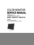
COLOR MONITOR
SERVICE MANUAL
CHASSIS NO. : CL-42
FACTORY MODEL: LB700G
MODEL:
L1710S (LB700G-GU)
L1710S (LB700G-GD)
L1710S (LB700G-GL)
*(
) ID LABEL MODEL No.
CAUTION
BEFORE SERVICING THE UNIT,
READ THE SAFETY PRECAUTIONS IN THIS MANUAL.
AUTO
MENU
SELECT
CONTENTS
SPECIFICATIONS ................................................... 2
PRECAUTIONS ....................................................... 3
TIMING CHART ....................................................... 4
OPERATING INSTRUCTIONS ................................ 5
WIRING DIAGRAM ................................................. 6
BLOCK DIAGRAM ................................................... 8
DESCRIPTION OF BLOCK DIAGRAM.....................9
ADJUSTMENT ....................................................... 11
TROUBLESHOOTING GUIDE .............................. 12
PRINTED CIRCUIT BOARD................................... 15
EXPLODED VIEW...................................................18
REPLACEMENT PARTS LIST ...............................20
SCHEMATIC DIAGRAM ......................................... 22
SPECIFICATIONS
1. LCD CHARACTERISTICS
Type
: TFT SXGA LCD
Size
: 17 inch
Pixel Pitch
: 0.264 (H) x 0.264 (V)
Color Depth
: 6-bit + FRC(16.2M)
Electrical Interface
: LVDS
Surface Treatment
: Anti-Glare, Polarizer Hardness
Operating Mode
: Normally White
Backlight Unit
: 4-CCFL (Cold Cathode
Fluorescent Lamp)
4. Max. Resolution
Analog
: 1280 x 1024 / 75Hz
5. POWER SUPPLY
5-1. Power : AC 100~240V, 50/60Hz , 1.0A
5-2. Power Consumption
MODE
2. OPTICAL CHARACTERISTICS
2-1. Viewing Angle by Contrast Ratio ≥ 10
(AU Module)
Left : -55° min., -70°(Typ) Right : +55° min., +70°(Typ)
Top :+55° min., +70°(Typ) Bottom : -55°min., -70°(Typ)
(Hydis Module)
Left : -60° min., -65°(Typ) Right : +60° min., +65°(Typ)
Top :+40° min., +45°(Typ) Bottom : -60°min., -65°(Typ)
(LPL Module)
Left : -70°(Typ)
Top : +60°(Typ)
: 200(min), 250(Typ)
2-3. Contrast Ratio
: 200(min), 450(Typ) - AU, Hydis
300(min), 400(Typ) - LPL
3. SIGNAL (Refer to the Timing Chart)
3-1. Sync Signal
• Type
: Separate Sync,
SOG (Sync On Green)
Composite Sync
3-2. Video Input Signal
1) Type
2) Voltage Level
a) Color 0, 0
b) Color 7, 0
c) Color 15, 0
3) Input Impedance
POWER ON (NORMAL)
ON/ON
ACTIVE
less than 40 W
GREEN
STAND-BY
OFF/ON
OFF
less than 3 W
AMBER
SUSPEND
ON/OFF
OFF
less than 3 W
AMBER
DPMS OFF
OFF/OFF
OFF
less than 3 W
AMBER
POWER S/W OFF
-
-
less than 1 W
(@120V AC)
OFF
6. ENVIRONMENT
6-1. Operating Temperature: 10°C~35°C (50°F~95°F)
(Ambient)
6-2. Relative Humidity
: 10%~80%
(Non-condensing)
6-3. MTBF
: 50,000 Hours(Min)
Right : +70°(Typ)
Bottom : -60°(Typ)
2-2. Luminance
H/V SYNC VIDEO POWER CONSUMPTION LED COLOR
7. DIMENSIONS (with TILT/SWIVEL)
Width
Depth
Height
: 370 mm (14.57'')
: 222.5 mm (8.76'')
: 421 mm (16.57'')
8. WEIGHT (with TILT/SWIVEL)
Net. Weight
Gross Weight
: R, G, B Analog
: 0~0.7 V
: 0 Vp-p
: 0.35 Vp-p
: 0.7 Vp-p
: 75 Ω
3-3. Operating Frequency
Horizontal
: 30 ~ 83kHz (Digital: 71kHz)
Vertical
: 56 ~ 75Hz
-2-
: 6.0 kg (13.23 lbs)
: 7.6 kg (16.76 lbs)
PRECAUTION
WARNING FOR THE SAFETY-RELATED COMPONENT.
WARNING
• There are some special components used in LCD
monitor that are important for safety. These parts are
marked on the schematic diagram and the
replacement parts list. It is essential that these critical
parts should be replaced with the manufacturer’s
specified parts to prevent electric shock, fire or other
hazard.
• Do not modify original design without obtaining written
permission from manufacturer or you will void the
original parts and labor guarantee.
TAKE CARE DURING HANDLING THE LCD MODULE
WITH BACKLIGHT UNIT.
• Must mount the module using mounting holes arranged
in four corners.
• Do not press on the panel, edge of the frame strongly
or electric shock as this will result in damage to the
screen.
• Do not scratch or press on the panel with any sharp
objects, such as pencil or pen as this may result in
damage to the panel.
• Protect the module from the ESD as it may damage the
electronic circuit (C-MOS).
• Make certain that treatment person’s body are
grounded through wrist band.
• Do not leave the module in high temperature and in
areas of high humidity for a long time.
• The module not be exposed to the direct sunlight.
• Avoid contact with water as it may a short circuit within
the module.
• If the surface of panel become dirty, please wipe it off
with a softmaterial. (Cleaning with a dirty or rough cloth
may damage the panel.)
CAUTION
Please use only a plastic screwdriver to protect yourself
from shock hazard during service operation.
-3-
BE CAREFUL ELECTRIC SHOCK !
• If you want to replace with the new backlight (CCFL) or
inverter circuit, must disconnect the AC adapter
because high voltage appears at inverter circuit about
650Vrms.
• Handle with care wires or connectors of the inverter
circuit. If the wires are pressed cause short and may
burn or take fire.
TIMING CHART
VIDEO
B
A
E
C
D
SYNC
F
<< Dot Clock (MHz), Horizontal Frequency (kHz), Vertical Frequency (Hz), Horizontal etc... (µs), Vertical etc... (ms) >>
Mode
1
2
3
4
5
6
7
8
9
10
11
12
13
H/V
Sort
Sync
Polarity
H
+
V
–
H
–
V
H
+
–
V
–
H
–
V
–
H
+
V
+
H
+
V
+
H
+/–
V
+/–
H
–
V
–
H
–
V
H
–
+/–
V
+/–
H
+/–
V
+/–
H
+
V
+
H
+
V
+
Dot
Clock
25.175
28.321
25.175
31.5
40.0
49.5
57.283
65.0
78.75
100.0
92.978
108.0
135.0
Frequency
Total Period Video Active Time
(E)
(A)
Front Porch
(C)
Sync Duration
(D)
Back Porch
(F)
31.469
800
640
16
96
48
70.8Hz
449
350
37
2
60
31.468
900
720
18
108
54
70.09
31.469
449
840
400
640
12
16
2
96
35
48
59.94
525
480
10
2
33
37.5
840
640
16
64
120
75
500
480
1
3
16
37.879
1056
800
40
128
88
60.317
628
600
1
4
23
46.875
1056
800
16
80
160
75.0
625
600
1
3
21
49.725
1152
832
32
64
224
74.55
667
624
1
3
39
48.363
1344
1024
24
136
160
60.0
806
768
3
6
29
60.123
1312
1024
16
96
176
75.029
68.681
800
1456
768
1152
1
32
3
128
28
144
75.062
915
870
3
3
39
61.805
1504
1152
18
134
200
65.96
937
900
2
4
31
63.981
1688
1280
48
112
248
60.02
1066
1024
1
3
38
79.976
1688
1280
16
144
248
75.035
1066
1024
1
3
38
-4-
Resolution
640x350
70Hz
720x400
70Hz
640x480
60Hz
640x480
75Hz
800x600
60Hz
800x600
75Hz
832x624
75Hz
1024x768
60Hz
1024x768
75Hz
1152x870
75Hz
1152x900
65Hz
1280x1024
60Hz
1280x1024
75Hz
OPERATING INSTRUCTIONS
FRONT VIEW
AUTO
REAR VIEW
MENU
D-Sub Signal
Connect
SELECT
See Front Control Panel
Power Connect
Front Control Panel
6
3
1. Power ON/OFF Button
Use this button to turn the monitor on or off.
2. Power Indicator
This indicator lights up green when the monitor
operates normally. If the display is in DPM(Energy
Saving)mode, this indicator color change to amber.
3. MENU Button
Use these buttons to enter or exit the On Screen Display.
4. ▼▲◀▶ Button
Use these buttons to choose or adjust items in the On
Screen Display.
4
5
1
2
5. SELECT Button
Use this button to enter a selection in the On Screen Display.
Use this button to scanning auto adjust.
6. AUTO Button
Use this button to enter a selection in the on screen
display.
* AUTO adjustment function
PROCESSING
AUTO CONFIGURATION
TO the AUTO button before
using OSD menu. This button is
for the automatic adjustment of the screen position, clock
and phase.
Note: Some signal from some graphics boards may not
function properly. If the results are unsatisfactory, adjust
your monitor’s Position, Clock and Phase manually.
-5-
WIRING DIAGRAM
(AU Module)
Connector Ass’y P/N:
6631T11012W
CN3
Connector Ass’y P/N:
6631T25008V
Power Board
CN2
CN1
Connector Ass’y P/N:
J702
6631T12002L
J705
J710
Main Board
J1
Connector Ass’y P/N:
6631T12002M
Control Board
LCD Module
-6-
WIRING DIAGRAM
(Hydis Module / LPL Module)
Connector Ass’y P/N:
6631T11012W
CN3
Connector Ass’y P/N:
6631T25008V
Power Board
CN2
CN1
Connector Ass’y P/N:
J702
6631T12002L
J705
J710
Main Board
J1
Connector Ass’y P/N:
6631T12002M
Control Board
LCD Module
-7-
AC Inpu t
5V
AVDD2.5V
DVDD2.5V
AVDD3.3V
DVDD3.3V
12V
5V
5V
AVDD 2.5V
DVDD 2.5V
AVDD 3.3V
DVDD 3.3V
5V
R,G,B
differential
..
-8-
B
R,G,B, H/V Sync
)
Data 8 Bi t
Address
LVDS
(Low Voltage
Differential Signaling)
BLOCK DIAGRAM
DESCRIPTION OF BLOCK DIAGRAM
1. Video Controller Part & Display Data Transmitter Part.
This part amplifies the level of video signal for the digital conversion and converts from the analog video signal to the
digital video signal using a pixel clock.
The pixel clock for each mode is generated by the PLL.
The range of the pixel clock is from 25MHz to 135MHz.
This part consists of the Scaler, Flash-ROM IC which stores program data, Reset IC.
The Scaler gets the video signal converted analog to digital, interpolates input to 1280 x 1024 resolution signal and
outputs 8-bit R, G, B signal to transmitter.
Especially pre-amp / ADC / Video controller/ Transmitter are merged to one chip ‘Gm2121’ by Genesis.
This part transmit digital signal from the Scaler to the receiver of module.
2. Power Part
This part consists of the one 3.3V and one 2.5 regulators to convert power which is provided 5V in LIPS Board.
5V is provided for LCD Panel.
Also, 5V is converted 3.3V and 2.5V by regulator. Converted power is provided for IC in the main board.
-9-
LIPS Board Block Diagram
12V
50 ~ 60Hz
EMI
COMPONENTS
INPUT RECTIFIER
AND FILTER
HVDC
ENERGY
TRANSFER
100KHz
OUTPUT RECTIFIER
AND FILTER
5V
GND
LINE
100 ~ 240V
PWM
CONTROL
CIRCUIT
PHOTOCOUPLER
ISOLATION
PRIMARY
12V
SIGNAL
COLLENTI
ON
SECONDARY
INVERTER CIRCUIT
High Voltage output
Operation description_LIPS
1. EMI components.
This part contains of EMI components to comply with global marketing EMI standards like FCC, VCCI CISPR, the
circuit included a line-filter, across line capacitor and of course the primary protection fuse.
2. Input rectifier and filter.
This part function is for transfer the input AC voltage to a DC voltage through a bridge rectifier and a bulk capacitor.
3. Energy Transfer.
This part function is transfer the primary energy to secondary through a power transformer.
4. Output rectifier and filter.
This part function is to make a pulse width modulation control and to provide the driver signal to power switch, to
adjust the duty cycle during different AC input and output loading condition to achive the dc output stablize, and also
the over power protection is also monitor by this part.
5. Photo-Coupler isolation.
This part function is to feed back the dc output changing status through a photo transistor to primary controller to
achieve the stabilized dc output voltage.
6. Signal collection.
This part function is to collect the any change from the dc output and feed back to the primary through photo
transistor.
7. Inverter
The inverter converts from DC12V to AC 700V and operate back-light lamp of module.
- 10 -
ADJUSTMENT
All adjustment are thoroughly checked and corrected
when the monitor leaves the factory, but sometimes
several minor adjustment may be required.
Adjustment should be following procedure and after
warming up for a minimum of 10 minutes.
• Alignment appliances and tools.
- IBM compatible PC
- Programmable Signal Generator.
(eg. VG-819 made by Astrodesign Co.)
- E(E)PROM with each mode data saved.
1. Adjustment Start
1) Display any pattern at any Mode.
2) Run alignment program for LB700G on the IBM
compatible PC.
3) Select EEPROM → Init → Initialize command and
Enter.
4) This will make all data to default state.
5) Select COLOR→ PRESET START command
and Enter.
2. Adjustment for White Balance
1) Display Black pattern at SXGA/60Hz.
2) Select COLOR → BIAS CALIBRATION command
and Enter.
3) No attempt to manually adjust, BIAS data is automatically adjusted and saved to the EEPROM.
4) Display Full White pattern at SXGA/60Hz.
5) Select GAIN CALIBRATION command and Enter.
6) 6500K and 9300K are automatically adjusted and
saved to the EEPROM.
7) Select COLOR → PRESET END command and
Enter.
3. Adjustment for EDID
1) Use this procedure only when there is some
probelm on EDID data.
2) Connect the D-sub cable.
3) Select EDID → Write EDID[A0] command and
Enter.
A
9
IBM
Compatible PC
Video Signal
Generator
15
10
5
11
6
1
6
1
5
C
13
se
d
PARALLEL PORT
2C
tu
23
No
RS
5V
OFF
14
ON
LL
EL
F
RA
C
PA
5V
Power inlet (required)
ON
R
220
WE
VG
CS
T
PO
S
MO
NI
TO
R
B
4.7K
OFF
74LS06
E ST Switch
B
F V-Sync On/Off Switch
(Switch must be ON.)
Figure 1. Cable Connection
- 11 -
4.7K
4.7K
5V
E
YN
A
Power Select Switch
(110V/220V)
Power LED
V-S
Control Line
1
25
74LS06
TROUBLESHOOTING GUIDE
1. NO POWER
NO POWER
(POWER INDICATOR OFF)
CHECK J702
INPUT VOLTAGE
(12V) ?
NO
TROUBLE IN
LIPS (POWER)
NO
TROUBLE IN
LIPS (POWER)
NO
TROUBLE IN
U203 or X201
YES
CHECK J702
5V VOLTAGE
(5V) ?
YES
CHECK
U203’s PIN 103.
IS THIS PIN
OSCILLATED?
YES
TROUBLE
SOMEWHERE ELSE
- 12 -
2. NO RASTER
NO RASTER
CHECK
J702 PIN 5, 6
(5V) ?
NO
TROUBLE IN
LIPS
YES
CHECK
J705 PIN 1, 2, 3
(5V) ?
NO
TROUBLE IN
U804
NO
TROUBLE IN
U801
NO
TROUBLE IN
U203
YES
CHECK
U801
(3.3V)?
YES
CHECK
U203(GM2121) ?
YES
TROUBLE IN
LCD MODULE
- 13 -
3. NO CLOCK (CLOCK GENERATOR)
NO DOT CLOCK
YES
CHECK
X201 20MHz ?
NO
TROUBLE IN
X201
4. TROUBLE IN DPM
TROUBLE IN DPM
CHECK
R713, R715
(SYNC) ?
NO
CHECK PC
PC IS NOT GOING
INTO DPM OFF MODE
YES
CHECK
U203 PIN 102
WAVEFORM
(20MHz) ?
NO
TROUBLE IN
X201
NO
TROUBLE IN
SIGNAL CABLE
YES
CHECK
U203 PIN 34
(0V) ?
YES
TROUBLE IN PC
- 14 -
PRINTED CIRCUIT BOARD
1. MAIN BOARD (Component Side)
J704
R748
J710
J705
D704
D703
5
20
10
40
30
160
50
150
C703
ZD719
R711
R714
R715
C717
U270
R236
R235
R716
R749
R750
80
C239
U702
J702
R717
R713
R741
70
ZD718
R740
R712
R276
130
C810
C238
L803
R733
R277
C811
C809
R734
C231
C808
C207
A
D701
D710
D709
140
R205
R701
C704
R224
R223
60
C234
C706
R217
C204
ZD720
C221
R206
R231
R227
R228
R225
R226
C282
R703
C211
C280
C210
C281
R210
C214
U804
R809
C235
D702
R702
C219
C212
C818
R219
C860
R704
R218
R215
R250
R209
R207
C213
R208
L823
R821
R705
C725
R747
C724
R745
C723
C722
R744
R743
C721
C209
R742
C217
C720
R220
C819
C817
R275
5
100
15
R204
R203
C206
C205
20
30
C806
R258
C203
R243
L802
R751
R263
R242
Q202
U803
X201
R213
R221
R265
R259
C807
C718
R752
R230
MODEL:LB700G
90
10
R264
C802
ZD703
C715
ZD704
C714
R211
C218
R202
R229
R222
C215
C244
C216
C224
C220
R280
C813
C812
C201
R214
R262
ZD711
U202
R255
L801
R257
R256
R254
R252
R248
R239
U201
25
R251
R253
R201
R240
R241
R244
R245
R246
R247
C242
C237
C241
C803
R249
C804
R233
C232
C805
R234
C801
R825
2. MAIN BOARD (Solder Side)
C904
R746
R810
C911
C236
C906
C225
C240
C903
C905
R830
C901
R811
C908
R813
R812
R815
R816
C902
R818
R817
R819
R820
C909
R814
C907
C910
- 15 -
DATE :2002.09.27
110
120
A
C202
P/N :6870T562A12
R238
R216
R212
R261
U203
C840
R232
U801
R266
R267
R268
R269
R270
R271
R272
R273
R274
C208
L804
L811
To apply the AU Module.
3. ADAPTER BOARD (Component Side)
4. ADAPTER BOARD (Solder Side)
- 16 -
To apply the HYDIS Module.
5. ADAPTER BOARD (Component Side)
6. ADAPTER BOARD (Solder Side)
- 17 -
- 18 -
5
6
3
1
2
b
10
8
a
EXPLODED VIEW
9
7
4
11
c
EXPLODED VIEW PARTS LIST
Ref. No.
Part No.
1
3091TKL053B
CABINET ASSEMBLY, LB700G BRAND 3090TKL053A HF350U
6304FHD005A
LCD(LIQUID CRYSTAL DISPLAY), HT17E12-100 HYUNDAI TFT COLOR LVDS TYPE SSM
6304FAU005A
LCD(LIQUID CRYSTAL DISPLAY), M170EN05 AU TFT COLOR 17.0" SXGA LVDS SMM
6304FLP058A
LCD(LIQUID CRYSTAL DISPLAY), M170E01-A4 LG PHILPS TFT COLOR 17.0" TFT LCD(LB700G-GL)
3
3809TKL035B
BACK COVER ASSEMBLY, LB700G 3808TKL039A HF350U
4
3043TKK091E
TILT SWIVEL ASSEMBLY, LM805L -HIPS NO USB
5
4814TKK231A
SHIELD INVERTER, LAMP WIRE,LB700K
4951TKS094D
METAL ASSEMBLY, FRAME LB700G (HYUNDAI) (LB700G-GD)
4951TKS094B
METAL ASSEMBLY, FRAME LB700G(AU) (LB700G-GU)
4951TKS094F
METAL ASSEMBLY, FRAME LB700G(LPL) (LB700G-GL)
6871TPT243A
PWB(PCB) ASSEMBLY,POWER, AI-0019 POWER TOTAL LIENCHANG LB700K LIPS FOR HYDIS/LPL (LB700G-GD), (LB700G-GL)
6871TPT237B
PWB(PCB) ASSEMBLY,POWER,LB700K POWER TOTAL POWERNET PWI1504FG-A 12V /1.2A 5V/1A LIPS FOR HYDIS (LB700G-GD), (LB700G-GL)
6871TPT241A
PWB(PCB) ASSEMBLY,POWER, 17'' HYDIS(LB700K) POWER TOTAL SPI FSP026-2PI01 (LB700G-GD), (LB700G-GL)
6871TPT241B
PWB(PCB) ASSEMBLY,POWER, 17'' AU(LB700K) POWER TOTAL SPI F SP026 -2PI02(LB700G-GU)
6871TPT237A
PWB(PCB) ASSEMBLY,POWER, LB700K POWER TOTAL POWERNET PWI1504FG 12V/1.2A 5V/1A LIPS FOR AUO(LB700G-GU)
8
3313TL7008A
MAIN TOTAL ASSEMBLY, LB700G.ASRDG BRAND CL-43
9
6631T11012W
CONNECTOR ASSEMBLY, 30P H-H 200MM UL20276 LG708G
10
6871TST321A
PWB(PCB) ASSEMBLY,SUB, LB800K CONTROL TOTAL BRAND CL-42
11
6850TD9001A
CABLE,D-SUB, UL 2990-9C(7.5) DT 1870MM GRAY(85964) BRAND DM
a
1SZZTMF008A
SCREW,DRAWING, D3.0 L6.0 MSWR/FZMY
b
332-113S
SCREW,DRAWING, D3.0 L12.0 MSWR/BK
c
332-105G
SCREW,DRAWING, PVS+4*10(MSWR/BK)
2
6
7
Description
- 19 -
REPLACEMENT PARTS LIST
CAUTION: BEFORE REPLACING ANY OF THESE COMPONENTS,
READ CAREFULLY THE SAFETY PRECAUTIONS IN THIS MANUAL.
* NOTE : S SAFETY Mark
AL ALTERNATIVE PARTS
*S *AL LOC. NO.
PART NO.
DATE: 2004. 05. 12.
DESCRIPTION / SPECIFICATION
*S *AL LOC. NO.
MAIN BOARD
CAPACITORS
C201
C202
C203
C204
C205
C206
C207
C208
C209
C210
C211
C212
C213
C214
C215
C216
C217
C218
C219
C220
C221
C224
C225
C231
C232
C234
C235
C236
C237
C238
C239
C240
C241
C242
C244
C280
C281
C282
C703
C704
C706
C714
C715
C717
C718
C720
C721
C722
C723
C724
C725
C801
0CC120CK41A
0CC120CK41A
0CK104CK56A
0CK103CK51A
0CC101CK41A
0CC101CK41A
0CH8106F611
0CK103CK51A
0CK103CK51A
0CK103CK51A
0CK103CK51A
0CK103CK51A
0CK103CK51A
0CK103CK51A
0CK103CK51A
0CK103CK51A
0CK103CK51A
0CK103CK51A
0CK103CK51A
0CK103CK51A
0CK103CK51A
0CK103CK51A
0CH3104K566
0CK103CK51A
0CK104CK56A
0CK103CK51A
0CK103CK51A
0CH3104K566
0CK103CK51A
0CK103CK51A
0CK104CK56A
0CH3104K566
0CK103CK51A
0CK103CK51A
0CK103CK51A
0CK103CK51A
0CK103CK51A
0CK103CK51A
0CK104CK56A
0CK104CK56A
0CC221CK41A
0CC101CK41A
0CC101CK41A
0CK104CK56A
0CC101CK41A
0CC471CK41A
0CC471CK41A
0CC471CK41A
0CC471CK41A
0CC471CK41A
0CC471CK41A
0CE107EF638
C802
C803
C804
C805
C806
C807
C808
C809
C810
C811
C812
C813
C817
C818
C819
C840
C860
C911
12PF 1608 50V 5% R/TP NP0
12PF 1608 50V 5% R/TP NP0
0.1UF 1608 50V 10% R/TP X7R
0.01UF 1608 50V 10% R/TP B(Y5
100PF 1608 50V 5% R/TP NP0
100PF 1608 50V 5% R/TP NP0
10UF 16V M 85STD(CYL) R/TP
0.01UF 1608 50V 10% R/TP B(Y5
0.01UF 1608 50V 10% R/TP B(Y5
0.01UF 1608 50V 10% R/TP B(Y5
0.01UF 1608 50V 10% R/TP B(Y5
0.01UF 1608 50V 10% R/TP B(Y5
0.01UF 1608 50V 10% R/TP B(Y5
0.01UF 1608 50V 10% R/TP B(Y5
0.01UF 1608 50V 10% R/TP B(Y5
0.01UF 1608 50V 10% R/TP B(Y5
0.01UF 1608 50V 10% R/TP B(Y5
0.01UF 1608 50V 10% R/TP B(Y5
0.01UF 1608 50V 10% R/TP B(Y5
0.01UF 1608 50V 10% R/TP B(Y5
0.01UF 1608 50V 10% R/TP B(Y5
0.01UF 1608 50V 10% R/TP B(Y5
0.1UF 50V 10% X7R 2012 R/TP
0.01UF 1608 50V 10% R/TP B(Y5
0.1UF 1608 50V 10% R/TP X7R
0.01UF 1608 50V 10% R/TP B(Y5
0.01UF 1608 50V 10% R/TP B(Y5
0.1UF 50V 10% X7R 2012 R/TP
0.01UF 1608 50V 10% R/TP B(Y5
0.01UF 1608 50V 10% R/TP B(Y5
0.1UF 1608 50V 10% R/TP X7R
0.1UF 50V 10% X7R 2012 R/TP
0.01UF 1608 50V 10% R/TP B(Y5
0.01UF 1608 50V 10% R/TP B(Y5
0.01UF 1608 50V 10% R/TP B(Y5
0.01UF 1608 50V 10% R/TP B(Y5
0.01UF 1608 50V 10% R/TP B(Y5
0.01UF 1608 50V 10% R/TP B(Y5
0.1UF 1608 50V 10% R/TP X7R
0.1UF 1608 50V 10% R/TP X7R
220PF 1608 50V 5% R/TP NP0
100PF 1608 50V 5% R/TP NP0
100PF 1608 50V 5% R/TP NP0
0.1UF 1608 50V 10% R/TP X7R
100PF 1608 50V 5% R/TP NP0
470PF 1608 50V 5% R/TP NP0
470PF 1608 50V 5% R/TP NP0
470PF 1608 50V 5% R/TP NP0
470PF 1608 50V 5% R/TP NP0
470PF 1608 50V 5% R/TP NP0
470PF 1608 50V 5% R/TP NP0
100UF KMG 16V M FM5 TP 5
PART NO.
DATE: 2004. 05. 12.
DESCRIPTION / SPECIFICATION
0CH8107D611
0CH8107D611
0CK104CK56A
0CC102CK41A
0CC102CK41A
0CK104CK56A
0CK104CK56A
0CH8476F611
0CH8476F611
0CC102CK41A
0CC102CK41A
0CK104CK56A
0CH8107F611
0CC102CK41A
0CK103CK51A
0CE477EH618
0CK105CD56A
0CH3104K566
100UF 10V 20% 85STD (CYL) R/T
100UF 10V 20% 85STD (CYL) R/T
0.1UF 1608 50V 10% R/TP X7R
1000PF 1608 50V 5% R/TP NP0
1000PF 1608 50V 5% R/TP NP0
0.1UF 1608 50V 10% R/TP X7R
0.1UF 1608 50V 10% R/TP X7R
47UF 16V 20% 85STD (CYL) R/TP
47UF 16V 20% 85STD (CYL) R/TP
1000PF 1608 50V 5% R/TP NP0
1000PF 1608 50V 5% R/TP NP0
0.1UF 1608 50V 10% R/TP X7R
100UF 16V M 85STD(CYL) R/TP
1000PF 1608 50V 5% R/TP NP0
0.01UF 1608 50V 10% R/TP B(Y5
470UF KMG 25V M FL TP 5
1UF 1608 10V 10% R/TP X7R
0.1UF 50V 10% X7R 2012 R/TP
0DS226009AA
0DS226009AA
0DS226009AA
0DS226009AA
0DS301109AA
0DS301109AA
0DZ560009DA
0DZ560009DA
0DZ560009DA
0DZ560009DA
0DZ560009DA
0DZ560009DA
KDS226 TP KEC SOT-23 80V 300
KDS226 TP KEC SOT-23 80V 300
KDS226 TP KEC SOT-23 80V 300
KDS226 TP KEC SOT-23 80V 300
MMBD301LT1 TP MOTOROLA SOT23
MMBD301LT1 TP MOTOROLA SOT23
UDZ S 5.6B TP ROHM-K SOD323 2
UDZ S 5.6B TP ROHM-K SOD323 2
UDZ S 5.6B TP ROHM-K SOD323 2
UDZ S 5.6B TP ROHM-K SOD323 2
UDZ S 5.6B TP ROHM-K SOD323 2
UDZ S 5.6B TP ROHM-K SOD323 2
0IMMRAL002A
0IZZTSZ213A
0IMMRSS040C
0IPRPGN004A
0ISTLFA058A
0ISS524202B
0IRH033200A
0IPMGFA003B
0TFVI80023A
"AT49F001N-70JC ATMEL 32PIN,PL"
ATMEL/STM 32PIN ST OTP LB700G
S524A60X51(SCT0) SAMSUNG ELEC
"GM2121 GENESIS 160P,PQFP TRAY"
"74F14SCX FAIRCHILD 14P,SOIC R"
S524A40X21(SCT0) SAMSUNG ELEC
BA033FP-E2 MOLD-3 TP REGULATO
RC1117S-2.5 FAIRCHILD SOT-223
VISHAY SI3865DV R/TP TSOP-6 8
DIODEs
D701
D702
D703
D704
D709
D710
ZD703
ZD704
ZD711
ZD718
ZD719
ZD720
ICs
U201
U201
U202
U203
U270
U702
U801
U803
U804
COILs & COREs
L801
L802
L803
L804
L811
L823
- 20 -
6210TCE001G
6210TCE001G
6210TCE001G
6210TCE001G
6210TCE001G
6210TCE001G
HH-1M3216-501 CERATEC 3216MM
HH-1M3216-501 CERATEC 3216MM
HH-1M3216-501 CERATEC 3216MM
HH-1M3216-501 CERATEC 3216MM
HH-1M3216-501 CERATEC 3216MM
HH-1M3216-501 CERATEC 3216MM
*S *AL LOC. NO.
PART NO.
DATE: 2004. 05. 12.
DESCRIPTION / SPECIFICATION
*S *AL LOC. NO.
PART NO.
DATE: 2004. 05. 12.
DESCRIPTION / SPECIFICATION
TRANSISTOR
Q202
0IKE702900D
R715
R716
R717
R733
R734
R740
R741
R742
R743
R744
R745
R746
R747
R748
R749
R750
R752
R809
R810
R811
R812
R813
R814
R815
R816
R817
R818
R819
R820
R825
R830
KIA7029AP TO-92 TP 2.9V DETEC
RESISTORs
R201
R203
R204
R205
R207
R208
R209
R210
R211
R212
R213
R214
R215
R216
R217
R218
R219
R221
R222
R223
R224
R225
R226
R227
R228
R229
R230
R231
R232
R233
R234
R238
R242
R243
R244
R246
R248
R250
R253
R255
R258
R261
R262
R265
R273
R275
R276
R277
R701
R702
R703
R704
R705
R711
R712
R713
R714
0RJ1002D677
0RJ1000D677
0RJ1000D677
0RJ1001D677
0RJ1001D677
0RJ1001D677
0RJ1001D677
0RJ1000D677
0RJ1001D677
0RJ0222D677
0RJ1000D677
0RJ1000D677
0RJ1001D677
0RJ1000D677
0RJ1000D677
0RJ1001D677
0RJ1002D677
0RJ0472D677
0RJ0472D677
0RJ0752D677
0RJ0752D677
0RJ0752D677
0RJ0752D677
0RJ0752D677
0RJ0752D677
0RJ0472D677
0RJ4701D677
0RJ4701D677
0RJ4701D677
0RJ4701D677
0RJ4701D677
0RJ0222D677
0RJ0000D677
0RJ3302D677
0RJ1002D677
0RJ1002D677
0RJ1002D677
0RJ1001D677
0RJ1002D677
0RJ1002D677
0RJ1002D677
0RJ4701D677
0RJ1001D677
0RJ1002D677
0RJ1002D677
0RJ1000D677
0RJ0472D677
0RJ0472D677
0RJ1001D677
0RJ1002D677
0RJ0752D677
0RJ0752D677
0RJ0752D677
0RJ0332D677
0RJ0332D677
0RJ1001D677
0RJ2201D677
10K OHM 1/10 W 5% 1608 R/TP
100 OHM 1/10 W 5% 1608 R/TP
100 OHM 1/10 W 5% 1608 R/TP
1K OHM 1/10 W 5% 1608 R/TP
1K OHM 1/10 W 5% 1608 R/TP
1K OHM 1/10 W 5% 1608 R/TP
1K OHM 1/10 W 5% 1608 R/TP
100 OHM 1/10 W 5% 1608 R/TP
1K OHM 1/10 W 5% 1608 R/TP
22 OHM 1/10 W 5% 1608 R/TP
100 OHM 1/10 W 5% 1608 R/TP
100 OHM 1/10 W 5% 1608 R/TP
1K OHM 1/10 W 5% 1608 R/TP
100 OHM 1/10 W 5% 1608 R/TP
100 OHM 1/10 W 5% 1608 R/TP
1K OHM 1/10 W 5% 1608 R/TP
10K OHM 1/10 W 5% 1608 R/TP
47 OHM 1/10 W 5% 1608 R/TP
47 OHM 1/10 W 5% 1608 R/TP
75 OHM 1/10 W 5% 1608 R/TP
75 OHM 1/10 W 5% 1608 R/TP
75 OHM 1/10 W 5% 1608 R/TP
75 OHM 1/10 W 5% 1608 R/TP
75 OHM 1/10 W 5% 1608 R/TP
75 OHM 1/10 W 5% 1608 R/TP
47 OHM 1/10 W 5% 1608 R/TP
4.7K OHM 1/10 W 5% 1608 R/TP
4.7K OHM 1/10 W 5% 1608 R/TP
4.7K OHM 1/10 W 5% 1608 R/TP
4.7K OHM 1/10 W 5% 1608 R/TP
4.7K OHM 1/10 W 5% 1608 R/TP
22 OHM 1/10 W 5% 1608 R/TP
0 OHM 1/10 W 5% 1608 R/TP
33K OHM 1/10 W 5% 1608 R/TP
10K OHM 1/10 W 5% 1608 R/TP
10K OHM 1/10 W 5% 1608 R/TP
10K OHM 1/10 W 5% 1608 R/TP
1K OHM 1/10 W 5% 1608 R/TP
10K OHM 1/10 W 5% 1608 R/TP
10K OHM 1/10 W 5% 1608 R/TP
10K OHM 1/10 W 5% 1608 R/TP
4.7K OHM 1/10 W 5% 1608 R/TP
1K OHM 1/10 W 5% 1608 R/TP
10K OHM 1/10 W 5% 1608 R/TP
10K OHM 1/10 W 5% 1608 R/TP
100 OHM 1/10 W 5% 1608 R/TP
47 OHM 1/10 W 5% 1608 R/TP
47 OHM 1/10 W 5% 1608 R/TP
1K OHM 1/10 W 5% 1608 R/TP
10K OHM 1/10 W 5% 1608 R/TP
75 OHM 1/10 W 5% 1608 R/TP
75 OHM 1/10 W 5% 1608 R/TP
75 OHM 1/10 W 5% 1608 R/TP
33 OHM 1/10 W 5% 1608 R/TP
33 OHM 1/10 W 5% 1608 R/TP
1K OHM 1/10 W 5% 1608 R/TP
2200 OHM 1/10 W 5% 1608 R/TP
0RJ1002D677
0RJ0472D677
0RJ2201D677
0RJ1002D677
0RJ1002D677
0RJ1500D677
0RJ1500D677
0RJ1002D677
0RJ1002D677
0RJ1002D677
0RJ1002D677
0RH0000D622
0RJ1002D677
0RJ1002D677
0RJ4701D677
0RJ4701D677
0RJ4701D677
0RJ2202D677
0RH5600D622
0RH0332D622
0RH0332D622
0RH0332D622
0RH0332D622
0RH0332D622
0RH0332D622
0RH0332D622
0RH0332D622
0RH0332D622
0RH0332D622
0RH0000D622
0RH0000D622
10K OHM 1/10 W 5% 1608 R/TP
47 OHM 1/10 W 5% 1608 R/TP
2200 OHM 1/10 W 5% 1608 R/TP
10K OHM 1/10 W 5% 1608 R/TP
10K OHM 1/10 W 5% 1608 R/TP
150 OHM 1/10 W 5% 1608 R/TP
150 OHM 1/10 W 5% 1608 R/TP
10K OHM 1/10 W 5% 1608 R/TP
10K OHM 1/10 W 5% 1608 R/TP
10K OHM 1/10 W 5% 1608 R/TP
10K OHM 1/10 W 5% 1608 R/TP
0 1/10W P-TYPE TAPPING
10K OHM 1/10 W 5% 1608 R/TP
10K OHM 1/10 W 5% 1608 R/TP
4.7K OHM 1/10 W 5% 1608 R/TP
4.7K OHM 1/10 W 5% 1608 R/TP
4.7K OHM 1/10 W 5% 1608 R/TP
22K OHM 1/10 W 5% 1608 R/TP
560 1/10W 5 D.R/TP
33 1/10W 5 D.R/TP
33 1/10W 5 D.R/TP
33 1/10W 5 D.R/TP
33 1/10W 5 D.R/TP
33 1/10W 5 D.R/TP
33 1/10W 5 D.R/TP
33 1/10W 5 D.R/TP
33 1/10W 5 D.R/TP
33 1/10W 5 D.R/TP
33 1/10W 5 D.R/TP
0 1/10W P-TYPE TAPPING
0 1/10W P-TYPE TAPPING
6212AA2004B
HC-49U TXC 20.0MHZ +/- 30 PPM
OTHERs
X201
CONTROL BOARD
LED1
SW1
SW2
SW3
SW4
SW5
SW6
SW7
SW8
- 21 -
0DLLT0208AA
140-058E
140-058E
140-058E
140-058E
140-058E
140-058E
140-058E
140-058E
LITEON LTST-C155KGJSKT R/TP G
SKHV10910B LGEC NON 12V 20A H
SKHV10910B LGEC NON 12V 20A H
SKHV10910B LGEC NON 12V 20A H
SKHV10910B LGEC NON 12V 20A H
SKHV10910B LGEC NON 12V 20A H
SKHV10910B LGEC NON 12V 20A H
SKHV10910B LGEC NON 12V 20A H
SKHV10910B LGEC NON 12V 20A H
SCHEMATIC DIAGRAM
1. GM2121
- 22 -
2. POWER
- 23 -
3. CONNECTOR
- 24 -
4. CONTROL KEY
- 25 -
5. ADAPTER (AU Module)
- 26 -
6. INVERTER (AU Module)
- 27 -
7. ADAPTER (HYDIS Module)
- 28 -
8. INVERTER (HYDIS Module)
- 29 -
P/NO : 3828TSL074G
Oct. 2002
Printed in Korea