1
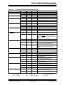
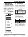
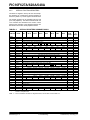
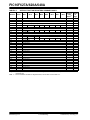
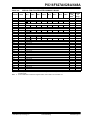
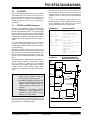
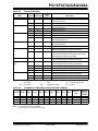
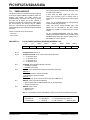
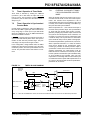
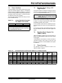
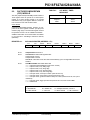
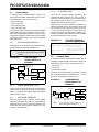
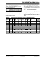
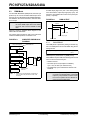
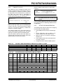
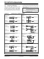
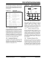
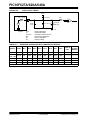
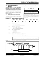
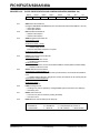
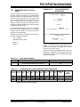
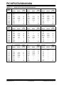
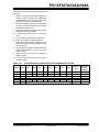
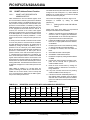
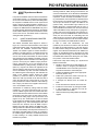
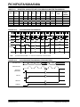
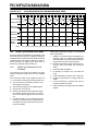
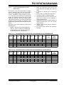
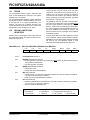
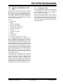
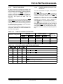
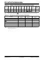
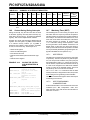
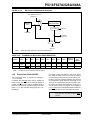
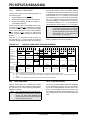
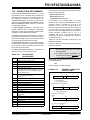
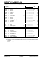
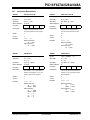
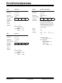
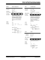
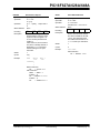
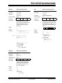
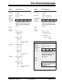
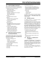
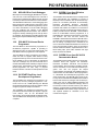
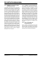
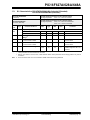
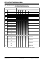
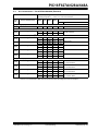
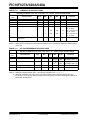
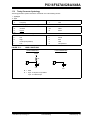
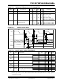
PIC16F627A/628A/648A TABLE 14-8: Address SUMMARY OF INTERRUPT REGISTERS Name 0Bh, 8Bh, INTCON 10Bh, 18Bh 0Ch PIR1 8Ch PIE1 Bit 7 Bit 6 Bit 5 Bit 4 Bit 3 Bit 2 Bit 1 Bit 0 Value on POR Reset Value on all other RESETS(1) GIE PEIE T0IE INTE RBIE T0IF INTF RBIF 0000 000x 0000 000u EEIF EEIE CMIF CMIE RCIF RCIE TXIF TXIE — — 0000 -000 0000 -000 0000 -000 0000 -000 CCP1IF TMR2IF TMR1IF CCP1IE TMR2IE TMR1IE Note 1: Other (non Power-up) Resets include MCLR Reset, Brown-out Reset and Watchdog Timer Reset during normal operation. 14.6 Context Saving During Interrupts During an interrupt, only the return PC value is saved on the stack. Typically, users may wish to save key registers during an interrupt (e.g., W register and STATUS register). This must be implemented in software. Example 14-2 stores and restores the STATUS and W registers. The user register, W_TEMP, must be defined in a common memory location (i.e., W_TEMP is defined at 0x70 in Bank 0 and is therefore, accessible at 0xF0, 0x170 and 0x1F0). The Example 14-2: • • • • Stores the W register Stores the STATUS register Executes the ISR code Restores the STATUS (and bank select bit register) • Restores the W register EXAMPLE 14-2: SAVING THE STATUS AND W REGISTERS IN RAM MOVWF W_TEMP ;copy W to temp register, ;could be in any bank SWAPF STATUS,W ;swap status to be saved ;into W BCF STATUS,RP0 ;change to bank 0 ;regardless of current ;bank MOVWF STATUS_TEMP ;save status to bank 0 ;register : :(ISR) : Watchdog Timer (WDT) The watchdog timer is a free running on-chip RC oscillator which does not require any external components. This RC oscillator is separate from the RC oscillator of the CLKIN pin. That means that the WDT will run, even if the clock on the OSC1 and OSC2 pins of the device has been stopped, for example, by execution of a SLEEP instruction. During normal operation, a WDT time out generates a device RESET. If the device is in SLEEP mode, a WDT time out causes the device to wake-up and continue with normal operation. The WDT can be permanently disabled by programming the configuration bit WDTE as clear (Section 14.1). 14.7.1 WDT PERIOD The WDT has a nominal time out period of 18 ms (with no prescaler). The time out periods vary with temperature, VDD and process variations from part to part (see DC Specifications, Table 17-7). If longer time out periods are desired, a postscaler with a division ratio of up to 1:128 can be assigned to the WDT under software control by writing to the OPTION register. Thus, time out periods up to 2.3 seconds can be realized. The CLRWDT and SLEEP instructions clear the WDT and the postscaler, if assigned to the WDT, and prevent it from timing out and generating a device RESET. The TO bit in the STATUS register will be cleared upon a Watchdog Timer time out. 14.7.2 SWAPF STATUS_TEMP,W;swap STATUS_TEMP register ;into W, sets bank to original ;state MOVWF STATUS ;move W into STATUS register SWAPF W_TEMP,F ;swap W_TEMP SWAPF W_TEMP,W ;swap W_TEMP into W DS40044A-page 106 14.7 WDT PROGRAMMING CONSIDERATIONS It should also be taken in account that under worst case conditions (VDD = Min., Temperature = Max., max. WDT prescaler) it may take several seconds before a WDT time out occurs. Preliminary 2002 Microchip Technology Inc.