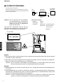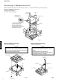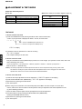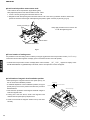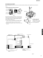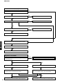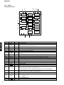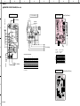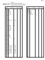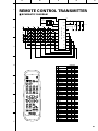
1
MDX-E100
MINIDISC RECORDER
MDX-E100
SERVICE MANUAL
For the system operation of MDX-E100,
please refer to Service Manual for the
RX-E100 100684 .
IMPORTANT NOTICE
WARNING:
Failure to follow appropriate service and safety procedures when servicing this product may result in personal
injury, destruction of expensive components and failure of the product to perform as specified. For these reasons,
we advise all YAMAHA product owners that all service required should be performed by an authorized
YAMAHA Retailer or the appointed service representative.
IMPORTANT: The presentation or sale of this manual to any individual or firm does not constitute authorization, certification or
recognition of any applicable technical capabilities, or establish a principle-agent relationship of any form.
The data provided is believed to be accurate and applicable to the unit(s) indicated on the cover. The research, engineering, and
service departments of YAMAHA are continually striving to improve YAMAHA products. Modifications are, therefore, inevitable
and specifications are subject to change without notice or obligation to retrofit. Should any discrepancy appear to exist, please contact
the distributor's Service Division.
WARNING:
Static discharges can destroy expensive components. Discharge any static electricity your body may have accumulated by grounding yourself to the ground buss in the unit (heavy gauge black wires connect to this buss).
IMPORTANT: Turn the unit OFF during disassembly and parts replacement. Recheck all work before you apply power to the unit.
■ CONTENTS
TO SERVICE PERSONNEL . . . . . . . . . . . . . . . . . . 1-2
REAR PANELS . . . . . . . . . . . . . . . . . . . . . . . . . . . . . . 2
SPECIFICATIONS . . . . . . . . . . . . . . . . . . . . . . . . . . . . 3
INTERNAL VIEW . . . . . . . . . . . . . . . . . . . . . . . . . . . . . 4
DISASSEMBLY PROCEDURES . . . . . . . . . . . . . . . 4-8
ADJUSTMENT & TEST MODE . . . . . . . . . . . . . . . 9-16
SPECIAL TEST MODE . . . . . . . . . . . . . . . . . . . . . . . 17
ERROR DISPLAY . . . . . . . . . . . . . . . . . . . . . . . . 18-19
TROUBLESHOOTING . . . . . . . . . . . . . . . . . . . . . 20-24
100686
IC DATA . . . . . . . . . . . . . . . . . . . . . . . . . . . . . . . . 25-34
BLOCK DIAGRAM . . . . . . . . . . . . . . . . . . . . . . . . 35-37
TEST POINT WAVEFORMS . . . . . . . . . . . . . . . . 38-39
PRINTED CIRCUIT BOARD . . . . . . . . . . . . . . . . 40-47
SCHEMATIC DIAGRAM . . . . . . . . . . . . . . . . . . . 48-50
PARTS LIST . . . . . . . . . . . . . . . . . . . . . . . . . . . . . 51-63
GREASE APPLICATION DIAGRAM . . . . . . . . . . . . 64
REMOTE CONTROL TRANSMITTER . . . . . . . . . . . 65
MDX-E100
This manual has been provided for the use of authorized YAMAHA Retailers and their service personnel.
It has been assumed that basic service procedures inherant to the industry, and more specifically YAMAHA Products, are already
known and understood by the users, and have therefore not been restated.
MDX-E100
■ TO SERVICE PERSONNEL
Critical Components Information.
Components having special characteristics are marked Z
and must be replaced with parts having specifications equal
to those originally installed.
WALL
OUTLET
EQUIPMENT
UNDER TEST
AC LEAKAGE
TESTER OR
EQUIVALENT
INSULATING
TABLE
CAUTION: USE OF CONTROLS OR ADJUSTMENTS
OR PERFORMANCE OF PROCEDURES
OTHER THAN THOSE SPECIFIED
HEREIN MAY RESULT IN HAZARDOUS
RADIATION EXPOSURE.
Laser Diode Properties
Material:
Wavelength:
GaAIAs
785 nm
Pulse time:
Read mode ...0.6 mW Continuous
Write mode ...max 10 mW 0.5S
THE MINI DISC RECORDER SHOULD NOT BE
ADJUSTED OR REPAIRED BY ANYONE EXCEPT
PROPERLY QUALIFIED SERVICE PERSONNEL.
min cycle 1.5S
Repetition
R, G, B models
➀
R, G, B models
MDX-E100
➁
English
➀ THIS PRINTING (SEE POSITION SHOWN IN THE ILLUSTRATION) INFORMS THE USER THAT THE APPARATUS
CONTAINS A LASER COMPONENT.
➁ THIS LABEL (SEE POSITION SHOWN IN THE ILLUSTRATION) WARNS THAT ANY FURTHER PROCEDURE WILL
BRING THE USER INTO EXPOSURE WITH THE LASER BEAM.
CAUTION : USE OF CONTROLS, ADJUSTMENTS OR PERFORMANCE OF PROCEDURES OTHER THAN THOSE
SPECIFIED HEREIN, MAY RESULT IN HAZARDOUS RADIATION EXPOSURE.
Swedish
➀ DENNA MÄRKNING (SE FIGUR) UPPLYSER OM ATT DET I APPARATEN INGÅR EN LASERKOMPONENT AV
TYP KLASS 1.
➁ VARNINGSMÄRKNING (SE FIGUR) FÖR STRÅLNING. INGREPP I APPARATEN BÖR ENDAST FÖRETAGAS AV
FACKMAN MED KÅNNEDOM OM LASER. APPARATEN INNEHÄLLER EN LASERKOMPONENT SOM AVGER
STRÅLNING ÖVERSTIGANDE GRÄNSEN FÖR LASERKLASS 1.
VARNING : OSYNLIG LASERSTRÅLNING NÄR DENNA DEL ÄR ÖPPNAD OCH SPÄRREN ÄR URKOPPLAD.
STIRRA EJ I STRÅLEN OCH BETRAKTA EJ STRÅLEN GENOM OPTISKT INSTRUMENT.
1
MDX-E100
Danish
➀ DETTE MÆRKAT ER ANBRAGT SOM VIST I ILLUSTRATIONEN FOR AT ADVARE BRUGEREN OM AT APPARATET INDEHOLDER EN LASERKOMPONENT.
➁ DETTE MÆRKAT OM LASEREN ER ANBRAGT PÅ APPARATET SOM EN OPLYSNING OM AT APPARATET
INDEHOLDER ET LASERKOMPONENT.
ADVARSEL : USYNLIG LASERSTRÅLING VED ÅBNING, NÅR SIKKERHEDSAFBRYDERE ER UDE AF FUNKTION.
SE IKKE IND I STRÅLEN-HELLER IKKE MED OPTISKE INSTRUMENTER.
ADVARSEL : USYNLIG LASERSTRÅLING NÅR DEKSEL ÅPNES OG SIKKERHEDSLÄS BRYTES. STIRR IKKE INN I
STRÅLEN ELLER SE DIREKTE MED OPTISKE INSTRUMENTER.
Finnish
VARO! :
AVATTAESSA JA SUOJALUKITUS OHITETTAESSA OLET ALTTIINA NÄKYMÄTTÖMÄLLE LASER-SÄTEILYLLE.
ÄLÄ TUIJOTA SÄTEESEEN ÄLÄKÄ KATSO SITÄ OPTISEN LAITTEEN LÄPI.
■ REAR PANELS
▼ A model
▼ R model
MDX-E100
240V
▼ B model
▼ G model
2
MDX-E100
Digital audio system
Outputs
System
MiniDisc digital audio system
Disc
MiniDisc
Recording method
Magnetic field variation overwrite
Reading method
Non-contact optical pickup (using semiconductor laser)
Laser
Semiconductor laser
Laser Diode Properties
Material: GaAIAs
Wavelength: 785 nm
Pulse time:
Read mode ... 0.6 mW Continuous
Write mode ... max 10 mW 0.5S
min cycle 1.5S
Repetition
Record/playback time
Max. 74 minutes
74 minutes (stereo)
148 minutes (mono)
Revolutions
Approx. 400-900 rpm (CLV)
Error Correction
ACIRC (Advanced Cross Interleave Reed-solomon Code)
Sampling frequency
44.1 kHz (32 kHz and 48 kHz signals converted to 44.1 kHz
for recording)
Coding
ATRAC (Adaptive TRansform Acoustic Coding)
Modulation system
EFM (Eight-to-Fourteen Modulation)
Number of channels
2 (stereo) or 1 (mono, for extended recording)
Frequency Response
5 - 20,000 Hz ±0.5 dB
Signal-to-Noise Ratio
More than 99 dB during playback
Wow and Flutter
Below measurable limit
LINE OUT (PLAY)
Type: pin jack
Standard output level: 2.0 ± 0.5 Vrms
DIGITAL OUT (OPTICAL)
Type: square optical connector jack
GENERAL
Power Supplies
A model
240 V, 50 Hz
G, B models
230 V, 50 Hz
R model
110/120/220/240 V, 50/60 Hz
Power Consumption
16 W
Dimensions (W x H x D)
217 x 88 x 298 mm (8-9/16" x 3-7/16" x 11-3/4")
Weight
3.0 kg (6 lbs. 9 oz.)
Accessories
Remote Control.... 1
Audio cord... 2
Optical cord... 1
Batteries (size AA, R6, UM-3).... 2
Specifications subject to change without notice.
298(11-3/4")
12
(1/2")
A : Australian model
B : British model
G : European model
R : Genaral model
275(10-13/16")
MDX-E100
■ SPECIFICATIONS
Inputs
217(8-9/16")
88
(3-7/16")
8
(5/16")
80
(3-1/8")
11
(7/16")
LINE IN (REC)
Type: pin jack
Input impedance: greater than 50 k-ohms
Standard input level: 300 mV
DIGITAL IN (OPTICAL) 1/2
Type: square optical connector jack
Units : mm (inch)
3
MDX-E100
■ INTERNAL VIEW
q
w
e
r
r
q
POWER TRANSFORMER
P.C.B. DIGITAL
P.C.B. MAIN (1)
P.C.B. MAIN (2)
MD MECHANISM UNIT
w
e r
CB102
CB107
CB101
t
■ DISASSEMBLY PROCEDURES
(Remove parts in disassembly order as numbered.)
2. Removal of Front Panel
a. Remove 2 connectors.
CB101, CB107
b. Remove 2 screws ( e ) and 2 screws ( r ) in Fig. 1.
3. Removal of MD Mechanism Unit
a. Remove 1 connector.
CB102
b. Remove 4 screws ( t ) in Fig. 1.
c. Remove 4 screws ( y ) in Fig. 2.
d. Remove 2 screws ( u ) in Fig. 2.
e. Remove 2 screws ( i ) in Fig. 2.
MDX-E100
1. Removal of Top Cover
a. Remove 4 screws ( q ) and 4 screw ( w ) in Fig. 1.
Top Cover
w
Shield Case (Top)
i
w
q
MD Mechanism Unit
i
(Bind Head S-tite) t
MD Mechanism Unit
q
u
e
Shield Case (Bottom)
y
u
t (Bind Head B-tite)
r
e
y
Front Panel
Frame (Mechanism)
Fig. 1
Fig. 2
4
MDX-E100
Disassembly of MD Mechanical Unit
Remove the MD mechanical unit according to Steps 1 - 3 of the disassembly procedure (page 4).
Removal of MD Main P.C.B. (Fig. 3)
1. Remove 4 screws (Q1).
2. Remove 6 connectors (Q2).
( Q1 ) x 4
1.7 x 3mm
( Q2 ) x 1
Flexible P.C.B. for
optical pickup (*1)
MD Main P.C.B.
(Q2)x1
(*1) After pulling off the flexible P.C.B.
for the optical pickup from the
connector, cover its end with
aluminum foil or the like which is
electrically conductive so as to prevent
the optical pickup from being
damaged by static electricity.
( Q2 ) x 1
( Q2 ) x 3
Frame
MDX-E100
Fig. 3
Removal of MD Mechanism (Fig.4)
Removal of Magnetic Head (Fig.5)
1. Remove 4 screws (R1).
1. Remove a screw (A1).
Caution
Almost the entire surface of the cartridge holder is
coated with oil. When removing the mechanism, hold it
at the rear end (where marked with arrows in the figure)
and avoid touching the oiled surface.
Cartridge Holder
Caution
a. When removing the magnetic head, hold its base and
do not touch the magnetic head itself or the leaf
spring.
b. Place the magnetic head upside down.
c. Use special care so as not to cause any damage to
the magnetic head when installing it.
MD Mechanism
(A1)x1
ø1.7x5mm
Leaf Spring
Black
MD Mechanism
Magnetic Head
Sheet, Head
Gray
Gray
(R1)x4
ø1.7x8.9mm
5
Fig. 4
Fig. 5
MDX-E100
Removal of Cartridge Holder (Fig.6)
1. Open the roller arm lever in the arrow direction and move the clamper lever to the rear.
2. With a +5V voltage (*2) applied to the red line side of the blue connector of the loading
motor, push the rack gear in the arrow direction until the cam plate lever clicks.
(*2) A +5V voltage can be obtained from the positive lead (D6.5/5V) of C135 and the
ground terminal of the Main P.C.B.
3. Remove a screw (B1 and B2, 1 each) from the holder arm and remove the cartridge
holder by moving it to the left.
Slider Lever
Cartridge Holder
Roller Arm Lever
Clamper
Lever
(B1) x1
Ø1.7x5mm
Loading
Motor
C135
Positive lead (D6.5/
5V)
Rack Gear
Cam Plate
Lever
(B2) x1
Fig.6
MDX-E100
Caution
Be careful so that oil does not get on the clamper lever
which contacts the roller of the roller arm lever.
Installation of Cartridge Holder
• To install the cartridge holder, the rack of the mechanism must be
lowered toward the rear.
• While pushing the roller arm lever outward, push in the slider lever.
• Apply a +5V to the loading motor (until a clicking sound is heard) and
push in the rack gear.
• With the slider lever and the rack gear installed as described above,
fit the cartridge holder as shown in the figure and tighten the screws.
6
MDX-E100
(E1)x1
Ø1.7x3mm
Removal of Mechanism SW P.C.B. (Fig.7)
• Once the mechanism switch P.C.B. is removed, it will
be necessary to perform “Adjustment of Lead-in Switch
(E1)x1
Ø1.7x9.5mm
Position”. (See page 13.)
Mechanism SW P.C.B.
1. Remove 2 screws (E1) and then remove the Mechanism SW P.C.B.
Fig.7
Installation of Mechanism SW P.C.B.
• Set the mechanism to the eject mode by applying -5V
to the loading motor.
• Install the Mechanism SW P.C.B. by aligning the hole
in the P.C.B. onto the guide-pin.
• Push the lead switch on the Mechanism SW P.C.B.
Guide-pin
(E1)x1
Ø1.7x3mm
(E1)x1
Ø1.7x9.5mm
toward the optical pickup side (so that looseness in the
guide-pin hole is eliminated).
MDX-E100
• Tighten screws and apply thread lock.
• Measure the lead-in switch position. (See page 13.)
(Enter the result in EEPROM.)
Lead-in switch
Mechanism SW P.C.B.
Removal of Sled Motor/Loading Motor (Fig.8)
(D1)x2
Ø1.7x2mm
1. Remove 4 screws (D1) and then remove the sled
motor/loading motor.
(D1)x2
Ø1.7x2mm
Caution
Use care so as not to cause any damage to the gear.
(The damaged gear will cause abnormal noise to occur
while searching.)
Loading Motor
Sled motor
Fig. 8
7
MDX-E100
Removal of Spindle Motor (Fig.9)
• Once the spindle motor is removed, it will be necessary to perform “Pickup Rating”. (See page 14.)
1. Remove 3 screws (C1).
2. Remove the spindle motor by moving it in the arrow
direction.
Caution
a. Be careful not to scratch the gear.
(Scratched gear will produce noises during searching.)
b. As the turn-table is magnetized, keep foreign objects
Turn Table
Spindle Motor
from being attracted.
(C1)x3
Ø1.7x2.5mm
(C1)x1
Ø1.7x2.1mm
Fig.9
(F1)x3
Ø1.7x9.5mm
Removal of Optical Pickup Head (Fig.10 and Fig.11)
1. Remove 3 screws (F1).
Caution
Use care so as not to cause any damage to the gear.
(The damaged gear will cause abnormal noise to occur
while searching.)
Optical Pickup Head
MDX-E100
2. Remove a screw (F2).
The leaf spring (A) attached to the P.U. will be reused
when replacing the pickup. It is not supplied with the
optical pickup.
3. Using tweezers or the like, pull the PU shaft from the
base a little. Pull only enough to allow the pickup to
come off. If it is pulled off completely, the oil on the
shaft will be scraped off.
Be sure to keep oil on the shaft!
MD Guide (B)
Fig. 10
MD Guide (A)
Assembly of Optical Pickup
• When installing the pickup to the MD guide (A), be
sure to tighten the leaf spring (A) with it.
• When installing the pickup to the MD mechanism, fit
Optical Pickup
PU Shaft
the pickup into the MD guide (B) first, match the boss
of the MD guide (A) and its hole in the chassis and
tighten them with a screw.
Leaf Spring (A)
Fig. 11
Fit the pickup into the MD guide (B) first
(F2)x1
Ø1.4x2.2mm
8
MDX-E100
■ ADJUSTMENT & TEST MODE
Preparation before Adjustment
● Test disc
● Extension cable (see connection diagram on page 14.)
Type
Test disc
High reflecting disc
TDYS1 (SONY) [for reproduction] (P/No. TX945850)
Low reflecting disc
Commercially available mini disc for recording
Low reflecting disc
MMD-318 [for pre-adjustment] (P/No. AAX04890)
Type
Part No.
1. Extension P.C.B. for servicing
TX946230
2. 2-pin extension connector for servicing
TX946200
3. 6-pin extension connector for servicing
TX946210
4. 5-pin flat cable for servicing
TX946190
5. 28-pin flat cable for servicing
TX946220
TEST MODE
1. How to set to the test mode
1) Press the POWER button while pressing the INPUT button and the STOP button.
Version of microprocessor is displayed for about 1 second, as shown below.
t s m 1 3 * * e * *
Version of EEPROM protect data (from 01)
Version of microprocessor ROM (from 01)
“EJECT” on display
2) Load either a disc for reproduction or a disc for recording.
“AUT YOBI” on display
MDX-E100
This completes setting to the test mode.
2. How to set to each mode
Every time the DISPLAY button (REMOCON) is pressed, the mode changes. (For operation of each mode, refer to the
section describing each mode.)
->AUTO pre-adjustment -> AUTO adjustment -> RESULT preparation -> RESULT -> MANUAL pre-adjustment ->
MANUAL adjustment -> EEPROM setting
Caution) The AUTO pre-adjustment and AUTO adjustment modes are used for adjustment during servicing. Other modes
are used when checking the specific measured values and adjusted values or when changing the set value and the
adjusted value. Note that use of other modes will rewrite RAM and EEPROM.
3. How to cancel test mode
1) Finish the AUTO pre-adjustment and AUTO adjustment. ( “COMPLETE” appears on the display)
2) Press the REC/PAUSE button (REMOCON). ( “TEST END” appears on the display)
3) Eject the disc by pressing the EJECT button.
4) Turn off the power.
● When using a new combination of a mechanical pickup and an MD P.C.B. after a repair or for some other
reason, make sure to set to the TEST mode and perform AUTO pre-adjustment and AUTO adjustment according to the following procedure.
1) Set to the TEST mode and perform AUTO pre-adjustment and AUTO adjustment.
2) Cancel the TEST mode by pressing the REC/PAUSE button (REMOCON).
(Writing into EEPROM starts from here.)
3) Eject the disc by pressing the EJECT button.
4) Turn off the power.
9
MDX-E100
Description of TEST modes
1. AUTO pre-adjustment mode
Automatic pre-adjustment is performed. (Grating adjustment mode after this adjustment.)
[ _ AUT _ YOBI _ ]
Adjusted values are output by using the interface.
2. AUTO adjustment mode
Automatic adjustment is performed.
[ AUTO _ AJST _ ]
Adjusted values are output by using the interface.
Continuous reproduction is performed. (Error rate on display, jump test)
3. RESULT preparation mode
Not used (Do not use this function as it is not for servicing)
[ _ RST _ YOBI _ ]
4. RESULT mode (main adjustment)
Not used (Do not use this function as it is not for servicing)
[ _ RESULT _ _ _ ]
5. MANUAL pre-adjustment mode
Not used (Do not use this function as it is not for servicing)
[ _ MNU _ YOBI _ ]
6. MANUAL adjustment mode
Not used (Do not use this function as it is not for servicing)
[ _ MNU _ AJST _ ]
7. EEPROM setting mode
Various factors of the digital servo function are changed manually.
[ EEPROM _ SET ]
Each servo function is turned on independently.
The voltage is measured at the temperature detect terminal and the standard value is set.
8. TEST-PLAY mode
Continuous reproduction from the specified address is performed.
[ TEST _ PLAY _ ]
C1 error rate is measured and ADIP error rate is measured.
9. TEST-REC mode
Continuous recording from the specified address is performed.
[ TEST _ REC _ _ ]
10. INNER mode
The position where the INNER switch is turned ON is measured.
[ _ _ INNER _ _ _ ]
To TEMP setting (of EEPROM setting)
[ _ _ EJECT _ _ _ ]
MDX-E100
11. EJECT mode
To CONTROL setting (of EEPROM setting)
Laser power setting (record/reproduction power) is performed.
1. AUTO pre-adjustment mode
Step
Low reflecting disc (MMD-318) only
Setting method
Remark
Display
1
Set the Test mode to STOP.
No disc is loaded.
[ EJECT ]
2
Load a disc.
Auto pre-adjustment menu
3
Press the SET/ENTER button
(REMOCON) once.
Grating adjustment is performed and
adjusted values are output.
Adjustment is completed.
Auto pre-adjustment is started after sliding to the innermost
track.
“ *** ” changes in the following order during automatic
adjustment.
HAo -> RFg -> SAg -> SBg -> PTG -> PCH -> GTG -> GCH ->
RCG -> SEG -> RFG -> SAG -> HAO -> HEO -> TCO -> LAO
Proceed to Step 4 when adjustment is OK.
Proceed to Step 5 when adjustment is NG.
The display returns to the AUTO pre-adjustment menu.
[ LOADING ]
[ _ AUT _ YOBI _ ]
[ *** : _ _ _ _ _ _ ]
4
5
When adjustment is OK, press the
DELETE/CANCEL button (REMOCON).
When adjustment is NG, press the
DELETE/CANCEL button (REMOCON).
There is an abnormality at the adjusted point such as HAo.
Refer to “Troubleshooting”. (page 20)
[ _ COMPLETE _ ]
[ Can't _ ADJ. ]
[ _ AUT _ YOBI _ ]
[ Can't _ ADJ. ]
10
MDX-E100
2. AUTO adjustment mode
Step
Setting method
1
Set the TEST mode to STOP.
2
Load a disc.
Press the DISPLAY button
(REMOCON) once.
Press the SET/ENTER button
(REMOCON) once.
Adjusted values are output.
3
Adjustment is completed.
4
When adjustment is OK, press the
SET/ENTER button (REMOCON).
5
Press the INPUT button.
Press the DELETE/CANCEL button
(REMOCON).
When adjustment is NG, press the
DELETE/CANCEL button
(REMOCON).
6
Remark
No disc is loaded.
AUTO pre-adjustment menu
AUTO adjustment menu
Automatic pre-adjustment is started after sliding to the innermost
track.
“ *** ” changes in the following order when a high reflecting disc
(disc for reproduction) is used.
PEG -> HAG
“ *** ” changes in the following order when a low reflecting disc
(disc for recording) is used.
PEG -> LAG -> GCG -> GEG -> LAG
Proceed to Step 4 when adjustment is OK.
Proceed to Step 5 when adjustment is NG.
Continuous reproduction (bit section)
(Address + C1 error display)
Continuous reproduction (group section)
(Address + C1 error display)
Continuous reproduction (group section)
(Address + ADIP error display)
Display returns to the AUTO adjustment menu display.
There is an abnormality at the adjusted point such as PEG.
Refer to “Troubleshooting”. (page 20)
Display
[ tsm13**e** ]
[ EJECT ]
[ LOADING ]
[ _ AUT _ YOBI _ ]
[ AUTO _ AJST _ ]
[ *** : _ _ _ _ _ _ ]
[ _ COMPLETE _ ]
[ Can't _ ADJ. ]
[ s XXXX c YYYY ]
[ a XXXX c YYYY ]
[ a XXXX a YYYY ]
[ AUTO _ AJST _ ]
[ Can't _ ADJ. ]
MDX-E100
Note) *** : Adjustment name, XXXX: Address, YYYY: Measured value
8. TEST-PLAY mode
(Use this mode to check that the playback function is provided at the specified address.)
Step
Setting method
1
2
3
Load a disc.
Press the TITLE button (REMOCON).
Press the INPUT button (REMOCON).
Press the SET/ENTER button
(REMOCON).
Continuous reproduction (bit section)
Continuous reproduction (group section)
Press the INPUT button (REMOCON).
Continuous reproduction (group section)
Press the DELETE/CANCEL button
(REMOCON).
4
5
6
Remark
Display
[ _ AUT _ YOBI _ ]
[ TEST _ PLAY _ ]
[ ADRES _ 0050 ]
AUTO pre-adjustment menu
TEST-PLAY menu
ADDRESS setting (The initial value of the target address is displayed.)
Set the search output to “H” while searching and back to “L” when
continuous reproduction is started.
(Address + C1 error display)
(Address + C1 error display)
(Address + ADIP error display)
[ s XXXX c YYYY ]
[ a XXXX c YYYY ]
[ a XXXX a YYYY ]
TEST-PLAY menu
[ TEST _ PLAY _ ]
• Every time the TITLE button (REMOCON) is pressed in the address setting mode, the address changes in the order of 0050-> 03C0 ->
0700 -> 08A0 -> 0050 -> —
• Pressing the DISPLAY button (REMOCON) in the TEST-PLAY menu changes to the AUTO pre-adjustment menu.
11
MDX-E100
9. TEST-REC mode
Use a disc for confirmation of recording function. (It is used to check the REC function at the specified address.)
Step
Setting method
1
2
3
4
Load a disc.
Press the TITLE button (REMOCON) twice.
Press the SET/ENTER button (REMOCON).
Press the SET/ENTER button (REMOCON).
5
Press the DELETE/CANCEL button
(REMOCON).
Remark
AUTO pre-adjustment menu
TEST-REC menu
ADDRESS setting (The initial value of the address is displayed.)
Set the search output to “H” while searching and back to “L” when
continuous reproduction is started.
Continuous recording
TEST-REC menu
Display
[ _ AUT _ YOBI _ ]
[ TEST _ REC _ _ ]
[ a0050 _ pw ZZ ]
[ a XXXX _ pw ZZ ]
[ TEST _ REC _ _ ]
• Every time the TITLE button (REMOCON) is pressed in the address setting mode, the address changes in the order of 0050-> 03C0 ->
0700 -> 08A0 -> 0050 -> —
• Pressing the DISPLAY button (REMOCON) in the TEST-REC menu changes to the AUTO pre-adjustment menu.
10. INNER mode
Step
Setting method
1
2
3
Load a disc.
Press the CHARA button (REMOCON).
Press the SET/ENTER button (REMOCON).
4
Press the DELETE/CANCEL button
(REMOCON).
Remark
AUTO pre-adjustment menu
INNER menu
INNER switch position is measured.
(Both SUBQ address and C1 error are displayed.)
INNER menu
Display
[ _ AUT _ YOBI _ ]
[ _ _ INNER _ _ _ ]
[ s XXXX c YYYY ]
[ _ _ INNER _ _ _ ]
• Pressing the DISPLAY button (REMOCON) in the INNER menu changes to the AUTO pre-adjustment menu.
MDX-E100
11. EJECT mode
Step
Setting method
1
2
3
4
5
EJECT status in the TEST mode
Press the INPUT button (REMOCON).
Press the INPUT button (REMOCON).
Press the INPUT button (REMOCON).
Press the TITLE edit button (REMOCON).
6
Press the CHARA button (REMOCON).
7
Press the DELETE/CANCEL button
(REMOCON).
Remark
EJECT menu (No disc is loaded.)
Maximum power output status
Recording power output status
Reproduction power output status
To TEMP setting of EEPROM setting
(Refer to TEMP setting of EEPROM.)
To CONTROL setting of EEPROM setting
(Refer to CONTROL setting of EEPROM.)
EJECT menu
Display
[ _ _ EJECT _ _ _ ]
[ xpw _ _ _ _ _ _ _ ]
[ rpw _ _ _ _ _ _ _ ]
[ ppw _ _ _ _ _ _ _ ]
[ _ _ EJECT _ _ _ ]
● Confirmation of pick-up laser power
Recording and reproduction can be checked by using the laser power meter. However, it should be used for checking only
because there is variation in its measurement.
When the measured value is excessively deviated from the reference value, replace the pick-up.
Reference value (measured at room temperature of 25 °C)
During reproduction (ppw) : 0.72 ± 0.1 mW
During recording (vpw) : 5.5 ± 0.5 mW
Note : Be very careful when using the laser power meter. The laser beam would cause damage to your eye if exposed to it
directly.
12
MDX-E100
● Lead-in switch position measurement mode
Load a TDYS1 disc for reproduction (high reflecting disc).
Note) Adjust the position of the lead-in switch to FF85 - FFD2.
1. Loosen 2 screws (A) fixing the mechanism switch P.C.B.
2. Retighten screws while pushing the mechanism switch P.C.B. in the arrow (➔) direction and then measure the
position of the lead-in switch again. After adjusting the position, tighten 2 screws (A) securely. (Fig.12)
Loosen 2 screws (A)
Note) Apply thread lock to 2 screws on the
P.C.B. after tightening them.
Lead-in switch
Mechanism SW P.C.B.
Fig.12
● Forced rotation of loading motor
MDX-E100
It is possible to force the loading motor to rotate by turning the jog dial when the microprocessor version (tsm13**e**)
of the test mode or EJECT appears on display. (This is used when the disc cannot be ejected.)
* To obtain the microprocessor version on display When a disc is loaded, “ _ AUT _ YOBI _ ” appears on display. Press
the DELETE/CANCEL key (REMOCON) in this state, and the microprocessor version will appear.
● Confirmation of magnetic head installation position
• After replacing the magnetic head and the optical pick-up, be
sure to confirm their installation positions.
• To facilitate adjustment of their installation positions, bring the
optical pick-up to the center position and follow the procedure
described below.
1.Push down the up-shift arm of the magnetic head with a finger to
Magnetic head
Circumferential direction
Objective lens
Radial direction
Push down with a finger.
raise the magnetic head.
2.Looking at the unit from above, check if the magnetic head
matches with the optical pick-up objective lens.
3.Check to ensure that the magnetic head moves up and down
smoothly.
Magnetic head
13
MDX-E100
MECHANISM ADJUSTMENT
When making adjustment, be sure to connect an extension cable for servicing and an expansion P.C.B. as shown in
Fig.15.
1
3
1. Optical pickup rating inspection method
(Externally attached)
GND (TP1125)
IC1101 No.43 pin
EOUT (TP1129)
IC1101 No.26 pin
Oscilloscope
2
a
100K
470p
GND CH1
CH2
470p
X
FOUT (TP1130)
IC1101 No.25 pin
100K
Y
Spindle motor
b
Lissajous waveform
a:b = Within 4:1
(See page E41/J39)
Fig. 13
After performing automatic adjustment in the AUTO mode
Adjustment hole
selected from the test mode by using a high reflecting MD
disc (COMPLETE status on display), adjust the EOUT to
3
Spindle motor
Check the Lissajous waveform while adjusting the
installation position by using a
screwdriver in the adjustment
Adjustment hole hole in the spindle motor.
1
FOUT Lissajous waveform (x-y).
1. Loosen 3 screws of the spindle motor a little and make
adjustment while watching the Lissajous waveform.
2. After adjustment, tighten screws in the order of (q), (w)
2
and (e).
Fig. 14
MDX-E100
Connector for 2P extension
TX946200
FFC for 5P extension
TX946190
From magnetic head
CN1300(Rear face)
From motor
Mechanism
SW P.C.B.
From optical pickup
CN1602(Rear face)
CN1601(Rear face)
FFC for 28P extension
TX946220
CN1603(Rear face)
CN1604(Rear face)
CN1101
MD Main P.C.B.
Extension P.C.B. for servicing
(TX946230)
Install an Extension P.C.B. for servicing
to the mechanism.
Connector for 6P-2P extension
TX946210
Fig. 15
14
MDX-E100
PROCEDURE TO WRITE DATA INTO EE-PROM (IC1402)
1. Procedure to change the EE-PROM and write the
initial value of the microprocessor into EE-PROM
(1) Replace the EE-PROM.
(2) Refer to the latest “List of EE-PROM contents”.
(3) Press the POWER button while pressing the INPUT
button and the STOP button to start the test mode.
(4) Version on display
Version of EEPROM protect data (from 01)
t s m 1 3 * * e * *
(5) Press the DISPLAY button (REMOCON) 4 times.
[
Temp
]
(6) Press the SET/ENTER button (REMOCON).
[ TEMP ❍ ❍ ◆ ◆ ]
❍ ❍ : Temperature measured value
◆ ◆ : Temperature set value
(7) Adjust the temperature set value to the value obtained as described above by using the jog dial.
(8) Press the DELETE/CANCEL button (REMOCON).
[
Temp
]
Version of microprocessor ROM (from 01)
(5) Load a disc.
LIST OF EE-PROM CONTENTS
[ AUT YOBI ]
(6) Press the DISPLAY button (REMOCON) 6 times.
[ EEPROM SET ]
MDX-E100
(7) Perform the procedure to have “EE-PROM setting
mode transition diagram” displayed, compare it with
“List of EE-PROM contents” and set to “List of EEPROM contents” by using the jog dial.
(8) Set the temperature standard value.
(Refer to “Procedure to set the temperature standard
value”.)
(9) Use the same settings as “List of EE-PROM contents” for all.
10) Set to the TEST mode and perform AUTO preadjustment and AUTO adjustment.
11) Cancel the TEST mode by pressing the REC/PAUSE
button (REMOCON).
(Writing into EEPROM starts from here.)
2. Procedure to set the temperature standard value
(This setting should be performed within the room
temperature range of 21 ˚C - 29 ˚C.)
(1) Have the AUTO pre-adjustment mode menu displayed.
● Focus setting
Item on display
FG
❍❍
FF1
❍❍
FF2
❍❍
FZHLEV
❍❍
FOKLEVn
❍❍
FOKLEVf
❍❍
FOKLPFn
❍❍
FOKPFVf
❍❍
WAITf
❍❍
● Spin setting
Item on display
SPG
❍❍
SPG-in
❍❍
SPG-mid
❍❍
SPG-out
❍❍
SP1
❍❍
SP2
❍❍
SP3
❍❍
SP4
❍❍
SP5
❍❍
SPDLIM
❍❍
[ AUT YOBI ]
(2) Compensate the temperature to be suitable for the
ambient temperature, referring to the table below.
Ambient temperature
+ 21.0 ˚C - + 23.2 ˚C
+ 23.3 ˚C - + 26.8 ˚C
+ 26.9 ˚C - + 23.7 ˚C
Compensation value
– 01H
± 0H
+ 01H
Example : When the ambient temperature is 22 ˚C
and the temperature measured value is 7AH
Temperature set value = 7AH – 01H
= 79H
* When the measured temperature deflects between 2
values, use the smaller one as the measured value
(79H if measured values are 7AH and 79H).
(3) Press the DISPLAY button (REMOCON) 6 times.
[ EEPROM SET ]
(4) Press the SET/ENTER button (REMOCON) 7 times.
[
15
Focus
]
Set value
DA H
70 H
E0 H
ED H
08 H
08 H
00 H
88 H
90 H
Set value
20 H
B8 H
95 H
79 H
10 H
87 H
E3 H
E3 H
10 H
7F H
● Tracking setting
Item on display
TG
❍❍
TF1
❍❍
TF2
❍❍
SVCNT4
❍❍
TRBLVo
❍❍
TRBLVt
❍❍
TRkLVo
❍❍
TRkLVt
❍❍
TDPWo
❍❍
TDPWt
❍❍
SLCTo
❍❍
SLCTt
❍❍
SLCTm
❍❍
TCRSCIP
❍❍
COTLVP
❍❍
COTLVr
❍❍
WAITm
❍❍
Set value
6B H
6B H
E0 H
00 H
50 H
54 H
50 H
2E H
89 H
1A H
00 H
40 H
53 H
16 H
0A H
1C H
FF H
MDX-E100
● Slide setting
Item on display
SLG
❍❍
SL2
❍❍
SLDLIM
❍❍
SLDLEV
❍❍
SLKLVk
❍❍
SLKLVt
❍❍
SLKLVm
❍❍
● Control setting
Set value
3B H
18 H
7F H
12 H
50 H
3A H
50 H
● Adjust setting
COK
FAT
TAT
CAT
FAB
STR
SFS
STC
Item on display
❍❍
❍❍
❍❍
❍❍
❍❍
❍❍
❍❍
❍❍
Set value
A0 H
C0 H
3E H
20 H
64 H
0A H
0D H
0D H
Item on display
CONTROL1
❍❍
CONTROL2
❍❍
SPKLEVm
❍❍
ADJTTM
❍❍
HDEQAD
❍❍
LDEQAD
❍❍
GDEQAD
❍❍
HDEQBC
❍❍
LDEQBC
❍❍
GDEQBC
❍❍
HALSG
❍❍
LALSG
❍❍
GALSG
❍❍
HALSOFS
❍❍
LALSOFS
❍❍
GALSOFS
❍❍
Set value
80 H
02 H
26 H
14 H
92 H
8F H
8D H
8C H
8F H
8D H
21 H
21 H
11 H
FF H
00 H
00 H
EE-PROM SETTING MODE TRANSITION DIAGRAM
MDX-E100
Note)
To return to the SUB MENU or MAIN MENU display of the test mode, press the DELETE/CANCEL button.
16
MDX-E100
■ SPECIAL TEST MODE
● How to set to the special test mode
Press the POWER button while pressing the REC/PAUSE button and the STOP button. Then all the indicators will light up.
● Operation procedure
Every time the REC/PAUSE button is pressed, lighting of indicators and items on the display change as follows.
1) All indicators light up.
2)
3)
All indicators turn off.
Segments not sharing the border light up.
4)
5)
Above segments turn off and other segments light up.
The date when the software was entered appears on the display.
6)
7)
The version of the micro processor appears on the display.
The time of auto-marking appears on the display.
[ CPU Ver:Z104 ]
[ AM Time :C8h ]
8)
9)
The analog level of auto-marking appears on the display.
The digital level of auto-marking appears on the display.
[ AM Lv1_A:24h ]
[ AM Lv1_D:1Ah ]
10) Write/read check for EEPROM appears on the display
[ EE W/R Check ]
When the INPUT button is pressed at this point, whether the micro processor executed data write/read function into
EEPROM or not is checked.
If [OK] appears on the display and the pin 6 of IC106 is at “H”, the check result is satisfactory.
[NG] is displayed when there is an error while writing or reading the data.
In such a case, check EEPROM (IC107).
11) Display the checking "Check SUM" of the micro processor program.
[ Check SUM ]
Press the PLAY button during "Check SUM" appears to confirm CHECK SUM of present program.
MDX-E100
12) Display the checking "Corr. Receive".
13) Display the checking "R.Corr.Clear".
[ Corr Receive ]
[ R.Corr.Clear ]
● How to cancel the special mode
Press the STOP button, and the mode will change from the special test mode to the product mode and the data in RAM will
be cleared.
Note : Turning off the power will cancel the special test mode but will not clear the data in RAM.
Data to write in EEPROM (IC107)
INPUT mode
REPEAT mode
RANDOM mode
PROGRAM mode
REC mode (STEREO/MONO)
AUTO MARK/MANUAL
DISPLAY mode
17
Initial settings
ANALOG
OFF
OFF
OFF
STEREO
AUTO (“MANUAL” does not light up.)
DISC TITLE
MDX-E100
■ ERROR DISPLAY
Error on display
Can't REC
Description
• DEFECT occurred 10 times continuously during RECPLAY.
• Recordable cluster became “0” due to occurrence of
DEFECT during REC-PLAY.
Countermeasure
• Check that the disc is free from scratch, dust,
finger print, black spot, etc. and that
decentering, face deflection, etc. are not
excessive.
• REC mode cannot be set for 20 seconds even after
repeated try of reading the read disabled address.
Can't Copy
• One of the following judgments has been made
depending on the channel status of the digital signal
• Check if the CD is a copy-inhibited one (e.g.,
CD-R, etc.)
inputted from D-IN during REC-PAUSE or REC-PLAY.
(1) Other than audio
(2) Other than civil purpose
(3) Copy NG due to reversed COPY bit of CD
DIGin Unlock
• Either of the following symptoms occurred for the digital
signal inputted from D-IN during REC-PAUSE or REC-
• Check that the D-IN signal line is free from
abnormality.
PLAY.
(1) Digital IN PLL is unlocked.
(2) Locked under conditions other than FS=44.1kHz.
TOC Full
• No space is left to register music No and character data
(song name, disc name, etc.) while the REC-PLAY
• Use a disc for recording and reproduction with a
space left to register UTOC.
function is used.
MDX-E100
• No recordable space is left when trying to activate the
REC-PAUSE function.
UTOC ERR R
• “FTNO > LTNO” occurred.
• “FTNO = 0 or 1” occurred.
• As an abnormality exists in the UTOC data, use
another disc.
• UTOC recorded in the disc could not be read.
UTOC ERR A
• “Start address > end address” occurred.
UTOC ERR L0 - 4
• Any one of the UTOC0 - 4 data was looped.
Not Audio
• Data not for audio purpose is recorded in the track mode
• Select another TNO or use another disc.
of TNO which is currently selected.
Disc Full
• No recordable space is left when trying to activate the
REC-PAUSE function.
Playback MD
• The loaded disc was for reproduction only when trying to
activate the REC-PAUSE function or trying to edit.
Protected
• Recording of editing was attempted while the data
protector of the disc for recording and reproduction is
set to the data protected state.
• Editing the track subject to write protect function was
• Use another disc for recording with a recordable
space left.
• As the loaded disc is for reproduction only, use
a disc for recording.
• Try again with the data protector set to the
original position.
• As the track to be edited is write protected, try
again with another track.
attempted by using the data written in UTOC.
18
MDX-E100
Error on display
Can' t Edit
Description
Countermeasure
• Editing conditions were not satisfied with respect to
• Wrong operation procedure was used. Try
again by using the correct procedure.
each editing function.
TMP Over!!
• The temperature in the set (MD unit) went up excessively high due to occurrence of some abnormality.
• Check according to troubleshooting.
• Check the temperature of the area where the
unit is used.
DISC ERR R
DISC ERR S
DISC ERR W
• The data was not correct or it was not possible to read it
• Use another disc as there is an abnormality in
TOC or UTOC data or the disc has a scratch or
correctly.
• Recording the music data failed as an abnormality
other faulty condition.
occurred while recording it.
TOC ERR S
• The TOC data was not correct.
TOC ERR R
• It was not possible to read the TOC data.
• The TOC data recorded in the disc is not in
compliance with the MD standard.
• Use another disc as the disc has a scratch or
other faulty condition.
U TOC W ERR
• It was not possible to rewrite UTOC correctly and an
abnormality occurred while rewriting it.
FOCUS ERR
• The disc was loaded but it was not possible to draw in
• Use another disc as the disc has a scratch or
other faulty condition.
• Check that the disc is free from scratch, dust,
finger print, black spot, etc. and that
FOCUS.
decentering, face deflection, etc. are not
MDX-E100
excessive.
BLANK DISC
• The total number of TNO and NAME characters was “0”
as a result of reading UTOC.
TOC W ERROR
• UTOC can be read but cannot be rewritten.
• Check if the disc is recordable by actually
recording.
• Check if the recording head contacts properly
and if wiring from the circuit board to the
recording head is free from breakage.
EEPROM ERROR
• The EEPROM data is not correct
• Try again after resetting and if still NG, replace
EEPROM.
Mechanism Error
Error on display
Description
MECHA_ERR2_*
The head fails to move up.
MECHA_ERR3_*
The head fails to move down.
HINF (IC1401 No.97 pin)
*=E
19
Eject completed position
< 1.3 V
* = M Horizontal midway position
> 3.06 V
*=L
Load completed position
1.853 - 2.48 V
*=D
Head down position
1.3 - 1.853 V
MDX-E100
■ TROUBLESHOOTING
When MD fails to operate
When the objective lens of the optical pickup becomes dirty, MD may fail to operate. Clean the objective lens first and
check MD for reproduction function. If it still fails to operate, check according to the following flow charts.
Contaminant on the pickup lens such as dust and a foreign matter may cause the pickup to skip or the TOC (content of the
selection) not to be displayed. Check if the lens is clean before making adjustments. If the lens is dirty, clean it as follows.
● Turn off the power. Dampen the lens cleaning paper with a small amount of isopropyl alcohol and wipe the lens with it,
using care not to cause any damage to the lens. Be sure not to touch the lens with your hand directly.
▲
Check the trouble item “Play mode is not available.”.
▲
Check the trouble item “Audio reproduction circuit”.
▲
Check the trouble item “Recording/reproduction function”.
▲
Check the display section.
▲
Check the power supply section and CN1501.
▲
Check IC106 and CN1501.
▲
Check IC1401.
▲
Check IC1201.
▲
NO
Check IC1401.
YES
Is appropriate audio output provided?
▼
NO
YES
Is the play mode available when the PLAY/PAUSE button is pressed?
▼
Check the trouble item “Disc cannot be loaded properly.”.
YES
Does the disc loading function work properly?
▼
Check the trouble item “Power fails to turn on”.
▲
▼
NO
▲
Does the power turn on when the POWER button of the main unit is pressed?
NO
YES
NO
Does recording/reproduction function work properly?
Does the unit operate properly when its STOP button of is pressed?
YES
MDX-E100
Power fails to turn on.
NO
▼
Is +5V - +6V voltage applied to No.17 and 18 pins of CN1501?
NO
YES
▼
Is a pulse applied to No.6 pin of CN1501 when the reset power is turned on?
▼
NO
YES
Is the voltage at No.62 pin of IC1401 +3.2V?
YES
NO
▼
Is a 8.4672MHz pulse applied to No.15 pin of IC1401?
NO
YES
▼
Is a pulse output from No.34 pin of IC1401?
NO
YES
▼
Check CN1501 and IC106.
20
MDX-E100
Disc cannot be loaded properly.
YES
Does the loading function work properly when a disc is inserted?
▼
NO
Check CN1901 and SW1956.
▲
Check IC1401.
▲
▼
▲
NO
Does No.4 pin of CN1901 become “L”?
Check CN1604 and IC1601.
YES
NO
Does a change occur at either No.1 or 28 pin of IC1601?
▼
YES
▼
NO
Does a change occur at either No.9 or 10 pin of IC1601?
YES
▼
Check M1953 and CN1604.
▼
YES
MDX-E100
Does eject function work when the MD eject button is pressed?
▼
NO
YES
Is the disc drawn in again immediately after it is ejected?
YES
▼
Check CN1901 and SW1956.
Play mode is not available.
YES
▲
Is the play mode unavailable with either high reflecting disc
Proceed to the check item “Checking by using the test mode”.
or low reflecting disc?
NO
NO
▼
▼
Is the play mode unavailable only with the high reflecting disc?
▼
YES
YES
▼
Is the voltage at No.93 pin of IC1401 1.02 ± 0.3V in the test
Is the voltage at No.93 pin of IC1401 with a low reflecting disc loaded
mode state with a high reflecting disc loaded?
3.2V ± 0.3V (recordable) or 2.06V ± 0.3V (recording inhibited)?
YES
▼
▼
After readjustment, proceed to the check item “Normal reproduction”.
▼
NO
21
The play mode unavailable only with the low reflecting disc.
YES
NO
▼
Check SW1952A/B, mechanical unit switch circuit board and CN1901.
MDX-E100
Normal reproduction
Applicable when the E2-PROM value has been confirmed as normal in the test mode
▲
YES
Is initialization done properly for reproduction of a high reflecting disc?
Does the play time display count up properly?
NO
▼
NO
Check IC1201.
▼
▲
NO
Is the disc turning properly?
Does the lead-in switch turn on with the pickup at the
innermost track in the test mode?
(Is No.6 pin of IC1401 at “L”?)
NO
▼
Check SW1953, soldered points in the mechanical switch
circuit board and around No.1 pin of CNP1901.
YES
▼
▲
NO
Is reading function attempted repeatedly to read the TOC section of
A new disc has no recording in the TOC section.
Replace it with a recorded low reflecting disc.
the low reflecting disc?
YES
▼
Check the position of the lead-in switch by selecting the lead-in
MDX-E100
switch position measurement mode from the adjustment items for
the high reflecting disc.
Audio reproduction circuit
Applicable when no sound is produced although the play time display counts up properly during reproduction in the normal mode
NO
▲
Is the audio output waveform obtained at No.24 and 26 pins of IC1701?
17, 19 pins of IC1701.
YES
▼
NO
▲
Is the audio output waveform obtained at No.1 and 7 pins of IC101?
Check No.70 - 72, 74 pins of IC1201 and No.12, 16,
Check IC101.
YES
▼
Check the muting section of IC106.
22
MDX-E100
Recording/reproduction function
Load a low reflection disc and after confirming the audio output in the normal reproduction mode, execute recording/reproduction.
Check that the disc is not in the recording inhibited status.
▲
Check around IC1401 and CN1101.
▲
Check IC1201 for proper soldering.
▲
▼
NO
▲
Does the recording function fail from the starting address?
Check around IC102 and IC103 and also check the
YES
Is an RF waveform available at No.1 pin of PT1201 or IC1201
YES
during reproduction after recording?
▼
NO
Does the level of No.3, 26 and 39 pins of IC1401 and No.9 and 19 pins of
NO
CN1101 change between during recording and during reproduction?
YES
▼
Is an RF pattern provided at No.50 pin of IC1201?
▼
NO
YES
Check IC1300, Q1300 - 1303 and CN1300.
▼
Is an output waveform available at No. 1 and 7 pins of IC102 and No. 1
NO
▼ YES
NO
Check around IC1701 and CN1501.
▲
Is an input waveform applied to No.3 and 5 pins of IC1701?
REC LEVEL volume.
▲
MDX-E100
and 7 pins of IC103 while recording the LINE input in the normal mode?
Check the waveform and soldering of No.9 and 10 pins of
▼ YES
Check between CN1701 and No.70 - 73 pins of IC1201.
Focus servo function does not work.
Is a correct waveform provided at No.27 and 28 pins of IC1101
NO
during the focus gain rough adjustment step in the test mode?
IC1101.
YES
▼
NO
▲
Has No.81 pin of IC1201 fall from “H” to “L”? Is a pulse
waveform provided at No.82 pin of IC1201?
▼
Check the waveform and soldering of No.8 and 9 pins of
IC1201.
YES
Check soldering and parts of IC1201
▲
Check soldering and parts of IC1601.
▲
NO
▲
Does the pulse waveform duty of No.18 and 19 pins of IC1201 change?
Check CN1101 and the pickup.
▼ YES
Does the waveform change at No.15, 16, 26, 27 pins of IC1601?
▼
YES
Does the waveform change at No.2 and 4 pins of CN1101?
▼ YES
OK
23
NO
NO
MDX-E100
Disc motor does not run.
NO
▲
Is a correct waveform provided at No.24 and 25 pins of IC1201
Check No.24 and 25 pins of IC1201 as well as soldering
and parts of the peripheral circuit.
during the focus gain rough adjustment step in the test mode?
YES
▼
NO
▲
Is a waveform provided at No.11 and 12 pins of IC1601 as
well as at No.1 and 2 pins of CN1603?
▼
Check the circuit boards of IC1601 and the complete disc
motor of CN1601 for soldering.
YES
Replace the disc motor as a complete unit.
Tracking servo function does not work.
NO
▲
Is a correct waveform provided at No.17 and 18 pins of IC1601 as
Check No.20 and 21 pins of IC1201, IC1601 and CN1101
for soldering.
well as at No.1 and 3 pins of CN1101 during the tracking gain
adjustment step in the test mode?
▼
YES
Replace the pickup head
MDX-E100
Slide servo function does not work.
YES
▲
Does the pickup move outward and inward when the R and
E button is pressed respectively in the test mode?
Check the waveform at No.22 and 23 pins of IC1201,
peripheral parts and soldering.
NO
▼
NO
▲
Does a change occur at No.22 and 23 pins of IC1201 when
Check the waveform at No.22 and 23 pins of IC1201,
peripheral parts and soldering.
R and E buttons are pressed?
YES
▼
Check IC1601 and 1602 for soldering.
▲
NO
▲
Does a change occur at No.13 and 14 pins of IC1601 and No.1 and
Check the connection section to the slide motor for
2 pins of CN1602 when the R and E buttons are pressed?
YES
▼
Does a voltage change occur at the + and - terminals of the
slide motor when the R and E buttons are pressed?
NO
soldering and broken wire.
YES
▼
Replace the slide motor.
24
MDX-E100
GOUT
ATTR
EFMAGI
EFMAGC
AGND
AVCC
EFMI
EFMO
RF2-1
ADAGI
ADAGC
48
47
46
45
44
43
42
41
40
39
38
37
EFM
AGC
RESISTOR & SW
IC1101 : IR3R55
RF Signal Processing
POUT
■ IC DATA
36 ADIPI
RF1
1
RF2
2
RF3
3
RF4
4
REFI
5
REFO
6
RFADD
7
TCGI
8
AIN
9
28 AOUT
BIN 10
27 BOUT
35 ADIPO
DIFF
34 NC
DIFF
33 ADLPFO
ADIP
AGC
32 22KO
31 22KI
BIAS
30 WBO
HPF
LPF
29 TCGO
EIN 11
26 EOUT
LOGIC
25 FOUT
MDX-E100
No.
1
2
3
4
5
6
7
8
9
10
11
12
13
14
15*
16*
17*
18
19
20
21
22
23
24
25
26
27
28
29
30
31
32
33*
34*
35
36
37
38
39
40
41*
42
43
44
45
46*
47
48
25
Pin Name
RF1
RF2
RF3
RF4
REFI
REFO
RFADD
TCGI
AIN
BIN
EIN
FIN
BIAS
AVCC
VSTBY
XDISC
XSGAIN
AGND
DGND
DTEMP
LATCH
CLOCK
DATA
DVCC
FOUT
EOUT
BOUT
AOUT
TCGO
WBO
22KI
22KO
ADLPFO
NC
ADIPO
ADIPI
ADAGC
ADAGI
RF2-1
EFMO
EFMI
AVCC
AGND
EFMAGC
EFMAGI
ATTR
GOUT
POUT
13
14
15
16
17
18
19
20
21
22
23
24
BAIS
AVCC
XSTBY
XDISC
XSGAIN
AGND
DGND
DTEMP
LATCH
CLOCK
DATA
DVCC
FIN 12
Function
RF signal input terminal 1 to input RF signal output from pickup
RF signal input terminal 2 to input RF signal output from pickup
RF signal input terminal 3 to input RF signal output from pickup
RF signal input terminal 4 to input RF signal output from pickup
Amplifier input terminal for reference voltage
Amplifier output terminal for reference voltage
Output terminal for added resistance of RF1 - 4
Amplifier input terminal for track cross detect signal when in groove section
Amplifier (focus servo system) reverse input terminal for servo signal
Amplifier (focus servo system) reverse input terminal for servo signal
Amplifier (tracking servo system) reverse input terminal for servo signal
Amplifier (tracking servo system) reverse input terminal for servo signal
Bias input terminal
Power supply terminal for analog section
Output terminal for logic signal (Inverse STBY signal is output.)
Output terminal for logic signal (Inverse DISC signal is output.)
Output terminal for logic signal (Inverse SGAIN signal is output.)
Ground terminal for analog section
Ground terminal for digital section
Chip temperature detect terminal
Input terminal for latch signal
Input terminal for clock signal
Input terminal for serial data
Power supply terminal for digital section
Amplifier (tracking servo system) output terminal for servo signal
Amplifier (tracking servo system) output terminal for servo signal
Amplifier (focus servo system) output terminal for servo signal
Amplifier (focus servo system) output terminal for servo signal
Amplifier output terminal for track cross detect signal when in groove section
Comparator output terminal to make ADIP signal into binary value
Comparator input terminal to make ADIP signal into binary value
HPF amplifier output terminal for ADIP signal
LPF amplifier output terminal for ADIP signal
NC
Pre-amplifier output terminal for ADIP signal
AGC amplifier output terminal for ADIP signal
AGC smooth capacitor connecting terminal for ADIP signal
AGC amplifier input terminal for ADIP signal
RF1, RF2 differential signal
Pre-amplifier output terminal for RF signal
AGC amplifier output terminal for RF signal
Power supply terminal for analog section
Ground terminal for analog section
AGC smooth capacitor connecting terminal for EFM signal
AGC amplifier input terminal for EFM signal
Terminal to attenuate 47, 48 pin output signal
Output terminal for RF1+RF2-RF3-RF4 signal when in groove section
Output terminal for added resistance of RF1 - 4 when in pit section
The * marked terminal is a terminal which is not connected externally (open terminal).
MDX-E100
FEMON
DADATA
ADDATA
DFCK
BCLK
LRCK
DGND
VDD3
DOUT
DIN
XO
XI
DGND
VDD1
VPO
VXI
CDBCLK
CDLRCK
CDDATA
TEST4
TEST3
TESO1
EXPORT1
EXPORT0
X700KO
IC1201 : LR376484
ATRAC Encoder/Decoder
75 74 73 72 71 70 69 68 67 66 65 64 63 62 61 60 59 58 57 56 55 54 53 52 51
TOTMON
TEMON
SBCK
SBO
SBSY
SFSY
FOK
SENSE
COUT
MCCK
DINTX
VDD1
DGND
RSTX
SYD0
SYD1
SYD2
SYD3
SYD4
SYD5
SYD6
SYD7
SYWRX
SYRDX
SYRS
76
77
78
79
80
81
82
83
84
85
86
87
88
89
90
91
92
93
94
95
96
97
98
99
100
LR376484
50
49
48
47
46
45
44
43
42
41
40
39
38
37
36
35
34
33
32
31
30
29
28
27
26
EFMO
PLCK
ACRCER
TCRS
RAD0
RAD1
RAWEX
RARASX
RAA9
RAD3
RAD2
RACASX
DGND
RAOEX
RAA8
RAA7
RAA6
RAA5
RAA4
VDD2
RAA10
RAA0
RAA1
RAA2
RAA3
EFMMON
AVCC
EFMI
AGND
AIN
EIN
TCG
BIN
FIN
VBAT
WBI
VDD1
DGND
TEST0
TEST1
TEST2
X176KO
FODRF
FODRR
TRDRF
TRDRR
SLDRF
SLDRR
SPDRF
SPDRR
1 2 3 4 5 6 7 8 9 10 11 12 13 14 15 16 17 18 19 20 21 22 23 24 25
Pin Name
EFMMON
AVCC
EFMI
AGND
AIN
EIN
TCG
BIN
FIN
VBAT
WBI
VDD1
DGND
TEST0,TEST1
TEST2
I/O
O
I
I
I
I
I
I
I
I
I
I
Function
EFM monitor output
Power supply terminal for analog section
Input terminal for EFM signal from RF amplifier
Ground terminal for analog section
Focus error signal A
Tracking error signal E
Tracking cross signal
Focus error signal B
Tracking error signal F
Power supply voltage detect signal for constant voltage servo
ADIP wobble signal
Power supply terminal for digital section
Digital ground terminal
Test input terminal, connected to GND when in normal use
Test input terminal, to select encode/decode/servo mode or ATRAC mode.
Connected to GND in normal use
Clock output. f=176.4KHz (4fs)
Focus servo forward output. PWM
Focus servo reverse output. PWM
Tracking servo forward output. PWM
Tracking servo reverse output. PWM
Slide servo forward output. PWM
Slide servo reverse output. PWM
Spindle servo forward output or spindle serve output. PWM
Spindle servo reverse output or switching of spindle rotation forward/reverse
Address output to external D-RAM. ADR3
Address output to external D-RAM. ADR2
Address output to external D-RAM. ADR1
Address output to external D-RAM. ADR0 (LSB)
Address output to external D-RAM. ADR10 (MSB)
Power supply terminal for DRAM interface
Address output to external D-RAM. ADR4
Address output to external D-RAM. ADR5
Address output to external D-RAM. ADR6
MDX-E100
No.
1*
2
3
4
5
6
7
8
9
10
11
12
13
14,15
16
17
X176KO
O
18
FODRF
O
19
FODRR
O
20
TRDRF
O
21
TRDRR
O
22
SLDRF
O
23
SLDRR
O
24
SPDRF
O
25
SPDRR
O
26
RAA3
O
27
RAA2
O
28
RAA1
O
29
RAA0
O
30*
RAA10
O
31
VDD2
32
RAA4
O
33
RAA5
O
34
RAA6
O
The * marked terminal is a terminal which is not connected externally (open terminal).
26
MDX-E100
IC1201 : LR376484
ATRAC Encoder/Decoder
MDX-E100
No.
35
36
37
38
39
40
41
42
43
44
45
46
47*
48*
49*
50
51*
52*
53*
54*
55
56
57
58
59
60
61*
62
63
64
65
66
67
68
69
70
71
72
73
74
75*
76*
77*
78
79
80
81
82
83
84
85
86
87
88
89
90
91 - 96
97
98
99
100
Pin Name
RAA7
RAA8
RAOEX
DGND
RACASX
RAD2
RAD3
RAA9
RARASX
RAWEX
RAD1
RAD0
TCRS
ACRCER
PLCK
EFM0
X700KO
EXPORT0
EXPORT1
TESO1
TEST3
TEST4
CDDATA
CDLRCK
CDBCLK
VXI
VPO
VDD1
DGND
XI
XO
DIN
DOUT
VDD3
DGND
LRCK
BCLK
DFCK
ADDATA
DADATA
FEMON
TOTMON
TEMON
SBCK
SBO
SBSY
SFSY
FOK
SENSE
COUT
MCCK
DINTX
VDD1
DGND
RSTX
SYD0
SYD1 - SYD6
SYD7
SYWRX
SYRDX
SYRS
I/O
O
O
O
O
I/O
I/O
O
O
O
I/O
I/O
O
O
O
O
O
O
O
O
I/O
I/O
I/O
I/O
I/O
I
O
I
O
I
O
O
O
O
I
O
O
O
O
I
O
O
O
O
O
O
O
O
I
I/O
I/O
I/O
I
I
I
Function
Address output to external D-RAM. ADR7
Address output to external D-RAM. ADR8
Data output enable signal output to external D-RAM
Ground terminal for digital section
Column address strobe signal output to external D-RAM
Data input/output with external D-RAM. D2
Data input/output with external D-RAM. D3 (MSB)
Address output to external D-RAM. ADR9
Low address strobe signal output to external D-RAM
Data write enable signal output to external D-RAM
Data input/output with external D-RAM. D1
Data input/output with external D-RAM. D0 (LSB)
Track cross signal
CRC error flag monitor output of ADIP
EFM PLL clock output during reproduction
EFM signal output during recording and C1F (C1 error flag) monitor output during reproduction
Clock output. f=705.6KHz. No clock output when RSTX=0.
Microporcessor expansion output port 0
Microprocessor expansion output port 1
Microprocessor expansion output port 2 when switching PLLLR.
Microprocessor expansion output port 3 when switching PLLOSC.
Microprocessor expansion output port 4 when switching EXTCLK.
CD data input for high speed dubbing. Microprocessor expansion output port 5 when switching.
CD LR clock input for high speed dubbing. Microprocessor expansion output port 6 when switching.
CD bit clock input for high speed dubbing. Microprocessor expansion output port 7 when switching.
PLL clock input for variable pitch.
PLL phase error output for variable pitch.
Power supply terminal for digital section
Ground terminal for digital section
Oscillation circuit input. 33.8688MHz
Oscillation circuit output. 33.8688MHz
Digital input signal
Digital output signal
Power supply terminal for internal PLL
Ground terminal for digital section
Output terminal for switching music data to Lch, Rch
Shift clock for music data
Clock for AD/DA converter digital filter. 256Fs
Voice data input
Voice data output
Focus error signal monitor output
Total signal monitor output
Tracking error signal monitor output
DIN sub-code reading clock. EIAJ CP-309 format
DIN sub-code serial data. EIAJ CP-309 format.
DIN sub-code block synchronous signal. EIAJ CP-309 format.
DIN sub-code frame synchronous signal. EIAJ CP-309 format.
Focus OK detect signal. "0": focus OK
Servo state detect signal. "1": Auto move, auto jump, auto focus being drawn in
Track cross signal output
Clock output for microprocessor. Clock output also when RSTX=0
Output terminal used to request interrupt into system control interface.
Power supply terminal for digital section
Ground terminal for digital section
Chip reset input. Reset at "L" (Note)
Data bus terminal of system control interface (LSB)
Data bus terminal of system control interface.
Data bus terminal of system control interface. (MSB)
Input terminal for register write pulse of system control interface
Input terminal for register read pulse of system control interface
Input terminal for register selection of system control interface
The * marked terminal is a terminal which is not connected externally (open terminal).
(Note) Set RSTX to "L" when or after turning on the power supply.
27
MDX-E100
IC1401 : iX0290AW
MD System Microprocessor
Pin Name
NX
SBCK
LDVAR
ADIS
SFSY
LOADIN
ERROR
BYTE
CNVss
STID OUT
SEACH OUT
RESET
NC
Vss
MCCK
Vcc
P85
DINT
DSENSE
ST-ID
SERCH
MDRSW
FSW
VARI-PSW
P-DOWN
HD ON
LD+
LDCIN
INNER
DATA
LATCH
CLOCK
DSTB
MD DATA
K DATA
DSCK
4M/16M
R/P
FOK
PLL SEL
S2
S1
SYRS
SYRD
SYWR
SYS D7
SYS D6
SYS D5
SYS D4
SYS D3
SYS D2
SYS D1
SYS D0
I/O
O
O
O
O
O
I
I
I
I
O
O
I
I
I
I
I
I
I
O
I
O
I
O
O
O
I
I
O
O
O
O
O
I
I
I
O
I
O
O
O
O
O
O
I/O
I/O
I/O
I/O
I/O
I/O
I/O
I/O
Function
Input/output port P96
Input/output port P95
LDVAR (Laser power adjustment output)
ADJS (for automatic adjustment step check)
Input/output port P92
LD SW CK input (interrupt input only when used individually)
ERR input (UNLOCK of monitor PLL)
GND
GND
ST-ID output
MD search output
RESET input
Clock output
GND
EXTAL (8.4672MHz)
+3.15V
Input/output port P85
DINT (interrupt input from MD•LSI)
DSENSE (servo sense input from MD•LSI)
ST-ID input (MD-ON)
CD search input (Synchro REC interrupt input)
MD RSW output
FSW1 (SW for power frequency switching)
Corresponding measure to variable pitch, provided (H)/ not provided (L)
P-DOWN (power failure detect)
HDON (Magnetic head current ON/OFF output)
LD+ (Loading motor + control output)
LD- (Loading motor - control output)
CIN (Track count signal input)
INN SW (Inner SW detect input)
R-DATA
R-LATCH
R-CLK
DSTB (System control communication possible and communication being executed)
MD DATA (MD data output)
K DATA (System control data input)
DSCK (System control communication clock input)
4M/16M DRAM select input
R/P output (REC/PLAY switching)
FOK (Focus servo state monitor input)
Input/output port P55
S2 output
S1 output
SYRS (MD-LSI register select signal output)
SYRD (MD-LSI read signal output)
SYWR (MD-LSI write signal output)
SYS D7 (Data bus 7)
SYS D6 (Data bus 6)
SYS D5 (Data bus 5)
SYS D4 (Data bus 4)
SYS D3 (Data bus 3)
SYS D2 (Data bus 2)
SYS D1 (Data bus 1)
SYS D0 (Data bus 0)
MDX-E100
No.
1*
2
3
4*
5
6
7
8
9
10
11
12
13*
14
15
16
17
18
19
20
21
22
23*
24
25
26
27
28
29
30
31
32
33
34
35
36
37
38
39
40
41
42
43
44
45
46
47
48
49
50
51
52
53
54
The * marked terminal is a terminal which is not connected externally (open terminal).
28
MDX-E100
IC1401 : iX0290AW
MD System Microprocessor
MDX-E100
No.
55*
56*
57*
58
59
60
61
62
63*
64
65
66
67
68*
69*
70
71*
72
73
74
75*
76*
77*
78
79
80
81*
82*
83*
84
85
86
87
88
89
90
91
92
93
94
95
96
97
98
99
100
Pin Name
P37/A15
P36
P35
EEPRO
EPCS
EEPD
EEPK
Vcc
P30
GND
L3 DATA
L3 MODE
L3 CLK
P24
P23
PCNT0
PCNT1
LD ON
A/B
SBSY
DAP ON
DFS0
DFS1
DIG EX
DIG CD
XRST
AD MUTE
EMPH
DAMUT
MUTE
DOUTM
TEST2
TEST1
TEST0
AVCK3
AVCK2
AVCK1
DTEMP
MINF
TEST K1
TEST K2
GND
HINF
VREF
AVcc
S80
I/O
O
O
O
O
O
I/O
O
I
O
O
O
O
O
O
O
O
O
O
O
O
O
O
O
O
O
O
O
O
O
O
I
I
I
I
I
I
I
I
I
I
I
I
Function
Input/output port P37
Input/output port P36
Input/output port P35
EEPRO (E2PROM protect cancel)
EPCS (E2PROM chip selector output)
EEPD (E2PROM serial data output)
EEPK (E2PROM serial clock output)
+3.15V
Input/output port P30
GND
L3 DATA (soft serial communication, 2 modes provided, LSB first)
L3 MODE (soft serial communication, 2 modes provided, LSB first)
L3 CLK (soft serial communication, 2 modes provided, LSB first)
Input/output port P24
Input/output port P23
PCNT0 output
Input/output port
LDON output (H: ON)
ANLPTR output
ADPON output (for CK)
DAPON output (for CK)
DFS0 output
DFS1 output
DIG EX output (for CK)
DIG CD OUTPUT (for CK)
XRST (system reset output)
ADMUTE output (for CK)
EMPHA output (for CK)
DAMUTE output (for CK)
MUTE output
DOUTM output (for CK)
TEST2 (special mode select 2)
TEST1 (special mode select 1)
TEST0 (special mode select 0)
AVCK3 (special mode monitor input)
AVCK2 (AD/DA section 3.1V monitor input)
AVCK1 (DOUT section 5V monitor input)
DTEMP (temperature detect input)
MINF (for each disc type/REC input)
TEST K1 (test key input 1)
TEST K2 (test key input 2)
GND
HINF (mechanical unit position/head position)
+3.15V
+3.15V
Input/output port
The * marked terminal is a terminal which is not connected externally (open terminal).
29
MDX-E100
1
2
3
4
5
6
7
8
9
10
11
12
13
14
15
16
17
18
19
20
21
22
23
24
25
26
27
28
29
30
81
82
83
84
85
86
87
88
89
90
91
92
93
94
95
96
97
98
99
100
50
49
48
47
46
45
44
43
42
41
40
39
38
37
36
35
34
33
32
31
P44/CS0
P45/CS1
P46/CS2
P47/CS3
P50/WRL/WR
P51/WRH/BHE
P52/RD
P53/BCLK
P54/HLDA
P55/HOLD
P56/ALE
P57/RDY/CLKOUT
P60/CTS0/RTS0
P61/CLK0
P62/RXD0
P63/TXD0
P64/CTS1/RTS1/CTS0/CLKS1
P65/CLK1
P66/RXD1
P67/TXD1
P96/ANEX1
P95/ANEX0
P94/DA1
P93/DA0
P92/TB2IN
P91/TB1IN
P90/TB0IN
BYTE
CNVSS
P87/XCIN
P86/XCOUT
RESET
XOUT
VSS
XIN
VCC
P85/NMI
P84/INT2
P83/INT1
P82/INT0
P81/TA4IN
P80/TA4OUT
P77/TA3IN
P76/TA3OUT
P75/TA2IN
P74/TA2OUT
P73/CTS2/RTS2/TA1IN
P72/CLK2/TA1OUT
P71/RXD2/TA0IN
P70/TXD2/TA0OUT
P07/D7
P06/D6
P05/D5
P04/D4
P03/D3
P02/D2
P01/D1
P00/D0
P107/AN7/K13
P106/AN6/K12
P105/AN5/K11
P104/AN4/K10
P103/AN3
P102/AN2
P101/AN1
AVSS
P100/AN0
VREF
AVCC
P97/ADTRG
80
79
78
77
76
75
74
73
72
71
70
69
68
67
66
65
64
63
62
61
60
59
58
57
56
55
54
53
52
51
P10/D8
P11/D9
P12/D10
P13/D11
P14/D12
P15/D13
P16/D14
P17/D15
P20/A0/(/D0/-)
P21/A1/(/D1/D0)
P22/A2/(/D2/D1)
P23/A3/(/D3/D2)
P24/A4/(/D4/D3)
P25/A5/(/D5/D4)
P26/A6/(/D6/D5)
P27/A7/(/D7/D6)
VSS
P30/A8(/-/D7)
VCC
P31/A9
P32/A10
P33/A11
P34/A12
P35/A13
P36/A14
P37/A15
P40/A16
P41/A17
P42/A18
P43/A19
IC106 : M30622MA-721FP
Main System Microprocessor
Port
P96/ANEX1
P95/ANEX0
P94/DA1
P93/DA0
P92/TB2in
P91/TB1in
P90/TB0in
BYTE
CNVss
P87/Xcin
P86/Xcout
/RESET
Xout
Vss
Xin
Vcc
P85//NMI
P84//INT2
P83//INT1
P82//INT0
P81/TA4in
P80/TA4out
P77/TA3in
P76/TA3out
P75/TA2in
P74/TA2out
P73/TA1in
P72/TA1out
P71/TA0in
P70/TA0out
P67/TxD1
P66/RxD1
P65/CLK1
P64//CTS
I/O
O
O
I
O
O
O
O
I
I
I/O
I/O
I
O
I
I
I
I
I
I
I
O
I
I/O
I/O
I/O
O
O
O
I
O
O
O
O
O
Name
CDI
XCLK
LDCKN
DSELB
DSELA
/MUTE
/FL OFF
GND
GND
/RES
XOUT
GND
XIN
VCC
PU
DSTB
/PDN
REM
SYO
SYI
6.5/5V
SCL
SDI
SDO
FLDAT
/FLCE
FLCLK
/FLRES
Function
MDX-E100
No.
1
2
3
4
5
6
7
8
9
10
11
12
13
14
15
16
17
18
19
20
21
22
23
24
25
26
27
28
29
30
31
32
33
34
Data to DEQ
Clock to DEQ
Lock flag input for DIR
Digital input switching
Digital input switching
LINE MUTE
Unused (GND)
Unused (GND)
Unused (GND)
Reset input
Ceramic lock 10MHz
GND level input
Ceramic lock 10MHz
Microprocessor power supply input
PU to Vcc
MD strobe input
Power failure detect (Power down)
Remote controller input
System control out
System control in
Unused (GND)
Unused (GND)
Unused (GND)
MD unit power supply switching
Unused (GND)
Clock to EEPROM
Data input for EEPROM
Data to EEPROM
Data to FL driver
CE FL driver
Clock FL data
Reset FL driver
30
MDX-E100
IC106 : M30622MA-721FP
Main System Microprocessor
MDX-E100
No.
35
36
37
38
39
40
41
42
43
44
45
46
47
48
49
50
51
52
53
54
55
56
57
58
59
60
61
62
63
64
65
66
67
68
69
70
71
72
73
74
75
76
77
78
79
80
81
82
83
84
85
86
87
88
89
90
91
92
93
94
95
96
97
98
99
100
31
Port
P63/TxD0
P62/RxD0
P61/CLK0
P60//CTS0,/RTS0
P57//RDY,CLKout
P56/ALE
P55//HOLD
P54//HLDA
P53/BCLK
P52//RD
P51//WRH,/BHE
P50//WRL,/WR
P47//CS3
P46//CS2
P45//CS1
P44//CS0
P43/A19
P42/A18
P41/A17
P40/A16
P37/A15
P36/A14
P35/A13
P34/A12
P33/A11
P32/A10
P31/A9
Vcc
P30/A8
Vss
P27/A7
P26/A6
P25/A5
P24/A4
P23/A3
P22/A2
P21/A1
P20/A0
P17/D15
P16/D14
P15/D13
P14/D12
P13/D11
P12/D10
P11/D9
P10/D8
P07/D7
P06/D6
P05/D5
P04/D4
P03/D3
P02/D2
P01/D1
P00/D0
P107/AN7
P106/AN6
P105/AN5
P104/AN4
P103/AN3
P102/AN2
P101/AN1
AVss
P100/AN0
Vref
AVcc
P97//ADTRG
I/O
O
I
O
O
O
I/O
I/O
O
I/O
I/O
I/O
I
I/O
I/O
I
I
I/O
I/O
I/O
I/O
I/O
I/O
I/O
I/O
I/O
I/O
I/O
I
I/O
I
I/O
I/O
I/O
I/O
I/O
I/O
I/O
I/O
I/O
I/O
I/O
I/O
I/O
I/O
I/O
I/O
I
I/O
I/O
I/O
I/O
I/O
I
I
O
O
I
O
O
I
I
I
I
I
I
O
Name
KDATA
MDDATA
DSCK
MD-ST
/MD-RES
/EPM
PDOWN
/CE
CG/CSG
Ver
/LOADIN
VCC
GND
DIG1
DIG2
DIG3
JOG2
JOG1
/DEQRES
/DITRES
ERRD
/DIRRES
/CRS
KEY3
KEY2
GND
KEY1
VREF
ADVCC
DITMUTE
Function
MD key data
MD data input
MD clock output
MD start (MD-ON)
MD reset output
Unused (GND)
Unused (GND)
Used at MD unit power failure
Unused (GND)
Unused (GND)
Unused (GND)
Chip enable
Unused (pull up)
Unused (pull up)
Destination input
H-L: DISC IN
Unused (GND)
Unused (GND)
Unused (GND)
Unused (GND)
Unused (GND)
Unused (GND)
Unused (GND)
Unused (GND)
Unused (GND)
Unused (GND)
Unused (GND)
Microprocessor power supply input
Unused (GND)
GND level input
Unused (GND)
Unused (GND)
Unused (GND)
Unused (GND)
Unused (GND)
Unused (GND)
Unused (GND)
Unused (GND)
Unused (GND)
Unused (GND)
Unused (GND)
Unused (GND)
Unused (GND)
Unused (GND)
Unused (GND)
Unused (GND)
DEQ (/OVF)
Unused (NC)
Unused (NC)
Unused (GND)
Unused (GND)
Unused (GND)
JOG input 2
JOG input 1
Rest DEQ
Rest DIT
● KEY INPUT (A-D)
Data error flag input for DIR
Reset DIR
Standard Permission
Serial rest DEQ
value(V)
value(V)
0.00
0.00—0.37
KEY input 3
1.25
1.00—1.51
KEY input 2
1.76
1.51—2.02
GND level input for AD
2.25
2.02—2.49
KEY input 1
2.75
2.49—3.00
Reference voltage input for AD
3.26
3.00—3.53
Power supply terminal for AD
5.00
4.02—5.00
Mute output to DIT
PULL UP RESISTOR 10kΩ
KEY 1
(97pin)
NO KEY
INPUT
PLAY/PAUSE
NO KEY
REC/PAUSE
NO KEY
KEY OFF
KEY 2
(95pin)
STOP
NO KEY
NO KEY
NO KEY
NO KEY
EJECT
KEY OFF
KEY 3
(94pin)
POWER
NO KEY
NO KEY
NO KEY
NO KEY
NO KEY
KEY OFF
MDX-E100
FS1
32
KM0
DOUT
3
31
KM2
VFL
4
30
TSTN
OPT
5
29
VSSa
SYNC
6
28
CTLP
MCC
7
27
(N.C.)
WC
8
26
PCO
MCB
9
25
CTLN
MCA 10
24
VDDa
SKSY 11
23
RSIN
EXTW
KM1
SKSY
RS IN
FS0
34
33
2
X1
KM2
CSM
35
1
HDLT
VSSA
VDDA
PCO
CTLP
CTLN
TC
LR
LOCKN
P256
X0
EXTW
36
DAUX
KMO
LR
VDD
39
DDIN
ERR
40
37
EMP
41
38
CCK
CDO
42
CLD
43
44
IC703 : YM3436DK
DIR (Digital Format Interface Receiver)
32
29 24 26 28 25 17 38 15 14 13
12 31
22
11
23
SEL
D DIN
ERR
CSM
EMP
FS1
FS0
SYSTEM
CLOCK
TIMING
GENERATOR
PLL
XI
I
13
14
15
16
17
18
19
20
21
22
23
24
25
XO
P256
LOCK
Vss
TC
DIM1
DIM0
DOM1
DOM0
KM1
RSTN
Vdda
CTLN
O
O
O
I
O
O
O
O
O
O
O
O
O
I
O
I
I
I
I
I
I
I
Function
Auxiliary input for audio data
Asynchronous buffer operation flag
Audio data output
Parity flag output
Fs x 1 Synchronous output signal for DAC
Fs x 1 Synchronous output signal for DSP
Fs x 64Bit clock output
Fs x 1Word clock output
Fs x 128Bit clock output
Fs x 256Bit clock output
Clock synchronization control input
Crystal oscillator connection or external
clock input
Crystal oscillator connection
VCO oscillating clock connection
PLL lock flag
Logic section power (GND)
PLL time constant switching output
Data input mode selection
Data input mode selection
Data output mode selection
Data output mode selection
Clock mode switching input 1
System reset input
VCO section power (+5V)
VCO control input N
3
D OUT
20
DOM1
DOM0
7
6
DATA CLOCK
CONTROLLER
EIAJ (AES/EBU)
DIGITAL AUDIO
INTERFACE
DECODER
40
35
41
33
34
S/P
BUFFER
P/S
42
1 18 19
CDO
DAUX
DIM1
DIM0
Pin
No.
26
27
28
29
30
31
32
Pin
Name
PCO
(NC)
CTLP
Vssa
TSTN
KM2
KM0
33
FS1
O
34
FS0
O
35
CSM
I
36
EXTW
I
37
38
39
40
DDIN
LR
Vdd
ERR
I
O
41
EMP
O
42
CD0
O
43
CCK
I
44
CLD
I
I/O
2
16 39 30
VSS
VDD
TSTN
43
HDLT
44
CCK
21
CLD
KM1 22
DOM0 21
DOM1 20
DIM0 19
DIM1 18
TC 17
VSS 16
LOCKN 15
P256 14
XO 13
XI 12
12
I/O
VFL
8
Function
O
PLL phase comparison output
I
VCO control input P
VCO section power (GND)
Test terminal. Open for normal use
Clock mode switching input 2
Clock mode switching input 0
Channel status sampling frequency display
output 1
Channel status sampling frequency display
output 0
Channel status output method selection
External synchronous auxiliary input word
clock
EIAJ (AES/EBU) data input
PLL word clock output
Logic section power (+5V)
Data error flag output
Channel status emphasis control code output
3-wire type microcomputer interface data
output
3-wire type microcomputer interface clock
input
3-wire type microcomputer interface load
input
I
I
I
O
MDX-E100
Pin
Name
DAUX
HDLT
DOUT
VFL
OPT
SYNC
MCC
WC
MCB
MCA
SKSY
4
9
37
SERIAL INTERFACE
Pin
No.
1
2
3
4
5
6
7
8
9
10
11
5
MCA
MCB
WC
MCC
SYNC
OPT
10
36
32
MDX-E100
SI0 13
SI1 14
ELD
ECLK
CEMD
XMD
XCLK
CRS
IC704 : YM6104
DEQ (Digital Equalizer)
9
10
22
2
6
3
SERIAL
DATA
INPUT
INPUT
BUFFER
8 WORDS
COEFFICIENT
RAM
MULTIPLIER
TRANSFER
BUFFER
ACCUMULATOR
MICRO
PROGRAM
RAM
Q SHIFTER
Q REGISTER
RANDOM
NUMBER
GENERATOR
OUTPUT
BUFFER
8 WORDS
ROM
7 WORDS
SCI
C0 21
C1 20
4
CDI
5
CDO
PARAMETER
CONTROL
C2 19
TRG 7
OVF 17
SERIAL
DATA
OUTPUT
SO0 15
SO1 16
DATA RAM
128 WORDS
ESL 8
MDX-E100
33
Pin No.
1
Pin Name
VDD
I/O
I
2
XMD
I
3
4
5
6
CRS
CDI
CDO
XCLK
I
I
O
I
7
TRG
I
8
9
10
11
12
13, 14
15, 16
17
18
ESL
ELD
ECLK
CLK
VSS
SI0, SI1
SO0, SO1
OVF
TEST
I
I
I
I
I
I
O
O
I
19
C2/Sign
O
20
C1/TESTM
O
21
CO
O
22
CEMD
I
23
24
IC
Sync
I
I
1
12
18
11
24
23
VDD
VSS
TEST
CLK
SYNC
IC
TIMING
CONTROL
ADDRESS
COUNTER
Function
+5V power supply
Switches CDI input to either synchronous mode (1 : 1) “L” or asynchronous mode
(Start-stop synchronous system 16 : 1) “H”
Initializes SCI interface
SCI input for setting micro program, factor and control register
SCI output for setting micro program, factor and control register
Input-output clock for CDI and CDO
Determines parameter transfer timing from transfer buffer to factor RAM when external trigger
is selected
Enters output timing into SO0 and SO1 when EXT clock is selected
Enters input timing into SI0 and SI1 when EXT clock is selected
Enters input-output clock for SI0, SO0 and SO1 when EXT clock is selected
Master clock input
Ground
16 bits serial input
16 bits serial output
Over flow detect
Used for testing Usually connected to +5V
Outputs bit 2 of factor RAM while delaying it by 1 bit. Used as a timing signal
Monitors sign bit of accumulator by setting test Reg
(When factor RAM is used as a timing signal, effective bit number of factor decreases)
Outputs bit 1 of factor RAM while delaying it by 1 bit. Used as a timing signal
Switches to test output of multiplier by setting test Reg
Outputs bit 2 of factor RAM while delaying it by 1 bit. Can be used as a timing signal
Turns OFF CE of SCI input
CE ON : “H”
CE OFF : “L”
Initializes DEQ operation
Synchronous signal of system
MDX-E100
IC705 : YM3437C-FE2
DIT (Digital Audio Interface Signal Transmitter)
VSS
MCLK
DM0
DM1
RSTN
WCIN
DIN
VDD
1
2
3
4
5
6
7
8
DOUT
CSM
CNTR/BLKIN
CLD/AUXEN
CIN/UDB
CCK/CSB
VFL
MUTE
16
15
14
13
12
11
10
9
MCLK
DM0,DM1
WCIN
TIMING
GENERATION
INPUT DATA
FORMAT
CONVERSION
DIN
MPX
CCK/CSB
CIN/UDB
CLD/AUXEN
CNTR/BLKIN
VFL
I/O
–
I
I
I
I
I
I
–
I
I
I
12
CIN/UDB
I
13
CLD/AUXEN
I
14
CNTR/BLKIN
I
15
CSM
I
16
DOUT
O
RSTN
MUTE
CSM
VSS
CONTROL CODE
CONVERSION
VDD
Pin Name
VSS
MCLK
DM0
DM1
RSTN
WCIN
DIN
VDD
MUTE
VFL
CCK/CSB
DOUT
MDX-E100
Pin No.
1
2
3
4
5
6
7
8
9
10
11
BI-PHASE
MODULATION
Function
Ground
Master clock input (128fs)
Data input mode select 0
Data input mode select 1
System reset input (“ L ” active)
Word clock input
Audio data input
+ 5V power supply
DOUT output muting control input (when “ H ”, muted audio data)
Validity flag input
CSM = “ L ” ; C, U bit data input serial clock
CSM = “ H ” ; C bit data input
CSM = “ L ” ; C, U bit data input serial data
CSM = “ H ” ; U bit data input
CSM = “ L ” ; C, U bit data input word clock
CSM = “ H ” ; 24-bit output at “ H ” (AUX bit used)
CSM = “ L ” ; Local sample address reset input
CSM = “ H ” ; Block start clock
Control code input mode select
(“ L ” ; Asynchronous mode “ H ” ; Synchronous mode)
Digital audio interface signal output
34
35
M
M902
SLED
MOTOR
M901
SPINDLE
MOTOR
M
M
M903
LOAD SW1956
REC SW1955
PLAY SW1954
LEAD IN SW1953
DISC ID
WRITE PRO
LOADING MOTOR
SW1952
E
B
A
E-F
RF1-RF4 SIGNAL
IC1101
IR3R55
RF SERVO/
SIGNAL
CONTROL
6.5/4.75 ~ 5.25V
6.5/4.75 ~ 5.25V
3.2V
E-F SIGNAL A-B SIGNAL
IC1601
BA5984FP
MOTOR DRIVER
LASER
DIODE
RF4
RF3
RF2
RF1
FOCUS
TRACKING
F
MD
MONITOR DIODE
LIGHT
RECEIVING
SECTION
RF
LIGHT
RECEIVING
SECTION
ERROR,
SIGNAL
PICKUP UNIT
RECORDING
HEAD
IC1300
TC74ACT02F
HEAD
DRIVE CIRCUIT
3.2V
3.2V
3.2V
D/A CONVERTER
A/D CONVERTER
3.2V
IC1801
NJM431U
IC1701
UDA1344
AUDIO OUT
AUDIO INPUT
VOLTAGE REGULATOR POWER
VOLTAGE REGULATOR POWER
IC1702
NJM431U
3.2V
IC1401
IX0253AW
MD SYSTEM
MICROCOMPUTER
IC1402
S29294A
EEPROM
EXT.
PLL
6.5/4.75 ~ 5.25V
DIGITAL
3.2V
IC1202
IX2474AF
4M BIT
D-RAM
IC1201
LR376484
ENDEC/ATRAC
XL1201
33.8688MHz
MDX-E100
MECHANISM
6.5/4.75 ~ 5.25V
BACKUP
DIGOUT
D.GND
DIGIN
BACKUP
PDOWN
RESET
MD-ST
DSCK
SERCH
KDATA
MDDATA
DSTB
D.GND
D.GND
D.GND
D.GND
DVDD
DVDD
PSWCK
LOADSW
AVCC
L.IN
AA.GND
R.IN
AD.GND
L.OUT
AA.GND
R.OUT
CN1501
q
w
e
r
t
y
u
i
o
!0
!1
!2
!3
!4
!5
!6
!7
!8
!9
@0
@1
@2
@3
@4
@5
@6
@7
@8
28P FFC
MDX-E100
■ BLOCK DIAGRAM (MD)
A
B
C
D
E
F
G
H
MDX-E100
■ BLOCK DIAGRAM
1
CB102
@8
@7
@6
@5
@4
@3
@2
@1
@0
!9
!8
!7
!6
!5
!4
!3
!2
!1
!0
o
i
u
y
t
r
e
w
q
MD
(MDM-98A)
2
R.OUT
L.OUT
R.IN
L.IN
AVCC
/LOADIN
BUFFER
AMP
Va+6V
1
6.5/5V
6.5/5V
+6.5/5V
DSTB
MDDATA
KDATA
SEARCH
DECK
MD-ST
RESET
PDOWN
BACKUP
DIGIN
REC
LEVEL
IC104
10
5
8
L
VR301
12
3
BUFFER
AMP
IC102
IN
IC103
R
ANALOG
IC101
5
7
L
Q101
Q103
Q102
Q104
Q105
D101,102
OUT
DIGOUT
IC101
3
1
R
CB103
DIGITAL
OUT
OPTICAL
MUTE
CONTROL
Q106,D104,105,106
4
3
IC706
EEPROM
IC107
DIT
IC705
9
5
7
90
100
42
39
38
37
41
35
36
18
50
28 ~ 30
6
15
DEQ
IC704
/MUTE
+BV
6
4
3
23
2
1
93
89
21
IC106 CPU
M30622MA-721FP
92
13
SYSTEM
CONTROL
22
3
IC108
Q107,108
DIR
IC703
23
13
15
26
4
5
12
94, 95, 97
37
87, 88
20
31 ~ 34
19
IC109
Q112
Vd+6.5/5V
/RES
/PDN
Vd+5V
Q113
D115
1
OPERATION KEY
SW301 ~ 306
OPTICAL1
JOG
7
5
2 B
14 A
4
CB106
OPTICAL2
L402
Q109,110
D113,114
CB105
5
TH401
D111,112
IC702
DIGITAL
IN
D107 ~ 110
JK101
XL101
12
XL701
Va+6V
Va-6V
13
4
-BV
IC105
REMOTE
SENSOR
U301
DISPLAY DRIVE
IC301
Q117
D118,119
D117
ROTARY
ENCODER
SW307
-BV
TH402
D120
T401
FL1
DISPLAY
V301
FL2
Q115,116
E-37/J-35
6
A
B
C
D
E
F
G
H
MDX-E100
■ TEST POINT WAVEFORM
1
PLAY
Stopped
NORM: 100M S/s
Stopped
NORM: 1k S/s
PIT PLAY
Stopped
NORM: 1M S/s
1997 / 08 / 04 09:30:15
T
CH1 500mV
AC 10:1
CH1 2V
DC 10:1
500ns/div
Filter
SMOOTH OFF
BW FULL
1
CH2 2V
DC 10:1
CH3 200mV
AC 10:1
CH4 5V
DC 10:1
1ms/div
Filter
SMOOTH OFF
BW FULL
TP1201
1
TP1201
1 (EFMMON)
T
--0.000V
0.000V
0.000V
6
TP1207
(TEMON)
1
Detay
0.000 000 000s
T
Detay
0.000 00s
7
Hold Off
TP1209
(TOTMON)
Hold Off
2
CH2 500mV
AC 10:1
Stopped
NORM: 1M S/s
CH1 2V
DC 10:1
500us/div
1
TP1121
(T+)
1
----0.000V
0.000V
6
TP1207
3
TP1123
(T-)
CH2 2V
DC 10:1
CH3 200mV
AC 10:1
CH4 5V
DC 10:1
Hold Off
Filter
SMOOTH OFF
BW FULL
8
(SLD-)
CH2 5V
DC 10:1
CH3 52V
DC 10:1
2us/div
Filter
SMOOTH OFF
BW FULL
T
18
DADATA
20
BCLK
Offset
0.000V
0.000V
0.000V
0.000V
CH1
CH2
CH3
CH4
1
Record Len
Main
2K
Zoom
20
Detay
0.000 000 00s
2
Hold Off
MIN
3
Hold Off
Trigger
AUTO
EDGE
CH2
16 TP1601
MIN
17
Trigger
NORMAL
EDGE
CH1
LRCK
3
4
T
6
Record Len
Main
10K
Zoom
100
CH3 200mV
AC 10:1
CH4 200mV
DC 10:1
5s/div
TP1205
CH1 2V
DC 10:1
CH2 2V
DC 10:1
500ns/div
Filter
SMOOTH ON
BW FULL
Offset
0.000V
0.000V
--25.000V
CH1
CH2
CH3
CH4
2
Filter
SMOOTH OFF
BW FULL
T
21
15
TP1600
1
Record Len
Main
500
Zoom
10
Detay
3
Detay
0.000 000 000s
0.00s
Hold Off
Hold Off
MIN
16
Trigger
AUTO
EDGE
CH2
TP1601
Offset
0.000V
0.000V
0.000V
0.000V
CH1
CH2
CH3
CH4
DFCK
Record Len
Main
10K
Zoom
20
MIN
Trigger
AUTO
EDGE
CH2
1997 / 08 / 04 10:35:14
T
Hold Off
TP1209
PLAY
Stopped
NORM: 100M S/s
1997 / 08 / 04 14:44:01
CH2 1V
DC 10:1
TP1207
Offset
0.000V
0.000V
--0.000V
CH1
CH2
CH3
CH4
Detay
0.000 00s
7
0.00s
TP1600
(SLD+)
T
3
Trigger
NORMAL
EDGE
CH1
Detay
15
CH1 5V
DC 10:1
Record Len
Main
10K
Zoom
100
2
1ms/div
2
MIN
2
T
T
Detay
0.000 000s
3
Offset
0.000V
0.000V
0.000V
0.000V
CH1
CH2
CH3
CH4
TP1207
Stopped
NORM: 200 S/s
1
Record Len
Main
10K
Zoom
100
TP1212
1
6
1997 / 08 / 04 11:23:12
T
1s/div
1994 / 08 / 04 13:37:11
TP1201
Offset
CH1
CH2
CH3
CH4
T
CH4 5V
DC 10:1
Filter
SMOOTH OFF
BW FULL
GROUP PLAY
T
Filter
SMOOTH OFF
BW FULL
CH3 5V
DC 10:1
4
1997 / 08 / 04 11:43:05
T
2
Trigger
AUTO
EDGE
CH2
GROUP PLAY
Stopped
NORM: 2M S/s
CH1 500mV
AC 10:1
8
TP1205
(TCRS)
CH2 2V
DC 10:1
MIN
3
MIN
Trigger
NORMAL
EDGE
CH1
9
Record Len
Main
10K
Zoom
100
2
Record Len
Main
500
Zoom
10
Offset
0.000V
0.000V
--0.000V
CH1
CH2
CH3
CH4
Offset
CH1
CH2
CH3
CH4
CH1 2V
DC 10:1
PLAY
Stopped
NORM: 100M S/s
1997 / 08 / 04 14:19:52
T
1997 / 08 / 04 13:35:24
T
20
MIN
BCLK
Trigger
NORMAL
EDGE
CH1
2
4
4
PIT PLAY
Stopped
NORM: 50M S/s
CH1 1V
DC 10:1
4
TP1134
(ADLPFO)
Stopped
NORM: 500 S/s
CH2 2V
DC 10:1
CH1 2V
DC 10:1
20us/div
Filter
SMOOTH OFF
BW FULL
T
Offset
0.000V
0.000V
0.000V
0.000V
Detay
0.000 000 0s
5
TP1135
(WBO)
9
6
TP1212
(FEMON)
CH2 2V
DC 10:1
CH3 2V
DC 10:1
CH4 2V
DC 10:1
2s/div
T
1
Offset
0.000V
0.000V
0.000V
0.000V
CH1
CH2
CH3
CH4
CH2 2V
DC 10:1
5us/div
17
LRCK
T
CH1
CH2
CH3
CH4
1
Hold Off
MIN
3
11
1997 / 08 / 04 16:59:39
Trigger
AUTO
EDGE
CH1
SPDRF
CH2 2V
DC 10:1
500ns/div
Filter
SMOOTH OFF
BW FULL
22
DiN
18
T
Record Len
Main
500
Zoom
50
1
Detay
0.000 000 000s
Hold Off
DADATA
Hold Off
MIN
MIN
Trigger
NORMAL
EDGE
CH1
2
Offset
0.000V
0.000V
0.000V
0.000V
CH1
CH2
CH3
CH4
Detay
0.000 000 00s
0.00s
SPDRR
Offset
0.000V
0.000V
0.000V
0.000V
Record Len
Main
5K
Zoom
50
Detay
10
CH1 2V
DC 10:1
Filter
SMOOTH OFF
BW FULL
Record Len
Main
10K
Zoom
100
MIN
Trigger
NORMAL
EDGE
CH1
CH1 2V
DC 10:1
Filter
SMOOTH OFF
BW FULL
2
Hold Off
2
DIGITAL REC
Stopped
NORM: 100M S/s
1997 / 08 / 04 10:03:45
T
TP1207
Record Len
Main
10K
Zoom
100
1
PLAY
Stopped
NORM: 100M S/s
1997 / 08 / 04 12:58:01
T
CH1
CH2
CH3
CH4
4
POWER OFF^STANDBY
T
1997 / 08 / 04 11:56:15
T
23
DOUT
Trigger
NORMAL
EDGE
CH1
2
4
AC POWER ON
Stopped
NORM: 50M S/s
GROUP PLAY
Stopped
NORM: 1k S/s
1997 / 08 / 04 11:55:38
T
POWER OFF^STANDBY
4
TP1134
T
5
CH2 2V
DC 10:1
CH1 2V
AC 10:1
20us/div
Filter
SMOOTH OFF
BW FULL
CH1
CH2
CH3
CH4
1
Offset
0.000V
0.000V
0.000V
0.000V
9
12
TP1212
Hold Off
2
TP1122
(F+)
T
2
Offset
CH1
CH2
CH3
CH4
------0.000V
14
CH2 2V
DC 10:1
T
CH1 500mV
DC 10:1
5us/div
17
LRCK
T
1
Record Len
Main
10K
Zoom
100
CH1
CH2
CH3
CH4
MIN
Trigger
AUTO
EDGE
CH2
FOK
Offset
0.000V
0.000V
0.000V
0.000V
Record Len
Main
5K
Zoom
50
1997 / 08 / 04 09:47:21
200us/div
Filter
SMOOTH OFF
BW FULL
Filter
SMOOTH OFF
BW FULL
T
24
VOUTL
VOUTR
CH1
CH2
CH3
CH4
Detay
0.000 000 s
Hold Off
Hold Off
19 ADDATA
MIN
MIN
2
Trigger
NORMAL
EDGE
CH1
Offset
0.0000V
0.000V
0.000V
0.000V
Record Len
Main
10k
Zoom
100
Detay
0.000 000 00s
Hold Off
3
4
E-38/J-36
CH1 2V
DC 10:1
0.00s
13 DSENSE
AC POWER ON
6
1s/div
Detay
MIN
Trigger
NORMAL
EDGE
CH1
CH4 5V
DC 10:1
1
Record Len
Main
10K
Zoom
100
TP1135
CH3 5V
AC 10:1
Filter
SMOOTH OFF
BW FULL
Detay
0.000 000 0s
5
CH2 2V
AC 10:1
Stopped
NORM: 5M S/s
1997 / 08 / 04 10:12:30
T
CH1 1V
DC 10:1
1 kHz, 0dB, PLAY
ANALOG REC (Non signal)
Stopped
NORM: 100M S/s
1997 / 08 / 04 13:57:22
T
1
Trigger
NORMAL
EDGE
CH1
A
B
C
D
E
F
G
H
MDX-E100
■ PRINTED CIRCUIT BOARD (Foil side)
1
Note : y ~ o
q to @4 : TEST POINT WAVEFORMS (See page E38/J36)
Connect an oscilloscope to the test points (y ~ o) through a
filter as shown below.
100K
test points
oscilloscope
MD MAIN PWB-A (BOTTOM VIEW)
270P
MD MAIN PWB-A (TOP VIEW)
1
28
CNW2002
BL
BL
CW1903
MAGNET HEAD(32)
RECORD
2 1
1
28
2
R1808 R1805
TP1511
TP1411
1
TP1217
70
75
80
R1417
R1510
R1515
C1506
R1511
1
TP1600
R1429
TP1209
TP1207
TP1216
20
TP1130
20
35
40
45
5
10
TP1900
TP1117
TP1210
TP1205
C1602
TP1202
1
6
TP1136
C1603
5
TP1119
1
12 TP1108
C1101 R1103
TP1109 TP1100
TP1124
C1102
TP1102
TP1111
TP1101
TP1110
R1606
IC1202
TP1103
TP1121
11
15
16
20
22
7
R1616
CN1401
17
23
22
12
1
CN1603
C1613
C1604
15
6
7
9
2
29
TP1801
3
2
TP1605
CN1604
2
1
TP1122
TP1116
TP1105
C1610
8
28
C1103 TP1104
TP1107
TP1115
30
TP1214
TP1206
10
13
21
R1222
51
50
TP1208
TP1118
15
48
TP1603
TP1602
TP1112
C1105
C1104
TP1137
30
26
1
TP1607
TP1203
C1106
45
C1208
55
TP1200
25
C1400
TP1400
14
15
C1611
IC1101
60
TP1213
25
24
IC1201
TP1401
C1619
R1618
C1109
TP1129
TP1127
30
C1209
IC1601
R1107
R1106
R1110
TP1402
R1217
65
15
TP1406
TP1126
70
10
5
C1401
XL1201
R1109 R1111
40
TP1403
75
C1607
C1115
C1117
TP1128
35
80
5
TP1135
36
37
85
R1211
TP1125
C1112 R1108
90
R1214 R1215
R1221
CHASSIS GND
95
C1600
1
TP1211
TP1212
76
18
19
21
20
16
CN1602
81
C1205
C1203
5
TP1706
TP1601
TP1413
R1605 R1601
FOUT
(TP1130)
R1100
65
TP1120
L1200
C1616
TP1704
TP1901
EOUT
(TP1129)
28
55
100
TP1134
TP1133
25
TP1278
TP1408
TP1409
TP1201
C1110 C1111
C1100
R1101
20
C1711
TP1407
60
C1120
C1119
C1200
15
C1701
TP1414
51
TP1131
R1102
C1710
TP1412
C1108
C1202
L1100
R1203
R1207
R1206
R1204
R1205
R1210
C1712
C1716
2
5
R1223
C1700
TP1701
R1414
90
50
10
R1201
C1709
C1713
TP1405
IC1401
40
R1105
TP1132
CN1101
R1202
3
TP1404
95
85
4
1
R1200
5
45
GND
(TP1125)
C1206
10
TP1415
C1116
R1806
C1201
L1201
15
100
2
IC1702
TP1218
20
TP1700
TP1705
R1404
1
25
L1503
R1707
30
31
R1112
L1101
R1427
R1531
TP1505
Q1701
C1406
R1407
R1409
TP1501 TP1503
TP1523
TP1703
TP1702
R1410
C1107
R1811
14
13
EFMMON
(TP1201) 1
11
10
5
5
R1428
R1809
TP1525
C1502
R1512
R1516
TP1510
TP1508
35
C1113
C1114
4
TP1204
TP1524
R1513
28
C1505
TP1507
TP1502
R1401
IC1801
25
TP1410
TP1303
C1800
5
TP1509
C1407
R1700
S
20
TP1520
R1530
R1525
R1526
R1527
R1528
R1529
TP1500
R1522
R1521
Q1801
TP1514
D1301
Q1302
1
TP1113
C1601
15
TP1504
TP1800
4
R1424
R1426
R1212
C1207
R1219
R1600
TP1516
R1535
D
S
TP1302
Q1804
C1801
R1430
IC1402
C1210 C1204
R1620
R1301
C1304
Q1403
Q1802
3
8
1
R1208
C1612
R1617
D
1
C1404
G
10
TP1512
C1608
S
G
C1411
R1420
R1425
R1423
R1209
C1615
TP1515
C1508
TP1517
TP1606
C1405
R1412
R1405
C1402
R1411
C1403
D
C1805
C1409 R1422
C1410
L1600
C1301
C1303
C1302
R1802
R1803
R1614
R1612
R1520
R1408
Q1401
R1406
R1416
R1419
R1421
4
G
5
CHASSIS GND
R1415
R1709
R1710
TP1300
C1300
14
10
1
TP1521
TP1506
TP1522
TP1518
TP1215
R1413
R1402
C1715
8
Q1300
2
Q1301
Q1303 TP1301
CN1501
TP1519
C1803
R1801
R1400
R1444
C1705
R1706
R1304
10
C1706
C1708
R1705
IC1300
Q1800
R1403
14
CN1300
R1804
R1807
L1701
1
TP1513
D1300
1
C1118
C1702
Q1402
R1702
D1401
IC1701
R1701
R1704
R1703
20
C1707
L1700
5
L1300
Q1400
C1408
Q1700
R1713
15
5
Q1500
Q1702
R1711
28
3
C1802
R1708
R1712
25
C1509
R1532
C1501
C1703
R1518
C1704
C1511
C1714
R1519
R1517
C1503
Q1805
R1514
7
L1301
L1501
C1606
Q1806 Q1803
C1804
TP1604
1
TP1123
TP1106
8
CW1901
2
4
1 2
RE
M902
MD SLED MOTOR
1
3
5
CN1901
MD PICKUP UNIT
R1904
FLEXIBLE
PWB
R1903
SW1953
LEAD IN
SW1954
PLAY
SW1955
RECORD
R1902
BL
SW1952
DISC MEDIA
WRITE PRO
R1901
1 2
RE
1 2
BL
RE
BL
SW1956
LOADING
MD MECHANISM SWITCH PWB-B
M901
MD SPINDLE MOTOR
M903
MD LOADING MOTOR
E-41/J-39
6
A
B
C
D
E
F
G
H
MDX-E100
■ PRINTED CIRCUIT BOARD (Foil side)
4
8
5
8
9
OUT
DIGITAL
2
IN
1
1
8
7
14
1
10
0
DGND
DI
+5D
DO
DIG1
DIG2
31 3
0
50
51
XCLK
CDI
/CRS
DIG3
NC
/DEQRES
DITMUTE
DGND
J only
8
7
1
FL2
FL1
AC2
GND
AC1
14
GNDD
BACKUP
/MC-RES
DSCK
KDATA
DSTBTA
GNDd
GNDd
D6.5/5V
/LOADIN
LIN
RIN
LOUT
ROUT
DIGOUT
DIGIN
PDOWN
MD-ST
NC
MDDATA
GNDd
GNDd
D6.5/5V
NC
AVCC
AAGND
AGND
AAGND
R, A, B, G only
80 8
1
/DITRE5
ERRD
/DIRRE5
LOCKN
IN-R
IN-L
G
OUT-R
OUT-L
AAGND
ROUT
LOUT
VA+6V
LM
VA-6V
G
VIN-L
VIN-R
3
(Surface Mount Device)
1
16
1
P. C. B. MAIN ( 1 )
2
FROM : MAIN (4)
2
FROM : DIGITAL
FROM : MAIN (2)
(Lead Type Device)
OUT
IN
P. C. B. MAIN ( 1 )
SYSTEM
CONNECTOR
ANALOG
1
Point q
V : 2V/div
DC range
16
8
1
FROM : MD MAIN
0V
2
Point w
CH1 : Pin 12 of IC106
CH2 : Cathode of D112
H : 0.5 sec/div
V : 2V/div CH1
V : 5V/div CH2
DC range
1 : 1 probe
1
8
5
CH 1
4
VIN-R
VOUT-R
G
VOUT-L
VIN-L
FL1
FLGND
FLCLK
FLDAT
REM
JOG1
KEY2
DGND
DGND
FL2
VP
/FLRES
/FLCE
V+5V
JOG2
KEY3
KEY1
5
9
FROM : MAIN (3)
FROM : MAIN (3)
4
(Pin 13 of IC106)
H : 50 nsec/div
1 : 1 probe
CH 2
AC CORD : ON
E-42/J-40
6
AC CORD : OFF
A
B
C
D
E
F
G
H
MDX-E100
■ PRINTED CIRCUIT BOARD (Foil side)
1
P. C. B. MAIN ( 3 )
P. C. B. MAIN ( 2 )
(Lead Type Device)
FROM : MAIN (1)
DGND
KEY2
JOG1
REM
FLDAT
FLCLK
FLGND
FL1
DGND
KEY1
KEY3
JOG2
Vd+5V
/FLCE
/FLRE3
VP
FL2
VIN-R
VIN-L
G
Va-6V
LM
Va+6V
LOUT
ROUT
AAGND
OUT-L
OUT-R
G
IN-L
IN-R
2
EJECT
PLAY/PAUSE
STOP
FROM : MAIN (1)
REC/PAUSE
INPUT
STANDBY/ON
VIN-L
VOUT-L
G
VOUT-R
VIN-R
3
(Lead Type Device)
ANALOG
DIGITAL
REC LEVEL
#2
W301
TO : MAIN (1)
P. C. B. MAIN ( 2 )
(Surface Mount Device)
(Surface Mount Device)
Point e
V : 2V/div
DC range
4
4
5
P. C. B. MAIN ( 3 )
17
0V
2
33 3
4
16
1
48
5
(Pin 58 of IC301)
H : 0.2 µsec/div
1 : 1 probe
14
49
64 1
8
1
8
3
8
7
5
E-45/J-43
6
A
B
C
D
E
F
G
H
MDX-E100
■ PRINTED CIRCUIT BOARD (Foil side)
1
P. C. B. MAIN ( 4 )
P.C.B DIGITAL
P. C. B. MAIN ( 5 )
(Lead Type Device)
1
GND
DITMUTE
/DEQRES
N.C.
DIG3
/CRS
CDI
XCLK
LOCKIN
/DIRRES
ERRD
/DITRES
DIG2
DIG1
DO
+5D
DI
GND
44
1
8
11
WH W404
J,R,G only
GY W402
J,R,A,G only
3
BE W406
R only
YE W407
R only
BL W405
R only
OR W408
R only
BL W405
R only
GY W402
J,R,A,G only
BR W403
A only
YE W407
R only
RE W409
R only
4
5
22
BE W406
R only
12
23
OR W408
R only
1
33
34
RE W109
R only
4
TO : MAIN (4)
Point r
V : 2V/div
DC range
FROM : MAIN(1)
1
8
13
16
9
24
VOLTAGE
SELECTOR
12
AC
OUTLET
TO : MAIN (1)
VIN-L
VOUT-L
G
VOUT-R
VIN-R
2
TO : MAIN (5)
#1
W401
(Pin 13 of IC703)
H : 50 nsec/div
1 : 1 probe
G
J
X
O
X
O
O
O
CB403, 404
F401
X
X
X
X
X
X
O
O
X
X
JK502
JK501
O
X
X
O
X
X
O
X
O
X
SW501
O
X
X
X
X
O : USED
X : NOT USED
0V
P.C.B DIGITAL
14
B
X
O
8
A
O
X
1
WH W404
J,R,G only
TO : MAIN (5)
R
J402
J401
7
4
BR W403
A only
FROM : POWER
CORD
CIRCUIT CHANGES BY MARKET.
(Surface Mount Device)
E-46/J-44
6
8
7
14
1
5
A
B
C
D
E
F
G
H
I
J
K
MDX-E100
MD MAIN PWB-A
TP1209
PLCK
ACRCER
RAD0
TCRS
RAD1
RAWEX
RARASX
3V
1.56V
0V
3V
1.1V
1.1V
A9 2V
R1215
1M
C1207
1
C1208
12P
(CH)
XL1201
33.8688MHz
TP1206
TP1208
TP1205
R1221
10K
R1219
10K
TP1211
NC
NC
NC
2
CN1604
TRY-
PLAY:0V
REC:1.5V
8
C1603
820P
28
+
+
3
2
1
C1615
0.0015
SLDRR
SLDRF
1.6V
R1618
15K
I/O4
GND
TP1703
TP1705
BCK
L3DATA
L3MODE
L3CLK
WS
VSSD
SYSCLK
DATAI
DATAO
TEST2
TEST3
VDDD
VADCP
TEST1
OVERFL
VADCN
VREFA
VINR
VINL
VDDA
VSSA
MP1
9
DIGITAL
INTERFACE
C1711
47/4
L3-BUS
INTERFACE
8
21
MC1
20
MP5
MC2
13
14
MP2
15
MP3
MP4
12
SYSCLK
24
VOUTR
DAC
26
1.5V
3.17V
3.17V
C1715
0.01
0V
3.2V
0V
TP1704
TP1706
0V
0V
3.2V
1.4V
1.5V
3.2V
1.4V
0V
28
27
22
23
VSSO VDDA(DAC) VSSA(DAC) Vref(D)
25
VDDO
L3CLK
L3MODE
R1710
680K
C1716
47/4
C1710
10/16
C1712
10/16
DIN
AA.GND
R1535
47
3.2V
0V
4
3
2
1
IC1801
XC62EP32
REGURATOR
0V 5
0.1V
R1522
220
CNW2002
TP1514
TP1515
TP1516
TP1517
TP1518
TP1519
R1807
27K
C1801
10
C1800
220/4
R1521
6.8K
R1514
1K
3.3V
3.2V
RESET
5V
0V
STID
DSCK
SERCH
KDATA
MDDATA
DSTB
TP1702
5.4V
Q1702
2SA1162 G
0.7V
5.4V R1711 R1712
4.8V
12
12
R1707
1K
R1708
27K
C1714
1
R1804
390
3.1V
TP1800
2
0V
1
BACKUP
C1508
0.047
Q1500
RNC1407
3.18V
3 0.1V
2
1 0V
TP1500
TP1501
TP1502
TP1503
TP1504
TP1505
2
0V
1
LOADIN
PDOWN
C1503
0.33
R1525 3.3K
R1526 1K
R1527 8.2K
R1528 8.2K
R1529 8.2K
R1530 220
R1531 220
R1517
10K
R1518
10K
R1520
10K
C1509
0.047
VREF3.2V
R1809
1
R1806
1
3.2V
Q1804
2SA1314 C
2.4V
Q1800
RNC1407
3.08V
VINR
DSP FEATURES
L3DATA
3.17V
0V
3.17V
1.55V
C1713
0.01
0V
0V
1V
1.57V
1.57V
3.2V
0V
AVDD
AVSS
1.6V
0V
VSSO
VREFD
C1704
47/4
18
16
17
19
VOUTL
4.8V
R1801
270
D.GND
TP1508
TP1509
TP1801
PCNT0
3.1V 3
Q1803
RN1406
2
0V
1
Q1805
2SA1314 C
C1804
2.2
P.GND
2
0V
R1532 1K
L1503 4.7uH
R1515 1.8K
3
1
TP1511
TP1512
TP1513
TP1520
TP1506
TP1521
TP1507
TP1522
TP1523
TP1524
TP1525
L1501
1uH
C1501
1
R1803
100K
R1808
1.8K
R1802
220K
TP1510
5V
4.3V
5V
C1803
100/10
EPCS
5
ADC
DECMATION FILTER
DAC
R1704
C1707 820
1
R1700
39K
R1701
30K
C1702
0.01
3.1V
EEPK
PRO
VDDO
VOUTR
1.2V
1.1V
VREF3.2V
PCNT0
3.18V
3
3.2V
5 DI
SK 4
3.2V R1425
6 DATA CS 3
0V 7 GND VCC 2 3.2V 100K
0V
C1409
8 PRTCT NC 1
0.1
0V
0V
DATAO
BCK
WS
DATAI
R1519 120
Q1801
2SA1162 G
0V
0V
0V
0V
3.15V
0V
0V
0V
3.2V
0V
0V
0V
R/P
0V
UDA1344
TP1415
0V
SYSD5
SYSD6
SYSD7
SYWR
SYRS
SYRD
S2
S1
FOK
PLL SEL
4M/16M
DSTB
0.8V
2.2V
0.2V
2.3V
1
11
0dB/6dB
switch
NOISE SHAPER
0.15V
Q1400
RNC1404
Q1402
RN2404
VSSD
4
INTERPOLATION FILTER
BACKUP
PCNT0
3
2.1V
1 0V
0V
10
Vref(A)
6
DC-CANCELLATION FILTER
R1811
1
0V
EMPH
ADMUT
3.2V DOUTMT
MUTE
3.2V
3.2V DAMUT
AVCK3
TP1407 3.2V TEST0
TP1408 3.2V TEST1
TP1409 3.2V TEST2
AVCK2
DTEMP
AVCK1
TP1406
3.15V
R1430
10K
Q1700
2SC2412 KR
IC1702
NJM431U 3.2V 5.4V
R1702 REGULATOR
1K 2.46V
3
1
3.85V
R1703
2
3.3K
0V
R1417
10K
2.3V
DFCK
I/O1
CAS
DADATA
ADDATA
LRCK
BCLK
A9
RAS
WE
I/O2
OE
I/O3
A0
2.2V
2.4V
A1
A7
A8
NC
NC
NC
NC
R1421
10K
R1423
10K
10K
0V
1.8V
1.8V
1.7V R1419
R1415
10K
R1416
10K
1.4V MINF
0V
HINF
GND
VREF
SBO
AVCC
TP1404 3.2V TEST-K
TP1405 3.2V TESTK1
3
2
R1424
10K EEPD
3
2
3.15V
Q1403
RN2404
TP1607
3
0V
1
2
0V
2
VDDD
VADCN
R1709
39K
R1706
1M
Q1701
RNC1404
IC1402
S29294A
EEPROM
3
7
TP1701
C1802
10
R1616
6.8K
1.6V
1.6V
1.6V
0V
R1705
39K
L1701
10uH
R1420
10K
R1422
10K
1.6V
3.2V
C1408
0.022
VREF
LD+
LD-
C1611
0.0082
3.18V
5V
R1406
100K
5
C1706
0.01
C1700
47/4
L1700
10uH
AA.GND
Q1802
RNC1407 2
C1411
330P
(CH)
3.2V
Q1401
1
RNC1404
STID
0V
0V
SPDRR
SPDRF
C1705
0.047
AA.GND
TP1410
SYSD4
DATA
31 32 33 34 35 36 37 38 39 40 41 42 43 44 45 46 47 48 49 50
VINL
R1713
100K
28 27 26 25 24 23 22 21 20 19 18 17 16 15
C1708
0.01
D1401
SB00703Q
56 0V
NC 55 0V
SYSD0 54 0V
0V
SYSD1 53
SYSD2 52 0V
SYSD3 51 0V
1
1 2 3 4 5 6 7 8 9 10 11 12 13 14
3
R1617
6.8K
+
CIN
INNER
0V
R/P
6
4
1.6V
R/P
PLAY : 3.15V
REC : 0V
KDATA
DSCK
0V
29
2V
30
3.2V
3.2V
CLOCK GENERATOR
0V
24
0V
0V
27
+
LD+
LD-
SK
ADC
0V
26
1.6V
-
HDON
MODE DECODER
LOGIC
2
C1701
47/4
3
C1616
100/10
FODRR
FODRF
-
26
27
28
CS
VDDA(ADC) VSSA(ADC) VADCP
TP1700
NC
OUTPUT BUFFER
IC1701 : UDA1344
A/D & D/A Converter
0V 1
C1612
8200P
VCC
MUTE
+
VARI-P SW
P-DOWN 3.2V
Vcc
GND
ADDRESS
DECODER
DO
1
20
SLP
C1610
4.7
+
-
+
-
-
-
-
24
1.6V 25
1.6V
+
1.6V
8
7
RVS
FWD RVS
R1600
6.8K
C1601
820P
23
R1601
6.8K
25
BANK 1
DATA RESISTER
Q1806
RN1406
R1516 1.8K
L1600
1uH
R1512 47
R1513 47
1
2
3
4
5
6
7
8
9
10
11
12
13
14
15
16
17
18
19
20
21
22
23
24
25
26
27
28
DIGOUT
GND
DIGIN
BACKUP
PDOWN
RESET
MD-ST
DSCK
SERCH
KDATA
MDDATA
DSTB
D.GND
D.GND
D.GND
D.GND
DVDD
DVDD
PSWCK
LOAD SW
AVCC
L IN
AA.GND
R IN
AD.GND
L OUT
AA.GND
R OUT
1
P-E49/J47
[A-2]
28
CN1501
R1510
8.2K
R1511
8.2K
C1511
22P
(CH)
C1506
100P
(CH)
C1502
220P(CH)
2
TRY+
1.6V
22
1.6V
3.15V
FSW NC 3.2V
MDDATA
0V
ST-ID
SERCH
MDRSW
5 DI
DI
EFMO
1
DSENSE
CLOCK
0V
24
DINT
6 DO
SK 4
TP1214
3.2V
A2
A6
2
17 18 19
NC 63 0V
3.2V
VCC 62
3.2V R1426 1K
EEPK 61
0V R1427 1K
EEPD 60
3.2V
EPCS 59
0V
R1428
EEPRO 58
1K
NC 57 0V
7 GND
BANK 2
VOUTL
A3
A5
3
16
2.1V SPP
2.1V SPN
29
-
3.2V
3.2V
3.1V
16 OE
8 PROTECT
CS 3
WRITE
PROTECTION
PROTECT
L1201
0.47uH
VCC
A4
4
11 12 13 14 15
R1444
100
Data Output
Buffer
MEMORY ARRAY
R1214
10K
55 0V
58V
54
0V
53
0V
52
58V
51
C1210
22P
(CH)
22
C1703
0.047
1
-
MCCK
VCC
NC 1
1.1V
1.8V
1.5V A9
5
I/O
Selection
VBB
TP1210
2V
3V
1.1V
0.8V A0
6
68 0V
TP1412
3.2V
L3CLK 67
3.2V TP1413
L3MODE 66
TP1414
3.2V
L3DATA 65
C1410
GND 64 0V
Sense Amp.
VCC 2
VREF
1
30
VSS
NC
Column Decoder
DOUT
RAA9
RAD3
RACASX
RAD2
1.1V
1.5V
1.2V
2.4V
2.2V
0V
1.3V
3.2V A3
1.2V A2
2.4V A1
7
LDON
TP1411
Row Address
Buffer
R1212
47
R1222
10K
FEMON
SBCK
TOTMON
TEMON
SBSY
SBO
FOK
SFSY
SENSE
MCCK
COUT
VDD1
DINTX
SYD0
RSTX
DGND
DGND
RAA6
1.3V
1.7V
23
C1209 R1217
12P(CH) 150
1.56V TP1207
1.8V
3.16V
0V
0V
0V
0V
1.5V R1209
0V 100
3.1V C1205
1.5V 1
3.17V
3.17V
0V
0.5V
0.4V
0.4V
0.6V
SYD1
SYD2
SYD3
RAA5
RAA7
RAA8
RAOEX
8
2.1V SLN
R1620
15K
+
—
TP1605
C1600
1 SPN
SPP
SLP
SLN
M
9
2.3V
C1613
0.0015
TP1604
3.2V
R1605
10K
SPTP1603
21
C1602
820P
R1606
10K
CN1603
TRDRR
TRDRF
SP+
11
10
1.6V
23
IC1401
IX0290AWZZ
MD SYSTEM
MICROCOMPUTER
3.18V
1.44V
LATCH
)
C1406
R1412 0.022
10K
TT+
F+
F2
C1607
1
C1604
820P
1
2
+
1
16
+
+
—
20
+
M
TP1601
TP1602
+
+
CN1602
+
2
12
+
+
2
18
+
13
19
SLD+
SLD-
1
17
14
+
-
M
1
2.2V
0V
+
+
-
TP1600
2.2V
15
16
RESET
NC
R/P
-
7
C1619
330P
(CH)
2.2V
18
MINF
PLAY DISC : 2.2V
REC DISC : 0.1V
CNVSS
STID OUT
17
R1410
3.3K
LD+
LD-
IC1601
BA5984FP
MOTOR DRIVER
2.2V
16
19
0V
20
0V
21
0V
22
R1409
1K
FP F+
FN FTP T+
TNT-
3.2V
3.2V
0V
C1405
680P
R1411
1K
R/P
C1403
R1407
0.047
100K
R1401
1.5K
C1608
100/10
-
15
M903
LOADING
MOTOR
0V 14
1.5V
15
(
MD MECHANISM SWITCH PWB-B
M901
SPINDLE
MOTOR
13
INNSW
+
—
C1206
0.0012
R1429
47K
XRST 80
0V
DIGCD 79
0V
DIGEX 78
0V
DFS1 77
3.2V
DFS0 76
3.2V
NC DAPON 75
0V
SBSY 74
0V
73
A/B
3.1V
LDON 72
NC PCNT1 71 0V
3.1V
PCNT0 70
NC 69 0V
SEACH OUT
3.2V
0V
LOADING
0.1V
3
2.6V
4
2.6V
5
0.1V
6
0V
7 GND
C1401
0.022
C1606
10
LOAD IN
ERROR 3.1V
BYTE
12
LOADIN
MINF
L1301
47uH
SW1956
LOADING
M902
SLED
MOTOR
5
0V 6
TP1303
C1404
0.022
C1304
10
TP1606
LDVAR
ADJS NC 3.2V
SFSY 0V
0V 10
0V
11
LEAD IN
TO CHASSIS GND
SBCK
4
R1408
3.3K
R1404
1K
HINF
TP1402
TP1403
2V
R1402
1K
R1403
1K
MINF
HINF
0V 1
0V
2
0.2V
3
7
0V 8
0V 9
R1400
2.7K
TP1400
TP1401
NC
A9 15
DQ0~DQ3
Memory
Cell
IC1402 : IX2474AF
EEPROM
IC1701
UDA1344
AD/DA CONVERTER
100 99 98 97 96 95 94 93 92 91 90 89 88 87 86 85 84 83 82 81
HDON
Q1303
2SK1473
CN1401
C1400
0.022
8
1.56V
5.2V
VCC 14
2.6V
13
0.1V
12
11 1.56V
2.6V
10
0.1V
9
TP1302
EFMO
C1402
680P
5
2.6V 1
2.6V 2
D
R1904
820
SW1955
RECORD
R1211
220
VREF3.2V
C1407
0.047
R1405
3.3K
SW1954
PLAY
5
C1302
10
R1413
1K
HDON
R1903
820
SW1953
LEAD IN
3
4
CN1901
R1901
470
2
G 2.6V
C1303
IC1300
4.7
74ACT02F
HEAD DRIVER
5V
2SK1473
0V
0V
2.6V
DISC
MEDIA
1
2
R1304
680
Q1302
2SK2909
G
2.6V
S
S Q1301
LEAD IN
HINF
3 GND
4 LOADING
MINF
1
1.5V
D
CW1901
R1902
1.8K
LEAD IN
HINF
GND
LOADING
MINF
S
L1300
47uH
D1301 1.4V
SB0209CP
5V
1.4V S
MD PICKUP UNIT
SW1952
D
F+ F- T+ T-
C1301
0.027
R1301
10
TP1300
C1300
120P
(CH)
2.6V
G
D1300
SB0209CP
5
Q1300
2SK2909 D
1.5V
7
6
CN1300
TP1301
CW1903
8
1
2
G
WRITE
PRO
R1614
100K
Word Driver
DADATA
ADDATA
DFCK
BCLK
LRCK
F+
T-
LVVIN
1/V
1/V
1/V
1/V
LDOUT VCC
DGND
EXTC
LDON
APC
LDVAR
LW
18
C1709
0.01
R1612
200K
1
2
1
2
3
4
TP1212
5 4 3 2 1
MAGNET HEAD
(RECORD)
5
9
R1414
1K
Row Decoder
CAS 17
L1200
4.7uH
12
2
CN1101
2 1
T.COOL
F.COOL
7 6
FT+
APCIN
8
2.5V
C1203
1
3
9
C1805
1
3
A4
A5
A6
A7
A8
Row Address
Buffer
On ChipVBB
Generator
3 WE
Data Input
Buffer
SELF Refresh
Timer
A0 5
VSS 20
LDVAR
LDON
6 5 4
DGND
RF2
VCC
AGND
MP/R
RF4
RF3
E
F
A
COM
RF1
LDVAR
DGND
DGND
LDON
28 27 26 25 24 23 22 21 20 19 18 17 16 15 14 13 12 11 10 9
SYD4
SYD6
SYD5
C1118
1
IC1202
IX2474 AF
4M BIT D-RAM
FN
TP
FP
TN
8 7
EXPORT0
X700KO
oscilloscope
R1210
220
10
1.2V
C1107
0.033
R1105
1.2K
FLEXIBLE
PWB
APCOUT
LDVCC
R/P
1.7V
1.3V
10
TP1203
TP1113
TP1115
TP1117
TP1118
TP1119
TP1120
TP1121
TP1122
TP1123
TP1107
TP1108
TP1109
TP1110
TP1111
TP1112
R1102
10K
TP1104
TP1105
TP1106
TP1103
28 27 26 25 24 23 22 21 20 19 18 1 7 16 15 1 4 13 12 11 10 9
0.4V
0.9V
0.7V
EXPORT1
2.5V
1.3V
11
L1101
10uH
R1100
27
TP1100
TP1101
TP1102
4
B
LVVOUT
SYD7
TESO1
SLDRR
SPDRF
SPDRR
TP1136
R/P
C1100
4.7
SW
+2.8V
3.16V
3.15V
SLDRF
CBR Refresh
Counter
270P
TP1213
TEST3
L1100
0.47uH
R1101
1
8
SYWRX
TRDRR
SGAIN
PLAY DISC : 0V
REC DISC : 3.2V
6
SYRDX
TRDRF
VDD2
RAA4
DVCC
0V
DATA
DTEMP
FODRR
C1119
1
NC
NC
X176KO
FODRF
RAA3
26 27 28 29 30 31 32 33 34 35 36 37 38 39 40 41 42 43 44 45 46 47 48 49 50
C1106
1
NC
TEST2
RAA10
DATA
24
R1200 120K
R1201 120K
R1202 150K
R1203 150K
R1204 62K
R1205 62K
R1206 33K
R1207 33K
3.2V
CLOCK
23
0V
22
3.2V
21
CLOCK
20
0V
0V
0V
19
TP1130 R1112
22K
25 1.78V
0V 16
1.45V
17
1.56V
18
1.62V
19
1.7V
20
1.5V
21
1.63V
22
1.53V
23
1.8V
24
1.4V
25
100K
test points
XI 641.3V
DGND 63 0V
3.17V
VDD1
62
DIN
0V
DIGITAL IN : 1.58V
VPD 61
OTHER : 0V
3.17V NC
VXI 60
3.2V
CDBCLK 59
3.2V
CDLRCK 58
3.2V
CDDATA 57
TEST4 56 0V
A4
A5
A6
A7
A8
TP1116
LATCH
18
1.45V
AGND
17
LATCH
SGAIN
16
DGND
DISC
15
FOUT
DTEMP
STBY
14
GROUP : 3.2V
PIT : 0V
AVCC
13
3.2V
BIAS
12 FIN
0.8V
0V
26
LOGIC
R1223
100
1.2V
EIN
IC1201
LR376484
ENDEC/ATRAC
VBAT
0V 14 TEST0
0V 15 TEST1
TP1200
FODRF
FODRR
TRDRF
TRDRR
SLDRF
SLDRR
SPDRF
SPDRR
FIN
RAA0
BIN
3.2V
RF2
RF1
FIN
EIN
RF3
RF4
AIN
BIN
TP1128 R1110
22K
BOUT
27 1.35V
TP1129 R1111
22K
EOUT
1.78V
TCG
BIN
7
Write Clock
Generator
Clock Generator
CAS 17
Connect an oscilloscope to the test points (y ~ o) through a
filter as shown below.
1.55V
75
1V
DADATA 74
ADDATA 73 0V
DFCK 721.5V
1.55V
BCLK 71
1.5V
LRCK 70
0V
DGND 69
3.17V
VDD3 68
1.58V
DOUT 67
DIN
66
XO 65 1.3V
19
21
20
17
EIN
1.6V 11
WBI
3.17V 12 VDD1
0V 13 DGND
C1200
1
28
1.6V
3
WBO-I
AGND
AIN
1.4V
NC 3.2V
1.2V
8 TCGI
11
30 1.6V
TP1126 R1108
22K
TCGO
29 1.6V
TP1127 R1109
22K
AOUT
1.36V
R1103 1.6V
390K
AIN
9
10
TP1135
R1107
560
1.25V 10
13 14
EFMI
RAA1
WBO
HPF
1.6V
1.6V 3
0V
4
1.36V
5
1.77V
6
1.6V
7
1.36V
8
1.77V 9
1.8V
LPF
5
C1201
10
1 EFMMON
2 AVCC
RAA2
22KI 31
REFO
BIAS
1.6V
32
C1117
270P(CH)
6
22KO
IC1101
AGC
IR3R55
RF SERVO/SIGNAL CONTROL
C1114
C1115 270P(CH)
C1116 270P(CH)
270P(CH)
ADIP
REFI
1.48V
3.2V
AOUT-IN
EOUT-IN
TCG
BOUT-IN
FOUT-IN
4
ADLPFO 1.6V
33
DIFF
0.7V RFADD
7
1.6V
C1112
330P
(CH)
34 0V
TP1201
1
EFMO-I
TP1133
ADIPO
NC
5
C1103
0.027
1.6V
1.6V
35
TP1134
C1102
1.6V
1
1.6V
TP1132
ADIPI
DIFF
RF3
4
1.6V
36
AGC
SW
R1106
56K
0.8V
EFM
u
100 99 98 97 96 95 94 93 92 91 90 89 88 87 86 85 84 83 82 81 80 79 78 77 76
SYRS
37
2.5V
1.6V
0.3V
38
ADAGI
39
A3
A2
A1
A0 C1202
1
1.6V
1.6V
40
TP1202
C1111
0.47
ADAGC
AVCC
41
EFMO
42
EFMI
43
6
TP1204
TP1131
TP1125
C1110
0.0047
RF2-1
3.2V
1.6V
C1109
1
0V
EFMAGC
44
AGND
1V
1.6V
1.6V
ATTR
GOUT
45
R
RF4
3
C1101
1
1.6V
TO CHASSIS GND
46
C1204
0.047 R1208
220
C1113
270P
(CH)
0.7V
C1120
0.01
47
EFMAGI
0.7V
POUT
0.7V
48
RF2
1
RF1
0.7V
2
2
0.7V
C1105
0.0033
C1104
0.033
0.7V
C1108
0.47
TP1124
RAS 4
Note : y ~ o
TP1215
TP1218
TP1217
TP1216
R1805
270
1
IC1202 : IX2474AF
4M Bit D-RAM
q to @4 : TEST POINT WAVEFORMS (See page E38/J36)
■ SCHEMATIC DIAGRAM (MD MAIN)
C1504
220P
(CH)
C1505
100P
(CH)
* All voltages are measured with a 10MΩ/DC electric volt meter.
* Components having special characteristics are marked Z and must be
replaced with parts having specifications equal to those originally installed.
* Schematic diagram is subject to change without notice.
E-48/J-46
A
B
C
D
E
F
G
H
I
J
K
L
MDX-E100
1
IC101 ~ 103 : NJM2068MD
Dual OP-Amp
■ SCHEMATIC DIAGRAM (MAIN)
LPF
MUTING
0
0
-5.9
0
0
-5.9
0
6.0
0
0
0
14 VDD
8 +VCC
1Y 2
13 6A
–IN1 2
7 OUT2
2A 3
12 6Y
+IN1 3
6 –IN2
2Y 4
11 5A
–VCC 4
5 +IN2
3A 5
10 5Y
3Y 6
9 4A
VSS 7
8 4Y
+ –
+ –
-5.9
0
0
5.0
1A 1
OUT1 1
0
-5.9
0
IC104 : TC74HCT04AF
Hex Inverters
0
5.0
0
0
2
6.0
0
P-E48/J46
0
0
0
-6.0
[K-7]
~
2.0
~
0
IC105 : TC74HC153AF
Dual 4 to 1 Data Selectors
~
~
~
0
VCC
0
REGULATOR
DATA INPUTS
STROBE A
2G SELECT
16
15
14
13
0
-6.0
2C3
2G
OUTPUT
2Y
12
11
10
9
2C2
2C1
2C0
2Y
BBAA
3.1
3.2
5.0
3.5
BBAA
3.5
0
8
1
0
1G
1C3
6.0
30
1
0
2
3
STROBE B
1G SELECT
2
1C2
1C1
1C0
4
5
6
1Y
7
8
OUTPUT GND
1Y
DATA INPUTS
3
OUTPUT
INPUTS
SELECT STROBE
B A
G
L
X
L
L
H
H
L
H
H
X
60
7
0
P-E50/J48
4
[F-2]
Y
H
L
L
L
C0
C1
L
C2
C3
L
0
5
-6.0
5.0
5.0
IC107 : X24C01P
Electrically Erasable PROM
0.6
4.8
0.2
2.5
2.5
0
0
~
-29.3
-27.0
-27.0
-27.1
-27.0
-27.0
5.0
0
5.0
MUTE CONTROL
5.0
4
0
5.0
e
0
0
0
0
4.2
DIGITAL INPUT SELECTOR
0
-27.0
-27.0
4.2
4.2
-27.0
0
-27.0
-27.0
4.9
0
FL DRIVER
-27.0
-27.0
4.4
4.4
0
0
0
4.0
4.0
0
4.9
0
-6.0
0
4.9
-27.0
POWER SUPPLY
-13.4
-6.0
~
~
~
-13.4
4
SDA
5
SCL
6
START
CYCLE
CONTROL
LOGIC
XDEC
5
WORD
ADDRESS
COUNTER
1
E2 PROM
32X32
32
INC
LOAD
NC
NC
NC
NC
H.V.GENERATION
TIMING &
CONTROL
START
STOP
LOGIC
32
2
YDEC
8
2
CK
3
PIN
7
DATA REGISTER
DOUT
ACK
-13.4
-12.7
0
0
8
VSS
DOUT
~
~
~
~
~
~
~
~
~
~
~
~
~
~
~
~
0
G8
G9
G10
G11
AA8/G12
AA7/G13
AA6/G14
AA5/G15
AA4/G16
AA3
AA2
AA1
AA35
AA34
AA33
46
45
44
43
42
41
40
39
38
37
36
35
34
33
60
21
AM21
RES
61
20
AM20
CE
62
19
AM19
CL
63
18
AM18
DI
64
17
AM17
0
16
AM22
VDD
15
AM23
OSCI
22
AM16
23
59
AM15
58
14
AM24
OSCO
AM14
24
13
57
AM13
AM25
VSS
12
25
11
56
AM12
AM26
TEST
AM11
AM27
26
10
4.8
0.6
0.2
~
0.1
5.0
4.5
27
55
AM10
0
0
0
0
4.9
5.6
0
0
0
0
0
0
0
5.0
0
54
9
5.6
0
AM28
G1
VFL
AM9
1.2
28
8
0
10.3
1.2
AC4.16
53
7
5.0
AM29
G2
AM8
10.8
29
AM7
10.3
5.0
0
5.0
5.0
5.0
0
0
0
0
5.0
5.0
0
0
52
6
EEPROM
AM30
G3
AM6
0
0
10.9
AM31
30
5
0
5.0
AM32
31
51
AM5
0
0
0
G7
-22.9
-22.9
0
0
0
47
-22.9
-22.9
~
-27.0
-27.1
-27.0
-27.0
-27.0
-27.0
-27.0
-27.0
-27.0
AC20.6
0
32
50
G4
4
0
49
G5
3
0
0
G6
AM4
0
-27.0
w
AM3
0
4.3
4.5
-27.0
5.7
0
~
0
5.0
~
~
~
~
~
~
~
~
~
~
10.9
6.4
48
5.0
5.0
6.4
0
2
0
0
4.9
1
2.1
AM2
0
~
~
~
~
~
~
~
~
~
~
~
~
0
IC301 : LC75710NE
FL Driver
~
~
~
~
~
~
~
~
~
~
~
~
~
4.9
2.4
0
-22.9
0
0
RESET
-22.9
q
0
0
10.9
10.9
-22.9
w
0
-22.9
6.0
-27.0
-27.0
-27.0
10.3
0
MAIN CPU
10.9
0
0
5.0
4.9
0
0
0
0.6
0
0
0
10.3
0
0
1.2
5.0
4.9
0
5.0
0
0
0
0
6
-0.6
5
1.3
4.9
5.0
0
4.9
5.0
5.0
5.0
0
5.0
5.0
5.0
0
5.0
5.0
0
0
0
4.9
0
0
5.0
-12.7
VCC
AM1
5.0
~
~
~
~
~
~
~
~
~
~
~
~
~
~
~
~
-27.0
5.0
-22.2
CL
-23.5
4.9
-29.9
-22.9
-32.9
-29.3
-29.3
4.2
-32.9
CE
-13.4
SHIFT
REGISTER
-22.9
VCC
V : 2V/div CH1
V : 5V/div CH2
DC range
(Pin 58 of IC301)
H : 0.2 µsec/div
1 : 1 probe
16
E– C+
15
14
NC
OUTPUT
(+5V)
13
12
1 : 1 probe
RES
DELAY
REFERENCE
REGULATOR
8
CURRENT
CONTROL
PROTECTION
11
REFERANCE
IN
8
RESET OUT
CH 1
0V
ON/OFF 10
OSC
ON/OFF
CONTROL
6
E-49/J-47
DISPLAY
REGISTER
DISPLAY
CONTROL
DUTYCYCLE
REGISTER
DUTY
GENERATOR
GRID
REGISTER
GRID
CONTROL
INSTRUCTION
DECODER
CONTROL
DIVIDER
TIMING
GENERATOR
AA2
AA3
AA4/G16
AA5/G15
AA6/G14
AA7/G13
AA8/G12
G11
G10
DECODER
G2
G1
+
CURRENT
CONTROL
AC CORD : OFF
BLINK
GENERATOR
AM35
OSC O
CH 2
AC CORD : ON
BLINKCYCLE
REGISTER
AD
RAM
OSC I
GND 9
0V
ADDRESS
COUNTER
AM2
TEST
7
+
H : 0.5 sec/div
Point e
V : 2V/div
DC range
VFL
DELAY
CIRCUIT
Point w
CH1 : Pin 12 of IC106
CH2 : Cathode of D112
ADDRESS
REGISTER
AM1
AA1
VSS
IC108 : M5290P
Constant-Voltage Tracking Supply with Reset
(Pin 13 of IC106)
H : 50 nsec/div
1 : 1 probe
CG
ROM
-22.9
VDD
Point q
V : 2V/div
DC range
DC RAM
CG
ROM
ANODE
DRIVER
DI
GRID
DRIVER
0
-22.9
-22.9
LATCH
-22.9
-22.9
LATCH
7
CONTROL
0
5.0
1
3
2
4
5
–VCC
E–
C–
NC
OUTPUT
(–5V)
BAL. ADJ.
* All voltages are measured with a 10MΩ/DC electric volt meter.
* Components having special characteristics are marked Z and must be
replaced with parts having specifications equal to those originally installed.
* Schematic diagram is subject to change without notice.
A
B
C
D
E
F
G
H
I
J
K
MDX-E100
1
■ SCHEMATIC DIAGRAM (DIGITAL)
P-E49/J47
2
[A-3]
4.9
2.6
3.2
3
3.2
0
4.9
0
0
0
0
V301 : 15-BT-53GN
$2
*2
4
0.1
0
0
0
0
PATTERN AREA
2.6
0
4.9
0
2.6
0
0
0
4.9
2.6
0
4.9
0.1
2.2
2.6
0
0
0
q
$1
2.6
0
2.6
0
2.1
5.0
4.9
0
DIT
DEQ
0
0
4.9
0
0
4.7
0
0
0
4.9
0
4.9
0.1
0
0
2.4
0
0
4.9
0
4.9
4.9
5) 1G~15G ..... Grid
4.7
3) NX .............. No extend Pin
4) P1~P35 ...... Datum Line
4.9
0
Note 1) F1, F2 ........ Filament
2) NP .............. No Pin
0
0
0
0
0
5
0
2.1
● PIN CONNECTION
4.9
r
0
2.3
4.9
0
0
0
0
4.9
0
6
2.4
0
2.4
0
4.9
4.9
0
4.9
4.9
4.9
DIR
0
4.9
4.9
0
4.9
0
● GRID ASSIGMENT
4.9
2.4
0
4.7
0
0
0
2.4
● ANODE CONNECTION
2.4
2.4
2.4
7
3Y 6
9 4A
VSS 7
8 4Y
A3
10 5Y
12
11
10
9
8
1
2
3
4
5
6
7
GND
11 5A
3A 5
B3
12 6Y
2Y 4
13
B2
5 +IN2
2A 3
Y3
6 –IN2
14
A2
+ –
13 6A
A4
–VCC 4
0V
+ –
14 VDD
1Y 2
B4
+IN1 3
1A 1
Y2
7 OUT2
Y4
8 +VCC
–IN1 2
B1
OUT1 1
VCC
8
(Pin 13 of IC703)
H : 50 nsec/div
1 : 1 probe
IC702 : HD74HC02FPEL
Quad 2 Input NOR
A1
Point r
V : 2V/div
DC range
IC706 : TC74VHC04F
Hex Inverters
Y1
IC701 : NJM2904M-T1
Dual OP-Amp
* All voltages are measured with a 10MΩ/DC electric volt meter.
* Components having special characteristics are marked Z and must be
replaced with parts having specifications equal to those originally installed.
* Schematic diagram is subject to change without notice.
E-50/J-48
MDX-E100
PARTS LIST
■ ELECTRICAL PARTS
■ WARNING
Components having special characteristics are marked Z and must be
replaced with parts having specifications equal to those originally installed.
● Carbon resistors (1/6W or 1/4W) are not included in the ELECTRICAL PARTS
List. For the part Nos. of the carbon resistors, refer to the last page.
ABBREVIATIONS IN THIS LIST ARE AS FOLLOWS :
:
:
:
:
:
:
:
:
:
:
:
:
:
:
:
:
:
:
:
:
:
:
:
:
:
:
:
:
:
:
:
:
:
:
:
:
:
:
:
:
:
:
:
:
:
:
:
:
:
:
:
:
:
:
:
CHIP ALUMI. ELECTROLYTIC CAP
CERAMIC CAP
CERAMIC CAP ARRAY
CHIP CERAMIC CAP
MULTILAYER CERAMIC CAP
CHIP MULTILAYER CERAMIC CAP
RECOGNIZED CERAMIC CAP
CERAMIC TUBULAR CAP
SEMI CONDUCTIVE CERAMIC CAP
ELECTROLYTIC CAP
MICA CAP
MULTILAYER FILM CAP
METALLIZED PAPER CAP
MYLAR FILM CAP
MULTILAYER MYLAR FILM CAP
PAPER CAPACITOR
POLYSTYRENE FILM CAP
POLYESTER FILM CAP
POLYETHYLENE FILM CAP
POLYPROPYLENE FILM CAP
TANTALUM CAP
CHIP TANTALUM CAP
TRIMMER CAP
CONNECTOR
CONNECTOR, BASE PIN
CONNECTOR, CANNON
CONNECTOR, DIN
CONNECTOR, FLAT CABLE
CONNECTOR, BASE POST
COIL, AM MIX
COIL, FM ANTENNA
COIL, FM DETECT
COIL, FM MIX
OUTPUT COIL
DIODE ARRAY
DIODE BRIDGE
CHIP DIODE
VARACTOR DIODE
CHIP ZENER DIODE
ZENER DIODE
CERAMIC DISCRIMINATOR
FERRITE BEADS
FERRITE CORE
CHIP FET
FLUORESCENT DISPLAY
CERAMIC FILTER
COMB FILTER MODULE
LC FILTER ,EMI
GROUND PLATE
GROUND TERMINAL
FUSE HOLDER
IC PROTECTOR
JUMPER CONNECTOR
JUMPER, TEST POINT
LIGHT DETECTING MODULE
L.EMIT
LED.DSPLY
LED.INFRD
MODUL.RF
PHOT.CPL
PHOT.INTR
PHOT.RFLCT
PIN.TEST
PLST.RIVET
R.ARRAY
R.CAR
R.CAR.CHP
R.CAR.FP
R.FUS
R.MTL.CHP
R.MTL.FLM
R.MTL.OXD
R.MTL.PLAT
RSNR.CE
RSNR.CRYS
R.TW.CEM
R.WW
SCR.BND.HD
SCR.BW.HD
SCR.CUP
SCR.TERM
SCR.TR
SUPRT.PCB
SURG.PRTCT
SW.TACT
SW.LEAF
SW.LEVER
SW.MICRO
SW.PUSH
SW.RT.ENC
SW.RT.MTR
SW.RT
SW.SLIDE
TERM.SP
TERM.WRAP
THRMST.CHP
TR.CHP
TR.DGT
TR.DGT.CHP
TRANS
TRANS.PULS
TRANS.PWR
TUNER.AM
TUNER.FM
TUNER.PK
VR
VR.MTR
VR.SW
VR.SLIDE
VR.TRIM
:
:
:
:
:
:
:
:
:
:
:
:
:
:
:
:
:
:
:
:
:
:
:
:
:
:
:
:
:
:
:
:
:
:
:
:
:
:
:
:
:
:
:
:
:
:
:
:
:
:
:
:
:
:
:
LIGHT EMITTING MODULE
LED DISPLAY
LED, INFRARED
MODULATOR, RF
PHOTO COUPLER
PHOTO INTERRUPTER
PHOTO REFLECTOR
PIN, TEST POINT
PLASTIC RIVET
RESISTOR ARRAY
CARBON RESISTOR
CHIP RESISTOR
FLAME PROOF CARBON RESISTOR
FUSABLE RESISTOR
CHIP METAL FILM RESISTOR
METAL FILM RESISTOR
METAL OXIDE FILM RESISTOR
METAL PLATE RESISTOR
CERAMIC RESONATOR
CRYSTAL RESONATOR
TWIN CEMENT FIXED RESISTOR
WIRE WOUND RESISTOR
BIND HEAD B-TITE SCREW
BW HEAD TAPPING SCREW
CUP TITE SCREW
SCREW TERMINAL
SCREW, TRANSISTOR
SUPPORT, P.C.B.
SURGE PROTECTOR
TACT SWITCH
LEAF SWITCH
LEVER SWITCH
MICRO SWITCH
PUSH SWITCH
ROTARY ENCODER
ROTARY SWITCH WITH MOTOR
ROTARY SWITCH
SLIDE SWITCH
SPEAKER TERMINAL
WRAPPING TERMINAL
CHIP THERMISTOR
CHIP TRANSISTOR
DIGITAL TRANSISTOR
CHIP DIGITAL TRANSISTOR
TRANSFORMER
PULSE TRANSFORMER
POWER TRANSFORMER ASS’y
TUNER PACK, AM
TUNER PACK, FM
FRONT-END TUNER PACK
ROTARY POTENTIOMETER
POTENTIOMETER WITH MOTOR
POTENTIOMETER WITH ROTARY SW
SLIDE POTENTIOMETER
TRIMMER POTENTIOMETER
MDX-E100
C.A.EL.CHP
C.CE
C.CE.ARRAY
C.CE.CHP
C.CE.ML
C.CE.M.CHP
C.CE.SAFTY
C.CE.TUBLR
C.CE.SMI
C.EL
C.MICA
C.ML.FLM
C.MP
C.MYLAR
C.MYLAR.ML
C.PAPER
C.PLS
C.POL
C.POLY
C.PP
C.TNTL
C.TNTL.CHP
C.TRIM
CN
CN.BS.PIN
CN.CANNON
CN.DIN
CN.FLAT
CN.POST
COIL.MX.AM
COIL.AT.FM
COIL.DT.FM
COIL.MX.FM
COIL.OUTPT
DIOD.ARRAY
DIODE.BRG
DIODE.CHP
DIODE.VAR
DIOD.Z.CHP
DIODE.ZENR
DSCR.CE
FER.BEAD
FER.CORE
FET.CHP
FL.DSPLY
FLTR.CE
FLTR.COMB
FLTR.LC.RF
GND.MTL
GND.TERM
HOLDER.FUS
IC.PRTCT
JUMPER.CN
JUMPER.TST
L.DTCT
Note) Those parts marked with “#” are not included in the P.C.B. ass'y.
51
MDX-E100
% : Note on the Main PCB
Of the main PCB part Nos., only the silver (SI) type part Nos. are included in the table.
The only different part between the gold (GD) and silver (SI) type parts is the sheet/FL that is attached to the
fluorescent character display tube. When a GD type main PCB becomes necessary, order a SI type main PCB and a
GD type sheet/FL (VR519500) and replace the sheet/FL of the SI type main PCB with the GD type sheet/FL.
Schm
Ref. PART NO.
%
%
%
%
MDX-E100
CB101
CB102
CB103
CB104
CB105
CB106
CB107
CB108
CB109
* CB110
* CB111
CB301
CB402
CB403
CB404
C101
C102
C103
C104
C105
C106
C107
C108
C109
C110
C111
C112
C113
C114
C115
C116
C117
C118
C119
C120
C121
C122
C123
C124
C125
C126
C127
C128
C129
C130
C131
C132
C133
C134
V4235600
V4235700
V4235800
V4235900
VB390100
V3733000
VT707200
VQ963900
V2508700
V2508700
VM973500
VB390100
VP682200
VQ963500
VQ961700
VF982300
VG879900
VP206500
VP206500
VQ083000
VQ083000
UA653300
UA653300
UA953390
UA953390
VG287600
VG287600
VQ569900
VQ569900
VL883800
VL883800
UR846470
UR846470
UB051100
UB051100
UR837100
UR837100
UB051470
UB051470
UR846470
UR846470
UA952560
UA952560
UA952220
UA952220
UR837100
UR837100
UR866100
UR866100
UB012220
UB012220
UB013100
UB045100
* New Parts
52
Description
P.C.B.
P.C.B.
P.C.B.
P.C.B.
CN.BS.PIN
CN
L.EMIT
CN.BS.PIN
CN.PHOT.SN
CN.PHOT.SN
CN.BS.PIN
CN.BS.PIN
CN.BS.PIN
CN.BS.PIN
CN.BS.PIN
CN.BS.PIN
CN.BS.PIN
HOLDER.FUS
HOLDER.FUS
C.EL
C.EL
C.MYLAR
C.MYLAR
C.MYLAR
C.MYLAR
C.EL
C.EL
C.EL
C.EL
C.PP
C.PP
C.EL
C.EL
C.CE.M.CHP
C.CE.M.CHP
C.EL
C.EL
C.CE.M.CHP
C.CE.M.CHP
C.EL
C.EL
C.MYLAR
C.MYLAR
C.MYLAR
C.MYLAR
C.EL
C.EL
C.EL
C.EL
C.CE.M.CHP
C.CE.M.CHP
C.CE.M.CHP
C.CE.M.CHP
SI:MAIN(R)
SI:MAIN(A)
SI:MAIN(B)
SI:MAIN(G)
5P
28P
TOTX178
18P
1P GP1F37R
1P GP1F37R
17P
5P
8P
14P
14P
17P
2P
EYF-52BC(G)
EYF-52BC(G)
47uF
16V
47uF
16V
3000pF
50V
3000pF
50V
3900pF
50V
3900pF
50V
100uF
25V
100uF
25V
100uF
25V
100uF
25V
2200pF
100V
2200pF
100V
4.7uF
25V
4.7uF
25V
10pF
50V
10pF
50V
10uF
16V
10uF
16V
47pF
50V
47pF
50V
4.7uF
25V
4.7uF
25V
560pF
50V
560pF
50V
220pF
50V
220pF
50V
10uF
16V
10uF
16V
1uF
50V
1uF
50V
220pF
50V
220pF
50V
1000pF
50V
0.1uF
50V
Schm
Ref. PART NO.
C135
C136
C137
C138
C139
C140
C141
C142
C143
C144
C145
C146
* C147
C148
C149
C150
C151
C152
C153
C154
C155
C156
C157
C158
C159
C160
C161
C162
C163
C164
C165
C166
C167
C168
C169
C170
C171
C172
C301
C302
C303
C304
C305
C306
C307
C308
Z
C401
Z
C402
D101
* D102
D103
D104
D105
UR838100
UB045100
UB045100
VU545000
UR838100
UR838100
UB045100
UB045100
UB045100
UB044220
UB045100
UB045100
VG289700
VG289800
UR837100
VG289800
VR420400
VG289600
UR837470
VK534100
VK534100
UR866220
UR866100
UR838470
UR866100
UA655330
UR837470
UR837100
UR866470
UR866470
UR868100
UB045100
UR867470
V3694000
V3694000
V3694000
UB045100
UB045100
UB045100
UM406470
UM406470
UM406470
UB045100
UB051330
UB045100
UB045100
VS741700
VS741700
VT332900
VU991400
VT332900
VT332900
VT332900
* New Parts
Description
C.EL
C.CE.M.CHP
C.CE.M.CHP
C.EL
C.EL
C.EL
C.CE.M.CHP
C.CE.M.CHP
C.CE.M.CHP
C.CE.M.CHP
C.CE.M.CHP
C.CE.M.CHP
C.EL
C.EL
C.EL
C.EL
C.EL
C.EL
C.EL
C.PP
C.PP
C.EL
C.EL
C.EL
C.EL
C.MYLAR
C.EL
C.EL
C.EL
C.EL
C.EL
C.CE.M.CHP
C.EL
C.EL
C.EL
C.EL
C.CE.M.CHP
C.CE.M.CHP
C.CE.M.CHP
C.EL
C.EL
C.EL
C.CE.M.CHP
C.CE.M.CHP
C.CE.M.CHP
C.CE.M.CHP
C.CE.SAFTY
C.CE.SAFTY
DIODE
DIODE.ZENR
DIODE
DIODE
DIODE
100uF
0.1uF
0.1uF
47000uF
100uF
100uF
0.1uF
0.1uF
0.1uF
0.022uF
0.1uF
0.1uF
470uF
1000uF
10uF
1000uF
6800uF
330uF
47uF
0.01uF
0.01uF
2.2uF
1uF
470uF
1uF
0.33uF
47uF
10uF
4.7uF
4.7uF
100uF
0.1uF
47uF
4.7uF
4.7uF
4.7uF
0.1uF
0.1uF
0.1uF
4.7uF
4.7uF
4.7uF
0.1uF
33pF
0.1uF
0.1uF
0.01uF
0.01uF
1SS355
MA8039-L
1SS355
1SS355
1SS355
16V
50V
50V
5.5V
16V
16V
50V
50V
50V
50V
50V
50V
35V
50V
16V
50V
16V
35V
16V
100V
100V
50V
50V
16V
50V
50V
16V
16V
50V
50V
50V
50V
50V
10V
10V
10V
50V
50V
50V
50V
50V
50V
50V
50V
50V
50V
275V
275V
3.8V
MDX-E100
P.C.B. MAIN & DIGITAL
Schm
Ref. PART NO.
VU991400
VU264200
VU264200
VU264200
VU264200
VU264200
VU264200
VT332900
VU993100
VU993100
VT332900
VU993100
VU999900
VU264200
VU264200
VT942900
VZ901000
VA119100
XJ553A00
XJ553A00
XJ553A00
Xi297A00
XR042A00
XW770A00
Xi668A00
XD201A00
XQ667A00
XR188A00
V3576300
VT915000
V3609200
V3609300
GE300610
GE300610
GE300610
GE300610
VD473700
VD473700
VD473700
VU984000
VT029100
iC287820
iC287820
iC287820
iC287820
iC174020
iA093320
iD040040
VS883300
VG722000
iA093320
iC174020
VC141900
* New Parts
DIODE.ZENR
DIODE
DIODE
DIODE
DIODE
DIODE
DIODE
DIODE
DIODE.ZENR
DIODE.ZENR
DIODE
DIODE.ZENR
DIODE.ZENR
DIODE
DIODE
FUSE
HEAT.SINK
HEAT.SINK
IC
IC
IC
IC
IC
IC
IC
IC
IC
IC
JACK
OUTLET.AC
OUTLET.AC
OUTLET.AC
FER.BEAD
FER.BEAD
FER.BEAD
FER.BEAD
COIL
COIL
COIL
FLTR
JACK.PIN
TR
TR
TR
TR
TR
TR
TR
TR
TR.DGT
TR
TR
TR
MA8039-L 3.8V
1SR139-400
1SR139-400
1SR139-400
1SR139-400
1SR139-400
1SR139-400
1SS355
MA8056-H 5.8V
MA8056-H 5.8V
1SS355
MA8056-H 5.8V
MA8300-M 30V
1SR139-400
1SR139-400
TH2.5A 250V(G)
OSH-1743-L50-SPL
NJM2068MD
NJM2068MD
NJM2068MD
TC74HCT04AF-T1
TC74HC153AF
M30622MA-XXXFP
X24C01P
M5290P
M5237L
LC75710NE FLD
2P
2P(A)
1P(G)
1P(R)
BL02RN1-R62T4
BL02RN1-R62T4
BL02RN1-R62T4
BL02RN1-R62T4
60uH
60uH
60uH
IE-UU10.5-009
4P
2SC2878 A,B
2SC2878 A,B
2SC2878 A,B
2SC2878 A,B
2SC1740S R,S
2SA933S Q,R
2SD400
2SB1565 E,F
DTC144ES
2SA933S Q,R
2SC1740S R,S
2SB941 P,Q
Z
*
*
*
*
*
*
*
Z*
Z*
Z*
Z*
Z
Z
*
Q113
Q114
Q115
Q116
Q117
R190
R191
R201
R202
R203
R204
R207
R211
R212
SW301
SW302
SW303
SW304
SW305
SW306
SW307
SW501
T401
T401
T401
TH401
TH402
U301
V301
VR301
XL101
*
*
%
CB701
C701
C702
C703
C704
C705
C706
C707
C708
C709
C710
Description
VS883400
VG721700
VE613400
VE613400
iA093320
Vi196400
Vi198400
Vi197600
Vi197700
Vi194900
Vi196600
VE009700
HV755100
HV755100
VG392900
VG392900
VG392900
VG392900
VG392900
VG392900
V3800600
VG388100
XW084A00
XW085A00
XW511A00
VT865700
VT865700
V2856200
V3200000
V3800700
VQ791000
V3750200
BB071360
V3688300
VR519500
V3747400
V3747500
EP600530
TR
TR.DGT
TR
TR
TR
R.MTL.CHP
R.MTL.CHP
R.MTL.CHP
R.MTL.CHP
R.MTL.CHP
R.MTL.CHP
R.FUS
R.CAR.FP
R.CAR.FP
SW.TACT
SW.TACT
SW.TACT
SW.TACT
SW.TACT
SW.TACT
SW.RT.ENC
VOLT.SELCT
TRANS.PWR
TRANS.PWR
TRANS.PWR
POSISTOR
POSISTOR
L.DTCT
FL.DSPLY
VR
RSNR.CE
PIN
SCR.TERM
SHEET.FL
SHEET.FL
SPACER.FL
SUPRT
SCR.BND.HD
2SD2394 E,F
DTA144ES
2SD1858 Q,R
2SD1858 Q,R
2SA933S Q,R
3.9KΩ
1/10W
27KΩ
1/10W
12KΩ
1/10W
13KΩ
1/10W
1KΩ
1/10W
4.7KΩ
1/10W
4.7Ω
1/4W
100Ω
1/4W
100Ω
1/4W
SKHVAA
SKHVAA
SKHVAA
SKHVAA
SKHVAA
SKHVAA
EC12E2420404
HXW0244-01-080(R)
(A)
(R)
(BG)
PTH8L14AR0R5M1C030
PTH8L14AR0R5M1C030
PIC-28043TH2
15-BT-53G
A5KΩ
10MHz
L=70
8.3x13
SI
GD
T4x6x18
V3548500
VQ962100
VJ900700
UB245100
UB245100
UB245100
UB052100
UB052100
UB052100
UB052100
UB052100
UB052100
P.C.B.
CN.BS.PIN
C.CE.M.CHP
C.CE.M.CHP
C.CE.M.CHP
C.CE.M.CHP
C.CE.M.CHP
C.CE.M.CHP
C.CE.M.CHP
C.CE.M.CHP
C.CE.M.CHP
C.CE.M.CHP
DIGITAL
18P
33pF
0.1uF
0.1uF
0.1uF
100pF
100pF
100pF
100pF
100pF
100pF
3x8
MDX-E100
* D106
D107
D108
D109
D110
D111
D112
D113
D114
D115
D116
D117
* D118
D119
D120
Z
F401
HS101
HS102
IC101
IC102
IC103
IC104
* IC105
IC106
* IC107
IC108
IC109
IC301
* JK101
Z
JK501
Z * JK502
Z * JK502
L101
L102
L103
L104
L105
L106
L107
Z
L402
PJ101
Q101
Q102
Q103
Q104
Q105
Q106
Z
Q107
Z
Q108
Q109
Q110
Q111
Z
Q112
Z
Z
Z
Z
Z
Z
Schm
Ref. PART NO.
Description
ZMC2-BL
50V
25V
25V
25V
50V
50V
50V
50V
50V
50V
* New Parts
53
MDX-E100
P.C.B. DIGITAL
Schm
Ref. PART NO.
MDX-E100
C711
C712
C713
C714
C715
C716
C717
C718
C719
C720
C721
C722
C723
C724
C725
C726
C727
C728
C729
C730
C731
C732
C733
C734
C735
C736
C737
D701
D702
D703
IC701
IC702
IC703
IC704
IC705
IC706
Q701
Q702
Q703
R720
R721
R724
R725
XL701
UB052100
UB245100
VJ900700
UB245100
UB013100
UB245100
UM388100
UA953470
UB245100
UB245100
UB245100
VJ900900
VJ900700
UM388100
UB245100
UM388100
UM388100
UB245100
UM387470
UM387470
UM388100
UB245100
UB052100
UB245100
UB052100
UB245100
UA954470
VT332900
VT332900
VU990900
XR038A00
XL091A00
XG948E00
XE788A00
XW060A00
XM332A00
iC174020
VC123900
VD303700
HV753220
HV753220
HV753220
HV753220
Vi552000
BB071360
C.CE.M.CHP
C.CE.M.CHP
C.CE.M.CHP
C.CE.M.CHP
C.CE.M.CHP
C.CE.M.CHP
C.EL
C.MYLAR
C.CE.M.CHP
C.CE.M.CHP
C.CE.M.CHP
C.CE.M.CHP
C.CE.M.CHP
C.EL
C.CE.M.CHP
C.EL
C.EL
C.CE.M.CHP
C.EL
C.EL
C.EL
C.CE.M.CHP
C.CE.M.CHP
C.CE.M.CHP
C.CE.M.CHP
C.CE.M.CHP
C.MYLAR
DIODE
DIODE
DIODE.ZENR
IC
IC
IC
IC
IC
IC
TR
TR.DGT
TR
R.CAR.FP
R.CAR.FP
R.CAR.FP
R.CAR.FP
RSNR.CRYS
SCR.TERM
100pF
50V
0.1uF
25V
33pF
50V
0.1uF
25V
1000pF
50V
0.1uF
25V
100uF
10V
4700pF
50V
0.1uF
25V
0.1uF
25V
0.1uF
25V
39pF
50V
33pF
50V
100uF
10V
0.1uF
25V
100uF
10V
100uF
10V
0.1uF
25V
47uF
16V
47uF
16V
100uF
10V
0.1uF
25V
100pF
50V
0.1uF
25V
100pF
50V
0.1uF
25V
0.047uF
50V
1SS355
1SS355
MA8033-H 3.4V
NJM2904M OP AMP
HD74HC02FPEL NOR
YM3436DK
YM6104
YM3437C-FE2
TC74VHC04F EL INV
2SC1740S R,S
DTA143EK
2SC3326 A,B
2.2Ω
1/4W
2.2Ω
1/4W
2.2Ω
1/4W
2.2Ω
1/4W
12.288MHz
8.3x13
RD250000
RD253220
RD254220
RD254470
RD255100
R.CAR.CHP
R.CAR.CHP
R.CAR.CHP
R.CAR.CHP
R.CAR.CHP
0Ω
2.2Ω
22Ω
47Ω
100Ω
* New Parts
54
Schm
Ref. PART NO.
Description
RD255120
RD255220
RD255270
RD255330
RD255390
RD255470
RD256100
RD256120
RD256150
RD256220
RD256270
RD256330
RD256390
RD256470
RD256510
RD256820
RD257100
RD257120
RD257150
RD257180
RD257220
RD257470
RD258100
RD258150
RD258220
RD259100
RD259220
1/10W
1/10W
1/10W
1/10W
1/10W
* New Parts
Description
R.CAR.CHP
R.CAR.CHP
R.CAR.CHP
R.CAR.CHP
R.CAR.CHP
R.CAR.CHP
R.CAR.CHP
R.CAR.CHP
R.CAR.CHP
R.CAR.CHP
R.CAR.CHP
R.CAR.CHP
R.CAR.CHP
R.CAR.CHP
R.CAR.CHP
R.CAR.CHP
R.CAR.CHP
R.CAR.CHP
R.CAR.CHP
R.CAR.CHP
R.CAR.CHP
R.CAR.CHP
R.CAR.CHP
R.CAR.CHP
R.CAR.CHP
R.CAR.CHP
R.CAR.CHP
120Ω
220Ω
270Ω
330Ω
390Ω
470Ω
1KΩ
1.2KΩ
1.5KΩ
2.2KΩ
2.7KΩ
3.3KΩ
3.9KΩ
4.7KΩ
5.1KΩ
8.2KΩ
10KΩ
12KΩ
15KΩ
18KΩ
22KΩ
47KΩ
100KΩ
150KΩ
220KΩ
1MΩ
2.2MΩ
1/10W
1/10W
1/10W
1/10W
1/10W
1/10W
1/10W
1/10W
1/10W
1/10W
1/10W
1/10W
1/10W
1/10W
1/10W
1/10W
1/10W
1/10W
1/10W
1/10W
1/10W
1/10W
1/10W
1/10W
1/10W
1/10W
1/10W
MDX-E100
P.C.B. MD MAIN
Schm
Ref.
Schm
PART NO.
Description
Remarks
*
AAX02260
P.C.B.
MAIN
PART NO.
Description
Remarks
92LPWB2976MDSS
* C1504
* C1100
AAX02530
C.CHP
4.7uF
* C1101
AAX02750
C.CHP
* C1102
AAX02770
* C1103
AAX02570
C.CHP
220pF
50V
VCCCCY1HH221J
10V
RCKZ0003AWZZ
* C1505
AAX02540
C.CHP
100pF
50V
VCCCCY1HH101J
1uF
6.3V
VCKYTV0JB105K
* C1506
AAX02540
C.CHP
100pF
50V
VCCCCY1HH101J
C.CHP
1uF
16V
VCKYTV1CF105K
* C1508
AAX02660
C.CHP
0.047uF 16V
VCKYCY1CB473K
AAX02800
C.CHP
0.027uF 50V
VCKYTV1HB273K
* C1509
AAX02660
C.CHP
0.047uF 16V
VCKYCY1CB473K
* C1104
AAX02810
C.CHP
0.033uF 50V
VCKYTV1HB333K
* C1511
AAX02560
C.CHP
22pF
50V
VCCCCY1HH220J
* C1105
AAX02690
C.CHP
3300pF 50V
VCKYCY1HB332K
* C1600
AAX02730
C.CHP
1uF
16V
VCKYTQ1CF105Z
* C1106
AAX02750
C.CHP
1uF
VCKYTV0JB105K
* C1601
AAX02610
C.CHP
820pF
50V
VCCSCY1HL821J
* C1107
AAX02650
C.CHP
0.033uF 16V
VCKYCY1CB333K
* C1602
AAX02610
C.CHP
820pF
50V
VCCSCY1HL821J
* C1108
AAX02760
C.CHP
0.47uF 16V
VCKYTV1CB474K
* C1603
AAX02610
C.CHP
820pF
50V
VCCSCY1HL821J
* C1109
AAX02750
C.CHP
1uF
VCKYTV0JB105K
* C1604
AAX02610
C.CHP
820pF
50V
VCCSCY1HL821J
* C1110
AAX02820
C.CHP
4700pF 50V
VCKYTV1HB472K
* C1606
AAX02520
C.CHP
10uF
10V
RCKZ0002AWZZ
* C1111
AAX02760
C.CHP
0.47uF 16V
VCKYTV1CB474K
* C1607
AAX02780
C.CHP
1uF
16V
VCKYTV1CF105Z
* C1112
AAX02590
C.CHP
330pF
50V
VCCCCY1HH331J
* C1608
AAX02490
C.EL.CHP
100uF
10V
VCEAPS107AF1A
* C1113
AAX02580
C.CHP
270pF
50V
VCCCCY1HH271J
* C1610
AAX02530
C.CHP
4.7uF
10V
RCKZ0003AWZZ
* C1114
AAX02580
C.CHP
270pF
50V
VCCCCY1HH271J
* C1611
AAX02710
C.CHP
8200pF 50V
VCKYCY1HB822K
* C1115
AAX02580
C.CHP
270pF
50V
VCCCCY1HH271J
* C1612
AAX02710
C.CHP
8200pF 50V
VCKYCY1HB822K
* C1116
AAX02580
C.CHP
270pF
50V
VCCCCY1HH271J
* C1613
AAX02680
C.CHP
1500pF 50V
VCKYCY1HB152K
* C1117
AAX02580
C.CHP
270pF
50V
VCCCCY1HH271J
* C1615
AAX02680
C.CHP
1500pF 50V
VCKYCY1HB152K
* C1118
AAX02780
C.CHP
1uF
16V
VCKYTV1CF105Z
* C1616
AAX02490
C.EL.CHP
100pF
10V
VCEAPS107AF1A
* C1119
AAX02750
C.CHP
1uF
6.3V
VCKYTV0JB105K
* C1619
AAX02590
C.CHP
330pF
50V
VCCCCY1HH331J
6.3V
6.3V
Ref.
* C1120
AAX02830
C.CHP
0.01uF 50V
VCKYTV1HF103Z
* C1700
AAX02510
C.EL.CHP
47uF
4V
VCEAPS476AF0G
* C1200
AAX02780
C.CHP
1uF
16V
VCKYTV1CF105Z
* C1701
AAX02510
C.EL.CHP
47uF
4V
VCEAPS476AF0G
* C1201
AAX02520
C.CHP
10uF
10V
RCKZ0002AWZZ
* C1702
AAX02620
C.CHP
0.01uF 16V
* C1202
AAX02780
C.CHP
1uF
16V
VCKYTV1CF105Z
* C1703
AAX02660
C.CHP
0.047uF 16V
VCKYCY1CB473K
* C1203
AAX02780
C.CHP
1uF
16V
VCKYTV1CF105Z
* C1704
AAX02510
C.EL.CHP
47uF
VCEAPS476AF0G
4V
VCKYCY1CB103K
AAX02660
C.CHP
0.047uF 16V
VCKYCY1CB473K
* C1705
AAX02660
C.CHP
0.047uF 16V
VCKYCY1CB473K
* C1205
AAX02780
C.CHP
1uF
VCKYTV1CF105Z
* C1706
AAX02830
C.CHP
0.01uF 50V
VCKYTV1HF103Z
* C1206
AAX02790
C.CHP
1200pF 50V
VCKYTV1HB122K
* C1707
AAX02780
C.CHP
1uF
VCKYTV1CF105Z
* C1207
AAX02780
C.CHP
1uF
16V
VCKYTV1CF105Z
* C1708
AAX02830
C.CHP
0.01uF 50V
VCKYTV1HF103Z
* C1208
AAX02550
C.CHP
12pF
50V
VCCCCY1HH120J
* C1709
AAX02830
C.CHP
0.01uF 50V
VCKYTV1HF103Z
* C1209
AAX02550
C.CHP
12pF
50V
VCCCCY1HH120J
* C1710
AAX02480
C.EL.CHP
10uF
16V
RCEZ1620AFZZ
* C1210
AAX02560
C.CHP
22pF
50V
VCCCCY1HH220J
* C1711
AAX02510
C.EL.CHP
47uF
4V
VCEAPS476AF0G
16V
16V
16V
* C1300
AAX02600
C.CHP
120pF
50V
VCCCTV1HH121J
* C1712
AAX02480
C.EL.CHP
10uF
* C1301
AAX02640
C.CHP
0.027uF 16V
VCKYCY1CB273K
* C1713
AAX02830
C.CHP
0.01uF 50V
VCKYTV1HF103Z
* C1302
AAX02520
C.CHP
10uF
10V
RCKZ0002AWZZ
* C1714
AAX02780
C.CHP
1uF
VCKYTV1CF105Z
* C1303
AAX02530
C.CHP
4.7uF
10V
RCKZ0003AWZZ
* C1715
AAX02830
C.CHP
0.01uF 50V
VCKYTV1HF103Z
* C1304
AAX02520
C.CHP
10uF
10V
RCKZ0002AWZZ
* C1716
AAX02510
C.EL.CHP
47uF
4V
VCEAPS476AF0G
* C1400
AAX02630
C.CHP
0.022uF 16V
VCKYCY1CB223K
* C1800
AAX02500
C.EL.CHP
220uF
4V
VCEAPS227AF0G
* C1401
AAX02630
C.CHP
0.022uF 16V
VCKYCY1CB223K
* C1801
AAX02520
C.CHP
10uF
10V
RCKZ0002AWZZ
* C1402
AAX02700
C.CHP
680pF
50V
VCKYCY1HB681K
* C1802
AAX02520
C.CHP
10uF
10V
RCKZ0002AWZZ
* C1403
AAX02660
C.CHP
0.047uF 16V
VCKYCY1CB473K
* C1803
AAX02490
C.EL.CHP
100pF
10V
VCEAPS107AF1A
* C1404
AAX02630
C.CHP
0.022uF 16V
VCKYCY1CB223K
* C1804
AAX02740
C.CHP
2.2uF
16V
VCKYTQ1CF225Z
* C1405
AAX02700
C.CHP
680pF
50V
VCKYCY1HB681K
* C1805
AAX02780
C.CHP
1uF
16V
VCKYTV1CF105Z
* C1406
AAX02630
C.CHP
0.022uF 16V
VCKYCY1CB223K
* CN1101 AAX01400
CN.PLUG
28P
QCNCWY028AFZZ
* C1407
AAX02660
C.CHP
0.047uF 16V
VCKYCY1CB473K
* CN1300 AAX01380
CN.PLUG
2P
QCNCM891BAFZZ
* C1408
AAX02630
C.CHP
0.022uF 16V
VCKYCY1CB223K
* CN1401 AAX01390
CN.PLUG
5P
QCNCWXC05AFZZ
* C1409
AAX02670
C.CHP
0.1uF
25V
VCKYCY1EF104Z
* CN1501 AAX01410
CN.PLUG
28P
QCNCWZ028AFZZ
* C1410
AAX02780
C.CHP
1uF
16V
VCKYTV1CF105Z
* CN1602 AAX01350
CN.PLUG
2P
QCNCM890BAF02
* C1411
AAX02590
C.CHP
330pF
* C1501
AAX02780
C.CHP
1uF
* C1502
AAX02570
C.CHP
220pF
* C1503
AAX02720
C.CHP
* New Parts
50V
16V
RCEZ1620AFZZ
VCCCCY1HH331J
* CN1603 AAX01370
CN.PLUG
2P
QCNCM890BAFZZ
VCKYTV1CF105Z
* CN1604 AAX01360
CN.PLUG
2P
QCNCM890BAF06
50V
VCCCCY1HH221J
* CW1901 AAX01340
CN.FLT
5P
QCNWN1042AWZZ
0.33uF 16V
VCKYTQ1CB334K
* CW1903 AAX02360
CN.BS.PIN
2P
QCNWN1044AWZZ
16V
MDX-E100
* C1204
* New Parts
55
MDX-E100
P.C.B. MD MAIN
Schm
MDX-E100
Ref.
Description
Remarks
PART NO.
Description
Remarks
* D1300
AAX02470
DIODE
SB0209CP
VHDSB0209CP1
* R1111
AAX01910
R.CAR.CHP
22KΩ
1/16W
* D1301
AAX02470
DIODE
SB0209CP
VHDSB0209CP1
* R1112
AAX01910
R.CAR.CHP
22KΩ
1/16W
* D1401
AAX02460
DIODE
SB00703Q
VHDSB00703Q1
* R1113
AAX01710
R.CAR.CHP
0Ω
Ref.
1/16W
VRSCY1JB223J
VRSCY1JB223J
VRSCY1JB000J
* IC1101
AAX02180
IC
IR3R55
VHIIR3R55//1
* R1200
AAX01820
R.CAR.CHP
120KΩ 1/16W
VRSCY1JB124J
* IC1201
AAX04880
IC
LR376484
VHILR3764841
* R1201
AAX01820
R.CAR.CHP
120KΩ 1/16W
VRSCY1JB124J
* IC1202
AAX02150
IC
IX2474AF
RHIX2474AFZZ
* R1202
AAX01860
R.CAR.CHP
150KΩ 1/16W
VRSCY1JB154D
* IC1300
AAX02160
IC
74ACT02F
VHI74ACT02F1
* R1203
AAX01860
R.CAR.CHP
150KΩ 1/16W
VRSCY1JB154D
* IC1401
AAX02140
IC
IX0290AW
RHIX0290AWZZ
* R1204
AAX02070
R.CAR.CHP
62KΩ
1/16W
VRSCY1JB623J
* IC1402
AAX02200
IC
S29294A
VHIS29294A/1
* R1205
AAX02070
R.CAR.CHP
62KΩ
1/16W
VRSCY1JB623J
* IC1601
AAX02170
IC
BA5984FP
VHIBA5984FP1
* R1206
AAX01990
R.CAR.CHP
33KΩ
1/16W
VRSCY1JB333J
* IC1701
AAX02210
IC
UDA1344
VHIUDA1344/1
* R1207
AAX01990
R.CAR.CHP
33KΩ
1/16W
VRSCY1JB333J
* IC1702
AAX02190
IC
NJM431U
VHINJM431U/1
* R1208
AAX01900
R.CAR.CHP
220Ω
1/16W
VRSCY1JB221J
* IC1801
AAX02220
IC
XC62EP32
VHIXC62EP321
* R1209
AAX01730
R.CAR.CHP
100Ω
1/16W
VRSCY1JB101J
* L1100
AAX02230
IC
0.47uH
VPBNNR47K0000
* R1210
AAX01900
R.CAR.CHP
220Ω
1/16W
VRSCY1JB221J
* L1101
AAX02330
COIL
10uH
VPBNN100K0000
* R1211
AAX01900
R.CAR.CHP
220Ω
1/16W
VRSCY1JB221J
* L1200
AAX02340
COIL
4.7uH
VPBNN4R7K0000
* R1212
AAX02030
R.CAR.CHP
47Ω
1/16W
VRSCY1JB470J
* L1201
AAX02230
COIL
0.47uH
VPBNNR47K0000
* R1214
AAX01760
R.CAR.CHP
10KΩ
1/16W
VRSCY1JB103J
* L1300
AAX02350
COIL
47uH
VPNM470K0000
* R1215
AAX01790
R.CAR.CHP
1MΩ
1/16W
VRSCY1JB105J
* L1301
AAX02350
COIL
47uH
VPNM470K0000
* R1216
AAX01710
R.CAR.CHP
0Ω
* L1501
AAX02320
COIL
1uH
RCILZ0016AWZZ
* R1217
AAX01830
R.CAR.CHP
150Ω
1/16W
VRSCY1JB151J
* L1503
AAX02340
COIL
4.7uH
VPBNN4R7K0000
* R1219
AAX01760
R.CAR.CHP
10KΩ
1/16W
VRSCY1JB103J
* L1600
AAX02320
COIL
1uH
RCILZ0016AWZZ
* R1220
AAX01710
R.CAR.CHP
0Ω
* L1700
AAX02330
COIL
10uH
VPBNN100K0000
* R1221
AAX01760
R.CAR.CHP
10KΩ
1/16W
VRSCY1JB103J
* L1701
AAX02330
COIL
10uH
VPBNN100K0000
* R1222
AAX01760
R.CAR.CHP
10KΩ
1/16W
VRSCY1JB103J
* Q1300
AAX02100
FET
2SK2909
VS2SK2909//1
* R1223
AAX01730
R.CAR.CHP
100Ω
1/16W
* Q1301
AAX02090
FET
2SK1473
VS2SK1473//1
* R1224
AAX01710
R.CAR.CHP
0Ω
1/16W
VRSCY1JB000J
* Q1302
AAX02100
FET
2SK2909
VS2SK2909//1
* R1300
AAX03090
R.CAR.CHP
0Ω
1/10W
VRSTV2AB000J
* Q1303
AAX02090
FET
2SK1473
VS2SK1473//1
* R1301
AAX01720
R.CAR.CHP
10Ω
1/16W
VRSCY1JB100J
* Q1400
AAX02890
TR
RNC1404
VSRNC1404//1
* R1302
AAX03090
R.CAR.CHP
0Ω
1/10W
VRSTV2AB000J
1/8W
VRSTQ2BB000J
1/16W
1/16W
VRSCY1JB000J
VRSCY1JB000J
VRSCY1JB101J
* Q1401
AAX02890
TR
RNC1404
VSRNC1404//1
* R1303
AAX03060
R.CAR.CHP
0Ω
* Q1402
AAX02880
TR
RN2404
VSRN2404///1
* R1304
AAX03150
R.CAR.CHP
680Ω
1/10W
VRSTV2AB681J
* Q1403
AAX02880
TR
RN2404
VSRN2404///1
* R1400
AAX01940
R.CAR.CHP
2.7KΩ 1/16W
VRSCY1JB272J
* Q1500
AAX02900
TR
RNC1407
VSRNC1407//1
* R1401
AAX01840
R.CAR.CHP
1.5KΩ 1/16W
VRSCY1JB152J
* Q1700
AAX02860
TR
2SC2412KR
VS2SC2412KR1
* R1402
AAX01750
R.CAR.CHP
1KΩ
1/16W
VRSCY1JB102J
* Q1701
AAX02890
TR
RNC1404
VSRNC1404//1
* R1403
AAX01750
R.CAR.CHP
1KΩ
1/16W
VRSCY1JB102J
* Q1702
AAX02840
TR
2SA1162G
VS2SA1162G/1
* R1404
AAX01750
R.CAR.CHP
1KΩ
1/16W
VRSCY1JB102J
* Q1800
AAX02900
TR
RNC1407
VSRNC1407//1
* R1405
AAX01980
R.CAR.CHP
3.3KΩ 1/16W
VRSCY1JB332J
* Q1801
AAX02840
TR
2SA1162G
VS2SA1162G/1
* R1406
AAX01780
R.CAR.CHP
100KΩ 1/16W
VRSCY1JB104J
* Q1802
AAX02900
TR
RNC1407
VSRNC1407//1
* R1407
AAX01780
R.CAR.CHP
100KΩ 1/16W
VRSCY1JB104J
* Q1803
AAX02870
TR
RN1406
VSRN1406///1
* R1408
AAX01980
R.CAR.CHP
3.3KΩ 1/16W
VRSCY1JB332J
* Q1804
AAX02850
TR
2SA1314C
VS2SA1314C/1
* R1409
AAX01750
R.CAR.CHP
1KΩ
VRSCY1JB102J
* Q1805
AAX02850
TR
2SA1314C
VS2SA1314C/1
* R1410
AAX01980
R.CAR.CHP
3.3KΩ 1/16W
VRSCY1JB332J
* Q1806
AAX02870
TR
RN1406
VSRN1406///1
* R1411
AAX01750
R.CAR.CHP
1KΩ
VRSCY1JB102J
1/16W
1/16W
* R1100
AAX03080
R.CAR.CHP
27Ω
1/8W
VRSTQ2BB270J
* R1412
AAX01760
R.CAR.CHP
10KΩ
1/16W
VRSCY1JB103J
* R1101
AAX01880
R.CAR.CHP
1Ω
1/16W
VRSCY1JB1R0J
* R1413
AAX01750
R.CAR.CHP
1KΩ
1/16W
VRSCY1JB102J
* R1102
AAX01760
R.CAR.CHP
10KΩ
1/16W
VRSCY1JB103J
* R1414
AAX01750
R.CAR.CHP
1KΩ
1/16W
VRSCY1JB102J
* R1103
AAX02020
R.CAR.CHP
390KΩ 1/16W
VRSCY1JB394J
* R1415
AAX01760
R.CAR.CHP
10KΩ
1/16W
VRSCY1JB103J
* R1105
AAX01810
R.CAR.CHP
1.2KΩ 1/16W
VRSCY1JB122J
* R1416
AAX01760
R.CAR.CHP
10KΩ
1/16W
VRSCY1JB103J
* R1106
AAX02060
R.CAR.CHP
56KΩ
1/16W
VRSCY1JB563J
* R1417
AAX01760
R.CAR.CHP
10KΩ
1/16W
VRSCY1JB103J
* R1107
AAX02050
R.CAR.CHP
560Ω
1/16W
VRSCY1JB561J
* R1419
AAX01760
R.CAR.CHP
10KΩ
1/16W
VRSCY1JB103J
* R1108
AAX01910
R.CAR.CHP
22KΩ
1/16W
VRSCY1JB223J
* R1420
AAX01760
R.CAR.CHP
10KΩ
1/16W
VRSCY1JB103J
* R1109
AAX01910
R.CAR.CHP
22KΩ
1/16W
VRSCY1JB223J
* R1421
AAX01760
R.CAR.CHP
10KΩ
1/16W
VRSCY1JB103J
* R1110
AAX01910
R.CAR.CHP
22KΩ
1/16W
VRSCY1JB223J
* R1422
AAX01760
R.CAR.CHP
10KΩ
1/16W
VRSCY1JB103J
*
56
Schm
PART NO.
New Parts
*
New Parts
MDX-E100
P.C.B. MD MAIN & OTHER
Schm
Ref.
Schm
PART NO.
Description
Remarks
PART NO.
Description
Remarks
* R1423
AAX01760
R.CAR.CHP
10KΩ
1/16W
VRSCY1JB103J
* R1706
Ref.
AAX01790
R.CAR.CHP
1MΩ
1/16W
VRSCY1JB105J
* R1424
AAX01760
R.CAR.CHP
10KΩ
1/16W
VRSCY1JB103J
* R1707
AAX01750
R.CAR.CHP
1KΩ
1/16W
VRSCY1JB102J
* R1425
AAX01780
R.CAR.CHP
100KΩ 1/16W
VRSCY1JB104J
* R1708
AAX01950
R.CAR.CHP
27KΩ
1/16W
VRSCY1JB273J
* R1426
AAX01750
R.CAR.CHP
1KΩ
1/16W
VRSCY1JB102J
* R1709
AAX02010
R.CAR.CHP
39KΩ
1/16W
VRSCY1JB393J
* R1427
AAX01750
R.CAR.CHP
1KΩ
1/16W
VRSCY1JB102J
* R1710
AAX03030
R.CAR.CHP
680KΩ 1/16W
VRSCY1JB684J
* R1428
AAX01750
R.CAR.CHP
1KΩ
1/16W
VRSCY1JB102J
* R1711
AAX03100
R.CAR.CHP
12Ω
1/10W
VRSTV2AB120J
* R1429
AAX02040
R.CAR.CHP
47KΩ
1/16W
VRSCY1JB473J
* R1712
AAX03100
R.CAR.CHP
12Ω
1/10W
VRSTV2AB120J
* R1430
AAX01760
R.CAR.CHP
10KΩ
1/16W
VRSCY1JB103J
* R1713
AAX01780
R.CAR.CHP
100KΩ 1/16W
VRSCY1JB104J
* R1444
AAX01730
R.CAR.CHP
100Ω
1/16W
VRSCY1JB101J
* R1801
AAX01930
R.CAR.CHP
270Ω
1/16W
VRSCY1JB271J
* R1510
AAX03050
R.CAR.CHP
8.2KΩ 1/16W
VRSCY1JB822J
* R1802
AAX01920
R.CAR.CHP
220K
1/16W
VRSCY1JB224D
* R1511
AAX03050
R.CAR.CHP
8.2KΩ 1/16W
VRSCY1JB822J
* R1803
AAX01770
R.CAR.CHP
100KΩ 1/16W
VRSCY1JB104D
* R1512
AAX02030
R.CAR.CHP
47Ω
1/16W
VRSCY1JB470J
* R1804
AAX02000
R.CAR.CHP
390Ω
VRSCY1JB391J
1/16W
* R1513
AAX02030
R.CAR.CHP
47Ω
1/16W
VRSCY1JB470J
* R1805
AAX01930
R.CAR.CHP
270Ω
* R1514
AAX01750
R.CAR.CHP
1KΩ
1/16W
VRSCY1JB102J
* R1806
AAX03120
R.CAR.CHP
1Ω
* R1515
AAX01870
R.CAR.CHP
1.8KΩ 1/16W
VRSCY1JB182J
* R1807
AAX01950
R.CAR.CHP
27KΩ
* R1516
AAX01870
R.CAR.CHP
1.8KΩ 1/16W
VRSCY1JB182J
* R1808
AAX01870
R.CAR.CHP
1.8KΩ 1/16W
VRSCY1JB182J
* R1517
AAX01760
R.CAR.CHP
10KΩ
1/16W
VRSCY1JB103J
* R1809
AAX03070
R.CAR.CHP
1Ω
1/8W
VRSTQ2BB1R0J
* R1518
AAX01760
R.CAR.CHP
10KΩ
1/16W
VRSCY1JB103J
* R1811
AAX03070
R.CAR.CHP
1Ω
1/8W
VRSTQ2BB1R0J
* R1518
AAX01760
R.CAR.CHP
10KΩ
1/16W
VRSCY1JB103J
* R1811
AAX03070
R.CAR.CHP
1Ω
1/8W
VRSTQ2BB1R0J
* R1519
AAX01800
R.CAR.CHP
120Ω
1/16W
VRSCY1JB121J
* XL1201
AAX01660
RSNR.CRYS
* R1520
AAX01760
R.CAR.CHP
10KΩ
1/16W
VRSCY1JB103J
* R1521
AAX03020
R.CAR.CHP
6.8KΩ 1/16W
VRSCY1JB682J
* R1522
AAX01900
R.CAR.CHP
220Ω
VRSCY1JB221J
* R1523
AAX01710
R.CAR.CHP
0Ω
VRSCY1JB000J
* CN1901 AAX02450
CN.SOKT
5P
* R1525
AAX01980
R.CAR.CHP
3.3KΩ 1/16W
VRSCY1JB332J
* R1901
AAX03140
R.CAR.CHP
470Ω
* R1526
AAX01750
R.CAR.CHP
1KΩ
1/16W
VRSCY1JB102J
* R1902
AAX03110
R.CAR.CHP
1.8KΩ 1/10W
VRSTV2AB182J
* R1527
AAX03050
R.CAR.CHP
8.2KΩ 1/16W
VRSCY1JB822J
* R1903
AAX03160
R.CAR.CHP
820Ω
1/10W
VRSTV2AB821J
* R1528
AAX03050
R.CAR.CHP
8.2KΩ 1/16W
VRSCY1JB822J
* R1904
AAX03160
R.CAR.CHP
820Ω
1/10W
VRSTV2AB821J
* R1529
AAX03050
R.CAR.CHP
8.2KΩ 1/16W
VRSCY1JB822J
* SW1952 AAX02410
SW
QSWP0006AWZZ
* R1530
AAX01900
R.CAR.CHP
220Ω
VRSCY1JB221J
* SW1953 AAX02400
SW
QSWM0157AFZZ
1/16W
1/16W
1/16W
VRSCY1JB271J
VRSTV2AB1R0J
VRSCY1JB273J
RCRSC0001AWZZ
QCNCW037EAWZZ
1/10W
VRSTV2AB471J
* R1531
AAX01900
R.CAR.CHP
220Ω
1/16W
VRSCY1JB221J
* SW1954 AAX02380
SW
QSWM0002AWZZ
* R1532
AAX01750
R.CAR.CHP
1KΩ
1/16W
VRSCY1JB102J
* SW1955 AAX02380
SW
QSWM0002AWZZ
* R1535
AAX03130
R.CAR.CHP
47Ω
1/10W
VRSTV2AB470J
* SW1956 AAX02390
SW
QSWM0156AFZZ
* R1536
AAX03090
R.CAR.CHP
0Ω
1/10W
VRSTV2AB000J
* R1537
AAX03090
R.CAR.CHP
0Ω
1/10W
VRSTV2AB000J
*
P.W.B.
* R1538
AAX03090
R.CAR.CHP
0Ω
1/10W
VRSTV2AB000J
* R1539
AAX03090
R.CAR.CHP
0Ω
1/10W
VRSTV2AB000J
* R1600
AAX02080
R.CAR.CHP
6.8KΩ 1/16W
* R1601
AAX02080
R.CAR.CHP
6.8KΩ 1/16W
VRSCY1JB682D
* R1605
AAX01760
R.CAR.CHP
10KΩ
1/16W
VRSCY1JB103J
* R1606
AAX01760
R.CAR.CHP
10KΩ
1/16W
VRSCY1JB103J
* R1612
AAX01890
R.CAR.CHP
200KΩ 1/16W
VRSCY1JB204D
* R1614
AAX01770
R.CAR.CHP
100KΩ 1/16W
VRSCY1JB104D
* R1616
AAX03020
R.CAR.CHP
6.8KΩ 1/16W
VRSCY1JB682J
* R1617
AAX03020
R.CAR.CHP
6.8KΩ 1/16W
VRSCY1JB682J
* R1618
AAX01850
R.CAR.CHP
15KΩ
1/16W
VRSCY1JB153J
* R1620
AAX01850
R.CAR.CHP
15KΩ
1/16W
VRSCY1JB153J
* R1700
AAX02010
R.CAR.CHP
39KΩ
1/16W
VRSCY1JB393J
* R1701
AAX01960
R.CAR.CHP
30KΩ
1/16W
VRSCY1JB303J
* R1702
AAX01740
R.CAR.CHP
1KΩ
1/16W
VRSCY1JB102D
* R1703
AAX01970
R.CAR.CHP
3.3KΩ 1/16W
VRSCY1JB332D
* R1704
AAX03040
R.CAR.CHP
820Ω
1/16W
VRSCY1JB821J
* R1705
AAX02010
R.CAR.CHP
39KΩ
1/16W
VRSCY1JB393J
*
New Parts
AAX01420
MECHANISM
MDX-E100
1/16W
1/16W
1/10W
QPWBF0400AWZZ
VRSCY1JB682D
* New Parts
57
A
B
C
D
E
MDX-E100
■ EXPLODED VIEW
1
101
142
142
11
150
12
142
140
143
140
2
140
140
122
140
150
103
3
(5)
3
200
4
5
151
151
145
3
145
200-1
(2)
1-1
4
151
1-21
104
1-21
145
146
3
(1)
1-21
3
(3)
121
1-20
5
1-21
1-13
1-15
3
1-12
102
(4)
120
149
120
1-16
1-17
1-14
120
6
110
1-20
110
148
113
148
114
1-13
142
1-11
7
58
149
142
MDX-E100
% : Note on the Main PCB
■ MECHANICAL PARTS
Ref.
No.
*
*
*
*
*
*
*
*
*
*
*
%
%
%
%
Z
Z
Z
Z
*
*
*
*
*
*
*
*
*
*
*
*
*
*
%
1- 1
1-11
1-11
1-12
1-12
1-13
1-14
1-15
1-15
1-16
1-16
1-17
1-20
1-21
3
3
3
3
4
5
11
11
11
11
12
101
101
102
103
103
103
103
104
110
113
113
114
114
120
121
122
140
142
143
145
146
148
149
150
151
PART NO.
MF117100
V3686000
V3810000
V3687000
V3810600
V3687500
V3688100
V4005800
V4006200
V3153600
V4006300
V3082300
VQ368600
VF617600
V4235600
V4235700
V4235800
V4235900
V3548500
V3098100
V2296800
VN363700
VV437300
VZ542500
V2438700
V3681800
V3809300
V3684500
V3683400
V3683500
V3683600
V3683700
V3684700
V3688500
V3687800
V3811300
V3687700
V3811200
VR264400
VQ390100
VP857700
VN413300
EP600830
EP600250
VT669400
V2728500
EL300650
EP600790
VY712800
EP630210
VR519500
Of the main PCB part Nos., only the silver (SI) type part Nos. are included in the table.
The only different part between the gold (GD) and silver (SI) type parts is the sheet/FL that is attached to the
fluorescent character display tube. When a GD type main PCB becomes necessary, order a SI type main PCB and a
GD type sheet/FL (VR519500) and replace the sheet/FL of the SI type main PCB with the GD type sheet/FL.
Description
FLEXIBLE FLAT CABLE
FRONT PANEL
FRONT PANEL
SUB PANEL-MDX
SUB PANEL-MDX
PANEL, SIDE-H61
SHEET, WINDOW-MDX
GRILL, LID
GRILL, LID
LID, MD
LID, MD
SPRING
PUSH RIVET
PAN HEAD P-TITE SCREW
P.C.B. ASS’Y
P.C.B. ASS’Y
P.C.B. ASS’Y
P.C.B. ASS’Y
P.C.B. ASS’Y
MD RECORDER UNIT
POWER CORD ASS’Y
POWER CORD ASS’Y
POWER CORD ASS’Y
POWER CORD ASS’Y
CORD STOPPER
TOP COVER
TOP COVER
CHASSIS
REAR PANEL
REAR PANEL
REAR PANEL
REAR PANEL
FRAME, MECH-MDX
LEG
KNOB
KNOB
KNOB, ED
KNOB, ED
SPACER
DAMPER
DAMPER
BIND HEAD BONDING B-T. SCREW
BIND HEAD B-TITE SCREW
BIND HEAD B-TITE SCREW
PW HEAD B-TITE SCREW
BIND HEAD S-TITE SCREW
PW HEAD B-TITE SCREW
FLAT HEAD B-TITE SCREW
PW HEAD B-TITE SCREW
BIND HEAD S-TITE SCREW
SHEET, FL
Remarks
Ref.
No.
Markets
PART NO.
17P 100mm
* 200
* 200-1
SI
GD
SI
GD
*
V4122600
AAX07830
V3541900
V4135300
VY952200
Description
ACCESSORIES
REMOTE CONTROL TRANSMITTER
LID
OPTICAL CABLE
SYSTEM CORD
PIN-PLUG CORD
BATTERY, MANGANESE
Remarks
Markets
SYS24
63.3BLSMK
1P
1P 1.0m
2P 1.0m
SUM-3,AA,R06
SI
GD
GD
SI
P3555-B
2.6x8 FCRM3-BL
MAIN
MAIN
MAIN
MAIN
DIGITAL
MDM-98A
SI
SI
SI
SI
(R)
(A)
(B)
(G)
(A)
(G)
(B)
(R)
‘10P1
SI
GD
(R)
(A)
(B)
(G)
M0080-M0
D10
D10
D10
D10
H8
8x8x15
4x6x5
3x8
MFZN2-BL
3x8
FCRM3-BL
3x8
ZMC2-Y
3x15-8 MFC2
4x7
MFZN2-BL
3x8-8 FCRM3-BL
3x8
MFZN2-BL
3x8-8 MFNI33
3x6
ZMC2-BL
GD
SI
GD
SI
GD
(RAG)
GD
* New Parts
* New Parts
59
60
A
B
C
D
E
MDX-E100
■ EXPLODED VIEW (MD Mechanism Unit)
1
607
■ MECHANICAL PARTS (MD Mechanism Unit)
39
15
7-2
7-1
11
7
9
2
612
4
10
16
608
CW1903
607
26
27
3
B1
32
608
12
B2
A1
33
24
34
8
30
A
21
20
A2
17
609
38x2
601
601
22
609
4
604
25
37x2
18
28
601
611x2
SW1956
19
601
611x2
605
PWB-A
CNW2002
1
PWB-B
5
SW
1952
SW1955
603x2
CW1901
5
SW1953
SW1954
14
29
✱13
603x2
23
613x4
602
6-1
31
6-2
6
602
3
A1
6
B2
A
612
A2 B1
2
M902
M903
M901
612
✱
36
610
7
606x2
✱ When replacing the motor (M901), be sure to replace the spin spring (13) at the same time (because
61
its shape may vary).
Ref.
No.
PART NO.
*
*
*
*
*
*
*
*
*
*
*
*
*
*
*
*
*
*
*
*
*
*
*
*
*
*
*
*
*
*
*
*
*
*
*
*
*
Z*
*
*
*
*
*
*
1
2
3
4
5
6
6-1
6-2
7
7-1
7-2
8
9
10
11
12
13
14
15
16
17
18
19
20
21
22
23
24
25
26
27
28
29
30
31
32
33
34
35
36
37
38
39
V3098100
AAX02240
AAX02250
AAX02930
AAX02270
AAX02280
AAX02130
AAX02120
AAX01510
AAX01480
AAX01460
AAX01440
AAX01600
AAX02310
AAX02290
AAX02440
AAX01590
AAX02430
AAX02370
AAX01470
AAX02300
AAX01680
AAX02950
AAX01500
AAX01570
AAX01540
AAX02920
AAX01530
AAX01560
AAX01490
AAX01580
AAX02910
AAX02940
AAX01520
AAX01310
AAX01320
AAX01640
AAX01630
AAX01450
AAX01650
AAX01670
AAX01700
AAX01690
AAX01430
MD RECORDER UNIT
MD GUIDE
MD GUIDE
DRIVE CHASSIS
CARTRIDGE HOLDER
CAM PLATE LEVER
SHIFT ARM ASSY
SHIFT ARM
SHEET, LEAD PROTECTION
HOLDER ARM ASSY
HOLDER ARM
SHEET, HEAD PROTECTION
ROLLER ARM LEVER
CLUTCH LEVER
CATCH
SLIDER LEVER
SPRING, ROLLER HOLDER
SPRING, SPIN
SPRING, SHIFT ARM
SPRING, HOLDER ARM
SPRING, CATCH
SPRING, LEAF
SPRING, DRIVE SHAFT
SPRING, RACK
SPRING, ROLLER
LOADING GEAR
DRIVE GEAR
LOADING GEAR
ROLLER GEAR
RACK GEAR
ROLLER HOLDER
TRANSFER ROLLER
DRIVING SHAFT
LOADING GEAR SHAFT
PICKUP SLIDE SHAFT
PICKUP GUIDE SHAFT
MAGNETIC HEAD
OPTICAL PICKUP
BASE FRAME
UPPER COVER
BOTTOM COVER
RUBBER, ANTI-VIBRATION
RUBBER, ANTI-VIBRATION
CUSHION, HEAD
*
*
*
*
*
*
*
*
601
602
603
604
605
606
607
608
AAX02960
AAX02970
AAX02980
AAX03000
AAX03010
AAX01260
AAX01280
AAX01610
SCREW
SCREW
SCREW
SCREW
SCREW
SCREW
SCREW
WASHER
35
612
* New Parts
62
Description
Remarks
A
B
HA
HA
A
B
A
A
B
M1.7x9.5
M1.7x7.5
M1.7x2
M1.4x2.2
M1.7x3
M1.7x2.5
M1.7x5
1.5x3.2x0.5
V3098100
LANGF0033AWZZ
LANGF0034AWZZ
LCHSM0080AWM1
LHLDX3004AWM1
MLEVF0036AWM1
MLEVF0025AWM1
MLEVF0025AWZZ
PSHEP0026AWZZ
MLEVF0037AWM2
MLEVF0037AWM1
PSHEP0024AWZZ
MLEVF0030AWM1
MLEVP0075AWZZ
MLEVP0076AWZZ
MLEVP0077AWZZ
MSPRD0103AWFJ
MSPRD0105AWFJ
MSPRD1318AFFJ
MSPRD1319AFFJ
MSPRD1334AFFJ
MSPRP0015AWFJ
MSPRP0017AWFJ
MSPRT0018AWFJ
MSPRT1566AFFJ
NGERH0066AWZZ
NGERH0067AWZZ
NGERH0068AWZZ
NGERH0084AWZZ
NGERR0002AWZZ
NROLP0010AWZZ
NROLR0001AWZZ
NSFTD0005AWFT
NSFTM0017AWFW
MSFTM0277AFFW
NSFTM0278AFFW
RCILH0108AFZZ
RCTRH8190AFZZ
LANGK0092AWFW
PCOVS3021AWFW
PCOVS3022AWFW
PCUSG0672AFSA
PCUSG0672AFSB
PCUSS0041AWZZ
LXBZ0030AWZZ
LXBZ0031AWZZ
LXBZ0032AWZZ
LXBZ0804AFFF
LXBZ0846AFZZ
LXBZ0851AFZZ
LXBZ0883AFZZ
LXWZ9268AFZZ
Markets
MDX-E100
*
*
*
*
*
Ref.
No.
PART NO.
609
610
611
612
613
AAX01620
AAX02990
AAX01270
AAX01290
AAX01300
Description
WASHER
SCREW
SCREW
SCREW
SCREW
* CNW2002 AAX02110 MD FLAT CABLE
* M901
* M902
* M903
AAX02420 MOTOR, SPINDLE
AAX01330 MOTOR, FEED
AAX01550 MOTOR, LOAD
Remarks
1.2x3x0.2
M1.7x2.1
M1.7x8.9
M2x4
M1.7x3
LXWZ9269AFZZ
LXBZ0036AWZZ
LXBZ0852AFFD
XBPSD20P04K00
XSPSN17P03K00
28P
QCNWN6763AFM1
Markets
RMOTV0012AWZZ
RMOTV0013AWM2
RMOTV0014AWM1
MDX-E100
* New Parts
63
A
B
C
D
MDX-E100
1
GREASE APPLICATION DIAGRAM
2
3
G
GB
GB
G
4
OL
G
GB
GB
GB
GB
5
G
G
GB
6
G
G
Grease
G
: Molykote PG664
GB : Molykote BR2PLUS
OL : HYDRO-FLUTE EP-68
7
64
E
A
B
C
D
E
MDX-E100
1
REMOTE CONTROL TRANSMITTER
■ SCHEMATIC DIAGRAM
20
1
X1
3.64MHz
/O0
VSS
19
2
X1
P2.0/
XO
TEST
18
K8
K7
K6
K5
K4
K3
K15
K14
K13
K12
K11
K24
K23
K22
K21
K20
K19
K32
K31
K30
K29
K28
K27
K26
K40
K39
K38
K37
K36
K35
K34
K47
K46
K44
K43
K42
2
4
K10
5
6
7
8
9
3
4
5
6
7
10
Key
No.
3
4
5
6
7
8
10
11
12
13
14
15
19
20
21
22
23
24
26
27
28
29
30
31
32
34
35
36
37
38
39
40
42
43
44
46
47
PO.0
PO.1
PO.2
PO.3
IC1 : KSS1850-K1DS
3
P2.1
P2.2
P2.3
P2.4
P1.0
P3.0
P1.1
P3.1
R3.3
P3.2
FUNCTION
5 (MNO)
+100
1 (ABC)
TITLE
EDIT
STOP
PLAY
SEARCH –
SKIP +
SKIP –
+10 (SPACE)
NUMBER
2 (DEF)
3 (GHI)
4 (JKL)
6 (PQR)
7 (STU)
8 (VWX)
0 (/)
REC/PAUSE
SYNCRO REC
TRACK MAKING
INPUT SEL
PAUSE
SET
CHARACTER
MONO/ST
POWER
PROGRAM
SCROLL
REPEAT S/F
REPEAT A–B
9 (YZ)
RANDOM
DISPLAY
SEARCH +
DELETE
D1
SID303C-01
1.5V x 2
C3
10µF
C4
0.1µF
17
16
15
14
13
12
11
CODE (HEX)
CUSTOM CUSTOM DATA
79
86
BB
79
86
9F
79
86
B7
79
86
A0
79
86
B6
79
86
AA
79
86
A8
79
86
AC
79
86
AE
79
86
AB
79
86
8F
79
86
A2
79
86
B8
79
86
B9
79
86
BA
79
86
BC
79
86
BD
79
86
BE
79
86
C0
79
86
B1
79
86
B2
79
86
B3
79
86
A7
79
86
A9
79
86
A3
79
86
A1
79
86
B4
79
86
B5
79
86
84
79
86
A6
79
86
81
79
86
82
79
86
BF
79
86
83
79
86
A5
79
86
AD
79
86
A4
65
MDX-E100
Parts List for Carbon Resistors
MDX-E100
Value
1.0 Ω
1.8 Ω
2.2 Ω
3.3 Ω
4.7 Ω
5.6 Ω
10 Ω
15 Ω
22 Ω
27 Ω
33 Ω
39 Ω
47 Ω
56 Ω
68 Ω
75 Ω
82 Ω
91 Ω
100 Ω
110 Ω
120 Ω
150 Ω
160 Ω
180 Ω
200 Ω
220 Ω
270 Ω
330 Ω
390 Ω
430 Ω
470 Ω
510 Ω
560 Ω
680 Ω
820 Ω
910 Ω
1.0 kΩ
1.2 kΩ
1.5 kΩ
1.8 kΩ
2.0 kΩ
2.2 kΩ
2.4 kΩ
2.7 kΩ
3.0 kΩ
3.3 kΩ
3.6 kΩ
3.9 kΩ
4.7 kΩ
5.1 kΩ
5.6 kΩ
6.8 kΩ
8.2 kΩ
9.1 kΩ
1/4W Type Part No. 1/6W Type Part No.
HJ35 3100
HF85 3100
❊
HJ35 3180
HJ35 3220
HF85 3220
HJ35 3330
HF85 3330
HJ35 3470
HF85 3470
HJ35 3560
HF85 3560
HF45 4100
HF45 4100
HJ35 4150
HF85 4150
HF45 4220
HF45 4220
HJ35 4270
HF85 4270
HF45 4330
HF45 4330
HJ35 4470
HF85 4390
HF45 4470
HF45 4470
HF45 4560
HF45 4560
HF45 4680
HF45 4680
HF45 4750
HF45 4750
HF45 4820
HF45 4820
HF45 4910
HF45 4910
HF45 5100
HF45 5100
HJ35 5110
HF85 5110
HF45 5120
HF45 5120
HF45 5150
HF45 5150
❊
HJ35 5160
HF45 5180
HF45 5180
HF45 5200
HF45 5200
HF45 5220
HF45 5220
HF45 5270
HF45 5270
HF45 5330
HF45 5330
HF45 5390
HF45 5390
HF45 5430
HF45 5430
HF45 5470
HF45 5470
HF45 5510
HF45 5510
HF45 5560
HF45 5560
HF45 5680
HF45 5680
HF45 5820
HF45 5820
HF45 5910
HF45 5910
HF45 6100
HF45 6100
HF45 6120
HF45 6120
HF45 6150
HF45 6150
HF45 6180
HF45 6180
HJ35 6200
HF85 6200
HF45 6220
HF45 6220
HJ35 6240
HF85 6240
HF45 6270
HF45 6270
HF45 6300
HF45 6300
HF45 6330
HF45 6330
HJ35 6360
HF85 6360
HF45 6390
HF45 6390
HF45 6470
HF45 6470
HF45 6510
HF45 6510
HF45 6560
HF45 6560
HF45 6680
HF45 6680
HF45 6820
HF45 6820
HF45 6910
HF45 6910
Value
10 kΩ
11 kΩ
12 kΩ
13 kΩ
15 kΩ
18 kΩ
22 kΩ
24 kΩ
27 kΩ
30 kΩ
33 kΩ
36 kΩ
39 kΩ
47 kΩ
51 kΩ
56 kΩ
62 kΩ
68 kΩ
82 kΩ
91 kΩ
100 kΩ
110 kΩ
120 kΩ
150 kΩ
180 kΩ
220 kΩ
270 kΩ
300 kΩ
330 kΩ
390 kΩ
470 kΩ
560 kΩ
680 kΩ
820 kΩ
1.0 MΩ
1.2 MΩ
1.5 MΩ
1.8 MΩ
2.2 MΩ
3.3 MΩ
3.9 MΩ
4.7 MΩ
1/4W Type Part No. 1/6W Type Part No.
HF45 7100
HF45 7100
HF45 7110
HF45 7110
HF85 7120
HJ35 7120
HF45 7130
HF45 7130
HF45 7150
HF45 7150
HF45 7180
HF45 7180
HF45 7220
HF45 7220
HF45 7240
HF45 7240
HF85 7270
HJ35 7270
HF45 7300
HF45 7300
HF45 7330
HF45 7330
HF45 7360
HF45 7360
HF45 7390
HF45 7390
HF45 7470
HF45 7470
HF45 7510
HF45 7510
HF45 7560
HF45 7560
HF45 7620
HF45 7620
HF45 7680
HF45 7680
HF45 7820
HF45 7820
HF45 7910
HF45 7910
HF45 8100
HF45 8100
HF45 8110
HF45 8110
HF45 8120
HF45 8120
HF45 8150
HF45 8150
HF45 8180
HF45 8180
HF85 8220
HJ35 8220
HF45 8270
HF45 8270
HF45 8300
HF45 8300
HF45 8330
HF45 8330
HF85 8390
HJ35 8390
HF45 8470
HF45 8470
HF85 8560
HJ35 8560
HF85 8680
HJ35 8680
HF85 8820
HJ35 8820
HF45 9100
HF45 9100
❊
HJ35 9120
HF85 9150
HJ35 9150
HF85 9180
HJ35 9180
HF85 9220
HJ35 9220
HF85 9330
HJ35 9330
❊
HJ35 9390
HF85 9470
HJ35 9470
1/4W Type
HF45
1/4W Type
HJ35
1/6W Type
HF85
10mm
5mm
1992
66