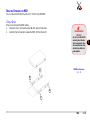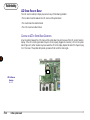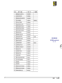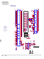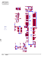
1
1 2 3 Notebook Computer Service Manual 4 5 6 3220/3420/3620 7 8 i Preface NOTICE The company reserves the right to revise this publication or to change its contents without notice. Information contained herein is for reference only and does not constitute a commitment on the part of the manufacturer or any subsequent vendor. They assume no responsibility or liability for any errors or inaccuracies that may appear in this publication nor are they in anyway responsible for any loss or damage resulting from the use (or misuse) of this publication. 1 This publication and any accompanying software may not, in whole or in part, be reproduced, translated, transmitted or reduced to any machine readable form without prior consent from the vendor, manufacturer or creators of this publication, except for copies kept by the user for backup purposes. 2 3 Brand and product names mentioned in this publication may or may not be copyrights and/or registered trademarks of their respective companies. They are mentioned for identification purposes only and are not intended as an endorsement of that product or its manufacturer. 4 First Edition ©May, 2000 5 6 7 8 Trademarks Intel, Pentium and Celeron are trademarks of Intel Corporation. IBM and PS/2 are trademarks of IBM Corporation. MS-DOS, Windows, Windows 95 and Windows NT are trademarks of Microsoft Corporation. Other brand and product names are trademarks and/or registered trademarks of their respective companies. ii copyrights ABOUT THIS MANUAL This manual is intended for service personnel who have completed sufficient training to undertake the maintenance and inspection of personal computers. It is organized to allow you to look up basic information for servicing and/or upgrading components of the 3220/ 3420/3620 notebook computer. The following information is included: 1 Chapter 1, Introduction, provides general information about the location of system elements and their specifications. 2 Chapter 2, Chipset, briefly describes the computer’s CPU, core logic and supporting chips. Chapter 3, Disassembly, provides step-by-step instructions for disassembling parts and subsystems and how to upgrade elements of the system. 3 Chapter 4, Troubleshooting, provides recommendations on how to solve possible system problems. 4 Appendix A, Parts Lists 5 Appendix B, Circuit Diagrams 6 7 8 the manual iii Preface RELATED DOCUMENTS You may also need to consult the following manuals for additional information: User’s Manual on CD 1 This describes the notebook’s features and the procedures for operating the computer and its ROM-based setup program. It also describes the installation and operation of the utility programs provided with the notebook. 2 Concise User’s Manual This gives a quick guide to the notebook and a brief introduction to its features. 3 4 5 6 7 8 iv related documents TABLE OF CONTENTS Preface Cover .................................................................................................................................................................................................... i Notice .................................................................................................................................................................................................. ii About This Manual ........................................................................................................................................................................... iii Related Documents .................................................................................................................................................................... iv Table of Contents............................................................................................................................................................................... v List of Figures .................................................................................................................................................................................. viii List of Tables ....................................................................................................................................................................................... x 1 2 3 Chapter 1: Introduction System Specifications .................................................................................................................................................................... 1-2 CPU ............................................................................................................................................................................................. 1-2 Core Logic .................................................................................................................................................................................. 1-2 Memory ...................................................................................................................................................................................... 1-2 BIOS ............................................................................................................................................................................................. 1-2 Video ........................................................................................................................................................................................... 1-3 Drives .......................................................................................................................................................................................... 1-3 Audio ........................................................................................................................................................................................... 1-3 I/O ............................................................................................................................................................................................... 1-4 Interface ..................................................................................................................................................................................... 1-4 Power System ............................................................................................................................................................................ 1-4 Other Features (optional) ......................................................................................................................................................... 1-5 Environment .................................................................................................................................................................................... 1-5 Physical ............................................................................................................................................................................................ 1-5 External Locator .............................................................................................................................................................................. 1-6 4 5 6 7 8 Chapter 2: Chipset CPU - Intel Mobile Pentium III/Celeron ...................................................................................................................................... 2-4 Core Logic Chipset - Intel 440ZX-M/BX AGPset ...................................................................................................................... 2-5 North Bridge, AGPset System Controller, 82443ZX-M/82443BX ..................................................................................... 2-5 South Bridge, PCI ISA IDE Xcelerator, 82371EB(PIIX4E) ........................................................................................................ 2-6 table of contents v Preface Supporting Chips ........................................................................................................................................................................... 2-8 Ricoh 5C475 PCI-CardBus Bridge .......................................................................................................................................... 2-8 SMSC FDC37N869 PC 99 ...................................................................................................................................................... 2-10 Compliant 5V and 3.3V Super I/O Controller with Infrared Support ............................................................................... 2-10 ATI RAGE LT PRO Graphics Controller ................................................................................................................................... 2-11 RealTek ALS300+ Integrated PCI Audio Accelerator .......................................................................................................... 2-12 1 Chapter 3: Disassembly 2 Connections ................................................................................................................................................................................... 3-2 Maintenance Precautions ...................................................................................................................................................... 3-3 Battery Precautions .................................................................................................................................................................. 3-3 Cleaning .................................................................................................................................................................................... 3-4 Maintenance Tools .................................................................................................................................................................. 3-4 General Disassembly: Removing the Keyboard & Heat Plate ................................................................................................ 3-5 Removing the Heat Sink Module ........................................................................................................................................... 3-6 Changing the CPU ................................................................................................................................................................... 3-7 General Disassembly: Removing the LCD Module ................................................................................................................... 3-8 Replacing the LCD .................................................................................................................................................................. 3-10 12.1” Disassembly .............................................................................................................................................................. 3-10 13.3” Disassembly ............................................................................................................................................................. 3-10 Removing the Inverter Board .......................................................................................................................................... 3-10 General Disassembly: Top Cover Assembly ............................................................................................................................ 3-12 Separating the Top Cover Assembly.................................................................................................................................... 3-12 General Disassembly: Top Cover Components ................................................................................................................. 3-14 TouchPad ........................................................................................................................................................................... 3-14 Microphone ....................................................................................................................................................................... 3-14 General Disassembly: Bottom Cover Assembly ...................................................................................................................... 3-16 HDD Bracket ........................................................................................................................................................................... 3-16 Mainboard .............................................................................................................................................................................. 3-16 Optional Fax/Modem Module, The Power Board, The IR Board, and the IO Bracket .................................................. 3-18 Fax/Modem Module (not shown) ................................................................................................................................... 3-18 The Power Board .............................................................................................................................................................. 3-18 The IR Board ...................................................................................................................................................................... 3-18 The IO Bracket ................................................................................................................................................................... 3-18 3 4 5 6 7 8 vi table of contents Module Disassembly: HDD Module .........................................................................................................................................3-20 Removing the HDD Module ..................................................................................................................................................3-20 Replacing/Upgrading the HDD ............................................................................................................................................ 3-21 Taking it Apart.................................................................................................................................................................... 3-21 Assembling the HDD Module .........................................................................................................................................3-22 Setting Up a New HDD for the First Time ......................................................................................................................3-23 Connectors ...................................................................................................................................................................................3-24 1 2 Chapter 4: Troubleshooting Before You Begin ........................................................................................................................................................................... 4-2 Tools ........................................................................................................................................................................................... 4-2 System Troubleshooting Chart ..................................................................................................................................................... 4-3 Pre-POST Assistant ........................................................................................................................................................................ 4-4 AC Power LED Fails .................................................................................................................................................................. 4-5 AC/DC Adapter ................................................................................................................................................................... 4-5 AC Power & Charge LEDs Fail ................................................................................................................................................ 4-6 Checking the Power Board ............................................................................................................................................... 4-6 Checking the Fuses ............................................................................................................................................................ 4-6 Checking the Battery Pack and its Cabling .................................................................................................................. 4-10 Checking the Battery Pack ........................................................................................................................................ 4-10 Checking the Cabling ................................................................................................................................................. 4-11 Checking the System Board ............................................................................................................................................ 4-11 LCD Screen Failure to Display ............................................................................................................................................... 4-12 Checking the LCD to System Board Connection .......................................................................................................... 4-12 Checking the Inverter Board ........................................................................................................................................... 4-13 Checking the LCD Screen ................................................................................................................................................ 4-14 POST — Testing the System ....................................................................................................................................................... 4-15 No Errors Found During the POST ........................................................................................................................................ 4-15 POST Error Beeps & Screen Messages .............................................................................................................................. 4-16 Post-POST Problems ...................................................................................................................................................................4-24 PC Card Socket Malfunction .................................................................................................................................................4-25 Sound Output Failure .............................................................................................................................................................4-26 Checking the Software Configuration ............................................................................................................................4-26 3 4 5 6 7 8 table of contents vii Preface Checking the Volume .......................................................................................................................................................4-26 Checking the Speaker Cable .......................................................................................................................................... 4-27 Suspend Function Failure ......................................................................................................................................................4-28 Charge LED Failure .................................................................................................................................................................4-28 Appendix A: Parts Lists Appendix B: Circuit Diagrams 1 2 LIST OF FIGURES 3 4 5 6 7 8 viii list of figures Fig. 1 – 1 Fig. 1 - 2 Fig. 1 – 3 Fig. 1 – 4 Fig. 1 – 5 Front View ............................................................................................................................................................1-6 Bottom View ........................................................................................................................................................1-6 Left View ............................................................................................................................................................... 1-7 Right View ............................................................................................................................................................ 1-7 Rear View ............................................................................................................................................................. 1-7 Fig. 2 – 1 Fig. 2 – 2 System Block Diagram .......................................................................................................................................2-1 Chipset Site Diagrams ................................................................................................................................... 2-2,3 Fig. 3 – 1 Fig. 3 – 2 Fig. 3 – 3 Fig. 3 – 4 Fig. 3 – 5 Fig. 3 – 6 Fig. 3 – 7 Fig. 3 – 8 Fig. 3 – 9 Fig. 3 – 10 Fig. 3 – 11 Fig. 3 – 12 Fig. 3 – 13 Fig. 3 – 14 Fig. 3 – 15 Releasing the Keyboard & Removing the Heat Plate ................................................................................... 3-5 Removing the Heat Sink Module ..................................................................................................................... 3-6 Changing the CPU ............................................................................................................................................. 3-7 Removing the LCD Module ............................................................................................................................... 3-9 Separating the LCD & Frame ........................................................................................................................... 3-11 Top Cover Disassembly (Bottom Screws) ...................................................................................................... 3-12 Top Cover Disassembly (Top Screws) ............................................................................................................ 3-13 Top Cover Assembly ........................................................................................................................................ 3-15 Bottom Cover Assembly ..................................................................................................................................3-17 Final Separation ............................................................................................................................................... 3-19 Removing the HDD ......................................................................................................................................... 3-20 HDD Module Disassembly .............................................................................................................................. 3-21 HDD Module Assembly .................................................................................................................................. 3-22 Ports & Connectors (top views) .................................................................................................................... 3-24 Ports & Connectors (bottom views) .............................................................................................................. 3-25 Fig. 4 – 1 Fig. 4 – 2 Fig. 4 – 3 Fig. 4 - 4 Fig. 4 - 5 Fig. 4 - 6 Fig. 4 – 7 Fig. 4 – 8 Troubleshooting Flowchart ............................................................................................................................... 4-3 Adapter’s Check Points ..................................................................................................................................... 4-5 Power Components .......................................................................................................................................... 4-7 Battery Circuitry ................................................................................................................................................ 4-10 LCD to Mainboard Connection ...................................................................................................................... 4-12 Inverter Board Component Sites ................................................................................................................... 4-13 Startup Screen: The POST ............................................................................................................................... 4-15 Speaker Connector on Mainboard ............................................................................................................... 4-27 Fig. A – 1 Fig. A – 2 Fig. A – 3 Fig. A – 4 Fig. A – 5 Fig. A – 6 Fig. A – 7 Fig. A – 8 Fig. A – 9 Fig. A – 10 Fig. A – 11 Fig. A – 12 Fig. A – 13 Fig. A – 14 Fig. A – 15 Fig. A – 16 Fig. A – 17 Fig. A – 18 Fig. A – 19 Fig. A – 20 3220 & 3620 Bottom Assembly ..................................................................................................................... A-2 3220 & 3620 Bottom Assembly Parts List .................................................................................................... A-3 3420 Bottom Assembly .................................................................................................................................... A-4 3420 Bottom Assembly Parts List ................................................................................................................... A-5 3220 Top Case Assembly ................................................................................................................................ A-6 3220 Top Case Assembly Parts List ................................................................................................................ A-7 3420 Top Case Assembly ................................................................................................................................ A-8 3420 Top Case Assembly Parts List ............................................................................................................... A-9 3620 Top Case Assembly ............................................................................................................................... A-10 3620 Top Case Assembly Parts List ............................................................................................................... A-11 3220/3420/3620 12.1” LCD Assembly .......................................................................................................... A-12 3220/3420/3620 12.1” LCD Assembly Parts List ......................................................................................... A-13 3220/3420/3620 13.3” LCD Assembly ......................................................................................................... A-14 3220/3420/3620 13.3” LCD Assembly Parts List ........................................................................................ A-15 3220/3420/3620 CD-ROM Assembly .......................................................................................................... A-16 3220/3420/3620 CD-ROM Assembly .......................................................................................................... A-17 3220/3420/3620 FDD Assembly ................................................................................................................... A-18 3220/3420/3620 FDD Assembly Parts List .................................................................................................. A-19 3220/3420/3620 HDD Assembly ................................................................................................................. A-20 3220/3420/3620 HDD Assembly Parts List ................................................................................................. A-21 Fig. B – 1 Fig. B – 2 Fig. B – 3 Fig. B – 4 Fig. B – 5 Fig. B – 6 Mainboard CPU: Pentium III Rev. 2 (Diagram 1 of 2)..................................................................................... B-2 CPU: Pentium III Rev. 2 (Diagram 2 of 2) ........................................................................................................ B-3 GTL Pull-Up Resistors Rev. 2 ............................................................................................................................ B-4 CPU Power Rev. 2 ............................................................................................................................................. B-5 CPU Power VCCT & 2.5V Rev. 2 ...................................................................................................................... B-6 443BX_443ZX Rev. 2 (Diagram 1 of 2) ............................................................................................................ B-7 1 2 3 4 5 6 7 8 list of figures ix Preface Fig. B – 7 Fig. B – 8 Fig. B – 9 Fig. B – 10 Fig. B – 11 Fig. B – 12 Fig. B – 13 Fig. B – 14 Fig. B – 15 Fig. B – 16 Fig. B – 17 Fig. B – 18 Fig. B – 19 Fig. B – 20 Fig. B – 21 Fig. B – 22 Fig. B – 23 Fig. B – 24 Fig. B – 25 Fig. B – 26 1 2 3 4 5 443BX_443ZX Rev. 2 (Diagram 2 of 2) ........................................................................................................... B-8 VGA Mobility/LT Pro Rev. 2 ............................................................................................................................... B-9 VGA Memory & TV-Out Rev. 2 ........................................................................................................................ B-10 VGA STARP Option Rev. 2 ................................................................................................................................. B-11 SODIMM Rev. 2 ................................................................................................................................................ B-12 Clock Generator Rev. 2 ................................................................................................................................... B-13 PIIX4 Rev. 2 (Diagram 1 of 2) .......................................................................................................................... B-14 PIIX4 Rev. 2 (Diagram 2 of 2) .......................................................................................................................... B-15 USB/ROM/PCI/ISA Pull High Rev. 2 ............................................................................................................... B-16 HDD & CDROM/FDD Connector Rev. 2 ..........................................................................................................B-17 Super I/O SMC869 Rev. 2 ............................................................................................................................... B-18 I/O Ports Rev. 2 ................................................................................................................................................ B-19 KBC H8 Rev. 2 ................................................................................................................................................. B-20 KBC PS/2 & FAN Rev. 2 ................................................................................................................................... B-21 Power Button & LED 3V H8 & LED Rev. 2 .................................................................................................... B-22 AC In Rev. 2 ..................................................................................................................................................... B-23 PCMCIA RL5C475A Rev. 2 ............................................................................................................................. B-24 RealTek Audio Controller ALS300+ & Conn. Rev. 2 ................................................................................... B-25 AC 97 Rev. 2 .................................................................................................................................................... B-26 MOdem Connector Rev. 2 .............................................................................................................................. B-27 6 7 LIST OF TABLES 8 Table 4 – 1 Table 4 – 2 Table 4 – 3 Table 4 – 4 Table 4 – 5 Table 4 – 6 Table 4 – 7 Table 4 – 8 x list of tables Pre-POST Problems ........................................................................................................................................... 4-4 Adapter Contacts ............................................................................................................................................... 4-5 Inverter Board Check Areas ........................................................................................................................... 4-13 Fatal Error Messages ...................................................................................................................................... 4-16 Non-Fatal Error Messages .................................................................................................................... 4-17,18,19 Phoenix BIOS POST Default Test Points (displayed on debug card) ......................................... 4-20,21,22,23 Post-POST Problems ....................................................................................................................................... 4-24 Possible PC Card Problems & Solutions ..................................................................................................... 4-25 1 1 Introduction This manual covers the information you need to service or upgrade the 3220/3420/3620 Notebook Computer. Information about operating the computer (e.g. getting started, and the Setup utility) is in the User’s Manual. Information about drivers (e.g. VGA & audio) is also found in User’s Manual. That manual is shipped with the computer. Operating systems (e.g. DOS, Windows 9x, Windows NT 4.0, Windows 2000, UNIX, etc.) have their own manuals as do application software (e.g. word processing and database programs). If you have questions about those programs, you should consult those manuals. The notebook is designed to be upgradable. It supports Intel mobile Pentium™ III and Celeron CPUs of different speeds and different types of LCD screens: TFT color from a variety of manufacturers and in a variety of resolution/color configurations. See Chapter 3, “Disassembly,” for a detailed description of the upgrade procedures for each specific component. In addition, system memory, hard disk, and BIOS are also upgradable. Please note the warning and safety information indicated by the “M” symbol. The balance of this chapter reviews the computer’s technical specifications and external features. 1–1 Introduction SYSTEM SPECIFICATIONS CPU mPGA2 Package Intel Celeron: 450 ~ 650 MHz Intel Pentium III: 450 ~ 650 MHz (including CPUs with SpeedStep technology) 1 CORE LOGIC chipset Intel 440ZX-M or 440BX (100MHz) AGPset MEMORY L1 cache (in CPU) 16KB code + 16KB data L2 cache (integrated with CPU) Celeron: 128KB on die SRAM Pentium III: 256KB on die SRAM RAM base 0MB (onboard) RAM expansion 2 small outline DIMM sockets (144 pin) DIMM sizes: 32MB, 64MB, 128MB standards: TSOP package, 3.3-volt mode: SDRAM speed: 100MHz or faster use: singly or mixed or identical pairs maximum expansion: 256MB BIOS 512KB Flash ROM support: Plug ‘n Play 1.0a, LBA, APM 1.2, ACPI 1–2 specifications VIDEO memory 8MB SGRAM chipset ATI Rage LT AGP (with 3D, & AGP proprietary driver) architecture 64-bit 2x AGP bus with Windows Acceleration display TFT (active matrix) 12.1” SVGA, (800x600) at 24-bit color (TrueColor) 13.3”/XGA, (1024x768) at 32-bit color (TrueColor) 1 DRIVES HDD Bay HDD module removable 2½” (9.5mm) , PCI local bus IDE interface Device Bay CD-ROM module or DVD† module full size (5.25”) ATAPI interface tray-loading mechanism, access time below 100ms full size (5.25”) ATAPI interface tray-loading mechanism, access time below 100ms or CD-RW module full size (5.25”) ATAPI interface tray-loading mechanism, access time below 100ms or FDD module removable 3.5”, 1.44 MB with 3-Mode support or LS-120 module removable 3½” (12.7mm height), 120MB PCI local bus IDE interface † with Software MPEG support AUDIO chipset architecture compatibility sampling RealTek ALS 300+, proprietary driver 32-bit PCI bus DirectSound, DirectSound3D Sound Blaster, Sound Blaster Pro, and Sound Blaster 16 emulation max. record & playback up to 48 KHz stereo (WAVE audio) specifications 1–3 Introduction 3D interface speakers QSound Q3D Positional /QEM EAX sound support speakers (phones), microphone, line-in 2 built-in: 0.5W stereo amp. USB compliant with UHCI 1.1, USB 1.0 & PCI 2.1 Serial 1 9-pin, 16C550 compatible Serial 2 infrared, IrDA v 1.1, FIR, SIR compatible Parallel 25-pin, ECP, EPP, output-only, bi-directional CRT 15-pin VGA TV-out S-Video PS/2 6-pin, mini-din, mouse or keyboard PC Card one Type I or Type II socket, PC Card 3.0 & CardBus compliant I/O 1 INTERFACE ¯ Advanced Users Actual battery life per charge may differ from this figure. It will vary depending on the condition of the battery, the environment, setup, and working habits. keyboard 87-key or 90-key (depending on the language) Windows 95 compliant with embedded numeric keypad pointing device PS/2 TouchPad (built-in), MS-Mouse compatible POWER SYSTEM adapters (external) universal, auto-sensing switching input: 90-240VAC @47- 63Hz output: 55W, 19V, 2.8A battery pack(s) Li-Ion: smart battery with gauge circuit Ni-MH: dumb battery without gauge circuit battery charge time Fast (system off) approx. 3 hours per battery, 2000mA ±200mA Slow (system on) approx. 6 hours per battery, 600mA ± 50mA (based on a 4000mA smart battery) 1–4 specifications life per charge approx. 180 minutes per battery (based on an Intel Pentium III 500 MHz CPU, running “ZD BatteryMark 2.0”” software in the Windows 98 operating system) management BIOS control, APM ver 1.2 levels: full-on, standby, suspend-to-RAM/suspend-to-disk (0 volt) OTHER FEATURES (OPTIONAL) 56K Fax/Data/Voice modem 1 ENVIRONMENT operating temp. 0oC to 35oC (32oF to 95oF) storage temp. -10oC to 65oC (14oF to 149oF) operating humidity 40% to 80%, non-condensing storage humidity 10% to 90%, non-condensing altitude 8000 feet shock (unpacked) 5G (11 + 1 microsecond pulse) PHYSICAL dimensions 306mm(w) x 232mm(d) x 29.8/32mm(h) weight 2.28Kg (with Li-Ion battery, FDD, HDD & 12.1” LCD) specifications 1–5 Introduction EXTERNAL LOCATOR The following figures show the external locations of the computer’s main subsystems. 1 1. 2. 3. 4. 5. 6. 7. 8. FRONT VIEW FIG. 1 – 1 Cover latch LCD Speakers Microphone On/Off switch LED status indicators Keyboard TouchPad & buttons 1 2 9 5 10 BOTTOM VIEW FIG. 1 - 2 9. Device bay 10. Battery bay 11. RAM bay 4 6 3 8 3 1–6 external locator 11 7 1. 2. 3. 4. 5. 6. 7. 8. 5 1 2 3 4 7 6 8 LEFT VIEW FIG. 1 – 3 PS/2 port Fan USB port PC Card slot HDD module Audio line-in jack Phone jack Mic jack 1 RIGHT VIEW FIG. 1 – 4 9. CD-ROM module (option) or DVD ROM module (option) or FDD module (option) or LS-120 module (option) 9 10. 11. 12. 13. 14. 15. 16. 17. 15 13 10 11 16 REAR VIEW FIG. 1 – 5 Kensington lock port IrDA (serial 2) port Fax/Modem (option) S-Video TV-out port Parallel port COM (serial 1) port External monitor port Adapter port 17 14 12 external locator 1–7 Introduction NOTES: 1 1–8 notes 2 Chipset The computer is completely AT-compatible. Its chipset supports a high-performance AGP bus video interface and state-of-the-art power management features. This chapter mainly describes the following major system components: • CPU • Core logic chipset • Supporting chips The following figures are the system block diagram and the component site diagram. These provide an overview of the computer’s layout and a practical locator for chipset components. 2 SYSTEM BLOCK DIAGRAM FIG. 2 – 1 2–1 Chipset CHIPSET SITE DIAGRAM FIG. 2 – 2 2 1. Pentium III/Celeron CPU 2. BIOS chip AMD AM29LV004BT 1 2 2–2 chipset diagram 3 CHIPSET SITE DIAGRAM FIG. 2 – 2 (CONT.) 4 5 7 6 8 10 3. Super I/O controller SMSC FDC37N869 4. Video controller ATI RAGE LT PRO 5. PC Card controller Ricoh R5C475 6. Audio controller RealTek ALS300+ 7. Core Logic chip 82443ZX-M/B (North Bridge) 8. Core Logic chip 82371EB (South Bridge) 9. Keyboard controller H8/3434 10. SDRAM DIMM socket 11. SDRAM DIMM socket 11 9 chipset diagram 2–3 2 Chipset CPU - INTEL MOBILE PENTIUM III/CELERON The Notebook uses the Intel Mobile Pentium III/Celeron processor in a microPGA2 package. The Intel Mobile Pentium III/Celeron processor features an integrated L2 cache (256KB for Pentium III and 128KB for Celeron) and a 64-bit high performance system bus. The Mobile Pentium III/Celeron processor’s 64-bit wide Low Power Gunning Transceiver Logic system bus is compatible with the 440BX AGPSet and provides a glue-less, point-to-point interface for an I/O bridge/memory controller. The Intel Mobile Pentium III and Celeron processors are fully compatible with all software written for the Pentium processor with MMX technology, Pentium processor, Intel486 microprocessor, and Intel386 microprocessor. In addition, they provide improved multimedia & communications performance. They feature: 2 • Performance improved over existing mobile processors - Supports the Intel Architecture with Dynamic Execution - Supports the Intel Architecture MMX technology • Integrated primary (L1) instructions and data caches - 4-way set associative, 32-byte line size, 1 line per sector - 16-Kbyte instruction cache and 16-Kbyte writeback data cache - Cacheable range programmable by processor programmable registers • Integrated second level (L2) cache - 4-way set associative, 32-byte line size, 1 line per sector - Operated at full core speed - 256-Kbyte, ECC protected cache data array • Low Power GTL+ system bus interface - 64-bit data bus, 66-MHz operation - Uniprocessor, two loads only (processor and I/O bridge/memory controller) - Short trace length and low capacitance allows for single ended termination • Voltage reduction technology • Pentium II processor clock control - Quick Start for low power, low exit latency clock “throttling” - Deep Sleep mode for extremely low power dissipation • Thermal diode for measuring processor temperature 2–4 CPU CORE LOGIC CHIPSET - INTEL 440ZX-M/440BX AGPSET The Intel 440ZX-M/BX AGPset consists of the BX System Controller (443ZX-M/443BX) and the PCI ISA IDE Xcelerator (PIIX4E). The AGPset forms a Host-to-PCI bridge and provides the second level cache control and a full function 64-bit data path to main memory. NORTH BRIDGE, AGPSET SYSTEM CONTROLLER, 82443ZX-M/82443BX The BX System Controller (443ZX-M/BX) integrates the cache and main memory DRAM control functions and provides bus control to transfer between the CPU, cache, main memory, AGP bus and the PCI Bus. Features • Supports the Pentium II processor family host bus at 100MHz and 66 MHz at 3.3V • PCI 2.1 compliant • Integrated Data Path • Integrated DRAM controller - 8Mbytes to 256Mbytes main memory - 64Mbit DRAM/SDRAM technology support - EDO and SDRAM DRAM support - Integrated programmable-strength for DRAM interface - CAS-Before-RAS refresh, extended CBR and self refresh for EDO - CAS-Before-RAS and self refresh for SDRAM • Fully synchronous, minimum latency 30/33 MHz PCI bus interface - Five PCI bus masters (including PIIX4) - 10 DWord PCI-to-DRAM read prefetch buffer - 18 DWord PCI-DRAM post buffer - Multi-Transaction timer to support multiple short PCI transactions • AGP Features - AGP 1.0 compliant - 66/133 MHz data transfer capability - Supports concurrent CPU, AGP and PCI transactions • Power Management Features - Dynamic stop clock support - Suspend to RAM (STR) - Suspend to Disk (STD) - Power On Suspend (POS) - Internal clock control - SDRAM and EDO self refresh during suspend - ACPI support - Compatible SMRAM (C_SMRAM) and Extended SMRAM (E_SMRAM) - SMM write-back cacheable in E_SMRAM mode up to 1MB • Supports the Universal Serial Bus (USB) • 492 Pin BGA 440BX AGPset with integrated data paths 2 core logic chipset 2–5 Chipset SOUTH BRIDGE, PCI ISA IDE XCELERATOR, 82371EB (PIIX4E) The PCI ISA IDE Xcelerator (PIIX4E) is a multi-function PCI device implementing a PCI-to-ISA bridge function, a PCI IDE function, a Universal Serial Bus host/hub function, and an Enhanced Power Management function. As a PCI-to-ISA bridge, the PIIX4E integrates many common I/O functions found in ISA-based PC systems - a seven channel DMA Controller, two 82C59 Interrupt Controllers, an 8254 Timer/Counter, and a Real Time Clock. In addition to compatible transfers, each DMA channel supports Type F transfers. The PIIX4E also contains full support for both PC/PCI and Distributed DMA protocols implementing PCI based DMA. The Interrupt Controller has Edge or Level sensitive and programmable inputs and fully supports the use of an external I/O Advanced Programmable Interrupt Controller (APIC) and Serial Interrupts. Chip select decoding is provided for BIOS, Real Time Clock, Keyboard Controller, second external Microcontroller, as well as 2 Programmable Chip Selects. The PIIX4 provides full Plug and Play compatibility. The PIIX4E can be configured as a Subtractive Decode bridge. This allows the use of a subtractive decode PCI-to-PCI bridge such as the 82380 chipset which implements a PCI/ISA docking station environment. 2 The PIIX4E supports two IDE connectors for up to four IDE devices providing an interface for IDE hard disks and ROMs. Up to four IDE devices can be supported in Bus Master mode. The PIIX4E contains support for “Ultra DMA” synchronous DMA compatible devices. The PIIX4E contains a Universal Serial Bus (USB) Host Controller that is Universal Host Controller Interface (UHCI) compatible. The Host Controller’s root hub has two programmable USB ports. The PIIX4E supports Enhanced Power Management, including full Clock Control, Device Management for up to 14 devices, and Suspend and Resume logic with Power On Suspend, Suspend to RAM or Suspend to Disk. It fully supports Operating System Directed Power Management via the Advanced Configuration and Power Interface (ACPI) specification. The PIIX4E integrates both a System Management Bus (SMBus) Host and Slave interface for serial communication with other devices. Features • Supports Pentium and Pentium II Microprocessors - 440BX ISA kit • Power Management Logic - Global and local device management - Suspend/resume logic - Supports thermal alarm - Support for external microcontroller - Full support for Advanced Configuration and Power Interface (ACPI) Specification and OS Directed Power Management 2–6 core logic chipset • Multifunction PCI to ISA Bridge - Supports PCI at 30 MHz and 33 MHz - Supports PCI Rev 2.1 specification - Supports Full ISA or Extended I/O (EIO) Bus - Supports full positive decode or subtractive decode of PCI - Supports ISA/EIO at 1/4 of PCI frequency • Supports both mobile and desktop deep green environments - 3.3 V operation with 5 V tolerant buffers - Ultra-low power for mobile environments - Power-On Suspend and Soft-OFF for desktop environment - All registers readable/restorable for proper resume from 0 V suspend • Integrated IDE Controller - Independent Timing of up to 4 drives - PIO Mode 4 transfers up to 14 Mbytes/s - Supports “Ultra 33” Synchronous DMA mode transfers up to 33 MBytes/sec - Integrated 8 x 32-bit buffer for IDE PCI Burst - Supports glue-less “Swap-Bay” option with full electrical isolation • Enhanced DMA Controller - Two 8237 DMA controllers - Supports PCI DMA with 3 PC/PCI channels and Distributed DMA protocols (simultaneously) - Fast Type-F DMA for reduced PCI bus usage • Interrupt Controller based on two 82C59 - 15 interrupt support - Independently programmable for Edge/Level sensitivity - Supports optional external I/O APIC - Serial interrupt input • Timers based on 82C54 - System Timer, Refresh Request, Speaker Tone Output • USB - Two USB 1.0 ports for serial transfers at 12 or 1.5 Mbit/sec - Supports legacy keyboard and mouse software with USB-based keyboard and mouse - Supports UHCI Design Guide Revision 1.1 Interface • SMBus - Host interface allows CPU to communicate via SMBus - Slave interface allows external SMBus master to control resume events • Real-Time Clock - 256 Byte Battery-Pack CMOS SRAM - Includes Date Alarm - Two 8-byte Lockout Ranges • Microsoft Win95/98 compliant 2 core logic chipset 2–7 Chipset SUPPORTING CHIPS The following subsections describe major supporting chips: • • • • Ricoh 5C475 PCI-CardBus Bridge SMSC FDC37N869 PC 99 Compliant 5V and 3.3V Super I/O Controller with Infrared Support ATI RAGE LT PRO Graphics Controller RealTeck ALS300 + Audio Controller RICOH 5C475 PCI-CARDBUS BRIDGE The 5C475 is a PC card controller offering a single chip solution as a bridge between PCI bus and CardBus. The 5C475 includes a PC Card 95 compliant socket interface and a bridge function to the PCI bus of 33MHz. The 5C475 can support the 32-bit CardBus (Card-32) and the 16-bit PC card (Card-16) without external buffers. 2 Concerning the card control interface, the 5C475’s register is compatible with the Intel 82365SL and Ricoh’s RF5C396/366 in order to maintain backward compatibility with the existing 16-bit PC Card compliant with PCMCIA2. 1/JEIDA4.2. All PC card interface signals are individually buffered to allow direct connection to CardBus and Hot insertion/removal without external buffers. The 5C475 also allows direct connection to PCI bus. The PCI interface and PC card socket interface have their own power supply terminals that can be powered at either 3.3V or 5V for compatibility with 3.3V and 5V signaling environments. The core logic is powered at 3.3V. The 5C475 allows the system to be equipped with the high performance multimedia PC cards like the Video capture card. It features: • PC98 compliant - PC98 Design Guide compliant (Subsystem ID, Subsystem Vender ID) - ACPI 1.0 and PCI Bus Power Management 1.0 compliant • Low Power consumption - Hardware Suspend - CLKRUN#, CCLKRUN# support • High-performance • Single Chip PCI-CardBus Bridge - PCMCIA PC-Card 95 socket support - CardBus (Card-32) Card and 16-bit (PCMCIA2.1/JEIDA4.2) Card support 2–8 supporting chip - PC Card • PCI Bus Interface - Compliant with PCI Local Bus Specification 2.1 - The maximum frequency 33MHz - PCI Master/Target protocol support - Direct connection to PCI bus • CardBus PC card Bridge - Compliant with PCMCIA PC Card 95/CardBus Standard Specification - Compliant with Yenta register set Rev2.2 - The maximum frequency 33MHz - CardBus Master/Target protocol support - Transfer transactions - All memory read/write transaction (bi-direction) - I/O read/write transaction (bi-direction) - Configuration read/write transaction (PCI-Card) - 2 programmable memory windows - 2 programmable I/O windows • PC Card-16 Bridge • Compliant with PCMCIA PC Card 95 CardBus (PC Card-16) Standard Specification - 5 programmable memory windows - 2 programmable I/O windows - Compliant with i82365SL compatible register set / ExCA TM • System Interrupt - INTA# support for PCI system interrupt - IRQn support for ISA system interrupt (Non shared IRQn pins) - Serialized IRQ support • 3.3V/5V Mixed Voltage Operation at 33Mhz • GPIO support • Posting Write and Prefetching Read support • Plug and Play support • 16-bit Legacy mode (3E0/3E2 I/O port) support • PCIway Legacy DMA support 2 supporting chip - PC Card 2–9 Chipset SMSC FDC37N869 PC 99 COMPLIANT 5V AND 3.3V SUPER I/O CONTROLLER WITH INFRARED SUPPORT The FDC37N869 features: • 5 volt and 3.3 volt operation • Intelligent auto power management • 16 bit address qualification • 2.88MB Super I/O Floppy Disk Controller - Licensed CMOS 765B Floppy Disk Controller - Software and register compatible with SMSC proprietary 82077AA compatible core - Supports one Floppy Drive directly - Configurable Open Drain/Push-Pull Output Drivers - Supports Vertical Recording Format - 16 byte data FIFO - 100% IBM compatibility - Detects all overrun and underrun conditions - Sophisticated Power Control Circuitry (PCC) including multiple power-down modes for reduced power consumption - DMA enable logic - Data rate and drive control registers - Swap drives A and B - Non-burst mode DMA option - 48 Base I/O address, 15 IRQ and 4 DMA options - Forceable write protect and disk change controls • Floppy disk available on parallel port pins ACPI compliant • Enhanced digital data separator - 2Mbps, 1Mbps, 500 Kbps, 300 Kbps, 250 Kbps data rates - Programmable precompensation modes 2 2 – 10 supporting chip - super I/O • Serial ports - Two high speed NS16C550 compatible UARTs with send/ receive 16 Byte FIFOs - Supports 230k and 460k baud - Programmable baud rate generator - Modem control circuitry • Infrared communications controller - IrDA v1.2 (4Mbps), HPSIR, ASKIR, Consumer IR Support - 2 IR Ports - 96 base I/O address, 15 IRQ options and 4 DMA options • Multi-mode parallel port with ChiProtect - Standard Mode - IBM PC/XT PC/AT and PS/2 compatible bi-directional parallel port - Enhanced Parallel Port (EPP) compatible - EPP 1.7 and EPP 1.9 (IEEE 1284 compliant) - Enhanced Capabilities Port (ECP) compatible (IEEE 1284 compliant) - Incorporates ChiProtect Circuitry for Protection Against Damage Due to Printer Power-On - 192 base I/O address, 16 IRQ and 4 DMA options • Game port select logic - 48 base I/O addresses • General Purpose Address Decoder - 16-byte block decode ATI RAGE LT PRO GRAPHICS CONTROLLER The RAGE LT Pro is a highly integrated graphics accelerator with superior support for 3D and motion video — ideal for notebooks and LCD desktops. It incorporates comprehensive support for Intel’s Accelerated Graphics Port (AGP), including 1X or 2X mode with sidebands. Delivering superior 3D acceleration and comprehensive 3D support, the RAGE LT Pro includes a triangle set-up engine, single-pass trilinear filtering, six perspectively correct texturing modes, video texturing, Gouraud and specular shading, and a host of 3D special effects. The best choice for DVD notebooks and LCD desktops, the RAGE LT Pro’s DVD features include motion compensation, acceleration for soft DVD, integrated TV-out with Macrovision and support for third-party MPEG-2 decoders via the ATI Multimedia Channel (AMC). 2 Using Tri-View™ the RAGE LT Pro can output to LCD, CRT, and TV simultaneously. It also includes two output controllers so that any two display devices can have different images and/or refresh rate. It has the following main features: • First mobile accelerator to use AGP 2X (133MHz) in AGP Texturing with sideband signals to realize all the benefits of AGP. • First mobile accelerator to deliver full motion soft DVD using motion compensation circuitry. • First mobile acccelerator with integrated LVDS transmitter. • Innovative Dynamic Power Management with ACPI compliance. • Superior 3D performance acheived through a hardware setup engine and a 4KB on-chip texture cache. • Superior 2D performance with support of 100MHz SGRAM. • TFT and DSTN panel interface support for up to 1280x1024 resolutions. • Integrated ImpacTV2-quality TV output provides optimal image quality via programmable 6 tap flicker filter, resolution modes scale down from 1024x768 and 16:9 wide mode support. Direct YUV422 mode, Macrovision 7.01 and CGMS support. • Support for 2, 4, or 8MB frame buffers, and integrated 230MHz DAC. • High quality ratiometric expansion that fits source images to any panel resolution. • Flexible graphics memory configurations: 4MB up to 8MB SDRAM/SGRAM. • Memory upgrade via industry standard SGRAM SO-DIMM, for reduced board area and higher memory speeds. • DDC1 and DDC2B+ for plug and play monitors. • External Spread Spectrum chip support to reduce EMI on digital interface. • Power management with full VESA DPMS and EPA Energy Star compliance. • Integrated hardware diagnostic tests performed automatically upon initialization. • High quality components through built-in SCAN, IDDQ, CRC and chip diagnostics. • Single chip solution in 0.25um, 2.5V CMOS technology. • Comprehensive HDKs, SDKs and utilities augmented by full engineering support. • Fully compliant with relevant sections of PC 98 and PC 99. supporting chip - video 2 – 11 Chipset REALTEK ALS300+ INTEGRATED PCI AUDIO ACCELERATOR The ALS300+ Integrated PCI Audio Accelerator brings forth a new age of highly integrated, single chip sound products. It provides cost-efficient audio solutions for motherboard and add-in card and notebook implementations. The ALS300+ fully supports the PCI Plug and Play standard. Its main features are as follows: • High performance VLSI sound ASIC • Compatible with DirectSound, DirectSound3D Sound Blaster, Sound Blaster Pro, and Sound Blaster 16 emulation • 64-Voice Wavetable Synthesis w/ DLS-1 support • Built-in ALSFM Synthesizer • Supports Dual AC-97 CODECs/4-channel speakers • I 2S & S/PDIF Digital In/Out • Host Modem support • Legacy/DOS compatibility • QSound Q3D Positional/QEM EAX Sound Support • Supports Sound Blaster ADPCM decompression • MPU-401 MIDI controller with FIFO • Enhanced normal & digital game port support • 16-bit full-duplex for concurrent recording and playback • ACPI/PCI Bus Power Management Interface Specification 1.1 • 5.0/3.3V dual power mode • 128-Pin PQFP package 2 2 – 12 supporting chip - audio 3 Disassembly 3 This chapter provides step-by-step instructions for disassembling parts and subsystems. When it comes to reassembly, reverse the procedures (unless otherwise indicated). We suggest you completely review any procedure before you take the computer apart. The computer comes in three (3) versions: 3220, 3420 and 3620. The principal differences between them are cosmetic and minor structural variations of the top and bottom covers. As appropriate, these differences are noted in the side-bars. Additional component information is available in Appendix A: Parts Lists or in Appendix B: Circuit diagrams. CPU Upgrades: You need to remove the keyboard and heat plate. Note: When re-assembling, make sure the heat plate is not “distorted” and is fastened securely. LCD Upgrades: You need to remove the keyboard and heat plate. Changing the LCD module itself, only requires minimal deconstruction. Note: When re-assembling, make sure the heat plate is not “distorted” and is fastened securely. Illustrations: To enhance procedural clarity, the illustrations in this chapter do not include all components. Mylar insulation and adhesive attachments are not shown unless they are critical to the disassembly process. For information about these parts, please refer to Appendix A: Parts Lists. 3–1 Disassembly The disassembly procedures appear in the following order: General Disassembly • Keyboard and heat plate • LCD module • Top cover assembly • Bottom cover assembly Module Disassembly • HDD module All disassembly procedures assume that the system is turned OFF, and disconnected from any power supply (the battery is removed too). We also assume that the CD device (CD-ROM/DVD-ROM/CD-RW) or the FDD device (FDD/LS-120) is removed as well as the HDD. All of these procedures are described in the User’s Manual which accompanies the system. 3 CONNECTIONS Connections within the computer are one of four types: 3–2 procedures Locking collar sockets for ribbon connectors To release these connectors, use a small flat-head screwdriver to gently pry the locking collar away from its base. When replacing the connection, make sure the connector is oriented in the same way. The pin1 side is usually not indicated. Pressure sockets for multi-wire connectors To release this connector type, grasp it at its head and gently rock it from side to side as you pull it out. Do not pull on the wires themselves. When replacing the connection, do not try to force it. The socket only fits one way. Pressure sockets for ribbon connectors To release these connectors, use a small pair of needle-nose pliers to gently lift the connector away from its socket. When replacing the connection, make sure the connector is oriented in the same way. The pin1 side is usually not indicated. Board-to-board or multi-pin sockets To separate the boards, gently rock them from side to side as you pull them apart. If the connection is very tight, use a small flathead screwdriver - use just enough force to start the separation. MAINTENANCE PRECAUTIONS The following precautions are a reminder. To avoid personal injury or damage to the notebook while performing a removal and/or replacement job, take the following precautions: 1. 2. 3. 4. 5. 6. 7. 8. 9. 10. Don't drop it. Perform your repairs and/or upgrades on a stable surface. If the computer falls, the case and other components could be damaged. Don't overheat it. Note the proximity of any heating elements. Keep the computer out of direct sunlight. Avoid interference. Note the proximity of any high capacity transformers, electric motors, and other strong magnetic fields. These can hinder proper performance and damage components and/or data. You should also monitor the position of magnetized tools (i. e. screwdrivers). Keep it dry. This is an electrical appliance. If water or any other liquid gets into it, the computer could be badly damaged. Be careful with power. Avoid accidental shocks, discharges or explosions. •Before removing or servicing any part from the notebook, turn the notebook off and detach any adapters (AC/DC or car adapter). • To prevent the notebook from being turned on accidentally, remove the battery pack before you start a removal or replacement procedure. • Only use a power adapter approved for use with this computer. • Make sure the AC adapter has a steady, uninterrupted power supply and is grounded. • When you want to unplug the power cord or any cable/wire, be sure to disconnect it by the plug head. Do not pull on the wire. • Be sure the socket and any extension cord(s) you use can support the total current load of all connected devices. Peripherals/Modules – Turn off and detach any peripherals. Remove all modules and power units. Beware of static discharge. ICs, such as the CPU and main supporting chips, are vulnerable to static electricity. Before handling any part in the notebook, discharge any static electricity inside the notebook. When handling a printed circuit board, do not use gloves or other materials which allow static electricity buildup. We suggest that you use an anti-static wrist strap instead. Beware of corrosion. As you perform your job, avoid touching any connector leads. Even the cleanest hands produce oils which can attract corrosive elements. Keep your work environment clean. Tobacco smoke, dust or other air-born particulate matter is often attracted to charged surfaces, reducing performance. Keep track of the components. When removing or replacing any part, be careful not to leave small parts, such as screws, loose inside the notebook. 3 BATTERY PRECAUTIONS Only use batteries designed for this computer. The wrong battery type may explode, leak or damage the computer. Recharge the battery using an approved system. Incorrect recharging may make the battery explode. Always dispose of batteries carefully. Batteries may explode or leak if exposed to fire, or improperly handled or discarded. Do not try to repair a battery. Damaged or defective batteries should be replaced. precautions 3–3 Disassembly CLEANING Do not apply cleaner directly to the computer, use a soft clean cloth. Do not use volatile (petroleum distillates) or abrasive cleaners on any part of the computer. MAINTENANCE TOOLS The following tools are recommended when working on the notebook: M3 Phillips-head screwdriver M2.5 Phillips-head screwdriver (magnetized)* M2 Phillips-head screwdriver Small flat-head screwdriver Pair of needle-nose pliers Anti-static wrist-strap * note Maintenance Precaution #3. 3 3–4 precautions GENERAL DISASSEMBLY: REMOVING THE KEYBOARD & HEAT PLATE 1. 2. 4. 3. Use a flat-head screwdriver to release the keyboard catches at points A ~ D. Carefully slide and lift the keyboard slightly up and towards the LCD. Use the flat-head screwdriver to disconnect the keyboard cable from the locking collar socket (E) on the mainboard. Set the keyboard aside until re-assembly. Disconnect the fan cable at JFAN1 (F). With a Phillips-head screwdriver, remove screws G ~ K. 3 RELEASING THE KEYBOARD & REMOVING THE HEAT PLATE FIG. 3 – 1 Heat Plate G ~K þ Tip This procedure involves: screws 5 connectors: 2 Stop here if you only need to replace /upgrade the CPU. E F keyboard & heat plate 3–5 Disassembly REMOVING THE HEAT SINK MODULE The heat sink module which includes the fan is attached to the reverse side of the heat plate. 1. 2. 3 REMOVING THE HEAT SINK MODULE FIG. 3 – 2 3–6 heat sink module Remove the heat plate (page 3-5). Remove the five screws which secure the heat sink module to the heat plate according to the sequence shown in the following figure. CHANGING THE CPU The removable CPU fits into a FoxConn microPGA2 socket. REMOVING THE CPU Loosen the socket screw using a flat-head screwdriver to disengage the CPU and the socket. INSERTING THE CPU Place the CPU in the center of the socket. Fasten the socket screw using a flat-head screwdriver to lock the CPU in the socket. 3 CPU IN MICROPGA2 SOCKET FIG. 3 – 3 CPU upgrade 3–7 Disassembly GENERAL DISASSEMBLY: REMOVING THE LCD MODULE The LCD module can be removed with only a little more disassembly after you’ve removed the keyboard and heat plate: 3 MODEL 3420 NOTE: The status panel is integrated into the top cover. However, removing hinge cover B opens a space large enough to pull through the LCD controller and inverter cables. 1. Using a flat-head screwdriver, pry the status panel (A) forward slightly. 2. Lift the status panel up and set it aside. 3. Remove the hinge covers (B & C). Use the flat-head screwdriver to flex the cover up and back slightly. 4. Disconnect the LCD controller cable from connector JLCD1 (D from E) and the inverter cable from connector JINV1 (F from G). 5. Remove the four (4) hinge screws (H ~ K), set them aside and lift the LCD module away from the body. Note: The LCD’s ground connector (L). If you are upgrading the LCD module to different size, stop here. The entire module should be replaced, including the rear panel and frame. The new module uses different components, but connects in the same way as the original. Refer to Appendix A for specific part numbers. If you are replacing the LCD panel with one of the same size, continue to page 3-10. 3–8 LCD module models 3220 & 3620 model 3420 A C B J~K B H~I L H~I L 3 J~K C ø D ø D A F REMOVING THE LCD MODULE FIG. 3 – 4 F G G E E þ Tip This procedure involves: screws 4 connectors: 2 LCD module 3–9 Disassembly REPLACING THE LCD The LCD module has two main elements, the LCD itself, and its inverter board. First separate the LCD module from the main body of the computer as described on pages 3-8 and 3-9. 12.1” DISASSEMBLY This LCD is attached directly to the rear panel of the LCD module. 1. Remove the 4 rubber caps (A ~ D) and frame screws under them. 2 Snap off the LCD frame (E). As you do this, make sure the cover latch (F) doesn’t spring out. There are snaps on all sides. 3. Disconnect the panel (G) from the inverter board ( H). 4. Remove the 4 LCD anchor screws (I ~ L), and lift the LCD (M) away from the rear panel (N). 5. Disconnect the LCD controller cable (O). 3 13.3” DISASSEMBLY This LCD is mounted in a frame, which in turn attaches to the rear panel of the module. 1. Remove the 4 rubber caps (A ~ D) and frame screws under them. 2 Snap off the LCD frame (E). As you do this, make sure the cover latch (F) doesn’t spring out. There are snaps on all sides. 3. Disconnect the panel (G) from the inverter board (H). 4. Disconnect the LCD power cable (P) from the inverter board (Q). Note: this cable is wrappped with the LCD controller cable (R). 5. Remove the frame anchor screws (S & T) and lift the LCD panel (U) and frame away from the rear panel (V). 6. Remove the frame screws (W~ Z). 7. Disconnect the LCD controller cable (R). REMOVING THE INVERTER BOARD The inverter board is anchored to the rear panel of the LCD module with adhesive. If you need to remove it for testing or replacement, make sure the system is disconnected from all power sources (including batteries). You should disconnect all leads from the inverter before removing it from the LCD module. The inverter board itself is housed in protective mylar. This package is itself may be glued together, so separate it carefully to avoid tearing. 3 – 10 LCD module 12.1” LCD module 13.3” LCD module 3 SEPARATING THE LCD & FRAME FIG. 3 – 5 þ Tip This procedure involves: 12.1” 13.3” screws 8 10 connectors: 2 3 LCD module 3 – 11 Disassembly GENERAL DISASSEMBLY: TOP COVER ASSEMBLY The top cover assembly also contains the TouchPad assembly and daughterboards for the status panel LEDs and the power switch. However, other components are only accessible after the top cover assembly is removed. Remove the keyboard and heat plate and the LCD module and status panel (3220 & 3620) as described respectively on pages 3-5 & 3-9. SEPARATING THE TOP COVER ASSEMBLY 3 MODEL 3420 NOTE: The equivalents of screws R & S are located on the underside of the notebook (roughly between screws J & K and K & L respectively). 1. 2. 3. 4. 5. 6. TOP COVER DISASSEMBLY (BOTTOM SCREWS) FIG. 3 – 6 þ Tip This procedure involves: screws 17 3 – 12 top cover & TouchPad If you haven’t already done so, remove the battery and the CD device/FDD device. Turn the notebook body upside-down. Remove 13 screws (A~ M). Remove the four (4) screws on the rear panel (N ~ Q). Return the notebook to its upright position and remove the two (2) screws in the status-panel area (R & S) and the three (3) screws on the back edge (T ~ V). Disconnect the on-board microphone at JINTMIC1 (W). Note: This connection is anchored with tape to conform to heat-sink spacing. Disconnect the TouchPad connector at CN3 (X). S R V U T TOP COVER DISASSEMBLY (TOP SCREWS) FIG. 3 – 7 Note for re-connecting the microphone cable The following illustration shows how the microphone cable should be placed. Please note the cable should be in a straight line, aligned with the left edge of the LCD connector (JLCD1) and fixed to the mainboard with adhesive tape. þ Tip This procedure involves: screws 5 connectors 2 W X top cover & TouchPad 3 – 13 3 Disassembly GENERAL DISASSEMBLY: TOP COVER COMPONENTS The two (2) TouchPad daughterboards in this assembly are unlikely to require any service. TOUCHPAD 3 NOTE FOR MODELS 3420 & 3620: To remove the TouchPad board, remove the two (2) screws anchoring its bracket. Slide the bracket either towards the keyboard space (3620) or to the left (3420) to release it. The TouchPad module is in 2 parts: the TouchPad itself and the “mouse” buttons. To take them out of the top cover assembly, first separate the top cover assembly as described on pages 3-12 and 3-13. 1. Disconnect the ribbon connector at J1 (A) on the mouse button board or J1 (B) on the TouchPad board. Note: These connector sockets flip up to release the ribbon. 2. Remove the four (4) screws (C ~ F) on the mouse button board. 3. The TouchPad is held in place by a collar (G) on the outer surface of the top cover. To remove this collar, we recommend using a flat-head screwdriver to gently free the collar’s tabs which extend to the underside (seen in the accompanying graphic). MICROPHONE The on-board microphone (H) is anchored in place with tape. No special tools are needed to remove it. 3 – 14 top cover assembly E A F C D TOP COVER ASSEMBLY FIG. 3 – 8 H þ Tip The TouchPad module has: buttons Pad board board screws 4 2 (for 3420 & 3620) connectors 2 1 B G top cover assembly 3 – 15 3 Disassembly GENERAL DISASSEMBLY: BOTTOM COVER ASSEMBLY The bottom cover assembly includes the mainboard, HDD bracket, IR board, power board, PCMCIA socket, and optional fax/modem module (not shown). HDD BRACKET The HDD bracket is held in place with a single screw. 1. Remove the HDD module anchor screw(A). 2. Lift the HDD bracket & HDD door assembly away from the mainboard. Note: The mylar insulation between the bottom of the bracket and the mainboard should remain attached to the bracket- there there only two strips of adhesive tape holding it to the mainboard. 3 MAINBOARD The lines connecting some of these components are taped in position. As you disconnect/remove them, note how this is done. This is especially important in the area close to the CPU. 3. Disconnect the speaker cable (C) from connector JINTSPK1 (B). 4. Remove screws F & G. 5. Angle the mainboard up from the right side. As you do so, flex the bottom of the case near the fax/ modem port (H). 3 – 16 bottom cover models 3220 & 3620 model 3420 G G 3 F F B B H A BOTTOM COVER ASSEMBLY FIG. 3 – 9 õ A E õ H E C C D D þ Tip Separating the mainboard from the bottom cover includes: screws 3 connectors 1 bottom cover 3 – 17 Disassembly OPTIONAL FAX/MODEM MODULE, THE POWER BOARD, THE IR BOARD AND THE IO BRACKET These are the remaining components which can be separated from the mainboard. None of these parts are serviceable. If any develop problems, the entire daughterboard should be replaced. Note: The PC Card socket is soldered directly to the mainboard and so is not removable. FAX/MODEM MODULE (NOT SHOWN) This daughterboard connects to the mainboard through the surface mounted socket JMDC1 ( A) and then to the fax/modem port through cable connector B. It is held in place with a single screw at point C. 3 THE POWER BOARD This daughterboard (D) connects to the mainboard through two multi-pin sockets JDD1 & JDD2 (E & F). To separate the daughterboard, gently rock it from side to side as you pull it up from the mainboard. The underside of the power board also has a strip of mylar insulation which should not be removed. THE IR BOARD This small daughterboard (G) contains the IrDA port and the ON/OFF switch. It is attached to the IO Bracket with two (2) screws, H & I. It connects to the mainboard through cable J to socket JIR1 (K). THE IO BRACKET This bracket (L), is held to the mainboard by six nuts (M ~ R). 3 – 18 bottom daughterboards G M~R L J 3 D H ~I FINAL SEPARATION FIG. 3 – 10 K C B þ Tip A E This procedure involves: screws 9 connectors 4 F bottom daughterboards 3 – 19 Disassembly MODULE DISASSEMBLY: HDD MODULE We are not including specific instructions for the CD device (CD-ROM/DVD-ROM/CD-RW) and the FDD device (FDD/LS-120). If any upgrade or replacement is required, the entire module should be replaced. If for some reason a specific part must be replaced, refer to the “exploded” drawings in Appendix A for the position and part number. 3 M Removal Warning Don’t try to remove the hard disk (HDD) while the system is ON. This will make the system “crash”, resulting in data loss or damage. REMOVING THE HDD MODULE A detailed description of how to disassemble this module is included in the User’s Manual Chapter 6: Extras. We strongly recommend reviewing that document. It includes information on how to setup the hard disk for use. Those instructions may be more current than those provided here. The section which follows is “lifted” from the 1st edition of the User’s Manual. 1. 2. 3. Make sure the computer is turned OFF. Open the HDD bay door. Unfurl the mylar pull-tab and use it to pull the HDD module out. REMOVING THE HDD FIG. 3 – 11 M Warranty Warning Under some warranty conditions, the user may not remove the hard disk. If this applies, note any indications that the warranty has been violated. 3 – 20 HDD ÷ REPLACING/UPGRADING THE HDD You can replace the HDD with another 2.5”, 9.5mm high IDE HDD. TAKING IT APART After you’ve removed the HDD module, 1. Remove the four (4) bracket screws (A~D), and set them aside. 2. Carefully flex the bracket to release the HDD. (Do Not Shake it!) M Contamination Warning Do not touch the HDD’s connector pins or the electronic components. Even the cleanest hands have oils which may attract corrosive particles. HDD MODULE DISASSEMBLY FIG. 3 – 12 B A D C HDD 3 – 21 3 Disassembly ASSEMBLING THE HDD MODULE M HDD 3 When you’re ready to install a new hard disk, 1. Hold the HDD by its edges and orient it so that the connector pins side faces the open end of the bracket. 2. Settle the bracket around the HDD. In the correct position, the holes in the bracket’s sides line up with the module’s screw holes. (To fit tnto the HDD bay, the HDD’s sides must not extend outside the bracket.) 3. Fasten the four (4) bracket screws (A ~ D) removed in step 1 in the section, “Taking it Apart”, described on page 3-21. Jumper Warning Some (usually older) HDDs have a small jumper switch. It must be set to “master” or the system may not correctly recognize the drive. Check your drive’s documentation. 3 ÷ 2 HDD MODULE ASSEMBLY FIG. 3 – 13 1. bracket 2. HDD (electronics face-down) 3. connector Refer to the text for the accompanying instructions. B A 1 D C 3 – 22 HDD SETTING UP A NEW HDD FOR THE FIRST TIME Before you can use a new HDD for the first time, you have to do two things: • tell the computer about the HDD (refer to the User’s Manual Chapter 4: Firmware). • prepare the HDD to accept data (refer to your operating system manual). Use the following directions to prepare the new HDD for use. HARDWARE SOFTWARE After you replace or upgrade the HDD, turn the system on and configure it for the newly-installed HDD using Setup. Refer to the User’s Manual Chapter 4: Firmware. A hard disk must be partitioned, and formatted before use. 3 PARTITIONING 528MB OR LARGER HDDS & LBA MODE The notebook automatically assumes any HDD 528MB or larger uses LBA Mode. If the HDD was formatted on an older system which did not use LBA mode, use the Setup utility to manually adjust the LBA setting for the Primary Master. If you don’t, the system will not “see” it correctly. The default, “Auto” type setting uses LBA mode. Use this if you’re preparing a “fresh” HDD. To partition the HDD, use the utility from your operating system (e.g. Microsoft’s fdisk command) to do this. Note: If you want to use the Save to Disk Partition feature, refer to the User’s Manual’s Chapter 5: Power before you partition the HDD. FORMATTING To format, use the utility from your operating system (e.g. Microsoft’s format/s command). Consult your operating system’s manual for more information on its partitioning and formatting utilities. M Save to Disk Warning Whenever you install a different hard disk that has a Save to Disk partition on it, make sure you follow the procedures detailed in the User’s Manual Chapter 4: Firmware and Chapter 5: Power. HDD 3 – 23 Disassembly 3 PORTS & CONNECTORS (TOP VIEWS) FIG. 3 – 14 Mainboard 1. PS/2 port 2. DC-in 19V 3. VGA port 4. Serial (COM1) port 5. Parallel port 6. TV-out port 7. Fax/Modem port 8. JINV1 to #23 (inverter) 9. JLCD1 to LCD 10. JMDC1 to Fax/Modem 11. JIR1 to #25 (IR Board) 12. JMODEM2 to Fax/Modem 13. USB port 14. JINTMIC1 to onboard mic 15. JFAN1 to fan 16. PCMCIA connection 17. JINTKB1 to Keyboard 18. JBAY1 to modules 19. JDD1 to #33 (Power) 20. JINTSPK1 to speakers 21. JHDD1 to Hard Disk Drive 22. JDD2 to #35 (power) Inverter Board 23. CN2 to #8 (Mainboard) 24. CN1 to LCD power IR Board 25. JIR1 to #11 (Mainboard) CONNECTORS These figures show the locations of the mainboard and principal daughterboard’s connectors. MAINBOARD (TOP) INVERTER BOARD (TOP) 3 2 1 3 – 24 connectors 6 8 11 9 13 7 5 4 14 12 25 POWER BOARD (TOP) 10 15 26 18 16 17 19 20 21 22 Power Board 26. CN3 to TouchPad 24 23 PORTS & CONNECTORS (BOTTOM VIEWS) FIG. 3 – 15 Mainboard 27. IrDA port 28. JDIM1 RAM bay 1 29. JDIM2 RAM bay 2 30. Jack1 audio line-in 31. Jack2 phones 32. Jack3 ext. microphone INVERTER BOARD (BOTTOM) 27 MAINBOARD (BOTTOM) Power Board 33. CN1 to #19 (Mainboard) 34. CN4 to main battery pack 35. CN2 to #22 (Mainboard) POWER BOARD (BOTTOM) 33 28 30 31 34 29 32 35 connectors 3 – 25 3 Disassembly NOTES: 3 3 – 26 notes ! " 4 4 Troubleshooting $ % If you are having trouble diagnosing and solving problems, this chapter has several tools which should help: • • • • Troubleshooting chart Pre-POST assistant POST assistant Post-POST assistant – a system flow chart indicating the location of possible system abnormalities. – a rundown of possible problems before the POST and solutions. – a listing of beeps and error messages and their definitions. – a rundown of possible problems after the POST and solutions. & This chapter does not tell you how to disassemble the notebook. For those procedures, go back to Chapter 3: Disassembly. 4–1 Troubleshooting BEFORE YOU BEGIN Before you start a troubleshooting job, be sure that: • • All peripheral devices are disconnected from the notebook. (They should be tested separately.) You have reviewed the safety precautions in the beginning of Chapter 3: Disassembly. TOOLS In addition to the tools listed in Chapter 3, troubleshooting jobs may call for some additional devices: • • • • ! " 4 $ % & 4–2 precautions & tools Multimeter Transistor checker Oscilloscope (100 MHz) Soldering/de-soldering station (30W) SYSTEM TROUBLESHOOTING CHART Use the following troubleshooting flow chart to locate the problem areas systematically. ! " TROUBLESHOOTING FLOWCHART FIG. 4 – 1 4 $ % & flow-chart 4–3 Troubleshooting PRE-POST ASSISTANT This section describes possible problems before the Power-On-Self-Test (POST) and ways to solve them. ! TABLE 4 – 1 PRE-POST PROBLEMS " 4 $ % & 4–4 pre-POST Possible Problems Possible Causes AC power LED fails The AC/DC adapter has malfunctioned. AC power & charge LEDs fail 1. The power board has failed. 2. The battery pack has malfunctioned or its connection to the power board is bad. 3. There is a short circuit in the system board. LCD screen fails to display 1. There is a bad connection between the LCD screen and the system board. 2. The inverter board has failed. 3. The LCD screen has malfunctioned. AC POWER LED FAILS Under normal conditions, plugging in the AC/DC adapter makes the AC Power LED light up. If it fails to light up, it is possible that the AC/DC adapter is malfunctioning. If you think this is the case, try the following: • Make sure the power cord to the adapter is securely plugged into a properly grounded socket. • Make sure the adapter is completely connected to the adapter port on the computer. • Check the adapter’s contacts. AC/DC ADAPTER ! The AC/DC adapter serves as both the system power source and the battery pack charger. Check the adapter’s contacts to see if the AC/DC adapter has failed. (Figure 4-2) " Contact Assignment inner ring (Pin 1) 20V outer ring (Pin 2) GND Description +20V/2.8A The adapter is in CV (constant voltage mode). 4 TABLE 4 – 2 ADAPTER CONTACTS $ % & Pin 1 ADAPTER’S CHECK POINTS FIG. 4 – 2 Pin 2 AC/DC adapter 4–5 Troubleshooting AC POWER & CHARGE LEDS FAIL There may be other problems responsible for a system status LED’s failure to appear: • The power board failed. • The battery pack malfunctioned or its connection with the power board is bad. • There is a short circuit in the system board. Try the following troubleshooting procedures. CHECKING THE POWER BOARD ! A blown fuse or an incorrect output voltage on the power board may cause the system status LEDs’ malfunction. " CHECKING THE FUSES 4 If the fuses are blown, replace them. See the figures on the next page for the location of the fuses on the power board. Each fuse is stamped with a rating. $ % & 4–6 power 1 2 ! 1. 2. 3. 4. 5. 6. 7. 8. 8 3 Power Board top POWER COMPONENTS FIG. 4 – 3 F1 fuse for adapter’s output JAC1 for AC adapter plug CN1 to Mainboard CN2 to Mainboard CN4 for primary battery F1 fuse for +12V F2 fuse for primary battery CN3 for TouchPad switch 4 4 $ % & Power Board bottom 6 " 5 7 power board 4–7 Troubleshooting CN1 Power Board to M/B (on the Power Board) ! " 4 $ % Pin Signal Pin Signal 1 3 5 7 9 11 13 15 17 19 21 23 25 27 29 VIN GND GND VA VA GND GND SHUTDOWN SMBDATA CHAGEN DDON BATTEMP N.C. GND GND 2 4 6 8 10 12 14 16 18 20 22 24 26 28 30 VIN VIN GND VA VA GND GND SMBCLK BATVOLT CURSEN BATFULL BATTYPE SUSB# CPU-ONL N.C. CN3 TouchPad Switch Connector (on the Power Board) & Pin 1 2 3 4 5 4–8 power board Signal +5VS TPADCLK TPADDATD LID-RSUM GND CN2 Power Board to M/B (on the Power Board) Pin Signal Pin Signal 1 3 5 7 9 11 13 15 17 19 21 23 25 27 29 TPADCLK +5VS +5V +5V +5VH8 GND GND GND GND GND +3.3V +3.3V GND GND N.C. 2 4 6 8 10 12 14 16 18 20 22 24 26 28 30 TPADDATA LID-RSUM# +5V +5V GND GND +12V GND GND +3.3V +3.3V +3.3V 3S2P_ON GND +2.5VS ! " 4 $ % CN4 Power Board to Battery Connector on the Power Board) Pin Signal 1 2 3 4 5 GND BATTEMP BDATA BCLK VB & power board 4–9 Troubleshooting CHECKING THE BATTERY PACK AND ITS CABLING A malfunctioning battery pack or a bad connection between the battery pack and the power board may be the cause of the LEDs’ failure. CHECKING THE BATTERY PACK Whether the battery pack functions well or not can be checked by measuring the voltage across battery contacts BAT and GND. Figure 4-3, on page 4-7, shows the battery pack connector’s location and its associated fuse. Figure 4-4 below is the battery circuit diagram. The measured voltage should be between 9V to 16.8V. (The voltage for a fully charged Ni-MH battery pack is around 9.6V while Li-Ion battery is around 10.8V for 3S2P or 14.4V for 4S2P.) If the supply voltage is still not in the correct range, replace the faulty battery pack. ! " 4 BATTERY CIRCUITRY FIG. 4 - 4 $ % & Li-Ion Battery 4 – 10 battery CHECKING THE CABLING If the battery pack is functioning properly, check if the measured voltage across pins 1 to 5 of connector CN4 on the power board (Fig. 4-3) is the same as the voltage measured for the battery pack. If the measured voltages are not the same, check if the fuse on the power board has been damaged. CHECKING THE SYSTEM BOARD Automatic short-circuit protection may have been activated by a short circuit occurring in the system. The system cannot be turned on with automatic short-circuit protection activated. If you detect a short circuit in the system board, fix the problem accordingly. ! " 4 $ % JINV1 JLCD1 & status panel & inverter 4 – 11 Troubleshooting LCD SCREEN FAILURE TO DISPLAY The LCD screen’s inability to display may be due to any of the following problems: • There is bad connection between the LCD screen and the system board • The inverter board has malfunctioned • The LCD screen has malfunctioned CHECKING THE LCD TO SYSTEM BOARD CONNECTION A bad connection between the LCD screen and the system board may be the cause of the LCD screen’s failure to display. If the LCD control signal cable is frayed or is not properly plugged into connector JLCD1 on the system board (Figure 4-5 ), either situation may have caused the LCD not to display. Replace the cable if it is frayed or plug it in if it is loose. If the problem still persists, proceed with the rest of the checking job. ! " 4 $ JLCD1 % LCD TO MAINOARD CONNECTION FIG. 4 – 5 & 4 – 12 LCD & system board CHECKING THE INVERTER BOARD Table 4-3 suggests areas where problems may occur and provides corresponding corrective actions. The component sites of the inverter board are shown in Figure 4-6. M Warning Inverter boards have highvoltage areas. To prevent electrical shock, do not touch the board when the system is on. Area to Check Action Fuse 1.0A (F1) Check the fuse and replace it if necessary. Connector CN1 Check if the voltages of all the pins of this connector are correct. (see the following figure). If any of the pins presents an incorrect voltage, check if the connection between the inverter board and the system board is OK. If the connecting cable is loose or frayed, plug it in or replace it. If the problem still persists, replace the inverter board. Connector CN2 Check if the cable connecting the LCD lamp to the inverter board is well plugged into connector CN2. If there is no connection problem, replace the inverter board. CN2 CN1 F1 JINV1 ! " TABLE 4 – 3 INVERTER BOARD CHECK AREAS 4 $ % CN1 Inverter to JINV1 on M/B Pin Signal 1 VIN DC 2 BRGHT 3 ON/OFF 4 GND & INVERTER BOARD COMPONENT SITES FIG. 4 - 6 LCD & inverter 4 – 13 Troubleshooting CHECKING THE LCD SCREEN If you found no problems with the inverter board and its connection to the system board and the LCD lamp, and the LCD still doesn’t work, it is possible that the LCD screen itself may have malfunctioned. Replace the LCD screen to see if the problem can be solved. If the problem persists, send the notebook to the nearest service center for repair. ! " 4 $ % & 4 – 14 LCD status POST — T ESTING THE SYSTEM Each time the system is powered on, it automatically performs a Power-On-Self-Test (POST). The POST tests major system hardware and checks the system configuration. Error beeps and messages If the system can’t pass the POST, an error beep or message may be issued or displayed. This will indicate the problem with the system. If any major component malfunctions, send the notebook to the nearest service center for replacement. NO ERRORS FOUND DURING THE POST The BIOS will initialize the video, sound a single short beep, and show a message if the system passes the POST. The system then will attempt to boot. If there is a problem which prevents the system from booting, it will tell you to run Setup. A sample screen message is shown below. Phoenix BIOS 4.Ø Release 6.Ø Copyright 1985-1999 Phoenix Technologies Ltd. All Rights Reserved. Notebook Computer Version 1.01.19 03.01a-01 } CPU = Intel(R) Mobile Pentium(R) III Processor 650 MHZ 64ØK System RAM Passed 63M Extended RAM Passed ! Ø256K Cache SRAM Passed System BIOS shadowed Video BIOS shadowded Mouse initialized Fixed Disk Ø: FUJITSU MHH2032AT " ATAPI CD-ROM: TOSHIBA 1902-B WARNING # ERROR Parallel Port configuration changed } } Press <F2> to enter SETUP, <F12> to enter BOOT MENU $ ! STARTUP SCREEN: THE POST FIG. 4 – 7 " If you choose the Quiet Boot option (not available for all models) in the Setup utility, you will only see an abbreviated version of this screen. 1. BIOS information 2. CPU type 3. memory status 4. HDD identification notice 5. error notice (example) 6. Enter Setup cue - appears only during POST 4 Note: your POST may identify different components. POST 4 – 15 $ % & Troubleshooting POST ERROR BEEPS & SCREEN MESSAGES Errors, fatal or non-fatal, can occur during the POST. All fatal errors and some non-fatal errors are communicated through a series of audible beeps. Table 4-4 below lists the error beep messages. Fatal errors do not allow the system to continue the boot process. ! " TABLE 4 – 4 FATAL ERROR MESSAGES 4 $ Error Code Beep Sequence Description 16 1-2-2-3 BIOS ROM checksum 20 1-3-1-1 Test DRAM refresh 22 1-3-1-3 Test 8742 Keyboard controller 2C 1-3-4-1 RAM failure on address line xxxx 2E 1-3-4-3 RAM failure on DATA bits xxxx of low byte of memory bus 30 1-4-1-1 RAM failure on DATA bits xxxx of high type of memory bus 46 2-1-2-3 Check ROM copyright notice 58 2-2-3-1 Test for unexpected interrupts each beep group is separated by a pause % & Most displayed errors as listed in Table 4-5 (pages 4-17 to 4-19) and Table 4-6 (pages 4-20 to 4-23), allow the system to continue the boot process. The system will halt after one of the screen messages and cannot usually be rebooted until a physical change is made in the system. For most errors there will be only one message displayed. However, a second message may appear: RUN SETUP. If this message occurs, press F2 to run Setup. 4 – 16 error beeps Meassage Description & Suggested Solution nnnn Cache SRAM Passed description: Diskette drive A error or Diskette drive B error description: solution: Drive A: or B: is present but fails the BIOS POST diskette tests. Check to see that the drive is defined with the proper diskette type in Setup and that the diskette drive is attached correctly. Entering SETUP... description: Starting Setup Program. Extended RAM failed at offset: nnnn description: solution: The extended memory is either not working, or is imporperly configured. Enter the Setup and allow the system to redetect the memory. Check that any DIMM modules are properly seated in their sockets. Try restarting the system. If the problem persists, remove the DIMMs and reboot. Replace any faulty DIMMs. nnnn Extended RAM Passed description: Where nnnn is the amount of RAM in kilobytes successfully tested. Failing Bits: nnnn description: Where hex number nnnn is a map of the bits at the RAM address (in System, Extended, or Shadow memory) which failed the memory test. Each 1 (one) in the map indicates a failed bit. Turn off the system and remove any DIMMs. Restart the system. If the problem disappears, replace the DIMMs one at a time to identify the defective module. Replace any defective DIMMs. Where nnnn is the amount of system cache in kilobytes successfully tested. solution: Fixed Disk Ø Failure or Fixed Disk 1 Failure or Fixed Disk Controller Failure description: solution: The hard disk is not working, or is not properly configured. Check that the HDD is properly attached. Run Setup to make sure the HDD is correctly configured. Incorrect Dirve A type - run SETUP description: Type of floppy drive A: not correctly identified in Setup. Invalid NVRAM media type description: Problem with NVRAM (CMOS) access. Keyboard Controller Error description: solution: The keyboard controller failed test. You may have to replace keyboard or controller. ! TABLE 4 – 5 NON-FATAL ERROR MESSAGES " 4 $ % & non-fatal error messages 4 – 17 Troubleshooting Meassage Description & Suggested Solution Keyboard Error description: solution: The keyboard is not working. Reboot the computer. If the problem persists, replace the computer. Keyboard Error nn description: The BIOS discovered a stuck key and displays the scan code nn for the stuck key. Try toggling the keys. Reboot the computer. If the problem persists, replace the keyboard. solution: ! Keyboard Locked - Unlock Key Switch description: Unlock the system to proceed. Monitor type does not match CMOS- run SETUP description: The monitor type is not correctly identified in Setup. Operating system not found description: solution: The operating system cannot be found on either drive A: or drive C:. Enter Setup and make sure the HDD and drive A: are properly identified. Parity Check 1 description: A parity error was found in the system bus. The BIOS attempts to locate the address and display it on the screen. If it cannot locate the address, it displays ????. $ Parity Check 2 description: A parity error was found in the system bus. The BIOS attempts to locate the address and display it on the screen. If it cannot locate the address, it displays ????. % Press <F1> to resume, <F2> to Setup description: Displayed after any recoverable error message. Press <F1> to start the boot process or <F2> to enter Setup and change any settings. Press <F2> to enter SETUP, <F12> to enter Boot Menu description: Optional message displayed during POST. Can be turned off in Setup. Previous boot incomplete-Default configuration used description: The previous POST did not complete successfully. The POST loads defult values and offers to run Setup. If the failure was caused by incorrect values and they are not corrected, the next boot will likely fail. On systems with control of wait states, improper Setup can also terminate POST and cause this error on the next boot. Run Setup and verify the wait-state configuration is correct. This error is cleared the next time the system is booted. " 4 TABLE 4 – 5 (CONT.) NON-FATAL ERROR MESSAGES & solution: 4 – 18 non-fatal error messages Meassage Description & Suggested Solution Real time clock error description: solution: The on-board clock fails the BIOS test. May require board repair. Shadow RAM failed at offset: nnnn description: solution: The shadow RAM failed at the offset nnnn of the 64K block at which the error was detected. Try to restart the system. Check that the DIMMs are properly seated. nnnn Shadow RAM Passed description: Where nnnn is the amount of shadow RAM in kilobytes successfully tested. System battery is dead - Replace and run SETUP description: solution: The CMOS clock battery indicator shows the battery is dead. Replace the battery and run Setup to reconfigure the system. System BIOS shadowed description: System BIOS copied to shadow RAM. System cache error - Cache disabled description: RAM cache failed the BIOS test and has been disabled. System CMOS checksum bad - run SETUP description: The CMOS has been corrupted or incorrectly modified, perhaps by an application program that changes data stored in the CMOS. Run Setup to reconfigure the system either by getting the Default Values and/or making your own selections. solution: ! " System RAM failed at offset: nnnn description: The system RAM failed at the offset nnnn of the 64K block at which the error was detected. nnnn System RAM passed description: Where nnnn is the amount of system RAM in kilobytes successfully tested. System timer error description: solution: The timer test failed. Go to Setup and reset the Date and Time fields. description: Displays the address nnnn of the upper limit of Upper Memory Blocks, indicating released segments of the BIOS which may be reclaimed by a virtual memory manager. description: Video BIOS successfully copied to shadow RAM. UMB upper limit segment address: nnnn Video BIOS shadowed TABLE 4 – 5 (CONT.) NON-FATAL ERROR MESSAGES 4 $ % non-fatal error messages & 4 – 19 Troubleshooting Error Code ! " 4 TABLE 4 – 6 PHOENIX BIOS POST DEFAULT TEST POINTS (DISPLAYED ON DEBUG CARD) $ % & 4 – 20 POST error messages D ef i n i t i o n Error Code D ef i n i t i o n 02 Verify real mode 20 Test DRAM refresh code 3-1-1 04 Get CPU type 22 06 Initialize system hardware Test 8247 keyboardcontroller (beep code 3-1-3) 24 Set ES segment gegister to 4GB 08 Initialize chipset registers with initial POST values 28 Autosize DRAM 09 Set in POST flag 2A Clear 512K base DRAM 0A Initialize CPU registers 2C RAM failure on address line xxxx' (beep code 3-4-1) 0B Enable CPU cache 2E RAM failure on data bits xxxx' of low byte of memory bus (beep code 3-4-3) 30 RAM failure on data bits xxxx' of high byte of memory bus (beep code 4-1-1) 0C Initialize caches to initial POST values 0E Initialize I/O 0F Initialize the local bus IDE 10 Initialize Power Management 32 Test CPU bus clock frequency 11 Load alternate registers with initial POST values 34 Test CMOS RAM Restore CPU control word during warm boot 35 Initialize alternate chipset registers 12 36 Warm start shutdown 14 Initialize keyboard controller 37 Reinitialize the chipset (MB only) 16 BIOS ROM checksum (beep code 2-2-3) 38 Shadow system BIOS ROM 18 8254 timer initialization 39 Reinitialize the cache (MB only) 1A 8237 DMA controller initialization 3A Autosize cache 1C Reset programmable interrup controller 3C Configure advanced chipset registers Error Code D ef i n i t i o n Error Code D ef i n i t i o n 3D Load alternate registers with CMOS values 60 Test extended memory 40 Set initial CPU speed 62 Test extended memory address lines 42 Initialize interrupt vectors 64 Jump to UserPatch1 44 initialize BIOS interrupts 66 Configure advanced cache registers 46 Check ROM copyright notice (beep code 2-1-2-3) 68 Enable external and CPU caches 47 Initialize manager for PCI option ROMs 6A Display external cache size 48 Check video configuration against CMOS 6C Display shadow message 49 Initialize PCI bus and devices 6E Display non-disposable segments 4A Initialize all video adapters in system 4B Display QuietBoot screen 4C Shadow video BIOS ROM 4E Display copyright notice 50 Display CPU type and speed 51 Initialize EISA board 52 Test keyboard 54 Set key click if enabled 56 Enable keyboard 58 Test for unexpected interrupts (beep code 2-2-3-1) 5A 5C 70 Display error messages 72 Check for configuration errors 74 Test real-time clock 76 Check for keyboard errors 7A Test for Keylock on 7C Test for hardware interrupt vectors 7E Test coprocessor if present 80 Disable onboard I/O ports 82 Detect and install external RS232 ports 84 Detect and install external parallel ports 85 Initialize PC-compatible PnP ISA devices Display prompt "Press F2 to enter Setup" 86 Re-initialize onboard I/O ports Test RAM between 512 and 640K 88 Initialize BIOS Data area ! " TABLE 4 – 6(CONT.) PHOENIX BIOS POST DEFAULT TEST POINTS (DISPLAYED ON DEBUG CARD) 4 $ % & POST error messages 4 – 21 Troubleshooting Error C o de Def init ion 8A Initialize Extended BIOS Data area 8C Initialize floppy controller 90 Initialize hard disk controller 91 Error Code D ef i n i t i o n B2 POST done - prepare to boot operating system B4 One beep Initialize local-bus hard disk controller B5 Display MultiBoot menu 92 Jump to UserPatch2 B6 Check password (optional) 93 Build MPTABLE for multi-processor boards B8 Clear global descriptor table 94 Disable A20 address line BC Clear parity checkers 95 Install CD-ROM for boot BE Clear screen (optional) 96 Clear huge ES segment register 98 Search for option ROMs BF Check virus and backup reminders 9A Shadow option ROMs C0 Try boot with INT 19 $ 9C Set up Power Management D0 Interrupt handler error 9E Enable hardware interrupts D2 Unknown interrupt error % A0 Set time fo day D4 Pending interrupt error A2 Check Keylock D6 Initialize option ROM error A4 Initialize typematic rate D8 Shutdown error A8 Erase F2 prompt DA Extended block move AA Scan for F2 keystroke DC Shutdown 10 error AC Enter SETUP AE Clear on-POST flag B0 Check for errors ! " 4 TABLE 4 – 6(CONT.) PHOENIX BIOS POST DEFAULT TEST POINTS (DISPLAYED ON DEBUG CARD) & 4 – 22 POST error messages The table below is for the boot block in the Flash ROM. Error Code D ef i n i t i o n E2 Initialize the chipset E3 Initizlize refresh counter E4 Check for Forced Flash E5 Check HW status of ROM E6 BIOS ROM is OK E7 Do a complete RAM test E8 Do OEM initialization E9 Initialize interrupt controller EA Read in the bootstrap code EB Initialize all vectors EC Boot the Flash program ED Initialize the boot device EE Boot code was read OK ! TABLE 4 – 6(CONT.) PHOENIX BIOS POST DEFAULT TEST POINTS (DISPLAYED ON DEBUG CARD) " 4 $ % & POST error messages 4 – 23 Troubleshooting POST-POST PROBLEMS This section describes possible problems the user might encounter after the POST and suggests problem-solving methods. Possible problems and possible causes leading to them are outlined below. ! " 4 Problems Possible Causes PCMCIA socket fails to work 1. Something wrong with the socket. 2. Something wrong with the card in use. Speakers fail to output sound 1. The audio driver is not properly installed. 2. The volume control key combinations are not properly adjusted. 3. The speaker cables are loose or frayed. Charge LED fails to display 1. The battery pack has malfunctioned. 2. The AC/DC adapter has malfunctioned. TABLE 4 – 7 POST-POST PROBLEMS $ % & 4 – 24 post-POST errors PC CARD SOCKET MALFUNCTION The faulty conditions the user might encounter when using the PC Card socket are listed below along with corresponding solutions. Possible faulty condition Solution Failure to insert the card into the socket If the card cannot be inserted into the socket, check for obstructions. If the system was reassembled, recheck if there is anything wrong with the reassembly procedures, or send the notebook to the nearest service center for repair. ! Failure to read from an inserted card Data reading error (SRAM card) 1. Check if the card is properly inserted. 2. Check if the card is configured with appropriate drivers. (For software installation, see the User's Manual.) 3. Check with the card vendor to see if the card is damaged. 4. If the card is still not readable, send the notebook to the nearest service center for repair. TABLE 4 – 8 POSSIBLE PC CARD PROBLEMS & SOLUTIONS " 4 $ 1. Replace the SRAM card's battery if necessary. 2. Check with the card vendor to see if the card is damaged. 3. If the problem persists, send the notebook to the nearest service center for repair. % & PC Cards 4 – 25 Troubleshooting SOUND OUTPUT FAILURE The notebook’s internal audio unit consists of the audio circuitry, built-in speakers, and built-in microphone. If the user cannot receive sound from the notebook’s internal speakers, it may be due to any of the following problems: • The audio chip is not configured with the supplied audio driver. • The volume control key combinations (Fn + F3, Fn + F5 & Fn + F6) are not properly adjusted. • The speaker cables are loose or frayed. CHECKING THE SOFTWARE CONFIGURATION ! To work, the audio unit should be configured with the audio driver on the Device Drivers and Tools CD-ROM supplied with the notebook. The audio driver installation is described in the User’s Manual. Install the driver if the user failed to do so. If the problem persists, continue checking. " CHECKING THE VOLUME 4 The sound cannot be heard if the volume control key combinations are not properly adjusted. Adjust the volume to the point you will be able to receive sound. If you still cannot hear any sound from the speaker, check the speakers’ cable connections. $ If you are using earphones or self-powered speakers, make sure they are properly set up. % & 4 – 26 sound CHECKING THE SPEAKER CABLE If the speaker cables are not properly plugged into their connector, or they are frayed, the speakers may not work. First locate connector JINTSPK1 on the mainboard, then check if the speaker cables are loose or frayed. Replace each cable if it is frayed or plug it in if it is loose. LOCATING SPEAKER CONNECTOR IN THE BOTTOM COVER 1. Dissassemble the bottom cover. (See Chapter 3: Disassembly.) 2. The figure below shows how the speakers are connected. ! " 4 SPEAKER CONNECTOR ON MAINBOARD FIG. 4 – 8 1. JINTSPK1 for both speakers 2. Speakers % & 1 2 $ 2 speakers 4 – 27 Troubleshooting SUSPEND FUNCTION FAILURE Pressing the suspend key combination will enable the system to enter Suspend mode after few seconds. The power status LED will not light if the system is in Save to Disk mode. If the system can’t enter Suspend mode it may be because the Power Savings in your BIOS setup are not set properly. If any of the current settings are wrong, change them. CHARGE LED FAILURE If the Charge LED doesn’t turn green after the battery pack has been recharged for about 3 hours with power off or 6 hours with power on, there are several possible explanations: ! • • • " 4 The battery pack is malfunctioning. The AC/DC adapter is malfunctioning. The Charge LED is malfunctioning. Replace the battery pack and recharge the new one. If the Charge LED still does not turn green after the necessary recharge time, check or replace the AC/DC adapter. If the problem persists with the new AC/DC adapter, check the Charge LED or send the notebook to the nearest service center for repair. $ % & 4 – 28 suspend & battery status Appendix A Parts Lists A This appendix breaks down the notebook’s construction into a series of “exploded” illustrations. The component part numbers are indicated in the drawings. Note: The illustrations indicate the manufacturer’s part numbers. Your organization may use a different system, so be sure to cross-check any relevant documentation. Note: Some assemblies may have parts in common (especially screws). Multiple occurrences of a part in an illustration are indicated by an asterisk. (e.g. Screw M2*5L indicates 5 units of this screw.) Note: Be sure to check any update notices. The parts shown in these illustrations are appropriate for the system at the time of publication. Over the product life, some parts may be improved or re-configured, resulting in new part numbers. A–1 P a r t s 3220 & 3620 BOTTOM ASSEMBLY FIG. A – 1 A A–2 general assembly 3220 & 3620 BOTTOM ASSEMBLY PARTS LIST FIG. A – 2 A general assembly A–3 P a r t s 3420 BOTTOM ASSEMBLY FIG. A – 3 A A–4 general assembly 3420 BOTTOM ASSEMBLY PARTS LIST FIG. A – 4 A general assembly A–5 P a r t s 3220 TOP CASE ASSEMBLY FIG. A – 5 A A–6 general assembly 3220 TOP CASE ASSEMBLY PARTS LIST FIG. A – 6 A general assembly A–7 P a r t s 3420 TOP CASE ASSEMBLY FIG. A – 7 A A–8 general assembly 3420 TOP CASE ASSEMBLY PARTS LIST FIG. A – 8 A general assembly A–9 P a r t s 3620 TOP CASE ASSEMBLY FIG. A – 9 A A – 10 general assembly 3620 TOP CASE ASSEMBLY PARTS LIST FIG. A – 10 A general assembly A – 11 P a r t s 1 4 2 3 4 4 1 3 9 7 4 6 7 5 8 7 10 3220/3420/3620 12.1” LCD A SSEMBLY FIG. A – 11 7 14 11 A 15 12 12 13 12 17 16 18 13 12 19 21 A – 12 LCD 20 3220/3420/3620 12.1” LCD A SSEMBLY PARTS LIST FIG. A – 12 A LCD A – 13 P a r t s 1 2 4 4 3 4 1 4 5 11 3 19 6 13 11 10 9 3220/3420/3620 13.3” LCD A SSEMBLY FIG. A – 13 24 12 23 A 7 28 13 25 17 15 20 14 18 17 16 13 11 11 A – 14 LCD 8 22 21 27 26 3220/3420/3620 13.3” LCD A SSEMBLY PARTS LIST FIG. A – 14 A LCD A – 15 P a r t s 1 3 3220/3420/3620 CD-ROM ASSEMBLY FIG. A – 15 A 4 5 2 4 6 A – 16 CD-ROM module 3220/3420/3620 CD-ROM ASSEMBLY PARTS LIST FIG. A – 16 A CD-ROM module A – 17 P a r t s 1 3 3220/3420/3620 FDD ASSEMBLY FIG. A – 17 5 A 4 6 5 2 A – 18 FDD module 3220/3420/3620 FDD ASSEMBLY PARTS LIST FIG. A – 18 A FDD module A – 19 P a r t s 1 2 4 3220/3420/3620 HDD ASSEMBLY FIG. A – 19 3 5 A 6 7 8 A – 20 HDD module 6 3220/3420/3620 HDD ASSEMBLY PARTS LIST FIG. A – 20 A HDD module A – 21 P a r t s NOTES: A A – 22 notes 1 2 3 4 5 Appendix B Circuit Diagrams B C This appendix has schematic circuit diagrams of the major parts of the notebook’s mainboard. Unless otherwise indicated, this reference has circuit diagrams for mainboard version 2. If the mainboard you are repairing is a different version, consult the manufacturer for the appropriate diagrams. B C–1 Diagrams MAINBOARD CPUVCC U8B MAINBOARD CPU:PENTIUM III REV. 2 (DIAGRAM 1 OF 2) FIG. B 1 5 B 7 T2 V4 V2 W3 W5 W2 AB2 GT L_ADS# CPU_IERR# 7 7 7 7 C6 U4 T4 R1 GT L_BREQ0# GT L_BPRI# GT L_BNR# GT L_HLOCK# V1 Y4 U3 7 GT L_HIT # 7 GT L_HIT M# 7 GT L_DEFER# 7 C GT L_RS#[0..2] 7 14 14 3 B GT L_RS#0 GT L_RS#1 GT L_RS#2 U1 AA2 W1 Y1 U2 GT L_HT RDY# A20M# AA1 AB1 Y2 E6 V21 AD9 AD10 AC12 AC9 AC13 AB10 V5 CPU_FERR# CPU_FLUSH# IGNNE# G_SMI# 3 G_CPUPWRGD 3 G_ST PCLK# 3 3 G_INT R G_NMI AC11 AB12 CPU_SLP# AB18 AC19 AA10 A6 3 G_INIT # 3,7 GT L_CPURST # M3 7,13 HCLK_CPU R302 10 REQ0# REQUEST PHASE REQ1# REQ2# SIGNALS REQ3# REQ4# ( G TL+ ) RP# ADS# AERR# AP0# AP1# BERR# BINIT # IERR# ERROR SIGNALS ( G TL+ ) ARBIT RAT ION BREQ0# BPRI# PHASE SIGNALS BNR# LOCK# ( G TL+ ) HIT# SNOO P PHASE HITM# SIGNALS DEFER# ( G TL+ ) RS0# RESPONSE RS1# RS2# PHASE SIGNALS RSP# ( G TL+ ) T RDY# A20M# FERR# FLUSH# IGNNE# ECMPATIBILIT Y SMI# PWRGOOD ST PCLK# SLP# INTR/LINT 0 NMI/LINT 1 INIT# RESET # BCLK DEP0# DEP1# DEP2# DEP3# DEP4# DEP5# DEP6# DEP7# DBSY# DRDY# T HERMDA T HERMDC SELPSB0 SELPSB1 EDGECTRLP GT L_HD#0 GT L_HD#1 GT L_HD#2 GT L_HD#3 GT L_HD#4 GT L_HD#5 GT L_HD#6 GT L_HD#7 GT L_HD#8 GT L_HD#9 GT L_HD#10 GT L_HD#11 GT L_HD#12 GT L_HD#13 GT L_HD#14 GT L_HD#15 GT L_HD#16 GT L_HD#17 GT L_HD#18 GT L_HD#19 GT L_HD#20 GT L_HD#21 GT L_HD#22 GT L_HD#23 GT L_HD#24 GT L_HD#25 GT L_HD#26 GT L_HD#27 GT L_HD#28 GT L_HD#29 GT L_HD#30 GT L_HD#31 GT L_HD#32 GT L_HD#33 GT L_HD#34 GT L_HD#35 GT L_HD#36 GT L_HD#37 GT L_HD#38 GT L_HD#39 GT L_HD#40 GT L_HD#41 GT L_HD#42 GT L_HD#43 GT L_HD#44 GT L_HD#45 GT L_HD#46 GT L_HD#47 GT L_HD#48 GT L_HD#49 GT L_HD#50 GT L_HD#51 GT L_HD#52 GT L_HD#53 GT L_HD#54 GT L_HD#55 GT L_HD#56 GT L_HD#57 GT L_HD#58 GT L_HD#59 GT L_HD#60 GT L_HD#61 GT L_HD#62 GT L_HD#63 R69 GT L_CPURST # 56 G_ST PCLK# R63 680 G_INIT # R66 1K CPU_FERR# R61 1.5K CPU_FLUSH# R72 1.5K CPU_IERR# R288 1.5K +V_CLKREF CPU_PREQ# R47 1.5K G_NMI R48 1.5K CPU_SLP# R62 1.5K 3 3 3 3 3 3 3 +V_CMOSREF C110 C112 C83 C67 C81 0.1U 0.1U 0.1U 0.1U 0.1U 0.1U 3,4 R71 270 A20M# R70 1.5K AD19 R2 G E5 E16 E17 F5 F17 U5 Y17 Y18 D *BSS138 C369 C372 VCCT IGNNE# R60 1.5K G_INT R R56 1.5K G_CPUPWRGD R408 300 C533 R304 1.5K 1 D37 2 1N4148 0.1U 0.1U 1.5K 1K 1K VCCT R94 L15 1 2 BK1608HS330 1 C434 0 66 M HZ 0 1 100 M H Z 1 0 Reserv ed 1 1 133 M H Z DEBUG BREAK POINT ( G TL+ ) T CK T DI T EST ACCESS T DO T MS PORT / IT P T RST # PREQ# PRDY# CLKREF CMOSREF_1 CMOSREF_2 RT TIMPEDP GHI# VREF_0 VREF_1 VREF_2 VREF_3 VREF_4 VREF_5 VREF_6 VREF_7 VT T REF ( G TL+ ) L2 M2 + T EST HI T EST LO1 T EST LO2 CMOS T EST T EST P_1 T EST P_2 T EST P_3 T EST P_4 INPUT VCCA PLL ANALOG VSSA VOLT AGE 33uF/8V B SEL1 B SEL0 System B us Frequ ency 0 AD17 Y5 N5 AD20 H4 AA17 G4 T 187 T 188 T 189 T 190 +2.5VS 2.2UF BP2# BP3# BPM0# BPM1# H8 H10 H12 H14 H16 J7 J9 J11 J13 J15 K8 K10 K12 K14 K16 L7 L9 L11 L13 L15 M8 M10 M12 M14 M16 N7 N9 N11 N13 N15 P8 P10 P12 P14 P16 R7 R9 R11 R13 R15 T8 T 10 T 12 T 14 T 16 U7 U9 U11 U13 U15 VCC VCC VCC VCC VCC VCC VCC VCC VCC VCC VCC VCC VCC VCC VCC VCC VCC VCC VCC VCC VCC VCC VCC VCC VCC VCC VCC VCC VCC VCC VCC VCC VCC VCC VCC VCC VCC VCC VCC VCC VCC VCC VCC VCC VCC VCC VCC VCC VCC VCC 0.1U R57 R90 R89 VCCT APIC Q44 + V_G T LREF C409 PICD0 PICD1 PICCLK GEY SERVILLE R407 *1K G_VR_HI/LO# AB19 RSVD coppermine VCCT R77 1K +3VS R88 10K E C Q14 FERR# 14 2N3904 +3VS GT L_DBSY# GT L_DRDY# 7 7 T HERMDA T HERMDC +3VS BSEL0 BSEL1 R64 R59 T HERMDA 1.5K 3 VCCT C427 .1UF AA16 110,1% R58 T HERMDC 0 R317 1K R292 1K coppermine R308 10K U33 2 C418 2200PF 4 10 6 +3VH8 VCC ST BY# DXP SMBDATA SMBCLK ALERT # 15 R315 10K R314 10K ST BY# 12 KB_SMDATA 14 KB_SMCLK 11 CPU_T HERM# KB_SMDATA KB_SMCLK 20,23 20,23 15 DXN ADD0 ADD1 GND1 GND2 N/C1 N/C2 N/C3 N/C4 N/C5 Equal length with KB_SMDATA & KB_SMCLK R316 10K 1 5 9 13 16 +3VS MAX1617/AD1021 C CPU R49 0 S G_SMI# P2 AA9 AD18 56.2 1% R406 GHI# B B–2 AA11 AD13 AC15 AD14 AA14 AB20 W20 CPU_T CK CPU_T DI CPU_T DO CPU_T MS CPU_T RST# CPU_PREQ# GT L_PRDY# C111 3 7 8 C422 10PF AB21 Y20 AA18 AA21 Y21 W21 W19 CPU_FERR# AA3 T1 AA12 AB15 1K VCCT V20 T 21 U21 R21 V18 P21 P20 U19 AA15 AB16 R46 CPU Sideband Pull-ups 1 4 GT L_HREQ#0 GT L_HREQ#1 GT L_HREQ#2 GT L_HREQ#3 GT L_HREQ#4 ( G TL+ ) D10 D11 C7 C8 B9 A9 C10 B11 C12 B13 A14 B12 E12 B16 A13 D13 D15 D12 B14 E14 C13 A19 B17 A18 C17 D17 C18 B19 D18 B20 A20 B21 D19 C21 E18 C20 F19 D20 D21 H18 F18 J18 F21 E20 H19 E21 J20 H21 L18 G20 P18 G21 K18 K21 M18 L21 R19 K19 T 20 J21 L20 M19 U18 R18 2 7 GT L_HREQ#[0..4] ADDRESS LINES D0# D1# D2# D3# D4# D5# D6# D7# D8# D9# D10# D11# D12# D13# D14# D15# D16# D17# D18# D19# D20# D21# D22# D23# D24# D25# D26# D27# D28# D29# D30# D31# D32# D33# D34# D35# D36# D37# D38# D39# D40# D41# D42# D43# D44# D45# D46# D47# D48# D49# D50# D51# D52# D53# D54# D55# D56# D57# D58# D59# D60# D61# D62# D63# 7 B 3 A3# A4# A5# A6# A7# A8# A9# A10# A11# A12# A13# A14# A15# A16# A17# A18# A19# A20# A21# A22# A23# A24# A25# A26# A27# A28# A29# A30# A31# A32# A33# A34# A35# ( GT L+ ) 2 L3 K3 J2 L4 L1 K5 K1 J1 J3 K4 G1 H1 E4 F1 F4 F2 E1 C4 D3 D1 E2 D5 D4 C3 C1 B3 A3 B2 C2 A4 A5 B4 C5 D ATA PH ASE SIGNALS 1 GT L_HA#3 GT L_HA#4 GT L_HA#5 GT L_HA#6 GT L_HA#7 GT L_HA#8 GT L_HA#9 GT L_HA#10 GT L_HA#11 GT L_HA#12 GT L_HA#13 GT L_HA#14 GT L_HA#15 GT L_HA#16 GT L_HA#17 GT L_HA#18 GT L_HA#19 GT L_HA#20 GT L_HA#21 GT L_HA#22 GT L_HA#23 GT L_HA#24 GT L_HA#25 GT L_HA#26 GT L_HA#27 GT L_HA#28 GT L_HA#29 GT L_HA#30 GT L_HA#31 GT L_HA#32 GT L_HA#33 GT L_HA#34 GT L_HA#35 GT L_HD#[0..63] VCC U8A 7 GT L_HA#[3..35] D E G S T 191 RP37 VCCT U8C A2 A7 A8 A12 A21 B1 B5 B6 B7 B8 B10 B15 B18 C9 C11 C15 C16 C19 D2 D6 D7 D9 E3 E7 E8 E9 E10 E11 E13 E19 F3 F6 F7 F8 F9 F10 F11 F12 F13 F14 F15 F16 F20 G3 G19 H2 H7 H9 H11 H13 H15 H20 J4 J8 J10 J12 J14 J16 J19 K2 K7 K9 K11 K13 K15 K20 L5 L8 L10 L12 L14 L16 L19 M7 M9 M11 M13 M15 M20 N2 N3 VSS VSS VSS VSS VSS VSS VSS VSS VSS VSS VSS VSS VSS VSS VSS VSS VSS VSS VSS VSS VSS VSS VSS VSS VSS VSS VSS VSS VSS VSS VSS VSS VSS VSS VSS VSS VSS VSS VSS VSS VSS VSS VSS VSS VSS VSS VSS VSS VSS VSS VSS VSS VSS VSS VSS VSS VSS VSS VSS VSS VSS VSS VSS VSS VSS VSS VSS VSS VSS VSS VSS VSS VSS VSS VSS VSS VSS VSS VSS VSS VSS VSS VSS VSS VSS VSS VSS VSS VSS VSS VSS VSS VSS VSS VSS VSS VSS VSS VSS VSS VSS VSS VSS VSS VSS VSS VSS VSS VSS VSS VSS VSS VSS VSS VSS VSS VSS VSS VSS VSS VSS VSS VSS VSS VSS VSS VSS VSS VSS VSS VSS VSS VSS VSS VSS VSS VSS VSS VSS VSS VSS VSS VSS VSS VSS VSS VSS VSS VSS VSS VSS VSS VSS VSS VSS VSS VSS N4 N8 N10 N12 N14 N16 N18 N19 N20 P5 P7 P9 P11 P13 P15 P19 R3 R4 R5 R8 R10 R12 R14 R16 R20 T3 T5 T7 T9 T11 T13 T15 T18 T19 U8 U10 U12 U14 U16 U20 V3 V19 W4 W18 Y3 Y9 Y10 Y11 Y12 Y13 Y14 Y15 Y16 Y19 AA4 AA13 AA20 AB3 AB5 AB9 AB11 AB13 AB14 AB17 AC1 AC2 AC5 AC10 AC14 AC16 AC18 AC21 AD1 AD5 AD16 AD21 G6 G7 G8 G9 G10 G11 G12 G13 G14 G15 G16 G17 H6 H17 J6 J17 K6 K17 L6 L17 M6 M17 N6 N17 P1 P6 P17 R6 R17 T6 T17 U6 U17 V6 V7 V8 V9 V10 V11 V12 V13 V14 V15 V16 V17 W6 W7 W8 W9 W10 W11 NMI INT R CPU_INIT# CPU_SMI# VCCT U8D W12 W13 W14 W15 W16 W17 Y6 Y7 Y8 AA6 AA7 AA8 AB6 AB7 AB8 AC6 AC7 AC8 AD6 AD7 AD8 VCCT VCCT VCCT VCCT VCCT VCCT VCCT VCCT VCCT VCCT VCCT VCCT VCCT VCCT VCCT VCCT VCCT VCCT VCCT VCCT VCCT VCCT VCCT VCCT VCCT VCCT VCCT VCCT VCCT VCCT VCCT VCCT VCCT VCCT VCCT VCCT VCCT VCCT VCCT VCCT VCCT VCCT VCCT VCCT VCCT VCCT VCCT VCCT VCCT VCCT VCCT VCCT VCCT VCCT VCCT VCCT VCCT VCCT VCCT VCCT VCCT VCCT VCCT VCCT VCCT VCCT VCCT VCCT VCCT VCCT VCCT VCCT NC NC NC NC NC NC NC NC NC NC NC NC NC NC NC NC NC NC NC NC NC NC NC NC A15 A16 A17 C14 D8 D14 D16 E15 G2 G5 G18 H3 H5 J5 M4 M5 P3 P4 AA5 AA19 AC3 AC17 AC20 AD15 + 3VS AD2 AD3 AD4 AC4 AB4 G_NMI G_INT R G_INIT# G_SMI# 8 7 6 5 G_ST PCLK# G_SUS-ST AT1# G_CPU-ST P# WITH GEYSERVILLE INSTALL U34 RP41 REMOVE + 3VS 1 2 3 4 5 10 9 8 7 6 RP37 , RP40 , D25 W/O GEYSERVILLE INSTALL RP37 , RP40 , D25 RP40 CPU_ST PCLK# SUS_ST1# CPU_ST P# 1 2 3 4 CPU_ST PCLK# REMOVE U34 , RP41 1 *8P4RX0 10P8RX4.7K D25 2 CPU_PWRGOOD G_CPUPWRGD 1 *RB751V U34 T150 T152 T154 T155 T156 T157 T158 T159 T160 T161 T162 T164 T165 T166 T167 T168 T169 T170 T171 T174 T175 T176 T177 T179 14 14 14 NMI INT R CPU_INIT# 14 CPU_SMI# NMI INT R CPU_INIT# 14 CPU_ST PCLK# 9,15 SUS_ST1# 15 CPU_ST P# 15 CPU_SMI# 20 16 22 24 21 17 CPU_ST PCLK# SUS_ST1# CPU_ST P# 23 19 13 G_LO/HI# R325 5,6,9,14,15,19,20,23 SUSB# 5,15 CPU_PWRGOOD + 3VS 0 R92 R93 7 Y2 2 R319 0 14.318MHz PIII NC PIN : C441 15P A15,A16,A17,C14,D8,D14,D16,E15 G2,G5,G18,H3,H5,J5,M4,M5,P3 P4,AA5,AA19,AC3,AC17,AC20,AD15 CLK_IN CLK_OUT CLKEN#(RESERVED) 38 37 36 T181 T182 T183 C449 15P VCC3 VCC3 1 4 8 48 2 5 G_NMI G_INT R G_INIT# T151 T153 G_SMI# 3 11 47 46 9 32 GND GND GND GND GND RESERVED RESERVED RESERVED 2 2 2 G_SMI# 2 3 T163 10 12 33 34 G_NMI G_INT R G_INIT# G_ST PCLK# 2 G_SUS-ST AT1# 8,9 G_CPU-ST P# 13 G_SUS-ST AT1# G_CPU-ST P# GHI# G_VRCHGNG# G_VR_HI/LO# 15,20 2,4 G_CPUPWRGD 2 4 2 T173 T178 7 30 +3V C439 0.1U ST B# DIN DOUT 35 39 40 T184 T185 T186 VRCHGNG# VR_HI/LO# LP_TRANS# CPUPWRGD VRPWRGD CRESET # 26 25 45 T180 100 GHI# VR100/50#(DEEP_SLEEP) PLL30/60#(IGN_PLLT MR#) 41 1 copperm ine RESERVED VR_ON VGAT E IGN_VGAT E# 28 44 GT L_CREST # G_ST PCLK# G_SUSSTAT1# G_CPU_ST P# G_LO/HI# 10K T172 G_NMI G_INT R G_INIT# G_A20M# G_IGNNE# G_SMI# ST PCLK# SUSSTAT1# CPU_ST P# 15 29 43 2 GCL NMI INT R INIT # A20M# IGNNE# SMI# 14 C445 0.1U 6 18 31 42 27 CPU: PENTIUM III REV. 2 (DIAGRAM 2 OF 2) FIG. B 2 5 B GEYSERVILLE CONTROL LOGIC C VCCT IN-Target Probe CPUVCC VID0 VID1 VID2 VID3 VID4 8 7 6 5 *8P4RX0 RP41 NMI INT R CPU_INIT# CPU_SMI# 1 2 3 4 CVID0 CVID1 CVID2 CVID3 CVID4 CVID0 CVID1 CVID2 CVID3 CVID4 4 4 4 4 4 CPUVCC B R164 *1K R157 1K R156 1K R165 150 R153 *150 R152 120 copperm ine J9 +3V VCCT VCCT +2.5VS R305 +V_AGPREF C414 0.1U R289 2.94K 1% R50 1K 1% +V_CMOSREF R290 C415 0.01U C412 0.1U 1.96K 1% C61 0.1U +V_GTLREF 1K 1% R53 C64 0.01U C68 0.1U 2K 1% R306 C421 0.1U +V_CLKREF 2K 1% R301 C428 0.01U C429 0.1U 2K 1% C430 0.01U C431 0.1U R303 2K 1% C432 0.1U 1 2 3 4 5 6 7 8 9 10 11 12 *CON12 R154 *240 R155 CPU_TDI 2 CPU_TDO 2 CPU_TRST # 2 CPU_PREQ# 2 GTL_PRDY# 2 GT L_CPURST # 2,7 CPU_PWRGOOD 5,15 CPU_T CK 2 CPU_TMS 2 *240 R167 R168 47 47 HCLK_1 13 R166 1K CPU B–3 Diagrams CPU Decoupling CPUVCC CPUVCC C376 .1UF 1 C377 C378 .1UF C379 .1UF C380 .1UF C386 .1UF C387 .1UF .1UF C388 .1UF C405 .1U C105 .1U C103 .1U C104 .1U C87 .1U C90 .1U C62 .1U C65 .1U C55 .1U C56 .1U C66 .1U C69 .1U C74 .1U C75 .1U C76 .1U C78 .1U CPUVCC 2 C389 .1UF C390 C395 .1UF C396 .1UF C397 .1UF C398 .1UF C399 .1UF .1UF C385 .1U C381 .1U C394 .1U C391 .1U C400 .1U C403 .1U C406 .1U C370 .1U C371 .1U C84 .1U C410 .1U C411 .1U C79 .1U C80 .1U C408 .1U .1UF C59 .1U C46 .1U C106 .1U C45 .1U C346 .1U C423 .1U C57 .1U C58 .1U VCCT CPUVCC +V_GT LREF C51 .1U C50 .1U C54 .1U C52 .1U C53 .1U C47 .1U C49 .1U C48 .1U 4 W/O GEYSERVILLE CVID0 CVID1 CVID2 CVID3 CVID4 8 7 6 5 GTL PULL-UP RESISTORS REV. 2 FIG. B 3 R32 *0 RP3 *8P4RX0 1 2 3 4 5 C375 .1U CPUVCC C404 3 VCCT B +3V U6 13,15 13,15 C 3 3 3 3 3 1 2 PCLK_SMB PDAT _SMB CVID0 CVID1 CVID2 CVID3 CVID4 CVID0 CVID1 CVID2 CVID3 CVID4 5 6 7 8 9 11 B 15 R30 VRM_WP 0 19 PCA9559 VCC SCL SDA A0 A1 MUX_IN A MUX_IN B MUX_IN C MUX_IN D MUX_IN E MUX_OUT A MUX_OUT B MUX_OUT C MUX_OUT D MUX_OUT E NON_MUXED_OUT MUX_SEL OVERRIDE# GND WP 20 4 3 16 15 14 13 12 R33 R35 10K 10K VID0 VID1 VID2 VID3 VID4 VID0 VID1 VID2 VID3 VID4 17 18 10 R31 10K 5 5 5 5 5 VID4 VID3 VID2 VID1 VID0 CPUVCC HIGH HIGH HIGH HIGH HIGH HIGH HIGH HIGH HIGH HIGH HIGH HIGH HIGH HIGH HIGH HIGH HIGH HIGH HIGH HIGH HIGH HIGH HIGH HIGH LOW LOW LOW LOW LOW LOW LOW LOW HIGH HIGH HIGH HIGH LOW LOW LOW LOW HIGH HIGH HIGH HIGH LOW LOW LOW LOW HIGH HIGH LOW LOW HIGH HIGH LOW LOW HIGH HIGH LOW LOW HIGH HIGH LOW LOW HIGH LOW HIGH LOW HIGH LOW HIGH LOW HIGH LOW HIGH LOW HIGH LOW HIGH LOW NO CPU 0.925V 0.950V 0.975V 1.000V 1.025V 1.050V 1.075V 1.100V 1.125V 1.150V 1.175V 1.200V 1.225V 1.250V 1.275V LOW LOW LOW LOW LOW LOW LOW LOW LOW LOW LOW LOW LOW LOW LOW LOW HIGH HIGH HIGH HIGH HIGH HIGH HIGH HIGH LOW LOW LOW LOW LOW LOW LOW LOW HIGH HIGH HIGH HIGH LOW LOW LOW LOW HIGH HIGH HIGH HIGH LOW LOW LOW LOW HIGH HIGH LOW LOW HIGH HIGH LOW LOW HIGH HIGH LOW LOW HIGH HIGH LOW LOW HIGH LOW HIGH LOW HIGH LOW HIGH LOW HIGH LOW HIGH LOW HIGH LOW HIGH LOW NO CPU 1.30V 1.35V 1.40V 1.45V 1.50V 1.55V 1.60V 1.65V 1.70V 1.75V 1.80V 1.85V 1.90V 1.95V 2.00V PCA9559 +3V R29 10K 2,3 B–4 GTL G_VR_HI/LO# B C Q11 DT D114EK E WITH GEYSERVILLE + 3VS VIN + 5V R102 10K 3,15 C PU_PWRG O O D C312 4.7U/25V C320 0.1UF/25V 1 R233 *0 R43 R23 2 2 2 2 R42 R231 0 Q 30 SI4880 M AX1711 *0 4 4 R230 R41 Q 29 SI4880 1 2 3 R236 1M R228 R26 3,6,9,14,15, 19,20,23 SUSB# + C362 + C335 +C382 220UF /2.5V 220UF /2.5V 220UF /2.5V 220UF /2.5V 220UF /2.5V 220UF /2.5V D20 EC10Q S06 *0 *0 4 1 SHOCKY DIODE 4526 SIZE + C393 +C407 + C343 1 JO PEN 4m 1.3 uH 4 1711VCC 1711REF 1 1 3 J5 R34 L13 +C342 +C341 220UF /2.5V 220UF /2.5V 2 fbs 1 1 d4 TON 2 fb 8 1 d3 C PUVCC 1 ton 0.1U/25V 14 2 16 pg nd d2 13 3 Q9 SI4416 4 2 VID4 d1 4 C41 23 1 4 17 dl 1N4148 24 2 VID3 d0 22 1 4 18 lx 2 C282 0.1UF/50V 2 VID2 shdn 1 1 VID1 dh D21 C283 0.1UF/50V 2 4 4 19 bst skip 2 1 R27 1M 20 VID0 g nds 1 Q8 SI4416 2 4 v+ + C27 10UF /25V 2 2 g nd 15 1 21 vdd + C28 10UF /25V 1UF /25V 5 6 7 8 11 ref 20 1 2 3 10 vcc 7 1711VCC 5 6 7 8 C326 1UF /25V cc 12 5 6 7 8 1711REF 9 pg ood ilim 1 2 3 5 5 6 7 8 470PF /25V 1 2 3 6 R24 *O PEN C323 U26 240K 1% C321 CPU POWER REV. 2 FIG. B 4 5 B *0 1K R235 10K C324 1UF /25V C PUVCC C C PU-ONL 23 C PUVCC SUSB B + 5V R20 100/1206 1206 SIZE D R22 10K 1 + 3V Q 10 2N7002 G 2 S JMP1 JO PEN B C Q 12 DT D114EK E R28 1M R36 100K CPU B–5 Diagrams FOR LT-PRO "+2.5V POWER" USE J7 JUMP OFFER +3.3V FOR MOBILITY-P "+2.5V POWER" USE J6 JUMP OFFER +2.5V 1 J7 + 3V 2 1 JO PEN 2 F3 1 2 C 2 C363 R254 + 5V C356 .1U U9 1 1 2 JO PEN R273 470 1% C113 10U/1206 3 J3 IN VOUT N.C VOUT IN G ND VC G ND 8 D22 4 C366 10UF /16V 1 4 3,5,9,14,15,19,20,23 SUSB# 2 3025LS R272 *10K 1% T L431 CPU POWER VCCT & 2.5V REV. 2 FIG. B 5 B C SUSB# + 3V U7 1 2 3 4 5 C44 2 R44 10K + C43 220uF /2.5V MIC29302BU 2 10U/1206 R45 47K B–6 CPU VCCT J1 Enable Input G round O utput Adjust 1 JO PEN 1 3,5,9,14,15,19,20,23 B R409 200 2 6 5 + 2.5VS 1 JO PEN 7 3 .1U 330 5 + 3V + 2.5V J6 E B C361 10U/1206 3 Q 33 2SC4672 1A C123 10U/1206 C116 10U/1206 U32B U32A B22 D22 E21 A22 D21 C21 A21 C20 B21 E20 A20 E19 B20 E18 D20 D19 D18 C19 B19 A18 A19 B18 C17 E17 D17 B17 C16 A17 C15 B16 D16 A16 B15 A15 D14 D15 B13 C14 E14 D13 A13 D12 B12 B14 C13 E13 D11 A12 B11 A11 B7 C12 C8 B10 A10 A9 A7 E11 D9 C11 C10 B8 A8 B9 HD#0 HD#1 HD#2 HD#3 HD#4 HD#5 HD#6 HD#7 HD#8 HD#9 HD#10 HD#11 HD#12 HD#13 HD#14 HD#15 HD#16 HD#17 HD#18 HD#19 HD#20 HD#21 HD#22 HD#23 HD#24 HD#25 HD#26 HD#27 HD#28 HD#29 HD#30 HD#31 HD#32 HD#33 HD#34 HD#35 HD#36 HD#37 HD#38 HD#39 HD#40 HD#41 HD#42 HD#43 HD#44 HD#45 HD#46 HD#47 HD#48 HD#49 HD#50 HD#51 HD#52 HD#53 HD#54 HD#55 HD#56 HD#57 HD#58 HD#59 HD#60 HD#61 HD#62 HD#63 HOST BUS INTERFACE G T L_HD#0 G T L_HD#1 G T L_HD#2 G T L_HD#3 G T L_HD#4 G T L_HD#5 G T L_HD#6 G T L_HD#7 G T L_HD#8 G T L_HD#9 GT L_HD#10 GT L_HD#11 GT L_HD#12 GT L_HD#13 GT L_HD#14 GT L_HD#15 GT L_HD#16 GT L_HD#17 GT L_HD#18 GT L_HD#19 GT L_HD#20 GT L_HD#21 GT L_HD#22 GT L_HD#23 GT L_HD#24 GT L_HD#25 GT L_HD#26 GT L_HD#27 GT L_HD#28 GT L_HD#29 GT L_HD#30 GT L_HD#31 GT L_HD#32 GT L_HD#33 GT L_HD#34 GT L_HD#35 GT L_HD#36 GT L_HD#37 GT L_HD#38 GT L_HD#39 GT L_HD#40 GT L_HD#41 GT L_HD#42 GT L_HD#43 GT L_HD#44 GT L_HD#45 GT L_HD#46 GT L_HD#47 GT L_HD#48 GT L_HD#49 GT L_HD#50 GT L_HD#51 GT L_HD#52 GT L_HD#53 GT L_HD#54 GT L_HD#55 GT L_HD#56 GT L_HD#57 GT L_HD#58 GT L_HD#59 GT L_HD#60 GT L_HD#61 GT L_HD#62 GT L_HD#63 G T L_HA #[3..35] 2 HA#3 HA#4 HA#5 HA#6 HA#7 HA#8 HA#9 HA#10 HA#11 HA#12 HA#13 HA#14 HA#15 HA#16 HA#17 HA#18 HA#19 HA#20 HA#21 HA#22 HA#23 HA#24 HA#25 HA#26 HA#27 HA#28 HA#29 HA#30 HA#31 ADS# HREQ #0 HREQ #1 HREQ #2 HREQ #3 HREQ #4 G 25 H22 G 23 H23 G 24 F 26 G 26 G 22 F 22 F 23 F 24 F 25 E23 E26 E25 D25 D26 B25 C26 A25 C25 A24 D24 C23 B24 C24 A23 E22 D23 G T L_HA#3 G T L_HA#4 G T L_HA#5 G T L_HA#6 G T L_HA#7 G T L_HA#8 G T L_HA#9 GT L_HA#10 GT L_HA#11 GT L_HA#12 GT L_HA#13 GT L_HA#14 GT L_HA#15 GT L_HA#16 GT L_HA#17 GT L_HA#18 GT L_HA#19 GT L_HA#20 GT L_HA#21 GT L_HA#22 GT L_HA#23 GT L_HA#24 GT L_HA#25 GT L_HA#26 GT L_HA#27 GT L_HA#28 GT L_HA#29 GT L_HA#30 GT L_HA#31 12 12 12 12 12 12 12 12 T 37 L23 K23 12 T 196 T 197 T 198 T 199 T 200 T 201 GT L_RS#[0..2] 2 HCLK_CPU 2,13 R76 10 C102 10PF 10K R110 *10K CSB0#/ RASB0# CSB1#/ RASB1# CSB2#/ RASB2# CSB3#/ RASB3# CSB4#/ RASB4# CSB5#/ RASB5# DQM A0/ CASA#0 DQM A0/ CASA#1 DQM A0/ CASA#2 DQM A0/ CASA#3 DQM A0/ CASA#4 DQM A0/ CASA#5 DQM A0/ CASA#6 DQM A0/ CASA#7 MD0 MD1 MD2 MD3 MD4 MD5 MD6 MD7 MD8 MD9 M D10 M D11 M D12 M D13 M D14 M D15 M D16 M D17 M D18 M D19 M D20 M D21 M D22 M D23 M D24 M D25 M D26 M D27 M D28 M D29 M D30 M D31 M D32 M D33 M D34 M D35 M D36 M D37 M D38 M D39 M D40 M D41 M D42 M D43 M D44 M D45 M D46 M D47 M D48 M D49 M D50 M D51 M D52 M D53 M D54 M D55 M D56 M D57 M D58 M D59 M D60 M D61 M D62 M D63 DQM B1/ CASB1# DQM B5/ CASB5# WEA# WEB# SRASA# SRASB# SCASA# SCASB# MECC0 MECC1 MECC2 MECC3 MECC4 MECC5 MECC6 MECC7 CKE0/FENA CKE 1/G CKE CKE2/CSA6# CKE3/CSA7# CKE4/CSB6# CKE5/CSB7# AF17 AB16 AE17 AC17 AF18 AE19 AF19 AC18 AC19 AE20 AD20 AF21 AC21 AF25 S T RAP0 S T RAP1 MAB8 S T RAP2 S T RAP3 S T RAP4 S T RAP5 M AB13 AD16 AC16 AD17 AB17 AE18 AD19 AB18 AB19 AF20 AC20 AB20 AE21 AD21 AF22 MAA0 MAA1 MAA2 MAA3 MAA4 MAA5 MAA6 MAA7 MAA8 MAA9 M AA10 M AA11 M AA12 M AA13 M AB#0 M AB#1 M AB#2 M AB#3 M AB#4 M AB#5 M AB#6 M AB#7 M AB#8 M AB#9 MAB#10 MAB#11 MAB#12 MAB#13 443BX/443Z X R109 S T RAP3 QUICK START MODE/ STOP CLOCK MODE# R95 S T RAP5 100/66# R103 DCLKO DCLKRD D CLKWR AE25 AD24 AD26 AC24 AC26 AB23 AF4 AE4 AF5 AD6 AE6 AB7 AC7 AF7 AB8 AB9 AC9 AE9 AB10 AC10 AF10 AD11 Y 24 Y 25 W23 W24 W26 W25 V26 U24 U23 T 22 T 23 T 26 R24 R25 P23 N25 AC5 AE5 AB6 AC6 AF6 AD7 AE7 AC8 AD8 AF8 AE8 AF9 AD10 AE10 AB11 AC11 Y 23 Y 26 W22 V22 V23 V25 U22 U25 U26 T 24 T 25 U21 R23 R26 P24 P25 T 49 T 53 T 46 T 56 T 45 T 38 R_MD0 R_MD1 R_MD2 R_MD3 R_MD4 R_MD5 R_MD6 R_MD7 R_MD8 R_MD9 R_M D10 R_M D11 R_M D12 R_M D13 R_M D14 R_M D15 R_M D16 R_M D17 R_M D18 R_M D19 R_M D20 R_M D21 R_M D22 R_M D23 R_M D24 R_M D25 R_M D26 R_M D27 R_M D28 R_M D29 R_M D30 R_M D31 R_M D32 R_M D33 R_M D34 R_M D35 R_M D36 R_M D37 R_M D38 R_M D39 R_M D40 R_M D41 R_M D42 R_M D43 R_M D44 R_M D45 R_M D46 R_M D47 R_M D48 R_M D49 R_M D50 R_M D51 R_M D52 R_M D53 R_M D54 R_M D55 R_M D56 R_M D57 R_M D58 R_M D59 R_M D60 R_M D61 R_M D62 R_M D63 AB21 AB22 DCLKRD AD25 D CLKWR M D[0..63] 12 4 RP46 3 2 8P4RX10 1 5 RP18 6 7 8P4RX10 8 4 RP43 3 2 8P4RX10 1 4 RP42 3 2 8P4RX10 1 4 RP38 3 2 8P4RX10 1 4 RP36 3 2 8P4RX10 1 5 RP14 6 7 8P4RX10 8 4 RP33 3 2 8P4RX10 1 4 RP47 3 2 8P4RX10 1 4 RP45 3 2 8P4RX10 1 4 RP44 3 2 8P4RX10 1 5 RP17 6 7 8P4RX10 8 4 RP39 3 2 8P4RX10 1 5 RP15 6 7 8P4RX10 8 4 RP35 3 2 8P4RX10 1 4 RP34 3 2 8P4RX10 1 R96 5 6 7 8 4 3 2 1 5 6 7 8 5 6 7 8 5 6 7 8 5 6 7 8 4 3 2 1 5 6 7 8 5 6 7 8 5 6 7 8 5 6 7 8 4 3 2 1 5 6 7 8 4 3 2 1 5 6 7 8 5 6 7 8 MD0 MD1 MD2 MD3 MD4 MD5 MD6 MD7 MD8 MD9 M D10 M D11 M D12 M D13 M D14 M D15 M D16 M D17 M D18 M D19 M D20 M D21 M D22 M D23 M D24 M D25 M D26 M D27 M D28 M D29 M D30 M D31 M D32 M D33 M D34 M D35 M D36 M D37 M D38 M D39 M D40 M D41 M D42 M D43 M D44 M D45 M D46 M D47 M D48 M D49 M D50 M D51 M D52 M D53 M D54 M D55 M D56 M D57 M D58 M D59 M D60 M D61 M D62 M D63 1 2 3 4 443BX_443ZX REV. 2 (DIAGRAM 1 OF 2) FIG. B 6 5 B C B 18 SDRAM _CLKIN 13 SDRAM CLK7 13 Equal length with SODIMM clks + 3V S T RAP2 AGP ENABLE# R98 MA0 MA1 MA2 MA3 MA4 MA5 MA6 MA7 MA8 MA9 M A10 M A11 M A12 M A13 G T L_CP URST # 2,3 G T L_C REST # 3 HCLK_CPU AF12 AB13 CSA0#/ RASA0# CSA1#/ RASA1# CSA2#/ RASA2# CSA3#/ RASA3# CSA4#/ RASA4# CSA5#/ RASA5# M A[0..13] GT L_HT RDY # 2 G T L_RS#0 G T L_RS#1 G T L_RS#2 AF16 AA17 AC22 AF23 AE24 AD23 AC23 AF24 CKE0 CKE1 CKE2 CKE3 T 58 T 59 G T L_DBSY # 2 G T L_DRDY # 2 GT L_RS#[0..2] + 3V S T RAP1 MM CONFIGURATON 12 12 12 12 AE12 AC12 AE11 AA10 AA23 AA26 AF11 AD12 AA25 Y 22 T 55 T 41 T 43 T 39 T 48 T 47 T 42 T 36 GT L_ADS# 2 G T L_HRE Q#[0..4] 2 GT L_HREQ #0 GT L_HREQ #1 GT L_HREQ #2 GT L_HREQ #3 GT L_HREQ #4 B23 CP URST # M 26 CRESET # 443BX/443Z X S T RAP0 LOW POWER GTL+ SCASA# T 44 G T L_HIT # 2 GT L_HIT M# 2 GT L_DEF ER# 2 N23 SRASA# T 40 L24 HIT # L22 HIT M# J26 DEF ER# HCLKIN AE13 AD14 BM WEA# 12 SCASA# AB14 AF15 AE15 AC15 AD15 AE16 AD13 AC13 AC25 AB26 AE14 AC14 AA22 AA24 CAS0# CAS1# CAS2# CAS3# CAS4# CAS5# CAS6# CAS7# 12 SRASA# GT L_BREQ 0# 2 GT L_BPRI# 2 GT L_BNR# 2 GT L_HLOCK# 2 H25 HT RDY # K26 RS0# L26 RS1# L25 RS2# T 61 T 60 T 51 T 50 B26 BREQ 0# H26 BPRI# H24 BNR# K22 HLOCK# DBSY # DRDY # CS0# CS1# CS2# CS3# 12 BM WEA# K21 J22 J23 K24 K25 J25 CS0# CS1# CS2# CS3# DRAM INTERFACE 2 G T L_HD#[0..63] 12 12 12 12 R100 10 *10K *10K C126 10PF 10K S T RAP4 R107 *10K RESERVED FOR FURTURE FUNCTIONS MAB8 R108 *10K R106 *10K M AB13 chipset B–7 Diagrams + 3V AD0 AD1 AD2 AD3 AD4 AD5 AD6 AD7 AD8 AD9 AD10 AD11 AD12 AD13 AD14 AD15 AD16 AD17 AD18 AD19 AD20 AD21 AD22 AD23 AD24 AD25 AD26 AD27 AD28 AD29 AD30 AD31 AG P_C/BE#0 AB2 AG P_C/BE#1 Y 4 G _C/BE0# AG P_C/BE#2 V4 G _C/BE1# AG P_C/BE#3 U2 G _C/BE2# G _C/BE3# AG P_F RAM E# 9 AG P_F RAM E# 9 AG P_IRDY # 443BX_443ZX REV. 2 (DIAGRAM 2 OF 2) FIG. B 7 5 B 9 AGP_T RDY # 9 AG P_DEVSEL# 9 AG P_PAR 9 AGP_ST O P# 9 AG P_SBA[0..7] 9 AG P_REQ # 9 AGP_GNT # C READ BUFFER FULL 9 9 9 AD_ST B0 AD_ST B1 SB_ST B AG P_IRDY # V5 AGP_T RDY # W4 AG P_DEVSEL# W5 AG P_PAR Y2 AGP_ST O P# Y1 K1 M2 M1 N2 P2 P4 P3 R1 AGP_SBA0 AGP_SBA1 AGP_SBA2 AGP_SBA3 AGP_SBA4 AGP_SBA5 AGP_SBA6 AGP_SBA7 SIDEBAND ADDRESS 9 RBF # 9 AGP_PIPE# AG P_REQ # AGP_GNT # L5 L3 RBF # M4 AGP_PIPE# M3 0 0 0 AD_ST B0 AD_ST B1 SB_ST B R311 R87 R291 9 9 AGP_ST [0..2] AGP_CLK R75 18 AGP_CLK R78 G _F RAM E# F RAM E# G _IRDY # IRDY # G_T RDY # G _DEVSEL# G _PAR G_ST O P# SBA0 SBA1 SBA2 SBA3 SBA4 SBA5 SBA6 SBA7 T RDY # DEVSEL# PAR ST O P# SERR# PLO CK# PHOLD# PHLDA# WSC# G _REQ # G_GNT # PREQ#0 PREQ#1 PREQ#2 PREQ#3 PREQ#4 RBF # PIPE# AC2 T 5 AD_ST BA N3 AD_ST BB SB_ST B L4 L2 L1 AG P_ST 0 AG P_ST 1 AG P_ST 2 B W3 AGP INTERFACE PCI INTERFACE 4 C/BE0# C/BE1# C/BE2# C/BE3# PG NT #0 PG NT #1 PG NT #2 PG NT #3 PG NT #4 ST 0 ST 1 ST 2 PCIRST # N5 P5 G CLKIN GCLKO CLKRUN# 18 PCLKIN K6 K2 K4 K3 K5 J1 J2 H2 H1 J5 H3 H5 H4 G1 G2 G4 D1 D3 D2 C1 A2 C3 B3 D4 E5 A4 D5 B4 B5 A5 E6 C6 AD0 AD1 AD2 AD3 AD4 AD5 AD6 AD7 AD8 AD9 AD10 AD11 AD12 AD13 AD14 AD15 AD16 AD17 AD18 AD19 AD20 AD21 AD22 AD23 AD24 AD25 AD26 AD27 AD28 AD29 AD30 AD31 J4 G3 E4 C4 C/BE0# C/BE1# C/BE2# C/BE3# E2 F RAM E# E1 IRDY # F5 T RDY # F3 DEVSEL# G5 PAR F4 ST O P# F1 SERR# F2 PLO CK# B6 D6 PHOLD# PHLDA# AE3 A6 C7 F 10 D8 D10 + 3V C368 .1UF C373 10UF /16V C456 10UF /16V C118 C117 C94 10UF /16V 10UF /16V 10UF /16V C86 .1UF C109 .1UF C114 .1UF C374 10UF /16V CLKRUN# B2 PCLK_BX C85 10UF /16V C97 10UF /16V F RAM E# 14,16,24,25 IRDY # 14,16,24,25 T RDY # 14,16,24,25 D24 RB751V DEVSEL# 14,16,24,25 PAR 14,24,25 ST O P# 14,16,24,25 SERR# 14,16,24 PLO CK# 16 14 + V_AG PREF + 3V chipset M23 E16 C2 T 35 T 54 T 52 + 3V R119 R120 + 3V P22 AE22 AE23 100K 0 M25 T 34 AD4 M24 F 17 VCCT T 57 15,16,24 15,16,25 15,16 16 G NT 0# G NT 1# G NT 2# G NT 3# + 3VS R67 PCIRST # 14,24,25 R310 10K BXPWROK U37A AF 3 VCC1 VCC2 VCC3 VCC4 VCC5 VCC6 VCC7 VCC8 VCC9 VCC10 VCC11 VCC12 VCC13 VCC14 VCC15 VCC16 VCC17 VCC18 VCC19 VCC20 VCC21 VCC22 VCC23 VCC24 VCC25 VCC26 VCC27 VCC28 VCC29 VCC30 VCC31 VCC32 VCC33 VCC34 VCC35 VCC36 VCC37 VCC38 VCC39 VCC40 G T L_REF A G T L_REF B REF VCC5_PCI AGPREF NC0 NC1 NC2 T EST IN# SUST AT # VT T A VT T B BXPWROK 14 U37B 14 10K 1 16,24 16,25 16 16 2 7 4 7 C447 1UF /16V *10K 3 74LVC14 VSS1 VSS2 VSS3 VSS4 VSS5 VSS6 VSS7 VSS8 VSS9 VSS10 VSS11 VSS12 VSS13 VSS14 VSS15 VSS16 VSS17 VSS18 VSS19 VSS20 VSS21 VSS22 VSS23 VSS24 VSS25 VSS26 VSS27 VSS28 VSS29 VSS30 VSS31 VSS32 VSS33 VSS34 VSS35 VSS36 VSS37 VSS38 VSS39 VSS40 VSS41 VSS42 VSS43 VSS44 VSS45 VSS46 VSS47 VSS48 VSS49 VSS50 VSS51 VSS52 VSS53 VSS54 VSS55 VSS56 VSS57 VSS58 VSS59 VSS60 VSS61 VSS62 VSS63 VSS64 VSS65 VSS66 A1 A14 A26 C5 C9 C18 C22 E3 E12 E15 E24 F6 F8 F 19 F 21 H6 H21 J3 J24 L12 L15 M5 M11 M13 M14 M16 M22 N1 N12 N13 N14 N15 N24 P12 P13 P14 P15 P26 R5 R11 R13 R14 R16 R22 T 12 T 15 V3 V24 W6 W21 AA6 AA8 AA19 AA21 AB3 AB12 AB15 AB24 AB25 AD5 AD9 AD18 AD22 AF 1 AF 13 AF 26 443BX/443Z X 74LVC14 + 3V + 3V R369 CLKRUN# 14,16,18,24 PCLK_BX 13 R263 R269 R240 R244 8.2K 8.2K 8.2K 8.2K AG P_REQ # AGP_GNT # RBF # AGP_PIPE# R261 R262 R248 R260 8.2K 8.2K 8.2K 8.2K AGP_T RDY # AG P_IRDY # AG P_DEVSEL# AGP_ST O P# + 3V AG P_F RAM E# AD_ST B0 AD_ST B1 SB_ST B R276 1K + V_AG PREF N4 + 3V AG P_PAR 9 + 5V C401 .1UF 14 U37F 13 100K B–8 PCI_VREF + V_AG PREF R274 8.2K 8.2K 8.2K 8.2K C88 10UF /16V + 3VS 22K The length from GCLKO to AGP VGA must equal to GCLKO to GCLKIN R307 C101 0.01UF C96 .1UF 14,24,25 14,24,25 14,24,25 14,24,25 443BX/443Z X R247 R257 R268 R252 C458 10UF /16V C95 .1UF C/BE0# C/BE1# C/BE2# C/BE3# AGP CLK: AG P_PAR C98 0.01UF + V_G T LREF REQ0# REQ1# REQ2# REQ3# G NT 0# G NT 1# G NT 2# G NT 3# G NT 4# PCIRST # C457 0.01UF 3,9 G _SUS-ST AT 1# REQ0# REQ1# REQ2# REQ3# AC4 C119 10UF /16V PHOLD# 14,16 PHOLDA# 14,16 PAD A3 C99 0.01UF + 3V R68 E7 D7 E10 E8 E9 U32D B1 F7 F9 F 18 F 20 G6 G21 J6 J21 L11 L13 L14 L16 M12 M15 N11 N16 N22 N26 P1 P11 P16 R12 R15 T 11 T 13 T 14 T 16 V6 V21 Y6 Y 21 AA7 AA9 AA18 AA20 AE1 AE26 AF 2 AF 14 POWER AND GROUND 9 AGP_C/BE#[0..3] G_AD0 G_AD1 G_AD2 G_AD3 G_AD4 G_AD5 G_AD6 G_AD7 G_AD8 G_AD9 G _AD10 G _AD11 G _AD12 G _AD13 G _AD14 G _AD15 G _AD16 G _AD17 G _AD18 G _AD19 G _AD20 G _AD21 G _AD22 G _AD23 G _AD24 G _AD25 G _AD26 G _AD27 G _AD28 G _AD29 G _AD30 G _AD31 1 2 AB5 AE2 AD3 AD2 AD1 AC3 AC1 AB4 AB1 AA5 AA3 AA4 AA2 AA1 Y5 Y3 W1 V2 W2 U5 V1 U4 U3 U1 T3 T4 T2 T1 U6 R3 R4 R2 2 AGP_AD0 AGP_AD1 AGP_AD2 AGP_AD3 AGP_AD4 AGP_AD5 AGP_AD6 AGP_AD7 AGP_AD8 AGP_AD9 AG P_AD10 AG P_AD11 AG P_AD12 AG P_AD13 AG P_AD14 AG P_AD15 AG P_AD16 AG P_AD17 AG P_AD18 AG P_AD19 AG P_AD20 AG P_AD21 AG P_AD22 AG P_AD23 AG P_AD24 AG P_AD25 AG P_AD26 AG P_AD27 AG P_AD28 AG P_AD29 AG P_AD30 AG P_AD31 1 3 AD[0..31] 14,24,25 U32C 9 AGP_AD[0..31] 10 C383 10PF C503 .1UF 14 U37E 12 7 11 10 7 74LVC14 RSMRST # 15 14 U37D 9 74LVC14 8 7 74LVC14 AG P_AD0 AG P_AD1 AG P_AD2 AG P_AD3 AG P_AD4 AG P_AD5 AG P_AD6 AG P_AD7 AG P_AD8 AG P_AD9 AG P_AD10 AG P_AD11 AG P_AD12 AG P_AD13 AG P_AD14 AG P_AD15 AG P_AD16 AG P_AD17 AG P_AD18 AG P_AD19 AG P_AD20 AG P_AD21 AG P_AD22 AG P_AD23 AG P_AD24 AG P_AD25 AG P_AD26 AG P_AD27 AG P_AD28 AG P_AD29 AG P_AD30 AG P_AD31 B11 A11 C11 D12 C12 A12 B12 D13 A13 E14 C14 D14 A14 A18 D15 B14 D18 C19 E17 E18 D20 B20 F 18 F 19 G 18 G 19 F 20 D17 J20 G 16 G 20 F 16 AG P_C/BE#0 AG P_C/BE#1 AG P_C/BE#2 AG P_C/BE#3 B13 E15 E20 C18 8 A GP_C/BE#[0..3] 8 AG P_CLK 8 AG P_S BA[0..7] 8 AGP_ST [0..2] AG P_CLK J19 AG P_SBA0 AG P_SBA1 AG P_SBA2 AG P_SBA3 AG P_SBA4 AG P_SBA5 AG P_SBA6 AG P_SBA7 AG P_ST 0 AG P_ST 1 AG P_ST 2 A19 B18 A17 C17 E16 B16 C16 A15 H16 H17 H20 R217 15 PIIX4_REQ 3# 8 8 8 8 8 AGP _PIPE# 8 AG P_F RAME# 8 AG P_IRDY # 8 AGP_T RDY # 8 AG P_D EVSEL# 8 AGP_ST O P# 8 AG P_PAR 8 AGP _G NT # 8 AG P_REQ# T 17 R239 + 3V R266 100K V4 C15 B15 H18 C13 F 17 C20 AG P_ST P# 0 AG P_BUSY # RBF # AD_ST B0 AD_ST B1 S B_ST B R259 RBF # AD_ST B0 AD_ST B1 S B_ST B 14,24 PRST # 10 10 10 10 10 10 10 10 10 0 V_CKE V_DQM #7 V_DQM #6 V_DQM #5 V_DQM #4 V_DQM #3 V_DQM #2 V_DQM #1 V_DQM #0 G 17 K16 VG AINT R# E19 AGP _PIPE# AG P_F RAME# D19 A20 AG P_IRDY # B19 AGP_T RDY # AG P_D EVSEL# D16 B17 AGP_ST O P# A16 AG P_PAR J18 AGP _G NT # J17 AG P_REQ# H19 10K Y5 V_CKE V_DQM #7 W11 V_DQM #6 V11 V_DQM #5 U10 V_DQM #4 V10 V_DQM #3 W10 V_DQM #2 Y 10 U9 V_DQM #1 V9 V_DQM #0 T 14 T 15 T 19 T 22 T5 T 18 R258 20K AG P_BUSY # AG P_ST P# R265 M 16 P5 P16 R6 R15 T8 MO BILI T Y -P / LT PRO AD0 AD1 AD2 AD3 AD4 AD5 AD6 AD7 AD8 AD9 AD10 AD11 AD12 AD13 AD14 AD15 AD16 AD17 AD18 AD19 AD20 AD21 AD22 AD23 AD24 AD25 AD26 AD27 AD28 AD29 AD30 AD31 C/BE#0 C/BE#1 C/BE#2 C/BE#3 CPUCLK SBA0 SBA1 SBA2 SBA3 SBA4 SBA5 SBA6 SBA7 ST 0 ST 1 ST 2 P CI33EN ST P_AGP# AG P_BUSY # RBF # AD_ST B0 AD_ST B1 S B_ST B CKE DQM #7 DQM #6 DQM #5 DQM #4 DQM #3 DQM #2 DQM #1 DQM #0 VREF NC/R1 NC/R2 NC/R3 NC/R4 NC/R5 R264 15,16 INT B# RO MCS# DSF MA0 MA1 MA2 MA3 MA4 MA5 MA6 MA7 MA8 MA9 RAS#/R AS0#/RAS0/RAS CAS#/WE#/CAS0/CAS M CK WE# CS0/RAS#1/RAS1 CS1/WE#1/CAS1 M A10 M A11 NC/R7 NC/R8 NC/R9 VMD0 VMD1 VMD2 VMD3 VMD4 VMD5 VMD6 VMD7 VMD8 VMD9 VM D10 VM D11 VM D12 VM D13 VM D14 VM D15 VM D16 VM D17 VM D18 VM D19 VM D20 VM D21 VM D22 VM D23 VM D24 VM D25 VM D26 VM D27 VM D28 VM D29 VM D30 VM D31 VM D32 VM D33 VM D34 VM D35 VM D36 VM D37 VM D38 VM D39 VM D40 VM D41 VM D42 VM D43 VM D44 VM D45 VM D46 VM D47 VM D48 VM D49 VM D50 VM D51 VM D52 VM D53 VM D54 VM D55 VM D56 VM D57 VM D58 VM D59 VM D60 VM D61 VM D62 VM D63 W5 V5 11 11 11 HSYNC VSYNC P0 P1 P2 P3 P4 P5 P6 P7 P8 P9 P10 P11 P12 P13 P14 P15 P16 P17 P18 P19 P20 P21 11 11 11 11 11 10 10 *0 ST P_AGP# 15 *0 R111 G _SUS-S T AT 1# 3,8 0 VG AINT R# VM A[0..11] VMAA8 VMAA9 VM AA10 VM AA11 8 7 6 5 VMA8 VMA9 VM A10 VM A11 RP28 *8P4RX33 VMAA8 VMAA9 VM AA10 VM AA11 P0 P1 P2 P3 P4 P5 P6 P7 P8 P9 P10 P11 P12 P13 P14 P15 P16 P17 P18 P19 P20 P21 G4 F3 F2 E1 F1 G3 G2 G1 H1 H2 J3 J2 J1 K4 K3 K2 K1 L1 L2 L3 L4 M1 M2 M3 F CM 1608C800 F CM 1608C800 F CM 1608C800 C3 C2 B1 F4 E3 2 F CM 1608K221 2 F CM 1608K221 N1 N2 N3 P2 VSY NC HSY NC L57 1 L56 1 R410 Y C 75 T 12 11 11 E NAVDD BLON# 11 DSF 1 2 3 4 1 2 3 4 BIASO N 10 VMA0 15 VMA1 VMA2 VMA3 VMA4 VMA5 VMA6 VMA7 T 23 T 29 T 32 T 25 T 30 T 21 T 24 T 28 T 27 T 31 R222 NEAR TO PIIX4 VG ASUSCLK R222 0 R221 *0 R222 FOR LT-PRO R221 FOR Mobility-P+ 3V R52 11 1 2 3 4 33 33 V_RAS# V_CAS# SGCLK V_WE# V_CS0# V_CS1# SGCLK DDID1 10 10 10 10 10 10 11 11 11 R54 R55 DDID2 DDCCLK DDCDAT A + 5V + 3V V3 Y1 W2 W1 A1 A2 B2 A3 B3 A4 B4 C4 A5 B5 10K C5 D5 *10K E5 *10K A6 B6 C6 D6 1 2 3 4 VVM A10 VMA8 VMA9 VM A10 RP27 8P4RX33 VVM A10 AVDD RSET AVSS1 AVSS2 A2VDD R2SET A2VSS1 A2VSS2 FOR LT-PRO K18 J4 F5 ALL OF VOLTAGE WITH +3V C319 1000PF C332 FOR MOB-P .1UF VOLTAGE WITH C360 +2.5V & +3V 10UF /16V L60 1 2 R241 422 1% C345 C311 C307 D4 E4 P1 N4 VDDR1 VDDR2 VDDR3 VDDR4 VDDR5 VDDR6 VDDR7 VDDR8 VDDR9 VDDR10 VDDC1 VDDC2 VDDC3 VDDC4 VDDC5 VDDC6 C349 10UF /16V .1UF AVDD .1UF 1000PF FOR MOBILITY-P R241:365 1% R238:356 1% R238 422 1% M4 M5 E13 F 14 G 15 J16 E11 1 VG AVDD C334 C337 .1UF T9 T7 P6 N5 H5 F6 E8 P15 T 14 T 12 C338 .1UF .1UF 2 C351 1000PF .1UF C308 0.001UF C327 0.01UF C353 0.001UF C352 0.01UF XT ALIN R2 *0 R1 T 1 SSIN SSO UT XT ALO UT LPVSSR1 LPVSSR2 VSS1 VSS2 VSS3 VSS4 VSS5 VSS6 VSS7 VSS8 VSS9 VSS10 VSS11 VSS12 VSS13 VSS14 VSS15 VSS16 VSS17 VSS18 VSS19 G IO CLAM P L58 2 BK1608LL121 C317 1000PF 1 + 2.5V 2 HB -1H3216-700T 05 C292 10UF /16V .1UF .1UF .1UF .1UF .1UF 10UF /16V R219 R220 R223 *0 *0 *0 10K R38 PID2 PID1 PID0 PID2 PID1 PID0 FOR Mobility-P + 3V OSC1 10 4 T 20 3 G5 L5 J9 U13 J5 E9 E12 T5 U8 T 15 R7 F 15 F7 G6 M 12 M 11 M 10 M9 L12 L11 L10 11,15 11,15 11,15 VGA MOBILITY/LT PRO REV. 2 FIG. B 8 + 3V BK1608LL121 2 1 VCC CNT OUT G ND R237 1 SUSB# 33 2 C 29.498928MHz C340 .1UF B FOR LT-PRO VM D41 R229 10K VM D59 R232 10K SUSB# SUSB# + 3V 3,5,6,14,15, 19,20,23 P4 R5 M ONDET T 2 NC NC/R R37,R39,R40 Mobility-P : Add LT-PRO : delete R37 R40 R39 5 B VG ASUS# 15 E2 R246 D1 4 L67 C295 C328 C357 C294 C325 C354 L63 DIGO N BLO N T E ST _EN BIASO N G PIO0 G PIO1 G PIO2 G PIO3 G PIO4 G PIO5 G PIO6 G PIO7 G PIO8 G PIO9 GPIO 10 GPIO 11 GPIO 12 GPIO 13 GPIO 14 GPIO 15 GPIO 16 3 + 3V T 10 E10 H6 U11 L16 K5 Y2 ST A NDBY # Y 3 SUSPEND# *0 2 + 3V BK1608LL121 C339 1 U1 LT G IO 2 T 4 LT G IO 1 T 3 LT G IO 0 Y C COM P SY NC R224 1 BK1608LL121 AVDD L61 VPP1 VPP2 VPP3 VPP4 AGP CLAM P R G B VSY HSY 10 R209 200/1% C329 1000PF C315 .1UF C359 10UF /16V K17 H4 C1 H3 D2 D3 2 L65 BK1608LL121 + 2.5V Z VPO RT 0 Z VPO RT 1 Z VPO RT 2 Z VPO RT 3 Z VPO RT 4 Z VPO RT 5 Z VPO RT 6 Z VPO RT 7 Z VPO RT 8 Z VPO RT 9 Z VP ORT 10 Z VP ORT 11 Z VP ORT 12 Z VP ORT 13 Z VP ORT 14 Z VP ORT 15 Z VP ORT 16 Z VP ORT 17 Z VP ORT 18 SGCLK 8 7 6 5 PAVSS LPVSS PVSS LCDDO 0 LCDDO 1 LCDDO 2 LCDDO 3 LCDDO 4 LCDDO 5 LCDDO 6 LCDDO 7 LCDDO 8 LCDDO 9 LCDDO 10 LCDDO 11 LCDDO 12 LCDDO 13 LCDDO 14 LCDDO 15 LCDDO 16 LCDDO 17 LCDDO 18 LCDDO 19 LCDDO 20 LCDDO 21 LCDDO 22 LCDDO 23 1 + 2.5V LPVDD PAVDD LPVDD PVDD LPVDDR LC DT M G0 LC DT M G1 LC DT M G2 LC DT M G3 R227 T 26 R214 300 1% T 33 T 13 VM A[0..11] 10 1 2 3 4 U3 U4 V1 V2 D11 D10 C10 B10 A10 D9 C9 B9 A9 D8 C8 B8 A8 E7 D7 C7 B7 A7 E6 R R249 G R245 B R255 R G B VSY NC HSY NC DE DCLK LP FP Y0 Y1 Y2 Y3 Y4 Y5 Y6 Y7 UV0 UV1 UV2 UV3 UV4 UV5 UV6 UV7 HREF VREF PCLK 24 A9_Y 0 24 A17_Y 1 24 A8_Y 2 24 A18_Y 3 24 A13_Y 4 24 A19_Y 5 24 A14_Y 6 24 A20_Y 7 24 A 21_UV0 24 A 22_UV1 24 A 16_UV2 24 A 23_UV3 24 A 15_UV4 24 A 24_UV5 24 A 12_UV6 24 A 25_UV7 24 A10_HREF 24 A11_VS 24 WP_PCLK 8 RP29 7 8P4RX33 6 5 8 RP31 7 8P4RX33 6 5 VMAA8 VMAA9 U5 8 Y6 RP30 7 V6 8P4RX33 6 W4 5 W3 R216 Y4 R218 W6 VM AA10 U2 VM AA11 T 13 T 16 T9 U6 T 16 T8 DCLK LP FP 11 11 11 11 11 11 11 11 11 11 11 11 11 11 11 11 11 11 11 11 11 11 T7 DSF T6 Y7 W7 V7 U7 Y8 W8 V8 Y9 W9 T 11 0 SU S_ST 1# 3,15 R267 MD0 MD1 MD2 MD3 MD4 MD5 MD6 MD7 MD8 MD9 M D10 M D11 M D12 M D13 M D14 M D15 M D16 M D17 M D18 M D19 M D20 M D21 M D22 M D23 M D24 M D25 M D26 M D27 M D28 M D29 M D30 M D31 M D32 M D33 M D34 M D35 M D36 M D37 M D38 M D39 M D40 M D41 M D42 M D43 M D44 M D45 M D46 M D47 M D48 M D49 M D50 M D51 M D52 M D53 M D54 M D55 M D56 M D57 M D58 M D59 M D60 M D61 M D62 M D63 R ESET # INT R# IDSE L/PIPE# F RAME# IRDY # T RDY # D EVSEL# ST O P# PAR G NT # REQ # C LKRUN# U27B MO BILI T Y -P / LT PRO VM D[0..63] 10 Y 11 U12 V12 W12 Y 12 V13 W13 Y 13 U14 V14 W14 Y 14 U15 V15 W15 Y 15 U16 V16 W16 Y 16 V17 W17 Y 17 W18 Y 18 W19 Y 19 Y 20 W20 V19 V18 V20 U20 U19 U18 U17 T 20 T 19 T 18 T 17 R16 R20 R19 R18 R17 P20 P19 P18 P17 N16 N20 N19 N18 N17 M 20 M 19 M 18 M 17 L20 L19 L18 L17 K20 K19 VSS31 VSS30 VSS29 VSS28 VSS27 VSS26 VSS25 VSS24 VSS23 VSS22 VSS21 VSS20 U27A AGP_AD[0..31] T 11 R4 R3 P3 J10 J11 K9 J12 K10 K11 K12 L9 8 *0 *0 *0 VGA B–9 Diagrams 2 9 9 VVM A10 V_RAS# 9 V_CAS# 9 V_WE# 9 3 23 V_DQM #0 9 V_DQM #1 9 V_DQM #2 9 V_DQM #3 9 DSF 9 9 9 V_CS0# V_CS1# V_CKE 9 SGCLK 56 24 57 53 28 52 54 55 -CAS VGA MEMORY & TV-OUT REV. 2 FIG. B 9 DQ M0 DQ M1 DQ M2 DQ M3 DSF -CS0 -CS1 CKE CLK 5 11 19 62 70 76 82 99 R212 10 VDD VDD VDD VDD DQ 16 DQ 17 DQ 18 DQ 19 DQ 20 DQ 21 DQ 22 DQ 23 DQ 24 DQ 25 DQ 26 DQ 27 DQ 28 DQ 29 DQ 30 DQ 31 VMD0 VMD1 VMD2 VMD3 VMD4 VMD5 VMD6 VMD7 60 61 63 64 68 69 71 72 VMD8 VMD9 VM D10 VM D11 VM D12 VM D13 VM D14 VM D15 9 10 12 13 17 18 20 21 VM D16 VM D17 VM D18 VM D19 VM D20 VM D21 VM D22 VM D23 74 75 77 78 80 81 83 84 VM D24 VM D25 VM D26 VM D27 VM D28 VM D29 VM D30 VM D31 9 9 Y Y C C R205 75 L50 1 2 HB-1H 1608-601T 02 C247 68PF + 3V C248 68PF C536 L12 1 2 BK1608LL121 1 IN 3 + 3VDD VVM A10 B 26 25 9 V_DQM #4 9 V_DQM #5 9 V_DQM #6 9 V_DQM #7 23 56 24 57 53 28 52 54 15 35 65 96 DQ8 DQ9 DQ 10 DQ 11 DQ 12 DQ 13 DQ 14 DQ 15 -WE DQ M0 DQ M1 DQ M2 DQ M3 DSF -CS0 -CS1 CKE CLK 5 11 19 62 70 76 82 99 VSSQ VSSQ VSSQ VSSQ VSSQ VSSQ VSSQ VSSQ 55 -CAS DQ0 DQ1 DQ2 DQ3 DQ4 DQ5 DQ6 DQ7 DQ 16 DQ 17 DQ 18 DQ 19 DQ 20 DQ 21 DQ 22 DQ 23 DQ 24 DQ 25 DQ 26 DQ 27 DQ 28 DQ 29 DQ 30 DQ 31 VSS VSS VSS VSS 9 A0 A1 A2 A3 A4 A5 A6 A7 A8 A9 A10/BS NC/M A10 -RAS 16 46 66 85 C 31 32 33 34 47 48 49 50 30 51 29 45 27 VDD VDD VDD VDD 2 8 14 22 59 67 73 79 VMA0 VMA1 VMA2 VMA3 VMA4 VMA5 VMA6 VMA7 VMA8 VMA9 VM A10 VGA DQ8 DQ9 DQ 10 DQ 11 DQ 12 DQ 13 DQ 14 DQ 15 97 98 100 1 3 4 6 7 OUT 2 EM I-470PF -ST C286 10PF B B – 10 DQ0 DQ1 DQ2 DQ3 DQ4 DQ5 DQ6 DQ7 -WE VDDQ VDDQ VDDQ VDDQ VDDQ VDDQ VDDQ VDDQ 5 25 VSSQ VSSQ VSSQ VSSQ VSSQ VSSQ VSSQ VSSQ 4 26 A0 A1 A2 A3 A4 A5 A6 A7 A8 A9 A10/BS NC/M A10 -RAS U25 256KX32X2 SG RAM G ND 1 31 32 33 34 47 48 49 50 30 51 29 45 27 VDDQ VDDQ VDDQ VDDQ VDDQ VDDQ VDDQ VDDQ VMA0 VMA1 VMA2 VMA3 VMA4 VMA5 VMA6 VMA7 VMA8 VMA9 VM A10 15 35 65 96 + 3VDD VMA[0..11] VSS VSS VSS VSS VMA[0..11] 16 46 66 85 VMD[0..63] 9 2 8 14 22 59 67 73 79 9 U5 256KX32X2 SG RAM 97 98 100 1 3 4 6 7 VM D32 VM D33 VM D34 VM D35 VM D36 VM D37 VM D38 VM D39 60 61 63 64 68 69 71 72 VM D40 VM D41 VM D42 VM D43 VM D44 VM D45 VM D46 VM D47 9 10 12 13 17 18 20 21 VM D48 VM D49 VM D50 VM D51 VM D52 VM D53 VM D54 VM D55 74 75 77 78 80 81 83 84 VM D56 VM D57 VM D58 VM D59 VM D60 VM D61 VM D62 VM D63 C298 10UF C42 .1UF C280 .1UF C299 10UF C316 10UF + 3VDD C301 .1UF C310 .1UF C306 .1UF C304 .1UF PANEL CONNECTOR C278 C279 33PF 33PF C30 PVDD 9 9 P0 P1 9 9 P2 P3 9 9 P4 P5 9 9 P6 P7 JLCD1 1 2 3 4 5 6 7 8 9 10 11 12 13 14 15 16 17 18 19 20 PID0 PID1 PID2 21 22 23 24 25 26 27 28 29 30 31 32 33 34 35 36 37 38 39 40 21 22 23 24 25 26 27 28 29 30 31 32 33 34 35 36 37 38 39 40 1 2 3 4 5 6 7 8 9 10 11 12 13 14 15 16 17 18 19 20 33PF 4 RP26 3 8P4RX22 2 1 4 RP25 3 8P4RX22 2 1 5 6 7 8 5 6 7 8 P8 P9 P10 P11 P12 P13 P16 P17 4 3 2 1 R14 R13 RP24 22 22 LP FP 9 9 C29 9 9 33PF 9 9 9 9 9 9 P8 P9 P10 P11 P12 P13 P16 P17 1 P18 P19 P20 P21 5 6 7 8 P18 P19 P20 P21 9 9 9 9 DCLK 9 2 8P4RX22 R213 A XN/CO N40 C277 C275 33PF C273 33PF C276 33PF C274 C288 33PF 22 3 C287 33PF 33PF C272 33PF 33PF C271 C270 33PF C293 33PF R215 R12 R11 R10 33PF 22 22 22 22 BIASO N 9 P15 P14 9 9 CO NT RAST 4 + 3VS + 3VS U22 9 1 ENAVDD 2 T 3 PAD 3 OUT FLG IN GAT E RP1 8 2 6 C289 5 IN 4 3 2 1 PVDD HB-1H3216-700T 05 C31 .1UF C37 10UF C36 + 3VS ADD U46 DELR400 L111 7 OUT G ND 4 + 5VS CT L L71 G 9 BLON# 5 D 4 1 3 4 U21 7SH32 14 U31C 9 11 15 CO NT RAST VGA STARP OPTION REV. 2 FIG. B 10 13 7 PWRO K + 3V 14 U31B 4 10 7 15 SWBKO N 5 7 + 5VS + 5VS C ACES/CON4 74LCX08 1RB751V 1 2 1 3 2 4 3 4 HB-1H1608-601T 02 HB-1H2012-151T 03 6 74LCX08 20,23 LID-RSUM# D19 2 JINV1 HB-1H1608-601T 02 L52 1 2 L51 1 2 L53 1 2 20 BRIG HT NESS 8 74LCX08 R15 10K + 5VS + 5VS INVERTER CONNECTOR B JVGA1 CEN/VG A DSUB VG A_G RN L29 1 BK1608HS121 2 FG RN 2 VG A_BLU L31 1 BK1608HS121 2 FBLU 3 B 9 75 75 75 C235 22PF C238 22PF C243 22PF BK1608LL121 C234 C281 1000PF L281 BK1608LL1212 10 11 L30 1 BK1608HS121 2 DDID2 R193 R194 R195 R206 9 1000PF 4 MID1 12 C4 C237 C242 C239 22PF 22PF 22PF 1000PF 5 L55 1BK1608LL121 2 13 HS L9 1BK1608LL121 2 14 VS L3 1BK1608LL121 2 6 7 MID3 L54 1 15 8 2 R225 15K 15K DDID1 SDA C285 .1UF R9 4.7K 9 DDCDAT A 9 3 U23A 74HCT 125 VG A_HSY NC 2 4 14 9 1 SCL DDCCLK 9 6 U23B 74HCT 125 5 VG A_VSY NC HSY NC 9 VSY NC 9 BK1608LL121 C249 C5 220PF 220PF C21 1000PF 7 G FRED 2 1 14 9 L2 1 VGA_RED 7 R 17 16 9 5 B 2 C20 .1UF 14 U31D 12 3 ENAVDD Q 27 2N7002 + 3V S 9 5 2 9,15 9,15 9,15 HB-1H2012-151T 03 + 3V U1 7SZ04 2 PID0 PID1 PID2 VIN .1UF M IC2505 PID0 PID1 PID2 8P4RX4.7K 1000P 20 H8CONST RAST 5 6 7 8 VGA B – 11 Diagrams BANK 0,1 + 3V BANK 2,3 + 3V + 3V + 3V JDIM1 1 3 5 7 9 11 13 15 17 19 21 23 25 27 29 31 33 35 37 39 41 43 45 47 49 51 53 55 57 59 MD0 MD1 MD2 MD3 MD4 MD5 MD6 MD7 1 7 7 CAS0# CAS1# CAS0# CAS1# MA0 MA1 MA2 2 MD8 MD9 M D10 M D11 M D12 M D13 M D14 M D15 3 T 89 T 85 4 61 63 SRASA# 65 BM WEA# 67 69 71 73 75 77 T 90 79 T 88 81 83 M D16 85 M D17 87 M D18 89 M D19 91 93 M D20 95 M D21 97 M D22 99 M D23 101 103 MA6 105 MA8 107 109 MA9 111 M A10 113 115 CAS2# 117 CAS3# 119 121 M D24 123 M D25 125 M D26 127 M D27 129 131 M D28 133 M D29 135 M D30 137 M D31 139 141 143 13 CLK_SDRAM0 7 7 7 7 R138 10 SODIMM REV. 2 FIG. B 11 5 SRASA# BM WEA# CS0# CS1# C185 10PF B C 7 7 CAS2# CAS3# B 13 SDAT A_A JDIM2 VSS DQ0 DQ1 DQ2 DQ3 VCC DQ4 DQ5 DQ6 DQ7 VSS CE0# CE1# VCC A0 A1 A2 VSS DQ8 DQ9 DQ 10 DQ 11 VCC DQ 12 DQ 13 DQ 14 DQ 15 VSS RESVD/DQ 64 RESVD/DQ 65 VSS DQ 32 DQ 33 DQ 34 DQ 35 VCC DQ 36 DQ 37 DQ 38 DQ 39 VSS CE4# CE5# VCC A3 A4 A5 VSS DQ 40 DQ 41 DQ 42 DQ 43 VCC DQ 44 DQ 45 DQ 46 DQ 47 VSS RESVD/DQ 68 RESVD/DQ 69 CLK0 VCC RAS# WE# S0# S1# OE# VSS RESVD/DQ 66 RESVD/DQ 67 VCC DQ 16 DQ 17 DQ 18 DQ 19 VSS DQ 20 DQ 21 DQ 22 DQ 23 VCC A6 A8 VSS A9 A10 VCC CE2#/RESVD CE3#/RESVD VSS DQ 24 DQ 25 DQ 26 DQ 27 VCC DQ 28 DQ 29 DQ 30 DQ 31 VSS SDA VCC CKE0 VCC CAS# CKE1 A12 A13 CLK1 VSS RESVD/DQ 70 RESVD/DQ 71 VCC DQ 48 DQ 49 DQ 50 DQ 51 VSS DQ 52 DQ 53 DQ 54 DQ 55 VCC A7 BA0 VSS BA1 A11 VCC CE6#/RESVD CE7#/RESVD VSS DQ 56 DQ 57 DQ 58 DQ 59 VCC DQ 60 DQ 61 DQ 62 DQ 63 VSS SCL VCC 2 4 6 8 10 12 14 16 18 20 22 24 26 28 30 32 34 36 38 40 42 44 46 48 50 52 54 56 58 60 62 64 66 68 70 72 74 76 78 80 82 84 86 88 90 92 94 96 98 100 102 104 106 108 110 112 114 116 118 120 122 124 126 128 130 132 134 136 138 140 142 144 M D32 M D33 M D34 M D35 MD0 MD1 MD2 MD3 M D36 M D37 M D38 M D39 MD4 MD5 MD6 MD7 CAS4# CAS5# CAS4# CAS5# CAS0# CAS1# 7 7 MA3 MA4 MA5 MA0 MA1 MA2 M D40 M D41 M D42 M D43 MD8 MD9 M D10 M D11 M D44 M D45 M D46 M D47 M D12 M D13 M D14 M D15 T 76 T 77 CKE0 SCASA# CKE1 M A12 M A13 1 3 5 7 9 11 13 15 17 19 21 23 25 27 29 31 33 35 37 39 41 43 45 47 49 51 53 55 57 59 T 96 T 95 CKE0 7 SCASA# CKE1 7 7 13 CLK_SDRAM2 7 7 7 7 SRASA# BM WEA# SRASA# BM WEA# CS2# CS3# CLK_SDRAM1 13 T 84 T 81 R147 10 R132 10 M D48 M D49 M D50 M D51 M D52 M D53 M D54 M D55 T 97 T 98 C170 10PF M D16 M D17 M D18 M D19 M D20 M D21 M D22 M D23 C206 10PF MA6 MA8 MA7 M A11 MA9 M A10 M A12 M A13 CAS6# CAS7# CAS6# CAS7# CAS2# CAS3# 7 7 M D56 M D57 M D58 M D59 M D24 M D25 M D26 M D27 M D60 M D61 M D62 M D63 M D28 M D29 M D30 M D31 SCLK_A 13 13 SDAT A_B M OLEX-144-SO DIMM A 61 63 65 67 69 71 73 75 77 79 81 83 85 87 89 91 93 95 97 99 101 103 105 107 109 111 113 115 117 119 121 123 125 127 129 131 133 135 137 139 141 143 VSS DQ0 DQ1 DQ2 DQ3 VCC DQ4 DQ5 DQ6 DQ7 VSS CE0# CE1# VCC A0 A1 A2 VSS DQ8 DQ9 DQ 10 DQ 11 VCC DQ 12 DQ 13 DQ 14 DQ 15 VSS RESVD/DQ 64 RESVD/DQ 65 CLK0 VCC RAS# WE# S0# S1# OE# VSS RESVD/DQ 66 RESVD/DQ 67 VCC DQ 16 DQ 17 DQ 18 DQ 19 VSS DQ 20 DQ 21 DQ 22 DQ 23 VCC A6 A8 VSS A9 A10 VCC CE2#/RESVD CE3#/RESVD VSS DQ 24 DQ 25 DQ 26 DQ 27 VCC DQ 28 DQ 29 DQ 30 DQ 31 VSS SDA VCC + 3V + 3V C202 C192 B – 12 SO DIMM C182 10UF /16V C191 .1UF C193 .1UF C195 .1UF CKE0 VCC CAS# CKE1 A12 A13 CLK1 VSS RESVD/DQ 70 RESVD/DQ 71 VCC DQ 48 DQ 49 DQ 50 DQ 51 VSS DQ 52 DQ 53 DQ 54 DQ 55 VCC A7 BA0 VSS BA1 A11 VCC CE6#/RESVD CE7#/RESVD VSS DQ 56 DQ 57 DQ 58 DQ 59 VCC DQ 60 DQ 61 DQ 62 DQ 63 VSS SCL VCC M OLEX-144-SO DIMM B MD[0..63] 10UF /16V 10UF /16V VSS DQ 32 DQ 33 DQ 34 DQ 35 VCC DQ 36 DQ 37 DQ 38 DQ 39 VSS CE4# CE5# VCC A3 A4 A5 VSS DQ 40 DQ 41 DQ 42 DQ 43 VCC DQ 44 DQ 45 DQ 46 DQ 47 VSS RESVD/DQ 68 RESVD/DQ 69 C196 .1UF C208 C204 C207 C205 1000PF 1000PF 1000PF 1000PF MA[0..13] C167 C187 C203 10UF /16V 10UF /16V 10UF /16V C168 .1UF C169 .1UF C171 .1UF C181 .1UF C183 C184 C186 C197 1000PF 1000PF 1000PF 1000PF MD[0..63] 7 MA[0..13] 7 2 4 6 8 10 12 14 16 18 20 22 24 26 28 30 32 34 36 38 40 42 44 46 48 50 52 54 56 58 60 62 64 66 68 70 72 74 76 78 80 82 84 86 88 90 92 94 96 98 100 102 104 106 108 110 112 114 116 118 120 122 124 126 128 130 132 134 136 138 140 142 144 M D32 M D33 M D34 M D35 M D36 M D37 M D38 M D39 CAS4# CAS5# MA3 MA4 MA5 M D40 M D41 M D42 M D43 M D44 M D45 M D46 M D47 T 92 T 91 CKE2 SCASA# CKE3 M A12 M A13 CKE2 7 SCASA# CKE3 7 7 CLK_SDRAM3 13 T 94 T 93 M D48 M D49 M D50 M D51 R143 10 M D52 M D53 M D54 M D55 C194 10PF MA7 M A11 M A12 M A13 CAS6# CAS7# M D56 M D57 M D58 M D59 M D60 M D61 M D62 M D63 SCLK_B 13 CLOCK GENERATOR L68 1 2 BK1608LL121 + 2.5VS U36 C443 L70 C453 10UF /16V C455 .1UF .1UF 25 BK1608LL121 1 CLKVCC 2 + C435 C472 .1UF 10UF /16V C440 .1UF C466 .1UF C127 1000PF C467 1000PF C468 .1UF REF 1/SPREAD# VDDQ 2 8 12 VDDQ 3 19 VDDQ 3 28 VDDQ 3 VDDQ 3 1 + 3VS C444 .1UF C451 8200PF REF O/SEL48# C452 .1UF 2 R105 10K 14 CPUCLK0 10K 16 15 1 D26 3 17 18 20 15 PCI_ST P# PWR_DWN# PCICLK1 CPU_ST O P# PCICLK2 PCI_ST O P# PCICLK3 2 Y1 2 14.318M Hz 3 R309 GND 2M C437 R_HCLK_CPU R101 10K + 3VS 14.3M_IO 18 GND + 3VS 22 14.3M _PX4 15 R327 22 HCLK_CPU 2,7 23 R332 *0 HCLK_1 1 3 2 4 R_PCLK_PIIX4 R318 33 PCLK_PIIX4 15 5 R_PCLK_M T SC R321 33 PCLK_BX 8 6 R_PCLK_AUDIO R323 33 PCLK_AUDIO 25 9 R_PCLK_PCM R326 33 PCLK_PCM 24 R335 33 PCLK_IO 18 R340 22 RB751V G_CPU-ST P# 1 24 R313 10K 10K 2 SUSA# R_14.3M _PX4 *10K R97 SEL_100/66# PCICLK_F R324 + 3VS 27 R320 24/48MHz/O E CPUCLK1 R342 22 R322 26 C436 10PF 10PF 1 7 15 21 22 3 X1 PCICLK4 10 4 T 203 X2 PCICLK5 GND GND GND GND GND 11 R_PCLK_IO R328 48MHZ 13 R_CLK_48MHZ 10K CLOCK GENERATOR REV. 2 FIG. B 12 + 3VS CLK_48MHZ 15 W137H U13 + 3V L20 1 2 1 5 10 19 24 28 13 CKBF VCC HB-1H3216-700T 05 C150 10UF C175 C160 C159 C149 C151 C176 .1UF .1UF .1UF .1UF 1000PF .1UF 9 7 SDRAM_CLKIN PCLK_SMB PDAT _SMB R133 10 + 3V C172 10PF SDRAM 2 SDRAM 3 SDRAM 4 SDRAM 5 BUF _IN 15 14 SCLO CK SDAT A 4 8 12 17 21 25 16 SDRAM 0 SDRAM 1 SDRAM 6 SDRAM 7 SDRAM 8 SDRAM 9 VSS0 VSS1 VSS2 VSS3 VSS4 VSS5 VSSIIC OE 2 3 R_CLK_SDRAM 0 R_CLK_SDRAM 1 R122 R125 10 10 CLK_SDRAM 0 12 CLK_SDRAM 1 12 6 7 R_CLK_SDRAM 2 R_CLK_SDRAM 3 R127 R129 10 10 CLK_SDRAM 2 12 CLK_SDRAM 3 12 22 23 26 27 11 18 20 B T 79 T 75 22 R124 C SDRAMCLK7 7 T 73 C155 *15P T 80 T 83 R124,C155 NEAR TO U10 1D9 + 3V B 47K R128 2 SUSA# 15 4 3 2 1 + 3V VDD0 VDD1 VDD2 VDD3 VDD4 VDD5 VDDIIC *10K U14 6 INHIBIT 10 9 A B 15 DRAMENA 15 DRAMENB 4,15 PCLK_SMB PCLK_SMB 13 PDAT _SMB 3 X 16 *.1UF 12 X0 14 X1 15 X2 11 X3 SCLK_A SCLK_B 1 Y0 5 Y1 2 Y2 4 Y3 SDAT A_A SDAT A_B SCLK_A SCLK_B + 3V R142 10K 4,15 PDAT _SMB + 3V R139 10K Y 7 8 VEE GND *HC4052_T SSOP RB751V RP20 *8P4RX100K C179 VCC SDRAM-BUF CLK lines roubting guide 5 6 7 8 R135 15 INHIB SDAT A_A 12 SDAT A_B 12 12 12 5 HCLK_CPU: The trace width from CK66 to juntion that 10mils width is required. 5 mil trace width from junction branch to CPU and 440BX are required. The length from CK66 to CPU = CK66 to 440BX + 1500 mils PCLK_MTXC: PCLK_MTXC = HCLK_CPU( from CK66 to 440BX). SDRAMCLK : Maximum length < 4inches clock B – 13 Diagrams SDA[0..2] 33 PHO LD# PHO LDA# F RAM E# T RDY # IRDY # SERR# ST O P# PAR C10 E5 A1 B12 A12 A5 C5 B5 A6 D5 B6 AD18 C A3 IDSEL 18 16,18,20 16,18,20 16 16 18 16,18 R365 0 RESET # R145 1 2 3 4 14 VCC 5 Q1 6 Q 1# R339 PCIRST # B – 14 CRT & TV 13 12 11 10 CLR2# D2 CLK2 PR2# PCIRST # R372 9 Q2 8 Q 2# 7 G ND 10K + 3VS R370 *0 0 ~2.8V R148 560 D29 1 2 ~2.6V 1 C470 C471 .1UF .1UF D11 RB751V 2 PRST # R378 *0 PCIRST # 9,24 C506,U43 FOR 443BX/ZX-M R378 FOR 443ZX JBAT 1 1N4148 R144 2K/1% R365,R377,R381 RESET # T 62 T 70 KBCCS# 2 C231 1 BT 1 .1UF *VL1220/1F C + 3V PCI_VREF 8 VBAT C505 .1UF C501 .1UF PIIX4E C481 C485 10UF /16V 10UF /16V VBAT 2 1 HRS/CO N2 + 3VH8 D12 2 1 RB751V 20 T 194 T 65 SD[0..15] 16,18,20 750/1% PCIRST # 8,24,25 .1UF C506 .1UF 20 16 ECCS# 20 BIO SCS# 16 A20G AT E 20 R16 N16 L16 + 5VH8 74LVC74 CLR1# D1 CLK1 PR1# C482 .1UF SA[0..18] 16,18,20 SD[0..15] + 3V 10K U43 R381 AEN IO R# IOW# MEM R# M EMW# RST DRV IO CHRDY SA[0..18] 1 330K SUSB# T 67 PAD 2 R377 C474 SBHE# T 68 T 66 VREF VCCSUS VCCSUS VCCRT C RCIN# PCS0# T 69 + 3VS T 72 16 USBP1USBP1+ USBP0USBP0+ O C1# O C0# SDCS3# SDCS1# SDIO R# SDIOW# SDDACK# SDDREQ SIO RDY POW ER 2 2 IG NNE# 2 CPU_ST PCLK# 3 SD15 SD14 SD13 SD12 SD11 SD10 SD9 SD8 SD7 SD6 SD5 SD4 SD3 SD2 SD1 SD0 SA0 SA1 SA2 SA3 SA4 SA5 SA6 SA7 SA8 SA9 SA10 SA11 SA12 SA13 SA14 SA15 SA16 SA17 SA18 SA19 16 IO CS16# 16 Z WS# 16 MEM 16# 16 REF RESH# + 3V H2 F1 H3 G2 J2 J1 C18 B18 C16 B16 A17 A16 D16 D15 C15 A15 E14 B14 D13 B13 D12 C12 A13 C13 A14 C14 D14 B15 E15 A18 B17 C17 SDA2 SDA1 SDA0 SDD15 SDD14 SDD13 SDD12 SDD11 SDD10 SDD9 SDD8 SDD7 SDD6 SDD5 SDD4 SDD3 SDD2 SDD1 SDD0 G 16 G 18 G 17 ISA BUS INTERFACE V12 Y3 Y 12 W7 U10 W12 W4 U3 R345 100 B PDA0 PDA1 PDA2 F 20 E18 E20 D18 D20 C20 B20 A20 A19 B19 C19 D19 D17 E19 E17 F 19 PDD0 PDD1 PDD2 PDD3 PDD4 PDD5 PDD6 PDD7 PDD8 PDD9 PDD10 PDD11 PDD12 PDD13 PDD14 PDD15 PIO RDY PDDREQ PDDACK# PDIOW# PDIO R# PDCS1# PDCS3# CLKRUN# DEVSEL# PCIRST # PHO LD# PHLDA# F RAM E# T RDY # IRDY # SERR# ST O P# PAR F ERR# A20M # T 87 VCCUSB VCC VCC VCC VCC VCC VCC VCC VCC VCC VCC VCC VCC VCC VCC 8,16 8,16 8,16,24,25 8,16,24,25 8,16,24,25 8,16,24 8,16,24,25 8,24,25 R344 GROUND C/BE0# C/BE1# C/BE2# C/BE3# 17 17 17 17 17 17 17 T 86 D10 E7 E13 J9 J10 J11 J12 K9 K10 K11 K12 L9 L10 L11 L12 M9 M10 M11 M12 J5 C148 1UF /16V J16 G ND G ND G ND G ND G ND G ND G ND G ND G ND G ND G ND G ND G ND G ND G ND G ND G ND G ND G ND G NDUSB SDCS3# SDCS1# SDIO R# SDIOW# SDDACK# SDDREQ SDIO RDY NMI 3 INT R 3 CPU_INIT # 3 CPU_SM I# 3 N20 L4 N5 N4 M2 P1 M3 M4 K1 K2 L1 RCIN# PCS0# PCS1# M CCS# BIO SCS# A20G AT E XDIR#/G PO22 XO E#/G PO23 KBCCS#/G PO26 RT CCS#/G PO24 RT CALE/G PO25 K5 T6 P15 R15 R7 R6 G6 F 15 F 14 F6 F5 E16 E12 E11 E9 RESET # C8 C6 D4 D2 211:" PCI BUS SD0 SD1 SD2 SD3 SD4 SD5 SD6 SD7 SD8 SD9 SD10 SD11 SD12 SD13 SD14 SD15 C/BE0# C/BE1# C/BE2# C/BE3# C/BE0# C/BE1# C/BE2# C/BE3# CLKRUN# DEVSEL# HOST X-BUS 16 L20 L19 L18 P20 K20 K19 M20 M19 L17 J18 NMI INT R INIT SM I# SLP# F ERR# A20M # CPURST IG NNE# ST PCLK# SDD[0..15] 17 SDCS3# SDCS1# SDIO R# SDIOW# SDDACK# SDDREQ SDIO RDY U39A USB V3 W3 U2 T2 W2 Y2 T1 V1 W16 T 16 Y 17 V17 Y 18 W18 Y 19 W19 B 8,24,25 8,24,25 8,24,25 8,24,25 8,16,18,24 8,16,24,25 SEC. IDE BUS SA19 SA18 SA17 SA16 SA15 SA14 SA13 SA12 SA11 SA10 SA9 SA8 SA7 SA6 SA5 SA4 SA3 SA2 SA1 SA0 5 PRI. IDE BUS V4 U4 W5 T5 Y6 V6 Y7 V7 U7 W8 T8 Y9 V9 U9 W10 T 10 Y 11 W11 T 11 U11 4 AD0 AD1 AD2 AD3 AD4 AD5 AD6 AD7 AD8 AD9 AD10 AD11 AD12 AD13 AD14 AD15 AD16 AD17 AD18 AD19 AD20 AD21 AD22 AD23 AD24 AD25 AD26 AD27 AD28 AD29 AD30 AD31 AEN IO R# IOW# MEM R# M EMW# RST DRV IO CHRDY IO CHK#/G PI0 3 B10 A10 D9 C9 B9 A9 D8 E8 B8 A8 D7 C7 B7 A7 D6 E6 E4 C4 B4 A4 D3 E3 C3 B3 E2 C2 B2 A2 D1 E1 C1 B1 Y4 Y5 T4 V15 U15 W1 T3 Y1 2 PIIX4 REV. 2 (DIAGRAM 1 OF 2) FIG. B 13 O C0# G 20 F 18 G 19 F 16 F 17 H17 H16 PDD[0..15] SDA[0..2] 17 SDD[0..15] T USBP1- 16 T USBP1+ 16 IO CS16# Z ERO WS# MEM CS16# REF RESH# BALE SBHE# SMEM R# SM EMW# AD0 AD1 AD2 AD3 AD4 AD5 AD6 AD7 AD8 AD9 AD10 AD11 AD12 AD13 AD14 AD15 AD16 AD17 AD18 AD19 AD20 AD21 AD22 AD23 AD24 AD25 AD26 AD27 AD28 AD29 AD30 AD31 PDA[0..2] SDIO RDY SDDREQ SDDACK# SDIOW# SDIO R# SDCS1# SDCS3# PDD[0..15] SDD0 SDD1 SDD2 SDD3 SDD4 SDD5 SDD6 SDD7 SDD8 SDD9 SDD10 SDD11 SDD12 SDD13 SDD14 SDD15 PDA[0..2] 17 SDA0 SDA1 SDA2 AD[0..31] 8,24,25 AD[0..31] 17 PDCS3# PDCS1# PDIO R# PDIOW# PDDACK# PDDREQ PDIO RDY PDCS3# PDCS1# PDIO R# PDIOW# PDDACK# PDDREQ PDIO RDY PDA2 PDA1 PDA0 1 PDD15 PDD14 PDD13 PDD12 PDD11 PDD10 PDD9 PDD8 PDD7 PDD6 PDD5 PDD4 PDD3 PDD2 PDD1 PDD0 17 17 17 17 17 17 17 C496 .1UF C494 .1UF C499 10UF /16V REQA# REQB# REQC# T 206 T 64 T 71 16,18 16,18 16,18 16,18 16 16 16 DREQ 0 DREQ 1 DREQ 2 DREQ 3 DREQ 5 DREQ 6 DREQ 7 DACK0# DACK1# DACK2# DACK3# T 74 T 78 T 82 MUT E F LASHON# SWBKO N + 3VS 17 BAY ST S0# 16,18,24 SERIRQ K18 J19 Y 15 T 14 W14 U13 V13 Y 13 T 12 ST P_AGP# DRAM ENA DRAM ENB SHDPWR IDE1RST IDE2RST + 3V 2 D28 1 1N4148 P19 L2 J3 L5 K3 K4 H1 H4 H5 G3 PID0 PID1 PID2 CLOCK 10 9 8 7 6 POW ER MANA. PIIX4 API CREQ#/GPI5 SERIRQ /GPI7 LA17/G PO1 LA18/G PO2 LA19/G PO3 LA20/G PO4 LA21/G PO5 LA22/G PO6 LA23/G PO7 GPI/O GCL SUSA# G PO15/SUSB# G PO16/SUSC# CPU_S T P#/G PO 17 PCI_S T P#/GPO 18 SUS_ST AT 1#/GPO 20 SUS_ST AT 2#/GPO 21 Z Z /GPO 19 VRM _WP 10K T 63 *1K BID0 *1K BID1 R360 100K 10PF D27 1 + 3V 2 1N4148 R361 R366 100K CO NF IG2 R368 100K 4 EXT SMI# 20 8.2K + 3V REQ 0# 8,16,24 REQ 1# 8,16,25 REQ 2# 8,16 PIIX4_REQ 3# 9 + 3V 22K 1 2 D32 1N4148 G_VRCHG# R373 R355 R141 W20 V19 U18 0 22K PIIX4 REV. 2 (DIAGRAM 2 OF 2) FIG. B 14 WAKE-UP 20 22K + 3V C PU_T HERM# 2 + 3V SUSA# 13 1 SUSC# 20 L71 2 BK1608LL121 SUSB# R1 R2 T 17 T 18 K16 3,5,6,9,14,19,20,23 CPU_ST P# 3 PCI_ST P# 13 SUS_ST 1# 3,9 INHIB R329 10K B U38 R334 R411 *0 3 150K R333 100K 4 5 + 5VS C469 .1UF MR# RESET # 1 PWRO K PWRO K 11 RST -IN VCC G ND + 3V R356 0 B C + 3VS * .1UF 5 13 2 MAX6306 10K G_VRCHG# R331 RSM RST # 8 R367 PID0 PID1 PID2 CO NF IG1 C489 R348 10 PCLK_SM B 4,13 PDAT _SM B 4,13 E10 A11 B11 C11 3,5 CPU_PWRG O O D + 3VS R330 PCLK_PIIX4 13 C534 + 3VS PID0 PID1 PID2 3 CLK_48M HZ 13 PC_BEEP 26 + 3VS 9,11 9,11 9,11 PCLK_PIIX4 + 3V PWRO K CO NF IG1 CO NF IG2 R341 W/O GEYSERVILLE CIRCUIT R343 WITH GEYSERVILLE CIRCUIT D11 14.3M_PX4 13 W/O GEYSERVILLE R411 ADD WITH GEYSERVILLE R411 DELETE GCL R343 10K CLK_48M HZ PIIX4E G _LO/HI# R354 4 14.3M_PX4 L3 R391 9 VGASUS# 19 E XT F DDPWR# 24 PCMSUS# R341 *10K V11 M 17 RSM RST # V20 EXT SMI# U20 PWRBT N# PCIREQA# PCIREQB# PCIREQC# PCIREQD# 10P8RX10K + 3VS T7 P16 LID/G PI10 H19 T HRM#/G PI8 P18 RI#/G PI12 U19 BAT LO W#/GPI9 N17 SMBALERT #/G PI11 BID0 BID1 3 PCICLK 22P VGASUSCLK 9 P17 R19 SMBCLK T 20 SMBDAT A APICACK#/GPO 12 APICCS#/G PO 13 IRQ 0/G PO 14 GPI1 G PI13 G PI14 G PI15 G PI16 G PI17 G PI18 G PI19 G PI20 G PI21 4 DACK0# DACK1# DACK2# DACK3# DACK5# DACK6# DACK7# INTR. CLK48 C498 1 N1 P2 P4 TC G NT A#/G PO9 GN T B#/G PO 10 GN T C#/G PO 11 O SC 22K RP50 1 2 3 4 5 SY SCLK 2 Y3 32.768KHZ R358 0 R20 NC NC NC NC NC NC R359 20 SCI# 10K RT CX2 C497 22P GND:3.4 N19 R357 *1M R5 N18 N3 M 16 M5 J4 17 17 17 R140 RT CX1 DMA PIRQA# PIRQB# PIRQC# PIRQD# 1 U39B SUSCLK CO NF IG2 CO NF IG1 PWRO K SPKR T EST # 9 13 13 J17 H18 H20 MUT E 25 16 11 REQC#/G PI4 REQB#/G PI3 REQA#/G PI2 U17 U16 Y 16 U5 V2 U6 W15 R3 R4 P5 G1 DREQ 7 DREQ 6 DREQ 5 DREQ 3 DREQ 2 DREQ 1 DREQ 0 INT A# INT B# INT C# INT D# IRQ 1 IRQ 3 IRQ 4 IRQ 5 IRQ 6 IRQ 7 IRQ 8/G PI6 IRQ 9 IRQ 10 IRQ 11 IRQ 12/M IRQ 14 IRQ 15 R18 R17 M 18 K17 V18 16,24 9,16 16,25 16 J20 T9 W9 U8 V8 Y8 Y 20 U1 U12 W13 T 13 V14 Y 14 G PO0 G PO8 GPO 27 GPO 28 GPO 29 GPO 30 PROGRAMABLE IRQ IRQ 1 IRQ 3 IRQ 4 IRQ 5 IRQ 6 IRQ 7 BAY ST S1# IRQ 9 IRQ 10 IRQ 11 IRQ 12 IRQ 14 IRQ 15 G4 T 19 G5 F2 F3 F4 BAYSTS1# PULL UP AT PAGE 16 16,20 16 16 16 16 16 16,17 16 16 16 16,20 16,17 16,17 18 18 18 18 U14 W6 Y 10 V5 T 15 V16 W17 16 16 16 PC/PCI DMA REQUEST V10 TC P3 N2 M1 18 G _VRCHG NG # 3,20 W/O GEYSERVILLE R356 DELETE WITH GEYSERVILLE R356 ADD BIOS & inverter B – 15 Diagrams R251 100K + 5VS O C0# 14 USB PORT U28 9 2 31 30 R176 R175 0 12 10K 10 38 37 29 11 39 23 C218 .1UF 3 VCC VCC RY /BY # REST # NC NC NC NC G ND G ND TSSOP CE# 4M OE# 22 24 B IOSCS# SA17 SA16 SA15 SA14 SA13 SA12 SA11 SA10 SA9 SA8 SA7 SA6 SA5 SA4 SA3 SA2 SA1 SA0 30 2 3 29 28 4 25 23 26 27 5 6 7 8 9 10 11 12 22 M EMR# 24 A17 A16 A15 A14 A13 A12 A11 A10 A9 A8 A7 A6 A5 A4 A3 A2 A1 A0 CE# OE# OD0 OD1 OD2 OD3 OD4 OD5 OD6 OD7 13 14 15 17 18 19 20 21 SD0 SD1 SD2 SD3 SD4 SD5 SD6 SD7 .1UF USB T RACE RO UT IN G 6 MIL 31 PGM 1 VPP VCC G ND L62 14 T USBP1- 14 T USBP1+ 1 MEM W# 15 F LA SHON# USB/ROM/PCI/ISA PULL HIGH REV. 2 FIG. B 15 PLCC 2M B 2 2 (+DATA) 3 F CM 1608C221 ROM WRIT E# SD0 SD1 SD2 SD3 SD4 SD5 SD6 SD7 C347 C358 47PF 47PF R256 15K IO W# PCS0# C B 8, 14,24,25 8 24 8,14,24 D EVSEL# PLOCK# PERR# SERR# 1 2 3 4 5 R242 15K + 3VS ISA Pullups 10 9 8 7 6 RP55 15 15,20 15,17 15,17 5 4 3 2 1 REQ A# REQ B# REQ C# RP51 + 3VS PHO LD# 8,14 PHO LDA# 8,14 IRQ 11 IRQ 12 IRQ 14 IRQ 15 IRQ 11 IRQ 12 IRQ 14 IRQ 15 15 15 15 14,18 14 14 14 10P 8RX10K IO CHRDY M EM16# REF RESH# Z WS# 8 7 6 5 1 2 3 4 8 7 6 5 8P 4RX10K RP52 1 2 3 4 SD5 SD1 SD4 SD0 1 2 3 4 5 SD8 SD9 SD10 SD11 1 2 3 4 5 10 9 8 7 6 15,20 15 15 15 REQ 0# REQ 1# REQ 2# REQ 3# 14 14 14,18,20 14,18,20 8,15,24 8,15,25 8,15 8 10P 8RX10K 1 2 3 4 5 IRQ1 IRQ3 IRQ4 IRQ5 USB/ROM/PCI/ISA 10 9 8 7 6 R347 BAY ST S1# 15,17 DREQ0 DREQ1 DREQ2 DREQ3 1 2 3 4 5 10 9 8 7 6 10P 8RX4.7K MEM W# M EMR# IO W# IO R# MEM W# M EMR# 1 2 3 4 5 IRQ6 IRQ7 IRQ9 IRQ 10 10 9 8 7 6 10P 8RX10K RP56 15,18 15,18 15,18 15,18 + 3V B – 16 SD12 SD13 SD14 SD15 15 15 15 15 10P 8RX10K RP48 10 9 8 7 6 10K 10 9 8 7 6 RP53 SERIRQ 15,18,24 C LKRUN# 8, 14,18,24 RP32 1 2 3 4 5 SD6 SD3 SD2 SD7 10P 8RX4.7K 10P 8RX10K GNT 0# GNT 1# GNT 2# GNT 3# 10 9 8 7 6 10P 8RX4.7K RP57 8P4RX1K RP16 8,24 8,25 8 8 L66 HB -1H3216-700T 05 14,18,20 SD[0..15] RP54 F RAME# T RDY # ST O P# IRDY # 33PF D AT A_H 14,18,20 14 *CO N12 + 3VS 10P 8RX10K 8, 14,24,25 8, 14,24,25 8, 14,24,25 8, 14,24,25 C350 33PF DAT A_L 4 5 G ND 5 SD[0..15] PCI Pullups RP49 6 7 8 9 10 C333 V+ 2 1 2 3 4 5 6 7 8 9 10 11 12 1 3 1 2 3 4 5 (-DATA) J10 5 2 INT A# INT B# INT C# INT D# JUSB1 BERG/ 1 SLO T 1 + 3V U41 7SH32 15,24 9,15 15,25 15 C331 10UF /16V F CM 1608C221 1 L64 B IOSCS# 14 4 2 *0 *AT 29LV020 + 3VS C330 .1UF R250 1K 22PF R174 16 2 HB -1H3216-700T 05 C344 + 3VS ROM WRIT E# SA18 32 L591 M AX893L AM29LV004/ T SSO P 4 5 WE# SA18 SA17 SA16 SA15 SA14 SA13 SA12 SA11 SA10 SA9 SA8 SA7 SA6 SA5 SA4 SA3 SA2 SA1 SA0 7 ROM WRIT E# + 3VS C336 U16 13 40 1 2 3 4 5 6 36 7 8 14 15 16 17 18 19 20 21 8 7 6 5 7 1 A18 A17 A16 A15 A14 A13 A12 A11 A10 A9 A8 A7 A6 A5 A4 A3 A2 A1 A0 1 F AULT 2 IN OUT 3 IN OUT 4 ON G ND SET 1 14,18,20 SA[0..18] U17 SD0 25 SD1 26 OD0 SD2 27 OD1 SD3 28 OD2 SD4 32 OD3 SD5 33 OD4 SD6 34 OD5 SD7 35 OD6 OD7 SA[0..18] 6 SD[0..7] 14,18,20 SD[0..7] 6 ROM DREQ5 DREQ6 DREQ7 15 15 15 I OCS16# I OCS16# 14 SBHE# 14 + 5VS + 5VHDD + 5VS J4 + 5VBAY 2 1 Q13 + 5VHDD 1 + 12V 2 2 C217 *10UF /16V C227 *10UF /16V D15 *EC10QS06 C230 *10UF /16V D D D G S 6 5 4 SI3456DV + 5VS 1 R51 100K 10K 1 C224 *10UF /16V 3 R243 D R253 C B IDE1RST # 47K 15 CDROM/FDD CONN HDD CONNECTOR 1 3 5 7 9 11 13 15 17 19 21 23 25 27 29 31 33 35 37 39 41 43 45 1 3 5 7 9 11 13 15 17 19 21 23 25 27 29 31 33 35 37 39 41 43 26 IDE1RST # PIDED7 PIDED6 PIDED5 PIDED4 PIDED3 PIDED2 PIDED1 PIDED0 INT _CD_R SIDED8 SIDED9 SIDED10 SIDED11 SIDED12 R362 10K R162 1K R158 33 PIDEDREQ PIDEIOW# PIDEIO R# PIDEIO RDY R170 PIDEDACK# IRQ 14 PIDEA1 PIDEA0 PIDECS1# PIDEACT # PDDREQ 33 PDIO RDY IRQ 14 15,16 PDIO RDY PDDREQ PDIO RDY 14 SDDREQ SIDED13 SIDED14 SIDED15 33 SIDEIO R# R279 PDDREQ 14 SIDEDACK# R150 5.6K SIDEA2 SIDECS3# PIDEACT # 22 R389 10K S-T ECH/CON44 + 5VHDD C519 10UF /16V 14 PDD[0..15] 14 C521 10UF /16V C524 .1UF 4 RP59 3 8P4RX33 2 1 4 RP58 3 8P4RX33 2 1 8 RP21 7 8P4RX33 6 5 8 RP22 7 8P4RX33 6 5 PDD0 PDD1 PDD2 PDD3 PDD4 PDD5 PDD6 PDD7 PDD8 PDD9 PDD10 PDD11 PDD12 PDD13 PDD14 PDD15 18 18 18 18 18 C517 .001UF 5 6 7 8 5 6 7 8 1 2 3 4 1 2 3 4 PIDED0 PIDED1 PIDED2 PIDED3 PIDED4 PIDED5 PIDED6 PIDED7 PIDED8 PIDED9 PIDED10 PIDED11 PIDED12 PIDED13 PIDED14 PIDED15 INDEX# DISKCHG # DIR# ST EP# WGAT E# 18 WRPRT # 18 HDSEL# 22 BAY LEDEN# + 5VS R211 100K 1 3 5 7 9 11 13 15 17 19 21 23 25 27 29 31 33 35 37 39 41 43 45 47 49 51 53 55 57 59 61 63 65 67 69 71 73 75 77 79 2 4 6 8 10 12 14 16 18 20 22 24 26 28 30 32 34 36 38 40 42 44 46 48 50 52 54 56 58 60 62 64 66 68 70 72 74 76 78 80 2 4 6 8 10 12 14 16 18 20 22 24 26 28 30 32 34 36 38 40 42 44 46 48 50 52 54 56 58 60 62 64 66 68 70 72 74 76 78 80 PDCS1# PDCS3# PDA0 PDA1 8 7 6 5 1 2 3 4 PIDECS1# PIDECS3# PIDEA0 PIDEA1 PDDACK# PDIO R# PDIO W# PDA2 8 7 6 5 1 2 3 4 PIDEDACK# PIDEIO R# PIDEIOW# PIDEA2 0 2 IDE2RST # R283 10K SIDED3 SIDED2 SIDED1 SIDEA0 SIDEIOW# R275 R277 1K SDIO RDY SDDREQ IRQ 15 HDD & CDROM/FDD CONNECTOR REV. 2 FIG. B 16 15,16 R271 SIDEACT # + 5VBAY 10K DRV0# M T R0# 1.6M_EN# WDAT A# T RK0# C355 10UF /16V 18,22 18 18 18 18 C367 .1UF 4 SDIO RDY 14 SDDREQ 14 R281 5.6K SDIO RDY 33 SIDEA1 SIDED0 SIDECS1# 3 + 3VS IDE2RST # SIDED7 SIDED6 SIDED5 SIDED4 C364 .001UF 5 B C RDAT A# 18 BAY ST S0# 15 BAY ST S1# 15,16 14 BAY LED BAYLEDEN# DO'NT WORK WORK 1 0 14 14 14 SDCS1# SDCS3# 14 14 14 SDDACK# SDIO W# SDIO R# SDD[0..15] FDD LS120 BSYSTS0# 1 0 0 1 BSYSTS1# 0 1 0 1 SDA[0..2] SDA[0..2] 8P4RX33 RP19 14 14 14 INT _CD_L 26 CDGND 26 CDGND RP60 14 14 R234 IDE2RST KEL/CON80 PDA[0..2] PDA[0..2] 15 JBAY 1 1 3 5 7 9 11 13 15 17 19 21 23 25 27 29 31 33 35 37 39 41 43 45 47 49 51 53 55 57 59 61 63 65 67 69 71 73 75 77 79 CDGND + 3VS 45 46 PIDEA2 PIDECS3# 2 4 6 8 10 12 14 16 18 20 22 24 26 28 30 32 34 36 38 40 42 44 46 JHDD1 2 4 6 8 10 12 14 16 18 20 22 24 26 28 30 32 34 36 38 40 42 44 PIDED8 PIDED9 PIDED10 PIDED11 PIDED12 PIDED13 PIDED14 PIDED15 Q32 2N7002 G SHDPWR E D 0 R121 IDE1RST S 15 C348 .1UF Q31 DT D114EK SDA2 SDA1 1 2 3 4 8 RP4 7 8P4RX33 6 5 SIDECS1# SIDECS3# SIDEA2 SIDEA1 SDA0 1 2 3 4 8 RP5 7 8P4RX33 6 5 SIDEDACK# SIDEIOW# SIDEIO R# SIDEA0 CDROM NC SDD8 SDD9 SDD7 SDD10 SDD6 SDD11 SDD5 SDD12 SDD4 SDD13 SDD3 SDD14 SDD2 SDD15 SDD1 SDD0 4 3 2 1 4 3 2 1 4 3 2 1 4 3 2 1 5 6 RP12 7 8P4RX33 8 5 6 RP11 7 8P4RX33 8 5 6 RP9 7 8P4RX33 8 5 6 RP8 7 8P4RX33 8 B SIDED8 SIDED9 SIDED7 SIDED10 SIDED6 SIDED11 SIDED5 SIDED12 SIDED4 SIDED13 SIDED3 SIDED14 SIDED2 SIDED15 SIDED1 SIDED0 8P4RX33 drives B – 17 Diagrams 14,16,20 SD[0..7] 46 47 48 49 51 52 53 54 SD0 SD1 SD2 SD3 SD4 SD5 SD6 SD7 SUPER I/O SMC869 REV. 2 FIG. B 17 15,16 15,16 15,16 15,16 R226 10 B 15 15 15 15 C314 10PF 19 19 19 19 19 19 19 19 19,22 C + 5VS RP2 1 2 3 4 8 7 6 5 T RK0# WRPRT # RDAT A# DISKCHG# 8P4R-4.7K + 5VS R210 1K 1.6M _EN# R25 4.7K INDEX# C – 18 I/O D0 D1 D2 D3 D4 D5 D6 D7 TC AEN IO R# IO W# RESET _DRV IO CHRDY SIRQ CLK33 DACK0# DACK1# DACK2# DACK3# 20 34 DACK_A# 94 DACK_B# 22 DACK_C# DACK_D# 57 58 59 60 71 72 73 74 75 2 1 + 5VS 1N4148 LPT D[0..7] LPT D0 LPT D1 LPT D2 LPT D3 LPT D4 LPT D5 LPT D6 LPT D7 RI1# DCD1# DSR1# DT R1# RT S1# CT S1# RXD1 T XD1 RI2# DCD2# DSR2# DT R2# RT S2# CT S2# RXD2/IRRX T XD2/IRT X 13 70 2 100 5 6 11 14 7 8 9 10 15 12 99 16 82 83 78 81 79 80 76 77 84 85 88 91 89 90 86 87 C39 0.01UF DRV0# 17,22 MT R0# 17 DIR# 17 ST EP# 17 T RK0# 17 RDAT A# 17 WDAT A# 17 WG AT E# 17 HDSEL# 17 INDEX# 17 DISKCHG# 17 WRPRT # 17 1.6M _EN# 17 T 10 RING 1# DCD1# DSR1# DT R1# RT S1# CT S1# RXD1 T XD1 RING 2# DCD2# DSR2# RT S2# CST 2# RXD2# 19 19 19 19 19 19 19 19 RXD2# RING 2# T6 C40 C300 10UF /16V 0.01UF (1206) RP23 6 7 8 9 10 5 4 3 2 1 DSR2# RT S2# CST 2# 10P8RX4.7K T4 + 3VS ALTERNATE IR PINS/MISC PARALLEL 10P8RX1K 19 SERIAL PORTS INTERFACE SLCT /WG AT E# PE /WRDAT A# PORT BUSY /MT R1# INTERFACE ACK# /DS1# SLCT IN# /ST EP# INIT # /DIR# ERRO R# /HDSEL# AUT O F D# /DENSEL# ST R OBE# /DS0# D7 10 9 8 7 6 DS0# MT R0# DIR# ST EP# T RK0# RDAT A# WDAT A# WG AT E# HDSEL# INDEX# DSKCHG# WRT PRT # DRVDEN0 DRVDEN1 HOST PROCESSOR INTERFACE 19 50 DRQ_A 97 DRQ_B 17 DRQ_C DRQ_D RN2 1 2 3 4 5 FLOPPY DISK INTERFACE DREQ0 DREQ1 DREQ2 DREQ3 LPT SLCT # LPT PE# LPT BUSY # LPT ACK# LPT SLCT IN# LPT INIT # LPT ERRO R# LPT AF D# LP T ST ROBE# VCC VCC POWER CLK14 IRRX2 IRT X2 IRQ IN IRM ODE/IRR3 PWRG D/G AMECS# ADR X# /CLKRUN# PD0 /INDEX# PD1 /T RK0# PD2 /WRT PRT # PD3 /RDAT A# PD4 /DSKCHG# PD5 PD6 /MT R0# PD7 4 B 33 44 42 43 55 98 37 38 15 TC 14 AEN 14,16,20 IO R# 14,16,20 IO W# 14 RST DRV 14,16 IO CHRDY 15,16,24 SERIRQ 13 PCLK_IO A0 A1 A2 A3 A4 A5 A6 A7 A8 A9 A10 A11 A12 A13 A14 A15 69 68 67 66 64 63 62 61 3 5 26 27 28 29 30 31 32 39 40 41 95 35 36 1 3 25 SA0 SA1 SA2 SA3 SA4 SA5 SA6 SA7 SA8 SA9 SA10 SA11 SA12 SA13 SA14 SA15 1 2 + 3VS U24 F DC37N 869 14,16,20 SA[0..18] GND 18 23 24 96 21 56 92 IRRX IRT X IRMO DE 14.3M _IO IRRX IRT X T2 IRMO DE 13 21 21 + 3VS R16 4.7K 21 CLKRUN# 8,14,16,24 4 VSS 45 VSS 65 VSS 93 VSS RT S2# R207 1K .1UF 24 1 C15 18 18 18 T XD1 RT S1# DT R1# 20 18 18 18 18 18 COM _RING DCD1# RING 1# RXD1 CT S1# DSR1# + 3V U20 28 .47UF 2 14 13 12 20 19 18 17 16 15 + 3V 23 22 3,5,6,9,14,15,20,23 SUSB# R3 C1+ C25 C1C2+ C16 3 C2- V- T 1IN T 2IN T 3IN 9 T 1OUT 10 T 2OUT 11 T 3OUT C252 .1UF C250 .001UF .47UF 18 ( BK1608l1 21) R199 ( BK1608l1 21) RT S# R200 ( BK1608l1 21) RING# R196 ( BK1608l1 21) CT S# R198 ( BK1608l1 21) RXD R201 ( BK1608l1 21) DSR# DCD# R202 ( BK1608l1 21) R203 ( BK1608l1 21) JCO M1 5 9 4 8 3 7 2 6 1 C14 C13 C12 C11 C10 C9 C8 C7 150P 150P 150P 150P 150P 150P 150P 150P PAN/C OM PO RT 2 BK1608LL121 LPT D[0..7] 1 LPT D0 LPT D1 LPT D2 LPT D3 LPT D4 LPT D5 LPT D6 LPT D7 1 1 1 1 1 1 1 2 2 2 2 2 2 2 L34 L36 L38 L40 L41 L42 2 L43 L44 LPD0 LPD1 LPD2 LPD3 LPD4 LPD5 LPD6 LPD7 1 C265 270P D6 1N4148 C264 270P C263 270P C262 270P C261 270P C259 270P C257 270P C255 270P /WGATE# LPPE DF DD/LPT # LPBUSY /WDATA# LPACK# /DRV1#/5V /MTR1# 2 LPD7 RN1 4.7K 10 9 8 7 6 LPD5 BK1608LL121 10P8R-1K 18 LPT INIT # 18 LPT ERRO R# 18 LPT AF D# 18 LP T SLCT IN# 18 LPT SLCT # 18 LPT PE# 18 LPT BUSY # 18 LPT ACK# 18,22 LPT ST ROBE# 1 1 1 2 1 1 1 1 1 2 2 2 2 2 2 2 L39 L48 L47 L46 L45 I/O PORTS REV. 2 FIG. B 18 5 B C266 270P C267 270P C268 270P C269 270P C260 270P C254 270P C256 270P C258 270P C19 220PF C CEN/PRINT PORT 7 Q2A SI9936DY + 5VS D1 + 5VS 7LPPOWER 5 S1 1 S1 + 3VS Q2B SI9936DY 8 + 3 4 - Connect to SMI 100K 2 R17 R208 39K R19 C38 100PF D1 4 R2 DF DD/LPT # 2 + 12V 100K C B + 5VS 22K E D 1 U3A LM358 3 B LPACK# 100K 15 EXT F DDPWR# Q7 2N7002 G Q1 DT D114EK C26 .1UF S 2 8 5 4 .1UF 1G R18 U2 7SZ 04 3 6 D1 C33 D1 LM358 20,22 EXT F DDEN# /RDATA# /STEP# /WP# /DIR# /TRK0# /HDSEL# /INDEX# /DENSEL# /DRV0# 4 G1 + /DSKCHG# LPD3 LPSLCT IN# LPD2 LPINIT # LPD1 LPERROR# LPD0 LPAF D# LPST RO BE# L32 U3B 6 LPINIT # LPERROR# LPAF D# LPSLCT IN# LPSLCT LPPE LPBUSY LPACK# LPST RO BE# L37 L35 L33 LPD4 13 25 12 24 11 23 10 22 9 21 8 20 7 19 6 18 5 17 4 16 3 15 2 14 1 26 27 1 2 C1 270P 5 /MTR0# LPD6 1 2 3 4 5 3 JPRN1 LPSLCT + 5VS R6 1 T1 M AX3243-MAX3243E 100K R197 T XD DCD# RING# RXD CT S# DSR# 21 25 INVALID G ND C251 .1UF T XD RT S# DT R# 4 5 6 7 8 R1IN R2IN R3IN R4IN R5IN F ORCEO N F O RCEO F F .47UF 27 V+ R2OUT B R1OUT R2OUT R3OUT R4OUT R5OUT DT R# 26 VCC 10 11 C24 I/O B – 19 Diagrams C522 10UF 2 VCC VCC R375 10K 6 R374 10K 5 + 3V 3 CO M_RING 3 4 RI_WKUP# 2 7 3 22 74LCX08 1 2 24 C223 + 3VH8 U19 R371 100K .1UF B 21,23 21,23 21 21 21 T PADCLK T PADDAT A PS2CLK1 PS2D AT A1 PS2CLK2 21 14 14 14 PS2D AT A2 A20G AT E KBCCS# ECCS# 2 5 6 9 10 15 16 19 20 23 12 1B1 1B2 1B3 1B4 1B5 1A1 1A2 1A3 1A4 1A5 2B1 2B2 2B3 2B4 2B5 2A1 2A2 2A3 2A4 2A5 G ND 3 4 7 8 11 KB_T PCLK KB _T PDAT A KB_PS2CLK1 KB_PS2D AT A1 KB_PS2CLK2 14 17 18 21 22 KB_PS2D AT A2 KB_G A20 KB_KBCCS# KB_ECCS# 1 O E1# 13 O E2# KB_KBCCS# KB_ECCS# 100K 100K 10K 10K SD0 SD1 SD2 SD3 SD4 SD5 SD6 SD7 14,16,18 SD [0..7] RI_WKUP# 11,23 LID-R SUM# SUSB KB_T PCLK KB _T PDAT A KB_PS2CLK1 KB_PS2D AT A1 KB_PS2CLK2 KB_PS2D AT A2 C B + 3H8 + 3VH8 2 RE SET # VCC WDI G ND MAX823S_S OT 23 1 2 4 WA T CH -DOG 1 H8_RE SET # C214 1U F /16V Keyboard 1 R376 10K 7 H8VPP H8F LASH B C Q 38 DT D114EK E P70/BAT T EM P71/BAT VO LT P72/CU RSEN P73/KBT Y PE P75/ PME# P74/SY SON# P76/C ONT RAST P 77/BRIG HT NESS P80/SA0 P81/G A20 P83/IOR# P84/IO W# P86/SM BCLK P97/SM BDAT A P82/CS1# P85/CS2# 36 Data O Data I CLK A/D P27/SC AN15 P26/SC AN14 P25/SC AN13 P24/SC AN12 P23/SC AN11 P22/SC AN10 P21/SCAN9 P20/SCAN8 P17/SCAN7 P16/SCAN6 P15/SCAN5 P14/SCAN4 P13/SCAN3 P12/SCAN2 P11/SCAN1 P10/SCAN0 D/A I2C BUS P30/SD0 P31/SD1 P32/SD2 P33/SD3 P34/SD4 P35/SD5 P36/SD6 P37/SD7 P90/USB PLUG P91/R ING# P92/LID# P93/BAT LT O NE P 94/SY S_ST AT 1# P 95/SY S_ST AT 2# P96/ AC-IN INTR CLKO 60 61 62 63 64 65 66 67 72 73 74 75 76 77 78 79 KB-SO 15 KB-SO 14 KB-SO 13 KB-SO 12 KB-SO 11 KB-SO 10 KB -SO9 KB -SO8 KB -SO7 KB -SO6 KB -SO5 KB -SO4 KB -SO3 KB -SO2 KB -SO1 KB -SO0 11 12 13 14 15 16 17 18 19 20 21 22 23 24 25 26 8 P A2/T PCLK PA 3/T PDAT A PA4/ MCLK P A5/M DAT A PA6/KBCLK PA7/KBDAT A 25 24 23 22 19 18 17 ACIN 22,23KBTYPE1 PAD PME# 24,25 H BEEP 21 G _V RCHG NG# 3,15 DDO N 22,23 B AT T _FULL 23 SUSB# 3,5,6,9,14,15,19,23 R382 P40/V OLUP P41/VO LD OWN P42/SMI# P43/SCI P44/IRQ1 P45/IRQ 12 PA0/DDO N PA 1/H8FLASH PWM RES ET _O UT # RE SET # 10K + 3V VO LU M_UP 25 VO LU M_DN 25 EXT SMI# 15 SCI# 15 IRQ1 15,16 IRQ 12 15,16 49 50 51 52 53 54 55 P46/C ONT RAST 56 P 47/BRIG HT NESS KBT Y PE 91 PB 0/BAT LOW 90 PB1/BAT FULL 81 P B2/LBC12.3 80 P B3/LBC12.6 69 PB4/ BAT T Y PE 68 PB5/RCIN# 58 PB6/C HARG EEN 57 PB7/CHEPRO H8F LASH WA T CH -DOG R396 10K XT AL F V PP/ST BY # VSS VSS VSS VSS C508 1U F /16V 21 PAD 3S2P_O N 23 WAK E-UP 15 BAT T Y PE 23 RCIN# 14 CHG EN 23 E XT F DDEN# 19,22 WATCH-DOG: 100HZ 2 EXT AL 3 Y4 10M HZ C511 22PF H8VPP + 3VH8 F AN_EN NMI# 15 70 71 92 D34 1N4148 R404 100K 1 2 3 4 5 6 7 8 9 10 R161 1M 1 D36 1N4148 C507 .1UF B – 20 H8_RE SET # H8_RE SET # 22 2 + 3VH8 MR# 48 47 100 R384 1K 2 5 G R395 47K R151 150K 1N4148 U15 3 Q 42 2SJ190 S D 1 + 12V + 3VH8 D13 82 83 84 85 86 87 88 89 31 30 21 20 11 10 PAD R146 10K P50/LCMD AT A1 P51/LCMD AT A0 P 52/LC MCLK 23 Q S3384 + 3VH8 93 94 96 97 99 16 95 98 KB_G A20 R386 R387 R383 R385 VCC 38 39 40 41 43 42 44 45 14,16,18 IOR# 14,16,18 IO W# 2,23 KB_S MCLK 2,23 KB _SM DAT A D10 1N4148 5 PWRSW# 14,16,18 SA2 + 5V KBC H8 REV. 2 FIG. B 19 .1UF 11 H8CO NST RAST PAD 11 BRIG HT NESS R21 100K 4 BAT T M P BAT VO LT CU RSEN SUSC# PAD PWRSW# KBT Y PE KB-SI7 KB-SI6 KB-SI5 KB-SI4 KB-SI3 KB-SI2 KB-SI1 KB-SI0 27 28 19 2 23 23 23 15 14 U31A 1 14 13 12 P 67/SENSE7 P 66/SENSE6 P 65/SENSE5 P 64/SENSE4 P 63/SENSE3 P 62/SENSE2 P 61/SENSE1 P 60/SENSE0 MD1 AVSS U4 7SZ 04 C529 35 34 33 32 29 28 27 26 MD0 1 .1UF 5 PAD LED_D AT A0 LED _CLK 22 22 JIN T KB1 SFW-26S-2 46 2 C32 .1UF U44 H8/ 3434F 2 + 3VH8 PCM _R ING# 37 C527 .1UF A VREF C510 .1UF 4 C509 .1UF C35 C516 .1UF + 3VH8 + 3V 24 + C513 2.2UF + 3VH8 10P8RX10K 1 1 C520 .1UF KB-SI4 KB-SI5 KB-SI6 KB-SI7 AVCC + 3VH8 10 9 8 7 6 9 59 1 2 3 4 5 VCCB KB-SI0 KB-SI1 KB-SI2 KB-SI3 + 5VH8 L72 1 2 B K1608LL121 + 5VH8 + 3VH8 RP61 C213 22PF F2 L8 1 2 HB-1H3216-700T 05 2 PS2_VCC MINI DIMM 1 1 + 5VS 1.1A + 5VS + C244 C3 4.7UF /16V 270PF KCLK 2 PCLK PAN/M INE DIM M VCC L5 PS2DAT A1 20 PS2CLK1 1 2 BK1608LL121 5 3 1 2 4 6 L4 PS2CLK2 20 PS2DAT A2 1 L10 1 L6 2 BK1608LL121 2 BK1608LL121 2 BK1608LL121 PDATA KDATA 20,23 T PADCLK 20,23 T PADDAT A 7 20 1 R183 10K PS2DAT A1 R184 10K PS2CLK2 R188 10K PS2DAT A2 R187 10K T PADCLK R178 10K T PADDAT A R182 10K 1 2 8 20 GND J PS1 PS2CLK1 3 C17 C18 C6 C2 270PF 270PF 270PF 270PF 4 POWER BOTTOM /IR CONNECTOR + 5V RB751V D23 1 J FAN1 2 1 2 3 C60 1K R270 20 F AN_EN B C Q34 .1UF E 2SC4672 KBC PS/2 & FAN REV. 2 FIG. B 20 B J IR1 18 IRT X ACES/CO N3 18 IRM ODE + 3VS 22 PWRBT N# C72 18 IRRX *.1UF PWRBT N# 1 2 3 4 5 6 7 C ACES/CO N7 + 3V 4 1 3 H8_BEEP 26 U11 7S08 + 3V U10 5 7SZ 14 4 B 5 2 20 HBEEP R115 2 3 C135 1000PF 5 1M keyboard B – 21 Diagrams + 5V 1198 E C R401 17 + 3VH8 PI DEACT # PI DEACT # U18 LED_CLK 20 H8_RESET # A B VCC 20 1 2 S 1 T 103PAD T 102PAD + 3VS G ND E 4 17 AS2951 B DDO N + 3VH8 23 F ORC EDO WN BAY LEDEN# 12 17,18 DRV0# R398 8 B R4 680 R5 680 R181 68K 1 7 C220 1UF /16V Q4 DT A114EUA + 5VH8 Q 21 2SC4672 R392 330 + 3VH8 HDD LED E B C D1 LED 2 POWER BUTTON & LED 3V H8 & LED REV. 2 FIG. B 21 FDD LED 2 D2 LED 1 4 U23C 74HCT 125 9 18,19 LPT ST RO BE# S 100K PI DEACT # B 14 10 Q 19 2N7002 G PWRBT N# 11 7 19,20 EXT F DDEN# D R180 10K Q3 DT A114EUA PWRSW# 20 10K R380 U23D 74HCT 125 20,23 C ERRO R + 3VS 3 14 13 5 21 Z D5.6V 10U CLR 74LV164 + 5VS 1 S.D CLK 2 1N4148 3 VCC 9 D35 47K 1 *1K R400 6 D31 C R379 56K SENSE C526 47K 2 E FB 2 1U/50V Q 37 1198 VIN 7 8 SCRO LL_LED# CAP_LED# NU M_LED# POWERSUS_LED# BAT T _LED# AC/CHARG ER_LED# E O UT PUT 3 4 5 6 10 11 12 13 C INPUT 2 8 G ND U45 2 QA QB QC QD QE QF QG QH 7 D30 1 C229 C532 C523 **.1UF R402 3.3K 1% + 3VH8 + 3VH8 C531 10UF /16V 3 B LED_DAT A0 + 5VH8 VA 1N4148 5 20 47K 1 14 10K Q 43 2N7002 G 20,23 DDO N 47K D B Q 41 .1UF ORANGE LED 1 D33 R403 680 R191 680 GREEN LED R405 10K 1% 3 C 1 2 T L431 D17 DLED + 3VS E E E Q5 47K NU M_LED# B B CAP_LED# 47K SCRO LL_LED# B BAT T _LED# 47K + 3VH8 47K + 3VH8 AC/CHARG ER_LED# Q6 DT A114EUA 47K B Q 28 DT A114EUA C C DT A114EUA R7 680 R8 680 R1 680 2 1 D18 LED 1 D16 LED 1 1 1 R190 680 C 47K R189 680 C Q 23 DT D114EK E POWERSUS_LED# B C Q 24 DT D114EK E B – 22 power D3 LED D4 LED 2 B 2 ACIN 2 D5 LED 2 ACIN 20,23 B 4 2 + 3VS + 3VS C Q 25 DT D114EK E B C Q 26 DT D114EK E + 3VH8 VIN VIN R397 10K JDD1 F 1 4A 1 1 2 3 1 2 3 2 4 1 5 4 C233 R192 C232 2200PF 5 4 680P 1 3 5 7 9 11 13 15 17 19 21 23 25 27 29 VA L1 4 1 3 2 VA 3 2 C241 2200PF 2,20 KB_SMDAT A 20 CHG EN 20,22 DDO N 20 BAT T M P JBT 0385-100805-4 100K C240 .1UF/50V/sm all C236 .1UF/50V/sm all SHUT DO WN + 5VS 2 4 6 8 10 12 14 16 18 20 22 24 26 28 30 + 5V C528 C23 C22 C34 .1UF/50V/sm all .1UF/50V/sm all + 5VH8 FOR LT-PRO DELETE FOR MOBILITY-P ADD .1UF/50V/sm all .1UF/50V/sm all Q 39 4800 *.1UF /50V/sm all R185 B 100K C Q 22 DT D114EK E + 5VS 8 7 6 5 C515 C502 1 + 3V R394 20 0 + 2.5VS 3S2P_O N 2 3 + 3VS 8 7 6 5 3 2 1 + 12V R346 4 R399 C464 Q 35 4800 + 3V + 12V 20,22 C284 + 5V + 12V S-T ECH/15X2 3 2 1 VIN ACIN T PADDAT A 20,21 LID-RSUM# 11,20 2 4 6 8 10 12 14 16 18 20 22 24 26 28 30 C128 .1UF/50V/sm all + 5V VA 1 3 5 7 9 11 13 15 17 19 21 23 25 27 29 KB_SMCLK 2,20 BAT VO LT 20 + 3V CURSEN 20 BAT T _F ULL 20 BAT T Y PE 20 SUSB# 3,5,6,9,14,15,19,20 CPU-ONL 5 CPUVCC R412 *0 + 2.5V S-T ECH/15X2 C465 T PADCLK VA VA + 3VH8 JDD2 20,21 4 4 JAC1 HCH/DC JACK C322 330K .1UF/50V/sm all .1UF/50V/sm all .1UF/50V/sm all .1UF/50V/sm all .1UF/50V/sm all R186 10K C C525 .1UF C530 10UF /16V R393 100K Q 40 DT D114EK R116 100K AC IN REV. 2 FIG. B 22 B SUSB E C138 10UF /16V .1UF C B SUSB C484 330K Q 36 DT D114EK E 5 FOR 443BX CHIPSET B + 5VH8 + 5VH8 + 5V R163 100K + 5VS R171 100K R172 22K 2 1 S R159 Q 18 2SJ190 B C Q 17 E 1782 2 SHUT DO WN 1 S 750K 2 4.7UF 30PF R179 SUSB# 5 B 6 SUSB SUSB 20 7 74LVC14 D 2 4.7UF C226 C 14 U37C 1 + C216 1 + 3V D + C219 2 Q 20 2N7002 G R160 10K 1 1N4148 D 10K + 3VS J8 FOR 443ZX CHIPSET D14 G + 3V J11 R173 750K Q 16 2N7002 C216, C219 USE TANTALUM CAP D S G Q 15 2N7002 G S 22 F O RCEDOWN power: B – 23 Diagrams RB751V 2 PCMCIAREQ # J2 Ricoh RL5C475 U30 AD[0..31] 8,14,25 AD[0..31] 3 PCM SPK# R82 33K GBRST # R85 100K RI_OUT # R294 100K SERIRQ R298 10K GPIO 0 R297 10K GPIO 1 R296 10K GPIO 2 R295 10K R86 100K PCMHWS# R86 FOR 475II 4 5 GPIO 3 8,14,25 8,14,25 8,14,25 8,14,25 RST # PCMCIA RL5C475A REV. 2 FIG. B 23 8,14,16,25 8,14,16,25 8,14,16,25 8,14,16,25 8,14,16,25 16 8,14,16 8,14,25 PAR 8,16 B C/BE3# C/BE2# C/BE1# C/BE0# C/BE3# C/BE2# C/BE1# C/BE0# 13 PCLK_PCM F RAM E# IRDY # T RDY # DEVSEL# ST O P# PERR# SERR# PCMCIAREQ # G NT 0# 100 R287 AD23 RI_OUT # GBRST # 8,14,16,18 CLKRUN# R293 10 0 R73 INT A# IRQ SPK# B 20,25 PM E# 20 PCM _RING # R80 R79 0 13 34 46 57 66 77 94 116 131 RST # *0 R84 R83 PRST # R81 0 0 RI_OUT # 0 14 15 16 17 18 19 20 21 22 23 82 144 + 3V 9,14 PRST # 8,14,25 PCIRST # 7 12 25 24 GPIO 0 GPIO 1 GPIO 2 GPIO 3 SERIRQ 15,16,18 SERIRQ C419 10PF 26 52 53 54 55 56 58 59 60 29 28 27 40 GBRST # C/BE3# C/BE2# C/BE1# C/BE0# RESET # F RAM E# IRDY # T RDY # DEVSEL# ST O P# PERR# SERR# PAR REQ # GNT # PCLK IDSEL A0/CAD26 A1/CAD25 A2/CAD24 A3/CAD23 A4/CAD22 A5/CAD21 A6/CAD20 A7/CAD18 A8/CC/BE1# A9/CAD14 A10/CAD9 A11/CAD12 A12/CC/BE2# A13/CPAR A14/CPERR# A15/CIRDY # A16/CCLK A17/CAD16 A18/RSVD A19/CBLO CK# A20/CST O P# A21/CDEVSEL# A22/CT RDY # A23/CF RAM E# A24/CAD17 A25/CAD19 BVD1/CST SCHG BVD2/CAUDIO # CD1#/CCD1# CD2#/CCD2# READY /CINT # WAIT #/CSERR# WP/CCLKRUN# INPACK#/CREQ # RI_OUT #/PM E# LED#/GLOBALRESET CLKRUN# CE1#/CC/BE0# CE2#/CAD10 WE#/CG NT # IO RD#/CAD13 IO WR#/CAD15 O E#/CAD11 VS1#/CVS1 VS2#/CVS2 REG #/CC/BE3# RESET /CRST # INT A# IRQ 3/GPIO 0 IRQ 4/GPIO 1 IRQ 5/GPIO 2 IRQ 7/GPIO 3 IRQ 9/SIRQ # IRQ 10 IRQ 11 IRQ 12 IRQ 14 IRQ 15 INTERRUPT C 15,16 39 51 61 72 PCI BUS INTERFACE 2 100K D0/CAD27 D1/CAD29 D2/RSVD D3/CAD0 D4/CAD1 D5/CAD3 D6/CAD5 D7/CAD7 D8/CAD28 D9/CAD30 D10/CAD31 D11/CAD2 D12/CAD4 D13/CAD6 D14/RSVD D15/CAD8 SPKROUT #/HWSUSP# VCC5V VCCPCI VCCPCI VCCCORE VCCCORE POW ER GND GND GND GND GND GND GND GND GND VCCSLO T VCCSLO T AND VPPEN0 VPPEN1 GROUND VCC5EN# VCC3EN# 137 139 141 85 87 89 91 93 138 140 142 86 88 90 92 95 D3 D4 D5 D6 D7 CE1# A10_HREF O E# A11_VS A9_Y 0 A8_Y 2 A13_Y 4 A14_Y 6 WE# RDY # S1_VCCF D0 D1 D2 D3 D4 D5 D6 D7 D8 D9 D10 D11 D12 D13 D14 D15 136 134 132 130 128 126 125 124 106 104 98 101 121 108 110 119 117 105 107 109 111 113 115 118 120 122 A0 A1 A2 A3 A4 A5 A6_M CLK A7_SCLK A8_Y 2 A9_Y 0 A10_HREF A11_VS A12_UV6 A13_Y 4 A14_Y 6 A15_UV4 R278 A16 A17_Y 1 47 A18_Y 3 A19_Y 5 A20_Y 7 A21_UV0 A22_UV1 A23_UV3 A24_UV5 A25_UV7 83 135 8 9 114 129 143 84 BVD1 B2/SPK_SDA CD1# CD2# RDY # WAIT # WP_PCLK INPK#_LRCLK 96 97 112 100 102 99 10 11 133 127 CE1# CE2# WE# IO RD# IO WR# O E# VS1 VS2 REG # RST 1 PCMHWS# A7_SCLK A8_Y 2 A9_Y 0 A10_HREF A11_VS A12_UV6 A13_Y 4 A14_Y 6 25 9 9 9 9 9 9 9 A15_UV4 9 A16_UV2 9 A17_Y 1 9 A18_Y 3 A19_Y 5 A20_Y 7 A21_UV0 A22_UV1 A23_UV3 A24_UV5 A25_UV7 9 9 9 9 9 9 9 9 WP_PCLK 9 INPK#_LRCLK 25 R284 *0 IRQ SPK# R74 41 69 + 3V PCM SPK# 26 0 103 123 35 36 37 38 39 40 41 42 43 44 45 46 47 48 49 50 51 CD1# D11 D12 D13 D14 D15 CE2# VS1 IO RD# IO WR# A17_Y 1 A18_Y 3 A19_Y 5 A20_Y 7 A21_UV0 S1_VCCF B2/SPK_SDA 25 6 18 19 20 21 22 23 24 25 26 27 28 29 30 31 32 33 34 S1_VPP A16_UV2 A15_UV4 A12_UV6 A7_SCLK A6_M CLK A5 A4 A3 A2 A1 A0 D0 D1 D2 WP_PCLK S1_VPP A22_UV1 A23_UV3 A24_UV5 A25_UV7 VS2 RST WAIT # INPK#_LRCLK REG # B2/SPK_SDA BVD1 D8 D9 D10 CD2# R74 FOR 475II S1_VCC 52 53 54 55 56 57 58 59 60 61 62 63 64 65 66 67 68 3 2 VPP0 VPP1 5 4 VCC5# VCC3# C73 .1UF C77 .1UF C89 .1UF C91 .1UF C70 10UF /16V C365 10UF /16V pcmcia R65 PCM SUS# + 3V *8P4RX47K 1 2 3 4 WP_PCLK B2/SPK_SDA WAIT # A15_UV4 8 7 6 5 0 *8P4RX47K 5 RP7 2 4 PCMHWS# 3 1 2 3 4 BVD1 INPK#_LRCLK A22_UV1 RDY # U29 *7SZ 125 8 7 6 5 *8P4RX47K A23_UV3 R280 4.7K WP_PCLK R286 *47K U12 9 + 3V + 3.3VIN 11 13 + 5V GND A36 A37 A38 A39 A40 A41 A42 A43 A44 A45 A46 A47 A48 A49 A50 VCC + 5VIN + 5VIN 12 10 8 S1_VCC 7 S1_VPP + 12VIN /F LAG 4 3 2 1 VPP1 VPP0 VCC3# VCC5# VCCO UT VCCO UT VCCO UT VPPO UT 6 + 12V VPPEN1 VPPEN0 VCC3EN VCC5EN GND 5 14 MIC2562A + 5V VPP2 A53 A54 A55 A56 A57 A58 A59 A60 A61 A62 A63 A64 A65 A66 A67 GND + 12V C139 .1UF C137 1UF /16V C147 .1UF C146 1UF /16V S1_VPP C425 .1UF C433 .01UF C140 10UF C426 10UF L19 1 HB-1H3216-700T 05 2 S1_VCCF S1_VCC R282 470K A S C L OS E T O 4 7 5 A S P OS S IB L E B – 24 15 * FOP 475II USE C93 .1UF 8 7 6 5 RP10 S1_VCC RST C71 .1UF 1 2 3 4 A21_UV0 A20_Y 7 A14_Y 6 A19_Y 5 R503 FOR 475II R2-CARDBUS + 3V C413 .1UF 5 6 7 8 *8P4RX33K VPP1 A19 A20 A21 A22 A23 A24 A25 A26 A27 A28 A29 A30 A31 A32 A33 GND R8 1 FOR 4 7 5 II US E C392 .1UF 4 3 2 1 CD1# CD2# VS1 VS2 S1_VCC RP6 69 70 71 72 R285 AD31 AD30 AD29 AD28 AD27 AD26 AD25 AD24 AD23 AD22 AD21 AD20 AD19 AD18 AD17 AD16 AD15 AD14 AD13 AD12 AD11 AD10 AD9 AD8 AD7 AD6 AD5 AD4 AD3 AD2 AD1 AD0 (RES ERVE D) + 3V RP13 GND A2 A3 A4 A5 A6 A7 A8 A9 A10 A11 A12 A13 A14 A15 A16 VCC 69 70 71 72 + 3V 30 31 32 33 35 36 37 38 42 43 44 45 47 48 49 50 62 63 64 65 67 68 70 71 73 74 75 76 78 79 80 81 16-BIT PC CARD / CARD BUS INTERFACE 1 AD31 AD30 AD29 AD28 AD27 AD26 AD25 AD24 AD23 AD22 AD21 AD20 AD19 AD18 AD17 AD16 AD15 AD14 AD13 AD12 AD11 AD10 AD9 AD8 AD7 AD6 AD5 AD4 AD3 AD2 AD1 AD0 1 2 3 4 5 6 7 8 9 10 11 12 13 14 15 16 17 1 D8 1 8,15,16 REQ0# C82 10UF /16V C92 10UF /16V VPP0 CD1# C402 0.01UF CD2# C384 68PF C448 68PF R299 33K C136 .1UF C424 .1UF C420 .01UF C417 10UF C416 10UF 8,14,24 AD[0..31] AD0 AD1 AD2 AD3 AD4 AD5 AD6 AD7 AD8 AD9 AD10 AD11 AD12 AD13 AD14 AD15 AD16 AD17 AD18 AD19 AD20 AD21 AD22 AD23 AD24 AD25 AD26 AD27 AD28 AD29 AD30 AD31 + 3VS VOLUM_UP VOLUM_DN C115 10PF SPDIF O 69 64 62 60 24 INPK#_LRCLK 24 A7_SCLK 24 B2/SPK_SDA R413 G PIO 7 *0 5 22 38 65 81 95 118 JACK_DET R337 100K C463 .1U 104 R312 26 10K Miscellaneous 55,57,58,59,61,63,66, 67,68,70,72,74,76,89, 99,100,105,106,119. XT ALO NC PIN GAME PORT MIDI PORT AGND1 C124 10UF /16V C454 10UF /16V 103 R104 98 R112 C442 10UF /16V C450 C460 C459 C107 C438 C108 C125 C446 C130 .1UF .1UF .1UF .1UF .1UF .1UF .1UF .1UF .1UF 1K 22PF C121 100PF BK1608HS121 CMCLK 26,27 C461 22pF + 5VS AUD_VDD X1 24.576MHz 96 L26 E2 PROM AVDD1 109 112 110 113 111 78 22pF 1 2 HB-1H3216-700T 05 L18 1 2 F CM1608K221 L16 1 L17 1 L69 1 2 F CM1608K221 2 F CM1608K221 2 F CM1608K221 52 + 3V 1 19 34 79 101 116 CRST # BIT _CLK SY NC SD_O UT SD_IN SD2_IN R414 4.7K 26,27 26,27 26,27 26,27 26 27 3 PLEASE PLACE CLOSE THE POWER INPUT PINS L27 1 2 HB-1H3216-700T 05 C152 10UF WO R C228 10UF C156 .1UF C225 1000PF C535 + 3VS AUD_ AGND 102 L73 1 2 HB-1H3216-700T 05 ALS300+ /128Q F P AUD_ AGND R351 0 4 C222 .1UF 1UF PME# EAPD 2 97 C462 VDD VDD VDD VDD VDD VDD 1 PLEASE PLACE CLOSE THE POWER INPUT PINS C120 G PIO 7 RESET # BIT _CLK SY NC SD_O UT PSD_IN SSD_IN VAUX G ND G ND G ND G ND G ND G ND G ND 80 82 83 84 85 86 87 88 + 3V GPIO 4/SY NCI G PIO 5/SCKI G PIO 6/SDI G PIO 7/SPDIFI PIN 2,3,13,27,35,36,37,54, AC-97 INTERFACE 20 20 4 56 90 PME# G PIO 0/SY NCO GPIO 1/SCKO GPIO 2/SDO GPIO 3/M CLKO 10UF /16V R336 1M POWER 77 75 73 71 XT ALI RO MCLK ROM DIN ROM DOUT ROM CS 51 JACK_DET XCLK AUDIO RING _IN PME# 20,24 PME# R99 10 ALS 300+ 10UF /16V C122 91 92 93 94 8,16 GNT 1# 8,15,16 REQ 1# F ILT MIDI_IN MIDI_OUT PCLK_AUDIO IDSEL F RAME# IRDY # T RDY # DVESEL# ST OP# PAR INT A# RST # CLK G NT # REQ# 53 F RAME# IRDY # T RDY # DEVSEL# ST OP# PAR INT C# PCIRST # VREF 3 VREF 3 VREF 3 PCI BUS INTERFACE 108 107 8 20 21 23 24 25 26 114 115 117 120 121 GD7 GD6 GD5 GD4 GD3 GD2 GD1 GD0 33 C/BE0# C/BE1# C/BE2# C/BE3# GPIO ZV PORT 13 R91 AD0 AD1 AD2 AD3 AD4 AD5 AD6 AD7 AD8 AD9 AD10 AD11 AD12 AD13 AD14 AD15 AD16 AD17 AD18 AD19 AD20 AD21 AD22 AD23 AD24 AD25 AD26 AD27 AD28 AD29 AD30 AD31 50 49 48 47 46 45 44 43 41 40 39 33 32 31 30 29 17 16 15 14 12 11 10 9 6 128 127 126 125 124 123 122 AD20 8,14,16,24 8,14,16,24 8,14,16,24 8,14,16,24 8,14,16,24 8,14,24 15,16 8,14,24 42 28 18 7 C/BE0# C/BE1# C/BE2# C/BE3# GROUND 8,14,24 8,14,24 8,14,24 8,14,24 C100 U35 REALTEK AUDIO CONTROLLER ALS300+ & CONN. REV. 2 FIG. B 24 R415 4.7K SHUT DN WO R R350 *0 JACK_DET SPDIF O R338 11K 20 1UF _16V 19 RHPIN RBY PASS ROUT + ROUT RVdd 22 10K R364 15 1 C504 2 47UF AUD_VDD 11 MUT E 0 9 SHUT DN 8 6 C493 C180 4 LINE_OUT _L MUT E O UT SHUT DO WN LVdd LO UT + LBY PASS R352 10K C492 6PF 680PF LO UT LLINEIN C512 1 3 AUD_ AGND 1 L23 2 HB-1H1608-601T 02 AUD_ AGND JINT SPK1 1 2 1 3 2 4 3 4 SPKR1 SPKR2 SPKL1 SPKL2 100K 10 26 2 T J 17 NC 23 NC 2 47UF 6PF 7 LHPIN G ND/HS G ND/HS G ND/HS G ND/HS T HREM/G ND T HREM/G ND T HREM/G ND T HREM/G ND T HREM/G ND T HREM/G ND T HREM/G ND T HREM/G ND T HREM/G ND C500 2.2UF _16V C SING AT RO N B 5 4 3 6 2 1 C212 680PF R136 11K 1UF _16V R137 47K 14 SE/BT L 16 HP/LINE HB-1H1608-601T 02 2 MIC_IN C210 680PF C209 680PF R149 1K AUD_ AGND ACES/CON4 C479 330PF C478 330PF C477 330PF C476 330PF JINT MIC1 C63 330PF 1 2 1 2 ACES/CON2 AUD_ AGND 24 13 12 1 25 26 27 28 29 30 31 32 33 26 5 R349 MUT E IN L24 1 C211 18 R134 15 JACK2 T PA0202 RLINEIN + 21 LINE_O UT _R + U42 R353 C495 26 SPDIF _DET SPDIF _DET B 0 AUD_ AGND 26 5 AUD_ AGND AUD_ AGND audio B – 25 Diagrams AD1881 1 C173 C177 270 PF 100 PF 1000 PF C165 *1UF C166 1 UF 4.7 UF 4.7 UF R169 2.2 K NC EAPD *.1UF 1 4 7 9 25 26 38 42 AUD_ AGND 3 2 3 5 6 8 10 11 25,27 CMCLK 25,27 25,27 25 25,27 25,27 SD_O UT BIT _CLK SD_IN SY NC CRST # XT L_IN XT L_O UT SDAT A_OUT BIT _CLK SDAT A_IN SY NC RESET # 44 43 40 CX3D RX3D F ILT _L F ILT _R AF ILT 2 AF ILT 1 V_REF O UT Vref 5 34 33 32 31 30 29 28 27 7.5K C518 1 UF 10 UF 7.5K 10 UF C201 1UF _16V 10UF V_REF O UT C199 .1UF 36 LINE_IN_R LINE_IN_L C200 680PF 0 LINE_O UT _R 25 R131 35 5 4 3 6 2 1 Line In 1UF _16V AUD_ AGND R130 LINE_O UT _R JACK1 L22 1 2 HB-1H1608-601T 02 L21 1 2 HB-1H1608-601T 02 C190 680PF C198 2200PF SING AT RO N C189 2200PF 0 LINE_OUT _L 25 AUD_ AGND 24 23 C134 1UF _16V BEEP C475 1UF AUD_VDD C131 MIC1 R113 .1UF 10K 27 7.5k C480 .1UF C483 .1UF MO DEM_SPK R126 1.5K C518 R169 7.5k R117 1.5K C215 1UF _16V C488 MIC1 R123 R118 1.5K 1.5K 1 10UF _16V AUD_ AGND L25 HB-1H1608-601T 02 2 C514 1UF _16V .1UF SPDIF _DET R388 INT _CD_L 17 AUD_ AGND 25 *2.2K V_REF O UT C145 R390 INT _CD_R 17 1UF _16V C486 .1UF C473 .1UF C NC 1000PF C163 C154 B R388 R390 C173 12 13 14 15 16 17 18 19 20 21 22 37 39 41 R114 10K 1000PF C162 LINE_OUT _L AC 97 REV. 2 FIG. B - 25 NC C177 AK4543 PC_BEEP PHO NE AUX_L AUX_R VIDEO _L VIDEO _R CD_L CD_G ND_REF CD_R MIC1 MIC2 MO NO _O UT LNLVL_OUT _L LNLVL_O UT _R 4 DVdd1 DVss1 DVss2 DVdd2 AVdd1 AVss1 AVdd2 AVss2 U40 AK4543 / ALC100 CHAIN_CLK EAPD/CHAIN_IN AUD_VDD CS1 CS0 48 47 46 45 + 3VS 2 C166 NC NC NC 25 ALC100 *.047UF 4.7UF /16V C164 AK4543 C178 330PF JACK3 5 4 3 6 2 1 SING AT RO N C221 2200PF MIC_IN 25 C174 *.1UF B AUD_ AGND AUD_ AGND C491 .1UF AUD_ AGND C188 R177 AUD_ AGND 1.5K CDG ND 17 C133 1UF _16V R363 1.5K 15 PC_BEEP 21 H8_BEEP 24 PCMSPK# 0.47UF _16V C132 1UF _16V + 3VS AUD_VDD AUD_ AGND C129 1UF _16V 1 + C143 .1UF C141 .1UF 2 C153 10UF /16V PLEASE PLACE CLOSE THE POWER INPUT PINS B – 26 audio BEEP C144 .1UF C142 .1UF C161 10UF C487 .1UF C157 .1UF PLEASE PLACE CLOSE THE POWER INPUT PINS C158 .1UF C490 .1UF AUD_ AGND Mic In H1 SCREW_HO LE H2 SCREW_HO LE +3VS + 3V 1 JMDC1 1 3 5 7 9 11 13 15 17 19 21 23 25 27 29 25,26 SD_O UT 25,26 CRST # 25,26 CMCLK 2 4 6 8 10 12 14 16 18 20 22 24 26 28 30 MO DEM_SPK 26 1 SY NC SD2_IN 25,26 25 BIT _CLK 25,26 1 2 3 AM P/CO N30 4 H3 HO LE/NO NE PDH 6 7 MDC MODEM 8 5 9 4 MODEM CONNECTOR REV. 2 FIG. B 26 B 3 1 2 5 C JMO DEM1 1 2 4 1 2 3 JMO DEM2 2 2 1 1 4 3 HRS/CO N2 FOR TELL LINE FID6 FID3 HRS/RJ11 FIDUCIAL MARK FIDUCIAL MARK FID5 FID2 FIDUCIAL MARK FIDUCIAL MARK FID4 FID1 FIDUCIAL MARK FIDUCIAL MARK FOR EMI REQUIRE B modem B – 27 Diagrams 1 2 3 4 5 B C B B – 28 notes NOTES: