1
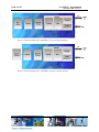
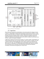
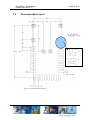
Anaren Integrated Radio A1101R09x Users Manual Release Date 02/10/11 THIS PAGE LEFT INTENTIONALLY BLANK iii Users Manual Models A1101R09A and A1101R09C Contents 1. Overview ............................................................................................................................................... 1.1. A1101R09A ................................................................................................................................... 5 1.2. A1101R09C ................................................................................................................................... 5 1.3. Features ........................................................................................................................................ 6 1.4. Theory of Operation....................................................................................................................... 6 1.4.1. Typical Flow ........................................................................................................................ 9 1.5. Applications ................................................................................................................................. 11 2. Product Approvals ............................................................................................................................ 12 2.1. USA (Federal Communications Commission, FCC, ) ............................................................ 12 2.1.1. FCC Labeling Requirements ............................................................................................. 12 2.1.2. End User Manual .............................................................................................................. 13 2.1.3. RF Exposure ..................................................................................................................... 13 2.2. Canada (Industry Canada, IC) .................................................................................................... 14 2.3. Potential Interference Sources .................................................................................................... 15 2.3.1. Time critical data ............................................................................................................... 15 2.4. Approved Usage .......................................................................................................................... 15 2.4.1. USA & Canada .................................................................................................................. 16 3. Electrical Characteristics .................................................................................................................. 18 3.1. Absolute Maximum Ratings ......................................................................................................... 18 3.2. Operating Conditions ................................................................................................................... 18 3.3. Pin Out ......................................................................................................................................... 19 3.4. Recommended Layout ................................................................................................................ 21 3.5. Power Supply Considerations ..................................................................................................... 23 THIS PAGE LEFT INTENTIONALLY BLANK A1101R09x – Users Manual Release Date 02/10/11 Page 5 of 26 1. Overview The A1101R09A and A1101R09C are surface mount modules – each with an integrated crystal, internal voltage regulator, matching circuitry and filtering. The A1101R09A has an integral antenna, whereas the A1101R09C utilizes an external antenna through a U.FL connector (see Table 1). The modules operate in the US 902 – 928MHz ISM band and are ideal for achieving low power wireless connectivity without having to deal with extensive RF, antenna design and regulatory compliance, allowing quick time to market. The modules are 100% tested to provide consistent performance. The A1101R09A and A1101R09C have received regulatory approvals for modular devices in the United States (FCC) and Canada under Industry Canada (IC) Radio Standards Specification (RSS) RSS-210 and RSS-Gen. The modular approval allows the OEM or end user to place either an A1101R09A or an A1101R09C with an approved antenna inside a finished product without having to perform costly regulatory testing for an intentional radiator. Section 2 has information on the requirements for the end user/integrator must fulfill to use the modules without intentional radiator regulatory testing. The A1101R09A and A1101R09C are based on the CC1101 transceiver IC from Texas Instruments. All control lines for the transceiver are provided at module level for full control of its operation. Please see the CC1101 data sheet (www.ti.com) for how to control the modules. Please see section 8 for the recommended register settings to achieve optimal performance and regulatory compliance. The A1101R09A measure 9x16x2.5mm and A1101R09C measures 9x12x2.5mm. The modules are footprint compatible with each other. 1.1. A1101R09A The A1101R09A has an integral antenna, providing high efficiency and near omni-directional radiation pattern. This approach offers the lowest system cost when the application allows collocation of radio and antenna. 1.2. A1101R09C The A1101R09C has a compact antenna connector that allows for locating the antenna away from the module due to form/function or in order to exit a metal enclosure, see figure 6 – figure 9 for more information on antenna location and enclosure considerations. Page 6 of 26 1.3. A1101R09x – Users Manual Release Date 02/10/11 Features Features: • • • • • • • • • • • • • • • • • • • • • Benefits Summary: Frequency range: 902-928 MHz Ultra small package size ¾ A1101R09C : 9mm x 12mm x 2.5mm ¾ A1101R09A : 9mm x 16mm x 2.5mm Impedance controlled multi-layer PCB Shielded Package 1.8 to 3.3 V operation SPI Interface ROHS Compliant LGA Footprint Low Power Consumption Regulatory approvals for FCC Digital RSSI output Programmable channel filter bandwidth Programmable output power up to +10 dBm High sensitivity (–104 dBm at 1.2 kBaud, 1% packet error rate) Low current consumption (14.4 mA in RX, 1.2kBaud, input well above sensitivity limit) Fast startup time: 240us from SLEEP to Rx or Tx mode Separate 64 byte Rx and Tx FIFOs Data Rate: 1.2 – 500 Kbit/Sec Programmable data rate from 1.2 to 500 kBaud Sleep state: 0.4µA Idle State: 1.7mA 1.4. • • • • • • • • Operating temperature -40 to +85C 100% RF Tested in production Common footprint for all family members No RF engineering experience necessary Only requires a 2 layer PCB implementation Excellent receiver selectivity and blocking Performance Suited for systems compliant with FCC CFR47 Part 15.247a2 and 15.249 (US) and Canada under Industry Canada (IC) Radio Standards Specification (RSS) RSS-210 and RSS-Gen. No regulatory “Intentional radiator” testing required to integrate module into end product. Simple certification labeling replaces testing. Theory of Operation The A1101R09A and A1101R09C are for low power wireless applications in the US 902 – 928MHz ISM band. The devices can be used to implement a variety of networks, including; point to point, point to multipoint, peer to peer and mesh networks. The A1101R09A and A1101R09C both interface to an application microcontroller via an SPI bus. Physical and MAC layer functionality are accessed via the SPI bus through addressable registers as well as execution commands. Data received, or to be transmitted, are also accessed through the SPI bus and are implemented as a FIFO register (64 bytes each for Tx and Rx). A1101R09x – Users Manual Release Date 02/10/11 Page 7 of 26 To transmit, a frame of data is placed in the FIFO; this may include a destination address. A transmit command is given, which will transmit the data according to the initial setup of the registers. To receive data, a receive command is given, which enables the unit to “listen” for a transmission; when such a transmission occurs, it places the received frame in the FIFO. When neither transmit or receive are required, the device can enter either an Idle mode, from which it can quickly re-enter receive, a transmit mode, or a low power sleep mode from which a crystal startup is required prior to transmit or receive operation. Below is a block diagram for each of the A1101R09A and A1101R09C modules. • Antenna o The antenna couples energy between the air and the AIR module. For applications where installations are done by an end user (non-professional), an omni-directional antenna pattern is desired, such that the application will work equally well in any direction. Similarly for peer to peer or point to multipoint applications an omni-directional pattern is desired such that all nodes have a fair chance of communicating. The A1101R09A module has an integral antenna that is near omni-directional, whereas the A1101R09C has approved antenna options ranging from near omni-directional to shaped front/back patterns (useful for inline, professional installations). Note that the end radiation pattern depends not only on the antenna, but also on the ground plane, enclosure and installation environment. • Filtering o Filtering removes spurious signals to comply with regulatory intentional radiator requirements. • Matching o Matching provides the correct loading of the transmit amplifier to achieve the highest output power, as well as the correct loading for the receive LNA to achieve the best sensitivity. • Physical o The physical layer provides conversions between data, symbol and RF signal. • MAC o The MAC layer is part of the Logical Link Layer and provides frame handling, addressing and medium access services. • Microcontroller Interface o The microcontroller interface exposes registers and commands for the physical and MAC layers to a microcontroller. • Power Management o Power management ensures a stable supply for the internal functions, as well as providing means for a low power sleep mode (in which case, most of the transceiver is power off). Page 8 of 26 A1101R09x – Users Manual Release Date 02/10/11 Figure 1 The functionality of the A1101R09A, using an integral antenna Figure 2 The functionality of the A1101R09C, using an external antenna. A1101R09x – Users Manual Release Date 02/10/11 Page 9 of 26 Figure 3 Transceiver IC block diagram. 1.4.1. Typical Flow After initial setup of registers for desired behavior, the normal operation flow diagram is shown in Figure 4. In applications of infrequent data transmissions, the transceiver would be in “sleep” mode to save power (400nA). From there it would awaken and then enter “idle” mode. As part of the wake up process the crystal oscillator is started (~240µs) and the digital microcontroller interface is powered up. Before transmit or receive, the frequency synthesizer needs to be started (“FS_Wakeup”) and, having been powered off (or idle for a while), the control loop of the VCO/PLL needs to be calibrated (“calibrate”). A data frame is loaded into the transmit FIFO and the “TX” mode is entered. The transceiver will transmit the data and enter “idle” mode after completion. When transmit is complete “RX” mode is entered to wait for the acknowledge frame. Once a frame is received, the transceiver will again enter “idle” mode. If no acknowledge frame is received within a given timeout, the data frame would be re-transmitted. If the acknowledge frame indicates that the data was received, the next data frame will be transmitted. After the last data frame has been transmitted successfully, the transceiver will again be put in “sleep” mode. Page 10 of 26 Medium access Figure 4 Transceiver state diagram A1101R09x – Users Manual Release Date 02/10/11 A1101R09x – Users Manual Release Date 02/10/11 1.5. Applications Ultra low-power wireless applications, operating in the 902-928 MHz ISM band. Wireless alarm and security systems Industrial monitoring and control Wireless sensor networks AMR – Automatic Meter Reading Home and building automation Existing applications where simple upgrade to wireless is desired Page 11 of 26 Page 12 of 26 A1101R09x – Users Manual Release Date 02/10/11 2. Product Approvals The A1101R09A and A1101R09C have been designed to meet most national regulations for worldwide ISM-band use. In particular, the radio modules have been certified to the following standards. 2.1. USA (Federal Communications Commission, FCC, ) The A1101R09A, with integrated antenna, as well as the A1101R09C, used with the antennae listed in Table 1 below, have been tested to comply with FCC Part 15 - 15.247(a2) and 15.247(b) and 15.249 “Intentional Radiators.” The devices meet the requirements for modular transmitter approval as detailed in FCC public notice DA 00-1407 Released: June 26, 2000. The A1101R09A and A1101R09C module can be integrated into a finished product with obtaining subsequent FCC approvals. (15.19a3) The modules comply with part 15 of the FCC rules. Operation is subject to the following two conditions: (1) this device may not cause harmful interference, and (2) this device must accept any interference received, including interference that may cause undesired operation. Anaren FCC ID: X7J-A10040601 Table 1 Approved Antennae Item 1 2 3 Part Number Integral part of A1101R09A 66089-0906 66089-0930 Manufacturer Anaren Anaren Anaren Type Integral Antenna Monopole whip, 6mm lead Monopole whip, 30mm lead Gain 2 3 3 2.1.1. FCC Labeling Requirements The A1101R09A and A1101R09C modules have been labeled with their own FCC ID number and if the FCC ID is not visible when the module is installed inside another device, then the outside of the finished product into which the module is installed must also display a label referring to the enclosed module. This exterior label can use wording such as the following: A1101R09x – Users Manual Release Date 02/10/11 Page 13 of 26 Contains Transmitter Module FCC ID: X7J-A10040601 -orContains FCC ID: X7J-A10040601 This device complies with Part 15 - 15.247(a2) and 15.247(b) and 15.249 of the FCC Rules. Operation is subject to the following two conditions: (1) this device may not cause harmful interference, and (2) this device must accept any interference received, including interference that may cause undesired operation. 2.1.2. End User Manual The end user manual should include the following statement: This equipment has been tested and found to comply with the limits for a Class B digital device, pursuant to part 15 - 15.247(a2) and 15.247(b) and 15.249 of the FCC Rules. These limits are designed to provide reasonable protection against harmful interference in a residential installation. This equipment generates, uses and can radiate radio frequency energy and, if not installed and used in accordance with the instructions, may cause harmful interference to radio communications. However, there is no guarantee that interference will not occur in a particular installation. If this equipment does cause harmful interference to radio or television reception, which can be determined by turning the equipment off and on, the user is encouraged to try to correct the interference by one or more of the following measures: • • • • Reorient or relocate the receiving antenna. Increase the separation between the equipment and receiver. Connect the equipment into an outlet on a circuit different from that to which the receiver is connected. Consult the dealer or an experienced radio/TV technician for help. 2.1.3. RF Exposure All transmitters regulated by the FCC must comply with RF exposure requirements. OET Bulletin 65 “Evaluating Compliance with FCC Guidelines for Human Exposure to Radio Frequency Electromagnetic Fields” provides assistance in determining whether proposed or existing transmitting facilities, operations or devices comply with limits for human exposure to Radio Frequency (RF) fields adopted by the Federal Communications Commission (FCC). The bulletin offers guidelines and suggestions for evaluating compliance. If appropriate, compliance with exposure guidelines for mobile and unlicensed devices can be accomplished by the use of warning labels and by providing end users with information Page 14 of 26 A1101R09x – Users Manual Release Date 02/10/11 concerning minimum separation distances from transmitting structures and proper installation of antennas. The following statement must be included as a CAUTION statement in manuals and OEM products to alert end users of FCC RF Exposure compliance: To satisfy FCC RF Exposure requirements for mobile and base station transmission devices, a separation distance of 20 cm or more should be maintained between the antenna of this device and persons during operation. To ensure compliance, operation at closer than this distance is not recommended. The antenna(s) used for this transmitter must not be co-located or operating in conjunction with any other antenna or transmitter. If the A1101R09A and A1101R09C module is used in a portable application (antenna is less than 20 cm from persons during operation), the end user is responsible for performing Specific Absorption Rate (SAR) testing in accordance with FCC rules 2.1091. 2.2. Canada (Industry Canada, IC) The A1101R09A and A1101R09C modules has been certified for use in Canada under Industry Canada (IC) Radio Standards Specification (RSS) RSS-210 and RSS-Gen. From section 7.1.1 RSS-Gen, Issue 2, June 2007, Modular Transmitter Approval: Host devices which contain separately certified modules do not need to be recertified, provided that they meet the following conditions: a) The host device, as a stand-alone unit without any separately certified modules, complies with all applicable Radio Standards Specifications. b) The host device and all the separately certified modules it contains jointly meet the RF exposure compliance requirements of RSS-102, if applicable. c) The host device complies with the certification labeling requirements of each of the modules it contains. Note: Compliance of a module in its final configuration is the responsibility of the applicant. A host device will not be considered certified if the instructions regarding antenna configuration provided in the original description, of one or more separately certified modules it contains, were not followed. From section 5.2, RSS-Gen, Issue 2, June 2007, Equipment Labels: All Category I radio equipment intended for use in Canada shall permanently display on each transmitter, receiver, or inseparable combination thereof, the applicant's name (i.e., manufacturer's name, trade name or brand name), model number and certification number. This information shall be affixed in such a manner as not to be removable except by destruction or defacement. The size of the lettering shall be legible without the aid of magnification, but is not required to be larger than 8- A1101R09x – Users Manual Release Date 02/10/11 Page 15 of 26 point font size. If the device is too small to meet this condition, the information can be included in the user manual upon agreement with Industry Canada. Label: Contains IC: 8975A-A10040601 From section 7.1.6, RSS-Gen, Issue 2, June 2007, Digital Circuits: If the device contains digital circuitry that is not directly associated with the radio transmitter, the device shall also have to comply with ICES-003, Class A or B as appropriate, except for ICES-003 labeling requirements. The test data obtained (for the ICES-003 tests) shall be kept by the manufacturer or importer whose name appears on the equipment label, and made available to Industry Canada on request, for as long as the model is being marketed in Canada. For more information see: Industry Canada http://www.ic.gc.ca/ 2.3. • • • Potential Interference Sources Alarm systems o These typically use low duty cycles and are therefore easy to avoid using acknowledge/retransmit methods Car alarms (internal motion sensors) Video surveillance o These are typically operated on a fixed channel determined at installation time and can be avoided by using clear channel assessment. It may be useful to change the channel used by the video surveillance equipment also, if possible. 2.3.1. Time critical data If the user requires specific time critical data throughput that cannot tolerate the delays of potentially many re-transmissions, the user is encouraged to implement an environment-aware algorithm that periodically monitors/scans the frequency band and maintain a list of “best available” channels. 2.4. Approved Usage These radio modules can be used in a variety of physical layer configurations; the following restricts the use to maintain compliance with the above referenced certification bodies. The user is encouraged to use minimum power required to establish a link, thus minimizing interference. Changes or modifications to the module and/or operation outside the limits set forth below are prohibited and could void the user’s authority to operate the modules. Page 16 of 26 A1101R09x – Users Manual Release Date 02/10/11 Uses of these radio modules are limited to the following frequency ranges and modulation settings. Using the radio modules outside of these limitations are prohibited and could void the user’s authority to operate the modules. The user should use one of the register configurations listed below. Anaren provides register setting files for optimal performance and compliance for each of the data rates given in the following at www.anaren.com. 2.4.1. USA & Canada Within the USA and Canada, the modules have been approved for use as digitally modulated transmitters, for which they must have a minimum occupied bandwidth (6dB) of 500kHz. In addition, the spectral density may not exceed 8dBm/3kHz and the total output power including antenna gain may not exceed 1W. The following table shows configurations that are compliant with this use and the expected performance. In a frequency-agile implementation or an implementation with multiple systems sharing the same location, using 2FSK or GFSK, the user is encouraged to only use even channel numbers to avoid overlapping channels (127 channels would thus be available). In a frequency-agile implementation or an implementation with multiple systems sharing the same location, using MSK, the user is encouraged to only use every 3rd or 4th channel to avoid overlapping channels (85 or 64 channels would thus be available). It is encouraged to use a medium access technique which should include addressing of individual transceiver nodes; and should include a combination of a clear channel assessment, transmit and detect, or a frequency hopping method. This ensures that the un-licensed band can be shared with other systems/applications. A1101R09x – Users Manual Release Date 02/10/11 Page 17 of 26 The field strengths of the emissions from intentional radiators shall have Fundamental field strength of 50mv/meter, wherein the receiver antenna is kept at 3meter distance from the radiator antenna. Page 18 of 26 A1101R09x – Users Manual Release Date 02/10/11 3. Electrical Characteristics 3.1. Absolute Maximum Ratings Under no circumstances must the absolute maximum ratings given in Table 2 be violated. Stress exceeding one or more of the limiting values may cause permanent damage to the device. Caution! ESD sensitive device. Precaution should be used when handling the device in order to prevent permanent damage. Table 2 Absolute Maximum Ratings 3.2. Operating Conditions A1101R09x – Users Manual Release Date 02/10/11 3.3. Page 19 of 26 Pin Out The A1101R09A and A1101R09C radio modules share a common pin-out and foot print, that is also shared by Anaren modules using other frequencies -- thus enabling easy changeover from one to another, e.g. if changing the frequency, antenna scheme, or adaptive antenna tuning is desired. Below the common footprint are shown. Pin # 1 Pin Name DNC Pin Type NC 2 DNC NC 3 DNC NC 4 NC NC 5 NC NC 6 NC NC 7 Vdcoup1 Analog Description Do Not Connect. Internal GND connection used during testing, not recommended to connect to main GND. Do Not Connect. Internal RF output connection used during test. Connecting this pin to anything will require recertification for intentional radiators. Do Not Connect. Internal GND connection used during testing, not recommended to connect to main GND. No Connect, the pin is not connected internally, but is reserved for future expansion. It is recommended not to connect this pin to anything. No Connect, the pin is not connected internally, but is reserved for future expansion. It is recommended not to connect this pin to anything. No Connect, the pin is not connected internally, but is reserved for future expansion. It is recommended not to connect this pin to anything. Optional decoupling of the modules internal Vdd supply. It Page 20 of 26 8 9 A1101R09x – Users Manual Release Date 02/10/11 14 15 Ground Digital Input MISO/GDO1 Digital Output MOSI Digital Input _CSN Digital Input GDO0 Digital I/O (Analog output) GDO2 Digital I/O Vdcoup2 Analog 16 NC NC 17 18 GND Vdd 19 NC Ground Power Supply NC 20 NC NC 21 NC NC 22 DNC NC 23 DNC NC 24 DNC NC 10 11 12 13 GND SCLK Table 3 Pin Descriptions is recommended to not connect anything to this pin. In particular noisy environment this pin can be used to further reduce the noise on the modules internal Vdd, please see section 3.4 for further information. One of two primary ground pins SPI bus clock signal SPI bus data out from radio when CSN is low, and general purpose I/O pin when CSN is high SPI bus data into radio SPI bus select (active low) General purpose port General purpose port Optional decoupling of the modules internal Vdd supply. It is recommended to not connect anything to this pin. In particular noisy environment this pin can be used to further reduce the noise on the modules internal Vdd, please see section 3.4 for further information. No Connect, the pin is not connected internally, but is reserved for future expansion. It is recommended not to connect this pin to anything. One of two primary ground pins Power supply pin No Connect, the pin is not connected internally, but is reserved for future expansion. It is recommended not to connect this pin to anything. No Connect, the pin is not connected internally, but is reserved for future expansion. It is recommended not to connect this pin to anything. No Connect, the pin is not connected internally, but is reserved for future expansion. It is recommended not to connect this pin to anything. Do Not Connect. Internal GND connection used during testing, not recommended to connect to main GND. No Connect, the pin is not connected internally, but is reserved for future expansion. It is recommended not to connect this pin to anything. Do Not Connect. Internal GND connection used during testing, not recommended to connect to main GND. A1101R09x – Users Manual Release Date 02/10/11 3.4. Recommended Layout Figure 5 Recommended PCB layout. Page 21 of 26 Page 22 of 26 A1101R09x – Users Manual Release Date 02/10/11 Figure 6 Mounting the module in a corner Figure 7 Mounting the module along an edge Figure 8 Mounting the module along an edge with overhang. This option is not generally recommended, but is a method to save PCB in an environmentally benign environment Figure 9 Mounting the module along an edge, with a ground plane cut-out. This option degrades range slightly. A1101R09x – Users Manual Release Date 02/10/11 3.5. Page 23 of 26 Power Supply Considerations Noise on the power supply line reduces the sensitivity of a receiver and modulates onto a transmitter’s signal, both of which causes a degradation of link quality and hence a reduction in range. The A1101R09A and A1101R09C radio modules each have an integral ferrite bead in the supply line from pin 18 (Vdd) and decoupling capacitance to reduce any noise on the incoming power supply line. This arrangement will eliminate most supply voltage noise. In particularly noisy environments (switching regulators, motor controls, etc.), it may be necessary to add additional noise reduction means. Pin 7 (Vdcoup1) is connected to the modules internal supply line after the ferrite bead and decoupling capacitors and can be used to probe the noise at module level. The noise level measured on pin 7 should not exceed 120mVpp when in transmit or receive mode; it may however exceed this value when setting up or accessing data to/from the FIFOs, while not actively transmitting or receiving. If the level measured is exceeding the above limit, steps should be taken to ensure maximum range, including: • • • Adding decoupling capacitance to pin 7 (Vdcoup1). Adding additional filtering in the supply line. Adding an LDO in the supply line (the TPS731xx low Dropout Regulator from TI is recommended). Page 24 of 26 A1101R09x – Users Manual Release Date 02/10/11 HISTORY Date 07/17/10 08/23/10 11/19/10 02/10/11 Author Richardson Richardson Richardson Richardson Change Note No./Notes Initial Draft Initial Release Formatting applied – no content change Corrected typographic error THIS PAGE LEFT INTENTIONALLY BLANK Thank you for learning more about the Anaren Integrated Radio (AIR) module line. If you have additional questions, need samples, or would like a quote – please do not hesitate to email the AIR team at [email protected] or contact any of these authorized distributors of the AIR product line. Worldwide North America Anaren Microwave, Inc. 6635 Kirkville Road East Syracuse, NY 13057 Tel: +1 315 432 8909 +1 800 411 6596 Fax: +1 315 432 8970 Anaren Microwave (Europe), Inc. 12 Somerset House, Suite 16 & 17 Hussar Court, Waterlooville Hampshire, England P07-7SG Tel: +44 2392 232392 Fax: +44 2392 251369 Worldwide Anaren Communication Suzhou Co. Ltd. No. 5 Chun Hui Road Wei Ting, Suzhou Industrial Park Suzhou 215122, PR China Tel: +86 512 6287 6400 Fax: +86 512 6274 9283