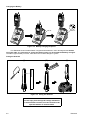
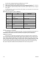
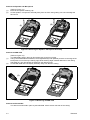
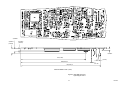
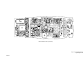
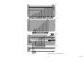
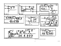
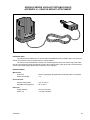
1
SRP8000 SERIES
VHF/UHF PORTABLE RADIO
SERVICE MANUAL
TP0332/2
intro.fm Page 1 Wednesday, August 5, 1998 10:39 AM
Introduction
Simoco Europe Ltd is a leading manufacturer of
professional mobile radio communications with
more than fifty years experience of designing,
manufacturing, installing and maintaining their
product range.
With an enviable pedigree, Simoco Europe Ltd
leads the field for innovation and quality; is fully
committed in design, development and enhancing standards which included POCSAG and
MPT1327. Simoco is deeply involved in TETRA
digital technology; pioneering its development
since 1990.
Simoco's products are backed by a world-wide
capability in system planning, installation and
commissioning, plus an after-sales service
organisation second to none.
The 'Simoco' name is synonymous with
outstanding technological innovation,
achievement and quality for mobile radio
communications systems world-wide that is
wholly dedicated to Customer satisfaction.
Amendspine.fm Page 1 Wednesday, August 5, 1998 10:42 AM
The performance figures quoted are subject to normal manufacturing and service tolerances. The right is
reserved to alter the equipment described in this manual in the light of future technical development.
WARNING
The Battery Chargers which form part of this equipment are designed to
meet relevant safety requirements.
If it is necessary to replace any safety-conscious component the
correct item MUST be fitted. Ensure that all insulators or covers are
fitted after servicing. Check that all warning labels are in place.
If any re-wiring of the mains input supply cables is necessary, the
specified type must be used and alterations to the routeing or
connections must not be made.
WARNING
NICAD batteries are used with this equipment. They must not be
short-circuited or incinerated. They must be disposed of safely in
accordance with the battery manufacturers’ instructions.
SRP8000 SERIES
VHF/UHF PORTABLE RADIO
SERVICE MANUAL
Publication No. TP0332/2
August 1998
Printed in England
© Simoco Europe Ltd. 1998
All rights reserved. No part of this publication may be
reproduced in any form or by any means without the prior permission of
Simoco Europe Ltd.
TP0332/2
1
AMENDMENT LIST
Changes made to the equipment described in this publication are published as amendments which
are dated and consecutively numbered.
Reprints will incorporate all amendments, and applicable change notes and service bulletins to date
and entries to this effect will be recorded on the amendment list below.
Each page affected by amendment action will bear the amendment number as a suffix to the
reference number, eg. TP0123/1AM4 indicates that the page has been corrected by amendment
number 4.
The text content of the page that has been affected by the amendment will be indicated by a marker
in the outside margin, starting on the first line and ending on the last line of text affected. This paragraph is
marked as an example.
Amendment packs, where applicable, can be obtained from the Order Desk.
Should it become necessary to raise the issue of a publication, the amendment numbering will
recommence with No. 1.
Amendment No
Date
Initials
July 1998
July 1998
Remarks
Change Notes up to 25 June 98 actioned in this issue.
Service Bulletins up to 17 July 98 actioned in this issue.
ERRORS AND OMISSIONS
The usefulness of this publication depends upon its accuracy. Whilst every endeavour has been
made to eliminate errors, some may exist. It is requested therefore that any errors or omissions noted be
advised as follows:
Please quote:
Please send to:
(1)
(2)
(3)
(4)
Simoco Europe Ltd,
Technical Publications Department,
P.O. Box 24,
St Andrews Road,
Cambridge, CB4 1DP,
England.
2
Title of publication
TP Ref No
Last amendment No. received.
Page and/or Figure No. in error.
TP0332/2
SP8000 SERIES
VHF/UHF PORTABLE RADIO
CONTENTS
Page
PRELIMINARY
PRODUCT SUPPORT POLICY . . . . . . . . . . . . . . . . . . . . . . . . . . . . . . . . . . . . . . . . . . . . . . . . . (i)
Sevice Concept . . . . . . . . . . . . . . . . . . . . . . . . . . . . . . . . . . . . . . . . . . . . . . . . . . . . . . . . . . . . . . (i)
Warranty . . . . . . . . . . . . . . . . . . . . . . . . . . . . . . . . . . . . . . . . . . . . . . . . . . . . . . . . . . . . . . . . . . . (i)
Service . . . . . . . . . . . . . . . . . . . . . . . . . . . . . . . . . . . . . . . . . . . . . . . . . . . . . . . . . . . . . . . . . . . . (i)
Service Level 1 . . . . . . . . . . . . . . . . . . . . . . . . . . . . . . . . . . . . . . . . . . . . . . . . . . . . . . . . . (i)
Service Level 2 . . . . . . . . . . . . . . . . . . . . . . . . . . . . . . . . . . . . . . . . . . . . . . . . . . . . . . . . . (i)
Service Level 3 . . . . . . . . . . . . . . . . . . . . . . . . . . . . . . . . . . . . . . . . . . . . . . . . . . . . . . . . . (i)
SERVICE BULLETINS . . . . . . . . . . . . . . . . . . . . . . . . . . . . . . . . . . . . . . . . . . . . . . . . . . . . . . . . (ii)
SECTION 1 - GENERAL INFORMATION
INTRODUCTION . . . . . . . . . . . . . . . . . . . . . . . . . . . . . . . . . . . . . . . . . . . . . . . . . . . . . . . . . . . . .
SUMMARY OF DATA . . . . . . . . . . . . . . . . . . . . . . . . . . . . . . . . . . . . . . . . . . . . . . . . . . . . . . . . .
General . . . . . . . . . . . . . . . . . . . . . . . . . . . . . . . . . . . . . . . . . . . . . . . . . . . . . . . . . . . . . . . . . . . .
Receiver . . . . . . . . . . . . . . . . . . . . . . . . . . . . . . . . . . . . . . . . . . . . . . . . . . . . . . . . . . . . . . . . . . .
Transmitter . . . . . . . . . . . . . . . . . . . . . . . . . . . . . . . . . . . . . . . . . . . . . . . . . . . . . . . . . . . . . . . . .
ASSOCIATED EQUIPMENTS . . . . . . . . . . . . . . . . . . . . . . . . . . . . . . . . . . . . . . . . . . . . . . . . . . .
ANCILLARY ITEMS . . . . . . . . . . . . . . . . . . . . . . . . . . . . . . . . . . . . . . . . . . . . . . . . . . . . . . . . . .
EQUIPMENT VARIATION . . . . . . . . . . . . . . . . . . . . . . . . . . . . . . . . . . . . . . . . . . . . . . . . . . . . . .
CTCSS TONE FREQUENCIES . . . . . . . . . . . . . . . . . . . . . . . . . . . . . . . . . . . . . . . . . . . . . . . . . .
SELCALL TONE FREQUENCIES . . . . . . . . . . . . . . . . . . . . . . . . . . . . . . . . . . . . . . . . . . . . . . .
1.1
1.2
1.2
1.2
1.3
1.3
1.3
1.4
1.5
1.5
SECTION 2 - COMMISSIONING
UNPACKING . . . . . . . . . . . . . . . . . . . . . . . . . . . . . . . . . . . . . . . . . . . . . . . . . . . . . . . . . . . . . . . .
COMMISSIONING . . . . . . . . . . . . . . . . . . . . . . . . . . . . . . . . . . . . . . . . . . . . . . . . . . . . . . . . . . . .
Warning Label . . . . . . . . . . . . . . . . . . . . . . . . . . . . . . . . . . . . . . . . . . . . . . . . . . . . . . . . . . . . . .
Charging the Battery . . . . . . . . . . . . . . . . . . . . . . . . . . . . . . . . . . . . . . . . . . . . . . . . . . . . . . . . .
Fitting the Antenna . . . . . . . . . . . . . . . . . . . . . . . . . . . . . . . . . . . . . . . . . . . . . . . . . . . . . . . . . .
Fitting the Wrist Lanyard . . . . . . . . . . . . . . . . . . . . . . . . . . . . . . . . . . . . . . . . . . . . . . . . . . . . . .
Fitting a Battery . . . . . . . . . . . . . . . . . . . . . . . . . . . . . . . . . . . . . . . . . . . . . . . . . . . . . . . . . . . . .
LCD DISPLAY . . . . . . . . . . . . . . . . . . . . . . . . . . . . . . . . . . . . . . . . . . . . . . . . . . . . . . . . . . . . . . .
17 x 7 Matrix . . . . . . . . . . . . . . . . . . . . . . . . . . . . . . . . . . . . . . . . . . . . . . . . . . . . . . . . . . . . . . . .
Alphanumeric Characters . . . . . . . . . . . . . . . . . . . . . . . . . . . . . . . . . . . . . . . . . . . . . . . . . . . . .
Message . . . . . . . . . . . . . . . . . . . . . . . . . . . . . . . . . . . . . . . . . . . . . . . . . . . . . . . . . . . . . . . . . . .
Battery Level . . . . . . . . . . . . . . . . . . . . . . . . . . . . . . . . . . . . . . . . . . . . . . . . . . . . . . . . . . . . . . .
Loudspeaker . . . . . . . . . . . . . . . . . . . . . . . . . . . . . . . . . . . . . . . . . . . . . . . . . . . . . . . . . . . . . . .
Signal Strength . . . . . . . . . . . . . . . . . . . . . . . . . . . . . . . . . . . . . . . . . . . . . . . . . . . . . . . . . . . . .
FUNCTION KEYS . . . . . . . . . . . . . . . . . . . . . . . . . . . . . . . . . . . . . . . . . . . . . . . . . . . . . . . . . . . .
NUMERIC KEYPAD . . . . . . . . . . . . . . . . . . . . . . . . . . . . . . . . . . . . . . . . . . . . . . . . . . . . . . . . . .
LED . . . . . . . . . . . . . . . . . . . . . . . . . . . . . . . . . . . . . . . . . . . . . . . . . . . . . . . . . . . . . . . . . . . . . . .
Channel LEDs (SRP8010 only) . . . . . . . . . . . . . . . . . . . . . . . . . . . . . . . . . . . . . . . . . . . . . . . . .
AUDIBLE ALERTS . . . . . . . . . . . . . . . . . . . . . . . . . . . . . . . . . . . . . . . . . . . . . . . . . . . . . . . . . . .
CUSTOMIZATION DATA . . . . . . . . . . . . . . . . . . . . . . . . . . . . . . . . . . . . . . . . . . . . . . . . . . . . . . .
2.1
2.1
2.1
2.2
2.2
2.3
2.4
2.4
2.4
2.5
2.5
2.5
2.5
2.5
2.5
2.5
2.6
2.6
2.7
2.7
SECTION 3 - TECHNICAL DESCRIPTION
INTRODUCTION . . . . . . . . . . . . . . . . . . . . . . . . . . . . . . . . . . . . . . . . . . . . . . . . . . . . . . . . . . . . .
RADIO PCB DESCRIPTION . . . . . . . . . . . . . . . . . . . . . . . . . . . . . . . . . . . . . . . . . . . . . . . . . . . .
Overall Block Schematic Diagram . . . . . . . . . . . . . . . . . . . . . . . . . . . . . . . . . . . . . . . . . . . . . .
POWER SUPPLIES AND ON/OFF CONTROL . . . . . . . . . . . . . . . . . . . . . . . . . . . . . . . . . . . . .
Turning On . . . . . . . . . . . . . . . . . . . . . . . . . . . . . . . . . . . . . . . . . . . . . . . . . . . . . . . . . . . . . . . . .
Turning Off . . . . . . . . . . . . . . . . . . . . . . . . . . . . . . . . . . . . . . . . . . . . . . . . . . . . . . . . . . . . . . . . .
Reset Circuit . . . . . . . . . . . . . . . . . . . . . . . . . . . . . . . . . . . . . . . . . . . . . . . . . . . . . . . . . . . . . . . .
3.1
3.1
3.1
3.2
3.2
3.3
3.3
TP0332/2
(i)
RECEIVER . . . . . . . . . . . . . . . . . . . . . . . . . . . . . . . . . . . . . . . . . . . . . . . . . . . . . . . . . . . . . . . . .
Antenna Filter . . . . . . . . . . . . . . . . . . . . . . . . . . . . . . . . . . . . . . . . . . . . . . . . . . . . . . . . . . . . . .
First Tracking Filter . . . . . . . . . . . . . . . . . . . . . . . . . . . . . . . . . . . . . . . . . . . . . . . . . . . . . . . . . .
RF Amplifier . . . . . . . . . . . . . . . . . . . . . . . . . . . . . . . . . . . . . . . . . . . . . . . . . . . . . . . . . . . . . . . .
Second Tracking Filter . . . . . . . . . . . . . . . . . . . . . . . . . . . . . . . . . . . . . . . . . . . . . . . . . . . . . . .
First Mixer . . . . . . . . . . . . . . . . . . . . . . . . . . . . . . . . . . . . . . . . . . . . . . . . . . . . . . . . . . . . . . . . .
First IF Filters and IF Amplifier . . . . . . . . . . . . . . . . . . . . . . . . . . . . . . . . . . . . . . . . . . . . . . . .
Second Mixer, Second IF Amplifier and Ceramic Filters . . . . . . . . . . . . . . . . . . . . . . . . . . . .
Squelch . . . . . . . . . . . . . . . . . . . . . . . . . . . . . . . . . . . . . . . . . . . . . . . . . . . . . . . . . . . . . . . . . . .
Page
3.4
3.4
3.4
3.4
3.4
3.4
3.4
3.5
3.5
TRANSMITTER . . . . . . . . . . . . . . . . . . . . . . . . . . . . . . . . . . . . . . . . . . . . . . . . . . . . . . . . . . . . . 3.6
FREQUENCY GENERATION . . . . . . . . . . . . . . . . . . . . . . . . . . . . . . . . . . . . . . . . . . . . . . . . . . . 3.6
CONTROL PROCESSOR SYSTEM . . . . . . . . . . . . . . . . . . . . . . . . . . . . . . . . . . . . . . . . . . . . . . 3.9
BASEBAND AUDIO AND SIGNALLING . . . . . . . . . . . . . . . . . . . . . . . . . . . . . . . . . . . . . . . . . . 3.10
Clock Generation . . . . . . . . . . . . . . . . . . . . . . . . . . . . . . . . . . . . . . . . . . . . . . . . . . . . . . . . . . . 3.10
Receive Audio Path . . . . . . . . . . . . . . . . . . . . . . . . . . . . . . . . . . . . . . . . . . . . . . . . . . . . . . . . . . 3.10
Transmit Audio Path . . . . . . . . . . . . . . . . . . . . . . . . . . . . . . . . . . . . . . . . . . . . . . . . . . . . . . . . . 3.10
Signalling Facilities . . . . . . . . . . . . . . . . . . . . . . . . . . . . . . . . . . . . . . . . . . . . . . . . . . . . . . . . . 3.12
CTCSS . . . . . . . . . . . . . . . . . . . . . . . . . . . . . . . . . . . . . . . . . . . . . . . . . . . . . . . . . . . . . . . 3.12
Selcall/DTMF . . . . . . . . . . . . . . . . . . . . . . . . . . . . . . . . . . . . . . . . . . . . . . . . . . . . . . . . . . 3.12
FFSK . . . . . . . . . . . . . . . . . . . . . . . . . . . . . . . . . . . . . . . . . . . . . . . . . . . . . . . . . . . . . . . . 3.12
DTMF Encoding . . . . . . . . . . . . . . . . . . . . . . . . . . . . . . . . . . . . . . . . . . . . . . . . . . . . . . . 3.12
USER INTERFACE . . . . . . . . . . . . . . . . . . . . . . . . . . . . . . . . . . . . . . . . . . . . . . . . . . . . . . . . . . . 3.13
Smart Interface . . . . . . . . . . . . . . . . . . . . . . . . . . . . . . . . . . . . . . . . . . . . . . . . . . . . . . . . . . . . . 3.13
EXT_LSA, EXT_LSB . . . . . . . . . . . . . . . . . . . . . . . . . . . . . . . . . . . . . . . . . . . . . . . . . . . . 3.15
MIC1 . . . . . . . . . . . . . . . . . . . . . . . . . . . . . . . . . . . . . . . . . . . . . . . . . . . . . . . . . . . . . . . . . 3.15
RS232/IIC Serial Communications . . . . . . . . . . . . . . . . . . . . . . . . . . . . . . . . . . . . . . . . . . . . . 3.15
Loudspeaker / Microphone Flexi Connector . . . . . . . . . . . . . . . . . . . . . . . . . . . . . . . . . . . . . 3.15
PTT and Side Key Press Detection . . . . . . . . . . . . . . . . . . . . . . . . . . . . . . . . . . . . . . . . . . . . . 3.15
MMI Display and Keypad (not fitted on SRP8010) . . . . . . . . . . . . . . . . . . . . . . . . . . . . . . . . . 3.16
Processor Interface to LCD Display . . . . . . . . . . . . . . . . . . . . . . . . . . . . . . . . . . . . . . . . . . . . 3.16
Key Press Detection . . . . . . . . . . . . . . . . . . . . . . . . . . . . . . . . . . . . . . . . . . . . . . . . . . . . . . . . . 3.16
Backlighting . . . . . . . . . . . . . . . . . . . . . . . . . . . . . . . . . . . . . . . . . . . . . . . . . . . . . . . . . . . . . . . 3.17
TRICKLE CHARGER . . . . . . . . . . . . . . . . . . . . . . . . . . . . . . . . . . . . . . . . . . . . . . . . . . . . . . . . . 3.18
BATTERY CONNECTIONS . . . . . . . . . . . . . . . . . . . . . . . . . . . . . . . . . . . . . . . . . . . . . . . . . . . . . 3.18
Battery Connections to Radio . . . . . . . . . . . . . . . . . . . . . . . . . . . . . . . . . . . . . . . . . . . . . . . . . 3.18
Battery Connections to Charger. . . . . . . . . . . . . . . . . . . . . . . . . . . . . . . . . . . . . . . . . . . . . . . . 3.18
SECTION 4 - SERVICING
DIS-ASSEMBLY . . . . . . . . . . . . . . . . . . . . . . . . . . . . . . . . . . . . . . . . . . . . . . . . . . . . . . . . . . . . .
Remove the Battery . . . . . . . . . . . . . . . . . . . . . . . . . . . . . . . . . . . . . . . . . . . . . . . . . . . . . . . . .
Remove the Antenna and On/Off/Volume Control Knob . . . . . . . . . . . . . . . . . . . . . . . . . . . .
Remove the Metal Frame Assembly . . . . . . . . . . . . . . . . . . . . . . . . . . . . . . . . . . . . . . . . . . . .
Remove the Metal Screen from the Radio PCB and Frame Assembly . . . . . . . . . . . . . . . .
Remove the Radio PCB . . . . . . . . . . . . . . . . . . . . . . . . . . . . . . . . . . . . . . . . . . . . . . . . . . . . . .
Remove the Speaker and Microphone . . . . . . . . . . . . . . . . . . . . . . . . . . . . . . . . . . . . . . . . . .
Remove the MMI PCB . . . . . . . . . . . . . . . . . . . . . . . . . . . . . . . . . . . . . . . . . . . . . . . . . . . . . . . .
Remove the Switch Mat . . . . . . . . . . . . . . . . . . . . . . . . . . . . . . . . . . . . . . . . . . . . . . . . . . . . . .
RE-ASSEMBLY . . . . . . . . . . . . . . . . . . . . . . . . . . . . . . . . . . . . . . . . . . . . . . . . . . . . . . . . . . . . .
TEST INFORMATION, EQUIPMENT AND DATA . . . . . . . . . . . . . . . . . . . . . . . . . . . . . . . . . . .
Test Information . . . . . . . . . . . . . . . . . . . . . . . . . . . . . . . . . . . . . . . . . . . . . . . . . . . . . . . . . . . .
CALIBRATION . . . . . . . . . . . . . . . . . . . . . . . . . . . . . . . . . . . . . . . . . . . . . . . . . . . . . . . . . . . . . .
Test Equipment . . . . . . . . . . . . . . . . . . . . . . . . . . . . . . . . . . . . . . . . . . . . . . . . . . . . . . . . . . . . .
(ii)
4.1
4.1
4.1
4.2
4.2
4.3
4.4
4.4
4.4
4.5
4.5
4.5
4.5
4.6
TP0332/2
Page
ALIGNING THE TRANSCEIVER USING THE ALIGNMENT TOOL . . . . . . . . . . . . . . . . . . . . . 4.7
Receiver Tests . . . . . . . . . . . . . . . . . . . . . . . . . . . . . . . . . . . . . . . . . . . . . . . . . . . . . . . . . . . . . . 4.7
Sensitivity . . . . . . . . . . . . . . . . . . . . . . . . . . . . . . . . . . . . . . . . . . . . . . . . . . . . . . . . . . . . 4.7
Supply Input Power . . . . . . . . . . . . . . . . . . . . . . . . . . . . . . . . . . . . . . . . . . . . . . . . . . . . . 4.7
Distortion at Rated Audio Power . . . . . . . . . . . . . . . . . . . . . . . . . . . . . . . . . . . . . . . . . . 4.7
Squelch Function . . . . . . . . . . . . . . . . . . . . . . . . . . . . . . . . . . . . . . . . . . . . . . . . . . . . . . 4.7
Transmitter Tests . . . . . . . . . . . . . . . . . . . . . . . . . . . . . . . . . . . . . . . . . . . . . . . . . . . . . . . . . . . . 4.7
RF Output Power . . . . . . . . . . . . . . . . . . . . . . . . . . . . . . . . . . . . . . . . . . . . . . . . . . . . . . . 4.7
Supply Input Power . . . . . . . . . . . . . . . . . . . . . . . . . . . . . . . . . . . . . . . . . . . . . . . . . . . . . 4.7
Frequency Error . . . . . . . . . . . . . . . . . . . . . . . . . . . . . . . . . . . . . . . . . . . . . . . . . . . . . . . . 4.7
Peak System Deviation . . . . . . . . . . . . . . . . . . . . . . . . . . . . . . . . . . . . . . . . . . . . . . . . . . 4.7
Total Harmonic Distortion . . . . . . . . . . . . . . . . . . . . . . . . . . . . . . . . . . . . . . . . . . . . . . . . 4.7
CTCSS Option Tests . . . . . . . . . . . . . . . . . . . . . . . . . . . . . . . . . . . . . . . . . . . . . . . . . . . . . . . . . 4.7
Selcall Option Tests . . . . . . . . . . . . . . . . . . . . . . . . . . . . . . . . . . . . . . . . . . . . . . . . . . . . . . . . . . 4.7
SECTION 5 - PARTS LIST
Antennae and Batteries . . . . . . . . . . . . . . . . . . . . . . . . . . . . . . . . . . . . . . . . . . . . . . . . . . . . . . . 5.1
Ancillaries . . . . . . . . . . . . . . . . . . . . . . . . . . . . . . . . . . . . . . . . . . . . . . . . . . . . . . . . . . . . . . . . . 5.1
Tranceiver parts . . . . . . . . . . . . . . . . . . . . . . . . . . . . . . . . . . . . . . . . . . . . . . . . . . . . . . . . . . . . . 5.2
SECTION 6 - DIAGRAMS
See LIST OF ILLUSTRATIONS
APPENDIX A - BATTERY CHARGERS
INTRODUCTION . . . . . . . . . . . . . . . . . . . . . . . . . . . . . . . . . . . . . . . . . . . . . . . . . . . . . . . . . . . . .
SPECIFICATION . . . . . . . . . . . . . . . . . . . . . . . . . . . . . . . . . . . . . . . . . . . . . . . . . . . . . . . . . . . . .
INSTALLATION . . . . . . . . . . . . . . . . . . . . . . . . . . . . . . . . . . . . . . . . . . . . . . . . . . . . . . . . . . . . . .
General . . . . . . . . . . . . . . . . . . . . . . . . . . . . . . . . . . . . . . . . . . . . . . . . . . . . . . . . . . . . . . . . . . . .
OPERATION . . . . . . . . . . . . . . . . . . . . . . . . . . . . . . . . . . . . . . . . . . . . . . . . . . . . . . . . . . . . . . . .
Radio with Battery . . . . . . . . . . . . . . . . . . . . . . . . . . . . . . . . . . . . . . . . . . . . . . . . . . . . . . . . . . .
Battery Alone . . . . . . . . . . . . . . . . . . . . . . . . . . . . . . . . . . . . . . . . . . . . . . . . . . . . . . . . . . . . . . .
SERVICE . . . . . . . . . . . . . . . . . . . . . . . . . . . . . . . . . . . . . . . . . . . . . . . . . . . . . . . . . . . . . . . . . . .
Cleaning of Charging Contacts . . . . . . . . . . . . . . . . . . . . . . . . . . . . . . . . . . . . . . . . . . . . . . . .
Sensing Circuits . . . . . . . . . . . . . . . . . . . . . . . . . . . . . . . . . . . . . . . . . . . . . . . . . . . . . . . . . . . .
LED Indications (except single unit charger) . . . . . . . . . . . . . . . . . . . . . . . . . . . . . . . . . . . . .
PARTS LIST . . . . . . . . . . . . . . . . . . . . . . . . . . . . . . . . . . . . . . . . . . . . . . . . . . . . . . . . . . . . . . . .
A.1
A.2
A.2
A.2
A.3
A.3
A.3
A.3
A.3
A.3
A.4
A.4
APPENDIX B - LAPEL SPEAKER / MICROPHONE
INTRODUCTION . . . . . . . . . . . . . . . . . . . . . . . . . . . . . . . . . . . . . . . . . . . . . . . . . . . . . . . . . . . . .
Terminology . . . . . . . . . . . . . . . . . . . . . . . . . . . . . . . . . . . . . . . . . . . . . . . . . . . . . . . . . . . . . . . .
SPECIFICATION . . . . . . . . . . . . . . . . . . . . . . . . . . . . . . . . . . . . . . . . . . . . . . . . . . . . . . . . . . . . .
Microphone . . . . . . . . . . . . . . . . . . . . . . . . . . . . . . . . . . . . . . . . . . . . . . . . . . . . . . . . . . . . . . . .
Loudspeaker . . . . . . . . . . . . . . . . . . . . . . . . . . . . . . . . . . . . . . . . . . . . . . . . . . . . . . . . . . . . . . .
Environmental . . . . . . . . . . . . . . . . . . . . . . . . . . . . . . . . . . . . . . . . . . . . . . . . . . . . . . . . . . . . . .
OPERATION . . . . . . . . . . . . . . . . . . . . . . . . . . . . . . . . . . . . . . . . . . . . . . . . . . . . . . . . . . . . . . . .
Ancillary Type . . . . . . . . . . . . . . . . . . . . . . . . . . . . . . . . . . . . . . . . . . . . . . . . . . . . . . . . . . . . . .
Microphone . . . . . . . . . . . . . . . . . . . . . . . . . . . . . . . . . . . . . . . . . . . . . . . . . . . . . . . . . . . . . . . .
Loudspeaker . . . . . . . . . . . . . . . . . . . . . . . . . . . . . . . . . . . . . . . . . . . . . . . . . . . . . . . . . . . . . . .
PARTS LIST . . . . . . . . . . . . . . . . . . . . . . . . . . . . . . . . . . . . . . . . . . . . . . . . . . . . . . . . . . . . . . . .
B.1
B.1
B.1
B.1
B.2
B.2
B.2
B.2
B.2
B.2
B.3
APPENDIX C - HEADSET
INTRODUCTION . . . . . . . . . . . . . . . . . . . . . . . . . . . . . . . . . . . . . . . . . . . . . . . . . . . . . . . . . . . . .
Terminology . . . . . . . . . . . . . . . . . . . . . . . . . . . . . . . . . . . . . . . . . . . . . . . . . . . . . . . . . . . . . . . .
SPECIFICATION . . . . . . . . . . . . . . . . . . . . . . . . . . . . . . . . . . . . . . . . . . . . . . . . . . . . . . . . . . . . .
Microphone . . . . . . . . . . . . . . . . . . . . . . . . . . . . . . . . . . . . . . . . . . . . . . . . . . . . . . . . . . . . . . . .
Earpiece . . . . . . . . . . . . . . . . . . . . . . . . . . . . . . . . . . . . . . . . . . . . . . . . . . . . . . . . . . . . . . . . . . .
Environmental . . . . . . . . . . . . . . . . . . . . . . . . . . . . . . . . . . . . . . . . . . . . . . . . . . . . . . . . . . . . . .
OPERATION . . . . . . . . . . . . . . . . . . . . . . . . . . . . . . . . . . . . . . . . . . . . . . . . . . . . . . . . . . . . . . . .
C.1
C.1
C.1
C.1
C.2
C.2
C.2
TP0332/2
(iii)
Page
Ancillary Type . . . . . . . . . . . . . . . . . . . . . . . . . . . . . . . . . . . . . . . . . . . . . . . . . . . . . . . . . . . . . . C.2
Microphone . . . . . . . . . . . . . . . . . . . . . . . . . . . . . . . . . . . . . . . . . . . . . . . . . . . . . . . . . . . . . . . . C.2
Earpiece . . . . . . . . . . . . . . . . . . . . . . . . . . . . . . . . . . . . . . . . . . . . . . . . . . . . . . . . . . . . . . . . . . . C.2
PARTS LIST . . . . . . . . . . . . . . . . . . . . . . . . . . . . . . . . . . . . . . . . . . . . . . . . . . . . . . . . . . . . . . . . C.2
APPENDIX D - ALIGNMENT TOOL
INTRODUCTION . . . . . . . . . . . . . . . . . . . . . . . . . . . . . . . . . . . . . . . . . . . . . . . . . . . . . . . . . . . .
Purpose of this Section . . . . . . . . . . . . . . . . . . . . . . . . . . . . . . . . . . . . . . . . . . . . . . . . . . . . . .
Purpose of Alignment Tool . . . . . . . . . . . . . . . . . . . . . . . . . . . . . . . . . . . . . . . . . . . . . . . . . . .
Components Associated with Alignment Tool . . . . . . . . . . . . . . . . . . . . . . . . . . . . . . . . . . . .
Alignment Tool Requirements . . . . . . . . . . . . . . . . . . . . . . . . . . . . . . . . . . . . . . . . . . . . . . . . .
Hardware Requirements . . . . . . . . . . . . . . . . . . . . . . . . . . . . . . . . . . . . . . . . . . . . . . . . . . . . . .
Software Requirements . . . . . . . . . . . . . . . . . . . . . . . . . . . . . . . . . . . . . . . . . . . . . . . . . . . . . .
INSTALLING THE ALIGNMENT TOOL . . . . . . . . . . . . . . . . . . . . . . . . . . . . . . . . . . . . . . . . . . .
Preparation . . . . . . . . . . . . . . . . . . . . . . . . . . . . . . . . . . . . . . . . . . . . . . . . . . . . . . . . . . . . . . . .
Installation . . . . . . . . . . . . . . . . . . . . . . . . . . . . . . . . . . . . . . . . . . . . . . . . . . . . . . . . . . . . . . . . .
Installation Warnings . . . . . . . . . . . . . . . . . . . . . . . . . . . . . . . . . . . . . . . . . . . . . . . . . . . . . . . .
Initialization File . . . . . . . . . . . . . . . . . . . . . . . . . . . . . . . . . . . . . . . . . . . . . . . . . . . . . . . . . . . .
GETTING STARTED . . . . . . . . . . . . . . . . . . . . . . . . . . . . . . . . . . . . . . . . . . . . . . . . . . . . . . . . .
Starting the Alignment Tool . . . . . . . . . . . . . . . . . . . . . . . . . . . . . . . . . . . . . . . . . . . . . . . . . . .
Errors on Starting the Alignment Tool . . . . . . . . . . . . . . . . . . . . . . . . . . . . . . . . . . . . . . . . . .
Multiple Instances . . . . . . . . . . . . . . . . . . . . . . . . . . . . . . . . . . . . . . . . . . . . . . . . . . . . . . . . . . .
Alignment Tool Application Window . . . . . . . . . . . . . . . . . . . . . . . . . . . . . . . . . . . . . . . . . . . .
USING THE ALIGNMENT TOOL . . . . . . . . . . . . . . . . . . . . . . . . . . . . . . . . . . . . . . . . . . . . . . . .
Connecting a Radio . . . . . . . . . . . . . . . . . . . . . . . . . . . . . . . . . . . . . . . . . . . . . . . . . . . . . . . . .
Aligning the Radio . . . . . . . . . . . . . . . . . . . . . . . . . . . . . . . . . . . . . . . . . . . . . . . . . . . . . . . . . .
Using On-line Help . . . . . . . . . . . . . . . . . . . . . . . . . . . . . . . . . . . . . . . . . . . . . . . . . . . . . . . . . .
Quitting the Alignment Tool . . . . . . . . . . . . . . . . . . . . . . . . . . . . . . . . . . . . . . . . . . . . . . . . . . .
Possible Errors on Quitting . . . . . . . . . . . . . . . . . . . . . . . . . . . . . . . . . . . . . . . . . . . . . . . . . . .
BACKGROUND SETTINGS . . . . . . . . . . . . . . . . . . . . . . . . . . . . . . . . . . . . . . . . . . . . . . . . . . . .
Display Settings . . . . . . . . . . . . . . . . . . . . . . . . . . . . . . . . . . . . . . . . . . . . . . . . . . . . . . . . . . . .
Colour Scheme . . . . . . . . . . . . . . . . . . . . . . . . . . . . . . . . . . . . . . . . . . . . . . . . . . . . . . . .
Memory Optimization . . . . . . . . . . . . . . . . . . . . . . . . . . . . . . . . . . . . . . . . . . . . . . . . . . . . . . . .
Optimizing the Disk Cache . . . . . . . . . . . . . . . . . . . . . . . . . . . . . . . . . . . . . . . . . . . . . .
TECHNICAL SUPPORT . . . . . . . . . . . . . . . . . . . . . . . . . . . . . . . . . . . . . . . . . . . . . . . . . . . . . . .
Help Desk and Upgrades . . . . . . . . . . . . . . . . . . . . . . . . . . . . . . . . . . . . . . . . . . . . . . . . . . . . .
Feedback . . . . . . . . . . . . . . . . . . . . . . . . . . . . . . . . . . . . . . . . . . . . . . . . . . . . . . . . . . . . . . . . . .
GLOSSARY . . . . . . . . . . . . . . . . . . . . . . . . . . . . . . . . . . . . . . . . . . . . . . . . . . . . . . . . . . . . . . . .
PARTS LIST . . . . . . . . . . . . . . . . . . . . . . . . . . . . . . . . . . . . . . . . . . . . . . . . . . . . . . . . . . . . . . . .
D.1
D.1
D.1
D.1
D.1
D.1
D.2
D.2
D.2
D.2
D.4
D.4
D.4
D.4
D.4
D.5
D.5
D.5
D.5
D.5
D.5
D.6
D.6
D.6
D.6
D.7
D.7
D.7
D.7
D.7
D.8
D.8
D.8
APPENDIX E - POWER SUPPLY FOR TRICKLE CHARGER
INTRODUCTION . . . . . . . . . . . . . . . . . . . . . . . . . . . . . . . . . . . . . . . . . . . . . . . . . . . . . . . . . . . .
Terminology . . . . . . . . . . . . . . . . . . . . . . . . . . . . . . . . . . . . . . . . . . . . . . . . . . . . . . . . . . . . . . . .
SPECIFICATION . . . . . . . . . . . . . . . . . . . . . . . . . . . . . . . . . . . . . . . . . . . . . . . . . . . . . . . . . . . . .
Electrical . . . . . . . . . . . . . . . . . . . . . . . . . . . . . . . . . . . . . . . . . . . . . . . . . . . . . . . . . . . . . . . . . .
Indicators . . . . . . . . . . . . . . . . . . . . . . . . . . . . . . . . . . . . . . . . . . . . . . . . . . . . . . . . . . . . . . . . . .
Mechanical . . . . . . . . . . . . . . . . . . . . . . . . . . . . . . . . . . . . . . . . . . . . . . . . . . . . . . . . . . . . . . . . .
Environmental . . . . . . . . . . . . . . . . . . . . . . . . . . . . . . . . . . . . . . . . . . . . . . . . . . . . . . . . . . . . . .
OPERATION . . . . . . . . . . . . . . . . . . . . . . . . . . . . . . . . . . . . . . . . . . . . . . . . . . . . . . . . . . . . . . . .
PARTS LIST . . . . . . . . . . . . . . . . . . . . . . . . . . . . . . . . . . . . . . . . . . . . . . . . . . . . . . . . . . . . . . . .
E.1
E.1
E.1
E.1
E.1
E.2
E.2
E.2
E.2
APPENDIX F - PROGRAMMING LEAD
INTRODUCTION . . . . . . . . . . . . . . . . . . . . . . . . . . . . . . . . . . . . . . . . . . . . . . . . . . . . . . . . . . . .
Terminology . . . . . . . . . . . . . . . . . . . . . . . . . . . . . . . . . . . . . . . . . . . . . . . . . . . . . . . . . . . . . . . .
SPECIFICATION . . . . . . . . . . . . . . . . . . . . . . . . . . . . . . . . . . . . . . . . . . . . . . . . . . . . . . . . . . . . .
Mechanical . . . . . . . . . . . . . . . . . . . . . . . . . . . . . . . . . . . . . . . . . . . . . . . . . . . . . . . . . . . . . . . . .
Environmental . . . . . . . . . . . . . . . . . . . . . . . . . . . . . . . . . . . . . . . . . . . . . . . . . . . . . . . . . . . . . .
PARTS LIST . . . . . . . . . . . . . . . . . . . . . . . . . . . . . . . . . . . . . . . . . . . . . . . . . . . . . . . . . . . . . . . .
F.1
F.1
F.1
F.1
F.1
F.2
(iv)
TP0332/2
Page
APPENDIX G - USER MEMORY PLUG
INTRODUCTION . . . . . . . . . . . . . . . . . . . . . . . . . . . . . . . . . . . . . . . . . . . . . . . . . . . . . . . . . . . . . G.1
Terminology . . . . . . . . . . . . . . . . . . . . . . . . . . . . . . . . . . . . . . . . . . . . . . . . . . . . . . . . . . . . . . . . G.1
SPECIFICATION . . . . . . . . . . . . . . . . . . . . . . . . . . . . . . . . . . . . . . . . . . . . . . . . . . . . . . . . . . . . . G.1
Mechanical . . . . . . . . . . . . . . . . . . . . . . . . . . . . . . . . . . . . . . . . . . . . . . . . . . . . . . . . . . . . . . . . . G.1
Environmental . . . . . . . . . . . . . . . . . . . . . . . . . . . . . . . . . . . . . . . . . . . . . . . . . . . . . . . . . . . . . . G.1
DESCRIPTION . . . . . . . . . . . . . . . . . . . . . . . . . . . . . . . . . . . . . . . . . . . . . . . . . . . . . . . . . . . . . . G.2
PARTS LIST . . . . . . . . . . . . . . . . . . . . . . . . . . . . . . . . . . . . . . . . . . . . . . . . . . . . . . . . . . . . . . . . G.2
APPENDIX H - VEHICLE MOUNT ATTACHMENT
INTRODUCTION . . . . . . . . . . . . . . . . . . . . . . . . . . . . . . . . . . . . . . . . . . . . . . . . . . . . . . . . . . . . .
SPECIFICATION . . . . . . . . . . . . . . . . . . . . . . . . . . . . . . . . . . . . . . . . . . . . . . . . . . . . . . . . . . . . .
Mechanical . . . . . . . . . . . . . . . . . . . . . . . . . . . . . . . . . . . . . . . . . . . . . . . . . . . . . . . . . . . . . . . . .
Environmental . . . . . . . . . . . . . . . . . . . . . . . . . . . . . . . . . . . . . . . . . . . . . . . . . . . . . . . . . . . . . .
Electrical . . . . . . . . . . . . . . . . . . . . . . . . . . . . . . . . . . . . . . . . . . . . . . . . . . . . . . . . . . . . . . . . . . .
INSTALLATION . . . . . . . . . . . . . . . . . . . . . . . . . . . . . . . . . . . . . . . . . . . . . . . . . . . . . . . . . . . . . .
PARTS LIST . . . . . . . . . . . . . . . . . . . . . . . . . . . . . . . . . . . . . . . . . . . . . . . . . . . . . . . . . . . . . . . .
H.1
H.1
H.1
H.1
H.1
H.2
H.2
APPENDIX I - PRP70 CHARGER POCKET ADAPTOR
INTRODUCTION . . . . . . . . . . . . . . . . . . . . . . . . . . . . . . . . . . . . . . . . . . . . . . . . . . . . . . . . . . . . . I.1
PARTS LIST . . . . . . . . . . . . . . . . . . . . . . . . . . . . . . . . . . . . . . . . . . . . . . . . . . . . . . . . . . . . . . . . I.1
TP0332/2
(v)
LIST OF ILLUSTRATIONS
Page
Figure 1.1 The SRP8010, SRP8020/21 and SRP8030/31 Portable Radios . . . . . . . . . . . . . . . . . . 1.1
Figure 2.1 Battery Warning Label . . . . . . . . . . . . . . . . . . . . . . . . . . . . . . . . . . . . . . . . . . . . . . . . . . 2.1
Figure 2.2 Battery Charging Sequence . . . . . . . . . . . . . . . . . . . . . . . . . . . . . . . . . . . . . . . . . . . . . . 2.2
Figure 2.3 Fitting the Antenna . . . . . . . . . . . . . . . . . . . . . . . . . . . . . . . . . . . . . . . . . . . . . . . . . . . . . 2.2
Figure 2.4 Fitting the Wrist Lanyard . . . . . . . . . . . . . . . . . . . . . . . . . . . . . . . . . . . . . . . . . . . . . . . . 2.3
Figure 2.5 Fitting a Battery . . . . . . . . . . . . . . . . . . . . . . . . . . . . . . . . . . . . . . . . . . . . . . . . . . . . . . . 2.4
Figure 2.6 LCD Display . . . . . . . . . . . . . . . . . . . . . . . . . . . . . . . . . . . . . . . . . . . . . . . . . . . . . . . . . . . 2.4
Figure 2.7 LCD Display Examples . . . . . . . . . . . . . . . . . . . . . . . . . . . . . . . . . . . . . . . . . . . . . . . . . . 2.5
Figure 2.8 SRP8010 LEDs . . . . . . . . . . . . . . . . . . . . . . . . . . . . . . . . . . . . . . . . . . . . . . . . . . . . . . . . 2.6
Figure 3.1 Overall Block Schematic Diagram . . . . . . . . . . . . . . . . . . . . . . . . . . . . . . . . . . . . . . . . . 3.1
Figure 3.2 Power Supply Distribution . . . . . . . . . . . . . . . . . . . . . . . . . . . . . . . . . . . . . . . . . . . . . . . 3.3
Figure 3.3 Receiver Block Diagram . . . . . . . . . . . . . . . . . . . . . . . . . . . . . . . . . . . . . . . . . . . . . . . . . 3.5
Figure 3.4 Transmitter Block Diagram . . . . . . . . . . . . . . . . . . . . . . . . . . . . . . . . . . . . . . . . . . . . . . 3.6
Figure 3.5 Frequency Generation Block Diagram . . . . . . . . . . . . . . . . . . . . . . . . . . . . . . . . . . . . . 3.7
Figure 3.6 Various Types of Digital Interfaces . . . . . . . . . . . . . . . . . . . . . . . . . . . . . . . . . . . . . . . . 3.9
Figure 3.7 Direct Processor Port Interface Signals . . . . . . . . . . . . . . . . . . . . . . . . . . . . . . . . . . . . 3.9
Figure 3.8 Baseband Receive Audio Path . . . . . . . . . . . . . . . . . . . . . . . . . . . . . . . . . . . . . . . . . . . 3.11
Figure 3.9 Baseband Transmit Audio Path . . . . . . . . . . . . . . . . . . . . . . . . . . . . . . . . . . . . . . . . . . . 3.11
Figure 3.10 User Controls and Display Facilities Overview. . . . . . . . . . . . . . . . . . . . . . . . . . . . . . . 3.13
Figure 3.11 Smart Interface Block Diagram . . . . . . . . . . . . . . . . . . . . . . . . . . . . . . . . . . . . . . . . . . . 3.14
Figure 3.12 Keypad and Function Keys . . . . . . . . . . . . . . . . . . . . . . . . . . . . . . . . . . . . . . . . . . . . . . 3.17
Figure 4.1 Removing the Battery . . . . . . . . . . . . . . . . . . . . . . . . . . . . . . . . . . . . . . . . . . . . . . . . . . . 4.1
Figure 4.2 Removing the Metal Frame Assembly . . . . . . . . . . . . . . . . . . . . . . . . . . . . . . . . . . . . . 4.2
Figure 4.3 Removing the Metal Screen . . . . . . . . . . . . . . . . . . . . . . . . . . . . . . . . . . . . . . . . . . . . . . 4.3
Figure 4.4 Removing the Radio PCB . . . . . . . . . . . . . . . . . . . . . . . . . . . . . . . . . . . . . . . . . . . . . . . 4.3
Figure 4.5 Removing the Speaker / Microphone Assembly . . . . . . . . . . . . . . . . . . . . . . . . . . . . . 4.4
Figure 4.6 Removing the MMI PCB . . . . . . . . . . . . . . . . . . . . . . . . . . . . . . . . . . . . . . . . . . . . . . . . . 4.4
Figure 6.1 Exploded View of the Portable Radio
Figure 6.2 Radio PCB Usage
Figure 6.3 Radio PCB Component Layout Diagram - Side 1
Figure 6.4 Radio PCB Component Layout Diagram - Side 2
Figure 6.5 PCB Connector Circuit Diagram
Figure 6.6 Radio PCB Circuit Diagram
Figure 6.7 Power Supplies Circuit Diagram
Figure 6.8 Receiver Circuit Diagram
Figure 6.9 Transmitter Circuit Diagram
Figure 6.10 Frequency Generation Circuit Diagram
Figure 6.11 Baseband Circuit Diagram
Figure 6.12 Control Circuit Diagram
Figure 6.13 SMART Interface Circuit Diagram
Figure 6.14 Top Control Flexi Circuit Diagram
Figure 6.15 MMI PCB Component Layout Diagrams
Figure 6.16 MMI PCB Circuit Diagram
Figure 6.17 Loudspeaker / Microphone Flexi Circiut Diagram
Figure A.1 Desk-top and Multi-unit Battery Chargers . . . . . . . . . . . . . . . . . . . . . . . . . . . . . . . . . . A.1
Figure B.1 Lapel Loudspeaker / Microphone . . . . . . . . . . . . . . . . . . . . . . . . . . . . . . . . . . . . . . . . . B.1
Figure B.2 Lapel Speaker / Microphone Circuit Diagram . . . . . . . . . . . . . . . . . . . . . . . . . . . . . . . B.2
Figure C.1 Headset . . . . . . . . . . . . . . . . . . . . . . . . . . . . . . . . . . . . . . . . . . . . . . . . . . . . . . . . . . . . . . C.1
Figure C.2 Headset Circuit Diagram . . . . . . . . . . . . . . . . . . . . . . . . . . . . . . . . . . . . . . . . . . . . . . . . C.2
Figure D.1 Installation Progress Indicators . . . . . . . . . . . . . . . . . . . . . . . . . . . . . . . . . . . . . . . . . . D.3
Figure E.1 Trickle Charger Power Supply . . . . . . . . . . . . . . . . . . . . . . . . . . . . . . . . . . . . . . . . . . . . E.1
Figure F.1 Programming Lead . . . . . . . . . . . . . . . . . . . . . . . . . . . . . . . . . . . . . . . . . . . . . . . . . . . . . F.1
Figure F.2 Programming Lead Circuit . . . . . . . . . . . . . . . . . . . . . . . . . . . . . . . . . . . . . . . . . . . . . . . F.2
Figure G.1 User Memory Plug . . . . . . . . . . . . . . . . . . . . . . . . . . . . . . . . . . . . . . . . . . . . . . . . . . . . . G.1
Figure G.2 User Memory Plug Circuit . . . . . . . . . . . . . . . . . . . . . . . . . . . . . . . . . . . . . . . . . . . . . . . G.2
Figure H.1 Vehicle Mount Attachment . . . . . . . . . . . . . . . . . . . . . . . . . . . . . . . . . . . . . . . . . . . . . . . H.1
Figure H.2 Vehicle Mount Attachment Circuit . . . . . . . . . . . . . . . . . . . . . . . . . . . . . . . . . . . . . . . . . H.2
Figure I.1 PRP70 Charger Pocket Adaptor . . . . . . . . . . . . . . . . . . . . . . . . . . . . . . . . . . . . . . . . . . I.1
(vi)
TP0332/2
SRP8000 SERIES
VHF/UHF PORTABLE RADIO
PRODUCT SUPPORT POLICY
SERVICE PHILOSOPHY
Service Concept
The SRP8000 series has been designed to provide low cost trunked and non trunked analogue,
portable transceivers, using common core electronics, software and interfacing. Once a customer has
purchased this equipment, Simoco Europe Ltd. can follow this by providing a ongoing, high level of
customer support together with a competitive and professional servicing activity.
There are three levels of service available, namely:
Level
Activity
Recommended
Spares
Recommended
Test equipment
1
Replacement of complete
transceiver/battery/antenna/fuses
Reprogramming
Transceivers, Batteries,
Antennas, Fuses Ancillaries
Multimeter, P.C.,
Radio software
Programmer
2
Replacement of MMI PCB or
mechanical component
replacement, cosmetic repair.
Listed in Level 2 Spares
Schedule
As above + service aids
and test equipment
3
Repair by PCB or major component
replacement, Cosmetic repair.
Repair of Radio PCB to component
level in CRU.
Listed in Level 2 Spares
Schedule.
Radio PCB components
only available to CRU.
As above + service aids
and test equipment
Warranty
The normal 12 month warranty will apply to all radios and ancillaries.
Service
The Field Service Level for the SRP8000 portable is Level 2, MMI PCB replacement.
Refer to Section 5 for the parts listing. Items marked with an asterisk ‘*’ are non-repairable and nonreturnable to the CRU.
-
Service Level 1
All ancillary items are Level 1 service.
These items should be replaced if faulty. They are non-repairable and non-returnable to the CRU.
-
Service Level 2
MMI PCB (only) and case part replacement, will be only be carried out in field repair workshops, or
in the Central Repair Unit (CRU) if required.
-
Service Level 3
Radio PCB component level repair will ONLY be carried out in the CRU. For this, the COMPLETE
radio MUST be returned to the CRU.
The CRU will not accept individual Radio PCB’s that have been removed from a radio.
Turn around time for Level 3 repair will be 48 hours maximum from customer back to customer.
TP0332/2
(i)
SERVICE BULLETINS
Service Bulletins will be issued as necessary to inform Branch Offices of any matter affecting the
serviceability of the equipment in the field.
(ii)
TP0332/2
SRP8000 SERIES
VHF/UHF PORTABLE RADIO
SECTION 1 - GENERAL INFORMATION
INTRODUCTION
Figure 1.1 The SRP8010, SRP8020/21 and SRP8030/31 Portable Radios
The SRP8000 Series is an advanced portable radio for use in hand-held and body-worn
applications. It provides two main types of signalling operation:
Conventional operation (SRP8010, SRP8020 and SRP8030) offering CTCSS and DTMF signalling
and channel scanning.
Trunked operation (SRP8021 and SRP8031) supporting operation on MPT1327 based trunking
systems.
There are five variants of the SRP8000 Series radio:
Basic
SRP8010 With PTT switch, On/Off/Volume control knob, channel change key, one other
programmable key* and four LEDs to indicate the channel in use.
* When one channel only is programmed, two programmable keys are
available.
Simple SRP8020 With PTT and Alarm switches, On/Off/Volume control knob, two other keys, an
LCD display and four keys associated with the display.
SRP8021 A trunked version of the SRP8020.
Complex SRP8030 The same controls as the Simple variant with an additional 12-key numeric
keypad.
SRP8031 A trunked version of the SRP8030.
All variants have a single interface for use with external ancillaries and tools. A coaxial RF connector
is provided for the antenna connection.
Operation of the SRP8000 Series is controlled by settings of the various software parameters.
These operating parameters are stored as data in Flash EPROM and these data may be programmed into
the radio using an external data programmer, allowing the SRP8000 Series to be customized to the
requirements of a particular user.
The SRP8000 Series can use customization data in a user memory plug (UMP), update its
customization data from a UMP, or copy its customization data to a UMP,
The radio is powered from a rechargeable battery unit which attaches to, and forms part of, the
equipment. The battery may either be removed for charging, or be charged whilst still attached to the
equipment, allowing the radio to remain in operation.
TP0332/2
1.1
SUMMARY OF DATA
Note: Typical figures based on normal operating conditions; certain options may modify the
figures quoted.
General
Operation
Single and two-frequency simplex.
Modulation
Frequency, with pre-emphasis.
Frequency Bands
E0
AB
U0
R1
Tk
68 to 88MHz
138 to 174MHz
440 to 470MHz
335 to 375MHz
403 to 450MHz (Rx), 403 to 440MHz (Tx).
Number of Channels
SRP8010
SRP8020
SRP8030
four
64
100.
Channel Spacing
12,5, 20 or 25kHz (depending on variant).
Power Supply
7,2V (nominal) 1600mAh re-chargeable nickel cadmium
battery.
Typical Battery Endurance
5% Transmit, 5% Receive, 90% Standby - 8 hours 20 minutes
5% Transmit, 20% Receive, 75% Standby - 8 hours.
Note: These battery endurance figures are for economized versions with no signalling or
encryption options.
Frequency Stability
VHF ±2 ppm over full temperature range.
UHF (20/25kHz) ±2 ppm over full temperature range.
UHF (12,5kHz) ±2 ppm over full temperature range.
Overall Dimensions
Height
Width
Depth
Weight
Radio
:
Battery pack :
Total
:
Environmental Protection
IEC 54.
:
:
:
143mm
58mm
42mm.
320g
250g
570g.
Electromagnetic Compatibility (EMC) Conforms with draft European Directive on EMC.
Receiver
Switching Bandwidth
Full band coverage without degradation.
Sensitivity
Speech
Better than 0,3µV (VHF), 0,35µV (UHF) for
12dB SINAD (unweighted)
Data
Better than 0,4µV (VHF), 0,5µV (VHF) for 1% bit
error rate.
Adjacent Channel Selectivity
Speech and DataBetter than 60dB for 12,5kHz
Better than 70dB for 20/25kHz.
1.2
Intermodulation
Better than 65dB.
Spurious Response Attenuation
Better than 70dB.
Audio Output
500mW into 16 ohms at less than 5% distortion.
TP0332/2
Transmitter
Switching Bandwidth
Full band coverage without degradation.
Power Output (into 50 ohms)
4W (E0, Tk and U0 Bands).
5W (AB and R1 Bands).
Modulation Distortion
Typically 5% with 60% modulation at 1kHz, better than 10%
at temperature extremes.
Spurious Emission
Better than –36dBm (9kHz to 1GHz)
Better than –30 dBm (1 to 4GHz).
Deviation
±2,5kHz for 12,5kHz channel spacing
±4kHz for 20kHz channel spacing
±5kHz for 25kHz channel spacing.
Note:
All measurements to ETS 300086.
Signalling
Selective Calling
EEA*
CCIR*
SVEI*
DZVEI*
SZVEI*
* Both ST500 and CML tone sets.
CTCSS - 39 tone EIA
DTMF.
ASSOCIATED EQUIPMENTS
Part NumberDescription
0000 138 10002
0000 138 10003
0000 138 20002
0000 138 20003
0000 138 20004
0000 138 20009
0000 138 20017
Battery 1,6Ah - Std
Battery 1,6Ah - FM.
Available Autumn 1998
Trickle Charger PSU (UK)
Trickle Charger PSU (US)
Trickle Charger PSU (EU).
Battery Charger Pocket (2-way)
Battery Charger Pocket (Single-way)
ANCILLARY ITEMS
Part Number
0000 242 10001
0000 242 10002
0000 321 60001
0000 445 90007
0000 445 90008
0000 405 90005
0000 138 10002
0000 138 20005
0000 138 20006
0000 138 20010
0000 138 20011
0000 138 20012
0000 138 20013
0000 138 20014
0000 138 20015
0000 138 20016
0000 138 20018
0000 268 90002
PA-PROG
PA-VEHA
TP0332/2
Description
Lapel Loudspeaker/Microphone
Headset, complete
Programming Lead
Carrying Case, Leather
Holster Assembly, complete (includes belt clip and stud)
Lanyard
User Memory Plug (UMP)
Desk Charger PSU - 110V
Desk Charger PSU - 230V
Multi-charger 6-way PSU - UK
Multi-charger 6-way PSU - EU
Multi-charger 10-way PSU - UK
Multi-charger 10-way PSU - EU
Single charger PSU - EU
Single charger PSU - UK
Single charger PSU - US
PRP70 Charger Pocket Adaptor
Antenna Adaptor
Programmer Kit
Vehicle Mount Attachment
(not yet available)
1.3
EQUIPMENT VARIATION
The SRP8000 Series portable radio is ordered using a ten character product code as defined in
Table 1.1.
For example:
PCU0XC01E1
Packed Items
Antenna
Market
Signalling Type
Channel Spacing
Frequency Band
Product Type
Product Code
Character
-
Portable radio, user guide plus 1,6Ahr battery
430 to 472MHz ¼ wave whip
Standard production
Conventional
12,5 / 20 / 25kHz
440 to 470MHz
Portable Complex
Parameter
Chars.
Definition
Chars.
Definition
1
2
Product
Type
PB
PS
=
=
Portable Basic
Portable Simple
PC
PA
=
=
Portable Complex
Portable Ancillaries
3
4
Frequency
Band
E0
Tk
=
=
68 to 88MHz
403 to 440MHz (Tx)
403 to 450MHz (Rx)
U0
AB
R1
=
=
440 to 470MHz
138 to 174MHz
335 to 375MHz
5
Channel
Spacing
S
=
12,5kHz
X
=
12,5 / 20 / 25 kHz
6
Signalling
Type
C
G
=
=
Conventional
Gong An (China)
T
=
Trunked
7
8
Markets
01
02
03
06
07
10
11
=
=
=
=
=
=
=
Standard Production
France
Germany
Denmark
Sweden
Norway
Switzerland
12
13
14
18
23
25
27
SA
=
=
=
=
=
=
=
=
Finland
Holland
Italy
Spain
Australia
Austria
Belgium
South East Asia
9
Antenna
0
1
2
3
4
5
6
7
=
=
=
=
=
=
=
=
NOT SUPPLIED
67 to 88MHz uncut
67 to 74MHz Helical
74 to 81MHz Helical
81 to 88MHz Helical
138 to 148MHz Helical
146 to 156MHz Helical
154 to 164MHz Helical
8
C
D
E
F
G
H
=
=
=
=
=
=
=
162 to 174MHz Helical
138 to 237MHz uncut
400 to 440MHz ¼wave Whip
430 to 472MHz ¼wave Whip
335 to 375MHz Helical
400 to 440MHz Helical
430 to 472MHz Helical
10
Packed
Items
0
1
2
=
=
=
Radio plus user guide only
Portable Radio, user guide and 1,6Ah battery
Portable Radio, user guide and factory mutual battery
Table 1.1 Product Code Definitions
1.4
TP0332/2
CTCSS TONE FREQUENCIES
Group A
Group B
Group C
Tone
No.
Tone
No.
Tone
No.
Tone
No.
Tone
No.
77,0
88,5
100,0
107,2
114,8
123,0
131,8
141,3
04
08
12
14
16
18
20
22
151,4
162,2
173,8
186,2
203,5
218,1
233,6
250,3
24
26
28
30
32
34
36
38
71,9
82,5
94,8
103,5
110,9
118,8
127,3
136,5
02
06
10
13
15
17
19
21
146,2
156,7
167,9
179,9
192,8
210,7
225,7
241,8
23
25
27
29
31
33
35
37
67,0
74,4
79,7
85,4
91,5
97,4
01
03
05
07
09
11
Table 1.2 CTCSS Tone Frequencies (All frequencies in Hz)
Note: It is recommended that for any one system, all tones employed are taken from the
same group.
SELCALL TONE FREQUENCIES
SYSTEM TONE FREQUENCIES
ST-500
FUNCTION
‘0’ TONE
‘1’ TONE
‘2’ TONE
‘3’ TONE
‘4’ TONE
‘5’ TONE
‘6’ TONE
‘7’ TONE
‘8’ TONE
‘9’ TONE
GROUP TONE
TONE B
ALARM TONE
TONE D
REPEAT
TONE
NO TONE
CODING
CHARACTER
CCIR/
EEA
Type 1
0
1
2
3
4
5
6
7
8
9
A
B
C
D
E
F
1981
1124
1197
1275
1358
1446
1540
1640
1747
1860
1055
2400
2110
-
CML
SZVEI
ZVEI DZVEI CCIR EEA
ZVEI DZVEI
Type 2 Type 3 Type 4 Type 5 Type 6 Type 7
2400
1060
1160
1270
1400
1530
1670
1830
2000
2200
970
2800
2600
-
2200
970
1060
1160
1270
1400
1530
1670
1830
2000
825
2600
2400
-
1981
1124
1197
1275
1358
1446
1540
1640
1747
1860
2400
930
2247
991
2110
-
1981
1124
1197
1275
1358
1446
1540
1640
1747
1860
1055
930
2247
991
2110
-
2400
1060
1160
1270
1400
1530
1670
1830
2000
2200
2800
810
970
886
2600
-
2200
970
1060
1160
1270
1400
1530
1670
1830
2000
2600
886
810
2400
-
2400
1060
1160
1270
1400
1530
1670
1830
2000
2200
886
740
680*
970
-
Table 1.3 Selcall Tone Frequencies (All frequencies in Hz)
TP0332/2
1.5
SRP8000 SERIES
VHF/UHF PORTABLE RADIO
SECTION 2 - COMMISSIONING
UNPACKING
On unpacking, each item should be checked against the contents list and thoroughly inspected for
any physical damage.
Note: The Company, or its authorized agents, must be advised by letter, within ten days of
equipment receipt, of any damage or shortages found.
COMMISSIONING
NICAD batteries are used with this equipment.
They must not be short-circuited or incinerated.
They must be disposed of safely in accordance
with the battery manufacturers’ instructions.
Warning Label
DO NOT SHORT CIRCUIT.
DO NOT INCINERATE.
SERIAL No.
0001288
RECYCLE OR DISPOSE
OF PROPERLY.
Figure 2.1 Battery Warning Label
Each battery carries a label giving simple warning to highlight the dangers of misuse of nickel
cadmium cells. The batteries must not be incinerated or allowed to short circuit, and they must be disposed
of safely.
(1)
(2)
(3)
(4)
Charge the battery before use. For full capacity, several complete charge/discharge cycles may be
required.
If required, fit the wrist lanyard.
Fit the antenna.
Fit the battery.
TP0332/2
2.1
Charging the Battery
RED LED
GREEN LED
Figure 2.2 Battery Charging Sequence
The SRP8000 Series Portable Radio is supplied with batteries in their discharged state. Before
using the radio, it is necessary to charge the battery using one of the approved battery chargers.
This takes approximately one hour, after which the red LED changes to green.
Fitting the Antenna
(1)
(2)
(3)
L
RY
AC
NO
A
CY
E
AT
Figure 2.3 Fitting the Antenna
WARNING
To avoid injury from the high RF voltage available at
an unterminated connector, the radio should not be
operated without an antenna fitted.
2.2
TP0332/2
The antenna supplied with the radio is the correct length for the frequency band ordered and must
be fitted to the mounting boss at the top of the radio (refer to Figure 2.3 step 3).
As an option, an uncut antenna may be supplied which will cover a wide frequency band. In this
case, the antenna must be cut to the transmitter centre frequency of the frequency band to be used.
Proceed as follows:
(1)
(2)
(3)
Using a suitable hacksaw or cutters, cut the antenna to the length required for the transmitter centre
frequency on which the radio is to be used, as shown on the cutting chart supplied (refer to
Figure 2.3).
Fit the antenna end-cap provided, securing with cyanoacrylate adhesive.
Fit the antenna.
Note: Where the antenna cutting chart shows a cut length that is longer than the uncut
length of the antenna supplied, then the antenna should be left uncut.
Fitting the Wrist Lanyard
Figure 2.4 Fitting the Wrist Lanyard
If purchased, the optional wrist lanyard is fitted as follows:
(1)
(2)
(3)
Remove the antenna (if already fitted).
Locate and hold the metal ring onto the antenna boss.
Refit the antenna through the metal ring.
TP0332/2
2.3
Fitting a Battery
(1)
(2)
Figure 2.5 Fitting a Battery
(1)
(2)
Locate the battery on the back of the radio with approximately 10mm of the nickel plated metal
casting showing.
Slide the battery up the radio. When the battery is fully in position, the catch will locate and lock.
(Refer to Remove the Battery on page 4.1 for instructions on removing the battery).
LCD DISPLAY
17 x 7 Matrix
Message Indicator
Battery Level
Signal Strength
12 Alphanumeric Characters
Open Channel Indicator
Figure 2.6 LCD Display
The SRP8010 variant does not have an LCD display.
An example of the LCD display is shown in Figure 2.6. The following paragraphs detail the normal
configuration of symbols. Refer to the appropriate Operating Instructions for the use of flags on particular
radios.
17 x 7 Matrix
This section is used to indicate the condition, eg. channel number or error messages, etc. - refer to
Figure 2.7.
2.4
TP0332/2
Alphanumeric Characters
Displays error messages (explaining the icon) and user prompts - refer to Figure 2.7.
Error - Customization Data
User Password Prompt
User Identity Prompt
Error - User Memory Plug Required
Figure 2.7 LCD Display Examples
Message
The Message symbol
appears when a message is available (if programmed).
Battery Level
The battery level symbol
indicates the state of the battery. A fully charged battery will result in
all four segments of the bar graph being displayed; only one segment will be displayed when the battery is
almost discharged
+
Loudspeaker
The loudspeaker symbol
is displayed to indicate an open channel (if programmed).
Signal Strength
This is a four stage bar graph
which indicates the strength of the received signal. When no
signal is present none of the segments are displayed; when a very strong signal is present then all
segments are displayed.
FUNCTION KEYS
The key layout and the key functions are described in the relevant SRP8000 Series User Guide.
NUMERIC KEYPAD
The keypad layout and key functions are described in the relevant SRP8000 Series User Guide.
TP0332/2
2.5
LED
A tri-colour LED is used to indicate the status of the radio.
Status
LED
Transceiver initializing at
switch-on
Steady Red
Error State
Steady Red
Recoverable Switch-on Error
Red for 2 seconds
Switch-on (no error)
Green for 2 seconds
Transmit
Steady Red
Busy
Flashing Yellow (0,5s on, 0,5s off)
Called
Flashing Green (0,5s on, 0,5s off)
Low Battery
Flashing Red (0,5s on, 0,5s off)
Transmitting with Low Battery
Flashing Red (0,2s on, 0,2s off)
Table 2.1 Tri-colour LED Indications
Channel LEDs (SRP8010 only)
1
2
3
4
Channel 4
Channel 3
Channel 2
Channel 1
Tri-colour LED
Figure 2.8 SRP8010 LEDs
The four channel LEDs indicate the SRP8010 receive and transmit modes (refer to Table 2.2).
Status
Channel LED Indication
Receive mode but no signal
The appropriate LED flashes.
Receive mode with signal
The appropriate LED is on continuously.
Transmit mode
The appropriate LED is on continuously.
Table 2.2 SRP8010 Channel LED Indications
2.6
TP0332/2
AUDIBLE ALERTS
Various tones are available to alert the user to the radio’s call and error states.
Alert
Tone/Tones
Valid Key Press ‘Key Click’ (if enabled)
1800Hz for 0,05s.
Invalid Key Press (if enabled)
400Hz for 0,15s.
Battery Low (if enabled)
400Hz, 0,2s on, 0,1s off, 0,2s on - repeated five times every
minute until battery on charge, or replaced.
Transmit Time-out Warning
1800Hz, 0,1s on, 0,9s off, repeated until Transmit Time-out.
Call Alert type 1
771Hz, 0,15s on, 0,3s off, repeated for up to four seconds or
until a key is pressed.
Call Alert Type 2
771Hz for 0,5s.
UK Ringing Tone
771Hz, 0,4s on, 0,2s off, 0,4s on, 0,2s off, repeated every 3
seconds until a key is pressed.
European Ringing Tone
771Hz, 0,4s on, 0,2s off, repeated until a key is pressed.
Group Call
1200Hz, 0,2s on, 0,1s off, 0,2s on.
Urgent Call
1200Hz, 0,2s on, 0,1s off, 0,2s on, 0,1s off, 0,2s on, 0,5s off
repeated five times or until a key is pressed.
Transmit Inhibit
1800Hz, 0,375s on, 0375s off, repeated once.
Remote Reset
1200Hz for 0,05s.
Error Lock (Synthesizer cannot lock)
400Hz, 150ms on, 150ms off, repeated five times.
Table 2.3 Alert Tones
CUSTOMIZATION DATA
The SRP8000 Series functionality depends on the customization data which has been loaded. An
SRP8000 series radio may be supplied with a ‘Factory Default’, or customer specific customization data.
An SRP8000 Series Programmer may be used to customize a radio.
Details are given in the SRP8000 Series Data Programmer User Guide (TP1858).
TP0332/2
2.7
SRP8000 SERIES
VHF/UHF PORTABLE RADIO
SECTION 3 - TECHNICAL DESCRIPTION
INTRODUCTION
The SRP8000 Series is a range of advanced portable radios using the latest modern technology to
achieve a very high performance in a small size. Internally the radio consists of:
(a)
Radio PCB
A multi-layer assembly with components mounted both sides.
(b)
MMI PCB
Man-Machine-Interface containing the keyboard and display.
RADIO PCB DESCRIPTION
A ‘Top Level’ circuit diagram (with a block for each function), and individual circuit diagrams for each
of these function blocks, are located in Section 6. Each circuit diagram has two-digit component circuit
references prefixed with a single digit, unique to that particular circuit (eg. C41, on the PSU circuit diagram,
has a prefix of 5 so that its circuit reference becomes C541 - see below). The main ‘Top Level’ circuit
diagram references are two-digit without a prefix).
The PCB assembly contains the following functional blocks:
Circuit Block
Figure Number
Circuit Reference Prefix
Power supply
6.7
5
Receiver
6.8
2 and 3
Transmitter
6.9
1
Frequency generation
6.10
4
Control
6.11
6
Baseband
6.12
7
Smart interface
6.13
8.
Overall Block Schematic Diagram
Antenna
Transmitter
Control
SMART
Interface
Ancillaries
Battery
Charger
Battery
Power
Supply
Frequency
Generation
Receiver
All
Supplies
Baseband
MMI
Internal
Options
Speaker
Microphone
User Controls and Display
Figure 3.1 Overall Block Schematic Diagram
TP0332/2
3.1
POWER SUPPLIES AND ON/OFF CONTROL
The main power supply for the radio is the 7,2V battery which is connected directly to the PCB via
the battery contacts on the rear of the radio. The power supply has five separate regulators supplying
power to the following blocks (see Figure 3.2):
VCO PSU
+5,6V
Frequency generation.
RF PSU
+5V
Transmitter and Receiver and switched supply to Tx
and Rx.
AF PSU
+5,2V
Audio and MMI.
Control PSU
+5V
Supply, reference, reset to control and baseband.
Rx/VCO Bias PSU
–12V
VCO bias to Frequency generation/Rx Filter Bias.
The power supply distribution system for the radio is illustrated in Figure 3.2 on page 3.3.
Turning On
When the radio is turned on by the rotary control, a positive pulse is applied to the CONT input of the
RF_PSU regulator IC501 via C538. This pulse turns on the RF_PSU regulator output. The RF_PSU rail in
turn enables the CONT_PSU, VCO_PSU and AF_PSU supplies and also powers the on/off latch formed
by TR526/TR527. This transistor latch keeps the RF_PSU supply on by holding PSU_ON high even after
the initial switch-on pulse via C538 has died away.
Once the processor starts running, it issues a periodic watchdog pulse on WDOG#RXD0. This
pumps up the voltage on the gate of TR529 to +5V via the charge pump formed by C541, D505 and C540.
Thus, the continued presence of watchdog pulses keeps TR529 on and, hence, TR528 off. The on/off
transistor latch TR526/TR527 is thus left untouched by the watchdog circuit and stays this way until the
watchdog pulses stop. This is described in the next section “Turning Off”.
Turning Off
Although powering off is initiated by turning the rotary control, the actual power shutdown is
controlled by software. This is to allow time for the software to finish any tasks it may be performing. When
the radio is turned off by the rotary control, the processor is informed of the request to turn the radio off by
means of the OFF signal. The processor then completes any outstanding tasks such as saving current
radio status or saving UMP data before it shuts down the power supplies by halting the generation of the
watchdog pulses on WDOG#RXD0.
In the absence of watchdog pulses, the voltage on the gate of TR529 decays to 0V and turns off
TR529. This turns on TR528 which changes the state of the on/off transistor latch TR526/TR527. This
forces PSU_ON low and turns off the RF_PSU regulator IC501. All the other regulators are then turned off
as they are enabled by RF_PSU.
Reset Circuit
The reset circuit, consisting of IC504_A, IC504_B and associated components, continuously
monitors the control supply voltage CONT_PSU and generates a reset whenever this supply drops below a
minimum acceptable level for the control circuits to continue running. When the supply returns above this
voltage, the reset is released and the processor restarts as if turned on by the rotary control.
3.2
TP0332/2
.
IC502
Regulator
AF_PSU
Baseband
MMI
Enable
VCO_PSU
IC502
Regulator
Frequency Generation
Enable
TR505
TR508
TR507
CONT_PSU
RX_BIAS
Enable
BAT+_FS
IC501
Regulator
PSU_ON
SWITCH
WATCHDOG PULSE
WDOG#RXD0
IC400_C
RF_PSU
TR509
TR501
TR527
TR526
TR529
TR528
VCO_BIAS
RX_PSU
RX_ON
TR502
TR503
Control
Baseband
MMI
Receiver
Frequency Generation
Receiver
Frequency Generation
Receiver
Control
TX_PSU
Transmitter
TX_ON
Control
Figure 3.2 Power Supply Distribution
TP0332/2
3.3
RECEIVER
Antenna Filter
Figure 3.3 on page 3.5 is a block diagram of the receiver and the circuit diagram is shown in
Figure 6.8.
The antenna low pass filter (L104 to RX_ANT on Figure 6.9) isolates the receiver input during
transmissions (D100 forward biased) whilst maintaining a low loss connection from the antenna in the
receive state.
First Tracking Filter
The first tracking band-pass filter limits the unwanted signals that can enter the receive path. This
filter also provides the attenuation required for image rejection and protection against IF spurious
response.
The filter is a conventional two section capacitively top coupled design, each section being tuned by
varicap diodes (D205 to D208 and D215 to D216). The required tune voltages are derived from an IIC
(Inter-Integrated Circuit bus) DAC (IC605), RX_TUNE1 and a DC level with a small amount of pulse width
modulation (RX_TUNE2). Both the DAC and the pulse width modulator have eight bit resolution. Alignment
of the filter is achieved by the control circuits recording the tune voltages required to peak the filter’s
response at the top, middle and bottom of the frequency band. The control circuitry uses quadratic
interpolation to predict the required operating point for all intermediate frequencies.
RF Amplifier
The RF amplifier (TR200 and associated components) is the first gain stage of the receiver and is
important in defining the overall performance of the receiver. The amplifier noise factor is less than 2dB
and gain is sufficient to overcome the losses of subsequent stages.
Second Tracking Filter
The second tracking filter, (varicap diodes D201 to D204, D217 to D218 and associated
components) supplies the remaining filtering required to meet image rejection and IF spurious response.
The required tuning voltages are derived from the Control section via RX_TUNE3, RX_TUNE4 inputs and
op amps IC200_B and IC200_C. RX_TUNE3 is controlled by a DAC and RX_TUNE4 by a pulse width
modulator.
The filter is of the same design as the first tracking filter.
First Mixer
The first mixer (D200 - T200) is a single balanced design implemented with a wound balun. The
local oscillator frequency is either 21,4MHz (E0 band) or 45MHz (AB and K bands) above the first IF
frequency or 45MHz below the first IF frequency (R1, Tk and U0 bands). The mixer requires 3dBm drive
from the local oscillator to achieve the required performance.
First IF Filters and IF Amplifier
The IF crystal filter (F200_A and F200_B) consists of two packages each providing two poles of
filtering. The IF amplifier (TR201) is placed between the mixer and filters. The choice of IF frequency is
band dependent as is the low/high side injection. This is summarized in Table 3.1.
Band
Injection
IF Frequency
E0
High
21,4MHz
AB and K
High
45MHz
R1, Tk, U0
Low
45MHz
Table 3.1 First IF Frequency for each Band
3.4
TP0332/2
Antenna
Low Pass
Filter
First
Tracking
Band Pass
Filter
RF
Amplifier
Second
Tracking
Band Pass
Filter
First
Mixer
45MHz/
21,4MHz
Crystal
Filter
First
IF
Low Pass
Filter
From
Antenna
Switch
From
Frequency
Generation
Loop
Filter
Switch
Ceramic
Filters
12,5kHz
Switch
2nd
IF
Second
Mixer
Ceramic
Filters
20/25kHz
Ceramic
Filters
12,5kHz
Second
Local
Oscillator
VCO
Switch
Limiter
Ceramic
Filters
20/25kHz
Discriminator
Squelch
Receiver
Audio
Output
Figure 3.3 Receiver Block Diagram
Second Mixer, Second IF Amplifier and Ceramic Filters
The second IF amplifier is implemented around an SA615 integrated circuit (IC201). The second
local oscillator is provided by a separate VCO (TR209 and associated components), tuned by D219/D220,
and whose frequency is 455kHz above or below the first IF frequency. The choice is made automatically for
each channel to avoid harmonics of the second local oscillator interfering with the required signal.
Dual channel spacing is achieved by using analogue switches, IC208, IC203, IC204 (20/25kHz
channel spacing) and IC209, IC205, IC206 (12,5kHz channel spacing) to select the required ceramic
filters. The switching arrangement is shown in Figure 3.3. The ceramic filters, F203, F202 (20/25kHz) and
F205, F206 (12,5kHz) are supplied through a 6dB splitter and a 4dB pad giving a total loss of 12dB (typical
filter loss is 2dB) for RSSI (Receive Signal Strength Indication) linearity.
In the single channel spacing variant, some of the switches are replaced by capacitors C324, C279
and C280.
Squelch
Squelch is derived from IC201 and fed to active filter (IC202_A and associated components) which
acts as a band-pass filter at approximately 20kHz. Noise picked up at 20kHz is amplified by IC202_B and
rectified by D213. This DC level is compared by IC207, with a DC level on TX_PWR_SQ_SET, from a DAC
(in IC701). This SQUELCH signal is fed back to the control section.
TP0332/2
3.5
TRANSMITTER
The transmitter block diagram is shown Figure 3.4 and the circuit diagram in Figure 6.9.
The transmitter consists of a PA module taking its input from the frequency generation block, and
feeding an antenna filter and switch. The transmit power is set by processor control of a DAC in the
baseband chip IC701. Feedback is not provided to the processor. The processor monitors the battery
voltage and the PA temperature, adjusting the transmitter output accordingly.
Frequency generator output, already modulated, is pre-amplified by TR411 and then attenuated by
R469, R472 and R473 (in the frequency generation section) before being fed to the power amplifier (signal
TX_RF), providing isolation between the VCO (TR413 and associated components) and the PA, preventing
excessive transient adjacent channel power.
The power control (IC406_B, TR101, TR102 and TR104) varies the power to ensure a smooth ramp
up and down and to set a steady state power level. The PA_ON input, when low, prevents the PA from
operating.
The antenna changeover switch routes the antenna to either the transmitter or receiver as required.
On receive, the pin diodes D100 and D101, transistors TR100 and TR103 and LED100 are off and the
antenna is connected to the receiver via the loop RX_ANT, C101, L107/L101/C103, L104, C110 and ANT.
On transmit, a DC level is applied to TR100 turning it on enabling PIN diodes D100 and D101. Control
signal PA_ON is applied to TR103 which conducts giving a DC path, the PIN diode, D100, is on and the
red LED, LED100, illuminates.
L102, L103, L104 and associated capacitors form a low pass filter.
Antenna Switch
From
Frequency
Generation
PreAmplifier
Attenuator
Power
Amplifier
Module
From
IC701
DAC
Power
Control
Low
Pass
Filter
Antenna
Switch
Low
Pass
Filter
Output to
Antenna
Low
Pass
Filter
Output to
Receiver
Temperature
Sensors
Output to
Controller
Figure 3.4 Transmitter Block Diagram
FREQUENCY GENERATION
The frequency generation block diagram is shown in Figure 3.5 on page 3.7 and the circuit diagram
in Figure 6.10.
The two receiver local oscillator frequencies and the transmitter frequency are generated by voltage
controlled oscillators (VCOs) phase locked to a temperature compensated crystal oscillator (TCXO). The
receiver second local oscillator is shown in Figure 6.8.
The TCXO, XL400, operates at 14,4MHz and is divided down by a programmable divider (IC403)
The output frequencies are shown in Table 3.2 on page 3.7. The module has provision for electronic and
mechanical frequency adjustment. The electronic adjustment is provided via an eight-bit DAC and corrects
for frequency shifts due to ageing. Mechanical adjustment is not normally required.
The synthesizer phase detector output is applied to the VCO varicap tuning input (LOOP_FILTER)
via a passive low-pass loop filter (R428, R429, R441, C412, C415, C416 and C485).
The circuit is unusual in that the other ends of the VCO varicaps are connected to a negative voltage
(VCAP_BIAS) controlled by a digital to analogue converter. This allows a varicap tuning voltage far in
excess of the output swing of the phase comparator voltages.
3.6
TP0332/2
LOOP_FILTER and VCAP_BIAS, are compared and the difference between them determines the
VCO frequency. Oscillator tuning is by varicap diodes D402 to D405 (receive oscillator) and D407 to D411
(transmit oscillator). Separate wideband VCOs (Rx first local oscillator - TR409, and Tx oscillator - TR413),
but a common buffer amplifier (TR410, TR414) are used on all bands. Switching between the receiver LO
and the transmitter oscillator is achieved by TR415 and TR412. A cascode amplifier is used to isolate both
VCOs from their respective loads. The Rx oscillator tuned circuit uses M400 in UHF applications and L416
in VHF applications.
The buffered VCO output is applied to the frequency synthesizer, IC401, on both receive and
transmit, and to a PIN diode switch (D422, D423). The latter switches the signal to the first mixer (as
LO1_RX) on receive or to an additional buffer amplifier, TR411, on transmit.
The negative voltage generator (TR402/3, TR405/6 and TR407/8) must generate very little noise if
the VCO performance is not to be degraded. This is achieved by applying the amplified and inverted DAC
output to a filter, D424, R414, C405 and C409.
IC400_B, D and A are used to switch the clock and data inputs for the synthesizer on and off.
Tx Mod 2
from
Baseband
Block
Phase
Modulator
TCXO
14,4MHz
Divider
Aux-LO2
Clock/Data
Gating
Control
Rx 2nd LO VCO
and
Loop Filter
(Rx Block)
Aux-CP
Secondary
Synthesizer
Reference
Divider
Fast, Lock,
Clock, Data,
Enable from
Control
Primary
Synthesizer Synthesizer
DAC
Loop
Filter
Rx First
LO VCO
Negative
Supply
Generator
Tx VCO
VCO
Buffer
Tx Mod I
from
Baseband
Block
First LO to
Rx Block
To PA on
Tx Block
Pin Switch
PA
Buffer
Rx PSU and
LO1_EN
from
Control
Figure 3.5 Frequency Generation Block Diagram
Two point modulation is used to achieve a flat, wide audio response, fast frequency switching and
low power in adjacent channels. Modulation of the synthesizer reference frequency is achieved by phase
modulation of the TCXO output. Since the phase modulator has a limited range and a greater phase
excursion is required at lower transmit frequencies, one of three TCXO to phase modulator division ratios
is used. TR423, TR420 and TR421 form a ramp generator. TR424 to TR426 form a Schmitt trigger to
which the ramp is applied. In the absence of modulation, the output of the Schmitt trigger approximates to
a square wave.
When modulation is applied, the Schmitt trigger switches at a point on the ramp that is related to the
amplitude of the modulating signal. Due to the frequency shaping produced by IC406_A, the synthesizer
IC receives a reference signal with frequency modulation (within the frequency range required).
Band
Phase Modulator Frequency
E
100kHz
AB and K
200kHz
U, T and R1
400kHz
Table 3.2 Phase Modulator Frequency
TP0332/2
3.7
The synthesizer, IC401, contains two synthesizer circuits. The second circuit is used for the
generation of the receiver second local oscillator (output control signal AUX_CP). This removes the need
for the alignment of this oscillator because the frequency is locked to the TCXO and allows its frequency to
be varied to avoid potential interference. The second local oscillator is switched off during transmissions.
The second local oscillator frequency is applied to the synthesizer as AUX_LO2.
3.8
TP0332/2
CONTROL PROCESSOR SYSTEM
The heart of the control processor system consists of the following:
(3)
(4)
(5)
(6)
H8/3002 Processor (IC600)
32KByte Static RAM (IC601)
512KByte Flash EPROM (IC602)
MAX512CSD Triple 10-bit DAC (IC605).
The processor controls and monitors the radio functions by a variety of types of digital and analogue
interfaces. The digital interfaces used are as follows:
(1)
(2)
(3)
(4)
(5)
Direct control from processor port pins (General Control)
Memory mapped peripheral via an 8-bit data bus (MMI LCD Controller Chip)
IIC serial bus (IC701 Baseband chip and Options)
3-wire Serial Bus (IC605 Triple DAC, IC401 Synthesizer)
Combined RS232 and IIC Serial Bus (Smart Interface).
TXS (CLK)
TXD0 (DATA)
SYNTH_EN
DAC CS
IC600
H8/3002
IC605
TRIPLE
DAC
IC401
SYNTHESISER
SCL
OPTIONS
CONNECTOR
SK5
SDA
IC701
BASEBAND
TxD/SCL
D7_D0
ANCILLARY
DUAL-JACK
SOCKET
TxD_OUT
SMART
INTERFACE
RxD/SDA
RxD_OUT
8
MMI
CONNECTOR
SK4
LCD_CS
A20
PORT PINS - GENERAL CONTROL
Figure 3.6 Various Types of Digital Interfaces
The direct processor port pin control signals that interface to various blocks are shown in Figure 3.7.
PSU and
On/Off Control
TX_ON
RX_ON
WDOG#RXD0
OFF
Receiver
CH_SP
SQUELCH
Transmitter
PA_ON
Baseband
FFSK_CD
FFSK_DATA
FFSK_RX_CLK
TXS_IN
TX_ON
IC600
H8/3002
BLITE
PTT1
PTT3
RED
GREEN
LS_ON
KEY_ROW1
KEY_ROW2
User Interface
(MMI and
Smart Interface)
FAST
LOCK
L01_EN
Frequency
Generation
Figure 3.7 Direct Processor Port Interface Signals
TP0332/2
3.9
The analogue control interfaces are as follows:
(1)
(2)
The processor generates and controls various analogue voltages for receiver and transmitter
purposes. IC605 is a triple 10-bit DAC which the processor controls via a 3-wire serial bus. Two of
the DAC outputs are used for receiver front-end tuning (RX_TUNE1, RX_TUNE3) and the third for
TCXO XL400 frequency trimming.
The processor has two pulse width modulator (PWM) outputs which are used as additional analogue
control voltages. These are RX_TUNE2 and RX_TUNE4 for receiver front-end tuning.
The processor has several ADC inputs for monitoring analogue voltages. These are used for:
(a)
Monitoring battery voltage (VBAT) for indicating battery status on the LCD display and
detecting low battery voltage condition
(b)
Reading the position of the rotary control ROT_CTRL1 for setting loudspeaker volume
(c)
Reading RSSI level from the discriminator IC201 in receive mode and the transmitter
temperature monitored by the thermistor R247 in transmit mode. These two voltages share
the same processor input RSSI_TX_TEMP.
BASEBAND AUDIO AND SIGNALLING
All of the baseband audio and signalling functions are carried out by the baseband chip IC701
(SC11372CQ). The device operates in half-duplex mode and many of the analogue paths are common
between receive and transmit modes of operation. The device is controlled via the IIC serial bus lines SCL
and SDA.
Clock Generation
All the microprocessor and signalling timing is derived from the crystal oscillator formed by TR700,
XL700 and associated components. The oscillator runs at 11,0592MHz ±80ppm. The oscillator runs at its
normal frequency when both the transmitter and receiver supplies are enabled by the processor. In this
case RX_ON and TX_ON are both high and TR702 is conducting. The oscillator operates at a ‘pulled’
frequency when only the receiver supply is enabled. In this case TX_ON is low and TR702 is off. The
transmit supply is inhibited from being turned on when the receiver is on and allows the ‘pulling’ feature to
be used.
The oscillator output from TR700 drives the XIN pin on the baseband chip IC701. The baseband
derives all of its internal signalling clocks from this input clock and also generates a buffered clock CLK for
the processor on the CLKOUT pin. The processor clock frequency is also 11,0592MHz.
Receive Audio Path
Refer to Figure 3.8 on page 3.11.
The discriminator audio signal RX_AF from IC201 enters the baseband chip on the RX_IN pin. The
internal path in receive mode is shown in Figure 3.8 on page 3.11. The path consists of:
(1)
(2)
(3)
(4)
(5)
A stage of amplification (GC2)
De-emphasis filter (F1)
300Hz High-pass CTCSS Filter (F5)
3kHz Low-pass Filter (F8)
Audio Volume Control (GC7, GC10, GC11).
Signalling detection is described in a later section.
Transmit Audio Path
Audio from the smart interface and the internal microphone enter the baseband chip on MIC1_IN
and MIC2_IN respectively. The internal path in transmit mode through to the TX modulator is shown in
Figure 3.9 on page 3.11 and consists of:
(1)
(2)
(3)
(4)
(5)
(6)
(7)
(8)
3.10
MIC1_IN/MIC2_IN Audio Source Selection
Amplification Stage (GC0)
Pre-emphasis Filter (F6)
Automatic Level Control (ALC)
300Hz High-pass Filter (F5)
Limiter
3kHz Low-pass Filter (F8)
Transmit Modulation Level Control (GC7, GC8, GC9).
TP0332/2
Signalling generation is described in the following section.
GC11
GC2
F1
F5
F8
EXTERNAL SPEAKER
RXOUT1
GC7
+
RXIN
GC10
INTERNAL SPEAKER
RXOUT2
ALERT
TONE
GENERATOR
SELCALL DETECT
TXS
FFSK
DETECT
RXDAT
RXCLK
CD
CTCSS DETECT
SUB_IO
Figure 3.8 Baseband Receive Audio Path
GC11
SMART I/F AUDIO
MIC1_IN
GC0
F5
F6
F8
GC7
GC8
TX VCO
TXOUT1
+
INTERNAL MIC
MIC2_IN
PREALC
EMPHASIS
HPF
LIMITER
LPF
CTCSS
ENCODER
GC9
TX MODULATOR
TXOUT2
SELCALL/DTMF
ENCODER
TXS
TXDAT
CLK
DATA
FFSK
TX
Figure 3.9 Baseband Transmit Audio Path
TP0332/2
3.11
Signalling Facilities
The baseband chip has facilities for CTCSS, SELCALL, DTMF and FFSK signalling. The way in
which these signalling modes are controlled and how to they relate to the receive and transmit audio paths
is described in the following sections. Figure 3.8 is referred to for receive signalling and Figure 3.9 for
transmit signalling.
-
CTCSS
The baseband chip has a CTCSS encoder which is programmed by the processor with the
appropriate frequency via the IIC serial bus lines SCL and SDA. The CTCSS tone is summed into the
internal transmit path before the 3kHz high-pass filter F8.
The CTCSS detector works from the signal before the de-emphasis filter F1. The detector consists
of a narrow bandpass filter followed by a comparator that generates a zero-crossing signal at the SUB_IO
pin. The processor continuously monitors the time interval between the zero-crossing events and decides
whether the correct CTCSS frequency is present.
-
Selcall/DTMF
The baseband chip has two tone generators which are used for SELCALL and DTMF tone
generation. The tone generators are programmed by the processor with the appropriate frequency via the
IIC serial bus lines SCL and SDA. The tones are summed into the internal transmit path before the 3kHz
high-pass filter F8.
There is no DTMF decode capability in the baseband chip.
The SELCALL decoder works from the signal after the de-emphasis filter F1. The detector consists
of a broad bandpass filter (450Hz to 3kHz) followed by a comparator that generates a zero-crossing signal
at the TXS pin. The processor continuously monitors the time interval between the zero-crossing events
and decides which SELCALL tone is present.
-
FFSK
In transmit mode the processor supplies the transmit FFSK clock on the TXS pin and the transmit
FFSK data on the TXDAT pin from which the FFSK signal is generated. The FFSK signal summed in to the
transmit audio path before the 3kHz low-pass filter F8.
The FFSK decoder works on the signal from either before or after the de-emphasis filter F1
depending on the FFSK system used. The decoder consists of analogue filtering, carrier detect, clock and
data recovery circuitry. The chip provides the processor with a carrier detect signal (CD), a receive clock
(RXCLK) and receive data (RXDAT). The chip carries out no interpretation of the FFSK data; this is left up
to the processor to decode.
-
DTMF Encoding
DTMF Encoding is achieved using the baseband chip tone generators.
3.12
TP0332/2
USER INTERFACE
The radio user controls and display facilities that exist on the three product variants is listed in
Table 3.3 below.
SRP8010
SRP8020
SRP8030
Microphone
✔
✔
✔
Loudspeaker
✔
✔
✔
Dual Stereo Jack SMART Interface Connector
✔
✔
✔
Multi-coloured Status Indicator
✔
✔
✔
Rotary Volume and On/Off Control
✔
✔
✔
3 side switches
✔
✔
✔
1 top switch
✕
✔
✔
LCD Display
✕
✔
✔
4 Functions keys
✕
✔
✔
12 key DTMF keypad
✕
✕
✔
Table 3.3 User Controls and Display Facilities on the SRP8010, 8020 and 8030
These user controls and display facilities are distributed between the top flexi assembly, the
loudspeaker/mic flexi assembly, the MMI board and the radio board as shown in Figure 3.10.
Loudspeaker / Mic Flexi
Loudspeaker
Microphone
SK8
Top Flexi
Smart Connector
PTT Switch
2 Sidekey Switches
1 Top Switch *
4 Channel Indicator LEDs *
SK6
Multi-coloured
Status LED
MMI Board
SK4
LCD Display *
Display Backlighting *
4 Function Keys *
12-key DTMF keypad *
Radio Board
* Not all models
Figure 3.10 User Controls and Display Facilities Overview
Smart Interface
The Smart Interface consists of a dual stereo jack socket which provides the following external
interface signals for the connection of ancillaries:
(1)
A pair of bridged audio loudspeaker outputs (EXT_LSA, EXT_LSB).
(2)
A combined accessory detect and audio input line (MIC1).
(3)
A combined RS232 input and a bi-directional IIC data line (RXD1_IN).
(4)
A combined RS232 output and IIC clock output line (TXD1_OUT).
(5)
A radio ground.
The way in which the smart interface signals relate to the rest of the radio and a typical ancillary,
such as a lapel speaker/microphone, is illustrated in Figure 3.11 on page 3.14.
TP0332/2
3.13
EXT_LSA
EXT_LSB
Baseband
IC701
Mic Input
IC600
H8/3002
Processor
Loudspeaker
Amplifier
IC1
5V
ADC
Mic Audio
KEY_DET1
5V
Interrupt
PTT
Key
MIC1
Mic
‘Type’
Resistor
PTT1
GND
IC801_A
IC801_B
TR804
0V
0V
RxD/SDA
RXD1
RXD1_OUT
TxD/SCL
TXD1
TXD1_OUT
+5V Mic Supply
TR806-808
TR801-803
Figure 3.11 Smart Interface Block Diagram
Connection
Signal Name
Use
Signal Type
Direction
2,5mm Ring
EXT_LS1 A
Balanced speaker drive
Nominal mid-supply
To ancillary
2,5mm Sleeve
EXT_LS1 B
Balanced speaker drive
Nominal mid-supply
To ancillary
2,5mm Tip
MIC1
Multi-function, audio in,
ancillary type voltage
and key press voltage
0V to 5V
To radio
3,5mm Ring
TXD1_OUT
RS232 TxD or IIC SCL or 0V to 5V
5V supply output (50mA
maximum.)
3,5mm Tip
RXD1_IN
RS232 RxD or IIC SDA
or trickle charge input
0V to 5V
0V or –12V Space
5V or +12V Mark
Ground
0V
3,5mm Sleeve
0VA
To ancillary
Bi-directional
) RS232
)
To ancillary
Table 3.4 Ancillary Connector Signal Names and Usage
3.14
TP0332/2
-
EXT_LSA, EXT_LSB
The bridged audio loudspeaker outputs are capable of delivering 500mW into a 16Ω load.
-
MIC1
The combined accessory detect and audio input line MIC1 allows the radio to detect what type of
ancillary is connected and the ancillary status (such as key presses). Each ancillary has a ‘type’ resistor
that sets up a unique voltage on this accessory detect line which is monitored by the comparator formed by
IC801_A and its associated components. The exception to this is the User Memory Plug (UMP) which
does not have a type resistor but is detected via the IIC lines. The processor reads the accessory detect
voltage via KEY_DET1. If the accessory detect voltage is below the threshold set by R823, R824 and
R825, a processor interrupt is generated on PTT1. The ancillary may superimpose audio on to the d.c.
level on MIC1 which gets routed to the baseband chip IC701. The input to the accessory detect
comparator IC801_A is filtered by R803/C802 to prevent any speech signal on the accessory detect line
affecting the accessory detection process.
RS232/IIC Serial Communications
The combined RS232 and IIC lines allow serial communication with external RS232 devices such as
the SRP8000 programmer, or external IIC devices such as a User Memory Plug.
The RXD1_IN line can accept an RS232 input signal which is typically ±10V in amplitude or an IIC
data input signal which is 0 to +5V in amplitude. Either type of input signal is inverted and converted to a
0 to +2,5V signal on RXD1 by TR804 and passed to the processor.
The RXD1_IN line can also be used as an open-collector output for IIC data. In this case, the
processor drives the RXD1 port pin as an output which gets inverted by comparator IC801_B. When RXD1
is driven high, the comparator pulls RXD1_IN low via D801. When RXD1 is driven low, the comparator
output turns off allowing R814 to pull the RXD1_IN output to +5V. TR804 plays no part when RXD1 is used
as an output.
The processor UART transmit signal TXD1 is inverted and converted to a 0 to +5V RS232 signal by
TR806 to TR808 and TR801 to TR803. Although the RS232 specification technically requires a minimum
voltage swing of ±5V, in practice modern RS232 receivers work on a 0 to +5V input voltage swing. An
external device may be powered from the smart interface TXD1_OUT line when this output is set to +5V.
The output is current limited to 50mA by TR802 and R808 with R808 sensing the output current drawn.
The TXD1_OUT line can also be used as an IIC clock driver. The operation of the driver is no
different from the RS232 case.
The RXD1_IN line can also be used to trickle charge the radio battery when a voltage greater than
the battery voltage is applied.
Loudspeaker / Microphone Flexi Connector
Signal Name
Use
Signal Type
Direction
MIC2
Microphone input
Nominally 3V DC
To baseband
0VA
Battery ground
0V
To flexi
INT_LS2A
INT_LS2B
Internal speaker
Balanced audio
3,5V nominal
To flexi
Table 3.5 Loudspeaker/Microphone Connector Signal Names and Usage
PTT and Side Key Press Detection
PTT, Sidekey 1, Sidekey 2, Alarm and MMI keypad key presses are detected by use of the
processor interrupt line PTT3 and the processor ADC input KEY_DET3.
Normally, with no key pressed, KEY_DET3 voltage sits at 0V due to the 10kΩ pull-down resistor
R15. Pressing any key takes the KEY_DET3 voltage above the reference set by resistors R13 and R16.
Comparator IC207_A then generates a PTT3 processor interrupt which informs the processor that a key
has been pressed. Each key is arranged to generate a different KEY_DET3 voltage which is how the
processor determines which key is pressed.
TP0332/2
3.15
(1)
(2)
(3)
The KEY_DET3 voltage generated by the different keys is as follows:
If the PTT is pressed, KEY_DET3 voltage will still be at 0V
If SIDE_KEY1 or SIDE_KEY2 is pressed, each side key generates a unique KEY_DET3 voltage by
virtue of resistors in series with each key (R12, R11, R81) in combination with R15
If the ALARM key is pressed, analogue switch IC3 forces KEY_DET3 voltage to the same voltage as
the AF_PSU.
The MMI keypad keys generate unique KEY_DET3 voltages. This is described in the section below
on the “MMI Display and Keypad”.
MMI Display and Keypad (not fitted on SRP8010)
Signal Name
Use
Signal Type
DATA (0:7)
Eight lines, processor data
0V or 5V
A(20)
Low duty cycle, display address
selection
0V or 5V
BLITE
Backlight enable
0V OFF, 5V ON
nLCD_CS
Display enable
0V or 5V, active low
nKEY_ROW 1-2
Local keypad enables
0V or 5V, active low
KEY_DET3
Voltage proportional to keypress
0V to 5V
AF_PSU
Supply
5V nominal
0VA
Ground
0V
nWR
Write line (for future use)
0V write, 5V read
Table 3.6 MMI Connector Signal Names and Usage
Processor Interface to LCD Display
The LCD display is driven by LCD driver chip IC901. The driver chip interfaces to the processor via
an 8-bit data bus with the write cycle being controlled by LCD_CS and the LCD register select line
controlled by processor address line A20. The processor is only able to write to the LCD driver.
Keypad Press Detection
Electronically, the keypad keys are arranged in a matrix of 3 rows and 7 columns. The rows are
driven directly by two processor port signals KEY_ROW1 and KEY_ROW2 which are normally in the low
state. Transistors TR910-916 generate a unique voltage on KEY_DET3 for each column. Any key in the
same column generates the same voltage. For example, if key “1” (S903) is pressed TR913 turns on and
sets up a voltage on KEY_DET3 according to the value of R932, R971 on the MMI board and R15 on the
main radio board. This generates a processor interrupt on PTT3. The processor then goes through a
process of deactivating the keypad rows selectively until it deduces which row the key press is in. The
KEY_DET3 voltage which initiated the interrupt identifies which column the key press is in.
3.16
TP0332/2
Four function keys are located below the display:
Legend
Function
M
Activate menu
–
Scroll down through channels (or menu, if active)
+
Scroll up through channels (or menu, if active)
OK
Confirm choice or action (ie. Enter).
The SRP8030 has 12 additional keys (supported by the daughter board) arranged as a DTMF
keypad.
–
M
+
OK
1
2
3
4
5
6
7
8
9
*
0
#
Figure 3.12 Keypad and Function Keys
Backlighting
The LCD and keypad backlighting LEDs, D904 to D918, are turned on by the processor port signal,
BLITE, via driver TR909.
TP0332/2
3.17
TRICKLE CHARGER
The trickle charger uses a positive input on the RxD pin of the smart interface to power a current
limited source feeding the battery, limiting the current to approximately 130mA. The charger is enabled by
the thermistor in the battery pack, so it is inhibited if a battery pack is not fitted (this is necessary to prevent
a voltage at the battery connector which could damage the radio when no battery is present).
The charger can also be inhibited by the processor to permit an RS232 (or IIC) device to drive the
RxD input correctly. This is achieved using the processor pin driving the green LED.
BATTERY CONNECTIONS
Battery Connections to Radio
The battery connections are three spring loaded pins mounted on the radio PCB. These pins
protrude through the metal casting to make contact with contact pads on the battery. The function of these
pads on the battery are listed in Table 3.7.
Signal Name
Use
Signal Type
Direction
+VE
Battery Positive Terminal
5V to 11V (during fast
charge)
To radio (from radio
during charge)
–VE
Battery Negative Terminal
Radio Ground
To radio
TEMP
To disable fast charging when
pulled low.
Open drain, active low
From radio
Table 3.7 Battery Connections to Radio
Battery Connections to Charger
These connections are located on the base of the battery.
Signal Name
Use
Signal Type
Direction
+VE
Current limiting in reverse
direction to prevent excessive
discharge
9V to 11V
From Charger
–VE
Battery Negative Terminal
0V
From Charger
TEMP
Voltage which decreases with an
increase in cell temperature.
0 to +5V
To Charger
BAT_TYPE
Battery type resistor
47k Resistor to –VE
To Charger
Table 3.8 Battery Connections to Charger
3.18
TP0332/2
SRP8000 SERIES
VHF/UHF PORTABLE RADIO
SECTION 4 - SERVICING
CAUTION
Metal Oxide Semiconductors (MOS) are used in this equipment; therefore
the following predictions should be strictly observed, otherwise the devices
may become damaged.
(4)
(5)
(6)
(7)
(8)
Device leads should always be in contact with a conductive material to avoid the build-up of static
charges.
Soldering iron tips, tools and metal parts of test equipment used in servicing must be grounded.
To avoid transient voltage spikes, devices must not be inserted into, nor removed from, circuits with
power applied.
Signals must NOT be applied to integrated circuits in the absence of power supplies to the devices.
Use conductive foam on work surfaces.
DIS-ASSEMBLY
Remove the Battery
(1)
(2)
(3)
(Refer to Figure 4.1)
Depress the spring-loaded battery latch to release the battery.
Slide the battery down the radio to disengage the retaining lugs.
Lift the battery away from the radio.
(1)
(3)
(2)
Figure 4.1 Removing the Battery
Remove the Antenna and On/Off/Volume Control Knob
(1)
(2)
(3)
(4)
Unscrew and remove the antenna.
Remove the lanyard ring (if fitted).
The On/Off/Volume control knob is a friction fit. Pull the knob from its spindle.
Remove the smart interface cover from the smart interface jacks and the antenna boss.
TP0332/2
4.1
Remove the Metal Frame Assembly
(1)
(2)
(3)
(Refer to Figure 4.2)
Use a small, flat bladed screwdriver to release the cast metal frame assembly from the bottom of the
front casing. This action releases the radio PCB from the MMI PCB.
Gently ease the frame assembly out of the front casing taking care not to damage the two
flexi-circuits (lift the bottom of the frame so that it just clears the plastic casing, then gently slide the
frame away from the top of the casing until it is released from the casing).
Caution: The loudspeaker / microphone flexi-circuit connects the radio PCB (attached to the
metal frame) and the loudspeaker / microphone assembly (attached to the front
casing). The flexi-circuit must be released from the connector on the radio PCB
before the frame can be lifted clear of the front casing.
(a)
Slide out the locking drawer of connector, SK81, (on the radio PCB) to release the flexi-circuit.
Use a very small bladed screwdriver.
(b)
Remove the flexi-circuit from connector, SK81.
Lift the frame away from the front casing. At this stage the radio PCB and metal screen are still
attached to the frame.
(2)(a)
(1)
(2)(b)
(3)
(2)
Figure 4.2 Removing the Metal Frame Assembly
Remove the Metal Screen from the Radio PCB and Frame Assembly
(1)
(2)
4.2
(Refer to Figure 4.3)
Use a small, flat bladed screwdriver to release the seven spring tabs on the metal screen.
Note: Releasing three spring tabs on one side and the one at the top of the metal screen
should be sufficient to remove the metal screen
Lift the metal screen away from the radio PCB and frame assembly.
TP0332/2
(2)
(1)
(1)
(1)
(1)
(1)
(1)
(1)
Figure 4.3 Removing the Metal Screen
Remove the Radio PCB
(1)
(2)
(Refer to Figure 4.4)
Release the remaining flexi-circuit from the radio PCB as follows:
(a)
Slide out the locking drawer of the PCB connector, SK6, (on the radio PCB). Use a very small
flat bladed screwdriver.
(b)
Remove the flexi-circuit from the connector, SK6.
The PCB is held in place by a leaf spring near the top of the unit (on the hidden side of the PCB).
(a)
Release the PCB from the frame by gentle leverage, with a small flat bladed screwdriver, at
the slots provided either side of the frame.
(b)
Withdraw the PCB from the frame taking great care not to damage the PCB or
flexi-circuit.
Caution: The PA module is a tight fit in the frame and may require easing at alternate edges of
the PCB to remove it. DO NOT attempt to remove the PCB by levering anywhere
other than at the slots provided - (2)(a) Figure 4.4.
(c)
Store the PCB in a safe place until required.
(2)(b)
(1)
(2)(a)
(2)(a)
Figure 4.4 Removing the Radio PCB
TP0332/2
4.3
Remove the Speaker and Microphone
(1)
(2)
(Refer to Figure 4.5)
Remove the speaker retaining clip.
Lift the speaker / microphone assembly away from the front casing taking care not to damage the
flexi-circuit.
(2)
(1)
Figure 4.5 Removing the Speaker / Microphone Assembly
Remove the MMI PCB
(1)
(2)
(Refer to Figure 4.6)
The MMI PCB is held in place by four plastic lugs on the front casing.
Using a small flat bladed screwdriver, exert slight sideways and upwards pressure on the edge of the
PCB (close to one of the top retaining lugs) whilst exerting slight outward deflection of the casing
side walls (A). This will release the PCB from the retaining lugs.
Lift the MMI PCB and LCD display assembly away from the front casing.
(2)
(1)
(A)
Figure 4.6 Removing the MMI PCB
Remove the Switch Mat
The switch mat was held in place by the MMI PCB. Lift the switch mat clear of the casing.
4.4
TP0332/2
RE-ASSEMBLY
(1)
(2)
(3)
(4)
(5)
Re-assembly is the reverse of dis-assembly. However:
Examine the various seals before re-assembly and replace with new items if necessary.
Slight outward deflection of the case walls will ease re-assembly of the MMI PCB behind the
retaining lugs.
Care must be taken when reconnecting the flexi-circuits to ensure that they are correctly aligned
before pressing home the locking drawers on the connectors.
Ensure that the metal screen is fitted to the PCB / frame assembly before the assembly is fitted to
the casing.
To prevent damage to the frame seal, use a thin, flat piece of plastic (or other material) in a
‘shoehorn’ action between the bottom inside of the front case and the frame / PCB assembly as the
assembly is pushed home. Carefully remove the piece of plastic (or other material) after the
frame / PCB assembly has been fitted to the front case.
TEST INFORMATION, EQUIPMENT AND DATA
Test Information
(1)
(2)
(3)
(4)
(5)
(6)
(7)
(8)
(9)
(10)
All RF generator levels are the potential difference from a 50 ohm source.
All measurements are performed at room temperature, 25°C ±5°C.
All tests are carried out at a standard test voltage of 7,2V ±0,05V unless otherwise specified.
Transmitter tests are not to exceed one minute transmission in any five minute period.
As tests are performed using the customer’s data, some tests may give different results, e.g., the
frequencies and power settings may be different from those specified.
All connections to the radio under test shall be made via the test interface unit (TIU). RF connections
are to be made via less than 10cm of low loss coaxial cable.
Tests are to be carried out in the order specified.
The receiver rated audio output is 500mW into 16 ohms with less than 5% distortion at 350mW.
Signalling option checks should be carried out where appropriate only.
Psophometrically weighted SINAD measurements are denoted SINADp.
CALIBRATION
Refer to the On-line help and the Alignment tool user instructions - APPENDIX D.
TP0332/2
4.5
Test Equipment
The following is a list of test equipment recommended for carrying out functional tests, setting-up
and fault location. Alternative types may be used provided that they are known to have at least equivalent
parameters and that corrections are made for any differences in parameters.
Test Set
Parameters
Power Supply
Output voltage
Output current
Current limiting
Suitable Type
5,5V to 9V
3A minimum
Adjustable to approximately
0,5A and 3A or greater
Connected to the sense
terminals of the TIU.
Coutant LB500
Thurlby PL154
* Modulation Meter
-
Marconi 2305
Racal 9008A
* RF Power Meter
-
Marconi 6960
Racal 9102
Bird equivalent
Voltage sensing
* RF Signal Generator ±5kHz deviation
Marconi 2019/2022
Farnell SG 1000
Ammeter
Accuracy
Range
±2%
100mA fsd; 3A fsd
AVO Model 8
* Frequency Counter
Accuracy
Readout accuracy
Frequency
Input impedance
0,1ppm or better
10Hz
470MHz or greater
50Ω
Racal 9917
* AF Generator
Frequency accuracy
Level accuracy
Waveform
Output amplitude
±5%
±2%
Sine
5V pk to pk max into 600 ohms
Levell TG152
* Distortion Analyser/
Millivolt Meter
-
-
HP333A
Lyons Instruments D10B
Oscilloscope
-
-
Philips PM2308
* These items can be replaced by a radio test set combining all their functions,
for eg,
Marconi MI2955
Wavetek 4032
or equivalent.
4.6
TP0332/2
ALIGNING THE RADIO USING THE ALIGNMENT TOOL
See Appendix D for details on installing the alignment tool and the use of the associated test
equipment.
Note: The alignment tool includes comprehensive on-line help text describing how to align
the Radio.
Receiver Tests
-
Sennsitivity
0,3µV (0,35µV U0 and Tk bands) for 12dB SINAD unweighted.
-
Supply Input Power
Standby
Receive at rated audio
-
-
75 to 150mA
250 to 350mA.
Distortion at Rated Audio Power
Less than 5%.
-
Squelch Function
Open at 0,3µV (0,35µV U0 and Tk bands).
Closed with RF input reduced 5dB.
Transmitter Tests
-
RF Output Power
5W
4W
-
-
E0 band
AB band
Tk band
U0 band
R1 band.
Frequency Error
±200Hz at +25°C.
-
AB and R1 bands.
E0, U0 and Tk bands.
Supply Input Current
1,0 to 2,5A
1,0 to 2,8A
1,0 to 2,2A
1,0 to 2,4A
1,4 to 2,1A
-
-
Note: Transmitting will cause the internal temperature of the radio to rise.
Keep transmission time to a minimum before and during this test.
Peak System Deviation
70% to 95% of 1,5kHz (12,5kHz channel spacing), 2,4kHz (20kHz channel spacing), 3kHz (25kHz
channel spacing).
-
Total Harmonic Distortion
Less than 10%.
CTCSS Option Tests
These are internal functions of the Sitel SC11372CQ device (IC701) and are controlled by the radio
software. If a problem exists, check the customization using the programmer.
Selcall Option Test
This is an internal function of the Sitel SC11372CQ device (IC701) and is controlled by the radio
software. If a problem exists, check the customization using the programmer.
TP0332/2
4.7
SRP8000 SERIES
VHF/UHF PORTABLE RADIO
SECTION 5 - PARTS LIST
Antennae and Batteries
Description
Antenna Helical, E3 Band (67-74MHz)
Antenna Helical, E4 Band (74-81MHz)
Antenna Helical, E5 Band (81-88MHz)
Antenna Uncut (67-88MHz)
Antenna Helical, B3 Band (138-148MHz)
Part No.
0000 303 90004
0000 303 90005
0000 303 90006
0000 303 90007
0000 303 90008
Remarks
Antenna Helical, AJ Band (146-156MHz
Antenna Helical, AK Band (154-164MHz)
Antenna Helical, AL Band (162-174MHz)
Antenna Uncut (138-273MHz)
Antenna Helical Tk Band (403-440MHz)
0000 303 90009
0000 303 90011
0000 303 90012
0000 303 90016
0000 303 90017
Antenna Helical U0 Band (430-472MHz)
Antenna Whip Tk Band (403-440MHz)
Antenna Whip U0 Band (430-472MHz)
Antenna Helical R1 Band (350-370MHz)
Battery, NiCad Standard
Battery, NiCad Factory Mutual
0000 303 90018
0000 303 90019
0000 303 90021
0000 303 90022
0000 138 10002
0000 138 10003
Description
Antenna Adaptor
Battery Charger Pocket (2-way)
Battery Charger Pocket (Single-way)
Belt Clip, Quick Release
Carrying Case, Leather
Part No.
0000 268 90002
0000 138 20009
0000 138 20017
5322 405 90895
0000 445 90007
*
*
*
*
Desk Charger PSU - 110V
Desk Charger PSU - 230V
Dummy Battery assembly
Headset complete
Holster Assembly complete
0000 138 20005
0000 138 20006
0000 138 10004
0000 242 10002
0000 445 90008
*
*
*
*
*
Lanyard
Lapel LS/Mic, complete
Multi-charger 6-way PSU - UK
Multi-charger 6-way PSU - EU
Multi-charger 10-way PSU - UK
0000 405 90005
0000 242 10001
0000 138 20010
0000 138 20011
0000 138 20012
*
*
*
*
*
Multi-charger 10-way PSU - EU
Programming Lead
PRP70 Charger Pocket Adaptor
Radio Test Interface Unit
Single Pocket Charger - EU
0000 138 20013
0000 321 60001
0000 138 20018
0000 693 20001
0000 138 20014
*
*
*
*
*
Single Pocket Charger - UK
Single Pocket Charger - US
Trickle Charger - UK
Trickle Charger - US
Trickle Charger - EU
0000 138 20015
0000 138 20016
0000 138 20002
0000 138 20003
0000 138 20004
*
*
*
*
*
*
* Available Autumn 1998
Ancillaries
TP0332/2
Remarks
5.1
Description
User Memory Plug (UMP)
Vehicle Charger
Part No.
0000 138 10002
PA-VEHA
Remarks
Note: Ancillary items marked with an asterisk ‘ * ’ are non repairable and are NOT to be returned to the
Central Repair Unit.
Tranceiver Parts
5.2
Description
Actuator Side Key "A"
Actuator Side Key "B"
Actuator PTT
Case Front Assy - SRP8010
Case Front Assy - SRP8020/21
Part No.
0000 276 10001
0000 276 10002
0000 276 10003
0000 447 40053
0000 447 40041
Case Front Assy - SRP8030/31
Contact Antenna-ground
Contact Antenna
Flexi-circuit Mic/spkr
Flexi-circuit Top Complete
0000 447 40039
0000 290 80004
0000 290 80005
0000 216 80028
0000 216 80622
Flexi-circuit Top Control
Frame Assy
Gasket LCD
Insulator Jack Socket
Insulator L/S
0000 216 80027
0000 447 40042
0000 532 40001
0000 325 10001
0000 325 10002
Loudspeaker 16Ω
Mat Switch Complex
Mat Switch Simple
Mic Electret
MMI Pcb Assy Complete
0000 240 90003
0000 466 90003
0000 466 90002
5322 242 10544
0000 216 80026
Pad Adhesive LCD
Pad Adhesive Lightguide
Pad Foam
Retainer Mic
Reflector LCD
0000 325 80001
0000 325 80003
0000 325 80004
0000 405 90008
0000 466 90004
Seal Actuator
Seal Frame
Seal L/S
Seal Top
Seal Top
0000 466 90005
0000 466 90007
0000 466 90006
0000 466 90010
0000 466 90008
Seal Twin Jack Skt (Bung)
Socket Jack Twin
Support Switch
Switch Rotary
Volume Knob Assy
0000 466 90009
0000 268 90001
0000 414 60005
0000 276 10004
0000 414 60004
Window LCD
0000 310 40001
Remarks
SRP8010 only
SRP8010 only
TP0332/2
SRP8000 SERIES
VHF/UHF PORTABLE RADIO
SECTION 6 - DIAGRAMS
ANTENNA
ANCILLARY SOCKET
COVER
FRONT CASE
ON/OFF
VOL CONTROL
SWITCH MAT
GASKET
MIC/LS FLEXI
LOUDSPEAKER
L/S CLIP
MMI PCB
METAL SCREEN
TOP FLEXI
RADIO PCB
FACILITY
SOCKET
CAST
METAL FRAME
BATTERY
Figure 6.1 Exploded View of the Portable Radio
TP0332/2
6.1
Antenna
Filter
Part of MMI
Antenna Filter
Smart I/F
Tx Power Amp
Tx Power Amp
Battery Connections
2nd I.F.
Loudspeaker
Amp
MMI
Part
of
MMI
PSU
Battery Connections
Rx Front End
2nd L.O.
Rx Front End
2nd I.F.
2nd
L.O.
2nd I.F.
Tx
Power
Amp
Tx Buffer
Squelch
1st I.F.
1st I.F.
VCO
Tx/Rx
Switch
Freq Ref
Control
Reference
Frequency
PSU
PSU
Phase Modulator
Synthesizer
VCO
Negative
Bias
VCOs
–ve Voltage
Generator
Smart I/F
PSU
Rx Front End
Smart I/F
Control
Baseband
Control
MMI
Baseband
Side 1
Side 2
Figure 6.2 Radio PCB Usage
TP0332/2
6.3
5,6 MAX
7,8 MAX
(3 POS)
4,0 MAX
(3 POS)
2,8 ±0,3
101,0 ±0,2
( 9,78° )
109,46 ±0,2
1,5° ±1°
124,0 ±0,3
MAIN ASSEMBLY SIDE 1 (TOP)
Figure 6.3 Radio PCB Component
Layout Diagram - Side 1
6.4
TP0332/2
MAIN ASSEMBLY SIDE 2 (BOTTOM)
Figure 6.4 Radio PCB Component
Layout Diagram - Side 2
TP0332/2
6.5
MMI CONNECTOR
WR
D3
D5
D2
D6
D8
D7
D1
D4
LCD_CS
0VA
KEY_ROW1
AF_PSU
KEY_ROW2
RX_BIAS
BLITE
BAT+_FS
KEY_DET3
A(20)
OPTIONS CONNECTOR
KRY_DET2
TXD1
CONT_PSU
RSSI_TX_TEMP
GP2
RXD1
GP1
0VA
GP3
0VA
PTT2
LIMI
COMPEX
LIM0
COMP1
SCL
EXPI
SDDA
SQUELCH
R88
47k
TOP CONTROL
FLEXIBLE CIRCUIT
CONNECTOR
KEY_ROW1
EXT_LSA
MIC1
EXT_LSB
TXD1_OUT
RXD1_IN
SWITCH
R68
OFF
47k
AF_PSU
ROT_CTRL1
R84 100
BAT+_FS
0VA
SIDE_KEY2
SIDE_KEY1
PTT_SWITCH
L/S AND MIC
FLEXI CONNECTOR
INT_LSB
INT_LSA
0VA
MIC2
Figure 6.5 PCB Connector Circuit Diagram
6.6
TP0332/2
Figure 6.6 Radio PCB Circuit Diagram
TP0332/2
6.7
Figure 6.7 Power Supplies Circuit Diagram
6.8
TP0332/2
Figure 6.8 Receiver Circuit Diagram
TP0332/2
6.9
* Values of these components are frequency dependent.
Figure 6.9 Transmitter Circuit Diagram
6.10
TP0332/2
Figure 6.10 Frequency Generation
Circuit Diagram
TP0332/2
6.11
Figure 6.11 Baseband Circuit Diagram
6.12
TP0332/2
Figure 6.12 Control Circuit Diagram
TP0332/2
6.13
Figure 6.13 SMART Interface Circuit Diagram
6.14
TP0332/2
ALARM
PL1_1
KEY_ROW1
PL1_2
EXT_LSB
PL1_3
MIC1
PL1_4
1
S4
Alarm Button
2
3
4
2,5mm
EXT_LSA
PL1_5
5
SK1_B
Jack Sockets
SK1_A
TXD1_OUT
PL1_6
6
3,5mm
RXD1_IN
PL1_7
0VD
PL1_8
Top Control Flexible
Circuit Connector
7
8
RV1_B
OFF
PL1_9
AF_PSU
PL1_10
ROT_CTRL1
PL1_11
BAT+_FS
PL1_12
0VA
PL1_13
SIDE_KEY2
PL1_14
SIDE_KEY1
PL1_15
PTT_SWITCH
PL1_16
9
10
AF_PSU
11
RV1_A
10k
12
Volume Control
BAT+_FS
13
14
S2
15
S3
16
S1
PTT and Side Buttons
0VA
Figure 6.14 Top Control Flexi Circuit Diagram
TP0332/2
6.15
R952 C909
R951
C915
R977
R954
PL900
R941
TR916
R978
R989
TR913
Side 1
6.16
D911
D908
R933
R932
R971
R946
R990
R973
D912
D909
R983
TR909
R925 R984
R926 R927
R935
R997
R974
R936
R996
R929 R928
TR911 R986 R969
R976
R995
R942
R985
TR908
R994
R947 R960
R939
R940
D914
D913
R979
C916
R930 R988
R970 R931
TR915
D910
TR907
TR906
TR914
TR912
R966
R981
R955
R975
TR918
FB905
R958
R956
D905
D916
1
R992
R967
R991
R982
R968 R964
FB904
R959
R993
D906
D915
FB902
R965
FB903
TR905
R962
R961
R934 R972
FB901
C906
R980
R957
R923
R901
R900
R911
R912
IC901
FB900
R904
R907
IC902
R902
C904
C905
CF2
R906
R903
TR917
R905
R924
R909
C903 R910
C902
R920
C901
R963
C907
R950
R949
C911
R953
R908
D907
D904
CF4
D917
D918
TR910
R998
C917
IC903
R948 C918
C910
IC900
PL901
1
CF1
CF3
Side 2
Figure 6.15 MMI PCB Component Layout Diagrams
TP0332/2
Figure 6.16 MMI PCB Circuit Diagram
TP0332/2
6.17
1
INT_LSB
PL1_1
LS1
T036S23A0001
INT_LSA
PL1_2
LOUDSPEAKER
2
0VA
Loudspeaker and Microphone
Flexible Circuit Connector
0VA
PL1_3
0VA
PL1_4
0VA
PL1_5
0VA
PL1_6
3
4
5
6
C1000
100p
MIC2
PL1_7
WM-62B
MIC1
MICROPHONE
7
Figure 6.17 Loudspeaker / Microphone Flexi Circuit Diagram
6.18
TP0332/2
SRP8000 SERIES
VHF/UHF PORTABLE RADIO
APPENDIX A - BATTERY CHARGERS
Single-pocket Desk-top
Charger with PSU
Two-pocket
Desk-top Charger
Six-pocket Multi-unit
Charger
Ten-pocket Multi-unit
Charger
Power Supply Unit
Figure A.1 Desk-top and Multi-unit Battery Chargers
INTRODUCTION
WARNING
This equipment is designed to meet relevant safety requirements.
If it is necessary to replace any safety-conscious component, the quoted item MUST be fitted.
Ensure that all insulators or covers are fitted after servicing. Check that all warning labels
are in place.
If any re-wiring of the mains input supply cables is necessary, the specified type must be used
and alterations to the routeing or connections must not be made.
The Desk-top and multi-unit chargers are battery chargers for use with the SP8000 Series radio
batteries. The Desk-top charger comprises a single-pocket unit (or a dual-pocket unit) and a power supply
unit which connect together. There are two versions of the multi-unit charger, similar to the two-pocket
desk-top unit, but with a higher rated PSU and three or five dual-pocket units mounted side by side.
The trickle charger is described in Appendix E.
TP0332/2
A.1
The chargers can accept:
Single Pocket
Desk-top Charger
One battery.
One radio with battery fitted.
Two pocket
Desk-top Charger
Two batteries.
Two radios with batteries fitted.
One radio with battery fitted and one battery.
Multi-unit Charger
Six Pocket
Six batteries.
Six radios with batteries fitted.
Any combination of radio with
battery fitted and battery only up to
a maximum of six units.
Ten Pocket
Ten batteries.
Ten radios with batteries fitted.
Any combination of radio with
battery fitted and battery only up to
a maximum of ten units.
All pockets can fast charge simultaneously.
Operation of the radio whilst in the charger, is permitted. Charging is suspended during transmission
and resumes at the end of a transmission.
Trickle charging, at the maximum rate allowed by the battery, will be carried out whenever a battery
is inserted into the charger and fast charging is either complete or not initiated.
SPECIFICATION
Charge Time
Standard battery
60 minutes (nominal).
Charge Rate
- Trickle
- Fast
160mA.
1600mA.
Indicators
Two pocket charger and multi-unit chargers:
- Amber
Power (one per pocket).
- Green
Battery ready - Charging cycle complete (one per pocket).
- Red
Charging in progress (one per pocket).
Single pocket charger:
- Red on
Fast
- Red flashing
Trickle
- Red off
No battery
AC Supply
230V AC at 50Hz ±10%.
DC Supply
10,8V DC to 15,6V DC.
Output Voltage
10,5V DC Maximum.
Operating Temperature
–10°C to +60°C.
Note: If the battery is outside temperature range 10°C to 40°C, fast charge is inhibited.
INSTALLATION
General
Ensure unrestricted air flow to ventilation holes in the base and cover of the charger.
A.2
TP0332/2
OPERATION
Each pocket of all charger units will accept a battery without radio, or a radio complete with battery.
Radio with Battery
To charge a battery connected to a radio, insert the radio into a charger pocket with the front of the
radio towards the front of the charger. The LED for that pocket will change from amber (Power) to red
(charging in progress). If the battery temperature and voltage are within the permitted ranges, fast charge
will commence; otherwise the battery will be trickle charged until the temperature and voltage are within
the permitted ranges. When the battery has received the correct amount of charge, fast charge will cease,
trickle charge will commence and the LED indicator will change to green (battery ready).
Battery Alone
To charge a battery, insert it into the rear of a charger pocket with the three battery/radio contacts
towards the front of the charger. The LED for that pocket will change from amber (Power) to red (charging
in progress). If the battery temperature and voltage are within the permitted ranges, fast charge will
commence; otherwise the battery will be trickle charged until the temperature and voltage are within the
permitted ranges. When the battery has received the correct amount of charge, fast charge will cease,
trickle charge will commence and the LED indicator will change to green (battery ready).
SERVICE
Cleaning of Charging Contacts
To maintain efficient operation, ensure that the charging contacts on both the charger and battery
are clean. Wipe dirty contacts with a clean damp cloth. Do not use industrial cleaning liquids as these may
react with the plastic of the battery or charger. Do not use abrasives as their use may remove the contact
plating.
Sensing Circuits
The following sensing circuits are included:
(1)
Transmit disable
If fast charge is occurring, it is disabled if a radio connected to the charger
has its transmitter enabled. When the transmission terminates, the fast
charging resumes.
(2)
End-of-charge
During fast charge, the cell temperature is monitored and when a positive rate
of change above a defined level is detected, fast charge is terminated.
(3)
Hot battery
When a battery is inserted into a charging pocket, the battery temperature is
measured; if the temperature is in excess of 40°C fast charge is inhibited until
the battery temperature falls to below 30°C.
(4)
Cold battery
When a battery is inserted into a charging pocket, the battery temperature is
measured; if the temperature is below 10°C fast charge is inhibited until the
battery temperature rises to above 10°C.
(5)
Low battery
If the battery voltage is below 6V, re-form charging (320mA) commences and
continues until 6V is reached.
(6)
No battery
If a battery is not inserted into a charging pocket, the LED for that pocket is
amber (provided power to the charger is on).
(7)
Over voltage
During fast charge, when 10,5V is reached, the charging current is reduced to
prevent 10,5V being exceeded.
TP0332/2
A.3
LED Indications (except single unit charger)
Each charging pocket has a tri-colour LED to indicate the charger/battery status:
Colour
Indication
Status
Amber
Power indicator
Power on
Green
Battery ready
Charging complete
Red
Battery not ready
Charging
Fault indication
Invalid battery type
Battery too hot
Battery too cold
Cell short circuit.
LED flashing, and colour, indicates fault:
Flashing amber
Flashing red
Flashing green
Flashing red/green.
The flash rate is 800ms ON, 800ms OFF.
PARTS LIST
A.4
Description
Desk Charger PSU - 110V
Desk Charger PSU - 230V
Battery Charger Pocket (2-way)
Battery Charger Pocket (single way)
Part No.
0000 138 20005
0000 138 20006
0000 138 20009
0000 138 20017
Remarks
PRP70 Charger Pocket Adaptor
Multi-charger 6-way PSU - UK
Multi-charger 6-way PSU - EU
Multi-charger 10-way PSU - UK
0000 138 20018
0000 138 20010
0000 138 20011
0000 138 20012
See Appendix I
Multi-charger 10-way PSU - EU
Single Pocket Charger - EU
Single Pocket Charger - UK
Single Pocket Charger - US
0000 138 20013
0000 138 20014
0000 138 20015
0000 138 20016
TP0332/2
SRP8000 SERIES VHF/UHF PORTABLE RADIO
APPENDIX B - LAPEL SPEAKER / MICROPHONE
Figure B.1 Lapel Loudspeaker / Microphone
INTRODUCTION
The lapel loudspeaker / microphone is a robust, lightweight, unit with an integral press-to-talk (PTT)
switch and a headset socket. The unit connects to the portable radio via a 1,5m ‘curly’ cable with a
2,5mm (J1) and 3,5mm (J2) stereo jack plugs mounted in a single moulding.
Terminology
In the following text, switch states and jack connections are defined as follows:
Switch ‘open’
Switch ‘closed’
Sleeve
Ring
Tip
SPECIFICATION
Microphone
Maximum circuit current
Type
Impedance
Sensitivity
Sensitivity variation relative to 1kHz over
frequency range 300 Hz to 4kHz.
PTT switch
DC voltage overshoot during switching periods
PTT ‘click’ suppress circuit:
DC voltage establishment time for
active PTT
DC voltage established time for PTT
release
TP0332/2
10mA.
Electret.
2kΩ (nominal).
–64dB ±4dB at 1kHz (0dB = 1V / µbar).
Less than +10dB, –2dB.
Push to transmit.
Within 2% of nominal voltage.
Less than 5ms to reach 95% of the nominal PTT
voltage.
50ms ±20% to reach 95% of the nominal PTT
release voltage.
B.1
Loudspeaker
Impedance
Power rating
Headset socket
16Ω ±2Ω.
0,3W nominal, 0,5W maximum.
3,5mm - loudspeaker disconnected when jack
inserted.
Environmental
Operating temperature range
Storage temperature range
–20°C to +55°C.
–40°C to +80°C.
white
red
+
black
J1 (2,5mm)
Headset Jack
(2,5mm)
Mylar
Loudspeaker
160Ω 0,3W
–
black
C5 1µF
yellow
M+
R5
2k4
Mic
M–
D
R3
24k
R4
1k
100p
T1 BS170
G
S
R1
R2
1M
C2
shield
C4
C3
2k2
100n
1µF
J2 (3,5mm)
PTT
Switch
C1
22µF
red
PCB
Schottky BAT545W
Diode
Schottky
BAT545W Diode
Figure B.2 Lapel Speaker / Microphone Circuit Diagram
OPERATION
Ancillary Type
R3 defines the ancillary as a Lapel Speaker / Microphone.
Microphone
The microphone connects to the radio via the tip of the 2,5mm stereo jack (J1) and is powered via
the ring and sleeve of the 3,5mm stereo jack (J2) on the cord assembly.
When the Lapel Speaker / Microphone is connected to the radio, the radio’s microphone is switched
out of circuit.
Operation of the PTT switch brings into circuit the electret microphone, which is powered from a
rectified and filtered DC supply from the radio. R5 is used to generate a PTT interrupt to the radio.
Speech is superimposed onto this voltage on using the microphone with the PTT switch pressed.
Loudspeaker
The loudspeaker connects to the radio via the ring and sleeve of the 2,5mm stereo jack (J1) on the
cord assembly.
When the Lapel Speaker / Microphone is connected to the radio, receive audio is routed to the
ancillary loudspeaker and not to the radio’s.
The Lapel Speaker / Microphone supports the use of a remote headset.
B.2
TP0332/2
PARTS LIST
Description
Lapel LS/Mic, complete
TP0332/2
Part No.
0000 242 10001
Remarks
B.3
SRP8000 SERIES VHF/UHF PORTABLE RADIO
APPENDIX C - HEADSET
Figure C.1 Headset
INTRODUCTION
The headset supported by the SRP8000 series portable radio is a single earpiece headset with
boom microphone, in-line PTT switch and a VOX PTT function.
The headset is connected to the portable radio via a 1,5m straight cable with a 2,5mm (J1) and
3,5mm (J2) stereo jack plugs mounted in a single moulding.
Terminology
In the following text, switch states and jack connections are defined as follows:
Switch ‘open’
Switch ‘closed’
Sleeve
Ring
Tip
SPECIFICATION
Microphone
Maximum circuit current
Type
Impedance
Sensitivity
Sensitivity variation relative to 1kHz over
frequency range 300 Hz to 4kHz.
PTT switch
DC voltage overshoot during switching periods
PTT ‘click’ suppress circuit:
DC voltage establishment time for
active PTT
DC voltage established time for PTT
release
TP0332/2
10mA.
Electret.
2,2kΩ.
–58dB ±3dB at 1kHz (0dB = 1V / µbar).
Less than +10dB, –2dB.
Push to transmit.
Within 2% of nominal voltage.
Less than 5ms to reach 95% of the nominal PTT
voltage.
50ms ±20% to reach 95% of the nominal PTT
release voltage.
C.1
Earpiece
Impedance
Power rating
16Ω ±2Ω.
3mW continuous per earpiece, 10mW maximum.
Environmental
Operating temperature range
Storage temperature range
–10°C to +55°C.
–40°C to +80°C.
R6 150R
D1
Earpiece
C3
0µ1
C1
C2
0µ1
C4 5k6
1n
1n
1n
C12 C13 C14
R5 5k6
1n
1n
SW1b
Tip
2k4
R28
SW2
3k9
C5
C7
C9
C10
C11
1n
1n
1n
1n
3µ3
C17
1µ
R11
C15
1n
R13
6k8
R2
22R
R14
2k2
Q2
2SC1815Y
27k
24k
C16
1n
C18
0µ1
R15
100R
Ring
R12
33k
PTT
Sleave
R10 2k2
2,5mm
Stereo
Plug
R7
100p
R4
BAV99
22µ
IC1
C8
R6
150R
NJM2072D
8
1
VR C6
Mic
WM-55A103
VOX
Adjust
Ring
1n
SW 1a
R3
100
Sleave
R1
100
SW1 Manual/VOX
PTT Switch
3,5mm
Stereo
Plug
Tip
C19
C20
C21
100µ
1n
1n
Figure C.2 Headset Circuit Diagram
OPERATION
Ancillary Type
R28 defines the ancillary as a Headset.
Microphone
The microphone connects to the radio via the tip of the 2,5mm stereo jack (J1) and is powered via
the ring and sleeve of the 3,5mm stereo jack (J2) on the cord assembly.
When the Headset is connected to the radio, the radio’s microphone is switched out of circuit.
Operation of the PTT switch brings into circuit the electret microphone, which is powered from a
rectified and filtered DC supply from the radio. R7 is used to generate a PTT interrupt to the radio.
Speech is superimposed onto this voltage on using the microphone with the PTT switch pressed.
Earpiece
The earpiece connects to the radio via the ring and sleeve of the 2,5mm stereo jack (J1) on the cord
assembly.
When the Headset is connected to the radio, receive audio is routed to the ancillary earpiece and
not the radio loudspeaker.
PARTS LIST
Description
Headset, complete
C.2
Part No.
0000 242 10002
Remarks
TP0332/2
SRP8000 SERIES VHF/UHF PORTABLE RADIO
APPENDIX D - ALIGNMENT TOOL
INTRODUCTION
Purpose of this Section
This section will help with the installation of the SRP8000 Series Alignment Tool. It lists the
equipment required and how to set-up the PC to get optimum performance from the Alignment Tool. It also
describes how to get started in connecting and aligning a radio.
Purpose of Alignment Tool
The Simoco SRP8000 Series Alignment Tool is used to align the RF circuitry within a SRP8000
Series radio. It may also be used to modify a radio’s hardware code (in the event that the radio’s hardware
has been upgraded).
The Alignment Tool cannot be used for the alignment of radios other than SRP8000 Series radios.
Components Associated with Alignment Tool
To use the alignment tool, a programming lead (0000 321 60001) and a radio test interface unit
(0000 693 20001) are required.
In addition, the Alignment Tool operations require various items of test equipment; these are listed
on page 4.6 Test Equipment in this Service Manual.
Alignment Tool Requirements
To install and use the Alignment Tool it is necessary to have compatible hardware and software.
Hardware Requirement
The computer that the Alignment Tool is to be installed on, must meet certain requirement criteria.
These criteria are classified as follows:
✔
Compulsory requirement; must have this to install and use Alignment Tool.
≥
Recommended minimum requirement; this is the minimum specification to achieve
‘useable’ performance and may be upgraded to achieve better performance.
≈
Optional requirement; provides defined options in using the Alignment Tool.
Specification
Aspect
Computer
Processor
Criteria
Category
✔
≥
RAM
Hard Disk Space
Floppy Disk Drive
Display Resolution
Graphics Mode
Display Type
IBM™ compatible PC
486, 33MHz clock
speed
8Mb
10Mb free
3,5”, 1.44Mb
At least 640 x 480
At least VGA
Colour
Serial Ports
Other Ports
Mouse
At least one
Additional serial port
Mouse connected
✔
≈
≈
≥
✔
✔
✔
✔
✔
Comment
Absolute minimum = 386, 20MHz
Absolute minimum = 4Mb
Required for installation
CGA and XGA not compatible
Mono display: some fields may be
unreadable
Necessary for interaction with radio
Necessary if using a mouse (see Mouse)
Provides alternate method of access to
screen functions.
Table D.16 Hardware Requirements
Note: Whilst the criteria in Table D.1 are a useful guide, it is recommended that the Alignment
Tool should be installed on the highest specification PC available, for optimum
performance.
TP0332/2
D.1
Software Requirements
The PC must have an operating system that is compatible with the Alignment Tool.
Compatible operating systems are Microsoft Windows™ version 3.1 or Windows 95.
Notes: (i) The Alignment Tool will not run on Windows NT™ .
(ii) It is not possible to install or use the Alignment Tool without one of these
compatible Windows systems running.
INSTALLING THE ALIGNMENT TOOL
To install the Alignment Tool as follows:
Preparation
(1)
(2)
(3)
These steps should be followed as a precursor for installation:
Start Windows.
Ensure that there is at least 10 Mb of space free on the hard disk on which the Alignment Tool is to
be installed.
The Alignment Tool installation process will be halted if there is less than 10 Mb hard disk space
free. This is the case even if the installation is being done for the second time and some of the files
copied during installation are already present (in this event the Alignment Tool will actually use less
than 10Mb but it must still ‘see’ at least 10 Mb free).
Note: If you are running a hard disk compression program, such as DoubleSpace ™
or Stacker ™ , the installation program has already made allowance for this when
checking for free space.
(4)
Close all applications except Program Manager, - this includes any applications that may be visible
as a minimized icon or a toolbar, eg. MS Office.
To confirm that all other applications are closed: run the Windows Task List [either by double clicking
on the Windows background or by pressing the <CTRL> + <ESC> keys together] and select End
Task for all tasks other than Program Manager.
If you prefer to run applications using File Manager, this may be left open.
Once these actions are complete, Alignment Tool installation may commence.
Installation
(1)
(2)
(3)
(4)
(5)
After preparation for installation is completed, the installation can proceed as follows:
Insert Disk 1 of the installation disks into the floppy disk drive.
From the File menu of Program Manager, choose Run.
A ‘Run’ dialogue box will appear.
In the dialogues command line box type:
a:\setup.exe (assuming your 3,5 floppy disk drive is allocated drive letter ‘a’).
After a short delay, a Setup progress indicator will appear and eventually the screen will display a
Welcome dialogue. This reminds you that all other applications should be closed down before
continuing (see - Preparation above) and details applicable copyright and reproduction rights (for
full details of these restrictions, see the Licence Agreement that is part of the Service Aid kit).
Select Next to Continue. The next step is selecting the installation directory.
Choose the directory where the Alignment Tool files are to be installed.
The default directory is C:\SP80ALIG.
(a)
To accept the default, select Next.
(b)
To install in a different directory, select Browse and select or type the path of the desired
directory. If the directory entered does not exist, the option will be given to create it.
(c)
When the Destination Directory shows the desired directory location, select Next.
Note: If there is not enough disk space for the installation, this is flagged and sufficient
disk space (see Preparation on page D.2) must be freed or a different hard disk
specified before installation can continue.
D.2
TP0332/2
Installation will now commence with a progress indicator in the centre of the screen showing overall
progress in copying Alignment Tool files into the specified directory.
In addition, there are three indicators on the left hand side as shown in Figure D.1.
Hard Disk Free Space Indicator
Installation Disk Amount Copied Indicator
Individual File Copied Indicator
Figure D.1 Installation Progress Indicators
Individual File Copied Indicator
-
Installation Disk Amount Copied Indicator
-
Hard Disk Free Space Indicator
-
This shows the progress made in copying a
particular file to the target directory.
This shows how much of the current installation
disk has been copied to the target directory. When
this has reached its maximum, insert the next
installation disk at the prompt.
This shows the free space available on the PC’s
hard disk; even if this shows Low, a complete
installation will still occur (installation would not
have been allowed to get to this stage if there was
not enough disk space).
Note: Installation may be cancelled at any time by selecting the Cancel button,
although this is not recommended as it may leave the installation in a midway
state.
(6)
(7)
(8)
Insert the next disk when prompted and select OK on the dialogue that appears. Installation will
continue, with these prompts, until the last disk is inserted.
Once the overall progress indicator has reached 100%, the installation will update certain Windows
system files; please wait whilst these files are updated - do not attempt to interrupt this process as
the installation will be left in an unstable state.
A Restart Windows dialogue will eventually appear.
Select the appropriate option from the Restart dialogue and select the OK button. The options are
as follows:
(a)
Yes, I want to restart Windows now - If the alignment tool is to be used immediately.
(b)
No, I will restart my computer later - If the Alignment Tool is not required immediately.
Note that the tool should not be used until the
computer has been re-started.
When Windows is restarted, a Program Group named ‘SRP80 series Tools’ is displayed containing a
Program Item ‘SRP80 series Alignment Tool’. This group may already contain the SRP8000 Series
Programmer (if previously installed).
TP0332/2
D.3
Installation Warnings
Warnings that could occur during installation are shown in Table D.2.
Warning
Stage Occurring
Action to Take
Lack of Disk
Space
After installation drive and directory
have been selected
Free at least 10Mb of hard disk space
before continuing with installation
File In Use
When installation or Windows
System files are being updated
Close any Windows applications that are
running, except Program Manager.
Table D.17 Installation Warnings
Initialization File
(1)
(2)
The initialization file, mapalign.ini, initializes certain settings at start-up:
The PC’s Serial Port used for communications with Radio [Default is COM1].
Baud rate at which communication with Radio take place through the serial link [Default is 19200]
These settings can be modified using the Alignment tool via Environment in the Options menu.
See Contents in the Help menu for further information (see section Using On-line Help).
GETTING STARTED
Once the Alignment Tool has been installed, it can be run.
Starting the Alignment Tool
(1)
(2)
To start the Alignment Tool:
Start Windows
Activate the item ‘SRP80 Series Alignment Tool’ in the SRP80 Series Tools program group (do this
by double clicking on the icon).
A dialogue is displayed showing the Part and Version Number of the Alignment Tool. After a delay,
the Alignment Tool application window is displayed.
Errors on Starting the Alignment Tool
When the Alignment Tool is started the following types of error messages may be displayed:
Error Message
Cause
Action to Take
Could not find
initialization file
The file mapalign.ini was not found in
the directory of the Alignment Tool
application. It may have been renamed
or moved to another directory.
No action required. A new, default *.ini
file is created automatically in the
directory of the Alignment Tool
application.
Initialization file
contains invalid
settings
The setting values in mapalign.ini were
not recognized.
Acknowledge the information dialogue
showing details of invalid settings–
default.ini file settings will then be used
for that session. Correct the settings in
mapalign.ini.
Display not
compatible
The display resolution is less than the
minimum 640 x 480 pixels (width x
height).
Change the display driver to a resolution
of at least 640 x 480 (see Display
Settings on page D.6).
Table D.18 Starting Errors
D.4
TP0332/2
Multiple Instances
Only one copy of the Alignment Tool can be run at any one time.
If an attempt is made to start the Alignment Tool whilst the Alignment Tool is already running, the
current Alignment Tool Application window is displayed.
It is possible to run the SRP8000 Series Programmer at the same time as the Alignment Tool;
however, if both tools have the same serial communication port defined, one of these tools may lock out
the serial port preventing its use by the other tool.
Alignment Tool Application Window
The size and colour of the application window depend upon the PC’s display settings. These settings
are set up from outside the Alignment Tool and are explained in section Display Settings.
The Alignment Tool window is designed to operate at its start-up size. There is no advantage to be
gained from maximising or increasing the initial size of the Alignment Tool application window – no more
data will be shown. Reducing the size of the window can cause certain fields to be hidden.
The Alignment Tool will always start up in its default size for the current resolution regardless of any
resizing done during the last session.
USING THE ALIGNMENT TOOL
Once the Alignment Tool has been started, it is ready to be used. The first step is to connect the
radio to be aligned, to the PC.
Connecting a Radio
A link must be established between the radio and the Alignment Tool using the programming lead
and the Test Interface Unit (TIU). To connect the radio:
(1)
Plug the 9 way socket, on the programming lead, into a serial port on the PC. Some serial ports may
be 25 way; in this case an adapter is required (not supplied).
(2)
Plug the programming lead’s twin jack plug into the twin jack socket, marked ‘ALIGNMENT’, on the
TIU box.
(3)
Ensure the following switches are set to the correct position:
(a)
ANCIL SIM / ALIGNMENT - set to ALIGNMENT
(b)
AMMETER - set to the up position
(4)
Connect the twin jack plug, on the lead from the TIU, into the twin jack socket on the top of the radio.
(5)
Connect the dummy battery to the radio (the dummy battery will be used to calibrate the battery
voltage - one of the first alignment operations).
(6)
Connect the TIU’s power supply and switch on.
(7)
Switch on the radio.
(8)
Check that the serial port connected is that shown in the ‘Setup Environment’ dialogue – access this
via Environment... in the Options menu.
The Alignment Tool should now be able to establish communications with the radio. If a link can not
be established, a Communications Failure dialogue will appear – possible reasons for this are outlined in
Help Contents (see Using On-line Help below).
Aligning the Radio
Once the Alignment Tool has been started and a link established with the radio, alignment of the
radio can proceed.
For information and instructions on the various steps involved in aligning the radio, please use the
on-line Help.
Using On-line Help
(1)
(2)
Whilst the Alignment Tool is running, on-line Help text is available.
To access the Help:
Select the Help menu.
Select Contents.
A Help window is displayed showing a list of topics for which Help is available. It may be necessary
to scroll down the window to see the desired topic.
TP0332/2
D.5
To navigate the on-line Help using the keyboard, use the Tab key to move between highlighted
topics. If you are unsure of the meaning of a term, select the Glossary key to display a list of terms.
More assistance on using on-line Help may be accessed through the item How to Use Help on the
Help window’s Help menu.
Certain Help topics can also be accessed in a context sensitive manner. These topics are:
Modifying the Hardware Code.
Displaying Analogue Measurements.
Setting Environment Options.
To access these topics directly during the relevant operation - press the <F1> key; this will bring up
the Help topic for that operation.
Quitting the Alignment Tool
The Alignment Tool application may be terminated using any of the methods for closing a Windows
application including:
From the File menu, select Exit.
Double click on the Alignment Tool’s control menu box (or click once and select Close)
situated on the window’s extreme top left hand corner.
Press the <ALT> and <F4> keys simultaneously whilst in the application window
End the task ‘SRP80 Series Alignment Tool’ through the task list.
Once the Alignment Tool application has been closed, any memory resource that it was using is
automatically freed for other applications to use.
Possible Errors on Quitting
If exiting of the Alignment Tool is attempted when the radio had been prepared for alignment but not
restored to its initial state, then a warned of this situation is displayed. Choose one of the following options:
Restore the radio before exiting
Exit without restoring the radio
Abort the exit
The Alignment Tool will carry out the action chosen.
BACKGROUND SETTINGS
Certain settings on the PC will affect the operation of the Alignment Tool. These are outlined below.
Display settings
The size of the Alignment Tool application window will depend upon the current resolution of the
display.
To determine the current resolution of the display, go to Program Manager and select
Windows Setup (normally in the Main program group). The Display heading usually shows the current
display settings in the format:
W x H x C (Font)
where
W
= Width Resolution (in pixels)
H
= Height Resolution (in pixels)
C
= Colour - Number of colours supported
Font = Small or Large Fonts
The minimum resolution supported by the Alignment Tool is 640 x 480. At this resolution, the
Alignment Tool application window will fill most of the screen; at higher resolutions the application window
will be displayed as a smaller window.
The Alignment Tool will be shown adequately at any ‘Number of Colours’ setting from 16 colours
upwards. The graphics mode of the display driver should either be: VGA or Super VGA (SVGA) type; it
should not be CGA or XGA.
D.6
TP0332/2
(1)
(2)
To change the display settings using the Windows Setup window:
From the Options menu, choose Change System Settings.
In the dialogue that appears, select a Display option and select the <OK> button. This change will
normally require Windows to be restarted.
-
Colour Scheme
The colours displayed by the Alignment Tool are governed to a certain extent by the Colour scheme
selected in Windows.
To determine the current colour scheme:
(1)
Activate the Control Panel (normally in Main program group).
(2)
Select Colour. A dialogue will appear showing the current colour scheme.
(3)
For best results, with the Alignment Tool, select Windows Default.
(4)
Select the OK button on the Colour dialogue. Any change to the colour scheme will now take effect.
Memory Optimization
This section is relevant to users of PC’s with less than 16Mb of RAM (if the PC has 16Mb of RAM or
more, memory optimization is less relevant).
If slow performance or ‘Out of Memory’ errors, are being experienced whilst using the Alignment
Tool, this could be due to inefficient use of Windows memory. The efficient use of memory in Windows
depends upon a number of settings. These are mainly associated with Virtual Memory and the set-up of
any Disk Cache.
For more information on Virtual Memory:
(1)
Activate the Control Panel.
(2)
Select Enhanced.
(3)
Select the Virtual Memory button.
-
Optimizing the Disk Cache
If the PC has a disk cache, such as SMARTDrive™ or NCache™, set-up, this should be
optimized for Alignment Tool use.
The following are the recommended settings for loading SMARTDrive (the loading of SMARTDrive
can normally be found in the autoexec.bat file, in the root directory):
c:\dos\smartdrv.exe 2048 128 /X
Where:
2048 = InitCacheSize
-
128
-
= WinCacheSize
this is the size (in Kb) of the cache when SMARTDrive
starts (when Windows is not running).
this is the smallest size to which SMARTDrive will reduce
the cache when Windows is running.
The difference in values between InitCacheSize and WinCacheSize will be the amount of extra
memory that is freed up for Windows to use, that is, with the above settings 1,92Mb RAM will be made
available from Disk Cache, when entering Windows.
For more information on SMARTDrive: go to a DOS prompt and type:
Help SMARTDRV
TECHNICAL SUPPORT
Help Desk and Upgrades
If there are questions or problems, regarding the Alignment Tool, that cannot be answered using the
On-line Help (see Using On-line Help on page D.5), support is available from Simoco Europe Ltd.
Information on how to obtain the latest upgrades of Alignment Tool software is available also.
The Telephone Number to call can be displayed as follows:
(1)
Start the Alignment Tool.
(2)
From the Help menu, select Technical Support....
A Technical Support dialogue is displayed showing the telephone number to call.
TP0332/2
D.7
Note: Before calling please note the following information (it may be required):
(3)
(4)
(5)
From the Help menu, select About Alignment Tool... and note the Alignment Tool’s Part and
Version Number.
If a radio is connected to the PC, then from the HWCode menu, select Modify and note the
hardware code of the connected radio.
For a particular problem - note the exact conditions under which the problem occurred.
Feedback
If there are any comments regarding the Alignment Tool software, On-line Help or this section of the
Service manual, it is requested that they are passed to the following address:
SRP8000 Series Product Support
Simoco Europe Ltd
P O Box 24
St Andrews Road
Cambridge, CB4 1DP
U.K.
GLOSSARY
Cache
An area of memory used to store the most recently accessed data. As a general rule: a
larger cache will result in faster access (and hence improved performance).
Control Menu
The menu that appears when the top left square in a window is clicked upon.
On-line Help
An interactive information system used to provide on screen help on Alignment Tool
operations. It can be accessed, once the Alignment Tool has been installed, through the
Help menu.
PC
IBM Compatible Personal Computer.
Task List
A facility of Windows that enables the viewing and ending (amongst other actions) of
current tasks being run in Windows. It is accessible by double clicking on the Windows
background (the ‘wallpaper’) or by pressing the <CTRL> and <ESC> keys simultaneously.
TIU
Test Interface Unit; used to connect the Alignment Tool PC to the radio being aligned.
Virtual Memory A facility that enables Windows to increase the amount of RAM that is available to it by
using some of the hard disk storage as if it was RAM.
PARTS LIST
Description
Alignment Tool
Programming Lead
Radio Test Interface Unit
D.8
Part No.
PA-ALGT
0000 321 60001
0000 693 20001
Remarks
Part of Service Aid Kit
Part of Service Aid Kit
TP0332/2
SRP8000 SERIES VHF/UHF PORTABLE RADIO
APPENDIX E - POWER SUPPLY FOR TRICKLE CHARGE
Figure E.1 Trickle Charge Power Supply
INTRODUCTION
The SRP8000 series trickle charge power supply is an AC mains powered module with a two metre
charging lead terminating in a 3,5mm mono jack plug. The mains power plug is an integral part of the
module. The battery is charged via the ancillaries connector on the portable radio.
Terminology
In the following text, jack connections are defined as follows:
Sleeve
Tip
SPECIFICATION
Electrical
Supply Voltage
:
Supply Frequency
:
Output Voltage
Output Current Limit
Charge Time
:
:
:
230V ±10% UK and EU versions.
110V AC ±10% US version.
50Hz nominal UK and EU versions.
60Hz nominal US version.
12V DC ±5% for a load in the range 0 to 120mA
150 to 200mA
20 hours (approximately). This time will increase if the radio is
switched on or a higher capacity battery is fitted.
Indicators
There are no indicators on the trickle charger power supply.
TP0332/2
E.1
Mechanical
Weight
Supply Input Connections
:
:
Charging Connections
:
Less than 300g.
UK
- 13A 3-pin with plastic earth pin.
EU
- Euro 2-pin.
US
- US 2-pin.
Positive - Tip of 3,5mm jack plug.
Negative - Sleeve of 3,5mm jack plug.
Environmental
Storage Temperature
Operational Temperature
: –30° to +85° C.
: 0° to 50° C.
OPERATION
CAUTION
A radio that is switched-off should NOT be left on
trickle charge for more than 24 hours.
CAUTION
Do NOT attempt to charge a battery when the battery
temperature is below 0° C.
(6)
(7)
(8)
To charge a battery (fitted to a portable radio):
Connect the 3,5mm jack plug of the charger to the 3,5mm socket on the top of the radio.
Connect the charger module to the mains power outlet.
Switch on the mains power (if switched).
The battery commences charging.
Note: The radio does not have to be switched on to charge the battery.
The trickle charge power supply uses a positive input on the RxD pin of the Smart interface (on the
portable radio) to power a current limited source feeding the battery, limiting the current to approximately
130mA. This circuit is enabled by the thermistor in the battery pack, so it is inhibited if a battery pack is not
fitted (this is necessary to prevent a voltage at the battery connector which could damage the radio when
no battery is present).
All functions of the portable radio may be used while connected to the power supply. However,
charging is inhibited while transmitting.
PARTS LIST
Description
Trickle Charger - UK
Trickle Charger - US
Trickle Charger - EU
E.2
Part No.
0000 138 20002
0000 138 20003
0000 138 20004
Remarks
TP0332/2
SRP8000 SERIES VHF/UHF PORTABLE RADIO
APPENDIX F - PROGRAMMING LEAD
Figure F.1 Programming Lead
INTRODUCTION
The SRP8000 series portable radios are programmed via a PC serial port. A connecting cable
(programming lead) is required. The PC end terminates in a 9-pin ‘D’ Type female connector and the radio
end terminates in a 3,5mm and a 2,5mm stereo jack housed in a common moulding.
The lead is not screened and, as a result, it is unlikely to operate successfully when the radio is
transmitting.
Terminology
In the following text, jack connections are defined as follows:
Sleeve
Ring
Tip
SPECIFICATION
Mechanical
Length
Connectors
:
:
1,5m.
9-way ‘D’ Type, female, straight.
3,5mm stereo jack ) housed in
2,5mm stereo jack ) common moulding.
:
:
–40° to +80° C.
20° to 55° C.
Environmental
Storage Temperature
Operational Temperature
TP0332/2
F.1
3,5mm Jack Plug
9-pin
‘D’ type
300 ohm, 0,125W
(mounted inside
‘D’ type housing)
2 TxD
3 RxD
5 Ground
2,5mm Jack Plug
270 ohm, 0,125W
(mounted inside
‘D’ type housing)
Dual-jack moulding
Figure F.2 Programming Lead Circuit
PARTS LIST
Description
Programming Lead
F.2
Part No.
0000 321 60001
Remarks
TP0332/2
SRP8000 SERIES VHF/UHF PORTABLE RADIO
APPENDIX G - USER MEMORY PLUG
Figure G.1 User Memory Plug
INTRODUCTION
The User Memory Plug (UMP) is used to transfer a radio customization from the radio to the UMP
(store customization data), and from the UMP to the radio (update or reload customization).
The UMP is a small robust module containing one IC, one capacitor, one resistor and three diodes.
Connection to the radio is via the ancillary sockets using a 3,5mm stereo jack plug and a 2,5mm dummy
jack plug in a common housing.
The UMP may be left permanently attached to the radio.
Terminology
In the following text, jack connections are defined as follows:
Sleeve
Ring
Tip
SPECIFICATION
Mechanical
Connectors
:
3,5mm stereo jack )
2,5mm dummy jack)
:
:
–40° to +80° C.
20° to 55° C.
housed in
common moulding.
Environmental
Storage Temperature
Operational Temperature
TP0332/2
G.1
DESCRIPTION
The UMP provides 8Kb x 8 of non-volatile memory, accessed by the IIC bus. The memory address is
A0 (Hex)
BAT54CW x 3
AT24C64N-10SI
3,5mm Jack Plug
6
5
SCL
SDA
Vcc 8
7
WP
GND 4
A0 1
2,5mm Dummy
Jack Plug
3
A2
1µF
A1 2
1k
Figure G.2 User Memory Plug Circuit
PARTS LIST
Description
User Memory Plug
G.2
Part No.
0000 138 10002
Remarks
TP0332/2
SRP8000 SERIES VHF/UHF PORTABLE RADIO
APPENDIX H - VEHICLE MOUNT ATTACHMENT
Figure H.1 Vehicle Mount Attachment
INTRODUCTION
The Vehicle Mount Attachment is used to allow the SRP8000 series portable radio to be used in a
vehicle and powered / trickle charged from the vehicle battery.
The vehicle mount attachment consists of a moulding (holster) and a one metre long power lead.
One end of the power lead is permanently wired to the holster and the other (free) end is terminated in a
vehicle cigar lighter plug (DIN ISO4165) containing a 9V regulator.
SPECIFICATION
Mechanical
Connector
Power lead length:
:
Vehicle cigar lighter plug (DIN ISO 4165) fitted with 9V regulator.
1 m.
:
:
–40° to +80° C.
20° to 55° C.
Environmental
Storage Temperature
Operational Temperature
Electrical
Supply Voltage:
Power out:
TP0332/2
12V DC (nominal).
7,2V DC (nominal).
H.1
Holster
Vehicle Cigar Lighter
Plug (DIN ISO4165)
9V
Reg
+ve
Power Lead (1 metre)
–ve
Contacts in
base of holster
Figure H.2 Vehicle Mount Attachment Circuit
CAUTION
A radio that is switched-off should NOT be left on
trickle charge for more than 24 hours.
CAUTION
Do NOT attempt to charge a battery when the battery
temperature is below 0° C.
INSTALLATION
(1)
Secure the holster to a convenient position in the vehicle.
(2)
Insert the vehicle mount attachment plug into the vehicle cigar lighter socket.
PARTS LIST
Description
Vehicle Mount Attachment
H.2
Part No.
PA-VEHA
Remarks
Not yet available
TP0332/2
SRP8000 SERIES VHF/UHF PORTABLE RADIO
APPENDIX I - PRP70 CHARGER POCKET ADAPTOR
Portable Radio
Charger Pocket Adaptor
PRX7001
Desk-top Charger
Figure I.1 PRP70 Charger Pocket Adaptor
INTRODUCTION
Using the PRP70 Charger Pocket Adaptor, batteries can be charged in PRX7001 or PRX7005
battery chargers. Refer to the PRX7001/7005 charger manual for charging details.
Note: When using a PRX7001 or PRX7005 battery charger, the charging time will be in excess
of 3 hours.
PARTS LIST
Description
PRP70 Charger Pocket Adaptor
TP0332/2
Part No.
0000 138 20018
Remarks
I.1