Download Motorola MCU MC9S12DP256 Technical information

Transcript
Application Note
AN2216/D
Rev. 2, 4/2003
MC9S12DP256 Software
Development Using
Metrowerk's Codewarrior
by
Stuart Robb
Applications Engineer
Motorola, East Kilbride
Introduction
Metrowerk's Codewarrior tool suite provides a set of tools and utilities for
MC9S12DP256 software development. While Metrowerk's documentation
adequately covers the installation and general use of their tools for the
MC68HC12 family of microcontrollers, it doesn’t adequately cover the specifics
of compilation and linking of code modules for execution in the paged memory
environment of the MC9S12DP256. While this application note is not a
substitute for the documentation provided with the Metrowerks tool set, it
attempts to provide the additional details necessary to compile, link and
generate an S-Record object code file that can be executed on the
MC9S12DP256 using Metrowerk's tools for the M68HC12 family. Be sure to
read the Codewarrior documentation to gain an understanding of the compiler,
linker and assembler features. This document is not a substitute for the
Codewarrior documentation.
The MC9S12DP256 Memory Map
The MC68HC12 family consist of 16-bit microcontrollers with a 16-bit program
counter, and therefore cannot directly address more than 64K bytes of
memory. To enable the MC68HC12 family to address more than 64K bytes of
program memory, a paging mechanism was designed into the architecture.
Access to program memory beyond the 64K limit is provided through a 16K
byte window located from $8000 through $BFFF. An 8-bit paging register,
called the PPAGE register, provides access to a maximum of 256, 16K byte
pages or 4 megabytes of program memory. The MC9S12 family adopt a similar
paging mechanism, but the PPAGE register is located at a different address in
the memory map.
© Motorola, Inc., 2003
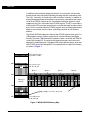
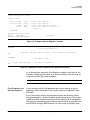
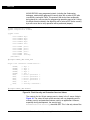
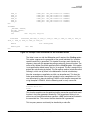
AN2216/D
In addition to the hardware paging mechanism, the instruction set has been
enhanced with two instructions that allow inter-page function (subroutine) calls.
The CALL instruction is similar to the JSR instruction, however, in addition to
placing the paged window return address on the stack, it also places the current
value of the PPAGE register on the stack before writing the new 8-bit value
supplied by the CALL instruction to the PPAGE register. The RTC instruction is
similar to the RTS instruction except that it is used to terminate functions called
by the CALL instruction. Both the PPAGE register value and the paged window
address are restored from the stack, continuing execution at the restored
address.
The MC9S12DP256 implements 6 bits of the PPAGE register which gives it a
1MB program memory address space that is accessed through the paged
window. The lower 768K portion of the address space, accessed with PPAGE
values $00 through $2F, are reserved for external memory when the part is
operated in expanded mode. The upper 256K of the address space, accessed
with PPAGE values $30 through $3F, is occupied by the on-chip Flash memory
as shown in Figure 1.
$0000
Flash Control Registers
Register Base + $100
$4000
$3E
Protected Low Area
0.5K, 1K, 2K, 4K
Block 3
Block 2
Block 1
Block 0
$8000
16K Paged
Memory
$30 $31 $32 $33 $34 $35 $36 $37 $38 $39 $3A $3B $3C $3D $3E $3F
$C000
$3F
$FFFF
$FF00 - $FF0F, Access Key, Protection,
S
i
Protected High Area
2K, 4K, 8K, 16K
Figure 1. MC9S12DP256 Memory Map
2
MC9S12DP256 Software Development Using Metrowerk’s Codewarrior
MOTOROLA
AN2216/D
CodeWarrior Compiler
While all 256K of Flash memory can be accessed through the 16K PPAGE
window, two of the 16K byte pages can also be accessed at fixed address
locations as shown in Figure 1. The fixed page at $4000 – $7FFF is the same
block of memory that can be accessed through the page window when the
PPAGE register contains $3E. The fixed page from $C000 – $FFFF is the same
block of memory that can be accessed through the page window when the
PPAGE register contains $3F. These two fixed page areas are provided to
overcome some of the restrictions of the M68HC12 memory paging design.
Because of the manner in which the memory paging mechanism is
implemented, functions residing in paged memory cannot directly access
constant data residing in a different memory page. This restriction is necessary
because the PPAGE register would have to be written with a different value in
order to access the data. Clearly, writing the PPAGE register with a new value
would result in problem because the code that was being executed would
disappear from the page window as soon as the new PPAGE value was written.
Any constant data such as lookup tables, string or numeric constants that are
shared by functions residing on different pages must either be placed in one of
the two fixed Flash memory pages or must be accessed through a runtime
routine that is located in the fixed Flash memory.
Finally, because the reset and interrupt vectors are only 16-bits, all interrupt
service routines and the initial reset routine must begin in one of the fixed page
memory areas. This does not mean that the entire initialization or interrupt
service routines must reside in the fixed memory areas, however, they must
begin there. If it is desired to place the bulk of the interrupt service routine or
initialization code in paged memory, the portion of the interrupt service routine
in the fixed page area could consist of a CALL to the paged functions followed
by an RTI instruction.
CodeWarrior Compiler
To efficiently handle the paged memory architecture, the Codewarrior compiler
introduces two non-ANSI keywords: near and far. A near function is called with
a JSR or BSR instruction, whereas a far function is called with a CALL
instruction. For example,
void far func1(void);
declares a far function which will be located in paged memory and which may
be called by a function in a different page.
The near and far keywords may also be used with data pointers. For example,
MOTOROLA
MC9S12DP256 Software Development Using Metrowerk’s Codewarrior
3
AN2216/D
const int *far ptr;
declares a pointer to a constant in paged memory. This pointer may be used to
access variables in paged memory. The MC9S12DP256 does not have
hardware support for far pointers, so if the code which uses this pointer is also
in paged memory, an intermediate runtime routine call will be inserted by the
compiler.
Compiler Memory
Models
The Metrowerks Codewarrior compiler for the MC68HC12 supports three
different memory models. The default is the SMALL memory model which
corresponds to a flat memory map of up to 64k byte of code addressing. By
default, all functions are of type 'near' in the SMALL memory model. The
BANKED memory model supports paged addressing of code. By default, all
user defined functions are of type 'far' in the BANKED memory model. 'Far' data
pointers may be used in both the SMALL and BANKED memory models. The
LARGE memory model supports both paged code and data by default. All
functions and data pointers are of type 'far' in the LARGE memory model. Due
to the increased overhead of the necessary runtime routines, this memory
model is not widely used. The BANKED memory model best suits most
applications of the MC9S12DP256.
Segmentation
The Codewarrior compiler supports the concept of segmentation. This means
that code and global variables may be separated into groups which are
allocated to specific memory address spaces by the linker. The attributes
specify the calling mechanism that the compiler must use when generating
code. Code and global variables are allocated segment names and attributes
by means of #pragma statements within the source code.
Code Segment
#pragma CODE_SEG
[NEAR | FAR] <segment_name>
#pragma CODE_SEG defines a code segment. The possible attributes include
NEAR and FAR. NEAR specifies that the functions in the segment are called
with a JSR instruction, i.e. the functions in the segment must only be called by
functions in the same page, or must be in non-paged memory. FAR specifies
that the functions in the segment are called with a CALL instruction, i.e there is
no restriction on where they may be located in the memory. If the attribute is
omitted, the default attribute of the specified memory model is assumed. In the
case of the BANKED memory model, the default attribute is FAR. If no segment
is specified, the code will be assigned to the default segment DEFAULT_ROM.
To explicitly assign the default segment, use the segment name DEFAULT. All
functions following the #pragma CODE_SEG statement are included in the
4
MC9S12DP256 Software Development Using Metrowerk’s Codewarrior
MOTOROLA
AN2216/D
CodeWarrior Compiler
segment until the next #pragma CODE_SEG statement is encountered. Thus
assignment of the default segment is a convenient means of terminating a
specific segment:
#pragma CODE_SEG DEFAULT
A function prototype must be declared in the same code segment as the
function definition itself. Thus, if the function prototypes are declared in a
separate header file, the #pragma CODE_SEG statement must be duplicated,
as shown in Figure 2 and Figure 3.
#pragma CODE_SEG FUNCTIONS
void func1(void);
void func2(void);
#pragma CODE_SEG DEFAULT
Figure 2. Example header file functions.h
#include "functions.h"
#pragma CODE_SEG FUNCTIONS
void func1(void)
{
/* code */
};
void func2(void)
{
/* code */
};
#pragma CODE_SEG DEFAULT
Figure 3. Example Code with include file
It is recommended not to omit the #pragma CODE_SEG DEFAULT statement
at the end of the functions.h file, as the resulting behaviour will very much
depend on the use of #pragma CODE_SEG statements in other included files
and on the order in which such files are included.
MOTOROLA
MC9S12DP256 Software Development Using Metrowerk’s Codewarrior
5
AN2216/D
Data Segment
#pragma DATA_SEG [SHORT] <segment_name>
#pragma DATA_SEG specifies a segment for global data variables. This
includes both variable and constant data by default. Constant data may be
assigned to a specific segment by means of the #pragma CONST_SEG
described below. The only relevant attribute for DATA_SEG for the
MC9S12DP256 is SHORT. This specifies that the direct addressing mode is
used to access the variable. A SHORT segment must therefore be allocated to
memory on the range $0000 to $00FF. If the attribute is omitted then normal
addressing modes other than direct will be used. If no segment is specified, the
data will be assigned to the default segment DEFAULT_RAM. To explicitly
assign the default segment, use the segment name DEFAULT. All global
variables following the #pragma DATA_SEG statement are included in the
segment until the next #pragma DATA_SEG statement. Thus assignment of
the default segment is a convenient means of terminating a specific segment:
#pragma DATA_SEG DEFAULT
Any declarations of external data variables must be within the same data
segment as the data variable definition itself. Thus if var1 is defined in data
segment A in a file, any other files which contain code which accesses var1
would contain the declaration:
#pragma DATA_SEG A
extern int var1;
#pragma DATA_SEG DEFAULT
Constants Segment
#pragma CONST_SEG [PPAGE] <segment_name>
#pragma CONST_SEG defines a segment for constant global data variables.
The only relevant attribute for the MC9S12DP256 is PPAGE. This specifies that
the constant data variables will be accessed by manipulation of the PPAGE
register. This is required if constant data variables will be located in paged
memory. The manipulation of the PPAGE register will be performed by a
runtime routine and this is specified to the compiler with the option
–CpPpage=RUNTIME on the compiler command line. If no attribute is
specified, the compiler assumes that the data variables will be accessed
without manipulation of any page register, i.e. the data variables will be
allocated to non-paged memory. If no segment is specified, constant data will
be assigned to the default segment ROM_VAR. To explicitly assign the default
segment for constant data, use the segment name DEFAULT. This assigns
6
MC9S12DP256 Software Development Using Metrowerk’s Codewarrior
MOTOROLA
AN2216/D
CodeWarrior Compiler
constant data to the segment ROM_VAR. All constant variables following the
#pragma CONST_SEG statement are included in the segment until the next
#pragma CONST_SEG statement. Thus assignment of the default segment is
a convenient means of terminating a specific segment:
#pragma CONST_SEG DEFAULT
Any declarations of external data variables must be within the same data
segment as the data variable definition itself. Thus if var2 is defined in a
constant data segment B in a file, any other files which contain code which
accesses var2 would contain the declaration:
#pragma CONST_SEG B
extern const int var2;
#pragma CONST_SEG DEFAULT
Interrupt Service
Routines
If the application uses interrupts, each interrupt service routine must have the
#pragma TRAP_PROC command immediately preceding the function, as
shown in Figure 4
#pragma CODE_SEG __NEAR_SEG INTERRUPT_ROUTINES
#pragma TRAP_PROC
void interrupt_func1(void)
{
/* code */
};
#pragma CODE_SEG DEFAULT
Figure 4. Example of ISR
The #pragma TRAP_PROC causes the interrupt routine to be terminated with
a RTI instruction instead of a RTS instruction. Furthermore, if the compiler
option -CpPpage=RUNTIME is specified due to paged data variable accesses,
it is also necessary to specify the compiler option –CpPpage=0x30. This
specifies the address of the PPAGE register which will be saved on the stack
at the start of the interrupt routine and restored at the end of the interrupt
routine.
The interrupt vectors themselves are only 16-bits wide and therefore can only
point to non-paged memory. This means that the interrupt service routines
must be located in non-paged memory. This is easily achieved by creating a
specific segment for interrupt routines. In the example in Figure 4, the code
segment name INTERRUPT_ROUTINES is defined. Note the use of the
attribute __NEAR_SEG in the #pragma statement; this makes it quite explicit
that the code segment has to be placed into non-banked memory.
MOTOROLA
MC9S12DP256 Software Development Using Metrowerk’s Codewarrior
7
AN2216/D
Compiling the
BANKED Memory
Model
The BANKED memory model is specified to the compiler with the option -Mb
on the compiler command line. If constant data variables located in paged
memory will be used, the options -CpPpage=RUNTIME -CpPpage=0x30 must
also be specified on the command line. If the Codewarrior IDE is being used,
Command line arguments are specified in the 'Compiler for HC12' dialogue in
'Target Settings Panels'.
Modification of
Startup Code for
MC9S12DP256
The _Startup function in version 1.2 of Codewarrior in file Start12.c has not
been targeted at the MC9S12DP256. The _Startup function initialises a
"WINDEF" register as shown in the code snippet in Figure 5.
/* Example : Set up WinDef Register to allow Paging */
#ifndef DG128 /* HC12 DG128 derivative has no WINDEF. Instead PPAGE is always enabled */
#if (__ENABLE_EPAGE__ != 0 || __ENABLE_DPAGE__ != 0 || __ENABLE_PPAGE__ != 0)
WINDEF= __ENABLE_EPAGE__ | __ENABLE_DPAGE__ | __ENABLE_PPAGE__;
#endif
#endif
Figure 5. Startup Code Snippet
The MC9S12DP256 has no such WINDEF register. In fact, the only MCU in the
HC12 family which has this register is the MC68HC812A4. The _Startup
function should therefore be modified so that it initialises the WINDEF register
only if the code is being compiled for the MC68HC812A4 MCU, as writes to the
WINDEF register address on other MCUs could cause unexpected results. It is
recommended that this piece of code is changed to that shown in Figure 6.
This change has been implemented in version 2.0 of the Codewarrior product.
/* Example : Set up WinDef Register to allow Paging on MC68HC812A4 */
#ifdef HC812A4
#if (__ENABLE_EPAGE__ != 0 || __ENABLE_DPAGE__ != 0 || __ENABLE_PPAGE__ != 0)
WINDEF= __ENABLE_EPAGE__ | __ENABLE_DPAGE__ | __ENABLE_PPAGE__;
#endif
#endif
Figure 6. Recommended _Startup Code Snippet
When compiling this code for the MC68HC812A4, the option -DHC812A4
would be specified on the compiler command line to enable this code when
required.
Modification of
Runtime Routines
for MC9S12DP256
8
A runtime routine must be used to access paged data on the MC9S12DP256.
The runtime routines supplied in version 1.2 of Codewarrior in file datapage.c
have not been targeted at the MC9S12DP256. If paged data will be accessed
in the application, it is recommended that the code snippet from datapage.c
MC9S12DP256 Software Development Using Metrowerk’s Codewarrior
MOTOROLA
AN2216/D
CodeWarrior Compiler
shown in Figure 7 is changed to that shown in Figure 8. This change has been
implemented in version 2.0 of the Codewarrior product.
/* Compile with option -DDG128 to activate this code */
#ifdef DG128 /* HC12 DG128 derivative has page register at 0xff and only P page */
#define PPAGE_ADDR
(0xFF+REGISTER_BASE)
#ifndef __PPAGE__ /* may be set already by option -CPPPAGE */
#define __PPAGE__
#endif
#elif defined (A4)
/* all setting default to A4 already */
#endif
Figure 7. Code snippet from unmodified datapage.c
/* Compile with option -DHCS12 to activate this code */
#ifdef HCS12 /* HCS12 family has PPAGE register only at 0x30 */
#define PPAGE_ADDR
(0x30+REGISTER_BASE)
#ifndef __PPAGE__ /* may be set already by option -CPPPAGE */
#define __PPAGE__
#endif
/* Compile with option -DDG128 to activate this code */
#elif defined DG128 /* HC912DG128 derivative has PPAGE register only at 0xFF */
#define PPAGE_ADDR
(0xFF+REGISTER_BASE)
#ifndef __PPAGE__ /* may be set already by option -CPPPAGE */
#define __PPAGE__
#endif
#elif defined (A4)
/* all setting default to A4 already */
#endif
Figure 8. Recommended Code Snippet for datapage.c
Datapage.c should be recompiled with the compiler option -DHCS12 when
paged data will be accessed on the MC9S12DP256. If the registers on the
MC9S12DP256 will be remapped in the application, it will be necessary to
change the defined value of REGISTER_BASE. This value is also defined in
datapage.c.
Datapage.c has already been compiled (without -DHCS12) and is included in
the library 'ansib.lib'. Either the entire ansib.lib library can be rebuilt using the
modified datapage.c and compiler option, or the modified datapage.c can be
included in the Codewarrior project. As long as the modified datapage.c is
above ansib.lib in the project link order list view, the modified datapage.c will
be linked into the project instead of the standard datapage.c in the unmodified
ansib.lib library.
MOTOROLA
MC9S12DP256 Software Development Using Metrowerk’s Codewarrior
9
AN2216/D
CodeWarrior Linker
Linking Compiled
Code Modules
Before presenting an example linker command file for the MC9S12DP256, a
short discussion on memory addresses used by the linker is necessary. The
Codewarrior development tools view the MC9S12DP256’s program memory
expansion space as a logical address space. For non-paged memory, the
logical address corresponds to the physical address. For paged memory, the
logical address is composed of the PPAGE value followed by the page window
address. This simple approach is intuitive and easy to understand.
PPAGE Value
Window Address
Logical Address
Memory type
N/A
$4000 – $7FFF
$4000 – $7FFF
Flash Block 0, non-paged
N/A
$C000 – $FFFF
$C000 – $FFFF
Flash Block 0, non-paged
$30
$8000 – $BFFF
$308000 – $30BFFF
Flash Block 3, paged
$31
$8000 – $BFFF
$318000 – $31BFFF
Flash Block 3, paged
$32
$8000 – $BFFF
$328000 – $32BFFF
Flash Block 3, paged
$33
$8000 – $BFFF
$338000 – $33BFFF
Flash Block 3, paged
$34
$8000 – $BFFF
$348000 – $34BFFF
Flash Block 2, paged
$35
$8000 – $BFFF
$358000 – $35BFFF
Flash Block 2, paged
$36
$8000 – $BFFF
$368000 – $36BFFF
Flash Block 2, paged
$37
$8000 – $BFFF
$378000 – $37BFFF
Flash Block 2, paged
$38
$8000 – $BFFF
$388000 – $38BFFF
Flash Block 1, paged
$39
$8000 – $BFFF
$398000 – $39BFFF
Flash Block 1, paged
$3A
$8000 – $BFFF
$3A8000 – $3ABFFF
Flash Block 1, paged
$3B
$8000 – $BFFF
$3B8000 – $3BBFFF
Flash Block 1, paged
$3C
$8000 – $BFFF
$3C8000 – $3CBFFF
Flash Block 0, paged
$3D
$8000 – $BFFF
$3D8000 – $3DBFFF
Flash Block 0, paged
$3E
$8000 – $BFFF
$3E8000 – $3EBFFF
Flash Block 0, paged
$3F
$8000 – $BFFF
$3F8000 – $3FBFFF
Flash Block 0, paged
Figure 9. Logical Address to PPAGE/Window Address Correspondence
The important thing to realise is that Flash address $4000 to $7FFF
corresponds to the same physical memory as $3E8000 to $3EBFFF. Therefore
code cannot be linked to address range $4000 to $7FFF and $3E8000 to
$3EBFFF. Code must be linked to address range $4000 to $7FFF or $3E8000
to $3EBFFF. Due to the necessity to have some code in non-page memory and
the advantage of constant data in non-page memory, $4000 to $7FFF is
usually chosen in preference to $3E8000 to $3EBFFF. Similarly Flash address
10
MC9S12DP256 Software Development Using Metrowerk’s Codewarrior
MOTOROLA
AN2216/D
CodeWarrior Linker
$C000 to $FFFF corresponds to the same physical memory as $3F8000 to
$3FBFFF. For the reasons described above, code is linked to $C000 to $FFFF
in preference to $3F8000 to $3FBFFF.
Linker Command
File
The allocation of the defined code and data segments to memory addresses is
controlled by the linker command file. This file may be recognised by the file
extension '.prm'. Within this file, the SECTIONS command block is used to
define physical regions of memory. An example of the SECTIONS command
block for the BANKED memory model on the MC9S12DP256 is given in Figure
10.
SECTIONS
EEPROM = READ_WRITE 0x0400 TO 0x0FFF;
RAM = READ_WRITE 0x1000 TO 0x3FFF;
/* non-paged FLASH ROM */
ROM_4000 = READ_ONLY 0x4000 TO 0x7FFF;
ROM_C000 = READ_ONLY 0xC000 TO 0xFEFF;
/* paged FLASH ROM */
PAGE_30 = READ_ONLY 0x308000
PAGE_31 = READ_ONLY 0x318000
PAGE_32 = READ_ONLY 0x328000
PAGE_33 = READ_ONLY 0x338000
PAGE_34 = READ_ONLY 0x348000
PAGE_35 = READ_ONLY 0x358000
PAGE_36 = READ_ONLY 0x368000
PAGE_37 = READ_ONLY 0x378000
PAGE_38 = READ_ONLY 0x388000
PAGE_39 = READ_ONLY 0x398000
PAGE_3A = READ_ONLY 0x3A8000
PAGE_3B = READ_ONLY 0x3B8000
PAGE_3C = READ_ONLY 0x3C8000
PAGE_3D = READ_ONLY 0x3D8000
TO
TO
TO
TO
TO
TO
TO
TO
TO
TO
TO
TO
TO
TO
0x30BFFF;
0x31BFFF;
0x32BFFF;
0x33BFFF;
0x34BFFF;
0x35BFFF;
0x36BFFF;
0x37BFFF;
0x38BFFF;
0x39BFFF;
0x3ABFFF;
0x3BBFFF;
0x3CBFFF;
0x3DBFFF;
END
Figure 10. Example of Linker Sections Command Block
Within the SECTIONS command block, each separate section of physical
memory is described with a name, an attribute and an address range. Each
page of flash memory is listed, except for PPAGE values $3E and $3F. Instead
this memory is allocated through the equivalent non-paged address, described
as ROM_4000 and ROM_C000. Note that ROM_C000 ends at $FEFF. $FF00
to $FF0F cannot be used for code as the Flash protection and security registers
are located here. Also $FF8C to $FFFF are occupied by the interrupt vectors
and cannot be used for code.
Once the SECTIONS are defined, the code and data segments are allocated to
memory using the PLACEMENT command block.
MOTOROLA
MC9S12DP256 Software Development Using Metrowerk’s Codewarrior
11
AN2216/D
PLACEMENT
_PRESTART, STARTUP,
ROM_VAR, STRINGS,
NON_BANKED,
INTERRUPT_ROUTINES,
COPY
INTO
ROM_C000, ROM_4000;
DEFAULT_ROM
INTO PAGE_30, PAGE_31, PAGE_32, PAGE_33, PAGE_34, PAGE_35,
PAGE_36, PAGE_37, PAGE_38, PAGE_39, PAGE_3A, PAGE_3B, PAGE_3C, PAGE_3D;
DEFAULT_RAM
INTO
RAM;
END
Figure 11. Example of Linker Placement Command Block
The PLACEMENT command block is used to allocate code and data segments
to the memory segments. The predefined segments PRESTART, STARTUP,
ROM_VAR, STRINGS, NON_BANKED and COPY must all be allocated to
fixed, or non-paged memory. The INTERRUPT_ROUTINES segment is the
name used in the example in Figure 4 and this must also be allocated to
non-paged memory. Note that segment COPY must always be the last
segment in this list of segments to be placed in non-paged memory.
The default code segment DEFAULT_ROM is allocated to paged memory
starting with the PAGE_30 section. When the PAGE_30 section has been
filled, the default code segment continues with the PAGE_31 and succeeding
sections until all code has been allocated to memory.
I/O Register
Placement
12
The use of segments together with the linker PLACEMENT command block
gives a convenient method for the allocation of register variables. The registers
for each peripheral module can be created as a structure within a data segment
and then that segment is allocated to the correct address in the linker command
file. An example for a limited number of registers is given in Figure 12 and
Figure 13.
MC9S12DP256 Software Development Using Metrowerk’s Codewarrior
MOTOROLA
AN2216/D
CodeWarrior Linker
typedef unsigned char tUINT8;
typedef struct
{
volatile tUINT8
volatile tUINT8
tUINT8
tUINT8
porta;
portb;
ddra;
ddrb;
/*
/*
/*
/*
/*
port A data register */
port B data register */
port A data direction register */
port B data direction register */
continue… */
}tREGISTER;
#pragma DATA_SEG S12_REG
extern
tREGISTER
Registers;
#pragma DATA_SEG DEFAULT
Figure 12. Example Code for Registers Variable
SECTIONS
/* flash, RAM, EEPROM etc */
DP256_REG = NO_INIT 0x0000 TO 0x0003; /* exact address for Registers */
END
PLACEMENT
/* Placement of code */
S12_REG INTO DP256_REG;
/* Placement of Registers */
END
Figure 13. Additional Linker Commands for Register Placement
As an alternative to placement of the Registers variable in the linker file, the
Registers variable may be placed at an absolute address within the code, by
using the non-ANSI '@' symbol as follows:
tREGISTER Registers @0x00;
Flash Protection and
Security Registers
A short summary of the Flash protection and security features is given in
Appendix A of this document. Further details are given in Application Note
AN2400/D.
Even if the memory security and protection features are not being utilized
during development, a constant variable containing data for this 16 byte area
should be created, compiled and linked into the absolute file for compatibility
with some Flash programming tools. Because of the inability to erase the Flash
and EEPROM using the BDM interface in the first mask set (0K36N) of the
MOTOROLA
MC9S12DP256 Software Development Using Metrowerk’s Codewarrior
13
AN2216/D
MC9S12DP256, many programming tools, including the Codewarrior
debugger, automatically program the security byte with a value of $FE after
successfully erasing the Flash. This prevents the device from accidentally
being placed in a secure state if a programming operation were to fail. Having
this block of data included in the object file with a value of $FE for the security
byte will ensure that a verify operation will be performed properly.
typedef unsigned char tUINT8;
typedef unsigned short tUINT16;
typedef struct
{
const tUINT16
const tUINT16
const tUINT16
const tUINT16
const tUINT16
const tUINT8
const tUINT8
const tUINT8
const tUINT8
const tUINT8
const tUINT8
}tFlashProt;
key1;
key2;
key3;
key4;
res1;
prot3;
prot2;
prot1;
prot0;
res2;
security;
#pragma CONST_SEG FLASH_PROT
extern const tFlashProt FlashProtection =
{
0xFFFF,
/* key1 */
0xFFFF,
/* key2 */
0xFFFF,
/* key3 */
0xFFFF,
/* key4 */
0xFFFF,
/* res1 */
0xFF,
/* block 3 protection */
0xFF,
/* block 2 protection */
0xFF,
/* block 1 protection */
0xFF,
/* block 0 protection */
0xFF,
/* res2 */
0xFE,
/* security: unsecured */
};
#pragma CONST_SEG DEFAULT
Figure 14. Flash Security and Protection Constant Values
The contents for the 16 byte memory area is shown in the C source listing in
Figure 14. The values for each of the constants will vary depending on the
memory security and protection features used by an application. However,
especially during development, the security byte,
FlashProtection.security, should be $FE. This is the only value of the
14
MC9S12DP256 Software Development Using Metrowerk’s Codewarrior
MOTOROLA
AN2216/D
CodeWarrior Linker
lower two bits in the security byte in which the part remains unsecured. Figure
15 shows an example linker commant for the placement of the flash security
and protection data.
SECTIONS
/* flash, RAM, EEPROM etc */
FLASH_PROT_AREA = READ_ONLY 0xFF00 TO 0xFF0F;
END
PLACEMENT
/* Placement of code */
FLASH_PROT INTO FLASH_PROT_AREA; /* Placement of Flash Protection Registers */
END
Figure 15. Flash Protection Register Placement
Interrupt Vectors
The reset and interrupt vector table for all M68HC12 family devices consists of
a 128 byte memory area that begins at $FF80. Because each vector occupies
two bytes, a total of 64 unique vectors are supported. The MC9S12DP256
implements 58 of the 64 vectors beginning at $FF8C. There are two methods
of creating the address constants for the interrupt vector table. Either the
interrupt vector table can be created manually or the linker can generate the
interrupt vector table automatically.
An example of a manually created vector table for the MC9S12DP256 is shown
in Figure 16. This shows an array of constant pointers to functions within a
segment called VECTORS.
#ifndef NULL
#define NULL
#endif
extern
extern
extern
extern
void
void
void
void
0
_Startup();
CAN0_WakeupISR();
CAN0_ReceiveISR();
CAN0_TransmitISR();
/* startup routine
*/
#pragma CONST_SEG VECTORS
void (* const vector_table[])() = {
NULL,
NULL,
NULL,
NULL,
NULL,
NULL,
NULL,
NULL,
MOTOROLA
/*
/*
/*
/*
/*
/*
/*
/*
$FF8C:8D
$FF8E:8F
$FF90:91
$FF92:93
$FF94:95
$FF96:97
$FF98:99
$FF9A:9B
PWM Emergency Shutdown */
Port P Interrupt */
MSCAN 4 transmit */
MSCAN 4 receive */
MSCAN 4 errors */
MSCAN 4 wake- up */
MSCAN 3 transmit */
MSCAN 3 receive */
MC9S12DP256 Software Development Using Metrowerk’s Codewarrior
15
AN2216/D
NULL,
NULL,
NULL,
NULL,
NULL,
NULL,
NULL,
NULL,
NULL,
NULL,
CAN0_TransmitISR,
CAN0_ReceiveISR,
NULL,
CAN0_WakeupISR,
NULL,
NULL,
NULL,
NULL,
NULL,
NULL,
NULL,
NULL,
NULL,
NULL,
NULL,
NULL,
NULL,
NULL,
NULL,
NULL,
NULL,
NULL,
NULL,
NULL,
NULL,
NULL,
NULL,
NULL,
NULL,
NULL,
NULL,
NULL,
NULL,
NULL,
NULL,
NULL,
NULL,
NULL,
NULL,
_Startup
/*
/*
/*
/*
/*
/*
/*
/*
/*
/*
/*
/*
/*
/*
/*
/*
/*
/*
/*
/*
/*
/*
/*
/*
/*
/*
/*
/*
/*
/*
/*
/*
/*
/*
/*
/*
/*
/*
/*
/*
/*
/*
/*
/*
/*
/*
/*
/*
/*
/*
$FF9C:9D
$FF9E:9F
$FFA0:A1
$FFA2:A3
$FFA4:A5
$FFA6:A7
$FFA8:A9
$FFAA:AB
$FFAC:AD
$FFAE:AF
$FFB0:B1
$FFB2:B3
$FFB4:B5
$FFB6:B7
$FFB8:B9
$FFBA:BB
$FFBC:BD
$FFBE:BF
$FFC0:C1
$FFC2:C3
$FFC4:C5
$FFC6:C7
$FFC8:C9
$FFCA:CB
$FFCC:CD
$FFCE:CF
$FFD0:D1
$FFD2:D3
$FFD4:D5
$FFD6:D7
$FFD8:D9
$FFDA:DB
$FFDC:DD
$FFDE:DF
$FFE0:E1
$FFE2:E3
$FFE4:E5
$FFE6:E7
$FFE8:E9
$FFEA:EB
$FFEC:ED
$FFEE:EF
$FFF0:F1
$FFF2:F3
$FFF4:F5
$FFF6:F7
$FFF8:F9
$FFFA:FB
$FFFC:FD
$FFFE:FF
MSCAN 3 errors */
MSCAN 3 wake- p */
MSCAN 2 transmit */
MSCAN 2 receive */
MSCAN 2 errors */
MSCAN 2 wake-up */
MSCAN 1 transmit */
MSCAN 1 receive */
MSCAN 1 errors */
MSCAN 1 wake-up */
MSCAN 0 transmit */
MSCAN 0 receive */
MSCAN 0 errors */
MSCAN 0 wake-up */
FLASH */
EEPROM */
SPI2 */
SPI1 */
IIC Bus */
DLC */
SCME */
CRG lock */
Pulse Accumulator B Overflow */
Modulus Down Counter underflow */
Port H*/
Port J */
ATD1 */
ATD0 */
SCI1 */
SCI0 */
SPI0 */
Pulse accumulator input edge */
Pulse accumulator A overflow */
Timer overflow */
Timer channel 7 */
Timer channel 6 */
Timer channel 5 */
Timer channel 4 */
Timer channel 3 */
Timer channel 2 */
Timer channel 1 */
Timer channel 0 */
Real Time Interrupt */
IRQ */
XIRQ */
SWI */
Unimplemented instruction trap */
COP failure reset */
Clock Monitor fail reset */
Reset */
};
#pragma CONST_SEG DEFAULT
Figure 16. Example Explicit Vector Table
16
MC9S12DP256 Software Development Using Metrowerk’s Codewarrior
MOTOROLA
AN2216/D
CodeWarrior Linker
The VECTORS segment must be allocated to the correct memory address in
the linker command file, as shown in Figure 17. In addition, the ENTRIES
command must be used to ensure that the table is included. As there are no
direct references to the vector table in the code, it would otherwise be
'optimised' and removed.
SECTIONS
/* flash, RAM, EEPROM etc */
VECTOR_TABLE = READ_ONLY 0xFF8C TO 0xFFFF; /* Vector Table address */
END
PLACEMENT
/* Placement of code */
VECTORS INTO VECTOR_TABLE;
/* Placement of vector_table */
END
ENTRIES
vector_table
END
Figure 17. Example Linker Command File for Manual Vector Table
Automatic Interrupt
Vector Entry
Generation
As a much easier alternative to the manual method, the linker can create
interrupt vector addresses automatically. This is done using the VECTOR
instruction in the linker command file. The array of constant function pointers
used for the manual method is not required.
VECTOR 0 _Startup
VECTOR 38 CAN0_ReceiveISR
Figure 18. Example of Linker Vector Command Block
The number following VECTOR instruction is used by the linker to calculate the
vector address. For vector number 'n', the address is given by $FFFE – 2*n.
Thus the address of vector 38 in the example in Figure 18 is $FFFE – $4C =
$FFB2. Vector 0 is the reset vector at $FFFE and _Startup is the default
Codewarrior start-up routine. The VECTOR instructions are placed at the end
of the linker command file. The ENTRIES command block is no longer required
for vector entries when this method is used.
MOTOROLA
MC9S12DP256 Software Development Using Metrowerk’s Codewarrior
17
AN2216/D
Linker Optimizations
for the BANKED
Memory Model
In the BANKED memory model all user defined functions are of type 'far' by
default. All functions are therefore called using the CALL instruction and
terminated with the RTC instruction. There is clearly a price to be paid for this
simplistic approach, as some functions which are called only by other functions
within the same page of memory could be called with a JSR/RTS instruction
sequence. Compared with a JSR/RTS sequence, a CALL/RTC sequence
typically requires one extra byte of code memory and 5 extra cycles to execute,
so the overhead is not great. In applications where this overhead cannot be
afforded, the default behaviour can be overriden. This can be done manually
by grouping functions together into specific segments each of which are
allocated to a single page in memory. Then all functions which are only called
by other functions within the same page can individually be declared with the
'near' type qualifier. Clearly this would be a difficult and laborious task even for
a relatively simple piece of code, but fortunately the Codewarrior linker is able
to perform this task automatically with the linker 'distribute' feature, activated
with the command line option, -Dist. This feature also minimises the amount of
unused memory in each of the pages. When using this feature, building an
application becomes a two-pass process.
The linker 'distribute feature' will distribute all functions in a single code
segment into paged memory sections. All functions which are to be optimized
must therefore be included in a single code segment. The default code
segment name DISTRIBUTE is expected by the linker, if a different name is to
be used then the linker must be informed of the name with the -DistSeg option.
With a distribution segment defined, the application is then compiled as normal.
In this first compiler pass, all functions are of type 'far' by default.
Before the application can be linked, the linker command file must be modified
so that the linker can be informed of which sections may use the near
inter-bank calling convention and which sections must used a far inter-bank
calling convention. This is done with the attributes IBCC_NEAR and
IBCC_FAR. An example of this is shown in Figure 19. Note also that the
DISTRIBUTE segment is placed with the DISTRIBUTE_INTO keyword.
SECTIONS
RAM
EEPROM
= READ_ONLY
/* unbanked FLASH ROM */
ROM_4000
ROM_C000
/* banked FLASH ROM */
PAGE_30
PAGE_31
PAGE_32
PAGE_33
PAGE_34
PAGE_35
PAGE_36
PAGE_37
18
= READ_WRITE 0x1000 TO 0x3FFF;
0x0400 TO 0x0FFF;
= READ_ONLY
= READ_ONLY
IBCC_NEAR 0x4000 TO 0x7FFF;
IBCC_NEAR 0xC000 TO 0xFEFF;
=
=
=
=
=
=
=
=
IBCC_FAR
IBCC_FAR
IBCC_FAR
IBCC_FAR
IBCC_FAR
IBCC_FAR
IBCC_FAR
IBCC_FAR
READ_ONLY
READ_ONLY
READ_ONLY
READ_ONLY
READ_ONLY
READ_ONLY
READ_ONLY
READ_ONLY
0x308000
0x318000
0x328000
0x338000
0x348000
0x358000
0x368000
0x378000
TO
TO
TO
TO
TO
TO
TO
TO
0x30BFFF;
0x31BFFF;
0x32BFFF;
0x33BFFF;
0x34BFFF;
0x35BFFF;
0x36BFFF;
0x37BFFF;
MC9S12DP256 Software Development Using Metrowerk’s Codewarrior
MOTOROLA
AN2216/D
CodeWarrior Linker
PAGE_38
PAGE_39
PAGE_3A
PAGE_3B
PAGE_3C
PAGE_3D
=
=
=
=
=
=
READ_ONLY
READ_ONLY
READ_ONLY
READ_ONLY
READ_ONLY
READ_ONLY
IBCC_FAR
IBCC_FAR
IBCC_FAR
IBCC_FAR
IBCC_FAR
IBCC_FAR
0x388000
0x398000
0x3A8000
0x3B8000
0x3C8000
0x3D8000
TO
TO
TO
TO
TO
TO
0x38BFFF;
0x39BFFF;
0x3ABFFF;
0x3BBFFF;
0x3CBFFF;
0x3DBFFF;
END
PLACEMENT
_PRESTART, STARTUP,
ROM_VAR, STRINGS,
NON_BANKED,
COPY
INTO
ROM_C000, ROM_4000;
DISTRIBUTE
DISTRIBUTE_INTO PAGE_30, PAGE_31, PAGE_32, PAGE_33, PAGE_34, PAGE_35, PAGE_36,
PAGE_37, PAGE_38, PAGE_39, PAGE_3A, PAGE_3B;
EEPROM
DEFAULT_RAM
INTO
INTO
EEPROM_AREA;
RAM;
END
Figure 19. Example Linker Commands for the Distribute feature
The linker is now run with the -Dist option and if required, the -DistSeg option.
This option suppresses the generation of the normal absolute file, instead a
special header file is generated. This header file assigns each function to a
segment, along with the appropriate calling mechanism for each function. The
name of this header file can be specified with the -DistFile option. If this option
is not specified the default name 'distr.inc' is assigned. This file is created in the
project /bin sub-directory by default. This file requires another include file called
interseg.h, which can by found in the Metrowerks /Include sub-directory.
Now the second pass compilation and link can be performed. This time the
linker generated header file must be included in every compilation unit. This
can conveniently by done by defining 'PASS2' on the compiler command line
using the option -DPASS2, with the following code in every source file:
#ifdef PASS2
#include "distr.inc"
#endif
This time the compiler uses the optimized calling convention specified for each
function in the linker generated header file. The second pass linking is run
without any of the distribute feature specifiers: -DIST should not be included in
the command line. This ensures that the absolute file is generated.
This two pass process could easily be handled by a make file.
MOTOROLA
MC9S12DP256 Software Development Using Metrowerk’s Codewarrior
19
AN2216/D
NOTE:
Whenever any new functions are added to the source, a new linker generated
header file must be generated, i.e. both passes must be executed.
NOTE:
When code is added to a function, it may no longer fit into its allocated section.
If this happens, both build passes must be executed to generate a new include
file.
Appendix A: Flash Memory Protection
The protected areas of each Flash block are controlled by four bytes of Flash
memory residing in the fixed page memory area from $FF0A – $FF0D During
the microcontroller reset sequence, each of the four banked Flash Protection
Registers (FPROT) is loaded from values programmed into these memory
locations. As shown in Figure 20, location $FF0A controls protection for block
three, $FF0B controls protection for block two, $FF0C controls protection for
block one and $FF0D controls protection for block zero. The values loaded into
each FPROT register determine whether the entire block or just subsections
are protected from being accidentally erased or programmed. As mentioned
previously, each 64K block can have two protected areas. One of these areas,
known as the lower protected block, grows from the middle of the 64K block
upward. The other, known as the upper protected block, grows from the top of
the 64K block downward. In general, the upper protected area of Flash block
zero is used to hold bootloader code since it contains the reset and interrupt
vectors. The lower protected area of block zero and the protected areas of the
other Flash blocks can be used for critical parameters that would not change
when program firmware was updated.
The FPOPEN bit in each FPROT register determines whether the the entire
Flash block or subsections of it can be programmed or erased. When the
FPOPEN bit is erased (1) the remainder of the bits in the register determine the
state of protection and the size of each protected block. In its programmed state
(0) the entire Flash block is protected and the state of the remaining bits within
the FPROT register is irrelevant.
20
MC9S12DP256 Software Development Using Metrowerk’s Codewarrior
MOTOROLA
AN2216/D
Appendix A: Flash Memory Protection
Address
Description
$FF00 - $FF07
Security Backdoor Comparison Key
$FF08 - $FF09
Reserved
$FF0A
Protection Byte For Flash Block 3
$FF0B
Protection Byte For Flash Block 2
$FF0C
Protection Byte For Flash Block 1
$FF0D
Protection Byte For Flash Block 0
$FF0E
Reserved
$FF0F
Security Byte
Figure 20. Flash Protection and Security Memory Locations
The FPHDIS and FPLDIS bits determine the protection state of the upper and
lower areas within each 64K block respectively. The erased state of these bits
allows erasure and programming of the two protected areas and renders the
state of the FPHS[1:0] and FPLS[1:0] bits immaterial. When either of these bits
is programmed, the FPHS[1:0] and FPLS[1:0] bits determine the size of the
upper and lower protected areas. The tables in Figure 21 summarize the
combinations of the FPHS[1:0] and FPLS[1:0] bits and the size of the protected
area selected by each.
FPHS[1:0]
Protected Size
FPLS[1:0]
Protected Size
0:0
2K
0:0
512 Bytes
0:1
4K
0:1
1K
1:0
8K
1:0
2K
1:1
16K
1:1
4K
Figure 21. Flash Protection Select Bits
Trying to program or erase any of the protected areas will result in a protection
violation error and bit PVIOL will be set in the Flash Status Register FSTAT.
NOTE:
MOTOROLA
A mass or bulk erase of the full 64K byte block is only possible when the
FPLDIS and FPHDIS bits are in the erased state.
MC9S12DP256 Software Development Using Metrowerk’s Codewarrior
21
AN2216/D
Flash Security
While no security feature can be 100% guaranteed to prevent access to an
MCU’s internal resources, the MC9S12DP256’s security mechanism makes it
extremely difficult to access the Flash or EEPROM contents. Once the security
mechanism has been enabled, access to the Flash and EEPROM either
through the BDM or the expanded bus is inhibited. Gaining access to either of
these resources may only be accomplished by erasing the contents of the
Flash and EEPROM or through a built in back door mechanism. While having
a back door mechanism may seem to be a weakness of the security
mechanism, the target application must specifically support this feature for it to
operate.
Erasing the Flash or EEPROM can be accomplished using one of two methods.
The first method requires resetting the target MCU in Special Single-chip mode
and using the BDM interface. When a secured device is reset in Special
Single-chip mode, a special BDM security ROM becomes active. The program
in this small ROM performs a blank check of the Flash and EEPROM
memories. If both memory spaces are erased, the BDM firmware temporarily
disables device security, allowing full BDM functionally. However, if the Flash
or EEPROM are not blank, security remains active and only the BDM hardware
commands remain functional. In this mode the BDM commands are restricted
to reading and writing the I/O register space. Because all other BDM
commands and on-chip resources are disabled, the contents of the Flash and
EEPROM remain protected. This functionality is adequate to manipulate the
Flash and EEPROM control registers to erase their contents.
NOTE:
Use of the BDM interface to erase the Flash and EEPROM memories is not
present in the initial mask set (0K36N) of the MC9S12DP256. Great care must
be exercised to ensure that the microcontroller is not programmed in a secure
state unless the back door mechanism is supported by the target firmware.
The second method requires the microcontroller to be connected to external
memory devices and reset in Expanded mode where a program can be
executed from the external memory to erase the Flash and EEPROM. This
method may be preferred before parts are placed in a target system.
As shown in Figure 22 the security mechanism is controlled by the two least
significant bits in the Security Byte. Because the only unsecured combination
is when SEC1 has a value of ‘1’ and SEC0 has a value of ‘0’, the microcontroller
will remain secured even after the Flash and EEPROM are erased since the
erased state of the security byte is $FF. As previously explained, even though
the device is secured after being erased, the part may be reset in Special
Single-chip mode allowing manipulation of the microcontroller via the BDM
interface. However, after erasing the Flash and EEPROM, the microcontroller
can be placed in the unsecured state by programming the security byte with a
value of $FE. Note that because the Flash must be programmed an aligned
word at a time and because the security byte resides at an odd address
($FF0F), the word at $FF0E must be programmed with a value of $FFFE.
22
MC9S12DP256 Software Development Using Metrowerk’s Codewarrior
MOTOROLA
AN2216/D
Appendix A: Flash Memory Protection
SEC[1:0]
Security State
0:0
Secured
0:1
Secured
1:0
Unsecured
1:1
Secured
Figure 22. Security Bits
Even if the memory security and protection features are not being utilized
during development, a file containing data for this 16 byte area should be
created, compiled and inserted into the linker file for compatibility with some
Flash programming tools. Because of the inability to erase the Flash and
EEPROM using the BDM interface in the first mask set (0K36N) of the
MC9S12DP256, many programming tools automatically program the security
byte with a value of $FE after successfully erasing the Flash. This prevents the
device from accidentally being placed in a secure state if a programming
operation were to fail. Having this block of data included in the object file with
a value of $FE for the security byte will ensure that a verify operation will be
performed properly.
MOTOROLA
MC9S12DP256 Software Development Using Metrowerk’s Codewarrior
23
HOW TO REACH US:
USA/EUROPE/LOCATIONS NOT LISTED:
Motorola Literature Distribution;
P.O. Box 5405, Denver, Colorado 80217
1-303-675-2140 or 1-800-441-2447
JAPAN:
Motorola Japan Ltd.; SPS, Technical Information Center,
3-20-1, Minami-Azabu Minato-ku, Tokyo 106-8573 Japan
81-3-3440-3569
ASIA/PACIFIC:
Motorola Semiconductors H.K. Ltd.;
Silicon Harbour Centre, 2 Dai King Street,
Tai Po Industrial Estate, Tai Po, N.T., Hong Kong
852-26668334
TECHNICAL INFORMATION CENTER:
Information in this document is provided solely to enable system and software
implementers to use Motorola products. There are no express or implied copyright
licenses granted hereunder to design or fabricate any integrated circuits or
integrated circuits based on the information in this document.
Motorola reserves the right to make changes without further notice to any products
herein. Motorola makes no warranty, representation or guarantee regarding the
1-800-521-6274
suitability of its products for any particular purpose, nor does Motorola assume any
HOME PAGE:
liability arising out of the application or use of any product or circuit, and specifically
http://motorola.com/semiconductors
disclaims any and all liability, including without limitation consequential or incidental
damages. “Typical” parameters which may be provided in Motorola data sheets
and/or specifications can and do vary in different applications and actual
performance may vary over time. All operating parameters, including “Typicals”
must be validated for each customer application by customer’s technical experts.
Motorola does not convey any license under its patent rights nor the rights of
others. Motorola products are not designed, intended, or authorized for use as
components in systems intended for surgical implant into the body, or other
applications intended to support or sustain life, or for any other application in which
the failure of the Motorola product could create a situation where personal injury or
death may occur. Should Buyer purchase or use Motorola products for any such
unintended or unauthorized application, Buyer shall indemnify and hold Motorola
and its officers, employees, subsidiaries, affiliates, and distributors harmless
against all claims, costs, damages, and expenses, and reasonable attorney fees
arising out of, directly or indirectly, any claim of personal injury or death associated
with such unintended or unauthorized use, even if such claim alleges that Motorola
was negligent regarding the design or manufacture of the part.
Motorola and the Stylized M Logo are registered in the U.S. Patent and Trademark
Office. digital dna is a trademark of Motorola, Inc. All other product or service
names are the property of their respective owners. Motorola, Inc. is an Equal
Opportunity/Affirmative Action Employer.
© Motorola, Inc. 2003
AN2216/D