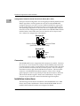
1
MVME197LE
Single Board Computer
User’s Manual
(MVME197LE/D2)
Notice
While reasonable efforts have been made to assure the accuracy of this document,
Motorola, Inc. assumes no liability resulting from any omissions in this document, or
from the use of the information obtained therein. Motorola reserves the right to revise
this document and to make changes from time to time in the content hereof without
obligation of Motorola to notify any person of such revision or changes.
No part of this material may be reproduced or copied in any tangible medium, or
stored in a retrieval system, or transmitted in any form, or by any means, radio,
electronic, mechanical, photocopying, recording or facsimile, or otherwise, without the
prior written permission of Motorola, Inc.
It is possible that this publication may contain reference to, or information about
Motorola products (machines and programs), programming, or services that are not
announced in your country. Such references or information must not be construed to
mean that Motorola intends to announce such Motorola products, programming, or
services in your country.
Restricted Rights Legend
If the documentation contained herein is supplied, directly or indirectly, to the U.S.
Government, the following notice shall apply unless otherwise agreed to in writing by
Motorola, Inc.
Use, duplication, or disclosure by the Government is subject to restrictions as set forth
in subparagraph (c)(1)(ii) of the Rights in Technical Data and Computer Software
clause at DFARS 252.227-7013.
Motorola, Inc.
Computer Group
2900 South Diablo Way
Tempe, Arizona 85282-9602
Preface
This document provides general information, hardware preparation and installation
instructions, operating instructions, and a functional description for the MVME197LE
Single Board Computer.
This document is intended for anyone who wants to design OEM systems, supply
additional capability to an existing compatible system, or work in a lab environment
for experimental purposes.
A basic knowledge of computers and digital logic is assumed.
To use this document, you may wish to become familiar with the publications listed in
the Related Documentation section found in the following pages.
Document Terminology
Throughout this document, a convention has been maintained whereby data and
address parameters are preceded by a character which specifies the numeric format, as
follows:
$
dollar
specifies a hexadecimal number
%
percent
specifies a binary number
&
ampersand
specifies a decimal number
For example, “12” is the decimal number twelve, and “$12” is the decimal number
eighteen. Unless otherwise specified, all address references are in hexadecimal
throughout this document.
An asterisk (*) following the signal name for signals which are level significant denotes
that the signal is true or valid when the signal is low.
An asterisk (*) following the signal name for signals which are edge significant denotes
that the actions initiated by that signal occur on high to low transition.
In this document, assertion and negation are used to specify forcing a signal to a
particular state. In particular, assertion and assert refer to a signal that is active or true;
negation and negate indicate a signal that is inactive or false. These terms are used
independently of the voltage level (high or low) that they represent.
Data and address sizes are defined as follows:
❏
A byte is eight bits, numbered 0 through 7, with bit 0 being the least
significant.
❏
A two-byte is 16 bits, numbered 0 through 15, with bit 0 being the least
significant. For the MVME197series and other RISC modules, this is called
a half-word.
❏
A four-byte is 32 bits, numbered 0 through 31, with bit 0 being the least
significant. For the MVME197 series and other RISC modules, this is called
a word.
❏
An eight-byte is 64 bits, numbered 0 through 63, with bit 0 being the least
significant. For the MVME197 series and other RISC modules, this is called
a double-word.
Throughout this document, it is assumed that the MPU on the MVME197 module
series is always programmed with big-endian byte ordering, as shown below. Any
attempt to use small-endian byte ordering will immediately render the MVME197Bug
debugger unusable.
BIT
BIT
63
56 55
ADRO
31
48 47
ADR1
24 23
ADR4
40 39
ADR2
16 15
ADR5
32
ADR3
08 07
ADR6
00
ADR7
The terms control bit and status bit are used extensively in this document. The term
control bit is used to describe a bit in a register that can be set and cleared under
software control. The term true is used to indicate that a bit is in the state that enables
the function it controls. The term false is used to indicate that the bit is in the state that
disables the function it controls. In all tables, the terms 0 and 1 are used to describe the
actual value that should be written to the bit, or the value that it yields when read. The
term status bit is used to describe a bit in a register that reflects a specific condition. The
status bit can be read by software to determine operational or exception conditions.
Related Documentation
The following publications are applicable to the MVME197LE module and may
provide additional helpful information. If not shipped with this product, they may be
purchased by contacting your Motorola sales office.
Document Title
Motorola
Publication Number
MVME197LE, MVME197DP, and MVME197SP Single
Board Computers Programmer’s Reference Guide
MVME197PG
MVME197BUG 197Bug Debugging Package User’s Manual
MVME197BUG
MVME197BUG 197Bug Diagnostic Firmware User’s Manual MVME197DIAG
MVME712M Transition Module and P2 Adapter Board
User’s Manual
MVME712M
MVME712-12, MVME712-13, MVME712A, MVME712AM, MVME712A
and MVME712B Transition Module and LCP2 Adapter Board
User’s Manual
MC88110 Second Generation RISC Microprocessor User’s
Manual
MC88110UM
MC68040 Microprocessor User’s Manual
MC68040UM
N ote
Although not shown in the above list, each Motorola
Computer Group manual publication number is suffixed
with characters which represent the revision level of the
document, such as “/D2” (the second revision of a manual);
a supplement bears the same number as the manual but has
a suffix such as “/A1” (the first supplement to the manual).
To further assist your development effort, Motorola has collected user’s manuals for
each of the peripheral controllers used on the MVME197 module series and other
boards from the suppliers. This bundle includes manuals for the following:
68-1X7DS for use with the MVME197 series of Single Board Computers.
NCR 53C710 SCSI Controller Data Manual and Programmer’s Guide
Intel i82596 Ethernet Controller User’s Manual
Cirrus Logic CD2401 Serial Controller User’s Manual
SGS-Thompson MK48T08 NVRAM/TOD Clock Data Sheet
The following non-Motorola publications may also be of interest and may be obtained
from the sources indicated. The VMEbus Specification is contained in ANSI/IEEE
Standard 1014-1987.
ANSI/IEEE Std 1014-1987
Versatile Backplane Bus: VMEbus
The Institute of Electrical and Electronics
Engineers, Incorporated
Publication and Sales Department
345 East 47th Street
New York, New York 10017-2633
Telephone: 1-800-678-4333
ANSI Small Computer System Interface-2
(SCSI-2), Draft Document X3.131-198X,
Revision 10c
Global Engineering Documents
P.O. Box 19539
Irvine, California 92713-9539
Telephone (714) 979-8135
The computer programs stored in the Read Only Memory of this device contain
material copyrighted by Motorola Inc., first published 1991, and may be used only
under license such as the License for Computer Programs (Article 14) contained in
Motorola’s Terms and Conditions of Sale, Rev. 1/79.
Motorola® and the Motorola symbol are registered trademarks of Motorola, Inc.
Delta Series, M88000, SYSTEM V/88, VMEmodule, VMEsystem, and 197bug are
trademarks of Motorola, Inc.
Timekeeper and Zeropower are trademarks of Thompson Components.
All other products mentioned in this document are trademarks or registered
trademarks of their respective holders
© Copyright Motorola 1993
All Rights Reserved
Printed in the United States of America
December 1993
!
WARNING
This equipment generates, uses, and can radiate radio
frequency energy and if not installed and used in
accordance with the documentation for this product, may
cause interference to radio communications. It has been
tested and found to comply with the limits for a Class A
Computing Device pursuant to Subpart J of Part 15 of FCC
rules, which are designed to provide reasonable protection
against such interference when operated in a commercial
environment. Operation of this equipment in a residential
area is likely to cause interference in which case the user, at
the user’s own expense, will be required to take whatever
measures necessary to correct the interference.
SAFETY SUMMARY
SAFETY DEPENDS ON YOU
The following general safety precautions must be observed during all phases of operation, service, and repair
of this equipment. Failure to comply with these precautions or with specific warnings elsewhere in this manual
violates safety standards of design, manufacture, and intended use of the equipment. Motorola Inc. assumes
no liability for the customer’s failure to comply with these requirements. The safety precautions listed below
represent warnings of certain dangers of which we are aware. You, as the user of the product, should follow
these warnings and all other safety precautions necessary for the safe operation of the equipment in your
operating environment.
GROUND THE INSTRUMENT.
To minimize shock hazard, the equipment chassis and enclosure must be connected to an electrical ground. The
equipment is supplied with a three-conductor ac power cable. The power cable must either be plugged into an
approved three-contact electrical outlet or used with a three-contact to two-contact adapter, with the grounding wire
(green) firmly connected to an electrical ground (safety ground) at the power outlet. The power jack and mating plug
of the power cable meet international Electrotechnical Commission (IEC) safety standards.
DO NOT OPERATE IN AN EXPLOSIVE ATMOSPHERE.
Do not operate the equipment in the presence of flammable gases or fumes. Operation of any electrical equipment in
such an environment constitutes a definite safety hazard.
KEEP AWAY FROM LIVE CIRCUITS.
Operating personnel must not remove equipment covers. Only Factory Authorized Service Personnel or other qualified
maintenance personnel may remove equipment covers for internal subassembly or component replacement or any
internal adjustment. Do not replace components with power cable connected. Under certain conditions, dangerous
voltages may exist even with the power cable removed. To avoid injuries, always disconnect power and discharge
circuits before touching them.
DO NOT SERVICE OR ADJUST ALONE.
Do not attempt internal service or adjustment unless another person, capable of rendering first aid and resuscitation,
is present.
USE CAUTION WHEN EXPOSING OR HANDLING THE CRT.
Breakage of the Cathode-Ray Tube (CRT) causes a high-velocity scattering of glass fragments (implosion). To prevent
CRT implosion, avoid rough handling or jarring of the equipment. Handling of the CRT should be done only by qualified
maintenance personnel using approved safety mask and gloves.
DO NOT SUBSTITUTE PARTS OR MODIFY EQUIPMENT.
Because of the danger of introducing additional hazards, do not install substitute parts or perform any unauthorized
modification of the equipment. Contact your local Motorola representative for service and repair to ensure that safety
features are maintained.
DANGEROUS PROCEDURE WARNINGS.
Warnings, such as the example below, precede potentially dangerous procedures throughout this manual. Instructions
contained in the warnings must be followed. You should also employ all other safety precautions which you deem
necessary for the operation of the equipment in your operating environment.
!
WARNING
Dangerous voltages, capable of causing death, are present in
this equipment. Use extreme caution when handling,
testing, and adjusting.
SPD 15163 R-2 (9/93)
Contents
CHAPTER 1
GENERAL INFORMATION
Introduction .............................................................................................................1-1
General Description ................................................................................................1-1
Features.....................................................................................................................1-2
Specifications ...........................................................................................................1-3
Cooling Requirements.....................................................................................1-4
FCC Compliance ..............................................................................................1-5
Equipment Required...............................................................................................1-5
Support Information ...............................................................................................1-6
CHAPTER 2
HARDWARE PREPARATION AND INSTALLATION
Introduction .............................................................................................................2-1
Unpacking Instructions ..........................................................................................2-1
Hardware Preparation............................................................................................2-1
Configuration Switches...................................................................................2-3
Configuration Switch S1: General Information....................................2-3
Configuration Switch S1: General Purpose Functions
(S1-1 to S1-8)...................................................................................2-4
Configuration Switch S1: System Controller Enable
Function (S1-9)...............................................................................2-4
Configuration Switch S6: Serial Port 4 Clock Select
(S6-1, S6-2) ......................................................................................2-5
Connectors ........................................................................................................2-5
Installation Instructions..........................................................................................2-5
MVME197LE Module Installation.................................................................2-6
System Considerations....................................................................................2-7
CHAPTER 3
OPERATING INSTRUCTIONS
Introduction .............................................................................................................3-1
Controls and Indicators..........................................................................................3-1
ABORT Switch S2.............................................................................................3-1
RESET Switch S3 ..............................................................................................3-1
Front Panel Indicators (DS1-DS6)..................................................................3-2
Memory Maps .........................................................................................................3-2
ix
Processor Bus Memory Map .......................................................................... 3-2
Detailed I/O Memory Maps.......................................................................3-5
BBRAM, TOD Clock Memory Map .........................................................3-19
VMEbus Memory Map .....................................................................................3-20
VMEbus Accesses to the Local Peripheral Bus ......................................3-20
VMEbus Short I/O Memory Map............................................................3-20
Software Initialization ..............................................................................................3-21
Multi-MPU Programming Considerations ....................................................3-21
Local Reset Operation .......................................................................................3-21
CHAPTER 4
FUNCTIONAL DESCRIPTION
Introduction .................................................................................................................4-1
MVME197LE Functional Description ......................................................................4-1
Data Bus Structure...............................................................................................4-1
MC88110 MPU .....................................................................................................4-1
BOOT ROM ..........................................................................................................4-3
FLASH Memory...................................................................................................4-3
Onboard DRAM...................................................................................................4-3
Battery Backup RAM and Clock .......................................................................4-3
VMEbus Interface ................................................................................................4-4
I/O Interfaces .......................................................................................................4-4
Serial Port Interface......................................................................................4-4
Printer Interface ............................................................................................4-5
Ethernet Interface .........................................................................................4-5
SCSI Interface ................................................................................................4-6
SCSI Termination .........................................................................................4-6
Peripheral Resources...........................................................................................4-6
Programmable Tick Timers ........................................................................4-6
Watchdog Timer...........................................................................................4-7
Software-Programmable Hardware Interrupts .......................................4-7
Processor Bus Timeout ................................................................................4-7
Local Peripheral Bus Timeout ....................................................................4-7
Interrupt Sources .................................................................................................4-7
APPENDIX A
x
EIA-232-D INTERCONNECTIONS...............................................A-1
List of Figures
Figure 2-1. MVME197LE Switches, Connectors, and LED Indicators
Location Diagram...................................................................2-2
Figure 4-1. MVME197LE Block Diagram.............................................................4-2
Figure A-1. Middle-of-the-Road EIA-232-D Configuration.............................A-5
Figure A-2. Minimum EIA-232-D Connection...................................................A-6
xi
xii
List of Tables
Table 1-1. MVME197LE Specifications.................................................................1-3
Table 3-1. Processor Bus Memory Map ................................................................3-3
Table 3-2. Local Devices Memory Map ...............................................................3-4
Table 3-3. BusSwitch Register Memory Map .....................................................3-6
Table 3-4. ECDM CSR Register Memory Map ....................................................3-7
Table 3-5. DCAM (I2C) Register Memory Map...................................................3-8
Table 3-6. VMEchip2 Memory Map......................................................................3-9
Table 3-7. PCCchip2 Memory Map.....................................................................3-13
Table 3-8. Printer Memory Map ..........................................................................3-14
Table 3-9. Cirrus Logic CD2401 Serial Port Memory Map ..............................3-15
Table 3-10. 82596CA Ethernet LAN Memory Map...........................................3-16
Table 3-11. 53C710 SCSI Memory Map ..............................................................3-17
Table 3-12. MK48T08 BBRAM, TOD Clock Memory Map ..............................3-17
Table 3-13. BBRAM Configuration Area Memory Map ..................................3-18
Table 3-14. TOD Clock Memory Map.................................................................3-18
Table A-1. EIA-232-D Interconnections...............................................................A-2
xiii
xiv
GENERAL INFORMATION
1
Introduction
This user’s manual provides general information, preparation for use and
installation instructions, operating instructions, and a functional description
for the MVME197LE version of the MVME197 series of single board
computers.
General Description
The MVME197LE module is a double-high VMEmodule based on the
MC88110 RISC microprocessor. The MVME197LE has 32/64MB of DRAM,
1MB of FLASH memory, 8KB of static RAM (with battery backup), a time of
day clock (with battery backup), an Ethernet transceiver interface, four serial
ports with EIA-232-D interface, six tick timers, a watchdog timer, 128/256KB
of BOOT ROM, a SCSI bus interface with DMA (Direct Memory Access), a
Centronics printer port, an A16/A24/A32/D8/D16/D32 VMEbus
master/slave interface, and a VMEbus system controller.
Input/Output (I/O) signals are routed through the MVME197LE’s backplane
connector P2. A P2 Adapter Board or LCP2 Adapter board routes the signals
and grounds from connector P2 to an MVME712 series transition module. The
MVME197LE supports the MVME712M, MVME712A, MVME712AM, and
MVME712B transition boards (referred to here as the MVME712X, unless
separately specified). The MVME197LE also supports the MVME712-12 and
MVME712-13 (referred to as the MVME712-XX, unless separately specified).
These transition boards provide configuration headers, serial port drivers, and
industry standard connectors for the I/O devices.
The MVME197LE modules have eight ASICs (Application-Specific Integrated
Circuits) described in the following order: BusSwitch, DCAM, ECDM, PCC2,
and VME2.
The BusSwitch ASIC provides an interface between the processor bus
(MC88110 bus) and the local peripheral bus (MC68040 compatible bus). Refer
to the MVME197LE block diagram (Figure 1-1). It provides bus arbitration for
the MC88110 bus and serves as a seven level interrupt handler. It has
programmable map decoders for both busses, as well as write post buffers on
each, two tick timers, and four 32-bit general purpose registers.
MVME197LE/D21-1
1
General Information
N ote
For the MVME197 series, the term Local Bus, as used in
other MVME1xx Single Board Computer series, is referred
to as the Local Peripheral Bus.
The DCAM (DRAM Controller and Address Multiplexer) ASIC provides the
address multiplexers and RAS/CAS/WRITE control for the DRAM as well as
data control for the ECDM.
The ECDM (Error Correction and Data Multiplexer) ASIC multiplexes
between four data paths on the DRAM array. Since the device handles 16 bits,
four such devices are required on the MVME197LE to accommodate the 64-bit
data bus of the MC88110 microprocessor. Single-bit error correction and
double-bit detection is performed in the ECDM.
The PCCchip2 (Peripheral Channel Controller) ASIC provides two tick timers
and the interface to the LAN chip, the SCSI chip, the serial port chip, the
printer port, and the BBRAM (Battery Backup RAM).
The VMEchip2 ASIC provides a VMEbus interface. The VMEchip2 includes
two tick timers, a watchdog timer, programmable map decoders for the master
and slave interfaces, and a VMEbus to/from the local peripheral bus DMA
controller, a VMEbus to/from the local peripheral bus non-DMA
programmed access interface, a VMEbus interrupter, a VMEbus system
controller, a VMEbus interrupt handler, and a VMEbus requester.
Local peripheral bus to VMEbus transfers can be D8, D16, or D32. VMEchip2
DMA transfers to the VMEbus, however, can be 64 bits wide as Block Transfer
(BLT).
Features
These are some of the major features of the MVME197LE single board
computer:
1-2
❏
MC88110 RISC Microprocessor
❏
32 or 64 megabytes of 64-bit Dynamic Random Access Memory (DRAM)
with error correction
❏
1 megabyte of FLASH memory
❏
Six status LEDs (FAIL, RUN, SCON, LAN, SCSI, and VME)
❏
8 kilobytes of Static Random Access Memory (SRAM) and Time of Day
(TOD) clock with Battery Backup RAM (BBRAM)
❏
Two push-button switches (ABORT and RESET)
User’s Manual
Specifications
❏
128 or 256 kilobytes of BOOT ROM
❏
Six 32-bit tick timers for periodic interrupts
❏
Watchdog timer
❏
Eight software interrupts
❏
I/O
❏
–
SCSI Bus interface with Direct Memory Access (DMA)
–
Four serial ports with EIA-232-D buffers
–
Centronics printer port
–
Ethernet transceiver interface
VMEbus interface
–
VMEbus system controller functions
–
VMEbus interface to local peripheral bus (A24/A32, D8/D16/D32
BLT (D8/D16/D32/D64))(BLT = Block Transfer)
–
Local peripheral bus to VMEbus interface (A24/A32, D8/D16/D32
BLT (D16/D32/D64))
–
VMEbus interrupter
–
VMEbus interrupt handler
–
Global CSR for inter-processor communications
–
DMA for fast local memory - VMEbus transfers (A16/A24/A32,
D16/D32 BLT (D16/D32/D64))
Specifications
The specifications for the MVME197LE are listed in Table 1-1.
Table 1-1. MVME197LE Specifications
Characteristics
Specifications
Power requirements
+5 Vdc (± 2.5%), 4 A (typical), 5 A (maximum)
+12 Vdc (± 2.5%), 100 mA (maximum)
-12 Vdc (± 2.5%), 100 mA (maximum)
Operating temperature
(refer to the Cooling
Requirements section)
0° to 55° C at point of entry of forced air
(approximately 490 LFM)
Storage temperature
-40° to 85° C
Relative humidity
5% to 90% (non-condensing)
MVME197LE/D2
1-3
1
1
General Information
Table 1-1. MVME197LE Specifications (Continued)
Characteristics
Physical dimensions:
PC board
Height
Width
Thickness
PC board with connectors
and front panel
Height
Width
Thickness
Board connectors:
P1 connector
Specifications
Double-high VMEboard
9.187 inches (233.35 mm)
6.299 inches (160.00 mm)
0.063 inch (1.60 mm)
10.309 inches (261.85 mm)
7.4 inches (188.00 mm)
0.80 inch (20.32 mm)
A 96-pin connector which provides the interface to the
VMEbus signals.
P2 connector
A 96-pin connector which provides the interface to the
extended VMEbus signals and other I/O signals.
J1 connector
A 20-pin connector which provides the interface to the
remote reset, abort, the LEDs, and three general purpose I/O
signals.
J2 connector
A 249-pin connector which provides the interface to the
MC88110 address, data, and control signals to and from the
mezzanine expansion.
Cooling Requirements
The Motorola MVME197LE VMEmodule is specified, designed, and tested to
operate reliably with an incoming air temperature range from 0° to 55° C (32°
to 131° F) with forced air cooling at a velocity typically achievable by using a
100 CFM axial fan. Temperature qualification is performed in a standard
Motorola VMEsystem 3000 chassis. Twenty-five watt load boards are inserted
in two card slots, one on each side, adjacent to the board under test, to simulate
a high power density system configuration. An assembly of three axial fans,
rated at 100 CFM per fan, is placed directly under the VME card cage. The
incoming air temperature is measured between the fan assembly and the card
cage, where the incoming airstream first encounters the module under test.
Test software is executed as the module is subjected to ambient temperature
variations. Case temperatures of critical, high power density integrated
circuits are monitored to ensure component vendors specifications are not
exceeded.
1-4
User’s Manual
Equipment Required
While the exact amount of airflow required for cooling depends on the
ambient air temperature and the type, number, and location of boards and
other heat sources, adequate cooling can usually be achieved with 10 CFM and
490 LFM flowing over the module. Less airflow is required to cool the module
in environments having lower maximum ambients. Under more favorable
thermal conditions, it may be possible to operate the module reliably at higher
than 55° C with increased airflow. It is important to note that there are several
factors, in addition to the rated CFM of the air mover, which determine the
actual volume and speed of air flowing over a module.
FCC Compliance
The MVME197LE was tested in an FCC-compliant chassis, and meets the
requirements for Class A equipment. FCC compliance was achieved under the
following conditions:
1.
2.
3.
4.
Shielded cables on all external I/O ports.
Cable shields are connected to earth ground via metal shell connectors
bonded to a conductive module front panel.
Conductive chassis rails connected to earth ground. This provides the path
for connecting shields to earth ground.
All chassis and MVME197LE front panel attachment screws are properly
tightened.
For minimum RF emissions, it is essential that the conditions above be
implemented; failure to do so could compromise the FCC compliance of the
equipment containing the module.
Equipment Required
The following equipment is required to make a complete system using the
MVME197LE:
System console terminal
Disk drives and controllers
MVME712 series transition modules (MVME712-12, MVME712-13,
MVME712A, MVME712AM, MVME712B, or MVME712M); P2 or LCP2
Adapter Boards
Operating system
The MVME197Bug debug monitor firmware (197Bug) is provided in the
FLASH memory on the MVME197LE module. It provides over 50 debug,
up/down line load, and disk bootstrap load commands, as well as a set of
onboard diagnostics and a one-line assembler/disassembler. 197Bug includes
MVME197LE/D2
1-5
1
1
General Information
a user interface which accepts commands from the system console terminal.
197Bug can also operate in a System Mode, which includes choices from a
service menu. Refer to the MVME197BUG 197Bug Debugging Package User’s
Manual for more details.
The MVME712 series transition modules provide an interface between the
MVME197LE module and peripheral devices. They connect the MVME197LE
to EIA-232-D serial devices, Centronics-compatible parallel devices, SCSI
devices, and Ethernet devices. A P2 Adapter Board or LCP2 Adapter Board
and cable is required with the MVME712 series transition modules. Refer to
the MVME712-12, MVME712-13, MVME712A, MVME712AM, and
MVME712B Transition Modules and LCP2 Adapter Board User’s Manual or the
MVME712M Transition Module and P2 Adapter Board User’s Manual for more
details.
Software available for the MVME197LE includes SYSTEM V/88 and real-time
operating systems, programming languages, and other tools and applications.
Contact your local Motorola sales office for more details.
Support Information
Detailed support information such as connector signal decriptions, the module
parts list, and the schematic diagram for the MVME197LE is contained in the
SIMVME197LE Single Board Computer Support Information manual.
This manual may be obtained free of charge by contacting your local Motorola
sales office.
1-6
User’s Manual
HARDWARE PREPARATION
AND INSTALLATION
2
Introduction
This chapter provides unpacking instructions, hardware preparation, and
installation instructions for the MVME197LE VMEmodule. The MVME712X
transition module hardware preparation is provided in separate manuals,
refer to the Related Documentation section found in the preface part of this
User’s Manual.
Unpacking Instructions
N ote
If shipping carton is damaged upon receipt, request that the
carrier’s agent be present during unpacking and inspection
of equipment.
Carefully unpack the equipment from the shipping carton. Refer to the
packing list and verify that all items are present. Save the shipping carton and
packing materials for storing or reshipping of the equipment.
C aution
Avoid touching areas of integrated circuits. Static discharge
can damage these components.
Inspect the equipment for any shipping damage. If no damage exists, then the
module can be prepared for operation according to the following sections of
this chapter.
Hardware Preparation
To select the desired configuration and ensure proper operation of the
MVME197LE module, certain modifications may be necessary before
installation. These modifications are made through switch settings as
described in the following sections. Many other modifications are done by
setting bits in control registers after the MVME197LE has been installed in a
system. (The MVME197LE registers are described in the MVME197LE,
MVME197DP, and MVME197SP Single Board Computers Programmer’s Reference
Guide as listed in the Related Documentation section of this manual).
MVME197LE/D22-1
Hardware Preparation and Installation
2
2-2
User’s Manual
MVME197LE/D2
VMEbus CONNECTOR P1
VMEbus CONNECTOR P2
P1
P2
A1
B1
C1
A32
B32
C32
A1
B1
C1
1A1
1E1
A32
B32
C32
1A17
1A1
2A17
3A1
3A17
1E17
1E1
2E17
3E1
3E17
MEZZANINE CONNECTOR J2
S6
S1
O 1
N
2
3
4
5
6
7
8
O 1
N
2
CONFIGURATION SWITCH S6
SERIAL PORT 4 CLOCK SELECT
9
CONFIGURATION SWITCH S1
GENERAL PURPOSE/SCON
MODULE CONNECTOR J1
REMOTE RESET/ABORT/LEDS
20
2
J1
1
DS1
DS2
DS3
DS4
DS5
DS6
FAIL
SCON
RUN
LAN
VME
SCSI
ABORT
SWITCH
S2
RESET
SWITCH
S3
S2
S3
Hardware Preparation
19
MVME197LE
2-3
Figure 2-1. MVME197LE Switches, Connectors, and LED Indicators Location Diagram
2
Hardware Preparation and Installation
2
Configuration Switches
The location of the switches, connectors, and LED indicators on the
MVME197LE is illustrated in Figure 2-1. The MVME197LE has been factory
tested and is shipped with factory switch settings that are described in the
following sections. The MVME197LE operates with its required and factoryinstalled Debug Monitor, MVME197Bug (197Bug), with these factory switch
setting.
Configuration Switch S1: General Information
Switch S1 is a bank of nine two-way switch segments. The following
illustration shows the factory configuration of switch S1. The bit values are
read as a one when the switch is OFF (open), and as a zero when the switch is
ON (closed). The default value for switch S1 is shown below.
Switch S1
O
N
1
2
3
4
5
6
7
8
9
CLOSED
OPEN
System Controller (SCON)
General Purpose Input 7 (GPI7)
General Purpose Input 6 (GPI6)
General Purpose Input 5 (GPI5)
General Purpose Input 4 (GPI4)
General Purpose Input 3 (GPI3)
General Purpose Input 2 (GPI2)
General Purpose Input 1 (GPI1)
General Purpose Input 0 (GPI0)
(FACTORY CONFIGURATION)
2-4
User’s Manual
Hardware Preparation
Configuration Switch S1: General Purpose Functions (S1-1 to S1-8)
The eight General Purpose Input lines (GPI0-GPI7) on the MVME197LE may
be configured with selectable switch segments S1-1 through S1-8. These
switches can be read as a register (at $FFF40088) in the VMEchip2 LCSR. Refer
to the VMEchip2 chapter in the MVME197LE, MVME197DP, and MVME197SP
Single Board Computers Programmer’s Reference Guide for the status of lines GPI0
through GPI7. Factory configuration is with the general purposes input lines
disabled (open).
Switch S1
O
O
N
N
1
2
3
4
5
6
7
8
9
CLOSED
OPEN
S1-1 to S1-8: OFF -- All Ones (FACTORY CONFIGURATION)
Configuration Switch S1: System Controller Enable Function (S1-9)
The MVME197LE can be the system controller. The system controller
function is enabled or disabled by configuring selectable switch segment
S1-9. When the MVME197LE is the system controller, the SCON LED is
turned ON. The VMEchip2 may be configured as a system controller as
illustrated below. Factory configuration is with the system controller
switch enabled (closed).
Switch S1
O
N
1
2
3
4
5
6
7
8
9
CLOSED
OPEN
S1-9: ON -- MVME197 IS the System Controller
(FACTORY CONFIGURATION)
Switch S1
O
N
1
2
3
4
5
6
7
8
9
CLOSED
OPEN
S1-9: OFF -- MVME197 IS NOT the System Controller
MVME197LE/D2
2-5
2
Hardware Preparation and Installation
2
Configuration Switch S6: Serial Port 4 Clock Select (S6-1, S6-2)
Serial port 4 can be configured to use clock signals provided by the RTXC4 and
TRXC4 signal lines. Switch segments S6-1 and S6-2 on the MVME197LE
configures serial port 4 to drive or receive TRXC4 and RTXC4, respectively.
Factory configuration is with serial port 4 set to receive both signals (open).
The remaining configuration of the clock lines is accomplished by using the
Serial Port 4 Clock Configuration Select header on the MVME712M transition
module. Refer to the MVME712M Transition Module and P2 Adapter Board
User’s Manual for configuration of that header.
Switch S6
O
N
1
2
CLOSED
OPEN
Receive TRXC4
Receive RTXC4
(FACTORY CONFIGURATION)
Switch S6
O
N
1
2
CLOSED
OPEN
Drive TRXC4
Drive RTXCC4
Connectors
The MVME197LE has two 64-position DIN connectors: P1 and P2. Connector
P1 rows A, B, C, and connector P2 row B provide the VMEbus interconnection.
Connector P2 rows A and C provide the interconnect to the SCSI bus, the serial
ports, the Ethernet interface, and the Centronics printer. There is a 249-pin
mezzanine connector (J2) with the MC88110 bus interface. This mezzanine
connector is for MVME197LE module expansion. There is also a 20-pin
general purpose connector (J1) which provides the interconnect to the LEDs
and the reset and abort signals. Refer to the SIMVME197LE Single Board
Computer Support Information manual for detailed signal descriptions.
Installation Instructions
The following sections discuss installation of the MVME197LE into a VME
chassis, and system considerations. Ensure that the BOOT ROM device is
installed. Ensure that all switches are configured as desired.
2-6
User’s Manual
Installation Instructions
MVME197LE Module Installation
2
Now that the MVME197LE module is ready for installation, proceed as
follows:
a. Turn all equipment power OFF and disconnect the power cable from the
power source.
C aution
Inserting or removing modules while power is applied
could result in damage to module components.
DANGEROUS VOLTAGES, CAPABLE OF CAUSING
DEATH, ARE PRESENT IN THIS EQUIPMENT. USE
EXTREME CAUTION WHEN HANDLING, TESTING,
AND ADJUSTING.
!
WARNING
b. Remove the chassis cover as instructed in the equipment user’s manual.
c. Remove the filler panel(s) from the appropriate card slot(s) at the front and
rear of the chassis (if the chassis has a rear card cage). The MVME197LE
module requires power from both P1 and P2. It may be installed in any
double-height unused card slot, if it is not configured as the system
controller. If the MVME197LE is configured as the system controller, it
must be installed in the left-most card slot (slot 1) to correctly initiate the
bus-grant daisy-chain and to have proper operation of the IACK-daisychain driver. The MVME197LE is to be installed in the front of the chassis
and the MVME712X transition board which has a double-wide front panel
is to be installed in the rear of the chassis.
d. Carefully slide the MVME197LE module into the card slot. Be sure the
module is seated properly into the P1 and P2 connectors on the backplane.
Do not damage or bend connector pins. Fasten the module in the chassis
with screws provided, making good contact with the transverse mounting
rails to minimize RFI emissions.
e. Remove the IACK and BG jumpers from the header on the chassis
backplane for the card slot in which the MVME197LE is installed.
f.
Connect the P2 Adapter Board and specified cable(s) to the MVME197LE
at P2 on the backplane at the MVME197LE slot, to mate with (optional)
terminals or other peripherals at the EIA-232-D serial ports, parallel port,
SCSI ports, and LAN Ethernet port. Refer to the manuals listed in the
Related Documentation section for information on installing the P2 Adapter
Board and the MVME712X transition module. (Some connection diagrams
MVME197LE/D2
2-7
Hardware Preparation and Installation
are provided in the MVME197LE, MVME197DP, and MVME197SP Single
Board Computers Programmer’s Reference Guide). Some cable(s) are not
provided with the MVME712X module and therefore, are made or
provided by the user. (Motorola recommends using shielded cables for all
connections to peripherals to minimize radiation). Connect the
peripherals to the cable(s). Detailed information on the EIA-232-D signals
supported is found in Appendix A.
2
g. Install any other required VMEmodules in the system.
h. Replace the chassis cover.
i.
Connect the power cable to the ac power source and turn the equipment
power ON.
System Considerations
The MVME197LE needs to draw power from both connectors P1 and P2 of the
VMEbus backplane. Connector P2 is also used for the upper 16 bits of data for
32-bit transfers, and for the upper 8 address lines for the extended addressing
mode. The MVME197LE may not operate properly without its main board
connected to connectors P1 and P2 of the VMEbus backplane.
Whether the MVME197LE operates as a VMEbus master or as a VMEbus slave,
it is configured for 32 bits of address and for 32 bits of data (A32/D32).
However, it handles A16 or A24 devices in certain address ranges. D8 and/or
D16 devices in the system must be handled by software. Refer to the memory
maps in the MVME197LE, MVME197DP, and MVME197SP Single Board
Computers Programmer’s Reference Guide.
The MVME197LE contains shared onboard DRAM whose base address is
software-selectable. Both the onboard processor and off-board VMEbus
devices see this local DRAM at base physical address $00000000, as
programmed by the MVME197Bug firmware. This may be changed, by
software, to any other base address. Refer to the MVME197LE, MVME197DP,
and MVME197SP Single Board Computers Programmer’s Reference Guide for
details.
If the MVME197LE tries to access off-board resources in a non-existent
location, and is not the system controller, and if the system does not have a
global bus timeout, the MVME197LE waits forever for the VMEbus cycle to
complete. This would cause the system to hang up. There is only one situation
in which the system might lack this global bus timeout: when the
MVME197LE is not the system controller and there is no global bus timeout
elsewhere in the system.
2-8
User’s Manual
Installation Instructions
Multiple MVME197LE modules may be configured into a single VME card
cage. In general, hardware multiprocessor features are supported.
2
Other MPUs on the VMEbus can interrupt, disable, communicate with and
determine the operational status of the RISC processor(s). One register of the
GCSR set includes four bits which function as location monitors to allow one
MVME197LE processor to broadcast a signal to other MVME197LE
processors, if any. All eight registers are accessible from any local processor as
well as from the VMEbus.
The MVME197LE provides +12 Vdc power to the Ethernet LAN transceiver
interface through a 1 amp fuse (F2) located on the MVME197LE module. If the
Ethernet transceiver fails to operate, check the fuse. When using the
MVME712M transition module, the yellow LED (DS1) on the MVME712M
front panel lights when LAN power is available, indicating that the fuse is
good.
MVME197LE/D2
2-9
Hardware Preparation and Installation
2
2-10
User’s Manual
OPERATING
INSTRUCTIONS
3
Introduction
This chapter provides the necessary information to use the MVME197LE
VMEmodule in a system configuration. This includes controls and indicators,
memory maps, and software initialization of the module.
Controls and Indicators
The MVME197LE Single Board Computer has two push-botton switches
(ABORT and RESET) and six LED indicators (FAIL, SCON, RUN, LAN, VME,
and SCSI), all located on the front panel of the module.
ABORT Switch S2
When enabled by software, the front panel ABORT switch (S2) generates an
NMI (Non-Maskable Interrupt) type interrupt at a user-programmable level.
It is normally used to abort program execution and return to the 197Bug
debugger. Refer to the VMEchip2 chapter of the MVME197LE, MVME197DP,
and MVME197SP Single Board Computers Programmer’s Reference Guide for more
information.
RESET Switch S3
The RESET switch (S3) will reset all the onboard devices and drive the
SYSRESET* signal if the MVME197LE module is the system controller. The
RESET switch (S3) will reset all the onboard devices, with the exception of the
DCAM and ECDM, if the MVME197LE module is not the system controller.
The VMEchip2 generates the SYSREST* signal. The BusSwitch combines the
local reset and the reset switch to generate a local board reset. Refer to the Reset
Driver section in the VMEchip2 chapter of the MVME197LE, MVME197DP, and
MVME197SP Single Board Computers Programmer’s Reference Guide for more
information.
The BusSwitch receives the reset switch signal, debounces it and combines
with the reset signal from the VMEchip2 to generate a board reset signal.
The VMEchip2 includes both a global and a local reset driver. When the chip
operates as the VMEbus system controller, the reset driver provides a global
system reset by asserting the VMEbus signal SYSRESET*. A SYSRESET* may
be generated by the RESET switch, a power up reset, a watchdog timeout, or
MVME197LE/D23-1
Operating Instructions
by a control bit in the LCSR. SYSRESET* remains asserted for at least 200 msec,
as required by the VMEbus specification.
Similarly, the VMEchip2 provides an input signal and a control bit to initiate
a local reset operation. By setting a control bit, software can maintain a board
in a reset state, disabling a faulty board from participating in normal system
operation.
3
The local reset driver is enabled even when the VMEchip2 is not the system
controller. A local reset may be generated by the RESET switch, a power up
reset, a watchdog timeout, a VMEbus SYSRESET*, or a control bit in the GCSR.
Front Panel Indicators (DS1-DS6)
The six LEDs on the MVME197LE front panel are: FAIL, SCON, RUN, LAN,
VME, and SCSI.
1.
The yellow FAIL LED (DS1) is lit when the BRDFAIL signal line is active.
2.
The green SCON LED (DS2) is lit when the VMEchip2 is the VMEbus
system controller.
3.
The green RUN LED (DS3) is lit when the MC88110 bus MC* pin is low.
4.
The green LAN LED (DS4) lights when the LAN chip is the local
peripheral bus master.
5.
The green VME LED (DS5) lights when the board is using the VMEbus or
when the board is accessed by the VMEbus.
6.
The green SCSI LED (DS6) lights when the SCSI chip is the local peripheral
bus master.
Memory Maps
There are three points of view for the memory maps: 1) the mapping of all
resources as viewed by the Processor Bus (MC88110 bus), 2) the mapping of
onboard/off-board resources as viewed from the Local Peripheral Bus
(MC68040 compatible bus), and 3) the mapping of onboard resources as
viewed by VMEbus Masters (VMEbus memory map).
Processor Bus Memory Map
Care should be taken, since all three maps are programmable. It is
recommended that direct mapping from the Processor Bus to the Local
Peripheral Bus be used.
3-2
User’s Manual
Memory Maps
The memory maps of MVME197LE devices are provided in the following
tables. Table 3-1 is the entire map from $00000000 to $FFFFFFFF. Many areas
of the map are user-programmable, and suggested uses are shown in the table.
This is assuming no address translation is used between the processor and
local peripheral bus and between the local peripheral bus and VMEbus. The
cache inhibit function is programmable in the MC88110. The onboard I/O
space must be marked cache inhibit and serialized in its page table. Table 3-2
further defines the map for the local devices.
Table 3-1. Processor Bus Memory Map
Address
Range
Devices
Accessed
$00000000 - (DRAMSIZE -1) User Programmable
(Onboard DRAM)
DRAMSIZE - $FF7FFFFF
$FF800000 - $FFBFFFFF
Size
D64
DRAMSIZE
N
1
3GB
?
2,3
D32
4MB
N
5
User Programmable D32/D16
(VMEbus)
Flash Memory
Software
Cache Notes
Inhibit
Port
Size
$FFC00000 - $FFEFFFFF
reserved
---
3MB
---
4
$FFF00000 - $FFFEFFFF
Local Devices
(Refer to next table)
D32-D8
1MB
Y
---
$FFFF0000 - $FFFFFFFF
User Programmable D32/D16
(VMEbus A16)
64KB
?
1,3
N otes
1. This area is user-programmable. The suggested use is
shown in the table. The DRAM decoder is programmed
in the DCAM through the ECDM I2CBus interface. The
Processor Bus to Local Peripheral Bus and the Local
Peripheral Bus to Processor Bus decoders are
programmed in the BusSwitch. The Local Peripheral to
VMEbus (master) and VMEbus to Local Peripheral Bus
(slave) decoders are programmed in the VMEchip2.
2. Size is approximate.
3. Cache inhibit depends on devices in area mapped.
4. This area is not decoded. If these locations are accessed
and the local peripheral bus timer is enabled, the cycle
times out and is terminated by a TEA signal.
5. This area is user programmable via the BusSwitch.
Default size is 4 megabytes.
MVME197LE/D2
3-3
3
Operating Instructions
The following table focuses on the Local Devices portion of the Memory Map.
Table 3-2. Local Devices Memory Map
3
Address Range
$FFF00000 $FFF01000 $FFF02000 $FFF03000 $FFF04000 $FFF05000 $FFF06000 $FFF07000 $FFF08000 $FFF40000 $FFF40100 $FFF40200 $FFF41000 $FFF42000 $FFF43000 $FFF44000 $FFF45000 $FFF46000 $FFF47000 $FFF48000 $FFF50000 $FFF70000 $FFF78000 $FFF80000 $FFFC0000 $FFFD0000-
N otes
$FFF00FFF
$FFF01FFF
$FFF02FFF
$FFF03FFF
$FFF04FFF
$FFF05FFF
$FFF06FFF
$FFF07FFF
$FFF3FFFF
$FFF400FF
$FFF401FF
$FFF40FFF
$FFF41FFF
$FFF42FFF
$FFF43FFF
$FFF44FFF
$FFF45FFF
$FFF46FFF
$FFF47FFF
$FFF4FFFF
$FFF6FFFF
$FFF77FFF
$FFF7FFFF
$FFFBFFFF
$FFFCFFFF
$FFFEFFFF
Devices Accessed
Port Size
BusSwitch
ECDM (DCAM access)
reserved
reserved
reserved
reserved
reserved
User defined
reserved
VMEchip2 (LCSR)
VMEchip2 (GCSR)
reserved
reserved
PCCchip2
reserved
reserved
CD2401 (Serial Comm. Cont.)
82596CA (LAN)
53C710 (SCSI)
reserved
reserved
reserved
reserved
DROM (BOOT ROM)
MK48T08 (BBRAM,TOD Clk)
reserved
D64-D8
----------------D32
D32-D8
----D32-D8
----D16-D8
D32
D32/D8
----------D32-D8
---
Size
4KB
4KB
4KB
4KB
4KB
4KB
4KB
4KB
224KB
256B
256B
3.5KB
4KB
4KB
4KB
4KB
4KB
4KB
4KB
32KB
128KB
32KB
288KB
256KB
64KB
128KB
Notes
1
1
4
4
4
4
4
4
4
1,2,3
1,2,3
4,5
4
1,2
4
3
1,2
1,2,6
1,2
4
4
4
4
7
1,2
4
1. For a complete description of the register bits, refer to
the appropriate data sheet for the specific chip. For a
more detailed memory map refer to the detailed
peripheral device memory maps in the MVME197LE,
MVME197DP, and MVME197SP Single Board Computers
Programmer’s Reference Guide.
2. Address is the physical address going to the device. It is
after the BusSwitch translation from the MC88110
address to the device seen address.
3-4
User’s Manual
Memory Maps
3. Writes to the LCSR in the VMEchip2 must be 32 bits.
LCSR writes of 8 or 16 bits terminate with a TEA signal.
Writes to the GCSR may be 8, 16, or 32 bits. Reads to the
LCSR and GCSR may be 8, 16, or 32 bits.
3
4. This area does not return an acknowledge signal. If the
processor bus timeout timer is enabled, the access times
out and is terminated by a TEA signal.
5. Size is approximate.
6. Port commands to the 82596CA must be written as two
16-bit writes: upper word first and lower word second.
7. DROM (BOOT ROM) appears at $0 following a local
peripheral bus reset. The DROM appears at 0 until the
DR0 bit is cleared in the PCCchip2. In addition, the
ROM0 bit in the BusSwitch must be cleared before
the DRAM is accessed.
Detailed I/O Memory Maps
Tables 3-3 through 3-14 give the detailed memory maps for the BusSwitch
register, the ECDM CSR register, the DCAM (I2C) register, the VMEchip2
register, the PCCchip2 register, the printer register, the CD2401 Serial Port
register, the Ethernet LAN register, the SCSI Controller register, and the
BBRAM/TOD Clock register.
MVME197LE/D2
3-5
Operating Instructions
Table 3-3. BusSwitch Register Memory Map
BusSwitch Base Address = $FFF00000
Offset
3
63
56
55
48
47
32
31
16
15
0
0
CHIPID CHIPREV
GCSR
IODATA
IODIR
8
PSAR1
PEAR1
PSAR2
PEAR2
10
PSAR3
PEAR3
PSAR4
PEAR4
18
PTR1
PTSR1
PTR2
PTSR2
20
PTR3
PTSR3
PTR4
PTSR4
28
SSAR1
SEAR1
SSAR2
SEAR2
30
SSAR3
SEAR3
SSAR4
SEAR4
38
STR1
STSR1
STR2
STSR2
40
STR3
STSR3
STR4
STSR4
48
PAR1
50
PAR2
68
PAR4
SAR1
SAR2
BTIMER PADJUST PCOUNT
58
60
PAR3
WPPA
ROMCR
ABORT
CPINT
SAR3
PAL
WPTPA
WPPAT
TCTRL1
TCTRL2
LEVEL
MASK
ISEL0
ISEL1
TINT1
TINT2
WPINT
PALINT
XINT
VBASE
70
TCOMP1
TCOUNT1
78
TCOMP2
TCOUNT2
80
GPR1
GPR2
88
GPR3
GPR4
90
XCTAGS
100
XCCR
VECTOR1
108
VECTOR2
VECTOR3
110
VECTOR4
VECTOR5
118
VECTOR6
VECTOR7
3-6
SAR4
User’s Manual
Memory Maps
3
MVME197LE/D2
3-7
3
Operating Instructions
3-8
Table 3-4. ECDM CSR Register Memory Map
Sub-System Memory CSR Base Address = $FFF01000
Offset/Register:
ECDM0
ECDM1
ECDM2
ECDM3
ADDR/REGISTER ADDR/REGISTER ADDR/REGISTER ADDR/REGISTER ADDR/REGISTER ADDR/REGISTER ADDR/REGISTER ADDR/REGISTER
00 / MEMCON0
01 / ECDMID0
02 / MEMCON1
03 / ECDMID1
04 / MEMCON2
05 / ECDMID2
06 / MEMCON3
07 / ECDMID3
08 / SYNSTAT0
09 / ERSTAT0
0A / SYNSTAT1
0B / ERSTAT1
0C / SYNSTAT2
0D / ERSTAT2
0E / SYNSTAT3
0F / ERSTAT3
10 / I2CON0
11 / I2STAT0
12 / I2CON1
13 / I2STAT1
14 / I2CON2
15 / I2STAT2
16 / I2CON3
17 / I2STAT3
18 / I2DATA0
19 / I2ADDR0
1A / I2DATA1
1B / I2ADDR1
1C / I2DATA2
1D / I2ADDR2
1E / I2DATA3
1F / I2ADDR3
D64
D56
D55
D48
D47
D40
D39
D32
D31
D24
D23
D16
D15
D8
D7
ECDM register map of four ECDM devices in a 64-bit system. The byte offset address is shown next to each register.
D0
User’s Manual
Memory Maps
Table 3-5. DCAM (I2C) Register Memory Map
DCAM (I2 C) Base Address = $C0 (default)
Offset
BIT 7
BIT 6
BIT 5
00 00
BIT 3
BIT 2
BIT 1
BIT 0
SL26
SL25
DISRAM
3
ID Register
01 01
02 02
BIT 4
Version Register
SL31
SL30
SL29
SL28
SL27
03 03
SH31
SH30
SH29
SH28
SH27
SH26
SH25
SCRUB1TIME
04 04
CASCLKSL
CASCLK2
CASCLK1
PGMODE
ONEBANK
DRAMSIZ3
DRAMSIZ2
DRAMSIZ1
05 05
REF7
REF6
REF5
REF4
REF3
REF2
REF1
REF0
06 06
REFTAIL4
REFTAIL3
REFTAIL2
REFTAIL1
REF11
REF10
REF9
REF8
07 07
NOT USED
NOT USED
RDTAIL5
RDTAIL4
RDTAIL3
RDTAIL2
RDTAIL1
RTCLKSL
08 08
READACK7
READACK6
READACK5
READACK4
READACK3
READACK2
READACK1
INTRRUPT
09 09
NOT USED
READOE6
READOE5
READOE4
READOE3
READOE2
READOE1
NOT USED
0A 10
FECCKSL
BREADOE6
BREADOE5
BREADOE4
BREADOE3
BREADOE2
BREADOE1
PCGCLKSL
0B 11
PCHG7
PCHG6
PCHG5
PCHG4
PCHG3
PCHG2
PCHG1
PCHG0
0C 12
SLECDM5
SLECDM4
SLECDM3
SLECDM2
FLECDM4
FLECDM3
FLECDM2
FLECDM1
0D 13
NOT USED
ERAMOE6
ERAMOE5
ERAMOE4
ERAMOE3
ERAMOE2
ERAMOE1
ROECLKSL
0D 14
NOT USED
0F 15
CSRTAIL7
RMWRMOE6 RMWRMOE5 RMWRMOE4 RMWRMOE3 RMWRMOE2 RMWRMOE1
CSRTAIL6
CSRTAIL5
CSRTAIL4
CSRTAIL3
CSRTAIL2
CSRTAIL1
RMWOE5
NOT USED
10 16
BWRTTL4
BWRTTL3
BWRTTL2
BWRTTL1
RMWOE4
RMWOE3
RMWOE2
RMWOE1
11 17
SECCLKSL
RMWOCKSL
BWRITE5
BWRITE4
BWRITE3
BWRITE2
BWRITE1
WRCLKSEL
12 18
NOT USED
NOT USED
RMW5
RMW4
RMW3
RMW2
RMW1
NOT USED
13 19
RMWTAIL7
RMWTAIL6
RMWTAIL5
RMWTAIL4
RMWTAIL3
RMWTAIL2
RMWTAIL1
RMWTLCSL
14 20
CBRDOE3
CBRDOE2
CBRDOE1
NOT USED
CREADOE3
CREADOE2
CREADOE1
BWRTCSL
15 21
SC9
SC8
SC7
SC6
SC5
SC4
SC3
SC2
16 22
SC17
SC16
SC15
SC14
SC13
SC12
SC11
SC10
SC18
17 23
SC25
SC24
SC23
SC22
SC21
SC20
SC19
18 24
NOT USED
SC32
SC31
SC30
SC29
SC28
SC27
SC26
19 25
NOT USED
NOT USED
NOT USED
CBTAIL4
CBTAIL3
CBTAIL2
CBTAIL1
CBTLCKSL
1A 26
CSR7
CSR6
CSR5
CSR4
NOT USED
NOT USED
NOT USED
NOT USED
1B 27
CSR15
CSR14
CSR13
CSR12
CSR11
CSR10
CSR9
CSR8
1C 28
CSR23
CSR22
CSR21
CSR20
CSR19
CSR18
CSR17
CSR16
1D 29
CSR31
CSR30
CSR29
CSR28
CSR27
CSR26
CSR25
CSR24
1E 30
NOT USED
NOT USED
BRDTAIL5
BRDTAIL4
BRDTAIL3
BRDTAIL2
BRDTAIL1
NOT USED
BIT 7
BIT 6
BIT 5
BIT 4
BIT 3
BIT 2
BIT 1
BIT 0
1F 31
DCAM registers are only accessible/addressable on the DRAM sub-system I2Cbus through
the ECDM I2C interface.
MVME197LE/D2
3-9
Operating Instructions
3
3-10
User’s Manual
MVME197LE/D2
Table 3-6. VMEchip2 Memory Map
(Sheet 1 of 4)
VMEchip2 LCSR Base Address = $FFF40000
OFFSET:
D31
D30
D29
D28
D27
D26
D25
D24
D23
D22
D21
D20
D19
D18
D17
D16
D15
D14
D13
D12
D11
D10
D9
D8
D7
D6
D5
D4
00
VMEbus SLAVE ENDING ADDRESS 1
VMEbus SLAVE STARTING ADDRESS 1
04
VMEbus SLAVE ENDING ADDRESS 2
VMEbus SLAVE STARTING ADDRESS 2
08
VMEbus SLAVE ADDRESS TRANSLATION ADDRESS 1
VMEbus SLAVE ADDRESS TRANSLATION SELECT 1
0C
VMEbus SLAVE ADDRESS TRANSLATION ADDRESS 2
(VB)
SNP
2
10
(VB)
WP
2
(VB)
SUP
2
(VB)
USR
2
(VB)
A32
2
(VB)
A24
2
(VB)
BLK
2
(VB)
PGM
2
(VB)
DAT
2
(VB)
SNP
1
(VB)
WP
1
(VB)
SUP
1
(VB)
USR
1
(VB)
A32
1
LOCAL BUS SLAVE ENDING ADDRESS 1
LOCAL BUS SLAVE STARTING ADDRESS 1
18
LOCAL BUS SLAVE ENDING ADDRESS 2
LOCAL BUS SLAVE STARTING ADDRESS 2
1C
LOCAL BUS SLAVE ENDING ADDRESS 3
LOCAL BUS SLAVE STARTING ADDRESS 3
20
LOCAL BUS SLAVE ENDING ADDRESS 4
LOCAL BUS SLAVE STARTING ADDRESS 4
28
LOCAL BUS SLAVE ADDRESS TRANSLATION ADDRESS 4
(LB)
D16
EN
(LB)
WP
EN
2C
(LB)
D16
EN
(LB) AM 4
LB
D30
D29
D28
D27
D26
= Local Bus
D25
D24
D23
D22
D21
D20
(LB)
D16
EN
(LB)
WP
EN
(LB)
D16
EN
(LB) AM 2
LB
EN4
LB
EN3
LB
EN2
LB
EN1
LB
I2
EN
LB
I2
WP
LB
I2
SU
LB
I2
PD
LB
I1
EN
LB
I1
D16
LB
I1
WP
LB
I1
SU
(VB)
A24
1
D19
D18
D17
D16
D15
D14
D13
D12
D11
D10
D9
D8
VB
(LB)
WP
EN
ROM
SIZE
(XX)
D7
D0
(VB)
D64
1
(VB)
BLK
1
(VB)
PGM
1
(VB)
DAT
1
D6
(LB) AM 1
ROM BANK B
SPEED
(XX)
D5
D4
ROM BANK A
SPEED
(XX)
D3
D2
D1
D0
= VMEbus
(VB) = VMEbus Slave
LV
(XX) = Not Used on the MVME197 Series
3-11
Memory Maps
(LB) = Local Bus Slave
= Local Bus to VMEbus
D1
LOCAL BUS SLAVE ADDRESS TRANSLATION SELECT 4
(LB) AM 3
(VB) GCSR
BOARD
ADDRESS
(VB) GCSR GROUP ADDRESS
D31
(LB)
WP
EN
D2
VMEbus SLAVE ADDRESS TRANSLATION SELECT 2
(VB)
D64
2
14
24
D3
3
Operating Instructions
3
3-12
User’s Manual
MVME197LE/D2
Table 3-6. VMEchip2 Memory Map (Continued)
(Sheet 2 of 4)
VMEchip2 LCSR Base Address = $FFF40000
OFFSET:
D31
D30
D29
D28
D27
D26
D25
D24
D23
D22
D21
D20
D19
ROM0
(XX)
30
D18
DMAC TB
SNP MODE
(XX)
D17
D16
SPRAM
SPEED
(XX)
D14
D13
LV
LV
ROBN DHB
MODE
D15
LV
DWB
DMAC
INTE
34
DMAC LB
SNP
MODE
38
DMAC LOCAL BUS ADDRESS COUNTER
3C
DMAC VMEbus ADDRESS COUNTER
40
DMAC BYTE COUNTER
44
D12
D11
D10
D9
LV
FAIR
LV
RWD
LV
REQUEST
LEVEL
D8
D7
D6
D5
D4
DMAC DMAC DMAC DMAC
HALT EN
TBL FAIR
D3
D2
DMAC
RELM
D1
D0
DMAC
REQUEST
LEVEL
DMAC DMAC DMAC DMAC DMAC DMAC DMAC DMAC DMAC DMAC DMAC DMAC
VME
LB TVME D16
BLK
BLK
AM
AM
AM
AM
AM
AM
INC
INC
TR
TR
DMAC TABLE ADDRESS COUNTER
INTERRUPT
1
SIGNAL
48
IRQ
CLR
IRQ
STAT
VMEbus
INTERRUPT
LEVEL
VB
TO
4C
DMAC
INTERRUPT
COUNTER
VMEbus INTERRUPT VECTOR
DMAC
TIME OFF
DMAC
TIME ON
VMEbus
GLOBAL
TIMEOUT
VMEbus
ACCESS
TIMEOUT
50
TICK TIMER 1 COMPARE
54
TICK TIMER 1 COUNTER
58
TICK TIMER 2 COMPARE
5C
MPU
CLR
LOCAL
BUS
TIMEOUT
MPU MPU MPU
LB
LB
LB
EN PERR OB
MPU DMAC DMAC DMAC DMAC DMAC DMAC DMAC
LB
LB
LB
LB
LB
LB
VME DONE
TO
EN PERR OB
TO
ERR ERR
WATCHDOG TIMEOUT
PRESCALER ADJUST
TICK TIMER 2 COUNTER
SCON SYS
FAIL
60
RST
SW
EN
SYS
RST
WD
CLR
STAT
WD
CLR
CNT
WD
TO
STAT
WD
BDF
EN
WD
SYS
LRST
WD
RST
EN
D28
D24
D23
D22
D21
D20
D19
D18
D17
64
WD
EN
OVERFLOW
COUNTER 2
CLR
OVF
2
COC
2
CNT
EN
2
D10
D9
D8
OVERFLOW
COUNTER 1
CLR
OVF
1
COC
1
CNT
EN
1
D2
D1
D0
PRESCALER COUNTER
D31
LB
D30
D29
D27
D26
= Local Bus
D25
D16
D15
VB
D14
D13
D12
D11
D7
D5
D4
D3
= VMEbus
3-13
(LB) = Local Bus Slave
(VB) = VMEbus Slave
LV
(XX) = Not Used on the MVME197 Series
= Local Bus to VMEbus
D6
Memory Maps
BRD PURS CLR BRD
FAIL STAT PURS FAIL
STAT
STAT OUT
3
Operating Instructions
3
3-14
User’s Manual
MVME197LE/D2
Table 3-6. VMEchip2 Memory Map (Continued)
(Sheet 3 of 4)
VMEchip2 LCSR Base Address = $FFF40000
OFFSET:
D31
D30
D29
D28
D27
68
AC
FAIL
IRQ
AB
SW
IRQ
SYS
FAIL
IRQ
MWP
ERR
IRQ
PE
IRQ
6C
EN
IRQ
31
EN
IRQ
30
EN
IRQ
29
EN
IRQ
28
EN
IRQ
27
D25
D24
D23
D15
D14
D13
D12
D11
D10
D9
D5
D4
D3
D2
D1
D0
IRQ1 TIC
EDGE TIM2
IRQ
IRQ
D26
TIC
TIM1
IRQ
VME DMAC GCSR GCSR GCSR GCSR GCSR GCSR LB
IACK IRQ SIG3 SIG2 SIG1 SIG0 LM1 LM0 SW7
IRQ
IRQ
IRQ
IRQ
IRQ
IRQ
IRQ
IRQ
LB
SW6
IRQ
LB
SW5
IRQ
LB
SW4
IRQ
LB
SW3
IRQ
LB
SW2
IRQ
LB
SW1
IRQ
LB SPARE VME
SW0
IRQ7
IRQ
IRQ
VME
IRQ6
IRQ
VME
IRQ5
IRQ
VME
IRQ4
IRQ
VME
IRQ3
IRQ
VME
IRQ2
IRQ
VME
IRQ1
IRQ
EN
IRQ
24
EN
IRQ
23
EN
IRQ
15
EN
IRQ
14
EN
IRQ
13
EN
IRQ
12
EN
IRQ
11
EN
IRQ
10
EN
IRQ
9
EN
IRQ
8
EN
IRQ
5
EN
IRQ
4
EN
IRQ
3
EN
IRQ
2
EN
IRQ
1
EN
IRQ
0
SET
IRQ
15
SET
IRQ
14
SET
IRQ
13
SET
IRQ
12
SET
IRQ
11
SET
IRQ
10
SET
IRQ
9
SET
IRQ
8
CLR
IRQ
15
CLR
IRQ
14
CLR
IRQ
13
CLR
IRQ
12
CLR
IRQ
11
CLR
IRQ
10
CLR
IRQ
9
CLR
IRQ
8
EN
IRQ
26
EN
IRQ
25
D22
EN
IRQ
22
D21
EN
IRQ
21
D20
EN
IRQ
20
D19
EN
IRQ
19
D18
EN
IRQ
18
D17
EN
IRQ
17
D16
EN
IRQ
16
70
74
CLR
IRQ
31
CLR
IRQ
30
CLR
IRQ
29
CLR
IRQ
28
CLR
IRQ
27
CLR
IRQ
26
CLR
IRQ
25
CLR
IRQ
24
CLR
IRQ
23
CLR
IRQ
22
CLR
IRQ
21
CLR
IRQ
20
CLR
IRQ
19
CLR
IRQ
18
CLR
IRQ
17
CLR
IRQ
16
D8
D7
EN
IRQ
7
D6
EN
IRQ
6
78
ACFAIL
IRQ LEVEL
ABORT
IRQ LEVEL
SYSFAIL
IRQ LEVEL
MASTER WRITE
POST ERROR
IRQ LEVEL
PARITY ERROR
IRQ LEVEL
IRQ1
EDGE-SENSITIVE
IRQ LEVEL
TICK TIMER 2
IRQ LEVEL
TICK TIMER 1
IRQ LEVEL
7C
VMEbus
ACKNOWLEDGE
IRQ LEVEL
DMAC
IRQ LEVEL
GCSR
SIG 3
IRQ LEVEL
GCSR
SIG 2
IRQ LEVEL
GCSR
SIG 1
IRQ LEVEL
GCSR
SIG 0
IRQ LEVEL
GCSR
LM 1
IRQ LEVEL
GCSR
LM 0
IRQ LEVEL
80
SW7
IRQ LEVEL
SW6
IRQ LEVEL
SW5
IRQ LEVEL
SW4
IRQ LEVEL
SW3
IRQ LEVEL
SW2
IRQ LEVEL
SW1
IRQ LEVEL
SW0
IRQ LEVEL
84
SPARE
IRQ LEVEL
VMEbus
IRQ7
IRQ LEVEL
VMEbus
IRQ6
IRQ LEVEL
VMEbus
IRQ5
IRQ LEVEL
VMEbus
IRQ4
IRQ LEVEL
VMEbus
IRQ3
IRQ LEVEL
VMEbus
IRQ2
IRQ LEVEL
VMEbus
IRQ1
IRQ LEVEL
VECTOR BASE
REGISTER 0
88
D31
LB
D30
D29
D28
D27
D26
= Local Bus
D25
GENERAL
PURPOSE
I/O ENABLE
MST SYS
AC ABORT
FAIL FAIL LEVEL
IRQ
EN LEVEL LEVEL
VECTOR BASE
REGISTER 1
D24
D23
D22
D21
D20
D19
D18
D17
GENERAL
PURPOSE
I/O OUTPUT
D16
D15
VB
D14
D13
GENERAL
PURPOSE
I/O INPUT
D12
D11
D10
D9
GENERAL PURPOSE INPUT
D8
D7
D5
D4
D3
D2
D1
D0
= VMEbus
(LB) = Local Bus Slave
(VB) = VMEbus Slave
LV
(XX) = Not Used on the MVME197 Series
= Local Bus to VMEbus
D6
Memory Maps
3-15
3
Operating Instructions
3
3-16
User’s Manual
MVME197LE/D2
Table 3-6. VMEchip2 Memory Map (Continued)
(Sheet 4 of 4)
VMEchip2 GCSR Base Address = $FFF40100
L
V
0
0
D15
D14
D13
D12
D11
D10
D9
D8
D7
D6
D5
4
2
8
4
GENERAL PURPOSE CONTROL AND STATUS REGISTER 0
C
6
GENERAL PURPOSE CONTROL AND STATUS REGISTER 1
10
8
GENERAL PURPOSE CONTROL AND STATUS REGISTER 2
14
A
GENERAL PURPOSE CONTROL AND STATUS REGISTER 3
18
C
GENERAL PURPOSE CONTROL AND STATUS REGISTER 4
1C
E
CHIP REVISION
LM3
LM2
LM1
LM0
SIG3
D4
D3
D2
D1
D0
D2
D1
D0
CHIP ID
SIG2
SIG1
SIG0
RST
ISF
BF
SCON
SYS
FL
GENERAL PURPOSE CONTROL AND STATUS REGISTER 5
D15
NOTES:
D14
D13
D12
D11
D10
D9
D8
D7
D6
D5
D4
D3
L = Local Bus Offset.
V = VMEbus Offset.
Memory Maps
3-17
3
Operating Instructions
3
3-18
User’s Manual
MVME197LE/D2
Table 3-7. PCCchip2 Memory Map
PCCchip2 LCSR Base Address = $FFF42000
OFFSET:
D31
D30
D29
00
D28
D27
D26
D25
D24
D23
D22
D21
CHIP ID
D20
D19
D18
D17
D16
CHIP REVISION
D15
D14
TIC TIMER 1 COMPARE
08
TIC TIMER 1 COUNTER
0C
TIC TIMER 2 COMPARE
10
TIC TIMER 2 COUNTER
18
PRESCALER COUNT
GPI
PLTY
GPI
E/L*
GPI
INT
1C
GPI
IEN
GPI
ICLR
SCC
RTRY
ERR
SCC
PAR
ERR
SCC
EXT
ERR
SCC
LTO
ERR
GPI
SCC
SCLR
SCC
MDM
SCC
MDM
D11
SCC
MDM
GIOE
D10
D9
D8
D7
D6
D5
GPO
SCC MODEM
IRQ LEVEL
TIC2
INT
TIC2
IEN
TIC2
ICLR
TIC TIMER 2
IRQ LEVEL
SCC
TX
IRQ
SCC
TX
IEN
SCC
TX
AVEC
SCC TRANSMIT
IRQ LEVEL
D4
D3
D2
D1
D0
VECTOR BASE
CLR COUN COUN
OVF
EN
EN
2
2
2
OVERFLOW
COUNTER 2
PRESCALER CLOCK ADJUST
GPI
IRQ LEVEL
D12
CPU MSTR FAST
040
INT BRAM
EN
04
14
D13
DR0
OVERFLOW
COUNTER 1
SCC
SC1
SCC
SC2
20
CLR COUN COUN
OVF
EN
EN
1
1
1
TIC1
INT
TIC1
IEN
TIC1
ICLR
TIC TIMER 1
IRQ LEVEL
SCC
IRQ
SCC
IEN
SCC
AVEC
SCC RECEIVE
IRQ LEVEL
SCC MODEM PIACK
24
SCC TRANSMIT PIACK
LAN
EXT
ERR
LAN
LTO
ERR
2C
SCSI
PAR
ERR
SCSI
EXT
ERR
SCSI SCSI
LTO SCLR
ERR
30
PRTR PRTR PRTR PRTR PRTR
ACK ACK ACK ACK ACK
PLTY E/L*
INT
IEN ICLR
PRTR ACK
IRQ LEVEL
34
PRTR PRTR PRTR PRTR PRTR
BSY BSY BSY BSY BSY
INT
IEN ICLR
PLTY E/L*
PRTR BSY
IRQ LEVEL
38
SCC RECEIVE PIACK
LAN
PLTY
LAN
SCLR
PRTR PRTR PRTR PRTR PRTR
FLT
FLT
FLT
FLT
FLT
PLTY E/L*
INT
IEN ICLR
PRTR FAULT
IRQ LEVEL
LAN
E/L*
LAN
INT
LAN
IEN
LAN
ICLR
PRTR PRTR PRTR PRTR PRTR
SEL
SEL
SEL
SEL
SEL
PLTY E/L*
INT
IEN ICLR
PRTR
ANY
INT
LAN
IRQ LEVEL
LAN
SC1
PRTR SEL
IRQ LEVEL
LAN
SC2
LAN
ERR
INT
LAN
ERR
IEN
SCSI
IRQ
SCSI
IEN
LAN ERR
IRQ LEVEL
SCSI INT
IRQ LEVEL
PRTR PRTR PRTR PRTR PRTR
PE
PE
PE
PE
PE
PLTY E/L*
INT
IEN ICLR
PRTR PRTR PRTR PRTR PRTR
ACK
FLT
SEL
PE
BSY
CHIP SPEED
LAN
ERR
ICLR
PRTR PE
IRQ LEVEL
PRTR PRTR PRTR PRTR PRTR
DAT
INP
STB FAST MAN
ENBL
ASTB STB
PRINTER DATA
INTERRUPT
IPL LEVEL
3C
D31
D30
D29
D28
D27
D26
D25
D24
D23
D22
D21
D20
D19
D18
D17
D16
D15
D14
D13
D12
D11
D10
D9
D8
INTERRUPT
MASK LEVEL
D7
D6
D5
D4
D3
D2
D1
D0
3-19
Memory Maps
28
LAN
PAR
ERR
3
Operating Instructions
Table 3-8. Printer Memory Map
Printer ACK Interrupt Control Register
3
$FFF42030
BIT
31
30
29
28
27
26
25
24
NAME
PLTY
E/L*
INT
IEN
ICLR
IL2
IL1
IL0
Printer FAULT Interrupt Control Register
$FFF42031
BIT
23
22
21
20
19
18
17
16
NAME
PLTY
E/L*
INT
IEN
ICLR
IL2
IL1
IL0
Printer SEL Interrupt Control Register
$FFF42032
BIT
15
14
13
12
11
10
9
8
NAME
PLTY
E/L*
INT
IEN
ICLR
IL2
IL1
IL0
Printer PE Interrupt Control Register
$FFF42033
BIT
7
6
5
4
3
2
1
0
NAME
PLTY
E/L*
INT
IEN
ICLR
IL2
IL1
IL0
Printer BUSY Interrupt Control Register
$FFF42034
BIT
31
30
29
28
27
26
25
24
NAME
PLTY
E/L*
INT
IEN
ICLR
IL2
IL1
IL0
Printer Input Status Register
BIT
15
NAME
PINT
14
$FFF42036
13
12
11
10
9
8
ACK
FLT
SEL
PE
BSY
Printer Port Control Register
BIT
7
6
NAME
$FFF42037
5
4
3
2
1
0
DOEN
INP
STB
FAST
MAN
Printer Data Register (16 bits)
$FFF4203A
BIT
15-0
NAME
PD15-PD0
Printer memory map is part of the PCCchip2 (refer to PCCchip2 Memory Map).
3-20
User’s Manual
Memory Maps
Table 3-9. Cirrus Logic CD2401 Serial Port Memory Map
Base Address Is $FFF45000
Cirrus Logic CD2400 Memory Map
Offsets
Size
Access
(GFRCR)
(TFTC)
(MEOIR)
(TEOIR)
(REOIR)
81
80
86
85
84
B
B
B
B
B
R
R
R/W
R/W
R/W
Modem (/Timer) Interrupt Status Register
Transmit Interrupt Status Register
Receive Interrupt Status Register
(MISR)
(TISR)
(RISR)
8B
8A
88
R
R
R
Receive Interrupt Status Register low
Receive Interrupt Status Register high
Timer Period Register
Priority Interrupt level Register 1
Priority Interrupt level Register 2
Priority Interrupt level Register 3
Channel Access Register
Receive Data Register
Transmit Data Register
(RISRl)
(RISRh)
(TPR)
(PILR1)
(PILR2)
(PILR3)
(CAR)
(RDR)
(TDR)
89
88
DA
E3
E0
E1
EE
F8
F8
B
B
W
(NOTE)
B
B
B
B
B
B
B
B
B
R
R
R/W
R/W
R/W
R/W
R/W
R
W
Local Interrupting Channel Register
Local Interrupt Vector Register
Channel Command Register
Special Transmit Command Register
Interrupt Enable Register
Channel Option Register 1
Channel Option Register 2
Channel Option Register 3
Channel Option Register 4
Channel Option Register 5
Channel Mode Register
(LICR)
(LIVR)
(CRR)
(STCR)
(IER)
(COR1)
(COR2)
(COR3)
(COR4)
(COR5)
(CMR)
26
09
13
12
11
10
17
16
15
14
1B
B
B
B
B
B
B
B
B
B
B
B
R/W
R/W
R/W
R/W
R/W
R/W
R/W
R/W
R/W
R/W
R/W
Global Firmware Revision Code Register
Transmit FIFO Transfer Count
Modem End Of Interrupt Register
Transmit End Of Interrupt Register
Receive End Of Interrupt Register
This is a 16-bit register.
MVME197LE/D2
3-21
3
Operating Instructions
Table 3-10. 82596CA Ethernet LAN Memory Map
82596CA Ethernet LAN
Directly Accessible Registers
3
Address
$FFF46000
$FFF46004
N otes
D31
Data Bits
D16
D15
D0
Upper Command Word
Lower Command Word
MPU Channel Attention (CA)
1. Refer to the MPU Port and MPU Channel Attention
registers in the PCCchip2 chapter of the MVME197LE,
MVME197DP, and MVME197SP Single Board
Computers Programmer’s Reference Guide.
2. After reset you must write the System Configuration
Pointer to the command registers prior to writing to the
CPU Channel Attention register. Writes to the System
Configuration Pointer must be upper word first, lower
word second.
3-22
User’s Manual
Memory Maps
Table 3-11. 53C710 SCSI Memory Map
53C710 Register Address Map
Big
Endian
Mode
00
04
08
0C
10
14
18
1C
20
24
28
2C
30
34
38
3C
SIEN
SOCL
SBCL
SSTAT2
CTEST3
CTEST7
LCRC
DCMD
DCNTL
N ote
Base Address is $FFF47000
SCRIPTs Mode
and Little
Endian Mode
SDID
SCNTL1
SODL
SXFER
SBDL
SIDL
SSTAT1
SSTAT0
DSA
CTEST2
CTEST1
CTEST6
CTEST5
TEMP
CTEST8
ISTAT
DBC
DNAD
DSP
DSPS
SCRATCH
DWT
DIEN
ADDER
SCNTL0
SCID
SFBR
DSTAT
CTEST0
CTEST4
DFIFO
DMODE
3
00
04
08
0C
10
14
18
1C
20
24
28
2C
30
34
38
3C
Accesses may be 8-bit or 32-bit, but not 16-bit.
Table 3-12. MK48T08 BBRAM, TOD Clock Memory Map
Address Range
Description
$FFFC0000
-
$FFFC0FFF
User Area
$FFFC1000
-
$FFFC10FF
Networking Area
Size (Bytes)
4096
256
$FFFC1100
-
$FFFC16F7
Operating System Area
1528
$FFFC16F8
-
$FFFC1EF7
Debugger Area
2048
$FFFC1EF8 -
$FFFC1FF7
Configuration Area
$FFFC1FF8
$FFFC1FFF
TOD Clock
-
MVME197LE/D2
256
8
3-23
Operating Instructions
Table 3-13. BBRAM Configuration Area Memory Map
Address Range
3
Description
Size (Bytes)
$FFFC1EF8 -
$FFFC1EFB
Version
$FFFC1EFC -
$FFFC1F07
Serial Number
12
4
$FFFC1F08
-
$FFFC1F17
Board ID
16
$FFFC1F18
-
$FFFC1F27
PWA
16
$FFFC1F28
-
$FFFC1F2B
Speed
4
$FFFC1F2C -
$FFFC1F33
Ethernet Address
8
$FFFC1F34
$FFFC1FF6
Reserved
-
$FFFC1FF7
195
Checksum
1
Table 3-14. TOD Clock Memory Map
Address
D7
D6
D5
Data Bits
D4 D3
D2
D1
D0
Function
$FFFC1FF8
W
R
S
--
--
--
--
--
CONTROL
$FFFC1FF9
ST
--
--
--
--
--
--
--
SECONDS
00
$FFFC1FFA
x
--
--
--
--
--
--
--
MINUTES
00
$FFFC1FFB
x
x
--
--
--
--
--
--
HOUR
00
$FFFC1FFC
x
x
x
x
x
--
--
--
DAY
01
$FFFC1FFD
x
x
FT
--
--
--
--
--
DATE
01
$FFFC1FFE
x
x
x
--
--
--
--
--
MONTH
01
$FFFC1FFF
--
--
--
--
--
--
--
--
YEAR
00
N otes
3-24
ST =
Stop Bit
S
=
W =
Write Bit
FT =
Frequency Test
R
=
Read Bit
x
Unused
--
=
Data Bit
=
Sign Bit
User’s Manual
Memory Maps
BBRAM, TOD Clock Memory Map
The MK48T08 BBRAM (also called Non-Volatile RAM or NVRAM) is divided
into six areas as shown in Table 3-12. The first five areas are defined by
software, while the sixth area, the time-of-day (TOD) clock, is defined by the
chip hardware. The first area is reserved for user data. The second area is used
by Motorola networking software. The third area is used by the SYSTEM V/88
operating system. The fourth area is used by the MVME197 board debugger.
The fifth area, detailed in Table 3-13, is the configuration area. The sixth area,
the TOD clock, detailed in Table 3-14, is defined by the chip hardware.
The data structure of the configuration bytes starts at $FFFC1EF8 and is as
follows.
struct config_rom {
char
char
char
char
char
char
char
char
}
version[4];
serial[12];
id[16];
pwa[16];
speed[4];
ethernet_adr[8];
reserved[195];
cksum[1];
The fields are defined as follows:
1.
Four bytes are reserved for the revision or version of this structure. This
revision is stored in ASCII format, with the first two bytes being the major
version numbers and the last two bytes being the minor version numbers.
For example, if the version of a structure is 4.6, this field contains:
0460
2.
Twelve bytes are reserved for the serial number of the board in ASCII
format. For example, this field could contain:
000000470476
3.
Sixteen bytes are reserved for the board ID in ASCII format. For example,
for a MVME197LE module, this field contains:
MVME197LE
(The nine characters are followed by seven blanks.)
MVME197LE/D2
3-25
3
Operating Instructions
4.
3
Sixteen bytes are reserved for the printed wiring assembly (PWA) number
assigned to this board in ASCII format. This includes the 01-W prefix. This
is for the main logic board if more than one board is required for a set.
Additional boards in a set are defined by a structure for that set. For
example, for a 32 megabyte, 50 MHz MVME197LE board at revision A, the
PWA field contains:
01-W3869B03A
(The 12 characters are followed by four blanks.)
5.
Four bytes contain the speed of the board in MHz. The first two bytes are
the whole number of MHz and the second two bytes are fractions of MHz.
For example, for a 50 MHz board, this field contains:
5000
6.
Eight bytes are reserved for the Ethernet address. The address is stored in
hexadecimal format, with the last two bytes not used. (Refer to the Ethernet
Interface section for a more detailed description). If the board does not
support Ethernet, this field is filled with zeros.
7.
Growth space (195 bytes) is reserved. This pads the structure to an even
256 bytes. Board-specific items, such as mezzanine board PWA numbers,
may go here.
8.
The final one byte of the area is reserved for a checksum (as defined in the
MVME197BUG 197Bug Debugging Package User’s Manual) for security and
data integrity of the configuration area of the NVRAM. This data is stored
in hexadecimal format.
VMEbus Memory Map
This section describes the mapping of local resources as viewed by VMEbus
masters.
VMEbus Accesses to the Local Peripheral Bus
The VMEchip2 includes a user-programmable map decoder for the VMEbus
to local peripheral bus interface. The map decoder allows the user to program
the starting and ending address and the modifiers the MVME197 responds to.
VMEbus Short I/O Memory Map
The VMEchip2 includes a user-programmable map decoder for the GCSR
(Global Control and Status Registers). The GCSR map decoder allows the user
to program the starting address of the GCSR in the VMEbus short I/O space.
3-26
User’s Manual
Software Initialization
Software Initialization
Most functions that have been done with switches or jumpers on other
modules are done by setting control registers on the MVME197LE. At powerup or reset, the FLASH memory that contains the 197Bug debugging package
sets up the default values of many of these registers.
Specific programming details may be determined by study of the MC88110
Second Generation RISC Microprocessor User’s Manual. Then check the details of
all the MVME197LE onboard registers as given in the MVME197LE,
MVME197DP, and MVME197SP Single Board Computers Programmer’s Reference
Guide.
Multi-MPU Programming Considerations
Good programming practice dictates that only one MPU at a time have control
of the MVME197LE control registers.Of particular note are:
registers that modify the address map;
registers that require two cycles to access; and
VMEbus interrupt request registers.
Local Reset Operation
Local reset (LRST) is a subset of system reset (SRST). Local reset can be
generated five ways: by expiration of the watchdog timer, by pressing the
front panel RESET switch (if the system controller function is disabled), by
asserting a bit in the board control register in the GSCR, by SYSRESET*, or by
power-up reset.
N ote
MVME197LE/D2
The GCSR allows a VMEbus master to reset the local bus.
This feature is very dangerous and should be used with
caution. The local reset feature is a partial system reset, not
a complete system reset such as power-up reset or
SYSRESET*. When the local bus reset signal is asserted, a
local bus cycle may be aborted. The VMEchip2 is connected
to both the local peripheral bus and the VMEbus and if the
aborted cycle is bound for the VMEbus, erratic operation
may result. Communications between the local processor
and a VMEbus master should use interrupts or mailbox
locations; reset should not be used in normal
communications. Reset should be used only when the local
processor is halted or the local peripheral bus is hung and
reset is the last resort.
3-27
3
Operating Instructions
Any VMEbus access to the MVME197LE while it is in the reset state is ignored.
If a global bus timer is enabled, a bus error is generated.
3
3-28
User’s Manual
FUNCTIONAL
DESCRIPTION
4
Introduction
This chapter provides a block diagram level description of the MVME197LE
Single Board Computer. The functional description provides an overview of
the module, followed by a detailed description of several blocks of the module.
The block diagram for the MVME197LE is illustrated in Figure 4-1.
Descriptions of the other blocks of the MVME197LE module, including
programmable registers in the ASICs and peripheral chips, are given in the
MVME197LE, MVME197DP, and MVME197SP Single Board Computers
Programmer’s Reference Guide. Refer to it for the rest of the functional
description of the MVME197LE module.
MVME197LE Functional Description
The MVME197LE module is a high functionality VMEbus single board
computer based on the MC88110 second generation RISC microprocessor. The
MVME197LE has 32/64MB of DRAM, 1MB of FLASH memory, 128/256KB of
BOOT ROM, 8KB of static RAM (with battery backup), a time of day clock
(with battery backup), an Ethernet transceiver interface, four serial ports with
EIA-232-D interface, six tick timers, a watchdog timer, a SCSI bus interface
with DMA (Direct Memory Access), a Centronics printer port, an A16/A24/
A32/D8/D16/D32 VMEbus master/slave interface, and a VMEbus system
controller.
Data Bus Structure
The local data bus on the MVME197LE module is designed to accommodate
the various 8-bit, 16-bit, and 32-bit devices that reside on the module. Refer to
the MVME197LE, MVME197DP, and MVME197SP Single Board Computers
Programmer’s Reference Guide and to the specific sections of this user’s manual
for each device to determine its port size, the data bus connection, and any
restrictions that apply when accessing the specific device.
MC88110 MPU
The MVME197LE is based on the MC88000 family and uses one MC88110
RISC microprocessor unit. Refer to the MC88110 Second Generation RISC
Microprocessor User’s Manual for more information.
MVME197LE/D24-1
Functional Description
4
4-2
User’s Manual
MVME197LE/D2
MC88110
Address
Address Bus
Mezzanine
Port
32
Data
64
DCAM
MUX Address
RAS, CAS
PROCESSOR
BUS
Data
Bus
ECDM
(X4)
Data Bus
BusSwitch
I 2CBus
Address
32
Data
Memory Array
32/64 MB
256
I 2C EEPROM
32
Data Bus
NVRAM/RTC
LAN
82596CA
VMEbus
(VMEchip2)
Flash
Memory
BOOT
ROM
PCCchip2
SCSI -II
NCR53710
4 Serial Ports
CL-CD2401
4-3
Figure 4-1. MVME197LE Block Diagram
MVME197LE Functional Description
LOCAL PERIPHERAL
BUS
Address Bus
4
Functional Description
BOOT ROM
Currently a socket (socket will be removed from module in later board
revisions) for a 32-pin PLCC/CLCC ROM/EPROM referred to as BOOT ROM
or DROM (Download ROM) is provided. It is organized as a 128K x 8 device,
but as viewed from the processor it looks like a 16K x 64 memory. This
memory is mapped starting at location $FFF80000, but after a local reset it is
also mapped at location 0, providing a reset vector and bootstrap code for the
processor. The DR0 bit in the General Control Register (GCR) of the PCCchip2
must be cleared to disable the BOOT ROM memory map at 0.
4
FLASH Memory
Up to 1MB of FLASH memory is available on the board. FLASH memory
works like EPROM, but can be erased and reprogrammed by software. It is
organized as 32 bits wide, but to the processor it looks as 64 bits wide. It is
mapped at location $FF800000. Reads can be of any size, including burst
transfers, but writes are always 32 bits wide, regardless of the size specified for
the transfer. For this reason, software should only use 32-bit write transfers.
This memory is controlled by the BusSwitch, and the memory size, access
time, and write enable capability can be programmed via the ROM Control
Register (ROMCR) in the BusSwitch. The FLASH memory can be accessed
from the processor bus only. It is not accessible from the local peripheral bus
or VMEbus.
Onboard DRAM
The MVME197LE onboard DRAM (2 banks of 32MB memory, one optionally
installed) is sized at 32MB using 1M x 4 devices and configured as 256 bits
wide. The DRAM is four-way interleaved to efficiently support cache burst
cycles. The DRAM is controlled by the DCAM and ECDM, and the map
decoders in the DCAM can be programmed through the I2Cbus interface in the
ECDM to accommodate different base address(es) and sizes. The onboard
DRAM is not reset by a local peripheral bus reset. Refer to the DCAM and
ECDM chapters in the MVME197LE, MVME197DP, and MVME197SP Single
Board Computers Programmer’s Reference Guide for detailed programming
information.
Battery Backup RAM and Clock
The MK48T08 RAM and clock chip is used on the MVME197LE. This chip
provides a time of day clock, oscillator, crystal, power fail detection, memory
write protection, 8KB of RAM, and a battery in one 28-pin package. The clock
provides seconds, minutes, hours, day, date, month, and year in BCD 24-hour
4-4
User’s Manual
MVME197LE Functional Description
format. Corrections for 28-, 29-, (leap year) and 30-day months are
automatically made. No interrupts are generated by the clock. The MK48T08
is an 8-bit device; however the interface provided by the PCCchip2 supports
8-, 16-, and 32-bit accesses to the MK48T08. Refer to the PCCchip2 chapter in
the MVME197LE, MVME197DP, and MVME197SP Single Board Computers
Programmer’s Reference Guide and to the MK48T08 data sheet for detailed
programming information.
VMEbus Interface
The local peripheral bus to VMEbus interface, the VMEbus to local peripheral
bus interface, and the local-VMEbus DMA controller functions on the
MVME197LE are provided by the VMEchip2. The VMEchip2 can also provide
the VMEbus system controller functions. Refer to the VMEchip2 chapter in the
MVME197LE, MVME197DP, and MVME197SP Single Board Computers
Programmer’s Reference Guide for detailed programming information.
I/O Interfaces
The MVME197LE provides onboard I/O for many system applications. The
I/O functions include serial ports, a printer port, an Ethernet transceiver
interface, and a SCSI mass storage interface.
Serial Port Interface
The CD2401 serial controller chip (SCC) is used to implement the four serial
ports. The serial ports support the standard baud rates (110 to 38.4K baud).
Serial port 4 also supports synchronous modes of operation.
The four serial ports are different functionally because of the limited number
of pins on the I/O connector.
Serial port 1 is a minimum function asynchronous port. It uses RXD, CTS,
TXD, and RTS.
Serial ports 2 and 3 are full function asynchronous ports. They use RXD,
CTS, DCD, TXD, RTS, and DTR.
Serial port 4 is a full function asynchronous or synchronous port. It can
operate at synchronous bit rates up to 64k bits per second. It uses RXD,
CTS, DCD, RTS, and DTR. It also interfaces to the synchronous clock
signal lines.
Refer to the MVME197LE, MVME197DP, and MVME197SP Single Board
Computers Programmer’s Reference Guide for drawings of the serial port interface
connections.
MVME197LE/D2
4-5
4
Functional Description
All four serial ports use EIA-232-D drivers and receivers located on the main
board, and all the signal lines are routed to the I/O connector. The
configuration headers are located on the MVME712X transition board. An
external I/O transition board such as the MVME712X should be used to
convert the I/O connector pinout to industry-standard connectors.
The interface provided by the PCCchip2 allows the 16-bit CD2401 to appear at
contiguous addresses; however, accesses to the CD2401 must be 8 or 16 bits.
32-bit accesses are not permitted. Refer to the CD2401 data sheet and to the
PCCchip2 chapter in the MVME197LE, MVME197DP, and MVME197SP Single
Board Computers Programmer’s Reference Guide for detailed programming
information.
4
The CD2401 supports DMA operations to local memory. Because the CD2401
does not support a retry operation necessary to break VMEbus lock conditions,
the CD2401 DMA controllers should not be programmed to access the
VMEbus. The hardware does not restrict the CD2401 to onboard DRAM.
Printer Interface
The MVME197LE has a Centronics-compatible printer interface. The printer
interface is provided by the PCCchip2. Refer to the PCCchip2 chapter in the
MVME197LE, MVME197DP, and MVME197SP Single Board Computers
Programmer’s Reference Guide for detailed programming information and for
drawings of the printer port interface connections.
Ethernet Interface
The 82596CA is used to implement the Ethernet transceiver interface. The
82596CA accesses local RAM using DMA operations to perform its normal
functions. Because the 82596CA has small internal buffers and the VMEbus
has an undefined latency period, buffer overrun may occur if the DMA is
programmed to access the VMEbus. Therefore, the 82596CA should not be
programmed to access the VMEbus.
Every MVME197LE module is assigned an Ethernet Station Address. This
address is $08003E2XXXXX, where XXXXX is the unique 5-nibble number
assigned to the board (i.e., every MVME197LE has a different value for
XXXXX).
The Ethernet Station Address is displayed on a label attached to the VMEbus
P2 connector. In addition, the eight bytes including the Ethernet address are
stored in the configuration area of the BBRAM, with the two lower bytes of
those set to 0. That is, 08003E2XXXXX0000 is stored in the BBRAM. At an
address of $FFFC1F2C, the upper four bytes (08003E2X) can be read. At an
address of $FFFC1F30, the lower four bytes (XXXX0000) can be read. Refer to
4-6
User’s Manual
MVME197LE Functional Description
the BBRAM, TOD Clock memory map description in the Operating Instructions
chapter of this manual. The MVME197LE debugger has the capability to
retrieve or set the Ethernet address.
If the data in the BBRAM is lost, the user should use the number on the
VMEbus P2 connector label to restore it. Refer to the MVME197BUG 197Bug
Debugging Package User’s Manual.
The Ethernet transceiver interface is located on the MVME197LE main
module, and the industry standard connector is located on the MVME712X
transition module.
Support functions for the 82596CA are provided by the PCCchip2. Refer to the
82596CA LAN Coprocessor User’s Manual and to the PCCchip2 chapter in the
MVME197LE, MVME197DP, and MVME197SP Single Board Computers
Programmer’s Reference Guide for detailed programming information.
SCSI Interface
The MVME197LE provides for mass storage subsystems through the industrystandard SCSI bus. These subsystems may include hard and floppy disk
drives, streaming tape drives, and other mass storage devices. The SCSI
interface is implemented using the NCR 53C710 SCSI I/O controller.
Support functions for the 53C710 are provided by the PCCchip2. Refer to the
NCR 53C710 SCSI I/O Processor Data Manual and to the PCCchip2 chapter in the
MVME197LE, MVME197DP, and MVME197SP Single Board Computers
Programmer’s Reference Guide for detailed programming information.
SCSI Termination
The system configurer must ensure that the SCSI bus is terminated properly.
On the MVME197LE, the terminators are located on the P2 transition board.
The +5V power to the SCSI bus termination resistors is provided by the P2
transition board.
Peripheral Resources
The MVME197LE includes many resources for the local processor. These
include tick timers, software programmable hardware interrupts, watchdog
timer, and local peripheral bus timeout.
Programmable Tick Timers
Six 32-bit programmable tick timers with 1 µsec resolution are provided, two
in the BusSwitch, two in the VMEchip2, and two in the PCCchip2. The tick
timers can be programmed to generate periodic interrupts to the processor.
MVME197LE/D2
4-7
4
Functional Description
Refer to the VMEchip2, PCCchip2, and BusSwitch chapters in the MVME197LE,
MVME197DP, and MVME197SP Single Board Computers Programmer’s Reference
Guide for detailed programming information.
Watchdog Timer
A watchdog timer function is provided in the VMEchip2. When the watchdog
timer is enabled, it must be reset by software within the programmed time or
it times out. The watchdog can be programmed to generate a SYSRESET*
signal, local reset signal, or board fail if it times out. Refer to the VMEchip2
chapter in the MVME197LE, MVME197DP, and MVME197SP Single Board
Computers Programmer’s Reference Guide for detailed programming
information.
4
Software-Programmable Hardware Interrupts
Eight software-programmable hardware interrupts are provided by the
VMEchip2. These interrupts allow software to create a hardware interrupt.
Refer to the VMEchip2 chapter in the MVME197LE, MVME197DP, and
MVME197SP Single Board Computers Programmer’s Reference Guide for detailed
programming information.
Processor Bus Timeout
The BusSwitch provides a bus timeout circuit for the processor bus. When
enabled by the BTIMER register in the BusSwitch, the timer starts counting
when DBB* is asserted, and if the cycle is not terminated (TA*, TEA*, or
TRTRY* asserted) before the programmed timeout period, TEA* is asserted.
This timer is disabled if the access goes to the local peripheral bus.
Local Peripheral Bus Timeout
The MVME197LE provides a timeout function for the processor bus (MC88110
bus) and for the local peripheral bus (MC68040 compatible bus). When the
timer is enabled and a bus access times out, a Transfer Error Acknowledge
(TEA) signal is generated. The timeout value is selectable by software for 8
µsec, 64 µsec, 256 µsec, or infinite for the local peripheral bus. The local
peripheral bus timer does not operate during VMEbus bound cycles. VMEbus
bound cycles are timed by the VMEbus access timer and the VMEbus global
timer.
Interrupt Sources
MVME197LE MPU interrupts are channeled through the BusSwitch. They
may come from internal BusSwitch sources as well as from the PCCchip2 (IPL
inputs to the BusSwitch), the VMEchip2 (XIPL inputs to the BusSwitch), and
4-8
User’s Manual
MVME197LE Functional Description
other external sources (PALINT and IRQ). The BusSwitch may also generate
the non-maskable interrupt (NMI) signal to the MPU from the ABORT pushbutton switch. Refer to the BusSwitch, PCCchip2, and VMEchip2 chapters in the
MVME197LE, MVME197DP, and MVME197SP Single Board Computers
Programmer’s Reference Guide for more detailed information.
4
MVME197LE/D2
4-9
Functional Description
4
4-10
User’s Manual
EIA-232-D
INTERCONNECTIONS
A
The EIA-232-D Standard is the most widely used interface between terminals
and computers or modems, and yet it is not fully understood. This is because
all the lines are not clearly defined, and many users do not see the need to
conform for their applications. A system should easily connect to any other.
Many times designers think only of their own equipment, but the state-of-theart is computer-to-computer or computer-to-modem operation.
The DIA-232-D Standard was originally developed by the Bell System to
connect terminals via modems. Therefore, several handshaking lines were
included. In many applications these are not needed, but since they permit
diagnosis of problems, they are included in many applications.
Table A-1 lists the standard DIA-232-D interconnections. To interpret this
information correctly it is necessary to know that EIA-232-D is intended to
connect a terminal to a modem. When computers are connected to computers
without modems, one of them must be configured as a terminal and the other
as a modem. Because computers are normally configured to work with
terminals, they are said to be configured as a modem. Also, the signal levels
must be between +3 and +15 volts for a high level, and between -3 and -15 volts
for a low level. Any attempt to connect units in parallel may result in out of
range voltages and is not allowed by the EIA-232-D specifications.
MVME197LE/D2A-1
A
EIA-232-D Interconnections
Table A-1. EIA-232-D Interconnections
A-2
Pin
Number
Signal
Mnemonic
1
---
2
TXD
TRANSMIT DATA - data to be transmitted is furnished on
this line to the modem from the terminal.
3
RCD
RECEIVE DATA - data which is demodulated from the
receive line is presented to the terminal by the modem.
4
RTS
REQUEST TO SEND - RTS is supplied by the terminal to the
modem when required to transmit a message. With RTS off,
the modem carrier remains off. When RTS is turned on, the
modem immediately turns on the carrier.
5
CTS
CLEAR TO SEND - CTS is a function supplied to the
terminal by the modem which indicates that it is permissible
to begin transmission of a message. When using a modem,
CTS follows the off-to-on transition of RTS after a time
delay.
6
DSR
DATA SET READY - data set ready is a function supplied
by the modem to the terminal to indicate that the modem is
ready to transmit data.
7
SIG-GND
8
DCD
9-14
---
15
TXC
16
---
17
RXC
18,19
---
20
DTR
21
---
Signal Name and Description
Not used.
SIGNAL GROUND - common return line for all signals at
the modem interface.
DATA CARRIER DETECT - sent by the modem to the
terminal to indicate that a valid carrier is being received.
Not used.
TRANSMIT CLOCK - this line clocks output data to the
modem from the terminal.
Not used.
RECEIVE CLOCK - this line clocks input data from a
terminal to a modem.
Not used.
DATA TERMINAL READY - a signal from the terminal to
the modem indicating that the terminal is ready to send or
receive data.
Not used.
User’s Manual
EIA-232-D Interconnections
Table A-1. EIA-232-D Interconnections (Continued)
Pin
Number
Signal
Mnemonic
22
RI
RING INDICATOR - RI is sent by the modem to the
terminal. This line indicates to the terminal that an incoming
call is present. The terminal causes the modem to answer the
phone by carrying DTR true while RI is active.
23
---
Not used.
24
TXC
TRANSMIT CLOCK - Same as TXC on pin 15.
25
BSY
BUSY - a positive EIA signal applied to this pin causes the
modem to go off-hook and make the associated phone busy.
N otes
Signal Name and Description
1. High level = +3 to +15 volts. Low level = -3 to -15 volts.
2. EIA-232-D is intended to connect a terminal to a modem.
When computers are connected to computers without
modems, one of the computers must be configured as a
modem and the other as a terminal.
There are several levels of conformance that are appropriate for typical EIA232-D interconnections. The bare minimum requirement is the two data lines
and a ground. The full version of EIA-232-D requires 12 lines and
accommodates automatic dialing, automatic answering, and synchronous
transmission. A middle-of-the-road approach is illustrated in Figure A-1.
One set of handshaking signals frequently implemented are RTS and CTS. CTS
is used in many systems to inhibit transmission until the signal is high. In the
modem applications, TRS is turned around and returned as TRS after 150
microseconds. RTS is programmable in some systems to work with the older
type 202 modem (half duplex). CTS is used in some systems to provide flow
control to avoid buffer overflow. This is not possible if modems are used. It is
usually necessary to make CTS high by connecting it to RTS or to some source
of +12 volts such as the resistors shown in Figure A-1. It is also frequently
jumpered to an MC1488 gate which has its inputs grounded (the gate is
provided for this purpose). Another signal used in many systems is DCD. The
original purpose of this signal was to tell the system that the carrier tone from
the distant modem was being received. This signal is frequently used by the
software to display a message like CARRIER NOT PRESENT to help the user
to diagnose failure to communicate. Obviously, if the system is designed
properly to use this signal, and it is not connected to a modem, the signal must
MVME197LE/D2
A-3
A
A
EIA-232-D Interconnections
be provided by a pull-up resistor or gate as described before (see Figure A-1).
Many modems expect a DTR high signal and issue a DSR. These signals are
used by software to help prompt the operator about possible causes of trouble.
The DTR signal is used sometimes to disconnect the phone circuit in
preparation for another automatic call. It is necessary to provide these signals
in order to talk to all possible modems (see Figure A-1). Figure A-1 is a good
minimum configuration that almost always works. If the CTS and DCD signals
are not received from the modem, the jumpers can be moved to artificially
provide the needed signal. Figure A-2 shows a way that an EIA-232-D
connector can be wired to enable a computer to connect to a basic terminal
with only three wires. This is because most terminals have a DTR signal that is
ON and can be used to pull-up the CTS, DCD and DSR signals. Two of these
connectors wired back-to-back can be used. It must be realized that all the
handshaking has been bypassed and possible diagnostic messages do not
occur. Also, the TX and RX lines may have to be crossed since TX from a
terminal is outgoing but the TX line on a modem is an incoming signal.
A-4
User’s Manual
EIA-232-D Interconnections
6850
TXD
RXD
TXD
RXD
39kΩ
NC
-12V
RTS
CTS
+12V
DSR
OPTIONAL
HARDWARE
DCD
470Ω
DCD
TRANSPARENT
SIG GND
MODE
LS08
1
5
6
8
7
CHASSIS GND
LOGIC
GND
TXC
SIG GND
RXC
NC
470Ω
+12V
6850
TO
TERMINAL
470Ω
CTS
2
CONNECTOR
470Ω
LS08
3
DTR
TXD
7
1
20
2
TXD
RXD
RXD
3
CONNECTOR
39kΩ
TO
-12V
MODEM
RTS
RTS
4
470Ω
OR
HOST
+12V
SYSTEM
CTS
CTS
5
39kΩ
-12V
470Ω
DCD
+12V
TXC
DCD
6
RXC
39kΩ
-12V
MODULE
Figure A-1. Middle-of-the-Road EIA-232-D Configuration
MVME197LE/D2
A-5
A
A
EIA-232-D Interconnections
Another subject that needs to be considered is the use of ground pins. There
are two pins labeled GND. Pin 7 is the SIGNAL GROUND and must be
connected to the distant device to complete the circuit. Pin 1 is the CHASSIS
GROUND, but it must be used with care. The chassis is connected to the
power ground through the green wire in the power cord and must be
connected to the chassis to be in compliance with the electrical code. The
problem is that when units are connected to different electrical outlets, there
may be several volts difference in ground potential. If pin 1 of the devices are
interconnected with a cable, several amperes of current could result. This not
only may be dangerous for the small wires in a typical cable, but could result
in electrical noise that could cause errors. That is the reason that Figure A-1
shows no connection for pin 1. Normally, pin 7 should only be connected to
the CHASSIS GROUND at one point and, if several terminals are used with
one computer, the logical place for that point is at the computer. The terminal
should not have a connection between the logic ground return and the chassis.
EIA-232-D
CONNECTOR
GND
1
O
TXD
2
O
RXD
3
O
RTS
4
O
CTS
5
O
DSR
6
O
GND
7
O
DCD
8
•
•
•
•
•
20
O
DTR
O
Figure A-2. Minimum EIA-232-D Connection
A-6
User’s Manual
Index
When using this index, keep in mind that a page number indicates only where
referenced material begins. It may extend to the page or pages following the page
referenced.
ABORT Switch S2 3-1
address, ethernet station 4-5
DCAM (I2C) Register Memory Map 3-8
DCAM ASIC 1-2
Detailed I/O Memory Maps 3-5
diagram(s)
MVME197LE Block 4-2
MVME197LE Switches, Connectors,
and LED Indicators Location
2-2
DROM (Download ROM) 4-3
B
E
Battery Backup RAM and Clock 4-3
BBRAM Configuration Area Memory
Map 3-18
BBRAM, TOD Clock Memory Map 3-19
BOOT ROM 2-5, 4-3
bus terminators, SCSI 4-6
BusSwitch ASIC 1-1
BusSwitch Register Memory Map 3-6
ECDM ASIC 1-2
ECDM CSR Register Memory Map 3-7
Equipment Required 1-5
Ethernet Interface 4-5
Ethernet Station Address 4-5
Numerics
197Bug 2-3
53C710 SCSI Memory Map 3-17
82596CA Ethernet LAN Memory Map
3-16
A
C
Cirrus Logic CD2401 Serial Port Memory
Map 3-15
Configuration Switch S1 2-3, 2-4
Configuration Switch S6 2-5
Connector P2 2-7
Connectors 1-4, 2-5
connectors, P1 and P2 2-5
Controls and Indicators 3-1
Cooling Requirements 1-4
F
FCC-compliant chassis 1-5
Features, MVME197LE 1-2
FFC Compliance 1-5
FLASH Memory 4-3
forced air cooling 1-4
Front Panel Indicators (DS1-DS6) 3-2
fuse (F2) 2-8
G
General Description, MVME197LE
module 1-1
General Information, Switch 2-3
D
H
Data Bus Structure 4-1
hardware interrupt, VMEchip2 4-7
MVME197LE/D2IN-1
Index
LEDs, front panel 3-2
Local Devices Memory Map 3-4
local peripheral bus (MC68040
compatible bus) 1-1
Local Peripheral Bus Timeout 4-7
PCCchip2 3-13
printer 3-14
Processor Bus 3-3
SCSI 3-17
VMEchip2 3-9
mezzanine connector 2-5
MK48T08 BBRAM Memory 3-19
MK48T08 BBRAM, TOD Clock Memory
Map 3-17
module expansion 2-5
MVME197BUG 197Bug Debugging
Package User’s Manual 1-6, 3-20
MVME197Bug debug monitor firmware
(197Bug) 1-5
MVME197LE Block Diagram 4-2
MVME197LE Functional Description 4-1
MVME197LE Module Installation 2-6
MVME197LE registers 2-1
MVME197LE Specifications 1-3
MVME712M Transition Module and P2
Adapter Board User’s Manual
2-5
MVME712X 1-1
MVME712-XX 1-1
M
N
mapping
Local Peripheral Bus (MC68040
compatible bus) 3-2
Processor Bus (MC88110 bus) 3-2
VMEbus Masters 3-2
MC88110 MPU 4-1
MC88110 RISC microprocessor 1-1, 4-1
memory map(s)
BBRAM Configuration Area 3-18
BBRAM/TOC Clock 3-17
BusSwitch Register 3-6
CD2401 Serial Port 3-15
DCAM (I2C) 3-8
ECDM CSR Register 3-7
Ethernet LAN 3-16
Local Devices 3-4
Non-Volatile RAM Memory (NVRAM)
3-19
I
I/O Interfaces 4-4
Installation Instructions 2-5
installation, MVME197LE 2-6
interfaces
ethernet 4-5
I/O 4-4
printer 4-5
SCSI 4-6
serial port 4-4
VMEbus 4-4
introduction(s)
Functional Description 4-1
General Information 1-1
Hardware Preparation and
Installation 2-1
Operating Instructions 3-1
L
I
N
D
E
X
IN-2
O
Onboard DRAM 4-3
Operating temperature 1-3
P
P1 and P2 connectors 2-6
PCCchip2 ASIC 1-2
PCCchip2 Memory Map 3-13
Peripheral Resources 4-6
Physical dimensions, board 1-4
Power requirements 1-3
Printer Interface 4-5
Printer Memory Map 3-14
User’s Manual
processor bus (MC88110 bus) 1-1
Processor Bus Memory Map 3-2, 3-3
Processor Bus Timeout 4-7
Programmable Tick Timers 4-6
U
Unpacking Instructions 2-1
V
Relative humidity 1-3
RESET switch (S3) 3-1
VMEbus Interface 4-4
VMEchip2 ASIC 1-2
VMEchip2 Memory Map 3-9
VMEsystem 3000 chassis 1-4
S
W
SCSI Interface 4-6
SCSI Termination 4-6
Serial Port Interface 4-4
Software-Programmable Hardware
Interrupts 4-7
specifications, MVME197LE 1-3
Storage temperature 1-3
Support Information 1-6
switch settings 2-1
switch(es)
ABORT (S2) 3-1
Configuration S1 2-3
Configuration S6 2-5
front panel 3-1
general purpose functions 2-4
LED 3-2
RESET (S3) 3-1
serial port 4 clock select 2-5
system controller enable function 2-4
Switches, Connectors, and LED
Indicators Location Diagram 2-2
System Considerations 2-7
system controller 2-4, 2-6
SYSTEM V/88 operating system 3-19
Watchdog Timer 4-7
R
T
I
N
D
E
X
terminal to modem interface A-1
tick timer, programmable 4-6
time-of-day (TOD) clock 3-19
TOD Clock Memory 3-19
transition boards 1-1
MVME197LE/D2
IN-3
Index
I
N
D
E
X
IN-4
User’s Manual