1
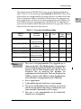
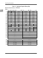
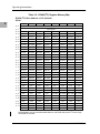
MVME197LE/D2A1
May 1994
Supplement to
MVME197LE
Single Board Computer
User’s Manual
(MVME197LE/D2)
The attached pages are replacements for the corresponding pages in the manual. Place
this page behind the title page of the manual as a record of this change. Please replace
the pages according to the following table:
Replace Old
v/vi,
1-1/1-2,
3-1/3-2 through 3-7/3-8,
3-13/3-14,
4-3/4-4,
A-1/A-2,
A-3/A-4
With New
v/vi,
1-1/1-2,
3-1/3-2 through 3-7/3-8,
3-13/3-14,
4-3/4-4,
A-1/A-2,
A-3/A-4
❏
A vertical bar (|) in the margin of a replacement page indicates a text
change or addition.
❏
The supplement number is shown at the bottom of each replacement page.
Notice
While reasonable efforts have been made to assure the accuracy of this document,
Motorola, Inc. assumes no liability resulting from any omissions in this document, or
from the use of the information obtained therein. Motorola reserves the right to revise
this document and to make changes from time to time in the content hereof without
obligation of Motorola to notify any person of such revision or changes.
No part of this material may be reproduced or copied in any tangible medium, or
stored in a retrieval system, or transmitted in any form, or by any means, radio,
electronic, mechanical, photocopying, recording or facsimile, or otherwise, without the
prior written permission of Motorola, Inc.
Restricted Rights Legend
If the documentation contained herein is supplied, directly or indirectly, to the U.S.
Government, the following notice shall apply unless otherwise agreed to in writing by
Motorola, Inc.
Use, duplication, or disclosure by the Government is subject to restrictions as set forth
in subparagraph (c)(1)(ii) of the Rights in Technical Data and Computer Software
clause at DFARS 252.227-7013.
Motorola, Inc.
Computer Group
2900 South Diablo Way
Tempe, Arizona 85282-9602
Related Documentation
The following publications are applicable to the MVME197LE module and may
provide additional helpful information. If not shipped with this product, they may be
purchased by contacting your Motorola sales office.
Document Title
Motorola
Publication Number
MVME197LE, MVME197DP, and MVME197SP Single
Board Computers Programmer’s Reference Guide
MVME197PG
MVME197BUG 197Bug Debugging Package User’s Manual
MVME197BUG
MVME197BUG 197Bug Diagnostic Firmware User’s Manual MVME197DIAG
MVME712M Transition Module and P2 Adapter Board
User’s Manual
MVME712M
MVME712-12, MVME712-13, MVME712A, MVME712AM, MVME712A
and MVME712B Transition Module and LCP2 Adapter Board
User’s Manual
MC68040/MC68EC040/MC68CL040 Microprocessor User’s
Manual
M68040UM/AD
MC88110 Second Generation RISC Microprocessor User’s
Manual
MC88110UM/AD
N ote
Although not shown in the above list, each Motorola
Computer Group manual publication number is suffixed
with characters which represent the revision level of the
document, such as “/D2” (the second revision of a manual);
a supplement bears the same number as the manual but has
a suffix such as “/A1” (the first supplement to the manual).
To further assist your development effort, Motorola has collected user’s manuals for
each of the peripheral controllers used on the MVME197 module series and other
boards from the suppliers. This bundle includes manuals for the following:
68-1X7DS for use with the MVME197 series of Single Board Computers.
NCR 53C710 SCSI Controller Data Manual and Programmer’s Guide
Intel i82596 Ethernet Controller User’s Manual
Cirrus Logic CD2401 Serial Controller User’s Manual
SGS-Thompson MK48T08 NVRAM/TOD Clock Data Sheet
The following non-Motorola publications may also be of interest and may be obtained
from the sources indicated. The VMEbus Specification is contained in ANSI/IEEE
Standard 1014-1987.
ANSI/IEEE Std 1014-1987
Versatile Backplane Bus: VMEbus
The Institute of Electrical and Electronics
Engineers, Incorporated
Publication and Sales Department
345 East 47th Street
New York, New York 10017-2633
Telephone: 1-800-678-4333
ANSI Small Computer System Interface-2
(SCSI-2), Draft Document X3.131-198X,
Revision 10c
Global Engineering Documents
P.O. Box 19539
Irvine, California 92713-9539
Telephone (714) 979-8135
GENERAL INFORMATION
1
Introduction
This user’s manual provides general information, preparation for use and
installation instructions, operating instructions, and a functional description
for the MVME197LE version of the MVME197 series of single board
computers.
General Description
The MVME197LE module is a double-high VMEmodule based on the
MC88110 RISC (Reduced Instruction Set Computing) microprocessor. The
MVME197LE has 32/64MB of DRAM, 1MB of FLASH memory, 8KB of static
RAM (with battery backup), a time of day clock (with battery backup), an
Ethernet transceiver interface, four serial ports with EIA-232-D interface, six
tick timers, a watchdog timer, 128/256KB of BOOT ROM, a SCSI bus interface
with DMA (Direct Memory Access), a Centronics printer port, an
A16/A24/A32/D8/D16/D32 VMEbus master/slave interface, and a VMEbus
system controller.
Input/Output (I/O) signals are routed through the MVME197LE’s backplane
connector P2. A P2 Adapter Board or LCP2 Adapter board routes the signals
and grounds from connector P2 to an MVME712 series transition module. The
MVME197LE supports the MVME712M, MVME712A, MVME712AM, and
MVME712B transition boards (referred to here as the MVME712X, unless
separately specified). The MVME197LE also supports the MVME712-12 and
MVME712-13 (referred to as the MVME712-XX, unless separately specified).
These transition boards provide configuration headers, serial port drivers, and
industry standard connectors for the I/O devices.
The MVME197LE modules have eight ASIC devices (Application-Specific
Integrated Circuits) described in the following order: BusSwitch, DCAM,
ECDM, PCC2, and VME2.
The BusSwitch ASIC provides an interface between the processor bus
(MC88110 bus) and the local peripheral bus (MC68040 compatible bus). Refer
to the MVME197LE block diagram (Figure 1-1). It provides bus arbitration for
the MC88110 bus and serves as a seven level interrupt handler. It has
programmable map decoders for both busses, as well as write post buffers on
each, two tick timers, and four 32-bit general purpose registers.
MVME197LE/D2A1
1-1
1
General Information
N ote
For the MVME197 series, the term Local Bus, as used in
other MVME1xx Single Board Computer series, is referred
to as the Local Peripheral Bus.
The DCAM (DRAM Controller and Address Multiplexer) ASIC provides the
address multiplexers and RAS/CAS/WRITE control for the DRAM as well as
data control for the ECDM.
The ECDM (Error Correction and Data Multiplexer) ASIC multiplexes
between four data paths on the DRAM array. Since the device handles 16 bits,
four such devices are required on the MVME197LE to accommodate the 64-bit
data bus of the MC88110 microprocessor. Single-bit error correction and
double-bit detection is performed in the ECDM.
The PCCchip2 (Peripheral Channel Controller) ASIC provides two tick timers
and the interface to the LAN chip, the SCSI chip, the serial port chip, the
printer port, and the BBRAM (Battery Backup RAM).
The VMEchip2 ASIC provides a VMEbus interface. The VMEchip2 includes
two tick timers, a watchdog timer, programmable map decoders for the master
and slave interfaces, and a VMEbus to/from the local peripheral bus DMA
controller, a VMEbus to/from the local peripheral bus non-DMA
programmed access interface, a VMEbus interrupter, a VMEbus system
controller, a VMEbus interrupt handler, and a VMEbus requester.
The local peripheral bus to VMEbus transfers can be D8, D16, or D32.
VMEchip2 DMA transfers to the VMEbus, however, can be 64 bits wide as
Block Transfer (BLT).
Features
These are some of the major features of the MVME197LE single board
computer:
1-2
❏
MC88110 RISC Microprocessor
❏
32 or 64 megabytes of 64-bit Dynamic Random Access Memory (DRAM)
with error correction
❏
1 megabyte of FLASH memory
❏
Six status LEDs (FAIL, RUN, SCON, LAN, SCSI, and VME)
❏
8 kilobytes of Static Random Access Memory (SRAM) and Time of Day
(TOD) clock with Battery Backup RAM (BBRAM)
❏
Two push-button switches (ABORT and RESET)
MVME197LE/D2A1
OPERATING
INSTRUCTIONS
3
Introduction
This chapter provides the necessary information to use the MVME197LE
VMEmodule in a system configuration. This includes controls and indicators,
memory maps, and software initialization of the module.
Controls and Indicators
The MVME197LE Single Board Computer has two push-button switches
(ABORT and RESET) and six LED (Light Emitting Diode) indicators (FAIL,
SCON, RUN, LAN, VME, and SCSI), all located on the front panel of the
module.
ABORT Switch S2
When enabled by software, the front panel ABORT switch (S2) generates an
NMI (Non-Maskable Interrupt) type interrupt at a user-programmable level.
It is normally used to abort program execution and return to the 197Bug
debugger. Refer to the VMEchip2 chapter of the MVME197LE, MVME197DP,
and MVME197SP Single Board Computers Programmer’s Reference Guide for more
information.
RESET Switch S3
The RESET switch (S3) will reset all the onboard devices and drive the
SYSRESET* signal if the MVME197LE module is the system controller. The
RESET switch (S3) will reset all the onboard devices, with the exception of the
DCAM and ECDM, if the MVME197LE module is not the system controller.
The VMEchip2 generates the SYSRESET* signal. The BusSwitch combines the
local reset and the reset switch to generate a local board reset. Refer to the Reset
Driver section in the VMEchip2 chapter of the MVME197LE, MVME197DP, and
MVME197SP Single Board Computers Programmer’s Reference Guide for more
information.
The BusSwitch receives the reset switch signal, debounces it and combines
with the reset signal from the VMEchip2 to generate a board reset signal.
The VMEchip2 includes both a global and a local reset driver. When the chip
operates as the VMEbus system controller, the reset driver provides a global
system reset by asserting the VMEbus signal SYSRESET*. A SYSRESET* may
MVME197LE/D2A1
3-1
Operating Instructions
be generated by the RESET switch, a power up reset, a watchdog timeout, or
by a control bit in the LCSR. SYSRESET* remains asserted for at least 200 msec,
as required by the VMEbus specification.
3
Similarly, the VMEchip2 provides an input signal and a control bit to initiate
a local reset operation. By setting a control bit, software can maintain a board
in a reset state, disabling a faulty board from participating in normal system
operation.
The local reset driver is enabled even when the VMEchip2 is not the system
controller. A local reset may be generated by the RESET switch, a power up
reset, a watchdog timeout, a VMEbus SYSRESET*, or a control bit in the GCSR.
Front Panel Indicators (DS1-DS6)
The six LEDs on the MVME197LE front panel are: FAIL, SCON, RUN, LAN,
VME, and SCSI.
1.
The yellow FAIL LED (DS1) is lit when the BRDFAIL signal line is active.
2.
The green SCON LED (DS2) is lit when the VMEchip2 is the VMEbus
system controller.
3.
The green RUN LED (DS3) is lit when the MC88110 bus MC* pin is low.
4.
The green LAN LED (DS4) lights when the LAN chip is the local
peripheral bus master.
5.
The green VME LED (DS5) lights when the board is using the VMEbus or
when the board is accessed by the VMEbus.
6.
The green SCSI LED (DS6) lights when the SCSI chip is the local peripheral
bus master.
Memory Maps
There are three points of view for the memory maps: 1) the mapping of all
resources as viewed by the Processor Bus (MC88110 bus), 2) the mapping of
onboard/off-board resources as viewed from the Local Peripheral Bus
(MC68040 compatible bus), and 3) the mapping of onboard resources as
viewed by VMEbus Masters (VMEbus memory map).
Processor Bus Memory Map
Care should be taken, since all three maps are programmable. It is
recommended that direct mapping from the Processor Bus to the Local
Peripheral Bus be used.
3-2
MVME197LE/D2A1
Memory Maps
The memory maps of MVME197LE devices are provided in the following
tables. Table 3-1 is the entire map from $00000000 to $FFFFFFFF. Many areas
of the map are user-programmable, and suggested uses are shown in the table.
This is assuming no address translation is used between the processor and
local peripheral bus and between the local peripheral bus and VMEbus. The
cache inhibit function is programmable in the MC88110. The onboard I/O
space must be marked cache inhibit and serialized in its page table. Table 3-2
further defines the map for the local devices.
Table 3-1. Processor Bus Memory Map
Address
Range
Devices
Accessed
$00000000 - (DRAMSIZE -1) User Programmable
(Onboard DRAM)
DRAMSIZE - $FF7FFFFF
$FF800000 - $FFBFFFFF
Size
D64
DRAMSIZE
N
1
3GB
?
2,3
4MB
N
5
User Programmable D32/D16
(VMEbus)
Flash Memory
Software
Cache Notes
Inhibit
Port
Size
D32
$FFC00000 - $FFEFFFFF
reserved
---
3MB
---
4
$FFF00000 - $FFFEFFFF
Local Devices
(Refer to next table)
D32-D8
1MB
Y
---
$FFFF0000 - $FFFFFFFF
User Programmable D32/D16
(VMEbus A16)
64KB
?
1,3
N otes
1. This area is user-programmable. The suggested use is
shown in the table. The DRAM decoder is programmed
in the DCAM through the ECDM I2C bus interface. The
Processor Bus to Local Peripheral Bus and the Local
Peripheral Bus to Processor Bus decoders are
programmed in the BusSwitch. The Local Peripheral to
VMEbus (master) and VMEbus to Local Peripheral Bus
(slave) decoders are programmed in the VMEchip2.
2. Size is approximate.
3. Cache inhibit depends on devices in area mapped.
4. This area is not decoded. If these locations are accessed
and the local peripheral bus timer is enabled, the cycle
times out and is terminated by a TEA signal.
5. This area is user programmable via the BusSwitch.
Default size is 4 megabytes.
MVME197LE/D2A1
3-3
3
Operating Instructions
The following table focuses on the Local Devices portion of the Memory Map.
Table 3-2. Local Devices Memory Map
3
Address Range
$FFF00000 $FFF01000 $FFF02000 $FFF03000 $FFF04000 $FFF05000 $FFF06000 $FFF07000 $FFF08000 $FFF40000 $FFF40100 $FFF40200 $FFF41000 $FFF42000 $FFF43000 $FFF44000 $FFF45000 $FFF46000 $FFF47000 $FFF48000 $FFF50000 $FFF70000 $FFF78000 $FFF80000 $FFFC0000 $FFFD0000-
N otes
$FFF00FFF
$FFF01FFF
$FFF02FFF
$FFF03FFF
$FFF04FFF
$FFF05FFF
$FFF06FFF
$FFF07FFF
$FFF3FFFF
$FFF400FF
$FFF401FF
$FFF40FFF
$FFF41FFF
$FFF42FFF
$FFF43FFF
$FFF44FFF
$FFF45FFF
$FFF46FFF
$FFF47FFF
$FFF4FFFF
$FFF6FFFF
$FFF77FFF
$FFF7FFFF
$FFFBFFFF
$FFFCFFFF
$FFFEFFFF
Devices Accessed
Port Size
BusSwitch
ECDM (DCAM access)
reserved
reserved
reserved
reserved
reserved
User defined
reserved
VMEchip2 (LCSR)
VMEchip2 (GCSR)
reserved
reserved
PCCchip2
reserved
reserved
CD2401 (Serial Comm. Cont.)
82596CA (LAN)
53C710 (SCSI)
reserved
reserved
reserved
reserved
DROM (BOOT ROM)
MK48T08 (BBRAM,TOD Clk)
reserved
D64-D8
----------------D32
D32-D8
----D32-D8
----D16-D8
D32
D32/D8
----------D32-D8
---
Size
4KB
4KB
4KB
4KB
4KB
4KB
4KB
4KB
224KB
256B
256B
3.5KB
4KB
4KB
4KB
4KB
4KB
4KB
4KB
32KB
128KB
32KB
288KB
256KB
64KB
128KB
Notes
1
1
4
4
4
4
4
4
4
1,2,3
1,2,3
4,5
4
1,2
4
3
1,2
1,2,6
1,2
4
4
4
4
7
1,2
4
1. For a complete description of the register bits, refer to
the appropriate data sheet for the specific chip. For a
more detailed memory map refer to the detailed
peripheral device memory maps in the MVME197LE,
MVME197DP, and MVME197SP Single Board Computers
Programmer’s Reference Guide.
2. Address is the physical address going to the device. It is
after the BusSwitch translation from the MC88110
address to the device seen address.
3-4
MVME197LE/D2A1
Memory Maps
3. Writes to the LCSR in the VMEchip2 must be 32 bits.
LCSR writes of 8 or 16 bits terminate with a TEA signal.
Writes to the GCSR may be 8, 16, or 32 bits. Reads to the
LCSR and GCSR may be 8, 16, or 32 bits.
3
4. This area does not return an acknowledge signal. If the
processor bus timeout timer is enabled, the access times
out and is terminated by a TEA signal.
5. Size is approximate.
6. Port commands to the 82596CA must be written as two
16-bit writes: upper word first and lower word second.
7. DROM (BOOT ROM) appears at $0 following a local
peripheral bus reset. The DROM appears at 0 until the
DR0 bit is cleared in the PCCchip2. In addition, the
ROM0 bit in the ROMCR register of the BusSwitch
must be cleared before the DRAM is accessed.
Detailed I/O Memory Maps
Tables 3-3 through 3-14 give the detailed memory maps for the BusSwitch
register, the ECDM CSR register, the DCAM (I2C) register, the VMEchip2
register, the PCCchip2 register, the printer register, the CD2401 Serial Port
register, the Ethernet LAN register, the SCSI Controller register, and the
BBRAM/TOD Clock register.
MVME197LE/D2A1
3-5
Operating Instructions
Table 3-3. BusSwitch Register Memory Map
BusSwitch Base Address = $FFF00000
Offset
3
63
56
55
48
47
32
31
16
15
0
0
CHIPID CHIPREV
GCSR
IODATA
IODIR
8
PSAR1
PEAR1
PSAR2
PEAR2
10
PSAR3
PEAR3
PSAR4
PEAR4
18
PTR1
PTSR1
PTR2
PTSR2
20
PTR3
PTSR3
PTR4
PTSR4
28
SSAR1
SEAR1
SSAR2
SEAR2
30
SSAR3
SEAR3
SSAR4
SEAR4
38
STR1
STSR1
STR2
STSR2
40
STR3
STSR3
STR4
STSR4
48
PAR1
50
PAR2
68
PAR4
SAR1
SAR2
BTIMER PADJUST PCOUNT
58
60
PAR3
WPPA
ROMCR
ABORT
CPINT
SAR3
PAL
WPTPA
WPPAT
TCTRL1
TCTRL2
LEVEL
MASK
ISEL0
ISEL1
TINT1
TINT2
WPINT
PALINT
XINT
VBASE
70
TCOMP1
TCOUNT1
78
TCOMP2
TCOUNT2
80
GPR1
GPR2
88
GPR3
GPR4
90
XCTAGS
100
XCCR
VECTOR1
108
VECTOR2
VECTOR3
110
VECTOR4
VECTOR5
118
VECTOR6
VECTOR7
3-6
SAR4
MVME197LE/D2A1
MVME197LE/D2A1
Table 3-4. ECDM CSR Register Memory Map
Sub-System Memory CSR Base Address = $FFF01000
Offset/Register:
ECDM0
ECDM1
ECDM2
ECDM3
ADDR/REGISTER ADDR/REGISTER ADDR/REGISTER ADDR/REGISTER ADDR/REGISTER ADDR/REGISTER ADDR/REGISTER ADDR/REGISTER
00 / MEMCON0
01 / ECDMID0
02 / MEMCON1
03 / ECDMID1
04 / MEMCON2
05 / ECDMID2
06 / MEMCON3
07 / ECDMID3
08 / SYNSTAT0
09 / ERSTAT0
0A / SYNSTAT1
0B / ERSTAT1
0C / SYNSTAT2
0D / ERSTAT2
0E / SYNSTAT3
0F / ERSTAT3
10 / I2CON0
11 / I2STAT0
12 / I2CON1
13 / I2STAT1
14 / I2CON2
15 / I2STAT2
16 / I2CON3
17 / I2STAT3
18 / I2DATA0
19 / I2ADDR0
1A / I2DATA1
1B / I2ADDR1
1C / I2DATA2
1D / I2ADDR2
1E / I2DATA3
1F / I2ADDR3
D63
D56 D55
D48 D47
D40
D39
D32
D31
D24
D23
D16
D15
D8
D7
D0
ECDM register map of four ECDM devices in a 64-bit system. The byte offset address is shown next to each register.
Memory Maps
3-7
3
Operating Instructions
Table 3-5. DCAM (I2C) Register Memory Map
DCAM (I2C) Base Address = $C0 (default)
Offset
3
BIT 7
BIT 6
BIT 5
00 00
BIT 3
BIT 2
BIT 1
BIT 0
SL26
SL25
DISRAM
ID Register
01 01
02 02
BIT 4
Version Register
SL31
SL30
SL29
SL28
SL27
03 03
SH31
SH30
SH29
SH28
SH27
SH26
SH25
SCRUB1TIME
04 04
CASCLKSL
CASCLK2
CASCLK1
PGMODE
ONEBANK
DRAMSIZ3
DRAMSIZ2
DRAMSIZ1
05 05
REF7
REF6
REF5
REF4
REF3
REF2
REF1
REF0
06 06
REFTAIL4
REFTAIL3
REFTAIL2
REFTAIL1
REF11
REF10
REF9
REF8
07 07
NOT USED
NOT USED
RDTAIL5
RDTAIL4
RDTAIL3
RDTAIL2
RDTAIL1
RTCLKSL
08 08
READACK7
READACK6
READACK5
READACK4
READACK3
READACK2
READACK1
INTRRUPT
09 09
NOT USED
READOE6
READOE5
READOE4
READOE3
READOE2
READOE1
NOT USED
0A 10
FECCKSL
BREADOE6
BREADOE5
BREADOE4
BREADOE3
BREADOE2
BREADOE1
PCGCLKSL
0B 11
PCHG7
PCHG6
PCHG5
PCHG4
PCHG3
PCHG2
PCHG1
PCHG0
0C 12
SLECDM5
SLECDM4
SLECDM3
SLECDM2
FLECDM4
FLECDM3
FLECDM2
FLECDM1
0D 13
NOT USED
ERAMOE6
ERAMOE5
ERAMOE4
ERAMOE3
ERAMOE2
ERAMOE1
ROECLKSL
0D 14
NOT USED
0F 15
CSRTAIL7
RMWRMOE6 RMWRMOE5 RMWRMOE4 RMWRMOE3 RMWRMOE2 RMWRMOE1
CSRTAIL6
CSRTAIL5
CSRTAIL4
CSRTAIL3
CSRTAIL2
CSRTAIL1
RMWOE5
NOT USED
10 16
BWRTTL4
BWRTTL3
BWRTTL2
BWRTTL1
RMWOE4
RMWOE3
RMWOE2
RMWOE1
11 17
SECCLKSL
RMWOCKSL
BWRITE5
BWRITE4
BWRITE3
BWRITE2
BWRITE1
WRCLKSEL
12 18
NOT USED
NOT USED
RMW5
RMW4
RMW3
RMW2
RMW1
NOT USED
13 19
RMWTAIL7
RMWTAIL6
RMWTAIL5
RMWTAIL4
RMWTAIL3
RMWTAIL2
RMWTAIL1
RMWTLCSL
14 20
CBRDOE3
CBRDOE2
CBRDOE1
NOT USED
CREADOE3
CREADOE2
CREADOE1
BWRTCSL
15 21
SC9
SC8
SC7
SC6
SC5
SC4
SC3
SC2
16 22
SC17
SC16
SC15
SC14
SC13
SC12
SC11
SC10
17 23
SC25
SC24
SC23
SC22
SC21
SC20
SC19
SC18
18 24
NOT USED
SC32
SC31
SC30
SC29
SC28
SC27
SC26
19 25
NOT USED
NOT USED
NOT USED
CBTAIL4
CBTAIL3
CBTAIL2
CBTAIL1
CBTLCKSL
1A 26
CSR7
CSR6
CSR5
CSR4
NOT USED
NOT USED
NOT USED
NOT USED
1B 27
CSR15
CSR14
CSR13
CSR12
CSR11
CSR10
CSR9
CSR8
1C 28
CSR23
CSR22
CSR21
CSR20
CSR19
CSR18
CSR17
CSR16
1D 29
CSR31
CSR30
CSR29
CSR28
CSR27
CSR26
CSR25
CSR24
1E 30
NOT USED
NOT USED
BRDTAIL5
BRDTAIL4
BRDTAIL3
BRDTAIL2
BRDTAIL1
NOT USED
BIT 7
BIT 6
BIT 5
BIT 4
BIT 3
BIT 2
BIT 1
BIT 0
1F 31
DCAM registers are only accessible/addressable on the DRAM sub-system I2C bus through
the ECDM I2C interface.
3-8
MVME197LE/D2A1
MVME197LE/D2A1
Table 3-7. PCCchip2 Memory Map
PCCchip2 LCSR Base Address = $FFF42000
OFFSET:
D31
D30
D29
00
D28
D27
D26
D25
D24
D23
D22
D21
CHIP ID
D20
D19
D18
D17
D16
CHIP REVISION
D15
D14
TIC TIMER 1 COMPARE
08
TIC TIMER 1 COUNTER
0C
TIC TIMER 2 COMPARE
10
TIC TIMER 2 COUNTER
18
PRESCALER COUNT
GPI
PLTY
GPI
E/L*
GPI
INT
GPI
IEN
GPI
ICLR
SCC SCC
RTRY PAR
ERR ERR
1C
SCC
EXT
ERR
SCC
LTO
ERR
GPI
SCC
SCLR
SCC
MDM
SCC
MDM
SCC
MDM
D11
OVERFLOW
COUNTER 2
PRESCALER CLOCK ADJUST
GPI
IRQ LEVEL
D12
GIOE
D10
D9
D8
D7
D6
D5
CPU MSTR FAST
040
INT BRAM
EN
04
14
D13
DR0
GPO
SCC MODEM
IRQ LEVEL
CLR
OVF
2
COC
2
TIC
2
TIC2
INT
TIC2
IEN
TIC2
ICLR
TIC TIMER 2
IRQ LEVEL
SCC
TX
IRQ
SCC
TX
IEN
SCC
TX
AVEC
SCC TRANSMIT
IRQ LEVEL
D4
D3
D2
D1
D0
CLR
OVF
1
COC
1
TIC
1
VECTOR BASE
OVERFLOW
COUNTER 1
SCC
SC1
SCC
SC2
20
TIC1
INT
TIC1
IEN
TIC1
ICLR
TIC TIMER 1
IRQ LEVEL
SCC
IRQ
SCC
IEN
SCC
AVEC
SCC RECEIVE
IRQ LEVEL
SCC MODEM PIACK
24
SCC TRANSMIT PIACK
LAN
EXT
ERR
LAN
LTO
ERR
2C
SCSI
PAR
ERR
SCSI
EXT
ERR
SCSI SCSI
LTO SCLR
ERR
30
PRTR PRTR PRTR PRTR PRTR
ACK ACK ACK ACK ACK
INT
IEN ICLR
PLTY E/L*
PRTR ACK
IRQ LEVEL
34
PRTR PRTR PRTR PRTR PRTR
BSY BSY BSY BSY BSY
INT
IEN ICLR
PLTY E/L*
PRTR BSY
IRQ LEVEL
38
SCC RECEIVE PIACK
LAN
PLTY
LAN
SCLR
PRTR PRTR PRTR PRTR PRTR
FLT
FLT
FLT
FLT
FLT
PLTY E/L*
INT
IEN ICLR
PRTR FAULT
IRQ LEVEL
LAN
E/L*
LAN
INT
LAN
IEN
LAN
ICLR
PRTR PRTR PRTR PRTR PRTR
SEL
SEL
SEL
SEL
SEL
PLTY E/L*
INT
IEN ICLR
PRTR
ANY
INT
LAN
IRQ LEVEL
LAN
SC1
PRTR SEL
IRQ LEVEL
LAN
SC2
LAN
ERR
INT
LAN
ERR
IEN
SCSI
IRQ
SCSI
IEN
LAN ERR
IRQ LEVEL
SCSI INT
IRQ LEVEL
PRTR PRTR PRTR PRTR PRTR
PE
PE
PE
PE
PE
PLTY E/L*
INT
IEN ICLR
PRTR PRTR PRTR PRTR PRTR
ACK
FLT
SEL
PE
BSY
CHIP SPEED
LAN
ERR
ICLR
PRTR PE
IRQ LEVEL
PRTR PRTR PRTR PRTR PRTR
DAT
INP
STB FAST MAN
ENBL
ASTB STB
PRINTER DATA
INTERRUPT
IPL LEVEL
3C
D31
D30
D29
D28
D27
D26
D25
D24
D23
D22
D21
D20
D19
D18
D17
D16
D15
D14
D13
D12
D11
D10
D9
D8
INTERRUPT
MASK LEVEL
D7
D6
D5
D4
D3
D2
D1
D0
3-13
Memory Maps
28
LAN
PAR
ERR
3
Operating Instructions
Table 3-8. Printer Memory Map
Printer ACK Interrupt Control Register
3
BIT
NAME
$FFF42030
31
30
29
28
27
26
25
24
PLTY
E/L*
INT
IEN
ICLR
IL2
IL1
IL0
Printer FAULT Interrupt Control Register
BIT
NAME
$FFF42031
23
22
21
0
19
18
17
16
PLTY
E/L*
INT
IEN
ICLR
IL2
IL1
IL0
Printer SEL Interrupt Control Register
BIT
NAME
$FFF42032
15
14
13
12
11
10
9
8
PLTY
E/L*
INT
IEN
ICLR
IL2
IL1
IL0
Printer PE Interrupt Control Register
BIT
NAME
$FFF42033
7
6
5
4
3
2
1
0
PLTY
E/L*
INT
IEN
ICLR
IL2
IL1
IL0
Printer BUSY Interrupt Control Register
BIT
NAME
$FFF42034
31
30
29
28
27
26
25
24
PLTY
E/L*
INT
IEN
ICLR
IL2
IL1
IL0
Printer Input Status Register
BIT
NAME
15
14
$FFF42036
13
PINT
12
11
10
9
8
ACK
FLT
SEL
PE
BSY
Printer Port Control Register
BIT
7
6
$FFF42037
5
NAME
4
3
2
1
0
DOEN
INP
STB
FAST
MAN
Printer Data Register (16 bits)
BIT
NAME
$FFF4203A
15-0
PD15-PD0
Printer memory map is part of the PCCchip2 (refer to PCCchip2 Memory Map).
3-14
MVME197LE/D2A1
MVME197LE Functional Description
BOOT ROM
The board accommodates a 32-pin PLCC/CLCC ROM/EPROM referred to as
BOOT ROM or DROM (Download ROM). It is organized as a 128K/256K x 8
device, but as viewed from the processor it looks like a 16K/32K x 64 memory.
This memory is mapped starting at location $FFF80000, but after a local reset
it is also mapped at location 0, providing a reset vector and bootstrap code for
the processor. The DR0 bit in the General Control Register (GCR) of the
PCCchip2 must be cleared to disable the BOOT ROM memory map at 0.
FLASH Memory
1MB of FLASH memory is available on the board. FLASH memory works like
EPROM, but can be erased and reprogrammed by software. It is organized as
32 bits wide, but to the processor it looks as 64 bits wide. It is mapped at
location $FF800000. Reads can be of any size, including burst transfers, but
writes are always 32 bits wide, regardless of the size specified for the transfer.
For this reason, software should only use 32-bit write transfers. This memory
is controlled by the BusSwitch, and the memory size, access time, and write
enable capability can be programmed via the ROM Control Register (ROMCR)
in the BusSwitch. The FLASH memory can be accessed from the processor bus
only. It is not accessible from the local peripheral bus or VMEbus.
Onboard DRAM
The MVME197LE onboard DRAM (2 banks of 32MB memory, one optionally
installed) is sized at 32MB using 1M x 4 devices and configured as 256 bits
wide. The DRAM is four-way interleaved to efficiently support cache burst
cycles. The DRAM is controlled by the DCAM and ECDM, and the map
decoders in the DCAM can be programmed through the I2Cbus interface in the
ECDM to accommodate different base address(es) and sizes. The onboard
DRAM is not reset by a local peripheral bus reset. Refer to the DCAM and
ECDM chapters in the MVME197LE, MVME197DP, and MVME197SP Single
Board Computers Programmer’s Reference Guide for detailed programming
information.
Battery Backup RAM and Clock
The MK48T08 RAM and clock chip is used on the MVME197LE. This chip
provides a time of day clock, oscillator, crystal, power fail detection, memory
write protection, 8KB of RAM, and a battery in one 28-pin package. The clock
provides seconds, minutes, hours, day, date, month, and year in BCD 24-hour
MVME197LE/D2A1
4-3
4
Functional Description
format. Corrections for 28-, 29-, (leap year) and 30-day months are
automatically made. No interrupts are generated by the clock. The MK48T08
is an 8-bit device; however the interface provided by the PCCchip2 supports
8-, 16-, and 32-bit accesses to the MK48T08. Refer to the PCCchip2 chapter in
the MVME197LE, MVME197DP, and MVME197SP Single Board Computers
Programmer’s Reference Guide and to the MK48T08 data sheet for detailed
programming information.
4
VMEbus Interface
The local peripheral bus to VMEbus interface, the VMEbus to local peripheral
bus interface, and the local-VMEbus DMA controller functions on the
MVME197LE are provided by the VMEchip2. The VMEchip2 can also provide
the VMEbus system controller functions. Refer to the VMEchip2 chapter in the
MVME197LE, MVME197DP, and MVME197SP Single Board Computers
Programmer’s Reference Guide for detailed programming information.
I/O Interfaces
The MVME197LE provides onboard I/O for many system applications. The
I/O functions include serial ports, a printer port, an Ethernet transceiver
interface, and a SCSI mass storage interface.
Serial Port Interface
The CD2401 serial controller chip (SCC) is used to implement the four serial
ports. The serial ports support the standard baud rates (110 to 38.4K baud).
Serial port 4 also supports synchronous modes of operation.
The four serial ports are different functionally because of the limited number
of pins on the I/O connector.
Serial port 1 is a minimum function asynchronous port. It uses RXD, CTS,
TXD, and RTS.
Serial ports 2 and 3 are full function asynchronous ports. They use RXD,
CTS, DCD, TXD, RTS, and DTR.
Serial port 4 is a full function asynchronous or synchronous port. It can
operate at synchronous bit rates up to 64k bits per second. It uses RXD,
CTS, DCD, RTS, and DTR. It also interfaces to the synchronous clock
signal lines.
Refer to the MVME197LE, MVME197DP, and MVME197SP Single Board
Computers Programmer’s Reference Guide for drawings of the serial port interface
connections.
4-4
MVME197LE/D2A1
EIA-232-D
INTERCONNECTIONS
A
The EIA-232-D Standard is the most widely used interface between terminals
and computers or modems, and yet it is not fully understood. This is because
all the lines are not clearly defined, and many users do not see the need to
conform for their applications. A system should easily connect to any other.
Many times designers think only of their own equipment, but the state-of-theart is computer-to-computer or computer-to-modem operation.
The EIA-232-D Standard was originally developed by the Bell System to
connect terminals via modems. Therefore, several handshaking lines were
included. In many applications these are not needed, but since they permit
diagnosis of problems, they are included in many applications.
Table A-1 lists the standard EIA-232-D interconnections. To interpret this
information correctly it is necessary to know that EIA-232-D is intended to
connect a terminal to a modem. When computers are connected to computers
without modems, one of them must be configured as a terminal and the other
as a modem. Because computers are normally configured to work with
terminals, they are said to be configured as a modem. Also, the signal levels
must be between +3 and +15 volts for a high level, and between -3 and -15 volts
for a low level. Any attempt to connect units in parallel may result in out of
range voltages and is not allowed by the EIA-232-D specifications.
MVME197LE/D2A1
A-1
A
EIA-232-D Interconnections
Table A-1. EIA-232-D Interconnections
A-2
Pin
Number
Signal
Mnemonic
1
---
2
TXD
TRANSMIT DATA - data to be transmitted is furnished on
this line to the modem from the terminal.
3
RCD
RECEIVE DATA - data which is demodulated from the
receive line is presented to the terminal by the modem.
4
RTS
REQUEST TO SEND - RTS is supplied by the terminal to the
modem when required to transmit a message. With RTS off,
the modem carrier remains off. When RTS is turned on, the
modem immediately turns on the carrier.
5
CTS
CLEAR TO SEND - CTS is a function supplied to the
terminal by the modem which indicates that it is permissible
to begin transmission of a message. When using a modem,
CTS follows the off-to-on transition of RTS after a time
delay.
6
DSR
DATA SET READY - data set ready is a function supplied
by the modem to the terminal to indicate that the modem is
ready to transmit data.
7
SIG-GND
8
DCD
9-14
---
15
TXC
16
---
17
RXC
18,19
---
20
DTR
21
---
Signal Name and Description
Not used.
SIGNAL GROUND - common return line for all signals at
the modem interface.
DATA CARRIER DETECT - sent by the modem to the
terminal to indicate that a valid carrier is being received.
Not used.
TRANSMIT CLOCK - this line clocks output data to the
modem from the terminal.
Not used.
RECEIVE CLOCK - this line clocks input data from a
terminal to a modem.
Not used.
DATA TERMINAL READY - a signal from the terminal to
the modem indicating that the terminal is ready to send or
receive data.
Not used.
MVME197LE/D2A1
EIA-232-D Interconnections
Table A-1. EIA-232-D Interconnections (Continued)
Pin
Number
Signal
Mnemonic
22
RI
RING INDICATOR - RI is sent by the modem to the
terminal. This line indicates to the terminal that an incoming
call is present. The terminal causes the modem to answer the
phone by carrying DTR true while RI is active.
23
---
Not used.
24
TXC
TRANSMIT CLOCK - Same as TXC on pin 15.
25
BSY
BUSY - a positive EIA signal applied to this pin causes the
modem to go off-hook and make the associated phone busy.
N otes
Signal Name and Description
1. High level = +3 to +15 volts. Low level = -3 to -15 volts.
2. EIA-232-D is intended to connect a terminal to a modem.
When computers are connected to computers without
modems, one of the computers must be configured as a
modem and the other as a terminal.
There are several levels of conformance that are appropriate for typical EIA232-D interconnections. The bare minimum requirement is the two data lines
and a ground. The full version of EIA-232-D requires 12 lines and
accommodates automatic dialing, automatic answering, and synchronous
transmission. A middle-of-the-road approach is illustrated in Figure A-1.
One set of handshaking signals frequently implemented are RTS and CTS. CTS
is used in many systems to inhibit transmission until the signal is high. In the
modem applications, RTS is turned around and returned as RTS after 150
microseconds. RTS is programmable in some systems to work with the older
type 202 modem (half duplex). CTS is used in some systems to provide flow
control to avoid buffer overflow. This is not possible if modems are used. It is
usually necessary to make CTS high by connecting it to RTS or to some source
of +12 volts such as the resistors shown in Figure A-1. It is also frequently
jumpered to an MC1488 gate which has its inputs grounded (the gate is
provided for this purpose). Another signal used in many systems is DCD. The
original purpose of this signal was to tell the system that the carrier tone from
the distant modem was being received. This signal is frequently used by the
software to display a message like CARRIER NOT PRESENT to help the user
to diagnose failure to communicate. Obviously, if the system is designed
properly to use this signal, and it is not connected to a modem, the signal must
MVME197LE/D2A1
A-3
A
A
EIA-232-D Interconnections
be provided by a pull-up resistor or gate as described before (see Figure A-1).
Many modems expect a DTR high signal and issue a DSR. These signals are
used by software to help prompt the operator about possible causes of trouble.
The DTR signal is used sometimes to disconnect the phone circuit in
preparation for another automatic call. It is necessary to provide these signals
in order to talk to all possible modems (see Figure A-1). Figure A-1 is a good
minimum configuration that almost always works. If the CTS and DCD signals
are not received from the modem, the jumpers can be moved to artificially
provide the needed signal. Figure A-2 shows a way that an EIA-232-D
connector can be wired to enable a computer to connect to a basic terminal
with only three wires. This is because most terminals have a DTR signal that is
ON and can be used to pull-up the CTS, DCD and DSR signals. Two of these
connectors wired back-to-back can be used. It must be realized that all the
handshaking has been bypassed and possible diagnostic messages do not
occur. Also, the TX and RX lines may have to be crossed since TX from a
terminal is outgoing but the TX line on a modem is an incoming signal.
A-4
MVME197LE/D2A1