1
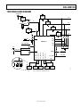
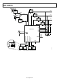
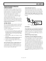
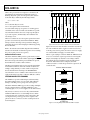
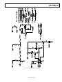
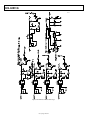
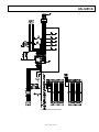
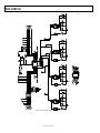
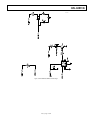
Evaluation Kits for ADM1186 Quad
Sequencer and Monitor
EVAL-ADM1186
FEATURES
4 on-board variables supplies with LEDs to show status
LEDs to show power good, fault, and sequence done (main
evaluation kits only)
Switchable capacitors to set time delays (main evaluation
kits only)
Manual fault push switch
Single step mode
Multiple boards can be cascaded for more than four supplies
(EVAL-ADM1186-1EBZ only)
PRODUCT DESCRIPTION
The ADM1186-1 and ADM1186-2 can be used to turn on and
off four supplies in sequence under the control of a state machine,
and can monitor the supplies to ensure that they are above a
user defined undervoltage (UV) threshold. If any supply drops
below the UV threshold, a fault occurs and the state machine
turns all the supplies off.
GENERAL DESCRIPTION
There are two types of evaluation kits for the ADM1186-1
and ADM1186-2. The main evaluation boards are intended for
standalone operation of the devices with just an external mains
power supply. They provide all the on-board supplies, controls,
and status indicators necessary to operate the device. The
micro-evaluation boards are intended to allow the ADM118-1
or ADM1186-2 to be easily used as part of a bench prototype,
and include the minimal set of components.
The evaluation kits for each device allow a user to perform
controlled up and down sequences of four supplies. The
main evaluation kits allow simulated fault conditions on
each on-board supply or on a control signal. All kits provide
the ability to single-step and observe the behavior of the state
machine during the power-up and power-down sequence.
A single ADM1186-1 can control four supplies, but it is possible
to join multiple devices and boards together to support cascaded
up and down sequences of eight, 12, or more supplies. The main
ADM1186-1 evaluation board supports a daisy-chain
connection to demonstrate this feature.
EVALUATION KIT CONTENTS
The EVAL-ADM1186-1EBZ and EVAL-ADM1186-2EBZ
evaluation kits contain an evaluation board, along with some
samples of the ADM1186-1 or the ADM1186-2 parts.
The EVAL-ADM1186-1MBZ and EVAL-ADM1186-2MBZ
micro-evaluation kits contain only an evaluation board.
For all types of evaluation kit, an ADM1186-1 or ADM1186-2
device is present and soldered to the board.
Rev. 0
Evaluation boards are only intended for device evaluation and not for production purposes.
Evaluation boards are supplied “as is” and without warranties of any kind, express, implied, or
statutory including, but not limited to, any implied warranty of merchantability or fitness for a
particular purpose. No license is granted by implication or otherwise under any patents or other
intellectual property by application or use of evaluation boards. Information furnished by Analog
Devices is believed to be accurate and reliable. However, no responsibility is assumed by Analog
Devices for its use, nor for any infringements of patents or other rights of third parties that may result
from its use. Analog Devices reserves the right to change devices or specifications at any time
without notice. Trademarks and registered trademarks are the property of their respective owners.
Evaluation boards are not authorized to be used in life support devices or systems.
One Technology Way, P.O. Box 9106, Norwood, MA 02062-9106, U.S.A.
www.analog.com
Tel: 781.329.4700
Fax: 781.461.3113
©2008 Analog Devices, Inc. All rights reserved.
EVAL-ADM1186
TABLE OF CONTENTS
Features .............................................................................................. 1
Evaluation Board Operation ............................................................9
Product Description ......................................................................... 1
Power Requirement.......................................................................9
General Description ......................................................................... 1
Getting Started ...............................................................................9
Evaluation Kit Contents ................................................................... 1
Cascading Multiple Boards ....................................................... 10
Revision History ............................................................................... 2
Micro-Evaluation Board ............................................................ 11
Functional Block Diagrams ............................................................. 3
Evaluation Board Schematics........................................................ 12
Evaluation Board Hardware ............................................................ 5
Ordering Information .................................................................... 20
Evaluation Board Connector, Switch, Jumper, LED, and Test
Point Functions ............................................................................. 5
Bill of Materials ........................................................................... 20
Micro-Evaluation Board Switch Functions ............................... 8
ESD Caution................................................................................ 24
Ordering Guide .......................................................................... 24
REVISION HISTORY
9/08—Revision 0: Initial Version
Rev. 0 | Page 2 of 24
EVAL-ADM1186
FUNCTIONAL BLOCK DIAGRAMS
5V
BARREL JACK
IN
SUPPLY 1
EN
OUT
IN
5V REG
OUT
3.3V
5V
JACK
5V
S1
IN
SUPPLY 2
EN
OUT
TERM
TERMINAL BLOCK
2.5V
5V
5V
IN
3.3V REG
OUT
IN
SUPPLY 3
EN
OUT
J4
3.3V
B
1.8V
5V
A
IN
SUPPLY 4
EN
OUT
VCC
VCC
OUT1
OUT2
OUT3
OUT4
ADM1186-1
J5
R7
R2
R4
R6
R8
VIN2
A
B
VIN4
UP
VCC
SEQ_DONE_NEXT
PWRGD BUS
VCC
BLANK_DLY
DLY_EN_OUT4
PWRGD
DLY_EN_OUT3
B
J7
DOWN
DLY_EN_OUT2
A
DLY_EN_OUT1
J6
SEQ_DONE
J8
SEQ_DONE
GND
OUT1
CAP
DELAYS
OUT2
CAP
DELAYS
OUT3
CAP
DELAYS
OUT4
CAP
DELAYS
Figure 1. ADM1186-1 Evaluation Board
Rev. 0 | Page 3 of 24
BLANK
CAP
DELAYS
07620-001
SEQ/HOLD
DOWN
R5
VIN3
SEQ_DONE_PREV
SEQ_CNTRL
R3
VIN1
FAULT
J10
S2
R1
J9
FAULT BUS
VCC
UP
1.5V
EVAL-ADM1186
BARREL JACK
5V
9V
IN
SUPPLY 1
EN
OUT
IN
5V REG
OUT
3.3V
5V
JACK
S1
5V
IN
SUPPLY 2
EN
OUT
TERM
TERMINAL BLOCK
2.5V
5V
5V
IN
3.3V REG
OUT
IN
SUPPLY 3
EN
OUT
J4
3.3V
B
1.8V
5V
A
VCC
IN
SUPPLY 4
EN
OUT
OUT1
OUT2
OUT3
OUT4
1.5V
R1
R3
R5
R7
R2
R4
R6
R8
VIN1
VIN2
ADM1186-2
VIN3
VCC
UP
S2
SEQ_CNTRL
VIN4
UP/DOWN
DOWN
BLANK_DLY
DLY_EN_OUT4
DLY_EN_OUT3
PWRGD
GND
OUT2
CAP
DELAYS
OUT3
CAP
DELAYS
OUT4
CAP
DELAYS
BLANK
CAP
DELAYS
Figure 2. ADM1186-2 Evaluation Board
Rev. 0 | Page 4 of 24
07620-002
SEQ/HOLD
DLY_EN_OUT2
VCC
EVAL-ADM1186
EVALUATION BOARD HARDWARE
EVALUATION BOARD CONNECTOR, SWITCH, JUMPER, LED, AND TEST POINT FUNCTIONS
Table 1. Connector Functions
Reference
J1
Name
Terminal block
J2
Cascade pin header
J3
DC barrel jack
J11
Cascade socket header
Function
J1-1: Connects the a positive terminal of a 5 V bench supply to the board
J1-2: Connects the ground terminal of a bench supply to the board
Connects to the previous board when interconnecting ADM1186-1 boards in cascade
(EVAL-ADM1186-1EBZ only)
J3-Outer: Connects the a positive terminal of a 9 V supply to the board
J3-Center: Connects the ground terminal of a supply to the board
Connects to the next board when interconnecting ADM1186-1 boards in cascade
(EVAL-ADM1186-1EBZ only)
Table 2. Switch Functions
Reference
S1
Description
Switch to select power source
S2
Sequence control
S3
Delay 1 control
(EVAL-ADM1186-1EBZ only)
S4
Delay 2 control
S5
Delay 3 control
S6
Delay 4 control
S7
Blanking delay control
S8
Sets time delay associated
with the 3.3 V supply
(EVAL-ADM1186-1EBZ only)
S9
Sets time delay associated
with the 2.5 V supply
S10
Sets time delay associated
with the 1.8 V supply
S11
Sets time delay associated
with the 1.5 V supply
S12
Sets time delay associated
with the blanking time
Position
Jack
Term
Up
Down
Hold
Seq
Hold
Seq
Hold
Seq
Hold
Seq
Hold
Seq
S8-1
S8-2
S8-3
S8-4
S9-1
S9-2
S9-3
S9-4
S10-1
S10-2
S10-3
S10-4
S11-1
S11-2
S11-3
S11-4
S12-1
S12-2
S12-3
S12-4
Function
Selects dc barrel jack as power source
Selects terminal block as power source
Connects the UP and DOWN pins to the ADM1186 supply
Connects the UP and DOWN pins to ground
Connects the DLY_EN_OUT1 pin to ground to pause the state machine
No connection to the DLY_EN_OUT1 pin, no effect on the state machine
Connects the DLY_EN_OUT2 pin to ground to pause the state machine
No connection to the DLY_EN_OUT2 pin, no effect on the state machine
Connects the DLY_EN_OUT3 pin to ground to pause the state machine
No connection to the DLY_EN_OUT3 pin, no effect on the state machine
Connects the DLY_EN_OUT4 pin to ground to pause the state machine
No connection to the DLY_EN_OUT4 pin, no effect on the state machine
Connects the BLANK_DLY pin to ground to pause the state machine
No connection to the BLANK_DLY pin, no effect on the state machine
Connects C9 and C5 (user-defined) between the DLY_EN_OUT1 pin and ground
Connects C8 (1 μF) between the DLY_EN_OUT1 pin and ground
Connects C7 (100 nF) between the DLY_EN_OUT1 pin and ground
Connects C2 (1 nF) between the DLY_EN_OUT1 pin and ground
Connects C21 and C14 (user-defined) between the DLY_EN_OUT2 pin and ground
Connects C17 (1 μF) between the DLY_EN_OUT2 pin and ground
Connects C15 (100 nF) between the DLY_EN_OUT2 pin and ground
Connects C12 (1 nF) between the DLY_EN_OUT2 pin and ground
Connects C35 and C24 (user-defined) between the DLY_EN_OUT3 pin and ground
Connects C27 (1 μF) between the DLY_EN_OUT3 pin and ground
Connects C25 (100 nF) between the DLY_EN_OUT3 pin and ground
Connects C23 (1 nF) between the DLY_EN_OUT3 pin and ground
Connects C36 and C31 (user-defined) between the DLY_EN_OUT4 pin and ground
Connects C30 (1 μF) between the DLY_EN_OUT4 pin and ground
Connects C29 (100 nF) between the DLY_EN_OUT4 pin and ground
Connects C28 (1 nF) between the DLY_EN_OUT4 pin and ground
Connects C41 and C38 (user-defined) between the DLY_EN_OUT4 pin and ground
Connects C40 (1 μF) between the DLY_EN_OUT4 pin and ground
Connects C39 (100 nF) between the DLY_EN_OUT4 pin and ground
Connects C37 (1 nF) between the DLY_EN_OUT4 pin and ground
Rev. 0 | Page 5 of 24
EVAL-ADM1186
Reference
S13
VR1
VR2
VR3
VR4
Description
Manual fault switch
(EVAL-ADM1186-1EBZ only)
3.3 V adjust
2.5 V adjust
1.8 V adjust
1.5 V adjust
Position
Pressed
Function
Connects the FAULT line to ground
N/A
N/A
N/A
N/A
Reduces the 3.3 V supply voltage when the switch is turned counterclockwise
Reduces the 2.5 V supply voltage when the switch is turned counterclockwise
Reduces the 1.8 V supply voltage when the switch is turned counterclockwise
Reduces the1.5 V supply voltage when the switch is turned counterclockwise
Table 3. Jumper Functions
Reference
J4
J5
J6
J7
J8
J9
J10
Description
J4-A: Connects the VCC pin to a 5 V supply
J4-B: Connects the VCC pin to a 3.3 V supply
J5-A: Connects the UP pin to the SEQ_DONE signal of the previous board in cascade
J5-B: Connects the UP pin to Switch S2 if the first board in cascade or a single standalone board
(EVAL-ADM1186-1EBZ only)
J6-A: Connects the DOWN pin to the SEQ_DONE signal of the next board in cascade
J6-B: Connects the DOWN pin to Switch S2 if the last board in cascade or a single standalone board
(EVAL-ADM1186-1EBZ only)
Connects PWRGD to a VCC supply via 10 kΩ pull-up resistor (EVAL-ADM1186-1EBZ only)
Connects the PWRGD pin to the PWRGD bus in cascade operation (EVAL-ADM1186-1EBZ only)
Connects the FAULT pin to VCC supply via 10 kΩ pull-up resistor (EVAL-ADM1186-1EBZ only)
Connects the FAULT pin to the FAULT bus in cascade operation (EVAL-ADM1186-1EBZ only)
Default
J4-A
J5-B
J6-B
Fitted
Fitted
Fitted
Fitted
Table 4. LED Functions
Reference
D1
D2
D3
D4
D5
D6
D7
D8
D9
Name
5 V board supply
3.3 V ADM1186 supply
3.3 V variable supply
2.5 V variable supply
1.8 V variable supply
1.5 V variable supply
PWRGD
SEQ_DONE (EVAL-ADM1186-1EBZ only)
FAULT (EVAL-ADM1186-1EBZ only)
Function
The green LED indicates the status of the main 5 V supply rail
The green LED indicates the status of the ADM1186 3.3 V supply rail
The green LED indicates the status of the variable 3.3 V supply rail
The green LED indicates the status of the variable 2.5 V supply rail
The green LED indicates the status of the variable 1.8 V supply rail
The green LED indicates the status of the variable 1.5 V supply rail
The green LED indicates when the PWRGD pin is asserted high
The green LED indicates when the SEQ_DONE pin is asserted high
The red LED indicates when the FAULT pin is asserted low
Rev. 0 | Page 6 of 24
EVAL-ADM1186
Table 5. Test Point Functions
Reference
5V0B
3V3B
3_3V
2_5V
1_8V
1_5V
VIN1
VIN2
VIN3
VIN4
UP
/DOWN
UP/DOWN
OUT1
OUT2
OUT3
OUT4
PWRGD
SEQ_DONE
/FAULT
DLY1
DLY2
DLY3
DLY4
BLNK
SEQ_DONE_NEXT
SEQ_DONE_PREV
SEQ_CNTRL_A
SEQ_CNTRL_B
GND1
GND2
Function
Monitors the voltage at the 5 V regulator output or input to J1-1 depending on position of Switch S1
Monitors the voltage at the output of the 3.3 V ADM1186 regulator
Monitors the voltage at the output of the 3.3 V variable regulator
Monitors the voltage at the output of the 2.5 V variable regulator
Monitors the voltage at the output of the 1.8 V variable regulator
Monitors the voltage at the output of the 1.5 V variable regulator
Monitors the voltage at the VIN1 pin
Monitors the voltage at the VIN2 pin
Monitors the voltage at the VIN3 pin
Monitors the voltage at the VIN4 pin
Monitors the voltage at the UP pin (EVAL-ADM1186-1EBZ only)
Monitors the voltage at the DOWN pin (EVAL-ADM1186-1EBZ only)
Monitors the voltage at the UP/DOWN pin (EVAL-ADM1186-2EBZ only)
Monitors the voltage at the OUT1 pin
Monitors the voltage at the OUT2 pin
Monitors the voltage at the OUT3 pin
Monitors the voltage at the OUT4 pin
Monitors the voltage at the PWRGD pin
Monitors the voltage at the SEQ_DONE pin (EVAL-ADM1186-1EBZ only)
Monitors the voltage at the FAULT pin (EVAL-ADM1186-1EBZ only)
Monitors the voltage at the DLY_EN_OUT1 pin (EVAL-ADM1186-1EBZ only)
Monitors the voltage at the DLY_EN_OUT2 pin
Monitors the voltage at the DLY_EN_OUT3 pin
Monitors the voltage at the DLY_EN_OUT4 pin
Monitors the voltage at the BLANK_DLY pin
Monitors the voltage at the SEQ_DONE pin of the next ADM1186-1 device in cascade (EVAL-ADM1186-1EBZ only)
Monitors the voltage at the SEQ_DONE pin of the previous ADM1186-1 device in cascade (EVAL-ADM1186-1EBZ only)
Monitors the voltage on the sequence control bus in cascade (EVAL-ADM1186-1EBZ only)
Monitors the same voltage as SEQ_CNTRL_A (EVAL-ADM1186-1EBZ only)
Ground terminal
Ground terminal
Rev. 0 | Page 7 of 24
EVAL-ADM1186
MICRO-EVALUATION BOARD SWITCH FUNCTIONS
Table 6. ADM1186-1MBZ Switch Functions
Reference
S1
Description
Single stepping and fault generation
Position
S1-1
S1-2
S1-3
S1-4
S1-5
S1-6
Function
Delay 1 control; when on, connects the DLY_EN_OUT1 pin to ground to
pause state machine
Delay 2 control; when on, connects the DLY_EN_OUT2 pin to ground to
pause state machine
Delay 3 control; when on, connects the DLY_EN_OUT3 pin to ground to
pause state machine
Delay 4 control; when on, connects the DLY_EN_OUT4 pin to ground to
pause state machine
Blanking delay control; when on, connects the BLANK_DLY pin to ground
to pause state machine
Fault generation; when on, holds the FAULT line low
Table 7.ADM1186-2MBZ Switch Functions
Reference
S1
Description
Single
stepping
Position
S1-1
S1-2
S1-3
S1-4
Function
Delay 2 control; when on, connects the DLY_EN_OUT2 pin to ground to pause state machine
Delay 3 control; when on, connects the DLY_EN_OUT3 pin to ground to pause state machine
Delay 4 control; when on, connects the DLY_EN_OUT4 pin to ground to pause state machine
Blanking delay control; when on, connects the BLANK_DLY pin to ground to pause state machine
Rev. 0 | Page 8 of 24
EVAL-ADM1186
EVALUATION BOARD OPERATION
POWER REQUIREMENT
Setting Voltage-Detection Levels
The evaluation board requires a supply rail of 5 V, which can
be provided in one of two ways: either a dc supply of 5 V can
be directly connected to the terminal block, J1 with polarity as
marked on the PCB, or a 9 V dc supply can be connected to
the J3 barrel jack connector, which is then regulated down.
The center of the barrel jack connector is ground.
The input pins, VIN1 to VIN4, monitor one of four supply
voltages. The VIN1 pin monitors the 3.3 V rail. An external
resistor divider scales this voltage down for monitoring at the
VIN1 pin. The resistor ratio has been chosen so that the VIN1
voltage is 0.6 V when the 3.3 V rail is 5% below its nominal
value. For example, if R1 is 100 kΩ and R2 is 23.7 kΩ, a voltage
level of 3.13 V corresponds to 0.6 V at the VIN1 pin, as shown
in Figure 3.
A switch, S1, selects which of the two supply options (jack
or term) is used by the board. At no time should a supply
connection be made to both J1 and J3.
V
3.3V
3.13V
0V
100kΩ
3.13V SUPPLY
GIVES 0.6V
AT VIN1 PIN
GETTING STARTED
This section demonstrates the basic operation of a main evaluation board, performing a simple up and down sequence. The
detailed operation and configuration of the board is covered
in the following sections.
To configure a single board to perform an up and down
sequence, use the following steps:
1.
2.
3.
4.
5.
Set S2 to the down position. Set the S3 to S7 switches to the
Seq position. S3 is present only on EVAL-ADM1186-1EBZ.
Set switch banks S8 to S12 such that only Switch Position 2
on each bank of switches is on. S8 is present only on EVALADM1186-1EBZ.
On EVAL-ADM1186-1EBZ, ensure that jumpers are fitted
on J8 to J10.
Ensure that jumpers are fitted in positions J4-A, J5-B, and
J6-B. Only J4 is present on EVAL-ADM1186-2EBZ.
Turn VR1 to VR4 so that they are fully clockwise.
Connect an appropriate supply to either J1 or J3 and set
Switch S1 accordingly.
The D1 and D2 LEDs should be on. Change Switch S2 to the
up position to start an up sequence. The four supplies turn
on, shown by LEDs D3 to D6. The PWRGD (power good)
and SEQ_DONE (sequence done) LEDs, D7 and D8, are also
turned on at the end of the up sequence. Setting S2 to down
reverses the sequence, turning off the LEDs.
t
ADM1186
VIN1
27.2kΩ
0.6V
TO LOGIC
CORE
07620-003
When multiple EVAL-ADM1186-1EBZ boards are cascaded
together, power needs to be applied to a single board. Switch S1
must be set to the same position on all boards, depending on
whether the terminal block or barrel jack is in use. This should
be done before power is connected.
Figure 3. Setting the Undervoltage Threshold with an
External Resistor Divider
Board Supplies
The board supply of 5 V is used to generate the four rails monitored by VIN1 to VIN2. The four other rails are nominally 3.3 V,
2.5 V, 1.8 V, and 1.5 V, but can be varied by about ±10% using
the variable resistors VR1 to VR4, respectively. This range is
sufficient to allow the user to set a supply above or below the
UV level to simulate undervoltage faults during a sequence or
once powered on.
Capacitor Timing and Single Stepping
The ADM1186-1 provides five timing pins, four used for
sequence delays and one for a blanking time. The ADM1186-2
provides four timing pins, three used for sequence delays and
one for a blanking time. A capacitor on each pin sets the time
delay for a given state during an up or a down sequence.
The evaluation boards provide three fixed value capacitors for
each sequence delay that can be individually switched in or out,
as required, using S8 to S11 (S8 is found only on EVAL-ADM11861EBZ). The capacitor values fitted are 10 nF, 100 nF, and 1 μF,
giving approximate delay times of 1 ms, 10 ms, and 100 ms.
The evaluation boards provide three fixed value capacitors
for the blanking delay that can be individually switched in or
out, as required, using S12. The capacitor values fitted are 10 nF,
47 nF, and 100 nF, giving approximate delay times of 1 ms, 5 ms,
and 10 ms.
Rev. 0 | Page 9 of 24
EVAL-ADM1186
PIN 1
There is also provision for user capacitors to be fitted to the
board that may be switched in for additional sequence or
blanking delay time options. For all capacitors, the duration
of the time delay is defined by the following formula:
Refer to the relevant state machine diagram in the ADM1186
data sheet for the details of when the capacitors are used during
the power-up and power-down sequences.
Manual Fault Generation
The EVAL-ADM1186-1EBZ provides a push switch, S13, that
can be used to generate a fault condition by bringing the FAULT
line low for as long as the switch is pressed. While S13 is pressed,
the D9 LED is lit to indicate a fault condition.
The delay control switches can be used to pause the state machine
and examine its behavior under various fault conditions. For
example, setting the Delay 2 control switch to hold prevents
the state machine from advancing to the ENABLE OUT2
state. This allows a user to simulate a UV condition on the 3.3 V
supply in the Delay 2 state that is otherwise difficult to achieve.
SEQ_CNTRL
SEQ_CNTRL
SEQ_DONE_N
SEQ_DONE_N + 1
07620-004
The S3 to S7 switches are set to the sequence position for normal
operation (S3 is found only on the EVAL-ADM1186-1EBZ).
Setting a switch to the hold position grounds the timing pin,
preventing the capacitor from charging and effectively pausing
the state machine.
SEQ_DONE_N
Associated with each group of capacitors on a timing pin is a
switch that can be used to hold the state machine in a specific
state. This function allows the user to single-step through an
up or down sequence, and manually control when the next
state change occurs.
PWRGD BUS
5V
where:
tDELAY is the time delay in seconds.
CDELAY is the capacitor value in microfarads.
FAULT BUS
tDELAY = CDELAY × 0.1
SEQ_DONE_N – 1
J2
J11
PIN 1
Figure 4. Pin Connections for the Cascade Connectors on Board N
Figure 5 shows how boards should be connected in cascade and
the order in which the twelve supplies are turned on, from 1 to
12. In the power down sequence, the order is reversed so Supply
12 is turned off first and Supply 1 is turned off last.
There is a pair of jumpers on EVAL-ADM1186-1EBZ that needs
to be set to connect the sequence up and down control signals.
Jumper J5 and Jumper J6 should be set according to Table 3.
For example, Board A would have J5 in Position B and J6 in
Position A. When all boards are configured, Switch S2
on Board A is able to control the up and down sequence for all
cascaded boards.
ADDITIONAL BOARDS IN CASCADE
J11
BOARD C
SUPPLIES 9 TO 12
CASCADING MULTIPLE BOARDS
J2
The ADM1186-1 provides additional pins and functionality
that enable multiple devices to be cascaded, while still maintaining a controlled power-up and power-down sequence.
J11
The J2 and J11 connectors are used to daisy-chain the EVALADM1186-1EBZ boards to cascade multiple devices. When
connecting the boards together the order is important as this
sets the place in the power-up/power-down sequence. The
pinouts for the two connectors used for cascading boards are
shown in Figure 4.
BOARD B
SUPPLIES 5 TO 8
J2
J11
BOARD A
SUPPLIES 1 TO 4
J2
NO CONNECTION
07620-005
The EVAL-ADM1186-1EBZ supports the cascading of multiple
boards so that the behavior of multiple ADM1186-1 parts
controlling eight, 12, 16, or more supplies can be demonstrated.
Figure 5. Connecting Multiple EVAL-ADM1186-1EBZs in Cascade
Rev. 0 | Page 10 of 24
EVAL-ADM1186
Jumper J8 and Jumper J10 allow the isolation of the PWRGD
and FAULT signals to individual boards. When the jumpers
are fitted, the PWRGD or FAULT signals of each board are
connected to the PWRGD or FAULT bus.
If the PWRGD signals from all the boards are joined to the
PWRGD bus, then the PWRGD signal is active only if all
supplies are above their UV threshold levels.
If the FAULT signals are all joined to the FAULT bus, a fault on
any one board causes all other devices to enter their fault
handler states as well. When multiple ADM1186-1 parts are
used in cascade, their FAULT pins are typically connected together
to ensure that the power-up and power-down sequence works
correctly.
Finally, Jumper J7 and Jumper J9 are used to connect pull-up
resistors to the PWRGD and FAULT pins on each board. The
pull-up resistors are connected to the VCC supply rail, selected
by J4, for a given ADM1186-1. If multiple PWRGD or FAULT
pins are connected together, particularly if the ADM1186-1 devices
are being powered from different supply voltages, then only one
J7 or J9 jumper should be fitted on all the boards in cascade.
MICRO-EVALUATION BOARD
The micro-evaluation boards can be used to easily create bench
prototypes of a power system. The ADM1186 micro-evaluation
boards provide all the minimum components necessary to
sequence and monitor four external dc-to-dc power modules
or LDOs.
Each micro-evaluation board provides precision resistors for
scaling to monitor 3.3 V, 2.5 V, 1.8 V, and 1.5 V rails, and capacitors to set the sequencing and blanking delays. A pull-up
resistor is also provided on each open-drain output to ensure
correct operation.
A bank of switches is provided to enable the single-step
operation of the state machine. These switches operate in
the same ways as the Delay x control switches on the main
evaluation boards. Turning on a switch grounds a time
capacitor and holds the state machine in the given state
if that capacitor is being used to control a time delay.
One of the switches on the EVAL-ADM1186-1MBZ is
connected to the FAULT line and can be used to generate
a fault condition, if required.
Rev. 0 | Page 11 of 24
EVAL-ADM1186
EVALUATION BOARD SCHEMATICS
07620-006
Figure 6. EVAL-ADM1186-1EBZ Schematic Page 1
Rev. 0 | Page 12 of 24
EVAL-ADM1186
07620-007
Figure 7. EVAL-ADM1186-1EBZ Schematic Page 2
Rev. 0 | Page 13 of 24
EVAL-ADM1186
07620-008
Figure 8. EVAL-ADM1186-1EBZ Schematic Page 3
Rev. 0 | Page 14 of 24
EVAL-ADM1186
07620-012
Figure 9. EVAL-ADM1186-1MBZ Schematic
Rev. 0 | Page 15 of 24
EVAL-ADM1186
07620-009
Figure 10. EVAL-ADM1186-2EBZ Schematic Page 1
Rev. 0 | Page 16 of 24
EVAL-ADM1186
07620-010
Figure 11. EVAL-ADM1186-2EBZ Schematic Page 2
Rev. 0 | Page 17 of 24
EVAL-ADM1186
07620-011
Figure 12. EVAL-ADM1186-2EBZ Schematic Page 3
Rev. 0 | Page 18 of 24
EVAL-ADM1186
07620-013
Figure 13. EVAL-ADM1186-2MBZ Schematic
Rev. 0 | Page 19 of 24
EVAL-ADM1186
ORDERING INFORMATION
BILL OF MATERIALS
Table 8. Bill of Materials for the ADM1186-1EBZ
Qty
25
5
6
5
10
Reference Designator
/DOWN, /FAULT, 1V5, 1V8, 2V5,
3V3, 3V3B, 5V0B, BLNK, DLY1,
DLY2, DLY3, DLY4, GND1, GND2,
OUT1 to OUT4, PWRGD,
SEQ_CNTRL_A, SEQ_CNTRL_B,
SEQ_DONE, SEQ_DONE_NEXT,
SEQ_DONE_PREV
UP, VIN1 to VIN4
C1, C8, C17, C27, C30, C43
C2, C12, C23, C28, C37
Description
Red testpoint
Supplier/Number
Vero 20-313137
Part Number
FEC 8731144
Red top layer testpoint
1 μF, 10 V, ±10%, 0805 capacitor
10 nF, ±10%, 0805 capacitor
Vero 20-313137
AVX 0805ZC105KAT2A
Multicomp
U0805R103KCT
Phycomp 222224015667
FEC 8731144
FEC 1327700
FEC 9406352
2.2 μF, 10 V, ±10%, X7R, 0805 capacitor
FEC 9402152
5
C3, C4, C6, C10, C11, C13, C16,
C18 to C20
C5, C14, C24, C31, C38
0805 capacitor, user defined
7
5
C7, C15, C22, C25, C26, C29, C34
C9, C21, C35, C36, C41
0.1 μF, ±10%, 0805 capacitor
Pin socket
Kemet C0805F104K5RAC
Harwin H3153F01
2
C32, C33
10 μF, 16 V, 10%, tantalum capacitor
1
C39
47 nF, 50 V, ±10% 0805 capacitor
1
8
1
C40
D1 to D8
D9
220 nF, 25 V, ±10% 0805 capacitor
Green 0805 chip LED
Red 0805 chip LED
1
1
1
D10
J1
J2
1
J3
High speed switching diode, SOD-80C
2-pin top-layer terminal block (5 mm pitch),
8-way top-layer right angle SIL header, (only
8 of the 36 way needed per board)
2.1 mm dc top-layer barrel power connector
3
J4 to J6
3-pin SIL header and shorting link
3
J7 to J9
2-pin (0.1" pitch) header and shorting shunt
1
J10
2-pin (0.1" pitch) header and shorting shunt
1
J11
FEC 1022248 and
150410
FEC 1022247 and
150411
FEC 1022247 and
150411
FEC 7992092
7
Q1 to Q5, Q8, Q10
NXP BC850C
FEC 1081241
1
Q9
NXP BC860C
FEC 1081249
1
R1
16-pin top-layer header; 100 mil centers,
DIP16
BC850C, SOT-23, general-purpose NPN SMD
transistor
BC860C, SOT-23, general-purpose PNP silicon
transistor
100 kΩ, ±0.1%, 0805 resistor
EPCOS
B45196H3106K209
Multicomp
U0805R473KCT
AVX 08053C224KAZ1A
Kingsbright KP-2012SGC
Kingsbright KP-2012SRCPRV
NXP BAS32L
Lumberg KRM 02
Fisher Elektronik SL
3.25.36G
Cliff Electronic
Components DC10A
Harwin M20-9990345
and M7567-05
Harwin M20-9990246
and M7566-05
Harwin M20-9990246
and M7566-05
Harwin M20-7890846
FEC 1160261
1
R2
23.7 kΩ, ±0.1%, 0805 resistor
2
R3, R5
56.2 kΩ, ±0.1%, 0805 resistor
Welwyn PCF0805R
100KBI.T1
Welwyn PCF0805R
23K7BI.T1
Welwyn PCF0805R
56K2BI.T1
Rev. 0 | Page 20 of 24
Option only, not
fitted
FEC 1288272
FEC 519935 (2 pins
required per
component)
FEC 9753893
FEC 9406379
FEC 7569572
FEC 1318243
FEC 1318244
FEC 1097173
FEC 1177875
FEC 9729100
FEC 224959
FEC 1160225
FEC 1160251
EVAL-ADM1186
Qty
1
Reference Designator
R4
Description
19.1 kΩ, ±0.1%, 0805 resistor
1
R6
30.1 kΩ, ±0.1%, 0805 resistor
1
R7
100 kΩ, ±0.1%, 0805 resistor
1
R8
73.2 kΩ, ±0.1%, 0805 resistor
1
1
18
18 kΩ, ±1%, 0805 resistor
18 kΩ, ±1%, 0805 resistor
1 kΩ, 0.1 W, ±2%, 0805 resistor
2
1
1
1
1
7
1
1
7
1
1
6
5
R9
R10
R11, R14 to R16, R19, R20, R23,
R24, R28 to R30, R32, R36, R38,
R39, R47, R48, R50
R12, R13
R17
R18
R21
R22
R25, R31, R33, R34, R35, R37, R40
R26
R27
R41 to R45, R49, R53
R51
S1
S2 to S7
S8 to S12
56 kΩ, ±1%, 0805 resistor
15 kΩ, ±1%, 0805 resistor
33 kΩ, ±1%, 0805 resistor
10 kΩ, ±1%, 0805 resistor
15 kΩ, ±1%, 0805 resistor
100 kΩ, 0.1 W, ±2%, 0805 resistor
5.6 kΩ, ±1%,0805 resistor
6.8 kΩ, ±1%, 0805 resistor
0 Ω, 0805 resistor
12 kΩ, 0.1 W, ±2%, 0805 resistor
Slide switch (extended top actuator)
Slide switch
4-way switch
1
S13
Push button switch
1
U1
ADM1186-1, 20-lead QSOP
5
U2 to U6
ADP1712-ADJ, 5-lead SOT-23, adjustable LDO
1
U7
1
U9
1
U8
3-terminal, 0.1 A, 5 V positive voltage
regulator, 78L05, TO-92
20-pin QSOP socket; fitted only if U1 is not
present
74LVC3G34, VSSOP8
4
VR1 to VR4
5 kΩ trimmer potentiometer
1
VR5
Trimmer potentiometer
Rev. 0 | Page 21 of 24
Supplier/Number
Welwyn PCF0805R19K1BT1
Welwyn PCF0805R
30K1BI.T1
Welwyn PCF0805R
100KBI.T1
Welwyn PCF0805R73K2BT1
Phycomp 232273461803
Phycomp 232273461803
Welwyn WCR 0805 1K G
Part Number
FEC 1353228
Phycomp 232273465603
Phycomp 232273461503
Phycomp 232273463303
Phycomp 232273461003
Phycomp 232273461503
Welwyn WCR 0805 100K G
Phycomp 232273465602
Phycomp 232273466802
Welwyn WCR 0805 0R0 G
Welwyn WCR 0805 12K G
Alps STSSS9221
Alps STSSS9121
Omron Electronic
Components A6S-4101
Omron Electronic
Components B3S-1000
Analog Devices, Inc.
ADM1186-1ARQZ
Analog Devices, Inc.
ADP1712AUJZ-R7
ON Semiconductor
MC78L05ACPG
Enplas OTS-20(28)-0.63502-00
Texas Instruments
SN74LVC3G34DCUR
Vishay Spectrol 63MT607-502
Vishay Spectrol
FEC 9237844
FEC 9237771
FEC 9237810
FEC 9237755
FEC 9237771
FEC 1099816
FEC 9237712
FEC 9237739
FEC 1099786
FEC 1100321
FEC 1123878
FEC 1123875
FEC 9901868
FEC 1160234
FEC 1160261
FEC 1353300
FEC 9237780
FEC 9237780
FEC 1099800
FEC 177807
ADM1186-1ARQZ
ADP1712AUJZ-R7
FEC 9666125
OTS-20(28)-0.63502-00
FEC 1287565
FEC 9608222
Option only, not
fitted
EVAL-ADM1186
Table 9. Bill Of Materials for the EVAL-ADM1186-1MBZ
Qty
5
1
1
2
3
2
1
2
1
1
1
7
1
1
Reference Designator
C1, C3 to C6
C2
C7
J1, J3
J2, J4, J5
R1, R7
R2
R3, R5
R4
R6
R8
R9 to R12, R13 to R15
SW1
U1
Description
1 μF, 10 V, ±10%, 0805 capacitor
0.1 μF, ±10%, 0805 capacitor
47 nF, 50 V, ±10%, 0805 capacitor
8-pin header, 100 mil centers
8-pin header, 100 mil centers
100 kΩ, ±0.1%, 0805 resistor
23.7 kΩ, ±0.1%, 0805 resistor
56.2 kΩ, ±0.1%, 0805 resistor
19.1 kΩ, ±0.1%, 0805 resistor
30.1 kΩ, ±0.1%, 0805 resistor
73.2 kΩ, ±0.1%, 0805 resistor
100 kΩ, 0.1 W, ±2%, 0805 resistor
6-way DIL switch
ADM1186-1, 20-lead QSOP, 4-channel
up/down sequencer and monitor
Rev. 0 | Page 22 of 24
Supplier/Number
AVX 0805ZC105KAT2A
Kemet C0805F104K5RAC
Multicomp U0805R473KCT
Harwin D01-9922046
No component fitted
Welwyn PCF0805R 100KBI.T1
Welwyn PCF0805R 23K7BI.T1
Welwyn PCF0805R 56K2BI.T1
Welwyn PCF0805R-19K1BT1
Welwyn PCF0805R 30K1BI.T1
Welwyn PCF0805R-73K2BT1
Welwyn WCR 0805 100K G
Multicomp MCDM(R)-06-T
Analog Devices, Inc.
ADM1186-1ARQZ
Part Number
FEC 1327700
FEC 1288272
FEC 9406379
FEC 1022217
N/A
FEC 1160261
FEC 1160225
FEC 1160251
FEC 1353228
FEC 1160234
FEC 1353300
FEC 1099816
FEC 9472045
ADM1186-1ARQZ
EVAL-ADM1186
Table 10. Bill of Materials for the ADM1186-2EBZ
1
4
2
4
Reference
Designator
1V5, 1V8, 2V5, 3V3, 3V3B,
5V0B, BLNK, DLY2 to DLY4,
GND1, GND2, OUT1 to OUT4,
PWRGD, UP/DOWN, VIN1 to
VIN4
C1, C17, C27, C30, C43
C3, C4, C6, C10, C11, C13, C16,
C18 to C20
C12
C14, C24, C31, C38
C15, C34
C21, C35, C36, C41
4
3
2
C22, C25, C26, C29
C23, C28, C37
C32, C33
1
1
7
1
1
1
C39
C40
D1 to D7
D10
J1
J3
0.1 μF, ±10%, 0805 capacitor
10 nF, ±10%, 0805 capacitor
10 μF, 10%, RTAJ_B, 16 V tantalum
capacitor
47 nF, ±10%, 50 V, 0805 capacitor
220 nF, ±10%, 25 V, 0805 capacitor
Green 0805 chip LED
High speed switching diode, SOD-80C
2-pin terminal block (5 mm pitch)
2.1 mm dc barrel power connector
1
J4
3-pin SIL header and shorting link
6
Q1 to Q5, Q8
1
R1
BC850B, SOT-23, general-purpose NPN
transistor
100 kΩ, ±0.1%, 0805 resistor
1
R2
23.7 kΩ, ±0.1%, 0805 resistor
2
R3, R5
56.2 kΩ, ±0.1%, 0805 resistor
1
R4
19.1 kΩ, ±0.1%, 0805 resistor
1
R6
30.1 kΩ, ±0.1%, 0805 resistor
1
R7
100 kΩ, ±0.1%, 0805 resistor
1
R8
73.2 kΩ, ±0.1%, 0805 resistor
2
14
R9, R10
R11, R14 to R16, R19, R20,
R23, R24, R28, R29, R30,
R38, R47, R50
R12, R13
R17, R22
R18
R21
R25, R33, R34, R35, R37
R26
Qty
22
5
10
2
2
1
1
5
1
Description
Red testpoint
Supplier/
Number
Vero 20-313137
Part Number
FEC 8731144
1 μF, ±10%, 10 V, 0805 capacitor
2.2 μF, ±10%, 10 V, X7R, 0805 capacitor
AVX 0805ZC105KAT2A
Phycomp 222224015667
FEC 1327700
FEC 9402152
10 nF, ±10%, 0805 capacitor
User defined, 0805 capacitor
0.1 μF, ±10%, 0805 capacitor
Single pin socket
Multicomp U0805R103KCT
Kemet C0805F104K5RAC
Multicomp U0805R103KCT
Kemet B45196H3106K209
FEC 9406352
Option only, not fitted
FEC 1288272
FEC 519935 (2 pins
required per component)
FEC 1288272
FEC 9406352
FEC 9753893
Kemet C0805F104K5RAC
Harwin H3153F01
Multicomp U0805R473KCT
AVX 08053C224KAZ1A
Kingsbright KP-2012SGC
NXP BAS32L
Lumberg KRM 02
Cliff Electronic
Components DC10A
Harwin M20-9990345
and M7567-05
NXP BC850C
FEC 9406379
FEC 7569572
FEC 1318243
FEC 1097173
FEC 1177875
FEC 224-959
FEC 1022248
and 150410
FEC 1081241
FEC 1160261
18 kΩ, ±1%, 0805 resistor
1 kΩ, ±2%, 0.1 W, 0805 resistor
Welwyn PCF0805R
100KBI.T1
Welwyn PCF0805R
23K7BI.T1
Welwyn PCF0805R
56K2BI.T1
Welwyn PCF0805R19K1BT1
Welwyn PCF0805R
30K1BI.T1
Welwyn PCF0805R
100KBI.T1
Welwyn PCF0805R73K2BT1
Phycomp 232273461803
Welwyn WCR 0805 1K G
56 kΩ, ±1%, 0805 resistor
15 kΩ, ±1%, 0805 resistor
33 kΩ, ±1%, 0805 resistor
10 kΩ, ±1%, 0805 resistor
100 kΩ, ±2%, 0805 resistor
5.6 kΩ, ±1%, 0805 resistor
Phycomp 232273465603
Phycomp 232273461503
Phycomp 232273463303
Phycomp 232273461003
Welwyn WCR 0805 100K G
Phycomp 232273465602
FEC 9237844
FEC 9237771
FEC 9237810
FEC 9237755
FEC 1099816
FEC 9237712
Rev. 0 | Page 23 of 24
FEC 1160225
FEC 1160251
FEC 1353228
FEC 1160234
FEC 1160261
FEC 1353300
FEC 9237780
FEC 1099800
EVAL-ADM1186
Qty
1
5
1
6
4
Reference
Designator
R27
R41 to R43, R49, R53
R51
S1, S2, S4 to S7
S9 to S12
Description
6.8 kΩ, ±1%, 0805 resistor
0 Ω, 0805 resistor
12 kΩ, ±2%, 0.1 W, 0805, resistor
SPDT slide switch
4-way switch
4
VR1 to VR4
Trimmer potentiometer
1
1
VR5
U1
Trimmer potentiometer
ADM1186-2, QSOP-16, top layer
5
U2 to U6
ADP1712-ADJ, SOT23-5, adjustable LDO
1
U7
1
U8
78L05, TO-92A, 3-terminal 0.1 A, 5 V
positive voltage regulator
74LVC3G34, VSSOP8, , top layer
1
U9
16-pin QSOP socket; fitted only if U1 not
present
Supplier/
Number
Phycomp 232273466802
Welwyn WCR 0805 0R0 G
Welwyn WCR 0805 12K G
Alps STSSS9121
Omron Electronic
Components A6S-4101
Vishay Spectrol 63M-T607502
Vishay Spectrol
Analog Devices, Inc.
ADM1186-2ARQZ
Analog Devices, Inc.
ADP1712AUJZ-R7
ON Semiconductor
MC78L05ACPG
Texas Instruments
SN74LVC3G34DCUR
Enplas OTS-16(28)-0.63502-00
Part Number
FEC 9237739
FEC 1099786
FEC 1100321
FEC 1123875
FEC 9901868
FEC 9608222
Option only, not fitted
ADM1186-2ARQZ
ADP1712AUJZ-R7
FEC 9666125
FEC 1287565
OTS-16(28)-0.635-02-00
Table 11. Analog Bill Of Materials for the EVAL-ADM1186-2MBZ
Qty
4
1
1
2
3
2
1
2
1
1
1
5
1
1
Reference
Designator
C1, C4 to C6
C2
C7
J1, J3
J2, J4, J5
R1, R7
R2
R3, R5
R4
R6
R8
R9 to R12, R14
SW1
U1
Description
1 μF, 10 V, ±10%, 0805 capacitor
0.1 μF, ±10%, 0805 capacitor
47 nF, 50 V, ±10%, 0805 capacitor
8-pin header, 100 mil centers
8-pin header, 100 mil centers
100 kΩ, ±0.1%, 0805 capacitor
23.7 kΩ, ±0.1%, 0805 capacitor
56.2 kΩ, ±0.1%, 0805 capacitor
19.1 kΩ, ±0.1%, 0805 capacitor
30.1 kΩ, ±0.1%, 0805 capacitor
73.2 kΩ, ±0.1%, 0805 capacitor
100 kΩ, ±2%, 0.1 W, 0805 capacitor
4-way switch
ADM1186-2, 16-lead QSOP, 4-channel
up/down sequencer and monitor
ORDERING GUIDE
Model
EVAL-ADM1186-1EBZ1
EVAL-ADM1186-1MBZ1
EVAL-ADM1186-2EBZ1
EVAL-ADM1186-2MBZ1
1
Supplier/Manufacturer
AVX 0805ZC105KAT2A
Kemet C0805F104K5RAC
Multicomp U0805R473KCT
Harwin D01-9922046
No component fitted
Welwyn PCF0805R 100KBI.T1
Welwyn PCF0805R 23K7BI.T1
Welwyn PCF0805R 56K2BI.T1
Welwyn PCF0805R-19K1BT1
Welwyn PCF0805R 30K1BI.T1
Welwyn PCF0805R-73K2BT1
Welwyn WCR 0805 100K G
Omron Electronic Components A6S-4101
Analog Devices, Inc.
ESD CAUTION
Description
Evaluation Board for ADM1186-1
Micro-Evaluation Board for ADM1186-1
Evaluation Board for ADM1186-2
Micro-Evaluation Board for ADM1186-2
Z = RoHS Compilant Part.
©2008 Analog Devices, Inc. All rights reserved. Trademarks and
registered trademarks are the property of their respective owners.
EB07620-0-9/08(0)
Rev. 0 | Page 24 of 24
Part Number
FEC 1327700
FEC 1288272
FEC 9406379
FEC 1022217
N/A
FEC 1160261
FEC 1160225
FEC 1160251
FEC 1353228
FEC 1160234
FEC 1353300
FEC 1099816
FEC 9901868
ADM1186-2ARQZ