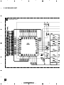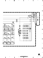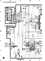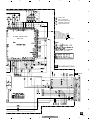
1
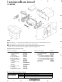
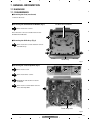
Service
Manual
ORDER NO.
DEH-P2550/XM/ES
CRT2983
MULTI-CD CONTROL HIGH POWER CD PLAYER WITH FM/AM TUNER
DEH-P2550
XM/ES, XN/ES
- This service manual should be used together with the following manual(s):
Model No.
CX-3026
Order No.
CRT2944
Mech. Module Remarks
S10
CD Mech. Module:Circuit Description, Mech.Description, Disassembly
For details, refer to "Important symbols for good services".
PIONEER CORPORATION
4-1, Meguro 1-Chome, Meguro-ku, Tokyo 153-8654, Japan
PIONEER ELECTRONICS (USA) INC. P.O.Box 1760, Long Beach, CA 90801-1760 U.S.A.
PIONEER EUROPE NV Haven 1087 Keetberglaan 1, 9120 Melsele, Belgium
PIONEER ELECTRONICS ASIACENTRE PTE.LTD. 253 Alexandra Road, #04-01, Singapore 159936
C PIONEER CORPORATION 2002
K-ZZA. OCT. 2002 Printed in Japan
1
A
2
3
4
SAFETY INFORMATION
This service manual is intended for qualified service technicians; it is not meant for the casual do-it-yourselfer.
Qualified technicians have the necessary test equipment and tools, and have been trained to properly and safely repair
complex products such as those covered by this manual.
Improperly performed repairs can adversely affect the safety and reliability of the product and may void the warranty.
If you are not qualified to perform the repair of this product properly and safely, you should not risk trying to do so
and refer the repair to a qualified service technician.
B
C
[ Important symbols for good services ]
D
In this manual, the symbols shown-below indicate that adjustments, settings or cleaning should be made securely.
When you find the procedures bearing any of the symbols, be sure to fulfill them:
1. Product safety
You should conform to the regulations governing the product (safety, radio and noise, and other regulations), and
should keep the safety during servicing by following the safety instructions described in this manual.
2. Adjustments
To keep the original performances of the product, optimum adjustments or specification confirmation is indispensable.
In accordance with the procedures or instructions described in this manual, adjustments should be performed.
3. Cleaning
E
For optical pickups, tape-deck heads, lenses and mirrors used in projection monitors, and other parts requiring cleaning,
proper cleaning should be performed to restore their performances.
4. Shipping mode and shipping screws
To protect the product from damages or failures that may be caused during transit, the shipping mode should be set or
the shipping screws should be installed before shipping out in accordance with this manual, if necessary.
5. Lubricants, glues, and replacement parts
Appropriately applying grease or glue can maintain the product performances. But improper lubrication or applying
glue may lead to failures or troubles in the product. By following the instructions in this manual, be sure to apply the
prescribed grease or glue to proper portions by the appropriate amount.For replacement parts or tools, the prescribed
ones should be used.
F
2
DEH-P2550/XM/ES
1
2
3
4
5
6
7
8
CONTENTS
A
SAFETY INFORMATION ............................................................................................................................................2
1. SPECIFICATIONS .......................................................................................................................................................4
2. EXPLODED VIEWS AND PARTS LIST.......................................................................................................................5
2.1 PACKING...............................................................................................................................................................5
2.2 EXTERIOR.............................................................................................................................................................6
2.3 CD MECHANISM MODULE .................................................................................................................................8
3. BLOCK DIAGRAM AND SCHEMATIC DIAGRAM ...................................................................................................10
3.1 BLOCK DIAGRAM ..............................................................................................................................................10
3.2 OVERALL CONNECTION DIAGRAM(GUIDE PAGE) ........................................................................................12
3.3 KEYBOARD UNIT ...............................................................................................................................................18
3.4 CD MECHANISM MODULE ...............................................................................................................................20
4. PCB CONNECTION DIAGRAM ................................................................................................................................24
4.1 TUNER AMP UNIT .............................................................................................................................................24
4.2 PANEL UNIT .......................................................................................................................................................28
4.3 KEYBOARD UNIT ...............................................................................................................................................29
4.4 CD MECHANISM MODULE ...............................................................................................................................30
5. ELECTRICAL PARTS LIST ........................................................................................................................................32
6. ADJUSTMENT .........................................................................................................................................................36
6.1 CD ADJUSTMENT .............................................................................................................................................36
6.2 CHECKING THE GRATING AFTER CHANGING THE PICKUP UNIT................................................................38
6.3 ERROR MODE ....................................................................................................................................................40
7. GENERAL INFORMATION .......................................................................................................................................41
7.1 DIAGNOSIS ........................................................................................................................................................41
7.1.1 DISASSEMBLY ..............................................................................................................................................41
7.1.2 CONNECTOR FUNCTION DESCRIPTION ....................................................................................................43
7.2 PARTS .................................................................................................................................................................44
7.2.1 IC ....................................................................................................................................................................44
7.2.2 DISPLAY.........................................................................................................................................................52
7.3 OPERATIONAL FLOW CHART...........................................................................................................................53
7.4 CLEANING ..........................................................................................................................................................54
8. OPERATIONS ...........................................................................................................................................................55
B
C
D
E
- CD Player Service Precautions
1. Before disassembling the unit, be sure to turn off the
power. Unplugging and plugging the connectors during power-on mode may damage the ICs inside the
unit.
2. To protect the pickup unit from electrostatic discharge during serviving, take an appropriate treatment(shorting-solder) by referring to "the DISASSEMBLY" on page 41.
3. After replacing the pickup unit, be sure to check the
grating.(See p.38.)
F
3
DEH-P2550/XM/ES
5
6
7
8
1
A
2
3
4
3
4
1. SPECIFICATIONS
Backup current
B
5 mA or less
C
D
E
F
4
DEH-P2550/XM/ES
1
2
6
5
8
7
2. EXPLODED VIEWS AND PARTS LIST
2.1 PACKING
A
B
C
NOTE:
- Parts marked by “*” are generally unavailable because they are not in our Master Spare Parts List.
- Screws adjacent to ∇ mark on the product are used for disassembly.
- For the applying amount of lubricants or glue, follow the instructions in this manual.
(In the case of no amount instructions, apply as you think it appropriate.)
D
- PACKING SECTION PARTS LIST
Mark No. Description
*
*
Part No.
Mark No. Description
1
2
3
4
5-1
Cord Assy
Accessory Assy
Spring
Screw Assy
Owner’s Manual
CDE7060
CEA3439
CBH1650
CEA3437
CRD3690
5-2
5-3
6
7
8
Owner’s Manual
Installation Manual
Screw
Polyethylene Bag
Screw
CRD3691
CRD3692
CBA1002
CEG-127
CRZ50P090FTC
Screw
Polyethylene Bag
Handle
Case Assy
Remote Control Unit
TRZ50P080FTC
CEG-158
CNC5395
CXB3520)
CXC1265
9
10
11
12
13
*
14
15
16
17
Part No.
Bush
Polyethylene Bag
Battery
CNV3930
CEG1173
CEX1065
Carton(DEH-P2550/XM/ES) CHG4961
Carton(DEH-P2550/XN/ES) CHG4975
18 Contain Box(DEH-P2550/XM/ES) CHL4975
Contain Box(DEH-P2550/XN/ES) CHL4961
19 Protector
CHP2663
20 Protector
CHP2664
E
- Owner's Manual, Installation Manual
Model
DEH-P2550/XM/ES
DEH-P2550/XN/ES
Part No.
CRD3690
CRD3691
CRD3692
Language
English, Spanish, Portuguese(B)
Traditional Chinese, Arabic
English, Spanish, Portuguese(B), Traditional Chinese, Arabic
F
5
DEH-P2550/XM/ES
5
6
7
8
1
2
3
4
3
4
2.2 EXTERIOR
A
B
C
D
E
F
6
DEH-P2550/XM/ES
1
2
6
5
8
7
- EXTERIOR SECTION PARTS LIST
Mark No. Description
A
Part No.
Mark No. Description
Part No.
CXC1265
CNS7068
ISS26P055FTC
BMZ30P040FZK
BSZ26P060FTC
46
47
48
49
50
Cover
Panel
Gear
Pin
Lighting Conductor
CNM6854
CNS7245
CNV5997
CNV6486
CNV6487
6
7
8
9
10
BSZ30P060FTC
BSZ30P200FTC
CDE7060
CDE7188
CD Mechanism Module(S10) CXK5600
51
52
53
54
55
Arm
Arm
Arm
Arm
Panel Unit
CNV7400
CNV7401
CNV7402
CNV7403
CWM8758
11
12
13
14
15
Case
Earth Plate
Cushion
Insulator
Insulator
CNB2793
CNC8915
CNM4870
CNM7935
CNM8174
56
57
58
59
60
Socket(CN1950)
Connector(CN1951)
Holder Unit
Holder Unit
Damper Unit
CKS3550
CKS4462
CXB9501
CXB9502
CXB9503
16
17
18
19
20
Panel
Tuner Amp Unit
Screw
Screw
Screw
CNS6935
CWM8619
ASZ26P060FTC
BPZ26P080FTC
BSZ26P160FTC
61
62
63
64
65
Service Panel Unit
Screw
Detach Grille Assy
Screw
Button(DISP)
CXX1691
IMS20P045FZK
CXB9604
BPZ20P100FZK
CAC7779
21
22
23
24
25
Fuse(10A)
FM/AM Tuner Unit
Holder
Pin Jack(CN351)
Plug(CN981)
CEK1208
CWE1646
CND1054
CKB1059
CKM1376
66
67
68
69
70
Button(PAUSE)
Button(AUDIO)
Button(OPEN)
Button(VOLUME)
Button(SELECT)
CAC7780
CAC7781
CAC7782
CAC7810
CAC7812
26
27
28
29
30
Connector(CN101)
Plug(CN831)
Connector(CN721)
Antenna Jack(CN401)
Holder
CKS3408
CKS3537
CKS3835
CKX1056
CND1237
71
72
73
74
75
Button(SRC)
Button(FUNC)
Button(1-6)
Button(CLK, EQ)
Spring
CAC7785
CAC7786
CAC7787
CAC7808
CBH2630
31
32
33
34
35
Holder
Insulator
Heat Sink
Terminal(CN402)
CND1352
CNM8245
CNR1668
VNF1084
Holder Unit(DEH-P2550/XM/ES) CXB6681
Holder(DEH-P2550/XN/ES) CNC8659
76
77
78
79
80
Cover
Lighting Conductor
Rubber
Keyboard Unit
LCD(LCD1901)
CNS7269
CNV7421
CNV7422
CWM8635
CAW1759
36
37
38
39
40
Chassis Unit
Button(EJECT)
Screw(M2x2)
Washer
Spring
CXB9528
CAC7752
CBA1176
CBF1038
CBH2650
81
82
83
84
85
Connector(CN1901)
Holder
Sheet
Cushion
Connector
CKS4524
CNC9757
CNM7647
CNM8092
CNV6440
41
42
43
44
45
Spring
Spring
Spring
Spring
Holder
CBH2651
CBH2652
CBH2653
CBL1512
CND1254
86
87
88
89
90
Lighting Conductor
Grille Unit
CNV7495
CXB9632
2SD2375
PAL007A
TSOP4840SB1
1
2
3
4
5
Remote Control Unit
Cover
Screw
Screw
Screw
Screw
Screw
Cord Assy
Cable
Transistor(Q752, 901, 911)
IC(IC301)
IC(IC1902)
91 •••••
92 •••••
93 Choke Coil(L981)
5
C
D
E
F
CTH1280
7
DEH-P2550/XM/ES
6
B
7
8
1
2
3
4
3
4
2.3 CD MECHANISM MODULE
A
1
B
1
1
2
1
C
2
1
2
2
1
1
1
1
D
3
1
2
2
1
1
1
1
1GEM1024
2GEM1045
3GEM1035
E
F
8
DEH-P2550/XM/ES
1
2
6
5
8
7
- CD MECHANISM MODULE SECTION PARTS LIST
Mark No. Description
Mark No. Description
Part No.
CD Core Unit(S10)
Connector(CN101)
Connector(CN701)
Screw
Screw
CWX2708
CKS4182
CKS4188
BMZ20P035FTC
BSZ20P040FTC
46
47
48
49
50
Rack
Holder
Holder
Arm
Gear
CNV7199
CNV7201
CNV7202
CNV7203
CNV7207
6
7
8
9
10
Screw(M2x4)
Screw(M2x3)
Screw(M2x3)
Washer
Washer
CBA1362
CBA1511
CBA1527
CBF1037
CBF1038
51
52
53
54
55
Gear
Gear
Gear
Gear
Gear
CNV7208
CNV7209
CNV7210
CNV7211
CNV7212
11
12
13
14
15
Washer
Spring
Spring
Spring
Spring
CBF1060
CBH2390
CBH2606
CBH2607
CBH2608
56
57
58
59
60
Rack
Arm
Arm
Guide
Roller
CNV7214
CNV7215
CNV7216
CNV7217
CNV7218
16
17
18
19
20
Spring
Spring
Spring
Spring
Spring
CBH2609
CBH2610
CBH2611
CBH2612
CBH2613
61
62
63
64
65
Gear
Arm
Arm
Arm
Damper
CNV7219
CNV7221
CNV7220
CNV7222
CNV7313
21
22
23
24
25
Spring
Spring
Spring
Spring
Spring
CBH2614
CBH2615
CBH2616
CBH2617
CBH2620
66
67
68
69
70
Damper
Arm
Arm
Guide
Guide
CNV7314
CNV7341
CNV7342
CNV7360
CNV7361
26
27
28
29
30
Spring
Spring
Spring
Spring
Spring
CBH2621
CBH2641
CBH2642
CBH2643
CBH2659
71
72
73
74
75
Holder
Arm
Gear
Damper
Motor Unit(M1)
CNV7437
CNV7444
CNV7595
CNV7618
CXB6007
31
32
33
34
35
Spring
Spring
Shaft
Frame
Frame
CBH2688
CBL1614
CLA3845
CNC9962
CNC9963
76
77
78
79
80
Chassis Unit
Screw Unit
Gear Unit
Arm Unit
Arm Unit
CXB8728
CXB8729
CXB8731
CXB8732
CXB8735
36
37
38
39
40
Bracket
Bracket
Arm
Arm
Lever
CNC9966
CNC9967
CNC9968
CNC9973
CNC9983
81
82
83
84
85
Arm Unit
Motor Unit(M2)
Bracket
Screw
Screw(M2x5)
CXB8852
CXB8933
CNC9985
JFZ20P020FTC
EBA1028
41
42
43
44
45
Lever
Sheet
Collar
Guide
Arm
CNC9984
CNM8134
CNV6906
CNV6925
CNV7198
86
87
88
89
90
Screw
JFZ20P020FTC
Screw
JGZ17P022FTC
Washer
YE15FTC
Washer
YE20FTC
Pickup Unit(Service)(P10) CXX1641
1
2
3
4
5
*
Part No.
A
91 Screw
B
C
D
IMS26P030FMC
6
F
9
DEH-P2550/XM/ES
5
E
7
8
1
2
3
4
3. BLOCK DIAGRAM AND SCHEMATIC DIAGRAM
3.1 BLOCK DIAGRAM
A
A TUNER AMP UNIT
VDD
IC 3 EEPROM
5.0V
5V
OSC
B
ANTENNA
NC
NC
NC
18 19 20 21
DO
NC
14
NC
11
CE1
DI
SL
10 9 8
CK
5
ROM_VDD
CE2
WC
13
IC 5
3.3V
←
7 6
FM/AM TUNER UNIT
LPF
CN401
AM ANT
1
1
FMRF
ATT
Rch
2
3
IC 1
3.3V
FM ANT
ATT
FMRF
ANT adj
24
IC 2
2.5V
Lch
MIXER, IF AMP
23
DET, FM MPX
RF adj
T51
CF52
AUDIOGND
NC
15
22
16
VDD_3.3
DGND
12
VCC
OSCGND
2
4
3.3V
IC 4
3.3V 2.5V 2.5V
←
C
RFGND
CF51
17
TUN L
TUN 3.3V
SYS 8.4V
3
BUS+L
BUS+L
5
BUS-L
BUS-L
6
CD L
4
CN101
7
11
5
1
8
100
PEE
IP-BUS DRIVER
BUS5
D CD CORE UNIT(S10)
BUS+
CN101
CN701
Q101
LOADING/ CARRIAGE
MOTOR
xtal
1
4
SERVO XTAL
CONTROL,
DSP,
LPF, DAC
TOP
FD, TD, SD, MD
42
ACT,MOTOR
DRIVER
M
16
SOP
15
SOM
17
LCOM
18
LCOP
M
IC 201 SO
UPD63712GC
23
SYSPW
LOEJ
BU
24
IC 722
12
XSI
16
6
2
66
61
TC7SET08FU
LIMIT
79
CLMP 63
HOME
22
LOEJ
9
CONT
5
17
7
15
6
16
11
11
1
20
2
21
VDSENS
VD
CLAMP
8EJ
ASENBO
DSCSNS
VD
3.3V REGULATOR
3R3V
3
IC 701
IC 601(2/2)
PE5341C
CDLOEJ
adpw
DSCSNS
FLPILM
XTALEN
ejectin
VDSENS
95
V
22
90
96
41
9
8
BU
20
VDD
Q752
BU
1
S
Q751
DETACH SENSE
DEH-P2550/XM/ES
2
83
CONT
F
1
X601
15
Q601
AVREF
NJM2391DL1-33
10
16
XSI
64
CLMP
X2
Q102
4
59
DSCSNS
12EJ
X1
SYSTEM CONTROLLER
71
IC 301
BA5996FP
E
21
Q101
80
CONT
IPPW
14
X201
FOP
37
CN721
8
ILMPW
FOP
TOP
12
FOP
13
TOP
SPINDLE
MOTOR
PD
LOUT
20
AC, F, E, BD
HOLOGRAM
UNIT
FOCUS ACT.
MONITOR TRACKING ACT.
DIODE
LOUT
mute
RX
swvdd
2
5
LD
24
DPDT
MD
1
14
85
TX
dsens
LD+
8
IPPW
86
VDCONT
LASER
DIODE
D
1 TX
IC 101
6 HA12187FP 2 RX
KYDT
PICKUP UNIT
(SERVICE)(P10)
EVST,EVCK,EVDT
BUZZER
3
4
6
5
8
7
A
RESET
1
2
IC 651
BD4834G
VDD
CN351
11
RL
RL
reset
4
CE2
32
CE1
99
DO
94
PRE OUT
RL
Q351
TUNPCE2
DI
98
CK
97
TUNPCE1
TUNPDI
TUNPDO
VDD REGULATOR
TUNPCK
Q901
74 SL
VDD
B
Q902
SYSTEM CONTROLLER
IC 601(1/2)
PE5341C
DALMON
10
CN981
BACKUP SENSE
asens
BU
93
Q931
92
FUSE
16
BACK UP
14
14
ACC
15
15
GND
16
BU
bsens
10A
ACC
ACC SENSE
C
TUN L
+L
-L
3
IN2-L
5 IN4+L
6 IN4-L
4
BU
ELECTRONIC VOLUME/
SOURCE SELECTOR
POWER AMP
20
IC 301
PAL007A
FL+
23
FL-
IC 131
PML003AM
FL
RL
10
14
11
12
FLIN
RLIN
IN3-L
MUTE
22
STBY
4
21
3
RL-
5
RL+
B.REMOTE
25
6
6
FLFL+
RLRL+
11
11
B.REM
7
7
5
5
8
8
MUTE
VST,EVCK,EVDT
Q502
SYS 8.4V REGULATOR
BU
Q911
Q912
SYS 8.4V
MUTE
BU
Q301
Q913
Q501
D
SYSPW
TUNER 3.3V REGULATOR
IC 921
X601
TUN 3.3V
3
1
SYS 8.4V
BA033FP
Q601
VDD
CN831
BU
Q831
5
5
6
6
8
8
9
9
B PANEL UNIT
S1970
EJECT
ILB
BU
C
KEYBOARD UNIT
CN1901
Q961
7
7
4
9
10
10
5
8
ILB
BL+B
E
Q962
Q971
SWDVDD
VDD
2
2
2
11
11
11
10
3
SWVDD
REMOTE CONTROL SENSOR
DPDT
OPT IN
3
1
IC 1902
TSOP4840SB1
55 11
17
18
KYDT
14
14
8
5
VDD
RFM
S801
DETACH SENSE
DPDT
KYDT
20
KTDT
VLCD
DPDT
KEY DATA
KEY MATRIX
LCD DRIVER/
KEY CONTROLLER
IC 1901
PD6340A
LCD
CN1951
CN1950
F
11
DEH-P2550/XM/ES
5
6
7
8
1
2
3
4
3.2 OVERALL CONNECTION DIAGRAM(GUIDE PAGE)
Note: When ordering service parts, be sure to refer to “EXPLODED VIEWS AND PARTS LIST” or “ELECTRICAL
PARTS LIST”.
A-a
A
A-a
A-a
A-a
A-b
A-b
A-b
Large size
SCH diagram
Guide page
Detailed page
FM:-31.0dBs
AM:-31.0dBs
IP-BUS:+2.2dBs
CD:0dBs
R4721
0R0
B
CD:0dBs
D
CN701
IP-BUS:+2.2dBs
IP-BUS
C
R9101
0R0
PE5
FM(30%):-30.0dBs
AM(30%):-30.0dBs
D
FM/AM TUNER UNIT
R9403
0R0
DETACH SENSE SW
E
EJECT
C
CN1901
F
B
12
A B
1
PANEL
UNIT
DEH-P2550/XM/ES
2
3
4
6
5
8
7
A-b
A
A
TUNER AMP UNIT
FM:-6.66dBs
AM:-6.66dBs
IP-BUS:+9.54dBs
CD:+9.34dBs
FM:-5.9dBs
AM:-5.9dBs
IP-BUS:+10.3dBs
CD:+10.1dBs
B
REAR
R CH
REAR
L CH
C
5341C
>
FUSE
10A
CEK1208
600µH
BACKUP
D
GND
ACC
B.REM
RL—
FL—
RL+
FL+
RR—
FR—
RR+
FR+
FM:+30dBs
AM:+20dBs
IP-BUS:+36dBs
CD:+36dBs
E
NOTE :
Symbol indicates a resistor.
No differentiation is made between chip resistors and
discrete resistors.
Symbol indicates a capacitor.
No differentiation is made between chip capacitors and
discrete capacitors.
Decimal points for resistor
and capacitor fixed values
are expressed as :
2.2 ← 2R2
0.022 ← R022
F
The > mark found on some component parts indicates
the importance of the safety factor of the part.
Therefore, when replacing, be sure to use parts of
identical designation.
A
DEH-P2550/XM/ES
5
6
7
8
13
1
F
A-a
IP-BUS
E
14
2
D
CN701
3
1
DEH-P2550/XM/ES
3
4
0R0
R9101
D
2
IP-BUS:+2.2dBs
CD:0dBs
B
FM:-31.0dBs
AM:-31.0dBs
IP-BUS:+2.2dBs
CD:0dBs
A-b
0R0
R4721
A-a A-b
1
4
2
A
C
FM(30%):-30.0dBs
AM(30%):-30.0dBs
5
0R0
R9403
A-a A-b
B
6
PANEL
UNIT
6
7
CN1901
C
EJECT
PE5341C
5
7
8
3
4
A-b
A
DETACH SENSE SW
B
C
D
E
FM/AM TUNER UNIT
F
A-a B
DEH-P2550/XM/ES
8
15
E
F
FM:-5.9dBs
AM:-5.9dBs
IP-BUS:+10.3dBs
CD:+10.1dBs
A-a A-b
B
A
TUNER AMP UNIT
A
A-b
16
1
2
REAR
L CH
REAR
R CH
FM:-6.66dBs
AM:-6.66dBs
IP-BUS:+9.54dBs
CD:+9.34dBs
1
2
3
1
3
4
C
D
2
DEH-P2550/XM/ES
4
1C
5
Decimal points for resistor
and capacitor fixed values
are expressed as :
2.2 ← 2R2
0.022 ← R022
6
FR+
RR+
FR—
RR—
FL+
RL+
FL—
RL—
B.RE
A
G
BACK
7
3
4
7
A-a A-b
>
FUSE
10A
CEK1208
6
The > mark found on some component parts indicates
the importance of the safety factor of the part.
Therefore, when replacing, be sure to use parts of
identical designation.
NOTE :
Symbol indicates a resistor.
No differentiation is made between chip resistors and
discrete resistors.
Symbol indicates a capacitor.
No differentiation is made between chip capacitors and
discrete capacitors.
FM:+30dBs
AM:+20dBs
IP-BUS:+36dBs
CD:+36dBs
600µH
5
8
A
B
C
D
E
A-b
DEH-P2550/XM/ES
8
17
F
1
A
2
3
4
3
4
3.3 KEYBOARD UNIT
C KEYBOARD UNIT
CAW1759
B
C
D
E
F
C
18
DEH-P2550/XM/ES
1
2
5
6
7
CEL1651
CEL1651
B
CN1951
6
150
150
150
150
SML-310PT x12
5
7
8
A
B
C
D
E
F
C
DEH-P2550/XM/ES
8
19
1
2
3
4
3.4 CD MECHANISM MODULE
Pickup Unit(Service)(P10)
A
#
F
B
F
T
T
T
T
F
F
T
T
F
T
T
F
F
F
F
F
T
T
!
C
0
1
9
D
MOTOR DRIVER
@
S
T
SPINDLE MOTOR
LOADING/CARRIAGE
MOTOR
M2 CXB8933
E
7
S
M1 CXB6007
5
C
F
S
8
6
C
3
C
C
C
F
F
T
S
S
T
3.3V
REGULATOR
F
D
20
DEH-P2550/XM/ES
1
2
3
4
6
5
8
7
A
F
TRACKING SERVO LINE
C
CARRIAGE SERVO LINE
S
SPINDLE SERVO LINE
F
T
C
S
T
SIGNAL LINE
FOCUS SERVO LINE
B
SWITCHES:
CD CORE UNIT
S901 : HOME SWITCH.....ON-OFF
S902 : CLAMP SWITCH....ON-OFF
S903 : DSCSNS SWITCH....ON-OFF
S904 : 12EJ SWITCH....ON-OFF
S905 : 8EJ SWITCH....ON-OFF
The underlined indicates the switch position.
RF AMP / SERVO / DSP
DAC / LPF
C
D
9
CD CORE UNIT (S10)
D
4
2
A
CN721
CN???
@
S
5
C
E
3
$%
F
D
21
DEH-P2550/XM/ES
5
6
7
8
1
2
- Waveforms
A
1 DSCSNS
2 CLCONT
3 LOEJ
4 VD
B
5V/div
5V/div
5V/div
10V/div
3
4
Note : 1. The encircled numbers denote measuring points in the circuit diagram.
2. Reference voltage REFO1(1.65V)
500ms/div 1 DSCSNS
2 CLCONT
3 LOEJ
4 VD
5V/div
5V/div
5V/div
10V/div
500ms/div 5 SIN
6 CIN
7 TIN
1V/div
2s/div
500mV/div
500mV/div
When loading a 12cm CD
When loading an 8cm CD
When setting up after loading a 12cm CD-DA
disc
Ref.:
GND
Ref.:
GND
Ref.:
REFO
Mode:
Normal
Mode:
Normal
Mode:
Normal
8 FIN
9 RFOK
5 SIN
200mV/div 500ms/div 0 TE
2V/div
! FE
2V/div
500mV/div 200ms/div ! FE
500mV/div
8 FIN
0 TE
7 TIN
500mV/div 20ms/div
500mV/div
500mV/div
500mV/div
When setting up "Source On"(12cm CD-DA)
When setting up "Source On"
During "Play"(CD-DA)
Ref.:
REFO
Ref.:
REFO
Ref.:
REFO
Mode:
Normal
Mode:
Normal
Mode:
Normal
C
@ MDX
5 SIN
500mV/div 5ms/div
1V/div
@ MDX
5 SIN
500mV/div 5µs/div
1V/div
# RFAGC
500mV/div 0.5µs/div
D
E
F
Spindle waveform during "Play"
Spindle waveform during "Play"(Magnified)
Ref.:
REFO
Ref.:
REFO
Ref.:
REFO
Mode:
Normal
Mode:
Normal
Mode:
Normal
8 FIN
! FE
500mV/div 200ms/div 0 TE
500mV/div
# RFAGC
500mV/div 2ms/div
500mV/div
RF eye pattern
# RFAGC
0 TE
7 TIN
Focus Search
When "Tracking Open"
1 Track Jump
Ref.:
REFO
Ref.:
REFO
Ref.:
REFO
Mode:
TEST
Mode:
TEST
Mode:
TEST
22
1V/div
500µs/div
500mV/div
500mV/div
DEH-P2550/XM/ES
1
2
3
4
6
5
8
7
A
# RFAGC
0 TE
7 TIN
1V/div
500ms/div # RFAGC
500mV/div
0 TE
500mV/div
7 TIN
1V/div
5ms/div
500mV/div
500mV/div
# RFAGC
7 TIN
0 TE
8 FIN
1V/div
1V/div
1V/div
1V/div
500µs/div
32 Track Jump
100(32x3) Track Jump
When reproducing black dots(1mm)
Ref.:
REFO
Ref.:
REFO
Ref.:
REFO
Mode:
TEST
Mode:
TEST
Mode:
Normal
# RFAGC
0 TE
6 CIN
5 SIN
500µs/div # RFAGC
1V/div
1V/div
0 TE
500mV/div
6 CIN
2V/div
5 SIN
5ms/div
1V/div
1V/div
500mV/div
2V/div
# RFAGC
0 TE
6 CIN
5 SIN
B
500µs/div
1V/div
1V/div
500mV/div
2V/div
When reproducing scratch(1mm)
When reproducing fingerprint(65µm)
During inside/outside search
(outer circumference → inner circumference)
Ref.:
REFO
Ref.:
REFO
Ref.:
REFO
Mode:
Normal
Mode:
Normal
Mode:
Normal
C
$ LOUT
% ROUT
1V/div
1V/div
200µs/div 1 DSCSNS 5V/div
2 CLCONT 5V/div
3 LOEJ
5V/div
200ms/div 1 DSCSNS 5V/div
2 CLCONT 5V/div
3 LOEJ
5V/div
200ms/div
D
Analog Audio
When "Eject"(12cm CD)
When "Eject"(8cm CD)
Ref.:
AGND
Ref.:
GND
Ref.:
GND
Mode:
Normal
Mode:
Normal
Mode:
Normal
E
F
23
DEH-P2550/XM/ES
5
6
7
8
1
2
3
4
4. PCB CONNECTION DIAGRAM
4.1 TUNER AMP UNIT
A
NOTE FOR PCB DIAGRAMS
1.The parts mounted on this PCB
include all necessary parts for
several destination.
For further information for
respective destinations, be sure
to check with the schematic diagram.
2.Viewpoint of PCB diagrams
Connector
A
TUNER AMP UNIT
CORD ASSY
WIRED
REMOTE
Capacitor
IP-BUS
SIDE A
B
P.C.Board
Chip Part
SIDE B
L981
C
R9101
D
R4721
D
CN701
E
DETACH SENSE
F
A
24
DEH-P2550/XM/ES
1
2
3
4
5
6
8
7
A
SIDE A
IC,Q
PRE OUT
B
ANTENNA
FM/AM TUNER UNIT
R9403
R9405
C
D
E
B
CN1950
F
FRONT
A
25
DEH-P2550/XM/ES
5
6
7
8
1
A
A
2
3
4
3
4
TUNER AMP UNIT
IC,Q
B
C
D
E
F
A
26
DEH-P2550/XM/ES
1
2
5
6
7
8
A
SIDE B
B
C
D
E
F
A
27
DEH-P2550/XM/ES
5
6
7
8
1
2
3
4
4.2 PANEL UNIT
A
B
SIDE A
PANEL UNIT
C CN1901
EJECT
B
C
B
SIDE B
PANEL UNIT
D
A
CN831
E
F
B
28
DEH-P2550/XM/ES
1
2
3
4
6
5
7
8
4.3 KEYBOARD UNIT
C
C
SIDE A
KEYBOARD UNIT
KEYBOARD UNIT
SIDE B
A
IC,Q
IC,Q
↓
↓
AUDIO
↓
B CN1951
FUNC
PAUSE
↓
LOUD
BAND/ESC
B
4
5
6
C
1
2
3
D
↓
EQ
↓
DISP
SRC
E
CLK
F
C
29
DEH-P2550/XM/ES
5
6
7
8
1
2
3
4
4.4 CD MECHANISM MODULE
D
SIDE A
CD CORE UNIT(S10)
A
M2
LOADING
/CARRIAGE MOTOR
B
M1
SPINDLE MOTOR
C
A
CN721
CN???
D
HOME
E
PICKUP UNIT
(SERVICE)(P10)
F
D
30
DEH-P2550/XM/ES
1
2
3
4
6
5
D
8
7
SIDE B
CD CORE UNIT(S10)
A
8EJ
12EJ
DSCSNS
CLAMP
B
C
D
E
F
D
31
DEH-P2550/XM/ES
5
6
7
8
1
A
2
3
4
5. ELECTRICAL PARTS LIST
NOTES:
- Parts whose parts numbers are omitted are subject to being not supplied.
- The part numbers shown below indicate chip components.
Chip Resistor
RS1/_S___J,RS1/__S___J
Chip Capacitor (except for CQS.....)
CKS....., CCS....., CSZS.....
B
=====Circuit Symbol and No.===Part Name
--- -----------------------------------------------
A
Part No.
-------------------------
Unit Number : CWM8619
Unit Name
: Tuner Amp Unit
MISCELLANEOUS
C
D
E
F
IC
IC
IC
IC
IC
101
131
301
601
651
IC
IC
IC
IC
IC
HA12187FP
PML003AM
PAL007A
PE5341C
BD4834G
IC
IC
Q
Q
Q
722
921
101
102
301
IC
IC
Transistor
Transistor
Transistor
TC7SET08FU
BA033FP
2SA1037K
DTC124EK
DTC124EK
Q
Q
Q
Q
Q
351
501
502
601
751
Transistor
Transistor
Transistor
Transistor
Transistor
IMH3A
2SC2412K
IMD2A
DTA114EK
IMD2A
Q
Q
Q
Q
Q
752
831
901
902
911
Transistor
Transistor
Transistor
Transistor
Transistor
2SD2375
DTC143EK
2SD2375
IMD2A
2SD2375
Q
Q
Q
Q
Q
912
913
931
961
962
Transistor
Transistor
Transistor
Transistor
Transistor
2SB1238
DTC114EK
IMX1
2SB1238
DTC114EK
Q
D
D
D
D
971
501
502
571
572
Transistor
Diode
Diode
Diode
Diode
2SA1036K
DAN202U
HZS9L(A2)
MPG06G-6415G50
MPG06G-6415G50
D
D
D
D
D
751
831
832
833
834
Diode
Diode
Diode
Diode
Diode
HZS9L(B1)
DAN202U
DAN202U
DAP202U
DAP202U
D
D
D
D
D
901
902
911
921
922
Diode
Diode
Diode
Diode
Diode
HZS6L(B1)
MPG06G-6415G50
HZS9L(B3)
1SR154-400
1SR154-400
D
D
D
D
D
923
931
932
981
982
Diode
Diode
Diode
Diode
Diode
1SR154-400
HZS7L(C3)
HZS7L(A1)
MPG06G-6415G50
MPG06G-6415G50
ZNR
L
L
L
L
401
131
401
402
404
Arrester
Inductor
Ferri-Inductor
Inductor
Inductor
DSP-201M
LCTA2R2J2520
LAU4R7K
LAU1R0K
LAU1R0K
32
=====Circuit Symbol and No.===Part Name
--- -----------------------------------------------
Part No.
-------------------------
L
L
L
L
X
405
601
971
981
601
Inductor
Inductor
Inductor
Choke Coil 600µH
Radiator 12.58291MHz
LAU2R2K
LAU2R2K
LAU2R2K
CTH1280
CSS1402
S
SP
831
601
Switch(DETACH SENSE)
Buzzer
Fuse 10A
FM/AM Tuner Unit
CSN1039
CPV1062
CEK1208
CWE1646
RESISTORS
R
R
R
R
R
101
102
103
104
105
RS1/16S150J
RS1/16S470J
RS1/16S101J
RS1/16S101J
RS1/16S181J
R
R
R
R
R
106
107
108
109
110
RS1/16S181J
RS1/16S223J
RS1/16S223J
RS1/16S102J
RS1/16S102J
R
R
R
R
R
111
112
113
114
131
RS1/16S222J
RS1/16S103J
RS1/16S332J
RS1/16S562J
RS1/16S0R0J
R
R
R
R
R
132
133
137
138
139
RS1/16S0R0J
RAB4C102J
RS1/16S101J
RS1/16S101J
RS1/16S101J
R
R
R
R
R
140
141
142
301
302
RS1/16S101J
RS1/16S0R0J
RS1/16S0R0J
RS1/16S153J
RS1/16S103J
R
R
R
R
R
303
304
351
352
359
RS1/16S103J
RS1/16S331J
RS1/16S821J
RS1/16S821J
RS1/16S223J
R
R
R
R
R
360
401
403
404
405
RS1/16S223J
RS1/16S681J
RS1/16S122J
RS1/16S681J
RS1/16S681J
R
R
R
R
R
406
501
502
504
601
RS1/16S681J
RS1/16S103J
RS1/16S473J
RS1/16S102J
RS1/16S102J
R
R
R
R
R
603
605
606
607
617
RS1/16S473J
RS1/16S102J
RS1/16S473J
RS1/16S104J
RS1/16S104J
DEH-P2550/XM/ES
1
2
3
4
5
6
7
8
=====Circuit Symbol and No.===Part Name
--- -----------------------------------------------
Part No.
-------------------------
=====Circuit Symbol and No.===Part Name
--- -----------------------------------------------
Part No.
-------------------------
R
R
R
R
R
619
620
621
622
623
RS1/16S1602D
RS1/16S473J
RS1/16S473J
RS1/16S473J
RS1/16S473J
R
R
R
R
R
965
971
972
973
981
RS1/16S182J
RS1/16S153J
RS1/16S153J
RS1/16S222J
RD1/4PU102J
R
R
R
R
R
624
625
626
627
628
RS1/16S473J
RS1/16S473J
RS1/16S681J
RS1/16S681J
RS1/16S681J
R
R
R
4721
9101
9403
RD1/4PU0R0J
RD1/4PU0R0J
RD1/4PU0R0J
R
R
R
R
R
640
651
652
713
716
RS1/16S0R0J
RS1/16S102J
RS1/16S183J
RS1/16S104J
RS1/16S221J
C
C
C
C
C
101
131
132
133
134
CKSRYB104K25
CEJQ1R0M50
CEJQ1R0M50
CKSRYB104K25
CKSRYB104K25
R
R
R
R
R
724
727
728
729
730
RS1/16S104J
RS1/16S0R0J
RS1/16S0R0J
RS1/16S221J
RS1/16S221J
C
C
C
C
C
135
136
137
138
139
CEJQ1R0M50
CEJQ1R0M50
CEJQ1R0M50
CEJQ1R0M50
CEJQ470M16
R
R
R
R
R
731
732
733
735
736
RS1/16S221J
RS1/16S221J
RS1/16S102J
RS1/16S221J
RS1/16S221J
C
C
C
C
C
140
143
145
146
147
CKSRYB104K25
CEJQ100M16
CKSRYB105K10
CKSRYB105K10
CKSRYB153K50
R
R
R
R
R
737
740
741
742
749
RS1/16S221J
RS1/16S102J
RS1/16S221J
RS1/16S221J
RS1/16S0R0J
C
C
C
C
C
148
301
302
303
304
CKSRYB153K50
CKSRYB474K10
CKSRYB474K10
CKSRYB474K10
CKSRYB474K10
R
R
R
R
R
751
752
753
754
757
RD1/4PU821J
RD1/4PU221J
RS1/16S222J
RS1/16S472J
RD1/4PU0R0J
C
C
C
C
C
305
306
307
308
309
CKSRYB474K10
CKSRYB474K10
CKSRYB474K10
CKSRYB474K10
CEHAR330M10
R
R
R
R
R
831
832
833
834
835
RS1/16S222J
RS1/16S222J
RS1/16S222J
RS1/16S222J
RS1/16S473J
C
C
C
C
C
310
311
312
313
314
R
R
R
R
R
836
837
838
839
840
RS1/16S473J
RD1/4PU391J
RS1/16S102J
RS1/16S102J
RS1/16S102J
C
C
C
C
C
351
352
401
402
403
CEJQ100M16
CEJQ100M16
CKSRYB103K50
CEJQ470M6R3
CKSRYB103K50
R
R
R
R
R
841
845
901
902
903
RS1/16S102J
RS1/16S102J
RD1/4PU221J
RS1/16S223J
RS1/16S821J
C
C
C
C
C
404
405
407
602
603
CKSRYB103K50
CEJQ101M16
CKSYB475K10
CKSRYB105K10
CCSRCH200J50
R
R
R
R
R
904
905
911
914
915
RS1/16S821J
RS1/16S0R0J
RS1/16S223J
RS1/16S152J
RD1/4PU152J
C
C
C
C
C
604
605
606
608
609
CCSRCH200J50
CEJQ4R7M35
CKSRYB104K25
CCSRCH101J50
CCSRCH470J50
R
R
R
R
R
916
921
931
932
933
RS1/16S223J
RD1/4PU1R8J
RS1/16S104J
RS1/16S473J
RS1/16S103J
C
C
C
C
C
611
652
729
751
752
CKSRYB104K25
CKSRYB105K10
CKSRYB473K50
CKSRYB224K10
CKSRYB102K50
R
R
R
R
R
934
935
961
962
963
RS1/16S473J
RS1/16S472J
RS1/16S223J
RS1/16S182J
RD1/4PU1R0J
C
C
C
C
C
753
901
902
903
904
CEJQ101M16
CEJQ470M10
CKSRYB103K50
CKSRYB472K50
CCH1331
A
CAPACITORS
3300µF/16V
470µF/16V
CCH1486
CKSRYB104K25
CEHAR100M16
CKSQYB225K10
CKSQYB225K10
B
C
D
E
F
33
DEH-P2550/XM/ES
5
6
7
8
1
A
C
3
Part No.
-------------------------
=====Circuit Symbol and No.===Part Name
--- -----------------------------------------------
C
C
C
C
C
911
912
913
921
922
CEJQ221M10
CKSRYB103K50
CEJQ101M16
CEJQ220M10
CKSRYB103K50
B
C
C
C
923
931
961
CKSYB475K10
CKSRYB104K25
CKSRYB473K50
Unit Number : CWM8635
Unit Name
: Keyboard Unit
1901
1902
1801
1802
1803
IC
IC
LED
LED
LED
PD6340A
TSOP4840SB1
NSSW440-9159
NSSW440-9159
SML-310PT
D
D
D
D
D
1804
1805
1806
1807
1808
LED
LED
LED
LED
LED
SML-310PT
SML-310PT
SML-310PT
SML-310PT
SML-310PT
D
D
D
D
D
1809
1810
1811
1812
1813
LED
LED
LED
LED
LED
SML-310PT
SML-310PT
SML-310PT
SML-310PT
SML-310PT
D
D
D
X
IL
1814
1901
1902
1901
1801
LED
Diode
Diode
Ceramic Resonator 4.97MHz
Lamp 14V 40mA
SML-310PT
DAN202U
DAP202U
CSS1422
CEL1651
Lamp 14V 40mA
LCD
CEL1651
CAW1759
1801
1802
1803
1804
1805
RS1/16S151J
RS1/16S151J
RS1/16S151J
RS1/16S181J
RS1/16S151J
R
R
R
R
R
1806
1807
1808
1809
1810
RS1/16S181J
RS1/16S181J
RS1/16S151J
RS1/16S181J
RS1/16S181J
R
R
R
R
R
1811
1812
1813
1814
1815
RS1/16S151J
RS1/16S181J
RS1/16S181J
RS1/16S151J
RS1/16S181J
R
R
R
R
R
1901
1902
1904
1905
1906
RS1/16S121J
RS1/16S2R2J
RS1/16S222J
RS1/16S222J
RS1/16S473J
CAPACITORS
1801
1802
1901
1902
D
S
1970
1970
LED
Push Switch(EJECT)
CL220PGC
CSG1112
RESISTORS
1970
1971
1972
RS1/16S101J
RS1/16S101J
RS1/16S0R0J
C
1970
D
CKSRYB104K16
Unit Number : CWX2708
Unit Name
: CD Core Unit(S10)
MISCELLANEOUS
IC
IC
IC
Q
D
201
301
701
101
101
IC
IC
IC
Transistor
Diode
UPD63712GC
BA5996FP
NJM2391DL1-33
2SB1132
1SS355
D
X
S
S
S
701
201
901
902
903
Diode
Ceramic Resonator 16.934MHz
Spring Switch(HOME)
Spring Switch(CLAMP)
Spring Switch(DSCSNS)
1SR154-400
CSS1603
CSN1051
CSN1051
CSN1052
S
S
904
905
Spring Switch(12EJ)
Spring Switch(8EJ)
CSN1051
CSN1051
RESISTORS
R
R
R
R
R
C
C
C
C
Unit Number : CWM8758
Unit Name
: Panel Unit
CAPACITORS
IC
IC
D
D
D
RESISTORS
E
Part No.
-------------------------
MISCELLANEOUS
R
R
R
MISCELLANEOUS
IL 1802
LCD1901
D
4
=====Circuit Symbol and No.===Part Name
--- -----------------------------------------------
C
B
2
CKSRYB104K16
CKSRYB104K16
CKSRYB224K10
CSZS4R7M16
R
R
R
R
R
101
102
103
104
105
RS1/10S1R5J
RS1/10S1R5J
RS1/10S1R5J
RS1/10S1R5J
RS1/10S1R5J
R
R
R
R
R
201
202
203
204
205
RS1/16S102J
RS1/16S1002D
RS1/16S1002D
RS1/16S1002D
RS1/16S1002D
R
R
R
R
R
206
207
208
209
214
RS1/16S1002D
RS1/16S1002D
RS1/16S1002D
RS1/16S1002D
RS1/16S103J
R
R
R
R
R
215
216
217
218
234
RS1/16S393J
RS1/16S122J
RS1/16S562J
RS1/16S472J
RS1/16S0R0J
R
R
R
R
R
235
236
301
302
303
RS1/16S103J
RS1/16S103J
RS1/16S183J
RS1/16S822J
RS1/16S183J
R
R
R
R
R
304
305
306
307
308
RS1/16S822J
RS1/16S183J
RS1/16S183J
RS1/16S183J
RS1/16S183J
F
34
DEH-P2550/XM/ES
1
2
3
4
5
6
7
=====Circuit Symbol and No.===Part Name
--- -----------------------------------------------
Part No.
-------------------------
R
R
R
R
R
501
503
505
506
507
RS1/16S102J
RS1/16S102J
RS1/16S102J
RS1/16S221J
RS1/16S221J
R
R
R
R
R
508
509
601
602
603
RS1/16S221J
RS1/16S221J
RS1/16S101J
RS1/16S101J
RS1/16S0R0J
R
R
R
901
902
903
RS1/16S104J
RS1/16S473J
RS1/16S273J
8
A
B
CAPACITORS
C
C
C
C
C
101
102
103
104
106
C
C
C
C
C
108
109
201
202
203
C
C
C
C
C
205
206
207
208
209
C
C
C
C
C
210
211
212
213
214
CKSRYB104K16
CKSRYB104K16
CKSRYB104K16
CKSRYB332K50
CKSRYB473K25
C
C
C
C
C
215
216
217
218
219
CKSRYB104K16
CKSRYB103K25
CCSRCH560J50
CCSRCH5R0C50
CKSRYB104K16
C
C
C
C
C
220
221
222
223
224
CKSRYB104K16
CKSRYB104K16
CKSRYB103K25
CCSRCH680J50
CCSRCH470J50
C
C
C
C
C
225
231
232
301
302
CKSRYB682K50
CKSRYB102K50
CKSRYB102K50
CCH1504
CCSRCH221J50
C
C
C
C
C
303
304
305
306
501
C
C
C
C
C
502
702
703
704
705
100µF/16V
47µF/6.3V
CKSRYB104K16
CKSRYB104K16
CCH1504
CCH1506
CCSRCH101J50
CKSRYB224K16
CKSRYB224K16
CKSRYB104K16
CKSRYB471K50
CKSRYB104K16
22µF/6.3V
100µF/6.3V
100µF/16V
CCH1507
CKSRYB103K25
CKSRYB104K16
CCH1505
CKSRYB104K16
C
D
CCSRCH221J50
CKSRYB472K50
CKSRYB103K25
CKSRYB104K16
CKSRYB103K25
100µF/16V
10µF/6.3V
E
CKSRYB103K25
CCH1504
CKSRYB224K16
CKSRYB104K16
CCH1470
Miscellaneous Parts List
M
M
1
2
Pickup Unit(Service)(P10)
Motor Unit(SPINDLE)
Motor Unit(LOADING/CARRIAGE)
CXX1641
CXB6007
CXB8933
F
35
DEH-P2550/XM/ES
5
6
7
8
1
2
3
4
6. ADJUSTMENT
6.1 CD ADJUSTMENT
A
B
1) Cautions on adjustments
• In this product the single voltage (3.3V) is used for the
regulator. The reference voltage is the REFO1 (1.65V)
instead of the GND.
If you should mistakenly short the REFO1 with the GND
during adjustment, accurate voltage will not be obtained,
and the servo’s misoperation will apply excessive shock
to the pickup. To avoid such problems:
a. Do not mix up the REFO1 with the GND when
connecting the (-) probe of measuring instruments.
Especially on an oscilloscope, avoid connecting the (-)
probe for CH1 to the GND.
b. In many cases, measuring instruments have the same
potential as that for the (-) probe. Be sure to set the
measuring instruments to the floating state.
c. If you have mistakenly connected the REFO1 to the GND,
turn off the regulator or the power immediately.
• Before mounting and removing filters or leads for
adjustment, be sure to turn off the regulator.
C
• For stable circuit operation, keep the mechanism
operating for about one minute or more after the
regulator is turned on.
2) Test mode
This mode is used to adjust the CD mechanism module.
• To enter the test mode.
While pressing the 4 and 6 keys at the same time, reset.
• To exit from the test mode.
Turn off the ACC and back up.
Notes:
a. During ejection, do not press any other keys than the
EJECT key until the loaded disc is ejected.
b. If you have pressed the (→) key or (←) key during focus
search, turn off the power immediately to protect the
actuator from damage caused by the lens stuck.
c. For the TR jump modes except 100TR, the track jump
operation will continue even if the key is released.
d. For the CRG move and 100TR jump modes, the tracking
loop will be closed at the same time when the key is
released.
e. When the power is turned off and on, the jump mode
is reset to the single TR (91), the RF amp gain is set to 0dB,
and the auto-adjustment values are reset to the default
settings.
• In the test mode, any software protections will not
work. Avoid applying any mechanical or electrical
shock to the mechanism during adjustment.
• The RFI and RFO signals with a wide frequency range
are easy to oscillate. When observing the signals,
insert a resistor of 1k ohms in series.
D
• The load and eject operation is not guarantied with the
mechanism upside down. If the mechanism is blocked
due to mistaken eject operation, reset the product or
turn off and on the ACC to restore it.
E
F
36
DEH-P2550/XM/ES
1
2
3
4
6
5
8
7
- Flow Chart
A
[4]+[6]+Reset
[KEY]
Test Mode In
Contents
Display
[CD]or[SOURCE]
Source On
TRK
MIN
[BAND]
[3]
Power On
(T.Offset is adjusted)
(T.Offset is not adjusted)
TRK 00 MIN00 SEC 00
[BAND]
[3]
Power Off
Focus Close /
S curve check
TRK
MIN
SEC
TRK
B
Power On
TRK 99 MIN 99 SEC 99
[1]
[→]
Tracking Servo
Close
CRG+
[6]
Focus Mode
*2
switching
TRK
MIN
SEC
0x 0x 0x
91 MIN91 SEC 91
[BAND]
TRK
MIN
Applicable servomechanism
TRK xx MINxx SEC xx
SEC
00 MIN00 SEC00
99 MIN99 SEC99
or
TRK xx MIN xx SEC xx
TRK ?? MIN ?? SEC ??
[←]
CRG-
TRK8x MIN8x SEC8x
TRK8x MIN8x SEC8x
[BAND]
[1]
TRK
MIN
*7
F.Bias display switching
TRK
SEC
[6]
[3]
F,T,RF AGC /
?? MIN?? SEC ??
F,T AGC /F.Bias
RF AGC
TRK
TRK 9x MIN 9x SEC 9x
CRG/TR Jump value
switching
xx MINxx SEC xx
TRK
or
TRK
[2]
T.Balance adjustment
C
T.Balance coefficient display
TRK ?? MIN?? SEC ??
[←]
*4
[2]
*4
CRG/TR Jump +
xxMIN xxSEC xx
?? MIN?? SEC ??
TRK 9x MIN 9x SEC 9x
[→]
*5
TRK
00 MIN00 SEC00
99 MIN 99 SEC 99
TRK
[→]
RF AGC coefficient display
Applicable servomechanism
TRK
or
Automatic adjustment
display switching
*8
CRG+
RF AGC /
or
Power Off
00 MIN00 SEC00
99 MIN99 SEC 99
TRK
[3]
T.Close and
CRG-
TRK
TRK
[6]
[1]
T.Close and F,T AGC
and RF AGC
Power Off
[2]
*3
TRK
or
[←]
*8
Tracking Open
CRG/TR Jump TRK
xxMIN xxSEC xx
xxMIN xxSEC xx
TRK
or
8x MIN8x SEC 8x
9xMIN 9xSEC 9x
TRK
*6
[BAND]
[2]
Power Off
Tracking Open
TRK
MIN
SEC
or
*1)
→
TYP
TRK
MIN
D
TRK8x MIN8x SEC8x
SEC
TRK 9x MIN 9x SEC 9x
-12dB
Operation
[Key]
TRK 12 MIN 12 SEC 12
Test Mode
*2) Focus Close
→
S.Curve
→
TRK 00 MIN 00 SEC 00 TRK 01 MIN 01 SEC 01
(TRK 99 MIN 99 SEC 99)
[BAND] Power On / Off
F EQ measurement setting
TRK 02 MIN 02 SEC 02
[→]
CRG + / TR Jump +
(Direction of the external surface)
[←]
CRG - / TR Jump (Direction of the internal surface)
[1]
CLS and AGC and Applicable servomechanism /
AGC, AGC display switching
[2]
RF Gain switching / Offset adjustment display /
T.Balance adjustment / T.Open
[3]
Close, S.Curve /
Rough Servo and RF AGC / F, T, RF AGC
*3) F.Offset Display → RF.Offset Display → T.Offset Display
*4) 1TR/32TR/100TR
*5) Single TR → 32TR → 100TR → CRG Move
9x(8x) : 91(81)
92(82)
93(83)
94(84)
*6) Only at the time of CRG Move or 100TR Jump
*7) TRK/MIN/SEC → F.AGC → T.AGC Gain → F.bias → RF AGC
*8) CRG motor voltage = 2[V]
-
SPDL 1X / 2X switching
(Double-speed compatibility only)
-
Gop measurement
[6]
E
Forcus Mode switching / Tracking Close
/ CRG, TR Jump switching
F
37
DEH-P2550/XM/ES
5
6
7
8
1
2
3
4
6.2 CHECKING THE GRATING AFTER CHANGING THE PICKUP UNIT
A
• Note :
The grating angle of the PU unit cannot be adjusted after the PU unit is changed. The PU unit in the CD mechanism
module is adjusted on the production line to match the CD mechanism module and is thus the best adjusted PU
unit for the CD mechanism module. Changing the PU unit is thus best considered as a last resort. However, if the
PU unit must be changed, the grating should be checked using the procedure below.
• Purpose :
To check that the grating is within an acceptable range when the PU unit is changed.
B
• Symptoms of Mal-adjustment :
If the grating is off by a large amount symptoms such as being unable to close tracking, being unable to perform
track search operations, or taking a long time for track searching.
• Method :
• Measuring Equipment
• Measuring Points
• Disc
• Mode
• Oscilloscope, Two L.P.F.
• E, F, REFO1
• ABEX TCD-782
• TEST MODE
CD CORE UNIT(S10)
C
L.P.F.
E
Xch
100kΩ
F
100kΩ
390pF
VREF
E
REFO1
L.P.F.
F
E
D
Oscilloscope
390pF
VREF
Ych
• Checking Procedure
1. In test mode, load the disc and switch the 3V regulator on.
2. Using the → and ← buttons, move the PU unit to the innermost track.
3. Press key 3 to close focus, the display should read "91". Press key 2 to implement the tracking balance
adjustment the display should now read "81". Press key 3. The display will change, returning to "81" on the
fourth press.
4. As shown in the diagram above, monitor the LPF outputs using the oscilloscope and check that the phase
difference is within 75° . Refer to the photographs supplied to determine the phase angle.
5. If the phase difference is determined to be greater than 75° try changing the PU unit to see if there is any
improvement. If, after trying this a number of times, the grating angle does not become less than 75° then the
mechanism should be judged to be at fault.
• Note
Because of eccentricity in the disc and a slight misalignment of the clamping center the grating waveform may be
seen to "wobble" ( the phase difference changes as the disc rotates). The angle specified above indicates the
average angle.
• Hint
Reloading the disc changes the clamp position and may decrease the "wobble".
F
38
DEH-P2550/XM/ES
1
2
3
4
5
6
7
8
Ech → Xch 20mV/div, AC
Fch → Ych 20mV/div, AC
Grating waveform
0°
A
30°
B
45°
60°
C
D
75°
90°
E
F
39
DEH-P2550/XM/ES
5
6
7
8
1
2
3
4
6.3 ERROR MODE
- Error Messages
A
If a CD is not operative or stopped during operation due to an error, the error mode is turned on and cause(s) of
the error is indicated with a corresponding number. This arrangement is intended at reducing nonsense calls from
the users and also for facilitating trouble analysis and repair work in servicing.
(1) Basic Indication Method
1) When SERRORM is selected for the CSMOD (CD mode area for the system), error codes are written to DMIN
(minutes display area) and DSEC (seconds display area). The same data is written to DMIN and DSEC. DTNO
remains in blank as before.
B
2) Head unit display examples
Depending on display capability of LCD used, display will vary as shown below. xx contains the error number.
8-digit display
ERROR–xx
6-digit display
ERR–xx
4-digit display
E–xx
(2) Error Code List
Displayed error code Description of the code and potential cause(s)
Code Class
Electricity Carriage Home NG
CRG can't be moved to inner diameter.
10
CRG can't be moved from inner diameter.
SERVO LSI ComC
→ Failure on home switch or CRG move mechanism.
munication Error
11
Electricity
Focus Servo NG
Communication error between microcomputer and SERVO LSI.
Focusing not available.
→ Stains on rear side of disc or excessive vibrations on REWRITABLE.
12
Electricity
Spindle Lock NG
Subcode NG
Spindle not locked. Sub-code is strange (not readable).
→ Failure on spindle, stains or damages on disc, or excessive vibrations.
A disc not containing CD-R data is found.
D
Turned over disc are found, though rarely.
CD signal error.
AGC protection doesn't work. Focus can be easily lost.
→ Damages or stains on disc, or excessive vibrations on REWRITABLE.
17
Electricity
Setup NG
30
Electricity
Search Time Out
Failed to reach target address.
→ CRG tracking error or damages on disc.
44
Electricity
ALL Skip
50
Mechanism CD On Mech Error
Skip setting for all track.
(CD-R/RW)
Mechanical error during CD ON.
→ Defective loading motor, mechanical lock and mechanical sensor.
A0
System
Power Supply NG
Power (VD) is ground faulted.
→ Failure on SW transistor or power supply (failure on connector).
E
Remarks: Mechanical errors are not displayed (because a CD is turned off in these errors).
Unreadable TOC does not constitute an error. An intended operation continues in this case.
Upper digits of an error code are subdivided as shown below:
1x: Setup relevant errors, 3x: Search relevant errors, Ax: Other errors.
F
40
DEH-P2550/XM/ES
1
2
3
4
5
6
8
7
7. GENERAL INFORMATION
7.1 DIAGNOSIS
7.1.1 DISASSEMBLY
A
- Removing the Case (not shown)
1. Remove the Case.
- Removing the CD Mechanism Module (Fig.1)
1
CD Mechanism Module
Remove the four screws.
B
Disconnect the connector and then remove the
CD Mechanism Module.
1
1
- Removing the Grille Assy (Fig.1)
2
Remove the two screws and then remove
the Grille Assy.
1
C
1
2
2
Grille Assy
Fig.1
- Removing the Tuner Amp Unit (Fig.2)
1
Remove the screw.
2
2
2
Remove the three screws.
3
Straight the tabs at three locations
indicated.
4
Remove the screw and then remove
the Tuner Amp Unit.
D
2
4
1
E
3
3
3
F
Tuner Amp Unit
Fig.2
41
DEH-P2550/XM/ES
5
6
7
8
1
2
3
4
- How to hold the Mechanical Unit
1. Hold the top and bottom frame.
2. Do not squeeze top frame's front portion too tight,
because it is fragile.
A
B
Do not squeeze.
- Removing the Upper and Lower Frames
C
1. With a disc clamped, remove the four springs (A),
the two springs (B), the two springs (C), and the
four screws.
2. To remove the upper frame, open it on the fulcrum
A.
3. While lifting the carriage mechanism, remove the
three dampers.
4. With the frames removed, insert the connectors
coming from the main unit and eject the disc.
Caution: Before installing the carriage mechanism in
the frames, be sure to apply some alcohol to the
dampers and set the mechanism to the clamp mode.
Upper Frame
A
A
C
A
A
Carriage Mechanism
B
Damper
Lower Frame
Damper
B
D
- Removing the Pickup Unit
E
1. Set the mechanism to the clamp mode.
2. Remove the lead wires from the inner holder.
3. Remove the two washers, styling holder, change
arm, and pickup lock arm.
4. While releasing from the hook of the inner holder,
lift the end of the feed screw.
Caution: In assembling, move the planet gear to the
load/eject position before setting the feed screw
in the inner holder.
C
A
Damper
Washer
Pickup Lock Arm
Change
Arm
Styling Holder
Feed Screw
F
Inner Holder
Planet Gear
42
DEH-P2550/XM/ES
1
2
3
4
ANTENNA JACK
REAR OUTPUT
1. FR+
2. RR3. FR4. RR+
5. FL+
6. RL+
7. FL8. RL-
10A
5
6
9. NC
10. NC
11. B.REM
12. NC
13. NC
14. ACC
15. GND
16. BACK UP
1 3 5 7 9 11 13 15
2 4 6 8 10 12 14 16
1. BUS+
2. GND
3. GND
4. NC
5. BUS6. GND
7. BUS L+ INPUT
8. ASENB
9. BUS R+ INPUT
10. BUS R- INPUT
11. BUS L- INPUT
1 2 3 4
7
8 9 10 11
5 6
5
6
7
7
8
7.1.2 CONNECTOR FUNCTION DESCRIPTION
A
B
C
D
E
F
DEH-P2550/XM/ES
8
43
1
2
3
4
7.2 PARTS
7.2.1 IC
A
B
C
D
E
F
- Pin Functions(PE5341C)
Pin No.
1
2-4
5
6
7
8
9
10
11
12
13
14
15
16
17
18
19
20
21
22
23
24
25
26
27
28
29-31
32
33
34
35
36
37
38, 39
40
41
42
43
44
45
46
47-57
58
59
60
61
62
63
64
65
66
67
68
69
70
71
72
73
74
75
Pin Name
swvdd
NC
TESTIN
LCDPW
TELIN
ejectin
FLPILM
DALMON
reset
XT2
XT1
VSS
X2
X1
REGOFF
REGC
VDD
ILMPW
SYSPW
adpw
NC
IPPW
NC
ROMDATA
ROMCLK
ROMCS
NC
tunpce@
VST
VCK
VDT
ANTPW
MUTE
NC
VSS
VDD
RDS57K
drst
rdslk
RDT
DORAON
NC
STRKEY2
CDLOEJ
CLCONT
CONT
PCL
CLAMPSW
VDCONT
xsck(TSCK)
XSI(TSI)
XSO(TSO)
XAO
xrst
xstb
ASENBO
EMUTE
TEST
SL
STRKEY1
I/O
O
Format
C
I
O
I
I
I
I/O
I
C
C
I
I
I
O
O
O
C
C
O
C
O
O
O
C
C
O
O
O
O
O
O
C
I
O
I
O
O
C
C
C
C
I
O
I
O
O
I
O
O
I
O
O
O
O
O
O
C
C
C
C
C
C
C
I
I
C
C
44
Function and Operation
Grille : Chip enable output
Not used
Test program mode input
LCD back light power supply control output
Telephone mute input
Eject sense input
Flap illumination input
For consumption low-current
Reset input
Not used
Clock connection pin
GND
Crystal oscillator connection pin
Crystal oscillator connection pin
Regulator operation specification signal
Capacitor for regulator connect pin
Power supply
Illumination power supply control output
System power control output
A/D converter power supply control output
Not used
Power supply control output for IP BUS interface IC
Not used
ROM correction data output
ROM correction clock output
ROM correction chip select output
Not used
PLL chip enable output2
E.VOL : Strobe output
E.VOL : Clock output
E.VOL : Data output
Antenna power output
System mute output
Not used
GND
Power supply
57kHz count pulse input
RDS : Decoder reset output
RDS : Decoder clock input
RDS : Decoder data input
TUNER : 3V power supply
Not used
Steering remote controller input
CD : Load Moter Load/Eject output
CD : Driver input switch output
CD : Servo driver power supply control output
Clock adjustment
Clamp SW input
CD : VD power control output
CD LSI clock output
CD LSI data input
CD LSI data output
CD LSI command/data control output
CD : LSI reset control output
CD LSI strobe output
IP-BUS : Slave power supply control output
E.VOL : Mute control output
GND
TUNER : Signal level input
Steering remote controller input
DEH-P2550/XM/ES
1
2
3
4
6
5
Pin No.
76
77
78
79
80
81
82
83
84
85
86
87
88
89
90
91
92
93
94
95
96
97
98
99
100
Pin Name
MODELIN
CSENS
NC
DSCSNS
VDSENS
TEMP
AVDD
AVREF
AVSS
RX
TX
NMI
ldet
rck
dsens
PACK
asens
bsens
TUNPDI
KYDT
DPDT
TUNPCK
TUNPDO
TUNPCE
PEE
I/O
I
I
Format
I
I
I
I
O
I
I
I
I
I
I
I
I
O
O
O
O
O
C
C
C
C
8
7
Function and Operation
Model select input
Flap close sense input
Not used
CD : Disc insert sense input
CD : VD voltage sense input
CD : Temperature sense input
A/D converter power supply terminal
A/D converter reference voltage terminal
GND
IP-BUS : Data input
IP-BUS : Data output
GND
PLL lock sense input
RDS : Clock input
Grille detach sense input
PACK input
ACC power sense input
Back up power sense input
PLL IC data input
Grille data input
Grille data output
PLL clock output
PLL data output
PLL chip enable output
Beep tone output
A
B
C
IC's marked by * are MOS type.
Be careful in handling them because they are very
liable to be damaged by electrostatic induction.
31
50
* PE5341C
30
51
D
Format
C
Meaning
CMOS
81
100
1
N.C.
80
N.C.
BD4834G
5
4
E
1
2
3
VOUT
VDD
GND
Vref
F
45
DEH-P2550/XM/ES
5
6
7
8
1
A
2
3
4
PAL007A
sw_vcc
Protector;
Over voltage
1
TAB
Reference
amp_vcc
6
OUT1-
7
12 13
IN4
14
IN3
15
AC-GND
16
OUT3+
17
P-GND3
18
OUT3-
19
VCC
OUT4+
20 21
MUTE
22
OUT4-
23
P-GND4
24 25
SWITCH
amp_vcc
S-GND
Protector;
Short circuit
Offset
Detection
Offset
Detection
-+
11
IN2
+-
10
IN1
-+
9
SVR
+-
8
OUT1+
Offset
Detection
-+
P-GND1
Protector;
Thermal
+-
5
VCC
Offset
Detection
-+
OUT2+
Stand-by
Circuit
+-
STBY
4
D
OUT2-
3
C
2
B
P-GND2
sw_vcc
Protector;
Over current limit
stby
E
Mute circuit
F
46
DEH-P2550/XM/ES
1
2
3
4
6
5
8
7
- Pin Functions (PD6340A)
Pin No.
1-5
6-9
10
11-14
15,16
17
18
19
20
21
22
23
24
25,26
27
28
29-32
33-55
56
57-64
Pin Name
SEG4-0
COM3-0
VLCD
KST3-0
KDT0,1
REM
DPDT
NC
KYDT
MODA
X0
X1
VSS
KDT2,3
NC
KST4
NC
SEG35-13
VDD
SEG12-5
I/O
O
O
A
Function and Operation
LCD segment output
LCD common output
LCD drive power supply
Key strobe output
Key data input (analogue input)
Remote control reception input
Display data input
Not used
Key data output
GND
Crystal oscillator connection pin
Crystal oscillator connection pin
GND
Key data input
Not used
Key strobe output
Not used
LCD segment output
Power supply
LCD segment output
O
I
I
I
O
I
O
O
O
B
C
48
33
*PD6340A
32
49
D
17
TSOP4840SB1
1
16
64
Control
Circuit
Input
Band
Pass
AGC
PIN
E
Demodulator
1
2
3
OUT
GND
VCC
F
47
DEH-P2550/XM/ES
5
6
7
8
1
2
3
4
- Pin Functions(UPD63712GC)
A
B
C
D
E
F
Pin No.
1
2
3
4
5
6
7
8
9
10
11
12
13
14
15
16
17
18
19
20
21
22
23
24
25
26
27
28
29
30
31
32
33
34
35
36
37
38
39
40
41
42
43
44
45
46
47
48
49
50
51
52
53
54
55
56
57
58
59
60
Pin Name
LD
PD
PN
AVDD
DGND
RFOK
INTQ
rst
A0
stb
sck
SO
SI
DVDD
DAVDD
ROUT
DAGND
REGC
DAGND
LOUT
DAVDD
XVDD
xtal
XTAL
XGND
DVDD
C1D1
C1D2
C2D1
C2D2
C2D3
LOCK
MIRR
HOLD
PLCK
C16M
DGND
TX
EMPH
FLAG
DVDD
LIMIT
xtalen
DGND
DIN
DOUT
SCKIN
SCKO
LRCKIN
LRCK
DVDD
FD+
FDTD+
TDSD+
SDMD+
MDDGND
I/O
O
I
I
Function and Operation
Output of LD
Input of PD
Assignment of pickup polarity
Power supply for the analog system
Ground for digital circuits
Output of RFOK
Interruption signals to the external microcomputer
Input of reset
Command/Parameter discrimination signal input
Data strobe signal input
Serial data clock input
Serial data output
Serial data input
Power supply for digital circuits
Power supply for DAC
Output of audio for the right channel
GND for DAC
Connected to the capacitor for band gap
GND for DAC
Output of audio for the left channel
Power supply for DAC
Power supply for the crystal oscillator
Connected to the crystal oscillator
Connected to the crystal oscillator
Ground for the crystal oscillator
Power supply for digital circuits
Information on error correction
Information on error correction
Information on error correction
Information on error correction
Information on error correction
Output of LOCK
MIRR signal
HOLD signal
Output of PLCK
Output of 16.9344MHz
Ground for digital circuits
DAI output
Pre-emphasis information output
The flag for which output sound data cannot be corrected is outputted
Power supply for digital circuits
Signal is inputted when the register can be read
Permission to oscillate
Ground for digital circuits
Input of audio data
Output of audio data
Clock input for audio data
Clock output for audio data
Input of LRCK for audio data
Output LRCK for audio data
Power supply for digital circuits
Output of focus drive PWM
Output of focus drive PWM
Output of tracking drive PWM
Output of tracking drive PWM
Output of thread drive PWM
Output of thread drive PWM
Output of spindle drive PWM
Output of spindle drive PWM
Ground for digital circuits
O
O
I
I
I
I
O
I
O
O
O
I
O
O
O
O
O
O
O
O
O
O
O
O
O
I
I
I
O
I
O
I
O
O
O
O
O
O
O
O
O
48
DEH-P2550/XM/ES
1
2
3
4
6
5
Pin No.
61
62-66
67
68
69
70
71
72, 73
74
75
76
77
78
79
80
81
82
83
84
85
86
87
88
89
90
91
92
93
94
95
96
97
98
99
100
Pin Name
TESTEN
TEST4-0
ADGND
EFM
ASY
ADVDD
RFI
EQ2, 1
RFRF2AGCO
AGCI
RFO
ATEST
C3T
AGND
A
C
B
D
F
E
VREFIN
AVDD
REFOUT
REFC
FEFEO
ADCIN
TETEO
TE2
TEC
AGND
PWMSW
I/O
I
I
7
8
Function and Operation
Connected to GND
Connected to GND
GND for DAC
Output of EFM signals
Input of asymmetry
Power supply for DAC
Input of RF
Equalizer 2, 1
Reversal input of RF
Reversal input of RF2
Output of RF
Input of AGC
Output of RF
Analog tests
Connection to the capacitor for detecting 3T
Ground for the analog system
Input of A
Input of C
Input of B
Input of D
Input of F
Input of E
Photo-detector input bias voltage
Power supply for the analog system
Output of reference voltage
Connected to the capacitor for output of REFOUT
Reversal input of FE
Output of FE
TEST
Reversal input of TE
Output of TE
TE2
TEC
Ground for the analog system
Servo PWM mode switching
O
I
I
I
I
O
I
O
O
I
I
I
I
I
I
I
O
I
O
I
I
O
O
I
I
A
B
C
D
26
50
* UPD63712GC
25
51
E
75
76
100
1
F
49
DEH-P2550/XM/ES
5
6
7
8
1
2
3
4
- Pin Functions(BA5996FP)
A
B
C
Pin No.
1
2
3
4
5
6
7
8
9
10
11
12
13
14
15
16
17
18
19
20
21
22
23
24
25
26
27
28
Pin Name
VR
OPIN2(+)
OPIN2(-)
OPOUT2
OPIN1(+)
OPIN1(-)
OPOUT1
GND
MUTE
POWVCC1
VO1(-)
VO1(+)
VO2(-)
VO2(+)
VO3(+)
VO3(-)
VO4(+)
VO4(-)
POWVCC2
GND
CNT
LDIN
OPOUTSL
OPINLSL
OPOUT3
OPIN3(-)
OPIN3(+)
PREVCC
Function and Operation
Input pin for reference voltage
Input pin for non-inverting input for CH2 preamplifier
Input pin for inverting input for CH2 preamplifier
Output pin for CH2 preamplifier
Input pin for non-inverting input for CH1 preamplifier
Input pin for inverting input from CH1 preamplifier
Output pin for CH1 preamplifier
Ground pin
Mute control pin
Power supply pin for CH1, CH2, and CH3 at "Power" stage
Driver CH1 - Negative output
Driver CH2 - Positive output
Driver CH2 - Negative output
Driver CH2 - Positive output
Driver CH2 - Positive output
Driver CH2 - Negative output
Driver CH4 - Positive output
Driver CH4 - Negative output
Power supply pin for CH4 at "Power" stage
Ground pin
Control pin
Loading input
Output pin for preamplifier for thread
Input pin for preamplifier for thread
CH3 preamplifier output pin
Input pin for inverting input for CH3 preamplifier
Input pin for non-inverting input for CH3 preamplifier
PreVcc
BA5996FP
D
NJM2391DL1-33
14
1
15
28
+-
VREF
E
Thermal
Shutdown
F
50
Over current
protector
1
2
3
IN
GND
OUT
DEH-P2550/XM/ES
1
2
3
4
6
5
8
7
- FM/AM Tuner Unit
5V
OSC
AM ANT
1
A
NC
NC
NC
18 19 20 21
NC
14
DO
NC
11
CE1
DI
SL
IC 3 EEPROM
5.0V
10 9 8
CK
5
ROM_VDD
CE2
WC
13
IC 5
3.3V
←
7 6
LPF
FMRF
ATT
Rch
3
IC 1
3.3V
FM ANT
ATT
FMRF
ANT adj
24
IC 2
2.5V
B
Lch
MIXER, IF AMP
23
DET, FM MPX
RF adj
T51
CF52
AUDIOGND
NC
15
22
16
4
VDD_3.3
DGND
12
VCC
OSCGND
2
3.3V
IC 4
3.3V 2.5V 2.5V
←
RFGND
CF51
17
C
No. Symbol
1 AMANT
2
3
4
5
6
7
RFGND
FMANT
VCC
SL
CE2
WC
I/O Explain
I AM antenna input
I
O
I
I
8
9
10
11
12
13
CE1
CK
DI
NC
OSCGND
ROM_VDD
I
I
I
14
15
16
17
18
19
20
21
22
23
24
DO
O
DGND
NC
VDD_3.3
NC
NC
NC
NC
AUDIOGND
L ch
O
R ch
O
RF ground
FM antenna input
power supply
signal level
chip enable-2
write control
chip enable-1
clock
data in
non connection
osc ground
power supply
data out
digital ground
non connection
power supply
non connection
non connection
non connection
non connection
audio ground
L channel output
R channel output
AM antenna input high impedance AMANT pin is connected with
an all antenna by way of 4.7µH. (LAU type inductor) A series circuit
including an inductor and a resistor is connected with RF ground for
the countermeasure against the ham of power transmission line.
Ground of antenna block
Input of FM antenna 75Ω Surge absorber(DSP-201M-S00B) is necessary.
The power supply for analog block. D.C 8.4V ± 0.3V
Output of FM/AM signals level
Chip enable for EEPROM ”Low” active
You can write EEPROM, when EEPROM write control is “Low”.
Ordinary non connection
Chip enable for AF•RF ”High” active
Clock
Data input
Not used
Ground of oscillator block
Power supply for EEPROM pin 13 is connected with a power supply of
micro computer.
Data output
Ground of digital block
Not used
The power supply for digital block. 3.3V ± 0.2V
Not used
Not used
Not used
Not used
Ground of audio block
FM stereo “L-ch” signal output or AM audio output
FM stereo “R-ch” signal output or AM audio output
D
E
F
51
DEH-P2550/XM/ES
5
6
7
8
1
2
3
4
3
4
DEH-P2550/XM/ES
52
SEG39
COMMON
SEGMENT
SEG38
SEG37
SEG36
F
COM3
COM3
COM2
COM2
COM1
COM1
COM0
COM0
SEG35
SEG34
SEG33
E
SEG32
SEG31
SEG30
SEG29
SEG28
SEG27
SEG26
SEG25
D
SEG24
SEG23
SEG22
SEG21
SEG20
SEG19
SEG18
SEG17
C
SEG16
SEG15
SEG14
SEG13
SEG12
SEG11
SEG10
SEG9
SEG8
B
SEG7
SEG6
SEG5
SEG4
SEG3
SEG2
SEG1
SEG0
A
- LCD(CAW1759)
7.2.2 DISPLAY
2
1
6
5
7
8
7.3 OPERATIONAL FLOW CHART
A
Power ON
VDD=5V
Pin 41
bsens
Pin 93
B
bsens=L
asens
Pin 92
asens=L
dsens
Pin 90
C
dsens=L
ASENBO←H
Pin 71
CSENS
Pin 77
- CSENS <
= 2V, 3V <
= CSENS
Last source returns.
CD loading functions are available.
Keys except for EJECT key are not available.
2V < CSENS < 3V
Starts
communication
with Grille
microcomputer.
300ms
swvdd←H
Pin 1
Source keys
operative
D
300ms
In case of the above signal, the communication
with Grille microcomputer may fail.
If the time interval is not 300msec, the oscillator
may be defective.
E
Source ON
SYSPW←H
Pin 21
F
Completes power-on operation.
(After that, proceed to each source operation)
53
DEH-P2550/XM/ES
5
6
7
8
1
2
3
4
3
4
7.4 CLEANING
Before shipping out the product, be sure to clean the
following portions by using the prescribed cleaning
tools:
A
Portions to be cleaned
CD pickup lenses
Cleaning tools
Cleaning liquid : GEM1004
Cleaning paper : GED-008
B
C
D
E
F
54
DEH-P2550/XM/ES
1
2
5
6
7
8
8. OPERATIONS
A
B
C
D
E
F
55
DEH-P2550/XM/ES
5
6
7
8
1
2
1
2
3
4
3
4
A
B
C
D
E
F
56
DEH-P2550/XM/ES
5
6
7
8
A
B
C
D
E
F
57
DEH-P2550/XM/ES
5
6
7
8
F
D
E
1
CXX1644
CXX1645
Fixing screw CXX1646
Holder
2
58
2
4. Fix the front panel to the unit using fixing screws.
3. Flip the holders into upright positions.
2. Replace the front panel to the unit.
Holder
1. Attach the holders to both sides of the front panel.
If you do not operate the Detaching and Replacing the Front Panel Function, use the supplied fixing screws
and fix the front panel to this unit.
Fixing the Front Panel
1
3
3
4
A
B
C
DEH-P2550/XM/ES
4
5
10. Fuse
6
7
9. Black (ground)
To vehicle (metal) body.
27. Rear speaker
22. Rear speaker
20. Left
15. Front speaker
24. Green/black
23. Green
17. White/black
16. White
26. Violet/black
25. Violet
19. Gray/black
18. Gray
27. Rear speaker
22. Rear speaker
21. Right
15. Front speaker
14. System remote control
12. Power amp
(sold separately)
7
29. Perform these connections when using
the optional amplfier.
28. With a 2 speaker system, do not connect
anything to the speaker leads that are not
connected to speakers.
5. Multi-CD player
(sold separately)
13. Blue/white
To system control terminal of the power amp
or Auto-antenna relay control terminal (max.
300mA 12 V DC).
6. IP-BUS cable
4. IP-BUS input (Blue)
11. Connecting cords with RCA pin plugs
(sold separately)
6
8. Red
To electric terminal controlled by ignition switch
(12 V DC) ON/OFF.
7. Yellow
To terminal always supplied with power regardless of
ignition switch position.
3. Antenna jack
2. Rear output
1. This Product
5
8
A
B
C
DEH-P2550/XM/ES
8
D
E
F
59