1
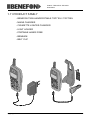
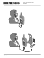
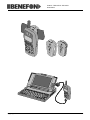
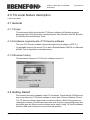
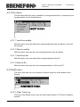
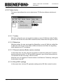
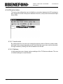
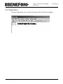
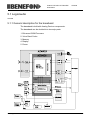
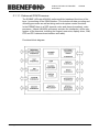
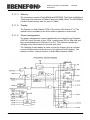
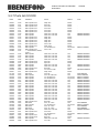
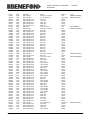
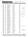
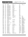
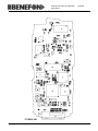
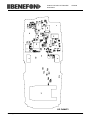
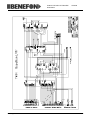
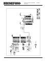
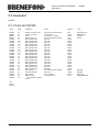
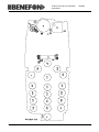
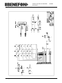
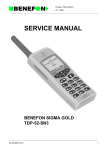
Product: TGP71EU & TGP73EU
08.02.2002
SERVICE MANUAL
Benefon Twin
TGP71EU
Benefon Twin DS (Dual SIM)
TGP73EU
Gp_71ugbTOC.fm
1
Product: TGP71EU & TGP73EU
08.02.2002
CONTENTS
1.0 PRODUCT FEATURE DESCRIPTION . . . . . . . . . . . . . . . . . . . . . . . . . 1 - 1
1.1 Network standard . . . . . . . . . . . . . . . . . . . . . . . . . . . . . . . . . . . . . 1 - 1
1.2 Physical dimensions . . . . . . . . . . . . . . . . . . . . . . . . . . . . . . . . . . . 1 - 1
1.3 Display . . . . . . . . . . . . . . . . . . . . . . . . . . . . . . . . . . . . . . . . . . . . . 1 - 1
1.4 SIM . . . . . . . . . . . . . . . . . . . . . . . . . . . . . . . . . . . . . . . . . . . . . . . . 1 - 1
1.5 Connectors . . . . . . . . . . . . . . . . . . . . . . . . . . . . . . . . . . . . . . . . . . 1 - 2
1.6 Operating voltages . . . . . . . . . . . . . . . . . . . . . . . . . . . . . . . . . . . . 1 - 2
1.7 Battery packs and operating times . . . . . . . . . . . . . . . . . . . . . . . . 1 - 2
1.8 Accessories . . . . . . . . . . . . . . . . . . . . . . . . . . . . . . . . . . . . . . . . . . 1 - 2
1.9 Main features of Benefon Twin . . . . . . . . . . . . . . . . . . . . . . . . . . . 1 - 3
1.9.1 User changeable mask . . . . . . . . . . . . . . . . . . . . . . . . . . . 1 - 3
1.9.2 Location based services . . . . . . . . . . . . . . . . . . . . . . . . . . 1 - 3
1.9.3 T9, text input with nine keys . . . . . . . . . . . . . . . . . . . . . . . 1 - 3
1.9.4 Abbreviated dialling memory . . . . . . . . . . . . . . . . . . . . . . . 1 - 3
1.9.5 Recent calls memory . . . . . . . . . . . . . . . . . . . . . . . . . . . . . 1 - 3
1.9.6 Personal organiser (Clock & calendar functions) . . . . . . . . 1 - 3
1.10 Manufacturer . . . . . . . . . . . . . . . . . . . . . . . . . . . . . . . . . . . . . . . . 1 - 4
1.11 PRODUCT FAMILY . . . . . . . . . . . . . . . . . . . . . . . . . . . . . . . . . . 1 - 5
2.0 OWNER’S MANUAL . . . . . . . . . . . . . . . . . . . . . . . . . . . . . . . . . . . . . . . 2 - 1
3.0 LIGHT CAR INSTALLATION . . . . . . . . . . . . . . . . . . . . . . . . . . . . . . . . . 3 - 1
4.0 TG Local feature description . . . . . . . . . . . . . . . . . . . . . . . . . . . . . . . . . 4 - 1
4.1 General . . . . . . . . . . . . . . . . . . . . . . . . . . . . . . . . . . . . . . . . . . . . . 4 - 1
4.1.1 Scope . . . . . . . . . . . . . . . . . . . . . . . . . . . . . . . . . . . . . . . . 4 - 1
4.1.2 Hardware requirements of TG Service software . . . . . . . . 4 - 1
4.1.3 Revision history . . . . . . . . . . . . . . . . . . . . . . . . . . . . . . . . . 4 - 1
4.2 Getting started . . . . . . . . . . . . . . . . . . . . . . . . . . . . . . . . . . . . . . . . 4 - 1
4.3 List of Features . . . . . . . . . . . . . . . . . . . . . . . . . . . . . . . . . . . . . . . 4 - 2
4.3.1 File menu . . . . . . . . . . . . . . . . . . . . . . . . . . . . . . . . . . . . . . 4 - 3
4.3.2 Edit menu . . . . . . . . . . . . . . . . . . . . . . . . . . . . . . . . . . . . . 4 - 3
4.3.3 View menu . . . . . . . . . . . . . . . . . . . . . . . . . . . . . . . . . . . . . 4 - 4
4.3.4 Device menu . . . . . . . . . . . . . . . . . . . . . . . . . . . . . . . . . . . 4 - 5
4.3.5 Service menu . . . . . . . . . . . . . . . . . . . . . . . . . . . . . . . . . . . 4 - 6
Gp_71ugbTOC.fm
2
Product: TGP71EU & TGP73EU
08.02.2002
4.3.6 Tuning menu . . . . . . . . . . . . . . . . . . . . . . . . . . . . . . . . . . . 4 - 7
4.3.7 Help menu . . . . . . . . . . . . . . . . . . . . . . . . . . . . . . . . . . . . . 4 - 8
5.0 TECHNICAL DESCRIPTION . . . . . . . . . . . . . . . . . . . . . . . . . . . . . . . . . 5 - 1
5.0.1 General . . . . . . . . . . . . . . . . . . . . . . . . . . . . . . . . . . . . . . . 5 - 1
5.0.2 Antenna connector . . . . . . . . . . . . . . . . . . . . . . . . . . . . . . 5 - 1
5.0.3 System connector description . . . . . . . . . . . . . . . . . . . . . . 5 - 1
5.0.4 Charging & battery . . . . . . . . . . . . . . . . . . . . . . . . . . . . . . . 5 - 4
5.0.5 HW and SW version numbering . . . . . . . . . . . . . . . . . . . . 5 - 5
5.1 Logic/audio . . . . . . . . . . . . . . . . . . . . . . . . . . . . . . . . . . . . . . . . . . 5 - 6
5.1.1 General description for the baseband . . . . . . . . . . . . . . . . 5 - 6
5.2 RF . . . . . . . . . . . . . . . . . . . . . . . . . . . . . . . . . . . . . . . . . . . . . . . . 5 - 10
5.2.1 General . . . . . . . . . . . . . . . . . . . . . . . . . . . . . . . . . . . . . . 5 - 10
5.2.2 Receiver . . . . . . . . . . . . . . . . . . . . . . . . . . . . . . . . . . . . . . 5 - 10
5.2.3 Transmitter . . . . . . . . . . . . . . . . . . . . . . . . . . . . . . . . . . . . 5 - 10
5.2.4 Synthesizer . . . . . . . . . . . . . . . . . . . . . . . . . . . . . . . . . . . 5 - 10
5.2.5 Power supply and power switching . . . . . . . . . . . . . . . . . 5 - 11
5.2.6 Antenna and antenna connector . . . . . . . . . . . . . . . . . . . 5 - 11
5.2.7 Parts list OC2300 . . . . . . . . . . . . . . . . . . . . . . . . . . . . . . . 5 - 12
5.3 Keyboard . . . . . . . . . . . . . . . . . . . . . . . . . . . . . . . . . . . . . . . . . . . 5 - 29
5.3.1 Parts list OK2300 . . . . . . . . . . . . . . . . . . . . . . . . . . . . . . . 5 - 29
5.4 MECHANICS . . . . . . . . . . . . . . . . . . . . . . . . . . . . . . . . . . . . . . . . 5 - 33
Gp_71ugbTOC.fm
3
Product: TGP71EU & TGP73EU
08.02.2002
1.0 PRODUCT FEATURE DESCRIPTION
1.1 Network standard
Benefon Twin is a dual band GSM phone operating seamlessly between the bands.
For GSM900 Benefon Twin operates only on primary P-GSM band, i.e. transmitting
on 890 - 915 MHz (mobile transmit, base receive) and receiving on 935 - 960 MHz
(base transmit, mobile receive) For GSM1800 Benefon Twin transmits on
1 710 - 1 785 MHz (mobile transmit, base receive) and receiving on 1 805 - 1 880
MHz (base transmit, mobile receive). Benefon Twin does not support E-GSM band.
Maximum output power on lower band is 2 W and on upper band 1 W. Thus Benefon
Twin belongs to power class 4 on lower band and to power class 1 on higher band.
Benefon Twin standard GSM Full Rate speech coding and Enhanced Full Rate
speech coding EFR. Benefon Twin supports full duplex, circuit switched asyncronous data services on data rates 300 bit/s, 1200 bit/s, 4.8 kbit/s, 9.6 kbit/s and
14.4 kbit/s. These data rates can be used for sending PC FAX. Additionally Twin
supports V.110 ISDN connection, Radio Link Protocol, RLP., and a set of GSM 07.07
AT commands. No syncronous data services and no alternate speech/data calls are
supported.
Benefon Twin supports Short Message Service and Short Message Service Cell
Broadcast. Depending on the network configuration Twin also supports concatenated short messages up to length of 640 characters.
1.2 Physical dimensions
Maximum length of the Twin is 112 mm; maximum width 49 mm and maximum thickness is 27 mm.
Weight of the phone is 108 g with 650 mAh Li-On battery pack and 126 g with 800
mAh NiMH and 1050 mAh Li-On battery pack.
1.3 Display
Display is a custom full-graphic display. It will have 48 pixel rows and 100 columns.
1.4 SIM
Benefon Twin is using small plug-in SIM card. SIM interface is guaranteed to work
only with 5 V SIM cards.
2gp_71gb.fm
1
Product: TGP71EU & TGP73EU
08.02.2002
1.5 Connectors
Benefon Twin has offers several types of connectors, namely
- battery connector with 4 connectors for battery pack
- charging connector with 2 connectors for chargers
- SIM connector with 6 pins for SIM card
- RF -connector (female SMA type) for integral antenna
- system connector with 16 pins for various accessories
There is no auxiliary RF -connector. However it's possible to detach integral antenna
and connect an external antenna to its connector.
1.6 Operating voltages
Maximum operating voltage is 5.2 V, minimum voltage 3.3 V. Nominal voltage 4.0 V.
1.7 Battery packs and operating times
Initially three battery packs are available for Benefon Twin, namely
Battery type
Li-On 650 mAh
NiMH 800 mAh
Li-On 1050 mAh
Talk time up to
320 min
375 min
540 min
Stand-by time up to
120 h
125 h
200 h
NiMH battery pack contains three NiMH cells and Li-On battery packs one Li-On cell.
Talk and standby times vary a lot depending on the network conditions.
1.8 Accessories
- belt clip
- portable hands-free kit
- light car cradle
- simple hands-free kit to use in car integrated to cigarette lighter adapter
charger
- cigarette lighter adapter charger with hands-free kit
- two different mains chargers, other slightly faster than other
- PC support software for administration of abbreviated dialling entries and
sending SMS to several recipients
- PC adapter cable for PC support software and data services
2gp_71gb.fm
2
Product: TGP71EU & TGP73EU
08.02.2002
1.9 Main features of Benefon Twin
This section list some of the most important features of Benefon Twin
1.9.1 User changeable mask
Lens mask framing the display can be detached and changed by the user. Many different colour options are available.
1.9.2 Location based services
Benefon Twin has a capability to send information of the base stations it can receive.
This information is wrapped into a SMS message including some service requests.
Network can calculate the location of the mobile based on this network information.
Thereafter network service can handle the service request and reply to the mobile
according to its location. This feature is available only in limited number of networks.
1.9.3 T9, text input with nine keys
While writing text into Benefon Twin, user may switch T9 active and make the writing
significantly easier and faster. While using T9, user has to press a key only once per
letter and the user interface suggests matching words to user.
1.9.4 Abbreviated dialling memory
Up to 255 Abbreviated Dialling entries on SIM card are supported. There's no ADN
memory in the phone's memory.
1.9.5 Recent calls memory
Twin separates calls to three different categories and stores the associated telephone numbers if available from the network. Twin stores last 15 dialled calls, last 10
unanswered calls and last 10 answered calls.
1.9.6 Personal organiser (Clock & calendar functions)
Benefon twin has an in-built real time clock and calendar that operates for a significant period even if battery is detached. Several features on the user interface of the
phone use this information, namely recent call timestamps, text message handling,
alarm clock and calendar with its reminders.
2gp_71gb.fm
3
Product: TGP71EU & TGP73EU
08.02.2002
1.10 Manufacturer
BENEFON OYJ
P.O. Box 84
(Meriniitynkatu 11)
FIN 24101 SALO
FINLAND
Telephone: + 358 2 77 400
Facsimile: + 358 2 332 633
2gp_71gb.fm
4
Product: TGP71EU & TGP73EU
08.02.2002
1.11 PRODUCT FAMILY
- BENEFON TWIN HANDPORTABLE TGP71EU / TGP73EU
- MAINS CHARGER
- CIGARETTE LIGHTER CHARGER
- LIGHT HOLDER
- PORTABLE HANDS FREE
- BENEWIN
- BELT CLIP
2gp_71gb.fm
5
Product: TGP71EU & TGP73EU
08.02.2002
2gp_71gb.fm
6
Product: TGP71EU & TGP73EU
08.02.2002
2gp_71gb.fm
7
2.0 OWNER’S MANUAL
1user_gb.fm
1
Product: TGP71EU & TGP73EU
12.12.2000
3.0 LIGHT CAR INSTALLATION
6gp_71gb.fm
1
Product: TGP71EU & TGP73EU /
Local Service
08.02.2002
4.0 TG Local feature description
Local Service Mode
4.1 General
4.1.1 Scope
This document briefly describes the TG Service software for Benefon products
belonging to the Twin Generation, namely Benefon Twin, Benefon Twin DS, Benefon
Q, Benefon Esc! and Benefon Track.
4.1.2 Hardware requirements of TG Service software
The use of TG Service software requires a proper service adapter ( APD 70 ).
It’s advisable connect the service PC to also a Rohde&Swartz CMD 55 or a Wavetek
4400M. This is required for automatic tuning.
4.1.3 Revision history
This document is based on TG Service software version 2.1.
4.2 Getting started
First connect the service adapter to the PC and phone. Check that the COM port setting is correctly set in TG Service software in menu item “Device->Options->Phone”.
The TG Service software works best on a phone without a SIM. During power-up:
reading the contents of a SIM card uses quite a lot of phone’s processing power and
during this time the Service mode software works slowly. Using TG Service software
without a SIM card in the phone overcomes this problem.
3gp_71sw21gb.fm
1
Product: TGP71EU & TGP73EU /
Local Service
08.02.2002
To establish a connection between the TG Service software and the phone do following
1. Switch the adapter to the Service mode. Connect the mobile phone to the
service adapter and check that the phone starts up.
NOTE! When the phone starts, wait until the text "Seeking emergency
cover" appears on the sreen, before you press OK. The right timing is
needed to get the phone to the local mode and to be sure, that
downloading will be completed successfully. (When phone has
successfully entered to the local mode the display will show the phone
type, SW- and HW-versions.
2. Click the leftmost Toolbar button to establish a connection between TG
Service software and the phone. Check the “Communication trace” for this.
While the phone is controlled by TG Service mode software, the user can read the
phone type, HW version and SW version number from the phone’s display.
4.3 List of Features
The opening screen of the service software looks like this.
3gp_71sw21gb.fm
2
Product: TGP71EU & TGP73EU /
Local Service
08.02.2002
4.3.1 File menu
The file menu allows the user to handle the tuning parameter file. It contains the tuning parameters of an individual phone.
4.3.1.1 Load from mobile
With this option user can read all the tuning parameters from the phone’s non-volatile memory.
4.3.1.2 Save to mobile
With this option user can save the tuning parameters from the phone.
4.3.1.3 Load from file
With this option user can read all the tuning parameters from PC.
4.3.1.4 Save to file
With this option user can save the tuning parameters to a file onto PC.
4.3.2 Edit menu
This menu item has only one function to clear the trace box at the bottom of the
window.
4.3.2.1 Clear Trace Log
This menu item allows user to clear the trace log at bottom of TG Service software
window.
3gp_71sw21gb.fm
3
Product: TGP71EU & TGP73EU /
Local Service
08.02.2002
4.3.3 View menu
This menu item allows the user to adjust some TG Service software window settings.
4.3.3.1 Toolbar
With this setting the user can toggle the toolbar on and off. With the visible Toolbar,
the user can access the most often needed functions faster than through the menu.
4.3.3.2 Status bar
With this setting, the user can toggle the Status Bar on and off. With the visible Status Bar the user can get some help on different features and follow the signalling
traffic between the PC and phone.
4.3.3.3 Channel window (Radio service window)
In this menu item, the user can open a window to control the radio part. Functions
include setting the active TX, RX and MON channels, type of burst transmitted etc.
This window can be used only in Service mode.
Note the user can toggle the Channel window on/off with the Toolbar by clicking the
fourth button from left.
4.3.3.4 Show RFG settings
In this menu item, it shows RF generator settings when RX Gain control is active.
3gp_71sw21gb.fm
4
Product: TGP71EU & TGP73EU /
Local Service
08.02.2002
4.3.4 Device menu
This menu item allows the user to initialise a connection between the PC and phone
plus toggle the mode of the phone between Service (Local) mode and Normal Operation mode.
4.3.4.1 Local mode
By clicking this line, the user can change the phone mode to Service (Local) mode
and back to the normal operating mode. Note that this menu item can be accessed
through toolbar by clicking the second button from the left.
4.3.4.2 Options
In this menu item user change various settings of the TG Service software. The use
of default settings is recommended.
3gp_71sw21gb.fm
5
Product: TGP71EU & TGP73EU /
Local Service
08.02.2002
4.3.5 Service menu
This menu item allows the service personnel to use the service functions needed
during unit repair and view related tune-up values.
4.3.5.1 View tuning values
This menu item allows the user to view the LCD contrast setting and battery voltage
correction value. A proper and valid battery voltage correction value is very important for the battery charging algorithm. The value is used to stop the charging process at the right point in time.
4.3.5.2 View TX tuning values
This menu item allows the user to view the tuning values related to the transmitter
part.
4.3.5.3 View RX tuning values
This menu item allows the user to view the tuning values related to the receiver part.
4.3.5.4 Sim Lock
4.3.5.5 MoviStar Sim Lock
4.3.5.6 Reset phone code
This menu item allows the user resets phone code to 1234.
3gp_71sw21gb.fm
6
Product: TGP71EU & TGP73EU /
Local Service
08.02.2002
4.3.6 Tuning menu
This menu item allows the user to tune an individual setting related to the phone.
4.3.6.1 TX Power ramp
This menu item allows the user to adjust the TX power levels on both GSM and DCS
bands.
4.3.6.2 RX Gain control
This menu item allows the user to adjust the RX gain control values for different signal levels. A routine for automatic adjustment with CMD 55 is available.
4.3.6.3 LCD & Buzzer test
This menu item allows user to change the LCD contrast setting. Note that too dark a
setting may cause the display to “flicker” in the light of fluorescent tubes.
Buzzer test enables to check the buzzer functioning.
4.3.6.4 Battery values
This menu item allows the user to measure and store the battery voltage correction
value. Be sure to apply to the phone’s exact operating voltage of 4,32 V with external
power adapter.
3gp_71sw21gb.fm
7
Product: TGP71EU & TGP73EU /
Local Service
08.02.2002
4.3.7 Help menu
This menu allows the user to check the version of the TG Service software.
3gp_71sw21gb.fm
8
Product: TGP71EU & TGP73EU /
08.02.2002
5.0 TECHNICAL DESCRIPTION
5.0.1 General
Benefon Twin and Benefon Twin DS has two circuit boards, PCBs. Main PCB has all
the GSM specific function on board, both radio and baseband section. Auxiliary PCB
provides a platform for LCD display and keypad. Circuit boards are connected to
together with a 32 pin connector.
5.0.2 Antenna connector
Antenna connector is SMA compatible and tilted 5 degrees away from the user
head. Connector is matched to 50 ohms.
5.0.3 System connector description
This section describes the female system connector in the phone.
5.0.3.1 Pin numbering
With Benefon Twin the system connector pin numbering starts from the right when
looking the phone from front, i.e. the display side.
Note that in other TG products the system connector may be assembled upside
down. Another way to remember pin numbering is to know that the charging pins are
the pins 17-20, i.e. the numbering starts as far as possible from charging connector.
Note that pins NMEA pins are active only in Benefon Esc! and Benefon Track.
9gp_71gb.fm
Pin
Nbr
NAME
FUNCTION
STATE
IN/
OUT
1
AGND
Analog Ground
0V
2
RS1CTS /
!2CINT
RS1 Clear to Send /
I2C Interrupt (NMT)
0V
2.7V
in
3
EXTMIC
External MIC line
0V -1.5V pp DC
in/out
4
RS1RTS /
ACCPWR
RS1 Ready to Send /
Accessory pwr control
0V
2.7V
out
5
EXTERP
External ERP line +
BOOT pin
0V -1.5V pp
0V/12V DC
out
in
6
CHARGE
Charging Current +
Power On
7
HEADSETDET
Headset Detector /
Accessory pwr control
in
0V
2.7V
in/out
1
Product: TGP71EU & TGP73EU /
08.02.2002
8
RS1RX
RS1 Receive Data
0V
2.7V
in
9
VBAT
Battery Voltage
2.7V -6.0V
out
10
RS1TX
RS1 Transmit Data
0V
2.7V
out
11
EERPP
Headset
0 VDC / 1.4 VDC
+ 0 -1 VRMS AC
out
12
EERPN
Headset
0 VDC / 1.4 VDC
+ 0 -1 VRMS AC
out
13
AUXDET
Headset Hook /
Accessory Detector
0V
2.7V
in/
14
RS2RX/
NMEAIN
RS2 Receive Data /
NMEA input (GPS)
0V
2.7V
in/out
15
RS2TX/
NMEAOUT
RS2 Transmit Data /
NMEA output (GPS)
0V
2.7V
out
16
DGND
Digital Ground
0V
17
NC
Not connected
18
DGND
Digital Ground
19
NC
Not connected
in
20
CHARGE
Charging Current +
Power On
in
in
0V
5.0.3.2 Pin descriptions
PIN 1:
Analog Ground should be connected to digital ground at only one point
inside the mobile phone. This point is the analog ground pin of the first
microphone amplifier stage.
PIN 2:
CTS signal for asynchronic serial line number 1 (RS232). Used for data
communication between the GSM mobile phones and PC. With NMT
phones this pin is used to detect I2C interrupt. The pin is normally in
logical ‘1’ state and I2C interrupt pulls the pin to logical ‘0’.
PIN 3:
External MIC line is used as an audio input for the mobile phone. There
is a DC level in this pin for headset. The DC level has been made by
connecting the pin to 2.2V voltage via 2.2 kohm resistor.
9gp_71gb.fm
2
Product: TGP71EU & TGP73EU /
08.02.2002
PIN 4:
RTS signal for asynchronic serial line number 1 (RS232). Used for data
communication between the GSM mobile phones and PC. When there
is other accessory than data cable connected to the mobile phone this
pin can be used to control the accessory power. Logical ‘1’ turns the
accessory power on and logical ‘0’ turns the accessory power off. With
MiniHF this same feature can be used to mute the audio lines.
PIN 5:
If boot signal is 12V when resetting the phone, the phone will start
performing software from the BOOT ROM memory. This is used for
FLASH downloading. Otherwise this pin is used as an EXTERP pin to
get the analog audio out from the mobile phone. The analog audio is
connected to this pin via 10 uF capacitor and there is not any DC level
in audio out signal.
PIN 6:
Charging current input, max. 1.0A. Connecting a charger to this pin will
also power on the mobile phone. Powering off the mobile happens with
EMMI command (see pins 14 & 15).
PIN 7:
The headset detector signal is normally at logic ‘1’ state (2.7V). When
pulling this signal to ground outside the mobile the mobile knows that
either the headset or the MiniHF car kit is connected to the phone.
When the mobile phone pulls this signal to ground it disables the
accessory regulator preventing the accessory to take power. With
MiniHF this same feature can be used to mute the audio lines. This can
be done with next circuit:
With this circuit the 100k resistor can be omitted if the in/out pin has an
internal pull-up when in input mode. The maximum voltage of VCC
connected to 100 kohm resistor in the accessory side is 2.7V. The in/
out pin is in output mode only when there is a need to power off an
accessory or to mute the audio lines of MiniHF car kit.
PIN 8 & 10:
Asynchronic serial line number 1 (RS232).
PIN 9:
The maximum current from the VBAT line is 300 mA.
PIN 11 & 12: Used for driving portable HF speaker capsule. Symmetrical output.
Minimum load 32 ohm symmetrical, 150 ohm asymmetrical (with DC
coupling). Maximun power 25 mW.
PIN 13:
Hook line for active headset and MiniHF detection line. This line is
normally at logic ‘1’ state (2.7V). When pulling this signal to ground
after the headset accessory has been detected the mobile phone
assumes that the hook of the headset has been pressed.
If pins 13 and 7 have been pulled to ground and the charger has been
connected to pin 6 (CHARGE) within 100ms, the mobile phone
assumes that the connected accessory is MiniHF car kit.
9gp_71gb.fm
3
Product: TGP71EU & TGP73EU /
08.02.2002
If this signal has been pulled to ground and the headset detector (pin 7)
is in logic ’1’ state the mobile assumes that there is an accessory using
serial port connected to the system connector.
PIN 14 & 15: Asynchronic serial line number 2 (RS232) for accessories and for
debugging mobile’s software. This line does not have CTS or RTS
signals. The data is transferred according EMMI protocol defined in
GSM phase2 specification 11.10-1 section 36.3.5.; 9600 bit/s, 1 start bit
(S), 8 bits (D1 to D8), no parity, 1 stopbit (E). The flow control is not
used.
NMEA 0183 signals for GPS phones
PIN 16:
PIN 17:
PIN 18:
PIN 19:
PIN 20:
The maximum current of DGND pin is 1,0A.
Not connected. If connected, Charger Switch 0 (CHGSW0) is normally
in logic ‘1’ state (2.7V) and grounded when the charger is connected to
DC jack.
Same as pin 16. The maximum current of DGND pin is 1.0A.
Not connected. If connected, Charger Switch 1 (CHGSW1) is normally
grounded and goes to logic ‘1’ state when the charger is connected to
DC jack.
Same as pin 6. The maximum current of CHARGE pin is 1.0A.
The maximum current of all pins except pins 6, 9 and 16 - 20 is 10 mA.
5.0.4 Charging & battery
During charging the charger provides a constant current that can be cut off by the
phone. After main charging phase phone uses short current pulses to keep up the
fully charged. Charging connector uses only two leads and therefore the charging
cable and connector can be simple.
The estimate of remaining battery capacity is based on both battery voltage and
used current integration. Current integration means that phone makes “notes” on the
current used and the period this current was used.
TG charging concept has charger options. Slow “overnight” charger and fast
charger.
TG battery concept uses to pins to read battery type. The pins can only have fixed
setting, low (ground) and high. This limits the number of battery categories to four.
Note that within a category the battery capacity can vary up to 10-15%, but the cell
type remains the same.
9gp_71gb.fm
4
Product: TGP71EU & TGP73EU /
08.02.2002
5.0.5 HW and SW version numbering
Both HW and SW version are displayed in Service (local) mode.
From idle mode SW version can be read from the phone by keying in *#0000#. Additionally this display shows also the SW compilation date.
5.0.5.1 Hardware version
HW version number consists of 8 digits like SBBRRDDZ. HW version numbers
are issued in alphabetical order (numbers preceding letters). i.e. later HW
versions come later in alphabetical order.
5.0.5.2 Software version
Software version code has format X.XXXXXA, for example 1.290162F. SW version
numbers are issued in alphabetical order (numbers preceding letters), i.e. later SW
versions come later in alphabetical order.
9gp_71gb.fm
5
Product:TGP71EU & TGP73EU /
OC2300
08.02.2002
5.1 Logic/audio
OC2300
5.1.1 General description for the baseband
The baseband is built with Analog Devices components.
The baseband can be devided into six major parts:
1. Enhanced GSM Processor
2. Voice Band Codec
3. Memory
4. Display
5. Power
Ramp
AFC
4c2300gb.fm
6
Product:TGP71EU & TGP73EU /
OC2300
08.02.2002
5.1.1.1 Enhanced GSM Processor
The EGSMP (ADI chip AD6426) performs all the baseband functions of the
layer 1 processing of the GSM interface. This includes all data encoding and
decoding processes as well as timing radio sub-system control functions.
In the EGSMP there is a DSP (speech codec and channel equalizer), main
processor ( Hitachi H8/300H processor) and also the interfaces ( all the subsystem of the therminal, including the keypad, memories, display driver, SIM,
DTE and DTA data services interface and radio).
Functional block diagram
4c2300gb.fm
7
Product:TGP71EU & TGP73EU /
OC2300
08.02.2002
5.1.1.2 Voice Band Codec
The VBC (ADI chip AD6425) contains complete codecs for the conversion of
voiceband and baseband signals as well as D/A- converters to control the radio
subsystem and auxiliary A/D-converter for signal monitoring purposes.
The voiceband codec is a complete analog front-end, which can interface
directly with a microphone and a speaker.
The baseband codec is a complete low power, two channel, input/output port
with signal conditioning. The transmit path consists of an on-chip burst store, a
GMSK modulator and two high speed DACDs with output reconstruction filters.
The receive path consists of two 15 bit Sigma Delta A/D converters, which
include high performance digital filters for RF-channel selection.
The auxiliary section of the VBC consists of D/A converters for AFC, AGC and
for control of the transmit-burst envelope.
The auxiliary section also includes A/D converters that measures different voltages and temperatures.
4c2300gb.fm
8
Product:TGP71EU & TGP73EU /
OC2300
08.02.2002
5.1.1.3
Memory
The memories consists of Flash SRAM and EEPROM. The Flash and RAM are
16 bits wide with total size of 32Mbit (Flash) and 4Mbit (RAM). The EEPROM is
a 2-Wire Serial memory with the size of 128kbit.
5.1.1.4
Display
The Display is a Seiko Epson FSTN LCD module (100*48 dots 2.7V) The
module have a possibility to be driven either in parallel or serial mode.
5.1.1.5
Power management
The power management is mainly handled by the Analog Device Regulator
(ADP3401) wich consists of four LDOs, charge pump (5V) for SIM card and
logic level translations for SIM card (3 to 5V). The chip also handles the
charging of the litium battery for the real time clock.
The charging of main battery is made so that the charger gives a constant
current and its switched in the phone to the right level for the battery. The
battery is Lithium, Lithium Polymer or Nickel Metal Hydride, NiMH.
4c2300gb.fm
9
Product:TGP71EU & TGP73EU /
OC2300
08.02.2002
5.2 RF
5.2.1 General
The RF-part is based on Hitachi dualband GSM RF-chip HD155121F, which
includes receiver circuit, offset loop modulation TX architecture and IF-VCO.
The final power amplifier is Hitachi PF08103B dualband TX module. RF parts
are powered by three 2.8V linear regulators, which provide separate power
supply for PLL synthesizer and VCO, modulator and TX-parts, and other RFparts such as AGC-amplifier and LNA etc.
5.2.2 Receiver
The incoming RX signal from antenna front-end switch X403 is fed via front
end filter X301 to the LNA-block, which consists of two amplifiers, one for each
band. After LNA-block RX signal is filtered again in filter X302 and applied to
the input of first mixer in the RF-chip where the signal is converted to first IF of
225MHz. The channel filtering is accoplished with first IF filter X303. After
filtering the signal is fed back to the RF-chip for second frequency conversion.
Second IF-frequency is 45 MHz. The second local oscillator signal and 45MHz
signal required for IQ demodulation is generated in RF-chip. Automatic Gain
Control (AGC) is made by changing the gain of both mixer stages and by
adjusting the gain of 45 MHz second IF-amplifier.
5.2.3 Transmitter
The TX signal is generated by dividing the 540 MHz IF-VCO frequency by 2 or
by 4. This 270 MHz signal ( 135 MHz in DCS-1800 band ) is then modulatid
with I and Q signals. The IQ modulated signal is fed to the phase comparator
where it is compared to the mixed signal of RF-VCO X304 and TX-VCO X401.
The phase comparator output is then filtered and applied to TX-VCO. This
architecture makes it possible to use oscillators running at final frequency.
Modulated RF-signal from TX-VCO is then amplified in dualband TX module
I405 and routed via antenna front-end switch X403 to the antenna connector.
The power control loop consists of directional coupler X402, detector diodes
D401 and comparator I404.
5.2.4 Synthesizer
RF-synthesizer, which controls RF-channel frequency, is made of serial
controlled dual synthesizer chip I304 and dualband VCO-module X304. IFsynthesizer includes the same synthesizer chip I304 and IF-VCO, which is
integrated in Hitachi RF-chip, resonator circuits is excluded. Loopfilters of both
synthesizers are passive type. 13 MHz reference signal is generated in
VCTCXO module X1. The frequency of IF-synthesizer is switched 4 MHz
depending on TX / RX cycle and uset RF channel.
4c2300gb.fm
10
Product:TGP71EU & TGP73EU /
OC2300
08.02.2002
5.2.5 Power supply and power switching
The battery voltage is regulated in switchable regulators I302, I303 and I401.
The used supply voltage for RF-components is 2.8 V, except dual-band TXmodule.The power on/off switching is controlled from baseband-processor
using output-enable pin of each regulator.
5.2.6 Antenna and antenna connector
The RF-signal from antenna front-end switch X403 is applied to the antenna
connector V2. The antenna connector is SMA-type and the nominal impedance
is 50 ohm. Antenna itself is a helical type dualband antenna.
4c2300gb.fm
11
Product:TGP71EU & TGP73EU /
OC2300
08.02.2002
5.2.7 Parts list OC2300
CODE
PART
DESCRIPT.
VALUE
MANUF.
CG0101
CG0330
CG0103
CG0103
CG0103
CG0103
CG0104
CG0104
CG0101
CG0101
CG0101
CG0101
CG0332
CG0471
CH0105
CG0332
CG0682
C100
C101
C102
C150
C151
C152
C160
C161
C162
C163
C164
C165
C180
C181
C182
C183
C184
100pF ñ5%
33pF ñ5%
10nF ñ10%
10nF ñ10%
10nF ñ10%
10nF ñ10%
100nF/10% 6,3V X5R
100nF/10% 6,3V X5R
100pF ñ5%
100pF ñ5%
100pF ñ5%
100pF ñ5%
3.3nF ñ10%
470pF ñ10%
1uF/-20/+80%/16V
3.3nF ñ10%
Murata
Murata
Murata
Murata
Murata
Murata
AVX
AVX
Murata
Murata
Murata
Murata
Murata
Murata
TaiyoYuden
Murata
CG0104
CG0104
CG0104
CG0104
CG0330
CG0330
CG0104
CG0104
CG0223
CF0105
CG0471
CU1106
CC2103
CH0105
CH0105
CG0104
CG0104
CG0104
CG0104
CG0104
CG0104
CG0104
CG0104
CG0104
CG0104
CG0104
CG0104
CG0223
CU3106
CH0105
CU3106
CU3106
CG0104
CG0103
CH0105
CG0101
CG0680
CG0104
CG0102
C185
C186
C187
C188
C190
C191
C200
C201
C202
C210
C211
C212
C213
C215
C216
C217
C218
C219
C220
C221
C222
C225
C226
C227
C228
C229
C230
C232
C233
C234
C235
C236
C237
C241
C242
C243
C244
C245
C248
SMD capasitor X7R
SMD capasitor NPO
SMD capasitor X7R
SMD capasitor X7R
SMD capasitor X7R
SMD capasitor X7R
SMD capasitor
SMD capasitor
SMD capasitor X7R
SMD capasitor X7R
SMD capasitor X7R
SMD capasitor X7R
SMD capasitor X7R
SMD capasitor X7R
SMD capasitor
SMD capasitor X7R
*** EI KOODATTU VARASTOON ***
SMD capasitor
SMD capasitor
SMD capasitor
SMD capasitor
SMD capasitor NPO
SMD capasitor NPO
SMD capasitor
SMD capasitor
SMD capasitor X7R
SMD capasitor
SMD capasitor X7R
SMD tantal
SMD capasitor
SMD capasitor
SMD capasitor
SMD capasitor
SMD capasitor
SMD capasitor
SMD capasitor
SMD capasitor
SMD capasitor
SMD capasitor
SMD capasitor
SMD capasitor
SMD capasitor
SMD capasitor
SMD capasitor
SMD capasitor X7R
SMD tantal
SMD capasitor
SMD tantal
SMD tantal
SMD capasitor
SMD capasitor X7R
SMD capasitor
SMD capasitor X7R
SMD capasitor NPO
SMD capasitor
SMD capasitor X7R
100nF/10% 6,3V X5R
100nF/10% 6,3V X5R
100nF/10% 6,3V X5R
100nF/10% 6,3V X5R
33pF ñ5%
33pF ñ5%
100nF/10% 6,3V X5R
100nF/10% 6,3V X5R
22nF 20%
1uF 10% 6,3V X5R
470pF ñ10%
10uF/16V
10nF 10% 100V X7R
1uF/-20/+80%/16V
1uF/-20/+80%/16V
100nF/10% 6,3V X5R
100nF/10% 6,3V X5R
100nF/10% 6,3V X5R
100nF/10% 6,3V X5R
100nF/10% 6,3V X5R
100nF/10% 6,3V X5R
100nF/10% 6,3V X5R
100nF/10% 6,3V X5R
100nF/10% 6,3V X5R
100nF/10% 6,3V X5R
100nF/10% 6,3V X5R
100nF/10% 6,3V X5R
22nF 20%
10uF / 6V +-20%
1uF/-20/+80%/16V
10uF / 6V +-20%
10uF / 6V +-20%
100nF/10% 6,3V X5R
10nF ñ10%
1uF/-20/+80%/16V
100pF ñ5%
68pF ñ5%
100nF/10% 6,3V X5R
1nF ñ10%
AVX
AVX
AVX
AVX
Murata
Murata
AVX
AVX
Murata
AVX
Murata
AVX
AVX
TaiyoYuden
TaiyoYuden
AVX
AVX
AVX
AVX
AVX
AVX
AVX
AVX
AVX
AVX
AVX
AVX
Murata
AVX
TaiyoYuden
AVX
AVX
AVX
Murata
TaiyoYuden
Murata
Murata
AVX
Murata
4c2300gb.fm
TYPE
‘
‘
‘
‘
CM05X5R104K06AH
CM05X5R104K06AH
EMK212 F105Z00T
CM05X5R104K06AH
CM05X5R104K06AH
CM05X5R104K06AH
CM05X5R104K06AH
CM05X5R104K06AH
CM05X5R104K06AH
CM105X5R105K06AT
TAJB106M016R
12061C103KAT2A
EMK212 F105Z00T
EMK212 F105Z00T
CM05X5R104K06AH
CM05X5R104K06AH
CM05X5R104K06AH
CM05X5R104K06AH
CM05X5R104K06AH
CM05X5R104K06AH
CM05X5R104K06AH
CM05X5R104K06AH
CM05X5R104K06AH
CM05X5R104K06AH
CM05X5R104K06AH
CM05X5R104K06AH
TAJA106M006R
EMK212 F105Z00T
TAJA106M006R
TAJA106M006R
CM05X5R104K06AH
‘
EMK212 F105Z00T
CM05X5R104K06AH
12
Product:TGP71EU & TGP73EU /
OC2300
08.02.2002
CODE
CG0104
CH0105
CG0101
CG0102
CG0101
CG0101
CG0101
CU3106
CG0104
CG0223
CG0223
CG0680
CG0680
CG0680
CG0680
CG0680
CG0680
CG0680
CG0680
CG0680
CG0680
CG0680
CG0680
CG0680
CG0104
CG0680
CF0105
CG0680
CG0471
CG0330
CG0279
CG0129
CG0109
CG0103
CG0221
CG0109
CG0100
CG0279
CG0229
CG0680
CG0270
CG0229
CG0109
CG0103
CG0221
CG0399
CG0479
CG0129
CG0189
CG0220
CG0101
CG0101
CG0103
CG0102
CG0103
CH0105
CG0103
CG0121
CG0121
CG0339
PART
C249
C250
C251
C252
C253
C254
C255
C260
C261
C263
C264
C270
C271
C272
C273
C274
C275
C276
C277
C278
C279
C280
C281
C282
C290
C291
C294
C295
C3
C301
C302
C303
C304
C305
C306
C307
C308
C311
C313
C321
C322
C323
C324
C325
C326
C327
C328
C331
C332
C333
C334
C335
C336
C337
C338
C339
C341
C343
C344
C345
4c2300gb.fm
DESCRIPT.
SMD capasitor
SMD capasitor
SMD capasitor X7R
SMD capasitor X7R
SMD capasitor X7R
SMD capasitor X7R
SMD capasitor X7R
SMD tantal
SMD capasitor
SMD capasitor X7R
SMD capasitor X7R
SMD capasitor NPO
SMD capasitor NPO
SMD capasitor NPO
SMD capasitor NPO
SMD capasitor NPO
SMD capasitor NPO
SMD capasitor NPO
SMD capasitor NPO
SMD capasitor NPO
SMD capasitor NPO
SMD capasitor NPO
SMD capasitor NPO
SMD capasitor NPO
SMD capasitor
SMD capasitor NPO
SMD capasitor
SMD capasitor NPO
SMD capasitor X7R
SMD capasitor NPO
SMD capasitor NPO
SMD capasitor NPO
SMD capasitor NPO
SMD capasitor X7R
SMD capasitor X7R
SMD capasitor NPO
SMD capasitor NPO
SMD capasitor NPO
SMD capasitor NPO
SMD capasitor NPO
SMD capasitor NPO
SMD capasitor NPO
SMD capasitor NPO
SMD capasitor X7R
SMD capasitor X7R
SMD capasitor NPO
SMD capasitor NPO
SMD capasitor NPO
SMD capasitor NPO
SMD capasitor NPO
SMD capasitor X7R
SMD capasitor X7R
SMD capasitor X7R
SMD capasitor X7R
SMD capasitor X7R
SMD capasitor
SMD capasitor X7R
SMD capasitor X7R
SMD capasitor X7R
SMD capasitor NPO
VALUE
100nF/10% 6,3V X5R
1uF/-20/+80%/16V
100pF ñ5%
1nF ñ10%
100pF ñ5%
100pF ñ5%
100pF ñ5%
10uF / 6V +-20%
100nF/10% 6,3V X5R
22nF 20%
22nF 20%
68pF ñ5%
68pF ñ5%
68pF ñ5%
68pF ñ5%
68pF ñ5%
68pF ñ5%
68pF ñ5%
68pF ñ5%
68pF ñ5%
68pF ñ5%
68pF ñ5%
68pF ñ5%
68pF ñ5%
100nF/10% 6,3V X5R
68pF ñ5%
1uF 10% 6,3V X5R
68pF ñ5%
470pF ñ10%
33pF ñ5%
2.7pF ñ0,25pF
1.2pF ñ0,25pF
1.0pF ñ0,25pF
10nF ñ10%
220pF ñ10%
1.0pF ñ0,25pF
10pF-+0.25pF
2.7pF ñ0,25pF
2.2pF ñ0,25pF
68pF ñ5%
27pF ñ5%
2.2pF ñ0,25pF
1.0pF ñ0,25pF
10nF ñ10%
220pF ñ10%
3.9pF ñ0,25pF
4.7pF ñ0,25pF
1.2pF ñ0,25pF
1.8pF ñ0,25pF
22pF ñ5%
100pF ñ5%
100pF ñ5%
10nF ñ10%
1nF ñ10%
10nF ñ10%
1uF/-20/+80%/16V
10nF ñ10%
120pF ñ5%
120pF ñ5%
3.3pF ñ0,25pF
MANUF.
AVX
TaiyoYuden
Murata
Murata
Murata
Murata
Murata
AVX
AVX
Murata
Murata
Murata
Murata
Murata
Murata
Murata
Murata
Murata
Murata
Murata
Murata
Murata
Murata
Murata
AVX
Murata
AVX
Murata
Murata
Murata
Murata
Murata
Murata
Murata
Murata
Murata
Murata
Murata
Murata
Murata
Murata
Murata
Murata
Murata
Murata
Murata
Murata
Murata
Murata
Murata
Murata
Murata
Murata
Murata
Murata
TaiyoYuden
Murata
Murata
Murata
Murata
TYPE
CM05X5R104K06AH
EMK212 F105Z00T
TAJA106M006R
CM05X5R104K06AH
CM05X5R104K06AH
CM105X5R105K06AT
‘
‘
‘
‘
EMK212 F105Z00T
‘
13
Product:TGP71EU & TGP73EU /
OC2300
08.02.2002
CODE
CG0339
CG0339
CG0151
CG0103
CG0103
CG0102
CU3475
CU3475
CG0102
CU3475
CG0680
CG0101
CG0331
CH0105
CG0103
CG0270
CG0100
CH0105
CG0101
CP2223
CG0152
CH0105
CG0102
CG0152
CP2223
CG0102
CG0100
CG0100
CG0569
CG0103
CG0220
CG0689
CG0689
CG0331
CG0100
CG0220
CG0220
CG0101
CG0103
CG0103
CG0103
CG0100
CG0100
CG0101
CP2682
CG0471
CD0103
CG0680
CG0121
CG0120
CG0102
CU3475
CG0104
CG0339
CG0100
CG0471
CG0220
CG0680
CG0680
CU1107
PART
C346
C347
C348
C351
C352
C353
C354
C355
C356
C357
C360
C361
C362
C363
C364
C365
C366
C367
C368
C371
C372
C373
C374
C375
C376
C378
C380
C381
C382
C383
C384
C385
C388
C389
C390
C401
C402
C403
C404
C405
C406
C407
C408
C409
C411
C412
C413
C414
C416
C420
C421
C422
C423
C424
C425
C426
C427
C428
C429
C430
4c2300gb.fm
DESCRIPT.
SMD capasitor NPO
SMD capasitor NPO
SMD capasitor X7R
SMD capasitor X7R
SMD capasitor X7R
SMD capasitor X7R
SMD tantal
SMD tantal
SMD capasitor X7R
SMD tantal
SMD capasitor NPO
SMD capasitor X7R
SMD capasitor X7R
SMD capasitor
SMD capasitor X7R
SMD capasitor NPO
SMD capasitor NPO
SMD capasitor
SMD capasitor X7R
SMD film capasitor
SMD capasitor X7R
SMD capasitor
SMD capasitor X7R
SMD capasitor X7R
SMD film capasitor
SMD capasitor X7R
SMD capasitor NPO
SMD capasitor NPO
SMD capasitor NPO
SMD capasitor X7R
SMD capasitor NPO
SMD capasitor NPO
SMD capasitor NPO
SMD capasitor X7R
SMD capasitor NPO
SMD capasitor NPO
SMD capasitor NPO
SMD capasitor X7R
SMD capasitor X7R
SMD capasitor X7R
SMD capasitor X7R
SMD capasitor NPO
SMD capasitor NPO
SMD capasitor X7R
SMD film capasitor
SMD capasitor X7R
SMD capasitor
SMD capasitor NPO
SMD capasitor X7R
SMD capasitor NPO
SMD capasitor X7R
SMD tantal
SMD capasitor
SMD capasitor NPO
SMD capasitor NPO
SMD capasitor X7R
SMD capasitor NPO
SMD capasitor NPO
SMD capasitor NPO
SMD tantal
VALUE
3.3pF ñ0,25pF
3.3pF ñ0,25pF
150pF ñ5%
10nF ñ10%
10nF ñ10%
1nF ñ10%
4.7uF/10V 20%
4.7uF/10V 20%
1nF ñ10%
4.7uF/10V 20%
68pF ñ5%
100pF ñ5%
330pF ñ10%
1uF/-20/+80%/16V
10nF ñ10%
27pF ñ5%
10pF-+0.25pF
1uF/-20/+80%/16V
100pF ñ5%
22nF/16V +-5%
1.5nF ñ10%
1uF/-20/+80%/16V
1nF ñ10%
1.5nF ñ10%
22nF/16V +-5%
1nF ñ10%
10pF-+0.25pF
10pF-+0.25pF
5.6pF ñ0,25pF
10nF ñ10%
22pF ñ5%
6.8pF ñ0,25pF
6.8pF ñ0,25pF
330pF ñ10%
10pF-+0.25pF
22pF ñ5%
22pF ñ5%
100pF ñ5%
10nF ñ10%
10nF ñ10%
10nF ñ10%
10pF-+0.25pF
10pF-+0.25pF
100pF ñ5%
6,8nF/16V +-5%
470pF ñ10%
10 nF 10% 50 V X7R
68pF ñ5%
120pF ñ5%
12pF ñ5%
1nF ñ10%
4.7uF/10V 20%
100nF/10% 6,3V X5R
3.3pF ñ0,25pF
10pF-+0.25pF
470pF ñ10%
22pF ñ5%
68pF ñ5%
68pF ñ5%
100uF/10V -+20%
MANUF.
Murata
Murata
Murata
Murata
Murata
Murata
AVX
AVX
Murata
AVX
Murata
Murata
Murata
TaiyoYuden
Murata
Murata
Murata
TaiyoYuden
Murata
Panasonic
Murata
TaiyoYuden
Murata
Murata
Panasonic
Murata
Murata
Murata
Murata
Murata
Murata
Murata
Murata
Murata
Murata
Murata
Murata
Murata
Murata
Murata
Murata
Murata
Murata
Murata
Panasonic
Murata
Philips
Murata
Murata
Murata
Murata
AVX
AVX
Murata
Murata
Murata
Murata
Murata
Murata
AVX
TYPE
‘
‘
TAJA475M010R
TAJA475M010R
TAJA475M010R
EMK212 F105Z00T
‘
EMK212 F105Z00T
ECHU1C223JB5
EMK212 F105Z00T
ECHU1C223JB5
‘
‘
‘
‘
ECHU1C682JB5
TAJA475M010R
CM05X5R104K06AH
TAJD107M010R
14
Product:TGP71EU & TGP73EU /
OC2300
08.02.2002
CODE
CU1107
CG0680
CG0103
CG0680
CG0103
CG0680
CG0330
CG0101
CG0229
CG0680
CG0101
CG0101
CF0689
CG0680
CG0330
CG0680
CG0330
CG0680
CG0680
CG0102
CG0330
CG0330
CG0101
DY0016
DS0019
DC0229
DY0062
AF1035
IX6426
IX6425
IM8421
IM0128
IR3401
IX0826
IF1551
IR2982
IR2982
IS1503
IR2982
IH0126
IA4165
IW0810
LC0567
LG0332
LG0103
LG0392
LG0332
LG0822
LG0682
LG0682
LC4104
LC4104
LC4154
LC3823
LC3823
LG0103
LC4822
LG0103
QS0060
QF6702
PART
C431
C432
C433
C434
C435
C436
C437
C438
C439
C440
C441
C442
C443
C445
C446
C447
C448
C450
C451
C452
C456
C457
C458
D200
D201
D301
D401
F251
I100
I101
I110
I115
I120
I122
I301
I302
I303
I304
I401
I403
I404
I405
L200
L301
L302
L303
L304
L305
L306
L307
L311
L312
L313
L314
L315
L317
L318
L402
Q150
Q200
4c2300gb.fm
DESCRIPT.
SMD tantal
SMD capasitor NPO
SMD capasitor X7R
SMD capasitor NPO
SMD capasitor X7R
SMD capasitor NPO
SMD capasitor NPO
SMD capasitor X7R
SMD capasitor NPO
SMD capasitor NPO
SMD capasitor X7R
SMD capasitor X7R
SMD capasitor
SMD capasitor NPO
SMD capasitor NPO
SMD capasitor NPO
SMD capasitor NPO
SMD capasitor NPO
SMD capasitor NPO
SMD capasitor X7R
SMD capasitor NPO
SMD capasitor NPO
SMD capasitor X7R
SMD shottky diode
SMD diode
SMD silicon tuning diode
SMD shcottky diode
PolySwitch
Enhanced GSM prosessor
Analog/Digital IC GSM
Flash+SRAM memory
EEPROM
Regulator
EL-lamp driver
RF-circuit Bright II
Regulator
Regulator
PLL frequency synthesize
Regulator
Quad tri state buffer
Op Amps
RF-power amplifier
SMD inductors
SMD inductor
SMD inductor
SMD inductor
SMD inductor
SMD inductor
SMD inductor
SMD inductor
SMD inductor
SMD inductor
SMD inductor
SMD inductor
SMD inductor
SMD inductor
SMD inductor
SMD inductor
SMD transistor arrey
P-channel MOSFET
VALUE
100uF/10V -+20%
68pF ñ5%
10nF ñ10%
68pF ñ5%
10nF ñ10%
68pF ñ5%
33pF ñ5%
100pF ñ5%
2.2pF ñ0,25pF
68pF ñ5%
100pF ñ5%
100pF ñ5%
6.8 pF/0.25pF 50 V NP0
68pF ñ5%
33pF ñ5%
68pF ñ5%
33pF ñ5%
68pF ñ5%
68pF ñ5%
1nF ñ10%
33pF ñ5%
33pF ñ5%
100pF ñ5%
40V/1,33A VF=0.55V
100v / 200mA
1V/19pF...4V/11pF
40V 20mA
16MB + 2MB
128K(16.384x8)
4,5V / 120V
GSM Tx/Rx
2,8V 50mA
2,8V 50mA
2,8V 50mA
2,7V--6,5V/80mA
900/1800MHz
560uH 10% 3,2x2,5mm
3n3 +-0,3nH
10n +-5%
3n9 +-0,3nH
3n3 +-0,3nH
8n2 +-5%
6n8 +-5%
6n8 +-5%
100n +-5%
100n +-5%
150n +-5%
82n +-5%
82n +-5%
10n +-5%
8n2 +-0,2n
10n +-5%
NPN/PNP 100mA/50V
Vdss 20V rds 0,2 ohm
MANUF.
AVX
Murata
Murata
Murata
Murata
Murata
Murata
Murata
Murata
Murata
Murata
Murata
Philips
Murata
Murata
Murata
Murata
Murata
Murata
Murata
Murata
Murata
Murata
Shindengen
Philips
Toshiba
Siemens
Raychem
AnalogDevi
AnalogDevi
Fujitsu
Atmel
AnalogDevi
Supertex
Hitachi
NationalSe
NationalSe
Fujitsu
NationalSe
Fairchild
Maxim
Hitachi
Murata
TaiyoYuden
TaiyoYuden
TaiyoYuden
TaiyoYuden
TaiyoYuden
TaiyoYuden
TaiyoYuden
TaiyoYuden
TaiyoYuden
TaiyoYuden
TaiyoYuden
TaiyoYuden
TaiyoYuden
Murata
TaiyoYuden
Siemens
I&R
TYPE
TAJD107M010R
‘
‘
M1FS4
BAS19
1SV229
BAT 62
miniSMDC035-2
AD6426AB
AD6425AST
MB84VD21091-85PB
AT24C128N-10SI2,
ADP3401ARU-REEL
HV826MG
HD155121FEB
LP2982IMS-2,8
LP2982IMS-2,8
MB15F03SLPV-ER
LP2982IMS-2,8
MM74HC126MTC
MAX4165
PF08103B
LQH3C561K34
HK1005 3N3J-T
HK1005 10NJ-T
HK1005 3N9J-T
HK1005 3N3J-T
HK1005 8N2J-T
HK1005 6N8J-T
HK1005 6N8J-T
HK1608 R10J-T
HK1608 R10J-T
HK1608 R15J-T
HK1608 82NJ-T
HK1608 82NJ-T
HK1005 10NJ-T
LQP21A8N2C14M00
HK1005 10NJ-T
BCR 10PN
IRLMS6702
15
Product:TGP71EU & TGP73EU /
OC2300
08.02.2002
CODE
QS1847
QS1847
QS0060
QS1847
QS1847
QA0420
QA0420
QS1857
QS0060
QS1857
QS1847
RG0151
RG0103
RG0103
RF0106
RG0103
RG0104
RG0104
RG0104
RG0000
RG0564
RG0104
RG0684
RT2500
RG0105
RG0104
RG0104
RG0104
RG0103
RG0472
RG0472
RG0472
RG0472
RG0472
RG0472
RG0472
RG0472
RG0104
RG0272
RG0101
RG0272
RG0103
RG0103
RG0272
RG0102
RG0103
RG0105
RG0103
RG0103
RG0103
RG0104
RG0102
RG0220
RG0564
RG0105
RG0472
RG0472
RG0103
RG0101
RG0103
PART
Q201
Q210
Q220
Q241
Q250
Q301
Q302
Q401
Q402
Q403
Q404
R100
R102
R103
R104
R105
R113
R114
R117
R121
R150
R151
R152
R153
R154
R155
R160
R161
R162
R163
R164
R165
R166
R170
R171
R172
R173
R174
R180
R181
R183
R190
R191
R192
R202
R203
R204
R205
R206
R207
R208
R210
R211
R212
R213
R215
R216
R220
R221
R241
4c2300gb.fm
DESCRIPT.
piensignaali yleistransi
piensignaali yleistransi
SMD transistor arrey
piensignaali yleistransi
piensignaali yleistransi
RF transistor
RF transistor
piensignaali yleistransi
SMD transistor arrey
piensignaali yleistransi
piensignaali yleistransi
SMD resistor
SMD resistor
SMD resistor
SMD resistor
SMD resistor
SMD resistor
SMD resistor
SMD resistor
SMD resistor
SMD resistor
SMD resistor
SMD resistor
NTC resistor
SMD resistor
SMD resistor
SMD resistor
SMD resistor
SMD resistor
SMD resistor
SMD resistor
SMD resistor
SMD resistor
SMD resistor
SMD resistor
SMD resistor
SMD resistor
SMD resistor
SMD resistor
SMD resistor
SMD resistor
SMD resistor
SMD resistor
SMD resistor
SMD resistor
SMD resistor
SMD resistor
SMD resistor
SMD resistor
SMD resistor
SMD resistor
SMD resistor
SMD resistor
SMD resistor
SMD resistor
SMD resistor
SMD resistor
SMD resistor
SMD resistor
SMD resistor
VALUE
NPN 100mA/45V hfe=200...450
NPN 100mA/45V hfe=200...450
NPN/PNP 100mA/50V
NPN 100mA/45V hfe=200...450
NPN 100mA/45V hfe=200...450
NPN silicon 1.8GHz
NPN silicon 1.8GHz
PNP 100mA/45V hfe=220...470
NPN/PNP 100mA/50V
PNP 100mA/45V hfe=220...470
NPN 100mA/45V hfe=200...450
150R 5% 0.063W
10k 5% 0.063W
10k 5% 0.063W
10 M 5% 0.125 W
10k 5% 0.063W
100k 5% 0.063W
100k 5% 0.063W
100k 5% 0.063W
0 ohm
560k 5% 0.063W
100k 5% 0.063W
680k 5% 0.063W
150k+-5% B=4750
1M0 5% 0.063W
100k 5% 0.063W
100k 5% 0.063W
100k 5% 0.063W
10k 5% 0.063W
4k7 5% 0.063W
4k7 5% 0.063W
4k7 5% 0.063W
4k7 5% 0.063W
4k7 5% 0.063W
4k7 5% 0.063W
4k7 5% 0.063W
4k7 5% 0.063W
100k 5% 0.063W
2k7 5% 0.063W
100R 5% 0.063W
2k7 5% 0.063W
10k 5% 0.063W
10k 5% 0.063W
2k7 5% 0.063W
1k0 5% 0.063W
10k 5% 0.063W
1M0 5% 0.063W
10k 5% 0.063W
10k 5% 0.063W
10k 5% 0.063W
100k 5% 0.063W
1k0 5% 0.063W
22R 5% 0.063W
560k 5% 0.063W
1M0 5% 0.063W
4k7 5% 0.063W
4k7 5% 0.063W
10k 5% 0.063W
100R 5% 0.063W
10k 5% 0.063W
MANUF.
Philips
Philips
Siemens
Philips
Philips
Siemens
Siemens
Philips
Siemens
Philips
Philips
Kamaya
Kamaya
Kamaya
Kamaya
Kamaya
Kamaya
Kamaya
Kamaya
TYPE
BC847BW
BC847BW
BCR 10PN
BC847BW
BC847BW
BFP420
BFP420
BC857BW
BCR 10PN
BC857BW
BC847BW
RMC1/16S
RMC1/16S
RMC1/16S
Kamaya
Kamaya
Kamaya
TaiyoYuden
Kamaya
Kamaya
Kamaya
Kamaya
Kamaya
Kamaya
Kamaya
Kamaya
Kamaya
Kamaya
Kamaya
Kamaya
Kamaya
Kamaya
Kamaya
Kamaya
Kamaya
Kamaya
Kamaya
Kamaya
Kamaya
Kamaya
Kamaya
Kamaya
Kamaya
Kamaya
Kamaya
Kamaya
Kamaya
Kamaya
Kamaya
Kamaya
Kamaya
Kamaya
Kamaya
Kamaya
RMC1/16S
RMC1/16S
RMC1/16S
TBPS1R154J475H5Q
RMC1/16S
RMC1/16S
RMC1/16S
RMC1/16S
RMC1/16S
RMC1/16S
RMC1/16S
RMC1/16S
RMC1/16S
RMC1/16S
RMC1/16S
RMC1/16S
RMC1/16S
RMC1/16S
RMC1/16S
RMC1/16S
RMC1/16S
RMC1/16S
RMC1/16S
RMC1/16S
RMC1/16S
RMC1/16S
RMC1/16S
RMC1/16S
RMC1/16S
RMC1/16S
RMC1/16S
RMC1/16S
RMC1/16S
RMC1/16S
RMC1/16S
RMC1/16S
RMC1/16S
RMC1/16S
RMC1/16S
RMC1/16S
RMC1/16S
RMC1/16S
RMC1/16S
RMC1/16S
16
Product:TGP71EU & TGP73EU /
OC2300
08.02.2002
CODE
RG0220
RG0222
RG0104
RG0222
RG0220
RG0151
RG0105
RG0105
RG0103
RG0104
RG0104
RG0101
RG0102
RG0101
RG0101
RG0101
RG0101
RG0101
RG0101
RG0101
RG0101
RG0101
RG0101
RG0104
RG0104
RG0104
RG0104
RG0104
RG0103
RG0102
RG0104
RG0223
RG0223
RG0000
RG0104
RG0102
RG0151
RG0472
RG0472
RG0101
RG0471
RG0100
RG0222
RG0100
RG0100
RG0101
RG0101
RG0101
RG0101
RG0101
RG0102
RG0100
RG0100
RG0180
RG0472
RG0182
RG0101
RG0100
RG0103
RG0100
PART
R242
R243
R244
R245
R246
R247
R250
R251
R255
R260
R261
R262
R263
R264
R265
R266
R267
R268
R269
R270
R271
R272
R273
R274
R275
R276
R277
R278
R281
R282
R283
R290
R291
R292
R293
R294
R301
R302
R303
R304
R305
R306
R307
R311
R312
R313
R314
R315
R316
R317
R319
R321
R322
R324
R326
R327
R328
R331
R332
R333
4c2300gb.fm
DESCRIPT.
SMD resistor
SMD resistor
SMD resistor
SMD resistor
SMD resistor
SMD resistor
SMD resistor
SMD resistor
SMD resistor
SMD resistor
SMD resistor
SMD resistor
SMD resistor
SMD resistor
SMD resistor
SMD resistor
SMD resistor
SMD resistor
SMD resistor
SMD resistor
SMD resistor
SMD resistor
SMD resistor
SMD resistor
SMD resistor
SMD resistor
SMD resistor
SMD resistor
SMD resistor
SMD resistor
SMD resistor
SMD resistor
SMD resistor
SMD resistor
SMD resistor
SMD resistor
SMD resistor
SMD resistor
SMD resistor
SMD resistor
SMD resistor
SMD resistor
SMD resistor
SMD resistor
SMD resistor
SMD resistor
SMD resistor
SMD resistor
SMD resistor
SMD resistor
SMD resistor
SMD resistor
SMD resistor
SMD resistor
SMD resistor
SMD resistor
SMD resistor
SMD resistor
SMD resistor
SMD resistor
VALUE
22R 5% 0.063W
2k2 5% 0.063W
100k 5% 0.063W
2k2 5% 0.063W
22R 5% 0.063W
150R 5% 0.063W
1M0 5% 0.063W
1M0 5% 0.063W
10k 5% 0.063W
100k 5% 0.063W
100k 5% 0.063W
100R 5% 0.063W
1k0 5% 0.063W
100R 5% 0.063W
100R 5% 0.063W
100R 5% 0.063W
100R 5% 0.063W
100R 5% 0.063W
100R 5% 0.063W
100R 5% 0.063W
100R 5% 0.063W
100R 5% 0.063W
100R 5% 0.063W
100k 5% 0.063W
100k 5% 0.063W
100k 5% 0.063W
100k 5% 0.063W
100k 5% 0.063W
10k 5% 0.063W
1k0 5% 0.063W
100k 5% 0.063W
22k 5% 0.063W
22k 5% 0.063W
0 ohm
100k 5% 0.063W
1k0 5% 0.063W
150R 5% 0.063W
4k7 5% 0.063W
4k7 5% 0.063W
100R 5% 0.063W
470R 5% 0.063W
10 R 5% 0.063W
2k2 5% 0.063W
10 R 5% 0.063W
10 R 5% 0.063W
100R 5% 0.063W
100R 5% 0.063W
100R 5% 0.063W
100R 5% 0.063W
100R 5% 0.063W
1k0 5% 0.063W
10 R 5% 0.063W
10 R 5% 0.063W
18R 5% 0.063W
4k7 5% 0.063W
1k8 5% 0.063W
100R 5% 0.063W
10 R 5% 0.063W
10k 5% 0.063W
10 R 5% 0.063W
MANUF.
Kamaya
Kamaya
Kamaya
Kamaya
Kamaya
Kamaya
Kamaya
Kamaya
Kamaya
Kamaya
Kamaya
Kamaya
Kamaya
Kamaya
Kamaya
Kamaya
Kamaya
Kamaya
Kamaya
Kamaya
Kamaya
Kamaya
Kamaya
Kamaya
Kamaya
Kamaya
Kamaya
Kamaya
Kamaya
Kamaya
Kamaya
Kamaya
Kamaya
TYPE
RMC1/16S
RMC1/16S
RMC1/16S
RMC1/16S
RMC1/16S
RMC1/16S
RMC1/16S
RMC1/16S
RMC1/16S
RMC1/16S
RMC1/16S
RMC1/16S
RMC1/16S
RMC1/16S
RMC1/16S
RMC1/16S
RMC1/16S
RMC1/16S
RMC1/16S
RMC1/16S
RMC1/16S
RMC1/16S
RMC1/16S
RMC1/16S
RMC1/16S
RMC1/16S
RMC1/16S
RMC1/16S
RMC1/16S
RMC1/16S
RMC1/16S
RMC1/16S
RMC1/16S
Kamaya
Kamaya
Kamaya
Kamaya
Kamaya
Kamaya
Kamaya
Kamaya
Kamaya
Kamaya
Kamaya
Kamaya
Kamaya
Kamaya
Kamaya
Kamaya
Kamaya
Kamaya
Kamaya
Kamaya
Kamaya
Kamaya
Kamaya
Kamaya
Kamaya
Kamaya
RMC1/16S
RMC1/16S
RMC1/16S
RMC1/16S
RMC1/16S
RMC1/16S
RMC1/16S
RMC1/16S
RMC1/16S
RMC1/16S
RMC1/16S
RMC1/16S
RMC1/16S
RMC1/16S
RMC1/16S
RMC1/16S
RMC1/16S
RMC1/16S
RMC1/16S
RMC1/16S
RMC1/16S
RMC1/16S
RMC1/16S
RMC1/16S
RMC1/16S
RMC1/16S
17
Product:TGP71EU & TGP73EU /
OC2300
08.02.2002
CODE
RG0100
RG0100
RG0270
RG0222
RG0562
RG0472
RG0101
RG0101
RG0101
RG0102
RG0101
RG0101
RG0101
RG0101
RG0100
RG0100
RG0223
RG0100
RG0473
RG0100
RG0560
RG0101
RG0121
RG0270
RG0390
RG0151
RG0101
RG0472
RG0473
RG0105
RG0563
RG0104
RG0472
RG0470
RG0104
RG0104
RG0104
RG0100
RG0100
RG0470
RG0472
RG0472
RG0472
RG0472
RG0472
RG0473
RG0100
RG0472
VN2302
VM0002
VM0002
VW0109
VI2302
VR0248
XO0174
X32766
LF0062
LF0062
XW8425
XW9418
PART
R334
R335
R336
R337
R338
R339
R341
R342
R343
R400
R401
R402
R403
R404
R405
R406
R408
R409
R410
R411
R412
R413
R415
R416
R417
R418
R422
R423
R424
R426
R427
R428
R429
R430
R431
R432
R433
R435
R436
R437
R440
R441
R442
R443
R444
R445
R446
R447
V100
V101
V102
V105
V120
V2
X1
X100
X250
X251
X301
X302
4c2300gb.fm
DESCRIPT.
SMD resistor
SMD resistor
SMD resistor
SMD resistor
SMD resistor
SMD resistor
SMD resistor
SMD resistor
SMD resistor
SMD resistor
SMD resistor
SMD resistor
SMD resistor
SMD resistor
SMD resistor
SMD resistor
SMD resistor
SMD resistor
SMD resistor
SMD resistor
SMD resistor
SMD resistor
SMD resistor
SMD resistor
SMD resistor
SMD resistor
SMD resistor
SMD resistor
SMD resistor
SMD resistor
SMD resistor
SMD resistor
SMD resistor
SMD resistor
SMD resistor
SMD resistor
SMD resistor
SMD resistor
SMD resistor
SMD resistor
SMD resistor
SMD resistor
SMD resistor
SMD resistor
SMD resistor
SMD resistor
SMD resistor
SMD resistor
In phone connector
Modulat cntact
Modulat cntact
Connector
SIM-reader
SMA connector
VCTCXO 3,5*6,0mm
SMD crystal
SMD EMI filter
SMD EMI filter
Rx Dual SAW-filter
SAW-filter
VALUE
10 R 5% 0.063W
10 R 5% 0.063W
27R 5% 0.063W
2k2 5% 0.063W
5k6 5% 0.063W
4k7 5% 0.063W
100R 5% 0.063W
100R 5% 0.063W
100R 5% 0.063W
1k0 5% 0.063W
100R 5% 0.063W
100R 5% 0.063W
100R 5% 0.063W
100R 5% 0.063W
10 R 5% 0.063W
10 R 5% 0.063W
22k 5% 0.063W
10 R 5% 0.063W
47k 5% 0.063W
10 R 5% 0.063W
56R 5% 0.063W
100R 5% 0.063W
120R 5% 0.063W
27R 5% 0.063W
39R 5% 0.063W
150R 5% 0.063W
100R 5% 0.063W
4k7 5% 0.063W
47k 5% 0.063W
1M0 5% 0.063W
56k 5% 0.063W
100k 5% 0.063W
4k7 5% 0.063W
47R 5% 0.063W
100k 5% 0.063W
100k 5% 0.063W
100k 5% 0.063W
10 R 5% 0.063W
10 R 5% 0.063W
47R 5% 0.063W
4k7 5% 0.063W
4k7 5% 0.063W
4k7 5% 0.063W
4k7 5% 0.063W
4k7 5% 0.063W
47k 5% 0.063W
10 R 5% 0.063W
4k7 5% 0.063W
2pin 2A/pin
2pin 2A/pin
32-pin 1mm pitch
13.0 MHz 2,5ppm 3V+-5%
32.768kHz +-30ppm
10nF/2A
10nF/2A
for GSM
Rx dual
MANUF.
Kamaya
Kamaya
Kamaya
Kamaya
Kamaya
Kamaya
Kamaya
Kamaya
Kamaya
Kamaya
Kamaya
Kamaya
Kamaya
Kamaya
Kamaya
Kamaya
Kamaya
Kamaya
Kamaya
Kamaya
Kamaya
Kamaya
Kamaya
Kamaya
Kamaya
Kamaya
Kamaya
Kamaya
Kamaya
Kamaya
Kamaya
Kamaya
Kamaya
Kamaya
Kamaya
Kamaya
Kamaya
Kamaya
Kamaya
Kamaya
Kamaya
Kamaya
Kamaya
Kamaya
Kamaya
Kamaya
Kamaya
Kamaya
L&K
Bours
Bours
Elco
Siemens
?????????
Raltron
MicroCryst
Panasonic
Panasonic
Panasonic
Panasonic
TYPE
RMC1/16S
RMC1/16S
RMC1/16S
RMC1/16S
RMC1/16S
RMC1/16S
RMC1/16S
RMC1/16S
RMC1/16S
RMC1/16S
RMC1/16S
RMC1/16S
RMC1/16S
RMC1/16S
RMC1/16S
RMC1/16S
RMC1/16S
RMC1/16S
RMC1/16S
RMC1/16S
RMC1/16S
RMC1/16S
RMC1/16S
RMC1/16S
RMC1/16S
RMC1/16S
RMC1/16S
RMC1/16S
RMC1/16S
RMC1/16S
RMC1/16S
RMC1/16S
RMC1/16S
RMC1/16S
RMC1/16S
RMC1/16S
RMC1/16S
RMC1/16S
RMC1/16S
RMC1/16S
RMC1/16S
RMC1/16S
RMC1/16S
RMC1/16S
RMC1/16S
RMC1/16S
RMC1/16S
RMC1/16S
HO1433GB
70AAJ002M0
70AAJ002M0
589158032000011
V23533-A9222-A20
982589
RTVY-174EF230S13
MS1V-TK
ELKE103FA
ELKE103FA
FARG6CH1G8425L22
EFCH9418MTYB
18
Product:TGP71EU & TGP73EU /
OC2300
08.02.2002
CODE
XW0225
XO0490
XO0473
XI1519
ID2300
PC2300
PART
X303
X304
X401
X402
X403
Y240
DESCRIPT.
SAW filter, GSM
Dual Rx-VCO
Dual Tx-VCO
Direktional coupler
Dual switch diplexer
*** EI KOODATTU VARASTOON ***
VALUE
225MHz
for GSM
for GSM
Dual coupler
900/1800MHz
MANUF.
Murata
Panasonic
Panasonic
Murata
Murata
TYPE
MKFC225.000MBA
ENFVZ4G90
ENFVZ4G73
LDC15D190A0007AH
LMC36-07A0501PTA
Last
update
08.05.00
There are some differences between the single (TGP71EU) and dual SIM
(TGP73EU) in the OC2300 module
4c2300gb.fm
CODE
PART
VALUE
VI1707
V121
SIM-reader
1sim
2sim
-
X
IC0454
I121
RG0000
R292
ana switch
-
X
0R
X
-
19
Product:TGP71EU & TGP73EU /
OC2300
08.02.2002
4c2300gb.fm
20
Product:TGP71EU & TGP73EU /
OC2300
08.02.2002
4c2300gb.fm
21
Product:TGP71EU & TGP73EU /
OC2300
08.02.2002
4c2300gb.fm
22
Product:TGP71EU & TGP73EU /
OC2300
08.02.2002
4c2300gb.fm
23
Product:TGP71EU & TGP73EU /
OC2300
08.02.2002
4c2300gb.fm
24
Product:TGP71EU & TGP73EU /
OC2300
08.02.2002
4c2300gb.fm
25
Product:TGP71EU & TGP73EU /
OC2300
08.02.2002
4c2300gb.fm
26
Product:TGP71EU & TGP73EU /
OC2300
08.02.2002
4c2300gb.fm
27
Product:TGP71EU & TGP73EU /
OC2300
08.02.2002
4c2300gb.fm
28
Product:TGP71EU & TGP73EU /
OK2300
08.02.2002
5.3 Keyboard
OK2300
5.3.1 Parts list OK2300
CODE
PART
DESCRIPT.
VALUE
MANUF.
TYPE
AM1846
AE0023
AE0024
AB0621
CG0330
CG0330
CG0330
CG0330
CG0330
CG0330
CG0330
CG0330
CG0330
CG0330
CG0330
CG0330
CG0330
CG0330
CG0103
CG0330
CG0330
CG0330
DS1070
QF0200
RG0472
VN2303
PK2300
A1
A2
A3
A5
C1
C10
C11
C12
C13
C14
C15
C16
C17
C18
C2
C3
C4
C5
C6
C7
C8
C9
D1
Q1
R4
V2
Y41
Electret condenser mocro
Dynamic transducer
Buzzer
Backup-akku 3,4V
SMD capasitor NPO
SMD capasitor NPO
SMD capasitor NPO
SMD capasitor NPO
SMD capasitor NPO
SMD capasitor NPO
SMD capasitor NPO
SMD capasitor NPO
SMD capasitor NPO
SMD capasitor NPO
SMD capasitor NPO
SMD capasitor NPO
SMD capasitor NPO
SMD capasitor NPO
SMD capasitor X7R
SMD capasitor NPO
SMD capasitor NPO
SMD capasitor NPO
SMD diode pair
N-channel MOSFET
SMD resistor
SMD connector
*** EI KOODATTU VARASTOON ***
phone with rubber holder+zeb
13,3x2,6 low Z
10x10x3mm 1,5V/70mA
Lithium-ion/Manganese Oxide
33pF ñ5%
33pF ñ5%
33pF ñ5%
33pF ñ5%
33pF ñ5%
33pF ñ5%
33pF ñ5%
33pF ñ5%
33pF ñ5%
33pF ñ5%
33pF ñ5%
33pF ñ5%
33pF ñ5%
33pF ñ5%
10nF ñ10%
33pF ñ5%
33pF ñ5%
33pF ñ5%
70V/100mA common cathode
20V/0,73A
4k7 5% 0.063W
18 pin 0,5mm pitch
BSE
Philips
Citizen
Varta
Murata
Murata
Murata
Murata
Murata
Murata
Murata
Murata
Murata
Murata
Murata
Murata
Murata
Murata
Murata
Murata
Murata
Murata
Philips
TEMIC
Kamaya
Elco
OBG18S46-C33
WD00518/32U
CHB-03E
MC621
‘
BAV 70W
TN0200T
RMC1/16S
046239018001800
Last
update
24.01.00
4k2300gb.fm
29
Product:TGP71EU & TGP73EU /
OK2300
08.02.2002
4k2300gb.fm
30
Product:TGP71EU & TGP73EU /
OK2300
08.02.2002
4k2300gb.fm
31
Product:TGP71EU & TGP73EU /
OK2300
08.02.2002
4k2300gb.fm
32
Product:TGP71EU & TGP73EU /
12.12.2000
5.4 MECHANICS
7gp_71gb.fm
33