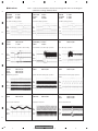
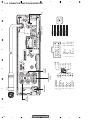
1
ORDER NO.
CRT3853
DEH-P6950IB/XN/ES
CD RECEIVER
DEH-P6950IB
/XN/ES
DEH-P6950IB
/XN/ES1
This service manual should be used together with the following manual(s):
Model No.
CX-3195
Order No.
CRT3815
Mech.Module
S10.5COMP2
Remarks
CD Mech. Module : Circuit Descriptions, Mech. Descriptions, Disassembly
For details, refer to "Important Check Points for Good Servicing".
PIONEER CORPORATION
4-1, Meguro 1-chome, Meguro-ku, Tokyo 153-8654, Japan
PIONEER ELECTRONICS (USA) INC. P.O. Box 1760, Long Beach, CA 90801-1760, U.S.A.
PIONEER EUROPE NV Haven 1087, Keetberglaan 1, 9120 Melsele, Belgium
PIONEER ELECTRONICS ASIACENTRE PTE. LTD. 253 Alexandra Road, #04-01, Singapore 159936
PIONEER CORPORATION 2006
K-ZZU. DEC. 2006 Printed in Japan
1
2
3
4
SAFETY INFORMATION
CAUTION
A
This service manual is intended for qualified service technicians; it is not meant for the casual do-it-yourselfer.
Qualified technicians have the necessary test equipment and tools, and have been trained to properly and safely repair
complex products such as those covered by this manual.
Improperly performed repairs can adversely affect the safety and reliability of the product and may void the warranty.
If you are not qualified to perform the repair of this product properly and safely, you should not risk trying to do so
and refer the repair to a qualified service technician.
WARNING
B
This product contains lead in solder and certain electrical parts contain chemicals which are known to the state of
California to cause cancer, birth defects or other reproductive harm.
Health & Safety Code Section 25249.6 - Proposition 65
- Safety Precautions for those who Service this Unit.
• When checking or adjusting the emitting power of the laser diode exercise caution in order to get safe, reliable
results.
Caution:
1. During repair or tests, minimum distance of 13 cm from the focus lens must be kept.
2. During repair or tests, do not view laser beam for 10 seconds or longer.
C
CAUTION
Danger of explosion if battery is incorrectly replaced.
Replaced only with the same or equivalent type recommended by the manufacture.
Discord used batteries according to the manufacture's instructions.
- Service Precaution
1. You should conform to the regulations governing
the product (safety, radio and noise, and other
regulations), and should keep the safety during
servicing by following the safety instructions
described in this manual.
2. Before disassembling the unit, be sure to turn off
the power. Unplugging and plugging the connectors
during power-on mode may damage the ICs inside
the unit.
3. To protect the pickup unit from electrostatic discharge
during servicing, take an appropriate treatment
(shorting-solder) by referring to "the DISASSEMBLY".
4. After replacing the pickup unit, be sure to check the
grating.
5. Be careful in handling ICs. Some ICs such as MOS
type are so fragile that they can be damaged by
electrostatic induction.
D
E
F
2
DEH-P6950IB/XN/ES
1
2
3
4
5
6
7
8
[Important Check Points for Good Servicing]
In this manual, procedures that must be performed during repairs are marked with the below symbol.
Please be sure to confirm and follow these procedures.
A
1. Product safety
Please conform to product regulations (such as safety and radiation regulations), and maintain a safe servicing environment by
following the safety instructions described in this manual.
1 Use specified parts for repair.
Use genuine parts. Be sure to use important parts for safety.
2 Do not perform modifications without proper instructions.
Please follow the specified safety methods when modification(addition/change of parts) is required due to interferences such as
radio/TV interference and foreign noise.
3 Make sure the soldering of repaired locations is properly performed.
B
When you solder while repairing, please be sure that there are no cold solder and other debris.
Soldering should be finished with the proper quantity. (Refer to the example)
4 Make sure the screws are tightly fastened.
Please be sure that all screws are fastened, and that there are no loose screws.
5 Make sure each connectors are correctly inserted.
Please be sure that all connectors are inserted, and that there are no imperfect insertion.
6 Make sure the wiring cables are set to their original state.
Please replace the wiring and cables to the original state after repairs.
In addition, be sure that there are no pinched wires, etc.
C
7 Make sure screws and soldering scraps do not remain inside the product.
Please check that neither solder debris nor screws remain inside the product.
8 There should be no semi-broken wires, scratches, melting, etc. on the coating of the power cord.
Damaged power cords may lead to fire accidents, so please be sure that there are no damages.
If you find a damaged power cord, please exchange it with a suitable one.
9 There should be no spark traces or similar marks on the power plug.
When spark traces or similar marks are found on the power supply plug, please check the connection and advise on secure
connections and suitable usage. Please exchange the power cord if necessary.
0 Safe environment should be secured during servicing.
D
When you perform repairs, please pay attention to static electricity, furniture, household articles, etc. in order to prevent injuries.
Please pay attention to your surroundings and repair safely.
2. Adjustments
To keep the original performance of the products, optimum adjustments and confirmation of characteristics within specification.
Adjustments should be performed in accordance with the procedures/instructions described in this manual.
3. Lubricants, Glues, and Replacement parts
Use grease and adhesives that are equal to the specified substance.
Make sure the proper amount is applied.
E
4. Cleaning
For parts that require cleaning, such as optical pickups, tape deck heads, lenses and mirrors used in projection monitors, proper
cleaning should be performed to restore their performances.
5. Shipping mode and Shipping screws
To protect products from damages or failures during transit, the shipping mode should be set or the shipping screws should be
installed before shipment. Please be sure to follow this method especially if it is specified in this manual.
F
DEH-P6950IB/XN/ES
5
6
7
8
3
1
2
3
4
CONTENTS
SAFETY INFORMATION ..................................................................................................................................... 2
1. SPECIFICATIONS ............................................................................................................................................ 5
2. EXPLODED VIEWS AND PARTS LIST ............................................................................................................ 6
2.1 PACKING ................................................................................................................................................... 6
2.2 EXTERIOR................................................................................................................................................. 8
2.3 CD MECHANISM MODULE..................................................................................................................... 10
3. BLOCK DIAGRAM AND SCHEMATIC DIAGRAM .......................................................................................... 12
3.1 BLOCK DIAGRAM ................................................................................................................................... 12
3.2 OVERALL CONNECTION DIAGRAM(GUIDE PAGE).............................................................................. 14
3.3 KEYBOARD UNIT.................................................................................................................................... 20
3.4 CD MECHANISM MODULE(GUIDE PAGE) ............................................................................................ 22
4. PCB CONNECTION DIAGRAM ..................................................................................................................... 30
4.1 TUNER AMP UNIT................................................................................................................................... 30
4.2 KEYBOARD UNIT.................................................................................................................................... 34
4.3 PANEL UNIT ............................................................................................................................................ 35
4.4 CD CORE UNIT(S10.5COMP2)............................................................................................................... 36
5. ELECTRICAL PARTS LIST ............................................................................................................................ 38
6. ADJUSTMENT ............................................................................................................................................... 44
6.1 CD ADJUSTMENT................................................................................................................................... 44
6.2 CHECKING THE GRATING AFTER CHANGING THE PICKUP UNIT .................................................... 46
6.3 ERROR MODE ........................................................................................................................................ 48
6.4 IPOD TEST MODE .................................................................................................................................. 49
6.5 SYSTEM MICROCOMPUTER TEST PROGRAM ................................................................................... 50
7. GENERAL INFORMATION ............................................................................................................................. 51
7.1 DIAGNOSIS ............................................................................................................................................. 51
7.1.1 DISASSEMBLY ..................................................................................................................................... 51
7.1.2 CONNECTOR FUNCTION DESCRIPTION .......................................................................................... 54
7.2 IC ............................................................................................................................................................. 55
7.3 OPERATIONAL FLOW CHART ............................................................................................................... 65
8. OPERATIONS ................................................................................................................................................ 66
A
B
C
D
E
F
4
DEH-P6950IB/XN/ES
1
2
3
4
5
6
7
8
1. SPECIFICATIONS
A
Backup current .................... 5 mA or less
B
C
D
E
F
DEH-P6950IB/XN/ES
5
6
7
8
5
1
2
3
4
2. EXPLODED VIEWS AND PARTS LIST
NOTES : • Parts marked by " * " are generally unavailable because they are not in our Master Spare Parts List.
• The > mark found on some component parts indicates the importance of the safety factor of the part.
Therefore, when replacing, be sure to use parts of identical designation.
• Screw adjacent to mark on the product are used for disassembly.
• For the applying amount of lubricants or glue, follow the instructions in this manual.
(In the case of no amount instructions,apply as you think it appropriate.)
A
"
2.1 PACKING
8
B
14
17
18
19
13
3
12
15
C
20
9
1
D
23
24
22
6
E
4
21
F
6
DEH-P6950IB/XN/ES
1
2
3
4
5
6
7
8
(1) PACKING SECTION PARTS LIST
Mark No.
*
*
*
Description
Part No.
Mark No.
Description
Part No.
1
2
3-1
3-2
3-3
3-4
Polyethylene Bag
•••••
Caution Card
Warranty Card
Owner's Manual
Owner's Manual
CEG-162
11
•••••
CRP1310
See Contrast table (2)
XRD7144
XRD7145
12
13
14
15
16
Handle
Bush
Screw Assy
Polyethylene Bag
•••••
CND3707
CNV3930
CEA3849
CEG-127
3-5
3-6
3-7
4
5
6
Installation Manual
Caution Card
Service Network
Remote Control Unit
Cord Assy
Cord Assy
XRD7146
XRP7002
See Contrast table (2)
CXC5717
XDE7026
XDP7004
17
18
19
20
21
Screw
Screw
Screw
Unit Box
Contain Box
CBA1650
CRZ50P090FTC
TRZ50P080FTC
See Contrast table (2)
See Contrast table (2)
7
8
9
10
•••••
Accessory Assy
Polyethylene Bag
•••••
CEA6708
CEG1160
22
23
24
Protector
Protector
Case Assy
XHP7016
XHP7017
XXA7417
*
A
B
(2) CONTRAST TABLE
DEH-P6950IB/XN/ES and DEH-P6950IB/XN/ES1 are constructed the same except for the following:
Mark
No.
*
*
3-2
3-7
20
21
Description
Warranty Card
Service Network
Unit Box
Contain Box
DEH-P6950IB/XN/ES
Not used
Not used
XHG7138
XHL7138
DEH-P6950IB/XN/ES1
CRY1250
CRY1251
XHG7145
XHL7145
C
Owner's Manual,Installation Manual
Part No.
Language
XRD7144
English, Spanish, Portuguese(B)
XRD7145
Arabic, Traditional Chinese
XRD7146
English, Spanish, Portuguese(B), Arabic, Traditional Chinese
D
E
F
DEH-P6950IB/XN/ES
5
6
7
8
7
1
2
3
4
2.2 EXTERIOR
2
81
A
15
2
12
6
2
10
2
B
11
A
C
35
17
B
38
18
85
37
38
3
19
87
33
42
34
84
83
38
19
83
38
43
18
23
31
22
32
26
D
30
B
45
27
25
7
28
A
B
C
20
5
44
50
47
A
24
49
46
48
29
86
52
82
41
55
D
39
53
54
4
D
4
40
57
60
4
1
73
75
E
70
D
76
77
88
8
C
65
59
66
72
64
36
71
79
1
80
9
78
56 62
58
63
13
68
69
58
58
F
16
8
61
67
58
74
DEH-P6950IB/XN/ES
1
2
3
4
5
6
7
8
EXTERIOR SECTION PARTS LIST
Mark No.
>
Description
Mark No.
Part No.
1
2
3
4
5
Screw
Screw
Screw
Screw
Earth Plate
BMZ30P040FTB
BSZ26P060FTC
BSZ30P060FTC
BSZ30P200FTC
CNC8915
6
7
8
9
10
Holder
Cushion
Remote Control Unit
Cover
CD Mechanism Module(S10.5)
CND3598
CNM8890
CXC5717
CZN5357
CXK5763
11
12
13
14
15
Cable
Cord Assy
Cord Assy
•••••
Insulator
XDE7022
XDE7026
XDP7004
16
17
18
19
20
Panel
Tuner Amp Unit
Screw
Screw
Screw
XNS7181
XWM7166
BPZ26P070FTC
BSZ26P060FTC
BSZ26P200FTC
21
22
23
24
25
•••••
Fuse(10 A)
Plug(CN901)
Plug(CN801)
Connector(CN651)
CEK1208
CKM1376
CKS3537
CKS3829
26
27
28
29
30
Connector(CN101)
Connector(CN701)
Antenna Jack(CN401)
Holder
Pin Jack(CN352)
CKS5271
CKS5691
CKX1056
CND1054
XKB7001
31
32
33
34
35
Holder
Holder
Insulator
Jack(CN171)
Heat Sink
XNC7026
XNC7030
XNM7031
XKS7006
YNR5031
36
37
38
39
40
Chassis Unit
Detachable Assy
Screw
Button
Button
XXA7507
XXA7520
BPZ20P080FTB
XAC7149
XAC7156
41
42
43
44
45
Spring
Cover
Lighting Conductor
Connector(CN1801)
Connector(CN1802)
XBH7001
XNS7180
XNV7035
CKS5207
CKS5545
46
47
48
49
Double side Tape
OEL Unit
Holder
Holder
CNM8673
MXS8231
XNC7009
XNV7029
XNM7106
Description
Part No.
50
Knob Unit
XXA7493
51
52
53
54
55
•••••
Sub Grille Assy
Plate
Grille Unit
Button Unit
XXA7502
XNS7196
XXA7506
XXA7508
56
57
58
59
60
Button
Screw(M2 x 4)
Screw
Washer
Spring
CAC7752
CBA1649
CBA1925
CBF1038
CBH2650
61
62
63
64
65
Spring
Spring
Spring
Holder
Gear
CBH2651
CBH2652
CBH2653
CND1254
CNV5997
66
67
68
69
70
Arm
Arm
Arm
Arm
Panel Unit
CNV7400
CNV7401
CNV7402
CNV7403
CWM8758
71
72
73
74
75
Connector(CN1951)
Connector(CN1950)
Holder Unit
Holder Unit
Damper Unit
CKS4806
CKS5192
CXB9501
CXB9502
CXB9503
76
77
78
79
80
Sub Panel Assy
Cover
Lighting Conductor
Spring
Pin
XXA7511
CNM6854
CNV6487
CBL1512
CNV6486
81
82
83
84
85
Case
Insulator
Transistor(Q650,911)
IC(IC901)
Choke Coil(L901)
YNB5014
YNM5062
2SD2396
NJM2388F84
CTH1280
86
87
88
FM/AM Tuner Unit
IC(IC301)
Sub Spring Assy
CWE1952
PAL007C
XXA7363
A
6
C
D
E
F
DEH-P6950IB/XN/ES
5
B
7
8
9
1
2
3
4
3
4
2.3 CD MECHANISM MODULE
A
B
C
D
E
F
10
DEH-P6950IB/XN/ES
1
2
5
6
7
8
CD MECHANISM MODULE SECTION PARTS LIST
Mark No.
Description
Mark No.
Part No.
1
2
3
4
5
CD Core Unit(S10.5COMP2)
Connector(CN101)
Connector(CN701)
Screw
Screw
CWX3514
CKS4182
CKS4808
BMZ20P025FTC
BSZ20P040FTC
6
7
8
9
10
Screw(M2 x 3)
Screw(M2 x 4)
Washer
•••••
Spring
CBA1511
CBA1835
CBF1038
11
12
13
14
15
Spring
Spring
Spring
Spring
Spring
CBH2612
CBH2614
CBH2616
CBH2617
CBH2620
16
17
18
19
20
Spring
Spring
Spring
Spring
Spring
CBH2855
CBH2937
CBH2735
CBH2854
CBH2642
21
22
23
24
25
Spring
Spring
Spring
Spring
Spring
CBH2856
CBH2857
CBH2860
CBH2861
CBL1686
26
27
28
29
30
Arm
Frame
Bracket
Arm
Lever
CND1909
CND2582
CND2583
CND2584
CND2585
31
32
33
34
35
Arm
Bracket
Arm
Lever
Holder
CND2586
CND2587
CND2588
CND2589
CNV7201
36
37
38
39
40
Gear
Gear
Gear
Gear
Gear
CNV7207
CNV7208
CNV7209
CNV7210
CNV7211
41
42
43
44
45
Gear
Rack
Arm
Roller
Gear
CNV7212
CNV7214
CNV7216
CNV7218
CNV7219
46
47
48
49
Guide
Gear
Guide
Arm
CNV7361
CNV7595
CNV7799
CNV7805
CBH2609
Description
Part No.
50
Rack
CNV8342
51
52
53
54
55
Roller
Holder
Arm
Guide
Arm
CNV8343
CNV8344
CNV8345
CNV8347
CNV8348
56
57
58
59
60
Arm
Arm
Clamper
Arm
Guide
CNV8349
CNV8350
CNV8365
CNV8386
CNV8396
61
62
63
64
65
Arm
Collar
Motor Unit(M2)
Arm Unit
Chassis Unit
CNV8413
CNV8938
CXC4026
CXC4027
CXC4028
66
67
68
69
70
Gear Unit
Frame Unit
Motor Unit(M1)
Screw Unit
Screw
CXC4029
CXC4031
CXC7134
CXC6359
JFZ20P020FTC
71
72
73
74
Screw
Washer
Pickup Unit(P10.5)(Service)
Screw
JGZ17P022FTC
YE20FTC
CXX1942
IMS26P030FTC
6
B
C
D
E
F
DEH-P6950IB/XN/ES
5
A
7
8
11
1
2
3
4
3. BLOCK DIAGRAM AND SCHEMATIC DIAGRAM
3.1 BLOCK DIAGRAM
A TUNER AMP UNIT
A
OSC
ANTENNA
CN401
AM ANT
1
1
TUNPDI
NC
NC
NC
NC
18 19 20 21
DO
14
NC
TUNPCK
DI
CK
SL
5V
11
CE1
10 9 8
IC3 EEPROM
5.0V
B
CE1
SL
TUNPDO
5
ROM_VDD
13
CE2
NC
7 6
FM/AM TUNER UNIT
IC5
3.3V
←
CE2
VDD
LPF
FMRF
ATT
2
IC2
2.5V
IC1
3.3V
FM ANT
3
ATT
FMRF
Lch
MIXER, IF AMP
23
DET, FM MPX,
RF adj
ANT adj
T51
DGND
AUDIOGND
NC
15
22
16
VDD_3.3
OSCGND
12
VCC
RFGND
2
4
E
IC4
3.3V 2.5V 2.5V
←
C
CF52
3.3V
14
17
3.3V
SYS+B
IP BUS
7
BUSL+
11
5
1
8
BUSL-
IP-BUS DRIVER
BUSBUS+
5
6
Q101
IC 101
HA12241FP
1
28
2
27
5
4
AUX IN/i-POD
SELECTOR
AUX IN
8
AUXINL
AUXGND 10
IC171
NJM2794V
7
4
1
IC703
TC4066BFT
13 12
MD
15
15
5
5
VREF 8
8
142
REFO
HOLOGRAM
UNIT
FOM
FOCUS ACT.
MONITOR
TRACKING ACT.
DIODE
E
LOAD/ CARRIAGE
MOTOR
3
FOM
4
FOP
2
1 TOP
TOM
4
14
14
FOP
2
TOP
1
TOM
LD+
SPINDLE
MOTOR
3
141
Q101
133
3
5
PD
6
CD
DRIVER
/XTAL 52
7
X201
16.93MHz
4
1
IC201
PE5547A
TD,FD
SD,MD
Q706
66
33
SYSPW
34
F/W PWR
Q801
TXPOD
87
RXPOD
EJTIN
LOUT
LOUT
55
13
3
ILB CONT
PVSENS
B.UP
Q705
ILMPW
PPOWER
ROT0
M
41
7
CLCONT
/PUEN
7
VDD
3
IC641
NJM2885DL-33
1
ROT1
35
SWVDD
VDD
VDD
16
12EJ
/RESET
8
8
RESET
4
BDATA,BSCK
VD
VD
S901
HOME
CDRST(RST2)
SWVDD
38
Q832
BRST,BRXEN,BSRQ,BDATA,BSCK
BRST,BRXEN,BSRQ
8EJ
DSCSNS
9
HOME
S905
8EJ
9
37
36
39
6
S904
12EJ
VDD
VCC
/RESET
8
VDD 3.3V REGULATOR
Q102
LOEJ
CONT
Q822
B.UP
CDL
VDD
43
42
Q702
M
5
40
PSENSG
Q703
Q701
65
16
22
SOP
LOEJ
15
SOM
21
18
LCOP CLCONT
17
9
CONT
LCOM
20
1
PSENS
FLPILM
64
CN651
CN701
PID
B.UP
iPOD GND
2
IPODON
OELPW
1
DOCK RX
AUXON
Q707
RX
3.3V 5.2V
IC 701
TC7SET08FUS1 1
4
4
OEL+B
Q820
52
7
TX
5.2V 3.3V
IC 702
TC7SH08FUS1
DOCK TX
85
Q819
63
ACC PW
90
OEL+B
SYSTEM
CONTROLLER
IC 601(2/2)
PEG274A
51
IC704
NJM2794V
REFOUT
XTAL 50
IC301
BA5839FP
10
13
58
ASENBO
5
6
ACC ID
LD
AC,BD,F,E
12
FOM
11
FOP
14
TOP
13
TOM
AUDGND
SAOUT
2
i-POD
8
10
IPPW
MUTE
←
LD-
10
AUDL
SACLK
TX
RX
6
SEL-L
3
←
VDD
CN101
LASER
DIODE
CN701
9
RF-AMP, CD DECODER,
MP3/WMA DECODER,
DIGITAL SERVO /
DATA PROCESSOR
7
BUSL-
VST,VCK,VDT
79
80
Q102
CN171
PICKUP UNIT
(P10.5)(SERVICE)
9
8
B.UP
C CD CORE UNIT(S10.5COMP2)
8
BUSL+
CN101
D
TUNL
CDL
2
14
1
15
VD
Q650
VD 7.5V REGULATOR
DPDT
B.UP
KYDT
29
30
Q651
VD
F
S903
DSCSNS
VDSENS
18
11
VDCONT
CSENS
DETACH SENSE SW
S802
DSENS
12
DEH-P6950IB/XN/ES
1
2
91
3
4
39
5
6
7
8
A
RESET
1
IC602
S-80835CNMC-B8U
2
VDD
CN352
MUTE
RL
RL
2
Q351
10
RESET
CE2
TUNPDO
TUNPCK
FL
FL
XIN
XOUT
95 SL
11
B
X601
20.00MHz
Q352
VDD REGULATOR
SYSTEM
CONTROLLER
IC 601(1/2)
PEG274A
VDD
Q912
67
DALMON
BACKUP SENSE
BSENS
ASENS
B.UP
ACC
EMUTE
TELIN
SML ILM
8
CDL
9 IN2_L
7
IN4+_L
6
IN4-_L
10 IN1_L
BUSL+
BUSLSEL-L
Front_L
IC201
PML016B
Rear_L
13
58
ILM
8
TEL
2
GND
10
FL-
12
FL+
9
RL-
11
RL+
6
B.REM
6,20
VCC
40
38
14
39
12
RLin
MUTE
Q201
43
IC 301
PAL007C
FLin
12V REGULATOR
Vp
5
C
B.UP
SA_out
CLK
TEL
CELLULAR MUTE
POWER AMP
PRE/SW_L
ACC
Q941
ILM
MUTE
IN3_L
B.UP
3
Q951
ELECTRONIC VOLUME/
SOURCE SELECTOR
8
1
Q931
72
81
ISENS
57
CN901
B.UP
73
ACC SENSE
TUNL
6
13
Q911
SL
14
4
Q353
PEE 24
69
TUNPCE2
70
TUNPCE1
43
TUNPDI
44
TUNPDO
45
TUNPCK
CE1
TUNPDI
SWL
SWL
BZ621
BUZZER
STBY
22
4
23
FLFL+
RL-
RL+
B.REM
FL-
21
FL+
3
RL-
5
RL+
25
B.REM
Q202
12
SA_clk
MUTE
Q982
VST,VCK,VDT
OUT
B.UP
90
MUTE
SYS +B REGULATOR
Q301
UTE
85
2
SYS+B
OEL+B
Q819
Q981
IC 901
NJM2388F84
1
B.UP
D
4
E-MUTE
OEL+B
B.UP
Q851
3.3V REGULATOR
Q852
Q820
IC851
NJM2360M
6,7
LPW
PW
3
3.3V
1
IC420
NJM2885DL1-33
1
SYS+B
20
DC/DC CONVERTER
1
SYSPW
CN801
5
D PANEL UNIT
OT0
OT1
CN1801
4
37
ROT0 13
ROT1
12
36
35
9
4
7
6
SWVDD
DD
SW+5V
Q831
10
ROT1
Phase_A
1
DT
JOYST
ROM
33
3.3V REGULATOR
12
11
SW+5V
1,3
IC1831
S-1200B33-M5
23
5
OPT IN
30
KYDT
2 43 14
IC1811
GP1UX31RK
3
60 14 96 97
4
1
REM
REMOTE CONTROL
SENSOR
DPDT
BYTE
Vcc
11
11
10
3
14
14
8
5
DPDT
27
KYDT
28
DPDT
KYDT
Q1812
Q1811
IC1871
PD8168A
2
Q832
YDT
S1810
Phase_B
5.1V
38
29
E
ROTARY COMMANDER
ROT0
12
2
KEYBOARD UNIT
8.3V
IL+B
13
2
VDD
9
48 47 46 42
KEY/OEL CONTROLLER
IC1841
PEG272A
KEY MATRIX
S1803-S1809
88 98
KD0-2,KS0-2
DIM
PW
IL+B
JOYST
7
EJECT
Q821
Q822
ADDRESS
7
ILB CONTROL
B.UP
B
A19
9
DATA
9
S1970
CS1
DGND
A18
8
CS0
EJECT
VCC1
42
OE
6
8
40
CE
6
CS2
RD
5
VREF
LM
TIN
FILM-
AVCC
Q801
VCC2
FILM+
B.UP
XIN
XOUT
OEL UNIT
13
11
X1841
16.000MHz
CN1802
10,11
2
8
LS,CKD,OELD,D_SEL
10
10
5
8
CSENS 4
4
3
10
OEL+B
NS
91
5.1V
CN1951
CN1950
DETACH SENSE SW
S802
ENS
OEL+B
CSENS
39
F
18V
Q1881
12V REGULATOR
Q1882
12V
DEH-P6950IB/XN/ES
5
6
7
8
13
1
2
3
4
3.2 OVERALL CONNECTION DIAGRAM(GUIDE PAGE)
Note: When ordering service parts, be sure to refer to " EXPLODED VIEWS AND PARTS LIST" or
"ELECTRICAL PARTS LIST".
A-a
A
A-a
Large size
SCH diagram
A-b
FM,AM(22.5 kHz,30 %) : -24 dBs
A-a
A-a
A-b
Guide page
Detailed page
A-b
FM/AM TUNER UNIT
IPBUS:2.2 dBs
B
C
AUX1/IPOD : 2.2 dBs
D
EJECT
B
CN1801
E
C
CN701
D
PANEL UNIT
CD:0.6 dBs
NOTE :
Symbol indicates a resistor.
No differentiation is made between chip resistors and
discrete resistors.
Symbol indicates a capacitor.
No differentiation is made between chip capacitors and
discrete capacitors.
For resistors and capacitors in the circuit diagrams, their resistance values or
capacitance values are expressed in codes:
Ex. *Resistors
Code
Practical value
123
12k ohms
103
10k ohms
F
*Capacitors
Code
Practical value
103
0.01uF
101/10
100uF/10V
A D
14
The > mark found on some component parts indicates
the importance of the safety factor of the part.
Therefore, when replacing, be sure to use parts of
identical designation.
DEH-P6950IB/XN/ES
1
2
3
4
5
6
7
8
A
A-b
A
TUNER AMP UNIT
SUB
WOOFER
L CH
SUB
WOOFER
R CH
B
FRONT
L CH
>
FRONT
R CH
REAR
L CH
3A
FM,AM:-0.9 dBs
IPBUS:14.3 dBs
CD:14.7 dBs
AUX1/IPOD:13.3 dBs
REAR
R CH
C
600uH
SYSTEM CONTROLLER
>
CEK1208
10A
D
FM,AM:21.1 dBs
IPBUS:36.3 dBs
CD:36.7 dBs
AUX1/IPOD:35.3 dBs
E
F
A
DEH-P6950IB/XN/ES
5
6
7
8
15
E
A
16
1
A-b
1
2
600uH
3A
>
TUNER AMP UNIT
B
SYSTEM CONTROLLER
FM,AM:-0.9 dBs
IPBUS:14.3 dBs
CD:14.7 dBs
AUX1/IPOD:13.3 dBs
A-a A-b
2
3
A
C
D
F
2
3
DEH-P6950IB/XN/ES
3
4
4
CEK1208
10A
>
REAR
R CH
REAR
L CH
FRONT
R CH
FRONT
L CH
SUB
WOOFER
R CH
SUB
WOOFER
L CH
1
4
A-a A-b
FM,AM:21.1 dBs
IPBUS:36.3 dBs
CD:36.7 dBs
AUX1/IPOD:35.3 dBs
CEK1208
10A
>
5
4
5
6
5
6
6
7
7
7
8
A
B
C
D
E
F
8
DEH-P6950IB/XN/ES
A-b
8
17
F
FM/AM TUNER UNIT
E
18
AUX1/IPOD : 2.2 dBs
IPBUS:2.2 dBs
A
FM,AM(22.5 kHz,30 %) : -24 dBs
A-a A-b
1
1
2
A-b
2
3
1
3
4
2
3
B
C
D
A-a
DEH-P6950IB/XN/ES
4
4
C
5
6
7
A-a A-b
7
8
DEH-P6950IB/XN/ES
8
*Capacitors
Code
Practical value
103
0.01uF
101/10
100uF/10V
7
Ex. *Resistors
Code
Practical value
123
12k ohms
103
10k ohms
The > mark found on some component parts indicates
the importance of the safety factor of the part.
Therefore, when replacing, be sure to use parts of
identical designation.
6
Symbol indicates a resistor.
No differentiation is made between chip resistors and
discrete resistors.
Symbol indicates a capacitor.
No differentiation is made between chip capacitors and
discrete capacitors.
For resistors and capacitors in the circuit diagrams, their resistance values or
capacitance values are expressed in codes:
PANEL UNIT
6
NOTE :
CD:0.6 dBs
D
5
CN701
B
4
CN1801
EJECT
5
8
A-b
D A-a
19
A
B
C
D
E
F
1
2
3
4
3.3 KEYBOARD UNIT
A
D
CN1951
MULTI-CONTROL
B
C
D
E
F
B
20
DEH-P6950IB/XN/ES
1
2
3
4
5
6
7
B
8
A
KEYBOARD UNIT
B
C
D
PD8168A
E
OEL UNIT
F
B
DEH-P6950IB/XN/ES
5
6
7
8
21
1
2
3
4
3.4 CD MECHANISM MODULE(GUIDE PAGE)
A
C-a
PICKUP UNIT(P10.5)(SERVICE)
B
F
%
T
F
T
F
F
T
T
F
F
F
F
T
T
T
T
C
#
@
SWITCHES:
CD CORE UNIT(S10.5COMP2)
S901:HOME SWITCH..........ON-OFF
S903:DSCSNS SWITCH......ON-OFF
S904:12EJ SWITCH.............ON-OFF
S905:8EJ SWITCH...............ON-OFF
The underlined indicates the switch position.
D
M1 CXC7134
SPINDLE MOTOR
S
S
C
$
C
M2 CXC4026
LOADING/CARRIAGE MOTOR
T
F
S
7
9
C
8
0
E
4
5
3
2
1
CD DRIVER
F
C
22
DEH-P6950IB/XN/ES
1
2
3
4
5
6
7
8
A
C-b
C
CD CORE UNIT(S10.5COMP2)
!
B
SIGNAL LINE
F
T
C
S
FOCUS SERVO LINE
TRACKING SERVO LINE
CARRIAGE SERVO LINE
SPINDLE SERVO LINE
C
D
A
CN651
6
E
^
&
F
C
DEH-P6950IB/XN/ES
5
6
7
8
23
!
C-a C-b
C
B
C
C-b
24
1
2
S
C
T
F
SPINDLE SERVO LINE
CARRIAGE SERVO LINE
TRACKING SERVO LINE
FOCUS SERVO LINE
SIGNAL LINE
CD CORE UNIT(S10.5COMP2)
1
2
A
D
E
F
1
DEH-P6950IB/XN/ES
3
4
3
4
7
8
A
6
A
6
CN651
5
^
&
B
C-a C-b
C
D
E
F
2
C-b
3
DEH-P6950IB/XN/ES
5
6
7
8
25
F
26
1
2
3
T
F
T
#
T
@
T
F
T
F
T
F
B
F
%
2
F
T
F
T
F
C-b
SWITCHES:
CD CORE UNIT(S10.5COMP2)
S901:HOME SWITCH..........ON-OFF
S903:DSCSNS SWITCH......ON-OFF
S904:12EJ SWITCH.............ON-OFF
S905:8EJ SWITCH
ON-OFF
PICKUP UNIT(P10.5)(SERVICE)
C-a C-b
1
3
4
A
1
C
D
E
C-a
DEH-P6950IB/XN/ES
4
5
M2 CXC4026
LOADING/CARRIAGE MOTOR
M1 CXC7134
SPINDLE MOTOR
6
C
C
S
S
F
T
C-a c-b
0
9
CD DRIVER
S
C
$
8
7
5
4
6
1
2
3
The underlined indicates the switch position.
SWITCHES:
CD CORE UNIT(S10.5COMP2)
S901:HOME SWITCH..........ON-OFF
S903:DSCSNS SWITCH......ON-OFF
S904:12EJ SWITCH.............ON-OFF
S905:8EJ SWITCH...............ON-OFF
5
7
7
8
A
2
3
C-b
B
C
D
E
F
C-a
DEH-P6950IB/XN/ES
8
27
1
2
- Waveforms
3
4
Note : 1. The encircled numbers denote measuring points in the circuit diagram.
2. Reference voltage REFO1(1.65 V)
A
1DSCSNS
28SNS
312SNS
4LOEJ
B
500 ms/div 1DSCSNS
28SNS
312SNS
4LOEJ
5 V/div
5 V/div
5 V/div
5 V/div
8 cm CD Loading operation
Ref.:
GND
Ref.:
GND
Ref.:
GND
Mode:
Normal
Mode:
Normal
Mode:
Normal
1 V/div
1 s/div
500 mV/div
1 V/div
0FIN
200 mV/div 500 ms/div @TE
!RFOK(MONI_2) 2 V/div
#FE
2 V/div
7SIN
12 cm CD-DA Source On setup operation
Source On setup operation
Ref.:
REFO
Ref.:
REFO
Ref.:
REFO
Mode:
Normal
Mode:
Normal
Mode:
Normal
500 mV/div 20 ms/div
500 mV/div
500 mV/div
500 mV/div
$MDX
7SIN
2 V/div
200 ms/div $MDX
500 mV/div
7SIN
500 ms/div
500 mV/div 200 ms/div
500 mV/div
12 cm CD-DA setup operation after loading
2 V/div
5 μs/div
500 mV/div
CD-DA Play operation
Spindle waveform during play operation
Spindle waveform during play operation
(Wider)
Ref.:
REFO
Ref.:
REFO
Ref.:
REFO
Mode:
Normal
Mode:
Normal
Mode:
Normal
0FIN
#FE
E
5 V/div
5 V/div
5 V/div
10 V/div
12 cm CD Loading operation
#FE
0FIN
@TE
9TIN
D
500 ms/div 1DSCSNS
5CLCONT
4LOEJ
6VD
12 cm CD Loading operation
7SIN
8CIN
9TIN
C
5 V/div
5 V/div
5 V/div
5 V/div
500 mV/div 200 ms/div @TE
500 mV/div
%RFAGC
500 mV/div 2 ms/div
500 mV/div
%RFAGC
@TE
9TIN
1 V/div
500 μs/div
500 mV/div
500 mV/div
Focus Search waveform
Track Open waveform
1 Track Jump waveform
Ref.:
REFO
Ref.:
REFO
Ref.:
REFO
Mode:
TEST
Mode:
TEST
Mode:
TEST
F
28
DEH-P6950IB/XN/ES
1
2
3
4
5
6
500 μs/div
1 V/div
500 mV/div
500 mV/div
%RFAGC
@TE
9TIN
%RFAGC
@TE
9TIN
7
500 μs/div
1 V/div
500 mV/div
500 mV/div
8
%RFAGC
@TE
9TIN
2 ms/div
1 V/div
500 mV/div
500 mV/div
4 Tracks Jump waveform
10 Tracks Jump waveform
32 Tracks Jump waveform
Ref.:
REFO
Ref.:
REFO
Ref.:
REFO
Mode:
TEST
Mode:
TEST
Mode:
TEST
A
B
%RFAGC
@TE
8CIN
7SIN
1 V/div
1 V/div
1 V/div
2 V/div
200 ms/div ^LOUT
&ROUT
1 V/div
1 V/div
200 μs/div
1DSCSNS
28SNS
312SNS
4LOEJ
5 V/div
5 V/div
5 V/div
5 V/div
Search operation(Outter to Inner)
Analog audio waveform
12 cm CD Eject operation
Ref.:
REFO
Ref.:
AGND
Ref.:
GND
Mode:
Normal
Mode:
Normal
Mode:
Normal
1DSCSNS
5CLCONT
4LOEJ
5 V/div
5 V/div
5 V/div
12 cm CD Eject operation
500 ms/div 1DSCSNS
28SNS
312SNS
4LOEJ
5 V/div
5 V/div
5 V/div
5 V/div
500 ms/div %RFAGC
9TIN
@TE
0FIN
500 ms/div
C
1 V/div
1 V/div
1 V/div
1 V/div
500 μs/div
Black dot(800 μm) during play
8 cm CD Eject operation
D
Ref.:
GND
Ref.:
GND
Ref.:
REFO
Mode:
Normal
Mode:
Normal
Mode:
Normal
E
F
DEH-P6950IB/XN/ES
5
6
7
8
29
1
2
3
4
4. PCB CONNECTION DIAGRAM
4.1 TUNER AMP UNIT
A
NOTE FOR PCB DIAGRAMS
1.The parts mounted on this PCB
include all necessary parts for
several destination.
For further information for
respective destinations, be sure
to check with the schematic diagram.
2.Viewpoint of PCB diagrams
A
i Po
TUNER AMP UNIT
AUX JACK
WIRED REMOTE INPUT
CORD ASSY
IP-BUS INPUT
Capacitor
Connector
B
SIDE A
Chip Part
P.C.Board
SIDE B
C
D
E
DSENS
F
FRONT
A
30
DEH-P6950IB/XN/ES
1
2
3
4
5
6
7
8
A
i Pod CONNECTOR
SIDE A
REAR OUTPUT
FRONT OUTPUT
SUBWOOFER OUTPUT
Y
8
ANTENNA JACK
7
6
4
2
5
3
1
B
CN352
2
1
FM/AM TUNER UNIT
C
D
TESTIN
PCL
E
D
C
CN1950
CN701
F
FRONT
A
DEH-P6950IB/XN/ES
5
6
7
8
31
1
2
3
4
3
4
A
A
TUNER AMP UNIT
>FU 352
(B,128,136) Fuse 3 A
CEK1286
B
C
D
E
F
A
32
DEH-P6950IB/XN/ES
1
2
5
6
7
8
A
SIDE B
B
C
D
E
F
A
DEH-P6950IB/XN/ES
5
6
7
8
33
1
2
3
4
4.2 KEYBOARD UNIT
B
A
KEYBOARD UNIT
B
SIDE A
B
D
KEYBOARD UNIT
SIDE B
CN1951
C
OEL UNIT
D
MULTI-CONTROL
E
F
B
34
DEH-P6950IB/XN/ES
1
2
3
4
5
6
7
8
4.3 PANEL UNIT
A
D
SIDE A
PANEL UNIT
B CN1801
EJECT
B
C
D
SIDE B
PANEL UNIT
D
A
CN801
E
F
D
DEH-P6950IB/XN/ES
5
6
7
8
35
1
2
3
4
4.4 CD CORE UNIT(S10.5COMP2)
C
CD CORE UNIT(S10.5COMP2)
SIDE A
A
A
CN651
PICKUP UNIT(P10.5)(SERVICE)
B
C
D
E
M2
LOADING
/CARRIAGE
MOTOR
M1
SPINDLE
MOTOR
F
C
36
DEH-P6950IB/XN/ES
1
2
3
4
5
C
6
7
8
CD CORE UNIT(S10.5COMP2)
SIDE B
A
B
C
D
E
F
C
DEH-P6950IB/XN/ES
5
6
7
8
37
1
2
3
4
5. ELECTRICAL PARTS LIST
A
B
NOTE:
• Parts whose parts numbers are omitted are subject to being not supplied.
• The part numbers shown below indicate chip components.
Chip Resistor
RS1/_S___J,RS1/__S___J
Chip Capacitor (except for CQS.....)
CKS....., CCS....., CSZS.....
• The > mark found on some component parts indicates the importance of the safety factor of the part.
Therefore, when replacing, be sure to use parts of identical designation.
• Meaning of the figures and others in the parentheses in the parts list.
Example) IC 301 is on the point (face A, 91 of x-axis, and 111 of y-axis) of the corresponding
PC board.
IC 301 (A, 91, 111) IC NJM2068V
Circuit Symbol and No.
C
Circuit Symbol and No.
Part No.
Unit Number : XWM7166
Unit Name : Tuner Amp Unit
Unit Number :
Unit Name : Keyboard Unit
Unit Number : CWX3514
Unit Name : CD Core
Unit(S10.5COMP2)
Unit Number : CWM8758
Unit Name : Panel Unit
D
A
Unit Number : XWM7166
Unit Name
: Tuner Amp Unit
MISCELLANEOUS
E
F
IC 101
IC 171
IC 201
IC 301
IC 420
(A,44,90) IC
(A,112,86) IC
(A,82,91) IC
(A,93,135) IC
(A,152,28) IC
HA12241FP
NJM2794V
PML016B
PAL007C
NJM2885DL1-33
IC 601
IC 602
IC 641
IC 701
IC 702
(A,109,56) IC
(A,84,64) IC
(A,54,35) IC
(A,116,37) IC
(A,119,37) IC
PEG274A
S-80835CNMC-B8U
NJM2885DL1-33
TC7SET08FUS1
TC7SH08FUS1
IC 703
IC 704
IC 851
IC 901
Q 101
(A,125,79) IC
(A,131,65) IC
(B,40,20) IC
(A,7,122) IC
(B,42,106) Transistor
TC4066BFT
NJM2794V
NJM2360M
NJM2388F84
2SA1576A
Q
Q
Q
Q
Q
(B,37,104) Transistor
(A,48,75) Transistor
(A,55,76) Transistor
(A,145,92) Transistor
(A,138,129) Transistor
RT1N141M-11
2SC4081
UMD2N
RT1N241M
RT3C99M
38
102
201
202
301
351
Part No.
Q
Q
Q
Q
Q
352
353
650
651
701
(B,139,128) Transistor
(B,164,132) Transistor
(A,7,69) Transistor
(B,22,66) Transistor
(A,120,120) Transistor
RT3C99M
RT3C99M
2SD2396
UMD2N
2SA2060
Q
Q
Q
Q
Q
702
703
705
706
707
(A,125,125) Transistor
(A,122,130) Transistor
(B,110,110) Transistor
(B,134,83) Transistor
(A,138,92) Transistor
2SA1162
2SA2060
2SC4081
RT1N241M
RT1N241M
Q
Q
Q
Q
Q
801
819
820
821
822
(A,103,29) Transistor
(A,112,25) Transistor
(A,112,31) Transistor
(A,34,41) Transistor
(B,72,19) Transistor
RT1N431M
2SA1576A
RT1N141M-11
2SD1767
UMD2N
Q
Q
Q
Q
Q
831
832
851
852
911
(B,97,30)
(B,93,22)
(A,18,34)
(B,32,35)
(A,7,103)
2SA1576A
RT1N141M-11
2SD1760F5
UMD2N
2SD2396
Q
Q
Q
Q
Q
912
931
941
951
981
(B,31,82) Transistor
(B,49,97) Transistor
(A,115,74) Transistor
(A,49,98) Transistor
(B,25,93) Transistor
UMD2N
RT3CLLM
RT1N141M-11
2SA1576A
2SC4081
Q
D
D
D
D
982
171
172
201
202
(A,141,102) Transistor
(A,16,129) Diode
(A,10,130) Diode
(A,55,80) Diode
(A,119,74) Diode
UMD2N
HZM6R2ZMWA
HZM6R2ZMWA
HZS12L(B1)
RB706F-40
D
D
D
D
D
301
302
612
650
801
(A,102,105) Diode
(A,99,100) Diode
(B,132,50) Diode
(A,18,70) Diode
(B,104,33) Diode
MPG06G-6415G3
MPG06G-6415G3
MC2850-11
MTZJA8R2(B)
MC2850-11
D
D
D
D
D
802
803
804
805
821
(B,114,31) Diode
(B,126,34) Diode
(B,121,34) Diode
(B,109,31) Diode
(A,78,14) Diode
MC2848-11
MC2846-11
MC2848-11
MC2846-11
HZS9L(B2)
Transistor
Transistor
Transistor
Transistor
Transistor
DEH-P6950IB/XN/ES
1
2
3
4
5
Circuit Symbol and No.
6
7
Part No.
Circuit Symbol and No.
D
D
D
D
D
852
853
854
901
902
(B,49,18) Diode
(A,24,29) Diode
(A,89,43) Diode
(A,66,119) Diode
(A,70,116) Diode
RB411D
MTZJA10(B)
MC2848-11
MPG06G-6415G3
MPG06G-6415G3
D
D
D
D
D
911
912
931
932
942
(A,15,86) Diode
(A,19,82) Diode
(A,55,103) Diode
(A,49,103) Diode
(A,138,75) Diode
MPG06G-6415G3
HZS6L(B1)
HZS7L(A1)
HZS7L(C3)
1SS133
D
D
D
D
L
951
981
982
984
101
(A,45,95) Diode
(A,20,90) Diode
(A,97,70) Diode
(A,138,79) Diode
(A,14,78) Inductor
MC2848-11
HZS9L(A2)
MC2848-11
1SS133
LAU2R2K
L
L
L
L
L
201
202
401
402
403
(A,66,78) Ferri-Inductor
(A,58,95) Ferri-Inductor
(A,154,51) Inductor
(A,149,93) Inductor
(B,156,98) Chip Coil
LAU4R7K
LAU100K
LAU1R0K
LAU1R0K
LCTAW4R7J2520
L
L
L
L
L
601
701
831
851
901
(A,78,57) Ferri-Inductor
LAU100K
(A,115,32) Inductor
CTF1382
(A,103,24) Ferri-Inductor
LAU100K
(A,44,17) Inductor
CTF1660
(A,32,109) Choke Coil 600 µH CTH1280
L 951
X 601
S 802
>FU352
TU401
(A,59,103) Inductor
LAU2R2K
(A,94,58) Crystal 20.00 MHz VSS1167
(A,23,11) Switch(DSENS) CSN1039
(B,128,136) Fuse 3 A
CEK1286
(A,162,103) FM/AM Tuner Unit CWE1952
BZ621
AR401
>
(A,137,25) Buzzer
CPV1062
(B,161,113) Surge Protector IMSA-6801-01Y901
Fuse 10 A
CEK1208
RESISTORS
R
R
R
R
R
101
102
103
104
105
(B,38,137)
(B,38,135)
(B,39,130)
(A,38,87)
(A,50,89)
RS1/16S101J
RS1/16S620J
RS1/16S101J
RS1/16S102J
RS1/16S472J
R
R
R
R
R
106
107
108
109
110
(A,51,91)
(B,28,135)
(B,26,132)
(B,37,106)
(B,30,122)
RS1/16S472J
RS1/16S181J
RS1/16S223J
RS1/16S222J
RS1/16S181J
R
R
R
R
R
111
112
113
114
115
(B,28,122)
(B,26,123)
(B,29,138)
(B,45,109)
(B,40,109)
RS1/16S223J
RS1/16S102J
RS1/16S102J
RS1/16S223J
RS1/16S472J
R
R
R
R
R
165
166
172
175
203
(A,79,65)
(A,77,59)
(A,111,93)
(A,103,91)
(B,36,38)
RS1/16S104J
RS1/16S104J
RS1/16S223J
RS1/16S223J
RS1/16S0R0J
R
R
R
R
R
209
210
212
213
301
(A,109,74)
(A,72,96)
(A,52,75)
(A,73,93)
(A,146,89)
RS1/16S221J
RS1/16S221J
RS1/16S152J
RAB4C102J
RS1/16S103J
8
Part No.
R
R
R
R
R
302
303
304
305
306
(A,140,95)
(A,144,89)
(A,151,105)
(B,90,92)
(B,102,96)
RS1/16S331J
RS1/16S103J
RS1/16S153J
RS1/16S682J
RS1/16S682J
R
R
R
R
R
307
308
309
310
311
(B,104,89)
(B,103,93)
(B,97,91)
(B,103,91)
(B,107,95)
RS1/16S682J
RS1/16S682J
RS1/16S123J
RS1/16S123J
RS1/16S123J
R
R
R
R
R
312
351
352
353
354
(B,108,92)
(B,138,113)
(A,137,125)
(A,139,127)
(B,161,136)
RS1/16S123J
RS1/16S390J
RS1/16S472J
RS1/16S472J
RS1/16S223J
R
R
R
R
R
355
358
359
360
361
(A,143,129)
(A,133,129)
(A,145,124)
(B,143,125)
(A,142,124)
RS1/16S223J
RS1/16S390J
RS1/16S390J
RS1/16S472J
RS1/16S223J
R
R
R
R
R
363
364
366
367
368
(B,134,129)
(B,128,132)
(B,132,129)
(B,163,124)
(B,168,127)
RS1/16S472J
RS1/16S223J
RS1/16S390J
RS1/16S390J
RS1/16S472J
R
R
R
R
R
369
371
372
373
401
(A,157,127)
(B,159,124)
(B,164,127)
(B,164,136)
(B,154,66)
RS1/16S223J
RS1/16S390J
RS1/16S472J
RS1/16S223J
RS1/16S0R0J
R
R
R
R
R
403
404
406
407
408
(B,160,72)
(B,114,49)
(B,157,82)
(B,118,52)
(B,157,85)
RS1/16S681J
RS1/16S681J
RS1/16S681J
RS1/16S681J
RS1/16S681J
R
R
R
R
R
409
411
413
424
602
(B,157,87)
(B,158,89)
(B,157,91)
(B,117,54)
(B,107,64)
RS1/16S681J
RS1/16S681J
RS1/16S681J
RS1/16S681J
RS1/16S104J
R
R
R
R
R
605
606
607
608
609
(B,114,59)
(A,91,65)
(B,82,58)
(B,101,59)
(A,96,42)
RS1/16S104J
RS1/16S104J
RS1/16S822J
RS1/16S102J
RS1/16S102J
R
R
R
R
R
610
611
612
613
614
(A,91,63)
(B,102,54)
(B,120,120)
(B,123,124)
(A,91,66)
RS1/16S471J
RS1/16S473J
RS1/16S682J
RS1/16S152J
RS1/16S0R0J
R
R
R
R
R
621
631
640
642
643
(B,102,40)
(A,131,49)
(A,74,35)
(A,71,39)
(A,104,41)
RS1/16S102J
RS1/16S104J
RS1/16S104J
RS1/16S682J
RS1/16S221J
R
R
R
R
R
645
646
647
649
651
(A,85,69)
(B,71,36)
(A,71,35)
(B,71,34)
(A,18,64)
RS1/16S221J
RS1/16S221J
RS1/16S221J
RS1/16S104J
RD1/4PU561J
DEH-P6950IB/XN/ES
5
6
7
8
A
B
C
D
E
F
39
1
Circuit Symbol and No.
A
B
C
D
E
F
2
3
Part No.
4
Circuit Symbol and No.
Part No.
R
R
R
R
R
653
654
666
673
701
(A,71,30)
(A,74,32)
(B,86,41)
(B,88,41)
(A,117,42)
RS1/16S221J
RS1/16S104J
RS1/16S104J
RS1/16S682J
RS1/16S102J
R
R
R
R
R
860
901
902
912
913
(B,33,24)
(B,21,99)
(B,20,100)
(B,34,81)
(B,12,81)
RS1/16S391J
RS1/16S102J
RS1/16S103J
RS1/16S222J
RS1/16S223J
R
R
R
R
R
702
705
706
707
708
(A,107,42)
(A,124,121)
(A,122,116)
(A,128,115)
(A,121,125)
RS1/16S102J
RS1/16S103J
RS1/16S102J
RS2PMFR47J
RS1/16S103J
R
R
R
R
R
914
915
916
918
931
(A,45,66)
(A,41,64)
(A,112,71)
(B,11,107)
(A,52,103)
RS1/16S104J
RS1/16S104J
RS1/16S104J
RS1/16S391J
RD1/4PU102J
R
R
R
R
R
709
710
711
712
713
(A,106,99)
(A,108,99)
(A,139,87)
(A,133,95)
(A,135,94)
RD1/4PU102J
RD1/4PU102J
RS1/16S104J
RS1/16S514J
RS1/16S393J
R
R
R
R
R
932
933
934
935
936
(B,47,106)
(B,50,100)
(B,53,99)
(B,42,104)
(B,45,102)
RS1/16S472J
RS1/16S473J
RS1/16S103J
RS1/16S473J
RS1/16S104J
R
R
R
R
R
714
716
717
718
720
(A,135,90)
(A,134,88)
(A,133,93)
(A,135,46)
(A,120,40)
RS1/16S104J
RS1/16S102J
RS1/16S472J
RS1/16S472J
RS1/16S102J
R
R
R
R
R
941
942
951
952
953
(A,64,103)
(B,141,73)
(A,62,103)
(A,46,98)
(A,51,94)
RD1/4PU102J
RS1/16S103J
RD1/4PU153J
RS1/16S472J
RS1/16S472J
R
R
R
R
R
721
722
723
724
725
(A,125,33)
(A,125,35)
(A,111,102)
(A,117,131)
(A,114,102)
RS1/16S102J
RS1/16S104J
RD1/4PU102J
RS1/16S103J
RD1/4PU102J
R
R
R
R
R
954
981
982
983
984
(A,52,97)
(B,22,96)
(B,22,93)
(B,24,87)
(A,142,95)
RS1/16S102J
RS1/16S683J
RS1/16S683J
RS1/16S223J
RS1/16S102J
R
R
R
R
R
726
728
731
734
801
(B,110,113)
(B,114,110)
(A,135,77)
(A,132,75)
(B,102,38)
RS1/16S103J
RS1/16S103J
RS1/16S223J
RS1/16S223J
RS1/16S473J
R
R
R
R
R
802
803
804
805
806
(A,66,16)
(A,66,14)
(A,126,25)
(A,129,25)
(A,122,25)
RS1/16S104J
RS1/16S102J
RD1/4PU222J
RD1/4PU222J
RD1/4PU222J
R
R
R
R
R
807
808
809
810
811
(A,119,25)
(B,114,26)
(A,106,23)
(B,132,27)
(B,117,35)
RD1/4PU222J
RS1/16S222J
RD1/4PU222J
RS1/16S102J
RS1/16S102J
R
R
R
R
R
812
813
814
815
816
(B,109,34)
(A,80,18)
(B,111,26)
(B,113,36)
(B,112,26)
RS1/16S102J
RS1/16S1R0J
RS1/16S222J
RS1/16S473J
RS1/16S473J
R
R
R
R
R
817
818
819
820
821
(B,104,30)
(B,134,27)
(A,109,25)
(A,112,28)
(A,43,45)
RS1/16S473J
RS1/16S104J
RS1/16S473J
RS1/16S472J
RD1/4PU391J
R
R
R
R
R
824
825
831
832
833
(A,83,18)
(B,46,41)
(B,94,30)
(B,96,26)
(B,101,21)
RS1/16S472J
RS1/16S102J
RS1/16S473J
RS1/16S102J
RS1/16S222J
R
R
R
R
R
850
852
857
858
859
(A,28,37)
(A,33,26)
(B,38,25)
(A,38,29)
(B,38,27)
RD1/4PU681J
RS1/16S1R0J
RS1/16S391J
RD1/4PU272J
RS1/16S391J
40
CAPACITORS
C
C
C
C
C
101
102
103
104
171
(B,33,139)
(A,41,86)
(A,41,94)
(A,44,86)
(A,109,93)
CKSRYB104K16
CKSRYB104K16
CCSRCH101J50
CCSRCH101J50
CKSRYB472K50
C
C
C
C
C
173
176
180
181
182
(A,103,89)
(B,15,140)
(A,105,87)
(A,120,86)
(A,107,90)
CKSRYB472K50
CKSRYB104K16
CKSRYB105K10
CEJQ2R2M50
CKSRYB105K10
C
C
C
C
C
183
185
201
202
204
(A,102,86)
(A,105,85)
(B,73,92)
(A,74,74)
(B,75,81)
CKSRYB105K10
CKSRYB105K10
CKSRYB474K10
CKSRYB104K16
CKSRYB104K16
C
C
C
C
C
205
206
207
208
209
(B,73,94)
(B,63,85)
(A,72,84)
(A,76,79)
(A,62,82)
CKSRYB105K10
CKSQYB225K10
CEJQ100M25
CEJQ470M16
CEJQ470M16
C
C
C
C
C
210
213
214
215
216
(A,91,97)
(B,86,96)
(B,82,96)
(B,81,93)
(B,81,90)
CKSRYB104K16
CCSRCH120J50
CCSRCH120J50
CCSRCH120J50
CCSRCH120J50
C
C
C
C
C
217
219
220
221
222
(B,78,83)
(A,66,94)
(A,69,99)
(A,73,103)
(A,77,103)
CKSRYB104K16
CEJQ1R0M50
CEJQ4R7M35
CEJQ4R7M35
CEJQ4R7M35
C 223
C 224
(A,83,103)
(A,90,103)
CEJQ4R7M35
CEJQ4R7M35
DEH-P6950IB/XN/ES
1
2
3
4
5
Circuit Symbol and No.
6
7
Part No.
8
Circuit Symbol and No.
Part No.
C 225
C 226
C 227
(A,81,79)
(A,88,79)
(A,97,78)
CEJQ4R7M35
CEJQ4R7M35
CEJQ4R7M35
C 709
C 710
C 711
(A,129,73)
(A,131,71)
(A,127,61)
CKSRYB105K10
CKSRYB105K10
CKSRYB104K16
C
C
C
C
C
229
230
231
232
233
(A,64,88)
(A,81,73)
(A,89,73)
(B,50,84)
(B,55,82)
CEJQ1R0M50
CEJQ4R7M35
CEJQ4R7M35
CKSRYB103K50
CKSRYB104K16
C
C
C
C
C
712
716
717
821
822
(A,123,67)
(A,122,83)
(A,136,60)
(B,77,17)
(A,83,16)
CEJQ330M10
CKSRYB473K50
CEJQ2R2M50
CKSRYB473K50
CKSRYB473K50
C
C
C
C
C
234
235
236
237
240
(A,56,85)
(A,96,86)
(A,78,108)
(A,76,74)
(A,106,70)
CEJQ470M16
CEJQ100M25
CKSRYB105K10
CKSRYB105K10
CCSRCH470J50
C
C
C
C
C
852
854
855
856
857
(B,41,31)
(B,45,16)
(B,29,20)
(B,21,33)
(B,19,35)
CKSRYB223K50
CCSRCH331J50
CKSRYB104K16
CKSRYB104K16
CKSYB475K16
C
C
C
C
C
309
311
312
313
314
(A,136,107)
(A,126,135)
(A,126,132)
(A,135,122)
(B,120,127)
CEJQ330M10
CKSQYB225K10
CKSQYB225K10
CEJQ100M25
CKSRYB474K10
C
C
C
C
C
858
859
860
901
902
(A,57,19)
(A,33,20)
(A,27,25)
(A,51,124) 3 300 µF/16 V
(B,61,122)
CEJQ470M25
CEJQ101M16
CEJQ470M16
CCH1486
CKSRYB104K16
C
C
C
C
C
315
316
317
318
319
(B,115,117)
(B,121,131)
(B,115,121)
(B,123,128)
(B,113,116)
CKSRYB474K10
CKSQYB474K25
CKSQYB474K25
CKSRYB474K10
CKSRYB474K10
C
C
C
C
C
911
912
913
914
915
(A,25,74)
(B,23,83)
(B,33,68)
(A,35,68)
(A,37,77)
CEAT102M16
CKSRYB472K50
CKSRYB103K50
CEJQ470M16
CEJQ221M16
C
C
C
C
C
320
321
359
360
361
(B,123,132)
(B,113,120)
(A,141,110)
(A,141,117)
(A,146,117)
CKSQYB474K25
CKSQYB474K25
CEJQ100M25
CEJQ100M25
CEJQ100M25
C
C
C
C
C
922
923
924
925
931
(B,16,117)
(A,16,96)
(B,29,91)
(A,26,84)
(B,45,106)
CKSRYB103K50
CEJQ101M16
CKSRYB103K50
CEJQ221M16
CKSRYB104K16
C
C
C
C
C
362
363
364
402
405
(A,146,110)
(A,159,120)
(A,152,120)
(B,159,58)
(B,147,96)
CEJQ100M25
CEJQ100M25
CEJQ100M25
CKSRYB103K50
CKSRYB103K50
C 941
C 984
(A,140,71)
(A,140,83)
CEJQ1R0M50
CEJQ220M16
C
C
C
C
C
406
408
415
420
422
(A,149,99)
(B,159,61)
(A,155,57)
(A,151,41)
(A,141,36)
CEJQ101M16
CKSRYB103K50
CEJQ470M6R3
CEJQ470M6R3
CEJQ1R0M50
C
C
C
C
C
430
601
602
603
604
(B,111,54)
(B,85,52)
(A,88,53)
(B,101,57)
(A,83,55)
CCSRCH470J50
CKSRYB105K10
CEJQ4R7M35
CCSRCH101J50
CEJQ2R2M50
C
C
C
C
C
605
606
608
650
651
(B,91,57)
(B,96,54)
(A,109,72)
(B,14,73)
(B,55,43)
CCSRCH100D50
CCSRCH100D50
CKSRYB102K50
CKSRYB473K50
CKSRYB104K16
C
C
C
C
C
659
660
661
662
663
(A,50,43)
(B,50,33)
(B,69,47)
(A,49,27)
(A,72,48)
CEJQ101M16
CKSRYB105K10
CKSRYB103K50
CEJQ470M6R3
CEJQ4R7M35
C
C
C
C
C
667
701
702
703
705
(B,65,64)
(A,118,33)
(A,120,33)
(A,117,125)
(A,136,71)
CKSRYB105K10
CKSRYB473K50
CKSRYB473K50
CKSYB475K16
CKSRYB105K10
(A,133,71)
(B,140,87)
CKSRYB105K10
CKSRYB103K50
A
C 706
C 708
6
C
B
Unit Number :
Unit Name
: Keyboard Unit
D
MISCELLANEOUS
IC 1811
IC 1831
IC 1841
IC 1871
Q 1811
(A,5,59) IC
(B,13,50) IC
(B,21,71) IC
(B,20,104) IC
(B,38,34) Transistor
GP1UX31RK
S-1200B33-M5
PEG272A
PD8168A
RT1N237M
Q
Q
Q
D
D
1812
1881
1882
1811
1812
(B,34,110) Transistor
(A,22,138) Transistor
(A,19,137) Transistor
(A,8,10) LED
(A,34,10) LED
RT1N237M
2SC4617
2SC2411K
SML412BC5T(NP)
SML412BC5T(NP)
D
D
D
D
D
1813
1814
1815
1816
1817
(A,22,22) LED
(A,4,40) LED
(A,22,57) LED
(A,38,40) LED
(A,40,103) LED
SML412BC5T(NP)
SML412BC5T(NP)
SML412BC5T(NP)
SML412BC5T(NP)
SML412BC5T(NP)
D
D
D
D
D
1818
1819
1820
1821
1822
(A,40,82) LED
(A,40,131) LED
(A,40,117) LED
(A,6,158) LED
(A,40,144) LED
SML412BC5T(NP)
SML412BC5T(NP)
SML412BC5T(NP)
SML412BC5T(NP)
SML412BC5T(NP)
(B,26,50) Diode
(A,29,62) Inductor
(A,23,130) Inductor
1SS355
CTF1617
CTF1617
D 1831
L 1831
L 1881
DEH-P6950IB/XN/ES
5
B
7
8
E
F
41
1
Circuit Symbol and No.
A
2
3
Part No.
Circuit Symbol and No.
L 1882
TH1881
(A,28,115) Inductor
(A,26,138) Thermistor
CTF1617
CCX1037
X
S
S
S
S
1841
1803
1804
1805
1806
(B,22,55) Ceramic Resonator 16.000 MHz CSS1616
(A,5,9) Push Switch
CSG1155
(A,39,107) Push Switch
CSG1155
(A,39,148) Push Switch
CSG1155
(A,39,78) Push Switch
CSG1155
S
S
S
S
1807
1808
1809
1810
(A,39,120) Push Switch
CSG1155
(A,39,134) Push Switch
CSG1155
(A,37,9) Push Switch
CSG1155
(A,21,39) Switch(MULTI-CONTROL) CSX1120
RESISTORS
B
C
D
E
F
4
Part No.
R
R
R
R
1860
1863
1881
1882
(B,35,52)
(B,7,132)
(A,20,134)
(A,24,138)
RS1/16S104J
RS1/16S103J
RS1/16S183J
RS1/16S563J
R
R
R
R
R
1883
1884
1885
1887
1889
(A,25,142)
(A,23,142)
(A,26,110)
(B,17,117)
(B,18,117)
RS1/16S333J
RS1/16S392J
RAB4C102J
RS1/16S0R0J
RS1/16S5101D
CAPACITORS
C
C
C
C
C
1805
1806
1811
1812
1813
(B,8,53)
(B,31,130)
(A,13,11)
(A,31,9)
(A,22,20)
CKSYF106Z10
CKSRYB104K16
CKSRYF104Z50
CKSRYF104Z50
CKSRYF104Z50
C
C
C
C
C
1814
1815
1816
1817
1818
(A,4,44)
(A,22,58)
(A,39,44)
(A,40,97)
(A,40,84)
CKSRYF104Z50
CKSRYF104Z50
CKSRYF104Z50
CKSRYF104Z50
CKSRYF104Z50
C
C
C
C
C
1819
1820
1821
1822
1831
(A,40,126)
(A,40,112)
(A,13,152)
(A,40,139)
(B,13,53)
CKSRYF104Z50
CKSRYF104Z50
CKSRYF104Z50
CKSRYF104Z50
CKSRYB224K10
C
C
C
C
C
1832
1833
1837
1871
1882
(B,11,46)
(A,36,60)
(B,30,48)
(B,10,105)
(A,27,134)
CKSRYB224K10
CKSRYB103K50
CKSRYB104K16
CKSRYB103K50
CKSRYB104K25
C
C
C
C
C
1883
1884
1885
1886
1887
(A,24,134)
(A,23,104)
(A,27,119)
(A,24,119)
(A,22,134)
CKSRYB104K25
CKSRYB104K25
CKSRYB104K25
CKSRYB104K25
CKSRYB104K25
R
R
R
R
R
1801
1802
1803
1808
1809
(B,8,138)
(B,12,150)
(B,31,132)
(B,27,22)
(B,29,22)
RS1/16S222J
RS1/16S222J
RS1/16S473J
RS1/16S332J
RS1/16S103J
R
R
R
R
R
1810
1811
1812
1813
1814
(B,31,22)
(B,8,42)
(B,24,22)
(B,21,22)
(B,10,50)
RS1/16S333J
RS1/16S103J
RS1/16S222J
RS1/16S103J
RS1/16S101J
R
R
R
R
R
1815
1816
1817
1818
1819
(B,8,50)
(B,6,50)
(B,35,33)
(B,32,37)
(B,34,37)
RS1/16S103J
RS1/16S2R2J
RS1/16S271J
RS1/16S271J
RS1/16S271J
R
R
R
R
R
1820
1821
1822
1823
1825
(B,35,119)
(B,35,121)
(B,35,118)
(B,33,34)
(B,35,116)
RS1/16S271J
RS1/16S271J
RS1/16S271J
RS1/16S121J
RS1/16S121J
R
R
R
R
R
1833
1834
1835
1836
1837
(A,31,56)
(B,36,65)
(A,28,69)
(B,34,65)
(B,38,65)
RS1/16S222J
RS1/16S101J
RS1/16S101J
RS1/16S101J
RS1/16S101J
R
R
R
R
R
1838
1839
1840
1841
1842
(A,27,94)
(A,11,84)
(B,29,85)
(A,23,94)
(B,25,90)
RAB4C101J
RAB4C101J
RAB4C101J
RAB4C101J
RAB4C101J
R
R
R
R
R
1843
1844
1845
1846
1847
(B,21,90)
(B,16,88)
(B,12,88)
(B,9,88)
(B,10,83)
RAB4C101J
RAB4C101J
RAB4C101J
RS1/16S101J
RS1/16S101J
IC 201
IC 301
Q 101
Q 102
(A,34,46)
(A,27,14)
(B,56,72)
(B,47,57)
R
R
R
R
R
1848
1849
1850
1851
1852
(A,26,104)
(B,8,83)
(B,10,109)
(B,8,65)
(B,4,68)
RS1/16S101J
RS1/16S101J
RS1/16S101J
RS1/16S473J
RS1/16S473J
X
S
S
S
S
(A,23,35) Ceramic Resonator 16.934 MHz CSS1603
(A,53,37) Switch(HOME) CSN1067
(B,19,58) Switch(DSCSNS) CSN1067
(B,38,67) Switch(12EJ)
CSN1068
(B,24,68) Switch(8EJ)
CSN1068
R
R
R
R
R
1853
1855
1856
1857
1858
(B,8,68)
(A,29,69)
(A,26,69)
(B,18,58)
(B,19,55)
RAB4C473J
RS1/16S101J
RS1/16S101J
RS1/16S101J
RS1/16S473J
R 1859
(B,26,55)
RS1/16S154J
42
C
Unit Number : CWX3514
Unit Name : CD Core
Unit(S10.5COMP2)
MISCELLANEOUS
201
901
903
904
905
IC
IC
Transistor
Transistor
PE5547A
BA5839FP
2SA1577
2SB1689
RESISTORS
R
R
R
R
R
101
102
103
104
105
(B,60,73)
(B,59,71)
(B,60,71)
(B,52,69)
(B,41,57)
RS1/10SR2R4J
RS1/10SR2R4J
RS1/10SR2R7J
RS1/16SS222J
RS1/16SS102J
DEH-P6950IB/XN/ES
1
2
3
4
5
Circuit Symbol and No.
6
7
Part No.
R
R
R
R
107
202
203
204
(B,41,59)
(B,32,62)
(B,42,45)
(A,25,61)
RS1/16SS105J
RS1/16SS473J
RS1/16S473J
RS1/16SS221J
R
R
R
R
R
206
210
214
216
221
(B,26,53)
(B,13,32)
(B,36,34)
(B,47,49)
(B,36,32)
RS1/16SS104J
RS1/16SS102J
RS1/16SS472J
RS1/16SS472J
RS1/16SS103J
R
R
R
R
R
222
225
226
227
228
(B,35,32)
(A,49,49)
(A,49,50)
(B,45,51)
(B,42,53)
RS1/16SS103J
RS1/16SS103J
RS1/16SS393J
RS1/16SS562J
RS1/16SS122J
R
R
R
R
R
229
230
232
233
234
(B,44,53)
(B,21,28)
(B,43,51)
(B,29,52)
(B,30,61)
RS1/16SS472J
RS1/16SS0R0J
RS1/16SS122J
RS1/16SS103J
RS1/16SS473J
R
R
R
R
235
239
240
241
(A,25,63)
(B,26,48)
(B,10,31)
(B,9,32)
RS1/16SS473J
RS1/16SS473J
RS1/16SS473J
RS1/16SS103J
R
R
R
R
R
244
255
307
308
309
(A,20,52)
(A,27,63)
(A,34,19)
(A,38,20)
(A,35,21)
RS1/16SS473J
RAB4CQ104J
RS1/16SS183J
RS1/16SS183J
RS1/16SS183J
R
R
R
R
R
310
601
602
606
701
(A,38,21)
(B,28,38)
(B,27,41)
(B,23,41)
(B,16,35)
RS1/16SS183J
RS1/16SS0R0J
RS1/16SS0R0J
RS1/16SS0R0J
RS1/16SS221J
R 702
(A,23,55)
RS1/16SS221J
CAPACITORS
C
C
C
C
106
202
204
205
(B,56,69)
(A,27,57)
(A,24,63)
(B,23,43)
CKSQYB475K6R3
CKSSYB104K10
CKSSYB103K16
CKSQYB475K6R3
C
C
C
C
C
206
207
209
210
211
(A,22,39)
(A,24,37)
(B,33,40)
(B,29,42)
(A,27,34)
CKSSYB104K10
CKSRYB104K16
CEVW220M6R3
CKSSYB104K10
CKSSYB104K10
C
C
C
C
C
212
213
214
216
217
(B,29,32)
(A,44,37)
(A,28,33)
(A,50,51)
(A,46,51)
CKSRYB104K16
CKSSYB104K10
CKSSYB104K10
CKSSYB332K50
CKSSYB104K10
C
C
C
C
C
218
219
220
221
222
(A,49,51)
(A,45,53)
(A,46,53)
(A,44,53)
(B,43,53)
CKSSYB473K10
CKSSYB104K10
CKSSYB182K50
CKSSYB104K10
CCSSCH560J50
C
C
C
C
223
224
226
227
(B,45,53)
(A,43,55)
(A,40,58)
(A,40,60)
CCSSCH4R0C50
CKSSYB104K10
CCSSCH680J50
CCSSCH470J50
8
Circuit Symbol and No.
Part No.
C 228
(A,39,62)
CKSSYB103K16
C
C
C
C
C
229
236
239
240
250
(B,49,59)
(A,42,61)
(B,44,51)
(A,35,61)
(B,36,30)
CKSSYB104K10
CKSSYB104K10
CCSSCH220J50
CKSSYB104K10
CKSSYB102K50
C
C
C
C
C
251
303
304
307
308
(B,33,29)
(A,35,19)
(A,34,21)
(B,25,9)
(B,10,27)
CKSSYB102K50
CKSSYB472K25
CKSSYB223K16
CKSRYB104K16
CKSRYB105K10
C 703
C 704
C 711
(B,11,37)
(B,8,36)
(A,25,26)
CCSSCH101J50
CKSSYB102K50
CKSSYB104K10
6
B
D
Unit Number : CWM8758
Unit Name
: Panel Unit
MISCELLANEOUS
D 1970
S 1970
LED
Push Switch(EJECT)
CL220PGC
CSG1112
C
RESISTORS
R 1970
R 1971
R 1972
RS1/16S101J
RS1/16S101J
RS1/16S0R0J
CAPACITORS
C 1970
CKSRYB104K16
Miscellaneous Parts List
M 1
M 2
Pickup Unit(P10.5)(Service) CXX1942
Motor Unit(SPINDLE)
CXC7134
Motor Unit(LOADING/CARRIAGE) CXC4026
D
E
F
DEH-P6950IB/XN/ES
5
A
7
8
43
1
2
3
4
6. ADJUSTMENT
6.1 CD ADJUSTMENT
A
1) Cautions on adjustments
• In this product the single voltage (3.3 V) is used for the
regulator. The reference voltage is the REFO1 (1.65 V)
instead of the GND.
If you should mistakenly short the REFO1 with the GND
during adjustment, accurate voltage will not be obtained,
and the servo’s misoperation will apply excessive shock
to the pickup. To avoid such problems:
a. Do not mix up the REFO1 with the GND when
connecting the (-) probe of measuring instruments.
Especially on an oscilloscope, avoid connecting the (-)
probe for CH1 to the GND.
b. In many cases, measuring instruments have the same
potential as that for the (-) probe. Be sure to set the
measuring instruments to the floating state.
c. If you have mistakenly connected the REFO1 to the GND,
turn off the regulator or the power immediately.
B
• Before mounting and removing filters or leads for
adjustment, be sure to turn off the regulator.
• For stable circuit operation, keep the mechanism
operating for about one minute or more after the
regulator is turned on.
C
2) Test mode
This mode is used to adjust the CD mechanism module.
• To enter the test mode.
While pressing the LIST and CLOCK keys at the same
time, reset.
• To exit from the test mode.
Turn off the ACC or back up.
Notes:
a. During ejection, do not press any other keys than the
EJECT key until the loaded disc is ejected.
b. If you have pressed the (→) key or (←) key during focus
search, turn off the power immediately to protect the
actuator from damage caused by the lens stuck.
c. For the TR jump modes except 100TR, the track jump
operation will continue even if the key is released.
d. For the CRG move and 100TR jump modes, the tracking
loop will be closed at the same time when the key is
released.
e. When the power is turned off and on, the jump mode
is reset to the single TR (91), the RF amp gain is set to 0 dB,
and the auto-adjustment values are reset to the default
settings.
• In the test mode, any software protections will not
work. Avoid applying any mechanical or electrical
shock to the mechanism during adjustment.
• The RFI and RFO signals with a wide frequency range
are easy to oscillate. When observing the signals,
insert a resistor of 1 k ohms in series.
• The load and eject operation is not guarantied with the
mechanism upside down. If the mechanism is blocked
due to mistaken eject operation, reset the product or
turn off and on the ACC to restore it.
D
E
F
44
DEH-P6950IB/XN/ES
1
2
3
4
5
6
7
8
- Flow Chart
[Key]
[LIST] + [CLOCK] + Reset or
[LIST] + [CLOCK] + BU + ACC
Contents
Test Mode In
A
Display
Head Unit
Remote Control
[CD] or [SOURCE]
Source On
TRK
MIN
SEC
[BAND]
[3]
Power On
(T.Offset is adjusted)
TRK MIN SEC
00
[BAND]
MIN
SEC
[BAND]
MIN
SEC
[BAND]
Power Off
TRK
MIN
91
91
[1]
T.Close & AGC
Applicable servomechanism
Power Off
SEC
99
99
99
TRK
MIN
SEC
[2]
[4]
RF AMP *1
Gain switching
TRK MIN SEC
SPINDLE *9
Speed switching
TRK MIN SEC
GG
[6]
Focus Close
S curve check
TRK MIN SEC
91
TRK
00
[3]
Power Off
TRK
00
Power On
(T.Offset is not adjusted)
TRK MIN SEC
GG
GG
SP
[1]
Focus Mode switching
TRK
MIN
SEC
0X
0X
0X
00 00 00
or 99 99 99
[6]
[3]
T.Close
Applicable servomechanism
TRK MIN SEC
[<]
CRG -
*8
00 00 00
or 99 99 99
*8
00 00 00
or 99 99 99
8X 8X 8X
or 9X 9X 9X
8X 8X 8X
or 9X 9X 9X
[>]
[<]
[3]
[6]
F,T AGC / F.Bias
RF AGC
TRK MIN SEC
CRG/TR jump
value switching
TRK MIN SEC
TRK
?tr ?min ?sec
?tr ?min ?sec
?tr ?min ?sec
??
??
*5
CRG/TR Jump -
*4
*4
SEC
TRK
??
OL
OL
OL
T.Balance adjustment /
T.BAL coefficient display
TRK MIN SEC
??
??
??
[2]
CRG/TR Jump +
MIN
??
B
Gop Mode *10
Gop Mode switching
TRK MIN SEC
[2]
CRG -
[1]
??
??
??
[<]
?tr ?min ?sec
[5]
Self-adjusting
switching *3
MIN SEC
TRK
CRG +
?tr ?min ?sec
F,T,RF AGC*7
F.Bias display switching
TRK MIN SEC
??
[2]
CRG +
[>]
RF AGC /
RF AGC coefficient display
TRK MIN SEC
??
SP
[>]
Tracking Servo
Close
*2
SP
MIN
Tracking Open
SEC
?tr ?min ?sec
8X 8X 8X
or 9X 9X 9X
C
*6
[BAND]
[2]
Power Off
TRK
*1)
MIN
Tracking Open
→
TYP
TRK
8X 8X 8X
or 9X 9X 9X
SEC
MIN
SEC
+ 6 dB
→
06MIN06SEC06
TRK
+ 12 dB
12MIN12SEC12
TRK
*2) Focus Close → S Curve check setting → F EQ measurement setting
TRK
TRK
TRK
00MIN00SEC00
01MIN01SEC01
02MIN02SEC02
(TRK99MIN99SEC99)
[Key]
[BAND]
[>]
[<]
[1]
*3) F.Offset Display → RF.Offset → T.Offset Display → Switch to the
order of the original display
[2]
[3]
*4) 1TR/4TR/10TR/32TR/100TR
*5) Single → 4TR → 10TR → 32TR → 100TR → CRG Move
9x(8x):91(81) 92(82)
93(83)
94(84)
95(85)
96(86)
[4]
*6) Only at the time of CRG move, 100TR jump
[5]
*7) TRK/MIN/SEC → F.AGC → T.AGC Gain → F.Bias → RF AGC
[6]
Operation
Test Mode
Power On/Off
CRG + / TR Jump +
(Direction of the external surface)
CRG - / TR Jump (Direction of the internal surface)
T. CLS & AGC & Applicable servomechanism /
AGC,AGC display setting
RF Gain switching / Offset adjustment display /
T.Balance adjustment / T. Open
F. Close,S Curve / Rough Servo and RF AGC /
F,T,RF AGC
SPDL 1X/2X switching
As for the double speed(2x), audio output cannot be
supported.
Error Rate measurement
ON : ERR 30Counts Start
BER display data[%]
F. Mode switching / Tracking Close / CRG•TR
Jump Switching
D
E
*8) CRG motor voltage = 2 [V]
*9)
TYP (1X)
TRK
MIN
SEC
→
2X
→
22MIN22SEC22
TRK
1X
11MIN11SEC11
TRK
*10)
→
OFF(TYP)
TRK
MIN
SEC
FORCUS
→
70MIN70SEC70
TRK
TRACKING
71MIN71SEC71
TRK
• As for the double speed (2x), audio output cannot be supported
*) • After the [Eject] key is pressed keys other than the [Eject] key should not be pressed, until disc ejection is complete.
• When the key [2] or [3] is pressed during the Focus Search, the power supply should be immediately turned off (otherwise the lens
sticks to Wall, causing the actuator to be damaged).
• In the case of TR jump other than to 100TR, the function shall continue to be processed even if the TR jump key is released. As for
the CRG Move and 100TR Jump, the mechanism shall be set to the Tracking Close mode when the key is released.
• When the power is turned on/off the jump mode is reset to the Single TR (91) while the gain of the RFAMP is reset to 0 dB. At the
same time all the self-adjusting values shall return to the default setting.
DEH-P6950IB/XN/ES
5
6
7
8
F
45
1
2
3
4
6.2 CHECKING THE GRATING AFTER CHANGING THE PICKUP UNIT
A
• Note :
The grating angle of the PU unit cannot be adjusted after the PU unit is changed. The PU unit in the CD mechanism
module is adjusted on the production line to match the CD mechanism module and is thus the best adjusted PU
unit for the CD mechanism module. Changing the PU unit is thus best considered as a last resort. However, if the
PU unit must be changed, the grating should be checked using the procedure below.
• Purpose :
To check that the grating is within an acceptable range when the PU unit is changed.
• Symptoms of Mal-adjustment :
If the grating is off by a large amount symptoms such as being unable to close tracking, being unable to perform
track search operations, or taking a long time for track searching.
B
• Method :
• Measuring Equipment
• Measuring Points
• Disc
• Mode
• Oscilloscope, Two L.P.F.
• E, F, REFO1
• TCD-782
• TEST MODE
CD CORE UNIT(S10.5COMP2)
C
REFO1
E
F
L.P.F.
E
VREF
F
VREF
Xch
100 kΩ
Ych
Oscilloscope
390 pF
100 kΩ
390 pF
L.P.F.
D
• Checking Procedure
1. In test mode, load the disc and switch the 3 V regulator on.
2. Using the → and ← buttons, move the PU unit to the innermost track.
3. Press key 3 to close focus, the display should read "91". Press key 2 to implement the tracking balance
adjustment the display should now read "81". Press key 3. The display will change, returning to "81" on the
fourth press.
4. As shown in the diagram above, monitor the LPF outputs using the oscilloscope and check that the phase
difference is within 75° . Refer to the photographs supplied to determine the phase angle.
5. If the phase difference is determined to be greater than 75° try changing the PU unit to see if there is any
improvement. If, after trying this a number of times, the grating angle does not become less than 75° then the
mechanism should be judged to be at fault.
• Note
Because of eccentricity in the disc and a slight misalignment of the clamping center the grating waveform may be
seen to "wobble" ( the phase difference changes as the disc rotates). The angle specified above indicates the
average angle.
• Hint
Reloading the disc changes the clamp position and may decrease the "wobble".
E
F
46
DEH-P6950IB/XN/ES
1
2
3
4
5
6
7
8
Ech → Xch 20 mV/div, AC
Fch → Ych 20 mV/div, AC
Grating waveform
A
0°
30°
B
45°
60°
C
D
75°
90°
E
F
DEH-P6950IB/XN/ES
5
6
7
8
47
1
2
3
4
6.3 ERROR MODE
- Error Messages
If a CD is not operative or stopped during operation due to an error, the error mode is turned on and cause(s) of
the error is indicated with a corresponding number. This arrangement is intended at reducing nonsense calls from
the users and also for facilitating trouble analysis and repair work in servicing.
A
(1) Basic Indication Method
1) When SERRORM is selected for the CSMOD (CD mode area for the system), error codes are written to DMIN
(minutes display area) and DSEC (seconds display area). The same data is written to DMIN and DSEC. DTNO
remains in blank as before.
2) Head unit display examples
Depending on display capability of LCD used, display will vary as shown below. xx contains the error number.
B
8-digit display
ERROR–xx
6-digit display
ERR–xx
4-digit display
E–xx
(2) Error Code List
Displayed error code Description of the code and potential cause(s)
Code Class
Electricity Carriage Home NG
CRG can't be moved to inner diameter.
10
CRG can't be moved from inner diameter.
SERVO LSI Com→ Failure on home switch or CRG move mechanism.
munication Error
C
11
Electricity
Focus Servo NG
Communication error between microcomputer and SERVO LSI.
Focusing not available.
→ Stains on rear side of disc or excessive vibrations on REWRITABLE.
12
Electricity
Spindle Lock NG
Subcode NG
Spindle not locked. Sub-code is strange (not readable).
→ Failure on spindle, stains or damages on disc, or excessive vibrations.
A disc not containing CD-R data is found.
Turned over disc are found, though rarely.
CD signal error.
AGC protection doesn't work. Focus can be easily lost.
→ Damages or stains on disc, or excessive vibrations on REWRITABLE.
17
Electricity
Setup NG
30
Electricity
Search Time Out
Failed to reach target address.
→ CRG tracking error or damages on disc.
44
Electricity
ALL Skip
50
Mechanism CD On Mech Error
Skip setting for all track.
(CD-R/RW)
Mechanical error during CD ON.
→ Defective loading motor, mechanical lock and mechanical sensor.
A0
System
D
Power Supply NG
Power (VD) is ground faulted.
→ Failure on SW transistor or power supply (failure on connector).
Remarks: Mechanical errors are not displayed (because a CD is turned off in these errors).
Unreadable TOC does not constitute an error. An intended operation continues in this case.
Upper digits of an error code are subdivided as shown below:
E
1x: Setup relevant errors, 3x: Search relevant errors, Ax: Other errors.
F
48
DEH-P6950IB/XN/ES
1
2
3
4
5
6
7
8
6.4 IPOD TEST MODE
[Built-in iPod Test Mode Specification (Test mode for service representatives)]
A
[Purpose of this test mode]
This is a specialized mode that aims to check malfunction condition of H/U and measure the product performance.
[Features of this test mode]
Enables switching at any time to the iPod source
Disables communication with iPod
Disables indication of logos (Pioneer) on iPod
Functions regardless of connection of the iPod body to H/U
[How to shift to test mode]
B
The following describes how to enter and display the test mode.
1 Disconnect the iPod body from H/U.
↓
[Background]
↓
If you try to start the test mode without disconnecting iPod, initial communication will start between iPod
↓
and H/U before you can enter the test mode. This will disable the iPod operation from the iPod body.
↓
To enable the iPod operation during the test mode from the iPod body, make sure to disconnect
↓
the iPod body from H/U.
↓
2 Press [LIST] and [CLOCK] together to reset and start the test mode.
↓
3 Press such as the [SOURCE] key to switch to the iPod source.
↓
4 Connect the iPod body to H/U as need.
C
[Cancellation of test mode]
The test mode is cancelled by executing any of the following.
ACC_OFF ∗This applies to the case that the test mode is set to be cancelled with ACC_OFF.
B. Up_OFF
Pressing the H/U reset button
[Operational specifications for test mode]
The following specifies the key allocation and the actions.
Key
→
Action
Switches ON/OFF the charging circuit to iPod.
Default
OFF
Remarks
D
[On-screen image]
The following are the on-screen display images.
The following are displayed as title information.
ON/OFF state of charging circuit (1: ON, 0: OFF)
E
F
DEH-P6950IB/XN/ES
5
6
7
8
49
1
2
3
4
6.5 SYSTEM MICROCOMPUTER TEST PROGRAM
A
- PCL Output
In the normal operation mode (with the detachable panel installed, the ACC switched ON, the standby mode
cancelled), shift the TESTIN IC601(Pin 86) terminal to H.
The clock signal is output from the PCL terminal IC601(Pin 41).
The frequency of the clock signal is 625 kHz that is one 32th of the fundamental frequency.
The clock signal should be 625 kHz(±25 Hz).
If the clock signal is out of the range, the X'tal (X601) should be replaced with new one.
B
C
D
E
F
50
DEH-P6950IB/XN/ES
1
2
3
4
5
6
7
8
7. GENERAL INFORMATION
7.1 DIAGNOSIS
7.1.1 DISASSEMBLY
A
- Removing the Case (not shown)
1. Remove the Case.
CD Mechanism Module
- Removing the CD Mechanism Module (Fig.1)
1
Remove the four screws.
B
1
Disconnect the connector and then remove the
CD Mechanism Module.
1
- Removing the Grille Assy (Fig.1)
2
Remove the two screws and then remove
the Grille Assy.
1
1
2
C
2
Fig.1
Grille Assy
- Removing the Tuner Amp Unit (Fig.2)
1
Remove the screw.
2
Remove the three screws.
3
Straighten the tabs at four locations
indicated and then remove the Tuner
Amp Unit.
2
2
2
D
3
1
E
3
3
3
Tuner Amp Unit
Fig.2
F
DEH-P6950IB/XN/ES
5
6
7
8
51
1
2
3
4
- How to hold the Mechanism Unit
1. Hold the Upper and Lower Frames.
2. Do not hold the front portion of the Upper
Frame, because it is not very solid.
A
B
Do not squeeze this area.
- Removing the Upper and Lower Frames
1. With a disc inserted and clamped in the
mechanism, remove the two Springs (A),
the six Springs (B), and the four Screws.
2. Turn the Upper Frame using the part "a" as
a pivot, and remove the Upper Frame.
3. While lifting the Carriage Mechanism,
remove it from the three Dampers.
Caution: When assembling, be sure to apply
some alcohol to the Dampers and assemble
the mechanism in a clamped state.
C
a
B
Upper Frame
B
B
B
B
B
A
Damper
D
Damper
A
Carriage Mechanism
Lower Frame
E
F
52
DEH-P6950IB/XN/ES
1
2
3
4
5
6
7
8
- How to remove the CD Core Unit
Shorting Solder
1. Apply Shorting Solder to the flexible cable of
the Pickup, and disconnect it from the
connector.
2. Unsolder the four leads, and loosen the
Screw.
3. Remove the CD Core Unit.
Caution: When assembling the CD Core Unit,
assemble it with the SW in a clamped state
so as not to damage it.
A
Screw
B
CD Core Unit
Solder
- How to remove the Pickup Unit
1. Make the system in the carriage mechanism mode, and have it clamped.
2. Remove the CD Core Unit and remove the leads from the Inner Holder.
3. Remove the Poly Washer, Change Arm, and Pickup Lock Arm.
4. While releasing from the hook of the Inner Holder, lift the end of the Feed Screw.
Caution: When assembling, move the Planet Gear to the load/eject position before setting the Feed Screw in the Inner
Holder.
Assemble the sub unit side of the Pickup, taking the plate (Chassis) in-between. When treating the leads of the Load
Carriage Motor Assy, do not make them loose over the Feed Screw.
Poly Washer
C
Change Arm
Pickup Lock Arm
Inner Holder
Feed Screw
D
Planet Gear
Pickup Rack
Chassis
E
Pickup
F
DEH-P6950IB/XN/ES
5
6
7
8
53
REAR
OUTPUT
E
54
1
2
SUBWOOFER
OUTPUT
3
1
2
3
4
5
6
7
8
B. UP
GROUND
ACC
NC
ILM
B. REM
NC
TEL MUTE
9
10
11
12
13
14
15
16
16 14 12 10 8 6 4
15 13 11 9 7 5 3
C
SHIELD GND
AUDIO GND
NC
IPOD GND
ACC POWER
D GND
AUDIO R
NC
DOCK RX
AUDIO L
ACC ID
DOCK TX
F/W POWER
F/W GND
D
FRONT
OUTPUT
RLFLRL+
FL+
RRFRRR+
FR+
2
1
B
1. BUS+
2. GND
3. GND
4. NC
5. BUS6. GND
7. BUS L+
8. ASENB
9. BUS R+
10. BUS R11. BUS L-
IP-BUS INPUT
1 2 3 4
7
8 9 10 11
5 6
AUX
2
E
13
12
11
10
9
8
7
6
5
4
3
2
1
ANTENNA
iPod
1
3
4
7.1.2 CONNECTOR FUNCTION DESCRIPTION
A
F
DEH-P6950IB/XN/ES
4
5
6
7
8
7.2 IC
NJM2794V
OUT1
1
NC
2
V+
14
IN1+
13
NC
12
IN1-
A
IN1OUT1
IN1+
GND
3
B
VREF
4
V+
5
Vref
11
NC
10
IN2-
9
NC
8
IN2+
IN2+
OUT2
IN2-
NC
6
OUT2
7
GND
C
34
35
36
37
38
39
40
41
42
44
- Pin Layout
43
PML016B
D
28
7
27
8
26
9
25
10
24
11
23
E
22
6
21
29
20
5
19
30
18
4
17
31
16
3
15
32
14
2
13
33
12
1
F
DEH-P6950IB/XN/ES
5
6
7
8
55
GND
&
Reference
Vcc
Vref
Block
Digital
LPF
MIC
Amp
Supply
CLK
DATA
STB
MUTE
Noise_DET_out
DC_filter
MIC_in
Vp
mute
Secondary
Volume
Anti-Rad. Filter
Anti-Alias Filter
Primary Volume
Spectrum Analyzer
&
Level Meter
Tout_FL
SVin_FL
SA_clk
Pref
Soft step Blocks (
S.S.
EQ2
M.S.S.
)
HPF
Secondary
Volume
mute
Secondary
Volume
mute
LPF
EQ7
BASS
HPF
mute
mute
Anti-Rad. Filter
ASL
Secondary
Volume
LOUD
Isolator
IN4+_R
IN4-_R
Secondary
Volume
Anti-Rad. Filter
Phase inv.
EQ5
IN1_R
IN2_R
IN3_R
Input Selector
IN3_L
IN2_L
IN1_L
EQ6
IN4-_L
IN4+_L
Isolator
Anti-Rad. Filter
EQ4
Gain Adjuster
EQ3
BASS
M.S.
Anti-Rad. Filter
TRE
EQ1
Auto Zero
Tout_RL
SVin_RL
SA_out
PGND
mute
Secondary
Volume
Anti-Rad. Filter
TRE
A
Front_L
3
Rear_L
2
PRE/SW_L
1
SVin_PreL
Tout_PreL
56
Tout_PreR
SVin_PreR
E
PRE/SW_R
D
Rear_R
C
SVin_RR
Tout_RR
B
2
Front_R
1
3
4
- Block Diagram
F
DEH-P6950IB/XN/ES
4
SVin_FR
Tout_FR
5
6
7
8
DEH-P6950IB/XN/ES
IN/OUT1 1
14 VDD
OUT/IN1 2
13 CONT1
OUT/IN2 3
12 CONT4
IN/OUT2 4
11 IN/OUT4
CONT2 5
10 OUT/IN4
CONT3 6
9 OUT/IN3
VSS 7
8 IN/OUT3
57
F
E
sw_vcc
TC4066BFT
Protector;
Over voltage
1
TAB
Reference
amp_vcc
3
Offset
Detection
4
5
24 25
23
22
20 21
19
18
17
16
15
14
IN4
12 13
S-GND
11
IN1
10
SVR
9
OUT1+
8
P-GND1
7
OUT1-
6
VCC
Protector;
Thermal
Offset
Detection
Protector;
Short circuit
Offset
Detection
-+
IN3
+-
AC-GND
Offset
Detection
-+
OUT3+
+-
P-GND3
-+
OUT3-
+-
OUT4+
IN2
-+
MUTE
VCC
+-
OUT4-
amp_vcc
P-GND4
SWITCH
Stand-by
Circuit
2
P-GND2
OUT2STBY
OUT2+
D
C
B
stby
sw_vcc
Protector;
Over current limit
Mute circuit
A
PAL007C
5
6
7
8
1
2
3
4
- Pin Functions (PEG274A)
Pin No.
1
2
3
4
5
6
7
8
9
10
11
12
13
14
15
16,17
18
19
20
21
22
23
24
25
26
27
28
29
30
31,32
33
34
35,36
37
38
39
40
41
42
43
44
45
46-50
51
52
53-56
57
58
59
60
61
62
63
64
65
A
B
C
D
E
Pin Name
SYSPW
KEYD
NC
cdrst(rst@)
NC
BYTE
CNVSS
TELIN
NC
reset
XOUT
VSS
XIN
VCC1
nmi
NC
VDCONT
NC
OELPW
NC
brxen
BRST
PEE
NC
brsq
RX
TX
DPDT
KYDT
NC
txpod
RXPOD
ROT1,0
ILMPW
SWVDD
dsens
FLPILM
PCL
ejtin
TUNPDI
TUNPDO
TUNPCK
NC
AUXON
IPODON
NC
EMUTE
SACLK
NC
VCC2
NC
VSS
PID
psensg
PPOWER
I/O
O
I
Format
C
O
C
I
I
I
C
I
O
I
I
I
I
O
C
O
C
I/O
O
O
C
C
C
I
N
C
C
I
O
O
I
O
O
I
I
O
O
C
C
C
C
C
O
O
C
C
O
O
C
C
I
I
O
I
O
C
C
Function and Operation
System power control output
Wired remote control key input
Not used
CD mechanism reset output
Not used
External data bus width change input
Processor mode change input
TEL mute input
Not used
Reset input
Main clock output
GND
Main clock input
Power supply input
NMI input
Not used
CD mechanism power supply output
Not used
OEL power supply control
Not used
P-BUS : Reception enable input/output
P-BUS : Reset output
BEEP sound output
Not used
P-BUS : Service request input
IPBUS : Input
IPBUS : Output
OEL display microcomputer communication data output
OEL display microcomputer communication data input
Not used
iPod data output
iPod data input
Rotary encoder pulse input 1,0
Illumination power output
Display microcomputer chip enable output
Detach sense input
Flap illumination output
Output for clock adjustment
Eject key input
TUNER : Data input(PLL)
TUNER : Data output(PLL)
TUNER : Clock output(PLL)
Not used
EVOL : Source select SW(AUX)
EVOL : Source select SW(iPod)
Not used
EVOL : Mute
Level indicator clock output
Not used
Power supply input
Not used
GND
Communication mode(UART) notification output
Connection sense input
Power supply control output
F
58
DEH-P6950IB/XN/ES
1
2
3
4
5
Pin No.
66
67
68
69
70
71
72
73
74
75
76
77
78
79
80
81
82,83
84
85
86
87
88
89
90
91
92
93
94
95
96
97
98
99
100
6
Pin Name
psens
DALMON
NC
tunpce@
TUNPCE1
ROMCS
asens
bsens
ROMCK
ROMDATA
VST
VDT
VCK
IPPW
ASENBO
isens
MODEL1,0
NC
MUTE
TESTIN
PVSENS
NC
KEYAD
SAOUT
CSENS
NC
ASLIN
AVSS
sl
VREF
AVCC
BSI/TESTDI
BSO/TESTDO
BSCK/TESTCLK
I/O
I
O
Format
O
O
O
I
I
O
I/O
O
O
O
O
O
I
I
C
C
C
O
I
C
C
C
C
C
C
C
C
C
I
I
I
C
C
7
Function and Operation
Connection sense input
For consumption current reduction output
Not used
TUNER : Chip enable output(EEPROM)
TUNER : Chip enable output(PLL)
ROM correction chip select output
ACC sense input
Backup sense input
ROM correction clock output
ROM correction data input/output
EVOL : Strobe output
EVOL : Data output
EVOL : Clock output
IPBUS : Driver power supply control output
IPBUS : Slave ACC sense output
Illumination sense
Model select input
Not used
System mute output
Test program input
iPod short circuit sense
Not used
Wired remote control AD input
Level indicator input
Detach sense input
Not used
ASL input
Analog GND
Signal level input(Field intensity)
Reference voltage input
Analog power supply input
P-BUS : Input/Chip test program data input
P-BUS : Output/Chip test program data output
P-BUS : Clock output/Chip test program data clock
Format
C
N
51
75
PEG274A
100
26
A
B
C
Meaning
CMOS
Nch open drain
D
25
50
1
76
8
E
Format
C
N
73
108
PE5547A
72
144
37
F
36
1
109
Meaning
CMOS
Nch open drain
DEH-P6950IB/XN/ES
5
6
7
8
59
1
2
3
4
- Pin Functions (PE5547A)
Pin No.
1
2
3
4
5
6
7
8
9
10
11
12
13
14
15
16
17
18
19
20
21
22
23
24
25
26
27
28
29
30
31
32-36
37
38
39
40
41
42
43
44
45
46
47
48
49
50
51
52
53
54
55
56
57
58
59
A
B
C
D
E
Pin Name
ROMDATA
ROMCK
ROMCS
NC
LOEJ
DSCSNS
*sns
!@sns
home
TEMP
VDSENS
adena
ADC.VDD
ADC.GND
FLMD0
reset
PULLDOWN
NC
testin
NC
BSI
BSO
bsck
FTxD
FRxD
BRXEN
bsrq
NC
fmode
FLRQ
ROM
NC
MCKRQ
LRCKOK
puen
CD3VON
CONT
VDCONT
CLCONT
CDMUTE
TEST
brst
REGS
C.VDD
C.GND
XTAL
X.GND
xtal
X.VDD
DA.VDD
LOUT
DA.GND
REGC
DA.GND
ROUT
I/O
I/O
O
O
Format
/C
C
C
O
I
I
I
I
C
O
C
I
I
O
C
I
N
N
N
N
I
O
I/O
O
I
I/O
I/O
/C
/C
I
O
I
C
N
N
C
C
C
C
C
C
O
O
O
O
O
O
O
O
I
I
I
O
O
O
Function and Operation
E2PROM : Data input/output
E2PROM : Clock output
E2PROM : Chip select output
Not used
LOAD/EJECT direction switching output
Disc sense input
8 cm disc detection input
12 cm disc detection input
HOME SW sense input
Temperature information sense input
VD power supply short circuit/earth fault sense input
A/D reference voltage supply control output
Power supply for A/D converter
Ground for A/D converter
Flash writing control terminal
Internal microcomputer reset terminal
Pull-down
Not used
Chip check, test program start-up input
Not used
P-BUS : Serial data input
P-BUS : Serial data output
P-BUS : Serial clock input/output
Tx for flash rewriting
Rx for flash rewriting
P-BUS : Reception enable input/output
P-BUS : Service request input
Not used
Flash self-rewriting mode start-up input
Flash self-rewriting reset voltage control
Open(EMPH)
Not used
CLOCK request
LRCK reference enable
Pickup hologram power supply control output
CD + 3.3 V power supply control output
Servo driver power supply control output
VD power supply control output
CRG/LOAD-EJECT switching control output
CD mute control output
Test terminal
P-BUS : Communication reset input
Capacitor connection for standby
Power supply for internal microcomputer
Ground for internal microcomputer
Connected to the crystal oscillator
Ground for the crystal oscillator
Connected to the crystal oscillator
Power supply for the crystal oscillator
Power supply for DAC
Output of audio for the left channel
Ground for DAC
Connected to the capacitor for band gap
Ground for DAC
Output of audio for the right channel
F
60
DEH-P6950IB/XN/ES
1
2
3
4
5
Pin No.
60
61
62
63
64
65
66
67-69
70
71
72
73
74
75
76
77
78
79-94
95
96
97-108
109
110
111
112
113
114
115
116
117
118
119
120
121
122
123,124
125
126
127
128
129
130
131
132
133
134
135
136
137
138
139
140
141
142
143
144
Pin Name
DA.VDD
D.GND
D.VDD
REG16
LRCK
SCKO
DOUT
SVMON0-2
SVMON3
C33M
(rcs)
(CKE)
ras
cas)(LDQM)
cas!(UDQM)
we
oe(cas)
RDB0-15
IO.GND
IO.VDD
RA0-11
FD
TD
SD
MD
EFM
ASY
ATEST
A.VDD
A.GND
RFI
AGCO
C3T
AGCI
RFO
EQ2,1
RF2RFA.GND
A.VDD
A
B
F
E
REFOUT
FEFEO
ADCIN
TETEO
TE2
TEC
LD
PD
AD.VDD
AD.GND
6
I/O
Format
O
O
O
I/O
I/O
O
O
O
O
O
O
O
O
I/O
C
C
C
/C
/C
C
C
C
C
C
C
C
C
/C
O
O
O
O
O
O
I
O
C
C
C
C
C
I
O
I
O
I
I
I
I
I
I
I
O
I
O
I
I
O
O
I
O
I
7
8
Function and Operation
Power supply for DAC
Ground for digital circuits
Power supply for digital circuits
Capacitor connection for 1.6 V regulator
3-wire audio LR clock output
3-wire audio serial I/F clock output
3-wire audio serial I/F data output
Servo monitor input/output 0-2
Servo monitor input/output 3(Ext MCK IN)
DRAM CLOCK
DRAM CS
DRAM CKE output
Output of DRAM RAS
DRAM Lower CAS(LDQM) output
DRAM Upper CAS(UDQM) output
Output of DRAM WE
DRAM OE(CAS) output
Input/output of DRAM data 0-15
Ground for I/O terminal
Power supply for I/O terminal
Output of DRAM address 0-11
Output of focus drive PWM
Output of tracking drive PWM
Output of thread drive PWM
Output of spindle drive PWM
Output of EFM signals
Asymmetry input
Analog tests
Power supply for the analog system
Ground for the analog system
Input of RF
Output of RF
Connection to the capacitor for detecting 3T
Input of AGC
Output of RF(AGC)
Equalizer 2, 1
Reversal input of RF2
Reversal input of RF
Ground for the analog system
Power supply for the analog system
Input of A
Input of B
Input of F
Input of E
Output of reference voltage
Reversal input of FE
Output of FE
FE,TE A/D converter input
Reversal input of TE
Output of TE
TE2
TEC
Output of LD
Input of PD
Power supply for servo ADC
Ground for servo ADC
A
B
C
D
E
F
DEH-P6950IB/XN/ES
5
6
7
8
61
1
2
3
4
- Pin Functions (PEG272A)
Pin No.
1
2
3
4
5
6
7
8,9
10
11
12
13
14
15
16
17
18-20
21
22
23
24
25
26
27
28
29-32
33
34
35
36
37
38
39
40,41
42
43-45
46,47
48
49
50
51
52
53
54
55
56
57
58
59
60
61
62
63
64
65
A
B
C
D
E
Pin Name
NC
ROMDT
ROMCK
REM
ROMCS
BYTE
CNVSS
NC
reset
XOUT
VSS1
XIN
VCC1
nmi
NC
ks#
ks@-)
NC
DSEL
NC
CKD
NC
LS
DPDT
KYDT
NC
OELD
NC
CLK0
NC
rdy
NC
hold
NC
rd
NC
CS2,1
cs)
A19
A18
A17
A16
A15
A14
A13
A12
A11
A10
A9
VCC2
A8
VSS2
A7
A6
A5
I/O
Format
I/O
O
I
O
I
I
C
C
C
I
O
I
I
O
I/O
C
C
O
C
O
C
O
I
O
C
N
N
O
C
I
C
I
C
I
C
O
C
O
O
O
O
O
O
O
O
O
O
O
O
O
C
C
C
C
C
C
C
C
C
C
C
C
C
O
C
O
O
O
C
C
C
Function and Operation
Not used
ROM correction data input/output
ROM correction clock output
Remote control input
ROM correction chip select output
External data bus width change input(VSS)
Processor mode change input
Not used
Reset input
Clock output
GND
Clock input
Power supply input
NMI input
Not used
Key strobe 3(Not used)
Key strobe 2-0
Not used
OEL driver : Display data select
Not used
OEL driver : Data transfer and driver clock frequency
Not used
OEL driver : Line sync signal
System controller communication : Display data input
System controller communication : Key data output
Not used
OEL driver : Display data
Not used
OEL driver : Clock input for UART0
Not used
RDY signal input
Not used
HOLD signal input
Not used
Image ROM : Read strobe
Not used
Image ROM : Bank address 1,0
External extended ROM chip select(image ROM)
Image ROM : Address bus 19 bit
Non connection
Image ROM : Address bus 17 bit
Image ROM : Address bus 16 bit
Image ROM : Address bus 15 bit
Image ROM : Address bus 14 bit
Image ROM : Address bus 13 bit
Image ROM : Address bus 12 bit
Image ROM : Address bus 11 bit
Image ROM : Address bus 10 bit
Image ROM : Address bus 9 bit
Power supply input
Image ROM : Address bus 8 bit
GND
Image ROM : Address bus 7 bit
Image ROM : Address bus 6 bit
Image ROM : Address bus 5 bit
F
62
DEH-P6950IB/XN/ES
1
2
3
4
5
Pin No.
66
67
68
69
70
71
72
73
74
75
76
77
78
79
80
81
82
83
84
85
86
87
88
89,90
91
92,93
94
95
96
97
98
99,100
6
Pin Name
A4
A3
A2
A1
A0
D15
D14
D13
D12
D11
D10
D9
D8
D7
D6
D5
D4
D3
D2
D1
D0
NC
JOYST
NC
kd#
kd@,!
AVSS
kd)
VREF
AVCC
dim
NC
7
I/O
O
O
O
O
O
I
I
I
I
I
I
I
I
I
I
I
I
I
I
I
I
Format
C
C
C
C
C
C
C
C
C
C
C
C
C
C
C
C
C
C
C
C
C
I
C
O
I
C
C
I
I
C
O
C
8
Function and Operation
Image ROM : Address bus 4 bit
Image ROM : Address bus 3 bit
Image ROM : Address bus 2 bit
Image ROM : Address bus 1 bit
Non connection
Image ROM : Data bus 15 bit
Image ROM : Data bus 14 bit
Image ROM : Data bus 13 bit
Image ROM : Data bus 12 bit
Image ROM : Data bus 11 bit
Image ROM : Data bus 10 bit
Image ROM : Data bus 9 bit
Image ROM : Data bus 8 bit
Image ROM : Data bus 7 bit
Image ROM : Data bus 6 bit
Image ROM : Data bus 5 bit
Image ROM : Data bus 4 bit
Image ROM : Data bus 3 bit
Image ROM : Data bus 2 bit
Image ROM : Data bus 1 bit
Image ROM : Data bus 0 bit
Not used
Rotary commander AD input terminal
Not used
Key data 3(Not used)
Key data 2,1
Analog GND
Key data 0
Reference voltage input
Analog power supply input
Terminal for Dimmer control
Not used
1
B
C
Format
C
N
76
100
PEG272A
A
75
Meaning
CMOS
Nch open drain
D
6
7
D3 21
8
D11 22
D2 19
D10 20
D9 18
D1 17
D8 16
D0 15
DEH-P6950IB/XN/ES
5
23 VCC
24 D4
25 D12
26 D5
27 D13
28 D6
29 D14
30 D7
32 VSS
31 D15/A-1
oe 14
6
A5
E
VSS 13
33 byte/VPP
34 A16
35 A15
36 A14
37 A13
38 A12
39 A11
40 A10
5
A6
D15/A-1 : Data output/Address input
A0 to A19 : Address input
D0 to D14 : Data output
A4 7
ce : Chip enable
A3 8 oe : Output enable
byte/VPP : Mode switch/Program power
A2 9
supply voltage
A1 10 VCC : Power supply voltage
VSS : GND
A0 11
NC : Non connection
ce 12
4
A7
41 A9
3
A17
42 A8
2
44 NC
1
NC
A18
50
51
26
25
43 A19
PD8168A(P5900IB)
F
63
1
2
3
4
- FM/AM Tuner Unit
A
NC
NC
NC
18 19 20 21
NC
DO
NC
DI
CK
SL
14
←
OSC
1
11
IC 5
5 V 3.3 V
IC 3 EEPROM
5.0 V
AM ANT
10 9 8
CE1
5
ROM_VDD
13
CE2
NC
7 6
LPF
FMRF
ATT
Rch
IC 1
3.3 V
FM ANT
ATT
FMRF
ANT adj
Lch
MIXER, IF AMP
RF adj
No. Symbol
1 AMANT
D
E
AUDIOGND
NC
12
15
22
16
I/O Explain
I AM antenna input
2
3
4
5
6
7
8
9
10
11
12
13
RFGND
FMANT
VCC
SL
CE2
NC
CE1
CK
DI
NC
OSCGND
ROM_VDD
RF ground
FM antenna input
power supply
O signal level
I chip enable-2
non connection
I chip enable-1
I clock
I data in
non connection
osc ground
power supply
14
15
16
17
18
19
20
21
22
23
24
DO
O
DGND
NC
VDD_3.3
NC
NC
NC
NC
AUDIOGND
L ch
O
R ch
O
I
data out
digital ground
non connection
power supply
non connection
non connection
non connection
non connection
audio ground
L channel output
R channel output
CF52
VCC
DGND
2
OSCGND
RFGND
T51
C
4
3.3 V 3.3 V
IC 4
2.5 V 2.5 V
17
AM antenna input high impedance AMANT pin is connected with
an all antenna by way of 4.7 μH. (LAU type inductor)A series circuit
including an inductor and a resistor is connected with RF ground for
the countermeasure against the hum of power transmission line.
Ground of antenna block
Input of FM antenna 75 Ω Surge absorber(DSP-201M-S00B) is necessary.
The power supply for analog block. D.C 8.4 V ± 0.3 V
Output of FM/AM signals level
Chip enable for EEPROM ”Low” active
Not used
Chip enable for AF•RF ”High” active
Clock
Data input
Not used
Ground of oscillator block
Power supply for EEPROM pin 13 is connected with a power supply of
micro computer.
Data output
Ground of digital block
Not used
The power supply for digital block. 3.3 V ± 0.2 V
Not used
Not used
Not used
Not used
Ground of audio block
FM stereo “L-ch” signal output or AM audio output
FM stereo “R-ch” signal output or AM audio output
F
64
DEH-P6950IB/XN/ES
1
23
DET, FM MPX
VDD_3.3
B
←
3
24
IC 2
2.5 V
2
3
4
5
6
7
8
7.3 OPERATIONAL FLOW CHART
A
Power ON
Vcc=5 V
Pin 14
bsens
Pin 73
B
bsens=L
asens
Pin 72
asens=L
dsens
Pin 39
C
dsens=L
ASENBO←H
Pin 80
CSENS
Pin 91
- 2 V < CSENS < 3 V
Last source returns.
CD loading functions are available.
Keys except for EJECT key are not available.
2 V < CSENS < 3 V
D
Starts communication with Grille microcomputer.
300 ms
SWVDD←H
Pin 38
Source keys
operative
300 ms
E
In case of the above signal, the communication
with Grille microcomputer may fail.
If the time interval is not 300 msec, the oscillator
may be defective.
Source ON
SYSPW←H
Pin 1
F
Completes power-on operation.
(After that, proceed to each source operation.)
DEH-P6950IB/XN/ES
5
6
7
8
65
1
2
3
4
3
4
8. OPERATIONS
A
B
C
D
E
F
66
DEH-P6950IB/XN/ES
1
2
5
6
7
8
A
B
C
D
E
F
DEH-P6950IB/XN/ES
5
6
7
8
67
1
2
3
4
3
4
A
CXX1645
CXX1644
B
C
D
XXX7020
E
F
68
DEH-P6950IB/XN/ES
1
2
5
6
7
8
- Connection Diagram
A
B
C
D
E
F
DEH-P6950IB/XN/ES
5
6
7
8
69
1
2
3
4
- Jigs List
Name
Test Disc
L.P.F.
A
Jig No.
TCD-782
Remarks
Checking
g the g
grating
g
Checking
g the g
grating
g ((Two pieces)
p
)
Grease No.
GEM1024
GEM1045
Remarks
CD Mechanism Module
CD Mechanism Module
- Grease List
Name
Grease
Grease
B
Before shipping out the product, be sure to clean the
following portions by using the prescribed cleaning
tools:
C
Portions to be cleaned
CD pickup lenses
Cleaning
g tools
Cleaning liquid : GEM1004
Cleaning
g paper
p p : GED-008
D
E
F
70
DEH-P6950IB/XN/ES
1
2
3
4