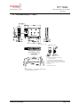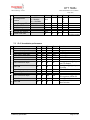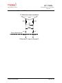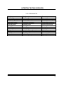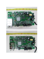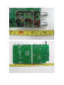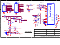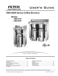
1
This Equipment Under Test (EUT) is a ATSC Set Top Box, it used to
receive the digital TV signal (ATSC) and demodulate to Audio / Video signal out
put via the RF tuner. This EUT is powered by 120V/AC. Besides , it can also
modulated the ATSC signal to TV receiver via RF output terminal which is
designed to convert the Audio / Video signal to standard NTSC CH3 or CH4 RF
signal. There are two different channels available, Channel 3 and Channel 4, it
can be selected by the switch on the back panel. A coaxial cable (75 ohm, 0.8m)
is provided with this device. Power and channel-select buttons are located on the
front panel, most of the input or output terminals are located at the back panel
including a smart antenna terminal that can be connected to a terrestrial antenna,
the EUT can control the terrestrial antenna gain and direction automatically to
optimize the receiving signal via the smart antenna terminal.
When the EUT is switched on, the software stored in the flash U8 (2
M-byte) and the memory U2 (16 x 16M DDR) is active, controls the MCU U1
(ZR39741) to search the ATSC TV signal via RF tuner, the RF tuner
demodulates the RF signal to IF signal and transmit to the MCU U1, the MCU U1
demodulates the IF signal to audio / video signal and outputs via the A / V output
terminal after the IC2 (CE2752, audio decoder) and U7 (4558, audio filter and
amplifier), and U6 (FMS6143, video filter and amplifier). Also, the MCU U1
transmits the audio / video signal to the RF tuner, the RF tuner modulates the A /
V signal to NTSC RF signal and output via the RF output terminal.
IC Function:
U1 (ZR39741) MCU, Program search, demodulation and decode
U2 (Memory) Software store
U8 (FLASH) Software store
IC1 (AF1071)Reset IC
IC2 (CE2752) Audio Decode IC
U6(FMS6143)CVBS active filter and amplifier
U7(4558)Audio active filter and amplifier
U13(AP1530)DC converter, convert 5V to 1.8V
U15(AP1513) DC converter, convert 5V to 3.3V
U10(TNY277) MCU of the built-in SMPS
D14, transformer, transfer 3.3V to 2.6V
The RF Tuner specification is attached as the following pages.
SBU Technology - Tuners
DTT 7685x
ATSC half NIM with ch 3 / 4 modulator
Specification
20 Apr 2007
Features
•
•
•
•
•
•
•
•
•
•
•
Receives digital off-air and cable signal
Receiving frequency 55.25MHz to 864.25MHz
Built-in 5-33V DC-DC converter (optional)
Single power supply to the tuner, IF VGA & modulator section
Wide Band AGC (bus control switch-able) to optimum strong signal
performance
Read RF AGC information via I2C Bus
Tuner power standby mode via I2C Bus
Modulator Video / Sound inputs and Ch3 / 4 RF output
Available in both vertical and horizontal mount versions
Meet A-74 requirement
RoHS compliance
MODEL
DESCRIPTION
PRODUCT
REF. NO.
DTT 76850
ATSC half NIM with Ch 3 /4 modulator, Horizontal mount LH
21682310
DTT 76851
ATSC half NIM with Ch 3 /4 modulator, Vertical mount
21686000
DTT 7685x
SBU Technology – Tuners
ATSC half NIM with Ch 3 / 4 modulator
20 Apr 2007
Table of content
1.
Brief description................................................................................................. 4
2.
Block diagram .................................................................................................... 4
3.
Mechanical Specification .................................................................................. 5
3.1 Horizontal Mounting LH (DTT 76850) .................................................................. 5
3.2 Vertical Mounting (DTT 76851)............................................................................ 6
4.
Pin Definitions .................................................................................................... 7
5.
Operational Conditions ..................................................................................... 8
6.
Standard Test Conditions ................................................................................. 8
7.
Electrical Characteristics .................................................................................. 9
7.1 RF Section............................................................................................................ 9
7.2 Ch 3/ 4 modulator performance ......................................................................... 10
8.
Application Information................................................................................... 11
8.1 Tuner I2C control ............................................................................................... 11
9.
Electrostatic Discharge ................................................................................... 16
9.1 Test .................................................................................................................... 16
9.2 Handling ............................................................................................................. 16
10.
10.1
10.2
10.3
10.4
10.5
10.6
10.7
10.8
10.9
Reliability Test Procedure & Conditions ....................................................... 17
Heat Load Test................................................................................................... 17
Humidity Load Test ............................................................................................ 17
Cold Test ............................................................................................................ 18
Thermal Shock ................................................................................................... 18
Temperature Cycle Test..................................................................................... 18
Vibration Test ..................................................................................................... 19
Drop Test............................................................................................................ 19
Life Test.............................................................................................................. 19
Reliability Test Requirement .............................................................................. 20
11.
11.1
11.2
11.3
11.4
Appendix ........................................................................................................... 21
Packaging........................................................................................................... 21
Identification / Traceability ................................................................................. 21
RF AGC Slope (Typical Curve).......................................................................... 22
Digital IF AGC Slope .......................................................................................... 25
Preliminary Specification
Page 2 / 29
DTT 7685x
SBU Technology – Tuners
ATSC half NIM with Ch 3 / 4 modulator
20 Apr 2007
11.5
11.6
11.7
11.8
11.9
Digital IF AGC Time Constant (Bandwidth) ....................................................... 25
Overall Gain Testing Method ............................................................................. 25
Application Diagram ........................................................................................... 26
Recommend AGC switch circuit for analogue reception only............................ 27
Internal Differential IF Circuit ............................................................................. 28
13. Revision ............................................................................................................... 29
Preliminary Specification
Page 3 / 29
DTT 7685x
SBU Technology – Tuners
ATSC half NIM with Ch 3 / 4 modulator
20 Apr 2007
1.
Brief description
DTT 7685x is a newly developed ATSC half NIM with ch 3 / 4 modulator to be used in ATSC
digital (VSB & QAM), it consists of:
a. A switch 2 bands RF tuner, which receives NTSC / ATSC signal & down-converts it to
an IF frequency of 44MHz for digital and 45.75MHz for analog IF.
b. A digital IF Stage, which consists of one SAW filters & gain controllable IF amplifiers
and outputs a 1.0Vp-p IF signal with a good IF selectivity.
c. An analog modulator which modulates base-band video and sound to RF channel 3
or 4.
d. An active splitter (optional), which is designed with 50 /50 split, with good signal
handling & also provide sufficient gain compensation for the splitting loss & with right
return loss for cable reception
e. RF switch at TV_OUT (optional) provides good isolation from Ant_IN to TV_OUT at
ch 3 / 4.
2.
Block diagram
Tuner
Ant_IN
Digital IF
Active
Splitter
IF
filter
Input filter
SAW Driver
UHF
SAW
MOPLL
VHF
H/ L
VGA
( Switch 2 band)
WB AGC
TV_ OUT
Ch 3 / 4
modulator
DC
Optional
Video Sound Ch3/ 4 Path
Input Input select Select
Preliminary Specification
External
AGC
5V
DC
Vt AIF AS I2 C
IF
AGC
DIF
Page 4 / 29
DTT 7685x
SBU Technology – Tuners
ATSC half NIM with Ch 3 / 4 modulator
20 Apr 2007
3.
Mechanical Specification
3.1 Horizontal Mounting LH (DTT 76850)
C1
THOMSON
Detail"F"(Fixation Hole)
Scale 2:1
PIN SQ0.50?
.04(21x)
PCB PINNING LAYOUT
(TOP VIEW)
(4x)
Notes:
Screw
Protrusion 3mm
1. Screw Fixation Designed with no Tapping
a) For Self Tapping Screw
b) Screw Length Used Is Depend on Application.
c) Guide Line For Screw Length Protrusion should not
(4x)
exceed 2.5mm From Tuner Fixation Hole (As Shown).
2. Gen.Tol.: ? .2mm
3. Angle Tol : ?
Unless otherwise specified
NOTE:
- GENERAL TOLERANCE ? .2mm UNLESS OTHERWISE STATED.
- ALL DIMENSIONS ARE IN MILLIMETER.
Note: please refer to the application section 12.7 for lug L1~L4 proper connection.
Preliminary Specification
Page 5 / 29
DTT 7685x
SBU Technology – Tuners
ATSC half NIM with Ch 3 / 4 modulator
20 Apr 2007
3.2 Vertical Mounting (DTT 76851)
C1
THOMSON
PIN SQ0.50?
.04(21x)
Detail"F"(Fixation Hole)
Scale 2:1
PCB PINNING LAYOUT
(TOP VIEW)
Notes:
Screw
Protrusion 2.5mm
1. Screw Fixation Designed with no Tapping
a) For Self Tapping Screw
b) Screw Length Used Is Depend on Application.
c) Guide Line For Screw Length Protrusion should not
exceed 2.5mm From Tuner Fixation Hole (As Shown).
2. Gen.Tol.: ? .2mm
3. Angle Tol : ?
Unless otherwise specified
NOTE:
- GENERAL TOLERANCE ? .3mm UNLESS OTHERWISE STATED.
- ALL DIMENSIONS ARE IN MILLIMETER.
Preliminary Specification
Page 6 / 29
DTT 7685x
SBU Technology – Tuners
ATSC half NIM with Ch 3 / 4 modulator
20 Apr 2007
4.
Pin Definitions
Pins No
Pins Name
Pins Description :
1
2
3
-Vcc1
Path Sel
4
5
6
7
8
9
10
11
12
13
14
15
16
17
18
19
20
21
Ch3/4
RF AGC
Audio in
Video in
Vcc2
---GND
-SCL
SDA
As
IF out
IF AGC
GND
D-IF out
D-IF out
-Supply for Tuner +5V
*Select modulator carrier On /Off
(Optional)
Select RF frequency CH3 / CH4
External RF AGC input
Base band sound input
Base band video input
Modulator supply +5V
---Ground
-I²C clock
I²C data
Tuner address select
IF output
IF amplifier AGC control 0…3.3 V
Ground
Digital IF output balanced
Digital IF output balanced
Note: 1. both “—“no connection & “int” in the application should leave it open
*2. Path sel (Mode On/Off select) is also controlled by I2C. Please refer to 3rd table on page 13 for details.
Preliminary Specification
Page 7 / 29
DTT 7685x
SBU Technology – Tuners
ATSC half NIM with Ch 3 / 4 modulator
20 Apr 2007
5.
Operational Conditions
No
1.
2.
3.
4.
5.
Parameter
Ambient temperature
Relative humidity
+5.0 V supply
+5.0 V current @ pin2
+5.0 V current @ pin8
6.
Standard Test Conditions
No
1.
2.
3.
4.
5.
6.
7.
Parameter
Ambient temperature
Relative humidity
+5Vdc supply
Input Impedance
Nominal Input level
Nominal Video I/P
Nominal Sound I/P
Unit
°C
%
V
mA
mA
Unit
°C
%
V
Ω
dBuV
Vp-p
Vp-p
Min
0
4.75
Min
23
45
4.9
-
Typ
25
5
190
50
Max
60
90
5.25
Typ.
25
60
5.0
75
60
1
1
Max
27
75
5.1
-
Remarks
Ripple ≤ 10mVpp
Remarks
(1.0mV) into 75Ω
@75Ω loaded
@600Ω loaded
Note: A proper function is guaranteed within the specified supply voltage and environmental conditions but a
certain deterioration of performance parameters may occur at the limits of operational conditions.
Preliminary Specification
Page 8 / 29
DTT 7685x
SBU Technology – Tuners
ATSC half NIM with Ch 3 / 4 modulator
20 Apr 2007
7.
Electrical Characteristics
7.1 RF Section
No Parameters
1.
Frequency Range
2.
IF Frequency
3.
Frequency Margin
4.
Tracking
5.
V.S.W.R.
6.
Noise Figure
7.
Voltage Gain
8.
AGC Range
9.
1% Cross Modulation
10. CB Rejection
Unit
Analog
Band - 1
Band - 2
Band - 3
Digital
Band - 1
Band - 2
Band – 3
Center
Picture
Chroma
Sound
MHz
MHz
MHz
PC-CC Tilt
PC-SC Tilt
dB
Min
55.25
151.25
421.25
-57.00
153.00
423.00
44
45.75
42.17
41.25
3
-3
Air Channels
Cable channels
@ pin 17
B1
B2
B3
(N±1)
(N±2)
0.5 - 30MHz
30 - 41MHz
11. IF Rejection
dB
dB
dB
Typ
50
45
40
2
6
6
39
70
58
58
dBuV
101
81
dB
60
88
CH06
CH05
dB
50
55
55
60
13. FM Beat Susceptibility
88.1 – 92MHz
92.1 - 107.9MHz
dBuV
59
69
63
73
2
5
25
18
35
25
55
60
70
60
50
-52
-85
-106
74
70
68
-62
-90
-112
15. Half-IF Susceptibility
16
88.1 - 90.1MHz
90.1 - 107.9MHz
Air Channels
Cable Channels
Adjacent Channel
Rejection
17. Image Rejection
18. LO Phase Noise
19. Oscillator Stability
Preliminary Specification
dB
dB
dB
CH06
CH14-CH55
All other channel
1kHz
10kHz
100kHz
at 25°C ± 15°C
dB
dBc/Hz
ppm
Remarks
145.25
415.25
859.25
-147.00
417.00
863.00
+3
+5
6
8
10
Unwanted: 80% AM.
S/I=46dB @ 75Ω
load open.
69
74
dBuV
12. Beat Rejection
14. FM Rejection on CH06
Max
30
4MHz crystal ref.
Page 9 / 29
DTT 7685x
SBU Technology – Tuners
ATSC half NIM with Ch 3 / 4 modulator
20 Apr 2007
No Parameters
Unit
5 -- 54MHz
54 -- 864MHz
864 -- 1810MHz
20.
LO Voltage at the
Antenna
21.
22.
23.
24.
25.
Tuning Response Time
Differential D-IF out
Pin 20 & 21
IF AGC Voltage
IF AGC Range
LO Level at IF Output
Min
Typ
dBuV
ms
Vp-p
V
dB
dBuV
26. Overall Tuner Gain
dB
30
1.0
0.5
43
Max
10
33
51
100
Remarks
3.3
48
88
72
80
See Appendix 12.5
For testing condition
7.2 Ch 3/ 4 modulator performance
No
1.
2.
3.
4.
5.
6.
7.
Parameters
Video carrier frequency accuracy
Video carrier output level
Video carrier frequency stability
Audio carrier output ratio
Audio 2nd harmonic distortion
Audio 3rd harmonic distortion
Video harmonic distortion
Unit
KHz
dBuV
KHz
dB
dB
dB
dB
Min
-25
70
-25
13.0
50
45
45
8.
Video modulation depth
%
75
9.
Video S/N
dB
Max
25
73
15.5
65
55
72
80
25
18.0
dB
%
°C
-1.1
-5
-5
13. Audio modulation depth
%
90
14. Audio distortion
%
15. Audio S/N
dB
45
85
0.3
5
5
100
110
1
2
50
Remarks
No signal
Ta = 25°C ±10
fpc+2x4.5MHz
fpc+3x4.5MHz
50
10. Video frequency response
11. Differential gain
12. Differential phase
Preliminary Specification
Typ.
10 step grey scale @1Vp-p
input,75Ω loaded
Un-weighted @1Vp-p input,
50% white
0.75 ~3.75MHz
Sound I/P = 1KHz @ 1vp-p,
100% equals to 25kHz dev
Sound I/P = 1KHz;
Sound I/P = 1KHz;
Video Color bar
Page 10 / 29
DTT 7685x
SBU Technology – Tuners
ATSC half NIM with Ch 3 / 4 modulator
20 Apr 2007
8.
Application Information
8.1 Tuner I2C control
Write Data format: (MSB is transmitted first)
Name
Address Byte 1
Prog. Divider Byte 2
Prog. Divider Byte 3
Control Data Byte 4
Control Data Byte 5
Control Data Byte 6
Control Data Byte 7
Byte
AB1
DB2
DB3
CD4
CD5
CD6
CD7
B7
1
0
N7
1
BS1
X
SAS
B6
1
N14
N6
C1
BS0
0
B5
0
N13
N5
C0
SL1
ATC
X
AGD
B4
0
N12
N4
R4
SL0
IFE
ADS
B3
0
N11
N3
R3
P3
X
T3
B2
MA1
N10
N2
R2
P2
AT2
T2
B1
MA0
N9
N1
R1
P1
AT1
T1
B0
0
N8
N0
R0
P0
AT0
T0
Ack
A
A
A
A
A
A
A
Following is the detail breakdown of each byte:
a) MA1, MA2
b) N14- N0
c) R4 - R0
d) C1, C0
e) BS1 – BS0
f) SL1 – SL0
g) SAS
h) P3 – P0
i) ADS
j) ATC
k) AGD
l) AT2:AT0
m) T3 – T0
n) IFE
o) POR
p) FL
q) AGF
r) V2:V0
s) X
:
:
:
:
:
:
:
:
:
:
:
:
:
:
:
:
:
:
:
address bits
programmable division ratio bits
reference divider ratio select
charge pump current select
band select bits
Power down modes
Saw filter drive output select
Port P3 – P0 output states
ADC input select
AGC decay current
AGC disable
AGC setting
test mode
IF AGC amplifier enables
power ON reset indicator
phase lock flag
AGC active flag
ADC out
don’t care
Read Data format: (MSB is transmitted first)
Name
Byte
B7
B6
B5
B4
B3
B2
B1
B0
Ack
Address Byte 1
Status Byte
AB1
SB2
1
POR
1
FL
0
0
0
0
0
AGF
MA1
V2
MA0
V1
1
V0
A
A
Preliminary Specification
Page 11 / 29
DTT 7685x
SBU Technology – Tuners
ATSC half NIM with Ch 3 / 4 modulator
20 Apr 2007
Tuner Address (AB1):
Tuner Address
(Hex)
C0
C2
C4
C6
MA1
MA0
0
0
1
1
Voltage at Pin16 AS
0
1
0
1
(0 to 0.1) *Vcc
Open Circuit
(0.4 to 0.6) *Vcc
(0.9 to 1) *Vcc
Programmable Divider Byte 2 & 3 (DB2 and DB3)
Divider Ratio (N14 to N0):
N = Fosc (MHz)/62.5 kHz
N =16384*N14 + 8192*N13 + 4096*N12 + 2048*N11 + 1024*N10 + 512*N9 + 256*N8 +
128*N7 + 64*N6 + 32*N5 + 16* N4 + 8*N3 + 4*N2 + 2*N1 + N0
Control Data Byte (CD4):
Charge Pump Current select:
C1
C0
Typ. current in (uA)
0
0
155
0
1
330
1
0
690
1
1
1450
Default state in power up: 00
Control Data byte (CD7):
Test Mode (T3, T2, T1 & T0)
Mode
T3
Normal Operation
0
AGC sink Iagc= -100uA
0
AGC source Iagc= 10uA,
0
P0=output of AGC bias DAC
Default state in power up: 0000
Preliminary Specification
T2
0
0
T1
0
1
T0
0
0
0
1
1
Page 12 / 29
DTT 7685x
SBU Technology – Tuners
ATSC half NIM with Ch 3 / 4 modulator
20 Apr 2007
Power mode select (CD5):
Section status
IIC
interface &
registers
0
X
Sleep
Enabled
1
0
PLL & VCO
Enabled
1
1
Full function
Enabled
Default state in power up: 01
SL1
SL0
Power mode
Crystal
oscillator
PLL &
VCO
Converter
& IF stages
Power (mA)
(excluding
IFamp)
Enabled
Enabled
Enabled
Disabled
Enabled
Enabled
Disabled
Disabled
Enabled
9
42
Full
Control Data byte (CD4):
Reference Divider Ratio
R4
R3
R2
R1
0
0
0
1
0
0
1
0
0
0
1
0
0
0
1
1
0
1
0
1
0
1
1
0
0
1
1
0
0
1
1
1
1
0
0
1
1
0
1
0
1
0
1
0
1
0
1
1
1
1
0
1
1
1
1
0
1
1
1
0
1
1
1
1
Default state in power up: 10011
R0
1
0
1
0
1
0
1
0
1
0
1
0
1
0
1
0
Ratio
16
32
64
128
20
40
80
160
24
48
96
192
28
56
112
224
Fref (kHz)
250
125
62.5
31.25
200
100
50
25
166
83.33
41.67
20.83
142.8
71.42
35.71
17.85
Tuner Band Switch Byte (CD5)
Modulator path off (P1=0)
Band
Band VHF-L (1)
Band VHF-H (2)
Band UHF (3)
Band VHF-L (1)
with FM trap enabled
Preliminary Specification
Modulator path on (P1=1)
CD5 (Hex)
39
7C
B5
CD5 (Hex)
3B
7E
B7
38
3A
Page 13 / 29
DTT 7685x
SBU Technology – Tuners
ATSC half NIM with Ch 3 / 4 modulator
20 Apr 2007
IF AGC amplifier Enable (CD6)
IFE
0
1
IF AGC Amplifier Function
Power down
Normal operation
Saw Drive output select (CD7)
SAS
0
1
SAWF output Drive
Analogue output enabled
Digital output enabled
AGC setting control bits (CD6)
Wideband AGC Take Over Point setting (AT2, AT1, AT0)
IF Output Level @pin17
AT2 AT1
AT0
(dBuV@75Ω)
105
0
0
0
103
0
0
1
101
0
1
0
99
0
1
1
97
1
0
0
94
1
0
1
91
1
1
0
87
1
1
1
Default state in power up: 000
a) Recommend wideband AGC TOP setting “0 1 1” for digital reception
b) Recommend external conventional AGC for analog reception
AGC Function (CD7)
AGD
0
1
Remarks
AGC enabled
AGC disabled
Wideband AGC Time Constant ATC (CD6)
ATC
0
1
Remarks
IAGC = 10uA; (Time constant ≈ 100mS)
IAGC = 0.3uA; (Time constant ≈ 3S)
Preliminary Specification
Page 14 / 29
DTT 7685x
SBU Technology – Tuners
ATSC half NIM with Ch 3 / 4 modulator
20 Apr 2007
ADC input select (CD7)
ADS
0
1
Status
AGC detector output
Disabled
ADC Output
Input Level (V)
Less 0.28Vcc
0.34Vcc to 0.44Vcc
0.5Vcc to 0.6Vcc
0.66Vcc to 0.76Vcc
More 0.8Vcc
V2
0
0
0
0
1
V1
0
0
1
1
0
V0
0
1
0
1
0
Read Status Byte (SB2)
Bit
POR (Bit0)
FL (Bit1)
AGF (Bit4)
Preliminary Specification
Description
The power-on reset indicator.
This is set to logic “1” if the Vcc supply to the device has
dropped below 3V (at 25°C).
The PLL lock flag.
It indicates whether the device is phase locked. A logic “1”
is present if the devide is locked.
The AGC detector flag.
Logic”0” means Vagc < 4V (gain reduction)
Logic”1” means Vagc > 4 V (max gain)
Page 15 / 29
DTT 7685x
SBU Technology – Tuners
ATSC half NIM with Ch 3 / 4 modulator
20 Apr 2007
9.
Electrostatic Discharge
9.1 Test
Each front-end must be capable of normal performance following its subjection to the
following tests:
MIL STD 883C HBM
Test is performed with a voltage discharge from a 100 PF capacitor over a 1500 Ω series
resistance in the discharge path. There is a direct contact between the test probe head and
the unit under test, using the test points and conditions detailed below:
•
Test to pins 1 through LAST PIN:
3 successive ESD discharges of 2 KVDC between each pin and the front-end
frame.
IEC 1000-4-2
Test is performed with a voltage discharge from a 150 PF capacitor over a 330 Ω series
resistance in the discharge path. There is a direct contact between the test probe head and
the unit under test, using the test point s a nd c on dit io ns det ai l ed bel ow:
• Test for antenna input socket ± 8 KVDC
9.2
Handling
Anyone handling a front-end must wear a properly grounded anti - static discharge bracelet
to minimize ESD damage.
After each front-end is aligned and tested, it will be packed with anti - static poly foam or
material prior to transportation and storage. This protective foam is to remain in place until
the front-end is assembled and soldered onto the receiver main board.
Preliminary Specification
Page 16 / 29
DTT 7685x
SBU Technology – Tuners
ATSC half NIM with Ch 3 / 4 modulator
20 Apr 2007
10. Reliability Test Procedure & Conditions
Note: Room temperature = 25 °C ± 2 °C
10.1 Heat Load Test
• Measure the DUTs at room temperature
• Load the DUTs into chamber of the following conditions:
Temperature
Period
Cycle
Quantity
= 60 °C
= 500 hrs
= 1.5 hrs on; 0.5 hrs off
= 10 pcs
• Cool-down 0.5 hr at room temperature, then measured the DUTs within 1 hr
• The test shall be continued to 1000 cycles for information only
10.2 Humidity Load Test
• Measure the DUTs at room temperature
• Load the DUTs into chamber of the following conditions:
Temperature
Period
Cycle
Quantity
= 40 ± 5 °C
= 24 hrs
= constantly on
= 20 pcs
• Cool-down 0.5 hr at room temperature, then measured the DUTs within 1 hr
• Load the DUTs again into chamber of the following conditions:
Temperature
Humidity
Period
Cycle
Quantity
= 40 ± 5 °C
= 90 to 95 %
= 500 hrs
= 1.5 hrs on; 0.5 hrs off
= 20 pcs
• Cool down 0.5 hr at room temperature, then measured the DUTs within 1 hr
Preliminary Specification
Page 17 / 29
DTT 7685x
SBU Technology – Tuners
ATSC half NIM with Ch 3 / 4 modulator
20 Apr 2007
10.3 Cold Test
• Measure the DUTs at room temperature
• Load the DUTs into chamber of the following conditions:
Temperature
Period
Cycle
Quantity
= - 20 ± 5°C
= 500 hrs
= constantly on
= 10 pcs
• Warm up for 2 hrs at room temperature, then measured the DUTs within 1 hr
10.4 Thermal Shock
• Measure the DUTs at room temperature
• Load the DUTs into chamber of the following conditions:
Temperature
Period
Power
Quantity
= - 25 °C for 60 min
↓
↑
85 °C for 60 min
= 200 cycles
= power off
= 10 pcs
• Cool-down 0.5 hr at room temperature then measured the DUTs within 1 hr
10.5 Temperature Cycle Test
• Measure the DUTs at room temperature
• Load the DUTs into chamber of the following conditions:
Temperature
= -5 °C for 16 hrs then 60 °C for 8 hrs
Period
= 500 hrs
Cycle
= constantly on
Quantity
= 10 pcs
• Cool down 0.5 hr at room temperature, then measured the DUTs within 1hr
Preliminary Specification
Page 18 / 29
DTT 7685x
SBU Technology – Tuners
ATSC half NIM with Ch 3 / 4 modulator
20 Apr 2007
10.6 Vibration Test
Frequency
Vertical amplitude
Duration
Quantity
: 3.5 Hz
: 15 to 25 mm
: 1 hr
: 1 carton
10.7 Drop Test
• Packaged apparatus:
< or = 50 kg
• Height:
< 32 … 50Kg: 0.5m
18 … 32Kg: 0.55m
10 … 18Kg: 0.65m
5 … 10Kg: 0.8m
• 1 corner + 3 edges + 6 faces
Drop on the weakest corner (point G)
Drop on the shortest edge in contact with point G
Drop on average edge in contact with point G
Drop on the longest edge in contact with point G
Drop flat wise on the side of minimum surface
Drop flat wise on the side of opposite minimum surface
Drop flat wise on the side of average surface
Drop flat wise on the side of opposite average surface
Drop flat wise on the side of maximum surface
Drop flat wise on the side of opposite maximum surface
• Quantity: 1 carton
10.8 Life Test
• Measure the DUTs at room temperature
• Load the DUTs into chamber of the following conditions:
Temperature
Period
Cycle
Quantity
= 60 °C
= 500 hrs
= constantly on
= 20 pcs
• Cool down 0.5 hr at room temperature, then measured the DUTs within 1 hr
Preliminary Specification
Page 19 / 29
DTT 7685x
SBU Technology – Tuners
ATSC half NIM with Ch 3 / 4 modulator
20 Apr 2007
10.9 Reliability Test Requirement
1
2
3
4
5
6
Initial value measurement and after test measurement shall be done at standard
conditions stated in Section 6.
Measurement or check shall be done at the interval of 0 hour (initial), 96H, 168H, 300H
and 500H.
For test items 10.1, 10.2, 10.3 & 10.8, the tested units shall meet the following after
duration of 96 hours, (Data compared with initial value).
- Unit is functional:
Frequency synthesizer is tunable on all channels for tuner as specified in section 7.1
and there is no visible defect in the received picture.
- Tuner Performance:
Max.
a) Change of Power Gain
3dB
b) Change of tilt (overall curve)
3dB
For all test items stated in this section, measurement shall be done to check whether
the unit is functional (per item 3 definition) at each interval hour as specified in item 2.
For test item 10.4, measurement shall be done to check whether the unit is functional
(per item 3 definition) at 50, 100, 150 & 200 cycles.
For test items 6 & 7, unit shall be functional (per item 3 definition) after test.
Preliminary Specification
Page 20 / 29
DTT 7685x
SBU Technology – Tuners
ATSC half NIM with Ch 3 / 4 modulator
20 Apr 2007
11. Appendix
11.1 Packaging
DTT76850/51
MASTER
BOX
Carton
1
65
5200
0.035kg
1
3.34kg
80 boxes
267.2kg
65.5x34.5x16.3
463x393x62
1200x800x150
INDIVIDUAL
1. TYPE
2. QUANTITIES
Tuners
Cartons
3. WEIGHT (Approximate)
4. DIMENSIONS
L × H × D (in mm)
PALLET
Wood
(*): not include antenna terminal
11.2 Identification / Traceability
PACKAGING LABEL:
(Tuner Model)
TOCOM NO.
QTY.
Order NO.
Customer P/N
CTN. NO.
: xxxxxxxx
: xx PCS
:
:
: Carton Label No.
TUNER LABEL:
(Tuner model) (Date Code)
(Tocom No)
Preliminary Specification
Page 21 / 29
DTT 7685x
SBU Technology – Tuners
ATSC half NIM with Ch 3 / 4 modulator
20 Apr 2007
11.3 RF AGC Slope (Typical Curve)
RF AGC Curve at 55.25MHz
0
-10
-20
-30
dB -40
-50
-60
-70
-80
0.0
0.2
0.4
0.6
0.8
1.0
1.2
1.4 1.6
1.8
2.0
2.2
2.4
2.6
2.8
3.0
3.2
3.4
3.6
3.8
4.0
3.0
3.2
3.4
3.6
3.8
4.0
3.0
3.2
3.4
3.6
3.8
4.0
Voltage (V)
RF AGC Curve at 145.25MHz
0
-10
-20
-30
dB -40
-50
-60
-70
-80
0.0
0.2
0.4
0.6
0.8
1.0
1.2
1.4 1.6
1.8
2.0
2.2
2.4
2.6
2.8
Voltage (V)
RF AGC Curve at 151.25MHz
0
-10
-20
-30
dB -40
-50
-60
-70
-80
0.0
0.2
0.4
0.6
0.8
1.0
1.2
1.4 1.6
1.8
2.0
2.2
2.4
2.6
2.8
Voltage (V)
Preliminary Specification
Page 22 / 29
DTT 7685x
SBU Technology – Tuners
ATSC half NIM with Ch 3 / 4 modulator
20 Apr 2007
RF AGC Curve at 289.25MHz (typical)
0
-10
-20
-30
dB -40
-50
-60
-70
-80
0.0
0.2
0.4
0.6
0.8
1.0
1.2
1.4 1.6
1.8
2.0
2.2
2.4
2.6
2.8
3.0
3.2
3.4
3.6
3.8
4.0
3.0
3.2
3.4
3.6
3.8
4.0
3.0
3.2
3.4
3.6
3.8
4.0
Voltage (V)
RF AGC Curve at 415.25MHz
0
-10
-20
-30
dB -40
-50
-60
-70
-80
0.0
0.2
0.4
0.6
0.8
1.0
1.2
1.4 1.6
1.8
2.0
2.2
2.4
2.6
2.8
Voltage (V)
RF AGC Curve at 421.25MHz
0
-10
-20
-30
dB -40
-50
-60
-70
-80
0.0
0.2
0.4
0.6
0.8
1.0
1.2
1.4 1.6
1.8
2.0
2.2
2.4
2.6
2.8
Voltage (V)
Preliminary Specification
Page 23 / 29
DTT 7685x
SBU Technology – Tuners
ATSC half NIM with Ch 3 / 4 modulator
20 Apr 2007
RF AGC Curve at 553.25MHz
0
-10
-20
-30
dB -40
-50
-60
-70
-80
0.0
0.2
0.4
0.6
0.8
1.0
1.2
1.4 1.6
1.8
2.0
2.2
2.4
2.6
2.8
3.0
3.2
3.4
3.6
3.8
4.0
3.0
3.2
3.4
3.6
3.8
4.0
3.0
3.2
3.4
3.6
3.8
4.0
Voltage (V)
RF AGC Curve at 703.25MHz
0
-10
-20
-30
dB -40
-50
-60
-70
-80
0.0
0.2
0.4
0.6
0.8
1.0
1.2
1.4 1.6
1.8
2.0
2.2
2.4
2.6
2.8
Voltage (V)
RF AGC Curve at 859.25MHz
0
-10
-20
-30
dB -40
-50
-60
-70
-80
0.0
0.2
0.4
0.6
0.8
1.0
1.2
1.4 1.6
1.8
2.0
2.2
2.4
2.6
2.8
Voltage (V)
Preliminary Specification
Page 24 / 29
DTT 7685x
SBU Technology – Tuners
ATSC half NIM with Ch 3 / 4 modulator
20 Apr 2007
11.4 Digital IF AGC Slope
0
-10
-20
dB
-30
-40
-50
-60
0.0
0.5
1.0
1.5
2.0
2.5
3.0
3.5
IF AGC(Volt)
11.5
Digital IF AGC Time Constant (Bandwidth)
The dominant IF AGC time constant τ = 1kΩ × 1nF = 1 µSec typ.
The equivalent bandwidth BW = 1/(2πτ) = 159 kHz typ.
11.6
Overall Gain Testing Method
RF AGC: for max gain
IF AGC : 3.0V
Preliminary Specification
Page 25 / 29
DTT 7685x
ATSC half NIM with Ch 3 / 4 modulator
SBU Technology – Tuners
20 Apr 2007
11.7 Application Diagram
ANT
1
2
3
4
5
6
7
8
9
10
11
12
13
16
17
18
19
20
21
470pF
470pF
22pF
22pF
100nF
100nF
*Path_sel
1). 5V: RF on
GND: RF stop
2).IIC control.
Refer to 3rd
table on page13
220uF
+
220uF
+
External AGC
for Analog
Reception
+5V
Preliminary Specification
15
14
CH3/4
Open:CH3
GND: CH4
Audio_IN
100ohm
100ohm
Video_IN
+5V
SCL
SDA
Tuner Analog IF IF AGC
Address
Differential IF
to De-mod IC
Page 26 / 29
DTT 7685x
ATSC half NIM with CH 3 / 4 modulator
SBU Technology – Tuners
20 Apr 2007
Application note:
1) All tuner supply line, CLK & DATA line decoupling Ceramic capacitor should be place near
to Tuner in PCB layout
2) The supply ripple must not more then 10mVp-p
3) Recommend CD6 setting hex “33” for digital reception
4) To ensure correct Time Constant & Filtering for analog application
5) Lug 3 and 4 (L3 & L4) are for holding the tuner module only, do not connect them to a
ground plane else it may result in immunity deterioration. Do ensure sufficient isolation of
these 2x lugs away from the ground plane to prevent stray capacitance coupling.
6) Lug 1 and 2 (L1 & L2) are for connection to a ground plane. The ground plane should be
large for lesser ground inductance hence providing better grounding for the tuner module.
8) For analog reception, set AGD bit to “1” to disable internal wideband AGC
11.8 Recommend AGC switch circuit for analogue reception only
DTT 7685X
Pin5
+5V
50k
1k
Conventional AGC
10k
AGC switch control
Preliminary Specification
Page 27 / 29
DTT 7685x
SBU Technology – Tuners
ATSC half NIM with Ch 3 / 4 modulator
20 Apr 2007
11.9
Internal Differential IF Circuit
IC differential output impedance
240R
100R
100R
12pF
680nH
1nF
1nF
Tuner internal circuit
Pin20
Pin21
Differential IF output to Demod IC
Preliminary Specification
Page 28 / 29
DTT 7685x
SBU Technology – Tuners
ATSC half NIM with Ch 3 / 4 modulator
20 Apr 2007
13. Revision
Date of
Changes
4 Oct 06
8 Jan 07
20 Apr 07
Index
----
Modification
Pages
Preliminary spec
Preliminary spec updates
Update Horizontal mount tuner mechanical spec, add lug
L1~L4 connection information & modulator output level.
1 - 32
1 - 31
All
For more information, contact our nearest sales office or e-mail any request to [email protected].
THOMSON – Business Units Tuners
NORTH AMERICA
THOMSON Tuners - 12950 Saratoga Ave, Saratoga CA 95070, USA
Tel. + 1 408 387 51 31 - Fax. + 1 408 255 94 14
ASIA
THOMSON Tuners – 8 Jurong Hall Road #29-01/06 – The JTC
Summit – SINGAPORE 609434
Tel. + 65 6 379 17 98 Fax. + 65 6 379 17 75
EUROPE & LATIN AMERICA
THOMSON Tuners - 46 quai A Le Gallo - 92648 Boulogne Cedex –
FRANCE
Tel. + 33 1 41 86 50 15 - Fax. + 33 1 41 86 56 75
JAPAN
THOMSON Tuners Japan – Daini-yanagiya Bldg., 5F
( Grass Valley Japan, Ltd )
1-12-8 Nihonbashi, Chuo-ku
Tokyo 103-0027, JAPAN
Tel. + 81 3 6848 6390 Fax +81 3 6848 6391
© 2005 Thomson all rights reserved. The information presented in this document is the exclusive
property of Thomson and should not be disclosed by the recipient to third parties without the prior
written agreement of Thomson. The information contained in this specification does not form part of
any quotation or contract, is believed to be accurate and reliable and may be changed without notice
by Thomson. No liability will be accepted by Thomson for any consequence of its use. Publication
does not convey nor imply any license under patent or other industrial or intellectual property rights.
For more information visit us at: http://www.thomson.net.
Preliminary Specification
Page 29 / 29
200MHz
EUT
RF Tuner
March 24, 2008
Shen Zhen MTC Co., LTD
31-32/F., A Xing He Shi Ji Bldg.,
2069 Cai Tian Road,
Shen Zhen, P.R.China
Dear Kang Jian:
Enclosed you will find your file copy of a Part 15 Certification (FCC ID:
UVD20071228001).
For your reference, TCB will normally take another 20 days for reviewing the report.
Approval will then be granted when no query is sorted.
Please contact me if you have any questions regarding the enclosed material.
Sincerely,
Shawn Xing
Assistant Manager
Enclosure
Intertek Testing Service Shenzhen Ltd. Guangzhou Branch
1~8th floor, Block E2, 11 Cai Pin Road, Science city, Guangzhou Economic Development Zone, Guangzhou, P. R. China
Tel: (8620) 8213 9688
Fax: (8620) 3205 7538
Shen Zhen MTC Co., LTD
Application
For
Certification
(FCC ID: UVD20071228001)
TV Interface Device
GZ08020186-1
Billy Li
March 24, 2008
•
The test results reported in this test report shall refer only to the sample actually tested and shall not refer or be deemed to refer to bulk from which such a sample may be said to
have been obtained.
•
This report shall not be reproduced except in full without prior authorization from Intertek Testing Services Hong Kong Limited.
•
For Terms And Conditions of the services, it can be provided upon request.
•
The evaluation data of the report will be kept for 3 years from the date of issuance.
Intertek Testing Service Shenzhen Ltd. Guangzhou Branch
1~8th floor, Block E2, 11 Cai Pin Road, Science city, Guangzhou Economic Development Zone, Guangzhou, P. R. China
Tel: (8620) 8213 9688
Fax: (8620) 3205 7538
INTERTEK TESTING SERVICES
LIST OF EXHIBITS
INTRODUCTION
EXHIBIT 1:
General Description
EXHIBIT 2:
System Test Configuration
EXHIBIT 3:
Emission Results
EXHIBIT 4:
Equipment Photographs
EXHIBIT 5:
Product Labelling
EXHIBIT 6:
Technical Specifications
EXHIBIT 7:
Instruction Manual
EXHIBIT 8:
Miscellaneous Information
FCC ID: UVD20071228001
i
INTERTEK TESTING SERVICES
MEASUREMENT/TECHNICAL REPORT
Shen Zhen MTC Co., LTD
MODEL: AT2016
ADDITIONAL MODEL: AT2*** (*** can from 001 to 999) / MAT-K50 /
DTA1010 / RJ-900ATSC, RJ-1000ATSC / STB-T8, STB-T9, STB-T10
ATSC Converter Box
FCC ID: UVD20071228001
March 24, 2008
This report concerns (check one:) Original Grant
X
Class II Change
Equipment Type: TV Interface Device (example: TV modulator, etc.)
Deferred grant requested per 47 CFR 0.457(d)(1)(ii)? Yes
No
X
If yes, defer until:
date Company Name agrees to notify
the Commission by:
date of the intended date of announcement of the
product so that the grant can be issued on that date.
Transition Rules Request per 15.37?
Yes
No
X
If no, assumed Part 15, Subpart B for intentional radiator - the new 47 CFR
[09-20-07 Edition] provision.
Report prepared by:
Shawn Xing
Intertek Testing Services Shenzhen Ltd.
Guangzhou Branch
1~8th floor, Block E2, 11 Cai Pin Road,
Sciencecity, Guangzhou Economic
Development Zone, Guangzhou, P. R.China.
Phone:
(8620) 8213 9688
Fax: (8620) 3205 7538
Fax: 86-755-8601-6751
FCC ID: UVD20071228001
ii
INTERTEK TESTING SERVICES
Table of Contents
1.0 General Description ............................................................................................ 2
1.1 Product Description ............................................................................................ 2
1.2 Related Submittal(s) Grants ............................................................................... 2
1.3 Test Methodology............................................................................................... 3
1.4 Test Facility........................................................................................................ 3
2.0 System Test Configuration ................................................................................. 5
2.1 Justification ........................................................................................................ 5
2.2 EUT Exercising Software.................................................................................... 5
2.3 Special Accessories ........................................................................................... 5
2.4 Equipment Modification ...................................................................................... 5
2.5 Measurement Uncertainty .................................................................................. 6
2.6 Support Equipment List and Description ............................................................. 6
3.0 Emission Results ................................................................................................ 8
3.1 Field Strength Calculation................................................................................... 9
3.2 Radiated Emission Configuration Photograph................................................... 11
3.3 Radiated Emission Data ................................................................................... 12
3.4 Conducted Emission Configuration Photograph................................................ 14
3.5 Conducted Emission Data .....................................................................................15
3.6 RF Output Level Measurement .............................................................................17
3.7 RF Output Level Data ............................................................................................18
3.8 Spurious Emission Measurment ..........................................................................20
3.9 Spurious Emission measurement Data.................................................................21
3.10 Antenna Transfer Switch Measurement..............................................................22
3.11 Antenna Transfer Switch Measurement Data .....................................................23
4.0 Equipment Photographs................................................................................... 26
5.0 Product Labelling.............................................................................................. 28
6.0 Technical Specifications................................................................................... 30
7.0 Instruction Manual ............................................................................................ 32
8.0 Miscellaneous Information ............................................................................... 34
8.1 Emissions Test Procedures .............................................................................. 35
FCC ID: UVD20071228001
iii
INTERTEK TESTING SERVICES
List of attached file
Exhibit type
Test Report
Operation Description
Test Setup Photo
Test Setup Photo
External Photo
Internal Photo
Block Diagram
Schematics
ID Label/Location
RF Signal
User Manual
Cover Letter
File Description
Test Report
Technical Description
Radiated Emission
Conducted Emission
External Photo
Internal Photo
Block Diagram
Circuit Diagram
Label Artwork and Location
Modulator Signal Output
User Manual
Letter of Agency
filename
report.pdf
descri.pdf
radiated photos.pdf
conducted photos.pdf
external photos.pdf
internal photos.pdf
block.pdf
circuit.pdf
label.pdf
ch3 and ch4.pdf
manual.pdf
agency.pdf
FCC ID: UVD20071228001
iv
INTERTEK TESTING SERVICES
EXHIBIT 1
GENERAL DESCRIPTION
FCC ID: UVD20071228001
1
INTERTEK TESTING SERVICES
1.0
General Description
1.1
Product Description
This Equipment Under Test (EUT) is a ATSC Set Top Box, it used to receive the
digital TV signal (ATSC) and demodulate to Audio / Video signal out put via the
RF tuner. This EUT is powered by 120V/AC. Besides , it can also modulated the
ATSC signal to TV receiver via RF output terminal which is designed to convert
the Audio / Video signal to standard NTSC CH3 or CH4 RF signal. There are
two different channels available, Channel 3 and Channel 4, it can be selected by
the switch on the back panel. A coaxial cable (75 ohm, 0.8m) is provided with
this device. Power and channel-select buttons are located on the front panel,
most of the input or output terminals are located at the back panel including a
smart antenna terminal that can be connected to a terrestrial antenna, the EUT
can control the terrestrial antenna gain and direction automatically to optimize
the receiving signal via the smart antenna terminal.
Models AT2*** (*** can from 001 to 999), MAT-K50, DTA1010, RJ-900ATSC,
RJ-1000ATSC, STB-T8, STB-T9, STB-T10 are identical in the hardware aspect,
The difference in model number and trade name serves as marketing strategy.
We have tested one model AT2601 during this compliance test period. For
electronic filing, the brief circuit description with the RF tuner specification is
saved with filename: descri.pdf.
1.2
Related Submittal(s) Grants
This is a single application for certification of a TV interface device for the
function RF modulation of this EUT, and the other function is subject to the FCC
part 15 verification.
FCC ID: UVD20071228001
2
INTERTEK TESTING SERVICES
1.3
Test Methodology
Both AC mains line-conducted and radiated emission measurements were
performed according to the procedures in ANSI C63.4 (2003). Radiated
emission measurement was performed in semi-anechoic chamber and
conducted emission measurement was performed in shield room. For radiated
emission measurement, preliminary scans were performed in the semianechoic chamber only to determine the worst case modes. All radiated tests
were performed at an antenna to EUT distance of 3 meters, unless stated
otherwise in the "Justification Section" of this Application.
1.4
Test Facility
The Semi-Anechoic Chamber & shielded room facility used to collect the
radiated & conducted emissions data is SHENZHEN ACADEMY OF
METROLOGY & QUALITY INSPECTION located at Longzhu Road,
Shenzhen. This test facility and site measurement data have been fully placed
on file with the FCC.
FCC ID: UVD20071228001
3
INTERTEK TESTING SERVICES
EXHIBIT 2
SYSTEM TEST CONFIGURATION
FCC ID: UVD20071228001
4
INTERTEK TESTING SERVICES
2.0
System Test Configuration
2.1
Justification
The system was configured for testing in a typical fashion (as a customer would
normally use it), and in the confines as outlined in ANSI C63.4 (2003).
For maximizing emissions below 30 MHz, the EUT was rotated through 360°,
the centre of the loop antenna was placed 1 meter above the ground, and the
antenna polarization was changed. For maximizing emission at and above 30
MHz, the EUT was rotated through 360°, the antenna height was varied from 1
meter to 4 meters above the ground plane, and the antenna polarization was
changed. This step by step procedure for maximizing emissions led to the data
report in Exhibit 3.0.
The unit was placed in the rear of the turntable.
The equipment under test (EUT) was configured for testing in a typical fashion
(as a customer would normally use it). The EUT was placed on a turn table,
which enabled the engineer to maximize emissions through its placement in the
three orthogonal axes.
The frequency range from 30MHz to 2GHz was searched for spurious emissions
from the device. Only those emissions reported were detected. All other
emissions were at least 20 dB below the applicable limits.
2.2
EUT Exercising Software
There was no special software to exercise the device. Once the unit is powered
up, it transmits the typical signal continuously.
2.3
Special Accessories
No special accessories were used for compliance of this product.
2.4
Equipment Modification
Any modifications installed previous to testing by Shenzhen MTC Co., LTD will
be incorporated in each production model sold/leased in the United States.
No modifications were installed by Intertek Testing Services
FCC ID: UVD20071228001
5
INTERTEK TESTING SERVICES
2.5
Measurement Uncertainty
When determining the test conclusion, the Measurement Uncertainty of test has
been considered.
2.6
Support Equipment List and Description
This product was tested in the following configuration:
Refer List:
Description
Manufacturer
Model No.
Serial No.
TV-Test Transmitter
ROHDE&SCHWARZ
SFQ
2072.5501.02
MPEG2 Measurement
Generator
ROHDE&SCHWARZ
DVG
2068.8600.03
75Ω RF Termination
---
---
---
---
---
---
3 x 1.5m AV cable
---
---
---
Pass splitter
ROHDE&SCHWARZ
---
800.6612.52
RF cable
---
50Ω, 1.5m
---
50 – 75Ω Matching Pad
---
---
---
Impedance Transformer
NMC
MB-009
---
10 kΩ, 22kΩ, 75Ω, 100Ω
Termination loading
1 x 75Ω coaxial cable
(Provided by Client)
All the items listed under section 2.0 of this report are
Confirmed by:
Shawn Xing
Assistant Manager
Intertek Testing Services Shenzhen Ltd. Guangzhou Branch
Agent for Shenzhen MTC Co., LTD
Signature
March 24, 2008
Date
FCC ID: UVD20071228001
6
INTERTEK TESTING SERVICES
EXHIBIT 3
EMISSION RESULTS
FCC ID: UVD20071228001
7
INTERTEK TESTING SERVICES
3.0
Emission Results
Data is included worst case configuration (the configuration which resulted in the
highest emission levels). A sample calculation, configuration photographs and
data tables of the emissions are included.
FCC ID: UVD20071228001
8
INTERTEK TESTING SERVICES
3.1
Field Strength Calculation
The field strength is calculated by adding the reading on the Spectrum Analyzer
to the factors associated with preamplifiers (if any), antennas, cables, pulse
desensitization and average factors (when specified limit is in average and
measurements are made with peak detectors). A sample calculation is
included below.
FS = RA + AF + CF - AG + PD + AV
where
FS = Field Strength in dBµV/m
RA = Receiver Amplitude (including preamplifier) in dBµV
CF = Cable Attenuation Factor in dB
AF = Antenna Factor in dB
AG = Amplifier Gain in dB
PD = Pulse Desensitization in dB
AV = Average Factor in -dB
In the radiated emission table which follows, the reading shown on the data
table may reflect the preamplifier gain. An example of the calculations, where
the reading does not reflect the preamplifier gain, follows:
FS = RA + AF + CF - AG + PD + AV
FCC ID: UVD20071228001
9
INTERTEK TESTING SERVICES
3.1
Field Strength Calculation (cont’d)
Example
Assume a receiver reading of 62.0 dBµV is obtained. The antenna factor of 7.4
dB and cable factor of 1.6 dB is added. The amplifier gain of 29 dB is
subtracted. The pulse desensitization factor of the spectrum analyzer was 0
dB, and the resultant average factor was -10 dB. The net field strength for
comparison to the appropriate emission limit is 32 dBµV/m. This value in dBµV/m
was converted to its corresponding level in µV/m.
RA = 62.0 dBµV
AF = 7.4 dB
CF = 1.6 dB
AG = 29.0 dB
PD = 0 dB
AV = -10 dB
FS = 62 + 7.4 + 1.6 - 29 + 0 + (-10) = 32 dBµV/m
Level in µV/m = Common Antilogarithm [(32 dBµV/m)/20] = 39.8 µV/m
FCC ID: UVD20071228001
10
INTERTEK TESTING SERVICES
3.2
Radiated Emission Configuration Photograph
Worst Case Radiated Emission
at
386.438 MHz
For electronic filing, the worst case radiated emission configuration photograph
is saved with filename: radiated photos.pdf.
FCC ID: UVD20071228001
11
INTERTEK TESTING SERVICES
3.3
Radiated Emission Data
The data on the following page lists the significant emission frequencies, the
limit and the margin of compliance. Numbers with a minus sign are below the
limit.
Judgement: Passed by 1.2 dB
TEST PERSONNEL:
Signature
Billy Li, Compliance Engineer
Typed/Printed Name
March 24, 2008
Date
FCC ID: UVD20071228001
12
INTERTEK TESTING SERVICES
Applicant: Shenzhen MTC Co., LTD
Model: AT2016
Mode: Modulating
Date of Test: January 28, 2008
Table 1
Radiated Emissions
Polar
H
V
H
H
V
V
V
V
V
Frequency
(MHz)
38.425
63.046
83.267
377.956
386.438
460.588
980.662
1240.266
1608.357
Reading
(dBuV)
49.8
52.5
52.1
45.3
48.2
44.5
41.8
39.0
38.8
Antenna
Pre-Amp factor Net at 3m Limit at 3m Margin
(dB)
(dB)
(dBuV/m) (dBuV/m)
(dB)
26.5
9.2
32.5
40.0
-7.5
26.2
9.3
35.6
40.0
-4.4
25.8
8.5
34.8
40.0
-5.2
25.7
23.7
43.3
46.0
-2.7
25.8
22.4
44.8
46.0
-1.2
26.0
22.0
40.5
46.0
-5.5
25.9
23.7
39.6
54.0
-14.4
34.8
27.6
31.8
54.0
-22.2
35.1
28.3
32.0
54.0
-22.0
Notes: 1. Peak Detector Data unless otherwise stated.
2. All measurements were made at 3 meter. Harmonic emissions not
detected at the 3 meter distance were measured at 0.3 meter and an
inverse proportional extrapolation was performed to compare the signal level
to the 3 meter limit. No other harmonic emissions than those reported were
detected at a test distance of 0.3 meter.
3. Negative value in the margin column shows emission below limit.
4. Horn antenna is used for the emissions over 1000MHz.
5. The smart antenna port was terminated with 10 kΩ and 100Ω resistor
according to the manufacturer’s specification.
Test Engineer: Billy Li
FCC ID: UVD20071228001
13
INTERTEK TESTING SERVICES
3.4
Conducted Emission Configuration Photograph
Worst Case Line-Conducted Configuration
At
0.852 MHz
For electronic filing, the worst case conducted emission configuration
photograph is saved with filename: conducted photos.pdf.
Marker:
Delta Mk:
852 kHz
0 Hz
43.01 dBµV
3.03 dB
Level [dBµV]
100
80
60
40
20
0
150k
300k
MES AT2016
MES AT2016
LIM EN 55013
LIM EN 55013
L
L
V
V
500k
PK
AV
QP
AV
1M
2M
Frequency [Hz]
3M
5M
7M
5M
7M
10M
30M
Voltage QP Limit
Voltage AV Limit
Live Line
Marker:
Delta Mk:
3.5475 MHz
0 Hz
37.15 dBµV
8.89 dB
Level [dBµV]
100
80
60
40
20
0
150k
300k
MES AT2016
MES AT2016
LIM EN 55013
LIM EN 55013
500k
N PK
N AV
V QP
V AV
1M
2M
Frequency [Hz]
3M
10M
30M
Voltage QP Limit
Voltage AV Limit
Neutral Line
FCC ID: UVD20071228001
14
INTERTEK TESTING SERVICES
3.5
Conducted Emission Data
Judgement: Passed by 3.2 dB
TEST PERSONNEL:
Signature
Billy Li, Compliance Engineer
Typed/Printed Name
March 24, 2008
Date
FCC ID: UVD20071228001
15
INTERTEK TESTING SERVICES
Applicant: Shenzhen MTC Co., LTD
Model: AT2016
Mode: Modulating
Date of Test: January 29, 2008
Table 2
Conducted Emissions
Live Line Data
Frequency
(MHz)
Quasi-Peak
Average
Disturbance
level
dB(μV)
Permitted
limit
dB(μV)
Disturbance
level
dB(μV)
Permitted
limit
dB(μV)
0.784
49.5
56.0
40.1
46.0
0.852
50.5
56.0
42.8
46.0
1.389
42.6
56.0
35.8
46.0
2.255
40.8
56.0
32.5
46.0
3.893
39.5
56.0
31.7
46.0
4.533
38.6
56.0
30.2
46.0
Neutral Line Data
Frequency
(MHz)
Quasi-Peak
Average
Disturbance
level
dB(μV)
Permitted
limit
dB(μV)
Disturbance
level
dB(μV)
Permitted
limit
dB(μV)
0.228
48.5
62.5
37.8
52.5
0.784
45.2
56.0
36.5
46.0
0.852
46.1
56.0
37.8
46.0
1.292
39.5
56.0
30.2
46.0
3.547
39.1
56.0
37.2
46.0
4.448
38.6
56.0
29.8
46.0
Test Engineer: Billy Li
FCC ID: UVD20071228001
16
INTERTEK TESTING SERVICES
3.6
RF Output Level Measurement
Worst Case Line-Conducted Configuration
At
61.250 MHz
For electronic filing, the plot shows the RF output signal are saved with
filename: ch3.pdf. and ch4.pdf
FCC ID: UVD20071228001
17
INTERTEK TESTING SERVICES
3.7
RF Output Level Data
The data on the following page lists the significant emission frequencies, the
limit and the margin of compliance. Numbers with a minus sign are below the
limit.
Judgement: Passed by 4.0 dB
TEST PERSONNEL:
Signature
Billy Li, Compliance Engineer
Typed/Printed Name
March 24, 2008
Date
FCC ID: UVD20071228001
18
INTERTEK TESTING SERVICES
Applicant: Shenzhen MTC Co., LTD
Model: AT2016
Mode: Modulating
Date of Test: March 20, 2008
Table 3
RF Output Level Measurement
Test
Mode
DTV
DTV
C hannel
Type
Frequency
(M H z)
Meter
Reading
(dBµV)
Pad
Loss
(dB)
Result
(dB µV)
Lim it
(dB µV)
Margin
(dB)
03
03
03
04
04
04
Aural
Visual
Aural
Aural
Visual
Aural
56.750
61.250
65.750
62.750
67.250
71.750
46.2
59.5
46.1
46.4
58.5
46.2
6.0
6.0
6.0
6.0
6.0
6.0
52.2
65.5
52.1
52.4
64.5
52.2
56.5
69.5
56.5
56.5
69.5
56.5
-4.3
-4.0
-4.4
-4.1
-5.0
-4.3
NOTES: 1. Test according to section 12.2.5 of ANSI C63.4
2. 50 to 75Ω (6dB attenuation) matching-impedance pad was employed.
3. Negative sign in the column shows value below limit.
4. Technical Limits: Video signal: 346.4 ×√R in microvolts = 3000.0µV or
69.5dBµV Audio signal: 77.5 ×√R in microvolts = 671.0µV or 56.5dBµV
Test Engineer: Billy Li
FCC ID: UVD20071228001
19
INTERTEK TESTING SERVICES
3.8
Spurious Emission Measurement
Conducted spurious emissions measurement more than 4.6MHz below or
7.4MHz above the carrier frequency.
1
2
3
The range for measurement is from 30MHz to 4.6MHz below the visual
carrier frequency, and any emissions in range from 7.4MHz above the
visual carrier frequency to 1G.
The measuring instrument was set to 100kHz bandwidth and the
detector function to peak mode.
Technical Limits: −4.6MHz of video carrier frequency and +7.4MHz
shall not exceed 10.95 ×√R in microvolts or 39.5dBµV.
FCC ID: UVD20071228001
20
INTERTEK TESTING SERVICES
3.9
Spurious Emission Measurement Data
Test
Mode
Channel
Frequency
(MHz)
DTV
DTV
03
04
56.250
62.290
Meter
Reading
(dBμV)
56.9
55.8
Pad
Loss
(dB)
6.0
6.0
Amplifier
(-dB)
Result
(dBμV)
Limit
(dBμV)
Margin
(dB)
26.0
26.0
36.9
35.8
39.5
39.5
-2.6
-3.7
The worst case emission for more than 4.6MHz below or 7.4MHz above the carrier
frequency was showed as above. And all spurious emission was measured and found
to be at least 20 dB below the limit.
TEST PERSONNEL:
Signature
Billy Li, Compliance Engineer
Typed/Printed Name
March 24, 2008
Date
FCC ID: UVD20071228001
21
INTERTEK TESTING SERVICES
3.10
Antenna Transfer Switch Measurement
Worst Case Transfer Switch Emission
At
61.250 MHz
FCC ID: UVD20071228001
22
INTERTEK TESTING SERVICES
3.11
Antenna Transfer Switch Measurement Data
The data on the following page lists the significant emission frequencies, the
limit and the margin of compliance. Numbers with a minus sign are below the
limit.
Judgement: Passed by 8.0 dB
TEST PERSONNEL:
Signature
Billy Li, Compliance Engineer
Typed/Printed Name
March 24, 2008
Date
FCC ID: UVD20071228001
23
INTERTEK TESTING SERVICES
Applicant: Shenzhen MTC Co., LTD
Model: AT2016
Mode: Modulating
Date of Test: March 19, 2008
Table 4 Antenna Transfer Switch Measurement Pursuant to FCC Part 15
Section 15.115 Requirement
Channel
Frequency
(M Hz)
Reading
(dBµV)
Pre-am
p (dB)
03
04
61.250
67.250
12.0
11.8
22.5
22.5
Pad +
Pass
splitter
Loss
(dB)
12.0
12.0
Result
(dBµV)
Lim it
(dBµV)
Margin
(dB)
1.5
1.3
9.5
9.5
-8.0
-8.2
NOTES: 1. Test according to section 12.2.6 of ANSI C63.4
2. A pass splitter (6dB attenuation) and a 50 to 75Ω (6dB attenuation)
matching-impedance pad were employed.
3. Negative sign in the column shows value below limit.
4. The measuring instrument was set to 100kHz bandwidth and the
detector function to peak mode
5. Limit should not exceed 3.0µV or 9.5dBµV.
Test Engineer: Billy Li
FCC ID: UVD20071228001
24
INTERTEK TESTING SERVICES
EXHIBIT 4
EQUIPMENT PHOTOGRAPHS
FCC ID: UVD20071228001
25
INTERTEK TESTING SERVICES
4.0
Equipment Photographs
For electronic filing, the photographs of the tested EUT are saved with filename:
external photos.doc & internal photos.doc.
FCC ID: UVD20071228001
26
INTERTEK TESTING SERVICES
EXHIBIT 5
PRODUCT LABELLING
FCC ID: UVD20071228001
27
INTERTEK TESTING SERVICES
5.0
Product Labelling
For electronic filing, the FCC ID label artwork and the label location are saved
with filename: label.pdf.
FCC ID: UVD20071228001
28
INTERTEK TESTING SERVICES
EXHIBIT 6
TECHNICAL SPECIFICATIONS
FCC ID: UVD20071228001
29
INTERTEK TESTING SERVICES
6.0
Technical Specifications
For electronic filing, the block diagram and schematics of the tested EUT are
saved with filename: block.pdf and circuit.pdf respectively.
FCC ID: UVD20071228001
30
INTERTEK TESTING SERVICES
EXHIBIT 7
INSTRUCTION MANUAL
FCC ID: UVD20071228001
31
INTERTEK TESTING SERVICES
7.0
Instruction Manual
For electronic filing, a preliminary copy of the Instruction Manual is saved with
filename: manual.pdf.
This manual will be provided to the end-user with each unit sold/leased in the
United States.
FCC ID: UVD20071228001
32
INTERTEK TESTING SERVICES
EXHIBIT 8
MISCELLANEOUS INFORMATION
FCC ID: UVD20071228001
33
INTERTEK TESTING SERVICES
8.0
Miscellaneous Information
This miscellaneous information includes emission measuring procedure.
FCC ID: UVD20071228001
34
INTERTEK TESTING SERVICES
8.1
Emissions Test Procedures
The following is a description of the test procedure used by Intertek Testing Services
in the measurements of EUT operating under Part 15, Subpart B rules.
The test set-up and procedures described below are designed to meet the
requirements of ANSI C63.4 - 2003.
The equipment under test (EUT) is placed on a wooden turntable which is four
feet in diameter and approximately one meter in height above the ground
plane. During the radiated emissions test, the turntable is rotated and any
cables leaving the EUT are manipulated to find the configuration resulting in
maximum emissions. The EUT is adjusted through all three orthogonal axes to
obtain maximum emission levels. The antenna height and polarization are
varied during the testing to search for maximum signal levels. The height of the
antenna is varied from one to four meters.
Detector function for radiated emissions from the frequency band 30MHz to
1GHz is in QP mode and RBW setting is 120kHz. Detector function for
radiated emissions for frequency band above 1GHz, both peak and AV
detectors shall be used to measure the emissions and the peak limit is 20dB
above the maximum permitted average emission limit and RBW setting is
1MHz. Detector function for conducted emissions are in QP & AV mode and
IFBW setting is 9kHz from the frequency band 150kHz to 30MHz.
For radiated emission, the frequency range scanned is 30MHz to 2GHz. For
line-conducted emissions, the range scanned is 150kHz to 30MHz.
FCC ID: UVD20071228001
35
INTERTEK TESTING SERVICES
8.1
Emissions Test Procedures (cont'd)
The EUT is warmed up for 15 minutes prior to the test.
AC power to the unit is varied from 85% to 115% nominal and variation in the
fundamental emission field strength is recorded. If battery powered, a new,
fully charged battery is used.
Conducted measurements are made as described in ANSI C63.4 - 2003.
FCC ID: UVD20071228001
36
External Photo
Internal Photo
Radiated Photo
Conducted Photo
* RBW
120 kHz
300 kHz
SWT 5 ms
* VBW
Ref
102 dBµV
* Att
30 dB
Marker 1 [T1 ]
59.47 dBµV
61.250000000 MHz
100
A
1 PK
MAXH
80
1
60
PA
PS
40
PRN
20
6DB
0
-20
-40
Center 61.25 MHz
Date:
19.MAR.2008
1 MHz/
Span 10 MHz
23:37:18
Input Signal: 0dBmV
* RBW 120 kHz
* VBW 300 kHz
Ref
102 dBµV
* Att
30 dB
SWT 5 ms
Marker 1 [T1 ]
59.38 dBµV
61.250000000 MHz
100
A
1 PK
MAXH
80
1
60
PA
PS
40
PRN
20
6DB
0
-20
-40
Center 61.25 MHz
Date:
19.MAR.2008
1 MHz/
23:38:03
Input Signal: 25dBmV
Span 10 MHz
* RBW 120 kHz
* VBW 300 kHz
Ref
102 dBµV
* Att
30 dB
SWT 5 ms
Marker 1 [T1 ]
58.49 dBµV
67.250000000 MHz
100
A
1 PK
MAXH
80
1
60
PA
PS
40
PRN
20
6DB
0
-20
-40
Center 67.25 MHz
Date:
20.MAR.2008
1 MHz/
Span 10 MHz
00:08:30
Input Signal: 0dBmV
* RBW 120 kHz
* VBW 300 kHz
Ref
102 dBµV
* Att
30 dB
SWT 5 ms
Marker 1 [T1 ]
58.38 dBµV
67.250000000 MHz
100
A
1 PK
MAXH
80
1
60
PA
PS
40
PRN
20
6DB
0
-20
-40
Center 67.25 MHz
Date:
20.MAR.2008
1 MHz/
00:09:17
Input Signal: 25dBmV
Span 10 MHz
5
4
3
2
1
AT2016(ZR39741) SCHEMATEIC DIAGRAM
D
D
01: COVER PAGE
02: POWER SUNPPLY
03: POWER & GROUND
04: GPIO
05: SUPER I/O
06: DDR
C
C
07: RF & Video Input
08: Audio Output
09: Video Output
10: FRONT PANEL SW & IRR
11: SMART ANTENNA I/F
B
B
DESIGN:
MODEL:
CHECKED:
AT2016(ZR39741)
SHEET:
COVER PAGE
DWG NO: AT2016-YL01-01(A)
PART NO.:
APPRD:
TITLE:
1 OF 11
VER:
A
A
A
SHENZHEN MTC MULTIMEDIA CO.,LTD
Table NO.: QR-RD-016A
5
4
3
2
1
5
4
3
2
1
Note:
2
T2
T1
ZY-T0073
ERL-19
UU9.8-40mH
2
1
+12V_A
+
1
1
EC39
100uF/16V
ECAP-5X5X11
2
C55
0.1uF
C0603
S
1
1
100uF/25V +
EC18
ECAP-5X6.3X11
2
100uF/25V +
EC16
ECAP-5X6.3X11
G
1
6
RD1/4W
220R/1W
R79
R127
100K
R0603
C54
0.1uF
C0603
21
R126
100K
7
1
5V_SW
4
2
D15
FR107
DIO-FR107\1A\1KV
2
1
1
R0603
Q16
2N3904
QSOT23
3
1
2
BD1
GBU206
2
FR107
DIO-FR107\1A\1KV
3
D
Q15
APM2301
QSOT23
3
2
2
D13
D
11
1
2
+12V
L11
6.8uH/0.5A
IND-10UH\2A
1
2
2
222/1KV
CAP5-5
1
3
R136
100K/1W
RD1/4W
2
C100
1
2
2
2 1
EC23
10uF/400V
ECAP-5X10X12
+
2
1
+
2
3
R129
100K/1W
RD1/4W
4
1
1
EC22
10uF/400V
ECAP-5X10X12
4
D
1
YC1
222/250V
PY222M
4
D
1
D17
2
2
5V
R88
5K1
R0603
2
2
R87
2.2K
R0603
1
R89
10K
R0603
CON2
CON2X7.9
2
1 2
D
1
2
0.1uF
C0603
1
R84
100K
R0603
1
5V_SW
2
1
Q4
2N3904
QSOT23
1
B
1_8V_D
VCC
1 2
DIP8-SOP
Output2
6
VCC
Output1
5
EC28
470uF/10V
D19
SS24
DIO/SMT
AP1513
C106
0.1uF
C0603
C115
0.1uF
C0603
C112
EC32
0.1uF
470uF/10V
C0603
ECAP-5X6.3X11
DIP8-SOP
B
R99
2.4K
R0603
1
1
2
C114
0.1uF
C0603
+
1
OCSET
4
C0603
NC/0.1uF
R96
10K
R0603
2
3
C111
NC/0.1uF
C0603
1
7
ECAP-5X6.3X11
1
C109
0.1uF
C0603
2
8
VSS
R95
5.1K
R0603
D18
SS24
DIO/SMT
AP1530
2
C126
0.1uF
C0603
1
2
1
2
EC29
+
470uF/10V
ECAP-5X6.3X11
1
C113
VSS
EN
2 R0603
2
Output1
5
2
6
4
+
1
Output2
R91
6.8K
R0603
2
OCSET
C0603
NC/0.1uF
1
3
C105
NC/0.1uF
C0603
2
7
2 R0603
1
8
VSS
2
VSS
EN
10K
FB
2
2
2
FB
2
1
1
C125
10K
1
470uF/10V +
EC33
ECAP-5X6.3X11
2
1
R92 1
2
1
2
R90
100K
R0603
1
1
U13
FB3
FERRITE BEAD
IND
1
2
R97 1
1
1
L9
10uH/3A
COIL-WSD10X5
1.8V regulator
2
2
R98
100K
R0603
1
1
FB5
FERRITE BEAD
IND
2
1 2
1
3V3_D
L10
47uH/2A
COIL-WSD10X5
2
2
2
5V
1
2
U15
1
3.3V regulator
R94
5K1
R0603
2
1
R93
100K
R0603
2
1
1
3
U12
TL431
BC337
POWER SWITCH
5V
C103
C122
0.1uF
C0603
2
CON1
CON2X7.9
AC100-240V INPUT
EC27 +
1000uF/16V
ECAP-5X8X11.5
2
2
2
1
3
C
5V_A
1
2
1
1
4
G
R82
100K
R0603
1N5822
R86
180R
R0603
Q3
APM2301
QSOT23
3
2
C102
0.1uF
C0603
3
1
U11
PC817
R85
100K
R0603
4
3
T1.6AL250V
C101
1uF
C0603
1
F1
EC25
1000uF/16V
ECAP-5X8X11.5
2
D12
1
+
EC24
1000uF/16V
ECAP-5X10X12
1
2
+
1
2
1
2
5V on/off
1
1N5822
12
R83
1K
R0603
C
5V
L8
10uH/2A
IND-10UH\2A
2
1
1
1
10
S
102(M)
CAP5-5
2
2
2
S
2
10R
R0603
5
S
6
S
S
1
8
2
8
C99
R80
5
TNY277
2
2
1
3
NC
U10
DIP8
1 2
EC26 +
10uF/25V
ECAP-5X5X11
BP
EN
R81
20R
R0603
7
1
9
3V3_D
2.6V regulator
D14
1N4001
A
A
D-1206
+
DESIGN:
EC30
22uF/10V
ECAP-5X5X11
2V6_D
+
MODEL:
CHECKED:
EC31
100uF/10V
ECAP-5X5X11
AT2016(ZR39741)
TITLE:
DWG NO: AT2016-YL01-01(A)
PART NO.:
APPRD:
SHEET:
POWER SUPPLY
2 OF 11
VER:
A
Power Supply
SHENZHEN MTC MULTIMEDIA CO.,LTD
5
4
3
2
1
5
4
3
2
1
U1F
HD-741 3.3V
POWER & GROUND
3V3_D
L4
LI0603G121R-00
L-0603
3V3_VDAC
3V3_D
D
C76
1.0uF
C0402
EC13
+
10uF/10V
PCAPR140_315
C71
0.1uF
C0402
C72
1nF
C0402
L5
LI0603G121R-00
L-0603
2V6_D
3V3_PLL
3V3_D
C80
1.0uF
C62
1.0uF
C0402
C0402
C82
1nF
C81
0.1uF
C0402
C0603
L6
LI0603G121R-00
1_8V_D
1V8_PLL
1_8V_D
L0603
C88
1.0uF
C0402
EC12
+
47uF/10V
PCAPR140_315
C
C63
1nF
C84
0.1uF
C0402
C0402
L7
LI0603G121R-00
3V3_IFE
3V3_D
L-0603
C90
1.0uF
C0402
C91
1.0uF
C0402
C92
0.1uF
C93
1nF
C0402
C0402
Place cap near pin
HD-741 1.8V
3V3_D
Bypass Caps
G5
L5
E7
N7
E9
N9
N10
E11
M13
R12
IVDD
IVDD
IVDD
IVDD
IVDD
IVDD
IVDD
IVDD
IVDD
IVDD
F12
E13
F13
G13
H13
J13
K13
L13
MVDD
MVDD
MVDD
MVDD
MVDD
MVDD
MVDD
MVDD
E5
F5
H5
J5
K5
M5
N5
E6
F6
M6
N6
E8
N8
E10
F11
N11
E12
M12
N12
N13
N15
P15
R11
T11
CVDD
CVDD
CVDD
CVDD
CVDD
CVDD
CVDD
CVDD
CVDD
CVDD
CVDD
CVDD
CVDD
CVDD
CVDD
CVDD
CVDD
CVDD
CVDD
CVDD
CVDD
CVDD
CVDD
CVDD
GND
GND
GND
GND
GND
GND
GND
GND
GND
GND
GND
GND
GND
GND
GND
GND
GND
GND
GND
GND
GND
GND
GND
GND
GND
GND
GND
GND
GND
GND
GND
GND
GND
GND
GND
GND
GND
GND
GND
GND
GND
GND
GND
GND
G6
H6
J6
K6
L6
F7
G7
H7
J7
K7
L7
M7
F8
G8
H8
J8
K8
L8
M8
F9
G9
H9
J9
K9
L9
M9
F10
G10
H10
J10
K10
L10
M10
G11
H11
J11
K11
L11
M11
G12
H12
J12
K12
L12
R5
ADAC_VDD
ADAC_VSS
R4
R9
VDD_DAC
GNDDAC_P
T10
U7
VDD_DAC1
GNDDAC_BS
R10
Bypass Caps
3V3_D
C64
0.1uF
C0402
C65
10nF
C0603
C59
0.1uF
C0402
C60
0.1uF
C0402
C66
0.1uF
C0603
C67
10nF
C0402
C68
0.1uF
C0603
BP1
BP2
BP3
BP4
BP5
BP6
BP7
HD-741 2.6V
B
C85
10nF
C86
10nF
C87
10nF
C88
10nF
C89
1.0uF
C0402
C0402
C0402
C0402
C0402
3V3_PLL
C7
GADC_VDD33
BP1
BP2
BP3
BP4
BP5
1V8_PLL
C9
C94
1.0uF
C95
1.0uF
C106
1.0uF
C97
1.0uF
C98
1.0uF
C0402
C0402
C0402
C0402
C0402
BP6
BP7
BP8
BP9
1_8V_D
3V3_IFE
BP10
PLL_GND
B8
PLL_VDD18
GADC_GND
C8
F2
H2
VFE_VDD
VFE_VDD1
VFE_GND
VFE_GND1
E2
J1
A2
IFE_VDD33
IFE_GND
IFE_GND1
D1
A1
D2
C61
0.1uF
C0402
C0402
D
Bypass Caps
2V6_D
C73
0.1uF
C0402
C74
10nF
C0603
C75
0.1uF
C0402
C76
0.1uF
C0402
BP1
BP2
BP3
BP4
C78
0.1uF
C0402
BP5
BP6
BP7
C
HD-741 Bulk
Bypass Caps
1_8V_D
EC14
+
10uF
PCAPR140_315
2V6_D
+
+
EC15
10uF
ECAP-5X5X11
1 cap per side of 7xx
3V3_VDAC
1_8V_D
C69
1.0uF
EC17
10uF
PCAPR140_315
3V3_D
+
EC3
10uF
EC20
10uF
1206
EC21
+
+
+
10uF
ECAP-5X5X11
PCAPR140_315
EC19
10uF
PCAPR140_315
2 caps on side of 7xx
1 cap per side of 7xx
B
DESIGN:
MODEL:
AT2016(ZR39741)
TITLE: POWER & Ground
NC
CHECKED:
DWG NO: AT2016-YL01-01(A)
PART NO.:
A
A
HD741
APPRD:
SHEET:
Power and Ground 1
3 OF 11
VER:
A
SHENZHEN MTC MULTIMEDIA CO.,LTD
5
4
3
2
1
5
4
3
2
1
U1G
GPIO
3V3_D
R66
10K
R0603
RF_OUT_CTL
RF_3/4CH_CTL
SMART_AN_STATUS
PWR/STB
UP/CLK
DN/DA
LED_CTRL_GRN
3V3_D
R67
10K
R0603
PWR_SW
R68
10K
R0603
CH_DN
1
5V_SW
LED_CTRL_GRN
C48
0.1uF
C49
0.1uF
C50
0.1uF
C0402
C0402
C0402
2
1
R71
4K7
R0603
RFOUT_SEL
8
7
6
5
4
3
2
1
DN/DA
PWR/STB
UP/CLK
IRR
GREEN_L
RED_L
GREEN_L
2
1
CON3
CONN RCPT 8
CON8P-2.0
5V
Q1
2N3904
QSOT23
D
CH_UP
R70
NC/0R
R0603
2
D
3V3_D
LED_CTRL_RED
L3
M3
N1
N2
N3
P1
P2
T5
R6
T6
R7
R8
U5
T12
U13
U12
T13
R13
T7
U6
T8
P16
N16
GPIO_06
GPIO_07
GPIO_08
GPIO_09
GPIO_10
GPIO_11
GPIO_12
GPIO_15
GPIO_18
GPIO_17
GPIO_20
GPIO_22
GPIO_14
GPIO_23
GPIO_27
GPIO_24
GPIO_26
GPIO_25
GPIO_19
GPIO_16
GPIO_21
GPIO_41
GPIO_42
3
(C_SEL)
(CB_UP)
(TSOCLK)
(TSODATA)
(TSOFAIL)
(TSOFRM)
(TSOVAL)
(SPARE)
(SPARE)
(RF_SWITCH)
(SPARE)
(SPARE)
(STATUS2)
(TSIOCLK)
(TSIODATA)
(TSIOFAIL)
(TSIOFRM)
(TSIOVAL)
(STATUS0)
8
7
6
5
4
3
2
1
TO FRONT CTRL BOARD
C77
1nF
C0603
Front Panel Interface
HD741
R73
NC/0R
R0603
2
1
2
RED_L
2
1
LED_CTRL_RED
Q2
2N3904
QSOT23
3
R74
4K7
R0603
1
C79
1nF
C0603
C
C
1
R112
1
10K
UART_RX
Q9
2N3904
QSOT23
R77
33R
R0603
2
1
/RX
FEB2
FB120/0603
L-0603
PC2
/TX
PC1
C56
10pF
C0603
PC2
C57
10pF
C0603
1
3
2
10K
R0603
B
2
R111
R76
33R
R0603
2
PC1
1
1
2
2
UART_TX
FEB1
FB120/0603
L-0603
1
6
2
7
3
8
4
9
5
3V3_D
UART_RX
1
J4A
DB9x2
DB9F
2
R108
10K
R0603
1uF
C0603
2
1
UART_TX
1
1
1
C51
2
2
1
5V
2
1
R110
10K
R0603
R109
4K7
R0603
2
R113
10K
R0603
PC1
JP1
UR0
SIP4
1
3
Q8
2N3904
QSOT23
3V3_D
1
2
3
4
+12V
R107
4K7
R0603
2
PC2
B
2
R0603
GPIO
A
A
DESIGN:
MODEL:
CHECKED:
AT2016(ZR39741)
TITLE:
DWG NO: AT2016-YL01-01(A)
PART NO.:
APPRD:
SHEET:
GPIO
4 OF 11
VER:
A
SHENZHEN MTC MULTIMEDIA CO.,LTD
5
4
3
2
1
5
4
3
2
W25X16VSNIG
U8 /KH25L1605A
U1D
SPI FLASH
Super I/O
D
SPI_SO
SPI_SI
SPI_CLK
SPI_CSN
SPI_WEN
SPI_HOLDN
IRR
1
A4
B4
C4
C5
A3
C6
R38
R0402
47
R39
R40
R0402
R0402
47
47
Boot2
Boot1
Boot0
SPI_D
SPI_Q
SPI_CLK
SPI_CSN
SPI_WPN
SPI_HOLDN
Boot3
IRR
C10
R41
R0402
7
5
2
6
1
3
47
HOLD Vcc
D
Q
C
S
W
GND
SPI BOOT Setting
3V3_D
3V3_D
8
C45
0.1uF
C0402
* U8 have to be programmed
before soldering on PCB.
Boot0
Boot1
Boot2
Boot3
4
DIP8-SOP2
2M-Byte
16M
IRR
SCN_MODE
TST_MODE
C
I2C0C
I2C0D
I2C1C
I2C1D
I2CTRNC
I2CTRND
A11
A12
A10
B10
R46
R0402
47
R47
R0402
47
UART0_TX
UART0_RX
UART1_TX
UART1_RX
M2
M1
C12
C11
B11
B12
A7
B7
R89
R0603
0R
R49
R0603
0R/NC
R50
R0603
0R
R51
R0603
0R/NC
UART_RX
R55
R0603
47
I2CT_CLK
I2CT_DATA
R44
10K
R0402
I2C Pullup
UART_TX
3V3_D
I2CT_CLK
I2CT_DATA
JP1, JP2 jumpers for UART port selection
R54
R0402
47
R45
10K
R0402
R43
10K
R0402
For test only.
UART0TX
UART0RX
UART1TX
UART1RX
D
R42
10K
R0603
R53
R52
R0402
R0402
10K
47K
C
Optional Test only.
I2CT_CLK
I2CT_DATA
J2
B9
CLKOUT
A9
4K7
3V3_D
3V3_D
RESETN
R58
4K7
R0402
3V3_D
EJTAG TERMINATION
HD2X7-2.5MM
3V3_D
D7
ZD-1206
BZT52C5V6S
D8
SOD323
BZT52C5V6S
D9
SOD323
BZT52C5V6S
D10
SOD323
BZT52C5V6S
D11
SOD323
BZT52C5V6S
TRSTN
TDI
TDO
TMS
TCK
TDI
TDO
TMS
TCK
R101
R59
R62
R64
R0603
R0402
R0402
R0402
1K
4K7
1K
1K
TRSTN
R65
R0402
1K
B
Y1
25 MHz
2
XTAL-SMD
18pF
C46
C0402
2
18pF
C47
C0603
2
Crystal Y1
15ppm 20C
30ppm 0-70C
2
2
HD741
(Slingshot)
RESETN
R61
1M
R0402
R63
100
R0402
EJTAG Interface
1
CLKIN
R57
R0402
2
4
6
8
10
12
14
1
A8
47
1
3
5
7
9
11
13
1
RESETN
R56
R0402
TRSTN
TDI
TDO
TMS
TCK
1
B
L2
K3
K1
K2
L1
J3
1
TRSTN
TDI
TDO
TMS
TCLK
TAPSEL
DESIGN:
Super I/O
MODEL:
CHECKED:
AT2016(ZR39741)
PART NO.:
TITLE:
Super I/O
DWG NO: AT2016-YL01-01(A)
A
A
APPRD:
SHEET:
5 OF 11
VER:
A
SHENZHEN MTC MULTIMEDIA CO.,LTD
5
4
3
2
1
5
4
3
2
1
DDRA[0:12]
DDRA0
33R (8P4R)
RN8 SMTRP8A
SADR0
5
SBS1
6
SRASN
7
SWEN
8
4
3
2
1
DDRWEN
DDRRASN
DDRBS1
U2A
U1B
DDR SDRAM
DDRBS0
DDRA9
DDRA5
DDRA1
1
2
3
4
DDRA9
DDRA5
DDRA1
SBS0
SADR9
SADR5
SADR1
8
7
6
5
RN3 SMTRP8A 33R (8P4R)
DDRA2
SADR2
R100
DDRA6
DDRA8
DDRA12
DDRA11
DDRA6
DDRA8
DDRA12
DDRA11
33R
1
2
3
4
RN4
DDRA10
DDRA10
DDRA4
DDRA3
C
DDRA7
RN1
DDRDQS1
DDRDQM1
DDRDQM0
DDRDQS0
A13
K17
B13
J16
J17
L15
H17
M15
SADR8
SADR8
SADR9
SADR10
SADR11
SADR12
SADR10
SCKE
SADR4
SADR3
8
7
6
5
SMTRP8A 33R (8P4R)
1
2
3
4
DDRA7
SADR6
SADR8
SADR12
SADR11
SADR0
SADR1
SADR2
SADR3
SADR4
SADR5
SADR6
SADR7
8
7
6
5
SCLK
SCLKN
SCASN
SADR7
SADR0
SADR1
SADR2
SADR3
SADR4
SADR5
SADR6
SADR7
SBS0
SBS1
H16
L16
K16
G17
H15
C13
L17
C14
SADR8
SADR9
SADR10
SADR11
SADR12
SADR13
SBS0
SBS1
SDQS0
SDQS1
SDQM0
SDQM1
SRASN
SCASN
SWEN
SCKE
C16
F15
B17
D16
B14
M16
A14
K15
SDQS0
SDQS1
SDQM0
SDQM1
SRASN
SCASN
SWEN
SCKE
N17
M17
SCLK
SCLKN
SMTRP8A 33R (8P4R)
RN2
DDRCK
DDRCKN
DDRCASN
R0603
8
7
6
5
1
2
3
4
DDRCKE
DDRA4
DDRA3
SDATA0
SDATA1
SDATA2
SDATA3
SDATA4
SDATA5
SDATA6
SDATA7
A16
D15
B16
C15
E15
B15
A17
A15
SDATA0
SDATA1
SDATA2
SDATA3
SDATA4
SDATA5
SDATA6
SDATA7
SDATA8
SDATA9
SDATA10
SDATA11
SDATA12
SDATA13
SDATA14
SDATA15
G16
C17
F17
E16
E17
D17
F16
G15
SDATA8
SDATA9
SDATA10
SDATA11
SDATA12
SDATA13
SDATA14
SDATA15
1
2
3
4
8
7
6
5
SCLK
SCLKN
SDQS1
SDQM1
SDQM0
SDQS0
J15
DDRDQ15
DDRDQ14
DDRDQ13
DDRDQ12
33R (8P4R)
SMTRP8A RN5
SDATA4 5
SDATA0 6
SDATA2 7
SDATA6 8
4
3
2
1
DDRDQ11
DDRDQ10
DDRDQ9
DDRDQ8
1
2
3
4
DDRDQ7
DDRDQ6
DDRDQ5
DDRDQ4
SDATA12
SDATA11
SDATA13
SDATA9
VREF
C0402
8
7
6
5
42
41
28
40
39
38
37
36
35
32
31
30
29
RES(A12)
A11
A10
A9
A8
A7
A6
A5
A4
A3
A2
A1
A0
DDRBS1
DDRBS0
27
26
BA1
BA0
DDRRASN
DDRCASN
DDRWEN
DDRDQM0
DDRDQM1
23
22
21
47
20
RAS
CAS
WE
UDM
LDM
46
45
44
CK
CK
CKE
DDRWEN
DDRRASN
DDRBS1
DDRBS0
DDRCKE
DDRCK
DDRCKN
DDRCASN
DDRDQS1
DDRDQM1
DDRDQS0
DDRDQS0
R38
DDRCKN
DDRCK
DDRCKE
SMTRP8A RN6
33R (8P4R)
C16
0.1uF
SVREF
4
3
2
1
SDATA8
SDATA15
SDATA10
SDATA14
2V6_D
SMTRP8A 33R (8P4R)
33R (8P4R)
SMTRP8A RN9
SDATA3 5
SDATA5 6
SDATA7 7
SDATA1 8
8
7
6
5
1
2
3
4
R7
100
R0402
2V6_D
EC5
PCAPR140_315
C21
0.1uF
C30
1.0uF
C23
0.1uF
C24
1.0uF
C25
0.1uF
C0402
C0402
C0402
C0402
C0402
C0402
C0603
C0402
+
10uF
C26
0.1uF
C0402
VREF
+
EC3
10uF
+
EC4
10uF/10V
ECAP-5X5X11
R8
100
R0603
14
17
19
25
43
50
53
NC1
NC2
NC3
NC4
NC5
NC6
NC7
49
VREF
C27
0.1uF
C0402
PCAPR140_315
BP1
BP2
BP3
BP4
BP5
BP6
BP7
BP8
BP9
A
DQ8
DQ9
DQ10
DQ11
DQ12
DQ13
DQ14
DQ15
54
56
57
59
60
62
63
65
DDRDQ8
DDRDQ9
DDRDQ10
DDRDQ11
DDRDQ12
DDRDQ13
DDRDQ14
DDRDQ15
UDQS
51
DDRDQS0
LDQS
16
DDRDQS1
CS
24
D
C
(TSOP66)
BP10
2V6_D
VDD1
VDD2
VDD3
1
18
33
VDDQ1
VDDQ2
VDDQ3
VDDQ4
VDDQ5
3
9
15
55
61
VSS1
VSS2
VSS3
34
48
66
VSSQ1
VSSQ2
VSSQ3
VSSQ4
VSSQ5
6
12
52
58
64
B
BP11
16X16M
HY5DU561622ETP-5-C
/HY5DU561622FTP-5-C
BP1 = Pin 1 DDR
BP2 = Pin 3 DDR
BP3 = Pin 61 DDR
BP4 = Pin 9 DDR
BP5 = Pin 55 DDR
BP6 = Pin 15 DDR
BP7 = Pin 33 DDR
BP8 = Pin 18 DDR
BP9 = Pin 61 DDR
BP10 = Pin 9 DDR
DDRDQ0
DDRDQ1
DDRDQ2
DDRDQ3
DDRDQ4
DDRDQ5
DDRDQ6
DDRDQ7
DDRDQ[0:15]
DDR SDRAM
(PWR)
DDR Bypass Caps
C20
0.1uF
2
4
5
7
8
10
11
13
U2B
2V6_D
C19
0.1uF
DQ0
DQ1
DQ2
DQ3
DQ4
DQ5
DQ6
DQ7
16X16M
HY5DU561622ETP-5-C
/HY5DU561622FTP-5-C
TSSOP PACKAGE
C0402
C18
1.0uF
R0402
DDRDQ3
DDRDQ2
DDRDQ1
DDRDQ0
C17
0.1uF
HD741
100
SMTRP8A RN7
33R (8P4R)
RN10 SMTRP8A 33R (8P4R)
B
DDRA12
DDRA11
DDRA10
DDRA9
DDRA8
DDRA7
DDRA6
DDRA5
DDRA4
DDRA3
DDRA2
DDRA1
DDRA0
DDR SDRAM I/F
D
DESIGN:
DDR
(TSOP66)
MODEL:
CHECKED:
AT2016(ZR39741)
PART NO.:
TITLE:
DDR
DWG NO: AT2016-YL01-01(A)
A
BP11 = Pin 33 DDR
APPRD:
SHEET:
6 OF 11
VER:
A
SHENZHEN MTC MULTIMEDIA CO.,LTD
5
4
3
2
1
5
4
3
2
1
TURE1
DIF1 R2
DIF2 R3
100
100
IF_P
IF_N
IF_AGC
C3
0.01uF
C0603
NC
TU_CLK
MOD_AUDIO_IN
MOD_VIDEO_IN
+B1_5V
C4
22pF
C0603
I2CT_CLK
BLM18AG601
L-0603
C31
IF_P
0.1uF
D
C32
IF_N
C1
43pF/NC
C0402
0.1uF
C0603
IF_AGC
TU_DATA
C8
22pF
C0603
IF_AGC
R4
2K
R0402
C2
0.1uF
C0402
I2CT_DATA
BLM18AG601
L0603
DIF1
DIF2
SMART_AN_S_DATA
5V_A
FB1
FB/0805
LC0805
C
L17
FB/0805
LC0805
+B1_5V
+12V_A
C6
0.1U
<PCB Footprint>
MD+12V
EC46
100u/16V
ECAP-5X5X11
C136
0.1U
C0603
R149
20K
AUDIO_R
Q21
2N3904
R152 100K
FB2
FB/0805
<PCB Footprint>
1uF
C0603
C124
R145
20K
AUDIO_L
C126
R150
22K
+B2_5V
R151
1K
Q19
2N3904
C9
0.1U
<PCB Footprint>
1uF
C0603
R148
100K
C0603
R146
22K
C10
0.1uF
C0402
MOD_AUDIO_IN
R153
1K
1uF
B
EC1
10u/16V
ECAP-5X5X11
Q20
2N3904
C125
EC2
1000u/10V
<PCB Footprint>
FB4
FB/0805
<PCB Footprint>
R147
1K
RF / Video Inputs
C0603
L3
TU_CLK
TU_DATA
U1A
L1
330nH/NC L0805
MB+5V
C14
0.1uF
C0402
C16
0.1uF
C0402
B1
IFE_AIN_P
C1
IFE_AIN_N
A5
IF_AGC
B5
RF_AGC
A6
AGC_SENSE
B6
PWM_OUT
P17
DEMOD IN
TU_CLK
TU_DATA
L2
CEA909
+B2_5V
+B2_5V
CONTROL
3/4CH_SW
SADATA
G2
Y
H1
C
F3
CVBS3
E3
CVBS2
F1
CVBS1
J2
VFE_VCM
G3
VFE_VREFP
G1
VFE_REFN
H3
VFE_IBEXT
E1
VFE_VBG
Analog VIDEO
MOD_AUDIO_IN
3/4CH_SW
+B1_5V
CONTROL
MOD_VIDEO_IN
1
2
3
4
5
6
7
8
9
10
11
12
13
14
15
16
1
2
3
4
5
6
7
8
9
10
11
12
13
14
15
16
17
18
19
20
21
25
24
23
22
20
19
18
17
GND
GND
GND
GND
AUDIO_IN
3/4CH_SW
+B1(+5V_MD)
COTROL
VIDEO_IN
RF_AGC
+B2(+5V_TU)
AS
SCL
SDA
IF_AGC
DIF1
DIF2
GND
NC
VT
NC
Vcc1
Path Sel
CH 3/4-SW
RF AGC
Audio_in
Video_in
Vcc2
NC
NC
NC
GND
NC
SCL
SDA
AS
IF OUT
IF AGC
GND
D-IFO
D-IFO
GND
GND
GND
GND
D
For tuner TDQU2-H04A
L1 220nH
C1 56pF
DTT76850
TUN2
TDVG-H05XF
IFE_VCM
C3
C5
0.1uF
C0402
IFE_VREFP
B2
C7
0.1uF
C0402
IFE_VREFN
B3
C12
0.1uF
C0402
IFE_VBIAS
D3
C15
0.1uF
C0402
IFE_RBIAS
C2
B
HD741
C15
0.1uF
C0402
EC48
10u/10V
C1206
C
R5
5.1K
R0402
MB+_5V
R158
10K
CONTROL
R156
10K
R155
10K
Q23
2N3904
R159
10K
RF_OUT_CTL
P2
DESIGN:
3/4CH_SW
MODEL:
AT2016(ZR39741)
TITLE: RF&Video Inputs
3V3_D
R157 0R/NC
5
1
2
A
SW1
1P2T_OPT
3
4
0: 4CH
1: 3CH
10K
R154
RF & Video Input
CHECKED:
R22
10K/NC
R0603
PART NO.:
DWG NO: AT2016-YL01-01(A)
A
RF_3/4CH_CTL
Q22
2N3904
1/4CH
0/3CH
P1
APPRD:
SHEET:
7 OF 11
VER:
A
SHENZHEN MTC MULTIMEDIA CO.,LTD
5
4
3
2
1
3
2
R64
6V_OP
ADATAI[1]
DDXSB
T1
GPIO 61
DDXRA
T4
DDXRB
U2
DDXLA
U3
DDXLB
T3
(Demod Audio)
C
4
3
2
1
5
6
7
8
R101
NC
R603
C40
NC
C603
ADATA_OUT
BCLK
R2
BCLK
LRCLK
R3
LRCLK
ACLK
R1
IEC958
U1
C123
NC
C603
R30
15K
R603
R141
0R
R603
C135
1N2
C603
2.2K
R603
4
3
2
1
HD741
+
MUTE
6V_OP
C50
NC
C603
C122
OP-
6
OP+
5
J1
AUD_R
1
Q5
2N3904
QSOT23
10K 1
2
C116
470PF
C0603
6
4
QSOT23
2N3904
Q6
R104
10K 1
R603
5
EC2
10uF/16V
CD5/2
3
AV3-8.4-13A(3 HOLES HORIZONTAL)
R75
1K
AUD_L
R603
7
U7B
4558
DIP8-SOP
C117
470PF
C0603
AUD_L
R74
10K
R603
RCA-4A
6V_OP
R76
47K
R105 NC R603
5V_A
R603
R77
47K
C603
0.1uF
C52
R603
+
EC34
+12V_A
+
10uF/16V EC3
CD5/2
3V3_D
3V3_D
IC2
CE2752
B
C127
10U/16
C128
0.1U
1
LRCK
MCLK
14
2
SDATA
FMT
13
3
SCLK
DEM
12
4
TEST
NC
11
NC
10
5
VCM
6
R-OUT
7
GND
L-OUT
9
DVDD
8
C51
0.1uF
C0603
100uF/10V
CD5/2
R1 10R
R603
4K7 (8P4R)
RN12 SMTRP8A
A-LRCH
A-SCLK
A-LRCK
A-MCLK
HH-1M3216-501
FB9
C129
0.1U
C
CVBS
R140
0R
R603
NC
C603
A-LRCH
A-SCLK
A-LRCK
A-MCLK
5
6
7
8
R73
0R
R603
47pF
C603
R115 R603
NC
33R (8P4R)
RN11 SMTRP8A
R28
10K
R603
39K
R603
C41
C37
NC
C603
ACLK
U7A
4558
DIP8-SOP
R103
R603
R29
R31
R69
1K
R603
1
3
U4
RN13
0R(8P4R)/NC
SMTRP8A
3
3
GPIO 62
2
OP+
8
T2
OP-
4
1
DDXSA
STROL
TP1
tp
ADATAI[0]
EC9
10uF/16V
ECAP-5X5X11
2
C132
1N2
C603
C33
NC
C603
P3
D
+
C603
NC
C47
R68
0R
R603
47pF
C603
8
STROR
Audio I/O
C38
+
U1E
39K
R603
-
D
R66
2.2K
R603
4
R65
15K
R603
+
C45
NC C603
1
2
4
-
5
4
3
2
1
B
5
6
7
8
CEC49
10U/16
Audio Outputs
C133
STROL
R128
270K
10U/16
C134
1.5N
DESIGN:
MODEL:
AT2016(ZR39741)
TITLE:
Audio Output
C130
STROR
10U/16
R75
270K
A
CHECKED:
C131
PART NO.:
DWG NO: AT2016-YL01-01(A)
A
1.5N
APPRD:
SHEET:
8 OF 11
VER:
A
SHENZHEN MTC MULTIMEDIA CO.,LTD
5
4
3
2
1
5
4
3
2
1
Change to eliminate the IC
U2C
Video Outputs
U10
VDAC_U
U9
VID_IN
NC2
GND
NC3
VID_OUT
VCC
NC6
NC7
8
4
6
7
VID_OUT
1
FMS6143
VDAC_COMP
U8
REFSET
T9
D
CVBS
C121
100PF
C0603
L14 FB/0805
VID_5V
R15
75
R0402
U11
CVBS
220uF/10V
ECAP-5X6.3X11
SO8
VDAC_V
2
+
VDAC_Y
1
2
5
3
R16
75
R0603
EC35
U6
C34
0.1uF
C0603
D
5V_A
EC8
100uF/10V
ECAP-5X5X11
C35
0.1uF
C0603
VID_5V
C118 39PF/NC C0603
DAC GAIN
L12
PIXOUT7
PIXOUT6
PIXOUT5
PIXOUT4
PIXOUT3
PIXOUT2
PIXOUT1
PIXOUT0
PIXEN
VSYNC
HSYNC
PIXCLK
T17
U16
T16
R16
U15
T15
R15
U17
U14
T14
R14
R17
1uH/NC
C119
150PF/NC
C0603
R18
348_1%
R0402
R106
150R
R0603
C120
150PF
C0603
R142
150R
R0603
C
R143
75
R0603
EC45
VID_OUT
1
2
MOD_VIN
+
C
2N3906
Q7
2N3906
Q8
220uF/10V
ECAP-5X6.3X11
R144
75
R0603
HD741
CN1
C36
10nF
C0603
R17
390
R0603
R20
91
R0402
B
R23
NC
R0603
MOD AUDIO IN
2
3
1
4
5
R21
91
R0603
RF OUT
CTP-156-C-S
LNB-1A
R19
75
R0402
B
NC
DESIGN:
MODEL:
CHECKED:
AT2016(ZR39741)
PART NO.:
TITLE:
Video Output
DWG NO: AT2016-YL01-01(A)
A
A
Video Output
APPRD:
SHEET:
9 OF 11
VER:
A
SHENZHEN MTC MULTIMEDIA CO.,LTD
5
4
3
2
1
5
4
3
+12V_A
D3
RF_3/4CH_CTL
R139
10K
R10
10K
R114
100K
IC1
AF1701
SOT23_D
/RST
3
EC7
10u/16V
3V3_D
+
1N4148
1N4148
D2
D
D5
EC36
Q10
2N3906
220uF/16V
R115
470K
2
Q17
2N3906
C28
0.1U
MUTEC
EC37
22uF/16V
1
3V3_D
3V3_D
5
2
3
U5
VCC
N.C.
NC7SZ14
4
C152
0.1uF
C0402
GND
8
4
RESET
2
TRIGGER
5
CONTROL
VCC
DISCHARGE
7
THRESHOLD
6
OUTPUT
3
GND
NC7SZ14M5
SOT-23-5
C151
10nF
1
3V3_D
C149
C148
0.1uF
C0603
1uF
C0603
RESETN
3V3_D
NC.
C
R78
1K
R0603
C0402
10K
R137
100K
R0603
1
1
C
U3
7555
SO8
R138
20K
R0603
C150
0.1uF
C0402
D
POWER ON/OFF MUTE
3V3_D
3V3_D
C153 C0402
10nF
MUTE
R13
+
GND
R14
10K
1N4148
RESETN
VCC
1
MUTEC
3V3_D
1N4148
D1
2
5
2
10uF
EC20 1206
3
B
U4
VCC
N.C.
NC7SZ14
4
GND
NC7SZ14M5
SOT-23-5
B
Reset & MUTE
MODEL:
DESIGN:
CHECKED:
AT2016(ZR39741)
TITLE:
RESET & MUTE
DWG NO: AT2016-YL01-01(A)
PART NO.:
A
A
APPRD:
SHEET:
10 OF 11
VER:
A
SHENZHEN MTC MULTIMEDIA CO.,LTD
5
4
3
2
1
5
5V_A
4
3
2
FB_0603
L16
1
+12V_A
D
EC38
100uF/16V
2
R122
1K
1
D
R123
10K
R121
1K
R124
10K
100uF/16V
EC40
1
2
3
4
5
6
J11
RJ11-6P6C
3V3_D
R120
1K
C53
2.2n
Q11
2N3906
R119
10K
Q12
2N3904
SMART_ANT_DATA
L15
FB
R116 100R
R125 10K
C
D22
BAT54S
3
Q14
2N3906
C
Q13
2N3904
R118
4.7K
SAMART_ANT_STATUS
C52
1n
R117
10K
- SMART ANTENNA I/F
B
B
MODEL:
DESIGN:
CHECKED:
AT2016(ZR39741)
TITLE:
SMART ANTENNA
DWG NO: AT2016-YL01-01(A)
PART NO.:
A
A
SHEET:
APPRD:
11 OF 11
VER:
A
SHENZHEN MTC MULTIMEDIA CO.,LTD
5
4
3
2
1
USER MANUAL
ATSC CONVERTER BOX
CHANNEL
ON
OFF
AT2016
AT2016
Please read this User Manual carefully to ensure proper use of this product and
keep this manual for future reference.
Table of Contents
Important Safety Instructions....................................................................1
1. Introduction.........................................................................................4
1.1 Remote control ..................................................................................5
1.1.1 Installing the batteries......................................................................6
1.1.2 Using the remote control ..................................................................6
1.2 Front Panel and Rear Panel Illustration ............................................... 7
1.2.1 Front Panel.....................................................................................7
1.2.2 Rear Panel .....................................................................................7
1.3 Connecting your Atsc Converter Box.................................................... 8
1.3.1 Connecting Antennas.......................................................................8
1.3.2 Connecting to a TV Set.....................................................................9
1.3.3 Connecting to an Audio System....................................................... 10
2.On-Screen Menus................................................................................11
2.1 Auto Program....................................................................................11
2.2 Manual Channel Set..........................................................................12
2.3 Password ........................................................................................ 12
2.4 Parental control ................................................................................ 12
2.5 Advanced Closed Caption.................................................................. 13
2.6 Language......................................................................................... 14
2.7 Auto Power Down Timer.................................................................... 14
2.8 Smart Antenna.................................................................................. 14
3. Troubleshooting ................................................................................ 15
4. Specifications ................................................................................... 16
5. Glossary............................................................................................ 17
Important Safety Instructions
1. The apparatus shall not be exposed to dripping
or Splashing and that no objects filled with liquids,
such as Vases, shall be placed the apparatus.
2. The mains plug is used as the disconnect device,
the disconnect device shall remain readily operable.
3. To be completely disconnect the power input,
the mains plug of apparatus shall be disconnected
from the mains.
4. The mains plug of apparatus should not be
obstructed or should be easily accessed during
intended use.
This symbol indicates that this product incorporates
double insulation between hazardous mains voltage
and user accessible parts. When servicing use only
identical replacement parts.
WARNING: To reduce the risk of fire or electric shock,
do not expose this apparatus to rain or cords.
5. The battery (battery or batteries or battery pack)
shall not be exposed to excessive heat such as
sunshine, fire or the like.
1
1. Read these Instructions.
2. Keep these Instructions.
3. Heed all Warnings.
4. Follow all instructions.
5. Do not use this apparatus near water.
6. Clean only with dry cloth.
7. Do not block any of the ventilation openings. Install in accordance with the
manufacturers instructions.
8. Do not install near any heat sources such as radiators, heat registers, stoves,
or other apparatus (including amplifiers) that produce heat.
9. Do not defeat the safety purpose of the polarized or grounding - type plug.
A polarized plug has two blades with one wider than the other. A grounding type
plug has two blades and a third grounding prong. The wide blade or the third
prong are provided for your safety. When the provided plug does not fit into your
outlet, consult an electrician for replacement of the obsolete outlet.
10. Protect the power cord from being walked on or pinched particularly at plugs,
convenience receptacles, and the point where they exit from the apparatus.
11. Only use attachments/accessories specified by the manufacturer.
12. Use only with a cart, stand, tripod, bracket, or table specified by the
manufacturer, or sold with the apparatus. When a cart is used, use caution when
moving the cart/apparatus combination to avoid injury from tip-over.
Portable Cart Warning
13. Unplug this apparatus during lightning storms or when unused for long
periods of time.
14. Refer all servicing to qualified service personnel. Servicing is required when
the apparatus has been damaged in any way, such as power-supply cord or plug
is damaged, liquid has been spilled or objects have fallen into the apparatus,
the apparatus has been exposed to rain or moisture , does not operate normally,
or has been dropped.
2
Note:
1. Important safety instructions shall be provide will each appliance.
These safety instructions may be in the form of a separate booklet, separate
sheet, or part of the instruction manual.
2. If included in the instruction manual, the safety instructions shall be located
before any operating instructions. 3. These instructions shall be entitled
IMPORTANT SAFETY INSTRUCTIONS .
4. The safety instructions shall include, as applicable to the particular apparatus,
the information and warnings listed before. The wording is capable of being
supplements, although not replaced, by drawing or cartoons.
5. The symbol shall be shown adjacent to the text of Important Safety Instructions
Warning: Changes or modifications to this unit not expressly approved by the
,
party responsible for compliance could void the users
authority to operate the
equipment.
NOTE: This equipment has been tested and found to comply with the limits for a
Class B digital device, pursuant to Part 15 of the FCC Rules. These limits are
designed to provide reasonable protection against harmful interference in a
residential installation. This equipment generates, uses, and can radiate radio
frequency energy and, if not installed and used in accordance with the
instructions, may cause harmful interference to radio communications. However,
there is no guarantee that interference will not occur in a particular installation.
If this equipment does cause harmful interference to radio or television reception,
which can be determined by turning the equipment off and on, the user is
encouraged to try to correct the interference by one or more of the following
measures:
- Reorient or relocate the receiving antenna,
- Increase the separation between the equipment and receiver.
- Connect the equipment into an outlet on a circuit different from that to
which the receiver is connected.
- Consult the dealer or an experienced radio TV technician for help.
3
Introduction
Thank you for purchasing this product which has been designed and manufactured
to give you many years of service.
About This User Guide
This user guide contains all the information you need to know about how to setup
and watch available digital TV channels using this ATSC Converter Box.
What's ATSC?
Advanced Television system committee, an international organization
establishing broadcasting standards for digital (including high-defimtion
and data broadcasting) television.
What's Digital Television?
Digital television (DTV) is a new way of transmitting high quality video and audio
to your TV set. Using DTV, broadcasters can transmit high definition TV (HDTV)
images, Dolby digital surround audio, and new services such as multiplexing
(transmitting more than one program on the same TV channel) and datacasting
(providing electronic program guides and interactive television). Several of these
services can be combined into a single digital broadcast.
How to View Digital Television?
DTV is broadcast from transmitters and received via a rooftop aerial. It works like
traditional TV, but because the signals are Digital you need an Atsc Converter Box
to convert them. There are three ways to watch DTV: an external DTV Atsc
Converter Box receiver to a DTV-ready television or an integrated digital TV with
a built-in digital television tuner or personal computer (PC) tuner cards and
computer monitors. An Atsc Converter Box receiver is the most popular case.
Look out for this symbol. It indicates useful and important tips
4
1.1 Remote Control
Remote Key Function:
AT2016
1. MUTE: Press to mute or unmute the audio output.
2. GUIDE: Press to display the on-screen Electronic Program
Guide (EPG).
3. CH+: Press to change the channels in non-menu state.
4. CH-: Press to change the channels in non-menu state.
5. INFO: Press to display information about the channel being
viewed.
6. EXIT: Press to completely exit from the on-screen menus.
7. OK: While using the on-screen menus, press ENTER to
activate (or change) a particular item.
8. : Press to move around the menu screens
9. PRE-CH: Press to return to the previous channel you viewed.
10. - : Press to input dash to select a channel, for example 14-1.
11. CAPTION: When a digital signal is received, Service1,
Service2,... or Service6 can be selected. When an analog
signal is received, CC1, CC2, CC3, or CC4 can be selected.
12. AUDIO: Press to select the available multi-tracks.
(Depending on the particular broadcast, one or more
foreign language translations might be available.)
13. STANDBY: Press to switch the Atsc Converter Box to on
and off.
14. VOL+: Press to increase the output volume level.
15. VOL-: Press to decrease the output volume level.
16. : Press to move around the menu screens
17. MENU: Press to display the main menu or to switch
back to the previous menu screen that was displayed.
18. : Press to move around the menu screens
19. : Press to move around the menu screens
20. NUMBER KEYS Press to directly tune to a particular
channel or input digits in menus.
21. ASPECT: Press to change the screen format (Normal/
Zoom/Wide/Cinema) according to the screen aspect ratio
and the input signal format.
22. SIGNAL: Press to show the signal strength.
5
1.1.1 Installing the Batteries
Remove the battery cover from the remote control and put 2xAAA size batteries
inside the compartment.
The diagram inside the battery compartment shows the correct way to install the
batteries.
1.Open the cover
O
PE
2.Install batteries
N
3.Close the cover
O
PE
N
1.1.2 Using the Remote Control
To use the remote control, point it towards the front of the digital Atsc Converter
Box. The remote control has a range of up to 7 metres from the Atsc Converter
Box at an angle of up to 60 degrees.
The remote control will not operate if its path is blocked.
Sunlight or very bright light will decrease the sensitivity of the remote
control.
6
1.2 Front Panel and Rear Panel Illustration
1.2.1 Front Panel
CHANNEL
ON
OFF
AT2016
1
2
3
POWER BUTTON: Used to turn on or off of the main power of the unit.
REMOTE CONTROL SENSOR: Used to receive the signal from the remote control.
STANDBY INDICATOR: Used to visually show power state of the Atsc Converter Box,
the red LED will be light if the Atsc Converter Box entered standby mode.
4. CHANNEL UP/DOWN: Used to change the channels in non-menu state.
1.2.2 Rear Panel
MODEL: AT2016
ATSC CONVERTER BOX
POWER SUPPLY: 100-240V~ 50/60Hz
MAX POWER CONSUMPTION: 8 WATTS
ATSC
NTSC
RF IN
RF OUT
1
Serial No.:
CONFORMS TO UL
STD.60065
CERTIFIED TO CSA
STD.C22.2 No. 60065
L
CH 3
2
CH 4
3
SMART ANT. I /F
This device complies with Part 15 of
the FCC Rules. Operation is subject
to the following two conditions:
(1) this device may not cause harmful
interference, and (2) this device must
accept any interference received,
including interference that may cause
undesired operation.
4
VIDEO
Video Out
R
Audio Out
5
SERVICE
6
7
100-240V~
50/60Hz
8
1 RF IN : Connect the AIR antenna or CATV cable here.(if the cable provider is passing
through 8VSB signal.)
2 RF OUT: This socket will transmit the NTSC CH3/4 RF signal to your TV ANT in socket.
3 CH3/4 SWITCH: Select NTSC channel (Channel3:61.25MHz, Channel4:67.25MHz).
4 SMART ANT I/F: Connect to an external smart antenna.
5 AUDIO L/R: Connect these terminals to the analog audio inputs of a TV set (i.e., to a
TV that has jacks for L/R inputs). Or connect these terminals to the L/R inputs of a
separate audio component.
6 Video output: Connect this jack to the Video Input jack on your TV using an Audio/Video
cable.This output port supports the only SD output..
7 SERVIC : This RS-232 PORT for software upgrade by manufacturer only and not for user.
8 MAIN POWER: Connect to main power supply using the power cord.
7
1.3 Connecting The Atsc Converter Box
The following diagrams are of typical configurations only, and may differ slightly
to your existing external equipment. If you are unsure how to connect to your
Atsc Converter Box, always consult your manufacturer's user manual supplied
with your equipment.
1.3.1 Connecting Antennas
This section tells how to connect an indoor or outdoor antenna to your Atsc
Converter Box. You may need a 75~ adaptor or a combiner.
NOTES:
A. If your antenna has separate leads for VHF/UHF signals, you will need
to purchase a combiner to combine it before connect to the receiver.
B.The Atsc Converter Box can receive DTV signals in the event that a local cable
provider is passing 8VSB through on their system. (8VSB is the RF modulation
format utilized by the DTV(ATSC) digital television standard to transmit digital
bits over the airwaves to the home consumer.)
C. When Receiving Digital Cable Signal : If your cable service signal does not
comply with the ATSC requirement, this product may not operate properly.
8
1.3.2 Connecting to a TV Set
TV Aerial
(For smart antenna only)
ATSC
RF IN
NTSC
L
RF OUT
R
Audio Out
CH 3
CH 4
SMART ANT. I /F
VIDEO
Video Out
SERVICE
100-240V~
50/60Hz
Composite Video
White
RED
Yellow
VIDEO IN
VIDEO
AUDIO IN
R
L
RFIN
9
1.3.3 Connecting to an Audio System
ATSC
NTSC
RF IN
RF OUT
VIDEO
Video Out
L
CH 3
CH 4
R
Audio Out
SMART ANT. I /F
SERVICE
Amplifier
VOLUME
INPUT SELECTOR
POWER
BYPASS
PRO LOGIC
3 STEREO
MODE
TEST
CHANNEL
KARAOKE
MUTE
UP
DOWN
BASS
1
MIC
2
1
MIC VOL
2
EXCITE
10
MIC
TREBLE
ECHO
100-240V~
50/60Hz
2. On-Screen Menus
Ensure all connections have been made following the diagrams on the previous
pages for reference.
When you plug the power cord of this set-top box into a power outlet and press
the POWER switch on the front panel, the box will be turn on for the first time.
Press STANDBY button on the remote control will switch the set-top box to or
from standby mode.
Turn on the TV set and switch it to external AV mode, you will see the picture
come from the box.
If it is the first time you use this device, an Auto Program menu appears to let
you to scan all the available channels in your area.
Initial Setup Menu
Menu Language
English
Auto Program
To Move OK To Select Exit To Exit
Main Menu
Press the MENU button on the remote control, the main menu will display as
below. the Auto Program focus is highlighted as default.
Main Menu
Auto Program
Manual Channel Set
Password
Parental Controls
Advanced Closed Caption
Language
English
Auto Power Down Timer
Off
Smart Antenna
To Move OK To Select Exit To Exit
2.1 Auto Program
If it's the first time you use the box, you should scan all the TV channels first,
press the arrow buttons to move the cursor to Auto Program in main menu,
press the OK button to confirm, you will see below menu which indicates auto
search is in process. After all channels in your area are found, you will see the
first found channel showing on the screen. Any time if you want to start auto
channel search again, you can follow the above procedure.
Autoprogram Menu
Autoprogram Menu
Scanning
Performing First Pass
Digital Channels Found
Progress(%)
Searching digital channels
0
Digital Channels Found
14
Progress(%)
11
69
Channel 17
0
2.2 Manual Channel Set
You can highlight this item and press OK button to confirm it, you will see below
menu showing on screen. You can specific the selected channel Viewable
or Not viewable , the not viewable channels will be skipped when you do
zapping next time.
Manual Channel Set Menu
Ch 14-1
ATSC-1
Viewable
Ch 14-2
ATSC-2
Viewable
Ch 14-3
ATSC-3
Viewable
To Move OK To Select Exit To Exit
2.3 Password
When this item is highlighted, press the OK button will enter the Enter Old
Password menu as below.
Enter Old Password
When you entered the correct password(the default password is 6666), the
Enter New Password and Confirm New Password will pop up sequentially,
if the new input passwords verified successfully, the Password Changed
message will pop up in the right up corner.
2.4 Parental Control
When this item is highlighted, press the OK button will enter the Enter Password
menu, you will enter the Parental Control Menu as below if the password you
entered is correct. This device support 2 rating systems used in the United States:
1),The Motion Picture Association of America's (MPAA) ratings include the
following ratings: G(General Audiences-All Ages Admitted), PG (Parental Guidance
Suggested. Some Material May Not Be Suitable For Children), PG-13(Parents
Strongly Cautioned. Some Material Maybe Inappropriate For Children Under 13),
R(Restricted, Under 17 Requires Accompanying Parent Or Adult Guardian),NC-17
(No One 17 And Under Admitted).
12
2),The TV Rating system include the following ratings: TV-Y(all children) and
TV-Y7(directed to older children),TV-G (general audience), TV-PG(parental
guidance suggested), TV-14(parents strongly cautioned), and TV-MA(mature
audiences only). The letters FV(Fantasy Violence),V(moderate Violence), S
(mild Sexual situations), L(mild coarse Language), D(mature themes suggestive
Dialogue) were added to indicate the presence of violence, sex, language,
suggestive dialogue respectively.
Parental Control Menu
MPAA
ALL
NONE
NONE
G
TV-Y
PG
TV RATING
FV
L
S
V
D
TV-Y7
PG-13
TV-G
R
TV-PG
NC-17
TV-14
X
TV-MA
To Move OK To Select Exit
2.5 Advanced Closed Caption
When this item is highlighted, press the OK button will enter the Advanced Closed
Caption menu as below.
Advanced Closed Caption
Style
Background Color
Custom
Normal
Default
White
Flashing
Black
Background Opacity
Solid
Edge Effect
None
Size
Font
Text Color
Text Opacity
Red
Edge Color
CLOSED CAPTION SAMPLE
To Move OK To Select Exit To Exit
If you choose the Style as Automatic, the caption Size/Font/Text Color/Text
Opacity/Background Color/Background Opacity/Edge Effect/Edge Color will
be set to Automatic also, and you will see help information DECIDED BY BROAD
CASTING at the bottom of the menu.
If you choose the Style as Custom, you will see help information CLOSED
CAPTION SAMPLE at the bottom of the menu, you can change all above caption
related parameters separately as you want.
13
2.6 Language
When this item is highlighted, you can press OK button to change the OSD menu
language as you want, there are 3 options: English, Spanish, French.
2.7 Auto Power Down Timer
When this item is highlighted, press the OK button you can choose the options:
Off, 2 hours, 4 hours. the receiver will enter standby mode according to
the specific setting if the latter 2 options chose.
2.8 Smart Antenna
When this item is highlighted, press the OK button you can enter the below menu
if a smart antenna is presented at the rear panel of your box,
Smart Antenna Menu
Change Antenna Position
1
Automatic Position Adjustmont
Save Now Position
To Move OK To Select Exit To Exit
If the smart antenna not presented you can not enter above menu, you will see
below No Smart Antenna Detected message.
No Smart Antenna Delected
14
3. Troubleshooting
Q: It takes a while to display picture on the screen after turning power on
or after changing channel.
A: It will take several seconds for this receiver to show the logo or picture after
power on sincee the system have to finished the initialization of the main chip
and demodulator. In case of digital broadcasting, it could take 1 to 2 seconds
to receive data. Therefore, it is not a faulty receiver if the picture display is
delayed.
Q: There is no picture on the screen.
A: Make sure the power is on.
Make sure the cable between the receiver and the TV is connected properly.
Make sure the TV's external video input mode is selected correctly.
Make sure the video output is selected correctly.
Make sure the antenna is positioned correctly.
Try turning the receiver off and then back on again.
Q: Poor video quality or screen flickering.
A. This is a result of a poor broadcast signal.
Rotate the antenna to a different direction.
Q: No Sound.
A: Make sure the cable between the receiver and the TV audio jack or your
audio system is connected properly.
Try pressing the MUTE button on the remote.
Try pressing the VOL+ button on the remote continuously.
Try turning the receiver off and then back on again.
Q: The remote control does not work.
A: Make sure there is no obstruction between the remote controller and the
remote sensor of the receiver.
Make sure the distance and degree is not out of range.
Check to insure the batteries are installed correctly.
Install a pair of new batteries.
15
4. Specification
Product Name
ATSC Converter Box Receiver
Power Supply
Input Voltage: 100 - 240V~ 50/60Hz
Power Consumption:Maximum 8W,Standby <1W.
Decoder
Video Format: Standard definition CVBS.
Audio Format: Dolby Digital audio
R F Signal Input/Output
ATSC Antenna/Cable RF In: F-Connector
NTSC Ch3/4 RF out: F-Connector
Antenna Impedance: 75 Ohms
Channels: VHF 2 -13 , UHF 14 - 69
Smart Antenna interface
Video Outputs
Composite Video Output for standard analog sets: RCA Connector
Audio Outputs
Analog Audio Outputs (L/R): RCA Connectors
Service
Software upgrade through RS-232 port: 9 pin D-Sub type
Remote Control format
NEC protocol (38KHz carrier pulse width modulation).
16
5. Glossary
ATSC:
Advanced Television Systems Committee. Formed to establish technical
standards for U.S. advanced television systems. Also, the name given to the
8-VSB transmission standard itself.
NTSC:
"National Television Systems Committee" and the name of the current analog
transmission standard used in the U.S., which the committee created in 1953.
Analog TV:
Analog technology has been in use for the past 50 years to transmit conventional
TV signals to consumers. "Standard" television broadcasts in analog TV. Analog
signals vary continuously, creating fluctuations in color, brightness and quality.
Digital Television (DTV):
Digital TV is the umbrella term encompassing High-definition Television and
several other applications, including Standard Definition Television.
SDTV:
"Standard Definition Television." Digital formats that do not achieve the video
quality of HDTV, but are at least equal, or superior to, NTSC pictures. SDTV may
have either 4:3 or 16:9 aspect ratios, and it includes surround sound. Variations
of fps (frames per second), lines of resolution, and other factors of 480p and
480i make up the 12 SDTV formats in the ATSC standard.
HDTV:
"High-definition Television." This is the most superior video picture available in
Digital TV. In the U.S., the 1080i and 720p formats in a 16:9 aspect ratio are the
two acceptable HDTV formats. HDTV is a component of DTV.
Dolby Digital:
This is a digital surround sound technology used in movie theaters and upscale
home theater systems that enhances audio. Home theater components with this
technology work in conjunction with a "5.1-speaker" system (five speakers plus a
low-frequency subwoofer) to produce true-to-life audio that draws the listener
into the onscreen action. Six discreet audio channels are used: Left, Center,
Right, Left Rear (or side), Right Rear (or side), and a subwoofer -- LFE, "low
frequency effects" -- (considered the ". 1 " as it is limited in bandwidth).
Smart Antenna:
A smart antenna system combines multiple antenna elements with a signal-processing
capability to optimize its radiation and/or reception pattern automatically in response
to the signal environment.
17