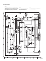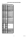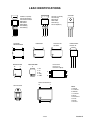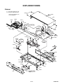
1
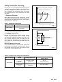
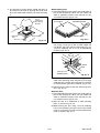
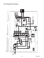
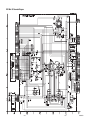
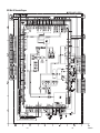
Service
Manual
DV4500 /N1B/N1S
DVD Player
DVD PLAYER DV4500
PLAY
STOP
PAUSE
STANDBY
FL OFF
ENTER
POWER ON / STANDBY
P.SCAN
DVD
FL OFF
OPEN/CLOSE
MENU
VCD
TABLE OF CONTENTS
SECTION
PAGE
TECHNICAL SPECIFICATIONS .............................................................................................. 1-1-1
SERVICE HINTS AND TOOLS ................................................................................................ 1-2-1
WARNING AND LASER SAFETY INSTRUCTIONS ................................................................ 1-2-2
LASER BEAM SAFETY PRECAUTIONS ................................................................................ 1-2-3
IMPORTANT SAFETY PRECAUTIONS .................................................................................. 1-3-1
STANDARD NOTES FOR SERVICING ................................................................................... 1-4-1
CABINET DISASSEMBLY INSTRUCTIONS ............................................................................ 1-5-1
TROUBLESHOOTING ............................................................................................................. 1-6-1
BLOCK DIAGRAMS ................................................................................................................. 1-7-1
SCHEMATIC DIAGRAMS / CBA'S AND TEST POINTS .......................................................... 1-8-1
WAVEFORMS .......................................................................................................................... 1-9-1
WIRING DIAGRAMS .............................................................................................................. 1-10-1
FIRMWARE RENEWAL MODE ............................................................................................. 1-11-1
IC PIN FUNCTION DESCRIPTIONS ..................................................................................... 1-12-1
LEAD IDENTIFICATIONS ...................................................................................................... 1-13-1
EXPLODED VIEWS ............................................................................................................... 1-14-1
PARTS LIST ........................................................................................................................... 1-15-1
DV4500
Please use this service manual with referring to the user guide (D.F.U) without fail.
DV4500
Part no. 90M12BW855010
First Issue 2004.05
ecm
MARANTZ DESIGN AND SERVICE
Using superior design and selected high grade components, MARANTZ company has created the ultimate in stereo sound.
Only original MARANTZ parts can insure that your MARANTZ product will continue to perform to the specifications for which
it is famous.
Parts for your MARANTZ equipment are generally available to our National Marantz Subsidiary or Agent.
ORDERING PARTS :
Parts can be ordered either by mail or by Fax.. In both cases, the correct part number has to be specified.
The following information must be supplied to eliminate delays in processing your order :
1. Complete address
2. Complete part numbers and quantities required
3. Description of parts
4. Model number for which part is required
5. Way of shipment
6. Signature : any order form or Fax. must be signed, otherwise such part order will be considered as null and void.
USA
CANADA
EUROPE / TRADING
MARANTZ EUROPE B.V.
P. O. BOX 8744, BUILDING SILVERPOINT
BEEMDSTRAAT 11, 5653 MA EINDHOVEN
THE NETHERLANDS
PHONE : +31 - 40 - 2507844
FAX
: +31 - 40 - 2507860
MARANTZ AMERICA, INC
1100 MAPLEWOOD DRIVE
ITASCA, IL. 60143
USA
PHONE : 630 - 741 - 0300
FAX
: 630 - 741 - 0301
AMERICAS
SUPERSCOPE TECHNOLOGIES, INC.
MARANTZ PROFESSIONAL PRODUCTS
2640 WHITE OAK CIRCLE, SUITE A
AURORA, ILLINOIS 60504 USA
PHONE : 630 - 820 - 4800
FAX
: 630 - 820 - 8103
AUSTRALIA
QualiFi Pty Ltd,
24 LIONEL ROAD,
MT. WAVERLEY VIC 3149
AUSTRALIA
PHONE : +61 - (0)3 - 9543 - 1522
FAX
: +61 - (0)3 - 9543 - 3677
NEW ZEALAND
WILDASH AUDIO SYSTEMS NZ
14 MALVERN ROAD MT ALBERT
AUCKLAND NEW ZEALAND
PHONE : +64 - 9 - 8451958
FAX
: +64 - 9 - 8463554
MARANTZ CANADA INC.
5-505 APPLE CREEK BLVD.
MARKHAM, ONTARIO L3R 5B1
CANADA
PHONE : 905 - 415 - 9292
FAX
: 905 - 475 - 4159
HONG KONG
AUSTRALIA
TECHNICAL AUDIO GROUP PTY, LTD
43-53 Bridge Rd.,
STANMORE NSW 2048
AUSTRALIA
PHONE : +61 - (0)2 - 9519 - 0900
FAX
: +61 - (0)2 - 9519 - 0600
THAILAND
MRZ STANDARD CO., LTD
746 - 754 MAHACHAI ROAD.,
WANGBURAPAPIROM, PHRANAKORN,
BANGKOK, 10200 THAILAND
PHONE : +66 - 2 - 222 9181
FAX
: +66 - 2 - 224 6795
TAIWAN
PAI- YUING CO., LTD.
6 TH FL NO, 148 SUNG KIANG ROAD,
TAIPEI, 10429, TAIWAN R.O.C.
PHONE : +886 - 2 - 25221304
FAX
: +886 - 2 - 25630415
JAPAN Technical
MARANTZ JAPAN, INC.
35- 1, 7- CHOME, SAGAMIONO
SAGAMIHARA - SHI, KANAGAWA
JAPAN 228-8505
PHONE : +81 42 748 1013
FAX
: +81 42 741 9190
Jolly ProAudio Broadcast Engineering Ltd.
UNIT 2, 10F, WAH HUNG CENTRE,
41 HUNG TO ROAD, KWUN TONG, KLN.,
HONG KONG
PHONE : 852 - 21913660
FAX
: 852 - 21913990
SINGAPORE
WO KEE HONG DISTRIBUTION PTE LTD
No.1 JALAN KILANG TIMOR
#08-03 PACIFIC TECH CENTRE
SINGAPORE 159303
PHONE : +65 6376 0338
FAX
: +65 6376 0166
MALAYSIA
WO KEE HONG ELECTRONICS SDN. BHD.
2ND FLOOR BANGUNAN INFINITE CENTRE
LOT 1, JALAN 13/6, 46200 PETALING JAYA
SELANGOR DARUL EHSAN, MALAYSIA
PHONE : +60 - 3 - 7954 8088
FAX
: +60 - 3 - 7954 7088
KOREA
MK ENTERPRISES LTD.
ROOM 604/605, ELECTRO-OFFICETEL, 16-58,
3GA, HANGANG-RO, YONGSAN-KU, SEOUL
KOREA
PHONE : +822 - 3232 - 155
FAX
: +822 - 3232 - 154
SHOCK, FIRE HAZARD SERVICE TEST :
CAUTION : After servicing this appliance and prior to returning to customer, measure the resistance between either primary AC
cord connector pins ( with unit NOT connected to AC mains and its Power switch ON ), and the face or Front Panel of product and
controls and chassis bottom.
Any resistance measurement less than 1 Megohms should cause unit to be repaired or corrected before AC power is applied, and
verified before it is return to the user/customer.
Ref. UL Standard No. 1492.
In case of difficulties, do not hesitate to contact the Technical
Department at above mentioned address.
040401ECM
TECHNICAL SPECIFICATIONS
SIGNAL SYSTEM
PAL color
APPLICABLE DISCS
(1) DVD-Video Discs
1-layer 12cm single-sided discs, 2-layer 12cm single-sided
discs, 2-layer 12cm double-sided discs (1 layer per side)
1-layer 8cm single-sided discs, 2-layer 8cm single-sided
discs, 2-layer 8cm double-sided discs (1 layer per side)
(2) DVD-R/DVD-RW
(3) Compact discs (CD-DA, Video CD)
12cm discs, 8cm discs
(4) CD-R/CD-RW
S-VIDEO OUTPUT
Y output level: 1Vp-p (75 /ohms)
C output level: 0.30Vp-p
Output connectors: S connectors, 1 set
VIDEO OUTPUT
Output level: 1Vp-p (75 /ohms)
Output connector: Pin jacks, 1 set
20 18 16 14 12 10 8 6 4 2
21 19 17 15 13 11 9 7 5 3 1
Contacts, signal levels and impedances
Contact 1
Audio Output (Right):
Contact 3
Audio Output (Left):
Contact 4
Audio, Ground
Contact 5
RGB, Ground (Blue)
Contact 7
RGB Output (Blue):
Contact 8
Function Select Switching Control
CR/PR output level: 0.7Vp-p (75 /ohms)
AUDIO/VIDEO
21-pin scart jack
AUDIO OUTPUT
Output level: 2Vrms
2 channel (L, R) output connector: Pin jack, 1 set
AUDIO OUTPUT PROPERTIES
(1) Frequency response
1 DVDs (linear PCM) : 4Hz to 22kHz (48 kHz sampling)
: 4Hz to 44kHz (96 kHz sampling)
2 CDs
: 4Hz to 20kHz
(2) S/N ratio
: 115dB
(3) Total harmonic distortion : 1kHz CD: 0.0045%
(4) Dynamic range
: DVD: 100dB
CD: 98dB
DIGITAL AUDIO OUTPUT
Optical digital output: Optical connector, 1 set
Coaxial digital output: Pin jack, 1 set
POWER SUPPLY
AC 230V, 50Hz
2.0Vrms/ 1kΩ
0.7Vp-p/75Ω
L : 0.0~2.0V DC
Power Off
M: 4.5~7.0V DC
Wide-Screen Mode
(16:9)
H: 9.5~12.0V DC
Normal Mode (4:3)
COMPONENT OUTPUT
Y output level: 1Vp-p (75 /ohms)
CB/PB output level: 0.7Vp-p (75 /ohms)
Output connector: Pin jacks, 1 set
2.0Vrms/ 1kΩ
Contact 9
RGB, Ground (Green)
Contact 11
RGB Output (Green):
Contact 13
RGB, Ground (Red)
Contact 14
RGB Switching Control, Ground
Contact 15
RGB Output (Red):
Contact 16
RGB Switching Control
H: 3.3V DC
Contact 17
Video Output Signal, Ground
Contact 18
Video Input Signal, Ground
Contact 19
Video Output (CVBS):
Contact 21
Common Ground (shielding)
POWER CONSUMPTION
12 W
MAXIMUM EXTERNAL DIMENSIONS
440 (width) x 75 (height) x 211 (depth) mm
MASS
2.1 Kg (4.6 lbs)
REMOTE CONTROL UNIT
RC6500DV
Infrared pulse type
Supply: DC 3V, 2 R6P/AA batteries
1-1-1
0.7Vp-p/75Ω
0.7Vp-p/75Ω
RGB Mode
1.0Vp-p/75Ω
NOTE:
Playable Discs
Only the sound recorded on the normal CD layer can be
delivered.
The sound recorded on the high density Super Audio CD
layer cannot be delivered.
The following discs can be played back on this
DVD player.
Usable
discs
Mark (logo)
Recorded
signals
Disc Size
Any other discs without compatibility indications.
DVD-Video
Disc Types
12 cm
(NOTE 1)
[DVD-Video]
Digital video
(MPEG2)
DVD-R
DVD-RW
Data on a DVD is divided into sections called "titles" and
then into subsections called “chapters” each of which is given
a title or chapter number. Playback conditions are
preset on some DVD-Video discs, and these playback
conditions take priority over user operations on this player.
If a function you selected does not run as desired, refer to
the manual accompanying the disc.
8 cm
(NOTE 2, 3)
CD
CD-R
CD-RW
Digital audio
MP3
WMA (NOTE 5)
Digital picture
(JPEG)
(NOTE 4)
12 cm
Example
8 cm
Title 1
Title 2
Chapter 1 Chapter 2 Chapter 3 Chapter 4 Chapter 1 Chapter 2
12 cm
DIGITAL VIDEO
Video
CD
Sound
and
Pictures
8 cm
(Singles)
[Audio CD, Video CD]
Data on an Audio CD, or a Video CD is divided into sections
called “tracks” each of which is given a track number.
Picture CD
JPEG
12 cm
Example
Track 1
NOTE 1: Some DVD-Video discs do not operate as described in this
manual due to the intentions of the discs’ producers.
NOTE 2: This unit can play DVD-RW discs recorded in DVD video
format or DVD video recording format.
* The disc may not be played back due to recording quality
or properties of the disc, dirt on the disc or the pickup lens,
or condensation on the pickup lens.
NOTE 3: Discs that have not be finalized cannot be played.
Depending on the disc’s recording status, the disc may not
be accepted or may not be played normally (the picture or
sound may not be smooth, etc.).
NOTE 4: Some of CD-R/CD-RW discs may be incompatible
because of “scratch and stain of disc”, “Recording
condition”, and “Characteristic of Recorder”.
NOTE 5:
Windows Media and the Windows logo are
trademarks or registered trademarks of
Microsoft Corporation in the United States
and/or other countries.
Track 2
Track 3
Track 4
Track 5
Track 6
ABOUT THE PBC FUNCTION OF VIDEO CD
This unit conforms to ver.1.1 and ver.2.0 of Video CD
standard, with PBC function.
Ver.1.1 (without PBC function): You can enjoy playback picture
as well as music CD.
Ver.2.0 (with PBC function): While using a Video CD with PBC
function, “PBC” appears on the screen and the display.
What is PBC? “PBC” stands for the Playback Control.
You can play interactive software using menu screens.
Refer to instructions in the Video CD.
This player conforms to the PAL colour system. Also
you can play discs recorded with the NTSC system
via a PAL system TV set.
NOTE:
When playing Video CDs with PBC function, some operations
(e.g., track search and repeat tracks) cannot be performed
unless the function is cancelled temporarily (Refer to page 15).
Some discs include region codes as shown below.
[MP3, JPEG, WMA]
The number inside the symbol refers to a region of the world,
and a disc encoded in a specific region format can only be
played back on DVD players with the same region code.
: This label indicates playback compatibility with DVD-RW
discs recorded in VR mode (Video Recording Format).
On the following discs, only the sound can be heard
(picture cannot be viewed).
CDV
CD-G
NEVER play back the following discs. Otherwise, malfunction may result!
DVD-RAM
CD-I
Photo CD
DVD with region codes other than 2 or ALL
DVD-ROM for personal computers
CD-ROM for personal computers
On the following disc, the sound MAY NOT be heard.
Super Audio CD
Data on an MP3, JPEG or WMA are divided into sections
called “groups” and then into subsections called “tracks” each
of which is given an group or track number.
Example
Track 1
Group 1
Track 2
Track 3
Group 2
Track 4
Track 5
Track 6
CAUTION:
• Use caution not to pinch your finger in the disc slot.
• Be sure to remove a disc and unplug the AC power cord
from the outlet before carrying the DVD player.
1-1-2
SERVICE HINTS AND TOOLS
SERVICE HINTS
SERVICE TOOLS
Audio signals disc
Disc without errors (SBC444)+
Disc with DO errors, black spots and fingerprints (SBC444A)
Disc (65 min 1kHz) without no pause
Max. diameter disc (58.0 mm)
Torx screwdrivers
Set (straight)
Set (square)
13th order filter
DVD test disc (PAL)
DVD test disc (NTSC) ALMEDIO
1-2-1
4822 397 30184
4822 397 30245
4822 397 30155
4822 397 60141
4822 395 50145
4822 395 50132
4822 395 30204
4822 397 10131
TDV-540
WARNING AND LASER SAFETY INSTRUCTIONS
GB
WARNING
NL
All ICs and many other semi-conductors are
susceptible to electrostatic discharges (ESD).
Careless handling during repair can reduce
life drastically.
When repairing, make sure that you are
connected with the same potential as the
mass of the set via a wrist wrap with
resistance.
Keep components and tools also at this
potential.
F
WAARSCHUWING
Alle IC’s en vele andere halfgeleiders zijn
gevoelig voor elektrostatische ontladingen
(ESD).
Onzorgvuldig behandelen tijdens reparatie
kan de levensduur drastisch doen
verminderen.
Zorg ervoor dat u tijdens reparatie via een
polsband met weerstand verbonden bent met
hetzelfde potentiaal als de massa van het
apparaat.
Houd componenten en hulpmiddelen ook op
ditzelfde potentiaal.
D
ATTENTION
Tous les IC et beaucoup d’autres semiconducteurs sont sensibles aux décharges
statiques (ESD).
Leur longévité pourrait être considérablement
écourtée par le fait qu’aucune précaution
n’est prise a leur manipulation.
Lors de réparations, s’assurer de bien être
relié au même potentiel que la masse de
l’appareil et enfiler le bracelet serti d’une
résistance de sécurité.
Veiller a ce que les composants ainsi que les
outils que l’on utilise soient également a ce
potentiel.
WARNUNG
I
Alle IC und viele andere Halbleiter sind
empfindlich gegen elektrostatische
Entladungen (ESD).
Unsorgfältige Behandlung bei der Reparatur
kann die Lebensdauer drastisch vermindern.
Sorgen sie dafür, das Sie im Reparaturfall
über ein Pulsarmband mit Widerstand mit
dem Massepotential des Gerätes verbunden
sind.
Halten Sie Bauteile und Hilfsmittel ebenfalls
auf diesem Potential.
AVVERTIMENTO
Tutti IC e parecchi semi-conduttori sono
sensibili alle scariche statiche (ESD).
La loro longevita potrebbe essere fortemente
ridatta in caso di non osservazione della piu
grande cauzione alla loro manipolazione.
Durante le riparazioni occorre quindi essere
collegato allo stesso potenziale che quello
della massa dell’apparecchio tramite un
braccialetto a resistenza.
Assicurarsi che i componenti e anche gli
utensili con quali si lavora siano anche a
questo potenziale.
D
GB
Safety regulations require that the set be restored to its original condition
and that parts which are identical with those specified be used.
Bei jeder Reparatur sind die geltenden Sicherheitsvorschriften zu beachten.
Der Originalzustand des Gerats darf nicht verandert werden.
Fur Reparaturen sind Original-Ersatzteile zu verwenden.
NL
I
Veiligheidsbepalingen vereisen, dat het apparaat in zijn oorspronkelijke
toestand wordt terug gebracht en dat onderdelen, identiek aan de
gespecifieerde worden toegepast.
Le norme di sicurezza esigono che l’apparecchio venga rimesso nelle
condizioni originali e che siano utilizzati pezzi di ricambiago idetici a quelli
specificati.
F
“Pour votre sécurité, ces documents
doivent être utilisés par des
spécialistes agrées, seuls habilités à
réparer votre appareil en panne.”
Les normes de sécurité exigent que l’appareil soit remis a l’état d’origine et
que soient utilisées les pièces de rechange identiques à celles spécifiées.
LASER SAFETY
This unit employs a laser. Only a qualified service person should remove the cover or attempt to service this
device, due to possible eye injury.
USE OF CONTROLS OR ADJUSTMENTS OR PERFORMANCE OF PROCEDURE OTHER THAN THOSE
SPECIFIED HEREIN MAY RESULT IN HAZARDOUS RADIATION EXPOSURE.
AVOID DIRECT EXPOSURE TO BEAM
WARNING
The use of optical instruments with this product will increase eye hazard.
Repair handling should take place as much as possible with a disc loaded inside the player
WARNING LOCATION: INSIDE ON LASER COVERSHIELD
CAUTION VISIBLE AND INVISIBLE LASER RADIATION WHEN OPEN AVOID EXPOSURE TO BEAM
ADVARSEL SYNLIG OG USYNLIG LASERSTRÅLING VED ÅBNING UNDGÅ UDSÆTTELSE FOR STRÅLING
ADVARSEL SYNLIG OG USYNLIG LASERSTRÅLING NÅR DEKSEL Å PNES UNNGÅ EKSPONERING FOR STRÅLEN
VARNING SYNLIG OCH OSYNLIG LASERSTRÅLNING NÄR DENNA DEL ÄR ÖPPNAD BETRAKTA EJ STRÅLEN
VARO! AVATT AESSA OLET ALTTIINA NÄKYVÄLLE JA NÄKYMÄTTÖMÄLLE LASER SÄTEILYLLE. ÄLÄ KATSO SÄTEESEEN
VORSICHT SICHTBARE UND UNSICHTBARE LASERSTRAHLUNG WENN ABDECKUNG GEÖFFNET NICHT DEM STRAHL AUSSETSEN
DANGER VISIBLE AND INVISIBLE LASER RADIATION WHEN OPEN AVOID DIRECT EXPOSURE TO BEAM
ATTENTION RAYONNEMENT LASER VISIBLE ET INVISIBLE EN CAS D'OUVERTURE EXPOSITION DANGEREUSE AU FAISCEAU
030804ecm
1-2-2
LASER BEAM SAFETY PRECAUTIONS
This DVD player uses a pickup that emits a laser beam.
Do not look directly at the laser beam coming
from the pickup or allow it to strike against your
skin.
The laser beam is emitted from the location shown in the figure. When checking the laser diode, be sure to keep
your eyes at least 30cm away from the pickup lens when the diode is turned on. Do not look directly at the laser
beam.
Caution: Use of controls and adjustments, or doing procedures other than those specified herein, may result in
hazardous radiation exposure.
Drive Mecha Assembly
Laser Beam Radiation
Laser Pickup
Turntable
1-2-3
E5981LBS
IMPORTANT SAFETY PRECAUTIONS
Product Safety Notice
J. Be careful that foreign objects (screws, solder
droplets, etc.) do not remain inside the set.
Some electrical and mechanical parts have special
safety-related characteristics which are often not evident from visual inspection, nor can the protection they
give necessarily be obtained by replacing them with
components rated for higher voltage, wattage, etc.
Parts that have special safety characteristics are identified by a ! on schematics and in parts lists. Use of a
substitute replacement that does not have the same
safety characteristics as the recommended replacement part might create shock, fire, and/or other hazards. The Product’s Safety is under review
continuously and new instructions are issued whenever appropriate. Prior to shipment from the factory,
our products are carefully inspected to confirm with
the recognized product safety and electrical codes of
the countries in which they are to be sold. However, in
order to maintain such compliance, it is equally important to implement the following precautions when a set
is being serviced.
K. Crimp type wire connector
The power transformer uses crimp type connectors
which connect the power cord and the primary side
of the transformer. When replacing the transformer,
follow these steps carefully and precisely to prevent
shock hazards.
Replacement procedure
1)Remove the old connector by cutting the wires at a
point close to the connector.
Important: Do not re-use a connector. (Discard it.)
2)Strip about 15 mm of the insulation from the ends
of the wires. If the wires are stranded, twist the
strands to avoid frayed conductors.
3)Align the lengths of the wires to be connected.
Insert the wires fully into the connector.
4)Use a crimping tool to crimp the metal sleeve at its
center. Be sure to crimp fully to the complete closure of the tool.
L. When connecting or disconnecting the internal
connectors, first, disconnect the AC plug from the
AC outlet.
Precautions during Servicing
A. Parts identified by the ! symbol are critical for
safety. Replace only with part number specified.
B. In addition to safety, other parts and assemblies
are specified for conformance with regulations
applying to spurious radiation. These must also be
replaced only with specified replacements.
Examples: RF converters, RF cables, noise blocking capacitors, and noise blocking filters, etc.
C. Use specified internal wiring. Note especially:
1)Wires covered with PVC tubing
2)Double insulated wires
3)High voltage leads
D. Use specified insulating materials for hazardous
live parts. Note especially:
1)Insulation tape
2)PVC tubing
3)Spacers
4)Insulators for transistors
E. When replacing AC primary side components
(transformers, power cord, etc.), wrap ends of
wires securely about the terminals before soldering.
F. Observe that the wires do not contact heat producing parts (heatsinks, oxide metal film resistors, fusible resistors, etc.).
G. Check that replaced wires do not contact sharp
edges or pointed parts.
H. When a power cord has been replaced, check that
5 - 6 kg of force in any direction will not loosen it.
I. Also check areas surrounding repaired locations.
1-3-1
DVD_SFNP
Safety Check after Servicing
Examine the area surrounding the repaired location for
damage or deterioration. Observe that screws, parts,
and wires have been returned to their original positions. Afterwards, do the following tests and confirm
the specified values to verify compliance with safety
standards.
Chassis or Secondary Conductor
Primary Circuit Terminals
d'
d
1. Clearance Distance
When replacing primary circuit components, confirm
specified clearance distance (d) and (d’) between soldered terminals, and between terminals and surrounding metallic parts. (See Fig. 1)
Table 1 : Ratings for selected area
AC Line Voltage
Clearance Distance (d), (d’)
220 to 240 V
≥ 3 mm(d)
≥ 6 mm(d’)
Fig. 1
Note: This table is unofficial and for reference only.
Be sure to confirm the precise values.
Exposed Accessible Part
2. Leakage Current Test
Confirm the specified (or lower) leakage current
between B (earth ground, power cord plug prongs)
and externally exposed accessible parts (RF terminals, antenna terminals, video and audio input and
output terminals, microphone jacks, earphone jacks,
etc.) is lower than or equal to the specified value in the
table below.
Z
Measuring Method (Power ON) :
Insert load Z between B (earth ground, power cord
plug prongs) and exposed accessible parts. Use an
AC voltmeter to measure across the terminals of load
Z. See Fig. 2 and the following table.
B
AC Voltmeter
(High Impedance)
One side of
Power Cord Plug Prongs
Fig. 2
Table 2: Leakage current ratings for selected areas
AC Line Voltage
220 to 240 V
Load Z
Leakage Current (i)
One side of power cord plug
prongs (B) to:
2kΩ RES.
Connected in
parallel
i≤0.7mA AC Peak
i≤2mA DC
RF or
Antenna terminals
50kΩ RES.
Connected in
parallel
i≤0.7mA AC Peak
i≤2mA DC
A/V Input, Output
Note: This table is unofficial and for reference only. Be sure to confirm the precise values.
1-3-2
DVD_SFNP
STANDARD NOTES FOR SERVICING
Circuit Board Indications
Pb (Lead) Free Solder
1. The output pin of the 3 pin Regulator ICs is indicated as shown.
When soldering, be sure to use the Pb free solder.
Top View
Out
How to Remove / Install Flat Pack-IC
Bottom View
In
1. Removal
Input
With Hot-Air Flat Pack-IC Desoldering Machine:.
(1) Prepare the hot-air flat pack-IC desoldering
machine, then apply hot air to the Flat Pack-IC
(about 5 to 6 seconds). (Fig. S-1-1)
2. For other ICs, pin 1 and every fifth pin are indicated
as shown.
5
Pin 1
10
Fig. S-1-1
3. The 1st pin of every male connector is indicated as
shown.
(2) Remove the flat pack-IC with tweezers while applying the hot air.
Pin 1
(3) Bottom of the flat pack-IC is fixed with glue to the
CBA; when removing entire flat pack-IC, first apply
soldering iron to center of the flat pack-IC and heat
up. Then remove (glue will be melted). (Fig. S-1-6)
Instructions for Connectors
(4) Release the flat pack-IC from the CBA using tweezers. (Fig. S-1-6)
1. When you connect or disconnect the FFC (Flexible
Foil Connector) cable, be sure to first disconnect
the AC cord.
Caution:
1. The Flat Pack-IC shape may differ by models. Use
an appropriate hot-air flat pack-IC desoldering
machine, whose shape matches that of the Flat
Pack-IC.
2. FFC (Flexible Foil Connector) cable should be
inserted parallel into the connector, not at an angle.
2. Do not supply hot air to the chip parts around the
flat pack-IC for over 6 seconds because damage to
the chip parts may occur. Put masking tape around
the flat pack-IC to protect other parts from damage.
(Fig. S-1-2)
FFC Cable
Connector
CBA
* Be careful to avoid a short circuit.
1-4-1
DVD_NOTE
With Soldering Iron:
(1) Using desoldering braid, remove the solder from all
pins of the flat pack-IC. When you use solder flux
which is applied to all pins of the flat pack-IC, you
can remove it easily. (Fig. S-1-3)
3. The flat pack-IC on the CBA is affixed with glue, so
be careful not to break or damage the foil of each
pin or the solder lands under the IC when removing
it.
Hot-air
Flat Pack-IC
Desoldering
Machine
Flat Pack-IC
Desoldering Braid
CBA
Masking
Tape
Flat Pack-IC
Soldering Iron
Fig. S-1-3
Tweezers
Fig. S-1-2
(2) Lift each lead of the flat pack-IC upward one by
one, using a sharp pin or wire to which solder will
not adhere (iron wire). When heating the pins, use
a fine tip soldering iron or a hot air desoldering
machine. (Fig. S-1-4)
Sharp
Pin
Fine Tip
Soldering Iron
Fig. S-1-4
(3) Bottom of the flat pack-IC is fixed with glue to the
CBA; when removing entire flat pack-IC, first apply
soldering iron to center of the flat pack-IC and heat
up. Then remove (glue will be melted). (Fig. S-1-6)
(4) Release the flat pack-IC from the CBA using tweezers. (Fig. S-1-6)
With Iron Wire:
(1) Using desoldering braid, remove the solder from all
pins of the flat pack-IC. When you use solder flux
which is applied to all pins of the flat pack-IC, you
can remove it easily. (Fig. S-1-3)
(2) Affix the wire to a workbench or solid mounting
point, as shown in Fig. S-1-5.
(3) While heating the pins using a fine tip soldering
iron or hot air blower, pull up the wire as the solder
melts so as to lift the IC leads from the CBA contact
pads as shown in Fig. S-1-5
1-4-2
DVD_NOTE
2. Installation
(4) Bottom of the flat pack-IC is fixed with glue to the
CBA; when removing entire flat pack-IC, first apply
soldering iron to center of the flat pack-IC and heat
up. Then remove (glue will be melted). (Fig. S-1-6)
(1) Using desoldering braid, remove the solder from
the foil of each pin of the flat pack-IC on the CBA so
you can install a replacement flat pack-IC more
easily.
(5) Release the flat pack-IC from the CBA using tweezers. (Fig. S-1-6)
(2) The “I” mark on the flat pack-IC indicates pin 1.
(See Fig. S-1-7.) Be sure this mark matches the 1
on the PCB when positioning for installation. Then
presolder the four corners of the flat pack-IC. (See
Fig. S-1-8.)
Note:
When using a soldering iron, care must be taken
to ensure that the flat pack-IC is not being held by
glue. When the flat pack-IC is removed from the
CBA, handle it gently because it may be damaged
if force is applied.
(3) Solder all pins of the flat pack-IC. Be sure that none
of the pins have solder bridges.
Example :
Hot Air Blower
or
Iron Wire
Pin 1 of the Flat Pack-IC
is indicated by a " " mark.
Fig. S-1-7
Soldering Iron
To Solid
Mounting Point
Presolder
Fig. S-1-5
CBA
Fine Tip
Soldering Iron
Flat Pack-IC
CBA
Fig. S-1-8
Flat Pack-IC
Tweezers
Fig. S-1-6
1-4-3
DVD_NOTE
Instructions for Handling
Semi-conductors
Electrostatic breakdown of the semi-conductors may
occur due to a potential difference caused by electrostatic charge during unpacking or repair work.
1. Ground for Human Body
Be sure to wear a grounding band (1MΩ) that is properly grounded to remove any static electricity that may
be charged on the body.
2. Ground for Workbench
(1) Be sure to place a conductive sheet or copper plate
with proper grounding (1MΩ) on the workbench or
other surface, where the semi-conductors are to be
placed. Because the static electricity charge on
clothing will not escape through the body grounding band, be careful to avoid contacting semi-conductors with your clothing.
< Incorrect >
CBA
< Correct >
Grounding Band
1MΩ
CBA
1MΩ
Conductive Sheet or
Copper Plate
1-4-4
DVD_NOTE
CABINET DISASSEMBLY INSTRUCTIONS
1. Disassembly Flowchart
This flowchart indicates the disassembly steps to gain
access to item(s) to be serviced. When reassembling,
follow the steps in reverse order. Bend, route, and
dress the cables as they were originally.
[12]
[1] Top Cover
[12] Stopper Bracket
[2] Front Unit
[3] Function CBA
[4] Front Assembly
[5] Rear Panel
PART
Stopper
Bracket
REMOVE/*UNHOOK/
Fig.
UNLOCK/RELEASE/ Note
No.
UNPLUG/DESOLDER
D8
----------
-
↓
↓
↓
↓
↓
(1)
(2)
(3)
(4)
(5)
(1): Identification (location) No. of parts in the figures
(2): Name of the part
(3): Figure Number for reference
(4): Identification of parts to be removed, unhooked,
unlocked, released, unplugged, unclamped, or
desoldered.
P=Spring, L=Locking Tab, S=Screw,
CN=Connector
*=Unhook, Unlock, Release, Unplug, or Desolder
e.g. 2(S-2) = two Screws (S-2),
2(L-2) = two Locking Tabs (L-2)
(5): Refer to “Reference Notes.”
[6] DVD Main CBA Unit
[7] DVD Mecha
[8] LED CBA
[9] AV CBA
[10] Loader Base
REMOVAL
ID/
LOC.
No.
[11] Power PCB Holder
About tightening screws
When tightening screws, tighten them with the following torque.
2. Disassembly Method
ID/
LOC.
No.
[1]
[2]
PART
Top Cover
Front Unit
REMOVAL
Screws
REMOVE/*UNHOOK/
Fig.
UNLOCK/RELEASE/ Note
No.
UNPLUG/DESOLDER
(S-1), (S-2), (S-3), (S-4),
(S-5A), (S-6), (S-7), (S-8),
(S-9), (S-10)
0.45 ± 0.05 N·m
(S-5B)
0.38 ± 0.04 N·m
D1 5(S-1)
D2
*2(L-1), Tray Panel,
*2(L-2), *3(L-3),
*CN2081
1
1-1
1-2
1-3
1-4
1-5
1-6
1-7
Torque
Reference Notes
CAUTION 1: Locking Tabs (L-1), (L-2) and (L-3) are
fragile. Be careful not to break them.
1-1. Connect the wall plug to an AC outlet and press
the [OPEN/CLOSE] button to open the tray.
[3]
Function
CBA
D3 6(S-2)
-
1-2. Remove the Tray Panel by releasing two locking
tabs (L-1).
[4]
Front
Assembly
D3 ----------
-
1-3. Press the [OPEN/CLOSE] button again to close
the tray.
[5]
Rear Panel
D4 8(S-3), 3(S-4)
DVD Main
CBA Unit
(S-5A), (S-5B),
D5 *CN201, *CN301,
*CN401, *CN601
[7]
DVD Mecha
D5
4(S-6)
D6
2
3
[8]
LED CBA
D7 *CN2082
-
[9]
AV CBA
D7 3(S-7), (S-8)
-
[6]
[10] Loader Base D8 4(S-9)
[11]
Power PCB
Holder
D8 2(S-10)
-
1-4. Press the [POWER] button to turn the power off.
2
2-1
2-2
1-5. Unplug an AC cord.
1-6. Disconnect connector CN2081.
1-7. Release two Locking Tabs (L-2). Then release
three Locking Tabs (L-3), and remove the Front
Unit.
-
1-5-1
E59M2DC
CAUTION 2: Electrostatic breakdown of the laser
diode in the optical system block may occur as a
potential difference caused by electrostatic charge
accumulated on cloth, human body etc, during
unpacking or repair work.
[3] Function CBA (S-2)
(S-2)
To avoid damage of pickup follow next procedures.
2-1. Short the three short lands of FPC cable with solder before removing the FFC cable (CN201) from
it. If you disconnect the FFC cable (CN201), the
laser diode of pickup will be destroyed. (Fig. D4)
2-2. Disconnect Connectors (CN301), (CN401) and
(CN601). Remove two Screws (S-5A) and (S-5B)
and lift the DVD Main CBA Unit. (Fig. D4)
[4] Front Assembly
CAUTION 3: When reassembling, confirm the FFC
cable (CN201) is connected completely. Then remove
the solder from the three short lands of FPC cable.
(Fig. D4)
Fig. D3
[1] Top Cover
(S-1)
[5] Rear Panel
(S-4)
(S-1)
(S-3)
(S-4)
(S-1)
Fig. D1
Fig. D4
Tray Panel
(L-1)
(L-1)
(L-2)
(L-2)
CN2081
(L-3)
[2] Front Unit
Fig. D2
1-5-2
E59M2DC
(S-5B)
(S-7)
(S-5A)
[8] LED CBA
CN201
CN601
CN301
CN401
(S-8)
CN2082
[6] DVD Main
CBA Unit
A
[9] AV CBA
Fig. D7
Short the three short lands by soldering.
(Either of two places.)
[11] Power
PCB Holder
(S-10)
(S-9)
(S-9)
[10] Loader
Base
Connector
View for A
[12] Stopper
Bracket
Fig. D5
(S-6)
(S-6)
Fig. D8
[7] DVD Mecha
Fig. D6
1-5-3
E59M2DC
HOW TO EJECT MANUALLY
1. Remove the Top Cover.
2. Rotate the roulette in the direction of the arrow as shown
below.
View for A
Rotate this roulette in
the direction of the arrow
A
1-5-4
E59M2DC
TROUBLESHOOTING
FLOW CHART NO.1
The power cannot be turned on.
Is the fuse normal?
Yes
Is normal state restored when once unplugged
power cord is plugged again after several seconds?
Yes
Is the EV +3.3V line voltage normal?
Yes
Check each rectifying circuit of the secondary circuit
and service it if defective.
No
No
No
See FLOW CHART No.2 <The fuse blows out.>
Check if there is any leak or short-circuiting on the
primary circuit component, and service it if defective.
(Q1003, Q1001, Q1008, T1001, D1001, D1002,
D1004, D1005, D1011, C1003, C1005)
FLOW CHART NO.2
The fuse blows out.
Check the presence that the primary component
is leaking or shorted and service it if defective.
Check the presence that the rectifying diode or
circuit is shorted in each rectifying circuit of
secondary side, and service it if defective.
After servicing, replace the fuse.
FLOW CHART NO.3
When the output voltage fluctuates.
Does the photo coupler circuit on the secondary
side operate normally?
Yes
Check IC1001, D1012, D1024 and their periphery,
and service it if defective.
No
Check IC1001, IC1006, D1048 and their
periphery, and service it if defective.
FLOW CHART NO.4
When buzz sound can be heard in the vicinity of power circuit.
Check if there is any short-circuit on the rectifying diode and the circuit in each rectifying circuit of the secondary side,
and service it if defective. (D1003, D1006, D1008, D1016, D1030, IC1002, Q1002, Q1004, Q1005, Q1011, Q1014)
FLOW CHART NO.5
-FL is not outputted.
Is approximately -23V voltage supplied to the
anode of D1003?
Yes
Check if there is any leak or short-circuit
on the loaded circuit, and service it if defective.
No
1-6-1
Check D1003 and periphery circuit, and service it
if defective.
E59M2TR
FLOW CHART NO.6
P-ON+11V (EV+11V) is not outputted.
Is 11V voltage supplied to the emitter of Q1002?
No
Yes
No
Is the voltage of base on Q1002 lower than the
voltage of emitter on Q1002 when turning the power on?
Check D1030, D1048, C1035, C1048, L1009 and
the periphery circuit, and service it if defective.
Check Q1016 and PWRCON line and service it if
defective.
Yes
Replace Q1002.
FLOW CHART NO.7
P-ON+5V is not outputted. (EV+11V is outputted normally.)
Is the "H" signal inputted into the base of Q1004?
Yes
Replace Q1004.
No
Check R1068 and D1046, and service it if defective.
FLOW CHART NO.8
P-ON+3.3V is not outputted. (P-ON+11V is outputted normally.)
Is 3.3V voltage supplied to the collector of Q1011?
Yes
Replace Q1011 or R1067.
No
Check D1008, C1007, C1038, L1007 and the
periphery circuit, and service it if defective.
FLOW CHART NO.9
EV+5V is not outputted.
Is EV+11V outputted normally?
Yes
Is the "H" signal inputted into the base of Q1014?
Yes
Replace Q1014.
No
Refer to "FLOW CHART NO.6"
<P-ON+11V (EV+11V) is not outputted.>
No
Check D1047, R1069, R1098 and the periphery
circuit, and service it if defective.
No
Check D1006, C1014, C1050, L1008 and the
periphery circuit, and service it if defective.
FLOW CHART NO.10
EV+1.2V is not outputted.
Is 2.5V voltage supplied to Pin(1) of IC1002?
Yes
Replace IC1002.
1-6-2
E59M2TR
FLOW CHART NO.11
The fluorescent display tube does not light up.
Is 3.3V voltage supplied to Pins(6,24) of IC2001?
Yes
Is the voltage of approximately -20V supplied to
Pin(15) of IC2001?
Yes
No
No
Check the -FL (-20V) line and service it if defective.
No
Is there 500kHz oscillation at Pin(26) of IC2001?
Yes
Are the filament voltage supplied between
Pins(1, 2) and Pins(29, 30) of the fluorescent
display tube? And the negative voltage applied
between these pins and GND?
Check the EV+3.3V line and service it if defective.
Check R2002, IC2001 and their periphery, and
service it if defective.
Check D1016, D1017, T1001, and their periphery,
and service it if defective.
No
No
Is -15V voltage supplied to collector of Q1005?
Yes
Check PWRCON
line, and service
No it if defective.
Yes
Check Q1015, Q1016, D1055, and
their periphery, and service it if defective.
Is the "H" signal inputted
to base of Q1016?
Yes
Replace the fluorescent display tube.
FLOW CHART NO.12
The key operation is not functioning.
No
Are the contact point and the installation state of the
key switches (SW2102, SW2184-2196) normal?
Yes
No
When pressing each switches (SW2102,
SW2184-2196), do the voltage of each pin of
IC2001 (shown below) increase?
SW2184, 2186, 2187, 2189, 2191, 2193, 2195: IC2001 3PIN
SW2102, 2185, 2188, 2190, 2192, 2194, 2196: IC2001 4PIN
Yes
Replace IC2001.
Re-install the switches (SW2102, SW2184-2196)
correctly or replace the poor switch.
Check the switches (SW2102, SW2184-2196) and
their periphery, and service it if detective.
FLOW CHART NO.13
No operation is possible from the remote control unit.
Operation is possible from the DVD, but no
operation is possible from the remote control unit.
No
Is 5V voltage supplied to Pin(3) terminal of
the infrared remote control receiver (RM2001)?
Yes
Is the "L" pulse sent out Pin(1) terminal of receiver
No
(RM2001) when the infrared remote control is activated?
Yes
No
Is the "L" pulse supplied to the Pin(22) of CN1001?
Yes
Replace DVD Main CBA.
1-6-3
Check EV+5V line and service it if defective.
Replace the infrared remote control receiver (RM2001).
Or replace the remote control unit.
Check the line between Pin(1) terminal of receiver
(RM2001) and Pin(22) of CN1001, and service it if
defective.
E59M2TR
FLOW CHART NO.14
The disc tray cannot be opened and closed. (It can be done using the remote control unit.)
Is the normal control voltage inputted to Pin(4) of
IC2001? Refer to "FLOW CHART NO.12" <The key
operation is not functioning.>
No
Replace the "OPEN/CLOSE" button (SW2188).
Yes
Refer to "FLOW CHART NO.15" <The disc tray
cannot be opened and closed.>
FLOW CHART NO.15
The disc tray cannot be opened and closed.
Replace the DVD Main CBA.
No improvement can be found.
Yes
Replace the DVD Mecha.
No
Original DVD Main CBA is poor.
FLOW CHART NO.16
[No Disc] indicated. (When the focus error occurs.)
Replace the DVD Main CBA.
No improvement can be found.
Yes
No
Original DVD Main CBA is poor.
Replace the DVD Mecha.
FLOW CHART NO.17
[No Disc] indicated. (When the focus servo is not functioning.)
Replace the DVD Main CBA.
No improvement can be found.
Yes
No
Original DVD Main CBA is poor.
Replace the DVD Mecha.
FLOW CHART NO.18
[No Disc] indicated. (When the laser beam does not light up.)
Replace the DVD Main CBA.
No improvement can be found.
Yes
No
Original DVD Main CBA is poor.
Replace the DVD Mecha.
FLOW CHART NO.19
Both functions of picture and sound do not operate normally.
Replace the DVD Main CBA.
No improvement can be found.
Yes
No
Original DVD Main CBA is poor.
Replace the DVD Mecha.
1-6-4
E59M2TR
FLOW CHART NO.20
Picture does not appear normally.
Set the disc on the disc tray, and playback.
Are the video signals outputted to each pin of
CN1601 on the AV CBA?
CN1601 1PIN
CN1601 4PIN
CN1601 6PIN
CN1601 8PIN
CN1601 10PIN
No
Replace the DVD Main CBA or DVD Mecha.
S-Y
Cr/Pr, R
Cb/Pb, B
Y, G
S-C
Yes
Are the video signals shown above inputted into
each pin of IC1401, IC1402, IC1405?
S-VIDEO OUT,
VIDEO OUT is NG.
IC1401
IC1401
3PIN S-Y
1PIN S-C
RGB OUT is NG.
IC1402
IC1402
IC1402
8PIN R
3PIN G
6PIN B
IC1405
Y, Cb/Pb, Cr/Pr is NG. IC1405
IC1405
Yes
No
CN1601 1PIN → IC1401
CN1601 10PIN → IC1401
CN1601 4PIN → IC1404
3PIN Y
6PIN Cb/Pb
8PIN Cr/Pr
Are the video signals outputted to each pin
of IC1401, IC1402, IC1405?
S-VIDEO OUT,
VIDEO OUT is NG.
IC1401
IC1401
IC1401
5PIN S-Y
7PIN S-C
6PIN CVBS
RGB OUT is NG.
IC1402 10PIN R
IC1402 13PIN G
IC1402 11PIN B
Check the line between each pin of CN1601 and
each pin of IC1401, IC1402, IC1405 on the AV
CBA, and service it if detective.
3PIN
1PIN
4PIN
8PIN
8PIN
CN1601
IC1404 5PIN → IC1402
IC1404 3PIN → IC1405
6PIN → IC1404 15PIN
6PIN
6PIN
CN1601
IC1404 2PIN → IC1402
IC1404 1PIN → IC1405
8PIN → IC1404 14PIN
IC1404 12PIN → IC1402
IC1404 13PIN → IC1405
3PIN
3PIN
No
Is 5V voltage applied to the pin(4, 12) of
IC1402, IC1405 and pin (4) of IC1401?
Yes
No
Replace IC1401, Check P-ON+5V line and
IC1402, IC1405.
service it if detective.
No
Check the periphery of JK1401 from
Pin (5) of IC1401 and service it if detective.
Are the chroma signals outputted to the
S-VIDEO OUT terminal (JK1401)?
No
Check the periphery of JK1401 from
Pin (7) of IC1401 and service it if detective.
Are the component video signals outputted to the
VIDEO OUT terminal (JK1402)?
No
Check the periphery of JK1404 from
Pin (6) of IC1401 and service it if detective.
Are the R, G, B signals outputted to the
RGB OUT terminal (JK1405)?
No
Check the periphery of JK1405 from Pins (10, 11,
13) of IC1402 and service it if detective.
Are the Y, Cb/Pb, Cr/Pr signals outputted to the
COMPONENT OUT terminal (JK1404)?
No
Check the periphery of JK1404 from Pins (10, 11,
13) of IC1405 and service it if detective.
IC1405 13PIN Y
Y, Cb/Pb, Cr/Pr is NG. IC1405 11PIN Cb/Pb
IC1405 10PIN Cr/Pr
Yes
Are the video signals outputted to the specific
output terminal?
Are the luminance signals outputted to the
S-VIDEO OUT terminal (JK1401)?
1-6-5
E59M2TR
FLOW CHART NO.21
Audio is not outputted normally.
Set the disc on the disc tray, and playback.
Are the analog audio signals outputted to each pin
of CN1601 on AV CBA?
No
Replace the DVD Main CBA or DVD Mecha.
CN1601 14PIN AUDIO-L
CN1601 16PIN AUDIO-R
Yes
Are the analog audio signals inputted to each pin
of IC1201.
No
IC1201 2PIN AUDIO-L
IC1201 6PIN AUDIO-R
Check each line between each pin of CN1601
and each pin of IC1201 on AV CBA, and service it
if detective.
CN1601 14PIN → IC1201 2PIN AUDIO-L
CN1601 16PIN → IC1201 6PIN AUDIO-R
Yes
Is the "H" level mute signal outputted to CN1601
on AV CBA ?
CN1601 13PIN A-MUTE
CN1601 15PIN A-R-MUTE
CN1601 20PIN A-L-MUTE
No
Replace the DVD Main CBA or DVD Mecha.
Yes
Are the analog audio signals outputted to each pin
of IC1201?
No
IC1201 1PIN AUDIO-L
IC1201 7PIN AUDIO-R
Replace IC1201.
Yes
Are the audio signals outputted to the specific
output terminal?
No
Check the periphery between Pins(1,7) of IC1201,
JK1404 and JK1405, and service it if detective.
Are the audio signals outputted to the audio
terminal (JK1404 and JK1405)?
1-6-6
E59M2TR
1-7-1
M
SLED
MOTOR
M
SPINDLE
MOTOR
TRAY-IN
DRIVE CBA
TO DIGITAL SIGNAL
PROCESS BLOCK
DIAGRAM
TO
VIDEO/ AUDIO
BLOCK DIAGRAM
CN301
SP(+)
3
SP(-)
4
TRAY-IN 5
GND
6
SL(-)
7
SL(+)
8
TS(+)
TS(-)
FS(+)
FS(-)
ASPECT
PCM-SCLK
A-MUTE
ADAC-MD
ADAC-MC
ADAC-ML
-
12
13
5
6
3
2
-
+
-
+
-
+
IC202
(OP AMP)
23
6
4
5
2
3
1
25
24
27
26
14
7
1
VREF
RESET 3
IC462
DVD MAIN CBA UNIT
+3.3V
+
SLED
MOTOR
DRIVE
17
18
-
+
-
-
+
+
SPINDLE
MOTOR
DRIVE
TRACKING
ACTUATOR
DRIVE
FOCUS
ACTUATOR
DRIVE
1
+3.3V
12
11
14
13
15
16
RESET 1
IC461
IC301
(SERVO DRIVE)
2
+3.3V
ASPECT
PCM-SCLK
A-MUTE
ADAC-MD
ADAC-MC
ADAC-ML
FP-STB
FP-DOUT
FP-CLK
REMOTE
FL-OFF
FL-OFF
66 TRAY-IN
81 SL-AMP
143 SP-ROT
75 SLD
76 SPDL
139 TD-OFST
147 TRACKING
DRIVE
146 FD-OFST
148 FOCUS DRIVE
73 RESET
21
163
88
57
56
86
82
61
59
67
181
65
CN401
20
21
18
22
23
FP-STB
FP-DOUT
FP-CLK
REMOTE
FL-OFF
RM2001
REMOTE
SENSOR
CN1001
20
2 FP-STB
21
27 FP-DOUT
18
1 FP-CLK
22
23
+5V
K2 4
K1 3
17
7
8
9
10
11
12
13
14
16
7G
a/KEY-1
b/KEY-2
c/KEY-3
d/KEY-4
e
f/KEY-6
g/KEY-7
h/KEY-8
i
1G 23
Q2084
Q2081
IC2001
(FRONT PANEL CONTROL)
~
~
IC101
(MICRO CONTROLLER)
AV CBA
Q2082
KEY-1
KEY-2
KEY-3
KEY-4
KEY-6
KEY-7
KEY-8
K2
K1
FIP
D2181
STANDBY
+5V
FL-OFF
JK2081
CN2101
8
6
7
9
3
2
1
4
5
REMOCON
-OUT
REMOCON
-IN
KEY
MATRIX
FUNCTION CBA
D2184
SW2102 POWER
CN2102
2
3
5
6
7
TO POWER
SUPPLY
BLOCK
DIAGRAM
LED CBA
INV-POWCON
+5V
SEGMENT
POWER-LED
STANDBY-LED
KEY-2
K2
FL-OFF-LED
SW2081
REMOCON
-SW
CN2081
8
6
7
9
3
2
1
4
5
Q2086
2
3
5
6
7
CN2082
Q2089
Q2088
GRID
FL2001
BLOCK DIAGRAMS
System Control / Servo Block Diagram
E59M2BLS
FS
PICK-UP
UNIT
TS
DETECTOR
FS(+)
FS(-)
TS(+)
TS(-)
CD-LD
DVD-LD
PD-MONI
GND(DVD-PD)
GND(CD-PD)
GND(LD)
C
D
A
B
E
F
CD/DVD
2
13
42
53
~
~
CN201
2
3
1
4
CD
4
6
FS(+)
FS(-)
TS(+)
TS(-)
IC201
(SW)
DVD
DATA
RAM
INST.
ROM
INTERRUPT
CONTROLLER
RF
SIGNAL
PROCESS
CIRCUIT
83 CD/DVD
126
124
125
123
114
115
116
117
132
131
134
133
129
130
TIMER
ECC
WATCH DOG
TIMER
32BIT
CPU
DVD/CD
FORMATTER
SDRAM DATA(0-15)
DVD MAIN CBA UNIT
1 3
Q253,Q254
CN201
10
AMP
8
AMP
Q251,Q252
7
6
5
9
252
256
1
18
EXTERNAL
MEMORY
I/F
IC101 (MICRO CONTROLLER)
TO SYSTEM
CONTROL/SERVO
BLOCK DIAGRAM
SDRAM DATA(0-15)
CN201
16
18
17
15
14
12
19
~
SDRAM
~
22
217
26
SDRAM ADDRESS(0-11)
SDRAM ADDRESS(0-11)
29
238
35
~
~
~
IC503 (SDRAM)
BCU
CPU
I/F
DMA
DECODER
I/F
192~212
READ
MEMORY
UMAC
STREAM
I/F
23~51
CPU
I/F
DEBUG
BCU
INST.
ROM
DATA
RAM
INST.
ROM
DATA
RAM
INST
RAM
DATA
RAM
32BIT CPU
REMOTE
CONTROL
WATCH DOG
TIMER
TIMER
INTERRUPT
CONTROLLER
GENERAL
I/O
SERIAL
I/O
PROCESSOR
DSP
DECODER
VIDEO
I/F
AUDIO
I/F
NTSC/PAL
ENCODER
Y/G
Pb/B
Pr/R
C
Y(I)
149
151
152
158
156
29
36
38
45
FADR (0-19)
FDQ (0-15)
TO VIDEO
/AUDIO
BLOCK
DIAGRAM
FLASH
ROM
IC103 (FLASH ROM)
I/P-SW
VIDEO-Y/G
VIDEO-Pb/B
VIDEO-Pr/R
VIDEO-C
VIDEO-Y(I)
1
9
16
25
48
I/P-SW 183
D/A
D/A
D/A
D/A
D/A
TO VIDEO
/AUDIO
BLOCK
DIAGRAM
DATA(AUDIO) SIGNAL
SPDIF
177
PCM-BCK
170
PCM-DATA
171
PCM-LRCLK
169
VIDEO SIGNAL
~
~
~
1-7-2
~
DATA(VIDEO/AUDIO) SIGNAL
Digital Signal Process Block Diagram
E59M2BLD
1-7-3
TO
SYSTEM
CONTROL
/SERVO
BLOCK
DIAGRAM
TO
DIGITAL
SIGNAL
PROCESS
BLOCK
DIAGRAM
PCM-SCLK
A-MUTE
ASPECT
ADAC-MD
ADAC-MC
ADAC-ML
PCM-BCK
PCM-DATA
PCM-LRCLK
SPDIF
TO DIGITAL
SIGNAL PROCESS
BLOCK DIAGRAM
VIDEO-Y(I)
VIDEO-C
VIDEO-Y/G
VIDEO-Pb/B
VIDEO-Pr/R
I/P-SW
DVD MAIN CBA UNIT
13
14
15
1
2
3
CN1601
VIDEO-Y(I) 1
VIDEO-C
10
VIDEO-Y/G 8
VIDEO-Pb/B 6
VIDEO-Pr/R 4
I/P-SW
2
SERIAL
CONTROL
SERIAL
PORT
4X/8X
OVERSAMPLING
DIGITAL FILTER
/FUNCTION
CONTROLLER
IC601 (AUDIO DAC)
CN601
1
10
8
6
4
2
Q1501
16
SYSTEM CLOCK
ZERO DETECT
ENHANCED
MULTI-LEVEL
DELTA-SIGMA
MODULATOR
WF1
WF2
CPN
RGB
15
4
DAC
DAC
CPN
RGB
3
5
1
2
LPF+AMP
L-CH
R-CH
13
12
LPF+AMP
9 10 11
SW CTL.
CPN
RGB
14
IC1404 (SWITCHING)
AV CBA
12
11
8
7
LPF
LPF
LPF
LPF
4dB
AMP
8
CN601
19
14
16
15
13
20
SPDIF
AUDIO-L
AUDIO-R
A-R-MUTE
A-MUTE
A-L-MUTE
2dB
AMP
2dB
AMP
2dB
AMP
2dB
AMP
2dB
AMP
2dB
AMP
CN1601
19
14
16
15
13
20
WF6
+5V
10
11
13
10
11
13
7
6
5
Q1204
+3.3V
WF5
WF4
Q1351
BUFFER
DRIVER
DRIVER
DRIVER
DRIVER
DRIVER
DRIVER
DRIVER
DRIVER
2dB
AMP
2dB
AMP
DRIVER
2dB
AMP
CN1601
3
LPF
4dB
AMP
6
CN601
3 ASPECT
LPF
IC1402 (VIDEO DRIVER)
4dB
AMP
4dB
AMP
4dB
AMP
4dB
AMP
3
8
6
3
LPF
4dB
AMP
1
IC1405 (VIDEO DRIVER)
LPF
4dB
AMP
3
IC1401 (VIDEO DRIVER)
6
5
3
2
+3.3V
Q1203
Q1201
Q1202
7
1
Y
1
4
C
JK1404
JK1202
AUDIO-R
OUT
AUDIO-L
OUT
COAXIAL
DIGITAL
AUDIO
OUT
AUDIO-R OUT
1
OPTICAL
AUDIO-L OUT
3
VIDEO-R
ASPECT
8
VIDEO-B
15
VIDEO-G
7
COMPOSITE
VIDEO OUT
11
19
JK1405
VIDEO-Cr/Pr
OUT
VIDEO-Cb/Pb
OUT
VIDEO-Y
OUT
COMPOSITE
VIDEO OUT
JK1401
S-VIDEO OUT
AUDIO SIGNAL
JK1404
2
IC1204
3
DATA(AUDIO) SIGNAL
IC1201 (AMP)
Q1521,Q1522
SWITCHING
WF3
VIDEO SIGNAL
Video / Audio Block Diagram
E59M2BLV
AC1001
AC CORD
1-7-4
HOT
LATCH
BRIDGE
RECTIFIER
AV CBA
SWITCHING
CONTROL
Q1003
D1001, D1002
D1004, D1005
Q1008
L1001
F1001
T1.6A L 250V
LINE
FILTER
HOT CIRCUIT. BE CAREFUL.
SWITCHING
Q1001
CAUTION !
Fixed voltage ( or Auto voltage selectable ) power supply circuit is used in this unit.
If Main Fuse (F1001) is blown, check to see that all components in the power supply
circuit are not defective before you connect the AC plug to the AC power supply.
Otherwise it may cause some components in the power supply circuit to fail.
3
4
D1003
RECTIFIER
D1016
RECTIFIER
D1030
D1008
SCHOTTKY
BARRIER
D1006
SCHOTTKY
BARRIER
RECTIFIER
IC1006 REG
(SHUNT REGULATOR)
2
1
18
6
IC1001
ERROR
VOLTAGE DET
17
16
15
14
13
12
11
7
4
2
T1001
Q1015
Q1005
Q1011
+1.2V
REG.
IC1002
CAUTION
FOR CONTINUED PROTECTION AGAINST FIRE HAZARD,
REPLACE ONLY WITH THE SAME TYPE FUSE.
Q1004
INV-POWCON
Q1016
Q1002
Q1014
TO SYSTEM
CONTROL/SERVO
BLOCK DIAGRAM
-FL
F1
F2
P-ON+11V
EV+3.3V
EV+5V
P-ON+5V
CN1001
1,2
3,4,5
8,9
7
6
17
TO CN401
EV+1.2V
EV+3.3V
EV+11V
P-ON+5V
P-ON+3.3V
PWRCON
NOTE :
The voltage for parts in hot circuit is measured using
hot GND as a common terminal.
Power Supply Block Diagram
E59M2BLP
SCHEMATIC DIAGRAMS / CBA’S AND TEST POINTS
Standard Notes
Notes:
WARNING
1. Do not use the part number shown on these drawings for ordering. The correct part number is shown
in the parts list, and may be slightly different or
amended since these drawings were prepared.
Many electrical and mechanical parts in this chassis
have special characteristics. These characteristics
often pass unnoticed and the protection afforded by
them cannot necessarily be obtained by using replacement components rated for higher voltage, wattage,
etc. Replacement parts that have these special safety
characteristics are identified in this manual and its
supplements; electrical components having such features are identified by the mark " ! " in the schematic
diagram and the parts list. Before replacing any of
these components, read the parts list in this manual
carefully. The use of substitute replacement parts that
do not have the same safety characteristics as specified in the parts list may create shock, fire, or other
hazards.
2. All resistance values are indicated in ohms
(K=103, M=106).
3. Resistor wattages are 1/4W or 1/6W unless otherwise specified.
4. All capacitance values are indicated in µF
(P=10-6 µF).
5. All voltages are DC voltages unless otherwise
specified.
6. Electrical parts such as capacitors, connectors,
diodes, IC’s, transistors, resistors, switches, and
fuses are identified by four digits. The first two digits are not shown for each component. In each
block of the diagram, there is a note such as shown
below to indicate these abbreviated two digits.
1-8-1
E5981SC
LIST OF CAUTION, NOTES, AND SYMBOLS USED IN THE SCHEMATIC DIAGRAMS ON THE FOLLOWING
PAGES:
1. CAUTION:
FOR CONTINUED PROTECTION AGAINST FIRE HAZARD, REPLACE ONLY WITH THE SAME TYPE FUSE.
2. CAUTION:
Fixed Voltage (or Auto voltage selectable) power supply circuit is used in this unit.
If Main Fuse (F1001) is blown, first check to see that all components in the power supply circuit are not defective
before you connect the AC plug to the AC power supply. Otherwise it may cause some components in the
power supply circuit to fail.
3. Note:
(1) Do not use the part number shown on the drawings for ordering. The correct part number is shown in the parts
list, and may be slightly different or amended since the drawings were prepared.
(2) To maintain original function and reliability of repaired units, use only original replacement parts which are
listed with their part numbers in the parts list section of the service manual.
4. Voltage indications for PLAY modes on the schematics are as shown below:
2
1
(Unit: Volt)
3
5.0
(2.5)
5.0
The same voltage for
both PLAY & STOP modes
PLAY mode
STOP mode
Indicates that the voltage
is not consistent here.
5. How to read converged lines
1-D3
3
Distinction Area
Line Number
(1 to 3 digits)
AREA D3
1-B1
AREA B1
2
Examples:
1. "1-D3" means that line number "1" goes to area "D3".
2. "1-B1" means that line number "1" goes to area "B1".
1-D3
1
A
B
C
D
6. Test Point Information
: Indicates a test point with a jumper wire across a hole in the PCB.
: Used to indicate a test point with a component lead on foil side.
: Used to indicate a test point with no test pin.
: Used to indicate a test point with a test pin.
1-8-2
E5981SC
DVD Main 1/3 Schematic Diagram
1-8-3
1-8-4
E59M2SCD1
DVD Main 2/3 Schematic Diagram
1-8-5
1-8-6
E59M2SCD2
IC101 VOLTAGE CHART
PIN.NO
PLAY
STOP
PIN.NO
PLAY
STOP
PIN.NO
PLAY
1
~
~
33
~
~
65
0
2
~
~
34
3.4
3.4
66
3.4
3
0
0
35
0
0
67
3.2
4
~
~
36
~
~
68
STOP
PIN.NO
PLAY
STOP
PIN.NO
PLAY
STOP
PIN.NO
PLAY
STOP
PIN.NO
PLAY
STOP
PIN.NO
PLAY
STOP
0
97
-----
-----
129
2.3
2.3
161
3.4
3.4
193
~
~
225
3.4
3.4
3.5
98
3.4
3.4
130
2.3
2.3
162
0
0
194
~
~
226
~
~
3.2
99
0.9
0.8
131
2.3
2.3
163
1.8
1.8
195
~
~
227
~
~
0
0
100
0
0
132
2.4
2.3
164
0
0
196
3.4
3.4
228
~
~
5
~
~
37
~
~
69
-----
-----
101
2.4
2.4
133
2.4
2.4
165
1.7
1.8
197
~
~
229
0
0
6
3.4
3.4
38
0.4
0.3
70
3.4
3.4
102
2.2
2.2
134
2.4
2.4
166
1.7
1.7
198
~
~
230
~
~
7
~
~
39
~
~
71
-----
-----
103
1.9
1.9
135
2.3
2.3
167
3.4
3.4
199
~
~
231
3.4
3.4
8
~
~
40
~
~
72
1.4
2.7
104
0.4
0.3
136
2.3
2.3
168
0
0
200
~
~
232
1.3
1.6
9
0
0
41
~
~
73
3.4
3.4
105
0
0
137
2.3
2.3
169
1.8
1.8
201
0
0
233
~
~
10
~
~
42
~
~
74
0
0
106
1.7
1.7
138
2.3
2.3
170
1.7
1.7
202
3.4
3.4
234
1.9
2.3
11
~
~
43
~
~
75
1.7
1.8
107
3.4
3.4
139
1.7
1.7
171
1.3
0.1
203
~
~
235
0
0
12
3.4
3.4
44
1.3
1.3
76
2.3
1.8
108
-----
-----
140
-----
-----
172
1.3
1.3
204
~
~
236
1.3
1.3
13
~
~
45
~
~
77
-----
-----
109
-----
-----
141
3.4
3.4
173
0
0
205
0
0
237
~
~
14
~
~
46
~
~
78
-----
-----
110
1.9
1.9
142
1.3
1.3
174
-----
-----
206
~
~
238
~
~
15
~
~
47
~
~
79
-----
-----
111
1.9
1.9
143
2.1
1.7
175
-----
-----
207
~
~
239
3.4
3.4
16
0
0
48
3.4
3.4
80
3.4
0.1
112
1.7
1.7
144
2.2
2.2
176
-----
-----
208
~
~
240
3.4
3.3
17
~
~
49
0
0
81
0.1
0.1
113
1.7
1.7
145
0
0
177
1.8
1.7
209
3.4
3.4
241
1.9
1.9
18
~
~
50
~
~
82
2.8
2.8
114
1.7
1.7
146
1.7
1.7
178
3.4
3.5
210
~
~
242
0
0
19
3.4
3.4
51
~
~
83
0.1
0.1
115
1.7
1.7
147
1.8
1.7
179
0
0
211
~
~
243
1.9
1.9
20
0
0
52
0.8
0.8
84
3.4
3.4
116
1.7
1.7
148
1.7
1.7
180
-----
-----
212
~
~
244
3.4
3.3
21
0.9
0.1
53
0
0
85
0.1
0.1
117
1.7
1.7
149
0.6
0.5
181
0
0
213
0
0
245
3.4
3.4
22
3.5
3.5
54
-----
-----
86
3.6
3.4
118
3.4
3.4
150
3.4
3.4
182
-----
-----
214
-----
-----
246
3.4
3.4
23
~
~
55
-----
-----
87
0
0
119
2.0
2.0
151
0.5
0.6
183
3.5
3.5
215
-----
-----
247
0
0
24
~
~
56
3.4
3.4
88
3.5
0.1
120
1.7
1.7
152
0.5
0.4
184
-----
-----
216
3.4
3.4
248
3.3
3.4
25
~
~
57
3.5
3.5
89
1.3
1.3
121
1.5
1.5
153
1.4
1.3
185
-----
-----
217
~
~
249
3.2
3
26
1.3
1.3
58
-----
-----
90
-----
-----
122
0
0
154
1.4
1.3
186
-----
-----
218
0
0
250
0
0
27
~
~
59
3.4
3.4
91
-----
-----
123
0.3
0.1
155
2.4
2.4
187
-----
-----
219
1.3
1.3
251
3.2
3.0
28
3.4
3.4
60
3.4
3.4
92
-----
-----
124
1.2
0.1
156
3.4
3.4
188
-----
-----
220
~
~
252
~
~
29
0
0
61
3.5
3.5
93
0
0
125
0.3
0.1
157
0
0
189
-----
-----
221
~
~
253
0
0
30
~
~
62
3.4
3.4
94
-----
-----
126
0.1
0.1
158
0.9
0.9
190
3.4
3.5
222
0
0
254
~
~
31
~
~
63
0
0
95
-----
-----
127
2.3
2.3
159
3.4
3.4
191
0
0
223
~
~
255
3.4
3.4
32
~
~
64
0
0
96
-----
-----
128
1.7
1.7
160
0
0
192
~
~
224
~
~
256
~
~
1-8-7
1-8-8
DVD Main 3/3 Schematic Diagram
1-8-9
1-8-10
E59M2SCD3
AV 1/3 Schematic Diagram
CAUTION !
Fixed voltage ( or Auto voltage selectable ) power supply circuit is used in this unit.
If Main Fuse (F1001) is blown, check to see that all components in the power supply
circuit are not defective before you connect the AC plug to the AC power supply.
Otherwise it may cause some components in the power supply circuit to fail.
1-8-11
CAUTION
NOTE :
FOR CONTINUED PROTECTION AGAINST FIRE HAZARD,
REPLACE ONLY WITH THE SAME TYPE FUSE.
THE VOLTAGE FOR PARTS IN HOT CIRCUIT IS MEASURED USING
HOT GND AS A COMMON TERMINAL.
1-8-12
E59M2SCAV1
AV 2/3 Schematic Diagram
1-8-13
1-8-14
E59M2SCAV2
AV 3/3,Function & LED Schematic Diagram
FL2001 MATRIX CHART
7G
6G
5G
4G
3G
2G
1G
a
a
a
a
a
SACD
b
b
b
c
c
c
d
d
d
e
REPEAT
A
B
ALL
e
e
e
f
f
f
f
f
g
g
g
a
b
c
d
g
h
i
7G
6G
5G
VCR
REPEAT TITLE GROUP
A B
ALL
f
4G
3G
2G
f
1-8-15
GROUP
TITLE VCR
b
c
c
1G
REC SACD
CHP TRK PSCAN
DVD A
PM
HD VCD
c
i
i
i
PSCAN
DVD
d
d
A
e
e
P
f
f
M
g
g
HD
CHP TRK V
REC CD
b
a
d
g
b
e
1-8-16
E59M2SCAV3
AV CBA Top View
CAUTION !
Fixed voltage ( or Auto voltage selectable ) power supply circuit is used in this unit.
If Main Fuse (F1001) is blown, check to see that all components in the power supply
circuit are not defective before you connect the AC plug to the AC power supply.
Otherwise it may cause some components in the power supply circuit to fail.
1-8-17
CAUTION
FOR CONTINUED PROTECTION AGAINST FIRE HAZARD,
REPLACE ONLY WITH THE SAME TYPE FUSE.
NOTE :
The voltage for parts in hot circuit is measured
using hot GND as a common terminal.
1-8-18
BE5982F01011A
AV CBA Bottom View
CAUTION !
Fixed voltage ( or Auto voltage selectable ) power supply circuit is used in this unit.
If Main Fuse (F1001) is blown, check to see that all components in the power supply
circuit are not defective before you connect the AC plug to the AC power supply.
Otherwise it may cause some components in the power supply circuit to fail.
CAUTION
FOR CONTINUED PROTECTION AGAINST FIRE HAZARD,
REPLACE ONLY WITH THE SAME TYPE FUSE.
NOTE :
The voltage for parts in hot circuit is measured
using hot GND as a common terminal.
WF3
C1402
PLUS LEAD
WF2
PIN 10 OF
CN1601
WF1
PIN 8 OF
CN1601
WF4
PIN 14 OF
CN1601
WF5
PIN 16 OF
CN1601
WF6
PIN 19 OF
CN1601
1-8-19
1-8-20
BE5982F01011A
FUNCTION CBA Top View
FUNCTION CBA Bottom View
1-8-21
1-8-22
BE5982F01011B
LED CBA Top View
LED CBA Bottom View
1-8-23
1-8-24
BE5982F01011C
WAVEFORMS
WF1
Pin 8 of CN1601
VIDEO-Y
WF2
0.2V
20µs
20
0.2V
Pin 16 of CN1601
AUDIO-R
Pin 10 of CN1601
VIDEO-C
WF3
WF5
WF6
20µs
20
1V
0.5ms
Pin 19 of CN1601
SPDIF
1V
0.1µs
0.1
C1402 PLUS LEAD
NOTE:
VIDEO-CVBS
WF4
0.5V
Input
CD: 1kHz PLAY
(WF4~WF6)
DVD: POWER ON (STOP) MODE
(WF1~WF3)
20µs
20
Pin 14 of CN1601
AUDIO-L
1V
0.5ms
1-9-1
E5PWF
AUDIO-L
OUT
AUDIO-R
OUT
CN1001
(CN1001 is soldered directly to the PCB.)
VIDEO
OUT
S-VIDEO
OUT
1
2
3
4
5
6
7
8
9
TRAY-IN
CN301
CN401
SP(+)
SP(-)
TRAY-IN
GND
SL(-)
SL(+)
DRIVE CBA
3
4
5
6
7
8
SPINDLE
MOTOR
M
SLED
MOTOR
M
DVD MECHA
CN601
CN201
21
20
TS
FS
PICK UP UNIT
DETECTOR
7 9 11 2 3 6 5 4
1
2
3
4
5
6
7
8
9
10
11
12
13
14
15
16
17
18
19
20
1-10-1
TS(+)
FS(+)
FS(-)
TS(-)
GND(CD-PD)
GND(DVD-PD)
PD-MONI
DVD-LD
GND(LD)
CD-LD
GND
F
VREF
E
B
C
A
D
CD/DVD
P-ON+5V
19
18
17
16
15
14
13
12
11
10
RGB OUT
CN1601
(CN1601 is soldered directly to the PCB.)
REMOCON REMOCON
-IN
-OUT
DVD MAIN CBA UNIT
AV CBA
COAXIAL
DIGITAL AUDIO OUT
OPTICAL
EV+1.2V
EV+1.2V
EV+3.3V
EV+3.3V
EV+3.3V
P-ON+3.3V
P-ON+5V
EV+11V
EV+11V
GND
GND
GND
GND
GND
GND
GND
PWRCON
FP-CLK
FP-DIN(NU)
FP-STB
FP-DOUT
REMOTE
FL-OFF
1
2
3
4
5
6
7
8
9
10
11
12
13
14
15
16
17
18
19
20
21
22
23
1
2
3
4
5
6
7
8
9
10
11
12
13
14
15
16
17
18
19
20
21
22
23
VIDEO-Y(I)
I/P-SW
ASPECT
VIDEO-Pr/R
GND
VIDEO-Pb/B
GND
VIDEO-Y/G
GND
VIDEO-C
AUDIO-GND
AUDIO-GND
A-MUTE
AUDIO-L
A-R-MUTE
AUDIO-R
AUDIO+5V
AUDIO+5V
SPDIF
A-L-MUTE
1
2
3
4
5
6
7
8
9
10
11
12
13
14
15
16
17
18
19
20
1
2
3
4
5
6
7
8
9
10
11
12
13
14
15
16
17
18
19
20
VIDEO-Y VIDEO-Cb/Pb VIDEO-Cr/Pr
OUT
OUT
OUT
KEY-8
KEY-7
KEY-6
K2
K1
KEY-2
KEY-3
KEY-1
KEY-4
EV+5V
POWER-LED
STANDBY-LED
GND
KEY-2
K2
FL-OFF-LED
CN2081
1
2
3
4
5
6
7
8
9
CN2082
1
2
3
4
5
6
7
AC CORD
CN2102
1
LED CBA
2
3
4
5
CN2102 is soldered
6
directly to the PCB.
7
CN2101
1
2
3
4
FUNCTION CBA
5
6
7
CN2101 is soldered
8
directly to the PCB.
9
WIRING DIAGRAM
E59M2WI
FIRMWARE RENEWAL MODE
1. Turn the power on and remove the disc on the tray.
2. To put the DVD player into version up mode, press
[9], [8], [7], [6], and [SEARCH MODE] buttons on
the remote control unit in that order. The tray will
open automatically.
Fig. a appears on the screen and Fig. b appears on
the VFD.
5. After programming is finished, the tray opens automatically. Fig. e appears on the screen and the
checksum in (*3) of Fig. e appears on the VFD.
(Fig. f)
"*******" differ depending on the models.
F/W Version Up Mode
Model No : *******
VERSION : *.**
VERSION : E5****_****.ab5
Completed
SUM : 7ABC (*3)
"*******" differ depending on the models.
F/W Version Up Mode
Model No : *******
VERSION : *.**
Please insert a DISC
for F/W Version Up.
Fig. e Completed Program Mode Screen
EXIT: POWER
Fig. a Version Up Mode Screen
Fig. f VFD upon Finishing the Programming Mode (Example)
Fig. b VFD in Version Up Mode
The DVD player can also enter the version up
mode with the tray open. In this case, Fig. a will be
shown on the screen while the tray is open.
3. Load the disc for version up.
4. The DVD player enters the F/W version up mode
automatically. Fig. c appears on the screen and
Fig. d appears on the VFD. If you enter the F/W for
different models, “Disc Error” will appear on the
screen, then the tray will open automatically.
At this time, no buttons are available.
6. Remove the disc on the tray.
7. Unplug the AC cord from the AC outlet. Then plug it
again.
8. Turn the power on by pressing the [POWER] button
and the tray will close.
9. Press [1], [2], [3], [4], and [DISPLAY] buttons on the
remote control unit in that order.
Fig. g appears on the screen.
"*******" differ depending on the models.
"*******" differ depending on the models.
MODEL : *******
Version : *.**
Region : *
F/W Version Up Mode
Model No : *******
VERSION : *.**
VERSION : E5****_****.ab5
Reading...(*2)
EEPROM CLEAR : CLEAR
EXIT: POWER
Fig. g
10.Press [CLEAR] button on the remote control unit.
Fig. h appears on the screen.
Fig. c Programming Mode Screen
"*******" differ depending on the models.
Fig. d VFD in Programming Mode (Example)
MODEL : *******
Version : *.**
Region : *
The appearance shown in (*2) of Fig. c is
described as follows:
EEPROM CLEAR : OK
No.
Appearance
State
1
Reading...
Sending files into the memory
2
Erasing...
Erasing previous version data
3
Programming... Writing new version data
EEPROM CLEAR : CLEAR
EXIT: POWER
Fig. h
When “OK” appears on the screen, the factory
default will be set. Then the firmware renewal mode
is complete.
11.To exit this mode, press [POWER] button.
1-11-1
E5981TEST
IC PIN FUNCTION DESCRIPTIONS
IC2001 [ PT6313-S-TP ]
Pin
In/Out
No.
Signal
Name
Name Function
1
In
FP-CLK
Clock Input
2
In
FP-STB
Serial Interface Strobe
3
In
K1
Key Data 1 Input
4
In
K2
Key Data 2 Input
5
-
VSS
GND
6
-
VDD
Power Supply
7
Out
a / KEY-1
Segment Output / Key
Source-1
8
Out
b / KEY-2
Segment Output / Key
Source-2
9
Out
c / KEY-3
Segment Output / Key
Source-3
10
Out
d / KEY-4
Segment Output/ Key
Source-4
11
Out
e
12
In
f / KEY-6
Segment Output/ Key
Source-6
13
In
g / KEY-7
Segment Output/ Key
Source-7
14
Out
h / KEY-8
Segment Output/ Key
Source-8
15
-
VEE
Pull Down Level
16
Out
i
Segment Output
17
7G
18
6G
19
5G
20
Out
4G
21
3G
22
2G
23
1G
Segment Output
Grid Output
24
-
VDD
Power Supply
25
-
VSS
GND
26
In
OSC
Oscillator Input
27
Out
28
-
FP-DOUT Serial Data Output
N.U.
Not Used
1-12-1
E59M2PIN
LEAD IDENTIFICATIONS
E C B
E C B
KIA4558P
MM1636XWRE
8
1
MM1637XVBE
9
16
8
1
2SK3566
2SC1815-Y(TPE2)
2SC2785(H)
BN1L3Z(P)
KRA110M
KTA1267(Y)
KTC3199(GR,Y)
2SA1015-Y(TPE2)
2SC2120-Y(TPE2)
2SC2236-Y-TPE6,C
BN1F4M-T
KRC103M
KTA1266(Y)
KTC3203(Y)
KTC3205(Y)
G D S
NJM4558D
5
8
5
4
1
4
1
PQ070XZ5MZP
14
LTV-817B-F
LTV-817C-F
PS2561A-1(Q,W)
3
12345
FAN431AZXA
KIA431-AT
PT6313-S-TP
SC16313
15
28
1: Vin
2: Vc
3: Vo
4: Vadj
5: GND
K A R
A
C
K
E
MM74HC4053MTCX
GP1FA513TZ
16
9
1 2 3
8
1
1-13-1
Note:
A: Anode
K: Cathode
E: Emitter
C: Collector
B: Base
R: Reference
G: Gate
D: Drain
S: Source
E59M2LE
EXPLODED VIEWS
Cabinet
See Electrical Parts List
for parts with this mark.
2L011
Some Ref. Numbers are
not in sequence.
2L011
A16
2L021
2L021
2L021
1B1
2L105 A18
DVD Main CBA Unit
2L106
A2
2L107
JK2081
2L105
2L021
JK1401
JK1405
2L011
JK1404
JK1202
2B5
IC1204
F1001
2L102
2B1
2L106
2L102
A19
LED CBA
A'
AV CBA
A19
2B1
2L051
2L051
AC1001
2B4
2B2
2L071
2L071
2L041
A17
A21a
2B14
A14
2L023
2L071
A13 A
2L052
A15
2L052
A13
A14
2L023
A1X
Function CBA
A19
1-14-1
E59M2EX
Packing
X13
X10
X5
X6
X2
S2
X1
X4
S4
S2
Unit
A22
A22
S1
1-14-2
E59M2EX
PARTS LIST
VERS.
POS. NO. COLOR
PART NO.
(FOR EUR)
PART NO.
(MJI)
PARTS NAME
DISCRIPTION
EXPLODED VIEW PARTS
A1X
/N1B
12BW248510
00M12BW248510 PANEL
FRONT ASSEMBLY BLACK
A1X
/N1S
12BW248530
00M12BW248530 PANEL
FRONT ASSEMBLY SILVER
1VM220044
A2
/N1B
44AW063010
00M44AW063010 ESCUTCHEON
TRAY PANEL BLACK
0VM204372
A2
/N1S
44AW063210
00M44AW063210 ESCUTCHEON
TRAY PANEL SILVER
0VM416014
44AW057020
00M44AW057020 LEG
FOOT(REAR) DV4500
0VM415007
A13
1VM220042
A14
/N1B
44AW057010
00M44AW057010 LEG
LEG ASSY BLACK GOLD
0VM415913
A14
/N1S
44AW057210
00M44AW057210 LEG
LEG ASSY SILVER
0VM416056
A15
nsp
nsp
CHASSIS
MAIN CHASSIS DV4500
0VM101362
A17
nsp
nsp
PANEL
REAR PANEL DV4500 FOR N
1VM220059
1B1
00M12BW304010 00M12BW304010 MECHA LOADER / DVD MECHA(FG LESS) 0838 VCZL0500
MECHA TRAVERSE
N79F0HVM
A18
A19
90M-ZZ002500R
90M-ZZ002500R PCB ASSY
DVD MAIN CBA UNIT
N79B0HEP
90M-ZZ002510R
90M-ZZ002510R PCB ASSY
1VSA10352
AC1001
90M-YC000820R 90M-YC000820R MAINS CORD
AV CBA ASSY / FUNCTION CBA ASSY
/ LED CBA ASSY
! MAINS CORD PE8B2CG980A-057
WAE0172LW006
PACKING
X1
00MZK12BW0010 00MZK12BW0010 UNIT KIT
REMOTE CONTROLLER RC6500DV
NA819ED
X10
00M12BW851310 00M12BW851310 USER GUIDE
USER GUIDE DV4500 FOR N
1VMN20116
NOT STANDARD SPARE PARTS
A16
/N1B
nsp
00M44AW257010 LID
TOP COVER BLACK
0VM101038B
A16
/N1S
nsp
00M44AW257210 LID
TOP COVER SILVER
0VM305312C
S1
nsp
00M12BW801010 CARTON BOX
GIFT BOX CARTON DV4500
1VM320178
S2
nsp
00M44AW809010 CUSHION
CUSHION DV4500
0VM101316
ELECTRICAL PARTS LIST
AV CBA
C1001
90M-DF100360R 90M-DF100360R FILM CAP.
! 0.047UF/250V K OR M
CN1001
nsp
90M-YU001620R FPC
23P FFC AV PCB TO MAIN
CT2E473DC011
OR CT2E473MS037
CCN2EMP0E222
OR CA2E222MR049
WX1E59M2-003
C1006
90M-DK100850R 90M-DK100850R CERAMIC CAP.
! SAFETY CAP. 2200PF/250V
CN1601
nsp
90M-YU001630R FPC
20P FFC AV PCB TO MAIN
WX1E5982-004
CN2082
nsp
90M-YU001640R FPC
7P FFC AV PCB TO IND PCB
WX1E59M2-001
90M-FS001120R FUSE
! FUSE T1.6AL/250V
PAGC20BW3162
OR 1790994
JWHHA00SH005
F1001
90M-FS001120R
IC1204
90M-YJ002710R
90M-YJ002710R OPT. CONNECTOR OPTIC TRANS.MODULE GP1FA513TZ
JK1202
90M-YT003370R
90M-YT003370R TERMINAL
CINCH (BLACK) MSP-251V-01 NI
JXRL010LY070
JK1401
90M-YT003380R
90M-YT003380R TERMINAL
S TYPE JACK MDC-050V-2.4
JXEL040LY001
JK1404
90M-YT003850R
90M-YT003850R TERMINAL
CINCH MSP-246V34-65NI-FELF
JXRL060LY082
OR MSD-246V-65NI/PBSN
OR JXRL060LY069
SCART CONNECTOR 21P RGB AJ-2050*040 JXGL210JD002
JK1405
90M-YT003390R
90M-YT003390R TERMINAL
JK2081
90M-YT003860R
90M-YT003860R TERMINAL
CINCH 2PIN (ORANGE) MSD-242V-24 NI
JXRL020LY105
L1001
90M-FN000190R 90M-FN000190R FILTER
! 50MH LF-4Z-E503
OR LF-4D-E503
OR TLF14CB5630R2
LLBG00ZKQ008
OR LLBG00ZKQ009
OR LLBG00ZTU022
SA1001
90M-HV000050R 90M-HV000050R VARISTOR
SW2081
90M-SS000760R 90M-SS000760R SWITCH
! PVR-10D471KB
OR CNR-10D471K
SLIDE SWITCH SK12D07VG5-L A
NVQZ10D471KB
OR
SSS0102LY003
T1001
90M-TP000080R
! PULSE TRANS CGS-SW0005A
OR 04715
LTT00CPSA155
OR LTT00CPKT128
9P FFC AV PCB TO FNT PCB
WX1E59M2-002
90M-TP000080R TRANSF.
FUNCTION CBA
CN2101
nsp
90M-YU001650R FPC
NOTE : “nsp” PARTS IS LISTED FOR REFERENCE ONLY, MARANTZ WILL NOT SUPPLY THESE PARTS.
NOTE ON SAFETY :
Symbol
Fire or electrical shock hazard. Only original
parts should be used to replaced any part marked with
symbol
. Any other component substitution (other
than original type), may increase risk of fire or electrical
shock hazard.
1-15-1