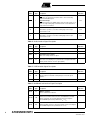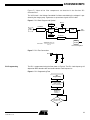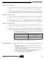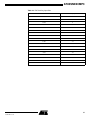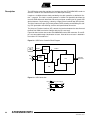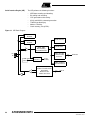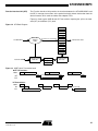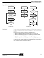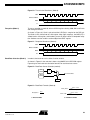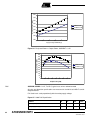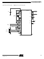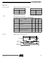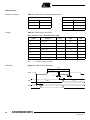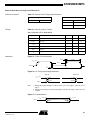
1
Features
• MPEG I/II-Layer 3 Hardwired Decoder
•
•
•
•
•
•
•
•
•
•
– Stand-alone MP3 Decoder
– 48, 44.1, 32, 24, 22.05, 16 kHz Sampling Frequency
– Separated Digital Volume Control on Left and Right Channels (Software Control
using 31 Steps)
– Bass, Medium, and Treble Control (31 Steps)
– Bass Boost Sound Effect
– Ancillary Data Extraction
– CRC Error and MPEG Frame Synchronization Indicators
20-bit Stereo Audio DAC
– 93 dB SNR Playback Stereo Channel
– 32 Ohm/ 20 mW Stereo Headset Drivers
– Stereo Line Level Input, Differential Mono Auxiliary Input
Programmable Audio Output for Interfacing with External Audio System
– I2S Format Compatible
Mono Audio Power Amplifier
– 440mW on 8 Ohms Load
USB Rev 1.1 Controller
– Full Speed Data Transmission
Built-in PLL
– MP3 Audio Clocks
– USB Clock
MultiMediaCard® Interface, Secure Digital Card Interface
Standard Full Duplex UART with Baud Rate Generator
Power Management
– Power-on Reset
– Idle Mode, Power-down Mode
Operating Conditions:
– 2.7 to 3V, ±10%, 25 mA Typical Operating at 25°C
– 37 mA Typical Operating at 25°C Playing Music on Earphone
– Temperature Range: -40°C to +85°C
– Power Amplifier Supply 3.2V to 5.5V
Packages
– CTBGA 100-pin
Typical
Applications
•
MP3-Player
•
PDA, Camera, Mobile Phone MP3
•
Car Audio/Multimedia MP3
•
Home Audio/Multimedia MP3
•
Toys
•
Industrial Background Music / Ads
Single-Chip MP3
Decoder with Full
Audio Interface
AT83SND2CMP3A1
AT83SND2CMP3
AT83SND2CDVX
Rev. 7524D–MP3–07/07
Description
The AT83SND2CMP3 has been developped as a versatile remote controlled MP3
player for very fast MP3 feature implementation into most existing system. It perfectly
fits features needed in mobile phones and toys, but can also be used in any portable
equipment and in industrial applications.
Audio files and any other data can be stored in a Nand Flash memory or in a removable
Flash card such as MultiMediaCard (MMC) or Secure Digital Card (SD). Music collections are very easy to build, as data can be stored using the standard FAT12/16 and
FAT32 file system.
Thanks to the USB port, data can be transferred and maintained from and to any computer based on Windows®, Linux® and Mac OS®.
File system is controlled by the AT83SND2CMP3 so the host controller does not have to
handle it.
In addition to the USB device port, the MP3 audio system can be connected to any
embedded host through a low cost serial link UART. Host controller can fully remote
control the MP3 decoder behaviour using a command protocol over the serial link.
File system is controlled by the AT83SND2CMP3 so host controller does not have to
handle it.
Files can also be uploaded or dowloaded from host environment to NAND Flash or
Flash Card.
2
AT83SND2CMP3
7524D–MP3–07/07
AT83SND2CMP3
Block Diagram
Figure 1. Block Diagram
VDD
VSS UVDD UVSS
3
FILT
X1
X2
Clock and PLL
Unit
Control Unit
Interrupt
Handler Unit
INT0
3
INT1
RST
D+
D-
P0-P4
X1
USB
Controller
X2
I/OPorts
MP3
Decoder
Unit
Keyboard
Interface
DOUT
DCLK
DSEL
I2S/PCM
Audio
Interface
SCLK
UART
and
BRG
Timers 0/1
Watchdog
HSR
HSL
AUXP
AUXN
KIN0
3
TXD
3
RXD
3
3
T0
T1
MCLK
Audio
DAC
SD / MMC
Interface
MDAT
LINEL
LINER
MONOP
MONON
PAINP
PAINN
HPP
HPN
Audio
PA
MCMD
3 Alternate function of Port 3
4 Alternate function of Port 4
3
7524D–MP3–07/07
Pin Description
Pinouts
Figure 3. AT83SND2CMP3 100-pin BGA Package
10
9
8
7
6
5
4
3
2
1
NC
NC
P2.0/
A8
P4.1/
VDD
VSS
NC
AUXP
AUXN
NC
A
VDD
P2.2/
A10
P2.1/
A9
P4.0/
P4.2/
MONON
MONOP
P0.0/
AD0
KIN0
NC
B
P2.4/
A12
P2.3/
A11
P2.5/
A13
P4.3/
P0.6/
AD6
P0.4/
AD4
P0.3/
AD3
P0.2/
AD2
P0.1/
AD1
NC
C
P2.6/
A14
P2.7/
A15
MCLK
NC
P0.7/
AD7
P0.5/
AD5
NC
NC
NC
NC
D
NC
VSS
VDD
ESDVSS
VDD
SDA
AUDVREF
SCL
HSL
AUDVDD
E
MCMD
MDAT
NC
P3.2/
INT0
P3.1/
TXD
VSS
FILT
PVDD
HSR
HSVDD
F
RST
AUDRST
SCLK
DSEL
P3.4/
T0
P3.0/
RXD
LINER
LINEL
PVSS
HSVSS
G
NC
VSS
DOUT
DCLK
P3.5/
T1
TST
X1
INGND
AUDVSS
H
VDD
AUDVSS
CBP
LPHN
P3.7/
RD
P3.6/
WR
VSS
D-
D+
AUDVCM
J
PAINP
PAINN
HPP
AUDVBAT
HPN
AUDVSS
P3.3/
INT1
VDD
UVDD
UVSS
X2
K
1. NC = Do Not Connect
4
AT83SND2CMP3
7524D–MP3–07/07
AT83SND2CMP3
Signals
All the AT83SND2CMP3 signals are detailed by functionality in following tables.
Table 1. Ports Signal Description
Signal
Name
Type
Description
P0.7:0
I/O
Port 0
P0 is an 8-bit open-drain bidirectional I/O port. Port 0 pins that have 1s
written to them float and can be used as high impedance inputs. To
avoid any parasitic current consumption, floating P0 inputs must be
polarized to VDD or VSS.
P2.7:0
I/O
Port 2
P2 is an 8-bit bidirectional I/O port with internal pull-ups.
Alternate
Function
AD7:0
A15:8
RXD
TXD
P3.7:0
I/O
Port 3
P3 is an 8-bit bidirectional I/O port with internal pull-ups.
P4.3:0
I/O
Port 4
P4 is an 8-bit bidirectional I/O port with internal pull-ups.
INT0
INT1
T0
T1
WR
RD
Table 2. Clock Signal Description
Signal
Name
Type
Description
Alternate
Function
X1
I
Input to the on-chip inverting oscillator amplifier
To use the internal oscillator, a crystal/resonator circuit is connected to
this pin. If an external oscillator is used, its output is connected to this
pin. X1 is the clock source for internal timing.
X2
O
Output of the on-chip inverting oscillator amplifier
To use the internal oscillator, a crystal/resonator circuit is connected to
this pin. If an external oscillator is used, leave X2 unconnected.
-
FILT
I
PLL Low Pass Filter input
FILT receives the RC network of the PLL low pass filter.
-
-
Table 3. Timer 0 and Timer 1 Signal Description
Signal
Name
Type
Description
Alternate
Function
Timer 0 Gate Input
INT0 serves as external run control for timer 0, when selected by
GATE0 bit in TCON register.
INT0
I
External Interrupt 0
INT0 input sets IE0 in the TCON register. If bit IT0 in this register is set,
bit IE0 is set by a falling edge on INT0#. If bit IT0 is cleared, bit IE0 is
set by a low level on INT0#.
P3.2
5
7524D–MP3–07/07
Signal
Name
Type
Alternate
Function
Description
Timer 1 Gate Input
INT1 serves as external run control for timer 1, when selected by
GATE1 bit in TCON register.
INT1
I
T0
I
Timer 0 External Clock Input
When timer 0 operates as a counter, a falling edge on the T0 pin
increments the count.
P3.4
T1
I
Timer 1 External Clock Input
When timer 1 operates as a counter, a falling edge on the T1 pin
increments the count.
P3.5
External Interrupt 1
INT1 input sets IE1 in the TCON register. If bit IT1 in this register is set,
bit IE1 is set by a falling edge on INT1#. If bit IT1 is cleared, bit IE1 is
set by a low level on INT1#.
P3.3
Table 4. Audio Interface Signal Description
Signal
Name
Type
Alternate
Function
DCLK
O
DAC Data Bit Clock
-
DOUT
O
DAC Audio Data Output
-
DSEL
O
DAC Channel Select Signal
DSEL is the sample rate clock output.
-
SCLK
O
DAC System Clock
SCLK is the oversampling clock synchronized to the digital audio data
(DOUT) and the channel selection signal (DSEL).
-
Description
Table 5. USB Controller Signal Description
Signal
Name
Type
Alternate
Function
D+
I/O
USB Positive Data Upstream Port
This pin requires an external 1.5 KΩ pull-up to VDD for full speed
operation.
-
D-
I/O
USB Negative Data Upstream Port
-
Description
Table 6. MutiMediaCard Interface Signal Description
6
Signal
Name
Type
Alternate
Function
MCLK
O
MMC Clock output
Data or command clock transfer.
-
MCMD
I/O
MMC Command line
Bidirectional command channel used for card initialization and data
transfer commands. To avoid any parasitic current consumption,
unused MCMD input must be polarized to VDD or VSS.
-
MDAT
I/O
MMC Data line
Bidirectional data channel. To avoid any parasitic current consumption,
unused MDAT input must be polarized to VDD or VSS.
-
Description
AT83SND2CMP3
7524D–MP3–07/07
AT83SND2CMP3
Table 7. UART Signal Description
Signal
Name
Type
RXD
I/O
Receive Serial Data
RXD sends and receives data in serial I/O mode 0 and receives data in
serial I/O modes 1, 2 and 3.
P3.0
TXD
O
Transmit Serial Data
TXD outputs the shift clock in serial I/O mode 0 and transmits data in
serial I/O modes 1, 2 and 3.
P3.1
Description
Alternate
Function
Table 8. Keypad Interface Signal Description
Signal
Name
Type
KIN0
I
Description
Keypad Input Line
Holding this pin high or low for 24 oscillator periods triggers a keypad
interrupt.
Alternate
Function
-
Table 9. System Signal Description
Signal
Name
Type
Description
RST
I
Reset Input
Holding this pin high for 64 oscillator periods while the oscillator is
running resets the device. The Port pins are driven to their reset
conditions when a voltage lower than VIL is applied, whether or not the
oscillator is running.
This pin has an internal pull-down resistor which allows the device to be
reset by connecting a capacitor between this pin and VDD.
Asserting RST when the chip is in Idle mode or Power-Down mode
returns the chip to normal operation.
TST
I
Test Input
Test mode entry signal. This pin must be set to VDD.
Alternate
Function
-
-
Table 10. Power Signal Description
Signal
Name
Type
Description
Alternate
Function
VDD
PWR
Digital Supply Voltage
Connect these pins to +3V supply voltage.
-
VSS
GND
Circuit Ground
Connect these pins to ground.
-
PVDD
PWR
PLL Supply voltage
Connect this pin to +3V supply voltage.
-
PVSS
GND
PLL Circuit Ground
Connect this pin to ground.
-
UVDD
PWR
USB Supply Voltage
Connect this pin to +3V supply voltage.
-
7
7524D–MP3–07/07
Signal
Name
Type
Description
UVSS
GND
USB Ground
Connect this pin to ground.
Alternate
Function
-
Table 11. Audio Power Signal Description
Signal
Name
Type
Description
Alternate
Function
AUDVDD
PWR
Audio Digital Supply Voltage
-
AUDVSS
GND
Audio Circuit Ground
Connect these pins to ground.
-
ESDVSS
GND
AUDVREF
PWR
Audio Voltage Reference pin for decoupling.
-
HSVDD
PWR
Headset Driver Power Supply.
-
HSVSS
GND
AUDVBAT
PWR
Audio Analog Circuit Ground for Electrostatic Discharge.
-
Connect this pin to ground.
Headset Driver Ground.
-
Connect this pin to ground.
Audio Amplifier Supply.
-
Table 12. Stereo Audio Dac and Mono Power Amplifier Signal Description
8
Signal
Name
Type
LPHN
O
Low Power Audio Stage Output
-
HPN
O
Negative Speaker Output
-
HPP
O
Positivie Speaker Output
-
CBP
O
Audio Amplifier Common Mode Voltage Decoupling
-
PAINN
I
Audio Amplifier Negative Input
-
PAINP
I
Audio Amplifier Positive Input
-
AUDRST
I
Audio Reset (Active Low)
-
MONON
O
Audio Negative Monaural Driver Output
-
MONOP
O
Audio Positive Monaural Driver Output
-
AUXP
I
Audio Mono Auxiliary Positive Input
-
AUXN
I
Audio Mono Auxiliary Negative Input
-
HSL
O
Audio Left Channel Headset Driver Output
-
HSR
O
Audio Right Channel Headset Driver Output
-
LINEL
I
Audio Left Channel Line In
-
LINER
I
Audio Right Channel Line In
-
INGND
I
Audio Line Signal Ground Pin for decoupling.
-
AUDVCM
I
Audio Common Mode reference for decoupling
-
Description
Alternate
Function
AT83SND2CMP3
7524D–MP3–07/07
AT83SND2CMP3
Internal Pin Structure
Table 13. Detailed Internal Pin Structure
Circuit(1)
Type
Pins
Input
TST
Input/Output
RST
Input/Output
P3
P4
Input/Output
P0
MCMD
MDAT
RTST
VDD
VDD
P
RRST
Watchdog Output
VSS
2 osc
periods
Latch Output
VDD
VDD
VDD
P1
P2
P3
N
VSS
VDD
P
N
VSS
ALE
SCLK
DCLK
VDD
P
Output
N
DOUT
DSEL
MCLK
VSS
D+
Input/Output
D+
D-
D-
Notes:
1. For information on resistors value, input/output levels, and drive capability, refer to
the DC Characteristics.
2. When the Two Wire controller is enabled, P3 transistors are disabled allowing pseudo
open-drain structure.
9
7524D–MP3–07/07
Clock Controller
The clock controller is based on an on-chip oscillator feeding an on-chip Phase Lock
Loop (PLL). All internal clocks to the peripherals and CPU core are generated by this
controller.
Oscillator
The X1 and X2 pins are the input and the output of a single-stage on-chip inverter (see
Figure 4) that can be configured with off-chip components such as a Pierce oscillator
(see Figure 5). Value of capacitors and crystal characteristics are detailed in the section
“DC Characteristics”.
The oscillator outputs three different clocks: a clock for the PLL, a clock for the CPU
core, and a clock for the peripherals as shown in Figure 4. These clocks are either
enabled or disabled, depending on the power reduction mode as detailed in the section.
The peripheral clock is used to generate the Timer 0, Timer 1, MMC, SPI, and Port sampling clocks.
Figure 4. Oscillator Block Diagram and Symbol
X1
0
÷2
Peripheral
Clock
1
CPU Core
Clock
X2
X2
CKCON.0
IDL
PCON.0
PD
Oscillator
Clock
PCON.1
PER
CLOCK
Peripheral Clock Symbol
CPU
CLOCK
OSC
CLOCK
CPU Core Clock Symbol
Oscillator Clock Symbol
Figure 5. Crystal Connection
X1
C1
Q
C2
VSS
X2
PLL
PLL Description
The PLL is used to generate internal high frequency clock (the PLL Clock) synchronized
with an external low-frequency (the Oscillator Clock). The PLL clock provides the MP3
decoder, the audio interface, and the USB interface clocks. Figure 6 shows the internal
structure of the PLL.
The PFLD block is the Phase Frequency Comparator and Lock Detector. This block
makes the comparison between the reference clock coming from the N divider and the
reverse clock coming from the R divider and generates some pulses on the Up or Down
signal depending on the edge position of the reverse clock. The PLLEN bit in PLLCON
register is used to enable the clock generation.
The CHP block is the Charge Pump that generates the voltage reference for the VCO by
injecting or extracting charges from the external filter connected on PFILT pin (see
10
AT83SND2CMP3
7524D–MP3–07/07
AT83SND2CMP3
Fi gure 7) . Value of the filter components ar e detailed in the Section “ DC
Characteristics”.
The VCO block is the Voltage Controlled Oscillator controlled by the voltage Vref produced by the charge pump. It generates a square wave signal: the PLL clock.
Figure 6. PLL Block Diagram and Symbol
PFILT
PLLCON.1
PLLEN
N divider
OSC
CLOCK
Up
N6:0
PFLD
CHP
Vref
VCO
Down
PLOCK
PLL
Clock
R divider
PLLCON.0
R9:0
PLL
CLOCK
OSCclk × ( R + 1 )
PLLclk = ----------------------------------------------N+1
PLL Clock Symbol
Figure 7. PLL Filter Connection
FILT
R
C2
C1
VSS
PLL Programming
VSS
The PLL is programmed using the flow shown in Figure 8. The PLL clock frequency will
depend on MP3 decoder clock and audio interface clock frequencies.
Figure 8. PLL Programming Flow
PLL
Programming
Configure Dividers
N6:0 = xxxxxxb
R9:0 = xxxxxxxxxxb
Enable PLL
PLLRES = 0
PLLEN = 1
PLL Locked?
PLOCK = 1?
11
7524D–MP3–07/07
MP3 Decoder
The product implements a MPEG I/II audio layer 3 decoder better known as MP3
decoder.
In MPEG I (ISO 11172-3) three layers of compression have been standardized supporting three sampling frequencies: 48, 44.1, and 32 kHz. Among these layers, layer 3
allows highest compression rate of about 12:1 while still maintaining CD audio quality.
For example, 3 minutes of CD audio (16-bit PCM, 44.1 kHz) data, which needs about
32M bytes of storage, can be encoded into only 2.7M bytes of MPEG I audio layer 3
data.
In MPEG II (ISO 13818-3), three additional sampling frequencies: 24, 22.05, and 16 kHz
are supported for low bit rates applications.
The AT83SND2CMP3 can decode in real-time the MPEG I audio layer 3 encoded data
into a PCM audio data, and also supports MPEG II audio layer 3 additional frequencies.
Additional features are supported by the AT83SND2CMP3 MP3 decoder such as volume control, bass, medium, and treble controls, bass boost effect and ancillary data
extraction.
Decoder
Description
The core interfaces to the MP3 decoder through nine special function registers:
MP3CON, the MP3 Control register; MP3STA, the MP3 Status register; MP3DAT, the
MP3 Data register; MP3ANC, the Ancillary Data register; MP3VOL and MP3VOR, the
MP3 Volume Left and Right Control registers; MP3BAS, MP3MED, and MP3TRE, the
MP3 Bass, Medium, and Treble Control registers; and MPCLK, the MP3 Clock Divider
register.
Figure 9 shows the MP3 decoder block diagram.
Figure 9. MP3 Decoder Block Diagram
Audio Data
From C51
8
1K Bytes
Frame Buffer
MP3DAT
Header Checker
Huffman Decoder
MPxREQ
ERRxxx MPFS1:0 MPVER
MP3STA1.n
MP3STA.5:3 MP3STA.2:1 MP3STA.0
Dequantizer
Stereo Processor
Side Information
MP3
CLOCK
Ancillary Buffer
MP3ANC
MPEN
MP3CON.7
Anti-Aliasing
MPBBST
MP3CON.6
12
MP3VOL
IMDCT
MP3VOR
MP3BAS
Sub-band
Synthesis
MP3MED
16
Decoded Data
To Audio Interface
MP3TRE
AT83SND2CMP3
7524D–MP3–07/07
AT83SND2CMP3
MP3 Data
The MP3 decoder does not start any frame decoding before having a complete frame in
its input buffer(1). In order to manage the load of MP3 data in the frame buffer, a hardware handshake consisting of data request and data acknowledgment is implemented.
Each time the MP3 decoder needs MP3 data, it sets the MPREQ, MPFREQ and
MPBREQ flags respectively in MP3STA and MP3STA1 registers. MPREQ flag can generate an interrupt if enabled as explained in Section “Interrupt”. The CPU must then load
data in the buffer by writing it through MP3DAT register thus acknowledging the previous request. As shown in Figure 10, the MPFREQ flag remains set while data (i.e a
frame) is requested by the decoder. It is cleared when no more data is requested and
set again when new data are requested. MPBREQ flag toggles at every Byte writing.
Note:
1. The first request after enable, consists in 1024 Bytes of data to fill in the input buffer.
Figure 10. Data Timing Diagram
MPREQ Flag
Cleared when Reading MP3STA
MPFREQ Flag
MPBREQ Flag
Write to MP3DAT
MP3 Clock
The MP3 decoder clock is generated by division of the PLL clock. The division factor is
given by MPCD4:0 bits in MP3CLK register. Figure 11 shows the MP3 decoder clock
generator and its calculation formula. The MP3 decoder clock frequency depends only
on the incoming MP3 frames.
Figure 11. MP3 Clock Generator and Symbol
MP3CLK
PLL
CLOCK
MPCD4:0
MP3
CLOCK
MP3 Decoder Clock
MP3 Clock Symbol
PLLclk
MP3clk = ---------------------------MPCD + 1
As soon as the frame header has been decoded and the MPEG version extracted, the
minimum MP3 input frequency must be programmed according to Table 14.
Table 14. MP3 Clock Frequency
MPEG Version
Minimum MP3 Clock (MHz)
I
21
II
10.5
13
7524D–MP3–07/07
Audio Controls
Volume Control
The MP3 decoder implements volume control on both right and left channels. The
MP3VOR and MP3VOL registers allow a 32-step volume control according to Table 15.
Table 15. Volume Control
Equalization Control
VOL4:0 or VOR4:0
Volume Gain (dB)
00000
Mute
00001
-33
00010
-27
11110
-1.5
11111
0
Sound can be adjusted using a 3-band equalizer: a bass band under 750 Hz, a medium
band from 750 Hz to 3300 Hz and a treble band over 3300 Hz. The MP3BAS, MP3MED,
and MP3TRE registers allow a 32-step gain control in each band according to Table 16.
Table 16. Bass, Medium, Treble Control
14
BAS4:0 or MED4:0 or TRE4:0
Gain (dB)
00000
-∞
00001
-14
00010
-10
11110
+1
11111
+1.5
AT83SND2CMP3
7524D–MP3–07/07
AT83SND2CMP3
Frame Information
The MP3 frame header contains information on the audio data contained in the frame.
These informations is made available in the MP3STA register for you information.
MPVER and MPFS1:0 bits allow decoding of the sampling frequency according to
Table 17. MPVER bit gives the MPEG version (2 or 1).
Table 17. MP3 Frame Frequency Sampling
Ancillary Data
MPVER
MPFS1
MPFS0
Fs (kHz)
0
0
0
22.05 (MPEG II)
0
0
1
24 (MPEG II)
0
1
0
16 (MPEG II)
0
1
1
Reserved
1
0
0
44.1 (MPEG I)
1
0
1
48 (MPEG I)
1
1
0
32 (MPEG I)
1
1
1
Reserved
MP3 frames also contain data bits called ancillary data. These data are made available
in the MP3ANC register for each frame. As shown in Figure 12, the ancillary data are
available by Bytes when MPANC flag in MP3STA register is set. MPANC flag is set
when the ancillary buffer is not empty (at least one ancillary data is available) and is
cleared only when there is no more ancillary data in the buffer. This flag can generate an
interrupt as explained in Section “Interrupt”. When set, software must read all Bytes to
empty the ancillary buffer.
Figure 12. Ancillary Data Block Diagram
Ancillary
Data To C51
8
MP3ANC
8
7-Byte
Ancillary Buffer
MPANC
MP3STA.7
15
7524D–MP3–07/07
Audio Output
Interface
The product implements an audio output interface allowing the audio bitstream to be
output in various formats. It is compatible with right and left justification PCM and I2S formats and thanks to the on-chip PLL (see Section “Clock Controller”, page 10) allows
connection of almost all of the commercial audio DAC families available on the market.
The audio bitstream can be from 2 different types:
Description
•
The MP3 decoded bitstream coming from the MP3 decoder for playing songs.
•
The audio bitstream coming from the MCU for outputting voice or sounds.
The control unit core interfaces to the audio interface through five special function registers: AUDCON0 and AUDCON1, the Audio Control registers ; AUDSTA, the Audio
Status register; AUDDAT, the Audio Data register; and AUDCLK, the Audio Clock
Divider register.
Figure 13 shows the audio interface block diagram, blocks are detailed in the following
sections.
Figure 13. Audio Interface Block Diagram
SCLK
AUD
CLOCK
DCLK
Clock Generator
0
DSEL
AUDEN
1
AUDCON1.0
Data Ready
HLR
DSIZ
AUDCON0.0
AUDCON0.1
POL
AUDCON0.2
Audio Data
From MP3
Decoder
16
MP3 Buffer
16
0
16
Sample
Request To
MP3 Decoder
DRQEN
AUDCON1.6
Data Converter
DOUT
1
JUST4:0
SRC
AUDCON0.7:3
AUDCON1.7
SREQ
Audio Data
From C51
8
Audio Buffer
AUDDAT
AUDSTA.7
UDRN
AUDSTA.6
AUBUSY
DUP1:0
AUDSTA.5
AUDCON1.2:1
16
AT83SND2CMP3
7524D–MP3–07/07
AT83SND2CMP3
Clock Generator
The audio interface clock is generated by division of the PLL clock. The division factor is
given by AUCD4:0 bits in CLKAUD register. Figure 14 shows the audio interface clock
generator and its calculation formula. The audio interface clock frequency depends on
the incoming MP3 frames and the audio DAC used.
Figure 14. Audio Clock Generator and Symbol
AUDCLK
PLL
CLOCK
AUCD4:0
Audio Interface Clock
AUD
CLOCK
Audio Clock Symbol
PLLclk
AUDclk = --------------------------AUCD + 1
As soon as audio interface is enabled by setting AUDEN bit in AUDCON1 register, the
master clock generated by the PLL is output on the SCLK pin which is the DAC system
clock. This clock is output at 256 or 384 times the sampling frequency depending on the
DAC capabilities. HLR bit in AUDCON0 register must be set according to this rate for
properly generating the audio bit clock on the DCLK pin and the word selection clock on
the DSEL pin. These clocks are not generated when no data is available at the data
converter input.
For DAC compatibility, the bit clock frequency is programmable for outputting 16 bits or
32 bits per channel using the DSIZ bit in AUDCON0 register (see Section "Data Converter", page 17), and the word selection signal is programmable for outputting left
channel on low or high level according to POL bit in AUDCON0 register as shown in
Figure 15.
Figure 15. DSEL Output Polarity
Data Converter
POL = 0
Left Channel
Right Channel
POL = 1
Left Channel
Right Channel
The data converter block converts the audio stream input from the 16-bit parallel format
to a serial format. For accepting all PCM formats and I 2 S format, JUST4:0 bits in
AUDCON0 register are used to shift the data output point. As shown in Figure 16, these
bits allow MSB justification by setting JUST4:0 = 00000, LSB justification by setting
JUST4:0 = 10000, I2S Justification by setting JUST4:0 = 00001, and more than 16-bit
LSB justification by filling the low significant bits with logic 0.
17
7524D–MP3–07/07
Figure 16. Audio Output Format
DSEL
DCLK
DOUT
Left Channel
1
2
3
Right Channel
13
14
15
LSB MSB B14
16
B1
1
2
3
13
14
15
LSB MSB B14
16
B1
I2S Format with DSIZ = 0 and JUST4:0 = 00001.
DSEL
DCLK
Left Channel
1
DOUT
2
Right Channel
3
17
MSB B14
LSB
18
32
1
2
3
17
MSB B14
LSB
18
32
I2S Format with DSIZ = 1 and JUST4:0 = 00001.
DSEL
DCLK
DOUT
Left Channel
1
2
3
Right Channel
13
14
MSB B14
15
B1
16
1
2
3
13
14
LSB MSB B15
15
B1
16
LSB
MSB/LSB Justified Format with DSIZ = 0 and JUST4:0 = 00000.
DSEL
DCLK
Left Channel
1
16
DOUT
17
Right Channel
18
31
MSB B14
B1
32
1
16
LSB
17
18
31
MSB B14
B1
32
LSB
16-bit LSB Justified Format with DSIZ = 1 and JUST4:0 = 10000.
DSEL
DCLK
DOUT
Left Channel
1
15
16
MSB B16
Right Channel
30
B2
31
B1
32
LSB
1
15
16
MSB B16
30
B2
31
B1
32
LSB
18-bit LSB Justified Format with DSIZ = 1 and JUST4:0 = 01110.
The data converter receives its audio stream from 2 sources selected by the SRC bit in
AUDCON1 register. When cleared, the audio stream comes from the MP3 decoder (see
Section “MP3 Decoder”, page 12) for song playing. When set, the audio stream is coming from the C51 core for voice or sound playing.
As soon as first audio data is input to the data converter, it enables the clock generator
for generating the bit and word clocks.
Audio Buffer
In voice or sound playing mode, the audio stream comes from the C51 core through an
audio buffer. The data is in 8-bit format and is sampled at 8 kHz. The audio buffer
adapts the sample format and rate. The sample format is extended to 16 bits by filling
the LSB to 00h. Rate is adapted to the DAC rate by duplicating the data using DUP1:0
bits in AUDCON1 register according to Table 18.
The audio buffer interfaces to the C51 core through three flags: the sample request flag
(SREQ in AUDSTA register), the under-run flag (UNDR in AUDSTA register) and the
busy flag (AUBUSY in AUDSTA register). SREQ and UNDR can generate an interrupt
request as explained in Section "Interrupt Request", page 19. The buffer size is 8 Bytes
large. SREQ is set when the samples number switches from 4 to 3 and reset when the
samples number switches from 4 to 5; UNDR is set when the buffer becomes empty signaling that the audio interface ran out of samples; and AUBUSY is set when the buffer is
full.
18
AT83SND2CMP3
7524D–MP3–07/07
AT83SND2CMP3
Table 18. Sample Duplication Factor
DUP1
DUP0
Factor
0
0
No sample duplication, DAC rate = 8 kHz (C51 rate).
0
1
One sample duplication, DAC rate = 16 kHz (2 x C51 rate).
1
0
2 samples duplication, DAC rate = 32 kHz (4 x C51 rate).
1
1
Three samples duplication, DAC rate = 48 kHz (6 x C51 rate).
MP3 Buffer
In song playing mode, the audio stream comes from the MP3 decoder through a buffer.
The MP3 buffer is used to store the decoded MP3 data and interfaces to the decoder
through a 16-bit data input and data request signal. This signal asks for data when the
buffer has enough space to receive new data. Data request is conditioned by the
DREQEN bit in AUDCON1 register. When set, the buffer requests data to the MP3
decoder. When cleared no more data is requested but data are output until the buffer is
empty. This bit can be used to suspend the audio generation (pause mode).
Interrupt Request
The audio interrupt request can be generated by 2 sources when in C51 audio mode: a
sample request when SREQ flag in AUDSTA register is set to logic 1, and an under-run
condition when UDRN flag in AUDSTA register is set to logic 1. Both sources can be
enabled separately by masking one of them using the MSREQ and MUDRN bits in
AUDCON1 register. A global enable of the audio interface is provided by setting the
EAUD bit in IEN0 register.
The interrupt is requested each time one of the 2 sources is set to one. The source flags
are cleared by writing some data in the audio buffer through AUDDAT, but the global
audio interrupt flag is cleared by hardware when the interrupt service routine is
executed.
Figure 17. Audio Interface Interrupt System
UDRN
AUDSTA.6
Audio
Interrupt
Request
MUDRN
AUDCON1.4
SREQ
EAUD
AUDSTA.7
IEN0.6
MSREQ
AUDCON1.5
MP3 Song Playing
In MP3 song playing mode, the operations to do are to configure the PLL and the audio
interface according to the DAC selected. The audio clock is programmed to generate
the 256·Fs or 384·Fs as explained in Section "Clock Generator", page 17. Figure 18
shows the configuration flow of the audio interface when in MP3 song mode.
19
7524D–MP3–07/07
Figure 18. MP3 Mode Audio Configuration Flow
MP3 Mode
Configuration
Program Audio Clock
Configure Interface
HLR = X
DSIZ = X
POL = X
JUST4:0 = XXXXXb
SRC = 0
20
Enable DAC System
Clock
AUDEN = 1
Wait For
DAC Set-up Time
Enable Data Request
DRQEN = 1
AT83SND2CMP3
7524D–MP3–07/07
AT83SND2CMP3
DAC and PA Interface
The AT83SND2CMP3 implements a stereo Audio Digital-to-Analog Converter and
Audio Power Amplifier targeted for Li-Ion or Ni-Mh battery powered devices.
Figure 19. Audio Interface Block Diagram
MP3
Decoder
Unit
DOUT
DCLK
DSEL
I2S/PCM
Audio
Interface
HSR
HSL
AUXP
AUXN
Audio
DAC
LINEL
LINER
MONOP
MONON
PAINP
PAINN
HPP
HPN
DAC
Serial Audio Interface
SCLK
AUDCDIN
AUDCDOUT
AUDCCLK
AUDCCS
Audio
PA
The Stereo DAC section is a complete high performance, stereo, audio digital-to-analog
converter delivering 93 dB Dynamic Range. It comprises a multibit sigma-delta modulator with dither, continuous time analog filters and analog output drive circuitry. This
architecture provides a high insensitivity to clock jitter. The digital interpolation filter
increases the sample rate by a factor of 8 using 3 linear phase half-band filters cascaded, followed by a first order SINC interpolator with a factor of 8. This filter eliminates
the images of baseband audio, remaining only the image at 64x the input sample rate,
which is eliminated by the analog post filter. Optionally, a dither signal can be added that
may reduce eventual noise tones at the output. However, the use of a multibit sigmadelta modulator already provides extremely low noise tones energy.
Master clock is 128 up to 512 times the input data rate allowing choice of input data rate
up to 50 kHz, including standard audio rates of 48, 44.1, 32, 16 and 8 kHz. The DAC
section is followed by a volume and mute control and can be simultaneously played
back directly through a Stereo 32Ω Headset pair of drivers. The Stereo 32Ω Headset
pair of drivers also includes a mixer of a LINEL and LINER pair of stereo inputs as well
as a differential monaural auxiliary input (line level).
21
7524D–MP3–07/07
DAC Features
• 20 bit D/A Conversion
• 72dB Dynamic Range, -75dB THD Stereo line-in or microphone interface with 20dB
•
•
•
•
•
•
amplification
93dB Dynamic Range, -80dB THD Stereo D/A conversion
74dB Dynamic Range / -65dB THD for 20mW output power over 32 Ohm loads
Stereo, Mono and Reverse Stereo Mixer
Left/Right speaker short-circuit detection flag
Differential mono auxiliary input amplifier and PA driver
Audio sampling rates (Fs): 16, 22.05, 24, 32, 44.1 and 48 kHz.
Figure 20. Stereo DAC functional diagram
PA Gain
MONOP
PADRV
+
MONON
AUXP
AUX
AUXN
AUXG Gain
LINEL
PGA
LLIG,RLIG Gain
20,12 to -33 dB
(3dB)
LINER
PGA
Line Out Gain
LLOG, RLOG
0 to -46.5dB
(1.5dB)
Master Playback
Gain
12 to -34dB (1.5dB)
Volume
Control
Volume
Control
DSEL
SPKR
DRV
32
HSL
+
DAC
+
Digital Filter
SCLK
Serial to
Parallel
Interface
DAC_OLC Gain
6 to -6dB (3dB)
SPKR
DRV
32
HSR
+
DAC
Volume
Control
+
Volume
Control
Digital Filter
DCLK
DOUT
Digital Signals Timing
Data Interface
To avoid noises at the output, the reset state is maintained until proper synchronism is
achieved in the DAC serial interface:
•
DSEL
•
SCLK
•
DCLK
•
DOUT
The data interface allows three different data transfer modes:
22
AT83SND2CMP3
7524D–MP3–07/07
AT83SND2CMP3
Figure 21. 20 bit I2S justified mode
SCLK
DSEL
DOUT
R1
R0
L(N-1)
L(N-2)
L(N-3)
...
L2
L1
L0
R(N-1)
R(N-2)
R(N-3)
...
R2
R1
R0
L(N-3)
...
L2
L1
L0
R(N-1)
R(N-2)
R(N-3)
...
R2
R1
R0
L(N-1)
...
L1
L0
Figure 22. 20 bit MSB justified mode
SCLK
DSEL
DOUT
R0
L(N-1)
L(N-2)
Figure 23. 20 bit LSB justified mode
SCLK
DSEL
DOUT
R0
L(N-1)
L(N-2)
R(N-1)
R(N-2)
...
R1
R0
L(N-1)
The selection between modes is done using the DINTSEL 1:0 in DAC_MISC register
(Table 40.) according with the following table:
DINTSEL 1:0
Format
00
I2S Justified
01
MSB Justified
1x
LSB Justified
The data interface always works in slave mode. This means that the DSEL and the
DCLK signals are provided by microcontroller audio data interface.
Serial Audio DAC Interface
The serial audio DAC interface is a Synchronous Peripheral Interface (SPI) in slave
mode:
•
AUDCDIN: is used to transfer data in series from the master to the slave DAC.
It is driven by the master.
•
AUDCDOUT: is used to transfer data in series from the slave DAC to the master.
It is driven by the selected slave DAC.
•
Serial Clock (AUDCCLK): it is used to synchronize the data transmission both in
and out the devices through the AUDCDIN and AUDCDOUT lines.
Note:
Refer to Table 29. for DAC SPI Interface Description
23
7524D–MP3–07/07
Audio
DAC
Serial Audio Interface
Figure 24. Serial Audio Interface
AUDCDIN
AUDCDOUT
AUDCCLK
AUDCCS
Audio
PA
Protocol is as following to access DAC registers:
Figure 25. Dac SPI Interface
AUDCCS
AUDCCLK
rw a6 a5 a4 a3 a2 a1 a0 d7 d6 d5 d4 d3 d2 d1 d0
AUDCDIN
AUDCDOUT
DAC Interface SPI Protocol
d7 d6 d5 d4 d3 d2 d1 d0
On AUDCDIN, the first bit is a read/write bit. 0 indicates a write operation while 1 is for a
read operation. The 7 following bits are used for the register address and the 8 last ones
are the write data. For both address and data, the most significant bit is the first one.
In case of a read operation, AUDCDOUT provides the contents of the read register,
MSB first.
The transfer is enabled by the AUDCCS signal active low. The interface is resetted at
every rising edge of AUDCCS in order to come back to an idle state, even if the transfer
does not succeed. The DAC Interface SPI is synchronized with the serial clock AUDC-
24
AT83SND2CMP3
7524D–MP3–07/07
AT83SND2CMP3
CLK. Falling edge latches AUDCDIN input and rising edge shifts AUDCDOUT output
bits.
Note that the DLCK must run during any DAC SPI interface access (read or write).
Figure 26. DAC SPI Interface Timings
AUDCCS
Tc
Tssen
Thsen
Twl
AUDCCLK
Twh
Tssdi
Thsdi
AUDCDIN
Tdsdo
Thsdo
AUDCDOUT
Table 19. Dac SPI Interface Timings
Timing parameter
Description
Min
Max
Tc
AUDCCLK min period
150 ns
-
Twl
AUDCCLK min pulse width low
50 ns
-
Twh
AUDCCLK min pulse width high
50 ns
-
Tssen
Setup time AUDCCS falling to AUDCCLK rising
50 ns
-
Thsen
Hold time AUDCCLK falling to AUDCCS rising
50 ns
-
Tssdi
Setup time AUDCDIN valid to AUDCCLK falling
20 ns
-
Thsdi
Hold time AUDCCLK falling to AUDCDIN not valid
20 ns
-
Tdsdo
Delay time AUDCCLK rising to AUDCDOUT valid
-
20 ns
Thsdo
Hold time AUDCCLK rising to AUDCDOUT not valid
0 ns
-
25
7524D–MP3–07/07
DAC Register Tables
DAC Gain
Table 20. DAC Register Address
Address
Register
00h
DAC_CTRL
01h
Name
Access
Reset state
Dac Control
Read/Write
00h
DAC_LLIG
Dac Left Line in Gain
Read/Write
05h
02h
DAC_RLIG
Dac Right Line in Gain
Read/Write
05h
03h
DAC_LPMG
Dac Left Master Playback Gain
Read/Write
08h
04h
DAC_RPMG
Dac Right Master Playback Gain
Read/Write
08h
05h
DAC_LLOG
Dac Left Line Out Gain
Read/Write
00h
06h
DAC_RLOG
Dac Right Line Out Gain
Read/Write
00h
07h
DAC_OLC
Dac Output Level Control
Read/Write
22h
08h
DAC_MC
Dac Mixer Control
Read/Write
09h
09h
DAC_CSFC
Dac Clock and Sampling Frequency
Control
Read/Write
00h
0Ah
DAC_MISC
Dac Miscellaneous
Read/Write
00h
0Ch
DAC_PRECH
Dac Precharge Control
Read/Write
00h
0Dh
DAC_AUXG
Dac Auxilary input gain Control
Read/Write
05h
10h
DAC_RST
Dac Reset
Read/Write
00h
11h
PA_CRTL
Power Amplifier Control
Read/Write
00h
The DAC implements severals gain control: line-in (Table 21.), master playback (), lineout (Table 24.).
Table 21. Line-in gain
LLIG 4:0
26
RLIG 4:0
Gain (dB)
00000
20
00001
12
00010
9
00011
6
00100
3
00101
0
00110
-3
00111
-6
01000
-9
01001
-12
01010
-15
01011
-18
01100
-21
AT83SND2CMP3
7524D–MP3–07/07
AT83SND2CMP3
Table 21. Line-in gain (Continued)
01101
-24
01110
-27
01111
-30
10000
-33
10001
< -60
Table 22. Master Playback Gain
LMPG 5:0
RMPG 5:0
Gain (dB)
000000
12.0
000001
10.5
000010
9.0
000011
7.5
000100
6.0
000101
4.5
000110
3.0
000111
1.5
001000
0.0
001001
-1.5
001010
-3.0
001011
-4.5
001100
-6.0
001101
-7.5
001110
-9.0
001111
-10.5
010000
-12.0
010001
-13.5
010010
-15.0
010011
-16.5
010100
-18.0
010101
-19.5
010110
-21.0
010111
-22.5
011000
-24.0
011001
-25.5
27
7524D–MP3–07/07
Table 22. Master Playback Gain (Continued)
LMPG 5:0
RMPG 5:0
Gain (dB)
011010
-27.0
011011
-28.5
011100
-30.0
011101
-31.5
011110
-33.0
011111
-34.5
100000
mute
Table 23. Line-out Gain
LLOG 5:0
28
RLOG 5:0
Gain (dB)
000000
0.0
000001
-1.5
000010
-3.0
000011
-4.5
000100
-6.0
000101
-7.5
000110
-9.0
000111
-10.5
001000
-12.0
001001
-13.5
001010
-15.0
001011
-16.5
001100
-18.0
001101
-19.5
001110
-21.0
001111
-22.5
010000
-24.0
010001
-25.5
010010
-27.0
010011
-28.5
010100
-30.0
010101
-31.5
010110
-33.0
AT83SND2CMP3
7524D–MP3–07/07
AT83SND2CMP3
Table 23. Line-out Gain (Continued)
010111
-34.5
011000
-36.0
011001
-37.5
011010
-39.0
011011
-40.5
011100
-42.0
011101
-43.5
011110
-45.0
011111
-46.5
100000
mute
Table 24. DAC Output Level Control
LOLC 2:0
Digital Mixer Control
ROLC 2:0
Gain (dB)
000
6
001
3
010
0
011
-3
100
-6
The Audio DAC features a digital mixer that allows the mixing and selection of multiple
input sources.
The mixing / multiplexing functions are described in the following table according with
the next figure:
Figure 27. Mixing / Multiplexing functions
Left channel
Volume
Control
1
+
Volume
Control
2
From digital
filters
To DACs
1
Volume
Control
+
2
Volume
Control
Right channel
Note:
Whenever the two mixer inputs are selected, a –6 dB gain is applied to the output signal.
Whenever only one input is selected, no gain is applied.
29
7524D–MP3–07/07
Signal
Description
LMSMIN1
Left Channel Mono/Stereo Mixer Left Mixed input enable – High to enable, Low to disable
LMSMIN2
Left Channel Mono/Stereo Mixer Right Mixed input enable – High to enable, Low to
disable
RMSMIN1
Right Channel Mono/Stereo Mixer Left Mixed input enable – High to enable, Low to
disable
RMSMIN2
Right Channel Mono/Stereo Mixer Right Mixed input enable – High to enable, Low to
disable
Note:
Master Clock and Sampling
Frequency Selection
Refer to DAC_MC register Table 38. for signal description
The following table describes the different modes available for master clock and sampling frequency selection by setting OVRSEL bit in DAC_CSFC register (refer to Table
39.).
Table 25. Master Clock selection
OVRSEL
Master Clock
0
256 x FS
1
384 x FS
The selection of input sample size is done using the NBITS 1:0 in DAC_MISC register
(refer to Table 40.) according to Table 26.
Table 26. Input Sample Size Selection
NBITS 1:0
Format
00
16 bits
01
18 bits
10
20 bits
The selection between modes is done using DINTSEL 1:0 in DAC_MISC register (refer
to Table 40.) according to Table 27.
Table 27. Format Selection
De-emphasis and dither
enable
DINTSEL 1:0
Format
00
I2S Justified
01
MSB Justified
1x
LSB Justified
The circuit features a de-emphasis filter for the playback channel. To enable the deemphasis filtering, DEEMPEN must be set to high.
Likewise, the dither option (added in the playback channel) is enabled by setting the
DITHEN signal to High.
30
AT83SND2CMP3
7524D–MP3–07/07
AT83SND2CMP3
Table 28. DAC Auxlilary Input Gain
AUXG 4:0
Gain (dB)
00000
20
00001
12
00010
9
00011
6
00100
3
00101
0
00110
-3
00111
-6
01000
-9
01001
-12
01010
-15
01011
-18
01100
-21
01101
-24
01110
-27
01111
-30
10000
-33
10001
<-60
31
7524D–MP3–07/07
Register
Table 29. AUXCON Register
AUXCON (S:90h) – Auxiliary Control Register
7
6
5
4
3
2
1
0
SDA
SCL
-
AUDCDOUT
AUDCDIN
AUDCCLK
AUDCCS
KIN0
Bit
Number
Bit
Mnemonic
7
SDA
Description
TWI Serial Data
SDA is the bidirectional Two Wire data line.
TWI Serial Clock
When TWI controller is in master mode, SCL outputs the serial clock to the
slave peripherals. When TWI controller is in slave mode, SCL receives clock
from the master controller.
6
SCL
5
-
4
AUDCDOUT
3
AUDCDIN
Audio Dac SPI Data Input
2
AUDCCLK
Audio Dac SPI clock
1
AUDCCS
Not used.
Audio Dac SPI Data Output.
Audio Dac Chip select
Set to deselect DAC
Clear to select DAC
0
KIN0
Keyboard Input Interrupt.
Reset Value = 1111 1111b
32
AT83SND2CMP3
7524D–MP3–07/07
AT83SND2CMP3
Table 30. Dac Control Register Register - DAC_CTRL (00h)
7
6
5
4
3
2
1
0
ONPADRV
ONAUXIN
ONDACR
ONDACL
ONLNOR
ONLNOL
ONLNIR
ONLNIL
Bit
Bit
Number
Mnemonic
7
ONPADRV
6
ONAUXIN
5
ONDACR
4
ONDACL
3
ONLNOR
2
ONLNOL
1
ONLNIR
0
ONLNIL
Description
Differential mono PA driver
Clear to power down. Set to power up.
Differential mono auxiliary input amplifier
Clear to power down. Set to power up.
Right channel DAC
Clear to power down. Set to power up.
Left channel DAC
Clear to power down. Set to power up.
Right channel line out driver
Clear to power down. Set to power up.
Left channel line out driver
Clear to power down. Set to power up.
Right channel line in amplifier
Clear to power down. Set to power up.
Left channel line in amplifier
Clear to power down. Set to power up.
Reset Value = 00000000b
Table 31. DAC Left Line In Gain Register - DAC_LLIG (01h)
7
6
5
4
3
2
1
0
-
-
-
LLIG4
LLIG3
LLIG2
LLIG1
LLIG0
Bit
Bit
Number
Mnemonic
7:5
-
4:0
LLIG 4:0
Description
Not used
Left channel line in analog gain selector
Reset Value = 00000101b
33
7524D–MP3–07/07
Table 32. DAC Right Line In Gain Register - DAC_RLIG (02h)
7
6
5
4
3
2
1
0
-
-
-
RLIG4
RLIG3
RLIG2
RLIG1
RLIG0
Bit
Number
Description
Bit Mnemonic
7:5
-
Not used
4:0
RLIG 4:0
Right channel line in analog gain selector
Reset Value = 0000101b
Table 33. DAC Left Master Playback Gain Register - DAC_LMPG (03h)
7
6
5
4
3
2
1
0
-
-
LMPG5
LMPG4
LMPG3
LMPG2
LMPG1
LMPG0
Bit
Number
Bit
Mnemonic
7:6
-
5:0
LMPG 5:0
Description
Not used
Left channel master playback digital gain selector
Reset Value = 00001000b
Table 34. DAC Right Master Playback Gain Register - DAC_RMPG (04h)
7
6
5
4
3
2
1
0
-
-
RMPG5
RMPG4
RMPG3
RMPG2
RMPG1
RMPG0
Bit
Number
Description
Bit
Mnemonic
7:6
-
Not used
5:0
RMPG 5:0
Right channel master playback digital gain selector
Reset Value = 00001000b
Table 35. DAC Left Line Out Gain Register - DAC_LLOG (05h)
7
6
5
4
3
2
1
0
-
-
LLOG5
LLOG4
LLOG3
LLOG2
LLOG1
LLOG0
Bit
Number
Bit
Mnemonic
7:6
-
5:0
LLOG 5:0
Description
Not used
Left channel line out digital gain selector
Reset Value = 00000000b
34
AT83SND2CMP3
7524D–MP3–07/07
AT83SND2CMP3
Table 36. DAC Rigth Line Out Gain Register - DAC_RLOG (06h)
7
6
5
4
3
2
1
0
-
-
RLOG5
RLOG4
RLOG3
RLOG2
RLOG1
RLOG0
Bit
Number
Description
Bit
Mnemonic
7:6
-
5:0
Not used
RLOG 5:0
Right channel line out digital gain selector
Reset Value = 00000000b
Table 37. DAC Output Level Control Register - DAC_OLC (07h)
7
6
5
4
3
2
1
0
RSHORT
ROLC2
RLOC1
RLOC0
LSHORT
LOLC2
LOLC1
LOLC0
Bit
Number
Bit
Mnemonic
7
RSHORT
Description
Right channel short circuit indicator (persistent; after being set, bit is not
cleared automatically even after the short circuit is eliminated; must be
cleared by reset cycle or direct register write operation)
6:4
ROLC 2:0
3
LSHORT
Right channel output level control selector
Left channel short circuit indicator (persistent; after being set, bit is not
cleared automatically even after the short circuit is eliminated; must be
cleared by reset cycle or direct register write operation)
2:0
LOLC 2:0
Left channel output level control selector
Reset Value = 00100010b
35
7524D–MP3–07/07
Table 38. Dac Mixer Control Register - DAC_MC (08h)
7
6
5
4
3
2
1
0
-
-
INVR
INVL
RMSMIN2
RMSMIN1
LMSMIN2
LMSMIN1
Bit
Bit
Mnemonic
Number
7:6
-
5
INVR
4
INVL
3
RMSMIN2
2
RMSMIN1
1
LMSMIN2
0
LMSMIN1
Description
Not used
Right channel mixer output invert
Set to enable. Clear to disable.
Left channel mixer output invert.
Set to enable. Clear to disable.
Right Channel Mono/Stereo Mixer Right Mixed input enable
Set to enable. Clear to disable.
Right Channel Mono/Stereo Mixer Left Mixed input enable
Set to enable. Clear to disable.
Left Channel Mono/Stereo Mixer Right Mixed input enable
Set to enable. Clear to disable.
Left Channel Mono/Stereo Mixer Left Mixed input enable
Set to enable. Clear to disable.
Reset Value = 00001001b
Table 39. DAC Mixer Control Register - DAC_CSFC (09h)
7
6
5
4
3
2
1
0
-
-
-
OVRSEL
-
-
-
-
Bit
Number
Bit
Mnemonic
7:5
-
4
OVRSEL
Description
Not used
Master clock selector
Clear for 256 x Fs.
Set for 384 x Fs.
3:0
-
Not Used
Reset Value = 00000000b
36
AT83SND2CMP3
7524D–MP3–07/07
AT83SND2CMP3
Table 40. Dac Miscellaneous Register - DAC_ MISC (0Ah)
7
6
5
4
3
2
1
0
-
-
DINTSEL1
DINTSEL0
DITHEN
DEEMPEN
NBITS1
NBITS0
Bit
Bit
Mnemonic
Number
Description
7
-
Not used
6
-
Not used
DINTSEL1:0
I2S data format selector
3
DITHEN
Dither enable (Clear this bit to disable, set to enable)
2
DEEMPEN
De-emphasis enable (clear this bit to disable, set to enable)
1:0
NBITS 1:0
Data interface word length
5:4
Reset Value = 00000010b
Table 41. DAC Precharge Control Register - DAC_ PRECH (0Ch)
7
6
5
4
3
2
1
0
PRCHAR
GEPADRV
PRCHAR
GEAUXIN
PRCHAR
GELNOR
PRCHAR
GELNOL
PRCHAR
GELNIL
PRCHAR
GELNIL
PRCHAR
GE
ONMSTR
Bit
Bit
Number
Mnemonic
Description
7
PRCHARGEPAD Differential mono PA driver pre-charge.
RV
Set to charge.
6
PRCHARGEAUX Differential mono auxiliary input pre-charge.
IN
Set to charge.
5
PRCHARGELNO Right channel line out pre-charge.
R
Set to charge.
4
PRCHARGELNO Left channel line out pre-charge.
L
Set to charge.
3
PRCHARGELNI
R
2
PRCHARGELNIL
1
PRCHARGE
0
ONMSTR
Right channel line in pre-charge.
Set to charge.
Left channel line in pre-charge
Set to charge.
Master pre-charge
Set to charge.
Master power on control
Clear to power down. Set to to power up.
Reset Value = 00000000b
37
7524D–MP3–07/07
Table 42. DAC Auxilary input gain Register - DAC_ AUXG (0Dh)l
7
6
5
4
3
2
1
0
-
-
-
AUXG4
AUXG3
AUXG2
AUXG1
AUXG0
Bit
Number
Bit
Mnemonic
7:5
-
4:0
AUXG 4:0
Description
Not used
Differential mono auxiliary input analog gain selector
Reset Value = 0000101b
DAC Reset Register - DAC_ RST (10h)
7
6
5
4
3
2
1
0
-
-
-
-
-
RESMASK
RESFILZ
RSTZ
Bit
Number
Bit
Mnemonic
7:3
-
2
RESMASK
1
RESFILZ
0
RSTZ
Description
Not Used.
Active high reset mask of the audio codec
Active low reset of the audio codec filter
Active low reset of the audio codec
Reset Value = 00000000b
Note:
38
Refer to Audio DAC Startup sequence.
AT83SND2CMP3
7524D–MP3–07/07
AT83SND2CMP3
Power Amplifier
High quality mono output is provided. The DAC output is connected through a buffer
stage to the input of the Audio Power Amplifier, using two coupling capacitors The
mono buffer stage also includes a mixer of the LINEL and LINER inputs as well as a differential monaural auxiliary input (line level) which can be, for example, the output of a
voice CODEC output driver in mobile phones.
In the full power mode, the Power Amplifier is capable of driving an 8Ω Loudspeaker at
maximum power of 440mW, making it suitable as a handsfree speaker driver in Wireless Handset Application.
The Low Power Mode is designed to be switched from the handsfree mode to the normal earphone/speaker mode of a telephone handset.
The audio power amplifier is not internally protected against short-circuit. The user
should avoid any short-circuit on the load.
PA Features
•
•
•
•
0.44W on 8Ω Load
Low Power Mode for Earphone
Programmable Gain (-22 to +20 dB)
Fully Differential Structure, Input and Output
Table 43. PA Gain
APAGAIN 3:0
Gain (db)
0000
-22
0001
20
0010
17
0011
14
0100
11
0101
8
0110
5
0111
2
1000
-1
1001
-4
1010
-7
1011
-10
1100
-13
1101
-16
1110
-19
1111
-22
39
7524D–MP3–07/07
Table 44. PA Operating Mode
APAON
APAPRECH
Operating Mode
0
0
Stand-By
0
1
Input Capacitors Precharge
1
0
Active Mode
1
1
Forbidden State
Table 45. PA Low Power Mode
APALP
Audio Supplies and
Start-up
Power Mode
0
Low power mode
1
High power mode
In operating mode AUDVBAT (supply of the audio power amplifier) must be between 3V
and 5,5V.
AUDVDD, HSVDD and VDD must be inferior or equal to AUDVBAT.
A typical application is AUDVBAT connected to a battery and AUDVDD, HSVDD and
VDD supplied by regulators.
AUDVBAT must be present at the same time or before AUDVDD, HSVDD and VDD.
AUDRST must be active low (0) until the voltages are not etablished and reach the
proper values.
To avoid noise issues, it is recommended to use ceramic decoupling capacitors for each
supply closed to the package. The track of the supplies must be optimized to minimize
the resistance especially on AUDVBAT where all the current from the power amplifier
comes from.
Note:
Refer to the application diagram.
Audio DAC Start-up Sequence In order to minimize any audio output noise during the start-up, the following sequence
should be applied.
Example of power-on: Path DAC
to Headset Output
Example of power-off: Path DAC
to Headset Output
40
•
Desassert the Reset: write 07h at address 10h.
•
All precharge and Master on: write FFh at address 0Ch.
•
Line Out On: write 30h at address 00h.
•
Delay 500 ms.
•
Precharge off: write 0Ch at address 01h.
•
Delay 1 ms.
•
Line Out on, DAC On: write 3Ch at address 00h.
•
DAC off: write 30h at address 00h.
•
Master off: write 00h at address 0Ch.
•
Delay 1 ms.
•
All off: write 00h at address 00h
AT83SND2CMP3
7524D–MP3–07/07
AT83SND2CMP3
Example Start I2S
Example Stop I2S:
•
Start DCLK.
•
RSTMASK=1.
•
RESFILZ=0 and RSTZ=0.
•
RESFILZ=1 and RSTZ=1.
•
RSTMASK=0.
•
Delay 5 ms.
•
ONDACL=1 and ONDACR=1.
•
Program all DAC settings: audio format, gains...
•
DAC off: ONDACL=0 and ONDACR=0.
•
Stop I2S and DLCK.
Audio PA Sequence
PA Power-On Sequence
To avoid an audible ‘click’ at start-up, the input capacitors have to be pre-charged
before the Power Amplifier.
PA Power-Off Sequence
To avoid an audible ‘click’ at power-off, the gain should be set to the minimum gain (22dB) before setting the Power Amplifier.
Precharge Control
The power up of the circuit can be performed independently for several blocks. The
sequence flow starts by setting to High the block specific fastcharge control bit and subsequently the associated power control bit. Once the power control bit is set to High, the
fast charging starts. This action begins a user controlled fastcharge cycle. When the
fastcharge period is over, the user must reset the associated fastcharge bit and the
block is ready for use. If a power control bit is cleared a new power up sequence is
needed.
The several blocks with independent power control are identified in Table 46. The table
describes the power on control and fastcharge bits for each block.
Table 46. Precharge and Power Control
Powered up block
Power on control bit
Vref & Vcm generator
ONMSTR
Left line in amplifier
ONLNIL
PRCHARGELNIL
Right line in amplifier
ONLNIR
PRCHARGELNIR
Left line out amplifier
ONLNOL
PRCHARGELNOL
Right line out amplifier
ONLNOR
PRCHARGELNOR
Left D-to-A converter
ONDACL
Not needed
Right D-to-A converter
ONDACR
Not needed
Auxiliary input amplifier
ONAUXIN
PRCHARGEAUXIN
PA Driver output
ONPADRV
PRCHARGEPADRV
Note:
Precharge Control Bit
PRCHARGE
(reg 12; bit 1)
Note that all block can be precharged simultaneously.
41
7524D–MP3–07/07
Register
Table 47. PA Control Register - PA_CTRL (11h)l
7
6
5
4
3
2
1
0
-
APAON
APAPREC
H
APALP
APAGAIN3
APAGAIN2
APAGAIN1
APAGAIN0
Bit
Number
Bit Mnemonic
Description
7
-
6
APAON
5
APAPRECH
Audio power amplifier precharge bit
4
APALP
Audio power amplifier low power bit
3:0
APAGAIN3:0
Not used
Audio power amplifier on bit
Audio power amplifier gain
Reset Value = 00000000b
42
AT83SND2CMP3
7524D–MP3–07/07
AT83SND2CMP3
Universal Serial Bus
The product implements a USB device controller supporting full speed data transfer. In
addition to the default control endpoint 0, it provides 2 other endpoints, which can be
configured in control, bulk, interrupt or isochronous modes:
•
Endpoint 0: 32-Byte FIFO, default control endpoint
•
Endpoint 1, 2: 64-Byte Ping-pong FIFO,
This allows the firmware to be developed conforming to most USB device classes, for
example:
USB Mass Storage Class
Bulk-Only Transport
•
USB Mass Storage Class Bulk-only Transport, Revision 1.0 - September 31, 1999
•
USB Human Interface Device Class, Version 1.1 - April 7, 1999
•
USB Device Firmware Upgrade Class, Revision 1.0 - May 13, 1999
Within the Bulk-only framework, the Control endpoint is only used to transport classspecific and standard USB requests for device set-up and configuration. One Bulk-out
endpoint is used to transport commands and data from the host to the device. One Bulk
in endpoint is used to transport status and data from the device to the host.
The following AT83SND2CMP3 configuration adheres to those requirements:
USB Device Firmware
Upgrade (DFU)
•
Endpoint 0: 32 Bytes, Control In-Out
•
Endpoint 1: 64 Bytes, Bulk-in
•
Endpoint 2: 64 Bytes, Bulk-out
The USB Device Firmware Update (DFU) protocol can be used to upgrade the on-chip
Flash memory of the AT83SND2CMP3. This allows installing product enhancements
and patches to devices that are already in the field. 2 different configurations and
descriptor sets are used to support DFU functions. The Run-Time configuration co-exist
with the usual functions of the device, which is USB Mass Storage for AT83SND2CMP3.
It is used to initiate DFU from the normal operating mode. The DFU configuration is
used to perform the firmware update after device re-configuration and USB reset. It
excludes any other function. Only the default control pipe (endpoint 0) is used to support
DFU services in both configurations.
The only possible value for the MaxPacketSize in the DFU configuration is 32 Bytes,
which is the size of the FIFO implemented for endpoint 0.
43
7524D–MP3–07/07
Description
The USB device controller provides the hardware that the AT83SND2CMP3 needs to
interface a USB link to a data flow stored in a double port memory.
It requires a 48 MHz reference clock provided by the clock controller as detailed in Section "", page 44. This clock is used to generate a 12 MHz Full Speed bit clock from the
received USB differential data flow and to transmit data according to full speed USB
device tolerance. Clock recovery is done by a Digital Phase Locked Loop (DPLL) block.
The Serial Interface Engine (SIE) block performs NRZI encoding and decoding, bit stuffing, CRC generation and checking, and the serial-parallel data conversion.
The Universal Function Interface (UFI) controls the interface between the data flow and
the Dual Port RAM, but also the interface with the C51 core itself.
Figure 30 shows how to connect the AT83SND2CMP3 to the USB connector. D+ and Dpins are connected through 2 termination resistors. Value of these resistors is detailed in
the section “DC Characteristics”.
Figure 28. USB Device Controller Block Diagram
USB
CLOCK
D+
D-
48 MHz
12 MHz
DPLL
USB
Buffer
UFI
To/From
C51 Core
SIE
Figure 29. USB Connection
VBUS
To Power Supply
D+
RUSB
D+
D-
RUSB
D-
GND
VSS
44
AT83SND2CMP3
7524D–MP3–07/07
AT83SND2CMP3
Clock Controller
The USB controller clock is generated by division of the PLL clock. The division factor is
given by USBCD1:0 bits in USBCLK register. Figure 30 shows the USB controller clock
generator and its calculation formula. The USB controller clock frequency must always
be 48 MHz.
Figure 30. USB Clock Generator and Symbol
USBCLK
PLL
CLOCK
USBCD1:0
48 MHz USB Clock
PLLclk
USBclk = -------------------------------USBCD + 1
USB
CLOCK
USB Clock Symbol
45
7524D–MP3–07/07
Serial Interface Engine (SIE)
The SIE performs the following functions:
•
NRZI data encoding and decoding.
•
Bit stuffing and unstuffing.
•
CRC generation and checking.
•
ACKs and NACKs automatic generation.
•
TOKEN type identifying.
•
Address checking.
•
Clock recovery (using DPLL).
Figure 31. SIE Block Diagram
End of Packet
Detector
SYNC Detector
Start of Packet
Detector
NRZI ‘ NRZ
Bit Unstuffing
Packet Bit Counter
Address Decoder
Serial to Parallel
Converter
D+
DUSB 48 MHz
CLOCK
Clock
Recover
PID Decoder
8
Data Out
SysClk
(12 MHz)
CRC5 & CRC16
Generator/Check
USB Pattern Generator
Parallel to Serial Converter
Bit Stuffing
NRZI Converter
CRC16 Generator
46
8
Data In
AT83SND2CMP3
7524D–MP3–07/07
AT83SND2CMP3
Function Interface Unit (UFI)
The Function Interface Unit provides the interface between the AT83SND2CMP3 and
the SIE. It manages transactions at the packet level with minimal intervention from the
device firmware, which reads and writes the endpoint FIFOs.
Figure 33 shows typical USB IN and OUT transactions reporting the split in the hardware (UFI) and software (C51) load.
Figure 32. UFI Block Diagram
12 MHz DPLL
Transfer
Control
FSM
To/From SIE
Endpoint Control
USB side
Asynchronous Information
Endpoint 2
USBCON
USBADDR
USBINT
USBIEN
UEPNUM
UEPCONX
UEPSTAX
UEPRST
UEPINT
UEPIEN
UEPDATX
UBYCTX
UFNUMH
UFNUML
To/From C51 Core
Endpoint Control
C51 side
Endpoint 1
Endpoint 0
Figure 33. USB Typical Transaction Load
OUT Transactions:
HOST
OUT
DATA0 (n Bytes)
UFI
C51
OUT
ACK
DATA1
C51 interrupt
OUT
DATA1
NACK
ACK
Endpoint FIFO read (n Bytes)
IN Transactions:
HOST
UFI
C51
IN
IN
NACK
Endpoint FIFO Write
IN
DATA1
ACK
DATA1
C51 interrupt
Endpoint FIFO write
47
7524D–MP3–07/07
Upstream Resume
A USB device can be allowed by the Host to send an upstream resume for Remote
Wake-up purpose.
When the USB controller receives the SET_FEATURE request:
DEVICE_REMOTE_WAKEUP, the firmware should set to 1 the RMWUPE bit in the
USBCON register to enable this functionality. RMWUPE value should be 0 in the other
cases.
If the device is in SUSPEND mode, the USB controller can send an upstream resume by
clearing first the SPINT bit in the USBINT register and by setting then to 1 the SDRMWUP bit in the USBCON register. The USB controller sets to 1 the UPRSM bit in the
USBCON register. All clocks must be enabled first. The Remote Wake is sent only if the
USB bus was in Suspend state for at least 5ms. When the upstream resume is completed, the UPRSM bit is reset to 0 by hardware. The firmware should then clear the
SDRMWUP bit.
Figure 34. Example of REMOTE WAKEUP Management
USB Controller Init
SET_FEATURE: DEVICE_REMOTE_WAKEUP
Set RMWUPE
SPINT
Detection of a SUSPEND state
Suspend Management
need USB resume
enable clocks
Clear SPINT
UPRSM = 1
Set SDMWUP
UPRSM
upstream RESUME sent
Clear SDRMWUP
48
AT83SND2CMP3
7524D–MP3–07/07
AT83SND2CMP3
USB Interrupt System
Interrupt System Priorities
D+
D-
Figure 35. USB Interrupt Control System
00
01
10
11
USB
Controller
EUSB
EA
IE1.6
IE0.7
IPH/L
Priority Enable
Interrupt Enable
Lowest Priority Interrupts
Table 1. Priority Levels
USB Interrupt Control System
IPHUSB
IPLUSB
USB Priority Level
0
0
0..................Lowest
0
1
1
1
0
2
1
1
3..................Highest
As shown in Figure 36, many events can produce a USB interrupt:
•
TXCMPL: Transmitted In Data. This bit is set by hardware when the Host accept a
In packet.
•
RXOUTB0: Received Out Data Bank 0. This bit is set by hardware when an Out
packet is accepted by the endpoint and stored in bank 0.
•
RXOUTB1: Received Out Data Bank 1 (only for Ping-pong endpoints). This bit is set
by hardware when an Out packet is accepted by the endpoint and stored in bank 1.
•
RXSETUP: Received Setup. This bit is set by hardware when an SETUP packet is
accepted by the endpoint.
•
STLCRC: STALLED (only for Control, Bulk and Interrupt endpoints). This bit is set
by hardware when a STALL handshake has been sent as requested by STALLRQ,
and is reset by hardware when a SETUP packet is received.
•
SOFINT: Start of Frame Interrupt . This bit is set by hardware when a USB start of
frame packet has been received.
•
WUPCPU: Wake-Up CPU Interrupt. This bit is set by hardware when a USB resume
is detected on the USB bus, after a SUSPEND state.
•
SPINT: Suspend Interrupt. This bit is set by hardware when a USB suspend is
detected on the USB bus.
49
7524D–MP3–07/07
Figure 36. USB Interrupt Control Block Diagram
Endpoint X (X = 0..2)
TXCMP
UEPSTAX.0
RXOUTB0
UEPSTAX.1
RXOUTB1
EPXINT
UEPSTAX.6
UEPINT.X
RXSETUP
EPXIE
UEPSTAX.2
UEPIEN.X
STLCRC
UEPSTAX.3
NAKOUT
UEPCONX.5
NAKIN
UEPCONX.4
NAKIEN
UEPCONX.6
WUPCPU
EUSB
USBINT.5
EWUPCPU
IE1.6
USBIEN.5
EORINT
USBINT.4
EEORINT
USBIEN.4
SOFINT
USBINT.3
ESOFINT
USBIEN.3
SPINT
USBINT.0
ESPINT
USBIEN.0
50
AT83SND2CMP3
7524D–MP3–07/07
AT83SND2CMP3
MultiMedia Card
Controller
The AT83SND2CMP3 implements a MultiMedia Card (MMC) controller. The MMC is
used to store MP3 encoded audio files in removable Flash memory cards that can be
easily plugged or removed from the application.
Card Concept
The basic MultiMedia Card concept is based on transferring data via a minimum number
of signals.
Card Signals
The communication signals are:
Card Registers
•
CLK: with each cycle of this signal a one bit transfer on the command and data lines
is done. The frequency may vary from zero to the maximum clock frequency.
•
CMD: is a bi-directional command channel used for card initialization and data
transfer commands. The CMD signal has 2 operation modes: open-drain for
initialization mode and push-pull for fast command transfer. Commands are sent
from the MultiMedia Card bus master to the card and responses from the cards to
the host.
•
DAT: is a bi-directional data channel. The DAT signal operates in push-pull mode.
Only one card or the host is driving this signal at a time.
Within the card interface five registers are defined: OCR, CID, CSD, RCA and DSR.
These can be accessed only by the corresponding commands.
The 32-bit Operation Conditions Register (OCR) stores the VDD voltage profile of the
card. The register is optional and can be read only.
The 128-bit wide CID register carries the card identification information (Card ID) used
during the card identification procedure.
The 128-bit wide Card-Specific Data register (CSD) provides information on how to
access the card contents. The CSD defines the data format, error correction type, maximum data access time, data transfer speed, and whether the DSR register can be used.
The 16-bit Relative Card Address register (RCA) carries the card address assigned by
the host during the card identification. This address is used for the addressed host-card
communication after the card identification procedure.
The 16-bit Driver Stage Register (DSR) can be optionally used to improve the bus performance for extended operating conditions (depending on parameters like bus length,
transfer rate or number of cards).
Bus Concept
The MultiMedia Card bus is designed to connect either solid-state mass-storage memory or I/O-devices in a card format to multimedia applications. The bus implementation
allows the coverage of application fields from low-cost systems to systems with a fast
data transfer rate. It is a single master bus with a variable number of slaves. The MultiMedia Card bus master is the bus controller and each slave is either a single mass
storage card (with possibly different technologies such as ROM, OTP, Flash etc.) or an
I/O-card with its own controlling unit (on card) to perform the data transfer.
The MultiMedia Card bus also includes power connections to supply the cards.
The bus communication uses a special protocol (MultiMedia Card bus protocol) which is
applicable for all devices. Therefore, the payload data transfer between the host and the
cards can be bi-directional.
51
7524D–MP3–07/07
Bus Lines
The MultiMedia Card bus architecture requires all cards to be connected to the same set
of lines. No card has an individual connection to the host or other devices, which
reduces the connection costs of the MultiMedia Card system.
The bus lines can be divided into three groups:
Bus Protocol
•
Power supply: VSS1 and VSS2, VDD – used to supply the cards.
•
Data transfer: MCMD, MDAT – used for bi-directional communication.
•
Clock: MCLK – used to synchronize data transfer across the bus.
After a power-on reset, the host must initialize the cards by a special message-based
MultiMedia Card bus protocol. Each message is represented by one of the following
tokens:
•
Command: a command is a token which starts an operation. A command is
transferred serially from the host to the card on the MCMD line.
•
Response: a response is a token which is sent from an addressed card (or all
connected cards) to the host as an answer to a previously received command. It is
transferred serially on the MCMD line.
•
Data: data can be transferred from the card to the host or vice-versa. Data is
transferred serially on the MDAT line.
Card addressing is implemented using a session address assigned during the initialization phase, by the bus controller to all currently connected cards. Individual cards are
identified by their CID number. This method requires that every card will have an unique
CID number. To ensure uniqueness of CIDs the CID register contains 24 bits (MID and
OID fields) which are defined by the MMCA. Every card manufacturers is required to
apply for an unique MID (and optionally OID) number.
MultiMedia Card bus data transfers are composed of these tokens. One data transfer is
a bus operation. There are different types of operations. Addressed operations always
contain a command and a response token. In addition, some operations have a data
token, the others transfer their information directly within the command or response
structure. In this case no data token is present in an operation. The bits on the MDAT
and the MCMD lines are transferred synchronous to the host clock.
2 types of data transfer commands are defined:
•
Sequential commands: These commands initiate a continuous data stream, they
are terminated only when a stop command follows on the MCMD line. This mode
reduces the command overhead to an absolute minimum.
•
Block-oriented commands: These commands send a data block succeeded by CRC
bits. Both read and write operations allow either single or multiple block
transmission. A multiple block transmission is terminated when a stop command
follows on the MCMD line similarly to the stream read.
Figure 37 through Figure 41 show the different types of operations, on these figures,
grayed tokens are from host to card(s) while white tokens are from card(s) to host.
Figure 37. Sequential Read Operation
Stop Command
MCMD
Command
Response
MDAT
Response
Data Stream
Data Transfer Operation
52
Command
Data Stop Operation
AT83SND2CMP3
7524D–MP3–07/07
AT83SND2CMP3
Figure 38. (Multiple) Block Read Operation
Stop Command
MCMD
Command
Response
MDAT
Command
Response
Data Block CRC Data Block CRC Data Block CRC
Block Read Operation
Data Stop Operation
Multiple Block Read Operation
As shown in Figure 39 and Figure 40 the data write operation uses a simple busy signalling of the write operation duration on the data line (MDAT).
Figure 39. Sequential Write Operation
Stop Command
MCMD
Command
Response
Command
MDAT
Data Stream
Response
Busy
Data Transfer Operation
Data Stop Operation
Figure 40. Multiple Block Write Operation
Stop Command
MCMD
Command
Response
MDAT
Command
Data Block CRC Status Busy
Response
Data Block CRC Status Busy
Block Write Operation
Data Stop Operation
Multiple Block Write Operation
Figure 41. No Response and No Data Operation
MCMD
Command
Command
Response
MDAT
No Response Operation
Command Token Format
No Data Operation
As shown in Figure 42, commands have a fixed code length of 48 bits. Each command
token is preceded by a Start bit: a low level on MCMD line and succeeded by an End bit:
a high level on MCMD line. The command content is preceded by a Transmission bit: a
high level on MCMD line for a command token (host to card) and succeeded by a 7 - bit
CRC so that transmission errors can be detected and the operation may be repeated.
Command content contains the command index and address information or parameters.
Figure 42. Command Token Format
0
1
Content
CRC
1
Total Length = 48 bits
53
7524D–MP3–07/07
Table 48. Command Token Format
Bit Position
47
46
45:40
39:8
7:1
0
Width (Bits)
1
1
6
32
7
1
Value
‘0’
‘1’
-
-
-
‘1’
Start bit
Transmission
bit
Command
Index
Argument
CRC7
End bit
Description
Response Token Format
There are five types of response tokens (R1 to R5). As shown in Figure 43, responses
have a code length of 48 bits or 136 bits. A response token is preceded by a Start bit: a
low level on MCMD line and succeeded by an End bit: a high level on MCMD line. The
command content is preceded by a Transmission bit: a low level on MCMD line for a
response token (card to host) and succeeded (R1,R2,R4,R5) or not (R3) by a 7 - bit
CRC.
Response content contains mirrored command and status information (R1 response),
CID register or CSD register (R2 response), OCR register (R3 response), or RCA register (R4 and R5 response).
Figure 43. Response Token Format
R1, R4, R5
0
0
Content
CRC
1
Total Length = 48 bits
R3
0
0
Content
1
Total Length = 48 bits
R2
0
0
Content = CID or CSD
CRC
1
Total Length = 136 bits
Table 49. R1 Response Format (Normal Response)
Bit Position
47
46
45:40
39:8
7:1
0
Width (bits)
1
1
6
32
7
1
Value
‘0’
‘0’
-
-
-
‘1’
Start bit
Transmission
bit
Command
Index
Card Status
CRC7
End bit
Description
Table 50. R2 Response Format (CID and CSD registers)
Bit Position
135
134
[133:128]
[127:1]
0
Width (bits)
1
1
6
32
1
Value
‘0’
‘0’
‘111111’
-
‘1’
Start bit
Transmission
bit
Reserved
Argument
End bit
Description
54
AT83SND2CMP3
7524D–MP3–07/07
AT83SND2CMP3
Table 51. R3 Response Format (OCR Register)
Bit Position
47
46
[45:40]
[39:8]
[7:1]
0
Width (bits)
1
1
6
32
7
1
Value
‘0’
‘0’
‘111111’
-
‘1111111’
‘1’
Start bit
Transmission
bit
Reserved
OCR
register
Reserved
End bit
Description
Table 52. R4 Response Format (Fast I/O)
Bit Position
47
46
[45:40]
[39:8]
[7:1]
0
Width (bits)
1
1
6
32
7
1
Value
‘0’
‘0’
‘100111’
-
-
‘1’
Start bit
Transmission
bit
Command
Index
Argument
CRC7
End bit
Description
Table 53. R5 Response Format
Bit Position
47
46
[45:40]
[39:8]
[7:1]
0
Width (bits)
1
1
6
32
7
1
Value
‘0’
‘0’
‘101000’
-
-
‘1’
Start bit
Transmission
bit
Command
Index
Argument
CRC7
End bit
Description
Data Packet Format
There are 2 types of data packets: stream and block. As shown in Figure 44, stream
data packets have an indeterminate length while block packets have a fixed length
depending on the block length. Each data packet is preceded by a Start bit: a low level
on MCMD line and succeeded by an End bit: a high level on MCMD line. Due to the fact
that there is no predefined end in stream packets, CRC protection is not included in this
case. The CRC protection algorithm for block data is a 16-bit CCITT polynomial.
Figure 44. Data Token Format
Sequential Data
0
Block Data
0
Content
Content
1
CRC
1
Block Length
Clock Control
The MMC bus clock signal can be used by the host to turn the cards into energy saving
mode or to control the data flow (to avoid under-run or over-run conditions) on the bus.
The host is allowed to lower the clock frequency or shut it down.
There are a few restrictions the host must follow:
•
The bus frequency can be changed at any time (under the restrictions of maximum
data transfer frequency, defined by the cards, and the identification frequency
defined by the specification document).
•
It is an obvious requirement that the clock must be running for the card to output
data or response tokens. After the last MultiMedia Card bus transaction, the host is
55
7524D–MP3–07/07
required, to provide 8 (eight) clock cycles for the card to complete the operation
before shutting down the clock. Following is a list of the various bus transactions:
Description
•
A command with no response. 8 clocks after the host command End bit.
•
A command with response. 8 clocks after the card command End bit.
•
A read data transaction. 8 clocks after the End bit of the last data block.
•
A write data transaction. 8 clocks after the CRC status token.
•
The host is allowed to shut down the clock of a “busy” card. The card will complete
the programming operation regardless of the host clock. However, the host must
provide a clock edge for the card to turn off its busy signal. Without a clock edge the
card (unless previously disconnected by a deselect command-CMD7) will force the
MDAT line down, forever.
The MMC controller interfaces to the C51 core through the following eight special function registers:
MMCON0, MMCON1, MMCON2, the three MMC control registers; MMSTA, the MMC
status register ; MMINT, the MMC interrupt register; MMMSK, the MMC interrupt mask
register; MMCMD, the MMC command register; MMDAT, the MMC data register; and
MMCLK, the MMC clock register.
As shown in Figure 45, the MMC controller is divided in four blocks: the clock generator
that handles the MCLK (formally the MMC CLK) output to the card, the command line
controller that handles the MCMD (formally the MMC CMD) line traffic to or from the
card, the data line controller that handles the MDAT (formally the MMC DAT) line traffic
to or from the card, and the interrupt controller that handles the MMC controller interrupt
sources. These blocks are detailed in the following sections.
Figure 45. MMC Controller Block Diagram
MCLK
OSC
CLOCK
Clock
Generator
Command Line
Controller
MCMD
Interrupt
Controller
Internal
Bus
Clock Generator
56
Data Line
Controller
8
MMC
Interrupt
Request
MDAT
The MMC clock is generated by division of the oscillator clock (FOSC) issued from the
Clock Controller block as detailed in Section "Oscillator", page 10. The division factor is
given by MMCD7:0 bits in MMCLK register, a value of 0x00 stops the MMC clock.
Figure 46 shows the MMC clock generator and its output clock calculation formula.
AT83SND2CMP3
7524D–MP3–07/07
AT83SND2CMP3
Figure 46. MMC Clock Generator and Symbol
OSC
CLOCK
Controller Clock
OSCclk
MMCclk = ----------------------------MMCD + 1
MMCLK
MMCEN
MMCON2.7
MMCD7:0
MMC Clock
MMC
CLOCK
MMC Clock Symbol
As soon as MMCEN bit in MMCON2 is set, the MMC controller receives its system
clock. The MMC command and data clock is generated on MCLK output and sent to the
command line and data line controllers. Figure 47 shows the MMC controller configuration flow.
As exposed in Section “Clock Control”, page 55, MMCD7:0 bits can be used to dynamically increase or reduce the MMC clock.
Figure 47. Configuration Flow
MMC Controller
Configuration
Configure MMC Clock
MMCLK = XXh
MMCEN = 1
FLOWC = 0
57
7524D–MP3–07/07
Command Line
Controller
As shown in Figure 48, the command line controller is divided in 2 channels: the command transmitter channel that handles the command transmission to the card through
the MCMD line and the command receiver channel that handles the response reception
from the card through the MCMD line. These channels are detailed in the following
sections.
Figure 48. Command Line Controller Block Diagram
TX Pointer
5-Byte FIFO
CTPTR
MMCMD
Write
MMCON0.4
Data Converter
// -> Serial
CRC7
Generator
TX COMMAND Line
Finished State Machine
CFLCK
MMSTA.0
CRPTR
MMCON0.5
CMDEN
MCMD
17 - Byte FIFO
Data Converter
Serial -> //
MMSTA.2
MMSTA.1
CRC7S
RESPFS
CRC7 and Format
Checker
MMCMD
Read
RX COMMAND Line
Finished State Machine
RESPEN
RFMT
MMINT.6
EORI
CRCDIS
MMCON1.1 MMCON0.1 MMCON0.0
Command Receiver
Command Transmitter
EOCI
MMCON1.0
Command Transmitter
RX Pointer
MMINT.5
For sending a command to the card, user must load the command index (1 Byte) and
argument (4 Bytes) in the command transmit FIFO using the MMCMD register. Before
starting transmission by setting and clearing the CMDEN bit in MMCON1 register, user
must first configure:
•
RESPEN bit in MMCON1 register to indicate whether a response is expected or not.
•
RFMT bit in MMCON0 register to indicate the response size expected.
•
CRCDIS bit in MMCON0 register to indicate whether the CRC7 included in the
response will be computed or not. In order to avoid CRC error, CRCDIS may be set
for response that do not include CRC7.
Figure 49 summarizes the command transmission flow.
As soon as command transmission is enabled, the CFLCK flag in MMSTA is set indicating that write to the FIFO is locked. This mechanism is implemented to avoid command
overrun.
The end of the command transmission is signalled to you by the EOCI flag in MMINT
register becoming set. This flag may generate an MMC interrupt request as detailed in
Section "Interrupt", page 66. The end of the command transmission also resets the
CFLCK flag.
58
AT83SND2CMP3
7524D–MP3–07/07
AT83SND2CMP3
User may abort command loading by setting and clearing the CTPTR bit in MMCON0
register which resets the write pointer to the transmit FIFO.
Figure 49. Command Transmission Flow
Command
Transmission
Configure Response
RESPEN = X
RFMT = X
CRCDIS = X
Load Command in
Buffer
MMCMD = index
MMCMD = argument
Transmit Command
CMDEN = 1
CMDEN = 0
Command Receiver
The end of the response reception is signalled to you by the EORI flag in MMINT register. This flag may generate an MMC interrupt request as detailed in Section "Interrupt",
page 66. When this flag is set, 2 other flags in MMSTA register: RESPFS and CRC7S
give a status on the response received. RESPFS indicates if the response format is correct or not: the size is the one expected (48 bits or 136 bits) and a valid End bit has been
received, and CRC7S indicates if the CRC7 computation is correct or not. These Flags
are cleared when a command is sent to the card and updated when the response has
been received.
User may abort response reading by setting and clearing the CRPTR bit in MMCON0
register which resets the read pointer to the receive FIFO.
According to the MMC specification delay between a command and a response (formally NCR parameter) can not exceed 64 MMC clock periods. To avoid any locking of
the MMC controller when card does not send its response (e.g. physically removed from
the bus), user must launch a time-out period to exit from such situation. In case of timeout user may reset the command controller and its internal state machine by setting and
clearing the CCR bit in MMCON2 register.
This time-out may be disarmed when receiving the response.
59
7524D–MP3–07/07
Data Line Controller
The data line controller is based on a 16-Byte FIFO used both by the data transmitter
channel and by the data receiver channel.
Figure 50. Data Line Controller Block Diagram
MMINT.0
MMINT.2
MMSTA.3
MMSTA.4
F1EI
F1FI
DATFS
CRC16S
CRC16 and Format
Checker
Data Converter
Serial -> //
8-Byte
TX Pointer
FIFO 1
DTPTR
MMCON0.6
RX Pointer
DRPTR
MMCON0.7
16-Byte FIFO
MMDAT
MCBI
CBUSY
MMINT.1
MMSTA.5
MDAT
Data Converter
// -> Serial
CRC16
Generator
8-Byte
MMINT.4
DATA Line
Finished State Machine
FIFO 2
F2EI
F2FI
MMINT.1
MMINT.3
DFMT
MBLOCK
DATEN
MMCON0.2
MMCON0.3
MMCON1.2
DATDIR
EOFI
BLEN3:0
MMCON1.3 MMCON1.7:4
FIFO Implementation
The 16-Byte FIFO is based on a dual 8-Byte FIFOs managed using 2 pointers and four
flags indicating the status full and empty of each FIFO.
Pointers are not accessible to user but can be reset at any time by setting and clearing
DRPTR and DTPTR bits in MMCON0 register. Resetting the pointers is equivalent to
abort the writing or reading of data.
F1EI and F2EI flags in MMINT register signal when set that respectively FIFO1 and
FIFO2 are empty. F1FI and F2FI flags in MMINT register signal when set that respectively FIFO1 and FIFO2 are full. These flags may generate an MMC interrupt request as
detailed in Section “Interrupt”.
Data Configuration
Before sending or receiving any data, the data line controller must be configured according to the type of the data transfer considered. This is achieved using the Data Format
bit: DFMT in MMCON0 register. Clearing DFMT bit enables the data stream format
while setting DFMT bit enables the data block format. In data block format, user must
also configure the single or multi-block mode by clearing or setting the MBLOCK bit in
MMCON0 register and the block length using BLEN3:0 bits in MMCON1 according to
Table 54. Figure 51 summarizes the data modes configuration flows.
Table 54. Block Length Programming
BLEN3:0
BLEN = 0000 to 1011
> 1011
60
Block Length (Byte)
Length = 2BLEN: 1 to 2048
Reserved: do not program BLEN3:0 > 1011
AT83SND2CMP3
7524D–MP3–07/07
AT83SND2CMP3
Figure 51. Data Controller Configuration Flows
Data Stream
Configuration
Data Single Block
Configuration
Data Multi-Block
Configuration
Configure Format
DFMT = 0
Configure Format
DFMT = 1
MBLOCK = 0
BLEN3:0 = XXXXb
Configure Format
DFMT = 1
MBLOCK = 1
BLEN3:0 = XXXXb
Data Transmitter
Configuration
For transmitting data to the card user must first configure the data controller in transmission mode by setting the DATDIR bit in MMCON1 register.
Figure 52 summarizes the data stream transmission flows in both polling and interrupt
modes while Figure 53 summarizes the data block transmission flows in both polling
and interrupt modes, these flows assume that block length is greater than 16 data.
Data Loading
Data is loaded in the FIFO by writing to MMDAT register. Number of data loaded may
vary from 1 to 16 Bytes. Then if necessary (more than 16 Bytes to send) user must wait
that one FIFO becomes empty (F1EI or F2EI set) before loading 8 new data.
Data Transmission
Transmission is enabled by setting and clearing DATEN bit in MMCON1 register.
Data is transmitted immediately if the response has already been received, or is delayed
after the response reception if its status is correct. In both cases transmission is delayed
if a card sends a busy state on the data line until the end of this busy condition.
According to the MMC specification, the data transfer from the host to the card may not
start sooner than 2 MMC clock periods after the card response was received (formally
N WR parameter). To address all card types, this delay can be programmed using
DATD1:0 bits in MMCON2 register from 3 MMC clock periods when DATD1:0 bits are
cleared to 9 MMC clock periods when DATD1:0 bits are set, by step of 2 MMC clock
periods.
End of Transmission
The end of a data frame (block or stream) transmission is signalled to you by the EOFI
flag in MMINT register. This flag may generate an MMC interrupt request as detailed in
Section "Interrupt", page 66.
In data stream mode, EOFI flag is set, after reception of the End bit. This assumes user
has previously sent the STOP command to the card, which is the only way to stop
stream transfer.
In data block mode, EOFI flag is set, after reception of the CRC status token (see
Figure 43). 2 other flags in MMSTA register: DATFS and CRC16S report a status on the
frame sent. DATFS indicates if the CRC status token format is correct or not, and
CRC16S indicates if the card has found the CRC16 of the block correct or not.
Busy Status
As shown in Figure 43 the card uses a busy token during a block write operation. This
busy status is reported to you by the CBUSY flag in MMSTA register and by the MCBI
flag in MMINT which is set every time CBUSY toggles, i.e. when the card enters and
exits its busy state. This flag may generate an MMC interrupt request as detailed in Section "Interrupt", page 66.
61
7524D–MP3–07/07
Figure 52. Data Stream Transmission Flows
Data Stream
Transmission
Data Stream
Initialization
FIFOs Filling
write 16 data to MMDAT
FIFOs Filling
write 16 data to MMDAT
Start Transmission
DATEN = 1
DATEN = 0
Unmask FIFOs Empty
F1EM = 0
F2EM = 0
FIFO Empty?
F1EI or F2EI = 1?
Start Transmission
DATEN = 1
DATEN = 0
FIFO Filling
write 8 data to MMDAT
No More Data
To Send?
Send
STOP Command
Data Stream
Transmission ISR
FIFO Empty?
F1EI or F2EI = 1?
FIFO Filling
write 8 data to MMDAT
No More Data
To Send?
Mask FIFOs Empty
F1EM = 1
F2EM = 1
Send
STOP Command
b. Interrupt mode
a. Polling mode
62
AT83SND2CMP3
7524D–MP3–07/07
AT83SND2CMP3
Figure 53. Data Block Transmission Flows
Data Block
Transmission
Data Block
Initialization
FIFOs Filling
write 16 data to MMDAT
FIFOs Filling
write 16 data to MMDAT
Start Transmission
DATEN = 1
DATEN = 0
Unmask FIFOs Empty
F1EM = 0
F2EM = 0
FIFO Empty?
F1EI or F2EI = 1?
Start Transmission
DATEN = 1
DATEN = 0
FIFO Filling
write 8 data to MMDAT
No More Data
To Send?
Data Block
Transmission ISR
FIFO Empty?
F1EI or F2EI = 1?
FIFO Filling
write 8 data to MMDAT
No More Data
To Send?
Mask FIFOs Empty
F1EM = 1
F2EM = 1
b. Interrupt mode
a. Polling mode
Data Receiver
Configuration
To receive data from the card you must first configure the data controller in reception
mode by clearing the DATDIR bit in MMCON1 register.
Figure 54 summarizes the data stream reception flows in both polling and interrupt
modes while Figure 55 summarizes the data block reception flows in both polling and
interrupt modes, these flows assume that block length is greater than 16 Bytes.
Data Reception
The end of a data frame (block or stream) reception is signalled to you by the EOFI flag
in MMINT register. This flag may generate an MMC interrupt request as detailed in Section "Interrupt", page 66. When this flag is set, 2 other flags in MMSTA register: DATFS
and CRC16S give a status on the frame received. DATFS indicates if the frame format
is correct or not: a valid End bit has been received, and CRC16S indicates if the CRC16
computation is correct or not. In case of data stream CRC16S has no meaning and
stays cleared.
According to the MMC specification data transmission from the card starts after the
access time delay (formally NAC parameter) beginning from the End bit of the read command. To avoid any locking of the MMC controller when card does not send its data
(e.g. physically removed from the bus), you must launch a time-out period to exit from
such situation. In case of time-out you may reset the data controller and its internal state
machine by setting and clearing the DCR bit in MMCON2 register.
63
7524D–MP3–07/07
This time-out may be disarmed after receiving 8 data (F1FI flag set) or after receiving
end of frame (EOFI flag set) in case of block length less than 8 data (1, 2 or 4).
Data is read from the FIFO by reading to MMDAT register. Each time one FIFO
becomes full (F1FI or F2FI set), user is requested to flush this FIFO by reading 8 data.
Data Reading
Figure 54. Data Stream Reception Flows
Data Stream
Reception
Data Stream
Initialization
Data Stream
Reception ISR
FIFO Full?
F1FI or F2FI = 1?
Unmask FIFOs Full
F1FM = 0
F2FM = 0
FIFO Full?
F1FI or F2FI = 1?
FIFO Reading
read 8 data from MMDAT
FIFO Reading
read 8 data from MMDAT
No More Data
To Receive?
No More Data
To Receive?
Send
STOP Command
Mask FIFOs Full
F1FM = 1
F2FM = 1
a. Polling mode
Send
STOP Command
b. Interrupt mode
64
AT83SND2CMP3
7524D–MP3–07/07
AT83SND2CMP3
Figure 55. Data Block Reception Flows
Data Block
Reception
Data Block
Initialization
Data Block
Reception ISR
Start Transmission
DATEN = 1
DATEN = 0
Unmask FIFOs Full
F1FM = 0
F2FM = 0
FIFO Full?
F1EI or F2EI = 1?
FIFO Full?
F1EI or F2EI = 1?
Start Transmission
DATEN = 1
DATEN = 0
FIFO Reading
read 8 data from MMDAT
No More Data
To Receive?
FIFO Reading
read 8 data from MMDAT
Mask FIFOs Full
F1FM = 1
F2FM = 1
No More Data
To Receive?
a. Polling mode
Flow Control
b. Interrupt mode
To allow transfer at high speed without taking care of CPU oscillator frequency, the
FLOWC bit in MMCON2 allows control of the data flow in both transmission and
reception.
During transmission, setting the FLOWC bit has the following effects:
•
MMCLK is stopped when both FIFOs become empty: F1EI and F2EI set.
•
MMCLK is restarted when one of the FIFOs becomes full: F1EI or F2EI cleared.
During reception, setting the FLOWC bit has the following effects:
•
MMCLK is stopped when both FIFOs become full: F1FI and F2FI set.
•
MMCLK is restarted when one of the FIFOs becomes empty: F1FI or F2FI cleared.
As soon as the clock is stopped, the MMC bus is frozen and remains in its state until the
clock is restored by writing or reading data in MMDAT.
65
7524D–MP3–07/07
Interrupt
Description
As shown in Figure 56, the MMC controller implements eight interrupt sources reported
in MCBI, EORI, EOCI, EOFI, F2FI, F1FI, and F2EI flags in MMCINT register. These
flags are detailed in the previous sections.
All these sources are maskable separately using MCBM, EORM, EOCM, EOFM, F2FM,
F1FM, and F2EM mask bits respectively in MMMSK register.
The interrupt request is generated each time an unmasked flag is set, and the global
MMC controller interrupt enable bit is set (EMMC in IEN1 register).
Reading the MMINT register automatically clears the interrupt flags (acknowledgment).
This implies that register content must be saved and tested interrupt flag by interrupt
flag to be sure not to forget any interrupts.
Figure 56. MMC Controller Interrupt System
MCBI
MMINT.7
MCBM
MMMSK.7
EORI
MMINT.6
EORM
EOCI
MMMSK.6
MMINT.5
EOCM
MMMSK.5
EOFI
MMINT.4
MMC Interface
Interrupt Request
EOFM
F2FI
MMMSK.4
EMMC
MMINT.3
F2FM
IEN1.0
MMMSK.3
F1FI
MMINT.2
F1FM
F2EI
MMMSK.2
MMINT.1
F2EM
MMMSK.1
F1EI
MMINT.0
F1EM
MMMSK.0
66
AT83SND2CMP3
7524D–MP3–07/07
AT83SND2CMP3
Serial I/O Port
The serial I/O port in the AT83SND2CMP3 provides both synchronous and asynchronous communication modes. It operates as a Synchronous Receiver and Transmitter in
one single mode (Mode 0) and operates as an Universal Asynchronous Receiver and
Transmitter (UART) in three full-duplex modes (Modes 1, 2 and 3). Asynchronous
modes support framing error detection and multiprocessor communication with automatic address recognition.
Mode Selection
SM0 and SM1 bits in SCON register are used to select a mode among the single synchronous and the three asynchronous modes according to Table 55.
Table 55. Serial I/O Port Mode Selection
Baud Rate Generator
SM0
SM1
Mode
Description
Baud Rate
0
0
0
Synchronous Shift Register
Fixed/Variable
0
1
1
8-bit UART
Variable
1
0
2
9-bit UART
Fixed
1
1
3
9-bit UART
Variable
Depending on the mode and the source selection, the baud rate can be generated from
either the Timer 1 or the Internal Baud Rate Generator. The Timer 1 can be used in
Modes 1 and 3 while the Internal Baud Rate Generator can be used in Modes 0, 1
and 3.
The addition of the Internal Baud Rate Generator allows freeing of the Timer 1 for other
purposes in the application. It is highly recommended to use the Internal Baud Rate
Generator as it allows higher and more accurate baud rates than Timer 1.
Baud rate formulas depend on the modes selected and are given in the following mode
sections.
Timer 1
When using Timer 1, the Baud Rate is derived from the overflow of the timer. As shown
in Figure 57 Timer 1 is used in its 8-bit auto-reload mode (detailed in Section "Mode 2
(8-bit Timer with Auto-Reload)", page 53). SMOD1 bit in PCON register allows doubling
of the generated baud rate.
Figure 57. Timer 1 Baud Rate Generator Block Diagram
PER
CLOCK
÷6
0
1
TL1
(8 bits)
T1
Overflow
÷2
0
1
To serial
Port
C/T1#
TMOD.6
SMOD1
INT1
GATE1
TMOD.7
TR1
PCON.7
TH1
(8 bits)
T1
CLOCK
TCON.6
67
7524D–MP3–07/07
Internal Baud Rate Generator
When using the Internal Baud Rate Generator, the Baud Rate is derived from the overflow of the timer. As shown in Figure 58 the Internal Baud Rate Generator is an 8-bit
auto-reload timer fed by the peripheral clock or by the peripheral clock divided by 6
depending on the SPD bit in BDRCON register. The Internal Baud Rate Generator is
enabled by setting BBR bit in BDRCON register. SMOD1 bit in PCON register allows
doubling of the generated baud rate.
Figure 58. Internal Baud Rate Generator Block Diagram
PER
CLOCK
÷6
0
BRG
(8 bits)
1
Overflow
÷2
0
To serial
Port
1
SPD
BRR
BDRCON.1
BDRCON.4
SMOD1
PCON.7
BRL
(8 bits)
Synchronous Mode
(Mode 0)
IBRG
CLOCK
Mode 0 is a half-duplex, synchronous mode, which is commonly used to expand the I/0
capabilities of a device with shift registers. The transmit data (TXD) pin outputs a set of
eight clock pulses while the receive data (RXD) pin transmits or receives a Byte of data.
The 8-bit data are transmitted and received least-significant bit (LSB) first. Shifts occur
at a fixed Baud Rate (see Section "Baud Rate Selection (Mode 0)", page 69). Figure 59
shows the serial port block diagram in Mode 0.
Figure 59. Serial I/O Port Block Diagram (Mode 0)
SCON.6
SCON.7
SM1
SM0
SBUF Tx SR
Mode Decoder
RXD
M3 M2 M1 M0
SBUF Rx SR
Mode
Controller
PER
CLOCK
Transmission (Mode 0)
TI
RI
SCON.1
SCON.0
BRG
CLOCK
Baud Rate
Controller
TXD
To start a transmission mode 0, write to SCON register clearing bits SM0, SM1.
As shown in Figure 60, writing the Byte to transmit to SBUF register starts the transmission. Hardware shifts the LSB (D0) onto the RXD pin during the first clock cycle
composed of a high level then low level signal on TXD. During the eighth clock cycle the
MSB (D7) is on the RXD pin. Then, hardware drives the RXD pin high and asserts TI to
indicate the end of the transmission.
68
AT83SND2CMP3
7524D–MP3–07/07
AT83SND2CMP3
Figure 60. Transmission Waveforms (Mode 0)
TXD
Write to SBUF
RXD
D0
D1
D2
D3
D4
D5
D6
D7
TI
Reception (Mode 0)
To start a reception in mode 0, write to SCON register clearing SM0, SM1 and RI bits
and setting the REN bit.
As shown in Figure 61, Clock is pulsed and the LSB (D0) is sampled on the RXD pin.
The D0 bit is then shifted into the shift register. After eight samplings, the MSB (D7) is
shifted into the shift register, and hardware asserts RI bit to indicate a completed reception. Software can then read the received Byte from SBUF register.
Figure 61. Reception Waveforms (Mode 0)
TXD
Set REN, Clear RI
Write to SCON
RXD
D0
D1
D2
D3
D4
D5
D6
D7
RI
Baud Rate Selection (Mode 0)
In mode 0, the baud rate can be either, fixed or variable.
As shown in Figure 62, the selection is done using M0SRC bit in BDRCON register.
Figure 63 gives the baud rate calculation formulas for each baud rate source.
Figure 62. Baud Rate Source Selection (mode 0)
PER
CLOCK
÷6
0
To Serial Port
1
IBRG
CLOCK
M0SRC
BDRCON.0
Figure 63. Baud Rate Formulas (Mode 0)
Baud_Rate=
Baud_Rate=
FPER
6
a. Fixed Formula
BRL= 256 -
6
6
2SMOD1 ⋅ FPER
⋅ 32 ⋅ (256 -BRL)
(1-SPD)
2SMOD1 ⋅ FPER
⋅ 32 ⋅ Baud_Rate
(1-SPD)
b. Variable Formula
69
7524D–MP3–07/07
Asynchronous Modes
(Modes 1, 2 and 3)
The Serial Port has one 8-bit and 2 9-bit asynchronous modes of operation. Figure 64
shows the Serial Port block diagram in such asynchronous modes.
Figure 64. Serial I/O Port Block Diagram (Modes 1, 2 and 3)
SCON.6
SCON.7
SCON.3
SM1
SM0
TB8
Mode Decoder
SBUF Tx SR
TXD
Rx SR
RXD
M3 M2 M1 M0
T1
CLOCK
Mode & Clock
Controller
IBRG
CLOCK
SBUF Rx
PER
CLOCK
SM2
TI
RI
SCON.4
SCON.1
SCON.0
RB8
SCON.2
Mode 1 is a full-duplex, asynchronous mode. The data frame (see Figure 65) consists of
10 bits: one start, eight data bits and one stop bit. Serial data is transmitted on the TXD
pin and received on the RXD pin. When a data is received, the stop bit is read in the
RB8 bit in SCON register.
Mode 1
Figure 65. Data Frame Format (Mode 1)
Mode 1
D0
D1
D2
Start bit
Modes 2 and 3
D3
D4
D5
D6
D7
8-bit data
Stop bit
Modes 2 and 3 are full-duplex, asynchronous modes. The data frame (see Figure 66)
consists of 11 bits: one start bit, eight data bits (transmitted and received LSB first), one
programmable ninth data bit and one stop bit. Serial data is transmitted on the TXD pin
and received on the RXD pin. On receive, the ninth bit is read from RB8 bit in SCON
register. On transmit, the ninth data bit is written to TB8 bit in SCON register. Alternatively, you can use the ninth bit can be used as a command/data flag.
Figure 66. Data Frame Format (Modes 2 and 3)
D0
Start bit
D1
D2
D3
D4
9-bit data
D5
D6
D7
D8
Stop bit
Transmission (Modes 1, 2
and 3)
To initiate a transmission, write to SCON register, set the SM0 and SM1 bits according
to Table 55, and set the ninth bit by writing to TB8 bit. Then, writing the Byte to be transmitted to SBUF register starts the transmission.
Reception (Modes 1, 2 and 3)
To prepare for reception, write to SCON register, set the SM0 and SM1 bits according to
Table 55, and set the REN bit. The actual reception is then initiated by a detected highto-low transition on the RXD pin.
70
AT83SND2CMP3
7524D–MP3–07/07
AT83SND2CMP3
Framing Error Detection
(Modes 1, 2 and 3)
Framing error detection is provided for the three asynchronous modes. To enable the
framing bit error detection feature, set SMOD0 bit in PCON register as shown in
Figure 67.
When this feature is enabled, the receiver checks each incoming data frame for a valid
stop bit. An invalid stop bit may result from noise on the serial lines or from simultaneous
transmission by 2 devices. If a valid stop bit is not found, the software sets FE bit in
SCON register.
Software may examine FE bit after each reception to check for data errors. Once set,
only software or a chip reset clear FE bit. Subsequently received frames with valid stop
bits cannot clear FE bit. When the framing error detection feature is enabled, RI rises on
stop bit instead of the last data bit as detailed in Figure 73.
Figure 67. Framing Error Block Diagram
Framing Error
Controller
FE
1
SM0/FE
0
SCON.7
SM0
SMOD0
PCON.6
Baud Rate Selection (Modes 1
and 3)
In modes 1 and 3, the Baud Rate is derived either from the Timer 1 or the Internal Baud
Rate Generator and allows different baud rate in reception and transmission.
As shown in Figure 68 the selection is done using RBCK and TBCK bits in BDRCON
register.
Figure 69 gives the baud rate calculation formulas for each baud rate source while
Table 56 details Internal Baud Rate Generator configuration for different peripheral
clock frequencies and giving baud rates closer to the standard baud rates.
Figure 68. Baud Rate Source Selection (Modes 1 and 3)
T1
CLOCK
0
÷ 16
1
IBRG
CLOCK
To Serial
Rx Port
T1
CLOCK
0
÷ 16
IBRG
CLOCK
RBCK
BDRCON.2
1
To Serial
Tx Port
TBCK
BDRCON.3
Figure 69. Baud Rate Formulas (Modes 1 and 3)
Baud_Rate=
BRL= 256 -
6
6
2SMOD1 ⋅ FPER
⋅ 32 ⋅ (256 -BRL)
(1-SPD)
2SMOD1 ⋅ FPER
⋅ 32 ⋅ Baud_Rate
(1-SPD)
a. IBRG Formula
Baud_Rate=
TH1= 256 -
2SMOD1 ⋅ FPER
6 ⋅ 32 ⋅ (256 -TH1)
2SMOD1 ⋅ FPER
192 ⋅ Baud_Rate
b. T1 Formula
71
7524D–MP3–07/07
Table 56. Internal Baud Rate Generator Value
FPER = 6 MHz(1)
FPER = 8 MHz(1)
FPER = 10 MHz(1)
Baud Rate
SPD
SMOD1
BRL
Error %
SPD
SMOD1
BRL
Error %
SPD
SMOD1
BRL
Error %
115200
-
-
-
-
-
-
-
-
-
-
-
-
57600
-
-
-
-
1
1
247
3.55
1
1
245
1.36
38400
1
1
246
2.34
1
1
243
0.16
1
1
240
1.73
19200
1
1
236
2.34
1
1
230
0.16
1
1
223
1.36
9600
1
1
217
0.16
1
1
204
0.16
1
1
191
0.16
4800
1
1
178
0.16
1
1
152
0.16
1
1
126
0.16
FPER = 12 MHz(2)
FPER = 16 MHz(2)
FPER = 20 MHz(2)
Baud Rate
SPD
SMOD1
BRL
Error %
SPD
SMOD1
BRL
Error %
SPD
SMOD1
BRL
Error %
115200
-
-
-
-
1
1
247
3.55
1
1
245
1.36
57600
1
1
243
0.16
1
1
239
2.12
1
1
234
1.36
38400
1
1
236
2.34
1
1
230
0.16
1
1
223
1.36
19200
1
1
217
0.16
1
1
204
0.16
1
1
191
0.16
9600
1
1
178
0.16
1
1
152
0.16
1
1
126
0.16
4800
1
1
100
0.16
1
1
48
0.16
1
0
126
0.16
Notes:
1. These frequencies are achieved in X1 mode, FPER = FOSC ÷ 2.
2. These frequencies are achieved in X2 mode, FPER = FOSC.
Baud Rate Selection (Mode 2)
In mode 2, the baud rate can only be programmed to 2 fixed values: 1/16 or 1/32 of the
peripheral clock frequency.
As shown in Figure 70 the selection is done using SMOD1 bit in PCON register.
Figure 71 gives the baud rate calculation formula depending on the selection.
Figure 70. Baud Rate Generator Selection (Mode 2)
PER
CLOCK
÷2
0
÷ 16
To Serial Port
1
SMOD1
PCON.7
72
AT83SND2CMP3
7524D–MP3–07/07
AT83SND2CMP3
Figure 71. Baud Rate Formula (Mode 2)
Baud_Rate=
Multiprocessor
Communication (Modes
2 and 3)
2SMOD1 ⋅ FPER
32
Modes 2 and 3 provide a ninth-bit mode to facilitate multiprocessor communication. To
enable this feature, set SM2 bit in SCON register. When the multiprocessor communication feature is enabled, the serial Port can differentiate between data frames (ninth bit
clear) and address frames (ninth bit set). This allows the AT83SND2CMP3 to function
as a slave processor in an environment where multiple slave processors share a single
serial line.
When the multiprocessor communication feature is enabled, the receiver ignores frames
with the ninth bit clear. The receiver examines frames with the ninth bit set for an
address match. If the received address matches the slaves address, the receiver hardware sets RB8 and RI bits in SCON register, generating an interrupt.
The addressed slave’s software then clears SM2 bit in SCON register and prepares to
receive the data Bytes. The other slaves are unaffected by these data Bytes because
they are waiting to respond to their own addresses.
Automatic Address
Recognition
The automatic address recognition feature is enabled when the multiprocessor communication feature is enabled (SM2 bit in SCON register is set).
Implemented in hardware, automatic address recognition enhances the multiprocessor
communication feature by allowing the Serial Port to examine the address of each
incoming command frame. Only when the Serial Port recognizes its own address, the
receiver sets RI bit in SCON register to generate an interrupt. This ensures that the CPU
is not interrupted by command frames addressed to other devices.
If desired, the automatic address recognition feature in mode 1 may be enabled. In this
configuration, the stop bit takes the place of the ninth data bit. Bit RI is set only when the
received command frame address matches the device’s address and is terminated by a
valid stop bit.
To support automatic address recognition, a device is identified by a given address and
a broadcast address.
Note:
Given Address
The multiprocessor communication and automatic address recognition features cannot
be enabled in mode 0 (i.e, setting SM2 bit in SCON register in mode 0 has no effect).
Each device has an individual address that is specified in SADDR register; the SADEN
register is a mask Byte that contains don’t care bits (defined by zeros) to form the
device’s given address. The don’t care bits provide the flexibility to address one or more
slaves at a time. The following example illustrates how a given address is formed.
To address a device by its individual address, the SADEN mask Byte must be
1111 1111b.
For example:
SADDR = 0101 0110b
SADEN = 1111 1100b
Given = 0101 01XXb
73
7524D–MP3–07/07
The following is an example of how to use given addresses to address different slaves:
Slave A:SADDR = 1111 0001b
SADEN = 1111 1010b
Given = 1111 0X0Xb
Slave B:SADDR = 1111 0011b
SADEN = 1111 1001b
Given = 1111 0XX1b
Slave C:SADDR = 1111 0011b
SADEN = 1111 1101b
Given = 1111 00X1b
The SADEN Byte is selected so that each slave may be addressed separately.
For slave A, bit 0 (the LSB) is a don’t-care bit; for slaves B and C, bit 0 is a 1. To communicate with slave A only, the master must send an address where bit 0 is clear (e.g.
1111 0000B).
For slave A, bit 1 is a 0; for slaves B and C, bit 1 is a don’t care bit. To communicate with
slaves A and B, but not slave C, the master must send an address with bits 0 and 1 both
set (e.g. 1111 0011B).
To communicate with slaves A, B and C, the master must send an address with bit 0 set,
bit 1 clear, and bit 2 clear (e.g. 1111 0001B).
Broadcast Address
A broadcast address is formed from the logical OR of the SADDR and SADEN registers
with zeros defined as don’t-care bits, e.g.:
SADDR = 0101 0110b
SADEN = 1111 1100b
(SADDR | SADEN)=1111 111Xb
The use of don’t-care bits provides flexibility in defining the broadcast address, however
in most applications, a broadcast address is FFh.
The following is an example of using broadcast addresses:
Slave A:SADDR = 1111 0001b
SADEN = 1111 1010b
Given = 1111 1X11b,
Slave B:SADDR = 1111 0011b
SADEN = 1111 1001b
Given = 1111 1X11b,
Slave C:SADDR = 1111 0010b
SADEN = 1111 1101b
Given = 1111 1111b,
For slaves A and B, bit 2 is a don’t care bit; for slave C, bit 2 is set. To communicate with
all of the slaves, the master must send the address FFh.
To communicate with slaves A and B, but not slave C, the master must send the
address FBh.
Reset Address
74
On reset, the SADDR and SADEN registers are initialized to 00h, i.e. the given and
broadcast addresses are XXXX XXXXb (all don’t care bits). This ensures that the Serial
Port is backwards compatible with the 80C51 microcontrollers that do not support automatic address recognition.
AT83SND2CMP3
7524D–MP3–07/07
AT83SND2CMP3
Interrupt
The Serial I/O Port handles 2 interrupt sources that are the “end of reception” (RI in
SCON) and “end of transmission” (TI in SCON) flags. As shown in Figure 72 these flags
are combined together to appear as a single interrupt source for the C51 core. Flags
must be cleared by software when executing the serial interrupt service routine.
The serial interrupt is enabled by setting ES bit in IEN0 register. This assumes interrupts
are globally enabled by setting EA bit in IEN0 register.
Depending on the selected mode and weather the framing error detection is enabled or
disabled, RI flag is set during the stop bit or during the ninth bit as detailed in Figure 73.
Figure 72. Serial I/O Interrupt System
SCON.0
RI
Serial I/O
Interrupt Request
TI
SCON.1
ES
IEN0.4
Figure 73. Interrupt Waveforms
a. Mode 1
RXD
D0
D1
D2
Start Bit
D3
D4
D5
D6
D7
8-bit Data
Stop Bit
RI
SMOD0 = X
FE
SMOD0 = 1
b. Mode 2 and 3
RXD
D0
Start bit
D1
D2
D3
D4
9-bit data
D5
D6
D7
D8
Stop bit
RI
SMOD0 = 0
RI
SMOD0 = 1
FE
SMOD0 = 1
75
7524D–MP3–07/07
Keyboard Interface
The AT83SND2CMP3 implement a keyboard interface allowing the connection of a keypad. It is based on one input with programmable interrupt capability on both high or low
level. This input allows exit from idle and power down modes.
Description
The keyboard interfaces with the C51 core through 2 special function registers: KBCON,
the keyboard control register; and KBSTA, the keyboard control and status register.
An interrupt enable bit (EKB in IEN1 register) allows global enable or disable of the keyboard interrupt (see Figure 74). As detailed in Figure 75 this keyboard input has the
capability to detect a programmable level according to KINL0 bit value in KBCON register. Level detection is then reported in interrupt flag KINF0 in KBSTA register.
A keyboard interrupt is requested each time this flag is set. This flag can be masked by
software using KINM0 bits in KBCON register and is cleared by reading KBSTA register.
Figure 74. Keyboard Interface Block Diagram
KIN0
Keyboard Interface
Interrupt Request
Input Circuitry
EKB
IEN1.4
Figure 75. Keyboard Input Circuitry
0
KIN0
KINF0
1
KBSTA.0
KINM0
KINL0
KBCON.0
KBCON.4
Power Reduction Mode
KIN0 inputs allow exit from idle and power-down modes as detailed in section “Power
Management”, page 46. To enable this feature, KPDE bit in KBSTA register must be set
to logic 1.
Due to the asynchronous keypad detection in power down mode (all clocks are
stopped), exit may happen on parasitic key press. In this case, no key is detected and
software must enter power down again.
76
AT83SND2CMP3
7524D–MP3–07/07
AT83SND2CMP3
Electrical Characteristics
Absolute Maximum Rating
Storage Temperature ......................................... -65 to +150°C
Voltage on any other Pin to VSS
.................................... -0.3
*NOTICE:
to +4.0 V
IOL per I/O Pin ................................................................. 5 mA
Power Dissipation ............................................................. 1 W
Stressing the device beyond the “Absolute Maximum Ratings” may cause permanent damage.
These are stress ratings only. Operation beyond
the “operating conditions” is not recommended
and extended exposure beyond the “Operating
Conditions” may affect device reliability.
Operating Conditions
Ambient Temperature Under Bias........................ -40 to +85°C
VDD ......................................................................................................... 2.7 to 3.3V
DC Characteristics
Digital Logic
Table 57. Digital DC Characteristics
VDD = 2.7 to 3.3 V, TA = -40 to +85°C
Symbol
VIL
VIH1
(2)
Parameter
Min
Input Low Voltage
Input High Voltage (except RST, X1)
Typ(1)
Max
Units
-0.5
0.2·VDD - 0.1
V
0.2·VDD + 1.1
VDD
V
0.7·VDD
VDD + 0.5
V
Test Conditions
VIH2
Input High Voltage (RST, X1)
VOL1
Output Low Voltage
(except P0, MCMD, MDAT, MCLK,
SCLK, DCLK, DSEL, DOUT)
0.45
V
IOL= 1.6 mA
VOL2
Output Low Voltage
(P0, MCMD, MDAT, MCLK, SCLK,
DCLK, DSEL, DOUT)
0.45
V
IOL= 3.2 mA
VOH1
Output High Voltage
(P1, P2, P3, P4 and P5)
VDD - 0.7
V
IOH= -30 µA
VOH2
Output High Voltage
(P0, P2 address mode, MCMD, MDAT,
MCLK, SCLK, DCLK, DSEL, DOUT, D+,
D-)
VDD - 0.7
V
IOH= -3.2 mA
IIL
Logical 0 Input Current (P1, P2, P3, P4
and P5)
-50
µA
VIN= 0.45 V
ILI
Input Leakage Current (P0, MCMD,
MDAT, MCLK, SCLK, DCLK, DSEL,
DOUT)
10
µA
0.45< VIN< VDD
ITL
Logical 1 to 0 Transition Current
(P1, P2, P3, P4 and P5)
-650
µA
VIN= 2.0 V
200
kΩ
RRST
CIO
VRET
Pull-Down Resistor
Pin Capacitance
VDD Data Retention Limit
50
90
10
pF
1.8
TA= 25°C
V
IDD
77
7524D–MP3–07/07
Table 57. Digital DC Characteristics
VDD = 2.7 to 3.3 V, TA = -40 to +85°C
Symbol
Parameter
Typ(1)
Min
Max
Units
VDD < 3.3 V
AT83SND2CMP3
Operating Current
X1 / X2 mode
7/ 11.5
9/ 14.5
10.5 / 18
IDL
AT83SND2CMP3
Idle Mode Current
X1 / X2 mode
6.3 / 9.1
7.4 / 11.3
8.5 / 14
mA
IPD
AT83SND2CMP3
Power-Down Mode Current
500
µA
IDD
20
Notes:
Test Conditions
mA
12 MHz
16 MHz
20 MHz
VDD < 3.3 V
12 MHz
16 MHz
20 MHz
VRET < VDD < 3.3 V
1. Typical values are obtained using VDD= 3 V and TA= 25°C. They are not tested and
there is no guarantee on these values.
Table 58. Typical Reference Design AT83SND2CMP3 Power Consumption
Player Mode
IDD
Test Conditions
Stop
10 mA
AT83SND2CMP3 at 16 MHz, X2 mode, VDD= 3 V
No song playing.
This consumption does not include AUDVBAT current.
Playing
37 mA
AT83SND2CMP3 at 16 MHz, X2 mode, VDD= 3 V
MP3 Song with Fs= 44.1 KHz, at any bit rates (Variable Bit Rate)
This consumption does not include AUDVBAT current.
IDD, IDL and IPD Test Conditions
Figure 76. IDD Test Condition, Active Mode
VDD
VDD
RST
(NC)
Clock Signal
VDD
PVDD
UVDD
AUDVDD
X2
X1
IDD
VDD
P0
VSS
PVSS
UVSS
AUDVSS
VSS
78
TST
All other pins are unconnected
AT83SND2CMP3
7524D–MP3–07/07
AT83SND2CMP3
Figure 77. IDL Test Condition, Idle Mode
VDD
VDD
PVDD
UVDD
AUDVDD
RST
VSS
(NC)
Clock Signal
X2
X1
IDL
VDD
P0
VSS
PVSS
UVSS
AUDVSS
VSS
TST
All other pins are unconnected
Figure 78. IPD Test Condition, Power-Down Mode
VDD
VDD
PVDD
UVDD
AUDVDD
RST
VSS
(NC)
X2
X1
VDD
P0
MCMD
VSS
PVSS
UVSS
AUDVSS
VSS
IPD
MDAT
TST
All other pins are unconnected
Oscillator & Crystal
Schematic
Figure 79. Crystal Connection
X1
C1
Q
C2
VSS
Note:
Parameters
X2
For operation with most standard crystals, no external components are needed on X1
and X2. It may be necessary to add external capacitors on X1 and X2 to ground in special cases (max 10 pF). X1 and X2 may not be used to drive other circuits.
Table 59. Oscillator & Crystal Characteristics
79
7524D–MP3–07/07
VDD = 2.7 to 3.3 V, TA = -40 to +85°C
Symbol
Parameter
Min
Typ
Max
Unit
CX1
Internal Capacitance (X1 - VSS)
10
pF
CX2
Internal Capacitance (X2 - VSS)
10
pF
CL
Equivalent Load Capacitance (X1 - X2)
5
pF
DL
Drive Level
50
µW
Crystal Frequency
20
MHz
RS
Crystal Series Resistance
40
Ω
CS
Crystal Shunt Capacitance
6
pF
Max
Unit
F
Phase Lock Loop
Schematic
Figure 80. PLL Filter Connection
FILT
R
C2
C1
VSS
Parameters
VSS
Table 60. PLL Filter Characteristics
VDD = 2.7 to 3.3 V, TA = -40 to +85°C
Symbol
Parameter
Min
Typ
R
Filter Resistor
100
Ω
C1
Filter Capacitance 1
10
nF
C2
Filter Capacitance 2
2.2
nF
USB Connection
Schematic
Figure 81. USB Connection
VBUS
D+
To Power Supply
RUSB
D-
RUSB
D+
D-
GND
VSS
Parameters
Table 61. USB Termination Characteristics
VDD = 2.7 to 3.3 V, TA = -40 to +85°C
Symbol
RUSB
80
Parameter
USB Termination Resistor
Min
Typ
27
Max
Unit
Ω
AT83SND2CMP3
7524D–MP3–07/07
AT83SND2CMP3
DAC and PA
Electrical Specifications
AUDVBAT = 3.6V, TA = 25°C unless otherwise noted.
PA
High power mode, 100nF capacitor connected between CBP and AUDVSS, 470nF input
capacitors, Load = 8 ohms.
Figure 82. PA Specification
Symbol
AUDVBAT
IDD
Parameter
Conditions
Supply Voltage
Min
Typ
Max
Unit
3.2
-
5.5
V
Quiescent Current
Inputs shorted, no load
-
6
8
mA
IDDstby
Standby Current
Capacitance
-
-
2
µA
VCBP
DC Reference
-
AUDVBAT/2
-
V
VOS
Output differential offset
full gain
-20
0
20
mV
Input impedance
Active state
12K
20k
30k
W
ZLFP
Output load
Full Power mode
6
8
32
W
ZLLP
Output load
Low-Power mode
100
150
300
W
-
-
100
pF
-
60
-
dB
50
-
20000
Hz
-
-
10
ms
ZIN
CL
PSRR
Capacitive load
200 – 2kHz
Power supply rejection ratio
Differential output
1KHz reference frequency
BW
Output Frequency bandwidth
3dB attenuation.
470nF input coupling capacitors
Off to on mode. Voltage already settled.
tUP
Output setup time
VN
Output noise
Max gain, A weighted
-
120
500
µVRMS
THDHP
Output distortion
High power mode, VDD = 3.2V, 1KHz,
Pout=100mW, gain=0dB
-
50
-
dB
THDLP
Output distortion
Low power mode, VDD = 3.2V , 1KHz,
Vout= 100mVpp, Max gain, load 8 ohms in
serie with 200 ohms
-
1
-
%
-2
0
2
dB
-0.7
0
0.7
dB
GACC
Overall Gain accuracy
GSTEP
Gain Step Accuracy
Input capacitors precharged
Figure 83. Maximum Dissipated Power Versus Power Supply
81
7524D–MP3–07/07
600
Dissipated Power [mW]
550
500
450
8 Ohms load
400
6.5 Ohms load
350
300
250
200
3,2
3,4
3,6
3,8
4
Supply Voltage AUDVBAT [V]
4,2
Figure 84. Dissipated Power vs Output Power, AUDVBAT = 3.2V
600
550
Dissipated Power [mW]
500
450
400
350
8 Ohms load
300
6.5 Ohms load
250
200
150
100
50
0
0
100
200
300
400
500
600
700
800
Output Power [mW]
DAC
AUDVDD, HSVDD = 2.8 V, Ta=25°C, typical case, unless otherwise noted
All noise and distortion specifications are measured in the 20 Hz to 0.425xFs and Aweighted filtered.
Full Scale levels scale proportionally with the analog supply voltage.
Figure 85. Audio DAC Specification
82
OVERALL
MIN
TYP
MAX
UNITS
Operating Temperature
-40
+25
+125
°C
Analog Supply Voltage (AUDVDD, HSVDD)
2.7
2.8
3.3
V
AT83SND2CMP3
7524D–MP3–07/07
AT83SND2CMP3
OVERALL
MIN
TYP
MAX
UNITS
Digital Supply Voltage (VDD)
2.4
2.8
3.3
V
Audio Amplifier Supply (AUDVBAT)
3.2
-
5.5
V
DIGITAL INPUTS/OUTPUTS
Resolution
20
Bits
Logic Family
CMOS
Logic Coding
2’s Complement
ANALOG PERFORMANCE – DAC to Line-out/Headphone Output
Output level for full scale input
(for AUDVDD, HSVDD = 2.8 V)
Output common mode voltage
1.65
Vpp
0.5xHSVDD
V
32
Ohm
10
kOhm
Output load resistance (on HSL, HSR)
- Headphone load
16
- Line load
Output load capacitance (on HSL, HSR)
- Headphone load
30
1000
pF
- Line load
30
150
pF
Signal to Noise Ratio
(–1dBFS @ 1kHz input and 0dB Gain)
- Line and Headphone loads
87
92
dB
Total Harmonic Distortion (–1dBFS @ 1kHz input and 0dB
Gain)
- Line Load
-80
- Headphone Load
-65
- Headphone Load (16 Ohm)
-40
-76
-60
dB
dB
dB
Dynamic Range (measured with -60 dBFS @ 1kHz input,
extrapolated to full-scale)
- Line Load
88
93
dB
- Headphone Load
70
74
dB
Interchannel mismatch
0.1
1
dB
Left-channel to right-channel crosstalk (@ 1kHz)
-90
-80
dB
-
6
dB
Output Power Level Control Range
Output Power Level Control Step
-6
3
dB
- 1kHz
55
dB
- 20kHz
50
dB
PSRR
Maximum output slope at power up (100 to 220F coupling
capacitor)
3
V/s
ANALOG PERFORMANCE – Line-in/Microphone Input to Line-out/Headphone Output
83
7524D–MP3–07/07
OVERALL
MIN
Input level for full scale output - 0dBFS Level
@ AUDVDD, HSVDD = 2.8 V and 0 dB gain
@ AUDVDD, HSVDD = 2.8 V and 20 dB gain
Input common mode voltage
Input impedance
7
TYP
MAX
UNITS
1.65
Vpp
583
mVrms
0.165
Vpp
58.3
mVrms
0.5xAUDVD
D
V
10
kOhm
85
dB
Signal to Noise Ratio
-1 dBFS @ 1kHz input and 0 dB gain
81
-21 dBFS @ 1kHz input and 20 dB gain
71
Dynamic Range (extrapolated to full scale level)
-60 dBFS @ 1kHz input and 0 dB gain
82
-60 dBFS @ 1kHz input and 20 dB gain
86
dB
72
Total Harmonic Distortion
–1dBFS @ 1kHz input and 0 dB gain
-80
-76
–1dBFS @ 1kHz input and 20 dB gain
-75
-68
dB
Interchannel mismatch
0.1
1
dB
Left-channel to right-channel crosstalk (@ 1kHz)
-90
-80
dB
ANALOG PERFORMANCE – Differential mono input amplifier
Differential input level for full scale output - 0dBFS Level
@ AUDVDD, HSVDD = 2.8 V and 0 dB gain
Input common mode voltage
1.65
Vppdif
583
mVrms
0.5xAUDVD
D
V
Input impedance
7
10
kOhm
Signal to Noise Ratio (-1 dBFS @ 1kHz input and 0 dB
gain)
76
80
dB
Total Harmonic Distortion (–1dBFS @ 1kHz input and 0 dB
gain)
-85
-81
dB
ANALOG PERFORMANCE – PA Driver
Differential output level for full scale input (for AUDVDD,
HSVDD = 3 V)
3.3
Vppdif
Output common mode voltage
0.5xHSVDD
V
Output load
10
Signal to Noise Ratio (–1dBFS @ 1kHz input and 0dB
Gain)
Total Harmonic Distortion (–1dBFS @ 1kHz input and 0dB
Gain)
76
kOhm
30
80
-75
pF
dB
-71
dB
1.5
nspp
MASTER CLOCK
Master clock Maximum Long Term Jitter
84
AT83SND2CMP3
7524D–MP3–07/07
AT83SND2CMP3
OVERALL
MIN
TYP
MAX
UNITS
DIGITAL FILTER PERFORMANCE
Frequency response (10 Hz to 20 kHz)
+/- 0.1
dB
Deviation from linear phase (10 Hz to 20 kHz)
+/- 0.1
deg
Passband 0.1 dB corner
0.4535
Fs
Stopband
0.5465
Fs
Stopband Attenuation
65
dB
DE-EMPHASIS FILTER PERFORMANCE (for 44.1kHz Fs)
Frequency
Gain
Pass band
0Hz to 3180Hz
Transition band
3180Hz to 10600Hz
Stop Band
10600Hz to 20kHz
-1dB
Logarithm
decay
-10.45dB
Margin
1dB
1dB
1dB
Power Performance
Current consumption from Audio Analog supply AVDD,
HSVDD in power on
9.5
Current consumption from Audio Analog supply AVDD,
HSVDD in power down
mA
10
µA
Power on Settling Time
- From full Power Down to Full Power Up (AUDVREF and
AUDVCM decoupling capacitors charge)
500
ms
- Linein amplifier (Line-in coupling capacitors charge)
50
ms
- Driver amplifier (out driver DC blocking capacitors
charge)
500
ms
85
7524D–MP3–07/07
Digital Filters Transfer
Function
Figure 86. Channel Filter
Figure 87. De-emphasis Filter
0
-2
-4
Gain
(dB)
-6
-8
-10
-12
3
4
10
10
Frequency (Hz)
86
AT83SND2CMP3
7524D–MP3–07/07
AT83SND2CMP3
Figure 88. DAC and PA Connection
Audio DAC and PA Connection
PAINN
Battery
AUDVSS
3.2V
to
5.5V
Audio Dac and
PA Connection
3V from LDO
VDD
AUDVBAT
C17
C16
CBP
AUDVDD
VSS
3V from LDO
AUDVSS C7
HPP
AUDVSS
C18
8 Ohm
Loud Speaker
HPN
HSVDD
AUDVSS
C19
LPHN
C15
R1
HSVSS
PAINP
C9
MONOP
AUDVREF
C11
MONON
C12
R
AUDVCM
C8
C3
L
LINEL
Mono
AUDVSS
Differential
Input
32 Ohm
mono input
(+)
AUXP
mono input
C1
(-)
AUXN
C6
C4
HSR
32 Ohm
C5
Headset
or Line Out
AUDVSS
LINER
Stereo
Line Input
VSS
HSL
32 Ohm
INGND
AUDVSS
C10
AUDVSS
ESDVSS
VSS
VSS
ESDVSS
87
7524D–MP3–07/07
Table 62. DAC and PA Characteristics
Symbol
88
Parameter
Typ
Unit
C1
Capacitance
470
nF
C3
Capacitance
470
nF
C4
Capacitance
470
nF
C5
Capacitance
100
µF
C6
Capacitance
100
µF
C7
Capacitance
100
nF
C8
Capacitance
470
nF
C9
Capacitance
100n
µF
C10
Capacitance
10
µF
C11
Capacitance
10
µF
C12
Capacitance
470
nF
C15
Capacitance
470
nF
C16
Capacitance
22
µF
C17
Capacitance
100
nF
C18
Capacitance
100
nF
C19
Capacitance
100
nF
R1
Resistor
200
Ω
AT83SND2CMP3
7524D–MP3–07/07
AT83SND2CMP3
MMC Interface
Definition of symbols
Table 63. MMC Interface Timing Symbol Definitions
Signals
Timings
Conditions
C
Clock
H
High
D
Data In
L
Low
O
Data Out
V
Valid
X
No Longer Valid
Table 64. MMC Interface AC timings
VDD = 2.7 to 3.3 V, TA = -40 to +85°C, CL ≤ 100pF (10 cards)
Symbol
Waveforms
Parameter
Min
Max
Unit
TCHCH
Clock Period
50
ns
TCHCX
Clock High Time
10
ns
TCLCX
Clock Low Time
10
ns
TCLCH
Clock Rise Time
10
ns
TCHCL
Clock Fall Time
10
ns
TDVCH
Input Data Valid to Clock High
3
ns
TCHDX
Input Data Hold after Clock High
3
ns
TCHOX
Output Data Hold after Clock High
5
ns
TOVCH
Output Data Valid to Clock High
5
ns
Figure 89. MMC Input-Output Waveforms
TCHCH
TCHCX
TCLCX
MCLK
TCHCL
TCHIX
TCLCH
TIVCH
MCMD Input
MDAT Input
TCHOX
TOVCH
MCMD Output
MDAT Output
89
7524D–MP3–07/07
Audio Interface
Definition of symbols
Table 65. Audio Interface Timing Symbol Definitions
Signals
Conditions
C
Clock
H
High
O
Data Out
L
Low
S
Data Select
V
Valid
X
No Longer Valid
Table 66. Audio Interface AC timings
Timings
VDD = 2.7 to 3.3 V, TA = -40 to +85°C, CL≤ 30pF
Symbol
Min
Max
Unit
325.5(1)
ns
TCHCH
Clock Period
TCHCX
Clock High Time
30
ns
TCLCX
Clock Low Time
30
ns
TCLCH
Clock Rise Time
10
ns
TCHCL
Clock Fall Time
10
ns
TCLSV
Clock Low to Select Valid
10
ns
TCLOV
Clock Low to Data Valid
10
ns
Note:
Waveforms
Parameter
1. 32-bit format with Fs= 48 KHz.
Figure 90. Audio Interface Waveforms
TCHCH
TCHCX
TCLCX
DCLK
TCHCL
TCLCH
TCLSV
DSEL
Right
Left
TCLOV
DDAT
90
AT83SND2CMP3
7524D–MP3–07/07
AT83SND2CMP3
External Clock Drive and Logic Level References
Definition of symbols
Table 67. External Clock Timing Symbol Definitions
Signals
C
Timings
Conditions
Clock
H
High
L
Low
X
No Longer Valid
Table 68. External Clock AC Timings
VDD = 2.7 to 3.3 V, TA = -40 to +85°C
Symbol
Parameter
Max
Unit
TCLCL
Clock Period
50
ns
TCHCX
High Time
10
ns
TCLCX
Low Time
10
ns
TCLCH
Rise Time
3
ns
TCHCL
Fall Time
3
ns
Cyclic Ratio in X2 mode
40
TCR
Waveforms
Min
60
%
Figure 91. External Clock Waveform
TCLCH
VDD - 0.5
VIH1
TCHCX
TCLCX
VIL
0.45 V
TCHCL
TCLCL
Figure 92. AC Testing Input/Output Waveforms
INPUTS
VDD - 0.5
0.45 V
Note:
OUTPUTS
0.7 VDD
VIH min
0.3 VDD
VIL max
1. During AC testing, all inputs are driven at VDD -0.5 V for a logic 1 and 0.45 V for a
logic 0.
2. Timing measurements are made on all outputs at VIH min for a logic 1 and VIL max for
a logic 0.
Figure 93. Float Waveforms
VLOAD
VLOAD + 0.1 V
VLOAD - 0.1 V
Timing Reference Points
VOH - 0.1 V
VOL + 0.1 V
91
7524D–MP3–07/07
Note:
92
For timing purposes, a port pin is no longer floating when a 100 mV change from load
voltage occurs and begins to float when a 100 mV change from the loading VOH/VOL level
occurs with IOL/IOH= ±20 mA.
AT83SND2CMP3
7524D–MP3–07/07
AT83SND2CMP3
Ordering Information
Table Possible order entries
Part Number
AT83SND2MP3A17FTUL
Supply
Voltage
3V
Temperature
Range
Industrial &
Green
Max
Frequency
Package
Packing
Product Marking
40 MHz
BGA100
Tray
83C51SND2CMP
3A1-ULA
RoHS
Compliant
Firmware
Version
Yes
2.40
RoHS
Compliant
Firmware
Version
Table Obsolete part numbers
Part Number
Supply
Voltage
Temperature
Range
Max
Frequency
Package
Packing
Product Marking
AT83SND2MP3-7FTIL
3V
Industrial
40 MHz
BGA100
Tray
83C51SND2C-IL
No
2.00
AT83SND2MP3-7FTJL
3V
Industrial &
ROHS
40 MHz
BGA100
Tray
83C51SND2C-JL
Yes
2.00
AT83SND2CDVX-7FTIL
3V
Industrial
40 MHz
BGA100
Tray
83C51SND2C-IL
No
2.07
3V
Industrial &
ROHS
40 MHz
BGA100
Tray
83C51SND2C-JL
Yes
2.07
AT83SND2CDVX7FTJL
93
7524D–MP3–07/07
Package Information
CTBGA100
94
AT83SND2CMP3
7524D–MP3–07/07
AT83SND2CMP3
Document Revision
History
Changes from 7524A07/05 to 7524B-05/06
1. Added AT83SND2CDVX part number.
Changes from 7524B05/06 to 7524C - 06/07
1. Added AT83SND2CMP3A1 part number.
Changes from7524C 06/07 to 7524D - 07/07
1. Updated Package drawing, CTBGA100.
95
7524D–MP3–07/07
Table of Contents
Features ................................................................................................. 1
Typical Applications ............................................................................. 1
Description ............................................................................................ 2
Block Diagram....................................................................................... 3
Pin Description ...................................................................................... 4
Pinouts ................................................................................................................. 4
Signals................................................................................................................... 5
Internal Pin Structure............................................................................................ 9
Clock Controller .................................................................................. 10
Oscillator ............................................................................................................ 10
PLL ..................................................................................................................... 10
MP3 Decoder ....................................................................................... 12
Decoder .............................................................................................................. 12
Audio Controls ..................................................................................................... 14
Frame Information ............................................................................................... 15
Ancillary Data ..................................................................................................... 15
Audio Output Interface ....................................................................... 16
Description ......................................................................................................... 16
Clock Generator .................................................................................................. 17
Data Converter ................................................................................................... 17
Audio Buffer........................................................................................................ 18
MP3 Buffer ......................................................................................................... 19
Interrupt Request................................................................................................ 19
MP3 Song Playing .............................................................................................. 19
DAC and PA Interface ......................................................................... 21
DAC .................................................................................................................... 21
Power Amplifier ................................................................................................... 39
Audio Supplies and Start-up............................................................................... 40
Universal Serial Bus ........................................................................... 43
Description .......................................................................................................... 44
USB Interrupt System......................................................................................... 49
MultiMedia Card Controller ................................................................ 51
96
AT83SND2CMP3
Card Concept...................................................................................................... 51
Bus Concept ....................................................................................................... 51
Description.......................................................................................................... 56
Clock Generator.................................................................................................. 56
Command Line Controller................................................................................... 58
Data Line Controller............................................................................................. 60
Interrupt ............................................................................................................... 66
Serial I/O Port ...................................................................................... 67
Mode Selection ................................................................................................... 67
Baud Rate Generator.......................................................................................... 67
Synchronous Mode (Mode 0) ............................................................................. 68
Asynchronous Modes (Modes 1, 2 and 3) ........................................................... 70
Multiprocessor Communication (Modes 2 and 3) ............................................... 73
Automatic Address Recognition.......................................................................... 73
Interrupt ............................................................................................................... 75
Keyboard Interface ............................................................................. 76
Description.......................................................................................................... 76
Electrical Characteristics ................................................................... 77
Absolute Maximum Rating.................................................................................. 77
DC Characteristics.............................................................................................. 77
Ordering Information .......................................................................... 93
Package Information .......................................................................... 94
CTBGA100 ......................................................................................................... 94
Document Revision History ............................................................... 95
Changes from 7524A-07/05 to 7524B-05/06 ...................................................... 95
Changes from 7524B-05/06 to 7524C - 06/07.................................................... 95
Changes from7524C - 06/07 to 7524D - 07/07................................................... 95
97
7524D–MP3–07/07
Atmel Corporation
2325 Orchard Parkway
San Jose, CA 95131, USA
Tel: 1(408) 441-0311
Fax: 1(408) 487-2600
Regional Headquarters
Europe
Atmel Sarl
Route des Arsenaux 41
Case Postale 80
CH-1705 Fribourg
Switzerland
Tel: (41) 26-426-5555
Fax: (41) 26-426-5500
Asia
Room 1219
Chinachem Golden Plaza
77 Mody Road Tsimshatsui
East Kowloon
Hong Kong
Tel: (852) 2721-9778
Fax: (852) 2722-1369
Japan
9F, Tonetsu Shinkawa Bldg.
1-24-8 Shinkawa
Chuo-ku, Tokyo 104-0033
Japan
Tel: (81) 3-3523-3551
Fax: (81) 3-3523-7581
Atmel Operations
Memory
2325 Orchard Parkway
San Jose, CA 95131, USA
Tel: 1(408) 441-0311
Fax: 1(408) 436-4314
RF/Automotive
Theresienstrasse 2
Postfach 3535
74025 Heilbronn, Germany
Tel: (49) 71-31-67-0
Fax: (49) 71-31-67-2340
Microcontrollers
2325 Orchard Parkway
San Jose, CA 95131, USA
Tel: 1(408) 441-0311
Fax: 1(408) 436-4314
La Chantrerie
BP 70602
44306 Nantes Cedex 3, France
Tel: (33) 2-40-18-18-18
Fax: (33) 2-40-18-19-60
ASIC/ASSP/Smart Cards
1150 East Cheyenne Mtn. Blvd.
Colorado Springs, CO 80906, USA
Tel: 1(719) 576-3300
Fax: 1(719) 540-1759
Biometrics/Imaging/Hi-Rel MPU/
High Speed Converters/RF Datacom
Avenue de Rochepleine
BP 123
38521 Saint-Egreve Cedex, France
Tel: (33) 4-76-58-30-00
Fax: (33) 4-76-58-34-80
Zone Industrielle
13106 Rousset Cedex, France
Tel: (33) 4-42-53-60-00
Fax: (33) 4-42-53-60-01
1150 East Cheyenne Mtn. Blvd.
Colorado Springs, CO 80906, USA
Tel: 1(719) 576-3300
Fax: 1(719) 540-1759
Scottish Enterprise Technology Park
Maxwell Building
East Kilbride G75 0QR, Scotland
Tel: (44) 1355-803-000
Fax: (44) 1355-242-743
Literature Requests
www.atmel.com/literature
Disclaimer: The information in this document is provided in connection with Atmel products. No license, express or implied, by estoppel or otherwise, to any
intellectual property right is granted by this document or in connection with the sale of Atmel products. EXCEPT AS SET FORTH IN ATMEL’S TERMS AND CONDITIONS OF SALE LOCATED ON ATMEL’S WEB SITE, ATMEL ASSUMES NO LIABILITY WHATSOEVER AND DISCLAIMS ANY EXPRESS, IMPLIED OR STATUTORY
WARRANTY RELATING TO ITS PRODUCTS INCLUDING, BUT NOT LIMITED TO, THE IMPLIED WARRANTY OF MERCHANTABILITY, FITNESS FOR A PARTICULAR
PURPOSE, OR NON-INFRINGEMENT. IN NO EVENT SHALL ATMEL BE LIABLE FOR ANY DIRECT, INDIRECT, CONSEQUENTIAL, PUNITIVE, SPECIAL OR INCIDENTAL DAMAGES (INCLUDING, WITHOUT LIMITATION, DAMAGES FOR LOSS OF PROFITS, BUSINESS INTERRUPTION, OR LOSS OF INFORMATION) ARISING OUT
OF THE USE OR INABILITY TO USE THIS DOCUMENT, EVEN IF ATMEL HAS BEEN ADVISED OF THE POSSIBILITY OF SUCH DAMAGES. Atmel makes no
representations or warranties with respect to the accuracy or completeness of the contents of this document and reserves the right to make changes to specifications
and product descriptions at any time without notice. Atmel does not make any commitment to update the information contained herein. Unless specifically provided
otherwise, Atmel products are not suitable for, and shall not be used in, automotive applications. Atmel’s products are not intended, authorized, or warranted for use
as components in applications intended to support or sustain life.
©2007 Atmel Corporation. All rights reserved. Atmel ®, logo and combinations thereof, are registered trademarks, or the trademarks of Atmel
Corporation or its subsidiaries. Other terms and product names may be trademarks of others.
Printed on recycled paper.
7524D–MP3–07/07