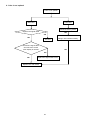
1
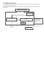
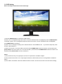
21.5" LCD Monitor
AOC E2250SWDN
Service
Service
Service
Horizontal Frequency
30 - 83kHz
Table of Contents
Description
Page
Description
Page
Table of Contents…………………..…………………..…...1
6.Schematic…………..….........................................30
Revision List.…...................................................……......2
6.1.Main Board..…….…...........................................30
Important Safety Notice.….….............................……......3
1.Monitor Specification..............................………............4
2.LCD Monitor Description……….…………………….......5
3.Operation Instruction.…………...................……...........6
6.2.Power Board..……….........................................35
7.PCB Layout..………..............................................37
7.1.Main Board………..…........................................37
3.1.General Instructions....................................…...........6
7.2.Power Board….…..............................................39
3.2.Control Buttons and Connections...............................6
7.3.Key Board………..…..........................................40
3.3.OSD Setting…..........................................................8
8.Maintainability………............................................41
4.Input/Output Specification...............……………….......24
8.1.Equipments and Tools Requirement…...............41
4.1.Input Signal Connector...............………..................24
8.2.Trouble Shooting…..………...............................42
4.2.Preset Display Modes…… ..........................25
4.3.Panel Specification…………..………………………..26
5.Block Diagram….........................................................28
5.1.Main Board…..….............................................28
9.White-Balance,Luminance Adjustment…..............46
10.Monitor Exploded View……...............................48
11.BOM List…………..……………………….............49
5.2.Power Board…………..…………………………......29
SAFETY NOTICE
ANY PERSON ATTEMPTING TO SERVICE THIS CHASSIS MUST FAMILIARIZE HIMSELF WITH THE
CHASSIS AND BE AWARE OF THE NECESSARY SAFETY PRECAUTIONS TO BE USED WHEN SERVICING
ELECTRONIC EQUIPMENT CONTAINING HIGH VOLTAGES.
CAUTION: USE A SEPARATE ISOLATION TRANSFOMER FOR THIS UNIT WHEN SERVICING
R FOR TH
UNIT WHEN S
Revision List
Version
Release Date
Revision History
A00
Feb.-21-2012
Initial release
TPV Model Name
TIBKN22QAGE6HNE
TIBKN22KAGE6HNE
TIAKN22LAGACHNE
TIB2N22BAGA1HNE
TIB2N22BDFA1HNE
TIB2N22KAGE6HNE
TIB2N22QAGE6HNE
TIBKN22BDFA1HNE
A01
Feb.-20-2013
Add new models
TIC1N22BAGA1HNE
TIC1N22KAGE6HNE
TIC1N22QAGE6HNE
TICAN22KAGE6HNE
TICAN22KAGE7HNE
TICAN22QAGE7HNE
Important Safety Notice
Proper service and repair is important to the safe, reliable operation of all AOC Company Equipment. The service
procedures recommended by AOC and described in this service manual are effective methods of performing service
operations. Some of these service operations require the use of tools specially designed for the purpose. The
special tools should be used when and as recommended.
It is important to note that this manual contains various CAUTIONS and NOTICES which should be carefully read in
order to minimize the risk of personal injury to service personnel. The possibility exists that improper service
methods may damage the equipment. It is also important to understand that these CAUTIONS and NOTICES ARE
NOT EXHAUSTIVE. AOC could not possibly know, evaluate and advise the service trade of all conceivable ways in
which service might be done or of the possible hazardous consequences of each way. Consequently, AOC has not
undertaken any such broad evaluation. Accordingly, a servicer who uses a service procedure or tool which is not
recommended by AOC must first satisfy himself thoroughly that neither his safety nor the safe operation of the
equipment will be jeopardized by the service method selected.
Hereafter throughout this manual, AOC Company will be referred to as AOC.
WARNING
Use of substitute replacement parts, which do not have the same, specified safety characteristics may create shock,
fire, or other hazards.
Under no circumstances should the original design be modified or altered without written permission from AOC.
AOC assumes no liability, express or implied, arising out of any unauthorized modification of design.
Servicer assumes all liability.
FOR PRODUCTS CONTAINING LASER:
DANGER-Invisible laser radiation when open AVOID DIRECT EXPOSURE TO BEAM.
CAUTION-Use of controls or adjustments or performance of procedures other than those specified herein may
result in hazardous radiation exposure.
CAUTION -The use of optical instruments with this product will increase eye hazard.
TO ENSURE THE CONTINUED RELIABILITY OF THIS PRODUCT, USE ONLY ORIGINAL MANUFACTURER'S
REPLACEMENT PARTS, WHICH ARE LISTED WITH THEIR PART NUMBERS IN THE PARTS LIST SECTION OF
THIS SERVICE MANUAL.
Take care during handling the LCD module with backlight unit
-Must mount the module using mounting holes arranged in four corners.
-Do not press on the panel, edge of the frame strongly or electric shock as this will result in damage to the screen.
-Do not scratch or press on the panel with any sharp objects, such as pencil or pen as this may result in damage to
the panel.
-Protect the module from the ESD as it may damage the electronic circuit (C-MOS).
-Make certain that treatment person’s body is grounded through wristband.
-Do not leave the module in high temperature and in areas of high humidity for a long time.
-Avoid contact with water as it may a short circuit within the module.
-If the surface of panel becomes dirty, please wipe it off with a soft material. (Cleaning with a dirty or rough cloth may
damage the panel.)
1.Monitor Specifications
2.LCD Monitor Description
The LCD MONITOR will contain a main board, a power board, and a key board which house the flat panel control
logic, brightness control logic and DDC.
The power board will provide AC to DC Inverter voltage to drive the backlight of panel and the main board chips
each voltage.
Monitor Block Diagram
LED Driver
Flat Panel and
LED backlight
Power Board
Main Board
RS232 Connector
For white balance
adjustment in factory
mode
Keyboard
Video signal DDC
AC-IN
100V-240V
HOST Computer
3. Operating Instructions
3.1 General Instructions
Press the power button to turn the monitor on or off. The other control knobs are located at front panel of the monitor
(See Figure ). By changing these settings, the picture can be adjusted to your personal preferences.
* The power cord should be connected.
* Press the power button to turn on the monitor. The power indicator will light up.
3.2 Control Buttons and Connections
Power
Press the Power button to turn on/off the monitor.
Eco (DCR)/ Press the Eco key continuously to select the Eco mode of brightness and DCR on when there is no OSD. ( Eco
mode hot key may not be available in all models).
4 : 3 or wide
When there is no OSD, press + continuously to change 4:3 or wide image ratio. (If the product screen size is 4:3 or
input signal resolution is wide format, the hot key is disable to adjust. )
Auto / Exit
When there is no OSD, press Auto/Source button continuously about 3 second to do auto configure
Source hot key
When the OSD is closed, press Source button will be Source hot key function. Press Source button continuously to
select the input source showed in the message bar, press Menu/Enter button to change to the source selected.
1. Power
2. Analog (DB-15 VGA cable)
3. DVI
To protect equipment, always turn off the PC and LCD monitor before connecting.
1 Connect the power cable to the AC port on the back of the monitor.
2 Connect one end of the 15-pin D-Sub cable to the back of the monitor and connect the other end to the computer's
D-Sub port.
3. Connect one end of the DVI cable to the back of the monitor and connect the other end to the computer‟s DVI
port.
4 Turn on your monitor and computer.
If your monitor displays an image, installation is complete. If it does not display an image, please refer
Troubleshooting.
3.3 OSD Setting
Basic and simple instruction on the control keys.
1) Press the MENU-button to activate the OSD window.
2) Press - or + to navigate through the functions. Once the desired function is highlighted, press the MENU-button
to activate it. press - or + to navigate through the sub-menu functions. Once the desired function is highlighted,
press MENU-button to activate it.
3) Press - or + to change the settings of the selected function. Press AUTO to exit.
If you want to adjust any other
function, repeat steps 2-3.
4) OSD Lock Function: To lock the OSD, press and hold the MENU button while the monitor is off and then press
power button to turn the monitor on. To un-lock the OSD - press and hold the MENU button while the monitor is off
and then press power button to turn the monitor on.
Notes:
1) If the product has only one signal input, the item of "Input Select" is disable to adjust.
2) If the product screen size is 4:3 or input signal resolution is wide format, the item of "Image Ratio" is disable to
adjust.
3) One of DCR, Color Boost, and Picture Boost functions is active, the other two function is turned off accordingly.
Luminance
1
Press
(Menu) to display menu.
2
Press
or
to select
(Luminance), and press
to enter.
3
Press
or
to select submenu, and press
or
to adjust.
to enter.
4
Press
9
5
Press
two times to exit.
10
Image Setup
1
Press
(Menu) to display menu.
2
Press
or
to select
(Image Setup), and press
to enter.
3
Press
or
to select submenu, and press
or
to adjust.
to enter.
4
Press
11
5
Press
two times to exit.
12
Color Setup
1
Press
(Menu) to display menu.
2
Press
or
to select
(Color Setup), and press
to enter.
3
Press
or
to select submenu, and press
or
to adjust.
to enter.
4
Press
13
5
Press
two times to exit.
14
Picture Boost
1
Press
(Menu) to display menu.
2
Press
or
to select
(Picture Boost), and press
or
to select submenu, and press
or
to adjust.
3
Press
to enter.
4
Press
15
to enter.
5
Press
two times to exit.
16
OSD Setup
1
Press
(Menu) to display menu.
2
Press
or
to select
(OSD Setup), and press
or
to select submenu, and press
or
to adjust.
3
Press
to enter.
4
Press
17
to enter.
5
Press
two times to exit.
18
Extra
1
Press
(Menu) to display menu.
2
Press
or
to select
(Extra), and press
to enter.
3
Press
or
to select submenu, and press
to enter.
4
Press
or
to adjust.
19
5
Press
two times to exit.
20
Exit
1
Press
(Menu) to display menu.
2
Press
or
to select
(Exit), and press
to enter.
3
Press
two times to exit
Exit
Exit the main OSD
21
LED Indicators
Status
LED Color
Full Power Mode
Green or Blue
Active-off Mode
Orange or red
e-Saver
Welcome to use AOC e-Saver monitor power management software! The AOC e-Saver features Smart Shutdown
functions for your monitors, allows your monitor to timely shutdown when PC unit is at any status (On, Off, Sleep or
Screen Saver); the actual shutdown time depends on your preferences (see example below).
Please click on "driver/e-Saver/setup.exe" to start installing the e-Saver software, follow the install wizard to
complete software installation.
Under each of the four PC status, you may choose from the pull-down menu the desired time (in minutes) for your
monitor to automatically shutdown. The example above illustrated:
1) The monitor will never shutdown when the PC is powered on.
2) The monitor will automatically shutdown 5 minutes after the PC is powered off.
3) The monitor will automatically shutdown 10 minutes after the PC is in sleep/stand-by mode.
4) The monitor will automatically shutdown 20 minutes after the screen saver appears.
You can click “RESET” to set the e-Saver to its default settings like below.
22
Screen+
Welcome to "Screen+" software by AOC, Screen+ software is a desktop screen splitting tool, it splits the desktop
into different panes, each pane displays a different window. You only need to drag the window to a corresponding
pane, when you want to access it. It supports multiple monitor display to make your task easier. Please follow the
installation software to install it.
23
4. Input/Output Specification
4.1 Input Signal Connector
Analog connector
24
4.2 Preset Display Modes
25
4.3 Panel Specification
4.3.1 General Features
HM215WU1-500 is a color active matrix TFT LCD module using amorphous silicon TFT's (Thin Film Transistors) as
an active switching devices. This module has a 21.5 inch diagonally measured active area with FHD resolutions
(1920 horizontal by 1080 vertical pixel array). Each pixel is divided into RED, GREEN, BLUE dots which are
arranged in vertical stripe and this module can display 16.7M colors. The TFT-LCD panel used for this module is
adapted for a low reflection and higher color type.
4.3.2 General Specifications
4.3.3 Electrical Characteristics
Electrical characteristics
[Ta =25±2 ℃]
Notes : 1. The supply voltage is measured and specified at the interface connector of LCM.
26
The current draw and power consumption specified is for VDD=5.0V, Frame rate=75Hz. Test Pattern of power
supply current
a) Typ : Color Bar pattern
b) Max : Skip Sub Pixel Pattern
2. Duration of rush current is about 2 ms and rising time of VDD is 520 μs ± 20 %
4.3.4 Optical Characteristics
[VDD = 5.0V, Frame rate = 60Hz, Clock = 78MHz, IBL = 240mA, Ta =25±2 ℃]
,
27
5. Block Diagram
5.1 Main Board
04.SCALER
02.INPUT
+5V
EDID_WP
+5V
EDID_WP
R0+
R0SOG_DET
G0+
G0B0+
B0AHS0
AVS0
DDCSDA1
DDCSCL1
VGA_CABLE_DET
R0+
R0SOG_DET
G0+
G0B0+
B0AHS0
AVS0
DDCSDA1
DDCSCL1
VGA_CABLE_DET
R0+
R0SOG_DET
G0+
G0B0+
B0AHS0
AVS0
VCC3.3
DDCSDA1
DDCSCL1
PA[0..9]
VCC1.8
+5V
VCC1.8
+5V
05.PANEL INTERFACE
PA[0..9]
PA[0..9]
VGA_CABLE_DET
02.D-SUB INPUT
PB[0..9]
EDID_WP
VCC3.3
PB[0..9]
PB[0..9]
EDID_WP
P_SCL
P_SCL
P_SDA
P_SDA
VLCD
VLCD
05.PANEL INTERFACE
03.DVI INPUT
+5V
EDID_WP
+5V
EDID_WP
RX0+
RX0RX1+
RX1RX2+
RX2RXC+
RXCDDCSCL2
DDCSDA2
DVI_CABLE_DET
DVI_HPD
RX0+
RX0RX1+
RX1RX2+
RX2RXC+
RXCDDCSCL2
DDCSDA2
DVI_CABLE_DET
DVI_HPD
RX0+
RX0RX1+
RX1RX2+
RX2RXC+
RXCDDCSCL2
DDCSDA2
DVI_CABLE_DET
06.POWER
Adj_BACKLIGHT
on_BACKLIGHT
Audio_EN
Audio_DET
PS_EN
DVI_HPD
Panel_ON
03.DVI INPUT
Adj_BACKLIGHT
on_BACKLIGHT
Audio_EN
Audio_DET
PS_EN
Panel_ON
Adj_BACKLIGHT
on_BACKLIGHT
Audio_EN
Audio_DET
PS_EN
Panel_ON
+5V
VCC3.3
VCC1.8
VLCD
04.SCALER
+5V
VCC3.3
VCC1.8
VLCD
06.POWER
OEM MODEL OTS
Size
絬 隔 瓜 絪 腹
715G4502-M0B-000-0040
TPV MODEL
DUAL
Rev
Key Component
T P V ( Top
COVER & REVISE HISTORY
PCB NAME
715G4502-M0B-000-0040
Date
28
Victory
Electronics
Friday , October 29, 2010
Co . ,
Ltd. )
Sheet
2
of
7
称爹
B
B
<称爹>
5.2 Power Board
EMI filter
Bridge
Rectifier
and Filter
Transformer
(T901)
Rectifier
diodes
14.5V
5V
Start Resistor
(R908,R911)
Feedback
PWM Control
LD7576AGR
(U901)
Circuit
Power Switch
(Q901)
Photo coupler
Regulator
(U902)
14.5V
L801
(IC903)
D801
C809
MOSFET
(Q801)
LED
ENA
DIM
PWM Control
OZ9998BGN
(U801)
29
(CN804)
6. Schematic
6.1 Main Board
DDCSCL1 R101
DDCSCL_A
100R 1/16W 5%
VSIN0
5 DDCSCL1
14
13
DDCSDA1 R106
DDCSDA_A
100R 1/16W 5%
5 DDCSDA1
DET_VGA
D-SUB 15P
10
5
9
4
8
3
7
2
6
1
15
HSIN0
CN101
12
11
R102
100R 1/16W 5%
VGA_CABLE_DET
VGA_CABLE_DET 5
VGA_5V
VGA_5V
BIN0BIN0
GIN0GIN0
RIN0RIN0
R103
0R05 1/16W
BIN0
ZD101
RLZ5.6B
R104
0R05 1/16W
5PF 50V
C103
16
715G4502M01000004C
17
R107
75 OHM +-5% 1/16W
BIN0-
R105
100R 1/16W 5%
C102
47N16V
B0+
R108
100R 1/16W 5%
C104
47N16V
B0-
R142
470R 1/16W 5%
GIN0
VGA_5V
4,5,7 +5V
1
75 OHM +-5% 1/16W
GIN0-
D101
BAV70
C120
1N50V
SOG_DET 5
R111
100R 1/16W 5% C105 47N16V
G0+
R113
100R 1/16W 5%
C107
47N16V
G0-
R119
100R 1/16W 5%
C108
47N16V
R0+
R121
100R 1/16W 5%
C110
47N16V
R0-
G0+ 5
G0- 5
ESD_VGA
U101
8
7
6
5
VCC
WP
SCL
SDA
A0
A1
A2
GND
1
2
3
4
R117
0R05 1/16W
RIN0
R118
0R05 1/16W
5PF 50V
C109
220N16V
C101
3
22K 1/16W 5%
2
R112
R116
4K7 1/16W 5%
R115
4K7 1/16W 5%
R114
EDID_WP
DDCSCL1
DDCSDA1
4,5 EDID_WP
R110
0R05 1/16W
B0- 5
5PF 50V
C106
+5V
R109
0R05 1/16W
B0+ 5
R120
75 OHM +-5% 1/16W
RIN0-
R0+ 5
R0- 5
CAT24C02WI-GT3
AOZ8902CIL
DET_VGA
C113
100N 16V
1
2
3
CH1 CH4
VN
VP
CH2 CH3
AOZ8902CIL
AHS0 5
AVS0 5
Ltd. )
OEM MODEL OTS
Size
絬隔瓜絪腹
715G4502-M0B-000-0040
TPV MODEL
DUAL
Rev
Key Component
D-SUB I/O
PCB NAME
715G4502-M0B-000-0040
ESD_VGA
6
5
4
RIN0
GIN0
C181
22P 50V
BIN0
C182
22P 50V
U103
ESD_VGA
6DDCSDA_A
5
4DDCSCL_A
100R 1/16W 5%
100R 1/16W 5%
C112
NC/22pF 50V
CH1 CH4
VN
VP
CH2 CH3
R123
R124
C111
NC/22pF 50V
HSIN0
1
2
3
0R05 1/10W
R126
2K2 1/16W 5%
U102
VSIN0
R122
R125
2K2 1/16W 5%
HSIN0
VSIN0
C114
100N 16V
T P V ( Top
Date
30
Victory
Electronics
Friday , October 29, 2010
Co . ,
Sheet
3
of
7
称爹
B
B
<称爹>
26
25
GND
GND
U104
1
2
3
DAT0+
DAT0DAT1+
DAT1DAT2+
DAT2-
1K 1/16W 5%
NC Q101
CH1 CH4
VN
VP
CH2 CH3
6
5
4
ESD_DVI
ESD_DVI
2
1
D102
BAV70
R134
R135
R136
R137
R138
R139
ESD_DVI
10R
10R
10R
10R
10R
10R
1/16W
1/16W
1/16W
1/16W
1/16W
1/16W
5%
5%
5%
5%
5%
5%
RX0+
RX0RX1+
RX1RX2+
RX2-
5
5
5
5
5
5
8
7
6
5
DDCSCL2 5
DDCSDA2 5
EDID_WP
DCLK+
DCLK-
ESD_DVI
C116
U105
C115
RLZ5.6B 100N 16V
C117
100N 16V
AOZ8902CIL
DVI_HPD 5
ZD102
DVI5V
22K 1/16W 5%
R130
+5V
R133
18
17
10
9
2
1
13
12
5
4
21
20
23
24
100R 1/16W 5%
100R 1/16W 5%
4K7 1/16W 5%
11
3
19
22
DVI5V
R128
R129
R132
DAT0+
DAT0DAT1+
DAT1DAT2+
DAT2DAT3+
DAT3DAT4+
DAT4DAT5+
DAT5clk+
clk-
3,5,7 +5V
DET_DVI
SCL_DVI
SDA_DVI
DVI5V
HPD
4K7 1/16W 5%
1/3shield
2/4shield
0/5shield
clk shield
8
15
6
7
14
16
DVI_CABLE_DET 5
R131
VSY NC
SY NC GND
DDC SCL
DDC SDA
+5V
HPD
R127
100R 1/16W 5%
3
CN102
JACK
R140
R141
10R 1/16W 5%
10R 1/16W 5%
VCC
WP
SCL
SDA
A0
A1
A2
GND
1
2
3
4
220N16V
CAT24C02WI-GT3
EDID_WP 3,5
RXC+ 5
RXC- 5
U106
1
2
3
CH1 CH4
VN
VP
CH2 CH3
6
5
4
U107
ESD_DVI
AOZ8902CIL C118
100N 16V
1
2
3
CH1 CH4
VN
VP
CH2 CH3
6
5
4
AOZ8902CIL
ESD_DVI
C119
100N 16V
OEM MODEL OTS
Size
絬隔瓜絪腹
T P V ( Top
715G4502-M0B-000-0040
TPV MODEL
DUAL
Rev
Key Component
DVI
PCB NAME
715G4502-M0B-000-0040
Date
31
Victory
Electronics
Co . ,
Monday , Nov ember 01, 2010
Ltd. )
Sheet
4
of
7
称爹
B
B
<称爹>
PB0
PB1
PB2
PB3
PB4
PB5
PB6
PB7
PB8
PB9
C403
100N 16V
R402
R403
LVB3P
LVB3M
LVBCKP
LVBCKM
LVB2P
LVB2M
LVB1P
LVB1M
LVB0P
LVB0M
1
3
5
7
NC/2K2 1/16W 5%
NC/2K2 1/16W 5%
2
4
6
8
VCC3.3
CN401
NC/8PIN
VCC3.3
C421
4.7UF 10V
C0805
C418
100N 16V
C419
100N 16V
RX2+
RX2RX1+
RX1RX0+
RX0RXC+
RXC-
RX2+
RX2RX1+
RX1RX0+
RX0RXC+
RXC-
3 AHS0
3 AVS0
C422
100N 16V
3 SOG_DET
3 G0+
3 G0-
C423
4.7UF 10V
C0805
AHS0
AVS0
25
26
B0+
B0-
15
16
17
18
19
R0+
R0-
20
21
3 R0+
3 R0-
C424
100N 16V
DDCSDA2
DDCSCL2
DDCSDA1
DDCSCL1
4 DDCSDA2
4 DDCSCL2
3 DDCSDA1
3 DDCSCL1
SPI_CE
SPI_SO
SPI_SI
R453
SPI_CK
0R05 1/16W
WP
PA3*
+5V
1
2
3
4
5
6
7
8
SOG_DET
G0+
G0-
3 B0+
3 B0-
OSC_VDD
98
97
28
27
89
87
88
86
85
RX2+
RX2RX1+
RX1RX0+
RX0RXC+
RXC-
NC
NC
NC
NC
NC
NC
NC
NC
NC
T0M
T0P
T1M
T1P
T2M
T2P
TCLK1M
TCLK1P
T3M
T3P
T4M
T4P
T5M
T5P
T6M
T6P
TCLK2M
TCLK2P
T7M
T7P
HSY NCI1
VSY NCI1
BIN1+
BIN1SOG1I
GIN1+
GIN1RIN1+
RIN1PB7*/DVI_SDA*/TXD*
PB6*/DVI_SCL*/RXD*
PB5*/VGA_SDA*/TXD*
PB4*/VGA_SCL*/RXD*
45
46
47
48
49
50
51
74
75
72
71
70
69
68
67
66
65
64
63
61
60
59
58
57
56
55
54
53
52
0R05 1/16W
0R05 1/16W
KEY 1
KEY 2
POWER
ADC3
ADC2
PC6
100N 16V C410
100N 16V C409
LED_G
LED_A
CN403
NC/6PIN
VCC3.3
7
6
5
4
3
2
1
PB9
PB8
PB7
PB6
PB5
PB4
PB3
PB2
PB1
PB0
PA9
PA8
PA7
PA6
PA5
PA4
PA3
PA2
PA1
PA0
LVB0M
LVB0P
LVB1M
LVB1P
LVB2M
LVB2P
LVBCKM
LVBCKP
LVB3M
LVB3P
LVA0M
LVA0P
LVA1M
LVA1P
LVA2M
LVA2P
LVACKM
LVACKP
LVA3M
LVA3P
1
2
3
4
5
6
7
CN404
NC/CONN
FB406
NC/120 OHM
TOUCH_POWER
R457
LED_A
CN405
NC/7PIN
NC
C420
NC
D404
NC/RLZ5.6B
+5V
SPI_CE
SPI_SO
SPI_SI
SPI_CLK
PA3*
R410
+5V
0R05 1/16W
R454
22K 1/16W 5%
R415
100K 1/16W 5%
R416
220K 1/16W 5%
CN402
CONN
R406
R407
100N 16V C408
92
11
12
22
23
38
73
DVDD
DVDD
DVDD
DVDD
REXT
TVCC
10
ADC_3V3
4
4
4
4
4
4
4
4
C415
100N 16V
OSC_VDD
1
2
3
4
5
6
R413
2K2 1/16W 5%
5V_DET LPD_IN1*
PE3*/PWMB*
PE2*/PWMA*/DBC*
PE1*/LPD_IN1*/INT_VSO*
PE0*/PWMA*/LPD_IN0*
VCC3.3
C425 100N 16V
D403
NC/RLZ5.6B
C417
100N 16V
ADC_VAA
6
5
4
3
2
1
LVA3P
LVA3M
LVACKP
LVACKM
LVA2P
LVA2M
LVA1P
LVA1M
LVA0P
LVA0M
D402
NC/RLZ5.6B
C416
4.7UF 10V
C0805
FB407
ADC_VAA33
300OHM
R408
470R 1/16W 1%
PA0
PA1
PA2
PA3
PA4
PA5
PA6
PA7
PA8
PA9
DVDD
D401
NC/RLZ5.6B
U401
AVCC
PA[0..9]
2
CVDD
C414
1UF 10V
C0402
AVCC
OSC_VDD
ADC_VAA33
13
C405
100N 16V
ADC_1V8
C404
4.7UF 10V
C0805
C413
4.7UF 10V
C0805
FB405
DVDD
300OHM
FB408
300OHM
6 PA[0..9]
39
AVCC
CVDD_1V8
FB404
300OHM
1
FB402
NC/300OHMADC_VAA
VCC3.3 7
3K9 +/-5% 1/16W
R405
C402
100N 16V
PB[0..9]
R404
3K9 +/-5% 1/16W
C401
4.7UF 10V
C0805
6 PB[0..9]
100N 16V C412
CVDD
100N 16V C411
U401 NT68660FG FB401 and FB402 is
NC==>3.3V use TO252 type
U401 NT68660UFG FB402 is NC==>3.3V
and 1.8V LDO use SOT-223 type
VCC1.8 7
FB401
300OHM
R401
3K9 +/-5% 1/16W
VCC1.8
PWMB*
PE2*
LPD_IN1*
PE0*
79
42
78
29
on_BACKLIGHT 7
Panel_ON 7
5V_DET_INT
DVI_HPD
+5V 3,4,7
VCC3.3
NC/0R05 1/16W
R414
DVI_HPD 4
LED_2
PC4
R427
10K 1/16W 5%
Q402
LMBT3906LT1G
R452
NC
R451
NC
TP3
TP-R-0.75
TP4
TP-R-0.75
DVDD
PC7
PC6/INTE2
PC5
PC4
PC1*/LPD_OUT*
PC0*/PWMA*/DBC*
TXD*
RXD*
P35*
P34*
MSDA
MSCL
44
43
31
32
P31*/TXD*
P30*/RXD*
P35*
P34*
R424
1K 1/16W 5%
PC6
PC5
PC4
PC1*
PC0*
P/SCL
POWER
RESETB
LED_2
LED_A
470OHM +-5% 1/10W
R418
PS_EN 7
Adj_BACKLIGHT 7
R409
+5V
0R05 1/16W
PB3/ADC3/INTE1
PB2/ADC2/INTE0
PB1/ADC1
PB0/ADC0
R429
10K 1/16W 5%
30
91
90
100
99
96
76
RSTB
82
83
36
35
ADC3
ADC2
ADC1
ADC0
KEY 1
KEY 2
CABLE_DET
5V_DET
80
81
41
40
84
34
33
PA7*
PWMC*
PA5*
PA4*
Audio_DET
Audio_EN
INTB(PWM)
P/SDA
LED_1
EDID_WP
EE_WP
R411
2K2 1/16W 5%
100R 1/16W 5%
100R 1/16W 5%
PA1*
PA0*
R425
PC5 10K 1/16W 5%
Q401
LMBT3906LT1G
Audio_DET 7
Audio_EN 7
LED_G
330OHM 1/10W
R417
EDID_WP
DGND
DGND
DGND
DGND
AGND
R431
R434
24
37
62
77
95
NT68660UFG/A
TGND
OSCO
14
93
PA7*
PA6*/PWMC*
PA5*/PWMB*
PA4*/INTE3*/INT_HSO*
PA2*/PWMD*/DBC*
PA1*/PWMD*/DBC*
PA0*/PWMC*
OSCI
OSC_GND
94
9
2
C428
22P 50V
1
X401
12MHz
R432
1MOHM 1/16W +/-5%
LED_1
C426
22P 50V
VCC3.3
NC/0R05 1/16W
R412
C427
100N 16V
VCC3.3
4 DVI_CABLE_DET
R419
390K
EE_WP
MSCL
MSDA
R422
100K 1/16W 5%
PA0*
P34*
P35*
R445
R447
R443
NC/22K 1/16W 5%
NC/100R 1/16W 5%
NC/100R 1/16W 5%
VCC
WP
SCL
SDA
A0
A1
A2
GND
1
2
3
4
R456
NC/4K7 1/16W 5%
R455
NC/4K7 1/16W 5%
1
2
3
4
5
NC/CONN
PA5*
P_SCL
1
2
3
4
5
6
MSCL
MSDA
INTB(PWM)
RESETB
NC/220N 10V
CN410
+5V
C430
8
7
6
5
R484
NC/4K7 1/16W 5%
P_SDA
R446
NC/0R05 1/16W
P/SCL
CN411
VCC3.3
R483
NC/4K7 1/16W 5%
PA4*
VCC3.3
R442
NC/4K7 1/16W 5%
Pm25LD020C-SCE
VCC3.3
3 VGA_CABLE_DET
R437
NC/22K 1/16W 5%
R440
NC/0R05 1/16W
P/SDA
R441
NC/4K7 1/16W 5%
VDD
SO
HOLD# CE#
WP# SCK
GND
SI
SPI_SO
SPI_CE
SPI_CK
SPI_SI
2
1
6
5
NC
C453
R439
100R 1/16W 5%
NC/10K 1/16W 5%
R438
WP PA3*
R436
NC/22K 1/16W 5%
U402
8
7
3
4
10K 1/16W 5%
R444
C429
220N16V
VCC3.3
R486
R485
NC
NC
C437
NC
U403
NC/M24C16
NC/CONN
VGA_CABLE_DET
CABLE_DET
DVI_CABLE_DET
ADC1
T P V ( Top
R423
220K 1/16W 5%
OEM MODEL OTS
Size
絬 隔 瓜 絪 腹
715G4502-M0B-000-0040
TPV MODEL
DUAL
Rev
Key Component
SCALER
PCB NAME
715G4502-M0B-000-0040
Date
32
Victory
Electronics
Co . ,
Monday , Nov ember 01, 2010
Ltd. )
Sheet
5
of
7
称爹
C
B
<称爹>
PA[0..9]
PB[0..9]
5 PB[0..9]
PA0
PA1
PA2
PA3
PA4
PA5
PA6
PA7
PA8
PA9
PB0
PB1
PB2
PB3
PB4
PB5
PB6
PB7
PB8
PB9
LVA3P
LVA3M
LVACKP
LVACKM
LVA2P
LVA2M
LVA1P
LVA1M
LVA0P
LVA0M
VLCD 7
2
FB409
120 OHM
RXO0+
RXO1+
RXO2+
RXOC+
RXO3+
RXE0+
RXE1+
RXE2+
RXEC+
RXE3+
RXO0RXO0+
RXO1RXO1+
RXO2RXO2+
LVBCKM
LVBCKP
LVB3M
LVB3P
LVA0M
LVA0P
RXOCRXOC+
RXO3RXO3+
RXE0RXE0+
LVA1M
LVA1P
RXE1RXE1+
LVA2M
LVA2P
LVACKM
LVACKP
LVA3M
LVA3P
RXE2RXE2+
RXECRXEC+
RXE3RXE3+
P_SCL
P_SDA
P_SCL
P_SDA
1
30
29
28
27
26
25
24
23
22
21
20
19
18
17
16
15
14
13
12
11
10
9
8
7
6
5
4
3
2
1
100N 16V
C434
R449
R448
+
300 OHM 1/4W
NC/CONN
RXOC-
C435
NC
RXEC+
LVB0M
LVB0P
LVB1M
LVB1P
LVB2M
LVB2P
P_SCL
100uF16V
1
3
5
7
9
11
13
15
17
19
21
23
25
27
29
C433
2
4
6
8
10
12
14
16
18
20
22
24
26
28
30
RXEC-
CN408
CONN
VLCD
CN409
RXO0RXO1RXO2RXOCRXO3RXE0RXE1RXE2RXECRXE3P_SDA
LVB3P
LVB3M
LVBCKP
LVBCKM
LVB2P
LVB2M
LVB1P
LVB1M
LVB0P
LVB0M
300 OHM 1/4W
5 PA[0..9]
C436
NC
RXOC+
OEM MODEL OTS
Size
絬隔瓜絪腹
T P V ( Top
715G4502-M0B-000-0040
TPV MODEL
DUAL
Rev
Key Component
LVDS PANEL I/O
PCB NAME
715G4502-M0B-000-0040
Date
Victory
Electronics
Co . ,
Friday , October 29, 2010
Ltd. )
Sheet
33
6
of
7
称爹
A
B
<称爹>
+5V
+5V
VCC3.3
C701
R702
4K7 1/16W 5%
+5V
4
INPUT OUTPUT
4
FB701
0 OHM +-5% 1/8W
2
1
ADJ/GND
+
VCC3.3 5
100N 16V
C704
3,4,5 +5V
DIM
ON/OFF
AZ1117H-3.3TRG1
100uF16V
C702
NC/CONN
VCC3.3
U701
3
C703
100N 16V
6
5
4
3
2
1
100N 16V
+5V 3,4,5
CN701
R703
9
8
7
6
5
4
3
2
1
100R 1/16W 5%
Adj_BACKLIGHT 5
+
C706
U702
VCC3.3
C705
100uF16V
NC/G1117-33T43UF
DIM
ON/OFF
VIN
VOUT(TAB)
ADJ(GND)
100N 16V
R704
R799
10K 1/16W 5%
3
2
1
10K 1/16W 5%
CONN
Q701
R701
22K 1/16W 5%
on_BACKLIGHT 5
TO-252
LMBT3904LT1G
R708
NC/10K 1/16W 5%
R798
NC/10K 1/16W 5%
NC/100NF 25V
NC/100R 1/16W 5%
Q702
R709
NC/22K 1/16W 5%
NC/2N3904S-RTK/PS
Audio_EN 5
VI
100N 16V
C713
VCC3.3
AZ1117H-1.8-E1
U703
3
R724
NC
is NC
VCC1.8
2
VO
1
R706
C709
U401=NT68660FG U703 U704 R707 C710 C712 C703
VCC1.8 5
+
C712
100N 16V
Audio_EN1
GND
R707
4.7 OHM +-5% 2WS
VCC3.3
C710
100uF16V
NC
4
C708
4
C707
NC/100N 16V
R710
NC/100R 1/16W 5%
Audio_DET 5
3
NC
Q703
+5V
NC/2N3904S-RTK/PS
R714
10K 1/16W 5%
Q705
AO3401A
Q707
PS_EN 5
R723
NC/4K7 1/16W 5%
NC/2N3904S-RTK/PS
R719
22K 1/16W 5%
Q706
+5V
LMBT3904LT1G
+
100N 16V
C718
5 Panel_ON
G
S
S
S
R715
100K 1/16W 5%
R717
NC
Q704
NC/AO4449 -7A/-30V
R716
R720
NC
2
NC
R718
+5V
NC/10K 1/16W 5%
VLCD 6
VOUT
TO252
C714
NC/100NF 25V
C717
NC/100NF 25V
VIN
5
6
7
8
R713
D
D
D
D
R712
4
3
2
1
NC/0R05 1/16W Audio_DET2
R711
220N16V
C715
Audio_DET1
VLCD
GND
U704
1
NC/100K 1/16W 5%
R721
4K7 1/16W 5%
CN702
C716
100uF16V
R722
NC/10K 1/16W 5%
R725
NC
<Variant Name>
OEM MODEL OTS
Size
絬 隔 瓜 絪 腹
T P V ( Top
715G4502-M0B-000-0040
TPV MODEL
DUAL
Rev
Key Component
POWER
PCB NAME
715G4502-M0B-000-0040
Date
34
Victory
Electronics
Friday , October 29, 2010
Co . ,
Ltd. )
Sheet
7
of
7
称爹
B
A
<称爹>
6.2 Power Board
715G4744P01000001C
!
1
R929 100 OHM 1/4W
C916
R930 100 OHM 1/4W 2N2 500V
C928
2N2 500V
F801
0R05 1/4W
+14.5V
2
+
BD901
KBP208G
3
R903 100 OHM 1/4W
R904
250OHM2W
!
+
R932
NC
!
!
R931
NC
R906
100K
C911
1500PF2KV
+
C907A
C907
47uF M 450V
47uF M 450V
!
D903
FR107
R911
10K 1/4W
D904
FR103
1
R933
NC
6
1
9
10
3
12
11
C917
R910 100 OHM 1/4W 2N2 500V
C929
2N2 500V
LD7576AGR
!
8
!Q901
R917
6
10 OHM 1/4W
5
R915
22 OHM 1/4W +-5%
C912
100N 50V
1
P0765ATF
C925
R918
10K OHM +-5% 1/8W
C920
1000uF/16V
+
C922
470UF M 16V
R919
220 OHM 1/8W
U902
PC123X2Y FZOF
C906
1N 50V
D906
3
R920
1K 1/8W
2
C914
1N 50V
2
1000uF/16V
SRF1060
1
NR901
NTCR
t
+5V
D905 NC/31DQ06FC3
FB901
BEAD
!
FUSE
+
D907
1N4148
эDIP 1/2W
C908
0.47UF
F902
N.C
2
R921
NC/100K 1/10W 1% U901
1
HV
2 CT
3 COMP
4 CS VCC
GND OUT
R907
1K OHM +-5% 1/8W
L906
R912 100 OHM 1/4W
R908
10K 1/4W
1
C927
47N 50V
620K 1/4W
C903
1000PF/250VAC
C923
1nF 50V
R913
5.1 OHM 1/4W
2
R902
C913
47uF/50V
4
620K 1/4W
8
7
1
D908
NC/IN4148
R901
620K 1/4W
5
D909 NC/31DQ06FC3
+
30mH
R900
R905
470OHM +-5% 1/8W
Q904
KTD1028
D902
SR515
+
!
2
C918
NC/680UF/25V
D901
SR515
R909 100 OHM 1/4W
!
3 L901 4
!
+
T901
POWER X'FMR
4
ZD901
MTZJ T-72 16B
1
80GL22T-3
4
-
!
3
2
R923
220 OHM 1/4W
R914
43.2K OHM 1%
C924
0.1uF 50V
C902
1000PF/250VAC
ADD C906
R924
0.47OHM2W
R916
7K5 1/8W +/-1%
R928
1K 1/8W
IC903
AS431AZTR-E1
F901
FUSE
C900
0.0022UF
C915
R925
2.43KOHM +-1% 1/8W
1
3
!
R935
7K5 1/8W +/-1%
!
FB902
2
BEAD
1
2
CN902
Wire Harness
L907
F903 FUSE
+5V1
CN901
HS1
HEAT SINK(Q901)
SOCKET
1
2
MUTE
VOL
HS2
NC/HEAT SINK(D906_5V/4A)
+5V
1
2
ON/OFF
C926
100N 50V
DIM
9
8
7
6
5
4
3
2
1
CN903
+
+ C931
NC/470uF/16V
C921
NC/1000uF25V
+5V1
1
2
3
4
CONN
FB903
HS3
HEAT SINK(D906_5V/2.5A)
GND1
GND
1
2
BEAD
1
2
1
2
T P V ( Top
絬隔瓜絪腹
Key Component
Date
35
Victory
Electronics
Co . ,
G4497-P0B-000-0010-1-100720
01.POWER
Friday , December 24, 2010
Ltd. )
OEM MODEL
Size
TPV MODEL
LNPCAB351AAB2
PCB NAME
Sheet
Rev
Custom
1
715G4497-P0B-000-0010
1
of
3
称爹
ODM MODEL
FB802
D801
L801
1
2
1
2
CN803
+14.5V
10 OHM 1/8W
47UH
BEAD
8
7
6
5
Q801
C814
100N 50V
APM8005KCTRG
1
2
C810
0.47UF 50V
S1
G1
S2
G2
R801
10K 1/8W
SK310B
1
2
3
4
R805
C802
10N 50V
1
R806
C803
1N 50V
C806
220N 50V
R803
300K 1/8W
C815
CN801
1 OHM +-5% 1/8W
9
10
11
12
13
14
15
16
R822
NC
NC/CONN
R808
1 OHM +-5% 1/8W
C808
100PF 500V
VIN
VREF
STATUS
LDR
SSTCMP
ISW
PWM
ENA
ISEN1
RT
ISEN2
OVP
GND
ISET
ISEN3
ISEN4
8
7
6
5
4
3
2
1
6
5
4
3
2
1
R817
100 OHM 1/4W
R812
0.1R 1%
C813
100PF 50V
1K 1/8W
C816
R813
1000PF500V
0.1R 1%
CN804
CONN
C812
R816 100PF 50V
5.1K OHM 1%
OZ9998BGN
C804
0.47UF 50V
R809
1N 50V
C805
5
4
3
2
1
R807
U801
100K 1/8W
R818 10K 1/8W
R819 R820 R821
NC
NC
NC
C811
33UF 100V 0.47UF 50V
FB801
BEAD
DIM
160K 1/8W
8
R802
300K 1/8W
R815
+
R814
10 OHM 1% 1/4W C809
2
ON/OFF
7
R804
C801
330uF 25V
D1
D1
D2
D2
+
1UF/25V
330K 1/8W 5%
R810
20K 1/8W 1%
C807
220N 50V
R811
0R05OHM1/8W
NC/CONN
CN802
1
2
NC/CONN
T P V ( Top
Electronics
Co . ,
Ltd. )
OEM MODEL
G4497-P0B-000-0010-1-100720
TPV MODEL
Key Component
02.INVERTER
PCB NAME
Date
36
Victory
絬 隔 瓜 絪 腹
Friday , December 24, 2010
Sheet
Custom
Size
LNPCAB351AAB2
715G4497-P0B-000-0010
2
of
3
Rev
称爹
1
ODM MODEL
7. PCB Layout
7.1 Main Board
715G4502M01000004C
37
38
7.2 Power Board
715G4744P01000001C
39
7.3 Key Board
715G4747K02000001C
40
8. Maintainability
8.1 Equipments and Tools Requirement
1.
Voltmeter.
2.
Oscilloscope.
3.
Pattern Generator.
4.
DDC Tool with an IBM Compatible Computer.
5.
Alignment Tool.
6.
LCD Color Analyzer.
7.
Service Manual.
8.
User Manual.
41
8.2 Trouble Shooting
No Power
No power
NG
Check power cable is
tightened?
Re-plug the power cable
OK
NG
Check Power “On/Off”
Turn on the Power “On/Off” switch
is “On”?
OK
NG
Check the LED
Check the AC power
indicate is OK?
OK
Replace the converter board
NG
Replace main board and check connections
NG
Replace key board and check connections
42
2. No Video (Power LED Blue)
No Video (Power LED Blue)
Press the power
NG
Replace the main board
button is OK?
OK
Replace the converter
OK
The end
board
NG
Replace the main
OK
The end
board and connection
NG
Check the LVDS/FFC
OK
Replace the LVDS/FFC
cable or panel
cable or panel
NG
Replace the key board
43
3.
DIM
DIM (image overlap, focus or flicker)
OK
Reset in factory mode
The end
NG
OK
Set to the optimal
frequency, select the
recommended frequency
The end
NG
OK
Readjust the phase and pixel
The end
clock in the user mode
NG
OK
Pull out signal cable and
check “Self Test Feature
Check” is ok?
Check the signal cable
and the PC
NG
NG
OK
Replace the main board
The end
NG
Replace the panel
OK
44
4. Color is not optimal
Color is not optimal
Color shift
Miss color
Reset the factory mode
Replace the signal cable
NG
OK
NG
The end
In the user mode, set the” color
settings” until customer satisfy
Pull out the signal cable
and check the screen
color display is normal?
NG
OK
NG
Replace the signal cable or PC
Replace the main board
45
9.White- Balance, Luminance Adjustment
Approximately 30 minutes should be allowed for warm up before proceeding white balance adjustment.
How to setting MEM channel you can reference to chroma 7120 user guide or simple use “SC” key and
“NEXT” Key to modify xyY value and use “ID” key to modify the TEXT description Following is the procedure to do
white-balance adjust .
1. Setting the color temp.
A. 6500K:
x=313±20 ,y=329±20
Warm color temp. parameter is
B. 7300K
Normal color temp. parameter is
x=301±20 ,y=317±20
C. 9300K
Cool color temp. parameter is
x=283±20,y=297±20
D. sRGB
sRGB color temp. parameter is x=313±20 ,y=329±20
2. Enter into the factory mode:
Press the MENU button,Pull out the power cord, then plug the power cord. Then the factory OSD will be at the
left top of the panel.
3. Biase adjustment:
Set the Contrast
to 50; Adjust the Brightness
to 90.
4. Gain adjustment:
A. Adjust Warm (6500K) color-temperature
1. Switch the chroma-7120 to RGB-Mode (with press “MODE” button)
2. Switch the MEM.channel to Channel 3 (with up or down arrow on chroma 7120)
3. The LCD-indicator on chroma 7120 will show x=313±20 ,y=329±20
4. Adjust the RED on factory window until chroma 7120 indicator reached the value R=100
5. Adjust the GREEN on factory window until chroma 7120 indicator reachedthe value G=100
6. Adjust the BLUE on factory window until chroma 7120 indicator reached the value B=100
7. Repeat above procedure (item4, 5, 6) until chroma 7120 RGB value meet the tolerance =100±2
46
B. Adjust Normal (7300K) color-temperature
1. Switch the chroma-7120 to RGB-Mode (with press “MODE” button)
2. Switch the MEM.channel to Channel 4(with up or down arrow on chroma 7120)
3. The LCD-indicator on chroma 7120 will show x=301±20 ,y=317±20
4. Adjust the RED on factory window until chroma 7120 indicator reached the value R=100
5. Adjust the GREEN on factory window until chroma 7120 indicator reachedthe value G=100
6. Adjust the BLUE on factory window until chroma 7120 indicator reached the value B=100
7. Repeat above procedure (item 4, 5, 6) until chroma 7120 RGB value meet the tolerance =100±2
C. Adjust Cool (9300K) color-temperature
1. Switch the Chroma-7120 to RGB-Mode (with press “MODE” button)
2. Switch the MEM. Channel to Channel 9 (with up or down arrow on chroma 7120)
3. The LCD-indicator on chroma 7120 will show
x=283±20,y=297±20
4. Adjust the RED on factory window until chroma 7120 indicator reached the value R=100
5. Adjust the GREEN on factory window until chroma 7120 indicator reached the value G=100
6. Adjust the BLUE on factory window until chroma 7120 indicator reached the value B=100
7. Repeat above procedure (item 4, 5, 6) until chroma 7120 RGB value meet the tolerance =100±2
D. Adjust sRGB color-temperature
1. Switch the chroma-7120 to RGB-Mode (with press “MODE” button)
2. Switch the MEM.channel to Channel 10 (with up or down arrow on chroma 7120)
3. The LCD-indicator on chroma 7120 will show x=313±20 ,y=329±20
4. Adjust the RED on factory window until chroma 7120 indicator reached the value R=100
5. Adjust the GREEN on factory window until chroma 7120 indicator reachedthe value G=100
6. Adjust the BLUE on factory window until chroma 7120 indicator reached the value B=100
7. Repeat above procedure (item 4, 5, 6) until chroma 7120 RGB value meet the tolerance =100±2
E. Turn the Power-button off to quit from factory mode.
47
10. Monitor Exploded Views
48
11. BOM List
Note: The parts information listed below are for reference only, and are subject to change without notice. Please go
to http://cs.tpvaoc.cn/hello1.asp for the latest information.
TIBKN22QAGE6HNE
Location
Part No.
040G 58162461A
EPA LABEL
052G
PAPER TAPE
2191
052G6019
HDCP-SMT
Description
A
1
Remark
INSULATING TAPE
070GHDCP500HDC
HDCP CODE
E08902
089G 715CAAE01
SIGNAL CABLE
2nd source
E08902
089G 715GAAE01
SIGNAL CABLE
2nd source
E08902
089G 715HAAE01
SIGNAL CABLE
E08901
089G402A15N HL
AC POWER CORD 1500mm
E08901
089G402A15N IS
AC POWER CORD 1500MM
E08907
095G179J30NE34
FFC CABLE 30pin 190mm 1.0mm
E09504
095G8014 6DE45
HARNESS 6P(CI1406)-6P(2008) 140
E09504
095G8014 6TE45
HARNESS 6P(CI1406)--6P(2008) 140
E09504
095G8014 6WE45
HARNESS 6P(CI1406S)-6P(2008) 140
0D1G1030
8120
screw
0M1G 930
8 47 CR3
SCREW 3x8
0M1G1140
8120
SCREW 4x8
0Q1G 140 12120
SCREW 4X12
0Q1G 930 10120
SCREW (T3X10)
E750
750GBK215W1512N000
LCD HM215WU1-500 3850 HF BOE
E750
750GBK215W1522N000
LCD HM215WU1-500 3950 HF BOE
A15G1587101
BKT_HINGE
A15G1597101D03
MAIN FRAME FOR 50TH 21.5W
A33G1181ABJ 1L0100
FUNCTION BUTTON FOR 50TH
A33G1182
POWER LENS FOR 50TH
1 1L0100
SGCC
A33G1183ABJ 1L0100
STAND TOP
FOR 50TH 18.5W
A33G1184ABJ 1L0100
HINGE COVER
A34G2530ABJ 1B0100
STAND COVER
A34G2547AEDP1B0105
BEZEL
A34G2548ABJ 1B0100
REAR COVER
A34G2549AED 1B0130
BASE FOR E2250SW
AM1G1740 10125
SCREW
H37G0030014
HINGE 21.5
H40G 001624 1A
CARTON LABEL BARCODE 1
H40G 22N61589A
E2250SWD EPI ID LABEL
H40G 45762413B
P/N LABEL FOR BASE
H40G 58161549A
guaranty sticker
H44GB018103
EPS
H44GB018203
EPS
H44GB01861507A00HX
ARTWORK CARTON e2250SWDN
FOR 50TH 18.5W
FOR 50TH 21.5W
49
2nd source
2nd source
2nd source
2nd source
H45G
77
6
PE PACKING
H45G
87
1 25
EPE COVER
H52G1801 16006
insulating sheet
H70G21C161507A
CD MANUAL e2250SWDN
KEPCAHB5
KEY BOARD
PLPCBB581AHD1
POWER BOARD
Q40G 58162435A
LABEL
Q45G
76 28
H
A
P.E. BAGx320x210x0.04
Q50G
4 10
TIE (Y1900221)
Q52G
1185 99
BIG CARTON TAPE FOR AOC
M05201
Q52G100202500A00JY
AL FOIL
M05203
Q52G100204500A00JY
AL FOIL
M05202
Q52G100204500A00JY
AL FOIL
Q52G6019 14
TAPE
S95G179T30NE34
FFC CABLE 30P 190mm P1.0MM
756GHACB A1171
MAIN BOARD-CBPCAN2A1H1
100GANBI001W11
MCU ASS'Y-056G2233 11
E08907
SMTCB-U402
CN402
033G3802 6B
Y
L
WAFER
CN701
033G3802 9B
Y
L
CONN 2.0 9P
CN408
033G801930F CH
L
FFC CONN 1.0mm 30P R/A 34mm 6mm
R707
061G152M47964L
SY
CN101
088G 35315FVXH
D-SUB CONN V/T 15P BLUE 1*1 V/T 30.8
CN102
088G 35424FVXH
DVI CONN V/T 24P WHITE
093G
CRYSTAL 12MHZ NXS12.000AC30F-KAB10
X401
2251B
J
RST MOFR 4.7 OHM +-5% 2WS FUTABA
709G4502 HM001
COMSUPTIVE ASS'Y
AIGAN2A1H1
MAIN BOARD FOR AI
H40G 45762429A
LABEL
LED001
081G
LED GREEN/YELLOW GHZYG603D2-5B
CN001
095G820H 6TE10
HARNESS 6P(SANW)-6P(2008) 120
CN001
095G820H 6WE10
HARNESS 6P(SANW)-6P(2008) 120
709G4747 HM001
COMSUPTIVE ASS'Y
SMTKEPCAHB5
KEY BOARD FOR SMT
GND1
009G6005
GND TERMINAL
U902
056G 139 3A
PC123Y22FZOF SHARP
061G
NTCR 8R 20% 3.1W SCK13084MMY501
NR901
12 1F GH
1
5810T
2nd source
C908
063G107K474 6S
0.47UF +-10%
C902
065G305M1023BW
CAP Y2 1NF 20% 250V Y5U
C903
065G305M1023BW
CAP Y2 1NF 20% 250V Y5U
C900
065G306M2222BP
CAP Y1 2.2NF 20% 250V Y5P
C809
067G 415330 9K
EC 33UF 20% 100V ED 8*12
C907
067G 42Z68015K
EC 68UF 20% 450V 12.5*50 2000 hr
C801
067G215D3314KV
EC 330UF 20% 25V 10*12 4000 hr
C918
067G215D6814KV
EC 680UF 20% 25V 10*20
C922
067G215S4713KV
EC 470UF 20% 16V 10X13
L901
073G 174 65 H2
LINE FILTER 30mH MIN
50
2nd source
L906
073G 253191
L801
073G 253214 DN
CHOKE COIL 47UH 10% LZ.CC013.G01 2.5A
T901
080GL22T
X'FMR 490UH 7% 4UH YUVA-1656
CN901
H
3 N3
087G 501 48
S
IND CHOKE 1.1uH DADON
AC SOCKET 3PIN + 3 Hole
D902
093G
60335
DIODE SR515 5A/150V DO-201AD
D901
093G
60335
DIODE SR515 5A/150V DO-201AD
CN902
095G 825 9T518
HARNESS 9P-9P 120MM
CN902
095G 825 9W518
HARNESS 9P-9P 120MM
0Q1G 340
SCREW Q1-SELF TAPING SCREW :Q
CN804
BD901
8140
311GW200A06ABX
WAFER 2.0mm 6P
705GHA57006
Q901 ASS"Y
705GHA93006
D906 ASS"Y
709G4744 HM001
CONSUMPTIVE ASS'Y
H40G 45762429A
LABEL
PLBB581AHD1SMT
POWER BOARD FOR SMT
093G
BRIDGE KBP308G-C 3A 800V KBP
50460515
2nd source
x8.0
Q55G 100625
TIN STICK_LOW ARGENTUM
C705
067G 3051013PB
EC 105C 100uF M 16V 5*11mm JH CD263
C702
067G 3051013PB
EC 105C 100uF M 16V 5*11mm JH CD263
C433
067G 3051013PB
EC 105C 100uF M 16V 5*11mm JH CD263
C716
067G 3051013PB
EC 105C 100uF M 16V 5*11mm JH CD263
C710
067G 3051013PB
EC 105C 100uF M 16V 5*11mm JH CD263
SMTCAN2A1H1
MAIN BOARD FOR SMT
U703
056G 133 33AAC
LDO AZ1117H-1.8TRE1
U401
056G 562369
SCALER NT68660UFG/B TQFP-100
U701
056G 563514
IC AZ1117H-3.3TRG1 1A/3.3V SOT223
U107
056G 662 48
ESD PROTECT AZC399-04S.R7G SOT23-6L
U106
056G 662 48
ESD PROTECT AZC399-04S.R7G SOT23-6L
U104
056G 662 48
ESD PROTECT AZC399-04S.R7G SOT23-6L
U103
056G 662 48
ESD PROTECT AZC399-04S.R7G SOT23-6L
U102
056G 662 48
ESD PROTECT AZC399-04S.R7G SOT23-6L
U101
056G1133 34
1
EEPROM M24C02-RMN6TP 2Kb SO-8
U105
056G1133 34
1
EEPROM M24C02-RMN6TP 2Kb SO-8
U402
056G2233 11
IC Pm25LD020C-SCE SIOC-8(150mil) 2M
Q401
057G 417517
Tra LMBT3906LT1G -200mA/-40V SOT-23 LRC
Q402
057G 417517
Tra LMBT3906LT1G -200mA/-40V SOT-23 LRC
Q706
057G 417518
TRA LMBT3904LT1G 200mA/40V SOT-23 LRC
Q701
057G 417518
TRA LMBT3904LT1G 200mA/40V SOT-23 LRC
Q705
057G 763940
MOSFET AO3401A SOT-23
R453
061G0402000 JT
RST CHIPR MAX0R05 1/16W TZAI YUAN
R410
061G0402000 JT
RST CHIPR MAX0R05 1/16W TZAI YUAN
R409
061G0402000 JT
RST CHIPR MAX0R05 1/16W TZAI YUAN
R407
061G0402000 JT
RST CHIPR MAX0R05 1/16W TZAI YUAN
R406
061G0402000 JT
RST CHIPR MAX0R05 1/16W TZAI YUAN
R118
061G0402000 JT
RST CHIPR MAX0R05 1/16W TZAI YUAN
51
R117
061G0402000 JT
RST CHIPR MAX0R05 1/16W TZAI YUAN
R110
061G0402000 JT
RST CHIPR MAX0R05 1/16W TZAI YUAN
R109
061G0402000 JT
RST CHIPR MAX0R05 1/16W TZAI YUAN
R104
061G0402000 JT
RST CHIPR MAX0R05 1/16W TZAI YUAN
R103
061G0402000 JT
RST CHIPR MAX0R05 1/16W TZAI YUAN
R141
061G0402100 JT
RST CHIP 10R 1/16W 5% TZAI YUAN
R140
061G0402100 JT
RST CHIP 10R 1/16W 5% TZAI YUAN
R139
061G0402100 JT
RST CHIP 10R 1/16W 5% TZAI YUAN
R138
061G0402100 JT
RST CHIP 10R 1/16W 5% TZAI YUAN
R137
061G0402100 JT
RST CHIP 10R 1/16W 5% TZAI YUAN
R136
061G0402100 JT
RST CHIP 10R 1/16W 5% TZAI YUAN
R135
061G0402100 JT
RST CHIP 10R 1/16W 5% TZAI YUAN
R134
061G0402100 JT
RST CHIP 10R 1/16W 5% TZAI YUAN
R123
061G0402101 JT
RST CHIP 100R 1/16W 5% TZAI YUAN
R124
061G0402101 JT
RST CHIP 100R 1/16W 5% TZAI YUAN
R127
061G0402101 JT
RST CHIP 100R 1/16W 5% TZAI YUAN
R128
061G0402101 JT
RST CHIP 100R 1/16W 5% TZAI YUAN
R129
061G0402101 JT
RST CHIP 100R 1/16W 5% TZAI YUAN
R431
061G0402101 JT
RST CHIP 100R 1/16W 5% TZAI YUAN
R434
061G0402101 JT
RST CHIP 100R 1/16W 5% TZAI YUAN
R439
061G0402101 JT
RST CHIP 100R 1/16W 5% TZAI YUAN
R703
061G0402101 JT
RST CHIP 100R 1/16W 5% TZAI YUAN
R121
061G0402101 JT
RST CHIP 100R 1/16W 5% TZAI YUAN
R119
061G0402101 JT
RST CHIP 100R 1/16W 5% TZAI YUAN
R113
061G0402101 JT
RST CHIP 100R 1/16W 5% TZAI YUAN
R111
061G0402101 JT
RST CHIP 100R 1/16W 5% TZAI YUAN
R108
061G0402101 JT
RST CHIP 100R 1/16W 5% TZAI YUAN
R106
061G0402101 JT
RST CHIP 100R 1/16W 5% TZAI YUAN
R105
061G0402101 JT
RST CHIP 100R 1/16W 5% TZAI YUAN
R102
061G0402101 JT
RST CHIP 100R 1/16W 5% TZAI YUAN
R101
061G0402101 JT
RST CHIP 100R 1/16W 5% TZAI YUAN
R488
061G0402102 JT
RST CHIP 1K 1/16W 5% TZAI YUAN
R487
061G0402102 JT
RST CHIP 1K 1/16W 5% TZAI YUAN
R424
061G0402102 JT
RST CHIP 1K 1/16W 5% TZAI YUAN
R130
061G0402102 JT
RST CHIP 1K 1/16W 5% TZAI YUAN
R799
061G0402103 JT
RST CHIP 10K 1/16W 5% TZAI YUAN
R714
061G0402103 JT
RST CHIP 10K 1/16W 5% TZAI YUAN
R704
061G0402103 JT
RST CHIP 10K 1/16W 5% TZAI YUAN
R444
061G0402103 JT
RST CHIP 10K 1/16W 5% TZAI YUAN
R429
061G0402103 JT
RST CHIP 10K 1/16W 5% TZAI YUAN
R427
061G0402103 JT
RST CHIP 10K 1/16W 5% TZAI YUAN
R425
061G0402103 JT
RST CHIP 10K 1/16W 5% TZAI YUAN
R415
061G0402104 JT
RST CHIP 100K 1/16W 5% TZAI YUAN
R422
061G0402104 JT
RST CHIP 100K 1/16W 5% TZAI YUAN
R715
061G0402104 JT
RST CHIP 100K 1/16W 5% TZAI YUAN
52
R432
061G0402105 JT
RST CHIP R 1Mohm 1/16W +/-5% TZAI YUAN
R413
061G0402222 JT
RST CHIP 2K2 1/16W 5% TZAI YUAN
R411
061G0402222 JT
RST CHIP 2K2 1/16W 5% TZAI YUAN
R126
061G0402222 JT
RST CHIP 2K2 1/16W 5% TZAI YUAN
R125
061G0402222 JT
RST CHIP 2K2 1/16W 5% TZAI YUAN
R116
061G0402223 JT
RST CHIP 22K 1/16W 5% TZAI YUAN
R133
061G0402223 JT
RST CHIP 22K 1/16W 5% TZAI YUAN
R454
061G0402223 JT
RST CHIP 22K 1/16W 5% TZAI YUAN
R701
061G0402223 JT
RST CHIP 22K 1/16W 5% TZAI YUAN
R719
061G0402223 JT
RST CHIP 22K 1/16W 5% TZAI YUAN
R423
061G0402224 JT
RST CHIP 220K 1/16W 5% TZAI YUAN
R416
061G0402224 JT
RST CHIP 220K 1/16W 5% TZAI YUAN
R401
061G0402392 JT
RST CHIP R 3K9 +/-5% 1/16W
TZAI YUAN
R404
061G0402392 JT
RST CHIP R 3K9 +/-5% 1/16W
TZAI YUAN
R405
061G0402392 JT
RST CHIP R 3K9 +/-5% 1/16W
TZAI YUAN
R419
061G0402394 JF
RST CHIP R 390K +/-5% 1/16W
R408
061G04024700FT
RST CHIP 470R 1/16W 1%
R142
061G0402471 JT
RST CHIP 470R 1/16W 5% TZAI YUAN
R721
061G0402472 JT
RST CHIP 4K7 1/16W 5% TZAI YUAN
R702
061G0402472 JT
RST CHIP 4K7 1/16W 5% TZAI YUAN
R132
061G0402472 JT
RST CHIP 4K7 1/16W 5% TZAI YUAN
R131
061G0402472 JT
RST CHIP 4K7 1/16W 5% TZAI YUAN
R115
061G0402472 JT
RST CHIP 4K7 1/16W 5% TZAI YUAN
R114
061G0402472 JT
RST CHIP 4K7 1/16W 5% TZAI YUAN
R107
061G0402750 JT
RST 0402 75R 5% 1/16W
R112
061G0402750 JT
RST 0402 75R 5% 1/16W
R120
061G0402750 JT
RST 0402 75R 5% 1/16W
R122
061G0603000 JT
RST CHIP MAX
R417
061G0603331 JT
RST 0603 330R 5% 1/10W
R418
061G0603471 JT
RST CHIPR 470OHM +-5% 1/10W TZAI YUAN
FB701
061G0805000 JT
RST 0805 0.05R MAX 1/8W
R726
061G0805000 JT
RST 0805 0.05R MAX 1/8W
R448
061G1206301 JT
RST CHIPR 300 OHM
+-5% 1/4W TZAI YUAN
R449
061G1206301 JT
RST CHIPR 300 OHM
+-5% 1/4W TZAI YUAN
C120
065G040210232K
A
CAP 0402 1NF 10% 50V X7R
C113
065G040210412K
A
CAP CHIP 0402 100nF K 16V X7R
C114
065G040210412K
A
CAP CHIP 0402 100nF K 16V X7R
C115
065G040210412K
A
CAP CHIP 0402 100nF K 16V X7R
C117
065G040210412K
A
CAP CHIP 0402 100nF K 16V X7R
C118
065G040210412K
A
CAP CHIP 0402 100nF K 16V X7R
C119
065G040210412K
A
CAP CHIP 0402 100nF K 16V X7R
C402
065G040210412K
A
CAP CHIP 0402 100nF K 16V X7R
C403
065G040210412K
A
CAP CHIP 0402 100nF K 16V X7R
C415
065G040210412K
A
CAP CHIP 0402 100nF K 16V X7R
C412
065G040210412K
A
CAP CHIP 0402 100nF K 16V X7R
53
FENGHUA
0R05 1/10W TZAI YUAN
C411
065G040210412K
A
CAP CHIP 0402 100nF K 16V X7R
C410
065G040210412K
A
CAP CHIP 0402 100nF K 16V X7R
C409
065G040210412K
A
CAP CHIP 0402 100nF K 16V X7R
C408
065G040210412K
A
CAP CHIP 0402 100nF K 16V X7R
C405
065G040210412K
A
CAP CHIP 0402 100nF K 16V X7R
C417
065G040210412K
A
CAP CHIP 0402 100nF K 16V X7R
C418
065G040210412K
A
CAP CHIP 0402 100nF K 16V X7R
C419
065G040210412K
A
CAP CHIP 0402 100nF K 16V X7R
C422
065G040210412K
A
CAP CHIP 0402 100nF K 16V X7R
C424
065G040210412K
A
CAP CHIP 0402 100nF K 16V X7R
C425
065G040210412K
A
CAP CHIP 0402 100nF K 16V X7R
C427
065G040210412K
A
CAP CHIP 0402 100nF K 16V X7R
C434
065G040210412K
A
CAP CHIP 0402 100nF K 16V X7R
C718
065G040210412K
A
CAP CHIP 0402 100nF K 16V X7R
C713
065G040210412K
A
CAP CHIP 0402 100nF K 16V X7R
C712
065G040210412K
A
CAP CHIP 0402 100nF K 16V X7R
C706
065G040210412K
A
CAP CHIP 0402 100nF K 16V X7R
C704
065G040210412K
A
CAP CHIP 0402 100nF K 16V X7R
C703
065G040210412K
A
CAP CHIP 0402 100nF K 16V X7R
C701
065G040210412K
A
CAP CHIP 0402 100nF K 16V X7R
C414
065G0402105A5K
Y
NO-SUGGEST CAP 0402 1UF 10% 10V X5R
C428
065G040222031J
A
CAP 0402 22PF J 50V NPO
C426
065G040222031J
A
CAP 0402 22PF J 50V NPO
C182
065G040222031J
A
CAP 0402 22PF J 50V NPO
C181
065G040222031J
A
CAP 0402 22PF J 50V NPO
C715
065G040222415K
Y
CAP CHIP 0402 220nF 16V X5R
C429
065G040222415K
Y
CAP CHIP 0402 220nF 16V X5R
C116
065G040222415K
Y
CAP CHIP 0402 220nF 16V X5R
C101
065G040222415K
Y
CAP CHIP 0402 220nF 16V X5R
C110
065G040247312K
T
CAP 0402 47NF 10% 16V X7R
C108
065G040247312K
T
CAP 0402 47NF 10% 16V X7R
C107
065G040247312K
T
CAP 0402 47NF 10% 16V X7R
C105
065G040247312K
T
CAP 0402 47NF 10% 16V X7R
C104
065G040247312K
T
CAP 0402 47NF 10% 16V X7R
C102
065G040247312K
T
CAP 0402 47NF 10% 16V X7R
C103
065G040250931C
Y
CAP 0402 5PF 0.25pF 50V NP0
C106
065G040250931C
Y
CAP 0402 5PF 0.25pF 50V NP0
C109
065G040250931C
Y
CAP 0402 5PF 0.25pF 50V NP0
C423
065G0805475A2K
Y
NO-SUGGEST CAP 0805 4.7UF 10% 10V X7R
C421
065G0805475A2K
Y
NO-SUGGEST CAP 0805 4.7UF 10% 10V X7R
C416
065G0805475A2K
Y
NO-SUGGEST CAP 0805 4.7UF 10% 10V X7R
C413
065G0805475A2K
Y
NO-SUGGEST CAP 0805 4.7UF 10% 10V X7R
C404
065G0805475A2K
Y
NO-SUGGEST CAP 0805 4.7UF 10% 10V X7R
C401
065G0805475A2K
Y
NO-SUGGEST CAP 0805 4.7UF 10% 10V X7R
FB407
071G 56K121
M
CHIP BEAD 120OHM 6A MGLB2012-120T-LF
54
FB409
071G 56K121
M
CHIP BEAD 120OHM 6A MGLB2012-120T-LF
FB401
071G 56V301
M
CHIP BEAD 0805 300R 25% 700mA
FB404
071G 56V301
M
CHIP BEAD 0805 300R 25% 700mA
FB405
071G 56V301
M
CHIP BEAD 0805 300R 25% 700mA
FB408
071G 56V301
M
CHIP BEAD 0805 300R 25% 700mA
D101
093G
64 42
L
DIODE LBAV70LT1G SOT-23 LRC
D102
093G
64 42
L
DIODE LBAV70LT1G SOT-23 LRC
ZD102
093G 39GA01
T
RLZ5.6B
ZD101
093G 39GA01
T
RLZ5.6B
709G4502 HS001
COMSUPTIVE ASS'Y
E715
715G4502M01000004C
MAIN BOARD PCB
E715
715G4502M01000004I
MAIN BOARD PCB
H52G1701
MESH PRINTTING_PAPER
1
2nd source
R002
061G0603000 FF
RST CHIPR MAX0R01 1/10W FENGHUA
R004
061G06031001FF
RST CHIPR 1 KOHM +-1% 1/10W FENGHUA
R003
061G06032001FF
RST CHIP 2KOHM 1% 1/10W FENGHUA
R001
061G06032001FF
RST CHIP 2KOHM 1% 1/10W FENGHUA
AIKEPCAHB5
KEY BOARD FOR AI
Q901
057G 667941
MOSFET P0765ATF 7 650 TO-220F
HS1
090G6064
1
HEAT SINK
0M1G 930
8120
SCREW 3x8
HS3
090G6084
1
D906
093G
60507
0M1G 930
055G
Q51G
8120
23524
6
4509
GP
HEAT SINK
SCHOTTKY SRF1060 C0 10A 60V ITO-220AB
SCREW 3x8
WELDING FLUX WITHOUT PB
GLUE_RTV
Q55G 100625
TIN STICK_LOW ARGENTUM
U901
056G 379529
AC/DC CONVERTER IC LD7576AGR SOP-7
U801
056G 700 11
LED DRIVER OZ9998BGN-A1-0-TR SOP-16
Q801
057G 763 92
FET P8008HV 4A/80V SOP-8
R811
061G0805000 JF
RST CHIPR 0 OHM +-5%
1/8W FENGHUA
RJ801
061G0805000 JF
RST CHIPR 0 OHM +-5%
1/8W FENGHUA
R804
061G0805100 JF
RST CHIPR 10 OHM +-5% 1/8W FENGHUA
R916
061G08051002FT
RST CHIP 10K 1/8W 1%
R806
061G0805102 JF
RST CHIPR 1K OHM +-5% 1/8W FENGHUA
R907
061G0805102 JT
RST CHIPR 1K OHM +- 5% 1/8W
R801
061G0805103 JF
RST CHIPR 10K OHM +-5% 1/8W FENGHUA
R818
061G0805103 JF
RST CHIPR 10K OHM +-5% 1/8W FENGHUA
R928
061G0805103 JF
RST CHIPR 10K OHM +-5% 1/8W FENGHUA
R918
061G0805103 JT
RST 0805 10K 5% 1/8W
R805
061G0805104 JT
RST CHIPR 100KOHM +- 5% 1/8W
R808
061G0805109 JF
RST CHIPR 1 OHM +- 5% 1/8W
FENGHUA
R807
061G0805109 JF
RST CHIPR 1 OHM +- 5% 1/8W
FENGHUA
R815
061G0805164 JF
RST 0805 160K 5% 1/8W
R810
061G08052002FT
RST CHIP 20K 1/8W 1%
55
TZAI YUAN
TZAI YUAN
R920
061G0805202 JF
RST CHIPR 2KOHM +-5% 1/8W FENGHUA
R919
061G0805221 JF
RST CHIPR 220 OHM +-5% 1/8W FENGHUA
R803
061G0805304 JF
RST CHIPR 300KOHM +-5% 1/8W FENGHUA
R802
061G0805304 JF
RST CHIPR 300KOHM +-5% 1/8W FENGHUA
R809
061G08053303FT
RST CHIP 330K 1% 1/8W
R905
061G0805471 JT
RST CHIPR 470OHM +-5% 1/8W TZAI YUAN
R816
061G08055101FT
RST CHIP 5K1 1/8W 1%
R925
061G08059101FF
RST CHIPR 9.1KOHM +-1% 1/8W FENGHUA
F801
061G1206000 JT
RST CHIPR MAX0R05 1/4W TZAI YUAN
R917
061G1206100 JT
RST CHIPR 10 OHM +-5% 1/4W TZAI YUAN
R814
061G12061009FF
RST CHIP 10 OHM 1% 1/4W FENGHUA
R929
061G1206101 JT
RST CHIPR 100 OHM +-5% 1/4W TZAI YUAN
R912
061G1206101 JT
RST CHIPR 100 OHM +-5% 1/4W TZAI YUAN
R910
061G1206101 JT
RST CHIPR 100 OHM +-5% 1/4W TZAI YUAN
R909
061G1206101 JT
RST CHIPR 100 OHM +-5% 1/4W TZAI YUAN
R903
061G1206101 JT
RST CHIPR 100 OHM +-5% 1/4W TZAI YUAN
R930
061G1206101 JT
RST CHIPR 100 OHM +-5% 1/4W TZAI YUAN
R911
061G1206103 JF
RST CHIPR 10KOHM +-5% 1/4W FENGHUA
R908
061G1206103 JT
RST CHIPR 10KOHM +-5% 1/4W TZAI YUAN
R913
061G1206109 JT
RST CHIPR 1 OHM +-5% 1/4W TZAI YUAN
R812
061G12062007FT
RST 1206 0.2R 1% 1/4W SMD12060R2
R813
061G12062007FT
RST 1206 0.2R 1% 1/4W SMD12060R2
R923
061G1206221 JT
RST CHIPR 220 OHM +-5% 1/4W TZAI YUAN
R900
061G1206624 JF
RST CHIPR 620KOHM +-5% 1/4W FENGHUA
R901
061G1206624 JF
RST CHIPR 620KOHM +-5% 1/4W FENGHUA
R902
061G1206624 JF
RST CHIPR 620KOHM +-5% 1/4W FENGHUA
R817
061G1206681 JT
RST CHIPR 680 OHM
C812
065G080510131J
F
CAP CHIP 0805 100PF J 50V NPO
C813
065G080510131J
F
CAP CHIP 0805 100PF J 50V NPO
C923
065G080510232K
F
CAP 0805 1000PF 10% 50V X7R
C906
065G080510232K
Y
CAP CHIP 0805 1N 50V X7R +/-10%
C815
065G080510232K
Y
CAP CHIP 0805 1N 50V X7R +/-10%
C914
065G080510232K
Y
CAP CHIP 0805 1N 50V X7R +/-10%
C803
065G080510232K
Y
CAP CHIP 0805 1N 50V X7R +/-10%
C802
065G080510332K
Y
CAP CHIP 0805 10N 50V X7R +/-10%
C915
065G080510332K
Y
CAP CHIP 0805 10N 50V X7R +/-10%
C924
065G080510432K
F
CAP CHIP 0805 0.1UF K 50V X7R
C814
065G080510432K
F
CAP CHIP 0805 0.1UF K 50V X7R
C912
065G080510432K
Y
CAP CHIP 0805 100N 50V X7R +/-10%
C926
065G080510432K
Y
CAP CHIP 0805 100N 50V X7R +/-10%
C807
065G080522432K
Y
CAP CHIP 0805 220N 50V X7R +/-10%
C806
065G080522432K
Y
CAP CHIP 0805 220N 50V X7R +/-10%
C927
065G080547332K
F
CAP CHIP 0805 47NF K 50V X7R
C811
065G080547432K
T
CAP CHIP 0805 0.47UF K 50V X7R
C810
065G080547432K
T
CAP CHIP 0805 0.47UF K 50V X7R
56
+-5% 1/4W TZAI YUAN
C804
065G080547432K
T
CAP CHIP 0805 0.47UF K 50V X7R
C808
065G120610171J
Y
CAP 1206 100PF 5% 500V NP0
C916
065G120622272K
Y
CER 1206 2N2 500V X7R 10%
C917
065G120622272K
Y
CER 1206 2N2 500V X7R 10%
C928
065G120622272K
Y
CER 1206 2N2 500V X7R 10%
C929
065G120622272K
Y
CER 1206 2N2 500V X7R 10%
D801
093G 60S907
T
SCHOTTKY B3100B 3A 100V SMB
709G4744 HS001
CONSUMPTIVE ASS'Y
PLA9361AHD1AI
POWER BOARD FOR AI
SW005
077G603S AI CJ
TACT SWITCH AI 2PIN SEALED
SW004
077G603S AI CJ
TACT SWITCH AI 2PIN SEALED
SW003
077G603S AI CJ
TACT SWITCH AI 2PIN SEALED
SW002
077G603S AI CJ
TACT SWITCH AI 2PIN SEALED
SW001
077G603S AI CJ
TACT SWITCH AI 2PIN SEALED
E715
715G4747K02000001C
KEY BOARD PCB
C805
065G250K1052HT
CAP CER 1UF 10% 25V X7R
C816
065G517K102 2T6921
CAP CER 1000PF K 500V Y5P
C911
065G
CAP CER 1500pF K 2KV Y5P
C913
067G215Y4707KT
EC 47uF 20% 50V 6.3*11mm EG
D903
093G
6026T52T
CTIFIER DIODE FR107
F901
084G
56
4
B
FUSE 4A 250V
F902
084G
56
4
B
FUSE 4A 250V
FB801
071G
55 29
FERRITE BEAD
FB802
071G
55 29
FERRITE BEAD
FB901
071G
55 29
FERRITE BEAD
FB902
071G
55 29
FERRITE BEAD
FB903
071G
55 29
FERRITE BEAD
R924
061G152M47852T
Q904
057G 530503
J801
095G
90 23
JUMPER WIRE
J802
095G
90 23
JUMPER WIRE
J803
095G
90 23
JUMPER WIRE
J804
095G
90 23
JUMPER WIRE
J805
095G
90 23
JUMPER WIRE
J806
095G
90 23
JUMPER WIRE
J807
095G
90 23
JUMPER WIRE
J808
095G
90 23
JUMPER WIRE
J809
095G
90 23
JUMPER WIRE
J810
095G
90 23
JUMPER WIRE
J811
095G
90 23
JUMPER WIRE
J812
095G
90 23
JUMPER WIRE
J813
095G
90 23
JUMPER WIRE
J814
095G
90 23
JUMPER WIRE
J815
095G
90 23
JUMPER WIRE
J901
095G
90 23
JUMPER WIRE
2K152 2T6921
T
SY
RST MOFR 0.47 OHM +-5% 2WS FUTABA
2SD1207T
57
J902
095G
90 23
JUMPER WIRE
J903
095G
90 23
JUMPER WIRE
J904
095G
90 23
JUMPER WIRE
J905
095G
90 23
JUMPER WIRE
J906
095G
90 23
JUMPER WIRE
J907
095G
90 23
JUMPER WIRE
J909
095G
90 23
JUMPER WIRE
J910
095G
90 23
JUMPER WIRE
J921
095G
90 23
JUMPER WIRE
CN901
006G
31500
EYELET
IC903
056G 158 10
R915
061G 17222052T
R906
061G152M10452T
SY
RST MOFR 100KOHM +-5% 2WS FUTABA
R904
061G152M25152T
SY
RST MOF 250R 5% 2W
C920
067G 2046812KT
CS CAP 680uF 10V
ZD901
093G
39A6852T
ZENER DIODES MTZJ22B DO-34
D907
093G
6452452T
SWITCHING 1N4148-B4006 0.2A 100V DO-35
J908
095G
90 23
JUMPER WIRE
D904
T
DC/DC AS431AZTR-E1 150MA 40V TO-92
TZ
RST CFR 22R 5% 1/4W
8*11 mm
709G4744 HA001
CONSUMPTIVE ASS'Y
715G4744P01000001C
POWER BOARD PCB
093G
CTIFIER DIODE FR107
6026T52T
58