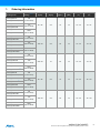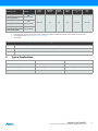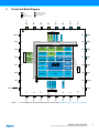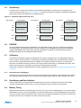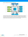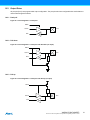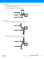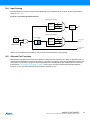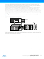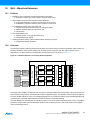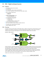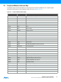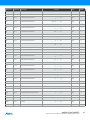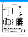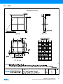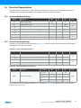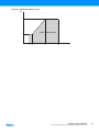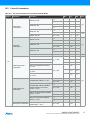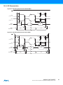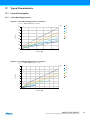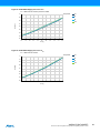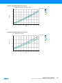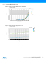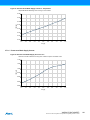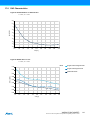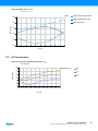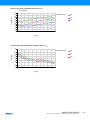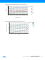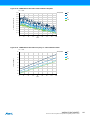
1
8/16-bit Atmel AVR XMEGA Microcontrollers ATxmega32E5 / ATxmega16E5 / ATxmega8E5 DATASHEET Features High-performance, low-power Atmel® AVR® XMEGA® 8/16-bit Microcontroller Nonvolatile program and data memories 8K –32KB of in-system self-programmable flash 2K – 4KB boot section 512Bytes – 1KB EEPROM 1K – 4KB internal SRAM Peripheral features Four-channel enhanced DMA controller with 8/16-bit address match Eight-channel event system Asynchronous and synchronous signal routing Quadrature encoder with rotary filter Three 16-bit timer/counters One timer/counter with four output compare or input capture channels Two timer/counter with two output compare or input capture channels High resolution extension enabling down to 4ns PWM resolution Waveform extension for control of motor, LED, lighting, H-bridge, high drives, and more Fault extension for safe and deterministic handling and/or shut-down of external driver CRC-16 (CRC-CCITT) and CRC-32 (IEEE 802.3) generator XMEGA Custom Logic (XCL) module with timer, counter and logic functions Two 8-bit timer/counters with capture/compare and 16-bit cascade mode Connected to one USART to support custom data frame length Connected to I/O pins and event system to do programmable logic functions MUX, AND, NAND, OR, NOR, XOR, XNOR, NOT, D-Flip-Flop, D Latch, RS Latch Two USARTs with full-duplex and single wire half-duplex configuration Master SPI mode Support custom protocols with configurable data frame length up to 256-bit System wake-up from deep sleep modes when used with internal 8MHz oscillator One two-wire interface with dual address match (I2C and SMBus compatible) Bridge configuration for simultaneous master and slave operation Up to 1MHz bus speed support One serial peripheral interface (SPI) 16-bit real time counter with separate oscillator and digital correction One sixteen-channel, 12-bit, 300ksps Analog to Digital Converter with: Offset and gain correction Averaging Over-sampling and decimation One two-channel, 12-bit, 1Msps Digital to Analog Converter Two Analog Comparators with window compare function and current sources External interrupts on all general purpose I/O pins Programmable watchdog timer with separate on-chip ultra low power oscillator QTouch® library support Capacitive touch buttons, sliders and wheels Special microcontroller features Power-on reset and programmable brown-out detection Internal and external clock options with PLL Programmable multilevel interrupt controller Five sleep modes Programming and debug interface PDI (Program and Debug Interface) I/O and Packages 26 programmable I/O pins 7x7mm 32-lead TQFP 5x5mm 32-lead VQFN 4x4mm 32-lead UQFN Operating Voltage 1.6 – 3.6V Operating frequency 0 – 12MHz from 1.6V 0 – 32MHz from 2.7V Atmel 8153J–AVR-ATxmega8E5-ATxmega16E5-ATxmega32E5_Datasheet–11/2014 1. Ordering Information Ordering Code ATxmega8E5-AU ATxmega8E5-AUR(4) ATxmega8E5-MU ATxmega8E5-MUR(4) ATxmega8E5-M4U ATxmega8E5-M4UR(4) ATxmega16E5-AU ATxmega16E5-AUR(4) ATxmega16E5-MU ATxmega16E5-MUR(4) ATxmega16E5-M4U ATxmega16E5-M4UR(4) ATxmega32E5-AU ATxmega32E5AUR(4) ATxmega32E5-MU ATxmega32E5-MUR(4) ATxmega32E5-M4U ATxmega32E5-M4UR(4) ATxmega8E5-AN ATxmega8E5-ANR(4) ATxmega8E5-MN ATxmega8E5-MNR(4) ATxmega8E5-M4N ATxmega8E5-M4NR(4) ATxmega16E5-AN ATxmega16E5-ANR(4) ATxmega16E5-MN ATxmega16E5-MNR(4) ATxmega16E5-M4N ATxmega16E5-M4NR(4) Package(1)(2)(3) Flash [Bytes] EEPROM [Bytes] SRAM [Bytes] Speed [MHz] Power supply [V] Temp. [°C] 8K + 2K 512 1K 32 1.6 – 3.6 -40 – 85 16K + 4K 512 2K 32 1.6 – 3.6 -40 – 85 32K + 4K 1K 4K 32 1.6 – 3.6 -40 – 85 8K + 2K 512 1K 32 1.6 – 3.6 -40 – 105 16K + 4K 512 2K 32 1.6 – 3.6 -40 – 105 32A (7x7mm TQFP) 32Z (5x5mm VQFN) 32MA (4x4mm UQFN) 32A (7x7mm TQFP) 32Z (5x5mm VQFN) 32MA (4x4mm UQFN) 32A (7x7mm TQFP) 32Z (5x5mm VQFN) 32MA (4x4mm UQFN) 32A (7x7mm TQFP) 32Z (5x5mm VQFN) 32MA (4x4mm UQFN) 32A (7x7mm TQFP) 32Z (5x5mm VQFN) 32MA (4x4mm UQFN) XMEGA E5 [DATASHEET] Atmel-8153J–AVR-ATxmega8E5-ATxmega16E5-ATxmega32E5_Datasheet–11/2014 2 Package(1)(2)(3) Ordering Code ATxmega32E5-AN ATxmega32E5ANR ATxmega32E5-MN (4) ATxmega32E5-M4N ATxmega32E5-M4NR Notes: 1. 2. 3. 4. EEPROM [Bytes] SRAM [Bytes] Speed [MHz] Power supply [V] Temp. [°C] 32K + 4K 1K 4K 32 1.6 – 3.6 -40 – 105 32A (7x7mm TQFP) (4) ATxmega32E5-MNR Flash [Bytes] (4) 32Z (5x5mm VQFN) 32MA (4x4mm UQFN) This device can also be supplied in wafer form. Please contact your local Atmel sales office for detailed ordering information. Pb-free packaging, complies to the European Directive for Restriction of Hazardous Substances (RoHS directive). Also Halide free and fully Green. For packaging information, see “Packaging Information” on page 68. Tape and Reel. Package Type 32A 32-lead, 7x7mm body size, 1.0mm body thickness, 0.8mm lead pitch, thin profile plastic quad flat package (TQFP) 32Z 32-lead, 0.5mm pitch, 5x5mm Very Thin quad Flat No Lead Package (VQFN) Sawn 32MA 32-lead, 0.4mm pitch, 4x4x0.60mm Ultra Thin Quad No Lead (UQFN) Package 2. Typical Applications Board controller Sensor control Motor control User interface Industrial control Ballast control, Inverters Communication bridges Battery charger Utility metering Appliances XMEGA E5 [DATASHEET] Atmel-8153J–AVR-ATxmega8E5-ATxmega16E5-ATxmega32E5_Datasheet–11/2014 3 Pinout and Block Diagram Power Programming, debug, test Ground External clock / Crystal pins Digital function General Purpose I/O PD1 PD2 PD3 26 25 PA7 29 27 PA6 30 PD0 PA5 31 28 AVCC 32 Analog function / Oscillators 24 PD4 23 PD5 22 PD6 21 PD7 20 PR0 19 PR1 18 GND 17 VCC XCL USART0 2 TC5 PA4 AREF 1 ADC Port D GND EVENT ROUTING NETWORK DATA BUS PA3 3 AREF 4 TEMPREF Watchdog Oscillator Reset Controller Real Time Counter VREF Sleep Controller OSC/CLK Control Event System Controller Interrupt Controller OCD Prog/Debug Interface ADC Port A PA2 Power Supervision DAC AC0:1 5 PA0 6 PDI 7 PDI / RESET 8 EDMA Controller CRC CPU BUS Controller EEPROM FLASH SRAM Port R PA1 Watchdog Timer IRCOM TWI SPI USART0 TC4:5 DATA BUS Notes: 1. 15 16 PC1 PC0 14 12 PC4 PC2 11 PC5 13 10 PC6 PC3 9 Port C PC7 3. For full details on pinout and alternate pin functions refer to “Pinout and Pin Functions” on page 57. XMEGA E5 [DATASHEET] Atmel-8153J–AVR-ATxmega8E5-ATxmega16E5-ATxmega32E5_Datasheet–11/2014 4 4. Overview The Atmel AVR XMEGA is a family of low power, high performance, and peripheral rich 8/16-bit microcontrollers based on the AVR enhanced RISC architecture. By executing instructions in a single clock cycle, the AVR XMEGA devices achieve CPU throughput approaching one million instructions per second (MIPS) per megahertz, allowing the system designer to optimize power consumption versus processing speed. The AVR CPU combines a rich instruction set with 32 general purpose working registers. All 32 registers are directly connected to the arithmetic logic unit (ALU), allowing two independent registers to be accessed in a single instruction, executed in one clock cycle. The resulting architecture is more code efficient while achieving throughputs many times faster than conventional single-accumulator or CISC based microcontrollers. The AVR XMEGA E5 devices provide the following features: in-system programmable flash with read-while-write capabilities; internal EEPROM and SRAM; four-channel enhanced DMA (EDMA) controller; eight-channel event system with asynchronous event support; programmable multilevel interrupt controller; 26 general purpose I/O lines; CRC-16 (CRC-CCITT) and CRC-32 (IEEE 802.3) generators; one XMEGA Custom Logic module with timer, counter and logic functions (XCL); 16-bit real-time counter (RTC) with digital correction; three flexible, 16-bit timer/counters with compare and PWM channels; two USARTs; one two-wire serial interface (TWI) allowing simultaneous master and slave; one serial peripheral interface (SPI); one sixteen-channel, 12-bit ADC with programmable gain, offset and gain correction, averaging, over-sampling and decimation; one 2-channel 12-bit DAC; two analog comparators (ACs) with window mode and current sources; programmable watchdog timer with separate internal oscillator; accurate internal oscillators with PLL and prescaler; and programmable brown-out detection. The program and debug interface (PDI), a fast, two-pin interface for programming and debugging, is available. The AVR XMEGA E5 devices have five software selectable power saving modes. The idle mode stops the CPU while allowing the SRAM, EDMA controller, event system, interrupt controller, and all peripherals to continue functioning. The power-down mode saves the SRAM and register contents, but stops the oscillators, disabling all other functions until the next TWI, or pin-change interrupt, or reset. In power-save mode, the asynchronous real-time counter continues to run, allowing the application to maintain a timer base while the rest of the device is sleeping. In standby mode, the external crystal oscillator keeps running while the rest of the device is sleeping. This allows very fast startup from the external crystal, combined with low power consumption. In extended standby mode, both the main oscillator and the asynchronous timer continue to run. In each power save, standby or extended standby mode, the low power mode of the internal 8MHz oscillator allows very fast startup time combined with very low power consumption. To further reduce power consumption, the peripheral clock to each individual peripheral can optionally be stopped in active mode and idle sleep mode and low power mode of the internal 8MHz oscillator can be enabled. Atmel offers a free QTouch library for embedding capacitive touch buttons, sliders and wheels functionality into AVR microcontrollers. The devices are manufactured using Atmel high-density, nonvolatile memory technology. The program flash memory can be reprogrammed in-system through the PDI. A boot loader running in the device can use any interface to download the application program to the flash memory. The boot loader software in the boot flash section can continue to run. By combining an 8/16-bit RISC CPU with in-system, self-programmable flash, the AVR XMEGA is a powerful microcontroller family that provides a highly flexible and cost effective solution for many embedded applications. All Atmel AVR XMEGA devices are supported with a full suite of program and system development tools, including C compilers, macro assemblers, program debugger/simulators, programmers, and evaluation kits. XMEGA E5 [DATASHEET] Atmel-8153J–AVR-ATxmega8E5-ATxmega16E5-ATxmega32E5_Datasheet–11/2014 5 5. Resources A comprehensive set of development tools, application notes and datasheets are available for download on http://www.atmel.com/avr. 5.1 Recommended Reading XMEGA E Manual XMEGA Application Notes This device data sheet only contains part specific information with a short description of each peripheral and module. The XMEGA E Manual describes the modules and peripherals in depth. The XMEGA application notes contain example code and show applied use of the modules and peripherals. All documentations are available from www.atmel.com/avr. 6. Capacitive Touch Sensing The Atmel QTouch® library provides a simple to use solution to realize touch sensitive interfaces on most Atmel AVR® microcontrollers. The patented charge-transfer signal acquisition offers robust sensing and includes fully debounced reporting of touch keys and includes Adjacent Key Suppression™ (AKS™) technology for unambiguous detection of key events. The QTouch library includes support for the QTouch and QMatrix acquisition methods. Touch sensing can be added to any application by linking the appropriate Atmel QTouch library for the AVR Microcontroller. This is done by using a simple set of APIs to define the touch channels and sensors, and then calling the touch sensing API’s to retrieve the channel information and determine the touch sensor states. The Atmel QTouch library is FREE and downloadable from the Atmel website at the following location: http://www.atmel.com/tools/QTOUCHLIBRARY.aspx. For implementation details and other information, refer to the Atmel QTouch library user guide - also available for download from the Atmel website. XMEGA E5 [DATASHEET] Atmel-8153J–AVR-ATxmega8E5-ATxmega16E5-ATxmega32E5_Datasheet–11/2014 6 7. CPU 7.1 Features 8/16-bit, high-performance Atmel AVR RISC CPU 142 instructions Hardware multiplier 32x8-bit registers directly connected to the ALU Stack in RAM Stack pointer accessible in I/O memory space Direct addressing of up to 16MB of program memory and 16MB of data memory True 16/24-bit access to 16/24-bit I/O registers Efficient support for 8-, 16-, and 32-bit arithmetic Configuration change protection of system-critical features 7.2 Overview All AVR XMEGA devices use the 8/16-bit AVR CPU. The main function of the CPU is to execute the code and perform all calculations. The CPU is able to access memories, perform calculations, control peripherals, and execute the program in the flash memory. Interrupt handling is described in a separate section, refer to “Interrupts and Programmable Multilevel Interrupt Controller” on page 28. 7.3 Architectural Overview In order to maximize performance and parallelism, the AVR CPU uses a Harvard architecture with separate memories and buses for program and data. Instructions in the program memory are executed with single-level pipelining. While one instruction is being executed, the next instruction is pre-fetched from the program memory. This enables instructions to be executed on every clock cycle. For details of all AVR instructions, refer to http://www.atmel.com/avr. XMEGA E5 [DATASHEET] Atmel-8153J–AVR-ATxmega8E5-ATxmega16E5-ATxmega32E5_Datasheet–11/2014 7 Figure 7-1. Block Diagram of the AVR CPU Architecture The arithmetic logic unit (ALU) supports arithmetic and logic operations between registers or between a constant and a register. Single-register operations can also be executed in the ALU. After an arithmetic operation, the status register is updated to reflect information about the result of the operation. The ALU is directly connected to the fast-access register file. The 32 x 8-bit general purpose working registers all have single clock cycle access time allowing single-cycle arithmetic logic unit (ALU) operation between registers or between a register and an immediate. Six of the 32 registers can be used as three 16-bit address pointers for program and data space addressing, enabling efficient address calculations. The memory spaces are linear. The data memory space and the program memory space are two different memory spaces. The data memory space is divided into I/O registers, SRAM, and memory mapped EEPROM. All I/O status and control registers reside in the lowest 4KB addresses of the data memory. This is referred to as the I/O memory space. The lowest 64 addresses can be accessed directly, or as the data space locations from 0x00 to 0x3F. The rest is the extended I/O memory space, ranging from 0x0040 to 0x0FFF. I/O registers here must be accessed as data space locations using load (LD/LDS/LDD) and store (ST/STS/STD) instructions. The SRAM holds data. Code execution from SRAM is not supported. It can easily be accessed through the five different addressing modes supported in the AVR architecture. The first SRAM address is 0x2000. Data addresses 0x1000 to 0x1FFF are reserved for EEPROM. The program memory is divided in two sections, the application program section and the boot program section. Both sections have dedicated lock bits for write and read/write protection. The SPM instruction that is used for selfprogramming of the application flash memory must reside in the boot program section. The application section contains an application table section with separate lock bits for write and read/write protection. The application table section can be used for save storing of nonvolatile data in the program memory. XMEGA E5 [DATASHEET] Atmel-8153J–AVR-ATxmega8E5-ATxmega16E5-ATxmega32E5_Datasheet–11/2014 8 7.4 ALU - Arithmetic Logic Unit The arithmetic logic unit (ALU) supports arithmetic and logic operations between registers or between a constant and a register. Single-register operations can also be executed. The ALU operates in direct connection with all 32 general purpose registers. In a single clock cycle, arithmetic operations between general purpose registers or between a register and an immediate are executed and the result is stored in the register file. After an arithmetic or logic operation, the status register is updated to reflect information about the result of the operation. ALU operations are divided into three main categories – arithmetic, logical, and bit functions. Both 8- and 16-bit arithmetic is supported, and the instruction set allows for efficient implementation of 32-bit arithmetic. The hardware multiplier supports signed and unsigned multiplication and fractional format. 7.4.1 Hardware Multiplier The multiplier is capable of multiplying two 8-bit numbers into a 16-bit result. The hardware multiplier supports different variations of signed and unsigned integer and fractional numbers: Multiplication of unsigned integers Multiplication of signed integers Multiplication of a signed integer with an unsigned integer Multiplication of unsigned fractional numbers Multiplication of signed fractional numbers Multiplication of a signed fractional number with an unsigned one A multiplication takes two CPU clock cycles. 7.5 Program Flow After reset, the CPU starts to execute instructions from the lowest address in the flash program memory ‘0.’ The program counter (PC) addresses the next instruction to be fetched. Program flow is provided by conditional and unconditional jump and call instructions capable of addressing the whole address space directly. Most AVR instructions use a 16-bit word format, while a limited number use a 32-bit format. During interrupts and subroutine calls, the return address PC is stored on the stack. The stack is allocated in the general data SRAM, and consequently the stack size is only limited by the total SRAM size and the usage of the SRAM. After reset, the stack pointer (SP) points to the highest address in the internal SRAM. The SP is read/write accessible in the I/O memory space, enabling easy implementation of multiple stacks or stack areas. The data SRAM can easily be accessed through the five different addressing modes supported in the AVR CPU. 7.6 Status Register The status register (SREG) contains information about the result of the most recently executed arithmetic or logic instruction. This information can be used for altering program flow in order to perform conditional operations. Note that the status register is updated after all ALU operations, as specified in the instruction set reference. This will in many cases remove the need for using the dedicated compare instructions, resulting in faster and more compact code. The status register is not automatically stored when entering an interrupt routine nor restored when returning from an interrupt. This must be handled by software. The status register is accessible in the I/O memory space. 7.7 Stack and Stack Pointer The stack is used for storing return addresses after interrupts and subroutine calls. It can also be used for storing temporary data. The stack pointer (SP) register always points to the top of the stack. It is implemented as two 8-bit registers that are accessible in the I/O memory space. Data are pushed and popped from the stack using the PUSH and POP instructions. The stack grows from a higher memory location to a lower memory location. This implies that pushing data onto the stack decreases the SP, and popping data off the stack increases the SP. The SP is automatically loaded XMEGA E5 [DATASHEET] Atmel-8153J–AVR-ATxmega8E5-ATxmega16E5-ATxmega32E5_Datasheet–11/2014 9 after reset, and the initial value is the highest address of the internal SRAM. If the SP is changed, it must be set to point above address 0x2000, and it must be defined before any subroutine calls are executed or before interrupts are enabled. During interrupts or subroutine calls, the return address is automatically pushed on the stack. The return address can be two or three bytes, depending on program memory size of the device. For devices with 128KB or less of program memory, the return address is two bytes, and hence the stack pointer is decremented/incremented by two. For devices with more than 128KB of program memory, the return address is three bytes, and hence the SP is decremented/incremented by three. The return address is popped off the stack when returning from interrupts using the RETI instruction, and from subroutine calls using the RET instruction. The SP is decremented by one when data are pushed on the stack with the PUSH instruction, and incremented by one when data is popped off the stack using the POP instruction. To prevent corruption when updating the stack pointer from software, a write to SPL will automatically disable interrupts for up to four instructions or until the next I/O memory write. 7.8 Register File The register file consists of 32 x 8-bit general purpose working registers with single clock cycle access time. The register file supports the following input/output schemes: One 8-bit output operand and one 8-bit result input Two 8-bit output operands and one 8-bit result input Two 8-bit output operands and one 16-bit result input One 16-bit output operand and one 16-bit result input Six of the 32 registers can be used as three 16-bit address register pointers for data space addressing, enabling efficient address calculations. One of these address pointers can also be used as an address pointer for lookup tables in flash program memory. XMEGA E5 [DATASHEET] Atmel-8153J–AVR-ATxmega8E5-ATxmega16E5-ATxmega32E5_Datasheet–11/2014 10 8. Memories 8.1 Features Flash program memory One linear address space In-system programmable Self-programming and boot loader support Application section for application code Application table section for application code or data storage Boot section for application code or bootloader code Separate read/write protection lock bits for all sections Built in fast CRC check of a selectable flash program memory section Data memory One linear address space Single-cycle access from CPU SRAM EEPROM Byte and page accessible Memory mapped for direct load and store I/O memory Configuration and status registers for all peripherals and modules Four bit-accessible general purpose registers for global variables or flags Bus arbitration Deterministic handling of priority between CPU, EDMA controller, and other bus masters Separate buses for SRAM, EEPROM, and I/O memory Simultaneous bus access for CPU and EDMA controller Production signature row memory for factory programmed data ID for each microcontroller device type Serial number for each device Calibration bytes for factory calibrated peripherals User signature row One flash page in size Can be read and written from software Content is kept after chip erase 8.2 Overview The Atmel AVR architecture has two main memory spaces, the program memory and the data memory. Executable code can reside only in the program memory, while data can be stored in the program memory and the data memory. The data memory includes the internal SRAM, and EEPROM for nonvolatile data storage. All memory spaces are linear and require no memory bank switching. Nonvolatile memory (NVM) spaces can be locked for further write and read/write operations. This prevents unrestricted access to the application software. A separate memory section contains the fuse bytes. These are used for configuring important system functions, and can only be written by an external programmer. The available memory size configurations are shown in “Ordering Information” on page 2”. In addition, each device has a Flash memory signature row for calibration data, device identification, serial number etc. 8.3 Flash Program Memory The Atmel AVR XMEGA devices contain on-chip, in-system reprogrammable flash memory for program storage. The flash memory can be accessed for read and write from an external programmer through the PDI or from application software running in the device. XMEGA E5 [DATASHEET] Atmel-8153J–AVR-ATxmega8E5-ATxmega16E5-ATxmega32E5_Datasheet–11/2014 11 All AVR CPU instructions are 16 or 32 bits wide, and each flash location is 16 bits wide. The flash memory is organized in two main sections, the application section and the boot loader section. The sizes of the different sections are fixed, but device-dependent. These two sections have separate lock bits, and can have different levels of protection. The store program memory (SPM) instruction, which is used to write to the flash from the application software, will only operate when executed from the boot loader section. The application section contains an application table section with separate lock settings. This enables safe storage of nonvolatile data in the program memory. Figure 8-1. Flash Program Memory (hexadecimal address) Word Address ATxmega32E5 ATxmega16E5 ATxmega8E5 0 0 0 Application Section (32K/16K/8K) ... 8.3.1 37FF / 17FF / BFF 3800 / 1800 / C00 Application Table Section 3FFF / 1FFF / FFF (4K/4K/2K) 4000 / 2000 / 1000 Boot Section 47FF / 27FF / 13FF (4K/4K/2K) Application Section The Application section is the section of the flash that is used for storing the executable application code. The protection level for the application section can be selected by the boot lock bits for this section. The application section can not store any boot loader code since the SPM instruction cannot be executed from the application section. 8.3.2 Application Table Section The application table section is a part of the application section of the flash memory that can be used for storing data. The size is identical to the boot loader section. The protection level for the application table section can be selected by the boot lock bits for this section. The possibilities for different protection levels on the application section and the application table section enable safe parameter storage in the program memory. If this section is not used for data, application code can reside here. 8.3.3 Boot Loader Section While the application section is used for storing the application code, the boot loader software must be located in the boot loader section because the SPM instruction can only initiate programming when executing from this section. When programming, the CPU is halted, waiting for the flash operation to complete. The SPM instruction can access the entire flash, including the boot loader section itself. The protection level for the boot loader section can be selected by the boot loader lock bits. If this section is not used for boot loader software, application code can be stored here. 8.3.4 Production Signature Row The production signature row is a separate memory section for factory programmed data. It contains calibration data for functions such as oscillators and analog modules. Some of the calibration values will be automatically loaded to the corresponding module or peripheral unit during reset. Other values must be loaded from the signature row and written to XMEGA E5 [DATASHEET] Atmel-8153J–AVR-ATxmega8E5-ATxmega16E5-ATxmega32E5_Datasheet–11/2014 12 the corresponding peripheral registers from software. For details on calibration conditions, refer to “Electrical Characteristics” on page 71. The production signature row also contains an ID that identifies each microcontroller device type and a serial number for each manufactured device. The serial number consists of the production lot number, wafer number, and wafer coordinates for the device. The device ID for the available devices is shown in Table 8-1. The production signature row cannot be written or erased, but it can be read from application software and external programmers. Table 8-1. Device ID Bytes for Atmel AVR XMEGA E5 Devices Device 8.3.5 Device ID bytes Byte 2 Byte 1 Byte 0 ATxmega32E5 4C 95 1E ATxmega16E5 45 94 1E ATxmega8E5 41 93 1E User Signature Row The user signature row is a separate memory section that is fully accessible (read and write) from application software and external programmers. It is one flash page in size, and is meant for static user parameter storage, such as calibration data, custom serial number, identification numbers, random number seeds, etc. This section is not erased by chip erase commands that erase the flash, and requires a dedicated erase command. This ensures parameter storage during multiple program/erase operations and on-chip debug sessions. 8.4 Fuses and Lock Bits The fuses are used to configure important system functions, and can only be written from an external programmer. The application software can read the fuses. The fuses are used to configure reset sources such as brownout detector and watchdog, startup configuration, etc. The lock bits are used to set protection levels for the different flash sections (i.e., if read and/or write access should be blocked). Lock bits can be written by external programmers and application software, but only to stricter protection levels. Chip erase is the only way to erase the lock bits. To ensure that flash contents are protected even during chip erase, the lock bits are erased after the rest of the flash memory has been erased. An un-programmed fuse or lock bit will have the value one, while a programmed fuse or lock bit will have the value zero. Both fuses and lock bits are reprogrammable like the flash program memory. XMEGA E5 [DATASHEET] Atmel-8153J–AVR-ATxmega8E5-ATxmega16E5-ATxmega32E5_Datasheet–11/2014 13 8.5 Data Memory The data memory contains the I/O memory, internal SRAM and EEPROM. The data memory is organized as one continuous memory section, see Table 8-2 on page 15. To simplify development, I/O Memory, EEPROM and SRAM will always have the same start addresses for all XMEGA devices. Figure 8-2. Data Memory Map (hexadecimal value) Byte Address ATxmega32E5 0 FFF Byte Address I/O Registers (4K) 1000 EEPROM (1K) 13FF ATxmega16E5 0 FFF 1000 11FF RESERVED 2000 2FFF 8.6 Internal SRAM (4K) I/O Registers (4K) EEPROM (512B) Byte Address 0 FFF 1000 11FF RESERVED 2000 27FF Internal SRAM (2K) ATxmega8E5 I/O Registers (4K) EEPROM (512B) RESERVED 2000 27FF Internal SRAM (2K) EEPROM Atmel AVR XMEGA E5 devices have EEPROM for nonvolatile data storage. It is memory mapped and accessed in normal data space. The EEPROM supports both byte and page access. EEPROM allows highly efficient EEPROM reading and EEPROM buffer loading. When doing this, EEPROM is accessible using load and store instructions. EEPROM will always start at hexadecimal address 0x1000. 8.7 I/O Memory The status and configuration registers for peripherals and modules, including the CPU, are addressable through I/O memory locations. All I/O locations can be accessed by the load (LD/LDS/LDD) and store (ST/STS/STD) instructions, which are used to transfer data between the 32 registers in the register file and the I/O memory. The IN and OUT instructions can address I/O memory locations in the range of 0x00 to 0x3F directly. In the address range 0x00 - 0x1F, single-cycle instructions for manipulation and checking of individual bits are available. The I/O memory address for all peripherals and modules in XMEGA E5 is shown in the “Peripheral Module Address Map” on page 61. 8.7.1 General Purpose I/O Registers The lowest four I/O memory addresses are reserved as general purpose I/O registers. These registers can be used for storing global variables and flags, as they are directly bit-accessible using the SBI, CBI, SBIS, and SBIC instructions. 8.8 Data Memory and Bus Arbitration Since the data memory is organized as three separate sets of memories, the different bus masters (CPU, EDMA controller read and EDMA controller write, etc.) can access different memory sections at the same time. 8.9 Memory Timing Read and write access to the I/O memory takes one CPU clock cycle. A write to SRAM takes one cycle, and a read from SRAM takes two cycles. For burst read (EDMA), new data are available every cycle. EEPROM page load (write) takes one cycle, and three cycles are required for read. For burst read, new data are available every second cycle. Refer to the instruction summary for more details on instructions and instruction timing. XMEGA E5 [DATASHEET] Atmel-8153J–AVR-ATxmega8E5-ATxmega16E5-ATxmega32E5_Datasheet–11/2014 14 8.10 Device ID and Revision Each device has a three-byte device ID. This ID identifies Atmel as the manufacturer of the device and the device type. A separate register contains the revision number of the device. 8.11 I/O Memory Protection Some features in the device are regarded as critical for safety in some applications. Due to this, it is possible to lock the I/O register related to the clock system, the event system, and the waveform extensions. As long as the lock is enabled, all related I/O registers are locked and they cannot be written from the application software. The lock registers themselves are protected by the configuration change protection mechanism. 8.12 Flash and EEPROM Page Size The flash program memory and EEPROM data memory are organized in pages. The pages are word accessible for the flash and byte accessible for the EEPROM. Table 8-2 shows the Flash Program Memory organization and Program Counter (PC) size. Flash write and erase operations are performed on one page at a time, while reading the Flash is done one byte at a time. For Flash access the Z-pointer (Z[m:n]) is used for addressing. The most significant bits in the address (FPAGE) give the page number and the least significant address bits (FWORD) give the word in the page. Table 8-2. Number of Words and Pages in the Flash Devices PC size Flash size Page Size FWORD bits bytes words ATxmega32E5 15 32K+4K 64 Z[6:0] ATxmega16E5 14 16K+4K 64 ATxmega8E5 13 8K+2K 64 FPAGE Application Boot Size No. of pages Size No. of pages Z[14:7] 32K 256 4K 32 Z[6:0] Z[13:7] 16K 128 4K 32 Z[6:0] Z[12:7] 8K 64 2K 16 Table 8-3 shows EEPROM memory organization for the Atmel AVR XMEGA E5 devices. EEPROM write and erase operations can be performed one page or one byte at a time, while reading the EEPROM is done one byte at a time. For EEPROM access the NVM address register (ADDR[m:n]) is used for addressing. The most significant bits in the address (E2PAGE) give the page number and the least significant address bits (E2BYTE) give the byte in the page. Table 8-3. Number of Words and Pages in the EEPROM Devices EEPROM Page Size E2BYTE E2PAGE No. of Pages Size bytes ATxmega32E5 1K 32 ADDR[4:0] ADDR[10:5] 32 ATxmega16E5 512Bytes 32 ADDR[4:0] ADDR[10:5] 16 ATxmega8E5 512Bytes 32 ADDR[4:0] ADDR[10:5] 16 XMEGA E5 [DATASHEET] Atmel-8153J–AVR-ATxmega8E5-ATxmega16E5-ATxmega32E5_Datasheet–11/2014 15 9. EDMA – Enhanced DMA Controller 9.1 Features The EDMA Controller allows data transfers with minimal CPU intervention from data memory to data memory from data memory to peripheral from peripheral to data memory from peripheral to peripheral Four peripheral EDMA channels with separate: transfer triggers interrupt vectors addressing modes data matching Two peripheral channels can be combined to one standard channel with separate: transfer triggers interrupt vectors addressing modes data search Programmable channel priority From 1byte to 128KB of data in a single transaction Up to 64K block transfer with repeat 1 or 2 bytes burst transfers Multiple addressing modes Static Increment Optional reload of source and destination address at the end of each Burst Block Transaction Optional Interrupt on end of transaction Optional connection to CRC Generator module for CRC on EDMA data 9.2 Overview The four-channel enhanced direct memory access (EDMA) controller can transfer data between memories and peripherals, and thus offload these tasks from the CPU. It enables high data transfer rates with minimum CPU intervention, and frees up CPU time. The four EDMA channels enable up to four independent and parallel transfers. The EDMA controller can move data between SRAM and peripherals, between SRAM locations and directly between peripheral registers. With access to all peripherals, the EDMA controller can handle automatic transfer of data to/from communication modules. The EDMA controller can also read from EEPROM memory. Data transfers are done in continuous bursts of 1 or 2 bytes. They build block transfers of configurable size from 1 byte to 64KB. Repeat option can be used to repeat once each block transfer for single transactions up to 128KB. Source and destination addressing can be static or incremental. Automatic reload of source and/or destination addresses can be done after each burst or block transfer, or when a transaction is complete. Application software, peripherals, and events can trigger EDMA transfers. The four EDMA channels have individual configuration and control settings. This includes source, destination, transfer triggers, and transaction sizes. They have individual interrupt settings. Interrupt requests can be generated when a transaction is complete or when the EDMA controller detects an error on an EDMA channel. To enable flexibility in transfers, channels can be interlinked so that the second takes over the transfer when the first is finished. XMEGA E5 [DATASHEET] Atmel-8153J–AVR-ATxmega8E5-ATxmega16E5-ATxmega32E5_Datasheet–11/2014 16 The EDMA controller supports extended features such as double buffering, data match for peripherals and data search for SRAM or EEPROM. The EDMA controller supports two types of channel. Each channel type can be selected individually. XMEGA E5 [DATASHEET] Atmel-8153J–AVR-ATxmega8E5-ATxmega16E5-ATxmega32E5_Datasheet–11/2014 17 10. Event System 10.1 Features System for direct peripheral-to-peripheral communication and signaling Peripherals can directly send, receive, and react to peripheral events CPU and EDMA controller independent operation 100% predictable signal timing Short and guaranteed response time Synchronous and asynchronous event routing Eight event channels for up to eight different and parallel signal routing and configurations Events can be sent and/or used by most peripherals, clock system, and software Additional functions include Quadrature decoder with rotary filtering Digital filtering of I/O pin state with configurable filter Simultaneous synchronous and asynchronous events provided to peripheral Works in all sleep modes 10.2 Overview The event system enables direct peripheral-to-peripheral communication and signaling. It allows a change in one peripheral’s state to automatically trigger actions in other peripherals. It is designed to provide a predictable system for short and predictable response times between peripherals. It allows for autonomous peripheral control and interaction without the use of interrupts, CPU, or EDMA controller resources, and is thus a powerful tool for reducing the complexity, size and execution time of application code. It allows for synchronized timing of actions in several peripheral modules. The event system enables also asynchronous event routing for instant actions in peripherals. A change in a peripheral’s state is referred to as an event, and usually corresponds to the peripheral’s interrupt conditions. Events can be directly passed to other peripherals using a dedicated routing network called the event routing network. How events are routed and used by the peripherals is configured in software. Figure 10-1 shows a basic diagram of all connected peripherals. The event system can directly connect together analog and digital converters, analog comparators, I/O port pins, the real-time counter, timer/counters, IR communication module (IRCOM), and XMEGA Custom Logic (programmable logic) block (XCL). It can also be used to trigger EDMA transactions (EDMA controller). Events can also be generated from software and peripheral clock. XMEGA E5 [DATASHEET] Atmel-8153J–AVR-ATxmega8E5-ATxmega16E5-ATxmega32E5_Datasheet–11/2014 18 Figure 10-1. Event System Overview and Connected Peripherals CPU / Software EDMA Controller Event Routing Network ADC Event System Controller AC DAC clkPER Prescaler Real Time Counter Timer / Counters XMEGA Custom Logic IRCOM Port Pins The event routing network consists of eight software-configurable multiplexers that control how events are routed and used. These are called event channels, and allow up to eight parallel event configurations and routing. The maximum routing latency of an external event is two peripheral clock cycles due to re-synchronization, but several peripherals can directly use the asynchronous event without any clock delay. The event system works in all power sleep modes, but only asynchronous events can be routed in sleep modes where the system clock is not available. XMEGA E5 [DATASHEET] Atmel-8153J–AVR-ATxmega8E5-ATxmega16E5-ATxmega32E5_Datasheet–11/2014 19 11. System Clock and Clock options 11.1 Features Fast start-up time Safe run-time clock switching Internal Oscillators: 32MHz run-time calibrated and tuneable oscillator 8MHz calibrated oscillator with 2MHz output option and fast start-up 32.768kHz calibrated oscillator 32kHz Ultra Low Power (ULP) oscillator with 1kHz output External clock options 0.4 - 16MHz Crystal Oscillator 32kHz crystal oscillator with digital correction External clock input in selectable pin location PLL with 20 - 128MHz output frequency Internal and external clock options and 1 to 31x multiplication Lock detector Clock Prescalers with 1x to 2048x division Fast peripheral clocks running at two and four times the CPU clock frequency Automatic Run-Time Calibration of the 32MHz internal oscillator External oscillator and PLL lock failure detection with optional non maskable interrupt 11.2 Overview Atmel AVR XMEGA E5 devices have a flexible clock system supporting a large number of clock sources. It incorporates both accurate internal oscillators and external crystal oscillator and resonator support. A high-frequency phase locked loop (PLL) and clock prescalers can be used to generate a wide range of clock frequencies. A calibration feature (DFLL) is available, and can be used for automatic run-time calibration of the 32MHz internal oscillator to remove frequency drift over voltage and temperature. An oscillator failure monitor can be enabled to issue a nonmaskable interrupt and switch to the internal oscillator if the external oscillator or PLL fails. When a reset occurs, all clock sources except the 32kHz ultra low power oscillator are disabled. After reset, the device will always start up running from the 2MHz output of the 8MHz internal oscillator. During normal operation, the system clock source and prescalers can be changed from software at any time. Figure 11-1 on page 21 presents the principal clock system in the XMEGA E5 family of devices. Not all of the clocks need to be active at a given time. The clocks for the CPU and peripherals can be stopped using sleep modes and power reduction registers, as described in “Power Management and Sleep Modes” on page 23. XMEGA E5 [DATASHEET] Atmel-8153J–AVR-ATxmega8E5-ATxmega16E5-ATxmega32E5_Datasheet–11/2014 20 Figure 11-1. The Clock System, Clock Sources, and Clock Distribution Real Time Counter Peripherals RAM Non-Volatile Memory AVR CPU clkPER clkCPU clkPER2 clkPER4 clk RTC Brown-out Detector System Clock Prescalers Watchdog Timer clkSYS System Clock Multiplexer (SCLKSEL) DIV32 DIV32 DIV32 RTCSRC PLL 11.3 XTAL2 0.4 – 16 MHz XTAL XTAL1 32.768 kHz TOSC TOSC2 32.768 kHz Int. OSC TOSC1 32 kHz Int. ULP 32 MHz Int. Osc 8 MHz Int. Osc PC[4] XOSCSEL DIV4 DIV4 PLLSRC Clock Sources The clock sources are divided in two main groups: internal oscillators and external clock sources. Most of the clock sources can be directly enabled and disabled from software, while others are automatically enabled or disabled, depending on peripheral settings. After reset, the device starts up running from the 2MHz output of the 8MHz internal oscillator. The other clock sources, DFLL and PLL, are turned off by default. The internal oscillators do not require any external components to run. For details on characteristics and accuracy of the internal oscillators, refer to the device datasheet. 11.3.1 32kHz Ultra Low Power Internal Oscillator This oscillator provides an approximate 32kHz clock. The 32kHz ultra low power (ULP) internal oscillator is a very low power clock source, and it is not designed for high accuracy. The oscillator employs a built-in prescaler that provides a 1kHz output. The oscillator is automatically enabled/disabled when it is used as clock source for any part of the device. This oscillator can be selected as the clock source for the RTC. XMEGA E5 [DATASHEET] Atmel-8153J–AVR-ATxmega8E5-ATxmega16E5-ATxmega32E5_Datasheet–11/2014 21 11.3.2 32.768kHz Calibrated Internal Oscillator This oscillator provides an approximate 32.768kHz clock. It is calibrated during production to provide a default frequency close to its nominal frequency. The calibration register can also be written from software for run-time calibration of the oscillator frequency. The oscillator employs a built-in prescaler, which provides both a 32.768kHz output and a 1.024kHz output. 11.3.3 32.768kHz Crystal Oscillator A 32.768kHz crystal oscillator can be connected between the TOSC1 and TOSC2 pins and enables a dedicated low frequency oscillator input circuit. A low power mode with reduced voltage swing on TOSC2 is available. This oscillator can be used as a clock source for the system clock and RTC, and as the DFLL reference clock. 11.3.4 0.4 - 16MHz Crystal Oscillator This oscillator can operate in four different modes optimized for different frequency ranges, all within 0.4 - 16MHz. 11.3.5 8MHz Calibrated Internal Oscillator The 8MHz calibrated internal oscillator is the default system clock source after reset. It is calibrated during production to provide a default frequency close to its nominal frequency. The calibration register can also be written from software for run-time calibration of the oscillator frequency. The oscillator employs a built-in prescaler, with 2MHz output. The default output frequency at start-up and after reset is 2MHz. A low power mode option can be used to enable fast system wakeup from power-save mode. In all other modes, the low power mode can be enabled to significantly reduce the power consumption of the internal oscillator. 11.3.6 32MHz Run-time Calibrated Internal Oscillator The 32MHz run-time calibrated internal oscillator is a high-frequency oscillator. It is calibrated during production to provide a default frequency close to its nominal frequency. A digital frequency looked loop (DFLL) can be enabled for automatic run-time calibration of the oscillator to compensate for temperature and voltage drift and optimize the oscillator accuracy. This oscillator can also be adjusted and calibrated to any frequency between 30 and 55MHz. 11.3.7 External Clock Sources The XTAL1 and XTAL2 pins can be used to drive an external oscillator, either a quartz crystal or a ceramic resonator. XTAL1 or pin 4 of port C (PC4) can be used as input for an external clock signal. The TOSC1 and TOSC2 pins are dedicated to driving a 32.768kHz crystal oscillator. 11.3.8 PLL with 1x-31x Multiplication Factor The built-in phase locked loop (PLL) can be used to generate a high-frequency system clock. The PLL has a userselectable multiplication factor of from 1 to 31. In combination with the prescalers, this gives a wide range of output frequencies from all clock sources. XMEGA E5 [DATASHEET] Atmel-8153J–AVR-ATxmega8E5-ATxmega16E5-ATxmega32E5_Datasheet–11/2014 22 12. Power Management and Sleep Modes 12.1 Features Power management for adjusting power consumption and functions Five sleep modes Idle Power down Power save Standby Extended standby Power reduction register to disable clock and turn off unused peripherals in active and idle modes 12.2 Overview Various sleep modes and clock gating are provided in order to tailor power consumption to application requirements. This enables the Atmel AVR XMEGA microcontroller to stop unused modules to save power. All sleep modes are available and can be entered from active mode. In active mode, the CPU is executing application code. When the device enters sleep mode, program execution is stopped and interrupts or a reset is used to wake the device again. The application code decides which sleep mode to enter and when. Interrupts from enabled peripherals and all enabled reset sources can restore the microcontroller from sleep to active mode. In addition, power reduction registers provide a method to stop the clock to individual peripherals from software. When this is done, the current state of the peripheral is frozen, and there is no power consumption from that peripheral. This reduces the power consumption in active mode and idle sleep modes and enables much more fine-tuned power management than sleep modes alone. 12.3 Sleep Modes Sleep modes are used to shut down modules and clock domains in the microcontroller in order to save power. XMEGA microcontrollers have five different sleep modes tuned to match the typical functional stages during application execution. A dedicated sleep instruction (SLEEP) is available to enter sleep mode. Interrupts are used to wake the device from sleep, and the available interrupt wake-up sources are dependent on the configured sleep mode. When an enabled interrupt occurs, the device will wake up and execute the interrupt service routine before continuing normal program execution from the first instruction after the SLEEP instruction. If other, higher priority interrupts are pending when the wake-up occurs, their interrupt service routines will be executed according to their priority before the interrupt service routine for the wake-up interrupt is executed. After wake-up, the CPU is halted for four cycles before execution starts. The content of the register file, SRAM and registers are kept during sleep. If a reset occurs during sleep, the device will reset, start up, and execute from the reset vector. 12.3.1 Idle Mode In idle mode the CPU and nonvolatile memory are stopped (note that any ongoing programming will be completed), but all peripherals, including the interrupt controller, event system and EDMA controller are kept running. Any enabled interrupt will wake the device. 12.3.2 Power-down Mode In power-down mode, all clocks, including the real-time counter clock source, are stopped. This allows operation only of asynchronous modules that do not require a running clock. The only interrupts that can wake up the MCU are the twowire interface address match interrupt and asynchronous port interrupts. XMEGA E5 [DATASHEET] Atmel-8153J–AVR-ATxmega8E5-ATxmega16E5-ATxmega32E5_Datasheet–11/2014 23 12.3.3 Power-save Mode Power-save mode is identical to power down, with one exception. If the real-time counter (RTC) is enabled, it will keep running during sleep, and the device can also wake up from either an RTC overflow or compare match interrupt. Low power mode option of 8MHz internal oscillator enables instant oscillator wake-up time. This reduces the MCU wake-up time or enables the MCU wake-up from UART bus. 12.3.4 Standby Mode Standby mode is identical to power down, with the exception that the enabled system clock sources are kept running while the CPU, peripheral, and RTC clocks are stopped. This reduces the wake-up time. The low power option of 8MHz internal oscillator can be enabled to further reduce the power consumption. 12.3.5 Extended Standby Mode Extended standby mode is identical to power-save mode, with the exception that the enabled system clock sources are kept running while the CPU and peripheral clocks are stopped. This reduces the wake-up time. The low power option of 8MHz internal oscillator can be enabled to further reduce the power consumption. XMEGA E5 [DATASHEET] Atmel-8153J–AVR-ATxmega8E5-ATxmega16E5-ATxmega32E5_Datasheet–11/2014 24 13. System Control and Reset 13.1 Features Reset the microcontroller and set it to initial state when a reset source goes active Multiple reset sources that cover different situations Power-on reset External reset Watchdog reset Brownout reset PDI reset Software reset Asynchronous operation No running system clock in the device is required for reset Reset status register for reading the reset source from the application code 13.2 Overview The reset system issues a microcontroller reset and sets the device to its initial state. This is for situations where operation should not start or continue, such as when the microcontroller operates below its power supply rating. If a reset source goes active, the device enters and is kept in reset until all reset sources have released their reset. The I/O pins are immediately tri-stated. The program counter is set to the reset vector location, and all I/O registers are set to their initial values. The SRAM content is kept. However, if the device accesses the SRAM when a reset occurs, the content of the accessed location can not be guaranteed. After reset is released from all reset sources, the default oscillator is started and calibrated before the device starts running from the reset vector address. By default, this is the lowest program memory address, 0, but it is possible to move the reset vector to the lowest address in the boot section. The reset functionality is asynchronous, and so no running system clock is required to reset the device. The software reset feature makes it possible to issue a controlled system reset from the user software. The reset status register has individual status flags for each reset source. It is cleared at power-on reset, and shows which sources have issued a reset since the last power-on. 13.3 Reset Sequence A reset request from any reset source will immediately reset the device and keep it in reset as long as the request is active. When all reset requests are released, the device will go through three stages before the device starts running again: Reset counter delay Oscillator startup Oscillator calibration If another reset requests occurs during this process, the reset sequence will start over again. 13.4 Reset Sources 13.4.1 Power-on Reset A power-on reset (POR) is generated by an on-chip detection circuit. The POR is activated when the VCC rises and reaches the POR threshold voltage (VPOT), and this will start the reset sequence. The POR is also activated to power down the device properly when the VCC falls and drops below the VPOT level. The VPOT level is higher for falling VCC than for rising VCC. Consult the datasheet for POR characteristics data. XMEGA E5 [DATASHEET] Atmel-8153J–AVR-ATxmega8E5-ATxmega16E5-ATxmega32E5_Datasheet–11/2014 25 13.4.2 Brownout Detection The on-chip brownout detection (BOD) circuit monitors the VCC level during operation by comparing it to a fixed, programmable level that is selected by the BODLEVEL fuses. If disabled, BOD is forced on at the lowest level during chip erase and when the PDI is enabled. 13.4.3 External Reset The external reset circuit is connected to the external RESET pin. The external reset will trigger when the RESET pin is driven below the RESET pin threshold voltage, VRST, for longer than the minimum pulse period, tEXT. The reset will be held as long as the pin is kept low. The RESET pin includes an internal pull-up resistor. 13.4.4 Watchdog Reset The watchdog timer (WDT) is a system function for monitoring correct program operation. If the WDT is not reset from the software within a programmable timeout period, a watchdog reset will be given. The watchdog reset is active for one to two clock cycles of the 2MHz internal oscillator. For more details, see “WDT – Watchdog Timer” on page 27. 13.4.5 Software Reset The software reset makes it possible to issue a system reset from software by writing to the software reset bit in the reset control register. The reset will be issued within two CPU clock cycles after writing the bit. It is not possible to execute any instruction from when a software reset is requested until it is issued. 13.4.6 Program and Debug Interface Reset The program and debug interface reset contains a separate reset source that is used to reset the device during external programming and debugging. This reset source is accessible only from external debuggers and programmers. XMEGA E5 [DATASHEET] Atmel-8153J–AVR-ATxmega8E5-ATxmega16E5-ATxmega32E5_Datasheet–11/2014 26 14. WDT – Watchdog Timer 14.1 Features Issues a device reset if the timer is not reset before its timeout period Asynchronous operation from dedicated oscillator 1kHz output of the 32kHz ultra low power oscillator 11 selectable timeout periods, from 8ms to 8s Two operation modes: Normal mode Window mode Configuration lock to prevent unwanted changes 14.2 Overview The watchdog timer (WDT) is a system function for monitoring correct program operation. It makes it possible to recover from error situations such as runaway or deadlocked code. The WDT is a timer, configured to a predefined timeout period, and is constantly running when enabled. If the WDT is not reset within the timeout period, it will issue a microcontroller reset. The WDT is reset by executing the WDR (watchdog timer reset) instruction from the application code. The window mode makes it possible to define a time slot or window inside the total timeout period during which WDT must be reset. If the WDT is reset outside this window, either too early or too late, a system reset will be issued. Compared to the normal mode, this can also catch situations where a code error causes constant WDR execution. The WDT will run in active mode and all sleep modes, if enabled. It is asynchronous, runs from a CPU-independent clock source, and will continue to operate to issue a system reset even if the main clocks fail. The configuration change protection mechanism ensures that the WDT settings cannot be changed by accident. For increased safety, a fuse for locking the WDT settings is also available. XMEGA E5 [DATASHEET] Atmel-8153J–AVR-ATxmega8E5-ATxmega16E5-ATxmega32E5_Datasheet–11/2014 27 15. Interrupts and Programmable Multilevel Interrupt Controller 15.1 Features Short and predictable interrupt response time Separate interrupt configuration and vector address for each interrupt Programmable multilevel interrupt controller Interrupt prioritizing according to level and vector address Three selectable interrupt levels for all interrupts: low, medium, and high Selectable, round-robin priority scheme within low-level interrupts Non-maskable interrupts for critical functions Interrupt vectors optionally placed in the application section or the boot loader section 15.2 Overview Interrupts signal a change of state in peripherals, and this can be used to alter program execution. Peripherals can have one or more interrupts, and all are individually enabled and configured. When an interrupt is enabled and configured, it will generate an interrupt request when the interrupt condition is present. The programmable multilevel interrupt controller (PMIC) controls the handling and prioritizing of interrupt requests. When an interrupt request is acknowledged by the PMIC, the program counter is set to point to the interrupt vector, and the interrupt handler can be executed. All peripherals can select between three different priority levels for their interrupts: low, medium, and high. Interrupts are prioritized according to their level and their interrupt vector address. Medium-level interrupts will interrupt low-level interrupt handlers. High-level interrupts will interrupt both medium- and low-level interrupt handlers. Within each level, the interrupt priority is decided from the interrupt vector address, where the lowest interrupt vector address has the highest interrupt priority. Low-level interrupts have an optional round-robin scheduling scheme to ensure that all interrupts are serviced within a certain amount of time. Non-maskable interrupts (NMI) are also supported, and can be used for system critical functions. 15.3 Interrupt Vectors The interrupt vector is the sum of the peripheral’s base interrupt address and the offset address for specific interrupts in each peripheral. The base addresses for the Atmel AVR XMEGA E5 devices are shown in Table 15-1. Offset addresses for each interrupt available in the peripheral are described for each peripheral in the XMEGA AU manual. For peripherals or modules that have only one interrupt, the interrupt vector is shown in Table 15-1. The program address is the word address. Table 15-1. Peripheral Module Address Map Program address (base address) Source 0x0000 RESET 0x0002 OSCF_INT_vect Crystal oscillator failure and PLL lock failure interrupt vector (NMI) 0x0004 PORTR_INT_vect Port R Interrupt vector 0x0006 EDMA_INT_base EDMA Controller Interrupt base 0x000E RTC_INT_base Real time counter interrupt base 0x0012 PORTC_INT_vect Port C interrupt vector 0x0014 TWIC_INT_base Two-wire interface on Port C interrupt base 0x0018 TCC4_INT_base Timer/counter 4 on port C interrupt base Interrupt description XMEGA E5 [DATASHEET] Atmel-8153J–AVR-ATxmega8E5-ATxmega16E5-ATxmega32E5_Datasheet–11/2014 28 Program address (base address) Source Interrupt description 0x0024 TCC5_INT_base Timer/counter 5 on port C interrupt base 0x002C SPIC_INT_vect SPI on port C interrupt vector 0x002E USARTC0_INT_base USART 0 on port C interrupt base 0x0034 NVM_INT_base Non-Volatile Memory interrupt base 0x0038 XCL_INT_base XCL (programmable logic) module interrupt base 0x003C PORTA_INT_vect Port A interrupt vector 0x003E ACA_INT_base Analog comparator on Port A interrupt base 0x0044 ADCA_INT_base Analog to digital converter on Port A interrupt base 0x0046 PORTD_INT_vect Port D interrupt vector 0x0048 TCD5_INT_base Timer/counter 5 on port D interrupt base 0x0050 USARTD0_INT_base USART 0 on port D interrupt base XMEGA E5 [DATASHEET] Atmel-8153J–AVR-ATxmega8E5-ATxmega16E5-ATxmega32E5_Datasheet–11/2014 29 16. I/O Ports 16.1 Features 26 general purpose input and output pins with individual configuration Output driver with configurable driver and pull settings: Totem-pole Wired-AND Wired-OR Bus-keeper Inverted I/O Input with asynchronous sensing with interrupts and events Sense both edges Sense rising edges Sense falling edges Sense low level Optional pull-up and pull-down resistor on input and Wired-OR/AND configurations Optional slew rate control per I/O port Asynchronous pin change sensing that can wake the device from all sleep modes One port interrupt with pin masking per I/O port Efficient and safe access to port pins Hardware read-modify-write through dedicated toggle/clear/set registers Configuration of multiple pins in a single operation Mapping of port registers into bit-accessible I/O memory space Peripheral clocks output on port pin Real-time counter clock output to port pin Event channels can be output on port pin Remapping of digital peripheral pin functions 16.2 Selectable USART and timer/counters input/output pin locations Selectable Analog Comparator output pin locations Overview One port consists of up to eight pins ranging from pin 0 to 7. Each port pin can be configured as input or output with configurable driver and pull settings. They also implement asynchronous input sensing with interrupt and events for selectable pin change conditions. Asynchronous pin-change sensing means that a pin change can wake the device from all sleep modes, including the modes where no clocks are running. All functions are individual and configurable per pin, but several pins can be configured in a single operation. The pins have hardware read-modify-write (RMW) functionality for safe and correct change of drive value and/or pull resistor configuration. The direction of one port pin can be changed without unintentionally changing the direction of any other pin. The port pin configuration also controls input and output selection of other device functions. It is possible to have both the peripheral clock and the real-time clock output to a port pin, and available for external use. The same applies to events from the event system that can be used to synchronize and control external functions. Other digital peripherals, such as USART, timer/counters, and analog comparator output can be remapped to selectable pin locations in order to optimize pin-out versus application needs. The notations of the ports are PORTA, PORTC, PORTD, and PORTR. XMEGA E5 [DATASHEET] Atmel-8153J–AVR-ATxmega8E5-ATxmega16E5-ATxmega32E5_Datasheet–11/2014 30 16.3 Output Driver All port pins (Pxn) have programmable output configuration. The port pins also have configurable slew rate limitation to reduce electromagnetic emission. 16.3.1 Push-pull Figure 16-1. I/O Configuration - Totem-pole DIRxn OUTxn Pxn INxn 16.3.2 Pull-down Figure 16-2. I/O Configuration - Totem-pole with Pull-down (on input) DIRxn OUTxn Pxn INxn 16.3.3 Pull-up Figure 16-3. I/O Configuration - Totem-pole with Pull-up (on input) DIRxn OUTxn Pxn INxn XMEGA E5 [DATASHEET] Atmel-8153J–AVR-ATxmega8E5-ATxmega16E5-ATxmega32E5_Datasheet–11/2014 31 16.3.4 Bus-keeper The bus-keeper’s weak output produces the same logical level as the last output level. It acts as a pull-up if the last level was ‘1’, and pull-down if the last level was ‘0’. Figure 16-4. I/O Configuration - Totem-pole with Bus-keeper DIRxn OUTxn Pxn INxn 16.3.5 Others Figure 16-5. Output Configuration - Wired-OR with Optional Pull-down OUTxn Pxn INxn Figure 16-6. I/O Configuration - Wired-AND with Optional Pull-up INxn Pxn OUTxn XMEGA E5 [DATASHEET] Atmel-8153J–AVR-ATxmega8E5-ATxmega16E5-ATxmega32E5_Datasheet–11/2014 32 16.4 Input Sensing Input sensing is synchronous or asynchronous depending on the enabled clock for the ports, and the configuration is shown in Figure 16-7. Figure 16-7. Input Sensing System Overview Asynchronous sensing EDGE DETECT Interrupt Control IRQ Synchronous sensing Pxn Synchronizer INn D Q D R Q EDGE DETECT Synchronous Events R INVERTED I/O Asynchronous Events When a pin is configured with inverted I/O, the pin value is inverted before the input sensing. 16.5 Alternate Port Functions Most port pins have alternate pin functions in addition to being a general purpose I/O pin. When an alternate function is enabled, it might override the normal port pin function or pin value. This happens when other peripherals that require pins are enabled or configured to use pins. If and how a peripheral will override and use pins is described in the section for that peripheral. “Pinout and Pin Functions” on page 57 shows which modules on peripherals that enable alternate functions on a pin, and which alternate functions that are available on a pin. XMEGA E5 [DATASHEET] Atmel-8153J–AVR-ATxmega8E5-ATxmega16E5-ATxmega32E5_Datasheet–11/2014 33 17. Timer Counter Type 4 and 5 17.1 Features Three 16-bit timer/counter One timer/counter of type 4 Two timer/counter of type 5 32-bit timer/counter support by cascading two timer/counters Up to four compare or capture (CC) channels Four CC channels for timer/counters of type 4 Two CC channels for timer/counters of type 5 Double buffered timer period setting Double buffered CC channels Waveform generation modes: Frequency generation Single-slope pulse width modulation Dual-slope pulse width modulation Input capture: Input capture with noise cancelling Frequency capture Pulse width capture 32-bit input capture Timer overflow and error interrupts/events One compare match or input capture interrupt/event per CC channel Can be used with event system for: Quadrature decoding Count and direction control Input capture Can be used with EDMA and to trigger EDMA transactions High-resolution extension Increases frequency and waveform resolution by 4x (2-bit) or 8x (3-bit) Waveform extension Low- and high-side output with programmable dead-time insertion (DTI) Fault extention 17.2 Event controlled fault protection for safe disabling of drivers Overview Atmel AVR XMEGA devices have a set of flexible, 16-bit timer/counters (TC). Their capabilities include accurate program execution timing, frequency and waveform generation, and input capture with time and frequency measurement of digital signals. Two timer/counters can be cascaded to create a 32-bit timer/counter with optional 32-bit input capture. A timer/counter consists of a base counter and a set of compare or capture (CC) channels. The base counter can be used to count clock cycles or events. It has direction control and period setting that can be used for timing. The CC channels can be used together with the base counter to do compare match control, frequency generation, and pulse width modulation (PWM) generation, as well as various input capture operations. A timer/counter can be configured for either capture, compare, or capture and compare function. A timer/counter can be clocked and timed from the peripheral clock with optional prescaling, or from the event system. The event system can also be used for direction control, input capture trigger, or to synchronize operations. XMEGA E5 [DATASHEET] Atmel-8153J–AVR-ATxmega8E5-ATxmega16E5-ATxmega32E5_Datasheet–11/2014 34 There are two differences between timer/counter type 4 and type 5. Timer/counter 4 has four CC channels, and timer/counter 5 has two CC channels. Both timer/counter 4 and 5 can be set in 8-bit mode, allowing the application to double the number of compare and capture channels that then get 8-bit resolution. Some timer/counters have extensions that enable more specialized waveform generation. The waveform extension (WeX) is intended for motor control, ballast, LED, H-bridge, power converters, and other types of power control applications. It enables more customized waveform output distribution, and low- and high-side channel output with optional dead-time insertion. It can also generate a synchronized bit pattern across the port pins. The high-resolution (hires) extension can increase the waveform resolution by four or eight times by using an internal clock source four times faster than the peripheral clock. The fault extension (FAULT) enables fault protection for safe and deterministic handling, disabling and/or shut down of external drivers. A block diagram of the 16-bit timer/counter with extensions and closely related peripheral modules (in grey) is shown in Figure 17-1. Figure 17-1. 16-bit Timer/counter and Closely Related Peripherals Timer/Counter Base Counter Prescaler clkPER Timer Period Control Logic Counter Event System clkPER4 Compare/Capture Channel D Compare/Capture Channel C Compare/Capture Channel B Compare/Capture Channel A Comparator Buffer WeX Capture Control Waveform Generation PORTC has one timer/counter 4 and one timer/counter 5. PORTD has one timer/counter 5. Notation of these are TCC4 (timer/counter C4), TCC5, and TCD5, respectively. XMEGA E5 [DATASHEET] Atmel-8153J–AVR-ATxmega8E5-ATxmega16E5-ATxmega32E5_Datasheet–11/2014 35 18. WeX – Waveform Extension 18.1 Features Module for more customized and advanced waveform generation Optimized for various type of motor, ballast, and power stage control Output matrix for timer/counter waveform output distribution Configurable distribution of compare channel output across port pins Redistribution of dead-time insertion resource between TC4 and TC5 Four dead-time insertion (DTI) units, each with Complementary high and low side with non overlapping outputs Separate dead-time setting for high and low side 8-bit resolution Four swap (SWAP) units Separate port pair or low high side drivers swap Double buffered swap feature Pattern generation creating synchronized bit pattern across the port pins Overview The waveform extension (WEX) provides extra functions to the timer/counter in waveform generation (WG) modes. It is primarily intended for motor control, ballast, LED, H-bridge, power converters, and other types of power control applications. The WEX consist of five independent and successive units, as shown in Figure 18-1. Figure 18-1. Waveform Extension and Closely Related Peripherals WEX Px0 DTI1 SWAP1 DTI1 DTI1 SWAP1 SWAP1 T/C5 Fault Unit 5 Px2 HIRES Fault Unit 4 OUTOVDIS T/C4 Pattern Generator Px1 Output Matrix 18.2 Double buffered pattern generation Px3 Px4 Px5 Px6 DTI1 SWAP1 Px7 The output matrix (OTMX) can distribute and route out the waveform outputs from timer/counter 4 and 5 across the port pins in different configurations, each optimized for different application types. The dead time insertion (DTI) unit splits the four lower OTMX outputs into a two non-overlapping signals, the non-inverted low side (LS) and inverted high side (HS) of the waveform output with optional dead-time insertion between LS and HS switching. The swap (SWAP) unit can swap the LS and HS pin position. This can be used for fast decay motor control. The pattern generation unit generates synchronized output waveform with constant logic level. This can be used for easy stepper motor and full bridge control. XMEGA E5 [DATASHEET] Atmel-8153J–AVR-ATxmega8E5-ATxmega16E5-ATxmega32E5_Datasheet–11/2014 36 The output override disable unit can disable the waveform output on selectable port pins to optimize the pins usage. This is to free the pins for other functional use, when the application does not need the waveform output spread across all the port pins as they can be selected by the OTMX configurations. The waveform extension is available for TCC4 and TCC5. The notation of this is WEXC. XMEGA E5 [DATASHEET] Atmel-8153J–AVR-ATxmega8E5-ATxmega16E5-ATxmega32E5_Datasheet–11/2014 37 19. Hi-Res – High Resolution Extension 19.1 Features Increases waveform generator resolution up to 8x (three bits) Supports frequency, single-slope PWM, and dual-slope PWM generation Supports the WeX when this is used for the same timer/counter 19.2 Overview The high-resolution (hi-res) extension can be used to increase the resolution of the waveform generation output from a timer/counter by four or eight. It can be used for a timer/counter doing frequency, single-slope PWM, or dual-slope PWM generation. It can also be used with the WeX if this is used for the same timer/counter. The hi-res extension uses the peripheral 4x clock (ClkPER4). The system clock prescalers must be configured so the peripheral 4x clock frequency is four times higher than the peripheral and CPU clock frequency when the hi-res extension is enabled. There is one hi-res extension that can be enabled for timer/counters pair on PORTC. The notation of this is HIRESC. XMEGA E5 [DATASHEET] Atmel-8153J–AVR-ATxmega8E5-ATxmega16E5-ATxmega32E5_Datasheet–11/2014 38 20. Fault Extension 20.1 Features Connected to timer/counter output and waveform extension input Event controlled fault protection for instant and predictable fault triggering Fast, synchronous and asynchronous fault triggering Flexible configuration with multiple fault sources Recoverable fault modes Restart or halt the timer/counter on fault condition Timer/counter input capture on fault condition Waveform output active time reduction on fault condition Non-recoverable faults Waveform output is forced to a pre-configured safe state on fault condition Optional fuse output value configuration defining the output state during system reset Flexible fault filter selections Digital filter to prevent false triggers from I/O pin glitches Fault blanking to prevent false triggers during commutation Fault input qualification to filter the fault input during the inactive output compare states 20.2 Overview The fault extension enables event controlled fault protection by acting directly on the generated waveforms from timer/counter compare outputs. It can be used to trigger two types of faults with the following actions: Recoverable faults: the timer/counter can be restarted or halted as long as the fault condition is preset. The compare output pulse active time can be reduced as long as the fault condition is preset. This is typically used for current sensing regulation, zero crossing re-triggering, demagnetization re-triggering, and so on. Non-recoverable faults: the compare outputs are forced to a safe and pre-configured values that are safe for the application. This is typically used for instant and predictable shut down and to disable the high current or voltage drivers. Events are used to trigger a fault condition. One or several simultaneous events are supported, both synchronously or asynchronously. By default, the fault extension supports asynchronous event operation, ensuring predictable and instant fault reaction, including system power modes where the system clock is stopped. By using the input blanking, the fault input qualification or digital filter option in event system, the fault sources can be filtered to avoid false faults detection. There are two fault extensions, one for each of the timer/counter 4 and timer/counter 5 on PORTC. The notation of these are FAULTC4 and FAULTC5, respectively. XMEGA E5 [DATASHEET] Atmel-8153J–AVR-ATxmega8E5-ATxmega16E5-ATxmega32E5_Datasheet–11/2014 39 21. RTC – 16-bit Real-Time Counter 21.1 Features 16-bit resolution Selectable clock source 32.768kHz external crystal External clock 32.768kHz internal oscillator 32kHz internal ULP oscillator Programmable 10-bit clock prescaling One compare register One period register Clear counter on period overflow Optional interrupt/event on overflow and compare match Correction for external crystal oscillator frequency error down to ±0.5ppm accuracy 21.2 Overview The 16-bit real-time counter (RTC) is a counter that typically runs continuously, including in low power sleep modes, to keep track of time. It can wake up the device from sleep modes and/or interrupt the device at regular intervals. The reference clock is typically the 1.024kHz output from a high-accuracy crystal of 32.768kHz, and this is the configuration most optimized for low power consumption. The faster 32.768kHz output can be selected if the RTC needs a resolution higher than 1ms. The RTC can also be clocked from an external clock signal, the 32.768kHz internal oscillator or the 32kHz internal ULP oscillator. The RTC includes a 10-bit programmable prescaler that can scale down the reference clock before it reaches the counter. A wide range of resolutions and time-out periods can be configured. With a 32.768kHz clock source, the maximum resolution is 30.5μs, and time-out periods can range up to 2000 seconds. With a resolution of 1s, the maximum timeout period is more than 18 hours (65536 seconds). The RTC can give a compare interrupt and/or event when the counter equals the compare register value, and an overflow interrupt and/or event when it equals the period register value. XMEGA E5 [DATASHEET] Atmel-8153J–AVR-ATxmega8E5-ATxmega16E5-ATxmega32E5_Datasheet–11/2014 40 Figure 21-1. Real-time Counter Overview External Clock TOSC1 TOSC2 32.768 kHz Crystal Osc 32.768 kHz Int. Osc DIV32 DIV32 32 kHz int ULP (DIV32) RTCSRC CALIB clkRTC PER = Correction Counter Hold Count 10-bit prescaler TOP/ Overflow CNT = ”match”/ Compare COMP The RTC also supports correction when operated using external 32.768 kHz crystal oscillator. An externally calibrated value will be used for correction. The calibration can be done by measuring the default RTC frequency relative to a more accurate clock input to the device as system clock. The RTC can be calibrated to an accuracy of ±0.5ppm. The RTC correction operation will either speed up (by skipping count) or slow down (adding extra cycles) the prescaler to account for the crystal oscillator error. XMEGA E5 [DATASHEET] Atmel-8153J–AVR-ATxmega8E5-ATxmega16E5-ATxmega32E5_Datasheet–11/2014 41 22. TWI – Two-Wire Interface 22.1 Features One two-wire interface Phillips I2C compatible System Management Bus (SMBus) compatible Bus master and slave operation supported Slave operation Single bus master operation Bus master in multi-master bus environment Multi-master arbitration Bridge mode with independent and simultaneous master and slave operation Flexible slave address match functions 7-bit and general call address recognition in hardware 10-bit addressing supported Address mask register for dual address match or address range masking Optional software address recognition for unlimited number of addresses Slave can operate in all sleep modes, including power-down Slave address match can wake device from all sleep modes 100kHz, 400kHz, and 1MHz bus frequency support Slew-rate limited output drivers Input filter for bus noise and spike suppression Support arbitration between start/repeated start and data bit (SMBus) Slave arbitration allows support for address resolve protocol (ARP) (SMBus) Supports SMBUS Layer 1 timeouts Configurable timeout values Independent timeout counters in master and slave (Bridge mode support) 22.2 Overview The two-wire interface (TWI) is a bidirectional, two-wire communication interface. It is I2C and System Management Bus (SMBus) compatible. The only external hardware needed to implement the bus is one pull-up resistor on each bus line. A device connected to the bus must act as a master or a slave. One bus can have many slaves and one or several masters that can take control of the bus. The TWI module supports master and slave functionality. The master and slave functionality are separated from each other, and can be enabled and operate simultaneously and separately. The master module supports multi-master bus operation and arbitration. It contains the baud rate generator. Quick command and smart mode can be enabled to autotrigger operations and reduce software complexity. The master can support 100kHz, 400kHz, and 1MHz bus frequency. The slave module implements 7-bit address match and general address call recognition in hardware. 10-bit addressing is also supported. A dedicated address mask register can act as a second address match register or as a register for address range masking. The slave continues to operate in all sleep modes, including power-down mode. This enables the slave to wake up the device from all sleep modes on TWI address match. It is possible to disable the address matching to let this be handled in software instead. By using the bridge option, the slave can be mapped to different pin locations. The master and slave can support 100kHz, 400kHz, and 1MHz bus frequency. The TWI module will detect START and STOP conditions, bus collisions, and bus errors. Arbitration lost, errors, collision, and clock hold on the bus are also detected and indicated in separate status flags available in both master and slave modes. XMEGA E5 [DATASHEET] Atmel-8153J–AVR-ATxmega8E5-ATxmega16E5-ATxmega32E5_Datasheet–11/2014 42 It is possible to disable the TWI drivers in the device, and enable a four-wire digital interface for connecting to an external TWI bus driver. This can be used for applications where the device operates from a different VCC voltage than used by the TWI bus. It is also possible to enable the bridge mode. In this mode, the slave I/O pins are selected from an alternative port, enabling independent and simultaneous master and slave operation. PORTC has one TWI. Notation of this peripheral is TWIC. Alternative TWI Slave location in bridge mode is on PORTD. XMEGA E5 [DATASHEET] Atmel-8153J–AVR-ATxmega8E5-ATxmega16E5-ATxmega32E5_Datasheet–11/2014 43 23. SPI – Serial Peripheral Interface 23.1 Features One SPI peripheral Full-duplex, three-wire synchronous data transfer Master or slave operation lsb first or msb first data transfer Eight programmable bit rates Interrupt flag at the end of transmission Write collision flag to indicate data collision Wake up from idle sleep mode Double speed master mode 23.2 Overview The Serial Peripheral Interface (SPI) is a high-speed, full duplex, synchronous data transfer interface using three or four pins. It allows fast communication between an AVR XMEGA device and peripheral devices or between several microcontrollers. A device connected to the bus must act as a master or slave. The master initiates and controls all data transactions. The interconnection between master and slave devices with SPI is shown in Figure 23-1. The system consists of two shift registers and a clock generator. The SPI master initiates the communication by pulling the slave select (SS) signal low for the desired slave. Master and slave prepare the data to be sent in their respective shift registers, and the master generates the required clock pulses on the SCK line to interchange data. Data are always shifted from master to slave on the master output, slave input (MOSI) line, and from slave to master on the master input, slave output (MISO) line. After each data packet, the master can synchronize the slave by pulling the SS line high. Figure 23-1. SPI Master-slave Interconnection MASTER SLAVE Transmit Data Register (DATA) msb lsb Transmit Data Register (DATA) MISO MISO MOSI MOSI 8-bit Shift Register lsb msb 8-bit Shift Register SPI CLOCK GENERATOR Receive Buffer Register Receive Data Register (DATA) SCK SCK SS SS Receive Buffer Register Receive Data Register (DATA) By default, the SPI module is single buffered and transmit direction and double buffered in the receive direction. A byte written to the transmit data register will be copied to the shift register when a full character has been received. When receiving data, a received character must be read from the transmit data register before the third character has been completely shifted in to avoid losing data. Optionally, buffer modes can be enabled. When used, one buffer is available for transmitter and a double buffer for reception. PORTC has one SPI. Notation of this is SPIC. XMEGA E5 [DATASHEET] Atmel-8153J–AVR-ATxmega8E5-ATxmega16E5-ATxmega32E5_Datasheet–11/2014 44 24. USART 24.1 Features Two identical USART peripherals Full-duplex or one-wire half-duplex operation Asynchronous or synchronous operation Synchronous clock rates up to 1/2 of the device clock frequency Asynchronous clock rates up to 1/8 of the device clock frequency Supports serial frames with: 5, 6, 7, 8, or 9 data bits Optionally even and odd parity bits 1 or 2 stop bits Fractional baud rate generator Can generate desired baud rate from any system clock frequency No need for external oscillator with certain frequencies Built-in error detection and correction schemes Odd or even parity generation and parity check Data overrun and framing error detection Noise filtering includes false start bit detection and digital low-pass filter Separate interrupts for Transmit complete Transmit data register empty Receive complete Multiprocessor communication mode Addressing scheme to address a specific devices on a multidevice bus Enable unaddressed devices to automatically ignore all frames System wake-up from Start bit Master SPI mode Double buffered operation Configurable data order Operation up to 1/2 of the peripheral clock frequency IRCOM module for IrDA compliant pulse modulation/demodulation One USART is connected to XMEGA Custom Logic (XCL) module: 24.2 Extend serial frame length up to 256 bit by using the peripheral counter Modulate/demodulate data within the frame by using the glue logic outputs Overview The universal synchronous and asynchronous serial receiver and transmitter (USART) is a fast and flexible serial communication module. The USART supports full-duplex with asynchronous and synchronous operation and single wire half-duplex communication with asynchronous operation. The USART can be configured to operate in SPI master mode and used for SPI communication. Communication is frame based, and the frame format can be customized to support a wide range of standards. The USART is buffered in both directions, enabling continued data transmission without any delay between frames. Separate interrupts for receive and transmit complete enable fully interrupt driven communication. Frame error and buffer overflow are detected in hardware and indicated with separate status flags. Even or odd parity generation and parity check can also be enabled. In one-wire configuration, the TxD pin is connected to the RxD pin internally, limiting the IO pins usage. If the receiver is enabled when transmitting, it will receive what the transmitter is sending. This mode can be used for bit error detection. XMEGA E5 [DATASHEET] Atmel-8153J–AVR-ATxmega8E5-ATxmega16E5-ATxmega32E5_Datasheet–11/2014 45 The clock generator includes a fractional baud rate generator that is able to generate a wide range of USART baud rates from any system clock frequencies. This removes the need to use an external crystal oscillator with a specific frequency to achieve a required baud rate. It also supports external clock input in synchronous slave operation. An IRCOM module can be enabled for one USART to support IrDA 1.4 physical compliant pulse modulation and demodulation for baud rates up to 115.2Kbps. One USART can be connected to the XMEGA Custom Logic module (XCL). When used with the XCL, the data length within an USART/SPI frame can be controlled by the peripheral counter (PEC) within the XCL. This enables configurable frame length up to 256 bits. In addition, the TxD/RxD data can be encoded/decoded before the signal is fed into the USART receiver, or after the signal is output from transmitter when the USART is connected to XCL LUT outputs. When the USART is set in master SPI mode, all USART-specific logic is disabled, leaving the transmit and receive buffers, shift registers, and baud rate generator enabled. The registers are used in both modes, but their functionality differs for some control settings. Pin control and interrupt generation are identical in both modes. PORTC and PORTD each has one USART. Notation of these peripherals are USARTC0 and USARTD0, respectively. XMEGA E5 [DATASHEET] Atmel-8153J–AVR-ATxmega8E5-ATxmega16E5-ATxmega32E5_Datasheet–11/2014 46 25. IRCOM – IR Communication Module 25.1 Features Pulse modulation/demodulation for infrared communication IrDA compatible for baud rates up to 115.2Kbps Selectable pulse modulation scheme 3/16 of the baud rate period Fixed pulse period, 8-bit programmable Pulse modulation disabled Built-in filtering Can be connected to and used by any USART 25.2 Overview Atmel AVR XMEGA devices contain an infrared communication module (IRCOM) that is IrDA compatible for baud rates up to 115.2Kbps. It can be connected to any USART to enable infrared pulse encoding/decoding for that USART. XMEGA E5 [DATASHEET] Atmel-8153J–AVR-ATxmega8E5-ATxmega16E5-ATxmega32E5_Datasheet–11/2014 47 26. XCL – XMEGA Custom Logic Module 26.1 Features Two independent 8-bit timer/counter with: Period and compare channel for each timer/counter Input Capture for each timer Serial peripheral data length control for each timer Timeout support for each timer Timer underflow interrupt/event Compare match or input capture interrupt/event for each timer One 16-bit timer/counter by cascading two 8-bit timer/counters with: Period and compare channel Input capture Timeout support Timer underflow interrupt/event Compare match or input capture interrupt/event Programmable lookup table supporting multiple configurations: Two 2-input units One 3-input unit RS configuration Duplicate input with selectable delay on one input or output Connection to external I/O pins, event system or one selectable USART Combinatorial Logic Functions using programmable truth table: AND, NAND, OR, NOR, XOR, XNOR, NOT, MUX Sequential Logic Functions: D-Flip-Flop, D Latch, RS Latch Input sources: From external pins or the event system One input source includes selectable delay or synchronizing option Can be shared with selectable USART pin locations Outputs: Available on external pins or event system Includes selectable delay or synchronizing option Can override selectable USART pin locations Operates in active mode and all sleep modes 26.2 Overview The XMEGA Custom Logic module (XCL) consists of two sub-units, each including 8-bit timer/counter with flexible settings, peripheral counter working with one software selectable USART module, delay elements, glue logic with programmable truth table and a global logic interconnect array. The timer/counter configuration allows for two 8-bits timer/counters. Each timer/counter supports normal, compare and input capture operation, with common flexible clock selections and event channels for each timer. By cascading the two 8-bit timer/counters, the XCL can be used as a 16-bit timer/counter. The peripheral counter (PEC) configuration, the XCL is connected to one software selectable USART. This USART controls the counter operation, and the PEC can optionally control the data length within the USART frame. The glue logic configuration, the XCL implements two programmable lookup tables (LUTs). Each defines the truth table corresponding to the logical condition between two inputs. Any combinatorial function logic is possible. The LUT inputs can be connected to I/O pins or event system channels. If the LUT is connected to the USART0 pin locations, the data lines (TXD/RXD) data encoding/decoding will be possible. Connecting together the LUT units, RS Latch, or any combinatorial logic between two operands or three inputs can be enabled. XMEGA E5 [DATASHEET] Atmel-8153J–AVR-ATxmega8E5-ATxmega16E5-ATxmega32E5_Datasheet–11/2014 48 The LUT works in all sleep modes. Combined with event system and one I/O pin, the LUT can wake-up the system if, and only if, condition on up to three input pins is true. A block diagram of the programmable logic unit with extensions and closely related peripheral modules (in grey) is shown in Figure 26-1. Figure 26-1. XMEGA Custom Logic Module and Closely Related Peripherals Event System Interrupts Port Pins USART BTC0 Normal BTC1 Capture PWM 8-bit T/C Normal One Shot Interconnect Array Capture Control Registers PWM Interconnect Array One Shot 8-bit T/C Periph.Counter Truth Table LUT0 D Q D Q G LUT1 Truth Table Periph.Counter Timer/Counter Glue Logic XMEGA E5 [DATASHEET] Atmel-8153J–AVR-ATxmega8E5-ATxmega16E5-ATxmega32E5_Datasheet–11/2014 49 27. CRC – Cyclic Redundancy Check Generator 27.1 Features Cyclic redundancy check (CRC) generation and checking for Communication data Program or data in flash memory Data in SRAM and I/O memory space Integrated with flash memory, EDMA controller, and CPU Continuous CRC on data going through an EDMA channel Automatic CRC of the complete or a selectable range of the flash memory CPU can load data to the CRC generator through the I/O interface CRC polynomial software selectable to: CRC-16 (CRC-CCITT) CRC-32 (IEEE 802.3) Zero remainder detection 27.2 Overview A cyclic redundancy check (CRC) is an error detection technique test algorithm used to find accidental errors in data, and it is commonly used to determine the correctness of a data transmission, and data present in the data and program memories. A CRC takes a data stream or a block of data as input and generates a 16- or 32-bit output that can be appended to the data and used as a checksum. When the same data are later received or read, the device or application repeats the calculation. If the new CRC result does not match the one calculated earlier, the block contains a data error. The application will then detect this and may take a corrective action, such as requesting the data to be sent again or simply not using the incorrect data. Typically, an n-bit CRC applied to a data block of arbitrary length will detect any single error burst not longer than n bits (any single alteration that spans no more than n bits of the data), and will detect the fraction 1-2-n of all longer error bursts. The CRC module in XMEGA devices supports two commonly used CRC polynomials; CRC-16 (CRC-CCITT) and CRC-32 (IEEE 802.3). CRC-16: Polynomial: x16 + x12 + x5 + 1 Hex Value: 0x1021 CRC-32: Polynomial: x32 + x26 + x23 + x22 + x16 + x12 + x11 + x10 + x8 + x7 + x5 + x4 + x2 + x + 1 Hex Value: 0x04C11DB7 XMEGA E5 [DATASHEET] Atmel-8153J–AVR-ATxmega8E5-ATxmega16E5-ATxmega32E5_Datasheet–11/2014 50 28. ADC – 12-bit Analog to Digital Converter 28.1 Features 12-bit resolution Up to 300 thousand samples per second Down to 2.3μs conversion time with 8-bit resolution Down to 3.35μs conversion time with 12-bit resolution Differential and single-ended input Up to 16 single-ended inputs 16x8 differential inputs with optional gain Built-in differential gain stage 1/2x, 1x, 2x, 4x, 8x, 16x, 32x, and 64x gain options Single, continuous and scan conversion options Four internal inputs Internal temperature sensor DAC output AVCC voltage divided by 10 1.1V bandgap voltage Internal and external reference options Compare function for accurate monitoring of user defined thresholds Offset and gain correction Averaging Over-sampling and decimation Optional event triggered conversion for accurate timing Optional interrupt/event on compare result Optional EDMA transfer of conversion results 28.2 Overview The ADC converts analog signals to digital values. The ADC has 12-bit resolution and is capable of converting up to 300 thousand samples per second (ksps). The input selection is flexible, and both single-ended and differential measurements can be done. For differential measurements, an optional gain stage is available to increase the dynamic range. In addition, several internal signal inputs are available. The ADC can provide both signed and unsigned results. The ADC measurements can either be started by application software or an incoming event from another peripheral in the device. The ADC measurements can be started with predictable timing, and without software intervention. It is possible to use EDMA to move ADC results directly to memory or peripherals when conversions are done. Both internal and external reference voltages can be used. An integrated temperature sensor is available for use with the ADC. The output from the DAC, AVCC/10, and the bandgap voltage can also be measured by the ADC. The ADC has a compare function for accurate monitoring of user defined thresholds with minimum software intervention required. When operation in noisy conditions, the average feature can be enabled to increase the ADC resolution. Up to 1024 samples can be averaged, enabling up to 16-bit resolution results. In the same way, using the over-sampling and decimation mode, the ADC resolution is increased up to 16-bits, which results in up to 4-bit extra lsb resolution. The ADC includes various calibration options. In addition to standard production calibration, the user can enable the offset and gain correction to improve the absolute ADC accuracy. XMEGA E5 [DATASHEET] Atmel-8153J–AVR-ATxmega8E5-ATxmega16E5-ATxmega32E5_Datasheet–11/2014 51 Figure 28-1. ADC Overview VIN S&H ADC ADC0 ADC1 • • • ADC14 ADC15 2x VOUT DAC 2 bits Stage 1 VINP 2 Internal Signals ADC0 • • • ADC7 Σ ½x - 64x CMP Stage 2 clkADC Digital Correction Logic VINN Internal 1.00V Internal AVCC/1.6 Internal AVCC/2 AREFA AREFD ADC < > 2 Gain & Offset Error Correction Threshold (Int. Req.) RES Averaging Reference Voltage The ADC may be configured for 8- or 12-bit result, reducing the propagation delay from 3.35µs for 12-bit to 2.3µs for 8-bit result. ADC conversion results are provided left- or right adjusted with eases calculation when the result is represented as a signed. PORTA has one ADC. Notation of this peripheral is ADCA. XMEGA E5 [DATASHEET] Atmel-8153J–AVR-ATxmega8E5-ATxmega16E5-ATxmega32E5_Datasheet–11/2014 52 29. DAC – Digital to Analog Converter 29.1 Features One Digital to Analog Converter (DAC) 12-bit resolution Two independent, continuous-drive output channels Up to 1 million samples per second conversion rate per DAC channel Built-in calibration that removes: Offset error Gain error Multiple conversion trigger sources On new available data Events from the event system Drive capabilities and support for Resistive loads Capacitive loads Combined resistive and capacitive loads Internal and external reference options DAC output available as input to analog comparator and ADC Low-power mode, with reduced drive strength Optional EDMA transfer of data 29.2 Overview The digital-to-analog converter (DAC) converts digital values to voltages. The DAC has two channels, each with 12-bit resolution, and is capable of converting up to one million samples per second (Msps) on each channel. The built-in calibration system can remove offset and gain error when loaded with calibration values from software. Figure 29-1. DAC Overview EDMA req (Data Empty) CH0DATA 12 D A T A DAC0 Output Driver Int. driver AVCC Internal 1.00V AREFA Reference selection AREFD Select CTRLB 12 D A T A Enable CTRLA Trigger CH1DATA EDMA req (Data Empty) Trigger Select DAC1 Enable To AC/ADC Internal Output enable Output Driver A DAC conversion is automatically started when new data to be converted are available. Events from the event system can also be used to trigger a conversion, and this enables synchronized and timed conversions between the DAC and other peripherals, such as a timer/counter. The EDMA controller can be used to transfer data to the DAC. The DAC is capable of driving both resistive and capacitive loads aswell as loads which combine both. A low-power mode is available, which will reduce the drive strength of the output. Internal and external voltage references can be used. The DAC output is also internally available for use as input to the analog comparator or ADC. PORTA has one DAC. Notation of this peripheral is DACA. XMEGA E5 [DATASHEET] Atmel-8153J–AVR-ATxmega8E5-ATxmega16E5-ATxmega32E5_Datasheet–11/2014 53 30. AC – Analog Comparator 30.1 Features Two Analog Comparators Selectable propagation delay Selectable hysteresis No Small Large Analog Comparator output available on pin Flexible Input Selection All pins on the port Output from the DAC Bandgap reference voltage A 64-level programmable voltage scaler of the internal AVCC voltage Interrupt and event generation on Rising edge Falling edge Toggle Window function interrupt and event generation on Signal above window Signal inside window Signal below window Constant current source with configurable output pin selection Source of asynchronous event 30.2 Overview The Analog Comparator (AC) compares the voltage level on two inputs and gives a digital output based on this comparison. The Analog Comparator may be configured to give interrupt requests and/or synchronous/asynchronous events upon several different combinations of input change. One important property of the Analog Comparator when it comes to the dynamic behavior, is the hysteresis. This parameter may be adjusted in order to find the optimal operation for each application. The input section includes analog port pins, several internal signals and a 64-level programmable voltage scaler. The analog comparator output state can also be directly available on a pin for use by external devices. Using as pair they can also be set in Window mode to monitor a signal compared to a voltage window instead of a voltage level. A constant current source can be enabled and output on a selectable pin. This can be used to replace, for example, external resistors used to charge capacitors in capacitive touch sensing applications. The analog comparators are always grouped in pairs on each port. These are called analog comparator 0 (AC0) and analog comparator 1 (AC1). They have identical behavior, but separate control registers. Used as pair, they can be set in window mode to compare a signal to a voltage range instead of a voltage level. PORTA has one AC pair. Notation is ACA. XMEGA E5 [DATASHEET] Atmel-8153J–AVR-ATxmega8E5-ATxmega16E5-ATxmega32E5_Datasheet–11/2014 54 Figure 30-1. Analog Comparator Overview Pin Input AC0OUT Pin Input Hysteresis DAC Enable Voltage Scaler ACnMUXCTRL ACnCTRL Interrupt Mode WINCTRL Enable Bandgap Interrupt Sensititivity Control & Window Function Interrupts Events Hysteresis Pin Input AC1OUT Pin Input The window function is realized by connecting the external inputs of the two analog comparators in a pair as shown in Figure 30-2. Figure 30-2. Analog Comparator Window Function + AC0 Upper limit of window Interrupt sensitivity control Input signal Interrupts Events + AC1 Lower limit of window - XMEGA E5 [DATASHEET] Atmel-8153J–AVR-ATxmega8E5-ATxmega16E5-ATxmega32E5_Datasheet–11/2014 55 31. Programming and Debugging 31.1 Features Programming External programming through PDI interface Minimal protocol overhead for fast operation Built-in error detection and handling for reliable operation Boot loader support for programming through any communication interface Debugging Nonintrusive, real-time, on-chip debug system No software or hardware resources required from device except pin connection Program flow control Go, Stop, Reset, Step Into, Step Over, Step Out, Run-to-Cursor Unlimited number of user program breakpoints Unlimited number of user data breakpoints, break on: Data location read, write, or both read and write Data location content equal or not equal to a value Data location content is greater or smaller than a value Data location content is within or outside a range No limitation on device clock frequency Program and Debug Interface (PDI) Two-pin interface for external programming and debugging Uses the Reset pin and a dedicated pin No I/O pins required during programming or debugging 31.2 Overview The Program and Debug Interface (PDI) is an Atmel proprietary interface for external programming and on-chip debugging of a device. The PDI supports fast programming of nonvolatile memory (NVM) spaces; flash, EEPOM, fuses, lock bits, and the user signature row. Debug is supported through an on-chip debug system that offers nonintrusive, real-time debug. It does not require any software or hardware resources except for the device pin connection. Using the Atmel tool chain, it offers complete program flow control and support for an unlimited number of program and complex data breakpoints. Application debug can be done from a C or other high-level language source code level, as well as from an assembler and disassemble level. Programming and debugging can be done through the PDI physical layer. This is a two-pin interface that uses the Reset pin for the clock input (PDI_CLK) and one other dedicated pin for data input and output (PDI_DATA). Any external programmer or on-chip debugger/emulator can be directly connected to this interface. XMEGA E5 [DATASHEET] Atmel-8153J–AVR-ATxmega8E5-ATxmega16E5-ATxmega32E5_Datasheet–11/2014 56 32. Pinout and Pin Functions The device pinout is shown in “Pinout and Block Diagram” on page 4. In addition to general purpose I/O functionality, each pin can have several alternate functions. This will depend on which peripheral is enabled and connected to the actual pin. Only one of the pin functions can be used at time. 32.1 Alternate Pin Function Description The tables below show the notation for all pin functions available and describe its function. 32.1.1 Operation/Power Supply VCC Digital supply voltage AVCC Analog supply voltage GND Ground 32.1.2 Port Interrupt Functions SYNC Port pin with full synchronous and limited asynchronous interrupt function ASYNC Port pin with full synchronous and full asynchronous interrupt function 32.1.3 Analog Functions ACn Analog Comparator input pin n ACnOUT Analog Comparator n Output ADCn Analog to Digital Converter input pin n DACn Digital to Analog Converter output pin n AREF Analog Reference input pin 32.1.4 Timer/Counter and WEX Functions OCnx Output Compare Channel x for timer/counter n OCnxLS Output Compare Channel x Low Side for Timer/Counter n OCnxHS Output Compare Channel x High Side for Timer/Counter n 32.1.5 Communication Functions SCL Serial Clock for TWI SDA Serial Data for TWI SCLIN Serial Clock In for TWI when external driver interface is enabled SCLOUT Serial Clock Out for TWI when external driver interface is enabled SDAIN Serial Data In for TWI when external driver interface is enabled SDAOUT Serial Data Out for TWI when external driver interface is enabled XMEGA E5 [DATASHEET] Atmel-8153J–AVR-ATxmega8E5-ATxmega16E5-ATxmega32E5_Datasheet–11/2014 57 XCKn Transfer Clock for USART n RXDn Receiver Data for USART n TXDn Transmitter Data for USART n SS Slave Select for SPI MOSI Master Out Slave In for SPI MISO Master In Slave Out for SPI SCK Serial Clock for SPI 32.1.6 Oscillators, Clock, and Event TOSCn Timer Oscillator pin n XTALn Input/Output for Oscillator pin n CLKOUT Peripheral Clock Output EVOUT Event Channel Output RTCOUT RTC Clock Source Output 32.1.7 Debug/System Functions RESET Reset pin PDI_CLK Program and Debug Interface Clock pin PDI_DATA Program and Debug Interface Data pin XMEGA E5 [DATASHEET] Atmel-8153J–AVR-ATxmega8E5-ATxmega16E5-ATxmega32E5_Datasheet–11/2014 58 32.2 Alternate Pin Functions The tables below show the primary/default function for each pin on a port in the first column, the pin number in the second column, and then all alternate pin functions in the remaining columns. The head row shows what peripheral that enable and use the alternate pin functions. For better flexibility, some alternate functions also have selectable pin locations for their functions, this is noted under the first table where this apply. Table 32-1. PORT A – Alternate Functions Pin# ADCA POS/ GAINPOS ADCA NEG/ GAINNEG ACA POS ACA NEG PA0 6 ADC 0 ADC 0 AC0 AC0 PA1 5 ADC 1 ADC 1 AC1 AC1 PA2 4 ADC 2 ADC 2 DAC0 AC2 PA3 3 ADC 3 ADC 3 DAC1 AC3 PA4 2 ADC 4 ADC 4 AC4 PA5 31 ADC 5 ADC 5 AC5 PA6 30 ADC 6 ADC 6 AC6 PA7 29 ADC 7 ADC 7 PORT A DACA ACA OUT REFA AREF AC3 AC5 AC1OUT AC7 AC0OUT Table 32-2. PORT C – Alternate Functions PORT C TCC5 USARTC0 SPIC TWI XCL (LUT) SDA IN1/OUT0 SCL IN2 Pin # TCC4 WEXC PC0 16 OC4A OC4ALS PC1 15 OC4B OC4AHS XCK0 PC2 14 OC4C OC4BLS RXD0 IN0 PC3 13 OC4D OC4BHS TXD0 IN3 PC4 12 OC4A OC4CLS OC5A PC5 11 OC4B OC4CHS OC5B PC6 10 OC4C PC7 9 OC4D EXTCLK AC OUT SS IN1/OUT0 EXTCLK XCK0 SCK IN2 OC4DLS RXD0 MISO IN0 AC1OUT OC4DHS TXD0 MOSI IN3 AC0OUT Table 32-3. Debug – Program and Debug Functions DEBUG Pin # PROG RESET 8 PDI CLOCK PDI 7 PDI DATA XMEGA E5 [DATASHEET] Atmel-8153J–AVR-ATxmega8E5-ATxmega16E5-ATxmega32E5_Datasheet–11/2014 59 Table 32-4. PORT R – Alternate Functions PORT R Pin # XTAL TOSC PR0 20 XTAL2 TOSC2 PR1 19 XTAL1 TOSC1 EXTCLK CLOCKOUT EVENTOUT RTCOUT AC OUT CLKOUT EVOUT RTCOUT AC1 OUT EXTCLK AC0 OUT Table 32-5. PORT D – Alternate Functions ADCAPOS GAINPOS 28 ADC8 PD1 27 ADC9 XCK0 PD2 26 ADC10 RXD0 IN0 OC0 PD3 25 ADC11 TXD0 IN3 OC1 24 ADC12 OC5A PD5 23 ADC13 OC5B PD6 22 PD7 21 PD0 PD4 TCD5 USART D0 TWID Pin # PORT D (Bridge) XCL (LUT) SDA IN1/ OUT0 SCL IN2 IN1/ OUT0 XCK0 IN2 ADC14 RXD0 IN0 ADC15 TXD0 IN3 XCL (TC) CLOCK OUT EVENT OUT RTCOUT ACOUT REFD AREF CLKOUT EVOUT RTCOUT CLKOUT EVOUT AC1OUT AC0OUT XMEGA E5 [DATASHEET] Atmel-8153J–AVR-ATxmega8E5-ATxmega16E5-ATxmega32E5_Datasheet–11/2014 60 33. Peripheral Module Address Map The address maps show the base address for each peripheral and module in XMEGA E5. For complete register description and summary for each peripheral module, refer to the XMEGA E Manual. Table 33-1. Peripheral Module Address Map Base Address Name Description 0x0000 GPIO General Purpose IO Registers 0x0010 VPORT0 Virtual Port A 0x0014 VPORT1 Virtual Port C 0x0018 VPORT2 Virtual Port D 0x001C VPORT3 Virtual Port R 0x0030 CPU CPU 0x0040 CLK Clock Control 0x0048 SLEEP Sleep Controller 0x0050 OSC Oscillator Control 0x0060 DFLLRC32M DFLL for the 32MHz Internal Oscillator 0x0070 PR Power Reduction 0x0078 RST Reset Controller 0x0080 WDT Watch-Dog Timer 0x0090 MCU MCU Control 0x00A0 PMIC Programmable Multilevel Interrupt Controller 0x00B0 PORTCFG Port Configuration 0x00D0 CRC CRC Module 0x0100 EDMA Enhanced DMA Controller 0x0180 EVSYS Event System 0x01C0 NVM Non Volatile Memory (NVM) Controller 0x0200 ADCA Analog to Digital Converter on port A 0x0300 DACA Digital to Analog Converter on port A 0x0380 ACA Analog Comparator pair on port A 0x0400 RTC Real Time Counter 0x0460 XCL XMEGA Custom Logic Module 0x0480 TWIC Two-Wire Interface on port C 0x0600 PORTA Port A 0x0640 PORTC Port C 0x0660 PORTD Port D XMEGA E5 [DATASHEET] Atmel-8153J–AVR-ATxmega8E5-ATxmega16E5-ATxmega32E5_Datasheet–11/2014 61 Base Address Name Description 0x07E0 PORTR Port R 0x0800 TCC4 Timer/Counter 4 on port C 0x0840 TCC5 Timer/Counter 5 on port C 0x0880 FAULTC4 Fault Extension on TCC4 0x0890 FAULTC5 Fault Extensionon TCC5 0x08A0 WEXC Waveform Extension on port C 0x08B0 HIRESC High Resolution Extension on port C 0x08C0 USARTC0 USART 0 on port C 0x08E0 SPIC Serial Peripheral Interface on port C 0x08F8 IRCOM Infrared Communication Module 0x0940 TCD5 Timer/Counter 5 on port D 0x09C0 USARTD0 USART 0 on port D XMEGA E5 [DATASHEET] Atmel-8153J–AVR-ATxmega8E5-ATxmega16E5-ATxmega32E5_Datasheet–11/2014 62 34. Instruction Set Summary Mnemonics Operands Description Operation Flags #Clocks Arithmetic and Logic Instructions ADD Rd, Rr Add without Carry Rd Rd + Rr Z,C,N,V,S,H 1 ADC Rd, Rr Add with Carry Rd Rd + Rr + C Z,C,N,V,S,H 1 ADIW Rd, K Add Immediate to Word Rd Rd + 1:Rd + K Z,C,N,V,S 2 SUB Rd, Rr Subtract without Carry Rd Rd - Rr Z,C,N,V,S,H 1 SUBI Rd, K Subtract Immediate Rd Rd - K Z,C,N,V,S,H 1 SBC Rd, Rr Subtract with Carry Rd Rd - Rr - C Z,C,N,V,S,H 1 SBCI Rd, K Subtract Immediate with Carry Rd Rd - K - C Z,C,N,V,S,H 1 SBIW Rd, K Subtract Immediate from Word Rd + 1:Rd Rd + 1:Rd - K Z,C,N,V,S 2 AND Rd, Rr Logical AND Rd Rd Rr Z,N,V,S 1 ANDI Rd, K Logical AND with Immediate Rd Rd K Z,N,V,S 1 OR Rd, Rr Logical OR Rd Rd v Rr Z,N,V,S 1 ORI Rd, K Logical OR with Immediate Rd Rd v K Z,N,V,S 1 EOR Rd, Rr Exclusive OR Rd Rd Rr Z,N,V,S 1 COM Rd One’s Complement Rd $FF - Rd Z,C,N,V,S 1 NEG Rd Two’s Complement Rd $00 - Rd Z,C,N,V,S,H 1 SBR Rd,K Set Bit(s) in Register Rd Rd v K Z,N,V,S 1 CBR Rd,K Clear Bit(s) in Register Rd Rd ($FFh - K) Z,N,V,S 1 INC Rd Increment Rd Rd + 1 Z,N,V,S 1 DEC Rd Decrement Rd Rd - 1 Z,N,V,S 1 TST Rd Test for Zero or Minus Rd Rd Rd Z,N,V,S 1 CLR Rd Clear Register Rd Rd Rd Z,N,V,S 1 SER Rd Set Register Rd $FF None 1 MUL Rd,Rr Multiply Unsigned R1:R0 Rd x Rr (UU) Z,C 2 MULS Rd,Rr Multiply Signed R1:R0 Rd x Rr (SS) Z,C 2 MULSU Rd,Rr Multiply Signed with Unsigned R1:R0 Rd x Rr (SU) Z,C 2 FMUL Rd,Rr Fractional Multiply Unsigned R1:R0 Rd x Rr<<1 (UU) Z,C 2 FMULS Rd,Rr Fractional Multiply Signed R1:R0 Rd x Rr<<1 (SS) Z,C 2 FMULSU Rd,Rr Fractional Multiply Signed with Unsigned R1:R0 Rd x Rr<<1 (SU) Z,C 2 DES K Data Encryption if (H = 0) then R15:R0 else if (H = 1) then R15:R0 Encrypt(R15:R0, K) Decrypt(R15:R0, K) PC PC + k + 1 None 2 1/2 Branch instructions RJMP k Relative Jump IJMP Indirect Jump to (Z) PC(15:0) PC(21:16) Z, 0 None 2 EIJMP Extended Indirect Jump to (Z) PC(15:0) PC(21:16) Z, EIND None 2 JMP k Jump PC k None 3 RCALL k Relative Call Subroutine PC PC + k + 1 None 2 / 3(1) XMEGA E5 [DATASHEET] Atmel-8153J–AVR-ATxmega8E5-ATxmega16E5-ATxmega32E5_Datasheet–11/2014 63 Mnemonics Operands Description Operation Flags #Clocks ICALL Indirect Call to (Z) PC(15:0) PC(21:16) Z, 0 None 2 / 3(1) EICALL Extended Indirect Call to (Z) PC(15:0) PC(21:16) Z, EIND None 3(1) call Subroutine PC k None 3 / 4(1) RET Subroutine Return PC STACK None 4 / 5(1) RETI Interrupt Return PC STACK I 4 / 5(1) if (Rd = Rr) PC PC + 2 or 3 None 1/2/3 CALL k CPSE Rd,Rr Compare, Skip if Equal CP Rd,Rr Compare CPC Rd,Rr Compare with Carry CPI Rd,K Compare with Immediate SBRC Rr, b Skip if Bit in Register Cleared if (Rr(b) = 0) PC PC + 2 or 3 None 1/2/3 SBRS Rr, b Skip if Bit in Register Set if (Rr(b) = 1) PC PC + 2 or 3 None 1/2/3 SBIC A, b Skip if Bit in I/O Register Cleared if (I/O(A,b) = 0) PC PC + 2 or 3 None 2/3/4 SBIS A, b Skip if Bit in I/O Register Set If (I/O(A,b) =1) PC PC + 2 or 3 None 2/3/4 BRBS s, k Branch if Status Flag Set if (SREG(s) = 1) then PC PC + k + 1 None 1/2 BRBC s, k Branch if Status Flag Cleared if (SREG(s) = 0) then PC PC + k + 1 None 1/2 BREQ k Branch if Equal if (Z = 1) then PC PC + k + 1 None 1/2 BRNE k Branch if Not Equal if (Z = 0) then PC PC + k + 1 None 1/2 BRCS k Branch if Carry Set if (C = 1) then PC PC + k + 1 None 1/2 BRCC k Branch if Carry Cleared if (C = 0) then PC PC + k + 1 None 1/2 BRSH k Branch if Same or Higher if (C = 0) then PC PC + k + 1 None 1/2 BRLO k Branch if Lower if (C = 1) then PC PC + k + 1 None 1/2 BRMI k Branch if Minus if (N = 1) then PC PC + k + 1 None 1/2 BRPL k Branch if Plus if (N = 0) then PC PC + k + 1 None 1/2 BRGE k Branch if Greater or Equal, Signed if (N V= 0) then PC PC + k + 1 None 1/2 BRLT k Branch if Less Than, Signed if (N V= 1) then PC PC + k + 1 None 1/2 BRHS k Branch if Half Carry Flag Set if (H = 1) then PC PC + k + 1 None 1/2 BRHC k Branch if Half Carry Flag Cleared if (H = 0) then PC PC + k + 1 None 1/2 BRTS k Branch if T Flag Set if (T = 1) then PC PC + k + 1 None 1/2 BRTC k Branch if T Flag Cleared if (T = 0) then PC PC + k + 1 None 1/2 BRVS k Branch if Overflow Flag is Set if (V = 1) then PC PC + k + 1 None 1/2 BRVC k Branch if Overflow Flag is Cleared if (V = 0) then PC PC + k + 1 None 1/2 BRIE k Branch if Interrupt Enabled if (I = 1) then PC PC + k + 1 None 1/2 BRID k Branch if Interrupt Disabled if (I = 0) then PC PC + k + 1 None 1/2 Rd Rr None 1 Rd+1:Rd Rr+1:Rr None 1 Rd K None 1 Rd - Rr Z,C,N,V,S,H 1 Rd - Rr - C Z,C,N,V,S,H 1 Rd - K Z,C,N,V,S,H 1 Data transfer instructions MOV Rd, Rr Copy Register MOVW Rd, Rr Copy Register Pair LDI Rd, K Load Immediate XMEGA E5 [DATASHEET] Atmel-8153J–AVR-ATxmega8E5-ATxmega16E5-ATxmega32E5_Datasheet–11/2014 64 Mnemonics Operands Description LDS Rd, k Load Direct from data space Rd (k) None 2(1)(2) LD Rd, X Load Indirect Rd (X) None 1(1)(2) LD Rd, X+ Load Indirect and Post-Increment Rd X (X) X+1 None 1(1)(2) LD Rd, -X Load Indirect and Pre-Decrement X X - 1, Rd (X) X-1 (X) None 2(1)(2) LD Rd, Y Load Indirect Rd (Y) (Y) None 1(1)(2) LD Rd, Y+ Load Indirect and Post-Increment Rd Y (Y) Y+1 None 1(1)(2) LD Rd, -Y Load Indirect and Pre-Decrement Y Rd Y-1 (Y) None 2(1)(2) LDD Rd, Y+q Load Indirect with Displacement Rd (Y + q) None 2(1)(2) LD Rd, Z Load Indirect Rd (Z) None 1(1)(2) LD Rd, Z+ Load Indirect and Post-Increment Rd Z (Z), Z+1 None 1(1)(2) LD Rd, -Z Load Indirect and Pre-Decrement Z Rd Z - 1, (Z) None 2(1)(2) LDD Rd, Z+q Load Indirect with Displacement Rd (Z + q) None 2(1)(2) STS k, Rr Store Direct to Data Space (k) Rd None 2(1) ST X, Rr Store Indirect (X) Rr None 1(1) ST X+, Rr Store Indirect and Post-Increment (X) X Rr, X+1 None 1(1) ST -X, Rr Store Indirect and Pre-Decrement X (X) X - 1, Rr None 2(1) ST Y, Rr Store Indirect (Y) Rr None 1(1) ST Y+, Rr Store Indirect and Post-Increment (Y) Y Rr, Y+1 None 1(1) ST -Y, Rr Store Indirect and Pre-Decrement Y (Y) Y - 1, Rr None 2(1) STD Y+q, Rr Store Indirect with Displacement (Y + q) Rr None 2(1) ST Z, Rr Store Indirect (Z) Rr None 1(1) ST Z+, Rr Store Indirect and Post-Increment (Z) Z Rr Z+1 None 1(1) ST -Z, Rr Store Indirect and Pre-Decrement Z Z-1 None 2(1) STD Z+q,Rr Store Indirect with Displacement (Z + q) Rr None 2(1) Load Program Memory R0 (Z) None 3 LPM Operation Flags #Clocks LPM Rd, Z Load Program Memory Rd (Z) None 3 LPM Rd, Z+ Load Program Memory and Post-Increment Rd Z (Z), Z+1 None 3 Extended Load Program Memory R0 (RAMPZ:Z) None 3 ELPM ELPM Rd, Z Extended Load Program Memory Rd (RAMPZ:Z) None 3 ELPM Rd, Z+ Extended Load Program Memory and PostIncrement Rd Z (RAMPZ:Z), Z+1 None 3 (RAMPZ:Z) R1:R0 None - SPM Store Program Memory XMEGA E5 [DATASHEET] Atmel-8153J–AVR-ATxmega8E5-ATxmega16E5-ATxmega32E5_Datasheet–11/2014 65 Mnemonics Operands Description Operation SPM Z+ Store Program Memory and Post-Increment by 2 IN Rd, A In From I/O Location OUT A, Rr Out To I/O Location PUSH Rr Push Register on Stack POP Rd XCH Flags #Clocks (RAMPZ:Z) Z R1:R0, Z+2 None - Rd I/O(A) None 1 I/O(A) Rr None 1 STACK Rr None 1(1) Pop Register from Stack Rd STACK None 2(1) Z, Rd Exchange RAM location Temp Rd (Z) Rd, (Z), Temp None 2 LAS Z, Rd Load and Set RAM location Temp Rd (Z) Rd, (Z), Temp v (Z) None 2 LAC Z, Rd Load and Clear RAM location Temp Rd (Z) Rd, (Z), ($FFh – Rd) (Z) None 2 LAT Z, Rd Load and Toggle RAM location Temp Rd (Z) Rd, (Z), Temp (Z) None 2 Rd(n+1) Rd(0) C Rd(n), 0, Rd(7) Z,C,N,V,H 1 Rd(n) Rd(7) C Rd(n+1), 0, Rd(0) Z,C,N,V 1 Rd(0) Rd(n+1) C C, Rd(n), Rd(7) Z,C,N,V,H 1 Bit and bit-test instructions LSL Rd Logical Shift Left LSR Rd Logical Shift Right ROL Rd Rotate Left Through Carry ROR Rd Rotate Right Through Carry Rd(7) Rd(n) C C, Rd(n+1), Rd(0) Z,C,N,V 1 ASR Rd Arithmetic Shift Right Rd(n) Rd(n+1), n=0..6 Z,C,N,V 1 SWAP Rd Swap Nibbles Rd(3..0) Rd(7..4) None 1 BSET s Flag Set SREG(s) 1 SREG(s) 1 BCLR s Flag Clear SREG(s) 0 SREG(s) 1 SBI A, b Set Bit in I/O Register I/O(A, b) 1 None 1 CBI A, b Clear Bit in I/O Register I/O(A, b) 0 None 1 BST Rr, b Bit Store from Register to T T Rr(b) T 1 BLD Rd, b Bit load from T to Register Rd(b) T None 1 SEC Set Carry C 1 C 1 CLC Clear Carry C 0 C 1 SEN Set Negative Flag N 1 N 1 CLN Clear Negative Flag N 0 N 1 SEZ Set Zero Flag Z 1 Z 1 CLZ Clear Zero Flag Z 0 Z 1 SEI Global Interrupt Enable I 1 I 1 XMEGA E5 [DATASHEET] Atmel-8153J–AVR-ATxmega8E5-ATxmega16E5-ATxmega32E5_Datasheet–11/2014 66 Mnemonics Operands Description Operation Flags #Clocks I 0 I 1 Set Signed Test Flag S 1 S 1 CLS Clear Signed Test Flag S 0 S 1 SEV Set Two’s Complement Overflow V 1 V 1 CLV Clear Two’s Complement Overflow V 0 V 1 SET Set T in SREG T 1 T 1 CLT Clear T in SREG T 0 T 1 SEH Set Half Carry Flag in SREG H 1 H 1 CLH Clear Half Carry Flag in SREG H 0 H 1 None 1 None 1 CLI Global Interrupt Disable SES MCU control instructions BREAK Break NOP No Operation SLEEP Sleep (see specific descr. for Sleep) None 1 Watchdog Reset (see specific descr. for WDR) None 1 WDR Notes: 1. 2. (See specific descr. for BREAK) Cycle times for data memory accesses assume internal memory accesses, and are not valid for accesses via the external RAM interface. One extra cycle must be added when accessing internal SRAM. XMEGA E5 [DATASHEET] Atmel-8153J–AVR-ATxmega8E5-ATxmega16E5-ATxmega32E5_Datasheet–11/2014 67 35. Packaging Information 35.1 32A XMEGA E5 [DATASHEET] Atmel-8153J–AVR-ATxmega8E5-ATxmega16E5-ATxmega32E5_Datasheet–11/2014 68 35.2 32Z XMEGA E5 [DATASHEET] Atmel-8153J–AVR-ATxmega8E5-ATxmega16E5-ATxmega32E5_Datasheet–11/2014 69 35.3 32MA XMEGA E5 [DATASHEET] Atmel-8153J–AVR-ATxmega8E5-ATxmega16E5-ATxmega32E5_Datasheet–11/2014 70 36. Electrical Characteristics All typical values are measured at T = 25°C unless other temperature condition is given. All minimum and maximum values are valid across operating temperature and voltage unless other conditions are given. 36.1 Absolute Maximum Ratings Symbol 36.2 Parameter Min. Typ. Max. Units VCC Power supply voltage -0.3 4 V IVCC Current into a VCC pin 200 IGND Current out of a Gnd pin 200 VPIN Pin voltage with respect to Gnd and VCC -0.5 VCC+0.5 V IPIN I/O pin sink/source current -25 25 mA TA Storage temperature -65 150 Tj Junction temperature mA °C 150 General Operating Ratings The device must operate within the ratings listed in Table 36-1 in order for all other electrical characteristics and typical characteristics of the device to be valid. Table 36-1. General Operating Conditions Symbol Parameter Min. Typ. Max. VCC Power supply voltage 1.6 3.6 AVCC Analog supply voltage 1.6 3.6 TA Temperature range -40 85 Tj Junction temperature -40 105 Units V °C Table 36-2. Operating Voltage and Frequency Symbol ClkCPU Parameter CPU clock frequency Condition Min. Typ. Max. VCC = 1.6V 0 12 VCC = 1.8V 0 12 VCC = 2.7V 0 32 VCC = 3.6V 0 32 Units MHz The maximum CPU clock frequency depends on VCC. As shown in Figure 36-1 the frequency vs. VCC curve is linear between 1.8V < VCC < 2.7V. XMEGA E5 [DATASHEET] Atmel-8153J–AVR-ATxmega8E5-ATxmega16E5-ATxmega32E5_Datasheet–11/2014 71 Figure 36-1. Maximum Frequency vs. VCC MHz 32 Safe Operating Area 12 1.6 1.8 2.7 3.6 V XMEGA E5 [DATASHEET] Atmel-8153J–AVR-ATxmega8E5-ATxmega16E5-ATxmega32E5_Datasheet–11/2014 72 36.3 Current Consumption Table 36-3. Current Consumption for Active Mode and Sleep Modes Symbol Parameter Condition Min. 32kHz, Ext. Clk Active power consumption (1) 1MHz, Ext. Clk 2MHz, Ext. Clk 32MHz, Ext. Clk 32kHz, Ext. Clk Idle power consumption (1) 1MHz, Ext. Clk 2MHz, Ext. Clk 32MHz, Ext. Clk All disabled, T = 85°C 20 VCC = 3.0V 35 VCC = 1.8V 155 VCC = 3.0V 290 VCC = 1.8V 300 400 VCC = 3.0V 0.6 1.2 VCC = 3.0V 7 10 VCC = 1.8V 7 VCC = 3.0V 12 VCC = 1.8V 55 VCC = 3.0V 105 VCC = 1.8V 110 250 VCC = 3.0V 200 350 VCC = 3.0V 3.5 5 0.1 0.9 1 3 2 5 VCC = 3.0V All disabled, T = 105°C Power-down power consumption WDT and sampled BOD enabled, T = 25°C WDT and sampled BOD enabled, T = 85°C Reset power consumption VCC = 3.0V Notes: 1. µA mA µA 1.2 3.5 2.5 6 RTC from ULP clock, WDT and VCC = 1.8V 0.4 sampled BOD enabled, T = 25C VCC = 3.0V 0.6 RTC from ULP clock, WDT, sampled BOD enabled and 8MHz internal oscillator in low power mode, T = 25C VCC = 1.8V 0.5 VCC = 3.0V 0.6 RTC on 1kHz low power 32.768kHz TOSC, T = 25C VCC = 1.8V 0.8 VCC = 3.0V 0.9 RTC from low power 32.768kHz TOSC, T = 25C VCC = 1.8V 0.9 VCC = 3.0V 1.0 VCC = 3.0V 110 Current through RESET pin substracted, T = 25°C Units mA 0.5 WDT and sampled BOD enabled, T = 105°C Power-save power consumption Max. VCC = 1.8V All disabled, T = 25°C ICC Typ. µA All Power Reduction Registers set. XMEGA E5 [DATASHEET] Atmel-8153J–AVR-ATxmega8E5-ATxmega16E5-ATxmega32E5_Datasheet–11/2014 73 Table 36-4. Current Consumption for Modules and Peripherals Symbol Parameter Condition(1) Min. Internal ULP oscillator 100 32.768kHz int. oscillator 27 8MHz int. oscillator 32MHz int. oscillator PLL Normal power mode 65 Low power mode 45 BOD Max. Units nA 275 DFLL enabled with 32.768kHz int. osc. as reference 20x multiplication factor, 400 230 32MHz int. osc. DIV4 as reference Watchdog timer µA 0.3 Continuous mode 245 Sampled mode 0.4 Internal 1.0V reference 200 Internal temperature sensor 100 1.5 ICC ADC 16ksps CURRLIMIT = LOW 1.4 VREF = Ext. ref. CURRLIMIT = MEDIUM 1.3 CURRLIMIT = HIGH 1.2 CURRLIMIT = LOW 1.7 75ksps, VREF = Ext. ref. 300ksps, VREF = Ext. ref. 250ksps DAC VREF = Ext. ref. No load 1. mA 3.1 Normal mode 1.9 Low Power mode 1.1 AC 200 EDMA 200 Timer/counter 25 USART Rx and Tx enabled, 9600 BAUD 8 XCL 16-bit timer/counter 6 Flash memory and EEPROM programming Notes: Typ. 4 µA mA All parameters measured as the difference in current consumption between module enabled and disabled. All data at VCC = 3.0V, ClkSYS = 1MHz external clock without prescaling, T = 25°C unless other conditions are given. XMEGA E5 [DATASHEET] Atmel-8153J–AVR-ATxmega8E5-ATxmega16E5-ATxmega32E5_Datasheet–11/2014 74 36.4 Wake-up Time from Sleep Modes Table 36-5. Device Wake-up Time from Sleep Modes with Various System Clock Sources Symbol Parameter Wake-up time from idle, standby, and extended standby mode Wake-up time from power save mode twakeup Wake-up time from power down mode Notes: 1. Condition Min. Typ.(1) External 2MHz clock 0.2 32kHz internal oscillator 120 8MHz internal oscillator 0.5 32MHz internal oscillator 0.2 External 2MHz clock 4.5 32kHz internal oscillator 320 8MHz internal oscillator Normal mode 4.5 Low power mode 0.5 32MHz internal oscillator 5.0 External 2MHz clock 4.5 32kHz internal oscillator 320 8MHz internal oscillator 4.5 32MHz internal oscillator 5.0 Max. Units µs The wake-up time is the time from the wake-up request is given until the peripheral clock is available on pin, see Figure 36-2. All peripherals and modules start execution from the first clock cycle, expect the CPU that is halted for four clock cycles before program execution starts. Figure 36-2. Wake-up Time Definition Wakeup time Wakeup request Clock output XMEGA E5 [DATASHEET] Atmel-8153J–AVR-ATxmega8E5-ATxmega16E5-ATxmega32E5_Datasheet–11/2014 75 36.5 I/O Pin Characteristics The I/O pins complies with the JEDEC LVTTL and LVCMOS specification and the high- and low-level input and output voltage limits reflect or exceed this specification. Table 36-6. I/O Pin Characteristics Symbol IOH (1)/ Parameter Condition I/O pin source/sink current IOL (2) Min. Typ. Max. Units -15 15 mA VIH High level input voltage, except XTAL1 and RESET pin VCC = 2.4 - 3.6V 0.7*VCC VCC+0.5 VCC = 1.6 - 2.4V 0.8*VCC VCC+0.5 VIL Low level input voltage, except XTAL1 and RESET pin VCC = 2.4 - 3.6V -0.5 0.3*VCC VCC = 1.6 - 2.4V -0.5 0.2*VCC VOH High level output voltage VOL Low level output voltage IIN Input leakage current RP Pull/buss keeper resistor Notes: 1. 2. 36.6 VCC = 3.3V IOH = -4mA 2.6 3.1 VCC = 3.0V IOH = -3mA 2.1 2.7 VCC = 1.8V IOH = -1mA 1.4 1.7 VCC = 3.3V IOL = 8mA 0.20 0.76 VCC = 3.0V IOL = 5mA 0.15 0.64 VCC = 1.8V IOL = 3mA 0.10 0.46 <0.01 1.0 T = 25°C V 27 µA k The sum of all IOH for PA[7:5] on PORTA must not exceed 100mA. The sum of all IOH for PA[4:0] on PORTA must not exceed 200mA. The sum of all IOH for PORTD and PORTR must not exceed 100mA. The sum of all IOH for PORTC and PDI must not exceed 100mA. The sum of all IOL for PA[7:5] on PORTA must not exceed 100mA. The sum of all IOL for PA[4:0] on PORTA must not exceed 100mA. The sum of all IOL for PORTD and PORTR must not exceed 100mA. The sum of all IOL for PORTC PDI must not exceed 100mA. ADC Characteristics Table 36-7. Power Supply, Reference, and Input Range Symbol Parameter AVCC Analog supply voltage VREF Reference voltage Condition Min. Typ. Max. VCC- 0.3 VCC+ 0.3 1 AVCC- 0.6 Units V Rin Input resistance Switched 4.5 k Cin Input capacitance Switched 5 pF RAREF Reference input resistance (leakage only) CAREF Reference input capacitance Static load >10 M 7 pF XMEGA E5 [DATASHEET] Atmel-8153J–AVR-ATxmega8E5-ATxmega16E5-ATxmega32E5_Datasheet–11/2014 76 Symbol Parameter Vin Input range Vin Conversion range Vin Conversion range Table 36-8. Symbol ClkADC Condition Min. VREF Differential mode, Vinp - Vinn -0.95*VREF 0.95*VREF Single ended unsigned mode, Vinp -0.05*VREF 0.95*VREF Condition Min. Maximum is 1/4 of Peripheral clock frequency 100 Table 36-9. Symbol RES Parameter ADC Clock frequency Sample rate Sample rate Typ. Max. 1800 V Units kHz 125 16 300 16 300 CURRLIMIT = LOW 250 CURRLIMIT = MEDIUM 150 CURRLIMIT = HIGH 50 Sampling Time 1/2 ClkADC cycle Conversion time (latency) (RES+2)/2+(GAIN !=0) RES (Resolution) = 8 or 12 Start-up time ADC clock cycles 12 24 ADC settling time After changing reference or input mode 7 7 0.25 5 6 10 Min. Typ. Max. Differential 8 12 12 Single ended signed 7 11 11 Single ended unsigned 8 12 12 ksps µs ClkADC cycles Accuracy Characteristics Condition(2) Parameter Resolution 12-bit resolution Differential mode INL(1) Units Clock and Timing Current limitation (CURRLIMIT) off fADC Max. 0 Measuring internal signals fClkADC Typ. Integral non-linearity Single ended unsigned mode 16ksps, VREF = 3V 1 16ksps, VREF = 1V 2 300ksps, VREF = 3V 1 300ksps, VREF = 1V 2 16ksps, VREF = 3.0V 1 1.5 16ksps, VREF = 1.0V 2 3 Units Bits lsb XMEGA E5 [DATASHEET] Atmel-8153J–AVR-ATxmega8E5-ATxmega16E5-ATxmega32E5_Datasheet–11/2014 77 Symbol Condition(2) Parameter Differential mode DNL(1) Differential non-linearity Single ended unsigned mode Offset Error Gain Error Differential mode Min. 1 16ksps, VREF = 1V 2 300ksps, VREF = 3V 1 300ksps, VREF = 1V 2 16ksps, VREF = 3.0V 1 1.5 16ksps, VREF = 1.0V 2 3 lsb mV Temperature drift 0.01 mV/K Operating voltage drift 0.25 mV/V External reference -5 AVCC/1.6 -5 AVCC/2.0 -6 Bandgap ±10 Differential mode mV 0.02 mV/K Operating voltage drift 2 mV/V External reference -8 AVCC/1.6 -8 AVCC/2.0 -8 Bandgap ±10 Single ended unsigned mode Operating voltage drift 1. 2. Units 8 Temperature drift Notes: Max. 16ksps, VREF = 3V Temperature drift Gain Error Typ. mV 0.03 mV/K 2 mV/V Maximum numbers are based on characterisation and not tested in production, and valid for 10% to 90% input voltage range. Unless otherwise noted all linearity, offset and gain error numbers are valid under the condition that external VREF is used. Table 36-10. Gain Stage Characteristics Symbol Rin Csample Parameter Condition Min. Typ. Max. Units Input resistance Switched 4.0 k Input capacitance Switched 4.4 pF Signal range Gain stage output Propagation delay ADC conversion rate 1/2 Clock rate Same as ADC 100 0 1 AVCC- 0.6 V 3 ClkADC cycles 1800 kHz XMEGA E5 [DATASHEET] Atmel-8153J–AVR-ATxmega8E5-ATxmega16E5-ATxmega32E5_Datasheet–11/2014 78 Symbol Parameter Condition Typ. 0.5x gain -1 1x gain -1 8x gain -1 64x gain -1.5 0.5x gain 10 Offset error, 1x gain 5 input referred 8x gain 5 64x gain 5 Gain error 36.7 Min. Max. Units % mV DAC Characteristics Table 36-11. Power Supply, Reference, and Output Range Symbol Parameter Condition AVCC Analog supply voltage AVREF External reference voltage Rchannel DC output impedance Linear output voltage range RAREF Reference input resistance CAREF Reference input capacitance Output sink/source Typ. Max. Units VCC- 0.3 VCC+ 0.3 1.0 VCC- 0.6 V 50 VREF-0.15 V 0.15 Static load Minimum Resistance load Maximum capacitance load Min. >10 M 7 pF 1 k 1000 serial resistance Operating within accuracy specification 100 pF 1 nF AVCC/1000 Safe operation mA 10 Table 36-12. Clock and Timing Symbol Parameter fDAC Conversion rate Condition Cload=100pF, maximum step size Min. Typ. Max. Normal mode 0 1000 Low power mode 0 500 XMEGA E5 [DATASHEET] Atmel-8153J–AVR-ATxmega8E5-ATxmega16E5-ATxmega32E5_Datasheet–11/2014 Units ksps 79 Table 36-13. Accuracy Characteristics Symbol RES Parameter Condition Min. Typ. Input Resolution VREF= Ext 1.0V INL (1) Integral non-linearity VREF=AVCC VREF=INT1V VREF=Ext 1.0V DNL (1) Differential non-linearity VREF=AVCC VREF=INT1V Gain error Max. Units 12 Bits VCC = 1.6V ±2.0 ±3 VCC = 3.6V ±1.5 ±2.5 VCC = 1.6V ±2.0 ±4 VCC = 3.6V ±1.5 ±4 VCC = 1.6V ±5.0 VCC = 3.6V ±5.0 VCC = 1.6V ±1.5 3 VCC = 3.6V ±0.6 1.5 VCC = 1.6V ±1.0 3.5 VCC = 3.6V ±0.6 1.5 VCC = 1.6V ±4.5 VCC = 3.6V ±4.5 After calibration lsb <4 Gain calibration step size 4 Gain calibration drift VREF= Ext 1.0V <0.2 mV/K Offset error After calibration <1 lsb Offset calibration step size Note: 1. 36.8 Analog Comparator Characteristics 1 Maximum numbers are based on characterisation and not tested in production, and valid for 5% to 95% output voltage range. Table 36-14. Analog Comparator Characteristics Symbol Voff Ilk Parameter Condition Min. Typ. Input offset voltage 10 Input leakage current <10 Input voltage range -0.1 AC startup time Max. Units mV 50 nA AVCC V 50 µs Vhys1 Hysteresis, none VCC = 1.6V - 3.6V 0 Vhys2 Hysteresis, small VCC = 1.6V - 3.6V 12 Vhys3 Hysteresis, large VCC = 1.6V - 3.6V 28 tdelay Propagation delay VCC = 3.0V, T= 85°C 22 30 VCC = 1.6V - 3.6V 21 40 mV XMEGA E5 [DATASHEET] Atmel-8153J–AVR-ATxmega8E5-ATxmega16E5-ATxmega32E5_Datasheet–11/2014 ns 80 Symbol Parameter Condition Min. 64-Level Voltage Scaler Integral nonlinearity (INL) Current source accuracy after calibration 36.9 Typ. Max. Units 0.3 0.5 lsb 5 % Current source calibration range Single mode 4 6 Current source calibration range Double mode 8 12 µA Bandgap and Internal 1.0V Reference Characteristics Table 36-15. Bandgap and Internal 1.0V Reference Characteristics Symbol Parameter Condition Min. As reference for ADC Startup time BANDGAP INT1V 36.9.1 Typ. Max. Units 1 ClkPER + 2.5μs As input voltage to ADC and AC µs 1.5 Bandgap voltage 1.1 Internal 1.00V reference for ADC and DAC T= 25°C, after calibration Variation over voltage and temperature Calibrated at T= 25°C 0.99 1.0 1.01 ±3 V % Brownout Detection Characteristics Symbol Parameter Condition BOD level 0 falling VCC VBOT Min. Typ. Max. 1.50 1.65 1.75 BOD level 1 falling VCC 1.8 BOD level 2 falling VCC 2.0 BOD level 3 falling VCC 2.2 BOD level 4 falling VCC 2.4 BOD level 5 falling VCC 2.6 BOD level 6 falling VCC 2.8 BOD level 7 falling VCC 3.0 TBOD Detection time VHYST Hysteresis Units V Continuous mode 0.4 µs Sampled mode 1.0 ms BOD level 0 - 7. Min value measured at BOD level 0 1.0 % XMEGA E5 [DATASHEET] Atmel-8153J–AVR-ATxmega8E5-ATxmega16E5-ATxmega32E5_Datasheet–11/2014 81 36.10 External Reset Characteristics Table 36-16. External Reset Characteristics Symbol tEXT Parameter Minimum reset pulse width Reset threshold voltage (VIH) VRST Reset threshold voltage (VIL) RRST Condition Min. Typ. 90 1000 VCC = 2.7 - 3.6V 0.6*VCC VCC = 1.6 - 2.7V 0.6*VCC Max. ns VCC = 2.7 - 3.6V 0.5*VCC VCC = 1.6 - 2.7V 0.4*VCC Reset pin Pull-up Resistor Units V 25 k 36.11 Power-on Reset Characteristics Table 36-17. Power-on Reset Characteristics Symbol Parameter VPOT-(1) POR threshold voltage falling VCC VPOT+ POR threshold voltage raising VCC Note: 1. Condition Min. Typ. VCC falls faster than 1V/ms 0.4 1.0 VCC falls at 1V/ms or slower 0.8 1.3 Max. Units V 1.3 1.59 Typ. Max. VPOT- values are only valid when BOD is disabled. When BOD is enabled VPOT- = VPOT+. 36.12 Flash and EEPROM Characteristics Table 36-18. Endurance and Data Retention Parameter Condition Write/Erase cycles Flash Data retention Write/Erase cycles EEPROM Data retention Min. 25C 10K 85°C 10K 105°C 2K 25°C 100 85°C 25 105°C 10 25°C 100K 85°C 100K 105°C 30K 25°C 100 85°C 25 105°C 10 Units Cycle Year Cycle Year XMEGA E5 [DATASHEET] Atmel-8153J–AVR-ATxmega8E5-ATxmega16E5-ATxmega32E5_Datasheet–11/2014 82 Table 36-19. Programming Time Parameter Condition Chip Erase Flash EEPROM Notes: 1. 2. Min. Typ.(1) 32KB Flash, EEPROM(2) 50 (2) 45 16KB Flash, EEPROM 8KB Flash, EEPROM(2) 42 Page erase 4 Page write 4 Atomic page erase and write 8 Page erase 4 Page write 4 Atomic page erase and write 8 Max. Units ms Programming is timed from the 2MHz output of 8MHz internal oscillator. EEPROM is not erased if the EESAVE fuse is programmed. XMEGA E5 [DATASHEET] Atmel-8153J–AVR-ATxmega8E5-ATxmega16E5-ATxmega32E5_Datasheet–11/2014 83 36.13 Clock and Oscillator Characteristics 36.13.1 Calibrated 32.768kHz Internal Oscillator Characteristics Table 36-20. 32.768kHz Internal Oscillator Characteristics Symbol Parameter Condition Min. Frequency Factory calibration accuracy Typ. Max. 32.768 T = 25°C, VCC = 3.0V User calibration accuracy Units kHz -0.5 0.5 -0.5 0.5 % 36.13.2 Calibrated 8MHz Internal Oscillator Characteristics Table 36-21. 8MHz Internal Oscillator Characteristics Symbol Parameter Condition Min. Frequency range 4.4 Factory calibrated frequency Factory calibration accuracy Typ. Max. 9.4 8 T = 25°C, VCC = 3.0V User calibration accuracy -0.5 0.5 -0.5 0.5 Units MHz % 36.13.3 Calibrated and Tunable 32MHz Internal Oscillator Characteristics Table 36-22. 32MHz Internal Oscillator Characteristics Symbol Parameter Condition Min. Frequency range DFLL can tune to this frequency over voltage and temperature 30 Factory calibrated frequency Factory calibration accuracy Typ. Max. 55 Units MHz 32 T = 25°C, VCC = 3.0V User calibration accuracy -1.5 1.5 -0.2 0.2 % Max. Units DFLL calibration step size 0.23 36.13.4 32 kHz Internal ULP Oscillator Characteristics Table 36-23. 32 kHz Internal ULP Oscillator Characteristics Symbol Parameter Condition Min. Output frequency Accuracy Typ. 32 -30 kHz 30 XMEGA E5 [DATASHEET] Atmel-8153J–AVR-ATxmega8E5-ATxmega16E5-ATxmega32E5_Datasheet–11/2014 % 84 36.13.5 Internal Phase Locked Loop (PLL) Characteristics Table 36-24. Internal PLL Characteristics Symbol fIN Condition Input frequency Output frequency (1) fOUT Note: Parameter 1. Min. Typ. Max. Output frequency must be within fOUT 0.4 64 VCC= 1.6 - 1.8V 20 48 VCC= 2.7 - 3.6V 20 128 Start-up time 25 Re-lock time 25 Units MHz µs The maximum output frequency vs. supply voltage is linear between 1.8V and 2.7V, and can never be higher than four times the maximum CPU frequency. 36.13.6 External Clock Characteristics Figure 36-3. External Clock Drive Waveform tCH tCH tCR tCF VIH1 VIL1 tCL tCK Table 36-25. External Clock used as System Clock without Prescaling Symbol Parameter Clock Frequency (1) 1/tCK tCK Clock Period tCH Clock High Time tCL Clock Low Time tCR Rise Time (for maximum frequency) tCF Fall Time (for maximum frequency) tCK Note: Change in period from one clock cycle to the next 1. Condition Min. Typ. Max. VCC = 1.6 - 1.8V 0 12 VCC = 2.7 - 3.6V 0 32 VCC = 1.6 - 1.8V 83.3 VCC = 2.7 - 3.6V 31.5 VCC = 1.6 - 1.8V 30.0 VCC = 2.7 - 3.6V 12.5 VCC = 1.6 - 1.8V 30.0 VCC = 2.7 - 3.6V 12.5 Units MHz ns VCC = 1.6 - 1.8V 10 VCC = 2.7 - 3.6V 3 VCC = 1.6 - 1.8V 10 VCC = 2.7 - 3.6V 3 10 % The maximum frequency vs. supply voltage is linear between 1.6V and 2.7V, and the same applies for all other parameters with supply voltage conditions. XMEGA E5 [DATASHEET] Atmel-8153J–AVR-ATxmega8E5-ATxmega16E5-ATxmega32E5_Datasheet–11/2014 85 Table 36-26. External Clock with Prescaler (1) for System Clock Symbol Parameter Condition Clock Frequency (2) 1/tCK tCK Clock Period tCH Clock High Time tCL Clock Low Time tCR Rise Time (for maximum frequency) tCF Fall Time (for maximum frequency) tCK Notes: Min. Typ. VCC = 1.6 - 1.8V 0 90 VCC = 2.7 - 3.6V 0 142 VCC = 1.6 - 1.8V 11 VCC = 2.7 - 3.6V 7 VCC = 1.6 - 1.8V 4.5 VCC = 2.7 - 3.6V 2.4 VCC = 1.6 - 1.8V 4.5 VCC = 2.7 - 3.6V 2.4 Units MHz ns VCC = 1.6 - 1.8V 1.5 VCC = 2.7 - 3.6V 1.0 VCC = 1.6 - 1.8V 1.5 VCC = 2.7 - 3.6V 1.0 Change in period from one clock cycle to the next 1. 2. Max. 10 % System Clock Prescalers must be set so that maximum CPU clock frequency for device is not exceeded. The maximum frequency vs. supply voltage is linear between 1.6V and 2.7V, and the same applies for all other parameters with supply voltage conditions. 36.13.7 External 16MHz Crystal Oscillator and XOSC Characteristics Table 36-27. External 16MHz Crystal Oscillator and XOSC Characteristics Symbol Parameter Cycle to cycle jitter Condition XOSCPWR=0 Min. FRQRANGE=0 <10 FRQRANGE=1, 2, or 3 <1 XOSCPWR=1 Long term jitter XOSCPWR=0 XOSCPWR=1 Typ. Max. <1 FRQRANGE=0 FRQRANGE=1, 2, or 3 <6 Units ns <0.5 <0.5 XMEGA E5 [DATASHEET] Atmel-8153J–AVR-ATxmega8E5-ATxmega16E5-ATxmega32E5_Datasheet–11/2014 86 Symbol Parameter Frequency error Condition XOSCPWR=0 Min. FRQRANGE=0 <0.1 FRQRANGE=1 <0.05 FRQRANGE=2 or 3 <0.005 XOSCPWR=1 Duty cycle XOSCPWR=0 Max. <0.005 FRQRANGE=0 40 FRQRANGE=1 42 FRQRANGE=2 or 3 45 XOSCPWR=1 XOSCPWR=0, FRQRANGE=0 Typ. Units % 48 0.4MHz resonator, CL=100pF 1MHz crystal, CL=20pF 2MHz crystal, CL=20pF XOSCPWR=0, FRQRANGE=1, CL=20pF XOSCPWR=0, FRQRANGE=2, CL=20pF RQ Negative impedance (1) XOSCPWR=0, FRQRANGE=3, CL=20pF XOSCPWR=1, FRQRANGE=0, CL=20pF XOSCPWR=1, FRQRANGE=1, CL=20pF ESR 2MHz crystal 8MHz crystal 9MHz crystal 8MHz crystal 9MHz crystal 12MHz crystal 9MHz crystal 12MHz crystal 9MHz crystal 12MHz crystal 16MHz crystal 9MHz crystal 12MHz crystal 16MHz crystal XOSCPWR=1, FRQRANGE=2, CL=20pF 12MHz crystal XOSCPWR=1, FRQRANGE=3, CL=20pF 12MHz crystal SF=Safety factor 16MHz crystal 16MHz crystal 16MHz crystal min(RQ) /SF XMEGA E5 [DATASHEET] Atmel-8153J–AVR-ATxmega8E5-ATxmega16E5-ATxmega32E5_Datasheet–11/2014 k 87 Symbol Parameter Condition Min. Typ. CXTAL1 Parasitic capacitance XTAL1 pin 5.4 CXTAL2 Parasitic capacitance XTAL2 pin 7.1 CLOAD Parasitic capacitance load 3.07 Note: 1. Max. Units pF Numbers for negative impedance are not tested in production but guaranteed from design and characterization. 36.13.8 External 32.768kHz Crystal Oscillator and TOSC Characteristics Table 36-28. External 32.768kHz Crystal Oscillator and TOSC Characteristics Symbol Parameter Condition ESR/R1 Recommended crystal equivalent series resistance (ESR) CTOSC1 Parasitic capacitance TOSC1 pin 5.3 CTOSC2 Parasitic capacitance TOSC2 pin 7.4 Recommended safety factor Note: 1. Min. Typ. Max. Crystal load capacitance 6.5pF 60 Crystal load capacitance 9.0pF 35 capacitance load matched to crystal specification Units k pF 3.0 See Figure 36-4 for definition. Figure 36-4. TOSC Input Capacitance CL1 TOSC1 CL2 Device internal External TOSC2 32.768kHz crystal The parasitic capacitance between the TOSC pins is CL1 + CL2 in series as seen from the crystal when oscillating without external capacitors. XMEGA E5 [DATASHEET] Atmel-8153J–AVR-ATxmega8E5-ATxmega16E5-ATxmega32E5_Datasheet–11/2014 88 36.14 SPI Characteristics Figure 36-5. SPI Timing Requirements in Master Mode SS tSCKR tMOS tSCKF SCK (CPOL = 0) tSCKW SCK (CPOL = 1) tSCKW tMIS MISO (Data Input) tMIH tSCK MSB LSB tMOH tMOH MOSI (Data Output) MSB LSB Figure 36-6. SPI Timing Requirements in Slave Mode SS tSSS tSCKR tSCKF tSSH SCK (CPOL = 0) tSSCKW SCK (CPOL = 1) tSSCKW tSIS MOSI (Data Input) tSIH MSB tSOSSS MISO (Data Output) tSSCK LSB tSOS MSB tSOSSH LSB XMEGA E5 [DATASHEET] Atmel-8153J–AVR-ATxmega8E5-ATxmega16E5-ATxmega32E5_Datasheet–11/2014 89 Table 36-29. SPI Timing Characteristics and Requirements Symbol Parameter Condition Min. Typ. Max. tSCK SCK period Master tSCKW SCK high/low width Master 0.5×SCK tSCKR SCK rise time Master 2.7 tSCKF SCK fall time Master 2.7 tMIS MISO setup to SCK Master 10 tMIH MISO hold after SCK Master 10 tMOS MOSI setup SCK Master 0.5×SCK tMOH MOSI hold after SCK Master 1.0 tSSCK Slave SCK Period Slave 4×t ClkPER tSSCKW SCK high/low width Slave 2×t ClkPER tSSCKR SCK rise time Slave 1600 tSSCKF SCK fall time Slave 1600 tSIS MOSI setup to SCK Slave 3.0 tSIH MOSI hold after SCK Slave t ClkPER tSSS SS setup to SCK Slave 21 tSSH SS hold after SCK Slave 20 tSOS MISO setup SCK Slave 8.0 tSOH MISO hold after SCK Slave 13 tSOSS MISO setup after SS low Slave 11 tSOSH MISO hold after SS high Slave 8.0 XMEGA E5 [DATASHEET] Atmel-8153J–AVR-ATxmega8E5-ATxmega16E5-ATxmega32E5_Datasheet–11/2014 Units ns 90 36.15 Two-Wire Interface Characteristics Table 36-6 on page 76 describes the requirements for devices connected to the two-wire interface (TWI) Bus. The Atmel AVR XMEGA TWI meets or exceeds these requirements under the noted conditions. Timing symbols refer to Figure 367. Figure 36-7. Two-wire Interface Bus Timing tof tHIGH tLOW tr SCL tSU;STA tHD;DAT tSU;STO tSU;DAT tHD;STA SDA tBUF Table 36-30. Two-wire Interface Characteristics Symbol Parameter Condition Min. Typ. Max. VIH Input high voltage 0.7VCC VCC+0.5 VIL Input low voltage -0.5 0.3VCC Vhys Hysteresis of Schmitt trigger inputs VOL Output low voltage IOL Low level output current tr Rise time for both SDA and SCL tof Output fall time from VIHmin to VILmax tSP Spikes suppressed by Input filter II Input current for each I/O Pin CI Capacitance for each I/O Pin fSCL SCL clock frequency 0.05VCC(1) 3mA, sink current 0 fSCL ≤ 400kHz VOL = 0.4V fSCL ≤ 1MHz Value of pull-up resistor 10pF< Cb<400pF(2) fSCL ≤ 400kHz 20+0.1Cb(1)(2) fSCL ≤ 1MHz 0.1 VCC <VI <0.9 VCC fPER(3) > max(10fSCL,250kHz) fSCL ≤ 400kHz tHD;STA 250 ns 120 0 50 -10 10 µA 10 pF 1 MHz 0 100ns/Cb (VCC-0.4V)/IOL fSCL ≤ 1MHz Hold time (repeated) START condition 300 120 fSCL ≤ 100kHz RP mA 20 fSCL ≤ 1MHz V 0.4 3 20+0.1Cb(1)(2) fSCL ≤ 400kHz Units 300ns/Cb Ω 550ns/Cb fSCL ≤ 100kHz 4 fSCL ≤ 400kHz 0.6 fSCL ≤ 1MHz 0.26 XMEGA E5 [DATASHEET] Atmel-8153J–AVR-ATxmega8E5-ATxmega16E5-ATxmega32E5_Datasheet–11/2014 µs 91 Symbol tLOW Low period of SCL Clock tHIGH High period of SCL Clock Set-up time for a repeated START condition tSU;STA tHD;DAT Data hold time tSU;DAT Data setup time tSU;STO Setup time for STOP condition Bus free time between a STOP and START condition tBUF Notes: Parameter 1. 2. 3. Condition Min. fSCL ≤ 100kHz 4.7 fSCL ≤ 400kHz 1.3 fSCL ≤ 1MHz 0.5 fSCL ≤ 100kHz 4 fSCL ≤ 400kHz 0.6 fSCL ≤ 1MHz 0.26 fSCL ≤ 100kHz 4.7 fSCL ≤ 400kHz 0.6 fSCL ≤ 1MHz 0.26 Typ. Max. µs fSCL ≤ 100kHz 0 3.45 fSCL ≤ 400kHz 0 0.9 fSCL ≤ 1MHz 0 0.45 fSCL ≤ 100kHz 250 fSCL ≤ 400kHz 100 fSCL ≤ 1MHz 50 fSCL ≤ 100kHz 4 fSCL ≤ 400kHz 0.6 fSCL ≤ 1MHz 0.26 fSCL ≤ 100kHz 4.7 fSCL ≤ 400kHz 1.3 fSCL ≤ 1MHz 0.5 Units ns µs Required only for fSCL > 100kHz. Cb = Capacitance of one bus line in pF. fPER = Peripheral clock frequency. XMEGA E5 [DATASHEET] Atmel-8153J–AVR-ATxmega8E5-ATxmega16E5-ATxmega32E5_Datasheet–11/2014 92 37. Typical Characteristics 37.1 Current Consumption 37.1.1 Active Mode Supply Current Figure 37-1. Active Mode Supply Current vs. Frequency fSYS = 0 – 1MHz external clock, T = 25°C V_CC_ 0.35 1.6 1.8 ICC [mA] 0.30 2.2 0.25 2.7 0.20 3 3.6 0.15 0.10 0.05 0.00 0.0 0.2 0.4 0.6 0.8 1.0 Frequency [MHz] Figure 37-2. Active Mode Supply Current vs. Frequency fSYS = 0 – 32MHz external clock, T = 25°C V_CC_ 9 1.8 8 2.2 7 2.7 6 ICC [mA] 1.6 3 5 3.6 4 3 2 1 0 0 4 8 12 16 20 24 28 32 Frequency [MHz] XMEGA E5 [DATASHEET] Atmel-8153J–AVR-ATxmega8E5-ATxmega16E5-ATxmega32E5_Datasheet–11/2014 93 Figure 37-3. Active Mode Supply Current vs. VCC fSYS = 32.768kHz internal oscillator Temperature 38.0 -40 37.0 25 36.0 85 35.0 105 ICC [uA] 34.0 33.0 32.0 31.0 30.0 29.0 28.0 27.0 1.6 1.8 2.0 2.2 2.4 2.6 2.8 3.0 3.2 3.4 3.6 Vcc [V] Figure 37-4. Active Mode Supply Current vs. VCC fSYS = 1MHz external clock Temperature 0.35 -40 25 85 0.30 ICC [mA] 105 0.25 0.20 0.15 0.10 1.6 1.8 2.0 2.2 2.4 2.6 2.8 3.0 3.2 3.4 3.6 Vcc [V] XMEGA E5 [DATASHEET] Atmel-8153J–AVR-ATxmega8E5-ATxmega16E5-ATxmega32E5_Datasheet–11/2014 94 Figure 37-5. Active Mode Supply Current vs. VCC fSYS = 8MHz internal oscillator prescaled to 2MHz Temperature 0.8 -40 25 0.7 85 105 ICC [mA] 0.6 0.5 0.4 0.3 0.2 1.6 1.8 2.0 2.2 2.4 2.6 2.8 3.0 3.2 3.4 3.6 Vcc [V] Figure 37-6. Active Mode Supply Current vs. VCC fSYS = 8MHz internal oscillator Temperature 2.5 -40 25 85 ICC [mA] 2.0 105 1.5 1.0 0.5 1.6 1.8 2.0 2.2 2.4 2.6 2.8 3.0 3.2 3.4 3.6 Vcc [V] XMEGA E5 [DATASHEET] Atmel-8153J–AVR-ATxmega8E5-ATxmega16E5-ATxmega32E5_Datasheet–11/2014 95 Figure 37-7. Active mode Supply Current vs. VCC fSYS = 32MHz internal oscillator prescaled to 8MHz Temperature 3.0 -40 25 85 2.5 ICC [mA] 105 2.0 1.5 1.0 1.6 1.8 2.0 2.2 2.4 2.6 2.8 3.0 3.2 3.4 3.6 Vcc [V] Figure 37-8. Active Mode Supply Current vs. VCC fSYS = 32MHz internal oscillator Temperature 8.0 -40 25 7.5 85 ICC [mA] 7.0 105 6.5 6.0 5.5 5.0 4.5 2.6 2.7 2.8 2.9 3.0 3.1 3.2 3.3 3.4 3.5 3.6 Vcc [V] XMEGA E5 [DATASHEET] Atmel-8153J–AVR-ATxmega8E5-ATxmega16E5-ATxmega32E5_Datasheet–11/2014 96 37.1.2 Idle Mode Supply Current Figure 37-9. Idle Mode Supply Current vs. Frequency fSYS = 0 - 1MHz external clock, T = 25C V_CC_ 150 1.600 1.800 125 2.200 2.700 ICC [uA] 100 3.000 75 3.600 50 25 0 0.0 0.2 0.4 0.6 0.8 1.0 Frequency [MHz] Figure 37-10.Idle Mode Supply Current vs. Frequency fSYS = 1 - 32MHz external clock, T = 25C V_CC_ 4.0 1.6 1.8 3.5 2.2 3.0 2.7 ICC [mA] 2.5 3 2.0 3.6 1.5 1.0 0.5 0.0 0 4 8 12 16 20 24 28 32 Frequency [MHz] XMEGA E5 [DATASHEET] Atmel-8153J–AVR-ATxmega8E5-ATxmega16E5-ATxmega32E5_Datasheet–11/2014 97 Figure 37-11.Idle Mode Supply Current vs. VCC fSYS = 32.768kHz internal oscillator Temperature 32 -40 25 31 85 ICC [uA] 30 105 29 28 27 26 25 1.6 1.8 2.0 2.2 2.4 2.6 2.8 3.0 3.2 3.4 3.6 Vcc [V] Figure 37-12.Idle Mode Supply Current vs. VCC fSYS = 1MHz external clock Temperature 55.5 -40 25 54.0 85 ICC [uA] 52.5 105 51.0 49.5 48.0 46.5 45.0 1.6 1.8 1.700 2.2 2.4 2.6 2.8 1.800 3.2 3.4 3.6 Vcc [V] XMEGA E5 [DATASHEET] Atmel-8153J–AVR-ATxmega8E5-ATxmega16E5-ATxmega32E5_Datasheet–11/2014 98 Figure 37-13.Idle Mode Supply Current vs. VCC fSYS = 8MHz internal oscillator prescaled to 2MHz Temperature 1.0 -40 25 0.9 85 0.8 105 ICC [mA] 0.7 0.6 0.5 0.4 0.3 0.2 1.6 1.8 2.0 2.2 2.4 2.6 2.8 3.0 3.2 3.4 3.6 Vcc [V] Figure 37-14.Idle Mode Supply Current vs. VCC fSYS = 8MHz internal oscillator Temperature 1.1 -40 25 1.0 85 0.9 105 ICC [mA] 0.8 0.7 0.6 0.5 0.4 0.3 1.6 1.8 2.0 2.2 2.4 2.6 2.8 3.0 3.2 3.4 3.6 Vcc [V] XMEGA E5 [DATASHEET] Atmel-8153J–AVR-ATxmega8E5-ATxmega16E5-ATxmega32E5_Datasheet–11/2014 99 Figure 37-15.Idle Mode Supply Current vs. VCC fSYS = 32MHz internal oscillator prescaled to 8MHz Temperature 1.8 -40 25 1.6 85 105 ICC [mA] 1.4 1.2 1.0 0.8 0.6 1.6 1.8 2.0 2.2 2.4 2.6 2.8 3.0 3.2 3.4 3.6 Vcc [V] Figure 37-16.Idle Mode Supply Current vs. VCC fSYS = 32MHz internal oscillator Temperature 4.5 -40 25 85 ICC [mA] 4.0 105 3.5 3.0 2.5 2.6 2.7 2.8 2.9 3.0 3.1 3.2 3.3 3.4 3.5 3.6 Vcc [V] XMEGA E5 [DATASHEET] Atmel-8153J–AVR-ATxmega8E5-ATxmega16E5-ATxmega32E5_Datasheet–11/2014 100 Power-down Mode Supply Current Figure 37-17.Power-down Mode Supply Current vs. Temperature All functions disabled V_CC_ ICC [uA] 3.00 1.6 2.70 1.8 2.40 2.2 2.10 2.7 1.80 3 1.50 3.6 1.20 0.90 0.60 0.30 0.00 -30 -15 0 15 30 45 60 75 90 105 Temperature [°C] Figure 37-18.Power-down Mode supply Current vs. VCC All functions disabled Temperature 3.00 ICC [uA] 37.1.3 -40 2.70 25 2.40 85 2.10 105 1.80 1.50 1.20 0.90 0.60 0.30 0.00 1.6 1.8 2.0 2.2 2.4 2.6 2.8 3.0 3.2 3.4 3.6 Vcc [V] XMEGA E5 [DATASHEET] Atmel-8153J–AVR-ATxmega8E5-ATxmega16E5-ATxmega32E5_Datasheet–11/2014 101 Figure 37-19.Power-down Mode Supply Current vs. Temperature Sampled BOD with Watchdog Timer running on ULP oscillator 0.760 0.755 Idd [µA] 0.750 0.745 0.740 0.735 0.730 0.725 1.6 1.8 2.0 2.2 2.4 2.6 2.8 3.0 3.2 3.4 3.6 Vcc [V] Power-save Mode Supply Current Figure 37-20.Power-save Mode Supply Current vs. VCC Real Time Counter enabled and running from 1.024kHz output of 32.768kHz TOSC 1.100 1.050 1.000 Idd [µA] 37.1.4 0.950 0.900 0.850 0.800 1.6 1.8 2.0 2.2 2.4 2.6 2.8 3.0 3.2 3.4 3.6 Vcc [V] XMEGA E5 [DATASHEET] Atmel-8153J–AVR-ATxmega8E5-ATxmega16E5-ATxmega32E5_Datasheet–11/2014 102 Standby Mode Supply Current Figure 37-21.Standby Supply Current vs. VCC Standby, fSYS = 1MHz Temperature 10 85 8 105 7 ICC [uA] -40 25 9 6 5 4 3 2 1 1.6 1.8 2.0 2.2 2.4 2.6 2.8 3.0 3.2 3.4 3.6 Vcc [V] Figure 37-22.Standby Supply Current vs. VCC 25°C, running from different crystal oscillators 500 Crystals 450 Idd [µA] 37.1.5 16.0MHz 400 12.0MHz 350 8.0MHz 300 2.0MHz 250 0.455MHz 200 150 1.6 1.8 2.0 2.2 2.4 2.6 2.8 3.0 3.2 3.4 3.6 Vcc [V] XMEGA E5 [DATASHEET] Atmel-8153J–AVR-ATxmega8E5-ATxmega16E5-ATxmega32E5_Datasheet–11/2014 103 37.2 I/O Pin Characteristics 37.2.1 Pull-up Figure 37-23.I/O pin pull-up Resistor Current vs. Input Voltage VCC = 1.8V Temperature 10 -40 25 0 85 IPIN [uA] -10 105 -20 -30 -40 -50 -60 -70 0.0 0.2 0.4 0.6 0.8 1.0 1.2 1.4 1.6 1.8 VPIN [V] Figure 37-24.I/O Pin Pull-up Resistor Current vs. Input Voltage VCC = 3.0V Temperature 20 -40 25 0 85 IPIN [uA] -20 105 -40 -60 -80 -100 -120 0.0 0.3 0.6 0.9 1.2 1.5 1.8 2.1 2.4 2.7 3.0 VPIN [V] XMEGA E5 [DATASHEET] Atmel-8153J–AVR-ATxmega8E5-ATxmega16E5-ATxmega32E5_Datasheet–11/2014 104 Figure 37-25.I/O Pin Pull-up Resistor Current vs. Input Voltage VCC = 3.3V Temperature -40 25 0 85 IPIN [uA] 105 -50 -100 -150 0.0 0.3 0.6 0.9 1.2 1.5 1.8 2.1 2.4 2.7 3.0 3.3 VPIN [V] 37.2.2 Output Voltage vs. Sink/Source Current Figure 37-26.I/O Pin Output Voltage vs. Source Current VCC = 1.8V Temperature 1.80 25 85 105 1.75 VPIN [V] -40 1.70 1.65 1.60 1.55 -2.0 -1.8 -1.6 -1.4 -1.2 -1.0 -0.8 -0.6 -0.4 -0.2 0.0 IPIN [mA] XMEGA E5 [DATASHEET] Atmel-8153J–AVR-ATxmega8E5-ATxmega16E5-ATxmega32E5_Datasheet–11/2014 105 Figure 37-27.I/O Pin Output Voltage vs. Source Current VCC = 3.0V Temperature 3.0 25 85 2.9 105 VPIN [V] 2.8 -40 2.7 2.6 2.5 2.4 2.3 -10 -9 -8 -7 -6 -5 -4 -3 -2 -1 0 IPIN [mA] Figure 37-28.I/O Pin Output Voltage vs. Source Current VCC = 3.3V Temperature 3.3 25 85 3.2 105 VPIN [V] 3.1 -40 3.0 2.9 2.8 2.7 2.6 -10 -9 -8 -7 -6 -5 -4 -3 -2 -1 0 IPIN [mA] XMEGA E5 [DATASHEET] Atmel-8153J–AVR-ATxmega8E5-ATxmega16E5-ATxmega32E5_Datasheet–11/2014 106 Figure 37-29.I/O Pin Output Voltage vs. Source Current , V_CC_ 4.0 1.6 1.8 VPIN [V] 3.5 2.7 3.0 3 2.5 3.3 3.6 2.0 1.5 1.0 0.5 -18 -15 -12 -9 -6 -3 0 IPIN [mA] Figure 37-30.I/O Pin Output Voltage vs. Sink Current VCC = 1.8V Temperature 0.30 25 85 0.25 105 -40 VPIN [V] 0.20 0.15 0.10 0.05 0.00 0.0 0.5 1.0 1.5 2.0 2.5 3.0 3.5 4.0 4.5 5.0 IPIN [mA] XMEGA E5 [DATASHEET] Atmel-8153J–AVR-ATxmega8E5-ATxmega16E5-ATxmega32E5_Datasheet–11/2014 107 Figure 37-31.I/O Pin Output Voltage vs. Sink Current VCC = 3.0V Temperature 0.7 25 85 0.6 105 VPIN [V] 0.5 -40 0.4 0.3 0.2 0.1 0.0 0 2 4 6 8 10 12 14 16 18 20 IPIN [mA] Figure 37-32.I/O Pin Output Voltage vs. Sink Current VCC = 3.3V Temperature 0.7 25 85 0.6 105 VPIN [V] 0.5 -40 0.4 0.3 0.2 0.1 0.0 0 2 4 6 8 10 12 14 16 18 20 IPIN [mA] XMEGA E5 [DATASHEET] Atmel-8153J–AVR-ATxmega8E5-ATxmega16E5-ATxmega32E5_Datasheet–11/2014 108 Figure 37-33.I/O Pin Output Voltage vs. Sink Current V_CC_ 1.60 1.6 1.8 1.40 2.7 1.20 3 VPIN [V] 1.00 3.3 0.80 3.6 0.60 0.40 0.20 0.00 0 2 4 6 8 10 12 14 16 18 20 IPIN [mA] Thresholds and Hysteresis Figure 37-34.I/O Pin Input Threshold Voltage vs. VCC T = 25°C Test Info 1.65 VIH VIL 1.50 VTHRESHOLD [V] 37.2.3 1.35 1.20 1.05 0.90 0.75 1.6 1.8 2.0 2.2 2.4 2.6 2.8 3.0 3.2 3.4 3.6 Vcc [V] XMEGA E5 [DATASHEET] Atmel-8153J–AVR-ATxmega8E5-ATxmega16E5-ATxmega32E5_Datasheet–11/2014 109 Figure 37-35.I/O Pin Input Threshold Voltage vs. VCC VIH I/O pin read as “1” Temperature 1.80 -40 25 VTHRESHOLD [V] 1.60 85 105 1.40 1.20 1.00 0.80 0.60 1.6 1.8 2.0 2.2 2.4 2.6 2.8 3.0 3.2 3.4 3.6 Vcc [V] Figure 37-36.I/O Pin Input Threshold Voltage vs. VCC VIL I/O pin read as “0” Temperature 1.80 -40 25 VTHRESHOLD [V] 1.60 85 105 1.40 1.20 1.00 0.80 0.60 1.6 1.8 2.0 2.2 2.4 2.6 2.8 3.0 3.2 3.4 3.6 Vcc [V] XMEGA E5 [DATASHEET] Atmel-8153J–AVR-ATxmega8E5-ATxmega16E5-ATxmega32E5_Datasheet–11/2014 110 Figure 37-37.I/O Pin Input Hysteresis vs. VCC Temperature 0.09 -40 25 0.08 85 VHYSTERESIS [V] 0.07 105 0.06 0.05 0.04 0.03 0.02 1.6 1.8 2.0 2.2 2.4 2.6 2.8 3.0 3.2 3.4 3.6 Vcc [V] ADC Characteristics Figure 37-38.ADC INL vs. VREF T = 25C, VCC = 3.6V, external reference Mode 1.75 Single-ended unsigned mode Single-ended signed mode 1.50 Differential mode 1.25 INL [LSB] 37.3 1.00 0.75 0.50 0.25 1.0 1.2 1.4 1.6 1.8 2.0 2.2 2.4 2.6 2.8 3.0 Vref [V] XMEGA E5 [DATASHEET] Atmel-8153J–AVR-ATxmega8E5-ATxmega16E5-ATxmega32E5_Datasheet–11/2014 111 Figure 37-39.ADC INL Error vs. VCC T = 25C, VREF = 1.0V Mode 1.80 Single-ended unsigned mode Single-ended signed mode 1.60 Differential mode INL [LSB] 1.40 1.20 1.00 0.80 0.60 1.6 1.8 2.0 2.2 2.4 2.6 2.8 3.0 3.2 3.4 3.6 2.8 3.0 Vcc [V] Figure 37-40.ADC DNL Error vs. VREF SE Unsigned mode, T=25C, VCC = 3.6V, external reference 0.75 0.70 DNL [LSB] 0.65 0.60 0.55 0.50 0.45 1.0 1.2 1.4 1.6 1.8 2.0 2.2 2.4 2.6 Vref [V] XMEGA E5 [DATASHEET] Atmel-8153J–AVR-ATxmega8E5-ATxmega16E5-ATxmega32E5_Datasheet–11/2014 112 Figure 37-41. ADC Gain Error vs. VCC T = 25C, VREF = 1.0V, ADC sample rate = 300ksps Mode 0.0 Single-ended signed mode Differential mode Gain error [mV] -1.0 Single-ended unsigned mode -2.0 -3.0 -4.0 -5.0 1.6 1.8 2.0 2.2 2.4 2.6 2.8 3.0 3.2 3.4 3.6 Vcc [V] Figure 37-42. ADC Gain Error vs. VREF T = 25C, VCC = 3.6V, ADC sample rate = 300ksps Mode 0.0 Single-ended signed mode Differential mode -2.0 Single-ended unsigned mode Gain error [mV] -4.0 -6.0 -8.0 -10.0 -12.0 -14.0 1.0 1.2 1.4 1.6 1.8 2.0 2.2 2.4 2.6 2.8 3.0 Vref [V] XMEGA E5 [DATASHEET] Atmel-8153J–AVR-ATxmega8E5-ATxmega16E5-ATxmega32E5_Datasheet–11/2014 113 Figure 37-43. ADC Gain Error vs. Temperature VCC = 3.6V, VREF = 1.0V, ADC sample rate = 300ksps Mode 0.0 Single-ended signed mode Differential mode -1.0 Single-ended unsigned mode Gain error [mV] -2.0 -3.0 -4.0 -5.0 -6.0 -7.0 -40 -20 0 20 40 60 80 100 Temperature [°C] Figure 37-44. ADC Offset Error vs. VCC T = 25C, VREF = 1.0V, ADC sample rate = 300ksps Mode 25.0 Single-ended unsigned mode Single-ended signed mode Differential mode Offset [mV] 20.0 15.0 10.0 5.0 0.0 1.6 1.8 2.0 2.2 2.4 2.6 2.8 3.0 3.2 3.4 3.6 Vcc [V] XMEGA E5 [DATASHEET] Atmel-8153J–AVR-ATxmega8E5-ATxmega16E5-ATxmega32E5_Datasheet–11/2014 114 Figure 37-45. ADC Offset Error vs. VREF T = 25C, VCC = 3.6V, ADC sample rate = 300ksps Mode 30.0 Single-ended unsigned mode Single-ended signed mode Differential mode Offset [mV] 25.0 20.0 15.0 10.0 5.0 1.0 1.2 1.4 1.6 1.8 2.0 2.2 2.4 2.6 2.8 3.0 Vref [V] Figure 37-46.ADC Gain Error vs. Temperature VCC = 3.6V, VREF = external 1.0V, sample rate = 300ksps Mode 0.0 Single-ended signed mode Differential mode -1.0 Single-ended unsigned mode Gain error [mV] -2.0 -3.0 -4.0 -5.0 -6.0 -7.0 -40 -20 0 20 40 60 80 100 Temperature [°C] XMEGA E5 [DATASHEET] Atmel-8153J–AVR-ATxmega8E5-ATxmega16E5-ATxmega32E5_Datasheet–11/2014 115 37.4 DAC Characteristics Figure 37-47.DAC INL Error vs. External VREF T = 25C, VCC = 3.6V 2.2 2.1 2 INL [LSB] 1.9 1.8 1.7 1.6 1.5 1.4 1.3 1.0 1.2 1.4 1.6 1.8 2.0 2.2 2.4 2.6 2.8 3.0 Vref [V] Figure 37-48.DNL Error vs. VREF T = 25C, VCC = 3.6V Mode 0.75 Single-ended unsigned mode Single-ended signed mode 0.70 Differential mode DNL [LSB] 0.65 0.60 0.55 0.50 0.45 0.40 0.35 1.0 1.2 1.4 1.6 1.8 2.0 2.2 2.4 2.6 2.8 3.0 Vref [V] XMEGA E5 [DATASHEET] Atmel-8153J–AVR-ATxmega8E5-ATxmega16E5-ATxmega32E5_Datasheet–11/2014 116 Figure 37-49.DNL Error vs. VCC T = 25C, VREF = 1.0V Mode 0.80 Single-ended unsigned mode Single-ended signed mode Differential mode DNL [LSB] 0.70 0.60 0.50 0.40 0.30 1.6 1.8 2.0 2.2 2.4 2.6 2.8 3.0 3.2 3.4 3.6 Vcc [V] AC Characteristics Figure 37-50.Analog Comparator Hysteresis vs. VCC Small hysteresis 16 Temperature (°C) 14 Vhyst [mV] 37.5 85 25 12 -40 10 8 6 4 1.6 1.8 2.0 2.2 2.4 2.6 2.8 3.0 3.2 3.4 3.6 Vcc [V] XMEGA E5 [DATASHEET] Atmel-8153J–AVR-ATxmega8E5-ATxmega16E5-ATxmega32E5_Datasheet–11/2014 117 Figure 37-51.Analog Comparator Hysteresis vs. VCC Vhyst [mV] Large hysteresis 34 32 30 28 26 24 22 20 18 16 14 Temperature (°C) 85 25 -40 1.6 1.8 2.0 2.2 2.4 2.6 2.8 3.0 3.2 3.4 3.6 Vcc [V] Figure 37-52.Analog Comparator Propagation Delay vs. VCC 26 Temperature (°C) tPD [ns] 24 85 22 25 20 -40 18 16 14 12 10 1.6 1.8 2 2.2 2.4 2.6 2.8 3 3.2 3.4 3.6 Vcc [V] XMEGA E5 [DATASHEET] Atmel-8153J–AVR-ATxmega8E5-ATxmega16E5-ATxmega32E5_Datasheet–11/2014 118 Figure 37-53.Analog Comparator Propagation Delay vs. Temperature 26 Vcc (V) tPD [ns] 24 1.6 22 2 20 2.7 18 3 16 14 3.3 12 3.6 10 -40 -30 -20 -10 0 10 20 30 40 50 60 70 80 90 Temperature [°C] Figure 37-54.Analog Comparator Current Consumption vs. VCC Temperature 240 25 230 Module current consumption [uA] -40 85 220 105 210 200 190 180 170 160 150 1.6 1.8 2.0 2.2 2.4 2.6 2.8 3.0 3.2 3.4 3.6 Vcc [V] XMEGA E5 [DATASHEET] Atmel-8153J–AVR-ATxmega8E5-ATxmega16E5-ATxmega32E5_Datasheet–11/2014 119 Figure 37-55.Analog Comparator Voltage Scaler vs. SCALEFAC T = 25C, VCC = 3.0V 0.050 0.025 INL [LSB] 0 -0.025 -0.050 -0.075 -0.100 25°C -0.125 -0.150 0 10 20 30 40 50 60 70 SCALEFAC Figure 37-56.Analog Comparator Offset Voltage vs. Common Mode Voltage 35 Temperature (°C) Voffset [mV] 30 -40 25 25 20 85 15 10 5 0 0 0.4 0.8 1.2 1.6 2 2.4 2.8 3.2 3.6 Vcm [V] XMEGA E5 [DATASHEET] Atmel-8153J–AVR-ATxmega8E5-ATxmega16E5-ATxmega32E5_Datasheet–11/2014 120 Figure 37-57.Analog Comparator Source vs. Calibration Value VCC = 3.0V 7.0 Temperature (°C) I [uA] 6.5 -40 6.0 25 5.5 85 5.0 4.5 4.0 3.5 0 1 2 3 4 5 6 7 8 9 10 11 12 13 14 15 CALIB [3..0] Figure 37-58.Analog Comparator Source vs. Calibration Value T = 25C 8.0 Vcc [V] 7.0 3 6.0 I [uA] 3.6 2.2 5.0 1.8 4.0 3.0 2.0 0 1 2 3 4 5 6 7 8 9 10 11 12 13 14 15 CALIB [3..0] XMEGA E5 [DATASHEET] Atmel-8153J–AVR-ATxmega8E5-ATxmega16E5-ATxmega32E5_Datasheet–11/2014 121 37.6 Internal 1.0V Reference Characteristics Figure 37-59.ADC/DAC Internal 1.0V Reference vs. Temperature Vcc 1.015 1.6 1.8 Bandgap Voltage [V] 1.010 2.2 1.005 2.7 1.000 3 3.3 0.995 3.6 0.990 0.985 0.980 -40 -30 -20 -10 0 10 20 30 40 50 60 70 80 90 100 110 Temperature [°C] BOD Characteristics Figure 37-60.BOD Thresholds vs. Temperature BOD level = 1.6V Test Info 1.70 fall rise 1.69 1.68 1.67 VBOT [V] 37.7 1.66 1.65 1.64 1.63 1.62 1.61 -30 -15 0 15 30 45 60 75 90 105 Temperature [°C] XMEGA E5 [DATASHEET] Atmel-8153J–AVR-ATxmega8E5-ATxmega16E5-ATxmega32E5_Datasheet–11/2014 122 Figure 37-61.BOD Thresholds vs. Temperature BOD level = 3.0V Test Info fall rise VBOT [V] 3.10 3.05 3.00 2.95 -30 -15 0 15 30 45 60 75 90 105 Temperature [°C] External Reset Characteristics Figure 37-62.Minimum Reset Pin Pulse Width vs. VCC T [°C] 140 -40 25 130 85 105 120 t_RST_ [ns] 37.8 110 100 90 80 1.6 1.8 2.0 2.2 2.4 2.6 2.8 3.0 3.2 3.4 3.6 Vcc [V] XMEGA E5 [DATASHEET] Atmel-8153J–AVR-ATxmega8E5-ATxmega16E5-ATxmega32E5_Datasheet–11/2014 123 Figure 37-63.Reset Pin Pull-up Resistor Current vs. Reset Pin Voltage VCC = 1.8V Temperature 10 25 0 85 -10 105 -20 IRESET [uA] -40 -30 -40 -50 -60 -70 -80 0.0 0.2 0.4 0.6 0.8 1.0 1.2 1.4 1.6 1.8 VRESET [V] Figure 37-64.Reset Pin Pull-up Resistor Current vs. Reset Pin Voltage VCC = 3.0V Temperature 25 -40 25 0 85 105 IRESET [uA] -25 -50 -75 -100 -125 0.0 0.3 0.6 0.9 1.2 1.5 1.8 2.1 2.4 2.7 3.0 VRESET [V] XMEGA E5 [DATASHEET] Atmel-8153J–AVR-ATxmega8E5-ATxmega16E5-ATxmega32E5_Datasheet–11/2014 124 Figure 37-65.Reset Pin Pull-up Resistor Current vs. Reset Pin Voltage VCC = 3.3V Temperature 0 -40 25 -25 85 105 IRESET [uA] -50 -75 -100 -125 -150 0.0 0.3 0.6 0.9 1.2 1.5 1.8 2.1 2.4 2.7 3.0 3.3 VRESET [V] Figure 37-66.Reset Pin Input Threshold Voltage vs. VCC VIH - Reset pin read as “1” , T [°C] V_threshold_ [V] 2.1 -40 2.0 25 1.9 85 1.8 105 1.7 1.6 1.5 1.4 1.3 1.2 1.1 1.0 1.6 1.8 2.0 2.2 2.4 2.6 2.8 3.0 3.2 3.4 3.6 Vcc [V] XMEGA E5 [DATASHEET] Atmel-8153J–AVR-ATxmega8E5-ATxmega16E5-ATxmega32E5_Datasheet–11/2014 125 Figure 37-67.Reset Pin Input Threshold Voltage vs. VCC VIL - Reset pin read as “0” T [°C] 1.7 1.6 25 1.5 85 1.4 V_threshold_ [V] -40 105 1.3 1.2 1.1 1.0 0.9 0.8 0.7 0.6 0.5 1.6 1.8 2.0 2.2 2.4 2.6 2.8 3.0 3.2 3.4 3.6 Vcc [V] Power-on Reset Characteristics Figure 37-68.Power-on Reset Current Consumption vs. VCC BOD level = 3.0V, enabled in continuous mode T [°C] 700 -40 25 600 85 500 ICC [uA] 37.9 105 400 300 200 100 0 0.0 0.4 0.8 1.2 1.6 2.0 2.4 2.8 V_CC_ [V] XMEGA E5 [DATASHEET] Atmel-8153J–AVR-ATxmega8E5-ATxmega16E5-ATxmega32E5_Datasheet–11/2014 126 Figure 37-69.Power-on Reset Current Consumption vs. VCC BOD level = 3.0V, enabled in sampled mode T [°C] ICC [uA] 650 -40 585 25 520 85 455 105 390 325 260 195 130 65 0 0.0 0.4 0.8 1.2 1.6 2.0 2.4 2.8 V_CC_ [V] XMEGA E5 [DATASHEET] Atmel-8153J–AVR-ATxmega8E5-ATxmega16E5-ATxmega32E5_Datasheet–11/2014 127 37.10 Oscillator Characteristics 37.10.1 Ultra Low-Power Internal Oscillator Figure 37-70. Ultra Low-Power Internal Oscillator Frequency vs. Temperature V_CC_ 37 1.8 36 2.2 35 Frequency [kHz] 1.6 2.7 34 3 33 3.6 32 31 30 29 28 -45 -30 -15 0 15 30 45 60 75 90 105 Temperature [°C] 37.10.2 32.768KHz Internal Oscillator Figure 37-71. 32.768kHz Internal Oscillator Frequency vs. Temperature V_CC_ 1.6 1.8 33.00 Frequency [kHz] 2.2 2.7 32.90 3 32.80 3.6 32.70 32.60 -45 -30 -15 0 15 30 45 60 75 90 105 Temperature [°C] XMEGA E5 [DATASHEET] Atmel-8153J–AVR-ATxmega8E5-ATxmega16E5-ATxmega32E5_Datasheet–11/2014 128 Figure 37-72. 32.768kHz Internal Oscillator Frequency vs. Calibration Value VCC = 3.0V Temperature 50.00 -40 25 Frequency [kHz] 45.00 85 105 40.00 35.00 30.00 25.00 20.00 0 24 48 72 96 120 144 168 192 216 240 264 CAL Figure 37-73. 32.768kHz Internal Oscillator Calibration Step Size VCC = 3.0V, T = 25°C to 105°C Temperature 1.00 -40 25 Frequency Step Size [%] 0.00 85 105 -1.00 -2.00 -3.00 -4.00 -5.00 0 32 64 96 128 160 192 224 256 CAL XMEGA E5 [DATASHEET] Atmel-8153J–AVR-ATxmega8E5-ATxmega16E5-ATxmega32E5_Datasheet–11/2014 129 37.10.3 8MHz Internal Oscillator Figure 37-74. 8MHz Internal Oscillator Frequency vs. Temperature Normal mode V_CC_[V] Frequency [MHz] 8.160 1.6 8.140 1.8 8.120 2.2 8.100 2.7 8.080 3 8.060 3.6 8.040 8.020 8.000 7.980 7.960 -45 -30 -15 0 15 30 45 60 75 90 105 Temperature [°C] Figure 37-75. 8MHz Internal Oscillator Frequency vs. Temperature Low power mode V_CC_ 8.160 1.8 8.140 2.2 8.120 Frequency [MHz] 1.6 2.7 8.100 3 8.080 3.6 8.060 8.040 8.020 8.000 7.980 -45 -30 -15 0 15 30 45 60 75 90 105 Temperature [°C] XMEGA E5 [DATASHEET] Atmel-8153J–AVR-ATxmega8E5-ATxmega16E5-ATxmega32E5_Datasheet–11/2014 130 Figure 37-76. 8MHz Internal Oscillator CAL Calibration Step Size VCC = 3.0V Temperature 1.50 -40 25 Frequency Step Size [%] 1.25 85 105 1.00 0.75 0.50 0.25 0.00 0 32 64 96 128 160 192 224 256 CAL Figure 37-77. 8MHz Internal Oscillator Frequency vs. Calibration VCC = 3.0V, normal mode Temperature 16.000 -40 25 14.000 85 Frequency [MHz] 12.000 105 10.000 8.000 6.000 4.000 2.000 0 32 64 96 128 160 192 224 256 CAL XMEGA E5 [DATASHEET] Atmel-8153J–AVR-ATxmega8E5-ATxmega16E5-ATxmega32E5_Datasheet–11/2014 131 37.10.4 32MHz Internal Oscillator Figure 37-78. 32MHz Internal Oscillator Frequency vs. Temperature DFLL disabled V_CC_[V] 34.00 1.6 1.8 33.50 2.2 Frequency [MHz] 33.00 2.7 32.50 3 32.00 3.6 31.50 31.00 30.50 30.00 -40 -30 -20 -10 0 10 20 30 40 50 60 70 80 90 100 110 Temperature [°C] Figure 37-79. 32MHz Internal Oscillator Frequency vs. Temperature DFLL enabled, from the 32.768kHz internal oscillator V_CC_ [V] Frequency [MHz] 32.10 1.6 32.08 1.8 32.06 2.2 32.04 2.7 32.02 3 32.00 3.6 31.98 31.96 31.94 31.92 31.90 31.88 -45 -30 -15 0 15 30 45 60 75 90 105 Temperature [°C] XMEGA E5 [DATASHEET] Atmel-8153J–AVR-ATxmega8E5-ATxmega16E5-ATxmega32E5_Datasheet–11/2014 132 Figure 37-80. 32MHz Internal Oscillator CALA Calibration Step Size VCC = 3.0V Temperature Frequency Step Size [%] 0.25 -40 0.24 25 0.23 85 0.22 105 0.21 0.20 0.19 0.18 0.17 0.16 0.15 0 16 32 48 64 80 96 112 128 CALA Figure 37-81. 32MHz Internal Oscillator Frequency vs. CALA Calibration Value VCC = 3.0V Temperature 54 25 52 85 50 Frequency [MHz] -40 105 48 46 44 42 40 38 0 16 32 48 64 80 96 112 128 CALA XMEGA E5 [DATASHEET] Atmel-8153J–AVR-ATxmega8E5-ATxmega16E5-ATxmega32E5_Datasheet–11/2014 133 Figure 37-82. 32MHz internal Oscillator Frequency vs. CALB Calibration Value VCC = 3.0V Temperature 70.00 -40 25 85 Frequency [MHz] 60.00 105 50.00 40.00 30.00 20.00 0 8 16 24 32 40 48 56 64 CALB 37.11 Two-wire Interface Characteristics Figure 37-83. SDA Fall Time vs. Temperature 80 Mode Fall Time [ns] 70 STD 60 FAST 50 FAST + 40 30 20 10 -40 -20 0 20 40 60 80 100 120 Temperature [°C] XMEGA E5 [DATASHEET] Atmel-8153J–AVR-ATxmega8E5-ATxmega16E5-ATxmega32E5_Datasheet–11/2014 134 Figure 37-84. SDA Fall Time vs. VCC 70 Mode Fall Time [ns] 60 STD FAST 50 FAST + 40 30 20 10 1.6 1.8 2 2.2 2.4 2.6 2.8 3 3.2 3.4 3.6 Vcc [V] 37.12 PDI Characteristics Figure 37-85. Maximum PDI Frequency vs. VCC T [°C] 24 -40 25 Maximum Frequency [MHz] 21 85 105 18 15 12 9 6 1.6 1.8 2.0 2.2 2.4 2.6 2.8 3.0 3.2 3.4 3.6 Vcc [V] XMEGA E5 [DATASHEET] Atmel-8153J–AVR-ATxmega8E5-ATxmega16E5-ATxmega32E5_Datasheet–11/2014 135 38. Errata – ATxmega32E5 / ATxmega16E5 / ATxmega8E5 38.1 Rev. B DAC: AREF on PD0 is not available for the DAC ADC: Offset correction fails in unsigned mode EEPROM write and Flash write operations fails under 2.0V TWI Master or slave remembering data TWI SM bus level one Master or slave remembering data Temperature Sensor not calibrated Automatic port override on PORT C Sext timer is not implemented in slave mode Issue: DAC: AREF on PD0 is not available for the DAC The AREF external reference input on pin PD0 is not available for the DAC. Workaround: No workaround. Only AREF on pin PA0 can be used as external reference input for the DAC. Issue: ADC: Offset correction fails in unsigned mode In single ended, unsigned mode, a problem appears in low saturation (zero) when the offset correction is activated. The offset is removed from result and when a negative result appears, the result is not correct. Workaround: No workaround, but avoid using this correction method to cancel V effect. Issue: EEPROM write and Flash write operations fails under 2.0V EEPROM write and Flash write operations are limited from 2.0V to 3.6V. Other functionalities operates from 1.6V to 3.6V. Workaround: None. Issue: TWI master or slave remembering data If a write is made to Data register, prior to Address register, the TWI design sends the data as soon as the write to Address register is made. But the send data will be always 0x00. Workaround: None. XMEGA E5 [DATASHEET] Atmel-8153J–AVR-ATxmega8E5-ATxmega16E5-ATxmega32E5_Datasheet–11/2014 136 Issue: TWI SM bus level one Master or slave remembering data If a write is made to Data register, prior to Address register, the TWI design sends the data as soon as the write to Address register is made. But the send data will be always 0x00. Workaround: Since single interrupt line is shared by both timeout interrupt and other TWI interrupt sources, there is a possibility in software that data register will be written after timeout is detected but before timeout interrupt routine is executed. To avoid this, in software, before writing data register, always ensure that timeout status flag is not set. Issue: Temperature sensor not calibrated Temperature sensor factory calibration is not implemented on devices before date code 1324. Workaround: None. Issue: Automatic port override on PORT C When Waveform generation is enabled on PORT C Timers, Automatic port override of peripherals other than Tc may not work even though the pin is not used as waveform output pin. Workaround: No workaround. Issue: Sext timer is not implemented in slave mode In slave mode, only Ttout timer is implemented. Sext timer is needed in slave mode to release the SCL line and to allow the master to send a STOP condition. If only master implements Sext timer, slave continues to stretch the SCL line (up to the Ttout timeout in the worse case). Sext = Slave cumulative timeout. Workaround: No workaround. XMEGA E5 [DATASHEET] Atmel-8153J–AVR-ATxmega8E5-ATxmega16E5-ATxmega32E5_Datasheet–11/2014 137 38.2 Rev. A DAC: AREF on PD0 is not available for the DAC EDMA: Channel transfer never stops when double buffering is enabled on sub-sequent channels ADC: Offset correction fails in unsigned mode ADC: Averaging is failing when channel scan is enabled ADC: Averaging in single conversion requires multiple conversion triggers ADC accumulator sign extends the result in unsigned mode averaging ADC: Free running average mode issue ADC: Event triggered conversion in averaging mode AC: Flag can not be cleared if the module is not enabled USART: Receiver not functional when variable data length and start frame detector are enabled T/C: Counter does not start when CLKSEL is written EEPROM write and Flash write operations fails under 2.0V TWI master or slave remembering data Temperature Sensor not calibrated Issue: DAC: AREF on PD0 is not available for the DAC The AREF external reference input on pin PD0 is not available for the DAC. Workaround: No workaround. Only AREF on pin PA0 can be used as external reference input for the DAC. Issue: EDMA: Channel transfer never stops when double buffering is enabled on sub-sequent channels When the double buffering is enabled on two channels, the channels which are not set in double buffering mode are never disabled at the end of the transfer. A new transfer can start if the channel is not disabled by software. Workaround: CHMODE = 00 Enable double buffering on all channels or do not use channels which are not set the double buffering mode. CHMODE = 01 or 10 Do not use the channel which is not supporting the double buffering mode. Issue: ADC: Offset correction fails in unsigned mode In single ended, unsigned mode, a problem appears in low saturation (zero) when the offset correction is activated. The offset is removed from result and when a negative result appears, the result is not correct. Workaround: No workaround, but avoid using this correction method to cancel V effect. XMEGA E5 [DATASHEET] Atmel-8153J–AVR-ATxmega8E5-ATxmega16E5-ATxmega32E5_Datasheet–11/2014 138 Issue: ADC: Averaging is failing when channel scan is enabled For a correct operation, the averaging must complete on the on-going channel before incrementing the input offset. In the current implementation, the input offset is incremented after the ADC sampling is done. Workaround: None. Issue: ADC: Averaging in single conversion requires multiple conversion triggers For a normal operation, an unique start of conversion trigger starts a complete average operation. Then, for Nsamples average operation, we should have: One start of conversion N conversions + average Optional interrupt when the Nth conversion/last average is completed On silicon we need: N start of conversion The two additional steps are well done. Workaround: Set averaging configuration N starts of conversion by polling the reset of START bit Wait for interrupt flag (end of averaging) Issue: ADC accumulator sign extends the result in unsigned mode averaging In unsigned mode averaging, when the msb is going high(1), measurements are considered as negative when right shift is used. This sets the unused most significant bits once the shift is done. Workaround: Mask to zero the unused most significant bits once shift is done. Issue: ADC: Free running average mode issue In free running mode the ADC stops the ongoing averaging as soon as free running bit is disabled. This creates the need to flush the ADC before starting the next conversion since one or two conversions might have taken place in the internal accumulator. Workaround: Disable and re-enable the ADC before the start of next conversion in free running average mode. Issue: ADC: Event triggered conversion in averaging mode If the ADC is configured as event triggered in averaging mode, then a single event does not complete the entire averaging as it should be. Workaround: In the current revision, N events are needed for completing averaging on N samples. XMEGA E5 [DATASHEET] Atmel-8153J–AVR-ATxmega8E5-ATxmega16E5-ATxmega32E5_Datasheet–11/2014 139 Issue: AC: Flag can not be cleared if the module is not enabled It is not possible to clear the AC interrupt flags without enabling either of the analog comparators. Workaround: Clear the interrupt flags before disabling the module. Issue: USART: Receiver not functional when variable data length and start frame detector are enabled When using USART in variable frame length with XCL PEC01 configuration and start frame detection activated, the USART receiver is not functional. Workaround: Use XCL BTC0PCE2 configuration instead of PEC01. Issue: T/C: Counter does not start when CLKSEL is written When STOP bit is cleared (CTRLGCLR.STOP) before the timer/counter is enabled (CTRLA.CLKSEL != OFF), the T/C doesn't start operation. Workaround: Do not write CTRLGCLR.STOP bit before writing CTRLA.CLKSEL bits. Issue: EEPROM write and Flash write operations fails under 2.0V EEPROM write and Flash write operations are limited from 2.0V to 3.6V. Other functionalities operates from 1.6V to 3.6V. Workaround: None. Issue: TWI master or slave remembering data If a write is made to Data register, prior to Address register, the TWI design sends the data as soon as the write to Address register is made. But the send data will be always 0x00. Workaround: None. Issue: Temperature sensor not calibrated Temperature sensor factory calibration is not implemented. Workaround: None. XMEGA E5 [DATASHEET] Atmel-8153J–AVR-ATxmega8E5-ATxmega16E5-ATxmega32E5_Datasheet–11/2014 140 39. Revision History Please note that referring page numbers in this section are referred to this document. The referring revision in this document section are referring to the document revision. 39.1 39.2 39.3 8153J – 11/2014 1. Changed error for ESR parameter in Table 36-27 on page 86. 2. Changed the use of capital letters in heading, figure titles, and table headings. 8153I – 08/2014 1. Removed preliminary from the front page. 2. Updated with ESR info in Table 36-27 on page 86. 3. Added errata on Automatic port override on PORT C in Section 38. “Errata – ATxmega32E5 / ATxmega16E5 / ATxmega8E5” on page 136. 4. Added errata on Sext timer not implemented in slave mode in Section 38. “Errata – ATxmega32E5 / ATxmega16E5 / ATxmega8E5” on page 136. 8153H – 07/2014 1. “Ordering Information” on page 2: Added ordering codes for XMEGA E5 devices @105C. 2. Electrical characteristics updates: “Current Consumption” : Added power-down numbers for 105°C and updated values in Table 36-3 on page 73. “ Flash and EEPROM Characteristics” : Added Flash and EEPROM write/erase cycles and data retention for 105°C in Table 36-18 on page 82. 39.4 3. Changed Vcc to AVcc in Section 28. “ADC – 12-bit Analog to Digital Converter” on page 51 and in Section 30.1 “Features” on page 54. 4. 32.768 KHz changed to 32 kHz in the heading in Section 36.13.4 on page 84 and in Table 36-23 on page 84. 5. Changed back page according to datasheet template 2014-0502. 8153G – 10/2013 1. 39.5 8153F – 08/2013 1. 39.6 Updated wake-up time from power-save mode for 32MHz internal oscillator from 0.2µs to 5.0µs in Table 36-5 on page 75. TWI characteristics: Units of Data setup time (tSU;DAT) changed from µs to ns in Table 36-30 on page 91. 8153E – 06/2013 1. Errata “Rev. B” : Updated date code from 1318 to 1324 in “Temperature sensor not calibrated” on page 137. XMEGA E5 [DATASHEET] Atmel-8153J–AVR-ATxmega8E5-ATxmega16E5-ATxmega32E5_Datasheet–11/2014 141 39.7 8153D – 06/2013 1. 39.8 39.9 Analog Comparator Characteristics: Updated minimum and maximum values of Input Voltage Range, Table 36-14 on page 80. 8153C – 05/2013 1. Electrical Characteristics, Table on page 73: Updated typical value from 7mA to 6mA for Active Current Consumption, 32MHz, VCC=3.0V. 2. Errata “Rev. A” and “Rev. B” : Added DAC errata: AREF on PORT C0. 8153B – 04/2013 1. “Rev. B” on page 136: Removed the “EDMA: Channel transfer never stops when double buffering is enabled on sub-sequent channels” errata. 39.10 8153A – 04/2013 1. Initial revision. XMEGA E5 [DATASHEET] Atmel-8153J–AVR-ATxmega8E5-ATxmega16E5-ATxmega32E5_Datasheet–11/2014 142 Table of Contents Features . . . . . . . . . . . . . . . . . . . . . . . . . . . . . . . . . . . . . . . . . . . . . . . . . . . . . . . . . . . . . . . . 1 1. Ordering Information . . . . . . . . . . . . . . . . . . . . . . . . . . . . . . . . . . . . . . . . . . . . . . . . . . 2 2. Typical Applications . . . . . . . . . . . . . . . . . . . . . . . . . . . . . . . . . . . . . . . . . . . . . . . . . . 3 3. Pinout and Block Diagram . . . . . . . . . . . . . . . . . . . . . . . . . . . . . . . . . . . . . . . . . . . . . 4 4. Overview . . . . . . . . . . . . . . . . . . . . . . . . . . . . . . . . . . . . . . . . . . . . . . . . . . . . . . . . . . . . 5 5. Resources . . . . . . . . . . . . . . . . . . . . . . . . . . . . . . . . . . . . . . . . . . . . . . . . . . . . . . . . . . . 6 5.1 Recommended Reading . . . . . . . . . . . . . . . . . . . . . . . . . . . . . . . . . . . . . . . . . . . . . . . . . . . . . . . . . . . 6 6. Capacitive Touch Sensing . . . . . . . . . . . . . . . . . . . . . . . . . . . . . . . . . . . . . . . . . . . . . 6 7. CPU . . . . . . . . . . . . . . . . . . . . . . . . . . . . . . . . . . . . . . . . . . . . . . . . . . . . . . . . . . . . . . . . 7 7.1 7.2 7.3 7.4 7.5 7.6 7.7 7.8 8. Memories . . . . . . . . . . . . . . . . . . . . . . . . . . . . . . . . . . . . . . . . . . . . . . . . . . . . . . . . . . 11 8.1 8.2 8.3 8.4 8.5 8.6 8.7 8.8 8.9 8.10 8.11 8.12 9. Features . . . . . . . . . . . . . . . . . . . . . . . . . . . . . . . . . . . . . . . . . . . . . . . . . . . . . . . . . . . . . . . . . . . . . . . 7 Overview . . . . . . . . . . . . . . . . . . . . . . . . . . . . . . . . . . . . . . . . . . . . . . . . . . . . . . . . . . . . . . . . . . . . . . . 7 Architectural Overview . . . . . . . . . . . . . . . . . . . . . . . . . . . . . . . . . . . . . . . . . . . . . . . . . . . . . . . . . . . . 7 ALU - Arithmetic Logic Unit . . . . . . . . . . . . . . . . . . . . . . . . . . . . . . . . . . . . . . . . . . . . . . . . . . . . . . . . . 9 Program Flow . . . . . . . . . . . . . . . . . . . . . . . . . . . . . . . . . . . . . . . . . . . . . . . . . . . . . . . . . . . . . . . . . . . 9 Status Register . . . . . . . . . . . . . . . . . . . . . . . . . . . . . . . . . . . . . . . . . . . . . . . . . . . . . . . . . . . . . . . . . . 9 Stack and Stack Pointer . . . . . . . . . . . . . . . . . . . . . . . . . . . . . . . . . . . . . . . . . . . . . . . . . . . . . . . . . . . 9 Register File . . . . . . . . . . . . . . . . . . . . . . . . . . . . . . . . . . . . . . . . . . . . . . . . . . . . . . . . . . . . . . . . . . . 10 Features . . . . . . . . . . . . . . . . . . . . . . . . . . . . . . . . . . . . . . . . . . . . . . . . . . . . . . . . . . . . . . . . . . . . . . 11 Overview . . . . . . . . . . . . . . . . . . . . . . . . . . . . . . . . . . . . . . . . . . . . . . . . . . . . . . . . . . . . . . . . . . . . . . 11 Flash Program Memory . . . . . . . . . . . . . . . . . . . . . . . . . . . . . . . . . . . . . . . . . . . . . . . . . . . . . . . . . . . 11 Fuses and Lock Bits . . . . . . . . . . . . . . . . . . . . . . . . . . . . . . . . . . . . . . . . . . . . . . . . . . . . . . . . . . . . . 13 Data Memory. . . . . . . . . . . . . . . . . . . . . . . . . . . . . . . . . . . . . . . . . . . . . . . . . . . . . . . . . . . . . . . . . . . 14 EEPROM. . . . . . . . . . . . . . . . . . . . . . . . . . . . . . . . . . . . . . . . . . . . . . . . . . . . . . . . . . . . . . . . . . . . . . 14 I/O Memory . . . . . . . . . . . . . . . . . . . . . . . . . . . . . . . . . . . . . . . . . . . . . . . . . . . . . . . . . . . . . . . . . . . . 14 Data Memory and Bus Arbitration . . . . . . . . . . . . . . . . . . . . . . . . . . . . . . . . . . . . . . . . . . . . . . . . . . . 14 Memory Timing . . . . . . . . . . . . . . . . . . . . . . . . . . . . . . . . . . . . . . . . . . . . . . . . . . . . . . . . . . . . . . . . . 14 Device ID and Revision . . . . . . . . . . . . . . . . . . . . . . . . . . . . . . . . . . . . . . . . . . . . . . . . . . . . . . . . . . . 15 I/O Memory Protection . . . . . . . . . . . . . . . . . . . . . . . . . . . . . . . . . . . . . . . . . . . . . . . . . . . . . . . . . . . 15 Flash and EEPROM Page Size. . . . . . . . . . . . . . . . . . . . . . . . . . . . . . . . . . . . . . . . . . . . . . . . . . . . . 15 EDMA – Enhanced DMA Controller . . . . . . . . . . . . . . . . . . . . . . . . . . . . . . . . . . . . . 16 9.1 9.2 Features . . . . . . . . . . . . . . . . . . . . . . . . . . . . . . . . . . . . . . . . . . . . . . . . . . . . . . . . . . . . . . . . . . . . . . 16 Overview . . . . . . . . . . . . . . . . . . . . . . . . . . . . . . . . . . . . . . . . . . . . . . . . . . . . . . . . . . . . . . . . . . . . . . 16 10. Event System . . . . . . . . . . . . . . . . . . . . . . . . . . . . . . . . . . . . . . . . . . . . . . . . . . . . . . . 18 10.1 10.2 Features . . . . . . . . . . . . . . . . . . . . . . . . . . . . . . . . . . . . . . . . . . . . . . . . . . . . . . . . . . . . . . . . . . . . . . 18 Overview . . . . . . . . . . . . . . . . . . . . . . . . . . . . . . . . . . . . . . . . . . . . . . . . . . . . . . . . . . . . . . . . . . . . . . 18 11. System Clock and Clock options . . . . . . . . . . . . . . . . . . . . . . . . . . . . . . . . . . . . . . . 20 11.1 11.2 11.3 Features . . . . . . . . . . . . . . . . . . . . . . . . . . . . . . . . . . . . . . . . . . . . . . . . . . . . . . . . . . . . . . . . . . . . . . 20 Overview . . . . . . . . . . . . . . . . . . . . . . . . . . . . . . . . . . . . . . . . . . . . . . . . . . . . . . . . . . . . . . . . . . . . . . 20 Clock Sources . . . . . . . . . . . . . . . . . . . . . . . . . . . . . . . . . . . . . . . . . . . . . . . . . . . . . . . . . . . . . . . . . . 21 XMEGA E5 [DATASHEET] Atmel-8153J–AVR-ATxmega8E5-ATxmega16E5-ATxmega32E5_Datasheet–11/2014 i 12. Power Management and Sleep Modes . . . . . . . . . . . . . . . . . . . . . . . . . . . . . . . . . . . 23 12.1 12.2 12.3 Features . . . . . . . . . . . . . . . . . . . . . . . . . . . . . . . . . . . . . . . . . . . . . . . . . . . . . . . . . . . . . . . . . . . . . . 23 Overview . . . . . . . . . . . . . . . . . . . . . . . . . . . . . . . . . . . . . . . . . . . . . . . . . . . . . . . . . . . . . . . . . . . . . . 23 Sleep Modes . . . . . . . . . . . . . . . . . . . . . . . . . . . . . . . . . . . . . . . . . . . . . . . . . . . . . . . . . . . . . . . . . . . 23 13. System Control and Reset . . . . . . . . . . . . . . . . . . . . . . . . . . . . . . . . . . . . . . . . . . . . 25 13.1 13.2 13.3 13.4 Features . . . . . . . . . . . . . . . . . . . . . . . . . . . . . . . . . . . . . . . . . . . . . . . . . . . . . . . . . . . . . . . . . . . . . . 25 Overview . . . . . . . . . . . . . . . . . . . . . . . . . . . . . . . . . . . . . . . . . . . . . . . . . . . . . . . . . . . . . . . . . . . . . . 25 Reset Sequence . . . . . . . . . . . . . . . . . . . . . . . . . . . . . . . . . . . . . . . . . . . . . . . . . . . . . . . . . . . . . . . . 25 Reset Sources. . . . . . . . . . . . . . . . . . . . . . . . . . . . . . . . . . . . . . . . . . . . . . . . . . . . . . . . . . . . . . . . . . 25 14. WDT – Watchdog Timer . . . . . . . . . . . . . . . . . . . . . . . . . . . . . . . . . . . . . . . . . . . . . . . 27 14.1 14.2 Features . . . . . . . . . . . . . . . . . . . . . . . . . . . . . . . . . . . . . . . . . . . . . . . . . . . . . . . . . . . . . . . . . . . . . . 27 Overview . . . . . . . . . . . . . . . . . . . . . . . . . . . . . . . . . . . . . . . . . . . . . . . . . . . . . . . . . . . . . . . . . . . . . . 27 15. Interrupts and Programmable Multilevel Interrupt Controller . . . . . . . . . . . . . . . . 28 15.1 15.2 15.3 Features . . . . . . . . . . . . . . . . . . . . . . . . . . . . . . . . . . . . . . . . . . . . . . . . . . . . . . . . . . . . . . . . . . . . . . 28 Overview . . . . . . . . . . . . . . . . . . . . . . . . . . . . . . . . . . . . . . . . . . . . . . . . . . . . . . . . . . . . . . . . . . . . . . 28 Interrupt Vectors . . . . . . . . . . . . . . . . . . . . . . . . . . . . . . . . . . . . . . . . . . . . . . . . . . . . . . . . . . . . . . . . 28 16. I/O Ports . . . . . . . . . . . . . . . . . . . . . . . . . . . . . . . . . . . . . . . . . . . . . . . . . . . . . . . . . . . 30 16.1 16.2 16.3 16.4 16.5 Features . . . . . . . . . . . . . . . . . . . . . . . . . . . . . . . . . . . . . . . . . . . . . . . . . . . . . . . . . . . . . . . . . . . . . . 30 Overview . . . . . . . . . . . . . . . . . . . . . . . . . . . . . . . . . . . . . . . . . . . . . . . . . . . . . . . . . . . . . . . . . . . . . . 30 Output Driver . . . . . . . . . . . . . . . . . . . . . . . . . . . . . . . . . . . . . . . . . . . . . . . . . . . . . . . . . . . . . . . . . . . 31 Input Sensing . . . . . . . . . . . . . . . . . . . . . . . . . . . . . . . . . . . . . . . . . . . . . . . . . . . . . . . . . . . . . . . . . . 33 Alternate Port Functions . . . . . . . . . . . . . . . . . . . . . . . . . . . . . . . . . . . . . . . . . . . . . . . . . . . . . . . . . . 33 17. Timer Counter Type 4 and 5 . . . . . . . . . . . . . . . . . . . . . . . . . . . . . . . . . . . . . . . . . . . 34 17.1 17.2 Features . . . . . . . . . . . . . . . . . . . . . . . . . . . . . . . . . . . . . . . . . . . . . . . . . . . . . . . . . . . . . . . . . . . . . . 34 Overview . . . . . . . . . . . . . . . . . . . . . . . . . . . . . . . . . . . . . . . . . . . . . . . . . . . . . . . . . . . . . . . . . . . . . . 34 18. WeX – Waveform Extension . . . . . . . . . . . . . . . . . . . . . . . . . . . . . . . . . . . . . . . . . . . 36 18.1 18.2 Features . . . . . . . . . . . . . . . . . . . . . . . . . . . . . . . . . . . . . . . . . . . . . . . . . . . . . . . . . . . . . . . . . . . . . . 36 Overview . . . . . . . . . . . . . . . . . . . . . . . . . . . . . . . . . . . . . . . . . . . . . . . . . . . . . . . . . . . . . . . . . . . . . . 36 19. Hi-Res – High Resolution Extension . . . . . . . . . . . . . . . . . . . . . . . . . . . . . . . . . . . . 38 19.1 19.2 Features . . . . . . . . . . . . . . . . . . . . . . . . . . . . . . . . . . . . . . . . . . . . . . . . . . . . . . . . . . . . . . . . . . . . . . 38 Overview . . . . . . . . . . . . . . . . . . . . . . . . . . . . . . . . . . . . . . . . . . . . . . . . . . . . . . . . . . . . . . . . . . . . . . 38 20. Fault Extension . . . . . . . . . . . . . . . . . . . . . . . . . . . . . . . . . . . . . . . . . . . . . . . . . . . . . 39 20.1 20.2 Features . . . . . . . . . . . . . . . . . . . . . . . . . . . . . . . . . . . . . . . . . . . . . . . . . . . . . . . . . . . . . . . . . . . . . . 39 Overview . . . . . . . . . . . . . . . . . . . . . . . . . . . . . . . . . . . . . . . . . . . . . . . . . . . . . . . . . . . . . . . . . . . . . . 39 21. RTC – 16-bit Real-Time Counter . . . . . . . . . . . . . . . . . . . . . . . . . . . . . . . . . . . . . . . . 40 21.1 21.2 Features . . . . . . . . . . . . . . . . . . . . . . . . . . . . . . . . . . . . . . . . . . . . . . . . . . . . . . . . . . . . . . . . . . . . . . 40 Overview . . . . . . . . . . . . . . . . . . . . . . . . . . . . . . . . . . . . . . . . . . . . . . . . . . . . . . . . . . . . . . . . . . . . . . 40 22. TWI – Two-Wire Interface . . . . . . . . . . . . . . . . . . . . . . . . . . . . . . . . . . . . . . . . . . . . . 42 22.1 22.2 Features . . . . . . . . . . . . . . . . . . . . . . . . . . . . . . . . . . . . . . . . . . . . . . . . . . . . . . . . . . . . . . . . . . . . . . 42 Overview . . . . . . . . . . . . . . . . . . . . . . . . . . . . . . . . . . . . . . . . . . . . . . . . . . . . . . . . . . . . . . . . . . . . . . 42 23. SPI – Serial Peripheral Interface . . . . . . . . . . . . . . . . . . . . . . . . . . . . . . . . . . . . . . . . 44 23.1 Features . . . . . . . . . . . . . . . . . . . . . . . . . . . . . . . . . . . . . . . . . . . . . . . . . . . . . . . . . . . . . . . . . . . . . . 44 XMEGA E5 [DATASHEET] Atmel-8153J–AVR-ATxmega8E5-ATxmega16E5-ATxmega32E5_Datasheet–11/2014 ii 23.2 Overview . . . . . . . . . . . . . . . . . . . . . . . . . . . . . . . . . . . . . . . . . . . . . . . . . . . . . . . . . . . . . . . . . . . . . . 44 24. USART . . . . . . . . . . . . . . . . . . . . . . . . . . . . . . . . . . . . . . . . . . . . . . . . . . . . . . . . . . . . . 45 24.1 24.2 Features . . . . . . . . . . . . . . . . . . . . . . . . . . . . . . . . . . . . . . . . . . . . . . . . . . . . . . . . . . . . . . . . . . . . . . 45 Overview . . . . . . . . . . . . . . . . . . . . . . . . . . . . . . . . . . . . . . . . . . . . . . . . . . . . . . . . . . . . . . . . . . . . . . 45 25. IRCOM – IR Communication Module . . . . . . . . . . . . . . . . . . . . . . . . . . . . . . . . . . . . 47 25.1 25.2 Features . . . . . . . . . . . . . . . . . . . . . . . . . . . . . . . . . . . . . . . . . . . . . . . . . . . . . . . . . . . . . . . . . . . . . . 47 Overview . . . . . . . . . . . . . . . . . . . . . . . . . . . . . . . . . . . . . . . . . . . . . . . . . . . . . . . . . . . . . . . . . . . . . . 47 26. XCL – XMEGA Custom Logic Module . . . . . . . . . . . . . . . . . . . . . . . . . . . . . . . . . . . 48 26.1 26.2 Features . . . . . . . . . . . . . . . . . . . . . . . . . . . . . . . . . . . . . . . . . . . . . . . . . . . . . . . . . . . . . . . . . . . . . . 48 Overview . . . . . . . . . . . . . . . . . . . . . . . . . . . . . . . . . . . . . . . . . . . . . . . . . . . . . . . . . . . . . . . . . . . . . . 48 27. CRC – Cyclic Redundancy Check Generator . . . . . . . . . . . . . . . . . . . . . . . . . . . . . 50 27.1 27.2 Features . . . . . . . . . . . . . . . . . . . . . . . . . . . . . . . . . . . . . . . . . . . . . . . . . . . . . . . . . . . . . . . . . . . . . . 50 Overview . . . . . . . . . . . . . . . . . . . . . . . . . . . . . . . . . . . . . . . . . . . . . . . . . . . . . . . . . . . . . . . . . . . . . . 50 28. ADC – 12-bit Analog to Digital Converter . . . . . . . . . . . . . . . . . . . . . . . . . . . . . . . . 51 28.1 28.2 Features . . . . . . . . . . . . . . . . . . . . . . . . . . . . . . . . . . . . . . . . . . . . . . . . . . . . . . . . . . . . . . . . . . . . . . 51 Overview . . . . . . . . . . . . . . . . . . . . . . . . . . . . . . . . . . . . . . . . . . . . . . . . . . . . . . . . . . . . . . . . . . . . . . 51 29. DAC – Digital to Analog Converter . . . . . . . . . . . . . . . . . . . . . . . . . . . . . . . . . . . . . . 53 29.1 29.2 Features . . . . . . . . . . . . . . . . . . . . . . . . . . . . . . . . . . . . . . . . . . . . . . . . . . . . . . . . . . . . . . . . . . . . . . 53 Overview . . . . . . . . . . . . . . . . . . . . . . . . . . . . . . . . . . . . . . . . . . . . . . . . . . . . . . . . . . . . . . . . . . . . . . 53 30. AC – Analog Comparator . . . . . . . . . . . . . . . . . . . . . . . . . . . . . . . . . . . . . . . . . . . . . 54 30.1 30.2 Features . . . . . . . . . . . . . . . . . . . . . . . . . . . . . . . . . . . . . . . . . . . . . . . . . . . . . . . . . . . . . . . . . . . . . . 54 Overview . . . . . . . . . . . . . . . . . . . . . . . . . . . . . . . . . . . . . . . . . . . . . . . . . . . . . . . . . . . . . . . . . . . . . . 54 31. Programming and Debugging . . . . . . . . . . . . . . . . . . . . . . . . . . . . . . . . . . . . . . . . . 56 31.1 31.2 Features . . . . . . . . . . . . . . . . . . . . . . . . . . . . . . . . . . . . . . . . . . . . . . . . . . . . . . . . . . . . . . . . . . . . . . 56 Overview . . . . . . . . . . . . . . . . . . . . . . . . . . . . . . . . . . . . . . . . . . . . . . . . . . . . . . . . . . . . . . . . . . . . . . 56 32. Pinout and Pin Functions . . . . . . . . . . . . . . . . . . . . . . . . . . . . . . . . . . . . . . . . . . . . . 57 32.1 32.2 Alternate Pin Function Description . . . . . . . . . . . . . . . . . . . . . . . . . . . . . . . . . . . . . . . . . . . . . . . . . . 57 Alternate Pin Functions . . . . . . . . . . . . . . . . . . . . . . . . . . . . . . . . . . . . . . . . . . . . . . . . . . . . . . . . . . . 59 33. Peripheral Module Address Map . . . . . . . . . . . . . . . . . . . . . . . . . . . . . . . . . . . . . . . 61 34. Instruction Set Summary . . . . . . . . . . . . . . . . . . . . . . . . . . . . . . . . . . . . . . . . . . . . . 63 35. Packaging Information . . . . . . . . . . . . . . . . . . . . . . . . . . . . . . . . . . . . . . . . . . . . . . . 68 35.1 35.2 35.3 32A . . . . . . . . . . . . . . . . . . . . . . . . . . . . . . . . . . . . . . . . . . . . . . . . . . . . . . . . . . . . . . . . . . . . . . . . . . 68 32Z . . . . . . . . . . . . . . . . . . . . . . . . . . . . . . . . . . . . . . . . . . . . . . . . . . . . . . . . . . . . . . . . . . . . . . . . . . 69 32MA . . . . . . . . . . . . . . . . . . . . . . . . . . . . . . . . . . . . . . . . . . . . . . . . . . . . . . . . . . . . . . . . . . . . . . . . . 70 36. Electrical Characteristics . . . . . . . . . . . . . . . . . . . . . . . . . . . . . . . . . . . . . . . . . . . . . 71 36.1 36.2 36.3 36.4 36.5 36.6 Absolute Maximum Ratings. . . . . . . . . . . . . . . . . . . . . . . . . . . . . . . . . . . . . . . . . . . . . . . . . . . . . . . . 71 General Operating Ratings . . . . . . . . . . . . . . . . . . . . . . . . . . . . . . . . . . . . . . . . . . . . . . . . . . . . . . . . 71 Current Consumption . . . . . . . . . . . . . . . . . . . . . . . . . . . . . . . . . . . . . . . . . . . . . . . . . . . . . . . . . . . . 73 Wake-up Time from Sleep Modes . . . . . . . . . . . . . . . . . . . . . . . . . . . . . . . . . . . . . . . . . . . . . . . . . . . 75 I/O Pin Characteristics. . . . . . . . . . . . . . . . . . . . . . . . . . . . . . . . . . . . . . . . . . . . . . . . . . . . . . . . . . . . 76 ADC Characteristics . . . . . . . . . . . . . . . . . . . . . . . . . . . . . . . . . . . . . . . . . . . . . . . . . . . . . . . . . . . . . 76 XMEGA E5 [DATASHEET] Atmel-8153J–AVR-ATxmega8E5-ATxmega16E5-ATxmega32E5_Datasheet–11/2014 iii 36.7 36.8 36.9 36.10 36.11 36.12 36.13 36.14 36.15 DAC Characteristics . . . . . . . . . . . . . . . . . . . . . . . . . . . . . . . . . . . . . . . . . . . . . . . . . . . . . . . . . . . . . 79 Analog Comparator Characteristics . . . . . . . . . . . . . . . . . . . . . . . . . . . . . . . . . . . . . . . . . . . . . . . . . 80 Bandgap and Internal 1.0V Reference Characteristics . . . . . . . . . . . . . . . . . . . . . . . . . . . . . . . . . . . 81 External Reset Characteristics . . . . . . . . . . . . . . . . . . . . . . . . . . . . . . . . . . . . . . . . . . . . . . . . . . . . . 82 Power-on Reset Characteristics . . . . . . . . . . . . . . . . . . . . . . . . . . . . . . . . . . . . . . . . . . . . . . . . . . . . 82 Flash and EEPROM Characteristics . . . . . . . . . . . . . . . . . . . . . . . . . . . . . . . . . . . . . . . . . . . . . . . . 82 Clock and Oscillator Characteristics. . . . . . . . . . . . . . . . . . . . . . . . . . . . . . . . . . . . . . . . . . . . . . . . . 84 SPI Characteristics . . . . . . . . . . . . . . . . . . . . . . . . . . . . . . . . . . . . . . . . . . . . . . . . . . . . . . . . . . . . . . 89 Two-Wire Interface Characteristics . . . . . . . . . . . . . . . . . . . . . . . . . . . . . . . . . . . . . . . . . . . . . . . . . . 91 37. Typical Characteristics . . . . . . . . . . . . . . . . . . . . . . . . . . . . . . . . . . . . . . . . . . . . . . . 93 37.1 37.2 37.3 37.4 37.5 37.6 37.7 37.8 37.9 37.10 37.11 37.12 Current Consumption . . . . . . . . . . . . . . . . . . . . . . . . . . . . . . . . . . . . . . . . . . . . . . . . . . . . . . . . . . . . 93 I/O Pin Characteristics. . . . . . . . . . . . . . . . . . . . . . . . . . . . . . . . . . . . . . . . . . . . . . . . . . . . . . . . . . . 104 ADC Characteristics . . . . . . . . . . . . . . . . . . . . . . . . . . . . . . . . . . . . . . . . . . . . . . . . . . . . . . . . . . . . 111 DAC Characteristics . . . . . . . . . . . . . . . . . . . . . . . . . . . . . . . . . . . . . . . . . . . . . . . . . . . . . . . . . . . . 116 AC Characteristics. . . . . . . . . . . . . . . . . . . . . . . . . . . . . . . . . . . . . . . . . . . . . . . . . . . . . . . . . . . . . . 117 Internal 1.0V Reference Characteristics . . . . . . . . . . . . . . . . . . . . . . . . . . . . . . . . . . . . . . . . . . . . . 122 BOD Characteristics . . . . . . . . . . . . . . . . . . . . . . . . . . . . . . . . . . . . . . . . . . . . . . . . . . . . . . . . . . . . 122 External Reset Characteristics . . . . . . . . . . . . . . . . . . . . . . . . . . . . . . . . . . . . . . . . . . . . . . . . . . . . 123 Power-on Reset Characteristics . . . . . . . . . . . . . . . . . . . . . . . . . . . . . . . . . . . . . . . . . . . . . . . . . . . 126 Oscillator Characteristics. . . . . . . . . . . . . . . . . . . . . . . . . . . . . . . . . . . . . . . . . . . . . . . . . . . . . . . . . 128 Two-wire Interface Characteristics . . . . . . . . . . . . . . . . . . . . . . . . . . . . . . . . . . . . . . . . . . . . . . . . . 134 PDI Characteristics. . . . . . . . . . . . . . . . . . . . . . . . . . . . . . . . . . . . . . . . . . . . . . . . . . . . . . . . . . . . . 135 38. Errata – ATxmega32E5 / ATxmega16E5 / ATxmega8E5 . . . . . . . . . . . . . . . . . . . . 136 38.1 38.2 Rev. B . . . . . . . . . . . . . . . . . . . . . . . . . . . . . . . . . . . . . . . . . . . . . . . . . . . . . . . . . . . . . . . . . . . . . . . 136 Rev. A . . . . . . . . . . . . . . . . . . . . . . . . . . . . . . . . . . . . . . . . . . . . . . . . . . . . . . . . . . . . . . . . . . . . . . . 138 39. Revision History . . . . . . . . . . . . . . . . . . . . . . . . . . . . . . . . . . . . . . . . . . . . . . . . . . . . 141 39.1 39.2 39.3 39.4 39.5 39.6 39.7 39.8 39.9 39.10 8153J – 11/2014 . . . . . . . . . . . . . . . . . . . . . . . . . . . . . . . . . . . . . . . . . . . . . . . . . . . . . . . . . . . . . . . 141 8153I – 08/2014 . . . . . . . . . . . . . . . . . . . . . . . . . . . . . . . . . . . . . . . . . . . . . . . . . . . . . . . . . . . . . . . 141 8153H – 07/2014. . . . . . . . . . . . . . . . . . . . . . . . . . . . . . . . . . . . . . . . . . . . . . . . . . . . . . . . . . . . . . . 141 8153G – 10/2013. . . . . . . . . . . . . . . . . . . . . . . . . . . . . . . . . . . . . . . . . . . . . . . . . . . . . . . . . . . . . . . 141 8153F – 08/2013 . . . . . . . . . . . . . . . . . . . . . . . . . . . . . . . . . . . . . . . . . . . . . . . . . . . . . . . . . . . . . . . 141 8153E – 06/2013 . . . . . . . . . . . . . . . . . . . . . . . . . . . . . . . . . . . . . . . . . . . . . . . . . . . . . . . . . . . . . . . 141 8153D – 06/2013. . . . . . . . . . . . . . . . . . . . . . . . . . . . . . . . . . . . . . . . . . . . . . . . . . . . . . . . . . . . . . . 142 8153C – 05/2013. . . . . . . . . . . . . . . . . . . . . . . . . . . . . . . . . . . . . . . . . . . . . . . . . . . . . . . . . . . . . . . 142 8153B – 04/2013 . . . . . . . . . . . . . . . . . . . . . . . . . . . . . . . . . . . . . . . . . . . . . . . . . . . . . . . . . . . . . . . 142 8153A – 04/2013 . . . . . . . . . . . . . . . . . . . . . . . . . . . . . . . . . . . . . . . . . . . . . . . . . . . . . . . . . . . . . . . 142 Table of Contents . . . . . . . . . . . . . . . . . . . . . . . . . . . . . . . . . . . . . . . . . . . . . . . . . . . . . . . . . . i XMEGA E5 [DATASHEET] Atmel-8153J–AVR-ATxmega8E5-ATxmega16E5-ATxmega32E5_Datasheet–11/2014 iv XXXXXX Atmel Corporation 1600 Technology Drive, San Jose, CA 95110 USAT: (+1)(408) 441.0311F: (+1)(408) 436.4200 |www.atmel.com © 2014 Atmel Corporation. / Rev.: Atmel-8153J-AVR-ATxmega8E5-ATxmega16E5-ATxmega32E5-Datasheet_11/2014. Atmel®, Atmel logo and combinations thereof, AVR®, XMEGA®, Enabling Unlimited Possibilities®, QTouch®, and others are registered trademarks or trademarks of Atmel Corporation in U.S. and other countries. Other terms and product names may be trademarks of others. DISCLAIMER: The information in this document is provided in connection with Atmel products. No license, express or implied, by estoppel or otherwise, to any intellectual property right is granted by this document or in connection with the sale of Atmel products. EXCEPT AS SET FORTH IN THE ATMEL TERMS AND CONDITIONS OF SALES LOCATED ON THE ATMEL WEBSITE, ATMEL ASSUMES NO LIABILITY WHATSOEVER AND DISCLAIMS ANY EXPRESS, IMPLIED OR STATUTORY WARRANTY RELATING TO ITS PRODUCTS INCLUDING, BUT NOT LIMITED TO, THE IMPLIED WARRANTY OF MERCHANTABILITY, FITNESS FOR A PARTICULAR PURPOSE, OR NON-INFRINGEMENT. IN NO EVENT SHALL ATMEL BE LIABLE FOR ANY DIRECT, INDIRECT, CONSEQUENTIAL, PUNITIVE, SPECIAL OR INCIDENTAL DAMAGES (INCLUDING, WITHOUT LIMITATION, DAMAGES FOR LOSS AND PROFITS, BUSINESS INTERRUPTION, OR LOSS OF INFORMATION) ARISING OUT OF THE USE OR INABILITY TO USE THIS DOCUMENT, EVEN IF ATMEL HAS BEEN ADVISED OF THE POSSIBILITY OF SUCH DAMAGES. Atmel makes no representations or warranties with respect to the accuracy or completeness of the contents of this document and reserves the right to make changes to specifications and products descriptions at any time without notice. Atmel does not make any commitment to update the information contained herein. Unless specifically provided otherwise, Atmel products are not suitable for, and shall not be used in, automotive applications. Atmel products are not intended, authorized, or warranted for use as components in applications intended to support or sustain life. SAFETY-CRITICAL, MILITARY, AND AUTOMOTIVE APPLICATIONS DISCLAIMER: Atmel products are not designed for and will not be used in connection with any applications where the failure of such products would reasonably be expected to result in significant personal injury or death (“Safety-Critical Applications”) without an Atmel officer's specific written consent. Safety-Critical Applications include, without limitation, life support devices and systems, equipment or systems for the operation of nuclear facilities and weapons systems. Atmel products are not designed nor intended for use in military or aerospace applications or environments unless specifically designated by Atmel as military-grade. Atmel products are not designed nor intended for use in automotive applications unless specifically designated by Atmel as automotive-grade.