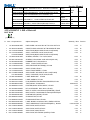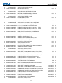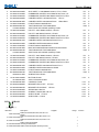
1
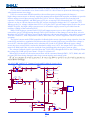
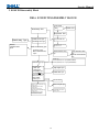
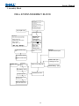
Service Manual
Service Manual
LCD Monitor E190Sf
-0-
1
Service Manual Versions and Revision
No.
Version
Release Date
Revision
1
1.0
2009/02/16
Initial Release
Copyright
Copyright 2009 InnoLux Display. Corp. Ltd
All Rights Reserved
This manual may not, in whole or in part, be copied, Photocopied, reproduced, translated, or converted to any
electronic or machine readable form without prior written permission of Foxconn Tech. Corp. Ltd.
Dell E190Sf Service Manual
Service Manual
Table of Contents
CHAPTER 1- PRECAUTIONS & SAFETY NOTICES ..................................................................................................................... 3
0H
1.
2.
3.
SAFETY PRECAUTIONS .................................................................................................................................................... 3
PRODUCT SAFETY NOTICE .............................................................................................................................................. 3
SERVICE NOTES.................................................................................................................................................................. 3
1H
2H
3H
CHAPTER 2- SERVICE TOOLS & EQUIPMENT REQUIRED ..................................................................................................... 4
4H
CHAPTER 3- CIRCUIT THEORY ...................................................................................................................................................... 5
5H
1.
2.
3.
4.
5.
6.
7.
8.
BLOCK DIAGRAM ................................................................................................................................................................... 5
ELECTRONIC CIRCUIT THEORY ............................................................................................................................................... 5
FACTORY PRESET TIMING TABLE ................................................................................................................................ 11
POWER ON/OFF SEQUENCY .................................................................................................................................................. 11
D-SUB CONNECTOR PIN ASSIGNMENT ................................................................................................................................. 12
AC OUTLET PIN ASSIGNMENT .............................................................................................................................................. 12
INNER CONNECTOR PIN ASSIGNMENT................................................................................................................................... 13
KEY PARTS PIN ASSIGNMENTS .............................................................................................................................................. 14
6H
7H
8H
9H
10H
CHAPTER 4- DISASSEMBLY & ASSEMBLY ................................................................................................................................. 18
11H
1.
2.
3.
EXPLODED DIAGRAM ........................................................................................................................................................... 18
E190SF DISASSEMBLY BLOCK .............................................................................................................................................. 19
ASSEMBLY BLOCK ................................................................................................................................................................ 20
12H
CHAPTER 5- TEST AND ADJUSTMENT ........................................................................................................................................ 21
1.
2.
3.
4.
5.
6.
7.
8.
FUNCTION KEY DEFINITIONS ................................................................................................................................................ 21
OSD CONTROL ...................................................................................................................................錯誤! 尚未定義書籤。
FACTORY MODE INTRODUCTION ........................................................................................................................................... 22
BURN-IN PATTERN ................................................................................................................................................................. 22
AUTO COLOR BALANCE (AUTOMATICALLY CALIBRATE CHIP ADC PARAMETER BY USING CHIP INTERNAL DAC.)................ 22
EDID (REWRITE EDID DATA TO EEPROM)......................................................................................................................... 23
UPLOAD FIRMWARE TO MCU VIA VGA CABLE .................................................................................................................... 23
AFTER REPAIR, TO ENSURE THE QUALITY YOU SHOULD DO THE FOLLOWING TEST AND ADJUSTMENT. ................................... 25
13H
14H
15H
16H
17H
18H
19H
CHAPTER 6- TROUBLE SHOOTING.............................................................................................................................................. 25
20H
1.
2.
3.
4.
5.
6.
7.
COMMON ACKNOWLEDGE .................................................................................................................................................... 25
NO POWER & POWER LED OFF ............................................................................................................................................ 26
POWER LED AMBER ............................................................................................................................................................. 26
BACKLIGHT CAN’T BE TURNED ON ........................................................................................................................................ 27
NO PICTURE & BACKLIGHT ON ............................................................................................................................................. 29
AT 32-GRAY SCALE PATTERN, COLOR LOST IN SOME SCALE ................................................................................................... 29
DIAGNOSTIC TEST PATTERN .................................................................................................................................................. 29
21H
22H
23H
24H
CHAPTER 7- RECOMMENDED PART LIST ................................................................................................................................. 32
ATTACHMENT 1- BILL OF MATERIAL......................................................................................................................................... 34
25H
ATTACHMENT 2- SCHEMATIC....................................................................................................................................................... 44
26H
ATTACHMENT 3- PCB LAYOUT ..................................................................................................................................................... 54
2
Service Manual
Chapter 1- PRECAUTIONS & SAFETY NOTICES
1.
SAFETY PRECAUTIONS
This monitor is manufactured and tested on a ground principle that a user’s safety comes first.
However, improper used or installation may cause damage to the monitor as well as to the user.
WARNINGS:
z
This monitor should be operated only at the correct power sources indicated on the rating label on
the rear cover of the monitor. If you’re unsure the power supply in your residence, consult your
local dealer or Power Company.
Use only the specified power cord that comes with this monitor.
Do not try to repair the monitor by yourself, as it contains no user-serviceable parts. This monitor
should only be repaired by a qualified technician.
Do not remove the monitor cabinet. There is high-voltage parts inside that may cause electric shock
to human bodies.
Stop using the monitor if the cabinet is damaged. Have it checked by a service technician.
Put your monitor only in a lean, cool, dry environment. If it gets wet, unplug the power cable
immediately and consult your closed dealer.
Always unplug the monitor before cleaning it. Clean the cabinet with a clean, dry cloth. Apply
non-ammonia based cleaner onto the cloth, not directly onto the class screen.
Do not place heavy objects on the monitor or power cord.
z
z
z
z
z
z
z
2.
PRODUCT SAFETY NOTICE
Many electrical and mechanical parts in this chassis have special safety visual inspections and the
protection afforded by them cannot necessarily be obtained by using replacement components rated
for higher voltage, wattage, etc. Before replacing any of these components read the parts list in this
manual carefully. The use of substitute replacement parts, which do not have the same safety
characteristics as specified in the parts list, may create shock, fire, or other hazards.
3.
SERVICE NOTES
z
When replacing parts on circuit boards, clamp the solder wires around terminals before soldering.
z
Keep wires away from high voltage, high temperature components and sharp edges.
z
Keep wires in their original position so as to reduce interference.
z
Adjustment of this product please refers to the user’ manual.
z
Use Pb free solder wire for circuit board preparation.
3
Service Manual
Chapter 2- SERVICE TOOLS & EQUIPMENT REQUIRED
1.
2.
3.
4.
5.
6.
7.
8.
9.
SIGNAL GENERATOR
MULTIMETER
SCREW DRIVER
OSCILLOSCOPE
Soldering IRON
SOLDER (Lead free, RoHS compliance)
Color Analyzer
Fox_VISP_Programmer
Fox_VEDID_Programmer
4
Service Manual
Chapter 3- CIRCUIT THEORY
1.
Block Diagram
This Block is comprised of interface board and switching power supplier board which is included by
inverter for CCFL
ON/OFF Control
+5V DC output
To IF Board
Brightness Control
+12V DC output
Snubber
&Schottky
Inverter
PWM IC
Power
Transformer
Feedback
MOSFET
CCFL
Lamp2
Panel
Inverter
Transformer
Lamp1
To
Snubber
&Schottky
Feedback
Control
Rectifier&
Filter
Circuit
AC Line Filter
Power
MOSFET
Photocoupler
Power PWM
Control IC
AC Input
90V~264V
2. Electronic Circuit Theory
2.1 Inverter PWM circuit
2.1.1 Inverter Control circuit operations:(fig.2)
Fig.2
DC_5V through R1 and C1 will provide power for U1 on the pin2(VDDA),When the voltage at VDDA
is less than ~3.4V,the IC will enter the lockout mode. The IC will resume operation when the voltage at pin
VDDA exceeds an approximate 3.8V threshold.
Pin3(SEL) used to select appropriate drive topologies,connecting pin SEL to GED shows the IC in the
5
Service Manual
push-pull configuration..
SSTCMP(pin14) applys the soft-start function and the loop compensation funtion.C5 at SSTCMP
compensates the feedback loop and provides good transient response to load changes.
When the IC is enabled,it starts from the strinking mode and the TIMER(pin8) is activated.During lamp
ignition,if the voltage at pin SSTCMP exceeds an approximate 2.0V threshold,the drive frequency will swith
from stinking frequency to the operation frequency, The striking frequency is determined by (R4& R5)
connected to Pin 4(RT1)and Pin5(RT). The operating frequency is determined just by R4.
Applying a voltage level greater than 2V from IF BD to pin6(PWM) can enable the IC,Once the
voltage less than ~1.0V for longer than 20ms will disable the IC.
Once the lamps are ignited and the voltage at pins ISEN1(pin9),ISEN2(pin10),OLP1(pin12),and
OLP2(pin13) all exseed approximately 0.8V,the IC enters the normal operation mode and the PWM
dimming control is actived. During start up, ISEN1 (pin9and pin10) senses the voltage on the transformer
secondary. If no current is sensed approximately 2 seconds, U1 shuts off. re used to limit current. C3 is used
to dump noise.
DRV1 and DRV2 of U1 are used to drive Q1. DRV1 and DRV2 are controlled by build-in PWM IC.
Q1 is switched which has two build-in IGBTs. The working principle of circuit of T1, the same to circuit of
Power.
The voltage signal on negative pole of D1 sensed through R7/R8 comes to Pin11 of U1 VSEN (Lamp
Current Detection & Control). The CCFL current is detected through R12/R21 and reaches a regulated value.
The CCFL current detected at resistor R12/R21 is converted to a voltage level and input to the ISEN1/2
Once the CCFLs are ignited and current is sensed through resistor R12/R21, performs the loop compensation
function. The voltage at IC pin12 controls the drive duty cycle of the power MOSFETs to regulate the CCFL
current.
2.1.2 Output Circuit and Protection Circuit operations:(fig.3)
Fig.3
The transformer (T1) secondary winding leakage inductance and output capacitance(C22) forms a
lower pass filter,which converts the square-wave driving signal into a sinusoidal output voltage signal for
CCFL.
The over-voltage protection feature is implemented by using an extermal capacitor devider(C20/C21) to
sense the output voltage.The divide-down voltage signal is sent to the IC Pin11(VSEN) ,thus regulating the
output voltage at the transformer secondary.
If a CCFL is removed, fails or damaged during normal operation, CCFL current is no longer sensed and
the voltage on ISEN1/ISEN2 drops. Once the voltage at the ISEN1/ISEN2 pin is less than the lamp” on”
threshold, the shutdown timer is activated. The IC maintains the output voltage for approximately
2-3seconds and once the timer reaches a threshold of approximately 3V, the IC will shutdown. To restart the
IC, either toggle the SST_CMP pin or recycle the power on the VDDA pin.
6
Service Manual
2.2 Power PWM circuit operations
2.2.1) Block diagram:(fig.4)
EMI Filter
Rectifier and
filter
PWM controller
Isolation power
transformer
Rectifier and filter
Switching element
Inverter circuit
Rectifier and filter
To IF connector
Feedback Isolation
Fig.4
2.2.2) AC Input and EMI Filter:(fig.5)
Fig.5
CN850 is a connector for connecting AC Power. F850 is a fuse to protect all the circuit AC. Input
voltage is from 90V to 264V. R850 and R851 are joined between two inputting main circuit to prevent
man from shock. L850 is used to filter low frequency noise. C850 and C851 are used to discharge the
noise that L850 produced. High frequency waves are damped by C852 .
7
Service Manual
2.2.3)High Voltage to Low Voltage Control Circuit:(fig.6)
2
D850
BL4-06
T850
SPW-119
R853
4
1
+
+ C854
0.2R
3
100u/450V
12
C875
4700p/250V
R880
D853
1
TVS-P6KE170A
82K 2W
.
11
3
7
Signal_GND
D851
FR10-10-LF
+
L854
R856
bead
D852
10 1%
SF10-04
8
9
10
5
6
C855
.
.
10u/50V
AP2764
1
Gate
1
Q850
CN852
C861
3300p/250V
T851
SPW-XXX
C872
100P/1KV
2
GND
2
R855
3
10K
3
12
Isense
1
4
FB
.
11
3
7
5
GND
VDD
7
NC
0R68 2W
Signal_GND
8
Vin
8
R869
6
9
10
5
CON8PIN
6
.
.
C860 OPEN
I850
LTV817M
ZD881
OPEN
Signal_GND
4
1
3
2
Signal_GND
R849
220R
3
I sense
220pF/50V NPO
HV
8
CN852
D849
NC
U850
LD7575
Signal_GND
5
NC
7
C846
OUT
1
2
GND
4
3
R842
COMP
Vcc
6
20K
4
R847
NC
1
2
RT
Signal_GND
5
6
C847
Gate
Isense
GND
FB
GND
VDD
R846
Open
7
100K/ 1%
8
C849
C848
100nF/50VX
CON8PIN
Signal_GND
R848
HV
20K
1nF/50V NPO
Signal_GND
NC
R843
Signal_GND
20R
R841
NC
Signal_GND
Fig.6
8
Service Manual
D850 is a rectifier in which there are 4 build-in diodes, inverting AC to DC.
C854 is used to smooth the wave from rectifier. R852 is a fuse resistor to protect the following circuit
when inrush current is too large.
U850 is a current-mode PWM controller with excellent power-saving opration,It features a
high-voltage current source to directly supply the startup current from bulk capacitor and further to provide
lossless startup circuit. Max start-up current for U850 is 100 uA, When current flow from the bulk
capacitor C854 through R843 and R842 gets to HV pin to start up U850, Meanwhile,the VCC supply
current is as low as 100 uA thus most of the HV current is utilized to change the VCC capacitor C855,
Whenever the Vcc voltage is higher than UVLO (16V),the GATE pin will output signal to drive the power
MOSFET(Q850), the high-voltage current source is off and the supply current is provided from the
auxiliary winding of the trasformer PIN5.
When U850 begins to operate Pin8 of U850 will output square wave to drive Q850, then the main
current flow get to GND bypassing through T850, Q850. Because of the change of current flow, wires in
the other side of T850 will induct current. In the same time, the current inducted by wires which connected
T850 Pin 1 and Pin 3, with components of D852, R856 and C855 ,will be supplied to U850 for normal
operating.
The typical current mode PWM controller feedbacks both current signal and voltage signal to close the
control loop and achieve ragulation.U850 detects the Q850 current from Isense pin which max voltage is
set as 0.85V, then the Q850 current can be calculated as:I peak=0.85V/R869,When the sense voltage
across the sense resistor R869, reaches the threshold voltage over 0.85V, the output GATE drive will be
turned off. R849 and C846 is used to avoid the Isen pin damaged by the negative turn-on spike.
The voltage feedback signal is provided from the TL431(I851) through the I850 to the COMP pin.When
the voltage on COMP pin is lower than 1.2V,the IC will turn off.
When Q850 is turned off, the main current flow will be consumed through D851, C875, R880, this will
prevent Q850 from being damaged under large current impulse and voltage spike.
RT pin is to program the switching frequency ,by connecting R846 to ground to set the switching frequency,f
=(65.0/R846)*100(KHz).
2.2.4) DC 12V and DC 5V Output Circuit and Feedback circuit:(fig.7)
C862
1000p/1KV
L852
CHK-053
R862
10R 2W
+12V
D854
SF5-20
D855
+
C863
+
470u/25V
NC/SF5-20
C864
ZD880
470u/25V
R888
GDZ14B/NC
R886
510R 2W/NC
C
10K/NC
Q851
2N4401/NC
B
E
R887
10K/NC
C866
1000p/1KV
R866
10R 2W
D856
SR5-10
D857
SR5-10
L851
CHK-053
+
C867
470u/25V
+
C868
+5V
F851
5A/125V
C869 +
470u/25V
470u/25V
C876
0.1/50V
CN851
1
2
3
4
5
6
7
8
DIM/ON/OFF
R867
PID
270
R899 OPEN
+
R871
R861
270k
3K65 1%
SIP-8P
C899
OPEN
R858
5K1 1%
C871
0.1/50V
R859
10K 1%
R890
9.1K/NC
0.01/50V
3
1
TL431
C890
R860
Q890
G
0.1uF/50V/NC
3K3 1%
S
2
D
I851
C859
Fig.7
9
+5V
GND
DIM
ENA
GND
+5V
PID
P-saving_on/off
R891
2N7000/NC 10K/NC
Service Manual
D854 is used to rectify the inducted current. R862 and C861 are used to store energy when current is
reversed. The parts including C862, C865 and L852 are used to smooth the current waves that are from
D855, then 13V voltage is supplied.
D856 and D857 are SCHTKY diodes used to rectify the inducted current.C866 and R866 are used to
store energy when current is reversed,The components including C864,C874,C875,L851 and C876 are
used to smooth the current waves,then DC+5V voltage is supplied. F851 is used for OCP for the LPS test.
DC 5V supply voltage feed back to PWM controller U850 via R861,R860,R859,C859,I851,R857,
R863 used to control the voltage feedback loop.
2.3 I/F Board Circuit
2.3.1 RGB CAPTURE
- Signal RED,GREEN,BLUE input through CN301 #1,#2,#3, Stop DC via C303, C302 and C301, and
then enter into U401 (gm2621-LF) analog input terminal #99,#96,#93, and then gm2621-LF deals
with signal internally. D303, D302, D301 are ESD protector to prevent U401 from ESD.
- Signal DDC_SCL (series clock) inputs via CN301#15, and then passes through ZD305 for ESD
protection, goes into EDID EEPROM IC U301 #6.
- Signal DDC_SDA (series data) inputs via CN301#12, and then passes through ZD306 for ESD
protection, goes into EDID EEPROM IC U301 #5.
- Signal TTL vertical sync. (Vsync) inputs via CN301 #14, and then clamped by ZD302 Zener, passes
through R311, and then goes into IC U401 (gm2621-LF) #90.
- Signal TTL horizontal sync. (Hsync) inputs via CN301 #13, and then clamped by ZD303 Zener,
passes through R310, and then goes into IC U401 (gm2621-LF) #89.
- CN301#5 is defined as cable detect pin, this detector realize via R319 and U401#114, and ZD301 is
ESD protector.
- U301 +3.3V is supplied by PC via CN301#9 or supplied by Monitor self via D307 with D306 and
ZD304 for ESD protection,.
- U301 is an EEPROM IC which is memory and EDID data saved in it.
2.3.2 Buttons Control
- Button “Power” on front bezel connects to U401 (gm2621-LF) #125 through CN401 #8, U401 #125
is defined as power on/off.
- Button “+” on front bezel connects to U401 (gm2621-LF) #124 through CN401 #3, U401 #124 is
defined as “Plus”.
- Button “-” on front bezel connects to U401 (gm2621-LF) #123 through CN401 #2, U401 #123 is
defined as “Minus”.
- Button “Menu” on front bezel connects to U401 (gm2621-LF) #122 through CN401 #1, U401 #122 is
defined as “Menu”.
- LED Indicator on Front Bezel
a. When press button “power”, U401(Scalar) #125 be send in low potential, make U401#57 sends out
high potential, and then to J1#2 on keypad, LED Green on.
b. When in “Suspend” mode, U401 (Scalar) #56 sends out a high potential, and then to J1 #3 on
keypad, LED Amber ON.
2.3.3 ST CHIP U401 (gm2621-LF)
- U401 (gm2621-LF) #7~#10 output 8 bit even and #31~#40 output 8 bit odd LVDS digital data to
panel control circuit through CN501.
- U401 (gm2621-LF) #127 output PPWR ”H” potential to make Q502 conducted, and then make Q501
conducted, +5V flow to CN501#1~#3 as Panel Vdd .
- U401 (gm2621-LF) #49 output CCFL_ON/OFF ”H” potential to control Inverter on/off.
- U401 (gm2621-LF) #50 outputs Brightness “PWM” signals to control CCFL brightness.
- TCLK by Crystal 14.318MHz input to U401 (gm2621-LF) #109.
- U401 (gm2621-LF) #111 Bidirectional RESET signals
Please refer to gm2621-LF Pin Assignments table in page
2.3.4 Regulator Circuit
10
Service Manual
- +5V is from switching mode power supply for panel and Regulater U601
- +3.3V generates from Regulater U601 supply for U401, U301, U402 used.
- +1.8V generates from Regulater U602 through C603, C604 filtering which is output +1.8V for U401
used.
3.
FACTORY PRESET TIMING TABLE
Standard
VESA
IBM DOS
4.
Resolution
640 x 480
640 x 480
800 x 600
800 x 600
1024 x 768
1024 x 768
1152x864
1280x1024
1280x1024
720 x 400
Horizontal Frequency
(KHz)
31.469
37.500
37.879
46.875
48.363
60.023
67.500
48.483
60.087
31.469
Vertical Frequency
(Hz)
59.940
75.000
60.317
75.000
60.004
75.029
75.000
60.042
75.034
70.087
Power On/Off Sequency
Hardware Power ON
When power cord plug into AC socket, Power provides 12V,&DC_5V from through U850, DC_3.3V be
generated from DC_3.3V Regulater U601.DC_5V is voltage for panel, DC_3.3v is main voltage for
U401. When DC_3.3V input to U401, U401 reset circuit active, set U401 all registers to default,. That
means finish hardware power on.
Software Power ON/OFF
When press power key, U401 #125 recieves low pulse, and then (gm2621-LF) U401 will be wake up and
send high plus(at 127,49pin) to on CCFL and switch 5.0v to panel module. And make the VGA cable input
signal source display normal on panel.
- If Power ON, U402 #57 (LED_Green) will send out High potential, and then LED green on.
- If Power OFF, U402 #56 (LED_Amber) will send out High potential, and then LED Amber on.
The Panel_Vcc, Backlight_En, CLK/DATA output to panel will follow the following sequency.
11
Service Manual
Power supply for
VDD
90%
90%
10%
Pin
1
2
3
4
5
T7
Symbol
Red
Green
Blue
GND
Cable Detect
Signals
(Digital RGB, HS, VS, DE, CLOCK)
0V
Pin
6
7
8
9
10
Symbol
Red_GND
Green_GND
Blue_GND
PC+5V
GND
T3
Pin
11
12
13
14
15
0V
T1
T5
Symbol
GND
DDC_SDA
Hsync
Vsync
DDC_SCL
Valid data
T4
Power supply for back light
T1(ms) T2 (ms) T3 (ms)
0.5~10 0.001~50 >200
0.5~10
0~50
>200
SPEC(LGD)
SPEC(HSD)
5.
D-SUB Connector Pin Assignment
AC Outlet Pin Assignment
2
6.
T4 (ms)
>200
>200
1
3
CN850
Pin
1
2
3
Symbol
Line
GND
Neutral
Description
12
T5 (ms)
0.001~50
0.0~50
T6 (ms)
10%
T2
T6
T7(ms)
>500
>500
Service Manual
7.
Inner Connector Pin Assignment
7.1 CN501 (Connect M/B to Panel, C11330MGHR0 or compatible connector)
Pin
Symbol
Description
1
Panel_Vcc
Panel power supply (typ.5.0V)
2
Panel_Vcc
Panel power supply (typ. 5.0V)
3
Panel_Vcc
Panel power supply (typ. 5.0V)
4
NC
5
NC
6
NC
7
GND_LVDS
LVDS Ground
8
RXE3+
LVDS signal of even channel 3(-)
9
RXE3LVDS signal of even channel 3(+)
10
RXEC+
LVDS signal of even channel clock (+)
11
RXECLVDS signal of even channel clock (-)
12
RXE2+
LVDS signal of even channel 2(+)
13
RXE2LVDS signal of even channel 2(-)
14
GND_LVDS
LVDS Ground
15
RXE1+
LVDS signal of even channel 1(+)
16
RXE1LVDS signal of even channel 1(-)
17
GND_LVDS
LVDS Ground
18
RXE0+
LVDS signal of odd channel 0(+)
19
RXE0LVDS signal of odd channel 0(-)
20
RXO3+
LVDS signal of odd channel 3(+)
21
RXO3LVDS signal of odd channel 3(-)
22
RXOC+
LVDS signal of even channel clock (+)
23
RXOCLVDS signal of even channel clock (-)
24
GND_LVDS
LVDS Ground
25
RXO2+
LVDS signal of even channel 2(+)
26
RXO2LVDS signal of even channel 2(-)
27
RXO1+
LVDS signal of even channel 1(+)
28
RXO1LVDS signal of even channel 1(-)
29
RXO0+
LVDS signal of odd channel 0(+)
30
RXO0LVDS signal of odd channel 0(-)
7.2 CN1, CN2 (Connect to Panel Backlight, SM02B-BHSS-1-TB or compatible connector)
Pin
Symbol
Description
1
HV
High voltage for lamp
2
LV
Low voltage for lamp
7.3 CN401 (Connect to keypad, SZ7103016B or compatible connector)
Pin
Symbol
Description
1
MENU
OSD “MENU” control
2
DOWN
OSD “-” control
3
UP
OSD “+” control and auto adjustment control
4
GND
Ground
5
GND
Ground
6
LED_Green
LED Green on/off control
7
LED_Amber
LED amber on/off control
8
Power
Power on/off control
13
Service Manual
8.
Key Parts Pin Assignments
8.1 U401 (gm2621-LF)
Pin
Symbol
1 AVSS_BIAS
2 VDD_OUT_33
3 RESERVED
4 RESERVED
5 RESERVED
6 RESERVED
7 E_CH3P_LV
8 E_CH3N_LV
9 E_CLKP_LV
10 E_CLKN_LV
11 E_CH2P_LV
12 E_CH2N_LV
13 E_CH1P_LV
14 E_CH1N_LV
15 E_CH0P_LV
16 E_CH0N_LV
17 CVDD_18
18 CRVSS
19 RESERVED
20 RESERVED
21 RESERVED
22 RESERVED
23 RESERVED
24 RESERVED
25 Vdd_out_33
26 VSS_OUT
27 RESERVED
28 RESERVED
29 RESERVED
30 RESERVED
31 O_CH3P_LV
32 O_CH3N_LV
33
O_CLKP_LV
34
O_CLKN_LV
35
36
O_CH2P_LV
O_CH2N_LV
37
38
O_CH1P_LV
O_CH1N_LV
39
40
O_CH0P_LV
O_CH0N_LV
41
42
43
RESERVED
RESERVED
RESERVED
I/O Legend: P=Power, G=Ground, O=Output, I=Input, A=Analog
I/O
Description
G Analog ground for LVDS PLL and Bandgap
P Digital 3.3V supply for LVDS output
O Reserved; Do not connect
O Reserved; Do not connect
O Reserved; Do not connect
O Reserved; Do not connect
O LVDS signal of even channel 3(+)
O LVDS signal of even channel 3(-)
O LVDS signal of even channel clock (+)
O LVDS signal of even channel clock (-)
O LVDS signal of even channel 2(+)
O LVDS signal of even channel 2(-)
O LVDS signal of even channel 1(+)
O LVDS signal of even channel 1(-)
O LVDS signal of even channel 0(-)
O LVDS signal of even channel 0(-)
P Core VDD connect to digital 1.8V
O Chip digital ground
O Reserved; Do not connect
O Reserved; Do not connect
O Reserved; Do not connect
O Reserved; Do not connect
O Reserved; Do not connect
O Reserved; Do not connect
P Digital 3.3V supply for LVDS output
G Digital ground for LVDS output
O Reserved; Do not connect
O Reserved; Do not connect
O Reserved; Do not connect
O Reserved; Do not connect
O LVDS odd channel 3 positive. Reserved for gm5611 and gm2621
O LVDS odd channel 3 negative. Reserved for gm5611 and
gm2621
O LVDS odd channel clock positive. Reserved for gm5611 and
gm2621
O LVDS odd channel clock negative. Reserved for gm5611 and
gm2621
O LVDS odd channel 2 positive. Reserved for gm5611 and gm2621
O LVDS odd channel 2 negative. Reserved for gm5611 and
gm2621
O LVDS odd channel 1 positive. Reserved for gm5611 and gm2621
O LVDS odd channel 1 negative. Reserved for gm5611 and
gm2621
O LVDS odd channel 0 positive. Reserved for gm5611 and gm2621
O LVDS odd channel 0 negative. Reserved for gm5611 and
gm2621
O Reserved; Do not connect
O Reserved; Do not connect
O Reserved; Do not connect
14
Service Manual
44
45
46
47
48
49
50
RESERVED
RESERVED
RESERVED
VDD_OUT_33
VSS_OUT
PBIAS
PWM0/GPO_4
O
O
O
P
G
O
I/O
51
52
53
54
55
56
57
58
59
60
61
GPIO_0
CRVSS
RVDD_33V
CRVSS
CVDD_18
GPIO_1
GPIO_2
GPIO_3
SPI_CSn
SPI_CLK
SPI_DI
I/O
G
P
G
P
I/O
I/O
I/O
I/O
I/O
I/O
62
SPI_DO
I/O
63
64
65
66
P
I
I/O
I
68
RVDD_33V
DDC_SCL_VGA
DDC_SDA_VGA
DDC_SCL_DVI/
HOST_SCA
DDC_SDL_DVI/
HOST_SDA
AVSS_DVI
69
REXT
I
70
AVDD_DVI_18
P
71
AVSS_DVI
G
72
73
74
RX2+
RX2AVDD_DVI_33
I
I
P
75
76
77
RX1+
RX1AVSS_DVI
I
I
G
78
AVDD_DVI_18
P
79
AVSS_DVI
G
80
RX0+
I
67
I/O
G
Reserved; Do not connect
Reserved; Do not connect
Reserved; Do not connect
Digital 3.3V supply for LVDS output
Digital ground for LVDS output
Panel backlight enable
PWM0 output or optional general-purpose output GPO_4.
Also used for bootstrap control
General-purpose output GPO_0. Also used for bootstrap control
Chip digital ground
Digital Output VDD. Connect to digital 3.3V
Chip digital ground
Core VDD connect to digital 1.8V
General-purpose output GPO_1. Also used for bootstrap control
General-purpose output GPO_2. Also used for bootstrap control
General-purpose output GPO_3. Also used for bootstrap control
SPI ROM chip select. Also used for bootstrap control.
SPI ROM Clock output.
SPI ROM Data input. Connect this pin to the data output of
Serial FLASH
SPI ROM Data input. Connect this pin to the data input of Serial
FLASH
Chip digital ground
DDC2Bi clock for Analog Port
DDC2Bi clock for Analog Port, internal pull up of 10K ohms
DDC2Bi clock for DVI Port or host I2C clock signal for
debugging
DDC2Bi clock for DVI Port or host I2C data signal for
debugging, internal pull up of 10k ohms
Analog GND for DVI input. Reserved for gm2621 and gm2621;
Do not connect
External reference resistor.
A 1%, 250Ω resistor should be connected from this pin to pin 74.
Reserved for gm2621 and gm2621; Do not connect.
Analog VDD (1.8V) for DVI input.
Must be bypassed with external capacitor(s) to AVSS_DVI.
Reserved for gm2621 and gm2621; Do not connect.
Analog GND for DVI input. Reserved for gm2621 and gm2621;
Do not connect.
Do not connect.
Do not connect.
Analog VDD (3.3V) for DVI input. Reserved for gm2621 and
gm2621; Do not connect.
Do not connect.
Do not connect.
Analog GND for DVI input. Reserved for gm2621 and gm2621;
Do not connect.
Analog VDD (1.8V) for DVI input.
Must be bypassed with external capacitor(s) to AVSS_DVI.
Reserved for gm2621 and gm2621; Do not connect.
Analog GND for DVI input. Reserved for gm2621 and gm2621;
Do not connect.
Do not connect.
15
Service Manual
81
82
RX0AVDD_DVI_33
I
P
83
84
85
RXC+
RXCAVSS_DVI
I
I
G
86
AVDD_DVI_18
P
87
88
89
90
91
92
93
94
95
96
97
98
99
100
101
CVDD_18
CRVSS
HSYNC
VSYNC
RVDD_33V
AVDD_ADC_33
BLUE+
BLUEAVSS_ADC
GREEN+
GREENAVSS_ADC
RED+
REDAVDD_ADC_33
P
G
I
I
P
I
I
I
G
I
I
G
I
I
P
102 AVSS_ADC
103 AVSS_ADC
104 AVDD_ADC_18
G
G
P
105
106
107
108
O
P
G
O
VBUFC_RPLL
VDD_RPLL_18
VSS_RPLL
XTAL
109 TCLK
I
110
111
112
113
114
115
116
117
118
119
AVDD_RPLL_33
P
RESETn
I/O
LBADC_VSS
G
LBADC_IN3
I
LBADC_IN2
I
LBADC_IN1
I
LBADC_VDD_33 P
CRVSS
G
CVDD_18
P
PWM0/GPO_5
I/O
120
121
122
123
124
GPIO_8
GPIO_9
GPIO_10
GPIO_11
GPIO_12
I/O
I/O
I/O
I/O
I/O
Do not connect.
Analog VDD (3.3V) for DVI input. Reserved for gm2621 and
gm2621; Do not connect.
Do not connect.
Do not connect.
Analog GND for DVI input. Reserved for gm2621 and gm2621;
Do not connect.
Analog VDD (1.8V) for DVI input.
Must be bypassed with external capacitor(s) to AVSS_DVI.
Reserved for gm2621 and gm2621; Do not connect.
Core VDD connect to digital 1.8V
Chip digital ground
ADC input horizontal sync or composite sync input.
ADC input vertical sync
Digital Output VDD. Connect to digital 3.3V
1.8V for gmZAN3SL core
Positive analog input for Blue channel
Negative analog input for Blue channel
Analog ground for ADC
Positive analog input for Green channel
Negative analog input for Green channel
Analog ground for ADC
Positive analog input for Red channel
Negative analog input for Red channel
Analog power (3.3V) for ADC. Must be bypassed with capacitor
to AVSS_ADC pin.
Analog ground for ADC
Analog ground for ADC
Analog power (1.8V) for ADC. Must be bypassed with capacitor
to AVSS_ADC pin.
Reserved; Do not connect
Digital 1.8V Power for PLL
Ground for PLL
Connect to 14.3MHz crystal. Should be bypassed with capacitor
to AVDD_RPLL_33.
Connect to 14.3MHz crystal. Should be bypassed with capacitor
to AVDD_RPLL_33.
Analog power (3.3V) for PLL
Bypass with 0.01uF capacitor GND
Ground for general-purpose LBADC
Ground-purpose LBADC input 3.
Ground-purpose LBADC input 2.
Ground-purpose LBADC input 1.
3.3V supply for general-purpose LBADC.
Chip digital ground
Core VDD connect to digital 1.8V
PWM0 output or optional general-purpose output GPO_5.
Also used for bootstrap control
General-purpose input/output 8
General-purpose input/output 9
General-purpose input/output 10
General-purpose input/output 11
General-purpose input/output 12
16
Service Manual
125
126
127
128
GPIO_13
GPIO_14
PPWR
AVDD_BIAS_33
I/O
I/O
O
P
General-purpose input/output 13
General-purpose input/output 14
Panel power enable
Analog 3.3V supply for LVDS PLL and Bandgap
8.2 U402 (Serial Flash)
Pin
Symbol
I/O
1
CE#
I
Description
The device is enabled by a high to low transition on CE#. CE#
must remain low for the duration of any command sequence.
2
SO
I/O
To transfer commands, addresses, or data serially into the device.
3
WP#
I/O
The write protect (WP#) pin is used to enable/disable BPL bit in
the status register.
4
VSS
G
Connect ground
5
SI
I/O
To transfer commands, addresses, or data serially into the device
input are latched on the rising edge of the serial clock.
6
SCK
I/O
To provide the timing of serial interface.
Commands, addresses, or input data are latched on the rising
edge of the clock input, while output data is shifted out on the
Falling edge of the clock input.
7
HOLD
I/O
To temporarily stop serial communication with SPI flash
memory without resetting the device.
8
VDD
P
To provide power supply.
8.3 U850 (LD7575, Power Controller)
Pin
Symbol
I/O
Description
1
RT
This pin is to program the switching frequency
I
Voltage feedback pin,By connecting a photo-coupler
2
COMP
to close the control loop and achieve the regulation
3
CS
I
Current sence pin
4
GND
O
PWM output ,Gate drive output to drive the external
5
OUT
MOSFET
6
VCC
I
Power supply
7
NC
Unconnected pin
8
HV
I
PWM output
8.4 U1 ( INL816GN, CCFL Inverter controller IC)
Pin
Symbol
I/O
Description
1
DRV1
O
Driver output 1
2
VDDA
--Supply voltage input
3
SEL
I
Select Signal for Push-Pull or Half-Bridge Topology
4
RT1
I/O
Timing Resistor for Striking Frequency
5
RT
I/O
Timing Resistor for Operation Frequency
6
ENAPWM
I
Enable and PWM Dimming input
7
PID
I
Analog Dimming input
8
TIMER
I/O
Timing Capacitor for Delay Timer
9
ISEN1
I
Currentfeedback1
10
ISEN2
I
Currentfeedback2
11
VSEN
I
Voltage Feedback
12
OLP1
I
Open-Lamp Protection Sense1
13
OLP2
I
Open-Lamp Protection Sense2
14
SSTCMP
I/O
Soft-Start and Compensation
15
GNDA
--Ground
16
DRV2
O
Driver output 2
17
Service Manual
Chapter 4- Disassembly & Assembly
1. Exploded Diagram
18
Service Manual
2. E198FPf Disassembly Block
DELL E190Sf DISASSEMBLY BLOCK
front-bezel
1PC
bezel assy 1PC
LOGO 1PC
key button 1PC
stand assy 1pc
Rubber
10x20x3.8mm
2pcs
back-cover 1pc
keypad PCB 1PC
kensing-ton 1pc
SCREW,I,CROSS,T.T-2*2.5,
Zn,ROHS, 2PCS
back-cover assy 1pc
screw,P,cross,
M4*10,blk-NYLOK,
4pcs
release button assy
1pc
vesa-release-button
1pc
release-metal-button
1pc
panel 1pc
screw,I,M3*4,Zn-Cc 4pcs(HSD PANEL)
screw,I,M3*5,Zn-Cc 4pcs(LGD PANEL)
chassis assy 1pc
chassis 1pc
slide 1pc
spring 2pc
fix-plate1 1pc
fix-plate2 1pc
top-mylar 1pc
LVDS cable 1pc
screw,F(90度),cross,
M3*4,Zn-Cc 2pcs
SHIELD EMI
LP2207,6pcs
TAPE ACE 85X45mm
PCBA,P/I board,LE1966-7B0 1pc
screw,p,cross,
W/WAS,M3*8,Zn-Cc 2PCS
screw,B,cross,
W/W(T),M4*6,Zn-Cc 1PC
PCBA,I/F board,LE1966-8B0 1pc
screw,p,cross,
W/WAS,M3*8,Zn-Cc 2PCS
BOLT,#4-40*12.5,Ni 2pcs
screw,I,M3*6,Zn-Cc 2PCS
bottom-mylar 1pc
SCREW,BPT3.0x4,C3UC
ROHS, 2PCS
19
Service Manual
3. Assembly Block
DELL E190Sf ASSEMBLY BLOCK
PCBA,P/I board,LE1966-7B0 1pc
screw,p,cross,
W/WAS,M3*8,Zn-Cc 2PCS
screw,B,cross,
W/W(T),M4*6,Zn-Cc 1PC
PCBA,I/F board,LE1966-8B0 1pc
screw,p,cross,
W/WAS,M3*8,Zn-Cc 2PCS
BOLT,#4-40*12.5,Ni 2pcs
screw,I,M3*6,Zn-Cc 2PCS
top-mylar 1pc
chassis assy 1pc
panel 1pc
screw,I,M3*4,Zn-Cc 4pcs (HSD PANEL)
screw,I,M3*5,Zn-Cc 4pcs (LGD PANEL)
bottom-mylar 1pc
SCREW,BPT3.0x4 C3UC
ROHS, 2PCS
LVDS cable 1pc
release button assy
1pc
chassis 1pc
slide 1pc
spring 2pc
fix-plate1 1pc
fix-plate2 1pc
screw,F(90度),cross,
M3*4,Zn-Cc 2pcs
SHELD EMI,
LP2207,6pcs
screw,P,cross,
M4*10,blk-NYLOK,
4pcs
vesa-release-button
1pc
release-metal-button
1pc
Rubber
10x20x3.8mm 2pcs
back-cover 1pc
kensing-ton 1pc
LOGO 1PC
front-bezel
1PC
back-cover assy1pc
key button 1PC
keypad PCB 1PC
bezel assy 1PC
SCREW,I,CROSS,T.T-2*2.5
,Zn,ROHS,2PCS
INSULATOR,MYLAR
,KEY-PAD PCB 1PCS
20
stand assy 1pc
Service Manual
Chapter 5- TEST AND ADJUSTMENT
1. Function key Definitions
Power Switch
Power LED
Power: On/Off, includes power indicator and Power ICON
Green- Active On
Amber- DPMS
Adjust Up:(+)symbol molded into button, move up the highlight bar
Adjust Down: (-) symbol molded into button, calls out
brightness/Contrast, move down the highlight bar.
Menu: Call out OSD Menu and select the item
Automatic adjust: Directly press “+”
Brightness/Contrast Icon: Directly press “−“
Front Panel Controls
Hot Key Function
2. OSD Control
First
Second
Brightness/Contrast (Press “-” directly)
Positioning
Image setting
Color Setting
OSD Settings
Language
Factory Reset
Third
Exit
Contrast
Brightness
Exit
Horizontal
Vertical
Exit
Auto Adjust
Pixel Clock
Phase
Normal Preset
Blue Preset
Red Preset
User Preset
Exit
Horizontal Pos.
Vertical Pos.
OSD Hold Time
OSD Lock
Exit
English
Espanol
François
Deutsch
Portuguese
Russia
Simplified Chinese
Japanese
Exit
Position Settings Only
21
Fourth
Exit, R, G, B
Yes, No
Service Manual
Color Settings Only
All Settings
Enable LCD Conditioning
DDC/CI
Enable
Disable
Automatic Adjustment (press “+“ directly)
3. Factory Mode Introduction
Fig.1
Fig.2
With signal input, press “Power” button to turn off the monitor. Press “Menu” and “Auto/Plus” buttons together, and
then press “Power” button to turn on the monitor. After power on, press “Menu” button to call out Main Menu
(Fig.1). Pull down to Factory Reset and choose Factory to enter Factory mode (Fig.2).
Panel: JT094: Current using panel part number(DELL supply)
Exit: Exit from Factory mode and back to Reset to Factory Settings.
Auto Color: Automatically calibrate chip ADC parameters by using internal DAC. (Only with Burn-in ON)
Burn In: Enable or disable the Burn-in mode by choosing ON or OFF.
Reset Timer: Reset the “Turn-on time” of the panel to 0H0M.
Color Temp: The R, G, B of Blue Preset (9300K), Red Preset (5700K) and Normal Preset (6500K) are generated
from scaling chip’s back-end white-balance program.
Time: Turn-on time of the panel.
4. Burn-in pattern
If it is a new monitor without VGA cable plugged in, burn-in pattern will self-generate automatically.
Burn-in pattern will not be stopped until plugging in the VGA cable. Then, press “Menu” button to call out
OSD Main Menu; pulling down to Factory Reset item and execute All Resetting to disable Bun-in ON.
5. Auto Color Balance (Automatically calibrate chip ADC parameter by using chip
internal DAC.)
5.1 If it is a new-built set, press “Auto/Plus” button to execute “Auto Color” at 32gray scale pattern.
5.2 Please confirm the following steps to perform “Auto Color Balance”:
- Connect the VGA cable with the standard video pattern generator and display 32gray scale pattern on
the monitor.
- Press “Power” button to power off the monitor.
- Press “Menu” and “Auto/Plus” buttons simultaneously; then press “Power” button to power on the
monitor.
- Press “Menu” button, pull down to Factory Reset and choose “Factory” item.
- Set Burn In to ON, then execute Auto Color.
- With “Auto Color” finished, return to Reset to Factory Settings OSD and execute All Settings to enable
burn-in OFF.
22
Service Manual
6. EDID (Rewrite EDID data to EEPROM by Fox_VEDID_Programmer)
The Write-Protect Pin of EEPROM is generally pulled up to enable EDID to be read only; EDID cannot be
written at that status. The following steps enable EDID to be written:
6.1 Connect the monitor and PC via a VGA cable.
6.2 Execute Fox_VEDID_Programmer.
- Click “browse” icon to choose a binary file from the PC.
- Type the “Serial Number” in the dedicated field. Each monitor will have its own serial number. Then
click Enter on the keyboard to jump to next field.
- Type 1 to 2 characters or digits in “Travel Card SN” field. Then click Enter to start writing EDID to
monitor.
- “PASS” will be shown with EDID finished programmed. Please plug out the AC power cord of the
monitor to restart.
7. Upgrade Firmware to Serial via Flash Cable by Fox_VISP_Programmer
7.1 Connect the monitor and PC via a VGA cable.
7.2 Fox_VISP_Programmer enables users to upgrade the firmware of the monitor directly through the VGA
cable of a PC. Please follow the steps for reprogramming the firmware:
- Click “Select Bin” icon to choose a binary file from the PC. The path of the selected binary file will be
shown in the “Message” text window. Meanwhile, the checksum of the binary file will be calculated and
displayed.
- Click “Connect” to check if the connection is satisfactory between the monitor and PC.
- If the connection is ready, click “Auto Programming F2 key” to begin flashing the firmware. During the
flashing process, the motherboard of the PC will send out tick sound. If the firmware is reprogrammed
successfully, “Command: Fast flash write successful” will be shown in the “Message” text window. The
“successful update” condition will make the motherboard bring “Do-Re-Mi” sound five times with the
interval of 500ms.
7.3 With the process of reprogramming firmware finished, plug out the power cable to restart the monitor.
※ The detailed reprogramming procedures will be described in Fox_VISP_Programmer User Manual.
23
Service Manual
8. After repair, to ensure the quality you should do the following test and adjustment.
24
Service Manual
Item
Test OSD
function
Content
1.Signal is set as 1280×1024@60Hz under General-1
2. LCM button are from left to right, checking whether each single function key and
compound function key can be worked.
Contrast
Check
1. Set input mode to 1280×1024@60Hz
2. Set to 32gray scale pattern
3. Set contrast to the maximum. At most 6 bars cannot be distinguished.
Equipment
Chroma
Signal
Generator
Chroma
Signal
Generator
Color
Temperature
1. Do “Auto color Balance” at 1280×1024@60Hz, 32gray scale pattern
2. Measure color temperature, check if it complies with the following temperature :
5700K x=0.328 +/- 0.03, y=0.344+/-0.03
6500K x= 0.313 +/- 0.03, y=0.329+/-0.03
9300K x= 0.283 +/- 0.03, y=0.298+/-0.03
Chroma
Signal
Generator
and color
analyzer
1. Use Chroma Pattern Generator to make sequence.
VESA (640x480 800x600 1024x768 1152x864 1280x1024), the detail supported
modes (see table 1) and power saving signal.
2. Confirm the above timing modes must be full screen and the picture must be
normal.
3. LED is amber at power saving mode.
Modes
switching
check
Chroma
Signal
Generator
VGA cable
When VGA cable is not plugged out, self-test OSD will be floated.
detector
Visual check
Minimum
1. LCD minimum luminance spec is 200cd/m2 (0-15 months from mfg. date)
luminance
2. 0-15 months: > 80% of minimum luminance
measurement
Chroma
Signal
Generator
and Color
Analyzer
OSD Lock
Test
Soft Lock: When OSD is locked, this icon should appear for only 2 seconds with all
buttons pressed, except for the “Menu” and “Power” ones.
Visual
Hard Lock: Press “Menu” button for 15 seconds enables the “locked” icon to be
Inspection
displayed, which will lock All buttons expect for the “Power”. Press “Menu” button
for another 15 seconds enables the “unlock” icon to be shown.
1. Mode:1280×1024@60Hz
Panel Flicker 2. Set Brightness& Contrast to default value (75%)
check
3. Do “Auto Adjustment”
4. Shut down PC to check whether there’s flicker on the center of the picture.
Power
saving
1. Mode:1280×1024@60Hz
2. Pattern: full white
3. Brightness: Max.
4. Contrast: Default
5. Check power consumption at each modes
State
Power Consumption
<25W
Normal
<1W
Stand By
Power Key Off
<0.5W
LED color
green
amber
Equipment::
Chroma
Signal
Generator &
PC
Chroma
signal
generator
and Power
meter
AC
input:230V/
50Hz
no
Chapter 6- TROUBLE SHOOTING
1. Common Acknowledge
z
If you change the M/B, be sure that the U301 and U402 these two components also changed to the
25
Service Manual
z
z
z
z
z
z
z
z
new M/B because there was program inside. If not, please re-write EDID or upload firmware into
serial flash(U402) via VGA Cable. How to do please refer to the Page 19.
If you adjust clock and phase, please do it at condition of Windows shut down pattern.
Please confirm the R/G/B color under 32gray scale pattern.
This LCM is analog interface. So if the entire screen is an abnormal color that means the problem
happen in the analog circuit part, if only some scale appears abnormal color that stand the problem
happen in the digital circuit part.
If you check the H/V position, please use the crosshatch pattern.
This LCM support 10 timing modes, if the input timing mode is out of specification, “Cannot Display
this Video Mode” will be displayed on the screen.
If brightness uneven, repairs Inverter circuit or change a new panel.
If you find the vertical line or horizontal line lost on the screen, please change panel.
If the self-test pattern is moving on the screen, please check whether VGA Cable is plugged in the
Monitor or PC. If the VGA Cable is plugged in well, please change another VGA cable.
2. No power supply
Is there DC12 at L852;
Is there DC 5V at L851;
YES
Check D854;
Check D856/D857;
NO
Is the voltage at C854 in the
range of 127V~372V?
YES
NO
Check D850, F850
Is the voltage at pin8 of U850 354V?
NO
Check R853
YES
NO
Is the voltage at pin6 of U850 18.0?
YES
Is the voltage at pin3 of T850 510?
YES
Check Q850 ,U850
26
Check D852 ,R856
Service Manual
3. Power LED Amber
Is Power LED Amber?
YES
Do the Hsync. & Vsync. Signals exist
in CN301 #13& #14 separately?
NO
Insert VGA Cable correctly
YES
Do the Hsync. & Vsync. Signals exist
in R310 & R311?
NO
Check R310 & R311
YES
Do the Hsync. & Vsync. Signals exist
in U401 #89 & #90?
NO
Change R310 & R311
YES
Is the frequency 14.318MHz at #109
of U401?
NO
YES
Change U401
END
27
Change X401
Service Manual
4. Power (include IF +5Vand +3.3V) supply normal
( key function OK, but backlight can’t be turned on)
Backlight cannot be turned on,is the
on-off control signal come from IF ok?
NO
Is the CN851
inserted CN101 OK?
Yes
Yes
Yes
Is the on-off control signal #109 of U105
high-low convertible when DC on/off
NO
Is the
voltage
13Vat T1
PIN3/4
NO
Change U105
Check
T1
Yes
Check U1
pin2 Voltage
is 5V
Yes
Check U1 pin6
Voltage is High
NO
Check
CN851
YES
Check U1 pin1 and pin16 Output
NO
Check
U1
Yes
Change Q1
28
Service Manual
5. No picture & Backlight on
No picture & Backlight on
YES
Touch OSD Menu Button,
Does OSD display?
YES
Is there R.G.B signal in
U401 #99, #96 #93?
NO
Change D301,
D302 & D303
YES
Is there clock signal in
U401 #109?
NO
Change X401
YES
Check DC 5.0V on
CN501#1, #2, #3
NO
Check Q501 circuit
YES
Are there data output on
U401#7~#16, #31~#40
NO
Change U401
END
29
Service Manual
6. At 32-gray scale pattern, color lost in some scale
Color lost in some scale at 32-gray scale pattern
Re-insert the FFC Cable
OK,
END
NO
Change FFC Cable
NO
Change M/B
7. Diagnostic Test Pattern
1. Press “menu”and “+”simultaneously and hold for 2 sec to enter to the diagnostic.
Check for line defects from the gray color test screen.
2. Press “+”to advance to the next test pattern - Red color screen. Check for
partial block dot(s) - Red color dead pixel. Continue this for the Green & Blue
color.
3. When in White color test screen, check for white color uniformity and if there
white color appears greenish/reddish, etc.
30
OK,
END
Service Manual
31
Service Manual
32
Service Manual
Chapter 7- RECOMMENDED PART LIST
Critical Parts List
E190S Critical Components List
Content
PN
Description
Supplier
412040098880R IC GM2621-LF-BC,QFP-128(GENESI S)RoHS
ST,
430631050060R WFR. 5P 2.0MM 180° W/L ROHS
FOXCONN,
JOWLE,
412000494310R IC PM25LV020-100SCE SOIC8(PMC)RoHS
PMC,
412000721560R IC W25X20AVNIG SOIC8(WINBOND) RoHS
WINBOND
412000661620R IC MX25L2025MC-12G (MXIC)RoH
MXIC,
412000494190R IC SST25LF020A-33-4C-SAE SOIC8(SST)ROHS
SST,
412000332130R IC AP1117D33LA 3.3V (ANACHIP) TO-252-3L,
ANACHIP,
412000332020R IC LD1117AL-3.3-A TO-252(UTC)RoHS
UTC,
412000332830R IC AS1117R-3.3.TR-LF,TO-252(A1 SEMI)RoHS
A1SEMI,
IF BD 412000333990R IC CAT24FC02W-TE13 SOIC-8 RoHS (CATALYST
Usage
U401,
Scaler
To Power
CN601,
Board
Connector
Serial
Flash
U402,
DC to DC
convert
U601,
EEPROM
U301,
DC to DC
convert
U602,
CATALYST,
412000769830R IC AS24C02ID-18/TR-LF SOP8(A1SEMI)
A1SEMI,
412000480280R IC M24C02-RMN6TP SO8(ST)RoHS
ST,
412000435480R IC AT24C02BN-10SU-1.8 SOIC8 2K (ATMEL)Ro
ATMEL,
412000480990R IC CAT24C02WI-TE13 SOIC-8(CATALYST)RoHS
CATALYST,
412000330130R IC AP1117E18LA 1.8V (ANACHIP) SOT223-3L
ANACHIP,
412000330830R IC AS1117L-1.8/TR-LF,SOT223(A1 SEMI)RoHS
A1SEMI,
412000330020R IC LD1117AL-1.8V-A SOT223(UTC) RoHS
UTC,
492421300100H PCB, I/F
EXPRESS,
SHENG HUA PCB
,2/OSP /FR4/16, LE19S1 HF
492421500000H PCB, K/P ,2/OSP /FR4/08, LE19S1 HF10
PI BD
412000453820R IC LD7575PS SOP8(LEADTREND) RoHS
412000783630R IC INL816GN SOP16(O2 MICRO)
Supplier
Location
IF PCB
EXPRESS,
KP PCB
SHENG HUA PCB
PWM
LEADTREN Control IC
D,
for Power U850
PWM
Control IC
O2
for Inverter U1
FOXCONN,
426000091190R XFMR SW DIP ER28 TP4 920uH SPW-119 ROHS
FRONTIER
LISHIN
Transfer
AC to
5V/13V
T850
MEIKAI,
DARFON
426000090540R XFMR SW 955mH,SPW-054,RoHS
FOXCONN
FRONTIER
High-vol.
transformer T1
for CCFLs
LISHIN,
ELITE
420431014083R CAP SEK 100uF/450V M,105℃
CF,18x40(2.5)
SAMXON
SU'SCON,
33
Filter AC
line voltage C854
to DC
Service Manual
410050114290R XSTR AP2764AI-A N-CH 650V/9A TO-220CFM
APEC,
410050103050R XSTR FMA09N65GX N-CH TO-220F(FUJI) RoHS
FUJI,
410050057280R XSTR STP8NK80ZFP N-CH TO220FP (ST)
ST,
492421400100H PCB,PCB,P/I ,1/OSP /CEM1/16,LE19S1,HF
HUIHO,
TATCHUN,
492422200000H PCB,CRL-I ,2/OSP /FR4/12(INL816)LE19S1,H
EXPRESS,
SHENG HUA PCB
490712100200H PCB,CONTROL(PWR LD7575),LE1521
EXPRESS
Switch
MOS
Q850
PCB
PCB
ATTACHMENT 1- Bill of Material
MNT BOM
E190Sf MNT BOM
Lv Item Component no.
Object description
Quantity BUn
RevLev
1
10 453070800150R
PWR CORD 10A/125V BLK 6FT UL/CSA SVT 3Cx
1 PC
C
1
20 453010100320R
CABLE D-SUB 15P MALE 6FT BLACK/BLUE AB 8
1 PC
B
1
30 714070HA2000R
ASSY,FINAL(B)W/O SPK,LE19S1-A10(E190Sf)
1 PC
A
1
40 713100016000R
ASSY, PACKAGE, PACK, DAO,LE19S1
1 PC
A
1
714070HA2000R
2
10 509012202100R
SCREW,I,CROSS,T.T-2*2.5,Zn,ROHS
2 PC
A
2
20 509116610510R
SCREW,P,CROSS,M4*10,BLACK-NL(NYLOK)
4 PC
A
2
30 503020004409R
RUBBER,FOOT,10x20x3.8mm
2 PC
A
2
40 714050024200R
ASS'Y BACK COVER LE19S1
1 PC
A
2
50 714000001410R
ASSY,RELEASE BUTTON(B), LE1X28
1 PC
A
2
60 714020021000R
ASS'Y STAND LE19S1
1 PC
A
2
70 714030027001R
ASS'Y FRONT BEZEL ,LE19S1
1 PC
A
2
80 714080HA2000R
ASSY,PANEL,W/O SPK,LE19S1-A10(E190Sf)
1 PC
A
1
713100016000R
2
10 506140005800R
LABEL BARCODE LE1963
1 PC
B
2
20 506250001900R
LABEL,AGENCY,LE19S1
1 PC
A
2
30 506431011200R
FILM,SCREEN,PROTECTION,PRINTED,LE19S1
1 PC
A
2
40 506380001400R
TAPE 3M-897 12x45000mm
0.00333 PC
A
2
50 506280011401R
POSTER,QUICK SETUP,WEST, LE19S1
1 PC
A
2
60 703500013600R
KIT,ACCESSORY, DOC, DAO, LE19S1
1 PC
A
2
70 506120300060R
BAG, PLASTIC,L670*W440mm(PRINTED), LE22E
1 PC
A
2
80 506120004400R
BAG PLASTIC L540xW460xT0.05mm(PRINTED)LE
1 PC
B
2
90 506020003700R
CARTON,DELL(WWW), LE19S1
1 PC
A
2
100 506060017600R
CUSHION TOP,LE19S1
1 PC
A
2
110 506060017601R
CUSHION BUTTOM ,LE19S1
1 PC
A
2
120 506340004700R
LABEL BLANK 101X50mm DELL EMEA CARTON
1 PC
A
2
130 506380002622R
TAPE, WRAPPING TYPE PRINTED(DELL), BLACK
2
140 713000100500R
ASSY PACK,20STD,LE19S1
PC
A
2
140 713000100501R
ASSY PACK,40STD,LE19S1
1 PC
A
2
140 713000100502R
ASSY PACK,40HQ,LE19S1
PC
A
2
140 713000100506R
ASSY PACK,AIR CARGO (20STD),LE19S1
PC
A
ASSY,FINAL(B)W/O SPK,LE19S1-A10(E190Sf)
ASSY, PACKAGE, PACK, DAO,LE19S1
34
0.00134 ROL A
Service Manual
2
140 713000100507R
2
714050024200R
3
10 501020233000R
3
20 502210100500R
2
714000001410R
3
10 501030202310R
3
20 502030100200R
2
714030027001R
3
10 501010226500R
3
ASSY PACK,AIR CARGO (40STD),LE19S1
PC
A
BACK COVER LE19S1
1 PC
A
KENSINGTON TON,LE1966
1 PC
A
BUTTON VESA RELEASE(B) LE1X28
1 PC
A
LATCH VESA RELEASE LE1X13
1 PC
A
FRONT BEZEL LE19S1
1 PC
A
20 750020201100R
SUB-BUTTON,LE19S1
1 PC
A
3
30 506102000600R
LOGO PLATE DELL LE1X13
1 PC
A
2
714080HA2000R
ASS'Y BACK COVER LE19S1
ASSY,RELEASE BUTTON(B), LE1X28
ASS'Y FRONT BEZEL ,LE19S1
ASSY,PANEL,W/O SPK,LE19S1-A10(E190Sf)
3
10 631102092520RD
LCP 19" LM190E08-TLJ3(A)(LGD)ROHS
1 PC
A
3
10 631102092530RD
LCP 19" LM190E08-TLJ4(A)(LGD)ROHS
PC
A
3
20 792811300A00R
PCBA,I/F BOARD,W/O SPK,LE19S1-A10 ROHS
1 PC
AA
3
30 792811400700R
PCBA,P/I BOARD,W/O SPK,LE19S1-710 ROHS
1 PC
AA
3
40 792811500000R
PCBA,KEYPAD BOARD,LE19S1 ROHS
1 PC
AA
3
50 430303002450R
HRN LVDS FFC 30P 207mm,W/CORE&LOCK
1 PC
A
3
60 509016306200R
SCREW,I,CROSS,M3*6,Zn-Cc
2 PC
A
3
70 509000001000R
BOLT,#4-40x12.5,Ni ROHS
2 PC
A
3
80 509016305200R
SCREW,I,CROSS,M3*5,Zn-Cc
4 PC
A
3
90 509112308102R
SCREW,P,CROSS,W/WAS,M3*8,Zn-Cc
4 PC
A
3
100 509476606100R
SCREW,B,CROSS W/W(T)M4*6,ZnROHS
1 PC
A
3
120 505040212900R
INSULATOR,TOP,PC,LE19S1
1 PC
A
3
130 701000003700R
ASSY,CHASSIS,LE1966
1 PC
D
3
140 506381000800R
TAPE,ACE,(PC=85x45mm)LE1913
1 PC
A
3
150 505040206510R
INSULATOR,MYLAR,BOTTOM,180.6x100x0.25mm
1 PC
A
3
160 509112304100R
SCREW BTP3x4C3UC,ROHS
2 PC
A
2
713000100500R
3
10 506432001100R
SLIP SHEET,L1280XW1000X100MM
PC
B
3
20 506432001500R
SLIP SHEET,L1130xW886xH100mm, LE1711 ROH
PC
A
3
30 506037013200R
CARDBOARD,COVER,L1233*W980*H100*T3mm, LE
PC
A
3
40 506037003901R
CARDBOARD,COVER,L986*W822*H100*T3mm,LE19
PC
A
3
50 506039000101R
CORNER PAPER 1000x50x50xT3mmLE1711
PC
A
3
60 506039007800R
CORNER PAPER 1150x50x50xT3mm LE1511
PC
A
3
70 506431000300R
FILM,PE 500mmx900M ROHS
PC
A
3
80 506380002612R
TAPE,WRAPPING TYPE,50Mx82mm
ROL A
3
90 506120400100R
BAG AIR DUNNAGE 2000x1000mmLE1X03 ROHS
PC
A
2
713000100501R
3
10 506432001100R
SLIP SHEET,L1280XW1000X100MM
0.01538 PC
B
3
20 506432001500R
SLIP SHEET,L1130xW886xH100mm, LE1711 ROH
0.01538 PC
A
3
30 506037013200R
CARDBOARD,COVER,L1233*W980*H100*T3mm, LE
0.03077 PC
A
3
40 506037003901R
CARDBOARD,COVER,L986*W822*H100*T3mm,LE19
0.03077 PC
A
3
50 506039000101R
CORNER PAPER 1000x50x50xT3mmLE1711
0.06154 PC
A
3
60 506039007800R
CORNER PAPER 1150x50x50xT3mm LE1511
0.06154 PC
A
3
70 506431000300R
FILM,PE 500mmx900M ROHS
0.00248 PC
A
3
80 506380002612R
TAPE,WRAPPING TYPE,50Mx82mm
0.00039 ROL A
2
713000100502R
ASSY PACK,20STD,LE19S1
ASSY PACK,40STD,LE19S1
ASSY PACK,40HQ,LE19S1
35
Service Manual
3
10 506432001100R
SLIP SHEET,L1280XW1000X100MM
PC
B
3
20 506432001500R
SLIP SHEET,L1130xW886xH100mm, LE1711 ROH
PC
A
3
30 506037013200R
CARDBOARD,COVER,L1233*W980*H100*T3mm, LE
PC
A
3
40 506037003901R
CARDBOARD,COVER,L986*W822*H100*T3mm,LE19
PC
A
3
50 506039007800R
CORNER PAPER 1150x50x50xT3mm LE1511
PC
A
3
60 506039006100R
CORNER PAPER 1250x50x50xT3mm LE963 ROH
PC
A
3
70 506431000300R
FILM,PE 500mmx900M ROHS
PC
A
3
80 506380002612R
TAPE,WRAPPING TYPE,50Mx82mm
ROL A
2
713000100506R
3
10 506150015000R
PALLET L1233*W980*H120mm, LE19S1
PC
A
3
20 506150003901R
PALLET L986*W822*H120mm, LE19S1
PC
A
3
30 506037013200R
CARDBOARD,COVER,L1233*W980*H100*T3mm, LE
PC
A
3
40 506037003901R
CARDBOARD,COVER,L986*W822*H100*T3mm,LE19
PC
A
3
50 506039000101R
CORNER PAPER 1000x50x50xT3mmLE1711
PC
A
3
60 506039001400R
CORNER PAPER 200x50x50mm ROHS
PC
A
3
70 506431000300R
FILM,PE 500mmx900M ROHS
PC
A
3
80 506120400100R
BAG AIR DUNNAGE 2000x1000mmLE1X03 ROHS
PC
A
3
90 506380002612R
TAPE,WRAPPING TYPE,50Mx82mm
ROL A
2
713000100507R
3
10 506150015000R
PALLET L1233*W980*H120mm, LE19S1
PC
A
3
20 506150003901R
PALLET L986*W822*H120mm, LE19S1
PC
A
3
30 506037013200R
CARDBOARD,COVER,L1233*W980*H100*T3mm, LE
PC
A
3
40 506037003901R
CARDBOARD,COVER,L986*W822*H100*T3mm,LE19
PC
A
3
50 506039000101R
CORNER PAPER 1000x50x50xT3mmLE1711
PC
A
3
60 506039001400R
CORNER PAPER 200x50x50mm ROHS
PC
A
3
70 506431000300R
FILM,PE 500mmx900M ROHS
PC
A
3
80 506380002612R
TAPE,WRAPPING TYPE,50Mx82mm
ROL A
3
750020201100R
4
10 501030214800R
3
701000003700R
4
10 502090306100R
CHASSIS,LE1966
4
20 502020300800R
BRACKET VESA LEFT
4
30 502020300810R
4
ASSY PACK,AIR CARGO (20STD),LE19S1
ASSY PACK,AIR CARGO (40STD),LE19S1
SUB-BUTTON,LE19S1
BUTTON,LE19S1
1 PC
A
1 PC
D
1 PC
A
BRACKET VESA RIGHT LE1X13
1 PC
A
40 504010000300R
SPRING Φ0.5*D5*H17
2 PC
A
4
50 509216304201R
SCREW,F,CROSS,M3*4,Zn-Cc
2 PC
A
4
60 502040000300R
SHIELD SLIDE LE1X13
1 PC
B
4
70 502040400600R
SHIELD EMI LP2207
6 PC
A
ASSY,CHASSIS,LE1966
LE1X13
PCBA PI BOM
E190Sf PCBA PI
BOM
ITEM P/N
10
20
30
40
Description
Supplier
PCBA,P/I BOARD,W/O SPK,LE19S1-710
792811400700R
ROHS
PCBA,P/I BOARD,W/O SPK,MI,LE19S1-710
792811420700R
RO
PCBA,P/I BOARD,W/O SPK,AI,LE19S1-710
792811410700R
RO
PCBA,CONTROL/B(PWR
792792100000R
LD7575),LP2261RoHS
792812200700R PCBA,CONTROL/B(INV INL816),LE19S1,
36
Usage
Location
1
1
1
1
Service Manual
50
70
80
80
735110012400R
511110000501R
511110000103R
511110000101R
RoHS
ASSY,H/S,Q850,LE19S1,ROHS
SILICONE RTV RUBBER,UB-511(EURO)
HOT-MELT ADHESIVES,UB-618
HOT-MELT ADHESIVES (#526)
EURO,
U-BOND,
EXCELSTAR,
ITEM P/N
Description
735110012400R ASSY,H/S,Q850,LE19S1,ROHS
XSTR AP2764AI-A N-CH 650V/9A
10 410050114290R
TO-220CFM
10 410050057280R XSTR STP8NK80ZFP N-CH TO220FP (ST)
XSTR FMA09N65GX N-CH TO-220F(FUJI)
10 410050103050R
RoHS
20 509146308102R SCREW,PW,CROSS W/WAS,M3*8,Zn
30 507200004200R HEATSINK,35x16.7xt10mm, LE1911
ITEM P/N
792792100000R
10 430632080020R
20 792792140000R
30 511130001200R
Description
PCBA,CONTROL/B(PWR
LD7575),LP2261RoHS
WFR. 8P 2.54mm 90°,HEADER,W/O
PIN2,RoHS
PCBA,CONTROL/B(PWR
LD7575),SMD,LP2261,RO
SOLDER
BAR,Sn96.5/Ag3.0/Cu0.5/Ni0.06/Ge0
Supplier
Usage
Location
APEC,
1 Q850,
ST,
0
FUJI,
0
GAOYI,YIJIE,
DMC,ORIENTAL
POWER,ZHONGJIAN,
1
Supplier
1
Usage
CVILUX,FOXCONN,JOWLE,
Location
1 CN852,
1
TOMAS,
ITEM P/N
Description
Supplier
PCBA,P/I BOARD,W/O SPK,AI,LE19S1-710
792811410700R
RO
PCBA,P/I BOARD,W/O
10 792811450700R
SPK,AI/A,LE19S1-710
PCBA,P/I BOARD,W/O
20 792811460700R
SPK,AI/R,LE19S1-710
ITEM P/N
10
20
30
1
0.45
1.5
0
Description
PCBA,P/I BOARD,W/O SPK,MI,LE19S1-710
792811420700R
RO
430637020030R WFR. 2P P=3.5mm 90°W/LOCK,RoHS
440149000350R SKT AC 10A/250V U/C/V, H 1.0MM ROHS
418110051520R CAP CD NPO 10pF 3KV J,S7.5, RoHS
CAP CD SL 10pF 3KV J,F7.5 RoHS
418110058510R
CC45SL3FD
418103051920R CAP CD NPO 3pF 3KV D,S7.5, RoHS
418103058920R CAP CD SL 3pF 3KV D,S7.5,RoHS
CAP MEY 2200pF 250V M Y2 Y5V,W /O
416202223620R
FORMIN
Supplier
0.5
Usage
Location
1
1
Usage
Location
CVILUX,FCN,FOXCONN,
TECX,
JNC,SUCCESS(SEC),
2 CN1,CN2,
1 CN850,
1 C22,
JNC,SUCCESS(SEC),
0
JNC,SUCCESS(SEC),
JNC,SUCCESS(SEC),
2 C20,C21,
0
JNC,POE,SUCCESS(SEC),
2 C850,C851,
ARCOTRONIC,EUROPTRONI
C,HJC,SCC,
1 C852,
ELITE,LELON,SAMXON,SU'S
CON,
1 C854,
JNC,POE,SUCCESS(SEC),
1 C860,
EUROPTRONIC,HJC,SCC,
FUTABA,QUEENMAO,TZAI
100 415502688551R RES NKNP 2W 0.68Ω J, MINI,HK15,ROHS
YUAN,UNIOHM,欣統,
FUTABA,QUEENMAO,TZAI
110 415350100550R RES MOF 2W 10Ω J,MINI,HK15, RoHS
YUAN,UNIOHM,欣統,
FUTABA,QUEENMAO,TZAI
120 415350823550R RES MOF 2W 82KΩ J,MINI,HK15 RoHS
YUAN,UNIOHM,欣統,
130 432009400701R NTC 5Ω 4A 10ψ P=5mm, F RoHS
THINKING,UPPERMOST,
IC LTV817M-PR VDE (LITE-ON) P=10mm
140 412140002380R
LITEON,
RoHS
140 412000756150R IC PS2561AL1-1-V-A D10(NEC)
NEC,
1 C875,
30
40
40
50
60 416194743011R CAP MEX 0.47uF 275V K X2,F15 RoHS
CAP SEK 100uF/450V M,105℃
CF,18x40(2.5)
CAP MEY 3300pF 250V M Y1,F10mm W/O
80 416213323620R
FORMI
90 416304723510R CAP PP 0.0047uF 250V J,F7.5 RoHS
70 420431014083R
150 425000010530R
COIL CHK 5uH 7.8X10 CHK-053
181085R0L
CHILISIN,DARFON,EASYMA
GNET,FOXCONN,FRONTIER
,TAICHANG,
0
37
1 R869,
2 R866,R862,
1 R880,
1 RT850,
1 I850,
0
2 L851,L852,
Service Manual
160 426000050070R
170 411050012010R
170 411050012020R
180 411090056022R
180 411090056452R
180 411090056092R
190 411090050022R
190 411090050012R
190 411090050092R
CHOKE L-FILTER 12mH LIN-007
ET-20,RoHS
DIO BRDG GBU405 600V/4A(TSC)RoHS
DIO BRDG GBU4-06-BF52
600V/4A(FEC)RoHS
SCHTKYSR520F75-LF 200V/5A
DO-201AD(FEC)
SCHTKYSR5200PT-A3 200V/5A
DO-201AD(CHENM
SCHTKY MBR5200-F46 200V/5A
DO-201AD(PANJ
SCHTKY SR515F75-LF 150V/5A
DO-201AD(FEC)
SCHTKY SR5150PT-A3 150V/5A
DO-201AD (CH
SCHTKY SB5150F46 150V/5A DO-201AD
(PANJI
200 426000090540R XFMR SW 955mH,SPW-054,RoHS
DARFON,FOXCONN,LISHIN,
MEIKAI,TAICHANG,
TSC,
1 D850,
FRONTIER,
0
FRONTIER,
1 D854,
CHENMKO,
0
PANJIT,
0
FRONTIER,
2 D856,D857,
CHENMKO,
0
PANJIT,
0
DARFON,FOXCONN,FRONTI
ER,LISHIN,TDK,
1 T1,
1 L850,
XFMR SW DIP ER28 TP4 920uH SPW-119 FOXCONN,FRONTIER,LISHI
ROHS
N,MEIKAI,
220 430300500540R HRN ASSY 5pin 100mm UL1007 #26 LOCK FOXCONN,JVE,銳升,
210 426000091190R
ITEM P/N
Description
PCBA,CONTROL/B(INV INL816),LE19S1,
792812200700R
RoHS
10 430632150010R WFR. 15P 2.54mm 90°,HEADER,RoHS
PCBA,CONTROL(INV
20 792812240700R
INL816),SMD,LE19S1,ROHs
SOLDER
30 511130001200R
BAR,Sn96.5/Ag3.0/Cu0.5/Ni0.06/Ge0
Supplier
TOMAS,
Supplier
10 419312210060R C SMD(0603) X7R 220PF/50V K RoHS
20 419311040060R C SMD(0603) X7R 0.1uF/50V K RoHS
30 419311020060R C SMD(0603) X7R 1000PF/50V K RoHS
50 414904020350R RES SMD (1206) 20KΩ J,RT RoHS
60 414916010410R RES SMD (0603) 100K F,RT RoHS
70 414916200910R RES SMD (0603) 20Ω F,RT,RoHS
80 414916022150R RES SMD (0603) 220Ω J,RT RoHS REV:A
90 412000453820R IC LD7575PS SOP8(LEADTREND) RoHS
100 490712100200H PCB,CONTROL(PWR LD7575),LE1521
ITEM P/N
10
20
20
30
30
30
40
Usage
Location
1 CN5,
1
Description
PCBA,CONTROL/B(PWR
792792140000R
LD7575),SMD,LP2261,RO
10
1 CN851,
CVILUX,FOXCONN,
ITEM P/N
10
1 T850,
Description
PCBA,P/I BOARD,W/O
792811450700R
SPK,AI/A,LE19S1-710
DIO FR10-10-LF 1000V/1A AT(FRO
411032006020R
NTIER)RoH
DIO FR107 1000V/1A DO-41(MOSPE
411032006040R
C)RoHS
DIO PS1010R 1000V/1A DO-41(PAN
411020053090R
JIT)RoHS
411020064090R DIO ER104 400V/1A DO-41(PANJIT RoHS
DIO SF10-04-LF 400V/1A DO-41(F
411032001020R
RONTIER)R
DIO P6KE170A 600W/100A DO-15
411020080090R
(PANJIT)
DIO P6KE170A 600W/100A DO-15
411020080460R
(SECOS)
411020080020R DIO P6KE170A-LF 600W/100A DO-15(FEC)
430613050100R FUSE SLOW PICO II 5A/125V U/C,AT,ROHS
38
0.5
Usage
DARFON,TDK,WALSIN,YAGE
O,
DARFON,TDK,WALSIN,YAGE
O,
DARFON,TDK,WALSIN,YAGE
O,
TA-I,UNIOHM,WALSIN,YAGE
O,
TA-I,UNIOHM,WALSIN,YAGE
O,
TA-I,UNIOHM,WALSIN,YAGE
O,
TA-I,UNIOHM,WALSIN,YAGE
O,
LEADTREND,
EXPRESS,SHENG HUA,
Supplier
Location
1 C846,
1 C848,
1 C849,
2 R843,R842,
1 R846,
1 R848,
1 R849,
1 U850,
1
Usage
Location
FRONTIER,
1 D851,
MOSPEC,
0
PANJIT,
0
PANJIT,
1 D852,
FRONTIER,
0
PANJIT,
1 D853,
SECOS,
0
FRONTIER,
LITTELFUSE,
0
1 F851,
Service Manual
40 430613050101R FUSE SLOW 5A/125V U/C,AT,ROHS
50 415211500140R RES MF 1/8W 150Ω F,AT,RoHS
60 415237503140R RES MF 1/2W 750KΩ F AT MINI,ROHS
70 415213301140R RES MF 1/8W 3.3KΩ F,AT,RoHS
80 415213601140R RES MF 1/8W 3.6KΩ F,AT ,ROHS
90 415221009140R RES MF 1/4W 10Ω F,AT MINI,RoHS
100 415222700140R RES MF 1/4W 270Ω F,AT,MINI,RoHS
110 415211002140R RES MF 1/8W 10KΩ F,AT RoHS
120 415215101140R RES MF 1/8W 5.1KΩ F,AT,RoHS
130 415212703140R RES MF 1/8W 270KΩ F,AT,RoHS
140 414040208540R RES FSM 1W 0.2Ω J,AT MINI RoHS
150
150
160
160
170
180
430405000000R JMPR ROLL/KG D=0.6mm,AT,RoHS 7.5MM
430405000000R JMPR ROLL/KG D=0.6mm,AT,RoHS 7.5MM
430405000000R JMPR ROLL/KG D=0.6mm,AT,RoHS 12.5MM
430405000000R JMPR ROLL/KG D=0.6mm,AT,RoHS 12.5MM
492421400100H PCB,PCB,P/I ,1/OSP /CEM1/16,LE19S1,HF
432002200220R FERRTIE BEAD 3.5*6*0.65 AT,RoHS
190 415211400140R RES MF 1/8W 140Ω F,AT,RoHS
200 506140005700R
ITEM P/N
792811460700R
10 420221000530R
20 420426810261R
30 420424710260R
40 418210233030R
WALTER,
QUEENMAO,TZAI
YUAN,UNIOHM,欣統,
QUEENMAO,TZAI
YUAN,UNIOHM,欣統,
QUEENMAO,TZAI
YUAN,UNIOHM,欣統,
QUEENMAO,TZAI
YUAN,UNIOHM,欣統,
QUEENMAO,TZAI
YUAN,UNIOHM,欣統,
QUEENMAO,TZAI
YUAN,UNIOHM,欣統,
QUEENMAO,TZAI
YUAN,UNIOHM,欣統,
QUEENMAO,TZAI
YUAN,UNIOHM,欣統,
QUEENMAO,TZAI
YUAN,UNIOHM,欣統,
FUTABA,QUEENMAO,TZAI
YUAN,UNIOHM,欣統,
HOTRON,YUANYE,
HOTRON,YUANYE,
HOTRON,YUANYE,
HOTRON,YUANYE,
HUIHO,TATCHUN,
CHILISIN,TAICHANG,
QUEENMAO,TZAI
YUAN,UNIOHM,欣統,
LABEL,BARCODE,BLANK,33x7mm,
ROHS,FOR PCB
HENGMINGDA,JIAYINMEI,KA
IDA,
Description
PCBA,P/I BOARD,W/O
SPK,AI/R,LE19S1-710
CAP HG 10uF 50V M,105℃ VT,5x11,RoHS
CAP SD 680UF/25V M 105℃ ST 10X20
ROHS
CAP SD 470uF/25V M 105℃ ST
10x16,RoHS
CAP CD X7R 1000pF/1KV K,VT
2X7R102K102K5
Supplier
0
1 R20,
2 R850,R851,
1 R860,
1 R861,
1 R856,
1 R867,
2 R855,R859,
1 R858,
1 R871,
1 R853,
200 J2,J4,J6,J7,
0
100 J1,J3,
0
1
1 L854,
1 R21,
1
Usage
Location
LELON,SAMXON,SU'SCON,
1 C855,
LELON,SAMXON,SU'SCON,
1 C25,
LELON,SAMXON,SU'SCON,
5
JNC,POE,SUCCESS(SEC),W
ANSHENG,
2 C862,C866,
JNC,POE,SUCCESS(SEC),W
ANSHENG,
CAP MTL X7R 0.1uF 50V K,VT, RoHS
JNC,POE,SUCCESS(SEC),
BELFUSE,CONQUER,LITTEL
FUSE TIME LAG 3.15A/250V,RoHS
FUSE,WALTER,
IC KA431AZ 1%,VT (FAIRCHILD) RoHS
FAIRCHILD,
IC AME431BAJATB25Z TO-92-3(AME RoHS AME,
IC AS431 TO-92 VT(A1SEMI)RoHS
A1SEMI,
IC AS431BZTR-E1 TO-92(BCD) RoHS
BCD,
CAP CD X7R 100pF 1KV K VT RoHS
JNC,POE,SUCCESS(SEC),
C863,C864,C867,C868,
C869,
50 418210313030R CAP CD X7R 0.01UF 50V K,VT,ROHS
1 C859,
60 419111040030R
2 C871,C876,
70 430613830290R
80
80
80
80
90
412022002240R
412022002550R
412022002830R
412022002440R
418210133030R
ITEM P/N
Description
PCBA,CONTROL(INV
792812240700R
INL816),SMD,LE19S1,ROHs
Supplier
10 419311053070R C SMD(0805) X7R 1UF/25V K ROHS REV:A
10 419311054070R C SMD(0805) X7R 1uF/16V K RoHS REV:A
20 419311020060R C SMD(0603) X7R 1000PF/50V K RoHS
30 419312254070R C SMD(0805) X7R 2.2uF 16V K RoHS
39
DARFON,TDK,WALSIN,YAGE
O,
DARFON,TDK,WALSIN,YAGE
O,
DARFON,TDK,WALSIN,YAGE
O,
DARFON,MURATA,TAIYO,TD
K,WALSIN,YAGEO,
1 F850,
1 I851,
0
0
0
1 C872,
Usage
Location
1 C1,
0
1 C2,
1 C3,
Service Manual
DARFON,TDK,WALSIN,YAGE
40 419314730060R C SMD (0603) X7R 0.047uF 50V,K RoHS
O,
DARFON,TDK,WALSIN,YAGE
50 419312720060R C SMD(0603) X7R 2700PF/50V K RoHS
O,
DARFON,TDK,WALSIN,YAGE
60 419313320070R C SMD(0805) X7R 3300PF/50V K RoHS
O,
70 411020047210R DIO BAV70 85V SOT23 (PHILIPS) RoHS
PHILIPS,
70 411020047020R DIO BAV70-LF, 70V SOT-23(FEC) ROHS
FRONTIER,
80 410500070290R XSTR AP9971GM,N-CH,SO8(APEC) RoHS APEC,
80 410050071380R XSTR AM9945N-T1-PF N-CH,SO8(AP)RoHS AP,
TA-I,UNIOHM,WALSIN,YAGE
90 414908100910R RES SMD(0805)10Ω F,RT ROHS
O,
TA-I,UNIOHM,WALSIN,YAGE
100 414908010350R RES SMD (0805) 10KΩ J,RT RoHS REV:A
O,
TA-I,UNIOHM,WALSIN,YAGE
110 414916560310R RES SMD (0603) 560KΩ F,RT,RoHS
O,
TA-I,UNIOHM,WALSIN,YAGE
120 414916169310R RES SMD (0603) 169KΩ F,RT,RoHS
O,
TA-I,UNIOHM,WALSIN,YAGE
130 414916010450R RES SMD (0603) 100KΩ J,RT REV:A RoHS
O,
TA-I,UNIOHM,WALSIN,YAGE
140 414916330210R RES SMD (0603) 33KΩ F,RT RoHS
O,
TA-I,UNIOHM,WALSIN,YAGE
150 414904200910R RES SMD (1206) 20Ω F,RT ROHS
O,
160 412000783630R IC INL816GN SOP16(O2 MICRO)
O2,
PCB,CRL-I ,2/OSP
EXPRESS,SHENG HUA,
170 492422200000H
/FR4/12(INL816)LE19S1,H
1 C5,
2 C7,C8,
2 C9,C10,
1 D1,
0
1 Q1,
0
1 R1,
3 R2,R3,R13,
1 R4,
1 R5,
2 R11,R12,
2 R7,R8,
2 R9,R10,
1 U1,
1
PCBA IF BOM
E190S PCBA IF
BOM
ITEM P/N
Description
PCBA,I/F BOARD,W/O SPK,LE19S1-410
792811300400R
ROHS
10 792811320700R
Supplier
Usage
PCBA,I/F BOARD,W/O SPK,MI,LE19S1-710
RO
PCBA,I/F BOARD,W/O
SPK,SMT,LE19S1-710 R
30 629030029120R PROGRAM,W/O SPK,LE19S1-410 ROHS
LABEL,BARCODE,BLANK,33x7mm,
40 506140005700R
ROHS,FOR PCB
1
20 792811340700R
ITEM P/N
Location
1
1
HENGMINGDA,JIAYINMEI,KA
IDA,
1
Description
PCBA,I/F BOARD,W/O SPK,MI,LE19S1-710
792811320700R
RO
10 430631050060R WFR. 5P 2.0MM 180° W/L ROHS
CON D-SUB FEM.15P RA W/O SCREW
20 440819015030R
DZ11AA1-H
Supplier
XTAL 14.31818MHz HC-49US DIP 16pF
30PPM
CAP SD 47UF/16V M 105℃,VT2.5,5X11
40 420424700440R
ROHS
CAP SD 100uF 16V M,105℃ VT2.5,5x
50 420421010440R
11,ROH
HRN ASS'Y 8P 305MM UL1571#28 WITH
60 430300801560R
LOCK R
HARMONY,HUAN
MOUN,TXC,ZGC,
1 X401,
LELON,SAMXON,SU'SCON,
2 C504,C603,
LELON,SAMXON,SU'SCON,
1 C602,
FOXCONN,HEIGHTEN,
1 CN401,
30 432008010270R
ITEM P/N
Description
PCBA,I/F BOARD,W/O
792811340700R
SPK,SMT,LE19S1-710 R
FOXCONN,JOWLE,
DLK,FOXCONN,TEKCON,ZJ
GHJ,
Supplier
40
Usage
Location
1 CN601,
1 CN301,
Usage
Location
Service Manual
C505,C503,C502,C435,
C431,C430,C429,C428,
C426,C424,C423,C418,
C411,C410,C409,C408,
30
C407,C405,C404,C310,
C312,C601,C605,C604,
C606,C434,C440,C441,
C443,C444,
10 419311044010R C SMD(0402) X7R 0.1uF/16V,K,RoHS
TDK,WALSIN,YAGEO,
20 419302700510R C SMD(0402) NPO 27PF/50V J RoHS
MURATA,TDK,WALSIN,YAGE
O,
2 C307,C308,
30 419301010510R C SMD(0402) NPO 100PF/50V J,RoHS
MURATA,TDK,WALSIN,YAGE
O,
2 C311,C309,
40 419301000510R C SMD(0402) NPO 10PF/50V J,RoHS
MURATA,TDK,WALSIN,YAGE
O,
2 C413,C414,
50 411020026210R DIO BAV99 350mW 70V SOT-23(PHI RoHS
PHILIPS,
3 D301,D302,D303,
50 411020026090R DIO BAV99 350mW 75V SOT-23(PEC RoHS
DIO BAV99-LF 350mW 70V SOT-23
50 411020026020R
(FEC)RoHS
60 411020047210R DIO BAV70 85V SOT23 (PHILIPS) RoHS
60 411020047020R DIO BAV70-LF, 70V SOT-23(FEC) ROHS
BEAD CORE SMD(0603)19Ω 500mA,
70 432002319041R
SBK160808
PANJIT,
0
FRONTIER,
0
PHILIPS,
FRONTIER,
1 D306,
0
L301,L302,L303,L401,L
6
402,L405,
CHILISIN,TAI-TECH,
80 432002312144R
BEAD CORE SMD(0603)120Ω 300mA
SBK160808
CHILISIN,TAI-TECH,
2 L410,L407,
90 432002360111R
BEAD CORE SMD(0805) 600Ω 2A
PBY201209T-
CHILISIN,MAGLAYERS,TAI-T
ECH,
3 L414,L412,L601,
CHILISIN,MAGLAYERS,TAI-T
ECH,
5
100 432002330140R BEAD CORE SMD(0603)300Ω 200mA RoHS
L413,L411,L403,L404,L
406,
110 410500045440R
XSTR LMBT3904LT1G NPN 200mA 40V
SOT23(
LRC,
1 Q502,
110 410500045210R
XSTR PMBT3904 NPN 200MA,40V
SOT23(PHILIP
PHILIPS,
0
ON SEMI,
0
AOS,
1 Q501,
A1SEMI,
0
XSTR MMBT3904LT1G NPN 200MA 40V
SOT23(ON
120 410060007270R XSTR AO3419 P-CH,SOT23(AOS)RoHS
XSTR ASM2307M/TR-LF P-CH
120 410060011390R
SOT-23(A1SEMI)R
110 410500045140R
120 410500068290R XSTR AP2305GN P-CH SOT23(APEC) RoHS APEC,
0
130 414918047250R RES SMD (0402) 4.7KΩ J,RT,RoHS
TA-I,UNIOHM,WALSIN,YAGE
O,
R430,R413,R412,R411,
11 R410,R409,R408,R314,
R313,R312,R501,
140 414918010250R RES SMD (0402) 1KΩ J,RT,RoHS
TA-I,UNIOHM,WALSIN,YAGE
O,
4 R428,R427,R426,R425,
150 414918750910R RES SMD (0402) 75Ω F,RT,RoHS
TA-I,UNIOHM,WALSIN,YAGE
O,
3 R306,R305,R304,
160 414918560910R RES SMD (0402) 56Ω F,RT,RoHS
TA-I,UNIOHM,WALSIN,YAGE
O,
5
170 414918010150R RES SMD (0402) 100Ω J,RT,RoHS
TA-I,UNIOHM,WALSIN,YAGE
O,
41
R316,R315,R303,R302,
R301,
R404,R405,R319,R318,
10 R317,R311,R310,R309,
R308,R307,
Service Manual
R502,R429,R420,R419,
11 R418,R415,R414,R424,
R423,R422,R421,
180 414918010350R RES SMD (0402) 10KΩ J,RT,RoHS
TA-I,UNIOHM,WALSIN,YAGE
O,
190 414918100210R RES SMD (0402) 10KΩ F,RT,RoHS
TA-I,UNIOHM,WALSIN,YAGE
O,
1 R416,
200 414918200210R RES SMD (0402) 20KΩ F,RT,RoHS
TA-I,UNIOHM,WALSIN,YAGE
O,
2 R503,R417,
ST,
E-CMOS,
UTC,
1 U401,
1 U601,
0
A1SEMI,
0
ATMEL,
1 U301,
A1SEMI,
ST,
0
0
CATALYST,
0
ANACHIP,
1 U602,
A1SEMI,
0
E-CMOS,
0
210 412040098880R IC GM2621-LF-BC,QFP-128(ST)ROHS
220 412000332990H IC EC50117KAG 3.3V TO-252(E-CMOS)
220 412000332020R IC LD1117AL-3.3-A TO-252(UTC)RoHS
IC AS1117R-3.3.TR-LF,TO-252(A1
220 412000332830R
SEMI)RoHS
IC AT24C02BN-SH-T 2K
SOIC8(ATMEL)RoHS
230 412000769830R IC AS24C02ID-18/TR-LF SOP8(A1SEMI)
230 412000480280R IC M24C02-RMN6TP SO8(ST)RoHS
IC CAT24C02WI-TE13
230 412000480990R
SOIC-8(CATALYST)RoHS
230 412000435481R
240 412000330130R
IC AP1117E18LA 1.8V (ANACHIP)
SOT223-3L
IC AS1117L-1.8/TR-LF,SOT223(A1
SEMI)RoHS
240 412000599990H IC EC50117BBG 1.8V SOT223(E-CMOS)
240 412000330830R
ZD306,ZD305,ZD304,Z
D303,ZD302,ZD301,ZD
10
401,ZD402,ZD403,ZD4
06,
ZENER 6.2V MMSZ5234B
250 411130962950R
SOD-123(PANJIT)RoH
PANJIT,
250 411121462950R
ZENER 6.2V BZT52-C6V2
SOD-123(WILLAS)ROH
WILLAS,
0
250 411131562950R
ZENER 6.2V BZT52C6V2-7-F
SOD-123(DIODES)
DIODES,
0
MURATA,TAIYO,TDK,WALSI
N,YAGEO,
5
260 419314755050R C SMD(1206) X7R 4.7uF/10V K RoHS
C442,C427,C412,C415,
C506,
270 444099030040R CON, SMD 1.0MM 30PIN with lock RoHS
MURATA,TAIYO,TDK,WALSI
N,YAGEO,
CVILUX,P-TWO,
280 419314733010R C SMD(0402) X7R 0.047uF/25V K,RoHS
TDK,WALSIN,YAGEO,
6
280 419314734010R C SMD(0402) X7R 0.047uF/16V K,RoHS
TDK,WALSIN,YAGEO,
0
290 412000494310R IC PM25LV020-100SCE SOIC8(PMC)RoHS
IC W25X20AVSNIG SOIC8(WINBOND)
290 412000721560R
RoHS
PMC,
1 U402,
WINBOND,
0
SST,
0
310 414918022250R RES SMD (0402) 2.2KΩ J,RT,RoHS
TA-I,UNIOHM,WALSIN,YAGE
O,
2 R320,R321,
320 414918051150R RES SMD (0402) 510Ω J,RT,RoHS
TA-I,UNIOHM,WALSIN,YAGE
O,
330 419311020010R C SMD(0402) X7R 1000PF/50V K,RoHS
TDK,WALSIN,YAGEO,
1 C607,
340 492421300100H PCB, I/F ,2/OSP /FR4/16, LE19S1 HF
EXPRESS,SHENG HUA,
1
260 419354755050R C SMD(1206) X5R 4.7uF/10V,K,RoHS
290 412000494190R
IC SST25LF020A-33-4C-SAE
SOIC8(SST)ROHS
PCBA KEYPAD BOM
42
0
1 CN501,
C306,C305,C304,C303,
C302,C301,
R505,R506,R507,R508,
10 R509,R510,R511,R512,
R513,R514,
Service Manual
E190Sf PCBA KP
BOM.xls
ITEM P/N
792811500000R
10 792811540000R
Description
PCBA,KEYPAD BOARD,LE19S1
Supplier
PCBA,KEYPAD BOARD,SMT,LE19S1 ROHS
1
20 430602680070R
SW METAL DOME 180gf 4P D07,RoHS
30 505040206500R
INSULATOR,MYLAR,KEY-PAD
PCB,72.5X10.6x0.
JEOU UEI,
Description
Supplier
792811540000R
Location
ROHS
FOXCONN,HUA-JIE,唯
佳_BEST,
ITEM P/N
Usage
PCBA,KEYPAD BOARD,SMT,LE19S1
1
1
Usage
Location
ROHS
10 411070033500R
LED SMD 0603 Y/G HTL-19-22VYVG C/TR8(HON HONGTONG,
1 LED1,
10 411070044500R
LED SMD 1612 Y/G KPTB-1612SYKC GKC-SZ(KI KINGBRIGHT,
0
10 411070125550R
LED Y/G 19-226A/Y5G7C-A01/2T(everlight)
EVERLIGHT,
0
20 492421500000H
PCB, K/P ,2/OSP /FR4/08, LE19S1 HF
EXPRESS,SHENG
HUA,
1
30 430631080160R
WAFER 8P 1.0MM SMD V/A WITH LOCK ROHS
FCN,
1 J1,
CHENMKO,
2 ZD201,ZD203,
PANJIT,
0
40 411101756950R
40 411100956952R
ZENER 5.6V MMPZ5232BPT
SOD323(Chenmko)Ro
ZENER 5.6V BZT52-C5V6S
SOD323(PANJIT)Ro
43
Service Manual
Attachment 2- Schematic
E190S ST gm2621
RevA
44
Service Manual
45
Service Manual
46
Service Manual
47
Service Manual
48
Service Manual
49
Service Manual
Power
50
Service Manual
51
Service Manual
52
Service Manual
53
Service Manual
54
Service Manual
Attachment 3- PCB Layout
IF board Top Layer
55
Service Manual
IF board Bottom Layer
56
Service Manual
power layout
57
Service Manual
58